JP4445351B2 - Semiconductor module - Google Patents
Semiconductor module Download PDFInfo
- Publication number
- JP4445351B2 JP4445351B2 JP2004253276A JP2004253276A JP4445351B2 JP 4445351 B2 JP4445351 B2 JP 4445351B2 JP 2004253276 A JP2004253276 A JP 2004253276A JP 2004253276 A JP2004253276 A JP 2004253276A JP 4445351 B2 JP4445351 B2 JP 4445351B2
- Authority
- JP
- Japan
- Prior art keywords
- heat sink
- chip
- semiconductor module
- chips
- mounting substrate
- Prior art date
- Legal status (The legal status is an assumption and is not a legal conclusion. Google has not performed a legal analysis and makes no representation as to the accuracy of the status listed.)
- Expired - Fee Related
Links
- 239000004065 semiconductor Substances 0.000 title claims description 175
- 239000000758 substrate Substances 0.000 claims description 117
- 239000011347 resin Substances 0.000 claims description 61
- 229920005989 resin Polymers 0.000 claims description 61
- 238000012937 correction Methods 0.000 claims description 9
- 238000007789 sealing Methods 0.000 claims description 5
- 239000000463 material Substances 0.000 description 83
- 229910000679 solder Inorganic materials 0.000 description 40
- 239000003990 capacitor Substances 0.000 description 31
- 239000010410 layer Substances 0.000 description 17
- 238000000034 method Methods 0.000 description 16
- XUIMIQQOPSSXEZ-UHFFFAOYSA-N Silicon Chemical compound [Si] XUIMIQQOPSSXEZ-UHFFFAOYSA-N 0.000 description 13
- 229910052710 silicon Inorganic materials 0.000 description 13
- 239000010703 silicon Substances 0.000 description 13
- 238000000465 moulding Methods 0.000 description 12
- 230000008569 process Effects 0.000 description 12
- 238000010586 diagram Methods 0.000 description 9
- 230000017525 heat dissipation Effects 0.000 description 9
- 230000008018 melting Effects 0.000 description 9
- 238000002844 melting Methods 0.000 description 9
- 229910052751 metal Inorganic materials 0.000 description 9
- 239000002184 metal Substances 0.000 description 9
- 230000004048 modification Effects 0.000 description 9
- 238000012986 modification Methods 0.000 description 9
- 230000008054 signal transmission Effects 0.000 description 9
- 230000000694 effects Effects 0.000 description 8
- 239000011229 interlayer Substances 0.000 description 8
- RYGMFSIKBFXOCR-UHFFFAOYSA-N Copper Chemical compound [Cu] RYGMFSIKBFXOCR-UHFFFAOYSA-N 0.000 description 7
- 239000010949 copper Substances 0.000 description 7
- 238000010438 heat treatment Methods 0.000 description 7
- 230000008646 thermal stress Effects 0.000 description 7
- 229910052802 copper Inorganic materials 0.000 description 6
- 230000003071 parasitic effect Effects 0.000 description 6
- 230000004888 barrier function Effects 0.000 description 5
- 230000015572 biosynthetic process Effects 0.000 description 5
- XEEYBQQBJWHFJM-UHFFFAOYSA-N Iron Chemical compound [Fe] XEEYBQQBJWHFJM-UHFFFAOYSA-N 0.000 description 4
- 229910052782 aluminium Inorganic materials 0.000 description 4
- XAGFODPZIPBFFR-UHFFFAOYSA-N aluminium Chemical compound [Al] XAGFODPZIPBFFR-UHFFFAOYSA-N 0.000 description 4
- 210000000746 body region Anatomy 0.000 description 4
- 239000004020 conductor Substances 0.000 description 4
- 239000000945 filler Substances 0.000 description 4
- 230000004907 flux Effects 0.000 description 4
- 230000007257 malfunction Effects 0.000 description 4
- 238000007747 plating Methods 0.000 description 4
- 239000000843 powder Substances 0.000 description 4
- 230000002441 reversible effect Effects 0.000 description 4
- 230000001360 synchronised effect Effects 0.000 description 4
- 101100478187 Arabidopsis thaliana MOS4 gene Proteins 0.000 description 3
- 101100461812 Arabidopsis thaliana NUP96 gene Proteins 0.000 description 3
- 102100030393 G-patch domain and KOW motifs-containing protein Human genes 0.000 description 3
- 101150090280 MOS1 gene Proteins 0.000 description 3
- 101100401568 Saccharomyces cerevisiae (strain ATCC 204508 / S288c) MIC10 gene Proteins 0.000 description 3
- 238000004140 cleaning Methods 0.000 description 3
- 230000007423 decrease Effects 0.000 description 3
- 230000003247 decreasing effect Effects 0.000 description 3
- 239000012535 impurity Substances 0.000 description 3
- 229910052982 molybdenum disulfide Inorganic materials 0.000 description 3
- PXHVJJICTQNCMI-UHFFFAOYSA-N Nickel Chemical compound [Ni] PXHVJJICTQNCMI-UHFFFAOYSA-N 0.000 description 2
- VYPSYNLAJGMNEJ-UHFFFAOYSA-N Silicium dioxide Chemical compound O=[Si]=O VYPSYNLAJGMNEJ-UHFFFAOYSA-N 0.000 description 2
- BQCADISMDOOEFD-UHFFFAOYSA-N Silver Chemical compound [Ag] BQCADISMDOOEFD-UHFFFAOYSA-N 0.000 description 2
- 229910045601 alloy Inorganic materials 0.000 description 2
- 239000000956 alloy Substances 0.000 description 2
- 238000005452 bending Methods 0.000 description 2
- 239000000919 ceramic Substances 0.000 description 2
- 238000004891 communication Methods 0.000 description 2
- 238000001514 detection method Methods 0.000 description 2
- 230000020169 heat generation Effects 0.000 description 2
- 239000012212 insulator Substances 0.000 description 2
- 229910052742 iron Inorganic materials 0.000 description 2
- 230000000149 penetrating effect Effects 0.000 description 2
- 230000002265 prevention Effects 0.000 description 2
- 230000009467 reduction Effects 0.000 description 2
- 229910052814 silicon oxide Inorganic materials 0.000 description 2
- 229910052709 silver Inorganic materials 0.000 description 2
- 239000004332 silver Substances 0.000 description 2
- 101001009694 Homo sapiens G-patch domain and KOW motifs-containing protein Proteins 0.000 description 1
- 229910020816 Sn Pb Inorganic materials 0.000 description 1
- 229910020830 Sn-Bi Inorganic materials 0.000 description 1
- 229910020922 Sn-Pb Inorganic materials 0.000 description 1
- 229910020994 Sn-Zn Inorganic materials 0.000 description 1
- 229910018728 Sn—Bi Inorganic materials 0.000 description 1
- 229910008783 Sn—Pb Inorganic materials 0.000 description 1
- 229910009069 Sn—Zn Inorganic materials 0.000 description 1
- 230000009471 action Effects 0.000 description 1
- 238000005219 brazing Methods 0.000 description 1
- 238000006243 chemical reaction Methods 0.000 description 1
- 239000011889 copper foil Substances 0.000 description 1
- 230000002950 deficient Effects 0.000 description 1
- 238000013461 design Methods 0.000 description 1
- 230000005669 field effect Effects 0.000 description 1
- PCHJSUWPFVWCPO-UHFFFAOYSA-N gold Chemical compound [Au] PCHJSUWPFVWCPO-UHFFFAOYSA-N 0.000 description 1
- 229910052737 gold Inorganic materials 0.000 description 1
- 239000010931 gold Substances 0.000 description 1
- 239000004519 grease Substances 0.000 description 1
- 238000002347 injection Methods 0.000 description 1
- 239000007924 injection Substances 0.000 description 1
- 238000009413 insulation Methods 0.000 description 1
- 239000004973 liquid crystal related substance Substances 0.000 description 1
- 238000004519 manufacturing process Methods 0.000 description 1
- 229910044991 metal oxide Inorganic materials 0.000 description 1
- 150000004706 metal oxides Chemical class 0.000 description 1
- 239000000203 mixture Substances 0.000 description 1
- 229910052759 nickel Inorganic materials 0.000 description 1
- 230000035515 penetration Effects 0.000 description 1
- 238000005498 polishing Methods 0.000 description 1
- 238000007639 printing Methods 0.000 description 1
- 238000004080 punching Methods 0.000 description 1
- 230000000191 radiation effect Effects 0.000 description 1
- 238000007650 screen-printing Methods 0.000 description 1
- 239000000243 solution Substances 0.000 description 1
- 239000007921 spray Substances 0.000 description 1
- 230000000087 stabilizing effect Effects 0.000 description 1
- 238000007740 vapor deposition Methods 0.000 description 1
Images


Classifications
-
- H—ELECTRICITY
- H01—ELECTRIC ELEMENTS
- H01L—SEMICONDUCTOR DEVICES NOT COVERED BY CLASS H10
- H01L23/00—Details of semiconductor or other solid state devices
- H01L23/28—Encapsulations, e.g. encapsulating layers, coatings, e.g. for protection
- H01L23/31—Encapsulations, e.g. encapsulating layers, coatings, e.g. for protection characterised by the arrangement or shape
- H01L23/3107—Encapsulations, e.g. encapsulating layers, coatings, e.g. for protection characterised by the arrangement or shape the device being completely enclosed
- H01L23/3121—Encapsulations, e.g. encapsulating layers, coatings, e.g. for protection characterised by the arrangement or shape the device being completely enclosed a substrate forming part of the encapsulation
-
- H—ELECTRICITY
- H01—ELECTRIC ELEMENTS
- H01L—SEMICONDUCTOR DEVICES NOT COVERED BY CLASS H10
- H01L21/00—Processes or apparatus adapted for the manufacture or treatment of semiconductor or solid state devices or of parts thereof
- H01L21/02—Manufacture or treatment of semiconductor devices or of parts thereof
- H01L21/04—Manufacture or treatment of semiconductor devices or of parts thereof the devices having at least one potential-jump barrier or surface barrier, e.g. PN junction, depletion layer or carrier concentration layer
- H01L21/50—Assembly of semiconductor devices using processes or apparatus not provided for in a single one of the subgroups H01L21/06 - H01L21/326, e.g. sealing of a cap to a base of a container
- H01L21/56—Encapsulations, e.g. encapsulation layers, coatings
- H01L21/565—Moulds
-
- H—ELECTRICITY
- H01—ELECTRIC ELEMENTS
- H01L—SEMICONDUCTOR DEVICES NOT COVERED BY CLASS H10
- H01L23/00—Details of semiconductor or other solid state devices
- H01L23/48—Arrangements for conducting electric current to or from the solid state body in operation, e.g. leads, terminal arrangements ; Selection of materials therefor
- H01L23/482—Arrangements for conducting electric current to or from the solid state body in operation, e.g. leads, terminal arrangements ; Selection of materials therefor consisting of lead-in layers inseparably applied to the semiconductor body
- H01L23/4822—Beam leads
-
- H—ELECTRICITY
- H01—ELECTRIC ELEMENTS
- H01L—SEMICONDUCTOR DEVICES NOT COVERED BY CLASS H10
- H01L23/00—Details of semiconductor or other solid state devices
- H01L23/48—Arrangements for conducting electric current to or from the solid state body in operation, e.g. leads, terminal arrangements ; Selection of materials therefor
- H01L23/488—Arrangements for conducting electric current to or from the solid state body in operation, e.g. leads, terminal arrangements ; Selection of materials therefor consisting of soldered or bonded constructions
- H01L23/498—Leads, i.e. metallisations or lead-frames on insulating substrates, e.g. chip carriers
- H01L23/49838—Geometry or layout
- H01L23/49844—Geometry or layout for devices being provided for in H01L29/00
-
- H—ELECTRICITY
- H01—ELECTRIC ELEMENTS
- H01L—SEMICONDUCTOR DEVICES NOT COVERED BY CLASS H10
- H01L24/00—Arrangements for connecting or disconnecting semiconductor or solid-state bodies; Methods or apparatus related thereto
- H01L24/01—Means for bonding being attached to, or being formed on, the surface to be connected, e.g. chip-to-package, die-attach, "first-level" interconnects; Manufacturing methods related thereto
- H01L24/34—Strap connectors, e.g. copper straps for grounding power devices; Manufacturing methods related thereto
- H01L24/36—Structure, shape, material or disposition of the strap connectors prior to the connecting process
- H01L24/37—Structure, shape, material or disposition of the strap connectors prior to the connecting process of an individual strap connector
-
- H—ELECTRICITY
- H01—ELECTRIC ELEMENTS
- H01L—SEMICONDUCTOR DEVICES NOT COVERED BY CLASS H10
- H01L24/00—Arrangements for connecting or disconnecting semiconductor or solid-state bodies; Methods or apparatus related thereto
- H01L24/01—Means for bonding being attached to, or being formed on, the surface to be connected, e.g. chip-to-package, die-attach, "first-level" interconnects; Manufacturing methods related thereto
- H01L24/34—Strap connectors, e.g. copper straps for grounding power devices; Manufacturing methods related thereto
- H01L24/39—Structure, shape, material or disposition of the strap connectors after the connecting process
- H01L24/40—Structure, shape, material or disposition of the strap connectors after the connecting process of an individual strap connector
-
- H—ELECTRICITY
- H01—ELECTRIC ELEMENTS
- H01L—SEMICONDUCTOR DEVICES NOT COVERED BY CLASS H10
- H01L24/00—Arrangements for connecting or disconnecting semiconductor or solid-state bodies; Methods or apparatus related thereto
- H01L24/01—Means for bonding being attached to, or being formed on, the surface to be connected, e.g. chip-to-package, die-attach, "first-level" interconnects; Manufacturing methods related thereto
- H01L24/34—Strap connectors, e.g. copper straps for grounding power devices; Manufacturing methods related thereto
- H01L24/39—Structure, shape, material or disposition of the strap connectors after the connecting process
- H01L24/41—Structure, shape, material or disposition of the strap connectors after the connecting process of a plurality of strap connectors
-
- H—ELECTRICITY
- H01—ELECTRIC ELEMENTS
- H01L—SEMICONDUCTOR DEVICES NOT COVERED BY CLASS H10
- H01L24/00—Arrangements for connecting or disconnecting semiconductor or solid-state bodies; Methods or apparatus related thereto
- H01L24/80—Methods for connecting semiconductor or other solid state bodies using means for bonding being attached to, or being formed on, the surface to be connected
- H01L24/84—Methods for connecting semiconductor or other solid state bodies using means for bonding being attached to, or being formed on, the surface to be connected using a strap connector
-
- H—ELECTRICITY
- H01—ELECTRIC ELEMENTS
- H01L—SEMICONDUCTOR DEVICES NOT COVERED BY CLASS H10
- H01L25/00—Assemblies consisting of a plurality of individual semiconductor or other solid state devices ; Multistep manufacturing processes thereof
- H01L25/03—Assemblies consisting of a plurality of individual semiconductor or other solid state devices ; Multistep manufacturing processes thereof all the devices being of a type provided for in the same subgroup of groups H01L27/00 - H01L33/00, or in a single subclass of H10K, H10N, e.g. assemblies of rectifier diodes
- H01L25/04—Assemblies consisting of a plurality of individual semiconductor or other solid state devices ; Multistep manufacturing processes thereof all the devices being of a type provided for in the same subgroup of groups H01L27/00 - H01L33/00, or in a single subclass of H10K, H10N, e.g. assemblies of rectifier diodes the devices not having separate containers
- H01L25/065—Assemblies consisting of a plurality of individual semiconductor or other solid state devices ; Multistep manufacturing processes thereof all the devices being of a type provided for in the same subgroup of groups H01L27/00 - H01L33/00, or in a single subclass of H10K, H10N, e.g. assemblies of rectifier diodes the devices not having separate containers the devices being of a type provided for in group H01L27/00
- H01L25/0655—Assemblies consisting of a plurality of individual semiconductor or other solid state devices ; Multistep manufacturing processes thereof all the devices being of a type provided for in the same subgroup of groups H01L27/00 - H01L33/00, or in a single subclass of H10K, H10N, e.g. assemblies of rectifier diodes the devices not having separate containers the devices being of a type provided for in group H01L27/00 the devices being arranged next to each other
-
- H—ELECTRICITY
- H01—ELECTRIC ELEMENTS
- H01L—SEMICONDUCTOR DEVICES NOT COVERED BY CLASS H10
- H01L25/00—Assemblies consisting of a plurality of individual semiconductor or other solid state devices ; Multistep manufacturing processes thereof
- H01L25/16—Assemblies consisting of a plurality of individual semiconductor or other solid state devices ; Multistep manufacturing processes thereof the devices being of types provided for in two or more different main groups of groups H01L27/00 - H01L33/00, or in a single subclass of H10K, H10N, e.g. forming hybrid circuits
- H01L25/165—Containers
-
- H—ELECTRICITY
- H01—ELECTRIC ELEMENTS
- H01L—SEMICONDUCTOR DEVICES NOT COVERED BY CLASS H10
- H01L2224/00—Indexing scheme for arrangements for connecting or disconnecting semiconductor or solid-state bodies and methods related thereto as covered by H01L24/00
- H01L2224/01—Means for bonding being attached to, or being formed on, the surface to be connected, e.g. chip-to-package, die-attach, "first-level" interconnects; Manufacturing methods related thereto
- H01L2224/02—Bonding areas; Manufacturing methods related thereto
- H01L2224/04—Structure, shape, material or disposition of the bonding areas prior to the connecting process
- H01L2224/05—Structure, shape, material or disposition of the bonding areas prior to the connecting process of an individual bonding area
- H01L2224/0554—External layer
- H01L2224/0556—Disposition
- H01L2224/0557—Disposition the external layer being disposed on a via connection of the semiconductor or solid-state body
-
- H—ELECTRICITY
- H01—ELECTRIC ELEMENTS
- H01L—SEMICONDUCTOR DEVICES NOT COVERED BY CLASS H10
- H01L2224/00—Indexing scheme for arrangements for connecting or disconnecting semiconductor or solid-state bodies and methods related thereto as covered by H01L24/00
- H01L2224/01—Means for bonding being attached to, or being formed on, the surface to be connected, e.g. chip-to-package, die-attach, "first-level" interconnects; Manufacturing methods related thereto
- H01L2224/02—Bonding areas; Manufacturing methods related thereto
- H01L2224/04—Structure, shape, material or disposition of the bonding areas prior to the connecting process
- H01L2224/05—Structure, shape, material or disposition of the bonding areas prior to the connecting process of an individual bonding area
- H01L2224/0554—External layer
- H01L2224/0556—Disposition
- H01L2224/05571—Disposition the external layer being disposed in a recess of the surface
-
- H—ELECTRICITY
- H01—ELECTRIC ELEMENTS
- H01L—SEMICONDUCTOR DEVICES NOT COVERED BY CLASS H10
- H01L2224/00—Indexing scheme for arrangements for connecting or disconnecting semiconductor or solid-state bodies and methods related thereto as covered by H01L24/00
- H01L2224/01—Means for bonding being attached to, or being formed on, the surface to be connected, e.g. chip-to-package, die-attach, "first-level" interconnects; Manufacturing methods related thereto
- H01L2224/02—Bonding areas; Manufacturing methods related thereto
- H01L2224/04—Structure, shape, material or disposition of the bonding areas prior to the connecting process
- H01L2224/05—Structure, shape, material or disposition of the bonding areas prior to the connecting process of an individual bonding area
- H01L2224/0554—External layer
- H01L2224/05573—Single external layer
-
- H—ELECTRICITY
- H01—ELECTRIC ELEMENTS
- H01L—SEMICONDUCTOR DEVICES NOT COVERED BY CLASS H10
- H01L2224/00—Indexing scheme for arrangements for connecting or disconnecting semiconductor or solid-state bodies and methods related thereto as covered by H01L24/00
- H01L2224/01—Means for bonding being attached to, or being formed on, the surface to be connected, e.g. chip-to-package, die-attach, "first-level" interconnects; Manufacturing methods related thereto
- H01L2224/02—Bonding areas; Manufacturing methods related thereto
- H01L2224/04—Structure, shape, material or disposition of the bonding areas prior to the connecting process
- H01L2224/06—Structure, shape, material or disposition of the bonding areas prior to the connecting process of a plurality of bonding areas
- H01L2224/061—Disposition
- H01L2224/0612—Layout
- H01L2224/0613—Square or rectangular array
- H01L2224/06131—Square or rectangular array being uniform, i.e. having a uniform pitch across the array
-
- H—ELECTRICITY
- H01—ELECTRIC ELEMENTS
- H01L—SEMICONDUCTOR DEVICES NOT COVERED BY CLASS H10
- H01L2224/00—Indexing scheme for arrangements for connecting or disconnecting semiconductor or solid-state bodies and methods related thereto as covered by H01L24/00
- H01L2224/01—Means for bonding being attached to, or being formed on, the surface to be connected, e.g. chip-to-package, die-attach, "first-level" interconnects; Manufacturing methods related thereto
- H01L2224/10—Bump connectors; Manufacturing methods related thereto
- H01L2224/15—Structure, shape, material or disposition of the bump connectors after the connecting process
- H01L2224/16—Structure, shape, material or disposition of the bump connectors after the connecting process of an individual bump connector
- H01L2224/161—Disposition
- H01L2224/16151—Disposition the bump connector connecting between a semiconductor or solid-state body and an item not being a semiconductor or solid-state body, e.g. chip-to-substrate, chip-to-passive
- H01L2224/16221—Disposition the bump connector connecting between a semiconductor or solid-state body and an item not being a semiconductor or solid-state body, e.g. chip-to-substrate, chip-to-passive the body and the item being stacked
- H01L2224/16225—Disposition the bump connector connecting between a semiconductor or solid-state body and an item not being a semiconductor or solid-state body, e.g. chip-to-substrate, chip-to-passive the body and the item being stacked the item being non-metallic, e.g. insulating substrate with or without metallisation
-
- H—ELECTRICITY
- H01—ELECTRIC ELEMENTS
- H01L—SEMICONDUCTOR DEVICES NOT COVERED BY CLASS H10
- H01L2224/00—Indexing scheme for arrangements for connecting or disconnecting semiconductor or solid-state bodies and methods related thereto as covered by H01L24/00
- H01L2224/01—Means for bonding being attached to, or being formed on, the surface to be connected, e.g. chip-to-package, die-attach, "first-level" interconnects; Manufacturing methods related thereto
- H01L2224/26—Layer connectors, e.g. plate connectors, solder or adhesive layers; Manufacturing methods related thereto
- H01L2224/31—Structure, shape, material or disposition of the layer connectors after the connecting process
- H01L2224/32—Structure, shape, material or disposition of the layer connectors after the connecting process of an individual layer connector
- H01L2224/321—Disposition
- H01L2224/32151—Disposition the layer connector connecting between a semiconductor or solid-state body and an item not being a semiconductor or solid-state body, e.g. chip-to-substrate, chip-to-passive
- H01L2224/32221—Disposition the layer connector connecting between a semiconductor or solid-state body and an item not being a semiconductor or solid-state body, e.g. chip-to-substrate, chip-to-passive the body and the item being stacked
- H01L2224/32225—Disposition the layer connector connecting between a semiconductor or solid-state body and an item not being a semiconductor or solid-state body, e.g. chip-to-substrate, chip-to-passive the body and the item being stacked the item being non-metallic, e.g. insulating substrate with or without metallisation
-
- H—ELECTRICITY
- H01—ELECTRIC ELEMENTS
- H01L—SEMICONDUCTOR DEVICES NOT COVERED BY CLASS H10
- H01L2224/00—Indexing scheme for arrangements for connecting or disconnecting semiconductor or solid-state bodies and methods related thereto as covered by H01L24/00
- H01L2224/01—Means for bonding being attached to, or being formed on, the surface to be connected, e.g. chip-to-package, die-attach, "first-level" interconnects; Manufacturing methods related thereto
- H01L2224/34—Strap connectors, e.g. copper straps for grounding power devices; Manufacturing methods related thereto
- H01L2224/36—Structure, shape, material or disposition of the strap connectors prior to the connecting process
- H01L2224/37—Structure, shape, material or disposition of the strap connectors prior to the connecting process of an individual strap connector
- H01L2224/37001—Core members of the connector
- H01L2224/37099—Material
- H01L2224/371—Material with a principal constituent of the material being a metal or a metalloid, e.g. boron [B], silicon [Si], germanium [Ge], arsenic [As], antimony [Sb], tellurium [Te] and polonium [Po], and alloys thereof
- H01L2224/37117—Material with a principal constituent of the material being a metal or a metalloid, e.g. boron [B], silicon [Si], germanium [Ge], arsenic [As], antimony [Sb], tellurium [Te] and polonium [Po], and alloys thereof the principal constituent melting at a temperature of greater than or equal to 400°C and less than 950°C
- H01L2224/37124—Aluminium [Al] as principal constituent
-
- H—ELECTRICITY
- H01—ELECTRIC ELEMENTS
- H01L—SEMICONDUCTOR DEVICES NOT COVERED BY CLASS H10
- H01L2224/00—Indexing scheme for arrangements for connecting or disconnecting semiconductor or solid-state bodies and methods related thereto as covered by H01L24/00
- H01L2224/01—Means for bonding being attached to, or being formed on, the surface to be connected, e.g. chip-to-package, die-attach, "first-level" interconnects; Manufacturing methods related thereto
- H01L2224/34—Strap connectors, e.g. copper straps for grounding power devices; Manufacturing methods related thereto
- H01L2224/36—Structure, shape, material or disposition of the strap connectors prior to the connecting process
- H01L2224/37—Structure, shape, material or disposition of the strap connectors prior to the connecting process of an individual strap connector
- H01L2224/37001—Core members of the connector
- H01L2224/37099—Material
- H01L2224/371—Material with a principal constituent of the material being a metal or a metalloid, e.g. boron [B], silicon [Si], germanium [Ge], arsenic [As], antimony [Sb], tellurium [Te] and polonium [Po], and alloys thereof
- H01L2224/37138—Material with a principal constituent of the material being a metal or a metalloid, e.g. boron [B], silicon [Si], germanium [Ge], arsenic [As], antimony [Sb], tellurium [Te] and polonium [Po], and alloys thereof the principal constituent melting at a temperature of greater than or equal to 950°C and less than 1550°C
- H01L2224/37147—Copper [Cu] as principal constituent
-
- H—ELECTRICITY
- H01—ELECTRIC ELEMENTS
- H01L—SEMICONDUCTOR DEVICES NOT COVERED BY CLASS H10
- H01L2224/00—Indexing scheme for arrangements for connecting or disconnecting semiconductor or solid-state bodies and methods related thereto as covered by H01L24/00
- H01L2224/01—Means for bonding being attached to, or being formed on, the surface to be connected, e.g. chip-to-package, die-attach, "first-level" interconnects; Manufacturing methods related thereto
- H01L2224/34—Strap connectors, e.g. copper straps for grounding power devices; Manufacturing methods related thereto
- H01L2224/39—Structure, shape, material or disposition of the strap connectors after the connecting process
- H01L2224/40—Structure, shape, material or disposition of the strap connectors after the connecting process of an individual strap connector
- H01L2224/401—Disposition
- H01L2224/40151—Connecting between a semiconductor or solid-state body and an item not being a semiconductor or solid-state body, e.g. chip-to-substrate, chip-to-passive
- H01L2224/40221—Connecting between a semiconductor or solid-state body and an item not being a semiconductor or solid-state body, e.g. chip-to-substrate, chip-to-passive the body and the item being stacked
- H01L2224/40225—Connecting between a semiconductor or solid-state body and an item not being a semiconductor or solid-state body, e.g. chip-to-substrate, chip-to-passive the body and the item being stacked the item being non-metallic, e.g. insulating substrate with or without metallisation
-
- H—ELECTRICITY
- H01—ELECTRIC ELEMENTS
- H01L—SEMICONDUCTOR DEVICES NOT COVERED BY CLASS H10
- H01L2224/00—Indexing scheme for arrangements for connecting or disconnecting semiconductor or solid-state bodies and methods related thereto as covered by H01L24/00
- H01L2224/73—Means for bonding being of different types provided for in two or more of groups H01L2224/10, H01L2224/18, H01L2224/26, H01L2224/34, H01L2224/42, H01L2224/50, H01L2224/63, H01L2224/71
- H01L2224/731—Location prior to the connecting process
- H01L2224/73151—Location prior to the connecting process on different surfaces
- H01L2224/73153—Bump and layer connectors
-
- H—ELECTRICITY
- H01—ELECTRIC ELEMENTS
- H01L—SEMICONDUCTOR DEVICES NOT COVERED BY CLASS H10
- H01L2224/00—Indexing scheme for arrangements for connecting or disconnecting semiconductor or solid-state bodies and methods related thereto as covered by H01L24/00
- H01L2224/73—Means for bonding being of different types provided for in two or more of groups H01L2224/10, H01L2224/18, H01L2224/26, H01L2224/34, H01L2224/42, H01L2224/50, H01L2224/63, H01L2224/71
- H01L2224/732—Location after the connecting process
- H01L2224/73201—Location after the connecting process on the same surface
- H01L2224/73203—Bump and layer connectors
- H01L2224/73204—Bump and layer connectors the bump connector being embedded into the layer connector
-
- H—ELECTRICITY
- H01—ELECTRIC ELEMENTS
- H01L—SEMICONDUCTOR DEVICES NOT COVERED BY CLASS H10
- H01L2224/00—Indexing scheme for arrangements for connecting or disconnecting semiconductor or solid-state bodies and methods related thereto as covered by H01L24/00
- H01L2224/73—Means for bonding being of different types provided for in two or more of groups H01L2224/10, H01L2224/18, H01L2224/26, H01L2224/34, H01L2224/42, H01L2224/50, H01L2224/63, H01L2224/71
- H01L2224/732—Location after the connecting process
- H01L2224/73251—Location after the connecting process on different surfaces
- H01L2224/73253—Bump and layer connectors
-
- H—ELECTRICITY
- H01—ELECTRIC ELEMENTS
- H01L—SEMICONDUCTOR DEVICES NOT COVERED BY CLASS H10
- H01L2224/00—Indexing scheme for arrangements for connecting or disconnecting semiconductor or solid-state bodies and methods related thereto as covered by H01L24/00
- H01L2224/80—Methods for connecting semiconductor or other solid state bodies using means for bonding being attached to, or being formed on, the surface to be connected
- H01L2224/83—Methods for connecting semiconductor or other solid state bodies using means for bonding being attached to, or being formed on, the surface to be connected using a layer connector
- H01L2224/838—Bonding techniques
- H01L2224/83801—Soldering or alloying
-
- H—ELECTRICITY
- H01—ELECTRIC ELEMENTS
- H01L—SEMICONDUCTOR DEVICES NOT COVERED BY CLASS H10
- H01L2224/00—Indexing scheme for arrangements for connecting or disconnecting semiconductor or solid-state bodies and methods related thereto as covered by H01L24/00
- H01L2224/80—Methods for connecting semiconductor or other solid state bodies using means for bonding being attached to, or being formed on, the surface to be connected
- H01L2224/84—Methods for connecting semiconductor or other solid state bodies using means for bonding being attached to, or being formed on, the surface to be connected using a strap connector
- H01L2224/848—Bonding techniques
- H01L2224/84801—Soldering or alloying
-
- H—ELECTRICITY
- H01—ELECTRIC ELEMENTS
- H01L—SEMICONDUCTOR DEVICES NOT COVERED BY CLASS H10
- H01L23/00—Details of semiconductor or other solid state devices
- H01L23/34—Arrangements for cooling, heating, ventilating or temperature compensation ; Temperature sensing arrangements
- H01L23/36—Selection of materials, or shaping, to facilitate cooling or heating, e.g. heatsinks
- H01L23/367—Cooling facilitated by shape of device
-
- H—ELECTRICITY
- H01—ELECTRIC ELEMENTS
- H01L—SEMICONDUCTOR DEVICES NOT COVERED BY CLASS H10
- H01L23/00—Details of semiconductor or other solid state devices
- H01L23/48—Arrangements for conducting electric current to or from the solid state body in operation, e.g. leads, terminal arrangements ; Selection of materials therefor
- H01L23/488—Arrangements for conducting electric current to or from the solid state body in operation, e.g. leads, terminal arrangements ; Selection of materials therefor consisting of soldered or bonded constructions
- H01L23/498—Leads, i.e. metallisations or lead-frames on insulating substrates, e.g. chip carriers
- H01L23/49805—Leads, i.e. metallisations or lead-frames on insulating substrates, e.g. chip carriers the leads being also applied on the sidewalls or the bottom of the substrate, e.g. leadless packages for surface mounting
-
- H—ELECTRICITY
- H01—ELECTRIC ELEMENTS
- H01L—SEMICONDUCTOR DEVICES NOT COVERED BY CLASS H10
- H01L24/00—Arrangements for connecting or disconnecting semiconductor or solid-state bodies; Methods or apparatus related thereto
- H01L24/01—Means for bonding being attached to, or being formed on, the surface to be connected, e.g. chip-to-package, die-attach, "first-level" interconnects; Manufacturing methods related thereto
- H01L24/10—Bump connectors ; Manufacturing methods related thereto
- H01L24/15—Structure, shape, material or disposition of the bump connectors after the connecting process
- H01L24/16—Structure, shape, material or disposition of the bump connectors after the connecting process of an individual bump connector
-
- H—ELECTRICITY
- H01—ELECTRIC ELEMENTS
- H01L—SEMICONDUCTOR DEVICES NOT COVERED BY CLASS H10
- H01L29/00—Semiconductor devices adapted for rectifying, amplifying, oscillating or switching, or capacitors or resistors with at least one potential-jump barrier or surface barrier, e.g. PN junction depletion layer or carrier concentration layer; Details of semiconductor bodies or of electrodes thereof ; Multistep manufacturing processes therefor
- H01L29/40—Electrodes ; Multistep manufacturing processes therefor
- H01L29/41—Electrodes ; Multistep manufacturing processes therefor characterised by their shape, relative sizes or dispositions
- H01L29/417—Electrodes ; Multistep manufacturing processes therefor characterised by their shape, relative sizes or dispositions carrying the current to be rectified, amplified or switched
- H01L29/41725—Source or drain electrodes for field effect devices
- H01L29/4175—Source or drain electrodes for field effect devices for lateral devices where the connection to the source or drain region is done through at least one part of the semiconductor substrate thickness, e.g. with connecting sink or with via-hole
-
- H—ELECTRICITY
- H01—ELECTRIC ELEMENTS
- H01L—SEMICONDUCTOR DEVICES NOT COVERED BY CLASS H10
- H01L29/00—Semiconductor devices adapted for rectifying, amplifying, oscillating or switching, or capacitors or resistors with at least one potential-jump barrier or surface barrier, e.g. PN junction depletion layer or carrier concentration layer; Details of semiconductor bodies or of electrodes thereof ; Multistep manufacturing processes therefor
- H01L29/66—Types of semiconductor device ; Multistep manufacturing processes therefor
- H01L29/68—Types of semiconductor device ; Multistep manufacturing processes therefor controllable by only the electric current supplied, or only the electric potential applied, to an electrode which does not carry the current to be rectified, amplified or switched
- H01L29/76—Unipolar devices, e.g. field effect transistors
- H01L29/772—Field effect transistors
- H01L29/78—Field effect transistors with field effect produced by an insulated gate
- H01L29/7801—DMOS transistors, i.e. MISFETs with a channel accommodating body or base region adjoining a drain drift region
- H01L29/7802—Vertical DMOS transistors, i.e. VDMOS transistors
- H01L29/7803—Vertical DMOS transistors, i.e. VDMOS transistors structurally associated with at least one other device
- H01L29/7806—Vertical DMOS transistors, i.e. VDMOS transistors structurally associated with at least one other device the other device being a Schottky barrier diode
-
- H—ELECTRICITY
- H01—ELECTRIC ELEMENTS
- H01L—SEMICONDUCTOR DEVICES NOT COVERED BY CLASS H10
- H01L29/00—Semiconductor devices adapted for rectifying, amplifying, oscillating or switching, or capacitors or resistors with at least one potential-jump barrier or surface barrier, e.g. PN junction depletion layer or carrier concentration layer; Details of semiconductor bodies or of electrodes thereof ; Multistep manufacturing processes therefor
- H01L29/66—Types of semiconductor device ; Multistep manufacturing processes therefor
- H01L29/68—Types of semiconductor device ; Multistep manufacturing processes therefor controllable by only the electric current supplied, or only the electric potential applied, to an electrode which does not carry the current to be rectified, amplified or switched
- H01L29/76—Unipolar devices, e.g. field effect transistors
- H01L29/772—Field effect transistors
- H01L29/78—Field effect transistors with field effect produced by an insulated gate
- H01L29/7801—DMOS transistors, i.e. MISFETs with a channel accommodating body or base region adjoining a drain drift region
- H01L29/7802—Vertical DMOS transistors, i.e. VDMOS transistors
- H01L29/7809—Vertical DMOS transistors, i.e. VDMOS transistors having both source and drain contacts on the same surface, i.e. Up-Drain VDMOS transistors
-
- H—ELECTRICITY
- H01—ELECTRIC ELEMENTS
- H01L—SEMICONDUCTOR DEVICES NOT COVERED BY CLASS H10
- H01L29/00—Semiconductor devices adapted for rectifying, amplifying, oscillating or switching, or capacitors or resistors with at least one potential-jump barrier or surface barrier, e.g. PN junction depletion layer or carrier concentration layer; Details of semiconductor bodies or of electrodes thereof ; Multistep manufacturing processes therefor
- H01L29/66—Types of semiconductor device ; Multistep manufacturing processes therefor
- H01L29/68—Types of semiconductor device ; Multistep manufacturing processes therefor controllable by only the electric current supplied, or only the electric potential applied, to an electrode which does not carry the current to be rectified, amplified or switched
- H01L29/76—Unipolar devices, e.g. field effect transistors
- H01L29/772—Field effect transistors
- H01L29/78—Field effect transistors with field effect produced by an insulated gate
- H01L29/7801—DMOS transistors, i.e. MISFETs with a channel accommodating body or base region adjoining a drain drift region
- H01L29/7802—Vertical DMOS transistors, i.e. VDMOS transistors
- H01L29/7813—Vertical DMOS transistors, i.e. VDMOS transistors with trench gate electrode, e.g. UMOS transistors
-
- H—ELECTRICITY
- H01—ELECTRIC ELEMENTS
- H01L—SEMICONDUCTOR DEVICES NOT COVERED BY CLASS H10
- H01L29/00—Semiconductor devices adapted for rectifying, amplifying, oscillating or switching, or capacitors or resistors with at least one potential-jump barrier or surface barrier, e.g. PN junction depletion layer or carrier concentration layer; Details of semiconductor bodies or of electrodes thereof ; Multistep manufacturing processes therefor
- H01L29/66—Types of semiconductor device ; Multistep manufacturing processes therefor
- H01L29/68—Types of semiconductor device ; Multistep manufacturing processes therefor controllable by only the electric current supplied, or only the electric potential applied, to an electrode which does not carry the current to be rectified, amplified or switched
- H01L29/76—Unipolar devices, e.g. field effect transistors
- H01L29/772—Field effect transistors
- H01L29/78—Field effect transistors with field effect produced by an insulated gate
- H01L29/7833—Field effect transistors with field effect produced by an insulated gate with lightly doped drain or source extension, e.g. LDD MOSFET's; DDD MOSFET's
- H01L29/7835—Field effect transistors with field effect produced by an insulated gate with lightly doped drain or source extension, e.g. LDD MOSFET's; DDD MOSFET's with asymmetrical source and drain regions, e.g. lateral high-voltage MISFETs with drain offset region, extended drain MISFETs
-
- H—ELECTRICITY
- H01—ELECTRIC ELEMENTS
- H01L—SEMICONDUCTOR DEVICES NOT COVERED BY CLASS H10
- H01L2924/00—Indexing scheme for arrangements or methods for connecting or disconnecting semiconductor or solid-state bodies as covered by H01L24/00
- H01L2924/0001—Technical content checked by a classifier
- H01L2924/00014—Technical content checked by a classifier the subject-matter covered by the group, the symbol of which is combined with the symbol of this group, being disclosed without further technical details
-
- H—ELECTRICITY
- H01—ELECTRIC ELEMENTS
- H01L—SEMICONDUCTOR DEVICES NOT COVERED BY CLASS H10
- H01L2924/00—Indexing scheme for arrangements or methods for connecting or disconnecting semiconductor or solid-state bodies as covered by H01L24/00
- H01L2924/01—Chemical elements
- H01L2924/01006—Carbon [C]
-
- H—ELECTRICITY
- H01—ELECTRIC ELEMENTS
- H01L—SEMICONDUCTOR DEVICES NOT COVERED BY CLASS H10
- H01L2924/00—Indexing scheme for arrangements or methods for connecting or disconnecting semiconductor or solid-state bodies as covered by H01L24/00
- H01L2924/01—Chemical elements
- H01L2924/01013—Aluminum [Al]
-
- H—ELECTRICITY
- H01—ELECTRIC ELEMENTS
- H01L—SEMICONDUCTOR DEVICES NOT COVERED BY CLASS H10
- H01L2924/00—Indexing scheme for arrangements or methods for connecting or disconnecting semiconductor or solid-state bodies as covered by H01L24/00
- H01L2924/01—Chemical elements
- H01L2924/01015—Phosphorus [P]
-
- H—ELECTRICITY
- H01—ELECTRIC ELEMENTS
- H01L—SEMICONDUCTOR DEVICES NOT COVERED BY CLASS H10
- H01L2924/00—Indexing scheme for arrangements or methods for connecting or disconnecting semiconductor or solid-state bodies as covered by H01L24/00
- H01L2924/01—Chemical elements
- H01L2924/01023—Vanadium [V]
-
- H—ELECTRICITY
- H01—ELECTRIC ELEMENTS
- H01L—SEMICONDUCTOR DEVICES NOT COVERED BY CLASS H10
- H01L2924/00—Indexing scheme for arrangements or methods for connecting or disconnecting semiconductor or solid-state bodies as covered by H01L24/00
- H01L2924/01—Chemical elements
- H01L2924/01029—Copper [Cu]
-
- H—ELECTRICITY
- H01—ELECTRIC ELEMENTS
- H01L—SEMICONDUCTOR DEVICES NOT COVERED BY CLASS H10
- H01L2924/00—Indexing scheme for arrangements or methods for connecting or disconnecting semiconductor or solid-state bodies as covered by H01L24/00
- H01L2924/01—Chemical elements
- H01L2924/0103—Zinc [Zn]
-
- H—ELECTRICITY
- H01—ELECTRIC ELEMENTS
- H01L—SEMICONDUCTOR DEVICES NOT COVERED BY CLASS H10
- H01L2924/00—Indexing scheme for arrangements or methods for connecting or disconnecting semiconductor or solid-state bodies as covered by H01L24/00
- H01L2924/01—Chemical elements
- H01L2924/01033—Arsenic [As]
-
- H—ELECTRICITY
- H01—ELECTRIC ELEMENTS
- H01L—SEMICONDUCTOR DEVICES NOT COVERED BY CLASS H10
- H01L2924/00—Indexing scheme for arrangements or methods for connecting or disconnecting semiconductor or solid-state bodies as covered by H01L24/00
- H01L2924/01—Chemical elements
- H01L2924/01047—Silver [Ag]
-
- H—ELECTRICITY
- H01—ELECTRIC ELEMENTS
- H01L—SEMICONDUCTOR DEVICES NOT COVERED BY CLASS H10
- H01L2924/00—Indexing scheme for arrangements or methods for connecting or disconnecting semiconductor or solid-state bodies as covered by H01L24/00
- H01L2924/01—Chemical elements
- H01L2924/01078—Platinum [Pt]
-
- H—ELECTRICITY
- H01—ELECTRIC ELEMENTS
- H01L—SEMICONDUCTOR DEVICES NOT COVERED BY CLASS H10
- H01L2924/00—Indexing scheme for arrangements or methods for connecting or disconnecting semiconductor or solid-state bodies as covered by H01L24/00
- H01L2924/01—Chemical elements
- H01L2924/01079—Gold [Au]
-
- H—ELECTRICITY
- H01—ELECTRIC ELEMENTS
- H01L—SEMICONDUCTOR DEVICES NOT COVERED BY CLASS H10
- H01L2924/00—Indexing scheme for arrangements or methods for connecting or disconnecting semiconductor or solid-state bodies as covered by H01L24/00
- H01L2924/01—Chemical elements
- H01L2924/01082—Lead [Pb]
-
- H—ELECTRICITY
- H01—ELECTRIC ELEMENTS
- H01L—SEMICONDUCTOR DEVICES NOT COVERED BY CLASS H10
- H01L2924/00—Indexing scheme for arrangements or methods for connecting or disconnecting semiconductor or solid-state bodies as covered by H01L24/00
- H01L2924/013—Alloys
- H01L2924/014—Solder alloys
-
- H—ELECTRICITY
- H01—ELECTRIC ELEMENTS
- H01L—SEMICONDUCTOR DEVICES NOT COVERED BY CLASS H10
- H01L2924/00—Indexing scheme for arrangements or methods for connecting or disconnecting semiconductor or solid-state bodies as covered by H01L24/00
- H01L2924/10—Details of semiconductor or other solid state devices to be connected
- H01L2924/11—Device type
- H01L2924/12—Passive devices, e.g. 2 terminal devices
- H01L2924/1203—Rectifying Diode
- H01L2924/12032—Schottky diode
-
- H—ELECTRICITY
- H01—ELECTRIC ELEMENTS
- H01L—SEMICONDUCTOR DEVICES NOT COVERED BY CLASS H10
- H01L2924/00—Indexing scheme for arrangements or methods for connecting or disconnecting semiconductor or solid-state bodies as covered by H01L24/00
- H01L2924/10—Details of semiconductor or other solid state devices to be connected
- H01L2924/11—Device type
- H01L2924/13—Discrete devices, e.g. 3 terminal devices
- H01L2924/1304—Transistor
- H01L2924/1306—Field-effect transistor [FET]
- H01L2924/13091—Metal-Oxide-Semiconductor Field-Effect Transistor [MOSFET]
-
- H—ELECTRICITY
- H01—ELECTRIC ELEMENTS
- H01L—SEMICONDUCTOR DEVICES NOT COVERED BY CLASS H10
- H01L2924/00—Indexing scheme for arrangements or methods for connecting or disconnecting semiconductor or solid-state bodies as covered by H01L24/00
- H01L2924/10—Details of semiconductor or other solid state devices to be connected
- H01L2924/11—Device type
- H01L2924/14—Integrated circuits
-
- H—ELECTRICITY
- H01—ELECTRIC ELEMENTS
- H01L—SEMICONDUCTOR DEVICES NOT COVERED BY CLASS H10
- H01L2924/00—Indexing scheme for arrangements or methods for connecting or disconnecting semiconductor or solid-state bodies as covered by H01L24/00
- H01L2924/15—Details of package parts other than the semiconductor or other solid state devices to be connected
- H01L2924/181—Encapsulation
-
- H—ELECTRICITY
- H01—ELECTRIC ELEMENTS
- H01L—SEMICONDUCTOR DEVICES NOT COVERED BY CLASS H10
- H01L2924/00—Indexing scheme for arrangements or methods for connecting or disconnecting semiconductor or solid-state bodies as covered by H01L24/00
- H01L2924/19—Details of hybrid assemblies other than the semiconductor or other solid state devices to be connected
- H01L2924/1901—Structure
- H01L2924/1904—Component type
- H01L2924/19041—Component type being a capacitor
-
- H—ELECTRICITY
- H01—ELECTRIC ELEMENTS
- H01L—SEMICONDUCTOR DEVICES NOT COVERED BY CLASS H10
- H01L2924/00—Indexing scheme for arrangements or methods for connecting or disconnecting semiconductor or solid-state bodies as covered by H01L24/00
- H01L2924/19—Details of hybrid assemblies other than the semiconductor or other solid state devices to be connected
- H01L2924/1901—Structure
- H01L2924/1904—Component type
- H01L2924/19042—Component type being an inductor
-
- H—ELECTRICITY
- H01—ELECTRIC ELEMENTS
- H01L—SEMICONDUCTOR DEVICES NOT COVERED BY CLASS H10
- H01L2924/00—Indexing scheme for arrangements or methods for connecting or disconnecting semiconductor or solid-state bodies as covered by H01L24/00
- H01L2924/19—Details of hybrid assemblies other than the semiconductor or other solid state devices to be connected
- H01L2924/191—Disposition
- H01L2924/19101—Disposition of discrete passive components
- H01L2924/19105—Disposition of discrete passive components in a side-by-side arrangement on a common die mounting substrate
-
- H—ELECTRICITY
- H01—ELECTRIC ELEMENTS
- H01L—SEMICONDUCTOR DEVICES NOT COVERED BY CLASS H10
- H01L2924/00—Indexing scheme for arrangements or methods for connecting or disconnecting semiconductor or solid-state bodies as covered by H01L24/00
- H01L2924/30—Technical effects
- H01L2924/301—Electrical effects
- H01L2924/30105—Capacitance
-
- H—ELECTRICITY
- H01—ELECTRIC ELEMENTS
- H01L—SEMICONDUCTOR DEVICES NOT COVERED BY CLASS H10
- H01L2924/00—Indexing scheme for arrangements or methods for connecting or disconnecting semiconductor or solid-state bodies as covered by H01L24/00
- H01L2924/30—Technical effects
- H01L2924/301—Electrical effects
- H01L2924/30107—Inductance
-
- H—ELECTRICITY
- H01—ELECTRIC ELEMENTS
- H01L—SEMICONDUCTOR DEVICES NOT COVERED BY CLASS H10
- H01L2924/00—Indexing scheme for arrangements or methods for connecting or disconnecting semiconductor or solid-state bodies as covered by H01L24/00
- H01L2924/30—Technical effects
- H01L2924/301—Electrical effects
- H01L2924/3011—Impedance
-
- H—ELECTRICITY
- H01—ELECTRIC ELEMENTS
- H01L—SEMICONDUCTOR DEVICES NOT COVERED BY CLASS H10
- H01L2924/00—Indexing scheme for arrangements or methods for connecting or disconnecting semiconductor or solid-state bodies as covered by H01L24/00
- H01L2924/30—Technical effects
- H01L2924/301—Electrical effects
- H01L2924/3025—Electromagnetic shielding
-
- H—ELECTRICITY
- H01—ELECTRIC ELEMENTS
- H01L—SEMICONDUCTOR DEVICES NOT COVERED BY CLASS H10
- H01L2924/00—Indexing scheme for arrangements or methods for connecting or disconnecting semiconductor or solid-state bodies as covered by H01L24/00
- H01L2924/30—Technical effects
- H01L2924/35—Mechanical effects
- H01L2924/351—Thermal stress
- H01L2924/3511—Warping
Landscapes
- Engineering & Computer Science (AREA)
- Microelectronics & Electronic Packaging (AREA)
- Power Engineering (AREA)
- Computer Hardware Design (AREA)
- Physics & Mathematics (AREA)
- Condensed Matter Physics & Semiconductors (AREA)
- General Physics & Mathematics (AREA)
- Geometry (AREA)
- Manufacturing & Machinery (AREA)
- Cooling Or The Like Of Semiconductors Or Solid State Devices (AREA)
Description
本発明は、例えばマルチチップモジュールのような半導体モジュールに関する。 The present invention relates to a semiconductor module such as a multichip module.
DC−DCコンバータは、ある電圧の直流電流を異なる電圧の直流電流に変換する装置である。DC−DCコンバータは高効率で小型化が可能であるため、小型の電子機器(例えばノートパソコンや携帯電話のような情報通信機器)に組み込まれる電源として利用されている。 A DC-DC converter is a device that converts a direct current of a certain voltage into a direct current of a different voltage. Since the DC-DC converter is highly efficient and can be miniaturized, the DC-DC converter is used as a power source incorporated in a small electronic device (for example, an information communication device such as a notebook computer or a mobile phone).
パソコン等の情報通信機器は、CPUの微細化・高速化により電源(駆動電源)の低電圧・大電流化が進んでいる。CPU用の電源電圧は1995年において、5.0(V)や3.3(V)が主流であったが、クロック周波数が1GHzを超える高性能CPUの登場で近年では、1.5(V)にまで低電圧化し、電流も100(A)クラスが必要となっている。また、CPUの動作速度に対応するため電源回路の動作周波数も1MHz以上が要求されている。このため、電源回路を構成するトランジスタのスイッチングの高速化も重要となっている。 In information communication equipment such as personal computers, the power supply (drive power supply) is becoming lower in voltage and current due to the miniaturization and speeding up of the CPU. In 1995, the power supply voltage for CPUs was 5.0 (V) or 3.3 (V) in 1995, but with the advent of high performance CPUs with clock frequencies exceeding 1 GHz, 1.5 (V) ) And a current of 100 (A) class is required. Further, the operating frequency of the power supply circuit is required to be 1 MHz or more in order to cope with the operating speed of the CPU. For this reason, it is important to increase the switching speed of the transistors constituting the power supply circuit.
電源の低電圧・大電流化によって、これまでの電源システムの形態も変化している。ひとつの電源で複数の回路に電力を供給する形態は、配線の僅かな寄生インピーダンスによっても電圧降下が発生するため、回路に必要な電圧が供給されず誤動作を起こす原因となる。そのため現在は電源の分散化が進み、それぞれの負荷に対応した電源を負荷の近くに置く形態に移行している。 The form of the power supply system so far has changed due to the low voltage and large current of the power supply. In the configuration in which power is supplied to a plurality of circuits with a single power source, a voltage drop is generated even by a slight parasitic impedance of the wiring, so that a necessary voltage is not supplied to the circuit and a malfunction occurs. For this reason, the power supply is currently being distributed, and the power supply corresponding to each load is shifted to a form near the load.
例えば、ノートパソコンで説明すると、ノートパソコンはCPU、液晶画面及びハードディスク等の負荷を備えている。それぞれの負荷に対応した電源(つまり、DC−DCコンバータ)が負荷の近くに配置されている。 For example, in the case of a notebook personal computer, the notebook personal computer includes loads such as a CPU, a liquid crystal screen, and a hard disk. A power supply (that is, a DC-DC converter) corresponding to each load is arranged near the load.
従来、大電力用のDC−DCコンバータのうち、同期整流方式の非絶縁型降圧式のコンバータは、Nチャネル型のパワーMOSFET(Metal Oxide Semiconductor Field Effect Transistor)、SBD(Schottky Barrier Diode:ショットキーバリアダイオード)及びPWM(Pulse Width Modulation)制御IC等により構成されている。これらの部品は個別にパッケージされており、パッケージされたこれらの部品がプリント基板に取り付けられている。 Conventionally, among high-power DC-DC converters, synchronous rectification non-insulated step-down converters are N-channel power MOSFETs (Metal Oxide Semiconductor Field Effect Transistors), SBDs (Schottky Barrier Diodes: Schottky barriers). Diode) and PWM (Pulse Width Modulation) control IC. These parts are individually packaged, and these packaged parts are attached to the printed circuit board.
通常、電源回路で使用されるパワーMOSFETのようなパワースイッチングデバイスは、オン抵抗やスイッチングによる電力損失が原因で発熱する。このため、パワーMOSFETのチップにヒートシンク板を取り付けて熱をチップの外部に放出させる必要がある。なお、半導体チップにヒートシンク板を取り付けた構造を有する高周波マルチチップモジュールが、特許文献1に開示されている。
本発明の目的は、実装スペースの小面積化、配線インピーダンスの低減及び放熱性の向上を図ることが可能な半導体モジュールを提供することである。 An object of the present invention is to provide a semiconductor module capable of reducing a mounting space, reducing wiring impedance, and improving heat dissipation.
本発明に係る半導体モジュールの一態様は、実装基板と、表面及び裏面を有すると共に前記表面が前記実装基板と面するように前記実装基板にフリップチップボンディングで実装された複数のパワースイッチングデバイスチップと、前記実装基板にフリップチップボンディングで実装されると共に前記複数のパワースイッチングデバイスチップに形成されたトランジスタのゲートを駆動するための駆動用ICチップと、前記複数のパワースイッチングデバイスチップの前記裏面上に配置された複数のヒートシンク部と、前記複数のパワースイッチングデバイスチップ及び前記駆動用ICチップを一つのパッケージとして封止する樹脂部材と、を備えることを特徴とする。 One aspect of the semiconductor module according to the present invention includes a mounting substrate, and a plurality of power switching device chips that have a front surface and a back surface and are mounted on the mounting substrate by flip chip bonding so that the front surface faces the mounting substrate. A driving IC chip mounted on the mounting substrate by flip chip bonding and driving a gate of a transistor formed on the plurality of power switching device chips; and on the back surface of the plurality of power switching device chips. A plurality of heat sink portions arranged, and a resin member that seals the plurality of power switching device chips and the driving IC chip as one package.
本発明によれば、実装スペースの小面積化、配線インピーダンスの低減及び放熱性の向上を図ることが可能な半導体モジュールを実現することができる。 According to the present invention, it is possible to realize a semiconductor module capable of reducing the mounting space, reducing the wiring impedance, and improving the heat dissipation.
以下、図面を用いて本発明の実施形態について説明する。各実施形態を説明する図において、既に説明した図の符号で示すものと同一又は同等のものについては、同一符号を付すことにより説明を省略する。本実施形態に係る半導体モジュールは、パワーMOSチップ及び駆動用ICチップを一つのパッケージに封止したマルチチップモジュールである。このモジュールはDC−DCコンバータの一部として機能する。 Hereinafter, embodiments of the present invention will be described with reference to the drawings. In the drawings for explaining the respective embodiments, the same or equivalent parts as those shown by the reference numerals in the drawings already described are designated by the same reference numerals and the description thereof is omitted. The semiconductor module according to this embodiment is a multi-chip module in which a power MOS chip and a driving IC chip are sealed in one package. This module functions as part of the DC-DC converter.
なお、パワーMOSチップは、ゲート絶縁膜がシリコン酸化膜を含むFETで構成されるが、本発明はこれに限定されず、ゲート絶縁膜がシリコン酸化膜以外の絶縁膜(例えば高誘電体膜)からなるFETで構成されるパワーMIS(Metal Insulator Semiconductor)チップにも適用される。パワーMOSチップやパワーMISチップは、パワースイッチングデバイスとも称される。 The power MOS chip is composed of an FET whose gate insulating film includes a silicon oxide film, but the present invention is not limited to this, and the gate insulating film is an insulating film other than the silicon oxide film (for example, a high dielectric film). The present invention is also applied to a power MIS (Metal Insulator Semiconductor) chip composed of FETs composed of The power MOS chip and the power MIS chip are also called power switching devices.
[第1実施形態]
(半導体モジュールの構造)
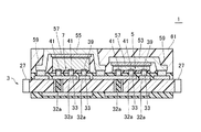
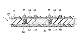
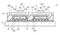
第1実施形態に係る半導体モジュールの構造について図1〜図3を用いて説明する。図1は、第1実施形態に係る半導体モジュール1の平面図である。図2は、図1のA1−A2線に沿った断面図であり、図3は、図1のB1−B2線に沿った断面図である。
[First Embodiment]
(Structure of semiconductor module)
The structure of the semiconductor module according to the first embodiment will be described with reference to FIGS. FIG. 1 is a plan view of a
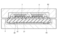
半導体モジュール1は、実装基板(例えばプリント基板)3と、この上に実装された二つのパワーMOSチップ5,7(パワースイッチングデバイスの一例)及び駆動用ICチップ9と、を備える。駆動用ICチップ9は、パワーMOSチップ5,7に形成されたMOSFETのゲートを駆動するためのチップである。パワーMOSチップ5及び駆動用ICチップ9は正方形状を有しており、パワーMOSチップ7は長方形状を有している。これにより、正方形状の実装基板3にチップ5,7,9を効率的に配置できる。
The
図4は、パワーMOSチップ5,7の一部の断面図である。チップ5,7は、多数の縦型のMOSFETが並列接続された構造を有する。詳しく説明すると、チップ5,7は、n型のエピタキシャル層11を有するn+型のシリコン基板13を備える。エピタキシャル層11の上層はp型のボディ領域15である。多数のトレンチゲート17がボディ領域15を貫通するように、エピタキシャル層11に形成されている。トレンチゲート17の周囲にはゲート酸化膜19が形成されている。
FIG. 4 is a sectional view of a part of the
ボディ領域15の表面にn+型のソース領域21が形成されている。トレンチゲート17やソース領域21を覆うように層間絶縁膜23が形成されている。層間絶縁膜23には、コンタクトホールが形成されており、このコンタクトホールを介してソース電極24がボディ領域15やソース領域21に接続されている。シリコン基板13がn+型のドレイン領域となる。シリコン基板13の裏面の全面にはドレイン電極43が形成されている。
An n +
図1〜図3に示すように、実装基板3は、正方形状の樹脂板25を有する。樹脂板25の四つの側面には、多数の外部端子27が所定のピッチで設けられている。端子27は半円筒状を有しており、このため実装基板3の縁は外部端子27の箇所で窪んでいる。樹脂板25の両面には、外部端子27と接続された配線29が形成されている。外部端子27及び配線29は、銅箔等の導体から構成される。
As shown in FIGS. 1 to 3, the
樹脂板25の両面には、配線29を覆うようにソルダーレジスト31が形成されている。ソルダーレジスト31は、外部端子27を覆っておらず、また配線29のうち電極32a,32bとなる箇所の上に開口を有する。電極32a,32b上に半田などの接続材33がスクリーン印刷により形成されている。
Solder resists 31 are formed on both surfaces of the
樹脂板25には多数のスルーホールが形成されている。スルーホールの側面には、例えばメッキにより銅等の導体膜35が形成されている。導体膜35により樹脂板25の両面の配線29が電気的に接続されている。導体膜35の内側には、樹脂37が充填されている。電気抵抗を下げるために、樹脂37の替わりに銅等の金属粉を含む樹脂を充填してもよい。
A number of through holes are formed in the
パワーMOSチップ5,7及び駆動用ICチップ9が実装基板3にフリップチップボンディングで実装されている。詳しくは、パワーMOSチップ5,7の表面には、ゲート電極パッド39及びソース電極パッド41が形成され、裏面にドレイン電極43が形成されている。電極パッド39,41は、図4に示すソース電極24の上層に形成されている。電極パッド39,41の上にバンプ電極が形成されることもある。ゲート電極パッド39は、多数のトレンチゲート17と共通接続されている。ソース電極パッド41は、ソース電極24と接続されている。
The
パワーMOSチップ5,7のゲート電極パッド39及びソース電極パッド41並びに駆動用ICチップ9の電極パッド49は、接続材33により実装基板3の電極32aに半田付けされている。チップ5,7,9と実装基板3とのスペースは、アンダーフィル材51で埋められている。
The
パワーMOSチップ5の裏面47(図4)上には、パワーMOSチップ5を覆うように正方形状のヒートシンク部53が配置され、同様に、パワーMOSチップ7の裏面47(図4)上には、パワーMOSチップ7を覆うように長方形状のヒートシンク部55が配置されている。ヒートシンク部53,55は、それぞれが一枚の金属性のヒートシンク板である。
On the back surface 47 (FIG. 4) of the
ヒートシンク部53,55は、側部の一部が端子59として機能する。ヒートシンク部53は、四辺のうちの一辺に端子59が設けられている。これに対して、ヒートシンク部55は、四辺のうちの向かい合う二つの長辺(つまり、長方形状のチップ7の向かい合う二つの長辺側)に端子59が設けられている。ヒートシンク部53,55は、端子59の箇所で折り曲げられて段差が形成され、接続材33により実装基板3の電極32bに半田付けされている。したがって、ヒートシンク部53,55は、電極32bの箇所で実装基板3に固定される共に実装基板3の配線29と電気的に接続される。
In the
ヒートシンク部53は端子59が一つなので、一箇所で固定されていることになる。一方、ヒートシンク部55は端子59が二つなので、二箇所で固定されていることになる。これはヒートシンク部53,55を含む電気回路の要求からである。したがって、電気回路の要求により、例えば、ヒートシンク部53に端子59が二つ形成される場合、ヒートシンク部53は二箇所で実装基板3に固定される。なお、ヒートシンク部が一箇所で固定される場合、ヒートシンク部の実装基板に対する平行度を維持できないこともある。この場合の対応策については第2実施形態で説明する。
Since the
ヒートシンク部53,55の端子59以外の平面部は、パワーMOSチップ5,7の裏面と対向しており、ヒートシンクとして機能する。上記平面部において、ヒートシンク部53,55は、パワーMOSチップ5,7の裏面のドレイン電極43に導電性の接続材57により半田付けされている。したがって、ヒートシンク部は、それぞれ、パワーMOSチップのうち対応するパワーMOSチップの裏面のドレイン電極(なお、チップの裏面側にソース電極がある場合はソース電極)と電気的に接続される。
Planar portions other than the
ヒートシンク部53,55は、(1)パワーMOSチップ5,7を覆い、(2)その端子59が電極32bと接続され、(3)ヒートシンク部53,55の高さが同じ(つまり同一面内)である。したがって、ヒートシンク部53,55の段差の大きさは、接続材57の厚み、パワーMOSチップ5,7の厚み、電極パッド39,41の高さ、接続材33の高さ及び電極32a,32bの高さを考慮して決める。
The
また、ヒートシンク部53,55は、ヒートシンクとしての機能及び配線としての機能を有する。よって、その材料は、熱的及び電気的に良好な伝導性を有する銅が用いられる。しかしながら、アルミニウムを用いることもできる。アルミニウムは、銅よりも電気抵抗が高いが、軽量で加工性が良好だからである。また、ヒートシンク部53,55の材料として、鉄系の材料(例えば42Alloy)を使用することもできる。この材料は、パワーMOSチップ5,7の材料と熱膨張係数の値が近いので、ヒートシンク部53,55が熱膨張による疲労を受けにくくすることができる。
Moreover, the
ヒートシンク部53,55として、アルミニウムや鉄系の材料を使用する場合、ヒートシンク部53,55の接続材33と接続される部分(つまり端子59)や接続材57と接続される部分に、金属層(例えば、銅、金、銀、ニッケル)や合金層(例えば、半田、銀ロウ)を、蒸着、溶射メッキ、メッキなどにより形成してもよい。これらの層を形成すれば、接続性を良好にすることができる。
When aluminum or iron-based materials are used as the
なお、ヒートシンク部53,55の材料や厚みは、通常、互いに同じである。しかしながら、パワーMOSチップ5,7の発熱量の違い等の理由で、互いに異ならせてもよい。
In addition, the material and thickness of the
ヒートシンク部53,55の厚みが小さすぎると、ヒートシンク部53,55の温度が急激に上昇するので好ましくない。したがって、ヒートシンク部53,55の厚みの目安は、例えば、100μm以上(さらには200μm以上)あればよい。
If the thickness of the
また、ヒートシンク部53,55は、それぞれ、パワーMOSチップ5,7の裏面を完全に覆うことにより、放熱性を良好にすると共に電気抵抗を小さくしている。しかしながら、ヒートシンク部53,55が、パワーMOSチップ5,7の裏面を完全に覆わず、一部露出していてもよい。
Further, the
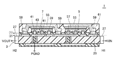
パワーMOSチップ5,7及び駆動用ICチップ9を一つのパッケージとして封止する樹脂部材61が実装基板3の上に固定されている。ヒートシンク部53,55は、それぞれ、対応するパワーMOSチップ5,7の裏面と面する一方の面63及びこれの反対側にある他方の面65を有している。他方の面65が半導体モジュール1の外部に露出している。したがって、全てのヒートシンク部が半導体モジュール1の外部に露出している。
A
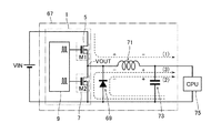
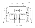
(DC−DCコンバータの回路構成及び動作)
次に、半導体モジュール1を含むDC−DCコンバータの回路構成及び動作について説明する。図5は、このDC−DCコンバータ67の回路図である。DC−DCコンバータ67は、同期整流方式の非絶縁型降圧式である。この回路が最も電力損失を低減し変換効率を高めることができる。
(Circuit configuration and operation of DC-DC converter)
Next, the circuit configuration and operation of the DC-DC converter including the
高電位側のパワーMOSチップ(制御側素子)5及び低電位側のパワーMOSチップ(同期整流側素子)7は、ともにオン抵抗が低く、かつ低ゲート容量のNチャネル型MOSFETが使用されている。パワーMOSチップ7は、VFの低いSBD(ショットキーバリアダイオード)69が並列に接続されている。パワーMOSチップ5,7のゲート端子には、ゲートを駆動するための駆動用ICチップ9が接続されている。
The high potential side power MOS chip (control side element) 5 and the low potential side power MOS chip (synchronous rectification side element) 7 both use N-channel MOSFETs with low on-resistance and low gate capacitance. . The
チップ5,7のゲートは通常時、PWM(Pulse Width Modulation)制御によって駆動されている。PWM制御とは、スイッチング式電源の直流出力電圧を安定化させるための制御方式である。つまり、スイッチング・トランジスタ(パワーMOSチップ5)のON時間とOFF時間の割合を変えて,出力電圧を制御する。出力電圧が低下するとON時間を長くし,上昇すると短くすることによって,常に一定の電圧を保つことができる。なお、チップ5,7のゲートをPFM(Pulse Frequency Modulation)制御によって駆動することもできる。PFM制御とは、スイッチング・トランジスタ(パワーMOSチップ5)のON時間は一定のままで、スイッチング周波数を変えて出力電力を制御する。出力電圧が低下するとスイッチグ周波数を高くし、上昇すると低くすることによって、常に一定の電圧を保つことができる制御である。
The gates of the
DC−DCコンバータ67の出力側には、インダクタ71およびコンデンサ73が接続されている。DC−DCコンバータ67の出力には、例えばCPU75のような負荷が接続される。
An
次に、DC−DCコンバータ67の基本的な動作について、図5及び図6を用いて説明する。図6は、パワーMOSチップ5,7に入力される信号のタイミングチャートである。入力電圧VINが例えば24Vの場合、このコンバータ67により、例えば1.5Vに変換されてCPU75に供給される。
Next, the basic operation of the DC-
まず、時刻t1において、パワーMOSチップ7のMOSFET(M2)がオフの状態でパワーMOSチップ5のMOSFET(M1)をオンさせる。これにより、入力電圧VINによって矢印(1)に示す電流が流れ、インダクタ71を介してCPU75に電力が供給される。つぎに、時刻t2でMOSFET(M1)をオフさせる。これにより、入力電圧VINによるCPU75への電力の供給は停止される。その替わり、インダクタ71に蓄えられた電力によって、矢印(2)に示す電流がSBD69を介して転流することにより、CPU75に電力が供給される。
First, at time t1, the MOSFET (M1) of the
MOSFET(M1)とMOSFET(M2)の貫通防止のために設定された所定のデッドタイムDTが経過したのち、時刻t3において、MOSFET(M2)をオンさせる。MOSFET(M2)はSBD69よりも抵抗が小さいため、インダクタ71に蓄えられた電力により生じる電流は、SBD69でなく、矢印(3)に示すようにMOSFET(M2)を介して転流する。これにより、CPU75に電力が供給される。コンデンサ73は出力電圧波形を平滑化するため使用される。パワーMOSチップ7、つまりMOSFET(M2)がなくても、DC−DCコンバータとして機能する。
After a predetermined dead time DT set for preventing penetration of the MOSFET (M1) and the MOSFET (M2) has elapsed, the MOSFET (M2) is turned on at time t3. Since the resistance of the MOSFET (M2) is smaller than that of the
ここで、MOSFET(M2)を設けた理由を説明する。時刻t2により、SBD69を介して矢印(2)の電流が流れる。SBD69に電流が流れると、それにより電圧降下が生じ、その分だけCPU75に供給される電力にロスが生じる。MOSFETはSBDよりも電圧降下を小さくできる。そこで、デッドタイムDT中は、SBD69を経由させて電流を流し、デッドタイムDT経過後は、MOSFET(M2)を経由させて電流を流すことにより、CPU75に効率良く電力を供給している。
Here, the reason why the MOSFET (M2) is provided will be described. At time t2, the current indicated by the arrow (2) flows through the
(第1実施形態の主な効果)
次に、第1実施形態の主な効果を説明する。第1実施形態によれば、半導体モジュール1を含む半導体装置(例えばDC−DCコンバータ67)の実装スペースの小面積化、配線インピーダンスの低減及び放熱性の向上を図ることができる。以下、詳細に説明する。
(Main effects of the first embodiment)
Next, main effects of the first embodiment will be described. According to the first embodiment, it is possible to reduce the mounting space of the semiconductor device including the semiconductor module 1 (for example, the DC-DC converter 67), reduce the wiring impedance, and improve the heat dissipation. Details will be described below.
従来のDC−DCコンバータは、パワーMOSチップ、駆動用ICチップ、SBD(ショットキーバリアダイオード)等の部品が個別にパッケージされており、パッケージされたこれらの部品がプリント基板に取り付けられている。近年、パソコン等の低電圧化及び大電流化が急激に進んでおり、このような構造のDC−DCコンバータでは、実装スペースの増大、配線インピーダンスの増加、熱の放散が難しくなるといった問題が生じる。 In a conventional DC-DC converter, components such as a power MOS chip, a driving IC chip, and an SBD (Schottky barrier diode) are individually packaged, and these packaged components are attached to a printed circuit board. In recent years, the reduction in voltage and increase in current of personal computers and the like have rapidly progressed. With such a DC-DC converter, problems such as an increase in mounting space, an increase in wiring impedance, and difficulty in heat dissipation arise. .
まず、実装スペースの増大について説明する。現在のDC−DCコンバータで必要な電流容量は、MOSFET単体(一個のパワーMOSチップ)の定格電流を超えることがある。このような場合、複数個のパワーMOSチップを並列接続することにより、上記必要な電流容量を賄っている。したがって、大電流化に対応するためにはパワーMOSチップの数を増やさなければならない。この結果、実装スペースが増えるので、DC−DCコンバータを小型化できない問題が生じる。 First, an increase in mounting space will be described. The current capacity required for the current DC-DC converter may exceed the rated current of a single MOSFET (one power MOS chip). In such a case, the necessary current capacity is covered by connecting a plurality of power MOS chips in parallel. Therefore, the number of power MOS chips must be increased in order to cope with the increase in current. As a result, the mounting space is increased, which causes a problem that the DC-DC converter cannot be reduced in size.
つぎに、配線インピーダンスの増加について説明する。実装スペースが増えることにより実装基板が大面積化すると、必然的に配線長が増えるため抵抗やインダクタンスの増加につながる。抵抗の増加は電圧降下の原因となり、負荷に供給する電圧が不足し誤動作を起こす原因となる。また、インダクタンスの増加は高速化や高周波化を妨げ、さらにリンギングも増加するためこれも誤動作の原因となる。 Next, an increase in wiring impedance will be described. If the mounting board is increased in area by increasing the mounting space, the wiring length will inevitably increase, leading to an increase in resistance and inductance. The increase in resistance causes a voltage drop, and the voltage supplied to the load is insufficient, causing malfunction. Further, an increase in inductance hinders speeding up and high frequency, and ringing also increases, which also causes a malfunction.
最後に熱の放散が難しくなる問題について説明する。CPUのような負荷は、発熱量が多いため負荷自身に大きなヒートシンク部を取り付ける必要がある。したがって、上記負荷の近くでは、パワーMOSチップのヒートシンク部の取り付けスペースを確保することが難しい。パワーMOSチップにヒートシンク部を取り付けない場合、パワーMOSチップの過大な電力損失を避けるためには、パワーMOSチップの個数を増やしてMOSFETの抵抗を下げなければならない。しかし、パワーMOSチップの個数が増えるため、実装スペースの増大や配線インピーダンスの増加という問題が生じる。 Finally, the problem that makes it difficult to dissipate heat will be explained. Since a load such as a CPU generates a large amount of heat, it is necessary to attach a large heat sink to the load itself. Therefore, it is difficult to secure a mounting space for the heat sink portion of the power MOS chip near the load. When the heat sink portion is not attached to the power MOS chip, in order to avoid excessive power loss of the power MOS chip, it is necessary to increase the number of power MOS chips and reduce the resistance of the MOSFET. However, since the number of power MOS chips increases, problems such as an increase in mounting space and an increase in wiring impedance arise.
第1実施形態に係る半導体モジュール1によれば、パワーMOSチップ5,7及び駆動用ICチップ9が一つのパッケージに収容されている、つまり、これらのチップが同一外囲器に搭載されている。このため、DC−DCコンバータ67の実装スペースの小面積化(小型化)を図ることができる。
According to the
また、小型化により実装密度が向上するため、素子間の配線を短くできる。これにより、DC−DCコンバータ67の配線インピーダンスを低減できる。よって、DC−DCコンバータ67の高速化および高周波化が可能となる。
Further, since the mounting density is improved by downsizing, the wiring between elements can be shortened. Thereby, the wiring impedance of the DC-
さらに、ヒートシンク部53,55により、パワーMOSチップ5,7から発生した熱を効率的に放散できる。特に、ヒートシンク部53,55の他方の面65が半導体モジュール1の外部に露出しているため、放熱性をさらに向上させることができる。また、第1実施形態によれば、パワーMOSチップ5,7をフリップチップボンディングにより実装し、パワーMOSチップ5,7の裏面の上にそれぞれヒートシンク部53,55が配置されている。これにより、実装面積を増やすことなくヒートシンク部53,55を配置できると共にパワーMOSチップ5,7がCPUの近くに配置されていても、CPUにヒートシンク部を取り付ける際の障害とならない。さらに、ヒートシンク部53,55が接続材57によりパワーMOSチップ5,7に取り付けられている。接続材57は熱伝導性が優れているので、チップ5,7で発生した熱は速やかに接続材57を介してヒートシンク部53,55に伝わる。この点からも熱を効率的に放散することができる。
Further, the heat generated by the
なお、駆動用ICチップ9にはヒートシンク部が取り付けられていない。つまり、駆動用ICチップ9は、パワーMOSチップ5,7のようにヒートシンク部で覆われていない。しかしながら、駆動用ICチップ9から発生する熱を効率的に放散するために、駆動用ICチップ9の裏面上にヒートシンク部を配置してもよい。
The driving
また、第1実施形態によれば、次の効果も生じる。ヒートシンク部53,55はパワーMOSチップ5,7のドレイン電極43と実装基板3の配線29とを接続する配線としての機能も有する。ヒートシンク部53,55は電流経路の幅が広いため、寄生抵抗や寄生インダクタンスが小さい配線となる。
In addition, according to the first embodiment, the following effects also occur. The
(第1実施形態の変形例)
図7は第1実施形態に係る半導体モジュール1の変形例の平面図であり、図1と対応する。パワーMOSチップ7が低電位側回路を構成し、パワーMOSチップ5が高電位側回路を構成する。パワーMOSチップ7が三つのチップ7−1,7−2,7−3に分割されている。この点で、図7の半導体モジュール1は図1のそれと異なる。ヒートシンク部55のうち、各チップ7−1,7−2,7−3と対応する領域が、各チップのヒートシンク部となる。したがって、この場合、複数のヒートシンク部が互いにつながり、一枚のヒートシンク板(ヒートシンク部55)を構成していると言える。
(Modification of the first embodiment)
FIG. 7 is a plan view of a modification of the
図1のパワーMOSチップ7は、その寸法が比較的大きい。よって、熱膨張量が大きいので、熱応力も大きくなる。そこで、図7の変形例では、パワーMOSチップ7を寸法の比較的小さい三つのチップ7−1,7−2,7−3に分割している。これにより、電流容量を確保しつつ熱応力を低減している。なお、熱応力低減ではなく、半導体モジュール1に大電流を流すために、複数のパワーMOSチップ7−1,7−2,7−3を配置する場合もある。
The
この変形例では、低電位側回路及び高電位側回路のうち、低電位側回路が三つのパワーMOSチップを有する。しかしながら、高電位側回路及び低電位側回路の少なくとも一方が、複数のパワーMOSチップを有すればよい。また、チップの個数も三つに制限されず、二つ以上であればよい。 In this modification, of the low potential side circuit and the high potential side circuit, the low potential side circuit has three power MOS chips. However, at least one of the high potential side circuit and the low potential side circuit only needs to have a plurality of power MOS chips. Further, the number of chips is not limited to three, and may be two or more.
[第2実施形態]
図8は、第2実施形態に係る半導体モジュール1の平面図である。図9は、図8のC1−C2線に沿った断面図である。図8及び図9を用いて、第2実施形態を第1実施形態と相違する点を中心に説明する。
[Second Embodiment]
FIG. 8 is a plan view of the
第2実施形態では、パワーMOSチップ5を覆うヒートシンク部53が、駆動用ICチップ9を覆うように駆動用ICチップ9の上まで延びている。パワーMOSチップ5と駆動用ICチップ9とでヒートシンク部53を共用している。したがって、ヒートシンク部53とは別に駆動用ICチップ9を覆うヒートシンク部を配置した場合に比べて、ヒートシンク部を大面積にでき、その分だけ放熱性を向上させることができる。
In the second embodiment, the
但し、駆動用ICチップ9の裏面77はグランド電位であり、パワーMOSチップ5のドレイン電極43の電位と異なる。したがって、ヒートシンク部53と駆動用ICチップ9との間は樹脂部材61で絶縁されている。つまり、ヒートシンク部53は、駆動用ICチップ9と絶縁されて駆動用ICチップ9の上まで延びている。
However, the
逆の構造、つまり、ヒートシンク部53が駆動用ICチップ9の裏面77と接続材により接続され、ヒートシンク部53とパワーMOSチップ5との間が樹脂部材61で絶縁された構造も可能である。熱は、樹脂よりも導電性の接続材57を介した方がヒートシンク部53に伝導しやすい。パワーMOSチップ5は駆動用ICチップ9よりも発熱量が多い。このため、第2実施形態では、パワーMOSチップ5がヒートシンク部53と接続材57より接続されている。
A reverse structure, that is, a structure in which the
上記接続により、ヒートシンク部53の電位がパワーMOSチップ5のドレイン電位と同じになる。よって、駆動用ICチップ9は、電位が固定されたヒートシンク部53によりシールドされることになる。駆動用ICチップ9の裏面77はグランド電位である。DC−DCコンバータが高周波化すると、高周波によりグランド電位が変動し、駆動用ICチップ9が誤動作する可能性がある。第2実施形態では、駆動用ICチップ9が電位の固定されたヒートシンク部53でシールドされるので、高周波によるグランド電位の変動を防止することが可能となる。
With the above connection, the potential of the
チップ5,9間にはヒートシンク部の端子がないため、チップ5,9間の距離は比較的短い。したがって、チップ5の裏面に接続材57を形成する際、接続材57が広がり、接続材57がチップ9と接触する可能性がある。そこで、第2実施形態では、駆動用ICチップ9を薄く研磨することにより、駆動用ICチップ9の厚み(例えば140μm)をパワーMOSチップ5の厚み(例えば150μm)より小さくしている。これにより、チップ5,9間の平面的な面積を増加させることなく、チップ5,9の裏面どうしを離すことができる。
Since there is no heat sink terminal between the
ところで、第2実施形態では、ヒートシンク部53が駆動用ICチップ9上まで延びているため、ヒートシンク部53は長方形状を有している。図10は、第2実施形態に係るヒートシンク部53の斜視図である。ヒートシンク部53には、一つ端子59が設けられており、一箇所で実装基板3に固定されている。さらに、端子59は、ヒートシンク部53の長辺の一部に形成されている。したがって、ヒートシンク部53の保持が不安定となり、ヒートシンク部53の実装基板3に対する平行度を維持できないことがある。端子をもう一箇所設ければ、平行度を維持することが可能であるが、電気回路上、端子が必要でないこともある。
By the way, in 2nd Embodiment, since the
このような場合、図11に示す第2実施形態に係るヒートシンク部53の変形例によれば、ヒートシンク部53の平行度を維持することができる。ヒートシンク部53は、向かい合う二つの短辺側が折り曲げられることにより、二つの折曲部79が形成されている。折曲部79は、実装基板3のソルダーレジスト31上に載せられる。これにより、一つの端子59を有するヒートシンク部53の平行度を維持することができる。
In such a case, according to the modification of the
[第3実施形態]
第3実施形態では、SBDが内蔵された低電位側のパワーMOSチップを備えたことがこれまでの実施形態と異なる。図12は、第3実施形態に備えられる低電位側のパワーMOSチップ7aの一部の断面図であり、図4のパワーMOSチップ7と対応する。MOSFETの形成領域の終端81から所定の距離を離して、SBD69が形成されている。この所定の距離とは、MOSFETとSBDとが互いに干渉しない距離である。
[Third Embodiment]
The third embodiment is different from the previous embodiments in that a low-potential-side power MOS chip with a built-in SBD is provided. FIG. 12 is a cross-sectional view of a part of the
SBD69は、エピタキシャル層11と、この上に形成されたアルミニウム等からなる金属膜83と、で構成される。エピタキシャル層11と金属膜83とが接触することにより、この接触部分にショットキーバリアが形成される。SBD69は、パワーMOSチップ7のMOSFETと並列接続されている。なお、SBD69の替りにpn接合を有するダイオードを用いることも可能である。
The
第3実施形態のように、SBD69を内蔵したパワーMOSチップ7aを半導体モジュールに使用すれば、SBD69のチップを使用した場合に比べて部品点数を削減出来る。このため、半導体モジュールの組立時間を短縮できると共に半導体モジュールの小型化も可能となる。また、パワーMOSチップ7aとSBD69のチップとを接続する配線が不要となる。よって、この配線のインピーダンスを無くすことができるため、高速性能の良い半導体モジュールが得られる。
If the
[第4実施形態]
図3に示す第1実施形態に係る半導体モジュール1では、ヒートシンク部53,55の二つとも半導体モジュール1の外部に露出させている。ヒートシンク部53,55を半導体モジュール1の外部に露出させた方が放熱効果は上がる。一方、パワーMOSチップ5,7どうしや外部とのショートを防止する必要もある。第4実施形態に係る半導体モジュールは、このショート防止構造を主な特徴としている。
[Fourth Embodiment]
In the
図13〜図16は、第4実施形態に係る半導体モジュールの第1〜第4態様の断面図であり、図3と対応する。図13に示す第1態様の半導体モジュール1では、ヒートシンク部53,55は樹脂部材61で覆われている。つまり、複数のヒートシンク部が全て樹脂部材61で覆われている。これにより、上記ショート防止を達成している。パワーMOSチップ5,7の発熱量が比較的小さければ、ヒートシンク部53,55を樹脂部材61で覆っていても、チップ5,7の動作に問題は生じない。このような場合に、第1態様を用いることができる。なお、図3に示すヒートシンク部53,55の上に樹脂部材61を形成する替わりに、グリス等を被覆してもよい。
13 to 16 are cross-sectional views of the first to fourth aspects of the semiconductor module according to the fourth embodiment, and correspond to FIG. In the
図14に示す第2態様の半導体モジュール1は、図3に示す半導体モジュールのヒートシンク部53,55上に絶縁性のヒートシンク板85が形成された構造を有する。ヒートシンク板85の材料は、例えばセラミックスである。第2態様によれば、第1態様に比べて放熱性を向上させることができる。
The
図15に示す第3態様の半導体モジュール1は、樹脂部材61で覆われたヒートシンク部53と、外部に露出しているヒートシンク部55とを備える。したがって、複数のヒートシンク部のうち、一部のヒートシンク部が半導体モジュールの外部に露出している。パワーMOSチップ7の発熱量が比較的大きいため、ヒートシンク部55を外部に露出させている。ヒートシンク部53は樹脂部材61で覆われているため、パワーMOSチップ5,7どうしのショートを防止できる。
The
第3態様では、ヒートシンク部55を外部に露出させるために、パワーMOSチップ7の厚みをパワーMOSチップ5の厚みよりも大きくしている。これ以外に、実装基板の電極32a、接続材33、電極パッド39,41、接続材57についても同様のことが言える。例えば、パワーMOSチップ7に対応する電極32aの高さを、パワーMOSチップ5に対応する電極32aの高さより大きくするのである。チップの厚み、電極の高さ等を組み合わせてもよいし、いずれか一つでもよい。
In the third aspect, the thickness of the
図16に示す第4態様の半導体モジュール1は、外部に露出しているヒートシンク部53,55を備え、パワーMOSチップ5の裏面上のヒートシンク部53は端子59を有さない。したがって、ヒートシンク部53は配線としての機能を有さない。
The
[第5実施形態]
図17は、第5実施形態に係る半導体モジュール1の平面図である。図18は、図17のD1−D2線に沿った断面図である。図1の半導体モジュール1と異なる点は、ソルダーレジスト31の外縁の位置である。以下、第5実施形態を詳細に説明する。
[Fifth Embodiment]
FIG. 17 is a plan view of the
実装基板3は、これまでの実施形態の実装基板3も同様であり、側面87、チップ5,7,9と対向する対向面89及びこの面89の反対側に位置する反対面91により規定されている。一方、これまでの実施形態と異なり、第5実施形態のソルダーレジスト31は、樹脂部材61の縁部と対向面89とで挟まれると共に樹脂部材61の縁部に沿って樹脂部材61からはみ出して対向面89に形成されている。これにより、モールドの際に樹脂部材61が外部端子27に流れるのを防止している。この効果については、次の第5実施形態に係る半導体モジュール1の組み立て工程でさらに説明する。
The mounting
図19〜図24は、第5実施形態に係る半導体モジュール1の組み立て工程を示す図であり、実装基板3等の断面が表れている。図19に示すように、配線29、電極32a,32b等が形成された状態の実装基板3を用意する。配線29はソルダーレジスト31で覆われ、電極32a,32bは露出している。実装基板3のサイズは、縦横11mmである。
19-24 is a figure which shows the assembly process of the
図20に示すように、電極32a,32b上に接続材33を印刷法により、供給する。接続材33は、はんだであり、具体的には、Sn10Pb90はんだである。はんだ材料には、Sn-Pb系のはんだ材ではなく、Sn-Zn系はんだ、Sn-Bi系はんだなどを使用しても良い。
As shown in FIG. 20, the connecting
次に、図21に示すように、マウンタ(図示せず)を使用して、パワーMOSチップ5,7の電極パッド39,41及び図示しない駆動用ICチップ9の電極パッドを、電極32aと対向させて、チップ5,7,9をマウントする。パワーMOSチップ5の寸法は、縦横2mm、厚さ250μmである。パワーMOSチップ7の寸法は、縦横3mm×5mm、厚さ250μmである。駆動用ICチップ9の寸法は、縦横2mm、厚さ200μmである。
Next, as shown in FIG. 21, using a mounter (not shown), the
上記チップがマウントされた実装基板3をリフロー炉に通して、はんだ接合を行う。リフロー加熱時の温度プロファイルの一例を図25に示す。加熱は、室温から180℃まで60秒で一定速度昇温し、180℃から220℃まで80秒で緩やかに昇温したのち、220℃から320℃まで40秒で一定速度昇温するプロファイルを用いた。
The mounting
はんだ接合をした後、フラックス残渣を除去するため、はんだ接合後の実装基板3を洗浄する。この実装基板3を、例えば、市販のフラックス洗浄液につけ、45kHzの超音波を10分間印加することにより、フラックス残渣は洗浄される。
After the solder bonding, the mounting
次に、図22に示すように、チップ5,7,9と実装基板3とのスペースに、アンダーフィル材51をディスペンサーによって供給する。アンダーフィル材51は毛細管現象により上記スペースに充填される。毛細管現象を発生しやすくするために、アンダーフィル材51中のフィラーの量は少ない。したがって、アンダーフィル材51中のフィラーのパーセンテージは、樹脂部材61のそれよりも低い。アンダーフィル材も樹脂である。よって、樹脂部材61及びアンダーフィル材51からなる樹脂部材は、チップ5,7,9と実装基板3とのスペースに位置する部分が他の部分よりもフィラー含有量が少ないと言うことができる。
Next, as shown in FIG. 22, an
その後、熱処理によりアンダーフィル材51を硬化させる。なお、上記スペースをこの後の樹脂封止にて使用する樹脂で充填でき、この方法でも特性上および信頼性上問題なければ、アンダーフィル材を使用しなくとも良い。
そして、チップ5,7,9の裏面上、電極32b上に、それぞれ、接続材57,33をディスペンス法により供給する。はんだ材には、上記フリップチップ接続で用いた接続材のはんだであるSn10Pb90の融点よりも高い融点を有するSn5Pb95はんだを使用している。はんだ材には、例えばSn-Pb-Ag系のものを使用しても良いが、はんだ材の融点は、フリップチップ接続で用いた接続材よりも高いものを供給する。この理由は、この後の第5実施形態の主な効果の箇所で説明する。
Thereafter, the
Then, connecting
図22の工程後、図23に示すように、多機能マウンタを用いて、ヒートシンク部53,55をマウントする。ヒートシンク部53,55は、厚さ200μmの銅のフレームを使用した。
After the process of FIG. 22, as shown in FIG. 23, the heat sinks 53 and 55 are mounted using a multi-function mounter. The
次に、ヒートシンク部53,55がマウントされた実装基板3をリフロー炉に通して、ヒートシンク部53,55をはんだ接合する。ここでの加熱プロファイルは、前記加熱プロファイルとピーク温度のみが異なり、ピーク温度330℃の条件で加熱する。リフロー後には、フラックス残渣の洗浄を実施する。
Next, the mounting
そして、洗浄後の実装基板3を図24に示すように、モールド金型93に入れて、チップ5,7,9を樹脂封止する、モールド工程を実施する。具体的に説明すると、モールド工程は、180℃に保持されたモールド金型93に上記洗浄後の実装基板3を入れ、樹脂を10秒かけて金型93内部に充填させた後、60秒間金型93内で保持して、樹脂を硬化させる。その後、チップ5,7,9が樹脂封止された実装基板3を金型から取り出す。
Then, as shown in FIG. 24, the mounting
通常、多数の実装基板3が一枚の状態でモールド工程まで実施される。したがって、ダイシング又は金型内抜きにより、実装基板3を個片かする。以上により、半導体モジュールが完成する。
Usually, a large number of mounting
もし、ヒートシンク部53,55の他方の面65(外部に露出する面)に樹脂漏れが発生していた場合、モールド前に、ヒートシンク部53,55の他方の面65の全面にテープを貼った後にモールドを行い、モールド後にテープを剥がすことで樹脂漏れを防止してもよい。
If a resin leak has occurred on the other surface 65 (surface exposed to the outside) of the
第5実施形態の主な効果を説明する。第5実施形態では、モールド金型93の開口部を規定するエッジ95全体がソルダーレジスト31と接触している。つまり、エッジ95と実装基板3の対向面89とでソルダーレジスト31を挟んだ状態にされている。ソルダーレジスト31は比較的柔軟性があるので、エッジ95と対向面89との間に隙間が発生しない。この結果、外部端子27に樹脂が漏れるのを防止することができる。エッジ95とソルダーレジスト31との接触面の幅は例えば100μmである。 また、図24に示すように、第5実施形態では、パワーMOSチップ5,7の裏面のドレイン電極43とヒートシンク部53,55とを電気的に接続する接続材57(第1の接続材の一例)と、パワーMOSチップ5,7の表面のゲート電極パッド39及びソース電極パッド41と実装基板3の電極32aとを電気的に接続する接続材33(第2の接続材)と、を備え、接続材57(第1の接続材の一例)の融点を、接続材33(第2の接続材)の融点よりも高くしている。
The main effects of the fifth embodiment will be described. In the fifth embodiment, the
接続材33,57を同一組成のはんだ材(つまり融点が同じ)にしてもよい。しかし、この場合、接続材57をリフローさせて、パワーMOSチップ5,7のドレイン電極43とヒートシンク部53,55とを接続する際に、溶融した接続材57を凝固させた後、室温まで温度を下げる段階において、接続材33の信頼性に問題(例えば、バンプオープン:接続材33から電極パッド39,41が剥がれること)が発生することがある。これは、接続材33に歪が残ることや、ヒートシンク部53,55の変形に接続材33が追従できないことが原因である。つまり、接続材33と電極パッド39,41との接合面積は小さいので、上記原因により、バンプオープンするのである。
The connecting
第5実施形態では、接続材57の融点が接続材33の融点よりも高いので、溶融した接続材57を凝固させた後、室温まで温度を下げる段階において、接続材33は凝固していない状態である。したがって、接続材33には上記原因が発生しないため、バンプオープンなどを防止できる。この結果、第5実施形態によれば、接続材33の信頼性、ひいては半導体パッケージの信頼性を向上させることができる。
In the fifth embodiment, since the melting point of the connecting
なお、第5実施形態では、接続材33,57の材料としてはんだを用いたが、金属粉含有の樹脂ペーストを用いることもできる。また、一方の接続材をはんだとし、他方の接続材を樹脂ペーストにしてもよい。
In the fifth embodiment, solder is used as the material of the
ところで、本発明には、図26〜図28に示す実施形態も含まれる。これらの図は、図3と対応する。図26の半導体モジュール1において、チップ5,7,9と実装基板3とのスペースに、アンダーフィル材51が設けられておらず、その場所に樹脂部材61が埋め込まれている。
Incidentally, the embodiment shown in FIGS. 26 to 28 is also included in the present invention. These figures correspond to FIG. In the
上記スペースは狭いので、樹脂部材61をモールドする際に上記スペースに樹脂部材61が入り込まないことがあり、樹脂部材61に気泡が発生する。そこで、図3の半導体モジュール1では、モールドの前に上記スペースにアンダーフィル材51を注入することにより、気泡の発生を防止している。
Since the space is narrow, the
モールドにより、チップ5,7,9と実装基板3とのスペースに樹脂部材61が入り込む場合、図26の半導体モジュール1となる。これにより、アンダーフィル材の注入工程を省略することができる。
When the
図27の半導体モジュール1が図3に示す半導体モジュール1と異なる点は、樹脂部材61及びアンダーフィル材51が設けられていないことである。
27 differs from the
樹脂部材61が設けられていないため、パワーMOSチップ5,7、駆動用ICチップ(図示せず)及びヒートシンク部53,55の全体が露出している。また、アンダーフィル材51が設けられていないため、これらのチップと実装基板3との間に隙間が形成されている。
Since the
樹脂部材61及びアンダーフィル材51を設けなくても、半導体モジュールの使用に支障が生じない場合がある。このような場合に図27の半導体モジュール1を用いることができる。例えば、実装基板3がセラミックス基板であると、実装基板3の熱膨張率とチップ5,7のそれとが近くなる。したがって、チップ5,7の発熱により、実装基板3やチップ5,7が膨張しても、接続材33が電極パッド39,41から剥がれることはない。つまり、接続材33の信頼性が低下しない。図27の半導体モジュール1では、樹脂部材61及びアンダーフィル材51を設けていないので、半導体モジュールの製造コストを下げることができる。
Even if the
図28の半導体モジュール1が図27の半導体モジュール1と異なる点は、パワーMOSチップ5,7及び駆動用ICチップ(図示せず)と実装基板3とのスペースに、アンダーフィル材51が埋め込まれていることである。したがって、実装基板の電極32a、接続材33及び電極パッド39,41のみが樹脂封止されている。
The
ゲート電極パッド39やソース電極パッド41の箇所には、チップ5,7の発熱により発生した熱応力が集中する。熱応力が原因で、接続材33が電極パッド39,41から剥がれるのを、アンダーフィル材51により防止することが可能となる。
Thermal stress generated by the heat generated by the
[第6実施形態]
図29は、第6実施形態に係る半導体モジュール1の裏面図である。一方、図30は、第5実施形態に係る半導体モジュール1の裏面図である。裏面は、実装基板3の面のうち、チップ5,7,9と対向する対向面の反対側に位置する反対面91である。
[Sixth Embodiment]
FIG. 29 is a rear view of the
反対面91には、外部端子27から延びた端子板97が形成されている。端子板97は、一つ外部端子27のみと接続されていたり、複数の外部端子27と共通接続されていたりしている。反対面91には、端子板97どうしを接続する配線29が形成されている。配線29や端子板97はソルダーレジスト31で覆われている。図30の第5実施形態に係る半導体モジュール1の配線29に比べて、図29の第6実施形態に係る半導体モジュール1の配線29は幅がかなり広い。図29の配線29は、反対面91のうち、チップ5,7,9と対応する領域をほぼ覆っている。図29の配線29は、段差補正部としての機能も有する。以下、段差補正部について説明する。
A
図31は、モールド金型93に入れられた、樹脂封止前の実装基板3等の断面図であり、図24と対応する。図24では反対面91に段差が形成されていないが、実際には図31に示すように段差99が形成されている。これは、図30に示すように、反対面91上に、配線29や端子板97の形成部と非形成部とがあると、非形成部に位置するソルダーレジスト31と、形成部に位置するソルダーレジスト31とに高さの差が生じるからである。配線29や端子板97の厚みは、例えば、35μmである。したがって、段差99は35μm程度である。
FIG. 31 is a cross-sectional view of the mounting
しかし、このような段差99が生じた状態でモールドすると、モールド金型93内に注入された樹脂の圧力により、モールド金型93内において、図32に示すような実装基板3のたわみが発生する。これにより、バンプオープン等が起こり、半導体モジュールの信頼性が低下する。段差99が18μm程度でも、このような問題が生じる。
However, when molding is performed in a state in which such a
これに対して、図29の第6実施形態に係る半導体モジュール1において、配線29が段差補正部としても機能するので、ソルダーレジスト31に段差が発生するのを防止できる。この結果、モールドの際に上記たわみが発生することはないので、半導体モジュールの信頼性を向上させることができる。
On the other hand, in the
なお、図33に示す第6実施形態の変形例のように、ダミー配線101を段差補正部にしてもよい。ダミー配線101は、配線29と同時に形成されたものであり、配線と同じ厚みである。したがって、ダミー配線101によっても、ソルダーレジスト31に段差が発生するのを防止できる。ダミー配線101は、いずれの配線とも接続されていない。
Note that, as in the modification of the sixth embodiment shown in FIG. 33, the
[第7実施形態]
図34は、第7実施形態に係る半導体モジュールに備えられるパワーMOSチップ5の表面45を示す平面図である。表面45には、一つのゲート電極パッド39と多数のソース電極パッド41が形成されている。ゲート電極パッド39は、図4のトレンチゲート17の引き出し電極である。ソース電極パッド41は、第1の主電極の一例である図4のソース電極24の引き出し電極である。この実施形態では、図4のドレイン電極43が第2の主電極である。
[Seventh Embodiment]
FIG. 34 is a plan view showing the
モールドの際に、熱により、実装基板3は延びる。この延びの影響は、コーナー部に近づくに従い大きくなる。したがって、コーナー部に位置する電極パッドは熱応力でバンプオープンしやすい。通常、ゲート電極パッド39は、表面45のコーナー部に形成される。しかし、ゲート電極パッド39は一つであるため、バンプオープンが発生すると、半導体モジュールが不良品となる。
During molding, the mounting
そこで、第7実施形態では、ゲート電極パッド39の周囲にソース電極パット41を形成している。したがって、ゲート電極パッド39がコーナー部に位置しないので、ゲート電極パッド39の熱応力によるバンプオープンを防止できる。
Therefore, in the seventh embodiment, the
[第8実施形態]
図35は、第8実施形態に係る半導体モジュール1の平面図である。図36は、図35のE1−E2線に沿った断面図であり、図37は、図35のF1−F2線に沿った断面図である。第8実施形態が図8の第2実施形態と主に相違するのは、ヒートシンク部53,55が互いにつながり、一枚のヒートシンク板103を構成していることである。
[Eighth Embodiment]
FIG. 35 is a plan view of the
パワーMOSチップ5(第1のパワーMISチップの一例)の表面には、ドレイン電極パッド105及びゲート電極パッド107が形成され、裏面にはソース電極109が形成されている。一方、パワーMOSチップ7(第2のパワーMISチップの一例)は、パワーMOSチップ5と比較して、ドレインとソースが逆に配置されている。つまり、パワーMOSチップ7の表面には、ソース電極パッド111及びゲート電極パッド113が形成され、裏面にはドレイン電極115が形成されている。
A
第8実施形態に係るパワーMOSチップ5,7のそれぞれの構造を説明する。図38は、パワーMOSチップ5の一部の断面図である。チップ5は、p+型のシリコン基板117及びこの上に形成されたエピタキシャル層であるp−型のベース領域119を備える。シリコン基板117はp+型のソース領域として機能する。シリコン基板117の裏面の全面は、ソース電極109とコンタクトしている。
The structures of the
ベース領域119には、互いに接するn+型のドレイン領域121及びn−型のドリフト領域123が形成されている。ベース領域119には、ドリフト領域123と間隔を設けてn+型のソース領域125が形成されている。ドリフト領域123とソース領域125との間の上にはゲート酸化膜を介してゲート127が形成されている。ゲート127によりベース領域119にチャネルが形成される。このチャネル及びドリフト領域123を介して、ドレイン領域121とソース領域125が導通する。
In the
ソース領域125の隣には、ベース領域119を貫通してシリコン基板117に到達するp+型の導通領域129が形成されている。導通領域129とソース領域125とは、ショート電極131により電気的に接続されている。これにより、ソース領域125とベース領域119とがショートされる。
Next to the
ゲート127及びショート電極131を覆うように層間絶縁膜133が形成されている。層間絶縁膜133上にはドレイン電極135が形成されている。ドレイン電極135は、層間絶縁膜133に形成されたコンタクトホールを介してドレイン領域121とコンタクトしている。
An interlayer insulating
上記構造を有するパワーMOSチップ5は、チップの表面に平行な方向に電流を流す、いわゆる横型である。これに対して、パワーMOSチップ7は、チップの表面に垂直な方向に電流を流す、いわゆる縦型である。図39は、第8実施形態に係るパワーMOSチップ7の一部の断面図である。チップ7は、n+型のシリコン基板137及びこの上に形成されたエピタキシャル層であるn−型のドリフト領域139を備える。シリコン基板137はn+型のドレイン領域として機能する。シリコン基板137の裏面の全面は、ドレイン電極115とコンタクトしている。ドリフト領域139はシリコン基板137の表面に垂直な方向に電流経路を有する。
The
ドリフト領域139には、複数のp型のベース領域141が間隔を設けて形成されている。各ベース領域141には、互いに間を隔ててn+型のソース領域143が形成されている。ベース領域141間の上にはゲート酸化膜を介してゲート145が形成されている。ゲート145によりベース領域141にチャネルが形成される。このチャネルを介して、ソース領域143とドリフト領域139とが導通する。
A plurality of p-
ゲート145を覆うように層間絶縁膜147が形成されている。層間絶縁膜147上にはソース電極149が形成されている。ソース電極149は、層間絶縁膜147に形成されたコンタクトホールを介してソース領域143及びベース領域141とコンタクトしている。
An interlayer insulating
図3に示すように、これまでの実施形態では、パワーMOSチップ5のソース電極パッド41とパワーMOSチップ7のドレイン電極43とが、接続材33、配線29、接続材33、端子59及びヒートシンク部55を介して接続されている。これに対して、第8実施形態によれば、パワーMOSチップ5のソース電極109とパワーMOSチップ7のドレイン電極115がヒートシンク板103を介して接続される。したがって、第8実施形態によれば、電流経路を短くできるため、配線抵抗を小さくできると共に電流経路の寄生インダクタンスを小さくすることができる。よって、第8実施形態に係る半導体モジュールを組み込んだ電子装置(例えば、DC−DCコンバータ)の高効率化を図ることができる。
As shown in FIG. 3, in the embodiments so far, the
[第9実施形態]
図40は、第9実施形態に係る半導体モジュール1の断面図である。実装基板3の断面構造や裏面の構造は省略されている。第9実施形態に係る半導体モジュール1は、図35〜図37に示す第8実施形態に係る半導体モジュール1と同様に、ヒートシンク部53,55は互いにつながり、一枚のヒートシンク板103を構成している。パワーMOSチップ5,7の裏面どうしがヒートシンク板103を介して電気的に接続されている。
[Ninth Embodiment]
FIG. 40 is a cross-sectional view of the
一方、第9実施形態に係るパワーMOSチップ5,7の構造は、第8実施形態に係るそれらの構造と相違する。パワーMOSチップ5はPチャネル型であり、パワーMOSチップ7はNチャネル型である。これらのチップ5,7の表面には、ゲート電極パッド151、ソース電極パッド153、ドレイン電極パッド155が形成されている。チップ5,7には、チップを貫通する接続導電部157が形成されている。ドレイン電極パッド155は、接続導電部157を介してチップ5,7の裏面のドレイン電極159と電気的に接続されている。電極パッド151,153,155は、接続材33により、実装基板3の電極32aと接続されている。なお、電極パッド151,153,155の上にバンプ電極を形成してもよい。この場合、電極パッド151,153,155は、バンプ電極及び接続材33を介して電極32aと接続される。
On the other hand, the structures of the
第9実施形態において、図5に示す半導体モジュール1の出力VOUTは、次の二つの電流経路から引き出すことができる。一つは、ヒートシンク板103、ヒートシンク部の端子及び実装基板3の配線で構成される電流経路である。もう一つは、ヒートシンク板103、接続導電部157、ドレイン電極パッド155、接続材33及び実装基板3の配線で構成される電流経路である。
In the ninth embodiment, the output VOUT of the
ドレイン電極パッド155がパワーMOSチップ5,7の表面に形成されているので、ヒートシンク板103とチップ5,7とを絶縁することもできるし、ヒートシンク板103自体を絶縁体にすることもできる。これらの場合、ユーザが必要に応じて行わなければならないヒートシンク板103の外部からの絶縁施策を省略でき、その上、EMI等を抑制できる。また、このように絶縁すると、パワーMOSチップ5,7を共にNチャネル型にしながら、配線抵抗及びインダクタンスを低減できる。なお、これらの場合、パワーMOSチップ5,7のドレイン電極159は、実装基板3に形成された配線を介して電気的に接続される。
Since the
図41は、第9実施形態に備えられるパワーMOSチップ7の一部の断面図である。このチップ7は、接続導電部及びその付近以外は、図39のパワーMOSチップ7と同様の構造を有する。第9実施形態において、ソース電極153が第1の主電極の一例であり、ドレイン電極159が第2の主電極の一例である。
FIG. 41 is a sectional view of a part of the
パワーMOSチップ7の表面から裏面に到達する貫通孔161が、チップ7に形成されている。貫通孔161の直径は10μm以上である。貫通孔161には、接続導電部157が埋め込まれている。接続導電部157は、貫通孔161に例えばCuをメッキすることにより形成される。貫通孔161の直径が10μm以上なので接続導電部157は比較的太くなる。このため、接続導電部157の抵抗は、接続導電部157の替わりに、ボンディングワイヤ等を用いてドレイン電極を実装基板3の電極に接続した場合の抵抗よりも小さくできる。接続導電部157は、厚さが5μm以上のドレイン電極159とコンタクトしている。厚さが5μm以上なので、(1)n+型のシリコン基板137からドレイン電極159を通り接続導電部157に至る電流経路の抵抗を下げることができ、(2)シリコン層を貫通する貫通孔161を形成する際にストッパとして利用できる。
A through
パワーMOSチップ7の表面側には、接続導電部157を囲むn+型の不純物領域163が形成されている。不純物領域163は、pベース領域141から延びてくる空乏層が接続導電部157に到達するのを防止している。つまり、不純物領域163により、pベース領域141とドレイン電極159との非導通を維持する。この非導通は、貫通孔161の表面に絶縁層を形成することによっても実現できる。この場合、空乏層が貫通孔161の表面の絶縁層にまで到達しても、直ちにpベース領域141とドレイン電極159との間の導通が成立しない。よって、設計上、貫通孔161とpベース領域141との間の距離を減らすことができるため、チップ面積を縮小できる。なお、第9実施形態に係るパワーMOSチップ5は、図41の各部の導電型を逆にした構造を有する。
On the surface side of the
第9実施形態では、ドレイン電極及びソース電極の両方がチップ5,7の表面に引き出されている。よって、ドレイン電極と実装基板3の配線29との距離を短くできるため、この電流経路の配線抵抗を小さくできる。また、実装基板3上において、ソース電極と接続する配線29とドレイン電極と接続する配線との距離を短くできるため、この電流経路の寄生インダクタンスを小さくできる。
In the ninth embodiment, both the drain electrode and the source electrode are drawn out to the surfaces of the
なお、第9実施形態はプレーナ型のMOSFETであるが、トレンチ型のMOSFETでもよい。トレンチ型では、MOSFET自体の抵抗が小さくなるため、半導体モジュール内の回路の抵抗をさらに下げることができる。 The ninth embodiment is a planar MOSFET, but may be a trench MOSFET. In the trench type, since the resistance of the MOSFET itself is reduced, the resistance of the circuit in the semiconductor module can be further reduced.
第9実施形態は、第8実施形態と同様に、電流経路を短くできる。このため、配線抵抗を小さくできると共に電流経路の寄生インダクタンスを小さくすることができる。よって、第9実施形態に係る半導体モジュールを組み込んだ電子装置(例えば、DC−DCコンバータ)の高効率化を図ることができる。 As in the eighth embodiment, the ninth embodiment can shorten the current path. For this reason, the wiring resistance can be reduced and the parasitic inductance of the current path can be reduced. Therefore, high efficiency of an electronic device (for example, a DC-DC converter) incorporating the semiconductor module according to the ninth embodiment can be achieved.
[第10実施形態]
図42は、第10実施形態に係る半導体モジュール1の平面図であり、図43は、図42のG1−G2線に沿った断面図である。第10実施形態は、図8に示す第2実施形態に、さらに、デカップリングコンデンサ165,167,169(以下、コンデンサということもある)が半導体モジュール1に内蔵されている。これらのコンデンサは、半導体モジュール1の電源端子と接地端子との間の配線インダクタンスをキャンセルするために、電源端子と接地端子との間に接続される。
[Tenth embodiment]
42 is a plan view of the
コンデンサ165,167,169は、実装基板3上に配置してもよいが、第10実施形態では、図43に示すように実装基板3の凹部171に、コンデンサ165,167,169の一部を埋め込んだ構造にしている。コンデンサ165,167,169は比較的寸法が大きいので、実装基板3上に配置すると、半導体モジュール1は、コンデンサ165,167,169の箇所で突き出した構造になるからである。また、凹部171にコンデンサ165,167,169を形成することにより、これらの位置を低くできるので、ヒートシンク部53,55をコンデンサ165,167,169上まで延ばすことができる。よって、ヒートシンク部53,55の面積を大きくできるので、放熱性を向上させることができる。
The
次に、コンデンサ165,167,169が接続される電源端子、接地端子について説明する。図44は、第10実施形態に係る半導体モジュール1の回路図である。図45は、第10実施形態に係る半導体モジュール1の外部端子とコンデンサとの関係を示す図である。第10実施形態で、デカップリングコンデンサを共通にせず、三つ設けた理由を説明する。
Next, the power supply terminal and the ground terminal to which the
パワー系のIC回路では、大電流が流れる第1のブロックと、電流が少し又はほとんど流れない第2のブロックとがある。第1及び第2のブロックの接地端子を共通にすると、電流が少し又はほとんど流れない第2のブロックの接地配線に、第1のブロックからの大電流が流れる。よって、これによる電圧降下の影響を第2のブロックが受けることになる。そこで、第1のブロックと第2のブロックとで接地端子を分けることにより、上記影響を防止する。第1のブロックの接地端子はPGND(パワーグランド)端子と称され、第2のブロックの接地端子はSGND(シグナルグランド)と称される。 In a power IC circuit, there are a first block in which a large current flows and a second block in which a little or little current does not flow. When the ground terminals of the first and second blocks are made common, a large current from the first block flows through the ground wiring of the second block where little or almost no current flows. Therefore, the second block is affected by the voltage drop caused by this. Therefore, the influence is prevented by dividing the ground terminal between the first block and the second block. The ground terminal of the first block is referred to as a PGND (power ground) terminal, and the ground terminal of the second block is referred to as an SGND (signal ground).
パワーMOSチップ5,7で構成される回路は第1のブロックに相当し、駆動用ICチップ9は第2のブロックに相当するため、コンデンサを二つ設ける必要がある。しかしながら、駆動用ICチップ9も第1及び第2のブロックに分けることができる。すなわち、駆動用ICチップ9は、パワーMOSチップ5,7のゲートを駆動するゲート駆動部173と、外部からの信号をゲート駆動部173へ伝達する信号伝達部175と、に分けることができる。信号伝達部175は信号伝達の他に、演算機能も有する。ゲート駆動部173には比較的大きな電流が流れ、これに対して、信号伝達部175にはほとんど電流が流れない。そこで、ゲート駆動部173の接地端子と信号伝達部175の接地端子とを分けている。
Since the circuit composed of the
よって、接地端子には、パワーMOSチップ5,7で構成される回路の接地端子であるPGND端子と、ゲート駆動部173の接地端子であるIC−PGND端子と、信号伝達部175の接地端子であるSGND端子と、の三種類がある。パワーMOSチップ5,7で構成される回路の電源端子であるVIN端子とPGND端子との間にコンデンサ165が接続され、ゲート駆動部173の電源端子であるVDD端子とIC−PGND端子との間にコンデンサ169が接続され、信号伝達部175の電源端子であるVDD端子とSGND端子との間にコンデンサ167が接続されている。
Therefore, the ground terminal includes a PGND terminal that is a ground terminal of a circuit composed of the
第10実施形態によれば、半導体モジュール1にデカップリングコンデンサ165,167,169が内蔵されている。したがって、これらのコンデンサが半導体モジュール1に外付けされている場合に比べて、電源端子と接地端子とを接続する配線を短くできるので、配線のインダクタンスを低減することができる。
According to the tenth embodiment, the
[第11実施形態]
図46は、第11実施形態に係る半導体モジュール1の平面図である。図47は、図46のH1−H2線に沿った断面図である。図48は、図46の半導体モジュール1の裏面図である。第11実施形態は、図1に示す第1実施形態において、さらに、電源端子及び接地端子の位置を規定したものである。
[Eleventh embodiment]
FIG. 46 is a plan view of the
実装基板3の第1の側面177に配置された外部端子27の全部が、パワーMOSチップ5,7で構成される回路のVIN端子に割り当てられている。第1の側面177と隣り合う第2の側面179に配置された外部端子27の全部が、上記回路のPGND端子に割り当てられている。実装基板3の第1の側面177と対向する第3の側面181に配置された外部端子27の一部が、図44に示すVOUT端子に割り当てられている。残る最後の第4の側面183に配置された外部端子27が、IC−PGND端子、VDD端子、SGND端子等に割り当てられている。なお、これらの端子については、第10実施形態で説明している。
All of the
第11実施形態では、第10実施形態と異なり、デカップリングコンデンサが半導体モジュール1に外付けされている。例えば、図48に示すように、VIN端子とPGND端子との間にデカップリングコンデンサ165が外付けで接続されている。
In the eleventh embodiment, unlike the tenth embodiment, a decoupling capacitor is externally attached to the
VIN端子は第1の側面177、PGND端子は第2の側面179にそれぞれ配置されている。つまり、これらの端子は、隣り合う二つの側面に配置されている。したがって、デカップリングコンデンサ165が外付けであっても、VIN端子とPGND端子とを接続する配線を短くできるので、配線のインダクタンスを低減することができる。
The VIN terminal is disposed on the
ところで、チップ5,7で構成される回路の電流経路は、図47に示すように、二つある。一つは、VIN端子→VOUT端子の電流経路(1)であり、もう一つは、PGND端子→VOUT端子の電流経路(2)である。
Incidentally, there are two current paths in the circuit constituted by the
VOUT端子を第3の側面181に配置しているので、第4の側面183に配置するのに比べて、電流経路(1)、(2)を短くできる。また、チップ5,7で構成される回路に設けられた三つの端子59が一列に並んでいる。このため、電流経路(1)を短くすることができる。さらに、長方形状のチップ7において、端子59は、向かい合う二つの長辺側が配置されているので、二つの短辺側に配置されるのに比べて、電流経路(1)を短くできる。
Since the VOUT terminal is disposed on the
以上説明したように、第11実施形態では、VIN端子とPGND端子とを接続する配線を短くでき、かつ電流経路を短くできるので、第11実施形態に係る半導体モジュールを組み込んだ電子装置の高効率化を図ることができる。 As described above, in the eleventh embodiment, the wiring connecting the VIN terminal and the PGND terminal can be shortened and the current path can be shortened. Therefore, the high efficiency of the electronic device incorporating the semiconductor module according to the eleventh embodiment can be achieved. Can be achieved.
[第12実施形態]
図49は、第12実施形態に係る半導体モジュール1の平面図である。第12実施形態は、パワーMOSチップ5,7をn個ずつ(チップ5−1〜5−n、チップ7−1〜7−n:nは複数)を備えている。そして、半導体モジュール1により制御する負荷に流れる電流値に応じて、駆動用ICチップ9が駆動するパワーMOSチップ5,7の数を変えるようにしたことを主な特徴とする。
[Twelfth embodiment]
FIG. 49 is a plan view of the
図50は、第12実施形態に係る半導体モジュール1を含むDC−DCコンバータ67の回路図である。図50のDC−DCコンバータ67は、図5のDC−DCコンバータ67に、さらに、負荷となるCPU75の電流を検出する負荷電流検出回路185を備える。半導体モジュール1は、n個のパワーMOSチップ5,7及びこれらのゲートを駆動する駆動用ICチップ9を備える。
FIG. 50 is a circuit diagram of a DC-
駆動用ICチップ9は、高電位側及び低電位側の駆動チップ数決定テーブル187,189、高電位側及び低電位側の駆動チップ数切替回路191,193、並びに高電位側及び低電位側のチップ駆動回路195−1〜195−n、197−1〜197−nを備える。チップ駆動回路は、各チップに対応している。
The driving
負荷電流に応じて駆動するチップ数のデータをこれらのテーブル185,187に記憶させる。このデータは、パワーMOSチップ5,7のオン抵抗、ゲート容量、数等を考慮して予め決めておく。負荷電流検出回路185によって検出した負荷電流の値がテーブル187,189のデータと比較されて、実際に駆動する所定数のチップが決定される。
Data on the number of chips driven according to the load current is stored in these tables 185 and 187. This data is determined in advance in consideration of the ON resistance, gate capacitance, number, etc. of the
この決定に基づいて、駆動チップ数切替回路191,193は、チップ駆動回路195−1〜195−n、197−1〜197−nのうち、所定数のチップ駆動回路を動作させる。これにより、高電位側及び低電位側において、所定数のパワーMOSチップが駆動される。
Based on this determination, the drive chip
第12実施形態の主な効果を説明する。同期整流方式降圧型DC−DCコンバータの損失には、パワーMOSチップのオン抵抗による定常損失と、それ以外の損失(スイッチング損失、ゲートチャージ損失等)とがある。上記DC−DCコンバータの大電流動作における損失は、主に定常損失であり、小電流動作における損失は、主にそれ以外の損失である。したがって、上記DC−DCコンバータの大電流動作では、定常損失を低減させることが効果的であり、一方、小電流動作では、それ以外の損失を低減させることが効果的である。 The main effects of the twelfth embodiment will be described. The loss of the synchronous rectification step-down DC-DC converter includes a steady loss due to the ON resistance of the power MOS chip and other losses (switching loss, gate charge loss, etc.). The loss in the large current operation of the DC-DC converter is mainly a steady loss, and the loss in the small current operation is mainly the other loss. Therefore, it is effective to reduce the steady loss in the large current operation of the DC-DC converter, while it is effective to reduce the other loss in the small current operation.
定常損失の低減は、MOSのオン抵抗を小さくすれば達成できる。それ以外の損失の低減は、ゲート容量を小さくすれば達成できる。パワーMOSチップの面積を大きくすれば、MOSのオン抵抗を小さくできるが、ゲート容量が増える。逆に、パワーMOSチップの面積を小さくすれば、ゲート容量を小さくできるが、MOSのオン抵抗が大きくなる。 The steady loss can be reduced by reducing the on-resistance of the MOS. Other loss reductions can be achieved by reducing the gate capacitance. If the area of the power MOS chip is increased, the on-resistance of the MOS can be reduced, but the gate capacitance increases. Conversely, if the area of the power MOS chip is reduced, the gate capacitance can be reduced, but the on-resistance of the MOS is increased.
したがって、大電流動作ではパワーMOSチップの面積を大きくすればよく、小電流動作ではパワーMOSチップの面積を小さくすればよいことになる。第12実施形態では、負荷に流れる電流値に応じて、駆動するパワーMOSチップ5,7の数を変えることにより、パワーMOSチップ5,7の面積を調節している。すなわち、大電流動作では、駆動するパワーMOSチップ5,7の数を増やし、小電流動作では、数を減らしている。したがって、第12実施形態によれば、大電流動作、小電流動作を問わず、DC−DCコンバータの効率的な動作が可能となる。
Therefore, the area of the power MOS chip may be increased in the large current operation, and the area of the power MOS chip may be decreased in the small current operation. In the twelfth embodiment, the area of the
[第13実施形態]
第13実施形態は、FDA(フルデジタルオーディオ)に適用されるスピーカドライバである。図51は、第13実施形態に係るスピーカドライバ199の回路図である。パワーMOSチップ5,7、駆動用ICチップ9及びLとCからなるローパスフィルタ201のセット203が二つで、一つのチャンネル(スピーカ)に対応する。
[Thirteenth embodiment]
The thirteenth embodiment is a speaker driver applied to FDA (full digital audio). FIG. 51 is a circuit diagram of the
MOS1(チップ5)及びMOS4(チップ7)がオン、MOS2(チップ7)及びMOS3(チップ5)がオフの状態と、MOS1及びMOS4がオフ、MOS2及びMOS3がオンの状態と、を交互に繰り返すことにより、スピーカ205を駆動する。一般に、MOS1、MOS2、MOS3、MOS4は同一特性のチップを使用する。したがって、次に示すように、チップ5とチップ7はサイズが同じで、共に正方形状を有する。
MOS1 (chip 5) and MOS4 (chip 7) are on, MOS2 (chip 7) and MOS3 (chip 5) are off, and MOS1 and MOS4 are off and MOS2 and MOS3 are on alternately. As a result, the
図51のスピーカドライバを構成する半導体モジュールは、次の二つが考えられる。一つは、図52に示すように、一つのセット203を搭載した半導体モジュール1である(ハーフブリッジ構成)。この場合、半導体モジュール1が二つ必要となる。もう一つは、図53に示すように、二つのセット203を搭載した半導体モジュール1である(フルブリッジ構成)。この場合は、半導体モジュール1が一つでスピーカドライバ199を構成する。いずれも、ローパスフィルタ201の図示を省略している。一つのセット203において、駆動用ICチップ9は、パワーMOSチップ5とパワーMOSチップ7と等距離の位置に配置されている。
The following two semiconductor modules are included in the speaker driver shown in FIG. One is a
図46に示す第11実施形態と同様に、VIN端子とPGND端子とを、隣り合わせにすることにより、外付けするデカップリングコンデンサの配線の長さを短くできる。駆動用ICチップ9からパワーMOSチップ5,7のゲートに接続する配線が短くなるように、チップ5,7,9を配置している。
Similar to the eleventh embodiment shown in FIG. 46, the VIN terminal and the PGND terminal are adjacent to each other, whereby the length of the wiring of the external decoupling capacitor can be shortened. The
[実施形態の構成の要約]
以上説明した発明を実施するための最良の形態の構成について要約すると、次のようになる。
(1):例えば第1実施形態と対応
実装基板と、
表面及び裏面を有すると共に前記表面が前記実装基板と面するように前記実装基板にフリップチップボンディングで実装された複数のパワースイッチングデバイスチップと、 前記実装基板にフリップチップボンディングで実装されると共に前記複数のパワースイッチングデバイスチップに形成されたトランジスタのゲートを駆動するための駆動用ICチップと、
前記複数のパワースイッチングデバイスチップの前記裏面上にそれぞれ配置された複数のヒートシンク部と、
前記複数のパワースイッチングデバイスチップ及び前記駆動用ICチップを一つのパッケージとして封止する樹脂部材と、を備える
ことを特徴とする半導体モジュール。
(2):例えば第1実施形態と対応
前記複数のヒートシンク部の少なくとも一つは、複数の箇所で前記実装基板に固定されている
ことを特徴とする(1)に記載の半導体モジュール。
(3):例えば第1実施形態と対応
前記複数のヒートシンク部には、複数の箇所で前記実装基板に固定されているヒートシンク部と、一箇所で前記実装基板に固定されているヒートシンク部とがある
ことを特徴とする(1)に記載の半導体モジュール。
(4):例えば第1実施形態と対応
前記複数のヒートシンク部は、それぞれ、前記実装基板の電極と電気的に接続される端子を有すると共に前記複数のパワースイッチングデバイスチップの前記裏面と電気的に接続されており、
前記複数のヒートシンク部の中に、二箇所で前記実装基板に固定されているヒートシンク部があり、
このヒートシンク部の前記端子は、前記二箇所で前記実装基板の前記電極と電気的に接続されている
ことを特徴とする(1)に記載の半導体モジュール。
(5):例えば第1実施形態と対応
複数のヒートシンク部は、それぞれ、一枚のヒートシンク板であり、
これらのヒートシンク板は互いに厚みが異なる
ことを特徴とする(1)に記載の半導体モジュール。
(6):例えば第1実施形態と対応
複数のヒートシンク部は、それぞれ、一枚のヒートシンク板であり、
これらのヒートシンク板は互いに材料が異なる
ことを特徴とする(1)に記載の半導体モジュール。
(7):例えば第1実施形態と対応
前記複数のヒートシンク部の全てが前記半導体モジュールの外部に露出している
ことを特徴とする(1)に記載の半導体モジュール。
(8):例えば第1実施形態と対応
前記半導体モジュールは、
前記駆動用ICチップで制御される高電位側回路及び低電位側回路を備え、
前記高電位側回路及び前記低電位側回路の少なくとも一方は、前記複数のパワースイッチングデバイスチップを有する
ことを特徴とする(1)に記載の半導体モジュール。
(9):例えば第1実施形態と対応
(1)に記載の前記半導体モジュールを含む、
ことを特徴とするDC−DCコンバータ。
(10):例えば第2実施形態と対応
前記複数のヒートシンク部のうち少なくとも一つが、前記駆動用ICチップと絶縁されて前記駆動用ICチップの上まで延びている
ことを特徴とする(1)に記載の半導体モジュール。
(11):例えば第2実施形態と対応
前記複数のヒートシンク部には、複数の箇所で前記実装基板に固定されているヒートシンク部と、一箇所で前記実装基板に固定されているヒートシンク部とがあり、
後者のヒートシンク部には折曲部が形成されており、この折曲部は前記実装基板のソルダーレジスト上に載せられている
ことを特徴とする(1)に記載の半導体モジュール。
(12):例えば第3実施形態と対応
前記複数のパワースイッチングデバイスチップのうち少なくとも一つのチップに前記トランジスタと並列接続されたダイオードが内蔵されている
ことを特徴とする(1)に記載の半導体モジュール。
(13):例えば第4実施形態と対応
前記複数のヒートシンク部の全てが前記樹脂部材で覆われている
ことを特徴とする(1)に記載の半導体モジュール。
(14):例えば第4実施形態と対応
前記複数のヒートシンク部は、それぞれ、前記複数のパワースイッチングデバイスチップの前記裏面と電気的に接続されると共に一枚のヒートシンク板であり、
前記複数のヒートシンク部を覆うように配置された一枚の絶縁性ヒートシンク板を備える
ことを特徴とする(1)に記載の半導体モジュール。
(15):例えば第4実施形態と対応
前記複数のヒートシンク部のうち、一部のヒートシンク部が前記半導体モジュールの外部に露出している
ことを特徴とする(1)に記載の半導体モジュール。
(16):例えば第4実施形態と対応
前記複数のヒートシンク部には、前記実装基板の電極と電気的に接続される端子を有するものと有さないものとがある
ことを特徴とする(1)に記載の半導体モジュール。
(17):例えば第5実施形態と対応
前記実装基板は、側面、前記複数のパワースイッチングデバイスチップ及び前記駆動用ICチップと対向する対向面及びこの面の反対側に位置する反対面により規定されており、
前記実装基板は、
前記側面に形成された外部端子と、
前記樹脂部材の縁部と前記対向面とで挟まれると共に前記樹脂部材の縁部に沿って前記樹脂部材からはみ出して前記対向面に形成されたソルダーレジストと、を含む
ことを特徴とする(1)に記載の半導体モジュール。
(18):例えば第5実施形態と対応
前記半導体モジュールは、
前記複数のヒートシンク部のそれぞれを、前記複数のパワースイッチングデバイスチップの前記裏面に形成された電極と電気的に接続する第1の接続材と、
前記複数のパワースイッチングデバイスチップの前記表面に形成された電極と前記実装基板の電極とを電気的に接続する第2の接続材と、を備え、
前記第1の接続材の融点は、前記第2の接続材の融点よりも高い
ことを特徴とする(1)に記載の半導体モジュール。
(19):例えば第5実施形態と対応
前記第1及び第2の接続材は、金属粉含有の樹脂ペーストである
ことを特徴とする(18)に記載の半導体モジュール。
(20):例えば第5実施形態と対応
前記第1及び第2の接続材は、はんだである
ことを特徴とする(18)に記載の半導体モジュール。
(21):例えば第5実施形態と対応
前記樹脂部材は、前記複数のパワースイッチングデバイスチップと前記実装基板との間のスペースに位置する部分が他の部分よりもフィラー含有量が少ない
ことを特徴とする(1)に記載の半導体モジュール。
(22):例えば第5実施形態と対応
前記複数のパワースイッチングデバイスチップ及び前記駆動用ICチップとのスペースに前記樹脂部材が埋め込まれている
ことを特徴とする(1)に記載の半導体モジュール。
(23):例えば第6実施形態と対応
前記実装基板は、側面、前記複数のパワースイッチングデバイスチップ及び前記駆動用ICチップと対向する対向面及びこの面の反対側に位置する反対面により規定されており、
前記実装基板は、
前記反対面に形成された配線と、
前記反対面のこれらのチップと対応する領域に形成されると共に前記配線と同じ厚みの段差補正部と、を含む
ことを特徴とする(1)に記載の半導体モジュール。
(24):例えば第6実施形態と対応
前記段差補正部は、前記配線の幅を広げたものである
ことを特徴とする(23)に記載の半導体モジュール。
(25):例えば第6実施形態と対応
前記段差補正部は、ダミー配線である
ことを特徴とする(23)に記載の半導体モジュール。
(26):例えば第7実施形態と対応
複数のパワースイッチングデバイスチップのそれぞれの前記表面には、第1の主電極、この電極の引き出し電極となる複数の電極パッド及び前記ゲートの引き出し電極となるゲート電極パッドが形成され、前記裏面には第2の主電極が形成されており、
前記複数のパワースイッチングデバイスチップの少なくとも一つは、前記ゲート電極パッドの周囲に前記複数の電極パットが形成されている
ことを特徴とする(1)に記載の半導体モジュール。
(27):例えば第8実施形態と対応
前記複数のヒートシンク部は互いにつながり、一枚のヒートシンク板を構成しており、
前記複数のパワースイッチングデバイスチップは、ドレイン電極パッドが形成された前記表面及びソース電極が形成された前記裏面を有する第1のパワーMISチップと、ソース電極パッドが形成された前記表面及びドレイン電極が形成された前記裏面を有する第2のパワーMISチップと、であり、
前記複数のパワースイッチングデバイスチップは、前記裏面同士が前記ヒートシンク板を介して電気的に接続されている
ことを特徴とする(1)に記載の半導体モジュール。
(28):例えば第9実施形態と対応
前記複数のヒートシンク部は互いにつながり、一枚のヒートシンク板を構成しており、
前記複数のパワースイッチングデバイスチップは、前記裏面どうしが前記ヒートシンク板を介して電気的に接続されており、
前記複数のパワースイッチングデバイスチップの少なくとも一つは、前記表面に形成された第1及び第2の主電極と、前記表面から前記裏面に到達する貫通孔に形成されると共に前記第2の主電極と前記裏面とを電気的に接続する接続導電部と、を含む
ことを特徴とする(1)に記載の半導体モジュール。
(29):例えば第10実施形態と対応
前記半導体モジュールは、電源端子及び接地端子を備え、
前記電源端子と前記接地端子との間に接続されたデカップリングコンデンサが前記半導体モジュールに内蔵されている
ことを特徴とする(1)に記載の半導体モジュール。
(30):例えば第10実施形態と対応
前記実装基板は、前記デカップリングコンデンサが配置される凹部を有する
ことを特徴とする(29)に記載の半導体モジュール。
(31):例えば第10実施形態と対応
前記駆動用ICチップは、ゲート駆動部と、外部からの信号を前記ゲート駆動部へ伝達する信号伝達部と、を有しており、
前記電源端子は、前記駆動用ICチップの電源端子であるVDD端子及び前記複数のパワースイッチングデバイスチップで構成される回路の電源端子であるVIN端子であり、
前記接地端子は、前記ゲート駆動部の接地端子であるIC−PGND端子、前記信号伝達部の接地端子であるSGND端子及び前記複数のパワースイッチングデバイスチップで構成される回路の接地端子であるPGND端子であり
前記デカップリングコンデンサは、前記VDD端子と前記IC−PGND端子との間に接続された第1のデカップリングコンデンサ、前記VDD端子と前記SGND端子との間に接続された第2のデカップリングコンデンサ及び前記VIN端子と前記PGND端子との間に接続された第3のデカップリングコンデンサである
ことを特徴とする(29)に記載の半導体モジュール。
(32):例えば第11実施形態と対応
前記半導体モジュールは、前記複数のパワースイッチングデバイスチップで構成される回路の電源端子と接地端子を備え、
前記電源端子は前記実装基板の隣り合う二つの側面の一方に配置され、前記接地端子は他方に配置される
ことを特徴とする(1)に記載の半導体モジュール。
(33):例えば第11実施形態と対応
前記複数のヒートシンク部は、それぞれ、前記実装基板の電極と電気的に接続される端子を有すると共に前記複数のパワースイッチングデバイスチップの前記裏面と電気的に接続されており、
これらの端子は一列に並んでいる
ことを特徴とする(1)に記載の半導体モジュール。
(34):例えば第11実施形態と対応
前記複数のパワースイッチングデバイスチップの少なくとも一つは長方形状を有しており、
前記長方形状のチップに対応するヒートシンク部は、前記実装基板の電極と電気的に接続される端子を有すると共に前記長方形状のチップの前記裏面と電気的に接続されており、
前記長方形状のチップの向かい合う二つの長辺側に前記端子が配置されている
ことを特徴とする(1)に記載の半導体モジュール。
(35):例えば第12実施形態と対応
前記駆動用ICチップは、前記半導体モジュールにより制御する負荷に流れる電流値に応じて、駆動する前記複数のパワースイッチングデバイスチップの数を変える
ことを特徴とする(1)に記載の半導体モジュール。
(36):例えば第13実施形態と対応
(1)に記載の前記半導体モジュールは、
表面及び裏面を有すると共に前記表面が前記実装基板と面するように前記実装基板にフリップチップボンディングで実装された複数の他のパワースイッチングデバイスチップと、
前記実装基板にフリップチップボンディングで実装されると共に前記複数の他のパワースイッチングデバイスチップに形成されたトランジスタのゲートを駆動するための他の駆動用ICチップと、
前記複数の他のパワースイッチングデバイスチップの前記裏面上にそれぞれ配置された複数の他のヒートシンク部と、を備え、
前記樹脂部材は、前記複数の他のパワースイッチングデバイスチップ及び前記他の駆動用ICチップを一つのパッケージとして封止する、前記半導体モジュールを含むスピーカドライバ。
(37):例えば第5実施形態と対応
実装基板と、
表面及び裏面を有すると共に前記表面が前記実装基板と面するように前記実装基板にフリップチップボンディングで実装された複数のパワースイッチングデバイスチップと、 前記実装基板にフリップチップボンディングで実装されると共に前記複数のパワースイッチングデバイスチップに形成されたトランジスタのゲートを駆動するための駆動用ICチップと、
前記複数のパワースイッチングデバイスチップの前記裏面上にそれぞれ配置された複数のヒートシンク部と、を備え、
前記複数のパワースイッチングデバイスチップ及び前記駆動用ICチップの全体が露出されていると共にこれらのチップと前記実装基板との間に隙間が形成されている
ことを特徴とする半導体モジュール。
(38):例えば第5実施形態と対応
実装基板と、
表面及び裏面を有すると共に前記表面が前記実装基板と面するように前記実装基板にフリップチップボンディングで実装された複数のパワースイッチングデバイスチップと、 前記実装基板にフリップチップボンディングで実装されると共に前記複数のパワースイッチングデバイスチップに形成されたトランジスタのゲートを駆動するための駆動用ICチップと、
前記複数のパワースイッチングデバイスチップの前記裏面上にそれぞれ配置された複数のヒートシンク部と、
前記複数のパワースイッチングデバイスチップ及び前記駆動用ICチップと前記実装基板とのスペースに埋め込まれたアンダーフィル材と、を備え、
前記複数のパワースイッチングデバイスチップ及び前記駆動用ICチップの全体が露出されている
ことを特徴とする半導体モジュール。
[Summary of Configuration of Embodiment]
The configuration of the best mode for carrying out the invention described above is summarized as follows.
(1): For example, corresponding to the first embodiment, a mounting board,
A plurality of power switching device chips having a front surface and a back surface and mounted on the mounting substrate by flip chip bonding so that the front surface faces the mounting substrate; and the plurality of power switching device chips mounted on the mounting substrate by flip chip bonding A driving IC chip for driving the gate of the transistor formed in the power switching device chip of
A plurality of heat sink portions respectively disposed on the back surface of the plurality of power switching device chips;
A resin member for sealing the plurality of power switching device chips and the driving IC chip as one package.
A semiconductor module characterized by that.
(2): Corresponding to, for example, the first embodiment At least one of the plurality of heat sink portions is fixed to the mounting substrate at a plurality of locations. The semiconductor module according to (1).
(3): Corresponding to, for example, the first embodiment The plurality of heat sink portions include a heat sink portion fixed to the mounting substrate at a plurality of locations and a heat sink portion fixed to the mounting substrate at one location. The semiconductor module according to (1), wherein the semiconductor module is provided.
(4): Corresponding to, for example, the first embodiment Each of the plurality of heat sink portions has a terminal electrically connected to the electrode of the mounting substrate and is electrically connected to the back surface of the plurality of power switching device chips. Connected,
Among the plurality of heat sink parts, there is a heat sink part fixed to the mounting substrate at two locations,
The semiconductor module according to (1), wherein the terminals of the heat sink portion are electrically connected to the electrodes of the mounting board at the two locations.
(5): Corresponding to, for example, the first embodiment The plurality of heat sink portions are each one heat sink plate,
These heat sink plates have different thicknesses from each other. The semiconductor module according to (1).
(6): Corresponding to, for example, the first embodiment Each of the plurality of heat sink portions is a single heat sink plate,
These heat sink plates are made of different materials from each other. The semiconductor module according to (1).
(7): Corresponding to, for example, the first embodiment. The semiconductor module according to (1), wherein all of the plurality of heat sink portions are exposed to the outside of the semiconductor module.
(8): For example, corresponding to the first embodiment The semiconductor module is
A high potential side circuit and a low potential side circuit controlled by the driving IC chip;
At least one of the high potential side circuit and the low potential side circuit includes the plurality of power switching device chips. The semiconductor module according to (1),
(9): Corresponding to, for example, the first embodiment, including the semiconductor module according to (1),
The DC-DC converter characterized by the above-mentioned.
(10): Corresponding to, for example, the second embodiment At least one of the plurality of heat sink portions is insulated from the driving IC chip and extends to the driving IC chip (1) The semiconductor module described in 1.
(11): For example, corresponding to the second embodiment
The plurality of heat sink portions include a heat sink portion fixed to the mounting substrate at a plurality of locations, and a heat sink portion fixed to the mounting substrate at one location,
The semiconductor module according to (1), wherein a bent portion is formed in the latter heat sink portion, and the bent portion is placed on a solder resist of the mounting substrate.
(12): Corresponding to, for example, the third embodiment At least one of the plurality of power switching device chips includes a diode connected in parallel to the transistor. The semiconductor according to (1) module.
(13): Corresponding to, for example, the fourth embodiment. The semiconductor module according to (1), wherein all of the plurality of heat sink portions are covered with the resin member.
(14): Corresponding to, for example, the fourth embodiment Each of the plurality of heat sink portions is a single heat sink plate that is electrically connected to the back surface of the plurality of power switching device chips.
The semiconductor module according to (1), further comprising a single insulating heat sink plate arranged to cover the plurality of heat sink portions.
(15): Corresponding to, for example, the fourth embodiment Among the plurality of heat sink portions, a part of the heat sink portion is exposed to the outside of the semiconductor module. The semiconductor module according to (1).
(16): Corresponding to, for example, the fourth embodiment The plurality of heat sink portions may or may not have terminals that are electrically connected to the electrodes of the mounting board (1) ) Semiconductor module.
(17): Corresponding to, for example, the fifth embodiment The mounting substrate is defined by a side surface, a facing surface facing the plurality of power switching device chips and the driving IC chip, and a facing surface located on the opposite side of this surface. And
The mounting substrate is
An external terminal formed on the side surface;
A solder resist sandwiched between the edge of the resin member and the facing surface and protruding from the resin member along the edge of the resin member and formed on the facing surface (1) ) Semiconductor module.
(18): For example, corresponding to the fifth embodiment The semiconductor module is
A first connecting member that electrically connects each of the plurality of heat sink portions to an electrode formed on the back surface of the plurality of power switching device chips;
A second connecting member for electrically connecting the electrode formed on the surface of the plurality of power switching device chips and the electrode of the mounting substrate;
The melting point of the first connecting material is higher than the melting point of the second connecting material. The semiconductor module according to (1),
(19): Corresponding to, for example, the fifth embodiment The first and second connecting materials are resin powder containing metal powder. The semiconductor module according to (18),
(20): Corresponding to, for example, the fifth embodiment The semiconductor module according to (18), wherein the first and second connecting members are solders.
(21): Corresponding to, for example, the fifth embodiment The resin member is characterized in that a portion located in a space between the plurality of power switching device chips and the mounting substrate has a smaller filler content than other portions. The semiconductor module according to (1).
(22): Corresponding to, for example, the fifth embodiment. The semiconductor member according to (1), wherein the resin member is embedded in a space between the plurality of power switching device chips and the driving IC chip.
(23): Corresponding to, for example, the sixth embodiment The mounting substrate is defined by a side surface, a plurality of power switching device chips, a facing surface facing the driving IC chip, and a facing surface located on the opposite side of the surface. And
The mounting substrate is
Wiring formed on the opposite surface;
The semiconductor module according to (1), further comprising: a step correction portion formed in a region corresponding to the chips on the opposite surface and having the same thickness as the wiring.
(24): Corresponding to, for example, the sixth embodiment. The step correction unit is obtained by expanding the width of the wiring. The semiconductor module according to (23).
(25): Corresponding to, for example, the sixth embodiment. The step correction unit is a dummy wiring. The semiconductor module according to (23),
(26): Corresponding to, for example, the seventh embodiment The first main electrode, the plurality of electrode pads serving as the lead electrode of this electrode, and the lead electrode of the gate are provided on each surface of the plurality of power switching device chips. A gate electrode pad is formed, and a second main electrode is formed on the back surface;
The semiconductor module according to (1), wherein at least one of the plurality of power switching device chips has the plurality of electrode pads formed around the gate electrode pad.
(27): Corresponding to, for example, the eighth embodiment The plurality of heat sink portions are connected to each other to constitute a single heat sink plate,
The plurality of power switching device chips includes a first power MIS chip having the front surface on which the drain electrode pad is formed and the back surface on which the source electrode is formed, and the front surface and drain electrode on which the source electrode pad is formed. A second power MIS chip having the back surface formed;
The semiconductor module according to (1), wherein the back surfaces of the plurality of power switching device chips are electrically connected to each other through the heat sink plate.
(28): For example, corresponding to the ninth embodiment The plurality of heat sink portions are connected to each other to constitute a single heat sink plate,
The plurality of power switching device chips, the back surfaces are electrically connected via the heat sink plate,
At least one of the plurality of power switching device chips is formed in the first and second main electrodes formed on the front surface and a through hole reaching the back surface from the front surface and the second main electrode. The semiconductor module according to (1), further comprising: a connection conductive portion that electrically connects the back surface and the back surface.
(29): Corresponding to, for example, the tenth embodiment The semiconductor module includes a power supply terminal and a ground terminal,
The semiconductor module according to (1), wherein a decoupling capacitor connected between the power supply terminal and the ground terminal is built in the semiconductor module.
(30): Corresponding to, for example, the tenth embodiment The mounting substrate has a recess in which the decoupling capacitor is disposed. The semiconductor module according to (29).
(31): Corresponding to, for example, the tenth embodiment The driving IC chip includes a gate driving unit and a signal transmission unit that transmits an external signal to the gate driving unit,
The power supply terminal is a VDD terminal that is a power supply terminal of the driving IC chip and a VIN terminal that is a power supply terminal of a circuit constituted by the plurality of power switching device chips.
The ground terminal is an IC-PGND terminal that is a ground terminal of the gate driving unit, an SGND terminal that is a ground terminal of the signal transmission unit, and a PGND terminal that is a ground terminal of a circuit including the plurality of power switching device chips. The decoupling capacitor includes a first decoupling capacitor connected between the VDD terminal and the IC-PGND terminal, and a second decoupling connected between the VDD terminal and the SGND terminal. The semiconductor module according to (29), wherein the semiconductor module is a capacitor and a third decoupling capacitor connected between the VIN terminal and the PGND terminal.
(32): Corresponding to, for example, the eleventh embodiment The semiconductor module includes a power supply terminal and a ground terminal of a circuit configured by the plurality of power switching device chips,
The semiconductor module according to (1), wherein the power supply terminal is disposed on one of two adjacent side surfaces of the mounting substrate, and the ground terminal is disposed on the other.
(33): Corresponding to, for example, the eleventh embodiment Each of the plurality of heat sink portions has a terminal electrically connected to the electrode of the mounting substrate and is electrically connected to the back surface of the plurality of power switching device chips. Connected,
These terminals are arranged in a line. The semiconductor module according to (1), wherein:
(34): Corresponding to, for example, the eleventh embodiment At least one of the plurality of power switching device chips has a rectangular shape,
The heat sink corresponding to the rectangular chip has a terminal electrically connected to the electrode of the mounting substrate and is electrically connected to the back surface of the rectangular chip,
The semiconductor module according to (1), wherein the terminals are arranged on two long sides facing each other of the rectangular chip.
(35): Corresponding to, for example, the twelfth embodiment The driving IC chip is characterized in that the number of the plurality of power switching device chips to be driven is changed according to a current value flowing in a load controlled by the semiconductor module. The semiconductor module according to (1).
(36): Corresponding to, for example, the thirteenth embodiment The semiconductor module according to (1)
A plurality of other power switching device chips that have a front surface and a back surface and are mounted on the mounting substrate by flip chip bonding so that the front surface faces the mounting substrate;
Another driving IC chip for driving a gate of a transistor mounted on the mounting substrate by flip chip bonding and formed on the plurality of other power switching device chips;
A plurality of other heat sink portions respectively disposed on the back surface of the plurality of other power switching device chips,
The resin member is a speaker driver including the semiconductor module, wherein the plurality of other power switching device chips and the other driving IC chips are sealed as one package.
(37): For example, corresponding to the fifth embodiment, a mounting board;
A plurality of power switching device chips having a front surface and a back surface and mounted on the mounting substrate by flip chip bonding so that the front surface faces the mounting substrate; and the plurality of power switching device chips mounted on the mounting substrate by flip chip bonding A driving IC chip for driving the gate of the transistor formed in the power switching device chip of
A plurality of heat sink portions respectively disposed on the back surface of the plurality of power switching device chips,
The plurality of power switching device chips and the whole driving IC chip are exposed and a gap is formed between these chips and the mounting substrate.
A semiconductor module characterized by that.
(38): Corresponding to, for example, the fifth embodiment, mounting board,
A plurality of power switching device chips having a front surface and a back surface and mounted on the mounting substrate by flip chip bonding so that the front surface faces the mounting substrate; and the plurality of power switching device chips mounted on the mounting substrate by flip chip bonding A driving IC chip for driving the gate of the transistor formed in the power switching device chip of
A plurality of heat sink portions respectively disposed on the back surface of the plurality of power switching device chips;
An underfill material embedded in a space between the plurality of power switching device chips and the driving IC chip and the mounting substrate;
The plurality of power switching device chips and the whole driving IC chip are exposed.
A semiconductor module characterized by that.
1・・・半導体モジュール、3・・・実装基板、5,7・・・パワーMOSチップ、9・・・駆動用ICチップ、17・・・トレンチゲート、45・・・パワーMOSチップの表面、47・・・パワーMOSチップの裏面、53,55・・・ヒートシンク部、59・・・端子、61・・・樹脂部材、101・・・ダミー配線(段差補正部の一例)、103・・・ヒートシンク板、157・・・接続導電部
DESCRIPTION OF
Claims (4)
表面及び裏面を有すると共に前記表面が前記実装基板と面するように前記実装基板にフリップチップボンディングで実装された複数のパワースイッチングデバイスチップと、
前記実装基板にフリップチップボンディングで実装されると共に前記複数のパワースイッチングデバイスチップに形成されたトランジスタのゲートを駆動するための駆動用ICチップと、
前記複数のパワースイッチングデバイスチップの前記裏面上にそれぞれ配置された複数のヒートシンク部と、
前記複数のパワースイッチングデバイスチップ及び前記駆動用ICチップを一つのパッケージとして封止する樹脂部材と、
を備え、
前記実装基板は、側面、前記複数のパワースイッチングデバイスチップ及び前記駆動用ICチップと対向する対向面及びこの面の反対側に位置する反対面により規定されており、
前記実装基板は、
前記反対面に形成された配線と、
前記反対面のこれらのチップと対応する領域に形成されると共に前記配線と同じ厚みの段差補正部と、を含む
ことを特徴とする半導体モジュール。 A mounting board;
A plurality of power switching device chips that have a front surface and a back surface and are mounted on the mounting substrate by flip chip bonding so that the front surface faces the mounting substrate;
A driving IC chip mounted on the mounting substrate by flip chip bonding and driving a gate of a transistor formed on the plurality of power switching device chips;
A plurality of heat sink portions respectively disposed on the back surface of the plurality of power switching device chips;
A resin member for sealing the plurality of power switching device chips and the driving IC chip as one package;
Equipped with a,
The mounting substrate is defined by a side surface, a plurality of power switching device chips, a facing surface facing the driving IC chip, and a facing surface located on the opposite side of the surface,
The mounting substrate is
Wiring formed on the opposite surface;
A semiconductor module comprising: a step correction portion formed in a region corresponding to the chips on the opposite surface and having the same thickness as the wiring .
ことを特徴とする請求項1に記載の半導体モジュール。 At least one of the plurality of heat sink portions is fixed to the mounting substrate at a plurality of locations.
The semiconductor module according to claim 1.
これらの端子は一列に並んでいる
ことを特徴とする請求項1又は2に記載の半導体モジュール。 Each of the plurality of heat sink portions has a terminal electrically connected to the electrode of the mounting substrate and is electrically connected to the back surface of the plurality of power switching device chips,
The semiconductor module according to claim 1, wherein these terminals are arranged in a line.
前記複数のパワースイッチングデバイスチップは、前記裏面どうしが前記ヒートシンク板を介して電気的に接続されており、
前記複数のパワースイッチングデバイスチップの少なくとも一つは、前記表面に形成された第1及び第2の主電極と、前記表面から前記裏面に到達する貫通孔に形成されると共に前記第2の主電極と前記裏面とを電気的に接続する接続導電部と、を含む
ことを特徴とする請求項1〜3のいずれか1項に記載の半導体モジュール。 The plurality of heat sink portions are connected to each other to form a single heat sink plate,
The plurality of power switching device chips, the back surfaces are electrically connected via the heat sink plate,
At least one of the plurality of power switching device chips is formed in the first and second main electrodes formed on the front surface and a through hole reaching the back surface from the front surface and the second main electrode. the semiconductor module according to any one of claims 1 to 3, characterized in that it comprises a connection conductive portion for electrically connecting the back surface and.
Priority Applications (4)
| Application Number | Priority Date | Filing Date | Title |
|---|---|---|---|
| JP2004253276A JP4445351B2 (en) | 2004-08-31 | 2004-08-31 | Semiconductor module |
| US11/214,730 US7514783B2 (en) | 2004-08-31 | 2005-08-31 | Semiconductor module |
| US11/778,516 US7633153B2 (en) | 2004-08-31 | 2007-07-16 | Semiconductor module |
| US11/778,493 US20070257376A1 (en) | 2004-08-31 | 2007-07-16 | Semiconductor module |
Applications Claiming Priority (1)
| Application Number | Priority Date | Filing Date | Title |
|---|---|---|---|
| JP2004253276A JP4445351B2 (en) | 2004-08-31 | 2004-08-31 | Semiconductor module |
Publications (2)
| Publication Number | Publication Date |
|---|---|
| JP2006073664A JP2006073664A (en) | 2006-03-16 |
| JP4445351B2 true JP4445351B2 (en) | 2010-04-07 |
Family
ID=36033232
Family Applications (1)
| Application Number | Title | Priority Date | Filing Date |
|---|---|---|---|
| JP2004253276A Expired - Fee Related JP4445351B2 (en) | 2004-08-31 | 2004-08-31 | Semiconductor module |
Country Status (2)
| Country | Link |
|---|---|
| US (3) | US7514783B2 (en) |
| JP (1) | JP4445351B2 (en) |
Families Citing this family (91)
| Publication number | Priority date | Publication date | Assignee | Title |
|---|---|---|---|---|
| JP4445351B2 (en) | 2004-08-31 | 2010-04-07 | 株式会社東芝 | Semiconductor module |
| US7449853B2 (en) * | 2005-09-01 | 2008-11-11 | Gm Global Technology Operations, Inc. | High power, low noise interconnection for an integrated dual wound motor to a dual inverter |
| JP4679309B2 (en) * | 2005-09-06 | 2011-04-27 | 株式会社東芝 | Semiconductor device |
| JP4686318B2 (en) * | 2005-09-28 | 2011-05-25 | ルネサスエレクトロニクス株式会社 | Semiconductor device |
| JP5291864B2 (en) * | 2006-02-21 | 2013-09-18 | ルネサスエレクトロニクス株式会社 | Manufacturing method of semiconductor device for DC / DC converter and semiconductor device for DC / DC converter |
| US7514780B2 (en) * | 2006-03-15 | 2009-04-07 | Hitachi, Ltd. | Power semiconductor device |
| JP4916745B2 (en) * | 2006-03-28 | 2012-04-18 | ルネサスエレクトロニクス株式会社 | Manufacturing method of semiconductor device |
| TWI321350B (en) * | 2006-04-18 | 2010-03-01 | Advanced Semiconductor Eng | Heatsink and heatsink positioning system |
| US7618896B2 (en) * | 2006-04-24 | 2009-11-17 | Fairchild Semiconductor Corporation | Semiconductor die package including multiple dies and a common node structure |
| US7812437B2 (en) * | 2006-05-19 | 2010-10-12 | Fairchild Semiconductor Corporation | Flip chip MLP with folded heat sink |
| TW200812066A (en) * | 2006-05-30 | 2008-03-01 | Renesas Tech Corp | Semiconductor device and power source unit using the same |
| JP5191689B2 (en) * | 2006-05-30 | 2013-05-08 | ルネサスエレクトロニクス株式会社 | Semiconductor device |
| JP2008042077A (en) * | 2006-08-09 | 2008-02-21 | Renesas Technology Corp | Semiconductor device and production method therefor |
| JP5223677B2 (en) * | 2006-11-02 | 2013-06-26 | 日本電気株式会社 | Semiconductor device |
| JP4827808B2 (en) * | 2007-08-15 | 2011-11-30 | パナソニック株式会社 | Semiconductor device |
| US8334787B2 (en) | 2007-10-25 | 2012-12-18 | Trilliant Networks, Inc. | Gas meter having ultra-sensitive magnetic material retrofitted onto meter dial and method for performing meter retrofit |
| WO2009067251A1 (en) * | 2007-11-25 | 2009-05-28 | Trilliant Networks, Inc. | Communication and message route optimization and messaging in a mesh network |
| CA2716727A1 (en) * | 2007-11-25 | 2009-05-28 | Trilliant Networks, Inc. | Application layer authorization token and method |
| WO2009067257A1 (en) | 2007-11-25 | 2009-05-28 | Trilliant Networks, Inc. | Energy use control system and method |
| WO2009067256A2 (en) | 2007-11-25 | 2009-05-28 | Trilliant Networks, Inc. | System and method for power outage and restoration notification in an advanced metering infrastructure network |
| US7799614B2 (en) * | 2007-12-21 | 2010-09-21 | Infineon Technologies Ag | Method of fabricating a power electronic device |
| JP4492695B2 (en) * | 2007-12-24 | 2010-06-30 | 株式会社デンソー | Semiconductor module mounting structure |
| US7800219B2 (en) * | 2008-01-02 | 2010-09-21 | Fairchild Semiconductor Corporation | High-power semiconductor die packages with integrated heat-sink capability and methods of manufacturing the same |
| US7741709B2 (en) * | 2008-01-09 | 2010-06-22 | Inpaq Technology Co., Ltd. | Embedded type multifunctional integrated structure for integrating protection components and method for manufacturing the same |
| US8143729B2 (en) * | 2008-01-25 | 2012-03-27 | International Rectifier Corporation | Autoclave capable chip-scale package |
| JP5224845B2 (en) * | 2008-02-18 | 2013-07-03 | 新光電気工業株式会社 | Semiconductor device manufacturing method and semiconductor device |
| US8319114B2 (en) * | 2008-04-02 | 2012-11-27 | Densel Lambda K.K. | Surface mount power module dual footprint |
| JP5060617B2 (en) * | 2008-04-03 | 2012-10-31 | パイオニア株式会社 | Circuit device driving method and circuit device |
| US7851928B2 (en) * | 2008-06-10 | 2010-12-14 | Texas Instruments Incorporated | Semiconductor device having substrate with differentially plated copper and selective solder |
| WO2010027495A1 (en) | 2008-09-04 | 2010-03-11 | Trilliant Networks, Inc. | A system and method for implementing mesh network communications using a mesh network protocol |
| JP5107839B2 (en) * | 2008-09-10 | 2012-12-26 | ルネサスエレクトロニクス株式会社 | Semiconductor device |
| JP2010092977A (en) * | 2008-10-06 | 2010-04-22 | Panasonic Corp | Semiconductor device, and method of manufacturing the same |
| US8289182B2 (en) | 2008-11-21 | 2012-10-16 | Trilliant Networks, Inc. | Methods and systems for virtual energy management display |
| JP2010129768A (en) * | 2008-11-27 | 2010-06-10 | Toshiba Corp | Semiconductor apparatus |
| WO2010105038A1 (en) | 2009-03-11 | 2010-09-16 | Trilliant Networks, Inc. | Process, device and system for mapping transformers to meters and locating non-technical line losses |
| US20110075392A1 (en) | 2009-09-29 | 2011-03-31 | Astec International Limited | Assemblies and Methods for Directly Connecting Integrated Circuits to Electrically Conductive Sheets |
| JP2011187809A (en) * | 2010-03-10 | 2011-09-22 | Renesas Electronics Corp | Semiconductor device and multilayer wiring board |
| JP5553652B2 (en) * | 2010-03-18 | 2014-07-16 | ルネサスエレクトロニクス株式会社 | Semiconductor substrate and semiconductor device |
| US8582317B2 (en) | 2010-05-26 | 2013-11-12 | Semiconductor Components Industries, Llc | Method for manufacturing a semiconductor component and structure therefor |
| US9084120B2 (en) | 2010-08-27 | 2015-07-14 | Trilliant Networks Inc. | System and method for interference free operation of co-located transceivers |
| WO2012037055A1 (en) | 2010-09-13 | 2012-03-22 | Trilliant Networks | Process for detecting energy theft |
| US8553420B2 (en) | 2010-10-19 | 2013-10-08 | Tessera, Inc. | Enhanced stacked microelectronic assemblies with central contacts and improved thermal characteristics |
| WO2012051704A1 (en) | 2010-10-19 | 2012-04-26 | Electronic Motion Systems Holdings Limited | A power module for converting dc to ac |
| EP2641137A2 (en) | 2010-11-15 | 2013-09-25 | Trilliant Holdings, Inc. | System and method for securely communicating across multiple networks using a single radio |
| US8497574B2 (en) * | 2011-01-03 | 2013-07-30 | International Rectifier Corporation | High power semiconductor package with conductive clips and flip chip driver IC |
| WO2012097204A1 (en) | 2011-01-14 | 2012-07-19 | Trilliant Holdings, Inc. | Process, device and system for volt/var optimization |
| WO2012103072A2 (en) | 2011-01-25 | 2012-08-02 | Trilliant Holdings, Inc. | Aggregated real-time power outages/restoration reporting (rtpor) in a secure mesh network |
| EP3285459B1 (en) | 2011-02-10 | 2022-10-26 | Trilliant Holdings, Inc. | Device and method for coordinating firmware updates |
| WO2012122310A1 (en) | 2011-03-08 | 2012-09-13 | Trilliant Networks, Inc. | System and method for managing load distribution across a power grid |
| US8970028B2 (en) | 2011-12-29 | 2015-03-03 | Invensas Corporation | Embedded heat spreader for package with multiple microelectronic elements and face-down connection |
| US8952516B2 (en) | 2011-04-21 | 2015-02-10 | Tessera, Inc. | Multiple die stacking for two or more die |
| US8304881B1 (en) | 2011-04-21 | 2012-11-06 | Tessera, Inc. | Flip-chip, face-up and face-down wirebond combination package |
| US9013033B2 (en) | 2011-04-21 | 2015-04-21 | Tessera, Inc. | Multiple die face-down stacking for two or more die |
| US8928153B2 (en) | 2011-04-21 | 2015-01-06 | Tessera, Inc. | Flip-chip, face-up and face-down centerbond memory wirebond assemblies |
| US8633576B2 (en) | 2011-04-21 | 2014-01-21 | Tessera, Inc. | Stacked chip-on-board module with edge connector |
| JP5857468B2 (en) * | 2011-06-22 | 2016-02-10 | 株式会社デンソー | Semiconductor device |
| JP5664475B2 (en) * | 2011-06-22 | 2015-02-04 | 株式会社デンソー | Semiconductor device |
| US9001787B1 (en) | 2011-09-20 | 2015-04-07 | Trilliant Networks Inc. | System and method for implementing handover of a hybrid communications module |
| CN102569247A (en) * | 2012-01-17 | 2012-07-11 | 华为终端有限公司 | Integrated module, integrated system board and electronic equipment |
| JP5992695B2 (en) * | 2012-02-29 | 2016-09-14 | スタンレー電気株式会社 | Semiconductor light emitting element array and vehicle lamp |
| US8916968B2 (en) * | 2012-03-27 | 2014-12-23 | Infineon Technologies Ag | Multichip power semiconductor device |
| CN103547117B (en) * | 2012-07-17 | 2016-04-27 | 光宝科技股份有限公司 | Combine the method for heater element and heat sink, pressure-sensitive conjunction and power supply unit |
| US8877560B2 (en) * | 2012-07-17 | 2014-11-04 | Lite-On Technology Corp. | Method for assembling heat generating element and heat dissipating element, pressure sensitive element, and power supplying unit |
| TWI508238B (en) * | 2012-12-17 | 2015-11-11 | Princo Corp | Chip thermal system |
| JP2014187086A (en) * | 2013-03-22 | 2014-10-02 | Toshiba Corp | Semiconductor device |
| US9437516B2 (en) | 2014-01-07 | 2016-09-06 | Infineon Technologies Austria Ag | Chip-embedded packages with backside die connection |
| US9196577B2 (en) * | 2014-01-09 | 2015-11-24 | Infineon Technologies Ag | Semiconductor packaging arrangement |
| US9831150B2 (en) | 2015-03-11 | 2017-11-28 | Toshiba Memory Corporation | Semiconductor device and electronic device |
| CN111315112A (en) * | 2015-06-26 | 2020-06-19 | 台达电子工业股份有限公司 | A package assembly, electronic equipment for chip power supply |
| JP6488938B2 (en) * | 2015-08-04 | 2019-03-27 | 株式会社デンソー | Manufacturing method of electronic device |
| JP2017045820A (en) * | 2015-08-26 | 2017-03-02 | 京セラ株式会社 | Aggregate substrate |
| US10607958B2 (en) * | 2015-08-28 | 2020-03-31 | Texas Instruments Incorporated | Flip chip backside die grounding techniques |
| JP6663927B2 (en) * | 2015-12-04 | 2020-03-13 | ルネサスエレクトロニクス株式会社 | Semiconductor chip, semiconductor device, and electronic device |
| JP2017112241A (en) * | 2015-12-17 | 2017-06-22 | ルネサスエレクトロニクス株式会社 | Semiconductor device |
| JP6261625B2 (en) * | 2016-01-14 | 2018-01-17 | 三菱電機株式会社 | Electronic circuit equipment |
| JP6888269B2 (en) * | 2016-10-07 | 2021-06-16 | 富士電機株式会社 | Gate drive |
| KR102050130B1 (en) * | 2016-11-30 | 2019-11-29 | 매그나칩 반도체 유한회사 | Semiconductor package and a method of manufacturing the same |
| DE102017108172B4 (en) * | 2017-04-18 | 2022-01-13 | Infineon Technologies Austria Ag | SMD package and method for manufacturing an SMD package |
| US10763193B2 (en) * | 2018-10-30 | 2020-09-01 | Hamilton Sundstrand Corporation | Power control modules |
| JP7192523B2 (en) * | 2019-01-23 | 2022-12-20 | 富士通株式会社 | Semiconductor packages and electronic devices |
| TWI698969B (en) * | 2019-08-14 | 2020-07-11 | 朋程科技股份有限公司 | Package structure for power device |
| CN112447614A (en) * | 2019-08-30 | 2021-03-05 | 朋程科技股份有限公司 | Power device packaging structure |
| CN112490202A (en) * | 2019-09-12 | 2021-03-12 | 朋程科技股份有限公司 | Power device packaging structure |
| US10861766B1 (en) * | 2019-09-18 | 2020-12-08 | Delta Electronics, Inc. | Package structures |
| WO2021059525A1 (en) * | 2019-09-27 | 2021-04-01 | 新電元工業株式会社 | Electronic device |
| TWI722633B (en) * | 2019-10-31 | 2021-03-21 | 同欣電子工業股份有限公司 | Chip packaging structure and chip packaging module |
| JP7354885B2 (en) | 2020-03-12 | 2023-10-03 | 富士通株式会社 | Semiconductor device and semiconductor device manufacturing method |
| JP7353233B2 (en) | 2020-05-14 | 2023-09-29 | 三菱電機株式会社 | semiconductor equipment |
| DE102020207401A1 (en) * | 2020-06-16 | 2021-12-16 | Zf Friedrichshafen Ag | Power module for operating an electric vehicle drive with improved heat conduction for control electronics |
| US20230035716A1 (en) * | 2021-07-28 | 2023-02-02 | Texas Instruments Incorporated | High-frequency ceramic packages with modified castellation and metal layer architectures |
| CN117476631B (en) * | 2023-12-26 | 2024-03-22 | 广东仁懋电子有限公司 | Gallium nitride microwave power device |
Family Cites Families (15)
| Publication number | Priority date | Publication date | Assignee | Title |
|---|---|---|---|---|
| US5808874A (en) * | 1996-05-02 | 1998-09-15 | Tessera, Inc. | Microelectronic connections with liquid conductive elements |
| JPH1145976A (en) | 1997-07-28 | 1999-02-16 | Hitachi Ltd | High frequency multi chip module and manufacture thereof |
| US6313521B1 (en) * | 1998-11-04 | 2001-11-06 | Nec Corporation | Semiconductor device and method of manufacturing the same |
| JP2001291823A (en) | 2000-04-05 | 2001-10-19 | Toshiba Digital Media Engineering Corp | Semiconductor device |
| JP3954314B2 (en) * | 2001-01-23 | 2007-08-08 | 株式会社東芝 | Pressure contact type semiconductor device |
| JP2002314029A (en) | 2001-04-09 | 2002-10-25 | Taiyo Yuden Co Ltd | Module electronic parts |
| US6766817B2 (en) | 2001-07-25 | 2004-07-27 | Tubarc Technologies, Llc | Fluid conduction utilizing a reversible unsaturated siphon with tubarc porosity action |
| JP3495727B2 (en) * | 2001-11-07 | 2004-02-09 | 新光電気工業株式会社 | Semiconductor package and manufacturing method thereof |
| JP2004221460A (en) | 2003-01-17 | 2004-08-05 | Matsushita Electric Ind Co Ltd | Semiconductor component, semiconductor device, and method of manufacturing semiconductor device |
| US7154174B2 (en) * | 2003-02-27 | 2006-12-26 | Power-One, Inc. | Power supply packaging system |
| US7015582B2 (en) * | 2003-04-01 | 2006-03-21 | International Business Machines Corporation | Dummy metal fill shapes for improved reliability of hybrid oxide/low-k dielectrics |
| JP4559777B2 (en) * | 2003-06-26 | 2010-10-13 | 株式会社東芝 | Semiconductor device and manufacturing method thereof |
| JP3809168B2 (en) * | 2004-02-03 | 2006-08-16 | 株式会社東芝 | Semiconductor module |
| JP4445351B2 (en) | 2004-08-31 | 2010-04-07 | 株式会社東芝 | Semiconductor module |
| US7250363B2 (en) * | 2005-05-09 | 2007-07-31 | International Business Machines Corporation | Aligned dummy metal fill and hole shapes |
-
2004
- 2004-08-31 JP JP2004253276A patent/JP4445351B2/en not_active Expired - Fee Related
-
2005
- 2005-08-31 US US11/214,730 patent/US7514783B2/en not_active Expired - Fee Related
-
2007
- 2007-07-16 US US11/778,493 patent/US20070257376A1/en not_active Abandoned
- 2007-07-16 US US11/778,516 patent/US7633153B2/en not_active Expired - Fee Related
Also Published As
| Publication number | Publication date |
|---|---|
| US7514783B2 (en) | 2009-04-07 |
| US20070257376A1 (en) | 2007-11-08 |
| JP2006073664A (en) | 2006-03-16 |
| US20070257708A1 (en) | 2007-11-08 |
| US20060055432A1 (en) | 2006-03-16 |
| US7633153B2 (en) | 2009-12-15 |
Similar Documents
| Publication | Publication Date | Title |
|---|---|---|
| JP4445351B2 (en) | Semiconductor module | |
| JP3809168B2 (en) | Semiconductor module | |
| JP4426955B2 (en) | Semiconductor device | |
| JP4565879B2 (en) | Semiconductor device | |
| JP5107839B2 (en) | Semiconductor device | |
| TWI600135B (en) | A semiconductor device for dc/dc converter | |
| CN101378053B (en) | High-side and low-side nmosfets composite package | |
| JP4010792B2 (en) | Semiconductor device | |
| JP2006216940A (en) | Semiconductor device | |
| JP2006073655A (en) | Semiconductor module | |
| JP5315378B2 (en) | Semiconductor device for DC / DC converter | |
| JP2006253734A (en) | Semiconductor device | |
| TW201320262A (en) | Lead frame substrate for manufacturing flip chip device | |
| JP2012235164A (en) | Semiconductor device |
Legal Events
| Date | Code | Title | Description |
|---|---|---|---|
| A621 | Written request for application examination |
Free format text: JAPANESE INTERMEDIATE CODE: A621 Effective date: 20070123 |
|
| A977 | Report on retrieval |
Free format text: JAPANESE INTERMEDIATE CODE: A971007 Effective date: 20081126 |
|
| A131 | Notification of reasons for refusal |
Free format text: JAPANESE INTERMEDIATE CODE: A131 Effective date: 20090929 |
|
| A521 | Request for written amendment filed |
Free format text: JAPANESE INTERMEDIATE CODE: A523 Effective date: 20091125 |
|
| TRDD | Decision of grant or rejection written | ||
| A01 | Written decision to grant a patent or to grant a registration (utility model) |
Free format text: JAPANESE INTERMEDIATE CODE: A01 Effective date: 20091222 |
|
| A01 | Written decision to grant a patent or to grant a registration (utility model) |
Free format text: JAPANESE INTERMEDIATE CODE: A01 |
|
| A61 | First payment of annual fees (during grant procedure) |
Free format text: JAPANESE INTERMEDIATE CODE: A61 Effective date: 20100115 |
|
| FPAY | Renewal fee payment (event date is renewal date of database) |
Free format text: PAYMENT UNTIL: 20130122 Year of fee payment: 3 |
|
| LAPS | Cancellation because of no payment of annual fees |