JP6621708B2 - 半導体装置、半導体装置の製造方法 - Google Patents
半導体装置、半導体装置の製造方法 Download PDFInfo
- Publication number
- JP6621708B2 JP6621708B2 JP2016105603A JP2016105603A JP6621708B2 JP 6621708 B2 JP6621708 B2 JP 6621708B2 JP 2016105603 A JP2016105603 A JP 2016105603A JP 2016105603 A JP2016105603 A JP 2016105603A JP 6621708 B2 JP6621708 B2 JP 6621708B2
- Authority
- JP
- Japan
- Prior art keywords
- wiring
- shield
- layer
- shield body
- sealing resin
- Prior art date
- Legal status (The legal status is an assumption and is not a legal conclusion. Google has not performed a legal analysis and makes no representation as to the accuracy of the status listed.)
- Active
Links
Images


Classifications
-
- H—ELECTRICITY
- H01—ELECTRIC ELEMENTS
- H01L—SEMICONDUCTOR DEVICES NOT COVERED BY CLASS H10
- H01L25/00—Assemblies consisting of a plurality of individual semiconductor or other solid state devices ; Multistep manufacturing processes thereof
- H01L25/03—Assemblies consisting of a plurality of individual semiconductor or other solid state devices ; Multistep manufacturing processes thereof all the devices being of a type provided for in the same subgroup of groups H01L27/00 - H01L33/00, or in a single subclass of H10K, H10N, e.g. assemblies of rectifier diodes
- H01L25/04—Assemblies consisting of a plurality of individual semiconductor or other solid state devices ; Multistep manufacturing processes thereof all the devices being of a type provided for in the same subgroup of groups H01L27/00 - H01L33/00, or in a single subclass of H10K, H10N, e.g. assemblies of rectifier diodes the devices not having separate containers
- H01L25/065—Assemblies consisting of a plurality of individual semiconductor or other solid state devices ; Multistep manufacturing processes thereof all the devices being of a type provided for in the same subgroup of groups H01L27/00 - H01L33/00, or in a single subclass of H10K, H10N, e.g. assemblies of rectifier diodes the devices not having separate containers the devices being of a type provided for in group H01L27/00
- H01L25/0655—Assemblies consisting of a plurality of individual semiconductor or other solid state devices ; Multistep manufacturing processes thereof all the devices being of a type provided for in the same subgroup of groups H01L27/00 - H01L33/00, or in a single subclass of H10K, H10N, e.g. assemblies of rectifier diodes the devices not having separate containers the devices being of a type provided for in group H01L27/00 the devices being arranged next to each other
-
- H—ELECTRICITY
- H01—ELECTRIC ELEMENTS
- H01L—SEMICONDUCTOR DEVICES NOT COVERED BY CLASS H10
- H01L23/00—Details of semiconductor or other solid state devices
- H01L23/52—Arrangements for conducting electric current within the device in operation from one component to another, i.e. interconnections, e.g. wires, lead frames
- H01L23/522—Arrangements for conducting electric current within the device in operation from one component to another, i.e. interconnections, e.g. wires, lead frames including external interconnections consisting of a multilayer structure of conductive and insulating layers inseparably formed on the semiconductor body
- H01L23/5222—Capacitive arrangements or effects of, or between wiring layers
- H01L23/5225—Shielding layers formed together with wiring layers
-
- H—ELECTRICITY
- H01—ELECTRIC ELEMENTS
- H01L—SEMICONDUCTOR DEVICES NOT COVERED BY CLASS H10
- H01L23/00—Details of semiconductor or other solid state devices
- H01L23/52—Arrangements for conducting electric current within the device in operation from one component to another, i.e. interconnections, e.g. wires, lead frames
- H01L23/538—Arrangements for conducting electric current within the device in operation from one component to another, i.e. interconnections, e.g. wires, lead frames the interconnection structure between a plurality of semiconductor chips being formed on, or in, insulating substrates
- H01L23/5383—Multilayer substrates
-
- H—ELECTRICITY
- H01—ELECTRIC ELEMENTS
- H01L—SEMICONDUCTOR DEVICES NOT COVERED BY CLASS H10
- H01L23/00—Details of semiconductor or other solid state devices
- H01L23/552—Protection against radiation, e.g. light or electromagnetic waves
-
- H—ELECTRICITY
- H01—ELECTRIC ELEMENTS
- H01L—SEMICONDUCTOR DEVICES NOT COVERED BY CLASS H10
- H01L24/00—Arrangements for connecting or disconnecting semiconductor or solid-state bodies; Methods or apparatus related thereto
- H01L24/01—Means for bonding being attached to, or being formed on, the surface to be connected, e.g. chip-to-package, die-attach, "first-level" interconnects; Manufacturing methods related thereto
- H01L24/02—Bonding areas ; Manufacturing methods related thereto
-
- H—ELECTRICITY
- H01—ELECTRIC ELEMENTS
- H01L—SEMICONDUCTOR DEVICES NOT COVERED BY CLASS H10
- H01L24/00—Arrangements for connecting or disconnecting semiconductor or solid-state bodies; Methods or apparatus related thereto
- H01L24/01—Means for bonding being attached to, or being formed on, the surface to be connected, e.g. chip-to-package, die-attach, "first-level" interconnects; Manufacturing methods related thereto
- H01L24/18—High density interconnect [HDI] connectors; Manufacturing methods related thereto
- H01L24/19—Manufacturing methods of high density interconnect preforms
-
- H—ELECTRICITY
- H01—ELECTRIC ELEMENTS
- H01L—SEMICONDUCTOR DEVICES NOT COVERED BY CLASS H10
- H01L24/00—Arrangements for connecting or disconnecting semiconductor or solid-state bodies; Methods or apparatus related thereto
- H01L24/93—Batch processes
- H01L24/95—Batch processes at chip-level, i.e. with connecting carried out on a plurality of singulated devices, i.e. on diced chips
- H01L24/96—Batch processes at chip-level, i.e. with connecting carried out on a plurality of singulated devices, i.e. on diced chips the devices being encapsulated in a common layer, e.g. neo-wafer or pseudo-wafer, said common layer being separable into individual assemblies after connecting
-
- H—ELECTRICITY
- H01—ELECTRIC ELEMENTS
- H01L—SEMICONDUCTOR DEVICES NOT COVERED BY CLASS H10
- H01L25/00—Assemblies consisting of a plurality of individual semiconductor or other solid state devices ; Multistep manufacturing processes thereof
- H01L25/50—Multistep manufacturing processes of assemblies consisting of devices, each device being of a type provided for in group H01L27/00 or H01L29/00
-
- H—ELECTRICITY
- H01—ELECTRIC ELEMENTS
- H01L—SEMICONDUCTOR DEVICES NOT COVERED BY CLASS H10
- H01L21/00—Processes or apparatus adapted for the manufacture or treatment of semiconductor or solid state devices or of parts thereof
- H01L21/02—Manufacture or treatment of semiconductor devices or of parts thereof
- H01L21/04—Manufacture or treatment of semiconductor devices or of parts thereof the devices having at least one potential-jump barrier or surface barrier, e.g. PN junction, depletion layer or carrier concentration layer
- H01L21/50—Assembly of semiconductor devices using processes or apparatus not provided for in a single one of the subgroups H01L21/06 - H01L21/326, e.g. sealing of a cap to a base of a container
- H01L21/56—Encapsulations, e.g. encapsulation layers, coatings
- H01L21/561—Batch processing
-
- H—ELECTRICITY
- H01—ELECTRIC ELEMENTS
- H01L—SEMICONDUCTOR DEVICES NOT COVERED BY CLASS H10
- H01L21/00—Processes or apparatus adapted for the manufacture or treatment of semiconductor or solid state devices or of parts thereof
- H01L21/02—Manufacture or treatment of semiconductor devices or of parts thereof
- H01L21/04—Manufacture or treatment of semiconductor devices or of parts thereof the devices having at least one potential-jump barrier or surface barrier, e.g. PN junction, depletion layer or carrier concentration layer
- H01L21/50—Assembly of semiconductor devices using processes or apparatus not provided for in a single one of the subgroups H01L21/06 - H01L21/326, e.g. sealing of a cap to a base of a container
- H01L21/56—Encapsulations, e.g. encapsulation layers, coatings
- H01L21/568—Temporary substrate used as encapsulation process aid
-
- H—ELECTRICITY
- H01—ELECTRIC ELEMENTS
- H01L—SEMICONDUCTOR DEVICES NOT COVERED BY CLASS H10
- H01L2224/00—Indexing scheme for arrangements for connecting or disconnecting semiconductor or solid-state bodies and methods related thereto as covered by H01L24/00
- H01L2224/01—Means for bonding being attached to, or being formed on, the surface to be connected, e.g. chip-to-package, die-attach, "first-level" interconnects; Manufacturing methods related thereto
- H01L2224/02—Bonding areas; Manufacturing methods related thereto
- H01L2224/023—Redistribution layers [RDL] for bonding areas
- H01L2224/0231—Manufacturing methods of the redistribution layers
- H01L2224/02311—Additive methods
-
- H—ELECTRICITY
- H01—ELECTRIC ELEMENTS
- H01L—SEMICONDUCTOR DEVICES NOT COVERED BY CLASS H10
- H01L2224/00—Indexing scheme for arrangements for connecting or disconnecting semiconductor or solid-state bodies and methods related thereto as covered by H01L24/00
- H01L2224/01—Means for bonding being attached to, or being formed on, the surface to be connected, e.g. chip-to-package, die-attach, "first-level" interconnects; Manufacturing methods related thereto
- H01L2224/02—Bonding areas; Manufacturing methods related thereto
- H01L2224/023—Redistribution layers [RDL] for bonding areas
- H01L2224/0233—Structure of the redistribution layers
- H01L2224/02331—Multilayer structure
-
- H—ELECTRICITY
- H01—ELECTRIC ELEMENTS
- H01L—SEMICONDUCTOR DEVICES NOT COVERED BY CLASS H10
- H01L2224/00—Indexing scheme for arrangements for connecting or disconnecting semiconductor or solid-state bodies and methods related thereto as covered by H01L24/00
- H01L2224/01—Means for bonding being attached to, or being formed on, the surface to be connected, e.g. chip-to-package, die-attach, "first-level" interconnects; Manufacturing methods related thereto
- H01L2224/02—Bonding areas; Manufacturing methods related thereto
- H01L2224/023—Redistribution layers [RDL] for bonding areas
- H01L2224/0237—Disposition of the redistribution layers
- H01L2224/02379—Fan-out arrangement
-
- H—ELECTRICITY
- H01—ELECTRIC ELEMENTS
- H01L—SEMICONDUCTOR DEVICES NOT COVERED BY CLASS H10
- H01L2224/00—Indexing scheme for arrangements for connecting or disconnecting semiconductor or solid-state bodies and methods related thereto as covered by H01L24/00
- H01L2224/01—Means for bonding being attached to, or being formed on, the surface to be connected, e.g. chip-to-package, die-attach, "first-level" interconnects; Manufacturing methods related thereto
- H01L2224/02—Bonding areas; Manufacturing methods related thereto
- H01L2224/023—Redistribution layers [RDL] for bonding areas
- H01L2224/0237—Disposition of the redistribution layers
- H01L2224/02381—Side view
-
- H—ELECTRICITY
- H01—ELECTRIC ELEMENTS
- H01L—SEMICONDUCTOR DEVICES NOT COVERED BY CLASS H10
- H01L2224/00—Indexing scheme for arrangements for connecting or disconnecting semiconductor or solid-state bodies and methods related thereto as covered by H01L24/00
- H01L2224/01—Means for bonding being attached to, or being formed on, the surface to be connected, e.g. chip-to-package, die-attach, "first-level" interconnects; Manufacturing methods related thereto
- H01L2224/02—Bonding areas; Manufacturing methods related thereto
- H01L2224/04—Structure, shape, material or disposition of the bonding areas prior to the connecting process
- H01L2224/04105—Bonding areas formed on an encapsulation of the semiconductor or solid-state body, e.g. bonding areas on chip-scale packages
-
- H—ELECTRICITY
- H01—ELECTRIC ELEMENTS
- H01L—SEMICONDUCTOR DEVICES NOT COVERED BY CLASS H10
- H01L2224/00—Indexing scheme for arrangements for connecting or disconnecting semiconductor or solid-state bodies and methods related thereto as covered by H01L24/00
- H01L2224/01—Means for bonding being attached to, or being formed on, the surface to be connected, e.g. chip-to-package, die-attach, "first-level" interconnects; Manufacturing methods related thereto
- H01L2224/10—Bump connectors; Manufacturing methods related thereto
- H01L2224/12—Structure, shape, material or disposition of the bump connectors prior to the connecting process
- H01L2224/12105—Bump connectors formed on an encapsulation of the semiconductor or solid-state body, e.g. bumps on chip-scale packages
-
- H—ELECTRICITY
- H01—ELECTRIC ELEMENTS
- H01L—SEMICONDUCTOR DEVICES NOT COVERED BY CLASS H10
- H01L2224/00—Indexing scheme for arrangements for connecting or disconnecting semiconductor or solid-state bodies and methods related thereto as covered by H01L24/00
- H01L2224/01—Means for bonding being attached to, or being formed on, the surface to be connected, e.g. chip-to-package, die-attach, "first-level" interconnects; Manufacturing methods related thereto
- H01L2224/18—High density interconnect [HDI] connectors; Manufacturing methods related thereto
- H01L2224/23—Structure, shape, material or disposition of the high density interconnect connectors after the connecting process
- H01L2224/24—Structure, shape, material or disposition of the high density interconnect connectors after the connecting process of an individual high density interconnect connector
- H01L2224/241—Disposition
- H01L2224/24135—Connecting between different semiconductor or solid-state bodies, i.e. chip-to-chip
- H01L2224/24137—Connecting between different semiconductor or solid-state bodies, i.e. chip-to-chip the bodies being arranged next to each other, e.g. on a common substrate
-
- H—ELECTRICITY
- H01—ELECTRIC ELEMENTS
- H01L—SEMICONDUCTOR DEVICES NOT COVERED BY CLASS H10
- H01L2224/00—Indexing scheme for arrangements for connecting or disconnecting semiconductor or solid-state bodies and methods related thereto as covered by H01L24/00
- H01L2224/93—Batch processes
- H01L2224/95—Batch processes at chip-level, i.e. with connecting carried out on a plurality of singulated devices, i.e. on diced chips
- H01L2224/95001—Batch processes at chip-level, i.e. with connecting carried out on a plurality of singulated devices, i.e. on diced chips involving a temporary auxiliary member not forming part of the bonding apparatus, e.g. removable or sacrificial coating, film or substrate
-
- H—ELECTRICITY
- H01—ELECTRIC ELEMENTS
- H01L—SEMICONDUCTOR DEVICES NOT COVERED BY CLASS H10
- H01L23/00—Details of semiconductor or other solid state devices
- H01L23/52—Arrangements for conducting electric current within the device in operation from one component to another, i.e. interconnections, e.g. wires, lead frames
- H01L23/538—Arrangements for conducting electric current within the device in operation from one component to another, i.e. interconnections, e.g. wires, lead frames the interconnection structure between a plurality of semiconductor chips being formed on, or in, insulating substrates
- H01L23/5389—Arrangements for conducting electric current within the device in operation from one component to another, i.e. interconnections, e.g. wires, lead frames the interconnection structure between a plurality of semiconductor chips being formed on, or in, insulating substrates the chips being integrally enclosed by the interconnect and support structures
-
- H—ELECTRICITY
- H01—ELECTRIC ELEMENTS
- H01L—SEMICONDUCTOR DEVICES NOT COVERED BY CLASS H10
- H01L2924/00—Indexing scheme for arrangements or methods for connecting or disconnecting semiconductor or solid-state bodies as covered by H01L24/00
- H01L2924/10—Details of semiconductor or other solid state devices to be connected
- H01L2924/102—Material of the semiconductor or solid state bodies
- H01L2924/1025—Semiconducting materials
- H01L2924/10251—Elemental semiconductors, i.e. Group IV
- H01L2924/10253—Silicon [Si]
-
- H—ELECTRICITY
- H01—ELECTRIC ELEMENTS
- H01L—SEMICONDUCTOR DEVICES NOT COVERED BY CLASS H10
- H01L2924/00—Indexing scheme for arrangements or methods for connecting or disconnecting semiconductor or solid-state bodies as covered by H01L24/00
- H01L2924/10—Details of semiconductor or other solid state devices to be connected
- H01L2924/11—Device type
- H01L2924/14—Integrated circuits
- H01L2924/143—Digital devices
- H01L2924/1432—Central processing unit [CPU]
-
- H—ELECTRICITY
- H01—ELECTRIC ELEMENTS
- H01L—SEMICONDUCTOR DEVICES NOT COVERED BY CLASS H10
- H01L2924/00—Indexing scheme for arrangements or methods for connecting or disconnecting semiconductor or solid-state bodies as covered by H01L24/00
- H01L2924/10—Details of semiconductor or other solid state devices to be connected
- H01L2924/11—Device type
- H01L2924/14—Integrated circuits
- H01L2924/143—Digital devices
- H01L2924/1434—Memory
- H01L2924/1435—Random access memory [RAM]
- H01L2924/1436—Dynamic random-access memory [DRAM]
-
- H—ELECTRICITY
- H01—ELECTRIC ELEMENTS
- H01L—SEMICONDUCTOR DEVICES NOT COVERED BY CLASS H10
- H01L2924/00—Indexing scheme for arrangements or methods for connecting or disconnecting semiconductor or solid-state bodies as covered by H01L24/00
- H01L2924/10—Details of semiconductor or other solid state devices to be connected
- H01L2924/11—Device type
- H01L2924/14—Integrated circuits
- H01L2924/143—Digital devices
- H01L2924/1434—Memory
- H01L2924/1435—Random access memory [RAM]
- H01L2924/1437—Static random-access memory [SRAM]
-
- H—ELECTRICITY
- H01—ELECTRIC ELEMENTS
- H01L—SEMICONDUCTOR DEVICES NOT COVERED BY CLASS H10
- H01L2924/00—Indexing scheme for arrangements or methods for connecting or disconnecting semiconductor or solid-state bodies as covered by H01L24/00
- H01L2924/10—Details of semiconductor or other solid state devices to be connected
- H01L2924/11—Device type
- H01L2924/14—Integrated circuits
- H01L2924/143—Digital devices
- H01L2924/1434—Memory
- H01L2924/1435—Random access memory [RAM]
- H01L2924/1438—Flash memory
-
- H—ELECTRICITY
- H01—ELECTRIC ELEMENTS
- H01L—SEMICONDUCTOR DEVICES NOT COVERED BY CLASS H10
- H01L2924/00—Indexing scheme for arrangements or methods for connecting or disconnecting semiconductor or solid-state bodies as covered by H01L24/00
- H01L2924/30—Technical effects
- H01L2924/301—Electrical effects
- H01L2924/3025—Electromagnetic shielding
Description
なお、添付図面は、便宜上、特徴を分かりやすくするために特徴となる部分を拡大して示している場合があり、各構成要素の寸法比率などが実際又は他の図と異なる場合がある。また、断面図では、各部材の断面構造を分かりやすくするために、一部の部材のハッチングを梨地模様に代えて示し、一部の部材のハッチングを省略している。
以下、一実施形態を図1〜図5に従って説明する。
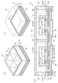
図1(a)は半導体装置1の斜視図であり、図1(b)は半導体装置1の概略断面図である。
配線構造体60は、絶縁層61、配線層62、絶縁層63、配線層64、絶縁層65、配線層66を有している。絶縁層61、配線層62、絶縁層63、配線層64、絶縁層65、配線層66は、この順番で封止樹脂40の下面43から下方に向かってこの順番で積層されている。
半導体装置1は、半導体素子20a,20bを被覆する封止樹脂40の上面41と側面42とが素子シールド体50により被覆されている。半導体装置1の配線構造体60は、上記の配線層62,64,66と、絶縁層61,63,65を有している。配線層62,64,66は、半導体素子20a,20bに接続されている。更に、配線構造体60の絶縁層61,63,65は、枠状の配線シールド体70により被覆され、この配線シールド体70は、素子シールド体50と接続されている。
なお、各図の説明に必要な部材について符号を付し、説明しない部材については符号を省略する場合がある。また、説明の便宜上、最終的に半導体装置の各構成要素となる部分には、最終的な構成要素の符号を付して説明する。
次に、上記の半導体装置1を製造する第1の製造方法を説明する。
図2(a)に示すように、板状の支持体100の上面に、シード層101を形成する。支持体100の材料としては、例えばシリコン、ガラス、金属(例えば、銅)などの剛性の高い板状材料を用いることができる。シード層101の材料としては、例えば銅や銅合金を用いることができる。シード層101は、例えばスパッタ法や無電解めっき法によって形成することができる。
次に、上記の半導体装置1を製造する第2の製造方法を説明する。
なお、各図の説明に必要な部材について符号を付し、説明しない部材については符号を省略する場合がある。
図6(a)に示すように、板状の支持体100の上面に、接着剤30a,30bによって、半導体素子20a,20bを配置する。接着剤30a,30bを、例えば半導体素子20a,20bの下面21a,21bに塗布し、半導体素子20a,20bを支持体100の上面に載置する。半導体素子20a,20bは、電極端子24a,24bが設けられた下面21a,21bを下側にしたフェイスダウン状態にて支持体100の上面に接着される。
図7(a)に示すように、封止樹脂40に、支持体100の上面を露出する開口部40A,40Bを形成する。開口部40A,40Bは、図1に示す素子シールド体50の形状に応じて形成される。詳しくは、素子シールド体50に含まれる第2の素子シールド部52に応じた位置に開口部40Aが形成され、第3の素子シールド部53に応じた位置に開口部40Bが形成される。
(1)半導体装置1は、半導体素子20a,20bを被覆する封止樹脂40の上面41と側面42とが素子シールド体50により被覆されている。半導体装置1の配線構造体60は、上記の配線層62,64,66と、絶縁層61,63,65を有している。配線層62,64,66は、半導体素子20a,20bに接続されている。更に、配線構造体60の絶縁層61,63,65は、枠状の配線シールド体70により被覆され、この配線シールド体70は、素子シールド体50と接続されている。
<変形例>
次に、上記実施形態に対する変形例を説明する。
<変形例1>
図8(b)に示すように、半導体装置1aは、半導体装置1は、複数の半導体素子20a,20b、封止樹脂40、素子シールド体50、配線構造体60a,60b、配線シールド体120、ソルダレジスト層80を有している。
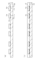
図9に示すように、この半導体装置1bは、柱状に形成された複数の配線シールド体130を有している。この変形例2において、配線構造体60は、半導体装置1bの側面において、部分的に露出している。
図10に示すように、半導体装置1cは、複数の半導体素子20a,20b、封止樹脂40、素子シールド体50、配線構造体60、配線シールド体70、ソルダレジスト層80を有している。半導体素子20a,20bの側面23a,23bが封止樹脂40により覆われている。そして、半導体素子20a,20bの上面22a,22bは、素子シールド体50の第1の素子シールド部51に接続されている。この半導体装置1cでは、半導体素子20a,20bの熱が素子シールド体50に対して直接伝達され、半導体装置1cの外部へと放出される。このように、素子シールド体50は、半導体素子20a,20bの熱を放熱する放熱体として機能する。
・上記実施形態において、第3の素子シールド部53(図1(b)参照)が省略されてもよい。また、複数の第3の素子シールド部53を設けるようにしてもよい。
・上記実施形態と各変形例とを適宜組み合わせて実施してもよい。例えば、図9に示す半導体装置1bにおいて、第2の金属部材132を一実施形態における第2の金属部材72と同様に、絶縁層を囲む枠状に形成してもよい。
20a,20b 半導体素子(電子部品)
40 封止樹脂
50 素子シールド体
51 第1の配線シールド部(第1のシールド部)
52 第2の配線シールド部(第2のシールド部)
53 第3の配線シールド部(第3のシールド部)
60,60a 配線構造体
70,120,130 配線シールド体
80 ソルダレジスト層(保護絶縁層)
Claims (9)
- 下面に電極端子が形成された電子部品と、
前記電子部品の下方にあって、絶縁層と前記電極端子に接続された配線層とを含む配線構造体と、
前記配線構造体に設けられた枠状の配線シールド体と、
前記配線構造体の上面及び前記電子部品の側面を覆う封止樹脂と、
前記封止樹脂の側面を覆うとともに、前記電子部品の上面側を連続的に覆う素子シールド体と、を有し、
前記配線シールド体は前記素子シールド体と接続され、
前記配線シールド体は電磁シールドであり、
前記配線シールド体は、前記配線構造体の積層方向に積層された複数の枠状の金属部材からなり、
前記複数の枠状の金属部材の各々は、前記絶縁層を貫通する第1金属層と、前記配線層と同一層に設けられた第2金属層とを含み、
前記複数の金属部材の少なくとも一部は、前記第1金属層の側面及び前記第2金属層の側面が共に前記配線構造体から外側に露出するように配置され、
前記配線構造体から露出する前記第1金属層の側面及び前記第2金属層の側面は前記素子シールド体の側面と同一平面上に位置していること、を特徴とする半導体装置。 - 下面に電極端子が形成された電子部品と、
前記電子部品の下方にあって、絶縁層と前記電極端子に接続された配線層とを含む配線構造体と、
前記配線構造体に設けられた複数の配線シールド体と、
前記配線構造体の上面及び前記電子部品の側面を覆う封止樹脂と、
前記封止樹脂の側面を覆うとともに、前記電子部品の上面側を連続的に覆う素子シールド体と、を有し、
前記複数の配線シールド体は前記素子シールド体と接続され、
前記複数の配線シールド体は電磁シールドであり、
前記複数の配線シールド体は、前記配線構造体の積層方向に各々貫通する柱状であり、
前記複数の配線シールド体は枠状に配置されており、
前記配線シールド体は、前記配線構造体を積層方向に積層された複数の金属部材からなり、
前記複数の金属部材の各々は、前記絶縁層を貫通する第1金属層と、前記配線層と同一層に設けられた第2金属層とを含み、
前記配線構造体から露出する前記第1金属層の側面及び前記第2金属層の側面は前記素子シールド体の側面と同一平面上に位置していること、を特徴とする半導体装置。 - 前記配線シールド体は、前記配線構造体に向かって凹凸状に形成されたことを特徴とする請求項1又は2に記載の半導体装置。
- 前記素子シールド体は、前記封止樹脂の上面を覆う第1のシールド部と、前記封止樹脂の側面を覆い前記第1のシールド部と接続された第2のシールド部とを有し、
前記配線シールド体は、前記第2のシールド部に接続されたこと、
を特徴とする請求項1〜3のいずれか1項に記載の半導体装置。 - 前記素子シールド体は、前記封止樹脂の上面を覆う第1のシールド部と、前記封止樹脂の側面を覆い前記第1のシールド部と接続された第2のシールド部と、前記封止樹脂に覆われた複数の電子部品のうちの少なくとも1つと他の電子部品と分離する第3のシールド部とを有し、
前記配線シールド体は、前記第2のシールド部の一部に接続された第1の配線シールド部と、前記第3のシールド部に接続された第2の配線シールド部とを含み、前記第1の配線シールド部と前記第2のシールド部とにより枠状に形成されたこと、を特徴とする請求項1に記載の半導体装置。 - 前記配線構造体は、前記電子部品と反対側の面において前記絶縁層及び前記配線シールド体の下面を被覆するとともに前記配線層の下面の一部を外部接続端子として露出する開口部を有する保護絶縁層を含むこと、を特徴とする請求項1〜5のいずれか1項に記載の半導体装置。
- 電子部品を該電子部品の電極端子が設けられた面を支持体に向けて該支持体に配置する工程と、
前記電子部品を覆う封止樹脂を形成する工程と、
前記封止樹脂を覆う素子シールド体を形成する工程と、
前記支持体を除去する工程と、
前記支持体を除去した前記封止樹脂の面に、絶縁層と前記電子部品に接続された配線層とを有する配線構造体と、前記配線構造体の側面に設けられて前記素子シールド体に接続された配線シールド体とを形成する工程と、
を含むことを特徴とする半導体装置の製造方法。 - 支持体の上面に立設されたシールド部を形成する工程と、
前記シールド部の間の前記支持体の上面に、電子部品を該電子部品の電極端子が設けられた面を支持体に向けて該支持体に配置する工程と、
前記電子部品を覆う封止樹脂を形成する工程と、
前記封止樹脂の上面に前記電子部品の上面側を連続的に覆い前記シールド部と接続された金属層を形成し、前記シールド部と前記金属層とからなる素子シールド体を形成する行程と、
前記支持体を除去する工程と、
前記支持体を除去した前記封止樹脂の面に、絶縁層と前記電子部品に接続された配線層とを有する配線構造体と、前記配線構造体の側面に設けられて前記素子シールド体に接続された配線シールド体とを形成する工程と、
を含むことを特徴とする半導体装置の製造方法。 - 前記配線構造体は、絶縁層と配線層とを交互に積層して形成され、
前記配線シールド体は、前記配線層と同時に形成された複数の金属部材により構成されること、
を特徴とする請求項7又は8に記載の半導体装置の製造方法。
Priority Applications (2)
| Application Number | Priority Date | Filing Date | Title |
|---|---|---|---|
| JP2016105603A JP6621708B2 (ja) | 2016-05-26 | 2016-05-26 | 半導体装置、半導体装置の製造方法 |
| US15/587,834 US9991228B2 (en) | 2016-05-26 | 2017-05-05 | Semiconductor device with electromagnetic shield |
Applications Claiming Priority (1)
| Application Number | Priority Date | Filing Date | Title |
|---|---|---|---|
| JP2016105603A JP6621708B2 (ja) | 2016-05-26 | 2016-05-26 | 半導体装置、半導体装置の製造方法 |
Publications (3)
| Publication Number | Publication Date |
|---|---|
| JP2017212377A JP2017212377A (ja) | 2017-11-30 |
| JP2017212377A5 JP2017212377A5 (ja) | 2019-03-07 |
| JP6621708B2 true JP6621708B2 (ja) | 2019-12-18 |
Family
ID=60418232
Family Applications (1)
| Application Number | Title | Priority Date | Filing Date |
|---|---|---|---|
| JP2016105603A Active JP6621708B2 (ja) | 2016-05-26 | 2016-05-26 | 半導体装置、半導体装置の製造方法 |
Country Status (2)
| Country | Link |
|---|---|
| US (1) | US9991228B2 (ja) |
| JP (1) | JP6621708B2 (ja) |
Families Citing this family (18)
| Publication number | Priority date | Publication date | Assignee | Title |
|---|---|---|---|---|
| TWI566339B (zh) * | 2014-11-11 | 2017-01-11 | 矽品精密工業股份有限公司 | 電子封裝件及其製法 |
| CN107424974A (zh) * | 2016-05-24 | 2017-12-01 | 胡迪群 | 具有埋入式噪声屏蔽墙的封装基板 |
| US10804119B2 (en) * | 2017-03-15 | 2020-10-13 | STATS ChipPAC Pte. Ltd. | Method of forming SIP module over film layer |
| US10629542B2 (en) | 2018-04-05 | 2020-04-21 | Samsung Electro-Mechanics Co., Ltd. | Electronic device module |
| KR20190129650A (ko) | 2018-05-10 | 2019-11-20 | 삼성전기주식회사 | 전자 소자 모듈 및 그 제조 방법 |
| US10790238B2 (en) | 2018-05-10 | 2020-09-29 | Samsung Electro-Mechanics Co., Ltd. | Electronic device module and method of manufacturing the same |
| KR102592329B1 (ko) | 2018-06-26 | 2023-10-20 | 삼성전자주식회사 | 반도체 패키지 제조 방법 |
| US10629518B2 (en) | 2018-08-29 | 2020-04-21 | Nxp Usa, Inc. | Internally-shielded microelectronic packages and methods for the fabrication thereof |
| US10755979B2 (en) * | 2018-10-31 | 2020-08-25 | Ningbo Semiconductor International Corporation | Wafer-level packaging methods using a photolithographic bonding material |
| US11071196B2 (en) | 2019-04-05 | 2021-07-20 | Samsung Electro-Mechanics Co., Ltd. | Electronic device module and method of manufacturing electronic device module |
| WO2020250425A1 (ja) * | 2019-06-14 | 2020-12-17 | 株式会社 東芝 | 半導体装置 |
| US11362041B2 (en) * | 2019-12-19 | 2022-06-14 | Amkor Technology Japan, Inc. | Semiconductor devices including shielding layer and methods of manufacturing semiconductor devices |
| JP2021125525A (ja) * | 2020-02-04 | 2021-08-30 | キオクシア株式会社 | 半導体パッケージおよびその製造方法 |
| US11626337B2 (en) * | 2020-05-19 | 2023-04-11 | Amkor Technology Singapore Holding Pte. Ltd. | Semiconductor devices and methods of manufacturing semiconductor devices |
| CN112701089A (zh) * | 2020-09-10 | 2021-04-23 | 成都芯源系统有限公司 | 集成电路封装结构、集成电路封装单元及相关制造方法 |
| CN112908984A (zh) * | 2021-01-18 | 2021-06-04 | 上海先方半导体有限公司 | 一种带有散热片的ssd堆叠封装结构及其制作方法 |
| EP4040483A3 (en) * | 2021-02-04 | 2022-10-26 | Murata Manufacturing Co., Ltd. | Electronic component with internal shielding |
| CN114206090B (zh) * | 2021-11-30 | 2024-04-16 | 四川天邑康和通信股份有限公司 | 一种能够有效解决pon/全光网关发热和屏蔽信号互绕的方法 |
Family Cites Families (18)
| Publication number | Priority date | Publication date | Assignee | Title |
|---|---|---|---|---|
| JP2006100302A (ja) * | 2004-09-28 | 2006-04-13 | Sharp Corp | 高周波モジュールおよびその製造方法 |
| JP4489575B2 (ja) | 2004-12-17 | 2010-06-23 | 新光電気工業株式会社 | 半導体装置及びその製造方法 |
| JP2006294701A (ja) * | 2005-04-06 | 2006-10-26 | Shinko Electric Ind Co Ltd | 半導体装置及びその製造方法 |
| EP1715520B1 (fr) * | 2005-04-21 | 2010-03-03 | St Microelectronics S.A. | Dispositif de protection d'un circuit électronique |
| CN101300911B (zh) * | 2005-11-28 | 2010-10-27 | 株式会社村田制作所 | 电路模块以及制造电路模块的方法 |
| JP4650244B2 (ja) * | 2005-12-02 | 2011-03-16 | 株式会社村田製作所 | 回路モジュールおよびその製造方法 |
| US7626247B2 (en) * | 2005-12-22 | 2009-12-01 | Atmel Corporation | Electronic package with integral electromagnetic radiation shield and methods related thereto |
| WO2008136251A1 (ja) * | 2007-05-02 | 2008-11-13 | Murata Manufacturing Co., Ltd. | 部品内蔵モジュール及びその製造方法 |
| JP2009218484A (ja) * | 2008-03-12 | 2009-09-24 | Tdk Corp | 電子モジュール、および電子モジュールの製造方法 |
| KR101711045B1 (ko) * | 2010-12-02 | 2017-03-02 | 삼성전자 주식회사 | 적층 패키지 구조물 |
| US8835226B2 (en) * | 2011-02-25 | 2014-09-16 | Rf Micro Devices, Inc. | Connection using conductive vias |
| JP5861260B2 (ja) * | 2011-03-10 | 2016-02-16 | 日本電気株式会社 | 半導体装置の製造方法及び半導体装置 |
| KR20120131530A (ko) * | 2011-05-25 | 2012-12-05 | 삼성전자주식회사 | 반도체 장치 및 그 제조 방법 |
| KR20140023112A (ko) * | 2012-08-17 | 2014-02-26 | 삼성전자주식회사 | 반도체 패키지를 포함하는 전자 장치 및 그 제조 방법 |
| JP5767268B2 (ja) * | 2013-04-02 | 2015-08-19 | 太陽誘電株式会社 | 回路モジュール及びその製造方法 |
| WO2015194435A1 (ja) * | 2014-06-20 | 2015-12-23 | 株式会社村田製作所 | 回路モジュール及びその製造方法 |
| US9570406B2 (en) * | 2015-06-01 | 2017-02-14 | Qorvo Us, Inc. | Wafer level fan-out with electromagnetic shielding |
| US10043761B2 (en) * | 2015-10-19 | 2018-08-07 | Taiwan Semiconductor Manufacturing Company Ltd. | Semiconductor device and manufacturing method thereof |
-
2016
- 2016-05-26 JP JP2016105603A patent/JP6621708B2/ja active Active
-
2017
- 2017-05-05 US US15/587,834 patent/US9991228B2/en active Active
Also Published As
| Publication number | Publication date |
|---|---|
| JP2017212377A (ja) | 2017-11-30 |
| US20170345793A1 (en) | 2017-11-30 |
| US9991228B2 (en) | 2018-06-05 |
Similar Documents
| Publication | Publication Date | Title |
|---|---|---|
| JP6621708B2 (ja) | 半導体装置、半導体装置の製造方法 | |
| JP6752553B2 (ja) | 配線基板 | |
| JP5188426B2 (ja) | 半導体装置及びその製造方法、電子装置 | |
| KR101103857B1 (ko) | 인쇄 배선 보드 및 그 제조 방법 | |
| JP6133549B2 (ja) | 配線基板及び配線基板の製造方法 | |
| JP6408540B2 (ja) | 無線モジュール及び無線モジュールの製造方法 | |
| TW201312713A (zh) | 半導體裝置、垂直堆疊有該半導體裝置之半導體模組構造及其製造方法 | |
| JP5372579B2 (ja) | 半導体装置及びその製造方法、並びに電子装置 | |
| TWI694612B (zh) | 半導體模組 | |
| JP2008226945A (ja) | 半導体装置およびその製造方法 | |
| JP2013243345A5 (ja) | ||
| JP5547615B2 (ja) | 配線基板、半導体装置及び配線基板の製造方法 | |
| JP2016207957A (ja) | 配線基板及び配線基板の製造方法 | |
| JP2017212376A (ja) | 半導体装置、半導体装置の製造方法 | |
| JP2016063130A (ja) | プリント配線板および半導体パッケージ | |
| JP2018022824A (ja) | 電子部品内蔵基板及びその製造方法と電子部品装置 | |
| JP6625491B2 (ja) | 配線基板、半導体装置、配線基板の製造方法 | |
| US20180014407A1 (en) | Wiring board | |
| JP2009260165A (ja) | 半導体装置 | |
| KR102235811B1 (ko) | 반도체 장치, 반도체 적층모듈구조, 적층모듈구조 및 이들의 제조방법 | |
| JP2017143096A (ja) | 配線基板、半導体装置及び配線基板の製造方法 | |
| JP2005150344A (ja) | 半導体装置およびその製造方法 | |
| US11153963B2 (en) | Circuit carrier structure and manufacturing method thereof | |
| JP7265877B2 (ja) | 配線基板 | |
| JP5257518B2 (ja) | 基板製造方法および樹脂基板 |
Legal Events
| Date | Code | Title | Description |
|---|---|---|---|
| A521 | Request for written amendment filed |
Free format text: JAPANESE INTERMEDIATE CODE: A523 Effective date: 20190121 |
|
| A621 | Written request for application examination |
Free format text: JAPANESE INTERMEDIATE CODE: A621 Effective date: 20190121 |
|
| A977 | Report on retrieval |
Free format text: JAPANESE INTERMEDIATE CODE: A971007 Effective date: 20190919 |
|
| TRDD | Decision of grant or rejection written | ||
| A01 | Written decision to grant a patent or to grant a registration (utility model) |
Free format text: JAPANESE INTERMEDIATE CODE: A01 Effective date: 20191105 |
|
| A61 | First payment of annual fees (during grant procedure) |
Free format text: JAPANESE INTERMEDIATE CODE: A61 Effective date: 20191120 |
|
| R150 | Certificate of patent or registration of utility model |
Ref document number: 6621708 Country of ref document: JP Free format text: JAPANESE INTERMEDIATE CODE: R150 |