US7433015B2 - Lithographic apparatus and device manufacturing method - Google Patents
Lithographic apparatus and device manufacturing method Download PDFInfo
- Publication number
- US7433015B2 US7433015B2 US10/961,369 US96136904A US7433015B2 US 7433015 B2 US7433015 B2 US 7433015B2 US 96136904 A US96136904 A US 96136904A US 7433015 B2 US7433015 B2 US 7433015B2
- Authority
- US
- United States
- Prior art keywords
- liquid
- space
- temperature
- substrate
- tuner
- Prior art date
- Legal status (The legal status is an assumption and is not a legal conclusion. Google has not performed a legal analysis and makes no representation as to the accuracy of the status listed.)
- Active, expires
Links
Images


Classifications
-
- G—PHYSICS
- G03—PHOTOGRAPHY; CINEMATOGRAPHY; ANALOGOUS TECHNIQUES USING WAVES OTHER THAN OPTICAL WAVES; ELECTROGRAPHY; HOLOGRAPHY
- G03F—PHOTOMECHANICAL PRODUCTION OF TEXTURED OR PATTERNED SURFACES, e.g. FOR PRINTING, FOR PROCESSING OF SEMICONDUCTOR DEVICES; MATERIALS THEREFOR; ORIGINALS THEREFOR; APPARATUS SPECIALLY ADAPTED THEREFOR
- G03F7/00—Photomechanical, e.g. photolithographic, production of textured or patterned surfaces, e.g. printing surfaces; Materials therefor, e.g. comprising photoresists; Apparatus specially adapted therefor
- G03F7/70—Microphotolithographic exposure; Apparatus therefor
- G03F7/708—Construction of apparatus, e.g. environment aspects, hygiene aspects or materials
- G03F7/70858—Environment aspects, e.g. pressure of beam-path gas, temperature
- G03F7/70883—Environment aspects, e.g. pressure of beam-path gas, temperature of optical system
- G03F7/70891—Temperature
-
- G—PHYSICS
- G02—OPTICS
- G02B—OPTICAL ELEMENTS, SYSTEMS OR APPARATUS
- G02B21/00—Microscopes
- G02B21/33—Immersion oils, or microscope systems or objectives for use with immersion fluids
-
- G—PHYSICS
- G02—OPTICS
- G02B—OPTICAL ELEMENTS, SYSTEMS OR APPARATUS
- G02B3/00—Simple or compound lenses
- G02B3/12—Fluid-filled or evacuated lenses
- G02B3/14—Fluid-filled or evacuated lenses of variable focal length
-
- G—PHYSICS
- G03—PHOTOGRAPHY; CINEMATOGRAPHY; ANALOGOUS TECHNIQUES USING WAVES OTHER THAN OPTICAL WAVES; ELECTROGRAPHY; HOLOGRAPHY
- G03F—PHOTOMECHANICAL PRODUCTION OF TEXTURED OR PATTERNED SURFACES, e.g. FOR PRINTING, FOR PROCESSING OF SEMICONDUCTOR DEVICES; MATERIALS THEREFOR; ORIGINALS THEREFOR; APPARATUS SPECIALLY ADAPTED THEREFOR
- G03F7/00—Photomechanical, e.g. photolithographic, production of textured or patterned surfaces, e.g. printing surfaces; Materials therefor, e.g. comprising photoresists; Apparatus specially adapted therefor
- G03F7/70—Microphotolithographic exposure; Apparatus therefor
- G03F7/70216—Mask projection systems
- G03F7/70341—Details of immersion lithography aspects, e.g. exposure media or control of immersion liquid supply
Definitions
- Such a patterned layer may then undergo various processes such as etching, ion-implantation (doping), metallization, oxidation, chemo-mechanical polishing, etc., all intended to finish off an individual layer. If several layers are required, then the whole procedure, or a variant thereof, will have to be repeated for each new layer. Eventually, an array of devices will be present on the substrate (wafer). These devices are then separated from one another by a technique such as dicing or sawing, whence the individual devices can be mounted on a carrier, connected to pins, etc.
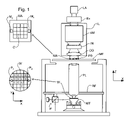
- FIG. 2 depicts a liquid supply system for supplying liquid to the area around the final element of the projection system according to an embodiment of the invention
- a liquid of a different composition may be added.
- the second liquid may be mixed with liquid already in the space or be arranged to replace the original liquid.
- liquids examples include: water, ethanol, acetone and benzoate.
Priority Applications (2)
| Application Number | Priority Date | Filing Date | Title |
|---|---|---|---|
| US12/230,979 US8174674B2 (en) | 2003-10-15 | 2008-09-09 | Lithographic apparatus and device manufacturing method |
| US13/446,687 US8570486B2 (en) | 2003-10-15 | 2012-04-13 | Lithographic apparatus and device manufacturing method |
Applications Claiming Priority (2)
| Application Number | Priority Date | Filing Date | Title |
|---|---|---|---|
| EP03256499A EP1524558A1 (en) | 2003-10-15 | 2003-10-15 | Lithographic apparatus and device manufacturing method |
| EP03256499.9 | 2003-10-15 |
Related Child Applications (1)
| Application Number | Title | Priority Date | Filing Date |
|---|---|---|---|
| US12/230,979 Continuation US8174674B2 (en) | 2003-10-15 | 2008-09-09 | Lithographic apparatus and device manufacturing method |
Publications (2)
| Publication Number | Publication Date |
|---|---|
| US20050179877A1 US20050179877A1 (en) | 2005-08-18 |
| US7433015B2 true US7433015B2 (en) | 2008-10-07 |
Family
ID=34354600
Family Applications (3)
| Application Number | Title | Priority Date | Filing Date |
|---|---|---|---|
| US10/961,369 Active 2025-10-07 US7433015B2 (en) | 2003-10-15 | 2004-10-12 | Lithographic apparatus and device manufacturing method |
| US12/230,979 Active 2027-01-28 US8174674B2 (en) | 2003-10-15 | 2008-09-09 | Lithographic apparatus and device manufacturing method |
| US13/446,687 Active US8570486B2 (en) | 2003-10-15 | 2012-04-13 | Lithographic apparatus and device manufacturing method |
Family Applications After (2)
| Application Number | Title | Priority Date | Filing Date |
|---|---|---|---|
| US12/230,979 Active 2027-01-28 US8174674B2 (en) | 2003-10-15 | 2008-09-09 | Lithographic apparatus and device manufacturing method |
| US13/446,687 Active US8570486B2 (en) | 2003-10-15 | 2012-04-13 | Lithographic apparatus and device manufacturing method |
Country Status (3)
| Country | Link |
|---|---|
| US (3) | US7433015B2 (ja) |
| EP (1) | EP1524558A1 (ja) |
| JP (2) | JP4378259B2 (ja) |
Cited By (9)
| Publication number | Priority date | Publication date | Assignee | Title |
|---|---|---|---|---|
| US20060098179A1 (en) * | 2003-05-28 | 2006-05-11 | Nikon Corporation | Exposure method, exposure apparatus, and method for producing device |
| US20060103824A1 (en) * | 2004-11-16 | 2006-05-18 | Dong-Woon Park | Auto focus system, auto focus method, and exposure apparatus using the same |
| US20070132969A1 (en) * | 2003-07-24 | 2007-06-14 | Carl Zeiss Smt Ag | Microlithographic projection exposure apparatus and method for introducing an immersion liquid into an immersion space |
| US20070242243A1 (en) * | 2006-04-14 | 2007-10-18 | Asml Netherlands B.V. | Lithographic apparatus and device manufacturing method |
| US20090021707A1 (en) * | 2003-10-15 | 2009-01-22 | Asml Netherlands B.V. | Lithographic apparatus and device manufacturing method |
| US8072576B2 (en) | 2003-05-23 | 2011-12-06 | Nikon Corporation | Exposure apparatus and method for producing device |
| US8085381B2 (en) | 2003-04-11 | 2011-12-27 | Nikon Corporation | Cleanup method for optics in immersion lithography using sonic device |
| US8520184B2 (en) | 2004-06-09 | 2013-08-27 | Nikon Corporation | Immersion exposure apparatus and device manufacturing method with measuring device |
| US9146477B2 (en) | 2010-12-23 | 2015-09-29 | Asml Netherlands B.V. | Lithographic apparatus and method of modifying a beam of radiation within a lithographic apparatus |
Families Citing this family (95)
| Publication number | Priority date | Publication date | Assignee | Title |
|---|---|---|---|---|
| DE10257766A1 (de) * | 2002-12-10 | 2004-07-15 | Carl Zeiss Smt Ag | Verfahren zur Einstellung einer gewünschten optischen Eigenschaft eines Projektionsobjektivs sowie mikrolithografische Projektionsbelichtungsanlage |
| KR101484435B1 (ko) | 2003-04-09 | 2015-01-19 | 가부시키가이샤 니콘 | 노광 방법 및 장치, 그리고 디바이스 제조 방법 |
| KR101178756B1 (ko) | 2003-04-11 | 2012-08-31 | 가부시키가이샤 니콘 | 액침 리소그래피 머신에서 웨이퍼 교환동안 투영 렌즈 아래의 갭에서 액침액체를 유지하는 장치 및 방법 |
| TWI421906B (zh) | 2003-05-23 | 2014-01-01 | 尼康股份有限公司 | An exposure method, an exposure apparatus, and an element manufacturing method |
| KR101528089B1 (ko) | 2003-06-13 | 2015-06-11 | 가부시키가이샤 니콘 | 노광 방법, 기판 스테이지, 노광 장치, 및 디바이스 제조 방법 |
| TWI433212B (zh) | 2003-06-19 | 2014-04-01 | 尼康股份有限公司 | An exposure apparatus, an exposure method, and an element manufacturing method |
| TWI553701B (zh) | 2003-10-09 | 2016-10-11 | 尼康股份有限公司 | Exposure apparatus and exposure method, component manufacturing method |
| EP1524557A1 (en) * | 2003-10-15 | 2005-04-20 | ASML Netherlands B.V. | Lithographic apparatus and device manufacturing method |
| TWI609409B (zh) | 2003-10-28 | 2017-12-21 | 尼康股份有限公司 | 照明光學裝置、曝光裝置、曝光方法以及元件製造方法 |
| TWI385414B (zh) | 2003-11-20 | 2013-02-11 | 尼康股份有限公司 | 光學照明裝置、照明方法、曝光裝置、曝光方法以及元件製造方法 |
| SG2014014955A (en) | 2003-12-03 | 2014-07-30 | Nippon Kogaku Kk | Exposure apparatus, exposure method, method for producing device, and optical part |
| WO2005057635A1 (ja) * | 2003-12-15 | 2005-06-23 | Nikon Corporation | 投影露光装置及びステージ装置、並びに露光方法 |
| ATE491221T1 (de) | 2003-12-15 | 2010-12-15 | Nikon Corp | Bühnensystem, belichtungsvorrichtung und belichtungsverfahren |
| US20070081133A1 (en) * | 2004-12-14 | 2007-04-12 | Niikon Corporation | Projection exposure apparatus and stage unit, and exposure method |
| US7385764B2 (en) | 2003-12-15 | 2008-06-10 | Carl Zeiss Smt Ag | Objectives as a microlithography projection objective with at least one liquid lens |
| JP4308638B2 (ja) | 2003-12-17 | 2009-08-05 | パナソニック株式会社 | パターン形成方法 |
| KR101748504B1 (ko) | 2004-01-05 | 2017-06-16 | 가부시키가이샤 니콘 | 노광 장치, 노광 방법 및 디바이스 제조 방법 |
| JP4843503B2 (ja) * | 2004-01-20 | 2011-12-21 | カール・ツァイス・エスエムティー・ゲーエムベーハー | マイクロリソグラフィ投影露光装置および投影レンズのための測定装置 |
| US7589822B2 (en) | 2004-02-02 | 2009-09-15 | Nikon Corporation | Stage drive method and stage unit, exposure apparatus, and device manufacturing method |
| TWI505329B (zh) | 2004-02-06 | 2015-10-21 | 尼康股份有限公司 | 光學照明裝置、曝光裝置、曝光方法以及元件製造方法 |
| KR101115111B1 (ko) * | 2004-02-13 | 2012-04-16 | 칼 짜이스 에스엠티 게엠베하 | 마이크로 리소그래프 투영 노광 장치 투영 대물 렌즈 |
| CN100592210C (zh) | 2004-02-13 | 2010-02-24 | 卡尔蔡司Smt股份公司 | 微平版印刷投影曝光装置的投影物镜 |
| JP4677986B2 (ja) * | 2004-04-19 | 2011-04-27 | 株式会社ニコン | ノズル部材、露光方法、露光装置及びデバイス製造方法 |
| US20060244938A1 (en) * | 2004-05-04 | 2006-11-02 | Karl-Heinz Schuster | Microlitographic projection exposure apparatus and immersion liquid therefore |
| WO2006007111A2 (en) * | 2004-07-01 | 2006-01-19 | Nikon Corporation | A dynamic fluid control system for immersion lithography |
| JP4655792B2 (ja) * | 2004-07-12 | 2011-03-23 | 株式会社ニコン | 露光条件の決定方法、及び露光方法、露光装置、並びにデバイス製造方法 |
| WO2006006562A1 (ja) * | 2004-07-12 | 2006-01-19 | Nikon Corporation | 露光条件の決定方法、露光方法、露光装置、及びデバイス製造方法 |
| JP2006032750A (ja) * | 2004-07-20 | 2006-02-02 | Canon Inc | 液浸型投影露光装置、及びデバイス製造方法 |
| EP1791164B2 (en) | 2004-08-03 | 2014-08-20 | Nikon Corporation | Exposure equipment, exposure method and device manufacturing method |
| US20090021709A1 (en) * | 2004-10-13 | 2009-01-22 | Nikon Corporation | Exposure apparatus, exposure method, and method for producing device |
| JP2006190971A (ja) * | 2004-10-13 | 2006-07-20 | Nikon Corp | 露光装置、露光方法及びデバイス製造方法 |
| DE102005045862A1 (de) | 2004-10-19 | 2006-04-20 | Carl Zeiss Smt Ag | Optisches System für Ultraviolettlicht |
| EP1803036A2 (en) * | 2004-10-22 | 2007-07-04 | Carl Zeiss SMT AG | Projection exposure apparatus for microlithography |
| US7782440B2 (en) * | 2004-11-18 | 2010-08-24 | Carl Zeiss Smt Ag | Projection lens system of a microlithographic projection exposure installation |
| US7623218B2 (en) * | 2004-11-24 | 2009-11-24 | Carl Zeiss Smt Ag | Method of manufacturing a miniaturized device |
| JP4752473B2 (ja) * | 2004-12-09 | 2011-08-17 | 株式会社ニコン | 露光装置、露光方法及びデバイス製造方法 |
| WO2006080250A1 (ja) * | 2005-01-25 | 2006-08-03 | Jsr Corporation | 液浸型露光システム、液浸型露光用液体のリサイクル方法及び供給方法 |
| JP2006222165A (ja) * | 2005-02-08 | 2006-08-24 | Canon Inc | 露光装置 |
| US7324185B2 (en) | 2005-03-04 | 2008-01-29 | Asml Netherlands B.V. | Lithographic apparatus and device manufacturing method |
| JP4072543B2 (ja) * | 2005-03-18 | 2008-04-09 | キヤノン株式会社 | 液浸露光装置及びデバイス製造方法 |
| USRE43576E1 (en) | 2005-04-08 | 2012-08-14 | Asml Netherlands B.V. | Dual stage lithographic apparatus and device manufacturing method |
| US8248577B2 (en) | 2005-05-03 | 2012-08-21 | Asml Netherlands B.V. | Lithographic apparatus and device manufacturing method |
| JP2006319064A (ja) * | 2005-05-11 | 2006-11-24 | Canon Inc | 測定装置、露光方法及び装置 |
| EP2660853B1 (en) | 2005-05-12 | 2017-07-05 | Nikon Corporation | Projection optical system, exposure apparatus and exposure method |
| US7265815B2 (en) * | 2005-05-19 | 2007-09-04 | Asml Holding N.V. | System and method utilizing an illumination beam adjusting system |
| JP4596191B2 (ja) | 2005-05-24 | 2010-12-08 | 株式会社ニコン | 露光方法及び露光装置、並びにデバイス製造方法 |
| KR101332540B1 (ko) * | 2005-05-27 | 2013-11-22 | 칼 짜이스 에스엠테 게엠베하 | 광산란 디스크, 그 사용 및 파면 측정 장치 |
| US20070085989A1 (en) * | 2005-06-21 | 2007-04-19 | Nikon Corporation | Exposure apparatus and exposure method, maintenance method, and device manufacturing method |
| JP2007036193A (ja) * | 2005-06-23 | 2007-02-08 | Canon Inc | 露光装置 |
| US7474379B2 (en) * | 2005-06-28 | 2009-01-06 | Asml Netherlands B.V. | Lithographic apparatus and device manufacturing method |
| JP2007027439A (ja) * | 2005-07-15 | 2007-02-01 | Nikon Corp | 投影光学系、露光装置、およびデバイスの製造方法 |
| WO2007023813A1 (ja) | 2005-08-23 | 2007-03-01 | Nikon Corporation | 露光装置及び露光方法、並びにデバイス製造方法 |
| KR20080065609A (ko) * | 2005-09-13 | 2008-07-14 | 칼 짜이스 에스엠테 아게 | 마이크로리소그래픽 투사 노광 장치에서 광학 결상 특성을설정하는 방법 및 이러한 타입의 투사 노광 장치 |
| JP2007103841A (ja) * | 2005-10-07 | 2007-04-19 | Toshiba Corp | 半導体装置の製造方法 |
| US8125610B2 (en) * | 2005-12-02 | 2012-02-28 | ASML Metherlands B.V. | Method for preventing or reducing contamination of an immersion type projection apparatus and an immersion type lithographic apparatus |
| US7542127B2 (en) * | 2005-12-21 | 2009-06-02 | Asml Netherlands B.V. | Lithographic apparatus and method for manufacturing a device |
| US8045134B2 (en) * | 2006-03-13 | 2011-10-25 | Asml Netherlands B.V. | Lithographic apparatus, control system and device manufacturing method |
| CN100590173C (zh) * | 2006-03-24 | 2010-02-17 | 北京有色金属研究总院 | 一种荧光粉及其制造方法和所制成的电光源 |
| US7675604B2 (en) * | 2006-05-04 | 2010-03-09 | Taiwan Semiconductor Manufacturing Company, Ltd. | Hood for immersion lithography |
| DE102006021797A1 (de) | 2006-05-09 | 2007-11-15 | Carl Zeiss Smt Ag | Optische Abbildungseinrichtung mit thermischer Dämpfung |
| DE102006023876A1 (de) * | 2006-05-19 | 2007-11-22 | Carl Zeiss Smt Ag | Optische Abbildungseinrichtung |
| US8027023B2 (en) | 2006-05-19 | 2011-09-27 | Carl Zeiss Smt Gmbh | Optical imaging device and method for reducing dynamic fluctuations in pressure difference |
| US7969548B2 (en) * | 2006-05-22 | 2011-06-28 | Asml Netherlands B.V. | Lithographic apparatus and lithographic apparatus cleaning method |
| KR100801234B1 (ko) | 2006-06-20 | 2008-02-11 | 주식회사 탑 엔지니어링 | 액체렌즈의 액체주입장치 및 방법 |
| US7969549B2 (en) * | 2006-06-30 | 2011-06-28 | Asml Netherlands B.V. | Liquid filled lens element, lithographic apparatus comprising such an element and device manufacturing method |
| DE102006032877A1 (de) * | 2006-07-15 | 2008-01-17 | Carl Zeiss Smt Ag | Mikrolithographische Projektionsbelichtungsanlage |
| KR100763334B1 (ko) | 2006-08-03 | 2007-10-04 | 삼성전자주식회사 | 이머젼 매질을 모니터링하는 유니트를 구비하는 이머젼포토리쏘그라피 장비 및 이를 사용하는 이머젼포토리쏘그라피 공정을 모니터링하는 방법 |
| US7443483B2 (en) * | 2006-08-11 | 2008-10-28 | Entegris, Inc. | Systems and methods for fluid flow control in an immersion lithography system |
| US7826030B2 (en) * | 2006-09-07 | 2010-11-02 | Asml Netherlands B.V. | Lithographic apparatus and device manufacturing method |
| US8045135B2 (en) | 2006-11-22 | 2011-10-25 | Asml Netherlands B.V. | Lithographic apparatus with a fluid combining unit and related device manufacturing method |
| US7995185B2 (en) * | 2006-12-07 | 2011-08-09 | Asml Holding N.V. | Systems and methods for thermally-induced aberration correction in immersion lithography |
| EP1939689A1 (en) * | 2006-12-28 | 2008-07-02 | DSM IP Assets B.V. | Immersion fluid and method for producing microchips |
| DE102008000968A1 (de) * | 2007-04-05 | 2008-10-09 | Carl Zeiss Smt Ag | Optisches Korrekturelement und Verfahren zur Korrektur von temperaturinduzierten Abbildungsfehlern in optischen Systemen, Projektionsobjektiv und Projektionsbelichtungsanlage für die Halbleiterlithographie |
| JP2009071193A (ja) * | 2007-09-14 | 2009-04-02 | Canon Inc | 露光装置及びデバイスの製造方法 |
| SG151198A1 (en) | 2007-09-27 | 2009-04-30 | Asml Netherlands Bv | Methods relating to immersion lithography and an immersion lithographic apparatus |
| JP5267029B2 (ja) | 2007-10-12 | 2013-08-21 | 株式会社ニコン | 照明光学装置、露光装置及びデバイスの製造方法 |
| US8379187B2 (en) | 2007-10-24 | 2013-02-19 | Nikon Corporation | Optical unit, illumination optical apparatus, exposure apparatus, and device manufacturing method |
| US9116346B2 (en) | 2007-11-06 | 2015-08-25 | Nikon Corporation | Illumination apparatus, illumination method, exposure apparatus, and device manufacturing method |
| KR101448152B1 (ko) * | 2008-03-26 | 2014-10-07 | 삼성전자주식회사 | 수직 포토게이트를 구비한 거리측정 센서 및 그를 구비한입체 컬러 이미지 센서 |
| NL1036715A1 (nl) | 2008-04-16 | 2009-10-19 | Asml Netherlands Bv | Lithographic apparatus. |
| WO2009133704A1 (ja) * | 2008-04-30 | 2009-11-05 | 株式会社ニコン | 露光装置及び露光方法、並びにデバイス製造方法 |
| US9176393B2 (en) | 2008-05-28 | 2015-11-03 | Asml Netherlands B.V. | Lithographic apparatus and a method of operating the apparatus |
| EP2136250A1 (en) * | 2008-06-18 | 2009-12-23 | ASML Netherlands B.V. | Lithographic apparatus and method |
| US20110080663A1 (en) * | 2008-08-06 | 2011-04-07 | Muzammil Arshad Arain | Adaptive laser beam shaping |
| US20100294742A1 (en) * | 2009-05-22 | 2010-11-25 | Enrico Magni | Modifications to Surface Topography of Proximity Head |
| NL2004808A (en) | 2009-06-30 | 2011-01-12 | Asml Netherlands Bv | Fluid handling structure, lithographic apparatus and device manufacturing method. |
| WO2011116792A1 (en) * | 2010-03-26 | 2011-09-29 | Carl Zeiss Smt Gmbh | Optical system, exposure apparatus, and waverfront correction method |
| EP2381310B1 (en) | 2010-04-22 | 2015-05-06 | ASML Netherlands BV | Fluid handling structure and lithographic apparatus |
| NL2008704A (en) | 2011-06-20 | 2012-12-28 | Asml Netherlands Bv | Wavefront modification apparatus, lithographic apparatus and method. |
| WO2013029879A1 (en) * | 2011-08-30 | 2013-03-07 | Asml Netherlands B.V. | Lithographic apparatus, method of setting up a lithographic apparatus and device manufacturing method |
| JP6122252B2 (ja) * | 2012-05-01 | 2017-04-26 | キヤノン株式会社 | 露光装置及びデバイスの製造方法 |
| US9377566B1 (en) | 2012-12-31 | 2016-06-28 | Nlight, Inc. | Flexible irradiance in laser imaging |
| JP6282742B2 (ja) | 2013-09-09 | 2018-02-21 | カール・ツァイス・エスエムティー・ゲーエムベーハー | マイクロリソグラフィ投影露光装置及びそのような装置における光学波面変形を補正する方法 |
| DE102018128418B3 (de) * | 2018-11-13 | 2019-11-14 | Nanoscribe Gmbh | Verwendung eines Dispenser-Aufsatzes und Dispenser-Aufsatz für eine Vorrichtung zum Schreiben von 3D-Strukturen mittels Laserlithografie |
| DE102019108611B3 (de) * | 2019-04-02 | 2020-08-06 | Leica Microsystems Cms Gmbh | Vorrichtung und Verfahren zum Zuführen eines Immersionsmediums und Objektiv mit einer Zuführvorrichtung |
Citations (78)
| Publication number | Priority date | Publication date | Assignee | Title |
|---|---|---|---|---|
| DE242880C (ja) | ||||
| DE224448C (ja) | ||||
| DE206607C (ja) | ||||
| DE221563C (ja) | ||||
| US3573975A (en) | 1968-07-10 | 1971-04-06 | Ibm | Photochemical fabrication process |
| US3648587A (en) | 1967-10-20 | 1972-03-14 | Eastman Kodak Co | Focus control for optical instruments |
| EP0023231A1 (de) | 1979-07-27 | 1981-02-04 | Tabarelli, Werner, Dr. | Optisches Lithographieverfahren und Einrichtung zum Kopieren eines Musters auf eine Halbleiterscheibe |
| FR2474708A1 (fr) | 1980-01-24 | 1981-07-31 | Dme | Procede de microphotolithographie a haute resolution de traits |
| US4346164A (en) | 1980-10-06 | 1982-08-24 | Werner Tabarelli | Photolithographic method for the manufacture of integrated circuits |
| US4390273A (en) | 1981-02-17 | 1983-06-28 | Censor Patent-Und Versuchsanstalt | Projection mask as well as a method and apparatus for the embedding thereof and projection printing system |
| US4396705A (en) | 1980-09-19 | 1983-08-02 | Hitachi, Ltd. | Pattern forming method and pattern forming apparatus using exposures in a liquid |
| JPS58202448A (ja) | 1982-05-21 | 1983-11-25 | Hitachi Ltd | 露光装置 |
| US4480910A (en) | 1981-03-18 | 1984-11-06 | Hitachi, Ltd. | Pattern forming apparatus |
| US4509852A (en) | 1980-10-06 | 1985-04-09 | Werner Tabarelli | Apparatus for the photolithographic manufacture of integrated circuit elements |
| JPS6265326A (ja) | 1985-09-18 | 1987-03-24 | Hitachi Ltd | 露光装置 |
| JPS62121417A (ja) | 1985-11-22 | 1987-06-02 | Hitachi Ltd | 液浸対物レンズ装置 |
| JPS63157419A (ja) | 1986-12-22 | 1988-06-30 | Toshiba Corp | 微細パタ−ン転写装置 |
| EP0418427A2 (en) | 1989-09-06 | 1991-03-27 | Eiichi Miyake | Exposure process |
| US5040020A (en) | 1988-03-31 | 1991-08-13 | Cornell Research Foundation, Inc. | Self-aligned, high resolution resonant dielectric lithography |
| JPH04305915A (ja) | 1991-04-02 | 1992-10-28 | Nikon Corp | 密着型露光装置 |
| JPH04305917A (ja) | 1991-04-02 | 1992-10-28 | Nikon Corp | 密着型露光装置 |
| JPH06124873A (ja) | 1992-10-09 | 1994-05-06 | Canon Inc | 液浸式投影露光装置 |
| JPH07132262A (ja) | 1992-12-21 | 1995-05-23 | Tokyo Electron Ltd | 浸漬式の液処理装置 |
| JPH07220990A (ja) | 1994-01-28 | 1995-08-18 | Hitachi Ltd | パターン形成方法及びその露光装置 |
| US5577552A (en) * | 1988-10-03 | 1996-11-26 | Canon Kabushiki Kaisha | Temperature controlling device for mask and wafer holders |
| US5598888A (en) * | 1994-09-23 | 1997-02-04 | Grumman Aerospace Corporation | Cryogenic temperature gradient microscopy chamber |
| US5610683A (en) | 1992-11-27 | 1997-03-11 | Canon Kabushiki Kaisha | Immersion type projection exposure apparatus |
| US5715039A (en) | 1995-05-19 | 1998-02-03 | Hitachi, Ltd. | Projection exposure apparatus and method which uses multiple diffraction gratings in order to produce a solid state device with fine patterns |
| JPH10228661A (ja) | 1997-02-14 | 1998-08-25 | Sony Corp | 光学記録媒体の原盤作製用露光装置 |
| JPH10255319A (ja) | 1997-03-12 | 1998-09-25 | Hitachi Maxell Ltd | 原盤露光装置及び方法 |
| US5825043A (en) | 1996-10-07 | 1998-10-20 | Nikon Precision Inc. | Focusing and tilting adjustment system for lithography aligner, manufacturing apparatus or inspection apparatus |
| JPH10303114A (ja) | 1997-04-23 | 1998-11-13 | Nikon Corp | 液浸型露光装置 |
| JPH10340846A (ja) | 1997-06-10 | 1998-12-22 | Nikon Corp | 露光装置及びその製造方法並びに露光方法及びデバイス製造方法 |
| US5883704A (en) | 1995-08-07 | 1999-03-16 | Nikon Corporation | Projection exposure apparatus wherein focusing of the apparatus is changed by controlling the temperature of a lens element of the projection optical system |
| US5900354A (en) | 1997-07-03 | 1999-05-04 | Batchelder; John Samuel | Method for optical inspection and lithography |
| JPH11176727A (ja) | 1997-12-11 | 1999-07-02 | Nikon Corp | 投影露光装置 |
| WO1999049504A1 (fr) | 1998-03-26 | 1999-09-30 | Nikon Corporation | Procede et systeme d'exposition par projection |
| JP2000058436A (ja) | 1998-08-11 | 2000-02-25 | Nikon Corp | 投影露光装置及び露光方法 |
| EP1039511A1 (en) | 1997-12-12 | 2000-09-27 | Nikon Corporation | Projection exposure method and projection aligner |
| JP2001091849A (ja) | 1999-09-21 | 2001-04-06 | Olympus Optical Co Ltd | 顕微鏡用液浸対物レンズ |
| US6236634B1 (en) | 1996-08-26 | 2001-05-22 | Digital Papyrus Corporation | Method and apparatus for coupling an optical lens to a disk through a coupling medium having a relatively high index of refraction |
| US20020006561A1 (en) | 1996-06-20 | 2002-01-17 | Nikon Corporation | Projection exposure apparatus and method |
| US20020020821A1 (en) * | 2000-08-08 | 2002-02-21 | Koninklijke Philips Electronics N.V. | Method of manufacturing an optically scannable information carrier |
| US20020163629A1 (en) | 2001-05-07 | 2002-11-07 | Michael Switkes | Methods and apparatus employing an index matching medium |
| US6560032B2 (en) | 2000-03-27 | 2003-05-06 | Olympus Optical Co., Ltd. | Liquid immersion lens system and optical apparatus using the same |
| US20030123040A1 (en) | 2001-11-07 | 2003-07-03 | Gilad Almogy | Optical spot grid array printer |
| US6600547B2 (en) | 2001-09-24 | 2003-07-29 | Nikon Corporation | Sliding seal |
| US6603130B1 (en) | 1999-04-19 | 2003-08-05 | Asml Netherlands B.V. | Gas bearings for use with vacuum chambers and their application in lithographic projection apparatuses |
| WO2003077037A1 (en) | 2002-03-08 | 2003-09-18 | Carl Zeiss Smt Ag | Refractive projection objective for immersion lithography |
| US6633365B2 (en) | 2000-12-11 | 2003-10-14 | Nikon Corporation | Projection optical system and exposure apparatus having the projection optical system |
| US20040000627A1 (en) | 2002-06-28 | 2004-01-01 | Carl Zeiss Semiconductor Manufacturing Technologies Ag | Method for focus detection and an imaging system with a focus-detection system |
| WO2004019128A2 (en) | 2002-08-23 | 2004-03-04 | Nikon Corporation | Projection optical system and method for photolithography and exposure apparatus and method using same |
| US20040075895A1 (en) | 2002-10-22 | 2004-04-22 | Taiwan Semiconductor Manufacturing Co., Ltd. | Apparatus for method for immersion lithography |
| US20040109237A1 (en) | 2002-12-09 | 2004-06-10 | Carl Zeiss Smt Ag | Projection objective, especially for microlithography, and method for adjusting a projection objective |
| US20040114117A1 (en) | 2002-11-18 | 2004-06-17 | Asml Netherlands B.V. | Lithographic apparatus and device manufacturing method |
| WO2004053957A1 (ja) | 2002-12-10 | 2004-06-24 | Nikon Corporation | 面位置検出装置、露光方法、及びデバイス製造方法 |
| WO2004053952A1 (ja) | 2002-12-10 | 2004-06-24 | Nikon Corporation | 露光装置及びデバイス製造方法 |
| WO2004053954A1 (ja) | 2002-12-10 | 2004-06-24 | Nikon Corporation | 露光装置及びデバイス製造方法 |
| WO2004053951A1 (ja) | 2002-12-10 | 2004-06-24 | Nikon Corporation | 露光方法及び露光装置並びにデバイス製造方法 |
| WO2004053959A1 (ja) | 2002-12-10 | 2004-06-24 | Nikon Corporation | 光学素子及びその光学素子を用いた投影露光装置 |
| WO2004053955A1 (ja) | 2002-12-10 | 2004-06-24 | Nikon Corporation | 露光装置及びデバイス製造方法 |
| US20040119954A1 (en) | 2002-12-10 | 2004-06-24 | Miyoko Kawashima | Exposure apparatus and method |
| WO2004053958A1 (ja) | 2002-12-10 | 2004-06-24 | Nikon Corporation | 露光装置及びデバイス製造方法 |
| WO2004053950A1 (ja) | 2002-12-10 | 2004-06-24 | Nikon Corporation | 露光装置及びデバイス製造方法 |
| WO2004053956A1 (ja) | 2002-12-10 | 2004-06-24 | Nikon Corporation | 露光装置及び露光方法、デバイス製造方法 |
| WO2004053953A1 (ja) | 2002-12-10 | 2004-06-24 | Nikon Corporation | 露光装置及びデバイス製造方法 |
| WO2004053596A2 (de) | 2002-12-10 | 2004-06-24 | Carl Zeiss Smt Ag | Verfahren zur einstellung einer optischen eigenschaft eines projektionsobjekts |
| WO2004055803A1 (en) | 2002-12-13 | 2004-07-01 | Koninklijke Philips Electronics N.V. | Liquid removal in a method and device for irradiating spots on a layer |
| US20040125351A1 (en) | 2002-12-30 | 2004-07-01 | Krautschik Christof Gabriel | Immersion lithography |
| WO2004057590A1 (en) | 2002-12-19 | 2004-07-08 | Koninklijke Philips Electronics N.V. | Method and device for irradiating spots on a layer |
| WO2004057589A1 (en) | 2002-12-19 | 2004-07-08 | Koninklijke Philips Electronics N.V. | Method and device for irradiating spots on a layer |
| JP2004193252A (ja) | 2002-12-10 | 2004-07-08 | Nikon Corp | 露光方法及びデバイス製造方法 |
| US20040135099A1 (en) | 2002-11-29 | 2004-07-15 | Asml Netherlands B.V. | Lithographic apparatus and device manufacturing method |
| US20040136494A1 (en) | 2002-11-12 | 2004-07-15 | Asml Netherlands B.V. | Lithographic apparatus and device manufacturing method |
| US20040160582A1 (en) | 2002-11-12 | 2004-08-19 | Asml Netherlands B.V. | Lithographic apparatus and device manufacturing method |
| US20040165159A1 (en) | 2002-11-12 | 2004-08-26 | Asml Netherlands B.V. | Lithographic apparatus and device manufacturing method |
| US20040207824A1 (en) | 2002-11-12 | 2004-10-21 | Asml Netherlands B.V. | Lithographic apparatus and device manufacturing method |
| US20040211920A1 (en) | 2002-11-12 | 2004-10-28 | Asml Netherlands B.V. | Lithographic apparatus and device manufacturing method |
Family Cites Families (25)
| Publication number | Priority date | Publication date | Assignee | Title |
|---|---|---|---|---|
| JPS57169244A (en) | 1981-04-13 | 1982-10-18 | Canon Inc | Temperature controller for mask and wafer |
| EP0063684A1 (de) * | 1981-04-27 | 1982-11-03 | F. HOFFMANN-LA ROCHE & CO. Aktiengesellschaft | Immersionsöl |
| DD206607A1 (de) | 1982-06-16 | 1984-02-01 | Mikroelektronik Zt Forsch Tech | Verfahren und vorrichtung zur beseitigung von interferenzeffekten |
| DD242880A1 (de) | 1983-01-31 | 1987-02-11 | Kuch Karl Heinz | Einrichtung zur fotolithografischen strukturuebertragung |
| DD221563A1 (de) | 1983-09-14 | 1985-04-24 | Mikroelektronik Zt Forsch Tech | Immersionsobjektiv fuer die schrittweise projektionsabbildung einer maskenstruktur |
| DD224448A1 (de) | 1984-03-01 | 1985-07-03 | Zeiss Jena Veb Carl | Einrichtung zur fotolithografischen strukturuebertragung |
| JPH06265782A (ja) * | 1993-03-16 | 1994-09-22 | Matsushita Electric Ind Co Ltd | 投写レンズ装置 |
| JPH1012515A (ja) | 1996-06-20 | 1998-01-16 | Nikon Corp | 投影露光装置 |
| JPH1092722A (ja) | 1996-09-18 | 1998-04-10 | Nikon Corp | 露光装置 |
| US7098290B1 (en) * | 1999-11-18 | 2006-08-29 | Ppg Industries Ohio, Inc. | Method of preparing an optical polymerizate |
| JP4150493B2 (ja) | 2000-08-22 | 2008-09-17 | 株式会社東芝 | パターン描画装置における温度測定方法 |
| JP2004301825A (ja) | 2002-12-10 | 2004-10-28 | Nikon Corp | 面位置検出装置、露光方法、及びデバイス製造方法 |
| KR20170064003A (ko) * | 2003-04-10 | 2017-06-08 | 가부시키가이샤 니콘 | 액침 리소그래피 장치용 운반 영역을 포함하는 환경 시스템 |
| KR101728664B1 (ko) | 2003-05-28 | 2017-05-02 | 가부시키가이샤 니콘 | 노광 방법, 노광 장치, 및 디바이스 제조 방법 |
| JP5143331B2 (ja) | 2003-05-28 | 2013-02-13 | 株式会社ニコン | 露光方法及び露光装置、並びにデバイス製造方法 |
| US6867844B2 (en) * | 2003-06-19 | 2005-03-15 | Asml Holding N.V. | Immersion photolithography system and method using microchannel nozzles |
| US7738074B2 (en) | 2003-07-16 | 2010-06-15 | Asml Netherlands B.V. | Lithographic apparatus and device manufacturing method |
| US6954256B2 (en) * | 2003-08-29 | 2005-10-11 | Asml Netherlands B.V. | Gradient immersion lithography |
| EP1664934B1 (de) | 2003-09-25 | 2013-12-18 | Infineon Technologies AG | Immersions-lithographie-verfahren und vorrichtung zum belichten eines substrats |
| JP2005123305A (ja) | 2003-10-15 | 2005-05-12 | Canon Inc | 液浸型露光装置 |
| EP1524558A1 (en) * | 2003-10-15 | 2005-04-20 | ASML Netherlands B.V. | Lithographic apparatus and device manufacturing method |
| EP1524557A1 (en) * | 2003-10-15 | 2005-04-20 | ASML Netherlands B.V. | Lithographic apparatus and device manufacturing method |
| US7545481B2 (en) * | 2003-11-24 | 2009-06-09 | Asml Netherlands B.V. | Lithographic apparatus and device manufacturing method |
| US7394521B2 (en) * | 2003-12-23 | 2008-07-01 | Asml Netherlands B.V. | Lithographic apparatus and device manufacturing method |
| US7589818B2 (en) * | 2003-12-23 | 2009-09-15 | Asml Netherlands B.V. | Lithographic apparatus, alignment apparatus, device manufacturing method, and a method of converting an apparatus |
-
2003
- 2003-10-15 EP EP03256499A patent/EP1524558A1/en not_active Withdrawn
-
2004
- 2004-10-12 US US10/961,369 patent/US7433015B2/en active Active
- 2004-10-15 JP JP2004300866A patent/JP4378259B2/ja not_active Expired - Fee Related
-
2008
- 2008-09-09 US US12/230,979 patent/US8174674B2/en active Active
- 2008-10-24 JP JP2008274669A patent/JP4945539B2/ja active Active
-
2012
- 2012-04-13 US US13/446,687 patent/US8570486B2/en active Active
Patent Citations (83)
| Publication number | Priority date | Publication date | Assignee | Title |
|---|---|---|---|---|
| DE242880C (ja) | ||||
| DE224448C (ja) | ||||
| DE206607C (ja) | ||||
| DE221563C (ja) | ||||
| US3648587A (en) | 1967-10-20 | 1972-03-14 | Eastman Kodak Co | Focus control for optical instruments |
| US3573975A (en) | 1968-07-10 | 1971-04-06 | Ibm | Photochemical fabrication process |
| EP0023231A1 (de) | 1979-07-27 | 1981-02-04 | Tabarelli, Werner, Dr. | Optisches Lithographieverfahren und Einrichtung zum Kopieren eines Musters auf eine Halbleiterscheibe |
| FR2474708A1 (fr) | 1980-01-24 | 1981-07-31 | Dme | Procede de microphotolithographie a haute resolution de traits |
| US4396705A (en) | 1980-09-19 | 1983-08-02 | Hitachi, Ltd. | Pattern forming method and pattern forming apparatus using exposures in a liquid |
| US4346164A (en) | 1980-10-06 | 1982-08-24 | Werner Tabarelli | Photolithographic method for the manufacture of integrated circuits |
| US4509852A (en) | 1980-10-06 | 1985-04-09 | Werner Tabarelli | Apparatus for the photolithographic manufacture of integrated circuit elements |
| US4390273A (en) | 1981-02-17 | 1983-06-28 | Censor Patent-Und Versuchsanstalt | Projection mask as well as a method and apparatus for the embedding thereof and projection printing system |
| US4480910A (en) | 1981-03-18 | 1984-11-06 | Hitachi, Ltd. | Pattern forming apparatus |
| JPS58202448A (ja) | 1982-05-21 | 1983-11-25 | Hitachi Ltd | 露光装置 |
| JPS6265326A (ja) | 1985-09-18 | 1987-03-24 | Hitachi Ltd | 露光装置 |
| JPS62121417A (ja) | 1985-11-22 | 1987-06-02 | Hitachi Ltd | 液浸対物レンズ装置 |
| JPS63157419A (ja) | 1986-12-22 | 1988-06-30 | Toshiba Corp | 微細パタ−ン転写装置 |
| US5040020A (en) | 1988-03-31 | 1991-08-13 | Cornell Research Foundation, Inc. | Self-aligned, high resolution resonant dielectric lithography |
| US5577552A (en) * | 1988-10-03 | 1996-11-26 | Canon Kabushiki Kaisha | Temperature controlling device for mask and wafer holders |
| EP0418427A2 (en) | 1989-09-06 | 1991-03-27 | Eiichi Miyake | Exposure process |
| JPH04305915A (ja) | 1991-04-02 | 1992-10-28 | Nikon Corp | 密着型露光装置 |
| JPH04305917A (ja) | 1991-04-02 | 1992-10-28 | Nikon Corp | 密着型露光装置 |
| JPH06124873A (ja) | 1992-10-09 | 1994-05-06 | Canon Inc | 液浸式投影露光装置 |
| US5610683A (en) | 1992-11-27 | 1997-03-11 | Canon Kabushiki Kaisha | Immersion type projection exposure apparatus |
| JPH07132262A (ja) | 1992-12-21 | 1995-05-23 | Tokyo Electron Ltd | 浸漬式の液処理装置 |
| JPH07220990A (ja) | 1994-01-28 | 1995-08-18 | Hitachi Ltd | パターン形成方法及びその露光装置 |
| US5598888A (en) * | 1994-09-23 | 1997-02-04 | Grumman Aerospace Corporation | Cryogenic temperature gradient microscopy chamber |
| US5715039A (en) | 1995-05-19 | 1998-02-03 | Hitachi, Ltd. | Projection exposure apparatus and method which uses multiple diffraction gratings in order to produce a solid state device with fine patterns |
| US5883704A (en) | 1995-08-07 | 1999-03-16 | Nikon Corporation | Projection exposure apparatus wherein focusing of the apparatus is changed by controlling the temperature of a lens element of the projection optical system |
| US20020006561A1 (en) | 1996-06-20 | 2002-01-17 | Nikon Corporation | Projection exposure apparatus and method |
| US6236634B1 (en) | 1996-08-26 | 2001-05-22 | Digital Papyrus Corporation | Method and apparatus for coupling an optical lens to a disk through a coupling medium having a relatively high index of refraction |
| US6191429B1 (en) | 1996-10-07 | 2001-02-20 | Nikon Precision Inc. | Projection exposure apparatus and method with workpiece area detection |
| US5825043A (en) | 1996-10-07 | 1998-10-20 | Nikon Precision Inc. | Focusing and tilting adjustment system for lithography aligner, manufacturing apparatus or inspection apparatus |
| JPH10228661A (ja) | 1997-02-14 | 1998-08-25 | Sony Corp | 光学記録媒体の原盤作製用露光装置 |
| JPH10255319A (ja) | 1997-03-12 | 1998-09-25 | Hitachi Maxell Ltd | 原盤露光装置及び方法 |
| JPH10303114A (ja) | 1997-04-23 | 1998-11-13 | Nikon Corp | 液浸型露光装置 |
| JPH10340846A (ja) | 1997-06-10 | 1998-12-22 | Nikon Corp | 露光装置及びその製造方法並びに露光方法及びデバイス製造方法 |
| US5900354A (en) | 1997-07-03 | 1999-05-04 | Batchelder; John Samuel | Method for optical inspection and lithography |
| JPH11176727A (ja) | 1997-12-11 | 1999-07-02 | Nikon Corp | 投影露光装置 |
| EP1039511A1 (en) | 1997-12-12 | 2000-09-27 | Nikon Corporation | Projection exposure method and projection aligner |
| WO1999049504A1 (fr) | 1998-03-26 | 1999-09-30 | Nikon Corporation | Procede et systeme d'exposition par projection |
| JP2000058436A (ja) | 1998-08-11 | 2000-02-25 | Nikon Corp | 投影露光装置及び露光方法 |
| US6603130B1 (en) | 1999-04-19 | 2003-08-05 | Asml Netherlands B.V. | Gas bearings for use with vacuum chambers and their application in lithographic projection apparatuses |
| JP2001091849A (ja) | 1999-09-21 | 2001-04-06 | Olympus Optical Co Ltd | 顕微鏡用液浸対物レンズ |
| US6560032B2 (en) | 2000-03-27 | 2003-05-06 | Olympus Optical Co., Ltd. | Liquid immersion lens system and optical apparatus using the same |
| US20020020821A1 (en) * | 2000-08-08 | 2002-02-21 | Koninklijke Philips Electronics N.V. | Method of manufacturing an optically scannable information carrier |
| US20040021844A1 (en) | 2000-12-11 | 2004-02-05 | Nikon Corporation | Projection optical system and exposure apparatus having the projection optical system |
| US6633365B2 (en) | 2000-12-11 | 2003-10-14 | Nikon Corporation | Projection optical system and exposure apparatus having the projection optical system |
| US20020163629A1 (en) | 2001-05-07 | 2002-11-07 | Michael Switkes | Methods and apparatus employing an index matching medium |
| US6600547B2 (en) | 2001-09-24 | 2003-07-29 | Nikon Corporation | Sliding seal |
| US20030123040A1 (en) | 2001-11-07 | 2003-07-03 | Gilad Almogy | Optical spot grid array printer |
| WO2003077037A1 (en) | 2002-03-08 | 2003-09-18 | Carl Zeiss Smt Ag | Refractive projection objective for immersion lithography |
| US20030174408A1 (en) | 2002-03-08 | 2003-09-18 | Carl Zeiss Smt Ag | Refractive projection objective for immersion lithography |
| WO2003077036A1 (de) | 2002-03-08 | 2003-09-18 | Carl Zeiss Smt Ag | Projektionsobjektiv höchster apertur |
| US20040000627A1 (en) | 2002-06-28 | 2004-01-01 | Carl Zeiss Semiconductor Manufacturing Technologies Ag | Method for focus detection and an imaging system with a focus-detection system |
| WO2004019128A2 (en) | 2002-08-23 | 2004-03-04 | Nikon Corporation | Projection optical system and method for photolithography and exposure apparatus and method using same |
| US20040075895A1 (en) | 2002-10-22 | 2004-04-22 | Taiwan Semiconductor Manufacturing Co., Ltd. | Apparatus for method for immersion lithography |
| US20040211920A1 (en) | 2002-11-12 | 2004-10-28 | Asml Netherlands B.V. | Lithographic apparatus and device manufacturing method |
| US20040207824A1 (en) | 2002-11-12 | 2004-10-21 | Asml Netherlands B.V. | Lithographic apparatus and device manufacturing method |
| US20040165159A1 (en) | 2002-11-12 | 2004-08-26 | Asml Netherlands B.V. | Lithographic apparatus and device manufacturing method |
| US20040160582A1 (en) | 2002-11-12 | 2004-08-19 | Asml Netherlands B.V. | Lithographic apparatus and device manufacturing method |
| US20040136494A1 (en) | 2002-11-12 | 2004-07-15 | Asml Netherlands B.V. | Lithographic apparatus and device manufacturing method |
| US20040114117A1 (en) | 2002-11-18 | 2004-06-17 | Asml Netherlands B.V. | Lithographic apparatus and device manufacturing method |
| US20040135099A1 (en) | 2002-11-29 | 2004-07-15 | Asml Netherlands B.V. | Lithographic apparatus and device manufacturing method |
| US20040109237A1 (en) | 2002-12-09 | 2004-06-10 | Carl Zeiss Smt Ag | Projection objective, especially for microlithography, and method for adjusting a projection objective |
| WO2004053953A1 (ja) | 2002-12-10 | 2004-06-24 | Nikon Corporation | 露光装置及びデバイス製造方法 |
| WO2004053951A1 (ja) | 2002-12-10 | 2004-06-24 | Nikon Corporation | 露光方法及び露光装置並びにデバイス製造方法 |
| WO2004053950A1 (ja) | 2002-12-10 | 2004-06-24 | Nikon Corporation | 露光装置及びデバイス製造方法 |
| WO2004053956A1 (ja) | 2002-12-10 | 2004-06-24 | Nikon Corporation | 露光装置及び露光方法、デバイス製造方法 |
| US20040119954A1 (en) | 2002-12-10 | 2004-06-24 | Miyoko Kawashima | Exposure apparatus and method |
| WO2004053596A2 (de) | 2002-12-10 | 2004-06-24 | Carl Zeiss Smt Ag | Verfahren zur einstellung einer optischen eigenschaft eines projektionsobjekts |
| US7227616B2 (en) * | 2002-12-10 | 2007-06-05 | Carl Zeiss Smt Ag | Method for improving an optical imaging property of a projection objective of a microlithographic projection exposure apparatus |
| WO2004053957A1 (ja) | 2002-12-10 | 2004-06-24 | Nikon Corporation | 面位置検出装置、露光方法、及びデバイス製造方法 |
| WO2004053952A1 (ja) | 2002-12-10 | 2004-06-24 | Nikon Corporation | 露光装置及びデバイス製造方法 |
| WO2004053954A1 (ja) | 2002-12-10 | 2004-06-24 | Nikon Corporation | 露光装置及びデバイス製造方法 |
| JP2004193252A (ja) | 2002-12-10 | 2004-07-08 | Nikon Corp | 露光方法及びデバイス製造方法 |
| WO2004053955A1 (ja) | 2002-12-10 | 2004-06-24 | Nikon Corporation | 露光装置及びデバイス製造方法 |
| WO2004053959A1 (ja) | 2002-12-10 | 2004-06-24 | Nikon Corporation | 光学素子及びその光学素子を用いた投影露光装置 |
| WO2004053958A1 (ja) | 2002-12-10 | 2004-06-24 | Nikon Corporation | 露光装置及びデバイス製造方法 |
| WO2004055803A1 (en) | 2002-12-13 | 2004-07-01 | Koninklijke Philips Electronics N.V. | Liquid removal in a method and device for irradiating spots on a layer |
| WO2004057589A1 (en) | 2002-12-19 | 2004-07-08 | Koninklijke Philips Electronics N.V. | Method and device for irradiating spots on a layer |
| WO2004057590A1 (en) | 2002-12-19 | 2004-07-08 | Koninklijke Philips Electronics N.V. | Method and device for irradiating spots on a layer |
| US20040125351A1 (en) | 2002-12-30 | 2004-07-01 | Krautschik Christof Gabriel | Immersion lithography |
Non-Patent Citations (33)
| Title |
|---|
| "Depth-of-Focus Enhancement Using High Refractive Index Layer on the Imaging Layer", IBM Technical Disclosure Bulletin, vol. 27, No. 11, Apr. 1985, p. 6521. |
| A. Suzuki, "Lithography Advances on Multiple Fronts", EEdesign, EE Times, Jan. 5, 2004. |
| B. Lin, The k<SUB>3 </SUB>coefficient in nonparaxial lambda/NA scaling equations for resolution, depth of focus, and immersion lithography, J. Microlith., Microfab., Microsyst. 1(1):7-12 (2002). |
| B.J. Lin, "Drivers, Prospects and Challenges for Immersion Lithography", TSMC, Inc., Sep. 2002. |
| B.J. Lin, "Proximity Printing Through Liquid", IBM Technical Disclosure Bulletin, vol. 20, No. 11B, Apr. 1978, p. 4997. |
| B.J. Lin, "The Paths To Subhalf-Micrometer Optical Lithography", SPIE vol. 922, Optical/Laser Microlithography (1988), pp. 256-269. |
| B.W. Smith et al., "Immersion Optical Lithography at 193nm", Future Fab International, vol. 15, Jul. 11, 2003. |
| G. Owen et al., "1/8 mum Optical Lithography", J. Vac. Sci. Technol. B., vol. 10, No. 6, Nov./Dec. 1992, pp. 3032-3036. |
| G.W.W. Stevens, "Reduction of Waste Resulting from Mask Defects", Solid State Technology, Aug. 1978, vol. 21 008, pp. 68-72. |
| H. Hata, "The Development of Immersion Exposure Tools", Litho Forum, International Sematech, Los Angeles, Jan. 27-29, 2004, Slide Nos. 1-22. |
| H. Hogan, "New Semiconductor Lithography Makes a Splash", Photonics Spectra, Photonics TechnologyWorld, Oct. 2003 Edition, pp. 1-3. |
| H. Kawata et al., "Fabrication of 0.2 mum Fine Patterns Using Optical Projection Lithography with an Oil Immersion Lens", Jpn. J. Appl. Phys. vol. 31, (1992), pp. 4174-4177. |
| H. Kawata et al., "Optical Projection Lithography using Lenses with Numerical Apertures Greater than Unity", Microelectronic Engineering 9 (1989), pp. 31-36. |
| http://dictionary.reference.com/browse/temperature. * |
| http://en.wikipedia.org/wiki/Velocity. * |
| http://www.glenbrook.k12.il.us/GBSSCI/PHYS/Class/energy/u5l1c.html. * |
| J.A. Hoffnagle et al., "Liquid Immersion Deep-Ultraviolet Interferometric Lithography", J. Vac. Sci. Technol. B., vol. 17, No. 6, Nov./Dec. 1999, pp. 3306-3309. |
| M. Switkes et al., "Immersion Lithography at 157 nm", J. Vac. Sci. Technol. B., vol. 19, No. 6, Nov./Dec. 2001, pp. 2353-2356. |
| M. Switkes et al., "Immersion Lithography at 157 nm", MIT Lincoln Lab, Orlando 2001-1, Dec. 17, 2001. |
| M. Switkes et al., "Immersion Lithography: Optics for the 50 nm Node", 157 Anvers-1, Sep. 4, 2002. |
| Nikon Precision Europe GmbH, "Investor Relations-Nikon's Real Solutions", May 15, 2003. |
| S. Owa and N. Nagasaka, "Potential Performance and Feasibility of Immersion Lithography", NGL Workshop 2003, Jul. 10, 2003, Slide Nos. 1-33. |
| S. Owa et al., "Advantage and Feasibility of Immersion Lithography", Proc. SPIE 5040 (2003). |
| S. Owa et al., "Immersion Lithography; its potential performance and issues", SPIE Microlithography 2003, 5040-186, Feb. 27, 2003. |
| S. Owa et al., "Update on 193nm immersion exposure tool", Litho Forum, International Sematech, Los Angeles, Jan. 27-29, 2004, Slide Nos. 1-51. |
| Search Report and European Application No. 03256499.9, dated Sep. 17, 2004. |
| T. Matsuyama et al., "Nikon Projection Lens Update", SPIE Microlithography 2004, 5377-65, Mar. 2004. |
| U.S. Appl. No. 10/698,012, filed Oct. 31, 2003, Flagello et al. |
| U.S. Appl. No. 10/719,683, filed Nov. 24, 2003, Streefkerk et al. |
| U.S. Appl. No. 10/743,266, filed Dec. 23, 2003, Mulkens et al. |
| U.S. Appl. No. 10/743,271, filed Dec. 23, 2003, Van Santen et al. |
| U.S. Appl. No. 10/964,816, filed Oct. 15, 2004, Streekferk et al. |
| University of Richmond, Refractive Index, 1996, http://web.uccs.edu/bgaddis/chem337/expts/nD/nD.htm. * |
Cited By (39)
| Publication number | Priority date | Publication date | Assignee | Title |
|---|---|---|---|---|
| US8085381B2 (en) | 2003-04-11 | 2011-12-27 | Nikon Corporation | Cleanup method for optics in immersion lithography using sonic device |
| US9958786B2 (en) | 2003-04-11 | 2018-05-01 | Nikon Corporation | Cleanup method for optics in immersion lithography using object on wafer holder in place of wafer |
| US8670103B2 (en) | 2003-04-11 | 2014-03-11 | Nikon Corporation | Cleanup method for optics in immersion lithography using bubbles |
| US8670104B2 (en) | 2003-04-11 | 2014-03-11 | Nikon Corporation | Cleanup method for optics in immersion lithography with cleaning liquid opposed by a surface of object |
| US8493545B2 (en) | 2003-04-11 | 2013-07-23 | Nikon Corporation | Cleanup method for optics in immersion lithography supplying cleaning liquid onto a surface of object below optical element, liquid supply port and liquid recovery port |
| US8269946B2 (en) | 2003-04-11 | 2012-09-18 | Nikon Corporation | Cleanup method for optics in immersion lithography supplying cleaning liquid at different times than immersion liquid |
| US8384877B2 (en) | 2003-05-23 | 2013-02-26 | Nikon Corporation | Exposure apparatus and method for producing device |
| US9304392B2 (en) | 2003-05-23 | 2016-04-05 | Nikon Corporation | Exposure apparatus and method for producing device |
| US8072576B2 (en) | 2003-05-23 | 2011-12-06 | Nikon Corporation | Exposure apparatus and method for producing device |
| US9939739B2 (en) | 2003-05-23 | 2018-04-10 | Nikon Corporation | Exposure apparatus and method for producing device |
| US8125612B2 (en) | 2003-05-23 | 2012-02-28 | Nikon Corporation | Exposure apparatus and method for producing device |
| US8130363B2 (en) | 2003-05-23 | 2012-03-06 | Nikon Corporation | Exposure apparatus and method for producing device |
| US8134682B2 (en) | 2003-05-23 | 2012-03-13 | Nikon Corporation | Exposure apparatus and method for producing device |
| US8169592B2 (en) | 2003-05-23 | 2012-05-01 | Nikon Corporation | Exposure apparatus and method for producing device |
| US8780327B2 (en) | 2003-05-23 | 2014-07-15 | Nikon Corporation | Exposure apparatus and method for producing device |
| US8174668B2 (en) | 2003-05-23 | 2012-05-08 | Nikon Corporation | Exposure apparatus and method for producing device |
| US8760617B2 (en) | 2003-05-23 | 2014-06-24 | Nikon Corporation | Exposure apparatus and method for producing device |
| US20060098179A1 (en) * | 2003-05-28 | 2006-05-11 | Nikon Corporation | Exposure method, exposure apparatus, and method for producing device |
| US8421992B2 (en) | 2003-05-28 | 2013-04-16 | Nikon Corporation | Exposure method, exposure apparatus, and method for producing device |
| US10082739B2 (en) | 2003-05-28 | 2018-09-25 | Nikon Corporation | Exposure method, exposure apparatus, and method for producing device |
| US20080309896A1 (en) * | 2003-05-28 | 2008-12-18 | Nikon Corporation | Exposure method, exposure apparatus, and method for producing device |
| US9488920B2 (en) | 2003-05-28 | 2016-11-08 | Nikon Corporation | Exposure method, exposure apparatus, and method for producing device |
| US20090104568A1 (en) * | 2003-05-28 | 2009-04-23 | Nikon Corporation | Exposure method, exposure apparatus, and method for producing device |
| US8711324B2 (en) | 2003-05-28 | 2014-04-29 | Nikon Corporation | Exposure method, exposure apparatus, and method for producing device |
| US8233133B2 (en) * | 2003-05-28 | 2012-07-31 | Nikon Corporation | Exposure method, exposure apparatus, and method for producing device |
| US20070132969A1 (en) * | 2003-07-24 | 2007-06-14 | Carl Zeiss Smt Ag | Microlithographic projection exposure apparatus and method for introducing an immersion liquid into an immersion space |
| US8174674B2 (en) * | 2003-10-15 | 2012-05-08 | Asml Netherlands B.V. | Lithographic apparatus and device manufacturing method |
| US20090021707A1 (en) * | 2003-10-15 | 2009-01-22 | Asml Netherlands B.V. | Lithographic apparatus and device manufacturing method |
| US8570486B2 (en) | 2003-10-15 | 2013-10-29 | Asml Netherlands B.V. | Lithographic apparatus and device manufacturing method |
| US8525971B2 (en) | 2004-06-09 | 2013-09-03 | Nikon Corporation | Lithographic apparatus with cleaning of substrate table |
| US8704997B2 (en) | 2004-06-09 | 2014-04-22 | Nikon Corporation | Immersion lithographic apparatus and method for rinsing immersion space before exposure |
| US9645505B2 (en) | 2004-06-09 | 2017-05-09 | Nikon Corporation | Immersion exposure apparatus and device manufacturing method with measuring device to measure specific resistance of liquid |
| US8520184B2 (en) | 2004-06-09 | 2013-08-27 | Nikon Corporation | Immersion exposure apparatus and device manufacturing method with measuring device |
| US20060103824A1 (en) * | 2004-11-16 | 2006-05-18 | Dong-Woon Park | Auto focus system, auto focus method, and exposure apparatus using the same |
| US7460210B2 (en) * | 2004-11-16 | 2008-12-02 | Samsung Electronics Co., Ltd. | Auto focus system, auto focus method, and exposure apparatus using the same |
| US9477158B2 (en) * | 2006-04-14 | 2016-10-25 | Asml Netherlands B.V. | Lithographic apparatus and device manufacturing method |
| US20070242243A1 (en) * | 2006-04-14 | 2007-10-18 | Asml Netherlands B.V. | Lithographic apparatus and device manufacturing method |
| US10802410B2 (en) | 2006-04-14 | 2020-10-13 | Asml Netherlands B.V. | Lithographic apparatus and device manufacturing method involving a barrier structure to handle liquid |
| US9146477B2 (en) | 2010-12-23 | 2015-09-29 | Asml Netherlands B.V. | Lithographic apparatus and method of modifying a beam of radiation within a lithographic apparatus |
Also Published As
| Publication number | Publication date |
|---|---|
| US20090021707A1 (en) | 2009-01-22 |
| US8570486B2 (en) | 2013-10-29 |
| JP2009071316A (ja) | 2009-04-02 |
| JP4945539B2 (ja) | 2012-06-06 |
| JP4378259B2 (ja) | 2009-12-02 |
| US8174674B2 (en) | 2012-05-08 |
| JP2005136404A (ja) | 2005-05-26 |
| EP1524558A1 (en) | 2005-04-20 |
| US20050179877A1 (en) | 2005-08-18 |
| US20120194790A1 (en) | 2012-08-02 |
Similar Documents
| Publication | Publication Date | Title |
|---|---|---|
| US7433015B2 (en) | Lithographic apparatus and device manufacturing method | |
| US7589818B2 (en) | Lithographic apparatus, alignment apparatus, device manufacturing method, and a method of converting an apparatus | |
| JP4364745B2 (ja) | リソグラフィ投影装置およびデバイス製造方法 | |
| KR100950069B1 (ko) | 리소그래피 장치 및 디바이스 제조 방법 | |
| EP1775635B1 (en) | Method and arrangement for predicting thermally-induced deformation of a substrate | |
| US6809797B2 (en) | Lithographic apparatus, device manufacturing method, and device manufactured thereby | |
| EP1653283A2 (en) | Lithographic apparatus and device manufacturing method | |
| EP1865359A1 (en) | Cooled mirror array for lithography | |
| KR100861076B1 (ko) | 리소그래피 장치, 제어시스템 및 디바이스 제조방법 | |
| EP1251402B1 (en) | Lithographic apparatus and device manufacturing method | |
| US7746447B2 (en) | Lithographic apparatus, device manufacturing method and method of calibrating a lithographic apparatus | |
| US7453063B2 (en) | Calibration substrate and method for calibrating a lithographic apparatus | |
| EP1498781B1 (en) | Immersion lithographic apparatus and device manufacturing method | |
| US7379156B2 (en) | Lithographic apparatus and device manufacturing method | |
| US7663741B2 (en) | Lithographic apparatus, device manufacturing method, calibration method and computer program product |
Legal Events
| Date | Code | Title | Description |
|---|---|---|---|
| AS | Assignment |
Owner name: CARL ZEISS SMT AG, GERMANY Free format text: ASSIGNMENT OF ASSIGNORS INTEREST;ASSIGNORS:MULKENS, JOHANNES CATHARINUS HUBERTUS;BASELMANS, JOHANNES JACOBUS MATTHEUS;GRAUPNER, PAUL;AND OTHERS;REEL/FRAME:016357/0689;SIGNING DATES FROM 20050106 TO 20050314 Owner name: ASML NETHERLANDS B.V., NETHERLANDS Free format text: ASSIGNMENT OF ASSIGNORS INTEREST;ASSIGNORS:MULKENS, JOHANNES CATHARINUS HUBERTUS;BASELMANS, JOHANNES JACOBUS MATTHEUS;GRAUPNER, PAUL;AND OTHERS;REEL/FRAME:016357/0689;SIGNING DATES FROM 20050106 TO 20050314 |
|
| FEPP | Fee payment procedure |
Free format text: PAYOR NUMBER ASSIGNED (ORIGINAL EVENT CODE: ASPN); ENTITY STATUS OF PATENT OWNER: LARGE ENTITY |
|
| STCF | Information on status: patent grant |
Free format text: PATENTED CASE |
|
| AS | Assignment |
Owner name: CARL ZEISS SMT GMBH, GERMANY Free format text: A MODIFYING CONVERSION;ASSIGNOR:CARL ZEISS SMT AG;REEL/FRAME:025763/0367 Effective date: 20101014 |
|
| FPAY | Fee payment |
Year of fee payment: 4 |
|
| FPAY | Fee payment |
Year of fee payment: 8 |
|
| MAFP | Maintenance fee payment |
Free format text: PAYMENT OF MAINTENANCE FEE, 12TH YEAR, LARGE ENTITY (ORIGINAL EVENT CODE: M1553); ENTITY STATUS OF PATENT OWNER: LARGE ENTITY Year of fee payment: 12 |