JP6031472B2 - 半導体装置および半導体装置の作製方法 - Google Patents
半導体装置および半導体装置の作製方法 Download PDFInfo
- Publication number
- JP6031472B2 JP6031472B2 JP2014139489A JP2014139489A JP6031472B2 JP 6031472 B2 JP6031472 B2 JP 6031472B2 JP 2014139489 A JP2014139489 A JP 2014139489A JP 2014139489 A JP2014139489 A JP 2014139489A JP 6031472 B2 JP6031472 B2 JP 6031472B2
- Authority
- JP
- Japan
- Prior art keywords
- oxide semiconductor
- semiconductor layer
- layer
- insulating layer
- oxide
- Prior art date
- Legal status (The legal status is an assumption and is not a legal conclusion. Google has not performed a legal analysis and makes no representation as to the accuracy of the status listed.)
- Active
Links
- 239000004065 semiconductor Substances 0.000 title claims description 794
- 238000004519 manufacturing process Methods 0.000 title claims description 26
- 238000000034 method Methods 0.000 claims description 73
- 238000010893 electron trap Methods 0.000 claims description 49
- 229910052751 metal Inorganic materials 0.000 claims description 43
- XUIMIQQOPSSXEZ-UHFFFAOYSA-N Silicon Chemical compound [Si] XUIMIQQOPSSXEZ-UHFFFAOYSA-N 0.000 claims description 40
- 229910052710 silicon Inorganic materials 0.000 claims description 40
- 239000010703 silicon Substances 0.000 claims description 40
- VYPSYNLAJGMNEJ-UHFFFAOYSA-N Silicium dioxide Chemical compound O=[Si]=O VYPSYNLAJGMNEJ-UHFFFAOYSA-N 0.000 claims description 27
- 229910052814 silicon oxide Inorganic materials 0.000 claims description 26
- 229910052581 Si3N4 Inorganic materials 0.000 claims description 24
- HQVNEWCFYHHQES-UHFFFAOYSA-N silicon nitride Chemical compound N12[Si]34N5[Si]62N3[Si]51N64 HQVNEWCFYHHQES-UHFFFAOYSA-N 0.000 claims description 24
- 230000005264 electron capture Effects 0.000 claims description 22
- 229910000449 hafnium oxide Inorganic materials 0.000 claims description 12
- WIHZLLGSGQNAGK-UHFFFAOYSA-N hafnium(4+);oxygen(2-) Chemical compound [O-2].[O-2].[Hf+4] WIHZLLGSGQNAGK-UHFFFAOYSA-N 0.000 claims description 12
- 239000010410 layer Substances 0.000 description 761
- 239000011701 zinc Substances 0.000 description 72
- 229910052760 oxygen Inorganic materials 0.000 description 51
- QVGXLLKOCUKJST-UHFFFAOYSA-N atomic oxygen Chemical compound [O] QVGXLLKOCUKJST-UHFFFAOYSA-N 0.000 description 49
- 239000001301 oxygen Substances 0.000 description 49
- 239000000758 substrate Substances 0.000 description 49
- 239000000463 material Substances 0.000 description 46
- 239000013078 crystal Substances 0.000 description 45
- 239000003990 capacitor Substances 0.000 description 33
- 238000004544 sputter deposition Methods 0.000 description 30
- XKRFYHLGVUSROY-UHFFFAOYSA-N Argon Chemical compound [Ar] XKRFYHLGVUSROY-UHFFFAOYSA-N 0.000 description 24
- 125000004429 atom Chemical group 0.000 description 24
- 229910052721 tungsten Inorganic materials 0.000 description 23
- IJGRMHOSHXDMSA-UHFFFAOYSA-N Atomic nitrogen Chemical compound N#N IJGRMHOSHXDMSA-UHFFFAOYSA-N 0.000 description 22
- 230000006870 function Effects 0.000 description 22
- 239000012298 atmosphere Substances 0.000 description 21
- 238000010438 heat treatment Methods 0.000 description 21
- 239000012535 impurity Substances 0.000 description 21
- 238000005229 chemical vapour deposition Methods 0.000 description 20
- 230000015572 biosynthetic process Effects 0.000 description 19
- 238000005530 etching Methods 0.000 description 18
- 230000008569 process Effects 0.000 description 16
- 239000010937 tungsten Substances 0.000 description 16
- 239000002184 metal Substances 0.000 description 14
- WFKWXMTUELFFGS-UHFFFAOYSA-N tungsten Chemical compound [W] WFKWXMTUELFFGS-UHFFFAOYSA-N 0.000 description 14
- 230000007547 defect Effects 0.000 description 13
- 229910052786 argon Inorganic materials 0.000 description 12
- 238000010586 diagram Methods 0.000 description 12
- 229910052738 indium Inorganic materials 0.000 description 12
- 239000010936 titanium Substances 0.000 description 12
- 239000004020 conductor Substances 0.000 description 11
- 238000012937 correction Methods 0.000 description 11
- 229910052757 nitrogen Inorganic materials 0.000 description 11
- 229910052782 aluminium Inorganic materials 0.000 description 10
- 238000000231 atomic layer deposition Methods 0.000 description 10
- 239000000460 chlorine Substances 0.000 description 10
- 230000000694 effects Effects 0.000 description 10
- 230000005684 electric field Effects 0.000 description 10
- 229910052733 gallium Inorganic materials 0.000 description 10
- MRELNEQAGSRDBK-UHFFFAOYSA-N lanthanum(3+);oxygen(2-) Chemical compound [O-2].[O-2].[O-2].[La+3].[La+3] MRELNEQAGSRDBK-UHFFFAOYSA-N 0.000 description 10
- PLDDOISOJJCEMH-UHFFFAOYSA-N neodymium(3+);oxygen(2-) Chemical compound [O-2].[O-2].[O-2].[Nd+3].[Nd+3] PLDDOISOJJCEMH-UHFFFAOYSA-N 0.000 description 10
- 238000003860 storage Methods 0.000 description 10
- 229910052719 titanium Inorganic materials 0.000 description 10
- 239000001257 hydrogen Substances 0.000 description 9
- 229910052739 hydrogen Inorganic materials 0.000 description 9
- 229910052725 zinc Inorganic materials 0.000 description 9
- 238000004458 analytical method Methods 0.000 description 8
- 230000004888 barrier function Effects 0.000 description 8
- 239000012212 insulator Substances 0.000 description 8
- UFHFLCQGNIYNRP-UHFFFAOYSA-N Hydrogen Chemical compound [H][H] UFHFLCQGNIYNRP-UHFFFAOYSA-N 0.000 description 7
- 229910052804 chromium Inorganic materials 0.000 description 7
- 229910052802 copper Inorganic materials 0.000 description 7
- 239000007789 gas Substances 0.000 description 7
- APFVFJFRJDLVQX-UHFFFAOYSA-N indium atom Chemical compound [In] APFVFJFRJDLVQX-UHFFFAOYSA-N 0.000 description 7
- 229910052750 molybdenum Inorganic materials 0.000 description 7
- PXHVJJICTQNCMI-UHFFFAOYSA-N nickel Substances [Ni] PXHVJJICTQNCMI-UHFFFAOYSA-N 0.000 description 7
- BPUBBGLMJRNUCC-UHFFFAOYSA-N oxygen(2-);tantalum(5+) Chemical compound [O-2].[O-2].[O-2].[O-2].[O-2].[Ta+5].[Ta+5] BPUBBGLMJRNUCC-UHFFFAOYSA-N 0.000 description 7
- 239000000523 sample Substances 0.000 description 7
- 229910001936 tantalum oxide Inorganic materials 0.000 description 7
- 229910052727 yttrium Inorganic materials 0.000 description 7
- 229910052726 zirconium Inorganic materials 0.000 description 7
- NRTOMJZYCJJWKI-UHFFFAOYSA-N Titanium nitride Chemical compound [Ti]#N NRTOMJZYCJJWKI-UHFFFAOYSA-N 0.000 description 6
- XLOMVQKBTHCTTD-UHFFFAOYSA-N Zinc monoxide Chemical compound [Zn]=O XLOMVQKBTHCTTD-UHFFFAOYSA-N 0.000 description 6
- 230000005669 field effect Effects 0.000 description 6
- 229910052759 nickel Inorganic materials 0.000 description 6
- TWNQGVIAIRXVLR-UHFFFAOYSA-N oxo(oxoalumanyloxy)alumane Chemical compound O=[Al]O[Al]=O TWNQGVIAIRXVLR-UHFFFAOYSA-N 0.000 description 6
- 238000000623 plasma-assisted chemical vapour deposition Methods 0.000 description 6
- 238000012545 processing Methods 0.000 description 6
- 238000004549 pulsed laser deposition Methods 0.000 description 6
- 229910052707 ruthenium Inorganic materials 0.000 description 6
- OKTJSMMVPCPJKN-UHFFFAOYSA-N Carbon Chemical compound [C] OKTJSMMVPCPJKN-UHFFFAOYSA-N 0.000 description 5
- ZAMOUSCENKQFHK-UHFFFAOYSA-N Chlorine atom Chemical compound [Cl] ZAMOUSCENKQFHK-UHFFFAOYSA-N 0.000 description 5
- 229910052799 carbon Inorganic materials 0.000 description 5
- 229910052801 chlorine Inorganic materials 0.000 description 5
- 230000007423 decrease Effects 0.000 description 5
- 230000006866 deterioration Effects 0.000 description 5
- AJNVQOSZGJRYEI-UHFFFAOYSA-N digallium;oxygen(2-) Chemical compound [O-2].[O-2].[O-2].[Ga+3].[Ga+3] AJNVQOSZGJRYEI-UHFFFAOYSA-N 0.000 description 5
- 238000002003 electron diffraction Methods 0.000 description 5
- 229910001195 gallium oxide Inorganic materials 0.000 description 5
- YBMRDBCBODYGJE-UHFFFAOYSA-N germanium oxide Inorganic materials O=[Ge]=O YBMRDBCBODYGJE-UHFFFAOYSA-N 0.000 description 5
- CPLXHLVBOLITMK-UHFFFAOYSA-N magnesium oxide Inorganic materials [Mg]=O CPLXHLVBOLITMK-UHFFFAOYSA-N 0.000 description 5
- 239000000395 magnesium oxide Substances 0.000 description 5
- AXZKOIWUVFPNLO-UHFFFAOYSA-N magnesium;oxygen(2-) Chemical compound [O-2].[Mg+2] AXZKOIWUVFPNLO-UHFFFAOYSA-N 0.000 description 5
- 239000000203 mixture Substances 0.000 description 5
- SIWVEOZUMHYXCS-UHFFFAOYSA-N oxo(oxoyttriooxy)yttrium Chemical compound O=[Y]O[Y]=O SIWVEOZUMHYXCS-UHFFFAOYSA-N 0.000 description 5
- PVADDRMAFCOOPC-UHFFFAOYSA-N oxogermanium Chemical compound [Ge]=O PVADDRMAFCOOPC-UHFFFAOYSA-N 0.000 description 5
- RVTZCBVAJQQJTK-UHFFFAOYSA-N oxygen(2-);zirconium(4+) Chemical compound [O-2].[O-2].[Zr+4] RVTZCBVAJQQJTK-UHFFFAOYSA-N 0.000 description 5
- 229910001928 zirconium oxide Inorganic materials 0.000 description 5
- 229910018137 Al-Zn Inorganic materials 0.000 description 4
- 229910018573 Al—Zn Inorganic materials 0.000 description 4
- 239000000470 constituent Substances 0.000 description 4
- 229910052732 germanium Inorganic materials 0.000 description 4
- 238000009616 inductively coupled plasma Methods 0.000 description 4
- 239000000047 product Substances 0.000 description 4
- -1 tungsten nitride Chemical class 0.000 description 4
- XLYOFNOQVPJJNP-UHFFFAOYSA-N water Substances O XLYOFNOQVPJJNP-UHFFFAOYSA-N 0.000 description 4
- 229910052684 Cerium Inorganic materials 0.000 description 3
- GYHNNYVSQQEPJS-UHFFFAOYSA-N Gallium Chemical compound [Ga] GYHNNYVSQQEPJS-UHFFFAOYSA-N 0.000 description 3
- 229910000577 Silicon-germanium Inorganic materials 0.000 description 3
- YKTSYUJCYHOUJP-UHFFFAOYSA-N [O--].[Al+3].[Al+3].[O-][Si]([O-])([O-])[O-] Chemical compound [O--].[Al+3].[Al+3].[O-][Si]([O-])([O-])[O-] YKTSYUJCYHOUJP-UHFFFAOYSA-N 0.000 description 3
- LEVVHYCKPQWKOP-UHFFFAOYSA-N [Si].[Ge] Chemical compound [Si].[Ge] LEVVHYCKPQWKOP-UHFFFAOYSA-N 0.000 description 3
- 239000000956 alloy Substances 0.000 description 3
- 230000008859 change Effects 0.000 description 3
- 238000010894 electron beam technology Methods 0.000 description 3
- XEEYBQQBJWHFJM-UHFFFAOYSA-N iron Substances [Fe] XEEYBQQBJWHFJM-UHFFFAOYSA-N 0.000 description 3
- 229910052746 lanthanum Inorganic materials 0.000 description 3
- 238000005457 optimization Methods 0.000 description 3
- KDLHZDBZIXYQEI-UHFFFAOYSA-N palladium Substances [Pd] KDLHZDBZIXYQEI-UHFFFAOYSA-N 0.000 description 3
- 230000003071 parasitic effect Effects 0.000 description 3
- BASFCYQUMIYNBI-UHFFFAOYSA-N platinum Substances [Pt] BASFCYQUMIYNBI-UHFFFAOYSA-N 0.000 description 3
- 230000000717 retained effect Effects 0.000 description 3
- 238000005477 sputtering target Methods 0.000 description 3
- 239000003381 stabilizer Substances 0.000 description 3
- 229910052715 tantalum Inorganic materials 0.000 description 3
- MZLGASXMSKOWSE-UHFFFAOYSA-N tantalum nitride Chemical compound [Ta]#N MZLGASXMSKOWSE-UHFFFAOYSA-N 0.000 description 3
- TXEYQDLBPFQVAA-UHFFFAOYSA-N tetrafluoromethane Chemical compound FC(F)(F)F TXEYQDLBPFQVAA-UHFFFAOYSA-N 0.000 description 3
- 229910052718 tin Inorganic materials 0.000 description 3
- 239000011787 zinc oxide Substances 0.000 description 3
- 229910018120 Al-Ga-Zn Inorganic materials 0.000 description 2
- CURLTUGMZLYLDI-UHFFFAOYSA-N Carbon dioxide Chemical compound O=C=O CURLTUGMZLYLDI-UHFFFAOYSA-N 0.000 description 2
- 102100040844 Dual specificity protein kinase CLK2 Human genes 0.000 description 2
- 101000749291 Homo sapiens Dual specificity protein kinase CLK2 Proteins 0.000 description 2
- GQPLMRYTRLFLPF-UHFFFAOYSA-N Nitrous Oxide Chemical compound [O-][N+]#N GQPLMRYTRLFLPF-UHFFFAOYSA-N 0.000 description 2
- 229910020868 Sn-Ga-Zn Inorganic materials 0.000 description 2
- 229910020994 Sn-Zn Inorganic materials 0.000 description 2
- 229910009069 Sn—Zn Inorganic materials 0.000 description 2
- 238000002441 X-ray diffraction Methods 0.000 description 2
- HCHKCACWOHOZIP-UHFFFAOYSA-N Zinc Chemical compound [Zn] HCHKCACWOHOZIP-UHFFFAOYSA-N 0.000 description 2
- 239000000969 carrier Substances 0.000 description 2
- 238000009792 diffusion process Methods 0.000 description 2
- 238000009826 distribution Methods 0.000 description 2
- GNPVGFCGXDBREM-UHFFFAOYSA-N germanium atom Chemical compound [Ge] GNPVGFCGXDBREM-UHFFFAOYSA-N 0.000 description 2
- 239000011521 glass Substances 0.000 description 2
- 229910001385 heavy metal Inorganic materials 0.000 description 2
- 150000002431 hydrogen Chemical class 0.000 description 2
- 239000011261 inert gas Substances 0.000 description 2
- 230000010354 integration Effects 0.000 description 2
- 238000005468 ion implantation Methods 0.000 description 2
- 150000002500 ions Chemical class 0.000 description 2
- 229910052742 iron Inorganic materials 0.000 description 2
- 238000004518 low pressure chemical vapour deposition Methods 0.000 description 2
- 230000007246 mechanism Effects 0.000 description 2
- 239000002159 nanocrystal Substances 0.000 description 2
- 230000001590 oxidative effect Effects 0.000 description 2
- 229910052763 palladium Inorganic materials 0.000 description 2
- 239000002245 particle Substances 0.000 description 2
- 229910052697 platinum Inorganic materials 0.000 description 2
- 238000005498 polishing Methods 0.000 description 2
- 230000006798 recombination Effects 0.000 description 2
- 238000001004 secondary ion mass spectrometry Methods 0.000 description 2
- HBMJWWWQQXIZIP-UHFFFAOYSA-N silicon carbide Chemical compound [Si+]#[C-] HBMJWWWQQXIZIP-UHFFFAOYSA-N 0.000 description 2
- 229910010271 silicon carbide Inorganic materials 0.000 description 2
- 238000012916 structural analysis Methods 0.000 description 2
- JBQYATWDVHIOAR-UHFFFAOYSA-N tellanylidenegermanium Chemical compound [Te]=[Ge] JBQYATWDVHIOAR-UHFFFAOYSA-N 0.000 description 2
- FAQYAMRNWDIXMY-UHFFFAOYSA-N trichloroborane Chemical compound ClB(Cl)Cl FAQYAMRNWDIXMY-UHFFFAOYSA-N 0.000 description 2
- 238000004402 ultra-violet photoelectron spectroscopy Methods 0.000 description 2
- 238000001771 vacuum deposition Methods 0.000 description 2
- JBRZTFJDHDCESZ-UHFFFAOYSA-N AsGa Chemical compound [As]#[Ga] JBRZTFJDHDCESZ-UHFFFAOYSA-N 0.000 description 1
- MYMOFIZGZYHOMD-UHFFFAOYSA-N Dioxygen Chemical compound O=O MYMOFIZGZYHOMD-UHFFFAOYSA-N 0.000 description 1
- 102100040862 Dual specificity protein kinase CLK1 Human genes 0.000 description 1
- 229910052692 Dysprosium Inorganic materials 0.000 description 1
- 229910052691 Erbium Inorganic materials 0.000 description 1
- 229910052693 Europium Inorganic materials 0.000 description 1
- KRHYYFGTRYWZRS-UHFFFAOYSA-M Fluoride anion Chemical compound [F-] KRHYYFGTRYWZRS-UHFFFAOYSA-M 0.000 description 1
- 229910052688 Gadolinium Inorganic materials 0.000 description 1
- 229910001218 Gallium arsenide Inorganic materials 0.000 description 1
- 229910052689 Holmium Inorganic materials 0.000 description 1
- 101000749294 Homo sapiens Dual specificity protein kinase CLK1 Proteins 0.000 description 1
- 206010021143 Hypoxia Diseases 0.000 description 1
- 229910052765 Lutetium Inorganic materials 0.000 description 1
- 229910052779 Neodymium Inorganic materials 0.000 description 1
- 229910052777 Praseodymium Inorganic materials 0.000 description 1
- KJTLSVCANCCWHF-UHFFFAOYSA-N Ruthenium Chemical compound [Ru] KJTLSVCANCCWHF-UHFFFAOYSA-N 0.000 description 1
- 229910052772 Samarium Inorganic materials 0.000 description 1
- BLRPTPMANUNPDV-UHFFFAOYSA-N Silane Chemical compound [SiH4] BLRPTPMANUNPDV-UHFFFAOYSA-N 0.000 description 1
- 229910020833 Sn-Al-Zn Inorganic materials 0.000 description 1
- 229910020944 Sn-Mg Inorganic materials 0.000 description 1
- 229910052771 Terbium Inorganic materials 0.000 description 1
- 229910052775 Thulium Inorganic materials 0.000 description 1
- ATJFFYVFTNAWJD-UHFFFAOYSA-N Tin Chemical compound [Sn] ATJFFYVFTNAWJD-UHFFFAOYSA-N 0.000 description 1
- RTAQQCXQSZGOHL-UHFFFAOYSA-N Titanium Chemical compound [Ti] RTAQQCXQSZGOHL-UHFFFAOYSA-N 0.000 description 1
- 229910052769 Ytterbium Inorganic materials 0.000 description 1
- 229910009369 Zn Mg Inorganic materials 0.000 description 1
- 229910007573 Zn-Mg Inorganic materials 0.000 description 1
- 230000002159 abnormal effect Effects 0.000 description 1
- XAGFODPZIPBFFR-UHFFFAOYSA-N aluminium Chemical compound [Al] XAGFODPZIPBFFR-UHFFFAOYSA-N 0.000 description 1
- NWAIGJYBQQYSPW-UHFFFAOYSA-N azanylidyneindigane Chemical compound [In]#N NWAIGJYBQQYSPW-UHFFFAOYSA-N 0.000 description 1
- 230000005540 biological transmission Effects 0.000 description 1
- 229910002092 carbon dioxide Inorganic materials 0.000 description 1
- 239000001569 carbon dioxide Substances 0.000 description 1
- 230000015556 catabolic process Effects 0.000 description 1
- 239000000919 ceramic Substances 0.000 description 1
- GWXLDORMOJMVQZ-UHFFFAOYSA-N cerium Chemical compound [Ce] GWXLDORMOJMVQZ-UHFFFAOYSA-N 0.000 description 1
- 238000005234 chemical deposition Methods 0.000 description 1
- 238000006243 chemical reaction Methods 0.000 description 1
- 150000001875 compounds Chemical class 0.000 description 1
- 229910021419 crystalline silicon Inorganic materials 0.000 description 1
- 238000002425 crystallisation Methods 0.000 description 1
- 230000008025 crystallization Effects 0.000 description 1
- 230000002950 deficient Effects 0.000 description 1
- 238000006731 degradation reaction Methods 0.000 description 1
- 238000000151 deposition Methods 0.000 description 1
- 230000008021 deposition Effects 0.000 description 1
- 238000013461 design Methods 0.000 description 1
- 238000003795 desorption Methods 0.000 description 1
- 229910001882 dioxygen Inorganic materials 0.000 description 1
- 239000000428 dust Substances 0.000 description 1
- KBQHZAAAGSGFKK-UHFFFAOYSA-N dysprosium atom Chemical compound [Dy] KBQHZAAAGSGFKK-UHFFFAOYSA-N 0.000 description 1
- UYAHIZSMUZPPFV-UHFFFAOYSA-N erbium Chemical compound [Er] UYAHIZSMUZPPFV-UHFFFAOYSA-N 0.000 description 1
- OGPBJKLSAFTDLK-UHFFFAOYSA-N europium atom Chemical compound [Eu] OGPBJKLSAFTDLK-UHFFFAOYSA-N 0.000 description 1
- 238000011156 evaluation Methods 0.000 description 1
- 230000005284 excitation Effects 0.000 description 1
- 230000001747 exhibiting effect Effects 0.000 description 1
- 230000002349 favourable effect Effects 0.000 description 1
- UIWYJDYFSGRHKR-UHFFFAOYSA-N gadolinium atom Chemical compound [Gd] UIWYJDYFSGRHKR-UHFFFAOYSA-N 0.000 description 1
- 229910052735 hafnium Inorganic materials 0.000 description 1
- VBJZVLUMGGDVMO-UHFFFAOYSA-N hafnium atom Chemical compound [Hf] VBJZVLUMGGDVMO-UHFFFAOYSA-N 0.000 description 1
- 125000005843 halogen group Chemical group 0.000 description 1
- KJZYNXUDTRRSPN-UHFFFAOYSA-N holmium atom Chemical compound [Ho] KJZYNXUDTRRSPN-UHFFFAOYSA-N 0.000 description 1
- 238000007654 immersion Methods 0.000 description 1
- 229910003437 indium oxide Inorganic materials 0.000 description 1
- PJXISJQVUVHSOJ-UHFFFAOYSA-N indium(iii) oxide Chemical compound [O-2].[O-2].[O-2].[In+3].[In+3] PJXISJQVUVHSOJ-UHFFFAOYSA-N 0.000 description 1
- 238000002347 injection Methods 0.000 description 1
- 239000007924 injection Substances 0.000 description 1
- 239000011229 interlayer Substances 0.000 description 1
- 230000001788 irregular Effects 0.000 description 1
- 229910052747 lanthanoid Inorganic materials 0.000 description 1
- 150000002602 lanthanoids Chemical class 0.000 description 1
- FZLIPJUXYLNCLC-UHFFFAOYSA-N lanthanum atom Chemical compound [La] FZLIPJUXYLNCLC-UHFFFAOYSA-N 0.000 description 1
- 230000007774 longterm Effects 0.000 description 1
- OHSVLFRHMCKCQY-UHFFFAOYSA-N lutetium atom Chemical compound [Lu] OHSVLFRHMCKCQY-UHFFFAOYSA-N 0.000 description 1
- 239000011777 magnesium Substances 0.000 description 1
- 230000014759 maintenance of location Effects 0.000 description 1
- 230000007257 malfunction Effects 0.000 description 1
- 229910052748 manganese Inorganic materials 0.000 description 1
- 239000011159 matrix material Substances 0.000 description 1
- 238000005259 measurement Methods 0.000 description 1
- 238000000691 measurement method Methods 0.000 description 1
- 230000008018 melting Effects 0.000 description 1
- 238000002844 melting Methods 0.000 description 1
- 238000002156 mixing Methods 0.000 description 1
- 229910021421 monocrystalline silicon Inorganic materials 0.000 description 1
- QEFYFXOXNSNQGX-UHFFFAOYSA-N neodymium atom Chemical compound [Nd] QEFYFXOXNSNQGX-UHFFFAOYSA-N 0.000 description 1
- 150000004767 nitrides Chemical class 0.000 description 1
- 239000012299 nitrogen atmosphere Substances 0.000 description 1
- 229960001730 nitrous oxide Drugs 0.000 description 1
- 235000013842 nitrous oxide Nutrition 0.000 description 1
- 230000003647 oxidation Effects 0.000 description 1
- 238000007254 oxidation reaction Methods 0.000 description 1
- 125000004430 oxygen atom Chemical group O* 0.000 description 1
- 238000004806 packaging method and process Methods 0.000 description 1
- 230000002093 peripheral effect Effects 0.000 description 1
- 238000005268 plasma chemical vapour deposition Methods 0.000 description 1
- PUDIUYLPXJFUGB-UHFFFAOYSA-N praseodymium atom Chemical compound [Pr] PUDIUYLPXJFUGB-UHFFFAOYSA-N 0.000 description 1
- 239000010453 quartz Substances 0.000 description 1
- 238000001552 radio frequency sputter deposition Methods 0.000 description 1
- 238000005215 recombination Methods 0.000 description 1
- 230000009467 reduction Effects 0.000 description 1
- 238000005057 refrigeration Methods 0.000 description 1
- 239000011347 resin Substances 0.000 description 1
- 229920005989 resin Polymers 0.000 description 1
- KZUNJOHGWZRPMI-UHFFFAOYSA-N samarium atom Chemical compound [Sm] KZUNJOHGWZRPMI-UHFFFAOYSA-N 0.000 description 1
- 229910052594 sapphire Inorganic materials 0.000 description 1
- 239000010980 sapphire Substances 0.000 description 1
- 238000007789 sealing Methods 0.000 description 1
- VSZWPYCFIRKVQL-UHFFFAOYSA-N selanylidenegallium;selenium Chemical compound [Se].[Se]=[Ga].[Se]=[Ga] VSZWPYCFIRKVQL-UHFFFAOYSA-N 0.000 description 1
- 229910000077 silane Inorganic materials 0.000 description 1
- 238000009751 slip forming Methods 0.000 description 1
- 238000004611 spectroscopical analysis Methods 0.000 description 1
- 239000000126 substance Substances 0.000 description 1
- 239000013589 supplement Substances 0.000 description 1
- 230000001629 suppression Effects 0.000 description 1
- GUVRBAGPIYLISA-UHFFFAOYSA-N tantalum atom Chemical compound [Ta] GUVRBAGPIYLISA-UHFFFAOYSA-N 0.000 description 1
- GZCRRIHWUXGPOV-UHFFFAOYSA-N terbium atom Chemical compound [Tb] GZCRRIHWUXGPOV-UHFFFAOYSA-N 0.000 description 1
- 238000002230 thermal chemical vapour deposition Methods 0.000 description 1
- FRNOGLGSGLTDKL-UHFFFAOYSA-N thulium atom Chemical compound [Tm] FRNOGLGSGLTDKL-UHFFFAOYSA-N 0.000 description 1
- XOLBLPGZBRYERU-UHFFFAOYSA-N tin dioxide Chemical compound O=[Sn]=O XOLBLPGZBRYERU-UHFFFAOYSA-N 0.000 description 1
- 229910001887 tin oxide Inorganic materials 0.000 description 1
- 229910052723 transition metal Inorganic materials 0.000 description 1
- 238000007738 vacuum evaporation Methods 0.000 description 1
- NAWDYIZEMPQZHO-UHFFFAOYSA-N ytterbium Chemical compound [Yb] NAWDYIZEMPQZHO-UHFFFAOYSA-N 0.000 description 1
- AKJVMGQSGCSQBU-UHFFFAOYSA-N zinc azanidylidenezinc Chemical compound [Zn++].[N-]=[Zn].[N-]=[Zn] AKJVMGQSGCSQBU-UHFFFAOYSA-N 0.000 description 1
Images


Classifications
-
- H—ELECTRICITY
- H01—ELECTRIC ELEMENTS
- H01L—SEMICONDUCTOR DEVICES NOT COVERED BY CLASS H10
- H01L29/00—Semiconductor devices adapted for rectifying, amplifying, oscillating or switching, or capacitors or resistors with at least one potential-jump barrier or surface barrier, e.g. PN junction depletion layer or carrier concentration layer; Details of semiconductor bodies or of electrodes thereof ; Multistep manufacturing processes therefor
- H01L29/66—Types of semiconductor device ; Multistep manufacturing processes therefor
- H01L29/68—Types of semiconductor device ; Multistep manufacturing processes therefor controllable by only the electric current supplied, or only the electric potential applied, to an electrode which does not carry the current to be rectified, amplified or switched
- H01L29/76—Unipolar devices, e.g. field effect transistors
- H01L29/772—Field effect transistors
- H01L29/78—Field effect transistors with field effect produced by an insulated gate
- H01L29/786—Thin film transistors, i.e. transistors with a channel being at least partly a thin film
- H01L29/7869—Thin film transistors, i.e. transistors with a channel being at least partly a thin film having a semiconductor body comprising an oxide semiconductor material, e.g. zinc oxide, copper aluminium oxide, cadmium stannate
-
- H—ELECTRICITY
- H01—ELECTRIC ELEMENTS
- H01L—SEMICONDUCTOR DEVICES NOT COVERED BY CLASS H10
- H01L29/00—Semiconductor devices adapted for rectifying, amplifying, oscillating or switching, or capacitors or resistors with at least one potential-jump barrier or surface barrier, e.g. PN junction depletion layer or carrier concentration layer; Details of semiconductor bodies or of electrodes thereof ; Multistep manufacturing processes therefor
- H01L29/66—Types of semiconductor device ; Multistep manufacturing processes therefor
- H01L29/68—Types of semiconductor device ; Multistep manufacturing processes therefor controllable by only the electric current supplied, or only the electric potential applied, to an electrode which does not carry the current to be rectified, amplified or switched
- H01L29/76—Unipolar devices, e.g. field effect transistors
- H01L29/772—Field effect transistors
- H01L29/78—Field effect transistors with field effect produced by an insulated gate
- H01L29/786—Thin film transistors, i.e. transistors with a channel being at least partly a thin film
- H01L29/78645—Thin film transistors, i.e. transistors with a channel being at least partly a thin film with multiple gate
-
- H—ELECTRICITY
- H01—ELECTRIC ELEMENTS
- H01L—SEMICONDUCTOR DEVICES NOT COVERED BY CLASS H10
- H01L29/00—Semiconductor devices adapted for rectifying, amplifying, oscillating or switching, or capacitors or resistors with at least one potential-jump barrier or surface barrier, e.g. PN junction depletion layer or carrier concentration layer; Details of semiconductor bodies or of electrodes thereof ; Multistep manufacturing processes therefor
- H01L29/40—Electrodes ; Multistep manufacturing processes therefor
- H01L29/401—Multistep manufacturing processes
- H01L29/4011—Multistep manufacturing processes for data storage electrodes
- H01L29/40114—Multistep manufacturing processes for data storage electrodes the electrodes comprising a conductor-insulator-conductor-insulator-semiconductor structure
-
- H—ELECTRICITY
- H01—ELECTRIC ELEMENTS
- H01L—SEMICONDUCTOR DEVICES NOT COVERED BY CLASS H10
- H01L29/00—Semiconductor devices adapted for rectifying, amplifying, oscillating or switching, or capacitors or resistors with at least one potential-jump barrier or surface barrier, e.g. PN junction depletion layer or carrier concentration layer; Details of semiconductor bodies or of electrodes thereof ; Multistep manufacturing processes therefor
- H01L29/40—Electrodes ; Multistep manufacturing processes therefor
- H01L29/41—Electrodes ; Multistep manufacturing processes therefor characterised by their shape, relative sizes or dispositions
- H01L29/423—Electrodes ; Multistep manufacturing processes therefor characterised by their shape, relative sizes or dispositions not carrying the current to be rectified, amplified or switched
- H01L29/42312—Gate electrodes for field effect devices
- H01L29/42316—Gate electrodes for field effect devices for field-effect transistors
- H01L29/4232—Gate electrodes for field effect devices for field-effect transistors with insulated gate
- H01L29/42384—Gate electrodes for field effect devices for field-effect transistors with insulated gate for thin film field effect transistors, e.g. characterised by the thickness or the shape of the insulator or the dimensions, the shape or the lay-out of the conductor
-
- H—ELECTRICITY
- H01—ELECTRIC ELEMENTS
- H01L—SEMICONDUCTOR DEVICES NOT COVERED BY CLASS H10
- H01L29/00—Semiconductor devices adapted for rectifying, amplifying, oscillating or switching, or capacitors or resistors with at least one potential-jump barrier or surface barrier, e.g. PN junction depletion layer or carrier concentration layer; Details of semiconductor bodies or of electrodes thereof ; Multistep manufacturing processes therefor
- H01L29/40—Electrodes ; Multistep manufacturing processes therefor
- H01L29/43—Electrodes ; Multistep manufacturing processes therefor characterised by the materials of which they are formed
- H01L29/49—Metal-insulator-semiconductor electrodes, e.g. gates of MOSFET
- H01L29/4908—Metal-insulator-semiconductor electrodes, e.g. gates of MOSFET for thin film semiconductor, e.g. gate of TFT
-
- H—ELECTRICITY
- H01—ELECTRIC ELEMENTS
- H01L—SEMICONDUCTOR DEVICES NOT COVERED BY CLASS H10
- H01L29/00—Semiconductor devices adapted for rectifying, amplifying, oscillating or switching, or capacitors or resistors with at least one potential-jump barrier or surface barrier, e.g. PN junction depletion layer or carrier concentration layer; Details of semiconductor bodies or of electrodes thereof ; Multistep manufacturing processes therefor
- H01L29/66—Types of semiconductor device ; Multistep manufacturing processes therefor
- H01L29/66007—Multistep manufacturing processes
- H01L29/66969—Multistep manufacturing processes of devices having semiconductor bodies not comprising group 14 or group 13/15 materials
-
- H—ELECTRICITY
- H01—ELECTRIC ELEMENTS
- H01L—SEMICONDUCTOR DEVICES NOT COVERED BY CLASS H10
- H01L29/00—Semiconductor devices adapted for rectifying, amplifying, oscillating or switching, or capacitors or resistors with at least one potential-jump barrier or surface barrier, e.g. PN junction depletion layer or carrier concentration layer; Details of semiconductor bodies or of electrodes thereof ; Multistep manufacturing processes therefor
- H01L29/66—Types of semiconductor device ; Multistep manufacturing processes therefor
- H01L29/68—Types of semiconductor device ; Multistep manufacturing processes therefor controllable by only the electric current supplied, or only the electric potential applied, to an electrode which does not carry the current to be rectified, amplified or switched
- H01L29/76—Unipolar devices, e.g. field effect transistors
- H01L29/772—Field effect transistors
- H01L29/78—Field effect transistors with field effect produced by an insulated gate
- H01L29/786—Thin film transistors, i.e. transistors with a channel being at least partly a thin film
- H01L29/78645—Thin film transistors, i.e. transistors with a channel being at least partly a thin film with multiple gate
- H01L29/78648—Thin film transistors, i.e. transistors with a channel being at least partly a thin film with multiple gate arranged on opposing sides of the channel
-
- H—ELECTRICITY
- H01—ELECTRIC ELEMENTS
- H01L—SEMICONDUCTOR DEVICES NOT COVERED BY CLASS H10
- H01L29/00—Semiconductor devices adapted for rectifying, amplifying, oscillating or switching, or capacitors or resistors with at least one potential-jump barrier or surface barrier, e.g. PN junction depletion layer or carrier concentration layer; Details of semiconductor bodies or of electrodes thereof ; Multistep manufacturing processes therefor
- H01L29/66—Types of semiconductor device ; Multistep manufacturing processes therefor
- H01L29/68—Types of semiconductor device ; Multistep manufacturing processes therefor controllable by only the electric current supplied, or only the electric potential applied, to an electrode which does not carry the current to be rectified, amplified or switched
- H01L29/76—Unipolar devices, e.g. field effect transistors
- H01L29/772—Field effect transistors
- H01L29/78—Field effect transistors with field effect produced by an insulated gate
- H01L29/786—Thin film transistors, i.e. transistors with a channel being at least partly a thin film
- H01L29/78696—Thin film transistors, i.e. transistors with a channel being at least partly a thin film characterised by the structure of the channel, e.g. multichannel, transverse or longitudinal shape, length or width, doping structure, or the overlap or alignment between the channel and the gate, the source or the drain, or the contacting structure of the channel
-
- H—ELECTRICITY
- H01—ELECTRIC ELEMENTS
- H01L—SEMICONDUCTOR DEVICES NOT COVERED BY CLASS H10
- H01L29/00—Semiconductor devices adapted for rectifying, amplifying, oscillating or switching, or capacitors or resistors with at least one potential-jump barrier or surface barrier, e.g. PN junction depletion layer or carrier concentration layer; Details of semiconductor bodies or of electrodes thereof ; Multistep manufacturing processes therefor
- H01L29/40—Electrodes ; Multistep manufacturing processes therefor
- H01L29/41—Electrodes ; Multistep manufacturing processes therefor characterised by their shape, relative sizes or dispositions
- H01L29/423—Electrodes ; Multistep manufacturing processes therefor characterised by their shape, relative sizes or dispositions not carrying the current to be rectified, amplified or switched
- H01L29/42312—Gate electrodes for field effect devices
- H01L29/42316—Gate electrodes for field effect devices for field-effect transistors
- H01L29/4232—Gate electrodes for field effect devices for field-effect transistors with insulated gate
- H01L29/42384—Gate electrodes for field effect devices for field-effect transistors with insulated gate for thin film field effect transistors, e.g. characterised by the thickness or the shape of the insulator or the dimensions, the shape or the lay-out of the conductor
- H01L2029/42388—Gate electrodes for field effect devices for field-effect transistors with insulated gate for thin film field effect transistors, e.g. characterised by the thickness or the shape of the insulator or the dimensions, the shape or the lay-out of the conductor characterised by the shape of the insulating material
-
- H—ELECTRICITY
- H01—ELECTRIC ELEMENTS
- H01L—SEMICONDUCTOR DEVICES NOT COVERED BY CLASS H10
- H01L29/00—Semiconductor devices adapted for rectifying, amplifying, oscillating or switching, or capacitors or resistors with at least one potential-jump barrier or surface barrier, e.g. PN junction depletion layer or carrier concentration layer; Details of semiconductor bodies or of electrodes thereof ; Multistep manufacturing processes therefor
- H01L29/40—Electrodes ; Multistep manufacturing processes therefor
- H01L29/401—Multistep manufacturing processes
- H01L29/4011—Multistep manufacturing processes for data storage electrodes
- H01L29/40117—Multistep manufacturing processes for data storage electrodes the electrodes comprising a charge-trapping insulator
-
- H—ELECTRICITY
- H10—SEMICONDUCTOR DEVICES; ELECTRIC SOLID-STATE DEVICES NOT OTHERWISE PROVIDED FOR
- H10B—ELECTRONIC MEMORY DEVICES
- H10B41/00—Electrically erasable-and-programmable ROM [EEPROM] devices comprising floating gates
- H10B41/70—Electrically erasable-and-programmable ROM [EEPROM] devices comprising floating gates the floating gate being an electrode shared by two or more components
Description
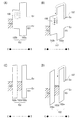
本実施の形態では、半導体層と電子捕獲層とゲート電極とを有する半導体装置の構成および動作原理、および、それを応用した回路について説明する。図1(A)は、半導体層101と電子捕獲層102とゲート電極103とゲート絶縁層104とゲート電極105とを有する半導体装置である。
本実施の形態では、本発明の一態様の半導体装置について図面を用いて説明する。なお、以下では、主として、しきい値補正用のゲート電極が基板と半導体層の間に存在するトランジスタについて説明するが、しきい値補正用のゲート電極と基板の間にと半導体層が存在するトランジスタであってもよい。
本実施の形態では、実施の形態2で説明した図7に示すトランジスタ450の作製方法について、図10および図11を用いて説明する。
本実施の形態では、プレナー構造のトランジスタについて説明する。
本実施の形態では、本発明の一態様のトランジスタを利用した回路の一例について、図面を参照して説明する。
本実施の形態では、少なくとも先の実施の形態で説明したトランジスタを用いることができ、先の実施の形態で説明した記憶装置を含むCPUについて説明する。
本発明の一態様に係る半導体装置は、表示機器、パーソナルコンピュータ、記録媒体を備えた画像再生装置(代表的にはDVD:Digital Versatile Disc等の記録媒体を再生し、その画像を表示しうるディスプレイを有する装置)に用いることができる。その他に、本発明の一態様に係る半導体装置を用いることができる電子機器として、携帯電話、携帯型を含むゲーム機、携帯データ端末、電子書籍、ビデオカメラ、デジタルスチルカメラ等のカメラ、ゴーグル型ディスプレイ(ヘッドマウントディスプレイ)、ナビゲーションシステム、音響再生装置(カーオーディオ、デジタルオーディオプレイヤー等)、複写機、ファクシミリ、プリンタ、プリンタ複合機、現金自動預け入れ払い機(ATM)、自動販売機などが挙げられる。これら電子機器の具体例を図18に示す。
102 電子捕獲層
102a 第1の絶縁層
102b 第2の絶縁層
102c 第3の絶縁層
102d 導電層
102e 絶縁体
103 ゲート電極
104 ゲート絶縁層
105 ゲート電極
106 電子捕獲準位
107 電子
108 曲線
109 曲線
110 トランジスタ
111 容量素子
121 トランジスタ
122 トランジスタ
123 容量素子
124 トランジスタ
125 容量素子
400 基板
401 ゲート電極
402 下地絶縁層
402a 第1の絶縁層
402b 第2の絶縁層
402c 第3の絶縁層
403c 酸化物半導体層
404 多層半導体層
404a 酸化物半導体層
404b 酸化物半導体層
404c 酸化物半導体層
406a ソース電極
406b ドレイン電極
407 絶縁層
408 ゲート絶縁層
409 導電層
410 ゲート電極
412 酸化物絶縁層
450 トランジスタ
470 トランジスタ
501 筐体
502 筐体
503 表示部
504 表示部
505 マイクロフォン
506 スピーカー
507 操作キー
508 スタイラス
511 筐体
512 筐体
513 表示部
514 表示部
515 接続部
516 操作キー
521 筐体
522 表示部
523 キーボード
524 ポインティングデバイス
531 筐体
532 冷蔵室用扉
533 冷凍室用扉
541 筐体
542 筐体
543 表示部
544 操作キー
545 レンズ
546 接続部
550 トランジスタ
551 車体
552 車輪
553 ダッシュボード
554 ライト
560 トランジスタ
570 トランジスタ
602 フォトダイオード
640 トランジスタ
656 トランジスタ
658 フォトダイオードリセット信号
659 ゲート信号線
671 フォトセンサ出力信号線
672 フォトセンサ基準信号線
673 接地線
700 記憶素子
701 回路
702 回路
703 スイッチ
704 スイッチ
706 論理素子
707 容量素子
708 容量素子
709 トランジスタ
710 トランジスタ
713 トランジスタ
714 トランジスタ
720 回路
1189 ROMインターフェース
1190 基板
1191 ALU
1192 ALUコントローラ
1193 インストラクションデコーダ
1194 インタラプトコントローラ
1195 タイミングコントローラ
1196 レジスタ
1197 レジスタコントローラ
1198 バスインターフェース
1199 ROM
2200 トランジスタ
2201 絶縁層
2202 配線
2203 プラグ
2204 絶縁層
2205 配線
2206 配線
Claims (16)
- 第1のゲート電極と、
前記第1のゲート電極上方の電子捕獲層と、
前記電子捕獲層上方の第1の酸化物半導体層と、
前記第1の酸化物半導体層上方の第2の酸化物半導体層と、
前記第2の酸化物半導体層と電気的に接続されたソース電極と、
前記第2の酸化物半導体層と電気的に接続されたドレイン電極と、
前記第2の酸化物半導体層上方の第3の酸化物半導体層と、
前記第3の酸化物半導体層上方のゲート絶縁層と、
前記ゲート絶縁層上方の第2のゲート電極と、を有し、
トランジスタのチャネル幅方向において、前記第2の酸化物半導体層は、前記第1の酸化物半導体層と前記第3の酸化物半導体層とに取り囲まれた領域を有し、
トランジスタのチャネル長方向において、前記第2の酸化物半導体層の上面は、前記ソース電極及びドレイン電極と接する領域を有し、
前記第1の酸化物半導体層は、前記第2の酸化物半導体層を構成する金属元素を一種以上有し、
前記第3の酸化物半導体層は、前記第2の酸化物半導体層を構成する金属元素を一種以上有し、
前記第2の酸化物半導体層の電子親和力は、前記第1の酸化物半導体層の電子親和力よりも大きく、
前記第2の酸化物半導体層の電子親和力は、前記第3の酸化物半導体層の電子親和力よりも大きいことを特徴とする半導体装置。 - 第1のゲート電極と、
前記第1のゲート電極上方の電子捕獲層と、
前記電子捕獲層上方の第1の酸化物半導体層と、
前記第1の酸化物半導体層上方の第2の酸化物半導体層と、
前記第2の酸化物半導体層と電気的に接続されたソース電極と、
前記第2の酸化物半導体層と電気的に接続されたドレイン電極と、
前記第2の酸化物半導体層上方の第3の酸化物半導体層と、
前記第3の酸化物半導体層上方のゲート絶縁層と、
前記ゲート絶縁層上方の第2のゲート電極と、を有し、
トランジスタのチャネル幅方向において、前記第3の酸化物半導体層は、前記第2の酸化物半導体層の上面に接する領域と、前記第2の酸化物半導体層の側面に接する領域と、前記第1の酸化物半導体層の側面に接する領域と、を有し、
トランジスタのチャネル長方向において、前記第2の酸化物半導体層の上面は、前記ソース電極及びドレイン電極と接する領域を有し、
前記第1の酸化物半導体層は、前記第2の酸化物半導体層を構成する金属元素を一種以上有し、
前記第3の酸化物半導体層は、前記第2の酸化物半導体層を構成する金属元素を一種以上有し、
前記第2の酸化物半導体層の電子親和力は、前記第1の酸化物半導体層の電子親和力よりも大きく、
前記第2の酸化物半導体層の電子親和力は、前記第3の酸化物半導体層の電子親和力よりも大きいことを特徴とする半導体装置。 - 第1のゲート電極と、
前記第1のゲート電極上方の第1の絶縁層と、
前記第1の絶縁層上方の第2の絶縁層と、
前記第2の絶縁層上方の第3の絶縁層と、
前記第3の絶縁層上方の第1の酸化物半導体層と、
前記第1の酸化物半導体層上方の第2の酸化物半導体層と、
前記第2の酸化物半導体層と電気的に接続されたソース電極と、
前記第2の酸化物半導体層と電気的に接続されたドレイン電極と、
前記第2の酸化物半導体層上方の第3の酸化物半導体層と、
前記第3の酸化物半導体層上方のゲート絶縁層と、
前記ゲート絶縁層上方の第2のゲート電極と、を有し、
トランジスタのチャネル幅方向において、前記第2の酸化物半導体層は、前記第1の酸化物半導体層と前記第3の酸化物半導体層とに取り囲まれた領域を有し、
トランジスタのチャネル長方向において、前記第2の酸化物半導体層の上面は、前記ソース電極及びドレイン電極と接する領域を有し、
前記第1の酸化物半導体層は、前記第2の酸化物半導体層を構成する金属元素を一種以上有し、
前記第3の酸化物半導体層は、前記第2の酸化物半導体層を構成する金属元素を一種以上有し、
前記第2の酸化物半導体層の電子親和力は、前記第1の酸化物半導体層の電子親和力よりも大きく、
前記第2の酸化物半導体層の電子親和力は、前記第3の酸化物半導体層の電子親和力よりも大きく、
前記第1の絶縁層は、酸化シリコン、酸窒化シリコン、又は窒化シリコンを有し、
前記第2の絶縁層は、酸化ハフニウムを有し、
前記第3の絶縁層は、酸化シリコン、酸窒化シリコン、又は窒化シリコンを有することを特徴とする半導体装置。 - 第1のゲート電極と、
前記第1のゲート電極上方の第1の絶縁層と、
前記第1の絶縁層上方の第2の絶縁層と、
前記第2の絶縁層上方の第3の絶縁層と、
前記第3の絶縁層上方の第1の酸化物半導体層と、
前記第1の酸化物半導体層上方の第2の酸化物半導体層と、
前記第2の酸化物半導体層と電気的に接続されたソース電極と、
前記第2の酸化物半導体層と電気的に接続されたドレイン電極と、
前記第2の酸化物半導体層上方の第3の酸化物半導体層と、
前記第3の酸化物半導体層上方のゲート絶縁層と、
前記ゲート絶縁層上方の第2のゲート電極と、を有し、
トランジスタのチャネル幅方向において、前記第3の酸化物半導体層は、前記第2の酸化物半導体層の上面に接する領域と、前記第2の酸化物半導体層の側面に接する領域と、前記第1の酸化物半導体層の側面に接する領域と、を有し、
トランジスタのチャネル長方向において、前記第2の酸化物半導体層の上面は、前記ソース電極及びドレイン電極と接する領域を有し、
前記第1の酸化物半導体層は、前記第2の酸化物半導体層を構成する金属元素を一種以上有し、
前記第3の酸化物半導体層は、前記第2の酸化物半導体層を構成する金属元素を一種以上有し、
前記第2の酸化物半導体層の電子親和力は、前記第1の酸化物半導体層の電子親和力よりも大きく、
前記第2の酸化物半導体層の電子親和力は、前記第3の酸化物半導体層の電子親和力よりも大きく、
前記第1の絶縁層は、酸化シリコン、酸窒化シリコン、又は窒化シリコンを有し、
前記第2の絶縁層は、酸化ハフニウムを有し、
前記第3の絶縁層は、酸化シリコン、酸窒化シリコン、又は窒化シリコンを有することを特徴とする半導体装置。 - 請求項1乃至請求項4のいずれか一において、
前記第1の酸化物半導体層の伝導帯下端のエネルギーは、前記第2の酸化物半導体層の伝導帯下端のエネルギーよりも、真空準位に近く、
前記第2の酸化物半導体の伝導帯下端のエネルギーと前記第1の酸化物半導体層の伝導帯下端のエネルギーとの差は、0.05eV以上2eV以下であり、
前記第3の酸化物半導体層の伝導帯下端のエネルギーは、前記第2の酸化物半導体層の伝導帯下端のエネルギーよりも、真空準位に近く、
前記第2の酸化物半導体の伝導帯下端のエネルギーと前記第3の酸化物半導体層の伝導帯下端のエネルギーとの差は、0.05eV以上2eV以下であることを特徴とする半導体装置。 - 請求項1乃至請求項5のいずれか一において、
前記第2の酸化物半導体層の端部は丸みを帯びた形状を有することを特徴とする半導体装置。 - 第1のゲート電極と、
前記第1のゲート電極上方の電子捕獲層と、
前記電子捕獲層上方の第1の酸化物半導体層と、
前記第1の酸化物半導体層上方の第2の酸化物半導体層と、
前記第2の酸化物半導体層と電気的に接続されたソース電極と、
前記第2の酸化物半導体層と電気的に接続されたドレイン電極と、
前記第2の酸化物半導体層上方の第3の酸化物半導体層と、
前記第3の酸化物半導体層上方のゲート絶縁層と、
前記ゲート絶縁層上方の第2のゲート電極と、を有し、
トランジスタのチャネル幅方向において、前記第2の酸化物半導体層は、前記第1の酸化物半導体層と前記第3の酸化物半導体層とに取り囲まれた領域を有し、
トランジスタのチャネル長方向において、前記第2の酸化物半導体層の上面は、前記ソース電極及びドレイン電極と接する領域を有し、
前記第1の酸化物半導体層は、前記第2の酸化物半導体層を構成する金属元素を一種以上有し、
前記第3の酸化物半導体層は、前記第2の酸化物半導体層を構成する金属元素を一種以上有し、
前記第2の酸化物半導体層の電子親和力は、前記第1の酸化物半導体層の電子親和力よりも大きく、
前記第2の酸化物半導体層の電子親和力は、前記第3の酸化物半導体層の電子親和力よりも大きい半導体装置の作製方法であって、
前記第1のゲート電極の電位を前記ソース電極の電位及び前記ドレイン電極の電位よりも高くして、前記電子捕獲層に電子を捕獲させることを特徴とする半導体装置の作製方法。 - 第1のゲート電極と、
前記第1のゲート電極上方の電子捕獲層と、
前記電子捕獲層上方の第1の酸化物半導体層と、
前記第1の酸化物半導体層上方の第2の酸化物半導体層と、
前記第2の酸化物半導体層と電気的に接続されたソース電極と、
前記第2の酸化物半導体層と電気的に接続されたドレイン電極と、
前記第2の酸化物半導体層上方の第3の酸化物半導体層と、
前記第3の酸化物半導体層上方のゲート絶縁層と、
前記ゲート絶縁層上方の第2のゲート電極と、を有し、
トランジスタのチャネル幅方向において、前記第2の酸化物半導体層は、前記第1の酸化物半導体層と前記第3の酸化物半導体層とに取り囲まれた領域を有し、
トランジスタのチャネル長方向において、前記第2の酸化物半導体層の上面は、前記ソース電極及びドレイン電極と接する領域を有し、
前記第1の酸化物半導体層は、前記第2の酸化物半導体層を構成する金属元素を一種以上有し、
前記第3の酸化物半導体層は、前記第2の酸化物半導体層を構成する金属元素を一種以上有し、
前記第2の酸化物半導体層の電子親和力は、前記第1の酸化物半導体層の電子親和力よりも大きく、
前記第2の酸化物半導体層の電子親和力は、前記第3の酸化物半導体層の電子親和力よりも大きい半導体装置の作製方法であって、
前記第1のゲート電極の電位を前記ソース電極の電位及び前記ドレイン電極の電位よりも高くして、前記電子捕獲層に電子を捕獲させ、前記トランジスタのしきい値を増加させることを特徴とする半導体装置の作製方法。 - 第1のゲート電極と、
前記第1のゲート電極上方の電子捕獲層と、
前記電子捕獲層上方の第1の酸化物半導体層と、
前記第1の酸化物半導体層上方の第2の酸化物半導体層と、
前記第2の酸化物半導体層と電気的に接続されたソース電極と、
前記第2の酸化物半導体層と電気的に接続されたドレイン電極と、
前記第2の酸化物半導体層上方の第3の酸化物半導体層と、
前記第3の酸化物半導体層上方のゲート絶縁層と、
前記ゲート絶縁層上方の第2のゲート電極と、を有し、
トランジスタのチャネル幅方向において、前記第3の酸化物半導体層は、前記第2の酸化物半導体層の上面に接する領域と、前記第2の酸化物半導体層の側面に接する領域と、前記第1の酸化物半導体層の側面に接する領域と、を有し、
トランジスタのチャネル長方向において、前記第2の酸化物半導体層の上面は、前記ソース電極及びドレイン電極と接する領域を有し、
前記第1の酸化物半導体層は、前記第2の酸化物半導体層を構成する金属元素を一種以上有し、
前記第3の酸化物半導体層は、前記第2の酸化物半導体層を構成する金属元素を一種以上有し、
前記第2の酸化物半導体層の電子親和力は、前記第1の酸化物半導体層の電子親和力よりも大きく、
前記第2の酸化物半導体層の電子親和力は、前記第3の酸化物半導体層の電子親和力よりも大きい半導体装置の作製方法であって、
前記第1のゲート電極の電位を前記ソース電極の電位及び前記ドレイン電極の電位よりも高くして、前記電子捕獲層に電子を捕獲させることを特徴とする半導体装置の作製方法。 - 第1のゲート電極と、
前記第1のゲート電極上方の電子捕獲層と、
前記電子捕獲層上方の第1の酸化物半導体層と、
前記第1の酸化物半導体層上方の第2の酸化物半導体層と、
前記第2の酸化物半導体層と電気的に接続されたソース電極と、
前記第2の酸化物半導体層と電気的に接続されたドレイン電極と、
前記第2の酸化物半導体層上方の第3の酸化物半導体層と、
前記第3の酸化物半導体層上方のゲート絶縁層と、
前記ゲート絶縁層上方の第2のゲート電極と、を有し、
トランジスタのチャネル幅方向において、前記第3の酸化物半導体層は、前記第2の酸化物半導体層の上面に接する領域と、前記第2の酸化物半導体層の側面に接する領域と、前記第1の酸化物半導体層の側面に接する領域と、を有し、
トランジスタのチャネル長方向において、前記第2の酸化物半導体層の上面は、前記ソース電極及びドレイン電極と接する領域を有し、
前記第1の酸化物半導体層は、前記第2の酸化物半導体層を構成する金属元素を一種以上有し、
前記第3の酸化物半導体層は、前記第2の酸化物半導体層を構成する金属元素を一種以上有し、
前記第2の酸化物半導体層の電子親和力は、前記第1の酸化物半導体層の電子親和力よりも大きく、
前記第2の酸化物半導体層の電子親和力は、前記第3の酸化物半導体層の電子親和力よりも大きい半導体装置の作製方法であって、
前記第1のゲート電極の電位を前記ソース電極の電位及び前記ドレイン電極の電位よりも高くして、前記電子捕獲層に電子を捕獲させ、前記トランジスタのしきい値を増加させることを特徴とする半導体装置の作製方法。 - 第1のゲート電極と、
前記第1のゲート電極上方の第1の絶縁層と、
前記第1の絶縁層上方の第2の絶縁層と、
前記第2の絶縁層上方の第3の絶縁層と、
前記第3の絶縁層上方の第1の酸化物半導体層と、
前記第1の酸化物半導体層上方の第2の酸化物半導体層と、
前記第2の酸化物半導体層と電気的に接続されたソース電極と、
前記第2の酸化物半導体層と電気的に接続されたドレイン電極と、
前記第2の酸化物半導体層上方の第3の酸化物半導体層と、
前記第3の酸化物半導体層上方のゲート絶縁層と、
前記ゲート絶縁層上方の第2のゲート電極と、を有し、
トランジスタのチャネル幅方向において、前記第2の酸化物半導体層は、前記第1の酸化物半導体層と前記第3の酸化物半導体層とに取り囲まれた領域を有し、
トランジスタのチャネル長方向において、前記第2の酸化物半導体層の上面は、前記ソース電極及びドレイン電極と接する領域を有し、
前記第1の酸化物半導体層は、前記第2の酸化物半導体層を構成する金属元素を一種以上有し、
前記第3の酸化物半導体層は、前記第2の酸化物半導体層を構成する金属元素を一種以上有し、
前記第2の酸化物半導体層の電子親和力は、前記第1の酸化物半導体層の電子親和力よりも大きく、
前記第2の酸化物半導体層の電子親和力は、前記第3の酸化物半導体層の電子親和力よりも大きく、
前記第1の絶縁層は、酸化シリコン、酸窒化シリコン、又は窒化シリコンを有し、
前記第2の絶縁層は、酸化ハフニウムを有し、
前記第3の絶縁層は、酸化シリコン、酸窒化シリコン、又は窒化シリコンを有する半導体装置の作製方法であって、
前記第1のゲート電極の電位を前記ソース電極の電位及び前記ドレイン電極の電位よりも高くして、前記第2の絶縁層に電子を捕獲させることを特徴とする半導体装置の作製方法。 - 第1のゲート電極と、
前記第1のゲート電極上方の第1の絶縁層と、
前記第1の絶縁層上方の第2の絶縁層と、
前記第2の絶縁層上方の第3の絶縁層と、
前記第3の絶縁層上方の第1の酸化物半導体層と、
前記第1の酸化物半導体層上方の第2の酸化物半導体層と、
前記第2の酸化物半導体層と電気的に接続されたソース電極と、
前記第2の酸化物半導体層と電気的に接続されたドレイン電極と、
前記第2の酸化物半導体層上方の第3の酸化物半導体層と、
前記第3の酸化物半導体層上方のゲート絶縁層と、
前記ゲート絶縁層上方の第2のゲート電極と、を有し、
トランジスタのチャネル幅方向において、前記第2の酸化物半導体層は、前記第1の酸化物半導体層と前記第3の酸化物半導体層とに取り囲まれた領域を有し、
トランジスタのチャネル長方向において、前記第2の酸化物半導体層の上面は、前記ソース電極及びドレイン電極と接する領域を有し、
前記第1の酸化物半導体層は、前記第2の酸化物半導体層を構成する金属元素を一種以上有し、
前記第3の酸化物半導体層は、前記第2の酸化物半導体層を構成する金属元素を一種以上有し、
前記第2の酸化物半導体層の電子親和力は、前記第1の酸化物半導体層の電子親和力よりも大きく、
前記第2の酸化物半導体層の電子親和力は、前記第3の酸化物半導体層の電子親和力よりも大きく、
前記第1の絶縁層は、酸化シリコン、酸窒化シリコン、又は窒化シリコンを有し、
前記第2の絶縁層は、酸化ハフニウムを有し、
前記第3の絶縁層は、酸化シリコン、酸窒化シリコン、又は窒化シリコンを有する半導体装置の作製方法であって、
前記第1のゲート電極の電位を前記ソース電極の電位及び前記ドレイン電極の電位よりも高くして、前記第2の絶縁層に電子を捕獲させ、前記トランジスタのしきい値を増加させることを特徴とする半導体装置の作製方法。 - 第1のゲート電極と、
前記第1のゲート電極上方の第1の絶縁層と、
前記第1の絶縁層上方の第2の絶縁層と、
前記第2の絶縁層上方の第3の絶縁層と、
前記第3の絶縁層上方の第1の酸化物半導体層と、
前記第1の酸化物半導体層上方の第2の酸化物半導体層と、
前記第2の酸化物半導体層と電気的に接続されたソース電極と、
前記第2の酸化物半導体層と電気的に接続されたドレイン電極と、
前記第2の酸化物半導体層上方の第3の酸化物半導体層と、
前記第3の酸化物半導体層上方のゲート絶縁層と、
前記ゲート絶縁層上方の第2のゲート電極と、を有し、
トランジスタのチャネル幅方向において、前記第3の酸化物半導体層は、前記第2の酸化物半導体層の上面に接する領域と、前記第2の酸化物半導体層の側面に接する領域と、前記第1の酸化物半導体層の側面に接する領域と、を有し、
トランジスタのチャネル長方向において、前記第2の酸化物半導体層の上面は、前記ソース電極及びドレイン電極と接する領域を有し、
前記第1の酸化物半導体層は、前記第2の酸化物半導体層を構成する金属元素を一種以上有し、
前記第3の酸化物半導体層は、前記第2の酸化物半導体層を構成する金属元素を一種以上有し、
前記第2の酸化物半導体層の電子親和力は、前記第1の酸化物半導体層の電子親和力よりも大きく、
前記第2の酸化物半導体層の電子親和力は、前記第3の酸化物半導体層の電子親和力よりも大きく、
前記第1の絶縁層は、酸化シリコン、酸窒化シリコン、又は窒化シリコンを有し、
前記第2の絶縁層は、酸化ハフニウムを有し、
前記第3の絶縁層は、酸化シリコン、酸窒化シリコン、又は窒化シリコンを有する半導体装置の作製方法であって、
前記第1のゲート電極の電位を前記ソース電極の電位及び前記ドレイン電極の電位よりも高くして、前記第2の絶縁層に電子を捕獲させることを特徴とする半導体装置の作製方法。 - 第1のゲート電極と、
前記第1のゲート電極上方の第1の絶縁層と、
前記第1の絶縁層上方の第2の絶縁層と、
前記第2の絶縁層上方の第3の絶縁層と、
前記第3の絶縁層上方の第1の酸化物半導体層と、
前記第1の酸化物半導体層上方の第2の酸化物半導体層と、
前記第2の酸化物半導体層と電気的に接続されたソース電極と、
前記第2の酸化物半導体層と電気的に接続されたドレイン電極と、
前記第2の酸化物半導体層上方の第3の酸化物半導体層と、
前記第3の酸化物半導体層上方のゲート絶縁層と、
前記ゲート絶縁層上方の第2のゲート電極と、を有し、
トランジスタのチャネル幅方向において、前記第3の酸化物半導体層は、前記第2の酸化物半導体層の上面に接する領域と、前記第2の酸化物半導体層の側面に接する領域と、前記第1の酸化物半導体層の側面に接する領域と、を有し、
トランジスタのチャネル長方向において、前記第2の酸化物半導体層の上面は、前記ソース電極及びドレイン電極と接する領域を有し、
前記第1の酸化物半導体層は、前記第2の酸化物半導体層を構成する金属元素を一種以上有し、
前記第3の酸化物半導体層は、前記第2の酸化物半導体層を構成する金属元素を一種以上有し、
前記第2の酸化物半導体層の電子親和力は、前記第1の酸化物半導体層の電子親和力よりも大きく、
前記第2の酸化物半導体層の電子親和力は、前記第3の酸化物半導体層の電子親和力よりも大きく、
前記第1の絶縁層は、酸化シリコン、酸窒化シリコン、又は窒化シリコンを有し、
前記第2の絶縁層は、酸化ハフニウムを有し、
前記第3の絶縁層は、酸化シリコン、酸窒化シリコン、又は窒化シリコンを有する半導体装置の作製方法であって、
前記第1のゲート電極の電位を前記ソース電極の電位及び前記ドレイン電極の電位よりも高くして、前記第2の絶縁層に電子を捕獲させ、前記トランジスタのしきい値を増加させることを特徴とする半導体装置の作製方法。 - 請求項7乃至請求項14のいずれか一において、
前記第1の酸化物半導体層の伝導帯下端のエネルギーは、前記第2の酸化物半導体層の伝導帯下端のエネルギーよりも、真空準位に近く、
前記第2の酸化物半導体の伝導帯下端のエネルギーと前記第1の酸化物半導体層の伝導帯下端のエネルギーとの差は、0.05eV以上2eV以下であり、
前記第3の酸化物半導体層の伝導帯下端のエネルギーは、前記第2の酸化物半導体層の伝導帯下端のエネルギーよりも、真空準位に近く、
前記第2の酸化物半導体の伝導帯下端のエネルギーと前記第3の酸化物半導体層の伝導帯下端のエネルギーとの差は、0.05eV以上2eV以下であることを特徴とする半導体装置の作製方法。 - 請求項7乃至請求項15のいずれか一において、
前記第2の酸化物半導体層の端部は丸みを帯びた形状を有することを特徴とする半導体装置の作製方法。
Priority Applications (1)
| Application Number | Priority Date | Filing Date | Title |
|---|---|---|---|
| JP2014139489A JP6031472B2 (ja) | 2013-07-08 | 2014-07-07 | 半導体装置および半導体装置の作製方法 |
Applications Claiming Priority (3)
| Application Number | Priority Date | Filing Date | Title |
|---|---|---|---|
| JP2013142308 | 2013-07-08 | ||
| JP2013142308 | 2013-07-08 | ||
| JP2014139489A JP6031472B2 (ja) | 2013-07-08 | 2014-07-07 | 半導体装置および半導体装置の作製方法 |
Related Child Applications (1)
| Application Number | Title | Priority Date | Filing Date |
|---|---|---|---|
| JP2016207817A Division JP6416846B2 (ja) | 2013-07-08 | 2016-10-24 | 半導体装置 |
Publications (3)
| Publication Number | Publication Date |
|---|---|
| JP2015035597A JP2015035597A (ja) | 2015-02-19 |
| JP2015035597A5 JP2015035597A5 (ja) | 2015-09-17 |
| JP6031472B2 true JP6031472B2 (ja) | 2016-11-24 |
Family
ID=52132177
Family Applications (4)
| Application Number | Title | Priority Date | Filing Date |
|---|---|---|---|
| JP2014139489A Active JP6031472B2 (ja) | 2013-07-08 | 2014-07-07 | 半導体装置および半導体装置の作製方法 |
| JP2016207817A Expired - Fee Related JP6416846B2 (ja) | 2013-07-08 | 2016-10-24 | 半導体装置 |
| JP2018189066A Active JP6697049B2 (ja) | 2013-07-08 | 2018-10-04 | 半導体装置 |
| JP2020076801A Withdrawn JP2020127040A (ja) | 2013-07-08 | 2020-04-23 | 半導体装置 |
Family Applications After (3)
| Application Number | Title | Priority Date | Filing Date |
|---|---|---|---|
| JP2016207817A Expired - Fee Related JP6416846B2 (ja) | 2013-07-08 | 2016-10-24 | 半導体装置 |
| JP2018189066A Active JP6697049B2 (ja) | 2013-07-08 | 2018-10-04 | 半導体装置 |
| JP2020076801A Withdrawn JP2020127040A (ja) | 2013-07-08 | 2020-04-23 | 半導体装置 |
Country Status (3)
| Country | Link |
|---|---|
| US (2) | US20150008428A1 (ja) |
| JP (4) | JP6031472B2 (ja) |
| KR (1) | KR102291882B1 (ja) |
Cited By (1)
| Publication number | Priority date | Publication date | Assignee | Title |
|---|---|---|---|---|
| KR20220091951A (ko) * | 2020-12-24 | 2022-07-01 | 주식회사 인트켐 | 발수 및 항균/항곰팡이 기능을 갖는 열교환기 핀의 표면처리방법 |
Families Citing this family (43)
| Publication number | Priority date | Publication date | Assignee | Title |
|---|---|---|---|---|
| US10304859B2 (en) * | 2013-04-12 | 2019-05-28 | Semiconductor Energy Laboratory Co., Ltd. | Semiconductor device having an oxide film on an oxide semiconductor film |
| US9312349B2 (en) | 2013-07-08 | 2016-04-12 | Semiconductor Energy Laboratory Co., Ltd. | Semiconductor device and method for manufacturing semiconductor device |
| US9443592B2 (en) | 2013-07-18 | 2016-09-13 | Semiconductor Energy Laboratory Co., Ltd. | Semiconductor device and method for manufacturing semiconductor device |
| US9601591B2 (en) | 2013-08-09 | 2017-03-21 | Semiconductor Energy Laboratory Co., Ltd. | Method for manufacturing semiconductor device |
| US9443990B2 (en) * | 2013-08-26 | 2016-09-13 | Semiconductor Energy Laboratory Co., Ltd. | Semiconductor device and method for manufacturing semiconductor device for adjusting threshold thereof |
| US9449853B2 (en) | 2013-09-04 | 2016-09-20 | Semiconductor Energy Laboratory Co., Ltd. | Method for manufacturing semiconductor device comprising electron trap layer |
| US9269822B2 (en) | 2013-09-12 | 2016-02-23 | Semiconductor Energy Laboratory Co., Ltd. | Semiconductor device and method for manufacturing semiconductor device |
| US9893194B2 (en) | 2013-09-12 | 2018-02-13 | Semiconductor Energy Laboratory Co., Ltd. | Method for manufacturing semiconductor device |
| TWI678740B (zh) | 2013-09-23 | 2019-12-01 | 日商半導體能源研究所股份有限公司 | 半導體裝置 |
| JP6615490B2 (ja) | 2014-05-29 | 2019-12-04 | 株式会社半導体エネルギー研究所 | 半導体装置及び電子機器 |
| TWI663726B (zh) | 2014-05-30 | 2019-06-21 | Semiconductor Energy Laboratory Co., Ltd. | 半導體裝置、模組及電子裝置 |
| JP6652342B2 (ja) | 2014-08-08 | 2020-02-19 | 株式会社半導体エネルギー研究所 | 半導体装置 |
| TWI766298B (zh) | 2014-11-21 | 2022-06-01 | 日商半導體能源研究所股份有限公司 | 半導體裝置 |
| JP6857447B2 (ja) * | 2015-01-26 | 2021-04-14 | 株式会社半導体エネルギー研究所 | 半導体装置 |
| JP6436531B2 (ja) * | 2015-01-30 | 2018-12-12 | 住友電工デバイス・イノベーション株式会社 | 半導体装置の製造方法 |
| US10403646B2 (en) * | 2015-02-20 | 2019-09-03 | Semiconductor Energy Laboratory Co., Ltd. | Semiconductor device and method for manufacturing the same |
| US9653613B2 (en) * | 2015-02-27 | 2017-05-16 | Semiconductor Energy Laboratory Co., Ltd. | Semiconductor device and manufacturing method thereof |
| KR102653836B1 (ko) * | 2015-03-03 | 2024-04-03 | 가부시키가이샤 한도오따이 에네루기 켄큐쇼 | 반도체 장치, 그 제작 방법, 또는 그를 포함하는 표시 장치 |
| JP6683503B2 (ja) * | 2015-03-03 | 2020-04-22 | 株式会社半導体エネルギー研究所 | 半導体装置 |
| KR20160114511A (ko) | 2015-03-24 | 2016-10-05 | 가부시키가이샤 한도오따이 에네루기 켄큐쇼 | 반도체 장치의 제작 방법 |
| US9806200B2 (en) | 2015-03-27 | 2017-10-31 | Semiconductor Energy Laboratory Co., Ltd. | Semiconductor device |
| TWI695513B (zh) * | 2015-03-27 | 2020-06-01 | 日商半導體能源研究所股份有限公司 | 半導體裝置及電子裝置 |
| KR20230098354A (ko) * | 2015-04-13 | 2023-07-03 | 가부시키가이샤 한도오따이 에네루기 켄큐쇼 | 반도체 장치 |
| US10056497B2 (en) * | 2015-04-15 | 2018-08-21 | Semiconductor Energy Laboratory Co., Ltd. | Semiconductor device and manufacturing method thereof |
| US10192995B2 (en) * | 2015-04-28 | 2019-01-29 | Semiconductor Energy Laboratory Co., Ltd. | Semiconductor device and manufacturing method thereof |
| US10553690B2 (en) | 2015-08-04 | 2020-02-04 | Semiconductor Energy Laboratory Co., Ltd. | Semiconductor device and manufacturing method thereof |
| US9847406B2 (en) * | 2015-08-27 | 2017-12-19 | Semiconductor Energy Laboratory Co., Ltd. | Semiconductor device, storage device, resistor circuit, display device, and electronic device |
| US9911756B2 (en) * | 2015-08-31 | 2018-03-06 | Semiconductor Energy Laboratory Co., Ltd. | Semiconductor device including transistor and electronic device surrounded by layer having assigned band gap to prevent electrostatic discharge damage |
| US10714633B2 (en) | 2015-12-15 | 2020-07-14 | Semiconductor Energy Laboratory Co., Ltd. | Semiconductor device and display device |
| US9882064B2 (en) * | 2016-03-10 | 2018-01-30 | Semiconductor Energy Laboratory Co., Ltd. | Transistor and electronic device |
| WO2017153882A1 (en) | 2016-03-11 | 2017-09-14 | Semiconductor Energy Laboratory Co., Ltd. | Semiconductor device, manufacturing method thereof, and display device including the semiconductor device |
| TW202129783A (zh) | 2016-08-24 | 2021-08-01 | 日商半導體能源研究所股份有限公司 | 半導體裝置及其製造方法 |
| CN113660439A (zh) * | 2016-12-27 | 2021-11-16 | 株式会社半导体能源研究所 | 摄像装置及电子设备 |
| US11257722B2 (en) | 2017-07-31 | 2022-02-22 | Semiconductor Energy Laboratory Co., Ltd. | Semiconductor device having oxide containing gallium indium and zinc |
| CN107611085B (zh) * | 2017-10-24 | 2019-12-24 | 深圳市华星光电半导体显示技术有限公司 | Oled背板的制作方法 |
| WO2019135731A1 (en) * | 2018-01-02 | 2019-07-11 | Intel Corporation | Thin-film transistor with source/drain structure to reduce parasitic capacitance |
| US11370669B2 (en) * | 2018-01-14 | 2022-06-28 | Applied Materials, Inc. | Amorphous silicon doped yttrium oxide films and methods of formation |
| KR20200127993A (ko) | 2018-03-07 | 2020-11-11 | 가부시키가이샤 한도오따이 에네루기 켄큐쇼 | 반도체 장치 및 반도체 장치의 제작 방법 |
| WO2019186315A1 (ja) | 2018-03-29 | 2019-10-03 | 株式会社半導体エネルギー研究所 | 半導体装置、および半導体装置の作製方法 |
| JP7275112B2 (ja) | 2018-04-20 | 2023-05-17 | 株式会社半導体エネルギー研究所 | 半導体装置 |
| KR20210062129A (ko) * | 2019-11-20 | 2021-05-31 | 삼성디스플레이 주식회사 | 표시 장치 및 표시 장치의 제조 방법 |
| CN111179750A (zh) * | 2019-12-12 | 2020-05-19 | 武汉华星光电技术有限公司 | 显示面板的结构和其制作方法 |
| US20220344357A1 (en) * | 2021-04-23 | 2022-10-27 | Taiwan Semiconductor Manufacturing Company, Ltd. | Memory device, integrated circuit, and manufacturing method of memory device |
Family Cites Families (173)
| Publication number | Priority date | Publication date | Assignee | Title |
|---|---|---|---|---|
| JPS60198861A (ja) | 1984-03-23 | 1985-10-08 | Fujitsu Ltd | 薄膜トランジスタ |
| JPH0244256B2 (ja) | 1987-01-28 | 1990-10-03 | Kagaku Gijutsucho Mukizaishitsu Kenkyushocho | Ingazn2o5deshimesarerurotsuhoshokeinosojokozoojusurukagobutsuoyobisonoseizoho |
| JPH0244258B2 (ja) | 1987-02-24 | 1990-10-03 | Kagaku Gijutsucho Mukizaishitsu Kenkyushocho | Ingazn3o6deshimesarerurotsuhoshokeinosojokozoojusurukagobutsuoyobisonoseizoho |
| JPS63210023A (ja) | 1987-02-24 | 1988-08-31 | Natl Inst For Res In Inorg Mater | InGaZn↓4O↓7で示される六方晶系の層状構造を有する化合物およびその製造法 |
| JPH0244260B2 (ja) | 1987-02-24 | 1990-10-03 | Kagaku Gijutsucho Mukizaishitsu Kenkyushocho | Ingazn5o8deshimesarerurotsuhoshokeinosojokozoojusurukagobutsuoyobisonoseizoho |
| JPH0244262B2 (ja) | 1987-02-27 | 1990-10-03 | Kagaku Gijutsucho Mukizaishitsu Kenkyushocho | Ingazn6o9deshimesarerurotsuhoshokeinosojokozoojusurukagobutsuoyobisonoseizoho |
| JPH0244263B2 (ja) | 1987-04-22 | 1990-10-03 | Kagaku Gijutsucho Mukizaishitsu Kenkyushocho | Ingazn7o10deshimesarerurotsuhoshokeinosojokozoojusurukagobutsuoyobisonoseizoho |
| US5079606A (en) * | 1989-01-26 | 1992-01-07 | Casio Computer Co., Ltd. | Thin-film memory element |
| JPH0382164A (ja) * | 1989-08-25 | 1991-04-08 | Casio Comput Co Ltd | 薄膜モランジスタメモリおよびその製造方法 |
| JPH05251705A (ja) | 1992-03-04 | 1993-09-28 | Fuji Xerox Co Ltd | 薄膜トランジスタ |
| JP3479375B2 (ja) | 1995-03-27 | 2003-12-15 | 科学技術振興事業団 | 亜酸化銅等の金属酸化物半導体による薄膜トランジスタとpn接合を形成した金属酸化物半導体装置およびそれらの製造方法 |
| US5902650A (en) | 1995-07-11 | 1999-05-11 | Applied Komatsu Technology, Inc. | Method of depositing amorphous silicon based films having controlled conductivity |
| JP3424427B2 (ja) | 1995-07-27 | 2003-07-07 | ソニー株式会社 | 不揮発性半導体メモリ装置 |
| EP0820644B1 (en) | 1995-08-03 | 2005-08-24 | Koninklijke Philips Electronics N.V. | Semiconductor device provided with transparent switching element |
| JP3625598B2 (ja) | 1995-12-30 | 2005-03-02 | 三星電子株式会社 | 液晶表示装置の製造方法 |
| JP4170454B2 (ja) | 1998-07-24 | 2008-10-22 | Hoya株式会社 | 透明導電性酸化物薄膜を有する物品及びその製造方法 |
| JP2000150861A (ja) | 1998-11-16 | 2000-05-30 | Tdk Corp | 酸化物薄膜 |
| JP3276930B2 (ja) | 1998-11-17 | 2002-04-22 | 科学技術振興事業団 | トランジスタ及び半導体装置 |
| JP4342621B2 (ja) | 1998-12-09 | 2009-10-14 | 株式会社東芝 | 不揮発性半導体記憶装置 |
| TW460731B (en) | 1999-09-03 | 2001-10-21 | Ind Tech Res Inst | Electrode structure and production method of wide viewing angle LCD |
| JP4089858B2 (ja) | 2000-09-01 | 2008-05-28 | 国立大学法人東北大学 | 半導体デバイス |
| KR20020038482A (ko) | 2000-11-15 | 2002-05-23 | 모리시타 요이찌 | 박막 트랜지스터 어레이, 그 제조방법 및 그것을 이용한표시패널 |
| JP3997731B2 (ja) | 2001-03-19 | 2007-10-24 | 富士ゼロックス株式会社 | 基材上に結晶性半導体薄膜を形成する方法 |
| JP2002289859A (ja) | 2001-03-23 | 2002-10-04 | Minolta Co Ltd | 薄膜トランジスタ |
| JP3925839B2 (ja) | 2001-09-10 | 2007-06-06 | シャープ株式会社 | 半導体記憶装置およびその試験方法 |
| JP4090716B2 (ja) | 2001-09-10 | 2008-05-28 | 雅司 川崎 | 薄膜トランジスタおよびマトリクス表示装置 |
| JP4164562B2 (ja) | 2002-09-11 | 2008-10-15 | 独立行政法人科学技術振興機構 | ホモロガス薄膜を活性層として用いる透明薄膜電界効果型トランジスタ |
| WO2003040441A1 (en) | 2001-11-05 | 2003-05-15 | Japan Science And Technology Agency | Natural superlattice homologous single crystal thin film, method for preparation thereof, and device using said single crystal thin film |
| JP4083486B2 (ja) | 2002-02-21 | 2008-04-30 | 独立行政法人科学技術振興機構 | LnCuO(S,Se,Te)単結晶薄膜の製造方法 |
| CN1445821A (zh) | 2002-03-15 | 2003-10-01 | 三洋电机株式会社 | ZnO膜和ZnO半导体层的形成方法、半导体元件及其制造方法 |
| JP3933591B2 (ja) | 2002-03-26 | 2007-06-20 | 淳二 城戸 | 有機エレクトロルミネッセント素子 |
| US7339187B2 (en) | 2002-05-21 | 2008-03-04 | State Of Oregon Acting By And Through The Oregon State Board Of Higher Education On Behalf Of Oregon State University | Transistor structures |
| JP2004022625A (ja) | 2002-06-13 | 2004-01-22 | Murata Mfg Co Ltd | 半導体デバイス及び該半導体デバイスの製造方法 |
| US20030235076A1 (en) | 2002-06-21 | 2003-12-25 | Micron Technology, Inc. | Multistate NROM having a storage density much greater than 1 Bit per 1F2 |
| US7105868B2 (en) | 2002-06-24 | 2006-09-12 | Cermet, Inc. | High-electron mobility transistor with zinc oxide |
| US7067843B2 (en) | 2002-10-11 | 2006-06-27 | E. I. Du Pont De Nemours And Company | Transparent oxide semiconductor thin film transistors |
| US6858899B2 (en) * | 2002-10-15 | 2005-02-22 | Matrix Semiconductor, Inc. | Thin film transistor with metal oxide layer and method of making same |
| JP4166105B2 (ja) | 2003-03-06 | 2008-10-15 | シャープ株式会社 | 半導体装置およびその製造方法 |
| JP2004273732A (ja) | 2003-03-07 | 2004-09-30 | Sharp Corp | アクティブマトリクス基板およびその製造方法 |
| JP4108633B2 (ja) | 2003-06-20 | 2008-06-25 | シャープ株式会社 | 薄膜トランジスタおよびその製造方法ならびに電子デバイス |
| US7262463B2 (en) | 2003-07-25 | 2007-08-28 | Hewlett-Packard Development Company, L.P. | Transistor including a deposited channel region having a doped portion |
| US7282782B2 (en) | 2004-03-12 | 2007-10-16 | Hewlett-Packard Development Company, L.P. | Combined binary oxide semiconductor device |
| US7297977B2 (en) | 2004-03-12 | 2007-11-20 | Hewlett-Packard Development Company, L.P. | Semiconductor device |
| CN1998087B (zh) | 2004-03-12 | 2014-12-31 | 独立行政法人科学技术振兴机构 | 非晶形氧化物和薄膜晶体管 |
| US7145174B2 (en) * | 2004-03-12 | 2006-12-05 | Hewlett-Packard Development Company, Lp. | Semiconductor device |
| US20050205969A1 (en) | 2004-03-19 | 2005-09-22 | Sharp Laboratories Of America, Inc. | Charge trap non-volatile memory structure for 2 bits per transistor |
| US7211825B2 (en) | 2004-06-14 | 2007-05-01 | Yi-Chi Shih | Indium oxide-based thin film transistors and circuits |
| JP2006100760A (ja) | 2004-09-02 | 2006-04-13 | Casio Comput Co Ltd | 薄膜トランジスタおよびその製造方法 |
| US7285501B2 (en) | 2004-09-17 | 2007-10-23 | Hewlett-Packard Development Company, L.P. | Method of forming a solution processed device |
| US7298084B2 (en) | 2004-11-02 | 2007-11-20 | 3M Innovative Properties Company | Methods and displays utilizing integrated zinc oxide row and column drivers in conjunction with organic light emitting diodes |
| US7829444B2 (en) | 2004-11-10 | 2010-11-09 | Canon Kabushiki Kaisha | Field effect transistor manufacturing method |
| JP5126729B2 (ja) | 2004-11-10 | 2013-01-23 | キヤノン株式会社 | 画像表示装置 |
| US7791072B2 (en) | 2004-11-10 | 2010-09-07 | Canon Kabushiki Kaisha | Display |
| RU2399989C2 (ru) | 2004-11-10 | 2010-09-20 | Кэнон Кабусики Кайся | Аморфный оксид и полевой транзистор с его использованием |
| US7863611B2 (en) | 2004-11-10 | 2011-01-04 | Canon Kabushiki Kaisha | Integrated circuits utilizing amorphous oxides |
| US7453065B2 (en) | 2004-11-10 | 2008-11-18 | Canon Kabushiki Kaisha | Sensor and image pickup device |
| WO2006051994A2 (en) | 2004-11-10 | 2006-05-18 | Canon Kabushiki Kaisha | Light-emitting device |
| US7868326B2 (en) | 2004-11-10 | 2011-01-11 | Canon Kabushiki Kaisha | Field effect transistor |
| US7579224B2 (en) | 2005-01-21 | 2009-08-25 | Semiconductor Energy Laboratory Co., Ltd. | Method for manufacturing a thin film semiconductor device |
| TWI569441B (zh) | 2005-01-28 | 2017-02-01 | 半導體能源研究所股份有限公司 | 半導體裝置,電子裝置,和半導體裝置的製造方法 |
| TWI412138B (zh) | 2005-01-28 | 2013-10-11 | Semiconductor Energy Lab | 半導體裝置,電子裝置,和半導體裝置的製造方法 |
| US7858451B2 (en) | 2005-02-03 | 2010-12-28 | Semiconductor Energy Laboratory Co., Ltd. | Electronic device, semiconductor device and manufacturing method thereof |
| KR100652401B1 (ko) | 2005-02-16 | 2006-12-01 | 삼성전자주식회사 | 복수의 트랩막들을 포함하는 비휘발성 메모리 소자 |
| US7948171B2 (en) | 2005-02-18 | 2011-05-24 | Semiconductor Energy Laboratory Co., Ltd. | Light emitting device |
| US20060197092A1 (en) | 2005-03-03 | 2006-09-07 | Randy Hoffman | System and method for forming conductive material on a substrate |
| US8681077B2 (en) | 2005-03-18 | 2014-03-25 | Semiconductor Energy Laboratory Co., Ltd. | Semiconductor device, and display device, driving method and electronic apparatus thereof |
| WO2006105077A2 (en) | 2005-03-28 | 2006-10-05 | Massachusetts Institute Of Technology | Low voltage thin film transistor with high-k dielectric material |
| US7645478B2 (en) | 2005-03-31 | 2010-01-12 | 3M Innovative Properties Company | Methods of making displays |
| US8300031B2 (en) | 2005-04-20 | 2012-10-30 | Semiconductor Energy Laboratory Co., Ltd. | Semiconductor device comprising transistor having gate and drain connected through a current-voltage conversion element |
| JP2006344849A (ja) | 2005-06-10 | 2006-12-21 | Casio Comput Co Ltd | 薄膜トランジスタ |
| US7402506B2 (en) | 2005-06-16 | 2008-07-22 | Eastman Kodak Company | Methods of making thin film transistors comprising zinc-oxide-based semiconductor materials and transistors made thereby |
| US7691666B2 (en) | 2005-06-16 | 2010-04-06 | Eastman Kodak Company | Methods of making thin film transistors comprising zinc-oxide-based semiconductor materials and transistors made thereby |
| US7507618B2 (en) | 2005-06-27 | 2009-03-24 | 3M Innovative Properties Company | Method for making electronic devices using metal oxide nanoparticles |
| KR100711890B1 (ko) | 2005-07-28 | 2007-04-25 | 삼성에스디아이 주식회사 | 유기 발광표시장치 및 그의 제조방법 |
| JP2007059128A (ja) | 2005-08-23 | 2007-03-08 | Canon Inc | 有機el表示装置およびその製造方法 |
| JP4850457B2 (ja) | 2005-09-06 | 2012-01-11 | キヤノン株式会社 | 薄膜トランジスタ及び薄膜ダイオード |
| JP4280736B2 (ja) | 2005-09-06 | 2009-06-17 | キヤノン株式会社 | 半導体素子 |
| JP2007073705A (ja) | 2005-09-06 | 2007-03-22 | Canon Inc | 酸化物半導体チャネル薄膜トランジスタおよびその製造方法 |
| JP5116225B2 (ja) | 2005-09-06 | 2013-01-09 | キヤノン株式会社 | 酸化物半導体デバイスの製造方法 |
| EP1995787A3 (en) | 2005-09-29 | 2012-01-18 | Semiconductor Energy Laboratory Co, Ltd. | Semiconductor device having oxide semiconductor layer and manufacturing method therof |
| JP5037808B2 (ja) | 2005-10-20 | 2012-10-03 | キヤノン株式会社 | アモルファス酸化物を用いた電界効果型トランジスタ、及び該トランジスタを用いた表示装置 |
| US8022465B2 (en) | 2005-11-15 | 2011-09-20 | Macronrix International Co., Ltd. | Low hydrogen concentration charge-trapping layer structures for non-volatile memory |
| CN101577282A (zh) | 2005-11-15 | 2009-11-11 | 株式会社半导体能源研究所 | 半导体器件及其制造方法 |
| TWI292281B (en) | 2005-12-29 | 2008-01-01 | Ind Tech Res Inst | Pixel structure of active organic light emitting diode and method of fabricating the same |
| US7867636B2 (en) | 2006-01-11 | 2011-01-11 | Murata Manufacturing Co., Ltd. | Transparent conductive film and method for manufacturing the same |
| JP4977478B2 (ja) | 2006-01-21 | 2012-07-18 | 三星電子株式会社 | ZnOフィルム及びこれを用いたTFTの製造方法 |
| US7576394B2 (en) | 2006-02-02 | 2009-08-18 | Kochi Industrial Promotion Center | Thin film transistor including low resistance conductive thin films and manufacturing method thereof |
| US7977169B2 (en) | 2006-02-15 | 2011-07-12 | Kochi Industrial Promotion Center | Semiconductor device including active layer made of zinc oxide with controlled orientations and manufacturing method thereof |
| KR20070101595A (ko) | 2006-04-11 | 2007-10-17 | 삼성전자주식회사 | ZnO TFT |
| US7692223B2 (en) | 2006-04-28 | 2010-04-06 | Semiconductor Energy Laboratory Co., Ltd | Semiconductor device and method for manufacturing the same |
| US20070252928A1 (en) | 2006-04-28 | 2007-11-01 | Toppan Printing Co., Ltd. | Structure, transmission type liquid crystal display, reflection type display and manufacturing method thereof |
| JP5028033B2 (ja) | 2006-06-13 | 2012-09-19 | キヤノン株式会社 | 酸化物半導体膜のドライエッチング方法 |
| JP4999400B2 (ja) | 2006-08-09 | 2012-08-15 | キヤノン株式会社 | 酸化物半導体膜のドライエッチング方法 |
| JP4609797B2 (ja) | 2006-08-09 | 2011-01-12 | Nec液晶テクノロジー株式会社 | 薄膜デバイス及びその製造方法 |
| JP4282699B2 (ja) | 2006-09-01 | 2009-06-24 | 株式会社東芝 | 半導体装置 |
| JP4332545B2 (ja) | 2006-09-15 | 2009-09-16 | キヤノン株式会社 | 電界効果型トランジスタ及びその製造方法 |
| JP4274219B2 (ja) | 2006-09-27 | 2009-06-03 | セイコーエプソン株式会社 | 電子デバイス、有機エレクトロルミネッセンス装置、有機薄膜半導体装置 |
| JP5164357B2 (ja) | 2006-09-27 | 2013-03-21 | キヤノン株式会社 | 半導体装置及び半導体装置の製造方法 |
| US7622371B2 (en) | 2006-10-10 | 2009-11-24 | Hewlett-Packard Development Company, L.P. | Fused nanocrystal thin film semiconductor and method |
| US7772021B2 (en) | 2006-11-29 | 2010-08-10 | Samsung Electronics Co., Ltd. | Flat panel displays comprising a thin-film transistor having a semiconductive oxide in its channel and methods of fabricating the same for use in flat panel displays |
| JP2008140684A (ja) | 2006-12-04 | 2008-06-19 | Toppan Printing Co Ltd | カラーelディスプレイおよびその製造方法 |
| KR101303578B1 (ko) | 2007-01-05 | 2013-09-09 | 삼성전자주식회사 | 박막 식각 방법 |
| US8207063B2 (en) | 2007-01-26 | 2012-06-26 | Eastman Kodak Company | Process for atomic layer deposition |
| KR100851215B1 (ko) | 2007-03-14 | 2008-08-07 | 삼성에스디아이 주식회사 | 박막 트랜지스터 및 이를 이용한 유기 전계 발광표시장치 |
| KR101402103B1 (ko) | 2007-03-23 | 2014-06-02 | 가부시키가이샤 한도오따이 에네루기 켄큐쇼 | 반도체장치 |
| KR20080088284A (ko) * | 2007-03-29 | 2008-10-02 | 삼성전자주식회사 | 플래시 메모리 소자 |
| US7795613B2 (en) | 2007-04-17 | 2010-09-14 | Toppan Printing Co., Ltd. | Structure with transistor |
| KR101325053B1 (ko) | 2007-04-18 | 2013-11-05 | 삼성디스플레이 주식회사 | 박막 트랜지스터 기판 및 이의 제조 방법 |
| KR20080094300A (ko) | 2007-04-19 | 2008-10-23 | 삼성전자주식회사 | 박막 트랜지스터 및 그 제조 방법과 박막 트랜지스터를포함하는 평판 디스플레이 |
| KR101334181B1 (ko) | 2007-04-20 | 2013-11-28 | 삼성전자주식회사 | 선택적으로 결정화된 채널층을 갖는 박막 트랜지스터 및 그제조 방법 |
| WO2008133345A1 (en) | 2007-04-25 | 2008-11-06 | Canon Kabushiki Kaisha | Oxynitride semiconductor |
| KR101345376B1 (ko) | 2007-05-29 | 2013-12-24 | 삼성전자주식회사 | ZnO 계 박막 트랜지스터 및 그 제조방법 |
| US8367506B2 (en) | 2007-06-04 | 2013-02-05 | Micron Technology, Inc. | High-k dielectrics with gold nano-particles |
| JP5430846B2 (ja) | 2007-12-03 | 2014-03-05 | 株式会社半導体エネルギー研究所 | 半導体装置の作製方法 |
| US8202365B2 (en) | 2007-12-17 | 2012-06-19 | Fujifilm Corporation | Process for producing oriented inorganic crystalline film, and semiconductor device using the oriented inorganic crystalline film |
| JP5345456B2 (ja) | 2008-08-14 | 2013-11-20 | 富士フイルム株式会社 | 薄膜電界効果型トランジスタ |
| KR101529575B1 (ko) | 2008-09-10 | 2015-06-29 | 삼성전자주식회사 | 트랜지스터, 이를 포함하는 인버터 및 이들의 제조방법 |
| JP4623179B2 (ja) | 2008-09-18 | 2011-02-02 | ソニー株式会社 | 薄膜トランジスタおよびその製造方法 |
| JP5451280B2 (ja) | 2008-10-09 | 2014-03-26 | キヤノン株式会社 | ウルツ鉱型結晶成長用基板およびその製造方法ならびに半導体装置 |
| KR101671210B1 (ko) | 2009-03-06 | 2016-11-01 | 가부시키가이샤 한도오따이 에네루기 켄큐쇼 | 반도체 장치 및 반도체 장치의 제작 방법 |
| JP5531259B2 (ja) | 2009-03-19 | 2014-06-25 | 株式会社東芝 | 半導体装置及びその製造方法 |
| US8581247B2 (en) | 2009-03-31 | 2013-11-12 | Panasonic Corporation | Flexible semiconductor device having gate electrode disposed within an opening of a resin film |
| EP2256795B1 (en) | 2009-05-29 | 2014-11-19 | Semiconductor Energy Laboratory Co., Ltd. | Manufacturing method for oxide semiconductor device |
| KR20110048614A (ko) | 2009-11-03 | 2011-05-12 | 삼성전자주식회사 | 게이트 구조물 및 그 형성 방법 |
| WO2011065216A1 (en) | 2009-11-28 | 2011-06-03 | Semiconductor Energy Laboratory Co., Ltd. | Stacked oxide material, semiconductor device, and method for manufacturing the semiconductor device |
| WO2011065210A1 (en) | 2009-11-28 | 2011-06-03 | Semiconductor Energy Laboratory Co., Ltd. | Stacked oxide material, semiconductor device, and method for manufacturing the semiconductor device |
| KR101714831B1 (ko) | 2009-11-28 | 2017-03-09 | 가부시키가이샤 한도오따이 에네루기 켄큐쇼 | 반도체 장치 |
| JP5679143B2 (ja) | 2009-12-01 | 2015-03-04 | ソニー株式会社 | 薄膜トランジスタならびに表示装置および電子機器 |
| JP5497417B2 (ja) * | 2009-12-10 | 2014-05-21 | 富士フイルム株式会社 | 薄膜トランジスタおよびその製造方法、並びにその薄膜トランジスタを備えた装置 |
| KR101436120B1 (ko) | 2009-12-28 | 2014-09-01 | 가부시키가이샤 한도오따이 에네루기 켄큐쇼 | 반도체 장치의 제작 방법 |
| JP2011138934A (ja) | 2009-12-28 | 2011-07-14 | Sony Corp | 薄膜トランジスタ、表示装置および電子機器 |
| KR20120130763A (ko) | 2010-02-05 | 2012-12-03 | 가부시키가이샤 한도오따이 에네루기 켄큐쇼 | 반도체 장치 및 반도체 장치의 제조 방법 |
| KR101391964B1 (ko) | 2010-04-02 | 2014-05-07 | 가부시키가이샤 한도오따이 에네루기 켄큐쇼 | 반도체 장치 |
| KR20220119771A (ko) | 2010-04-02 | 2022-08-30 | 가부시키가이샤 한도오따이 에네루기 켄큐쇼 | 반도체 장치 |
| KR101706081B1 (ko) | 2010-04-06 | 2017-02-15 | 삼성디스플레이 주식회사 | 박막 트랜지스터, 그 제조 방법 및 이를 포함하는 액정 표시 장치 |
| JP2011222767A (ja) | 2010-04-09 | 2011-11-04 | Sony Corp | 薄膜トランジスタならびに表示装置および電子機器 |
| US8629438B2 (en) | 2010-05-21 | 2014-01-14 | Semiconductor Energy Laboratory Co., Ltd. | Semiconductor device and manufacturing method thereof |
| JP2012004371A (ja) | 2010-06-17 | 2012-01-05 | Sony Corp | 薄膜トランジスタおよび表示装置 |
| DE112011102644B4 (de) | 2010-08-06 | 2019-12-05 | Semiconductor Energy Laboratory Co., Ltd. | Integrierte Halbleiterschaltung |
| WO2012029674A1 (en) * | 2010-09-03 | 2012-03-08 | Semiconductor Energy Laboratory Co., Ltd. | Field effect transistor and method for manufacturing semiconductor device |
| KR20120037838A (ko) * | 2010-10-12 | 2012-04-20 | 삼성전자주식회사 | 트랜지스터 및 이를 포함하는 전자소자 |
| WO2012060253A1 (en) | 2010-11-05 | 2012-05-10 | Semiconductor Energy Laboratory Co., Ltd. | Semiconductor device |
| TWI562379B (en) | 2010-11-30 | 2016-12-11 | Semiconductor Energy Lab Co Ltd | Semiconductor device and method for manufacturing semiconductor device |
| KR101680768B1 (ko) * | 2010-12-10 | 2016-11-29 | 삼성전자주식회사 | 트랜지스터 및 이를 포함하는 전자장치 |
| JP2012142562A (ja) | 2010-12-17 | 2012-07-26 | Semiconductor Energy Lab Co Ltd | 半導体記憶装置 |
| US9024317B2 (en) | 2010-12-24 | 2015-05-05 | Semiconductor Energy Laboratory Co., Ltd. | Semiconductor circuit, method for driving the same, storage device, register circuit, display device, and electronic device |
| CN103348464B (zh) | 2011-01-26 | 2016-01-13 | 株式会社半导体能源研究所 | 半导体装置及其制造方法 |
| US8841664B2 (en) | 2011-03-04 | 2014-09-23 | Semiconductor Energy Laboratory Co., Ltd. | Semiconductor device |
| US8530886B2 (en) | 2011-03-18 | 2013-09-10 | International Business Machines Corporation | Nitride gate dielectric for graphene MOSFET |
| US9082860B2 (en) | 2011-03-31 | 2015-07-14 | Semiconductor Energy Laboratory Co., Ltd. | Semiconductor device |
| KR20130007426A (ko) * | 2011-06-17 | 2013-01-18 | 가부시키가이샤 한도오따이 에네루기 켄큐쇼 | 반도체 장치 및 그 제작 방법 |
| KR20140024866A (ko) * | 2011-06-17 | 2014-03-03 | 가부시키가이샤 한도오따이 에네루기 켄큐쇼 | 반도체 장치 및 그의 제조 방법 |
| US9385238B2 (en) | 2011-07-08 | 2016-07-05 | Semiconductor Energy Laboratory Co., Ltd. | Transistor using oxide semiconductor |
| US8952377B2 (en) * | 2011-07-08 | 2015-02-10 | Semiconductor Energy Laboratory Co., Ltd. | Semiconductor device and manufacturing method thereof |
| US8748886B2 (en) * | 2011-07-08 | 2014-06-10 | Semiconductor Energy Laboratory Co., Ltd. | Semiconductor device and method for manufacturing semiconductor device |
| JP2013125826A (ja) | 2011-12-14 | 2013-06-24 | Renesas Electronics Corp | 半導体装置及び半導体装置の製造方法 |
| TWI562361B (en) | 2012-02-02 | 2016-12-11 | Semiconductor Energy Lab Co Ltd | Semiconductor device |
| WO2013179922A1 (en) | 2012-05-31 | 2013-12-05 | Semiconductor Energy Laboratory Co., Ltd. | Semiconductor device and method for manufacturing the same |
| KR102071545B1 (ko) | 2012-05-31 | 2020-01-30 | 가부시키가이샤 한도오따이 에네루기 켄큐쇼 | 반도체 장치 |
| JP2014027263A (ja) | 2012-06-15 | 2014-02-06 | Semiconductor Energy Lab Co Ltd | 半導体装置およびその作製方法 |
| KR102161077B1 (ko) | 2012-06-29 | 2020-09-29 | 가부시키가이샤 한도오따이 에네루기 켄큐쇼 | 반도체 장치 |
| JP6310194B2 (ja) | 2012-07-06 | 2018-04-11 | 株式会社半導体エネルギー研究所 | 半導体装置 |
| KR20140009023A (ko) | 2012-07-13 | 2014-01-22 | 가부시키가이샤 한도오따이 에네루기 켄큐쇼 | 반도체 장치 |
| US20140027762A1 (en) | 2012-07-27 | 2014-01-30 | Semiconductor Energy Laboratory Co. Ltd. | Semiconductor device |
| JP6134598B2 (ja) | 2012-08-02 | 2017-05-24 | 株式会社半導体エネルギー研究所 | 半導体装置 |
| JP6220597B2 (ja) | 2012-08-10 | 2017-10-25 | 株式会社半導体エネルギー研究所 | 半導体装置 |
| KR20150043307A (ko) | 2012-08-10 | 2015-04-22 | 가부시키가이샤 한도오따이 에네루기 켄큐쇼 | 반도체 장치 및 반도체 장치의 제조 방법 |
| US9245958B2 (en) | 2012-08-10 | 2016-01-26 | Semiconductor Energy Laboratory Co., Ltd. | Semiconductor device and method for manufacturing the same |
| US9929276B2 (en) | 2012-08-10 | 2018-03-27 | Semiconductor Energy Laboratory Co., Ltd. | Semiconductor device and method for manufacturing the same |
| WO2014024808A1 (en) | 2012-08-10 | 2014-02-13 | Semiconductor Energy Laboratory Co., Ltd. | Semiconductor device and manufacturing method thereof |
| CN103632968B (zh) | 2012-08-21 | 2016-10-05 | 中芯国际集成电路制造(上海)有限公司 | 晶体管及其形成方法 |
| JP6400336B2 (ja) | 2013-06-05 | 2018-10-03 | 株式会社半導体エネルギー研究所 | 半導体装置 |
| US9666697B2 (en) | 2013-07-08 | 2017-05-30 | Semiconductor Energy Laboratory Co., Ltd. | Semiconductor device and method for manufacturing semiconductor device including an electron trap layer |
-
2014
- 2014-06-24 US US14/313,154 patent/US20150008428A1/en not_active Abandoned
- 2014-07-03 KR KR1020140083193A patent/KR102291882B1/ko active IP Right Grant
- 2014-07-07 JP JP2014139489A patent/JP6031472B2/ja active Active
-
2016
- 2016-10-24 JP JP2016207817A patent/JP6416846B2/ja not_active Expired - Fee Related
-
2018
- 2018-04-05 US US15/946,149 patent/US11404585B2/en active Active
- 2018-10-04 JP JP2018189066A patent/JP6697049B2/ja active Active
-
2020
- 2020-04-23 JP JP2020076801A patent/JP2020127040A/ja not_active Withdrawn
Cited By (1)
| Publication number | Priority date | Publication date | Assignee | Title |
|---|---|---|---|---|
| KR20220091951A (ko) * | 2020-12-24 | 2022-07-01 | 주식회사 인트켐 | 발수 및 항균/항곰팡이 기능을 갖는 열교환기 핀의 표면처리방법 |
Also Published As
| Publication number | Publication date |
|---|---|
| JP2020127040A (ja) | 2020-08-20 |
| KR20150006363A (ko) | 2015-01-16 |
| JP2015035597A (ja) | 2015-02-19 |
| US20150008428A1 (en) | 2015-01-08 |
| US20180233597A1 (en) | 2018-08-16 |
| US11404585B2 (en) | 2022-08-02 |
| JP2018207133A (ja) | 2018-12-27 |
| KR102291882B1 (ko) | 2021-08-19 |
| JP6697049B2 (ja) | 2020-05-20 |
| JP6416846B2 (ja) | 2018-10-31 |
| JP2017022419A (ja) | 2017-01-26 |
Similar Documents
| Publication | Publication Date | Title |
|---|---|---|
| JP6416846B2 (ja) | 半導体装置 | |
| JP6637566B2 (ja) | 半導体装置 | |
| JP6322503B2 (ja) | 半導体装置 | |
| JP6366398B2 (ja) | 半導体装置 | |
| JP6320201B2 (ja) | 半導体装置の作製方法 | |
| JP6437751B2 (ja) | 半導体装置の作製方法 | |
| JP6401977B2 (ja) | 半導体装置 | |
| JP6435124B2 (ja) | 半導体装置の作製方法 | |
| JP6429547B2 (ja) | 半導体装置 | |
| JP6431729B2 (ja) | 半導体装置の作製方法および半導体装置 | |
| JP2019071481A (ja) | 半導体装置、及び半導体装置の作製方法 |
Legal Events
| Date | Code | Title | Description |
|---|---|---|---|
| A521 | Request for written amendment filed |
Free format text: JAPANESE INTERMEDIATE CODE: A523 Effective date: 20150729 |
|
| A621 | Written request for application examination |
Free format text: JAPANESE INTERMEDIATE CODE: A621 Effective date: 20150729 |
|
| A131 | Notification of reasons for refusal |
Free format text: JAPANESE INTERMEDIATE CODE: A131 Effective date: 20160712 |
|
| A977 | Report on retrieval |
Free format text: JAPANESE INTERMEDIATE CODE: A971007 Effective date: 20160714 |
|
| A521 | Request for written amendment filed |
Free format text: JAPANESE INTERMEDIATE CODE: A523 Effective date: 20160907 |
|
| TRDD | Decision of grant or rejection written | ||
| A01 | Written decision to grant a patent or to grant a registration (utility model) |
Free format text: JAPANESE INTERMEDIATE CODE: A01 Effective date: 20161004 |
|
| A61 | First payment of annual fees (during grant procedure) |
Free format text: JAPANESE INTERMEDIATE CODE: A61 Effective date: 20161024 |
|
| R150 | Certificate of patent or registration of utility model |
Ref document number: 6031472 Country of ref document: JP Free format text: JAPANESE INTERMEDIATE CODE: R150 |
|
| R250 | Receipt of annual fees |
Free format text: JAPANESE INTERMEDIATE CODE: R250 |
|
| R250 | Receipt of annual fees |
Free format text: JAPANESE INTERMEDIATE CODE: R250 |
|
| R250 | Receipt of annual fees |
Free format text: JAPANESE INTERMEDIATE CODE: R250 |
|
| R250 | Receipt of annual fees |
Free format text: JAPANESE INTERMEDIATE CODE: R250 |
|
| R250 | Receipt of annual fees |
Free format text: JAPANESE INTERMEDIATE CODE: R250 |