WO2019186315A1 - 半導体装置、および半導体装置の作製方法 - Google Patents
半導体装置、および半導体装置の作製方法 Download PDFInfo
- Publication number
- WO2019186315A1 WO2019186315A1 PCT/IB2019/052105 IB2019052105W WO2019186315A1 WO 2019186315 A1 WO2019186315 A1 WO 2019186315A1 IB 2019052105 W IB2019052105 W IB 2019052105W WO 2019186315 A1 WO2019186315 A1 WO 2019186315A1
- Authority
- WO
- WIPO (PCT)
- Prior art keywords
- layer
- region
- insulating layer
- semiconductor layer
- film
- Prior art date
Links
- 239000004065 semiconductor Substances 0.000 title claims abstract description 329
- 238000004519 manufacturing process Methods 0.000 title claims description 23
- 229910044991 metal oxide Inorganic materials 0.000 claims abstract description 176
- 150000004706 metal oxides Chemical class 0.000 claims abstract description 166
- 150000004767 nitrides Chemical class 0.000 claims abstract description 19
- 238000000034 method Methods 0.000 claims description 89
- 238000010438 heat treatment Methods 0.000 claims description 52
- 239000001257 hydrogen Substances 0.000 claims description 48
- 229910052739 hydrogen Inorganic materials 0.000 claims description 48
- UFHFLCQGNIYNRP-UHFFFAOYSA-N Hydrogen Chemical compound [H][H] UFHFLCQGNIYNRP-UHFFFAOYSA-N 0.000 claims description 42
- IJGRMHOSHXDMSA-UHFFFAOYSA-N Atomic nitrogen Chemical compound N#N IJGRMHOSHXDMSA-UHFFFAOYSA-N 0.000 claims description 34
- XUIMIQQOPSSXEZ-UHFFFAOYSA-N Silicon Chemical compound [Si] XUIMIQQOPSSXEZ-UHFFFAOYSA-N 0.000 claims description 20
- 229910052782 aluminium Inorganic materials 0.000 claims description 20
- XAGFODPZIPBFFR-UHFFFAOYSA-N aluminium Chemical compound [Al] XAGFODPZIPBFFR-UHFFFAOYSA-N 0.000 claims description 20
- 229910052710 silicon Inorganic materials 0.000 claims description 20
- 239000010703 silicon Substances 0.000 claims description 20
- 239000010936 titanium Substances 0.000 claims description 17
- 229910052738 indium Inorganic materials 0.000 claims description 16
- 229910052757 nitrogen Inorganic materials 0.000 claims description 16
- RTAQQCXQSZGOHL-UHFFFAOYSA-N Titanium Chemical compound [Ti] RTAQQCXQSZGOHL-UHFFFAOYSA-N 0.000 claims description 15
- APFVFJFRJDLVQX-UHFFFAOYSA-N indium atom Chemical compound [In] APFVFJFRJDLVQX-UHFFFAOYSA-N 0.000 claims description 15
- 229910052719 titanium Inorganic materials 0.000 claims description 15
- WFKWXMTUELFFGS-UHFFFAOYSA-N tungsten Chemical compound [W] WFKWXMTUELFFGS-UHFFFAOYSA-N 0.000 claims description 14
- 229910052721 tungsten Inorganic materials 0.000 claims description 14
- 239000010937 tungsten Substances 0.000 claims description 14
- 229910052715 tantalum Inorganic materials 0.000 claims description 12
- GUVRBAGPIYLISA-UHFFFAOYSA-N tantalum atom Chemical compound [Ta] GUVRBAGPIYLISA-UHFFFAOYSA-N 0.000 claims description 12
- VYZAMTAEIAYCRO-UHFFFAOYSA-N Chromium Chemical compound [Cr] VYZAMTAEIAYCRO-UHFFFAOYSA-N 0.000 claims description 8
- 229910052804 chromium Inorganic materials 0.000 claims description 8
- 239000011651 chromium Substances 0.000 claims description 8
- 229910052707 ruthenium Inorganic materials 0.000 claims description 7
- KJTLSVCANCCWHF-UHFFFAOYSA-N Ruthenium Chemical compound [Ru] KJTLSVCANCCWHF-UHFFFAOYSA-N 0.000 claims description 6
- 239000010410 layer Substances 0.000 description 698
- 239000010408 film Substances 0.000 description 359
- QVGXLLKOCUKJST-UHFFFAOYSA-N atomic oxygen Chemical compound [O] QVGXLLKOCUKJST-UHFFFAOYSA-N 0.000 description 104
- 229910052760 oxygen Inorganic materials 0.000 description 104
- 239000001301 oxygen Substances 0.000 description 104
- 108091006146 Channels Proteins 0.000 description 93
- 239000000758 substrate Substances 0.000 description 89
- 230000006870 function Effects 0.000 description 77
- 230000015572 biosynthetic process Effects 0.000 description 76
- 239000000463 material Substances 0.000 description 49
- 239000011701 zinc Substances 0.000 description 47
- 239000004973 liquid crystal related substance Substances 0.000 description 43
- 239000013078 crystal Substances 0.000 description 41
- 239000003990 capacitor Substances 0.000 description 31
- 229910052751 metal Inorganic materials 0.000 description 30
- 238000005530 etching Methods 0.000 description 26
- 239000007789 gas Substances 0.000 description 22
- 230000001965 increasing effect Effects 0.000 description 21
- 239000002184 metal Substances 0.000 description 20
- 239000011347 resin Substances 0.000 description 18
- 229920005989 resin Polymers 0.000 description 18
- 239000010409 thin film Substances 0.000 description 17
- 230000005669 field effect Effects 0.000 description 16
- 238000004544 sputter deposition Methods 0.000 description 16
- 239000000203 mixture Substances 0.000 description 15
- 238000012545 processing Methods 0.000 description 15
- 229910052581 Si3N4 Inorganic materials 0.000 description 14
- HQVNEWCFYHHQES-UHFFFAOYSA-N silicon nitride Chemical compound N12[Si]34N5[Si]62N3[Si]51N64 HQVNEWCFYHHQES-UHFFFAOYSA-N 0.000 description 14
- 238000000151 deposition Methods 0.000 description 12
- 230000008021 deposition Effects 0.000 description 12
- 230000008569 process Effects 0.000 description 12
- PMHQVHHXPFUNSP-UHFFFAOYSA-M copper(1+);methylsulfanylmethane;bromide Chemical compound Br[Cu].CSC PMHQVHHXPFUNSP-UHFFFAOYSA-M 0.000 description 11
- 238000005477 sputtering target Methods 0.000 description 11
- 230000005684 electric field Effects 0.000 description 10
- VYPSYNLAJGMNEJ-UHFFFAOYSA-N Silicium dioxide Chemical compound O=[Si]=O VYPSYNLAJGMNEJ-UHFFFAOYSA-N 0.000 description 9
- 229910052733 gallium Inorganic materials 0.000 description 9
- 239000011521 glass Substances 0.000 description 9
- 230000003287 optical effect Effects 0.000 description 9
- 239000011241 protective layer Substances 0.000 description 9
- GYHNNYVSQQEPJS-UHFFFAOYSA-N Gallium Chemical compound [Ga] GYHNNYVSQQEPJS-UHFFFAOYSA-N 0.000 description 8
- 239000004020 conductor Substances 0.000 description 8
- 239000012535 impurity Substances 0.000 description 8
- 239000002159 nanocrystal Substances 0.000 description 8
- 229910045601 alloy Inorganic materials 0.000 description 7
- 239000000956 alloy Substances 0.000 description 7
- 230000007547 defect Effects 0.000 description 7
- 238000001312 dry etching Methods 0.000 description 7
- 230000000694 effects Effects 0.000 description 7
- 229910000449 hafnium oxide Inorganic materials 0.000 description 7
- WIHZLLGSGQNAGK-UHFFFAOYSA-N hafnium(4+);oxygen(2-) Chemical compound [O-2].[O-2].[Hf+4] WIHZLLGSGQNAGK-UHFFFAOYSA-N 0.000 description 7
- 239000002096 quantum dot Substances 0.000 description 7
- 229910052814 silicon oxide Inorganic materials 0.000 description 7
- RYGMFSIKBFXOCR-UHFFFAOYSA-N Copper Chemical group [Cu] RYGMFSIKBFXOCR-UHFFFAOYSA-N 0.000 description 6
- 230000000903 blocking effect Effects 0.000 description 6
- 238000005229 chemical vapour deposition Methods 0.000 description 6
- 229910052802 copper Inorganic materials 0.000 description 6
- 239000010949 copper Chemical group 0.000 description 6
- 238000010586 diagram Methods 0.000 description 6
- 238000010894 electron beam technology Methods 0.000 description 6
- TWNQGVIAIRXVLR-UHFFFAOYSA-N oxo(oxoalumanyloxy)alumane Chemical compound O=[Al]O[Al]=O TWNQGVIAIRXVLR-UHFFFAOYSA-N 0.000 description 6
- 238000000623 plasma-assisted chemical vapour deposition Methods 0.000 description 6
- XLYOFNOQVPJJNP-UHFFFAOYSA-N water Substances O XLYOFNOQVPJJNP-UHFFFAOYSA-N 0.000 description 6
- UQZIWOQVLUASCR-UHFFFAOYSA-N alumane;titanium Chemical compound [AlH3].[Ti] UQZIWOQVLUASCR-UHFFFAOYSA-N 0.000 description 5
- 125000004429 atom Chemical group 0.000 description 5
- 238000004040 coloring Methods 0.000 description 5
- 150000002431 hydrogen Chemical class 0.000 description 5
- 238000009832 plasma treatment Methods 0.000 description 5
- 230000001681 protective effect Effects 0.000 description 5
- 229910052725 zinc Inorganic materials 0.000 description 5
- MYMOFIZGZYHOMD-UHFFFAOYSA-N Dioxygen Chemical compound O=O MYMOFIZGZYHOMD-UHFFFAOYSA-N 0.000 description 4
- XEEYBQQBJWHFJM-UHFFFAOYSA-N Iron Chemical group [Fe] XEEYBQQBJWHFJM-UHFFFAOYSA-N 0.000 description 4
- ZOKXTWBITQBERF-UHFFFAOYSA-N Molybdenum Chemical group [Mo] ZOKXTWBITQBERF-UHFFFAOYSA-N 0.000 description 4
- PXHVJJICTQNCMI-UHFFFAOYSA-N Nickel Chemical group [Ni] PXHVJJICTQNCMI-UHFFFAOYSA-N 0.000 description 4
- 239000004983 Polymer Dispersed Liquid Crystal Substances 0.000 description 4
- ATJFFYVFTNAWJD-UHFFFAOYSA-N Tin Chemical compound [Sn] ATJFFYVFTNAWJD-UHFFFAOYSA-N 0.000 description 4
- HCHKCACWOHOZIP-UHFFFAOYSA-N Zinc Chemical compound [Zn] HCHKCACWOHOZIP-UHFFFAOYSA-N 0.000 description 4
- 230000009471 action Effects 0.000 description 4
- 239000012790 adhesive layer Substances 0.000 description 4
- -1 aluminum or copper Chemical compound 0.000 description 4
- 238000000231 atomic layer deposition Methods 0.000 description 4
- 230000004888 barrier function Effects 0.000 description 4
- 238000004891 communication Methods 0.000 description 4
- 239000002131 composite material Substances 0.000 description 4
- 229910001882 dioxygen Inorganic materials 0.000 description 4
- 230000002349 favourable effect Effects 0.000 description 4
- 239000011810 insulating material Substances 0.000 description 4
- 229910052750 molybdenum Inorganic materials 0.000 description 4
- 239000011733 molybdenum Chemical group 0.000 description 4
- 238000005268 plasma chemical vapour deposition Methods 0.000 description 4
- 229910052718 tin Inorganic materials 0.000 description 4
- NRTOMJZYCJJWKI-UHFFFAOYSA-N Titanium nitride Chemical compound [Ti]#N NRTOMJZYCJJWKI-UHFFFAOYSA-N 0.000 description 3
- 238000004458 analytical method Methods 0.000 description 3
- 238000012937 correction Methods 0.000 description 3
- 230000006378 damage Effects 0.000 description 3
- 238000009792 diffusion process Methods 0.000 description 3
- 238000002003 electron diffraction Methods 0.000 description 3
- 230000001747 exhibiting effect Effects 0.000 description 3
- 229910052735 hafnium Inorganic materials 0.000 description 3
- 239000011156 metal matrix composite Substances 0.000 description 3
- 238000000206 photolithography Methods 0.000 description 3
- 229920000642 polymer Polymers 0.000 description 3
- 238000004549 pulsed laser deposition Methods 0.000 description 3
- 238000000926 separation method Methods 0.000 description 3
- 238000001039 wet etching Methods 0.000 description 3
- QGZKDVFQNNGYKY-UHFFFAOYSA-N Ammonia Chemical compound N QGZKDVFQNNGYKY-UHFFFAOYSA-N 0.000 description 2
- XKRFYHLGVUSROY-UHFFFAOYSA-N Argon Chemical compound [Ar] XKRFYHLGVUSROY-UHFFFAOYSA-N 0.000 description 2
- ZOXJGFHDIHLPTG-UHFFFAOYSA-N Boron Chemical compound [B] ZOXJGFHDIHLPTG-UHFFFAOYSA-N 0.000 description 2
- MWUXSHHQAYIFBG-UHFFFAOYSA-N Nitric oxide Chemical compound O=[N] MWUXSHHQAYIFBG-UHFFFAOYSA-N 0.000 description 2
- BLRPTPMANUNPDV-UHFFFAOYSA-N Silane Chemical compound [SiH4] BLRPTPMANUNPDV-UHFFFAOYSA-N 0.000 description 2
- 238000002441 X-ray diffraction Methods 0.000 description 2
- 238000004833 X-ray photoelectron spectroscopy Methods 0.000 description 2
- 230000001133 acceleration Effects 0.000 description 2
- 229910021417 amorphous silicon Inorganic materials 0.000 description 2
- 230000005540 biological transmission Effects 0.000 description 2
- 229910052796 boron Inorganic materials 0.000 description 2
- 210000005252 bulbus oculi Anatomy 0.000 description 2
- 239000000969 carrier Substances 0.000 description 2
- 238000003776 cleavage reaction Methods 0.000 description 2
- 230000000295 complement effect Effects 0.000 description 2
- 230000008878 coupling Effects 0.000 description 2
- 238000010168 coupling process Methods 0.000 description 2
- 238000005859 coupling reaction Methods 0.000 description 2
- 238000003795 desorption Methods 0.000 description 2
- AJNVQOSZGJRYEI-UHFFFAOYSA-N digallium;oxygen(2-) Chemical compound [O-2].[O-2].[O-2].[Ga+3].[Ga+3] AJNVQOSZGJRYEI-UHFFFAOYSA-N 0.000 description 2
- 229910001873 dinitrogen Inorganic materials 0.000 description 2
- 238000006073 displacement reaction Methods 0.000 description 2
- 229910001195 gallium oxide Inorganic materials 0.000 description 2
- 229910052732 germanium Inorganic materials 0.000 description 2
- GNPVGFCGXDBREM-UHFFFAOYSA-N germanium atom Chemical compound [Ge] GNPVGFCGXDBREM-UHFFFAOYSA-N 0.000 description 2
- AMGQUBHHOARCQH-UHFFFAOYSA-N indium;oxotin Chemical compound [In].[Sn]=O AMGQUBHHOARCQH-UHFFFAOYSA-N 0.000 description 2
- 230000001939 inductive effect Effects 0.000 description 2
- 239000011261 inert gas Substances 0.000 description 2
- 238000005468 ion implantation Methods 0.000 description 2
- 150000002500 ions Chemical class 0.000 description 2
- 229910052742 iron Inorganic materials 0.000 description 2
- MRELNEQAGSRDBK-UHFFFAOYSA-N lanthanum(3+);oxygen(2-) Chemical compound [O-2].[O-2].[O-2].[La+3].[La+3] MRELNEQAGSRDBK-UHFFFAOYSA-N 0.000 description 2
- 239000012528 membrane Substances 0.000 description 2
- 238000002156 mixing Methods 0.000 description 2
- PLDDOISOJJCEMH-UHFFFAOYSA-N neodymium(3+);oxygen(2-) Chemical compound [O-2].[O-2].[O-2].[Nd+3].[Nd+3] PLDDOISOJJCEMH-UHFFFAOYSA-N 0.000 description 2
- 229910052759 nickel Inorganic materials 0.000 description 2
- 150000002894 organic compounds Chemical class 0.000 description 2
- CNRZQDQNVUKEJG-UHFFFAOYSA-N oxo-bis(oxoalumanyloxy)titanium Chemical compound O=[Al]O[Ti](=O)O[Al]=O CNRZQDQNVUKEJG-UHFFFAOYSA-N 0.000 description 2
- 238000003825 pressing Methods 0.000 description 2
- 238000005546 reactive sputtering Methods 0.000 description 2
- 239000000523 sample Substances 0.000 description 2
- 230000007017 scission Effects 0.000 description 2
- 239000000565 sealant Substances 0.000 description 2
- 238000007789 sealing Methods 0.000 description 2
- 229910000077 silane Inorganic materials 0.000 description 2
- 229910052709 silver Inorganic materials 0.000 description 2
- 239000004332 silver Substances 0.000 description 2
- 239000002356 single layer Substances 0.000 description 2
- 238000003860 storage Methods 0.000 description 2
- 239000000126 substance Substances 0.000 description 2
- MZLGASXMSKOWSE-UHFFFAOYSA-N tantalum nitride Chemical compound [Ta]#N MZLGASXMSKOWSE-UHFFFAOYSA-N 0.000 description 2
- 238000002230 thermal chemical vapour deposition Methods 0.000 description 2
- 229910052727 yttrium Inorganic materials 0.000 description 2
- VWQVUPCCIRVNHF-UHFFFAOYSA-N yttrium atom Chemical group [Y] VWQVUPCCIRVNHF-UHFFFAOYSA-N 0.000 description 2
- 229910017150 AlTi Inorganic materials 0.000 description 1
- OKTJSMMVPCPJKN-UHFFFAOYSA-N Carbon Chemical group [C] OKTJSMMVPCPJKN-UHFFFAOYSA-N 0.000 description 1
- 229910052684 Cerium Inorganic materials 0.000 description 1
- 229910002601 GaN Inorganic materials 0.000 description 1
- JMASRVWKEDWRBT-UHFFFAOYSA-N Gallium nitride Chemical compound [Ga]#N JMASRVWKEDWRBT-UHFFFAOYSA-N 0.000 description 1
- 239000005264 High molar mass liquid crystal Substances 0.000 description 1
- 206010021143 Hypoxia Diseases 0.000 description 1
- FYYHWMGAXLPEAU-UHFFFAOYSA-N Magnesium Chemical compound [Mg] FYYHWMGAXLPEAU-UHFFFAOYSA-N 0.000 description 1
- 229910052779 Neodymium Inorganic materials 0.000 description 1
- 206010034972 Photosensitivity reaction Diseases 0.000 description 1
- 239000004642 Polyimide Substances 0.000 description 1
- 206010037660 Pyrexia Diseases 0.000 description 1
- 229910000577 Silicon-germanium Inorganic materials 0.000 description 1
- BQCADISMDOOEFD-UHFFFAOYSA-N Silver Chemical compound [Ag] BQCADISMDOOEFD-UHFFFAOYSA-N 0.000 description 1
- 229910008813 Sn—Si Inorganic materials 0.000 description 1
- 239000004974 Thermotropic liquid crystal Substances 0.000 description 1
- QCWXUUIWCKQGHC-UHFFFAOYSA-N Zirconium Chemical group [Zr] QCWXUUIWCKQGHC-UHFFFAOYSA-N 0.000 description 1
- LEVVHYCKPQWKOP-UHFFFAOYSA-N [Si].[Ge] Chemical compound [Si].[Ge] LEVVHYCKPQWKOP-UHFFFAOYSA-N 0.000 description 1
- NIXOWILDQLNWCW-UHFFFAOYSA-N acrylic acid group Chemical group C(C=C)(=O)O NIXOWILDQLNWCW-UHFFFAOYSA-N 0.000 description 1
- 239000000654 additive Substances 0.000 description 1
- 230000000996 additive effect Effects 0.000 description 1
- 229910052786 argon Inorganic materials 0.000 description 1
- 238000005452 bending Methods 0.000 description 1
- 229910052790 beryllium Inorganic materials 0.000 description 1
- ATBAMAFKBVZNFJ-UHFFFAOYSA-N beryllium atom Chemical group [Be] ATBAMAFKBVZNFJ-UHFFFAOYSA-N 0.000 description 1
- 239000000919 ceramic Substances 0.000 description 1
- ZMIGMASIKSOYAM-UHFFFAOYSA-N cerium Chemical group [Ce][Ce][Ce][Ce][Ce][Ce][Ce][Ce][Ce][Ce][Ce][Ce][Ce][Ce][Ce][Ce][Ce][Ce][Ce][Ce][Ce][Ce][Ce][Ce][Ce][Ce][Ce][Ce][Ce][Ce][Ce][Ce][Ce][Ce][Ce][Ce][Ce][Ce] ZMIGMASIKSOYAM-UHFFFAOYSA-N 0.000 description 1
- 229910000420 cerium oxide Inorganic materials 0.000 description 1
- 230000008859 change Effects 0.000 description 1
- 239000011248 coating agent Substances 0.000 description 1
- 238000000576 coating method Methods 0.000 description 1
- 229910017052 cobalt Inorganic materials 0.000 description 1
- 239000010941 cobalt Substances 0.000 description 1
- GUTLYIVDDKVIGB-UHFFFAOYSA-N cobalt atom Chemical compound [Co] GUTLYIVDDKVIGB-UHFFFAOYSA-N 0.000 description 1
- 239000003086 colorant Substances 0.000 description 1
- 150000001875 compounds Chemical class 0.000 description 1
- 239000000470 constituent Substances 0.000 description 1
- 238000001514 detection method Methods 0.000 description 1
- 230000006866 deterioration Effects 0.000 description 1
- 238000002050 diffraction method Methods 0.000 description 1
- 239000002019 doping agent Substances 0.000 description 1
- 230000009977 dual effect Effects 0.000 description 1
- 238000001962 electrophoresis Methods 0.000 description 1
- 238000001704 evaporation Methods 0.000 description 1
- 238000007687 exposure technique Methods 0.000 description 1
- 210000001508 eye Anatomy 0.000 description 1
- 210000000744 eyelid Anatomy 0.000 description 1
- 239000005262 ferroelectric liquid crystals (FLCs) Substances 0.000 description 1
- 238000007667 floating Methods 0.000 description 1
- 239000012530 fluid Substances 0.000 description 1
- PCHJSUWPFVWCPO-UHFFFAOYSA-N gold Chemical compound [Au] PCHJSUWPFVWCPO-UHFFFAOYSA-N 0.000 description 1
- 229910052737 gold Inorganic materials 0.000 description 1
- 239000010931 gold Substances 0.000 description 1
- 229910002804 graphite Inorganic materials 0.000 description 1
- 239000010439 graphite Substances 0.000 description 1
- VBJZVLUMGGDVMO-UHFFFAOYSA-N hafnium atom Chemical compound [Hf] VBJZVLUMGGDVMO-UHFFFAOYSA-N 0.000 description 1
- 125000005843 halogen group Chemical group 0.000 description 1
- 230000012447 hatching Effects 0.000 description 1
- 210000003128 head Anatomy 0.000 description 1
- 230000017525 heat dissipation Effects 0.000 description 1
- 239000001307 helium Substances 0.000 description 1
- 229910052734 helium Inorganic materials 0.000 description 1
- SWQJXJOGLNCZEY-UHFFFAOYSA-N helium atom Chemical compound [He] SWQJXJOGLNCZEY-UHFFFAOYSA-N 0.000 description 1
- 125000004435 hydrogen atom Chemical group [H]* 0.000 description 1
- 238000007654 immersion Methods 0.000 description 1
- 230000001771 impaired effect Effects 0.000 description 1
- 229910003437 indium oxide Inorganic materials 0.000 description 1
- PJXISJQVUVHSOJ-UHFFFAOYSA-N indium(iii) oxide Chemical compound [O-2].[O-2].[O-2].[In+3].[In+3] PJXISJQVUVHSOJ-UHFFFAOYSA-N 0.000 description 1
- 150000002484 inorganic compounds Chemical class 0.000 description 1
- 229910010272 inorganic material Inorganic materials 0.000 description 1
- 238000009413 insulation Methods 0.000 description 1
- 229910052746 lanthanum Inorganic materials 0.000 description 1
- FZLIPJUXYLNCLC-UHFFFAOYSA-N lanthanum atom Chemical group [La] FZLIPJUXYLNCLC-UHFFFAOYSA-N 0.000 description 1
- 239000007788 liquid Substances 0.000 description 1
- 238000001459 lithography Methods 0.000 description 1
- 229910052749 magnesium Inorganic materials 0.000 description 1
- 239000011777 magnesium Substances 0.000 description 1
- 239000000395 magnesium oxide Substances 0.000 description 1
- CPLXHLVBOLITMK-UHFFFAOYSA-N magnesium oxide Inorganic materials [Mg]=O CPLXHLVBOLITMK-UHFFFAOYSA-N 0.000 description 1
- AXZKOIWUVFPNLO-UHFFFAOYSA-N magnesium;oxygen(2-) Chemical compound [O-2].[Mg+2] AXZKOIWUVFPNLO-UHFFFAOYSA-N 0.000 description 1
- 230000005389 magnetism Effects 0.000 description 1
- 230000007257 malfunction Effects 0.000 description 1
- WPBNNNQJVZRUHP-UHFFFAOYSA-L manganese(2+);methyl n-[[2-(methoxycarbonylcarbamothioylamino)phenyl]carbamothioyl]carbamate;n-[2-(sulfidocarbothioylamino)ethyl]carbamodithioate Chemical compound [Mn+2].[S-]C(=S)NCCNC([S-])=S.COC(=O)NC(=S)NC1=CC=CC=C1NC(=S)NC(=O)OC WPBNNNQJVZRUHP-UHFFFAOYSA-L 0.000 description 1
- 239000011159 matrix material Substances 0.000 description 1
- 239000007769 metal material Substances 0.000 description 1
- 239000003094 microcapsule Substances 0.000 description 1
- 239000002105 nanoparticle Substances 0.000 description 1
- QEFYFXOXNSNQGX-UHFFFAOYSA-N neodymium atom Chemical group [Nd] QEFYFXOXNSNQGX-UHFFFAOYSA-N 0.000 description 1
- 238000005121 nitriding Methods 0.000 description 1
- 238000007645 offset printing Methods 0.000 description 1
- 239000011368 organic material Substances 0.000 description 1
- 230000001151 other effect Effects 0.000 description 1
- 230000001590 oxidative effect Effects 0.000 description 1
- BMMGVYCKOGBVEV-UHFFFAOYSA-N oxo(oxoceriooxy)cerium Chemical compound [Ce]=O.O=[Ce]=O BMMGVYCKOGBVEV-UHFFFAOYSA-N 0.000 description 1
- SIWVEOZUMHYXCS-UHFFFAOYSA-N oxo(oxoyttriooxy)yttrium Chemical compound O=[Y]O[Y]=O SIWVEOZUMHYXCS-UHFFFAOYSA-N 0.000 description 1
- BPUBBGLMJRNUCC-UHFFFAOYSA-N oxygen(2-);tantalum(5+) Chemical compound [O-2].[O-2].[O-2].[O-2].[O-2].[Ta+5].[Ta+5] BPUBBGLMJRNUCC-UHFFFAOYSA-N 0.000 description 1
- RVTZCBVAJQQJTK-UHFFFAOYSA-N oxygen(2-);zirconium(4+) Chemical compound [O-2].[O-2].[Zr+4] RVTZCBVAJQQJTK-UHFFFAOYSA-N 0.000 description 1
- 230000003071 parasitic effect Effects 0.000 description 1
- 230000002093 peripheral effect Effects 0.000 description 1
- 239000012466 permeate Substances 0.000 description 1
- 230000036211 photosensitivity Effects 0.000 description 1
- 230000000704 physical effect Effects 0.000 description 1
- 239000004033 plastic Substances 0.000 description 1
- 229910021420 polycrystalline silicon Inorganic materials 0.000 description 1
- 229920001721 polyimide Polymers 0.000 description 1
- 239000000843 powder Substances 0.000 description 1
- 239000010453 quartz Substances 0.000 description 1
- 230000005855 radiation Effects 0.000 description 1
- 238000002310 reflectometry Methods 0.000 description 1
- 239000003870 refractory metal Substances 0.000 description 1
- 239000004576 sand Substances 0.000 description 1
- 238000005488 sandblasting Methods 0.000 description 1
- 229910052594 sapphire Inorganic materials 0.000 description 1
- 239000010980 sapphire Substances 0.000 description 1
- 238000007650 screen-printing Methods 0.000 description 1
- HBMJWWWQQXIZIP-UHFFFAOYSA-N silicon carbide Chemical compound [Si+]#[C-] HBMJWWWQQXIZIP-UHFFFAOYSA-N 0.000 description 1
- 229910010271 silicon carbide Inorganic materials 0.000 description 1
- 238000009751 slip forming Methods 0.000 description 1
- 238000005507 spraying Methods 0.000 description 1
- 238000012916 structural analysis Methods 0.000 description 1
- 238000010897 surface acoustic wave method Methods 0.000 description 1
- 229910001936 tantalum oxide Inorganic materials 0.000 description 1
- 238000010345 tape casting Methods 0.000 description 1
- 238000012546 transfer Methods 0.000 description 1
- 230000005641 tunneling Effects 0.000 description 1
- 238000001771 vacuum deposition Methods 0.000 description 1
- 229910052720 vanadium Inorganic materials 0.000 description 1
- GPPXJZIENCGNKB-UHFFFAOYSA-N vanadium Chemical group [V]#[V] GPPXJZIENCGNKB-UHFFFAOYSA-N 0.000 description 1
- 239000011800 void material Substances 0.000 description 1
- 229910052724 xenon Inorganic materials 0.000 description 1
- FHNFHKCVQCLJFQ-UHFFFAOYSA-N xenon atom Chemical compound [Xe] FHNFHKCVQCLJFQ-UHFFFAOYSA-N 0.000 description 1
- 229910052726 zirconium Inorganic materials 0.000 description 1
- 229910001928 zirconium oxide Inorganic materials 0.000 description 1
Images


Classifications
-
- H—ELECTRICITY
- H01—ELECTRIC ELEMENTS
- H01L—SEMICONDUCTOR DEVICES NOT COVERED BY CLASS H10
- H01L29/00—Semiconductor devices adapted for rectifying, amplifying, oscillating or switching, or capacitors or resistors with at least one potential-jump barrier or surface barrier, e.g. PN junction depletion layer or carrier concentration layer; Details of semiconductor bodies or of electrodes thereof ; Multistep manufacturing processes therefor
- H01L29/66—Types of semiconductor device ; Multistep manufacturing processes therefor
- H01L29/66007—Multistep manufacturing processes
- H01L29/66969—Multistep manufacturing processes of devices having semiconductor bodies not comprising group 14 or group 13/15 materials
-
- H—ELECTRICITY
- H01—ELECTRIC ELEMENTS
- H01L—SEMICONDUCTOR DEVICES NOT COVERED BY CLASS H10
- H01L27/00—Devices consisting of a plurality of semiconductor or other solid-state components formed in or on a common substrate
- H01L27/15—Devices consisting of a plurality of semiconductor or other solid-state components formed in or on a common substrate including semiconductor components with at least one potential-jump barrier or surface barrier specially adapted for light emission
- H01L27/153—Devices consisting of a plurality of semiconductor or other solid-state components formed in or on a common substrate including semiconductor components with at least one potential-jump barrier or surface barrier specially adapted for light emission in a repetitive configuration, e.g. LED bars
- H01L27/156—Devices consisting of a plurality of semiconductor or other solid-state components formed in or on a common substrate including semiconductor components with at least one potential-jump barrier or surface barrier specially adapted for light emission in a repetitive configuration, e.g. LED bars two-dimensional arrays
-
- H—ELECTRICITY
- H01—ELECTRIC ELEMENTS
- H01L—SEMICONDUCTOR DEVICES NOT COVERED BY CLASS H10
- H01L29/00—Semiconductor devices adapted for rectifying, amplifying, oscillating or switching, or capacitors or resistors with at least one potential-jump barrier or surface barrier, e.g. PN junction depletion layer or carrier concentration layer; Details of semiconductor bodies or of electrodes thereof ; Multistep manufacturing processes therefor
- H01L29/66—Types of semiconductor device ; Multistep manufacturing processes therefor
- H01L29/68—Types of semiconductor device ; Multistep manufacturing processes therefor controllable by only the electric current supplied, or only the electric potential applied, to an electrode which does not carry the current to be rectified, amplified or switched
- H01L29/76—Unipolar devices, e.g. field effect transistors
- H01L29/772—Field effect transistors
- H01L29/78—Field effect transistors with field effect produced by an insulated gate
- H01L29/786—Thin film transistors, i.e. transistors with a channel being at least partly a thin film
- H01L29/78645—Thin film transistors, i.e. transistors with a channel being at least partly a thin film with multiple gate
- H01L29/78648—Thin film transistors, i.e. transistors with a channel being at least partly a thin film with multiple gate arranged on opposing sides of the channel
-
- H—ELECTRICITY
- H01—ELECTRIC ELEMENTS
- H01L—SEMICONDUCTOR DEVICES NOT COVERED BY CLASS H10
- H01L29/00—Semiconductor devices adapted for rectifying, amplifying, oscillating or switching, or capacitors or resistors with at least one potential-jump barrier or surface barrier, e.g. PN junction depletion layer or carrier concentration layer; Details of semiconductor bodies or of electrodes thereof ; Multistep manufacturing processes therefor
- H01L29/66—Types of semiconductor device ; Multistep manufacturing processes therefor
- H01L29/68—Types of semiconductor device ; Multistep manufacturing processes therefor controllable by only the electric current supplied, or only the electric potential applied, to an electrode which does not carry the current to be rectified, amplified or switched
- H01L29/76—Unipolar devices, e.g. field effect transistors
- H01L29/772—Field effect transistors
- H01L29/78—Field effect transistors with field effect produced by an insulated gate
- H01L29/786—Thin film transistors, i.e. transistors with a channel being at least partly a thin film
- H01L29/7869—Thin film transistors, i.e. transistors with a channel being at least partly a thin film having a semiconductor body comprising an oxide semiconductor material, e.g. zinc oxide, copper aluminium oxide, cadmium stannate
-
- H—ELECTRICITY
- H10—SEMICONDUCTOR DEVICES; ELECTRIC SOLID-STATE DEVICES NOT OTHERWISE PROVIDED FOR
- H10K—ORGANIC ELECTRIC SOLID-STATE DEVICES
- H10K59/00—Integrated devices, or assemblies of multiple devices, comprising at least one organic light-emitting element covered by group H10K50/00
- H10K59/10—OLED displays
- H10K59/12—Active-matrix OLED [AMOLED] displays
- H10K59/131—Interconnections, e.g. wiring lines or terminals
Definitions
- One embodiment of the present invention relates to a semiconductor device.
- One embodiment of the present invention relates to a display device.
- One embodiment of the present invention relates to a method for manufacturing a semiconductor device or a display device.
- one embodiment of the present invention is not limited to the above technical field.
- Technical fields of one embodiment of the present invention disclosed in this specification and the like include semiconductor devices, display devices, light-emitting devices, power storage devices, memory devices, electronic devices, lighting devices, input devices, input / output devices, and driving methods thereof , Or a method for producing them, can be mentioned as an example.
- a semiconductor device refers to any device that can function by utilizing semiconductor characteristics.
- An oxide semiconductor using a metal oxide has attracted attention as a semiconductor material applicable to a transistor.
- a plurality of oxide semiconductor layers are stacked, and among the plurality of oxide semiconductor layers, the oxide semiconductor layer serving as a channel contains indium and gallium, and the proportion of indium is the proportion of gallium.
- a semiconductor device is disclosed in which the field effect mobility (which may be simply referred to as mobility or ⁇ FE) is increased by increasing the field effect mobility.
- a metal oxide that can be used for a semiconductor layer can be formed by a sputtering method or the like, it can be used for a semiconductor layer of a transistor included in a large display device.
- a transistor using a metal oxide has higher field-effect mobility than that of using amorphous silicon, and thus a high-performance display device provided with a driver circuit can be realized.
- Patent Document 2 has a low resistance region including at least one of a group consisting of aluminum, boron, gallium, indium, titanium, silicon, germanium, tin, and lead as a dopant in the source region and the drain region.
- a thin film transistor to which an oxide semiconductor film is applied is disclosed.
- An object of one embodiment of the present invention is to provide a semiconductor device with favorable electrical characteristics.
- an object is to provide a semiconductor device capable of flowing a large current.
- Another object is to provide a semiconductor device with stable electrical characteristics.
- Another object is to provide a highly reliable semiconductor device.
- Another object is to provide a highly reliable display device.
- One embodiment of the present invention is a semiconductor device including a semiconductor layer, a first insulating layer, a second insulating layer, a third insulating layer, and a first conductive layer.
- the semiconductor layer is provided on the first insulating layer.
- the first insulating layer has a shape in which a portion overlapping the semiconductor layer protrudes in the thickness direction, and the first insulating layer overlaps with the semiconductor layer, and does not overlap with the semiconductor layer.
- a thin second region is provided so as to cover the upper surface of the second region, the side surface of the first region, and the upper surface and side surfaces of the semiconductor layer.
- the first conductive layer is provided on the second insulating layer, and has a portion in which the lower surface on the second region is positioned lower than the lower surface of the semiconductor layer.
- the semiconductor layer includes a third region that overlaps with the second insulating layer and the first conductive layer, and a fourth region that does not overlap with the first conductive layer and the second insulating layer.
- the third insulating layer is provided in contact with the fourth region of the semiconductor layer.
- the semiconductor layer includes a metal oxide, and the third insulating layer includes a nitride.
- the first insulating layer has a thickness of the first region of 1.2 times or more and 10 times or less of the thickness of the second region.
- the first insulating layer has a shape in which the side surface of the first region has a gradient that continuously changes from the portion in contact with the lower end of the semiconductor layer to the second region.
- the first conductive layer has a portion whose upper surface is located lower than the lower surface of the semiconductor layer.
- the semiconductor layer preferably has a stacked structure in which a first metal oxide film and a second metal oxide film are stacked in this order.
- the second metal oxide film preferably has higher crystallinity than the first metal oxide film.
- the semiconductor layer preferably includes a first metal oxide film and a second metal oxide film.
- the first metal oxide film is located on the first region
- the second metal oxide film is on the side surface of the first region, and the side surface and the upper surface of the first metal oxide film. It is preferable to be provided in contact.
- the second metal oxide film preferably has higher crystallinity than the first metal oxide film.
- the third insulating layer preferably contains one or more elements selected from aluminum, titanium, tantalum, tungsten, chromium, or ruthenium and nitrogen. At this time, it is preferable that indium in a metal state exists in the fourth region of the semiconductor layer.
- the third insulating layer preferably contains silicon, nitrogen, and hydrogen.
- the length of the first conductive layer in the channel length direction in the region overlapping with the semiconductor layer is preferably 2 ⁇ m or more and 3 ⁇ m or less.
- the length of the semiconductor layer in the region covered with the first conductive layer in the channel width direction is 1 ⁇ m or more and 100 ⁇ m or less.
- Another embodiment of the present invention is a first step of forming a first insulating layer containing an oxide, and a second step of forming a metal oxide film over the first insulating layer.
- a resist mask is formed on the metal oxide film, a part of the metal oxide film not covered with the resist mask is etched to form a semiconductor layer, and a part of the first insulating layer is exposed.
- Step 3 and a part of the first insulating layer not covered by the resist mask are etched to form a thin film, thereby forming a first region that overlaps with the semiconductor layer and a second region that does not overlap with the semiconductor layer.
- a fourth step a fifth step of removing the resist mask, a second insulating layer covering the semiconductor layer, the side surface of the first region, and the upper surface of the second region, and on the second insulating layer And a first conductive layer whose lower surface is positioned lower than the lower surface of the semiconductor layer.
- the first layer is preferably formed so as to contain one or more elements selected from aluminum, titanium, tantalum, tungsten, chromium, or ruthenium and nitrogen.
- the first layer is preferably formed so as to include silicon, nitrogen, and hydrogen.
- a semiconductor device with favorable electrical characteristics can be provided.
- a semiconductor device capable of flowing a large current can be provided.
- a semiconductor device with stable electrical characteristics can be provided.
- a highly reliable semiconductor device can be provided.
- a highly reliable display device can be provided.
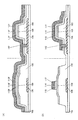
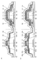
- FIG. 4A and 4B illustrate a method for manufacturing a semiconductor device.
- 4A and 4B illustrate a method for manufacturing a semiconductor device.
- 4A and 4B illustrate a method for manufacturing a semiconductor device.
- 4A and 4B illustrate a method for manufacturing a semiconductor device.
- 4A and 4B illustrate a method for manufacturing a semiconductor device.
- 4A and 4B illustrate a method for manufacturing a semiconductor device.
- 4A and 4B illustrate a method for manufacturing a semiconductor device.
- FIG. 4B illustrate a method for manufacturing a semiconductor device.
- Sectional drawing of a display apparatus Sectional drawing of a display apparatus. Sectional drawing of a display apparatus. Sectional drawing of a display apparatus. Sectional drawing of a display apparatus. (A) Block diagram of display device, (B), (C) circuit diagram. (A), (C), (D) The circuit diagram of a display apparatus, (B) A timing chart. (A), (B) The structural example of a display module. (A), (B) The structural example of an electronic device. (A) thru
- the functions of the source and drain of a transistor may be interchanged when a transistor with a different polarity is used or when the direction of current changes during circuit operation.
- the terms “source” and “drain” can be used interchangeably.
- the channel length direction of a transistor refers to one of directions parallel to a straight line connecting the source region and the drain region with the shortest distance. That is, the channel length direction corresponds to one of the directions of current flowing through the semiconductor layer when the transistor is on.
- the channel width direction is a direction orthogonal to the channel length direction. Note that depending on the structure and shape of the transistor, the channel length direction and the channel width direction may not be determined as one.
- “electrically connected” includes a case of being connected via “something having an electric action”.
- the “thing having some electric action” is not particularly limited as long as it can exchange electric signals between connection targets.
- “thing having some electric action” includes electrodes, wiring, switching elements such as transistors, resistance elements, inductors, capacitors, and other elements having various functions.
- film and “layer” can be interchanged.
- conductive layer and “insulating layer” may be interchangeable with the terms “conductive film” and “insulating film”.
- off-state current refers to drain current when a transistor is off (also referred to as a non-conduction state or a cutoff state).
- the off state is a state where the voltage V gs between the gate and the source is lower than the threshold voltage V th in the n-channel transistor (in the case of the p-channel transistor, higher than V th ) unless otherwise specified.
- a display panel which is one embodiment of a display device has a function of displaying (outputting) an image or the like on a display surface. Therefore, the display panel is one mode of the output device.
- a display panel substrate is attached with a connector such as FPC (Flexible Printed Circuit) or TCP (Tape Carrier Package), or the substrate is integrated with a COG (Chip On Glass) method.
- a connector such as FPC (Flexible Printed Circuit) or TCP (Tape Carrier Package)
- COG Chip On Glass
- a display panel module is mounted with a connector such as FPC (Flexible Printed Circuit) or TCP (Tape Carrier Package)
- COG Chip On Glass
- the touch panel which is one embodiment of the display device has a function of displaying an image or the like on the display surface, and a touched object such as a finger or a stylus touching, pressing, or approaching the display surface. And a function as a touch sensor to detect. Accordingly, the touch panel is an embodiment of an input / output device.
- the touch panel can also be called, for example, a display panel with a touch sensor (or display device) or a display panel with a touch sensor function (or display device).
- the touch panel can be configured to include a display panel and a touch sensor panel.
- the display panel may have a function as a touch sensor inside or on the surface.
- a connector or IC mounted on a touch panel substrate may be referred to as a touch panel module, a display module, or simply a touch panel.
- One embodiment of the present invention includes a semiconductor layer in which a channel is formed over a first insulating layer, a gate insulating layer over the semiconductor layer, and a conductive layer functioning as a gate electrode over the gate insulating layer (first conductive layer).
- a transistor The semiconductor layer preferably includes a metal oxide exhibiting semiconductor characteristics (hereinafter also referred to as an oxide semiconductor).
- the first insulating layer has a first region overlapping with the semiconductor layer and a second region other than the first region.
- the thickness of the first region is thicker than the thickness of the second region.
- the first region has a convex portion protruding in the thickness direction as compared with the second region.
- the semiconductor layer is provided on the convex portion of the first region of the first insulating layer.
- the side surface of the first region of the first insulating layer (that is, the outer edge portion of the convex portion) preferably has a tapered shape.
- the angle formed between the side surface of the first region and the upper surface of the second region is greater than 90 ° and less than 180 °, preferably 100 ° to 170 °, more preferably 110 ° to 160 °. .
- the side surface of the first region of the first insulating layer has a shape in which the gradient continuously changes from the portion in contact with the lower end of the semiconductor layer to the second region. Accordingly, the coverage of the gate insulating layer, the gate electrode, the first layer described later, and the like that further cover the semiconductor layer and the first insulating layer can be further improved.
- the gate insulating layer and the gate electrode are provided so as to cover the upper surface and side surfaces of the semiconductor layer, the side surfaces of the first region of the first insulating layer, and the upper surface of the second region in the channel width direction of the transistor. .
- the lower surface of the gate electrode in a portion overlapping with the second region is located below the lower surface of the semiconductor layer on the first region.
- the difference in thickness of the first insulating layer between the first region and the second region can be controlled in consideration of the thickness of the gate insulating layer and the like.
- the difference in thickness between the first region and the second region is at least larger than the thickness of the gate insulating layer.
- the thickness of the first region is 1.2 times or more, preferably 1.5 times or more, more preferably 2 times or more, and further preferably 2.5 times or more the thickness of the second region.
- the thickness can be 10 times or less.
- the difference between the thickness of the first region and the thickness of the second region is 1 time or more, preferably 1.2 times or more, more preferably 1.5 times or more, more preferably, the thickness of the gate insulating layer.
- the first insulating layer is preferably processed so that it is preferably 2 times or more and 20 times or less.
- a metal oxide film to be a semiconductor layer is formed over an insulating film to be a first insulating layer, a resist mask is formed over the metal oxide film, and a metal oxide that is not covered with the resist mask A part of the film is etched to form a semiconductor layer.
- a first region that overlaps with the semiconductor layer and a thinner first layer are formed. 2 regions can be formed. At this time, it is important to perform etching so that the second region does not disappear.
- the first insulating layer may have a stacked structure in which two or more insulating films are stacked, and the second region may have a structure in which one or more insulating films located above the first insulating layer are removed.
- the metal oxide film and the insulating film to be the first insulating layer may be continuously etched by a dry etching method.
- the region covered with the gate electrode of the semiconductor layer functions as a channel formation region.
- the region not covered with the gate electrode preferably functions as a source region or a drain region and has a lower resistance than the channel formation region (hereinafter also referred to as a low resistance region). Therefore, it is preferable to provide a first layer (also referred to as a third insulating layer) that can reduce the resistance of the semiconductor layer in contact with a portion of the semiconductor layer that is not covered with the gate electrode.
- the low resistance region of the semiconductor layer is a region whose resistance is reduced by performing heat treatment in a state where the low resistance region is covered and the first layer is formed.
- a film containing at least one of metal elements such as aluminum, titanium, tantalum, tungsten, chromium, and ruthenium can be used.
- metal elements such as aluminum, titanium, tantalum, tungsten, chromium, and ruthenium
- at least one of aluminum, titanium, tantalum, and tungsten is preferably included.
- a nitride containing at least one of these metal elements or an oxide containing at least one of these metal elements can be preferably used.
- a nitride film such as an aluminum nitride film, an aluminum titanium nitride film, or a titanium nitride film, or an oxide film such as an aluminum titanium oxide film can be suitably used.
- a metal film such as a tungsten film or a titanium film may be used.
- the composition formula is AlTiN x (x is a real number greater than 0 and 3 or less), or the composition formula is AlTi x N y (x is a real number greater than 0 and less than 2 and y is greater than 0). It is more preferable to use a film satisfying a real number of 4 or less.
- the temperature of the heat treatment is higher because the lower resistance in the low resistance region is promoted.
- the temperature of the heat treatment may be determined in consideration of the heat resistance of the gate electrode.
- the temperature may be 150 ° C. or higher and 500 ° C. or lower, preferably 200 ° C. or higher and 450 ° C. or lower, more preferably 250 ° C. or higher and 450 ° C. or lower, and even more preferably 300 ° C. or higher and 400 ° C. or lower.
- the temperature of the heat treatment by setting the temperature of the heat treatment to about 350 ° C., a semiconductor device can be manufactured with high yield using a production facility using a large glass substrate.
- the low resistance region formed in this way has a feature that it is difficult to increase the resistance by a subsequent process. For example, even if heat treatment in an atmosphere containing oxygen, film formation treatment in an atmosphere containing oxygen, or the like is performed, the electrical properties of the low resistance region are not impaired, and thus the electrical characteristics are good. A highly reliable transistor can be realized.
- the first layer after the heat treatment has conductivity, it is preferable to remove the first layer after the heat treatment.
- the first layer has an insulating property, the first layer can function as a protective insulating film (third insulating layer) by remaining.
- the above-described aluminum nitride or aluminum titanium nitride film is preferably a film because it is excellent in insulation.
- the low resistance region may be a region containing more hydrogen than the channel formation region.
- the low resistance region can be in a state of lower resistance than the channel formation region. Accordingly, the channel formation region has a very low carrier density, and the source region and the drain region have extremely low resistance, so that a transistor with excellent electrical characteristics can be realized.
- a film containing hydrogen (third insulating layer) is provided as a first layer in contact with part of the semiconductor layer, and heat treatment is performed in that state. preferable. Thereby, the hydrogen concentration in the low resistance region can be made higher than that in the channel formation region.
- an insulating film containing, for example, silicon, hydrogen, and nitrogen More specifically, a silicon nitride film containing hydrogen (also referred to as SiN: H) formed by a plasma CVD method is preferably used.
- the method for supplying hydrogen to the low-resistance region is not limited to the above.
- the gate electrode may be used as a mask to supply hydrogen to the semiconductor layer by an ion doping method, an ion implantation method, or a heat treatment in an atmosphere containing hydrogen. You may supply.
- the first insulating layer is preferably a film capable of releasing oxygen by heating. At this time, oxygen can be supplied from the first region located below the semiconductor layer to the channel formation region of the semiconductor layer by heating.
- the first layer not only covers the low resistance region of the semiconductor layer, but also is located outside the low resistance region of the semiconductor layer in the channel length direction of the transistor. It is preferable to cover the side surface of the first region of the insulating layer. Since the first layer described above has a property of being hard to permeate oxygen, oxygen contained in the first region can be prevented from diffusing outward from the side surface. Accordingly, a large amount of oxygen can be supplied to the channel formation region of the semiconductor layer, the carrier density in the channel formation region is reduced, and a highly reliable transistor can be realized.
- the transistor of one embodiment of the present invention having such a structure is a transistor having both good electrical characteristics and high reliability.
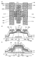
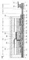
- FIG. 1A is a top view of the transistor 100
- FIG. 1B corresponds to a cross-sectional view of a cross-sectional view taken along dashed-dotted line A1-A2 in FIG. 1A
- FIG. 1 corresponds to a cross-sectional view of a cut surface taken along one-dot chain line B1-B2 shown in FIG.
- FIG. 1A some components (such as an insulating layer) of the transistor 100 are omitted.
- the direction of the alternate long and short dash line A1-A2 corresponds to the channel length direction
- the direction of the alternate long and short dash line B1-B2 corresponds to the channel width direction.
- the top view of the transistor in the subsequent drawings, as in FIG. 1A, some of the components are omitted.
- the transistor 100 is provided over a substrate 102 and includes an insulating layer 103, a semiconductor layer 108, an insulating layer 110, a metal oxide layer 114, a conductive layer 112, an insulating layer 116, an insulating layer 118, and the like.
- the island-shaped semiconductor layer 108 is provided over the insulating layer 103.
- the insulating layer 110, the metal oxide layer 114, and the conductive layer 112 are stacked so as to cover part of the semiconductor layer 108 and part of the insulating layer 103 in this order.
- the insulating layer 110, the metal oxide layer 114, and the conductive layer 112 are provided so that their upper surface shapes substantially match in plan view.
- the insulating layer 116 is provided so as to cover the top and side surfaces of the conductive layer 112, the side surface of the metal oxide layer 114, the top and side surfaces of the insulating layer 110, the top and side surfaces of the semiconductor layer 108, and the surface of the insulating layer 103. .
- the insulating layer 118 is provided so as to cover the insulating layer 116.
- the top surface shape is approximately the same” means that at least a part of the contour overlaps between the stacked layers.
- the case where the upper layer and the lower layer are processed by the same mask pattern or a part thereof by the same mask pattern is included.
- the contours do not overlap, and the upper layer may be located inside the lower layer, or the upper layer may be located outside the lower layer.
- Part of the conductive layer 112 functions as a gate electrode.
- a part of the insulating layer 110 functions as a gate insulating layer.
- a portion of the semiconductor layer 108 that overlaps with the conductive layer 112 functions as a channel formation region.
- the transistor 100 is a so-called top gate transistor in which a gate electrode is provided over the semiconductor layer 108.
- the transistor 100 may include a conductive layer 120 a and a conductive layer 120 b over the insulating layer 118.
- the conductive layer 120a and the conductive layer 120b function as a source electrode or a drain electrode.
- the conductive layer 120a and the conductive layer 120b are electrically connected to a region 108N to be described later through an opening 141a or an opening 141b provided in the insulating layer 118 and the insulating layer 116, respectively.
- the semiconductor layer 108 preferably contains a metal oxide.
- the semiconductor layer 108 includes indium and M (M is gallium, aluminum, silicon, boron, yttrium, tin, copper, vanadium, beryllium, titanium, iron, nickel, germanium, zirconium, molybdenum, lanthanum, cerium, neodymium, One or more selected from hafnium, tantalum, tungsten, or magnesium) and zinc are preferable.
- M is preferably one or more selected from aluminum, gallium, yttrium, or tin.
- an oxide containing indium, gallium, and zinc is preferably used as the semiconductor layer 108.
- the semiconductor layer 108 may have a stacked structure in which layers having different compositions, layers having different crystallinity, or layers having different impurity concentrations are stacked.
- the metal oxide layer 114 positioned between the insulating layer 110 and the conductive layer 112 functions as a barrier film that prevents oxygen contained in the insulating layer 110 from diffusing to the conductive layer 112 side. Further, the metal oxide layer 114 also functions as a barrier film that prevents hydrogen and water contained in the conductive layer 112 from diffusing to the insulating layer 110 side.
- a material that hardly transmits oxygen and hydrogen more than the insulating layer 110 can be used.
- the metal oxide layer 114 can prevent oxygen from diffusing from the insulating layer 110 to the conductive layer 112. . Further, even when the conductive layer 112 contains hydrogen, diffusion of hydrogen from the conductive layer 112 to the semiconductor layer 108 through the insulating layer 110 can be prevented. As a result, the carrier density in the channel formation region of the semiconductor layer 108 can be extremely low.
- the metal oxide layer 114 an insulating material or a conductive material can be used. In the case where the metal oxide layer 114 has an insulating property, it functions as part of the gate insulating layer. On the other hand, when the metal oxide layer 114 has conductivity, it functions as a part of the gate electrode.
- an insulating material having a dielectric constant higher than that of silicon oxide is preferably used.
- an aluminum oxide film, a hafnium oxide film, a hafnium aluminate film, or the like is preferably used because the driving voltage can be reduced.
- a conductive oxide such as indium oxide, indium tin oxide (ITO), or indium tin oxide containing silicon (ITSO) can be used.
- ITO indium tin oxide
- ITSO indium tin oxide containing silicon
- a conductive oxide containing indium is preferable because of its high conductivity.
- an oxide material containing one or more of the same elements as the semiconductor layer 108 is preferably used.
- an oxide semiconductor material that can be used for the semiconductor layer 108 is preferably used.
- a metal oxide film formed using the same sputtering target as that of the semiconductor layer 108 is preferably used as the metal oxide layer 114 because the device can be used in common.
- a material having a higher gallium composition (content ratio) than the material used for the semiconductor layer 108 is oxidized by metal. It is preferable to use the material layer 114 because the blocking property against oxygen can be further improved. At this time, the field-effect mobility of the transistor 100 can be increased by using a material whose indium composition is higher than that of the material used for the metal oxide layer 114 for the semiconductor layer 108.
- the metal oxide layer 114 is preferably formed using a sputtering apparatus.
- oxygen can be preferably added to the insulating layer 110 and the semiconductor layer 108 by being formed in an atmosphere containing oxygen gas.
- the semiconductor layer 108 has a channel formation region which overlaps with the conductive layer 112 with the insulating layer 110 interposed therebetween.
- the semiconductor layer 108 includes a pair of regions 108N that sandwich the channel formation region.
- the region 108N has a lower resistance than the channel formation region and functions as a source region or a drain region of the transistor 100.
- the insulating layer 103 includes a region 103 a that overlaps with the semiconductor layer 108 and a region 103 b that does not overlap with the semiconductor layer 108.
- the insulating layer 103 has a shape in which the region 103a protrudes in the thickness direction from the region 103b.
- the region 103a can also be referred to as a convex portion.
- the region 103a of the insulating layer 103 is a region thicker than the region 103b.
- the side surface of the region 103a (the outer edge portion of the convex portion of the insulating layer 103) preferably has a tapered shape from a portion in contact with the lower end portion of the semiconductor layer 108 to the region 103b.
- the angle formed between the side surface of the region 103a and the upper surface of the region 103b is preferably an obtuse angle. More specifically, the angle formed between the side surface of the region 103a and the upper surface of the region 103b is greater than 90 ° and less than 180 °, preferably 100 ° to 170 °, more preferably 110 ° to 160 °.
- the coverage of a film eg, the insulating layer 110, the metal oxide layer 114, the conductive layer 112, the insulating layer 116, and the like
- a low-density region can be formed in these regions. (Also referred to as a void) is less likely to be formed, so that the reliability of the transistor 100 can be increased.
- the side surface of the region 103a preferably has a shape in which the gradient continuously changes from the upper end portion (near the portion in contact with the lower end portion of the semiconductor layer 108) to the upper surface of the region 103b.
- the side surface of the region 103a has a gently curved shape, and the side surface of the region 103a and the upper surface of the region 103b are continuously connected to each other, so that the film positioned above the insulating layer 103 can be formed. Coverability can be further increased.
- the insulating layer 110, the metal oxide layer 114, and the conductive layer 112 are formed using the top surface and side surfaces of the semiconductor layer 108 and the side surfaces and regions of the region 103a of the insulating layer 103.
- 103b is provided to cover the upper surface.
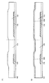
- FIG. 2 (A) is an enlarged view of a part of FIG. 1 (C).
- FIG. 2A shows the thicknesses t1 to t4 and the heights h1 to h4, respectively.
- the thickness t1 is the thickness of the region 103a
- the thickness t2 is the thickness of the region 103b
- the thickness t3 is the total thickness of the insulating layer 110 and the metal oxide layer 114 in a portion overlapping with the region 103b
- the thickness t4 is the total thickness of the insulating layer 110, the metal oxide layer 114, and the conductive layer 112 in a portion overlapping with the region 103b.
- the difference between the thickness of the region 103a and the thickness of the region 103b is the difference d1
- the difference d1 is preferably larger than the thickness t3.
- the difference d1 is more preferably larger than the thickness t4.
- the heights h1 to h4 are based on the height of the bottom surface of the region 103a of the insulating layer 103, respectively.
- the height h1 is the height of the lower surface of the semiconductor layer 108 (in the case where the insulating layer 103 and the semiconductor layer 108 are in contact with each other).
- the height h2 is the height of the upper surface of the region 103b (in the case where the insulating layer 103 and the insulating layer 110 are in contact with each other).
- the height h3 is the height of the bottom surface of the conductive layer 112 (in the case where the conductive layer 112 and the metal oxide layer 114 are in contact with each other) in a portion overlapping with the region 103b.
- the height h4 is the height of the upper surface of the conductive layer 112 (in the case where the conductive layer 112 and the insulating layer 116 are in contact with each other) in a portion overlapping with the region 103b.
- the height h1 of the lower surface of the semiconductor layer 108 is preferably higher than the height h3 of the lower surface of the conductive layer 112.
- the height h1 is more preferably higher than the height h4 of the upper surface of the conductive layer 112.
- the difference d1 between the thickness of the region 103a and the thickness of the region 103b is the difference between the insulating layer 110, the metal oxide layer 114, and the conductive layer 112 in a portion overlapping with the region 103b. It may be smaller than the thickness t4.
- the height h1 of the lower surface of the semiconductor layer 108 may be lower than the height h4 of the upper surface of the conductive layer 112.
- the conductive layer 112 in the channel width direction, can be provided not only on the upper surface side of the semiconductor layer 108 but also on the side surface side and obliquely below the lower end portion.
- the semiconductor layer 108 can be electrically surrounded by an electric field generated when voltage is applied to the conductive layer 112, and the on-state current of the transistor 100 can be increased.
- the on-current of the transistor can be increased.
- the field-effect mobility of the transistor can be improved and the on-state current can be increased without changing these designs, that is, without increasing the channel width W.
- the channel width W of the transistor may be set in accordance with a characteristic value required when it is incorporated in a circuit. For example, when applied to a pixel circuit or a drive circuit of a display device, the channel width W is set to 1 ⁇ m. Even when the thickness is 100 ⁇ m or less, preferably 1.2 ⁇ m or more and 50 ⁇ m or less, and more preferably 1.5 ⁇ m or more and 30 ⁇ m or less, a very large current can be passed.
- the channel width W is not limited to this, and may be larger than 100 ⁇ m depending on required characteristics.
- the channel length L can be set to be relatively large, and the transistor characteristic variation and the production yield can be increased.
- the channel length L of the transistor may be set in accordance with a required characteristic value. For example, when applied to a pixel circuit or a drive circuit of a display device, the channel length L is set to 1 ⁇ m or more. It is preferably set to 20 ⁇ m or less, preferably 1.2 ⁇ m to 15 ⁇ m, more preferably 1.5 ⁇ m to 10 ⁇ m.
- the channel length L is 1.5 ⁇ m or more and 5 ⁇ m or less, preferably 2 ⁇ m or more and 3 ⁇ m or less, variations in the substrate length of the channel length L can be suppressed, and the production yield can be increased.
- the channel length L is not limited to this, and may be larger than 20 ⁇ m depending on required characteristics.
- the channel length direction of a transistor refers to one of directions parallel to a straight line connecting the source region and the drain region with the shortest distance. That is, the channel length direction corresponds to one of the directions of current flowing through the semiconductor layer when the transistor is on.
- the channel width direction is a direction orthogonal to the channel length direction. Note that depending on the structure and shape of the transistor, the channel length direction and the channel width direction may not be determined as one.
- the channel length L of the transistor 100 refers to the length of the conductive layer 112 in the channel length direction in a region overlapping with the semiconductor layer 108.
- the channel width of the transistor 100 refers to the length of the semiconductor layer 108 in the channel width direction in a region covered with the conductive layer 112.
- an insulating layer 116 is provided in contact with the region 108N of the semiconductor layer 108.
- the insulating layer 116 is preferably insulative because it is in contact with both the semiconductor layer 108 and the conductive layer 112.
- an insulating film containing nitride can be used as the insulating layer 116 in contact with the region 108N.
- an insulating film containing nitride can be used as the insulating layer 116 in contact with the region 108N.
- nitride of a semiconductor material such as silicon nitride or gallium nitride or a metal nitride such as aluminum nitride.
- silicon nitride has a blocking property against hydrogen and oxygen, it can prevent both diffusion of hydrogen from the outside to the semiconductor layer and desorption of oxygen from the semiconductor layer to the outside, and is a highly reliable transistor. Can be realized.
- metal nitride when metal nitride is used, it is preferable to use aluminum, titanium, tantalum, tungsten, chromium, or ruthenium nitride. It is particularly preferable that aluminum or titanium is included.
- an insulating film containing such a metal nitride in contact with the semiconductor layer not only can the resistance of the semiconductor layer be reduced, but also oxygen can be released from the semiconductor layer and hydrogen can diffuse into the semiconductor layer. It can prevent suitably.
- the thickness of the insulating layer containing the aluminum nitride is preferably 5 nm or more. Even such a thin film can achieve both a high blocking property against hydrogen and oxygen and a function of reducing the resistance of the semiconductor layer.
- the thickness of the insulating layer may be any thickness, but in consideration of productivity, the thickness is preferably 500 nm or less, preferably 200 nm or less, more preferably 50 nm or less.
- a film satisfying the composition formula AlN x (x is a real number greater than 0 and equal to or less than 2, preferably x is greater than 0.5 and less than or equal to 1.5) is used. Is preferred. Accordingly, a film having excellent insulating properties and excellent thermal conductivity can be obtained, so that heat dissipation of heat generated when the transistor 100 is driven can be improved.
- an aluminum titanium nitride film, a titanium nitride film, or the like can be used as the insulating layer 116.
- the insulating layer 116 can absorb oxygen in the region 108N and form oxygen vacancies in the region 108N.
- a layer containing an oxide of a metal element (eg, aluminum) contained in the insulating layer 116 is formed between the insulating layer 116 and the region 108N. May be.
- a region where indium in a metal state is deposited or a region with a high indium concentration is formed in the vicinity of the interface on the insulating layer 116 side of the region 108N. It may be formed. The presence of such a region may be observed by an analysis method such as X-ray photoelectron spectroscopy (XPS).
- XPS X-ray photoelectron spectroscopy
- the region 108N can be a region containing more oxygen vacancies than the channel formation region, the region 108N can have a lower resistance than the channel formation region. Further, by using an insulating film containing a metal oxide as the insulating layer 116, a region in which highly conductive indium is deposited is formed in the vicinity of the interface on the insulating layer 116 side of the region 108N, and the region is further reduced in resistance. be able to.
- the insulating layer 116 a film functioning as a hydrogen supply source for the region 108N can be used.
- the insulating layer 116 is preferably a film that releases hydrogen by heating.
- the insulating layer 116 is preferably a film formed using a gas containing a hydrogen element as a film forming gas used for film formation. Accordingly, hydrogen can be effectively supplied to the region 108N even when the insulating layer 116 is formed.
- an insulating film such as silicon nitride, silicon nitride oxide, silicon oxynitride, aluminum nitride, or aluminum nitride oxide can be used.
- Hydrogen is supplied to the region 108N by the heat treatment when the insulating layer 116 is formed and after the insulating layer 116 is formed.
- the supplied hydrogen is combined with oxygen vacancies in the region 108N and can serve as a carrier generation source. Accordingly, the region 108N having a higher carrier concentration and lower resistance than the channel formation region can be formed.
- An oxide film is preferably used for the insulating layers 103 and 110 in contact with the channel formation region of the semiconductor layer 108.
- an oxide film such as a silicon oxide film, a silicon oxynitride film, or an aluminum oxide film can be used. Accordingly, oxygen released from the insulating layers 103 and 110 can be supplied to the channel formation region of the semiconductor layer 108 by heat treatment or the like in the manufacturing process of the transistor 100, so that oxygen vacancies in the semiconductor layer 108 can be reduced. .
- the insulating layer 116 is preferably provided so as to cover a side surface of the region 103 a of the insulating layer 103. Oxygen contained in the insulating layer 103 that can be released by heating can be supplied from the region 103 a of the insulating layer 103 to the semiconductor layer 108. Therefore, in order to prevent oxygen from being released from the side surface of the region 103a by heating, the side surface is covered with an insulating layer 116 in which oxygen is difficult to diffuse.
- the insulating layer 116 preferably covers the top surface of the region 103 b of the insulating layer 103. Accordingly, oxygen released from the insulating layer 103 can be effectively supplied to the semiconductor layer 108. Accordingly, the carrier density in the channel formation region of the semiconductor layer 108 can be reduced, and the reliability of the transistor 100 can be increased.
- the insulating layer 118 functions as a protective layer that protects the transistor 100.
- an inorganic insulating material such as an oxide or a nitride can be used.
- an inorganic insulating material such as silicon nitride, silicon nitride oxide, silicon oxynitride, aluminum oxide, aluminum oxynitride, aluminum nitride, hafnium oxide, or hafnium aluminate can be used.
- the insulating layer 118 can also be used as a planarization layer. In that case, an organic resin material can be used for the insulating layer 118.
- the insulating layer 118 is not necessarily provided if not necessary.
- the insulating layer 118 may have a stacked structure of two or more layers.
- Oxygen vacancies formed in the channel formation region of the semiconductor layer 108 are problematic because they affect transistor characteristics. For example, when an oxygen vacancy is formed in the semiconductor layer 108, hydrogen is bonded to the oxygen vacancy and can serve as a carrier supply source. When a carrier supply source is generated in the channel formation region, a change in electrical characteristics of the transistor 100, typically, a threshold voltage shift occurs. Therefore, the smaller the number of oxygen vacancies in the channel formation region, the better.
- the insulating film in the vicinity of the channel formation region of the semiconductor layer 108, specifically, the insulating layer 110 located above the channel formation region and the insulating layer 103 located below is oxidized.
- the structure includes a physical film.
- the semiconductor layer 108 preferably has a region in which the atomic ratio of In is larger than the atomic ratio of M. As the In atomic ratio increases, the field-effect mobility of the transistor can be improved.
- a very large amount of oxygen can be supplied into the channel formation region of the semiconductor layer 108 containing a metal oxide; thus, a metal oxide material with a large atomic ratio of In can be used.
- a transistor having extremely high field effect mobility, stable electrical characteristics, and high reliability can be realized.
- a metal oxide in which the atomic ratio of In is 1.5 times or more, or 2 times or more, or 3 times or more, or 3.5 times or more, or 4 times or more of the atomic ratio of M can be preferably used.
- a display device with a narrow frame width can be provided by using the above-described transistor with high field-effect mobility for a gate driver that generates a gate signal.
- a display device with a small number of connected wirings can be provided by using the transistor with high field-effect mobility described above for a source driver (particularly, a demultiplexer connected to an output terminal of a shift register included in the source driver). can do.
- the crystallinity of the semiconductor layer 108 can be analyzed by, for example, analyzing using X-ray diffraction (XRD: X-Ray Diffraction), or analyzing using a transmission electron microscope (TEM). .
- XRD X-ray diffraction
- TEM transmission electron microscope
- the channel formation region of the semiconductor layer 108 has a low impurity concentration and a low density of defect states (less oxygen vacancies), whereby the carrier density in the film can be reduced.
- a transistor in which such a metal oxide film is used for a channel formation region of a semiconductor layer rarely has electrical characteristics (also referred to as normally-on) in which the threshold voltage is negative.
- a transistor including such a metal oxide film can obtain characteristics with extremely low off-state current.
- a metal oxide film having a CAAC (c-axis aligned crystal) structure, a metal oxide film having an nc (nano crystal) structure, or a metal oxide in which a CAAC structure and an nc structure are mixed is used. It is preferable to use a membrane.
- the transistor 100 having excellent electrical characteristics and high reliability can be realized.
- FIG. 1 portions having the same functions as those in the above configuration example have the same hatching pattern and may not be denoted by reference numerals.
- FIG. 3A is a top view of the transistor 100A
- FIG. 3B is a cross-sectional view in the channel length direction of the transistor 100A
- FIG. 3C is a cross-sectional view in the channel width direction of the transistor 100A.
- the transistor 100A is mainly different from the configuration example 1 in that a conductive layer 106 is provided between the substrate 102 and the insulating layer 103.
- the conductive layer 106 includes a channel formation region of the semiconductor layer 108 and a region overlapping with the conductive layer 112.
- the conductive layer 106 functions as a first gate electrode (also referred to as a bottom gate electrode), and the conductive layer 112 functions as a second gate electrode (also referred to as a top gate electrode).
- a part of the insulating layer 103 functions as a first gate insulating layer, and a part of the insulating layer 110 functions as a second gate insulating layer.
- a portion of the semiconductor layer 108 overlapping with at least one of the conductive layer 112 and the conductive layer 106 functions as a channel formation region. Note that a portion overlapping with the conductive layer 112 of the semiconductor layer 108 is sometimes referred to as a channel formation region for ease of explanation below, but actually overlaps with the conductive layer 106 without overlapping with the conductive layer 112. A channel can also be formed in a portion (a portion including the region 108N).
- the conductive layer 106 is connected to the conductive layer 112 through the metal oxide layer 114, the insulating layer 110, and the opening 142 provided in the insulating layer 103. It may be electrically connected. Accordingly, the same potential can be applied to the conductive layer 106 and the conductive layer 112.
- the conductive layer 106 can be formed using a material similar to that of the conductive layer 112, the conductive layer 120a, or the conductive layer 120b. In particular, it is preferable to use a material containing copper for the conductive layer 106 because wiring resistance can be reduced. In addition, when a material containing a refractory metal such as tungsten or molybdenum is used for the conductive layer 106, treatment can be performed at a high temperature in a later step.
- the conductive layer 112 and the conductive layer 106 protrude outward from the end portion of the semiconductor layer 108 in the channel width direction.
- the entire semiconductor layer 108 in the channel width direction is covered with the conductive layer 112 and the conductive layer 106 with the insulating layer 110 and the insulating layer 103 interposed therebetween.
- the semiconductor layer 108 can be electrically surrounded by an electric field generated by the pair of gate electrodes. At this time, it is particularly preferable to apply the same potential to the conductive layer 106 and the conductive layer 112. Accordingly, an electric field for inducing a channel can be effectively applied to the semiconductor layer 108, so that the on-state current of the transistor 100A can be increased. Therefore, the transistor 100A can be miniaturized.
- the conductive layer 112 and the conductive layer 106 may not be connected. At this time, a constant potential may be supplied to one of the pair of gate electrodes, and a signal for driving the transistor 100A may be supplied to the other. At this time, the threshold voltage when the transistor 100A is driven by the other electrode can be controlled by the potential applied to the one electrode.
- FIG. 4A is a cross-sectional view in the channel length direction of the transistor 100B
- FIG. 4B is a cross-sectional view in the channel width direction of the transistor 100B. Note that the top view is omitted because FIG. 3A can be used.
- the transistor 100B is mainly different from the transistor 100A illustrated in the above configuration example 2 in that the semiconductor layer 108a and the semiconductor layer 108b are stacked from the insulating layer 103 side instead of the semiconductor layer 108. Yes.
- metal oxide films having different compositions can be used for the semiconductor layer 108a and the semiconductor layer 108b.
- metal oxide films having different crystallinity may be stacked. In that case, it is preferable that the same oxide target is used and the film formation conditions are different so that the film is continuously formed without being exposed to the atmosphere.
- a stacked structure using a metal oxide film having an nc structure as the semiconductor layer 108a and a metal oxide film having a CAAC structure as the semiconductor layer 108b can be used.
- a metal oxide film having an nc structure may be used for both the semiconductor layer 108a and the semiconductor layer 108b.
- a CAC (Cloud-Aligned Composite) described later can be used as a function or a material structure of a metal oxide that can be preferably used for the semiconductor layer 108a and the semiconductor layer 108b.
- the oxygen flow rate ratio at the time of forming the first metal oxide film formed first is made smaller than the oxygen flow rate ratio at the time of forming the second metal oxide film formed later.
- oxygen is not allowed to flow when the first metal oxide film is formed.
- oxygen can be effectively supplied when forming the second metal oxide film.
- the first metal oxide film can be a film having lower crystallinity and higher electrical conductivity than the second metal oxide film.
- the second metal oxide film provided on the top is a film having higher crystallinity than the first metal oxide film, so that damage during the processing of the semiconductor layer 108 or the film formation of the insulating layer 110 is caused. Can be suppressed.
- the oxygen flow rate ratio during the formation of the first metal oxide film is 0% or more and less than 50%, preferably 0% or more and 30% or less, more preferably 0% or more and 20% or less. Specifically, it is 10%.
- the oxygen flow rate ratio during the formation of the second metal oxide film is 50% to 100%, preferably 60% to 100%, more preferably 80% to 100%, and still more preferably 90% or more. 100% or less, typically 100%.
- the first metal oxide film and the second metal oxide film may have different conditions such as pressure, temperature, and power at the time of film formation, but the conditions other than the oxygen flow rate ratio are the same. This is preferable because the time required for the film forming process can be shortened.
- FIG. 5A is a cross-sectional view in the channel length direction of the transistor 100C
- FIG. 5B is a cross-sectional view in the channel width direction of the transistor 100C. Note that the top view is omitted because FIG. 3A can be used.
- the transistor 100C is mainly different from the transistor 100B exemplified in the above configuration example 3 in that the shape of the semiconductor layer 108b is different.
- the top surface shape of the semiconductor layer 108b is substantially the same as that of the conductive layer 112, the metal oxide layer 114, and the insulating layer 110.
- the semiconductor layer 108b can be formed by processing using a resist mask for etching the conductive layer 112 and the like.
- the semiconductor layer 108b is provided to cover the upper surface and side surfaces of the semiconductor layer 108a, the side surfaces of the region 103a of the insulating layer 103, and part of the upper surface of the region 103b.
- a metal oxide film having a CAAC structure has a feature that oxygen diffusibility with respect to the c-axis direction of a crystal part included in the metal oxide film is low. Further, the metal oxide film having a CAAC structure can be formed so that the c-axis of the crystal part included in the metal oxide film is oriented in a direction substantially perpendicular to the formation surface.
- FIG. 5C shows an enlarged view of a region Q surrounded by a broken line in FIG.
- the crystalline semiconductor layer 108b is provided so as to cover the top and side surfaces of the semiconductor layer 108a, the side surface of the region 103a of the insulating layer 103, and the top surface of the region 103b.
- FIG. 5C schematically illustrates the c-axis direction of crystals included in the semiconductor layer 108b and the orientation of the layer 108L included in the layered crystal portion indicated by a broken line in each portion of the semiconductor layer 108b.
- the crystal part in the semiconductor layer 108b having crystallinity has a c-axis (that is, a direction perpendicular to the layer of the layered crystal part) oriented in a direction substantially perpendicular to the formation surface.
- the semiconductor layer 108 b covers the side surface of the region 103 b of the insulating layer 103 and the side surface of the semiconductor layer 108 a, so that oxygen that can be released from the insulating layer 103 is , Diffusion from the region 103b can be suppressed. Further, oxygen can be prevented from diffusing outside from the side surface of the semiconductor layer 108a. Accordingly, oxygen vacancies in the semiconductor layer 108a can be effectively reduced, and a highly reliable transistor can be realized.
- Example of production method A method for manufacturing a semiconductor device of one embodiment of the present invention is described below with reference to drawings.
- the transistor 100A exemplified in the above configuration example is described as an example.
- a thin film (insulating film, semiconductor film, conductive film, or the like) included in the semiconductor device is formed by a sputtering method, a chemical vapor deposition (CVD) method, a vacuum evaporation method, or a pulse laser deposition (PLD: Pulse Laser Deposition).
- CVD chemical vapor deposition
- PLD Pulse Laser Deposition
- ALD Atomic Layer Deposition
- the CVD method include a plasma enhanced chemical vapor deposition (PECVD) method and a thermal CVD method.
- PECVD plasma enhanced chemical vapor deposition
- thermal CVD there is a metal organic chemical vapor deposition (MOCVD) method.
- Thin films (insulating films, semiconductor films, conductive films, etc.) that constitute semiconductor devices are spin coat, dip, spray coating, ink jet, dispense, screen printing, offset printing, doctor knife, slit coat, roll coat, curtain coat. It can be formed by a method such as knife coating.
- the thin film constituting the semiconductor device when processing the thin film constituting the semiconductor device, it can be processed using a photolithography method or the like.
- the thin film may be processed by a nanoimprint method, a sand blast method, a lift-off method, or the like.
- the island-shaped thin film may be directly formed by a film forming method using a shielding mask such as a metal mask.
- light used for exposure can be, for example, i-line (wavelength 365 nm), g-line (wavelength 436 nm), h-line (wavelength 405 nm), or light obtained by mixing these.
- ultraviolet light, KrF laser light, ArF laser light, or the like can be used.
- exposure may be performed by an immersion exposure technique.
- extreme ultraviolet light (EUV: Extreme-violet) or X-rays may be used as light used for exposure.
- an electron beam can be used instead of the light used for exposure. It is preferable to use extreme ultraviolet light, X-rays, or an electron beam because extremely fine processing is possible. Note that a photomask is not necessary when exposure is performed by scanning a beam such as an electron beam.
- etching the thin film For etching the thin film, a dry etching method, a wet etching method, a sand blasting method, or the like can be used.
- 6A to 10B show a cross section in the channel length direction and the channel width direction in each stage of the manufacturing process of the transistor 100A.
- a conductive film is formed over the substrate 102 and processed by etching, so that the conductive layer 106 functioning as the first gate electrode is formed.
- an insulating layer 103 is formed so as to cover the substrate 102 and the conductive layer 106 (FIG. 6A).
- the insulating layer 103 can be formed by a PECVD method, an ALD method, a sputtering method, or the like.
- the insulating layer 103 can be formed with a thickness of a region 103a to be formed later.
- the thickness of the insulating layer 103 can be set to a thickness that does not disappear in a subsequent thinning process.
- a process for supplying oxygen to the insulating layer 103 may be performed.
- plasma treatment or heat treatment in an oxygen atmosphere can be performed.
- oxygen may be supplied to the insulating layer 103 by a plasma ion doping method, an ion implantation method, or the like.
- the metal oxide film is preferably formed by a sputtering method using a metal oxide target.
- an inert gas eg, helium gas, argon gas, xenon gas, etc.
- oxygen flow ratio the ratio of oxygen gas to the entire deposition gas when forming the metal oxide film
- the lower the oxygen flow ratio the lower the crystallinity of the metal oxide film and the transistor with higher on-state current.
- the semiconductor layer 108 has a stacked structure
- the deposition conditions for each metal oxide film may be different in conditions such as pressure, temperature, power, etc. during the deposition. This is preferable because the time can be shortened.
- metal oxide films having different compositions are stacked, it is preferable to form the films continuously without being exposed to the atmosphere.
- the film formation conditions are set so that the metal oxide film is a metal oxide film having a CAAC structure, a metal oxide film having an nc structure, or a metal oxide film in which a CAAC structure and an nc structure are mixed. Is preferred. Note that the film formation conditions for the metal oxide film to be formed to have a CAAC structure and the film formation conditions to have an nc structure differ depending on the composition of the sputtering target used, and thus the substrate temperature and oxygen depend on the composition. What is necessary is just to set suitably a pressure, electric power, etc. other than a flow rate ratio.
- the film formation conditions for the metal oxide film include a substrate temperature of room temperature to 450 ° C., preferably a substrate temperature of room temperature to 300 ° C., more preferably room temperature to 200 ° C., more preferably room temperature to 140 ° C. And it is sufficient.
- the film formation temperature is set to be room temperature or higher and lower than 140 ° C. because productivity is increased. Further, the crystallinity can be lowered by forming the metal oxide film with the substrate temperature set to room temperature or without intentional heating.
- a process for desorbing water, hydrogen, organic components, or the like adsorbed on the surface of the insulating layer 103 or a process for supplying oxygen into the insulating layer 103 is performed.
- the heat treatment can be performed at a temperature of 70 ° C. or higher and 200 ° C. or lower in a reduced pressure atmosphere.
- plasma treatment in an atmosphere containing oxygen may be performed.
- organic substances on the surface of the insulating layer 103 can be preferably removed. After such treatment, it is preferable to continuously form a metal oxide film without exposing the surface of the insulating layer 103 to the atmosphere.
- a resist mask 115 is formed on the metal oxide film 108f. After that, part of the metal oxide film 108f that is not covered with the resist mask 115 is etched to form the semiconductor layer 108 (FIG. 7A).
- a wet etching method and a dry etching method can be used.
- the insulating layer 103 is preferably etched by a dry etching method.
- a dry etching method For example, an anisotropic dry etching method can be used.
- the etching conditions and the etching processing time are set so that the portion that becomes the region 103b does not disappear.
- the insulating layer 103 has a stacked structure of two insulating films having different etching rates, and a film having a high etching rate is applied to the insulating film located on the upper side, so that only the upper insulating film is etched to form the region 103b. May be formed.
- the two insulating films constituting the insulating layer 103 may be insulating films containing different elements.
- a film containing the same element may be used for the two insulating films, and a film having a higher density may be applied to the insulating film positioned on the lower side.
- the method of separately performing the etching of the metal oxide film 108f and the etching for reducing the thickness of the insulating layer 103 may be performed collectively by a single etching process.
- the same etching method preferably dry etching method
- the processing is continuously performed with different etchants without being exposed to the atmosphere with the same etching apparatus. May be.
- the resist mask 115 is removed.
- heating is performed in order to remove hydrogen or water in the metal oxide film or the semiconductor layer 108. Processing may be performed.
- the temperature of the heat treatment can be typically 150 ° C. or higher and lower than the strain point of the substrate, 250 ° C. or higher and 450 ° C. or lower, or 300 ° C. or higher and 450 ° C. or lower.
- the heat treatment can be performed in an atmosphere containing a rare gas or nitrogen. Alternatively, after heating in the atmosphere, heating may be performed in an atmosphere containing oxygen. Note that it is preferable that hydrogen, water, and the like be not contained in the heat treatment atmosphere.
- an electric furnace, an RTA apparatus, or the like can be used. By using the RTA apparatus, the heat treatment time can be shortened.
- the insulating film 110 f is a film that later becomes the insulating layer 110.
- an oxide film such as a silicon oxide film or a silicon oxynitride film is preferably formed using a plasma chemical vapor deposition apparatus (a PECVD apparatus or simply a plasma CVD apparatus). Alternatively, a PECVD method using a microwave may be used.
- the metal oxide film 114 f is a film that later becomes the metal oxide layer 114.
- the metal oxide film 114f is preferably formed by a sputtering method in an atmosphere containing oxygen, for example. Accordingly, oxygen can be supplied to the insulating film 110f when the metal oxide film 114f is formed.
- the metal oxide film 114f is formed by a sputtering method using an oxide target containing a metal oxide similar to that of the semiconductor layer 108, the above can be used.
- the metal oxide film 114f may be formed by a reactive sputtering method using oxygen as a deposition gas and using a metal target. When aluminum is used for the metal target, an aluminum oxide film can be formed.
- the oxygen flow rate ratio or the oxygen partial pressure is, for example, 50% to 100%, preferably 65% to 100%, more preferably 80% to 100%, and still more preferably 90% to 100%. In particular, it is preferable that the oxygen flow rate ratio is 100% and the oxygen partial pressure is as close as possible to 100%.
- oxygen may be supplied from the insulating film 110f to the semiconductor layer 108 by performing heat treatment after the metal oxide film 114f is formed.
- the heat treatment can be performed at a temperature of 200 ° C. to 400 ° C. in an atmosphere containing one or more of nitrogen, oxygen, and a rare gas.
- the metal oxide film 114f, the insulating film 110f, and part of the insulating layer 103 are etched to form an opening reaching the conductive layer 106. Accordingly, the conductive layer 112 and the conductive layer 106 to be formed later can be electrically connected through the opening.
- a conductive film 112f to be the conductive layer 112 is formed over the metal oxide film 114f (FIG. 8A).
- the conductive film 112f is preferably formed by a sputtering method using a metal or alloy sputtering target.
- the conductive film 112f, the metal oxide film 114f, and the insulating film 110f may be etched at the same time under the same etching conditions, or may be etched at least twice using different etching conditions or techniques. .
- etching damage to the semiconductor layer 108 can be reduced by etching the conductive film 112f and the metal oxide film 114f first, and then etching the insulating film 110f under different etching conditions.
- a film containing at least one of metal elements such as aluminum, titanium, tantalum, tungsten, chromium, and ruthenium is formed.
- metal elements such as aluminum, titanium, tantalum, and tungsten is preferably included.
- a nitride containing at least one of these metal elements or an oxide containing at least one of these metal elements can be preferably used.
- a nitride film such as an aluminum titanium nitride film, a titanium nitride film, or an aluminum nitride film, an oxide film such as an aluminum titanium oxide film, or the like can be preferably used.
- the insulating layer 116 is preferably formed by a sputtering method using nitrogen gas or oxygen gas as a deposition gas.
- the film quality can be easily controlled by controlling the flow rate of the film forming gas.
- the heat treatment is preferably performed in an inert gas atmosphere such as nitrogen or a rare gas.
- an inert gas atmosphere such as nitrogen or a rare gas.
- the temperature can be 120 ° C. or higher and 500 ° C. or lower, preferably 150 ° C. or higher and 450 ° C. or lower, more preferably 200 ° C. or higher and 400 ° C. or lower, and even more preferably 250 ° C. or higher and 400 ° C. or lower.
- a semiconductor device can be manufactured with high yield using a production facility using a large glass substrate.
- the heat treatment may be performed at any stage after the insulating layer 116 is formed. Moreover, you may combine with the process which concerns on another heat processing or a heat
- Oxygen deficiency is generated by extracting oxygen in the semiconductor layer 108 to the insulating layer 116 by heat treatment.
- the oxygen concentration and hydrogen in the semiconductor layer 108 are combined to increase the carrier concentration, so that the resistance of the region 108N in contact with the insulating layer 116 is reduced.
- the metal element contained in the insulating layer 116 is diffused into the semiconductor layer 108 by heat treatment, so that part of the semiconductor layer 108 may be alloyed and the resistance may be reduced.
- nitrogen or hydrogen contained in the insulating layer 116, nitrogen contained in the heat treatment atmosphere, or the like may diffuse into the semiconductor layer 108 due to heat treatment, which may reduce the resistance.
- the region 108N of the semiconductor layer 108 whose resistance is reduced by such a combined action is an extremely stable low resistance region.
- the region 108N formed in this manner has a feature that, for example, even if a process for supplying oxygen is performed in a later step, it is difficult to increase the resistance again.
- the insulating layer 116 having an insulating property is used as a layer for forming the region 108N, by forming a conductive film in contact with the region to be the region 108N, The region 108N may be formed. At this time, after the region 108N is formed, the insulating film 116 is preferably formed by oxidizing or nitriding the conductive film to form an insulating layer 116. Alternatively, the insulating layer 116 may be omitted by removing the film after the formation of the region 108N.
- the region 108N may be formed by performing a process of supplying hydrogen to the exposed region of the semiconductor layer 108.
- hydrogen is supplied by forming an insulating layer 116 containing hydrogen in contact with the exposed region of the semiconductor layer 108.
- the insulating layer 116 is preferably formed by a plasma CVD method using a deposition gas containing hydrogen.
- a silicon nitride film is formed using a deposition gas containing silane gas and ammonia gas.
- ammonia gas in addition to silane gas, a large amount of hydrogen can be contained in the film.
- hydrogen can be supplied to the exposed portion of the semiconductor layer 108 even during film formation.
- part of hydrogen released from the insulating layer 116 be supplied to part of the semiconductor layer 108 by performing heat treatment after the insulating layer 116 is formed.
- the heat treatment is preferably performed at a temperature of 150 ° C. to 450 ° C., preferably 200 ° C. to 400 ° C., in an atmosphere containing one or more of nitrogen, oxygen, and a rare gas.
- an extremely low resistance region 108N can be formed in the semiconductor layer 108.
- the region 108N can also be referred to as a region with a higher carrier concentration, a region with a larger amount of oxygen vacancies, a region with a higher hydrogen concentration, or a region with a higher impurity concentration than the channel formation region.
- oxygen can be supplied from the insulating layers 110 and 103 to the channel formation region of the semiconductor layer 108 by heat treatment.
- the insulating layer 118 is formed by a plasma CVD method, if the deposition temperature is too high, the impurity may be diffused into the peripheral portion of the semiconductor layer 108 including the channel formation region depending on the impurity contained in the region 108N. As a result, the channel formation region may have a low resistance, or the electric resistance of the region 108N may increase.
- the film formation temperature of the insulating layer 116 or the insulating layer 118 is, for example, 150 ° C. or higher and 400 ° C. or lower, preferably 180 ° C. or higher and 360 ° C. or lower, more preferably 200 ° C. or higher and 250 ° C. or lower.
- heat treatment may be performed after the insulating layer 118 is formed.
- Opening 141a and Opening 141b [Formation of Opening 141a and Opening 141b] Subsequently, after a mask is formed by lithography at a desired position of the insulating layer 118, the insulating layer 118 and a part of the insulating layer 116 are etched to form an opening 141a and an opening 141b reaching the region 108N.
- the transistor 100A can be manufactured.
- the substrate 102 there is no particular limitation on the material of the substrate 102, but it is necessary that the substrate 102 have at least heat resistance to withstand heat treatment performed later.
- a single crystal semiconductor substrate made of silicon or silicon carbide, a polycrystalline semiconductor substrate, a compound semiconductor substrate such as silicon germanium, an SOI substrate, a glass substrate, a ceramic substrate, a quartz substrate, a sapphire substrate, or the like is used as the substrate 102. Also good.
- a substrate in which a semiconductor element is provided over these substrates may be used as the substrate 102.
- a flexible substrate may be used as the substrate 102, and the transistor 100 or the like may be formed directly over the flexible substrate.
- a separation layer may be provided between the substrate 102 and the transistor 100 or the like. The separation layer can be used for separation from the substrate 102 and transfer onto another substrate after part or all of the semiconductor device is completed thereon. At that time, the transistor 100 or the like can be transferred to a substrate having poor heat resistance or a flexible substrate.
- the insulating layer 103 can be formed using a sputtering method, a CVD method, an evaporation method, a pulsed laser deposition (PLD) method, or the like as appropriate.
- a sputtering method for example, an oxide insulating film or a nitride insulating film can be formed as a single layer or a stacked layer.
- at least a region in contact with the semiconductor layer 108 in the insulating layer 103 is preferably formed using an oxide insulating film.
- the insulating layer 103 is preferably a film that releases oxygen by heating.
- the insulating layer 103 for example, silicon oxide, silicon oxynitride, silicon nitride oxide, silicon nitride, aluminum oxide, hafnium oxide, gallium oxide, Ga—Zn oxide, or the like may be used, and the insulating layer 103 can be provided as a single layer or a stacked layer.
- the surface in contact with the semiconductor layer 108 of the insulating layer 103 is subjected to pretreatment such as oxygen plasma treatment. Or it is preferable to oxidize the vicinity of the surface.
- the conductive layer 112 and the conductive layer 106 functioning as a gate electrode, the conductive layer 120a functioning as one of a source electrode or a drain electrode, and the conductive layer 120b functioning as the other include chromium, copper, aluminum, gold, silver, and zinc. , Molybdenum, tantalum, titanium, tungsten, manganese, nickel, iron, cobalt, an alloy containing the above metal elements, or an alloy that combines the above metal elements. be able to.
- the conductive layer 112, the conductive layer 106, the conductive layer 120a, and the conductive layer 120b include an In—Sn oxide, an In—W oxide, an In—W—Zn oxide, an In—Ti oxide, and an In—Ti oxide.
- An oxide conductor such as -Sn oxide, In-Zn oxide, In-Sn-Si oxide, or In-Ga-Zn oxide, or a metal oxide film can also be used.
- an oxide conductor (OC: Oxide Conductor)
- OC Oxide Conductor
- a donor level is formed in the vicinity of the conduction band.
- the metal oxide becomes highly conductive and becomes a conductor.
- the conductive metal oxide can be referred to as an oxide conductor.
- the conductive layer 112 or the like may have a stacked structure of a conductive film including the oxide conductor (metal oxide) and a conductive film including a metal or an alloy.
- a conductive film including an oxide conductor is preferably applied to a side in contact with the insulating layer functioning as a gate insulating film.
- the conductive layer 112, the conductive layer 106, the conductive layer 120a, and the conductive layer 120b each include any one or more selected from titanium, tungsten, tantalum, and molybdenum among the above metal elements. Is preferred.
- the tantalum nitride film is conductive, has a high barrier property against copper, oxygen, or hydrogen, and emits less hydrogen from itself. Therefore, the conductive film in contact with the semiconductor layer 108, Alternatively, it can be preferably used as a conductive film in the vicinity of the semiconductor layer 108.
- the insulating layer 110 functioning as a gate insulating film of the transistor 100 or the like can be formed by a PECVD method, a sputtering method, or the like.
- An insulating layer including one or more of a film, a lanthanum oxide film, a cerium oxide film, and a neodymium oxide film can be used.
- the insulating layer 110 may have a two-layer structure or a three-layer structure.
- the insulating layer 110 in contact with the semiconductor layer 108 is preferably an oxide insulating film, and more preferably has a region containing oxygen in excess of the stoichiometric composition.
- the insulating layer 110 is an insulating film capable of releasing oxygen.
- the insulating layer 110 is formed in an oxygen atmosphere, the heat treatment in the oxygen atmosphere, plasma treatment, or the like is performed on the insulating layer 110 after film formation, or the oxygen layer is formed over the insulating layer 110 in an oxygen atmosphere.
- Oxygen can be supplied into the insulating layer 110 by forming an oxide film or the like.
- the insulating layer 110 a material such as hafnium oxide having a higher relative dielectric constant than silicon oxide or silicon oxynitride can be used. This increases the thickness of the insulating layer 110 and suppresses leakage current due to tunneling current.
- hafnium oxide having crystallinity is preferable because it has a higher relative dielectric constant than amorphous hafnium oxide.
- a sputtering target used for forming the In-M-Zn oxide preferably has an In atomic ratio equal to or higher than the M atomic ratio.
- the atomic ratio of the semiconductor layer 108 to be formed includes a variation of plus or minus 40% of the atomic ratio of the metal element included in the sputtering target.
- the atomic ratio of Ga is larger than 0.1 when the atomic ratio of In is 5. 2 or less, and includes the case where the atomic ratio of Zn is 5 or more and 7 or less.
- the atomic ratio of Ga is larger than 0.1 when the atomic ratio of In is 1. 2 or less, including the case where the atomic ratio of Zn is greater than 0.1 and 2 or less.
- the semiconductor layer 108 has an energy gap of 2 eV or more, preferably 2.5 eV or more. In this manner, off-state current of a transistor can be reduced by using a metal oxide having a wider energy gap than silicon.
- the semiconductor layer 108 preferably has a non-single crystal structure.
- the non-single crystal structure includes, for example, a CAAC structure, a polycrystalline structure, a microcrystalline structure, or an amorphous structure, which will be described later.
- the amorphous structure has the highest defect level density
- the CAAC structure has the lowest defect level density.
- CAAC c-axis aligned crystal
- the CAAC structure is one of crystal structures such as a thin film having a plurality of nanocrystals (a crystal region having a maximum diameter of less than 10 nm). Each nanocrystal has a c-axis oriented in a specific direction and an a-axis.
- the b-axis is a crystal structure having a feature that nanocrystals are continuously connected without forming a grain boundary without having orientation.
- a thin film having a CAAC structure has a feature that the c-axis of each nanocrystal is easily oriented in the thickness direction of the thin film, the normal direction of the surface to be formed, or the normal direction of the surface of the thin film.
- CAAC-OS Oxide Semiconductor
- CAAC-OS Oxide Semiconductor
- CAAC-OS cannot confirm a clear crystal grain boundary, it can be said that a decrease in electron mobility due to the crystal grain boundary hardly occurs.
- the CAAC-OS can be said to be an oxide semiconductor with few impurities and defects (such as oxygen vacancies). Therefore, the physical properties of the oxide semiconductor including a CAAC-OS are stable. Therefore, an oxide semiconductor including a CAAC-OS is resistant to heat and has high reliability.
- crystallography it is common to take a unit cell having a specific axis as the c-axis among the three axes (crystal axis) of the a-axis, b-axis, and c-axis constituting the unit cell.
- a crystal having a layered structure two axes parallel to the plane direction of the layer are generally defined as an a axis and a b axis, and an axis intersecting the layer is generally defined as a c axis.
- a crystal having such a layered structure there is graphite classified as a hexagonal system, the a-axis and b-axis of the unit cell are parallel to the cleavage plane, and the c-axis is orthogonal to the cleavage plane.
- graphite classified as a hexagonal system the a-axis and b-axis of the unit cell are parallel to the cleavage plane, and the c-axis is orthogonal to the cleavage plane.
- an InGaZnO 4 crystal having a layered structure of YbFe 2 O 4 type crystal structure can be classified into a hexagonal system, and the a-axis and b-axis of the unit cell are parallel to the plane direction of the layer, and the c-axis Is orthogonal to the layer (ie, the a-axis and b-axis).
- a crystal part may not be clearly observed in an observation image using a TEM.
- a crystal part included in the microcrystalline oxide semiconductor film has a size of 1 nm to 100 nm, or 1 nm to 10 nm.
- an oxide semiconductor film including nanocrystals (nc: nanocrystal) that is 1 nm to 10 nm, or 1 nm to 3 nm is referred to as an nc-OS (nanocrystalline Oxide Semiconductor) film.
- nc-OS nanocrystalline Oxide Semiconductor
- the nc-OS film has periodicity in atomic arrangement in a minute region (for example, a region of 1 nm to 10 nm, particularly a region of 1 nm to 3 nm).
- the nc-OS film does not have regularity in crystal orientation between different crystal parts. Therefore, orientation is not seen in the whole film. Therefore, the nc-OS film may not be distinguished from an amorphous oxide semiconductor film depending on an analysis method. For example, when structural analysis is performed on the nc-OS film using an XRD apparatus using X-rays having a diameter larger than that of the crystal part, a peak indicating a crystal plane is not detected in the analysis by the out-of-plane method.
- nc-OS film is subjected to electron diffraction (also referred to as nanobeam electron diffraction) using an electron beam with a probe diameter (for example, 1 nm to 30 nm) that is close to the crystal part or smaller than the crystal part. A region with a high luminance is observed so as to draw a circle (in a ring shape), and a plurality of spots may be observed in the ring-shaped region.
- the nc-OS film has a lower density of defect states than the amorphous oxide semiconductor film. Note that the nc-OS film does not have regularity in crystal orientation between different crystal parts. Therefore, the nc-OS film has a higher density of defect states than the CAAC-OS film. Therefore, the nc-OS film has a higher carrier density and higher electron mobility than the CAAC-OS film in some cases. Therefore, a transistor including the nc-OS film may exhibit high field effect mobility.
- the nc-OS film can be formed by reducing the oxygen flow rate ratio during deposition as compared with the CAAC-OS film.
- the nc-OS film can also be formed by lowering the substrate temperature at the time of deposition as compared with the CAAC-OS film.
- the nc-OS film can be formed even when the substrate temperature is relatively low (for example, 130 ° C. or lower) or the substrate is not heated, so that a large glass substrate, a resin substrate, or the like can be used. And can increase productivity.
- the metal oxide formed by sputtering using the above target at a substrate temperature of 100 ° C. or higher and 130 ° C. or lower is a crystal structure of one of an nc (nano crystal) structure and a CAAC structure, or a structure in which these are mixed It is easy to take.
- a metal oxide formed by a sputtering method at a substrate temperature of room temperature (RT) is likely to have an nc crystal structure.
- the room temperature (RT) here includes a temperature when the substrate is not intentionally heated.
- composition of metal oxide A structure of a CAC (Cloud-Aligned Composite) -OS that can be used for the transistor disclosed in one embodiment of the present invention is described below.
- CAAC c-axis aligned crystal
- CAC Cloud-Aligned Composite
- CAC-OS or CAC-metal oxide has a conductive function in a part of the material and an insulating function in a part of the material, and the whole material has a function as a semiconductor.
- the conductive function is a function of flowing electrons (or holes) serving as carriers
- the insulating function is an electron serving as carriers. It is a function that does not flow.
- CAC-OS or CAC-metal oxide has a conductive region and an insulating region.
- the conductive region has the above-described conductive function
- the insulating region has the above-described insulating function.
- the conductive region and the insulating region may be separated at the nanoparticle level.
- the conductive region and the insulating region may be unevenly distributed in the material, respectively.
- the conductive region may be observed with the periphery blurred and connected in a cloud shape.
- the conductive region and the insulating region are dispersed in the material with a size of 0.5 nm to 10 nm, preferably 0.5 nm to 3 nm, respectively. There is.
- CAC-OS or CAC-metal oxide is composed of components having different band gaps.
- CAC-OS or CAC-metal oxide includes a component having a wide gap caused by an insulating region and a component having a narrow gap caused by a conductive region.
- the carrier when the carrier flows, the carrier mainly flows in the component having the narrow gap.
- the component having a narrow gap acts in a complementary manner to the component having a wide gap, and the carrier flows through the component having the wide gap in conjunction with the component having the narrow gap. Therefore, when the CAC-OS or the CAC-metal oxide is used for a channel formation region of a transistor, high current driving force, that is, high on-state current and high field-effect mobility can be obtained in the on-state of the transistor.
- CAC-OS or CAC-metal oxide can also be called a matrix composite material (metal matrix composite) or a metal matrix composite material (metal matrix composite).
- FIG. 11A shows a top view of the display device 700.
- the display device 700 includes a first substrate 701 and a second substrate 705 which are bonded to each other with a sealant 712.
- the pixel portion 702, the source driver circuit portion 704, and the gate driver circuit portion 706 are provided over the first substrate 701. It is done.
- the pixel portion 702 is provided with a plurality of display elements.
- an FPC terminal portion 708 to which an FPC 716 (FPC: Flexible printed circuit) is connected is provided in a portion of the first substrate 701 that does not overlap with the second substrate 705.
- FPC Flexible printed circuit
- Various signals and the like are supplied to the pixel portion 702, the source driver circuit portion 704, and the gate driver circuit portion 706 by the FPC 716 through the FPC terminal portion 708 and the signal line 710.
- a plurality of gate driver circuit units 706 may be provided. Further, the gate driver circuit portion 706 and the source driver circuit portion 704 may be in the form of an IC chip separately formed and packaged on a semiconductor substrate or the like. The IC chip can be mounted on the first substrate 701 or the FPC 716.
- the transistor which is a semiconductor device of one embodiment of the present invention can be applied to the transistors included in the pixel portion 702, the source driver circuit portion 704, and the gate driver circuit portion 706.
- Examples of the display element provided in the pixel portion 702 include a liquid crystal element and a light emitting element.
- a liquid crystal element a transmissive liquid crystal element, a reflective liquid crystal element, a transflective liquid crystal element, or the like can be used.
- the light emitting element include self-luminous light emitting elements such as LEDs (Light Emitting Diode), OLEDs (Organic LEDs), QLEDs (Quantum-dot LEDs), and semiconductor lasers.
- a shutter type or optical interference type MEMS (Micro Electro Mechanical Systems) element a display element using a microcapsule type, an electrophoretic method, an electrowetting method, an electronic powder fluid (registered trademark) method, or the like is used. You can also
- a display device 700A illustrated in FIG. 11B is an example of a display device that can be used as a flexible display by being applied with a flexible resin layer 743 instead of the first substrate 701.
- the pixel portion 702 does not have a rectangular shape, and the corner portion has an arc shape.
- the pixel portion 702 and the notch portion in which the resin layer 743 is partly cut are provided.
- the pair of gate driver circuit portions 706 are provided on both sides with the pixel portion 702 interposed therebetween.
- the gate driver circuit portion 706 is provided along the arcuate contour at the corner of the pixel portion 702.
- the resin layer 743 has a shape in which a portion where the FPC terminal portion 708 is provided protrudes. Further, a part of the resin layer 743 including the FPC terminal portion 708 can be folded back in the region P2 in FIG. By folding part of the resin layer 743, the display device 700A can be mounted on the electronic device in a state where the FPC 716 is placed over the back side of the pixel portion 702, and space saving of the electronic device can be achieved. .
- an IC 717 is mounted on the FPC 716 connected to the display device 700A.
- the IC 717 has a function as a source driver circuit, for example.
- the source driver circuit portion 704 in the display device 700A can include at least one of a protection circuit, a buffer circuit, a demultiplexer circuit, and the like.
- a display device 700B illustrated in FIG. 11C is a display device that can be suitably used for an electronic device having a large screen.
- it can be suitably used for a television device, a monitor device, a personal computer (including a notebook type or a desktop type), a tablet terminal, a digital signage, and the like.
- the display device 700B includes a plurality of source driver ICs 721 and a pair of gate driver circuit units 722.
- the plurality of source driver ICs 721 are attached to the FPC 723, respectively.
- the plurality of FPCs 723 have one terminal connected to the substrate 701 and the other terminal connected to the printed circuit board 724.
- the printed circuit board 724 can be disposed on the back side of the pixel portion 702 and mounted on the electronic device, so that space saving of the electronic device can be achieved.
- the gate driver circuit portion 722 is formed on the substrate 701. Thereby, an electronic device with a narrow frame can be realized.
- a large-sized and high-resolution display device can be realized.
- the present invention can be applied to a display device having a screen size of 30 inches or more, 40 inches or more, 50 inches or more, or 60 inches or more.
- a display device with extremely high resolution such as 4K2K or 8K4K can be realized.
- FIGS. 12 to 14 are cross-sectional views taken along one-dot chain line QR shown in FIG.
- FIG. 15 is a cross-sectional view taken along one-dot chain line ST in display device 700A shown in FIG. 12 and 13 show a configuration using a liquid crystal element as a display element, and FIGS. 14 and 15 show a configuration using an EL element.
- the display device illustrated in FIGS. 12 to 15 includes a lead wiring portion 711, a pixel portion 702, a source driver circuit portion 704, and an FPC terminal portion 708.
- the lead wiring portion 711 includes a signal line 710.
- the pixel portion 702 includes a transistor 750 and a capacitor 790.
- the source driver circuit portion 704 includes a transistor 752.
- FIG. 13 shows a case where the capacitor 790 is not provided.
- the transistor illustrated in Embodiment 1 can be used as the transistor 750 and the transistor 752.
- the transistor used in this embodiment includes an oxide semiconductor film which is highly purified and suppresses formation of oxygen vacancies.
- the transistor can have low off-state current. Therefore, the holding time of an electric signal such as an image signal can be increased, and the writing interval of the image signal can be set longer. Therefore, since the frequency of the refresh operation can be reduced, there is an effect of reducing power consumption.
- the transistor used in this embodiment can be driven at high speed because relatively high field-effect mobility can be obtained.
- the switching transistor in the pixel portion and the driver transistor used in the driver circuit portion can be formed over the same substrate. That is, a configuration in which a drive circuit formed of a silicon wafer or the like is not applied is possible, and the number of parts of the display device can be reduced.
- a high-quality image can be provided by using a transistor that can be driven at high speed.
- the capacitor 790 includes a lower electrode formed by processing the same film as the first gate electrode included in the transistor 750 and a metal oxide that is the same as the semiconductor layer. And an upper electrode formed. The resistance of the upper electrode is reduced like the source region and the drain region of the transistor 750. In addition, part of the insulating film functioning as the first gate insulating layer of the transistor 750 is provided between the lower electrode and the upper electrode. That is, the capacitor 790 has a stacked structure in which an insulating film functioning as a dielectric film is sandwiched between a pair of electrodes. In addition, a wiring obtained by processing the same film as the source electrode and the drain electrode of the transistor is connected to the upper electrode.
- a planarization insulating film 770 is provided over the transistor 750, the transistor 752, and the capacitor 790.
- the transistor 750 included in the pixel portion 702 and the transistor 752 included in the source driver circuit portion 704 may have different structures. For example, a structure in which a top-gate transistor is applied to one of them and a bottom-gate transistor is applied to the other may be employed. Note that the gate driver circuit portion 706 is similar to the source driver circuit portion 704.
- the signal line 710 is formed of the same conductive film as the source and drain electrodes of the transistors 750 and 752. At this time, it is preferable to use a low-resistance material such as a material containing copper element because signal delay due to wiring resistance is small and display on a large screen is possible.
- the FPC terminal portion 708 includes a wiring 760 that functions as a connection electrode, an anisotropic conductive film 780, and an FPC 716.
- the wiring 760 is electrically connected to a terminal included in the FPC 716 through an anisotropic conductive film 780.
- the wiring 760 is formed using the same conductive film as the source and drain electrodes of the transistors 750 and 752.
- a flexible substrate such as a glass substrate or a plastic substrate can be used.
- an insulating layer having a barrier property against water or hydrogen is preferably provided between the first substrate 701 and the transistor 750 and the like.
- a light shielding film 738, a coloring film 736, and an insulating film 734 in contact with the light shielding film 738 are provided on the second substrate 705 side.
- a display device 700 illustrated in FIG. 12 includes a liquid crystal element 775.
- the liquid crystal element 775 includes a conductive layer 772, a conductive layer 774, and a liquid crystal layer 776 therebetween.
- the conductive layer 774 is provided on the second substrate 705 side and functions as a common electrode.
- the conductive layer 772 is electrically connected to a source electrode or a drain electrode included in the transistor 750.
- the conductive layer 772 is formed over the planarization insulating film 770 and functions as a pixel electrode.
- the conductive layer 772 can be formed using a material that transmits visible light (hereinafter also referred to as a light-transmitting material) or a material that has reflectivity (hereinafter also referred to as a reflective material).
- a material that transmits visible light hereinafter also referred to as a light-transmitting material
- a material that has reflectivity hereinafter also referred to as a reflective material.
- the light-transmitting material for example, an oxide material containing indium, zinc, tin, or the like is preferably used.
- the reflective material for example, a material containing aluminum, silver, or the like may be used.
- the display device 700 is a reflective liquid crystal display device.
- a transmissive liquid crystal display device is obtained.
- a polarizing plate is provided on the viewing side.
- a transmissive liquid crystal display device a pair of polarizing plates is provided so as to sandwich a liquid crystal element.
- a display device 700 illustrated in FIG. 13 illustrates an example using a liquid crystal element 775 of a horizontal electric field type (for example, FFS mode).
- a conductive layer 774 functioning as a common electrode is provided over the conductive layer 772 with an insulating layer 773 interposed therebetween.
- the alignment state of the liquid crystal layer 776 can be controlled by an electric field generated between the conductive layers 772 and 774.
- a storage capacitor can be formed by a stacked structure of a conductive layer 774, an insulating layer 773, and a conductive layer 772. Therefore, there is no need to provide a separate capacitor element, and the aperture ratio can be increased.
- an alignment film in contact with the liquid crystal layer 776 may be provided.
- an optical member optical substrate
- a polarizing member such as a polarizing member, a retardation member, and an antireflection member
- a light source such as a backlight and a sidelight
- the liquid crystal layer 776 includes a thermotropic liquid crystal, a low molecular liquid crystal, a polymer liquid crystal, a polymer dispersed liquid crystal (PDLC: Polymer Dispersed Liquid Crystal), a polymer network type liquid crystal (PNLC: Polymer Network Liquid Crystal), and a ferroelectric liquid crystal.
- PDLC Polymer Dispersed Liquid Crystal
- PNLC Polymer Network Liquid Crystal
- An antiferroelectric liquid crystal or the like can be used.
- a liquid crystal exhibiting a blue phase for which an alignment film is unnecessary may be used.
- a TN (Twisted Nematic) mode a VA (Vertical Alignment) mode, an IPS (In-Plane-Switching) mode, an FFS (Fringe Field Switching-Mode), and an ASM (Axially Symmetrically-symmetrical).
- a mode an OCB (Optical Compensated Birefringence) mode, an ECB (Electrically Controlled Birefringence) mode, a guest host mode, and the like can be used.
- a scattering liquid crystal using a polymer dispersed liquid crystal, a polymer network liquid crystal, or the like can be used for the liquid crystal layer 776.
- black and white display may be performed without providing the colored film 736, or color display may be performed using the colored film 736.
- a time division display method (also referred to as a field sequential driving method) that performs color display based on a continuous additive color mixing method may be applied.
- a structure in which the coloring film 736 is not provided can be employed.
- the time-division display method for example, there is no need to provide sub-pixels exhibiting the respective colors of R (red), G (green), and B (blue). There are advantages such as increasing the degree.
- a display device 700 illustrated in FIG. 14 includes a light-emitting element 782.
- the light-emitting element 782 includes a conductive layer 772, an EL layer 786, and a conductive film 788.
- the EL layer 786 includes an organic compound or an inorganic compound such as a quantum dot.
- Examples of materials that can be used for the organic compound include fluorescent materials and phosphorescent materials.
- Examples of materials that can be used for the quantum dots include colloidal quantum dot materials, alloy type quantum dot materials, core / shell type quantum dot materials, and core type quantum dot materials.
- an insulating film 730 covering a part of the conductive layer 772 is provided over the planarization insulating film 770.
- the light-emitting element 782 includes a light-transmitting conductive film 788 and is a top emission light-emitting element. Note that the light-emitting element 782 may have a bottom emission structure in which light is emitted to the conductive layer 772 side or a dual emission structure in which light is emitted to both the conductive layer 772 side and the conductive film 788 side.
- the colored film 736 is provided at a position overlapping with the light emitting element 782, and the light shielding film 738 is provided at a position overlapping with the insulating film 730, the lead wiring portion 711, and the source driver circuit portion 704. Further, the coloring film 736 and the light shielding film 738 are covered with an insulating film 734. A space between the light emitting element 782 and the insulating film 734 is filled with a sealing film 732. Note that in the case where the EL layer 786 is formed in an island shape for each pixel or in a stripe shape for each pixel column, that is, formed by separate coating, the coloring film 736 may not be provided.
- FIG. 15 shows a configuration of a display device that can be suitably applied to a flexible display.
- FIG. 15 is a cross-sectional view taken along one-dot chain line ST in display device 700A shown in FIG.
- the 15 has a configuration in which a support substrate 745, an adhesive layer 742, a resin layer 743, and an insulating layer 744 are stacked instead of the substrate 701 shown in FIG.
- the transistor 750, the capacitor 790, and the like are provided over the insulating layer 744 provided over the resin layer 743.
- the support substrate 745 includes an organic resin, glass, or the like, and is a substrate that is thin enough to have flexibility.
- the resin layer 743 is a layer containing an organic resin such as polyimide or acrylic.
- the insulating layer 744 includes an inorganic insulating film such as silicon oxide, silicon oxynitride, or silicon nitride.
- the resin layer 743 and the support substrate 745 are attached to each other with an adhesive layer 742.
- the resin layer 743 is preferably thinner than the support substrate 745.
- the display device 700A illustrated in FIG. 15 includes a protective layer 740 instead of the substrate 705 illustrated in FIG.
- the protective layer 740 is attached to the sealing film 732.
- a glass substrate, a resin film, or the like can be used as the protective layer 740.
- an optical member such as a polarizing plate or a scattering plate, an input device such as a touch sensor panel, or a configuration in which two or more of these are stacked may be applied.
- the EL layer 786 included in the light-emitting element 782 is provided in an island shape over the insulating film 730 and the conductive layer 772. By forming the EL layer 786 so that the emission color is different for each sub-pixel, color display can be realized without using the coloring film 736.
- a protective layer 741 is provided so as to cover the light-emitting element 782.
- the protective layer 741 has a function of preventing impurities such as water from diffusing into the light-emitting element 782.
- the protective layer 741 is preferably an inorganic insulating film. Further, it is more preferable to have a stacked structure including one or more inorganic insulating films and one or more organic insulating films.
- FIG. 15 shows a foldable region P2.
- the region P2 in addition to the support substrate 745 and the adhesive layer 742, there is a portion where an inorganic insulating film such as the insulating layer 744 is not provided.
- a resin layer 746 is provided to cover the wiring 760.
- An inorganic insulating film is not provided in the bendable region P2 as much as possible, and a structure in which only a conductive layer containing a metal or an alloy and a layer containing an organic material are stacked is prevented from generating cracks when bent. be able to.
- a part of the display device 700A can be bent with a very small radius of curvature.
- an input device may be provided in the display device 700 or the display device 700A illustrated in FIGS.
- Examples of the input device include a touch sensor.
- various methods such as a capacitance method, a resistance film method, a surface acoustic wave method, an infrared method, an optical method, and a pressure-sensitive method can be used as a sensor method. Or two or more of these may be used in combination.
- the structure of the touch panel is a so-called in-cell touch panel in which the input device is formed inside a pair of substrates, a so-called on-cell touch panel in which the input device is formed on the display device 700, or a display device 700.
- the display device illustrated in FIG. 16A includes a pixel portion 502, a driver circuit portion 504, a protection circuit 506, and a terminal portion 507. Note that the protection circuit 506 may be omitted.
- the transistor of one embodiment of the present invention can be applied to the transistors included in the pixel portion 502 and the driver circuit portion 504.
- the transistor of one embodiment of the present invention may also be applied to the protective circuit 506.
- the pixel unit 502 includes a plurality of pixel circuits 501 for driving a plurality of display elements arranged in X rows and Y columns (X and Y are each independently a natural number of 2 or more).
- the driving circuit unit 504 includes driving circuits such as a gate driver 504a that outputs scanning signals to the gate lines GL_1 to GL_X and a source driver 504b that supplies data signals to the data lines DL_1 to DL_Y.
- the gate driver 504a may have at least a shift register.
- the source driver 504b is configured by using a plurality of analog switches, for example. Further, the source driver 504b may be configured using a shift register or the like.
- the terminal portion 507 is a portion where a terminal for inputting a power source, a control signal, an image signal, and the like from an external circuit to the display device is provided.
- the protection circuit 506 is a circuit that brings the wiring and another wiring into a conductive state when a potential outside a certain range is applied to the wiring to which the protection circuit 506 is connected.
- the protection circuit 506 illustrated in FIG. 16A includes, for example, a scanning line GL that is a wiring between the gate driver 504a and the pixel circuit 501, or a data line DL that is a wiring between the source driver 504b and the pixel circuit 501. Connected to various wirings.
- the gate driver 504a and the source driver 504b may be provided over the same substrate as the pixel portion 502, or a substrate over which the gate driver 504a or the source driver 504b is separately formed (for example, a single crystal semiconductor film or a multi-source film)
- a driving circuit board formed of a crystalline semiconductor film may be mounted on the board by COG or TAB (Tape Automated Bonding).
- the plurality of pixel circuits 501 illustrated in FIG. 16A can have a structure illustrated in FIGS. 16B and 16C, for example.
- a pixel circuit 501 illustrated in FIG. 16B includes a liquid crystal element 570, a transistor 550, and a capacitor 560.
- a data line DL_n, a scanning line GL_m, a potential supply line VL, and the like are connected to the pixel circuit 501.
- One potential of the pair of electrodes of the liquid crystal element 570 is appropriately set according to the specification of the pixel circuit 501.
- the alignment state of the liquid crystal element 570 is set by written data. Note that a common potential (common potential) may be applied to one of the pair of electrodes of the liquid crystal element 570 included in each of the plurality of pixel circuits 501. Further, a different potential may be applied to one of the pair of electrodes of the liquid crystal element 570 of the pixel circuit 501 in each row.
- the pixel circuit 501 illustrated in FIG. 16C includes transistors 552 and 554, a capacitor 562, and a light-emitting element 572.
- a data line DL_n, a scanning line GL_m, a potential supply line VL_a, a power supply line VL_b, and the like are connected to the pixel circuit 501.
- one of the potential supply line VL_a and the potential supply line VL_b is supplied with the high power supply potential VDD, and the other is supplied with the low power supply potential VSS.
- the light emission luminance from the light emitting element 572 is controlled by controlling the current flowing through the light emitting element 572 in accordance with the potential applied to the gate of the transistor 554.
- Embodiment 4 a pixel circuit including a memory for correcting a gradation displayed on a pixel and a display device including the pixel circuit will be described.
- the transistor exemplified in Embodiment 1 can be applied to a transistor used in a pixel circuit exemplified below.
- FIG. 400 A circuit diagram of the pixel circuit 400 is shown in FIG.
- the pixel circuit 400 includes a transistor M1, a transistor M2, a capacitor C1, and a circuit 401.
- the pixel circuit 400 is connected to the wiring S1, the wiring S2, the wiring G1, and the wiring G2.
- the transistor M1 has a gate connected to the wiring G1, one of a source and a drain connected to the wiring S1, and the other connected to one electrode of the capacitor C1.
- a gate is connected to the wiring G2
- one of a source and a drain is connected to the wiring S2
- the other is connected to the other electrode of the capacitor C1 and the circuit 401.
- the circuit 401 is a circuit including at least one display element.
- the display element various elements can be used.
- a light-emitting element such as an organic EL element or an LED element, a liquid crystal element, a MEMS (Micro Electro Mechanical Systems) element, or the like can be used.
- a node connecting the transistor M1 and the capacitor C1 is N1
- a node connecting the transistor M2 and the circuit 401 is N2.
- the pixel circuit 400 can hold the potential of the node N1 by turning off the transistor M1. Further, by turning off the transistor M2, the potential of the node N2 can be held. Further, by writing a predetermined potential to the node N1 through the transistor M1 in a state where the transistor M2 is turned off, the potential of the node N2 according to the displacement of the potential of the node N1 by capacitive coupling through the capacitor C1. Can be changed.
- the transistor to which the oxide semiconductor exemplified in Embodiment 1 is applied can be applied to one or both of the transistor M1 and the transistor M2. Therefore, the potential of the node N1 and the node N2 can be held for a long time with an extremely low off-state current. Note that in the case where the period for holding the potential of each node is short (specifically, when the frame frequency is 30 Hz or more), a transistor using a semiconductor such as silicon may be used.
- FIG. 17B is a timing chart relating to the operation of the pixel circuit 400.
- various resistances such as wiring resistance, parasitic capacitances such as transistors and wirings, and threshold voltages of transistors is not considered here.
- one frame period is divided into a period T1 and a period T2.
- the period T1 is a period for writing a potential to the node N2
- the period T2 is a period for writing a potential to the node N1.
- Period T1 a potential for turning on the transistor is applied to both the wiring G1 and the wiring G2. Further, the supply voltage V ref is a fixed potential to the wiring S1, and supplies a first data potential V w to the wiring S2.
- the potential V ref is applied to the node N1 from the wiring S1 through the transistor M1. Further, the node N2, the first data potential V w via the transistor M2 is given. Therefore, a state where the potential difference V w -V ref is held in the capacitor C1.
- a potential for turning on the transistor M1 is supplied to the wiring G1
- a potential for turning off the transistor M2 is supplied to the wiring G2.
- the second data potential V data is supplied to the wiring S1.
- a predetermined constant potential may be applied to the wiring S2, or it may be floating.
- the second data potential V data is supplied to the node N1 through the transistor M1.
- the capacitive coupling by the capacitor C1 the potential of the node N2 is changed by the potential dV according to the second data potential V data. That is, a potential obtained by adding the first data potential Vw and the potential dV is input to the circuit 401.
- dV is shown to be a positive value, but may be a negative value. That is, the potential V data may be lower than the potential V ref .
- the potential dV is substantially determined by the capacitance value of the capacitor C ⁇ b> 1 and the capacitance value of the circuit 401.
- the potential dV is a potential close to the second data potential V data .
- the pixel circuit 400 can generate a potential to be supplied to the circuit 401 including the display element by combining two kinds of data signals, gradation correction can be performed in the pixel circuit 400. Become.
- the pixel circuit 400 can generate a potential exceeding the maximum potential that can be supplied to the wiring S1 and the wiring S2.
- a light emitting element high dynamic range (HDR) display or the like can be performed.
- HDR high dynamic range
- liquid crystal element when a liquid crystal element is used, overdrive driving or the like can be realized.
- a pixel circuit 400LC illustrated in FIG. 17C includes a circuit 401LC.
- the circuit 401LC includes a liquid crystal element LC and a capacitor C2.
- one electrode is connected to one electrode of the node N2 and the capacitor C2, and the other electrode is connected to a wiring to which a potential Vcom2 is applied.
- the other electrode of the capacitor C2 is connected to a wiring to which the potential Vcom1 is applied.
- the capacity C2 functions as a holding capacity. Note that the capacitor C2 can be omitted if unnecessary.
- the pixel circuit 400LC can supply a high voltage to the liquid crystal element LC, for example, high-speed display can be realized by overdrive driving, and a liquid crystal material having a high driving voltage can be applied.
- the gradation can be corrected according to the operating temperature, the deterioration state of the liquid crystal element LC, or the like.
- a pixel circuit 400EL illustrated in FIG. 17D includes a circuit 401EL.
- the circuit 401EL includes a light emitting element EL, a transistor M3, and a capacitor C2.
- a gate is connected to one electrode of the node N2 and the capacitor C2, one of a source and a drain is connected to a wiring to which the potential VH is applied, and the other is connected to one electrode of the light-emitting element EL.
- the other electrode of the capacitor C2 is connected to a wiring to which the potential Vcom is applied.
- the other electrode is connected to a wiring to which a potential VL is applied.
- the transistor M3 has a function of controlling a current supplied to the light emitting element EL.
- the capacitor C2 functions as a holding capacitor. The capacitor C2 can be omitted if unnecessary.
- the pixel circuit 400EL can flow a large current to the light-emitting element EL by applying a high potential to the gate of the transistor M3, for example, HDR display can be realized. Further, by supplying a correction signal to the wiring S1 or the wiring S2, variations in electrical characteristics of the transistor M3 and the light-emitting element EL can be corrected.
- circuit is not limited to the circuits illustrated in FIGS. 17C and 17D, and a structure in which a transistor, a capacitor, or the like is added may be used.
- a display module 6000 illustrated in FIG. 18A includes a display device 6006 to which an FPC 6005 is connected, a frame 6009, a printed circuit board 6010, and a battery 6011 between an upper cover 6001 and a lower cover 6002.
- a display device manufactured using one embodiment of the present invention can be used for the display device 6006.
- the display device 6006 a display module with extremely low power consumption can be realized.
- the shape and dimensions of the upper cover 6001 and the lower cover 6002 can be changed as appropriate in accordance with the size of the display device 6006.
- the display device 6006 may have a function as a touch panel.
- the frame 6009 may have a protection function of the display device 6006, a function of blocking electromagnetic waves generated by the operation of the printed circuit board 6010, a function as a heat sink, and the like.
- the printed circuit board 6010 includes a power supply circuit, a signal processing circuit for outputting a video signal and a clock signal, a battery control circuit, and the like.
- a power source by the battery 6011 may be used.
- FIG. 18B is a schematic cross-sectional view of a display module 6000 including an optical touch sensor.
- the display module 6000 includes a light emitting unit 6015 and a light receiving unit 6016 provided on the printed circuit board 6010. Further, a region surrounded by the upper cover 6001 and the lower cover 6002 has a pair of light guide portions (light guide portion 6017a and light guide portion 6017b).
- the display device 6006 is provided so as to overlap the printed circuit board 6010 and the battery 6011 with a frame 6009 interposed therebetween.
- the display device 6006 and the frame 6009 are fixed to the light guide unit 6017a and the light guide unit 6017b.
- the light 6018 emitted from the light emitting unit 6015 passes through the upper part of the display device 6006 by the light guide unit 6017a and reaches the light receiving unit 6016 through the light guide unit 6017b.
- the touch operation can be detected by blocking the light 6018 by a detection target such as a finger or a stylus.
- a plurality of light emitting units 6015 are provided, for example, along two adjacent sides of the display device 6006.
- a plurality of light receiving units 6016 are provided at positions facing the light emitting unit 6015. Thereby, the information on the position where the touch operation is performed can be acquired.
- the light emitting unit 6015 can use a light source such as an LED element, and it is particularly preferable to use a light source that emits infrared rays.
- the light receiving unit 6016 can be a photoelectric element that receives light emitted from the light emitting unit 6015 and converts the light into an electrical signal.
- a photodiode capable of receiving infrared light can be used.
- the light emitting unit 6015 and the light receiving unit 6016 can be arranged below the display device 6006, and external light reaches the light receiving unit 6016 and touch sensor. Can be prevented from malfunctioning.
- a resin that absorbs visible light and transmits infrared light is used for the light guide unit 6017a and the light guide unit 6017b, malfunction of the touch sensor can be more effectively suppressed.
- An electronic device 6500 illustrated in FIG. 19A is a portable information terminal that can be used as a smartphone.
- the electronic device 6500 includes a display portion 6502, a power button 6503, a button 6504, a speaker 6505, a microphone 6506, a camera 6507, a light source 6508, and the like in a housing 6501.
- the display portion 6502 has a touch panel function.
- the display device of one embodiment of the present invention can be applied to the display portion 6502.
- FIG. 19B is a schematic cross-sectional view including an end portion of the housing 6501 on the microphone 6506 side.
- a protective member 6510 having a light-transmitting property is provided on the display surface side of the housing 6501.
- a display panel 6511 In a space surrounded by the housing 6501 and the protective member 6510, a display panel 6511, an optical member 6512, a touch sensor panel 6513, a print A substrate 6517, a battery 6518, and the like are provided.
- a display panel 6511, an optical member 6512, and a touch sensor panel 6513 are fixed to the protective member 6510 by an adhesive layer not shown.
- a part of the display panel 6511 is folded in an area outside the display portion 6502. Further, an FPC 6515 is connected to the folded portion. An IC 6516 is mounted on the FPC 6515. The FPC 6515 is connected to a terminal provided on the printed circuit board 6517.
- the flexible display panel of one embodiment of the present invention can be applied to the display panel 6511. Therefore, an extremely lightweight electronic device can be realized. Further, since the display panel 6511 is extremely thin, a large-capacity battery 6518 can be mounted while suppressing the thickness of the electronic device. Further, by folding a part of the display panel 6511 and arranging a connection portion with the FPC 6515 on the back side of the pixel portion, an electronic device with a narrow frame can be realized.
- the electronic device exemplified below includes the display device of one embodiment of the present invention in the display portion. Therefore, the electronic device has a high resolution. In addition, the electronic device can achieve both high resolution and a large screen.
- full high vision, 4K2K, 8K4K, 16K8K, or higher resolution video can be displayed on the display portion of the electronic device of one embodiment of the present invention.
- Examples of the electronic device include a digital camera, a digital video camera, a digital photo, as well as an electronic device having a relatively large screen such as a television device, a notebook personal computer, a monitor device, a digital signage, a pachinko machine, and a game machine.
- Examples include a frame, a mobile phone, a portable game machine, a portable information terminal, and a sound reproducing device.
- the electronic device to which one embodiment of the present invention is applied can be incorporated along a plane or a curved surface of an inner wall or an outer wall of a house or a building, an interior or an exterior of an automobile, or the like.
- FIG. 20A is a diagram illustrating an appearance of the camera 8000 with the viewfinder 8100 attached.
- the camera 8000 includes a housing 8001, a display portion 8002, operation buttons 8003, a shutter button 8004, and the like.
- the camera 8000 is attached with a detachable lens 8006.
- the lens 8006 and the housing may be integrated.
- the camera 8000 can capture an image by pressing a shutter button 8004 or touching a display portion 8002 that functions as a touch panel.
- the housing 8001 has a mount having electrodes, and can be connected to a strobe device or the like in addition to the finder 8100.
- the finder 8100 includes a housing 8101, a display portion 8102, a button 8103, and the like.
- the housing 8101 is attached to the camera 8000 by a mount that engages with the mount of the camera 8000.
- the viewfinder 8100 can display a video or the like received from the camera 8000 on the display portion 8102.
- the button 8103 has a function as a power button or the like.
- the display device of one embodiment of the present invention can be applied to the display portion 8002 of the camera 8000 and the display portion 8102 of the finder 8100.
- a camera 8000 with a built-in finder may be used.
- FIG. 20B is a diagram showing the appearance of the head mounted display 8200.
- the head mounted display 8200 includes a mounting portion 8201, a lens 8202, a main body 8203, a display portion 8204, a cable 8205, and the like.
- a battery 8206 is built in the mounting portion 8201.
- the cable 8205 supplies power from the battery 8206 to the main body 8203.
- a main body 8203 includes a wireless receiver and the like, and can display received video information on a display portion 8204.
- the main body 8203 includes a camera, and can use information on the movement of the user's eyeballs and eyelids as input means.
- the mounting portion 8201 may have a function of recognizing the line of sight by providing a plurality of electrodes that can detect a current flowing along with the movement of the user's eyeball at a position touching the user. Moreover, you may have a function which monitors a user's pulse with the electric current which flows into the said electrode.
- the wearing unit 8201 may include various sensors such as a temperature sensor, a pressure sensor, and an acceleration sensor, and the function of displaying the user's biological information on the display unit 8204 and the movement of the user's head. It may have a function of changing the video displayed on the display portion 8204 in accordance with the above.
- the display device of one embodiment of the present invention can be applied to the display portion 8204.
- FIG. 20C, 20D, and 20E are views showing the appearance of the head mounted display 8300.
- FIG. The head mounted display 8300 includes a housing 8301, a display portion 8302, a band-shaped fixture 8304, and a pair of lenses 8305.
- the user can visually recognize the display on the display portion 8302 through the lens 8305.
- the display portion 8302 be provided in a curved shape because the user can feel high presence. Further, by viewing another image displayed in a different area of the display portion 8302 through the lens 8305, three-dimensional display using parallax or the like can be performed.
- the present invention is not limited to the configuration in which one display unit 8302 is provided, and two display units 8302 may be provided, and one display unit may be arranged for one eye of the user.
- the display device of one embodiment of the present invention can be applied to the display portion 8302. Since the display device including the semiconductor device of one embodiment of the present invention has extremely high definition, the pixel is not visually recognized by the user even when the display device is enlarged using the lens 8305 as illustrated in FIG. More realistic video can be displayed.
- An electronic device illustrated in FIGS. 21A to 21G includes a housing 9000, a display portion 9001, a speaker 9003, operation keys 9005 (including a power switch or an operation switch), a connection terminal 9006, a sensor 9007 (force , Displacement, position, velocity, acceleration, angular velocity, rotation speed, distance, light, liquid, magnetism, temperature, chemical, voice, time, hardness, electric field, current, voltage, power, radiation, flow rate, humidity, gradient, vibration , Including a function of measuring odor or infrared light), a microphone 9008, and the like.
- the electronic devices illustrated in FIGS. 21A to 21G have various functions. For example, a function for displaying various information (still images, moving images, text images, etc.) on the display unit, a touch panel function, a function for displaying a calendar, date or time, a function for controlling processing by various software (programs), A wireless communication function, a function of reading and processing a program or data recorded in a recording medium, and the like can be provided. Note that the functions of the electronic device are not limited to these, and can have various functions.
- the electronic device may have a plurality of display units.
- a camera or the like has a function of shooting a still image or a moving image and saving it in a recording medium (externally or built in the camera), a function of displaying the shot image on a display unit, etc. Good.
- FIGS. 21A to 21G Details of the electronic devices illustrated in FIGS. 21A to 21G will be described below.
- FIG. 21A is a perspective view showing the television device 9100.
- the television device 9100 can incorporate a display portion 9001 having a large screen, for example, 50 inches or more, or 100 inches or more.
- FIG. 21B is a perspective view showing the portable information terminal 9101.
- the portable information terminal 9101 can be used as a smartphone, for example.
- the portable information terminal 9101 may include a speaker 9003, a connection terminal 9006, a sensor 9007, and the like.
- the portable information terminal 9101 can display characters and image information on the plurality of surfaces.
- FIG. 21B shows an example in which three icons 9050 are displayed. Further, information 9051 indicated by a broken-line rectangle can be displayed on another surface of the display portion 9001.
- the information 9051 there are notifications of incoming e-mails, SNSs, telephone calls, etc., titles of e-mails, SNSs, etc., sender names, date / time, time, remaining battery level, and antenna reception strength.
- an icon 9050 or the like may be displayed at a position where the information 9051 is displayed.
- FIG. 21C is a perspective view showing the portable information terminal 9102.
- the portable information terminal 9102 has a function of displaying information on three or more surfaces of the display portion 9001.
- information 9052, information 9053, and information 9054 are displayed on different planes.
- the user can check the information 9053 displayed at a position where the portable information terminal 9102 can be observed from above with the portable information terminal 9102 stored in a chest pocket of clothes. The user can confirm the display without taking out the portable information terminal 9102 from the pocket, and can determine whether to receive a call, for example.
- FIG. 21D is a perspective view showing a wristwatch-type portable information terminal 9200.
- the portable information terminal 9200 can be used as a smart watch, for example.
- the display portion 9001 is provided with a curved display surface, and can perform display along the curved display surface.
- the portable information terminal 9200 can make a hands-free call by communicating with a headset capable of wireless communication, for example.
- the portable information terminal 9200 can perform data transmission and charging with another information terminal through the connection terminal 9006. Note that the charging operation may be performed by wireless power feeding.
- FIGS. 21E, 21F, and 21G are perspective views showing a foldable portable information terminal 9201.
- FIG. FIG. 21E shows a state where the portable information terminal 9201 is expanded
- FIG. 21G shows a folded state
- FIG. 21F changes from one of FIGS. 21E and 21G to the other. It is a perspective view of the state in the middle of doing.
- the portable information terminal 9201 is excellent in portability in the folded state and excellent in display listability due to a seamless wide display area in the expanded state.
- a display portion 9001 included in the portable information terminal 9201 is supported by three housings 9000 connected by a hinge 9055.
- the display portion 9001 can be bent with a curvature radius of 1 mm to 150 mm.
- FIG. 22A shows an example of a television device.
- a display portion 7500 is incorporated in a housing 7101.
- a structure in which the housing 7101 is supported by a stand 7103 is shown.
- the operation of the television device 7100 illustrated in FIG. 22A can be performed with an operation switch included in the housing 7101 or a separate remote controller 7111.
- the television device 7100 may be operated by applying a touch panel to the display portion 7500 and touching the touch panel.
- the remote controller 7111 may have a display unit in addition to the operation buttons.
- the television device 7100 may include a television broadcast receiver and a communication device for network connection.
- FIG. 22B shows a laptop personal computer 7200.
- a laptop personal computer 7200 includes a housing 7211, a keyboard 7212, a pointing device 7213, an external connection port 7214, and the like.
- a display portion 7500 is incorporated in the housing 7211.
- FIGS. 22C and 22D show examples of digital signage (digital signage).
- a digital signage 7300 illustrated in FIG. 22C includes a housing 7301, a display portion 7500, a speaker 7303, and the like. Furthermore, an LED lamp, operation keys (including a power switch or an operation switch), a connection terminal, various sensors, a microphone, and the like can be provided.
- FIG. 22D shows a digital signage 7400 attached to a columnar column 7401.
- the digital signage 7400 includes a display portion 7500 provided along the curved surface of the pillar 7401.
- the display unit 7500 As the display unit 7500 is wider, the amount of information that can be provided at a time can be increased, and since it is easily noticeable by humans, for example, the effect of improving the advertising effect of the advertisement is achieved.
- a touch panel is applied to the display portion 7500 so that a user can operate.
- it can be used not only for advertising purposes but also for providing information required by the user, such as route information, traffic information, and commercial facility guidance information.
- the digital signage 7300 or the digital signage 7400 is preferably capable of cooperating with an information terminal 7311 such as a smartphone possessed by the user by wireless communication.
- the display of the display unit 7500 can be switched by displaying the information of the advertisement displayed on the display unit 7500 on the screen of the information terminal 7311 or operating the information terminal 7311.
- the digital signage 7300 or the digital signage 7400 can execute a game using the information terminal 7311 as an operation means (controller). Thereby, an unspecified number of users can participate and enjoy the game at the same time.
- the display device of one embodiment of the present invention can be applied to the display portion 7500 in FIGS.
- the electronic device of this embodiment includes a display portion
- one embodiment of the present invention can also be applied to an electronic device that does not have a display portion.
Abstract
要約書 電気特性の良好な半導体装置を提供する。電気特性の安定した半導体装置を提供する。 半導体装置は金属酸化物を含む半導体層と、 第1の絶縁層と、 第2の絶縁層と、 窒化物を含む第3の 絶縁層と、第1の導電層と、を有する。第1の絶縁層は半導体層と重なり、凸状の第1の領域と、半 導体層と重ならず第1の領域よりも薄い第2の領域と、を有する。第2の絶縁層は第2の領域の上面、 第1の領域の側面、及び半導体層を覆って設けられる。第1の導電層は、第2の絶縁層上に設けられ、 且つ、 第2の領域上における下面が半導体層の下面よりも低く位置する部分を有する。 半導体層は第 2の絶縁層及び第1の導電層と重なる第3の領域と、第1の導電層及び第2の絶縁層と重ならない第 4の領域と、を有する。第3の絶縁層は半導体層の第4の領域と接して設けられる。
Description
本発明の一態様は、半導体装置に関する。本発明の一態様は、表示装置に関する。本発明の一態様は、半導体装置、または表示装置の作製方法に関する。
なお、本発明の一態様は、上記の技術分野に限定されない。本明細書等で開示する本発明の一態様の技術分野としては、半導体装置、表示装置、発光装置、蓄電装置、記憶装置、電子機器、照明装置、入力装置、入出力装置、それらの駆動方法、又はそれらの製造方法、を一例として挙げることができる。半導体装置は、半導体特性を利用することで機能しうる装置全般を指す。
トランジスタに適用可能な半導体材料として、金属酸化物を用いた酸化物半導体が注目されている。例えば、特許文献1では、複数の酸化物半導体層を積層し、当該複数の酸化物半導体層の中で、チャネルとなる酸化物半導体層がインジウム及びガリウムを含み、且つインジウムの割合をガリウムの割合よりも大きくすることで、電界効果移動度(単に移動度、またはμFEという場合がある)を高めた半導体装置が開示されている。
半導体層に用いることのできる金属酸化物は、スパッタリング法などを用いて形成できるため、大型の表示装置を構成するトランジスタの半導体層に用いることができる。また、多結晶シリコンや非晶質シリコンを用いたトランジスタの生産設備の一部を改良して利用することが可能なため、設備投資を抑えられる。また、金属酸化物を用いたトランジスタは、非晶質シリコンを用いた場合に比べて高い電界効果移動度を有するため、駆動回路を設けた高性能の表示装置を実現できる。
また、特許文献2には、ソース領域およびドレイン領域に、アルミニウム、ホウ素、ガリウム、インジウム、チタン、シリコン、ゲルマニウム、スズ、および鉛からなる群のうちの少なくとも一種をドーパントとして含む低抵抗領域を有する酸化物半導体膜が適用された薄膜トランジスタが開示されている。
本発明の一態様は、電気特性の良好な半導体装置を提供することを課題の一とする。特に、大きな電流を流すことのできる半導体装置を提供することを課題の一とする。または、電気特性の安定した半導体装置を提供することを課題の一とする。または、信頼性の高い半導体装置を提供することを課題の一とする。または、信頼性の高い表示装置を提供することを課題の一とする。
なお、これらの課題の記載は、他の課題の存在を妨げるものではない。なお、本発明の一態様は、これらの課題の全てを解決する必要はないものとする。なお、これら以外の課題は、明細書、図面、請求項などの記載から抽出することが可能である。
本発明の一態様は、半導体層と、第1の絶縁層と、第2の絶縁層と、第3の絶縁層と、第1の導電層と、を有する半導体装置である。半導体層は、第1の絶縁層上に設けられる。第1の絶縁層は、半導体層と重なる一部が厚さ方向に突出した形状を有し、且つ、半導体層と重なる第1の領域と、半導体層と重ならず、第1の領域よりも薄い第2の領域と、を有する。第2の絶縁層は、第2の領域の上面、第1の領域の側面、並びに半導体層の上面及び側面を覆って設けられる。第1の導電層は、第2の絶縁層上に設けられ、且つ、第2の領域上における下面が、半導体層の下面よりも低く位置する部分を有する。半導体層は、第2の絶縁層及び第1の導電層と重なる第3の領域と、第1の導電層及び第2の絶縁層と重ならない第4の領域と、を有する。第3の絶縁層は、半導体層の第4の領域と接して設けられる。半導体層は、金属酸化物を含み、第3の絶縁層は、窒化物を含む。
また、上記において、第1の絶縁層は、第1の領域の厚さが、第2の領域の厚さの1.2倍以上10倍以下であることが好ましい。
また、上記において、第1の絶縁層は、第1の領域の側面が、半導体層の下端部と接する部分から第2の領域にかけて、勾配が連続的に変化する形状を有することが好ましい。
また、上記において、第1の導電層は、その上面が半導体層の下面よりも低く位置する部分を有することが好ましい。
また、上記において、半導体層は、第1の金属酸化物膜と、第2の金属酸化物膜とがこの順に積層された積層構造を有することが好ましい。このとき、第2の金属酸化物膜は、第1の金属酸化物膜よりも結晶性が高いことが好ましい。
または、上記において、半導体層は、第1の金属酸化物膜と、第2の金属酸化物膜とを有することが好ましい。このとき、第1の金属酸化物膜は、第1の領域上に位置し、第2の金属酸化物膜は、第1の領域の側面、並びに第1の金属酸化物膜の側面及び上面に接して設けられることが好ましい。さらに、第2の金属酸化物膜は、第1の金属酸化物膜よりも結晶性が高いことが好ましい。
また、上記において、第3の絶縁層は、アルミニウム、チタン、タンタル、タングステン、クロム、またはルテニウムから選ばれる一以上の元素と、窒素とを含むことが好ましい。このとき、半導体層の第4の領域は、金属状態のインジウムが存在することが好ましい。
または、上記において、第3の絶縁層は、シリコンと、窒素と、水素と、を含むことが好ましい。
また、上記において、第1の導電層の、半導体層と重畳する領域におけるチャネル長方向の長さが、2μm以上3μm以下であることが好ましい。
また、上記において、半導体層の、第1の導電層に覆われる領域におけるチャネル幅方向の長さが、1μm以上100μm以下であることが好ましい。
また、本発明の他の一態様は、酸化物を含む第1の絶縁層を形成する第1の工程と、第1の絶縁層上に、金属酸化物膜を成膜する第2の工程と、金属酸化物膜上にレジストマスクを形成し、当該レジストマスクに覆われない金属酸化物膜の一部をエッチングして半導体層を形成すると共に、第1の絶縁層の一部を露出させる第3の工程と、レジストマスクに覆われない第1の絶縁層の一部をエッチングして薄膜化し、半導体層と重なる第1の領域と、半導体層と重ならない第2の領域と、を形成する第4の工程と、レジストマスクを除去する第5の工程と、半導体層、第1の領域の側面、及び第2の領域の上面を覆う第2の絶縁層と、当該第2の絶縁層上に、下面が半導体層の下面よりも低く位置する第1の導電層と、を形成する第6の工程と、半導体層の、第1の導電層に覆われない部分に接して、窒化物を含む第1の層を形成した後に、加熱処理を行なう第7の工程と、を有する、半導体装置の作製方法である。
また、上記において、第1の層は、アルミニウム、チタン、タンタル、タングステン、クロム、またはルテニウムから選ばれる一以上の元素と、窒素とを含むように形成することが好ましい。
または、上記において、第1の層は、シリコンと、窒素と、水素とを含むように形成することが好ましい。
本発明の一態様によれば、電気特性の良好な半導体装置を提供できる。または、大きな電流を流すことのできる半導体装置を提供できる。または、電気特性の安定した半導体装置を提供できる。または、信頼性の高い半導体装置を提供できる。または、信頼性の高い表示装置を提供できる。
なお、これらの効果の記載は、他の効果の存在を妨げるものではない。なお、本発明の一態様は、必ずしも、これらの効果の全てを有する必要はない。なお、これら以外の効果は、明細書、図面、請求項などの記載から抽出することが可能である。
以下、実施の形態について図面を参照しながら説明する。ただし、実施の形態は多くの異なる態様で実施することが可能であり、趣旨及びその範囲から逸脱することなくその形態及び詳細を様々に変更し得ることは当業者であれば容易に理解される。従って、本発明は、以下の実施の形態の記載内容に限定して解釈されるものではない。
また、本明細書で説明する各図において、各構成の大きさ、層の厚さ、または領域は、明瞭化のために誇張されている場合がある。
また、本明細書にて用いる「第1」、「第2」、「第3」という序数詞は、構成要素の混同を避けるために付したものであり、数的に限定するものではない。
また、本明細書において、「上に」、「下に」などの配置を示す語句は、構成同士の位置関係を、図面を参照して説明するために、便宜上用いている。また、構成同士の位置関係は、各構成を描写する方向に応じて適宜変化するものである。従って、明細書で説明した語句に限定されず、状況に応じて適切に言い換えることができる。
また、本明細書等において、トランジスタが有するソースとドレインの機能は、異なる極性のトランジスタを採用する場合や、回路動作において電流の方向が変化する場合などには入れ替わることがある。このため、ソースやドレインの用語は、入れ替えて用いることができるものとする。
なお、本明細書等において、トランジスタのチャネル長方向とは、ソース領域とドレイン領域間を最短距離で結ぶ直線に平行な方向のうちの1つをいう。すなわち、チャネル長方向は、トランジスタがオン状態のときに半導体層を流れる電流の方向のうちの1つに相当する。また、チャネル幅方向とは、当該チャネル長方向に直交する方向をいう。なお、トランジスタの構造や形状によっては、チャネル長方向及びチャネル幅方向は1つに定まらない場合がある。
また、本明細書等において、「電気的に接続」には、「何らかの電気的作用を有するもの」を介して接続されている場合が含まれる。ここで、「何らかの電気的作用を有するもの」は、接続対象間での電気信号の授受を可能とするものであれば、特に制限を受けない。例えば、「何らかの電気的作用を有するもの」には、電極や配線をはじめ、トランジスタなどのスイッチング素子、抵抗素子、インダクタ、キャパシタ、その他の各種機能を有する素子などが含まれる。
また、本明細書等において、「膜」という用語と、「層」という用語とは、互いに入れ替えることが可能である。例えば、「導電層」や「絶縁層」という用語は、「導電膜」や「絶縁膜」という用語に相互に交換することが可能な場合がある。
また、本明細書等において、特に断りがない場合、オフ電流とは、トランジスタがオフ状態(非導通状態、遮断状態、ともいう)にあるときのドレイン電流をいう。オフ状態とは、特に断りがない場合、nチャネル型トランジスタでは、ゲートとソースの間の電圧Vgsがしきい値電圧Vthよりも低い(pチャネル型トランジスタでは、Vthよりも高い)状態をいう。
本明細書等において、表示装置の一態様である表示パネルは表示面に画像等を表示(出力)する機能を有するものである。したがって表示パネルは出力装置の一態様である。
また、本明細書等では、表示パネルの基板に、例えばFPC(Flexible Printed Circuit)もしくはTCP(Tape Carrier Package)などのコネクターが取り付けられたもの、または基板にCOG(Chip On Glass)方式等によりICが実装されたものを、表示パネルモジュール、表示モジュール、または単に表示パネルなどと呼ぶ場合がある。
なお、本明細書等において、表示装置の一態様であるタッチパネルは表示面に画像等を表示する機能と、表示面に指やスタイラスなどの被検知体が触れる、押圧する、または近づくことなどを検出するタッチセンサとしての機能と、を有する。したがってタッチパネルは入出力装置の一態様である。
タッチパネルは、例えばタッチセンサ付き表示パネル(または表示装置)、タッチセンサ機能つき表示パネル(または表示装置)とも呼ぶことができる。タッチパネルは、表示パネルとタッチセンサパネルとを有する構成とすることもできる。または、表示パネルの内部または表面にタッチセンサとしての機能を有する構成とすることもできる。
また、本明細書等では、タッチパネルの基板に、コネクターやICが実装されたものを、タッチパネルモジュール、表示モジュール、または単にタッチパネルなどと呼ぶ場合がある。
(実施の形態1)
本実施の形態では、本発明の一態様の半導体装置、表示装置、およびその作製方法について説明する。
本実施の形態では、本発明の一態様の半導体装置、表示装置、およびその作製方法について説明する。
本発明の一態様は、第1の絶縁層上に、チャネルが形成される半導体層と、半導体層上にゲート絶縁層と、ゲート絶縁層上にゲート電極として機能する導電層(第1の導電層ともいう)と、を有するトランジスタである。半導体層は、半導体特性を示す金属酸化物(以下、酸化物半導体ともいう)を含んで構成されることが好ましい。
第1の絶縁層は、半導体層と重畳する第1の領域と、それ以外の第2の領域とを有する。また第1の絶縁層は、第1の領域の厚さが、第2の領域の厚さよりも厚い。言い換えると、第1の領域が第2の領域よりも厚さ方向に突出した凸部を有する。このとき、半導体層は、第1の絶縁層の第1の領域の凸部の上に設けられる。
また、第1の絶縁層の第1の領域の側面(すなわち、凸部の外縁部)は、テーパ形状を有することが好ましい。このとき、第1の領域の側面と第2の領域の上面との成す角が、90°より大きく180°未満、好ましくは100°以上170°以下、より好ましくは110°以上160°以下とする。これにより、第1の領域の側面を覆うゲート絶縁層の被覆性を向上できるため、この部分の厚さが薄くなることを抑制することができる。
また、第1の絶縁層の第1の領域の側面は、半導体層の下端部と接する部分から、第2の領域にかけて、連続的に勾配が変化する形状とすることが好ましい。これにより、半導体層及び第1の絶縁層を覆うゲート絶縁層、ゲート電極、また後述する第1の層等の被覆性をさらに向上させることができる。
また、ゲート絶縁層及びゲート電極は、トランジスタのチャネル幅方向において、半導体層の上面及び側面、ならびに第1の絶縁層の第1の領域の側面、及び第2の領域の上面を覆って設けられる。このとき、第2の領域と重なる部分におけるゲート電極の下面が、第1の領域上の半導体層の下面よりも下側に位置することが好ましい。これにより、ゲート電極に電圧を印加した時に生じる電界が、半導体層の上面側からだけでなく、側面側、及び斜め下方側からも作用し、当該電界で半導体層を電気的に取り囲むことができる。したがって、半導体層にチャネルを誘起させるための電界を、より効果的に印加することができるため、トランジスタの電界効果移動度が向上し、オン電流を増大させることができる。
第1の絶縁層の、第1の領域と第2の領域との厚さの差は、ゲート絶縁層の厚さ等を考慮して制御することができる。第1の領域と第2の領域との厚さの差は、少なくともゲート絶縁層の厚さよりも大きくする。また、半導体層と、ゲート電極との間に、ゲート絶縁層以外の層を設ける場合には、その層の厚さも考慮して、第2の領域を薄く加工することが好ましい。
例えば、第1の領域の厚さは、第2の領域の厚さの1.2倍以上、好ましくは1.5倍以上、より好ましくは2倍以上、さらに好ましくは2.5倍以上であって、10倍以下の厚さとすることができる。
または、第1の領域の厚さと、第2の領域の厚さの差が、ゲート絶縁層の厚さの1倍以上、好ましくは1.2倍以上、より好ましくは1.5倍以上、さらに好ましくは2倍以上であって、20倍以下となるように、第1の絶縁層が加工されていることが好ましい。
第1の絶縁層の形成方法の例について説明する。まず、第1の絶縁層となる絶縁膜上に半導体層となる金属酸化物膜を成膜し、当該金属酸化物膜上にレジストマスクを形成して、当該レジストマスクに覆われない金属酸化物膜の一部をエッチングして半導体層を形成する。続いて、第1の絶縁層となる絶縁膜の、上記レジストマスクに覆われない部分をエッチングにより薄膜化することで、半導体層と重畳する第1の領域と、これよりも厚さの薄い第2の領域とを形成することができる。このとき、第2の領域が消失しない程度にエッチングすることが重要である。
なお、第1の絶縁層を2以上の絶縁膜を積層した積層構造とし、第2の領域は、第1の絶縁層の上部に位置する1以上の絶縁膜を除去した構成としてもよい。
ここで、金属酸化物膜のエッチングにウェットエッチング法を用い、第1の絶縁層となる絶縁膜のエッチングには、異方性のドライエッチング法を用いることが好ましい。または、金属酸化物膜と、第1の絶縁層となる絶縁膜とを、ドライエッチング法により連続してエッチングしてもよい。
半導体層のゲート電極に覆われる領域は、チャネル形成領域として機能する。一方、ゲート電極に覆われない領域は、ソース領域またはドレイン領域として機能し、チャネル形成領域よりも低抵抗な領域(以下、低抵抗領域ともいう)とすることが好ましい。そこで、半導体層のゲート電極に覆われない部分に、半導体層を低抵抗化させることのできる第1の層(第3の絶縁層ともいう)を接して設けることが好ましい。
例えば、半導体層の低抵抗領域は、当該低抵抗領域を覆って、第1の層を形成した状態で加熱処理を施すことで、低抵抗化された領域であることが好ましい。
第1の層としては、アルミニウム、チタン、タンタル、タングステン、クロム、及びルテニウムなどの金属元素の少なくとも一を含む膜を用いることができる。特に、アルミニウム、チタン、タンタル、及びタングステンの少なくとも一を含むことが好ましい。または、これら金属元素を少なくとも一を含む窒化物、またはこれら金属元素の少なくとも一を含む酸化物を好適に用いることができる。
例えば、窒化アルミニウム膜、窒化アルミニウムチタン膜、窒化チタン膜などの窒化物膜や、酸化アルミニウムチタン膜などの酸化物膜などを好適に用いることができる。または、タングステン膜、チタン膜などの金属膜を用いてもよい。
例えば窒化アルミニウムチタン膜を用いる場合、組成式がAlTiNx(xは0より大きく3以下の実数)、または組成式がAlTixNy(xは0より大きく2以下の実数、yは0より大きく4以下の実数)を満たす膜を用いることがより好ましい。
また、加熱処理の温度は高いほど低抵抗領域の低抵抗化が促進されるため好ましい。加熱処理の温度は、ゲート電極の耐熱性などを考慮して決定すればよい。例えば、150℃以上500℃以下、好ましくは200℃以上450℃以下、より好ましくは250℃以上450℃以下、さらに好ましくは300℃以上400℃以下の温度とすることができる。例えば加熱処理の温度を350℃程度とすることで、大型のガラス基板を用いた生産設備で歩留り良く半導体装置を生産することができる。
半導体層の一部に第1の層を接して設けた状態で、加熱処理を行うことで、半導体層中の酸素が第1の層に吸引され、半導体層中に酸素欠損を多く形成することができる。これにより、極めて低抵抗な低抵抗領域を形成することができる。
このように形成された低抵抗領域は、後の処理で高抵抗化しにくいといった特徴を有する。例えば、酸素を含む雰囲気下での加熱処理や、酸素を含む雰囲気下での成膜処理などを行っても、低抵抗領域の導電性が損なわれる恐れがないため、電気特性が良好で、且つ信頼性の高いトランジスタを実現できる。
また、加熱処理を経た後の第1の層が導電性を有する場合には、加熱処理後に第1の層を除去することが好ましい。一方、第1の層が絶縁性を有する場合には、これを残存させることで第1の層を保護絶縁膜(第3の絶縁層)として機能させることができる。
特に、上述した窒化アルミニウム、または窒化アルミニウムチタン膜は絶縁性に優れた膜であるため、残存させることが好ましい。
または、低抵抗領域は、チャネル形成領域よりも水素を多く含む領域としてもよい。これにより、低抵抗領域を、チャネル形成領域よりも低抵抗な状態とすることができる。これにより、チャネル形成領域はキャリア密度が極めて低く、ソース領域及びドレイン領域は極めて低抵抗な状態となるため、電気特性に優れたトランジスタを実現できる。
低抵抗領域に水素を供給する方法としては、例えば、第1の層として水素を含む膜(第3の絶縁層)を半導体層の一部に接して設け、その状態で加熱処理を行なうことが好ましい。これにより、低抵抗領域の水素濃度を、チャネル形成領域よりも高くすることができる。
第1の層としては、例えばシリコンと、水素と、窒素とを含む絶縁膜を用いることが特に好ましい。より具体的には、プラズマCVD法により成膜された、水素を含む窒化シリコン膜(SiN:Hとも表記する)を用いることが好ましい。
なお、低抵抗領域に水素を供給する方法は上記に限られず、例えばゲート電極をマスクとして、イオンドーピング法やイオン注入法、水素を含む雰囲気下における加熱処理などの方法により、半導体層に水素を供給してもよい。
ここで、第1の絶縁層は、加熱により酸素を放出しうる膜であることが好ましい。このとき、半導体層の下部に位置する第1の領域から、加熱により半導体層のチャネル形成領域に酸素を供給することができる。
さらに、第1の層(第3の絶縁層)は、半導体層の低抵抗領域を覆うだけでなく、トランジスタのチャネル長方向において、半導体層の低抵抗領域よりも外側に位置する、第1の絶縁層の第1の領域の側面を覆って設けられることが好ましい。上述した第1の層は、酸素を透過しにくい性質を有するため、第1の領域に含まれる酸素が、その側面から外方拡散することを防ぐことができる。これにより、半導体層のチャネル形成領域に多くの酸素を供給することができ、チャネル形成領域中のキャリア密度が低減し、信頼性の高いトランジスタを実現できる。
このような構成を有する本発明の一態様のトランジスタは、良好な電気特性と、高い信頼性を兼ね備えたトランジスタである。
以下では、より具体的な例について、図面を参照して説明する。
[構成例1]
図1(A)は、トランジスタ100の上面図であり、図1(B)は、図1(A)に示す一点鎖線A1−A2における切断面の断面図に相当し、図1(C)は、図1(A)に示す一点鎖線B1−B2における切断面の断面図に相当する。なお、図1(A)において、トランジスタ100の構成要素の一部(絶縁層等)を省略して図示している。また、一点鎖線A1−A2方向はチャネル長方向、一点鎖線B1−B2方向はチャネル幅方向に相当する。また、トランジスタの上面図については、以降の図面においても図1(A)と同様に、構成要素の一部を省略して図示するものとする。
図1(A)は、トランジスタ100の上面図であり、図1(B)は、図1(A)に示す一点鎖線A1−A2における切断面の断面図に相当し、図1(C)は、図1(A)に示す一点鎖線B1−B2における切断面の断面図に相当する。なお、図1(A)において、トランジスタ100の構成要素の一部(絶縁層等)を省略して図示している。また、一点鎖線A1−A2方向はチャネル長方向、一点鎖線B1−B2方向はチャネル幅方向に相当する。また、トランジスタの上面図については、以降の図面においても図1(A)と同様に、構成要素の一部を省略して図示するものとする。
トランジスタ100は、基板102上に設けられ、絶縁層103、半導体層108、絶縁層110、金属酸化物層114、導電層112、絶縁層116、絶縁層118等を有する。島状の半導体層108は、絶縁層103上に設けられる。絶縁層110、金属酸化物層114、及び導電層112は、この順に半導体層108の一部、及び絶縁層103の一部を覆って積層されている。また絶縁層110、金属酸化物層114、及び導電層112は、平面視において、上面形状が概略一致するように設けられている。絶縁層116は、導電層112の上面及び側面、金属酸化物層114の側面、絶縁層110の上面及び側面、半導体層108の上面及び側面、並びに絶縁層103の表面を覆って設けられている。絶縁層118は、絶縁層116を覆って設けられている。
なお、本明細書等において「上面形状が概略一致」とは、積層した層と層との間で少なくとも輪郭の一部が重なることをいう。例えば、上層と下層とが、同一のマスクパターン、または一部が同一のマスクパターンにより加工された場合を含む。ただし、厳密には輪郭が重なり合わず、上層が下層の内側に位置することや、上層が下層の外側に位置することもあり、この場合も「上面形状が概略一致」という。
導電層112の一部は、ゲート電極として機能する。絶縁層110の一部は、ゲート絶縁層として機能する。半導体層108の導電層112と重畳する部分は、チャネル形成領域として機能する。トランジスタ100は、半導体層108上にゲート電極が設けられる、いわゆるトップゲート型のトランジスタである。
また、図1(A)、(B)に示すように、トランジスタ100は、絶縁層118上に導電層120a及び導電層120bを有していてもよい。導電層120a及び導電層120bはソース電極またはドレイン電極として機能する。導電層120a及び導電層120bは、それぞれ絶縁層118及び絶縁層116に設けられた開口部141aまたは開口部141bを介して、後述する領域108Nに電気的に接続される。
半導体層108は、金属酸化物を含むことが好ましい。
例えば半導体層108は、インジウムと、M(Mは、ガリウム、アルミニウム、シリコン、ホウ素、イットリウム、スズ、銅、バナジウム、ベリリウム、チタン、鉄、ニッケル、ゲルマニウム、ジルコニウム、モリブデン、ランタン、セリウム、ネオジム、ハフニウム、タンタル、タングステン、またはマグネシウムから選ばれた一種または複数種)と、亜鉛と、を有すると好ましい。特にMはアルミニウム、ガリウム、イットリウム、またはスズから選ばれた一種または複数種とすることが好ましい。
特に、半導体層108として、インジウム、ガリウム、及び亜鉛を含む酸化物を用いることが好ましい。
半導体層108として、組成の異なる層、または結晶性の異なる層、または不純物濃度の異なる層を積層した積層構造としてもよい。
絶縁層110と導電層112との間に位置する金属酸化物層114は、絶縁層110に含まれる酸素が導電層112側に拡散することを防ぐバリア膜として機能する。さらに金属酸化物層114は、導電層112に含まれる水素や水が絶縁層110側に拡散することを防ぐバリア膜としても機能する。金属酸化物層114は、例えば少なくとも絶縁層110よりも酸素及び水素を透過しにくい材料を用いることができる。
導電層112にアルミニウムや銅などの酸素を吸引しやすい金属材料を用いた場合であっても、金属酸化物層114により、絶縁層110から導電層112へ酸素が拡散することを防ぐことができる。また、導電層112が水素を含む場合であっても、導電層112から絶縁層110を介して半導体層108へ水素が拡散することを防ぐことができる。その結果、半導体層108のチャネル形成領域におけるキャリア密度を極めて低いものとすることができる。
金属酸化物層114としては、絶縁性材料または導電性材料を用いることができる。金属酸化物層114が絶縁性を有する場合には、ゲート絶縁層の一部として機能する。一方、金属酸化物層114が導電性を有する場合には、ゲート電極の一部として機能する。
金属酸化物層114として、酸化シリコンよりも誘電率の高い絶縁性材料を用いることが好ましい。特に、酸化アルミニウム膜、酸化ハフニウム膜、またはハフニウムアルミネート膜等を用いると、駆動電圧を低減できるため好ましい。
金属酸化物層114として、例えば酸化インジウム、インジウムスズ酸化物(ITO)、またはシリコンを含有したインジウムスズ酸化物(ITSO)などの、導電性酸化物を用いることもできる。特にインジウムを含む導電性酸化物は、導電性が高いため好ましい。
また、金属酸化物層114として、半導体層108と同一の元素を一以上含む酸化物材料を用いることが好ましい。特に、上記半導体層108に適用可能な酸化物半導体材料を用いることが好ましい。このとき、金属酸化物層114として、半導体層108と同じスパッタリングターゲットを用いて形成した金属酸化物膜を適用することで、装置を共通化できるため好ましい。
または、半導体層108と金属酸化物層114の両方に、インジウム及びガリウムを含む金属酸化物材料を用いる場合、半導体層108に用いられる材料よりもガリウムの組成(含有割合)が高い材料を金属酸化物層114に用いると、酸素に対するブロッキング性をより高めることができるため好ましい。このとき、半導体層108には、金属酸化物層114に用いられる材料よりもインジウムの組成が高い材料を用いることで、トランジスタ100の電界効果移動度を高めることができる。
また、金属酸化物層114は、スパッタリング装置を用いて形成すると好ましい。例えば、スパッタリング装置を用いて酸化物膜を形成する場合、酸素ガスを含む雰囲気で形成することで、絶縁層110や半導体層108中に好適に酸素を添加することができる。
半導体層108は、絶縁層110を介して導電層112と重なる、チャネル形成領域を有する。また、半導体層108は、当該チャネル形成領域を挟む一対の領域108Nを有する。領域108Nは、チャネル形成領域よりも低抵抗な領域であり、トランジスタ100のソース領域またはドレイン領域として機能する。
絶縁層103は、半導体層108と重畳する領域103aと、半導体層108と重畳しない領域103bと、を有する。絶縁層103は、領域103aが、領域103bよりも厚さ方向に突出した形状を有する。領域103aは凸部ともいうことができる。
絶縁層103の領域103aは、領域103bよりも厚さが厚い領域である。また、領域103aの側面(絶縁層103の凸部の外縁部)は、半導体層108の下端部と接する部分から、領域103bにかけて、テーパ形状を有することが好ましい。このとき、領域103aの側面と、領域103bの上面との成す角が鈍角であることが好ましい。より具体的には、領域103aの側面と、領域103bの上面との成す角が、90°より大きく180°未満、好ましくは100°以上170°以下、より好ましくは110°以上160°以下であることが好ましい。これにより、絶縁層103よりも上方に位置する膜(例えば絶縁層110、金属酸化物層114、導電層112、絶縁層116等)の被覆性を向上させることができ、これらに低密度な領域(鬆ともいう)が形成されにくくなるため、トランジスタ100の信頼性を高めることができる。
さらに、領域103aの側面は、その上端部(半導体層108の下端部と接する部分の近傍)から、領域103bの上面にかけて、連続的に勾配が変化する形状を有することが好ましい。このように、領域103aの側面がなだらかな曲面形状を有し、且つ、領域103aの側面と領域103bの上面とが連続的につながる形状を有することで、絶縁層103の上方に位置する膜の被覆性をより高めることができる。
図1(C)に示すように、チャネル幅方向において、絶縁層110、金属酸化物層114、及び導電層112は、半導体層108の上面及び側面、ならびに絶縁層103の領域103aの側面及び領域103bの上面を覆って設けられる。
図2(A)は、図1(C)の一部の拡大図である。図2(A)には、厚さt1乃至t4と、高さh1乃至h4をそれぞれ示している。
厚さt1は、領域103aの厚さであり、厚さt2は、領域103bの厚さである。また、厚さt3は、領域103bと重畳する部分における、絶縁層110及び金属酸化物層114の総厚である。また、厚さt4は、領域103bと重畳する部分における、絶縁層110、金属酸化物層114、及び導電層112の総厚である。
ここで、領域103aの厚さと、領域103bの厚さの差分を差分d1とすると、「d1=t1−t2」で表される。このとき、図2(A)に示すように、差分d1は、厚さt3よりも大きいことが好ましい。また、差分d1は、厚さt4よりも大きいことがより好ましい。
一方、高さh1乃至h4は、それぞれ絶縁層103の領域103aの底面の高さを基準とすることとする。高さh1は、半導体層108の下面(絶縁層103と半導体層108とが接する場合には、これらの界面)の高さである。高さh2は、領域103bの上面(絶縁層103と絶縁層110とが接する場合には、これらの界面)の高さである。高さh3は、領域103bと重畳する部分における、導電層112の底面(導電層112と金属酸化物層114とが接する場合には、これらの界面)の高さである。高さh4は、領域103bと重畳する部分における、導電層112の上面(導電層112と絶縁層116とが接する場合には、これらの界面)の高さである。
このとき、図2(A)に示すように、半導体層108の下面の高さh1は、導電層112の下面の高さh3よりも高いことが好ましい。また、高さh1は、導電層112の上面の高さh4よりも高いことがより好ましい。
なお、図2(B)に示すように、領域103aの厚さと領域103bの厚さの差分d1は、領域103bと重畳する部分における、絶縁層110、金属酸化物層114、及び導電層112の厚さt4よりも小さくてもよい。また、図2(B)に示すように、半導体層108の下面の高さh1は、導電層112の上面の高さh4よりも低くてもよい。
このような構成とすることで、チャネル幅方向において、導電層112を、半導体層108の上面側だけでなく、側面側、及び下端部の斜め下方に位置するように設けることができる。このような構成とすることで、導電層112に電圧を印加した際に生じる電界で、半導体層108を電気的に取り囲むことができ、トランジスタ100のオン電流を増大させることができる。
一般に、チャネル幅Wのチャネル長Lに対する比(W/L比)を大きく設計することで、トランジスタのオン電流を増大させることができる。しかしながら本発明の一態様は、これらの設計を変更することなく、すなわちチャネル幅Wを大きくすることなく、トランジスタの電界効果移動度を向上させ、オン電流を増大させることが可能である。
トランジスタのチャネル幅Wは、回路に組み込んだときに要求される特性値に応じて設定すればよいが、例えば、表示装置の画素回路や駆動回路等に適用する場合などでは、チャネル幅Wを1μm以上100μm以下、好ましくは1.2μm以上50μm以下、より好ましくは1.5μm以上30μm以下としても、極めて大きな電流を流すことができる。なお、チャネル幅Wはこれに限られず、要求される特性に応じて、100μmより大きくしてもよい。
また、トランジスタ100は電界効果移動度及びオン電流を高めることができるため、チャネル長Lを比較的大きく設定することができ、トランジスタの特性ばらつきや、生産歩留まりを高めることができる。トランジスタのチャネル長Lもチャネル幅Wと同様に、要求される特性値に応じて設定すればよいが、例えば表示装置の画素回路や駆動回路等に適用する場合などでは、チャネル長Lを1μm以上20μm以下、好ましくは1.2μm以上15μm以下、より好ましくは1.5μm以上10μm以下に設定することが好ましい。特にチャネル長Lを1.5μm以上5μm以下、好ましくは2μm以上3μm以下とすることで、チャネル長Lの基板面内のばらつきが抑えられ、生産歩留まりを高くすることができる。なお、チャネル長Lはこれに限られず、要求される特性に応じて、20μmよりも大きくしてもよい。
なお、本明細書等において、トランジスタのチャネル長方向とは、ソース領域とドレイン領域間を最短距離で結ぶ直線に平行な方向のうちの1つをいう。すなわち、チャネル長方向は、トランジスタがオン状態のときに半導体層を流れる電流の方向のうちの1つに相当する。また、チャネル幅方向とは、当該チャネル長方向に直交する方向をいう。なお、トランジスタの構造や形状によっては、チャネル長方向及びチャネル幅方向は1つに定まらない場合がある。
ここで、トランジスタ100のチャネル長Lは、半導体層108と重畳する領域における導電層112のチャネル長方向の長さをいう。また、トランジスタ100のチャネル幅は、導電層112に覆われる領域における、チャネル幅方向における半導体層108の長さをいう。
図1(B)に示すように、半導体層108の領域108Nに接して、絶縁層116が設けられる。絶縁層116は、半導体層108と導電層112の両方に接するため、絶縁性を有していることが好ましい。
領域108Nに接する絶縁層116としては、窒化物を含む絶縁膜を用いることができる。領域108Nに接して窒化物を含む絶縁層116を設けることで、領域108Nの導電性をより高める効果を奏する。さらに、領域108Nに絶縁層116が接した状態で加熱処理を行なうことで、より低抵抗化が促進されるため好ましい。
絶縁層116に適用できる窒化物としては、例えば窒化シリコンや窒化ガリウムなどの半導体材料の窒化物、または窒化アルミニウムなどの金属窒化物を用いることが特に好ましい。例えば、窒化シリコンは、水素や酸素に対するブロッキング性を有するため、外部から半導体層への水素の拡散と、半導体層から外部への酸素の脱離の両方を防ぐことができ、信頼性の高いトランジスタを実現できる。
また、金属窒化物を用いる場合、アルミニウム、チタン、タンタル、タングステン、クロム、またはルテニウムの窒化物を用いることが好ましい。特に、アルミニウムまたはチタンを含むことが特に好ましい。例えば、アルミニウムをスパッタリングターゲットに用い、成膜ガスとして窒素を含むガスを用いた反応スパッタリング法により形成した窒化アルミニウム膜は、成膜ガスの全流量に対する窒素ガスの流量を適切に制御することで、極めて高い絶縁性と、水素や酸素に対する極めて高いブロッキング性とを兼ね備えた膜とすることができる。そのため、このような金属窒化物を含む絶縁膜を、半導体層に接して設けることで、半導体層を低抵抗化できるだけでなく、半導体層から酸素が脱離すること、及び半導体層へ水素が拡散することを好適に防ぐことができる。
金属窒化物として、窒化アルミニウムを用いた場合、当該窒化アルミニウムを含む絶縁層の厚さを5nm以上とすることが好ましい。このように薄い膜であっても、水素及び酸素に対する高いブロッキング性と、半導体層の低抵抗化の機能とを両立できる。なお、当該絶縁層の厚さはどれだけ厚くてもよいが、生産性を考慮し、500nm以下、好ましくは200nm以下、より好ましくは50nm以下とすることが好ましい。
絶縁層116に窒化アルミニウム膜を用いる場合、組成式がAlNx(xは0より大きく2以下の実数、好ましくは、xは0.5より大きく1.5以下の実数)を満たす膜を用いることが好ましい。これにより、絶縁性に優れ、且つ熱伝導性に優れた膜とすることができるため、トランジスタ100を駆動させたときに生じる熱の放熱性を高めることができる。
または、絶縁層116として、窒化アルミニウムチタン膜、窒化チタン膜などを用いることができる。
このような絶縁層116を領域108Nに接して設けることで、絶縁層116が領域108N中の酸素を吸引し、領域108N中に酸素欠損を形成させることができる。またこのとき、絶縁層116に金属酸化物を含む膜を用いた場合、絶縁層116と領域108Nとの間に、絶縁層116に含まれる金属元素(例えばアルミニウム)の酸化物を含む層が形成される場合がある。
ここで、半導体層108として、インジウムを含む金属酸化物膜を用いた場合、領域108Nの絶縁層116側の界面近傍に、金属状態であるインジウムが析出した領域、または、インジウム濃度の高い領域が形成されている場合がある。このような領域の存在は、例えば、X線光電子分光法(XPS:X−ray Photoelectron Spectroscopy)等の分析法で観測できる場合がある。
このように、領域108Nは、チャネル形成領域に比べて酸素欠損を多く含む領域とすることができるため、チャネル形成領域よりも低抵抗化した領域とすることができる。さらに、絶縁層116として金属酸化物を含む絶縁膜を用いることで、領域108Nの絶縁層116側の界面近傍には導電性の高いインジウムが析出した領域が形成され、さらに低抵抗な領域とすることができる。
または、絶縁層116として、領域108Nに対する水素の供給源として機能する膜を用いることもできる。例えば、絶縁層116は、加熱により水素を放出する膜であることが好ましい。このような絶縁層116を領域108Nに接して設け、絶縁層116の形成後に加熱処理を行なうことで、領域108Nに水素を供給して低抵抗化させることができる。
絶縁層116は、成膜の際に用いる成膜ガスに、水素元素を含むガスを用いて成膜される膜であることが好ましい。これにより、絶縁層116の成膜時にも、領域108Nに水素を効果的に供給することができる。
絶縁層116としては、例えば、窒化シリコン、窒化酸化シリコン、酸化窒化シリコン、窒化アルミニウム、窒化酸化アルミニウムなどの絶縁膜を用いることができる。
絶縁層116の成膜時、及び絶縁層116の成膜後の加熱処理により、領域108Nには水素が供給される。供給された水素は、領域108N中の酸素欠損と結合し、キャリア生成源となりうる。これにより、チャネル形成領域よりもキャリア濃度が高く、低抵抗な領域108Nを形成することができる。
半導体層108のチャネル形成領域に接する絶縁層103と絶縁層110には、酸化物膜を用いることが好ましい。例えば、酸化シリコン膜、酸化窒化シリコン膜、酸化アルミニウム膜などの酸化物膜を用いることができる。これにより、トランジスタ100の作製工程における熱処理などで、絶縁層103や絶縁層110から脱離した酸素を半導体層108のチャネル形成領域に供給し、半導体層108中の酸素欠損を低減することができる。
ここで、図1(B)に示すように、絶縁層116は絶縁層103の領域103aの側面を覆って設けられることが好ましい。絶縁層103に含まれる、加熱により放出しうる酸素は、絶縁層103の領域103aから半導体層108に供給することができる。そのため、加熱により領域103aの側面から酸素が脱離することを防ぐために、当該側面を酸素が拡散しにくい絶縁層116で覆う構成とする。また、図1(B)に示すように、絶縁層116は絶縁層103の領域103bの上面も覆う構成とすることがより好ましい。これにより、絶縁層103から放出される酸素を効果的に半導体層108に供給することができる。これにより、半導体層108のチャネル形成領域におけるキャリア密度を低減することができ、トランジスタ100の信頼性を高めることができる。
絶縁層118は、トランジスタ100を保護する保護層として機能する。絶縁層118としては、例えば、酸化物または窒化物などの無機絶縁材料を用いることができる。より具体的な例としては、窒化シリコン、窒化酸化シリコン、酸化窒化シリコン、酸化アルミニウム、酸化窒化アルミニウム、窒化アルミニウム、酸化ハフニウム、ハフニウムアルミネートなどの無機絶縁材料を用いることができる。また、絶縁層118を平坦化層として用いることもできる。その場合、絶縁層118として有機樹脂材料を用いることができる。
なお、ここでは保護層として絶縁層116と絶縁層118の積層構造とする場合を示したが、絶縁層118は不要であれば設けなくてもよい。また、絶縁層118を2層以上の積層構造としてもよい。
ここで、半導体層108について、及び半導体層108中に形成されうる酸素欠損について説明する。
半導体層108のチャネル形成領域に形成される酸素欠損は、トランジスタ特性に影響を与えるため問題となる。例えば、半導体層108中に酸素欠損が形成されると、該酸素欠損に水素が結合し、キャリア供給源となりうる。チャネル形成領域中にキャリア供給源が生成されると、トランジスタ100の電気特性の変動、代表的にはしきい値電圧のシフトが生じる。したがって、チャネル形成領域においては、酸素欠損が少ないほど好ましい。
そこで、本発明の一態様においては、半導体層108のチャネル形成領域近傍の絶縁膜、具体的には、チャネル形成領域の上方に位置する絶縁層110、及び下方に位置する絶縁層103が、酸化物膜を含む構成である。作製工程中の熱などにより絶縁層103及び絶縁層110からチャネル形成領域へ酸素を移動させることで、チャネル形成領域中の酸素欠損を低減することが可能となる。
また、半導体層108は、Inの原子数比がMの原子数比より多い領域を有すると好ましい。Inの原子数比が多いほど、トランジスタの電界効果移動度を向上させることができる。
ここで、In、Ga、Znを含む金属酸化物膜の場合、Inと酸素の結合力は、Gaと酸素の結合力よりも弱いため、Inの原子数比が大きい場合には、金属酸化物膜中に酸素欠損が形成されやすい。また、Gaに代えて、上記Mで示す金属元素を用いた場合でも同様の傾向がある。金属酸化物膜中に酸素欠損が多く存在すると、トランジスタの電気特性の低下や、信頼性の低下が生じる。
しかしながら本発明の一態様では、金属酸化物を含む半導体層108のチャネル形成領域中に極めて多くの酸素を供給できるため、Inの原子数比の大きな金属酸化物材料を用いることが可能となる。これにより、極めて高い電界効果移動度と、安定した電気特性と、高い信頼性とを兼ね備えたトランジスタを実現することができる。
例えば、Inの原子数比が、Mの原子数比に対して1.5倍以上、または2倍以上、または3倍以上、または3.5倍以上、または4倍以上である金属酸化物を、好適に用いることができる。
特に、半導体層108のIn、M、及びZnの原子数の比を、In:M:Zn=4:2:3またはその近傍とすることが好ましい。または、In、M、及びZnの原子数の比を、In:M:Zn=5:1:6またはその近傍とすると好ましい。また、半導体層108の組成として、In、M、及びZnの原子数の比を概略等しくしてもよい。すなわち、In、M、及びZnの原子数の比が、In:M:Zn=1:1:1またはその近傍である材料を含んでいてもよい。
例えば、上記の電界効果移動度が高いトランジスタを、ゲート信号を生成するゲートドライバに用いることで、額縁幅の狭い(狭額縁ともいう)表示装置を提供することができる。また、上記の電界効果移動度が高いトランジスタを、ソースドライバ(特に、ソースドライバが有するシフトレジスタの出力端子に接続されるデマルチプレクサ)に用いることで、接続される配線数が少ない表示装置を提供することができる。
なお、半導体層108が、Inの原子数比がMの原子数比より多い領域を有していても、半導体層108の結晶性が高い場合、電界効果移動度が低くなる場合がある。半導体層108の結晶性としては、例えば、X線回折(XRD:X−Ray Diffraction)を用いて分析する、あるいは、透過型電子顕微鏡(TEM:Transmission Electron Microscope)を用いて分析することで解析できる。
ここで、半導体層108のチャネル形成領域は、不純物濃度が低く、欠陥準位密度を低く(酸素欠損を少なく)することにより、膜中のキャリア密度を低くすることができる。このような金属酸化物膜を半導体層のチャネル形成領域に用いたトランジスタは、しきい値電圧がマイナスとなる電気特性(ノーマリーオンともいう。)になることが少ない。また、このような金属酸化物膜を用いたトランジスタは、オフ電流が著しく小さい特性を得ることができる。
半導体層108に結晶性の高い金属酸化物膜を用いると、半導体層108の加工時や、絶縁層110の成膜時のダメージを抑制することができ、信頼性の高いトランジスタを実現できる。一方、半導体層108に結晶性の比較的低い金属酸化物膜を用いることで、電気伝導性が向上し、電界効果移動度の高いトランジスタを実現できる。
半導体層108としては、後述するCAAC(c−axis aligned crystal)構造を有する金属酸化物膜、nc(nano crystal)構造を有する金属酸化物膜、またはCAAC構造とnc構造とが混在した金属酸化物膜を用いることが好ましい。
このような構成とすることで、電気特性に優れ、且つ信頼性の高いトランジスタ100を実現できる。
以下では、上記構成例1と一部の構成が異なるトランジスタの構成例について説明する。なお、以下では、上記構成例1と重複する部分は説明を省略する場合がある。また、以下で示す図面において、上記構成例と同様の機能を有する部分についてはハッチングパターンを同じくし、符号を付さない場合もある。
[構成例2]
図3(A)は、トランジスタ100Aの上面図であり、図3(B)はトランジスタ100Aのチャネル長方向の断面図であり、図3(C)はトランジスタ100Aのチャネル幅方向の断面図である。
図3(A)は、トランジスタ100Aの上面図であり、図3(B)はトランジスタ100Aのチャネル長方向の断面図であり、図3(C)はトランジスタ100Aのチャネル幅方向の断面図である。
トランジスタ100Aは、基板102と絶縁層103との間に導電層106を有する点で、構成例1と主に相違している。導電層106は半導体層108のチャネル形成領域と、導電層112と重畳する領域を有する。
トランジスタ100Aにおいて、導電層106は、第1のゲート電極(ボトムゲート電極ともいう)としての機能を有し、導電層112は、第2のゲート電極(トップゲート電極ともいう)としての機能を有する。また、絶縁層103の一部は第1のゲート絶縁層として機能し、絶縁層110の一部は、第2のゲート絶縁層として機能する。
半導体層108の、導電層112及び導電層106の少なくとも一方と重畳する部分は、チャネル形成領域として機能する。なお以下では説明を容易にするため、半導体層108の導電層112と重畳する部分をチャネル形成領域と呼ぶ場合があるが、実際には導電層112と重畳せずに、導電層106と重畳する部分(領域108Nを含む部分)にもチャネルが形成しうる。
また、図3(A)、(C)に示すように、導電層106は、金属酸化物層114、絶縁層110、及び絶縁層103に設けられた開口部142を介して、導電層112と電気的に接続されていてもよい。これにより、導電層106と導電層112には、同じ電位を与えることができる。
導電層106は、導電層112、導電層120a、または導電層120bと同様の材料を用いることができる。特に導電層106に銅を含む材料を用いると、配線抵抗を低減できるため好ましい。また、導電層106にタングステンやモリブデンなどの高融点金属を含む材料を用いると、後の工程において高い温度で処理を行なうことができる。
また、図3(A)、(C)に示すように、チャネル幅方向において、導電層112及び導電層106が、半導体層108の端部よりも外側に突出していることが好ましい。このとき、図3(C)に示すように、半導体層108のチャネル幅方向の全体が、絶縁層110と絶縁層103を介して、導電層112と導電層106に覆われた構成となる。
このような構成とすることで、半導体層108を一対のゲート電極によって生じる電界で、電気的に取り囲むことができる。このとき特に、導電層106と導電層112に同じ電位を与えることが好ましい。これにより、半導体層108にチャネルを誘起させるための電界を効果的に印加できるため、トランジスタ100Aのオン電流を増大させることができる。そのため、トランジスタ100Aを微細化することも可能となる。
なお、導電層112と導電層106とを接続しない構成としてもよい。このとき、一対のゲート電極の一方に定電位を与え、他方にトランジスタ100Aを駆動するための信号を与えてもよい。このとき、一方の電極に与えられる電位により、トランジスタ100Aを他方の電極で駆動する際のしきい値電圧を制御することもできる。
以上が、構成例2についての説明である。
[構成例3]
図4(A)はトランジスタ100Bのチャネル長方向の断面図であり、図4(B)はトランジスタ100Bのチャネル幅方向の断面図である。なお、上面図は図3(A)を援用できるため省略する。
図4(A)はトランジスタ100Bのチャネル長方向の断面図であり、図4(B)はトランジスタ100Bのチャネル幅方向の断面図である。なお、上面図は図3(A)を援用できるため省略する。
トランジスタ100Bは、半導体層108に換えて、絶縁層103側から半導体層108aと、半導体層108bとが積層された構成を有する点で、上記構成例2で例示したトランジスタ100Aと主に相違している。
半導体層108aと半導体層108bには、例えば、それぞれ組成の異なる金属酸化物膜を用いることができる。例えば、In−Ga−Zn酸化物を用いた場合に、In、M、及びZnの原子数の比が、In:M:Zn=5:1:6、In:M:Zn=4:2:3、In:M:Zn=1:1:1、In:M:Zn=2:2:1、In:M:Zn=1:3:4、In:M:Zn=1:3:2、またはそれらの近傍であるスパッタリングターゲットで形成する膜から選択して、それぞれに用いることが好ましい。
また、結晶性の異なる金属酸化物膜を積層してもよい。その場合、同じ酸化物ターゲットを用い、成膜条件を異ならせることで、大気に触れることなく連続して形成されることが好ましい。
このとき、半導体層108aとして、nc構造を有する金属酸化物膜を用い、半導体層108bとして、CAAC構造を有する金属酸化物膜を用いた積層構造とすることができる。または、半導体層108aと半導体層108bの両方にnc構造を有する金属酸化物膜を用いてもよい。なお、半導体層108a及び半導体層108bに好適に用いることのできる金属酸化物の機能、または材料の構成については、後述するCAC(Cloud−Aligned Composite)を援用することができる。
例えば、先に形成する第1の金属酸化物膜の成膜時の酸素流量比を、後に形成する第2の金属酸化物膜の成膜時の酸素流量比よりも小さくする。または、第1の金属酸化物膜の成膜時に、酸素を流さない条件とする。これにより、第2の金属酸化物膜の成膜時に、酸素を効果的に供給することができる。また、第1の金属酸化物膜は第2の金属酸化物膜よりも結晶性が低く、電気伝導性の高い膜とすることができる。一方、上部に設けられる第2の金属酸化物膜を第1の金属酸化物膜よりも結晶性の高い膜とすることで、半導体層108の加工時や、絶縁層110の成膜時のダメージを抑制することができる。
より具体的には、第1の金属酸化物膜の成膜時の酸素流量比を、0%以上50%未満、好ましくは0%以上30%以下、より好ましくは0%以上20%以下、代表的には10%とする。また第2の金属酸化物膜の成膜時の酸素流量比を、50%以上100%以下、好ましくは60%以上100%以下、より好ましくは80%以上100%以下、さらに好ましくは90%以上100%以下、代表的には100%とする。また、第1の金属酸化物膜と第2の金属酸化物膜とで、成膜時の圧力、温度、電力等の条件を異ならせてもよいが、酸素流量比以外の条件を同じとすることで、成膜工程にかかる時間を短縮することができるため好ましい。
[構成例4]
図5(A)はトランジスタ100Cのチャネル長方向の断面図であり、図5(B)はトランジスタ100Cのチャネル幅方向の断面図である。なお、上面図は図3(A)を援用できるため省略する。
図5(A)はトランジスタ100Cのチャネル長方向の断面図であり、図5(B)はトランジスタ100Cのチャネル幅方向の断面図である。なお、上面図は図3(A)を援用できるため省略する。
トランジスタ100Cは、半導体層108bの形状が異なる点で、上記構成例3で例示したトランジスタ100Bと主に相違している。
半導体層108bは、導電層112、金属酸化物層114、及び絶縁層110と上面形状が概略一致している。例えば半導体層108bは、導電層112等をエッチングするためのレジストマスクを用いて加工することにより形成できる。
半導体層108bは、半導体層108aの上面及び側面、絶縁層103の領域103aの側面、ならびに領域103bの上面の一部を覆って設けられている。
半導体層108bとして、半導体層108aよりも結晶性の高い膜を用いた場合、膜厚方向に対する酸素の拡散性を低減することができる。特に、CAAC構造を有する金属酸化物膜は、当該金属酸化物膜に含まれる結晶部のc軸方向に対する酸素の拡散性が低いといった特徴を有する。さらに、CAAC構造を有する金属酸化物膜は、当該金属酸化物膜に含まれる結晶部のc軸が被形成面に対して概略垂直方向に配向するように成膜することが可能となる。
図5(C)に、図5(B)中の破線で囲った領域Qにおける拡大図を示す。図5(C)に示すように、結晶性を有する半導体層108bは、半導体層108aの上面及び側面、絶縁層103の領域103aの側面、及び領域103bの上面を覆って設けられている。
また図5(C)では、半導体層108bの各部分における、半導体層108bに含まれる結晶のc軸の向きと、破線で示す層状の結晶部を構成する層108Lの配向を模式的に示している。このように、結晶性を有する半導体層108b中の結晶部は、c軸(すなわち層状の結晶部の層に対して垂直な向き)が被形成面に対して概略垂直方向に配向している。
このように、図5(C)に示すように、半導体層108bを絶縁層103の領域103bの側面、及び半導体層108aの側面を覆う構成とすることで、絶縁層103から放出されうる酸素が、領域103bから拡散することを抑制することができる。また、半導体層108aの側面から外部に酸素が拡散することを防ぐことができる。これにより、半導体層108a中の酸素欠損を効果的に低減でき、信頼性の高いトランジスタを実現できる。
以上が、構成例についての説明である。
[作製方法例]
以下では、本発明の一態様の半導体装置の作製方法について、図面を参照して説明する。ここでは、上記構成例で例示したトランジスタ100Aを例に挙げて説明する。
以下では、本発明の一態様の半導体装置の作製方法について、図面を参照して説明する。ここでは、上記構成例で例示したトランジスタ100Aを例に挙げて説明する。
なお、半導体装置を構成する薄膜(絶縁膜、半導体膜、導電膜等)は、スパッタリング法、化学気相堆積(CVD:Chemical Vapor Deposition)法、真空蒸着法、パルスレーザー堆積(PLD:Pulse Laser Deposition)法、原子層堆積(ALD:Atomic Layer Deposition)法等を用いて形成することができる。CVD法としては、プラズマ化学気相堆積(PECVD:Plasma Enhanced CVD)法や、熱CVD法などがある。また、熱CVD法のひとつに、有機金属化学気相堆積(MOCVD:Metal Organic CVD)法がある。
また、半導体装置を構成する薄膜(絶縁膜、半導体膜、導電膜等)は、スピンコート、ディップ、スプレー塗布、インクジェット、ディスペンス、スクリーン印刷、オフセット印刷、ドクターナイフ、スリットコート、ロールコート、カーテンコート、ナイフコート等の方法により形成することができる。
また、半導体装置を構成する薄膜を加工する際には、フォトリソグラフィ法等を用いて加工することができる。それ以外に、ナノインプリント法、サンドブラスト法、リフトオフ法などにより薄膜を加工してもよい。また、メタルマスクなどの遮蔽マスクを用いた成膜方法により、島状の薄膜を直接形成してもよい。
フォトリソグラフィ法としては、代表的には以下の2つの方法がある。一つは、加工したい薄膜上にレジストマスクを形成して、エッチング等により当該薄膜を加工し、レジストマスクを除去する方法である。もう一つは、感光性を有する薄膜を成膜した後に、露光、現像を行って、当該薄膜を所望の形状に加工する方法である。
フォトリソグラフィ法において、露光に用いる光は、例えばi線(波長365nm)、g線(波長436nm)、h線(波長405nm)、またはこれらを混合させた光を用いることができる。そのほか、紫外線やKrFレーザ光、またはArFレーザ光等を用いることもできる。また、液浸露光技術により露光を行ってもよい。また、露光に用いる光として、極端紫外光(EUV:Extreme Ultra−violet)やX線を用いてもよい。また、露光に用いる光に換えて、電子ビームを用いることもできる。極端紫外光、X線または電子ビームを用いると、極めて微細な加工が可能となるため好ましい。なお、電子ビームなどのビームを走査することにより露光を行う場合には、フォトマスクは不要である。
薄膜のエッチングには、ドライエッチング法、ウェットエッチング法、サンドブラスト法などを用いることができる。
図6(A)乃至図10(B)には、トランジスタ100Aの作製工程の各段階におけるチャネル長方向及びチャネル幅方向の断面を並べて示している。
〔導電層106の形成〕
基板102上に導電膜を成膜し、これをエッチングにより加工して、第1のゲート電極として機能する導電層106を形成する。
基板102上に導電膜を成膜し、これをエッチングにより加工して、第1のゲート電極として機能する導電層106を形成する。
〔絶縁層103の形成〕
続いて、基板102及び導電層106を覆って絶縁層103を形成する(図6(A))。絶縁層103は、PECVD法、ALD法、スパッタリング法等を用いて形成することができる。
続いて、基板102及び導電層106を覆って絶縁層103を形成する(図6(A))。絶縁層103は、PECVD法、ALD法、スパッタリング法等を用いて形成することができる。
絶縁層103は、後に形成する領域103aの厚さで成膜することができる。絶縁層103の厚さは、後の薄膜化の工程で消失しない程度の厚さに設定することができる。
絶縁層103を形成した後に、絶縁層103に対して酸素を供給する処理を行なってもよい。例えば、酸素雰囲気下でのプラズマ処理または加熱処理などを行うことができる。または、プラズマイオンドーピング法やイオン注入法などにより、絶縁層103に酸素を供給してもよい。
〔半導体層108の形成〕
続いて、絶縁層103上に、後に半導体層108となる金属酸化物膜108fを成膜する(図6(B))。
続いて、絶縁層103上に、後に半導体層108となる金属酸化物膜108fを成膜する(図6(B))。
金属酸化物膜は、金属酸化物ターゲットを用いたスパッタリング法により形成することが好ましい。
また、金属酸化物膜を成膜する際に、酸素ガスの他に、不活性ガス(例えば、ヘリウムガス、アルゴンガス、キセノンガスなど)を混合させてもよい。なお、金属酸化物膜を成膜する際の成膜ガス全体に占める酸素ガスの割合(以下、酸素流量比ともいう)が高いほど、金属酸化物膜の結晶性を高めることができ、信頼性の高いトランジスタを実現できる。一方、酸素流量比が低いほど、金属酸化物膜の結晶性が低くなり、オン電流が高められたトランジスタとすることができる。
半導体層108を積層構造とする場合、同じスパッタリングターゲットを用いて同じ成膜室で連続して成膜することで、界面を良好なものとすることができるため好ましい。特に、各金属酸化物膜の成膜条件として、成膜時の圧力、温度、電力等の条件を異ならせてもよいが、酸素流量比以外の条件を同じとすることで、成膜工程にかかる時間を短縮することができるため好ましい。また、異なる組成の金属酸化物膜を積層する場合には、大気に暴露することなく、連続して成膜することが好ましい。
金属酸化物膜は、CAAC構造を有する金属酸化物膜、nc構造を有する金属酸化物膜、またはCAAC構造とnc構造とが混在した金属酸化物膜となるように、成膜条件を設定することが好ましい。なお、成膜される金属酸化物膜がCAAC構造となる成膜条件、及びnc構造となる成膜条件は、それぞれ使用するスパッタリングターゲットの組成によって異なるため、その組成に応じて、基板温度や酸素流量比の他、圧力や電力などを適宜設定すればよい。
また、金属酸化物膜の成膜条件としては、基板温度を室温以上450℃以下、好ましくは基板温度を室温以上300℃以下、より好ましくは室温以上200℃以下、さらに好ましくは室温以上140℃以下とすればよい。例えば基板102に大型のガラス基板や、樹脂基板を用いた場合には、成膜温度を室温以上140℃未満とすると、生産性が高くなり好ましい。また、基板温度を室温とする、または意図的に加熱しない状態で、金属酸化物膜を成膜することで、結晶性を低くすることができる。
また、金属酸化物膜を成膜する前に、絶縁層103の表面に吸着した水や水素、有機物成分等を脱離させるための処理や、絶縁層103中に酸素を供給する処理を行うことが好ましい。例えば、減圧雰囲気下にて70℃以上200℃以下の温度で加熱処理を行うことができる。または、酸素を含む雰囲気下におけるプラズマ処理を行ってもよい。また、一酸化窒素ガスを含むプラズマ処理を行うと、絶縁層103の表面の有機物を好適に除去することができる。このような処理の後、絶縁層103の表面を大気に暴露することなく、連続して金属酸化物膜を成膜することが好ましい。
続いて、金属酸化物膜108f上にレジストマスク115を形成する。その後、レジストマスク115に覆われない金属酸化物膜108fの一部を、エッチングすることにより、半導体層108を形成する(図7(A))。
金属酸化物膜の加工には、ウェットエッチング法及びドライエッチング法のいずれか一方または双方を用いることができる。
〔絶縁層103の薄膜化〕
続いて、レジストマスク115に覆われない絶縁層103の一部をエッチングにより薄膜化して、半導体層108と重畳する部分を有する領域103aと、半導体層108と重畳せず、且つ領域103aよりも厚さの薄い領域103bを形成する。
続いて、レジストマスク115に覆われない絶縁層103の一部をエッチングにより薄膜化して、半導体層108と重畳する部分を有する領域103aと、半導体層108と重畳せず、且つ領域103aよりも厚さの薄い領域103bを形成する。
絶縁層103のエッチングは、ドライエッチング法を用いることが好ましい。例えば、異方性のドライエッチング法を用いることができる。このとき、領域103bとなる部分が消失してしまわないように、エッチング条件やエッチングの処理時間を設定する。また、絶縁層103の領域103aの側面が、連続的に勾配が変化するような曲面形状となるように、エッチング条件を最適化することが好ましい。
ここで、絶縁層103として、エッチング速度が異なる2つの絶縁膜の積層構造とし、上側に位置する絶縁膜にエッチング速度の高い膜を適用することで、上側の絶縁膜のみをエッチングして領域103bを形成してもよい。このとき、絶縁層103を構成する2つの絶縁膜は、異なる元素を含む絶縁膜であってもよい。また、2つの絶縁膜に同じ元素を含む膜を用い、下側に位置する絶縁膜に、より密度の高い膜を適用してもよい。
なお、ここでは金属酸化物膜108fのエッチングと、絶縁層103の薄膜化のためのエッチングとを別々に行う方法について説明したが、これらを一度のエッチング処理により一括で行ってもよい。また、金属酸化物膜108fと絶縁層103の両方に同じエッチング法(好適にはドライエッチング法)を用い、同じエッチング装置で大気に曝すことなく、エッチャントを異ならせて、連続して処理を行なってもよい。
絶縁層103の薄膜化の処理を行なった後、レジストマスク115を除去する。
ここで、金属酸化物膜の成膜後、半導体層108に加工した後、または絶縁層103の薄膜化の処理後に、金属酸化物膜または半導体層108中の水素または水を除去するために加熱処理を行ってもよい。加熱処理の温度は、代表的には、150℃以上基板の歪み点未満、または250℃以上450℃以下、または300℃以上450℃以下とすることができる。
加熱処理は、希ガス、または窒素を含む雰囲気で行うことができる。または、当該雰囲気で加熱した後、酸素を含む雰囲気で加熱してもよい。なお、上記加熱処理の雰囲気に水素、水などが含まれないことが好ましい。該加熱処理は、電気炉、RTA装置等を用いることができる。RTA装置を用いることで、加熱処理時間を短縮することができる。
〔絶縁膜110f、金属酸化物膜114fの形成〕
続いて、絶縁層103及び半導体層108を覆って、絶縁膜110fと金属酸化物膜114fを形成する。
続いて、絶縁層103及び半導体層108を覆って、絶縁膜110fと金属酸化物膜114fを形成する。
絶縁膜110fは、後に絶縁層110となる膜である。絶縁膜110fとしては、例えば酸化シリコン膜または酸化窒化シリコン膜などの酸化物膜を、プラズマ化学気相堆積装置(PECVD装置、または単にプラズマCVD装置という)を用いて形成することが好ましい。また、マイクロ波を用いたPECVD法を用いて形成してもよい。
金属酸化物膜114fは、後に金属酸化物層114となる膜である。金属酸化物膜114fは、例えば酸素を含む雰囲気下でスパッタリング法により形成することが好ましい。これにより、金属酸化物膜114fの成膜時に絶縁膜110fに酸素を供給することができる。
金属酸化物膜114fを、上記半導体層108の場合と同様の金属酸化物を含む酸化物ターゲットを用いたスパッタリング法により形成する場合には、上記を援用することができる。
金属酸化物膜114fは、成膜ガスに酸素を用い、金属ターゲットを用いた反応性スパッタリング法により、形成してもよい。金属ターゲットにアルミニウムを用いた場合には、酸化アルミニウム膜を成膜することができる。
金属酸化物膜114fの成膜時に、成膜装置の成膜室内に導入する成膜ガスの全流量に対する酸素流量の割合(酸素流量比)、または成膜室内の酸素分圧が高いほど、絶縁層110中に供給される酸素を増やすことができる。酸素流量比または酸素分圧は、例えば50%以上100%以下、好ましくは65%以上100%以下、より好ましくは80%以上100%以下、さらに好ましくは90%以上100%以下とする。特に、酸素流量比100%とし、酸素分圧を100%にできるだけ近づけることが好ましい。
このように、酸素を含む雰囲気下でスパッタリング法により金属酸化物膜114fを形成することにより、金属酸化物膜114fの成膜時に、絶縁膜110fへ酸素を供給するとともに、絶縁膜110fから酸素が脱離することを防ぐことができる。その結果、絶縁膜110fに極めて多くの酸素を閉じ込めることができる。そして、後の加熱処理によって、半導体層108のチャネル形成領域に多くの酸素が供給され、チャネル形成領域中の酸素欠損を低減でき、信頼性の高いトランジスタを実現できる。
また、金属酸化物膜114fの形成後に、加熱処理を行うことで、絶縁膜110fから半導体層108に酸素を供給してもよい。加熱処理は、窒素、酸素、希ガスのうち一以上を含む雰囲気下にて、200℃以上400℃以下の温度で行うことができる。
続いて、金属酸化物膜114f、絶縁膜110f、及び絶縁層103の一部をエッチングすることで、導電層106に達する開口を形成する。これにより、後に形成する導電層112と導電層106とを、当該開口を介して電気的に接続することができる。
〔導電膜112fの形成〕
続いて、金属酸化物膜114f上に、導電層112となる導電膜112fを成膜する(図8(A))。導電膜112fは、金属または合金のスパッタリングターゲットを用いたスパッタリング法により成膜することが好ましい。
続いて、金属酸化物膜114f上に、導電層112となる導電膜112fを成膜する(図8(A))。導電膜112fは、金属または合金のスパッタリングターゲットを用いたスパッタリング法により成膜することが好ましい。
〔絶縁層110、金属酸化物層114、導電層112の形成〕
続いて、導電膜112f上にレジストマスクを形成する。その後、レジストマスクに覆われていない領域において、異方性のエッチング法を用いて導電膜112f、金属酸化物膜114f、及び絶縁膜110fをエッチングし、レジストマスクを除去する(図8(B))。
続いて、導電膜112f上にレジストマスクを形成する。その後、レジストマスクに覆われていない領域において、異方性のエッチング法を用いて導電膜112f、金属酸化物膜114f、及び絶縁膜110fをエッチングし、レジストマスクを除去する(図8(B))。
導電膜112f、金属酸化物膜114f、及び絶縁膜110fのエッチングは、同じエッチング条件により同時にエッチングしてもよいし、異なるエッチング条件または手法を用いて、少なくとも2回に分けてエッチングしてもよい。例えば、導電膜112fと金属酸化物膜114fを先にエッチングし、続いて異なるエッチング条件で絶縁膜110fをエッチングすることで、半導体層108へのエッチングのダメージを低減することができる。
〔絶縁層116、領域108Nの形成〕
続いて、半導体層108の露出した領域に接して、絶縁層116を形成する(図9(A))。
続いて、半導体層108の露出した領域に接して、絶縁層116を形成する(図9(A))。
絶縁層116として、アルミニウム、チタン、タンタル、タングステン、クロム、及びルテニウムなどの金属元素の少なくとも一を含む膜を成膜する。特に、アルミニウム、チタン、タンタル、及びタングステンの少なくとも一を含むことが好ましい。また特に、これら金属元素を少なくとも一を含む窒化物、またはこれら金属元素の少なくとも一を含む酸化物を好適に用いることができる。絶縁性を有する膜として、窒化アルミニウムチタン膜、窒化チタン膜、窒化アルミニウム膜などの窒化物膜、酸化アルミニウムチタン膜などの酸化物膜などを好適に用いることができる。
ここで、絶縁層116は、成膜ガスに窒素ガスまたは酸素ガスを用いたスパッタリング法により形成することが好ましい。これにより、成膜ガスの流量を制御することにより、膜質の制御が容易となる。
続いて、加熱処理を行う。加熱処理により、半導体層108の絶縁層116と接する領域が低抵抗化し、半導体層108中に低抵抗な領域108Nが形成される(図9(B))。
加熱処理は、窒素または希ガスなどの不活性ガス雰囲気で行うことが好ましい。加熱処理の温度は高いほど好ましいが、基板102、導電層106、導電層112等の耐熱性を考慮した温度とすることができる。例えば、120℃以上500℃以下、好ましくは150℃以上450℃以下、より好ましくは200℃以上400℃以下、さらに好ましくは250℃以上400℃以下の温度とすることができる。例えば加熱処理の温度を350℃程度とすることで、大型のガラス基板を用いた生産設備で歩留り良く半導体装置を生産することができる。
なおここでは絶縁層116を除去しないため、加熱処理は絶縁層116の形成後であればどの段階で行ってもよい。また他の加熱処理または熱の係る工程と兼ねてもよい。
加熱処理により、半導体層108中の酸素が絶縁層116に引き抜かれることにより酸素欠損が生成される。当該酸素欠損と、半導体層108中の水素とが結合することによりキャリア濃度が高まり、絶縁層116と接する領域108Nが低抵抗化される。
または、加熱処理により、絶縁層116に含まれる金属元素が半導体層108中に拡散することにより、半導体層108の一部が合金化し、低抵抗化される場合もある。
または、絶縁層116に含まれる窒素や水素、若しくは加熱処理の雰囲気に含まれる窒素などが、加熱処理により半導体層108中に拡散することで、これらが低抵抗化する場合もある。
このような複合的な作用により低抵抗化された半導体層108の領域108Nは、極めて安定な低抵抗な領域となる。このように形成された領域108Nは、例えば後の工程で酸素が供給される処理が行われたとしても、再度高抵抗化しにくいといった特徴を有する。
なお、ここでは、領域108Nを形成するための層として、絶縁性を有する絶縁層116を用いる例について説明したが、領域108Nとなる領域に接して、導電性を有する膜を形成することで、領域108Nを形成してもよい。このとき、領域108Nの形成後に、当該導電性を有する膜を酸化または窒化させて絶縁化して、絶縁層116とすることが好ましい。または、領域108Nの形成後に当該膜を除去し、絶縁層116を設けない構成としてもよい。
または、半導体層108の露出した領域に、水素を供給する処理を行なうことにより、領域108Nを形成してもよい。以下では、半導体層108の露出した領域に接して、水素を含む絶縁層116を成膜することで水素を供給する。
絶縁層116は、水素を含む成膜ガスを用いたプラズマCVD法により形成することが好ましい。例えば、シランガスとアンモニアガスとを含む成膜ガスを用いて、窒化シリコン膜を成膜する。シランガスに加えてアンモニアガスを用いることで、膜中に多くの水素を含有させることができる。また、成膜時においても、半導体層108の露出した部分に水素を供給することが可能となる。
絶縁層116の成膜後に、加熱処理を行なうことで、絶縁層116から放出される水素の一部を、半導体層108の一部に供給することが好ましい。加熱処理は、窒素、酸素、希ガスのうち一以上を含む雰囲気下にて、150℃以上450℃以下、好ましくは200℃以上400℃以下の温度で行うことが好ましい。
このように水素を供給することで、半導体層108中に極めて低抵抗な領域108Nを形成することができる。領域108Nは、チャネル形成領域よりもキャリア濃度の高い領域、酸素欠損量の多い領域、水素濃度の高い領域、または、不純物濃度の高い領域とも言うことができる。
また、加熱処理により、絶縁層110及び絶縁層103から半導体層108のチャネル形成領域に酸素を供給することができる。
[絶縁層118の形成]
続いて、絶縁層116上に絶縁層118を形成する(図10(A))。
続いて、絶縁層116上に絶縁層118を形成する(図10(A))。
絶縁層118をプラズマCVD法により形成する場合、成膜温度が高すぎると、領域108Nに含まれる不純物によっては、当該不純物が半導体層108のチャネル形成領域を含む周辺部に拡散する恐れがある。その結果、チャネル形成領域が低抵抗化することや、領域108Nの電気抵抗が上昇してしまうなどの恐れがある。絶縁層116または絶縁層118の成膜温度としては、例えば150℃以上400℃以下、好ましくは180℃以上360℃以下、より好ましくは200℃以上250℃以下とすることが好ましい。絶縁層118を低温で成膜することにより、チャネル長の短いトランジスタであっても、良好な電気特性を付与することができる。
また、絶縁層118の形成後に加熱処理を行なってもよい。
〔開口部141a、開口部141bの形成〕
続いて、絶縁層118の所望の位置にリソグラフィによりマスクを形成した後、絶縁層118及び絶縁層116の一部をエッチングすることで、領域108Nに達する開口部141a及び開口部141bを形成する。
続いて、絶縁層118の所望の位置にリソグラフィによりマスクを形成した後、絶縁層118及び絶縁層116の一部をエッチングすることで、領域108Nに達する開口部141a及び開口部141bを形成する。
〔導電層120a、導電層120bの形成〕
続いて、開口部141a及び開口部141bを覆うように、絶縁層118上に導電膜を成膜し、当該導電膜を所望の形状に加工することで、導電層120a及び導電層120bを形成する(図10(B))。
続いて、開口部141a及び開口部141bを覆うように、絶縁層118上に導電膜を成膜し、当該導電膜を所望の形状に加工することで、導電層120a及び導電層120bを形成する(図10(B))。
以上の工程により、トランジスタ100Aを作製することができる。
以上が、作製方法例の変形例についての説明である。
[半導体装置の構成要素]
次に、本実施の形態の半導体装置に含まれる構成要素について、詳細に説明する。
次に、本実施の形態の半導体装置に含まれる構成要素について、詳細に説明する。
〔基板〕
基板102の材質などに大きな制限はないが、少なくとも、後の熱処理に耐えうる程度の耐熱性を有している必要がある。例えば、シリコンや炭化シリコンを材料とした単結晶半導体基板、多結晶半導体基板、シリコンゲルマニウム等の化合物半導体基板、SOI基板、ガラス基板、セラミック基板、石英基板、サファイア基板等を、基板102として用いてもよい。また、これらの基板上に半導体素子が設けられたものを、基板102として用いてもよい。
基板102の材質などに大きな制限はないが、少なくとも、後の熱処理に耐えうる程度の耐熱性を有している必要がある。例えば、シリコンや炭化シリコンを材料とした単結晶半導体基板、多結晶半導体基板、シリコンゲルマニウム等の化合物半導体基板、SOI基板、ガラス基板、セラミック基板、石英基板、サファイア基板等を、基板102として用いてもよい。また、これらの基板上に半導体素子が設けられたものを、基板102として用いてもよい。
また、基板102として、可撓性基板を用い、可撓性基板上に直接、トランジスタ100等を形成してもよい。または、基板102とトランジスタ100等の間に剥離層を設けてもよい。剥離層は、その上に半導体装置の一部あるいは全部を完成させた後、基板102より分離し、他の基板に転載するために用いることができる。その際、トランジスタ100等は耐熱性の劣る基板や可撓性の基板にも転載できる。
〔絶縁層103〕
絶縁層103としては、スパッタリング法、CVD法、蒸着法、パルスレーザー堆積(PLD)法等を適宜用いて形成することができる。また、絶縁層103としては、例えば、酸化物絶縁膜または窒化物絶縁膜を単層または積層して形成することができる。なお、半導体層108との界面特性を向上させるため、絶縁層103において少なくとも半導体層108と接する領域は酸化物絶縁膜で形成することが好ましい。また、絶縁層103には、加熱により酸素を放出する膜を用いることが好ましい。
絶縁層103としては、スパッタリング法、CVD法、蒸着法、パルスレーザー堆積(PLD)法等を適宜用いて形成することができる。また、絶縁層103としては、例えば、酸化物絶縁膜または窒化物絶縁膜を単層または積層して形成することができる。なお、半導体層108との界面特性を向上させるため、絶縁層103において少なくとも半導体層108と接する領域は酸化物絶縁膜で形成することが好ましい。また、絶縁層103には、加熱により酸素を放出する膜を用いることが好ましい。
絶縁層103として、例えば酸化シリコン、酸化窒化シリコン、窒化酸化シリコン、窒化シリコン、酸化アルミニウム、酸化ハフニウム、酸化ガリウムまたはGa−Zn酸化物などを用いればよく、単層または積層で設けることができる。
また、絶縁層103の半導体層108に接する側に窒化シリコン膜などの酸化物膜以外の膜を用いた場合、半導体層108と接する表面に対して酸素プラズマ処理などの前処理を行い、当該表面、または表面近傍を酸化することが好ましい。
〔導電膜〕
ゲート電極として機能する導電層112及び導電層106、並びにソース電極またはドレイン電極の一方として機能する導電層120a及び、他方として機能する導電層120bとしては、クロム、銅、アルミニウム、金、銀、亜鉛、モリブデン、タンタル、チタン、タングステン、マンガン、ニッケル、鉄、コバルトから選ばれた金属元素、または上述した金属元素を成分とする合金か、上述した金属元素を組み合わせた合金等を用いてそれぞれ形成することができる。
ゲート電極として機能する導電層112及び導電層106、並びにソース電極またはドレイン電極の一方として機能する導電層120a及び、他方として機能する導電層120bとしては、クロム、銅、アルミニウム、金、銀、亜鉛、モリブデン、タンタル、チタン、タングステン、マンガン、ニッケル、鉄、コバルトから選ばれた金属元素、または上述した金属元素を成分とする合金か、上述した金属元素を組み合わせた合金等を用いてそれぞれ形成することができる。
また、導電層112、導電層106、導電層120a、及び導電層120bには、In−Sn酸化物、In−W酸化物、In−W−Zn酸化物、In−Ti酸化物、In−Ti−Sn酸化物、In−Zn酸化物、In−Sn−Si酸化物、In−Ga−Zn酸化物等の酸化物導電体または金属酸化物膜を適用することもできる。
ここで、酸化物導電体(OC:OxideConductor)について説明を行う。例えば、半導体特性を有する金属酸化物に酸素欠損を形成し、該酸素欠損に水素を添加すると、伝導帯近傍にドナー準位が形成される。この結果、金属酸化物は、導電性が高くなり導電体化する。導電体化された金属酸化物を、酸化物導電体ということができる。
また、導電層112等として、上記酸化物導電体(金属酸化物)を含む導電膜と、金属または合金を含む導電膜の積層構造としてもよい。金属または合金を含む導電膜を用いることで、配線抵抗を小さくすることができる。このとき、ゲート絶縁膜として機能する絶縁層と接する側には酸化物導電体を含む導電膜を適用することが好ましい。
また、導電層112、導電層106、導電層120a、導電層120bには、上述の金属元素の中でも、特にチタン、タングステン、タンタル、及びモリブデンの中から選ばれるいずれか一つまたは複数を有すると好適である。特に、窒化タンタル膜を用いると好適である。当該窒化タンタル膜は、導電性を有し、且つ、銅、酸素、または水素に対して、高いバリア性を有し、且つ自身からの水素の放出が少ないため、半導体層108と接する導電膜、または半導体層108の近傍の導電膜として、好適に用いることができる。
〔絶縁層110〕
トランジスタ100等のゲート絶縁膜として機能する絶縁層110は、PECVD法、スパッタリング法等により形成できる。絶縁層110としては、酸化シリコン膜、酸化窒化シリコン膜、窒化酸化シリコン膜、窒化シリコン膜、酸化アルミニウム膜、酸化ハフニウム膜、酸化イットリウム膜、酸化ジルコニウム膜、酸化ガリウム膜、酸化タンタル膜、酸化マグネシウム膜、酸化ランタン膜、酸化セリウム膜および酸化ネオジム膜を一種以上含む絶縁層を用いることができる。なお、絶縁層110を、2層の積層構造または3層以上の積層構造としてもよい。
トランジスタ100等のゲート絶縁膜として機能する絶縁層110は、PECVD法、スパッタリング法等により形成できる。絶縁層110としては、酸化シリコン膜、酸化窒化シリコン膜、窒化酸化シリコン膜、窒化シリコン膜、酸化アルミニウム膜、酸化ハフニウム膜、酸化イットリウム膜、酸化ジルコニウム膜、酸化ガリウム膜、酸化タンタル膜、酸化マグネシウム膜、酸化ランタン膜、酸化セリウム膜および酸化ネオジム膜を一種以上含む絶縁層を用いることができる。なお、絶縁層110を、2層の積層構造または3層以上の積層構造としてもよい。
また、半導体層108と接する絶縁層110は、酸化物絶縁膜であることが好ましく、化学量論的組成よりも過剰に酸素を含有する領域を有することがより好ましい。別言すると、絶縁層110は、酸素を放出することが可能な絶縁膜である。例えば、酸素雰囲気下にて絶縁層110を形成すること、成膜後の絶縁層110に対して酸素雰囲気下での熱処理、プラズマ処理等を行うこと、または、絶縁層110上に酸素雰囲気下で酸化物膜を成膜することなどにより、絶縁層110中に酸素を供給することもできる。
また、絶縁層110として、酸化シリコンや酸化窒化シリコンと比べて比誘電率の高い酸化ハフニウム等の材料を用いることもできる。これにより絶縁層110の膜厚を厚くしトンネル電流によるリーク電流を抑制できる。特に結晶性を有する酸化ハフニウムは、非晶質の酸化ハフニウムと比べて高い比誘電率を備えるため好ましい。
〔半導体層〕
半導体層108がIn−M−Zn酸化物の場合、In−M−Zn酸化物を成膜するために用いるスパッタリングターゲットは、Inの原子数比がMの原子数比以上であることが好ましい。このようなスパッタリングターゲットの金属元素の原子数比として、In:M:Zn=1:1:1、In:M:Zn=1:1:1.2、In:M:Zn=2:1:3、In:M:Zn=3:1:2、In:M:Zn=4:2:3、In:M:Zn=4:2:4.1、In:M:Zn=5:1:6、In:M:Zn=5:1:7、In:M:Zn=5:1:8、In:M:Zn=6:1:6、In:M:Zn=5:2:5等が挙げられる。
半導体層108がIn−M−Zn酸化物の場合、In−M−Zn酸化物を成膜するために用いるスパッタリングターゲットは、Inの原子数比がMの原子数比以上であることが好ましい。このようなスパッタリングターゲットの金属元素の原子数比として、In:M:Zn=1:1:1、In:M:Zn=1:1:1.2、In:M:Zn=2:1:3、In:M:Zn=3:1:2、In:M:Zn=4:2:3、In:M:Zn=4:2:4.1、In:M:Zn=5:1:6、In:M:Zn=5:1:7、In:M:Zn=5:1:8、In:M:Zn=6:1:6、In:M:Zn=5:2:5等が挙げられる。
また、スパッタリングターゲットとしては、多結晶の酸化物を含むターゲットを用いると、結晶性を有する半導体層108を形成しやすくなるため好ましい。なお、成膜される半導体層108の原子数比は、上記のスパッタリングターゲットに含まれる金属元素の原子数比のプラスマイナス40%の変動を含む。例えば、半導体層108に用いるスパッタリングターゲットの組成がIn:Ga:Zn=4:2:4.1[原子数比]の場合、成膜される半導体層108の組成は、In:Ga:Zn=4:2:3[原子数比]の近傍となる場合がある。
なお、原子数比がIn:Ga:Zn=4:2:3またはその近傍と記載する場合、Inの原子数比を4としたとき、Gaの原子数比が1以上3以下であり、Znの原子数比が2以上4以下である場合を含む。また、原子数比がIn:Ga:Zn=5:1:6またはその近傍であると記載する場合、Inの原子数比を5としたときに、Gaの原子数比が0.1より大きく2以下であり、Znの原子数比が5以上7以下である場合を含む。また、原子数比がIn:Ga:Zn=1:1:1またはその近傍であると記載する場合、Inの原子数比を1としたときに、Gaの原子数比が0.1より大きく2以下であり、Znの原子数比が0.1より大きく2以下である場合を含む。
また、半導体層108は、エネルギーギャップが2eV以上、好ましくは2.5eV以上である。このように、シリコンよりもエネルギーギャップの広い金属酸化物を用いることで、トランジスタのオフ電流を低減することができる。
また、半導体層108は、非単結晶構造であると好ましい。非単結晶構造は、例えば、後述するCAAC構造、多結晶構造、微結晶構造、または非晶質構造を含む。非単結晶構造において、非晶質構造は最も欠陥準位密度が高く、CAAC構造は最も欠陥準位密度が低い。
以下では、CAAC(c−axis aligned crystal)について説明する。CAACは結晶構造の一例を表す。
CAAC構造とは、複数のナノ結晶(最大径が10nm未満である結晶領域)を有する薄膜などの結晶構造の一つであり、各ナノ結晶はc軸が特定の方向に配向し、かつa軸及びb軸は配向性を有さずに、ナノ結晶同士が粒界を形成することなく連続的に連結しているといった特徴を有する結晶構造である。特にCAAC構造を有する薄膜は、各ナノ結晶のc軸が、薄膜の厚さ方向、被形成面の法線方向、または薄膜の表面の法線方向に配向しやすいといった特徴を有する。
CAAC−OS(Oxide Semiconductor)は結晶性の高い酸化物半導体である。一方、CAAC−OSは、明確な結晶粒界を確認することはできないため、結晶粒界に起因する電子移動度の低下が起こりにくいといえる。また、酸化物半導体の結晶性は不純物の混入や欠陥の生成などによって低下する場合があるため、CAAC−OSは不純物や欠陥(酸素欠損など)の少ない酸化物半導体ともいえる。従って、CAAC−OSを有する酸化物半導体は、物理的性質が安定する。そのため、CAAC−OSを有する酸化物半導体は熱に強く、信頼性が高い。
ここで、結晶学において、単位格子を構成するa軸、b軸、及びc軸の3つの軸(結晶軸)について、特異的な軸をc軸とした単位格子を取ることが一般的である。特に層状構造を有する結晶では、層の面方向に平行な2つの軸をa軸及びb軸とし、層に交差する軸をc軸とすることが一般的である。このような層状構造を有する結晶の代表的な例として、六方晶系に分類されるグラファイトがあり、その単位格子のa軸及びb軸は劈開面に平行であり、c軸は劈開面に直交する。例えば層状構造であるYbFe2O4型の結晶構造をとるInGaZnO4の結晶は六方晶系に分類することができ、その単位格子のa軸及びb軸は層の面方向に平行となり、c軸は層(すなわちa軸及びb軸)に直交する。
微結晶構造を有する酸化物半導体膜(微結晶酸化物半導体膜)は、TEMによる観察像では、明確に結晶部を確認することができない場合がある。微結晶酸化物半導体膜に含まれる結晶部は、1nm以上100nm以下、または1nm以上10nm以下の大きさであることが多い。特に、1nm以上10nm以下、または1nm以上3nm以下の微結晶であるナノ結晶(nc:nanocrystal)を有する酸化物半導体膜を、nc−OS(nanocrystalline Oxide Semiconductor)膜と呼ぶ。また、nc−OS膜は、例えば、TEMによる観察像では、結晶粒界を明確に確認できない場合がある。
nc−OS膜は、微小な領域(例えば、1nm以上10nm以下の領域、特に1nm以上3nm以下の領域)において原子配列に周期性を有する。また、nc−OS膜は、異なる結晶部間で結晶方位に規則性が見られない。そのため、膜全体で配向性が見られない。従って、nc−OS膜は、分析方法によっては、非晶質酸化物半導体膜と区別が付かない場合がある。例えば、nc−OS膜に対し、結晶部よりも大きい径のX線を用いるXRD装置を用いて構造解析を行うと、out−of−plane法による解析では、結晶面を示すピークが検出されない。また、nc−OS膜に対し、結晶部よりも大きいプローブ径(例えば50nm以上)の電子線を用いる電子線回折(制限視野電子線回折ともいう。)を行うと、ハローパターンのような回折パターンが観測される。一方、nc−OS膜に対し、結晶部の大きさと近いか結晶部より小さいプローブ径(例えば1nm以上30nm以下)の電子線を用いる電子線回折(ナノビーム電子線回折ともいう。)を行うと、円を描くように(リング状に)輝度の高い領域が観測され、当該リング状の領域内に複数のスポットが観測される場合がある。
nc−OS膜は、非晶質酸化物半導体膜よりも欠陥準位密度が低い。ただし、nc−OS膜は、異なる結晶部間で結晶方位に規則性が見られない。そのため、nc−OS膜は、CAAC−OS膜と比べて欠陥準位密度が高くなる。従って、nc−OS膜はCAAC−OS膜と比べて、キャリア密度が高く、電子移動度が高くなる場合がある。従って、nc−OS膜を用いたトランジスタは、高い電界効果移動度を示す場合がある。
nc−OS膜は、CAAC−OS膜と比較して、成膜時の酸素流量比を小さくすることで形成することができる。また、nc−OS膜は、CAAC−OS膜と比較して、成膜時の基板温度を低くすることでも形成することができる。例えば、nc−OS膜は、基板温度を比較的低温(例えば130℃以下の温度)とした状態、または基板を加熱しない状態でも成膜することができるため、大型のガラス基板や、樹脂基板などに適しており、生産性を高めることができる。
金属酸化物の結晶構造の一例について説明する。なお、以下では、In−Ga−Zn酸化物ターゲット(In:Ga:Zn=4:2:4.1[原子数比])を用いて、スパッタリング法にて成膜された金属酸化物を一例として説明する。上記ターゲットを用いて、基板温度を100℃以上130℃以下として、スパッタリング法により形成した金属酸化物は、nc(nano crystal)構造及びCAAC構造のいずれか一方の結晶構造、またはこれらが混在した構造をとりやすい。一方、基板温度を室温(R.T.)として、スパッタリング法により形成した金属酸化物は、ncの結晶構造をとりやすい。なお、ここでいう室温(R.T.)とは、基板を意図的に加熱しない場合の温度を含む。
[金属酸化物の構成]
以下では、本発明の一態様で開示されるトランジスタに用いることができるCAC(Cloud−Aligned Composite)−OSの構成について説明する。
以下では、本発明の一態様で開示されるトランジスタに用いることができるCAC(Cloud−Aligned Composite)−OSの構成について説明する。
なお、本明細書等において、CAAC(c−axis aligned crystal)、及びCAC(Cloud−Aligned Composite)と記載する場合がある。なお、CAACは結晶構造の一例を表し、CACは機能、または材料の構成の一例を表す。
CAC−OSまたはCAC−metal oxideとは、材料の一部では導電性の機能と、材料の一部では絶縁性の機能とを有し、材料の全体では半導体としての機能を有する。なお、CAC−OSまたはCAC−metal oxideを、トランジスタの活性層に用いる場合、導電性の機能は、キャリアとなる電子(またはホール)を流す機能であり、絶縁性の機能は、キャリアとなる電子を流さない機能である。導電性の機能と、絶縁性の機能とを、それぞれ相補的に作用させることで、スイッチングさせる機能(On/Offさせる機能)をCAC−OSまたはCAC−metal oxideに付与できる。CAC−OSまたはCAC−metal oxideにおいて、それぞれの機能を分離させることで、双方の機能を最大限に高めることができる。
また、CAC−OSまたはCAC−metal oxideは、導電性領域、及び絶縁性領域を有する。導電性領域は、上述の導電性の機能を有し、絶縁性領域は、上述の絶縁性の機能を有する。また、材料中において、導電性領域と、絶縁性領域とは、ナノ粒子レベルで分離している場合がある。また、導電性領域と、絶縁性領域とは、それぞれ材料中に偏在する場合がある。また、導電性領域は、周辺がぼけてクラウド状に連結して観察される場合がある。
また、CAC−OSまたはCAC−metal oxideにおいて、導電性領域と、絶縁性領域とは、それぞれ0.5nm以上10nm以下、好ましくは0.5nm以上3nm以下のサイズで材料中に分散している場合がある。
また、CAC−OSまたはCAC−metal oxideは、異なるバンドギャップを有する成分により構成される。例えば、CAC−OSまたはCAC−metal oxideは、絶縁性領域に起因するワイドギャップを有する成分と、導電性領域に起因するナローギャップを有する成分と、により構成される。当該構成の場合、キャリアを流す際に、ナローギャップを有する成分において、主にキャリアが流れる。また、ナローギャップを有する成分が、ワイドギャップを有する成分に相補的に作用し、ナローギャップを有する成分に連動してワイドギャップを有する成分にもキャリアが流れる。このため、上記CAC−OSまたはCAC−metal oxideをトランジスタのチャネル形成領域に用いる場合、トランジスタのオン状態において高い電流駆動力、つまり大きなオン電流、及び高い電界効果移動度を得ることができる。
すなわち、CAC−OSまたはCAC−metal oxideは、マトリックス複合材(matrix composite)、または金属マトリックス複合材(metal matrix composite)と呼称することもできる。
以上が、構成要素についての説明である。
本実施の形態は、少なくともその一部を本明細書中に記載する他の実施の形態と適宜組み合わせて実施することができる。
(実施の形態2)
本実施の形態では、先の実施の形態で例示したトランジスタを有する表示装置の一例について説明する。
本実施の形態では、先の実施の形態で例示したトランジスタを有する表示装置の一例について説明する。
[構成例]
図11(A)に、表示装置700の上面図を示す。表示装置700は、シール材712により貼り合された第1の基板701と第2の基板705を有する。また第1の基板701、第2の基板705、及びシール材712で封止される領域において、第1の基板701上に画素部702、ソースドライバ回路部704、及びゲートドライバ回路部706が設けられる。また画素部702には、複数の表示素子が設けられる。
図11(A)に、表示装置700の上面図を示す。表示装置700は、シール材712により貼り合された第1の基板701と第2の基板705を有する。また第1の基板701、第2の基板705、及びシール材712で封止される領域において、第1の基板701上に画素部702、ソースドライバ回路部704、及びゲートドライバ回路部706が設けられる。また画素部702には、複数の表示素子が設けられる。
また、第1の基板701の第2の基板705と重ならない部分に、FPC716(FPC:Flexible printed circuit)が接続されるFPC端子部708が設けられている。FPC716によって、FPC端子部708及び信号線710を介して、画素部702、ソースドライバ回路部704、及びゲートドライバ回路部706のそれぞれに各種信号等が供給される。
ゲートドライバ回路部706は、複数設けられていてもよい。また、ゲートドライバ回路部706及びソースドライバ回路部704は、それぞれ半導体基板等に別途形成され、パッケージされたICチップの形態であってもよい。当該ICチップは、第1の基板701上、またはFPC716に実装することができる。
画素部702、ソースドライバ回路部704及びゲートドライバ回路部706が有するトランジスタに、本発明の一態様の半導体装置であるトランジスタを適用することができる。
画素部702に設けられる表示素子としては、液晶素子、発光素子などが挙げられる。液晶素子としては、透過型の液晶素子、反射型の液晶素子、半透過型の液晶素子などを用いることができる。また、発光素子としては、LED(Light Emitting Diode)、OLED(Organic LED)、QLED(Quantum−dot LED)、半導体レーザなどの、自発光性の発光素子が挙げられる。また、シャッター方式または光干渉方式のMEMS(Micro Electro Mechanical Systems)素子や、マイクロカプセル方式、電気泳動方式、エレクトロウェッティング方式、または電子粉流体(登録商標)方式等を適用した表示素子などを用いることもできる。
図11(B)に示す表示装置700Aは、第1の基板701に換えて、可撓性を有する樹脂層743が適用され、フレキシブルディスプレイとして用いることのできる表示装置の例である。
表示装置700Aは、画素部702が矩形形状でなく、角部が円弧状の形状を有している。また、図11(B)中の領域P1に示すように、画素部702、及び樹脂層743の一部が切りかかれた切欠き部を有する。一対のゲートドライバ回路部706は、画素部702を挟んで両側に設けられる。またゲートドライバ回路部706は、画素部702の角部において、円弧状の輪郭に沿って設けられている。
樹脂層743は、FPC端子部708が設けられる部分が突出した形状を有している。また樹脂層743のFPC端子部708を含む一部は、図11(B)中の領域P2で裏側に折り返すことができる。樹脂層743の一部を折り返すことで、FPC716を画素部702の裏側に重ねて配置した状態で、表示装置700Aを電子機器に実装することができ、電子機器の省スペース化を図ることができる。
また表示装置700Aに接続されるFPC716には、IC717が実装されている。IC717は、例えばソースドライバ回路としての機能を有する。このとき、表示装置700Aにおけるソースドライバ回路部704は、保護回路、バッファ回路、デマルチプレクサ回路等の少なくとも一を含む構成とすることができる。
図11(C)に示す表示装置700Bは、大型の画面を有する電子機器に好適に用いることのできる表示装置である。例えばテレビジョン装置、モニタ装置、パーソナルコンピュータ(ノート型またはデスクトップ型を含む)、タブレット端末、デジタルサイネージなどに好適に用いることができる。
表示装置700Bは、複数のソースドライバIC721と、一対のゲートドライバ回路部722を有する。
複数のソースドライバIC721は、それぞれFPC723に取り付けられている。また、複数のFPC723は、一方の端子が基板701に、他方の端子がプリント基板724にそれぞれ接続されている。FPC723を折り曲げることで、プリント基板724を画素部702の裏側に配置して、電子機器に実装することができ、電子機器の省スペース化を図ることができる。
一方、ゲートドライバ回路部722は、基板701上に形成されている。これにより、狭額縁の電子機器を実現できる。
このような構成とすることで、大型で且つ高解像度の表示装置を実現できる。例えば画面サイズが対角30インチ以上、40インチ以上、50インチ以上、または60インチ以上の表示装置にも適用することができる。また、解像度が4K2K、または8K4Kなどといった極めて高解像度の表示装置を実現することができる。
[断面構成例]
以下では、表示素子として液晶素子を用いる構成、及びEL素子を用いる構成について、図12乃至図15を用いて説明する。なお、図12乃至図14は、それぞれ図11(A)に示す一点鎖線Q−Rにおける断面図である。また図15は、図11(B)に示した表示装置700A中の一点鎖線S−Tにおける断面図である。図12及び図13は、表示素子として液晶素子を用いた構成であり、図14及び図15は、EL素子を用いた構成である。
以下では、表示素子として液晶素子を用いる構成、及びEL素子を用いる構成について、図12乃至図15を用いて説明する。なお、図12乃至図14は、それぞれ図11(A)に示す一点鎖線Q−Rにおける断面図である。また図15は、図11(B)に示した表示装置700A中の一点鎖線S−Tにおける断面図である。図12及び図13は、表示素子として液晶素子を用いた構成であり、図14及び図15は、EL素子を用いた構成である。
〔表示装置の共通部分に関する説明〕
図12乃至図15に示す表示装置は、引き回し配線部711と、画素部702と、ソースドライバ回路部704と、FPC端子部708と、を有する。引き回し配線部711は、信号線710を有する。画素部702は、トランジスタ750及び容量素子790を有する。ソースドライバ回路部704は、トランジスタ752を有する。図13では、容量素子790が無い場合を示している。
図12乃至図15に示す表示装置は、引き回し配線部711と、画素部702と、ソースドライバ回路部704と、FPC端子部708と、を有する。引き回し配線部711は、信号線710を有する。画素部702は、トランジスタ750及び容量素子790を有する。ソースドライバ回路部704は、トランジスタ752を有する。図13では、容量素子790が無い場合を示している。
トランジスタ750及びトランジスタ752は、実施の形態1で例示したトランジスタを適用できる。
本実施の形態で用いるトランジスタは、高純度化し、酸素欠損の形成を抑制した酸化物半導体膜を有する。該トランジスタは、オフ電流を低くできる。よって、画像信号等の電気信号の保持時間を長くでき、画像信号等の書き込み間隔も長く設定できる。よって、リフレッシュ動作の頻度を少なくできるため、消費電力を低減する効果を奏する。
また、本実施の形態で用いるトランジスタは、比較的高い電界効果移動度が得られるため、高速駆動が可能である。例えば、このような高速駆動が可能なトランジスタを表示装置に用いることで、画素部のスイッチングトランジスタと、駆動回路部に使用するドライバトランジスタを同一基板上に形成することができる。すなわち、シリコンウェハ等により形成された駆動回路を適用しない構成も可能であり、表示装置の部品点数を削減することができる。また、画素部においても、高速駆動が可能なトランジスタを用いることで、高画質な画像を提供することができる。
図12、図14、及び図15に示す容量素子790は、トランジスタ750が有する第1のゲート電極と同一の膜を加工して形成される下部電極と、半導体層と同一の金属酸化物を加工して形成される上部電極と、を有する。上部電極は、トランジスタ750のソース領域及びドレイン領域と同様に低抵抗化されている。また、下部電極と上部電極との間には、トランジスタ750の第1のゲート絶縁層として機能する絶縁膜の一部が設けられる。すなわち、容量素子790は、一対の電極間に誘電体膜として機能する絶縁膜が挟持された積層型の構造である。また、上部電極には、トランジスタのソース電極及びドレイン電極と同一の膜を加工して得られる配線が接続されている。
また、トランジスタ750、トランジスタ752、及び容量素子790上には平坦化絶縁膜770が設けられている。
画素部702が有するトランジスタ750と、ソースドライバ回路部704が有するトランジスタ752とは、異なる構造のトランジスタを用いてもよい。例えば、いずれか一方にトップゲート型のトランジスタを適用し、他方にボトムゲート型のトランジスタを適用した構成としてもよい。なお、上記ゲートドライバ回路部706についてもソースドライバ回路部704と同様である。
信号線710は、トランジスタ750、752のソース電極及びドレイン電極等と同じ導電膜で形成されている。このとき、銅元素を含む材料等の低抵抗な材料を用いると、配線抵抗に起因する信号遅延等が少なく、大画面での表示が可能となるため好ましい。
FPC端子部708は、一部が接続電極として機能する配線760、異方性導電膜780、及びFPC716を有する。配線760は、異方性導電膜780を介してFPC716が有する端子と電気的に接続される。ここでは、配線760は、トランジスタ750、752のソース電極及びドレイン電極等と同じ導電膜で形成されている。
第1の基板701及び第2の基板705としては、例えばガラス基板、またはプラスチック基板等の可撓性を有する基板を用いることができる。第1の基板701に可撓性を有する基板を用いる場合には、第1の基板701とトランジスタ750等との間に、水や水素に対するバリア性を有する絶縁層を設けることが好ましい。
また、第2の基板705側には、遮光膜738と、着色膜736と、これらに接する絶縁膜734と、が設けられる。
〔液晶素子を用いる表示装置の構成例〕
図12に示す表示装置700は、液晶素子775を有する。液晶素子775は、導電層772、導電層774、及びこれらの間に液晶層776を有する。導電層774は、第2の基板705側に設けられ、共通電極としての機能を有する。また、導電層772は、トランジスタ750が有するソース電極またはドレイン電極と電気的に接続される。導電層772は、平坦化絶縁膜770上に形成され、画素電極として機能する。
図12に示す表示装置700は、液晶素子775を有する。液晶素子775は、導電層772、導電層774、及びこれらの間に液晶層776を有する。導電層774は、第2の基板705側に設けられ、共通電極としての機能を有する。また、導電層772は、トランジスタ750が有するソース電極またはドレイン電極と電気的に接続される。導電層772は、平坦化絶縁膜770上に形成され、画素電極として機能する。
導電層772には、可視光に対して透光性を有する材料(以下、透光性の材料ともいう)、または反射性を有する材料(以下、反射性の材料ともいう)を用いることができる。透光性の材料としては、例えば、インジウム、亜鉛、スズ等を含む酸化物材料を用いるとよい。反射性の材料としては、例えば、アルミニウム、銀等を含む材料を用いるとよい。
導電層772に反射性の材料を用いると、表示装置700は反射型の液晶表示装置となる。一方、導電層772に透光性の材料を用いると、透過型の液晶表示装置となる。反射型の液晶表示装置の場合、視認側に偏光板を設ける。一方、透過型の液晶表示装置の場合、液晶素子を挟むように一対の偏光板を設ける。
図13に示す表示装置700は、横電界方式(例えば、FFSモード)の液晶素子775を用いる例を示す。導電層772上に絶縁層773を介して、共通電極として機能する導電層774が設けられる。導電層772と導電層774との間に生じる電界によって、液晶層776の配向状態を制御することができる。
図13において、導電層774、絶縁層773、導電層772の積層構造により保持容量を構成することができる。そのため、別途容量素子を設ける必要がなく、開口率を高めることができる。
また、図12及び図13には図示しないが、液晶層776と接する配向膜を設ける構成としてもよい。また、偏光部材、位相差部材、反射防止部材などの光学部材(光学基板)、及びバックライト、サイドライトなどの光源を適宜設けることができる。
液晶層776には、サーモトロピック液晶、低分子液晶、高分子液晶、高分子分散型液晶(PDLC:Polymer Dispersed Liquid Crystal)、高分子ネットワーク型液晶(PNLC:Polymer Network Liquid Crystal)、強誘電性液晶、反強誘電性液晶等を用いることができる。また、横電界方式を採用する場合、配向膜を用いないブルー相を示す液晶を用いてもよい。
また、液晶素子のモードとしては、TN(Twisted Nematic)モード、VA(Vertical Alignment)モード、IPS(In−Plane−Switching)モード、FFS(Fringe Field Switching)モード、ASM(Axially Symmetric aligned Micro−cell)モード、OCB(Optical Compensated Birefringence)モード、ECB(Electrically Controlled Birefringence)モード、ゲストホストモードなどを用いることができる。
また、液晶層776に高分子分散型液晶や、高分子ネットワーク型液晶などを用いた、散乱型の液晶を用いることもできる。このとき、着色膜736を設けずに白黒表示を行う構成としてもよいし、着色膜736を用いてカラー表示を行う構成としてもよい。
また、液晶素子の駆動方法として、継時加法混色法に基づいてカラー表示を行う、時間分割表示方式(フィールドシーケンシャル駆動方式ともいう)を適用してもよい。その場合、着色膜736を設けない構成とすることができる。時間分割表示方式を用いた場合、例えばR(赤色)、G(緑色)、B(青色)のそれぞれの色を呈する副画素を設ける必要がないため、画素の開口率を向上させることや、精細度を高められるなどの利点がある。
〔発光素子を用いる表示装置〕
図14に示す表示装置700は、発光素子782を有する。発光素子782は、導電層772、EL層786、及び導電膜788を有する。EL層786は、有機化合物、または量子ドットなどの無機化合物を有する。
図14に示す表示装置700は、発光素子782を有する。発光素子782は、導電層772、EL層786、及び導電膜788を有する。EL層786は、有機化合物、または量子ドットなどの無機化合物を有する。
有機化合物に用いることのできる材料としては、蛍光性材料または燐光性材料などが挙げられる。また、量子ドットに用いることのできる材料としては、コロイド状量子ドット材料、合金型量子ドット材料、コア・シェル型量子ドット材料、コア型量子ドット材料、などが挙げられる。
図14に示す表示装置700には、平坦化絶縁膜770上に導電層772の一部を覆う絶縁膜730が設けられる。ここで、発光素子782は透光性の導電膜788を有し、トップエミッション型の発光素子である。なお、発光素子782は、導電層772側に光を射出するボトムエミッション構造や、導電層772側及び導電膜788側の双方に光を射出するデュアルエミッション構造としてもよい。
また、着色膜736は発光素子782と重なる位置に設けられ、遮光膜738は絶縁膜730と重なる位置、引き回し配線部711、及びソースドライバ回路部704に設けられている。また、着色膜736及び遮光膜738は、絶縁膜734で覆われている。また、発光素子782と絶縁膜734の間は封止膜732で充填されている。なお、EL層786を画素毎に島状または画素列毎に縞状に形成する、すなわち塗り分けにより形成する場合においては、着色膜736を設けない構成としてもよい。
図15には、フレキシブルディスプレイに好適に適用できる表示装置の構成を示している。図15は、図11(B)に示した表示装置700A中の一点鎖線S−Tにおける断面図である。
図15に示す表示装置700Aは、図14で示した基板701に代えて、支持基板745、接着層742、樹脂層743、及び絶縁層744が積層された構成を有する。トランジスタ750や容量素子790等は、樹脂層743上に設けられた絶縁層744上に設けられている。
支持基板745は、有機樹脂やガラス等を含み、可撓性を有する程度に薄い基板である。樹脂層743は、ポリイミドやアクリルなどの有機樹脂を含む層である。絶縁層744は、酸化シリコン、酸化窒化シリコン、窒化シリコン等の無機絶縁膜を含む。樹脂層743と支持基板745とは、接着層742によって貼りあわされている。樹脂層743は、支持基板745よりも薄いことが好ましい。
また、図15に示す表示装置700Aは、図14で示した基板705に代えて保護層740を有する。保護層740は、封止膜732と貼りあわされている。保護層740としては、ガラス基板や樹脂フィルムなどを用いることができる。また、保護層740として、偏光板、散乱板などの光学部材や、タッチセンサパネルなどの入力装置、またはこれらを2つ以上積層した構成を適用してもよい。
また、発光素子782が有するEL層786は、絶縁膜730及び導電層772上に島状に設けられている。EL層786を、副画素毎に発光色が異なるように作り分けることで、着色膜736を用いずにカラー表示を実現することができる。また、発光素子782を覆って、保護層741が設けられている。保護層741は発光素子782に水などの不純物が拡散することを防ぐ機能を有する。保護層741は、無機絶縁膜を用いることが好ましい。また、無機絶縁膜と有機絶縁膜をそれぞれ一以上含む積層構造とすることがより好ましい。
また、図15では、折り曲げ可能な領域P2を示している。領域P2では、支持基板745、接着層742のほか、絶縁層744等の無機絶縁膜が設けられていない部分を有する。また、領域P2において、配線760を覆って樹脂層746が設けられている。折り曲げ可能な領域P2に無機絶縁膜をできるだけ設けず、且つ、金属または合金を含む導電層と、有機材料を含む層のみを積層した構成とすることで、曲げた際にクラックが生じることを防ぐことができる。また、領域P2に支持基板745を設けないことで、極めて小さい曲率半径で、表示装置700Aの一部を曲げることができる。
〔表示装置に入力装置を設ける構成例〕
また、図12乃至図15に示す表示装置700または表示装置700Aに入力装置を設けてもよい。当該入力装置としては、例えば、タッチセンサ等が挙げられる。
また、図12乃至図15に示す表示装置700または表示装置700Aに入力装置を設けてもよい。当該入力装置としては、例えば、タッチセンサ等が挙げられる。
例えばセンサの方式としては、静電容量方式、抵抗膜方式、表面弾性波方式、赤外線方式、光学方式、感圧方式など様々な方式を用いることができる。または、これら2つ以上を組み合わせて用いてもよい。
なお、タッチパネルの構成は、入力装置を一対の基板の内側に形成する、所謂インセル型のタッチパネル、入力装置を表示装置700上に形成する、所謂オンセル型のタッチパネル、または表示装置700に貼り合わせて用いる、所謂アウトセル型のタッチパネルなどがある。
本実施の形態で示した構成例、及びそれらに対応する図面等は、少なくともその一部を他の構成例、または図面等と適宜組み合わせて実施することができる。
本実施の形態は、少なくともその一部を本明細書中に記載する他の実施の形態と適宜組み合わせて実施することができる。
(実施の形態3)
本実施の形態では、本発明の一態様の半導体装置を有する表示装置について、図16(A)、(B)、(C)を用いて説明を行う。
本実施の形態では、本発明の一態様の半導体装置を有する表示装置について、図16(A)、(B)、(C)を用いて説明を行う。
図16(A)に示す表示装置は、画素部502と、駆動回路部504と、保護回路506と、端子部507と、を有する。なお、保護回路506は、設けない構成としてもよい。
画素部502や駆動回路部504が有するトランジスタに、本発明の一態様のトランジスタを適用することができる。また保護回路506にも、本発明の一態様のトランジスタを適用してもよい。
画素部502は、X行Y列(X、Yはそれぞれ独立に2以上の自然数)に配置された複数の表示素子を駆動する複数の画素回路501を有する。
駆動回路部504は、ゲート線GL_1乃至GL_Xに走査信号を出力するゲートドライバ504a、データ線DL_1乃至DL_Yにデータ信号を供給するソースドライバ504bなどの駆動回路を有する。ゲートドライバ504aは、少なくともシフトレジスタを有する構成とすればよい。またソースドライバ504bは、例えば複数のアナログスイッチなどを用いて構成される。また、シフトレジスタなどを用いてソースドライバ504bを構成してもよい。
端子部507は、外部の回路から表示装置に電源、制御信号、及び画像信号等を入力するための端子が設けられた部分をいう。
保護回路506は、自身が接続する配線に一定の範囲外の電位が与えられたときに、該配線と別の配線とを導通状態にする回路である。図16(A)に示す保護回路506は、例えば、ゲートドライバ504aと画素回路501の間の配線である走査線GL、またはソースドライバ504bと画素回路501の間の配線であるデータ線DL等の各種配線に接続される。
また、ゲートドライバ504aとソースドライバ504bは、それぞれ画素部502と同じ基板上に設けられていてもよいし、ゲートドライバ504aまたはソースドライバ504bが別途形成された基板(例えば、単結晶半導体膜または多結晶半導体膜で形成された駆動回路基板)をCOGやTAB(Tape Automated Bonding)によって基板に実装する構成としてもよい。
また、図16(A)に示す複数の画素回路501は、例えば、図16(B)、(C)に示す構成とすることができる。
図16(B)に示す画素回路501は、液晶素子570と、トランジスタ550と、容量素子560と、を有する。また画素回路501には、データ線DL_n、走査線GL_m、電位供給線VL等が接続されている。
液晶素子570の一対の電極の一方の電位は、画素回路501の仕様に応じて適宜設定される。液晶素子570は、書き込まれるデータにより配向状態が設定される。なお、複数の画素回路501のそれぞれが有する液晶素子570の一対の電極の一方に共通の電位(コモン電位)を与えてもよい。また、各行の画素回路501の液晶素子570の一対の電極の一方に異なる電位を与えてもよい。
また、図16(C)に示す画素回路501は、トランジスタ552、554と、容量素子562と、発光素子572と、を有する。また画素回路501には、データ線DL_n、走査線GL_m、電位供給線VL_a、電源供給線VL_b等が接続されている。
なお、電位供給線VL_a及び電位供給線VL_bの一方には、高電源電位VDDが与えられ、他方には、低電源電位VSSが与えられる。トランジスタ554のゲートに与えられる電位に応じて、発光素子572に流れる電流が制御されることにより、発光素子572からの発光輝度が制御される。
本実施の形態で示した構成例、及びそれらに対応する図面等は、少なくともその一部を他の構成例、または図面等と適宜組み合わせて実施することができる。
本実施の形態は、少なくともその一部を本明細書中に記載する他の実施の形態と適宜組み合わせて実施することができる。
(実施の形態4)
以下では、画素に表示される階調を補正するためのメモリを備える画素回路と、これを有する表示装置について説明する。実施の形態1で例示したトランジスタは、以下で例示する画素回路に用いられるトランジスタに適用することができる。
以下では、画素に表示される階調を補正するためのメモリを備える画素回路と、これを有する表示装置について説明する。実施の形態1で例示したトランジスタは、以下で例示する画素回路に用いられるトランジスタに適用することができる。
[回路構成]
図17(A)に、画素回路400の回路図を示す。画素回路400は、トランジスタM1、トランジスタM2、容量C1、及び回路401を有する。また画素回路400には、配線S1、配線S2、配線G1、及び配線G2が接続される。
図17(A)に、画素回路400の回路図を示す。画素回路400は、トランジスタM1、トランジスタM2、容量C1、及び回路401を有する。また画素回路400には、配線S1、配線S2、配線G1、及び配線G2が接続される。
トランジスタM1は、ゲートが配線G1と、ソース及びドレインの一方が配線S1と、他方が容量C1の一方の電極と、それぞれ接続する。トランジスタM2は、ゲートが配線G2と、ソース及びドレインの一方が配線S2と、他方が容量C1の他方の電極、及び回路401と、それぞれ接続する。
回路401は、少なくとも一の表示素子を含む回路である。表示素子としては様々な素子を用いることができるが、代表的には有機EL素子やLED素子などの発光素子、液晶素子、またはMEMS(Micro Electro Mechanical Systems)素子等を適用することができる。
トランジスタM1と容量C1とを接続するノードをN1、トランジスタM2と回路401とを接続するノードをN2とする。
画素回路400は、トランジスタM1をオフ状態とすることで、ノードN1の電位を保持することができる。また、トランジスタM2をオフ状態とすることで、ノードN2の電位を保持することができる。また、トランジスタM2をオフ状態とした状態で、トランジスタM1を介してノードN1に所定の電位を書き込むことで、容量C1を介した容量結合により、ノードN1の電位の変位に応じてノードN2の電位を変化させることができる。
ここで、トランジスタM1、トランジスタM2のうちの一方または両方に、実施の形態1で例示した、酸化物半導体が適用されたトランジスタを適用することができる。そのため極めて低いオフ電流により、ノードN1及びノードN2の電位を長期間に亘って保持することができる。なお、各ノードの電位を保持する期間が短い場合(具体的には、フレーム周波数が30Hz以上である場合等)には、シリコン等の半導体を適用したトランジスタを用いてもよい。
[駆動方法例]
続いて、図17(B)を用いて、画素回路400の動作方法の一例を説明する。図17(B)は、画素回路400の動作に係るタイミングチャートである。なおここでは説明を容易にするため、配線抵抗などの各種抵抗や、トランジスタや配線などの寄生容量、及びトランジスタのしきい値電圧などの影響は考慮しない。
続いて、図17(B)を用いて、画素回路400の動作方法の一例を説明する。図17(B)は、画素回路400の動作に係るタイミングチャートである。なおここでは説明を容易にするため、配線抵抗などの各種抵抗や、トランジスタや配線などの寄生容量、及びトランジスタのしきい値電圧などの影響は考慮しない。
図17(B)に示す動作では、1フレーム期間を期間T1と期間T2とに分ける。期間T1はノードN2に電位を書き込む期間であり、期間T2はノードN1に電位を書き込む期間である。
〔期間T1〕
期間T1では、配線G1と配線G2の両方に、トランジスタをオン状態にする電位を与える。また、配線S1には固定電位である電位Vrefを供給し、配線S2には第1データ電位Vwを供給する。
期間T1では、配線G1と配線G2の両方に、トランジスタをオン状態にする電位を与える。また、配線S1には固定電位である電位Vrefを供給し、配線S2には第1データ電位Vwを供給する。
ノードN1には、トランジスタM1を介して配線S1から電位Vrefが与えられる。また、ノードN2には、トランジスタM2を介して第1データ電位Vwが与えられる。したがって、容量C1には電位差Vw−Vrefが保持された状態となる。
〔期間T2〕
続いて期間T2では、配線G1にはトランジスタM1をオン状態とする電位を与え、配線G2にはトランジスタM2をオフ状態とする電位を与える。また、配線S1には第2データ電位Vdataを供給する。配線S2には所定の定電位を与える、またはフローティングとしてもよい。
続いて期間T2では、配線G1にはトランジスタM1をオン状態とする電位を与え、配線G2にはトランジスタM2をオフ状態とする電位を与える。また、配線S1には第2データ電位Vdataを供給する。配線S2には所定の定電位を与える、またはフローティングとしてもよい。
ノードN1には、トランジスタM1を介して第2データ電位Vdataが与えられる。このとき、容量C1による容量結合により、第2データ電位Vdataに応じてノードN2の電位が電位dVだけ変化する。すなわち、回路401には、第1データ電位Vwと電位dVを足した電位が入力されることとなる。なお、図17(B)ではdVが正の値であるように示しているが、負の値であってもよい。すなわち、電位Vdataが電位Vrefより低くてもよい。
ここで、電位dVは、容量C1の容量値と、回路401の容量値によって概ね決定される。容量C1の容量値が回路401の容量値よりも十分に大きい場合、電位dVは第2データ電位Vdataに近い電位となる。
このように、画素回路400は、2種類のデータ信号を組み合わせて表示素子を含む回路401に供給する電位を生成することができるため、画素回路400内で階調の補正を行うことが可能となる。
また画素回路400は、配線S1及び配線S2に供給可能な最大電位を超える電位を生成することも可能となる。例えば発光素子を用いた場合では、ハイダイナミックレンジ(HDR)表示等を行うことができる。また、液晶素子を用いた場合では、オーバードライブ駆動等を実現できる。
[適用例]
〔液晶素子を用いた例〕
図17(C)に示す画素回路400LCは、回路401LCを有する。回路401LCは、液晶素子LCと、容量C2とを有する。
〔液晶素子を用いた例〕
図17(C)に示す画素回路400LCは、回路401LCを有する。回路401LCは、液晶素子LCと、容量C2とを有する。
液晶素子LCは、一方の電極がノードN2及び容量C2の一方の電極と、他方の電極が電位Vcom2が与えられる配線と接続する。容量C2は、他方の電極が電位Vcom1が与えられる配線と接続する。
容量C2は保持容量として機能する。なお、容量C2は不要であれば省略することができる。
画素回路400LCは、液晶素子LCに高い電圧を供給することができるため、例えばオーバードライブ駆動により高速な表示を実現すること、駆動電圧の高い液晶材料を適用することなどができる。また、配線S1または配線S2に補正信号を供給することで、使用温度や液晶素子LCの劣化状態等に応じて階調を補正することもできる。
〔発光素子を用いた例〕
図17(D)に示す画素回路400ELは、回路401ELを有する。回路401ELは、発光素子EL、トランジスタM3、及び容量C2を有する。
図17(D)に示す画素回路400ELは、回路401ELを有する。回路401ELは、発光素子EL、トランジスタM3、及び容量C2を有する。
トランジスタM3は、ゲートがノードN2及び容量C2の一方の電極と、ソース及びドレインの一方が電位VHが与えられる配線と、他方が発光素子ELの一方の電極と、それぞれ接続される。容量C2は、他方の電極が電位Vcomが与えられる配線と接続する。発光素子ELは、他方の電極が電位VLが与えられる配線と接続する。
トランジスタM3は、発光素子ELに供給する電流を制御する機能を有する。容量C2は保持容量として機能する。容量C2は不要であれば省略することができる。
なお、ここでは発光素子ELのアノード側がトランジスタM3と接続する構成を示しているが、カソード側にトランジスタM3を接続してもよい。そのとき、電位VHと電位VLの値を適宜変更することができる。
画素回路400ELは、トランジスタM3のゲートに高い電位を与えることで、発光素子ELに大きな電流を流すことができるため、例えばHDR表示などを実現することができる。また、また、配線S1または配線S2に補正信号を供給することで、トランジスタM3や発光素子ELの電気特性のばらつきの補正を行うこともできる。
なお、図17(C)、(D)で例示した回路に限られず、別途トランジスタや容量などを追加した構成としてもよい。
本実施の形態は、少なくともその一部を本明細書中に記載する他の実施の形態と適宜組み合わせて実施することができる。
(実施の形態5)
本実施の形態では、本発明の一態様を用いて作製することができる表示モジュールについて説明する。
本実施の形態では、本発明の一態様を用いて作製することができる表示モジュールについて説明する。
図18(A)に示す表示モジュール6000は、上部カバー6001と下部カバー6002との間に、FPC6005が接続された表示装置6006、フレーム6009、プリント基板6010、及びバッテリー6011を有する。
例えば、本発明の一態様を用いて作製された表示装置を、表示装置6006に用いることができる。表示装置6006により、極めて消費電力の低い表示モジュールを実現することができる。
上部カバー6001及び下部カバー6002は、表示装置6006のサイズに合わせて、形状や寸法を適宜変更することができる。
表示装置6006はタッチパネルとしての機能を有していてもよい。
フレーム6009は、表示装置6006の保護機能、プリント基板6010の動作により発生する電磁波を遮断する機能、放熱板としての機能等を有していてもよい。
プリント基板6010は、電源回路、ビデオ信号及びクロック信号を出力するための信号処理回路、バッテリー制御回路等を有する。バッテリー6011による電源であってもよい。
図18(B)は、光学式のタッチセンサを備える表示モジュール6000の断面概略図である。
表示モジュール6000は、プリント基板6010に設けられた発光部6015及び受光部6016を有する。また、上部カバー6001と下部カバー6002により囲まれた領域に一対の導光部(導光部6017a、導光部6017b)を有する。
表示装置6006は、フレーム6009を間に介してプリント基板6010やバッテリー6011と重ねて設けられている。表示装置6006とフレーム6009は、導光部6017a、導光部6017bに固定されている。
発光部6015から発せられた光6018は、導光部6017aにより表示装置6006の上部を経由し、導光部6017bを通って受光部6016に達する。例えば指やスタイラスなどの被検知体により、光6018が遮られることにより、タッチ操作を検出することができる。
発光部6015は、例えば表示装置6006の隣接する2辺に沿って複数設けられる。受光部6016は、発光部6015と対向する位置に複数設けられる。これにより、タッチ操作がなされた位置の情報を取得することができる。
発光部6015は、例えばLED素子などの光源を用いることができ、特に、赤外線を発する光源を用いることが好ましい。受光部6016は、発光部6015が発する光を受光し、電気信号に変換する光電素子を用いることができる。好適には、赤外線を受光可能なフォトダイオードを用いることができる。
光6018を透過する導光部6017a、導光部6017bにより、発光部6015と受光部6016とを表示装置6006の下側に配置することができ、外光が受光部6016に到達してタッチセンサが誤動作することを抑制できる。特に、可視光を吸収し、赤外線を透過する樹脂を導光部6017a、導光部6017bに用いると、タッチセンサの誤動作をより効果的に抑制できる。
本実施の形態は、少なくともその一部を本明細書中に記載する他の実施の形態と適宜組み合わせて実施することができる。
(実施の形態6)
本実施の形態では、本発明の一態様の表示装置を適用可能な、電子機器の例について説明する。
本実施の形態では、本発明の一態様の表示装置を適用可能な、電子機器の例について説明する。
図19(A)に示す電子機器6500は、スマートフォンとして用いることのできる携帯情報端末機である。
電子機器6500は、筐体6501に、表示部6502、電源ボタン6503、ボタン6504、スピーカ6505、マイク6506、カメラ6507、及び光源6508等を有する。表示部6502はタッチパネル機能を備える。
表示部6502に、本発明の一態様の表示装置を適用することができる。
図19(B)は、筐体6501のマイク6506側の端部を含む断面概略図である。
筐体6501の表示面側には透光性を有する保護部材6510が設けられ、筐体6501と保護部材6510に囲まれた空間内に、表示パネル6511、光学部材6512、タッチセンサパネル6513、プリント基板6517、バッテリー6518等が配置されている。
保護部材6510には、表示パネル6511、光学部材6512、及びタッチセンサパネル6513が図示されていない接着層により固定されている。
また、表示部6502よりも外側の領域において、表示パネル6511の一部が折り返されている。また、当該折り返された部分に、FPC6515が接続されている。FPC6515には、IC6516が実装されている。またFPC6515は、プリント基板6517に設けられた端子に接続されている。
表示パネル6511には本発明の一態様のフレキシブルディスプレイパネルを適用することができる。そのため、極めて軽量な電子機器を実現できる。また、表示パネル6511が極めて薄いため、電子機器の厚さを抑えつつ、大容量のバッテリー6518を搭載することもできる。また、表示パネル6511の一部を折り返して、画素部の裏側にFPC6515との接続部を配置することにより、狭額縁の電子機器を実現できる。
本実施の形態は、少なくともその一部を本明細書中に記載する他の実施の形態と適宜組み合わせて実施することができる。
(実施の形態7)
本実施の形態では、本発明の一態様を用いて作製された表示装置を備える電子機器について説明する。
本実施の形態では、本発明の一態様を用いて作製された表示装置を備える電子機器について説明する。
以下で例示する電子機器は、表示部に本発明の一態様の表示装置を備えるものである。したがって、高い解像度が実現された電子機器である。また高い解像度と、大きな画面が両立された電子機器とすることができる。
本発明の一態様の電子機器の表示部には、例えばフルハイビジョン、4K2K、8K4K、16K8K、またはそれ以上の解像度を有する映像を表示させることができる。
電子機器としては、例えば、テレビジョン装置、ノート型のパーソナルコンピュータ、モニタ装置、デジタルサイネージ、パチンコ機、ゲーム機などの比較的大きな画面を備える電子機器の他、デジタルカメラ、デジタルビデオカメラ、デジタルフォトフレーム、携帯電話機、携帯型ゲーム機、携帯情報端末、音響再生装置、などが挙げられる。
本発明の一態様が適用された電子機器は、家屋やビルの内壁または外壁、自動車等の内装または外装等が有する平面または曲面に沿って組み込むことができる。
図20(A)は、ファインダー8100を取り付けた状態のカメラ8000の外観を示す図である。
カメラ8000は、筐体8001、表示部8002、操作ボタン8003、シャッターボタン8004等を有する。またカメラ8000には、着脱可能なレンズ8006が取り付けられている。
なおカメラ8000は、レンズ8006と筐体とが一体となっていてもよい。
カメラ8000は、シャッターボタン8004を押す、またはタッチパネルとして機能する表示部8002をタッチすることにより撮像することができる。
筐体8001は、電極を有するマウントを有し、ファインダー8100のほか、ストロボ装置等を接続することができる。
ファインダー8100は、筐体8101、表示部8102、ボタン8103等を有する。
筐体8101は、カメラ8000のマウントと係合するマウントにより、カメラ8000に取り付けられている。ファインダー8100はカメラ8000から受信した映像等を表示部8102に表示させることができる。
ボタン8103は、電源ボタン等としての機能を有する。
カメラ8000の表示部8002、及びファインダー8100の表示部8102に、本発明の一態様の表示装置を適用することができる。なお、ファインダーが内蔵されたカメラ8000であってもよい。
図20(B)は、ヘッドマウントディスプレイ8200の外観を示す図である。
ヘッドマウントディスプレイ8200は、装着部8201、レンズ8202、本体8203、表示部8204、ケーブル8205等を有している。また装着部8201には、バッテリー8206が内蔵されている。
ケーブル8205は、バッテリー8206から本体8203に電力を供給する。本体8203は無線受信機等を備え、受信した映像情報を表示部8204に表示させることができる。また、本体8203はカメラを備え、使用者の眼球やまぶたの動きの情報を入力手段として用いることができる。
また、装着部8201には、使用者に触れる位置に、使用者の眼球の動きに伴って流れる電流を検知可能な複数の電極が設けられ、視線を認識する機能を有していてもよい。また、当該電極に流れる電流により、使用者の脈拍をモニタする機能を有していてもよい。また、装着部8201には、温度センサ、圧力センサ、加速度センサ等の各種センサを有していてもよく、使用者の生体情報を表示部8204に表示する機能や、使用者の頭部の動きに合わせて表示部8204に表示する映像を変化させる機能を有していてもよい。
表示部8204に、本発明の一態様の表示装置を適用することができる。
図20(C)(D)(E)は、ヘッドマウントディスプレイ8300の外観を示す図である。ヘッドマウントディスプレイ8300は、筐体8301と、表示部8302と、バンド状の固定具8304と、一対のレンズ8305と、を有する。
使用者は、レンズ8305を通して、表示部8302の表示を視認することができる。なお、表示部8302を湾曲して配置させると、使用者が高い臨場感を感じることができるため好ましい。また、表示部8302の異なる領域に表示された別の画像を、レンズ8305を通して視認することで、視差を用いた3次元表示等を行うこともできる。なお、表示部8302を1つ設ける構成に限られず、表示部8302を2つ設け、使用者の片方の目につき1つの表示部を配置してもよい。
なお、表示部8302に、本発明の一態様の表示装置を適用することができる。本発明の一態様の半導体装置を有する表示装置は、極めて精細度が高いため、図20(E)のようにレンズ8305を用いて拡大したとしても、使用者に画素が視認されることなく、より現実感の高い映像を表示することができる。
図21(A)乃至図21(G)に示す電子機器は、筐体9000、表示部9001、スピーカ9003、操作キー9005(電源スイッチ、又は操作スイッチを含む)、接続端子9006、センサ9007(力、変位、位置、速度、加速度、角速度、回転数、距離、光、液、磁気、温度、化学物質、音声、時間、硬度、電場、電流、電圧、電力、放射線、流量、湿度、傾度、振動、におい又は赤外線を測定する機能を含むもの)、マイクロフォン9008、等を有する。
図21(A)乃至図21(G)に示す電子機器は、様々な機能を有する。例えば、様々な情報(静止画、動画、テキスト画像など)を表示部に表示する機能、タッチパネル機能、カレンダー、日付または時刻などを表示する機能、様々なソフトウェア(プログラム)によって処理を制御する機能、無線通信機能、記録媒体に記録されているプログラムまたはデータを読み出して処理する機能、等を有することができる。なお、電子機器の機能はこれらに限られず、様々な機能を有することができる。電子機器は、複数の表示部を有していてもよい。また、電子機器にカメラ等を設け、静止画や動画を撮影し、記録媒体(外部またはカメラに内蔵)に保存する機能、撮影した画像を表示部に表示する機能、等を有していてもよい。
図21(A)乃至図21(G)に示す電子機器の詳細について、以下説明を行う。
図21(A)は、テレビジョン装置9100を示す斜視図である。テレビジョン装置9100は、大画面、例えば、50インチ以上、または100インチ以上の表示部9001を組み込むことが可能である。
図21(B)は、携帯情報端末9101を示す斜視図である。携帯情報端末9101は、例えばスマートフォンとして用いることができる。なお、携帯情報端末9101は、スピーカ9003、接続端子9006、センサ9007等を設けてもよい。また、携帯情報端末9101は、文字や画像情報をその複数の面に表示することができる。図21(B)では3つのアイコン9050を表示した例を示している。また、破線の矩形で示す情報9051を表示部9001の他の面に表示することもできる。情報9051の一例としては、電子メール、SNS、電話などの着信の通知、電子メールやSNSなどの題名、送信者名、日時、時刻、バッテリーの残量、アンテナ受信の強度などがある。または、情報9051が表示されている位置にはアイコン9050などを表示してもよい。
図21(C)は、携帯情報端末9102を示す斜視図である。携帯情報端末9102は、表示部9001の3面以上に情報を表示する機能を有する。ここでは、情報9052、情報9053、情報9054がそれぞれ異なる面に表示されている例を示す。例えば使用者は、洋服の胸ポケットに携帯情報端末9102を収納した状態で、携帯情報端末9102の上方から観察できる位置に表示された情報9053を確認することもできる。使用者は、携帯情報端末9102をポケットから取り出すことなく表示を確認し、例えば電話を受けるか否かを判断できる。
図21(D)は、腕時計型の携帯情報端末9200を示す斜視図である。携帯情報端末9200は、例えばスマートウォッチとして用いることができる。また、表示部9001はその表示面が湾曲して設けられ、湾曲した表示面に沿って表示を行うことができる。また、携帯情報端末9200は、例えば無線通信可能なヘッドセットと相互通信することによって、ハンズフリーで通話することもできる。また、携帯情報端末9200は、接続端子9006により、他の情報端末と相互にデータ伝送を行うことや、充電を行うこともできる。なお、充電動作は無線給電により行ってもよい。
図21(E)(F)(G)は、折り畳み可能な携帯情報端末9201を示す斜視図である。また、図21(E)は携帯情報端末9201を展開した状態、図21(G)は折り畳んだ状態、図21(F)は図21(E)と図21(G)の一方から他方に変化する途中の状態の斜視図である。携帯情報端末9201は、折り畳んだ状態では可搬性に優れ、展開した状態では継ぎ目のない広い表示領域により表示の一覧性に優れる。携帯情報端末9201が有する表示部9001は、ヒンジ9055によって連結された3つの筐体9000に支持されている。例えば、表示部9001は、曲率半径1mm以上150mm以下で曲げることができる。
図22(A)にテレビジョン装置の一例を示す。テレビジョン装置7100は、筐体7101に表示部7500が組み込まれている。ここでは、スタンド7103により筐体7101を支持した構成を示している。
図22(A)に示すテレビジョン装置7100の操作は、筐体7101が備える操作スイッチや、別体のリモコン操作機7111により行うことができる。または、表示部7500にタッチパネルを適用し、これに触れることでテレビジョン装置7100を操作してもよい。リモコン操作機7111は、操作ボタンの他に表示部を有していてもよい。
なお、テレビジョン装置7100は、テレビ放送の受信機や、ネットワーク接続のための通信装置を有していてもよい。
図22(B)に、ノート型パーソナルコンピュータ7200を示す。ノート型パーソナルコンピュータ7200は、筐体7211、キーボード7212、ポインティングデバイス7213、外部接続ポート7214等を有する。筐体7211に、表示部7500が組み込まれている。
図22(C)、(D)に、デジタルサイネージ(Digital Signage:電子看板)の一例を示す。
図22(C)に示すデジタルサイネージ7300は、筐体7301、表示部7500、及びスピーカ7303等を有する。さらに、LEDランプ、操作キー(電源スイッチ、または操作スイッチを含む)、接続端子、各種センサ、マイクロフォン等を有することができる。
また、図22(D)は円柱状の柱7401に取り付けられたデジタルサイネージ7400である。デジタルサイネージ7400は、柱7401の曲面に沿って設けられた表示部7500を有する。
表示部7500が広いほど、一度に提供できる情報量を増やすことができ、また人の目につきやすいため、例えば広告の宣伝効果を高める効果を奏する。
表示部7500にタッチパネルを適用し、使用者が操作できる構成とすると好ましい。これにより、広告用途だけでなく、路線情報や交通情報、商用施設の案内情報など、使用者が求める情報を提供するための用途にも用いることができる。
また、図22(C)、(D)に示すように、デジタルサイネージ7300またはデジタルサイネージ7400は、ユーザが所持するスマートフォン等の情報端末機7311と無線通信により連携可能であることが好ましい。例えば、表示部7500に表示される広告の情報を情報端末機7311の画面に表示させることや、情報端末機7311を操作することで、表示部7500の表示を切り替えることができる。
また、デジタルサイネージ7300またはデジタルサイネージ7400に、情報端末機7311を操作手段(コントローラ)としたゲームを実行させることもできる。これにより、不特定多数のユーザが同時にゲームに参加し、楽しむことができる。
図22(A)乃至(D)における表示部7500に、本発明の一態様の表示装置を適用することができる。
本実施の形態の電子機器は表示部を有する構成としたが、表示部を有さない電子機器にも本発明の一態様を適用することができる。
本実施の形態は、少なくともその一部を本明細書中に記載する他の実施の形態と適宜組み合わせて実施することができる。
100、100A~100C:トランジスタ、102:基板、103:絶縁層、103a、b:領域、106:導電層、108、108a、b:半導体層、108f:金属酸化物膜、108L:層、108N:領域、110:絶縁層、110f:絶縁膜、112:導電層、112f:導電膜、114:金属酸化物層、114f:金属酸化物膜、115:レジストマスク、116、118:絶縁層、120a、120b:導電層、141a、b、142:開口部
Claims (13)
- 半導体層と、第1の絶縁層と、第2の絶縁層と、第3の絶縁層と、第1の導電層と、を有し、
前記半導体層は、前記第1の絶縁層上に設けられ、
前記第1の絶縁層は、前記半導体層と重なる一部が厚さ方向に突出した形状を有し、且つ、前記半導体層と重なる第1の領域と、前記半導体層と重ならず、前記第1の領域よりも薄い第2の領域と、を有し、
前記第2の絶縁層は、前記第2の領域の上面、前記第1の領域の側面、並びに前記半導体層の上面及び側面を覆って設けられ、
前記第1の導電層は、前記第2の絶縁層上に設けられ、且つ、前記第2の領域上における下面が、前記半導体層の下面よりも低く位置する部分を有し、
前記半導体層は、前記第2の絶縁層及び前記第1の導電層と重なる第3の領域と、前記第1の導電層及び前記第2の絶縁層と重ならない第4の領域と、を有し、
前記第3の絶縁層は、前記半導体層の前記第4の領域と接して設けられ、
前記半導体層は、金属酸化物を含み、
前記第3の絶縁層は、窒化物を含む、
半導体装置。 - 請求項1において、
前記第1の絶縁層は、前記第1の領域の厚さが、前記第2の領域の厚さの1.2倍以上10倍以下である、
半導体装置。 - 請求項1または請求項2において、
前記第1の絶縁層は、前記第1の領域の側面が、前記半導体層の下端部と接する部分から前記第2の領域にかけて、勾配が連続的に変化する形状を有する、
半導体装置。 - 請求項1乃至請求項3のいずれか一において、
前記第1の導電層は、その上面が前記半導体層の下面よりも低く位置する部分を有する、
半導体装置。 - 請求項1乃至請求項4のいずれか一において、
前記半導体層は、第1の金属酸化物膜と、第2の金属酸化物膜とがこの順に積層された積層構造を有し、
前記第2の金属酸化物膜は、前記第1の金属酸化物膜よりも結晶性が高い、
半導体装置。 - 請求項1乃至請求項4のいずれか一において、
前記半導体層は、第1の金属酸化物膜と、第2の金属酸化物膜とを有し、
前記第1の金属酸化物膜は、前記第1の領域上に位置し、
前記第2の金属酸化物膜は、前記第1の領域の側面、並びに前記第1の金属酸化物膜の側面及び上面に接して設けられ、
前記第2の金属酸化物膜は、前記第1の金属酸化物膜よりも結晶性が高い、
半導体装置。 - 請求項1乃至請求項6のいずれか一において、
前記第3の絶縁層は、アルミニウム、チタン、タンタル、タングステン、クロム、またはルテニウムから選ばれる一以上の元素と、窒素とを含み、
前記半導体層の前記第4の領域は、金属状態のインジウムが存在する、
半導体装置。 - 請求項1乃至請求項6のいずれか一において、
前記第3の絶縁層は、シリコンと、窒素と、水素と、を含む、
半導体装置。 - 請求項1乃至請求項8のいずれか一において、
前記第1の導電層の、前記半導体層と重畳する領域におけるチャネル長方向の長さが、2μm以上3μm以下である、
半導体装置。 - 請求1乃至請求項9のいずれか一において、
前記半導体層の、前記第1の導電層に覆われる領域におけるチャネル幅方向の長さが、1μm以上100μm以下である、
半導体装置。 - 酸化物を含む第1の絶縁層を形成する第1の工程と、
前記第1の絶縁層上に、金属酸化物膜を成膜する第2の工程と、
前記金属酸化物膜上にレジストマスクを形成し、当該レジストマスクに覆われない金属酸化物膜の一部をエッチングして半導体層を形成すると共に、前記第1の絶縁層の一部を露出させる第3の工程と、
前記レジストマスクに覆われない前記第1の絶縁層の一部をエッチングして薄膜化し、前記半導体層と重なる第1の領域と、前記半導体層と重ならない第2の領域と、を形成する第4の工程と、
前記レジストマスクを除去する第5の工程と、
前記半導体層、前記第1の領域の側面、及び前記第2の領域の上面を覆う第2の絶縁層と、当該第2の絶縁層上に、下面が前記半導体層の下面よりも低く位置する第1の導電層と、を形成する第6の工程と、
前記半導体層の、前記第1の導電層に覆われない部分に接して、窒化物を含む第1の層を形成した後に、加熱処理を行なう第7の工程と、を有する、
半導体装置の作製方法。 - 請求項11において、
前記第1の層は、アルミニウム、チタン、タンタル、タングステン、クロム、またはルテニウムから選ばれる一以上の元素と、窒素とを含むように形成する、
半導体装置の作製方法。 - 請求項11において、
前記第1の層は、シリコンと、窒素と、水素とを含むように形成する、
半導体装置の作製方法。
Priority Applications (4)
| Application Number | Priority Date | Filing Date | Title |
|---|---|---|---|
| US16/982,182 US11482626B2 (en) | 2018-03-29 | 2019-03-15 | Semiconductor device and manufacturing method of semiconductor device |
| JP2020510161A JP7245230B2 (ja) | 2018-03-29 | 2019-03-15 | 半導体装置、および半導体装置の作製方法 |
| US17/949,632 US20230020210A1 (en) | 2018-03-29 | 2022-09-21 | Semiconductor device and manufacturing method of semiconductor device |
| JP2023037708A JP7462087B2 (ja) | 2018-03-29 | 2023-03-10 | 半導体装置 |
Applications Claiming Priority (2)
| Application Number | Priority Date | Filing Date | Title |
|---|---|---|---|
| JP2018-064931 | 2018-03-29 | ||
| JP2018064931 | 2018-03-29 |
Related Child Applications (2)
| Application Number | Title | Priority Date | Filing Date |
|---|---|---|---|
| US16/982,182 A-371-Of-International US11482626B2 (en) | 2018-03-29 | 2019-03-15 | Semiconductor device and manufacturing method of semiconductor device |
| US17/949,632 Division US20230020210A1 (en) | 2018-03-29 | 2022-09-21 | Semiconductor device and manufacturing method of semiconductor device |
Publications (1)
| Publication Number | Publication Date |
|---|---|
| WO2019186315A1 true WO2019186315A1 (ja) | 2019-10-03 |
Family
ID=68059349
Family Applications (1)
| Application Number | Title | Priority Date | Filing Date |
|---|---|---|---|
| PCT/IB2019/052105 WO2019186315A1 (ja) | 2018-03-29 | 2019-03-15 | 半導体装置、および半導体装置の作製方法 |
Country Status (3)
| Country | Link |
|---|---|
| US (2) | US11482626B2 (ja) |
| JP (2) | JP7245230B2 (ja) |
| WO (1) | WO2019186315A1 (ja) |
Families Citing this family (2)
| Publication number | Priority date | Publication date | Assignee | Title |
|---|---|---|---|---|
| US11211501B2 (en) * | 2019-07-19 | 2021-12-28 | Semiconductor Energy Laboratory Co., Ltd. | Semiconductor device |
| CN111584426B (zh) * | 2020-05-14 | 2023-03-28 | 深圳市华星光电半导体显示技术有限公司 | 一种显示面板的制备方法、显示面板及显示装置 |
Citations (7)
| Publication number | Priority date | Publication date | Assignee | Title |
|---|---|---|---|---|
| US20080254613A1 (en) * | 2007-04-10 | 2008-10-16 | Applied Materials, Inc. | Methods for forming metal interconnect structure for thin film transistor applications |
| US20150205194A1 (en) * | 2014-01-17 | 2015-07-23 | Taiwan Semiconductor Manufacturing Company, Ltd. | Lithography Mask |
| JP2015216369A (ja) * | 2014-04-23 | 2015-12-03 | 株式会社半導体エネルギー研究所 | 撮像装置 |
| JP2016074580A (ja) * | 2014-02-21 | 2016-05-12 | 株式会社半導体エネルギー研究所 | 半導体膜、トランジスタ及び半導体装置、並びに表示装置、電子機器 |
| WO2017085591A1 (ja) * | 2015-11-20 | 2017-05-26 | 株式会社半導体エネルギー研究所 | 半導体装置、該半導体装置を有する表示装置、及び該半導体装置を有する電子機器 |
| JP2017112374A (ja) * | 2015-12-16 | 2017-06-22 | 株式会社半導体エネルギー研究所 | トランジスタ、半導体装置、および電子機器 |
| JP2018006734A (ja) * | 2016-03-11 | 2018-01-11 | 株式会社半導体エネルギー研究所 | 半導体装置、当該半導体装置の作製方法、及び当該半導体装置を有する表示装置 |
Family Cites Families (7)
| Publication number | Priority date | Publication date | Assignee | Title |
|---|---|---|---|---|
| JP5708910B2 (ja) | 2010-03-30 | 2015-04-30 | ソニー株式会社 | 薄膜トランジスタおよびその製造方法、並びに表示装置 |
| US8936965B2 (en) | 2010-11-26 | 2015-01-20 | Semiconductor Energy Laboratory Co., Ltd. | Semiconductor device and manufacturing method thereof |
| WO2013180040A1 (en) | 2012-05-31 | 2013-12-05 | Semiconductor Energy Laboratory Co., Ltd. | Semiconductor device |
| JP6400336B2 (ja) * | 2013-06-05 | 2018-10-03 | 株式会社半導体エネルギー研究所 | 半導体装置 |
| US20150008428A1 (en) | 2013-07-08 | 2015-01-08 | Semiconductor Energy Laboratory Co., Ltd. | Semiconductor device and method for manufacturing semiconductor device |
| KR102332469B1 (ko) | 2014-03-28 | 2021-11-30 | 가부시키가이샤 한도오따이 에네루기 켄큐쇼 | 트랜지스터 및 반도체 장치 |
| KR20170107997A (ko) | 2015-02-06 | 2017-09-26 | 가부시키가이샤 한도오따이 에네루기 켄큐쇼 | 반도체 장치 및 그 제작 방법 |
-
2019
- 2019-03-15 JP JP2020510161A patent/JP7245230B2/ja active Active
- 2019-03-15 WO PCT/IB2019/052105 patent/WO2019186315A1/ja active Application Filing
- 2019-03-15 US US16/982,182 patent/US11482626B2/en active Active
-
2022
- 2022-09-21 US US17/949,632 patent/US20230020210A1/en active Pending
-
2023
- 2023-03-10 JP JP2023037708A patent/JP7462087B2/ja active Active
Patent Citations (7)
| Publication number | Priority date | Publication date | Assignee | Title |
|---|---|---|---|---|
| US20080254613A1 (en) * | 2007-04-10 | 2008-10-16 | Applied Materials, Inc. | Methods for forming metal interconnect structure for thin film transistor applications |
| US20150205194A1 (en) * | 2014-01-17 | 2015-07-23 | Taiwan Semiconductor Manufacturing Company, Ltd. | Lithography Mask |
| JP2016074580A (ja) * | 2014-02-21 | 2016-05-12 | 株式会社半導体エネルギー研究所 | 半導体膜、トランジスタ及び半導体装置、並びに表示装置、電子機器 |
| JP2015216369A (ja) * | 2014-04-23 | 2015-12-03 | 株式会社半導体エネルギー研究所 | 撮像装置 |
| WO2017085591A1 (ja) * | 2015-11-20 | 2017-05-26 | 株式会社半導体エネルギー研究所 | 半導体装置、該半導体装置を有する表示装置、及び該半導体装置を有する電子機器 |
| JP2017112374A (ja) * | 2015-12-16 | 2017-06-22 | 株式会社半導体エネルギー研究所 | トランジスタ、半導体装置、および電子機器 |
| JP2018006734A (ja) * | 2016-03-11 | 2018-01-11 | 株式会社半導体エネルギー研究所 | 半導体装置、当該半導体装置の作製方法、及び当該半導体装置を有する表示装置 |
Also Published As
| Publication number | Publication date |
|---|---|
| JP7462087B2 (ja) | 2024-04-04 |
| JP7245230B2 (ja) | 2023-03-23 |
| JPWO2019186315A1 (ja) | 2021-04-15 |
| JP2023060345A (ja) | 2023-04-27 |
| US20230020210A1 (en) | 2023-01-19 |
| US11482626B2 (en) | 2022-10-25 |
| US20210028313A1 (en) | 2021-01-28 |
Similar Documents
| Publication | Publication Date | Title |
|---|---|---|
| JP7183184B2 (ja) | 半導体装置 | |
| JP7344707B2 (ja) | 半導体装置の作製方法 | |
| WO2019175708A1 (ja) | 半導体装置、および半導体装置の作製方法 | |
| JP7462087B2 (ja) | 半導体装置 | |
| US20220359691A1 (en) | Semiconductor device | |
| WO2020089726A1 (ja) | 半導体装置 | |
| JP2023166508A (ja) | 半導体装置の作製方法 | |
| WO2020089733A1 (ja) | 半導体装置 | |
| JP2024037777A (ja) | 半導体装置の作製方法 | |
| WO2020089762A1 (ja) | 半導体装置 | |
| JP7300442B2 (ja) | 半導体装置の作製方法 | |
| WO2020074993A1 (ja) | 半導体装置 | |
| JP2021019197A (ja) | 半導体装置 | |
| WO2019202430A1 (ja) | 半導体装置 | |
| JP7475282B2 (ja) | 半導体装置 | |
| JPWO2020012276A1 (ja) | 半導体装置 | |
| KR20230056797A (ko) | 반도체 장치의 제작 방법 |
Legal Events
| Date | Code | Title | Description |
|---|---|---|---|
| 121 | Ep: the epo has been informed by wipo that ep was designated in this application |
Ref document number: 19776611 Country of ref document: EP Kind code of ref document: A1 |
|
| ENP | Entry into the national phase |
Ref document number: 2020510161 Country of ref document: JP Kind code of ref document: A |
|
| NENP | Non-entry into the national phase |
Ref country code: DE |
|
| 122 | Ep: pct application non-entry in european phase |
Ref document number: 19776611 Country of ref document: EP Kind code of ref document: A1 |