WO2020089726A1 - 半導体装置 - Google Patents
半導体装置 Download PDFInfo
- Publication number
- WO2020089726A1 WO2020089726A1 PCT/IB2019/058935 IB2019058935W WO2020089726A1 WO 2020089726 A1 WO2020089726 A1 WO 2020089726A1 IB 2019058935 W IB2019058935 W IB 2019058935W WO 2020089726 A1 WO2020089726 A1 WO 2020089726A1
- Authority
- WO
- WIPO (PCT)
- Prior art keywords
- layer
- insulating layer
- film
- region
- metal oxide
- Prior art date
Links
- 239000004065 semiconductor Substances 0.000 title claims abstract description 238
- 229910044991 metal oxide Inorganic materials 0.000 claims abstract description 281
- 150000004706 metal oxides Chemical class 0.000 claims abstract description 271
- QVGXLLKOCUKJST-UHFFFAOYSA-N atomic oxygen Chemical compound [O] QVGXLLKOCUKJST-UHFFFAOYSA-N 0.000 claims description 108
- 239000001301 oxygen Substances 0.000 claims description 108
- 229910052760 oxygen Inorganic materials 0.000 claims description 108
- 229910052710 silicon Inorganic materials 0.000 claims description 64
- 239000010703 silicon Substances 0.000 claims description 64
- IJGRMHOSHXDMSA-UHFFFAOYSA-N Atomic nitrogen Chemical compound N#N IJGRMHOSHXDMSA-UHFFFAOYSA-N 0.000 claims description 46
- 229910052757 nitrogen Inorganic materials 0.000 claims description 19
- 239000011800 void material Substances 0.000 claims description 19
- 229910052782 aluminium Inorganic materials 0.000 claims description 16
- XAGFODPZIPBFFR-UHFFFAOYSA-N aluminium Chemical compound [Al] XAGFODPZIPBFFR-UHFFFAOYSA-N 0.000 claims description 16
- ZOXJGFHDIHLPTG-UHFFFAOYSA-N Boron Chemical compound [B] ZOXJGFHDIHLPTG-UHFFFAOYSA-N 0.000 claims description 15
- 229910052796 boron Inorganic materials 0.000 claims description 15
- 150000004767 nitrides Chemical class 0.000 claims description 15
- 229910052738 indium Inorganic materials 0.000 claims description 14
- APFVFJFRJDLVQX-UHFFFAOYSA-N indium atom Chemical compound [In] APFVFJFRJDLVQX-UHFFFAOYSA-N 0.000 claims description 14
- 229910052698 phosphorus Inorganic materials 0.000 claims description 9
- 239000011574 phosphorus Substances 0.000 claims description 9
- OAICVXFJPJFONN-UHFFFAOYSA-N Phosphorus Chemical compound [P] OAICVXFJPJFONN-UHFFFAOYSA-N 0.000 claims description 8
- 239000011777 magnesium Substances 0.000 claims description 7
- FYYHWMGAXLPEAU-UHFFFAOYSA-N Magnesium Chemical compound [Mg] FYYHWMGAXLPEAU-UHFFFAOYSA-N 0.000 claims description 6
- 229910052749 magnesium Inorganic materials 0.000 claims description 6
- 238000009413 insulation Methods 0.000 abstract 8
- 239000010410 layer Substances 0.000 description 889
- 239000010408 film Substances 0.000 description 494
- 239000000758 substrate Substances 0.000 description 137
- 238000000034 method Methods 0.000 description 113
- 239000007789 gas Substances 0.000 description 94
- 230000006870 function Effects 0.000 description 92
- 230000015572 biosynthetic process Effects 0.000 description 89
- 239000000523 sample Substances 0.000 description 82
- 239000012535 impurity Substances 0.000 description 64
- XUIMIQQOPSSXEZ-UHFFFAOYSA-N Silicon Chemical compound [Si] XUIMIQQOPSSXEZ-UHFFFAOYSA-N 0.000 description 59
- 238000010438 heat treatment Methods 0.000 description 56
- 239000011701 zinc Substances 0.000 description 48
- 239000004973 liquid crystal related substance Substances 0.000 description 47
- 238000005530 etching Methods 0.000 description 45
- 229910052739 hydrogen Inorganic materials 0.000 description 40
- 239000000463 material Substances 0.000 description 40
- 239000001257 hydrogen Substances 0.000 description 39
- GQPLMRYTRLFLPF-UHFFFAOYSA-N Nitrous Oxide Chemical compound [O-][N+]#N GQPLMRYTRLFLPF-UHFFFAOYSA-N 0.000 description 38
- UFHFLCQGNIYNRP-UHFFFAOYSA-N Hydrogen Chemical compound [H][H] UFHFLCQGNIYNRP-UHFFFAOYSA-N 0.000 description 33
- 239000013078 crystal Substances 0.000 description 33
- 239000012298 atmosphere Substances 0.000 description 29
- 238000004544 sputter deposition Methods 0.000 description 29
- 239000003990 capacitor Substances 0.000 description 27
- 238000000151 deposition Methods 0.000 description 26
- 230000008021 deposition Effects 0.000 description 26
- 229910052751 metal Inorganic materials 0.000 description 25
- 230000001681 protective effect Effects 0.000 description 25
- 230000001965 increasing effect Effects 0.000 description 24
- 229910052581 Si3N4 Inorganic materials 0.000 description 21
- 230000007547 defect Effects 0.000 description 21
- 150000002500 ions Chemical class 0.000 description 21
- 239000002184 metal Substances 0.000 description 21
- HQVNEWCFYHHQES-UHFFFAOYSA-N silicon nitride Chemical compound N12[Si]34N5[Si]62N3[Si]51N64 HQVNEWCFYHHQES-UHFFFAOYSA-N 0.000 description 21
- BLRPTPMANUNPDV-UHFFFAOYSA-N Silane Chemical compound [SiH4] BLRPTPMANUNPDV-UHFFFAOYSA-N 0.000 description 20
- 239000011521 glass Substances 0.000 description 20
- 229910000077 silane Inorganic materials 0.000 description 20
- 238000012360 testing method Methods 0.000 description 20
- 229960001730 nitrous oxide Drugs 0.000 description 19
- 235000013842 nitrous oxide Nutrition 0.000 description 19
- 239000011347 resin Substances 0.000 description 18
- 229920005989 resin Polymers 0.000 description 18
- XLYOFNOQVPJJNP-UHFFFAOYSA-N water Substances O XLYOFNOQVPJJNP-UHFFFAOYSA-N 0.000 description 18
- 230000005684 electric field Effects 0.000 description 16
- 238000004519 manufacturing process Methods 0.000 description 16
- 238000005268 plasma chemical vapour deposition Methods 0.000 description 15
- 239000010409 thin film Substances 0.000 description 15
- XKRFYHLGVUSROY-UHFFFAOYSA-N Argon Chemical compound [Ar] XKRFYHLGVUSROY-UHFFFAOYSA-N 0.000 description 14
- 238000005229 chemical vapour deposition Methods 0.000 description 14
- 238000009832 plasma treatment Methods 0.000 description 13
- 125000004429 atom Chemical group 0.000 description 12
- 238000010586 diagram Methods 0.000 description 12
- 239000000203 mixture Substances 0.000 description 12
- 238000000851 scanning transmission electron micrograph Methods 0.000 description 12
- RYGMFSIKBFXOCR-UHFFFAOYSA-N Copper Chemical compound [Cu] RYGMFSIKBFXOCR-UHFFFAOYSA-N 0.000 description 11
- 229910052802 copper Inorganic materials 0.000 description 11
- 239000010949 copper Substances 0.000 description 11
- 230000008569 process Effects 0.000 description 11
- 238000012545 processing Methods 0.000 description 11
- 238000001039 wet etching Methods 0.000 description 11
- MYMOFIZGZYHOMD-UHFFFAOYSA-N Dioxygen Chemical compound O=O MYMOFIZGZYHOMD-UHFFFAOYSA-N 0.000 description 10
- 229910001882 dioxygen Inorganic materials 0.000 description 10
- 230000003287 optical effect Effects 0.000 description 10
- 239000011241 protective layer Substances 0.000 description 10
- 239000000956 alloy Substances 0.000 description 9
- 239000004020 conductor Substances 0.000 description 9
- 238000001312 dry etching Methods 0.000 description 9
- 238000010894 electron beam technology Methods 0.000 description 9
- ZOKXTWBITQBERF-UHFFFAOYSA-N Molybdenum Chemical compound [Mo] ZOKXTWBITQBERF-UHFFFAOYSA-N 0.000 description 8
- 229910045601 alloy Inorganic materials 0.000 description 8
- 230000000903 blocking effect Effects 0.000 description 8
- PMHQVHHXPFUNSP-UHFFFAOYSA-M copper(1+);methylsulfanylmethane;bromide Chemical compound Br[Cu].CSC PMHQVHHXPFUNSP-UHFFFAOYSA-M 0.000 description 8
- 238000009792 diffusion process Methods 0.000 description 8
- 229910001873 dinitrogen Inorganic materials 0.000 description 8
- 230000001976 improved effect Effects 0.000 description 8
- 229910052750 molybdenum Inorganic materials 0.000 description 8
- 239000011733 molybdenum Substances 0.000 description 8
- 238000005477 sputtering target Methods 0.000 description 8
- GYHNNYVSQQEPJS-UHFFFAOYSA-N Gallium Chemical compound [Ga] GYHNNYVSQQEPJS-UHFFFAOYSA-N 0.000 description 7
- 238000004833 X-ray photoelectron spectroscopy Methods 0.000 description 7
- 238000004458 analytical method Methods 0.000 description 7
- 229910052786 argon Inorganic materials 0.000 description 7
- 238000000231 atomic layer deposition Methods 0.000 description 7
- 238000004040 coloring Methods 0.000 description 7
- 229910052733 gallium Inorganic materials 0.000 description 7
- 239000002159 nanocrystal Substances 0.000 description 7
- 229910052814 silicon oxide Inorganic materials 0.000 description 7
- QTBSBXVTEAMEQO-UHFFFAOYSA-N Acetic acid Chemical compound CC(O)=O QTBSBXVTEAMEQO-UHFFFAOYSA-N 0.000 description 6
- XEEYBQQBJWHFJM-UHFFFAOYSA-N Iron Chemical compound [Fe] XEEYBQQBJWHFJM-UHFFFAOYSA-N 0.000 description 6
- PXHVJJICTQNCMI-UHFFFAOYSA-N Nickel Chemical compound [Ni] PXHVJJICTQNCMI-UHFFFAOYSA-N 0.000 description 6
- MUBZPKHOEPUJKR-UHFFFAOYSA-N Oxalic acid Chemical compound OC(=O)C(O)=O MUBZPKHOEPUJKR-UHFFFAOYSA-N 0.000 description 6
- VYPSYNLAJGMNEJ-UHFFFAOYSA-N Silicium dioxide Chemical compound O=[Si]=O VYPSYNLAJGMNEJ-UHFFFAOYSA-N 0.000 description 6
- XLOMVQKBTHCTTD-UHFFFAOYSA-N Zinc monoxide Chemical compound [Zn]=O XLOMVQKBTHCTTD-UHFFFAOYSA-N 0.000 description 6
- 230000005540 biological transmission Effects 0.000 description 6
- 230000005669 field effect Effects 0.000 description 6
- 150000002431 hydrogen Chemical class 0.000 description 6
- 239000010936 titanium Substances 0.000 description 6
- RTAQQCXQSZGOHL-UHFFFAOYSA-N Titanium Chemical compound [Ti] RTAQQCXQSZGOHL-UHFFFAOYSA-N 0.000 description 5
- 230000001133 acceleration Effects 0.000 description 5
- 239000012790 adhesive layer Substances 0.000 description 5
- 238000004891 communication Methods 0.000 description 5
- 230000006378 damage Effects 0.000 description 5
- 230000007423 decrease Effects 0.000 description 5
- 230000000694 effects Effects 0.000 description 5
- 238000011156 evaluation Methods 0.000 description 5
- 239000001307 helium Substances 0.000 description 5
- 229910052734 helium Inorganic materials 0.000 description 5
- SWQJXJOGLNCZEY-UHFFFAOYSA-N helium atom Chemical compound [He] SWQJXJOGLNCZEY-UHFFFAOYSA-N 0.000 description 5
- 238000005468 ion implantation Methods 0.000 description 5
- 239000002994 raw material Substances 0.000 description 5
- 238000001350 scanning transmission electron microscopy Methods 0.000 description 5
- 238000001004 secondary ion mass spectrometry Methods 0.000 description 5
- -1 silane and disilane Chemical compound 0.000 description 5
- 238000003860 storage Methods 0.000 description 5
- 239000000126 substance Substances 0.000 description 5
- 229910052719 titanium Inorganic materials 0.000 description 5
- WFKWXMTUELFFGS-UHFFFAOYSA-N tungsten Chemical compound [W] WFKWXMTUELFFGS-UHFFFAOYSA-N 0.000 description 5
- 229910052721 tungsten Inorganic materials 0.000 description 5
- 239000010937 tungsten Substances 0.000 description 5
- QGZKDVFQNNGYKY-UHFFFAOYSA-N Ammonia Chemical compound N QGZKDVFQNNGYKY-UHFFFAOYSA-N 0.000 description 4
- OKTJSMMVPCPJKN-UHFFFAOYSA-N Carbon Chemical compound [C] OKTJSMMVPCPJKN-UHFFFAOYSA-N 0.000 description 4
- NBIIXXVUZAFLBC-UHFFFAOYSA-N Phosphoric acid Chemical compound OP(O)(O)=O NBIIXXVUZAFLBC-UHFFFAOYSA-N 0.000 description 4
- HCHKCACWOHOZIP-UHFFFAOYSA-N Zinc Chemical compound [Zn] HCHKCACWOHOZIP-UHFFFAOYSA-N 0.000 description 4
- 230000004888 barrier function Effects 0.000 description 4
- 230000015556 catabolic process Effects 0.000 description 4
- 239000011248 coating agent Substances 0.000 description 4
- 238000000576 coating method Methods 0.000 description 4
- 230000006866 deterioration Effects 0.000 description 4
- 230000002349 favourable effect Effects 0.000 description 4
- AMGQUBHHOARCQH-UHFFFAOYSA-N indium;oxotin Chemical compound [In].[Sn]=O AMGQUBHHOARCQH-UHFFFAOYSA-N 0.000 description 4
- 238000005259 measurement Methods 0.000 description 4
- TWNQGVIAIRXVLR-UHFFFAOYSA-N oxo(oxoalumanyloxy)alumane Chemical compound O=[Al]O[Al]=O TWNQGVIAIRXVLR-UHFFFAOYSA-N 0.000 description 4
- 238000002360 preparation method Methods 0.000 description 4
- 238000004549 pulsed laser deposition Methods 0.000 description 4
- 229910052715 tantalum Inorganic materials 0.000 description 4
- GUVRBAGPIYLISA-UHFFFAOYSA-N tantalum atom Chemical compound [Ta] GUVRBAGPIYLISA-UHFFFAOYSA-N 0.000 description 4
- 238000002230 thermal chemical vapour deposition Methods 0.000 description 4
- 229910052725 zinc Inorganic materials 0.000 description 4
- 206010021143 Hypoxia Diseases 0.000 description 3
- CBENFWSGALASAD-UHFFFAOYSA-N Ozone Chemical compound [O-][O+]=O CBENFWSGALASAD-UHFFFAOYSA-N 0.000 description 3
- 239000004983 Polymer Dispersed Liquid Crystal Substances 0.000 description 3
- ATJFFYVFTNAWJD-UHFFFAOYSA-N Tin Chemical group [Sn] ATJFFYVFTNAWJD-UHFFFAOYSA-N 0.000 description 3
- 230000009471 action Effects 0.000 description 3
- 229910021417 amorphous silicon Inorganic materials 0.000 description 3
- 229910052799 carbon Inorganic materials 0.000 description 3
- 239000002131 composite material Substances 0.000 description 3
- 238000012937 correction Methods 0.000 description 3
- 238000003795 desorption Methods 0.000 description 3
- 238000006073 displacement reaction Methods 0.000 description 3
- 229910052735 hafnium Inorganic materials 0.000 description 3
- 238000010884 ion-beam technique Methods 0.000 description 3
- 229910052742 iron Inorganic materials 0.000 description 3
- 239000007788 liquid Substances 0.000 description 3
- 229910052759 nickel Inorganic materials 0.000 description 3
- 230000001590 oxidative effect Effects 0.000 description 3
- 238000000206 photolithography Methods 0.000 description 3
- BASFCYQUMIYNBI-UHFFFAOYSA-N platinum Chemical compound [Pt] BASFCYQUMIYNBI-UHFFFAOYSA-N 0.000 description 3
- 229920000642 polymer Polymers 0.000 description 3
- 238000007789 sealing Methods 0.000 description 3
- 230000008093 supporting effect Effects 0.000 description 3
- 229910052718 tin Inorganic materials 0.000 description 3
- 229910052724 xenon Inorganic materials 0.000 description 3
- FHNFHKCVQCLJFQ-UHFFFAOYSA-N xenon atom Chemical compound [Xe] FHNFHKCVQCLJFQ-UHFFFAOYSA-N 0.000 description 3
- 239000011787 zinc oxide Substances 0.000 description 3
- MGWGWNFMUOTEHG-UHFFFAOYSA-N 4-(3,5-dimethylphenyl)-1,3-thiazol-2-amine Chemical compound CC1=CC(C)=CC(C=2N=C(N)SC=2)=C1 MGWGWNFMUOTEHG-UHFFFAOYSA-N 0.000 description 2
- VYZAMTAEIAYCRO-UHFFFAOYSA-N Chromium Chemical compound [Cr] VYZAMTAEIAYCRO-UHFFFAOYSA-N 0.000 description 2
- PXGOKWXKJXAPGV-UHFFFAOYSA-N Fluorine Chemical compound FF PXGOKWXKJXAPGV-UHFFFAOYSA-N 0.000 description 2
- VEXZGXHMUGYJMC-UHFFFAOYSA-N Hydrochloric acid Chemical compound Cl VEXZGXHMUGYJMC-UHFFFAOYSA-N 0.000 description 2
- GRYLNZFGIOXLOG-UHFFFAOYSA-N Nitric acid Chemical compound O[N+]([O-])=O GRYLNZFGIOXLOG-UHFFFAOYSA-N 0.000 description 2
- NINIDFKCEFEMDL-UHFFFAOYSA-N Sulfur Chemical compound [S] NINIDFKCEFEMDL-UHFFFAOYSA-N 0.000 description 2
- QAOWNCQODCNURD-UHFFFAOYSA-N Sulfuric acid Chemical compound OS(O)(=O)=O QAOWNCQODCNURD-UHFFFAOYSA-N 0.000 description 2
- NIXOWILDQLNWCW-UHFFFAOYSA-N acrylic acid group Chemical group C(C=C)(=O)O NIXOWILDQLNWCW-UHFFFAOYSA-N 0.000 description 2
- 239000000654 additive Substances 0.000 description 2
- 230000000996 additive effect Effects 0.000 description 2
- 229910000147 aluminium phosphate Inorganic materials 0.000 description 2
- 229910052785 arsenic Inorganic materials 0.000 description 2
- RQNWIZPPADIBDY-UHFFFAOYSA-N arsenic atom Chemical compound [As] RQNWIZPPADIBDY-UHFFFAOYSA-N 0.000 description 2
- 238000005452 bending Methods 0.000 description 2
- 210000005252 bulbus oculi Anatomy 0.000 description 2
- 239000000969 carrier Substances 0.000 description 2
- 229910052804 chromium Inorganic materials 0.000 description 2
- 239000011651 chromium Substances 0.000 description 2
- 238000003776 cleavage reaction Methods 0.000 description 2
- 230000008878 coupling Effects 0.000 description 2
- 238000010168 coupling process Methods 0.000 description 2
- 238000005859 coupling reaction Methods 0.000 description 2
- 239000003085 diluting agent Substances 0.000 description 2
- PZPGRFITIJYNEJ-UHFFFAOYSA-N disilane Chemical compound [SiH3][SiH3] PZPGRFITIJYNEJ-UHFFFAOYSA-N 0.000 description 2
- 229910052731 fluorine Inorganic materials 0.000 description 2
- 239000011737 fluorine Substances 0.000 description 2
- 229910000449 hafnium oxide Inorganic materials 0.000 description 2
- WIHZLLGSGQNAGK-UHFFFAOYSA-N hafnium(4+);oxygen(2-) Chemical compound [O-2].[O-2].[Hf+4] WIHZLLGSGQNAGK-UHFFFAOYSA-N 0.000 description 2
- 229910003437 indium oxide Inorganic materials 0.000 description 2
- PJXISJQVUVHSOJ-UHFFFAOYSA-N indium(iii) oxide Chemical compound [O-2].[O-2].[O-2].[In+3].[In+3] PJXISJQVUVHSOJ-UHFFFAOYSA-N 0.000 description 2
- 150000002484 inorganic compounds Chemical class 0.000 description 2
- 229910010272 inorganic material Inorganic materials 0.000 description 2
- 239000011810 insulating material Substances 0.000 description 2
- 229910052743 krypton Inorganic materials 0.000 description 2
- DNNSSWSSYDEUBZ-UHFFFAOYSA-N krypton atom Chemical compound [Kr] DNNSSWSSYDEUBZ-UHFFFAOYSA-N 0.000 description 2
- MRELNEQAGSRDBK-UHFFFAOYSA-N lanthanum(3+);oxygen(2-) Chemical compound [O-2].[O-2].[O-2].[La+3].[La+3] MRELNEQAGSRDBK-UHFFFAOYSA-N 0.000 description 2
- 239000007769 metal material Substances 0.000 description 2
- PLDDOISOJJCEMH-UHFFFAOYSA-N neodymium(3+);oxygen(2-) Chemical compound [O-2].[O-2].[O-2].[Nd+3].[Nd+3] PLDDOISOJJCEMH-UHFFFAOYSA-N 0.000 description 2
- 229910052754 neon Inorganic materials 0.000 description 2
- GKAOGPIIYCISHV-UHFFFAOYSA-N neon atom Chemical compound [Ne] GKAOGPIIYCISHV-UHFFFAOYSA-N 0.000 description 2
- 229910017604 nitric acid Inorganic materials 0.000 description 2
- JCXJVPUVTGWSNB-UHFFFAOYSA-N nitrogen dioxide Inorganic materials O=[N]=O JCXJVPUVTGWSNB-UHFFFAOYSA-N 0.000 description 2
- 235000006408 oxalic acid Nutrition 0.000 description 2
- 239000002096 quantum dot Substances 0.000 description 2
- 238000005546 reactive sputtering Methods 0.000 description 2
- 230000009467 reduction Effects 0.000 description 2
- 230000007017 scission Effects 0.000 description 2
- 239000000565 sealant Substances 0.000 description 2
- 238000000926 separation method Methods 0.000 description 2
- 229910052709 silver Inorganic materials 0.000 description 2
- 239000004332 silver Substances 0.000 description 2
- 125000006850 spacer group Chemical group 0.000 description 2
- 229910052717 sulfur Inorganic materials 0.000 description 2
- 239000011593 sulfur Substances 0.000 description 2
- MZLGASXMSKOWSE-UHFFFAOYSA-N tantalum nitride Chemical compound [Ta]#N MZLGASXMSKOWSE-UHFFFAOYSA-N 0.000 description 2
- 238000001771 vacuum deposition Methods 0.000 description 2
- 229910052727 yttrium Inorganic materials 0.000 description 2
- VWQVUPCCIRVNHF-UHFFFAOYSA-N yttrium atom Chemical group [Y] VWQVUPCCIRVNHF-UHFFFAOYSA-N 0.000 description 2
- YVTHLONGBIQYBO-UHFFFAOYSA-N zinc indium(3+) oxygen(2-) Chemical compound [O--].[Zn++].[In+3] YVTHLONGBIQYBO-UHFFFAOYSA-N 0.000 description 2
- 229910052684 Cerium Inorganic materials 0.000 description 1
- 239000005264 High molar mass liquid crystal Substances 0.000 description 1
- 229910052779 Neodymium Inorganic materials 0.000 description 1
- 206010034972 Photosensitivity reaction Diseases 0.000 description 1
- 239000004642 Polyimide Substances 0.000 description 1
- KJTLSVCANCCWHF-UHFFFAOYSA-N Ruthenium Chemical compound [Ru] KJTLSVCANCCWHF-UHFFFAOYSA-N 0.000 description 1
- 229910000577 Silicon-germanium Inorganic materials 0.000 description 1
- BQCADISMDOOEFD-UHFFFAOYSA-N Silver Chemical compound [Ag] BQCADISMDOOEFD-UHFFFAOYSA-N 0.000 description 1
- 229910008813 Sn—Si Inorganic materials 0.000 description 1
- 239000004974 Thermotropic liquid crystal Substances 0.000 description 1
- NRTOMJZYCJJWKI-UHFFFAOYSA-N Titanium nitride Chemical compound [Ti]#N NRTOMJZYCJJWKI-UHFFFAOYSA-N 0.000 description 1
- 229910010967 Ti—Sn Inorganic materials 0.000 description 1
- QCWXUUIWCKQGHC-UHFFFAOYSA-N Zirconium Chemical group [Zr] QCWXUUIWCKQGHC-UHFFFAOYSA-N 0.000 description 1
- LEVVHYCKPQWKOP-UHFFFAOYSA-N [Si].[Ge] Chemical compound [Si].[Ge] LEVVHYCKPQWKOP-UHFFFAOYSA-N 0.000 description 1
- 229910052783 alkali metal Inorganic materials 0.000 description 1
- 150000001340 alkali metals Chemical class 0.000 description 1
- 229910052784 alkaline earth metal Inorganic materials 0.000 description 1
- 150000001342 alkaline earth metals Chemical class 0.000 description 1
- UQZIWOQVLUASCR-UHFFFAOYSA-N alumane;titanium Chemical compound [AlH3].[Ti] UQZIWOQVLUASCR-UHFFFAOYSA-N 0.000 description 1
- 238000013459 approach Methods 0.000 description 1
- 238000004380 ashing Methods 0.000 description 1
- 229910052790 beryllium Inorganic materials 0.000 description 1
- ATBAMAFKBVZNFJ-UHFFFAOYSA-N beryllium atom Chemical group [Be] ATBAMAFKBVZNFJ-UHFFFAOYSA-N 0.000 description 1
- 239000000919 ceramic Substances 0.000 description 1
- ZMIGMASIKSOYAM-UHFFFAOYSA-N cerium Chemical group [Ce][Ce][Ce][Ce][Ce][Ce][Ce][Ce][Ce][Ce][Ce][Ce][Ce][Ce][Ce][Ce][Ce][Ce][Ce][Ce][Ce][Ce][Ce][Ce][Ce][Ce][Ce][Ce][Ce][Ce][Ce][Ce][Ce][Ce][Ce][Ce][Ce][Ce] ZMIGMASIKSOYAM-UHFFFAOYSA-N 0.000 description 1
- 229910000420 cerium oxide Inorganic materials 0.000 description 1
- 229910017052 cobalt Inorganic materials 0.000 description 1
- 239000010941 cobalt Substances 0.000 description 1
- GUTLYIVDDKVIGB-UHFFFAOYSA-N cobalt atom Chemical compound [Co] GUTLYIVDDKVIGB-UHFFFAOYSA-N 0.000 description 1
- 239000003086 colorant Substances 0.000 description 1
- 230000000295 complement effect Effects 0.000 description 1
- 150000001875 compounds Chemical class 0.000 description 1
- 239000000470 constituent Substances 0.000 description 1
- 230000007812 deficiency Effects 0.000 description 1
- 230000003111 delayed effect Effects 0.000 description 1
- 238000002050 diffraction method Methods 0.000 description 1
- AJNVQOSZGJRYEI-UHFFFAOYSA-N digallium;oxygen(2-) Chemical compound [O-2].[O-2].[O-2].[Ga+3].[Ga+3] AJNVQOSZGJRYEI-UHFFFAOYSA-N 0.000 description 1
- 238000007865 diluting Methods 0.000 description 1
- 239000004815 dispersion polymer Substances 0.000 description 1
- 238000009826 distribution Methods 0.000 description 1
- 230000009977 dual effect Effects 0.000 description 1
- 238000001962 electrophoresis Methods 0.000 description 1
- 230000001747 exhibiting effect Effects 0.000 description 1
- 238000007687 exposure technique Methods 0.000 description 1
- 210000001508 eye Anatomy 0.000 description 1
- 210000000744 eyelid Anatomy 0.000 description 1
- 239000005262 ferroelectric liquid crystals (FLCs) Substances 0.000 description 1
- 238000007667 floating Methods 0.000 description 1
- 239000012530 fluid Substances 0.000 description 1
- 229910001195 gallium oxide Inorganic materials 0.000 description 1
- 229910052732 germanium Inorganic materials 0.000 description 1
- GNPVGFCGXDBREM-UHFFFAOYSA-N germanium atom Chemical group [Ge] GNPVGFCGXDBREM-UHFFFAOYSA-N 0.000 description 1
- PCHJSUWPFVWCPO-UHFFFAOYSA-N gold Chemical compound [Au] PCHJSUWPFVWCPO-UHFFFAOYSA-N 0.000 description 1
- 229910052737 gold Inorganic materials 0.000 description 1
- 239000010931 gold Substances 0.000 description 1
- 229910002804 graphite Inorganic materials 0.000 description 1
- 239000010439 graphite Substances 0.000 description 1
- VBJZVLUMGGDVMO-UHFFFAOYSA-N hafnium atom Chemical compound [Hf] VBJZVLUMGGDVMO-UHFFFAOYSA-N 0.000 description 1
- 125000005843 halogen group Chemical group 0.000 description 1
- 210000003128 head Anatomy 0.000 description 1
- 230000017525 heat dissipation Effects 0.000 description 1
- 230000020169 heat generation Effects 0.000 description 1
- 238000005286 illumination Methods 0.000 description 1
- 238000007654 immersion Methods 0.000 description 1
- 230000001771 impaired effect Effects 0.000 description 1
- 238000002513 implantation Methods 0.000 description 1
- 230000006872 improvement Effects 0.000 description 1
- 230000001939 inductive effect Effects 0.000 description 1
- 239000011261 inert gas Substances 0.000 description 1
- 230000001678 irradiating effect Effects 0.000 description 1
- 229910052746 lanthanum Inorganic materials 0.000 description 1
- FZLIPJUXYLNCLC-UHFFFAOYSA-N lanthanum atom Chemical group [La] FZLIPJUXYLNCLC-UHFFFAOYSA-N 0.000 description 1
- 239000000395 magnesium oxide Substances 0.000 description 1
- CPLXHLVBOLITMK-UHFFFAOYSA-N magnesium oxide Inorganic materials [Mg]=O CPLXHLVBOLITMK-UHFFFAOYSA-N 0.000 description 1
- AXZKOIWUVFPNLO-UHFFFAOYSA-N magnesium;oxygen(2-) Chemical compound [O-2].[Mg+2] AXZKOIWUVFPNLO-UHFFFAOYSA-N 0.000 description 1
- 230000005389 magnetism Effects 0.000 description 1
- 230000007257 malfunction Effects 0.000 description 1
- WPBNNNQJVZRUHP-UHFFFAOYSA-L manganese(2+);methyl n-[[2-(methoxycarbonylcarbamothioylamino)phenyl]carbamothioyl]carbamate;n-[2-(sulfidocarbothioylamino)ethyl]carbamodithioate Chemical compound [Mn+2].[S-]C(=S)NCCNC([S-])=S.COC(=O)NC(=S)NC1=CC=CC=C1NC(=S)NC(=O)OC WPBNNNQJVZRUHP-UHFFFAOYSA-L 0.000 description 1
- 239000011159 matrix material Substances 0.000 description 1
- 239000011156 metal matrix composite Substances 0.000 description 1
- 238000002488 metal-organic chemical vapour deposition Methods 0.000 description 1
- 239000003094 microcapsule Substances 0.000 description 1
- 238000001000 micrograph Methods 0.000 description 1
- 239000011259 mixed solution Substances 0.000 description 1
- 238000002156 mixing Methods 0.000 description 1
- 238000012544 monitoring process Methods 0.000 description 1
- 239000002105 nanoparticle Substances 0.000 description 1
- QEFYFXOXNSNQGX-UHFFFAOYSA-N neodymium atom Chemical group [Nd] QEFYFXOXNSNQGX-UHFFFAOYSA-N 0.000 description 1
- 239000012299 nitrogen atmosphere Substances 0.000 description 1
- QJGQUHMNIGDVPM-UHFFFAOYSA-N nitrogen group Chemical group [N] QJGQUHMNIGDVPM-UHFFFAOYSA-N 0.000 description 1
- 150000002894 organic compounds Chemical class 0.000 description 1
- 239000011368 organic material Substances 0.000 description 1
- 230000001151 other effect Effects 0.000 description 1
- BMMGVYCKOGBVEV-UHFFFAOYSA-N oxo(oxoceriooxy)cerium Chemical compound [Ce]=O.O=[Ce]=O BMMGVYCKOGBVEV-UHFFFAOYSA-N 0.000 description 1
- SIWVEOZUMHYXCS-UHFFFAOYSA-N oxo(oxoyttriooxy)yttrium Chemical compound O=[Y]O[Y]=O SIWVEOZUMHYXCS-UHFFFAOYSA-N 0.000 description 1
- BPUBBGLMJRNUCC-UHFFFAOYSA-N oxygen(2-);tantalum(5+) Chemical compound [O-2].[O-2].[O-2].[O-2].[O-2].[Ta+5].[Ta+5] BPUBBGLMJRNUCC-UHFFFAOYSA-N 0.000 description 1
- RVTZCBVAJQQJTK-UHFFFAOYSA-N oxygen(2-);zirconium(4+) Chemical compound [O-2].[O-2].[Zr+4] RVTZCBVAJQQJTK-UHFFFAOYSA-N 0.000 description 1
- 230000003071 parasitic effect Effects 0.000 description 1
- 230000000737 periodic effect Effects 0.000 description 1
- 230000002093 peripheral effect Effects 0.000 description 1
- 230000036211 photosensitivity Effects 0.000 description 1
- 230000000704 physical effect Effects 0.000 description 1
- 238000000623 plasma-assisted chemical vapour deposition Methods 0.000 description 1
- 239000004033 plastic Substances 0.000 description 1
- 229910052697 platinum Inorganic materials 0.000 description 1
- 229910021420 polycrystalline silicon Inorganic materials 0.000 description 1
- 229920001721 polyimide Polymers 0.000 description 1
- 239000000843 powder Substances 0.000 description 1
- 238000003825 pressing Methods 0.000 description 1
- 239000010453 quartz Substances 0.000 description 1
- 230000005855 radiation Effects 0.000 description 1
- 238000002310 reflectometry Methods 0.000 description 1
- 230000002040 relaxant effect Effects 0.000 description 1
- 229910052707 ruthenium Inorganic materials 0.000 description 1
- 229910052594 sapphire Inorganic materials 0.000 description 1
- 239000010980 sapphire Substances 0.000 description 1
- HBMJWWWQQXIZIP-UHFFFAOYSA-N silicon carbide Chemical compound [Si+]#[C-] HBMJWWWQQXIZIP-UHFFFAOYSA-N 0.000 description 1
- 229910010271 silicon carbide Inorganic materials 0.000 description 1
- 238000009751 slip forming Methods 0.000 description 1
- 239000007787 solid Substances 0.000 description 1
- 238000001179 sorption measurement Methods 0.000 description 1
- 230000003595 spectral effect Effects 0.000 description 1
- 238000001228 spectrum Methods 0.000 description 1
- 239000007921 spray Substances 0.000 description 1
- 238000012916 structural analysis Methods 0.000 description 1
- 230000001629 suppression Effects 0.000 description 1
- 238000010897 surface acoustic wave method Methods 0.000 description 1
- 229910001936 tantalum oxide Inorganic materials 0.000 description 1
- 238000012546 transfer Methods 0.000 description 1
- 229910052720 vanadium Inorganic materials 0.000 description 1
- GPPXJZIENCGNKB-UHFFFAOYSA-N vanadium Chemical group [V]#[V] GPPXJZIENCGNKB-UHFFFAOYSA-N 0.000 description 1
- 238000007740 vapor deposition Methods 0.000 description 1
- 229910052726 zirconium Inorganic materials 0.000 description 1
- 229910001928 zirconium oxide Inorganic materials 0.000 description 1
Images


Classifications
-
- H—ELECTRICITY
- H01—ELECTRIC ELEMENTS
- H01L—SEMICONDUCTOR DEVICES NOT COVERED BY CLASS H10
- H01L27/00—Devices consisting of a plurality of semiconductor or other solid-state components formed in or on a common substrate
- H01L27/02—Devices consisting of a plurality of semiconductor or other solid-state components formed in or on a common substrate including semiconductor components specially adapted for rectifying, oscillating, amplifying or switching and having at least one potential-jump barrier or surface barrier; including integrated passive circuit elements with at least one potential-jump barrier or surface barrier
- H01L27/12—Devices consisting of a plurality of semiconductor or other solid-state components formed in or on a common substrate including semiconductor components specially adapted for rectifying, oscillating, amplifying or switching and having at least one potential-jump barrier or surface barrier; including integrated passive circuit elements with at least one potential-jump barrier or surface barrier the substrate being other than a semiconductor body, e.g. an insulating body
- H01L27/1214—Devices consisting of a plurality of semiconductor or other solid-state components formed in or on a common substrate including semiconductor components specially adapted for rectifying, oscillating, amplifying or switching and having at least one potential-jump barrier or surface barrier; including integrated passive circuit elements with at least one potential-jump barrier or surface barrier the substrate being other than a semiconductor body, e.g. an insulating body comprising a plurality of TFTs formed on a non-semiconducting substrate, e.g. driving circuits for AMLCDs
- H01L27/1251—Devices consisting of a plurality of semiconductor or other solid-state components formed in or on a common substrate including semiconductor components specially adapted for rectifying, oscillating, amplifying or switching and having at least one potential-jump barrier or surface barrier; including integrated passive circuit elements with at least one potential-jump barrier or surface barrier the substrate being other than a semiconductor body, e.g. an insulating body comprising a plurality of TFTs formed on a non-semiconducting substrate, e.g. driving circuits for AMLCDs comprising TFTs having a different architecture, e.g. top- and bottom gate TFTs
-
- H—ELECTRICITY
- H01—ELECTRIC ELEMENTS
- H01L—SEMICONDUCTOR DEVICES NOT COVERED BY CLASS H10
- H01L29/00—Semiconductor devices adapted for rectifying, amplifying, oscillating or switching, or capacitors or resistors with at least one potential-jump barrier or surface barrier, e.g. PN junction depletion layer or carrier concentration layer; Details of semiconductor bodies or of electrodes thereof ; Multistep manufacturing processes therefor
- H01L29/66—Types of semiconductor device ; Multistep manufacturing processes therefor
- H01L29/66007—Multistep manufacturing processes
- H01L29/66969—Multistep manufacturing processes of devices having semiconductor bodies not comprising group 14 or group 13/15 materials
-
- G—PHYSICS
- G09—EDUCATION; CRYPTOGRAPHY; DISPLAY; ADVERTISING; SEALS
- G09F—DISPLAYING; ADVERTISING; SIGNS; LABELS OR NAME-PLATES; SEALS
- G09F9/00—Indicating arrangements for variable information in which the information is built-up on a support by selection or combination of individual elements
- G09F9/30—Indicating arrangements for variable information in which the information is built-up on a support by selection or combination of individual elements in which the desired character or characters are formed by combining individual elements
- G09F9/301—Indicating arrangements for variable information in which the information is built-up on a support by selection or combination of individual elements in which the desired character or characters are formed by combining individual elements flexible foldable or roll-able electronic displays, e.g. thin LCD, OLED
-
- H—ELECTRICITY
- H01—ELECTRIC ELEMENTS
- H01L—SEMICONDUCTOR DEVICES NOT COVERED BY CLASS H10
- H01L27/00—Devices consisting of a plurality of semiconductor or other solid-state components formed in or on a common substrate
- H01L27/02—Devices consisting of a plurality of semiconductor or other solid-state components formed in or on a common substrate including semiconductor components specially adapted for rectifying, oscillating, amplifying or switching and having at least one potential-jump barrier or surface barrier; including integrated passive circuit elements with at least one potential-jump barrier or surface barrier
- H01L27/12—Devices consisting of a plurality of semiconductor or other solid-state components formed in or on a common substrate including semiconductor components specially adapted for rectifying, oscillating, amplifying or switching and having at least one potential-jump barrier or surface barrier; including integrated passive circuit elements with at least one potential-jump barrier or surface barrier the substrate being other than a semiconductor body, e.g. an insulating body
- H01L27/1214—Devices consisting of a plurality of semiconductor or other solid-state components formed in or on a common substrate including semiconductor components specially adapted for rectifying, oscillating, amplifying or switching and having at least one potential-jump barrier or surface barrier; including integrated passive circuit elements with at least one potential-jump barrier or surface barrier the substrate being other than a semiconductor body, e.g. an insulating body comprising a plurality of TFTs formed on a non-semiconducting substrate, e.g. driving circuits for AMLCDs
- H01L27/1222—Devices consisting of a plurality of semiconductor or other solid-state components formed in or on a common substrate including semiconductor components specially adapted for rectifying, oscillating, amplifying or switching and having at least one potential-jump barrier or surface barrier; including integrated passive circuit elements with at least one potential-jump barrier or surface barrier the substrate being other than a semiconductor body, e.g. an insulating body comprising a plurality of TFTs formed on a non-semiconducting substrate, e.g. driving circuits for AMLCDs with a particular composition, shape or crystalline structure of the active layer
- H01L27/1225—Devices consisting of a plurality of semiconductor or other solid-state components formed in or on a common substrate including semiconductor components specially adapted for rectifying, oscillating, amplifying or switching and having at least one potential-jump barrier or surface barrier; including integrated passive circuit elements with at least one potential-jump barrier or surface barrier the substrate being other than a semiconductor body, e.g. an insulating body comprising a plurality of TFTs formed on a non-semiconducting substrate, e.g. driving circuits for AMLCDs with a particular composition, shape or crystalline structure of the active layer with semiconductor materials not belonging to the group IV of the periodic table, e.g. InGaZnO
-
- H—ELECTRICITY
- H01—ELECTRIC ELEMENTS
- H01L—SEMICONDUCTOR DEVICES NOT COVERED BY CLASS H10
- H01L27/00—Devices consisting of a plurality of semiconductor or other solid-state components formed in or on a common substrate
- H01L27/02—Devices consisting of a plurality of semiconductor or other solid-state components formed in or on a common substrate including semiconductor components specially adapted for rectifying, oscillating, amplifying or switching and having at least one potential-jump barrier or surface barrier; including integrated passive circuit elements with at least one potential-jump barrier or surface barrier
- H01L27/12—Devices consisting of a plurality of semiconductor or other solid-state components formed in or on a common substrate including semiconductor components specially adapted for rectifying, oscillating, amplifying or switching and having at least one potential-jump barrier or surface barrier; including integrated passive circuit elements with at least one potential-jump barrier or surface barrier the substrate being other than a semiconductor body, e.g. an insulating body
- H01L27/1214—Devices consisting of a plurality of semiconductor or other solid-state components formed in or on a common substrate including semiconductor components specially adapted for rectifying, oscillating, amplifying or switching and having at least one potential-jump barrier or surface barrier; including integrated passive circuit elements with at least one potential-jump barrier or surface barrier the substrate being other than a semiconductor body, e.g. an insulating body comprising a plurality of TFTs formed on a non-semiconducting substrate, e.g. driving circuits for AMLCDs
- H01L27/1259—Multistep manufacturing methods
- H01L27/127—Multistep manufacturing methods with a particular formation, treatment or patterning of the active layer specially adapted to the circuit arrangement
-
- H—ELECTRICITY
- H01—ELECTRIC ELEMENTS
- H01L—SEMICONDUCTOR DEVICES NOT COVERED BY CLASS H10
- H01L29/00—Semiconductor devices adapted for rectifying, amplifying, oscillating or switching, or capacitors or resistors with at least one potential-jump barrier or surface barrier, e.g. PN junction depletion layer or carrier concentration layer; Details of semiconductor bodies or of electrodes thereof ; Multistep manufacturing processes therefor
- H01L29/66—Types of semiconductor device ; Multistep manufacturing processes therefor
- H01L29/68—Types of semiconductor device ; Multistep manufacturing processes therefor controllable by only the electric current supplied, or only the electric potential applied, to an electrode which does not carry the current to be rectified, amplified or switched
- H01L29/76—Unipolar devices, e.g. field effect transistors
- H01L29/772—Field effect transistors
- H01L29/78—Field effect transistors with field effect produced by an insulated gate
- H01L29/786—Thin film transistors, i.e. transistors with a channel being at least partly a thin film
- H01L29/78606—Thin film transistors, i.e. transistors with a channel being at least partly a thin film with supplementary region or layer in the thin film or in the insulated bulk substrate supporting it for controlling or increasing the safety of the device
- H01L29/78618—Thin film transistors, i.e. transistors with a channel being at least partly a thin film with supplementary region or layer in the thin film or in the insulated bulk substrate supporting it for controlling or increasing the safety of the device characterised by the drain or the source properties, e.g. the doping structure, the composition, the sectional shape or the contact structure
- H01L29/78621—Thin film transistors, i.e. transistors with a channel being at least partly a thin film with supplementary region or layer in the thin film or in the insulated bulk substrate supporting it for controlling or increasing the safety of the device characterised by the drain or the source properties, e.g. the doping structure, the composition, the sectional shape or the contact structure with LDD structure or an extension or an offset region or characterised by the doping profile
- H01L29/78627—Thin film transistors, i.e. transistors with a channel being at least partly a thin film with supplementary region or layer in the thin film or in the insulated bulk substrate supporting it for controlling or increasing the safety of the device characterised by the drain or the source properties, e.g. the doping structure, the composition, the sectional shape or the contact structure with LDD structure or an extension or an offset region or characterised by the doping profile with a significant overlap between the lightly doped drain and the gate electrode, e.g. GOLDD
-
- H—ELECTRICITY
- H01—ELECTRIC ELEMENTS
- H01L—SEMICONDUCTOR DEVICES NOT COVERED BY CLASS H10
- H01L29/00—Semiconductor devices adapted for rectifying, amplifying, oscillating or switching, or capacitors or resistors with at least one potential-jump barrier or surface barrier, e.g. PN junction depletion layer or carrier concentration layer; Details of semiconductor bodies or of electrodes thereof ; Multistep manufacturing processes therefor
- H01L29/66—Types of semiconductor device ; Multistep manufacturing processes therefor
- H01L29/68—Types of semiconductor device ; Multistep manufacturing processes therefor controllable by only the electric current supplied, or only the electric potential applied, to an electrode which does not carry the current to be rectified, amplified or switched
- H01L29/76—Unipolar devices, e.g. field effect transistors
- H01L29/772—Field effect transistors
- H01L29/78—Field effect transistors with field effect produced by an insulated gate
- H01L29/786—Thin film transistors, i.e. transistors with a channel being at least partly a thin film
- H01L29/78645—Thin film transistors, i.e. transistors with a channel being at least partly a thin film with multiple gate
- H01L29/78648—Thin film transistors, i.e. transistors with a channel being at least partly a thin film with multiple gate arranged on opposing sides of the channel
-
- H—ELECTRICITY
- H01—ELECTRIC ELEMENTS
- H01L—SEMICONDUCTOR DEVICES NOT COVERED BY CLASS H10
- H01L29/00—Semiconductor devices adapted for rectifying, amplifying, oscillating or switching, or capacitors or resistors with at least one potential-jump barrier or surface barrier, e.g. PN junction depletion layer or carrier concentration layer; Details of semiconductor bodies or of electrodes thereof ; Multistep manufacturing processes therefor
- H01L29/66—Types of semiconductor device ; Multistep manufacturing processes therefor
- H01L29/68—Types of semiconductor device ; Multistep manufacturing processes therefor controllable by only the electric current supplied, or only the electric potential applied, to an electrode which does not carry the current to be rectified, amplified or switched
- H01L29/76—Unipolar devices, e.g. field effect transistors
- H01L29/772—Field effect transistors
- H01L29/78—Field effect transistors with field effect produced by an insulated gate
- H01L29/786—Thin film transistors, i.e. transistors with a channel being at least partly a thin film
- H01L29/7869—Thin film transistors, i.e. transistors with a channel being at least partly a thin film having a semiconductor body comprising an oxide semiconductor material, e.g. zinc oxide, copper aluminium oxide, cadmium stannate
-
- H—ELECTRICITY
- H01—ELECTRIC ELEMENTS
- H01L—SEMICONDUCTOR DEVICES NOT COVERED BY CLASS H10
- H01L29/00—Semiconductor devices adapted for rectifying, amplifying, oscillating or switching, or capacitors or resistors with at least one potential-jump barrier or surface barrier, e.g. PN junction depletion layer or carrier concentration layer; Details of semiconductor bodies or of electrodes thereof ; Multistep manufacturing processes therefor
- H01L29/66—Types of semiconductor device ; Multistep manufacturing processes therefor
- H01L29/68—Types of semiconductor device ; Multistep manufacturing processes therefor controllable by only the electric current supplied, or only the electric potential applied, to an electrode which does not carry the current to be rectified, amplified or switched
- H01L29/76—Unipolar devices, e.g. field effect transistors
- H01L29/772—Field effect transistors
- H01L29/78—Field effect transistors with field effect produced by an insulated gate
- H01L29/786—Thin film transistors, i.e. transistors with a channel being at least partly a thin film
- H01L29/78696—Thin film transistors, i.e. transistors with a channel being at least partly a thin film characterised by the structure of the channel, e.g. multichannel, transverse or longitudinal shape, length or width, doping structure, or the overlap or alignment between the channel and the gate, the source or the drain, or the contacting structure of the channel
-
- H—ELECTRICITY
- H05—ELECTRIC TECHNIQUES NOT OTHERWISE PROVIDED FOR
- H05B—ELECTRIC HEATING; ELECTRIC LIGHT SOURCES NOT OTHERWISE PROVIDED FOR; CIRCUIT ARRANGEMENTS FOR ELECTRIC LIGHT SOURCES, IN GENERAL
- H05B33/00—Electroluminescent light sources
- H05B33/12—Light sources with substantially two-dimensional radiating surfaces
- H05B33/14—Light sources with substantially two-dimensional radiating surfaces characterised by the chemical or physical composition or the arrangement of the electroluminescent material, or by the simultaneous addition of the electroluminescent material in or onto the light source
-
- H—ELECTRICITY
- H10—SEMICONDUCTOR DEVICES; ELECTRIC SOLID-STATE DEVICES NOT OTHERWISE PROVIDED FOR
- H10K—ORGANIC ELECTRIC SOLID-STATE DEVICES
- H10K77/00—Constructional details of devices covered by this subclass and not covered by groups H10K10/80, H10K30/80, H10K50/80 or H10K59/80
- H10K77/10—Substrates, e.g. flexible substrates
- H10K77/111—Flexible substrates
-
- G—PHYSICS
- G02—OPTICS
- G02F—OPTICAL DEVICES OR ARRANGEMENTS FOR THE CONTROL OF LIGHT BY MODIFICATION OF THE OPTICAL PROPERTIES OF THE MEDIA OF THE ELEMENTS INVOLVED THEREIN; NON-LINEAR OPTICS; FREQUENCY-CHANGING OF LIGHT; OPTICAL LOGIC ELEMENTS; OPTICAL ANALOGUE/DIGITAL CONVERTERS
- G02F1/00—Devices or arrangements for the control of the intensity, colour, phase, polarisation or direction of light arriving from an independent light source, e.g. switching, gating or modulating; Non-linear optics
- G02F1/01—Devices or arrangements for the control of the intensity, colour, phase, polarisation or direction of light arriving from an independent light source, e.g. switching, gating or modulating; Non-linear optics for the control of the intensity, phase, polarisation or colour
- G02F1/13—Devices or arrangements for the control of the intensity, colour, phase, polarisation or direction of light arriving from an independent light source, e.g. switching, gating or modulating; Non-linear optics for the control of the intensity, phase, polarisation or colour based on liquid crystals, e.g. single liquid crystal display cells
- G02F1/133—Constructional arrangements; Operation of liquid crystal cells; Circuit arrangements
- G02F1/136—Liquid crystal cells structurally associated with a semi-conducting layer or substrate, e.g. cells forming part of an integrated circuit
- G02F1/1362—Active matrix addressed cells
- G02F1/1368—Active matrix addressed cells in which the switching element is a three-electrode device
-
- H—ELECTRICITY
- H01—ELECTRIC ELEMENTS
- H01L—SEMICONDUCTOR DEVICES NOT COVERED BY CLASS H10
- H01L21/00—Processes or apparatus adapted for the manufacture or treatment of semiconductor or solid state devices or of parts thereof
- H01L21/02—Manufacture or treatment of semiconductor devices or of parts thereof
- H01L21/02104—Forming layers
- H01L21/02365—Forming inorganic semiconducting materials on a substrate
- H01L21/02518—Deposited layers
- H01L21/02521—Materials
- H01L21/02551—Group 12/16 materials
- H01L21/02554—Oxides
-
- H—ELECTRICITY
- H01—ELECTRIC ELEMENTS
- H01L—SEMICONDUCTOR DEVICES NOT COVERED BY CLASS H10
- H01L21/00—Processes or apparatus adapted for the manufacture or treatment of semiconductor or solid state devices or of parts thereof
- H01L21/02—Manufacture or treatment of semiconductor devices or of parts thereof
- H01L21/02104—Forming layers
- H01L21/02365—Forming inorganic semiconducting materials on a substrate
- H01L21/02518—Deposited layers
- H01L21/02521—Materials
- H01L21/02565—Oxide semiconducting materials not being Group 12/16 materials, e.g. ternary compounds
-
- H—ELECTRICITY
- H01—ELECTRIC ELEMENTS
- H01L—SEMICONDUCTOR DEVICES NOT COVERED BY CLASS H10
- H01L21/00—Processes or apparatus adapted for the manufacture or treatment of semiconductor or solid state devices or of parts thereof
- H01L21/02—Manufacture or treatment of semiconductor devices or of parts thereof
- H01L21/02104—Forming layers
- H01L21/02365—Forming inorganic semiconducting materials on a substrate
- H01L21/02518—Deposited layers
- H01L21/0257—Doping during depositing
- H01L21/02573—Conductivity type
-
- H—ELECTRICITY
- H01—ELECTRIC ELEMENTS
- H01L—SEMICONDUCTOR DEVICES NOT COVERED BY CLASS H10
- H01L21/00—Processes or apparatus adapted for the manufacture or treatment of semiconductor or solid state devices or of parts thereof
- H01L21/02—Manufacture or treatment of semiconductor devices or of parts thereof
- H01L21/02104—Forming layers
- H01L21/02365—Forming inorganic semiconducting materials on a substrate
- H01L21/02612—Formation types
- H01L21/02617—Deposition types
- H01L21/02631—Physical deposition at reduced pressure, e.g. MBE, sputtering, evaporation
-
- H—ELECTRICITY
- H10—SEMICONDUCTOR DEVICES; ELECTRIC SOLID-STATE DEVICES NOT OTHERWISE PROVIDED FOR
- H10K—ORGANIC ELECTRIC SOLID-STATE DEVICES
- H10K59/00—Integrated devices, or assemblies of multiple devices, comprising at least one organic light-emitting element covered by group H10K50/00
- H10K59/10—OLED displays
- H10K59/12—Active-matrix OLED [AMOLED] displays
- H10K59/121—Active-matrix OLED [AMOLED] displays characterised by the geometry or disposition of pixel elements
- H10K59/1213—Active-matrix OLED [AMOLED] displays characterised by the geometry or disposition of pixel elements the pixel elements being TFTs
-
- Y—GENERAL TAGGING OF NEW TECHNOLOGICAL DEVELOPMENTS; GENERAL TAGGING OF CROSS-SECTIONAL TECHNOLOGIES SPANNING OVER SEVERAL SECTIONS OF THE IPC; TECHNICAL SUBJECTS COVERED BY FORMER USPC CROSS-REFERENCE ART COLLECTIONS [XRACs] AND DIGESTS
- Y02—TECHNOLOGIES OR APPLICATIONS FOR MITIGATION OR ADAPTATION AGAINST CLIMATE CHANGE
- Y02E—REDUCTION OF GREENHOUSE GAS [GHG] EMISSIONS, RELATED TO ENERGY GENERATION, TRANSMISSION OR DISTRIBUTION
- Y02E10/00—Energy generation through renewable energy sources
- Y02E10/50—Photovoltaic [PV] energy
- Y02E10/549—Organic PV cells
Definitions
- One embodiment of the present invention relates to a semiconductor device and a manufacturing method thereof.
- One embodiment of the present invention relates to a display device.
- the technical field of one embodiment of the present invention disclosed in this specification and the like includes a semiconductor device, a display device, a light-emitting device, a power storage device, a storage device, an electronic device, a lighting device, an input device, an input / output device, and a driving method thereof. , Or their manufacturing method can be mentioned as an example.
- a semiconductor device refers to all devices that can function by utilizing semiconductor characteristics.
- Oxide semiconductors using metal oxides are drawing attention as semiconductor materials applicable to transistors.
- a plurality of oxide semiconductor layers are stacked, and in the plurality of oxide semiconductor layers, the oxide semiconductor layer serving as a channel contains indium and gallium, and the proportion of indium is the proportion of gallium.
- the field-effect mobility (which may be simply referred to as mobility or ⁇ FE) is increased by increasing the thickness.
- the metal oxide that can be used for the semiconductor layer can be formed by a sputtering method or the like, it can be used for the semiconductor layer of a transistor included in a large-sized display device.
- the metal oxide that can be used for the semiconductor layer can be formed by a sputtering method or the like, it can be used for the semiconductor layer of a transistor included in a large-sized display device.
- it is possible to improve and utilize a part of the production equipment of a transistor using polycrystalline silicon or amorphous silicon capital investment can be suppressed.
- a transistor including a metal oxide has higher field-effect mobility than a transistor including amorphous silicon, a high-performance display device including a driver circuit can be realized.
- One object of one embodiment of the present invention is to provide a semiconductor device with favorable electric characteristics.
- An object of one embodiment of the present invention is to provide a highly reliable semiconductor device.
- An object of one embodiment of the present invention is to provide a semiconductor device with stable electric characteristics.
- An object of one embodiment of the present invention is to provide a novel semiconductor device.
- An object of one embodiment of the present invention is to provide a highly reliable display device.
- An object of one embodiment of the present invention is to provide a novel display device.
- One embodiment of the present invention is a semiconductor device including a semiconductor layer, a first insulating layer, a metal oxide layer, a conductive layer, and an insulating region.
- the first insulating layer covers the top surface and the side surface of the semiconductor layer, and the conductive layer is located on the first insulating layer.
- the metal oxide layer is located between the first insulating layer and the conductive layer, and the end portion of the metal oxide layer is located inside the end portion of the conductive layer.
- the insulating region is adjacent to the metal oxide layer and is located between the first insulating layer and the conductive layer.
- the semiconductor layer has a first region, a pair of second regions, and a pair of third regions. The first region overlaps the metal oxide layer and the conductive layer.
- the second region sandwiches the first region and overlaps with the insulating region and the conductive layer.
- the third region sandwiches the first region and the pair of second regions and does not overlap with the conductive layer.
- the third region preferably includes a portion having a lower resistance than that of the first region.
- the second region preferably includes a portion having a higher resistance than the third region.
- the insulating region and the first insulating layer have different relative dielectric constants.
- the insulating region preferably has a void.
- the semiconductor device described above preferably further includes a second insulating layer, the second insulating layer is in contact with the upper surface of the first insulating layer, and the insulating region preferably includes the second insulating layer.
- the first insulating layer contains an oxide or a nitride and the second insulating layer contains an oxide or a nitride.
- the first insulating layer contains silicon and oxygen
- the second insulating layer contains silicon and oxygen
- the first insulating layer preferably contains silicon and oxygen
- the second insulating layer preferably contains silicon and nitrogen
- the semiconductor device described above preferably further includes a third insulating layer, the third insulating layer is in contact with the upper surface of the second insulating layer, and the third insulating layer preferably contains a nitride.
- the third insulating layer preferably contains silicon and nitrogen.
- the third region preferably contains the first element, and the first element is preferably one or more selected from boron, phosphorus, aluminum, and magnesium.
- the semiconductor layer and the metal oxide layer each contain indium, and the semiconductor layer and the metal oxide layer have substantially the same indium content.
- a semiconductor device with favorable electric characteristics can be provided.
- a highly reliable semiconductor device can be provided.
- a semiconductor device with stable electric characteristics can be provided.
- a new semiconductor device can be provided.
- a highly reliable display device can be provided.
- a new display device can be provided.
- FIG. 1A is a top view illustrating a structural example of a transistor.
- 1B and 1C are cross-sectional views illustrating a structural example of a transistor.
- 2A and 2B are cross-sectional views illustrating a structural example of a transistor.
- 3A and 3B are cross-sectional views each illustrating a structural example of a transistor.
- 4A and 4B are cross-sectional views each illustrating a structural example of a transistor.
- FIG. 5A is a top view illustrating a structural example of a transistor.
- 5B and 5C are cross-sectional views each illustrating a structural example of a transistor.
- 6A and 6B are cross-sectional views each illustrating a structural example of a transistor.
- 7A and 7B are cross-sectional views each illustrating a structural example of a transistor.
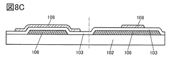
- 8A, 8B, 8C, 8D, and 8E are cross-sectional views illustrating a method for manufacturing a transistor.
- 9A, 9B, and 9C are cross-sectional views illustrating a method for manufacturing a transistor.
- 10A, 10B, and 10C are cross-sectional views illustrating a method for manufacturing a transistor.
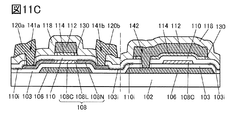
- 11A, 11B, and 11C are cross-sectional views illustrating a method for manufacturing a transistor.
- 12A, 12B, and 12C are top views of the display device.
- FIG. 13 is a cross-sectional view of the display device.
- FIG. 14 is a cross-sectional view of the display device.
- FIG. 15 is a cross-sectional view of the display device.
- FIG. 16 is a cross-sectional view of the display device.
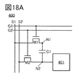
- FIG. 17A is a block diagram of a display device. 17B and 17C are circuit diagrams of the display device. 18A, 18C, and 18D are circuit diagrams of the display device.
- FIG. 18B is a timing chart of the display device. 19A and 19B are configuration examples of the display module.
- 20A and 20B are configuration examples of electronic devices.
- 21A, 21B, 21C, 21D, and 21E are configuration examples of electronic devices.
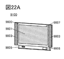
- 22A, 22B, 22C, 22D, 22E, 22F, and 22G are configuration examples of electronic devices.
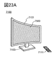
- 23A, 23B, 23C, and 23D are configuration examples of electronic devices.
- FIG. 24 is a STEM image of a cross section.
- FIG. 25 is a diagram showing the Id-Vg characteristics of the transistor and a STEM image of the cross section.
- FIG. 26 is a diagram showing an Id-Vg characteristic of a transistor and a STEM image of a cross section.
- FIG. 27 is a diagram showing the Id-Vg characteristics of the transistor and a STEM image of the cross section.
- FIG. 28 is a diagram showing a reliability test result of a transistor.
- FIG. 29 is a diagram showing a cross-sectional structure of the sample.
- FIG. 30 is a diagram showing the sheet resistance of the sample.
- FIG. 31 is a STEM image of a cross section.
- the functions of the source and the drain of the transistor may be switched when the polarity of the transistor or the direction of current flow in circuit operation is changed. Therefore, the terms source and drain can be used interchangeably.
- the channel length direction of a transistor refers to one of directions parallel to a straight line connecting a source region and a drain region with the shortest distance. That is, the channel length direction corresponds to one of the directions of current flowing through the semiconductor layer when the transistor is on. Further, the channel width direction means a direction orthogonal to the channel length direction. Note that depending on the structure and shape of the transistor, the channel length direction and the channel width direction may not be defined as one.
- the term “electrically connected” includes the case of being connected via “something having an electrical action”.
- the “object having some kind of electrical action” is not particularly limited as long as it can transfer an electric signal between the connection targets.
- “things having some kind of electrical action” include electrodes and wirings, switching elements such as transistors, resistance elements, inductors, capacitors, and other elements having various functions.
- film and “layer” can be interchanged with each other.
- conductive layer and “insulating layer” may be interchangeable with the terms “conductive film” and “insulating film”.
- the top shapes are substantially the same.
- it includes a case where the upper layer and the lower layer are processed with the same mask pattern or a part of the same mask pattern.
- the contours do not overlap with each other, and the upper layer may be located inside the lower layer, or the upper layer may be located outside the lower layer.
- off-state current refers to drain current when a transistor is in an off state (also referred to as a non-conducting state or a blocking state).
- the off state is a state in which the voltage V gs between the gate and the source is lower than the threshold voltage V th in the n-channel transistor (higher than V th in the p-channel transistor) unless otherwise specified.
- a display panel which is one mode of a display device, has a function of displaying (outputting) an image or the like on a display surface. Therefore, the display panel is one mode of the output device.
- a connector of FPC Flexible Printed Circuit
- TCP Transmission Carrier Package
- a connector of FPC Flexible Printed Circuit
- TCP Transmission Carrier Package
- COG Chip On Glass
- a touch panel which is one mode of a display device has a function of displaying an image or the like on a display surface, and a touch surface of a detected object such as a finger or a stylus touches, presses, or approaches the display surface. And a function as a touch sensor for detecting. Therefore, the touch panel is an aspect of the input / output device.
- the touch panel can also be called, for example, a display panel (or display device) with a touch sensor or a display panel (or display device) with a touch sensor function.
- the touch panel can also be configured to have a display panel and a touch sensor panel. Alternatively, the inside or the surface of the display panel may have a function as a touch sensor.
- a touch panel substrate on which connectors and ICs are mounted may be referred to as a touch panel module, a display module, or simply a touch panel.
- One embodiment of the present invention is a transistor including a semiconductor layer in which a channel is formed over a formation surface, an insulating layer over the semiconductor layer, a metal oxide layer over the insulating layer, and a conductive layer. Further, the transistor which is one embodiment of the present invention preferably has an insulating region which is adjacent to the metal oxide layer. The insulating region is located between the gate insulating layer and the conductive layer.
- the semiconductor layer is preferably configured to include a metal oxide having semiconductor characteristics (hereinafter, also referred to as an oxide semiconductor).
- the end of the metal oxide layer is provided inside the end of the conductive layer.
- the conductive layer has a portion protruding outward from the end of the metal oxide layer. Part of the metal oxide layer and the conductive layer functions as a gate electrode.
- the insulating region has a different relative dielectric constant from the insulating layer.
- the insulating region may include voids.
- the insulating layer is preferably provided so as to cover the top surface and the side surface of the semiconductor layer. The insulating layer and part of the insulating region function as a gate insulating layer.
- the semiconductor layer has a first region overlapping with the metal oxide layer and the conductive layer, a second region overlapping with the insulating region and the conductive layer, and a third region not overlapping with the conductive layer.
- the first region is a region that functions as a channel formation region.
- the third region has a lower resistance than the first region and functions as a source region or a drain region.
- the second region has a higher resistance than the third region.
- the second region overlaps with the conductive layer that functions as a gate electrode with the insulating region interposed, it can also be called an overlap region (Lov region).
- the second region functions as a buffer region to which the electric field of the gate is not applied or which is less likely to be applied than the first region.
- a transistor which is one embodiment of the present invention has a second region between a first region which is a channel formation region in a semiconductor layer and a third region which functions as a source region or a drain region. By having the second region, the source-drain breakdown voltage of the transistor can be improved, and a highly reliable transistor can be realized even when driven at a high voltage.
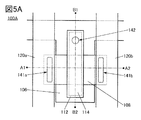
- FIG. 1A is a top view of the transistor 100
- FIG. 1B corresponds to a cross-sectional view taken along the dashed-dotted line A1-A2 in FIG. 1A
- FIG. 1C is a sectional view taken along the dashed-dotted line B1-B2 in FIG. 1A. It corresponds to a sectional view of the plane.
- FIG. 1A some of components of the transistor 100 (a gate insulating layer and the like) are omitted.
- the dashed-dotted line A1-A2 direction corresponds to the channel length direction
- the dashed-dotted line B1-B2 direction corresponds to the channel width direction.
- the top view of the transistor some of the components are omitted in the following drawings, as in FIG. 1A.
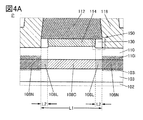
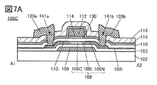
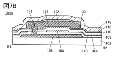
- the transistor 100 is provided over the substrate 102 and includes an insulating layer 103, a semiconductor layer 108, an insulating layer 110, a metal oxide layer 114, a conductive layer 112, an insulating layer 118, and the like.
- the island-shaped semiconductor layer 108 is provided over the insulating layer 103.
- the insulating layer 110 is provided in contact with the top surface of the insulating layer 103 and the top surface and side surfaces of the semiconductor layer 108.
- the metal oxide layer 114 and the conductive layer 112 are stacked over the insulating layer 110 in this order and have a portion overlapping with the semiconductor layer 108.
- the insulating layer 118 is provided so as to cover the top surface of the insulating layer 110 and the top and side surfaces of the conductive layer 112.
- FIG. 2A shows an enlarged view of a region P surrounded by the alternate long and short dash line in FIG. 1B.
- the transistor 100 has an insulating region 150 adjacent to the metal oxide layer 114.
- the insulating region 150 is located between the insulating layer 110 and the conductive layer 112.
- a conductive material can be used as the metal oxide layer 114.
- Part of the conductive layer 112 and the metal oxide layer 114 function as a gate electrode.
- Part of the insulating layer 110 and the insulating region 150 functions as a gate insulating layer.
- the transistor 100 is a so-called top-gate transistor in which a gate electrode is provided over the semiconductor layer 108.
- the end of the metal oxide layer 114 is located inside the end of the conductive layer 112 on the insulating layer 110.
- the conductive layer 112 has a portion on the insulating layer 110 that protrudes outward from the end portion of the metal oxide layer 114.
- the semiconductor layer 108 is configured to include a metal oxide having semiconductor characteristics (hereinafter, also referred to as an oxide semiconductor).
- the semiconductor layer 108 preferably contains at least indium and oxygen.
- the semiconductor layer 108 may contain zinc.
- the semiconductor layer 108 may contain gallium.
- indium oxide indium zinc oxide (In-Zn oxide), indium gallium zinc oxide (also referred to as In-Ga-Zn oxide, or IGZO), or the like can be used. ..
- indium tin oxide In—Sn oxide
- indium tin oxide containing silicon or the like can be used. Note that details of materials that can be used for the semiconductor layer 108 will be described later.
- the composition of the semiconductor layer 108 greatly affects the electrical characteristics and reliability of the transistor 100. For example, by increasing the content of indium in the semiconductor layer 108, carrier mobility is improved and a transistor with high field-effect mobility can be realized.
- the semiconductor layer 108 has a region 108C, a pair of regions 108L sandwiching the region 108C, and a pair of regions 108N outside thereof.
- the region 108C overlaps with the conductive layer 112 and the metal oxide layer 114 and functions as a channel formation region.
- the region 108L overlaps the conductive layer 112 and the insulating region 150. It can also be said that the region 108L overlaps with the conductive layer 112 and does not overlap with the metal oxide layer 114.
- the region 108L is a region where a channel can be formed when a gate voltage is applied to the conductive layer 112.
- the electric field applied to the region 108L is weaker than the electric field applied to the region 108C.
- the region 108L has a higher resistance than the region 108C, and functions as a buffer region for relaxing the drain electric field.
- a channel can be formed by the electric field of the conductive layer 112.
- the region 108L between the region 108C which is a channel formation region and the region 108N which is a source region or a drain region a high drain breakdown voltage and a high on-state current are combined, and the reliability is high.
- a transistor can be realized.
- the region 108N does not overlap with either the conductive layer 112 or the metal oxide layer 114 and functions as a source region or a drain region.
- the width of the conductive layer 112 in the channel length direction of the transistor 100 is indicated by L1.
- the width of the insulating region in the channel length direction of the transistor 100 is indicated by L2.
- the low-resistance region 108N has a higher carrier concentration than the region 108C and functions as a source region and a drain region.
- the region 108N can be referred to as a region having a lower resistance than the region 108C, a region having a high carrier concentration, a region having a large amount of oxygen vacancies, a region having a high hydrogen concentration, or a region having a high impurity concentration.
- the sheet resistance of the region 108N is 1 ⁇ / ⁇ or more and less than 1 ⁇ 10 3 ⁇ / ⁇ , preferably 1 ⁇ / ⁇ or more and 8 ⁇ 10 2 ⁇ / ⁇ or less. preferable.
- the higher the electric resistance of the region 108C in the state where no channel is formed the more preferable.
- the sheet resistance of the region 108C is 1 ⁇ 10 9 ⁇ / ⁇ or more, preferably 5 ⁇ 10 9 ⁇ / ⁇ or more, more preferably Is preferably 1 ⁇ 10 10 ⁇ / ⁇ or more.
- the region 108L is also referred to as a region having similar or lower resistance, a region having similar or higher carrier concentration, a region having similar or higher oxygen defect density, or a region having similar or higher impurity concentration than the region 108C. it can.
- the region 108L may also be referred to as a region having similar or higher resistance, a region having similar or lower carrier concentration, a region having similar or lower oxygen defect density, and a region having similar or lower impurity concentration than the region 108N. it can.
- the sheet resistance of the region 108L is preferably 1 ⁇ 10 3 ⁇ / ⁇ or more and 1 ⁇ 10 9 ⁇ / ⁇ or less, more preferably 1 ⁇ 10 3 ⁇ / ⁇ or more and 1 ⁇ 10 8 ⁇ / ⁇ or less, and further 1 It is preferably not less than ⁇ 10 3 ⁇ / ⁇ and not more than 1 ⁇ 10 7 ⁇ / ⁇ .
- the sheet resistance can be calculated from the resistance value.
- the source-drain breakdown voltage of the transistor 100 can be increased by providing such a region 108L between the region 108N and the region 108C.
- the carrier concentration in the region 108L may not be uniform, and may have a gradient such that the carrier concentration decreases from the region 108N side to the region 108C side.
- the hydrogen concentration and the oxygen deficiency concentration in the region 108L may have a gradient such that the concentration decreases from the region 108N side to the region 108C side.
- the region 108L can be formed in a self-aligned manner, a photomask for forming the region 108L is not needed and the manufacturing cost can be reduced. Further, by forming the region 108L in a self-aligning manner, relative displacement between the region 108L and the conductive layer 112 does not occur, so that the width of the region 108L in the semiconductor layer 108 can be approximately matched.
- a region 108L that functions as an offset region in which the electric field of the gate is not applied or is less likely to be applied than the region 108C can be stably formed between the region 108C and the region 108N in the semiconductor layer 108 without variation. As a result, the source-drain breakdown voltage of the transistor can be improved, and a highly reliable transistor can be realized.
- the width L2 of the region 108L is preferably 5 nm or more and 2 ⁇ m or less, more preferably 10 nm or more and 1 ⁇ m or less, and further preferably 15 nm or more and 500 nm or less.
- the width L2 of the region 108L can be determined depending on the thickness of the semiconductor layer 108, the thickness of the insulating layer 110, and the magnitude of the voltage applied between the source and the drain when the transistor 100 is driven.
- the region 108L between the region 108C and the region 108N By providing the region 108L between the region 108C and the region 108N, the current density at the boundary between the region 108C and the region 108N can be relaxed, heat generation at the boundary between the channel and the source or drain can be suppressed, and a highly reliable transistor or semiconductor can be obtained. It can be a device.
- the insulating region 150 may include the void 130.
- the insulating region 150 may include one or more of the void 130 and the insulating layer 118.
- FIG. 2A shows an example in which the insulating region 150 includes the void 130 and does not include the insulating layer 118.
- FIG. 2A illustrates an example in which the insulating layer 118 is provided without being in contact with the side surface of the metal oxide layer 114.
- FIG. 2B shows an example in which the insulating region 150 includes the void 130 and the insulating layer 118.
- 2B illustrates an example in which the insulating layer 118 is provided in contact with part of the side surface of the metal oxide layer 114.
- FIG. 3A shows an example in which the insulating region 150 includes the insulating layer 118 and does not include the void 130.
- 3A illustrates an example in which the insulating layer 118 is provided in contact with the side surface of the metal oxide layer 114.
- the insulating region 150 when the insulating region 150 includes the void 130 and does not include the insulating layer 118, the insulating region 150 has air, and the relative permittivity ⁇ r of the insulating region 150 is about 1 as in air. ..
- the relative permittivity ⁇ r of silicon oxide that can be used as the insulating layer 110 is approximately 4.0 to 4.5, and the relative permittivity ⁇ r of silicon nitride is approximately 7.0.
- the relative permittivity ⁇ r is larger than 1.
- the relative permittivity ⁇ r of the insulating region 150 can be calculated from the area ratio of the void 130 and the insulating layer 118 in the cross section, and the insulating region 150 The relative permittivity ⁇ r becomes larger than 1. Therefore, when the insulating region 150 includes the void 130, the relative dielectric constants of the insulating region 150 and the insulating layer 110 are different.
- the term “differing relative permittivity” means that, of the two relative permittivities, the ratio of the relative permittivity of the one having the smaller relative permittivity to the relative permittivity of the other is 2. Indicates 0 or more.
- the transistor 100 may include a conductive layer 120a and a conductive layer 120b over the insulating layer 118.
- the conductive layers 120a and 120b function as a source electrode or a drain electrode.
- the conductive layers 120a and 120b are electrically connected to the region 108N through the openings 141a and 141b provided in the insulating layer 118 and the insulating layer 110, respectively.
- a conductive film containing a metal or an alloy as the conductive layer 112 because electric resistance can be suppressed.
- an oxide conductive film may be used for the conductive layer 112.
- the metal oxide layer 114 has a function of supplying oxygen into the insulating layer 110. Further, the metal oxide layer 114 located between the insulating layer 110 and the conductive layer 112 functions as a barrier film that prevents oxygen contained in the insulating layer 110 from diffusing to the conductive layer 112 side. Further, the metal oxide layer 114 also functions as a barrier film which prevents hydrogen and water contained in the conductive layer 112 from diffusing to the insulating layer 110 side. For the metal oxide layer 114, for example, it is preferable to use a material that is less likely to transmit oxygen and hydrogen than at least the insulating layer 110.
- the metal oxide layer 114 can prevent diffusion of oxygen from the insulating layer 110 to the conductive layer 112 even when a metal material such as aluminum or copper which easily absorbs oxygen is used for the conductive layer 112. .. Even when the conductive layer 112 contains hydrogen, hydrogen can be prevented from diffusing from the conductive layer 112 to the semiconductor layer 108 through the insulating layer 110. As a result, the carrier density in the channel formation region of the semiconductor layer 108 can be extremely low.
- a metal oxide can be used as the metal oxide layer 114.
- an oxide containing indium such as indium oxide, indium zinc oxide, indium tin oxide (ITO), or indium tin oxide containing silicon (ITSO) can be used.
- ITO indium tin oxide
- ITSO indium tin oxide containing silicon
- a conductive oxide containing indium is preferable because it has high conductivity.
- ITSO does not easily crystallize due to the inclusion of silicon and has high flatness, adhesion with a film formed on ITSO is increased.
- a metal oxide such as zinc oxide or zinc oxide containing gallium can be used as the metal oxide layer 114.
- a structure in which these are stacked may be used.
- the metal oxide layer 114 it is preferable to use an oxide material containing one or more elements that are the same as those of the semiconductor layer 108. In particular, it is preferable to use an oxide semiconductor material applicable to the semiconductor layer 108. At this time, it is preferable to use, as the metal oxide layer 114, a metal oxide film formed using the same sputtering target as that for the semiconductor layer 108 because the devices can be shared.
- the metal oxide layer 114 is preferably formed using a sputtering device.
- oxygen can be added to the insulating layer 110 and the semiconductor layer 108 by forming the oxide film in an atmosphere containing oxygen gas.
- the region 108N of the semiconductor layer 108 is a region containing an impurity element.
- the impurity element include hydrogen, boron, carbon, nitrogen, fluorine, phosphorus, sulfur, arsenic, aluminum, or a rare gas.
- typical examples of rare gases include helium, neon, argon, krypton, xenon, and the like.
- the process of adding an impurity to the region 108N can be performed through the insulating layer 110 with the conductive layer 112 as a mask.
- the region 108N has an impurity concentration of 1 ⁇ 10 19 atoms / cm 3 or more and 1 ⁇ 10 23 atoms / cm 3 or less, preferably 5 ⁇ 10 19 atoms / cm 3 or more, 5 ⁇ 10 22 atoms / cm 3 or less, It is more preferable to include a region of 1 ⁇ 10 20 atoms / cm 3 or more and 1 ⁇ 10 22 atoms / cm 3 or less.
- the concentration of impurities contained in the region 108N may be analyzed by an analysis method such as secondary ion mass spectrometry (SIMS: Secondary Ion Mass Spectrometry) or X-ray photoelectron spectroscopy (XPS: X-ray Photoelectron Spectroscopy). It can.
- an analysis method such as secondary ion mass spectrometry (SIMS: Secondary Ion Mass Spectrometry) or X-ray photoelectron spectroscopy (XPS: X-ray Photoelectron Spectroscopy).
- SIMS Secondary Ion Mass Spectrometry
- XPS X-ray Photoelectron Spectroscopy
- the impurity element preferably exists in an oxidized state.
- an easily oxidizable element such as boron, phosphorus, magnesium, aluminum, or silicon
- Such an element that is easily oxidized can exist stably in a state where it is oxidized by being combined with oxygen in the semiconductor layer 108, and therefore, at a high temperature (for example, 400 ° C or higher, 600 ° C or higher, or 800 ° C or higher) in a later step. ), The desorption is suppressed. Further, a large number of oxygen vacancies are generated in the region 108N because the impurity element deprives oxygen in the semiconductor layer 108.
- the oxygen deficiency and hydrogen in the film combine to serve as a carrier supply source, so that the region 108N has an extremely low resistance.
- the boron contained in the region 108N can exist in a state of being bonded to oxygen. This can be confirmed by the fact that the spectrum peak due to the B 2 O 3 bond is observed in the XPS analysis. Further, in XPS analysis, a spectral peak due to the state where elemental boron is present alone is not observed, or the peak intensity is extremely small to such an extent that it is buried in background noise observed near the lower limit of measurement.
- the concentration of the impurity element in each of the regions 108L and 108C is preferably less than or equal to 1/10 of the concentration of the impurity element in the region 108N, further preferably less than or equal to 1/100.
- An oxide film is preferably used for the insulating layers 103 and 110 which are in contact with the channel formation region of the semiconductor layer 108.
- an oxide film such as a silicon oxide film, a silicon oxynitride film, or an aluminum oxide film can be used.
- oxygen desorbed from the insulating layer 103 or the insulating layer 110 can be supplied to the channel formation region of the semiconductor layer 108 by heat treatment or the like in the manufacturing process of the transistor 100, so that oxygen vacancies in the semiconductor layer 108 can be reduced.
- an oxynitride refers to a substance whose composition contains more oxygen than nitrogen, and an oxynitride is included in an oxide.
- Nitride oxide refers to a substance whose composition contains more nitrogen than oxygen, and nitride oxide is included in nitride.
- the insulating layer 110 in contact with the semiconductor layer 108 more preferably has a region containing oxygen in excess of the stoichiometric composition.
- the insulating layer 110 has an insulating film that can release oxygen.
- the insulating layer 110 is formed in an oxygen atmosphere, heat treatment in an oxygen atmosphere, plasma treatment, or the like is performed on the formed insulating layer 110, or the insulating layer 110 is formed over the insulating layer 110 in an oxygen atmosphere.
- Oxygen can be supplied into the insulating layer 110 by forming an oxide film or the like.
- the insulating layer 110 is formed by a sputtering method, a chemical vapor deposition (CVD) method, a vacuum deposition method, a pulsed laser deposition (PLD) method, an atomic layer deposition (ALD) method. And the like.
- CVD chemical vapor deposition
- PLA pulsed laser deposition
- ALD atomic layer deposition
- CVD method there are a plasma chemical vapor deposition (PECVD: Plasma Enhanced CVD) method, a thermal CVD method and the like.
- the insulating layer 110 is preferably formed by the plasma CVD method.
- the insulating layer 110 is formed on the semiconductor layer 108, it is preferable that the insulating layer 110 is a film formed under conditions that do not damage the semiconductor layer 108 as much as possible.
- the film formation can be performed under the condition that the film formation rate (also referred to as a film formation rate) is sufficiently low.
- a film forming gas used for forming the silicon oxynitride film includes, as a raw material, a deposition gas containing silicon such as silane and disilane, and an oxidizing gas such as oxygen, ozone, dinitrogen monoxide, and nitrogen dioxide. Gas can be used. Further, in addition to the raw material gas, a diluent gas such as argon, helium or nitrogen may be contained.
- the insulating layer 110 has a region in contact with the region 108C of the semiconductor layer 108, that is, a region overlapping with the conductive layer 112 and the metal oxide layer 114.
- the insulating layer 110 has a region which is in contact with the region 108L of the semiconductor layer 108 and which does not overlap with the metal oxide layer 114.
- the insulating layer 110 has a region which is in contact with the region 108N of the semiconductor layer 108 and which does not overlap with the conductive layer 112.
- a region 110i of the insulating layer 110 which overlaps with the region 108N, may contain the above-described impurity element.
- the impurity element in the insulating layer 110 preferably exists in a state of being bonded to oxygen.
- Such an element that is easily oxidized can stably exist in a state of being oxidized by being combined with oxygen in the insulating layer 110, and thus desorption is suppressed even when a high temperature is applied in a later step.
- the insulating layer 110 contains oxygen which can be released by heating (also referred to as excess oxygen)
- the excess oxygen and the impurity element are combined and stabilized, so that oxygen is transferred from the insulating layer 110 to the region 108N.
- Oxygen is less likely to diffuse in a part of the insulating layer 110 containing the oxidized impurity element; therefore, oxygen is supplied to the region 108N from above the insulating layer 110 through the insulating layer 110. It can be suppressed that the resistance of the region 108N is increased.
- the insulating layer 103 has a region 103i containing the above-described impurity element at or near the interface in contact with the insulating layer 110. Further, as shown in FIG. 2A, the region 103i may be provided at the interface in contact with the region 108N or in the vicinity thereof. At this time, the impurity concentration in a portion overlapping with the region 108N is lower than that in a portion in contact with the insulating layer 110.
- the insulating layer 110 and the insulating layer 103 may each have a laminated structure.
- An example in which the insulating layer 110 and the insulating layer 103 each have a stacked structure is illustrated in FIG. 3B.
- the insulating layer 110 has a stacked structure in which an insulating layer 110a, an insulating layer 110b, and an insulating layer 110c are stacked from the semiconductor layer 108 side.
- the insulating layer 103 has a stacked structure in which an insulating layer 103a, an insulating layer 103b, an insulating layer 103c, and an insulating layer 103d are stacked from the substrate 102 side. Note that in FIG. 3B, the region 110i and the region 103i are omitted for clarity.
- the insulating layer 110a has a region in contact with the semiconductor layer 108.
- the insulating layer 110c has a region in contact with the metal oxide layer 114.
- the insulating layer 110b is located between the insulating layer 110a and the insulating layer 110c.
- the insulating layer 110a, the insulating layer 110b, and the insulating layer 110c are preferably insulating films each containing an oxide. At this time, it is preferable that the insulating layer 110a, the insulating layer 110b, and the insulating layer 110c be continuously formed by the same film forming apparatus.
- insulating layers 110a, 110b, and 110c a silicon oxide film, a silicon oxynitride film, a silicon nitride oxide film, an aluminum oxide film, a hafnium oxide film, a yttrium oxide film, a zirconium oxide film, or a gallium oxide film is used.
- An insulating layer containing one or more of a tantalum oxide film, a magnesium oxide film, a lanthanum oxide film, a cerium oxide film, and a neodymium oxide film can be used.
- the insulating layer 110 that is in contact with the semiconductor layer 108 preferably has a stacked-layer structure of oxide insulating films and more preferably has a region containing oxygen in excess of the stoichiometric composition.
- the insulating layer 110 has an insulating film that can release oxygen.
- the insulating layer 110 is formed in an oxygen atmosphere, heat treatment in an oxygen atmosphere, plasma treatment, or the like is performed on the formed insulating layer 110, or the insulating layer 110 is formed over the insulating layer 110 in an oxygen atmosphere.
- Oxygen can be supplied into the insulating layer 110 by forming an oxide film or the like.
- the insulating layer 110a, the insulating layer 110b, and the insulating layer 110c are formed by a sputtering method, a chemical vapor deposition (CVD) method, a vacuum evaporation method, a pulse laser deposition (PLD) method, an atomic layer deposition (ALD) method, or the like. Can be formed. Further, as the CVD method, there are a plasma chemical vapor deposition (PECVD) method, a thermal CVD method and the like.
- PECVD plasma chemical vapor deposition
- the insulating layer 110a, the insulating layer 110b, and the insulating layer 110c are preferably formed by a plasma CVD method.
- the insulating layer 110a is formed on the semiconductor layer 108, it is preferable that the insulating layer 110a is a film formed under conditions that do not damage the semiconductor layer 108 as much as possible.
- the film formation can be performed under the condition that the film formation rate (also referred to as a film formation rate) is sufficiently low.
- a silicon oxynitride film is formed as the insulating layer 110a by a plasma CVD method
- damage to the semiconductor layer 108 can be extremely reduced by forming it under low power conditions.
- a film formed by a film formation method in which damage to the semiconductor layer 108 is reduced is used as the insulating layer 110a in contact with the top surface of the semiconductor layer 108. Therefore, the defect level density at the interface between the semiconductor layer 108 and the insulating layer 110 is reduced, so that the transistor 100 having high reliability can be provided.
- a film forming gas used for forming the silicon oxynitride film includes, as a raw material, a deposition gas containing silicon such as silane and disilane, and an oxidizing gas such as oxygen, ozone, dinitrogen monoxide, and nitrogen dioxide. Gas can be used. Further, in addition to the raw material gas, a diluent gas such as argon, helium or nitrogen may be contained.
- the deposition rate can be reduced, and a dense film with few defects can be deposited. it can.
- the insulating layer 110b is preferably a film formed under the condition that the film forming rate is higher than that of the insulating layer 110a. Thereby, the productivity can be improved.
- the insulating layer 110b can be deposited under the condition that the deposition rate is increased by increasing the flow rate ratio of the deposition gas to that of the insulating layer 110a.
- the insulating layer 110c is preferably an extremely dense film in which surface defects are reduced and impurities such as water contained in the atmosphere are not easily adsorbed.
- the film can be formed under the condition that the film formation rate is sufficiently low.
- the insulating layer 110c is formed on the insulating layer 110b, the influence on the semiconductor layer 108 at the time of forming the insulating layer 110c is smaller than that of the insulating layer 110a. Therefore, the insulating layer 110c can be formed under a condition of higher power than that of the insulating layer 110a. By reducing the flow rate ratio of the deposition gas and forming the film with relatively high power, a dense film with reduced surface defects can be obtained.
- a laminated film formed under the conditions in which the insulating layer 110b, the insulating layer 110a, and the insulating layer 110c are arranged in this order from the one having the highest film forming rate can be used as the insulating layer 110.
- the insulating layer 110 has a higher etching rate under the same conditions for wet etching or dry etching in the order of the insulating layer 110b, the insulating layer 110a, and the insulating layer 110c.
- the insulating layer 110b is preferably formed thicker than the insulating layers 110a and 110c. By forming the insulating layer 110b having the highest film formation rate thick, the time required for the step of forming the insulating layer 110 can be shortened.
- the boundary between the insulating layer 110a and the insulating layer 110b and the boundary between the insulating layer 110b and the insulating layer 110c may be unclear in some cases, these boundaries are clearly indicated by broken lines in FIG. 3B. Since the insulating layers 110a and 110b have different film densities, it is possible to observe these boundaries as differences in contrast in a transmission electron microscope (TEM) image in a cross section of the insulating layer 110. Sometimes you can. Similarly, the boundary between the insulating layer 110b and the insulating layer 110c can be observed in some cases.
- TEM transmission electron microscope
- the insulating layer 103 has a stacked structure in which an insulating layer 103a, an insulating layer 103b, an insulating layer 103c, and an insulating layer 103d are stacked from the substrate 102 side.
- the insulating layer 103a is in contact with the substrate 102.
- the insulating layer 103d is in contact with the semiconductor layer 108.
- the insulating layer 103 which functions as the second gate insulating layer has a high withstand voltage, a small stress in the film, a difficulty in releasing hydrogen and water, a small number of defects in the film, and an impurity contained in the substrate 102. Among the suppression of diffusion, it is preferable to satisfy one or more, and it is most preferable to satisfy all of these.
- the four insulating films included in the insulating layer 103 it is preferable to use insulating films containing nitrogen for the insulating layers 103a, 103b, and 103c located on the substrate 102 side. On the other hand, it is preferable to use an insulating film containing oxygen for the insulating layer 103d which is in contact with the semiconductor layer 108. In addition, it is preferable that the four insulating films included in the insulating layer 103 be successively formed using a plasma CVD apparatus without being exposed to the air.
- a nitrogen-containing insulating film such as a silicon nitride film, a silicon nitride oxide film, an aluminum nitride film, or a hafnium nitride film can be used.
- an insulating film that can be used for the insulating layer 110 can be used.
- the insulating layers 103a and 103c are preferably dense films that can prevent diffusion of impurities from below.
- the insulating layer 103a is preferably a film capable of blocking impurities contained in the substrate 102
- the insulating layer 103c is preferably a film capable of blocking hydrogen or water contained in the insulating layer 103b. Therefore, for the insulating layers 103a and 103c, an insulating film formed at a lower film formation rate than the insulating layer 103b can be used.
- the insulating layer 103b it is preferable to use an insulating film formed under the condition of low stress and high film formation rate.
- the insulating layer 103b is preferably formed thicker than the insulating layers 103a and 103c.
- the insulating layer 103b is a film more than the other two insulating films.
- the film has a low density. Therefore, in a transmission electron microscope image or the like in the cross section of the insulating layer 103, it may be possible to observe as a difference in contrast. Note that the boundary between the insulating layer 103a and the insulating layer 103b and the boundary between the insulating layer 103b and the insulating layer 103c may be unclear in some cases. Therefore, in FIG. 3B, these boundaries are clearly indicated by broken lines.
- the insulating layer 103d in contact with the semiconductor layer 108 is preferably a dense insulating film in which impurities such as water are less likely to be adsorbed on the surface.
- impurities such as water are less likely to be adsorbed on the surface.
- the same insulating film as the insulating layer 110c included in the insulating layer 110 can be used as the insulating layer 103d.
- the insulating layer 118 functions as a protective layer that protects the transistor 100.
- an inorganic insulating material such as an oxide or a nitride can be used.
- an inorganic insulating material such as silicon oxide, silicon oxynitride, silicon nitride, silicon nitride oxide, aluminum oxide, aluminum oxynitride, aluminum nitride, hafnium oxide, or hafnium aluminate can be used.
- the insulating layer 118 is preferably made of a material having high step coverage. Alternatively, the insulating layer 118 is preferably formed by a film formation method with high step coverage. The PECVD method can be preferably used for forming the insulating layer 118, for example. Note that due to the step between the conductive layer 112 and the insulating layer 110, the coverage with the insulating layer 118 provided thereover is deteriorated, and a stepped portion of the insulating layer 118 or a low-density region (also referred to as a void) is formed.
- a stepped portion of the insulating layer 118 or a low-density region also referred to as a void
- impurities such as water or hydrogen enter from the outside, which might lead to deterioration in reliability of the transistor.
- the insulating layer 118 having high step coverage a highly reliable transistor can be obtained.
- FIG. 4A shows an example in which the thickness of the insulating layer 110 in a region which does not overlap with the metal oxide layer 114 is smaller than the thickness of the insulating layer 110 in a region which overlaps with the metal oxide layer 114.
- FIG. 4B illustrates an example in which the thickness of the insulating layer 110 in a region which does not overlap with the conductive layer 112 is smaller than that of the insulating layer 110 in a region which does not overlap with the conductive layer 112. Note that when the insulating layer 110 has a stacked-layer structure as illustrated in FIG.
- the insulating layer 110c is preferably left in a region which does not overlap with the metal oxide layer 114. With the structure in which the insulating layer 110c remains in the non-overlapping region, adsorption of water to the insulating layer 110 can be efficiently suppressed.
- the thickness of the insulating layer 110c in a region overlapping with the conductive layer 112 is 1 nm to 50 nm inclusive, preferably 2 nm to 40 nm inclusive, more preferably 3 nm to 30 nm inclusive.
- FIG. 5A is a top view of the transistor 100A
- FIG. 5B is a cross-sectional view of the transistor 100A in the channel length direction
- FIG. 5C is a cross-sectional view of the transistor 100A in the channel width direction.
- the transistor 100A mainly differs from the configuration example 1 in that the conductive layer 106 is provided between the substrate 102 and the insulating layer 103.
- the conductive layer 106 has a region overlapping with the semiconductor layer 108 and the conductive layer 112.
- the conductive layer 112 has a function as a second gate electrode (also referred to as a top gate electrode), and the conductive layer 106 has a function as a first gate electrode (also referred to as a bottom gate electrode). ..
- part of the insulating layer 110 functions as a second gate insulating layer and part of the insulating layer 103 functions as a first gate insulating layer.
- the conductive layer 106 may be electrically connected to the conductive layer 112 through the openings 142 provided in the metal oxide layer 114, the insulating layer 110, and the insulating layer 103. .. Accordingly, the same potential can be applied to the conductive layer 106 and the conductive layer 112.
- the conductive layer 106 can be made of the same material as the conductive layer 112, the conductive layer 120a, or the conductive layer 120b. In particular, it is preferable to use a material containing copper for the conductive layer 106 because wiring resistance can be reduced.
- the conductive layer 112 and the conductive layer 106 project outward from the end portion of the semiconductor layer 108 in the channel width direction.
- the entire semiconductor layer 108 in the channel width direction is covered with the conductive layer 112 and the conductive layer 106 with the insulating layer 110 and the insulating layer 103 interposed therebetween.
- the semiconductor layer 108 can be electrically surrounded by an electric field generated by the pair of gate electrodes. At this time, it is particularly preferable to apply the same potential to the conductive layer 106 and the conductive layer 112. Thus, an electric field for inducing a channel can be effectively applied to the semiconductor layer 108, so that the on-state current of the transistor 100A can be increased. Therefore, the transistor 100A can be miniaturized.
- the conductive layer 112 and the conductive layer 106 may not be connected. At this time, a constant potential may be applied to one of the pair of gate electrodes and a signal for driving the transistor 100A may be applied to the other. At this time, the threshold voltage when the transistor 100A is driven by the other gate electrode can be controlled by the potential applied to the one gate electrode.
- the insulating layer 103 preferably has a laminated structure.
- the insulating layer 103 can have a stacked-layer structure in which the insulating layer 103a, the insulating layer 103b, the insulating layer 103c, and the insulating layer 103d are stacked from the conductive layer 106 side (see FIG. 3B).
- the insulating layer 103a in contact with the conductive layer 106 is preferably a film which can block a metal element contained in the conductive layer 106. Since the above description can be referred to for the insulating layer 103a, the insulating layer 103b, the insulating layer 103c, and the insulating layer 103d, detailed description thereof is omitted.
- the insulating layer 103a is not provided and the three insulating films of the insulating layer 103b, the insulating layer 103c, and the insulating layer 103d are provided. May be laminated.
- FIG. 6A is a cross-sectional view of the transistor 100B in the channel length direction
- FIG. 6B is a cross-sectional view of the transistor 100B in the channel width direction.
- the top view of the transistor 100B can be referred to FIG. 5A; therefore, the description is omitted.
- the transistor 100B mainly differs from the transistor 100A illustrated in the configuration example 2 in that the insulating layer 116 is provided on the insulating layer 118.
- the insulating layer 116 is provided so as to cover the upper surface of the insulating layer 110.
- the insulating layer 116 has a function of suppressing diffusion of impurities from above the insulating layer 116 into the semiconductor layer 108.
- the conductive layers 120a and 120b are electrically connected to the region 108N through the openings 141a and 141b provided in the insulating layer 116, the insulating layer 118, and the insulating layer 110, respectively.
- an insulating film containing a nitride such as silicon nitride, silicon nitride oxide, silicon oxynitride, aluminum nitride, or aluminum nitride oxide can be preferably used.
- silicon nitride has a blocking property against hydrogen and oxygen, it is possible to prevent both diffusion of hydrogen from the outside to the semiconductor layer and desorption of oxygen from the semiconductor layer to the outside, so that a highly reliable transistor can be obtained. realizable.
- a metal nitride As the insulating layer 116, it is preferable to use a nitride of aluminum, titanium, tantalum, tungsten, chromium, or ruthenium. In particular, it is particularly preferable to contain aluminum or titanium.
- aluminum As a sputtering target, an aluminum nitride film formed by a reactive sputtering method using a gas containing nitrogen as a film forming gas, by appropriately controlling the flow rate of nitrogen gas with respect to the total flow rate of the film forming gas, A film having both extremely high insulating properties and extremely high blocking properties against hydrogen and oxygen can be obtained.
- the thickness of the insulating layer containing the aluminum nitride is preferably 5 nm or more. Even with such a thin film, a high blocking property against hydrogen and oxygen and a function of lowering the resistance of the semiconductor layer can both be achieved.
- the insulating layer may have any thickness, but in view of productivity, it is preferably 500 nm or less, preferably 200 nm or less, more preferably 50 nm or less.
- a film whose composition formula satisfies AlN x (x is a real number greater than 0 and 2 or less, preferably x is greater than 0.5 and less than or equal to 1.5) is used. Is preferred. Accordingly, a film having excellent insulating properties and excellent thermal conductivity can be obtained, so that heat dissipation of heat generated when the transistor 100B is driven can be improved.
- An aluminum titanium nitride film, a titanium nitride film, or the like can be used as the insulating layer 116.
- a transistor with high on-state current can be obtained.
- a transistor whose threshold voltage can be controlled can be used. Further, the transistor can have high reliability.
- FIG. 7A is a cross-sectional view of the transistor 100C in the channel length direction
- FIG. 7B is a cross-sectional view of the transistor 100C in the channel width direction.
- the top view of the transistor 100C can be referred to FIG. 5A; therefore, the description is omitted.
- the transistor 100C mainly differs from the transistor 100A illustrated in the configuration example 2 in that the insulating layer 116 is provided between the insulating layer 118 and the insulating layer 110.
- the insulating layer 116 is provided so as to cover the upper surface of the insulating layer 118 and the upper and side surfaces of the conductive layer.
- the insulating layer 116 may be provided in contact with the side surface of the metal oxide layer 114.
- the insulating layer 116 may be provided in contact with part of the side surface of the metal oxide layer 114.
- the insulating layer 116 has a function of suppressing diffusion of impurities from above the insulating layer 116 into the semiconductor layer 108.
- a transistor with high on-state current can be obtained.
- a transistor whose threshold voltage can be controlled can be used. Further, the transistor can have high reliability.
- Example of manufacturing method> An example of a method for manufacturing a transistor of one embodiment of the present invention will be described below.
- the transistor 100A illustrated in the configuration example 2 will be described as an example.
- the thin films (insulating film, semiconductor film, conductive film, etc.) constituting the semiconductor device are sputtering method, chemical vapor deposition (CVD) method, vacuum vapor deposition method, pulse laser deposition (PLD) method, atomic layer deposition (ALD). ) Method etc. can be used.
- CVD method include a plasma chemical vapor deposition (PECVD) method and a thermal CVD method.
- PECVD plasma chemical vapor deposition
- MOCVD metal organic chemical vapor deposition
- Thin films (insulating films, semiconductor films, conductive films, etc.) that compose semiconductor devices are spin coat, dip, spray coat, inkjet, dispense, screen print, offset print, doctor knife, slit coat, roll coat, curtain coat, knife. It can be formed by a method such as coating.
- the thin film When processing a thin film that constitutes a semiconductor device, it is possible to process it using a photolithography method or the like.
- the thin film may be processed by a nanoimprint method, a sandblast method, a lift-off method, or the like.
- the island-shaped thin film may be directly formed by a film forming method using a shielding mask such as a metal mask.
- the following two methods are typically used as the photolithography method.
- One is a method of forming a resist mask on a thin film to be processed, processing the thin film by etching or the like, and removing the resist mask.
- the other is a method in which a thin film having photosensitivity is formed and then exposed and developed to process the thin film into a desired shape.
- the light used for exposure can be, for example, i-line (wavelength 365 nm), g-line (wavelength 436 nm), h-line (wavelength 405 nm), or a mixture thereof.
- ultraviolet light, KrF laser light, ArF laser light, or the like can be used.
- the exposure may be performed by a liquid immersion exposure technique.
- extreme ultraviolet (EUV) light or X-ray may be used.
- an electron beam may be used instead of the light used for exposure. The use of extreme ultraviolet light, X-rays or electron beams is preferable because it enables extremely fine processing. Note that a photomask is not necessary when exposure is performed by scanning a beam such as an electron beam.
- etching of the thin film a dry etching method, a wet etching method, a sandblast method, etc. can be used.
- 8A to 11C show side by side cross-sectional views in the channel length direction and the channel width direction at each stage of the manufacturing process of the transistor 100A.
- a conductive film is formed over the substrate 102 and processed by etching to form the conductive layer 106 which functions as a gate electrode (FIG. 8A).
- the wiring resistance can be reduced by using a conductive film containing copper as the conductive film to be the conductive layer 106.
- a conductive film containing copper As the conductive film to be the conductive layer 106, it is preferable to use a conductive film containing copper. Even when a conductive film containing copper is used for the conductive layer 106, the insulating layer 103 suppresses diffusion of copper toward the semiconductor layer 108, so that a highly reliable transistor can be realized.
- the insulating layer 103 is formed so as to cover the substrate 102 and the conductive layer 106.
- the insulating layer 103 can be formed by a PECVD method, an ALD method, a sputtering method, or the like.
- the insulating layer 103 is formed by stacking an insulating layer 103a, an insulating layer 103b, an insulating layer 103c, and an insulating layer 103d.
- each insulating layer forming the insulating layer 103 is formed by the PECVD method.
- the description of Structural Example 1 can be applied to the method for forming the insulating layer 103.
- a process of supplying oxygen to the insulating layer 103 may be performed.
- plasma treatment or heat treatment in an oxygen atmosphere can be performed.
- oxygen may be supplied to the insulating layer 103 by a plasma ion doping method or an ion implantation method.
- the metal oxide film 108f is preferably formed by a sputtering method using a metal oxide target.
- the metal oxide film 108f is preferably a dense film with as few defects as possible.
- the metal oxide film 108f is preferably a high-purity film in which impurities such as hydrogen and water are reduced as much as possible.
- impurities such as hydrogen and water are reduced as much as possible.
- oxygen gas and an inert gas for example, helium gas, argon gas, xenon gas, etc.
- an inert gas for example, helium gas, argon gas, xenon gas, etc.
- the crystallinity of the metal oxide film 108f can be increased as the proportion of oxygen gas in the entire deposition gas in forming the metal oxide film 108f (hereinafter also referred to as an oxygen flow rate ratio) increases.
- an oxygen flow rate ratio the proportion of oxygen gas in the entire deposition gas in forming the metal oxide film 108f
- the lower the oxygen flow rate ratio the lower the crystallinity of the metal oxide film 108f, and the transistor with higher on-state current can be obtained.
- the film formation conditions for the metal oxide film 108f may be such that the substrate temperature is room temperature or higher and 250 ° C. or lower, preferably room temperature or higher and 200 ° C. or lower, and more preferably the substrate temperature is room temperature or higher and 140 ° C. or lower.
- the substrate temperature is room temperature or higher and lower than 140 ° C. because productivity is high.
- the crystallinity can be lowered by forming the metal oxide film 108f in a state where the substrate temperature is room temperature or the substrate is not heated.
- any one or more of a treatment for desorbing water, hydrogen, an organic substance, and the like adsorbed on the surface of the insulating layer 103 and a treatment for supplying oxygen into the insulating layer 103 before forming the metal oxide film 108f. Is preferably performed.
- heat treatment can be performed at a temperature of 70 ° C to 200 ° C in a reduced pressure atmosphere.
- plasma treatment may be performed in an atmosphere containing oxygen.
- oxygen may be supplied to the insulating layer 103 by plasma treatment in an atmosphere containing an oxidizing gas such as dinitrogen monoxide (N 2 O).
- oxygen can be supplied while preferably removing organic substances on the surface of the insulating layer 103. After such treatment, it is preferable to continuously form the metal oxide film 108f without exposing the surface of the insulating layer 103 to the air.
- the semiconductor layer 108 has a stacked-layer structure in which a plurality of semiconductor layers is stacked, after the metal oxide film which is formed first is formed, the surface of the metal oxide film is continuously exposed without being exposed to the atmosphere. It is preferable to form a metal oxide film.
- the island-shaped semiconductor layer 108 is formed by etching a part of the metal oxide film 108f (FIG. 8C).
- the metal oxide film 108f may be processed by either the wet etching method or the dry etching method, or both. At this time, part of the insulating layer 103 which does not overlap with the semiconductor layer 108 may be etched and thinned. For example, in the insulating layer 103, the insulating layer 103d may disappear by etching and the surface of the insulating layer 103c may be exposed.
- the heat treatment it is preferable to perform heat treatment after forming the metal oxide film 108f or after processing the semiconductor layer 108.
- the heat treatment may improve the film quality of the metal oxide film 108f or the semiconductor layer 108 (eg, reduction of defects, improvement of crystallinity, or the like).
- oxygen can be supplied from the insulating layer 103 to the metal oxide film 108f or the semiconductor layer 108. At this time, it is more preferable to perform heat treatment before processing the semiconductor layer 108.
- the temperature of the heat treatment can be typically 150 ° C. or higher and lower than the strain point of the substrate, 200 ° C. or higher and 500 ° C. or lower, or 250 ° C. or higher and 450 ° C. or lower, or 300 ° C. or higher and 450 ° C. or lower.
- Heat treatment can be performed in an atmosphere containing a rare gas or nitrogen. Alternatively, after heating in the atmosphere, heating may be performed in an atmosphere containing oxygen. Alternatively, the heating may be performed in a dry air atmosphere. Note that it is preferable that the atmosphere for the heat treatment contains as little hydrogen and water as possible.
- An electric furnace, an RTA (Rapid Thermal Anneal) device, or the like can be used for the heat treatment. By using the RTA device, the heat treatment time can be shortened.
- heat treatment may be omitted if unnecessary.
- heat treatment may not be performed here and may also serve as heat treatment performed in a later step. In some cases, it can be combined with the heat treatment in a high-temperature treatment (such as a film-forming step) in a later step.
- the insulating layer 110 is formed so as to cover the insulating layer 103 and the semiconductor layer 108 (FIG. 8D).
- each insulating layer forming the insulating layer 110 is formed by the PECVD method.
- the description in Structural Example 1 can be applied to the method for forming each layer included in the insulating layer 110.
- the plasma treatment Before forming the insulating layer 110, it is preferable to perform plasma treatment on the surface of the semiconductor layer 108.
- impurities such as water adsorbed on the surface of the semiconductor layer 108 can be reduced. Therefore, impurities at the interface between the semiconductor layer 108 and the insulating layer 110 can be reduced, so that a highly reliable transistor can be realized.
- the plasma treatment can be performed in an atmosphere of oxygen, ozone, nitrogen, dinitrogen monoxide, argon, or the like. Further, the plasma treatment and the film formation of the insulating layer 110 are preferably performed continuously without being exposed to the air.
- the heat treatment it is preferable to perform heat treatment after forming the insulating layer 110.
- hydrogen or water contained in the insulating layer 110 or adsorbed on the surface can be removed.
- defects in the insulating layer 110 can be reduced.
- heat treatment may be omitted if unnecessary.
- heat treatment may not be performed here and may also serve as heat treatment performed in a later step. In some cases, it can be combined with the heat treatment in a high-temperature treatment (such as a film-forming step) in a later step.
- the metal oxide film 114f is preferably formed in an atmosphere containing oxygen, for example.
- it is preferably formed by a sputtering method in an atmosphere containing oxygen. Accordingly, oxygen can be supplied to the insulating layer 110 when the metal oxide film 114f is formed.
- the metal oxide film 114f is formed by a sputtering method using an oxide target containing a metal oxide similar to that of the semiconductor layer 108.
- the metal oxide film may be formed by a reactive sputtering method using oxygen as a film forming gas and a metal target.
- oxygen as a film forming gas
- a metal target for example, an aluminum oxide film can be formed.
- the width L2 of the region 108L can be controlled by adjusting the film formation conditions of the metal oxide film 114f. For example, when the metal oxide film 114f is formed, the crystallinity of the metal oxide film 114f becomes higher as the pressure inside the film forming chamber of the film forming apparatus becomes lower, and the width of the region 108L becomes larger when the metal oxide layer 114 is formed later. L2 can be reduced. The higher the pressure in the deposition chamber, the lower the crystallinity of the metal oxide film 114f, and the larger the width L2 of the region 108L can be when the metal oxide layer 114 is formed later. In this way, the width L2 of the region 108L can be controlled by adjusting the pressure in the deposition chamber when the metal oxide film 114f is deposited.
- the higher the power supply power, the higher the crystallinity of the metal oxide film 114f, and the width L2 of the region 108L can be reduced when the metal oxide layer 114 is formed later.
- the substrate temperature during the formation of the metal oxide film 108f and the substrate during the formation of the metal oxide film 114f is the same.
- the ratio of the oxygen flow rate to the total flow rate of the deposition gas introduced into the deposition chamber of the deposition apparatus oxygen flow rate ratio
- the higher the oxygen partial pressure in the deposition chamber the higher the metal content.
- the crystallinity of the oxide film 114f is increased, and the width L2 of the region 108L can be reduced when the metal oxide layer 114 is formed later.
- the ratio of the oxygen flow rate to the total flow rate of the deposition gas introduced into the deposition chamber of the deposition apparatus is, for example, higher than 0% and 100% or less, preferably 10% or more and 100% or less, more preferably 20% or more and 100% or less, further preferably 30% or more and 100% or less, and further preferably Is 40% or more and 100% or less.
- the oxygen flow rate ratio be 100% and the oxygen partial pressure be as close as possible to 100%.
- Heat treatment is preferably performed after the metal oxide film 114f is formed.
- oxygen contained in the insulating layer 110 can be supplied to the semiconductor layer 108.
- oxygen can be prevented from being released from the insulating layer 110 to the outside and a large amount of oxygen can be supplied to the semiconductor layer 108.
- oxygen vacancies in the semiconductor layer 108 can be reduced and a highly reliable transistor can be realized.
- heat treatment may be omitted if unnecessary.
- heat treatment may not be performed here and may also serve as heat treatment performed in a later step. In some cases, it can be combined with the heat treatment in a high-temperature treatment (such as a film-forming step) in a later step.
- Opening 142 and Conductive Film 112f [Formation of Opening 142 and Conductive Film 112f] Subsequently, the metal oxide film 114f, the insulating layer 110, and part of the insulating layer 103 are etched, so that an opening 142 reaching the conductive layer 106 is formed. Accordingly, the conductive layer 112 to be formed later and the conductive layer 106 can be electrically connected to each other through the opening 142.
- a conductive film 112f to be the conductive layer 112 is formed on the metal oxide film 114f (FIG. 9A).
- the conductive film 112f is preferably made of a low resistance metal or alloy material. Further, as the conductive film 112f, it is preferable to use a material which does not easily release hydrogen and which does not easily diffuse hydrogen. Further, it is preferable to use a material which is not easily oxidized as the conductive film 112f.
- the conductive film 112f is preferably formed by a sputtering method using a sputtering target containing a metal or an alloy.
- the conductive film 112f is a stacked film in which a conductive film that is difficult to oxidize and hydrogen does not diffuse and a conductive film having low resistance are stacked.
- a wet etching method can be preferably used for forming the conductive layer 112 and the metal oxide layer 114.
- an etchant containing one or more of oxalic acid, phosphoric acid, acetic acid, nitric acid, hydrochloric acid, or sulfuric acid can be used.
- an etchant containing phosphoric acid, acetic acid, and nitric acid can be preferably used.
- the metal oxide layer 114 and the conductive layer 112 can be formed in the same step by using a structure in which the etching rate of the metal oxide layer 114 is higher than that of the conductive layer 112. Further, the end portion of the metal oxide layer 114 can be located inside the end portion of the conductive layer 112. The width L2 of the region 108L can be controlled by adjusting the etching time. In addition, since they can be formed in the same process, the process can be simplified and the productivity can be improved.
- the end portions of the conductive layer 112 and the metal oxide layer 114 are located inside the contour of the resist mask 115 as illustrated in FIG. 9C.
- the width L1 of the conductive layer 112 is smaller than the width of the resist mask 115, the width of the resist mask 115 may be increased so that the width L1 of the conductive layer 112 is desired.
- the insulating layer 110 is not etched, and the top surface and the side surface of the semiconductor layer 108 and the insulating layer 103 are covered, so that the semiconductor layer 108 and the insulating layer are formed when the conductive layer 112 and the like are formed. It is possible to prevent a part of 103 from being etched and thinning.
- a resist mask 115 is formed on the conductive film 112f (FIG. 10A).
- the conductive film 112f is etched using anisotropic etching to form the conductive layer 112 (FIG. 10B). Dry etching can be preferably used as the anisotropic etching.
- the metal oxide film 114f is etched by wet etching to form the metal oxide layer 114 (FIG. 10C).
- the etching time is adjusted so that the end portion of the metal oxide layer 114 is inside the end portion of the conductive layer 112.
- the width L2 of the region 108L can be controlled by adjusting the etching time.
- the conductive layer 112 and the metal oxide layer 114 are formed by etching the conductive film 112f and the metal oxide film 114f by an anisotropic etching method and then by using an isotropic etching method.
- the side faces of the metal oxide film 114f may be etched to make the end faces recede (also referred to as side etching).
- the metal oxide layer 114 which is located inside the conductive layer 112 in plan view, can be formed.
- etching conditions or techniques may be used for forming the conductive layer 112 and the metal oxide layer 114, and etching may be performed at least twice.
- the conductive film 112f may be etched first, and then the metal oxide film 114f may be etched under different etching conditions.
- the thickness of the insulating layer 110 in a region which is not in contact with the metal oxide layer 114 may be thin (see FIGS. 2A, 2B, 3A, and 3B). ).
- a plasma ion doping method or an ion implantation method can be preferably used. According to these methods, the concentration profile in the depth direction can be controlled with high accuracy by the acceleration voltage of ions, the dose amount, and the like. The productivity can be improved by using the plasma ion doping method. Further, by using the ion implantation method using mass separation, the purity of the supplied impurity element can be increased.
- the interface between the semiconductor layer 108 and the insulating layer 110, a portion close to the interface in the semiconductor layer 108, or a portion close to the interface in the insulating layer 110 has a highest concentration. It is preferable to control the processing conditions. Thus, the impurity element 140 with an optimum concentration can be supplied to both the semiconductor layer 108 and the insulating layer 110 by one treatment.
- the impurity element 140 may be hydrogen, boron, carbon, nitrogen, fluorine, phosphorus, sulfur, arsenic, aluminum, magnesium, silicon, or a rare gas.
- rare gases include helium, neon, argon, krypton, xenon, and the like.
- a gas containing the above impurity element can be used.
- B 2 H 6 gas, BF 3 gas, or the like can be typically used.
- PH 3 gas can be typically used.
- a mixed gas obtained by diluting these source gases with a rare gas may be used.
- raw material gases CH 4 , N 2 , NH 3 , AlH 3 , AlCl 3 , SiH 4 , Si 2 H 6 , F 2 , HF, H 2 , (C 5 H 5 ) 2 Mg, and rare gas, etc.
- the ion source is not limited to a gas, and a solid or liquid heated and vaporized may be used.
- the addition of the impurity element 140 can be controlled by setting conditions such as an acceleration voltage and a dose amount in consideration of the composition, density, and thickness of the insulating layer 110 and the semiconductor layer 108.
- the accelerating voltage can be, for example, 5 kV or more and 100 kV or less, preferably 7 kV or more and 70 kV or less, and more preferably 10 kV or more and 50 kV or less.
- the dose amount is, for example, 1 ⁇ 10 13 ions / cm 2 or more and 1 ⁇ 10 17 ions / cm 2 or less, preferably 1 ⁇ 10 14 ions / cm 2 or more and 5 ⁇ 10 16 ions / cm 2 or less, and more preferably 1 It can be set in the range of not less than ⁇ 10 15 ions / cm 2 and not more than 3 ⁇ 10 16 ions / cm 2 .
- the acceleration voltage can be, for example, 10 kV or more and 100 kV or less, preferably 30 kV or more and 90 kV or less, and more preferably 40 kV or more and 80 kV or less.
- the dose amount is, for example, 1 ⁇ 10 13 ions / cm 2 or more and 1 ⁇ 10 17 ions / cm 2 or less, preferably 1 ⁇ 10 14 ions / cm 2 or more and 5 ⁇ 10 16 ions / cm 2 or less, and more preferably 1 It can be set in the range of not less than ⁇ 10 15 ions / cm 2 and not more than 3 ⁇ 10 16 ions / cm 2 .
- the method of supplying the impurity element 140 is not limited to this, and for example, plasma treatment or treatment utilizing thermal diffusion by heating may be used.
- the impurity element can be added by generating plasma in a gas atmosphere containing the impurity element to be added and performing plasma treatment.
- a dry etching device, an ashing device, a plasma CVD device, a high density plasma CVD device, or the like can be used as the device for generating the plasma.
- the impurity element 140 can be supplied to the semiconductor layer 108 through the insulating layer 110. Therefore, even when the semiconductor layer 108 has crystallinity, damage that the semiconductor layer 108 receives when the impurity element 140 is supplied can be reduced and the crystallinity can be prevented from being impaired. Therefore, it is suitable when the electrical resistance increases due to the decrease in crystallinity.
- an insulating layer 118 is formed so as to cover the insulating layer 110, the metal oxide layer 114, and the conductive layer 112 (FIG. 11B).
- the film formation temperature of the insulating layer 118 may be determined in consideration of the above.
- the film forming temperature of the insulating layer 118 is preferably 150 ° C. or higher and 400 ° C. or lower, preferably 180 ° C. or higher and 360 ° C. or lower, and more preferably 200 ° C. or higher and 250 ° C. or lower.
- heat treatment may be performed.
- the heat treatment makes it possible to more stably form the low-resistance region 108N.
- the impurity element 140 is appropriately diffused and locally homogenized, so that the region 108N having an ideal impurity element concentration gradient can be formed. Note that if the temperature of the heat treatment is too high (eg, 500 ° C. or higher), the impurity element 140 may diffuse into the channel formation region, which might lead to deterioration in electrical characteristics and reliability of the transistor.
- heat treatment may be omitted if unnecessary.
- heat treatment may not be performed here and may also serve as heat treatment performed in a later step.
- a high temperature treatment for example, a film forming step
- Opening 141a and Opening 141b [Formation of Opening 141a and Opening 141b] Then, part of the insulating layer 118 and the insulating layer 110 is etched to form an opening 141a and an opening 141b reaching the region 108N.
- the transistor 100A can be manufactured. For example, when the transistor 100A is applied to a pixel of a display device, a step of forming one or more of a protective insulating layer, a planarization layer, a pixel electrode, or a wiring may be added after this.
- the formation step of the conductive layer 106 and the formation step of the opening 142 in the above-described Manufacturing Method Example 1 may be omitted. Further, the transistor 100 and the transistor 100A can be formed over the same substrate through the same step.
- the substrate 102 there is no particular limitation on the material of the substrate 102, but it is necessary that the substrate 102 have at least heat resistance high enough to withstand heat treatment performed later.
- a single crystal semiconductor substrate made of silicon or silicon carbide, a polycrystalline semiconductor substrate, a compound semiconductor substrate such as silicon germanium, an SOI substrate, a glass substrate, a ceramic substrate, a quartz substrate, a sapphire substrate, or the like is used as the substrate 102.
- a substrate provided with a semiconductor element may be used as the substrate 102.
- a flexible substrate may be used as the substrate 102, and the semiconductor device may be directly formed on the flexible substrate.
- a separation layer may be provided between the substrate 102 and the semiconductor device.
- the peeling layer can be used for separating a semiconductor device over the peeling layer, separating the substrate 102 from the substrate 102, and transferring the semiconductor device to another substrate. At that time, the semiconductor device can be transferred to a substrate having poor heat resistance or a flexible substrate.
- the conductive layer 112 and the conductive layer 106 which function as gate electrodes, the conductive layer 120a which functions as one of the source electrode and the drain electrode, and the conductive layer 120b which functions as the other are chromium, copper, aluminum, gold, silver, zinc, Form each using a metal element selected from molybdenum, tantalum, titanium, tungsten, manganese, nickel, iron, cobalt, or an alloy containing the above metal element as a component or an alloy in which the above metal elements are combined. You can
- In—Sn oxide, In—W oxide, In—W—Zn oxide, In—Ti oxide, and In—Ti—Sn are used.
- An oxide conductor such as an oxide, an In-Zn oxide, an In-Sn-Si oxide, or an In-Ga-Zn oxide, or a metal oxide film can also be applied.
- the oxide conductor (OC: Oxide Conductor)
- OC Oxide Conductor
- a donor level is formed in the vicinity of the conduction band.
- the metal oxide has high conductivity and becomes a conductor.
- the metal oxide converted into a conductor can be referred to as an oxide conductor.
- the conductive layer 112 and the like may have a laminated structure of a conductive film containing the above oxide conductor (metal oxide) and a conductive film containing a metal or an alloy.
- a conductive film containing a metal or an alloy wiring resistance can be reduced.
- a conductive film containing an oxide conductor is preferably applied to the side which is in contact with the insulating layer functioning as a gate insulating film.
- the conductive layer 112, the conductive layer 106, the conductive layer 120a, and the conductive layer 120b have at least one selected from titanium, tungsten, tantalum, and molybdenum among the above metal elements. is there.
- the tantalum nitride film has conductivity, has a high barrier property against copper, oxygen, or hydrogen, and emits little hydrogen from itself; therefore, the conductive film in contact with the semiconductor layer 108 or the semiconductor layer.
- the conductive film near 108 can be preferably used.
- the semiconductor layer 108 preferably contains a metal oxide.
- the semiconductor layer 108 includes indium and M (M is gallium, aluminum, silicon, boron, yttrium, tin, copper, vanadium, beryllium, titanium, iron, nickel, germanium, zirconium, molybdenum, lanthanum, cerium, neodymium, It is preferable to have one or more kinds selected from hafnium, tantalum, tungsten, or magnesium) and zinc.
- M is preferably one or more selected from aluminum, gallium, yttrium, or tin.
- the semiconductor layer 108 is an In-M-Zn oxide
- M: Zn 1: 1: 1 as the atomic ratio of metal elements of a sputtering target used for forming the In-M-Zn oxide.
- M: Zn 1: 1: 1.2
- M: Zn 1: 3: 2
- M: Zn 1: 3: 4
- M: Zn 1: 3: 6.
- the atomic ratio of the semiconductor layer 108 to be formed includes a fluctuation of ⁇ 40% in the atomic ratio of the metal element contained in the above sputtering target.
- the semiconductor layer 108 has an energy gap of 2 eV or more, preferably 2.5 eV or more.
- the off-state current of the transistor can be reduced by using the metal oxide whose energy gap is wider than that of silicon.
- a metal oxide having a low carrier concentration for the semiconductor layer 108.
- the concentration of impurities in the metal oxide may be lowered and the density of defect states may be lowered.
- low impurity concentration and low defect level density are referred to as high-purity intrinsic or substantially high-purity intrinsic.
- the impurities in the metal oxide include, for example, hydrogen, nitrogen, alkali metals, alkaline earth metals, iron, nickel, silicon and the like.
- hydrogen contained in the metal oxide reacts with oxygen bonded to the metal atom to become water, which may form oxygen deficiency in the metal oxide. If the channel formation region in the metal oxide contains oxygen vacancies, the transistor might have normally-on characteristics. Further, a defect in which hydrogen is contained in an oxygen vacancy may function as a donor and an electron which is a carrier may be generated. Further, part of hydrogen may be bonded to oxygen which is bonded to a metal atom to generate an electron which is a carrier. Therefore, a transistor including a metal oxide containing a large amount of hydrogen is likely to have normally-on characteristics.
- the metal oxide may be evaluated not by the donor concentration but by the carrier concentration. Therefore, in this specification and the like, the carrier concentration which is assumed to be a state where no electric field is applied may be used as the parameter of the metal oxide, instead of the donor concentration. That is, the “carrier concentration” described in this specification and the like can be called the “donor concentration” in some cases.
- the hydrogen concentration obtained by secondary ion mass spectroscopy is less than 1 ⁇ 10 20 atoms / cm 3 , preferably 1 ⁇ 10 19 atoms / cm 3. It is less than 3 , more preferably less than 5 ⁇ 10 18 atoms / cm 3 , and even more preferably less than 1 ⁇ 10 18 atoms / cm 3 .
- the carrier concentration of the metal oxide in the channel formation region is preferably 1 ⁇ 10 18 cm ⁇ 3 or less, more preferably less than 1 ⁇ 10 17 cm ⁇ 3, and less than 1 ⁇ 10 16 cm ⁇ 3 . It is more preferable that it is less than 1 ⁇ 10 13 cm ⁇ 3 , and it is further preferable that it is less than 1 ⁇ 10 12 cm ⁇ 3 .
- the lower limit of the carrier concentration of the metal oxide in the channel formation region is not particularly limited, but can be set to, for example, 1 ⁇ 10 ⁇ 9 cm ⁇ 3 .
- the semiconductor layer 108 preferably has a non-single crystal structure.
- the non-single-crystal structure includes, for example, a CAAC structure, a polycrystalline structure, a microcrystalline structure, or an amorphous structure described later.
- the amorphous structure has the highest defect level density
- the CAAC structure has the lowest defect level density.
- CAAC c-axis aligned aligned crystal
- the CAAC structure is one of crystal structures such as a thin film including a plurality of nanocrystals (a crystal region whose maximum diameter is less than 10 nm), in which each nanocrystal has a c-axis oriented in a specific direction and an a-axis.
- the b-axis and the b-axis have a crystal structure having no orientation, and the nanocrystals are continuously connected to each other without forming grain boundaries.
- a thin film having a CAAC structure is characterized in that the c-axis of each nanocrystal is likely to be oriented in the thickness direction of the thin film, the normal direction of the formation surface, or the normal direction of the thin film surface.
- CAAC-OS Oxide Semiconductor
- CAAC-OS is an oxide semiconductor with high crystallinity.
- the CAAC-OS a clear crystal grain boundary cannot be confirmed, so that it can be said that a decrease in electron mobility due to the crystal grain boundary is unlikely to occur.
- the crystallinity of an oxide semiconductor might be lowered due to the inclusion of impurities, the generation of defects, or the like; therefore, it can be said that the CAAC-OS is an oxide semiconductor with few impurities and defects (such as oxygen vacancies). Therefore, the oxide semiconductor including the CAAC-OS has stable physical properties. Therefore, the oxide semiconductor including the CAAC-OS is highly heat resistant and highly reliable.
- crystallography it is common to take a unit cell having a specific axis as the c-axis among the three axes (crystal axes) of the a-axis, the b-axis, and the c-axis that form the unit cell. ..
- the two axes parallel to the plane direction of the layer are the a-axis and the b-axis, and the axis intersecting the layer is the c-axis.
- a crystal having such a layered structure there is graphite classified into a hexagonal system, and the a-axis and the b-axis of its unit cell are parallel to the cleavage plane, and the c-axis is orthogonal to the cleavage plane.
- InGaZnO 4 crystals having a YbFe 2 O 4 type crystal structure which is a layered structure, can be classified into a hexagonal system, and the a-axis and the b-axis of the unit cell are parallel to the plane direction of the layer and the c-axis.
- Are orthogonal to the layers ie the a-axis and the b-axis).
- an oxide semiconductor film having a microcrystalline structure crystal parts may not be clearly confirmed.
- the crystal part included in the microcrystalline oxide semiconductor film is often 1 nm to 100 nm inclusive, or 1 nm to 10 nm inclusive.
- an oxide semiconductor film having nanocrystals nc: nanocrystals
- an oxide semiconductor film having nanocrystals nc: nanocrystals
- the crystal grain boundary may not be clearly confirmed in an observation image by TEM.
- the nc-OS film has a periodic atomic arrangement in a minute region (for example, a region of 1 nm or more and 10 nm or less, particularly a region of 1 nm or more and 3 nm or less).
- a minute region for example, a region of 1 nm or more and 10 nm or less, particularly a region of 1 nm or more and 3 nm or less.
- the nc-OS film may be indistinguishable from the amorphous oxide semiconductor film depending on the analysis method. For example, when structural analysis is performed on an nc-OS film using an XRD apparatus that uses X-rays having a diameter larger than that of a crystal part, a peak indicating a crystal plane is not detected in the analysis by the out-of-plane method.
- a diffraction pattern such as a halo pattern is obtained. Is observed.
- the nc-OS film is subjected to electron beam diffraction (also referred to as nanobeam electron beam diffraction) using an electron beam having a probe diameter close to or smaller than that of the crystal portion (eg, 1 nm to 30 nm). In some cases, a high-luminance region is observed in a circular shape (in a ring shape), and a plurality of spots are observed in the ring-shaped region.
- the nc-OS film has a lower density of defect states than the amorphous oxide semiconductor film.
- the nc-OS film there is no regularity in crystal orientation between different crystal parts. Therefore, the nc-OS film has a higher density of defect states than the CAAC-OS film. Therefore, the nc-OS film may have higher carrier density and higher electron mobility than the CAAC-OS film. Therefore, a transistor including the nc-OS film may have high field-effect mobility.
- the nc-OS film can be formed by reducing the oxygen flow rate ratio during film formation as compared with the CAAC-OS film. Further, the nc-OS film can be formed by lowering the substrate temperature at the time of film formation as compared with the CAAC-OS film. For example, the nc-OS film can be formed even when the substrate temperature is relatively low (e.g., 130 ° C. or lower) or when the substrate is not heated; therefore, a large glass substrate, a resin substrate, or the like is used. Suitable for use with, and can increase productivity.
- the substrate temperature is relatively low (e.g., 130 ° C. or lower) or when the substrate is not heated; therefore, a large glass substrate, a resin substrate, or the like is used. Suitable for use with, and can increase productivity.
- a metal oxide formed at a substrate temperature of room temperature (RT) tends to have an nc crystal structure.
- the room temperature (RT) referred to here includes the temperature when the substrate is not heated.
- CAAC c-axis aligned crystal
- CAC Cloud-Aligned Composite
- CAC-OS or CAC-metal oxide has a conductive function in a part of the material and an insulating function in a part of the material, and the whole material has a function as a semiconductor.
- the conductive function is a function of flowing electrons (or holes) serving as carriers
- the insulating function is the function of electrons serving as carriers. It is a function that does not flow.
- CAC-OS or CAC-metal oxide has a conductive area and an insulating area.
- the conductive region has the above-mentioned conductive function
- the insulating region has the above-mentioned insulating function.
- the conductive region and the insulating region may be separated at the nanoparticle level.
- the conductive region and the insulating region may be unevenly distributed in the material.
- the conductive region may be observed as a cloudy connection at the periphery and connected in a cloud shape.
- the conductive region and the insulating region may be dispersed in the material in a size of 0.5 nm or more and 10 nm or less, preferably 0.5 nm or more and 3 nm or less. ..
- CAC-OS or CAC-metal oxide is composed of components having different band gaps.
- CAC-OS or CAC-metal oxide is composed of a component having a wide gap due to the insulating region and a component having a narrow gap due to the conductive region.
- a carrier when flowing a carrier, a carrier mainly flows in the component which has a narrow gap.
- the component having the narrow gap acts complementarily to the component having the wide gap, and the carrier also flows to the component having the wide gap in conjunction with the component having the narrow gap. Therefore, when the CAC-OS or CAC-metal oxide is used in the channel formation region of the transistor, a high current driving force, that is, a high on-current and a high field-effect mobility can be obtained in the on state of the transistor.
- CAC-OS or CAC-metal oxide can also be referred to as a matrix composite material or a metal matrix composite material.
- FIG. 12A shows a top view of the display device 700.
- the display device 700 includes a first substrate 701 and a second substrate 705 which are attached to each other with a sealant 712.
- a pixel portion 702, a source driver circuit portion 704, and a gate driver circuit portion 706 are provided over the first substrate 701 in a region sealed with the first substrate 701, the second substrate 705, and the sealant 712. Be done.
- the pixel portion 702 is provided with a plurality of display elements.
- An FPC terminal portion 708 to which an FPC 716 (FPC: Flexible printed circuit) is connected is provided in a portion of the first substrate 701 that does not overlap with the second substrate 705.
- the FPC 716 supplies various signals and the like to the pixel portion 702, the source driver circuit portion 704, and the gate driver circuit portion 706 through the FPC terminal portion 708 and the signal line 710.
- a plurality of gate driver circuit units 706 may be provided. Further, the gate driver circuit unit 706 and the source driver circuit unit 704 may be in the form of IC chips separately formed and packaged on a semiconductor substrate or the like. The IC chip can be mounted on the first substrate 701 or the FPC 716.
- a transistor which is a semiconductor device of one embodiment of the present invention can be applied to the transistors included in the pixel portion 702, the source driver circuit portion 704, and the gate driver circuit portion 706.
- a liquid crystal element, a light emitting element, or the like can be given.
- a transmissive liquid crystal element, a reflective liquid crystal element, a semi-transmissive liquid crystal element, or the like can be used.
- the light emitting element include self-luminous light emitting elements such as LEDs (Light Emitting Diodes), OLEDs (Organic LEDs), QLEDs (Quantum-dot LEDs), and semiconductor lasers.
- a shutter type or optical interference type MEMS (Micro Electro Mechanical Systems) element a display element to which a microcapsule method, an electrophoresis method, an electrowetting method, or an electronic powder fluid (registered trademark) method is applied is used. You can also
- a display device 700A shown in FIG. 12B is an example of a display device to which a resin layer 743 having flexibility is applied instead of the first substrate 701 and which can be used as a flexible display.
- the pixel portion 702 does not have a rectangular shape, but the corner portion has an arc shape. Further, as shown in a region P1 in FIG. 12B, the pixel portion 702 and the resin layer 743 have a cutout portion in which a part is cut out.
- the pair of gate driver circuit portions 706 are provided on both sides with the pixel portion 702 interposed therebetween. The gate driver circuit portion 706 is provided along the arcuate contour at the corner of the pixel portion 702.
- the resin layer 743 has a shape in which a portion where the FPC terminal portion 708 is provided protrudes. Further, a part of the resin layer 743 including the FPC terminal portion 708 can be folded back to the back side in the region P2 in FIG. 12B. By folding a part of the resin layer 743, the display device 700A can be mounted in an electronic device in a state where the FPC 716 is overlapped and arranged on the back side of the pixel portion 702, and space saving of the electronic device can be achieved. ..
- An IC 717 is mounted on the FPC 716 connected to the display device 700A.
- the IC 717 has a function as a source driver circuit, for example.
- the source driver circuit portion 704 in the display device 700A can be configured to include at least one of a protection circuit, a buffer circuit, a demultiplexer circuit, and the like.
- the display device 700B shown in FIG. 12C is a display device that can be suitably used for an electronic device having a large screen.
- it can be suitably used for a television device, a monitor device, a personal computer (including a notebook type or a desktop type), a tablet terminal, a digital signage, and the like.
- the display device 700B has a plurality of source driver ICs 721 and a pair of gate driver circuit units 722.
- a plurality of source driver ICs 721 are attached to the FPC 723, respectively.
- one terminal of each of the plurality of FPCs 723 is connected to the first board 701 and the other terminal is connected to the printed board 724.
- the printed board 724 can be arranged on the back side of the pixel portion 702 and mounted on an electronic device, so that space saving of the electronic device can be achieved.
- the gate driver circuit portion 722 is formed on the first substrate 701. Thereby, an electronic device with a narrow frame can be realized.
- a display device having a screen size of 30 inches or more, 40 inches or more, 50 inches or more, or 60 inches or more can be realized. Further, it is possible to realize a display device having an extremely high resolution such as 4K2K or 8K4K.
- FIGS. 13 to 15 are cross-sectional views taken along the alternate long and short dash line QR shown in FIG. 12A.
- 16 is a cross-sectional view taken along alternate long and short dash line ST in the display device 700A shown in FIG. 12B.
- 13 and 14 show a configuration using a liquid crystal element as a display element
- FIGS. 15 and 16 show a configuration using an EL element.
- the display device illustrated in FIGS. 13 to 16 includes a lead wiring portion 711, a pixel portion 702, a source driver circuit portion 704, and an FPC terminal portion 708.
- the lead wiring portion 711 has a signal line 710.
- the pixel portion 702 includes a transistor 750 and a capacitor 790.
- the source driver circuit portion 704 includes a transistor 752.
- FIG. 14 shows a case where the capacitor 790 is not provided.
- the transistors illustrated in Embodiment 1 can be applied to the transistors 750 and 752.
- the transistor used in this embodiment has a highly purified oxide semiconductor film in which formation of oxygen vacancies is suppressed.
- the transistor can have low off-state current. Therefore, the holding time of the electric signal such as the image signal can be lengthened, and the writing interval of the image signal can be set longer. Therefore, the frequency of refresh operations can be reduced, which leads to an effect of reducing power consumption.
- the transistor used in this embodiment has a relatively high field-effect mobility, it can be driven at high speed.
- a switching transistor in a pixel portion and a driver transistor used in a driver circuit portion can be formed over the same substrate. That is, a configuration in which a drive circuit formed of a silicon wafer or the like is not applied is also possible, and the number of parts of the display device can be reduced.
- a transistor which can be driven at high speed by using a transistor which can be driven at high speed, a high-quality image can be provided.
- the capacitor 790 illustrated in FIGS. 13, 15, and 16 includes a lower electrode formed by processing the same film as the first gate electrode included in the transistor 750 and a metal oxide that is the same as the semiconductor layer. And an upper electrode formed by.
- the upper electrode has a low resistance like the source region and the drain region of the transistor 750.
- a part of an insulating film functioning as a first gate insulating layer of the transistor 750 is provided between the lower electrode and the upper electrode. That is, the capacitor 790 has a stacked structure in which an insulating film functioning as a dielectric film is sandwiched between a pair of electrodes. Further, a wiring obtained by processing the same film as the source electrode and the drain electrode of the transistor is connected to the upper electrode.
- a planarization insulating film 770 is provided over the transistor 750, the transistor 752, and the capacitor 790.
- a transistor having a different structure from the transistor 750 included in the pixel portion 702 and the transistor 752 included in the source driver circuit portion 704 may be used.
- a top-gate transistor may be applied to either one and a bottom-gate transistor may be applied to the other.
- the signal line 710 is formed of the same conductive film as the source and drain electrodes of the transistor 750 and the transistor 752. At this time, it is preferable to use a low-resistance material such as a material containing a copper element because a signal delay or the like due to wiring resistance is small and a large screen can be displayed.
- the FPC terminal portion 708 has a wiring 760, a part of which functions as a connection electrode, an anisotropic conductive film 780, and an FPC 716.
- the wiring 760 is electrically connected to a terminal included in the FPC 716 through the anisotropic conductive film 780.
- the wiring 760 is formed using the same conductive film as the source electrode, the drain electrode, and the like of the transistor 750 and the transistor 752.
- a flexible substrate such as a glass substrate or a plastic substrate can be used.
- an insulating layer having a barrier property against water or hydrogen is preferably provided between the first substrate 701 and the transistor 750 or the like.
- a light-shielding film 738, a coloring film 736, and an insulating film 734 in contact with these are provided on the second substrate 705 side.
- the display device 700 illustrated in FIG. 13 includes a liquid crystal element 775 and a spacer 778.
- the liquid crystal element 775 includes a conductive layer 772, a conductive layer 774, and a liquid crystal layer 776 therebetween.
- the conductive layer 774 is provided on the second substrate 705 side and has a function as a common electrode.
- the conductive layer 772 is electrically connected to a source electrode or a drain electrode included in the transistor 750.
- the conductive layer 772 is formed over the planarization insulating film 770 and functions as a pixel electrode.
- a material having a property of transmitting visible light or a material having a property of reflecting light can be used.
- the light-transmitting material for example, an oxide material containing indium, zinc, tin, or the like may be used.
- the material having reflectivity for example, a material containing aluminum, silver, or the like may be used.
- the display device 700 becomes a reflective liquid crystal display device.
- a transmissive liquid crystal display device is obtained.
- a polarizing plate is provided on the viewing side.
- a pair of polarizing plates are provided so as to sandwich the liquid crystal element.
- the display device 700 shown in FIG. 14 shows an example in which a horizontal electric field mode (for example, FFS mode) liquid crystal element 775 is used.
- a conductive layer 774 serving as a common electrode is provided over the conductive layer 772 with an insulating layer 773 provided therebetween.
- the alignment state of the liquid crystal layer 776 can be controlled by an electric field generated between the conductive layers 772 and 774.
- a storage capacitor can be formed by a laminated structure of a conductive layer 774, an insulating layer 773, and a conductive layer 772. Therefore, it is not necessary to separately provide a capacitive element, and the aperture ratio can be increased.
- an alignment film in contact with the liquid crystal layer 776 may be provided.
- a polarizing member, a retardation member, an optical member (optical substrate) such as an antireflection member, and a light source such as a backlight and a sidelight can be appropriately provided.
- the liquid crystal layer 776 includes thermotropic liquid crystal, low molecular weight liquid crystal, polymer liquid crystal, polymer dispersed liquid crystal (PDLC: Polymer Dispersed Liquid Crystal), polymer network liquid crystal (PNLC: Polymer Network Liquid Crystal), and ferroelectric liquid crystal.
- PDLC Polymer Dispersed Liquid Crystal
- PNLC Polymer Network Liquid Crystal
- ferroelectric liquid crystal An antiferroelectric liquid crystal or the like can be used.
- liquid crystal exhibiting a blue phase for which an alignment film is unnecessary may be used.
- the modes of the liquid crystal element are a TN (Twisted Nematic) mode, a VA (Vertical Alignment) mode, an IPS (In-Plane-Switching) mode, an FFS (Fringe Field Switching) mode, and an ASM (Axially Symmetrical) mode. It is possible to use OCB (optically compensated birefringence) mode, ECB (electrically controlled birefringence) mode, guest host mode, and the like.
- a liquid crystal layer 776 may be a scattering type liquid crystal using a polymer dispersion type liquid crystal or a polymer network type liquid crystal. At this time, a monochrome display may be performed without providing the coloring film 736, or a color display may be performed using the coloring film 736.
- a time-division display method (also referred to as a field sequential driving method) in which color display is performed based on the successive additive color mixing method may be applied.
- the coloring film 736 can be omitted.
- the time-division display method it is not necessary to provide sub-pixels that exhibit R (red), G (green), and B (blue), so that it is possible to improve the aperture ratio of pixels and There are advantages such as being able to increase the degree.
- the display device 700 illustrated in FIG. 15 includes a light emitting element 782.
- the light emitting element 782 includes a conductive layer 772, an EL layer 786, and a conductive film 788.
- the EL layer 786 includes a light emitting material such as an organic compound or an inorganic compound.
- a fluorescent material a fluorescent material, a phosphorescent material, a thermally activated delayed fluorescence (TADF) material, an inorganic compound (quantum dot material, etc.), or the like can be used.
- TADF thermally activated delayed fluorescence
- an insulating film 730 which covers a part of the conductive layer 772 is provided over the planarization insulating film 770.
- the light emitting element 782 is a top emission type light emitting element having a light-transmitting conductive film 788.
- the light-emitting element 782 may have a bottom emission structure in which light is emitted to the conductive layer 772 side or a dual emission structure in which light is emitted to both the conductive layer 772 side and the conductive film 788 side.
- the colored film 736 is provided at a position overlapping the light emitting element 782.
- the light-blocking film 738 is provided in a position overlapping with the insulating film 730, the lead wiring portion 711, and the source driver circuit portion 704. Further, the coloring film 736 and the light shielding film 738 are covered with the insulating film 734. A space between the light emitting element 782 and the insulating film 734 is filled with a sealing film 732. Note that when the EL layer 786 is formed in an island shape for each pixel or in a stripe shape for each pixel column, that is, when the EL layer 786 is formed by coating separately, the coloring film 736 may not be provided.
- FIG. 16 shows the configuration of a display device that can be suitably applied to a flexible display.
- FIG. 16 is a cross-sectional view taken along alternate long and short dash line ST in the display device 700A shown in FIG. 12B.
- a display device 700A shown in FIG. 16 has a structure in which a support substrate 745, an adhesive layer 742, a resin layer 743, and an insulating layer 744 are laminated in place of the first substrate 701 shown in FIG.
- the transistor 750, the capacitor 790, and the like are provided over the insulating layer 744 provided over the resin layer 743.
- the support substrate 745 is a thin substrate that includes organic resin, glass, etc. and is flexible enough.
- the resin layer 743 is a layer containing an organic resin such as polyimide or acrylic.
- the insulating layer 744 includes an inorganic insulating film such as silicon oxide, silicon oxynitride, or silicon nitride.
- the resin layer 743 and the supporting substrate 745 are attached to each other with an adhesive layer 742.
- the resin layer 743 is preferably thinner than the supporting substrate 745.
- the display device 700A shown in FIG. 16 has a protective layer 740 instead of the second substrate 705 shown in FIG.
- the protective layer 740 is attached to the sealing film 732.
- a glass substrate, a resin film, or the like can be used as the protective layer 740.
- an optical member such as a polarizing plate or a scattering plate, an input device such as a touch sensor panel, or a structure in which two or more of these are stacked may be applied.
- the EL layer 786 included in the light emitting element 782 is provided in an island shape over the insulating film 730 and the conductive layer 772. By forming the EL layer 786 so that emission colors are different for each subpixel, color display can be realized without using the coloring film 736. Further, a protective layer 741 is provided so as to cover the light emitting element 782.
- the protective layer 741 has a function of preventing impurities such as water from diffusing into the light emitting element 782.
- FIG. 16 shows a bendable area P2.
- the region P2 in addition to the supporting substrate 745 and the adhesive layer 742, there is a portion where an inorganic insulating film such as the insulating layer 744 is not provided. Further, in the region P2, the resin layer 746 is provided so as to cover the wiring 760.
- the inorganic insulating film By preventing the inorganic insulating film from being provided in the bendable region P2 as much as possible and by stacking only a conductive layer containing a metal or an alloy and a layer containing an organic material, it is possible to prevent a crack from being generated when bending. be able to.
- the support substrate 745 since the support substrate 745 is not provided in the region P2, part of the display device 700A can be bent with an extremely small radius of curvature.
- An input device may be provided in the display device 700 or the display device 700A shown in FIGS. 13 to 16.
- Examples of the input device include a touch sensor and the like.
- a sensor method various methods such as a capacitance method, a resistance film method, a surface acoustic wave method, an infrared method, an optical method, and a pressure sensitive method can be used. Alternatively, these two or more may be used in combination.
- the touch panel has a structure in which an input device is formed between a pair of substrates, a so-called in-cell touch panel, an input device is formed over the display device 700, a so-called on-cell touch panel, or an input device is provided in the display device 700.
- a so-called out-cell type touch panel that is used by pasting.
- the display device illustrated in FIG. 17A includes a pixel portion 502, a driver circuit portion 504, a protection circuit 506, and a terminal portion 507. Note that the protection circuit 506 may not be provided.
- the transistor of one embodiment of the present invention can be applied to the transistors included in the pixel portion 502 and the driver circuit portion 504.
- the transistor of one embodiment of the present invention may also be applied to the protection circuit 506.
- the pixel portion 502 has a plurality of pixel circuits 501 that drive a plurality of display elements arranged in X rows and Y columns (X and Y are each independently a natural number of 2 or more).
- the driver circuit portion 504 includes driver circuits such as a gate driver 504a that outputs a scan signal to the gate lines GL_1 to GL_X and a source driver 504b that supplies a data signal to the data lines DL_1 to DL_Y.
- the gate driver 504a may have at least a shift register.
- the source driver 504b is configured using, for example, a plurality of analog switches and the like. Alternatively, the source driver 504b may be formed using a shift register or the like.
- the terminal portion 507 is a portion provided with a terminal for inputting a power supply, a control signal, an image signal, and the like to a display device from an external circuit.
- the protection circuit 506 is a circuit which, when a potential outside a certain range is applied to the wiring to which it is connected, makes the wiring and another wiring electrically conductive.
- the protection circuit 506 illustrated in FIG. 17A is applied to various wirings such as a gate line GL which is a wiring between the gate driver 504a and the pixel circuit 501 or a data line DL which is a wiring between the source driver 504b and the pixel circuit 501, for example. Connected.
- the gate driver 504a and the source driver 504b may each be provided on the same substrate as the pixel portion 502, or may be a substrate on which a gate driver circuit or a source driver circuit is separately formed (for example, a single crystal semiconductor film or a polycrystalline semiconductor).
- a drive circuit board formed of a film) may be mounted on the board on which the pixel portion 502 is provided by COG or TAB (Tape Automated Bonding).
- the plurality of pixel circuits 501 shown in FIG. 17A can have the configuration shown in FIG. 17B or 17C, for example.
- the pixel circuit 501 illustrated in FIG. 17B includes a liquid crystal element 570, a transistor 550, and a capacitor 560. Further, the data line DL_n, the gate line GL_m, the potential supply line VL, and the like are connected to the pixel circuit 501.
- the potential of one of the pair of electrodes of the liquid crystal element 570 is appropriately set according to the specifications of the pixel circuit 501.
- the alignment state of the liquid crystal element 570 is set according to the written data. Note that a common potential (common potential) may be applied to one of the pair of electrodes of the liquid crystal element 570 included in each of the plurality of pixel circuits 501. Further, different potentials may be applied to one of the pair of electrodes of the liquid crystal element 570 of the pixel circuit 501 in each row.
- the pixel circuit 501 illustrated in FIG. 17C includes a transistor 552, a transistor 554, a capacitor 562, and a light emitting element 572. Further, the data line DL_n, the gate line GL_m, the potential supply line VL_a, the potential supply line VL_b, and the like are connected to the pixel circuit 501.
- the high power supply potential VDD is applied to one of the potential supply line VL_a and the potential supply line VL_b, and the low power supply potential VSS is applied to the other.
- the luminance of light emitted from the light emitting element 572 is controlled by controlling the current flowing through the light emitting element 572 according to the potential applied to the gate of the transistor 554.
- Embodiment 4 a pixel circuit including a memory for correcting the gradation displayed in the pixel and a display device including the pixel circuit will be described.
- the transistors illustrated in Embodiment 1 can be applied to the transistors used in the pixel circuits illustrated below.
- FIG. 18A shows a circuit diagram of the pixel circuit 400.
- the pixel circuit 400 includes a transistor M1, a transistor M2, a capacitor C1, and a circuit 401.
- the wiring S1, the wiring S2, the wiring G1, and the wiring G2 are connected to the pixel circuit 400.
- the gate is connected to the wiring G1, one of the source and the drain is connected to the wiring S1, and the other is connected to one electrode of the capacitor C1.
- the transistor M2 has a gate connected to the wiring G2, one of a source and a drain connected to the wiring S2, and the other connected to the other electrode of the capacitor C1 and the circuit 401, respectively.
- the circuit 401 is a circuit including at least one display element. Although various elements can be used as the display element, typically, a light emitting element such as an organic EL element or an LED element, a liquid crystal element, or a MEMS (Micro Electro Mechanical Systems) element can be applied.
- a light emitting element such as an organic EL element or an LED element
- a liquid crystal element such as an organic EL element or an LED element
- MEMS Micro Electro Mechanical Systems
- a node connecting the transistor M1 and the capacitor C1 is a node N1
- a node connecting the transistor M2 and the circuit 401 is a node N2.
- the pixel circuit 400 can hold the potential of the node N1 by turning off the transistor M1. Further, the potential of the node N2 can be held by turning off the transistor M2. In addition, by writing a predetermined potential to the node N1 via the transistor M1 with the transistor M2 in the off state, the potential of the node N2 changes in accordance with the displacement of the potential of the node N1 due to capacitive coupling via the capacitor C1. Can be changed.
- the transistor to which an oxide semiconductor is applied which is illustrated in Embodiment 1, can be applied to one or both of the transistor M1 and the transistor M2. Therefore, the potential of the node N1 or the node N2 can be held for a long time with an extremely low off-state current. Note that in the case where the period for holding the potential of each node is short (specifically, when the frame frequency is 30 Hz or higher), a transistor to which a semiconductor such as silicon is applied may be used.
- FIG. 18B is a timing chart regarding the operation of the pixel circuit 400.
- influences of various resistances such as wiring resistance, parasitic capacitances of transistors and wirings, and threshold voltage of transistors are not taken into consideration.
- one frame period is divided into a period T1 and a period T2.
- the period T1 is a period for writing a potential to the node N2
- the period T2 is a period for writing a potential to the node N1.
- Period T1 a potential for turning on the transistor is applied to both the wiring G1 and the wiring G2. Further, the potential V ref which is a fixed potential is supplied to the wiring S1, and the first data potential V w is supplied to the wiring S2.
- the potential V ref is applied to the node N1 from the wiring S1 through the transistor M1. Further, the node N2 is supplied with the first data potential V w via the transistor M2. Therefore, a state where the potential difference V w -V ref is held in the capacitor C1.
- Period T2 a potential for turning on the transistor M1 is applied to the wiring G1 and a potential for turning off the transistor M2 is applied to the wiring G2.
- the second data potential V data is supplied to the wiring S1.
- a predetermined constant potential may be applied to the wiring S2 or the wiring S2 may be in a floating state.
- the second data potential V data is applied to the node N1 through the transistor M1.
- the potential of the node N2 changes by the potential dV according to the second data potential V data due to the capacitive coupling by the capacitance C1. That is, a potential obtained by adding the first data potential Vw and the potential dV is input to the circuit 401.
- the potential dV is shown as a positive value in FIG. 18B, it may be a negative value. That is, the second data potential V data may be lower than the potential V ref .
- the potential dV is generally determined by the capacitance value of the capacitance C1 and the capacitance value of the circuit 401.
- the potential dV becomes a potential close to the second data potential V data .
- the pixel circuit 400 can generate a potential to be supplied to the circuit 401 including a display element by combining two types of data signals, so that gradation correction can be performed in the pixel circuit 400. Become.
- the pixel circuit 400 can also generate a potential exceeding the maximum potential that can be supplied by the source driver connected to the wiring S1 and the wiring S2. For example, when a light emitting element is used, high dynamic range (HDR) display or the like can be performed. Moreover, when a liquid crystal element is used, overdrive drive or the like can be realized.
- HDR high dynamic range
- the pixel circuit 400LC illustrated in FIG. 18C includes a circuit 401LC.
- the circuit 401LC includes a liquid crystal element LC and a capacitor C2.
- one electrode is connected to one electrode of the node N2 and the capacitor C2, and the other electrode is connected to a wiring to which the potential Vcom2 is applied.
- the other electrode of the capacitor C2 is connected to a wiring to which the potential Vcom1 is applied.
- the capacity C2 functions as a storage capacity.
- the capacitor C2 can be omitted if unnecessary.
- the pixel circuit 400LC can supply a high voltage to the liquid crystal element LC, it is possible to realize a high-speed display by overdriving and apply a liquid crystal material having a high driving voltage, for example. Further, by supplying a correction signal to the wiring S1 or the wiring S2, the gradation can be corrected in accordance with the operating temperature, the deterioration state of the liquid crystal element LC, or the like.
- the pixel circuit 400EL illustrated in FIG. 18D includes a circuit 401EL.
- the circuit 401EL includes a light emitting element EL, a transistor M3, and a capacitor C2.
- the gate is connected to one electrode of the node N2 and the capacitor C2, one of the source and the drain is connected to the wiring to which the potential V H is applied, and the other is connected to one electrode of the light emitting element EL.
- the other electrode of the capacitor C2 is connected to the wiring to which the potential Vcom is applied.
- the other electrode of the light-emitting element EL is connected to a wiring to which the potential V L is applied.
- the transistor M3 has a function of controlling the current supplied to the light emitting element EL.
- the capacitor C2 functions as a storage capacitor. The capacitor C2 can be omitted if unnecessary.
- the transistor M3 may be connected to the cathode side. At that time, the values of the potential V H and the potential V L can be changed as appropriate.
- the pixel circuit 400EL can flow a large amount of current through the light-emitting element EL, so that, for example, HDR display or the like can be realized. Further, by supplying a correction signal to the wiring S1 or the wiring S2, variation in electrical characteristics of the transistor M3 or the light emitting element EL can be corrected.
- circuit is not limited to the circuits illustrated in FIGS. 18C and 18D, and may have a configuration in which a transistor or a capacitance is added separately.
- the display module 6000 illustrated in FIG. 19A includes a display device 6006 to which an FPC 6005 is connected, a frame 6009, a printed board 6010, and a battery 6011 between an upper cover 6001 and a lower cover 6002.
- a display device manufactured using one embodiment of the present invention can be used as the display device 6006.
- the display device 6006 can realize a display module with extremely low power consumption.
- the shape and dimensions of the upper cover 6001 and the lower cover 6002 can be appropriately changed according to the size of the display device 6006.
- the display device 6006 may have a function as a touch panel.
- the frame 6009 may have a function of protecting the display device 6006, a function of blocking electromagnetic waves generated by the operation of the printed circuit board 6010, a function of a heat sink, and the like.
- the printed circuit board 6010 has a power supply circuit, a signal processing circuit for outputting a video signal and a clock signal, a battery control circuit, and the like.
- FIG. 19B is a schematic sectional view of a display module 6000 including an optical touch sensor.
- the display module 6000 includes a light emitting unit 6015 and a light receiving unit 6016 provided on the printed board 6010.
- a pair of light guide portions (a light guide portion 6017a and a light guide portion 6017b) are provided in a region surrounded by the upper cover 6001 and the lower cover 6002.
- the display device 6006 is provided so as to overlap with the printed circuit board 6010 and the battery 6011 with the frame 6009 interposed therebetween.
- the display device 6006 and the frame 6009 are fixed to the light guide portions 6017a and 6017b.
- the light 6018 emitted from the light emitting unit 6015 passes through the upper portion of the display device 6006 by the light guiding unit 6017a and reaches the light receiving unit 6016 through the light guiding unit 6017b.
- a touch operation can be detected by blocking the light 6018 by a detected object such as a finger or a stylus.
- a plurality of light emitting units 6015 are provided, for example, along two adjacent sides of the display device 6006.
- a plurality of light receiving units 6016 are provided at positions facing the light emitting unit 6015. As a result, it is possible to obtain information on the position where the touch operation is performed.
- the light emitting unit 6015 can use a light source such as an LED element, and it is particularly preferable to use a light source that emits infrared rays.
- the light receiving unit 6016 can use a photoelectric element that receives the light emitted by the light emitting unit 6015 and converts the light into an electric signal.
- a photodiode capable of receiving infrared rays can be used.
- the light emitting portion 6015 and the light receiving portion 6016 can be arranged below the display device 6006, and external light reaches the light receiving portion 6016 and touch sensor Can be prevented from malfunctioning.
- malfunction of the touch sensor can be suppressed more effectively.
- the electronic device 6500 shown in FIG. 20A is a personal digital assistant that can be used as a smartphone.
- the electronic device 6500 includes a housing 6501, a display portion 6502, a power button 6503, a button 6504, a speaker 6505, a microphone 6506, a camera 6507, a light source 6508, and the like.
- the display portion 6502 has a touch panel function.
- the display device of one embodiment of the present invention can be applied to the display portion 6502.
- FIG. 20B is a schematic cross-sectional view including an end portion of the housing 6501 on the microphone 6506 side.
- a protective member 6510 having a light-transmitting property is provided on a display surface side of the housing 6501, and a display panel 6511, an optical member 6512, a touch sensor panel 6513, a print are provided in a space surrounded by the housing 6501 and the protective member 6510.
- a substrate 6517, a battery 6518, and the like are arranged.
- a display panel 6511, an optical member 6512, and a touch sensor panel 6513 are fixed to the protective member 6510 by an adhesive layer (not shown).
- a part of the display panel 6511 is folded back in the area outside the display portion 6502. Further, the FPC 6515 is connected to the folded back portion. An IC 6516 is mounted on the FPC 6515. Further, the FPC 6515 is connected to a terminal provided on the printed board 6517.
- the flexible display panel of one embodiment of the present invention can be applied to the display panel 6511. Therefore, an extremely lightweight electronic device can be realized. Further, since the display panel 6511 is extremely thin, a large-capacity battery 6518 can be mounted while suppressing the thickness of the electronic device. In addition, a part of the display panel 6511 is folded back and a connection portion with the FPC 6515 is provided on the back side of the pixel portion, whereby an electronic device with a narrow frame can be realized.
- the electronic devices exemplified below are provided with a display device of one embodiment of the present invention in a display portion. Therefore, the electronic device achieves high resolution. Further, it is possible to provide an electronic device having both a high resolution and a large screen.
- the display unit of the electronic device of one embodiment of the present invention can display an image having a resolution of, for example, full high-definition, 4K2K, 8K4K, 16K8K, or higher.
- Examples of the electronic device include electronic devices having a relatively large screen such as a television device, a laptop personal computer, a monitor device, a digital signage, a pachinko machine, and a game machine, as well as a digital camera, a digital video camera, and a digital photo.
- a relatively large screen such as a television device, a laptop personal computer, a monitor device, a digital signage, a pachinko machine, and a game machine, as well as a digital camera, a digital video camera, and a digital photo.
- a frame, a mobile phone, a portable game machine, a portable information terminal, a sound reproducing device, and the like can be given.
- the electronic device to which one embodiment of the present invention is applied can be incorporated along a flat surface or a curved surface of an inner wall or an outer wall of a house or a building, an interior or exterior of an automobile, or the like.
- FIG. 21A is a diagram showing the appearance of the camera 8000 with the finder 8100 attached.
- the camera 8000 has a housing 8001, a display portion 8002, operation buttons 8003, a shutter button 8004, and the like.
- a detachable lens 8006 is attached to the camera 8000.
- the camera 8000 may have a lens 8006 and a housing integrated with each other.
- the camera 8000 can take an image by pressing a shutter button 8004 or touching a display portion 8002 which functions as a touch panel.
- the housing 8001 has a mount having electrodes, and can be connected to a strobe device or the like in addition to the finder 8100.
- the finder 8100 has a housing 8101, a display portion 8102, buttons 8103, and the like.
- the housing 8101 is attached to the camera 8000 by a mount that engages with the mount of the camera 8000.
- the finder 8100 can display an image or the like received from the camera 8000 on the display portion 8102.
- the button 8103 has a function as a power button or the like.
- the display device of one embodiment of the present invention can be applied to the display portion 8002 of the camera 8000 and the display portion 8102 of the finder 8100.
- the camera 8000 with a built-in viewfinder may be used.
- FIG. 21B is a diagram showing an appearance of the head mounted display 8200.
- the head mounted display 8200 has a mounting portion 8201, a lens 8202, a main body 8203, a display portion 8204, a cable 8205 and the like.
- a battery 8206 is built in the mounting portion 8201.
- the cable 8205 supplies electric power from the battery 8206 to the main body 8203.
- the main body 8203 includes a wireless receiver and the like, and can display received video information on the display portion 8204.
- the main body 8203 is provided with a camera, and information about movements of a user's eyeballs and eyelids can be used as input means.
- the mounting portion 8201 may be provided with a plurality of electrodes capable of detecting a current flowing with the movement of the eyeball of the user at a position where the user touches it, and may have a function of recognizing the line of sight. Further, it may have a function of monitoring the pulse of the user by the current flowing through the electrode.
- the mounting portion 8201 may have various sensors such as a temperature sensor, a pressure sensor, and an acceleration sensor, and has a function of displaying biological information of the user on the display portion 8204 and movement of the head of the user. It may have a function of changing the image displayed on the display portion 8204 in accordance with the above.
- the display device of one embodiment of the present invention can be applied to the display portion 8204.
- the head mounted display 8300 includes a housing 8301, a display portion 8302, a band-shaped fixture 8304, and a pair of lenses 8305.
- the user can view the display on the display portion 8302 through the lens 8305.
- the display portion 8302 it is preferable to arrange the display portion 8302 so as to be curved because the user can feel a high sense of reality. Further, another image displayed in a different region of the display portion 8302 can be viewed through the lens 8305 so that three-dimensional display using parallax can be performed.
- the structure is not limited to one display portion 8302 provided, and two display portions 8302 may be provided and one display portion may be arranged for one eye of the user.
- the display device of one embodiment of the present invention can be applied to the display portion 8302. Since the display device including the semiconductor device of one embodiment of the present invention has extremely high definition, even if the display device is enlarged using the lens 8305 as illustrated in FIG. It is possible to display high-quality images.
- the electronic devices illustrated in FIGS. 22A to 22G include a housing 9000, a display portion 9001, a speaker 9003, operation keys 9005 (including a power switch or an operation switch), a connection terminal 9006, a sensor 9007 (force, displacement, position, speed). , Acceleration, angular velocity, rotation speed, distance, light, liquid, magnetism, temperature, chemical substance, voice, time, hardness, electric field, current, voltage, power, radiation, flow rate, humidity, gradient, vibration, odor or infrared (Including a function to perform), a microphone 9008, and the like.
- the electronic devices shown in FIGS. 22A to 22G have various functions. For example, a function of displaying various information (still images, moving images, text images, etc.) on the display unit, a touch panel function, a function of displaying a calendar, date or time, a function of controlling processing by various software (programs), It can have a wireless communication function, a function of reading and processing a program or data recorded in a recording medium, and the like. Note that the functions of the electronic device are not limited to these and can have various functions.
- the electronic device may have a plurality of display units.
- the electronic device is provided with a camera or the like and has a function of shooting a still image or a moving image and storing it in a recording medium (external or built in the camera), a function of displaying the taken image on the display unit Good.
- FIGS. 22A to 22G The details of the electronic devices shown in FIGS. 22A to 22G will be described below.
- FIG. 22A is a perspective view showing the television device 9100.
- the television device 9100 can incorporate a large screen, for example, a display portion 9001 having a size of 50 inches or more, or 100 inches or more.
- FIG. 22B is a perspective view showing the mobile information terminal 9101.
- the mobile information terminal 9101 can be used as, for example, a smartphone.
- the portable information terminal 9101 may be provided with a speaker 9003, a connection terminal 9006, a sensor 9007, and the like.
- the mobile information terminal 9101 can display characters and image information on its plurality of surfaces.
- FIG. 22B shows an example in which three icons 9050 are displayed.
- the information 9051 indicated by a dashed rectangle can be displayed on another surface of the display portion 9001. Examples of the information 9051 include notification of an incoming call such as email, SNS, and telephone, title of email, SNS, and the like, sender name, date and time, time, battery level, antenna reception strength, and the like.
- the icon 9050 or the like may be displayed at the position where the information 9051 is displayed.
- FIG. 22C is a perspective view showing the portable information terminal 9102.
- the mobile information terminal 9102 has a function of displaying information on three or more surfaces of the display portion 9001.
- the information 9052, the information 9053, and the information 9054 are displayed on different surfaces is shown.
- the user can check the information 9053 displayed at a position where it can be observed from above the mobile information terminal 9102 while the mobile information terminal 9102 is stored in the chest pocket of clothes. The user can confirm the display without taking out the portable information terminal 9102 from the pocket, and can judge whether or not to receive a call, for example.
- FIG. 22D is a perspective view showing a wristwatch type portable information terminal 9200.
- the mobile information terminal 9200 can be used as, for example, a smart watch. Further, the display portion 9001 is provided with a curved display surface, and display can be performed along the curved display surface.
- the mobile information terminal 9200 can also make a hands-free call by mutual communication with, for example, a headset capable of wireless communication. Further, the portable information terminal 9200 can also perform data transmission with another information terminal or charge by using the connection terminal 9006. Note that the charging operation may be performed by wireless power feeding.
- FIGS. 22E, 21F, and 21G are perspective views showing a foldable portable information terminal 9201. Further, FIG. 22E is a state in which the mobile information terminal 9201 is expanded, FIG. 22G is a state in which the portable information terminal 9201 is folded, and FIG. 22F is a perspective view in the state of changing from one of FIGS. 22E and 22G to the other.
- the portable information terminal 9201 is excellent in portability in a folded state and excellent in displayability due to a wide display area without a joint in an expanded state.
- a display portion 9001 included in the portable information terminal 9201 is supported by three housings 9000 connected by a hinge 9055. For example, the display portion 9001 can be bent with a radius of curvature of 1 mm or more and 150 mm or less.
- FIG. 23A shows an example of a television device.
- a display portion 7500 is incorporated in a housing 7101 of the television device 7100.
- a structure is shown in which the housing 7101 is supported by a stand 7103.
- the television device 7100 shown in FIG. 23A can be operated with an operation switch included in the housing 7101 or a separate remote controller 7111.
- a touch panel may be applied to the display portion 7500 and the television device 7100 may be operated by touching the touch panel.
- the remote controller 7111 may have a display portion in addition to the operation buttons.
- the television device 7100 may include a television broadcast receiver and a communication device for network connection.
- FIG. 23B shows a notebook personal computer 7200.
- the laptop personal computer 7200 includes a housing 7211, a keyboard 7212, a pointing device 7213, an external connection port 7214, and the like.
- a display portion 7500 is incorporated in the housing 7211.
- 23C and 23D show an example of digital signage (digital signage).
- the digital signage 7300 illustrated in FIG. 23C includes a housing 7301, a display portion 7500, a speaker 7303, and the like. Further, an LED lamp, an operation key (including a power switch or an operation switch), a connection terminal, various sensors, a microphone, and the like can be provided.
- FIG. 23D is a digital signage 7400 attached to a column 7401.
- the digital signage 7400 includes a display portion 7500 provided along the curved surface of the pillar 7401.
- the wider the display unit 7500 the more information that can be provided at one time, and the more noticeable it is. Therefore, for example, the advertising effect of an advertisement is enhanced.
- a touch panel to the display portion 7500 so that the user can operate it.
- it can be used not only for advertising purposes but also for purposes such as providing route information, traffic information, guidance information for commercial facilities, and other information required by users.
- the digital signage 7300 or the digital signage 7400 can be linked to the information terminal 7311 such as a smartphone owned by the user by wireless communication.
- the display of the display unit 7500 can be switched by displaying the advertisement information displayed on the display unit 7500 on the screen of the information terminal device 7311 or operating the information terminal device 7311.
- the digital signage 7300 or the digital signage 7400 can execute a game using the information terminal device 7311 as an operation means (controller). This allows an unspecified number of users to simultaneously participate in the game and enjoy it.
- the display device of one embodiment of the present invention can be applied to the display portion 7500 in FIGS. 23A to 23D.
- the electronic device of this embodiment has a display portion; however, one embodiment of the present invention can be applied to an electronic device without a display portion.
- the etching rate of the material that can be used for the metal oxide layer 114 was evaluated.
- samples (sample A1 to sample A4) having a metal oxide film formed on a glass substrate were used.
- the substrate temperature during film formation was 100 ° C., and oxygen gas (oxygen flow rate ratio 100%) was used as the film formation gas.
- oxygen gas oxygen flow rate ratio 100%
- the power source of the sample A1 was 2.5 kW (AC) and the pressure was 0.3 Pa.
- the power source of the sample A2 was 2.5 kW (AC) and the pressure was 0.6 Pa.
- the power of the sample A3 was set to 4.5 kW (AC) and the pressure was set to 0.3 Pa.
- the power of the sample A4 was set to 4.5 kW (AC) and the pressure was set to 0.6 Pa.
- the etching rate was evaluated by the wet etching method.
- As an etchant a mixed solution of oxalic acid (5% or less), an additive (concentration not disclosed), and water (95% or more) was used.
- the etchant temperature during etching was 45 ° C.
- the etching rate was calculated from the film thickness obtained by the optical interference type film thickness measurement.
- the etching rate shown in this example means the etching rate in the film thickness direction of the metal oxide film.
- Table 1 shows the etching rate (ER) of each sample. Table 1 also shows the deposition rate (DR) of the metal oxide film.
- samples (sample B1 to sample B4) corresponding to the transistor 100 shown in FIG. 1 were prepared and the cross-sectional shape was evaluated.
- an insulating layer having a thickness of 150 nm was formed over a glass substrate.
- a first silicon oxynitride film having a thickness of about 5 nm, a second silicon oxynitride film having a thickness of about 140 nm, and a third silicon oxynitride film having a thickness of about 5 nm were respectively formed by a plasma CVD method. A film was formed.
- the film formation of the first silicon oxynitride film was performed by setting the flow rates of the silane gas and the dinitrogen monoxide gas to be 24 sccm and 18000 sccm, the pressure was 200 Pa, the film formation power was 130 W, and the substrate temperature was 350 ° C.
- the second silicon oxynitride film was formed by setting the flow rates of the silane gas and the dinitrogen monoxide gas at 200 sccm and 4000 sccm, the pressure at 300 Pa, the film formation power at 750 W, and the substrate temperature at 350 ° C.
- the flow rates of silane gas and dinitrogen monoxide gas were 20 sccm and 3000 sccm, respectively, the pressure was 40 Pa, the film formation power was 500 W, and the substrate temperature was 350 ° C.
- a metal oxide film having a thickness of about 20 nm was formed on the insulating layer by the sputtering method.
- the substrate temperature during film formation was 100 ° C., and oxygen gas (oxygen flow rate ratio 100%) was used as the film formation gas.
- four samples (sample B1 to sample B4) with different power supply power and pressure at the time of forming the metal oxide film were prepared.
- the power source of the sample B1 was 2.5 kW (AC) and the pressure was 0.3 Pa.
- the power source of the sample B2 was 2.5 kW (AC) and the pressure was 0.6 Pa.
- the power source of the sample B3 was 4.5 kW (AC) and the pressure was 0.3 Pa.
- the power of the sample B4 was set to 4.5 kW (AC) and the pressure was set to 0.6 Pa.
- a conductive film was formed on the metal oxide film.
- a molybdenum film having a thickness of about 100 nm was formed by a sputtering method.
- the conductive film was etched using the resist pattern as a mask to obtain a conductive layer.
- a dry etching method was used for etching, and SF 6 gas was used as an etching gas.
- Example 1 the metal oxide film was etched to obtain a metal oxide layer.
- a wet etching method was used for etching. Since the description of Example 1 can be referred to as the etchant, detailed description thereof will be omitted.
- the etching treatment time was set to 75 seconds for each of sample B1 to sample B4.
- sample B1 to sample B4 were thinned by a focused ion beam (FIB), and the cross section was observed by scanning transmission electron microscopy (STEM).
- FIB focused ion beam
- FIG. 24 shows STEM images of cross sections of sample B1 to sample B4.
- FIG. 24 is a transmission electron image (TE image) with a magnification of 100,000 times, showing power supply power (Power) at the time of forming the metal oxide layer in the vertical direction, and forming the metal oxide layer in the horizontal direction. The pressure (Pressure) at the time is shown.
- the glass substrate is Glass
- the insulating layer is SiON
- the metal oxide layer is IGZO
- the conductive layer is Mo
- the platinum coating used as an antistatic film for cross-section observation is Pt
- the carbon coating used as a protective film Is described as C.
- the width L2 which is the difference between the positions of the end of the conductive layer (Mo) and the end of the metal oxide layer (IGZO), is shown.
- the edge of the metal oxide layer (IGZO) was located inside the edge of the conductive layer (Mo) in all the samples. Further, it was confirmed that the width L2 tends to become smaller when the power supply power at the time of forming the metal oxide film is increased. It was confirmed that the width L2 tended to decrease when the pressure during the formation of the metal oxide film was lowered. It was also confirmed that the etching rate of the metal oxide film shown in Example 1 and the width L2 have a substantially linear correlation.
- the width L2 can be controlled by changing the film forming conditions of the metal oxide.
- samples (sample C1 to sample C3) corresponding to the transistor 100A shown in FIG. 5 were manufactured, and electrical characteristics and cross-sectional shapes were evaluated.
- the transistor 100A illustrated in Embodiment 1 can be used for the structure of the manufactured transistor.
- a tungsten film having a thickness of about 100 nm was formed on a glass substrate by a sputtering method and processed to obtain a first gate electrode. Then, a first silicon nitride film having a thickness of approximately 240 nm, a second silicon nitride film having a thickness of approximately 60 nm, and a silicon oxynitride film having a thickness of approximately 3 nm are formed as a first gate insulating layer by a plasma CVD method. It was formed by stacking.
- the first silicon nitride film was formed by setting the flow rates of silane gas, nitrogen gas, and ammonia gas at 290 sccm, 2000 sccm, and 2000 sccm, the pressure at 200 Pa, the film forming power at 3000 W, and the substrate temperature at 350 ° C.
- the second silicon nitride film was formed by setting the flow rates of silane gas, nitrogen gas, and ammonia gas at 200 sccm, 2000 sccm, and 100 sccm, the pressure at 100 Pa, the film formation power at 2000 W, and the substrate temperature at 350 ° C.
- the silicon oxynitride film was formed by setting the flow rates of silane gas and dinitrogen monoxide gas at 20 sccm and 3000 sccm, the pressure at 40 Pa, the film forming power at 3000 W, and the substrate temperature at 350 ° C.
- a metal oxide film having a thickness of 40 nm was formed on the first gate insulating layer and processed to obtain a semiconductor layer.
- the substrate temperature during film formation was 100 ° C.
- a mixed gas of oxygen gas and argon gas was used as a film forming gas, and the oxygen flow rate ratio was set to 50%. Further, the power supply was 2.5 kW (AC) and the pressure was 0.6 Pa.
- heat treatment was performed at 350 ° C. for 1 hour in a nitrogen gas atmosphere, and then heat treatment was performed at 350 ° C. for 1 hour in a mixed atmosphere of nitrogen gas and oxygen gas.
- the film formation of the first silicon oxynitride film was performed by setting the flow rates of the silane gas and the dinitrogen monoxide gas to be 24 sccm and 18000 sccm, the pressure was 200 Pa, the film formation power was 130 W, and the substrate temperature was 350 ° C.
- the second silicon oxynitride film was formed by setting the flow rates of the silane gas and the dinitrogen monoxide gas at 200 sccm and 4000 sccm, the pressure at 300 Pa, the film formation power at 750 W, and the substrate temperature at 350 ° C.
- the flow rates of silane gas and dinitrogen monoxide gas were 20 sccm and 3000 sccm, respectively, the pressure was 40 Pa, the film formation power was 500 W, and the substrate temperature was 350 ° C.
- a metal oxide film was formed on the second gate insulating layer by the sputtering method.
- the substrate temperature during film formation was 100 ° C.
- Oxygen gas oxygen flow rate ratio 100%
- the power supply was 4.5 kW (AC) and the pressure was 0.3 Pa.
- sample C1 to sample C3 having different thicknesses of the metal oxide film were prepared.
- the sample C1 has a metal oxide film thickness of 20 nm. In sample C2, the thickness of the metal oxide film was 30 nm. Sample C3 has a metal oxide film thickness of 40 nm.
- a molybdenum film having a thickness of about 100 nm was formed as a conductive film on the metal oxide film by a sputtering method.
- the conductive film was etched using the resist pattern as a mask to obtain a conductive layer.
- a dry etching method was used for etching, and SF 6 gas was used as an etching gas.
- Example 1 the metal oxide film was etched to obtain a metal oxide layer.
- a wet etching method was used for etching. Since the description of Example 1 can be referred to as the etchant, detailed description thereof will be omitted.
- the etching treatment time was set to 75 seconds for each of sample C1 to sample C3.
- boron was added as an impurity element using the conductive layer as a mask.
- a plasma ion doping apparatus was used to add impurities.
- B 2 H 6 gas was used as a gas for supplying boron.
- a silicon oxynitride film having a thickness of about 300 nm was formed as a protective insulating layer covering the transistor by the plasma CVD method.
- the film formation of the protective insulating layer was performed by setting the flow rates of silane gas and nitrogen gas at 290 sccm and 4000 sccm, the pressure at 133 Pa, the film forming power at 1000 W, and the substrate temperature at 350 ° C.
- a part of the protective insulating layer and the second gate insulating layer was opened by etching, a molybdenum film was formed by a sputtering method, and this was processed to obtain a source electrode and a drain electrode. Then, an acrylic film having a thickness of about 1.5 ⁇ m was formed as a flattening layer, and heat treatment was performed under a nitrogen atmosphere at a temperature of 250 ° C. for 1 hour.
- sample C1 to sample C3 each having a transistor formed on a glass substrate were obtained.
- the voltage applied to the gate electrode (hereinafter, also referred to as the gate voltage (Vg)) was applied from -15V to + 20V in steps of 0.25V. Further, the voltage applied to the source electrode (hereinafter, also referred to as source voltage (Vs)) is 0 V (comm), and the voltage applied to the drain electrode (hereinafter, also referred to as drain voltage (Vd)) is 0.1 V and 10 V.
- Vg gate voltage
- the gate bias stress test As one of the indexes for evaluating the reliability of the transistor, the characteristics of the transistor are evaluated by holding the electric field applied to the gate.
- a PBTS (Positive Bias Temperature) test and a negative gate bias test are performed in which a positive potential is applied to the gate with respect to the source potential and the drain potential.
- a test in which a potential is maintained at a high temperature is called an NBTS (Negative Bias Temperature Stress) test.
- the PBTS test and the NBTS test performed in the state of irradiating light such as white LED light are respectively PBTIS (Positive Bias Temperature Illumination Stress) test and NBTI (Negative Bias Temperature Illination) test.
- a positive potential is applied to the gate when the transistor is turned on (a state in which current flows), so that the amount of fluctuation in threshold voltage in the PBTS test is large. Is one of the important items to be noted as an index of transistor reliability.
- the PBTS test and the NBTIS test are shown.
- the substrate on which the transistor was formed was kept at 60 ° C., 0 V was applied to the source and drain of the transistor, and 20 V or ⁇ 20 V was applied to the gate, and this state was kept for 1 hour.
- about 10000 lx of white LED light was used for light irradiation in the NBTIS test.
- FIG. 25 shows the Id-Vg characteristics of the transistor in sample C1 and the STEM image of the cross section.
- FIG. 26 shows the Id-Vg characteristics of the transistor in sample C2 and the STEM image of the cross section.
- FIG. 27 shows the Id-Vg characteristics of the transistor and the STEM image of the cross section in the sample C3. 25 to 27 show Id-Vg characteristics under the condition that the transistor channel lengths are different in the vertical direction, and show two types of transistors having channel lengths of 2 ⁇ m, 3 ⁇ m, and channel width of 50 ⁇ m.
- the horizontal axis represents the gate voltage (Vg) and the vertical axis represents the drain current (Id).
- FIGS. 25 to 27 cross-sectional STEM images are shown at the bottom of each of FIGS. 25 to 27.
- the silicon nitride layer is described as SiN
- the silicon oxynitride layer as SiON
- the metal oxide layer as IGZO
- the conductive layer as Mo.
- the width L2 which is the difference between the positions of the end of the conductive layer (Mo) and the end of the metal oxide layer (IGZO), is shown.
- the width L2 tends to become smaller as the metal oxide layer becomes thicker. That is, it was found that the width L2 can be controlled by changing the film thickness of the metal oxide.
- FIG. 28 shows the variation amount ( ⁇ Vth) of the threshold voltage before and after the PBTS test and the NBTIS test in sample C1 to sample C3.
- the horizontal axis represents the thickness of the metal oxide layer
- the vertical axis represents the variation amount ( ⁇ Vth) of the threshold voltage.
- the resistance of the metal oxide film was evaluated.
- sample D For the evaluation, a sample (sample D) having a metal oxide film formed on a glass substrate was used. The cross-sectional structure of sample D is shown in FIG.
- a 100-nm-thick metal oxide film 214 was formed over the glass substrate 200.
- the substrate temperature during film formation was 100 ° C.
- Oxygen gas oxygen flow rate ratio 100% was used as a film forming gas.
- the power supply was 4.5 kW (AC) and the pressure was 0.3 Pa.
- a conductive film 212 was formed on the metal oxide film 214.
- a molybdenum film having a thickness of about 50 nm was formed by a sputtering method.
- an insulating film 218 was formed on the conductive film 212.
- a silicon oxynitride film having a thickness of about 300 nm was formed by a plasma CVD method.
- the insulating film 218 was formed by setting the flow rates of the silane gas and the dinitrogen monoxide gas at 290 sccm and 4000 sccm, the pressure at 133 Pa, the film forming power at 1000 W, and the substrate temperature at 350 ° C.
- the insulating film 218 and the conductive film 212 were removed by a dry etching method. SF 6 gas was used for etching.
- ⁇ Resistance measurement> the resistance of the metal oxide film 214 in the film thickness direction was evaluated. Specifically, the film thickness and resistance of the metal oxide film 214 are measured, and then the surface side of the metal oxide film 214 is partially removed by etching to reduce the film thickness, and the film thickness and resistance are measured again. Repeated.
- the sheet resistance of the metal oxide film 214 is shown in FIG. In FIG. 30, the horizontal axis represents the amount of reduction of the metal oxide film 214, and the vertical axis represents the sheet resistance.
- the sheet resistance was as low as 1 ⁇ 10 3 ⁇ / ⁇ or less from the surface of the metal oxide film 214 to a depth of about 80 nm. It was confirmed that the metal oxide film 214 functions as a conductive film even when it is thickened to about 80 nm.
- samples (sample E1 to sample E4) corresponding to the transistor 100 shown in FIG. 1 were manufactured and the cross-sectional shape was evaluated.
- the film type and film forming conditions of the insulating layer corresponding to the insulating layer 118 which is the protective insulating layer are different.
- a sample having an insulating layer, a metal oxide layer, a conductive layer and a protective insulating layer formed on a glass substrate was used.
- an insulating layer having a thickness of 150 nm was formed over a glass substrate.
- a first silicon oxynitride film having a thickness of about 5 nm, a second silicon oxynitride film having a thickness of about 140 nm, and a third silicon oxynitride film having a thickness of about 5 nm were respectively formed by a plasma CVD method. A film was formed.
- the film formation of the first silicon oxynitride film was performed by setting the flow rates of the silane gas and the dinitrogen monoxide gas to be 24 sccm and 18000 sccm, the pressure was 200 Pa, the film formation power was 130 W, and the substrate temperature was 350 ° C.
- the second silicon oxynitride film was formed by setting the flow rates of the silane gas and the dinitrogen monoxide gas at 200 sccm and 4000 sccm, the pressure at 300 Pa, the film formation power at 750 W, and the substrate temperature at 350 ° C.
- the flow rates of silane gas and dinitrogen monoxide gas were 20 sccm and 3000 sccm, respectively, the pressure was 40 Pa, the film formation power was 500 W, and the substrate temperature was 350 ° C.
- a metal oxide film having a thickness of about 20 nm was formed on the insulating layer by the sputtering method.
- the substrate temperature during film formation was 100 ° C., and oxygen gas (oxygen flow rate ratio 100%) was used as the film formation gas.
- the power supply was 4.5 kW (AC) and the pressure was 0.3 Pa.
- a conductive film was formed on the metal oxide film.
- a molybdenum film having a thickness of about 100 nm was formed by a sputtering method.
- the conductive film was etched using the resist pattern as a mask to obtain a conductive layer.
- a dry etching method was used for etching, and SF 6 gas was used as an etching gas.
- Example 1 the metal oxide film was etched to obtain a metal oxide layer.
- a wet etching method was used for etching. Since the description of Example 1 can be referred to as the etchant, detailed description thereof will be omitted.
- the etching time was set to 75 seconds for each of sample E1 to sample E4.
- an insulating film having a thickness of about 300 nm was formed as a protective insulating layer by the plasma CVD method.
- four samples (sample E1 to sample E4) with different film types and film forming conditions of the protective insulating layer were prepared.
- a silicon oxynitride film was formed as a protective insulating layer.
- the silicon oxynitride film was formed by setting the flow rates of silane gas and dinitrogen monoxide gas at 290 sccm and 4000 sccm, the pressure at 133 Pa, the film forming power at 1000 W, and the substrate temperature at 350 ° C.
- a silicon oxynitride film was formed as a protective insulating layer.
- the silicon oxynitride film was formed by setting the flow rates of the silane gas and the dinitrogen monoxide gas at 150 sccm and 1000 sccm, the pressure at 200 Pa, the film forming power at 2000 W, and the substrate temperature at 350 ° C.
- a silicon oxynitride film was formed as a protective insulating layer.
- the silicon oxynitride film was formed by using silane gas, dinitrogen monoxide gas, nitrogen gas, and ammonia gas at flow rates of 150 sccm, 1000 sccm, 5000 sccm, and 100 sccm, a pressure of 200 Pa, a film-forming power of 2000 W, and a substrate temperature of 350 ° C.
- a silicon nitride film was formed as a protective insulating layer.
- the silicon nitride film was formed by setting the flow rates of silane gas, nitrogen gas, and ammonia gas at 150 sccm, 5000 sccm, and 100 sccm, the pressure at 200 Pa, the film formation power at 2000 W, and the substrate temperature at 350 ° C.
- sample E1 to sample E4 were thinned by a focused ion beam (FIB), and the cross section was observed by scanning transmission electron microscopy (STEM).
- FIB focused ion beam
- FIG. 31 shows STEM images of cross sections of sample E1 to sample E4.
- FIG. 31 is a transmission electron image (TE image) at a magnification of 100,000 times.
- the glass substrate is shown as Glass
- the insulating layer is shown as SiON1
- the conductive layer is shown as Mo
- the metal oxide layer is shown as IGZO.
- a silicon oxynitride film is described as SiON2
- a silicon nitride oxide film is described as SiNO
- SiN silicon nitride film
- the light-colored region observed between the conductive layer (Mo) and the metal oxide layer (IGZO) indicates a void.
- sample E1 and sample E2 using silicon oxynitride as a protective insulating layer sample E2 has a smaller void than sample E1, and the protective insulating layer is between the conductive layer (Mo) and the metal oxide layer (IGZO). It was found that (SiON2) was formed. It was found that the size of the void between the conductive layer (Mo) and the metal oxide layer (IGZO) can be controlled by changing the film formation conditions of the protective insulating layer.
- sample E3 using silicon oxynitride as the protective insulating layer tended to have smaller voids. It was found that the size of the void between the conductive layer (Mo) and the metal oxide layer (IGZO) can be controlled by changing the film type of the protective insulating layer.
Abstract
電気特性の良好な半導体装置を提供する。信頼性の高い半導体装置を提供する。電気特性の安定した半導体装置を提供する。半導体装置は、半導体層と、第1の絶縁層と、金属酸化物層と、導電層と、絶縁領域と、を有する。第1の絶縁層は、半導体層の上面及び側面を覆い、導電層は、第1の絶縁層上に位置する。金属酸化物層は、第1の絶縁層と導電層との間に位置し、金属酸化物層の端部は、導電層の端部よりも内側に位置する。絶縁領域は、金属酸化物層と隣接し、且つ第1の絶縁層と導電層との間に位置する。また、半導体層は、第1の領域と、一対の第2の領域と、一対の第3の領域と、を有する。第1の領域は、金属酸化物層及び導電層と重なる。第2の領域は、第1の領域を挟み、絶縁領域及び導電層と重なる。第3の領域は、第1の領域及び一対の第2の領域を挟み、且つ導電層と重ならない。第3の領域は、第1の領域よりも低抵抗である部分を含むことが好ましい。第2の領域は、第3の領域よりも高抵抗である部分を含むことが好ましい。
Description
本発明の一態様は、半導体装置、及びその作製方法に関する。本発明の一態様は、表示装置に関する。
なお、本発明の一態様は、上記の技術分野に限定されない。本明細書等で開示する本発明の一態様の技術分野としては、半導体装置、表示装置、発光装置、蓄電装置、記憶装置、電子機器、照明装置、入力装置、入出力装置、それらの駆動方法、又はそれらの製造方法、を一例として挙げることができる。半導体装置は、半導体特性を利用することで機能しうる装置全般を指す。
トランジスタに適用可能な半導体材料として、金属酸化物を用いた酸化物半導体が注目されている。例えば、特許文献1では、複数の酸化物半導体層を積層し、当該複数の酸化物半導体層の中で、チャネルとなる酸化物半導体層がインジウム及びガリウムを含み、且つインジウムの割合をガリウムの割合よりも大きくすることで、電界効果移動度(単に移動度、またはμFEという場合がある)を高めた半導体装置が開示されている。
半導体層に用いることのできる金属酸化物は、スパッタリング法などを用いて形成できるため、大型の表示装置を構成するトランジスタの半導体層に用いることができる。また、多結晶シリコンや非晶質シリコンを用いたトランジスタの生産設備の一部を改良して利用することが可能なため、設備投資を抑えられる。また、金属酸化物を用いたトランジスタは、非晶質シリコンを用いた場合に比べて高い電界効果移動度を有するため、駆動回路を設けた高性能の表示装置を実現できる。
本発明の一態様は、電気特性の良好な半導体装置を提供することを課題の一とする。本発明の一態様は、信頼性の高い半導体装置を提供することを課題の一とする。本発明の一態様は、電気特性の安定した半導体装置を提供することを課題の一とする。本発明の一態様は、新規の半導体装置を提供することを課題の一とする。本発明の一態様は、信頼性の高い表示装置を提供することを課題の一とする。本発明の一態様は、新規の表示装置を提供することを課題の一とする。
なお、これらの課題の記載は、他の課題の存在を妨げるものではない。なお、本発明の一態様は、これらの課題の全てを解決する必要はないものとする。なお、これら以外の課題は、明細書、図面、請求項などの記載から抽出することが可能である。
本発明の一態様は、半導体層と、第1の絶縁層と、金属酸化物層と、導電層と、絶縁領域と、を有する半導体装置である。第1の絶縁層は、半導体層の上面及び側面を覆い、導電層は、第1の絶縁層上に位置する。金属酸化物層は、第1の絶縁層と導電層との間に位置し、金属酸化物層の端部は、導電層の端部よりも内側に位置する。絶縁領域は、金属酸化物層と隣接し、且つ第1の絶縁層と導電層との間に位置する。また、半導体層は、第1の領域と、一対の第2の領域と、一対の第3の領域と、を有する。第1の領域は、金属酸化物層及び導電層と重なる。第2の領域は、第1の領域を挟み、且つ絶縁領域及び導電層と重なる。第3の領域は、第1の領域及び一対の第2の領域を挟み、且つ導電層と重ならない。第3の領域は、第1の領域よりも低抵抗である部分を含むことが好ましい。第2の領域は、第3の領域よりも高抵抗である部分を含むことが好ましい。
前述の半導体装置において、絶縁領域と、第1の絶縁層とは、比誘電率が異なることが好ましい。
前述の半導体装置において、絶縁領域は、空隙を有することが好ましい。
前述の半導体装置において、さらに第2の絶縁層を有し、第2の絶縁層は、第1の絶縁層の上面と接し、絶縁領域は、第2の絶縁層を含むことが好ましい。
前述の半導体装置において、第1の絶縁層は、酸化物又は窒化物を含み、第2の絶縁層は、酸化物又は窒化物を含むことが好ましい。
前述の半導体装置において、第1の絶縁層は、シリコン及び酸素を含み、第2の絶縁層は、シリコン及び酸素を含むことが好ましい。
前述の半導体装置において、第1の絶縁層は、シリコン及び酸素を含み、第2の絶縁層は、シリコン及び窒素を含むことが好ましい。
前述の半導体装置において、さらに第3の絶縁層を有し、第3の絶縁層は、第2の絶縁層の上面と接し、第3の絶縁層は、窒化物を含むことが好ましい。
前述の半導体装置において、第3の絶縁層は、シリコン及び窒素を含むことが好ましい。
前述の半導体装置において、第3の領域は、第1の元素を含み、第1の元素は、ホウ素、リン、アルミニウム、及びマグネシウムから選ばれる一以上であることが好ましい。
前述の半導体装置において、半導体層及び金属酸化物層はそれぞれ、インジウムを含み、半導体層と、金属酸化物層とは、インジウムの含有率が概略等しいことが好ましい。
本発明の一態様によれば、電気特性の良好な半導体装置を提供できる。または、信頼性の高い半導体装置を提供できる。または、電気特性の安定した半導体装置を提供できる。または、新規の半導体装置を提供できる。または、信頼性の高い表示装置を提供できる。または、新規の表示装置を提供できる。
なお、これらの効果の記載は、他の効果の存在を妨げるものではない。なお、本発明の一態様は、必ずしも、これらの効果の全てを有する必要はない。なお、これら以外の効果は、明細書、図面、請求項などの記載から抽出することが可能である。
図1Aは、トランジスタの構成例を示す上面図である。図1B、図1Cは、トランジスタの構成例を示す断面図である。
図2A、図2Bは、トランジスタの構成例を示す断面図である。
図3A、図3Bは、トランジスタの構成例を示す断面図である。
図4A、図4Bは、トランジスタの構成例を示す断面図である。
図5Aは、トランジスタの構成例を示す上面図である。図5B、図5Cは、トランジスタの構成例を示す断面図である。
図6A、図6Bは、トランジスタの構成例を示す断面図である。
図7A、図7Bは、トランジスタの構成例を示す断面図である。
図8A、図8B、図8C、図8D、図8Eは、トランジスタの作製方法を説明する断面図である。
図9A、図9B、図9Cは、トランジスタの作製方法を説明する断面図である。
図10A、図10B、図10Cは、トランジスタの作製方法を説明する断面図である。
図11A、図11B、図11Cは、トランジスタの作製方法を説明する断面図である。
図12A、図12B、図12Cは、表示装置の上面図である。
図13は、表示装置の断面図である。
図14は、表示装置の断面図である。
図15は、表示装置の断面図である。
図16は、表示装置の断面図である。
図17Aは、表示装置のブロック図である。図17B、図17Cは、表示装置の回路図である。
図18A、図18C、図18Dは、表示装置の回路図である。図18Bは、表示装置のタイミングチャートである。
図19A、図19Bは、表示モジュールの構成例である。
図20A、図20Bは、電子機器の構成例である。
図21A、図21B、図21C、図21D、図21Eは、電子機器の構成例である。
図22A、図22B、図22C、図22D、図22E、図22F、図22Gは、電子機器の構成例である。
図23A、図23B、図23C、図23Dは、電子機器の構成例である。
図24は、断面のSTEM像である。
図25は、トランジスタのId−Vg特性を示す図、及び断面のSTEM像である。
図26は、トランジスタのId−Vg特性を示す図、及び断面のSTEM像である。
図27は、トランジスタのId−Vg特性を示す図、及び断面のSTEM像である。
図28は、トランジスタの信頼性試験結果を示す図である。
図29は、試料の断面構造を示す図である。
図30は、試料のシート抵抗を示す図である。
図31は、断面のSTEM像である。
以下、実施の形態について図面を参照しながら説明する。ただし、実施の形態は多くの異なる態様で実施することが可能であり、趣旨及びその範囲から逸脱することなくその形態及び詳細を様々に変更し得ることは当業者であれば容易に理解される。従って、本発明は、以下の実施の形態の記載内容に限定して解釈されるものではない。
本明細書で説明する各図において、各構成の大きさ、層の厚さ、または領域は、明瞭化のために誇張されている場合がある。
本明細書等にて用いる「第1」、「第2」、「第3」という序数詞は、構成要素の混同を避けるために付したものであり、数的に限定するものではない。
本明細書等において、「上に」、「下に」などの配置を示す語句は、構成同士の位置関係を、図面を参照して説明するために、便宜上用いている。また、構成同士の位置関係は、各構成を描写する方向に応じて適宜変化するものである。従って、明細書で説明した語句に限定されず、状況に応じて適切に言い換えることができる。
本明細書等において、トランジスタが有するソースとドレインの機能は、トランジスタの極性や、回路動作において電流の方向が変化する場合などには入れ替わることがある。このため、ソースやドレインの用語は、入れ替えて用いることができるものとする。
なお、本明細書等において、トランジスタのチャネル長方向とは、ソース領域とドレイン領域間を最短距離で結ぶ直線に平行な方向のうちの1つをいう。すなわち、チャネル長方向は、トランジスタがオン状態のときに半導体層を流れる電流の方向のうちの1つに相当する。また、チャネル幅方向とは、当該チャネル長方向に直交する方向をいう。なお、トランジスタの構造や形状によっては、チャネル長方向及びチャネル幅方向は1つに定まらない場合がある。
本明細書等において、「電気的に接続」には、「何らかの電気的作用を有するもの」を介して接続されている場合が含まれる。ここで、「何らかの電気的作用を有するもの」は、接続対象間での電気信号の授受を可能とするものであれば、特に制限を受けない。例えば、「何らかの電気的作用を有するもの」には、電極や配線をはじめ、トランジスタなどのスイッチング素子、抵抗素子、インダクタ、キャパシタ、その他の各種機能を有する素子などが含まれる。
本明細書等において、「膜」という用語と、「層」という用語とは、互いに入れ替えることが可能である。例えば、「導電層」や「絶縁層」という用語は、「導電膜」や「絶縁膜」という用語に相互に交換することが可能な場合がある。
なお、本明細書等において「上面形状が概略一致」とは、積層した層と層との間で少なくとも輪郭の一部が重なることをいう。例えば、上層と下層とが、同一のマスクパターン、または一部が同一のマスクパターンにより加工された場合を含む。ただし、厳密には輪郭が重なり合わず、上層が下層の内側に位置することや、上層が下層の外側に位置することもあり、この場合も「上面形状が概略一致」という。
本明細書等において、特に断りがない場合、オフ電流とは、トランジスタがオフ状態(非導通状態、遮断状態、ともいう)にあるときのドレイン電流をいう。オフ状態とは、特に断りがない場合、nチャネル型トランジスタでは、ゲートとソースの間の電圧Vgsがしきい値電圧Vthよりも低い(pチャネル型トランジスタでは、Vthよりも高い)状態をいう。
本明細書等において、表示装置の一態様である表示パネルは表示面に画像等を表示(出力)する機能を有するものである。したがって表示パネルは出力装置の一態様である。
本明細書等では、表示パネルの基板に、例えばFPC(Flexible Printed Circuit)もしくはTCP(Tape Carrier Package)などのコネクターが取り付けられたもの、または基板にCOG(Chip On Glass)方式等によりICが実装されたものを、表示パネルモジュール、表示モジュール、または単に表示パネルなどと呼ぶ場合がある。
なお、本明細書等において、表示装置の一態様であるタッチパネルは表示面に画像等を表示する機能と、表示面に指やスタイラスなどの被検知体が触れる、押圧する、または近づくことなどを検出するタッチセンサとしての機能と、を有する。したがってタッチパネルは入出力装置の一態様である。
タッチパネルは、例えばタッチセンサ付き表示パネル(または表示装置)、タッチセンサ機能つき表示パネル(または表示装置)とも呼ぶことができる。タッチパネルは、表示パネルとタッチセンサパネルとを有する構成とすることもできる。または、表示パネルの内部または表面にタッチセンサとしての機能を有する構成とすることもできる。
本明細書等では、タッチパネルの基板に、コネクターやICが実装されたものを、タッチパネルモジュール、表示モジュール、または単にタッチパネルなどと呼ぶ場合がある。
(実施の形態1)
本実施の形態では、本発明の一態様の半導体装置、およびその作製方法について説明する。特に本実施の形態では、半導体装置の一例として、チャネルが形成される半導体層に酸化物半導体を用いたトランジスタについて説明する。
本実施の形態では、本発明の一態様の半導体装置、およびその作製方法について説明する。特に本実施の形態では、半導体装置の一例として、チャネルが形成される半導体層に酸化物半導体を用いたトランジスタについて説明する。
本発明の一態様は、被形成面上に、チャネルが形成される半導体層と、半導体層上に絶縁層と、絶縁層上に金属酸化物層と、導電層と、を有するトランジスタである。また、本発明の一態様であるトランジスタは、金属酸化物層と隣接する絶縁領域を有することが好ましい。絶縁領域は、ゲート絶縁層と導電層との間に位置する。半導体層は、半導体特性を示す金属酸化物(以下、酸化物半導体ともいう)を含んで構成されることが好ましい。
金属酸化物層の端部は、導電層の端部よりも内側に位置するように設けられていることが好ましい。言い換えると、導電層は、金属酸化物層の端部よりも外側に突出した部分を有することが好ましい。金属酸化物層及び導電層の一部は、ゲート電極と機能する。
絶縁領域は、絶縁層と比誘電率が異なることが好ましい。例えば、絶縁領域は、空隙を含んでもよい。また、絶縁層は、半導体層の上面及び側面を覆って設けられることが好ましい。絶縁層及び絶縁領域の一部は、ゲート絶縁層として機能する。
半導体層は、金属酸化物層及び導電層と重なる第1の領域と、絶縁領域及び導電層と重なる第2の領域と、導電層と重ならない第3の領域を有する。第1の領域は、チャネル形成領域として機能する領域である。第3の領域は、第1の領域よりも低抵抗な領域であり、ソース領域またはドレイン領域として機能する領域である。また第2の領域は、第3の領域よりも高抵抗な領域であることが好ましい。
第2の領域は、絶縁領域を挟んでゲート電極として機能する導電層と重なるため、オーバーラップ領域(Lov領域)とも呼ぶことができる。また、第2の領域は、ゲートの電界が掛からない、または第1の領域よりも掛かりにくいバッファ領域として機能する。本発明の一態様であるトランジスタは、半導体層中のチャネル形成領域である第1の領域と、ソース領域またはドレイン領域として機能する第3の領域との間に、第2の領域を有する。第2の領域を有することにより、トランジスタのソース−ドレイン耐圧を向上させることができ、高電圧で駆動する場合であっても信頼性の高いトランジスタを実現できる。
以下では、より具体的な例について、図面を参照して説明する。
<構成例1>
図1Aは、トランジスタ100の上面図であり、図1Bは、図1Aに示す一点鎖線A1−A2における切断面の断面図に相当し、図1Cは、図1Aに示す一点鎖線B1−B2における切断面の断面図に相当する。なお、図1Aにおいて、トランジスタ100の構成要素の一部(ゲート絶縁層等)を省略して図示している。また、一点鎖線A1−A2方向はチャネル長方向、一点鎖線B1−B2方向はチャネル幅方向に相当する。また、トランジスタの上面図については、以降の図面においても図1Aと同様に、構成要素の一部を省略して図示するものとする。
図1Aは、トランジスタ100の上面図であり、図1Bは、図1Aに示す一点鎖線A1−A2における切断面の断面図に相当し、図1Cは、図1Aに示す一点鎖線B1−B2における切断面の断面図に相当する。なお、図1Aにおいて、トランジスタ100の構成要素の一部(ゲート絶縁層等)を省略して図示している。また、一点鎖線A1−A2方向はチャネル長方向、一点鎖線B1−B2方向はチャネル幅方向に相当する。また、トランジスタの上面図については、以降の図面においても図1Aと同様に、構成要素の一部を省略して図示するものとする。
トランジスタ100は、基板102上に設けられ、絶縁層103、半導体層108、絶縁層110、金属酸化物層114、導電層112、絶縁層118等を有する。島状の半導体層108は、絶縁層103上に設けられる。絶縁層110は、絶縁層103の上面、半導体層108の上面及び側面に接して設けられる。金属酸化物層114及び導電層112は、絶縁層110上にこの順に積層して設けられ、半導体層108と重畳する部分を有する。絶縁層118は、絶縁層110の上面、並びに導電層112の上面及び側面を覆って設けられている。図1B中の一点鎖線で囲った領域Pの拡大図を、図2Aに示す。
図2Aに示すように、トランジスタ100は金属酸化物層114と隣接する絶縁領域150を有する。絶縁領域150は、絶縁層110と導電層112との間に位置する。
金属酸化物層114として導電性材料を用いることができる。導電層112及び金属酸化物層114の一部は、ゲート電極として機能する。絶縁層110及び絶縁領域150の一部は、ゲート絶縁層として機能する。トランジスタ100は、半導体層108上にゲート電極が設けられた、いわゆるトップゲート型のトランジスタである。
金属酸化物層114の端部は、絶縁層110上において、導電層112の端部よりも内側に位置する。言い換えると、導電層112は、絶縁層110上において、金属酸化物層114の端部よりも外側に突出した部分を有する。
半導体層108は、半導体特性を示す金属酸化物(以下、酸化物半導体ともいう)を含んで構成される。半導体層108は、少なくともインジウムと酸素とを含むことが好ましい。半導体層108がインジウムの酸化物を含むことで、キャリア移動度を高めることができ、例えばアモルファスシリコンよりも大きな電流を流すことのできるトランジスタを実現できる。また、半導体層108は、これらに加えて亜鉛を含んでいてもよい。また、半導体層108は、ガリウムを含んでいてもよい。
半導体層108として、代表的には、酸化インジウム、インジウム亜鉛酸化物(In−Zn酸化物)、インジウムガリウム亜鉛酸化物(In−Ga−Zn酸化物、IGZOとも表記する)などを用いることができる。また、インジウムスズ酸化物(In−Sn酸化物)、またはシリコンを含むインジウムスズ酸化物などを用いることもできる。なお半導体層108に用いることのできる材料の詳細については、後述する。
ここで、半導体層108の組成は、トランジスタ100の電気的特性や、信頼性に大きく影響する。例えば、半導体層108中のインジウムの含有量を多くすることで、キャリア移動度が向上し、電界効果移動度の高いトランジスタを実現することができる。
半導体層108は、領域108Cと、領域108Cを挟む一対の領域108Lと、その外側に一対の領域108Nとを有する。
領域108Cは、導電層112及び金属酸化物層114と重なり、チャネル形成領域として機能する。
領域108Lは、導電層112及び絶縁領域150と重なる。また、領域108Lは、導電層112と重なり、且つ金属酸化物層114とは重ならないとも言える。領域108Lは、導電層112にゲート電圧が与えられた場合に、チャネルが形成されうる領域である。しかし、領域108Lは、絶縁領域150を介して導電層112と重畳するため、領域108Lに与えられる電界は、領域108Cに与えられる電界よりも弱くなる。その結果、領域108Lは、領域108Cよりも高抵抗な領域となり、ドレイン電界を緩和させるためのバッファ領域として機能する。さらに、例えば領域108Lのキャリア濃度が極めて低く、領域108Cと同程度である場合であっても、導電層112の電界によってチャネルが形成されうる。
このように、チャネル形成領域である領域108Cと、ソース領域またはドレイン領域である領域108Nとの間に、領域108Lを設けることにより、高いドレイン耐圧と、高いオン電流とを兼ね備え、信頼性の高いトランジスタを実現することができる。
領域108Nは、導電層112及び金属酸化物層114のいずれとも重ならず、ソース領域またはドレイン領域として機能する。
図2Aでは、トランジスタ100のチャネル長方向における導電層112の幅、つまり領域108C及び領域108Lの幅をL1で示している。また、トランジスタ100のチャネル長方向における絶縁領域の幅、つまり領域108Lの幅をL2で示している。
低抵抗の領域108Nは、領域108Cよりもキャリア濃度の高い領域であり、ソース領域、及びドレイン領域として機能する。領域108Nは、領域108Cよりも低抵抗な領域、キャリア濃度の高い領域、酸素欠損量の多い領域、水素濃度の高い領域、または、不純物濃度の高い領域とも言うことができる。
領域108Nの電気抵抗は低いほど好ましく、例えば、領域108Nのシート抵抗は、1Ω/□以上1×103Ω/□未満、好ましくは1Ω/□以上8×102Ω/□以下とすることが好ましい。また、チャネルが形成されていない状態における領域108Cの電気抵抗は高いほど好ましく、例えば領域108Cのシート抵抗は、1×109Ω/□以上、好ましくは5×109Ω/□以上、より好ましくは1×1010Ω/□以上であることが好ましい。
領域108Lは、領域108Cと比較して、抵抗が同程度または低い領域、キャリア濃度が同程度または高い領域、酸素欠陥密度が同程度または高い領域、不純物濃度が同程度または高い領域ともいうことができる。
領域108Lは、領域108Nと比較して、抵抗が同程度または高い領域、キャリア濃度が同程度または低い領域、酸素欠陥密度が同程度または低い領域、不純物濃度が同程度または低い領域ともいうことができる。
領域108Lのシート抵抗は、1×10³Ω/□以上1×109Ω/□以下が好ましく、さらには1×103Ω/□以上1×108Ω/□以下が好ましく、さらには1×103Ω/□以上1×107Ω/□以下が好ましい。前述の抵抗の範囲とすることで、電気特性が良好でかつ信頼性の高いトランジスタとすることができる。なお、シート抵抗は、抵抗の値から算出できる。このような領域108Lを、領域108Nと領域108Cとの間に設けることで、トランジスタ100のソース−ドレイン耐圧を高めることができる。
なお、領域108L中のキャリア濃度は均一でなくてもよく、領域108N側から領域108C側にかけてキャリア濃度が小さくなるような勾配を有している場合がある。例えば、領域108L中の水素濃度または酸素欠損の濃度のいずれか一方、または両方が、領域108N側から領域108C側にかけて濃度が小さくなるような勾配を有していてもよい。
後述するように、領域108Lを自己整合的に形成することが可能となるため、領域108Lを形成するためのフォトマスクを必要とせず、作製コストを低減できる。また、自己整合的に領域108Lを形成することにより、領域108Lと導電層112の相対的な位置ずれが生じることがないため、半導体層108中の領域108Lの幅を概略一致させることができる。
半導体層108中の領域108Cと領域108Nの間に、ゲートの電界が掛からない、または領域108Cよりも掛かりにくいオフセット領域として機能する領域108Lをばらつきなく安定して形成できる。その結果、トランジスタのソース−ドレイン耐圧を向上させることができ、信頼性の高いトランジスタを実現できる。
領域108Lの幅L2は、5nm以上2μm以下が好ましく、さらには10nm以上1μm以下が好ましく、さらに15nm以上500nm以下が好ましい。領域108Lを設けることにより、ドレイン付近に電界が集中することが緩和され、特にドレイン電圧が高い状態でのトランジスタの劣化を抑制できる。また、特に、領域108Lの幅L2を大きくすることで、効果的にドレイン付近への電界集中を抑制することができる。一方、幅L2が500nmよりも長いとソース−ドレイン抵抗が高まり、トランジスタの駆動速度が遅くなる場合がある。幅L2を前述の範囲とすることで、信頼性が高く、かつ駆動速度の速いトランジスタ、半導体装置とすることができる。なお、領域108Lの幅L2は、半導体層108の厚さ、絶縁層110の厚さ、トランジスタ100を駆動する際のソース−ドレイン間に印加する電圧の大きさに応じて決定することができる。
領域108Cと領域108Nの間に領域108Lを設けることにより、領域108Cと領域108Nの境界での電流密度を緩和でき、チャネルとソース又はドレインの境界における発熱が抑制され、信頼性の高いトランジスタ、半導体装置とすることができる。
トランジスタ100は、絶縁領域150が空隙130を含んでもよい。または、絶縁領域150が空隙130及び絶縁層118のいずれか一以上を含んでもよい。図2Aは、絶縁領域150が空隙130を含み、かつ絶縁層118を含まない例を示している。また、図2Aは、絶縁層118が金属酸化物層114の側面と接触せずに設けられる例を示している。図2Bは、絶縁領域150が空隙130及び絶縁層118を含む例を示している。また、図2Bは、絶縁層118が金属酸化物層114の側面の一部と接触して設けられる例を示している。図3Aは、絶縁領域150が絶縁層118を含み、かつ空隙130を含まない例を示している。また、図3Aは、絶縁層118が金属酸化物層114の側面と接触して設けられる例を示している。
なお、図2A示すように絶縁領域150が空隙130を含み、かつ絶縁層118を含まない場合、絶縁領域150は空気を有し、絶縁領域150の比誘電率εrは空気と同じく概ね1となる。これに対し、例えば、絶縁層110として用いることができる酸化シリコンの比誘電率εrは概ね4.0乃至4.5、窒化シリコンの比誘電率εrは概ね7.0であり、絶縁層110の比誘電率εrは1より大きい。また、図2Bに示すように絶縁領域150が空隙130及び絶縁層118を含む場合、断面における空隙130及び絶縁層118の面積比から絶縁領域150の比誘電率εrを算出でき、絶縁領域150の比誘電率εrは1より大きくなる。したがって、絶縁領域150が空隙130を含む場合、絶縁領域150と絶縁層110との比誘電率が異なる。
なお、本明細書等において比誘電率が異なるとは、2つの比誘電率の内、比誘電率が小さい一方の比誘電率に対する比誘電率が大きい他方の比誘電率の比が、2.0以上であることを指す。
図1A及び図1Bに示すように、トランジスタ100は、絶縁層118上に導電層120a及び導電層120bを有していてもよい。導電層120a及び導電層120bは、ソース電極またはドレイン電極として機能する。導電層120a及び導電層120bは、それぞれ絶縁層118、及び絶縁層110に設けられた開口部141aまたは開口部141bを介して、領域108Nに電気的に接続される。
導電層112として、金属または合金を含む導電膜を用いると、電気抵抗が抑制できるため好ましい。なお、導電層112に酸化物導電膜を用いてもよい。
金属酸化物層114は、絶縁層110中に酸素を供給する機能を有する。また、絶縁層110と導電層112との間に位置する金属酸化物層114は、絶縁層110に含まれる酸素が導電層112側に拡散することを防ぐバリア膜として機能する。さらに金属酸化物層114は、導電層112に含まれる水素や水が絶縁層110側に拡散することを防ぐバリア膜としても機能する。金属酸化物層114は、例えば少なくとも絶縁層110よりも酸素及び水素を透過しにくい材料を用いることが好ましい。
金属酸化物層114により、導電層112にアルミニウムや銅などの酸素を吸引しやすい金属材料を用いた場合であっても、絶縁層110から導電層112へ酸素が拡散することを防ぐことができる。また、導電層112が水素を含む場合であっても、導電層112から絶縁層110を介して半導体層108へ水素が拡散することを防ぐことができる。その結果、半導体層108のチャネル形成領域におけるキャリア密度を極めて低いものとすることができる。
金属酸化物層114として、金属酸化物を用いることができる。例えば、酸化インジウム、インジウム亜鉛酸化物、インジウムスズ酸化物(ITO)、シリコンを含有したインジウムスズ酸化物(ITSO)等のインジウムを有する酸化物を用いることができる。インジウムを含む導電性酸化物は、導電性が高いため好ましい。また、ITSOはシリコンを含有することにより結晶化しづらく、平坦性が高いことから、ITSO上に形成される膜との密着性が高くなる。また、金属酸化物層114として、酸化亜鉛、ガリウムを含有した酸化亜鉛等の金属酸化物を用いることができる。金属酸化物層114として、これらを積層した構造を用いてもよい。
金属酸化物層114として、半導体層108と同一の元素を一以上含む酸化物材料を用いることが好ましい。特に、上記半導体層108に適用可能な酸化物半導体材料を用いることが好ましい。このとき、金属酸化物層114として、半導体層108と同じスパッタリングターゲットを用いて形成した金属酸化物膜を適用することで、装置を共通にすることができるため好ましい。
金属酸化物層114は、スパッタリング装置を用いて形成することが好ましい。例えば、スパッタリング装置を用いて酸化物膜を形成する場合、酸素ガスを含む雰囲気で形成することで、絶縁層110や半導体層108中に好適に酸素を添加することができる。
半導体層108の領域108Nは、不純物元素を含む領域である。当該不純物元素として、例えば水素、ホウ素、炭素、窒素、フッ素、リン、硫黄、ヒ素、アルミニウム、または希ガスなどが挙げられる。なお、希ガスの代表例は、ヘリウム、ネオン、アルゴン、クリプトン、及びキセノン等がある。特に、ホウ素またはリンを含むことが好ましい。またこれら不純物元素を2以上含んでいてもよい。
後述するように、領域108Nに不純物を添加する処理は、導電層112をマスクとして、絶縁層110を介して行うことができる。
領域108Nは、不純物濃度が、1×10¹⁹atoms/cm3以上、1×1023atoms/cm3以下、好ましくは5×1019atoms/cm3以上、5×1022atoms/cm3以下、より好ましくは1×1020atoms/cm3以上、1×1022atoms/cm3以下である領域を含むことが好ましい。
領域108Nに含まれる不純物の濃度は、例えば二次イオン質量分析法(SIMS:Secondary Ion Mass Spectrometry)や、X線光電子分光法(XPS:X−ray Photoelectron Spectroscopy)等の分析法により分析することができる。XPS分析を用いる場合には、表面側または裏面側からのイオンスパッタリングとXPS分析を組み合わせることで、深さ方向の濃度分布を知ることができる。
領域108Nにおいて、不純物元素は酸化した状態で存在していることが好ましい。例えば不純物元素としてホウ素、リン、マグネシウム、アルミニウム、シリコンなどの酸化しやすい元素を用いることが好ましい。このような酸化しやすい元素は、半導体層108中の酸素と結合して酸化した状態で安定に存在しうるため、後の工程で高い温度(例えば400℃以上、600℃以上、または800℃以上)がかかった場合であっても、脱離することが抑制される。また、不純物元素が半導体層108中の酸素を奪うことで、領域108N中に多くの酸素欠損が生成される。この酸素欠損と、膜中の水素とが結合することでキャリア供給源となるため、領域108Nは極めて低抵抗な状態となる。
例えば、不純物元素としてホウ素を用いた場合、領域108Nに含まれるホウ素は酸素と結合した状態で存在しうる。このことは、XPS分析において、B2O3結合に起因するスペクトルピークが観測されることで確認できる。また、XPS分析において、ホウ素元素が単体で存在する状態に起因するスペクトルピークが観測されない、または測定下限付近に観測されるバックグラウンドノイズに埋もれる程度にまでピーク強度が極めて小さくなる。
なお、作製工程中にかかる熱の影響などにより、領域108Nに含まれる上記不純物元素の一部が、領域108L及び領域108Cに拡散する場合がある。領域108L及び領域108C中の不純物元素の濃度はそれぞれ、領域108N中の不純物元素の濃度の10分の1以下であることが好ましく、さらには100分の1以下であることが好ましい。
半導体層108のチャネル形成領域に接する絶縁層103と絶縁層110には、酸化物膜を用いることが好ましい。例えば、酸化シリコン膜、酸化窒化シリコン膜、酸化アルミニウム膜などの酸化物膜を用いることができる。これにより、トランジスタ100の作製工程における熱処理などで、絶縁層103や絶縁層110から脱離した酸素を半導体層108のチャネル形成領域に供給し、半導体層108中の酸素欠損を低減できる。
なお、本明細書等において、酸化窒化物とはその組成として窒素よりも酸素の含有量が多い物質を指し、酸化窒化物は酸化物に含まれる。窒化酸化物とはその組成として酸素よりも窒素の含有量が多い物質を指し、窒化酸化物は窒化物に含まれる。
半導体層108と接する絶縁層110は、化学量論的組成よりも過剰に酸素を含有する領域を有することがより好ましい。別言すると、絶縁層110は、酸素を放出することが可能な絶縁膜を有する。例えば、酸素雰囲気下にて絶縁層110を形成すること、成膜後の絶縁層110に対して酸素雰囲気下での熱処理、プラズマ処理等を行うこと、または、絶縁層110上に酸素雰囲気下で酸化物膜を成膜することなどにより、絶縁層110中に酸素を供給することもできる。
例えば、絶縁層110は、スパッタリング法、化学気相堆積(CVD:Chemical Vapor Deposition)法、真空蒸着法、パルスレーザー堆積(PLD:Pulsed Laser Deposition)法、原子層堆積(ALD:Atomic Layer Deposition)法等を用いて形成することができる。また、CVD法としては、プラズマ化学気相堆積(PECVD:Plasma Enhanced CVD)法や、熱CVD法などがある。
特に、絶縁層110は、プラズマCVD法により形成することが好ましい。
絶縁層110は、半導体層108上に成膜されるため、出来るだけ半導体層108にダメージを与えない条件で成膜された膜であることが好ましい。例えば、成膜速度(成膜レートともいう)が十分に低い条件で成膜することができる。
酸化窒化シリコン膜の成膜に用いる成膜ガスには、例えばシラン、ジシランなどのシリコンを含む堆積性ガスと、酸素、オゾン、一酸化二窒素、二酸化窒素などの酸化性ガスと、を含む原料ガスを用いることができる。また原料ガスに加えて、アルゴンやヘリウム、窒素などの希釈ガスを含んでもよい。
絶縁層110は、半導体層108の領域108Cと接する領域、すなわち導電層112及び金属酸化物層114と重畳する領域を有する。また、絶縁層110は、半導体層108の領域108Lと接し、且つ金属酸化物層114と重畳しない領域を有する。また、絶縁層110は、半導体層108の領域108Nと接し、且つ導電層112と重畳しない領域を有する。
絶縁層110の、領域108Nと重畳する領域110iには、上述した不純物元素が含まれる場合がある。このとき、領域108Nと同様に、絶縁層110中の不純物元素が酸素と結合した状態で存在することが好ましい。このような酸化しやすい元素は、絶縁層110中の酸素と結合して酸化した状態で安定に存在しうるため、後の工程で高い温度がかかった場合でも脱離することが抑制される。また特に絶縁層110中に加熱により脱離しうる酸素(過剰酸素ともいう)が含まれる場合には、当該過剰酸素と不純物元素とが結合して安定化するため、絶縁層110から領域108Nへ酸素が供給されることを抑制することができる。また、酸化した状態の不純物元素が含まれる絶縁層110の一部は、酸素が拡散しにくい状態となるため、絶縁層110よりも上側から当該絶縁層110を介して領域108Nに酸素が供給されることが抑制され、領域108Nの抵抗が高くなることを抑制できる。
絶縁層103は、図1B及び図1Cに示すように、絶縁層110と接する界面またはその近傍に、上述した不純物元素を含む領域103iを有している。また、図2Aに示すように、領域103iは、領域108Nと接する界面またはその近傍にも設けられていてもよい。このとき、領域108Nと重なる部分の不純物濃度は、絶縁層110と接する部分よりも低い濃度となる。
絶縁層110及び絶縁層103はそれぞれ、積層構造を有してもよい。絶縁層110及び絶縁層103がそれぞれ積層構造を有する例を、図3Bに示す。絶縁層110は、半導体層108側から絶縁層110a、絶縁層110b、及び絶縁層110cが積層された積層構造を有する。また、絶縁層103は、基板102側から絶縁層103a、絶縁層103b、絶縁層103c、及び絶縁層103dが積層された、積層構造を有する。なお、図3Bでは、明瞭化のため、領域110i及び領域103iを省略して図示している。
積層構造を有する絶縁層110の一例について、説明する。
絶縁層110aは、半導体層108と接する領域を有する。絶縁層110cは、金属酸化物層114と接する領域を有する。絶縁層110bは、絶縁層110aと絶縁層110cの間に位置する。
絶縁層110a、絶縁層110b、及び絶縁層110cは、それぞれ酸化物を含む絶縁膜であることが好ましい。このとき、絶縁層110a、絶縁層110b及び絶縁層110cは、それぞれ同じ成膜装置で連続して成膜されることが好ましい。
例えば、絶縁層110a、絶縁層110b、及び絶縁層110cとしては、酸化シリコン膜、酸化窒化シリコン膜、窒化酸化シリコン膜、酸化アルミニウム膜、酸化ハフニウム膜、酸化イットリウム膜、酸化ジルコニウム膜、酸化ガリウム膜、酸化タンタル膜、酸化マグネシウム膜、酸化ランタン膜、酸化セリウム膜および酸化ネオジム膜を一種以上含む絶縁層を用いることができる。
半導体層108と接する絶縁層110は、酸化物絶縁膜の積層構造を有することが好ましく、化学量論的組成よりも過剰に酸素を含有する領域を有することがより好ましい。別言すると、絶縁層110は、酸素を放出することが可能な絶縁膜を有する。例えば、酸素雰囲気下にて絶縁層110を形成すること、成膜後の絶縁層110に対して酸素雰囲気下での熱処理、プラズマ処理等を行うこと、または、絶縁層110上に酸素雰囲気下で酸化物膜を成膜することなどにより、絶縁層110中に酸素を供給することもできる。
例えば、絶縁層110a、絶縁層110b及び絶縁層110cは、スパッタリング法、化学気相堆積(CVD)法、真空蒸着法、パルスレーザー堆積(PLD)法、原子層堆積(ALD)法等を用いて形成することができる。また、CVD法としては、プラズマ化学気相堆積(PECVD)法や、熱CVD法などがある。
特に、絶縁層110a、絶縁層110b及び絶縁層110cは、プラズマCVD法により形成することが好ましい。
絶縁層110aは、半導体層108上に成膜されるため、出来るだけ半導体層108にダメージを与えない条件で成膜された膜であることが好ましい。例えば、成膜速度(成膜レートともいう)が十分に低い条件で成膜することができる。
例えば、絶縁層110aとして、プラズマCVD法により酸化窒化シリコン膜を形成する場合、低電力の条件で形成することにより、半導体層108に与えるダメージを極めて小さくすることができる。本発明の一態様のトランジスタ100は、半導体層108の上面に接する絶縁層110aとして、半導体層108に与えるダメージが低減された成膜方法で形成した膜が用いられている。そのため、半導体層108と絶縁層110の界面における欠陥準位密度が低減され、高い信頼性を有するトランジスタ100とすることができる。
酸化窒化シリコン膜の成膜に用いる成膜ガスには、例えばシラン、ジシランなどのシリコンを含む堆積性ガスと、酸素、オゾン、一酸化二窒素、二酸化窒素などの酸化性ガスと、を含む原料ガスを用いることができる。また原料ガスに加えて、アルゴンやヘリウム、窒素などの希釈ガスを含んでもよい。
例えば、成膜ガスの全流量に対する堆積性ガスの流量の割合(以下、単に流量比ともいう)を小さくすることで、成膜速度を低くでき、緻密で欠陥の少ない膜を成膜することができる。
絶縁層110bは、絶縁層110aよりも成膜速度の高い条件で成膜された膜であることが好ましい。これにより、生産性を向上させることができる。
例えば絶縁層110bは、絶縁層110aよりも堆積性ガスの流量比を増やした条件とすることで、成膜速度を高めた条件で成膜することができる。
絶縁層110cは、その表面の欠陥が低減され、水などの大気中に含まれる不純物が吸着しにくい、極めて緻密な膜であることが好ましい。例えば、絶縁層110aと同様に、成膜速度が十分に低い条件で成膜することができる。
絶縁層110cは絶縁層110b上に成膜するため、絶縁層110aと比較して絶縁層110cの成膜時に半導体層108へ与える影響は小さい。そのため、絶縁層110cは、絶縁層110aよりも高い電力の条件で成膜することができる。堆積性ガスの流量比を減らし、比較的高い電力で成膜することで、緻密で表面の欠陥が低減された膜とすることができる。
すなわち、成膜速度が高い方から、絶縁層110b、絶縁層110a、絶縁層110cの順となるような条件で成膜された積層膜を、絶縁層110に用いることができる。また、絶縁層110は、絶縁層110b、絶縁層110a、絶縁層110cの順で、ウェットエッチングまたはドライエッチングに対する同一条件下でのエッチング速度が高い。
絶縁層110bは、絶縁層110a及び絶縁層110cよりも厚く形成することが好ましい。成膜速度の最も早い絶縁層110bを厚く形成することで、絶縁層110の成膜工程に係る時間を短縮することができる。
ここで、絶縁層110aと絶縁層110bの境界、及び絶縁層110bと絶縁層110cの境界は不明瞭である場合があるため、図3Bでは、これらの境界を破線で明示している。なお、絶縁層110aと絶縁層110bは、膜密度が異なるため、絶縁層110の断面における透過型電子顕微鏡(TEM:Transmission Electron Microscopy)像などにおいて、これらの境界をコントラストの違いとして観察することができる場合がある。同様に、絶縁層110bと絶縁層110cの境界も観察することができる場合がある。
積層構造を有する絶縁層103の一例について、説明する。
絶縁層103は、基板102側から、絶縁層103a、絶縁層103b、絶縁層103c、及び絶縁層103dが積層された積層構造を有する。絶縁層103aは基板102と接する。また、絶縁層103dは、半導体層108と接する。
第2のゲート絶縁層として機能する絶縁層103は、耐圧が高いこと、膜の応力が小さいこと、水素や水を放出しにくいこと、膜中の欠陥が少ないこと、基板102に含まれる不純物の拡散を抑制すること、のうち、1つ以上を満たすことが好ましく、これら全てを満たすことが最も好ましい。
絶縁層103が有する4つの絶縁膜のうち、基板102側に位置する絶縁層103a、絶縁層103b、及び絶縁層103cには、窒素を含む絶縁膜を用いることが好ましい。一方、半導体層108と接する絶縁層103dには、酸素を含む絶縁膜を用いることが好ましい。また、絶縁層103が有する4つの絶縁膜は、それぞれプラズマCVD装置を用いて、大気に触れることなく連続して成膜することが好ましい。
絶縁層103a、絶縁層103b、及び絶縁層103cとしては、例えば窒化シリコン膜、窒化酸化シリコン膜、窒化アルミニウム膜、窒化ハフニウム膜などの窒素を含む絶縁膜を用いることができる。また、絶縁層103cとして、上記絶縁層110に用いることのできる絶縁膜を援用できる。
絶縁層103aと絶縁層103cは、これよりも下側からの不純物の拡散を防止できる、緻密な膜であることが好ましい。絶縁層103aは、基板102に含まれる不純物を、絶縁層103cは、絶縁層103bに含まれる水素や水を、それぞれブロックできる膜であることが好ましい。そのため、絶縁層103a及び絶縁層103cには、絶縁層103bよりも成膜速度の低い条件で成膜した絶縁膜を適用することができる。
一方、絶縁層103bは、応力が小さく、成膜速度の高い条件で成膜された絶縁膜を用いることが好ましい。また、絶縁層103bは、絶縁層103a及び絶縁層103cよりも厚く形成されていることが好ましい。
例えば絶縁層103a、絶縁層103b、及び絶縁層103cのそれぞれに、プラズマCVD法で成膜した窒化シリコン膜を用いた場合であっても、絶縁層103bが、他の2つの絶縁膜よりも膜密度が小さい膜となる。したがって、絶縁層103の断面における透過型電子顕微鏡像などにおいて、コントラストの違いとして観察することができる場合がある。なお、絶縁層103aと絶縁層103bの境界、及び絶縁層103bと絶縁層103cの境界は不明瞭である場合があるため、図3Bでは、これらの境界を破線で明示している。
半導体層108と接する絶縁層103dは、その表面に水などの不純物が吸着しにくい、緻密な絶縁膜とすることが好ましい。また、可能な限り欠陥が少なく、水や水素などの不純物が低減された絶縁膜を用いることが好ましい。例えば、絶縁層103dとして、上記絶縁層110が有する絶縁層110cと同様の絶縁膜を用いることができる。
このような積層構造を有する絶縁層103により、極めて信頼性の高いトランジスタを実現することができる。
絶縁層118は、トランジスタ100を保護する保護層として機能する。絶縁層110として、例えば酸化物または窒化物などの無機絶縁材料を用いることができる。より具体的な例としては、酸化シリコン、酸化窒化シリコン、窒化シリコン、窒化酸化シリコン、酸化アルミニウム、酸化窒化アルミニウム、窒化アルミニウム、酸化ハフニウム、ハフニウムアルミネートなどの無機絶縁材料を用いることができる。
絶縁層118は、段差被覆性の高い材料を用いることが好ましい。または、絶縁層118は、段差被覆性の高い成膜方法を用いて形成することが好ましい。絶縁層118の形成には、例えば、PECVD法を好適に用いることができる。なお、導電層112と絶縁層110との段差により、該層の上に設けられる絶縁層118の被覆性が低下し、絶縁層118の段切れや低密度な領域(鬆ともいう)が形成される場合がある。絶縁層118の段切れや低密度な領域(鬆ともいう)が形成されると、外部から水、水素などの不純物が侵入し、トランジスタの信頼性の低下につながる恐れがある。段差被覆性の高い絶縁層118を用いることにより、信頼性の高いトランジスタとすることができる。
導電層112及び金属酸化物層114を形成する際に、絶縁層110の一部の膜厚が薄くなる場合がある。金属酸化物層114と重ならない領域の絶縁層110の膜厚が、金属酸化物層114と重なる領域の絶縁層110の膜厚より薄い例を、図4Aに示す。また、導電層112と重ならない領域の絶縁層110の膜厚が、導電層112と重なる領域の絶縁層110の膜厚より薄い例を、図4Bに示す。なお、図3Bで示したように、絶縁層110を積層構造とする場合は、金属酸化物層114と重ならない領域に絶縁層110cが残存することが好ましい。重ならない領域に絶縁層110cが残存する構成とすることで、絶縁層110に水が吸着することを効率良く抑制できる。導電層112と重なる領域の絶縁層110cの厚さは1nm以上50nm以下、好ましくは2nm以上40nm以下、さらに好ましくは3nm以上30nm以下とする。
<構成例2>
図5Aは、トランジスタ100Aの上面図であり、図5Bはトランジスタ100Aのチャネル長方向の断面図であり、図5Cはトランジスタ100Aのチャネル幅方向の断面図である。
図5Aは、トランジスタ100Aの上面図であり、図5Bはトランジスタ100Aのチャネル長方向の断面図であり、図5Cはトランジスタ100Aのチャネル幅方向の断面図である。
トランジスタ100Aは、基板102と絶縁層103との間に導電層106を有する点で、構成例1と主に相違している。導電層106は半導体層108及び導電層112と重なる領域を有する。
トランジスタ100Aにおいて、導電層112は、第2のゲート電極(トップゲート電極ともいう)としての機能を有し、導電層106は、第1のゲート電極(ボトムゲート電極ともいう)としての機能を有する。また、絶縁層110の一部は、第2のゲート絶縁層として機能し、絶縁層103の一部は、第1のゲート絶縁層として機能する。
半導体層108の、導電層112及び導電層106の少なくとも一方と重なる部分は、チャネル形成領域として機能する。なお以下では説明を容易にするため、半導体層108の導電層112と重なる部分をチャネル形成領域と呼ぶ場合があるが、実際には導電層112と重ならずに、導電層106と重なる部分(領域108Nを含む部分)にもチャネルが形成しうる。
図5Cに示すように、導電層106は、金属酸化物層114、絶縁層110、及び絶縁層103に設けられた開口部142を介して、導電層112と電気的に接続されていてもよい。これにより、導電層106と導電層112には、同じ電位を与えることができる。
導電層106は、導電層112、導電層120a、または導電層120bと同様の材料を用いることができる。特に導電層106に銅を含む材料を用いると、配線抵抗を低減できるため好ましい。
図5A及び図5Cに示すように、チャネル幅方向において、導電層112及び導電層106が、半導体層108の端部よりも外側に突出していることが好ましい。このとき、図5Cに示すように、半導体層108のチャネル幅方向の全体が、絶縁層110と絶縁層103を介して、導電層112と導電層106に覆われた構成となる。
このような構成とすることで、半導体層108を一対のゲート電極によって生じる電界で、電気的に取り囲むことができる。このとき特に、導電層106と導電層112に同じ電位を与えることが好ましい。これにより、半導体層108にチャネルを誘起させるための電界を効果的に印加できるため、トランジスタ100Aのオン電流を増大させることができる。そのため、トランジスタ100Aを微細化することも可能となる。
なお、導電層112と導電層106とを接続しない構成としてもよい。このとき、一対のゲート電極の一方に定電位を与え、他方にトランジスタ100Aを駆動するための信号を与えてもよい。このとき、一方のゲート電極に与える電位により、トランジスタ100Aを他方のゲート電極で駆動する際のしきい値電圧を制御することもできる。
絶縁層103は、積層構造を有することが好ましい。例えば、絶縁層103を、導電層106側から、絶縁層103a、絶縁層103b、絶縁層103c、及び絶縁層103dが積層された積層構造とすることができる(図3B参照)。導電層106と接する絶縁層103aは、導電層106に含まれる金属元素をブロックできる膜であることが好ましい。絶縁層103a、絶縁層103b、絶縁層103c、及び絶縁層103dについては前述の記載を参照できるため、詳細な説明は省略する。
なお、導電層106として、絶縁層103に拡散しにくい金属膜または合金膜を用いる場合などでは、絶縁層103aを設けずに、絶縁層103b、絶縁層103c、及び絶縁層103dの3つの絶縁膜が積層された構成としてもよい。
このような積層構造を有する絶縁層103により、極めて信頼性の高いトランジスタを実現することができる。
<構成例3>
図6Aはトランジスタ100Bのチャネル長方向の断面図であり、図6Bはトランジスタ100Bのチャネル幅方向の断面図である。トランジスタ100Bの上面図は図5Aを参照できるため、記載を省略する。
図6Aはトランジスタ100Bのチャネル長方向の断面図であり、図6Bはトランジスタ100Bのチャネル幅方向の断面図である。トランジスタ100Bの上面図は図5Aを参照できるため、記載を省略する。
トランジスタ100Bは、構成例2で例示したトランジスタ100Aと比較して、絶縁層118上に絶縁層116を有する点で、主に相違している。
絶縁層116は、絶縁層110の上面を覆って設けられている。絶縁層116は、絶縁層116より上からの不純物が半導体層108に拡散することを抑制する機能を有する。導電層120a及び導電層120bは、それぞれ絶縁層116、絶縁層118及び絶縁層110に設けられた開口部141aまたは開口部141bを介して、領域108Nに電気的に接続される。
絶縁層116としては、例えば、窒化シリコン、窒化酸化シリコン、酸化窒化シリコン、窒化アルミニウム、窒化酸化アルミニウムなどの、窒化物を含む絶縁膜を好適に用いることができる。特に窒化シリコンは、水素や酸素に対するブロッキング性を有するため、外部から半導体層への水素の拡散と、半導体層から外部への酸素の脱離の両方を防ぐことができ、信頼性の高いトランジスタを実現できる。
絶縁層116として金属窒化物を用いる場合、アルミニウム、チタン、タンタル、タングステン、クロム、またはルテニウムの窒化物を用いることが好ましい。特に、アルミニウムまたはチタンを含むことが特に好ましい。例えば、アルミニウムをスパッタリングターゲットに用い、成膜ガスとして窒素を含むガスを用いた反応スパッタリング法により形成した窒化アルミニウム膜は、成膜ガスの全流量に対する窒素ガスの流量を適切に制御することで、極めて高い絶縁性と、水素や酸素に対する極めて高いブロッキング性とを兼ね備えた膜とすることができる。そのため、このような金属窒化物を含む絶縁膜を半導体層108に接して設けることで、半導体層108の抵抗を低くするとともに、半導体層108から酸素が脱離すること、及び半導体層108へ水素が拡散することを好適に防ぐことができる。
金属窒化物として、窒化アルミニウムを用いた場合、当該窒化アルミニウムを含む絶縁層の厚さを5nm以上とすることが好ましい。このように薄い膜であっても、水素及び酸素に対する高いブロッキング性と、半導体層の抵抗を低くする機能とを両立することができる。なお、当該絶縁層の厚さはどれだけ厚くてもよいが、生産性を考慮し、500nm以下、好ましくは200nm以下、より好ましくは50nm以下とすることが好ましい。
絶縁層116に窒化アルミニウム膜を用いる場合、組成式がAlNx(xは0より大きく2以下の実数、好ましくは、xは0.5より大きく1.5以下の実数)を満たす膜を用いることが好ましい。これにより、絶縁性に優れ、且つ熱伝導性に優れた膜とすることができるため、トランジスタ100Bを駆動したときに生じる熱の放熱性を高めることができる。
絶縁層116として、窒化アルミニウムチタン膜、窒化チタン膜などを用いることができる。
絶縁層118上に絶縁層116を設ける構成とすることで、オン電流の高いトランジスタとすることができる。また、しきい値電圧を制御することのできるトランジスタとすることができる。また、信頼性の高いトランジスタとすることができる。
<構成例4>
図7Aはトランジスタ100Cのチャネル長方向の断面図であり、図7Bはトランジスタ100Cのチャネル幅方向の断面図である。トランジスタ100Cの上面図は図5Aを参照できるため、記載を省略する。
図7Aはトランジスタ100Cのチャネル長方向の断面図であり、図7Bはトランジスタ100Cのチャネル幅方向の断面図である。トランジスタ100Cの上面図は図5Aを参照できるため、記載を省略する。
トランジスタ100Cは、構成例2で例示したトランジスタ100Aと比較して、絶縁層118と絶縁層110との間に絶縁層116を有する点で、主に相違している。
絶縁層116は、絶縁層118の上面、並びに導電層の上面及び側面を覆って設けられている。また、絶縁層116は金属酸化物層114の側面と接触して設けられてもよい。また、絶縁層116は金属酸化物層114の側面の一部と接触して設けられてもよい。絶縁層116は、絶縁層116より上からの不純物が半導体層108に拡散することを抑制する機能を有する。
絶縁層118と絶縁層110との間に絶縁層116を設ける構成とすることで、オン電流の高いトランジスタとすることができる。また、しきい値電圧を制御することのできるトランジスタとすることができる。また、信頼性の高いトランジスタとすることができる。
<作製方法例>
以下では、本発明の一態様のトランジスタの作製方法の例について説明する。ここでは、構成例2で例示したトランジスタ100Aを例に挙げて説明する。
以下では、本発明の一態様のトランジスタの作製方法の例について説明する。ここでは、構成例2で例示したトランジスタ100Aを例に挙げて説明する。
なお、半導体装置を構成する薄膜(絶縁膜、半導体膜、導電膜等)は、スパッタリング法、化学気相堆積(CVD)法、真空蒸着法、パルスレーザー堆積(PLD)法、原子層堆積(ALD)法等を用いて形成することができる。CVD法としては、プラズマ化学気相堆積(PECVD)法や、熱CVD法などがある。また、熱CVD法のひとつに、有機金属化学気相堆積(MOCVD:Metal Organic CVD)法がある。
半導体装置を構成する薄膜(絶縁膜、半導体膜、導電膜等)は、スピンコート、ディップ、スプレー塗布、インクジェット、ディスペンス、スクリーン印刷、オフセット印刷、ドクターナイフ、スリットコート、ロールコート、カーテンコート、ナイフコート等の方法により形成することができる。
半導体装置を構成する薄膜を加工する際には、フォトリソグラフィ法等を用いて加工することができる。それ以外に、ナノインプリント法、サンドブラスト法、リフトオフ法などにより薄膜を加工してもよい。また、メタルマスクなどの遮蔽マスクを用いた成膜方法により、島状の薄膜を直接形成してもよい。
フォトリソグラフィ法としては、代表的には以下の2つの方法がある。一つは、加工したい薄膜上にレジストマスクを形成して、エッチング等により当該薄膜を加工し、レジストマスクを除去する方法である。もう一つは、感光性を有する薄膜を成膜した後に、露光、現像を行って、当該薄膜を所望の形状に加工する方法である。
フォトリソグラフィ法において、露光に用いる光は、例えばi線(波長365nm)、g線(波長436nm)、h線(波長405nm)、またはこれらを混合させた光を用いることができる。そのほか、紫外線やKrFレーザ光、またはArFレーザ光等を用いることもできる。また、液浸露光技術により露光を行ってもよい。また、露光に用いる光として、極端紫外(EUV:Extreme Ultra−violet)光やX線を用いてもよい。また、露光に用いる光に代えて、電子ビームを用いることもできる。極端紫外光、X線または電子ビームを用いると、極めて微細な加工が可能となるため好ましい。なお、電子ビームなどのビームを走査することにより露光を行う場合には、フォトマスクは不要である。
薄膜のエッチングには、ドライエッチング法、ウェットエッチング法、サンドブラスト法などを用いることができる。
図8A乃至図11Cは、トランジスタ100Aの作製工程の各段階におけるチャネル長方向及びチャネル幅方向の断面図を並べて示している。
〔導電層106の形成〕
基板102上に導電膜を成膜し、これをエッチングにより加工して、ゲート電極として機能する導電層106を形成する(図8A)。
基板102上に導電膜を成膜し、これをエッチングにより加工して、ゲート電極として機能する導電層106を形成する(図8A)。
このとき、図8Aに示すように、導電層106の端部がテーパ形状となるように加工することが好ましい。これにより、次に形成する絶縁層103の段差被覆性を高めることができる。
導電層106となる導電膜として、銅を含む導電膜を用いることで、配線抵抗を小さくすることができる。例えば大型の表示装置に適用する場合や、解像度の高い表示装置とする場合には、銅を含む導電膜を用いることが好ましい。また、導電層106に銅を含む導電膜を用いた場合であっても、絶縁層103により銅が半導体層108側に拡散することが抑制されるため、信頼性の高いトランジスタを実現できる。
〔絶縁層103の形成〕
続いて、基板102及び導電層106を覆って、絶縁層103を形成する。絶縁層103は、PECVD法、ALD法、スパッタリング法などを用いて形成することができる。
続いて、基板102及び導電層106を覆って、絶縁層103を形成する。絶縁層103は、PECVD法、ALD法、スパッタリング法などを用いて形成することができる。
ここでは、絶縁層103として、絶縁層103a、絶縁層103b、絶縁層103c、及び絶縁層103dを積層して形成する。
特に、絶縁層103を構成する各絶縁層は、PECVD法により形成することが好ましい。絶縁層103の形成方法は、上記構成例1の記載を援用できる。
絶縁層103を形成した後に、絶縁層103に対して酸素を供給する処理を行ってもよい。例えば、酸素雰囲気下でのプラズマ処理または加熱処理などを行うことができる。または、プラズマイオンドーピング法やイオン注入法により、絶縁層103に酸素を供給してもよい。
〔半導体層108の形成〕
続いて、絶縁層103上に金属酸化物膜108fを成膜する(図8B)。
続いて、絶縁層103上に金属酸化物膜108fを成膜する(図8B)。
金属酸化物膜108fは、金属酸化物ターゲットを用いたスパッタリング法により形成することが好ましい。
金属酸化物膜108fは、可能な限り欠陥の少ない緻密な膜とすることが好ましい。また、金属酸化物膜108fは、可能な限り水素や水などの不純物が低減され、高純度な膜であることが好ましい。特に、金属酸化物膜108fとして、結晶性を有する金属酸化物膜を用いることが好ましい。
金属酸化物膜108fを成膜する際に、酸素ガスと、不活性ガス(例えば、ヘリウムガス、アルゴンガス、キセノンガスなど)と、を混合させてもよい。なお、金属酸化物膜108fを成膜する際の成膜ガス全体に占める酸素ガスの割合(以下、酸素流量比ともいう)が高いほど、金属酸化物膜108fの結晶性を高めることができ、信頼性の高いトランジスタを実現できる。一方、酸素流量比が低いほど、金属酸化物膜108fの結晶性が低くなり、オン電流が高められたトランジスタとすることができる。
金属酸化物膜108fを成膜する際、基板温度が高いほど、結晶性が高く、緻密な金属酸化物膜とすることができる。一方、基板温度が低いほど、結晶性が低く、電気伝導性の高い金属酸化物膜とすることができる。
金属酸化物膜108fの成膜条件は、基板温度を室温以上250℃以下、好ましくは室温以上200℃以下、より好ましくは基板温度を室温以上140℃以下とすればよい。例えば基板温度を、室温以上140℃未満とすると、生産性が高くなり好ましい。また、基板温度を室温とする、または基板を加熱しない状態で、金属酸化物膜108fを成膜することにより、結晶性を低くすることができる。
金属酸化物膜108fを成膜する前に、絶縁層103の表面に吸着した水や水素、有機物等を脱離させるための処理、及び絶縁層103中に酸素を供給する処理のいずれか一以上を行うことが好ましい。例えば、減圧雰囲気下にて70℃以上200℃以下の温度で加熱処理を行うことができる。または、酸素を含む雰囲気下におけるプラズマ処理を行ってもよい。または、一酸化二窒素(N2O)などの酸化性気体を含む雰囲気下におけるプラズマ処理により、絶縁層103に酸素を供給してもよい。一酸化二窒素ガスを含むプラズマ処理を行うと、絶縁層103の表面の有機物を好適に除去しつつ、酸素を供給することができる。このような処理の後、絶縁層103の表面を大気に暴露することなく、連続して金属酸化物膜108fを成膜することが好ましい。
なお、半導体層108として、複数の半導体層を積層した積層構造とする場合には、先に形成する金属酸化物膜を成膜した後に、その表面を大気に曝すことなく連続して、次の金属酸化物膜を成膜することが好ましい。
続いて、金属酸化物膜108fの一部をエッチングすることにより、島状の半導体層108を形成する(図8C)。
金属酸化物膜108fの加工には、ウェットエッチング法またはドライエッチング法のいずれか一方、または双方を用いればよい。このとき、半導体層108と重ならない絶縁層103の一部がエッチングされ、薄くなる場合がある。例えば、絶縁層103のうち、絶縁層103dがエッチングにより消失し、絶縁層103cの表面が露出する場合もある。
ここで、金属酸化物膜108fの成膜後、または半導体層108に加工した後に、加熱処理を行うことが好ましい。加熱処理により、金属酸化物膜108fまたは半導体層108中に含まれる、または表面に吸着した水素または水を除去することができる。また、加熱処理により、金属酸化物膜108fまたは半導体層108の膜質が向上する(例えば欠陥の低減、結晶性の向上など)場合がある。
加熱処理により、絶縁層103から金属酸化物膜108f、または半導体層108に酸素を供給することもできる。このとき、半導体層108に加工する前に加熱処理を行うことがより好ましい。
加熱処理の温度は、代表的には150℃以上基板の歪み点未満、または200℃以上500℃以下、または250℃以上450℃以下、または300℃以上450℃以下とすることができる。
加熱処理は、希ガス、または窒素を含む雰囲気で行うことができる。または、当該雰囲気で加熱した後、酸素を含む雰囲気で加熱してもよい。または、乾燥空気雰囲気で加熱してもよい。なお、上記加熱処理の雰囲気に水素、水などができるだけ含まれないことが好ましい。該加熱処理は、電気炉、またはRTA(Rapid Thermal Anneal)装置等を用いることができる。RTA装置を用いることで、加熱処理時間を短縮することができる。
なお、当該加熱処理は不要であれば行わなくてもよい。また、ここでは加熱処理は行わず、後の工程で行われる加熱処理と兼ねてもよい。また、後の工程での高温下の処理(例えば成膜工程など)などで、当該加熱処理と兼ねることができる場合もある。
〔絶縁層110の形成〕
続いて、絶縁層103及び半導体層108を覆って、絶縁層110を形成する(図8D)。
続いて、絶縁層103及び半導体層108を覆って、絶縁層110を形成する(図8D)。
特に、絶縁層110を構成する各絶縁層は、PECVD法により形成することが好ましい。絶縁層110を構成する各層の形成方法は、上記構成例1の記載を援用できる。
絶縁層110の成膜前に、半導体層108の表面に対してプラズマ処理を行なうことが好ましい。当該プラズマ処理により、半導体層108の表面に吸着する水などの不純物を低減することができる。そのため、半導体層108と絶縁層110との界面における不純物を低減できるため、信頼性の高いトランジスタを実現できる。特に、半導体層108の形成から、絶縁層110の成膜までの間に半導体層108の表面が大気に曝される場合には好適である。プラズマ処理として、例えば酸素、オゾン、窒素、一酸化二窒素、アルゴンなどの雰囲気下で行うことができる。また、プラズマ処理と絶縁層110の成膜とは、大気に曝すことなく連続して行われることが好ましい。
ここで、絶縁層110を成膜した後に、加熱処理を行うことが好ましい。加熱処理により、絶縁層110中に含まれる、または表面に吸着した水素または水を除去することができる。また、絶縁層110中の欠陥を低減することができる。
加熱処理の条件は、上記の記載を援用できる。
なお、当該加熱処理は不要であれば行わなくてもよい。また、ここでは加熱処理は行わず、後の工程で行われる加熱処理と兼ねてもよい。また、後の工程での高温下の処理(例えば成膜工程など)などで、当該加熱処理と兼ねることができる場合もある。
〔金属酸化物膜114fの形成〕
続いて、絶縁層110上に、金属酸化物膜114fを形成する(図8E)。
続いて、絶縁層110上に、金属酸化物膜114fを形成する(図8E)。
金属酸化物膜114fは、例えば酸素を含む雰囲気下で成膜することが好ましい。特に、酸素を含む雰囲気下でスパッタリング法により形成することが好ましい。これにより、金属酸化物膜114fの成膜時に絶縁層110に酸素を供給することができる。
金属酸化物膜114fを、上記半導体層108の場合と同様の金属酸化物を含む酸化物ターゲットを用いたスパッタリング法により形成する場合には、上記の記載を援用できる。
例えば金属酸化物膜114fの成膜条件として、成膜ガスに酸素を用い、金属ターゲットを用いた反応性スパッタリング法により、金属酸化物膜を形成してもよい。金属ターゲットとして、例えばアルミニウムを用いた場合には、酸化アルミニウム膜を成膜することができる。
金属酸化物膜114fの膜厚が厚いほど、後の金属酸化物層114形成時に領域108Lの幅L2を小さくすることができる。金属酸化物膜114fの膜厚が薄いほど、後の金属酸化物層114形成時に領域108Lの幅L2を大きくすることができる。このように、金属酸化物膜114fの膜厚を調整することにより、領域108Lの幅L2を制御できる。
金属酸化物膜114fの成膜条件を調整することにより、領域108Lの幅L2を制御できる。例えば、金属酸化物膜114fの成膜時に、成膜装置の成膜室内の圧力が低いほど、金属酸化物膜114fの結晶性が高くなり、後の金属酸化物層114形成時に領域108Lの幅L2を小さくすることができる。成膜室内の圧力が高いほど、金属酸化物膜114fの結晶性が低くなり、後の金属酸化物層114形成時に領域108Lの幅L2を大きくすることができる。このように、金属酸化物膜114fの成膜時の成膜室内の圧力を調整することにより、領域108Lの幅L2を制御できる。
金属酸化物膜114fの成膜時に、電源電力が高いほど、金属酸化物膜114fの結晶性が高くなり、後の金属酸化物層114形成時に領域108Lの幅L2を小さくすることができる。電源電力が低いほど、金属酸化物膜114fの結晶性が低くなり、後の金属酸化物層114形成時に領域108Lの幅L2を大きくすることができる。このように、金属酸化物膜114fの成膜時の電源電力を調整することにより、領域108Lの幅L2を制御できる。
金属酸化物膜114fの成膜時の基板温度が高いほど、金属酸化物膜114fの結晶性が高くなり、後の金属酸化物層114形成時に領域108Lの幅L2を小さくすることができる。基板温度が低いほど、金属酸化物膜114fの結晶性が低くなり、後の金属酸化物層114形成時に領域108Lの幅L2を大きくすることができる。このように、金属酸化物膜114fの成膜時の基板温度を調整することにより、領域108Lの幅L2を制御できる。
金属酸化物層114として、半導体層108と同一の元素を一以上含む酸化物材料を用いる場合、金属酸化物膜108fの成膜時の基板温度と、金属酸化物膜114fの成膜時の基板温度とを同じにすることが好ましい。このとき、金属酸化物膜114fとして、金属酸化物膜108fと同じスパッタリングターゲット、同じ基板温度を用いて形成した金属酸化物膜を適用することで、装置を共通にすることができるため好ましい。
金属酸化物膜114fの成膜時に、成膜装置の成膜室内に導入する成膜ガスの全流量に対する酸素流量の割合(酸素流量比)、または成膜室内の酸素分圧が高いほど、金属酸化物膜114fの結晶性が高くなり、後の金属酸化物層114形成時に領域108Lの幅L2を小さくすることができる。成膜室内の酸素流量比、または成膜室内の酸素分圧が低いほど、金属酸化物膜114fの結晶性が低くなり、後の金属酸化物層114形成時に領域108Lの幅L2を大きくすることができる。このように、金属酸化物膜114fの成膜時の成膜室内の酸素流量比、または成膜室内の酸素分圧を調整することにより、領域108Lの幅L2を制御できる。
なお、金属酸化物膜114fの成膜時に、成膜装置の成膜室内に導入する成膜ガスの全流量に対する酸素流量の割合(酸素流量比)、または成膜室内の酸素分圧が高いほど、絶縁層110中に供給される酸素を増やすことができ、好ましい。酸素流量比または酸素分圧は、例えば、0%より高く100%以下、好ましくは10%以上100%以下、より好ましくは20%以上100%以下、さらに好ましくは30%以上100%以下、さらに好ましくは40%以上100%以下とする。特に、酸素流量比を100%とし、酸素分圧を100%にできるだけ近づけることが好ましい。
このように、酸素を含む雰囲気下でスパッタリング法により金属酸化物膜114fを形成することにより、金属酸化物膜114fの成膜時に、絶縁層110へ酸素を供給するとともに、絶縁層110から酸素が脱離することを防ぐことができる。その結果、絶縁層110に極めて多くの酸素を閉じ込めることができる。
前述した金属酸化物膜114fの膜厚、成膜条件(圧力など)をそれぞれ組み合わせることで、領域108Lの幅L2を制御することが好ましい。
金属酸化物膜114fの成膜後に、加熱処理を行うことが好ましい。加熱処理により、絶縁層110に含まれる酸素を、半導体層108に供給することができる。金属酸化物膜114fが絶縁層110を覆った状態で加熱することにより、絶縁層110から外部へ酸素が脱離することを防ぎ、半導体層108に多くの酸素を供給することができる。その結果、半導体層108中の酸素欠損を低減でき、信頼性の高いトランジスタを実現できる。
加熱処理の条件は、上記の記載を援用できる。
なお、当該加熱処理は不要であれば行わなくてもよい。また、ここでは加熱処理は行わず、後の工程で行われる加熱処理と兼ねてもよい。また、後の工程での高温下の処理(例えば成膜工程など)などで、当該加熱処理と兼ねることができる場合もある。
〔開口部142、導電膜112fの形成〕
続いて、金属酸化物膜114f、絶縁層110、及び絶縁層103の一部をエッチングすることで、導電層106に達する開口部142を形成する。これにより、後に形成する導電層112と導電層106とを、開口部142を介して電気的に接続することができる。
続いて、金属酸化物膜114f、絶縁層110、及び絶縁層103の一部をエッチングすることで、導電層106に達する開口部142を形成する。これにより、後に形成する導電層112と導電層106とを、開口部142を介して電気的に接続することができる。
続いて、金属酸化物膜114f上に、導電層112となる導電膜112fを成膜する(図9A)。
導電膜112fは、低抵抗な金属または合金材料を用いることが好ましい。また、導電膜112fとして、水素を放出しにくい材料であり、また水素が拡散しにくい材料を用いることが好ましい。また、導電膜112fとして、酸化しにくい材料を用いることが好ましい。
例えば導電膜112fは、金属または合金を含むスパッタリングターゲットを用いたスパッタリング法により成膜することが好ましい。
例えば、導電膜112fとして、酸化しにくく、水素が拡散しにくい導電膜と、低抵抗な導電膜とを積層した積層膜とすることが好ましい。
〔導電層112、金属酸化物層114の形成1〕
続いて、導電膜112f上にレジストマスク115を形成する(図9B)。その後、レジストマスク115に覆われていない領域において、導電膜112f及び金属酸化物膜114fを除去し、導電層112及び金属酸化物層114を形成する(図9C)。
続いて、導電膜112f上にレジストマスク115を形成する(図9B)。その後、レジストマスク115に覆われていない領域において、導電膜112f及び金属酸化物膜114fを除去し、導電層112及び金属酸化物層114を形成する(図9C)。
導電層112及び金属酸化物層114の形成には、ウェットエッチング法を好適に用いることができる。ウェットエッチング法には、例えば、シュウ酸、リン酸、酢酸、硝酸、塩酸又は硫酸の一以上を有するエッチャントを用いることができる。特に、導電層112に銅を有する材料を用いる場合は、リン酸、酢酸及び硝酸を有するエッチャントを好適に用いることができる。
金属酸化物層114のエッチング速度が導電層112のエッチング速度より速い構成とすることにより、同一の工程で金属酸化物層114及び導電層112を形成できる。さらに、導電層112の端部より、金属酸化物層114の端部を内側にすることができる。また、エッチング時間を調整することにより、領域108Lの幅L2を制御できる。また、同一の工程で形成できることにより、工程を簡略にすることができ、生産性を高められる。
導電層112及び金属酸化物層114の形成にウェットエッチング法を用いる場合、図9Cに示すように、導電層112及び金属酸化物層114の端部が、レジストマスク115の輪郭よりも内側に位置する場合がある。その場合は、レジストマスク115の幅よりも導電層112の幅L1が小さくなるため、所望の導電層112の幅L1となるようにレジストマスク115の幅を大きくしておけばよい。
続いて、レジストマスク115を除去する。
このように、絶縁層110をエッチングせずに、半導体層108の上面及び側面、並びに絶縁層103を覆った構造とすることで、導電層112等の形成の際に、半導体層108や絶縁層103の一部がエッチングされ、薄膜化することを防ぐことができる。
〔導電層112、金属酸化物層114の形成2〕
図9B及び図9Cに示した導電層112、金属酸化物層114の形成方法と異なる方法について、説明する。
図9B及び図9Cに示した導電層112、金属酸化物層114の形成方法と異なる方法について、説明する。
導電膜112f上にレジストマスク115を形成する(図10A)。
続いて、異方性エッチングを用いて、導電膜112fをエッチングし、導電層112を形成する(図10B)。異方性エッチングとして、ドライエッチングを好適に用いることができる。
続いて、ウェットエッチングを用いて、金属酸化物膜114fをエッチングし、金属酸化物層114を形成する(図10C)。このとき、導電層112の端部より、金属酸化物層114の端部を内側になるようにエッチング時間を調整する。また、エッチング時間を調整することにより、領域108Lの幅L2を制御できる。
導電層112及び金属酸化物層114の形成には、異方性のエッチング法を用いて導電膜112f及び金属酸化物膜114fをエッチングした後に、等方性のエッチング法を用いて導電膜112f及び金属酸化物膜114fの側面をエッチングして、端面を後退させてもよい(サイドエッチングともいう)。これにより、平面視において、導電層112よりも内側に位置する、金属酸化物層114を形成できる。
なお、導電層112及び金属酸化物層114の形成には異なるエッチング条件または手法を用いて、少なくとも2回に分けてエッチングしてもよい。例えば、導電膜112fを先にエッチングし、続いて異なるエッチング条件で金属酸化物膜114fをエッチングしてもよい。
導電層112及び金属酸化物層114の形成の際に、金属酸化物層114と接しない領域の絶縁層110の膜厚が薄くなる場合がある(図2A、図2B、図3A、図3B参照)。
続いて、レジストマスク115を除去する。
〔不純物元素の供給処理〕
続いて、導電層112をマスクとして、絶縁層110を介して半導体層108に不純物元素140を供給(添加、または注入ともいう)する処理を行う(図11A)。これにより、半導体層108の導電層112に覆われない領域に、領域108Nを形成することができる。このとき、半導体層108の導電層112と重なる領域には、導電層112がマスクとなり、不純物元素140は供給されない。
続いて、導電層112をマスクとして、絶縁層110を介して半導体層108に不純物元素140を供給(添加、または注入ともいう)する処理を行う(図11A)。これにより、半導体層108の導電層112に覆われない領域に、領域108Nを形成することができる。このとき、半導体層108の導電層112と重なる領域には、導電層112がマスクとなり、不純物元素140は供給されない。
不純物元素140の供給は、プラズマイオンドーピング法、またはイオン注入法を好適に用いることができる。これらの方法は、深さ方向の濃度プロファイルを、イオンの加速電圧とドーズ量等により、高い精度で制御することができる。プラズマイオンドーピング法を用いることで、生産性を高めることができる。また質量分離を用いたイオン注入法を用いることで、供給される不純物元素の純度を高めることができる。
不純物元素140の供給処理において、半導体層108と絶縁層110との界面、または半導体層108中の界面に近い部分、または絶縁層110中の当該界面に近い部分が、最も高い濃度となるように、処理条件を制御することが好ましい。これにより、一度の処理で半導体層108と絶縁層110の両方に、最適な濃度の不純物元素140を供給することができる。
不純物元素140としては、水素、ホウ素、炭素、窒素、フッ素、リン、硫黄、ヒ素、アルミニウム、マグネシウム、シリコン、または希ガスなどが挙げられる。なお、希ガスの代表例としては、ヘリウム、ネオン、アルゴン、クリプトン、及びキセノン等がある。特に、ホウ素、リン、アルミニウム、マグネシウム、またはシリコンを用いることが好ましい。
不純物元素140の原料ガスとして、上記不純物元素を含むガスを用いることができる。ホウ素を供給する場合、代表的にはB2H6ガスやBF3ガスなどを用いることができる。またリンを供給する場合には、代表的にはPH3ガスを用いることができる。また、これらの原料ガスを希ガスで希釈した混合ガスを用いてもよい。
その他、原料ガスとして、CH4、N2、NH3、AlH3、AlCl3、SiH4、Si2H6、F2、HF、H2、(C5H5)2Mg、及び希ガス等を用いることができる。また、イオン源は気体に限られず、固体や液体を加熱して気化させたものを用いてもよい。
不純物元素140の添加は、絶縁層110及び半導体層108の組成や密度、厚さなどを考慮して、加速電圧やドーズ量などの条件を設定することで制御することができる。
例えば、イオン注入法またはプラズマイオンドーピング法でホウ素の添加を行う場合、加速電圧は例えば5kV以上100kV以下、好ましくは7kV以上70kV以下、より好ましくは10kV以上50kV以下の範囲とすることができる。またドーズ量は、例えば1×10¹³ions/cm2以上1×1017ions/cm2以下、好ましくは1×1014ions/cm2以上5×1016ions/cm2以下、より好ましくは1×1015ions/cm2以上、3×1016ions/cm2以下の範囲とすることができる。
イオン注入法またはプラズマイオンドーピング法でリンイオンの添加を行う場合、加速電圧は、例えば10kV以上100kV以下、好ましくは30kV以上90kV以下、より好ましくは40kV以上80kV以下の範囲とすることができる。またドーズ量は、例えば1×10¹³ions/cm2以上1×1017ions/cm2以下、好ましくは1×1014ions/cm2以上5×1016ions/cm2以下、より好ましくは1×1015ions/cm2以上、3×1016ions/cm2以下の範囲とすることができる。
なお、不純物元素140の供給方法はこれに限られず、例えばプラズマ処理や、加熱による熱拡散を利用した処理などを用いてもよい。プラズマ処理法の場合、添加する不純物元素を含むガス雰囲気にてプラズマを発生させて、プラズマ処理を行うことによって、不純物元素を添加することができる。上記プラズマを発生させる装置としては、ドライエッチング装置、アッシング装置、プラズマCVD装置、高密度プラズマCVD装置等を用いることができる。
本発明の一態様では、絶縁層110を介して不純物元素140を半導体層108に供給することができる。そのため、半導体層108が結晶性を有する場合であっても、不純物元素140の供給の際に半導体層108が受けるダメージが軽減され、結晶性が損なわれてしまうことを抑制できる。そのため、結晶性の低下により電気抵抗が増大してしまうような場合には好適である。
〔絶縁層118の形成〕
続いて、絶縁層110、金属酸化物層114、及び導電層112を覆って、絶縁層118を形成する(図11B)。
続いて、絶縁層110、金属酸化物層114、及び導電層112を覆って、絶縁層118を形成する(図11B)。
絶縁層118をプラズマCVD法により形成する場合、成膜温度が高すぎると、領域108N等に含まれる不純物が、半導体層108のチャネル形成領域を含む周辺部に拡散することや、領域108Nの電気抵抗が上昇してしまう恐れがあるため、絶縁層118の成膜温度は、これらのことを考慮して決定すればよい。
例えば、絶縁層118の成膜温度としては、例えば150℃以上400℃以下、好ましくは180℃以上360℃以下、より好ましくは200℃以上250℃以下とすることが好ましい。絶縁層118を低温で成膜することにより、チャネル長の短いトランジスタであっても、良好な電気特性を付与することができる。
絶縁層118の形成後、加熱処理を行ってもよい。当該加熱処理により、より安定して低抵抗の領域108Nとすることができる場合がある。例えば、加熱処理を行うことにより、不純物元素140が適度に拡散して局所的に均一化され、理想的な不純物元素の濃度勾配を有する領域108Nが形成されうる。なお、加熱処理の温度が高すぎる(例えば500℃以上)と、不純物元素140がチャネル形成領域内にまで拡散し、トランジスタの電気特性や信頼性の悪化を招く恐れがある。
加熱処理の条件は、上記の記載を援用できる。
なお、当該加熱処理は不要であれば行わなくてもよい。また、ここでは加熱処理は行わず、後の工程で行われる加熱処理と兼ねてもよい。また、後の工程での高温下の処理(例えば成膜工程など)がある場合には、当該加熱処理と兼ねることができる場合もある。
〔開口部141a、開口部141bの形成〕
続いて、絶縁層118及び絶縁層110の一部をエッチングすることで、領域108Nに達する開口部141a及び開口部141bを形成する。
続いて、絶縁層118及び絶縁層110の一部をエッチングすることで、領域108Nに達する開口部141a及び開口部141bを形成する。
〔導電層120a、導電層120bの形成〕
続いて、開口部141a及び開口部141bを覆うように、絶縁層118上に導電膜を成膜し、当該導電膜を所望の形状に加工することで、導電層120a及び導電層120bを形成する(図11C)。
続いて、開口部141a及び開口部141bを覆うように、絶縁層118上に導電膜を成膜し、当該導電膜を所望の形状に加工することで、導電層120a及び導電層120bを形成する(図11C)。
以上の工程により、トランジスタ100Aを作製することができる。例えば、トランジスタ100Aを表示装置の画素に適用する場合には、この後に、保護絶縁層、平坦化層、画素電極、または配線のうち1以上を形成する工程を追加すればよい。
以上が、作製方法例1についての説明である。
なお、構成例1で例示したトランジスタ100を作製する場合には、上記作製方法例1における導電層106の形成工程、及び開口部142の形成工程を省略すればよい。また、トランジスタ100とトランジスタ100Aとは、同じ工程を経て同一基板上に形成することができる。
<半導体装置の構成要素>
以下では、本実施の形態の半導体装置に含まれる構成要素について説明する。
以下では、本実施の形態の半導体装置に含まれる構成要素について説明する。
〔基板〕
基板102の材質などに大きな制限はないが、少なくとも、後の熱処理に耐えうる程度の耐熱性を有している必要がある。例えば、シリコンや炭化シリコンを材料とした単結晶半導体基板、多結晶半導体基板、シリコンゲルマニウム等の化合物半導体基板、SOI基板、ガラス基板、セラミック基板、石英基板、サファイア基板等を、基板102として用いてもよい。また、これらの基板上に半導体素子が設けられたものを、基板102として用いてもよい。
基板102の材質などに大きな制限はないが、少なくとも、後の熱処理に耐えうる程度の耐熱性を有している必要がある。例えば、シリコンや炭化シリコンを材料とした単結晶半導体基板、多結晶半導体基板、シリコンゲルマニウム等の化合物半導体基板、SOI基板、ガラス基板、セラミック基板、石英基板、サファイア基板等を、基板102として用いてもよい。また、これらの基板上に半導体素子が設けられたものを、基板102として用いてもよい。
基板102として、可撓性基板を用い、可撓性基板上に直接、半導体装置を形成してもよい。または、基板102と半導体装置の間に剥離層を設けてもよい。剥離層は、その上に半導体装置を一部あるいは全部完成させた後、基板102より分離し、他の基板に転載するために用いることができる。その際、半導体装置は耐熱性の劣る基板や可撓性の基板にも転載できる。
〔導電膜〕
ゲート電極として機能する導電層112及び導電層106、並びにソース電極またはドレイン電極の一方として機能する導電層120a及び、他方として機能する導電層120bは、クロム、銅、アルミニウム、金、銀、亜鉛、モリブデン、タンタル、チタン、タングステン、マンガン、ニッケル、鉄、コバルトから選ばれた金属元素、または上述した金属元素を成分とする合金か、上述した金属元素を組み合わせた合金等を用いてそれぞれ形成することができる。
ゲート電極として機能する導電層112及び導電層106、並びにソース電極またはドレイン電極の一方として機能する導電層120a及び、他方として機能する導電層120bは、クロム、銅、アルミニウム、金、銀、亜鉛、モリブデン、タンタル、チタン、タングステン、マンガン、ニッケル、鉄、コバルトから選ばれた金属元素、または上述した金属元素を成分とする合金か、上述した金属元素を組み合わせた合金等を用いてそれぞれ形成することができる。
導電層112、導電層106、導電層120a、及び導電層120bには、In−Sn酸化物、In−W酸化物、In−W−Zn酸化物、In−Ti酸化物、In−Ti−Sn酸化物、In−Zn酸化物、In−Sn−Si酸化物、In−Ga−Zn酸化物等の酸化物導電体または金属酸化物膜を適用することもできる。
ここで、酸化物導電体(OC:OxideConductor)について説明を行う。例えば、半導体特性を有する金属酸化物に酸素欠損を形成し、該酸素欠損に水素を添加すると、伝導帯近傍にドナー準位が形成される。この結果、金属酸化物は、導電性が高くなり導電体化する。導電体化された金属酸化物を、酸化物導電体ということができる。
導電層112等として、上記酸化物導電体(金属酸化物)を含む導電膜と、金属または合金を含む導電膜の積層構造としてもよい。金属または合金を含む導電膜を用いることで、配線抵抗を小さくすることができる。このとき、ゲート絶縁膜として機能する絶縁層と接する側には酸化物導電体を含む導電膜を適用することが好ましい。
導電層112、導電層106、導電層120a、導電層120bには、上述の金属元素の中でも、特にチタン、タングステン、タンタル、及びモリブデンの中から選ばれるいずれか一つまたは複数を有すると好適である。特に、窒化タンタル膜を用いると好適である。当該窒化タンタル膜は、導電性を有し、銅、酸素、または水素に対して高いバリア性を有し、さらに自身からの水素の放出が少ないため、半導体層108と接する導電膜、または半導体層108の近傍の導電膜として、好適に用いることができる。
〔半導体層〕
半導体層108は、金属酸化物を含むことが好ましい。
半導体層108は、金属酸化物を含むことが好ましい。
例えば半導体層108は、インジウムと、M(Mは、ガリウム、アルミニウム、シリコン、ホウ素、イットリウム、スズ、銅、バナジウム、ベリリウム、チタン、鉄、ニッケル、ゲルマニウム、ジルコニウム、モリブデン、ランタン、セリウム、ネオジム、ハフニウム、タンタル、タングステン、またはマグネシウムから選ばれた一種または複数種)と、亜鉛と、を有することが好ましい。特にMはアルミニウム、ガリウム、イットリウム、またはスズから選ばれた一種または複数種とすることが好ましい。
半導体層108がIn−M−Zn酸化物の場合、In−M−Zn酸化物を成膜するために用いるスパッタリングターゲットの金属元素の原子数比として、In:M:Zn=1:1:1、In:M:Zn=1:1:1.2、In:M:Zn=1:3:2、In:M:Zn=1:3:4、In:M:Zn=1:3:6、In:M:Zn=2:2:1、In:M:Zn=2:1:3、In:M:Zn=3:1:2、In:M:Zn=4:2:3、In:M:Zn=4:2:4.1、In:M:Zn=5:1:6、In:M:Zn=5:1:7、In:M:Zn=5:1:8、In:M:Zn=6:1:6、In:M:Zn=5:2:5等が挙げられる。
スパッタリングターゲットとして、多結晶の酸化物を含むターゲットを用いると、結晶性を有する半導体層108を形成しやすくなるため好ましい。なお、成膜される半導体層108の原子数比は、上記のスパッタリングターゲットに含まれる金属元素の原子数比のプラスマイナス40%の変動を含む。例えば、半導体層108に用いるスパッタリングターゲットの組成がIn:Ga:Zn=4:2:4.1[原子数比]の場合、成膜される半導体層108の組成は、In:Ga:Zn=4:2:3[原子数比]の近傍となる場合がある。
なお、原子数比がIn:Ga:Zn=4:2:3またはその近傍と記載する場合、Inを4としたとき、Gaが1以上3以下であり、Znが2以上4以下である場合を含む。また、原子数比がIn:Ga:Zn=5:1:6またはその近傍であると記載する場合、Inを5としたときに、Gaが0.1より大きく2以下であり、Znが5以上7以下である場合を含む。また、原子数比がIn:Ga:Zn=1:1:1またはその近傍であると記載する場合、Inを1としたときに、Gaが0.1より大きく2以下であり、Znが0.1より大きく2以下である場合を含む。
半導体層108は、エネルギーギャップが2eV以上、好ましくは2.5eV以上である。このように、シリコンよりもエネルギーギャップの広い金属酸化物を用いることで、トランジスタのオフ電流を低減することができる。
半導体層108には、キャリア濃度の低い金属酸化物を用いることが好ましい。金属酸化物のキャリア濃度を低くする場合においては、金属酸化物中の不純物濃度を低くし、欠陥準位密度を低くすればよい。本明細書等において、不純物濃度が低く、欠陥準位密度の低いことを高純度真性または実質的に高純度真性という。なお、金属酸化物中の不純物としては、例えば、水素、窒素、アルカリ金属、アルカリ土類金属、鉄、ニッケル、シリコン等がある。
特に、金属酸化物に含まれる水素は、金属原子と結合する酸素と反応して水になるため、金属酸化物中に酸素欠損を形成する場合がある。金属酸化物中のチャネル形成領域に酸素欠損が含まれていると、トランジスタはノーマリーオン特性となる場合がある。さらに、酸素欠損に水素が入った欠陥はドナーとして機能し、キャリアである電子が生成されることがある。また、水素の一部が金属原子と結合する酸素と結合して、キャリアである電子を生成する場合がある。従って、水素が多く含まれている金属酸化物を用いたトランジスタは、ノーマリーオン特性となりやすい。
酸素欠損に水素が入った欠陥は、金属酸化物のドナーとして機能しうる。しかしながら、当該欠陥を定量的に評価することは困難である。そこで、金属酸化物においては、ドナー濃度ではなく、キャリア濃度で評価される場合がある。よって、本明細書等では、金属酸化物のパラメータとして、ドナー濃度ではなく、電界が印加されない状態を想定したキャリア濃度を用いる場合がある。つまり、本明細書等に記載の「キャリア濃度」は、「ドナー濃度」と言い換えることができる場合がある。
よって、金属酸化物中の水素はできる限り低減されていることが好ましい。具体的には、金属酸化物において、二次イオン質量分析法(SIMS:Secondary Ion Mass Spectrometry)により得られる水素濃度を、1×10²⁰atoms/cm3未満、好ましくは1×1019atoms/cm3未満、より好ましくは5×1018atoms/cm3未満、さらに好ましくは1×1018atoms/cm3未満とする。水素などの不純物が十分に低減された金属酸化物をトランジスタのチャネル形成領域に用いることで、安定した電気特性を付与することができる。
チャネル形成領域の金属酸化物のキャリア濃度は、1×1018cm−3以下であることが好ましく、1×1017cm−3未満であることがより好ましく、1×1016cm−3未満であることがさらに好ましく、1×1013cm−3未満であることがさらに好ましく、1×1012cm−3未満であることがさらに好ましい。なお、チャネル形成領域の金属酸化物のキャリア濃度の下限値については、特に限定は無いが、例えば、1×10⁻⁹cm−3とすることができる。
半導体層108は、非単結晶構造であることが好ましい。非単結晶構造は、例えば、後述するCAAC構造、多結晶構造、微結晶構造、または非晶質構造を含む。非単結晶構造において、非晶質構造は最も欠陥準位密度が高く、CAAC構造は最も欠陥準位密度が低い。
以下では、CAAC(c−axis aligned crystal)について説明する。CAACは結晶構造の一例を表す。
CAAC構造とは、複数のナノ結晶(最大径が10nm未満である結晶領域)を有する薄膜などの結晶構造の一つであり、各ナノ結晶はc軸が特定の方向に配向し、かつa軸及びb軸は配向性を有さずに、ナノ結晶同士が粒界を形成することなく連続的に連結しているといった特徴を有する結晶構造である。特にCAAC構造を有する薄膜は、各ナノ結晶のc軸が、薄膜の厚さ方向、被形成面の法線方向、または薄膜の表面の法線方向に配向しやすいといった特徴を有する。
CAAC−OS(Oxide Semiconductor)は結晶性の高い酸化物半導体である。一方、CAAC−OSは、明確な結晶粒界を確認することはできないため、結晶粒界に起因する電子移動度の低下が起こりにくいといえる。また、酸化物半導体の結晶性は不純物の混入や欠陥の生成などによって低下する場合があるため、CAAC−OSは不純物や欠陥(酸素欠損など)の少ない酸化物半導体ともいえる。従って、CAAC−OSを有する酸化物半導体は、物理的性質が安定する。そのため、CAAC−OSを有する酸化物半導体は熱に強く、信頼性が高い。
ここで、結晶学において、単位格子を構成するa軸、b軸、及びc軸の3つの軸(結晶軸)について、特異的な軸をc軸とした単位格子を取ることが一般的である。特に層状構造を有する結晶では、層の面方向に平行な2つの軸をa軸及びb軸とし、層に交差する軸をc軸とすることが一般的である。このような層状構造を有する結晶の代表的な例として、六方晶系に分類されるグラファイトがあり、その単位格子のa軸及びb軸は劈開面に平行であり、c軸は劈開面に直交する。例えば層状構造であるYbFe2O4型の結晶構造をとるInGaZnO4の結晶は六方晶系に分類することができ、その単位格子のa軸及びb軸は層の面方向に平行となり、c軸は層(すなわちa軸及びb軸)に直交する。
微結晶構造を有する酸化物半導体膜(微結晶酸化物半導体膜)は、TEMによる観察像では、明確に結晶部を確認することができない場合がある。微結晶酸化物半導体膜に含まれる結晶部は、1nm以上100nm以下、または1nm以上10nm以下の大きさであることが多い。特に、1nm以上10nm以下、または1nm以上3nm以下の微結晶であるナノ結晶(nc:nanocrystal)を有する酸化物半導体膜を、nc−OS(nanocrystalline Oxide Semiconductor)膜と呼ぶ。また、nc−OS膜は、例えば、TEMによる観察像では、結晶粒界を明確に確認できない場合がある。
nc−OS膜は、微小な領域(例えば、1nm以上10nm以下の領域、特に1nm以上3nm以下の領域)において原子配列に周期性を有する。また、nc−OS膜は、異なる結晶部間で結晶方位に規則性が見られない。そのため、膜全体で配向性が見られない。従って、nc−OS膜は、分析方法によっては、非晶質酸化物半導体膜と区別が付かない場合がある。例えば、nc−OS膜に対し、結晶部よりも大きい径のX線を用いるXRD装置を用いて構造解析を行うと、out−of−plane法による解析では、結晶面を示すピークが検出されない。また、nc−OS膜に対し、結晶部よりも大きいプローブ径(例えば50nm以上)の電子線を用いる電子線回折(制限視野電子線回折ともいう。)を行うと、ハローパターンのような回折パターンが観測される。一方、nc−OS膜に対し、結晶部の大きさと近いか結晶部より小さいプローブ径(例えば1nm以上30nm以下)の電子線を用いる電子線回折(ナノビーム電子線回折ともいう。)を行うと、円を描くように(リング状に)輝度の高い領域が観測され、当該リング状の領域内に複数のスポットが観測される場合がある。
nc−OS膜は、非晶質酸化物半導体膜よりも欠陥準位密度が低い。ただし、nc−OS膜は、異なる結晶部間で結晶方位に規則性が見られない。そのため、nc−OS膜は、CAAC−OS膜と比べて欠陥準位密度が高くなる。従って、nc−OS膜はCAAC−OS膜と比べて、キャリア密度が高く、電子移動度が高くなる場合がある。従って、nc−OS膜を用いたトランジスタは、高い電界効果移動度を示す場合がある。
nc−OS膜は、CAAC−OS膜と比較して、成膜時の酸素流量比を小さくすることで形成することができる。また、nc−OS膜は、CAAC−OS膜と比較して、成膜時の基板温度を低くすることでも形成することができる。例えば、nc−OS膜は、基板温度を比較的低温(例えば130℃以下の温度)とした状態、または基板を加熱しない状態でも成膜することができるため、大型のガラス基板や、樹脂基板などを使う場合に適しており、生産性を高めることができる。
金属酸化物の結晶構造の一例について説明する。In−Ga−Zn酸化物ターゲット(In:Ga:Zn=4:2:4.1[原子数比])を用いて、基板温度を100℃以上130℃以下として、スパッタリング法により形成した金属酸化物は、nc(nano crystal)構造及びCAAC構造のいずれか一方の結晶構造、またはこれらが混在した構造をとりやすい。一方、基板温度を室温(R.T.)として形成した金属酸化物は、ncの結晶構造をとりやすい。なお、ここでいう室温(R.T.)とは、基板を加熱しない場合の温度を含む。
[金属酸化物の構成]
以下では、本発明の一態様で開示されるトランジスタに用いることができるCAC(Cloud−Aligned Composite)−OSの構成について説明する。
以下では、本発明の一態様で開示されるトランジスタに用いることができるCAC(Cloud−Aligned Composite)−OSの構成について説明する。
なお、CAAC(c−axis aligned crystal)は結晶構造の一例を表し、CAC(Cloud−Aligned Composite)は機能、または材料の構成の一例を表す。
CAC−OSまたはCAC−metal oxideとは、材料の一部では導電性の機能と、材料の一部では絶縁性の機能とを有し、材料の全体では半導体としての機能を有する。なお、CAC−OSまたはCAC−metal oxideを、トランジスタの活性層に用いる場合、導電性の機能は、キャリアとなる電子(またはホール)を流す機能であり、絶縁性の機能は、キャリアとなる電子を流さない機能である。導電性の機能と、絶縁性の機能とを、それぞれ相補的に作用させることで、スイッチングさせる機能(On/Offさせる機能)をCAC−OSまたはCAC−metal oxideに付与できる。CAC−OSまたはCAC−metal oxideにおいて、それぞれの機能を分離させることで、双方の機能を最大限に高めることができる。
CAC−OSまたはCAC−metal oxideは、導電性領域、及び絶縁性領域を有する。導電性領域は、上述の導電性の機能を有し、絶縁性領域は、上述の絶縁性の機能を有する。また、材料中において、導電性領域と、絶縁性領域とは、ナノ粒子レベルで分離している場合がある。また、導電性領域と、絶縁性領域とは、それぞれ材料中に偏在する場合がある。また、導電性領域は、周辺がぼけてクラウド状に連結して観察される場合がある。
CAC−OSまたはCAC−metal oxideにおいて、導電性領域と、絶縁性領域とは、それぞれ0.5nm以上10nm以下、好ましくは0.5nm以上3nm以下のサイズで材料中に分散している場合がある。
CAC−OSまたはCAC−metal oxideは、異なるバンドギャップを有する成分により構成される。例えば、CAC−OSまたはCAC−metal oxideは、絶縁性領域に起因するワイドギャップを有する成分と、導電性領域に起因するナローギャップを有する成分と、により構成される。当該構成の場合、キャリアを流す際に、ナローギャップを有する成分において、主にキャリアが流れる。また、ナローギャップを有する成分が、ワイドギャップを有する成分に相補的に作用し、ナローギャップを有する成分に連動してワイドギャップを有する成分にもキャリアが流れる。このため、上記CAC−OSまたはCAC−metal oxideをトランジスタのチャネル形成領域に用いる場合、トランジスタのオン状態において高い電流駆動力、つまり大きなオン電流、及び高い電界効果移動度を得ることができる。
すなわち、CAC−OSまたはCAC−metal oxideは、マトリックス複合材(matrix composite)、または金属マトリックス複合材(metal matrix composite)と呼称することもできる。
以上が、金属酸化物の構成についての説明である。
本実施の形態で例示した構成例、及びそれらに対応する図面等は、少なくともその一部を他の構成例、または図面等と適宜組み合わせて実施することができる。
本実施の形態は、少なくともその一部を本明細書中に記載する他の実施の形態と適宜組み合わせて実施することができる。
(実施の形態2)
本実施の形態では、先の実施の形態で例示したトランジスタを有する表示装置の一例について説明する。
本実施の形態では、先の実施の形態で例示したトランジスタを有する表示装置の一例について説明する。
<構成例>
図12Aに、表示装置700の上面図を示す。表示装置700は、シール材712により貼り合された第1の基板701と第2の基板705を有する。また第1の基板701、第2の基板705、及びシール材712で封止される領域において、第1の基板701上に画素部702、ソースドライバ回路部704、及びゲートドライバ回路部706が設けられる。また画素部702には、複数の表示素子が設けられる。
図12Aに、表示装置700の上面図を示す。表示装置700は、シール材712により貼り合された第1の基板701と第2の基板705を有する。また第1の基板701、第2の基板705、及びシール材712で封止される領域において、第1の基板701上に画素部702、ソースドライバ回路部704、及びゲートドライバ回路部706が設けられる。また画素部702には、複数の表示素子が設けられる。
第1の基板701の第2の基板705と重ならない部分に、FPC716(FPC:Flexible printed circuit)が接続されるFPC端子部708が設けられている。FPC716によって、FPC端子部708及び信号線710を介して、画素部702、ソースドライバ回路部704、及びゲートドライバ回路部706のそれぞれに各種信号等が供給される。
ゲートドライバ回路部706は、複数設けられていてもよい。また、ゲートドライバ回路部706及びソースドライバ回路部704は、それぞれ半導体基板等に別途形成され、パッケージされたICチップの形態であってもよい。当該ICチップは、第1の基板701上、またはFPC716に実装することができる。
画素部702、ソースドライバ回路部704及びゲートドライバ回路部706が有するトランジスタに、本発明の一態様の半導体装置であるトランジスタを適用することができる。
画素部702に設けられる表示素子としては、液晶素子、発光素子などが挙げられる。液晶素子としては、透過型の液晶素子、反射型の液晶素子、半透過型の液晶素子などを用いることができる。また、発光素子としては、LED(Light Emitting Diode)、OLED(Organic LED)、QLED(Quantum−dot LED)、半導体レーザなどの、自発光性の発光素子が挙げられる。また、シャッター方式または光干渉方式のMEMS(Micro Electro Mechanical Systems)素子や、マイクロカプセル方式、電気泳動方式、エレクトロウェッティング方式、または電子粉流体(登録商標)方式等を適用した表示素子などを用いることもできる。
図12Bに示す表示装置700Aは、第1の基板701に代えて、可撓性を有する樹脂層743が適用され、フレキシブルディスプレイとして用いることのできる表示装置の例である。
表示装置700Aは、画素部702が矩形形状でなく、角部が円弧状の形状を有している。また、図12B中の領域P1に示すように、画素部702、及び樹脂層743の一部が切り欠かれた切欠き部を有する。一対のゲートドライバ回路部706は、画素部702を挟んで両側に設けられる。またゲートドライバ回路部706は、画素部702の角部において、円弧状の輪郭に沿って設けられている。
樹脂層743は、FPC端子部708が設けられる部分が突出した形状を有している。また樹脂層743のFPC端子部708を含む一部は、図12B中の領域P2で裏側に折り返すことができる。樹脂層743の一部を折り返すことで、FPC716を画素部702の裏側に重ねて配置した状態で、表示装置700Aを電子機器に実装することができ、電子機器の省スペース化を図ることができる。
表示装置700Aに接続されるFPC716には、IC717が実装されている。IC717は、例えばソースドライバ回路としての機能を有する。このとき、表示装置700Aにおけるソースドライバ回路部704は、保護回路、バッファ回路、デマルチプレクサ回路等の少なくとも一を含む構成とすることができる。
図12Cに示す表示装置700Bは、大型の画面を有する電子機器に好適に用いることのできる表示装置である。例えばテレビジョン装置、モニタ装置、パーソナルコンピュータ(ノート型またはデスクトップ型を含む)、タブレット端末、デジタルサイネージなどに好適に用いることができる。
表示装置700Bは、複数のソースドライバIC721と、一対のゲートドライバ回路部722を有する。
複数のソースドライバIC721は、それぞれFPC723に取り付けられている。また、複数のFPC723は、一方の端子が第1の基板701に、他方の端子がプリント基板724にそれぞれ接続されている。FPC723を折り曲げることで、プリント基板724を画素部702の裏側に配置して、電子機器に実装することができ、電子機器の省スペース化を図ることができる。
一方、ゲートドライバ回路部722は、第1の基板701上に形成されている。これにより、狭額縁の電子機器を実現できる。
このような構成とすることで、大型で且つ高解像度の表示装置を実現できる。例えば画面サイズが対角30インチ以上、40インチ以上、50インチ以上、または60インチ以上の表示装置を実現できる。また、解像度が4K2K、または8K4Kなどといった極めて高解像度の表示装置を実現できる。
<断面構成例>
以下では、表示素子として液晶素子を用いる構成、及びEL素子を用いる構成について、図13乃至図16を用いて説明する。なお、図13乃至図15は、それぞれ図12Aに示す一点鎖線Q−Rにおける断面図である。また図16は、図12Bに示した表示装置700A中の一点鎖線S−Tにおける断面図である。図13及び図14は、表示素子として液晶素子を用いた構成であり、図15及び図16は、EL素子を用いた構成である。
以下では、表示素子として液晶素子を用いる構成、及びEL素子を用いる構成について、図13乃至図16を用いて説明する。なお、図13乃至図15は、それぞれ図12Aに示す一点鎖線Q−Rにおける断面図である。また図16は、図12Bに示した表示装置700A中の一点鎖線S−Tにおける断面図である。図13及び図14は、表示素子として液晶素子を用いた構成であり、図15及び図16は、EL素子を用いた構成である。
<表示装置の共通部分に関する説明>
図13乃至図16に示す表示装置は、引き回し配線部711と、画素部702と、ソースドライバ回路部704と、FPC端子部708と、を有する。引き回し配線部711は、信号線710を有する。画素部702は、トランジスタ750及び容量素子790を有する。ソースドライバ回路部704は、トランジスタ752を有する。図14では、容量素子790が無い場合を示している。
図13乃至図16に示す表示装置は、引き回し配線部711と、画素部702と、ソースドライバ回路部704と、FPC端子部708と、を有する。引き回し配線部711は、信号線710を有する。画素部702は、トランジスタ750及び容量素子790を有する。ソースドライバ回路部704は、トランジスタ752を有する。図14では、容量素子790が無い場合を示している。
トランジスタ750及びトランジスタ752は、実施の形態1で例示したトランジスタを適用できる。
本実施の形態で用いるトランジスタは、高純度化し、酸素欠損の形成を抑制した酸化物半導体膜を有する。該トランジスタは、オフ電流を低くできる。よって、画像信号等の電気信号の保持時間を長くでき、画像信号等の書き込み間隔も長く設定できる。よって、リフレッシュ動作の頻度を少なくできるため、消費電力を低減する効果を奏する。
本実施の形態で用いるトランジスタは、比較的高い電界効果移動度が得られるため、高速駆動が可能である。例えば、このような高速駆動が可能なトランジスタを表示装置に用いることで、画素部のスイッチングトランジスタと、駆動回路部に使用するドライバトランジスタを同一基板上に形成することができる。すなわち、シリコンウェハ等により形成された駆動回路を適用しない構成も可能であり、表示装置の部品点数を削減することができる。また、画素部においても、高速駆動が可能なトランジスタを用いることで、高画質な画像を提供することができる。
図13、図15、及び図16に示す容量素子790は、トランジスタ750が有する第1のゲート電極と同一の膜を加工して形成される下部電極と、半導体層と同一の金属酸化物を加工して形成される上部電極と、を有する。上部電極は、トランジスタ750のソース領域及びドレイン領域と同様に低抵抗化されている。また、下部電極と上部電極との間には、トランジスタ750の第1のゲート絶縁層として機能する絶縁膜の一部が設けられる。すなわち、容量素子790は、一対の電極間に誘電体膜として機能する絶縁膜が挟持された積層型の構造である。また、上部電極には、トランジスタのソース電極及びドレイン電極と同一の膜を加工して得られる配線が接続されている。
トランジスタ750、トランジスタ752、及び容量素子790上には平坦化絶縁膜770が設けられている。
画素部702が有するトランジスタ750と、ソースドライバ回路部704が有するトランジスタ752とは、異なる構造のトランジスタを用いてもよい。例えば、いずれか一方にトップゲート型のトランジスタを適用し、他方にボトムゲート型のトランジスタを適用した構成としてもよい。なお、上記ゲートドライバ回路部706についてもソースドライバ回路部704と同様に、トランジスタ750と同じ構造のトランジスタを用いてもよいし、異なる構造のトランジスタを用いてもよい。
信号線710は、トランジスタ750やトランジスタ752のソース電極及びドレイン電極等と同じ導電膜で形成されている。このとき、銅元素を含む材料等の低抵抗な材料を用いると、配線抵抗に起因する信号遅延等が少なく、大画面での表示が可能となるため好ましい。
FPC端子部708は、一部が接続電極として機能する配線760、異方性導電膜780、及びFPC716を有する。配線760は、異方性導電膜780を介してFPC716が有する端子と電気的に接続される。ここでは、配線760は、トランジスタ750やトランジスタ752のソース電極及びドレイン電極等と同じ導電膜で形成されている。
第1の基板701及び第2の基板705として、例えばガラス基板、またはプラスチック基板等の可撓性を有する基板を用いることができる。第1の基板701に可撓性を有する基板を用いる場合には、第1の基板701とトランジスタ750等との間に、水や水素に対するバリア性を有する絶縁層を設けることが好ましい。
第2の基板705側には、遮光膜738と、着色膜736と、これらに接する絶縁膜734と、が設けられる。
<液晶素子を用いる表示装置の構成例>
図13に示す表示装置700は、液晶素子775と、スペーサ778と、を有する。液晶素子775は、導電層772、導電層774、及びこれらの間に液晶層776を有する。導電層774は、第2の基板705側に設けられ、共通電極としての機能を有する。また、導電層772は、トランジスタ750が有するソース電極またはドレイン電極と電気的に接続される。導電層772は、平坦化絶縁膜770上に形成され、画素電極として機能する。
図13に示す表示装置700は、液晶素子775と、スペーサ778と、を有する。液晶素子775は、導電層772、導電層774、及びこれらの間に液晶層776を有する。導電層774は、第2の基板705側に設けられ、共通電極としての機能を有する。また、導電層772は、トランジスタ750が有するソース電極またはドレイン電極と電気的に接続される。導電層772は、平坦化絶縁膜770上に形成され、画素電極として機能する。
導電層772には、可視光に対して透光性を有する材料、または反射性を有する材料を用いることができる。透光性を有する材料として、例えば、インジウム、亜鉛、スズ等を含む酸化物材料を用いるとよい。反射性を有する材料として、例えば、アルミニウム、銀等を含む材料を用いるとよい。
導電層772に反射性の材料を用いると、表示装置700は反射型の液晶表示装置となる。一方、導電層772に透光性の材料を用いると、透過型の液晶表示装置となる。反射型の液晶表示装置の場合、視認側に偏光板を設ける。一方、透過型の液晶表示装置の場合、液晶素子を挟むように一対の偏光板を設ける。
図14に示す表示装置700は、横電界方式(例えば、FFSモード)の液晶素子775を用いる例を示す。導電層772上に絶縁層773を介して、共通電極として機能する導電層774が設けられる。導電層772と導電層774との間に生じる電界によって、液晶層776の配向状態を制御することができる。
図14において、導電層774、絶縁層773、導電層772の積層構造により保持容量を構成することができる。そのため、別途容量素子を設ける必要がなく、開口率を高めることができる。
図13及び図14には図示しないが、液晶層776と接する配向膜を設ける構成としてもよい。また、偏光部材、位相差部材、反射防止部材などの光学部材(光学基板)、及びバックライト、サイドライトなどの光源を適宜設けることができる。
液晶層776には、サーモトロピック液晶、低分子液晶、高分子液晶、高分子分散型液晶(PDLC:Polymer Dispersed Liquid Crystal)、高分子ネットワーク型液晶(PNLC:Polymer Network Liquid Crystal)、強誘電性液晶、反強誘電性液晶等を用いることができる。また、横電界方式を採用する場合、配向膜を用いないブルー相を示す液晶を用いてもよい。
液晶素子のモードとしては、TN(Twisted Nematic)モード、VA(Vertical Alignment)モード、IPS(In−Plane−Switching)モード、FFS(Fringe Field Switching)モード、ASM(Axially Symmetric aligned Micro−cell)モード、OCB(Optically Compensated Birefringence)モード、ECB(Electrically Controlled Birefringence)モード、ゲストホストモードなどを用いることができる。
液晶層776に高分子分散型液晶や、高分子ネットワーク型液晶などを用いた、散乱型の液晶を用いることもできる。このとき、着色膜736を設けずに白黒表示を行う構成としてもよいし、着色膜736を用いてカラー表示を行う構成としてもよい。
液晶素子の駆動方法として、継時加法混色法に基づいてカラー表示を行う、時間分割表示方式(フィールドシーケンシャル駆動方式ともいう)を適用してもよい。その場合、着色膜736を設けない構成とすることができる。時間分割表示方式を用いた場合、例えばR(赤色)、G(緑色)、B(青色)のそれぞれの色を呈する副画素を設ける必要がないため、画素の開口率を向上させることや、精細度を高められることなどの利点がある。
<発光素子を用いる表示装置>
図15に示す表示装置700は、発光素子782を有する。発光素子782は、導電層772、EL層786、及び導電膜788を有する。EL層786は、有機化合物、または無機化合物などの発光材料を有する。
図15に示す表示装置700は、発光素子782を有する。発光素子782は、導電層772、EL層786、及び導電膜788を有する。EL層786は、有機化合物、または無機化合物などの発光材料を有する。
発光材料としては、蛍光材料、燐光材料、熱活性化遅延蛍光(Thermally activated delayed fluorescence:TADF)材料、無機化合物(量子ドット材料など)などを用いることができる。
図15に示す表示装置700には、平坦化絶縁膜770上に導電層772の一部を覆う絶縁膜730が設けられる。ここで、発光素子782は透光性の導電膜788を有し、トップエミッション型の発光素子である。なお、発光素子782は、導電層772側に光を射出するボトムエミッション構造や、導電層772側及び導電膜788側の双方に光を射出するデュアルエミッション構造としてもよい。
着色膜736は発光素子782と重なる位置に設けられている。遮光膜738は絶縁膜730と重なる位置、引き回し配線部711、及びソースドライバ回路部704に設けられている。また、着色膜736及び遮光膜738は、絶縁膜734で覆われている。また、発光素子782と絶縁膜734の間は封止膜732で充填されている。なお、EL層786を画素毎に島状または画素列毎に縞状に形成する、すなわち塗り分けにより形成する場合においては、着色膜736を設けない構成としてもよい。
図16には、フレキシブルディスプレイに好適に適用できる表示装置の構成を示している。図16は、図12Bに示した表示装置700A中の一点鎖線S−Tにおける断面図である。
図16に示す表示装置700Aは、図15で示した第1の基板701に代えて、支持基板745、接着層742、樹脂層743、及び絶縁層744が積層された構成を有する。トランジスタ750や容量素子790等は、樹脂層743上に設けられた絶縁層744上に設けられている。
支持基板745は、有機樹脂やガラス等を含み、可撓性を有する程度に薄い基板である。樹脂層743は、ポリイミドやアクリルなどの有機樹脂を含む層である。絶縁層744は、酸化シリコン、酸化窒化シリコン、窒化シリコン等の無機絶縁膜を含む。樹脂層743と支持基板745とは、接着層742によって貼り合わされている。樹脂層743は、支持基板745よりも薄いことが好ましい。
図16に示す表示装置700Aは、図15で示した第2の基板705に代えて保護層740を有する。保護層740は、封止膜732と貼り合わされている。保護層740として、ガラス基板や樹脂フィルムなどを用いることができる。また、保護層740として、偏光板、散乱板などの光学部材や、タッチセンサパネルなどの入力装置、またはこれらを2つ以上積層した構成を適用してもよい。
発光素子782が有するEL層786は、絶縁膜730及び導電層772上に島状に設けられている。EL層786を、副画素毎に発光色が異なるように作り分けることで、着色膜736を用いずにカラー表示を実現することができる。また、発光素子782を覆って、保護層741が設けられている。保護層741は発光素子782に水などの不純物が拡散することを防ぐ機能を有する。保護層741は、無機絶縁膜を用いることが好ましい。また、無機絶縁膜と有機絶縁膜をそれぞれ一以上含む積層構造とすることがより好ましい。
図16では、折り曲げ可能な領域P2を示している。領域P2では、支持基板745、接着層742のほか、絶縁層744等の無機絶縁膜が設けられていない部分を有する。また、領域P2において、配線760を覆って樹脂層746が設けられている。折り曲げ可能な領域P2に無機絶縁膜をできるだけ設けず、且つ、金属または合金を含む導電層と、有機材料を含む層のみを積層した構成とすることで、曲げた際にクラックが生じることを防ぐことができる。また、領域P2に支持基板745を設けないことで、極めて小さい曲率半径で、表示装置700Aの一部を曲げることができる。
<表示装置に入力装置を設ける構成例>
図13乃至図16に示す表示装置700または表示装置700Aに、入力装置を設けてもよい。当該入力装置は、例えば、タッチセンサ等が挙げられる。
図13乃至図16に示す表示装置700または表示装置700Aに、入力装置を設けてもよい。当該入力装置は、例えば、タッチセンサ等が挙げられる。
例えばセンサの方式としては、静電容量方式、抵抗膜方式、表面弾性波方式、赤外線方式、光学方式、感圧方式など様々な方式を用いることができる。または、これら2つ以上を組み合わせて用いてもよい。
なお、タッチパネルの構成は、入力装置を一対の基板の間に形成する、所謂インセル型のタッチパネル、入力装置を表示装置700上に形成する、所謂オンセル型のタッチパネル、または入力装置を表示装置700に貼り合わせて用いる、所謂アウトセル型のタッチパネルなどがある。
本実施の形態で例示した構成例、及びそれらに対応する図面等は、少なくともその一部を他の構成例、または図面等と適宜組み合わせて実施することができる。
本実施の形態は、少なくともその一部を本明細書中に記載する他の実施の形態と適宜組み合わせて実施することができる。
(実施の形態3)
本実施の形態では、本発明の一態様の半導体装置を有する表示装置について、図17を用いて説明を行う。
本実施の形態では、本発明の一態様の半導体装置を有する表示装置について、図17を用いて説明を行う。
図17Aに示す表示装置は、画素部502と、駆動回路部504と、保護回路506と、端子部507と、を有する。なお、保護回路506は、設けない構成としてもよい。
画素部502や駆動回路部504が有するトランジスタに、本発明の一態様のトランジスタを適用することができる。また保護回路506にも、本発明の一態様のトランジスタを適用してもよい。
画素部502は、X行Y列(X、Yはそれぞれ独立に2以上の自然数)に配置された複数の表示素子を駆動する複数の画素回路501を有する。
駆動回路部504は、ゲート線GL_1乃至ゲート線GL_Xに走査信号を出力するゲートドライバ504a、データ線DL_1乃至データ線DL_Yにデータ信号を供給するソースドライバ504bなどの駆動回路を有する。ゲートドライバ504aは、少なくともシフトレジスタを有する構成とすればよい。またソースドライバ504bは、例えば複数のアナログスイッチなどを用いて構成される。また、シフトレジスタなどを用いてソースドライバ504bを構成してもよい。
端子部507は、外部の回路から表示装置に電源、制御信号、及び画像信号等を入力するための端子が設けられた部分をいう。
保護回路506は、自身が接続する配線に一定の範囲外の電位が与えられたときに、該配線と別の配線とを導通状態にする回路である。図17Aに示す保護回路506は、例えば、ゲートドライバ504aと画素回路501の間の配線であるゲート線GL、またはソースドライバ504bと画素回路501の間の配線であるデータ線DL等の各種配線に接続される。
ゲートドライバ504aとソースドライバ504bは、それぞれ画素部502と同じ基板上に設けられていてもよいし、ゲートドライバ回路またはソースドライバ回路が別途形成された基板(例えば、単結晶半導体膜または多結晶半導体膜で形成された駆動回路基板)をCOGやTAB(Tape Automated Bonding)によって、画素部502が設けられる基板に実装する構成としてもよい。
図17Aに示す複数の画素回路501は、例えば、図17Bまたは図17Cに示す構成とすることができる。
図17Bに示す画素回路501は、液晶素子570と、トランジスタ550と、容量素子560と、を有する。また画素回路501には、データ線DL_n、ゲート線GL_m、電位供給線VL等が接続されている。
液晶素子570の一対の電極の一方の電位は、画素回路501の仕様に応じて適宜設定される。液晶素子570は、書き込まれるデータにより配向状態が設定される。なお、複数の画素回路501のそれぞれが有する液晶素子570の一対の電極の一方に共通の電位(コモン電位)を与えてもよい。また、各行の画素回路501の液晶素子570の一対の電極の一方に異なる電位を与えてもよい。
図17Cに示す画素回路501は、トランジスタ552と、トランジスタ554と、容量素子562と、発光素子572と、を有する。また画素回路501には、データ線DL_n、ゲート線GL_m、電位供給線VL_a、及び電位供給線VL_b等が接続されている。
なお、電位供給線VL_a及び電位供給線VL_bの一方には、高電源電位VDDが与えられ、他方には、低電源電位VSSが与えられる。トランジスタ554のゲートに与えられる電位に応じて、発光素子572に流れる電流が制御されることにより、発光素子572からの発光輝度が制御される。
本実施の形態で例示した構成例、及びそれらに対応する図面等は、少なくともその一部を他の構成例、または図面等と適宜組み合わせて実施することができる。
本実施の形態は、少なくともその一部を本明細書中に記載する他の実施の形態と適宜組み合わせて実施することができる。
(実施の形態4)
以下では、画素に表示される階調を補正するためのメモリを備える画素回路と、これを有する表示装置について説明する。実施の形態1で例示したトランジスタは、以下で例示する画素回路に用いられるトランジスタに適用することができる。
以下では、画素に表示される階調を補正するためのメモリを備える画素回路と、これを有する表示装置について説明する。実施の形態1で例示したトランジスタは、以下で例示する画素回路に用いられるトランジスタに適用することができる。
<回路構成>
図18Aに、画素回路400の回路図を示す。画素回路400は、トランジスタM1、トランジスタM2、容量C1、及び回路401を有する。また画素回路400には、配線S1、配線S2、配線G1、及び配線G2が接続される。
図18Aに、画素回路400の回路図を示す。画素回路400は、トランジスタM1、トランジスタM2、容量C1、及び回路401を有する。また画素回路400には、配線S1、配線S2、配線G1、及び配線G2が接続される。
トランジスタM1は、ゲートが配線G1と、ソース及びドレインの一方が配線S1と、他方が容量C1の一方の電極と、それぞれ接続する。トランジスタM2は、ゲートが配線G2と、ソース及びドレインの一方が配線S2と、他方が容量C1の他方の電極、及び回路401と、それぞれ接続する。
回路401は、少なくとも一の表示素子を含む回路である。表示素子として様々な素子を用いることができるが、代表的には有機EL素子やLED素子などの発光素子、液晶素子、またはMEMS(Micro Electro Mechanical Systems)素子等を適用することができる。
トランジスタM1と容量C1とを接続するノードをノードN1、トランジスタM2と回路401とを接続するノードをノードN2とする。
画素回路400は、トランジスタM1をオフ状態とすることで、ノードN1の電位を保持することができる。また、トランジスタM2をオフ状態とすることで、ノードN2の電位を保持することができる。また、トランジスタM2をオフ状態とした状態で、トランジスタM1を介してノードN1に所定の電位を書き込むことで、容量C1を介した容量結合により、ノードN1の電位の変位に応じてノードN2の電位を変化させることができる。
ここで、トランジスタM1、トランジスタM2のうちの一方または両方に、実施の形態1で例示した、酸化物半導体が適用されたトランジスタを適用することができる。そのため極めて低いオフ電流により、ノードN1またはノードN2の電位を長期間に亘って保持することができる。なお、各ノードの電位を保持する期間が短い場合(具体的には、フレーム周波数が30Hz以上である場合等)には、シリコン等の半導体を適用したトランジスタを用いてもよい。
<駆動方法例>
続いて、図18Bを用いて、画素回路400の動作方法の一例を説明する。図18Bは、画素回路400の動作に係るタイミングチャートである。なおここでは説明を容易にするため、配線抵抗などの各種抵抗や、トランジスタや配線などの寄生容量、及びトランジスタのしきい値電圧などの影響は考慮しない。
続いて、図18Bを用いて、画素回路400の動作方法の一例を説明する。図18Bは、画素回路400の動作に係るタイミングチャートである。なおここでは説明を容易にするため、配線抵抗などの各種抵抗や、トランジスタや配線などの寄生容量、及びトランジスタのしきい値電圧などの影響は考慮しない。
図18Bに示す動作では、1フレーム期間を期間T1と期間T2とに分ける。期間T1はノードN2に電位を書き込む期間であり、期間T2はノードN1に電位を書き込む期間である。
〔期間T1〕
期間T1では、配線G1と配線G2の両方に、トランジスタをオン状態にする電位を与える。また、配線S1には固定電位である電位Vrefを供給し、配線S2には第1データ電位Vwを供給する。
期間T1では、配線G1と配線G2の両方に、トランジスタをオン状態にする電位を与える。また、配線S1には固定電位である電位Vrefを供給し、配線S2には第1データ電位Vwを供給する。
ノードN1には、トランジスタM1を介して配線S1から電位Vrefが与えられる。また、ノードN2には、トランジスタM2を介して第1データ電位Vwが与えられる。したがって、容量C1には電位差Vw−Vrefが保持された状態となる。
〔期間T2〕
続いて期間T2では、配線G1にはトランジスタM1をオン状態とする電位を与え、配線G2にはトランジスタM2をオフ状態とする電位を与える。また、配線S1には第2データ電位Vdataを供給する。配線S2には所定の定電位を与える、またはフローティング状態としてもよい。
続いて期間T2では、配線G1にはトランジスタM1をオン状態とする電位を与え、配線G2にはトランジスタM2をオフ状態とする電位を与える。また、配線S1には第2データ電位Vdataを供給する。配線S2には所定の定電位を与える、またはフローティング状態としてもよい。
ノードN1には、トランジスタM1を介して第2データ電位Vdataが与えられる。このとき、容量C1による容量結合により、第2データ電位Vdataに応じてノードN2の電位が電位dVだけ変化する。すなわち、回路401には、第1データ電位Vwと電位dVを足した電位が入力されることとなる。なお、図18Bでは電位dVが正の値であるように示しているが、負の値であってもよい。すなわち、第2のデータ電位Vdataが電位Vrefより低くてもよい。
ここで、電位dVは、容量C1の容量値と、回路401の容量値によって概ね決定される。容量C1の容量値が回路401の容量値よりも十分に大きい場合、電位dVは第2データ電位Vdataに近い電位となる。
このように、画素回路400は、2種類のデータ信号を組み合わせて表示素子を含む回路401に供給する電位を生成することができるため、画素回路400内で階調の補正を行うことが可能となる。
画素回路400は、配線S1及び配線S2に接続されるソースドライバが供給可能な最大電位を超える電位を生成することも可能となる。例えば発光素子を用いた場合では、ハイダイナミックレンジ(HDR)表示等を行うことができる。また、液晶素子を用いた場合では、オーバードライブ駆動等を実現できる。
<適用例>
〔液晶素子を用いた例〕
図18Cに示す画素回路400LCは、回路401LCを有する。回路401LCは、液晶素子LCと、容量C2とを有する。
〔液晶素子を用いた例〕
図18Cに示す画素回路400LCは、回路401LCを有する。回路401LCは、液晶素子LCと、容量C2とを有する。
液晶素子LCは、一方の電極がノードN2及び容量C2の一方の電極と、他方の電極が電位Vcom2が与えられる配線と接続する。容量C2は、他方の電極が電位Vcom1が与えられる配線と接続する。
容量C2は保持容量として機能する。なお、容量C2は不要であれば省略することができる。
画素回路400LCは、液晶素子LCに高い電圧を供給することができるため、例えばオーバードライブ駆動により高速な表示を実現すること、駆動電圧の高い液晶材料を適用することなどができる。また、配線S1または配線S2に補正信号を供給することで、使用温度や液晶素子LCの劣化状態等に応じて階調を補正することもできる。
〔発光素子を用いた例〕
図18Dに示す画素回路400ELは、回路401ELを有する。回路401ELは、発光素子EL、トランジスタM3、及び容量C2を有する。
図18Dに示す画素回路400ELは、回路401ELを有する。回路401ELは、発光素子EL、トランジスタM3、及び容量C2を有する。
トランジスタM3は、ゲートがノードN2及び容量C2の一方の電極と、ソース及びドレインの一方が電位VHが与えられる配線と、他方が発光素子ELの一方の電極と、それぞれ接続される。容量C2は、他方の電極が電位Vcomが与えられる配線と接続する。発光素子ELは、他方の電極が電位VLが与えられる配線と接続する。
トランジスタM3は、発光素子ELに供給する電流を制御する機能を有する。容量C2は保持容量として機能する。容量C2は不要であれば省略することができる。
なお、ここでは発光素子ELのアノード側がトランジスタM3と接続する構成を示しているが、カソード側にトランジスタM3を接続してもよい。そのとき、電位VHと電位VLの値を適宜変更することができる。
画素回路400ELは、トランジスタM3のゲートに高い電位を与えることで、発光素子ELに大きな電流を流すことができるため、例えばHDR表示などを実現することができる。また、配線S1または配線S2に補正信号を供給することで、トランジスタM3や発光素子ELの電気特性のばらつきを補正することもできる。
なお、図18C及び図18Dで例示した回路に限られず、別途トランジスタや容量などを追加した構成としてもよい。
本実施の形態は、少なくともその一部を本明細書中に記載する他の実施の形態と適宜組み合わせて実施することができる。
(実施の形態5)
本実施の形態では、本発明の一態様を用いて作製することができる表示モジュールについて説明する。
本実施の形態では、本発明の一態様を用いて作製することができる表示モジュールについて説明する。
図19Aに示す表示モジュール6000は、上部カバー6001と下部カバー6002との間に、FPC6005が接続された表示装置6006、フレーム6009、プリント基板6010、及びバッテリー6011を有する。
例えば、本発明の一態様を用いて作製された表示装置を、表示装置6006に用いることができる。表示装置6006により、極めて消費電力の低い表示モジュールを実現することができる。
上部カバー6001及び下部カバー6002は、表示装置6006のサイズに合わせて、形状や寸法を適宜変更することができる。
表示装置6006はタッチパネルとしての機能を有していてもよい。
フレーム6009は、表示装置6006の保護機能、プリント基板6010の動作により発生する電磁波を遮断する機能、放熱板としての機能等を有していてもよい。
プリント基板6010は、電源回路、ビデオ信号及びクロック信号を出力するための信号処理回路、バッテリー制御回路等を有する。
図19Bは、光学式のタッチセンサを備える表示モジュール6000の断面概略図である。
表示モジュール6000は、プリント基板6010に設けられた発光部6015及び受光部6016を有する。また、上部カバー6001と下部カバー6002により囲まれた領域に一対の導光部(導光部6017a、導光部6017b)を有する。
表示装置6006は、フレーム6009を間に介してプリント基板6010やバッテリー6011と重ねて設けられている。表示装置6006とフレーム6009は、導光部6017a、導光部6017bに固定されている。
発光部6015から発せられた光6018は、導光部6017aにより表示装置6006の上部を経由し、導光部6017bを通って受光部6016に達する。例えば指やスタイラスなどの被検知体により、光6018が遮られることにより、タッチ操作を検出することができる。
発光部6015は、例えば表示装置6006の隣接する2辺に沿って複数設けられる。受光部6016は、発光部6015と対向する位置に複数設けられる。これにより、タッチ操作がなされた位置の情報を取得することができる。
発光部6015は、例えばLED素子などの光源を用いることができ、特に、赤外線を発する光源を用いることが好ましい。受光部6016は、発光部6015が発する光を受光し、電気信号に変換する光電素子を用いることができる。好適には、赤外線を受光可能なフォトダイオードを用いることができる。
光6018を透過する導光部6017a、導光部6017bにより、発光部6015と受光部6016とを表示装置6006の下側に配置することができ、外光が受光部6016に到達してタッチセンサが誤動作することを抑制できる。特に、可視光を吸収し、赤外線を透過する樹脂を用いると、タッチセンサの誤動作をより効果的に抑制できる。
本実施の形態は、少なくともその一部を本明細書中に記載する他の実施の形態と適宜組み合わせて実施することができる。
(実施の形態6)
本実施の形態では、本発明の一態様の表示装置を適用可能な、電子機器の例について説明する。
本実施の形態では、本発明の一態様の表示装置を適用可能な、電子機器の例について説明する。
図20Aに示す電子機器6500は、スマートフォンとして用いることのできる携帯情報端末機である。
電子機器6500は、筐体6501、表示部6502、電源ボタン6503、ボタン6504、スピーカ6505、マイク6506、カメラ6507、及び光源6508等を有する。表示部6502はタッチパネル機能を備える。
表示部6502に、本発明の一態様の表示装置を適用することができる。
図20Bは、筐体6501のマイク6506側の端部を含む断面概略図である。
筐体6501の表示面側には透光性を有する保護部材6510が設けられ、筐体6501と保護部材6510に囲まれた空間内に、表示パネル6511、光学部材6512、タッチセンサパネル6513、プリント基板6517、バッテリー6518等が配置されている。
保護部材6510には、表示パネル6511、光学部材6512、及びタッチセンサパネル6513が図示しない接着層により固定されている。
表示部6502よりも外側の領域において、表示パネル6511の一部が折り返されている。また、当該折り返された部分に、FPC6515が接続されている。FPC6515には、IC6516が実装されている。またFPC6515は、プリント基板6517に設けられた端子に接続されている。
表示パネル6511には本発明の一態様のフレキシブルディスプレイパネルを適用することができる。そのため、極めて軽量な電子機器を実現できる。また、表示パネル6511が極めて薄いため、電子機器の厚さを抑えつつ、大容量のバッテリー6518を搭載することもできる。また、表示パネル6511の一部を折り返して、画素部の裏側にFPC6515との接続部を配置することにより、狭額縁の電子機器を実現できる。
本実施の形態は、少なくともその一部を本明細書中に記載する他の実施の形態と適宜組み合わせて実施することができる。
(実施の形態7)
本実施の形態では、本発明の一態様を用いて作製された表示装置を備える電子機器について説明する。
本実施の形態では、本発明の一態様を用いて作製された表示装置を備える電子機器について説明する。
以下で例示する電子機器は、表示部に本発明の一態様の表示装置を備えるものである。したがって、高い解像度が実現された電子機器である。また高い解像度と、大きな画面が両立された電子機器とすることができる。
本発明の一態様の電子機器の表示部には、例えばフルハイビジョン、4K2K、8K4K、16K8K、またはそれ以上の解像度を有する映像を表示させることができる。
電子機器としては、例えば、テレビジョン装置、ノート型のパーソナルコンピュータ、モニタ装置、デジタルサイネージ、パチンコ機、ゲーム機などの比較的大きな画面を備える電子機器の他、デジタルカメラ、デジタルビデオカメラ、デジタルフォトフレーム、携帯電話機、携帯型ゲーム機、携帯情報端末、音響再生装置、などが挙げられる。
本発明の一態様が適用された電子機器は、家屋やビルの内壁または外壁、自動車等の内装または外装等が有する平面または曲面に沿って組み込むことができる。
図21Aは、ファインダー8100を取り付けた状態のカメラ8000の外観を示す図である。
カメラ8000は、筐体8001、表示部8002、操作ボタン8003、シャッターボタン8004等を有する。またカメラ8000には、着脱可能なレンズ8006が取り付けられている。
なおカメラ8000は、レンズ8006と筐体とが一体となっていてもよい。
カメラ8000は、シャッターボタン8004を押す、またはタッチパネルとして機能する表示部8002をタッチすることにより撮像することができる。
筐体8001は、電極を有するマウントを有し、ファインダー8100のほか、ストロボ装置等を接続することができる。
ファインダー8100は、筐体8101、表示部8102、ボタン8103等を有する。
筐体8101は、カメラ8000のマウントと係合するマウントにより、カメラ8000に取り付けられている。ファインダー8100はカメラ8000から受信した映像等を表示部8102に表示させることができる。
ボタン8103は、電源ボタン等としての機能を有する。
カメラ8000の表示部8002、及びファインダー8100の表示部8102に、本発明の一態様の表示装置を適用することができる。なお、ファインダーが内蔵されたカメラ8000であってもよい。
図21Bは、ヘッドマウントディスプレイ8200の外観を示す図である。
ヘッドマウントディスプレイ8200は、装着部8201、レンズ8202、本体8203、表示部8204、ケーブル8205等を有している。また装着部8201には、バッテリー8206が内蔵されている。
ケーブル8205は、バッテリー8206から本体8203に電力を供給する。本体8203は無線受信機等を備え、受信した映像情報を表示部8204に表示させることができる。また、本体8203はカメラを備え、使用者の眼球やまぶたの動きの情報を入力手段として用いることができる。
装着部8201には、使用者に触れる位置に、使用者の眼球の動きに伴って流れる電流を検知可能な複数の電極が設けられ、視線を認識する機能を有していてもよい。また、当該電極に流れる電流により、使用者の脈拍をモニタする機能を有していてもよい。また、装着部8201には、温度センサ、圧力センサ、加速度センサ等の各種センサを有していてもよく、使用者の生体情報を表示部8204に表示する機能や、使用者の頭部の動きに合わせて表示部8204に表示する映像を変化させる機能を有していてもよい。
表示部8204に、本発明の一態様の表示装置を適用することができる。
図21C、図21D及び図21Eは、ヘッドマウントディスプレイ8300の外観を示す図である。ヘッドマウントディスプレイ8300は、筐体8301と、表示部8302と、バンド状の固定具8304と、一対のレンズ8305と、を有する。
使用者は、レンズ8305を通して、表示部8302の表示を視認することができる。なお、表示部8302を湾曲して配置させると、使用者が高い臨場感を感じることができるため好ましい。また、表示部8302の異なる領域に表示された別の画像を、レンズ8305を通して視認することで、視差を用いた3次元表示等を行うこともできる。なお、表示部8302を1つ設ける構成に限られず、表示部8302を2つ設け、使用者の片方の目につき1つの表示部を配置してもよい。
なお、表示部8302に、本発明の一態様の表示装置を適用することができる。本発明の一態様の半導体装置を有する表示装置は、極めて精細度が高いため、図21Eのようにレンズ8305を用いて拡大したとしても、使用者に画素が視認されることなく、より現実感の高い映像を表示することができる。
図22A乃至図22Gに示す電子機器は、筐体9000、表示部9001、スピーカ9003、操作キー9005(電源スイッチ、又は操作スイッチを含む)、接続端子9006、センサ9007(力、変位、位置、速度、加速度、角速度、回転数、距離、光、液、磁気、温度、化学物質、音声、時間、硬度、電場、電流、電圧、電力、放射線、流量、湿度、傾度、振動、におい又は赤外線を測定する機能を含むもの)、マイクロフォン9008、等を有する。
図22A乃至図22Gに示す電子機器は、様々な機能を有する。例えば、様々な情報(静止画、動画、テキスト画像など)を表示部に表示する機能、タッチパネル機能、カレンダー、日付または時刻などを表示する機能、様々なソフトウェア(プログラム)によって処理を制御する機能、無線通信機能、記録媒体に記録されているプログラムまたはデータを読み出して処理する機能、等を有することができる。なお、電子機器の機能はこれらに限られず、様々な機能を有することができる。電子機器は、複数の表示部を有していてもよい。また、電子機器にカメラ等を設け、静止画や動画を撮影し、記録媒体(外部またはカメラに内蔵)に保存する機能、撮影した画像を表示部に表示する機能、等を有していてもよい。
図22A乃至図22Gに示す電子機器の詳細について、以下説明を行う。
図22Aは、テレビジョン装置9100を示す斜視図である。テレビジョン装置9100は、大画面、例えば、50インチ以上、または100インチ以上の表示部9001を組み込むことが可能である。
図22Bは、携帯情報端末9101を示す斜視図である。携帯情報端末9101は、例えばスマートフォンとして用いることができる。なお、携帯情報端末9101は、スピーカ9003、接続端子9006、センサ9007等を設けてもよい。また、携帯情報端末9101は、文字や画像情報をその複数の面に表示することができる。図22Bでは3つのアイコン9050を表示した例を示している。また、破線の矩形で示す情報9051を表示部9001の他の面に表示することもできる。情報9051の一例として、電子メール、SNS、電話などの着信の通知、電子メールやSNSなどの題名、送信者名、日時、時刻、バッテリーの残量、アンテナ受信の強度などがある。または、情報9051が表示されている位置にはアイコン9050などを表示してもよい。
図22Cは、携帯情報端末9102を示す斜視図である。携帯情報端末9102は、表示部9001の3面以上に情報を表示する機能を有する。ここでは、情報9052、情報9053、情報9054がそれぞれ異なる面に表示されている例を示す。例えば使用者は、洋服の胸ポケットに携帯情報端末9102を収納した状態で、携帯情報端末9102の上方から観察できる位置に表示された情報9053を確認することもできる。使用者は、携帯情報端末9102をポケットから取り出すことなく表示を確認し、例えば電話を受けるか否かを判断できる。
図22Dは、腕時計型の携帯情報端末9200を示す斜視図である。携帯情報端末9200は、例えばスマートウォッチとして用いることができる。また、表示部9001はその表示面が湾曲して設けられ、湾曲した表示面に沿って表示を行うことができる。また、携帯情報端末9200は、例えば無線通信可能なヘッドセットと相互通信することによって、ハンズフリーで通話することもできる。また、携帯情報端末9200は、接続端子9006により、他の情報端末と相互にデータ伝送を行うことや、充電を行うこともできる。なお、充電動作は無線給電により行ってもよい。
図22E、図21F及び図21Gは、折り畳み可能な携帯情報端末9201を示す斜視図である。また、図22Eは携帯情報端末9201を展開した状態、図22Gは折り畳んだ状態、図22Fは図22Eと図22Gの一方から他方に変化する途中の状態の斜視図である。携帯情報端末9201は、折り畳んだ状態では可搬性に優れ、展開した状態では継ぎ目のない広い表示領域により表示の一覧性に優れる。携帯情報端末9201が有する表示部9001は、ヒンジ9055によって連結された3つの筐体9000に支持されている。例えば、表示部9001は、曲率半径1mm以上150mm以下で曲げることができる。
図23Aにテレビジョン装置の一例を示す。テレビジョン装置7100は、筐体7101に表示部7500が組み込まれている。ここでは、スタンド7103により筐体7101を支持した構成を示している。
図23Aに示すテレビジョン装置7100の操作は、筐体7101が備える操作スイッチや、別体のリモコン操作機7111により行うことができる。または、表示部7500にタッチパネルを適用し、これに触れることでテレビジョン装置7100を操作してもよい。リモコン操作機7111は、操作ボタンの他に表示部を有していてもよい。
なお、テレビジョン装置7100は、テレビ放送の受信機や、ネットワーク接続のための通信装置を有していてもよい。
図23Bに、ノート型パーソナルコンピュータ7200を示す。ノート型パーソナルコンピュータ7200は、筐体7211、キーボード7212、ポインティングデバイス7213、外部接続ポート7214等を有する。筐体7211に、表示部7500が組み込まれている。
図23C及び図23Dに、デジタルサイネージ(Digital Signage:電子看板)の一例を示す。
図23Cに示すデジタルサイネージ7300は、筐体7301、表示部7500、及びスピーカ7303等を有する。さらに、LEDランプ、操作キー(電源スイッチ、または操作スイッチを含む)、接続端子、各種センサ、マイクロフォン等を有することができる。
図23Dは円柱状の柱7401に取り付けられたデジタルサイネージ7400である。デジタルサイネージ7400は、柱7401の曲面に沿って設けられた表示部7500を有する。
表示部7500が広いほど、一度に提供できる情報量を増やすことができ、また人の目につきやすいため、例えば広告の宣伝効果を高める効果を奏する。
表示部7500にタッチパネルを適用し、使用者が操作できる構成とすることが好ましい。これにより、広告用途だけでなく、路線情報や交通情報、商用施設の案内情報など、使用者が求める情報を提供するための用途にも用いることができる。
図23C及び図23Dに示すように、デジタルサイネージ7300またはデジタルサイネージ7400は、ユーザが所持するスマートフォン等の情報端末機7311と無線通信により連携可能であることが好ましい。例えば、表示部7500に表示される広告の情報を情報端末機7311の画面に表示させることや、情報端末機7311を操作することで、表示部7500の表示を切り替えることができる。
デジタルサイネージ7300またはデジタルサイネージ7400に、情報端末機7311を操作手段(コントローラ)としたゲームを実行させることもできる。これにより、不特定多数のユーザが同時にゲームに参加し、楽しむことができる。
図23A乃至図23Dにおける表示部7500に、本発明の一態様の表示装置を適用することができる。
本実施の形態の電子機器は表示部を有する構成としたが、表示部を有さない電子機器にも本発明の一態様を適用することができる。
本実施の形態は、少なくともその一部を本明細書中に記載する他の実施の形態と適宜組み合わせて実施することができる。
本実施例では、金属酸化物層114に用いることができる材料のエッチング速度を評価した。
評価には、ガラス基板上に金属酸化物膜を形成した試料(sample A1乃至sample A4)を用いた。
金属酸化物膜は、In−Ga−Zn酸化物ターゲット(In:Ga:Zn=1:1:1[原子数比])を用いたスパッタリング法により成膜した。成膜時の基板温度は100℃とし、成膜ガスとして酸素ガス(酸素流量比100%)を用いた。ここで、金属酸化物膜の成膜時の電源電力及び圧力を異ならせた4つの試料(sample A1乃至sample A4)を作製した。
sample A1は、電源電力を2.5kW(交流)とし、圧力を0.3Paとした。sample A2は、電源電力を2.5kW(交流)とし、圧力を0.6Paとした。sample A3は、電源電力を4.5kW(交流)とし、圧力を0.3Paとした。sample A4は、電源電力を4.5kW(交流)とし、圧力を0.6Paとした。
エッチング速度は、ウェットエッチング法で評価した。エッチャントとして、シュウ酸(5%以下)、添加剤(濃度非公開)、水(95%以上)の混合液を用いた。エッチング時のエッチャント温度は45℃とした。エッチング速度は、光干渉式膜厚測定により得た膜厚から算出した。なお、本実施例で示すエッチング速度は、金属酸化物膜の膜厚方向のエッチング速度を意味する。
各試料のエッチング速度(ER)を、表1に示す。表1には金属酸化物膜の成膜速度(DR)も示している。

表1に示すように、金属酸化物膜の成膜時の電源電力(Power)を高くすると、金属酸化物膜のエッチング速度が遅くなる傾向を確認できた。また、金属酸化物膜の成膜時の圧力(Pressure)を低くすると、金属酸化物膜のエッチング速度が遅くなる傾向を確認できた。金属酸化物膜の成膜時の電源電力を高くする、または圧力を低くすることにより金属酸化物膜の結晶性が高まり、エッチング速度が遅くなったと考えられる。なお、金属酸化物膜の成膜時の電源電力を高くすると成膜速度が速くなる傾向を確認できた。金属酸化物膜の成膜時の圧力で、成膜速度に大きな差は見られなかった。
本実施例では、図1に示すトランジスタ100に相当する試料(sample B1乃至sample B4)を作製し、断面形状を評価した。
評価には、ガラス基板上に絶縁層、金属酸化物層及び導電層を形成した試料を用いた。
<試料の作製>
まず、ガラス基板上に厚さ150nmの絶縁層を成膜した。絶縁層として、厚さ約5nmの第1の酸化窒化シリコン膜、厚さ約140nmの第2の酸化窒化シリコン膜、及び厚さ約5nmの第3の酸化窒化シリコン膜を、それぞれプラズマCVD法により成膜した。
まず、ガラス基板上に厚さ150nmの絶縁層を成膜した。絶縁層として、厚さ約5nmの第1の酸化窒化シリコン膜、厚さ約140nmの第2の酸化窒化シリコン膜、及び厚さ約5nmの第3の酸化窒化シリコン膜を、それぞれプラズマCVD法により成膜した。
第1の酸化窒化シリコン膜の成膜は、シランガス、一酸化二窒素ガスの流量をそれぞれ24sccm、18000sccmとし、圧力を200Pa、成膜電力を130W、基板温度を350℃とした。
第2の酸化窒化シリコン膜の成膜は、シランガス、一酸化二窒素ガスの流量をそれぞれ200sccm、4000sccmとし、圧力を300Pa、成膜電力を750W、基板温度を350℃とした。
第3の酸化窒化シリコン膜の成膜は、シランガス、一酸化二窒素ガスの流量をそれぞれ20sccm、3000sccmとし、圧力を40Pa、成膜電力を500W、基板温度を350℃とした。
続いて、絶縁層上にスパッタリング法により、厚さ約20nmの金属酸化物膜を成膜した。金属酸化物膜の成膜は、In−Ga−Zn酸化物ターゲット(In:Ga:Zn=1:1:1[原子数比])を用いたスパッタリング法により行った。成膜時の基板温度を100℃とし、成膜ガスとして酸素ガス(酸素流量比100%)を用いた。ここで、金属酸化物膜の成膜時の電源電力及び圧力を異ならせた4つの試料(sample B1乃至sample B4)を作製した。
sample B1は、電源電力を2.5kW(交流)とし、圧力を0.3Paとした。sample B2は、電源電力を2.5kW(交流)とし、圧力を0.6Paとした。sample B3は、電源電力を4.5kW(交流)とし、圧力を0.3Paとした。sample B4は、電源電力を4.5kW(交流)とし、圧力を0.6Paとした。
続いて、窒素を含む雰囲気下で350℃、1時間の加熱処理を行なった。
続いて、金属酸化物膜上に導電膜を成膜した。導電膜として、厚さ約100nmのモリブデン膜をスパッタリング法により成膜した。
続いて、導電膜上にレジストパターンを形成した。
続いて、レジストパターンをマスクとして、導電膜をエッチングし、導電層を得た。エッチングにはドライエッチング法を用い、エッチングガスとしてSF6ガスを用いた。
続いて、金属酸化物膜をエッチングし、金属酸化物層を得た。エッチングにはウェットエッチング法を用いた。エッチャントは実施例1の記載を参照できるため、詳細な説明は省略する。なお、エッチング処理時間は、sample B1乃至sample B4のいずれも75秒とした。
<試料の断面観察>
次に、sample B1乃至sample B4を集束イオンビーム(FIB:Focused Ion Beam)により薄片化し、断面を走査透過電子顕微鏡法(STEM:Scanning Transmission Electron Microscopy)で観察した。
次に、sample B1乃至sample B4を集束イオンビーム(FIB:Focused Ion Beam)により薄片化し、断面を走査透過電子顕微鏡法(STEM:Scanning Transmission Electron Microscopy)で観察した。
sample B1乃至sample B4の断面のSTEM像を、図24に示す。図24は倍率10万倍の透過電子像(TE像)であり、縦方向に金属酸化物層の成膜時の電源電力(Power)を示しており、横方向に金属酸化物層の成膜時の圧力(Pressure)を示している。また、図24において、ガラス基板をGlass、絶縁層をSiON、金属酸化物層をIGZO、導電層をMo、断面観察用の帯電防止膜として用いたプラチナコーティングをPt、保護膜として用いたカーボンコーティングをCと記している。また、導電層(Mo)の端部と金属酸化物層(IGZO)の端部の位置の差である幅L2の値を示している。
図24に示すように、いずれの試料においても導電層(Mo)の端部より金属酸化物層(IGZO)の端部が内側に位置することを確認できた。また、金属酸化物膜の成膜時の電源電力を高くすると、幅L2が小さくなる傾向を確認できた。金属酸化物膜の成膜時の圧力を低くすると、幅L2が小さくなる傾向を確認できた。なお、実施例1で示した金属酸化物膜のエッチング速度と、幅L2はほぼ線形の相関関係であることも確認できた。
以上示したように、金属酸化物の成膜条件を異ならせることにより、幅L2を制御できることが分かった。
本実施例では、図5に示すトランジスタ100Aに相当する試料(sample C1乃至sample C3)を作製し、電気特性及び断面形状を評価した。
<試料の作製>
作製したトランジスタの構成は、実施の形態1で例示したトランジスタ100Aを援用できる。
作製したトランジスタの構成は、実施の形態1で例示したトランジスタ100Aを援用できる。
まず、ガラス基板上に厚さ約100nmのタングステン膜をスパッタリング法により形成し、これを加工して第1のゲート電極を得た。続いて、第1のゲート絶縁層として厚さ約240nmの第1の窒化シリコン膜と、厚さ約60nmの第2の窒化シリコン膜と、厚さ約3nmの酸化窒化シリコン膜をプラズマCVD法により積層して形成した。
第1の窒化シリコン膜の成膜は、シランガス、窒素ガス、アンモニアガスの流量をそれぞれ290sccm、2000sccm、2000sccmとし、圧力を200Pa、成膜電力を3000W、基板温度を350℃とした。
第2の窒化シリコン膜の成膜は、シランガス、窒素ガス、アンモニアガスの流量をそれぞれ200sccm、2000sccm、100sccmとし、圧力を100Pa、成膜電力を2000W、基板温度を350℃とした。
酸化窒化シリコン膜の成膜は、シランガス、一酸化二窒素ガスの流量をそれぞれ20sccm、3000sccmとし、圧力を40Pa、成膜電力を3000W、基板温度を350℃とした。
続いて、第1のゲート絶縁層上に、厚さ40nmの金属酸化物膜を成膜し、これを加工して半導体層を得た。金属酸化物膜の成膜は、In−Ga−Zn酸化物ターゲット(In:Ga:Zn=1:1:1[原子数比])を用いたスパッタリング法により行った。成膜時の基板温度は100℃とした。成膜ガスとして酸素ガス及びアルゴンガスの混合ガスを用い、酸素流量比を50%とした。また、電源電力を2.5kW(交流)とし、圧力を0.6Paとした。
半導体層の形成後、窒素ガス雰囲気下にて350℃、1時間の加熱処理を行なった後、窒素ガスと酸素ガスの混合雰囲気下にて350℃、1時間の加熱処理を行なった。
続いて、第2のゲート絶縁層として、厚さ約5nmの第1の酸化窒化シリコン膜、厚さ約140nmの第2の酸化窒化シリコン膜、及び厚さ約5nmの第3の酸化窒化シリコン膜を、それぞれプラズマCVD法により成膜した。
第1の酸化窒化シリコン膜の成膜は、シランガス、一酸化二窒素ガスの流量をそれぞれ24sccm、18000sccmとし、圧力を200Pa、成膜電力を130W、基板温度を350℃とした。
第2の酸化窒化シリコン膜の成膜は、シランガス、一酸化二窒素ガスの流量をそれぞれ200sccm、4000sccmとし、圧力を300Pa、成膜電力を750W、基板温度を350℃とした。
第3の酸化窒化シリコン膜の成膜は、シランガス、一酸化二窒素ガスの流量をそれぞれ20sccm、3000sccmとし、圧力を40Pa、成膜電力を500W、基板温度を350℃とした。
続いて、第2のゲート絶縁層上にスパッタリング法により、金属酸化物膜を成膜した。金属酸化物膜の成膜は、In−Ga−Zn酸化物ターゲット(In:Ga:Zn=1:1:1[原子数比])を用いたスパッタリング法により行った。成膜時の基板温度は100℃とした。成膜ガスとして酸素ガス(酸素流量比100%)を用いた。また、電源電力を4.5kW(交流)とし、圧力を0.3Paとした。ここで、金属酸化物膜の厚さを異ならせた3つの試料(sample C1乃至sample C3)を作製した。
sample C1は、金属酸化物膜の厚さを20nmとした。sample C2は、金属酸化物膜の厚さを30nmとした。sample C3は、金属酸化物膜の厚さを40nmとした。
その後、窒素を含む雰囲気下で350℃、1時間の加熱処理を行なった。
続いて、導電膜として、金属酸化物膜上に厚さ約100nmのモリブデン膜をスパッタリング法により成膜した。
続いて、導電膜上にレジストパターンを形成した。
続いて、レジストパターンをマスクとして、導電膜をエッチングし、導電層を得た。エッチングにはドライエッチング法を用い、エッチングガスとしてSF6ガスを用いた。
続いて、金属酸化物膜をエッチングし、金属酸化物層を得た。エッチングにはウェットエッチング法を用いた。エッチャントは実施例1の記載を参照できるため、詳細な説明は省略する。なお、エッチング処理時間は、sample C1乃至sample C3のいずれも75秒とした。
続いて、導電層をマスクとして、不純物元素としてホウ素の添加処理を行なった。不純物の添加は、プラズマイオンドーピング装置を用いた。ホウ素を供給するためのガスには、B2H6ガスを用いた。
続いて、トランジスタを覆う保護絶縁層として厚さ約300nmの酸化窒化シリコン膜をプラズマCVD法により成膜した。
保護絶縁層の成膜は、シランガス、窒素ガスの流量をそれぞれ290sccm、4000sccmとし、圧力を133Pa、成膜電力を1000W、基板温度を350℃とした。
続いて、保護絶縁層及び第2のゲート絶縁層の一部をエッチングにより開口し、モリブデン膜をスパッタリング法により成膜した後、これを加工してソース電極及びドレイン電極を得た。その後、平坦化層として厚さ約1.5μmのアクリル膜を形成し、窒素雰囲気下、温度250℃、1時間の条件で加熱処理を行った。
以上の工程により、それぞれガラス基板上に形成されたトランジスタを有する、sample C1乃至sample C3を得た。
<試料の断面観察>
続いて、上記で作製したsample C1乃至sample C3を集束イオンビーム(FIB:Focused Ion Beam)により薄片化し、断面を走査透過型電子顕微鏡(STEM:Scanning Transmission Electron Microscope)で観察した。
続いて、上記で作製したsample C1乃至sample C3を集束イオンビーム(FIB:Focused Ion Beam)により薄片化し、断面を走査透過型電子顕微鏡(STEM:Scanning Transmission Electron Microscope)で観察した。
<トランジスタのId−Vg特性>
続いて、上記で作製したトランジスタのId−Vg特性を測定した。
続いて、上記で作製したトランジスタのId−Vg特性を測定した。
トランジスタのId−Vg特性の測定は、ゲート電極に印加する電圧(以下、ゲート電圧(Vg)ともいう)を、−15Vから+20Vまで0.25Vのステップで印加した。また、ソース電極に印加する電圧(以下、ソース電圧(Vs)ともいう)を0V(comm)とし、ドレイン電極に印加する電圧(以下、ドレイン電圧(Vd)ともいう)を、0.1V及び10Vとした。
<トランジスタの信頼性>
続いて、上記トランジスタを用いて信頼性の評価として、ゲートバイアスストレス試験(GBT:Gate Bias Stress Test)を行った。
続いて、上記トランジスタを用いて信頼性の評価として、ゲートバイアスストレス試験(GBT:Gate Bias Stress Test)を行った。
ここで、ゲートバイアスストレス試験(GBT)は、トランジスタの信頼性を評価する指標の1つとして、ゲートに電界を印加した状態で保持し、トランジスタの特性変動を評価する。ゲートバイアスストレス試験(GBT)の中でも、ソース電位及びドレイン電位に対して、ゲートに正の電位を与えた状態で、高温下で保持する試験をPBTS(Positive Bias Temperature Stress)試験、ゲートに負の電位を与えた状態で、高温下で保持する試験をNBTS(Negative Bias Temperature Stress)試験と呼ぶ。また、白色LED光などの光を照射した状態で行うPBTS試験及びNBTS試験を、それぞれPBTIS(Positive Bias Temperature Illumination Stress)試験、NBTIS(Negative Bias Temperature Illumination Stress)試験と呼ぶ。
特に、酸化物半導体を用いたn型のトランジスタにおいては、トランジスタをオン状態(電流を流す状態)とする際にゲートに正の電位が与えられるため、PBTS試験でのしきい値電圧の変動量が、トランジスタの信頼性の指標として着目すべき重要な項目の1つとなる。
本実施例では、PBTS試験及びNBTIS試験について示す。PBTS試験及びNBTIS試験は、トランジスタが形成されている基板を60℃に保持し、トランジスタのソースとドレインに0V、ゲートには20Vまたは−20Vの電圧を印加し、この状態を1時間保持した。なお、NBTIS試験における光の照射は、約10000lxの白色LED光を用いた。
sample C1におけるトランジスタのId−Vg特性、及び断面のSTEM像を図25に示す。sample C2におけるトランジスタのId−Vg特性、及び断面のSTEM像を図26に示す。sample C3におけるトランジスタのId−Vg特性、及び断面のSTEM像を図27に示す。図25乃至図27では縦方向にトランジスタのチャネル長が異なる条件のId−Vg特性を示しており、チャネル長が2μm、3μm、チャネル幅が50μmの2種類のトランジスタについて示している。図25乃至図27のId−Vg特性において、横軸にゲート電圧(Vg)を示し、縦軸にドレイン電流(Id)を示す。なお、それぞれの試料で10個のトランジスタのId−Vg特性を測定し、図25乃至図27では10個のトランジスタのId−Vg特性結果をそれぞれ重ねて示している。また、図25乃至図27それぞれの最下段に、断面のSTEM像を示している。STEM像において、窒化シリコン層をSiN、酸化窒化シリコン層をSiON、金属酸化物層をIGZO、導電層をMo、と記している。また、導電層(Mo)の端部と金属酸化物層(IGZO)の端部の位置の差である幅L2の値を示している。
図25乃至図27に示すように、金属酸化物層が厚くなると幅L2が小さくなる傾向となった。つまり、金属酸化物の膜厚を異ならせることにより、幅L2を制御できることが分かった。
図25乃至図27に示すように、いずれの試料においても良好な電気特性が得られることを確認できた。
sample C1乃至sample C3における、PBTS試験及びNBTIS試験前後でのしきい値電圧の変動量(ΔVth)を図28に示す。図28において、横軸に金属酸化物層の厚さを示し、縦軸にしきい値電圧の変動量(ΔVth)を示す。
図28に示すように、いずれの試料においても、しきい値電圧の変動量(ΔVth)は小さく、良好な信頼性であることを確認できた。また、金属酸化物層の膜厚でしきい値電圧の変動量(ΔVth)に差は見られなかった。
本実施例では、金属酸化物膜の抵抗を評価した。
評価には、ガラス基板上に金属酸化物膜を形成した試料(sample D)を用いた。sample Dの断面構造を図29に示す。
<試料の作製>
まず、ガラス基板200上に、厚さ100nmの金属酸化物膜214を成膜した。金属酸化物膜214の成膜は、In−Ga−Zn酸化物ターゲット(In:Ga:Zn=1:1:1[原子数比])を用いたスパッタリング法により行った。成膜時の基板温度を100℃とした。成膜ガスとして酸素ガス(酸素流量比100%)を用いた。また、電源電力を4.5kW(交流)とし、圧力を0.3Paとした。
まず、ガラス基板200上に、厚さ100nmの金属酸化物膜214を成膜した。金属酸化物膜214の成膜は、In−Ga−Zn酸化物ターゲット(In:Ga:Zn=1:1:1[原子数比])を用いたスパッタリング法により行った。成膜時の基板温度を100℃とした。成膜ガスとして酸素ガス(酸素流量比100%)を用いた。また、電源電力を4.5kW(交流)とし、圧力を0.3Paとした。
その後、窒素を含む雰囲気下で350℃、1時間の加熱処理を行なった。
続いて、金属酸化物膜214上に、導電膜212を成膜した。導電膜212として、厚さ約50nmのモリブデン膜をスパッタリング法により成膜した。
続いて、導電膜212上に、絶縁膜218を成膜した。絶縁膜218として、厚さ約300nmの酸化窒化シリコン膜をプラズマCVD法により成膜した。絶縁膜218の成膜は、シランガス、一酸化二窒素ガスの流量をそれぞれ290sccm、4000sccmとし、圧力を133Pa、成膜電力を1000W、基板温度を350℃とした。
続いて、絶縁膜218及び導電膜212をドライエッチング法により除去した。エッチングには、SF6ガスを用いた。
以上の工程で、sample Dを得た。
<抵抗測定>
本実施例では、金属酸化物膜214の膜厚方向の抵抗を評価した。具体的には、金属酸化物膜214の膜厚及び抵抗を測定し、その後、金属酸化物膜214の表面側を一部エッチングにより除去して膜厚を薄くし、再び膜厚及び抵抗を測定する、を繰り返した。
本実施例では、金属酸化物膜214の膜厚方向の抵抗を評価した。具体的には、金属酸化物膜214の膜厚及び抵抗を測定し、その後、金属酸化物膜214の表面側を一部エッチングにより除去して膜厚を薄くし、再び膜厚及び抵抗を測定する、を繰り返した。
金属酸化物膜214のシート抵抗を、図30に示す。図30において、横軸に金属酸化物膜214の膜減り量を示し、縦軸にシート抵抗を示す。
図30に示すように、金属酸化物膜214の表面から深さ約80nm程度までは、シート抵抗が1×10³Ω/□以下と抵抗が低いことが分かった。金属酸化物膜214を約80nm程度に厚くした場合においても、導電膜として機能することを確認できた。
本実施例では、図1に示すトランジスタ100に相当する試料(sample E1乃至sample E4)を作製し、断面形状を評価した。ここでは、保護絶縁層である絶縁層118に相当する絶縁層の膜種、成膜条件を異ならせた。
評価には、ガラス基板上に絶縁層、金属酸化物層、導電層及び保護絶縁層を形成した試料を用いた。
<試料の作製>
まず、ガラス基板上に厚さ150nmの絶縁層を成膜した。絶縁層として、厚さ約5nmの第1の酸化窒化シリコン膜、厚さ約140nmの第2の酸化窒化シリコン膜、及び厚さ約5nmの第3の酸化窒化シリコン膜を、それぞれプラズマCVD法により成膜した。
まず、ガラス基板上に厚さ150nmの絶縁層を成膜した。絶縁層として、厚さ約5nmの第1の酸化窒化シリコン膜、厚さ約140nmの第2の酸化窒化シリコン膜、及び厚さ約5nmの第3の酸化窒化シリコン膜を、それぞれプラズマCVD法により成膜した。
第1の酸化窒化シリコン膜の成膜は、シランガス、一酸化二窒素ガスの流量をそれぞれ24sccm、18000sccmとし、圧力を200Pa、成膜電力を130W、基板温度を350℃とした。
第2の酸化窒化シリコン膜の成膜は、シランガス、一酸化二窒素ガスの流量をそれぞれ200sccm、4000sccmとし、圧力を300Pa、成膜電力を750W、基板温度を350℃とした。
第3の酸化窒化シリコン膜の成膜は、シランガス、一酸化二窒素ガスの流量をそれぞれ20sccm、3000sccmとし、圧力を40Pa、成膜電力を500W、基板温度を350℃とした。
続いて、絶縁層上にスパッタリング法により、厚さ約20nmの金属酸化物膜を成膜した。金属酸化物膜の成膜は、In−Ga−Zn酸化物ターゲット(In:Ga:Zn=1:1:1[原子数比])を用いたスパッタリング法により行った。成膜時の基板温度は100℃とし、成膜ガスとして酸素ガス(酸素流量比100%)を用いた。また、電源電力を4.5kW(交流)とし、圧力を0.3Paとした。
続いて、窒素を含む雰囲気下で350℃、1時間の加熱処理を行なった。
続いて、金属酸化物膜上に導電膜を成膜した。導電膜として、厚さ約100nmのモリブデン膜をスパッタリング法により成膜した。
続いて、導電膜上にレジストパターンを形成した。
続いて、レジストパターンをマスクとして、導電膜をエッチングし、導電層を得た。エッチングにはドライエッチング法を用い、エッチングガスとしてSF6ガスを用いた。
続いて、金属酸化物膜をエッチングし、金属酸化物層を得た。エッチングにはウェットエッチング法を用いた。エッチャントは実施例1の記載を参照できるため、詳細な説明は省略する。なお、エッチング処理時間は、sample E1乃至sample E4のいずれも75秒とした。
続いて、保護絶縁層として厚さ約300nmの絶縁膜をプラズマCVD法により成膜した。ここで、保護絶縁層の膜種及び成膜条件を異ならせた4つの試料(sample E1乃至sample E4)を作製した。
sample E1は、保護絶縁層として酸化窒化シリコン膜を成膜した。酸化窒化シリコン膜の成膜は、シランガス、一酸化二窒素ガスの流量をそれぞれ290sccm、4000sccmとし、圧力を133Pa、成膜電力を1000W、基板温度を350℃とした。
sample E2は、保護絶縁層として酸化窒化シリコン膜を成膜した。酸化窒化シリコン膜の成膜は、シランガス、一酸化二窒素ガスの流量をそれぞれ150sccm、1000sccmとし、圧力を200Pa、成膜電力を2000W、基板温度を350℃とした。
sample E3は、保護絶縁層として窒化酸化シリコン膜を成膜した。窒化酸化シリコン膜の成膜は、シランガス、一酸化二窒素ガス、窒素ガス、アンモニアガスの流量をそれぞれ150sccm、1000sccm、5000sccm、100sccmとし、圧力を200Pa、成膜電力を2000W、基板温度を350℃とした。
sample E4は、保護絶縁層として窒化シリコン膜を成膜した。窒化シリコン膜の成膜は、シランガス、窒素ガス、アンモニアガスの流量をそれぞれ150sccm、5000sccm、100sccmとし、圧力を200Pa、成膜電力を2000W、基板温度を350℃とした。
以上の工程により、sample E1乃至sample E4を得た。
<試料の断面観察>
次に、sample E1乃至sample E4を集束イオンビーム(FIB:Focused Ion Beam)により薄片化し、断面を走査透過電子顕微鏡法(STEM:Scanning Transmission Electron Microscopy)で観察した。
次に、sample E1乃至sample E4を集束イオンビーム(FIB:Focused Ion Beam)により薄片化し、断面を走査透過電子顕微鏡法(STEM:Scanning Transmission Electron Microscopy)で観察した。
sample E1乃至sample E4の断面のSTEM像を、図31に示す。図31は、倍率10万倍の透過電子像(TE像)である。また、図31では、ガラス基板をGlass、絶縁層をSiON1、導電層をMo、金属酸化物層をIGZOと記している。また、保護絶縁層は酸化窒化シリコン膜をSiON2、窒化酸化シリコン膜をSiNO、窒化シリコン膜をSiNと記している。
図31において、導電層(Mo)と金属酸化物層(IGZO)との間に観察される淡色の領域は、空隙であることを示す。保護絶縁層として酸化窒化シリコンを用いたsample E1とsample E2において、sample E1と比較してsample E2は空隙が小さく、導電層(Mo)と金属酸化物層(IGZO)との間に保護絶縁層(SiON2)が形成されていることが分かった。保護絶縁層の成膜条件を異ならせることで、導電層(Mo)と金属酸化物層(IGZO)との間の空隙の大きさを制御できることが分かった。
sample E1と比較して、保護絶縁層として窒化酸化シリコンを用いたsample E3は空隙が小さい傾向となった。保護絶縁層の膜種を異ならせることで、導電層(Mo)と金属酸化物層(IGZO)との間の空隙の大きさを制御できることが分かった。
保護絶縁層として窒化シリコンを用いたsample E4では、保護絶縁層に鬆(図31中の矢印)が観察された。
C1:容量、C2:容量、DL_1:データ線、G1:配線、G2:配線、GL_1:ゲート線、M1:トランジスタ、M2:トランジスタ、M3:トランジスタ、N1:ノード、N2:ノード、P1:領域、P2:領域、S1:配線、S2:配線、T1:期間、T2:期間、100:トランジスタ、100A:トランジスタ、100B:トランジスタ、100C:トランジスタ、102:基板、103:絶縁層、103a:絶縁層、103b:絶縁層、103c:絶縁層、103d:絶縁層、103i:領域、106:導電層、108:半導体層、108C:領域、108f:金属酸化物膜、108L:領域、108N:領域、110:絶縁層、110a:絶縁層、110b:絶縁層、110c:絶縁層、110i:領域、112:導電層、112f:導電膜、114:金属酸化物層、114f:金属酸化物膜、115:レジストマスク、116:絶縁層、118:絶縁層、120a:導電層、120b:導電層、130:空隙、140:不純物元素、141a:開口部、141b:開口部、142:開口部、150:絶縁領域、200:ガラス基板、212:導電膜、214:金属酸化物膜、218:絶縁膜、400:画素回路、400EL:画素回路、400LC:画素回路、401:回路、401EL:回路、401LC:回路、501:画素回路、502:画素部、504:駆動回路部、504a:ゲートドライバ、504b:ソースドライバ、506:保護回路、507:端子部、550:トランジスタ、552:トランジスタ、554:トランジスタ、560:容量素子、562:容量素子、570:液晶素子、572:発光素子、700:表示装置、700A:表示装置、700B:表示装置、701:基板、702:画素部、704:ソースドライバ回路部、705:基板、706:ゲートドライバ回路部、708:FPC端子部、710:信号線、711:配線部、712:シール材、716:FPC、717:IC、721:ソースドライバIC、722:ゲートドライバ回路部、723:FPC、724:プリント基板、730:絶縁膜、732:封止膜、734:絶縁膜、736:着色膜、738:遮光膜、740:保護層、741:保護層、742:接着層、743:樹脂層、744:絶縁層、745:支持基板、746:樹脂層、750:トランジスタ、752:トランジスタ、760:配線、770:平坦化絶縁膜、772:導電層、773:絶縁層、774:導電層、775:液晶素子、776:液晶層、778:スペーサ、780:異方性導電膜、782:発光素子、786:EL層、788:導電膜、790:容量素子、6000:表示モジュール、6001:上部カバー、6002:下部カバー、6005:FPC、6006:表示装置、6009:フレーム、6010:プリント基板、6011:バッテリー、6015:発光部、6016:受光部、6017a:導光部、6017b:導光部、6018:光、6500:電子機器、6501:筐体、6502:表示部、6503:電源ボタン、6504:ボタン、6505:スピーカ、6506:マイク、6507:カメラ、6508:光源、6510:保護部材、6511:表示パネル、6512:光学部材、6513:タッチセンサパネル、6515:FPC、6516:IC、6517:プリント基板、6518:バッテリー、7100:テレビジョン装置、7101:筐体、7103:スタンド、7111:リモコン操作機、7200:ノート型パーソナルコンピュータ、7211:筐体、7212:キーボード、7213:ポインティングデバイス、7214:外部接続ポート、7300:デジタルサイネージ、7301:筐体、7303:スピーカ、7311:情報端末機、7400:デジタルサイネージ、7401:柱、7500:表示部、8000:カメラ、8001:筐体、8002:表示部、8003:操作ボタン、8004:シャッターボタン、8006:レンズ、8100:ファインダー、8101:筐体、8102:表示部、8103:ボタン、8200:ヘッドマウントディスプレイ、8201:装着部、8202:レンズ、8203:本体、8204:表示部、8205:ケーブル、8206:バッテリー、8300:ヘッドマウントディスプレイ、8301:筐体、8302:表示部、8304:固定具、8305:レンズ、9000:筐体、9001:表示部、9003:スピーカ、9005:操作キー、9006:接続端子、9007:センサ、9008:マイクロフォン、9050:アイコン、9051:情報、9052:情報、9053:情報、9054:情報、9055:ヒンジ、9100:テレビジョン装置、9101:携帯情報端末、9102:携帯情報端末、9200:携帯情報端末、9201:携帯情報端末
Claims (11)
- 半導体層と、第1の絶縁層と、金属酸化物層と、導電層と、絶縁領域と、を有し、
前記第1の絶縁層は、前記半導体層の上面及び側面を覆い、
前記導電層は、前記第1の絶縁層上に位置し、
前記金属酸化物層は、前記第1の絶縁層と前記導電層との間に位置し、
前記金属酸化物層の端部は、前記導電層の端部よりも内側に位置し、
前記絶縁領域は、前記金属酸化物層と隣接し、且つ前記第1の絶縁層と前記導電層との間に位置し、
前記半導体層は、第1の領域と、一対の第2の領域と、一対の第3の領域と、を有し、
前記第1の領域は、前記金属酸化物層及び前記導電層と重なり、
前記第2の領域は、前記第1の領域を挟み、且つ前記絶縁領域及び前記導電層と重なり、
前記第3の領域は、前記第1の領域及び一対の前記第2の領域を挟み、且つ前記導電層と重ならず、
前記第3の領域は、前記第1の領域よりも低抵抗である部分を含み、
前記第2の領域は、前記第3の領域よりも高抵抗である部分を含む半導体装置。 - 請求項1において、
前記絶縁領域と、前記第1の絶縁層とは、比誘電率が異なる半導体装置。 - 請求項1又は請求項2において、
前記絶縁領域は、空隙を有する半導体装置。 - 請求項1乃至請求項3のいずれか一において、
さらに第2の絶縁層を有し、
前記第2の絶縁層は、前記第1の絶縁層の上面と接し、
前記絶縁領域は、前記第2の絶縁層を含む半導体装置。 - 請求項4において、
前記第1の絶縁層は、酸化物又は窒化物を含み、
前記第2の絶縁層は、酸化物又は窒化物を含む半導体装置。 - 請求項4において、
前記第1の絶縁層は、シリコン及び酸素を含み、
前記第2の絶縁層は、シリコン及び酸素を含む半導体装置。 - 請求項4において、
前記第1の絶縁層は、シリコン及び酸素を含み、
前記第2の絶縁層は、シリコン及び窒素を含む半導体装置。 - 請求項4乃至請求項7のいずれか一において、
さらに第3の絶縁層を有し、
前記第3の絶縁層は、前記第2の絶縁層の上面と接し、
前記第3の絶縁層は、窒化物を含む半導体装置。 - 請求項8において、
前記第3の絶縁層は、シリコン及び窒素を含む半導体装置。 - 請求項1乃至請求項9のいずれか一において、
前記第3の領域は、第1の元素を含み、
前記第1の元素は、ホウ素、リン、アルミニウム、及びマグネシウムから選ばれる一以上である半導体装置。 - 請求項1乃至請求項10のいずれか一において、
前記半導体層及び前記金属酸化物層はそれぞれ、インジウムを含み、
前記半導体層と、前記金属酸化物層とは、インジウムの含有率が概略等しい半導体装置。
Priority Applications (4)
| Application Number | Priority Date | Filing Date | Title |
|---|---|---|---|
| JP2020554603A JPWO2020089726A1 (ja) | 2018-11-02 | 2019-10-21 | 半導体装置 |
| CN201980072744.5A CN112997335A (zh) | 2018-11-02 | 2019-10-21 | 半导体装置 |
| US17/288,675 US20220013667A1 (en) | 2018-11-02 | 2019-10-21 | Semiconductor device |
| KR1020217012635A KR20210083269A (ko) | 2018-11-02 | 2019-10-21 | 반도체 장치 |
Applications Claiming Priority (2)
| Application Number | Priority Date | Filing Date | Title |
|---|---|---|---|
| JP2018-207226 | 2018-11-02 | ||
| JP2018207226 | 2018-11-02 |
Publications (1)
| Publication Number | Publication Date |
|---|---|
| WO2020089726A1 true WO2020089726A1 (ja) | 2020-05-07 |
Family
ID=70463449
Family Applications (1)
| Application Number | Title | Priority Date | Filing Date |
|---|---|---|---|
| PCT/IB2019/058935 WO2020089726A1 (ja) | 2018-11-02 | 2019-10-21 | 半導体装置 |
Country Status (6)
| Country | Link |
|---|---|
| US (1) | US20220013667A1 (ja) |
| JP (1) | JPWO2020089726A1 (ja) |
| KR (1) | KR20210083269A (ja) |
| CN (1) | CN112997335A (ja) |
| TW (1) | TW202101759A (ja) |
| WO (1) | WO2020089726A1 (ja) |
Cited By (3)
| Publication number | Priority date | Publication date | Assignee | Title |
|---|---|---|---|---|
| WO2023156876A1 (ja) * | 2022-02-17 | 2023-08-24 | 株式会社半導体エネルギー研究所 | 半導体装置、及び半導体装置の作製方法 |
| WO2023243073A1 (ja) * | 2022-06-17 | 2023-12-21 | シャープディスプレイテクノロジー株式会社 | 半導体装置、半導体装置の製造方法 |
| EP4207303A4 (en) * | 2021-06-25 | 2024-01-10 | Boe Technology Group Co Ltd | OXIDE THIN FILM TRANSISTOR AND PREPARATION METHOD THEREFOR, AND DISPLAY DEVICE |
Families Citing this family (2)
| Publication number | Priority date | Publication date | Assignee | Title |
|---|---|---|---|---|
| KR101643835B1 (ko) * | 2009-07-10 | 2016-07-28 | 가부시키가이샤 한도오따이 에네루기 켄큐쇼 | 반도체 장치 및 그 제조 방법 |
| CN112635571A (zh) * | 2019-09-24 | 2021-04-09 | 乐金显示有限公司 | 薄膜晶体管及其制造方法及包括该薄膜晶体管的显示设备 |
Citations (3)
| Publication number | Priority date | Publication date | Assignee | Title |
|---|---|---|---|---|
| JP2007180480A (ja) * | 2005-12-28 | 2007-07-12 | Lg Philips Lcd Co Ltd | 液晶表示装置用アレイ基板及びその製造方法並びに多結晶シリコン薄膜トランジスタ |
| JP2015188079A (ja) * | 2014-03-14 | 2015-10-29 | 株式会社半導体エネルギー研究所 | 半導体装置の作製方法 |
| JP2017034251A (ja) * | 2015-07-30 | 2017-02-09 | 株式会社半導体エネルギー研究所 | 半導体装置、該半導体装置を有する表示装置 |
Family Cites Families (2)
| Publication number | Priority date | Publication date | Assignee | Title |
|---|---|---|---|---|
| WO2013180040A1 (en) | 2012-05-31 | 2013-12-05 | Semiconductor Energy Laboratory Co., Ltd. | Semiconductor device |
| JP6112886B2 (ja) * | 2013-02-01 | 2017-04-12 | 三菱電機株式会社 | 薄膜トランジスタアレイ基板およびその製造方法 |
-
2019
- 2019-10-21 KR KR1020217012635A patent/KR20210083269A/ko active Search and Examination
- 2019-10-21 JP JP2020554603A patent/JPWO2020089726A1/ja active Pending
- 2019-10-21 US US17/288,675 patent/US20220013667A1/en active Pending
- 2019-10-21 CN CN201980072744.5A patent/CN112997335A/zh active Pending
- 2019-10-21 WO PCT/IB2019/058935 patent/WO2020089726A1/ja active Application Filing
- 2019-10-29 TW TW108138968A patent/TW202101759A/zh unknown
Patent Citations (3)
| Publication number | Priority date | Publication date | Assignee | Title |
|---|---|---|---|---|
| JP2007180480A (ja) * | 2005-12-28 | 2007-07-12 | Lg Philips Lcd Co Ltd | 液晶表示装置用アレイ基板及びその製造方法並びに多結晶シリコン薄膜トランジスタ |
| JP2015188079A (ja) * | 2014-03-14 | 2015-10-29 | 株式会社半導体エネルギー研究所 | 半導体装置の作製方法 |
| JP2017034251A (ja) * | 2015-07-30 | 2017-02-09 | 株式会社半導体エネルギー研究所 | 半導体装置、該半導体装置を有する表示装置 |
Cited By (3)
| Publication number | Priority date | Publication date | Assignee | Title |
|---|---|---|---|---|
| EP4207303A4 (en) * | 2021-06-25 | 2024-01-10 | Boe Technology Group Co Ltd | OXIDE THIN FILM TRANSISTOR AND PREPARATION METHOD THEREFOR, AND DISPLAY DEVICE |
| WO2023156876A1 (ja) * | 2022-02-17 | 2023-08-24 | 株式会社半導体エネルギー研究所 | 半導体装置、及び半導体装置の作製方法 |
| WO2023243073A1 (ja) * | 2022-06-17 | 2023-12-21 | シャープディスプレイテクノロジー株式会社 | 半導体装置、半導体装置の製造方法 |
Also Published As
| Publication number | Publication date |
|---|---|
| KR20210083269A (ko) | 2021-07-06 |
| TW202101759A (zh) | 2021-01-01 |
| JPWO2020089726A1 (ja) | 2021-11-18 |
| US20220013667A1 (en) | 2022-01-13 |
| CN112997335A (zh) | 2021-06-18 |
Similar Documents
| Publication | Publication Date | Title |
|---|---|---|
| WO2020089726A1 (ja) | 半導体装置 | |
| JP7344707B2 (ja) | 半導体装置の作製方法 | |
| JP7462391B2 (ja) | 半導体装置 | |
| JP7242633B2 (ja) | 半導体装置、および半導体装置の作製方法 | |
| JP7462087B2 (ja) | 半導体装置 | |
| JP2023118763A (ja) | 半導体装置の作製方法 | |
| JP2023166508A (ja) | 半導体装置の作製方法 | |
| WO2020089733A1 (ja) | 半導体装置 | |
| JP2023017043A (ja) | 半導体装置 | |
| JP2024037777A (ja) | 半導体装置の作製方法 | |
| WO2020178654A1 (ja) | 半導体装置 | |
| WO2020089762A1 (ja) | 半導体装置 | |
| WO2021028750A1 (ja) | 半導体装置、および半導体装置の作製方法 | |
| TW202111767A (zh) | 半導體裝置 | |
| WO2020074993A1 (ja) | 半導体装置 | |
| JP7475282B2 (ja) | 半導体装置 | |
| JP7275112B2 (ja) | 半導体装置 | |
| WO2020012276A1 (ja) | 半導体装置 | |
| TW202410452A (zh) | 半導體裝置 |
Legal Events
| Date | Code | Title | Description |
|---|---|---|---|
| 121 | Ep: the epo has been informed by wipo that ep was designated in this application |
Ref document number: 19877570 Country of ref document: EP Kind code of ref document: A1 |
|
| ENP | Entry into the national phase |
Ref document number: 2020554603 Country of ref document: JP Kind code of ref document: A |
|
| NENP | Non-entry into the national phase |
Ref country code: DE |
|
| 122 | Ep: pct application non-entry in european phase |
Ref document number: 19877570 Country of ref document: EP Kind code of ref document: A1 |