WO2023156876A1 - 半導体装置、及び半導体装置の作製方法 - Google Patents
半導体装置、及び半導体装置の作製方法 Download PDFInfo
- Publication number
- WO2023156876A1 WO2023156876A1 PCT/IB2023/051026 IB2023051026W WO2023156876A1 WO 2023156876 A1 WO2023156876 A1 WO 2023156876A1 IB 2023051026 W IB2023051026 W IB 2023051026W WO 2023156876 A1 WO2023156876 A1 WO 2023156876A1
- Authority
- WO
- WIPO (PCT)
- Prior art keywords
- layer
- insulating layer
- conductive
- semiconductor
- light
- Prior art date
Links
- 239000004065 semiconductor Substances 0.000 title claims abstract description 446
- 238000000034 method Methods 0.000 title claims description 145
- 238000004519 manufacturing process Methods 0.000 title claims description 48
- IJGRMHOSHXDMSA-UHFFFAOYSA-N Atomic nitrogen Chemical compound N#N IJGRMHOSHXDMSA-UHFFFAOYSA-N 0.000 claims description 50
- 238000012545 processing Methods 0.000 claims description 27
- 229910052757 nitrogen Inorganic materials 0.000 claims description 25
- 239000004020 conductor Substances 0.000 claims description 18
- 238000010030 laminating Methods 0.000 abstract description 3
- 238000009413 insulation Methods 0.000 abstract 13
- 239000010410 layer Substances 0.000 description 2351
- 239000010408 film Substances 0.000 description 272
- 239000000463 material Substances 0.000 description 237
- 229910044991 metal oxide Inorganic materials 0.000 description 157
- 150000004706 metal oxides Chemical class 0.000 description 157
- 229910052760 oxygen Inorganic materials 0.000 description 154
- 239000001301 oxygen Substances 0.000 description 154
- QVGXLLKOCUKJST-UHFFFAOYSA-N atomic oxygen Chemical compound [O] QVGXLLKOCUKJST-UHFFFAOYSA-N 0.000 description 151
- 239000011701 zinc Substances 0.000 description 139
- 230000006870 function Effects 0.000 description 136
- 239000000758 substrate Substances 0.000 description 117
- 230000000903 blocking effect Effects 0.000 description 62
- 238000002347 injection Methods 0.000 description 61
- 239000007924 injection Substances 0.000 description 61
- 230000015572 biosynthetic process Effects 0.000 description 59
- 229910052751 metal Inorganic materials 0.000 description 56
- 239000000126 substance Substances 0.000 description 55
- 239000011135 tin Substances 0.000 description 45
- 229920005989 resin Polymers 0.000 description 44
- 239000011347 resin Substances 0.000 description 44
- 239000001257 hydrogen Substances 0.000 description 43
- 229910052739 hydrogen Inorganic materials 0.000 description 43
- 239000002184 metal Substances 0.000 description 41
- GYHNNYVSQQEPJS-UHFFFAOYSA-N Gallium Chemical compound [Ga] GYHNNYVSQQEPJS-UHFFFAOYSA-N 0.000 description 39
- 229910052733 gallium Inorganic materials 0.000 description 39
- 239000012535 impurity Substances 0.000 description 37
- APFVFJFRJDLVQX-UHFFFAOYSA-N indium atom Chemical compound [In] APFVFJFRJDLVQX-UHFFFAOYSA-N 0.000 description 37
- 239000011241 protective layer Substances 0.000 description 37
- 238000005401 electroluminescence Methods 0.000 description 36
- 230000032258 transport Effects 0.000 description 36
- 229910052738 indium Inorganic materials 0.000 description 34
- UFHFLCQGNIYNRP-UHFFFAOYSA-N Hydrogen Chemical compound [H][H] UFHFLCQGNIYNRP-UHFFFAOYSA-N 0.000 description 32
- XUIMIQQOPSSXEZ-UHFFFAOYSA-N Silicon Chemical compound [Si] XUIMIQQOPSSXEZ-UHFFFAOYSA-N 0.000 description 31
- 239000000203 mixture Substances 0.000 description 31
- 229910052710 silicon Inorganic materials 0.000 description 31
- 239000010703 silicon Substances 0.000 description 31
- 230000005525 hole transport Effects 0.000 description 29
- XLYOFNOQVPJJNP-UHFFFAOYSA-N water Substances O XLYOFNOQVPJJNP-UHFFFAOYSA-N 0.000 description 29
- 229910001868 water Inorganic materials 0.000 description 29
- 238000010438 heat treatment Methods 0.000 description 28
- 229910052782 aluminium Inorganic materials 0.000 description 26
- XAGFODPZIPBFFR-UHFFFAOYSA-N aluminium Chemical compound [Al] XAGFODPZIPBFFR-UHFFFAOYSA-N 0.000 description 26
- 239000007789 gas Substances 0.000 description 26
- 230000003287 optical effect Effects 0.000 description 26
- 230000008569 process Effects 0.000 description 25
- 229910052725 zinc Inorganic materials 0.000 description 25
- HCHKCACWOHOZIP-UHFFFAOYSA-N Zinc Chemical compound [Zn] HCHKCACWOHOZIP-UHFFFAOYSA-N 0.000 description 24
- -1 indium oxide Chemical compound 0.000 description 23
- 150000004767 nitrides Chemical class 0.000 description 22
- 239000012298 atmosphere Substances 0.000 description 21
- 238000000151 deposition Methods 0.000 description 21
- 230000008021 deposition Effects 0.000 description 20
- 229910010272 inorganic material Inorganic materials 0.000 description 20
- 238000012360 testing method Methods 0.000 description 20
- 230000002349 favourable effect Effects 0.000 description 19
- 238000004891 communication Methods 0.000 description 18
- 238000009792 diffusion process Methods 0.000 description 18
- 239000011368 organic material Substances 0.000 description 18
- 239000003086 colorant Substances 0.000 description 17
- 150000001875 compounds Chemical class 0.000 description 17
- 238000006243 chemical reaction Methods 0.000 description 16
- 238000009832 plasma treatment Methods 0.000 description 16
- 238000004544 sputter deposition Methods 0.000 description 16
- PXHVJJICTQNCMI-UHFFFAOYSA-N Nickel Chemical compound [Ni] PXHVJJICTQNCMI-UHFFFAOYSA-N 0.000 description 13
- VYPSYNLAJGMNEJ-UHFFFAOYSA-N Silicium dioxide Chemical compound O=[Si]=O VYPSYNLAJGMNEJ-UHFFFAOYSA-N 0.000 description 13
- 125000004429 atom Chemical group 0.000 description 13
- 239000000872 buffer Substances 0.000 description 13
- 238000004140 cleaning Methods 0.000 description 13
- 230000007547 defect Effects 0.000 description 13
- 239000011147 inorganic material Substances 0.000 description 13
- GQPLMRYTRLFLPF-UHFFFAOYSA-N Nitrous Oxide Chemical compound [O-][N+]#N GQPLMRYTRLFLPF-UHFFFAOYSA-N 0.000 description 12
- 229910052581 Si3N4 Inorganic materials 0.000 description 12
- XLOMVQKBTHCTTD-UHFFFAOYSA-N Zinc monoxide Chemical compound [Zn]=O XLOMVQKBTHCTTD-UHFFFAOYSA-N 0.000 description 12
- 229910045601 alloy Inorganic materials 0.000 description 12
- 239000000956 alloy Substances 0.000 description 12
- 238000005530 etching Methods 0.000 description 12
- 238000003384 imaging method Methods 0.000 description 12
- 239000002346 layers by function Substances 0.000 description 12
- HQVNEWCFYHHQES-UHFFFAOYSA-N silicon nitride Chemical compound N12[Si]34N5[Si]62N3[Si]51N64 HQVNEWCFYHHQES-UHFFFAOYSA-N 0.000 description 12
- 238000011282 treatment Methods 0.000 description 12
- 229910052727 yttrium Inorganic materials 0.000 description 12
- 150000002431 hydrogen Chemical class 0.000 description 11
- TWNQGVIAIRXVLR-UHFFFAOYSA-N oxo(oxoalumanyloxy)alumane Chemical compound O=[Al]O[Al]=O TWNQGVIAIRXVLR-UHFFFAOYSA-N 0.000 description 11
- 229920000178 Acrylic resin Polymers 0.000 description 10
- 239000004925 Acrylic resin Substances 0.000 description 10
- 229910001111 Fine metal Inorganic materials 0.000 description 10
- ATJFFYVFTNAWJD-UHFFFAOYSA-N Tin Chemical compound [Sn] ATJFFYVFTNAWJD-UHFFFAOYSA-N 0.000 description 10
- 239000000853 adhesive Substances 0.000 description 10
- 230000001070 adhesive effect Effects 0.000 description 10
- 229910052796 boron Inorganic materials 0.000 description 10
- 238000003795 desorption Methods 0.000 description 10
- 238000000206 photolithography Methods 0.000 description 10
- 238000000623 plasma-assisted chemical vapour deposition Methods 0.000 description 10
- 229910052814 silicon oxide Inorganic materials 0.000 description 10
- 239000010409 thin film Substances 0.000 description 10
- 229910052718 tin Inorganic materials 0.000 description 10
- 238000001039 wet etching Methods 0.000 description 10
- RYGMFSIKBFXOCR-UHFFFAOYSA-N Copper Chemical compound [Cu] RYGMFSIKBFXOCR-UHFFFAOYSA-N 0.000 description 9
- XEEYBQQBJWHFJM-UHFFFAOYSA-N Iron Chemical compound [Fe] XEEYBQQBJWHFJM-UHFFFAOYSA-N 0.000 description 9
- 230000008859 change Effects 0.000 description 9
- 239000010949 copper Substances 0.000 description 9
- 238000010586 diagram Methods 0.000 description 9
- 229910052735 hafnium Inorganic materials 0.000 description 9
- 150000002894 organic compounds Chemical class 0.000 description 9
- 239000012044 organic layer Substances 0.000 description 9
- XKRFYHLGVUSROY-UHFFFAOYSA-N Argon Chemical compound [Ar] XKRFYHLGVUSROY-UHFFFAOYSA-N 0.000 description 8
- KDLHZDBZIXYQEI-UHFFFAOYSA-N Palladium Chemical compound [Pd] KDLHZDBZIXYQEI-UHFFFAOYSA-N 0.000 description 8
- NBIIXXVUZAFLBC-UHFFFAOYSA-N Phosphoric acid Chemical compound OP(O)(O)=O NBIIXXVUZAFLBC-UHFFFAOYSA-N 0.000 description 8
- BQCADISMDOOEFD-UHFFFAOYSA-N Silver Chemical compound [Ag] BQCADISMDOOEFD-UHFFFAOYSA-N 0.000 description 8
- 239000012790 adhesive layer Substances 0.000 description 8
- 238000004458 analytical method Methods 0.000 description 8
- 230000005540 biological transmission Effects 0.000 description 8
- 238000001514 detection method Methods 0.000 description 8
- 230000000694 effects Effects 0.000 description 8
- 229910000449 hafnium oxide Inorganic materials 0.000 description 8
- WIHZLLGSGQNAGK-UHFFFAOYSA-N hafnium(4+);oxygen(2-) Chemical compound [O-2].[O-2].[Hf+4] WIHZLLGSGQNAGK-UHFFFAOYSA-N 0.000 description 8
- 229910052709 silver Inorganic materials 0.000 description 8
- 239000004332 silver Substances 0.000 description 8
- 239000010936 titanium Substances 0.000 description 8
- 238000012546 transfer Methods 0.000 description 8
- 238000004833 X-ray photoelectron spectroscopy Methods 0.000 description 7
- 230000004888 barrier function Effects 0.000 description 7
- AJNVQOSZGJRYEI-UHFFFAOYSA-N digallium;oxygen(2-) Chemical compound [O-2].[O-2].[O-2].[Ga+3].[Ga+3] AJNVQOSZGJRYEI-UHFFFAOYSA-N 0.000 description 7
- 229910001195 gallium oxide Inorganic materials 0.000 description 7
- 239000011521 glass Substances 0.000 description 7
- VBJZVLUMGGDVMO-UHFFFAOYSA-N hafnium atom Chemical compound [Hf] VBJZVLUMGGDVMO-UHFFFAOYSA-N 0.000 description 7
- 230000007246 mechanism Effects 0.000 description 7
- 150000002739 metals Chemical class 0.000 description 7
- 229910052759 nickel Inorganic materials 0.000 description 7
- 230000003647 oxidation Effects 0.000 description 7
- 238000007254 oxidation reaction Methods 0.000 description 7
- 230000005855 radiation Effects 0.000 description 7
- 238000001771 vacuum deposition Methods 0.000 description 7
- 238000000576 coating method Methods 0.000 description 6
- 229910052802 copper Inorganic materials 0.000 description 6
- PMHQVHHXPFUNSP-UHFFFAOYSA-M copper(1+);methylsulfanylmethane;bromide Chemical compound Br[Cu].CSC PMHQVHHXPFUNSP-UHFFFAOYSA-M 0.000 description 6
- 238000001312 dry etching Methods 0.000 description 6
- 150000002484 inorganic compounds Chemical class 0.000 description 6
- MRELNEQAGSRDBK-UHFFFAOYSA-N lanthanum(3+);oxygen(2-) Chemical compound [O-2].[O-2].[O-2].[La+3].[La+3] MRELNEQAGSRDBK-UHFFFAOYSA-N 0.000 description 6
- 239000007788 liquid Substances 0.000 description 6
- 238000004768 lowest unoccupied molecular orbital Methods 0.000 description 6
- 239000011159 matrix material Substances 0.000 description 6
- 229910052750 molybdenum Inorganic materials 0.000 description 6
- PLDDOISOJJCEMH-UHFFFAOYSA-N neodymium(3+);oxygen(2-) Chemical compound [O-2].[O-2].[O-2].[Nd+3].[Nd+3] PLDDOISOJJCEMH-UHFFFAOYSA-N 0.000 description 6
- 229960001730 nitrous oxide Drugs 0.000 description 6
- 229920001721 polyimide Polymers 0.000 description 6
- 239000002356 single layer Substances 0.000 description 6
- 239000007787 solid Substances 0.000 description 6
- 238000005477 sputtering target Methods 0.000 description 6
- 229910052715 tantalum Inorganic materials 0.000 description 6
- 238000002834 transmittance Methods 0.000 description 6
- 238000007740 vapor deposition Methods 0.000 description 6
- VWQVUPCCIRVNHF-UHFFFAOYSA-N yttrium atom Chemical compound [Y] VWQVUPCCIRVNHF-UHFFFAOYSA-N 0.000 description 6
- 239000011787 zinc oxide Substances 0.000 description 6
- XMWRBQBLMFGWIX-UHFFFAOYSA-N C60 fullerene Chemical class C12=C3C(C4=C56)=C7C8=C5C5=C9C%10=C6C6=C4C1=C1C4=C6C6=C%10C%10=C9C9=C%11C5=C8C5=C8C7=C3C3=C7C2=C1C1=C2C4=C6C4=C%10C6=C9C9=C%11C5=C5C8=C3C3=C7C1=C1C2=C4C6=C2C9=C5C3=C12 XMWRBQBLMFGWIX-UHFFFAOYSA-N 0.000 description 5
- MYMOFIZGZYHOMD-UHFFFAOYSA-N Dioxygen Chemical compound O=O MYMOFIZGZYHOMD-UHFFFAOYSA-N 0.000 description 5
- ZOKXTWBITQBERF-UHFFFAOYSA-N Molybdenum Chemical compound [Mo] ZOKXTWBITQBERF-UHFFFAOYSA-N 0.000 description 5
- RTAQQCXQSZGOHL-UHFFFAOYSA-N Titanium Chemical compound [Ti] RTAQQCXQSZGOHL-UHFFFAOYSA-N 0.000 description 5
- 238000010521 absorption reaction Methods 0.000 description 5
- 238000000231 atomic layer deposition Methods 0.000 description 5
- 238000005229 chemical vapour deposition Methods 0.000 description 5
- 229910052804 chromium Inorganic materials 0.000 description 5
- 239000011651 chromium Substances 0.000 description 5
- 229910001882 dioxygen Inorganic materials 0.000 description 5
- 230000005684 electric field Effects 0.000 description 5
- 230000005669 field effect Effects 0.000 description 5
- 238000004770 highest occupied molecular orbital Methods 0.000 description 5
- 229910003437 indium oxide Inorganic materials 0.000 description 5
- PJXISJQVUVHSOJ-UHFFFAOYSA-N indium(iii) oxide Chemical compound [O-2].[O-2].[O-2].[In+3].[In+3] PJXISJQVUVHSOJ-UHFFFAOYSA-N 0.000 description 5
- AMGQUBHHOARCQH-UHFFFAOYSA-N indium;oxotin Chemical compound [In].[Sn]=O AMGQUBHHOARCQH-UHFFFAOYSA-N 0.000 description 5
- 229910052742 iron Inorganic materials 0.000 description 5
- 239000011733 molybdenum Substances 0.000 description 5
- 235000013842 nitrous oxide Nutrition 0.000 description 5
- 229920006122 polyamide resin Polymers 0.000 description 5
- 239000009719 polyimide resin Substances 0.000 description 5
- 238000007789 sealing Methods 0.000 description 5
- 238000001004 secondary ion mass spectrometry Methods 0.000 description 5
- GUVRBAGPIYLISA-UHFFFAOYSA-N tantalum atom Chemical compound [Ta] GUVRBAGPIYLISA-UHFFFAOYSA-N 0.000 description 5
- 229910052719 titanium Inorganic materials 0.000 description 5
- WFKWXMTUELFFGS-UHFFFAOYSA-N tungsten Chemical compound [W] WFKWXMTUELFFGS-UHFFFAOYSA-N 0.000 description 5
- 229910052721 tungsten Inorganic materials 0.000 description 5
- 239000010937 tungsten Substances 0.000 description 5
- 229910001316 Ag alloy Inorganic materials 0.000 description 4
- 229910018137 Al-Zn Inorganic materials 0.000 description 4
- 229910018573 Al—Zn Inorganic materials 0.000 description 4
- VYZAMTAEIAYCRO-UHFFFAOYSA-N Chromium Chemical compound [Cr] VYZAMTAEIAYCRO-UHFFFAOYSA-N 0.000 description 4
- WHXSMMKQMYFTQS-UHFFFAOYSA-N Lithium Chemical compound [Li] WHXSMMKQMYFTQS-UHFFFAOYSA-N 0.000 description 4
- MWUXSHHQAYIFBG-UHFFFAOYSA-N Nitric oxide Chemical compound O=[N] MWUXSHHQAYIFBG-UHFFFAOYSA-N 0.000 description 4
- 239000004372 Polyvinyl alcohol Substances 0.000 description 4
- 229910052783 alkali metal Inorganic materials 0.000 description 4
- 150000001340 alkali metals Chemical class 0.000 description 4
- 229910052784 alkaline earth metal Inorganic materials 0.000 description 4
- 150000001342 alkaline earth metals Chemical class 0.000 description 4
- 229910000147 aluminium phosphate Inorganic materials 0.000 description 4
- 229910021417 amorphous silicon Inorganic materials 0.000 description 4
- 229910052786 argon Inorganic materials 0.000 description 4
- WZJYKHNJTSNBHV-UHFFFAOYSA-N benzo[h]quinoline Chemical class C1=CN=C2C3=CC=CC=C3C=CC2=C1 WZJYKHNJTSNBHV-UHFFFAOYSA-N 0.000 description 4
- XJHCXCQVJFPJIK-UHFFFAOYSA-M caesium fluoride Chemical compound [F-].[Cs+] XJHCXCQVJFPJIK-UHFFFAOYSA-M 0.000 description 4
- 229910017052 cobalt Inorganic materials 0.000 description 4
- 239000010941 cobalt Substances 0.000 description 4
- GUTLYIVDDKVIGB-UHFFFAOYSA-N cobalt atom Chemical compound [Co] GUTLYIVDDKVIGB-UHFFFAOYSA-N 0.000 description 4
- XCJYREBRNVKWGJ-UHFFFAOYSA-N copper(II) phthalocyanine Chemical compound [Cu+2].C12=CC=CC=C2C(N=C2[N-]C(C3=CC=CC=C32)=N2)=NC1=NC([C]1C=CC=CC1=1)=NC=1N=C1[C]3C=CC=CC3=C2[N-]1 XCJYREBRNVKWGJ-UHFFFAOYSA-N 0.000 description 4
- 230000007423 decrease Effects 0.000 description 4
- 230000006866 deterioration Effects 0.000 description 4
- 239000003822 epoxy resin Substances 0.000 description 4
- 239000000284 extract Substances 0.000 description 4
- PCHJSUWPFVWCPO-UHFFFAOYSA-N gold Chemical compound [Au] PCHJSUWPFVWCPO-UHFFFAOYSA-N 0.000 description 4
- 229910052737 gold Inorganic materials 0.000 description 4
- 239000010931 gold Substances 0.000 description 4
- 210000003128 head Anatomy 0.000 description 4
- 238000007654 immersion Methods 0.000 description 4
- 229910052744 lithium Inorganic materials 0.000 description 4
- 229910000476 molybdenum oxide Inorganic materials 0.000 description 4
- SIWVEOZUMHYXCS-UHFFFAOYSA-N oxo(oxoyttriooxy)yttrium Chemical compound O=[Y]O[Y]=O SIWVEOZUMHYXCS-UHFFFAOYSA-N 0.000 description 4
- PQQKPALAQIIWST-UHFFFAOYSA-N oxomolybdenum Chemical compound [Mo]=O PQQKPALAQIIWST-UHFFFAOYSA-N 0.000 description 4
- BPUBBGLMJRNUCC-UHFFFAOYSA-N oxygen(2-);tantalum(5+) Chemical compound [O-2].[O-2].[O-2].[O-2].[O-2].[Ta+5].[Ta+5] BPUBBGLMJRNUCC-UHFFFAOYSA-N 0.000 description 4
- RVTZCBVAJQQJTK-UHFFFAOYSA-N oxygen(2-);zirconium(4+) Chemical compound [O-2].[O-2].[Zr+4] RVTZCBVAJQQJTK-UHFFFAOYSA-N 0.000 description 4
- IEQIEDJGQAUEQZ-UHFFFAOYSA-N phthalocyanine Chemical compound N1C(N=C2C3=CC=CC=C3C(N=C3C4=CC=CC=C4C(=N4)N3)=N2)=C(C=CC=C2)C2=C1N=C1C2=CC=CC=C2C4=N1 IEQIEDJGQAUEQZ-UHFFFAOYSA-N 0.000 description 4
- BASFCYQUMIYNBI-UHFFFAOYSA-N platinum Chemical compound [Pt] BASFCYQUMIYNBI-UHFFFAOYSA-N 0.000 description 4
- 229920002037 poly(vinyl butyral) polymer Polymers 0.000 description 4
- 229910021420 polycrystalline silicon Inorganic materials 0.000 description 4
- 229920000647 polyepoxide Polymers 0.000 description 4
- 229920002451 polyvinyl alcohol Polymers 0.000 description 4
- 230000001681 protective effect Effects 0.000 description 4
- 229910001936 tantalum oxide Inorganic materials 0.000 description 4
- 229910001928 zirconium oxide Inorganic materials 0.000 description 4
- XESMNQMWRSEIET-UHFFFAOYSA-N 2,9-dinaphthalen-2-yl-4,7-diphenyl-1,10-phenanthroline Chemical compound C1=CC=CC=C1C1=CC(C=2C=C3C=CC=CC3=CC=2)=NC2=C1C=CC1=C(C=3C=CC=CC=3)C=C(C=3C=C4C=CC=CC4=CC=3)N=C21 XESMNQMWRSEIET-UHFFFAOYSA-N 0.000 description 3
- DHDHJYNTEFLIHY-UHFFFAOYSA-N 4,7-diphenyl-1,10-phenanthroline Chemical compound C1=CC=CC=C1C1=CC=NC2=C1C=CC1=C(C=3C=CC=CC=3)C=CN=C21 DHDHJYNTEFLIHY-UHFFFAOYSA-N 0.000 description 3
- 229910000881 Cu alloy Inorganic materials 0.000 description 3
- FYYHWMGAXLPEAU-UHFFFAOYSA-N Magnesium Chemical compound [Mg] FYYHWMGAXLPEAU-UHFFFAOYSA-N 0.000 description 3
- MUBZPKHOEPUJKR-UHFFFAOYSA-N Oxalic acid Chemical compound OC(=O)C(O)=O MUBZPKHOEPUJKR-UHFFFAOYSA-N 0.000 description 3
- CBENFWSGALASAD-UHFFFAOYSA-N Ozone Chemical compound [O-][O+]=O CBENFWSGALASAD-UHFFFAOYSA-N 0.000 description 3
- 229910001252 Pd alloy Inorganic materials 0.000 description 3
- 229910008355 Si-Sn Inorganic materials 0.000 description 3
- 229910006453 Si—Sn Inorganic materials 0.000 description 3
- 229910052769 Ytterbium Inorganic materials 0.000 description 3
- 230000001133 acceleration Effects 0.000 description 3
- 150000001454 anthracenes Chemical class 0.000 description 3
- 150000004982 aromatic amines Chemical class 0.000 description 3
- 150000001716 carbazoles Chemical class 0.000 description 3
- 239000000969 carrier Substances 0.000 description 3
- 239000001913 cellulose Substances 0.000 description 3
- 229920002678 cellulose Polymers 0.000 description 3
- 239000011248 coating agent Substances 0.000 description 3
- 239000000470 constituent Substances 0.000 description 3
- 238000011161 development Methods 0.000 description 3
- 230000018109 developmental process Effects 0.000 description 3
- 239000000428 dust Substances 0.000 description 3
- 238000010894 electron beam technology Methods 0.000 description 3
- 238000002149 energy-dispersive X-ray emission spectroscopy Methods 0.000 description 3
- 230000012447 hatching Effects 0.000 description 3
- 150000003949 imides Chemical class 0.000 description 3
- 238000001095 inductively coupled plasma mass spectrometry Methods 0.000 description 3
- 238000002354 inductively-coupled plasma atomic emission spectroscopy Methods 0.000 description 3
- 238000005468 ion implantation Methods 0.000 description 3
- 150000002500 ions Chemical class 0.000 description 3
- 239000004973 liquid crystal related substance Substances 0.000 description 3
- PQXKHYXIUOZZFA-UHFFFAOYSA-M lithium fluoride Chemical compound [Li+].[F-] PQXKHYXIUOZZFA-UHFFFAOYSA-M 0.000 description 3
- 239000011777 magnesium Substances 0.000 description 3
- CPLXHLVBOLITMK-UHFFFAOYSA-N magnesium oxide Inorganic materials [Mg]=O CPLXHLVBOLITMK-UHFFFAOYSA-N 0.000 description 3
- 239000000395 magnesium oxide Substances 0.000 description 3
- AXZKOIWUVFPNLO-UHFFFAOYSA-N magnesium;oxygen(2-) Chemical compound [O-2].[Mg+2] AXZKOIWUVFPNLO-UHFFFAOYSA-N 0.000 description 3
- 238000002156 mixing Methods 0.000 description 3
- 150000002790 naphthalenes Chemical class 0.000 description 3
- 230000000737 periodic effect Effects 0.000 description 3
- 239000005011 phenolic resin Substances 0.000 description 3
- 229920000642 polymer Polymers 0.000 description 3
- 239000004800 polyvinyl chloride Substances 0.000 description 3
- 229920000915 polyvinyl chloride Polymers 0.000 description 3
- 238000007639 printing Methods 0.000 description 3
- 150000003222 pyridines Chemical class 0.000 description 3
- 229940083082 pyrimidine derivative acting on arteriolar smooth muscle Drugs 0.000 description 3
- 150000003230 pyrimidines Chemical class 0.000 description 3
- 239000002096 quantum dot Substances 0.000 description 3
- 150000003252 quinoxalines Chemical class 0.000 description 3
- 238000004151 rapid thermal annealing Methods 0.000 description 3
- 239000011342 resin composition Substances 0.000 description 3
- 229920002050 silicone resin Polymers 0.000 description 3
- 239000000243 solution Substances 0.000 description 3
- NAWDYIZEMPQZHO-UHFFFAOYSA-N ytterbium Chemical compound [Yb] NAWDYIZEMPQZHO-UHFFFAOYSA-N 0.000 description 3
- ROFVEXUMMXZLPA-UHFFFAOYSA-N Bipyridyl Chemical class N1=CC=CC=C1C1=CC=CC=N1 ROFVEXUMMXZLPA-UHFFFAOYSA-N 0.000 description 2
- OKTJSMMVPCPJKN-UHFFFAOYSA-N Carbon Chemical compound [C] OKTJSMMVPCPJKN-UHFFFAOYSA-N 0.000 description 2
- 229920002284 Cellulose triacetate Polymers 0.000 description 2
- 229920000089 Cyclic olefin copolymer Polymers 0.000 description 2
- VEXZGXHMUGYJMC-UHFFFAOYSA-N Hydrochloric acid Chemical compound Cl VEXZGXHMUGYJMC-UHFFFAOYSA-N 0.000 description 2
- 229910052779 Neodymium Inorganic materials 0.000 description 2
- 229920001609 Poly(3,4-ethylenedioxythiophene) Polymers 0.000 description 2
- 239000002202 Polyethylene glycol Substances 0.000 description 2
- 239000004373 Pullulan Substances 0.000 description 2
- 229920001218 Pullulan Polymers 0.000 description 2
- JUJWROOIHBZHMG-UHFFFAOYSA-N Pyridine Chemical group C1=CC=NC=C1 JUJWROOIHBZHMG-UHFFFAOYSA-N 0.000 description 2
- SMWDFEZZVXVKRB-UHFFFAOYSA-N Quinoline Chemical compound N1=CC=CC2=CC=CC=C21 SMWDFEZZVXVKRB-UHFFFAOYSA-N 0.000 description 2
- 229910000577 Silicon-germanium Inorganic materials 0.000 description 2
- 229910020994 Sn-Zn Inorganic materials 0.000 description 2
- 229910009069 Sn—Zn Inorganic materials 0.000 description 2
- FZWLAAWBMGSTSO-UHFFFAOYSA-N Thiazole Chemical group C1=CSC=N1 FZWLAAWBMGSTSO-UHFFFAOYSA-N 0.000 description 2
- QCWXUUIWCKQGHC-UHFFFAOYSA-N Zirconium Chemical compound [Zr] QCWXUUIWCKQGHC-UHFFFAOYSA-N 0.000 description 2
- NNLVGZFZQQXQNW-ADJNRHBOSA-N [(2r,3r,4s,5r,6s)-4,5-diacetyloxy-3-[(2s,3r,4s,5r,6r)-3,4,5-triacetyloxy-6-(acetyloxymethyl)oxan-2-yl]oxy-6-[(2r,3r,4s,5r,6s)-4,5,6-triacetyloxy-2-(acetyloxymethyl)oxan-3-yl]oxyoxan-2-yl]methyl acetate Chemical compound O([C@@H]1O[C@@H]([C@H]([C@H](OC(C)=O)[C@H]1OC(C)=O)O[C@H]1[C@@H]([C@@H](OC(C)=O)[C@H](OC(C)=O)[C@@H](COC(C)=O)O1)OC(C)=O)COC(=O)C)[C@@H]1[C@@H](COC(C)=O)O[C@@H](OC(C)=O)[C@H](OC(C)=O)[C@H]1OC(C)=O NNLVGZFZQQXQNW-ADJNRHBOSA-N 0.000 description 2
- LEVVHYCKPQWKOP-UHFFFAOYSA-N [Si].[Ge] Chemical compound [Si].[Ge] LEVVHYCKPQWKOP-UHFFFAOYSA-N 0.000 description 2
- 229940027991 antiseptic and disinfectant quinoline derivative Drugs 0.000 description 2
- UMIVXZPTRXBADB-UHFFFAOYSA-N benzocyclobutene Chemical compound C1=CC=C2CCC2=C1 UMIVXZPTRXBADB-UHFFFAOYSA-N 0.000 description 2
- DQXBYHZEEUGOBF-UHFFFAOYSA-N but-3-enoic acid;ethene Chemical compound C=C.OC(=O)CC=C DQXBYHZEEUGOBF-UHFFFAOYSA-N 0.000 description 2
- 229910052792 caesium Inorganic materials 0.000 description 2
- TVFDJXOCXUVLDH-UHFFFAOYSA-N caesium atom Chemical compound [Cs] TVFDJXOCXUVLDH-UHFFFAOYSA-N 0.000 description 2
- 239000003990 capacitor Substances 0.000 description 2
- 230000000295 complement effect Effects 0.000 description 2
- 239000002131 composite material Substances 0.000 description 2
- 238000012937 correction Methods 0.000 description 2
- 239000013078 crystal Substances 0.000 description 2
- 238000002484 cyclic voltammetry Methods 0.000 description 2
- 230000003111 delayed effect Effects 0.000 description 2
- 238000013461 design Methods 0.000 description 2
- 150000004826 dibenzofurans Chemical class 0.000 description 2
- IYYZUPMFVPLQIF-ALWQSETLSA-N dibenzothiophene Chemical class C1=CC=CC=2[34S]C3=C(C=21)C=CC=C3 IYYZUPMFVPLQIF-ALWQSETLSA-N 0.000 description 2
- KPUWHANPEXNPJT-UHFFFAOYSA-N disiloxane Chemical class [SiH3]O[SiH3] KPUWHANPEXNPJT-UHFFFAOYSA-N 0.000 description 2
- 238000006073 displacement reaction Methods 0.000 description 2
- 150000002148 esters Chemical class 0.000 description 2
- 239000005038 ethylene vinyl acetate Substances 0.000 description 2
- 238000001704 evaporation Methods 0.000 description 2
- 230000004424 eye movement Effects 0.000 description 2
- 210000000744 eyelid Anatomy 0.000 description 2
- 150000002220 fluorenes Chemical class 0.000 description 2
- 229910003472 fullerene Inorganic materials 0.000 description 2
- 150000002240 furans Chemical class 0.000 description 2
- 229910052732 germanium Inorganic materials 0.000 description 2
- GNPVGFCGXDBREM-UHFFFAOYSA-N germanium atom Chemical compound [Ge] GNPVGFCGXDBREM-UHFFFAOYSA-N 0.000 description 2
- YBMRDBCBODYGJE-UHFFFAOYSA-N germanium oxide Inorganic materials O=[Ge]=O YBMRDBCBODYGJE-UHFFFAOYSA-N 0.000 description 2
- 238000005247 gettering Methods 0.000 description 2
- 230000009477 glass transition Effects 0.000 description 2
- 150000002390 heteroarenes Chemical class 0.000 description 2
- AMWRITDGCCNYAT-UHFFFAOYSA-L hydroxy(oxo)manganese;manganese Chemical compound [Mn].O[Mn]=O.O[Mn]=O AMWRITDGCCNYAT-UHFFFAOYSA-L 0.000 description 2
- 238000005286 illumination Methods 0.000 description 2
- 150000002460 imidazoles Chemical class 0.000 description 2
- 239000011261 inert gas Substances 0.000 description 2
- 239000011810 insulating material Substances 0.000 description 2
- 230000010354 integration Effects 0.000 description 2
- 229940079865 intestinal antiinfectives imidazole derivative Drugs 0.000 description 2
- 229910052741 iridium Inorganic materials 0.000 description 2
- GKOZUEZYRPOHIO-UHFFFAOYSA-N iridium atom Chemical compound [Ir] GKOZUEZYRPOHIO-UHFFFAOYSA-N 0.000 description 2
- 229910052746 lanthanum Inorganic materials 0.000 description 2
- FZLIPJUXYLNCLC-UHFFFAOYSA-N lanthanum atom Chemical compound [La] FZLIPJUXYLNCLC-UHFFFAOYSA-N 0.000 description 2
- 150000002605 large molecules Chemical class 0.000 description 2
- 239000003446 ligand Substances 0.000 description 2
- 229910052749 magnesium Inorganic materials 0.000 description 2
- 230000005389 magnetism Effects 0.000 description 2
- WPBNNNQJVZRUHP-UHFFFAOYSA-L manganese(2+);methyl n-[[2-(methoxycarbonylcarbamothioylamino)phenyl]carbamothioyl]carbamate;n-[2-(sulfidocarbothioylamino)ethyl]carbamodithioate Chemical compound [Mn+2].[S-]C(=S)NCCNC([S-])=S.COC(=O)NC(=S)NC1=CC=CC=C1NC(=S)NC(=O)OC WPBNNNQJVZRUHP-UHFFFAOYSA-L 0.000 description 2
- 238000005259 measurement Methods 0.000 description 2
- 125000005395 methacrylic acid group Chemical group 0.000 description 2
- 229910021424 microcrystalline silicon Inorganic materials 0.000 description 2
- 230000004048 modification Effects 0.000 description 2
- 238000012986 modification Methods 0.000 description 2
- QEFYFXOXNSNQGX-UHFFFAOYSA-N neodymium atom Chemical compound [Nd] QEFYFXOXNSNQGX-UHFFFAOYSA-N 0.000 description 2
- 238000007645 offset printing Methods 0.000 description 2
- 239000005416 organic matter Substances 0.000 description 2
- 125000002524 organometallic group Chemical group 0.000 description 2
- 150000004866 oxadiazoles Chemical class 0.000 description 2
- 125000002971 oxazolyl group Chemical class 0.000 description 2
- PVADDRMAFCOOPC-UHFFFAOYSA-N oxogermanium Chemical compound [Ge]=O PVADDRMAFCOOPC-UHFFFAOYSA-N 0.000 description 2
- 125000004430 oxygen atom Chemical group O* 0.000 description 2
- 230000035699 permeability Effects 0.000 description 2
- 150000005041 phenanthrolines Chemical class 0.000 description 2
- 229920002120 photoresistant polymer Polymers 0.000 description 2
- 229910052697 platinum Inorganic materials 0.000 description 2
- 229920001200 poly(ethylene-vinyl acetate) Polymers 0.000 description 2
- 229920000058 polyacrylate Polymers 0.000 description 2
- 239000004417 polycarbonate Substances 0.000 description 2
- 229920000515 polycarbonate Polymers 0.000 description 2
- 229920001223 polyethylene glycol Polymers 0.000 description 2
- 229920000139 polyethylene terephthalate Polymers 0.000 description 2
- 239000005020 polyethylene terephthalate Substances 0.000 description 2
- 229920000193 polymethacrylate Polymers 0.000 description 2
- 229920001343 polytetrafluoroethylene Polymers 0.000 description 2
- 239000004810 polytetrafluoroethylene Substances 0.000 description 2
- 229920000036 polyvinylpyrrolidone Polymers 0.000 description 2
- 239000001267 polyvinylpyrrolidone Substances 0.000 description 2
- 235000013855 polyvinylpyrrolidone Nutrition 0.000 description 2
- 239000011148 porous material Substances 0.000 description 2
- 239000002243 precursor Substances 0.000 description 2
- 235000019423 pullulan Nutrition 0.000 description 2
- 238000004549 pulsed laser deposition Methods 0.000 description 2
- 125000003373 pyrazinyl group Chemical group 0.000 description 2
- 150000003220 pyrenes Chemical class 0.000 description 2
- 125000000714 pyrimidinyl group Chemical group 0.000 description 2
- 150000003248 quinolines Chemical class 0.000 description 2
- 125000002943 quinolinyl group Chemical class N1=C(C=CC2=CC=CC=C12)* 0.000 description 2
- 229910052761 rare earth metal Inorganic materials 0.000 description 2
- 150000002910 rare earth metals Chemical class 0.000 description 2
- YYMBJDOZVAITBP-UHFFFAOYSA-N rubrene Chemical compound C1=CC=CC=C1C(C1=C(C=2C=CC=CC=2)C2=CC=CC=C2C(C=2C=CC=CC=2)=C11)=C(C=CC=C2)C2=C1C1=CC=CC=C1 YYMBJDOZVAITBP-UHFFFAOYSA-N 0.000 description 2
- 238000006748 scratching Methods 0.000 description 2
- 230000002393 scratching effect Effects 0.000 description 2
- 238000007650 screen-printing Methods 0.000 description 2
- 238000000926 separation method Methods 0.000 description 2
- 150000003384 small molecules Chemical class 0.000 description 2
- 238000004528 spin coating Methods 0.000 description 2
- 238000003860 storage Methods 0.000 description 2
- 229940042055 systemic antimycotics triazole derivative Drugs 0.000 description 2
- 238000002230 thermal chemical vapour deposition Methods 0.000 description 2
- 150000007979 thiazole derivatives Chemical class 0.000 description 2
- 150000003577 thiophenes Chemical class 0.000 description 2
- 125000005580 triphenylene group Chemical group 0.000 description 2
- YVTHLONGBIQYBO-UHFFFAOYSA-N zinc indium(3+) oxygen(2-) Chemical compound [O--].[Zn++].[In+3] YVTHLONGBIQYBO-UHFFFAOYSA-N 0.000 description 2
- 229910052726 zirconium Inorganic materials 0.000 description 2
- JYEUMXHLPRZUAT-UHFFFAOYSA-N 1,2,3-triazine Chemical group C1=CN=NN=C1 JYEUMXHLPRZUAT-UHFFFAOYSA-N 0.000 description 1
- FCEHBMOGCRZNNI-UHFFFAOYSA-N 1-benzothiophene Chemical class C1=CC=C2SC=CC2=C1 FCEHBMOGCRZNNI-UHFFFAOYSA-N 0.000 description 1
- QWENRTYMTSOGBR-UHFFFAOYSA-N 1H-1,2,3-Triazole Chemical group C=1C=NNN=1 QWENRTYMTSOGBR-UHFFFAOYSA-N 0.000 description 1
- DMEVMYSQZPJFOK-UHFFFAOYSA-N 3,4,5,6,9,10-hexazatetracyclo[12.4.0.02,7.08,13]octadeca-1(18),2(7),3,5,8(13),9,11,14,16-nonaene Chemical group N1=NN=C2C3=CC=CC=C3C3=CC=NN=C3C2=N1 DMEVMYSQZPJFOK-UHFFFAOYSA-N 0.000 description 1
- MGWGWNFMUOTEHG-UHFFFAOYSA-N 4-(3,5-dimethylphenyl)-1,3-thiazol-2-amine Chemical compound CC1=CC(C)=CC(C=2N=C(N)SC=2)=C1 MGWGWNFMUOTEHG-UHFFFAOYSA-N 0.000 description 1
- AEJARLYXNFRVLK-UHFFFAOYSA-N 4H-1,2,3-triazole Chemical group C1C=NN=N1 AEJARLYXNFRVLK-UHFFFAOYSA-N 0.000 description 1
- JWBHNEZMQMERHA-UHFFFAOYSA-N 5,6,11,12,17,18-hexaazatrinaphthylene Chemical compound C1=CC=C2N=C3C4=NC5=CC=CC=C5N=C4C4=NC5=CC=CC=C5N=C4C3=NC2=C1 JWBHNEZMQMERHA-UHFFFAOYSA-N 0.000 description 1
- 229910000838 Al alloy Inorganic materials 0.000 description 1
- JBRZTFJDHDCESZ-UHFFFAOYSA-N AsGa Chemical compound [As]#[Ga] JBRZTFJDHDCESZ-UHFFFAOYSA-N 0.000 description 1
- ZOXJGFHDIHLPTG-UHFFFAOYSA-N Boron Chemical compound [B] ZOXJGFHDIHLPTG-UHFFFAOYSA-N 0.000 description 1
- AZSFNTBGCTUQFX-UHFFFAOYSA-N C12=C3C(C4=C5C=6C7=C8C9=C(C%10=6)C6=C%11C=%12C%13=C%14C%11=C9C9=C8C8=C%11C%15=C%16C=%17C(C=%18C%19=C4C7=C8C%15=%18)=C4C7=C8C%15=C%18C%20=C(C=%178)C%16=C8C%11=C9C%14=C8C%20=C%13C%18=C8C9=%12)=C%19C4=C2C7=C2C%15=C8C=4C2=C1C12C3=C5C%10=C3C6=C9C=4C32C1(CCCC(=O)OC)C1=CC=CC=C1 Chemical compound C12=C3C(C4=C5C=6C7=C8C9=C(C%10=6)C6=C%11C=%12C%13=C%14C%11=C9C9=C8C8=C%11C%15=C%16C=%17C(C=%18C%19=C4C7=C8C%15=%18)=C4C7=C8C%15=C%18C%20=C(C=%178)C%16=C8C%11=C9C%14=C8C%20=C%13C%18=C8C9=%12)=C%19C4=C2C7=C2C%15=C8C=4C2=C1C12C3=C5C%10=C3C6=C9C=4C32C1(CCCC(=O)OC)C1=CC=CC=C1 AZSFNTBGCTUQFX-UHFFFAOYSA-N 0.000 description 1
- OYPRJOBELJOOCE-UHFFFAOYSA-N Calcium Chemical compound [Ca] OYPRJOBELJOOCE-UHFFFAOYSA-N 0.000 description 1
- 229910052684 Cerium Inorganic materials 0.000 description 1
- 235000002673 Dioscorea communis Nutrition 0.000 description 1
- 241000544230 Dioscorea communis Species 0.000 description 1
- 229910052693 Europium Inorganic materials 0.000 description 1
- PXGOKWXKJXAPGV-UHFFFAOYSA-N Fluorine Chemical compound FF PXGOKWXKJXAPGV-UHFFFAOYSA-N 0.000 description 1
- 229910001218 Gallium arsenide Inorganic materials 0.000 description 1
- DGAQECJNVWCQMB-PUAWFVPOSA-M Ilexoside XXIX Chemical compound C[C@@H]1CC[C@@]2(CC[C@@]3(C(=CC[C@H]4[C@]3(CC[C@@H]5[C@@]4(CC[C@@H](C5(C)C)OS(=O)(=O)[O-])C)C)[C@@H]2[C@]1(C)O)C)C(=O)O[C@H]6[C@@H]([C@H]([C@@H]([C@H](O6)CO)O)O)O.[Na+] DGAQECJNVWCQMB-PUAWFVPOSA-M 0.000 description 1
- 229910018068 Li 2 O Inorganic materials 0.000 description 1
- 229910012294 LiPP Inorganic materials 0.000 description 1
- 229910000861 Mg alloy Inorganic materials 0.000 description 1
- 239000004677 Nylon Substances 0.000 description 1
- ZCQWOFVYLHDMMC-UHFFFAOYSA-N Oxazole Chemical compound C1=COC=N1 ZCQWOFVYLHDMMC-UHFFFAOYSA-N 0.000 description 1
- 229910002668 Pd-Cu Inorganic materials 0.000 description 1
- 208000035753 Periorbital contusion Diseases 0.000 description 1
- 239000004962 Polyamide-imide Substances 0.000 description 1
- 229920002873 Polyethylenimine Polymers 0.000 description 1
- 239000004642 Polyimide Substances 0.000 description 1
- 229920000265 Polyparaphenylene Polymers 0.000 description 1
- 239000004721 Polyphenylene oxide Substances 0.000 description 1
- 239000004743 Polypropylene Substances 0.000 description 1
- 229920001328 Polyvinylidene chloride Polymers 0.000 description 1
- NRCMAYZCPIVABH-UHFFFAOYSA-N Quinacridone Chemical class N1C2=CC=CC=C2C(=O)C2=C1C=C1C(=O)C3=CC=CC=C3NC1=C2 NRCMAYZCPIVABH-UHFFFAOYSA-N 0.000 description 1
- 229910004298 SiO 2 Inorganic materials 0.000 description 1
- BLRPTPMANUNPDV-UHFFFAOYSA-N Silane Chemical compound [SiH4] BLRPTPMANUNPDV-UHFFFAOYSA-N 0.000 description 1
- 229910008813 Sn—Si Inorganic materials 0.000 description 1
- NRTOMJZYCJJWKI-UHFFFAOYSA-N Titanium nitride Chemical compound [Ti]#N NRTOMJZYCJJWKI-UHFFFAOYSA-N 0.000 description 1
- WGLPBDUCMAPZCE-UHFFFAOYSA-N Trioxochromium Chemical compound O=[Cr](=O)=O WGLPBDUCMAPZCE-UHFFFAOYSA-N 0.000 description 1
- 235000005811 Viola adunca Nutrition 0.000 description 1
- 240000009038 Viola odorata Species 0.000 description 1
- 235000013487 Viola odorata Nutrition 0.000 description 1
- 235000002254 Viola papilionacea Nutrition 0.000 description 1
- 244000172533 Viola sororia Species 0.000 description 1
- 241000700605 Viruses Species 0.000 description 1
- MCEWYIDBDVPMES-UHFFFAOYSA-N [60]pcbm Chemical compound C123C(C4=C5C6=C7C8=C9C%10=C%11C%12=C%13C%14=C%15C%16=C%17C%18=C(C=%19C=%20C%18=C%18C%16=C%13C%13=C%11C9=C9C7=C(C=%20C9=C%13%18)C(C7=%19)=C96)C6=C%11C%17=C%15C%13=C%15C%14=C%12C%12=C%10C%10=C85)=C9C7=C6C2=C%11C%13=C2C%15=C%12C%10=C4C23C1(CCCC(=O)OC)C1=CC=CC=C1 MCEWYIDBDVPMES-UHFFFAOYSA-N 0.000 description 1
- DZLPZFLXRVRDAE-UHFFFAOYSA-N [O--].[O--].[O--].[O--].[Al+3].[Zn++].[In+3] Chemical compound [O--].[O--].[O--].[O--].[Al+3].[Zn++].[In+3] DZLPZFLXRVRDAE-UHFFFAOYSA-N 0.000 description 1
- XHCLAFWTIXFWPH-UHFFFAOYSA-N [O-2].[O-2].[O-2].[O-2].[O-2].[V+5].[V+5] Chemical compound [O-2].[O-2].[O-2].[O-2].[O-2].[V+5].[V+5] XHCLAFWTIXFWPH-UHFFFAOYSA-N 0.000 description 1
- 238000004847 absorption spectroscopy Methods 0.000 description 1
- NIXOWILDQLNWCW-UHFFFAOYSA-N acrylic acid group Chemical group C(C=C)(=O)O NIXOWILDQLNWCW-UHFFFAOYSA-N 0.000 description 1
- 229920000122 acrylonitrile butadiene styrene Polymers 0.000 description 1
- 239000002390 adhesive tape Substances 0.000 description 1
- 230000000274 adsorptive effect Effects 0.000 description 1
- 150000001339 alkali metal compounds Chemical class 0.000 description 1
- 150000001341 alkaline earth metal compounds Chemical class 0.000 description 1
- 229940054051 antipsychotic indole derivative Drugs 0.000 description 1
- 239000004760 aramid Substances 0.000 description 1
- 229920003235 aromatic polyamide Polymers 0.000 description 1
- 210000001367 artery Anatomy 0.000 description 1
- 125000003118 aryl group Chemical group 0.000 description 1
- 238000004380 ashing Methods 0.000 description 1
- 230000003190 augmentative effect Effects 0.000 description 1
- 238000005452 bending Methods 0.000 description 1
- 125000005605 benzo group Chemical group 0.000 description 1
- 229910052790 beryllium Inorganic materials 0.000 description 1
- ATBAMAFKBVZNFJ-UHFFFAOYSA-N beryllium atom Chemical compound [Be] ATBAMAFKBVZNFJ-UHFFFAOYSA-N 0.000 description 1
- 210000000988 bone and bone Anatomy 0.000 description 1
- QHIWVLPBUQWDMQ-UHFFFAOYSA-N butyl prop-2-enoate;methyl 2-methylprop-2-enoate;prop-2-enoic acid Chemical compound OC(=O)C=C.COC(=O)C(C)=C.CCCCOC(=O)C=C QHIWVLPBUQWDMQ-UHFFFAOYSA-N 0.000 description 1
- YVVVSJAMVJMZRF-UHFFFAOYSA-N c1cncc(c1)-c1cccc(c1)-c1cccc(c1)-c1nc(nc(n1)-c1cccc(c1)-c1cccc(c1)-c1cccnc1)-c1cccc(c1)-c1cccc(c1)-c1cccnc1 Chemical compound c1cncc(c1)-c1cccc(c1)-c1cccc(c1)-c1nc(nc(n1)-c1cccc(c1)-c1cccc(c1)-c1cccnc1)-c1cccc(c1)-c1cccc(c1)-c1cccnc1 YVVVSJAMVJMZRF-UHFFFAOYSA-N 0.000 description 1
- FJDQFPXHSGXQBY-UHFFFAOYSA-L caesium carbonate Chemical compound [Cs+].[Cs+].[O-]C([O-])=O FJDQFPXHSGXQBY-UHFFFAOYSA-L 0.000 description 1
- 229910000024 caesium carbonate Inorganic materials 0.000 description 1
- 229910052791 calcium Inorganic materials 0.000 description 1
- 239000011575 calcium Substances 0.000 description 1
- WUKWITHWXAAZEY-UHFFFAOYSA-L calcium difluoride Chemical compound [F-].[F-].[Ca+2] WUKWITHWXAAZEY-UHFFFAOYSA-L 0.000 description 1
- 229910001634 calcium fluoride Inorganic materials 0.000 description 1
- 229910052799 carbon Inorganic materials 0.000 description 1
- 230000015556 catabolic process Effects 0.000 description 1
- 239000000919 ceramic Substances 0.000 description 1
- ZMIGMASIKSOYAM-UHFFFAOYSA-N cerium Chemical compound [Ce][Ce][Ce][Ce][Ce][Ce][Ce][Ce][Ce][Ce][Ce][Ce][Ce][Ce][Ce][Ce][Ce][Ce][Ce][Ce][Ce][Ce][Ce][Ce][Ce][Ce][Ce][Ce][Ce][Ce][Ce][Ce][Ce][Ce][Ce][Ce][Ce][Ce] ZMIGMASIKSOYAM-UHFFFAOYSA-N 0.000 description 1
- 229910000420 cerium oxide Inorganic materials 0.000 description 1
- 229910000423 chromium oxide Inorganic materials 0.000 description 1
- 238000011109 contamination Methods 0.000 description 1
- 150000004696 coordination complex Chemical class 0.000 description 1
- 229920001577 copolymer Polymers 0.000 description 1
- 150000001893 coumarin derivatives Chemical class 0.000 description 1
- 150000001907 coumarones Chemical class 0.000 description 1
- 238000007766 curtain coating Methods 0.000 description 1
- 150000001925 cycloalkenes Chemical class 0.000 description 1
- 230000002950 deficient Effects 0.000 description 1
- 230000018044 dehydration Effects 0.000 description 1
- 238000006297 dehydration reaction Methods 0.000 description 1
- 238000006356 dehydrogenation reaction Methods 0.000 description 1
- 230000000994 depressogenic effect Effects 0.000 description 1
- JAONJTDQXUSBGG-UHFFFAOYSA-N dialuminum;dizinc;oxygen(2-) Chemical compound [O-2].[O-2].[O-2].[O-2].[O-2].[Al+3].[Al+3].[Zn+2].[Zn+2] JAONJTDQXUSBGG-UHFFFAOYSA-N 0.000 description 1
- 125000005331 diazinyl group Chemical group N1=NC(=CC=C1)* 0.000 description 1
- 238000003618 dip coating Methods 0.000 description 1
- 230000008034 disappearance Effects 0.000 description 1
- PZPGRFITIJYNEJ-UHFFFAOYSA-N disilane Chemical compound [SiH3][SiH3] PZPGRFITIJYNEJ-UHFFFAOYSA-N 0.000 description 1
- 239000002019 doping agent Substances 0.000 description 1
- 230000009977 dual effect Effects 0.000 description 1
- 239000000975 dye Substances 0.000 description 1
- 230000005674 electromagnetic induction Effects 0.000 description 1
- 230000005670 electromagnetic radiation Effects 0.000 description 1
- 125000006575 electron-withdrawing group Chemical group 0.000 description 1
- OGPBJKLSAFTDLK-UHFFFAOYSA-N europium atom Chemical compound [Eu] OGPBJKLSAFTDLK-UHFFFAOYSA-N 0.000 description 1
- 230000001747 exhibiting effect Effects 0.000 description 1
- 238000007687 exposure technique Methods 0.000 description 1
- 238000000605 extraction Methods 0.000 description 1
- 210000000887 face Anatomy 0.000 description 1
- 238000007667 floating Methods 0.000 description 1
- 239000011737 fluorine Substances 0.000 description 1
- 229910052731 fluorine Inorganic materials 0.000 description 1
- YZZNJYQZJKSEER-UHFFFAOYSA-N gallium tin Chemical compound [Ga].[Sn] YZZNJYQZJKSEER-UHFFFAOYSA-N 0.000 description 1
- 229910021389 graphene Inorganic materials 0.000 description 1
- LNEPOXFFQSENCJ-UHFFFAOYSA-N haloperidol Chemical compound C1CC(O)(C=2C=CC(Cl)=CC=2)CCN1CCCC(=O)C1=CC=C(F)C=C1 LNEPOXFFQSENCJ-UHFFFAOYSA-N 0.000 description 1
- 239000001307 helium Substances 0.000 description 1
- 229910052734 helium Inorganic materials 0.000 description 1
- SWQJXJOGLNCZEY-UHFFFAOYSA-N helium atom Chemical compound [He] SWQJXJOGLNCZEY-UHFFFAOYSA-N 0.000 description 1
- 125000001072 heteroaryl group Chemical group 0.000 description 1
- 125000002883 imidazolyl group Chemical group 0.000 description 1
- BDVZHDCXCXJPSO-UHFFFAOYSA-N indium(3+) oxygen(2-) titanium(4+) Chemical compound [O-2].[Ti+4].[In+3] BDVZHDCXCXJPSO-UHFFFAOYSA-N 0.000 description 1
- 150000002475 indoles Chemical class 0.000 description 1
- VVVPGLRKXQSQSZ-UHFFFAOYSA-N indolo[3,2-c]carbazole Chemical class C1=CC=CC2=NC3=C4C5=CC=CC=C5N=C4C=CC3=C21 VVVPGLRKXQSQSZ-UHFFFAOYSA-N 0.000 description 1
- 230000003993 interaction Effects 0.000 description 1
- 238000002361 inverse photoelectron spectroscopy Methods 0.000 description 1
- 210000000554 iris Anatomy 0.000 description 1
- FUJCRWPEOMXPAD-UHFFFAOYSA-N lithium oxide Chemical compound [Li+].[Li+].[O-2] FUJCRWPEOMXPAD-UHFFFAOYSA-N 0.000 description 1
- 229910001947 lithium oxide Inorganic materials 0.000 description 1
- 229910052748 manganese Inorganic materials 0.000 description 1
- 239000011572 manganese Substances 0.000 description 1
- 239000002923 metal particle Substances 0.000 description 1
- 238000004776 molecular orbital Methods 0.000 description 1
- 229910021421 monocrystalline silicon Inorganic materials 0.000 description 1
- 239000002159 nanocrystal Substances 0.000 description 1
- 239000002121 nanofiber Substances 0.000 description 1
- LKKPNUDVOYAOBB-UHFFFAOYSA-N naphthalocyanine Chemical class N1C(N=C2C3=CC4=CC=CC=C4C=C3C(N=C3C4=CC5=CC=CC=C5C=C4C(=N4)N3)=N2)=C(C=C2C(C=CC=C2)=C2)C2=C1N=C1C2=CC3=CC=CC=C3C=C2C4=N1 LKKPNUDVOYAOBB-UHFFFAOYSA-N 0.000 description 1
- 229910052758 niobium Inorganic materials 0.000 description 1
- 239000010955 niobium Substances 0.000 description 1
- GUCVJGMIXFAOAE-UHFFFAOYSA-N niobium atom Chemical compound [Nb] GUCVJGMIXFAOAE-UHFFFAOYSA-N 0.000 description 1
- 229910000484 niobium oxide Inorganic materials 0.000 description 1
- URLJKFSTXLNXLG-UHFFFAOYSA-N niobium(5+);oxygen(2-) Chemical compound [O-2].[O-2].[O-2].[O-2].[O-2].[Nb+5].[Nb+5] URLJKFSTXLNXLG-UHFFFAOYSA-N 0.000 description 1
- JCXJVPUVTGWSNB-UHFFFAOYSA-N nitrogen dioxide Inorganic materials O=[N]=O JCXJVPUVTGWSNB-UHFFFAOYSA-N 0.000 description 1
- 239000001272 nitrous oxide Substances 0.000 description 1
- 229910052756 noble gas Inorganic materials 0.000 description 1
- QGLKJKCYBOYXKC-UHFFFAOYSA-N nonaoxidotritungsten Chemical compound O=[W]1(=O)O[W](=O)(=O)O[W](=O)(=O)O1 QGLKJKCYBOYXKC-UHFFFAOYSA-N 0.000 description 1
- 229920001778 nylon Polymers 0.000 description 1
- 239000003960 organic solvent Substances 0.000 description 1
- 230000001151 other effect Effects 0.000 description 1
- 235000006408 oxalic acid Nutrition 0.000 description 1
- 150000007978 oxazole derivatives Chemical class 0.000 description 1
- 230000001590 oxidative effect Effects 0.000 description 1
- BMMGVYCKOGBVEV-UHFFFAOYSA-N oxo(oxoceriooxy)cerium Chemical compound [Ce]=O.O=[Ce]=O BMMGVYCKOGBVEV-UHFFFAOYSA-N 0.000 description 1
- DYIZHKNUQPHNJY-UHFFFAOYSA-N oxorhenium Chemical compound [Re]=O DYIZHKNUQPHNJY-UHFFFAOYSA-N 0.000 description 1
- 238000006213 oxygenation reaction Methods 0.000 description 1
- NRNFFDZCBYOZJY-UHFFFAOYSA-N p-quinodimethane Chemical class C=C1C=CC(=C)C=C1 NRNFFDZCBYOZJY-UHFFFAOYSA-N 0.000 description 1
- 229910052763 palladium Inorganic materials 0.000 description 1
- 239000002245 particle Substances 0.000 description 1
- 238000005192 partition Methods 0.000 description 1
- 239000012466 permeate Substances 0.000 description 1
- PJQYNUFEEZFYIS-UHFFFAOYSA-N perylene maroon Chemical compound C=12C3=CC=C(C(N(C)C4=O)=O)C2=C4C=CC=1C1=CC=C2C(=O)N(C)C(=O)C4=CC=C3C1=C42 PJQYNUFEEZFYIS-UHFFFAOYSA-N 0.000 description 1
- FVDOBFPYBSDRKH-UHFFFAOYSA-N perylene-3,4,9,10-tetracarboxylic acid Chemical class C=12C3=CC=C(C(O)=O)C2=C(C(O)=O)C=CC=1C1=CC=C(C(O)=O)C2=C1C3=CC=C2C(=O)O FVDOBFPYBSDRKH-UHFFFAOYSA-N 0.000 description 1
- 150000002987 phenanthrenes Chemical class 0.000 description 1
- 150000005359 phenylpyridines Chemical class 0.000 description 1
- 238000001420 photoelectron spectroscopy Methods 0.000 description 1
- 239000000049 pigment Substances 0.000 description 1
- 238000001020 plasma etching Methods 0.000 description 1
- 150000003057 platinum Chemical class 0.000 description 1
- 229920003227 poly(N-vinyl carbazole) Polymers 0.000 description 1
- 229920003229 poly(methyl methacrylate) Polymers 0.000 description 1
- 229920000553 poly(phenylenevinylene) Chemical class 0.000 description 1
- 229920000172 poly(styrenesulfonic acid) Polymers 0.000 description 1
- 229920006350 polyacrylonitrile resin Polymers 0.000 description 1
- 229920002312 polyamide-imide Polymers 0.000 description 1
- 229920000728 polyester Polymers 0.000 description 1
- 229920001225 polyester resin Polymers 0.000 description 1
- 239000004645 polyester resin Substances 0.000 description 1
- 229920000570 polyether Polymers 0.000 description 1
- 239000011112 polyethylene naphthalate Substances 0.000 description 1
- 229920002098 polyfluorene Polymers 0.000 description 1
- 239000004926 polymethyl methacrylate Substances 0.000 description 1
- 229920001155 polypropylene Polymers 0.000 description 1
- 229920005591 polysilicon Polymers 0.000 description 1
- 229920001296 polysiloxane Polymers 0.000 description 1
- 229920005990 polystyrene resin Polymers 0.000 description 1
- 229940005642 polystyrene sulfonic acid Drugs 0.000 description 1
- 229920000123 polythiophene Polymers 0.000 description 1
- 229920005749 polyurethane resin Polymers 0.000 description 1
- 239000005033 polyvinylidene chloride Substances 0.000 description 1
- 150000004032 porphyrins Chemical class 0.000 description 1
- 238000003825 pressing Methods 0.000 description 1
- PBMFSQRYOILNGV-UHFFFAOYSA-N pyridazine Chemical group C1=CC=NN=C1 PBMFSQRYOILNGV-UHFFFAOYSA-N 0.000 description 1
- 150000003233 pyrroles Chemical class 0.000 description 1
- 239000010453 quartz Substances 0.000 description 1
- 150000004059 quinone derivatives Chemical class 0.000 description 1
- 239000002994 raw material Substances 0.000 description 1
- 238000005546 reactive sputtering Methods 0.000 description 1
- 230000006798 recombination Effects 0.000 description 1
- 238000005215 recombination Methods 0.000 description 1
- 238000002310 reflectometry Methods 0.000 description 1
- 230000008439 repair process Effects 0.000 description 1
- 239000005871 repellent Substances 0.000 description 1
- 230000004044 response Effects 0.000 description 1
- 230000002441 reversible effect Effects 0.000 description 1
- 229910003449 rhenium oxide Inorganic materials 0.000 description 1
- PYWVYCXTNDRMGF-UHFFFAOYSA-N rhodamine B Chemical class [Cl-].C=12C=CC(=[N+](CC)CC)C=C2OC2=CC(N(CC)CC)=CC=C2C=1C1=CC=CC=C1C(O)=O PYWVYCXTNDRMGF-UHFFFAOYSA-N 0.000 description 1
- 238000005488 sandblasting Methods 0.000 description 1
- 229910052594 sapphire Inorganic materials 0.000 description 1
- 239000010980 sapphire Substances 0.000 description 1
- 230000035939 shock Effects 0.000 description 1
- 238000004904 shortening Methods 0.000 description 1
- 229910000077 silane Inorganic materials 0.000 description 1
- 150000004756 silanes Chemical class 0.000 description 1
- HBMJWWWQQXIZIP-UHFFFAOYSA-N silicon carbide Chemical compound [Si+]#[C-] HBMJWWWQQXIZIP-UHFFFAOYSA-N 0.000 description 1
- 229910010271 silicon carbide Inorganic materials 0.000 description 1
- 239000000377 silicon dioxide Substances 0.000 description 1
- 238000009751 slip forming Methods 0.000 description 1
- 239000011734 sodium Substances 0.000 description 1
- 229910052708 sodium Inorganic materials 0.000 description 1
- 125000006850 spacer group Chemical group 0.000 description 1
- 238000005507 spraying Methods 0.000 description 1
- 238000010186 staining Methods 0.000 description 1
- 229910052712 strontium Inorganic materials 0.000 description 1
- CIOAGBVUUVVLOB-UHFFFAOYSA-N strontium atom Chemical compound [Sr] CIOAGBVUUVVLOB-UHFFFAOYSA-N 0.000 description 1
- 150000003457 sulfones Chemical class 0.000 description 1
- 229910052717 sulfur Inorganic materials 0.000 description 1
- 238000010897 surface acoustic wave method Methods 0.000 description 1
- MZLGASXMSKOWSE-UHFFFAOYSA-N tantalum nitride Chemical compound [Ta]#N MZLGASXMSKOWSE-UHFFFAOYSA-N 0.000 description 1
- 238000010345 tape casting Methods 0.000 description 1
- JBQYATWDVHIOAR-UHFFFAOYSA-N tellanylidenegermanium Chemical compound [Te]=[Ge] JBQYATWDVHIOAR-UHFFFAOYSA-N 0.000 description 1
- 150000003518 tetracenes Chemical class 0.000 description 1
- UGNWTBMOAKPKBL-UHFFFAOYSA-N tetrachloro-1,4-benzoquinone Chemical class ClC1=C(Cl)C(=O)C(Cl)=C(Cl)C1=O UGNWTBMOAKPKBL-UHFFFAOYSA-N 0.000 description 1
- 229920001187 thermosetting polymer Polymers 0.000 description 1
- 150000003918 triazines Chemical class 0.000 description 1
- VEDJZFSRVVQBIL-UHFFFAOYSA-N trisilane Chemical compound [SiH3][SiH2][SiH3] VEDJZFSRVVQBIL-UHFFFAOYSA-N 0.000 description 1
- 229910001930 tungsten oxide Inorganic materials 0.000 description 1
- 229910052720 vanadium Inorganic materials 0.000 description 1
- GPPXJZIENCGNKB-UHFFFAOYSA-N vanadium Chemical compound [V]#[V] GPPXJZIENCGNKB-UHFFFAOYSA-N 0.000 description 1
- 229910001935 vanadium oxide Inorganic materials 0.000 description 1
- 210000003462 vein Anatomy 0.000 description 1
- 238000005406 washing Methods 0.000 description 1
- 230000037303 wrinkles Effects 0.000 description 1
- 229910052724 xenon Inorganic materials 0.000 description 1
- FHNFHKCVQCLJFQ-UHFFFAOYSA-N xenon atom Chemical compound [Xe] FHNFHKCVQCLJFQ-UHFFFAOYSA-N 0.000 description 1
- TYHJXGDMRRJCRY-UHFFFAOYSA-N zinc indium(3+) oxygen(2-) tin(4+) Chemical compound [O-2].[Zn+2].[Sn+4].[In+3] TYHJXGDMRRJCRY-UHFFFAOYSA-N 0.000 description 1
- OPCPDIFRZGJVCE-UHFFFAOYSA-N zinc indium(3+) oxygen(2-) titanium(4+) Chemical compound [O-2].[Zn+2].[In+3].[Ti+4] OPCPDIFRZGJVCE-UHFFFAOYSA-N 0.000 description 1
Images


Classifications
-
- H—ELECTRICITY
- H01—ELECTRIC ELEMENTS
- H01L—SEMICONDUCTOR DEVICES NOT COVERED BY CLASS H10
- H01L29/00—Semiconductor devices adapted for rectifying, amplifying, oscillating or switching, or capacitors or resistors with at least one potential-jump barrier or surface barrier, e.g. PN junction depletion layer or carrier concentration layer; Details of semiconductor bodies or of electrodes thereof ; Multistep manufacturing processes therefor
- H01L29/40—Electrodes ; Multistep manufacturing processes therefor
- H01L29/41—Electrodes ; Multistep manufacturing processes therefor characterised by their shape, relative sizes or dispositions
- H01L29/417—Electrodes ; Multistep manufacturing processes therefor characterised by their shape, relative sizes or dispositions carrying the current to be rectified, amplified or switched
-
- H—ELECTRICITY
- H01—ELECTRIC ELEMENTS
- H01L—SEMICONDUCTOR DEVICES NOT COVERED BY CLASS H10
- H01L29/00—Semiconductor devices adapted for rectifying, amplifying, oscillating or switching, or capacitors or resistors with at least one potential-jump barrier or surface barrier, e.g. PN junction depletion layer or carrier concentration layer; Details of semiconductor bodies or of electrodes thereof ; Multistep manufacturing processes therefor
- H01L29/66—Types of semiconductor device ; Multistep manufacturing processes therefor
- H01L29/66007—Multistep manufacturing processes
- H01L29/66075—Multistep manufacturing processes of devices having semiconductor bodies comprising group 14 or group 13/15 materials
- H01L29/66227—Multistep manufacturing processes of devices having semiconductor bodies comprising group 14 or group 13/15 materials the devices being controllable only by the electric current supplied or the electric potential applied, to an electrode which does not carry the current to be rectified, amplified or switched, e.g. three-terminal devices
- H01L29/66409—Unipolar field-effect transistors
- H01L29/66477—Unipolar field-effect transistors with an insulated gate, i.e. MISFET
-
- H—ELECTRICITY
- H01—ELECTRIC ELEMENTS
- H01L—SEMICONDUCTOR DEVICES NOT COVERED BY CLASS H10
- H01L29/00—Semiconductor devices adapted for rectifying, amplifying, oscillating or switching, or capacitors or resistors with at least one potential-jump barrier or surface barrier, e.g. PN junction depletion layer or carrier concentration layer; Details of semiconductor bodies or of electrodes thereof ; Multistep manufacturing processes therefor
- H01L29/66—Types of semiconductor device ; Multistep manufacturing processes therefor
- H01L29/68—Types of semiconductor device ; Multistep manufacturing processes therefor controllable by only the electric current supplied, or only the electric potential applied, to an electrode which does not carry the current to be rectified, amplified or switched
- H01L29/76—Unipolar devices, e.g. field effect transistors
- H01L29/772—Field effect transistors
- H01L29/78—Field effect transistors with field effect produced by an insulated gate
- H01L29/786—Thin film transistors, i.e. transistors with a channel being at least partly a thin film
-
- H—ELECTRICITY
- H05—ELECTRIC TECHNIQUES NOT OTHERWISE PROVIDED FOR
- H05B—ELECTRIC HEATING; ELECTRIC LIGHT SOURCES NOT OTHERWISE PROVIDED FOR; CIRCUIT ARRANGEMENTS FOR ELECTRIC LIGHT SOURCES, IN GENERAL
- H05B33/00—Electroluminescent light sources
- H05B33/02—Details
-
- H—ELECTRICITY
- H05—ELECTRIC TECHNIQUES NOT OTHERWISE PROVIDED FOR
- H05B—ELECTRIC HEATING; ELECTRIC LIGHT SOURCES NOT OTHERWISE PROVIDED FOR; CIRCUIT ARRANGEMENTS FOR ELECTRIC LIGHT SOURCES, IN GENERAL
- H05B33/00—Electroluminescent light sources
- H05B33/10—Apparatus or processes specially adapted to the manufacture of electroluminescent light sources
-
- H—ELECTRICITY
- H10—SEMICONDUCTOR DEVICES; ELECTRIC SOLID-STATE DEVICES NOT OTHERWISE PROVIDED FOR
- H10K—ORGANIC ELECTRIC SOLID-STATE DEVICES
- H10K50/00—Organic light-emitting devices
Definitions
- One embodiment of the present invention relates to semiconductor devices, display devices, display modules, and electronic devices.
- One embodiment of the present invention relates to a method for manufacturing a semiconductor device and a method for manufacturing a display device.
- one aspect of the present invention is not limited to the above technical field.
- Technical fields of one embodiment of the present invention include semiconductor devices, display devices, light-emitting devices, power storage devices, memory devices, electronic devices, lighting devices, input devices (eg, touch sensors), input/output devices (eg, touch panels), and the like. or methods of manufacturing them.
- Semiconductor devices having transistors are widely applied to display devices and electronic devices, and there is a demand for higher integration and higher speed of semiconductor devices. For example, when a semiconductor device is applied to a high-definition display device, a highly integrated semiconductor device is required. As one of means for increasing the degree of integration of transistors, development of fine-sized transistors is underway.
- VR virtual reality
- AR augmented reality
- SR alternative reality
- MR mixed reality
- Display devices for XR are desired to have high definition and high color reproducibility in order to enhance the sense of reality and immersion. Examples of applicable display devices include liquid crystal display devices, organic EL (Electro Luminescence) elements, light emitting devices including light emitting devices such as light emitting diodes (LEDs), and the like.
- LEDs light emitting diodes
- Patent Document 1 discloses a display device for VR using an organic EL device (also called an organic EL element).
- An object of one embodiment of the present invention is to provide a semiconductor device including a fine-sized transistor and a manufacturing method thereof. Another object of one embodiment of the present invention is to provide a semiconductor device including a transistor with high on-state current and a manufacturing method thereof. Another object of one embodiment of the present invention is to provide a semiconductor device with favorable electrical characteristics and a manufacturing method thereof. Another object of one embodiment of the present invention is to provide a highly reliable semiconductor device and a manufacturing method thereof. Another object of one embodiment of the present invention is to provide a method for manufacturing a semiconductor device with high productivity. Another object of one embodiment of the present invention is to provide a novel semiconductor device and a manufacturing method thereof.
- One embodiment of the present invention is a semiconductor device including a semiconductor layer, a first conductive layer, a second conductive layer, a third conductive layer, a first insulating layer, and a second insulating layer.
- a first insulating layer is provided on the first conductive layer.
- the first insulating layer has a first opening reaching the first conductive layer.
- the semiconductor layer is in contact with the top and side surfaces of the first insulating layer and the top surface of the first conductive layer.
- a second conductive layer is provided on the semiconductor layer.
- the second conductive layer has a second opening in a region overlapping the first opening.
- a second insulating layer is provided on the semiconductor layer and the second conductive layer.
- a third conductive layer is provided on the second insulating layer.
- the first insulating layer has a laminated structure of a third insulating layer and a fourth insulating layer on the third insulating layer.
- the fourth insulating layer has a region with a higher film density
- One embodiment of the present invention is a semiconductor device including a semiconductor layer, a first conductive layer, a second conductive layer, a third conductive layer, a first insulating layer, and a second insulating layer.
- a first insulating layer is provided on the first conductive layer.
- the first insulating layer has a first opening reaching the first conductive layer.
- the semiconductor layer is in contact with the top and side surfaces of the first insulating layer and the top surface of the first conductive layer.
- a second conductive layer is provided on the semiconductor layer.
- the second conductive layer has a second opening in a region overlapping the first opening.
- a second insulating layer is provided on the semiconductor layer and the second conductive layer.
- a third conductive layer is provided on the second insulating layer.
- the first insulating layer has a laminated structure of a third insulating layer and a fourth insulating layer on the third insulating layer.
- the fourth insulating layer has a region with a higher nitrogen content
- the first insulating layer preferably has a fifth insulating layer.
- the fifth insulating layer is preferably located between the third insulating layer and the first conductive layer.
- the fifth insulating layer preferably has a region with a higher film density than the third insulating layer.
- the first insulating layer preferably has a fifth insulating layer.
- the fifth insulating layer is preferably located between the third insulating layer and the first conductive layer.
- the fifth insulating layer preferably has a region with a higher nitrogen content than the third insulating layer.
- the film thickness of the first insulating layer is preferably 0.01 ⁇ m or more and less than 3 ⁇ m.
- the first conductive layer preferably contains an oxide conductor.
- the second conductive layer preferably contains an oxide conductor.
- a first conductive film is formed, the first conductive film is processed to form a first conductive layer, and a first insulating film is formed over the first conductive layer.
- processing the first insulating film to form a first insulating layer having a first opening reaching the first conductive layer; a second conductive film is formed over the semiconductor layer; the second conductive film is processed; and a second conductive layer having a second opening in a region overlapping with the first opening is formed.
- is formed, a second insulating layer is formed over the semiconductor layer and the second conductive layer, and a third conductive layer is formed over the second insulating layer.
- the first insulating layer has a laminated structure of a third insulating layer and a fourth insulating layer on the third insulating layer.
- the fourth insulating layer has a region with a higher film density than the third insulating layer.
- a first conductive film is formed, the first conductive film is processed to form a first conductive layer, and a first insulating film is formed over the first conductive layer.
- processing the first insulating film to form a first insulating layer having a first opening reaching the first conductive layer; a second conductive film is formed over the semiconductor layer; the second conductive film is processed; and a second conductive layer having a second opening in a region overlapping with the first opening is formed.
- is formed, a second insulating layer is formed over the semiconductor layer and the second conductive layer, and a third conductive layer is formed over the second insulating layer.
- the first insulating layer has a laminated structure of a third insulating layer and a fourth insulating layer on the third insulating layer.
- the fourth insulating layer has a region with a higher nitrogen content than the third insulating layer.
- a semiconductor device including a fine-sized transistor and a manufacturing method thereof can be provided.
- a semiconductor device including a transistor with high on-state current and a manufacturing method thereof can be provided.
- a semiconductor device with favorable electrical characteristics and a manufacturing method thereof can be provided.
- a highly reliable semiconductor device and a manufacturing method thereof can be provided.
- a method for manufacturing a semiconductor device with high productivity can be provided.
- one embodiment of the present invention can provide a novel semiconductor device and a manufacturing method thereof.
- FIG. 1A is a top view showing an example of a semiconductor device.
- 1B and 1C are cross-sectional views showing examples of semiconductor devices.
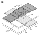
- FIG. 2 is a perspective view showing an example of a semiconductor device.
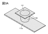
- 3A to 3C are perspective views showing examples of semiconductor devices.
- FIG. 4A is a top view showing an example of a semiconductor device.
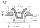
- FIG. 4B is a cross-sectional view showing an example of a semiconductor device;
- FIG. 5A is a top view showing an example of a semiconductor device.
- 7A and 7B are cross-sectional views showing examples of semiconductor devices.
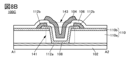
- FIG. 8A is a top view showing an example of a semiconductor device.
- 8B and 8C are cross-sectional views showing examples of semiconductor devices.
- FIG. 9A is a top view showing an example of a semiconductor device.
- FIG. 9B is a cross-sectional view showing an example of a semiconductor device;
- FIG. 10A is a top view showing an example of a semiconductor device;
- 10B and 10C are cross-sectional views showing examples of semiconductor devices.
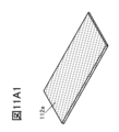
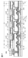
- 11A1 and 11B1 are perspective views illustrating an example of a method for manufacturing a semiconductor device.
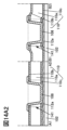
- 11A2 and 11B2 are cross-sectional views illustrating an example of a method for manufacturing a semiconductor device.
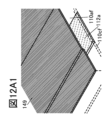
- 12A1 and 12B1 are perspective views illustrating an example of a method for manufacturing a semiconductor device.
- 12A2 and 12B2 are cross-sectional views illustrating an example of a method for manufacturing a semiconductor device.
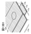
- 13A1 and 13B1 are perspective views illustrating an example of a method for manufacturing a semiconductor device.
- 13A2 and 13B2 are cross-sectional views illustrating an example of a method for manufacturing a semiconductor device.
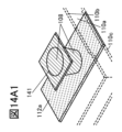
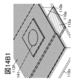
- 14A1 and 14B1 are perspective views illustrating an example of a method for manufacturing a semiconductor device.
- 14A2 and 14B2 are cross-sectional views illustrating an example of a method for manufacturing a semiconductor device.
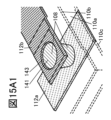
- 15A1 and 15B1 are perspective views illustrating an example of a method for manufacturing a semiconductor device.
- 15A2 and 15B2 are cross-sectional views illustrating an example of a method for manufacturing a semiconductor device.
- FIG. 16 is a perspective view showing an example of a display device.
- FIG. 17 is a cross-sectional view showing an example of a display device.
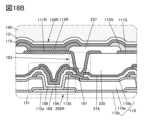
- 18A and 18B are cross-sectional views showing examples of display devices.
- FIG. 19 is a cross-sectional view showing an example of a display device.
- FIG. 20 is a cross-sectional view showing an example of a display device.
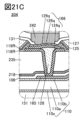
- 21A to 21C are cross-sectional views showing examples of display devices.
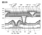
- 22A and 22B are cross-sectional views showing an example of a display device.
- FIG. 23 is a cross-sectional view showing an example of a display device.
- FIG. 24 is a cross-sectional view showing an example of a display device.
- FIG. 25 is a cross-sectional view showing an example of a display device.
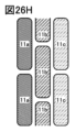
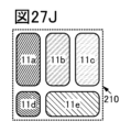
- 26A to 26H are diagrams showing examples of pixels.
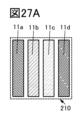
- 27A to 27K are diagrams showing examples of pixels.
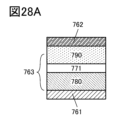
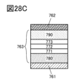
- 28A to 28F are diagrams showing configuration examples of light emitting devices.
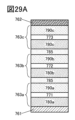
- 29A to 29C are diagrams showing configuration examples of light-emitting devices.
- 30A and 30B are diagrams showing configuration examples of light receiving devices.
- 30C to 30E are diagrams showing configuration examples of display devices.
- 31A to 31D are diagrams illustrating examples of electronic devices.
- 32A to 32F are diagrams illustrating examples of electronic devices.
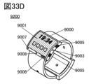
- 33A to 33G are diagrams illustrating examples of electronic devices.
- film and “layer” can be interchanged depending on the case or situation.
- conductive layer can be changed to the term “conductive film.”
- insulating film can be changed to the term “insulating layer”.
- a device manufactured using a metal mask or FMM may be referred to as a device with an MM (metal mask) structure.
- a device manufactured without using a metal mask or FMM may be referred to as a device with an MML (metal maskless) structure.
- an SBS side-by-side structure
- the material and configuration can be optimized for each light-emitting device, so the degree of freedom in selecting the material and configuration increases, and it becomes easy to improve luminance and reliability.
- holes or electrons are sometimes referred to as "carriers".
- the hole injection layer or electron injection layer is referred to as a "carrier injection layer”
- the hole transport layer or electron transport layer is referred to as a “carrier transport layer”
- the hole blocking layer or electron blocking layer is referred to as a "carrier It is sometimes called a block layer.
- the carrier injection layer, the carrier transport layer, and the carrier block layer described above may not be clearly distinguished from each other due to their cross-sectional shape, characteristics, or the like.
- one layer may serve as two or three functions of the carrier injection layer, the carrier transport layer, and the carrier block layer.
- a light-emitting device (also referred to as a light-emitting element) has an EL layer between a pair of electrodes.
- the EL layer has at least a light-emitting layer.
- the layers (also referred to as functional layers) included in the EL layer include a light-emitting layer, a carrier-injection layer (a hole-injection layer and an electron-injection layer), a carrier-transport layer (a hole-transport layer and an electron-transport layer), and a carrier layer.
- block layers (hole block layer and electron block layer);
- a light-receiving device (also referred to as a light-receiving element) has an active layer that functions at least as a photoelectric conversion layer between a pair of electrodes.
- an island-shaped light-emitting layer means that the light-emitting layer is physically separated from an adjacent light-emitting layer.
- a tapered shape refers to a shape in which at least a part of the side surface of the structure is inclined with respect to the substrate surface or the formation surface. For example, it is preferable to have a region where the angle between the inclined side surface and the substrate surface or the formation surface (also referred to as a taper angle) is less than 90 degrees.
- the side surfaces of the structure, the substrate surface, and the formation surface are not necessarily completely flat, and may be substantially planar with a minute curvature or substantially planar with minute unevenness.
- a mask layer (also referred to as a sacrificial layer) is positioned above at least the light-emitting layer (more specifically, among the layers constituting the EL layer, the layer processed into an island shape), It has a function of protecting the light-emitting layer during the manufacturing process.
- discontinuity refers to a phenomenon in which a layer, film, or electrode is divided due to the shape of the formation surface (for example, steps).
- the top surface shape roughly matches means that at least a part of the outline overlaps between the laminated layers.
- the upper layer and the lower layer may be processed with the same mask pattern, or partially with the same mask pattern. Strictly speaking, however, the contours do not overlap, and the upper layer may be located inside the lower layer, or the upper layer may be located outside the lower layer.
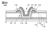
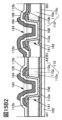
- FIG. 1A A top view (also called a plan view) of transistor 100 is shown in FIG. 1A.
- FIG. 1B shows a cross-sectional view taken along the dashed line A1-A2 shown in FIG. 1A
- FIG. 1C shows a cross-sectional view taken along the dashed-dotted line B1-B2.
- a perspective view of transistor 100 is shown in FIG. Note that some of the components of the transistor 100 (such as a gate insulating layer) are omitted in FIG. 1A.
- the top view of the transistor some of the constituent elements are omitted in the subsequent drawings, as in FIG. 1A.
- the insulating layer is transparent and the outline is indicated by a dashed line.
- the transistor 100 is provided over the substrate 102 .
- the transistor 100 includes a conductive layer 104 , an insulating layer 106 , a semiconductor layer 108 , a conductive layer 112 a, a conductive layer 112 b, and an insulating layer 110 .
- the conductive layer 104 functions as a gate electrode.
- a portion of the insulating layer 106 functions as a gate insulating layer.
- the conductive layer 112a functions as one of a source electrode and a drain electrode, and the conductive layer 112b functions as the other.
- the entire region of the semiconductor layer 108 which overlaps with the gate electrode with the gate insulating layer interposed therebetween, functions as a channel formation region between the source electrode and the drain electrode.
- a region in contact with the source electrode functions as a source region
- a region in contact with the drain electrode functions as a drain region.
- a conductive layer 112a is provided over the substrate 102, and an insulating layer 110 is provided over the conductive layer 112a.
- the insulating layer 110 has an opening 141 in a region overlapping with the conductive layer 112a. In opening 141, conductive layer 112a is exposed.
- a semiconductor layer 108 is provided to cover the opening 141 . In the opening 141, the semiconductor layer 108 has a region in contact with the conductive layer 112a.
- the insulating layer 110 has a region sandwiched between the conductive layer 112 a and the semiconductor layer 108 .
- a conductive layer 112 b is provided over the semiconductor layer 108 .
- the conductive layer 112b has an opening 143 in a region overlapping with the conductive layer 112a.
- the opening 143 is provided in a region overlapping with the opening 141 .
- the conductive layer 112b has a region overlapping with the conductive layer 112a with the insulating layer 110 and the semiconductor layer
- the semiconductor layer 108 has regions in contact with the bottom surface of the conductive layer 112b, the top surface and side surfaces of the insulating layer 110, and the top surface of the conductive layer 112a. That is, the bottom surface of the semiconductor layer 108 is in contact with one of the source and drain electrodes, and the top surface is in contact with the other of the source and drain electrodes.
- the semiconductor layer 108 has a shape that conforms to the top and side surfaces of the insulating layer 110 and the top surface of the conductive layer 112a.
- the surface on the layer formation surface side is referred to as the lower surface, and the surface opposite to the lower surface is referred to as the upper surface.
- the surface on which the semiconductor layer 108 is formed, which faces the insulating layer 110 and the conductive layer 112a, is referred to as the lower surface of the semiconductor layer 108, and the surface opposite to the lower surface is referred to as the upper surface.
- FIG. 3A is a perspective view showing an extract of the conductive layer 112a and the semiconductor layer 108.
- the semiconductor layer 108 is provided to cover the opening 141 provided in the insulating layer 110 (not shown in FIG. 3A). In the opening 141, the semiconductor layer 108 has a region in contact with the upper surface of the conductive layer 112a.
- the semiconductor layer 108 has a single-layer structure in FIG. 1B and the like, one embodiment of the present invention is not limited to this.
- the semiconductor layer 108 may have a laminated structure of two or more layers.
- FIG. 3B is a perspective view selectively showing the conductive layer 112a and the conductive layer 112b. Note that openings 141 provided in insulating layer 110 (not shown in FIG. 3B) are indicated by dashed lines.
- the conductive layer 112b has an opening 143 in a region overlapping with the conductive layer 112a.
- the top surface shape of the opening 141 and the opening 143 can be circular or elliptical, for example.
- the upper surface shapes of the openings 141 and 143 may be triangles, quadrangles (including rectangles, rhombuses, and squares), polygons such as pentagons, or these polygons with rounded corners. As shown in FIG. 1A and the like, it is preferable that the upper surface shape of each of the openings 141 and 143 is circular.
- the processing accuracy when forming the openings 141 and 143 can be improved, and the openings 141 and 143 can be formed in fine sizes.
- the circle is not limited to a perfect circle.
- the conductive layer 112b is not provided inside the opening 141, as shown in FIG. 1B and the like. Specifically, the conductive layer 112b preferably does not have a region in contact with the side surface of the insulating layer 110 on the opening 141 side.
- FIG. 1B and the like show a configuration in which the end of the conductive layer 112b on the side of the opening 143 matches or substantially matches the end of the insulating layer 110 on the side of the opening 141.
- the end portion of the conductive layer 112b on the opening 143 side refers to the bottom end portion of the conductive layer 112b on the opening 143 side.
- the lower surface of the conductive layer 112b refers to the surface on the insulating layer 110 side.
- the end of the insulating layer 110 on the side of the opening 141 refers to the end of the upper surface of the insulating layer 110 on the side of the opening 141 .
- the upper surface of the insulating layer 110 refers to the surface on the conductive layer 112b side.
- the upper surface shape of the opening 143 refers to the shape of the lower surface end portion of the conductive layer 112b on the opening 143 side.
- the shape of the upper surface of the opening 141 refers to the shape of the edge of the upper surface of the insulating layer 110 on the side of the opening 141 .
- the ends are aligned or approximately aligned to match or substantially match the ends.
- the ends are aligned or substantially aligned, and when the top surface shapes are matched or substantially matched, at least a part of the outline overlaps between the laminated layers when viewed from the top.
- the upper layer and the lower layer may be processed with the same mask pattern, or partially with the same mask pattern. Strictly speaking, however, the contours do not overlap, and the upper layer may be located inside the lower layer, or the upper layer may be located outside the lower layer, and in this case also the edges are roughly aligned, or the top surface shape is It is said that they roughly match.
- An insulating layer 106 functioning as a gate insulating layer is provided to cover the openings 141 and 143 .
- the insulating layer 106 is provided over the semiconductor layer 108 , the conductive layer 112 b , and the insulating layer 110 .
- the insulating layer 106 has regions in contact with the top surface and side surfaces of the semiconductor layer 108 , the top surface and side surfaces of the conductive layer 112 b , and the top surface of the insulating layer 110 .
- the insulating layer 106 has a shape that conforms to the top and side surfaces of the semiconductor layer 108 , the top and side surfaces of the conductive layer 112 b , and the top surface of the insulating layer 110 .
- the conductive layer 104 functioning as a gate electrode is provided over the insulating layer 106 and has a region in contact with the top surface of the insulating layer 106 .
- the conductive layer 104 has a region overlapping with the semiconductor layer 108 with the insulating layer 106 interposed therebetween.
- the conductive layer 104 has a shape that follows the top surface of the insulating layer 106 .
- FIG. 3C is a perspective view selectively showing the conductive layer 112a and the conductive layer 104.
- the conductive layer 104 is provided to cover the openings 141 and 143 .
- the conductive layer 104 has a region overlapping the semiconductor layer 108 with the insulating layer 106 interposed therebetween.
- the conductive layer 104 has a region overlapping with the conductive layer 112a with the insulating layer 106 and the semiconductor layer 108 interposed therebetween, and has a region overlapping with the conductive layer 112b with the insulating layer 106 interposed therebetween.
- the conductive layer 104 preferably covers the end of the conductive layer 112b on the opening 143 side.
- the transistor 100 is a so-called top-gate transistor that has a gate electrode above the semiconductor layer 108 .
- the conductive layer 112a, the conductive layer 112b, and the conductive layer 104 can each function as wiring. Further, the transistor 100 can be provided in a region where these wirings overlap. That is, in a circuit including the transistor 100 and the wiring, the area occupied by the transistor 100 and the wiring can be reduced. Furthermore, it is possible to reduce the area occupied by the circuit. Therefore, the semiconductor device can be small. For example, when the semiconductor device of one embodiment of the present invention is applied to a pixel circuit of a display device, the area occupied by the pixel circuit can be reduced, and the display device can have high definition. Further, when applied to a driver circuit (for example, a gate line driver circuit and a source line driver circuit) of a display device, the area occupied by the driver circuit can be reduced, and a display device with a narrow frame can be obtained.
- a driver circuit for example, a gate line driver circuit and a source line driver circuit
- FIGS. 4A and 4B are described with reference to FIGS. 4A and 4B.
- 4A is a top view of transistor 100.
- FIG. FIG. 4B is an enlarged view of FIG. 1B.
- a region in contact with the conductive layer 112a functions as one of a source region and a drain region
- a region in contact with the conductive layer 112b functions as the other of the source region and the drain region
- a region between the source region and the drain region functions as a channel forming region.
- the channel length of the transistor 100 is the distance between the source region and the drain region.
- FIG. 4B shows the channel length L100 of the transistor 100 with a dashed double-headed arrow.
- the channel length L100 is the distance between the end of the region where the semiconductor layer 108 and the conductive layer 112a are in contact and the end of the region where the semiconductor layer 108 and the conductive layer 112b are in contact in a cross-sectional view.
- the channel length L100 of the transistor 100 corresponds to the sum of the length of the side surface of the insulating layer 110 on the opening 141 side and the film thickness of the semiconductor layer 108 in a cross-sectional view. That is, the channel length L100 is determined by the film thickness T110 of the insulating layer 110, the angle ⁇ 110 between the side surface of the insulating layer 110 on the opening 141 side and the formation surface of the insulating layer 110 (here, the upper surface of the conductive layer 112a), and the semiconductor It is determined by the thickness of the layer 108 and is not affected by the performance of the exposure equipment used to fabricate the transistor.
- the channel length L100 can be set to a value smaller than the limit resolution of the exposure apparatus, and a fine-sized transistor can be realized.
- the channel length L100 is preferably 0.01 ⁇ m or more and less than 3 ⁇ m, more preferably 0.05 ⁇ m or more and less than 3 ⁇ m, further preferably 0.1 ⁇ m or more and less than 3 ⁇ m, further preferably 0.15 ⁇ m or more and less than 3 ⁇ m.
- the film thickness T110 of the insulating layer 110 is indicated by a double-headed arrow, and the film thickness T108 of the semiconductor layer 108 is indicated by a solid arrow.
- the ON current of the transistor 100 can be increased by reducing the channel length L100.
- a circuit that can operate at high speed can be manufactured.
- the semiconductor device of one embodiment of the present invention is applied to a large-sized display device or a high-definition display device, signal delay in each wiring can be reduced even when the number of wirings is increased. Unevenness can be suppressed. Therefore, the display device can have high display quality.
- the display device since the area occupied by the circuit can be reduced, the display device can have a narrow frame.
- the channel length L100 can be controlled.
- the film thickness T110 of the insulating layer 110 is preferably 0.01 ⁇ m or more and less than 3 ⁇ m, more preferably 0.05 ⁇ m or more and less than 3 ⁇ m, further preferably 0.1 ⁇ m or more and less than 3 ⁇ m, further preferably 0.15 ⁇ m or more and less than 3 ⁇ m.
- 0.2 ⁇ m or more and less than 3 ⁇ m more preferably 0.2 ⁇ m or more and less than 2.5 ⁇ m, further preferably 0.2 ⁇ m or more and less than 2 ⁇ m, further preferably 0.2 ⁇ m or more and less than 1.5 ⁇ m, and further is preferably 0.3 ⁇ m or more and 1.5 ⁇ m or less, more preferably 0.3 ⁇ m or more and 1.2 ⁇ m or less, further preferably 0.4 ⁇ m or more and 1.2 ⁇ m or less, further preferably 0.4 ⁇ m or more and 1 ⁇ m or less, and further is preferably 0.5 ⁇ m or more and 1 ⁇ m or less.
- the side surface of the insulating layer 110 on the side of the opening 141 is preferably tapered.
- Angle ⁇ 110 of insulating layer 110 is preferably less than 90 degrees. By reducing the angle ⁇ 110, the coverage of a layer (for example, the semiconductor layer 108) provided on the insulating layer 110 can be improved. However, if the angle ⁇ 110 is made smaller, the contact area between the semiconductor layer 108 and the conductive layer 112a becomes smaller, which may increase the contact resistance between the semiconductor layer 108 and the conductive layer 112a.
- the angle ⁇ 110 is preferably 45 degrees or more and less than 90 degrees, more preferably 50 degrees or more and less than 90 degrees, further preferably 55 degrees or more and less than 90 degrees, further preferably 60 degrees or more and less than 90 degrees, further preferably 60 degrees or more. It is preferably 85 degrees or less, more preferably 65 degrees or more and 85 degrees or less, further preferably 65 degrees or more and 80 degrees or less, further preferably 70 degrees or more and 80 degrees or less.
- FIG. 4B and the like show a structure in which the side surface of the insulating layer 110 on the opening 141 side has a linear shape in a cross-sectional view; however, one embodiment of the present invention is not limited thereto.
- the shape of the side surface of the insulating layer 110 on the opening 141 side may be curved, or may have both a linear region and a curved region.
- the thickness of the semiconductor layer 108 is preferably 3 nm or more and 100 nm or less, more preferably 5 nm or more and 100 nm or less, further preferably 10 nm or more and 100 nm or less, further preferably 10 nm or more and 70 nm or less, further preferably 15 nm or more and 70 nm or less. Further, it is preferably 15 nm or more and 50 nm or less, further preferably 20 nm or more and 50 nm or less, further preferably 20 nm or more and 40 nm or less, further preferably 25 nm or more and 40 nm or less.
- the channel width of the transistor 100 is the width of the source region or the width of the drain region in the direction orthogonal to the channel length direction. That is, the channel width is the width of the region where the semiconductor layer 108 and the conductive layer 112a are in contact or the width of the region where the semiconductor layer 108 and the conductive layer 112b are in contact in the direction orthogonal to the channel length direction.
- the channel width of the transistor 100 is described as the width of a region where the semiconductor layer 108 and the conductive layer 112b are in contact with each other in a direction orthogonal to the channel length direction.
- 4A and 4B show the channel width W100 of the transistor 100 with a solid double-headed arrow.
- the channel width W100 is the length of the lower surface end portion of the conductive layer 112b on the opening 143 side in a top view (also referred to as a plan view).
- the channel width W100 is determined by the top surface shape of the opening 143.
- 4A and 4B show the width D143 of the opening 143 with a two-dot chain double-headed arrow.
- the width D143 indicates the shortest rectangular short side that circumscribes the opening 143 when viewed from above.
- the width D143 of the opening 143 is equal to or greater than the resolution limit of the exposure apparatus.
- the width D143 is, for example, preferably 0.2 ⁇ m or more and less than 5 ⁇ m, more preferably 0.2 ⁇ m or more and less than 4.5 ⁇ m, further preferably 0.2 ⁇ m or more and less than 4 ⁇ m, further preferably 0.2 ⁇ m or more and less than 3.5 ⁇ m.
- the width D143 corresponds to the diameter of the opening 143, and the channel width W100 can be calculated as "D143 ⁇ ".
- a semiconductor material that can be used for the semiconductor layer 108 is not particularly limited.
- a single semiconductor or a compound semiconductor can be used.
- Silicon or germanium for example, can be used as a single semiconductor.
- compound semiconductors include gallium arsenide and silicon germanium.
- an organic substance having semiconductor characteristics or a metal oxide having semiconductor characteristics also referred to as an oxide semiconductor
- These semiconductor materials may contain impurities as dopants.
- the crystallinity of the semiconductor material used for the semiconductor layer 108 is not particularly limited. ) may be used. It is preferable to use a crystalline semiconductor because deterioration of transistor characteristics can be suppressed.
- Silicon can be used for the semiconductor layer 108 .
- Examples of silicon include monocrystalline silicon, polycrystalline silicon, microcrystalline silicon, amorphous silicon, and the like.
- Examples of polycrystalline silicon include low temperature poly silicon (LTPS).
- a transistor using amorphous silicon for the semiconductor layer 108 can be formed on a large glass substrate and manufactured at low cost.
- a transistor using polycrystalline silicon for the semiconductor layer 108 has high field-effect mobility and can operate at high speed.
- a transistor using microcrystalline silicon for the semiconductor layer 108 has higher field-effect mobility than a transistor using amorphous silicon and can operate at high speed.
- the semiconductor layer 108 preferably has a metal oxide (oxide semiconductor) exhibiting semiconductor properties.
- Metal oxides that can be used for the semiconductor layer 108 include, for example, indium oxide, gallium oxide, and zinc oxide.
- the metal oxide preferably contains at least indium (In) or zinc (Zn).
- the metal oxide preferably contains two or three elements selected from indium, the element M, and zinc.
- Element M includes gallium, aluminum, silicon, boron, yttrium, tin, copper, vanadium, beryllium, titanium, iron, nickel, germanium, zirconium, molybdenum, lanthanum, cerium, neodymium, hafnium, tantalum, tungsten, cobalt, and magnesium.
- the element M is preferably one or more selected from aluminum, gallium, yttrium, and tin.
- the semiconductor layer 108 is made of, for example, indium oxide, indium zinc oxide (In--Zn oxide), indium tin oxide (In--Sn oxide), indium titanium oxide (In--Ti oxide), indium aluminum zinc oxide.
- In-Al-Zn oxide also referred to as IAZO
- indium tin zinc oxide In-Sn-Zn oxide
- indium titanium zinc oxide In-Ti-Zn oxide
- indium gallium zinc oxide In-Ga-Zn oxide, also referred to as IGZO
- indium gallium tin zinc oxide (In-Ga-Sn-Zn oxide), indium gallium aluminum zinc oxide (In-Ga-Al-Zn oxide, IGAZO or IAGZO can be used.
- indium tin oxide containing silicon, or the like can be used.
- the element M is preferably one or more selected from gallium, aluminum, yttrium, and tin.
- the element M is preferably gallium.
- composition of the metal oxide included in the semiconductor layer 108 greatly affects the electrical characteristics and reliability of the transistor 100 .
- the semiconductor layer 108 When an In-Zn oxide is used for the semiconductor layer 108, it is preferable to use a metal oxide in which the atomic ratio of indium is equal to or greater than the atomic ratio of zinc.
- the semiconductor layer 108 When an In—Sn oxide is used for the semiconductor layer 108, it is preferable to use a metal oxide in which the atomic ratio of indium is equal to or higher than the atomic ratio of tin.
- a metal oxide in which the atomic ratio of indium is higher than that of tin can be applied. Furthermore, it is preferable to use a metal oxide in which the atomic ratio of zinc is higher than that of tin.
- a metal oxide in which the atomic ratio of indium is higher than that of aluminum can be applied. Furthermore, it is preferable to use a metal oxide in which the atomic ratio of zinc is higher than that of aluminum.
- the semiconductor layer 108 When an In--Ga--Zn oxide is used for the semiconductor layer 108, a metal oxide in which the atomic ratio of indium to the atomic number of metal elements is higher than that of gallium can be applied. Furthermore, it is more preferable to use a metal oxide in which the atomic ratio of zinc is higher than that of gallium.
- an In-M-Zn oxide is used for the semiconductor layer 108
- a metal oxide in which the atomic ratio of indium to the atomic number of the metal element is higher than that of the element M can be applied.
- a metal oxide in which the atomic ratio of zinc is higher than the atomic ratio of the element M is more preferable to use.
- the sum of the atomic ratios of the metal elements can be used as the atomic ratio of the element M.
- the atomic ratio of the element M can be the sum of the atomic ratio of gallium and the atomic ratio of aluminum.
- the atomic ratio of indium, the element M, and zinc is preferably within the above range.
- the ratio of the number of indium atoms to the number of atoms of the metal element contained in the metal oxide is 30 atomic % or more and 100 atomic % or less, preferably 30 atomic % or more and 95 atomic % or less, more preferably 35 atomic % or more and 95 atoms.
- the ratio of the number of indium atoms to the total number of atoms of indium, the element M, and zinc is preferably within the above range.
- the ratio of the number of indium atoms to the number of atoms of the contained metal element is sometimes referred to as the indium content.
- a transistor with a large on-current By increasing the indium content of the metal oxide, a transistor with a large on-current can be obtained. By applying the transistor to a transistor that requires a large on-state current, a semiconductor device with excellent electrical characteristics can be obtained.
- Analysis of the composition of metal oxides can be performed, for example, by energy dispersive X-ray spectroscopy (EDX: Energy Dispersive X-ray spectroscopy), X-ray photoelectron spectroscopy (XPS: X-ray Photoelectron Spectroscopy), inductively coupled plasma mass spectroscopy.
- EDX Energy Dispersive X-ray spectroscopy
- XPS X-ray Photoelectron Spectroscopy
- ICP-MS Inductively Coupled Plasma-Mass Spectrometry
- ICP-AES Inductively Coupled Plasma-Atomic Emission Spectrometry
- a plurality of these techniques may be combined for analysis.
- the actual content rate and the content rate obtained by analysis may differ due to the influence of analysis accuracy. For example, when the content of element M is low, the content of element M obtained by analysis may be lower than the actual content.
- the composition in the vicinity includes the range of ⁇ 30% of the desired atomic number ratio.
- the atomic ratio of indium is 1, the atomic ratio of M is greater than 0.1. 2 or less, including the case where the atomic ratio of zinc is greater than 0.1 and 2 or less.
- a sputtering method or an atomic layer deposition (ALD) method can be preferably used to form the metal oxide.
- the atomic ratio of the target may differ from the atomic ratio of the metal oxide.
- zinc may have a lower atomic ratio in the metal oxide than in the target.
- the atomic ratio of zinc contained in the target may be about 40% or more and 90% or less.
- GBT Gate Bias Temperature
- PBTS Positive Bias Temperature Stress
- NBTS Negative Bias Temperature Stress
- the PBTS test and the NBTS test which are performed under light irradiation, are called PBTIS (Positive Bias Temperature Illumination Stress) test and NBTIS (Negative Bias Temperature Illumination Stress) test, respectively.
- n-type transistor In an n-type transistor, a positive potential is applied to the gate when the transistor is turned on (a state in which current flows), so the amount of change in the threshold voltage in the PBTS test is an index of the reliability of the transistor. It is one of the important items to pay attention to.
- the transistor can be highly reliable with respect to the application of a positive bias. In other words, the transistor can have a small amount of change in threshold voltage in the PBTS test. Further, when a metal oxide containing gallium is used, the content of gallium is preferably lower than the content of indium. Accordingly, a highly reliable transistor can be realized.
- One of the causes of threshold voltage fluctuation in PBTS tests is the defect level at or near the interface between the semiconductor layer and the gate insulating layer.
- the semiconductor layer 108 when an In--Ga--Zn oxide is used for the semiconductor layer 108, a metal oxide in which the atomic ratio of indium is higher than that of gallium can be used for the semiconductor layer 108. can. Moreover, it is more preferable to use a metal oxide in which the atomic ratio of zinc is higher than the atomic ratio of gallium. In other words, it is preferable that the semiconductor layer 108 be made of a metal oxide that satisfies the atomic ratios of In>Ga and Zn>Ga.
- the ratio of the number of gallium atoms to the number of contained metal element atoms is higher than 0 atomic % and 50 atomic % or less, preferably 0.1 atomic % or more and 40 atomic % or less, more preferably 0.1 atomic % or more and 40 atomic % or less.
- a metal oxide that does not contain gallium may be applied to the semiconductor layer 108 .
- In—Zn oxide can be applied to the semiconductor layer 108 .
- the field-effect mobility of the transistor can be increased by increasing the atomic ratio of indium to the atomic number of the metal element contained in the metal oxide.
- the metal oxide becomes a highly crystalline metal oxide, which suppresses fluctuations in the electrical characteristics of the transistor and improves reliability. be able to.
- a metal oxide that does not contain gallium and zinc, such as indium oxide may be used for the semiconductor layer 108 .
- an oxide containing indium and zinc can be used for the semiconductor layer 108 .
- Gallium has been described as a representative example, but it can also be applied to the case where the element M is used instead of gallium.
- a metal oxide in which the atomic ratio of indium is higher than the atomic ratio of the element M is preferably used for the semiconductor layer 108 .
- the transistor can be highly reliable with respect to positive bias application.
- the semiconductor device can have high reliability.
- the electrical characteristics of the transistor may change.
- a transistor applied to a region where light can enter have small variation in electrical characteristics under light irradiation and have high reliability against light. Reliability against light can be evaluated, for example, by the amount of change in threshold voltage in an NBTIS test.
- the transistor By increasing the content of the element M in the metal oxide, a transistor with high reliability against light can be obtained. That is, the transistor can have a small amount of change in threshold voltage in the NBTIS test. Specifically, a metal oxide in which the atomic ratio of the element M is equal to or higher than the atomic ratio of indium has a larger bandgap, and the variation of the threshold voltage in the NBTIS test of the transistor can be reduced. .
- the band gap of the metal oxide included in the semiconductor layer 108 is preferably 2.0 eV or more, more preferably 2.5 eV or more, further preferably 3.0 eV or more, further preferably 3.2 eV or more, further preferably 3.2 eV or more. 0.3 eV or more is preferable, 3.4 eV or more is preferable, and 3.5 eV or more is more preferable.
- the ratio of the number of atoms of the element M to the number of atoms of the contained metal element is 20 atomic % or more and 70 atomic % or less, preferably 30 atomic % or more and 70 atomic % or less, more preferably 30 atoms. % or more and 60 atomic % or less, more preferably 40 atomic % or more and 60 atomic % or less, more preferably 50 atomic % or more and 60 atomic % or less, can be suitably used.
- a metal oxide in which the atomic ratio of indium to the atomic number of metal elements is equal to or lower than that of gallium can be applied.
- the ratio of the number of gallium atoms to the number of atoms of the contained metal element is 20 atomic % or more and 60 atomic % or less, preferably 20 atomic % or more and 50 atomic % or less, more preferably 30 atoms. % or more and 50 atomic % or less, more preferably 40 atomic % or more and 60 atomic % or less, more preferably 50 atomic % or more and 60 atomic % or less, can be suitably used.
- the semiconductor device By using a metal oxide with a high content of the element M for the semiconductor layer 108, a transistor with high reliability against light can be obtained. By applying the transistor to a transistor that requires high reliability against light, the semiconductor device can have high reliability.
- the electrical characteristics and reliability of the transistor differ depending on the composition of the metal oxide applied to the semiconductor layer 108. Therefore, by changing the composition of the metal oxide according to the electrical characteristics and reliability required for the transistor, a semiconductor device having both excellent electrical characteristics and high reliability can be obtained.
- the semiconductor layer 108 may have a laminated structure having two or more metal oxide layers. Two or more metal oxide layers included in the semiconductor layer 108 may have the same or substantially the same composition. By using a stacked structure of metal oxide layers having the same composition, for example, the same sputtering target can be used for formation, so that the manufacturing cost can be reduced.
- the two or more metal oxide layers included in the semiconductor layer 108 may have different compositions.
- the element M it is particularly preferable to use gallium or aluminum.
- a crystalline metal oxide layer is preferably used for the semiconductor layer 108 .
- a metal oxide layer having a CAAC (c-axis aligned crystal) structure, a polycrystalline structure, a nano-crystal (nc) structure, or the like, which will be described later, can be used.
- CAAC c-axis aligned crystal
- nc nano-crystal
- the higher the substrate temperature during formation the higher the crystallinity of the metal oxide layer.
- the substrate temperature during formation can be adjusted, for example, by the temperature of the stage on which the substrate is placed.
- a metal oxide layer with higher crystallinity is formed as the flow rate of the oxygen gas to the total deposition gas used at the time of formation (hereinafter also referred to as the oxygen flow rate ratio) or the oxygen partial pressure in the treatment chamber of the deposition apparatus is higher. can be formed.
- the semiconductor layer 108 may have a laminated structure of two or more metal oxide layers with different crystallinities.
- a stacked structure of a first metal oxide layer and a second metal oxide layer provided on the first metal oxide layer is used, and the second metal oxide layer is composed of the first metal oxide layer.
- a structure having a region with higher crystallinity than that of the oxide layer can be employed.
- the second metal oxide layer can have a region with lower crystallinity than the first metal oxide layer.
- Two or more metal oxide layers included in the semiconductor layer 108 may have the same or substantially the same composition. By using a stacked structure of metal oxide layers having the same composition, for example, the same sputtering target can be used for formation, so that the manufacturing cost can be reduced.
- a laminated structure of two or more metal oxide layers with different crystallinities can be formed.
- two or more metal oxide layers included in the semiconductor layer 108 may have different compositions.
- the substrate temperature during the formation of the semiconductor layer 108 is preferably room temperature (25° C.) or higher and 200° C. or lower, more preferably room temperature or higher and 130° C. or lower. By setting the substrate temperature within the above range, bending or distortion of the substrate can be suppressed when a large glass substrate is used.
- V 2 O oxygen vacancies
- part of hydrogen may bond with oxygen that bonds with a metal atom to generate an electron that is a carrier. Therefore, a transistor including an oxide semiconductor containing a large amount of hydrogen is likely to have normally-on characteristics.
- hydrogen in an oxide semiconductor easily moves due to stress such as heat and an electric field; therefore, when a large amount of hydrogen is contained in the oxide semiconductor, the reliability of the transistor might be deteriorated.
- VOH can function as a donor of an oxide semiconductor.
- the oxide semiconductor is evaluated based on the carrier concentration instead of the donor concentration. Therefore, in this specification and the like, instead of the donor concentration, the carrier concentration assuming a state in which no electric field is applied is used as a parameter of the oxide semiconductor in some cases.
- the “carrier concentration” described in this specification and the like may be rephrased as “donor concentration”.
- V OH in the semiconductor layer 108 is preferably reduced as much as possible to make the semiconductor layer 108 highly pure intrinsic or substantially highly pure intrinsic.
- impurities such as water and hydrogen in the oxide semiconductor are removed (sometimes referred to as dehydration or dehydrogenation treatment). Therefore, it is important to repair oxygen vacancies (V 0 ) by supplying oxygen to the oxide semiconductor.
- oxygenation treatment By using an oxide semiconductor in which impurities such as V OH are sufficiently reduced for a channel formation region of a transistor, stable electrical characteristics can be imparted. Note that repairing oxygen vacancies ( V.sub.2O.sub.3 ) by supplying oxygen to an oxide semiconductor is sometimes referred to as oxygenation treatment.
- the carrier concentration of the oxide semiconductor in the region functioning as a channel formation region is preferably 1 ⁇ 10 18 cm ⁇ 3 or less and less than 1 ⁇ 10 17 cm ⁇ 3 . more preferably less than 1 ⁇ 10 16 cm ⁇ 3 , still more preferably less than 1 ⁇ 10 13 cm ⁇ 3 , even more preferably less than 1 ⁇ 10 12 cm ⁇ 3 . Note that there is no particular limitation on the lower limit of the carrier concentration of the oxide semiconductor in the region that functions as a channel formation region;
- a transistor using an oxide semiconductor (hereinafter referred to as an OS transistor) has extremely high field-effect mobility compared to a transistor using amorphous silicon.
- an OS transistor has extremely low source-drain leakage current (also referred to as an off-state current) in an off state, and can hold charge accumulated in a capacitor connected in series with the transistor for a long time. is. Further, by using the OS transistor, power consumption of the semiconductor device can be reduced.
- a semiconductor device which is one embodiment of the present invention can be applied to a display device, for example.
- a display device for example.
- the OS transistor has a higher breakdown voltage between the source and the drain than a transistor using silicon (hereinafter referred to as a Si transistor)
- a high voltage can be applied between the source and the drain of the OS transistor. Therefore, by using an OS transistor as the drive transistor included in the pixel circuit, the amount of current flowing through the light emitting device can be increased, and the light emission luminance of the light emitting device can be increased.
- the OS transistor When the transistor operates in the saturation region, the OS transistor can reduce the change in the source-drain current with respect to the change in the gate-source voltage compared to the Si transistor. Therefore, by applying an OS transistor as a drive transistor included in a pixel circuit, the current flowing between the source and the drain can be finely determined according to the change in the voltage between the gate and the source. can be controlled. Therefore, it is possible to increase the gradation in the pixel circuit.
- the OS transistor In the saturation characteristics of the current that flows when the transistor operates in the saturation region, the OS transistor can flow a more stable current (saturation current) than the Si transistor even when the source-drain voltage gradually increases. can. Therefore, by using the OS transistor as the driving transistor, stable current can be supplied to the light-emitting device even when the current-voltage characteristics of the light-emitting device vary. That is, when the OS transistor operates in the saturation region, even if the source-drain voltage is increased, the source-drain current hardly changes, so that the light emission luminance of the light-emitting device can be stabilized.
- an OS transistor as a driving transistor included in a pixel circuit, it is possible to suppress black floating, increase emission luminance, provide multiple gradations, and suppress variations in light emitting devices. can be planned.
- the OS transistor has little change in electrical characteristics due to radiation exposure, that is, it is highly resistant to radiation, so it can be suitably used in an environment where radiation may be incident. It can be said that the OS transistor has high reliability against radiation.
- an OS transistor can be preferably used in a pixel circuit of an X-ray flat panel detector.
- the OS transistor can be suitably used for a semiconductor device used in outer space. Radiation includes electromagnetic radiation (eg, X-rays and gamma rays) and particle radiation (eg, alpha rays, beta rays, proton rays, and neutron rays).
- the insulating layer 110 An inorganic material or an organic material can be used for the insulating layer 110 .
- the insulating layer 110 may have a layered structure of a layer containing an inorganic material and a layer containing an organic material.
- An inorganic material can be suitably used for the insulating layer 110 .
- inorganic materials one or more of oxides, oxynitrides, nitride oxides, and nitrides can be used.
- the insulating layer 110 is made of, for example, silicon oxide, silicon oxynitride, aluminum oxide, hafnium oxide, yttrium oxide, zirconium oxide, gallium oxide, tantalum oxide, magnesium oxide, lanthanum oxide, cerium oxide, neodymium oxide, silicon nitride, or silicon nitride oxide. , and aluminum nitride can be used.
- oxynitride refers to a material that contains more oxygen than nitrogen in its composition.
- Nitrided oxide refers to a material whose composition contains more nitrogen than oxygen.
- silicon oxynitride refers to a material whose composition contains more oxygen than nitrogen
- silicon oxynitride refers to a material whose composition contains more nitrogen than oxygen.
- SIMS secondary ion mass spectrometry
- XPS X-ray photoelectron spectroscopy
- SIMS is suitable when the content of the target element is high (for example, 0.5 atomic % or more, or 1 atomic % or more).
- SIMS is suitable when the target element content is low (for example, less than 0.5 atomic % or less than 1 atomic %).
- the insulating layer 110 may have a laminated structure of two or more layers.
- FIG. 1B and the like show a configuration in which the insulating layer 110 has a laminated structure of an insulating layer 110a and an insulating layer 110b on the insulating layer 110a.
- the insulating layer 110a and the insulating layer 110b can each use the material that can be used for the insulating layer 110 described above. Note that the same material or different materials may be used for the insulating layers 110a and 110b.
- the insulating layer 110a may have a laminated structure of two or more layers.
- the insulating layer 110b may have a laminated structure of two or more layers.
- the film thickness of the insulating layer 110a can be made thicker than the film thickness of the insulating layer 110b. It is preferable that the film formation rate of the insulating layer 110a is high. In particular, when the insulating layer 110a is thick, it is preferable that the insulating layer 110a is formed at a high deposition rate. Productivity can be improved by increasing the deposition rate of the insulating layer 110a. For example, the deposition rate can be increased by increasing the power for forming the insulating layer 110a.
- the insulating layer 110a has a small stress.
- the stress of the insulating layer 110a increases, which may cause warping of the substrate.
- By reducing the stress of the insulating layer 110a it is possible to suppress the occurrence of problems during the process due to the stress such as warpage of the substrate.
- the insulating layer 110b functions as a blocking film that suppresses desorption of gas from the insulating layer 110a.
- the insulating layer 110b it is preferable to use a material that makes it difficult for gas to diffuse.
- the insulating layer 110b preferably has a region with a higher film density than the insulating layer 110a.
- the blocking property can be improved by increasing the film density of the insulating layer 110b.
- a material containing more nitrogen than the insulating layer 110a can be used. By increasing the nitrogen content of the insulating layer 110b, the blocking property can be improved.
- the insulating layer 110b may have a thickness that functions as a blocking film that suppresses desorption of gas from the insulating layer 110a, and may be thinner than the insulating layer 110a.
- the deposition rate of the insulating layer 110b is preferably slower than the deposition rate of the insulating layer 110a. By slowing down the deposition rate of the insulating layer 110b, the film density of the insulating layer 110b can be increased, and the blocking property can be improved. Similarly, by increasing the substrate temperature during the deposition of the insulating layer 110b, the film density of the insulating layer 110b is increased and the blocking property can be improved.
- the film densities are different. may be observable.
- the higher the film density the darker (dark) the transmission electron (TE) image, and the lower the film density, the lighter (brighter) the transmission electron (TE) image. Therefore, in a transmission electron (TE) image, the insulating layer 110b may appear darker (darker) than the insulating layer 110a.
- the insulating layer 110b may have a region where the hydrogen concentration in the film is lower than that of the insulating layer 110a.
- the difference in hydrogen concentration between the insulating layers 110a and 110b can be evaluated by secondary ion mass spectrometry (SIMS), for example.
- SIMS secondary ion mass spectrometry
- the insulating layer 110 will be specifically described by taking a configuration using a metal oxide for the semiconductor layer 108 as an example.
- an inorganic material can be preferably used for each of the insulating layers 110a and 110b.
- An oxide or an oxynitride is preferably used for the insulating layer 110a.
- a film that releases oxygen by heating is preferably used for the insulating layer 110a.
- Silicon oxide or silicon oxynitride, for example, can be suitably used for the insulating layer 110a.
- Oxygen can be supplied from the insulating layer 110a to the semiconductor layer 108 by releasing oxygen from the insulating layer 110a.
- oxygen vacancies (V 0 ) and V OH in the semiconductor layer 108 can be reduced, and favorable electrical characteristics can be obtained.
- the transistor can have high reliability.
- the insulating layer 110a preferably has a high oxygen diffusion coefficient. By increasing the diffusion coefficient of oxygen in the insulating layer 110a, oxygen can easily diffuse in the insulating layer 110a, and oxygen can be efficiently supplied from the insulating layer 110a to the semiconductor layer .
- the treatment for supplying oxygen to the semiconductor layer 108 also includes heat treatment in an atmosphere containing oxygen, plasma treatment in an atmosphere containing oxygen, or the like.
- the insulating layer 110a release less impurities (for example, water and hydrogen) from itself. By reducing the release of impurities from the insulating layer 110a, the diffusion of impurities into the semiconductor layer 108 is suppressed, and the transistor can have favorable electrical characteristics and high reliability.
- impurities for example, water and hydrogen
- the insulating layer 110a for example, silicon oxide or silicon oxynitride using a plasma enhanced CVD (PECVD) method can be preferably used.
- PECVD plasma enhanced CVD
- a mixed gas of a gas containing silicon and a gas containing oxygen is preferably used as the raw material gas.
- the gas containing silicon for example, one or more of silane, disilane, trisilane, and fluorinated silane can be used.
- the oxygen-containing gas for example, one or more of oxygen (O 2 ), ozone (O 3 ), dinitrogen monoxide (N 2 O), nitrogen monoxide (NO), or nitrogen dioxide (NO 2 ) can be used.
- O 2 oxygen
- O 3 oxygen
- N 2 O ozone
- NO nitrogen monoxide
- NO 2 nitrogen dioxide
- the amount of impurities (eg, water and hydrogen) released from the insulating layer 110a can be reduced by increasing the power for forming the insulating layer 110a.
- the insulating layer 110b is preferably impermeable to oxygen.
- the insulating layer 110b functions as a blocking film that suppresses desorption of oxygen from the insulating layer 110a. Furthermore, it is preferable that the insulating layer 110b is difficult to permeate hydrogen.
- the insulating layer 110b functions as a blocking film that prevents hydrogen from diffusing from outside the transistor through the insulating layer 110 to the semiconductor layer . It is preferable that the film density of the insulating layer 110b is high. By increasing the film density of the insulating layer 110b, the property of blocking oxygen and hydrogen can be improved.
- the film density of the insulating layer 110b is preferably higher than the film density of the insulating layer 110a.
- the insulating layer 110b preferably has, for example, a region containing more nitrogen than the insulating layer 110a.
- a material containing more nitrogen than the insulating layer 110a can be used.
- the insulating layer 110b is preferably made of nitride or oxynitride.
- silicon nitride or silicon oxynitride can be preferably used for the insulating layer 110b.
- the amount of oxygen supplied from the insulating layer 110a to the semiconductor layer 108 decreases. It may become less.
- the insulating layer 110b over the insulating layer 110a, diffusion of oxygen contained in the insulating layer 110a from a region of the insulating layer 110a that is not in contact with the semiconductor layer 108 can be suppressed. Therefore, the amount of oxygen supplied from the insulating layer 110a to the semiconductor layer 108 increases, and oxygen vacancies (V 0 ) and V OH in the semiconductor layer 108 can be reduced. Therefore, the transistor can have favorable electrical characteristics and high reliability.
- Oxygen contained in the insulating layer 110a might oxidize the conductive layer 112b and increase the resistance thereof. Further, the conductive layer 112b is oxidized by oxygen contained in the insulating layer 110a, so that the amount of oxygen supplied from the insulating layer 110a to the semiconductor layer 108 may decrease. By providing the insulating layer 110b over the insulating layer 110a, oxidation of the conductive layer 112b and an increase in resistance can be suppressed. At the same time, the amount of oxygen supplied from the insulating layer 110a to the semiconductor layer 108 increases, oxygen vacancies (V 0 ) and V OH in the semiconductor layer 108 can be reduced, good electrical characteristics are exhibited, and A highly reliable transistor can be obtained.
- the insulating layer 110b preferably has a thickness that functions as a blocking film for oxygen and hydrogen. If the film thickness of the insulating layer 110b is thin, the function as a blocking film may deteriorate. On the other hand, when the thickness of the insulating layer 110b is large, the region of the semiconductor layer 108 in contact with the insulating layer 110a is narrowed, and the amount of oxygen supplied from the insulating layer 110a to the semiconductor layer 108 may be reduced. The film thickness of the insulating layer 110b may be thinner than the film thickness of the insulating layer 110a.
- the thickness of the insulating layer 110b is preferably 5 nm or more and 100 nm or less, more preferably 5 nm or more and 70 nm or less, further preferably 10 nm or more and 70 nm or less, further preferably 10 nm or more and 50 nm or less, further preferably 20 nm or more and 50 nm or less. , and more preferably 20 nm or more and 40 nm or less.
- the insulating layer 110b release less impurities (for example, water and hydrogen) from itself. By reducing the release of impurities from the insulating layer 110b, diffusion of impurities into the semiconductor layer 108 is suppressed, and the transistor can have favorable electrical characteristics and high reliability.
- impurities for example, water and hydrogen
- a region of the semiconductor layer 108 in contact with the insulating layer 110 can function as a channel formation region. That is, oxygen is selectively supplied to the channel formation region, and oxygen vacancies (V 0 ) and V OH can be reduced. Therefore, the transistor can have favorable electrical characteristics and high reliability.
- the conductive layers 112a and 112b functioning as source and drain electrodes and the conductive layer 104 functioning as a gate electrode are chromium, copper, aluminum, gold, silver, zinc, molybdenum, tantalum, titanium, tungsten, manganese, and nickel. , iron, cobalt, and niobium, or an alloy containing one or more of the aforementioned metals.
- the conductive layer 104, the conductive layer 112a, and the conductive layer 112b can preferably be formed using a low-resistance conductive material containing one or more of copper, silver, gold, and aluminum. In particular, copper or aluminum is preferable because of its excellent mass productivity.
- a conductive metal oxide (also referred to as an oxide conductor) can be used for the conductive layer 104, the conductive layer 112a, and the conductive layer 112b.
- an oxide conductor for example, In--Sn oxide (ITO), In--W oxide, In--W--Zn oxide, In--Ti oxide, In--Ti--Sn oxide , In—Zn oxide, In—Sn—Si oxide (ITSO), and In—Ga—Zn oxide.
- oxide conductor (OC)
- OC oxide conductor
- oxygen vacancies are formed in a metal oxide having semiconductor properties and hydrogen is added to the oxygen vacancies, a donor level is formed near the conduction band.
- the metal oxide becomes highly conductive and becomes a conductor.
- a metal oxide that is made a conductor can be referred to as an oxide conductor.
- the conductive layer 104, the conductive layer 112a, and the conductive layer 112b may have a laminated structure of a conductive layer containing the aforementioned oxide conductor (metal oxide) and a conductive layer containing a metal or alloy. Wiring resistance can be reduced by using a conductive layer containing a metal or an alloy.
- a Cu—X alloy film (X is Mn, Ni, Cr, Fe, Co, Mo, Ta, or Ti) may be applied to the conductive layer 104, the conductive layer 112a, and the conductive layer 112b.
- X is Mn, Ni, Cr, Fe, Co, Mo, Ta, or Ti
- processing can be performed by a wet etching method, so that manufacturing costs can be suppressed.
- the conductive layer 104, the conductive layer 112a, and the conductive layer 112b may be made of the same material or may be made of different materials.
- the conductive layer 112a and the conductive layer 112b are specifically described using a structure in which a metal oxide is used for the semiconductor layer 108 as an example.
- the conductive layers 112a and 112b may be oxidized by oxygen contained in the semiconductor layer 108, resulting in increased resistance.
- the conductive layers 112a and 112b may be oxidized by oxygen contained in the insulating layer 110a, resulting in increased resistance.
- Oxygen contained in the semiconductor layer 108 oxidizes the conductive layers 112a and 112b, which might increase oxygen vacancies (V 0 ) in the semiconductor layer 108 .
- the conductive layers 112a and 112b are oxidized by oxygen contained in the insulating layer 110a, so that the amount of oxygen supplied from the insulating layer 110a to the semiconductor layer 108 is reduced in some cases.
- the conductive layers 112a and 112b are preferably made of materials that are difficult to oxidize.
- An oxide conductor is preferably used for each of the conductive layers 112a and 112b.
- ITO In--Sn oxide
- ITSO In--Sn--Si oxide
- a nitride conductor may be used for each of the conductive layers 112a and 112b.
- Nitride conductors include tantalum nitride and titanium nitride.
- the conductive layer 112a and the conductive layer 112b may have a layered structure of the materials described above.
- the insulating layer 106 functioning as a gate insulating layer preferably has a low defect density. Since the insulating layer 106 has a low defect density, the transistor can have favorable electrical characteristics. Furthermore, the insulating layer 106 preferably has a high withstand voltage. Since the insulating layer 106 has high withstand voltage, the transistor can have high reliability.
- the insulating layer 106 one or more of insulating oxides, oxynitrides, nitride oxides, and nitrides can be used, for example.
- the insulating layer 106 includes silicon oxide, silicon oxynitride, silicon nitride oxide, silicon nitride, aluminum oxide, aluminum oxynitride, aluminum nitride oxide, aluminum nitride, hafnium oxide, hafnium oxynitride, gallium oxide, gallium oxynitride, yttrium oxide, One or more of yttrium oxynitride and Ga—Zn oxide can be used.
- the insulating layer 106 may be a single layer or a laminate.
- the insulating layer 106 may have, for example, a layered structure of oxide and nitride.
- gallium oxide, hafnium oxide, zirconium oxide, oxides with aluminum and hafnium, oxynitrides with aluminum and hafnium, oxides with silicon and hafnium, oxynitrides with silicon and hafnium, or Nitrides with silicon and hafnium are mentioned.
- the insulating layer 106 preferably releases less impurities (eg, water and hydrogen) from itself. Since the amount of impurities released from the insulating layer 106 is small, the diffusion of impurities into the semiconductor layer 108 is suppressed, and the transistor can have favorable electrical characteristics and high reliability.
- impurities eg, water and hydrogen
- the insulating layer 106 is formed on the semiconductor layer 108 , it is preferably a film formed under conditions that cause little damage to the semiconductor layer 108 .
- it can be formed under conditions where the film formation speed (also referred to as film formation rate) is sufficiently slow.
- the film formation speed also referred to as film formation rate
- damage to the semiconductor layer 108 can be reduced by forming the insulating layer 106 under low power conditions.
- the insulating layer 106 will be specifically described by taking a configuration in which a metal oxide is used for the semiconductor layer 108 as an example.
- oxide or oxynitride at least on the side of the insulating layer 106 that is in contact with the semiconductor layer 108.
- oxide or oxynitride can be preferably used for the insulating layer 106, for example.
- a film that releases oxygen by heating is more preferably used for the insulating layer 106 .
- the insulating layer 106 may have a laminated structure.
- the insulating layer 106 can have a stacked-layer structure of an oxide layer or an oxynitride layer on the side in contact with the semiconductor layer 108 and a nitride layer on the side in contact with the conductive layer 104 .
- the oxide layer or the oxynitride layer one or more of silicon oxide and silicon oxynitride can be preferably used, for example. Silicon nitride can be preferably used as the nitride layer.
- Substrate 102 There are no particular restrictions on the material of the substrate 102, but it must have at least heat resistance to withstand subsequent heat treatment.
- a single crystal semiconductor substrate made of silicon or silicon carbide, a polycrystalline semiconductor substrate, a compound semiconductor substrate such as silicon germanium, an SOI substrate, a glass substrate, a quartz substrate, a sapphire substrate, a ceramic substrate, or an organic resin substrate, It may also be used as the substrate 102 .
- a substrate having a semiconductor element provided thereon may be used as the substrate 102 .
- the shape of the semiconductor substrate and the insulating substrate may be circular or rectangular.
- a flexible substrate may be used as the substrate 102, and the transistor 100 and the like may be formed directly over the flexible substrate.
- a separation layer may be provided between the substrate 102 and the transistor 100 or the like.
- the release layer can be used to separate from the substrate 102 and transfer to another substrate after a semiconductor device is partially or wholly completed thereon. At that time, the transistor 100 and the like can be transferred to a substrate having poor heat resistance or a flexible substrate.
- the region of the semiconductor layer 108 in contact with the insulating layer 110b functions as the other of the source region and the drain region, and the region in contact with the insulating layer 110a functions as a channel formation region. That is, in the semiconductor layer 108, the region in contact with the conductive layer 112b and the region in contact with the insulating layer 110b function as the other of the source region and the drain region in some cases.
- FIGS. 5A and 5B The channel length and channel width when the region of the semiconductor layer 108 in contact with the insulating layer 110b functions as the other of the source region and the drain region will be described with reference to FIGS. 5A and 5B.
- 5A is a top view of transistor 100.
- FIG. FIG. 5B is an enlarged view of FIG. 1B.
- the channel length L100 of the transistor 100 corresponds to the length of the side surface of the insulating layer 110a on the opening 141 side in a cross-sectional view.
- the channel length L100 is determined by the film thickness T110a of the insulating layer 110a and the angle ⁇ 110a between the side surface of the insulating layer 110a on the opening 141 side and the formation surface of the insulating layer 110a (here, the upper surface of the conductive layer 112a). , is not affected by the performance of the exposure apparatus used to fabricate the transistor. Therefore, the channel length L100 can be set to a value smaller than the limit resolution of the exposure apparatus, and a fine-sized transistor can be realized. For example, the channel length L100 can be in the ranges described above.
- the film thickness T110a of the insulating layer 110a is indicated by a dashed-dotted double-headed arrow.
- the channel length L100 can be controlled by adjusting the film thickness T110a and the angle ⁇ 110a of the insulating layer 110a.
- the thickness T110a of the insulating layer 110a is preferably 0.01 ⁇ m or more and less than 3 ⁇ m, more preferably 0.05 ⁇ m or more and less than 3 ⁇ m, further preferably 0.1 ⁇ m or more and less than 3 ⁇ m, further preferably 0.15 ⁇ m or more and less than 3 ⁇ m.
- 0.2 ⁇ m or more and less than 3 ⁇ m more preferably 0.2 ⁇ m or more and less than 2.5 ⁇ m, further preferably 0.2 ⁇ m or more and less than 2 ⁇ m, further preferably 0.2 ⁇ m or more and less than 1.5 ⁇ m, and further is preferably 0.3 ⁇ m or more and 1.5 ⁇ m or less, more preferably 0.3 ⁇ m or more and 1.2 ⁇ m or less, further preferably 0.4 ⁇ m or more and 1.2 ⁇ m or less, further preferably 0.4 ⁇ m or more and 1 ⁇ m or less, and further is preferably 0.5 ⁇ m or more and 1 ⁇ m or less.
- the angle ⁇ 110a of the insulating layer 110a is preferably 45 degrees or more and less than 90 degrees, more preferably 50 degrees or more and less than 90 degrees, further preferably 55 degrees or more and less than 90 degrees, further preferably 60 degrees or more and less than 90 degrees. More preferably 60 to 85 degrees, more preferably 65 to 85 degrees, more preferably 65 to 80 degrees, and even more preferably 70 to 80 degrees.
- the channel width W100 is the length of the lower surface end portion of the insulating layer 110b on the opening 141 side when viewed from above.
- 5A and 5B show the channel width W100 of the transistor 100 with a solid double-headed arrow.
- the channel width W100 is determined by the shape of the bottom end of the insulating layer 110b.
- the width D141a between the ends of the lower surfaces of the insulating layers 110b facing each other in the opening 141 is indicated by a two-dot chain double-headed arrow.
- the width D141a refers to the shortest rectangular short side that circumscribes the contour of the bottom surface edge of the insulating layer 110b when viewed from above.
- the width D141a is, for example, preferably 0.2 ⁇ m or more and less than 5 ⁇ m, more preferably 0.2 ⁇ m or more and less than 4.5 ⁇ m, further preferably 0.2 ⁇ m or more and less than 4 ⁇ m, further preferably 0.2 ⁇ m or more and less than 3.5 ⁇ m.
- 0.2 ⁇ m or more and less than 3 ⁇ m more preferably 0.2 ⁇ m or more and less than 2.5 ⁇ m, further preferably 0.2 ⁇ m or more and less than 2 ⁇ m, further preferably 0.2 ⁇ m or more and less than 1.5 ⁇ m, Further preferably 0.3 ⁇ m or more and 1.5 ⁇ m or less, further preferably 0.3 ⁇ m or more and 1.2 ⁇ m or less, further preferably 0.4 ⁇ m or more and 1.2 ⁇ m or less, further preferably 0.4 ⁇ m or more and 1 ⁇ m or less, Further, it is preferably 0.5 ⁇ m or more and 1 ⁇ m or less.
- hydrogen may diffuse from the insulating layer 110b into a region of the semiconductor layer 108 which is in contact with the insulating layer 110a.
- the supply of oxygen from the insulating layer 110a to the semiconductor layer 108 suppresses an increase in oxygen vacancies (V 0 ) and V OH in a region of the semiconductor layer 108 in contact with the insulating layer 110a. Therefore, at least a region of the semiconductor layer 108 in contact with the insulating layer 110a can function as a channel formation region, and the transistor can exhibit favorable electrical characteristics and high reliability.
- FIG. 1A can be referred to for a top view of a transistor 100A that can be applied to a semiconductor device that is one embodiment of the present invention.
- FIG. 6A shows a cross-sectional view taken along the dashed line A1-A2 shown in FIG. 1A
- FIG. 6B shows a cross-sectional view taken along the dashed-dotted line B1-B2. See FIG. 2 for a perspective view of the transistor 100A.
- the transistor 100A mainly differs from the transistor 100 described above in that the insulating layer 110 has an insulating layer 110c.
- the insulating layer 110 has a laminated structure of an insulating layer 110c, an insulating layer 110a on the insulating layer 110c, and an insulating layer 110b on the insulating layer 110a.
- the insulating layer 110c has regions in contact with the top surface of the substrate 102 and the top surface and side surfaces of the conductive layer 112a.
- the insulating layer 110c functions as a blocking film that suppresses desorption of gas from the insulating layer 110a.
- the insulating layer 110c is preferably made of a material that makes it difficult for gas to diffuse.
- the insulating layer 110c preferably has a region with a higher film density than the insulating layer 110a.
- the blocking property can be improved by increasing the film density of the insulating layer 110c.
- the insulating layer 110c preferably has, for example, a region containing more nitrogen than the insulating layer 110a.
- a material containing more nitrogen than the insulating layer 110a can be used. By increasing the nitrogen content of the insulating layer 110c, the blocking property can be improved.
- the insulating layer 110c may have a thickness that functions as a blocking film that suppresses desorption of gas from the insulating layer 110a, and may be thinner than the insulating layer 110a.
- the deposition rate of the insulating layer 110c is preferably slower than the deposition rate of the insulating layer 110a. By slowing down the deposition rate of the insulating layer 110c, the film density of the insulating layer 110c can be increased and the blocking property can be improved. Similarly, by increasing the substrate temperature during the deposition of the insulating layer 110c, the film density of the insulating layer 110c can be increased and the blocking property can be improved.
- the film densities are different. Therefore, in a cross-sectional transmission electron microscope (TEM) image or the like, the boundary between these layers can be observed as a difference in contrast. Sometimes we can. In TEM observation, the higher the film density, the darker (dark) the transmission electron (TE) image, and the lower the film density, the lighter (brighter) the transmission electron (TE) image. Therefore, in a transmission electron (TE) image, the insulating layer 110c may appear darker (darker) than the insulating layer 110a.
- TEM transmission electron microscope
- the insulating layer 110a may have a region with a higher hydrogen concentration than the insulating layer 110c.
- a difference in hydrogen concentration between the insulating layer 110a and the insulating layer 110c can be evaluated by secondary ion mass spectrometry (SIMS), for example.
- SIMS secondary ion mass spectrometry
- a material that can be used for the insulating layer 110b can be used for the insulating layer 110c.
- the insulating layer 110c may use the same material as the insulating layer 110b, or may use a different material.
- a case where an oxide semiconductor is used for the semiconductor layer 108 will be taken as an example to specifically describe the insulating layer 110c.
- the insulating layer 110c is preferably impermeable to oxygen.
- the insulating layer 110c functions as a blocking film that suppresses desorption of oxygen from the insulating layer 110a.
- Oxygen contained in the insulating layer 110a might oxidize the conductive layer 112a and increase the resistance thereof. Further, the conductive layer 112a is oxidized by oxygen contained in the insulating layer 110a, so that the amount of oxygen supplied from the insulating layer 110a to the semiconductor layer 108 is reduced in some cases. By providing the insulating layer 110c between the insulating layer 110a and the conductive layer 112a, oxidation of the conductive layer 112a and an increase in resistance can be suppressed.
- the amount of oxygen supplied from the insulating layer 110a to the semiconductor layer 108 increases, oxygen vacancies (V 0 ) and V OH in the semiconductor layer 108 can be reduced, good electrical characteristics are exhibited, and A highly reliable transistor can be obtained.
- the insulating layer 110c is preferably impermeable to impurities.
- the insulating layer 110 c functions as a blocking film that suppresses diffusion of impurities from the substrate 102 side to the semiconductor layer 108 through the insulating layer 110 .
- impurities include water, hydrogen, and sodium.
- the insulating layer 110c preferably has a thickness that functions as a blocking film for oxygen and hydrogen. If the film thickness of the insulating layer 110c is thin, the function as a blocking film may deteriorate. On the other hand, if the thickness of the insulating layer 110c is large, the region of the semiconductor layer 108 in contact with the insulating layer 110a becomes narrow, and the amount of oxygen supplied from the insulating layer 110a to the semiconductor layer 108 may decrease. The film thickness of the insulating layer 110c may be thinner than the film thickness of the insulating layer 110a.
- the thickness of the insulating layer 110c is preferably 5 nm or more and 100 nm or less, more preferably 5 nm or more and 70 nm or less, further preferably 10 nm or more and 70 nm or less, further preferably 10 nm or more and 50 nm or less, further preferably 20 nm or more and 50 nm or less. , and more preferably 20 nm or more and 40 nm or less.
- the insulating layer 110c preferably releases less impurities (eg, water and hydrogen) from itself. By reducing the release of impurities from the insulating layer 110c, the diffusion of impurities into the semiconductor layer 108 is suppressed, and the transistor can have favorable electrical characteristics and high reliability.
- impurities eg, water and hydrogen
- a region of the semiconductor layer 108 in contact with the insulating layer 110c may function as one of a source region and a drain region.
- the region of the semiconductor layer 108 in contact with the insulating layer 110b may function as the other of the source region and the drain region.
- a region in contact with the insulating layer 110a may function as a channel formation region.
- the channel length L100 of the transistor 100A is the length of the side surface of the insulating layer 110a on the opening 141 side in a cross-sectional view. length (see FIG. 5B).
- hydrogen may diffuse from the insulating layer 110c into a region of the semiconductor layer 108 which is in contact with the insulating layer 110a.
- hydrogen may diffuse from the insulating layer 110b into a region of the semiconductor layer 108 which is in contact with the insulating layer 110a.
- the supply of oxygen from the insulating layer 110a to the semiconductor layer 108 suppresses an increase in oxygen vacancies (V 0 ) and V OH in a region of the semiconductor layer 108 in contact with the insulating layer 110a. Therefore, at least a region of the semiconductor layer 108 in contact with the insulating layer 110a can function as a channel formation region, and the transistor can exhibit favorable electrical characteristics and high reliability.
- the configuration of the insulating layer 110 shown here can also be applied to other configuration examples.
- FIG. 1A can be referred to for a top view of a transistor 100B that can be applied to a semiconductor device that is one embodiment of the present invention.
- FIG. 7A shows a cross-sectional view taken along the dashed line A1-A2 in FIG. 1A
- FIG. 7B shows a cross-sectional view taken along the dashed-dotted line B1-B2. See FIG. 2 for a perspective view of the transistor 100B.
- the transistor 100B is mainly different from the transistor 100 described above in that the insulating layer 110a has a laminated structure.
- the insulating layer 110a has a laminated structure of an insulating layer 110a_1 and an insulating layer 110a_2 on the insulating layer 110a_1. Materials that can be used for the insulating layer 110a can be used for each of the insulating layers 110a_1 and 110a_2. The same material or different materials may be used for the insulating layers 110a_1 and 110a_2. Further, the insulating layer 110a_1 and the insulating layer 110a_2 may have different thicknesses.
- the stress of the insulating layer 110a increases, which may cause warping of the substrate.
- the insulating layer 110a in multiple steps, it may be possible to suppress the occurrence of problems during the process due to stress.
- FIGS. 7A and 7B show a structure in which the insulating layer 110a has a two-layer structure, one embodiment of the present invention is not limited to this.
- the insulating layer 110a may have a laminated structure of three or more layers.
- TEM transmission electron microscope
- the configuration of the insulating layer 110 shown here can also be applied to other configuration examples.
- FIG. 8A A top view of a transistor 100C that can be applied to a semiconductor device that is one embodiment of the present invention is shown in FIG. 8A.
- FIG. 8B shows a cross-sectional view taken along the dashed-dotted line A1-A2 shown in FIG. 8A
- FIG. 8C shows a cross-sectional view taken along the dashed-dotted line B1-B2. See FIG. 2 for a perspective view of the transistor 100C.
- the transistor 100C differs from the transistor 100 described above mainly in that the top surface shape of the opening 143 does not match the top surface shape of the opening 141 .
- the opening 143 includes the opening 141 when viewed from above.
- the end of the conductive layer 112b on the opening 143 side is located outside the end of the insulating layer 110 on the opening 141 side.
- the step on the surface on which the layer 106) is formed is reduced. Therefore, coverage of layers formed over the conductive layer 112b and the semiconductor layer 108 can be improved, and problems such as disconnection or voids in the layers can be suppressed.
- FIG. 9A is a top view of transistor 100C.
- FIG. 9B is an enlarged view of FIG. 8B.
- the channel length L100 of the transistor 100C is indicated by a dashed double-headed arrow.
- the width D141 of the opening 141 is indicated by a dotted double-headed arrow
- the width D143 of the opening 143 is indicated by a two-dot chain double-headed arrow.
- the width D141 indicates the shortest short side of the rectangle that circumscribes the opening 141 when viewed from above.
- the channel length L100 of the transistor 100C is the distance between the end of the conductive layer 112b on the opening 143 side and the end of the insulating layer 110 on the opening 141 side, and the length of the side surface of the insulating layer 110 on the opening 141 side. corresponds to the sum of That is, the channel length L100 can be adjusted by the width D141 of the opening 141, the width D143 of the opening 143, the thickness T110 of the insulating layer 110, and the angle ⁇ 110.
- the channel length L100 is preferably within the range described above.
- the width D143 is preferably within the range described above.
- Width D141 is preferably smaller than width D143.
- the width D141 is, for example, preferably 0.2 ⁇ m or more and less than 5 ⁇ m, more preferably 0.2 ⁇ m or more and less than 4.5 ⁇ m, further preferably 0.2 ⁇ m or more and less than 4 ⁇ m, further preferably 0.2 ⁇ m or more and less than 3.5 ⁇ m.
- 0.2 ⁇ m or more is preferably less than 0.2 ⁇ m or more, more preferably less than 3 ⁇ m, more preferably 0.2 ⁇ m or more and less than 2.5 ⁇ m, further preferably 0.2 ⁇ m or more and less than 2 ⁇ m, further preferably 0.2 ⁇ m or more and less than 1.5 ⁇ m It is preferably 0.3 ⁇ m or more and 1.5 ⁇ m or less, further preferably 0.3 ⁇ m or more and 1.2 ⁇ m or less, further preferably 0.4 ⁇ m or more and 1.2 ⁇ m or less, further preferably 0.4 ⁇ m or more and 1 ⁇ m or less. It is preferably 0.5 ⁇ m or more and 1 ⁇ m or less.
- the channel width W100 is the length of the end of the conductive layer 112b on the opening 143 side when viewed from above.
- the width D143 corresponds to the diameter of the opening 143, and the channel width W100 can be calculated as "D143 ⁇ ".
- a region of the semiconductor layer 108 in contact with the insulating layer 110b functions as the other of a source region and a drain region
- a region in contact with the insulating layer 110a functions as the other of the source region and the drain region. It may function as a channel formation region. That is, in the semiconductor layer 108, the region in contact with the conductive layer 112b and the region in contact with the insulating layer 110b function as the other of the source region and the drain region in some cases.
- the configuration of the openings 141 and 143 shown here can also be applied to other configuration examples.
- FIG. 10A A top view of a transistor 100D that can be applied to a semiconductor device that is one embodiment of the present invention is shown in FIG. 10A.
- FIG. 10B shows a cross-sectional view taken along the dashed-dotted line A1-A2 shown in FIG. 10A
- FIG. 10C shows a cross-sectional view taken along the dashed-dotted line B1-B2.
- the transistor 100D is mainly different from the transistor 100 described above in that the insulating layer 106 has a region in contact with the side surface of part of the semiconductor layer 108 .
- a part of the end of the conductive layer 112b on the side not facing the opening 143 is located on the semiconductor layer . It can be said that part of the end of the conductive layer 112 b on the side not facing the opening 143 is in contact with the upper surface of the semiconductor layer 108 .
- Example of manufacturing method> A method for manufacturing a semiconductor device of one embodiment of the present invention is described below with reference to drawings.
- a structure in which an oxide semiconductor is used for the semiconductor layer 108 of the transistor 100A illustrated in FIG. 6A and the like will be described as an example.
- the thin films (insulating film, semiconductor film, conductive film, etc.) constituting the semiconductor device can be formed by sputtering, chemical vapor deposition (CVD), vacuum deposition, pulsed laser deposition (PLD). ) method, atomic layer deposition (ALD) method, or the like.
- the CVD method includes a plasma enhanced CVD (PECVD) method, a thermal CVD method, and the like.
- PECVD plasma enhanced CVD
- thermal CVD methods is the metal organic CVD (MOCVD) method.
- Thin films that make up semiconductor devices can be processed by spin coating, dip coating, spray coating, inkjet, dispensing, screen printing, offset printing, doctor knife, slit coating, roll coating, curtain coating, and knife coating. It can be formed by a method such as coating.
- a photolithography method or the like can be used when processing the thin films that make up the semiconductor device.
- the thin film may be processed by a nanoimprint method, a sandblast method, a lift-off method, or the like.
- an island-shaped thin film may be directly formed by a film formation method using a shielding mask such as a metal mask.
- the photolithography method typically includes the following two methods. One is a method of forming a resist mask on a thin film to be processed, processing the thin film by etching or the like, and removing the resist mask. The other is a method of forming a photosensitive thin film, then performing exposure and development to process the thin film into a desired shape.
- the light used for exposure can be, for example, i-line (wavelength 365 nm), g-line (wavelength 436 nm), h-line (wavelength 405 nm), or a mixture of these.
- ultraviolet rays, KrF laser light, ArF laser light, or the like can also be used.
- extreme ultraviolet (EUV: Extreme Ultra-violet) light or X-rays may be used.
- An electron beam can also be used instead of the light used for exposure. The use of extreme ultraviolet light, X-rays, or electron beams is preferable because extremely fine processing is possible.
- a photomask is not necessary when exposure is performed by scanning a beam such as an electron beam.
- a dry etching method, a wet etching method, a sandblasting method, or the like can be used to etch the thin film.
- 11A1 to 15B2 each illustrate a method for manufacturing the transistor 100A.
- A1 and B1 show perspective views
- A2 and B2 show cross-sectional views taken along the dashed-dotted line A1-A2 and the dashed-dotted line B1-B2.
- the substrate 102 is omitted in A1 and B1 of each figure.
- the insulating layer 110 is transparent, and the outline is indicated by a dashed line.
- a conductive film to be the conductive layer 112 a is formed over the substrate 102 .
- a sputtering method for example, can be suitably used to form the conductive film.
- the conductive film is processed to form an island-shaped conductive layer 112a functioning as one of a source electrode and a drain electrode (FIGS. 11A1 and 11A2).
- One or both of a wet etching method and a dry etching method may be used for processing the conductive film.
- insulating film 110cf and insulating film 110af are formed over the substrate 102 and the conductive layer 112a (FIGS. 11B1 and 11B2).
- the PECVD method can be suitably used for the formation of the insulating film 110cf and the insulating film 110af.
- the PECVD method can be suitably used.
- impurities include, for example, water and organic matter.
- the substrate temperature during the formation of the insulating film 110cf and the insulating film 110af is preferably 180° C. or higher and 450° C. or lower, more preferably 200° C. or higher and 450° C. or lower, further preferably 250° C. or higher and 450° C. or lower, further preferably 300° C. or higher. C. or higher and 450.degree. C. or lower are preferable, 300.degree. C. or higher and 400.degree.
- impurities for example, water and hydrogen
- the insulating film 110cf and the insulating film 110af are formed before the semiconductor layer 108 is formed, there is no need to worry about desorption of oxygen from the semiconductor layer 108 due to heat applied during formation of the insulating film 110cf and the insulating film 110af. do not have.
- Heat treatment may be performed after the insulating film 110cf and the insulating film 110af are formed. By the heat treatment, water and hydrogen can be released from the surfaces and inside of the insulating films 110cf and 110af.
- the temperature of the heat treatment is preferably 150° C. or higher and lower than the strain point of the substrate, more preferably 200° C. or higher and 450° C. or lower, further preferably 250° C. or higher and 450° C. or lower, further preferably 300° C. or higher and 450° C. or lower. More preferably 300° C. or higher and 400° C. or lower, more preferably 350° C. or higher and 400° C. or lower.
- Heat treatment can be performed in an atmosphere containing one or more of noble gas, nitrogen, and oxygen. Dry air (CDA: Clean Dry Air) may be used as the atmosphere containing nitrogen or the atmosphere containing oxygen. Note that it is preferable that the content of hydrogen, water, or the like in the atmosphere is as small as possible.
- CDA Clean Dry Air
- a high-purity gas with a dew point of ⁇ 60° C. or lower, preferably ⁇ 100° C. or lower.
- a dew point of ⁇ 60° C. or lower, preferably ⁇ 100° C. or lower.
- an atmosphere containing as little hydrogen, water, or the like as possible entry of hydrogen, water, or the like into the insulating film 110cf and the insulating film 110af can be prevented as much as possible.
- an oven, a rapid thermal annealing (RTA) device, or the like can be used for the heat treatment. The heat treatment time can be shortened by using the RTA apparatus.
- a metal oxide layer 149 is formed on the insulating film 110af (FIGS. 12A1 and 12A2).
- the conductivity of the metal oxide layer 149 does not matter. At least one of an insulating layer, a semiconductor layer, and a conductive layer can be used for the metal oxide layer 149 .
- Metal oxide layer 149 can also be, for example, aluminum oxide, hafnium oxide, hafnium aluminate, indium oxide, indium tin oxide (ITO), or silicon-containing indium tin oxide (ITSO).
- an oxide material containing one or more of the same elements is preferably used as the semiconductor layer 108 as the metal oxide layer 149 .
- an oxide semiconductor material applicable to the semiconductor layer 108 is preferably used.
- a metal oxide film formed using a sputtering target having the same composition as the semiconductor layer 108 can be used as the metal oxide layer 149 .
- the use of sputtering targets with the same composition is preferable because the manufacturing apparatus and sputtering targets can be used in common.
- a material with a higher gallium composition (content rate) than the semiconductor layer 108 is used for the metal oxide layer 149.
- a material having a high gallium composition (content rate) for the metal oxide layer 149 because the blocking property against oxygen can be further improved.
- the field-effect mobility of the transistor can be increased.
- the metal oxide layer 149 is preferably formed, for example, in an atmosphere containing oxygen. In particular, it is preferably formed by a sputtering method in an atmosphere containing oxygen. Oxygen can thus be suitably supplied to the insulating film 110af when the metal oxide layer 149 is formed.
- the metal oxide layer 149 may be formed by a reactive sputtering method using oxygen as a deposition gas and a metal target.
- a reactive sputtering method using oxygen as a deposition gas and a metal target.
- an aluminum oxide film can be formed.
- the oxygen supplied to the insulating film 110af can be increased as the oxygen flow ratio of the deposition gas introduced into the treatment chamber of the deposition apparatus or the oxygen partial pressure in the treatment chamber is higher.
- the oxygen flow ratio or oxygen partial pressure is, for example, 50% to 100%, preferably 65% to 100%, more preferably 80% to 100%, and even more preferably 90% to 100%.
- the metal oxide layer 149 By forming the metal oxide layer 149 by a sputtering method in an atmosphere containing oxygen in this manner, oxygen is supplied to the insulating film 110af and oxygen is released from the insulating film 110af when the metal oxide layer 149 is formed. can prevent you from doing it. As a result, a large amount of oxygen can be confined in the insulating film 110af. Then, a large amount of oxygen can be supplied to the semiconductor layer 108 by heat treatment performed later. As a result, oxygen vacancies (V 0 ) and V OH in the semiconductor layer 108 can be reduced, and the transistor can have favorable electrical characteristics and high reliability.
- heat treatment may be performed. Since the above description can be referred to for the heat treatment, detailed description thereof is omitted.
- oxygen can be effectively supplied from the metal oxide layer 149 to the insulating film 110af.
- oxygen may be supplied to the insulating film 110af through the metal oxide layer 149.
- a method for supplying oxygen for example, an ion implantation method, an ion doping method, a plasma immersion ion implantation method, or plasma treatment can be used.
- the plasma treatment an apparatus that transforms oxygen gas into plasma with high-frequency power can be preferably used.
- a plasma etching apparatus and a plasma ashing apparatus, for example, are exemplified as apparatuses that turn gas into plasma with high-frequency power.
- wet etching can be preferably used.
- wet etching By using wet etching, etching of the insulating film 110af can be suppressed when the metal oxide layer 149 is removed. Accordingly, it is possible to prevent the thickness of the insulating film 110af from being thinned, and to make the thickness of the insulating layer 110a uniform.
- the process of supplying oxygen to the insulating film 110af is not limited to the method described above.
- oxygen radicals, oxygen atoms, oxygen atomic ions, oxygen molecular ions, and the like are supplied to the insulating film 110af by an ion doping method, an ion implantation method, a plasma treatment, or the like.
- oxygen may be supplied to the insulating film 110af through the film. The film is preferably removed after supplying oxygen.
- a conductive film or a semiconductor film containing at least one of indium, zinc, gallium, tin, aluminum, chromium, tantalum, titanium, molybdenum, nickel, iron, cobalt, or tungsten is used as the film that suppresses desorption of oxygen. be able to.
- an insulating film 110bf to be the insulating layer 110b is formed on the insulating film 110af (FIGS. 12B1 and 12B2).
- the description regarding the formation of the insulating film 110af and the insulating film 110cf can be referred to, so detailed description thereof is omitted.
- the insulating film 110f (the insulating film 110af, the insulating film 110bf, and the insulating film 110cf) in the region overlapping with the conductive layer 112a is removed, and the insulating layer 110 having the opening 141 (the insulating layer 110a, the insulating layer 110b, and the insulating layer 110c) is removed.
- a wet etching method and a dry etching method can be used to form the opening 141 .
- a dry etching method for example, can be preferably used to form the opening 141 .
- a metal oxide film 108f to be the semiconductor layer 108 is formed so as to cover the opening 141 (FIGS. 13B1 and 13B2).
- the metal oxide film 108f is provided in contact with the top and side surfaces of the insulating layer 110 and the top surface of the conductive layer 112a.
- the metal oxide film 108f is preferably formed by a sputtering method using a metal oxide target.
- the metal oxide film 108f is preferably a dense film with as few defects as possible.
- the metal oxide film 108f preferably has high purity with reduced impurities including hydrogen elements as much as possible.
- oxygen gas when forming the metal oxide film 108f.
- oxygen gas when forming the metal oxide film 108f, oxygen can be suitably supplied into the insulating layer 110.
- FIG. For example, when oxide or oxynitride is used for the insulating layer 110a, oxygen can be preferably supplied to the insulating layer 110a.
- oxygen vacancies (V 0 ) and V OH in the semiconductor layer 108 can be reduced.
- oxygen gas may be mixed with an inert gas (eg, helium gas, argon gas, xenon gas, etc.).
- an inert gas eg, helium gas, argon gas, xenon gas, etc.
- the crystallinity of the metal oxide film 108f can be increased as the oxygen flow rate of the deposition gas or the oxygen partial pressure in the treatment chamber when the metal oxide film 108f is formed is higher, and the reliability of the transistor is increased. can be realized.
- the lower the oxygen flow ratio or the oxygen partial pressure the lower the crystallinity of the metal oxide film 108f, so that the transistor can have a large on-state current.
- the substrate temperature during formation of the metal oxide film 108f should be room temperature or higher and 250°C or lower, preferably room temperature or higher and 200°C or lower, and more preferably room temperature or higher and 140°C or lower. For example, if the substrate temperature is room temperature or higher and 140° C. or lower, the productivity is increased, which is preferable. Crystallinity can be lowered by forming the metal oxide film 108f with the substrate temperature set to room temperature or without heating the substrate.
- At least one of a process for desorbing water, hydrogen, and organic substances adsorbed on the surface of the insulating layer 110 and a process for supplying oxygen into the insulating layer 110 is performed. It is preferable to do one.
- heat treatment can be performed at a temperature of 70° C. to 200° C. in a reduced pressure atmosphere.
- plasma treatment may be performed in an atmosphere containing oxygen.
- oxygen may be supplied to the insulating layer 110 by plasma treatment in an atmosphere containing an oxidizing gas such as dinitrogen monoxide (N 2 O).
- N 2 O dinitrogen monoxide
- oxygen can be supplied while organic substances on the surface of the insulating layer 110 are preferably removed. After such treatment, it is preferable to continuously form a metal oxide film 108f without exposing the surface of the insulating layer 110 to the atmosphere.
- the semiconductor layer 108 has a stacked structure, after the first metal oxide film is formed, the next metal oxide film is formed continuously without exposing the surface to the atmosphere. is preferred.
- the metal oxide film 108f is processed into an island shape to form the semiconductor layer 108 (FIGS. 14A1 and 14A2).
- Either or both of a wet etching method and a dry etching method can be used to form the semiconductor layer 108 .
- a wet etching method for example, can be preferably used to form the semiconductor layer 108 .
- part of the insulating layer 110 in a region that does not overlap with the semiconductor layer 108 is etched, and the thickness of the insulating layer 110 may be reduced.
- the insulating layer 110b of the insulating layer 110 may disappear by etching, and the surface of the insulating layer 110a may be exposed.
- the etching of the metal oxide film 108f by using a material with a high selection ratio for the insulating layer 110b, it is possible to suppress the thickness of the insulating layer 110b from being thinned.
- Heat treatment is preferably performed after the metal oxide film 108f is formed or after the metal oxide film 108f is processed into the semiconductor layer 108. Hydrogen or water contained in the metal oxide film 108f or the semiconductor layer 108 or adsorbed to the surface can be removed by the heat treatment. Further, the heat treatment may improve the film quality of the metal oxide film 108f or the semiconductor layer 108 (eg, reduce defects, improve crystallinity, and the like).
- Oxygen can also be supplied from the insulating layer 110a to the metal oxide film 108f or the semiconductor layer 108 by heat treatment. At this time, heat treatment is preferably performed before the semiconductor layer 108 is processed. Since the above description can be referred to for the heat treatment, detailed description thereof is omitted.
- the heat treatment does not have to be performed if unnecessary. Further, the heat treatment may not be performed here, and may be combined with the heat treatment performed in a later step. Further, in some cases, the heat treatment can also be performed in a high-temperature treatment in a later process (for example, a film formation process).
- a conductive film 112f to be the conductive layer 112b is formed over the semiconductor layer 108 (FIGS. 14B1 and 14B2).
- a sputtering method for example, can be preferably used to form the conductive film 112f.
- the conductive film 112f is processed to form a conductive layer 112b having an opening 143 (FIGS. 15A1 and 15A2).
- the opening 143 is formed in a region overlapping with the opening 141 .
- Either or both of a wet etching method and a dry etching method can be used to form the conductive layer 112b.
- a wet etching method for example, can be preferably used to form the conductive layer 112b.
- the conductive layer 112 b preferably does not contact the semiconductor layer 108 in the opening 141 .
- the channel length L100 of the transistor may be shorter than the length of the side surface of the insulating layer 110, making it difficult to control the channel length L100. Therefore, it is preferable that the top surface shape of the opening 143 matches the top surface shape of the opening 141, or that the opening 143 includes the opening 141 when viewed from the top.
- the thickness of the semiconductor layer 108 in the region not overlapping with the conductive layer 112b may be thinner than the thickness of the semiconductor layer 108 in the region overlapping with the conductive layer 112b.
- the thickness of the insulating layer 110 in a region that does not overlap with the conductive layer 112b is thinner than the thickness of the insulating layer 110 that overlaps with the conductive layer 112b.
- the insulating layer 110b of the insulating layer 110 may disappear by etching, and the surface of the insulating layer 110a may be exposed. Note that in the etching of the conductive film 112f, thinning of the insulating layer 110b can be suppressed by using a material with a high selectivity for the insulating layer 110b.
- a cleaning process may be performed after the conductive layer 112b is formed.
- As the cleaning treatment wet cleaning using a cleaning solution or the like, plasma treatment using plasma, or cleaning by heat treatment can be used. Any suitable combination of the washings described above may be carried out.
- the surface of the semiconductor layer 108 may be damaged during the formation of the conductive layer 112b.
- V 2 O is formed in the damaged semiconductor layer 108, and V 2 OH may be further formed.
- the damaged layer can be removed.
- impurities eg, metals and organic substances adhering to the surface of the semiconductor layer 108 during formation of the conductive layer 112b can be removed.
- a cleaning solution containing one or more of phosphoric acid, oxalic acid, and hydrochloric acid can be used.
- Wet cleaning can preferably use a cleaning liquid containing phosphoric acid.
- the concentration of the cleaning liquid is preferably determined in consideration of the etching rate for the semiconductor layer 108 .
- the phosphoric acid concentration is preferably 0.01 weight % or more and 5 weight % or less, more preferably 0.02 weight % or more and 4 weight % or less, further preferably 0.05 weight % or more and 3 weight % or less.
- It is preferably 0.1 weight % or more and 2 weight % or less, further preferably 0.15 weight % or more and 1 weight % or less.
- concentration within the range described above, it is possible to suppress the disappearance of the semiconductor layer 108 and effectively remove damaged layers of the semiconductor layer 108 and impurities (for example, metals and organic substances) adhering to the semiconductor layer 108 . can be removed well.
- Plasma treatments can use gases including, for example, one or more of oxygen, ozone, nitrogen, nitrous oxide (N 2 O), and argon.
- the plasma treatment preferably uses a gas containing oxygen.
- organic matter on the surface of the semiconductor layer 108 can be preferably removed by using a gas containing dinitrogen monoxide (N 2 O).
- a PECVD device or an etching device can be used for plasma processing.
- plasma treatment and formation of the insulating layer 106 may be performed continuously in a PECVD apparatus. After the plasma treatment, the insulating layer 106 is continuously formed using the same apparatus, so that the surface of the semiconductor layer 108 is not exposed to the atmosphere, and impurities (for example, water and organic substances) are not present at the interface between the semiconductor layer 108 and the insulating layer 106 . ) can be suppressed from adhering.
- impurities for example, water and organic substances
- the insulating layer 106 is formed to cover the semiconductor layer 108, the conductive layer 112b, and the insulating layer 110.
- FIG. The PECVD method can be suitably used for forming the insulating layer 106 .
- the insulating layer 106 When an oxide semiconductor is used for the semiconductor layer 108, the insulating layer 106 preferably functions as a barrier film that suppresses diffusion of oxygen. Since the insulating layer 106 has a function of suppressing diffusion of oxygen, diffusion of oxygen from the insulating layer 106 to the conductive layer 104 can be suppressed, and oxidation of the conductive layer 104 can be suppressed. As a result, the transistor can have favorable electrical characteristics and high reliability.
- the insulating layer 106 By increasing the temperature at which the insulating layer 106 functioning as a gate insulating layer is formed, the insulating layer can have few defects. However, if the insulating layer 106 is formed at a high temperature, oxygen is released from the semiconductor layer 108, and oxygen vacancies (V 0 ) and V OH in the semiconductor layer 108 may increase.
- the substrate temperature during formation of the insulating layer 106 is preferably 180° C. to 450° C., more preferably 200° C. to 450° C., further preferably 250° C. to 450° C., further preferably 300° C. to 450° C. is preferred, and 300° C. or higher and 400° C. or lower is more preferred.
- the transistor can have favorable electrical characteristics and high reliability.
- Plasma treatment may be performed on the surface of the semiconductor layer 108 before forming the insulating layer 106 . Impurities such as water adsorbed to the surface of the semiconductor layer 108 can be reduced by the plasma treatment. Therefore, impurities at the interface between the semiconductor layer 108 and the insulating layer 106 can be reduced, and a highly reliable transistor can be realized. In particular, it is suitable when the surface of the semiconductor layer 108 is exposed to the atmosphere between the formation of the semiconductor layer 108 and the formation of the insulating layer 106 . Plasma treatment can be performed, for example, in an atmosphere of oxygen, ozone, nitrogen, dinitrogen monoxide, argon, or the like. Further, plasma treatment and deposition of the insulating layer 106 are preferably performed successively without exposure to the air.
- a conductive film to be the conductive layer 104 is formed over the insulating layer 106 .
- a sputtering method for example, can be suitably used to form the conductive film.
- the conductive film is processed to form an island-shaped conductive layer 104 functioning as a gate electrode (FIGS. 15B1 and 15B2).
- the transistor 100A can be manufactured.
- the display device of this embodiment can be a high-definition display device. Therefore, the display device of the present embodiment includes, for example, wristwatch-type and bracelet-type information terminal devices (wearable devices), VR devices such as head-mounted displays (HMD), and eyeglass-type devices. It can be used for the display part of wearable equipment that can be worn on the head, such as equipment for AR.
- wearable devices wristwatch-type and bracelet-type information terminal devices
- VR devices such as head-mounted displays (HMD)
- eyeglass-type devices It can be used for the display part of wearable equipment that can be worn on the head, such as equipment for AR.
- the display device of this embodiment can be a high-resolution display device or a large-sized display device. Therefore, the display device of the present embodiment can be used, for example, in televisions, desktop or notebook personal computers, monitors for computers, digital signage, and relatively large screens such as large game machines such as pachinko machines. It can be used for display portions of digital cameras, digital video cameras, digital photo frames, mobile phones, portable game machines, personal digital assistants, and sound reproducing devices, in addition to electronic devices equipped with
- FIG. 16 shows a perspective view of the display device 200A.
- the display device 200A has a configuration in which a substrate 152 and a substrate 151 are bonded together.
- the substrate 152 is indicated by dashed lines.
- the display device 200A has a display section 162, a connection section 140, a circuit 164, wiring 165, and the like.
- FIG. 16 shows an example in which an IC 173 and an FPC 172 are mounted on the display device 200A. Therefore, the configuration shown in FIG. 16 can also be said to be a display module including the display device 200A, an IC (integrated circuit), and an FPC.
- the display unit 162 has a plurality of pixels arranged in a matrix. Each pixel has multiple sub-pixels.
- Each sub-pixel has a display device (also called a display element).
- display devices include liquid crystal devices (also referred to as liquid crystal elements) and light-emitting devices.
- the light emitting device for example, an OLED (Organic Light Emitting Diode) or a QLED (Quantum-dot Light Emitting Diode) is preferably used.
- the light-emitting substance included in the light-emitting device include a substance that emits fluorescence (fluorescent material), a substance that emits phosphorescence (phosphorescent material), and a substance that exhibits thermally activated delayed fluorescence (thermally activated delayed fluorescence: TADF). materials), and inorganic compounds (quantum dot materials, etc.).
- LEDs such as micro LED (Light Emitting Diode), can also be used as a light emitting device.
- the emission color of the light emitting device can be infrared, red, green, blue, cyan, magenta, yellow, white, or the like.
- color purity can be enhanced by providing a light-emitting device with a microcavity structure.
- a display device of one embodiment of the present invention includes a light-emitting device manufactured for each emission color, and is capable of full-color display.
- a display device of one embodiment of the present invention is a top emission type in which light is emitted in a direction opposite to a substrate over which a light-emitting device is formed, and light is emitted toward a substrate over which a light-emitting device is formed.
- a bottom emission type bottom emission type
- a double emission type dual emission type in which light is emitted from both sides may be used.
- connection part 140 is provided outside the display part 162 .
- the connecting portion 140 can be provided, for example, along one side or a plurality of sides of the display portion 162 .
- the shape of the upper surface of the connecting portion 140 is not particularly limited, and may be strip-shaped, L-shaped, U-shaped, frame-shaped, or the like.
- the number of connection parts 140 may be singular or plural.
- FIG. 16 shows an example in which the connecting portion 140 is provided so as to surround the four sides of the display portion 162 .
- the connection portion 140 can also be called a cathode contact portion.
- a scanning line driving circuit can be used.
- the wiring 165 has a function of supplying signals and power to the display section 162 and the circuit 164 .
- the signal and power are input to the wiring 165 from the outside through the FPC 172 or input to the wiring 165 from the IC 173 .
- FIG. 16 shows an example in which an IC 173 is provided on a substrate 151 by a COG (Chip On Glass) method, a COF (Chip On Film) method, or the like.
- a COG Chip On Glass
- COF Chip On Film
- the IC 173 for example, an IC having a scanning line driver circuit or a signal line driver circuit can be applied.
- the display device 200A and the display module may be configured without an IC.
- the IC may be mounted on the FPC by the COF method or the like.
- Cross-sections of the display device 200A when part of the area including the FPC 172, part of the circuit 164, part of the display part 162, part of the connection part 140, and part of the area including the end are cut. An example of is shown in FIG.
- a display device 200A illustrated in FIG. 17 includes a transistor 201, a transistor 205R, a transistor 205G, a transistor 205B, a light emitting device 130R, a light emitting device 130G, a light emitting device 130B, and the like between substrates 151 and 152.
- a transistor 201 , a transistor 205 R, a transistor 205 G, and a transistor 205 B are provided over the substrate 151 .
- An insulating layer 218 and an insulating layer 235 over the insulating layer 218 are provided to cover the transistors 201, 205R, 205G, and 205B.
- the light emitting device 130R, the light emitting device 130G and the light emitting device 130B are provided.
- the light-emitting device 130 When describing items common to the light-emitting device 130R, the light-emitting device 130G, and the light-emitting device 130B, they may be referred to as the light-emitting device 130, omitting the letters that distinguish them. Similarly, for constituent elements that are distinguished by letters, such as the transistor 205R, the transistor 205G, and the transistor 205B, there are cases where the letters are omitted when describing common items.
- the transistors 201 , 205 R, 205 G, and 205 B are all formed over the substrate 151 . These transistors can be made with the same material and the same process.
- the transistor described in Embodiment 1 can be preferably used as the transistor 201, the transistor 205R, the transistor 205G, and the transistor 205B.
- FIG. 17 shows a configuration in which the transistor 100A shown in FIG. 6 is applied to the transistors 201, 205R, 205G, and 205B.
- the display device can have a narrow frame.
- the transistor included in the circuit 164 and the transistor included in the display portion 162 may have the same structure or different structures.
- the plurality of transistors included in the circuit 164 may all have the same structure, or may have two or more types.
- the structures of the plurality of transistors included in the display portion 162 may all be the same, or may be of two or more types.
- All of the transistors in the display portion 162 may be OS transistors, all of the transistors in the display portion 162 may be Si transistors, or some of the transistors in the display portion 162 may be OS transistors and the rest may be Si transistors. good.
- a transistor using LTPS hereinafter referred to as an LTPS transistor may be used as the Si transistor.
- LTPS transistors and OS transistors in the display portion 162 a display device with low power consumption and high driving capability can be realized.
- a structure in which an LTPS transistor and an OS transistor are combined is sometimes called an LTPO.
- an OS transistor as a transistor that functions as a switch for controlling conduction/non-conduction between wirings, and use an LTPS transistor as a transistor that controls current.
- one of the transistors included in the display portion 162 functions as a transistor for controlling the current flowing through the light emitting device and can also be called a driving transistor.
- One of the source and drain of the driving transistor is electrically connected to the pixel electrode of the light emitting device.
- An LTPS transistor is preferably used as the driving transistor. This makes it possible to increase the current flowing through the light emitting device in the pixel circuit.
- the other transistor included in the display portion 162 functions as a switch for controlling selection/non-selection of pixels and can also be called a selection transistor.
- the gate of the selection transistor is electrically connected to the gate line, and one of the source and the drain is electrically connected to the source line (signal line).
- An OS transistor is preferably used as the selection transistor.
- Each of the light emitting device 130R, the light emitting device 130G, and the light emitting device 130B has a pair of electrodes and a layer sandwiched between the pair of electrodes.
- the layer has at least a light-emitting layer.
- one electrode functions as an anode and the other electrode functions as a cathode.
- the case where the pixel electrode functions as an anode and the common electrode functions as a cathode may be taken as an example.
- the light-emitting device 130R has a pixel electrode 111R on the insulating layer 235, an island-shaped layer 113R on the pixel electrode 111R, and a common electrode 115 on the island-shaped layer 113R.
- the light-emitting device 130G has a pixel electrode 111G on the insulating layer 235, an island-shaped layer 113G on the pixel electrode 111G, and a common electrode 115 on the island-shaped layer 113G.
- the light-emitting device 130B has a pixel electrode 111B on the insulating layer 235, an island-shaped layer 113B on the pixel electrode 111B, and a common electrode 115 on the island-shaped layer 113B.
- Each of layer 113R, layer 113G, or layer 113B has at least a light-emitting layer.
- light emitting device 130R may emit red (R) light
- light emitting device 130G may emit green (G) light
- light emitting device 130B may emit blue (B) light.
- Layer 113R has a light-emitting layer that emits red light
- layer 113G has a light-emitting layer that emits green light
- layer 113B has a light-emitting layer that emits blue light.
- layer 113R has a luminescent material that emits red light
- layer 113G has a luminescent material that emits green light
- layer 113B has a luminescent material that emits blue light.
- Layer 113R, layer 113G, or layer 113B may each have one or more functional layers.
- Functional layers include carrier injection layers (hole injection layer and electron injection layer), carrier transport layers (hole transport layer and electron transport layer), and carrier block layers (hole block layer and electron block layer).
- the present invention is not limited to this.
- Layers 113R, 113G, and 113B may have different thicknesses.
- the layers 113R, 113G, and 113B can each be formed, for example, by vacuum deposition using a fine metal mask. In vacuum deposition using a fine metal mask, the layers 113R, 113G, and 113B can be formed in a wider range than the openings of the fine metal mask. Also, the end portions of the layers 113R, 113G, and 113B are tapered. Note that a sputtering method using a fine metal mask or an inkjet method may be used to form the layers 113R, 113G, and 113B.
- a single structure (a structure having only one light emitting unit) or a tandem structure (a structure having a plurality of light emitting units) may be applied to the light emitting device of this embodiment.
- the light-emitting unit has at least one light-emitting layer.
- the layer 113R has a structure having a plurality of light-emitting units that emit red light
- the layer 113G has a structure that has a plurality of light-emitting units that emit green light
- the layer 113B has a structure having blue light-emitting units. It is preferable that the structure has a plurality of light-emitting units that emit light of .
- a charge generating layer is preferably provided between each light emitting unit.
- the common electrode 115 is shared by the light emitting device 130R, the light emitting device 130G, and the light emitting device 130B.
- the common electrode 115 is electrically connected to the conductive layer 123 provided in the connecting portion 140 .
- the conductive layer 123 is preferably formed using the same material and in the same process as the pixel electrodes 111R, 111G, and 111B. It is preferable not to form the layers 113R, 113G, and 113B over the conductive layer 123 .
- a common electrode 115 is provided on the conductive layer 123 in the connection portion 140 .
- a sputtering method or a vacuum deposition method can be used for forming the common electrode 115.
- a film formed by an evaporation method and a film formed by a sputtering method may be stacked.
- a mask also referred to as an area mask or a rough metal mask to be distinguished from a fine metal mask
- An insulating layer 218 provided over the transistors 205R, 205G, and 205B functions as a protective layer for the transistors 205R, 205G, and 205B.
- the insulating layer 218 is preferably made of a material into which impurities are difficult to diffuse.
- the insulating layer 218 functions as a blocking film that suppresses diffusion of impurities from the outside into the transistor. Impurities include, for example, water and hydrogen.
- the insulating layer 218 can be an insulating layer having an inorganic material or an insulating layer having an organic material.
- An inorganic material can be preferably used for the insulating layer 218 .
- inorganic materials one or more of oxides, oxynitrides, nitride oxides, and nitrides can be used. More specifically, one or more of silicon nitride, silicon nitride oxide, silicon oxynitride, aluminum oxide, aluminum oxynitride, aluminum nitride, hafnium oxide, and hafnium aluminate can be used.
- silicon oxynitride releases less impurities (for example, water and hydrogen) from itself and can function as a blocking film that suppresses the diffusion of impurities from above the transistor into the transistor.
- 218 can be preferably used.
- the organic material for example, one or more of acrylic resin and polyimide resin can be used.
- a photosensitive material may be used as the organic material.
- two or more of the insulating films described above may be laminated and used.
- the insulating layer 218 may have a stacked-layer structure of an insulating layer containing an inorganic material and an insulating layer containing an organic material.
- the property of blocking impurities can be improved.
- an oxide semiconductor is used for the semiconductor layer 108
- oxygen is released from the semiconductor layer 108, and oxygen vacancies (V 0 ) and V OH in the semiconductor layer 108 increase. It may happen.
- the substrate temperature at the time of forming the insulating film is preferably 180° C. or higher and 450° C. or lower, more preferably 200° C. or higher and 450° C. or lower, further preferably 250° C. or higher and 450° C. or lower, further preferably 300° C. or higher and 450° C.
- the transistor can have favorable electrical characteristics and high reliability.
- the insulating layer 235 has a function of reducing unevenness caused by the transistors 205R, 205G, and 205B and making the surface on which the light emitting device 130 is formed flatter. Note that the insulating layer 235 is sometimes referred to as a planarization layer in this specification and the like.
- An organic material can be suitably used for the insulating layer 235 .
- a photosensitive organic resin for example, it is preferable to use a photosensitive resin composition containing an acrylic resin.
- acrylic resin does not only refer to polymethacrylate esters or methacrylic resins, but may refer to all acrylic polymers in a broad sense.
- the insulating layer 235 may be made of acrylic resin, polyimide resin, epoxy resin, imide resin, polyamide resin, polyimideamide resin, silicone resin, siloxane resin, benzocyclobutene resin, phenol resin, or precursors of these resins. good. Also, the insulating layer 235 may be made of an organic material such as polyvinyl alcohol (PVA), polyvinyl butyral, polyvinylpyrrolidone, polyethylene glycol, polyglycerin, pullulan, water-soluble cellulose, or alcohol-soluble polyamide resin. A photoresist may also be used as the photosensitive resin. As the photosensitive organic resin, either a positive material or a negative material may be used.
- the insulating layer 235 may have a laminated structure of an organic insulating layer and an inorganic insulating layer.
- the insulating layer 235 can have a stacked structure of an organic insulating layer and an inorganic insulating layer over the organic insulating layer.
- an inorganic insulating layer on the outermost surface of the insulating layer 235, it can function as an etching protection layer. As a result, it is possible to prevent the insulating layer 235 from being partially etched when forming the pixel electrode 111 and lowering the flatness of the insulating layer 235 .
- the flatness of the top surface of the insulating layer 235 which is the surface on which the light-emitting device 130 is formed, is low, for example, a connection failure due to a disconnection of the common electrode 115 or a local thinning of the common electrode 115 causes electrical resistance to decrease. may rise. Further, when the planarity of the top surface of the insulating layer 235 is low, the processing accuracy of layers formed over the insulating layer 235 may be low. By flattening the top surface of the insulating layer 235, the processing accuracy of the light-emitting device 130 and the like provided over the insulating layer 235 is increased, so that a display device with high definition can be obtained. In addition, it is possible to prevent connection failure due to disconnection of the common electrode 115 and increase in electric resistance due to local thinning of the thickness of the common electrode 115, so that a display device with high display quality can be obtained.
- a part of the insulating layer 235 may be removed when forming the pixel electrode 111R, the pixel electrode 111G, and the pixel electrode 111B.
- the insulating layer 235 may have recesses in regions that do not overlap with any of the pixel electrodes 111R, 111G, and 111B.
- FIG. 18A shows an enlarged view of the light emitting device 130R, the transistor 205R, and the vicinity thereof.
- the insulating layers 106 and 218 have openings 191 in regions overlapping with the conductive layer 112b included in the transistor 205R. In opening 191, conductive layer 112b is exposed.
- the insulating layer 235 has an opening 193 in a region overlapping with the opening 191 .
- a pixel electrode 111R is provided to cover the openings 191 and 193 .
- the pixel electrode 111R has regions in contact with the top and side surfaces of the insulating layer 235, the side surfaces of the insulating layer 218, the side surface of the insulating layer 106, and the top surface of the conductive layer 112b.
- Light emitting device 130R is electrically connected to transistor 205R through opening 191 and opening 193.
- the position of the end of the insulating layer 106 on the side of the opening 191 and the position of the end of the insulating layer 218 on the side of the opening 191 match or approximately match, and the position of the end of the insulating layer 235 on the side of the opening 193 matches.
- An example in which the positions of the ends of the insulating layer 218 on the opening 191 side are aligned or substantially aligned is shown, but one embodiment of the present invention is not limited to this.
- the position of the end of the insulating layer 106 on the side of the opening 191 does not have to match the position of the end of the insulating layer 218 on the side of the opening 191 .
- the position of the end of the insulating layer 235 on the side of the opening 193 and the position of the end of the insulating layer 218 on the side of the opening 191 do not have to match.
- the end of the insulating layer 235 on the side of the opening 193 is preferably located inside the end of the insulating layer 218 on the side of the opening 191 . That is, it is preferable that the end portion of the insulating layer 235 on the opening 193 side be in contact with the upper surface of the insulating layer 218 . It can also be said that opening 193 encompasses opening 191 . With such a configuration, the coverage of the pixel electrode 111R can be improved.
- the end of the insulating layer 106 on the side of the opening 191 may be located outside the end of the insulating layer 218 on the side of the opening 191 .
- the pixel electrode 111G in the light emitting device 130G and the conductive layer 112b in the transistor 205G, and the pixel electrode 111B in the light emitting device 130B and the conductive layer 112b in the transistor 205B are the pixel electrode 111R in the light emitting device 130R and the conductive layer 112b in the transistor 205R. Since it is similar to , detailed description is omitted.
- FIG. 17 and the like show a structure in which the pixel electrode 111R, the pixel electrode 111G, and the pixel electrode 111B are each electrically connected to the conductive layer 112b
- the pixel electrode 111R, the pixel electrode 111G, and the pixel electrode 111B may each be electrically connected to the conductive layer 112a.
- the pixel electrode 111R, the pixel electrode 111G, and the pixel electrode 111B are electrically connected to the conductive layer 112a through openings provided in the insulating layers 110, 106, 218, and 235.
- It can be configured as follows.
- the structure of the pixel electrode that can be applied to the display device which is one embodiment of the present invention is not limited to the structure of the pixel electrode 111 illustrated in FIG. 17 and the like.
- the insulating layer 237 covers the upper surface end portions of the pixel electrode 111R, the pixel electrode 111G, and the pixel electrode 111B.
- the insulating layer 237 functions as a partition wall (also called bank, bank, or spacer).
- the insulating layer 237 can be an insulating layer with an inorganic material or an insulating layer with an organic material.
- a material that can be used for the insulating layer 218 or a material that can be used for the insulating layer 235 can be used for the insulating layer 237 .
- the insulating layer 237 may have a laminated structure of an inorganic insulating layer and an organic insulating layer.
- the insulating layer 237 By providing the insulating layer 237, it is possible to prevent the pixel electrode 111 and the common electrode 115 from coming into contact with each other, thereby preventing the light emitting device 130 from short-circuiting.
- the ends of the insulating layer 237 are preferably tapered. By tapering the end portion of the insulating layer 237, coverage with a film to be formed later can be improved. In particular, it is preferable to use a photosensitive material for the organic insulating layer because the shape of the end portion can be easily controlled by the conditions of exposure and development.
- an inorganic insulating layer may be used as the insulating layer 237 . By using an inorganic insulating layer for the insulating layer 237, a high-definition display device can be obtained.
- the insulating layer 237 can be formed by applying a composition containing an organic material by a spin coating method and then selectively exposing and developing the composition. can.
- a photosensitive organic material a positive photosensitive resin may be used, or a negative photosensitive resin may be used.
- Light used for exposure preferably includes i-line. Also, the light used for exposure may include at least one of g-line and h-line. The width of the opening can be controlled by adjusting the exposure amount.
- a sputtering method, an evaporation method, a droplet discharge method (inkjet method), screen printing, or offset printing may be used.
- a concave portion is formed in the pixel electrode 111R, the pixel electrode 111G, and the pixel electrode 111B so as to cover the openings of the insulating layer 106, the insulating layer 218, and the insulating layer 235.
- An insulating layer 237 is embedded in the recess. For example, after forming the insulating layer 237 covering the upper surface end portion of the pixel electrode 111 and the opening, the island-shaped layers 113R, 113G, and 113B can be formed using a fine metal mask.
- a layer 113R, a layer 113G, and a layer 113B may be provided on the insulating layer 237.
- FIG. 17 illustrates a structure in which adjacent layers 113 are not in contact with each other; however, one embodiment of the present invention is not limited to this.
- Adjacent layers 113 may be in contact on the insulating layer 237 .
- adjacent layers 113 may overlap on the insulating layer 237 .
- the layers 113R and 113G may be in contact with each other, or the layers 113R and 113G may overlap each other.
- insulating layer 237 can also be applied to other configuration examples.
- a protective layer 131 is provided on the light emitting device 130R, the light emitting device 130G, and the light emitting device 130B.
- the protective layer 131 and the substrate 152 are adhered via the adhesive layer 142 .
- a light shielding layer 117 is provided on the substrate 152 .
- a solid sealing structure, a hollow sealing structure, or the like can be applied to sealing the light-emitting device.
- the space between substrates 152 and 151 is filled with an adhesive layer 142 to apply a solid sealing structure.
- the space may be filled with an inert gas (such as nitrogen or argon) to apply a hollow sealing structure.
- the adhesive layer 142 may be provided so as not to overlap the light emitting device.
- the space may be filled with a resin different from the adhesive layer 142 provided in a frame shape.
- a protective layer 131 is preferably provided on the light emitting device 130R, the light emitting device 130G, and the light emitting device 130B.
- the protective layer 131 may have a single layer structure or a laminated structure of two or more layers. The conductivity of the protective layer 131 does not matter. At least one of an insulating layer, a semiconductor layer, and a conductive layer can be used for the protective layer 131 .
- Protective layer 131 can use, for example, one or more of oxides, oxynitrides, nitrided oxides, or nitrides. Specific examples include silicon oxide, silicon oxynitride, silicon nitride oxide, silicon nitride, aluminum oxide, aluminum oxynitride, and hafnium oxide.
- the protective layer 131 preferably comprises a nitride or nitrided oxide, more preferably a nitride.
- a layer containing In--Sn oxide (ITO), In--Zn oxide, Ga--Zn oxide, Al--Zn oxide, or In--Ga--Zn oxide (IGZO) is used for the protective layer 131.
- the layer preferably has high resistance, specifically, preferably has higher resistance than the common electrode 115 .
- the layer may further contain nitrogen.
- the protective layer 131 When the light emitted from the light-emitting device is taken out through the protective layer 131, the protective layer 131 preferably has high transparency to visible light.
- the protective layer 131 preferably has high transparency to visible light.
- In--Sn oxide, In--Ga--Zn oxide, and aluminum oxide are each preferable because they have high visible light transmittance.
- the protective layer 131 may have an organic film.
- protective layer 131 may have both an organic film and an inorganic film.
- Examples of film formation methods for the protective layer 131 include a vacuum deposition method, a sputtering method, a CVD method, and an ALD method.
- the protective layer 131 may have a laminated structure formed using a different film formation method.
- the protective layer 131 is provided at least on the display section 162 and is preferably provided so as to cover the entire display section 162 .
- the protective layer 131 is preferably provided so as to cover not only the display portion 162 but also the connection portion 140 and the circuit 164 . Moreover, it is preferable that the protective layer 131 is provided up to the end portion of the display device 200A.
- a connecting portion 204 is provided in a region of the substrate 151 where the substrate 152 does not overlap.
- the wiring 165 is electrically connected to the FPC 172 via the conductive layer 166 and the connecting layer 242 .
- the conductive layer 166 can be formed in the same process as the pixel electrodes 111R, 111G, and 111B.
- the conductive layer 166 is exposed on the upper surface of the connecting portion 204 . Thereby, the connecting portion 204 and the FPC 172 can be electrically connected via the connecting layer 242 .
- connection layer 242 for example, an anisotropic conductive film (ACF) or an anisotropic conductive paste (ACP) can be used.
- ACF anisotropic conductive film
- ACP anisotropic conductive paste
- the connecting portion 204 has a portion where the protective layer 131 is not provided in order to electrically connect the FPC 172 and the conductive layer 166 .
- the conductive layer 166 can be exposed by removing a region of the protective layer 131 overlapping the conductive layer 166 using a mask.
- a laminated structure of at least one organic layer and a conductive layer may be provided on the conductive layer 166, and the protective layer 131 may be provided on the laminated structure. Then, using a laser or a sharp edged tool (e.g., a needle or a cutter) on the laminated structure, a peeling starting point (a portion that triggers peeling) is formed, and the laminated structure and the protective layer thereon are formed. 131 may be selectively removed to expose conductive layer 166 .
- the protective layer 131 can be selectively removed by pressing an adhesive roller against the substrate 151 and relatively moving the roller while rotating. Alternatively, an adhesive tape may be attached to the substrate 151 and removed.
- the adhesion between the organic layer and the conductive layer or the adhesion between the organic layers is low, separation occurs at the interface between the organic layer and the conductive layer or within the organic layer. Accordingly, a region of the protective layer 131 overlapping with the conductive layer 166 can be selectively removed. Note that when an organic layer or the like remains over the conductive layer 166, it can be removed with an organic solvent or the like.
- the organic layer for example, at least one organic layer (a layer that functions as a light-emitting layer, a carrier block layer, a carrier transport layer, or a carrier injection layer) used for any of the layers 113B, 113G, and 113R is used. can be done.
- the organic layer may be formed when any one of the layers 113B, 113G, and 113R is formed, or may be provided separately.
- the conductive layer can be formed using the same process and the same material as the common electrode 115 .
- an ITO film is preferably formed as the common electrode 115 and the conductive layer. Note that in the case where the common electrode 115 has a stacked-layer structure, at least one of the layers forming the common electrode 115 is provided as a conductive layer.
- the upper surface of the conductive layer 166 may be covered with a mask so that the protective layer 131 is not formed on the conductive layer 166 .
- a mask for example, a metal mask (area metal mask) may be used, or an adhesive or adsorptive tape or film may be used.
- connection portion 204 a region where the protective layer 131 is not provided is formed in the connection portion 204, and the conductive layer 166 and the FPC 172 can be electrically connected through the connection layer 242 in this region. .
- a conductive layer 123 is provided on the insulating layer 235 in the connecting portion 140 .
- the ends of the conductive layer 123 are covered with an insulating layer 237 .
- a common electrode 115 is provided over the conductive layer 123 .
- a display device 200A shown in FIG. 17 is of a top emission type. Light emitted by the light emitting device is emitted to the substrate 152 side. A material having high visible light transmittance is preferably used for the substrate 152 .
- the pixel electrode 111 contains a material that reflects visible light, and the common electrode 115 contains a material that transmits visible light.
- FIG. 17 shows the light R, the light G, and the light B emitted from the light emitting device 130R, the light emitting device 130G, and the light emitting device 130B toward the substrate 152 by dashed arrows.
- a light shielding layer 117 is preferably provided on the surface of the substrate 152 on the substrate 151 side.
- a light shielding layer 117 can be provided between adjacent light emitting devices, on the connections 140 and on the circuitry 164 .
- By providing the light shielding layer 117 light emitted from adjacent sub-pixels is blocked and color mixture can be prevented.
- external light can be suppressed from reaching the transistors 201, 205R, 205G, and 205B, and deterioration of the transistors 201, 205R, 205G, and 205B can be suppressed. Note that a structure in which the light shielding layer 117 is not provided may be employed.
- optical members can be arranged outside the substrate 152 .
- optical members include polarizing plates, retardation plates, light diffusion layers (eg, diffusion films), antireflection layers, and light-condensing films.
- an antistatic film that suppresses adhesion of dust e.g., a water-repellent film that prevents adhesion of dirt, a hard coat film that suppresses the occurrence of scratches due to use, a shock absorption layer, etc. Layers may be arranged.
- DLC diamond-like carbon
- AlO x aluminum oxide
- polyester-based material polycarbonate-based material, or the like
- a material having a high visible light transmittance is preferably used for the surface protective layer.
- a material that can be used for the substrate 102 can be used for each of the substrates 151 and 152 .
- a material that transmits the light is used for the substrate on the side from which the light from the light-emitting device is extracted.
- a polarizing plate may also be used as the substrate on the side from which light from the light-emitting device is extracted.
- the substrates 151 and 152 are made of, for example, polyester resins such as polyethylene terephthalate (PET) and polyethylene naphthalate (PEN), polyacrylonitrile resins, acrylic resins, polyimide resins, polymethyl methacrylate resins, polycarbonate (PC) resins, and polyether resins.
- polyester resins such as polyethylene terephthalate (PET) and polyethylene naphthalate (PEN)
- PET polyethylene naphthalate
- polyacrylonitrile resins acrylic resins
- polyimide resins polyimide resins
- polymethyl methacrylate resins polycarbonate (PC) resins
- PC polycarbonate
- polyether resins polyether resins
- Sulfone (PES) resin polyamide resin (nylon, aramid, etc.), polysiloxane resin, cycloolefin resin, polystyrene resin, polyamideimide resin, polyurethane resin, polyvinyl chloride resin, polyvinylidene chloride resin, polypropylene resin, polytetrafluoroethylene (PTFE) resin, ABS resin, or cellulose nanofibers can be used.
- PES polyamide resin
- aramid polysiloxane resin
- polystyrene resin polyamideimide resin
- polyurethane resin polyvinyl chloride resin
- polyvinylidene chloride resin polypropylene resin
- PTFE polytetrafluoroethylene
- ABS resin polytetrafluoroethylene
- a substrate having high optical isotropy has small birefringence (it can be said that the amount of birefringence is small).
- the absolute value of the retardation (retardation) value of the substrate with high optical isotropy is preferably 30 nm or less, more preferably 20 nm or less, and even more preferably 10 nm or less.
- Films with high optical isotropy include triacetylcellulose (TAC, also called cellulose triacetate) films, cycloolefin polymer (COP) films, cycloolefin copolymer (COC) films, and acrylic films.
- TAC triacetylcellulose
- COP cycloolefin polymer
- COC cycloolefin copolymer
- a film having a low water absorption rate as the substrate.
- various curable adhesives such as photocurable adhesives such as ultraviolet curable adhesives, reaction curable adhesives, thermosetting adhesives, and anaerobic adhesives can be used.
- These adhesives include epoxy resins, acrylic resins, silicone resins, phenol resins, polyimide resins, imide resins, PVC (polyvinyl chloride) resins, PVB (polyvinyl butyral) resins, EVA (ethylene vinyl acetate) resins, and the like.
- a material with low moisture permeability such as epoxy resin is preferable.
- a two-liquid mixed type resin may be used.
- an adhesive sheet or the like may be used.
- a display device 200B shown in FIG. 19 is mainly different from the display device 200A shown in FIG. 17 in that the configurations of the light emitting device 130R, the light emitting device 130G, and the light emitting device 130B are different.
- the light emitting device 130R has a layer 113W instead of the layer 113R.
- Light emitting device 130G has layer 113W instead of layer 113G.
- Light emitting device 130B has layer 113W instead of layer 113B.
- Layer 113W may be configured to emit white light, for example.
- the formation of the layer 113W can use, for example, a vacuum deposition method or a sputtering method.
- Layer 113W may be a structure shared by light emitting device 130R, light emitting device 130G, and light emitting device 130B. By sharing the layer 113W with a plurality of light emitting devices 130, the layer 113W can be formed without using a fine metal mask.
- the layer 113W is provided on the display portion 162 .
- An area mask for example, can be used to form the layer 113W.
- An optical adjustment layer (not shown) may be provided between the pixel electrode 111 and the layer 113 .
- a conductive layer having transparency to visible light can be used as the optical adjustment layer.
- the film thickness of the optical adjustment layer may be different between the light emitting device 130R, the light emitting device 130G, and the light emitting device 130B. It is preferable to adjust the film thickness of the optical adjustment layer so that the light emitted from the light emitting device 130 has an optical path length that intensifies. As a result, even when the layer 113W that emits white light is used, it is possible to obtain intensified light of a desired wavelength from the light emitting device 130 .
- a colored layer 132R transmitting red light, a colored layer 132G transmitting green light, and a colored layer 132B transmitting blue light may be provided on the surface of the substrate 152 on the adhesive layer 142 side.
- the colored layer 132R is provided in a region overlapping with the light emitting device 130R.
- the colored layer 132G is provided in a region overlapping with the light emitting device 130G.
- the colored layer 132B is provided in a region overlapping with the light emitting device 130B.
- the colored layer 132R can shield light of unnecessary wavelengths emitted from the red light emitting device 130R. With such a configuration, the color purity of light emitted from each light emitting device can be enhanced.
- a combination of the light-emitting device 130G and the colored layer 132G and a combination of the light-emitting device 130B and the colored layer 132B have similar effects.
- the colored layer 132R, the colored layer 132G, and the colored layer 132B can also be applied to other configuration examples.
- the display device 200A differs from the display device 200A shown in FIG. 17 mainly in that the top surface and side surfaces are covered and that the common layer 114, the insulating layer 125 and the insulating layer 127 are provided.
- the light-emitting device 130R includes a pixel electrode 111R on the insulating layer 235, an island-shaped layer 113R on the pixel electrode 111R, a common layer 114 on the island-shaped layer 113R, and a common electrode 115 on the common layer 114. have.
- layer 113R and common layer 114 can be collectively referred to as EL layers.
- the light-emitting device 130G includes a pixel electrode 111G on the insulating layer 235, an island-shaped layer 113G on the pixel electrode 111G, a common layer 114 on the island-shaped layer 113G, and a common electrode 115 on the common layer 114. have.
- layer 113G and common layer 114 can be collectively referred to as EL layers.
- the light-emitting device 130B includes a pixel electrode 111B on the insulating layer 235, an island-shaped layer 113B on the pixel electrode 111B, a common layer 114 on the island-shaped layer 113B, and a common electrode 115 on the common layer 114. have.
- layer 113B and common layer 114 can be collectively referred to as EL layers.
- a layer provided in an island shape for each light-emitting device is indicated as a layer 113R, a layer 113G, or a layer 113B, and a layer shared by a plurality of light-emitting devices is indicated. Shown as common layer 114 .
- the layers 113R, 113G, and 113B, excluding the common layer 114 may be referred to as an island-shaped EL layer, an island-shaped EL layer, or the like.
- the layers 113R, 113G, and 113B may each have a hole injection layer, a hole transport layer, a light emitting layer, and an electron transport layer in this order. Moreover, you may have an electron block layer between a hole transport layer and a light emitting layer. Moreover, you may have a hole blocking layer between an electron carrying layer and a light emitting layer. Moreover, you may have an electron injection layer on an electron carrying layer.
- the layers 113R, 113G, and 113B may each have an electron injection layer, an electron transport layer, a light emitting layer, and a hole transport layer in this order. Moreover, you may have a hole blocking layer between an electron carrying layer and a light emitting layer. Moreover, you may have an electron block layer between a hole transport layer and a light emitting layer. Also, a hole injection layer may be provided on the hole transport layer.
- each of the layers 113R, 113G, and 113B preferably has a light-emitting layer and a carrier-transporting layer (electron-transporting layer or hole-transporting layer) on the light-emitting layer.
- the layers 113R, 113G, and 113B each preferably have a light emitting layer and a carrier blocking layer (hole blocking layer or electron blocking layer) over the light emitting layer.
- the layers 113R, 113G, and 113B each preferably have a light emitting layer, a carrier blocking layer over the light emitting layer, and a carrier transport layer over the carrier blocking layer.
- a tandem structure may be applied to the light emitting device 130R, the light emitting device 130G, and the light emitting device 130G.
- the layer 113R has a structure having a plurality of light-emitting units that emit red light
- the layer 113G has a structure that has a plurality of light-emitting units that emit green light
- the layer 113B has a structure that has a plurality of light-emitting units that emit blue light. It is preferable that the structure has a plurality of light-emitting units that emit .
- a charge generating layer is preferably provided between each light emitting unit. Layers 113R, 113G, and 113B may, for example, have a first light emitting unit, a charge generating layer on the first light emitting unit, and a second light emitting unit on the charge generating layer. .
- the second light-emitting unit preferably has a light-emitting layer and a carrier-transporting layer (electron-transporting layer or hole-transporting layer) on the light-emitting layer.
- the second light emitting unit preferably has a light emitting layer and a carrier blocking layer (hole blocking layer or electron blocking layer) on the light emitting layer.
- the second light-emitting unit preferably has a light-emitting layer, a carrier-blocking layer on the light-emitting layer, and a carrier-transporting layer on the carrier-blocking layer.
- the light-emitting unit provided in the uppermost layer preferably has a light-emitting layer and one or both of a carrier transport layer and a carrier block layer over the light-emitting layer.
- the common layer 114 has, for example, an electron injection layer or a hole injection layer.
- the common layer 114 may have a laminate of an electron transport layer and an electron injection layer, or may have a laminate of a hole transport layer and a hole injection layer.
- Common layer 114 is shared by light emitting device 130R, light emitting device 130G, and light emitting device 130B.
- a vapor deposition method including a vacuum vapor deposition method
- a transfer method a printing method, an inkjet method, or a coating method can be used.
- the common layer 114 may not be provided in the connecting portion 140 .
- 20 shows a structure in which the common electrode 115 is provided over the conductive layer 123.
- the common layer 114 may be provided over the conductive layer 123 and the conductive layer 123 and the common electrode 115 may be electrically connected to each other through the common layer 114 .
- the areas where the common layer 114 and the common electrode 115 are deposited can be changed.
- FIG. 21A shows an enlarged view of the light emitting device 130R, the transistor 205R, and the vicinity thereof.
- the pixel electrode 111R of the light emitting device 130R has a laminated structure of a conductive layer 124R, a conductive layer 126R on the conductive layer 124R, and a conductive layer 129R on the conductive layer 126R.
- the conductive layer 124R is electrically connected to the conductive layer 112b of the transistor 205R through the openings 191 and 193 provided in the insulating layers 106, 218, and 235.
- the end of the conductive layer 124R is positioned outside the end of the conductive layer 126R.
- the end of the conductive layer 126R is located inside the end of the conductive layer 129R.
- the end of the conductive layer 124R is located inside the end of the conductive layer 129R. That is, the end of the conductive layer 126R is located on the conductive layer 124R. Also, the end of the conductive layer 129R is located on the conductive layer 124R.
- the top and side surfaces of the conductive layer 126R are covered with a conductive layer 129R.
- the conductive layer 124R is not particularly limited in its transparency and reflectivity to visible light.
- a conductive layer that transmits visible light or a conductive layer that reflects visible light can be used as the conductive layer 124R.
- a conductive layer that transmits visible light a conductive layer containing an oxide conductor (also referred to as an oxide conductive layer) can be used, for example.
- an In--Si--Sn oxide also referred to as ITSO
- ITSO In--Si--Sn oxide
- the conductive layer 124R may have a layered structure of a conductive layer that transmits visible light and a reflective conductive layer over the conductive layer.
- a material with high adhesion to the formation surface of the conductive layer 124R here, the insulating layer 235. Thereby, film peeling of the conductive layer 124R can be suppressed.
- a conductive layer reflective to visible light can be used for the conductive layer 126R.
- the conductive layer 126R may have a layered structure of a conductive layer that transmits visible light and a reflective conductive layer over the conductive layer.
- a material that can be applied to the conductive layer 124R can be applied to the conductive layer 126R.
- a laminated structure of In—Si—Sn oxide (ITSO) and an alloy of silver, palladium, and copper (APC) on the In—Si—Sn oxide (ITSO) is preferably used as the conductive layer 126R. be able to.
- a material that can be applied to the conductive layer 124R can be applied to the conductive layer 129R.
- a conductive layer that is transparent to visible light can be used.
- In--Si--Sn oxide (ITSO) can be used as the conductive layer 129R.
- the conductive layer 126R When a material that is easily oxidized is used for the conductive layer 126R, it is possible to suppress oxidation of the conductive layer 126R by applying a material that is difficult to be oxidized for the conductive layer 129R and covering the conductive layer 126R with the conductive layer 129R. In addition, it is possible to suppress deposition of metal components contained in the conductive layer 126R. For example, when a material containing silver is used for the conductive layer 126R, an In--Si--Sn oxide (ITSO) can be preferably used for the conductive layer 129R. Thereby, it is possible to suppress the oxidation of the conductive layer 126R and suppress the deposition of silver.
- ITSO In--Si--Sn oxide
- conductive layers 124G, 126G, and 129G in light emitting device 130G and conductive layers 124B, 126B, and 129B in light emitting device 130B conductive layers 124R, 126R, and 126R in light emitting device 130R. Since it is the same as the conductive layer 129R, detailed description is omitted.
- the conductive layer 123 can have a stacked-layer structure of, for example, a conductive layer 124p, a conductive layer 126p over the conductive layer 124p, and a conductive layer 129p over the conductive layer 126p.
- the conductive layer 124p can be formed in the same step as the conductive layers 124R, 124G, and 124B.
- the conductive layer 126p can be formed in the same step as the conductive layers 126R, 126G, and 126B.
- the conductive layer 129p can be formed in the same step as the conductive layers 129R, 129G, and 129B.
- the conductive layer 166 can have a stacked structure of, for example, a conductive layer 124q, a conductive layer 126q over the conductive layer 124q, and a conductive layer 129q over the conductive layer 126q.
- the conductive layer 124q can be formed in the same step as the conductive layers 124R, 124G, and 124B.
- the conductive layer 126q can be formed in the same step as the conductive layers 126R, 126G, and 126B.
- the conductive layer 129q can be formed in the same step as the conductive layers 129R, 129G, and 129B.
- FIG. 20 and the like show a configuration in which the thicknesses of the conductive layers 129p and 129q are different from the thicknesses of the conductive layers 129R, 129G, and 129B.
- the thickness of the conductive layer 129p, the conductive layer 129q, the conductive layer 129R, the conductive layer 129G, and the conductive layer 129B may be varied according to the resistivity of the materials used. In the case where the thicknesses of the conductive layers 129p and 129q are different, the conductive layers 129R, 129G, and 129B may be formed in different steps.
- part of the step of forming the conductive layers 129p and 129q and the step of forming the conductive layers 129R, 129G, and 129B may be shared. Further, the thickness of the conductive layer 129p and the thickness of the conductive layer 129q may be different.
- the pixel electrode 111R, the pixel electrode 111G, the pixel electrode 111B, the conductive layer 123, and the conductive layer 166 shown in FIG. 20 and the like can also be applied to other configuration examples.
- recesses are formed so as to cover the openings provided in the insulating layer 106, the insulating layer 218, and the insulating layer 235.
- a layer 128 is embedded in the recess.
- the layer 128 has a function of flattening recesses of the conductive layers 124R, 124G, 124B, and 124q.
- a layer 126G, a conductive layer 126B, and a conductive layer 126q are provided. Therefore, in the light-emitting device 130, regions overlapping the recesses of the conductive layers 124R, 124G, and 124B also function as light-emitting regions, and the aperture ratio of pixels can be increased.
- the layer 128 may be an insulating layer or a conductive layer. Various inorganic insulating materials, organic insulating materials, and conductive materials can be used as appropriate for layer 128 .
- Layer 128 is preferably formed using an organic material. It is particularly preferable to use a photosensitive organic resin as the organic material.
- a photosensitive resin composition containing acrylic resin can be suitably used for the layer 128, for example.
- the layer 128 when the layer 128 is a conductive layer, the layer 128 can function as part of the pixel electrode.
- the 20 and 21A show an example in which the edge of the layer 113R is located outside the edge of the pixel electrode 111R.
- the layer 113R is formed to cover the edge of the pixel electrode 111R.
- the entire upper surface of the pixel electrode can be used as a light-emitting region, and the edge of the island-shaped EL layer is located inside the edge of the pixel electrode. rate can be increased.
- by covering the side surface of the pixel electrode 111 with the EL layer contact between the pixel electrode 111 and the common electrode 115 can be suppressed, so short-circuiting of the light emitting device 130 can be suppressed.
- the pixel electrode 111R and the layer 113R are described here as an example, the same applies to the pixel electrode 111G and the layer 113G and the pixel electrode 111B and the layer 113B.
- the insulating layer 237 in FIG. 17 there is no insulating layer (see the insulating layer 237 in FIG. 17) covering the edge of the upper surface of the pixel electrode 111R.
- no insulating layer is provided between the pixel electrode 111G and the layer 113G to cover the edge of the upper surface of the pixel electrode 111G. Therefore, the interval between adjacent light emitting devices can be reduced. Therefore, a high-definition or high-resolution display device can be obtained.
- a mask for forming the insulating layer is not required, and the manufacturing cost of the display device can be reduced.
- the EL layer can be formed using, for example, photolithography. Specifically, after forming a pixel electrode for each sub-pixel, a film serving as a light-emitting layer is formed over a plurality of pixel electrodes. After that, the film is processed using a photolithographic method to form one island-shaped light-emitting layer for one pixel electrode. Thereby, the light-emitting layer is divided for each sub-pixel, and an island-shaped light-emitting layer can be formed for each sub-pixel. By using a photolithography method, a fine-sized EL layer can be formed. By providing an island-shaped EL layer for each light-emitting device, leakage current between adjacent light-emitting devices can be suppressed. As a result, unintended light emission due to crosstalk can be prevented, and a display device with extremely high contrast can be realized. In particular, a display device with high current efficiency at low luminance can be realized.
- the heat resistance temperature of the compounds contained in the layers 113R, 113G, and 113B is preferably 100° C. or higher and 180° C. or lower, more preferably 120° C. or higher and 180° C. or lower, and more preferably 140° C. or higher and 180° C. or lower. preferable.
- the glass transition point (Tg) of these compounds is preferably 100° C. or higher and 180° C. or lower, more preferably 120° C. or higher and 180° C. or lower, and more preferably 140° C. or higher and 180° C. or lower.
- FIG. 20 shows a plurality of cross sections of the insulating layer 125 and the insulating layer 127, when the display device 200C is viewed from above, the insulating layer 125 and the insulating layer 127 are each connected to one. That is, the display device 200C can be configured to have one insulating layer 125 and one insulating layer 127, for example.
- the display device 200C may have a plurality of insulating layers 125 separated from each other, and may have a plurality of insulating layers 127 separated from each other.
- the insulating layer 125 is preferably in contact with the side surfaces of the layers 113R, 113G, and 113B. With the structure in which the insulating layer 125 is in contact with the layers 113R, 113G, and 113B, peeling of the layers 113R, 113G, and 113B can be prevented. Adhesion between the insulating layer and the layer 113B, the layer 113G, or the layer 113R has the effect of fixing or adhering the adjacent layer 113B or the like by the insulating layer. This can improve the reliability of the light emitting device. Moreover, the production yield of the light-emitting device can be increased.
- An inorganic material can be used for the insulating layer 125 .
- the insulating layer 125 can use one or more of oxides, oxynitrides, nitride oxides, and nitrides, for example.
- the insulating layer 125 may have a single-layer structure or a laminated structure.
- Oxides include silicon oxide, aluminum oxide, magnesium oxide, indium gallium zinc oxide, gallium oxide, germanium oxide, yttrium oxide, zirconium oxide, lanthanum oxide, neodymium oxide, hafnium oxide, and tantalum oxide.
- Nitrides include silicon nitride and aluminum nitride.
- Oxynitrides include silicon oxynitride and aluminum oxynitride.
- Nitride oxides include silicon oxynitride and aluminum oxynitride.
- aluminum oxide is preferable because it has a high etching selectivity with respect to the EL layer and has a function of protecting
- the insulating layer 125 preferably functions as a barrier insulating layer against at least one of water and oxygen. Further, the insulating layer 125 preferably has a function of suppressing diffusion of at least one of water and oxygen. Further, the insulating layer 125 preferably has a function of capturing or fixing at least one of water and oxygen (also referred to as gettering).
- a barrier insulating layer refers to an insulating layer having a barrier property.
- the term "barrier property" refers to a function of suppressing diffusion of a corresponding substance (also referred to as low permeability).
- the insulating layer 125 has a function as a barrier insulating layer or a gettering function to suppress entry of impurities (typically, at least one of water and oxygen) that can diffuse into each light-emitting device from the outside. is possible. With such a structure, a highly reliable light-emitting device and a highly reliable display device can be provided.
- impurities typically, at least one of water and oxygen
- the insulating layer 127 is provided on the insulating layer 125 so as to fill the recesses formed in the insulating layer 125 .
- the insulating layer 127 can overlap with part of the top surface and side surfaces of the layers 113R, 113G, and 113B with the insulating layer 125 interposed therebetween.
- the insulating layer 127 preferably covers at least part of the side surface of the insulating layer 125 .
- the top surface of the insulating layer 127 preferably has a highly flat shape, but may have a convex portion, a convex curved surface, a concave curved surface, or a concave portion.
- An insulating layer containing an organic material can be suitably used as the insulating layer 127 .
- the organic material it is preferable to use a photosensitive organic resin, for example, it is preferable to use a photosensitive resin composition containing an acrylic resin.
- acrylic resin does not only refer to polymethacrylate esters or methacrylic resins, but may refer to all acrylic polymers in a broad sense.
- Acrylic resin polyimide resin, epoxy resin, imide resin, polyamide resin, polyimideamide resin, silicone resin, siloxane resin, benzocyclobutene resin, phenol resin, and precursors of these resins may be used as the insulating layer 127. good.
- an organic material such as polyvinyl alcohol (PVA), polyvinyl butyral, polyvinylpyrrolidone, polyethylene glycol, polyglycerin, pullulan, water-soluble cellulose, or alcohol-soluble polyamide resin may be used as the insulating layer 127 .
- a photoresist may also be used as the photosensitive resin.
- the photosensitive organic resin either a positive material or a negative material may be used.
- a material that absorbs visible light may be used for the insulating layer 127 . Since the insulating layer 127 absorbs light emitted from the light emitting device, leakage of light (stray light) from the light emitting device to an adjacent light emitting device via the insulating layer 127 can be suppressed. Thereby, the display quality of the display device can be improved. In addition, since the display quality can be improved without using a polarizing plate for the display device, the weight and thickness of the display device can be reduced.
- Materials that absorb visible light include materials containing pigments such as black, materials containing dyes, light-absorbing resin materials (e.g., polyimide), and resin materials that can be used for color filters (color filter materials). is mentioned.
- resin material obtained by laminating or mixing color filter materials of two colors or three or more colors, because the effect of shielding visible light can be enhanced.
- color filter materials it is possible to obtain a black or nearly black resin layer.
- Mask layers 118R and 119R are located on layer 113R of light emitting device 130R, mask layers 118G and 119G are located on layer 113G of light emitting device 130G, and layer 113B of light emitting device 130B is located. , mask layer 118B and mask layer 119B are located. Mask layers 118 and 119 are provided to surround the light emitting region. In other words, the mask layer has openings in portions overlapping the light emitting regions. The mask layer 118R and the mask layer 119R are part of the remaining mask layer provided on the layer 113R when forming the layer 113R.
- the mask layers 118G and 119G are part of the mask layers that were provided when the layer 113G was formed, and the mask layers 118B and 119B are part of the mask layers that were provided when the layer 113B was formed. .
- part of the mask layer used to protect the EL layer may remain during manufacturing.
- the common layer 114 and the common electrode 115 are provided on the layers 113R, 113G, 113B, the mask layers 118, 119, the insulating layers 125 and 127.
- a region where the pixel electrode and the island-shaped EL layer are provided, a region where the pixel electrode and the island-shaped EL layer are not provided (region between the light emitting devices) There is a step due to Since the display device of one embodiment of the present invention includes the insulating layer 125 and the insulating layer 127 , the step can be reduced, and coverage with the common layer 114 and the common electrode 115 can be improved. Therefore, it is possible to suppress poor connection due to disconnection. In addition, it is possible to prevent the film thickness of the common electrode 115 from locally thinning due to the steps, and the increase in electrical resistance.
- the insulating layer 127 includes at least the side surfaces of the insulating layer 125, the mask layer 118R, the mask layer 119R, the mask layer 118G, the mask layer 119G, the mask layer 118B, and the mask layer 119B. You can partially cover it. In addition, the insulating layer 127 may have regions in contact with the layers 113R, 113G, and 113B.
- FIGS. 22A and 22B A configuration example different from the pixel electrode 111R shown in FIG. 21A and the like is shown in FIGS. 22A and 22B.
- the ends of the conductive layer 129R, the conductive layer 126R, and the conductive layer 124R are aligned or substantially aligned.
- the layer 113R contacts the sides of the conductive layer 129R, the sides of the conductive layer 126R, and the sides of the conductive layer 124R.
- a resist mask is formed on the substrate, and the first conductive film, the second conductive film, and the third conductive film are processed using the resist mask to form the conductive layer 124R, the conductive layer 126R, and the conductive layer 129R. can do.
- the process can be simplified. .
- the side surface of the conductive layer 124R and the upper and side surfaces of the conductive layer 126R are covered with the conductive layer 129R.
- the edges of the conductive layer 124R and the edges of the conductive layer 126R are aligned or substantially aligned with each other.
- Layer 113R contacts the top and side surfaces of conductive layer 129R.
- a resist mask is formed over the second conductive film, and the resist mask is used.
- a conductive layer 124R and a conductive layer 126R are formed by processing the first conductive film and the second conductive film.
- a third conductive film to be the conductive layer 129R is formed so as to cover the conductive layers 124R and 126R, and the third conductive film is processed, whereby the conductive layer 129R can be formed. .
- the process can be simplified. Further, even when a material that is easily diffused, such as silver, is applied to the conductive layer 124R or the conductive layer 126R, diffusion can be suppressed by covering the top surface and side surfaces of the conductive layer 124R and the conductive layer 126R with the conductive layer 129R. .
- FIG. 22A and the like show a configuration in which the upper surface of the layer 128 has a shape in which the center and the vicinity thereof are swollen in a cross-sectional view, that is, a shape having a convex curved surface, but the shape of the layer 128 is not particularly limited.
- the upper surface of the layer 128 can be configured to have a shape in which the center and the vicinity thereof are depressed in a cross-sectional view, that is, a shape having a concave curved surface.
- the top surface of layer 128 may have one or both of convex and concave surfaces.
- the number of convex curved surfaces and concave curved surfaces that the upper surface of the layer 128 has is not limited, and may be one or more.
- the height of the top surface of the layer 128 and the height of the top surface of the conductive layer 124R may match or substantially match, or may differ from each other.
- the height of the top surface of layer 128 may be lower or higher than the height of the top surface of conductive layer 124R.
- pixel electrode 111 shown in FIGS. 21A, 22A, and 22B can also be applied to other configuration examples.
- a display device 200D shown in FIG. 23 is mainly different from the display device 200C shown in FIG. 20 in that an insulating layer 239 is included.
- the insulating layer 239 is provided on the insulating layer 235 and has an opening in a region overlapping with the opening of the insulating layer 235 .
- the pixel electrode 111 is provided so as to cover openings provided in the insulating layer 239 , the insulating layer 235 , the insulating layer 218 , and the insulating layer 106 .
- the insulating layer 239 can function as an etching protection film when forming the layer 113 .
- the insulating layer 235 can be prevented from being partially etched when the layer 113 is formed, and the insulating layer 235 can be prevented from becoming uneven. In other words, the steps on the surface on which the insulating layer 125 is formed are reduced, and the coverage of the insulating layer 125 can be improved. Therefore, the side surface of the layer 113 is covered with the insulating layer 125, and peeling of the layer 113 can be prevented.
- the insulating layer 239 can be an insulating layer containing an inorganic material.
- oxides include silicon oxide, aluminum oxide, magnesium oxide, indium gallium zinc oxide, gallium oxide, germanium oxide, yttrium oxide, zirconium oxide, lanthanum oxide, neodymium oxide, hafnium oxide, and tantalum oxide.
- Nitrides include silicon nitride and aluminum nitride.
- oxynitride examples include silicon oxynitride, aluminum oxynitride, and the like. Silicon oxynitride, aluminum oxynitride, and the like can be given as the oxynitride. Silicon oxide or silicon oxynitride can be preferably used for the insulating layer 239, for example.
- the insulating layer 239 it is preferable to select a material that has a high etching rate ratio (also referred to as a high selection ratio) to the film to be used as the layer 113 when the film is etched.
- a material that has a high etching rate ratio also referred to as a high selection ratio
- the flatness of the surface on which the light-emitting device 130 is formed is low, for example, there is a case where the common electrode 115 is poorly connected due to step disconnection, or the thickness of the common electrode 115 is locally thinned, and the electrical resistance is increased. be. In addition, the processing accuracy of the layer formed on the formation surface may be lowered.
- the surface on which the light-emitting device 130 is formed can be made flatter. Therefore, the processing accuracy of the light-emitting device 130 and the like provided over the insulating layer 239 is improved, and the display device can have high definition. In addition, it is possible to prevent connection failure due to disconnection of the common electrode 115 and increase in electric resistance due to local thinning of the thickness of the common electrode 115, so that a display device with high display quality can be obtained.
- the insulating layer 239 has a single-layer structure in FIG. 23, one embodiment of the present invention is not limited to this.
- the insulating layer 239 may have a laminated structure.
- a portion of the insulating layer 239 may be removed in a region that does not overlap with any of the layers 113R, 113G, and 113B.
- the thickness of the insulating layer 239 in a region that overlaps none of the layers 113R, 113G, and 113B may be thinner than the thickness of the insulating layer 239 in a region that overlaps with the layer 113R, the layer 113G, or the layer 113B.
- insulating layer 239 can also be applied to other configuration examples.
- a display device 200E shown in FIG. 24 is mainly different from the display device 200D shown in FIG. 23 in that it is a bottom emission type display device.
- the light emitted by the light emitting device is emitted to the substrate 151 side.
- a material having high visible light transmittance is preferably used for the substrate 151 .
- the material used for the substrate 152 may or may not be translucent.
- a light shielding layer 117 is preferably formed between the substrate 151 and the transistor 201 and between the substrate 151 and the transistor 205 .
- 24 shows an example in which the light-blocking layer 117 is provided over the substrate 151, the insulating layer 153 is provided over the light-blocking layer 117, and the transistor 201, the transistor 205R, and the transistor 205G are provided over the insulating layer 153.
- FIG. 24 shows an example in which the light-blocking layer 117 is provided over the substrate 151, the insulating layer 153 is provided over the light-blocking layer 117, and the transistor 201, the transistor 205R, and the transistor 205G are provided over the insulating layer 153.
- the pixel electrode 111R, the pixel electrode 111G, and the pixel electrode 111B each use a material with high transparency to visible light.
- a material that reflects visible light is preferably used for the common electrode 115 .
- a display device 200F shown in FIG. 25 is mainly different from the display device 200D shown in FIG. 23 in that a light receiving device 150 is provided.
- a pn-type or pin-type photodiode can be used as the light receiving device 150 .
- the light receiving device 150 functions as a photoelectric conversion device (also referred to as a photoelectric conversion element) that detects light incident on the light receiving device 150 and generates charges. The amount of charge generated from the light receiving device 150 is determined based on the amount of light incident on the light receiving device 150 .
- the light receiving device 150 can detect one or both of visible light and infrared light.
- visible light for example, one or more of colors such as blue, purple, violet, green, yellow-green, yellow, orange, and red can be detected.
- infrared light it is possible to detect an object even in a dark place, which is preferable.
- organic photodiode having a layer containing an organic compound as the light receiving device 150 .
- Organic photodiodes can be easily made thinner, lighter, and larger, and have a high degree of freedom in shape and design, so that they can be applied to various display devices.
- an organic EL device is used as the light emitting device 130 and an organic photodiode is used as the light receiving device 150 .
- An organic EL device and an organic photodiode can be formed on the same substrate. Therefore, an organic photodiode can be incorporated in a display device using an organic EL device.
- the light-receiving device 150 is driven by applying a reverse bias between the pixel electrode and the common electrode, thereby detecting light incident on the light-receiving device, generating an electric charge, and extracting it as a current.
- FIG. 25 shows the light G and light B emitted from the light emitting device 130G and the light emitting device 130B to the substrate 152 side, and the light Lin incident on the light receiving device 150 from the substrate 152 side with dashed arrows.
- An island-shaped active layer (also referred to as a photoelectric conversion layer) of a light receiving device can be formed using, for example, a fine metal mask.
- the active layer can be formed using a photolithographic method instead of using a fine metal mask.
- a film to be the active layer is formed over the entire surface and processed to form the active layer, so that the island-shaped active layer can be formed with a uniform thickness.
- the damage to the active layer during the manufacturing process of the display device can be reduced, and the reliability of the light-receiving device can be improved.
- a configuration in which an active layer is formed using a photolithographic method will be described as an example.
- the light receiving device 150 has a pixel electrode 111 S, a layer 113 S, a common layer 114 and a common electrode 115 .
- Layer 113S has at least an active layer.
- the pixel electrode 111S can be formed in the same process as the pixel electrode 111R (not shown), the pixel electrode 111G, and the pixel electrode 111B.
- the pixel electrode 111S is electrically connected to the conductive layer 112b included in the transistor 205S.
- the transistor 205S can be formed in the same process as the transistors 205R, 205G, and 205B.
- Each of the insulating layer 235, the insulating layer 218, and the insulating layer 106 has an opening in a region overlapping with the conductive layer 112b included in the transistor 205S.
- a pixel electrode 111S included in the light receiving device 150 is provided so as to cover the opening.
- a conductive layer 112b included in the transistor 205S is electrically connected to the pixel electrode 111S through the opening.
- a layer 113S is provided on the pixel electrode 111S.
- a common layer 114 is provided on the layer 113 S, and a common electrode 115 is provided on the common layer 114 .
- the common layer 114 is a continuous film provided in common to the light receiving device 150 and the light emitting device 130 .
- the layer 113S includes at least an active layer and preferably has multiple functional layers.
- functional layers include carrier transport layers (hole transport layer and electron transport layer) and carrier block layers (hole block layer and electron block layer).
- the layer 113S is a layer provided in the light receiving device 150 and not provided in the light emitting device.
- the functional layers other than the active layer included in the layer 113S may have the same material as the functional layers other than the light-emitting layers included in the layers 113B to 113R.
- the common layer 114 is a sequence of layers shared by the light-emitting and light-receiving devices.
- a layer shared by the light-receiving device and the light-emitting device may have different functions in the light-emitting device and in the light-receiving device. Components are sometimes referred to herein based on their function in the light emitting device.
- a hole-injecting layer functions as a hole-injecting layer in light-emitting devices and as a hole-transporting layer in light-receiving devices.
- an electron-injecting layer functions as an electron-injecting layer in light-emitting devices and as an electron-transporting layer in light-receiving devices.
- a layer shared by the light-receiving device and the light-emitting device may have the same function in the light-emitting device as in the light-receiving device.
- a hole-transporting layer functions as a hole-transporting layer in both a light-emitting device and a light-receiving device
- an electron-transporting layer functions as an electron-transporting layer in both a light-emitting device and a light-receiving device.
- An insulating layer 125 and an insulating layer 127 on the insulating layer 125 are provided in a region between the adjacent light emitting device 130 and light receiving device 150 .
- mask layers 118R and 119R are mask layers between the layer 113R and the insulating layer 125 , and between the layer 113S and the insulating layer 125 are mask layers 118S and 119S.
- the mask layer 118R and the mask layer 119R are part of the remaining mask layer provided on the layer 113R when the layer 113R is processed.
- the mask layer 118S and the mask layer 119S are part of the remaining mask layer provided in contact with the upper surface of the layer 113S when processing the layer 113S, which is the layer containing the active layer.
- Mask layer 118B and mask layer 118S may have the same material or may have different materials.
- Mask layer 119B and mask layer 119S may have the same material or may have different materials.
- Sub-pixel arrangements include, for example, a stripe arrangement, an S-stripe arrangement, a matrix arrangement, a delta arrangement, a Bayer arrangement, and a pentile arrangement.
- top surface shapes of sub-pixels include triangles, quadrilaterals (including rectangles and squares), polygons such as pentagons, shapes with rounded corners of these polygons, ellipses, and circles.
- the top surface shape of the sub-pixel corresponds to the top surface shape of the light emitting region of the light emitting device or the light receiving region of the light receiving device.
- a stripe arrangement is applied to the pixels 210 shown in FIG. 26A.
- the pixel 210 is composed of three types of sub-pixels: sub-pixel 11a, sub-pixel 11b, and sub-pixel 11c.
- Sub-pixel 11a, sub-pixel 11b, and sub-pixel 11c exhibit different colors of light.
- sub-pixels 11a, 11b, and 11c sub-pixels of three colors of red (R), green (G), and blue (B), yellow (Y), cyan (C), and magenta (M ), and the like.
- the number of sub-pixel color types is not limited to three, and may be four or more.
- four-color sub-pixels As the four-color sub-pixels, four-color sub-pixels of R, G, B, and white (W), four-color sub-pixels of R, G, B, and Y, and R, G, B, and infrared light (IR) four color sub-pixels.
- W white
- IR infrared light
- Each sub-pixel has a pixel circuit that controls a light-emitting device.
- the pixel circuit is not limited to the range of sub-pixels shown in FIG. 26A, and may be arranged outside thereof.
- the transistors included in the pixel circuit of the sub-pixel 11a may be positioned within the range of the sub-pixel 11a shown in FIG. 26A, or part or all of them may be positioned outside the range of the sub-pixel 11a.
- FIG. 26A shows that the aperture ratios of the sub-pixels 11a, 11b, and 11c are equal or approximately equal (it can be said that the sizes of the light-emitting regions are equal or approximately equal), one embodiment of the present invention is not limited thereto. .
- the aperture ratios of the sub-pixel 11a, the sub-pixel 11b, and the sub-pixel 11c can be determined as appropriate.
- the sub-pixel 11a, the sub-pixel 11b, and the sub-pixel 11c may have different aperture ratios, or two or more of them may have the same or substantially the same aperture ratio.
- a pixel 210 shown in FIG. 26B is composed of three types of sub-pixels: sub-pixel 11a, sub-pixel 11b, and sub-pixel 11c. sub-pixel 11b), and one sub-pixel (sub-pixel 11c) in the right column (second column).
- a pixel 210 shown in FIG. 26C includes a subpixel 11a having a substantially trapezoidal top surface shape with rounded corners, a subpixel 11b having a substantially triangular top surface shape with rounded corners, and a substantially quadrangular or substantially hexagonal top surface shape with rounded corners. and a sub-pixel 11c having Also, the sub-pixel 11b has a larger light emitting area than the sub-pixel 11a.
- the shape and size of each sub-pixel can be determined independently. For example, sub-pixels with more reliable light emitting devices can be smaller in size.
- FIG. 26D shows an example in which a pixel 210a having sub-pixels 11a and 11b and a pixel 210b having sub-pixels 11b and 11c are alternately arranged.
- a delta arrangement is applied to the pixels 210a and 210b shown in FIGS. 26E to 26G.
- the pixel 210a has two sub-pixels (sub-pixel 11a and sub-pixel 11b) in the upper row (first row) and one sub-pixel (sub-pixel 11c) in the lower row (second row).
- Pixel 210b has one sub-pixel (sub-pixel 11c) in the upper row (first row) and two sub-pixels (sub-pixel 11a and sub-pixel 11b) in the lower row (second row).
- FIG. 26E is an example in which each sub-pixel has a substantially square top surface shape with rounded corners
- FIG. 26F is an example in which each sub-pixel has a circular top surface shape
- FIG. which has a substantially hexagonal top shape with rounded corners.
- each sub-pixel is arranged inside a hexagonal region arranged closely.
- Each sub-pixel is arranged so as to be surrounded by six sub-pixels when focusing on one sub-pixel.
- sub-pixels that emit light of the same color are provided so as not to be adjacent to each other.
- the sub-pixels are provided such that three sub-pixels 11b and three sub-pixels 11c are alternately arranged so as to surround the sub-pixel 11a.
- FIG. 26H is an example in which sub-pixels of each color are arranged in a zigzag pattern. Specifically, when viewed from above, the positions of the upper sides of two sub-pixels (for example, sub-pixel 11a and sub-pixel 11b, or sub-pixel 11b and sub-pixel 11c) aligned in the row direction are shifted.
- the sub-pixel 11a is a sub-pixel R that emits red light
- the sub-pixel 11b is a sub-pixel G that emits green light
- the sub-pixel 11c is a sub-pixel that emits blue light.
- Sub-pixel B is preferred. Note that the configuration of the sub-pixels is not limited to this, and the colors exhibited by the sub-pixels and the order in which the sub-pixels are arranged can be determined as appropriate.
- the sub-pixel 11b may be a sub-pixel R that emits red light
- the sub-pixel 11a may be a sub-pixel G that emits green light.
- the top surface shape of the sub-pixel may be a polygonal shape with rounded corners, an elliptical shape, a circular shape, or the like.
- a technique for correcting the mask pattern in advance so that the design pattern and the transfer pattern match.
- OPC Optical Proximity Correction
- a pattern for correction is added to a corner portion of a figure on a mask pattern.
- a pixel can have four types of sub-pixels.
- a stripe arrangement is applied to the pixels 210 shown in FIGS. 27A to 27C.
- FIG. 27A is an example in which each sub-pixel has a rectangular top surface shape
- FIG. 27B is an example in which each sub-pixel has a top surface shape connecting two semicircles and a rectangle
- FIG. This is an example where the sub-pixel has an elliptical top surface shape.
- a matrix arrangement is applied to the pixels 210 shown in FIGS. 27D to 27F.
- FIG. 27D is an example in which each sub-pixel has a square top surface shape
- FIG. 27E is an example in which each sub-pixel has a substantially square top surface shape with rounded corners
- FIG. which have a circular top shape.
- 27G and 27H show an example in which one pixel 210 is composed of 2 rows and 3 columns.
- the pixel 210 shown in FIG. 27G has three sub-pixels (sub-pixel 11a, sub-pixel 11b, and sub-pixel 11c) in the upper row (first row), and It has one sub-pixel (sub-pixel 11d).
- pixel 210 has sub-pixel 11a in the left column (first column), sub-pixel 11b in the center column (second column), and sub-pixel 11b in the right column (third column). It has pixels 11c and further has sub-pixels 11d over these three columns.
- the pixel 210 shown in FIG. 27H has three sub-pixels (sub-pixel 11a, sub-pixel 11b, and sub-pixel 11c) in the upper row (first row), and It has three sub-pixels 11d.
- the pixel 210 has sub-pixels 11a and 11d in the left column (first column), sub-pixels 11b and 11d in the center column (second column), and sub-pixels 11b and 11d in the center column (second column).
- a column (third column) has a sub-pixel 11c and a sub-pixel 11d.
- FIG. 27I shows an example in which one pixel 210 is composed of 3 rows and 2 columns.
- a pixel 210 shown in FIG. 27I has sub-pixels 11a in the upper row (first row) and sub-pixels 11b in the middle row (second row). It has a sub-pixel 11c and one sub-pixel (sub-pixel 11d) in the lower row (third row). In other words, pixel 210 has sub-pixel 11a and sub-pixel 11b in the left column (first column), sub-pixel 11c in the right column (second column), and these two columns. It has sub-pixels 11d over the entire area.
- a pixel 210 shown in FIGS. 27A to 27I is composed of four sub-pixels: sub-pixel 11a, sub-pixel 11b, sub-pixel 11c, and sub-pixel 11d.
- the sub-pixel 11a, the sub-pixel 11b, the sub-pixel 11c, and the sub-pixel 11d can be configured to have light-emitting devices with different emission colors.
- Sub-pixel 11a, sub-pixel 11b, sub-pixel 11c, and sub-pixel 11d are four-color sub-pixels of R, G, B, and white (W), four-color sub-pixels of R, G, B, and Y, or , R, G, B, and infrared light (IR) sub-pixels.
- the sub-pixel 11a is a sub-pixel R that emits red light
- the sub-pixel 11b is a sub-pixel G that emits green light
- the sub-pixel 11c is a sub-pixel that emits blue light.
- the sub-pixel 11d be the sub-pixel B that emits white light, the sub-pixel Y that emits yellow light, or the sub-pixel IR that emits near-infrared light.
- the pixel 210 shown in FIGS. 27G and 27H has a stripe arrangement of R, G, and B, so that the display quality can be improved.
- the layout of R, G, and B is a so-called S-stripe arrangement, so the display quality can be improved.
- the pixel 210 may have sub-pixels with light-receiving devices.
- any one of the sub-pixels 11a to 11d may be a sub-pixel having a light receiving device.
- the sub-pixel 11a is a sub-pixel R that emits red light
- the sub-pixel 11b is a sub-pixel G that emits green light
- the sub-pixel 11c is a sub-pixel that emits blue light.
- the sub-pixel B is the sub-pixel B
- the sub-pixel 11d is the sub-pixel S having the light-receiving device.
- the pixel 210 shown in FIGS. 27G and 27H has a stripe arrangement of R, G, and B, so that the display quality can be improved.
- the layout of R, G, and B is a so-called S-stripe arrangement, so the display quality can be improved.
- the wavelength of light detected by the sub-pixel S having a light receiving device is not particularly limited.
- the sub-pixel S can be configured to detect one or both of visible light and infrared light.
- the pixel can be configured to have five types of sub-pixels.
- FIG. 27J shows an example in which one pixel 210 is composed of 2 rows and 3 columns.
- the pixel 210 shown in FIG. 27J has three sub-pixels (sub-pixel 11a, sub-pixel 11b, and sub-pixel 11c) in the upper row (first row), and It has two sub-pixels (sub-pixel 11d and sub-pixel 11e).
- pixel 210 has sub-pixels 11a and 11d in the left column (first column), sub-pixel 11b in the center column (second column), and right column (3 column), and sub-pixels 11e are provided from the second to third columns.
- FIG. 27K shows an example in which one pixel 210 is composed of 3 rows and 2 columns.
- a pixel 210 shown in FIG. 27K has sub-pixels 11a in the upper row (first row) and sub-pixels 11b in the middle row (second row). It has a sub-pixel 11c and two sub-pixels (sub-pixel 11d and sub-pixel 11e) in the lower row (third row). In other words, pixel 210 has subpixels 11a, 11b, and 11d in the left column (first column), and subpixels 11c and 11e in the right column (second column). have
- the sub-pixel 11a is a sub-pixel R that emits red light
- the sub-pixel 11b is a sub-pixel G that emits green light
- the sub-pixel 11c is a sub-pixel that emits blue light.
- the sub-pixel B that exhibits
- the pixel 210 shown in FIG. 27J has a stripe arrangement of R, G, and B, so that the display quality can be improved.
- the layout of R, G, and B is a so-called S-stripe arrangement, so the display quality can be improved.
- each pixel 210 shown in FIGS. 27J and 27K it is preferable to apply a sub-pixel S having a light receiving device to at least one of the sub-pixels 11d and 11e.
- the structures of the light receiving devices may be different from each other.
- at least a part of the wavelength regions of the light to be detected may be different.
- one of the sub-pixel 11d and the sub-pixel 11e may have a light receiving device that mainly detects visible light, and the other may have a light receiving device that mainly detects infrared light.
- one of the sub-pixel 11d and the sub-pixel 11e is applied with a sub-pixel S having a light receiving device, and the other is a light-emitting device that can be used as a light source. It is preferable to apply sub-pixels with For example, it is preferable that one of the sub-pixels 11d and 11e is a sub-pixel IR that emits infrared light, and the other is a sub-pixel S that has a light receiving device that detects infrared light.
- a pixel having sub-pixels R, G, B, IR, and S an image is displayed using the sub-pixels R, G, and B, and the sub-pixel IR is used as a light source at the sub-pixel S. Reflected infrared light can be detected.
- various layouts can be applied to pixels each including subpixels each including a light-emitting device. Further, a structure in which a pixel includes both a light-emitting device and a light-receiving device can be applied to the display device of one embodiment of the present invention. Also in this case, various layouts can be applied.
- the light-emitting device has an EL layer 763 between a pair of electrodes (lower electrode 761 and upper electrode 762).
- EL layer 763 can be composed of multiple layers, such as layer 780 , light-emitting layer 771 , and layer 790 .
- the light-emitting layer 771 has at least a light-emitting substance (also referred to as a light-emitting material).
- the layer 780 can be a layer containing a material with high hole injection property (hole injection layer) or a layer containing a material with high hole transport property (positive electrode layer). hole-transporting layer) and a layer containing a highly electron-blocking material (electron-blocking layer).
- the layer 790 includes a layer containing a material with high electron injection properties (electron injection layer), a layer containing a material with high electron transport properties (electron transport layer), and a layer containing a material with high hole blocking properties (positive layer). pore blocking layer).
- layers 780 and 790 are reversed to each other.
- a structure having a layer 780, a light-emitting layer 771, and a layer 790 provided between a pair of electrodes can function as a single light-emitting unit, and the structure of FIG. 28A is called a single structure in this specification.
- FIG. 28B is a modification of the EL layer 763 included in the light emitting device shown in FIG. 28A. Specifically, the light-emitting device shown in FIG. It has a top layer 792 and a top electrode 762 on layer 792 .
- layer 781 is a hole injection layer
- layer 782 is a hole transport layer
- layer 791 is an electron transport layer
- layer 792 is an electron injection layer.
- the layer 781 is an electron injection layer
- the layer 782 is an electron transport layer
- the layer 791 is a hole transport layer
- the layer 792 is a hole injection layer.
- FIGS. 28C and 28D a configuration in which a plurality of light-emitting layers (light-emitting layers 771, 772, and 773) are provided between layers 780 and 790 is also a variation of the single structure.
- FIGS. 28C and 28D show an example having three light-emitting layers, the number of light-emitting layers in a single-structure light-emitting device may be two or four or more.
- a single structure light emitting device may also have a buffer layer between the two light emitting layers.
- the buffer layer for example, a carrier transport layer (a hole transport layer and an electron transport layer) can be used.
- tandem structure a configuration in which a plurality of light-emitting units (light-emitting unit 763a and light-emitting unit 763b) are connected in series via a charge generation layer 785 (also referred to as an intermediate layer) is herein referred to as a tandem structure. call.
- the tandem structure may also be called a stack structure.
- FIGS. 28D and 28F are examples in which the display device has a layer 764 that overlaps the light emitting device.
- Figure 28D is an example of layer 764 overlapping the light emitting device shown in Figure 28C
- Figure 28F is an example of layer 764 overlapping the light emitting device shown in Figure 28E.
- a conductive film that transmits visible light is used for the upper electrode 762 in order to extract light to the upper electrode 762 side.
- One or both of a color conversion layer and a color filter (colored layer) can be used as the layer 764 .
- the light-emitting layers 771, 772, and 773 may be made of a light-emitting material that emits light of the same color, or even the same light-emitting material.
- a light-emitting substance that emits blue light may be used for the light-emitting layers 771 , 772 , and 773 .
- blue light emitted by the light-emitting device can be extracted.
- a color conversion layer is provided as layer 764 shown in FIG. and can extract red or green light.
- a color conversion layer and a colored layer as the layer 764 .
- Some of the light emitted by the light emitting device may pass through without being converted by the color conversion layer.
- the colored layer absorbs light of colors other than the desired color, and the color purity of the light exhibited by the sub-pixels can be increased.
- a single-structure light-emitting device preferably has a light-emitting layer containing a light-emitting substance that emits blue light and a light-emitting layer containing a light-emitting substance that emits visible light with a longer wavelength than blue.
- a color filter may be provided as the layer 764 shown in FIG. 28D.
- a desired color of light can be obtained by passing the white light through the color filter.
- a single-structure light-emitting device has three light-emitting layers, a light-emitting layer containing a light-emitting substance that emits red (R) light, a light-emitting layer containing a light-emitting substance that emits green (G) light, and a light-emitting layer that emits blue light. It is preferable to have a light-emitting layer having a light-emitting substance (B) that emits light.
- the stacking order of the light-emitting layers can be R, G, B from the anode side, or R, B, G, etc. from the anode side.
- a buffer layer may be provided between R and G or B.
- a light-emitting device with a single structure has two light-emitting layers, it has a light-emitting layer containing a light-emitting substance that emits blue (B) light and a light-emitting layer containing a light-emitting substance that emits yellow (Y) light. configuration is preferred.
- This structure is sometimes called a BY single structure.
- a light-emitting device that emits white light preferably contains two or more types of light-emitting substances.
- a light-emitting substance may be selected so that the light emitted from each light-emitting substance is mixed to produce white light. For example, by making the emission color of the first light-emitting layer and the emission color of the second light-emitting layer have a complementary color relationship, it is possible to obtain a light-emitting device that emits white light as a whole. The same applies to light-emitting devices having three or more light-emitting layers.
- the layer 780 and the layer 790 may each independently have a laminated structure consisting of two or more layers.
- the luminescent layers 771 and 772 may be made of a luminescent material that emits light of the same color, or even the same luminescent material.
- a light-emitting substance that emits blue light may be used for each of the light-emitting layers 771 and 772 .
- blue light emitted by the light-emitting device can be extracted.
- a color conversion layer is provided as layer 764 shown in FIG. and can extract red or green light.
- a light-emitting device having the configuration shown in FIG. 28E or FIG. 28F is used for sub-pixels that emit light of each color
- different light-emitting substances may be used depending on the sub-pixels.
- a light-emitting substance that emits red light may be used for each of the light-emitting layers 771 and 772 .
- a light-emitting substance that emits green light may be used for each of the light-emitting layers 771 and 772 .
- a light-emitting substance that emits blue light may be used for each of the light-emitting layers 771 and 772 . It can be said that the display device having such a configuration employs a tandem structure light emitting device and has an SBS structure. Therefore, it is possible to have both the merit of the tandem structure and the merit of the SBS structure. As a result, a highly reliable light-emitting device capable of emitting light with high brightness can be realized.
- light-emitting substances with different emission colors may be used for the light-emitting layers 771 and 772 .
- the light emitted from the light-emitting layer 771 and the light emitted from the light-emitting layer 772 are complementary colors, white light emission is obtained.
- a color filter may be provided as layer 764 shown in FIG. 28F. A desired color of light can be obtained by passing the white light through the color filter.
- FIGS. 28E and 28F show an example in which the light emitting unit 763a has one light emitting layer 771 and the light emitting unit 763b has one light emitting layer 772, but the present invention is not limited to this.
- Each of the light-emitting unit 763a and the light-emitting unit 763b may have two or more light-emitting layers.
- FIGS. 28E and 28F exemplify a light-emitting device having two light-emitting units
- a light emitting device may have three or more light emitting units.
- a structure having two light-emitting units may be called a two-stage tandem structure, and a structure having three light-emitting units may be called a three-stage tandem structure.
- light-emitting unit 763a has layers 780a, 771 and 790a
- light-emitting unit 763b has layers 780b, 772 and 790b.
- layers 780a and 780b each have one or more of a hole injection layer, a hole transport layer, and an electron blocking layer.
- layers 790a and 790b each include one or more of an electron injection layer, an electron transport layer, and a hole blocking layer. If the bottom electrode 761 is the cathode and the top electrode 762 is the anode, then layers 780a and 790a would have the opposite arrangement, and layers 780b and 790b would also have the opposite arrangement.
- layer 780a has a hole-injection layer and a hole-transport layer over the hole-injection layer, and further includes a hole-transport layer. It may have an electron blocking layer on the layer.
- Layer 790a also has an electron-transporting layer and may also have a hole-blocking layer between the light-emitting layer 771 and the electron-transporting layer.
- Layer 780b also has a hole transport layer and may also have an electron blocking layer on the hole transport layer.
- Layer 790b also has an electron-transporting layer, an electron-injecting layer on the electron-transporting layer, and may also have a hole-blocking layer between the light-emitting layer 772 and the electron-transporting layer. If the bottom electrode 761 is the cathode and the top electrode 762 is the anode, for example, layer 780a has an electron injection layer, an electron transport layer on the electron injection layer, and a positive electrode on the electron transport layer. It may have a pore blocking layer. Layer 790a also has a hole-transporting layer and may also have an electron-blocking layer between the light-emitting layer 771 and the hole-transporting layer.
- Layer 780b also has an electron-transporting layer and may also have a hole-blocking layer on the electron-transporting layer.
- Layer 790b may also have a hole-transporting layer, a hole-injecting layer on the hole-transporting layer, and an electron-blocking layer between the light-emitting layer 772 and the hole-transporting layer. good.
- two light-emitting units are stacked with the charge generation layer 785 interposed therebetween.
- Charge generation layer 785 has at least a charge generation region.
- the charge-generating layer 785 has a function of injecting electrons into one of the two light-emitting units and holes into the other when a voltage is applied between the pair of electrodes.
- An example of a tandem-structured light-emitting device includes the configurations shown in FIGS. 29A to 29C.
- FIG. 29A shows a configuration having three light emitting units.
- a plurality of light-emitting units (light-emitting unit 763a, light-emitting unit 763b, and light-emitting unit 763c) are connected in series via charge generation layers 785, respectively.
- Light-emitting unit 763a includes layer 780a, light-emitting layer 771, and layer 790a
- light-emitting unit 763b includes layer 780b, light-emitting layer 772, and layer 790b
- light-emitting unit 763c includes , a layer 780c, a light-emitting layer 773, and a layer 790c.
- a structure applicable to the layers 780a and 780b can be used for the layer 780c
- a structure applicable to the layers 790a and 790b can be used for the layer 790c.
- the light-emitting layer 771, the light-emitting layer 772, and the light-emitting layer 773 preferably have light-emitting substances that emit light of the same color.
- the light-emitting layer 771, the light-emitting layer 772, and the light-emitting layer 773 each include a red (R) light-emitting substance (so-called three-stage tandem structure of R ⁇ R ⁇ R), the light-emitting layer 771, and the light-emitting layer 772 and 773 each include a green (G) light-emitting substance (so-called G ⁇ G ⁇ G three-stage tandem structure), or the light-emitting layers 771, 772, and 773 each include a blue light-emitting layer.
- R red
- G green
- a structure (B) including a light-emitting substance (a so-called three-stage tandem structure of B ⁇ B ⁇ B) can be employed.
- a ⁇ b means that a light-emitting unit having a light-emitting substance that emits light b is provided over a light-emitting unit that has a light-emitting substance that emits light a through a charge generation layer.
- a, b denote colors.
- light-emitting substances with different emission colors may be used for part or all of the light-emitting layer 771, light-emitting layer 772, and light-emitting layer 773.
- the combination of the emission colors of the light-emitting layer 771, the light-emitting layer 772, and the light-emitting layer 773 is, for example, a configuration in which any two are blue (B) and the remaining one is yellow (Y), and any one is red (R ), the other one is green (G), and the remaining one is blue (B).
- FIG. 29B shows a configuration in which two light-emitting units (light-emitting unit 763a and light-emitting unit 763b) are connected in series via a charge generation layer 785.
- the light-emitting unit 763a includes a layer 780a, a light-emitting layer 771a, a light-emitting layer 771b, a light-emitting layer 771c, and a layer 790a. and a light-emitting layer 772c and a layer 790b.
- the luminescent material can be selected so that the light emitted from the light-emitting layer 771a, the light-emitting layer 771b, and the light-emitting layer 771c are mixed so that the light-emitting unit 763a emits white light (W).
- light-emitting substances can be selected so that the light emitted from each layer is mixed so that the light-emitting unit 763b emits white light (W). That is, the configuration shown in FIG. 29B is a two-stage tandem structure of W ⁇ W.
- a tandem structure light-emitting device When using a tandem structure light-emitting device, a two-stage tandem structure of B ⁇ Y or Y ⁇ B having a light-emitting unit that emits yellow (Y) light and a light-emitting unit that emits blue (B) light, red (R ) and green (G) light, and a two-stage tandem structure of R ⁇ G ⁇ B or B ⁇ R ⁇ G having a light-emitting unit that emits blue (B) light, blue (B) light , a light-emitting unit that emits yellow (Y) light, and a light-emitting unit that emits blue (B) light, in this order.
- a three-stage tandem structure of B ⁇ YG ⁇ B having, in this order, a light-emitting unit that emits light, a light-emitting unit that emits yellow-green (YG) light, and a light-emitting unit that emits blue (B) light.
- a light-emitting unit that emits light
- a light-emitting unit that emits yellow-green (YG) light
- green (G) light-emitting light emitting unit, and blue (B) light-emitting unit in this order such as a three-stage tandem structure of B ⁇ G ⁇ B.
- a ⁇ b means that one light-emitting unit includes a light-emitting substance that emits light a and a light-emitting substance that emits light b.
- a light-emitting unit having one light-emitting layer and a light-emitting unit having multiple light-emitting layers may be combined.
- a plurality of light-emitting units (light-emitting unit 763a, light-emitting unit 763b, and light-emitting unit 763c) are connected in series via charge generation layers 785, respectively.
- Light-emitting unit 763a includes layer 780a, light-emitting layer 771, and layer 790a
- light-emitting unit 763b includes layer 780b, light-emitting layer 772a, light-emitting layer 772b, light-emitting layer 772c, and layer 790b.
- the light-emitting unit 763c includes a layer 780c, a light-emitting layer 773, and a layer 790c.
- the light-emitting unit 763a is a light-emitting unit that emits blue (B) light
- the light-emitting unit 763b emits red (R), green (G), and yellow-green (YG) light.
- a three-stage tandem structure of B ⁇ R, G, and YG ⁇ B, in which the light-emitting unit 763c is a light-emitting unit that emits blue (B) light, or the like can be applied.
- the number of layers of the light emitting units and the order of colors are, from the anode side, a two-stage structure of B and Y, a two-stage structure of B and the light-emitting unit X, a three-stage structure of B, Y, and B, B, X
- the order of the number of layers of light-emitting layers and the colors in the light-emitting unit X is, from the anode side, a two-layer structure of R and Y, a two-layer structure of R and G, and a two-layer structure of G and R. structure, a three-layer structure of G, R, and G, or a three-layer structure of R, G, and R, or the like.
- another layer may be provided between the two light-emitting layers.
- a conductive film that transmits visible light is used for the electrode on the light extraction side of the lower electrode 761 and the upper electrode 762 .
- a conductive film that reflects visible light is preferably used for the electrode on the side from which light is not extracted.
- the display device has a light-emitting device that emits infrared light
- a conductive film that transmits visible light and infrared light is used for the electrode on the side from which light is extracted
- a conductive film is used for the electrode on the side that does not extract light.
- a conductive film that reflects visible light and infrared light is preferably used.
- a conductive film that transmits visible light may also be used for the electrode on the side that does not take out light.
- the electrode is preferably placed between the reflective layer and the EL layer 763 . That is, the light emitted from the EL layer 763 may be reflected by the reflective layer and extracted from the display device.
- Metals, alloys, electrically conductive compounds, mixtures thereof, and the like can be appropriately used as materials for forming the pair of electrodes of the light-emitting device.
- Specific examples of such materials include aluminum, magnesium, titanium, chromium, manganese, iron, cobalt, nickel, copper, gallium, zinc, indium, tin, molybdenum, tantalum, tungsten, palladium, gold, platinum, silver, and yttrium. , metals such as neodymium, and alloys containing these in appropriate combinations.
- examples of such materials include indium tin oxide (In—Sn oxide, also referred to as ITO), In—Si—Sn oxide (also referred to as ITSO), indium zinc oxide (In—Zn oxide), and In— W—Zn oxide and the like can be mentioned.
- an alloy containing aluminum (aluminum alloy) such as an alloy of aluminum, nickel, and lanthanum (Al-Ni-La), an alloy of silver and magnesium, and an alloy of silver, palladium and copper ( APC) and other silver-containing alloys.
- elements belonging to Group 1 or Group 2 of the periodic table of elements not exemplified above e.g., lithium, cesium, calcium, strontium
- europium e.g., europium
- rare earth metals such as ytterbium, and appropriate combinations thereof alloys, graphene, and the like.
- a micro optical resonator (microcavity) structure is preferably applied to the light emitting device. Therefore, one of the pair of electrodes included in the light-emitting device is preferably an electrode (semi-transmissive/semi-reflective electrode) that is transparent and reflective to visible light, and the other is an electrode that is reflective to visible light ( reflective electrode). Since the light-emitting device has a microcavity structure, the light emitted from the light-emitting layer can be resonated between both electrodes, and the light emitted from the light-emitting device can be enhanced.
- the light transmittance of the transparent electrode is set to 40% or more.
- an electrode having a transmittance of 40% or more for visible light (light having a wavelength of 400 nm or more and less than 750 nm) as the transparent electrode of the light emitting device.
- the visible light reflectance of the semi-transmissive/semi-reflective electrode is 10% or more and 95% or less, preferably 30% or more and 80% or less.
- the visible light reflectance of the reflective electrode is 40% or more and 100% or less, preferably 70% or more and 100% or less.
- the resistivity of these electrodes is preferably 1 ⁇ 10 ⁇ 2 ⁇ cm or less.
- a light-emitting device has at least a light-emitting layer. Further, in the light-emitting device, as layers other than the light-emitting layer, a material with high hole-injection property, a material with high hole-transport property, a hole-blocking material, a material with high electron-transport property, an electron-blocking material, and a material with high electron-injection property A layer containing a material, a bipolar material (a material with high electron-transport properties and high hole-transport properties), or the like may be further included.
- the light-emitting device has, in addition to the light-emitting layer, one or more of a hole injection layer, a hole transport layer, a hole blocking layer, a charge generation layer, an electron blocking layer, an electron transport layer, and an electron injection layer. can be configured.
- Both low-molecular-weight compounds and high-molecular-weight compounds can be used in the light-emitting device, and inorganic compounds may be included.
- Each of the layers constituting the light-emitting device can be formed by a vapor deposition method (including a vacuum vapor deposition method), a transfer method, a printing method, an inkjet method, a coating method, or the like.
- the luminescent layer has one or more luminescent substances.
- a substance that emits light such as blue, purple, blue-violet, green, yellow-green, yellow, orange, or red is used as appropriate.
- a substance that emits near-infrared light can be used as the light-emitting substance.
- Examples of light-emitting substances include fluorescent materials, phosphorescent materials, TADF materials, and quantum dot materials.
- fluorescent materials include pyrene derivatives, anthracene derivatives, triphenylene derivatives, fluorene derivatives, carbazole derivatives, dibenzothiophene derivatives, dibenzofuran derivatives, dibenzoquinoxaline derivatives, quinoxaline derivatives, pyridine derivatives, pyrimidine derivatives, phenanthrene derivatives, and naphthalene derivatives. be done.
- a phosphorescent material for example, a 4H-triazole skeleton, a 1H-triazole skeleton, an imidazole skeleton, a pyrimidine skeleton, a pyrazine skeleton, or an organometallic complex (especially an iridium complex) having a pyridine skeleton, or a phenylpyridine derivative having an electron-withdrawing group is coordinated.
- Organometallic complexes particularly iridium complexes
- platinum complexes, rare earth metal complexes, and the like, which are used as a child, can be mentioned.
- the light-emitting layer may contain one or more organic compounds (host material, assist material, etc.) in addition to the light-emitting substance (guest material).
- One or both of a highly hole-transporting material (hole-transporting material) and a highly electron-transporting material (electron-transporting material) can be used as the one or more organic compounds.
- a highly hole-transporting material hole-transporting material
- a highly electron-transporting material electron-transporting material
- electron-transporting material a material having a high electron-transporting property that can be used for the electron-transporting layer, which will be described later, can be used.
- Bipolar materials or TADF materials may also be used as one or more organic compounds.
- the light-emitting layer preferably includes, for example, a phosphorescent material and a combination of a hole-transporting material and an electron-transporting material that easily form an exciplex.
- ExTET Exciplex-Triplet Energy Transfer
- a combination that forms an exciplex that emits light that overlaps with the wavelength of the absorption band on the lowest energy side of the light-emitting substance energy transfer becomes smooth and light emission can be efficiently obtained. With this configuration, high efficiency, low-voltage driving, and long life of the light-emitting device can be realized at the same time.
- the hole-injecting layer is a layer that injects holes from the anode into the hole-transporting layer, and contains a material with high hole-injecting properties.
- highly hole-injecting materials include aromatic amine compounds and composite materials containing a hole-transporting material and an acceptor material (electron-accepting material).
- hole-transporting material a material having a high hole-transporting property that can be used for the hole-transporting layer, which will be described later, can be used.
- oxides of metals belonging to groups 4 to 8 in the periodic table can be used.
- Specific examples include molybdenum oxide, vanadium oxide, niobium oxide, tantalum oxide, chromium oxide, tungsten oxide, manganese oxide, and rhenium oxide.
- molybdenum oxide is particularly preferred because it is stable in the atmosphere, has low hygroscopicity, and is easy to handle.
- An organic acceptor material containing fluorine can also be used.
- Organic acceptor materials such as quinodimethane derivatives, chloranil derivatives, and hexaazatriphenylene derivatives can also be used.
- a material with a high hole-injection property a material containing a hole-transporting material and an oxide of a metal belonging to Groups 4 to 8 in the above-described periodic table (typically molybdenum oxide) is used. may be used.
- the hole-transporting layer is a layer that transports the holes injected from the anode through the hole-injecting layer to the light-emitting layer.
- a hole-transporting layer is a layer containing a hole-transporting material.
- a substance having a hole mobility of 1 ⁇ 10 ⁇ 6 cm 2 /Vs or more is preferable as the hole-transporting material. Note that materials other than these can also be used as long as they have higher hole-transport properties than electron-transport properties.
- hole-transporting materials materials with high hole-transporting properties such as ⁇ -electron-rich heteroaromatic compounds (e.g., carbazole derivatives, thiophene derivatives, furan derivatives, etc.) and aromatic amines (compounds having an aromatic amine skeleton) are available. preferable.
- ⁇ -electron-rich heteroaromatic compounds e.g., carbazole derivatives, thiophene derivatives, furan derivatives, etc.
- aromatic amines compounds having an aromatic amine skeleton
- the electron blocking layer is provided in contact with the light emitting layer.
- the electron blocking layer is a layer containing a material capable of transporting holes and blocking electrons.
- a material having an electron blocking property can be used among the above hole-transporting materials.
- the electron blocking layer has hole transport properties, it can also be called a hole transport layer. Moreover, the layer which has electron blocking property can also be called an electron blocking layer among hole transport layers.
- the electron transport layer is a layer that transports electrons injected from the cathode through the electron injection layer to the light emitting layer.
- the electron-transporting layer is a layer containing an electron-transporting material.
- a substance having an electron mobility of 1 ⁇ 10 ⁇ 6 cm 2 /Vs or more is preferable as the electron-transporting material. Note that materials other than these can also be used as long as they have higher electron-transport properties than hole-transport properties.
- Electron-transporting materials include metal complexes having a quinoline skeleton, metal complexes having a benzoquinoline skeleton, metal complexes having an oxazole skeleton, metal complexes having a thiazole skeleton, oxadiazole derivatives, triazole derivatives, imidazole derivatives, and oxazole. derivatives, thiazole derivatives, phenanthroline derivatives, quinoline derivatives with quinoline ligands, benzoquinoline derivatives, quinoxaline derivatives, dibenzoquinoxaline derivatives, pyridine derivatives, bipyridine derivatives, pyrimidine derivatives, and other nitrogen-containing heteroaromatic compounds.
- a material having a high electron transport property such as a type heteroaromatic compound can be used.
- the hole blocking layer is provided in contact with the light emitting layer.
- the hole-blocking layer is a layer containing a material that has electron-transport properties and can block holes. Among the above electron-transporting materials, materials having hole-blocking properties can be used for the hole-blocking layer.
- the hole-blocking layer can also be called an electron-transporting layer because it has electron-transporting properties. Moreover, among the electron transport layers, a layer having hole blocking properties can also be referred to as a hole blocking layer.
- the electron injection layer is a layer that injects electrons from the cathode to the electron transport layer, and is a layer that contains a material with high electron injection properties.
- Alkali metals, alkaline earth metals, or compounds thereof can be used as materials with high electron injection properties.
- a composite material containing an electron-transporting material and a donor material (electron-donating material) can also be used as a material with high electron-injecting properties.
- the lowest unoccupied molecular orbital (LUMO) level of a material with high electron injection properties has a small difference (specifically, 0.5 eV or less) from the value of the work function of the material used for the cathode. preferable.
- the electron injection layer includes, for example, lithium, cesium, ytterbium, lithium fluoride (LiF), cesium fluoride (CsF), calcium fluoride (CaF x , X is an arbitrary number), 8-(quinolinolato)lithium (abbreviation: Liq), 2-(2-pyridyl)phenoratritium (abbreviation: LiPP), 2-(2-pyridyl)-3-pyridinolatritium (abbreviation: LiPPy), 4-phenyl-2-(2-pyridyl)pheno Alkali metals such as latolithium (abbreviation: LiPPP), lithium oxide (LiO x ), cesium carbonate, alkaline earth metals, or compounds thereof can be used.
- the electron injection layer may have a laminated structure of two or more layers. Examples of the laminated structure include a structure in which lithium fluoride is used for the first layer and ytterbium is provided for the second layer.
- the electron injection layer may have an electron-transporting material.
- a compound having a lone pair of electrons and an electron-deficient heteroaromatic ring can be used as the electron-transporting material.
- a compound having at least one of a pyridine ring, diazine ring (pyrimidine ring, pyrazine ring, pyridazine ring), and triazine ring can be used.
- the LUMO level of the organic compound having a lone pair of electrons is preferably -3.6 eV or more and -2.3 eV or less.
- CV cyclic voltammetry
- photoelectron spectroscopy optical absorption spectroscopy
- inverse photoelectron spectroscopy etc. are used to determine the highest occupied molecular orbital (HOMO: Highest Occupied Molecular Orbital) level and LUMO level of an organic compound. can be estimated.
- BPhen 4,7-diphenyl-1,10-phenanthroline
- NBPhen 2,9-di(naphthalen-2-yl)-4,7-diphenyl-1,10-phenanthroline
- HATNA diquinoxalino [2,3-a:2′,3′-c]phenazine
- TmPPPyTz 2,4,6-tris[3′-(pyridin-3-yl)biphenyl-3-yl]-1,3 , 5-triazine
- the charge generation layer has at least a charge generation region as described above.
- the charge generation region preferably contains an acceptor material, for example, preferably contains a hole transport material and an acceptor material applicable to the hole injection layer described above.
- the charge generation layer preferably has a layer containing a material with high electron injection properties. This layer can also be called an electron injection buffer layer.
- the electron injection buffer layer is preferably provided between the charge generation region and the electron transport layer. Since the injection barrier between the charge generation region and the electron transport layer can be relaxed by providing the electron injection buffer layer, electrons generated in the charge generation region can be easily injected into the electron transport layer.
- the electron injection buffer layer preferably contains an alkali metal or an alkaline earth metal, and can be configured to contain, for example, an alkali metal compound or an alkaline earth metal compound.
- the electron injection buffer layer preferably has an inorganic compound containing an alkali metal and oxygen, or an inorganic compound containing an alkaline earth metal and oxygen. Lithium (Li 2 O), etc.) is more preferred.
- the above materials applicable to the electron injection layer can be preferably used.
- the charge generation layer preferably has a layer containing a material with high electron transport properties. Such layers may also be referred to as electron relay layers.
- the electron relay layer is preferably provided between the charge generation region and the electron injection buffer layer. If the charge generation layer does not have an electron injection buffer layer, the electron relay layer is preferably provided between the charge generation region and the electron transport layer.
- the electron relay layer has a function of smoothly transferring electrons by preventing interaction between the charge generation region and the electron injection buffer layer (or electron transport layer).
- a phthalocyanine-based material such as copper (II) phthalocyanine (abbreviation: CuPc), or a metal complex having a metal-oxygen bond and an aromatic ligand.
- charge generation region the electron injection buffer layer, and the electron relay layer described above may not be clearly distinguishable depending on their cross-sectional shape or characteristics.
- the charge generation layer may have a donor material instead of the acceptor material.
- the charge-generating layer may have a layer containing an electron-transporting material and a donor material, which are applicable to the electron-injecting layer described above.
- the light receiving device has a layer 765 between a pair of electrodes (lower electrode 761 and upper electrode 762).
- Layer 765 has at least one active layer and may have other layers.
- FIG. 30B is a modification of the layer 765 included in the light receiving device shown in FIG. 30A. Specifically, the light-receiving device shown in FIG. have.
- the active layer 767 functions as a photoelectric conversion layer.
- the layer 766 has one or both of a hole transport layer and an electron blocking layer.
- Layer 768 also includes one or both of an electron-transporting layer and a hole-blocking layer.
- Both low-molecular-weight compounds and high-molecular-weight compounds can be used in the light-receiving device, and inorganic compounds may be included.
- the layers constituting the light-receiving device can be formed by methods such as a vapor deposition method (including a vacuum vapor deposition method), a transfer method, a printing method, an inkjet method, and a coating method.
- the active layer of the light receiving device contains a semiconductor.
- the semiconductor include inorganic semiconductors such as silicon and organic semiconductors including organic compounds.
- an organic semiconductor is used as the semiconductor included in the active layer.
- the light-emitting layer and the active layer can be formed by the same method (for example, a vacuum deposition method), and a manufacturing apparatus can be shared, which is preferable.
- Electron-accepting organic semiconductor materials such as fullerenes (eg, C 60 , C 70 , etc.) and fullerene derivatives are examples of the n-type semiconductor material of the active layer.
- fullerene derivatives include [6,6]-Phenyl- C71 -butyric acid methyl ester (abbreviation: PC70BM), [6,6]-Phenyl- C61 -butyric acid methyl ester (abbreviation: PC60BM), 1' , 1′′,4′,4′′-Tetrahydro-di[1,4]methanonaphthaleno[1,2:2′,3′,56,60:2′′,3′′][5,6]fullerene -C60 (abbreviation: ICBA) and the like.
- PC70BM [6,6]-Phenyl- C71 -butyric acid methyl ester
- PC60BM [6,6]-Phenyl- C61 -butyric acid
- n-type semiconductor materials include perylenetetracarboxylic acid derivatives such as N,N'-dimethyl-3,4,9,10-perylenetetracarboxylic diimide (abbreviation: Me-PTCDI), and 2,2' -(5,5′-(thieno[3,2-b]thiophene-2,5-diyl)bis(thiophene-5,2-diyl))bis(methane-1-yl-1-ylidene)dimalononitrile (abbreviation) : FT2TDMN).
- Me-PTCDI N,N'-dimethyl-3,4,9,10-perylenetetracarboxylic diimide
- FT2TDMN 2,2' -(5,5′-(thieno[3,2-b]thiophene-2,5-diyl)bis(thiophene-5,2-diyl))bis(methane-1-yl-1-ylidene)
- n-type semiconductor materials include metal complexes having a quinoline skeleton, metal complexes having a benzoquinoline skeleton, metal complexes having an oxazole skeleton, metal complexes having a thiazole skeleton, oxadiazole derivatives, triazole derivatives, imidazole derivatives, oxazole derivatives, thiazole derivatives, phenanthroline derivatives, quinoline derivatives, benzoquinoline derivatives, quinoxaline derivatives, dibenzoquinoxaline derivatives, pyridine derivatives, bipyridine derivatives, pyrimidine derivatives, naphthalene derivatives, anthracene derivatives, coumarin derivatives, rhodamine derivatives, triazine derivatives, quinone derivatives, etc. mentioned.
- Materials for the p-type semiconductor of the active layer include copper (II) phthalocyanine (CuPc), tetraphenyldibenzoperiflanthene (DBP), zinc phthalocyanine (ZnPc), tin phthalocyanine ( SnPc), quinacridones, and electron-donating organic semiconductor materials such as rubrene.
- CuPc copper
- DBP tetraphenyldibenzoperiflanthene
- ZnPc zinc phthalocyanine
- SnPc tin phthalocyanine
- quinacridones quinacridones
- electron-donating organic semiconductor materials such as rubrene.
- Examples of p-type semiconductor materials include carbazole derivatives, thiophene derivatives, furan derivatives, and compounds having an aromatic amine skeleton. Furthermore, materials for p-type semiconductors include naphthalene derivatives, anthracene derivatives, pyrene derivatives, triphenylene derivatives, fluorene derivatives, pyrrole derivatives, benzofuran derivatives, benzothiophene derivatives, indole derivatives, dibenzofuran derivatives, dibenzothiophene derivatives, indolocarbazole derivatives, and porphyrins.
- phthalocyanine derivatives phthalocyanine derivatives, naphthalocyanine derivatives, quinacridone derivatives, rubrene derivatives, tetracene derivatives, polyphenylenevinylene derivatives, polyparaphenylene derivatives, polyfluorene derivatives, polyvinylcarbazole derivatives, and polythiophene derivatives.
- the HOMO level of the electron-donating organic semiconductor material is preferably shallower (higher) than the HOMO level of the electron-accepting organic semiconductor material.
- the LUMO level of the electron-donating organic semiconductor material is preferably shallower (higher) than the LUMO level of the electron-accepting organic semiconductor material.
- a spherical fullerene as the electron-accepting organic semiconductor material, and use an organic semiconductor material with a shape close to a plane as the electron-donating organic semiconductor material. Molecules with similar shapes tend to gather together, and when molecules of the same type aggregate, the energy levels of the molecular orbitals are close to each other, so the carrier transportability can be enhanced.
- PBDB-T polymer compound such as a PBDB-T derivative
- a method of dispersing an acceptor material in PBDB-T or a PBDB-T derivative can be used.
- the active layer is preferably formed by co-depositing an n-type semiconductor and a p-type semiconductor.
- the active layer may be formed by laminating an n-type semiconductor and a p-type semiconductor.
- a third material may be mixed in addition to the n-type semiconductor material and the p-type semiconductor material.
- the third material may be a low-molecular compound or a high-molecular compound.
- the light-receiving device further includes, as layers other than the active layer, a layer containing a highly hole-transporting material, a highly electron-transporting material, or a bipolar material (materials with high electron-transporting and hole-transporting properties). may have.
- the layer is not limited to the above, and may further include a layer containing a highly hole-injecting material, a hole-blocking material, a highly electron-injecting material, an electron-blocking material, or the like.
- materials that can be used in the above-described light-emitting device can be used.
- polymer compounds such as poly(3,4-ethylenedioxythiophene)/polystyrene sulfonic acid (abbreviation: PEDOT/PSS), molybdenum oxide, and copper iodide Inorganic compounds such as (CuI) can be used.
- Inorganic compounds such as zinc oxide (ZnO) and organic compounds such as polyethyleneimine ethoxylate (PEIE) can be used as the electron-transporting material or the hole-blocking material.
- the light receiving device may have, for example, a mixed film of PEIE and ZnO.
- Display device having photodetection function In the display device of one embodiment of the present invention, light-emitting devices are arranged in matrix in the display portion, and an image can be displayed on the display portion. Further, light receiving devices are arranged in a matrix in the display section, and the display section has one or both of an imaging function and a sensing function in addition to an image display function.
- the display part can be used for an image sensor or a touch sensor. That is, by detecting light on the display portion, an image can be captured, or proximity or contact of an object (a finger, hand, pen, or the like) can be detected.
- the display device of one embodiment of the present invention can use a light-emitting device as a light source of a sensor.
- the light-receiving device can detect the reflected light (or scattered light).
- imaging or touch detection is possible.
- a display device of one embodiment of the present invention includes a light-emitting device and a light-receiving device in a pixel.
- a display device of one embodiment of the present invention uses an organic EL device as a light-emitting device and an organic photodiode as a light-receiving device.
- An organic EL device and an organic photodiode can be formed on the same substrate. Therefore, an organic photodiode can be incorporated in a display device using an organic EL device.
- a display device having a light-emitting device and a light-receiving device in a pixel, since the pixel has a light-receiving function, it is possible to detect contact or proximity of an object while displaying an image. For example, in addition to displaying an image with all the sub-pixels of the display device, some sub-pixels exhibit light as a light source, some other sub-pixels perform light detection, and the remaining sub-pixels Images can also be displayed.
- the display device can capture an image using the light receiving device.
- the display device of this embodiment can be used as a scanner.
- an image sensor can be used to capture images for personal authentication using fingerprints, palm prints, irises, pulse shapes (including vein shapes and artery shapes), or faces.
- an image sensor can be used to capture an image around the eye, the surface of the eye, or the inside of the eye (such as the fundus) of the user of the wearable device. Therefore, the wearable device can have a function of detecting any one or more selected from the user's blink, black eye movement, and eyelid movement.
- the light-receiving device can be used as a touch sensor (also called a direct touch sensor) or a near-touch sensor (also called a hover sensor, hover touch sensor, non-contact sensor, or touchless sensor).
- a touch sensor also called a direct touch sensor
- a near-touch sensor also called a hover sensor, hover touch sensor, non-contact sensor, or touchless sensor.
- the touch sensor or near-touch sensor can detect the proximity or contact of an object (finger, hand, pen, etc.).
- a touch sensor can detect an object by bringing the display device into direct contact with the object.
- the near-touch sensor can detect the object even if the object does not touch the display device.
- the display device can detect the object when the distance between the display device and the object is 0.1 mm or more and 300 mm or less, preferably 3 mm or more and 50 mm or less.
- the display device can be operated without direct contact with the object, in other words, the display device can be operated without contact.
- the risk of staining or scratching the display device can be reduced, or the object can be displayed without directly touching the stain (for example, dust or virus) attached to the display device. It becomes possible to operate the device.
- a display device of one embodiment of the present invention can have a variable refresh rate.
- the power consumption can be reduced by adjusting the refresh rate (for example, in the range of 1 Hz to 240 Hz) according to the content displayed on the display device.
- the drive frequency of the touch sensor or the near-touch sensor may be changed according to the refresh rate. For example, when the refresh rate of the display device is 120 Hz, the driving frequency of the touch sensor or the near-touch sensor can be higher than 120 Hz (typically 240 Hz). With this structure, low power consumption can be achieved and the response speed of the touch sensor or the near touch sensor can be increased.
- a display device 200 shown in FIGS. 30C to 30E has a layer 353 having a light receiving device, a functional layer 355, and a layer 357 having a light emitting device between a substrate 351 and a substrate 359.
- FIG. 30C to 30E has a layer 353 having a light receiving device, a functional layer 355, and a layer 357 having a light emitting device between a substrate 351 and a substrate 359.
- the functional layer 355 has a circuit for driving the light receiving device and a circuit for driving the light emitting device.
- One or more of switches, transistors, capacitors, resistors, wirings, terminals, and the like can be provided in the functional layer 355 .
- switches, transistors, capacitors, resistors, wirings, terminals, and the like can be provided in the functional layer 355 .
- a structure in which the switch and the transistor are not provided may be employed.
- the transistor provided in the functional layer 355 the transistor described in Embodiment 1 can be preferably used.
- a finger 352 touching the display device 200 reflects light emitted by a light-emitting device in a layer 357 having a light-emitting device, so that a light-receiving device in a layer 353 having a light-receiving device reflects the light. Detect light. Thereby, it is possible to detect that the finger 352 touches the display device 200 .
- FIGS. 30D and 30E it may have a function of detecting or imaging an object that is close to (not in contact with) the display device.
- FIG. 30D shows an example of detecting a finger of a person
- FIG. 30E shows an example of detecting information around, on the surface of, or inside the human eye (number of blinks, eye movement, eyelid movement, etc.).
- An electronic device of this embodiment includes the display device of one embodiment of the present invention in a display portion.
- the display device of one embodiment of the present invention can easily have high definition and high resolution. Therefore, it can be used for display portions of various electronic devices.
- Examples of electronic devices include electronic devices with relatively large screens such as televisions, desktop or notebook personal computers, computer monitors, digital signage, and large game machines such as pachinko machines, as well as digital cameras. , digital video cameras, digital photo frames, mobile phones, portable game machines, personal digital assistants, sound reproduction devices, and the like.
- the display device of one embodiment of the present invention can have high definition, it can be suitably used for an electronic device having a relatively small display portion.
- electronic devices include wristwatch-type and bracelet-type information terminals (wearable devices), VR devices such as head-mounted displays, glasses-type AR devices, and MR devices. wearable devices that can be attached to
- a display device of one embodiment of the present invention includes HD (1280 ⁇ 720 pixels), FHD (1920 ⁇ 1080 pixels), WQHD (2560 ⁇ 1440 pixels), WQXGA (2560 ⁇ 1600 pixels), 4K (2560 ⁇ 1600 pixels), 3840 ⁇ 2160) and 8K (7680 ⁇ 4320 pixels).
- the resolution it is preferable to set the resolution to 4K, 8K, or higher.
- the pixel density (definition) of the display device of one embodiment of the present invention is preferably 100 ppi or more, preferably 300 ppi or more, more preferably 500 ppi or more, more preferably 1000 ppi or more, more preferably 2000 ppi or more, and 3000 ppi or more.
- the display device can support various screen ratios such as 1:1 (square), 4:3, 16:9, 16:10.
- the electronic device of this embodiment includes sensors (force, displacement, position, velocity, acceleration, angular velocity, number of revolutions, distance, light, liquid, magnetism, temperature, chemical substance, sound, time, hardness, electric field, current, voltage , power, radiation, flow, humidity, gradient, vibration, odor or infrared sensing, detection or measurement).
- the electronic device of this embodiment can have various functions. For example, functions to display various information (still images, moving images, text images, etc.) on the display unit, touch panel functions, calendars, functions to display the date or time, functions to execute various software (programs), wireless communication function, a function of reading a program or data recorded on a recording medium, and the like.
- FIGS. 31A to 31D An example of a wearable device that can be worn on the head will be described with reference to FIGS. 31A to 31D.
- These wearable devices have at least one of a function of displaying AR content, a function of displaying VR content, a function of displaying SR content, and a function of displaying MR content.
- the electronic device has a function of displaying at least one content such as AR, VR, SR, and MR, it is possible to enhance the immersive feeling of the user.
- Electronic device 700A shown in FIG. 31A and electronic device 700B shown in FIG. It has a control section (not shown), an imaging section (not shown), a pair of optical members 753 , a frame 757 and a pair of nose pads 758 .
- the display device of one embodiment of the present invention can be applied to the display panel 751 . Therefore, the electronic device can display images with extremely high definition.
- the electronic device 700A and the electronic device 700B can each project an image displayed on the display panel 751 onto the display area 756 of the optical member 753. Since the optical member 753 has translucency, the user can see the image displayed in the display area superimposed on the transmitted image visually recognized through the optical member 753 . Therefore, the electronic device 700A and the electronic device 700B are electronic devices capable of AR display.
- the electronic device 700A and the electronic device 700B may be provided with a camera capable of capturing an image in front as an imaging unit. Further, the electronic devices 700A and 700B each include an acceleration sensor such as a gyro sensor to detect the orientation of the user's head and display an image corresponding to the orientation in the display area 756. You can also
- the communication unit has a wireless communication device, and can supply video signals, etc. by the wireless communication device.
- a connector to which a cable to which a video signal and a power supply potential are supplied may be provided.
- a battery is provided in the electronic device 700A and the electronic device 700B, and can be charged wirelessly and/or wiredly.
- the housing 721 may be provided with a touch sensor module.
- the touch sensor module has a function of detecting that the outer surface of the housing 721 is touched.
- the touch sensor module can detect a user's tap operation or slide operation and execute various processes. For example, it is possible to perform processing such as pausing or resuming a moving image by a tap operation, and fast-forward or fast-reverse processing can be performed by a slide operation. Further, by providing a touch sensor module for each of the two housings 721, the range of operations can be expanded.
- Various touch sensors can be applied to the touch sensor module.
- various methods such as a capacitance method, a resistive film method, an infrared method, an electromagnetic induction method, a surface acoustic wave method, and an optical method can be adopted.
- a photoelectric conversion device (also referred to as a photoelectric conversion element) can be used as the light receiving device.
- a photoelectric conversion device also referred to as a photoelectric conversion element
- One or both of an inorganic semiconductor and an organic semiconductor can be used for the active layer of the photoelectric conversion device.
- Electronic device 800A shown in FIG. 31C and electronic device 800B shown in FIG. It has a pair of imaging units 825 and a pair of lenses 832 .
- the display device of one embodiment of the present invention can be applied to the display portion 820 . Therefore, the electronic device can display images with extremely high definition. This allows the user to feel a high sense of immersion.
- the display unit 820 is provided inside the housing 821 at a position where it can be viewed through the lens 832 . By displaying different images on the pair of display portions 820, three-dimensional display using parallax can be performed.
- Each of the electronic device 800A and the electronic device 800B can be said to be an electronic device for VR.
- a user wearing electronic device 800 ⁇ /b>A or electronic device 800 ⁇ /b>B can view an image displayed on display unit 820 through lens 832 .
- the electronic device 800A and the electronic device 800B each have a mechanism that can adjust the left and right positions of the lens 832 and the display unit 820 so that they are optimally positioned according to the position of the user's eyes. preferably. In addition, it is preferable to have a mechanism for adjusting focus by changing the distance between the lens 832 and the display portion 820 .
- the wearing section 823 allows the user to wear the electronic device 800A or the electronic device 800B on the head.
- the shape is illustrated as a temple of eyeglasses (also referred to as a temple), but the shape is not limited to this.
- the mounting portion 823 may be worn by the user, and may be, for example, a helmet-type or band-type shape.
- the imaging unit 825 has a function of acquiring external information. Data acquired by the imaging unit 825 can be output to the display unit 820 . An image sensor can be used for the imaging unit 825 . Also, a plurality of cameras may be provided so as to be able to deal with a plurality of angles of view such as telephoto and wide angle.
- a distance measuring sensor capable of measuring the distance of an object
- the imaging unit 825 is one aspect of the detection unit.
- the detection unit can use, for example, an image sensor or a distance image sensor such as LIDAR (Light Detection and Ranging).
- LIDAR Light Detection and Ranging
- the electronic device 800A may have a vibration mechanism that functions as bone conduction earphones.
- a vibration mechanism that functions as bone conduction earphones.
- one or more of the display portion 820, the housing 821, and the mounting portion 823 can be provided with the vibration mechanism.
- the user can enjoy video and audio simply by wearing the electronic device 800A without the need for separate audio equipment such as headphones, earphones, or speakers.
- the electronic device 800A and the electronic device 800B may each have an input terminal.
- the input terminal can be connected to a cable that supplies a video signal from a video output device or the like and power or the like for charging a battery provided in the electronic device.
- the electronic device of one embodiment of the present invention may have a function of wirelessly communicating with the earphone 750.
- Earphone 750 has a communication unit (not shown) and has a wireless communication function.
- the earphone 750 can receive information (eg, audio data) from the electronic device by wireless communication function.
- information eg, audio data
- electronic device 700A shown in FIG. 31A has a function of transmitting information to earphone 750 by a wireless communication function.
- electronic device 800A shown in FIG. 31C has a function of transmitting information to earphone 750 by a wireless communication function.
- the electronic device may have an earphone part.
- Electronic device 700B shown in FIG. 31B has earphone section 727 .
- the earphone section 727 and the control section can be configured to be wired to each other.
- a part of the wiring connecting the earphone section 727 and the control section may be arranged inside the housing 721 or the mounting section 723 .
- the electronic device 800B shown in FIG. 31D has an earphone section 827.
- the earphone unit 827 and the control unit 824 can be configured to be wired to each other.
- a part of the wiring connecting the earphone section 827 and the control section 824 may be arranged inside the housing 821 or the mounting section 823 .
- the earphone section 827 and the mounting section 823 may have magnets. Accordingly, the earphone section 827 can be fixed to the mounting section 823 by magnetic force, which is preferable because it facilitates storage.
- the electronic device may have an audio output terminal to which earphones or headphones can be connected. Also, the electronic device may have one or both of an audio input terminal and an audio input mechanism.
- the voice input mechanism can use, for example, a sound collecting device such as a microphone. By providing the electronic device with a voice input mechanism, the electronic device may function as a so-called headset.
- the electronic device of one embodiment of the present invention is suitable for both glasses type (electronic device 700A, electronic device 700B, etc.) and goggle type (electronic device 800A, electronic device 800B, etc.). is.
- An electronic device of one embodiment of the present invention can transmit information to earphones by wire or wirelessly.
- An electronic device 6500 shown in FIG. 32A is a mobile information terminal that can be used as a smart phone.
- the electronic device 6500 has a housing 6501, a display unit 6502, a power button 6503, a button 6504, a speaker 6505, a microphone 6506, a camera 6507, a light source 6508, and the like.
- a display portion 6502 has a touch panel function.
- the display device of one embodiment of the present invention can be applied to the display portion 6502 .
- FIG. 32B is a schematic cross-sectional view including the end of the housing 6501 on the microphone 6506 side.
- a light-transmitting protective member 6510 is provided on the display surface side of the housing 6501, and a display panel 6511, an optical member 6512, a touch sensor panel 6513, and a printer are placed in a space surrounded by the housing 6501 and the protective member 6510.
- a substrate 6517, a battery 6518, and the like are arranged.
- a display panel 6511, an optical member 6512, and a touch sensor panel 6513 are fixed to the protective member 6510 with an adhesive layer (not shown).
- a portion of the display panel 6511 is folded back in a region outside the display portion 6502, and the FPC 6515 is connected to the folded portion.
- An IC6516 is mounted on the FPC6515.
- the FPC 6515 is connected to terminals provided on the printed circuit board 6517 .
- the flexible display of one embodiment of the present invention can be applied to the display panel 6511 . Therefore, an extremely lightweight electronic device can be realized. In addition, since the display panel 6511 is extremely thin, the thickness of the electronic device can be reduced and the large-capacity battery 6518 can be mounted. In addition, by folding back part of the display panel 6511 and arranging a connection portion with the FPC 6515 on the back side of the pixel portion, an electronic device with a narrow frame can be realized.
- a television set 7100 has a display portion 7000 incorporated in a housing 7101 .
- a configuration in which a housing 7101 is supported by a stand 7103 is shown.
- the display device of one embodiment of the present invention can be applied to the display portion 7000 .
- the operation of the television apparatus 7100 shown in FIG. 32C can be performed using operation switches provided in the housing 7101 and a separate remote control operation device 7111 .
- the display portion 7000 may be provided with a touch sensor, and the television device 7100 may be operated by touching the display portion 7000 with a finger or the like.
- the remote controller 7111 may have a display unit that displays information output from the remote controller 7111 .
- a channel and a volume can be operated with operation keys or a touch panel provided in the remote controller 7111 , and an image displayed on the display portion 7000 can be operated.
- the television device 7100 is configured to include a receiver, a modem, and the like.
- the receiver can receive general television broadcasts. Also, by connecting to a wired or wireless communication network via a modem, one-way (from the sender to the receiver) or two-way (between the sender and the receiver, or between the receivers, etc.) information communication. is also possible.
- FIG. 32D shows an example of a notebook personal computer.
- a notebook personal computer 7200 has a housing 7211, a keyboard 7212, a pointing device 7213, an external connection port 7214, and the like.
- the display portion 7000 is incorporated in the housing 7211 .
- the display device of one embodiment of the present invention can be applied to the display portion 7000 .
- FIGS. 32E and 32F An example of digital signage is shown in FIGS. 32E and 32F.
- a digital signage 7300 shown in FIG. 32E includes a housing 7301, a display unit 7000, speakers 7303, and the like. Furthermore, it can have an LED lamp, an operation key (including a power switch or an operation switch), connection terminals, various sensors, a microphone, and the like.
- FIG. 32F is a digital signage 7400 attached to a cylindrical post 7401.
- a digital signage 7400 has a display section 7000 provided along the curved surface of a pillar 7401 .
- the display device of one embodiment of the present invention can be applied to the display portion 7000 in FIGS. 32E and 32F.
- the wider the display unit 7000 the more information can be provided at once.
- the wider the display unit 7000 the more conspicuous it is, and the more effective the advertisement can be, for example.
- a touch panel By applying a touch panel to the display unit 7000, not only can images or moving images be displayed on the display unit 7000, but also the user can intuitively operate the display unit 7000, which is preferable. Further, when used for providing information such as route information or traffic information, usability can be enhanced by intuitive operation.
- the digital signage 7300 or digital signage 7400 is preferably capable of cooperating with an information terminal 7311 or information terminal 7411 such as a smartphone possessed by the user through wireless communication.
- advertisement information displayed on the display unit 7000 can be displayed on the screen of the information terminal 7311 or the information terminal 7411 .
- display on the display portion 7000 can be switched.
- the digital signage 7300 or 7400 can execute a game using the screen of the information terminal 7311 or 7411 as an operating means (controller). This allows an unspecified number of users to simultaneously participate in and enjoy the game.
- the electronic device shown in FIGS. 33A to 33G includes a housing 9000, a display unit 9001, a speaker 9003, operation keys 9005 (including a power switch or an operation switch), connection terminals 9006, sensors 9007 (force, displacement, position, speed , acceleration, angular velocity, number of rotations, distance, light, liquid, magnetism, temperature, chemical substances, sound, time, hardness, electric field, current, voltage, power, radiation, flow rate, humidity, gradient, vibration, smell, or infrared rays , detection or measurement), a microphone 9008, and the like.
- the display device described in any of the above embodiments can be preferably used for the display portion 9001 .
- the electronic devices shown in FIGS. 33A to 33G have various functions. For example, a function to display various information (still images, moving images, text images, etc.) on the display unit, a touch panel function, a calendar, a function to display the date or time, a function to control processing by various software (programs), It can have a wireless communication function, a function of reading and processing programs or data recorded on a recording medium, and the like. Note that the functions of the electronic device are not limited to these, and can have various functions.
- the electronic device may have a plurality of display units.
- the electronic device may be provided with a camera or the like, and may have a function of capturing a still image or moving image and storing it in a recording medium (external or built into the camera), a function of displaying the captured image on a display unit, and the like. .
- FIGS. 33A to 33G Details of the electronic devices shown in FIGS. 33A to 33G will be described below.
- FIG. 33A is a perspective view showing a mobile information terminal 9101.
- the mobile information terminal 9101 can be used as a smart phone, for example.
- the portable information terminal 9101 may be provided with a speaker 9003, a connection terminal 9006, a sensor 9007, and the like.
- the mobile information terminal 9101 can display text and image information on its multiple surfaces.
- FIG. 33A shows an example in which three icons 9050 are displayed.
- Information 9051 indicated by a dashed rectangle can also be displayed on another surface of the display portion 9001 . Examples of the information 9051 include notification of incoming e-mail, SNS, phone call, title of e-mail or SNS, sender name, date and time, remaining battery power, radio wave intensity, and the like.
- an icon 9050 or the like may be displayed at the position where the information 9051 is displayed.
- FIG. 33B is a perspective view showing the mobile information terminal 9102.
- the portable information terminal 9102 has a function of displaying information on three or more sides of the display portion 9001 .
- information 9052, information 9053, and information 9054 are displayed on different surfaces.
- the user can confirm the information 9053 displayed at a position where the mobile information terminal 9102 can be viewed from above the mobile information terminal 9102 while the mobile information terminal 9102 is stored in the chest pocket of the clothes.
- the user can check the display without taking out the portable information terminal 9102 from the pocket, and can determine, for example, whether to receive a call.
- FIG. 33C is a perspective view showing the tablet terminal 9103.
- the tablet terminal 9103 can execute various applications such as mobile phone, e-mail, reading and creating text, playing music, Internet communication, and computer games.
- the tablet terminal 9103 has a display portion 9001, a camera 9002, a microphone 9008, and a speaker 9003 on the front of the housing 9000, operation keys 9005 as operation buttons on the left side of the housing 9000, and connection terminals on the bottom. 9006.
- FIG. 33D is a perspective view showing a wristwatch-type mobile information terminal 9200.
- the mobile information terminal 9200 can be used as a smart watch (registered trademark), for example.
- the display portion 9001 has a curved display surface, and display can be performed along the curved display surface.
- the mobile information terminal 9200 can also make hands-free calls by mutual communication with a headset capable of wireless communication, for example.
- the portable information terminal 9200 can transmit data to and from another information terminal through the connection terminal 9006, and can be charged. Note that the charging operation may be performed by wireless power supply.
- FIG. 33E to 33G are perspective views showing a foldable personal digital assistant 9201.
- FIG. 33E is a state in which the portable information terminal 9201 is unfolded
- FIG. 33G is a state in which it is folded
- FIG. 33F is a perspective view in the middle of changing from one of FIGS. 33E and 33G to the other.
- the portable information terminal 9201 has excellent portability in the folded state, and has excellent display visibility due to a seamless wide display area in the unfolded state.
- a display portion 9001 included in the portable information terminal 9201 is supported by three housings 9000 connected by hinges 9055 .
- the display portion 9001 can be bent with a curvature radius of 0.1 mm or more and 150 mm or less.
Abstract
微細なサイズのトランジスタを有する半導体装置を提供する。 半導体層と、第1の導電層と、第2の導電層と、第3の導電層と、第1の絶縁層と、第2の絶縁層 と、を有する半導体装置とする。第1の絶縁層は、第1の導電層上に設けられる。第1の絶縁層は、 第1の導電層に達する第1の開口を有する。半導体層は、第1の絶縁層の上面及び側面、並びに第 1の導電層の上面と接する。第2の導電層は、半導体層上に設けられる。第2の導電層は、第1の 開口と重なる領域に第2の開口を有する。第2の絶縁層は、半導体層及び第2の導電層上に設けら れる。第3の導電層は、第2の絶縁層上に設けられる。第1の絶縁層は、第3の絶縁層と、第3の 絶縁層上の第4の絶縁層と、の積層構造を有する。第4の絶縁層は、第3の絶縁層より膜密度が高 い領域を有する。
Description
本発明の一態様は、半導体装置、表示装置、表示モジュール、及び電子機器に関する。本発明の一態様は、半導体装置の作製方法、及び表示装置の作製方法に関する。
なお、本発明の一態様は、上記の技術分野に限定されない。本発明の一態様の技術分野として、半導体装置、表示装置、発光装置、蓄電装置、記憶装置、電子機器、照明装置、入力装置(例えば、タッチセンサ)、入出力装置(例えば、タッチパネル)、それらの駆動方法、またはそれらの製造方法を一例として挙げることができる。
トランジスタを有する半導体装置は、表示装置及び電子機器に広く適用されており、半導体装置の高集積化、及び高速化が求められている。例えば、高精細な表示装置に半導体装置を適用する場合、高集積の半導体装置が求められる。トランジスタの集積度を高める手段の一つとして、微細なサイズのトランジスタの開発が進められている。
近年、仮想現実(VR:Virtual Reality)、拡張現実(AR:Augmented Reality)、代替現実(SR:Substitutional Reality)、または複合現実(MR:Mixed Reality)に適用可能な表示装置が求められている。VR、AR、SR、およびMRは総称してXR(Extended Reality)とも呼ばれる。XR向けの表示装置は、現実感、及び没入感を高めるために、精細度の高いこと、及び色再現性の高いことが望まれている。当該表示装置に適用可能なものとして、例えば、液晶表示装置、有機EL(Electro Luminescence)素子、発光ダイオード(LED:Light Emitting Diode)等の発光デバイスを備える発光装置などが挙げられる。
特許文献1には、有機ELデバイス(有機EL素子ともいう)を用いた、VR向けの表示装置が開示されている。
本発明の一態様は、微細なサイズのトランジスタを有する半導体装置、及びその作製方法を提供することを課題の一とする。または、本発明の一態様は、オン電流の大きいトランジスタを有する半導体装置、及びその作製方法を提供することを課題の一とする。または、本発明の一態様は、電気特性の良好な半導体装置、及びその作製方法を提供することを課題の一とする。または、本発明の一態様は、信頼性の高い半導体装置、及びその作製方法を提供することを課題の一とする。または、本発明の一態様は、生産性の高い半導体装置の作製方法を提供することを課題の一とする。または、本発明の一態様は、新規な半導体装置、およびその作製方法を提供することを課題の一とする。
なお、これらの課題の記載は、他の課題の存在を妨げるものではない。なお、本発明の一態様は、これらの課題の全てを解決する必要はないものとする。なお、これら以外の課題は、明細書、図面、請求項などの記載から抽出することが可能である。
本発明の一態様は、半導体層と、第1の導電層と、第2の導電層と、第3の導電層と、第1の絶縁層と、第2の絶縁層と、を有する半導体装置である。第1の絶縁層は、第1の導電層上に設けられる。第1の絶縁層は、第1の導電層に達する第1の開口を有する。半導体層は、第1の絶縁層の上面及び側面、並びに第1の導電層の上面と接する。第2の導電層は、半導体層上に設けられる。第2の導電層は、第1の開口と重なる領域に第2の開口を有する。第2の絶縁層は、半導体層及び第2の導電層上に設けられる。第3の導電層は、第2の絶縁層上に設けられる。第1の絶縁層は、第3の絶縁層と、第3の絶縁層上の第4の絶縁層と、の積層構造を有する。第4の絶縁層は、第3の絶縁層より膜密度が高い領域を有する。
本発明の一態様は、半導体層と、第1の導電層と、第2の導電層と、第3の導電層と、第1の絶縁層と、第2の絶縁層と、を有する半導体装置である。第1の絶縁層は、第1の導電層上に設けられる。第1の絶縁層は、第1の導電層に達する第1の開口を有する。半導体層は、第1の絶縁層の上面及び側面、並びに第1の導電層の上面と接する。第2の導電層は、半導体層上に設けられる。第2の導電層は、第1の開口と重なる領域に第2の開口を有する。第2の絶縁層は、半導体層及び第2の導電層上に設けられる。第3の導電層は、第2の絶縁層上に設けられる。第1の絶縁層は、第3の絶縁層と、第3の絶縁層上の第4の絶縁層と、の積層構造を有する。第4の絶縁層は、第3の絶縁層より窒素の含有量が多い領域を有する。
前述の半導体装置において、第1の絶縁層は、第5の絶縁層を有することが好ましい。第5の絶縁層は、第3の絶縁層と第1の導電層との間に位置することが好ましい。第5の絶縁層は、第3の絶縁層より膜密度が高い領域を有することが好ましい。
前述の半導体装置において、第1の絶縁層は、第5の絶縁層を有することが好ましい。第5の絶縁層は、第3の絶縁層と第1の導電層との間に位置することが好ましい。第5の絶縁層は、第3の絶縁層より窒素の含有量が多い領域を有することが好ましい。
前述の半導体装置において、第1の絶縁層の膜厚は、0.01μm以上3μm未満であることが好ましい。
前述の半導体装置において、第1の導電層は、酸化物導電体を含むことが好ましい。
前述の半導体装置において、第2の導電層は、酸化物導電体を含むことが好ましい。
本発明の一態様は、第1の導電膜を形成し、第1の導電膜を加工して第1の導電層を形成し、第1の導電層上に、第1の絶縁膜を形成し、第1の絶縁膜を加工し、第1の導電層に達する第1の開口を有する第1の絶縁層を形成し、第1の導電層の上面、並びに第1の絶縁層の上面及び側面と接する半導体層を形成し、半導体層上に、第2の導電膜を形成し、第2の導電膜を加工し、第1の開口と重なる領域に第2の開口を有する第2の導電層を形成し、半導体層上及び第2の導電層上に、第2の絶縁層を形成し、第2の絶縁層上に、第3の導電層を形成する半導体装置の作製方法である。第1の絶縁層は、第3の絶縁層と、第3の絶縁層上の第4の絶縁層と、の積層構造を有する。第4の絶縁層は、第3の絶縁層より膜密度が高い領域を有する。
本発明の一態様は、第1の導電膜を形成し、第1の導電膜を加工して第1の導電層を形成し、第1の導電層上に、第1の絶縁膜を形成し、第1の絶縁膜を加工し、第1の導電層に達する第1の開口を有する第1の絶縁層を形成し、第1の導電層の上面、並びに第1の絶縁層の上面及び側面と接する半導体層を形成し、半導体層上に、第2の導電膜を形成し、第2の導電膜を加工し、第1の開口と重なる領域に第2の開口を有する第2の導電層を形成し、半導体層上及び第2の導電層上に、第2の絶縁層を形成し、第2の絶縁層上に、第3の導電層を形成する半導体装置の作製方法である。第1の絶縁層は、第3の絶縁層と、第3の絶縁層上の第4の絶縁層と、の積層構造を有する。第4の絶縁層は、第3の絶縁層より窒素の含有量が多い領域を有する。
本発明の一態様により、微細なサイズのトランジスタを有する半導体装置、及びその作製方法を提供できる。または、本発明の一態様により、オン電流の大きいトランジスタを有する半導体装置、及びその作製方法を提供できる。または、本発明の一態様により、電気特性の良好な半導体装置、及びその作製方法を提供できる。または、本発明の一態様により、信頼性の高い半導体装置、及びその作製方法を提供できる。または、本発明の一態様により、生産性の高い半導体装置の作製方法を提供できる。または、本発明の一態様により、新規な半導体装置、およびその作製方法を提供できる。
なお、これらの効果の記載は、他の効果の存在を妨げるものではない。本発明の一態様は、必ずしも、これらの効果の全てを有する必要はない。明細書、図面、請求項の記載から、これら以外の効果を抽出することが可能である。
図1Aは、半導体装置の一例を示す上面図である。図1B及び図1Cは、半導体装置の一例を示す断面図である。
図2は、半導体装置の一例を示す斜視図である。
図3A乃至図3Cは、半導体装置の一例を示す斜視図である。
図4Aは、半導体装置の一例を示す上面図である。図4Bは、半導体装置の一例を示す断面図である。
図5Aは、半導体装置の一例を示す上面図である。図5Bは、半導体装置の一例を示す断面図である。
図6A及び図6Bは、半導体装置の一例を示す断面図である。
図7A及び図7Bは、半導体装置の一例を示す断面図である。
図8Aは、半導体装置の一例を示す上面図である。図8B及び図8Cは、半導体装置の一例を示す断面図である。
図9Aは、半導体装置の一例を示す上面図である。図9Bは、半導体装置の一例を示す断面図である。
図10Aは、半導体装置の一例を示す上面図である。図10B及び図10Cは、半導体装置の一例を示す断面図である。
図11A1及び図11B1は、半導体装置の作製方法の一例を示す斜視図である。図11A2及び図11B2は、半導体装置の作製方法の一例を示す断面図である。
図12A1及び図12B1は、半導体装置の作製方法の一例を示す斜視図である。図12A2及び図12B2は、半導体装置の作製方法の一例を示す断面図である。
図13A1及び図13B1は、半導体装置の作製方法の一例を示す斜視図である。図13A2及び図13B2は、半導体装置の作製方法の一例を示す断面図である。
図14A1及び図14B1は、半導体装置の作製方法の一例を示す斜視図である。図14A2及び図14B2は、半導体装置の作製方法の一例を示す断面図である。
図15A1及び図15B1は、半導体装置の作製方法の一例を示す斜視図である。図15A2及び図15B2は、半導体装置の作製方法の一例を示す断面図である。
図16は、表示装置の一例を示す斜視図である。
図17は、表示装置の一例を示す断面図である。
図18A及び図18Bは、表示装置の一例を示す断面図である。
図19は、表示装置の一例を示す断面図である。
図20は、表示装置の一例を示す断面図である。
図21A乃至図21Cは、表示装置の一例を示す断面図である。
図22A及び図22Bは、表示装置の一例を示す断面図である。
図23は、表示装置の一例を示す断面図である。
図24は、表示装置の一例を示す断面図である。
図25は、表示装置の一例を示す断面図である。
図26A乃至図26Hは、画素の一例を示す図である。
図27A乃至図27Kは、画素の一例を示す図である。
図28A乃至図28Fは、発光デバイスの構成例を示す図である。
図29A乃至図29Cは、発光デバイスの構成例を示す図である。
図30A及び図30Bは、受光デバイスの構成例を示す図である。図30C乃至図30Eは、表示装置の構成例を示す図である。
図31A乃至図31Dは、電子機器の一例を示す図である。
図32A乃至図32Fは、電子機器の一例を示す図である。
図33A乃至図33Gは、電子機器の一例を示す図である。
実施の形態について、図面を用いて詳細に説明する。但し、本発明は以下の説明に限定されず、本発明の趣旨及びその範囲から逸脱することなくその形態及び詳細を様々に変更し得ることは当業者であれば容易に理解される。従って、本発明は以下に示す実施の形態の記載内容に限定して解釈されるものではない。
なお、以下に説明する発明の構成において、同一部分又は同様な機能を有する部分には同一の符号を異なる図面間で共通して用い、その繰り返しの説明は省略する。また、同様の機能を指す場合には、ハッチングパターンを同じくし、特に符号を付さない場合がある。
図面において示す各構成の、位置、大きさ、及び、範囲などは、理解の簡単のため、実際の位置、大きさ、及び、範囲などを表していない場合がある。このため、開示する発明は、必ずしも、図面に開示された位置、大きさ、及び、範囲などに限定されない。
なお、「膜」という言葉と、「層」という言葉とは、場合によっては、または、状況に応じて、互いに入れ替えることが可能である。例えば、「導電層」という用語を、「導電膜」という用語に変更することが可能である。または、例えば、「絶縁膜」という用語を、「絶縁層」という用語に変更することが可能である。
本明細書等において、メタルマスク、またはFMM(ファインメタルマスク、高精細なメタルマスク)を用いて作製されるデバイスをMM(メタルマスク)構造のデバイスと呼称する場合がある。また、本明細書等において、メタルマスク、またはFMMを用いることなく作製されるデバイスをMML(メタルマスクレス)構造のデバイスと呼称する場合がある。
本明細書等では、発光波長が異なる発光デバイスで少なくとも発光層を作り分ける構造をSBS(Side By Side)構造と呼ぶ場合がある。SBS構造は、発光デバイスごとに材料及び構成を最適化することができるため、材料及び構成の選択の自由度が高まり、輝度の向上及び信頼性の向上を図ることが容易となる。
本明細書等において、正孔または電子を、「キャリア」といって示す場合がある。具体的には、正孔注入層または電子注入層を「キャリア注入層」といい、正孔輸送層または電子輸送層を「キャリア輸送層」といい、正孔ブロック層または電子ブロック層を「キャリアブロック層」という場合がある。なお、上述のキャリア注入層、キャリア輸送層、及びキャリアブロック層は、それぞれ、断面形状、または特性などによって明確に区別できない場合がある。また、1つの層が、キャリア注入層、キャリア輸送層、及びキャリアブロック層のうち2つまたは3つの機能を兼ねる場合がある。
本明細書等において、発光デバイス(発光素子ともいう)は、一対の電極間にEL層を有する。EL層は、少なくとも発光層を有する。ここで、EL層が有する層(機能層ともいう)として、発光層、キャリア注入層(正孔注入層及び電子注入層)、キャリア輸送層(正孔輸送層及び電子輸送層)、及び、キャリアブロック層(正孔ブロック層及び電子ブロック層)などが挙げられる。
本明細書等において、受光デバイス(受光素子ともいう)は、一対の電極間に少なくとも光電変換層として機能する活性層を有する。
本明細書等において、島状とは、同一工程で形成された同一材料を用いた2以上の層が、物理的に分離されている状態であることを示す。例えば、島状の発光層とは、当該発光層と、隣接する発光層とが、物理的に分離されている状態であることを示す。
本明細書等において、テーパ形状とは、構造の側面の少なくとも一部が、基板面または被形成面に対して傾斜して設けられている形状のことを指す。例えば、傾斜した側面と基板面または被形成面とがなす角(テーパ角ともいう)が90度未満である領域を有すると好ましい。なお、構造の側面、基板面、及び被形成面は、必ずしも完全に平坦である必要はなく、微小な曲率を有する略平面状、または微細な凹凸を有する略平面状であってもよい。
本明細書等において、マスク層(犠牲層ともいう)とは、少なくとも発光層(より具体的には、EL層を構成する層のうち、島状に加工される層)の上方に位置し、製造工程中において、当該発光層を保護する機能を有する。
本明細書等において、段切れとは、層、膜、または電極が、被形成面の形状(例えば段差など)に起因して分断されてしまう現象を示す。
本明細書等において「上面形状が概略一致」とは、積層した層と層との間で少なくとも輪郭の一部が重なることをいう。例えば、上層と下層とが、同一のマスクパターン、または一部が同一のマスクパターンにより加工された場合を含む。ただし、厳密には輪郭が重なり合わず、上層が下層の内側に位置すること、または、上層が下層の外側に位置することもあり、この場合も「上面形状が概略一致」という。
(実施の形態1)
本実施の形態では、本発明の一態様の半導体装置、及びその作製方法等について、図1乃至図15を用いて説明する。
本実施の形態では、本発明の一態様の半導体装置、及びその作製方法等について、図1乃至図15を用いて説明する。
<構成例1>
本発明の一態様である半導体装置に適用できるトランジスタについて、説明する。トランジスタ100の上面図(平面図ともいう)を、図1Aに示す。図1Aに示す一点鎖線A1−A2における切断面の断面図を図1Bに示し、一点鎖線B1−B2における切断面の断面図を図1Cに示す。トランジスタ100の斜視図を、図2に示す。なお、図1Aにおいて、トランジスタ100の構成要素の一部(ゲート絶縁層等)を省略している。トランジスタの上面図については、以降の図面においても図1Aと同様に、構成要素の一部を省略する。また、図2は、分かりやすくするため、絶縁層を透過させ、輪郭を破線で示している。
本発明の一態様である半導体装置に適用できるトランジスタについて、説明する。トランジスタ100の上面図(平面図ともいう)を、図1Aに示す。図1Aに示す一点鎖線A1−A2における切断面の断面図を図1Bに示し、一点鎖線B1−B2における切断面の断面図を図1Cに示す。トランジスタ100の斜視図を、図2に示す。なお、図1Aにおいて、トランジスタ100の構成要素の一部(ゲート絶縁層等)を省略している。トランジスタの上面図については、以降の図面においても図1Aと同様に、構成要素の一部を省略する。また、図2は、分かりやすくするため、絶縁層を透過させ、輪郭を破線で示している。
トランジスタ100は、基板102上に設けられる。トランジスタ100は、導電層104と、絶縁層106と、半導体層108と、導電層112aと、導電層112bと、絶縁層110と、を有する。導電層104はゲート電極として機能する。絶縁層106の一部はゲート絶縁層として機能する。導電層112aはソース電極及びドレイン電極の一方として機能し、導電層112bは他方として機能する。半導体層108のうち、ソース電極とドレイン電極との間において、ゲート絶縁層を介してゲート電極と重なる領域の全体がチャネル形成領域として機能する。また、半導体層108のうち、ソース電極と接する領域はソース領域として機能し、ドレイン電極と接する領域はドレイン領域として機能する。
基板102上に、導電層112aが設けられ、導電層112a上に絶縁層110が設けられる。絶縁層110は、導電層112aと重なる領域に開口141を有する。開口141において、導電層112aが露出する。開口141を覆うように、半導体層108が設けられる。開口141において、半導体層108は導電層112aと接する領域を有する。絶縁層110は、導電層112aと半導体層108に挟持される領域を有する。半導体層108上に、導電層112bが設けられる。導電層112bは、導電層112aと重なる領域に開口143を有する。開口143は、開口141と重なる領域に設けられる。導電層112bは、絶縁層110及び半導体層108を介して導電層112aと重なる領域を有する。
半導体層108は、導電層112bの下面、絶縁層110の上面及び側面、並びに導電層112aの上面と接する領域を有する。つまり、半導体層108の下面がソース電極及びドレイン電極の一方と接し、上面がソース電極及びドレイン電極の他方と接する。半導体層108は、絶縁層110の上面及び側面、並びに導電層112aの上面の形状に沿った形状を有する。
なお、本明細書等において、層の被形成面側の面を下面、当該下面と対向する面を上面と記す。例えば、半導体層108の被形成面である絶縁層110及び導電層112a側の面を半導体層108の下面、当該下面と対向する面を上面と記す。
図3Aは、導電層112a及び半導体層108を抜粋して示す斜視図である。半導体層108は、絶縁層110(図3Aでは図示せず)に設けられる開口141を覆うように設けられる。開口141において、半導体層108は、導電層112aの上面と接する領域を有する。
図1B等では半導体層108を単層構造で示しているが、本発明の一態様はこれに限られない。半導体層108を2層以上の積層構造としてもよい。
図3Bは、導電層112a、及び導電層112b抜粋して示す斜視図である。なお、絶縁層110(図3Bでは図示せず)に設けられる開口141を破線で示している。導電層112bは、導電層112aと重なる領域に開口143を有する。
開口141及び開口143の上面形状はそれぞれ、例えば、円形、または楕円形とすることができる。開口141及び開口143の上面形状はそれぞれ、三角形、四角形(長方形、菱形、正方形を含む)、五角形などの多角形、またはこれら多角形の角が丸い形状としてもよい。図1A等に示すように、開口141及び開口143の上面形状はそれぞれ、円形であることが好ましい。開口141及び開口143の上面形状を円形とすることにより、開口141及び開口143を形成する際の加工精度を高めることができ、微細なサイズの開口141及び開口143を形成することができる。なお、本明細書等において、円形とは真円に限定されない。
図1B等に示すように、導電層112bは、開口141の内部に設けないことが好ましい。具体的には、導電層112bは、絶縁層110の開口141側の側面と接する領域を有さないことが好ましい。図1B等は、導電層112bの開口143側の端部が、絶縁層110の開口141側の端部と一致、または概略一致する構成を示している。開口143の上面形状は、開口141の上面形状と一致、または概略一致するともいえる。なお、本明細書等において、導電層112bの開口143側の端部とは、導電層112bの開口143側の下面端部を指す。導電層112bの下面とは、絶縁層110側の面を指す。絶縁層110の開口141側の端部とは、絶縁層110の開口141側の上面端部を指す。絶縁層110の上面とは、導電層112b側の面を指す。また、開口143の上面形状とは、導電層112bの開口143側の下面端部の形状を指す。開口141の上面形状とは、絶縁層110の開口141側の上面端部の形状を指す。
なお、端部が一致、または概略一致するとは、端部が揃っている、または概略揃っているともいえる。端部が揃っている、または概略揃っている場合、及び、上面形状が一致または概略一致している場合、上面視において、積層した層と層との間で少なくとも輪郭の一部が重なっているといえる。例えば、上層と下層とが、同一のマスクパターン、または一部が同一のマスクパターンにより加工された場合を含む。ただし、厳密には輪郭が重なり合わず、上層が下層の内側に位置すること、または、上層が下層の外側に位置することもあり、この場合も端部が概略揃っている、または上面形状が概略一致している、という。
ゲート絶縁層として機能する絶縁層106は、開口141及び開口143を覆うように設けられる。絶縁層106は、半導体層108、導電層112b、及び絶縁層110上に設けられる。絶縁層106は、半導体層108の上面及び側面、導電層112bの上面及び側面、並びに絶縁層110の上面と接する領域を有する。絶縁層106は、半導体層108の上面及び側面、導電層112bの上面及び側面、並びに絶縁層110の上面の形状に沿った形状を有する。
ゲート電極として機能する導電層104は、絶縁層106上に設けられ、絶縁層106の上面と接する領域を有する。導電層104は、絶縁層106を介して、半導体層108と重なる領域を有する。導電層104は、絶縁層106の上面の形状に沿った形状を有する。
図3Cは、導電層112a及び導電層104を抜粋して示す斜視図である。導電層104は、開口141及び開口143を覆うように設けられる。
図1B等に示すように、開口141において、導電層104は、絶縁層106を介して半導体層108と重なる領域を有する。また、導電層104は、絶縁層106及び半導体層108を介して導電層112aと重なる領域を有し、絶縁層106を介して導電層112bと重なる領域を有する。導電層104は、導電層112bの開口143側の端部を覆っていることが好ましい。このような構成とすることで、半導体層108のうち、ソース電極とドレイン電極との間において、ゲート絶縁層を介してゲート電極と重なる領域の全体がチャネル形成領域として機能することができる。
トランジスタ100は、半導体層108よりも上方にゲート電極を有する、いわゆるトップゲート型のトランジスタである。
導電層112a、導電層112b及び導電層104はそれぞれ、配線として機能することができる。また、トランジスタ100は、これらの配線が重なる領域に設けることができる。つまり、トランジスタ100及び当該配線を有する回路において、トランジスタ100及び配線の占有面積を縮小することができる。さらに、回路の占有面積を縮小することが可能となる。したがって、小型の半導体装置とすることができる。例えば、本発明の一態様である半導体装置を表示装置の画素回路に適用する場合、画素回路の占有面積を縮小することができ、高精細の表示装置とすることができる。また、表示装置の駆動回路(例えば、ゲート線駆動回路及びソース線駆動回路)に適用する場合、駆動回路の占有面積を縮小することができ、狭額縁の表示装置とすることができる。
ここで、トランジスタ100のチャネル長及びチャネル幅について、図4A及び図4Bを用いて説明する。図4Aは、トランジスタ100の上面図である。図4Bは、図1Bの拡大図である。
半導体層108において、導電層112aと接する領域はソース領域及びドレイン領域の一方として機能し、導電層112bと接する領域はソース領域及びドレイン領域の他方として機能し、ソース領域とドレイン領域の間の領域はチャネル形成領域として機能する。
トランジスタ100のチャネル長は、ソース領域とドレイン領域の間の距離となる。図4Bは、トランジスタ100のチャネル長L100を破線の両矢印で示している。チャネル長L100は、断面視において、半導体層108と導電層112aが接する領域の端部と、半導体層108と導電層112bが接する領域の端部との距離となる。
ここで、トランジスタ100のチャネル長L100は、断面視における絶縁層110の開口141側の側面の長さと、半導体層108の膜厚の和に相当する。つまり、チャネル長L100は、絶縁層110の膜厚T110、絶縁層110の開口141側の側面と絶縁層110の被形成面(ここでは、導電層112aの上面)とのなす角θ110、及び半導体層108の膜厚で決まり、トランジスタの作製に用いる露光装置の性能に影響されない。したがって、チャネル長L100を露光装置の限界解像度よりも小さな値とすることができ、微細なサイズのトランジスタを実現することができる。例えば、チャネル長L100は、0.01μm以上3μm未満が好ましく、さらには0.05μm以上3μm未満が好ましく、さらには0.1μm以上3μm未満が好ましく、さらには0.15μm以上3μm未満が好ましく、さらには0.2μm以上3μm未満が好ましく、さらには0.2μm以上2.5μm未満が好ましく、さらには0.2μm以上2μm未満が好ましく、さらには0.2μm以上1.5μm未満が好ましく、さらには0.3μm以上1.5μm以下が好ましく、さらには0.3μm以上1.2μm以下が好ましく、さらには0.4μm以上1.2μm以下が好ましく、さらには0.4μm以上1μm以下が好ましく、さらには0.5μm以上1μm以下が好ましい。図4Bは、絶縁層110の膜厚T110を一点鎖線の両矢印で示し、半導体層108の膜厚T108を実線の矢印で示している。
チャネル長L100を小さくすることにより、トランジスタ100のオン電流を大きくすることができる。トランジスタ100を用いることにより、高速動作が可能な回路を作製することができる。さらには回路の占有面積を縮小することが可能となる。したがって、小型の半導体装置とすることができる。例えば、本発明の一態様である半導体装置を大型の表示装置、または高精細な表示装置に適用する際、配線数が増加した場合においても、各配線における信号遅延を低減することができ、表示ムラを抑制することができる。したがって、表示品位の高い表示装置とすることができる。また、回路の占有面積を縮小できるため、狭額縁の表示装置とすることができる。
絶縁層110の膜厚T110及び角θ110を調整することにより、チャネル長L100を制御することができる。
絶縁層110の膜厚T110は、0.01μm以上3μm未満が好ましく、さらには0.05μm以上3μm未満が好ましく、さらには0.1μm以上3μm未満が好ましく、さらには0.15μm以上3μm未満が好ましく、さらには0.2μm以上3μm未満が好ましく、さらには0.2μm以上2.5μm未満が好ましく、さらには0.2μm以上2μm未満が好ましく、さらには0.2μm以上1.5μm未満が好ましく、さらには0.3μm以上1.5μm以下が好ましく、さらには0.3μm以上1.2μm以下が好ましく、さらには0.4μm以上1.2μm以下が好ましく、さらには0.4μm以上1μm以下が好ましく、さらには0.5μm以上1μm以下が好ましい。
絶縁層110の開口141側の側面は、テーパ形状であることが好ましい。絶縁層110の角θ110は、90度未満であることが好ましい。角θ110を小さくすることにより、絶縁層110上に設けられる層(例えば、半導体層108)の被覆性を高めることができる。しかしながら、角θ110を小さくすると、半導体層108と導電層112aとの接触面積が小さくなり、半導体層108と導電層112aの接触抵抗が高くなってしまう場合がある。角θ110は45度以上90度未満が好ましく、さらには50度以上90度未満が好ましく、さらには55度以上90度未満が好ましく、さらには60度以上90度未満が好ましく、さらには60度以上85度以下が好ましく、さらには65度以上85度以下が好ましく、さらには65度以上80度以下が好ましく、さらには70度以上80度以下が好ましい。角θ110を前述の範囲とすることで、導電層112a及び絶縁層110上に形成される層(例えば、半導体層108)の被覆性を高めることができ、当該層に段切れまたは鬆といった不具合が発生することを抑制できる。また、半導体層108と導電層112aの接触抵抗を低くすることができる。
なお、図4B等では、断面視において、絶縁層110の開口141側の側面の形状が直線である構成を示しているが、本発明の一態様はこれに限られない。断面視において、絶縁層110の開口141側の側面の形状は曲線であってもよく、また直線である領域と曲線である領域の双方を有してもよい。
半導体層108の厚さは、3nm以上100nm以下が好ましく、さらには5nm以上100nm以下が好ましく、さらには10nm以上100nm以下が好ましく、さらには10nm以上70nm以下が好ましく、さらには15nm以上70nm以下が好ましく、さらには15nm以上50nm以下が好ましく、さらには20nm以上50nm以下が好ましく、さらには20nm以上40nm以下が好ましく、さらには25nm以上40nm以下が好ましい。
トランジスタ100のチャネル幅は、チャネル長方向と直交する方向における、ソース領域の幅、またはドレイン領域の幅となる。つまり、チャネル幅は、チャネル長方向と直交する方向における、半導体層108と導電層112aが接する領域の幅、または半導体層108と導電層112bが接する領域の幅となる。ここでは、トランジスタ100のチャネル幅は、チャネル長方向と直交する方向における、半導体層108と導電層112bが接する領域の幅として説明する。図4A及び図4Bは、トランジスタ100のチャネル幅W100を実線の両矢印で示している。チャネル幅W100は、上面視(平面視ともいう)において、導電層112bの開口143側の下面端部の長さとなる。
チャネル幅W100は、開口143の上面形状で決まる。図4A及び図4Bは、開口143の幅D143を二点鎖線の両矢印で示している。幅D143は、上面視において、開口143に外接する最小の矩形の短辺を指す。フォトリソグラフィ法を用いて開口143を形成する場合、開口143の幅D143は露光装置の限界解像度以上となる。幅D143は、例えば、0.2μm以上5μm未満が好ましく、さらには0.2μm以上4.5μm未満が好ましく、さらには0.2μm以上4μm未満が好ましく、さらには0.2μm以上3.5μm未満が好ましく、さらには0.2μm以上3μm未満が好ましく、さらには0.2μm以上2.5μm未満が好ましく、さらには0.2μm以上2μm未満が好ましく、さらには0.2μm以上1.5μm未満が好ましく、さらには0.3μm以上1.5μm以下が好ましく、さらには0.3μm以上1.2μm以下が好ましく、さらには0.4μm以上1.2μm以下が好ましく、さらには0.4μm以上1μm以下が好ましく、さらには0.5μm以上1μm以下が好ましい。なお、開口143の上面形状が円形の場合、幅D143は開口143の直径に相当し、チャネル幅W100は“D143×π”と算出することができる。
以下では、本実施の形態の半導体装置に含まれる構成要素について、説明する。
<半導体装置の構成要素>
〔半導体層108〕
半導体層108に用いることができる半導体材料は、特に限定されない。例えば、単体半導体、または化合物半導体を用いることができる。単体半導体として、例えば、シリコンまたはゲルマニウムを用いることができる。化合物半導体として、例えば、ヒ化ガリウム、シリコンゲルマニウムが挙げられる。化合物半導体として、半導体特性を有する有機物、または半導体特性を有する金属酸化物(酸化物半導体ともいう)を用いることができる。なお、これらの半導体材料に、ドーパントとして不純物が含まれてもよい。
〔半導体層108〕
半導体層108に用いることができる半導体材料は、特に限定されない。例えば、単体半導体、または化合物半導体を用いることができる。単体半導体として、例えば、シリコンまたはゲルマニウムを用いることができる。化合物半導体として、例えば、ヒ化ガリウム、シリコンゲルマニウムが挙げられる。化合物半導体として、半導体特性を有する有機物、または半導体特性を有する金属酸化物(酸化物半導体ともいう)を用いることができる。なお、これらの半導体材料に、ドーパントとして不純物が含まれてもよい。
半導体層108に用いる半導体材料の結晶性は特に限定されず、非晶質半導体、または結晶性を有する半導体(単結晶性半導体、多結晶半導体、微結晶半導体、または一部に結晶領域を有する半導体)のいずれを用いてもよい。結晶性を有する半導体を用いると、トランジスタ特性の劣化を抑制できるため好ましい。
半導体層108は、シリコンを用いることができる。シリコンとして、単結晶シリコン、多結晶シリコン、微結晶シリコン、非晶質シリコン等が挙げられる。多結晶シリコンとして、例えば、低温ポリシリコン(LTPS:Low Temperature Poly Silicon)が挙げられる。
半導体層108に非晶質シリコンを用いたトランジスタは、大型のガラス基板上に形成でき、低コストで作製することができる。半導体層108に多結晶シリコンを用いたトランジスタは、電界効果移動度が高く、高速動作が可能である。また、半導体層108に微結晶シリコンを用いたトランジスタは、非晶質シリコンを用いたトランジスタより電界効果移動度が高く、高速動作が可能である。
半導体層108は、半導体特性を示す金属酸化物(酸化物半導体)を有することが好ましい。半導体層108に用いることができる金属酸化物として、例えば、インジウム酸化物、ガリウム酸化物、及び亜鉛酸化物が挙げられる。金属酸化物は、少なくともインジウム(In)または亜鉛(Zn)を含むことが好ましい。また、金属酸化物は、インジウムと、元素Mと、亜鉛と、の中から選ばれる二または三を有することが好ましい。なお、元素Mは、ガリウム、アルミニウム、シリコン、ホウ素、イットリウム、スズ、銅、バナジウム、ベリリウム、チタン、鉄、ニッケル、ゲルマニウム、ジルコニウム、モリブデン、ランタン、セリウム、ネオジム、ハフニウム、タンタル、タングステン、コバルト、及びマグネシウムから選ばれた一種または複数種である。特に、元素Mは、アルミニウム、ガリウム、イットリウム、及びスズから選ばれた一種または複数種であることが好ましい。
半導体層108は、例えば、酸化インジウム、インジウム亜鉛酸化物(In−Zn酸化物)、インジウムスズ酸化物(In−Sn酸化物)、インジウムチタン酸化物(In−Ti酸化物)、インジウムアルミニウム亜鉛酸化物(In−Al−Zn酸化物、IAZOとも記す)、インジウムスズ亜鉛酸化物(In−Sn−Zn酸化物)、インジウムチタン亜鉛酸化物(In−Ti−Zn酸化物)、インジウムガリウム亜鉛酸化物(In−Ga−Zn酸化物、IGZOとも記す)、インジウムガリウムスズ亜鉛酸化物(In−Ga−Sn−Zn酸化物)、インジウムガリウムアルミニウム亜鉛酸化物(In−Ga−Al−Zn酸化物、IGAZOまたはIAGZOとも記す)などを用いることができる。または、シリコンを含むインジウムスズ酸化物などを用いることができる。
元素Mは、特に、ガリウム、アルミニウム、イットリウム、及びスズから選ばれた一種または複数種であることが好ましい。特に、元素Mは、ガリウムが好ましい。
ここで、半導体層108が有する金属酸化物の組成は、トランジスタ100の電気的特性、及び信頼性に大きく影響する。
例えば、金属酸化物のインジウムの含有率を高くすることにより、オン電流の大きいトランジスタを実現することができる。
半導体層108にIn−Zn酸化物を用いる場合、インジウムの原子数比が亜鉛の原子数比以上である金属酸化物を適用することが好ましい。例えば、金属元素の原子数比が、In:Zn=1:1、In:Zn=2:1、In:Zn=3:1、In:Zn=4:1、In:Zn=5:1、In:Zn=7:1、In:Zn=10:1、またはこれらの近傍の金属酸化物を用いることができる。
半導体層108にIn−Sn酸化物を用いる場合、インジウムの原子数比がスズの原子数比以上である金属酸化物を適用することが好ましい。例えば、金属元素の原子数比が、In:Sn=1:1、In:Sn=2:1、In:Sn=3:1、In:Sn=4:1、In:Sn=5:1、In:Sn=7:1、In:Sn=10:1、またはこれらの近傍の金属酸化物を用いることができる。
半導体層108にIn−Sn−Zn酸化物を用いる場合、インジウムの原子数比が、スズの原子数比よりも高い金属酸化物を適用することができる。さらには、亜鉛の原子数比が、スズの原子数比よりも高い金属酸化物を用いることが好ましい。例えば、金属元素の原子数比が、In:Sn:Zn=2:1:3、In:Sn:Zn=3:1:2、In:Sn:Zn=4:2:3、In:Sn:Zn=4:2:4.1、In:Sn:Zn=5:1:3、In:Sn:Zn=5:1:6、In:Sn:Zn=5:1:7、In:Sn:Zn=5:1:8、In:Sn:Zn=6:1:6、In:Sn:Zn=10:1:3、In:Sn:Zn=10:1:6、In:Sn:Zn=10:1:7、In:Sn:Zn=10:1:8、In:Sn:Zn=5:2:5、In:Sn:Zn=10:1:10、In:Sn:Zn=20:1:10、In:Sn:Zn=40:1:10、またはこれらの近傍の金属酸化物を用いることができる。
半導体層108にIn−Al−Zn酸化物を用いる場合、インジウムの原子数比が、アルミニウムの原子数比よりも高い金属酸化物を適用することができる。さらには、亜鉛の原子数比が、アルミニウムの原子数比よりも高い金属酸化物を用いることが好ましい。例えば、金属元素の原子数比が、In:Al:Zn=2:1:3、In:Al:Zn=3:1:2、In:Al:Zn=4:2:3、In:Al:Zn=4:2:4.1、In:Al:Zn=5:1:3、In:Al:Zn=5:1:6、In:Al:Zn=5:1:7、In:Al:Zn=5:1:8、In:Al:Zn=6:1:6、In:Al:Zn=10:1:3、In:Al:Zn=10:1:6、In:Al:Zn=10:1:7、In:Al:Zn=10:1:8、In:Al:Zn=5:2:5、In:Al:Zn=10:1:10、In:Al:Zn=20:1:10、In:Al:Zn=40:1:10、またはこれらの近傍の金属酸化物を用いることができる。
半導体層108にIn−Ga−Zn酸化物を用いる場合、金属元素の原子数に対するインジウムの原子数比が、ガリウムの原子数比よりも高い金属酸化物を適用することができる。さらには、亜鉛の原子数比が、ガリウムの原子数比よりも高い金属酸化物を用いることが、より好ましい。例えば、半導体層108は、金属元素の原子数比が、In:Ga:Zn=2:1:3、In:Ga:Zn=3:1:2、In:Ga:Zn=4:2:3、In:Ga:Zn=4:2:4.1、In:Ga:Zn=5:1:3、In:Ga:Zn=5:1:6、In:Ga:Zn=5:1:7、In:Ga:Zn=5:1:8、In:Ga:Zn=6:1:6、In:Ga:Zn=10:1:3、In:Ga:Zn=10:1:6、In:Ga:Zn=10:1:7、In:Ga:Zn=10:1:8、In:Ga:Zn=5:2:5、In:Ga:Zn=10:1:10、In:Ga:Zn=20:1:10、In:Ga:Zn=40:1:10、またはこれらの近傍の金属酸化物を用いることができる。
半導体層108にIn−M−Zn酸化物を用いる場合、金属元素の原子数に対するインジウムの原子数比が、元素Mの原子数比よりも高い金属酸化物を適用することができる。さらには、亜鉛の原子数比が、元素Mの原子数比よりも高い金属酸化物を用いることが、より好ましい。例えば、半導体層108は、金属元素の原子数比が、In:M:Zn=2:1:3、In:M:Zn=3:1:2、In:M:Zn=4:2:3、In:M:Zn=4:2:4.1、In:M:Zn=5:1:3、In:M:Zn=5:1:6、In:M:Zn=5:1:7、In:M:Zn=5:1:8、In:M:Zn=6:1:6、In:M:Zn=10:1:3、In:M:Zn=10:1:6、In:M:Zn=10:1:7、In:M:Zn=10:1:8、In:M:Zn=5:2:5、In:M:Zn=10:1:10、In:M:Zn=20:1:10、In:M:Zn=40:1:10、またはこれらの近傍の金属酸化物を用いることができる。
なお、元素Mとして複数の金属元素を有する場合は、当該金属元素の原子数比の合計を、元素Mの原子数比とすることができる。例えば、元素Mとしてガリウムとアルミニウムを有するIn−Ga−Al−Zn酸化物の場合、ガリウムの原子数比とアルミニウムの原子数比の合計を元素Mの原子数比とすることができる。また、インジウム、元素M、及び亜鉛の原子数比が前述の範囲であることが好ましい。
金属酸化物に含有される金属元素の原子数に対するインジウムの原子数の割合が、30原子%以上100原子%以下、好ましくは30原子%以上95原子%以下、より好ましくは35原子%以上95原子%以下、より好ましくは35原子%以上90原子%以下、より好ましくは40原子%以上90原子%以下、より好ましくは45原子%以上90原子%以下、より好ましくは50原子%以上80原子%以下、より好ましくは60原子%以上80原子%以下、より好ましくは70原子%以上80原子%以下である金属酸化物を用いることが好ましい。例えば、半導体層108にIn−Ga−Zn酸化物を用いる場合、インジウム、元素M、及び亜鉛の原子数の合計に対する、インジウムの原子数の割合が前述の範囲であることが好ましい。
本明細書等において、含有される金属元素の原子数に対するインジウムの原子数の割合を、インジウムの含有率と記す場合がある。他の金属元素においても同様である。
金属酸化物のインジウムの含有率を高くすることにより、オン電流の大きいトランジスタとすることができる。当該トランジスタを大きいオン電流が求められるトランジスタに適用することにより、優れた電気特性を有する半導体装置とすることができる。
金属酸化物の組成の分析は、例えば、エネルギー分散型X線分光法(EDX:Energy Dispersive X−ray spectroscopy)、X線光電子分光法(XPS:X−ray Photoelectron Spectroscopy)、誘導結合プラズマ質量分析法(ICP−MS:Inductively Coupled Plasma−Mass Spectrometry)、または誘導結合高周波プラズマ発光分光法(ICP−AES:Inductively Coupled Plasma−Atomic Emission Spectrometry)を用いることができる。または、これらの手法を複数組み合わせて分析を行ってもよい。なお、含有率が低い元素は、分析精度の影響により、実際の含有率と分析によって得られた含有率が異なる場合がある。例えば、元素Mの含有率が低い場合、分析によって得られた元素Mの含有率が、実際の含有率より低くなる場合がある。
本明細書等において、近傍の組成とは、所望の原子数比の±30%の範囲を含む。例えば、原子数比がIn:M:Zn=4:2:3またはその近傍の組成と記載する場合、インジウムの原子数比を4としたとき、Mの原子数比が1以上3以下であり、亜鉛の原子数比が2以上4以下である場合を含む。また、原子数比がIn:M:Zn=5:1:6またはその近傍の組成と記載する場合、インジウムの原子数比を5としたときに、Mの原子数比が0.1より大きく2以下であり、亜鉛の原子数比が5以上7以下である場合を含む。また、原子数比がIn:M:Zn=1:1:1またはその近傍の組成と記載する場合、インジウムの原子数比を1としたときに、Mの原子数比が0.1より大きく2以下であり、亜鉛の原子数比が0.1より大きく2以下である場合を含む。
金属酸化物の形成は、スパッタリング法、または原子層堆積(ALD:Atomic Layer Deposition)法を好適に用いることができる。なお、金属酸化物をスパッタリング法で形成する場合、ターゲットの原子数比と、当該金属酸化物の原子数比が異なる場合がある。特に、亜鉛は、ターゲットの原子数比よりも金属酸化物の原子数比が小さくなる場合がある。具体的には、ターゲットに含まれる亜鉛の原子数比の40%以上90%以下程度となる場合がある。
ここで、トランジスタの信頼性について、説明する。トランジスタの信頼性を評価する指標の1つとして、ゲートに電界を印加した状態で保持する、GBT(Gate Bias Temperature)ストレス試験がある。その中でも、ソース電位及びドレイン電位に対して、ゲートに正の電位(正バイアス)を与えた状態で、高温下で保持する試験をPBTS(Positive Bias Temperature Stress)試験、ゲートに負の電位(負バイアス)を与えた状態で、高温下で保持する試験をNBTS(Negative Bias Temperature Stress)試験と呼ぶ。また、光を照射した状態で行うPBTS試験及びNBTS試験をそれぞれ、PBTIS(Positive Bias Temperature Illumination Stress)試験、NBTIS(Negative Bias Temperature Illumination Stress)試験と呼ぶ。
n型のトランジスタにおいては、トランジスタをオン状態(電流を流す状態)とする際にゲートに正の電位が与えられるため、PBTS試験でのしきい値電圧の変動量が、トランジスタの信頼性の指標として着目すべき重要な項目の1つとなる。
半導体層108にガリウムを含まない、またはガリウムの含有率の低い金属酸化物を用いることにより、正バイアス印加に対する信頼性が高いトランジスタとすることができる。つまり、PBTS試験でのしきい値電圧の変動量が小さいトランジスタとすることができる。また、ガリウムを含む金属酸化物を用いる場合は、インジウムの含有率よりも、ガリウムの含有率を低くすることが好ましい。これにより、信頼性の高いトランジスタを実現することができる。
PBTS試験でのしきい値電圧の変動の1つの要因として、半導体層とゲート絶縁層の界面、または界面近傍における欠陥準位が挙げられる。欠陥準位密度が大きいほど、PBTS試験での劣化が顕著になる。半導体層の、ゲート絶縁層と接する領域におけるガリウムの含有率を低くすることにより、当該欠陥準位の生成を抑制することができる。
ガリウムを含まない、またはガリウムの含有率の低い金属酸化物を半導体層に用いることによりPBTS試験でのしきい値電圧の変動を抑制できる理由として、例えば、以下のようなことが考えられる。金属酸化物に含まれるガリウムは、他の金属元素(例えば、インジウムまたは亜鉛)と比較して、酸素を誘引しやすい性質を有する。そのため、ガリウムを多く含む金属酸化物と、ゲート絶縁層との界面において、ガリウムがゲート絶縁層中の余剰酸素と結合することにより、キャリア(ここでは電子)トラップサイトを生じさせやすくなると推察される。そのため、ゲートに正の電位を与えた際に、半導体層とゲート絶縁層との界面にキャリアがトラップされることにより、しきい値電圧が変動することが考えられる。
より具体的には、半導体層108にIn−Ga−Zn酸化物を用いた場合、インジウムの原子数比が、ガリウムの原子数比よりも高い金属酸化物を、半導体層108に適用することができる。また、亜鉛の原子数比が、ガリウムの原子数比よりも高い金属酸化物を用いることが、より好ましい。言い換えると、金属元素の原子数比が、In>Ga、且つZn>Gaを満たす金属酸化物を、半導体層108に適用することが好ましい。
半導体層108は、含有される金属元素の原子数に対するガリウムの原子数の割合が、0原子%より高く50原子%以下、好ましくは0.1原子%以上40原子%以下、より好ましくは0.1原子%以上35原子%以下、より好ましくは0.1原子%以上30原子%以下、より好ましくは0.1原子%以上25原子%以下、より好ましくは0.1原子%以上20原子%以下、より好ましくは0.1原子%以上15原子%以下、より好ましくは0.1原子%以上10原子%以下である金属酸化物を用いることが好ましい。半導体層中のガリウムの含有率を低くすることにより、PBTS試験に対する耐性の高いトランジスタとすることができる。なお、金属酸化物にガリウムを含有させることにより、金属酸化物に酸素欠損(VO:Oxygen Vacancy)が生じにくくなるといった効果を奏する。
半導体層108に、ガリウムを含まない金属酸化物を適用してもよい。例えば、In−Zn酸化物を半導体層108に適用することができる。このとき、金属酸化物に含まれる金属元素の原子数に対するインジウムの原子数比を高くすることにより、トランジスタの電界効果移動度を高めることができる。一方、金属酸化物に含まれる金属元素の原子数に対する亜鉛の原子数比を高くすることにより、結晶性の高い金属酸化物となるため、トランジスタの電気特性の変動が抑制され、信頼性を高めることができる。また、半導体層108には、酸化インジウムなどの、ガリウム及び亜鉛を含まない金属酸化物を適用してもよい。ガリウムを含まない金属酸化物を用いることにより、特に、PBTS試験におけるしきい値電圧の変動を極めて小さなものとすることができる。
例えば、半導体層108に、インジウムと亜鉛を含む酸化物を用いることができる。このとき、金属元素の原子数比が、例えばIn:Zn=2:3、In:Zn=4:1、またはこれらの近傍である金属酸化物を用いることができる。
なお、代表的にガリウムを挙げて説明したが、ガリウムに代えて元素Mを用いた場合にも適用できる。半導体層108には、インジウムの原子数比が元素Mの原子数比よりも高い金属酸化物を適用することが好ましい。また、亜鉛の原子数比が元素Mの原子数比よりも高い金属酸化物を適用することが好ましい。
半導体層108に元素Mの含有率が低い金属酸化物を適用することにより、正バイアス印加に対する信頼性が高いトランジスタとすることができる。当該トランジスタを正バイアス印加に対する高い信頼性が求められるトランジスタに適用することにより、高い信頼性を有する半導体装置とすることができる。
続いて、光に対するトランジスタの信頼性について、説明する。
トランジスタに光が入射することにより、トランジスタの電気特性が変動してしまう場合がある。特に、光が入射しうる領域に適用されるトランジスタは、光照射下での電気特性の変動が小さく、光に対する信頼性が高いことが好ましい。光に対する信頼性は、例えば、NBTIS試験でのしきい値電圧の変動量により評価することができる。
金属酸化物の元素Mの含有率を高くすることにより、光に対する信頼性の高いトランジスタとすることができる。つまり、NBTIS試験でのしきい値電圧の変動量が小さいトランジスタとすることができる。具体的には、元素Mの原子数比がインジウムの原子数比以上である金属酸化物はバンドギャップがより大きくなり、トランジスタのNBTIS試験でのしきい値電圧の変動量を小さくすることができる。半導体層108が有する金属酸化物のバンドギャップは、2.0eV以上が好ましく、さらには2.5eV以上が好ましく、さらには3.0eV以上が好ましく、さらには3.2eV以上が好ましく、さらには3.3eV以上が好ましく、さらには3.4eV以上が好ましく、さらには3.5eV以上が好ましい。
例えば、半導体層108は、金属元素の原子数比が、In:M:Zn=1:1:1、In:M:Zn=1:1:1.2、In:M:Zn=1:3:2、In:M:Zn=1:3:3、In:M:Zn=1:3:4、またはこれらの近傍の金属酸化物を用いることができる。
半導体層108は、特に、含有される金属元素の原子数に対する元素Mの原子数の割合が、20原子%以上70原子%以下、好ましくは30原子%以上70原子%以下、より好ましくは30原子%以上60原子%以下、より好ましくは40原子%以上60原子%以下、より好ましくは50原子%以上60原子%以下である金属酸化物を好適に用いることができる。
半導体層108にIn−Ga−Zn酸化物を用いた場合、金属元素の原子数に対するインジウムの原子数比が、ガリウムの原子数比以下の金属酸化物を適用することができる。例えば、金属元素の原子数比が、In:Ga:Zn=1:1:1、In:Ga:Zn=1:1:1.2、In:Ga:Zn=1:3:2、In:Ga:Zn=1:3:3、In:Ga:Zn=1:3:4、またはこれらの近傍の金属酸化物を用いることができる。
半導体層108は、特に、含有される金属元素の原子数に対するガリウムの原子数の割合が、20原子%以上60原子%以下、好ましくは20%原子%以上50原子%以下、より好ましくは30原子%以上50原子%以下、より好ましくは40%原子%以上60原子%以下、より好ましくは50%原子%以上60原子%以下である金属酸化物を好適に用いることができる。
半導体層108に元素Mの含有率が高い金属酸化物を適用することにより、光に対する信頼性が高いトランジスタとすることができる。当該トランジスタを光に対する高い信頼性が求められるトランジスタに適用することにより、高い信頼性を有する半導体装置とすることができる。
前述したように、半導体層108に適用する金属酸化物の組成により、トランジスタの電気特性、及び信頼性が異なる。したがって、トランジスタに求められる電気特性、及び信頼性に応じて金属酸化物の組成を異ならせることにより、優れた電気特性と高い信頼性を両立した半導体装置とすることができる。
半導体層108は、2以上の金属酸化物層を有する積層構造としてもよい。半導体層108が有する2以上の金属酸化物層は、組成が互いに同じ、または概略同じであってもよい。組成が同じ金属酸化物層の積層構造とすることで、例えば、同じスパッタリングターゲットを用いて形成できるため、製造コストを削減できる。
半導体層108が有する2以上の金属酸化物層は、組成が互いに異なってもよい。例えば、In:M:Zn=1:3:4[原子数比]もしくはその近傍の組成の第1の金属酸化物層と、当該第1の金属酸化物層上に設けられるIn:M:Zn=1:1:1[原子数比]もしくはその近傍の組成の第2の金属酸化物層と、の積層構造を好適に用いることができる。また、元素Mとして、ガリウム又はアルミニウムを用いることが特に好ましい。例えば、インジウム酸化物、インジウムガリウム酸化物、及びIGZOの中から選ばれるいずれか一と、IAZO、IAGZO、及びITZO(登録商標)の中から選ばれるいずれか一と、の積層構造などを用いてもよい。
半導体層108は、結晶性を有する金属酸化物層を用いることが好ましい。例えば、後述するCAAC(c−axis aligned crystal)構造、多結晶構造、微結晶(nc:nano−crystal)構造等を有する金属酸化物層を用いることができる。結晶性を有する金属酸化物層を半導体層108に用いることにより、半導体層108中の欠陥準位密度を低減でき、信頼性の高い半導体装置を実現できる。
半導体層108に用いる金属酸化物層の結晶性が高いほど、半導体層108中の欠陥準位密度を低減できる。一方、結晶性の低い金属酸化物層を用いることで、大きな電流を流すことができるトランジスタを実現することができる。
金属酸化物層をスパッタリング法により形成する場合、形成時の基板温度が高いほど、結晶性の高い金属酸化物層を形成することができる。形成時の基板温度は、例えば、基板を載せるステージの温度により調整することができる。また、形成時に用いる成膜ガス全体に対する酸素ガスの流量の割合(以下、酸素流量比ともいう)、または成膜装置の処理室内の酸素分圧が高いほど、結晶性の高い金属酸化物層を形成することができる。
半導体層108は、結晶性が異なる2以上の金属酸化物層の積層構造としてもよい。例えば、第1の金属酸化物層と、当該第1の金属酸化物層上に設けられる第2の金属酸化物層と、の積層構造とし、第2の金属酸化物層は、第1の金属酸化物層より結晶性が高い領域を有する構成とすることができる。または、第2の金属酸化物層は、第1の金属酸化物層より結晶性が低い領域を有する構成とすることができる。半導体層108が有する2以上の金属酸化物層は、組成が互いに同じ、または概略同じであってもよい。組成が同じ金属酸化物層の積層構造とすることで、例えば、同じスパッタリングターゲットを用いて形成できるため、製造コストを削減できる。例えば、同じスパッタリングターゲットを用いて、酸素流量比または酸素分圧を異ならせることにより、結晶性が異なる2以上の金属酸化物層の積層構造を形成することができる。なお、半導体層108が有する2以上の金属酸化物層は、組成が互いに異なってもよい。
半導体層108の形成時の基板温度は、室温(25℃)以上200℃以下が好ましく、室温以上130℃以下がより好ましい。基板温度を前述の範囲とすることで、大面積のガラス基板を用いる場合に、基板の撓みまたは歪みを抑制できる。
ここで、半導体層108中に形成されうる酸素欠損について、説明する。
半導体層108に酸化物半導体を用いる場合、酸化物半導体に含まれる水素が金属原子と結合する酸素と反応して水になり、酸化物半導体中に酸素欠損(VO)が形成される場合がある。さらに、酸素欠損に水素が入った欠陥(以下、VOHと記す)はドナーとして機能し、キャリアである電子が生成されることがある。また、水素の一部が金属原子と結合する酸素と結合して、キャリアである電子を生成する場合がある。従って、水素が多く含まれている酸化物半導体を用いたトランジスタは、ノーマリーオン特性となりやすい。また、酸化物半導体中の水素は、熱、電界などのストレスによって動きやすいため、酸化物半導体に多くの水素が含まれると、トランジスタの信頼性が悪化する恐れもある。
VOHは、酸化物半導体のドナーとして機能しうる。しかしながら、当該欠陥を定量的に評価することは困難である。そこで、酸化物半導体においては、ドナー濃度ではなく、キャリア濃度で評価される場合がある。よって、本明細書等では、酸化物半導体のパラメータとして、ドナー濃度ではなく、電界が印加されない状態を想定したキャリア濃度を用いる場合がある。つまり、本明細書等に記載の「キャリア濃度」は、「ドナー濃度」と言い換えることができる場合がある。
以上より、半導体層108に酸化物半導体を用いる場合、半導体層108中のVOHをできる限り低減し、高純度真性または実質的に高純度真性にすることが好ましい。このように、VOHが十分低減された酸化物半導体を得るには、酸化物半導体中の水、水素などの不純物を除去すること(脱水、脱水素化処理と記載する場合がある。)と、酸化物半導体に酸素を供給して酸素欠損(VO)を修復することが重要である。VOHなどの不純物が十分に低減された酸化物半導体をトランジスタのチャネル形成領域に用いることで、安定した電気特性を付与することができる。なお、酸化物半導体に酸素を供給して酸素欠損(VO)を修復することを、加酸素化処理と記す場合がある。
半導体層108に酸化物半導体を用いる場合、チャネル形成領域として機能する領域の酸化物半導体のキャリア濃度は、1×1018cm−3以下であることが好ましく、1×1017cm−3未満であることがより好ましく、1×1016cm−3未満であることがさらに好ましく、1×1013cm−3未満であることがさらに好ましく、1×1012cm−3未満であることがさらに好ましい。なお、チャネル形成領域として機能する領域の酸化物半導体のキャリア濃度の下限値については、特に限定は無いが、例えば、1×10⁻⁹cm−3とすることができる。
酸化物半導体を用いたトランジスタ(以下、OSトランジスタと記す)は、非晶質シリコンを用いたトランジスタと比較して電界効果移動度が極めて高い。また、OSトランジスタは、オフ状態におけるソース−ドレイン間のリーク電流(オフ電流ともいう)が著しく小さく、当該トランジスタと直列に接続された容量に蓄積した電荷を長期間に亘って保持することが可能である。また、OSトランジスタを適用することで、半導体装置の消費電力を低減することができる。
本発明の一態様である半導体装置は、例えば、表示装置に適用することができる。表示装置の画素回路に含まれる発光デバイスの発光輝度を高くする場合、発光デバイスに流す電流量を大きくする必要がある。そのためには、画素回路に含まれている駆動トランジスタのソース−ドレイン間電圧を高くする必要がある。OSトランジスタは、シリコンを用いたトランジスタ(以下、Siトランジスタと記す)と比較して、ソース−ドレイン間において耐圧が高いため、OSトランジスタのソース−ドレイン間には高い電圧を印加することができる。したがって、画素回路に含まれる駆動トランジスタをOSトランジスタとすることで、発光デバイスに流れる電流量を大きくし、発光デバイスの発光輝度を高くすることができる。
トランジスタが飽和領域で動作する場合において、OSトランジスタは、Siトランジスタよりも、ゲート−ソース間電圧の変化に対して、ソース−ドレイン間電流の変化を小さくすることができる。このため、画素回路に含まれる駆動トランジスタとしてOSトランジスタを適用することによって、ゲート−ソース間電圧の変化によって、ソース−ドレイン間に流れる電流を細かく定めることができるため、発光デバイスに流れる電流量を制御することができる。このため、画素回路における階調を大きくすることができる。
トランジスタが飽和領域で動作するときに流れる電流の飽和特性において、OSトランジスタは、ソース−ドレイン間電圧が徐々に高くなった場合においても、Siトランジスタよりも安定した電流(飽和電流)を流すことができる。そのため、OSトランジスタを駆動トランジスタとして用いることで、例えば、発光デバイスの電流−電圧特性にばらつきが生じた場合においても、発光デバイスに安定した電流を流すことができる。つまり、OSトランジスタは、飽和領域で動作する場合において、ソース−ドレイン間電圧を高くしても、ソース−ドレイン間電流がほぼ変化しないため、発光デバイスの発光輝度を安定させることができる。
上記のとおり、画素回路に含まれる駆動トランジスタにOSトランジスタを用いることで、「黒浮きの抑制」、「発光輝度の上昇」、「多階調化」、「発光デバイスのばらつきの抑制」などを図ることができる。
OSトランジスタは、放射線照射による電気特性の変動が小さい、つまり放射線に対する耐性が高いため、放射線が入射しうる環境においても好適に用いることができる。OSトランジスタは、放射線に対する信頼性が高いともいえる。例えば、X線のフラットパネルディテクタの画素回路に、OSトランジスタを好適に用いることができる。また、OSトランジスタは、宇宙空間で使用する半導体装置に好適に用いることができる。放射線として、電磁放射線(例えば、X線、及びガンマ線)、及び粒子放射線(例えば、アルファ線、ベータ線、陽子線、及び中性子線)が挙げられる。
〔絶縁層110〕
絶縁層110は、無機材料または有機材料を用いることができる。絶縁層110は、無機材料を有する層と有機材料を有する層の積層構造としてもよい。
絶縁層110は、無機材料または有機材料を用いることができる。絶縁層110は、無機材料を有する層と有機材料を有する層の積層構造としてもよい。
絶縁層110は、無機材料を好適に用いることができる。無機材料として、酸化物、酸化窒化物、窒化酸化物、及び窒化物の一または複数を用いることができる。絶縁層110は、例えば、酸化シリコン、酸化窒化シリコン、酸化アルミニウム、酸化ハフニウム、酸化イットリウム、酸化ジルコニウム、酸化ガリウム、酸化タンタル、酸化マグネシウム、酸化ランタン、酸化セリウム、酸化ネオジム、窒化シリコン、窒化酸化シリコン、及び窒化アルミニウムの一または複数を用いることができる。
なお、本明細書等において、酸化窒化物とは、その組成として窒素よりも酸素の含有量が多い材料を指す。窒化酸化物とは、その組成として酸素よりも窒素の含有量が多い材料を指す。例えば、酸化窒化シリコンとは、その組成として窒素よりも酸素の含有量が多い材料を指し、窒化酸化シリコンとは、その組成として酸素よりも窒素の含有量が多い材料を示す。
酸素及び窒素の含有量の分析は、例えば、二次イオン質量分析法(SIMS:Secondary Ion Mass Spectrometry)、またはX線光電子分光法(XPS:X−ray Photoelectron Spectroscopy)を用いることができる。目的の元素の含有率が高い(例えば、0.5atomic%以上、または1atomic%以上)場合は、XPSが適している。一方、目的の元素の含有率が低い(例えば0.5atomic%未満、または1atomic%未満)場合には、SIMSが適している。元素の含有量を比較する際には、SIMSとXPSの両方の分析手法を用いた複合解析を行うことがより好ましい。
絶縁層110を2層以上の積層構造としてもよい。図1B等では、絶縁層110が、絶縁層110aと、絶縁層110a上の絶縁層110bとの積層構造を有する構成を示している。絶縁層110a及び絶縁層110bはそれぞれ、前述の絶縁層110に用いることができる材料を用いることができる。なお、絶縁層110aと絶縁層110bで同じ材料を用いてもよく、異なる材料を用いてもよい。なお、絶縁層110aを2層以上の積層構造としてもよい。絶縁層110bを2層以上の積層構造としてもよい。
絶縁層110aの膜厚は、絶縁層110bの膜厚より厚い構成とすることができる。絶縁層110aの成膜速度は速いことが好ましい。特に、絶縁層110aの膜厚が厚い場合は、絶縁層110aの成膜速度が速いことが好ましい。絶縁層110aの成膜速度を速くすることにより、生産性を高めることができる。例えば、絶縁層110aの形成時のパワーを高くすると、成膜速度を速くすることができる。
絶縁層110aは、応力が小さいことが好ましい。絶縁層110aの膜厚を厚くすると、絶縁層110aの応力が大きくなり、基板の反りが発生する場合がある。絶縁層110aの応力を小さくすることにより、基板の反りなどの応力に起因する工程中の問題の発生を抑制できる。
絶縁層110bは、絶縁層110aからガスが脱離することを抑制するブロッキング膜として機能する。絶縁層110bは、ガスを拡散しづらい材料を用いることが好ましい。絶縁層110bは、絶縁層110aより膜密度が高い領域を有することが好ましい。絶縁層110bの膜密度を高くすることで、ブロッキング性を高めることができる。絶縁層110bは、例えば、絶縁層110aより窒素の含有量が多い材料を用いることができる。絶縁層110bの窒素の含有量を多くすることで、ブロッキング性を高めることができる。
絶縁層110bは、絶縁層110aからガスが脱離することを抑制するブロッキング膜として機能する膜厚であればよく、絶縁層110aの膜厚より薄い構成とすることができる。絶縁層110bの成膜速度は、絶縁層110aの成膜速度より遅いことが好ましい。なお、絶縁層110bの成膜速度を遅くすることにより、絶縁層110bの膜密度が高くなり、ブロッキング性を高めることができる。同様に、絶縁層110bの成膜時の基板温度を高くすることで、絶縁層110bの膜密度が高くなり、ブロッキング性を高めることができる。
絶縁層110aと絶縁層110bに同じ材料を適用する場合であっても、膜密度が異なるため、断面の透過型電子顕微鏡(TEM:Transmission Electron Microscopy)像などにおいて、これらの境界をコントラストの違いとして観察することができる場合がある。TEM観察において、膜密度が高いと透過電子(TE)像が濃く(暗く)、膜密度が低いと透過電子(TE)像が淡く(明るく)なる。したがって、透過電子(TE)像において、絶縁層110aと比較して、絶縁層110bは濃い(暗い)像となる場合がある。
絶縁層110bは、絶縁層110aより膜中の水素濃度が低い領域を有する場合がある。絶縁層110a及び絶縁層110bの水素濃度の違いは、例えば、二次イオン質量分析法(SIMS)で評価できる。
ここで、半導体層108に金属酸化物を用いる構成を例に挙げて、絶縁層110について具体的に説明する。
半導体層108に酸化物半導体を用いる場合、絶縁層110a及び絶縁層110bはそれぞれ、無機材料を好適に用いることができる。
絶縁層110aは、酸化物または酸化窒化物を用いることが好ましい。絶縁層110aは、加熱により酸素を放出する膜を用いることが好ましい。絶縁層110aは、例えば、酸化シリコンまたは酸化窒化シリコンを好適に用いることができる。
絶縁層110aが酸素を放出することで、絶縁層110aから半導体層108に酸素を供給することができる。絶縁層110aから半導体層108、特に半導体層108のチャネル形成領域に酸素を供給することで、半導体層108中の酸素欠損(VO)及びVOHを低減することができ、良好な電気特性を示し、かつ信頼性の高いトランジスタとすることができる。絶縁層110aは、酸素の拡散係数が高いことが好ましい。絶縁層110aの酸素の拡散係数を高くすることで、絶縁層110a中を酸素が拡散しやすくなり、効率よく絶縁層110aから半導体層108に酸素を供給することができる。なお、半導体層108に酸素を供給する処理は、他に、酸素を含む雰囲気での加熱処理、または酸素を含む雰囲気下におけるプラズマ処理などがある。
絶縁層110aは、自身からの不純物(例えば、水及び水素)の放出が少ないことが好ましい。絶縁層110aからの不純物の放出を少なくすることにより、不純物が半導体層108に拡散することが抑制され、良好な電気特性を示し、かつ信頼性の高いトランジスタとすることができる。
絶縁層110aは、例えば、プラズマ化学気相堆積(PECVD:Plasma Enhanced CVD)法を用いた酸化シリコンまたは酸化窒化シリコンを好適に用いることができる。この場合、原料ガスは、シリコンを含むガスと、酸素を含むガスとの混合ガスを用いることが好ましい。シリコンを含むガスとして、例えば、シラン、ジシラン、トリシラン、またはフッ化シランのいずれか一または複数を用いることができる。酸素を含むガスとして、例えば、酸素(O2)、オゾン(O3)、一酸化二窒素(N2O)、一酸化窒素(NO)、または二酸化窒素(NO2)のいずれか一または複数を用いることができる。なお、絶縁層110aの形成時のパワーを高くすることにより、絶縁層110aから放出される不純物(例えば、水及び水素)の量を少なくすることができる。
絶縁層110bは、酸素を透過しづらいことが好ましい。絶縁層110bは、絶縁層110aから酸素が脱離することを抑制するブロッキング膜として機能する。さらに、絶縁層110bは、水素を透過しづらいことが好ましい。絶縁層110bは、トランジスタの外から絶縁層110を介して半導体層108へ水素が拡散することを抑制するブロッキング膜として機能する。絶縁層110bの膜密度は高いことが好ましい。絶縁層110bの膜密度を高くすることで、酸素及び水素のブロッキング性を高めることができる。絶縁層110bの膜密度は、絶縁層110aの膜密度より高いことが好ましい。絶縁層110bは、例えば、絶縁層110aより窒素の含有量が多い領域を有することが好ましい。絶縁層110bは、例えば、絶縁層110aより窒素の含有量が多い材料を用いることができる。絶縁層110bは、窒化物または窒化酸化物を用いることが好ましい。絶縁層110bは、例えば、窒化シリコンまたは窒化酸化シリコンを好適に用いることができる。
絶縁層110aに含まれる酸素が、絶縁層110aの半導体層108と接しない領域(例えば、絶縁層110aの上面)から上方へ拡散すると、絶縁層110aから半導体層108へ供給される酸素の量が少なくなってしまう場合がある。絶縁層110a上に絶縁層110bを設けることにより、絶縁層110aに含まれる酸素が、絶縁層110aの半導体層108と接しない領域から拡散することを抑制できる。したがって、絶縁層110aから半導体層108へ供給される酸素の量が増え、半導体層108中の酸素欠損(VO)及びVOHを低減することができる。したがって、良好な電気特性を示し、かつ信頼性の高いトランジスタとすることができる。
絶縁層110aに含まれる酸素によって、導電層112bが酸化され、抵抗が高くなってしまう場合がある。また、絶縁層110aに含まれる酸素によって導電層112bが酸化されることにより、絶縁層110aから半導体層108に供給される酸素の量が少なくなってしまう場合がある。絶縁層110a上に絶縁層110bを設けることにより、導電層112bが酸化され、抵抗が高くなることを抑制できる。それとともに、絶縁層110aから半導体層108へ供給される酸素の量が増え、半導体層108中の酸素欠損(VO)及びVOHを低減することができ、良好な電気特性を示し、かつ信頼性の高いトランジスタとすることができる。
半導体層108に水素が拡散すると、酸化物半導体に含まれる酸素原子と反応して水になり、酸素欠損(VO)が形成される場合がある。さらに、VOHが形成され、キャリア濃度が高くなってしまう場合がある。絶縁層110a上に絶縁層110bを設けることにより、半導体層108中の酸素欠損(VO)及びVOHを低減することができ、良好な電気特性を示し、かつ信頼性の高いトランジスタとすることができる。
絶縁層110bは、酸素及び水素のブロッキング膜として機能する膜厚であることが好ましい。絶縁層110bの膜厚が薄いと、ブロッキング膜としての機能が低くなってしまう場合がある。一方、絶縁層110bの膜厚が厚いと、絶縁層110aと接する半導体層108の領域が狭くなり、絶縁層110aから半導体層108へ供給される酸素の量が少なくなってしまう場合がある。絶縁層110bの膜厚は、絶縁層110aの膜厚より薄くてもよい。絶縁層110bの膜厚は、5nm以上100nm以下が好ましく、さらには5nm以上70nm以下が好ましく、さらには10nm以上70nm以下が好ましく、さらには10nm以上50nm以下が好ましく、さらには20nm以上50nm以下が好ましく、さらには20nm以上40nm以下が好ましい。絶縁層110bの膜厚を前述の範囲とすることで、半導体層108中、特にチャネル形成領域の酸素欠損(VO)及びVOHを低減することができ、良好な電気特性を示し、かつ信頼性の高いトランジスタとすることができる。
絶縁層110bは、自身からの不純物(例えば、水及び水素)の放出が少ないことが好ましい。絶縁層110bからの不純物の放出を少なくすることにより、不純物が半導体層108に拡散することが抑制され、良好な電気特性を示し、かつ信頼性の高いトランジスタとすることができる。
トランジスタ100において、半導体層108の絶縁層110と接する領域がチャネル形成領域として機能することができる。つまり、チャネル形成領域に選択的に酸素が供給され、酸素欠損(VO)及びVOHを低減することができる。したがって、良好な電気特性を示し、かつ信頼性の高いトランジスタとすることができる。
〔導電層112a、導電層112b、導電層104〕
ソース電極またはドレイン電極として機能する導電層112a及び導電層112b、並びにゲート電極として機能する導電層104は、クロム、銅、アルミニウム、金、銀、亜鉛、モリブデン、タンタル、チタン、タングステン、マンガン、ニッケル、鉄、コバルト、及びニオブの一または複数、もしくは前述した金属の一または複数を成分とする合金を用いてそれぞれ形成することができる。導電層104、導電層112a、及び導電層112bは、銅、銀、金、またはアルミニウムの一または複数を含む、低抵抗な導電性材料を好適に用いることができる。特に、銅またはアルミニウムは量産性に優れるため好ましい。
ソース電極またはドレイン電極として機能する導電層112a及び導電層112b、並びにゲート電極として機能する導電層104は、クロム、銅、アルミニウム、金、銀、亜鉛、モリブデン、タンタル、チタン、タングステン、マンガン、ニッケル、鉄、コバルト、及びニオブの一または複数、もしくは前述した金属の一または複数を成分とする合金を用いてそれぞれ形成することができる。導電層104、導電層112a、及び導電層112bは、銅、銀、金、またはアルミニウムの一または複数を含む、低抵抗な導電性材料を好適に用いることができる。特に、銅またはアルミニウムは量産性に優れるため好ましい。
導電層104、導電層112a、及び導電層112bは、導電性を有する金属酸化物(酸化物導電体ともいう)を用いることができる。酸化物導電体(OC:Oxide Conductor)として、例えば、In−Sn酸化物(ITO)、In−W酸化物、In−W−Zn酸化物、In−Ti酸化物、In−Ti−Sn酸化物、In−Zn酸化物、In−Sn−Si酸化物(ITSO)、及びIn−Ga−Zn酸化物が挙げられる。
ここで、酸化物導電体(OC)について説明を行う。例えば、半導体特性を有する金属酸化物に酸素欠損を形成し、該酸素欠損に水素を添加すると、伝導帯近傍にドナー準位が形成される。この結果、金属酸化物は、導電性が高くなり導電体化する。導電体化された金属酸化物を、酸化物導電体ということができる。
導電層104、導電層112a、及び導電層112bは、前述の酸化物導電体(金属酸化物)を含む導電層と、金属または合金を含む導電層の積層構造としてもよい。金属または合金を含む導電層を用いることで、配線抵抗を小さくすることができる。
導電層104、導電層112a、及び導電層112bは、Cu−X合金膜(Xは、Mn、Ni、Cr、Fe、Co、Mo、Ta、またはTi)を適用してもよい。Cu−X合金膜を用いることで、ウェットエッチング法により加工できるため、製造コストを抑制することが可能となる。
なお、導電層104、導電層112aと導電層112bで互いに同じ材料を用いてもよく、互いに異なる材料を用いてもよい。
ここで、半導体層108に金属酸化物を用いる構成を例に挙げて、導電層112a、及び導電層112bについて具体的に説明する。
半導体層108に酸化物半導体を用いる場合、半導体層108に含まれる酸素によって導電層112a及び導電層112bが酸化され、抵抗が高くなってしまう場合がある。また、絶縁層110aに含まれる酸素によって、導電層112a及び導電層112bが酸化され、抵抗が高くなってしまう場合がある。半導体層108に含まれる酸素によって導電層112a及び導電層112bが酸化されることにより、半導体層108中の酸素欠損(VO)が増加してしまう場合がある。また、絶縁層110aに含まれる酸素によって導電層112a及び導電層112bが酸化されることにより、絶縁層110aから半導体層108に供給される酸素の量が少なくなってしまう場合がある。
導電層112a及び導電層112bはそれぞれ、酸化されにくい材料を用いることが好ましい。導電層112a及び導電層112bはそれぞれ、酸化物導電体を用いることが好ましい。例えば、In−Sn酸化物(ITO)、またはIn−Sn−Si酸化物(ITSO)を好適に用いることができる。導電層112a及び導電層112bはそれぞれ、窒化物導電体を用いてもよい。窒化物導電体として、窒化タンタル、及び窒化チタンが挙げられる。導電層112a及び導電層112bは、前述の材料の積層構造を有してもよい。
導電層112a及び導電層112bに酸化されにくい材料を用いることにより、半導体層108に含まれる酸素または絶縁層110aに含まれる酸素によって酸化され、抵抗が高くなることを抑制できる。また、半導体層108中の酸素欠損(VO)の増加が抑制されるとともに、絶縁層110aから半導体層108に供給される酸素の量を増やすことができる。したがって、半導体層108中の酸素欠損(VO)及びVOHを低減することができ、良好な電気特性を示し、かつ信頼性の高いトランジスタとすることができる。なお、導電層112aと導電層112bで同じ材料を用いてもよく、異なる材料を用いてもよい。
〔絶縁層106〕
ゲート絶縁層として機能する絶縁層106は、欠陥密度が低いことが好ましい。絶縁層106の欠陥密度が低いことにより、良好な電気特性を示すトランジスタとすることができる。さらに、絶縁層106は、絶縁耐圧が高いことが好ましい。絶縁層106の絶縁耐圧が高いことにより、信頼性の高いトランジスタとすることができる。
ゲート絶縁層として機能する絶縁層106は、欠陥密度が低いことが好ましい。絶縁層106の欠陥密度が低いことにより、良好な電気特性を示すトランジスタとすることができる。さらに、絶縁層106は、絶縁耐圧が高いことが好ましい。絶縁層106の絶縁耐圧が高いことにより、信頼性の高いトランジスタとすることができる。
絶縁層106は、例えば、絶縁性を有する酸化物、酸化窒化物、窒化酸化物、及び窒化物の一または複数を用いることができる。絶縁層106は、酸化シリコン、酸化窒化シリコン、窒化酸化シリコン、窒化シリコン、酸化アルミニウム、酸化窒化アルミニウム、窒化酸化アルミニウム、窒化アルミニウム、酸化ハフニウム、酸化窒化ハフニウム、酸化ガリウム、酸化窒化ガリウム、酸化イットリウム、酸化窒化イットリウム、及びGa−Zn酸化物の一または複数を用いることができる。絶縁層106は、単層でもよく、積層であってもよい。絶縁層106は、例えば、酸化物と窒化物の積層構造としてもよい。
なお、微細なトランジスタにおいて、ゲート絶縁層の膜厚が薄くなると、リーク電流が大きくなってしまう場合がある。ゲート絶縁層に、比誘電率の高い材料(high−k材料ともいう)を用いることで物理膜厚を保ちながら、トランジスタ動作時の低電圧化が可能となる。high−k材料として、酸化ガリウム、酸化ハフニウム、酸化ジルコニウム、アルミニウムおよびハフニウムを有する酸化物、アルミニウムおよびハフニウムを有する酸化窒化物、シリコンおよびハフニウムを有する酸化物、シリコンおよびハフニウムを有する酸化窒化物、またはシリコンおよびハフニウムを有する窒化物が挙げられる。
絶縁層106は、自身からの不純物(例えば、水、及び水素)の放出が少ないことが好ましい。絶縁層106からの不純物の放出が少ないことにより、不純物が半導体層108に拡散することが抑制され、良好な電気特性を示し、かつ信頼性の高いトランジスタとすることができる。
絶縁層106は半導体層108上に形成されるため、半導体層108へのダメージが少ない条件で形成された膜であることが好ましい。例えば、成膜速度(成膜レートともいう)が十分に遅い条件で形成することができる。例えば、PECVD法により絶縁層106を形成する場合、低電力の条件で形成することにより、半導体層108に与えるダメージを小さくすることができる。
ここで、半導体層108に金属酸化物を用いる構成を例に挙げて、絶縁層106について具体的に説明する。
半導体層108との界面特性を向上させるため、絶縁層106の少なくとも半導体層108と接する側は酸化物または酸化窒化物を用いることが好ましい。絶縁層106は、例えば、酸化シリコン、及び酸化窒化シリコンの一以上を好適に用いることができる。また、絶縁層106には、加熱により酸素を放出する膜を用いるとより好ましい。
なお、絶縁層106を積層構造としてもよい。絶縁層106は、半導体層108と接する側の酸化物層または酸化窒化物層と、導電層104と接する側の窒化物層との積層構造とすることができる。当該酸化物層または酸化窒化物層として、例えば、酸化シリコン、及び酸化窒化シリコンの一以上を好適に用いることができる。当該窒化物層として、窒化シリコンを好適に用いることができる。
〔基板102〕
基板102の材質などに大きな制限はないが、少なくとも、後の熱処理に耐えうる程度の耐熱性を有している必要がある。例えば、シリコン、または炭化シリコンを材料とした単結晶半導体基板、多結晶半導体基板、シリコンゲルマニウム等の化合物半導体基板、SOI基板、ガラス基板、石英基板、サファイア基板、セラミック基板、または有機樹脂基板を、基板102として用いてもよい。また、これらの基板上に半導体素子が設けられたものを、基板102として用いてもよい。なお、半導体基板、及び絶縁性基板の形状は円形であってもよく、角形であってもよい。
基板102の材質などに大きな制限はないが、少なくとも、後の熱処理に耐えうる程度の耐熱性を有している必要がある。例えば、シリコン、または炭化シリコンを材料とした単結晶半導体基板、多結晶半導体基板、シリコンゲルマニウム等の化合物半導体基板、SOI基板、ガラス基板、石英基板、サファイア基板、セラミック基板、または有機樹脂基板を、基板102として用いてもよい。また、これらの基板上に半導体素子が設けられたものを、基板102として用いてもよい。なお、半導体基板、及び絶縁性基板の形状は円形であってもよく、角形であってもよい。
基板102として、可撓性基板を用い、可撓性基板上に直接、トランジスタ100等を形成してもよい。または、基板102とトランジスタ100等の間に剥離層を設けてもよい。剥離層は、その上に半導体装置を一部あるいは全部完成させた後、基板102より分離し、他の基板に転載するために用いることができる。その際、トランジスタ100等を耐熱性の劣る基板、または可撓性基板にも転載できる。
以上が構成要素についての説明である。
なお、半導体層108に金属酸化物を用い、絶縁層110bが水素を含む場合、絶縁層110bと接する領域の半導体層108に水素が拡散し、半導体層108中に酸素欠損(VO)及びVOHが増加しうる。これにより、半導体層108の絶縁層110bと接する領域がソース領域及びドレイン領域の他方として機能し、絶縁層110aと接する領域がチャネル形成領域として機能する場合がある。つまり、半導体層108は、導電層112bと接する領域及び絶縁層110bと接する領域が、ソース領域及びドレイン領域の他方として機能する場合がある。
半導体層108の絶縁層110bと接する領域がソース領域及びドレイン領域の他方として機能する場合のチャネル長及びチャネル幅について、図5A及び図5Bを用いて説明する。図5Aは、トランジスタ100の上面図である。図5Bは、図1Bの拡大図である。
トランジスタ100のチャネル長L100は、断面視における絶縁層110aの開口141側の側面の長さに相当する。つまり、チャネル長L100は、絶縁層110aの膜厚T110a、及び絶縁層110aの開口141側の側面と絶縁層110aの被形成面(ここでは、導電層112aの上面)とのなす角θ110aで決まり、トランジスタの作製に用いる露光装置の性能に影響されない。したがって、チャネル長L100を露光装置の限界解像度よりも小さな値とすることができ、微細なサイズのトランジスタを実現することができる。例えば、チャネル長L100は、前述の範囲とすることができる。図5Bは、絶縁層110aの膜厚T110aを一点鎖線の両矢印で示している。
絶縁層110aの膜厚T110a及び角θ110aを調整することにより、チャネル長L100を制御することができる。
絶縁層110aの膜厚T110aは、0.01μm以上3μm未満が好ましく、さらには0.05μm以上3μm未満が好ましく、さらには0.1μm以上3μm未満が好ましく、さらには0.15μm以上3μm未満が好ましく、さらには0.2μm以上3μm未満が好ましく、さらには0.2μm以上2.5μm未満が好ましく、さらには0.2μm以上2μm未満が好ましく、さらには0.2μm以上1.5μm未満が好ましく、さらには0.3μm以上1.5μm以下が好ましく、さらには0.3μm以上1.2μm以下が好ましく、さらには0.4μm以上1.2μm以下が好ましく、さらには0.4μm以上1μm以下が好ましく、さらには0.5μm以上1μm以下が好ましい。
絶縁層110aの角θ110aは、45度以上90度未満が好ましく、さらには50度以上90度未満が好ましく、さらには55度以上90度未満が好ましく、さらには60度以上90度未満が好ましく、さらには60度以上85度以下が好ましく、さらには65度以上85度以下が好ましく、さらには65度以上80度以下が好ましく、さらには70度以上80度以下が好ましい。
チャネル幅W100は、上面視において、絶縁層110bの開口141側の下面端部の長さとなる。図5A及び図5Bは、トランジスタ100のチャネル幅W100を実線の両矢印で示している。
チャネル幅W100は、絶縁層110bの下面端部の形状で決まる。図5A及び図5Bは、開口141において対向する絶縁層110bの下面端部間の幅D141aを二点鎖線の両矢印で示している。幅D141aは、上面視において、絶縁層110bの下面端部の輪郭に外接する最小の矩形の短辺を指す。幅D141aは、例えば、0.2μm以上5μm未満が好ましく、さらには0.2μm以上4.5μm未満が好ましく、さらには0.2μm以上4μm未満が好ましく、さらには0.2μm以上3.5μm未満が好ましく、さらには0.2μm以上3μm未満が好ましく、さらには0.2μm以上2.5μm未満が好ましく、さらには0.2μm以上2μm未満が好ましく、さらには0.2μm以上1.5μm未満が好ましく、さらには0.3μm以上1.5μm以下が好ましく、さらには0.3μm以上1.2μm以下が好ましく、さらには0.4μm以上1.2μm以下が好ましく、さらには0.4μm以上1μm以下が好ましく、さらには0.5μm以上1μm以下が好ましい。
なお、絶縁層110bから、半導体層108の絶縁層110aと接する領域にも水素が拡散する場合がある。しかし、絶縁層110aから半導体層108へ酸素が供給されることにより、半導体層108の絶縁層110aと接する領域に酸素欠損(VO)及びVOHが増加することが抑制される。したがって、少なくとも半導体層108の絶縁層110aと接する領域はチャネル形成領域として機能することができ、良好な電気特性を示し、かつ信頼性の高いトランジスタとすることができる。
以下では、前述の構成例1と一部の構成が異なるトランジスタの構成例について、説明する。なお、以下では、前述の構成例1と重複する部分は説明を省略する場合がある。また、以下で示す図面において、前述の構成例1と同様の機能を有する部分についてはハッチングパターンを同じくし、符号を付さない場合もある。
<構成例2>
本発明の一態様である半導体装置に適用できるトランジスタ100Aの上面図は、図1Aを参照できる。図1Aに示す一点鎖線A1−A2における切断面の断面図を図6Aに示し、一点鎖線B1−B2における切断面の断面図を図6Bに示す。トランジスタ100Aの斜視図は、図2を参照できる。
本発明の一態様である半導体装置に適用できるトランジスタ100Aの上面図は、図1Aを参照できる。図1Aに示す一点鎖線A1−A2における切断面の断面図を図6Aに示し、一点鎖線B1−B2における切断面の断面図を図6Bに示す。トランジスタ100Aの斜視図は、図2を参照できる。
トランジスタ100Aは、絶縁層110が絶縁層110cを有する点で、前述のトランジスタ100と主に異なる。
絶縁層110は、絶縁層110cと、絶縁層110c上の絶縁層110aと、絶縁層110a上の絶縁層110bとの積層構造を有する。絶縁層110cは、基板102の上面、導電層112aの上面及び側面と接する領域を有する。
絶縁層110cは、絶縁層110aからガスが脱離することを抑制するブロッキング膜として機能する。絶縁層110cは、ガスを拡散しづらい材料を用いることが好ましい。絶縁層110cは、絶縁層110aより膜密度が高い領域を有することが好ましい。絶縁層110cの膜密度を高くすることで、ブロッキング性を高めることができる。絶縁層110cは、例えば、絶縁層110aより窒素の含有量が多い領域を有することが好ましい。絶縁層110cは、例えば、絶縁層110aより窒素の含有量が多い材料を用いることができる。絶縁層110cの窒素の含有量を多くすることで、ブロッキング性を高めることができる。
絶縁層110cは、絶縁層110aからガスが脱離することを抑制するブロッキング膜として機能する膜厚であればよく、絶縁層110aの膜厚より薄い構成とすることができる。絶縁層110cの成膜速度は、絶縁層110aの成膜速度より遅いことが好ましい。なお、絶縁層110cの成膜速度を遅くすることにより、絶縁層110cの膜密度が高くなり、ブロッキング性を高めることができる。同様に、絶縁層110cの成膜時の基板温度を高くすることで、絶縁層110cの膜密度が高くなり、ブロッキング性を高めることができる。
絶縁層110aと絶縁層110cに同じ材料を適用する場合であっても、膜密度が異なるため、断面の透過型電子顕微鏡(TEM)像などにおいて、これらの境界をコントラストの違いとして観察することができる場合がある。TEM観察において、膜密度が高いと透過電子(TE)像が濃く(暗く)、膜密度が低いと透過電子(TE)像が淡く(明るく)なる。したがって、透過電子(TE)像において、絶縁層110aと比較して、絶縁層110cは濃い(暗い)像となる場合がある。
絶縁層110cと比較して、絶縁層110aは膜中の水素濃度が高い領域を有する場合がある。絶縁層110a及び絶縁層110cの水素濃度の違いは、例えば、二次イオン質量分析法(SIMS)で評価できる。
絶縁層110cは、絶縁層110bに用いることができる材料を用いることができる。絶縁層110cは、絶縁層110bと同じ材料を用いてもよく、異なる材料を用いてもよい。
半導体層108に酸化物半導体を用いる場合を例に挙げて、絶縁層110cについて具体的に説明する。
絶縁層110cは、酸素を透過しづらいことが好ましい。絶縁層110cは、絶縁層110aから酸素が脱離することを抑制するブロッキング膜として機能する。
絶縁層110aに含まれる酸素によって、導電層112aが酸化され、抵抗が高くなってしまう場合がある。また、絶縁層110aに含まれる酸素によって導電層112aが酸化されることにより、絶縁層110aから半導体層108に供給される酸素の量が少なくなってしまう場合がある。絶縁層110aと導電層112aとの間に絶縁層110cを設けることにより、導電層112aが酸化され、抵抗が高くなることを抑制できる。それとともに、絶縁層110aから半導体層108へ供給される酸素の量が増え、半導体層108中の酸素欠損(VO)及びVOHを低減することができ、良好な電気特性を示し、かつ信頼性の高いトランジスタとすることができる。
絶縁層110cは、不純物を透過しづらいことが好ましい。絶縁層110cは、基板102側から絶縁層110を介して半導体層108へ不純物が拡散することを抑制するブロッキング膜として機能する。当該不純物として、水、水素、及びナトリウムが挙げられる。
絶縁層110cは、酸素及び水素のブロッキング膜として機能する膜厚であることが好ましい。絶縁層110cの膜厚が薄いと、ブロッキング膜としての機能が低くなってしまう場合がある。一方、絶縁層110cの膜厚が厚いと、絶縁層110aと接する半導体層108の領域が狭くなり、絶縁層110aから半導体層108へ供給される酸素の量が少なくなってしまう場合がある。絶縁層110cの膜厚は、絶縁層110aの膜厚より薄くてもよい。絶縁層110cの膜厚は、5nm以上100nm以下が好ましく、さらには5nm以上70nm以下が好ましく、さらには10nm以上70nm以下が好ましく、さらには10nm以上50nm以下が好ましく、さらには20nm以上50nm以下が好ましく、さらには20nm以上40nm以下が好ましい。絶縁層110cの膜厚を前述の範囲とすることで、半導体層108中、特にチャネル形成領域の酸素欠損(VO)及びVOHを低減することができ、良好な電気特性を示し、かつ信頼性の高いトランジスタとすることができる。
絶縁層110cは、自身からの不純物(例えば、水及び水素)の放出が少ないことが好ましい。絶縁層110cからの不純物の放出を少なくすることにより、不純物が半導体層108に拡散することが抑制され、良好な電気特性を示し、かつ信頼性の高いトランジスタとすることができる。
なお、半導体層108に金属酸化物を用い、絶縁層110cが水素を含む場合、絶縁層110cと接する領域の半導体層108に水素が拡散し、半導体層108中に酸素欠損(VO)及びVOHが増加しうる。これにより、半導体層108の絶縁層110cと接する領域が、ソース領域及びドレイン領域の一方として機能する場合がある。同様に、半導体層108の絶縁層110bと接する領域が、ソース領域及びドレイン領域の他方として機能する場合がある。絶縁層110aと接する領域がチャネル形成領域として機能する場合がある。
半導体層108の絶縁層110bと接する領域及び絶縁層110cと接する領域が、ソース領域及びドレイン領域として機能する場合、トランジスタ100Aのチャネル長L100は、断面視における絶縁層110aの開口141側の側面の長さに相当する(図5B参照)。
なお、絶縁層110cから、半導体層108の絶縁層110aと接する領域にも水素が拡散する場合がある。同様に、絶縁層110bから、半導体層108の絶縁層110aと接する領域にも水素が拡散する場合がある。しかし、絶縁層110aから半導体層108へ酸素が供給されることにより、半導体層108の絶縁層110aと接する領域に酸素欠損(VO)及びVOHが増加することが抑制される。したがって、少なくとも半導体層108の絶縁層110aと接する領域はチャネル形成領域として機能することができ、良好な電気特性を示し、かつ信頼性の高いトランジスタとすることができる。
なお、ここで示した絶縁層110の構成は他の構成例にも適用できる。
<構成例3>
本発明の一態様である半導体装置に適用できるトランジスタ100Bの上面図は、図1Aを参照できる。図1Aに示す一点鎖線A1−A2における切断面の断面図を図7Aに示し、一点鎖線B1−B2における切断面の断面図を図7Bに示す。トランジスタ100Bの斜視図は、図2を参照できる。
本発明の一態様である半導体装置に適用できるトランジスタ100Bの上面図は、図1Aを参照できる。図1Aに示す一点鎖線A1−A2における切断面の断面図を図7Aに示し、一点鎖線B1−B2における切断面の断面図を図7Bに示す。トランジスタ100Bの斜視図は、図2を参照できる。
トランジスタ100Bは、絶縁層110aが積層構造を有する点で、前述のトランジスタ100と主に異なる。
絶縁層110aは、絶縁層110a_1と、絶縁層110a_1上の絶縁層110a_2との積層構造を有する。絶縁層110a_1及び絶縁層110a_2はそれぞれ、絶縁層110aに用いることができる材料を用いることができる。絶縁層110a_1と絶縁層110a_2で同じ材料を用いてもよく、異なる材料を用いてもよい。また、絶縁層110a_1と絶縁層110a_2で膜厚が異なってもよい。
絶縁層110aの膜厚を厚くすると、絶縁層110aの応力が大きくなり、基板の反りが発生する場合がある。絶縁層110aを複数回に分けて形成することにより、応力に起因する工程中の問題の発生を抑制できる場合がある。
図7A及び図7Bでは絶縁層110aが2層の積層構造を有する構成を示したが、本発明の一態様はこれに限られない。絶縁層110aは3層以上の積層構造を有してもよい。
なお、断面の透過型電子顕微鏡(TEM)像などにおいて、絶縁層110aを構成する各層(例えば、絶縁層110a_1及び絶縁層110a_2)の境界が不明瞭となる場合がある。
なお、ここで示した絶縁層110の構成は他の構成例にも適用できる。
<構成例4>
本発明の一態様である半導体装置に適用できるトランジスタ100Cの上面図を、図8Aに示す。図8Aに示す一点鎖線A1−A2における切断面の断面図を図8Bに示し、一点鎖線B1−B2における切断面の断面図を図8Cに示す。トランジスタ100Cの斜視図は、図2を参照できる。
本発明の一態様である半導体装置に適用できるトランジスタ100Cの上面図を、図8Aに示す。図8Aに示す一点鎖線A1−A2における切断面の断面図を図8Bに示し、一点鎖線B1−B2における切断面の断面図を図8Cに示す。トランジスタ100Cの斜視図は、図2を参照できる。
トランジスタ100Cは、開口143の上面形状が、開口141の上面形状と一致しない点で、前述のトランジスタ100と主に異なる。
上面視において、開口143は開口141を包含することが好ましい。導電層112bの開口143側の端部が、絶縁層110の開口141側の端部より外側に位置する構成とすることにより、導電層112b及び半導体層108上に形成される層(例えば、絶縁層106)の被形成面の段差が小さくなる。したがって、導電層112b及び半導体層108上に形成される層の被覆性を高めることができ、当該層に段切れまたは鬆といった不具合が発生することを抑制できる。
ここで、トランジスタ100Cのチャネル長及びチャネル幅について、図9A及び図9Bを用いて説明する。図9Aは、トランジスタ100Cの上面図である。図9Bは、図8Bの拡大図である。
図9Bは、トランジスタ100Cのチャネル長L100を破線の両矢印で示している。図9A及び図9Bは、開口141の幅D141を点線の両矢印で示し、開口143の幅D143を二点鎖線の両矢印で示している。幅D141は、上面視において、開口141に外接する最小の矩形の短辺を指す。
ここで、トランジスタ100Cのチャネル長L100は、導電層112bの開口143側の端部と絶縁層110の開口141側の端部の間の距離と、絶縁層110の開口141側の側面の長さの和に相当する。つまり、チャネル長L100は、開口141の幅D141、開口143の幅D143、絶縁層110の膜厚T110及び角θ110で調整することができる。
チャネル長L100は、前述の範囲とすることが好ましい。幅D143は、前述の範囲とすることが好ましい。幅D141は、幅D143より小さいことが好ましい。さらに、幅D141は、例えば、0.2μm以上5μm未満が好ましく、さらには0.2μm以上4.5μm未満が好ましく、さらには0.2μm以上4μm未満が好ましく、さらには0.2μm以上3.5μm未満が好ましく、さらには0.2μm以上3μm未満が好ましく、さらには0.2μm以上2.5μm未満が好ましく、さらには0.2μm以上2μm未満が好ましく、さらには0.2μm以上1.5μm未満が好ましく、さらには0.3μm以上1.5μm以下が好ましく、さらには0.3μm以上1.2μm以下が好ましく、さらには0.4μm以上1.2μm以下が好ましく、さらには0.4μm以上1μm以下が好ましく、さらには0.5μm以上1μm以下が好ましい。
図9A及び図9Bは、トランジスタ100Cのチャネル幅W100を実線の両矢印で示している。チャネル幅W100は、上面視において、導電層112bの開口143側の端部の長さとなる。例えば、開口143の上面形状が円形の場合、幅D143は開口143の直径に相当し、チャネル幅W100は“D143×π”と算出することができる。
なお、半導体層108に金属酸化物を用い、絶縁層110bが水素を含む場合、半導体層108の絶縁層110bと接する領域がソース領域及びドレイン領域の他方として機能し、絶縁層110aと接する領域がチャネル形成領域として機能する場合がある。つまり、半導体層108は、導電層112bと接する領域及び絶縁層110bと接する領域が、ソース領域及びドレイン領域の他方として機能する場合がある。
半導体層108の絶縁層110bと接する領域がソース領域及びドレイン領域の他方として機能する場合のチャネル長及びチャネル幅は、図5A及び図5Bに係る記載を参照できるため、詳細な説明は省略する。
なお、ここで示した開口141及び開口143の構成は他の構成例にも適用できる。
<構成例5>
本発明の一態様である半導体装置に適用できるトランジスタ100Dの上面図を、図10Aに示す。図10Aに示す一点鎖線A1−A2における切断面の断面図を図10Bに示し、一点鎖線B1−B2における切断面の断面図を図10Cに示す。
本発明の一態様である半導体装置に適用できるトランジスタ100Dの上面図を、図10Aに示す。図10Aに示す一点鎖線A1−A2における切断面の断面図を図10Bに示し、一点鎖線B1−B2における切断面の断面図を図10Cに示す。
トランジスタ100Dは、絶縁層106が、半導体層108の一部の側面と接する領域を有する点で、前述のトランジスタ100と主に異なる。
導電層112bの開口143に面しない側の端部の一部は、半導体層108上に位置する。導電層112bの開口143に面しない側の端部の一部は、半導体層108の上面に接するともいえる。導電層112bの幅を半導体層108の幅より小さくすることにより、導電層112bの占有面積を縮小することができ、小型の半導体装置とすることができる。
なお、ここで示した絶縁層106の構成は他の構成例にも適用できる。
<作製方法例>
以下では、本発明の一態様の半導体装置の作製方法について、図面を参照して説明する。ここでは、図6A等に示したトランジスタ100Aの半導体層108に酸化物半導体を用いる構成を例に挙げて、説明する。
以下では、本発明の一態様の半導体装置の作製方法について、図面を参照して説明する。ここでは、図6A等に示したトランジスタ100Aの半導体層108に酸化物半導体を用いる構成を例に挙げて、説明する。
なお、半導体装置を構成する薄膜(絶縁膜、半導体膜、導電膜等)は、スパッタリング法、化学気相堆積(CVD:Chemical Vapor Deposition)法、真空蒸着法、パルスレーザー堆積(PLD:Pulsed Laser Deposition)法、原子層堆積(ALD)法等を用いて形成することができる。CVD法は、プラズマ化学気相堆積(PECVD:Plasma Enhanced CVD)法、熱CVD法などがある。また、熱CVD法のひとつに、有機金属化学気相堆積(MOCVD:Metal Organic CVD)法がある。
半導体装置を構成する薄膜(絶縁膜、半導体膜、導電膜等)は、スピンコート、ディップ、スプレー塗布、インクジェット、ディスペンス、スクリーン印刷、オフセット印刷、ドクターナイフ、スリットコート、ロールコート、カーテンコート、ナイフコート等の方法により形成することができる。
半導体装置を構成する薄膜を加工する際には、フォトリソグラフィ法等を用いることができる。それ以外に、ナノインプリント法、サンドブラスト法、リフトオフ法などにより薄膜を加工してもよい。また、メタルマスクなどの遮蔽マスクを用いた成膜方法により、島状の薄膜を直接形成してもよい。
フォトリソグラフィ法は、代表的には以下の2つの方法がある。一つは、加工したい薄膜上にレジストマスクを形成して、エッチング等により当該薄膜を加工し、レジストマスクを除去する方法である。もう一つは、感光性を有する薄膜を形成した後に、露光、現像を行って、当該薄膜を所望の形状に加工する方法である。
フォトリソグラフィ法において、露光に用いる光は、例えばi線(波長365nm)、g線(波長436nm)、h線(波長405nm)、またはこれらを混合させた光を用いることができる。そのほか、紫外線、KrFレーザ光、またはArFレーザ光等を用いることもできる。また、液浸露光技術により露光を行ってもよい。また、露光に用いる光として、極端紫外(EUV:Extreme Ultra−violet)光、またはX線を用いてもよい。また、露光に用いる光に換えて、電子ビームを用いることもできる。極端紫外光、X線または電子ビームを用いると、極めて微細な加工が可能となるため好ましい。なお、電子ビームなどのビームを走査することにより露光を行う場合には、フォトマスクは不要である。
薄膜のエッチングには、ドライエッチング法、ウェットエッチング法、サンドブラスト法などを用いることができる。
図11A1乃至図15B2に示す各図は、トランジスタ100Aの作製方法を説明する図である。各図のA1及びB1は斜視図を示し、A2及びB2は一点鎖線A1−A2及び一点鎖線B1−B2における切断面の断面図を示している。なお、各図のA1及びB1は、基板102を省略している。また、絶縁層110を透過させ、輪郭を破線で示している。
〔導電層112aの形成〕
基板102上に、導電層112aとなる導電膜を形成する。当該導電膜の形成は、例えば、スパッタリング法を好適に用いることができる。当該導電膜上にフォトリソグラフィ工程によりレジストマスクを形成した後、当該導電膜を加工することにより、ソース電極及びドレイン電極の一方として機能する島状の導電層112aを形成する(図11A1及び図11A2)。当該導電膜の加工は、ウェットエッチング法及びドライエッチング法の一方または双方を用いればよい。
基板102上に、導電層112aとなる導電膜を形成する。当該導電膜の形成は、例えば、スパッタリング法を好適に用いることができる。当該導電膜上にフォトリソグラフィ工程によりレジストマスクを形成した後、当該導電膜を加工することにより、ソース電極及びドレイン電極の一方として機能する島状の導電層112aを形成する(図11A1及び図11A2)。当該導電膜の加工は、ウェットエッチング法及びドライエッチング法の一方または双方を用いればよい。
〔絶縁膜110cf及び絶縁膜110afの形成〕
続いて、基板102及び導電層112a上に、絶縁層110cとなる絶縁膜110cf、及び絶縁層110aとなる絶縁膜110afを形成する(図11B1及び図11B2)。
続いて、基板102及び導電層112a上に、絶縁層110cとなる絶縁膜110cf、及び絶縁層110aとなる絶縁膜110afを形成する(図11B1及び図11B2)。
絶縁膜110cf及び絶縁膜110afの形成は、例えば、PECVD法を好適に用いることができる。絶縁膜110cfを形成した後、絶縁膜110cfの表面を大気に曝すことなく、真空中で連続して絶縁膜110afを形成することが好ましい。絶縁膜110cf及び絶縁膜110afを連続して形成することで、絶縁膜110cfの表面に大気由来の不純物が付着することを抑制できる。当該不純物として、例えば、水、及び有機物が挙げられる。
絶縁膜110cf及び絶縁膜110afの形成時の基板温度はそれぞれ、180℃以上450℃以下が好ましく、さらには200℃以上450℃以下が好ましく、さらには250℃以上450℃以下が好ましく、さらには300℃以上450℃以下が好ましく、さらには300℃以上400℃以下が好ましく、さらには350℃以上400℃以下が好ましい。絶縁膜110cf及び絶縁膜110afの形成時の基板温度を前述の範囲とすることで、自身からの不純物(例えば、水及び水素)の放出を少なくすることができ、不純物が半導体層108に拡散することを抑制することができる。したがって、良好な電気特性を示し、かつ信頼性の高いトランジスタとすることができる。
なお、絶縁膜110cf及び絶縁膜110afは、半導体層108より先に形成されるため、絶縁膜110cf及び絶縁膜110afの形成時に加わる熱によって半導体層108から酸素が脱離することを懸念する必要はない。
絶縁膜110cf及び絶縁膜110afを形成した後に、加熱処理を行ってもよい。加熱処理を行うことで、絶縁膜110cf及び絶縁膜110afの表面及び膜中から水及び水素を脱離させることができる。
加熱処理の温度は、150℃以上基板の歪み点未満が好ましく、さらには200℃以上450℃以下が好ましく、さらには250℃以上450℃以下が好ましく、さらには300℃以上450℃以下が好ましく、さらには300℃以上400℃以下が好ましく、さらには350℃以上400℃以下が好ましい。加熱処理は、貴ガス、窒素または酸素の一以上を含む雰囲気で行うことができる。窒素を含む雰囲気、又は酸素を含む雰囲気として、乾燥空気(CDA:Clean Dry Air)を用いてもよい。なお、当該雰囲気に水素、水などの含有量が極力少ないことが好ましい。当該雰囲気として、露点が−60℃以下、好ましくは−100℃以下の高純度ガスを用いることが好ましい。水素、水などの含有量が極力少ない雰囲気を用いることで、絶縁膜110cf及び絶縁膜110afに水素、水などが取り込まれることを可能な限り防ぐことができる。加熱処理は、オーブン、急速加熱(RTA:Rapid Thermal Annealing)装置等を用いることができる。RTA装置を用いることで、加熱処理時間を短縮できる。
続いて、絶縁膜110afに対して酸素を供給する。ここでは、金属酸化物層を用いる方法を例に挙げて、説明する。絶縁膜110af上に、金属酸化物層149を形成する(図12A1及び図12A2)。
金属酸化物層149の導電性は問わない。金属酸化物層149は、絶縁層、半導体層、及び導電層の少なくとも一種を用いることができる。金属酸化物層149は、例えば、酸化アルミニウム、酸化ハフニウム、ハフニウムアルミネート、インジウム酸化物、インジウムスズ酸化物(ITO)、またはシリコンを含有したインジウムスズ酸化物(ITSO)を用いることもできる。
金属酸化物層149として、半導体層108と同一の元素を一以上含む酸化物材料を用いることが好ましい。特に、半導体層108に適用可能な酸化物半導体材料を用いることが好ましい。
金属酸化物層149として、半導体層108と同じ組成のスパッタリングターゲットを用いて形成した金属酸化物膜を適用することができる。同じ組成のスパッタリングターゲットを用いることで、製造装置及びスパッタリングターゲットを共通に用いることができるため、好ましい。
半導体層108と金属酸化物層149の両方に、インジウム及びガリウムを含む金属酸化物材料を用いる場合、半導体層108よりもガリウムの組成(含有率)が高い材料を金属酸化物層149に用いることができる。ガリウムの組成(含有率)が高い材料を金属酸化物層149に用いることにより、酸素に対するブロッキング性をより高めることができるため、好ましい。このとき、半導体層108には、金属酸化物層149よりもインジウムの組成が高い材料を用いることで、トランジスタの電界効果移動度を高めることができる。
金属酸化物層149は、例えば、酸素を含む雰囲気で形成することが好ましい。特に、酸素を含む雰囲気でスパッタリング法により形成することが好ましい。これにより、金属酸化物層149の形成の際、絶縁膜110afに酸素を好適に供給することができる。
例えば、成膜ガスに酸素を用い、金属ターゲットを用いた反応性スパッタリング法により、金属酸化物層149を形成してもよい。例えば、金属ターゲットとしてアルミニウムを用いた場合には、酸化アルミニウム膜を形成することができる。
金属酸化物層149の形成時に、成膜装置の処理室内に導入する成膜ガスの酸素流量比、または処理室内の酸素分圧が高いほど、絶縁膜110af中に供給される酸素を増やすことができる。酸素流量比または酸素分圧は、例えば50%以上100%以下、好ましくは65%以上100%以下、より好ましくは80%以上100%以下、さらに好ましくは90%以上100%以下とする。特に、酸素流量比を100%とし、酸素分圧を100%にできるだけ近づけることが好ましい。
このように、酸素を含む雰囲気でスパッタリング法により金属酸化物層149を形成することにより、金属酸化物層149の形成時に、絶縁膜110afへ酸素を供給するとともに、絶縁膜110afから酸素が脱離することを防ぐことができる。その結果、絶縁膜110afに多くの酸素を閉じ込めることができる。そして、後の加熱処理によって、半導体層108に多くの酸素を供給することができる。その結果、半導体層108中の酸素欠損(VO)及びVOHを低減することができ、良好な電気特性を示し、かつ信頼性の高いトランジスタとすることができる。
金属酸化物層149を形成した後、加熱処理を行ってもよい。加熱処理については、前述の記載を参照できるため、詳細な説明は省略する。金属酸化物層149を形成した後に加熱処理を行うことで、金属酸化物層149から絶縁膜110afに効果的に酸素を供給することができる。
金属酸化物層149を形成した後、または前述の加熱処理の後に、さらに、金属酸化物層149を介して絶縁膜110afに酸素を供給してもよい。酸素の供給方法として、例えば、イオン注入法、イオンドーピング法、プラズマイマージョンイオン注入法、またはプラズマ処理を用いることができる。当該プラズマ処理として、酸素ガスを高周波電力によってプラズマ化させる装置を好適に用いることができる。ガスを高周波電力によってプラズマ化させる装置として、例えば、プラズマエッチング装置及びプラズマアッシング装置が挙げられる。
続いて、金属酸化物層149を除去する。
金属酸化物層149の除去方法に特に限定は無いが、ウェットエッチングを好適に用いることができる。ウェットエッチングを用いることで、金属酸化物層149の除去の際に、絶縁膜110afがエッチングされることを抑制できる。これにより、絶縁膜110afの膜厚が薄くなることを抑制でき、絶縁層110aの膜厚を均一にすることができる。
絶縁膜110afに対して酸素を供給する処理は、前述の方法に限定されない。例えば、絶縁膜110afに対してイオンドーピング法、イオン注入法、プラズマ処理等により、酸素ラジカル、酸素原子、酸素原子イオン、酸素分子イオン等を供給する。また、絶縁膜110af上に酸素の脱離を抑制する膜を形成した後、当該膜を介して絶縁膜110afに酸素を供給してもよい。当該膜は、酸素を供給した後に除去することが好ましい。上述の酸素の脱離を抑制する膜として、インジウム、亜鉛、ガリウム、錫、アルミニウム、クロム、タンタル、チタン、モリブデン、ニッケル、鉄、コバルト、またはタングステンの1以上を有する導電膜あるいは半導体膜を用いることができる。
なお、絶縁膜110afに対して酸素を供給する処理は行わなくてもよい。
〔絶縁膜110bfの形成〕
続いて、絶縁膜110af上に、絶縁層110bとなる絶縁膜110bfを形成する(図12B1及び図12B2)。絶縁膜110bfの形成は、絶縁膜110af及び絶縁膜110cfの形成に係る記載を参照できるため、詳細な説明は省略する。
続いて、絶縁膜110af上に、絶縁層110bとなる絶縁膜110bfを形成する(図12B1及び図12B2)。絶縁膜110bfの形成は、絶縁膜110af及び絶縁膜110cfの形成に係る記載を参照できるため、詳細な説明は省略する。
〔開口141の形成〕
続いて、導電層112aと重なる領域の絶縁膜110f(絶縁膜110af、絶縁膜110bf及び絶縁膜110cf)を除去し、開口141を有する絶縁層110(絶縁層110a、絶縁層110b及び絶縁層110c)を形成する(図13A1及び図13A2)。開口141の形成は、ウェットエッチング法及びドライエッチング法の一方または双方を用いることができる。開口141の形成は、例えば、ドライエッチング法を好適に用いることができる。
続いて、導電層112aと重なる領域の絶縁膜110f(絶縁膜110af、絶縁膜110bf及び絶縁膜110cf)を除去し、開口141を有する絶縁層110(絶縁層110a、絶縁層110b及び絶縁層110c)を形成する(図13A1及び図13A2)。開口141の形成は、ウェットエッチング法及びドライエッチング法の一方または双方を用いることができる。開口141の形成は、例えば、ドライエッチング法を好適に用いることができる。
〔半導体層108の形成〕
続いて、開口141を覆うように、半導体層108となる金属酸化物膜108fを形成する(図13B1及び図13B2)。金属酸化物膜108fは、絶縁層110の上面及び側面、並びに導電層112aの上面に接して設けられる。
続いて、開口141を覆うように、半導体層108となる金属酸化物膜108fを形成する(図13B1及び図13B2)。金属酸化物膜108fは、絶縁層110の上面及び側面、並びに導電層112aの上面に接して設けられる。
金属酸化物膜108fは、金属酸化物ターゲットを用いたスパッタリング法により形成することが好ましい。
金属酸化物膜108fは、可能な限り欠陥の少ない緻密な膜とすることが好ましい。また、金属酸化物膜108fは、可能な限り水素元素を含む不純物が低減され、高純度であることが好ましい。特に、金属酸化物膜108fとして、結晶性を有する金属酸化物膜を用いることが好ましい。
金属酸化物膜108fを形成する際に、酸素ガスを用いることが好ましい。金属酸化物膜108fの形成時に酸素ガスを用いることで、絶縁層110中に好適に酸素を供給することができる。例えば、絶縁層110aに酸化物または酸化窒化物を用いる場合、絶縁層110a中に好適に酸素を供給することができる。
絶縁層110aに酸素を供給することにより、後の工程で半導体層108に酸素が供給され、半導体層108中の酸素欠損(VO)及びVOHを低減できる。
金属酸化物膜108fを成膜する際に、酸素ガスと、不活性ガス(例えば、ヘリウムガス、アルゴンガス、キセノンガスなど)とを混合させてもよい。なお、金属酸化物膜108fを成膜する際の成膜ガスの酸素流量比または処理室内の酸素分圧が高いほど、金属酸化物膜108fの結晶性を高めることができ、信頼性の高いトランジスタを実現できる。一方、酸素流量比または酸素分圧が低いほど、金属酸化物膜108fの結晶性が低くなり、オン電流の大きいトランジスタとすることができる。
金属酸化物膜108fを形成する際の基板温度が高いほど、結晶性が高く、緻密な金属酸化物膜とすることができる。一方、基板温度が低いほど、結晶性が低く、電気伝導性の高い金属酸化物膜108fとすることができる。
金属酸化物膜108fの形成時の基板温度は、室温以上250℃以下、好ましくは室温以上200℃以下、より好ましくは室温以上140℃以下とすればよい。例えば、基板温度を、室温以上140℃以下とすると、生産性が高くなり好ましい。また、基板温度を室温とする、または基板を加熱しない状態で、金属酸化物膜108fを成膜することにより、結晶性を低くすることができる。
金属酸化物膜108fを成膜する前に、絶縁層110の表面に吸着した水、水素、及び有機物等を脱離させるための処理、及び絶縁層110中に酸素を供給する処理のうち、少なくとも一方を行うことが好ましい。例えば、減圧雰囲気にて70℃以上200℃以下の温度で加熱処理を行うことができる。または、酸素を含む雰囲気におけるプラズマ処理を行ってもよい。または、一酸化二窒素(N2O)などの酸化性気体を含む雰囲気におけるプラズマ処理により、絶縁層110に酸素を供給してもよい。一酸化二窒素ガスを含むプラズマ処理を行うと、絶縁層110の表面の有機物を好適に除去しつつ、酸素を供給することができる。このような処理の後、絶縁層110の表面を大気に暴露することなく、連続して金属酸化物膜108fを成膜することが好ましい。
なお、半導体層108を積層構造とする場合には、先に形成する金属酸化物膜を成膜した後に、その表面を大気に曝すことなく連続して、次の金属酸化物膜を成膜することが好ましい。
続いて、金属酸化物膜108fを島状に加工し、半導体層108を形成する(図14A1及び図14A2)。
半導体層108の形成は、ウェットエッチング法及びドライエッチング法の一方または双方を用いることができる。半導体層108の形成は、例えば、ウェットエッチング法を好適に用いることができる。このとき、半導体層108と重ならない領域の絶縁層110の一部がエッチングされ、膜厚が薄くなる場合がある。例えば、絶縁層110のうち、絶縁層110bがエッチングにより消失し、絶縁層110aの表面が露出する場合もある。なお、金属酸化物膜108fのエッチングにおいて、絶縁層110bに選択比の高い材料を用いることで、絶縁層110bの膜厚が薄くなることを抑制できる。
金属酸化物膜108fの成膜後、または金属酸化物膜108fを半導体層108に加工した後に、加熱処理を行うことが好ましい。加熱処理により、金属酸化物膜108fまたは半導体層108中に含まれる、または表面に吸着した水素または水を除去することができる。また、加熱処理により、金属酸化物膜108fまたは半導体層108の膜質が向上する(例えば、欠陥の低減、結晶性の向上など)場合がある。
加熱処理により、絶縁層110aから金属酸化物膜108f、または半導体層108に酸素を供給することもできる。このとき、半導体層108に加工する前に加熱処理を行うことがより好ましい。加熱処理については、前述の記載を参照できるため、詳細な説明は省略する。
なお、当該加熱処理は不要であれば行わなくてもよい。また、ここでは加熱処理は行わず、後の工程で行われる加熱処理と兼ねてもよい。また、後の工程での高温下の処理(例えば成膜工程など)などで、当該加熱処理と兼ねることができる場合もある。
〔導電層112bの形成〕
続いて、半導体層108上に、導電層112bとなる導電膜112fを形成する(図14B1及び図14B2)。導電膜112fの形成は、例えば、スパッタリング法を好適に用いることができる。
続いて、半導体層108上に、導電層112bとなる導電膜112fを形成する(図14B1及び図14B2)。導電膜112fの形成は、例えば、スパッタリング法を好適に用いることができる。
続いて、導電膜112fを加工し、開口143を有する導電層112bを形成する(図15A1及び図15A2)。開口143は、開口141と重なる領域に形成される。導電層112bの形成は、ウェットエッチング法及びドライエッチング法の一方または双方を用いることができる。導電層112bの形成は、例えば、ウェットエッチング法を好適に用いることができる。
ここで、導電層112bは、開口141の内側に設けないことが好ましい。具体的には、導電層112bは、開口141において、半導体層108と接しないことが好ましい。導電層112bを開口141の内側にも設ける場合、トランジスタのチャネル長L100が絶縁層110の側面の長さより短くなり、チャネル長L100の制御が困難になってしまう場合がある。したがって、開口143の上面形状が開口141の上面形状と一致、または上面視において開口143が開口141を包含することが好ましい。なお、開口141を包含するように開口143を形成することにより、図8A等に示すトランジスタ100Cを作製することができる。
なお、導電層112bの形成の際に、導電層112bと重なる領域の半導体層108の膜厚より、導電層112bと重ならない領域の半導体層108の膜厚が薄くなる場合がある。また、導電層112bと重なる領域の絶縁層110の膜厚より、導電層112bと重ならない領域の絶縁層110の膜厚が薄くなる場合がある。例えば、絶縁層110のうち、絶縁層110bがエッチングにより消失し、絶縁層110aの表面が露出する場合がある。なお、導電膜112fのエッチングにおいて、絶縁層110bに選択比の高い材料を用いることで、絶縁層110bの膜厚が薄くなることを抑制できる。
導電層112bを形成した後に、洗浄処理を行ってもよい。洗浄処理として、洗浄液などを用いたウェット洗浄、プラズマを用いたプラズマ処理、または熱処理による洗浄を用いることができる。前述の洗浄を適宜組み合わせて行ってもよい。
導電層112bの形成の際、半導体層108の表面がダメージを受ける場合がある。ダメージを受けた半導体層108にVOが形成され、さらにVOHが形成されてしまう場合がある。導電層112bの形成後に洗浄処理を行うことで、ダメージを受けた層を除去することができる。また、洗浄処理を行うことで、導電層112bの形成の際に半導体層108の表面に付着した不純物(例えば、金属、及び有機物)を除去することができる。
ウェット洗浄は、例えば、リン酸、シュウ酸、及び塩酸のいずれか一以上を含む洗浄液を用いることができる。ウェット洗浄は、リン酸を含む洗浄液を好適に用いることができる。洗浄液の濃度は、半導体層108に対するエッチング速度を考慮して決定することが好ましい。例えば、リン酸を含む洗浄液を用いる場合、リン酸濃度は0.01weight%以上5weight%以下が好ましく、さらには0.02weight%以上4weight%以下が好ましく、さらには0.05weight%以上3weight%以下が好ましく、さらには0.1weight%以上2weight%以下が好ましく、さらには0.15weight%以上1weight%以下が好ましい。前述の濃度の範囲とすることで、半導体層108が消失することを抑制でき、かつ半導体層108のダメージを受けた層、及び半導体層108に付着した不純物(例えば、金属、及び有機物)を効率よく除去できる。
プラズマ処理は、例えば、酸素、オゾン、窒素、一酸化二窒素(N2O)、及びアルゴンの一以上を含むガスを用いることができる。プラズマ処理は、酸素を含むガスを用いることが好ましい。特に、一酸化二窒素(N2O)を含むガスを用いることにより、半導体層108の表面の有機物を好適に除去することができる。プラズマ処理は、例えば、PECVD装置、またはエッチング装置を用いることができる。
なお、絶縁層106の形成にPECVD法を用いる場合、PECVD装置で連続してプラズマ処理及び絶縁層106の形成を行ってもよい。プラズマ処理の後、同じ装置で連続して絶縁層106を形成することにより、半導体層108の表面が大気に暴露されず、半導体層108と絶縁層106の界面に不純物(例えば、水、及び有機物)が付着することを抑制できる。
〔絶縁層106の形成〕
続いて、半導体層108、導電層112b、及び絶縁層110を覆って、絶縁層106を形成する。絶縁層106の形成は、PECVD法を好適に用いることができる。
続いて、半導体層108、導電層112b、及び絶縁層110を覆って、絶縁層106を形成する。絶縁層106の形成は、PECVD法を好適に用いることができる。
半導体層108に酸化物半導体を用いる場合、絶縁層106は、酸素が拡散することを抑制するバリア膜として機能することが好ましい。絶縁層106が酸素の拡散を抑制する機能を有することにより、酸素が絶縁層106より上側から導電層104へ拡散することが抑制され、導電層104が酸化されることを抑制できる。その結果、良好な電気特性を示し、かつ信頼性の高いトランジスタとすることができる。
ゲート絶縁層として機能する絶縁層106の形成時の温度を高くすることにより、欠陥の少ない絶縁層とすることができる。しかしながら、絶縁層106の形成時の温度が高いと半導体層108から酸素が脱離し、半導体層108中の酸素欠損(VO)及びVOHが増加してしまう場合がある。絶縁層106の形成時の基板温度は、180℃以上450℃以下が好ましく、さらには200℃以上450℃以下が好ましく、さらには250℃以上450℃以下が好ましく、さらには300℃以上450℃以下が好ましく、さらには300℃以上400℃以下が好ましい。絶縁層106の形成時の基板温度を前述の範囲とすることで、絶縁層106の欠陥を少なくするとともに、半導体層108から酸素が脱離することを抑制できる。したがって、良好な電気特性を示し、かつ信頼性の高いトランジスタとすることができる。
絶縁層106を形成する前に、半導体層108の表面に対してプラズマ処理を行ってもよい。当該プラズマ処理により、半導体層108の表面に吸着する水などの不純物を低減することができる。そのため、半導体層108と絶縁層106との界面における不純物を低減でき、信頼性の高いトランジスタを実現できる。特に、半導体層108の形成から、絶縁層106の形成までの間に半導体層108の表面が大気に曝される場合には好適である。プラズマ処理は、例えば、酸素、オゾン、窒素、一酸化二窒素、アルゴンなどの雰囲気で行うことができる。また、プラズマ処理と絶縁層106の成膜とは、大気に曝すことなく連続して行われることが好ましい。
〔導電層104の形成〕
続いて、絶縁層106上に、導電層104となる導電膜を形成する。当該導電膜の形成は、例えば、スパッタリング法を好適に用いることができる。当該導電膜上にフォトリソグラフィ工程によりレジストマスクを形成した後、当該導電膜を加工することにより、ゲート電極として機能する島状の導電層104を形成する(図15B1及び図15B2)。
続いて、絶縁層106上に、導電層104となる導電膜を形成する。当該導電膜の形成は、例えば、スパッタリング法を好適に用いることができる。当該導電膜上にフォトリソグラフィ工程によりレジストマスクを形成した後、当該導電膜を加工することにより、ゲート電極として機能する島状の導電層104を形成する(図15B1及び図15B2)。
以上の工程により、トランジスタ100Aを作製することができる。
本実施の形態は、他の実施の形態と適宜組み合わせることができる。また、本明細書において、1つの実施の形態の中に、複数の構成例が示される場合は、構成例を適宜組み合わせることが可能である。
(実施の形態2)
本実施の形態では、本発明の一態様の半導体装置を適用した表示装置について、説明する。
本実施の形態では、本発明の一態様の半導体装置を適用した表示装置について、説明する。
本実施の形態の表示装置は、高精細な表示装置とすることができる。したがって、本実施の形態の表示装置は、例えば、腕時計型、及び、ブレスレット型などの情報端末機(ウェアラブル機器)の表示部、並びにヘッドマウントディスプレイ(HMD)などのVR向け機器、及び、メガネ型のAR向け機器などの頭部に装着可能なウェアラブル機器の表示部に用いることができる。
本実施の形態の表示装置は、高解像度の表示装置または大型の表示装置とすることができる。したがって、本実施の形態の表示装置は、例えば、テレビジョン装置、デスクトップ型もしくはノート型のパーソナルコンピュータ、コンピュータ用などのモニタ、デジタルサイネージ、及び、パチンコ機などの大型ゲーム機などの比較的大きな画面を備える電子機器の他、デジタルカメラ、デジタルビデオカメラ、デジタルフォトフレーム、携帯電話機、携帯型ゲーム機、携帯情報端末、及び、音響再生装置の表示部に用いることができる。
<表示装置200A>
図16に、表示装置200Aの斜視図を示す。
図16に、表示装置200Aの斜視図を示す。
表示装置200Aは、基板152と基板151とが貼り合わされた構成を有する。図16では、基板152を破線で示している。
表示装置200Aは、表示部162、接続部140、回路164、配線165等を有する。図16では表示装置200AにIC173及びFPC172が実装されている例を示している。そのため、図16に示す構成は、表示装置200Aと、IC(集積回路)と、FPCと、を有する表示モジュールということもできる。
表示部162は、複数の画素がマトリクス状に配置される。画素はそれぞれ、複数の副画素を有する。
副画素はそれぞれ、表示デバイス(表示素子ともいう)を有する。表示デバイスとして、例えば、液晶デバイス(液晶素子ともいう)及び発光デバイスが挙げられる。発光デバイスとして、例えば、OLED(Organic Light Emitting Diode)、またはQLED(Quantum−dot Light Emitting Diode)を用いることが好ましい。発光デバイスが有する発光物質として、例えば、蛍光を発する物質(蛍光材料)、燐光を発する物質(燐光材料)、熱活性化遅延蛍光を示す物質(熱活性化遅延蛍光(Thermally activated delayed fluorescence:TADF)材料)、及び、無機化合物(量子ドット材料等)が挙げられる。また、発光デバイスとして、マイクロLED(Light Emitting Diode)などのLEDを用いることもできる。
発光デバイスの発光色は、赤外、赤、緑、青、シアン、マゼンタ、黄、または白などとすることができる。また、発光デバイスにマイクロキャビティ構造を付与することにより色純度を高めることができる。
以降では、表示デバイスとして発光デバイスを用いる構成を例に挙げて、説明する。
本発明の一態様の表示装置は、発光色ごとに作り分けられた発光デバイスを有し、フルカラー表示が可能である。
本発明の一態様の表示装置は、発光デバイスが形成されている基板とは反対方向に光を射出する上面射出型(トップエミッション型)、発光デバイスが形成されている基板側に光を射出する下面射出型(ボトムエミッション型)、両面に光を射出する両面射出型(デュアルエミッション型)のいずれであってもよい。
接続部140は、表示部162の外側に設けられる。接続部140は、例えば、表示部162の一辺または複数の辺に沿って設けることができる。接続部140の上面形状は特に限定されず、帯状、L字状、U字状、または枠状等とすることができる。接続部140は、単数であっても複数であってもよい。図16では、表示部162の四辺を囲むように接続部140が設けられている例を示す。接続部140では、発光デバイスの共通電極と、導電層とが電気的に接続されており、共通電極に電位を供給することができる。接続部140は、カソードコンタクト部と呼ぶこともできる。
回路164は、例えば、走査線駆動回路を用いることができる。
配線165は、表示部162及び回路164に信号及び電力を供給する機能を有する。当該信号及び電力は、FPC172を介して外部から配線165に入力される、またはIC173から配線165に入力される。
図16では、COG(Chip On Glass)方式またはCOF(Chip On Film)方式等により、基板151にIC173が設けられている例を示す。IC173は、例えば走査線駆動回路または信号線駆動回路などを有するICを適用できる。なお、表示装置200A及び表示モジュールは、ICを設けない構成としてもよい。また、ICを、COF方式等により、FPCに実装してもよい。
表示装置200Aの、FPC172を含む領域の一部、回路164の一部、表示部162の一部、接続部140の一部、及び、端部を含む領域の一部をそれぞれ切断したときの断面の一例を、図17に示す。
図17に示す表示装置200Aは、基板151と基板152の間に、トランジスタ201、トランジスタ205R、トランジスタ205G、トランジスタ205B、発光デバイス130R、発光デバイス130G、及び発光デバイス130B等を有する。
基板151上に、トランジスタ201、トランジスタ205R、トランジスタ205G、及びトランジスタ205Bが設けられる。トランジスタ201、トランジスタ205R、トランジスタ205G、及びトランジスタ205Bを覆うように絶縁層218と、絶縁層218上の絶縁層235と、が設けられる。絶縁層235上に、発光デバイス130R、発光デバイス130G及び発光デバイス130Bが設けられる。
なお、発光デバイス130R、発光デバイス130G、及び発光デバイス130Bに共通する事項を説明する場合には、これらを区別するアルファベットを省略し、発光デバイス130と記す場合がある。同様に、トランジスタ205R、トランジスタ205G、及びトランジスタ205Bなど、アルファベットで区別する構成要素についても、これらに共通する事項を説明する場合には、アルファベットを省略した符号を用いて説明する場合がある。
トランジスタ201、トランジスタ205R、トランジスタ205G及びトランジスタ205Bは、いずれも基板151上に形成される。これらのトランジスタは、同一の材料及び同一の工程により作製することができる。トランジスタ201、トランジスタ205R、トランジスタ205G及びトランジスタ205Bは、実施の形態1に示したトランジスタを好適に用いることができる。図17は、トランジスタ201、トランジスタ205R、トランジスタ205G、及びトランジスタ205Bに、図6に示したトランジスタ100Aを適用した構成を示している。実施の形態1に示したトランジスタを表示部162に用いることにより、高精細な表示装置とすることができる。また、実施の形態1に示したトランジスタを回路164に用いることにより、狭額縁の表示装置とすることができる。
なお、回路164が有するトランジスタと、表示部162が有するトランジスタは、同じ構造であってもよく、異なる構造であってもよい。回路164が有する複数のトランジスタの構造は、全て同じであってもよく、2種類以上あってもよい。同様に、表示部162が有する複数のトランジスタの構造は、全て同じであってもよく、2種類以上あってもよい。
表示部162が有するトランジスタの全てをOSトランジスタとしてもよく、表示部162が有するトランジスタの全てをSiトランジスタとしてもよく、表示部162が有するトランジスタの一部をOSトランジスタとし、残りをSiトランジスタとしてもよい。Siトランジスタとして、LTPSを用いたトランジスタ(以下、LTPSトランジスタと記す)を用いてもよい。
例えば、表示部162にLTPSトランジスタとOSトランジスタとの双方を用いることで、消費電力が低く、駆動能力の高い表示装置を実現することができる。また、LTPSトランジスタと、OSトランジスタとを、組み合わせる構成をLTPOと呼称する場合がある。例えば、配線間の導通、非導通を制御するためのスイッチとして機能するトランジスタにOSトランジスタを適用し、電流を制御するトランジスタにLTPSトランジスタを適用すると好適である。
例えば、表示部162が有するトランジスタの一は、発光デバイスに流れる電流を制御するためのトランジスタとして機能し、駆動トランジスタとも呼ぶことができる。駆動トランジスタのソース及びドレインの一方は、発光デバイスの画素電極と電気的に接続される。当該駆動トランジスタには、LTPSトランジスタを用いることが好ましい。これにより、画素回路において発光デバイスに流れる電流を大きくできる。一方、表示部162が有するトランジスタの他の一は、画素の選択、非選択を制御するためのスイッチとして機能し、選択トランジスタとも呼ぶことができる。選択トランジスタのゲートはゲート線と電気的に接続され、ソース及びドレインの一方は、ソース線(信号線)と電気的に接続される。選択トランジスタには、OSトランジスタを適用することが好ましい。これにより、フレーム周波数を著しく小さく(例えば1fps以下)しても、画素の階調を維持することができるため、静止画を表示する際にドライバを停止することで、消費電力を低減することができる。
発光デバイス130R、発光デバイス130G、及び発光デバイス130Bはそれぞれ、一対の電極と、一対の電極に挟持される層を有する。層は少なくとも発光層を有する。発光デバイスが有する一対の電極のうち、一方の電極は陽極として機能し、他方の電極は陰極として機能する。以下では、画素電極が陽極として機能し、共通電極が陰極として機能する場合を例に挙げて説明する場合がある。
発光デバイス130Rは、絶縁層235上の画素電極111Rと、画素電極111R上の島状の層113Rと、島状の層113R上の共通電極115と、を有する。
発光デバイス130Gは、絶縁層235上の画素電極111Gと、画素電極111G上の島状の層113Gと、島状の層113G上の共通電極115と、を有する。
発光デバイス130Bは、絶縁層235上の画素電極111Bと、画素電極111B上の島状の層113Bと、島状の層113B上の共通電極115と、を有する。
層113R、層113G、または層113Bはそれぞれ、少なくとも発光層を有する。例えば、発光デバイス130Rは、赤色(R)の光を発し、発光デバイス130Gは、緑色(G)の光を発し、発光デバイス130Bは、青色(B)の光を発する構成とすることができる。層113Rは、赤色の光を発する発光層を有し、層113Gは、緑色の光を発する発光層を有し、層113Bは、青色の光を発する発光層を有する。言い換えると、層113Rは、赤色の光を発する発光材料を有し、層113Gは、緑色の光を発する発光材料を有し、層113Bは、青色の光を発する発光材料を有する。層113R、層113G、または層113Bはそれぞれ、1以上の機能層を有してもよい。機能層として、キャリア注入層(正孔注入層及び電子注入層)、キャリア輸送層(正孔輸送層及び電子輸送層)、及びキャリアブロック層(正孔ブロック層及び電子ブロック層)が挙げられる。
図17では、層113R、層113G、及び層113Bを全て同じ膜厚で示すが、本発明はこれに限られない。層113R、層113G、及び層113Bのそれぞれの膜厚は異なっていてもよい。例えば、層113R、層113G、及び層113Bそれぞれの発する光が強まる光路長になるように、膜厚を設定することが好ましい。これにより、マイクロキャビティ構造を実現し、それぞれの発光デバイス130から射出される光の色純度を高めることができる。
層113R、層113G、及び層113Bはそれぞれ、例えば、ファインメタルマスクを用いた真空蒸着法により形成することができる。ファインメタルマスクを用いた真空蒸着法では、ファインメタルマスクの開口よりも広い範囲に層113R、層113G、及び層113Bが形成されうる。また、層113R、層113G、及び層113Bの端部はそれぞれ、テーパ形状となる。なお、層113R、層113G、及び層113Bの形成に、ファインメタルマスクを用いたスパッタリング法、またはインクジェット法を用いてもよい。
本実施の形態の発光デバイスには、シングル構造(発光ユニットを1つだけ有する構造)を適用してもよく、タンデム構造(発光ユニットを複数有する構造)を適用してもよい。発光ユニットは、少なくとも1層の発光層を有する。
タンデム構造の発光デバイスを用いる場合、層113Rは、赤色の光を発する発光ユニットを複数有する構造であり、層113Gは、緑色の光を発する発光ユニットを複数有する構造であり、層113Bは、青色の光を発する発光ユニットを複数有する構造であると好ましい。各発光ユニットの間には、電荷発生層を設けることが好ましい。
共通電極115は、発光デバイス130R、発光デバイス130G、及び発光デバイス130Bで共有されている。共通電極115は、接続部140に設けられた導電層123と電気的に接続される。導電層123には、画素電極111R、画素電極111G、及び画素電極111Bと同じ材料及び同じ工程で形成された導電層を用いることが好ましい。導電層123上には、層113R、層113G及び層113Bを形成しないことが好ましい。
接続部140において、導電層123上に共通電極115が設けられる。共通電極115の形成は、例えば、スパッタリング法または真空蒸着法を用いることができる。または、蒸着法で形成した膜と、スパッタリング法で形成した膜を積層させてもよい。共通電極115を形成する際、共通電極115を形成する領域を規定するためのマスク(ファインメタルマスクと区別して、エリアマスク、またはラフメタルマスクともいう)を用いてもよい。
トランジスタ205R、トランジスタ205G、及びトランジスタ205B上に設けられる絶縁層218は、トランジスタ205R、トランジスタ205G、及びトランジスタ205Bの保護層として機能する。絶縁層218は、不純物が拡散しにくい材料を用いることが好ましい。絶縁層218は、不純物が外部からトランジスタに拡散することを抑制するブロッキング膜として機能する。不純物として、例えば、水及び水素が挙げられる。絶縁層218を設けることにより、表示装置の信頼性を高めることができる。
絶縁層218は、無機材料を有する絶縁層、または有機材料を有する絶縁層とすることができる。絶縁層218は、無機材料を好適に用いることができる。無機材料として、酸化物、酸化窒化物、窒化酸化物、及び窒化物の一または複数を用いることができる。より具体的には、窒化シリコン、窒化酸化シリコン、酸化窒化シリコン、酸化アルミニウム、酸化窒化アルミニウム、窒化アルミニウム、酸化ハフニウム、及びハフニウムアルミネートの一または複数を用いることができる。例えば、窒化酸化シリコンは自身からの不純物(例えば、水及び水素)の放出が少なく、また、トランジスタより上側からトランジスタへ不純物が拡散することを抑制するブロッキング膜として機能することができるため、絶縁層218として好適に用いることができる。有機材料として、例えば、アクリル樹脂、及びポリイミド樹脂の一または複数を用いることができる。有機材料は感光性の材料を用いてもよい。また、上述の絶縁膜を2以上積層して用いてもよい。絶縁層218は、無機材料を有する絶縁層と、有機材料を有する絶縁層との積層構造としてもよい。
絶縁層218となる絶縁膜の形成時の温度を高くすることにより、不純物(例えば、水及び水素)のブロッキング性を高めることができる。しかしながら、半導体層108に酸化物半導体を用いる場合、当該絶縁膜の形成時の温度が高いと半導体層108から酸素が脱離し、半導体層108中の酸素欠損(VO)及びVOHが増加してしまう場合がある。当該絶縁膜の形成時の基板温度は、180℃以上450℃以下が好ましく、さらには200℃以上450℃以下が好ましく、さらには250℃以上450℃以下が好ましく、さらには300℃以上450℃以下が好ましく、さらには300℃以上400℃以下が好ましい。当該絶縁膜の形成時の基板温度を前述の範囲とすることで、絶縁層218のブロッキング性を高めるとともに、半導体層108から酸素が脱離することを抑制できる。したがって、良好な電気特性を示し、かつ信頼性の高いトランジスタとすることができる。
絶縁層235は、トランジスタ205R、トランジスタ205G、及びトランジスタ205Bに起因する凹凸を小さくし、発光デバイス130の被形成面をより平坦にする機能を有する。なお、本明細書等において、絶縁層235を平坦化層と記す場合がある。
絶縁層235は、有機材料を好適に用いることができる。有機材料として、感光性の有機樹脂を用いることが好ましく、例えば、アクリル樹脂を含む感光性の樹脂組成物を用いることが好ましい。なお、本明細書などにおいて、アクリル樹脂とは、ポリメタクリル酸エステル、またはメタクリル樹脂だけを指すものではなく、広義のアクリル系ポリマー全体を指す場合がある。
絶縁層235は、アクリル樹脂、ポリイミド樹脂、エポキシ樹脂、イミド樹脂、ポリアミド樹脂、ポリイミドアミド樹脂、シリコーン樹脂、シロキサン樹脂、ベンゾシクロブテン系樹脂、フェノール樹脂、及びこれら樹脂の前駆体等を用いてもよい。また、絶縁層235は、ポリビニルアルコール(PVA)、ポリビニルブチラール、ポリビニルピロリドン、ポリエチレングリコール、ポリグリセリン、プルラン、水溶性のセルロース、またはアルコール可溶性のポリアミド樹脂等の有機材料を用いてもよい。また、感光性の樹脂としてフォトレジストを用いてもよい。感光性の有機樹脂として、ポジ型の材料及びネガ型の材料のどちらを用いてもよい。
絶縁層235を、有機絶縁層と、無機絶縁層との積層構造にしてもよい。例えば、絶縁層235を、有機絶縁層と、当該有機絶縁層上の無機絶縁層との積層構造とすることができる。絶縁層235の最表面に無機絶縁層を設けることにより、エッチング保護層として機能させることができる。これにより、画素電極111を形成する際に絶縁層235の一部がエッチングされ、絶縁層235の平坦性が低くなってしまうことを抑制できる。
発光デバイス130の被形成面である絶縁層235の上面の平坦性が低い場合、例えば、共通電極115の段切れによる接続不良、または共通電極115の膜厚が局所的に薄くなり、電気抵抗が上昇する場合がある。また、絶縁層235の上面の平坦性が低い場合、絶縁層235上に形成される層の加工精度が低くなる場合がある。絶縁層235の上面を平坦にすることにより、絶縁層235上に設けられる発光デバイス130等の加工精度が高まり、精細度の高い表示装置とすることができる。また、共通電極115の段切れによる接続不良、及び共通電極115の膜厚が局所的に薄くなり、電気抵抗が上昇することを防止でき、表示品質の高い表示装置とすることができる。
なお、画素電極111R、画素電極111G、及び画素電極111Bを形成する際に絶縁層235の一部が除去される場合がある。絶縁層235は、画素電極111R、画素電極111G、及び画素電極111Bのいずれとも重ならない領域に凹部を有してもよい。
発光デバイス130R、トランジスタ205R、及びその近傍の拡大図を、図18Aに示す。絶縁層106、及び絶縁層218は、トランジスタ205Rが有する導電層112bと重なる領域に開口191を有する。開口191において、導電層112bが露出する。絶縁層235は、開口191と重なる領域に開口193を有する。開口191及び開口193を覆うように、画素電極111Rが設けられる。画素電極111Rは、絶縁層235の上面及び側面、絶縁層218の側面、絶縁層106の側面、及び導電層112bの上面と接する領域を有する。発光デバイス130Rは、開口191及び開口193を介してトランジスタ205Rと電気的に接続される。
図18Aは、絶縁層106の開口191側の端部の位置と絶縁層218の開口191側の端部の位置が一致、または概略一致し、絶縁層235の開口193側の端部の位置と絶縁層218の開口191側の端部の位置が一致、または概略一致する例を示しているが、本発明の一態様はこれに限られない。絶縁層106の開口191側の端部の位置と絶縁層218の開口191側の端部の位置が一致しなくてもよい。また、絶縁層235の開口193側の端部の位置と絶縁層218の開口191側の端部の位置が一致しなくてもよい。例えば、図18Bに示すように、絶縁層235の開口193側の端部が、絶縁層218の開口191側の端部より内側に位置することが好ましい。つまり、絶縁層235の開口193側の端部が、絶縁層218の上面と接することが好ましい。開口193が開口191を包含するともいえる。このような構成とすることにより、画素電極111Rの被覆性を高めることができる。さらに、絶縁層106の開口191側の端部が、絶縁層218の開口191側の端部より外側に位置してもよい。
発光デバイス130Gにおける画素電極111G、及びトランジスタ205Gにおける導電層112b、並びに発光デバイス130Bにおける画素電極111B、及びトランジスタ205Bにおける導電層112bについては、発光デバイス130Rにおける画素電極111R、及びトランジスタ205Rにおける導電層112bと同様であるため詳細な説明は省略する。
なお、図17等は、画素電極111R、画素電極111G及び画素電極111Bがそれぞれ、導電層112bと電気的に接続される構成を示しているが、本発明の一態様はこれに限られない。画素電極111R、画素電極111G及び画素電極111Bがそれぞれ、導電層112aと電気的に接続される構成としてもよい。その場合、画素電極111R、画素電極111G及び画素電極111Bは、絶縁層110、絶縁層106、絶縁層218、及び絶縁層235に設けられた開口を介して、導電層112aと電気的に接続される構成とすることができる。なお、本発明の一態様である表示装置に適用できる画素電極の構成は、図17等に示す画素電極111の構成に限定されない。
絶縁層237は、画素電極111R、画素電極111G、及び画素電極111Bの上面端部を覆う。絶縁層237は、隔壁(土手、バンク、スペーサともいう)として機能する。絶縁層237は、無機材料を有する絶縁層、または有機材料を有する絶縁層とすることができる。絶縁層237は、絶縁層218に用いることができる材料、または絶縁層235に用いることができる材料を用いることができる。絶縁層237は、無機絶縁層と、有機絶縁層との積層構造としてもよい。
絶縁層237を設けることにより、画素電極111と、共通電極115が接し、発光デバイス130がショートしてしまうことを抑制できる。絶縁層237の端部はテーパ形状であることが好ましい。絶縁層237の端部をテーパ形状とすることにより、後に形成される膜の被覆性を高めることができる。特に、有機絶縁層として感光性の材料を用いる場合は、露光及び現像の条件により端部の形状を制御しやすいため好ましい。なお、絶縁層237は無機絶縁層を用いてもよい。絶縁層237に無機絶縁層を用いることにより、高精細な表示装置とすることができる。
絶縁層237となる膜に感光性の有機材料を用いる場合、有機材料を含む組成物をスピンコート法により塗布した後、選択的に露光、現像を行うことにより、絶縁層237を形成することができる。感光性の有機材料を用いる場合、ポジ型の感光性の樹脂を用いてもよく、ネガ型の感光性の樹脂を用いてもよい。露光に用いる光は、i線を含むことが好ましい。また、露光に用いる光は、g線、及びh線の少なくとも一方を含んでいてもよい。露光量を調整することにより、開口の幅を制御することができる。この他の形成方法として、スパッタリング法、蒸着法、液滴吐出法(インクジェット法)、スクリーン印刷、またはオフセット印刷の一または複数を用いてもよい。
画素電極111R、画素電極111G、及び画素電極111Bには、絶縁層106、絶縁層218及び絶縁層235が有する開口を覆うように凹部が形成される。当該凹部には、絶縁層237が埋め込まれている。例えば、画素電極111の上面端部及び当該開口を覆う絶縁層237を形成した後に、ファインメタルマスクを用いて島状の層113R、層113G、及び層113Bをそれぞれ形成することができる。
絶縁層237上に、層113R、層113G、及び層113Bが設けられてもよい。なお、図17は、隣り合う層113が接しない構成を示しているが、本発明の一態様はこれに限られない。絶縁層237上において、隣り合う層113が接してもよい。また、絶縁層237上において、隣り合う層113が重なってもよい。例えば、絶縁層237上において、層113Rと層113Gが接してもよく、また層113Rと層113Gが重なってもよい。
なお、絶縁層237は他の構成例にも適用できる。
発光デバイス130R、発光デバイス130G、及び発光デバイス130B上には保護層131が設けられている。保護層131と基板152は接着層142を介して接着されている。基板152には、遮光層117が設けられている。発光デバイスの封止には、固体封止構造または中空封止構造などが適用できる。図17では、基板152と基板151との間の空間が、接着層142で充填されており、固体封止構造が適用されている。または、当該空間を不活性ガス(窒素またはアルゴンなど)で充填し、中空封止構造を適用してもよい。このとき、接着層142は、発光デバイスと重ならないように設けられていてもよい。また、当該空間を、枠状に設けられた接着層142とは異なる樹脂で充填してもよい。
発光デバイス130R、発光デバイス130G、及び発光デバイス130B上に保護層131を設けることが好ましい。保護層131を設けることで、共通電極115が酸化されること、及び発光デバイスに不純物(水分及び酸素等)が入り込むことを抑制することができる。したがって、発光デバイスの劣化が抑制され、表示装置の信頼性を高めることができる。保護層131は単層構造でもよく、2層以上の積層構造であってもよい。保護層131の導電性は問わない。保護層131は、絶縁層、半導体層、及び導電層の少なくとも一種を用いることができる。
保護層131は、無機物を用いることができる。保護層131は、例えば、酸化物、酸化窒化物、窒化酸化物、または窒化物の一または複数を用いることができる。具体的には、酸化シリコン、酸化窒化シリコン、窒化酸化シリコン、窒化シリコン、酸化アルミニウム、酸化窒化アルミニウム、及び酸化ハフニウムが挙げられる。特に、保護層131は、窒化物または窒化酸化物を有することが好ましく、窒化物を有することがより好ましい。
保護層131には、In−Sn酸化物(ITO)、In−Zn酸化物、Ga−Zn酸化物、Al−Zn酸化物、またはIn−Ga−Zn酸化物(IGZO)を含む層を用いることもできる。当該層は、高抵抗であることが好ましく、具体的には、共通電極115よりも高抵抗であることが好ましい。当該層は、さらに窒素を含んでいてもよい。
発光デバイスの発光を、保護層131を介して取り出す場合、保護層131は、可視光に対する透過性が高いことが好ましい。例えば、In−Sn酸化物、In−Ga−Zn酸化物、及び酸化アルミニウムはそれぞれ、可視光に対する透過性が高いため、好ましい。
さらに、保護層131は、有機膜を有してもよい。例えば、保護層131は、有機膜と無機膜の双方を有してもよい。
保護層131の成膜方法として、真空蒸着法、スパッタリング法、CVD法、及びALD法が挙げられる。保護層131は、異なる成膜方法を用いて形成された積層構造であってもよい。
保護層131は、少なくとも表示部162に設けられており、表示部162全体を覆うように設けられていることが好ましい。保護層131は、表示部162だけでなく、接続部140及び回路164を覆うように設けられていることが好ましい。また、保護層131は、表示装置200Aの端部にまで設けられていることが好ましい。
基板151の、基板152が重ならない領域には、接続部204が設けられている。接続部204では、配線165が導電層166及び接続層242を介してFPC172と電気的に接続されている。導電層166は、画素電極111R、画素電極111G及び画素電極111Bと同じ工程で形成することができる。接続部204の上面では、導電層166が露出している。これにより、接続部204とFPC172とを接続層242を介して電気的に接続することができる。
接続層242は、例えば、異方性導電フィルム(ACF:Anisotropic Conductive Film)、または異方性導電ペースト(ACP:Anisotropic Conductive Paste)を用いることができる。
なお、接続部204には、FPC172と導電層166とを電気的に接続させるため、保護層131が設けられていない部分が生じる。例えば、保護層131を表示装置200Aの一面全体に成膜した後、マスクを用いて保護層131の導電層166と重なる領域を除去することで、導電層166を露出させることができる。
導電層166上に、少なくとも1層の有機層と導電層との積層構造を設け、当該積層構造上に、保護層131を設けてもよい。そして、当該積層構造に対して、レーザ、または、鋭利な刃物(例えば針またはカッター)を用いて、剥離の起点(剥離のきっかけとなる部分)を形成し、当該積層構造及びその上の保護層131を選択的に除去し、導電層166を露出させてもよい。例えば、粘着性のローラーを基板151に押し付け、ローラーを回転させながら相対的に移動させることで、保護層131を選択的に除去することができる。または、粘着性のテープを基板151に貼り付け、剥してもよい。有機層と導電層の密着性、または、有機層同士の密着性が低いため、有機層と導電層の界面、または、有機層中で分離が生じる。これにより、保護層131の導電層166と重なる領域を選択的に除去することができる。なお、導電層166上に有機層等が残存した場合は、有機溶剤等により除去することができる。
有機層は、例えば、層113B、層113G、及び層113Rのいずれかに用いる少なくとも1層の有機層(発光層、キャリアブロック層、キャリア輸送層、またはキャリア注入層として機能する層)を用いることができる。有機層は、層113B、層113G、及び層113Rのいずれかの形成時に形成してもよく、別途設けてもよい。導電層は、共通電極115と同一工程及び同一材料で形成することができる。例えば、共通電極115及び導電層として、ITO膜を形成することが好ましい。なお、共通電極115に積層構造を用いる場合、導電層として、共通電極115を構成する層のうち、少なくとも1層を設ける。
導電層166上に保護層131が成膜されないように、導電層166の上面をマスクで覆ってもよい。マスクは、例えば、メタルマスク(エリアメタルマスク)を用いてもよく、粘着性または吸着性を有するテープまたはフィルムを用いてもよい。当該マスクを配置した状態で保護層131を形成し、その後、マスクを取り除くことで、保護層131を形成した後でも、導電層166が露出した状態を保つことができる。
このような方法を用いて、接続部204に保護層131が設けられていない領域を形成し、当該領域において、導電層166とFPC172とを接続層242を介して電気的に接続することができる。
接続部140において、絶縁層235上に導電層123が設けられている。導電層123の端部は、絶縁層237によって覆われている。また、導電層123上に、共通電極115が設けられる。
図17に示す表示装置200Aは、トップエミッション型である。発光デバイスが発する光は、基板152側に射出される。基板152には、可視光に対する透過性が高い材料を用いることが好ましい。画素電極111は可視光を反射する材料を含み、共通電極115は可視光を透過する材料を含む。図17は、発光デバイス130R、発光デバイス130G、及び発光デバイス130Bから基板152側に射出される光R、光G、及び光Bを破線の矢印で示している。
基板152の基板151側の面には、遮光層117を設けることが好ましい。遮光層117は、隣り合う発光デバイスの間、接続部140、及び回路164に設けることができる。遮光層117を設けることで、隣り合う副画素から発せられる光が遮られ、混色を防ぐことができる。また、外光がトランジスタ201、トランジスタ205R、トランジスタ205G、及びトランジスタ205Bに到達することを抑制でき、トランジスタ201、トランジスタ205R、トランジスタ205G、及びトランジスタ205Bの劣化を抑制することができる。なお、遮光層117を設けない構成としてもよい。
基板152の外側には各種光学部材を配置することができる。光学部材として、偏光板、位相差板、光拡散層(例えば、拡散フィルム)、反射防止層、及び集光フィルムが挙げられる。また、基板152の外側には、ゴミの付着を抑制する帯電防止膜、汚れを付着しにくくする撥水性の膜、使用に伴う傷の発生を抑制するハードコート膜、衝撃吸収層等の表面保護層を配置してもよい。例えば、表面保護層として、ガラス層またはシリカ層(SiOx層)を設けることで、表面汚染及び傷の発生を抑制することができ、好ましい。また、表面保護層として、DLC(ダイヤモンドライクカーボン)、酸化アルミニウム(AlOx)、ポリエステル系材料、またはポリカーボネート系材料などを用いてもよい。なお、表面保護層には、可視光に対する透過率が高い材料を用いることが好ましい。また、表面保護層には、硬度が高い材料を用いることが好ましい。
基板151及び基板152はそれぞれ、基板102に用いることができる材料を用いることができる。発光デバイスからの光を取り出す側の基板には、該光を透過する材料を用いる。また、発光デバイスからの光を取り出す側の基板として偏光板を用いてもよい。
基板151及び基板152に可撓性を有する材料を用いると、表示装置の可撓性を高めることができる。基板151及び基板152はそれぞれ、例えば、ポリエチレンテレフタレート(PET)、ポリエチレンナフタレート(PEN)等のポリエステル樹脂、ポリアクリロニトリル樹脂、アクリル樹脂、ポリイミド樹脂、ポリメチルメタクリレート樹脂、ポリカーボネート(PC)樹脂、ポリエーテルスルホン(PES)樹脂、ポリアミド樹脂(ナイロン、アラミド等)、ポリシロキサン樹脂、シクロオレフィン樹脂、ポリスチレン樹脂、ポリアミドイミド樹脂、ポリウレタン樹脂、ポリ塩化ビニル樹脂、ポリ塩化ビニリデン樹脂、ポリプロピレン樹脂、ポリテトラフルオロエチレン(PTFE)樹脂、ABS樹脂、またはセルロースナノファイバーを用いることができる。基板151及び基板152はそれぞれ、可撓性を有する程度の厚さのガラスを用いてもよい。
なお、表示装置に円偏光板を重ねる場合、表示装置が有する基板には、光学等方性の高い基板を用いることが好ましい。光学等方性が高い基板は、複屈折が小さい(複屈折量が小さい、ともいえる)。
光学等方性が高い基板のリタデーション(位相差)値の絶対値は、30nm以下が好ましく、20nm以下がより好ましく、10nm以下がさらに好ましい。
光学等方性が高いフィルムとして、トリアセチルセルロース(TAC、セルローストリアセテートともいう)フィルム、シクロオレフィンポリマー(COP)フィルム、シクロオレフィンコポリマー(COC)フィルム、及びアクリルフィルム等が挙げられる。
基板としてフィルムを用いる場合、フィルムが吸水することで、表示装置にしわが発生するなどの形状変化が生じる恐れがある。そのため、基板には、吸水率の低いフィルムを用いることが好ましい。例えば、吸水率が1%以下のフィルムを用いることが好ましく、0.1%以下のフィルムを用いることがより好ましく、0.01%以下のフィルムを用いることがさらに好ましい。
接着層142は、紫外線硬化型等の光硬化型接着剤、反応硬化型接着剤、熱硬化型接着剤、嫌気型接着剤などの各種硬化型接着剤を用いることができる。これら接着剤として、エポキシ樹脂、アクリル樹脂、シリコーン樹脂、フェノール樹脂、ポリイミド樹脂、イミド樹脂、PVC(ポリビニルクロライド)樹脂、PVB(ポリビニルブチラール)樹脂、EVA(エチレンビニルアセテート)樹脂等が挙げられる。特に、エポキシ樹脂等の透湿性が低い材料が好ましい。また、二液混合型の樹脂を用いてもよい。また、接着シート等を用いてもよい。
以下では、前述の表示装置と異なる構成例について、説明する。なお、前述の表示装置と重複する部分は説明を省略する場合がある。また、以下で示す図面において、前述の表示装置と同様の機能を有する部分についてはハッチングパターンを同じくし、符号を付さない場合もある。
<表示装置200B>
図19に示す表示装置200Bは、発光デバイス130R、発光デバイス130G、及び発光デバイス130Bの構成が異なる点で、図17に示す表示装置200Aと主に異なる。
図19に示す表示装置200Bは、発光デバイス130R、発光デバイス130G、及び発光デバイス130Bの構成が異なる点で、図17に示す表示装置200Aと主に異なる。
発光デバイス130Rは、層113Rに代わり、層113Wを有する。発光デバイス130Gは、層113Gに代わり、層113Wを有する。発光デバイス130Bは、層113Bに代わり、層113Wを有する。層113Wは、例えば、白色の光を発する構成とすることができる。層113Wの形成は、例えば、真空蒸着法またはスパッタリング法を用いることができる。層113Wは、発光デバイス130R、発光デバイス130G、及び発光デバイス130Bで共有される構成とすることができる。複数の発光デバイス130で層113Wを共有させることにより、ファインメタルマスクを用いずに層113Wを形成することができる。層113Wは、表示部162に設けられる。層113Wの形成に、例えば、エリアマスクを用いることができる。
画素電極111と層113との間に光学調整層(図示せず)を設けてもよい。光学調整層として可視光に対して透過性を有する導電層を用いることができる。発光デバイス130R、発光デバイス130G、及び発光デバイス130Bで光学調整層の膜厚を異ならせてもよい。発光デバイス130の発する光が強まる光路長となるように、光学調整層の膜厚を調整することが好ましい。これにより、白色の光を発する層113Wを用いた場合であっても発光デバイス130から所望の波長の光が強められた光を得ることができる。
基板152の接着層142側の面には、赤色の光を透過する着色層132R、緑色の光を透過する着色層132G、及び青色の光を透過する着色層132Bを設けてもよい。着色層132Rは、発光デバイス130Rと重なる領域に設けられる。着色層132Gは、発光デバイス130Gと重なる領域に設けられる。着色層132Bは、発光デバイス130Bと重なる領域に設けられる。例えば、赤色の発光デバイス130Rから射出される不要な波長の光を、着色層132Rで遮光することができる。このような構成とすることで、各発光デバイスから射出される光の色純度を高めることができる。なお、発光デバイス130Gと着色層132Gの組み合わせ、及び発光デバイス130Bと着色層132Bの組み合わせにおいても同様の効果を奏する。
なお、着色層132R、着色層132G、及び着色層132Bは他の構成例にも適用できる。
<表示装置200C>
図20に示す表示装置200Cは、画素電極111R、画素電極111G、画素電極111B、導電層123及び導電層166の構成が異なる点、絶縁層237を有さない点、層113が画素電極111の上面及び側面を覆う点、並びに共通層114、絶縁層125及び絶縁層127を有する点で、図17に示す表示装置200Aと主に異なる。
図20に示す表示装置200Cは、画素電極111R、画素電極111G、画素電極111B、導電層123及び導電層166の構成が異なる点、絶縁層237を有さない点、層113が画素電極111の上面及び側面を覆う点、並びに共通層114、絶縁層125及び絶縁層127を有する点で、図17に示す表示装置200Aと主に異なる。
発光デバイス130Rは、絶縁層235上の画素電極111Rと、画素電極111R上の島状の層113Rと、島状の層113R上の共通層114と、共通層114上の共通電極115と、を有する。発光デバイス130Rにおいて、層113R、及び共通層114をまとめてEL層と呼ぶことができる。
発光デバイス130Gは、絶縁層235上の画素電極111Gと、画素電極111G上の島状の層113Gと、島状の層113G上の共通層114と、共通層114上の共通電極115と、を有する。発光デバイス130Gにおいて、層113G、及び共通層114をまとめてEL層と呼ぶことができる。
発光デバイス130Bは、絶縁層235上の画素電極111Bと、画素電極111B上の島状の層113Bと、島状の層113B上の共通層114と、共通層114上の共通電極115と、を有する。発光デバイス130Bにおいて、層113B、及び共通層114をまとめてEL層と呼ぶことができる。
本明細書等では、発光デバイスが有するEL層のうち、発光デバイスごとに島状に設けられた層を層113R、層113G、または層113Bと示し、複数の発光デバイスが共有して有する層を共通層114と示す。なお、本明細書等において、共通層114を含めず、層113R、層113G、及び層113Bを指して、島状のEL層、島状に形成されたEL層などと呼ぶ場合もある。
例えば、層113R、層113G、及び層113Bは、それぞれ、正孔注入層、正孔輸送層、発光層、及び、電子輸送層をこの順で有してもよい。また、正孔輸送層と発光層との間に電子ブロック層を有してもよい。また、電子輸送層と発光層との間に正孔ブロック層を有してもよい。また、電子輸送層上に電子注入層を有してもよい。
例えば、層113R、層113G、及び層113Bは、それぞれ、電子注入層、電子輸送層、発光層、及び、正孔輸送層をこの順で有してもよい。また、電子輸送層と発光層との間に正孔ブロック層を有してもよい。また、正孔輸送層と発光層との間に電子ブロック層を有してもよい。また、正孔輸送層上に正孔注入層を有してもよい。
このように、層113R、層113G、及び層113Bは、それぞれ、発光層と、発光層上のキャリア輸送層(電子輸送層または正孔輸送層)と、を有することが好ましい。または、層113R、層113G、及び層113Bは、それぞれ、発光層と、発光層上のキャリアブロック層(正孔ブロック層または電子ブロック層)と、を有することが好ましい。または、層113R、層113G、及び層113Bは、それぞれ、発光層と、発光層上のキャリアブロック層と、キャリアブロック層上のキャリア輸送層と、を有することが好ましい。
発光デバイス130R、発光デバイス130G、及び発光デバイス130Gにタンデム構造を適用してもよい。タンデム構造を適用する場合、層113Rは、赤色の光を発する発光ユニットを複数有する構造であり、層113Gは、緑色の光を発する発光ユニットを複数有する構造であり、層113Bは、青色の光を発する発光ユニットを複数有する構造であると好ましい。各発光ユニットの間には、電荷発生層を設けることが好ましい。層113R、層113G、及び層113Bは、例えば、第1の発光ユニットと、第1の発光ユニット上の電荷発生層と、電荷発生層上の第2の発光ユニットと、を有してもよい。
第2の発光ユニットは、発光層と、発光層上のキャリア輸送層(電子輸送層または正孔輸送層)と、を有することが好ましい。または、第2の発光ユニットは、発光層と、発光層上のキャリアブロック層(正孔ブロック層または電子ブロック層)と、を有することが好ましい。または、第2の発光ユニットは、発光層と、発光層上のキャリアブロック層と、キャリアブロック層上のキャリア輸送層と、を有することが好ましい。第2の発光ユニットの表面は、表示装置の作製工程中に露出するため、キャリア輸送層及びキャリアブロック層の一方または双方を発光層上に設けることで、発光層が最表面に露出することを抑制し、発光層が受けるダメージを低減することができる。これにより、発光デバイスの信頼性を高めることができる。なお、発光ユニットを3つ以上有する場合は、最も上層に設けられる発光ユニットにおいて、発光層と、発光層上のキャリア輸送層及びキャリアブロック層の一方または双方と、を有することが好ましい。
共通層114は、例えば、電子注入層、または正孔注入層を有する。または、共通層114は、電子輸送層と電子注入層とを積層して有していてもよく、正孔輸送層と正孔注入層とを積層して有してもよい。共通層114は、発光デバイス130R、発光デバイス130G、及び発光デバイス130Bで共有されている。共通層114の形成は、例えば、蒸着法(真空蒸着法を含む)、転写法、印刷法、インクジェット法、または塗布法を用いることができる。
接続部140には共通層114を設けなくてもよい。図20では、導電層123上に共通電極115が設けられる構成を示している。なお、導電層123上に共通層114が設けられ、共通層114を介して、導電層123と共通電極115とが電気的に接続される構成としてもよい。例えば、エリアマスクを用いることで、共通層114と、共通電極115とで成膜される領域を変えることができる。
発光デバイス130R、トランジスタ205R、及びその近傍の拡大図を、図21Aに示す。
発光デバイス130Rが有する画素電極111Rは、導電層124Rと、導電層124R上の導電層126Rと、導電層126R上の導電層129Rと、の積層構造を有する。
導電層124Rは、絶縁層106、絶縁層218及び絶縁層235に設けられた開口191及び開口193を介して、トランジスタ205Rが有する導電層112bと電気的に接続される。
導電層124Rの端部は、導電層126Rの端部より外側に位置している。導電層126Rの端部は、導電層129Rの端部より内側に位置している。導電層124Rの端部は、導電層129Rの端部より内側に位置している。つまり、導電層126Rの端部は、導電層124R上に位置する。また、導電層129Rの端部は、導電層124R上に位置する。導電層126Rの上面及び側面は、導電層129Rで覆われる。
導電層124Rは、可視光に対する透過性、及び反射性は特に限定されない。導電層124Rは、可視光に対して透過性を有する導電層、または可視光に対して反射性を有する導電層を用いることができる。可視光に対して透過性を有する導電層として、例えば、酸化物導電体を含む導電層(酸化物導電層ともいう)を用いることができる。具体的には、導電層124Rとして、In−Si−Sn酸化物(ITSOともいう)を好適に用いることができる。可視光に対して反射性を有する導電層として、例えば、アルミニウム、チタン、クロム、ニッケル、銅、イットリウム、ジルコニウム、銀、スズ、亜鉛、白金、金、モリブデン、タンタル、またはタングステンなどの金属、またはこれを主成分とする合金(例えば、銀とパラジウムと銅の合金(APC:Ag−Pd−Cu))を用いることができる。導電層124Rは、可視光に対して透過性を有する導電層と、当該導電層上の反射性を有する導電層との積層構造としてもよい。導電層124Rは、導電層124Rの被形成面(ここでは、絶縁層235)との密着性が高い材料を適用することが好ましい。これにより、導電層124Rの膜剥がれを抑制することができる。
導電層126Rは可視光に対して反射性を有する導電層を用いることができる。導電層126Rは、可視光に対して透過性を有する導電層と、当該導電層上の反射性を有する導電層との積層構造としてもよい。導電層126Rは、導電層124Rに適用できる材料を適用することができる。具体的には、導電層126RとしてIn−Si−Sn酸化物(ITSO)と、In−Si−Sn酸化物(ITSO)上の銀とパラジウムと銅の合金(APC)の積層構造を好適に用いることができる。
導電層129Rは、導電層124Rに適用できる材料を適用することができる。導電層129Rは、例えば、可視光に対して透過性を有する導電層を用いることができる。具体的には、導電層129RとしてIn−Si−Sn酸化物(ITSO)を用いることができる。
導電層126Rに酸化されやすい材料を用いる場合、導電層129Rに酸化されにくい材料を適用し、導電層129Rで導電層126Rを覆うことにより、導電層126Rが酸化されてしまうことを抑制できる。また、導電層126Rに含まれる金属成分が析出してしまうことを抑制できる。例えば、導電層126Rに銀を含む材料を適用する場合、導電層129RはIn−Si−Sn酸化物(ITSO)を好適に用いることができる。これにより、導電層126Rが酸化されることを抑制でき、銀の析出を抑制することができる。
発光デバイス130Gにおける導電層124G、導電層126G、及び導電層129G、並びに発光デバイス130Bにおける導電層124B、導電層126B、及び導電層129Bについては、発光デバイス130Rにおける導電層124R、導電層126R、及び導電層129Rと同様であるため詳細な説明は省略する。
接続部140の拡大図を、図21Bに示す。導電層123は、例えば、導電層124pと、導電層124p上の導電層126pと、導電層126p上の導電層129pとの積層構造とすることができる。導電層124pは、導電層124R、導電層124G、及び導電層124Bと同じ工程で形成することができる。導電層126pは、導電層126R、導電層126G、及び導電層126Bと同じ工程で形成することができる。導電層129pは、導電層129R、導電層129G、及び導電層129Bと同じ工程で形成することができる。
接続部204の拡大図を、図21Cに示す。導電層166は、例えば、導電層124qと、導電層124q上の導電層126qと、導電層126q上の導電層129qとの積層構造とすることができる。導電層124qは、導電層124R、導電層124G、及び導電層124Bと同じ工程で形成することができる。導電層126qは、導電層126R、導電層126G、及び導電層126Bと同じ工程で形成することができる。導電層129qは、導電層129R、導電層129G、及び導電層129Bと同じ工程で形成することができる。
図20等は、導電層129p及び導電層129qの膜厚が、導電層129R、導電層129G、及び導電層129Bの膜厚と異なる構成を示している。導電層129p、導電層129q、導電層129R、導電層129G、及び導電層129Bに用いる材料の抵抗率に応じて、これらの膜厚を異ならせてもよい。膜厚を異ならせる場合、導電層129p及び導電層129qは、導電層129R、導電層129G、及び導電層129Bと異なる工程で形成してもよい。または、導電層129p及び導電層129qを形成する工程と、導電層129R、導電層129G、及び導電層129Bを形成する工程の一部を共通にしてもよい。また、導電層129pと導電層129qの膜厚を異ならせてもよい。
なお、図20等に示す画素電極111R、画素電極111G、画素電極111B、導電層123及び導電層166は他の構成例にも適用できる。
導電層124R、導電層124G、導電層124B、及び導電層124qには、絶縁層106、絶縁層218及び絶縁層235に設けられた開口を覆うように凹部が形成される。当該凹部には、層128が埋め込まれている。
層128は、導電層124R、導電層124G、導電層124B及び導電層124qの凹部を平坦にする機能を有する。導電層124R、導電層124G、導電層124B、導電層124q、及び層128上には、導電層124R、導電層124G、導電層124B及び導電層124qと電気的に接続される導電層126R、導電層126G、導電層126B、及び導電層126qが設けられている。したがって、発光デバイス130において、導電層124R、導電層124G、及び導電層124Bの凹部と重なる領域も発光領域として機能し、画素の開口率を高めることができる。
層128は絶縁層であってもよく、導電層であってもよい。層128には、各種無機絶縁材料、有機絶縁材料、及び導電材料を適宜用いることができる。層128は、有機材料を用いて形成されることが好ましい。有機材料として、感光性の有機樹脂を用いることが特に好ましい。層128は、例えば、アクリル樹脂を含む感光性の樹脂組成物を好適に用いることができる。
なお、層128を導電層とする場合、層128は画素電極の一部として機能することができる。層128は、例えば、金属粒子を分散させた有機樹脂を用いることができる。
なお、図20等に示す層128は他の構成例にも適用できる。
図20及び図21Aは、画素電極111Rの端部よりも層113Rの端部が外側に位置する例を示している。層113Rは、画素電極111Rの端部を覆うように形成される。このような構成とすることで、画素電極の上面全体を発光領域とすることも可能となり、島状のEL層の端部が画素電極の端部よりも内側に位置する構成に比べて、開口率を高めることができる。また、画素電極111の側面をEL層で覆うことにより、画素電極111と共通電極115とが接することを抑制できるため、発光デバイス130のショートを抑制することができる。なお、ここでは画素電極111Rと層113Rを例に挙げて説明するが、画素電極111Gと層113G、及び画素電極111Bと層113Bにおいても同様のことがいえる。
画素電極111Rと層113Rとの間には、画素電極111Rの上面端部を覆う絶縁層(図17の絶縁層237参照)が設けられていない。また、画素電極111Gと層113Gとの間には、画素電極111Gの上面端部を覆う絶縁層が設けられていない。そのため、隣り合う発光デバイスの間隔を小さくすることができる。したがって、高精細、または高解像度の表示装置とすることができる。また、当該絶縁層を形成するためのマスクも不要となり、表示装置の製造コストを削減することができる。
EL層は、例えば、フォトリソグラフィ法を用いて形成することができる。具体的には、副画素ごとに画素電極を形成した後、複数の画素電極にわたって発光層となる膜を成膜する。その後、当該膜を、フォトリソグラフィ法を用いて加工し、1つの画素電極に対して1つの島状の発光層を形成する。これにより、発光層が副画素ごとに分割され、副画素ごとに島状の発光層を形成することができる。フォトリソグラフィ法を用いることにより、微細なサイズのEL層を形成することができる。EL層を発光デバイスごとに島状に設けることで、隣接する発光デバイス間のリーク電流を抑制することができる。これにより、クロストークに起因した意図しない発光を防ぐことができ、コントラストの極めて高い表示装置を実現できる。特に、低輝度における電流効率の高い表示装置を実現できる。
層113R、層113G、及び層113Bに含まれる化合物の耐熱温度は、それぞれ、100℃以上180℃以下であることが好ましく、120℃以上180℃以下がより好ましく、140℃以上180℃以下がより好ましい。例えば、これらの化合物のガラス転移点(Tg)は、それぞれ、100℃以上180℃以下であることが好ましく、120℃以上180℃以下がより好ましく、140℃以上180℃以下がより好ましい。これにより、工程中に加わる熱により層113R、層113G、及び層113Bがダメージを受けて発光効率が低下すること、及び、寿命が短くなることを抑制できる。
隣り合う発光デバイス130の間の領域には、絶縁層125と、絶縁層125上の絶縁層127と、が設けられている。図20では、絶縁層125及び絶縁層127の断面が複数示されているが、表示装置200Cを上面から見た場合、絶縁層125及び絶縁層127は、それぞれ1つに繋がっている。つまり、表示装置200Cは、例えば絶縁層125及び絶縁層127を1つずつ有する構成とすることができる。なお、表示装置200Cは、互いに分離された複数の絶縁層125を有してもよく、また互いに分離された複数の絶縁層127を有してもよい。
絶縁層125は、層113R、層113G、及び層113Bのそれぞれの側面と接することが好ましい。絶縁層125が層113R、層113G、及び層113Bと接する構成とすることで、層113R、層113G、及び層113Bの膜剥がれを防止することができる。絶縁層と層113B、層113G、または層113Rとが密着することで、隣り合う層113Bなどが絶縁層によって固定される、または、接着される効果を奏する。これにより、発光デバイスの信頼性を高めることができる。また、発光デバイスの作製歩留まりを高めることができる。
絶縁層125は、無機材料用いることができる。絶縁層125は、例えば、酸化物、酸化窒化物、窒化酸化物、及び窒化物の一または複数を用いることができる。絶縁層125は単層構造であってもよく積層構造であってもよい。酸化物として、酸化シリコン、酸化アルミニウム、酸化マグネシウム、インジウムガリウム亜鉛酸化物、酸化ガリウム、酸化ゲルマニウム、酸化イットリウム、酸化ジルコニウム、酸化ランタン、酸化ネオジム、酸化ハフニウム、及び酸化タンタルが挙げられる。窒化物として、窒化シリコン及び窒化アルミニウムが挙げられる。酸化窒化物として、酸化窒化シリコン、及び酸化窒化アルミニウムが挙げられる。窒化酸化物として、窒化酸化シリコン、及び窒化酸化アルミニウムが挙げられる。特に、酸化アルミニウムは、エッチングにおいて、EL層との選択比が高く、EL層を保護する機能を有するため、好ましい。
絶縁層125は、水及び酸素の少なくとも一方に対するバリア絶縁層としての機能を有することが好ましい。また、絶縁層125は、水及び酸素の少なくとも一方の拡散を抑制する機能を有することが好ましい。また、絶縁層125は、水及び酸素の少なくとも一方を捕獲、または固着する(ゲッタリングともいう)機能を有することが好ましい。なお、本明細書等において、バリア絶縁層とは、バリア性を有する絶縁層を指す。また、本明細書等において、バリア性とは、対応する物質の拡散を抑制する機能(透過性が低いともいう)を指す。
絶縁層125が、バリア絶縁層としての機能、またはゲッタリング機能を有することで、外部から各発光デバイスに拡散しうる不純物(代表的には、水及び酸素の少なくとも一方)の侵入を抑制することが可能な構成となる。当該構成とすることで、信頼性の高い発光デバイス、さらには、信頼性の高い表示装置を提供することができる。
絶縁層127は、絶縁層125に形成された凹部を充填するように、絶縁層125上に設けられる。絶縁層127は、絶縁層125を介して、層113R、層113G、及び層113Bのそれぞれの上面の一部及び側面と重なる構成とすることができる。絶縁層127は、絶縁層125の側面の少なくとも一部を覆うことが好ましい。絶縁層125及び絶縁層127を設けることで、隣り合う島状の層の間を埋めることができるため、島状の層上に設ける層(例えばキャリア注入層、及び共通電極など)の被形成面の凹凸を低減し、当該層の被覆性を高めることができる。絶縁層127の上面はより平坦性の高い形状を有することが好ましいが、凸部、凸曲面、凹曲面、または凹部を有してもよい。
絶縁層127として、有機材料を有する絶縁層を好適に用いることができる。有機材料として、感光性の有機樹脂を用いることが好ましく、例えば、アクリル樹脂を含む感光性の樹脂組成物を用いることが好ましい。なお、本明細書などにおいて、アクリル樹脂とは、ポリメタクリル酸エステル、またはメタクリル樹脂だけを指すものではなく、広義のアクリル系ポリマー全体を指す場合がある。
絶縁層127として、アクリル樹脂、ポリイミド樹脂、エポキシ樹脂、イミド樹脂、ポリアミド樹脂、ポリイミドアミド樹脂、シリコーン樹脂、シロキサン樹脂、ベンゾシクロブテン系樹脂、フェノール樹脂、及びこれら樹脂の前駆体等を用いてもよい。また、絶縁層127として、ポリビニルアルコール(PVA)、ポリビニルブチラール、ポリビニルピロリドン、ポリエチレングリコール、ポリグリセリン、プルラン、水溶性のセルロース、またはアルコール可溶性のポリアミド樹脂等の有機材料を用いてもよい。また、感光性の樹脂としてフォトレジストを用いてもよい。感光性の有機樹脂として、ポジ型の材料及びネガ型の材料のどちらを用いてもよい。
絶縁層127には可視光を吸収する材料を用いてもよい。絶縁層127が発光デバイスからの発光を吸収することで、発光デバイスから絶縁層127を介して隣接する発光デバイスに光が漏れること(迷光)を抑制することができる。これにより、表示装置の表示品位を高めることができる。また、表示装置に偏光板を用いなくても、表示品位を高めることができるため、表示装置の軽量化及び薄型化を図ることができる。
可視光を吸収する材料として、黒色などの顔料を含む材料、染料を含む材料、光吸収性を有する樹脂材料(例えばポリイミドなど)、及び、カラーフィルタに用いることのできる樹脂材料(カラーフィルタ材料)が挙げられる。特に、2色、または3色以上のカラーフィルタ材料を積層または混合した樹脂材料を用いると、可視光の遮蔽効果を高めることができるため好ましい。特に3色以上のカラーフィルタ材料を混合させることで、黒色または黒色近傍の樹脂層とすることが可能となる。
発光デバイス130Rが有する層113R上に、マスク層118R及びマスク層119Rが位置し、発光デバイス130Gが有する層113G上に、マスク層118G及びマスク層119Gが位置し、発光デバイス130Bが有する層113B上に、マスク層118B及びマスク層119Bが位置する。マスク層118及びマスク層119は、発光領域を囲むように設けられる。言い換えると、マスク層は、発光領域と重なる部分に開口を有する。マスク層118R及びマスク層119Rは、層113Rを形成する際に層113R上に設けたマスク層の一部が残存しているものである。同様に、マスク層118G及びマスク層119Gは層113Gを形成する際、マスク層118B及びマスク層119Bは層113Bを形成する際に、それぞれ設けたマスク層の一部が残存しているものである。このように、本発明の一態様の表示装置は、その作製時にEL層を保護するために用いるマスク層が一部残存していてもよい。
共通層114及び共通電極115は、層113R、層113G、層113B、マスク層118、マスク層119、絶縁層125、及び絶縁層127上に設けられる。絶縁層125及び絶縁層127を設ける前の段階では、画素電極及び島状のEL層が設けられる領域と、画素電極及び島状のEL層が設けられない領域(発光デバイス間の領域)と、に起因する段差が生じている。本発明の一態様の表示装置は、絶縁層125及び絶縁層127を有することで当該段差を小さくすることができ、共通層114及び共通電極115の被覆性を向上させることができる。したがって、段切れによる接続不良を抑制することができる。また、段差によって共通電極115の膜厚が局所的に薄くなり、電気抵抗が上昇することを抑制することができる。
なお、絶縁層127は、絶縁層125の側面、マスク層118Rの側面、マスク層119Rの側面、マスク層118Gの側面、マスク層119Gの側面、マスク層118Bの側面、マスク層119Bの側面の少なくとも一部を覆ってもよい。また、絶縁層127は、層113R、層113G及び層113Bと接する領域を有してもよい。
図21A等に示す画素電極111Rと異なる構成例を、図22A及び図22Bに示す。
図22Aに示す画素電極111Rは、導電層129R、導電層126R及び導電層124Rの端部が互いに揃っている、または概略揃っている。層113Rは、導電層129Rの側面、導電層126Rの側面及び導電層124Rの側面と接する。
例えば、導電層124Rとなる第1の導電膜、層128、導電層126Rとなる第2の導電膜、及び導電層129Rとなる第3の導電膜を成膜した後、第3の導電膜上にレジストマスクを形成し、当該レジストマスクを用いて第1の導電膜、第2の導電膜、及び第3の導電膜を加工することにより、導電層124R、導電層126R及び導電層129Rを形成することができる。同じ工程で第1の導電膜、第2の導電膜、及び第3の導電膜を加工し、導電層124R、導電層126R及び導電層129Rを形成することにより、工程を簡略にすることができる。
図22Bに示す画素電極111Rは、導電層124Rの側面、並びに導電層126Rの上面及び側面が導電層129Rに覆われている。導電層124Rの端部と導電層126Rの端部は互いに揃っている、または概略揃っている。層113Rは、導電層129Rの上面及び側面と接する。
例えば、導電層124Rとなる第1の導電膜、層128、導電層126Rとなる第2の導電膜を成膜した後、第2の導電膜上にレジストマスクを形成し、当該レジストマスクを用いて第1の導電膜、及び第2の導電膜を加工することにより、導電層124R、及び導電層126Rを形成する。その後に、導電層124R、及び導電層126Rを覆うように導電層129Rとなる第3の導電膜を成膜し、第3の導電膜を加工することにより、導電層129Rを形成することができる。同じ工程で第1の導電膜、及び第2の導電膜を加工し、導電層124R、及び導電層126Rを形成することにより、工程を簡略にすることができる。また、銀などの拡散しやすい材料を導電層124Rまたは導電層126Rに適用した場合でも、導電層124R及び導電層126Rの上面及び側面を導電層129Rで覆うことにより、拡散を抑制することができる。
なお、図22A等では、層128の上面が、断面視において、中央及びその近傍が膨らんだ形状、つまり、凸曲面を有する形状を有する構成を示しているが、層128の形状は特に限定されない。層128の上面は、断面視において、中央及びその近傍が窪んだ形状、つまり、凹曲面を有する形状を有する構成とすることができる。また、層128の上面は、凸曲面及び凹曲面の一方または双方を有してもよい。また、層128の上面が有する凸曲面及び凹曲面の数はそれぞれ限定されず、一つまたは複数とすることができる。
層128の上面の高さと、導電層124Rの上面の高さとは、一致または概略一致していてもよく、互いに異なっていてもよい。例えば、層128の上面の高さは、導電層124Rの上面の高さより低くてもよく、高くてもよい。
なお、図21A、図22A及び図22Bに示す画素電極111は他の構成例にも適用できる。
<表示装置200D>
図23に示す表示装置200Dは、絶縁層239を有する点で、図20に示す表示装置200Cと主に異なる。
図23に示す表示装置200Dは、絶縁層239を有する点で、図20に示す表示装置200Cと主に異なる。
絶縁層239は、絶縁層235上に設けられ、絶縁層235が有する開口と重なる領域に開口を有する。画素電極111は、絶縁層239、絶縁層235、絶縁層218及び絶縁層106に設けられた開口を覆うように設けられる。
絶縁層239は、層113を形成する際にエッチング保護膜として機能することができる。絶縁層239を設けることにより、層113を形成する際に絶縁層235の一部がエッチングされ、絶縁層235に凹凸が生じることを防止することができる。つまり、絶縁層125の被形成面の段差が小さくなり、絶縁層125の被覆性を高めることができる。したがって、層113の側面が絶縁層125で覆われ、層113の膜剥がれを防止することができる。
絶縁層239は、無機材料を有する絶縁層とすることができる。絶縁層239には、例えば、酸化物、窒化物、酸化窒化物、及び窒化酸化物の一または複数を用いることができる。絶縁層239は単層構造であってもよく積層構造であってもよい。酸化物として、酸化シリコン、酸化アルミニウム、酸化マグネシウム、インジウムガリウム亜鉛酸化物、酸化ガリウム、酸化ゲルマニウム、酸化イットリウム、酸化ジルコニウム、酸化ランタン、酸化ネオジム、酸化ハフニウム、及び酸化タンタル等が挙げられる。窒化物として、窒化シリコン及び窒化アルミニウム等が挙げられる。酸化窒化物として、酸化窒化シリコン、及び酸化窒化アルミニウム等が挙げられる。窒化酸化物として、窒化酸化シリコン、及び窒化酸化アルミニウム等が挙げられる。絶縁層239は、例えば、酸化シリコンまたは酸化窒化シリコンを好適に用いることができる。
絶縁層239は、層113となる膜をエッチングする際に、当該膜とエッチングレートの比が大きい(選択比が大きいともいう)材料を選択することが好ましい。
ここで、発光デバイス130の被形成面の平坦性が低い場合、例えば、共通電極115の段切れによる接続不良、または共通電極115の膜厚が局所的に薄くなり、電気抵抗が上昇する場合がある。また、当該被形成面に形成される層の加工精度が低くなる場合がある。
本発明の一態様である表示装置は絶縁層239を設けることにより、発光デバイス130の被形成面をより平坦にすることができる。したがって、絶縁層239上に設けられる発光デバイス130等の加工精度が高まり、精細度の高い表示装置とすることができる。また、共通電極115の段切れによる接続不良、及び共通電極115の膜厚が局所的に薄くなり、電気抵抗が上昇することを防止でき、表示品質の高い表示装置とすることができる。
なお、図23では絶縁層239を単層構造で示しているが、本発明の一態様はこれに限られない。絶縁層239は、積層構造であってもよい。
層113R、層113G、及び層113Bのいずれとも重ならない領域において、絶縁層239の一部が除去されてもよい。層113R、層113G、及び層113Bのいずれとも重ならない領域の絶縁層239の膜厚が、層113R、層113G、または層113Bと重なる領域の絶縁層239の膜厚より薄くなってもよい。
なお、絶縁層239は他の構成例にも適用できる。
<表示装置200E>
図24に示す表示装置200Eは、ボトムエミッション型の表示装置である点で、図23に示す表示装置200Dと主に異なる。
図24に示す表示装置200Eは、ボトムエミッション型の表示装置である点で、図23に示す表示装置200Dと主に異なる。
発光デバイスが発する光は、基板151側に射出される。基板151には、可視光に対する透過性が高い材料を用いることが好ましい。一方、基板152に用いる材料の透光性は問わない。
基板151とトランジスタ201との間、基板151とトランジスタ205との間には、遮光層117を形成することが好ましい。図24では、基板151上に遮光層117が設けられ、遮光層117上に絶縁層153が設けられ、絶縁層153上にトランジスタ201、トランジスタ205R、及びトランジスタ205Gが設けられている例を示す。
画素電極111R、画素電極111G、及び画素電極111Bはそれぞれ、可視光に対する透過性が高い材料を用いる。共通電極115には可視光を反射する材料を用いることが好ましい。
<表示装置200F>
図25に示す表示装置200Fは、受光デバイス150を有する点で、図23に示す表示装置200Dと主に異なる。
図25に示す表示装置200Fは、受光デバイス150を有する点で、図23に示す表示装置200Dと主に異なる。
受光デバイス150として、例えば、pn型またはpin型のフォトダイオードを用いることができる。受光デバイス150は、受光デバイス150に入射する光を検出し電荷を発生させる光電変換デバイス(光電変換素子ともいう)として機能する。受光デバイス150に入射する光量に基づき、受光デバイス150から発生する電荷量が決まる。
受光デバイス150は、可視光及び赤外光の一方または双方を検出することができる。可視光を検出する場合、例えば、青色、紫色、青紫色、緑色、黄緑色、黄色、橙色、赤色などの色のうち一つまたは複数を検出することができる。赤外光を検出する場合、暗い場所でも対象物の検出が可能となり、好ましい。
特に、受光デバイス150として、有機化合物を含む層を有する有機フォトダイオードを用いることが好ましい。有機フォトダイオードは、薄型化、軽量化、及び大面積化が容易であり、また、形状及びデザインの自由度が高いため、様々な表示装置に適用できる。
本発明の一態様では、発光デバイス130として有機ELデバイスを用い、受光デバイス150として有機フォトダイオードを用いる。有機ELデバイス及び有機フォトダイオードは、同一基板上に形成することができる。したがって、有機ELデバイスを用いた表示装置に有機フォトダイオードを内蔵することができる。
受光デバイス150は、画素電極と共通電極との間に逆バイアスをかけて駆動することで、受光デバイスに入射する光を検出し、電荷を発生させ、電流として取り出すことができる。
図25は、発光デバイス130G、及び発光デバイス130Bから基板152側に射出される光G及び光B、並びに基板152側から受光デバイス150に入射する光Linを破線の矢印で示している。
受光デバイス150は、発光デバイス130と同様の作製方法を適用することができる。受光デバイスが有する島状の活性層(光電変換層ともいう)は、例えば、ファインメタルマスクを用いて形成することができる。または、活性層はファインメタルマスクを用いて形成されるのではなく、フォトリソグラフィ法を用いて形成することができる。フォトリソグラフィ法を用いる場合、活性層となる膜を一面に成膜し、当該膜を加工することにより活性層を形成するため、島状の活性層を均一の厚さで形成することができる。また、活性層上にマスク層を設けることで、表示装置の作製工程中に活性層が受けるダメージを低減し、受光デバイスの信頼性を高めることができる。ここでは、フォトリソグラフィ法を用いて活性層を形成する構成を例に挙げて、説明する。
受光デバイス150は、画素電極111Sと、層113Sと、共通層114と、共通電極115と、を有する。層113Sは、少なくとも活性層を有する。画素電極111Sは、画素電極111R(図示せず)、画素電極111G、及び画素電極111Bと同じ工程で形成することができる。
画素電極111Sは、トランジスタ205Sが有する導電層112bと電気的に接続される。トランジスタ205Sは、トランジスタ205R、トランジスタ205G、及びトランジスタ205Bと同じ工程で形成することができる。絶縁層235、絶縁層218及び絶縁層106はそれぞれ、トランジスタ205Sが有する導電層112bと重なる領域に開口を有する。当該開口を覆うように、受光デバイス150が有する画素電極111Sが設けられる。トランジスタ205Sが有する導電層112bは、当該開口を介して画素電極111Sと電気的に接続される。層113Sは、画素電極111S上に設けられる。層113S上に、共通層114が設けられ、共通層114上に共通電極115が設けられている。共通層114は、受光デバイス150と発光デバイス130に共通して設けられるひと続きの膜である。
層113Sは、少なくとも活性層を含み、好ましくは複数の機能層を有する。例えば、機能層として、キャリア輸送層(正孔輸送層及び電子輸送層)、及び、キャリアブロック層(正孔ブロック層及び電子ブロック層)などが挙げられる。また、活性層上に1層以上の層を有することが好ましい。活性層とマスク層との間に他の層を有することで、表示装置の作製工程中に活性層が最表面に露出することを抑制し、活性層が受けるダメージを低減することができる。これにより、受光デバイス150の信頼性を高めることができる。したがって、層113Sは、活性層と、活性層上のキャリアブロック層(正孔ブロック層または電子ブロック層)、もしくはキャリア輸送層(電子輸送層または正孔輸送層)と、を有することが好ましい。
層113Sは、受光デバイス150に設けられ、発光デバイスには設けられない層である。ただし、層113Sに含まれる活性層以外の機能層は、層113B乃至層113Rに含まれる発光層以外の機能層と同じ材料を有する場合がある。一方、共通層114は、発光デバイスと受光デバイスが共有する一続きの層である。
ここで、受光デバイスと発光デバイスが共通で有する層は、発光デバイスにおける機能と受光デバイスにおける機能とが異なる場合がある。本明細書中では、発光デバイスにおける機能に基づいて構成要素を呼称することがある。例えば、正孔注入層は、発光デバイスにおいて正孔注入層として機能し、受光デバイスにおいて正孔輸送層として機能する。同様に、電子注入層は、発光デバイスにおいて電子注入層として機能し、受光デバイスにおいて電子輸送層として機能する。また、受光デバイスと発光デバイスが共通で有する層は、発光デバイスにおける機能と受光デバイスにおける機能とが同一である場合もある。例えば、正孔輸送層は、発光デバイス及び受光デバイスのいずれにおいても、正孔輸送層として機能し、電子輸送層は、発光デバイス及び受光デバイスのいずれにおいても、電子輸送層として機能する。
隣り合う発光デバイス130と受光デバイス150との間の領域には、絶縁層125と、絶縁層125上の絶縁層127と、が設けられている。
層113Rと絶縁層125との間にはマスク層118R及びマスク層119Rが位置し、層113Sと絶縁層125との間にはマスク層118S及びマスク層119Sが位置する。マスク層118R及びマスク層119Rは、層113Rを加工する際に層113R上に設けたマスク層の一部が残存しているものである。また、マスク層118S及びマスク層119Sは、活性層を含む層である層113Sを加工する際に層113Sの上面に接して設けたマスク層の一部が残存しているものである。マスク層118Bとマスク層118Sは同じ材料を有していてもよく、異なる材料を有してもよい。マスク層119Bとマスク層119Sは同じ材料を有していてもよく、異なる材料を有してもよい。
本実施の形態は、他の実施の形態と適宜組み合わせることができる。
(実施の形態3)
本実施の形態では、本発明の一態様の表示装置について、図26及び図27を用いて説明する。
本実施の形態では、本発明の一態様の表示装置について、図26及び図27を用いて説明する。
画素レイアウトについて説明する。副画素の配列に特に限定はなく、様々な方法を適用することができる。副画素の配列として、例えば、ストライプ配列、Sストライプ配列、マトリクス配列、デルタ配列、ベイヤー配列、及びペンタイル配列が挙げられる。
副画素の上面形状として、例えば、三角形、四角形(長方形、正方形を含む)、五角形などの多角形、これら多角形の角が丸い形状、楕円形、及び円形が挙げられる。副画素の上面形状は、発光デバイスの発光領域、または受光デバイスの受光領域の上面形状に相当する。
図26Aに示す画素210には、ストライプ配列が適用されている。画素210は、副画素11a、副画素11b、及び副画素11cの3種類の副画素で構成される。副画素11a、副画素11b、及び副画素11cは、それぞれ異なる色の光を呈する。副画素11a、副画素11b、及び副画素11cとして、赤色(R)、緑色(G)、及び青色(B)の3色の副画素、黄色(Y)、シアン(C)、及びマゼンタ(M)の3色の副画素などが挙げられる。また、副画素の色の種類は3つに限られず、4つ以上としてもよい。4色の副画素として、R、G、B、白色(W)の4色の副画素、R、G、B、Yの4色の副画素、及び、R、G、B、赤外光(IR)の4色の副画素が挙げられる。
副画素はそれぞれ、発光デバイスを制御する画素回路を有する。画素回路は、図26Aに示す副画素の範囲に限定されず、その外側に配置されてもよい。例えば、副画素11aの画素回路が有するトランジスタは、図26Aに示す副画素11aの範囲内に位置してもよく、一部または全てが副画素11aの範囲外に位置してもよい。
図26Aでは、副画素11a、副画素11b、及び副画素11cの開口率を等しくまたは概略等しく(発光領域のサイズを等しくまたは概略等しくともいえる)示すが、本発明の一態様はこれに限定されない。副画素11a、副画素11b、及び副画素11cの開口率は、それぞれ適宜決定することができる。副画素11a、副画素11b、及び副画素11cの開口率は、それぞれ異なっていてもよく、2つ以上が等しいまたは概略等しくてもよい。
図26Bに示す画素210には、Sストライプ配列が適用されている。図26Bに示す画素210は、副画素11a、副画素11b、及び副画素11cの3種類の副画素で構成され、左の列(1列目)に、2つの副画素(副画素11a、及び副画素11b)を有し、右の列(2列目)に、1つの副画素(副画素11c)を有する。
図26Cに示す画素210は、角が丸い略台形の上面形状を有する副画素11aと、角が丸い略三角形の上面形状を有する副画素11bと、角が丸い略四角形または略六角形の上面形状を有する副画素11cと、を有する。また、副画素11bは、副画素11aよりも発光面積が広い。このように、各副画素の形状及びサイズはそれぞれ独立に決定することができる。例えば、信頼性の高い発光デバイスを有する副画素ほど、サイズを小さくすることができる。
図26Dに示す画素210a、及び画素210bには、ペンタイル配列が適用されている。図26Dでは、副画素11a及び副画素11bを有する画素210aと、副画素11b及び副画素11cを有する画素210bと、が交互に配置されている例を示す。
図26E乃至図26Gに示す画素210a、及び画素210bは、デルタ配列が適用されている。画素210aは上の行(1行目)に、2つの副画素(副画素11a、及び副画素11b)を有し、下の行(2行目)に、1つの副画素(副画素11c)を有する。画素210bは上の行(1行目)に、1つの副画素(副画素11c)を有し、下の行(2行目)に、2つの副画素(副画素11a、及び副画素11b)を有する。
図26Eは、各副画素が、角が丸い略四角形の上面形状を有する例であり、図26Fは、各副画素が、円形の上面形状を有する例であり、図26Gは、各副画素が、角が丸い略六角形の上面形状を有する例である。
図26Gでは、各副画素が、最密に配列した六角形の領域の内側に配置されている。各副画素は、その1つの副画素に着目したとき、6つの副画素に囲まれるように、配置されている。また、同じ色の光を呈する副画素が隣り合わないように設けられている。例えば、副画素11aに着目したとき、これを囲むように3つの副画素11bと3つの副画素11cが、交互に配置されるように、それぞれの副画素が設けられている。
図26Hは、各色の副画素がジグザグに配置されている例である。具体的には、上面視において、行方向に並ぶ2つの副画素(例えば、副画素11aと副画素11b、または、副画素11bと副画素11c)の上辺の位置がずれている。
図26A乃至図26Hに示す各画素において、例えば、副画素11aを赤色の光を呈する副画素Rとし、副画素11bを緑色の光を呈する副画素Gとし、副画素11cを青色の光を呈する副画素Bとすることが好ましい。なお、副画素の構成はこれに限定されず、副画素が呈する色とその並び順は適宜決定することができる。例えば、副画素11bを赤色の光を呈する副画素Rとし、副画素11aを緑色の光を呈する副画素Gとしてもよい。
フォトリソグラフィ法では、加工するパターンが微細になるほど、光の回折の影響を無視できなくなるため、露光によりフォトマスクのパターンを転写する際に忠実性が損なわれ、レジストマスクを所望の形状に加工することが困難になる。そのため、フォトマスクのパターンが矩形であっても、角が丸まったパターンが形成されやすい。したがって、副画素の上面形状が、多角形の角が丸い形状、楕円形、または円形などになることがある。
なお、副画素の上面形状を所望の形状とするために、設計パターンと、転写パターンとが、一致するように、あらかじめマスクパターンを補正する技術(OPC(Optical Proximity Correction:光近接効果補正)技術)を用いてもよい。具体的には、OPC技術では、マスクパターン上の図形コーナー部などに補正用のパターンを追加する。
図27A乃至図27Iに示すように、画素は副画素を4種類有する構成とすることができる。
図27A乃至図27Cに示す画素210は、ストライプ配列が適用されている。
図27Aは、各副画素が、長方形の上面形状を有する例であり、図27Bは、各副画素が、2つの半円と長方形をつなげた上面形状を有する例であり、図27Cは、各副画素が、楕円形の上面形状を有する例である。
図27D乃至図27Fに示す画素210は、マトリクス配列が適用されている。
図27Dは、各副画素が、正方形の上面形状を有する例であり、図27Eは、各副画素が、角が丸い略正方形の上面形状を有する例であり、図27Fは、各副画素が、円形の上面形状を有する例である。
図27G及び図27Hでは、1つの画素210が、2行3列で構成されている例を示す。
図27Gに示す画素210は、上の行(1行目)に、3つの副画素(副画素11a、副画素11b、及び副画素11c)を有し、下の行(2行目)に、1つの副画素(副画素11d)を有する。言い換えると、画素210は、左の列(1列目)に、副画素11aを有し、中央の列(2列目)に副画素11bを有し、右の列(3列目)に副画素11cを有し、さらに、この3列にわたって、副画素11dを有する。
図27Hに示す画素210は、上の行(1行目)に、3つの副画素(副画素11a、副画素11b、及び副画素11c)を有し、下の行(2行目)に、3つの副画素11dを有する。言い換えると、画素210は、左の列(1列目)に、副画素11a及び副画素11dを有し、中央の列(2列目)に副画素11b及び副画素11dを有し、右の列(3列目)に副画素11c及び副画素11dを有する。図27Hに示すように、上の行と下の行との副画素の配置を揃える構成とすることで、製造プロセスで生じうるゴミなどを効率よく除去することが可能となる。したがって、表示品位の高い表示装置を提供することができる。
図27Iでは、1つの画素210が、3行2列で構成されている例を示す。
図27Iに示す画素210は、上の行(1行目)に、副画素11aを有し、中央の行(2行目)に、副画素11bを有し、1行目から2行目にわたって副画素11cを有し、下の行(3行目)に、1つの副画素(副画素11d)を有する。言い換えると、画素210は、左の列(1列目)に、副画素11a、及び副画素11bを有し、右の列(2列目)に副画素11cを有し、さらに、この2列にわたって、副画素11dを有する。
図27A乃至図27Iに示す画素210は、副画素11a、副画素11b、副画素11c、及び副画素11dの4つの副画素で構成される。
副画素11a、副画素11b、副画素11c、及び副画素11dは、それぞれ発光色の異なる発光デバイスを有する構成とすることができる。副画素11a、副画素11b、副画素11c、及び副画素11dとして、R、G、B、白色(W)の4色の副画素、R、G、B、Yの4色の副画素、または、R、G、B、赤外光(IR)の副画素などが挙げられる。
図27A乃至図27Iに示す各画素210において、例えば、副画素11aを赤色の光を呈する副画素Rとし、副画素11bを緑色の光を呈する副画素Gとし、副画素11cを青色の光を呈する副画素Bとし、副画素11dを白色の光を呈する副画素W、黄色の光を呈する副画素Y、または近赤外光を呈する副画素IRのいずれかとすることが好ましい。このような構成とする場合、図27G及び図27Hに示す画素210では、R、G、Bのレイアウトがストライプ配列となるため、表示品位を高めることができる。また、図27Iに示す画素210では、R、G、BのレイアウトがいわゆるSストライプ配列となるため、表示品位を高めることができる。
画素210は、受光デバイスを有する副画素を有してもよい。
図27A乃至図27Iに示す各画素210において、副画素11a乃至副画素11dのいずれか一つを、受光デバイスを有する副画素としてもよい。
図27A乃至図27Iに示す各画素210において、例えば、副画素11aを赤色の光を呈する副画素Rとし、副画素11bを緑色の光を呈する副画素Gとし、副画素11cを青色の光を呈する副画素Bとし、副画素11dを、受光デバイスを有する副画素Sとすることが好ましい。このような構成とする場合、図27G及び図27Hに示す画素210では、R、G、Bのレイアウトがストライプ配列となるため、表示品位を高めることができる。また、図27Iに示す画素210では、R、G、BのレイアウトがいわゆるSストライプ配列となるため、表示品位を高めることができる。
受光デバイスを有する副画素Sが検出する光の波長は特に限定されない。副画素Sは、可視光及び赤外光の一方または双方を検出する構成とすることができる。
図27J及び図27Kに示すように、画素は副画素を5種類有する構成とすることができる。
図27Jでは、1つの画素210が、2行3列で構成されている例を示す。
図27Jに示す画素210は、上の行(1行目)に、3つの副画素(副画素11a、副画素11b、及び副画素11c)を有し、下の行(2行目)に、2つの副画素(副画素11d、及び副画素11e)を有する。言い換えると、画素210は、左の列(1列目)に、副画素11a、及び副画素11dを有し、中央の列(2列目)に副画素11bを有し、右の列(3列目)に副画素11cを有し、さらに、2列目から3列目にわたって、副画素11eを有する。
図27Kでは、1つの画素210が、3行2列で構成されている例を示す。
図27Kに示す画素210は、上の行(1行目)に、副画素11aを有し、中央の行(2行目)に、副画素11bを有し、1行目から2行目にわたって副画素11cを有し、下の行(3行目)に、2つの副画素(副画素11d、及び副画素11e)を有する。言い換えると、画素210は、左の列(1列目)に、副画素11a、副画素11b、及び副画素11dを有し、右の列(2列目)に副画素11c、及び副画素11eを有する。
図27J及び図27Kに示す各画素210において、例えば、副画素11aを赤色の光を呈する副画素Rとし、副画素11bを緑色の光を呈する副画素Gとし、副画素11cを青色の光を呈する副画素Bとすることが好ましい。このような構成とする場合、図27Jに示す画素210では、R、G、Bのレイアウトがストライプ配列となるため、表示品位を高めることができる。また、図27Kに示す画素210では、R、G、BのレイアウトがいわゆるSストライプ配列となるため、表示品位を高めることができる。
図27J及び図27Kに示す各画素210において、例えば、副画素11dと副画素11eのうち、少なくとも一方に、受光デバイスを有する副画素Sを適用することが好ましい。副画素11dと副画素11eの両方に受光デバイスを用いる場合、受光デバイスの構成が互いに異なっていてもよい。例えば、互いに検出する光の波長域が少なくとも一部が異なっていてもよい。具体的には、副画素11dと副画素11eのうち、一方は主に可視光を検出する受光デバイスを有し、他方は主に赤外光を検出する受光デバイスを有してもよい。
図27J及び図27Kに示す各画素210において、例えば、副画素11dと副画素11eのうち、一方に、受光デバイスを有する副画素Sを適用し、他方に、光源として用いることが可能な発光デバイスを有する副画素を適用することが好ましい。例えば、副画素11dと副画素11eのうち、一方は赤外光を呈する副画素IRとし、他方は赤外光を検出する受光デバイスを有する副画素Sとすることが好ましい。
副画素R、G、B、IR、Sを有する画素では、副画素R、G、Bを用いて画像を表示しながら、副画素IRを光源として用いて、副画素Sにて副画素IRが発する赤外光の反射光を検出することができる。
以上のように、本発明の一態様の表示装置は、発光デバイスを有する副画素からなる構成の画素について、様々なレイアウトを適用することができる。また、本発明の一態様の表示装置は、画素に発光デバイスと受光デバイスとの双方を有する構成を適用することができる。この場合においても、様々なレイアウトを適用することができる。
本実施の形態は、他の実施の形態と適宜組み合わせることができる。
(実施の形態4)
本実施の形態では、本発明の一態様の表示装置に用いることができる発光デバイスについて、説明する。
本実施の形態では、本発明の一態様の表示装置に用いることができる発光デバイスについて、説明する。
図28Aに示すように、発光デバイスは、一対の電極(下部電極761及び上部電極762)の間に、EL層763を有する。EL層763は、層780、発光層771、及び、層790などの複数の層で構成することができる。
発光層771は、少なくとも発光物質(発光材料ともいう)を有する。
下部電極761が陽極であり、上部電極762が陰極である場合、層780は、正孔注入性の高い材料を含む層(正孔注入層)、正孔輸送性の高い材料を含む層(正孔輸送層)、及び、電子ブロック性の高い材料を含む層(電子ブロック層)のうち一つまたは複数を有する。また、層790は、電子注入性の高い材料を含む層(電子注入層)、電子輸送性の高い材料を含む層(電子輸送層)、及び、正孔ブロック性の高い材料を含む層(正孔ブロック層)のうち一つまたは複数を有する。下部電極761が陰極であり、上部電極762が陽極である場合、層780と層790は互いに上記と逆の構成になる。
一対の電極間に設けられた層780、発光層771、及び層790を有する構成は単一の発光ユニットとして機能することができ、本明細書では図28Aの構成をシングル構造と呼ぶ。
図28Bは、図28Aに示す発光デバイスが有するEL層763の変形例である。具体的には、図28Bに示す発光デバイスは、下部電極761上の層781と、層781上の層782と、層782上の発光層771と、発光層771上の層791と、層791上の層792と、層792上の上部電極762と、を有する。
下部電極761が陽極であり、上部電極762が陰極である場合、例えば、層781を正孔注入層、層782を正孔輸送層、層791を電子輸送層、層792を電子注入層とすることができる。また、下部電極761が陰極であり、上部電極762が陽極である場合、層781を電子注入層、層782を電子輸送層、層791を正孔輸送層、層792を正孔注入層とすることができる。このような層構造とすることで、発光層771に効率よくキャリアを注入し、発光層771内におけるキャリアの再結合の効率を高めることができる。
なお、図28C及び図28Dに示すように、層780と層790との間に複数の発光層(発光層771、772、773)が設けられる構成もシングル構造のバリエーションである。なお、図28C及び図28Dでは、発光層を3層有する例を示すが、シングル構造の発光デバイスにおける発光層は、2層であってもよく、4層以上であってもよい。また、シングル構造の発光デバイスは、2つの発光層の間に、バッファ層を有してもよい。バッファ層として、例えば、キャリア輸送層(正孔輸送層及び電子輸送層)を用いることができる。
図28E及び図28Fに示すように、複数の発光ユニット(発光ユニット763a及び発光ユニット763b)が電荷発生層785(中間層ともいう)を介して直列に接続された構成を本明細書ではタンデム構造と呼ぶ。なお、タンデム構造をスタック構造と呼んでもよい。タンデム構造とすることで、高輝度発光が可能な発光デバイスとすることができる。また、タンデム構造は、シングル構造と比べて、同じ輝度を得るために必要な電流を小さくすることができるため、信頼性を高めることができる。
なお、図28D及び図28Fは、表示装置が、発光デバイスと重なる層764を有する例である。図28Dは、層764が、図28Cに示す発光デバイスと重なる例であり、図28Fは、層764が、図28Eに示す発光デバイスと重なる例である。図28D及び図28Fでは、上部電極762側に光を取り出すため、上部電極762には、可視光を透過する導電膜を用いる。
層764として、色変換層及びカラーフィルタ(着色層)の一方または双方を用いることができる。
図28C及び図28Dにおいて、発光層771、発光層772、及び発光層773に、同じ色の光を発する発光物質、さらには、同じ発光物質を用いてもよい。例えば、発光層771、発光層772、及び発光層773に、青色の光を発する発光物質を用いてもよい。青色の光を呈する副画素においては、発光デバイスが発する青色の光を取り出すことができる。また、赤色の光を呈する副画素及び緑色の光を呈する副画素においては、図28Dに示す層764として色変換層を設けることで、発光デバイスが発する青色の光をより長波長の光に変換し、赤色または緑色の光を取り出すことができる。また、層764として、色変換層と着色層との双方を用いることが好ましい。発光デバイスが発する光の一部は、色変換層で変換されずにそのまま透過してしまうことがある。色変換層を透過した光を、着色層を介して取り出すことで、所望の色の光以外を着色層で吸収し、副画素が呈する光の色純度を高めることができる。
図28C及び図28Dにおいて、発光層771、発光層772、及び発光層773に、それぞれ発光色の異なる発光物質を用いてもよい。発光層771、発光層772、及び発光層773のそれぞれ発する光が混合することにより、白色発光が得られる構成とすることができる。例えば、シングル構造の発光デバイスは、青色の光を発する発光物質を有する発光層、及び、青色よりも長波長の可視光を発する発光物質を有する発光層を有することが好ましい。
図28Dに示す層764として、カラーフィルタを設けてもよい。白色光がカラーフィルタを透過することで、所望の色の光を得ることができる。
例えば、シングル構造の発光デバイスが3層の発光層を有する場合、赤色(R)の光を発する発光物質を有する発光層、緑色(G)の光を発する発光物質を有する発光層、及び、青色(B)の光を発する発光物質を有する発光層を有することが好ましい。発光層の積層順は、陽極側から、R、G、B、または、陽極側からR、B、Gなどとすることができる。このとき、RとGまたはBとの間にバッファ層が設けられていてもよい。
例えば、シングル構造の発光デバイスが2層の発光層を有する場合、青色(B)の光を発する発光物質を有する発光層、及び、黄色(Y)の光を発する発光物質を有する発光層を有する構成が好ましい。当該構成をBYシングル構造と呼称する場合がある。
白色の光を発する発光デバイスは、2種類以上の発光物質を含むことが好ましい。それぞれの発光物質の発する光が混合することにより白色となるような発光物質を選択すればよい。例えば、第1の発光層の発光色と第2の発光層の発光色を補色の関係になるようにすることで、発光デバイス全体として白色発光する発光デバイスを得ることができる。また、発光層を3つ以上有する発光デバイスの場合も同様である。
なお、図28C、図28Dにおいても、図28Bに示すように、層780と、層790とを、それぞれ独立に、2層以上の層からなる積層構造としてもよい。
図28E及び図28Fにおいて、発光層771と、発光層772とに、同じ色の光を発する発光物質、さらには、同じ発光物質を用いてもよい。例えば、各色の光を呈する副画素が有する発光デバイスにおいて、発光層771と、発光層772に、それぞれ青色の光を発する発光物質を用いてもよい。青色の光を呈する副画素においては、発光デバイスが発する青色の光を取り出すことができる。また、赤色の光を呈する副画素及び緑色の光を呈する副画素においては、図28Fに示す層764として色変換層を設けることで、発光デバイスが発する青色の光をより長波長の光に変換し、赤色または緑色の光を取り出すことができる。また、層764として、色変換層と着色層との双方を用いることが好ましい。
各色の光を呈する副画素に、図28Eまたは図28Fに示す構成の発光デバイスを用いる場合、副画素によって、異なる発光物質を用いてもよい。具体的には、赤色の光を呈する副画素が有する発光デバイスにおいて、発光層771と、発光層772に、それぞれ赤色の光を発する発光物質を用いてもよい。同様に、緑色の光を呈する副画素が有する発光デバイスにおいて、発光層771と、発光層772に、それぞれ緑色の光を発する発光物質を用いてもよい。青色の光を呈する副画素が有する発光デバイスにおいて、発光層771と、発光層772に、それぞれ青色の光を発する発光物質を用いてもよい。このような構成の表示装置は、タンデム構造の発光デバイスが適用されており、かつ、SBS構造であるといえる。そのため、タンデム構造のメリットと、SBS構造のメリットの両方を併せ持つことができる。これにより、高輝度発光が可能であり、信頼性の高い発光デバイスを実現することができる。
図28E及び図28Fにおいて、発光層771と、発光層772とに、発光色の異なる発光物質を用いてもよい。発光層771が発する光と、発光層772が発する光が補色の関係である場合、白色発光が得られる。図28Fに示す層764として、カラーフィルタを設けてもよい。白色光がカラーフィルタを透過することで、所望の色の光を得ることができる。
なお、図28E及び図28Fにおいて、発光ユニット763aが1層の発光層771を有し、発光ユニット763bが1層の発光層772を有する例を示すが、これに限られない。発光ユニット763a及び発光ユニット763bは、それぞれ、2層以上の発光層を有してもよい。
図28E及び図28Fでは、発光ユニットを2つ有する発光デバイスを例示したが、これに限られない。発光デバイスは、発光ユニットを3つ以上有してもよい。なお、発光ユニットを2つ有する構成を2段タンデム構造と、発光ユニットを3つ有する構成を3段タンデム構造と、それぞれ呼称してもよい。
図28E及び図28Fにおいて、発光ユニット763aは、層780a、発光層771、及び、層790aを有し、発光ユニット763bは、層780b、発光層772、及び、層790bを有する。
下部電極761が陽極であり、上部電極762が陰極である場合、層780a及び層780bは、それぞれ、正孔注入層、正孔輸送層、及び、電子ブロック層のうち一つまたは複数を有する。また、層790a及び層790bは、それぞれ、電子注入層、電子輸送層、及び、正孔ブロック層のうち一つまたは複数を有する。下部電極761が陰極であり、上部電極762が陽極である場合、層780aと層790aは互いに上記と逆の構成になり、層780bと層790bも互いに上記と逆の構成になる。
下部電極761が陽極であり、上部電極762が陰極である場合、例えば、層780aは、正孔注入層と、正孔注入層上の正孔輸送層と、を有し、さらに、正孔輸送層上の電子ブロック層を有してもよい。また、層790aは、電子輸送層を有し、さらに、発光層771と電子輸送層との間の正孔ブロック層を有してもよい。また、層780bは、正孔輸送層を有し、さらに、正孔輸送層上の電子ブロック層を有してもよい。また、層790bは、電子輸送層と、電子輸送層上の電子注入層と、を有し、さらに、発光層772と電子輸送層との間の正孔ブロック層を有してもよい。下部電極761が陰極であり、上部電極762が陽極である場合、例えば、層780aは、電子注入層と、電子注入層上の電子輸送層と、を有し、さらに、電子輸送層上の正孔ブロック層を有してもよい。また、層790aは、正孔輸送層を有し、さらに、発光層771と正孔輸送層との間の電子ブロック層を有してもよい。また、層780bは、電子輸送層を有し、さらに、電子輸送層上の正孔ブロック層を有してもよい。また、層790bは、正孔輸送層と、正孔輸送層上の正孔注入層と、を有し、さらに、発光層772と正孔輸送層との間の電子ブロック層を有してもよい。
タンデム構造の発光デバイスを作製する場合、2つの発光ユニットは、電荷発生層785を介して積層される。電荷発生層785は、少なくとも電荷発生領域を有する。電荷発生層785は、一対の電極間に電圧を印加したときに、2つの発光ユニットの一方に電子を注入し、他方に正孔を注入する機能を有する。
タンデム構造の発光デバイスの一例として、図29A乃至図29Cに示す構成が挙げられる。
図29Aは、発光ユニットを3つ有する構成である。図29Aでは、複数の発光ユニット(発光ユニット763a、発光ユニット763b、及び発光ユニット763c)がそれぞれ電荷発生層785を介して、直列に接続されている。また、発光ユニット763aは、層780aと、発光層771と、層790aと、を有し、発光ユニット763bは、層780bと、発光層772と、層790bと、を有し、発光ユニット763cは、層780cと、発光層773と、層790cと、を有する。なお、層780cは、層780a及び層780bに適用可能な構成を用いることができ、層790cは、層790a及び層790bに適用可能な構成を用いることができる。
図29Aにおいて、発光層771、発光層772、及び発光層773は、同じ色の光を発する発光物質を有すると好ましい。具体的には、発光層771、発光層772、及び発光層773が、それぞれ赤色(R)の発光物質を有する構成(いわゆるR\R\Rの3段タンデム構造)、発光層771、発光層772、及び発光層773が、それぞれ緑色(G)の発光物質を有する構成(いわゆるG\G\Gの3段タンデム構造)、または発光層771、発光層772、及び発光層773が、それぞれ青色(B)の発光物質を有する構成(いわゆるB\B\Bの3段タンデム構造)とすることができる。なお、「a\b」は、aの光を発する発光物質を有する発光ユニット上に、電荷発生層を介して、bの光を発する発光物質を有する発光ユニットが設けられていることを意味し、a、bは、色を意味する。
図29Aにおいて、発光層771、発光層772、及び発光層773のうち、一部または全てに発光色の異なる発光物質を用いてもよい。発光層771、発光層772、及び発光層773の発光色の組み合わせは、例えば、いずれか2つが青色(B)、残りの一つが黄色(Y)の構成、並びに、いずれか一つが赤色(R)、他の一つが緑色(G)、残りの一つが青色(B)の構成が挙げられる。
なお、それぞれ同じ色の光を発する発光物質は、上記の構成に限定されない。例えば、図29Bに示すように、複数の発光層を有する発光ユニットを積層したタンデム型の発光デバイスとしてもよい。図29Bは、2つの発光ユニット(発光ユニット763a、及び発光ユニット763b)が電荷発生層785を介して直列に接続された構成である。また、発光ユニット763aは、層780aと、発光層771a、発光層771b、及び発光層771cと、層790aと、を有し、発光ユニット763bは、層780bと、発光層772a、発光層772b、及び発光層772cと、層790bと、を有する。
図29Bにおいては、発光層771a、発光層771b、及び発光層771cのそれぞれが発する光が混合することにより、発光ユニット763aが白色発光(W)するように発光物質を選択することができる。また、発光層772a、発光層772b、及び発光層772cについても、それぞれが発する光が混合することにより、発光ユニット763bが白色発光(W)するように発光物質を選択することができる。すなわち、図29Bに示す構成は、W\Wの2段タンデム構造である。なお、白色発光(W)となる発光物質の積層順については、特に限定はない。実施者が適宜最適な積層順を選択することができる。また、図示しないが、W\W\Wの3段タンデム構造、または4段以上のタンデム構造としてもよい。
タンデム構造の発光デバイスを用いる場合、黄色(Y)の光を発する発光ユニットと、青色(B)の光を発する発光ユニットとを有するB\YまたはY\Bの2段タンデム構造、赤色(R)と緑色(G)の光を発する発光ユニットと、青色(B)の光を発する発光ユニットとを有するR・G\BまたはB\R・Gの2段タンデム構造、青色(B)の光を発する発光ユニットと、黄色(Y)の光を発する発光ユニットと、青色(B)の光を発する発光ユニットとをこの順で有するB\Y\Bの3段タンデム構造、青色(B)の光を発する発光ユニットと、黄緑色(YG)の光を発する発光ユニットと、青色(B)の光を発する発光ユニットとをこの順で有するB\YG\Bの3段タンデム構造、青色(B)の光を発する発光ユニットと、緑色(G)の光を発する発光ユニットと、青色(B)の光を発する発光ユニットとをこの順で有するB\G\Bの3段タンデム構造などが挙げられる。なお、「a・b」は、1つの発光ユニットにaの光を発する発光物質とbの光を発する発光物質とを有することを意味する。
図29Cに示すように、1つの発光層を有する発光ユニットと、複数の発光層を有する発光ユニットと、を組み合わせてもよい。
具体的には、図29Cに示す構成においては、複数の発光ユニット(発光ユニット763a、発光ユニット763b、及び発光ユニット763c)がそれぞれ電荷発生層785を介して直列に接続された構成である。また、発光ユニット763aは、層780aと、発光層771と、層790aと、を有し、発光ユニット763bは、層780bと、発光層772a、発光層772b、及び発光層772cと、層790bと、を有し、発光ユニット763cは、層780cと、発光層773と、層790cと、を有する。
例えば、図29Cに示す構成において、発光ユニット763aが青色(B)の光を発する発光ユニットであり、発光ユニット763bが赤色(R)、緑色(G)、及び黄緑色(YG)の光を発する発光ユニットであり、発光ユニット763cが青色(B)の光を発する発光ユニットである、B\R・G・YG\Bの3段タンデム構造などを適用することができる。
例えば、発光ユニットの積層数と色の順番は、陽極側から、B、Yの2段構造、Bと発光ユニットXとの2段構造、B、Y、Bの3段構造、B、X、Bの3段構造が挙げられ、発光ユニットXにおける発光層の積層数と色の順番は、陽極側から、R、Yの2層構造、R、Gの2層構造、G、Rの2層構造、G、R、Gの3層構造、または、R、G、Rの3層構造などとすることができる。また、2つの発光層の間に他の層が設けられていてもよい。
次に、発光デバイスに用いることができる材料について説明する。
下部電極761と上部電極762のうち、光を取り出す側の電極には、可視光を透過する導電膜を用いる。また、光を取り出さない側の電極には、可視光を反射する導電膜を用いることが好ましい。また、表示装置が赤外光を発する発光デバイスを有する場合には、光を取り出す側の電極には、可視光及び赤外光を透過する導電膜を用い、光を取り出さない側の電極には、可視光及び赤外光を反射する導電膜を用いることが好ましい。
光を取り出さない側の電極にも可視光を透過する導電膜を用いてもよい。この場合、反射層と、EL層763との間に当該電極を配置することが好ましい。つまり、EL層763の発光は、当該反射層によって反射されて、表示装置から取り出されてもよい。
発光デバイスの一対の電極を形成する材料として、金属、合金、電気伝導性化合物、及びこれらの混合物などを適宜用いることができる。当該材料として、具体的には、アルミニウム、マグネシウム、チタン、クロム、マンガン、鉄、コバルト、ニッケル、銅、ガリウム、亜鉛、インジウム、スズ、モリブデン、タンタル、タングステン、パラジウム、金、白金、銀、イットリウム、ネオジムなどの金属、及びこれらを適宜組み合わせて含む合金が挙げられる。また、当該材料として、インジウムスズ酸化物(In−Sn酸化物、ITOともいう)、In−Si−Sn酸化物(ITSOともいう)、インジウム亜鉛酸化物(In−Zn酸化物)、及びIn−W−Zn酸化物などを挙げることができる。また、当該材料として、アルミニウム、ニッケル、及びランタンの合金(Al−Ni−La)等のアルミニウムを含む合金(アルミニウム合金)、並びに、銀とマグネシウムの合金、及び、銀とパラジウムと銅の合金(APC)等の銀を含む合金が挙げられる。その他、当該材料として、上記例示のない元素周期表の第1族または第2族に属する元素(例えば、リチウム、セシウム、カルシウム、ストロンチウム)、ユウロピウム、イッテルビウムなどの希土類金属及びこれらを適宜組み合わせて含む合金、グラフェン等が挙げられる。
発光デバイスには、微小光共振器(マイクロキャビティ)構造が適用されていることが好ましい。したがって、発光デバイスが有する一対の電極の一方は、可視光に対する透過性及び反射性を有する電極(半透過・半反射電極)であることが好ましく、他方は、可視光に対する反射性を有する電極(反射電極)であることが好ましい。発光デバイスがマイクロキャビティ構造を有することで、発光層から得られる発光を両電極間で共振させ、発光デバイスから射出される光を強めることができる。
透明電極の光の透過率は、40%以上とする。例えば、発光デバイスの透明電極には、可視光(波長400nm以上750nm未満の光)の透過率が40%以上である電極を用いることが好ましい。半透過・半反射電極の可視光の反射率は、10%以上95%以下、好ましくは30%以上80%以下とする。反射電極の可視光の反射率は、40%以上100%以下、好ましくは70%以上100%以下とする。また、これらの電極の抵抗率は、1×10⁻²Ωcm以下が好ましい。
発光デバイスは少なくとも発光層を有する。また、発光デバイスは、発光層以外の層として、正孔注入性の高い材料、正孔輸送性の高い材料、正孔ブロック材料、電子輸送性の高い材料、電子ブロック材料、電子注入性の高い材料、またはバイポーラ性の材料(電子輸送性及び正孔輸送性が高い材料)等を含む層をさらに有してもよい。例えば、発光デバイスは、発光層の他に、正孔注入層、正孔輸送層、正孔ブロック層、電荷発生層、電子ブロック層、電子輸送層、及び電子注入層のうち1層以上を有する構成とすることができる。
発光デバイスには低分子化合物及び高分子化合物のいずれを用いることもでき、無機化合物を含んでいてもよい。発光デバイスを構成する層は、それぞれ、蒸着法(真空蒸着法を含む)、転写法、印刷法、インクジェット法、塗布法等の方法で形成することができる。
発光層は、1種または複数種の発光物質を有する。発光物質として、青色、紫色、青紫色、緑色、黄緑色、黄色、橙色、または赤色などの発光色を呈する物質を適宜用いる。また、発光物質として、近赤外光を発する物質を用いることもできる。
発光物質として、蛍光材料、燐光材料、TADF材料、及び量子ドット材料などが挙げられる。
蛍光材料として、例えば、ピレン誘導体、アントラセン誘導体、トリフェニレン誘導体、フルオレン誘導体、カルバゾール誘導体、ジベンゾチオフェン誘導体、ジベンゾフラン誘導体、ジベンゾキノキサリン誘導体、キノキサリン誘導体、ピリジン誘導体、ピリミジン誘導体、フェナントレン誘導体、及びナフタレン誘導体などが挙げられる。
燐光材料として、例えば、4H−トリアゾール骨格、1H−トリアゾール骨格、イミダゾール骨格、ピリミジン骨格、ピラジン骨格、またはピリジン骨格を有する有機金属錯体(特にイリジウム錯体)、電子吸引基を有するフェニルピリジン誘導体を配位子とする有機金属錯体(特にイリジウム錯体)、白金錯体、及び希土類金属錯体等が挙げられる。
発光層は、発光物質(ゲスト材料)に加えて、1種または複数種の有機化合物(ホスト材料、アシスト材料等)を有してもよい。1種または複数種の有機化合物として、正孔輸送性の高い材料(正孔輸送性材料)及び電子輸送性の高い材料(電子輸送性材料)の一方または双方を用いることができる。正孔輸送性材料として、後述の、正孔輸送層に用いることができる正孔輸送性の高い材料を用いることができる。電子輸送性材料として、後述の、電子輸送層に用いることができる電子輸送性の高い材料を用いることができる。また、1種または複数種の有機化合物として、バイポーラ性材料、またはTADF材料を用いてもよい。
発光層は、例えば、燐光材料と、励起錯体を形成しやすい組み合わせである正孔輸送性材料及び電子輸送性材料と、を有することが好ましい。このような構成とすることにより、励起錯体から発光物質(燐光材料)へのエネルギー移動であるExTET(Exciplex−Triplet Energy Transfer)を用いた発光を効率よく得ることができる。発光物質の最も低エネルギー側の吸収帯の波長と重なるような発光を呈する励起錯体を形成するような組み合わせを選択することで、エネルギー移動がスムーズとなり、効率よく発光を得ることができる。この構成により、発光デバイスの高効率、低電圧駆動、長寿命を同時に実現できる。
正孔注入層は、陽極から正孔輸送層に正孔を注入する層であり、正孔注入性の高い材料を含む層である。正孔注入性の高い材料として、芳香族アミン化合物、及び、正孔輸送性材料とアクセプター性材料(電子受容性材料)とを含む複合材料などが挙げられる。
正孔輸送性材料として、後述の、正孔輸送層に用いることができる正孔輸送性の高い材料を用いることができる。
アクセプター性材料として、例えば、元素周期表における第4族乃至第8族に属する金属の酸化物を用いることができる。具体的には、酸化モリブデン、酸化バナジウム、酸化ニオブ、酸化タンタル、酸化クロム、酸化タングステン、酸化マンガン、及び、酸化レニウムが挙げられる。中でも特に、酸化モリブデンは大気中でも安定であり、吸湿性が低く、扱いやすいため好ましい。また、フッ素を含む有機アクセプター性材料を用いることもできる。また、キノジメタン誘導体、クロラニル誘導体、及び、ヘキサアザトリフェニレン誘導体などの有機アクセプター性材料を用いることもできる。
例えば、正孔注入性の高い材料として、正孔輸送性材料と、上述の元素周期表における第4族乃至第8族に属する金属の酸化物(代表的には酸化モリブデン)とを含む材料を用いてもよい。
正孔輸送層は、正孔注入層によって陽極から注入された正孔を、発光層に輸送する層である。正孔輸送層は、正孔輸送性材料を含む層である。正孔輸送性材料として、1×10⁻⁶cm2/Vs以上の正孔移動度を有する物質が好ましい。なお、電子よりも正孔の輸送性の高い材料であれば、これら以外のものも用いることができる。正孔輸送性材料として、π電子過剰型複素芳香族化合物(例えばカルバゾール誘導体、チオフェン誘導体、フラン誘導体など)、芳香族アミン(芳香族アミン骨格を有する化合物)等の正孔輸送性の高い材料が好ましい。
電子ブロック層は、発光層に接して設けられる。電子ブロック層は、正孔輸送性を有し、かつ、電子をブロックすることが可能な材料を含む層である。電子ブロック層には、上記正孔輸送性材料のうち、電子ブロック性を有する材料を用いることができる。
電子ブロック層は、正孔輸送性を有するため、正孔輸送層と呼ぶこともできる。また、正孔輸送層のうち、電子ブロック性を有する層を、電子ブロック層と呼ぶこともできる。
電子輸送層は、電子注入層によって陰極から注入された電子を、発光層に輸送する層である。電子輸送層は、電子輸送性材料を含む層である。電子輸送性材料として、1×10⁻⁶cm2/Vs以上の電子移動度を有する物質が好ましい。なお、正孔よりも電子の輸送性の高い材料であれば、これら以外のものも用いることができる。電子輸送性材料として、キノリン骨格を有する金属錯体、ベンゾキノリン骨格を有する金属錯体、オキサゾール骨格を有する金属錯体、チアゾール骨格を有する金属錯体等の他、オキサジアゾール誘導体、トリアゾール誘導体、イミダゾール誘導体、オキサゾール誘導体、チアゾール誘導体、フェナントロリン誘導体、キノリン配位子を有するキノリン誘導体、ベンゾキノリン誘導体、キノキサリン誘導体、ジベンゾキノキサリン誘導体、ピリジン誘導体、ビピリジン誘導体、ピリミジン誘導体、その他、含窒素複素芳香族化合物を含むπ電子不足型複素芳香族化合物等の電子輸送性の高い材料を用いることができる。
正孔ブロック層は、発光層に接して設けられる。正孔ブロック層は、電子輸送性を有し、かつ、正孔をブロックすることが可能な材料を含む層である。正孔ブロック層には、上記電子輸送性材料のうち、正孔ブロック性を有する材料を用いることができる。
正孔ブロック層は、電子輸送性を有するため、電子輸送層と呼ぶこともできる。また、電子輸送層のうち、正孔ブロック性を有する層を、正孔ブロック層と呼ぶこともできる。
電子注入層は、陰極から電子輸送層に電子を注入する層であり、電子注入性の高い材料を含む層である。電子注入性の高い材料として、アルカリ金属、アルカリ土類金属、またはそれらの化合物を用いることができる。電子注入性の高い材料として、電子輸送性材料とドナー性材料(電子供与性材料)とを含む複合材料を用いることもできる。
電子注入性の高い材料の最低空軌道(LUMO:Lowest Unoccupied Molecular Orbital)準位は、陰極に用いる材料の仕事関数の値との差が小さい(具体的には0.5eV以下)であることが好ましい。
電子注入層には、例えば、リチウム、セシウム、イッテルビウム、フッ化リチウム(LiF)、フッ化セシウム(CsF)、フッ化カルシウム(CaFx、Xは任意数)、8−(キノリノラト)リチウム(略称:Liq)、2−(2−ピリジル)フェノラトリチウム(略称:LiPP)、2−(2−ピリジル)−3−ピリジノラトリチウム(略称:LiPPy)、4−フェニル−2−(2−ピリジル)フェノラトリチウム(略称:LiPPP)、リチウム酸化物(LiOx)、炭酸セシウム等のようなアルカリ金属、アルカリ土類金属、またはこれらの化合物を用いることができる。また、電子注入層は、2以上の積層構造としてもよい。当該積層構造として、例えば、1層目にフッ化リチウムを用い、2層目にイッテルビウムを設ける構成が挙げられる。
電子注入層は、電子輸送性材料を有してもよい。例えば、非共有電子対を備え、電子不足型複素芳香環を有する化合物を、電子輸送性材料に用いることができる。具体的には、ピリジン環、ジアジン環(ピリミジン環、ピラジン環、ピリダジン環)、トリアジン環の少なくとも1つを有する化合物を用いることができる。
なお、非共有電子対を備える有機化合物のLUMO準位は、−3.6eV以上−2.3eV以下であると好ましい。また、一般にCV(サイクリックボルタンメトリ)、光電子分光法、光吸収分光法、逆光電子分光法等により、有機化合物の最高被占有軌道(HOMO:Highest Occupied Molecular Orbital)準位及びLUMO準位を見積もることができる。
例えば、4,7−ジフェニル−1,10−フェナントロリン(略称:BPhen)、2,9−ジ(ナフタレン−2−イル)−4,7−ジフェニル−1,10−フェナントロリン(略称:NBPhen)、ジキノキサリノ[2,3−a:2’,3’−c]フェナジン(略称:HATNA)、2,4,6−トリス[3’−(ピリジン−3−イル)ビフェニル−3−イル]−1,3,5−トリアジン(略称:TmPPPyTz)等を、非共有電子対を備える有機化合物に用いることができる。なお、NBPhenはBPhenと比較して、高いガラス転移点(Tg)を備え、耐熱性に優れる。
電荷発生層は、上述の通り、少なくとも電荷発生領域を有する。電荷発生領域は、アクセプター性材料を含むことが好ましく、例えば、上述の正孔注入層に適用可能な、正孔輸送性材料とアクセプター性材料とを含むことが好ましい。
電荷発生層は、電子注入性の高い材料を含む層を有することが好ましい。当該層は、電子注入バッファ層と呼ぶこともできる。電子注入バッファ層は、電荷発生領域と電子輸送層との間に設けられることが好ましい。電子注入バッファ層を設けることで、電荷発生領域と電子輸送層との間の注入障壁を緩和することができるため、電荷発生領域で生じた電子を電子輸送層に容易に注入することができる。
電子注入バッファ層は、アルカリ金属またはアルカリ土類金属を含むことが好ましく、例えば、アルカリ金属の化合物またはアルカリ土類金属の化合物を含む構成とすることができる。具体的には、電子注入バッファ層は、アルカリ金属と酸素とを含む無機化合物、または、アルカリ土類金属と酸素とを含む無機化合物を有することが好ましく、リチウムと酸素とを含む無機化合物(酸化リチウム(Li2O)など)を有することがより好ましい。その他、電子注入バッファ層には、上述の電子注入層に適用可能な材料を好適に用いることができる。
電荷発生層は、電子輸送性の高い材料を含む層を有することが好ましい。当該層は、電子リレー層と呼ぶこともできる。電子リレー層は、電荷発生領域と電子注入バッファ層との間に設けられることが好ましい。電荷発生層が電子注入バッファ層を有さない場合、電子リレー層は、電荷発生領域と電子輸送層との間に設けられることが好ましい。電子リレー層は、電荷発生領域と電子注入バッファ層(または電子輸送層)との相互作用を防いで、電子をスムーズに受け渡す機能を有する。
電子リレー層は、銅(II)フタロシアニン(略称:CuPc)などのフタロシアニン系の材料、または、金属−酸素結合と芳香族配位子を有する金属錯体を用いることが好ましい。
なお、上述の電荷発生領域、電子注入バッファ層、及び電子リレー層は、断面形状、または特性などによって明確に区別できない場合がある。
なお、電荷発生層は、アクセプター性材料の代わりに、ドナー性材料を有してもよい。例えば、電荷発生層として、上述の電子注入層に適用可能な、電子輸送性材料とドナー性材料とを含む層を有してもよい。
発光ユニットを積層する際、2つの発光ユニットの間に電荷発生層を設けることで、駆動電圧の上昇を抑制することができる。
本実施の形態は、他の実施の形態と適宜組み合わせることができる。
(実施の形態5)
本実施の形態では、本発明の一態様の表示装置に用いることができる受光デバイスと、受発光機能を有する表示装置と、について説明する。
本実施の形態では、本発明の一態様の表示装置に用いることができる受光デバイスと、受発光機能を有する表示装置と、について説明する。
[受光デバイス]
図30Aに示すように、受光デバイスは、一対の電極(下部電極761及び上部電極762)の間に層765を有する。層765は、少なくとも1層の活性層を有し、さらに他の層を有してもよい。
図30Aに示すように、受光デバイスは、一対の電極(下部電極761及び上部電極762)の間に層765を有する。層765は、少なくとも1層の活性層を有し、さらに他の層を有してもよい。
図30Bは、図30Aに示す受光デバイスが有する層765の変形例である。具体的には、図30Bに示す受光デバイスは、下部電極761上の層766と、層766上の活性層767と、活性層767上の層768と、層768上の上部電極762と、を有する。
活性層767は、光電変換層として機能する。
下部電極761が陽極であり、上部電極762が陰極である場合、層766は、正孔輸送層、及び、電子ブロック層のうち一方または双方を有する。また、層768は、電子輸送層、及び、正孔ブロック層のうち一方または双方を有する。下部電極761が陰極であり、上部電極762が陽極である場合、層766と層768は互いに上記と逆の構成になる。
次に、受光デバイスに用いることができる材料について説明する。
受光デバイスには低分子化合物及び高分子化合物のいずれを用いることもでき、無機化合物を含んでいてもよい。受光デバイスを構成する層は、それぞれ、蒸着法(真空蒸着法を含む)、転写法、印刷法、インクジェット法、塗布法等の方法で形成することができる。
受光デバイスが有する活性層は、半導体を含む。当該半導体として、シリコンなどの無機半導体、及び、有機化合物を含む有機半導体が挙げられる。本実施の形態では、活性層が有する半導体として、有機半導体を用いる例を示す。有機半導体を用いることで、発光層と、活性層と、を同じ方法(例えば、真空蒸着法)で形成することができ、製造装置を共通化できるため好ましい。
活性層が有するn型半導体の材料として、フラーレン(例えばC60、C70等)、フラーレン誘導体等の電子受容性の有機半導体材料が挙げられる。フラーレン誘導体として、例えば、[6,6]−Phenyl−C71−butyric acid methyl ester(略称:PC70BM)、[6,6]−Phenyl−C61−butyric acid methyl ester(略称:PC60BM)、1’,1’’,4’,4’’−Tetrahydro−di[1,4]methanonaphthaleno[1,2:2’,3’,56,60:2’’,3’’][5,6]fullerene−C60(略称:ICBA)などが挙げられる。
n型半導体の材料として、例えば、N,N’−ジメチル−3,4,9,10−ペリレンテトラカルボン酸ジイミド(略称:Me−PTCDI)などのペリレンテトラカルボン酸誘導体、及び、2,2’−(5,5’−(チエノ[3,2−b]チオフェン−2,5−ジイル)ビス(チオフェン−5,2−ジイル))ビス(メタン−1−イル−1−イリデン)ジマロノニトリル(略称:FT2TDMN)が挙げられる。
n型半導体の材料として、キノリン骨格を有する金属錯体、ベンゾキノリン骨格を有する金属錯体、オキサゾール骨格を有する金属錯体、チアゾール骨格を有する金属錯体、オキサジアゾール誘導体、トリアゾール誘導体、イミダゾール誘導体、オキサゾール誘導体、チアゾール誘導体、フェナントロリン誘導体、キノリン誘導体、ベンゾキノリン誘導体、キノキサリン誘導体、ジベンゾキノキサリン誘導体、ピリジン誘導体、ビピリジン誘導体、ピリミジン誘導体、ナフタレン誘導体、アントラセン誘導体、クマリン誘導体、ローダミン誘導体、トリアジン誘導体、及び、キノン誘導体等が挙げられる。
活性層が有するp型半導体の材料として、銅(II)フタロシアニン(Copper(II)phthalocyanine;CuPc)、テトラフェニルジベンゾペリフランテン(Tetraphenyldibenzoperiflanthene;DBP)、亜鉛フタロシアニン(Zinc Phthalocyanine;ZnPc)、スズフタロシアニン(SnPc)、キナクリドン、及び、ルブレン等の電子供与性の有機半導体材料が挙げられる。
p型半導体の材料として、カルバゾール誘導体、チオフェン誘導体、フラン誘導体、芳香族アミン骨格を有する化合物等が挙げられる。さらに、p型半導体の材料として、ナフタレン誘導体、アントラセン誘導体、ピレン誘導体、トリフェニレン誘導体、フルオレン誘導体、ピロール誘導体、ベンゾフラン誘導体、ベンゾチオフェン誘導体、インドール誘導体、ジベンゾフラン誘導体、ジベンゾチオフェン誘導体、インドロカルバゾール誘導体、ポルフィリン誘導体、フタロシアニン誘導体、ナフタロシアニン誘導体、キナクリドン誘導体、ルブレン誘導体、テトラセン誘導体、ポリフェニレンビニレン誘導体、ポリパラフェニレン誘導体、ポリフルオレン誘導体、ポリビニルカルバゾール誘導体、及び、ポリチオフェン誘導体等が挙げられる。
電子供与性の有機半導体材料のHOMO準位は、電子受容性の有機半導体材料のHOMO準位よりも浅い(高い)ことが好ましい。電子供与性の有機半導体材料のLUMO準位は、電子受容性の有機半導体材料のLUMO準位よりも浅い(高い)ことが好ましい。
電子受容性の有機半導体材料として、球状のフラーレンを用い、電子供与性の有機半導体材料として、平面に近い形状の有機半導体材料を用いることが好ましい。似た形状の分子同士は集まりやすい傾向にあり、同種の分子が凝集すると、分子軌道のエネルギー準位が近いため、キャリア輸送性を高めることができる。
活性層に、ドナーとして機能するPoly[[4,8−bis[5−(2−ethylhexyl)−2−thienyl]benzo[1,2−b:4,5−b’]dithiophene−2,6−diyl]−2,5−thiophenediyl[5,7−bis(2−ethylhexyl)−4,8−dioxo−4H,8H−benzo[1,2−c:4,5−c’]dithiophene−1,3−diyl]]polymer(略称:PBDB−T)、または、PBDB−T誘導体などの高分子化合物を用いることができる。例えば、PBDB−TまたはPBDB−T誘導体にアクセプター材料を分散させる方法などが使用できる。
例えば、活性層は、n型半導体とp型半導体とを共蒸着して形成することが好ましい。または、活性層は、n型半導体とp型半導体とを積層して形成してもよい。
活性層には3種類以上の材料を混合させてもよい。例えば、吸収波長域を拡大する目的で、n型半導体の材料と、p型半導体の材料と、に加えて、第3の材料を混合してもよい。このとき、第3の材料は、低分子化合物でも高分子化合物でもよい。
受光デバイスは、活性層以外の層として、正孔輸送性の高い材料、電子輸送性の高い材料、またはバイポーラ性の材料(電子輸送性及び正孔輸送性が高い材料)等を含む層をさらに有してもよい。また、上記に限られず、正孔注入性の高い材料、正孔ブロック材料、電子注入性の高い材料、または電子ブロック材料などを含む層をさらに有してもよい。受光デバイスが有する活性層以外の層には、例えば、上述の発光デバイスに用いることができる材料を用いることができる。
例えば、正孔輸送性材料または電子ブロック材料として、ポリ(3,4−エチレンジオキシチオフェン)/ポリスチレンスルホン酸(略称:PEDOT/PSS)などの高分子化合物、及び、モリブデン酸化物、ヨウ化銅(CuI)などの無機化合物を用いることができる。また、電子輸送性材料または正孔ブロック材料として、酸化亜鉛(ZnO)などの無機化合物、ポリエチレンイミンエトキシレート(PEIE)などの有機化合物を用いることができる。受光デバイスは、例えば、PEIEとZnOとの混合膜を有してもよい。
[光検出機能を有する表示装置]
本発明の一態様の表示装置は、表示部に、発光デバイスがマトリクス状に配置されており、当該表示部で画像を表示することができる。また、当該表示部には、受光デバイスがマトリクス状に配置されており、表示部は、画像表示機能に加えて、撮像機能及びセンシング機能の一方または双方を有する。表示部は、イメージセンサまたはタッチセンサに用いることができる。つまり、表示部で光を検出することで、画像を撮像すること、または、対象物(指、手、またはペンなど)の近接もしくは接触を検出することができる。
本発明の一態様の表示装置は、表示部に、発光デバイスがマトリクス状に配置されており、当該表示部で画像を表示することができる。また、当該表示部には、受光デバイスがマトリクス状に配置されており、表示部は、画像表示機能に加えて、撮像機能及びセンシング機能の一方または双方を有する。表示部は、イメージセンサまたはタッチセンサに用いることができる。つまり、表示部で光を検出することで、画像を撮像すること、または、対象物(指、手、またはペンなど)の近接もしくは接触を検出することができる。
さらに、本発明の一態様の表示装置は、発光デバイスをセンサの光源として利用することができる。本発明の一態様の表示装置では、表示部が有する発光デバイスが発した光を対象物が反射(または散乱)した際、受光デバイスがその反射光(または散乱光)を検出できるため、暗い場所でも、撮像またはタッチ検出が可能である。
したがって、表示装置と別に受光部及び光源を設けなくてもよく、電子機器の部品点数を削減することができる。例えば、電子機器に設けられる生体認証装置、またはスクロールなどを行うための静電容量方式のタッチパネルなどを別途設ける必要がない。したがって、本発明の一態様の表示装置を用いることで、製造コストが低減された電子機器を提供することができる。
具体的には、本発明の一態様の表示装置は、画素に、発光デバイスと受光デバイスを有する。本発明の一態様の表示装置では、発光デバイスとして有機ELデバイスを用い、受光デバイスとして有機フォトダイオードを用いる。有機ELデバイス及び有機フォトダイオードは、同一基板上に形成することができる。したがって、有機ELデバイスを用いた表示装置に有機フォトダイオードを内蔵することができる。
画素に、発光デバイス及び受光デバイスを有する表示装置では、画素が受光機能を有するため、画像を表示しながら、対象物の接触または近接を検出することができる。例えば、表示装置が有する副画素全てで画像を表示するだけでなく、一部の副画素は、光源としての光を呈し、他の一部の副画素は光検出を行い、残りの副画素で画像を表示することもできる。
受光デバイスをイメージセンサに用いる場合、表示装置は、受光デバイスを用いて、画像を撮像することができる。例えば、本実施の形態の表示装置は、スキャナとして用いることができる。
例えば、イメージセンサを用いて、指紋、掌紋、虹彩、脈形状(静脈形状、動脈形状を含む)、または顔などを用いた個人認証のための撮像を行うことができる。
例えば、イメージセンサを用いて、ウェアラブル機器の使用者の、目の周辺、目の表面、または目の内部(眼底など)の撮像を行うことができる。したがって、ウェアラブル機器は、使用者の瞬き、黒目の動き、及び瞼の動きの中から選ばれるいずれか一または複数を検出する機能を備えることができる。
受光デバイスは、タッチセンサ(ダイレクトタッチセンサともいう)またはニアタッチセンサ(ホバーセンサ、ホバータッチセンサ、非接触センサ、タッチレスセンサともいう)などに用いることができる。
ここで、タッチセンサまたはニアタッチセンサは、対象物(指、手、またはペンなど)の近接もしくは接触を検出することができる。
タッチセンサは、表示装置と、対象物とが、直接接することで、対象物を検出できる。また、ニアタッチセンサは、対象物が表示装置に接触しなくても、当該対象物を検出することができる。例えば、表示装置と、対象物との間の距離が0.1mm以上300mm以下、好ましくは3mm以上50mm以下の範囲で表示装置が当該対象物を検出できる構成であると好ましい。当該構成とすることで、表示装置に対象物が直接触れずに操作することが可能となる、別言すると非接触(タッチレス)で表示装置を操作することが可能となる。上記構成とすることで、表示装置に汚れ、または傷がつくリスクを低減することができる、または対象物が表示装置に付着した汚れ(例えば、ゴミ、またはウィルスなど)に直接触れずに、表示装置を操作することが可能となる。
本発明の一態様の表示装置は、リフレッシュレートを可変にすることができる。例えば、表示装置に表示されるコンテンツに応じてリフレッシュレートを調整(例えば、1Hz以上240Hz以下の範囲で調整)して消費電力を低減させることができる。また、当該リフレッシュレートに応じて、タッチセンサ、またはニアタッチセンサの駆動周波数を変化させてもよい。例えば、表示装置のリフレッシュレートが120Hzの場合、タッチセンサ、またはニアタッチセンサの駆動周波数を120Hzよりも高い周波数(代表的には240Hz)とする構成とすることができる。当該構成とすることで、低消費電力が実現でき、かつタッチセンサ、またはニアタッチセンサの応答速度を高めることが可能となる。
図30C乃至図30Eに示す表示装置200は、基板351と基板359との間に、受光デバイスを有する層353、機能層355、及び、発光デバイスを有する層357を有する。
機能層355は、受光デバイスを駆動する回路、及び、発光デバイスを駆動する回路を有する。機能層355には、スイッチ、トランジスタ、容量、抵抗、配線、及び端子などのうち一つまたは複数を設けることができる。なお、発光デバイス及び受光デバイスをパッシブマトリクス方式で駆動させる場合には、スイッチ及びトランジスタを設けない構成としてもよい。機能層355に設けるトランジスタは、実施の形態1に示したトランジスタを好適に用いることができる。
例えば、図30Cに示すように、発光デバイスを有する層357において発光デバイスが発した光を、表示装置200に接触した指352が反射することで、受光デバイスを有する層353における受光デバイスがその反射光を検出する。これにより、表示装置200に指352が接触したことを検出することができる。
図30D及び図30Eに示すように、表示装置に近接している(接触していない)対象物を検出または撮像する機能を有してもよい。図30Dでは、人の指を検出する例を示し、図30Eでは人の目の周辺、表面、または内部の情報(瞬きの回数、眼球の動き、瞼の動きなど)を検出する例を示す。
本実施の形態は、他の実施の形態と適宜組み合わせることができる。
(実施の形態6)
本実施の形態では、本発明の一態様の電子機器について、図31乃至図33を用いて説明する。
本実施の形態では、本発明の一態様の電子機器について、図31乃至図33を用いて説明する。
本実施の形態の電子機器は、表示部に本発明の一態様の表示装置を有する。本発明の一態様の表示装置は、高精細化及び高解像度化が容易である。したがって、様々な電子機器の表示部に用いることができる。
電子機器として、例えば、テレビジョン装置、デスクトップ型もしくはノート型のパーソナルコンピュータ、コンピュータ用などのモニタ、デジタルサイネージ、パチンコ機などの大型ゲーム機などの比較的大きな画面を備える電子機器の他、デジタルカメラ、デジタルビデオカメラ、デジタルフォトフレーム、携帯電話機、携帯型ゲーム機、携帯情報端末、音響再生装置、などが挙げられる。
特に、本発明の一態様の表示装置は、精細度を高めることが可能なため、比較的小さな表示部を有する電子機器に好適に用いることができる。このような電子機器として、例えば、腕時計型及びブレスレット型の情報端末機(ウェアラブル機器)、並びに、ヘッドマウントディスプレイなどのVR向け機器、メガネ型のAR向け機器、及び、MR向け機器など、頭部に装着可能なウェアラブル機器等が挙げられる。
本発明の一態様の表示装置は、HD(画素数1280×720)、FHD(画素数1920×1080)、WQHD(画素数2560×1440)、WQXGA(画素数2560×1600)、4K(画素数3840×2160)、8K(画素数7680×4320)といった極めて高い解像度を有していることが好ましい。特に4K、8K、またはそれ以上の解像度とすることが好ましい。また、本発明の一態様の表示装置における画素密度(精細度)は、100ppi以上が好ましく、300ppi以上が好ましく、500ppi以上がより好ましく、1000ppi以上がより好ましく、2000ppi以上がより好ましく、3000ppi以上がより好ましく、5000ppi以上がより好ましく、7000ppi以上がさらに好ましい。このように高い解像度及び高い精細度の一方または双方を有する表示装置を用いることで、臨場感及び奥行き感などをより高めることが可能となる。また、本発明の一態様の表示装置の画面比率(アスペクト比)については、特に限定はない。例えば、表示装置は、1:1(正方形)、4:3、16:9、16:10など様々な画面比率に対応することができる。
本実施の形態の電子機器は、センサ(力、変位、位置、速度、加速度、角速度、回転数、距離、光、液、磁気、温度、化学物質、音声、時間、硬度、電場、電流、電圧、電力、放射線、流量、湿度、傾度、振動、においまたは赤外線を検知、検出、または測定する機能を含むもの)を有してもよい。
本実施の形態の電子機器は、様々な機能を有することができる。例えば、様々な情報(静止画、動画、テキスト画像など)を表示部に表示する機能、タッチパネル機能、カレンダー、日付または時刻などを表示する機能、様々なソフトウェア(プログラム)を実行する機能、無線通信機能、記録媒体に記録されているプログラムまたはデータを読み出す機能等を有することができる。
図31A乃至図31Dを用いて、頭部に装着可能なウェアラブル機器の一例を説明する。これらウェアラブル機器は、ARのコンテンツを表示する機能、VRのコンテンツを表示する機能、SRのコンテンツを表示する機能、MRのコンテンツを表示する機能のうち少なくとも一つを有する。電子機器が、AR、VR、SR、及びMRなどの少なくとも一つのコンテンツを表示する機能を有することで、使用者の没入感を高めることが可能となる。
図31Aに示す電子機器700A、及び、図31Bに示す電子機器700Bは、それぞれ、一対の表示パネル751と、一対の筐体721と、通信部(図示しない)と、一対の装着部723と、制御部(図示しない)と、撮像部(図示しない)と、一対の光学部材753と、フレーム757と、一対の鼻パッド758と、を有する。
表示パネル751には、本発明の一態様の表示装置を適用することができる。したがって極めて精細度の高い表示が可能な電子機器とすることができる。
電子機器700A、及び、電子機器700Bは、それぞれ、光学部材753の表示領域756に、表示パネル751で表示した画像を投影することができる。光学部材753は透光性を有するため、使用者は光学部材753を通して視認される透過像に重ねて、表示領域に表示された画像を見ることができる。したがって、電子機器700A、及び、電子機器700Bは、それぞれ、AR表示が可能な電子機器である。
電子機器700A、及び、電子機器700Bには、撮像部として、前方を撮像することのできるカメラが設けられていてもよい。また、電子機器700A、及び、電子機器700Bは、それぞれ、ジャイロセンサなどの加速度センサを備えることで、使用者の頭部の向きを検知して、その向きに応じた画像を表示領域756に表示することもできる。
通信部は無線通信機を有し、当該無線通信機により映像信号等を供給することができる。なお、無線通信機に代えて、または無線通信機に加えて、映像信号及び電源電位が供給されるケーブルを接続可能なコネクタを備えていてもよい。
電子機器700A、及び、電子機器700Bには、バッテリが設けられており、無線及び有線の一方または双方によって充電することができる。
筐体721には、タッチセンサモジュールが設けられていてもよい。タッチセンサモジュールは、筐体721の外側の面がタッチされることを検出する機能を有する。タッチセンサモジュールにより、使用者のタップ操作またはスライド操作などを検出し、様々な処理を実行することができる。例えば、タップ操作によって動画の一時停止または再開などの処理を実行することが可能となり、スライド操作により、早送りまたは早戻しの処理を実行することなどが可能となる。また、2つの筐体721のそれぞれにタッチセンサモジュールを設けることで、操作の幅を広げることができる。
タッチセンサモジュールは、様々なタッチセンサを適用することができる。例えば、静電容量方式、抵抗膜方式、赤外線方式、電磁誘導方式、表面弾性波方式、光学方式等、種々の方式を採用することができる。特に、静電容量方式または光学方式のセンサを、タッチセンサモジュールに適用することが好ましい。
光学方式のタッチセンサを用いる場合には、受光デバイスとして、光電変換デバイス(光電変換素子ともいう)を用いることができる。光電変換デバイスの活性層には、無機半導体及び有機半導体の一方または双方を用いることができる。
図31Cに示す電子機器800A、及び、図31Dに示す電子機器800Bは、それぞれ、一対の表示部820と、筐体821と、通信部822と、一対の装着部823と、制御部824と、一対の撮像部825と、一対のレンズ832と、を有する。
表示部820には、本発明の一態様の表示装置を適用することができる。したがって極めて精細度の高い表示が可能な電子機器とすることができる。これにより、使用者に高い没入感を感じさせることができる。
表示部820は、筐体821の内部の、レンズ832を通して視認できる位置に設けられる。また、一対の表示部820に異なる画像を表示させることで、視差を用いた3次元表示を行うこともできる。
電子機器800A、及び、電子機器800Bは、それぞれ、VR向けの電子機器ということができる。電子機器800Aまたは電子機器800Bを装着した使用者は、レンズ832を通して、表示部820に表示される画像を視認することができる。
電子機器800A、及び、電子機器800Bは、それぞれ、レンズ832及び表示部820が、使用者の目の位置に応じて最適な位置となるように、これらの左右の位置を調整可能な機構を有していることが好ましい。また、レンズ832と表示部820との距離を変えることで、ピントを調整する機構を有していることが好ましい。
装着部823により、使用者は電子機器800Aまたは電子機器800Bを頭部に装着することができる。なお、図31Cなどにおいては、メガネのつる(テンプルともいう)のような形状として例示しているがこれに限定されない。装着部823は、使用者が装着できればよく、例えば、ヘルメット型またはバンド型の形状としてもよい。
撮像部825は、外部の情報を取得する機能を有する。撮像部825が取得したデータは、表示部820に出力することができる。撮像部825には、イメージセンサを用いることができる。また、望遠、広角などの複数の画角に対応可能なように複数のカメラを設けてもよい。
なお、ここでは撮像部825を有する例を示したが、対象物の距離を測定することのできる測距センサ(以下、検知部ともよぶ)を設ければよい。すなわち、撮像部825は、検知部の一態様である。検知部は、例えばイメージセンサ、または、ライダー(LIDAR:Light Detection and Ranging)などの距離画像センサを用いることができる。カメラによって得られた画像と、距離画像センサによって得られた画像とを用いることにより、より多くの情報を取得し、より高精度のジェスチャー操作を可能とすることができる。
電子機器800Aは、骨伝導イヤフォンとして機能する振動機構を有してもよい。例えば、表示部820、筐体821、及び装着部823のいずれか一または複数に、当該振動機構を有する構成を適用することができる。これにより、別途、ヘッドフォン、イヤフォン、またはスピーカなどの音響機器を必要とせず、電子機器800Aを装着しただけで映像と音声を楽しむことができる。
電子機器800A、及び、電子機器800Bは、それぞれ、入力端子を有してもよい。入力端子には映像出力機器等からの映像信号、及び、電子機器内に設けられるバッテリを充電するための電力等を供給するケーブルを接続することができる。
本発明の一態様の電子機器は、イヤフォン750と無線通信を行う機能を有してもよい。イヤフォン750は、通信部(図示しない)を有し、無線通信機能を有する。イヤフォン750は、無線通信機能により、電子機器から情報(例えば音声データ)を受信することができる。例えば、図31Aに示す電子機器700Aは、無線通信機能によって、イヤフォン750に情報を送信する機能を有する。また、例えば、図31Cに示す電子機器800Aは、無線通信機能によって、イヤフォン750に情報を送信する機能を有する。
電子機器がイヤフォン部を有してもよい。図31Bに示す電子機器700Bは、イヤフォン部727を有する。例えば、イヤフォン部727と制御部とは、互いに有線接続されている構成とすることができる。イヤフォン部727と制御部とをつなぐ配線の一部は、筐体721または装着部723の内部に配置されていてもよい。
同様に、図31Dに示す電子機器800Bは、イヤフォン部827を有する。例えば、イヤフォン部827と制御部824とは、互いに有線接続されている構成とすることができる。イヤフォン部827と制御部824とをつなぐ配線の一部は、筐体821または装着部823の内部に配置されていてもよい。また、イヤフォン部827と装着部823とがマグネットを有してもよい。これにより、イヤフォン部827を装着部823に磁力によって固定することができ、収納が容易となり好ましい。
なお、電子機器は、イヤフォンまたはヘッドフォンなどを接続することができる音声出力端子を有してもよい。また、電子機器は、音声入力端子及び音声入力機構の一方または双方を有してもよい。音声入力機構は、例えば、マイクなどの集音装置を用いることができる。電子機器が音声入力機構を有することで、電子機器に、いわゆるヘッドセットとしての機能を付与してもよい。
このように、本発明の一態様の電子機器は、メガネ型(電子機器700A、及び、電子機器700Bなど)と、ゴーグル型(電子機器800A、及び、電子機器800Bなど)と、のどちらも好適である。
本発明の一態様の電子機器は、有線または無線によって、イヤフォンに情報を送信することができる。
図32Aに示す電子機器6500は、スマートフォンとして用いることのできる携帯情報端末機である。
電子機器6500は、筐体6501、表示部6502、電源ボタン6503、ボタン6504、スピーカ6505、マイク6506、カメラ6507、及び光源6508等を有する。表示部6502はタッチパネル機能を備える。
表示部6502に、本発明の一態様の表示装置を適用することができる。
図32Bは、筐体6501のマイク6506側の端部を含む断面概略図である。
筐体6501の表示面側には透光性を有する保護部材6510が設けられ、筐体6501と保護部材6510に囲まれた空間内に、表示パネル6511、光学部材6512、タッチセンサパネル6513、プリント基板6517、バッテリ6518等が配置されている。
保護部材6510には、表示パネル6511、光学部材6512、及びタッチセンサパネル6513が接着層(図示しない)により固定されている。
表示部6502よりも外側の領域において、表示パネル6511の一部が折り返されており、当該折り返された部分にFPC6515が接続されている。FPC6515には、IC6516が実装されている。FPC6515は、プリント基板6517に設けられた端子に接続されている。
表示パネル6511には本発明の一態様のフレキシブルディスプレイを適用することができる。そのため、極めて軽量な電子機器を実現できる。また、表示パネル6511が極めて薄いため、電子機器の厚さを抑えつつ、大容量のバッテリ6518を搭載することもできる。また、表示パネル6511の一部を折り返して、画素部の裏側にFPC6515との接続部を配置することにより、狭額縁の電子機器を実現できる。
図32Cにテレビジョン装置の一例を示す。テレビジョン装置7100は、筐体7101に表示部7000が組み込まれている。ここでは、スタンド7103により筐体7101を支持した構成を示している。
表示部7000に、本発明の一態様の表示装置を適用することができる。
図32Cに示すテレビジョン装置7100の操作は、筐体7101が備える操作スイッチ、及び、別体のリモコン操作機7111により行うことができる。または、表示部7000にタッチセンサを備えていてもよく、指等で表示部7000に触れることでテレビジョン装置7100を操作してもよい。リモコン操作機7111は、当該リモコン操作機7111から出力する情報を表示する表示部を有してもよい。リモコン操作機7111が備える操作キーまたはタッチパネルにより、チャンネル及び音量の操作を行うことができ、表示部7000に表示される映像を操作することができる。
なお、テレビジョン装置7100は、受信機及びモデムなどを備えた構成とする。受信機により一般のテレビ放送の受信を行うことができる。また、モデムを介して有線または無線による通信ネットワークに接続することにより、一方向(送信者から受信者)または双方向(送信者と受信者間、あるいは受信者同士など)の情報通信を行うことも可能である。
図32Dに、ノート型パーソナルコンピュータの一例を示す。ノート型パーソナルコンピュータ7200は、筐体7211、キーボード7212、ポインティングデバイス7213、外部接続ポート7214等を有する。筐体7211に、表示部7000が組み込まれている。
表示部7000に、本発明の一態様の表示装置を適用することができる。
図32E及び図32Fに、デジタルサイネージの一例を示す。
図32Eに示すデジタルサイネージ7300は、筐体7301、表示部7000、及びスピーカ7303等を有する。さらに、LEDランプ、操作キー(電源スイッチ、または操作スイッチを含む)、接続端子、各種センサ、マイクロフォン等を有することができる。
図32Fは円柱状の柱7401に取り付けられたデジタルサイネージ7400である。デジタルサイネージ7400は、柱7401の曲面に沿って設けられた表示部7000を有する。
図32E及び図32Fにおいて、表示部7000に、本発明の一態様の表示装置を適用することができる。
表示部7000が広いほど、一度に提供できる情報量を増やすことができる。また、表示部7000が広いほど、人の目につきやすく、例えば、広告の宣伝効果を高めることができる。
表示部7000にタッチパネルを適用することで、表示部7000に画像または動画を表示するだけでなく、使用者が直感的に操作することができ、好ましい。また、路線情報もしくは交通情報などの情報を提供するための用途に用いる場合には、直感的な操作によりユーザビリティを高めることができる。
図32E及び図32Fに示すように、デジタルサイネージ7300またはデジタルサイネージ7400は、使用者が所持するスマートフォン等の情報端末機7311または情報端末機7411と無線通信により連携可能であることが好ましい。例えば、表示部7000に表示される広告の情報を、情報端末機7311または情報端末機7411の画面に表示させることができる。また、情報端末機7311または情報端末機7411を操作することで、表示部7000の表示を切り替えることができる。
デジタルサイネージ7300またはデジタルサイネージ7400に、情報端末機7311または情報端末機7411の画面を操作手段(コントローラ)としたゲームを実行させることもできる。これにより、不特定多数の使用者が同時にゲームに参加し、楽しむことができる。
図33A乃至図33Gに示す電子機器は、筐体9000、表示部9001、スピーカ9003、操作キー9005(電源スイッチ、または操作スイッチを含む)、接続端子9006、センサ9007(力、変位、位置、速度、加速度、角速度、回転数、距離、光、液、磁気、温度、化学物質、音声、時間、硬度、電場、電流、電圧、電力、放射線、流量、湿度、傾度、振動、においまたは赤外線を検知、検出、または測定する機能を含むもの)、マイクロフォン9008、等を有する。表示部9001は、先の実施の形態に示した表示装置を好適に用いることができる。
図33A乃至図33Gに示す電子機器は、様々な機能を有する。例えば、様々な情報(静止画、動画、テキスト画像など)を表示部に表示する機能、タッチパネル機能、カレンダー、日付または時刻などを表示する機能、様々なソフトウェア(プログラム)によって処理を制御する機能、無線通信機能、記録媒体に記録されているプログラムまたはデータを読み出して処理する機能、等を有することができる。なお、電子機器の機能はこれらに限られず、様々な機能を有することができる。電子機器は、複数の表示部を有してもよい。また、電子機器にカメラ等を設け、静止画または動画を撮影し、記録媒体(外部またはカメラに内蔵)に保存する機能、撮影した画像を表示部に表示する機能、等を有してもよい。
図33A乃至図33Gに示す電子機器の詳細について、以下説明を行う。
図33Aは、携帯情報端末9101を示す斜視図である。携帯情報端末9101は、例えばスマートフォンとして用いることができる。なお、携帯情報端末9101は、スピーカ9003、接続端子9006、センサ9007等を設けてもよい。また、携帯情報端末9101は、文字及び画像情報をその複数の面に表示することができる。図33Aでは3つのアイコン9050を表示した例を示している。また、破線の矩形で示す情報9051を表示部9001の他の面に表示することもできる。情報9051の一例として、電子メール、SNS、電話などの着信の通知、電子メールまたはSNSなどの題名、送信者名、日時、時刻、バッテリの残量、電波強度などがある。または、情報9051が表示されている位置にはアイコン9050などを表示してもよい。
図33Bは、携帯情報端末9102を示す斜視図である。携帯情報端末9102は、表示部9001の3面以上に情報を表示する機能を有する。ここでは、情報9052、情報9053、情報9054がそれぞれ異なる面に表示されている例を示す。例えば使用者は、洋服の胸ポケットに携帯情報端末9102を収納した状態で、携帯情報端末9102の上方から観察できる位置に表示された情報9053を確認することもできる。使用者は、携帯情報端末9102をポケットから取り出すことなく表示を確認し、例えば電話を受けるか否かを判断できる。
図33Cは、タブレット端末9103を示す斜視図である。タブレット端末9103は、一例として、移動電話、電子メール、文章閲覧及び作成、音楽再生、インターネット通信、コンピュータゲーム等の種々のアプリケーションの実行が可能である。タブレット端末9103は、筐体9000の正面に表示部9001、カメラ9002、マイクロフォン9008、スピーカ9003を有し、筐体9000の左側面には操作用のボタンとしての操作キー9005、底面には接続端子9006を有する。
図33Dは、腕時計型の携帯情報端末9200を示す斜視図である。携帯情報端末9200は、例えばスマートウォッチ(登録商標)として用いることができる。また、表示部9001はその表示面が湾曲して設けられ、湾曲した表示面に沿って表示を行うことができる。また、携帯情報端末9200は、例えば無線通信可能なヘッドセットと相互通信することによって、ハンズフリーで通話することもできる。また、携帯情報端末9200は、接続端子9006により、他の情報端末と相互にデータ伝送を行うこと、及び、充電を行うこともできる。なお、充電動作は無線給電により行ってもよい。
図33E乃至図33Gは、折り畳み可能な携帯情報端末9201を示す斜視図である。また、図33Eは携帯情報端末9201を展開した状態、図33Gは折り畳んだ状態、図33Fは図33Eと図33Gの一方から他方に変化する途中の状態の斜視図である。携帯情報端末9201は、折り畳んだ状態では可搬性に優れ、展開した状態では継ぎ目のない広い表示領域により表示の一覧性に優れる。携帯情報端末9201が有する表示部9001は、ヒンジ9055によって連結された3つの筐体9000に支持されている。例えば、表示部9001は、曲率半径0.1mm以上150mm以下で曲げることができる。
本実施の形態は、他の実施の形態と適宜組み合わせることができる。
11a:副画素、11b:副画素、11c:副画素、11d:副画素、11e:副画素、100A:トランジスタ、100B:トランジスタ、100C:トランジスタ、100D:トランジスタ、100:トランジスタ、102:基板、104:導電層、106:絶縁層、108f:金属酸化物膜、108:半導体層、110a:絶縁層、110a_1:絶縁層、110a_2:絶縁層、110af:絶縁膜、110b:絶縁層、110bf:絶縁膜、110c:絶縁層、110cf:絶縁膜、110f:絶縁膜、110:絶縁層、111B:画素電極、111G:画素電極、111R:画素電極、111S:画素電極、111:画素電極、112a:導電層、112b:導電層、112f:導電膜、113B:層、113G:層、113R:層、113S:層、113W:層、113:層、114:共通層、115:共通電極、117:遮光層、118B:マスク層、118G:マスク層、118R:マスク層、118S:マスク層、118:マスク層、119B:マスク層、119G:マスク層、119R:マスク層、119S:マスク層、119:マスク層、123:導電層、124B:導電層、124G:導電層、124p:導電層、124q:導電層、124R:導電層、125:絶縁層、126B:導電層、126G:導電層、126p:導電層、126q:導電層、126R:導電層、127:絶縁層、128:層、129B:導電層、129G:導電層、129p:導電層、129q:導電層、129R:導電層、130B:発光デバイス、130G:発光デバイス、130R:発光デバイス、130:発光デバイス、131:保護層、132B:着色層、132G:着色層、132R:着色層、140:接続部、141:開口、142:接着層、143:開口、149:金属酸化物層、150:受光デバイス、151:基板、152:基板、153:絶縁層、162:表示部、164:回路、165:配線、166:導電層、172:FPC、173:IC、191:開口、193:開口、200A:表示装置、200B:表示装置、200C:表示装置、200D:表示装置、200E:表示装置、200F:表示装置、200:表示装置、201:トランジスタ、204:接続部、205B:トランジスタ、205G:トランジスタ、205R:トランジスタ、205S:トランジスタ、210a:画素、210b:画素、210:画素、218:絶縁層、235:絶縁層、237:絶縁層、239:絶縁層、242:接続層、351:基板、352:指、353:層、355:機能層、357:層、359:基板、700A:電子機器、700B:電子機器、721:筐体、723:装着部、727:イヤフォン部、750:イヤフォン、751:表示パネル、753:光学部材、756:表示領域、757:フレーム、758:鼻パッド、761:下部電極、762:上部電極、763a:発光ユニット、763b:発光ユニット、763c:発光ユニット、763:EL層、764:層、765:層、766:層、767:活性層、768:層、771a:発光層、771b:発光層、771c:発光層、771:発光層、772a:発光層、772b:発光層、772c:発光層、772:発光層、773:発光層、780a:層、780b:層、780c:層、780:層、781:層、782:層、785:電荷発生層、790a:層、790b:層、790c:層、790:層、791:層、792:層、800A:電子機器、800B:電子機器、820:表示部、821:筐体、822:通信部、823:装着部、824:制御部、825:撮像部、827:イヤフォン部、832:レンズ、6500:電子機器、6501:筐体、6502:表示部、6503:電源ボタン、6504:ボタン、6505:スピーカ、6506:マイク、6507:カメラ、6508:光源、6510:保護部材、6511:表示パネル、6512:光学部材、6513:タッチセンサパネル、6515:FPC、6516:IC、6517:プリント基板、6518:バッテリ、7000:表示部、7100:テレビジョン装置、7101:筐体、7103:スタンド、7111:リモコン操作機、7200:ノート型パーソナルコンピュータ、7211:筐体、7212:キーボード、7213:ポインティングデバイス、7214:外部接続ポート、7300:デジタルサイネージ、7301:筐体、7303:スピーカ、7311:情報端末機、7400:デジタルサイネージ、7401:柱、7411:情報端末機、9000:筐体、9001:表示部、9002:カメラ、9003:スピーカ、9005:操作キー、9006:接続端子、9007:センサ、9008:マイクロフォン、9050:アイコン、9051:情報、9052:情報、9053:情報、9054:情報、9055:ヒンジ、9101:携帯情報端末、9102:携帯情報端末、9103:タブレット端末、9200:携帯情報端末、9201:携帯情報端末
Claims (12)
- 半導体層と、第1の導電層と、第2の導電層と、第3の導電層と、第1の絶縁層と、第2の絶縁層と、を有し、
前記第1の絶縁層は、前記第1の導電層上に設けられ、
前記第1の絶縁層は、前記第1の導電層に達する第1の開口を有し、
前記半導体層は、前記第1の絶縁層の上面及び側面、並びに前記第1の導電層の上面と接し、
前記第2の導電層は、前記半導体層上に設けられ、
前記第2の導電層は、前記第1の開口と重なる領域に第2の開口を有し、
前記第2の絶縁層は、前記半導体層及び前記第2の導電層上に設けられ、
前記第3の導電層は、前記第2の絶縁層上に設けられ、
前記第1の絶縁層は、第3の絶縁層と、前記第3の絶縁層上の第4の絶縁層と、の積層構造を有し、
前記第4の絶縁層は、前記第3の絶縁層より膜密度が高い領域を有する半導体装置。 - 請求項1において、
前記第1の絶縁層は、第5の絶縁層を有し、
前記第5の絶縁層は、前記第3の絶縁層と前記第1の導電層との間に位置し、
前記第5の絶縁層は、前記第3の絶縁層より膜密度が高い領域を有する半導体装置。 - 請求項1において、
前記第1の絶縁層は、第5の絶縁層を有し、
前記第5の絶縁層は、前記第3の絶縁層と前記第1の導電層との間に位置し、
前記第5の絶縁層は、前記第3の絶縁層より窒素の含有量が多い領域を有する半導体装置。 - 半導体層と、第1の導電層と、第2の導電層と、第3の導電層と、第1の絶縁層と、第2の絶縁層と、を有し、
前記第1の絶縁層は、前記第1の導電層上に設けられ、
前記第1の絶縁層は、前記第1の導電層に達する第1の開口を有し、
前記半導体層は、前記第1の絶縁層の上面及び側面、並びに前記第1の導電層の上面と接し、
前記第2の導電層は、前記半導体層上に設けられ、
前記第2の導電層は、前記第1の開口と重なる領域に第2の開口を有し、
前記第2の絶縁層は、前記半導体層及び前記第2の導電層上に設けられ、
前記第3の導電層は、前記第2の絶縁層上に設けられ、
前記第1の絶縁層は、第3の絶縁層と、前記第3の絶縁層上の第4の絶縁層と、の積層構造を有し、
前記第4の絶縁層は、前記第3の絶縁層より窒素の含有量が多い領域を有する半導体装置。 - 請求項4において、
前記第1の絶縁層は、第5の絶縁層を有し、
前記第5の絶縁層は、前記第3の絶縁層と前記第1の導電層との間に位置し、
前記第5の絶縁層は、前記第3の絶縁層より膜密度が高い領域を有する半導体装置。 - 請求項4において、
前記第1の絶縁層は、第5の絶縁層を有し、
前記第5の絶縁層は、前記第3の絶縁層と前記第1の導電層との間に位置し、
前記第5の絶縁層は、前記第3の絶縁層より窒素の含有量が多い領域を有する半導体装置。 - 請求項1乃至請求項6のいずれか一において、
前記第1の絶縁層の膜厚は、0.01μm以上3μm未満である半導体装置。 - 請求項1乃至請求項6のいずれか一において、
前記第1の導電層は、酸化物導電体を含む半導体装置。 - 請求項1乃至請求項6のいずれか一において、
前記第2の導電層は、酸化物導電体を含む半導体装置。 - 請求項8において、
前記第2の導電層は、酸化物導電体を含む半導体装置。 - 第1の導電膜を形成し、
前記第1の導電膜を加工して第1の導電層を形成し、
前記第1の導電層上に、第1の絶縁膜を形成し、
前記第1の絶縁膜を加工し、前記第1の導電層に達する第1の開口を有する第1の絶縁層を形成し、
前記第1の導電層の上面、並びに前記第1の絶縁層の上面及び側面と接する半導体層を形成し、
前記半導体層上に、第2の導電膜を形成し、
前記第2の導電膜を加工し、前記第1の開口と重なる領域に第2の開口を有する第2の導電層を形成し、
前記半導体層上及び前記第2の導電層上に、第2の絶縁層を形成し、
前記第2の絶縁層上に、第3の導電層を形成し、
前記第1の絶縁層は、第3の絶縁層と、前記第3の絶縁層上の第4の絶縁層と、の積層構造を有し、
前記第4の絶縁層は、前記第3の絶縁層より膜密度が高い領域を有する半導体装置の作製方法。 - 第1の導電膜を形成し、
前記第1の導電膜を加工して第1の導電層を形成し、
前記第1の導電層上に、第1の絶縁膜を形成し、
前記第1の絶縁膜を加工し、前記第1の導電層に達する第1の開口を有する第1の絶縁層を形成し、
前記第1の導電層の上面、並びに前記第1の絶縁層の上面及び側面と接する半導体層を形成し、
前記半導体層上に、第2の導電膜を形成し、
前記第2の導電膜を加工し、前記第1の開口と重なる領域に第2の開口を有する第2の導電層を形成し、
前記半導体層上及び前記第2の導電層上に、第2の絶縁層を形成し、
前記第2の絶縁層上に、第3の導電層を形成し、
前記第1の絶縁層は、第3の絶縁層と、前記第3の絶縁層上の第4の絶縁層と、の積層構造を有し、
前記第4の絶縁層は、前記第3の絶縁層より窒素の含有量が多い領域を有する半導体装置の作製方法。
Applications Claiming Priority (2)
| Application Number | Priority Date | Filing Date | Title |
|---|---|---|---|
| JP2022022886 | 2022-02-17 | ||
| JP2022-022886 | 2022-02-17 |
Publications (1)
| Publication Number | Publication Date |
|---|---|
| WO2023156876A1 true WO2023156876A1 (ja) | 2023-08-24 |
Family
ID=87577686
Family Applications (1)
| Application Number | Title | Priority Date | Filing Date |
|---|---|---|---|
| PCT/IB2023/051026 WO2023156876A1 (ja) | 2022-02-17 | 2023-02-06 | 半導体装置、及び半導体装置の作製方法 |
Country Status (2)
| Country | Link |
|---|---|
| TW (1) | TW202347621A (ja) |
| WO (1) | WO2023156876A1 (ja) |
Citations (4)
| Publication number | Priority date | Publication date | Assignee | Title |
|---|---|---|---|---|
| JP2014044428A (ja) * | 2006-04-06 | 2014-03-13 | Semiconductor Energy Lab Co Ltd | 表示装置、モジュール、及び電子機器 |
| JP2016146422A (ja) * | 2015-02-09 | 2016-08-12 | 株式会社ジャパンディスプレイ | 表示装置 |
| JP2016149552A (ja) * | 2015-02-11 | 2016-08-18 | 株式会社半導体エネルギー研究所 | 半導体装置、および半導体装置の作製方法 |
| WO2020089726A1 (ja) * | 2018-11-02 | 2020-05-07 | 株式会社半導体エネルギー研究所 | 半導体装置 |
-
2023
- 2023-02-06 WO PCT/IB2023/051026 patent/WO2023156876A1/ja unknown
- 2023-02-13 TW TW112104998A patent/TW202347621A/zh unknown
Patent Citations (4)
| Publication number | Priority date | Publication date | Assignee | Title |
|---|---|---|---|---|
| JP2014044428A (ja) * | 2006-04-06 | 2014-03-13 | Semiconductor Energy Lab Co Ltd | 表示装置、モジュール、及び電子機器 |
| JP2016146422A (ja) * | 2015-02-09 | 2016-08-12 | 株式会社ジャパンディスプレイ | 表示装置 |
| JP2016149552A (ja) * | 2015-02-11 | 2016-08-18 | 株式会社半導体エネルギー研究所 | 半導体装置、および半導体装置の作製方法 |
| WO2020089726A1 (ja) * | 2018-11-02 | 2020-05-07 | 株式会社半導体エネルギー研究所 | 半導体装置 |
Also Published As
| Publication number | Publication date |
|---|---|
| TW202347621A (zh) | 2023-12-01 |
Similar Documents
| Publication | Publication Date | Title |
|---|---|---|
| WO2023156876A1 (ja) | 半導体装置、及び半導体装置の作製方法 | |
| WO2023139447A1 (ja) | 半導体装置、及び半導体装置の作製方法 | |
| WO2023144656A1 (ja) | 表示装置 | |
| WO2023175437A1 (ja) | 半導体装置、及び、半導体装置の作製方法 | |
| WO2023199160A1 (ja) | 半導体装置、及び、半導体装置の作製方法 | |
| WO2023203428A1 (ja) | 半導体装置、及び、半導体装置の作製方法 | |
| WO2023126742A1 (ja) | 表示装置、及び表示装置の作製方法 | |
| WO2023144643A1 (ja) | 表示装置、及び表示装置の作製方法 | |
| WO2023089439A1 (ja) | 表示装置の作製方法 | |
| WO2023100014A1 (ja) | 表示装置 | |
| WO2023275654A1 (ja) | 表示装置、表示モジュール、及び電子機器 | |
| WO2023281347A1 (ja) | 表示装置、表示モジュール、及び電子機器 | |
| WO2022185149A1 (ja) | 表示装置、表示モジュール、電子機器、及び、表示装置の作製方法 | |
| WO2022185150A1 (ja) | 表示装置、表示モジュール、電子機器、及び、表示装置の作製方法 | |
| WO2022224080A1 (ja) | 表示装置、表示モジュール、電子機器、及び、表示装置の作製方法 | |
| WO2023021360A1 (ja) | 表示装置、及び電子機器 | |
| US20230320135A1 (en) | Semiconductor Device And Manufacturing Method Of The Semiconductor Device | |
| WO2023285907A1 (ja) | 表示装置、表示モジュール、電子機器、及び、表示装置の作製方法 | |
| WO2023119050A1 (ja) | 表示装置 | |
| WO2023073489A1 (ja) | 表示装置、表示モジュール、及び、電子機器 | |
| WO2022189883A1 (ja) | 表示装置、表示モジュール、電子機器、及び、表示装置の作製方法 | |
| WO2023111754A1 (ja) | 表示装置、及び、表示装置の作製方法 | |
| WO2023094943A1 (ja) | 表示装置、及び、表示装置の作製方法 | |
| WO2023100022A1 (ja) | 表示装置、及び表示装置の作製方法 | |
| WO2022180482A1 (ja) | 表示装置、表示モジュール、電子機器、及び、表示装置の作製方法 |
Legal Events
| Date | Code | Title | Description |
|---|---|---|---|
| 121 | Ep: the epo has been informed by wipo that ep was designated in this application |
Ref document number: 23755971 Country of ref document: EP Kind code of ref document: A1 |