WO2023094943A1 - 表示装置、及び、表示装置の作製方法 - Google Patents
表示装置、及び、表示装置の作製方法 Download PDFInfo
- Publication number
- WO2023094943A1 WO2023094943A1 PCT/IB2022/061051 IB2022061051W WO2023094943A1 WO 2023094943 A1 WO2023094943 A1 WO 2023094943A1 IB 2022061051 W IB2022061051 W IB 2022061051W WO 2023094943 A1 WO2023094943 A1 WO 2023094943A1
- Authority
- WO
- WIPO (PCT)
- Prior art keywords
- layer
- film
- mask
- conductive
- light
- Prior art date
Links
Images


Classifications
-
- G—PHYSICS
- G09—EDUCATION; CRYPTOGRAPHY; DISPLAY; ADVERTISING; SEALS
- G09F—DISPLAYING; ADVERTISING; SIGNS; LABELS OR NAME-PLATES; SEALS
- G09F9/00—Indicating arrangements for variable information in which the information is built-up on a support by selection or combination of individual elements
- G09F9/30—Indicating arrangements for variable information in which the information is built-up on a support by selection or combination of individual elements in which the desired character or characters are formed by combining individual elements
-
- H—ELECTRICITY
- H05—ELECTRIC TECHNIQUES NOT OTHERWISE PROVIDED FOR
- H05B—ELECTRIC HEATING; ELECTRIC LIGHT SOURCES NOT OTHERWISE PROVIDED FOR; CIRCUIT ARRANGEMENTS FOR ELECTRIC LIGHT SOURCES, IN GENERAL
- H05B33/00—Electroluminescent light sources
- H05B33/10—Apparatus or processes specially adapted to the manufacture of electroluminescent light sources
-
- H—ELECTRICITY
- H05—ELECTRIC TECHNIQUES NOT OTHERWISE PROVIDED FOR
- H05B—ELECTRIC HEATING; ELECTRIC LIGHT SOURCES NOT OTHERWISE PROVIDED FOR; CIRCUIT ARRANGEMENTS FOR ELECTRIC LIGHT SOURCES, IN GENERAL
- H05B33/00—Electroluminescent light sources
- H05B33/12—Light sources with substantially two-dimensional radiating surfaces
- H05B33/14—Light sources with substantially two-dimensional radiating surfaces characterised by the chemical or physical composition or the arrangement of the electroluminescent material, or by the simultaneous addition of the electroluminescent material in or onto the light source
-
- H—ELECTRICITY
- H05—ELECTRIC TECHNIQUES NOT OTHERWISE PROVIDED FOR
- H05B—ELECTRIC HEATING; ELECTRIC LIGHT SOURCES NOT OTHERWISE PROVIDED FOR; CIRCUIT ARRANGEMENTS FOR ELECTRIC LIGHT SOURCES, IN GENERAL
- H05B33/00—Electroluminescent light sources
- H05B33/12—Light sources with substantially two-dimensional radiating surfaces
- H05B33/22—Light sources with substantially two-dimensional radiating surfaces characterised by the chemical or physical composition or the arrangement of auxiliary dielectric or reflective layers
-
- H—ELECTRICITY
- H05—ELECTRIC TECHNIQUES NOT OTHERWISE PROVIDED FOR
- H05B—ELECTRIC HEATING; ELECTRIC LIGHT SOURCES NOT OTHERWISE PROVIDED FOR; CIRCUIT ARRANGEMENTS FOR ELECTRIC LIGHT SOURCES, IN GENERAL
- H05B33/00—Electroluminescent light sources
- H05B33/12—Light sources with substantially two-dimensional radiating surfaces
- H05B33/26—Light sources with substantially two-dimensional radiating surfaces characterised by the composition or arrangement of the conductive material used as an electrode
- H05B33/28—Light sources with substantially two-dimensional radiating surfaces characterised by the composition or arrangement of the conductive material used as an electrode of translucent electrodes
-
- H—ELECTRICITY
- H10—SEMICONDUCTOR DEVICES; ELECTRIC SOLID-STATE DEVICES NOT OTHERWISE PROVIDED FOR
- H10K—ORGANIC ELECTRIC SOLID-STATE DEVICES
- H10K50/00—Organic light-emitting devices
- H10K50/10—OLEDs or polymer light-emitting diodes [PLED]
-
- H—ELECTRICITY
- H10—SEMICONDUCTOR DEVICES; ELECTRIC SOLID-STATE DEVICES NOT OTHERWISE PROVIDED FOR
- H10K—ORGANIC ELECTRIC SOLID-STATE DEVICES
- H10K50/00—Organic light-emitting devices
- H10K50/80—Constructional details
- H10K50/805—Electrodes
- H10K50/81—Anodes
- H10K50/816—Multilayers, e.g. transparent multilayers
-
- H—ELECTRICITY
- H10—SEMICONDUCTOR DEVICES; ELECTRIC SOLID-STATE DEVICES NOT OTHERWISE PROVIDED FOR
- H10K—ORGANIC ELECTRIC SOLID-STATE DEVICES
- H10K50/00—Organic light-emitting devices
- H10K50/80—Constructional details
- H10K50/805—Electrodes
- H10K50/82—Cathodes
-
- H—ELECTRICITY
- H10—SEMICONDUCTOR DEVICES; ELECTRIC SOLID-STATE DEVICES NOT OTHERWISE PROVIDED FOR
- H10K—ORGANIC ELECTRIC SOLID-STATE DEVICES
- H10K59/00—Integrated devices, or assemblies of multiple devices, comprising at least one organic light-emitting element covered by group H10K50/00
- H10K59/10—OLED displays
- H10K59/12—Active-matrix OLED [AMOLED] displays
- H10K59/122—Pixel-defining structures or layers, e.g. banks
-
- H—ELECTRICITY
- H10—SEMICONDUCTOR DEVICES; ELECTRIC SOLID-STATE DEVICES NOT OTHERWISE PROVIDED FOR
- H10K—ORGANIC ELECTRIC SOLID-STATE DEVICES
- H10K59/00—Integrated devices, or assemblies of multiple devices, comprising at least one organic light-emitting element covered by group H10K50/00
- H10K59/30—Devices specially adapted for multicolour light emission
-
- H—ELECTRICITY
- H10—SEMICONDUCTOR DEVICES; ELECTRIC SOLID-STATE DEVICES NOT OTHERWISE PROVIDED FOR
- H10K—ORGANIC ELECTRIC SOLID-STATE DEVICES
- H10K71/00—Manufacture or treatment specially adapted for the organic devices covered by this subclass
- H10K71/10—Deposition of organic active material
- H10K71/16—Deposition of organic active material using physical vapour deposition [PVD], e.g. vacuum deposition or sputtering
-
- H—ELECTRICITY
- H10—SEMICONDUCTOR DEVICES; ELECTRIC SOLID-STATE DEVICES NOT OTHERWISE PROVIDED FOR
- H10K—ORGANIC ELECTRIC SOLID-STATE DEVICES
- H10K71/00—Manufacture or treatment specially adapted for the organic devices covered by this subclass
- H10K71/20—Changing the shape of the active layer in the devices, e.g. patterning
-
- H—ELECTRICITY
- H10—SEMICONDUCTOR DEVICES; ELECTRIC SOLID-STATE DEVICES NOT OTHERWISE PROVIDED FOR
- H10K—ORGANIC ELECTRIC SOLID-STATE DEVICES
- H10K71/00—Manufacture or treatment specially adapted for the organic devices covered by this subclass
- H10K71/60—Forming conductive regions or layers, e.g. electrodes
-
- H—ELECTRICITY
- H10—SEMICONDUCTOR DEVICES; ELECTRIC SOLID-STATE DEVICES NOT OTHERWISE PROVIDED FOR
- H10K—ORGANIC ELECTRIC SOLID-STATE DEVICES
- H10K2102/00—Constructional details relating to the organic devices covered by this subclass
- H10K2102/10—Transparent electrodes, e.g. using graphene
Definitions
- One aspect of the present invention relates to a display device, a display module, and an electronic device.
- One embodiment of the present invention relates to a method for manufacturing a display device.
- one aspect of the present invention is not limited to the above technical field.
- Technical fields of one embodiment of the present invention include semiconductor devices, display devices, light-emitting devices, power storage devices, memory devices, lighting devices, input devices (eg, touch sensors), input/output devices (eg, touch panels), and these devices.
- an electronic device having the display module, a driving method thereof, or a manufacturing method thereof.
- display devices are expected to be applied to various purposes.
- applications of large display devices include household television devices (also referred to as televisions or television receivers), digital signage (digital signage), and PID (Public Information Display).
- household television devices also referred to as televisions or television receivers
- digital signage digital signage
- PID Public Information Display
- Devices that require high-definition display devices include, for example, virtual reality (VR), augmented reality (AR), alternative reality (SR), and mixed reality (MR) ) are being actively developed.
- VR virtual reality
- AR augmented reality
- SR alternative reality
- MR mixed reality
- a light-emitting device having a light-emitting device As a display device, for example, a light-emitting device having a light-emitting device (also called a light-emitting element) has been developed.
- a light-emitting device also referred to as an EL device or an EL element
- EL electroluminescence
- Patent Document 1 discloses a display device for VR using an organic EL device (also called an organic EL element).
- An object of one embodiment of the present invention is to provide a display device capable of high-luminance display.
- An object of one embodiment of the present invention is to provide a high-definition display device.
- An object of one embodiment of the present invention is to provide a high-resolution display device.
- An object of one embodiment of the present invention is to provide a highly reliable display device.
- An object of one embodiment of the present invention is to provide a method for manufacturing a high-definition display device.
- An object of one embodiment of the present invention is to provide a method for manufacturing a high-resolution display device.
- An object of one embodiment of the present invention is to provide a highly reliable method for manufacturing a display device.
- An object of one embodiment of the present invention is to provide a method for manufacturing a display device with high yield.
- One aspect of the invention includes a first light emitting device, a second light emitting device, and an insulating layer, wherein the first light emitting device comprises a first conductive layer and a A second light emitting device having a second conductive layer, a first layer over the second conductive layer, and a common electrode over the first layer, the second light emitting device comprising a third conductive layer, a third a fourth conductive layer on the conductive layer of, a fifth conductive layer on the fourth conductive layer, a second layer on the fifth conductive layer, and a common electrode on the second layer a fifth conductive layer covering the top and side surfaces of the third conductive layer and the top and side surfaces of the fourth conductive layer; the ends of the fifth conductive layer and the ends of the second layer;
- the insulating layer overlaps part of the top surface and side surfaces of the first layer and part of the top surface and side surfaces of the fifth conductive layer and the second layer, respectively, and the common electrode overlaps the second layer.
- the display device is provided on
- each of the second conductive layer, the fourth conductive layer, and the fifth conductive layer has an oxide conductive layer.
- the insulating layer preferably has a tapered side surface.
- the insulating layer preferably has an organic insulating material.
- a first conductive layer and a second conductive layer are formed, a first conductive film is formed over the first conductive layer and the second conductive layer, and the first conductive layer is formed.
- a third conductive layer is formed in a region overlapping with the first mask layer, a second conductive film is formed over the first mask layer and the second conductive layer, and over the second conductive film , forming a second film, forming a second mask film over the second film, processing the second film and the second mask film, and forming a second conductive layer overlapping with the second conductive layer; forming a second layer and a second mask layer over the conductive film; removing exposed portions of the second
- a first insulating film is formed over the first mask layer and the second mask layer, and a second insulating film is formed over the first insulating film.
- the second insulating film is processed to form an insulating layer in a region sandwiched between the first conductive layer and the second conductive layer, and etching treatment is performed using the insulating layer as a mask,
- the first insulating film, the first mask layer, and the second mask layer are processed to expose the upper surface of the first layer and the upper surface of the second layer, and the first layer, the second layer, and the insulating layer to form a common electrode.
- one embodiment of the present invention includes a first conductive layer and a second conductive layer, a third conductive layer over the first conductive layer, a fourth conductive layer over the second conductive layer, a first film is formed over the third conductive layer and the fourth conductive layer; a first mask film is formed over the first film; is processed to form a first layer and a first mask layer in regions overlapping with the first conductive layer and the third conductive layer; A conductive film is formed thereon, a second film is formed over the conductive film, a second mask film is formed over the second film, and the second film and the second mask film are processed.
- a second layer and a second mask layer are formed in regions overlapping with the second conductive layer and the fourth conductive layer, and exposed portions of the conductive film are removed to form the second conductive layer and the fourth conductive layer.
- a fifth conductive layer is formed in a region overlapping with the fourth conductive layer, the second layer, and the second mask layer.
- a first insulating film is formed over the first mask layer and the second mask layer, and a second insulating film is formed over the first insulating film. is formed, and the second insulating film is processed to form an insulating layer in a region sandwiched between the first conductive layer, the third conductive layer, and the second conductive layer and the fourth conductive layer. Then, etching treatment is performed using the insulating layer as a mask to process the first insulating film, the first mask layer, and the second mask layer, thereby removing the top surface of the first layer and the second layer.
- a common electrode is preferably formed to expose the top surface and cover the first layer, the second layer, and the insulating layer.
- the third conductive layer and the fourth conductive layer are preferably formed using an oxide conductive layer.
- the fifth conductive layer is preferably formed using an oxide conductive layer.
- the etching treatment is performed separately into a first etching treatment and a second etching treatment.
- the first etching treatment using the insulating layer as a mask the first insulating film and the first The mask layer and the second mask layer are processed to remove part of the first insulating film and reduce the film thickness of part of the first mask layer and part of the second mask layer.
- a second etching treatment using the insulating layer as a mask part of the first mask layer and part of the second mask layer are removed, and the top surface of the first layer is removed. and the upper surface of the second layer is preferably exposed.
- the first etching treatment and the second etching treatment are preferably performed by wet etching.
- an aluminum oxide film is formed by an ALD method as the first insulating film, and an aluminum oxide film is formed by an ALD method as the first mask film and the second mask film.
- a film is preferred.
- the second insulating film is preferably formed using a photosensitive acrylic resin.
- a display device capable of high-luminance display can be provided.
- One embodiment of the present invention can provide a high-definition display device.
- a high-resolution display device can be provided.
- a highly reliable display device can be provided.
- a method for manufacturing a high-definition display device can be provided.
- a method for manufacturing a high-resolution display device can be provided.
- a highly reliable method for manufacturing a display device can be provided.
- a method for manufacturing a display device with high yield can be provided.
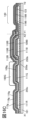
- FIG. 1A is a top view showing an example of a display device.
- FIG. 1B is a cross-sectional view showing an example of a display device;
- FIG. 1C is a top view showing an example of the first layer.
- 2A and 2B are cross-sectional views showing an example of a display device.
- 3A and 3B are cross-sectional views showing an example of a display device.
- 4A and 4B are cross-sectional views showing an example of a display device.
- 5A and 5B are cross-sectional views showing an example of the display device.
- 6A and 6B are cross-sectional views showing an example of the display device.
- FIG. 7A is a cross-sectional view showing an example of a display device.
- FIG. 7B and 7C are cross-sectional views showing examples of pixel electrodes.
- 8A to 8C are cross-sectional views showing examples of display devices.
- 9A and 9B are cross-sectional views showing an example of a display device.
- 10A to 10C are cross-sectional views showing examples of display devices.
- 11A and 11B are cross-sectional views showing an example of a display device.
- 12A and 12B are cross-sectional views showing examples of display devices.
- FIG. 13A is a top view showing an example of a display device.
- FIG. 13B is a cross-sectional view showing an example of a display device;
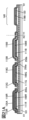
- 14A to 14C are cross-sectional views illustrating an example of a method for manufacturing a display device.
- 15A to 15C are cross-sectional views illustrating an example of a method for manufacturing a display device.
- 16A to 16C are cross-sectional views illustrating an example of a method for manufacturing a display device.
- 17A to 17C are cross-sectional views illustrating an example of a method for manufacturing a display device.
- 18A to 18C are cross-sectional views illustrating an example of a method for manufacturing a display device.
- 19A to 19C are cross-sectional views illustrating an example of a method for manufacturing a display device.
- 20A to 20C are cross-sectional views illustrating an example of a method for manufacturing a display device.
- 21A to 21C are cross-sectional views illustrating an example of a method for manufacturing a display device.
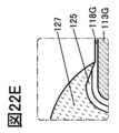
- 22A to 22F are cross-sectional views illustrating an example of a method for manufacturing a display device.
- 23A to 23C are cross-sectional views illustrating an example of a method for manufacturing a display device.
- 24A and 24B are cross-sectional views illustrating an example of a method for manufacturing a display device.
- 25A to 25C are cross-sectional views illustrating an example of a method for manufacturing a display device.
- 26A to 26C are cross-sectional views illustrating an example of a method for manufacturing a display device.
- 27A to 27C are cross-sectional views illustrating an example of a method for manufacturing a display device.
- 28A to 28C are cross-sectional views illustrating an example of a method for manufacturing a display device.
- 29A to 29C are cross-sectional views illustrating an example of a method for manufacturing a display device.
- 30A to 30C are cross-sectional views illustrating an example of a method for manufacturing a display device.
- 31A and 31B are cross-sectional views illustrating an example of a method for manufacturing a display device.
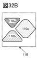
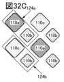
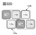
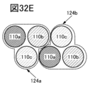
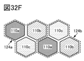
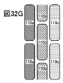
- 32A to 32G are diagrams showing examples of pixels.
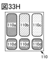
- 33A to 33K are diagrams showing examples of pixels.
- 34A and 34B are perspective views showing an example of a display device.
- 35A to 35C are cross-sectional views showing examples of display devices.
- FIG. 36 is a cross-sectional view showing an example of a display device.
- FIG. 37 is a cross-sectional view showing an example of a display device.
- FIG. 38 is a cross-sectional view showing an example of a display device.
- FIG. 39 is a cross-sectional view showing an example of a display device.
- FIG. 40 is a cross-sectional view showing an example of a display device.
- FIG. 41 is a perspective view showing an example of a display device.
- FIG. 42A is a cross-sectional view showing an example of a display device.
- 42B and 42C are cross-sectional views showing examples of transistors.
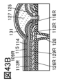
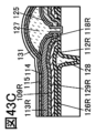
- 43A to 43D are cross-sectional views showing examples of display devices.
- FIG. 44 is a cross-sectional view showing an example of a display device.
- 45A to 45F are diagrams showing configuration examples of light-emitting devices.
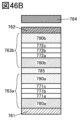
- 46A to 46C are diagrams showing configuration examples of light emitting devices.
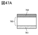
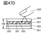
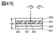
- 47A and 47B are diagrams showing configuration examples of light receiving devices.
- 47C to 47E are diagrams showing configuration examples of display devices.
- 48A to 48D are diagrams showing examples of electronic devices.
- 49A to 49F are diagrams illustrating examples of electronic devices.
- 50A to 50G are diagrams showing examples of electronic devices.
- film and “layer” can be interchanged depending on the case or situation.
- conductive layer can be changed to the term “conductive film.”
- insulating film can be changed to the term “insulating layer”.
- devices manufactured using metal masks or FMM are sometimes referred to as devices with MM (metal mask) structures.
- MM metal mask
- a device manufactured without using a metal mask or FMM may be referred to as a device with an MML (metal maskless) structure.
- an SBS side-by-side structure
- the material and configuration can be optimized for each light-emitting device, so the degree of freedom in selecting the material and configuration increases, and it becomes easy to improve luminance and reliability.
- holes or electrons are sometimes referred to as "carriers".
- the hole injection layer or electron injection layer is referred to as a "carrier injection layer”
- the hole transport layer or electron transport layer is referred to as a “carrier transport layer”
- the hole blocking layer or electron blocking layer is referred to as a "carrier It is sometimes called a block layer.
- the carrier injection layer, the carrier transport layer, and the carrier block layer described above may not be clearly distinguished from each other due to their cross-sectional shape, characteristics, or the like.
- one layer may have two or three functions among the carrier injection layer, the carrier transport layer, and the carrier block layer.
- a light-emitting device (also referred to as a light-emitting element) has an EL layer between a pair of electrodes.
- the EL layer has at least a light-emitting layer.
- layers included in the EL layer include a light-emitting layer, a carrier-injection layer (a hole-injection layer and an electron-injection layer), a carrier-transport layer (a hole-transport layer and an electron-transport layer), and , a carrier block layer (a hole block layer and an electron block layer), and the like.
- a light-receiving device (also referred to as a light-receiving element) has an active layer that functions at least as a photoelectric conversion layer between a pair of electrodes.
- an island-shaped light-emitting layer means that the light-emitting layer is physically separated from an adjacent light-emitting layer.
- a tapered shape refers to a shape in which at least a part of the side surface of the structure is inclined with respect to the substrate surface or the formation surface.
- it refers to a shape having a region in which an angle (also referred to as a taper angle) between an inclined side surface and a substrate surface or a formation surface is less than 90°.
- the side surfaces of the structure, the formation surface, and the substrate surface are not necessarily completely flat, and may be substantially planar with a fine curvature or substantially planar with fine unevenness.
- a mask layer also referred to as a sacrificial layer, a protective layer, etc. refers to at least a light-emitting layer (more specifically, a layer that is processed into an island shape among layers constituting an EL layer). It is positioned above and has the function of protecting the light-emitting layer during the manufacturing process.
- a display device of one embodiment of the present invention includes a light-emitting device manufactured for each emission color, and is capable of full-color display.
- an island-shaped light-emitting layer can be formed by vacuum deposition using a metal mask.
- island-shaped light emission is caused by various influences such as precision of the metal mask, misalignment between the metal mask and the substrate, bending of the metal mask, and broadening of the contour of the deposited film due to vapor scattering. Since the shape and position of the layer deviate from the design, it is difficult to increase the definition and aperture ratio of the display device.
- the layer profile may be blurred and the edge thickness may be reduced. In other words, the thickness of the island-shaped light-emitting layer formed using a metal mask may vary depending on the location.
- the manufacturing yield will be low due to low dimensional accuracy of the metal mask and deformation due to heat or the like.
- the light-emitting layer is processed into a fine pattern by photolithography without using a shadow mask such as a metal mask. Specifically, after forming a pixel electrode for each sub-pixel, a light-emitting layer is formed over a plurality of pixel electrodes. After that, the light-emitting layer is processed by photolithography to form one island-shaped light-emitting layer for one pixel electrode. Thereby, the light-emitting layer is divided for each sub-pixel, and an island-shaped light-emitting layer can be formed for each sub-pixel.
- the display device may include a light-emitting device that emits blue light (also simply referred to as a blue light-emitting device), a light-emitting device that emits green light (also simply referred to as a green light-emitting device), and a light-emitting device that emits red light. (also referred to simply as a red light-emitting device), three types of island-shaped light-emitting layers are formed by repeating film formation of the light-emitting layer and processing by photolithography three times. can be done.
- the state of the interface between the pixel electrode and the EL layer is important in the characteristics of the light-emitting device.
- the pixel electrodes in the light-emitting devices of the second and subsequent colors may be damaged by the previous step.
- the state of the interface between the pixel electrode and the EL layer of the second and subsequent color light emitting devices may deteriorate, and the driving voltage of the light emitting device may increase.
- the light-emitting layer of each light-emitting device is formed after forming a film that protects the surface of each light-emitting device in advance. This prevents the pixel electrode from being exposed in any of the light-emitting devices when forming the light-emitting layer of each light-emitting device. Therefore, when forming the light-emitting layer of each light-emitting device, it is possible to prevent the pixel electrode of the light-emitting device in which the light-emitting layer is not formed from being damaged by the formation process.
- the state of the interface between the pixel electrode and the EL layer of each light-emitting device is maintained in a favorable condition, and as described above, the driving voltage of the light-emitting devices of the second and subsequent colors is increased. can be suppressed.
- the life of each light emitting device can be extended and the reliability can be improved.
- a structure in which the light-emitting layer is processed using a photolithography method can be considered.
- the light-emitting layer may be damaged (damage due to processing, etc.) and the reliability may be significantly impaired. Therefore, when a display device of one embodiment of the present invention is manufactured, a functional layer (for example, a carrier block layer, a carrier transport layer, or a carrier injection layer, more specifically, a hole It is preferable to use a method in which a mask layer or the like is formed on the blocking layer, the electron transport layer, or the electron injection layer, and the light emitting layer and the functional layer are processed into an island shape.
- a highly reliable display device By applying the method, a highly reliable display device can be provided.
- the light-emitting layer By providing another functional layer between the light-emitting layer and the mask layer, the light-emitting layer can be prevented from being exposed to the outermost surface during the manufacturing process of the display device, and damage to the light-emitting layer can be reduced.
- the EL layer preferably has a first region that is a light-emitting region (also referred to as a light-emitting area) and a second region outside the first region.
- the second area can also be called a dummy area or a dummy area.
- the first region is located between the pixel electrode and the common electrode.
- the first region is covered with a mask layer during the manufacturing process of the display device, and the damage received is extremely reduced. Therefore, it is possible to realize a light-emitting device with high luminous efficiency and long life.
- the second region includes the end portion of the EL layer and its vicinity, and includes a portion that may be damaged due to exposure to plasma or the like during the manufacturing process of the display device. By not using the second region as the light emitting region, variations in the characteristics of the light emitting device can be suppressed.
- a layer located below the light-emitting layer (for example, a carrier injection layer, a carrier transport layer, or a carrier block layer, more specifically a hole injection layer, A hole-transporting layer, an electron-blocking layer, etc.) is preferably processed into islands in the same pattern as the light-emitting layer.
- a layer located below the light-emitting layer is preferably processed into islands in the same pattern as the light-emitting layer.
- the hole-injection layer can be processed into an island shape in the same pattern as the light-emitting layer; therefore, lateral leakage current substantially occurs between adjacent subpixels. or the lateral leakage current can be made extremely small.
- the EL layer when performing processing using a photolithography method, various damages are caused to the EL layer due to exposure to an etchant or etching gas during heating during manufacturing of the resist mask and during processing and removal of the resist mask. may be added. Further, when a mask layer is provided over the EL layer, the EL layer may be affected by heat, an etchant, an etching gas, or the like during film formation, processing, and removal of the mask layer.
- each step performed after forming the EL layer is performed at a temperature higher than the heat-resistant temperature of the EL layer, the deterioration of the EL layer progresses, and the luminous efficiency and reliability of the light-emitting device may decrease. .
- the heat resistance temperature of each compound contained in the light-emitting device is preferably 100° C. or higher and 180° C. or lower, more preferably 120° C. or higher and 180° C. or lower, and 140° C. or higher and 180° C. or lower. is more preferred.
- heat resistant temperature indicators examples include glass transition point (Tg), softening point, melting point, thermal decomposition temperature, 5% weight loss temperature, and the like.
- Tg glass transition point
- the glass transition point of the material of the layer can be used as an index of the heat resistance temperature of each layer forming the EL layer.
- the glass transition point of the most abundant material can be used when the layer is a mixed layer made of a plurality of materials.
- the lowest temperature among the glass transition points of the plurality of materials may be used.
- the heat resistance temperature of the functional layer provided on the light emitting layer it is preferable to increase the heat resistance temperature of the functional layer provided on the light emitting layer. Further, it is more preferable to increase the heat resistance temperature of the functional layer provided on and in contact with the light emitting layer. Since the functional layer has high heat resistance, the light-emitting layer can be effectively protected, and damage to the light-emitting layer can be reduced.
- the heat resistance temperature of the light-emitting layer it is particularly preferable to increase the heat resistance temperature of the light-emitting layer. As a result, it is possible to prevent the light-emitting layer from being damaged by heating, thereby reducing the light-emitting efficiency and shortening the life of the light-emitting layer.
- the reliability of the light-emitting device can be improved.
- the width of the temperature range in the manufacturing process of the display device can be widened, and the manufacturing yield and reliability can be improved.
- a display device In light-emitting devices that emit different colors, it is not necessary to separately manufacture all the layers that make up the EL layer, and some layers can be formed in the same process.
- the method for manufacturing a display device of one embodiment of the present invention after some layers forming the EL layer are formed in an island shape for each color, at least part of the mask layer is removed, and the remaining layer forming the EL layer is removed.
- a layer (sometimes called a common layer) and a common electrode also referred to as an upper electrode
- a carrier injection layer and a common electrode can be formed in common for each color light emitting device.
- the carrier injection layer is often a layer with relatively high conductivity among the EL layers. Therefore, the light-emitting device may be short-circuited when the carrier injection layer comes into contact with the side surface of a part of the EL layer formed like an island or the side surface of the pixel electrode. Note that even in the case where the carrier injection layer is provided in an island shape and the common electrode is formed in common for the light emitting devices of each color, the common electrode is in contact with the side surface of the EL layer or the side surface of the pixel electrode, thereby causing light emission. The device may short out.
- the display device of one embodiment of the present invention includes an insulating layer covering at least the side surface of the island-shaped light-emitting layer. Further, the insulating layer preferably covers part of the top surface of the island-shaped light-emitting layer.
- the end of the insulating layer preferably has a taper shape with a taper angle of less than 90°. Accordingly, disconnection of the common layer and the common electrode provided over the insulating layer can be prevented. Therefore, it is possible to suppress poor connection due to disconnection of the common layer and the common electrode. In addition, it is possible to suppress an increase in electrical resistance of the common layer and the common electrode due to local thinning of the common layer and the common electrode due to the step at the edge of the insulating layer.
- discontinuity refers to a phenomenon in which a layer, film, or electrode is divided due to the shape of the formation surface (for example, a step).
- the island-shaped light-emitting layer manufactured by the method for manufacturing a display device of one embodiment of the present invention is not formed using a fine metal mask, but is processed after the light-emitting layer is formed over the entire surface. formed by Therefore, it is possible to realize a high-definition display device or a display device with a high aperture ratio, which has hitherto been difficult to achieve. Furthermore, since the light-emitting layer can be separately formed for each color, a display device with extremely vivid, high-contrast, and high-quality display can be realized. Further, by providing the mask layer over the light-emitting layer, damage to the light-emitting layer during the manufacturing process of the display device can be reduced, and the reliability of the light-emitting device can be improved.
- the distance between adjacent light emitting devices, the distance between adjacent EL layers, or the distance between adjacent pixel electrodes is less than 10 ⁇ m, 5 ⁇ m or less, 3 ⁇ m or less, 2 ⁇ m or less, 1.5 ⁇ m or less, 1 ⁇ m or less, Alternatively, it can be narrowed down to 0.5 ⁇ m or less.
- the interval between adjacent light emitting devices, the interval between adjacent EL layers, or the interval between adjacent pixel electrodes can be reduced to, for example, 500 nm or less, 200 nm or less. , 100 nm or less, or even 50 nm or less.
- the area of the non-light-emitting region that can exist between the two light-emitting devices can be greatly reduced, and the aperture ratio can be brought close to 100%.
- the aperture ratio is 40% or more, 50% or more, 60% or more, 70% or more, 80% or more, further 90% or more and less than 100%. It can also be realized.
- the reliability of the display device can be improved by increasing the aperture ratio of the display device. More specifically, when the lifetime of a display device using an organic EL device and having an aperture ratio of 10% is used as a reference, the life of the display device has an aperture ratio of 20% (that is, the aperture ratio is twice the reference). The life is about 3.25 times longer, and the life of a display device with an aperture ratio of 40% (that is, the aperture ratio is four times the reference) is about 10.6 times longer. As described above, as the aperture ratio is improved, the density of the current flowing through the organic EL device required to obtain the same display can be reduced, so that the life of the display device can be extended. Since the aperture ratio of the display device of one embodiment of the present invention can be improved, the display quality of the display device can be improved. Further, as the aperture ratio of the display device is improved, the reliability (especially life) of the display device is significantly improved, which is an excellent effect.
- the processing size of the light-emitting layer itself can be made extremely smaller than when using a fine metal mask.
- the thickness of the light-emitting layer varies between the center and the edge after processing.
- the manufacturing method described above since a film having a uniform thickness is processed, an island-shaped light-emitting layer can be formed with a uniform thickness. Therefore, even if the processing size of the light-emitting layer is fine, almost the entire area thereof can be used as the light-emitting region. Therefore, a display device having both high definition and high aperture ratio can be manufactured. In addition, it is possible to reduce the size and weight of the display device.
- the definition of the display device of one embodiment of the present invention is, for example, 2000 ppi or more, preferably 3000 ppi or more, more preferably 5000 ppi or more, and still more preferably 6000 ppi or more, and 20000 ppi or less, or 30000 ppi or less. can do.
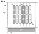
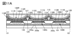
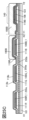
- FIG. 1A shows a top view of the display device 100.
- the display device 100 has a display section in which a plurality of pixels 110 are arranged, and a connection section 140 outside the display section. A plurality of sub-pixels are arranged in a matrix in the display section.
- FIG. 1A shows sub-pixels of 2 rows and 6 columns, which constitute the pixels 110 of 2 rows and 2 columns.
- the connection portion 140 can also be called a cathode contact portion.
- the top surface shape of the sub-pixel shown in FIG. 1A corresponds to the top surface shape of the light emitting region.
- top surface shapes of sub-pixels include triangles, quadrilaterals (including rectangles and squares), polygons such as pentagons, polygons with rounded corners, ellipses, and circles.
- the circuit layout forming the sub-pixel is not limited to the range of the sub-pixel shown in FIG. 1A, and may be arranged outside it.
- a transistor (not shown) included in the sub-pixel 11R may be positioned within the range of the sub-pixel 11G shown in FIG. 1A, or part or all may be positioned outside the range of the sub-pixel 11R.
- the sub-pixel 11R, the sub-pixel 11G, and the sub-pixel 11B have the same or approximately the same aperture ratio (which can also be called the size or the size of the light-emitting region), but one embodiment of the present invention is not limited to this.
- the aperture ratios of the sub-pixel 11R, sub-pixel 11G, and sub-pixel 11B can be determined as appropriate.
- the aperture ratios of the sub-pixel 11R, the sub-pixel 11G, and the sub-pixel 11B may be different, or two or more may be equal or substantially equal.
- a stripe arrangement is applied to the pixels 110 shown in FIG. 1A.
- a pixel 110 shown in FIG. 1A is composed of three sub-pixels, a sub-pixel 11R, a sub-pixel 11G, and a sub-pixel 11B.
- the sub-pixel 11R, sub-pixel 11G, and sub-pixel 11B have light-emitting devices that emit light of different colors.
- the sub-pixel 11R, sub-pixel 11G, and sub-pixel 11B include sub-pixels of three colors of red (R), green (G), and blue (B), yellow (Y), cyan (C), and magenta (M).
- R red
- G green
- B blue
- M yellow
- M magenta
- sub-pixels of three colors can be used.
- the number of types of sub-pixels is not limited to three, and may be four or more.
- the four sub-pixels are R, G, B, and white (W) sub-pixels, R, G, B, and Y sub-pixels
- FIG. 1A shows an example in which sub-pixels of different colors are arranged side by side in the X direction and sub-pixels of the same color are arranged side by side in the Y direction. Note that the display device of one embodiment of the present invention is not limited to this, and subpixels of the same color may be arranged in the X direction and subpixels of different colors may be arranged in the Y direction.
- FIG. 1A shows an example in which the connecting portion 140 is positioned below the display portion in a plan view, it is not particularly limited.
- the connecting portion 140 may be provided in at least one of the upper side, the right side, the left side, and the lower side of the display portion in plan view, and may be provided so as to surround the four sides of the display portion.
- the shape of the upper surface of the connecting portion 140 may be strip-shaped, L-shaped, U-shaped, frame-shaped, or the like.
- the number of connection parts 140 may be singular or plural.
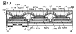
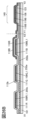
- FIG. 1B shows a cross-sectional view between the dashed-dotted line X1-X2 in FIG. 1A.
- FIG. 1C shows a top view of layer 113B.
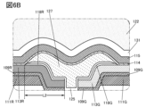
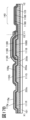
- 2A and 2B show enlarged views of a portion of the cross-sectional view shown in FIG. 1B.
- 3 to 6 show modifications of FIG. 7A and 8 to 11 show a modification of FIG. 1B.
- 7B and 7C show cross-sectional views of modifications of the pixel electrode.
- 12A and 12B show cross-sectional views along the dashed-dotted line Y1-Y2 in FIG. 1A.
- insulating layers are provided on a layer 101 including a transistor (not shown).
- a light-emitting device 130R, a light-emitting device 130G, and a light-emitting device 130B are provided at the bottom, and a protective layer 131 is provided to cover these light-emitting devices.
- a substrate 120 is bonded onto the protective layer 131 with a resin layer 122 .
- An insulating layer 125 and an insulating layer 127 on the insulating layer 125 are provided in a region (non-light emitting region) between adjacent light emitting devices.
- FIG. 1B shows a plurality of cross sections of the insulating layer 125 and the insulating layer 127
- the insulating layer 125 and the insulating layer 127 are each connected to one.
- the display device 100 can be configured to have one insulating layer 125 and one insulating layer 127, for example.
- the display device 100 may have a plurality of insulating layers 125 separated from each other, and may have a plurality of insulating layers 127 separated from each other.
- a display device of one embodiment of the present invention is a top emission type in which light is emitted in a direction opposite to a substrate over which a light-emitting device is formed, and light is emitted toward a substrate over which a light-emitting device is formed.
- a bottom emission type bottom emission type
- a double emission type dual emission type in which light is emitted from both sides may be used.
- a laminated structure in which a plurality of transistors (not shown) are provided on a substrate and an insulating layer is provided to cover these transistors can be applied.
- An insulating layer over a transistor may have a single-layer structure or a stacked-layer structure.
- FIG. 1B shows an insulating layer 255a, an insulating layer 255b over the insulating layer 255a, and an insulating layer 255c over the insulating layer 255b among the insulating layers over the transistor.
- These insulating layers may have recesses between adjacent light emitting devices (non-light emitting regions).
- FIG. 1B and the like show an example in which a concave portion is provided in the insulating layer 255c.
- the insulating layer 255c may not have recesses between adjacent light emitting devices. Note that the insulating layers (the insulating layers 255 a to 255 c ) over the transistors can also be regarded as part of the layer 101 .
- various inorganic insulating films such as an oxide insulating film, a nitride insulating film, an oxynitride insulating film, and a nitride oxide insulating film can be preferably used.
- an oxide insulating film or an oxynitride insulating film such as a silicon oxide film, a silicon oxynitride film, or an aluminum oxide film is preferably used.
- a nitride insulating film or a nitride oxide insulating film such as a silicon nitride film or a silicon nitride oxide film is preferably used. More specifically, a silicon oxide film is preferably used for the insulating layers 255a and 255c, and a silicon nitride film is preferably used for the insulating layer 255b.
- the insulating layer 255b preferably functions as an etching protection film.
- oxynitride refers to a material whose composition contains more oxygen than nitrogen
- nitride oxide refers to a material whose composition contains more nitrogen than oxygen. point to the material.
- silicon oxynitride refers to a material whose composition contains more oxygen than nitrogen
- silicon nitride oxide refers to a material whose composition contains more nitrogen than oxygen. point to
- the light emitting device 130R emits red (R) light
- the light emitting device 130G emits green (G) light
- the light emitting device 130B emits blue (B) light.
- the light emitting device for example, it is preferable to use an OLED (Organic Light Emitting Diode) or a QLED (Quantum-dot Light Emitting Diode).
- the light-emitting substance included in the light-emitting device include a substance that emits fluorescence (fluorescent material), a substance that emits phosphorescence (phosphorescent material), and a substance that exhibits thermally activated delayed fluorescence (thermally activated delayed fluorescence: TADF ) materials), and inorganic compounds (quantum dot materials, etc.).
- LEDs such as micro LED (Light Emitting Diode), can also be used as a light emitting device.
- the emission color of the light emitting device can be infrared, red, green, blue, cyan, magenta, yellow, white, or the like.
- color purity can be enhanced by providing a light-emitting device with a microcavity structure.
- Embodiment 5 can be referred to for the configuration and materials of the light-emitting device.
- one electrode functions as an anode and the other electrode functions as a cathode.
- the case where the pixel electrode functions as an anode and the common electrode functions as a cathode may be taken as an example.
- the light-emitting device 130R includes a conductive layer 111R on the insulating layer 255c, an island-shaped conductive layer 109R on the conductive layer 111R, an island-shaped layer 113R on the island-shaped conductive layer 109R, and an island-shaped layer 113R on the island-shaped layer 113R. It has a common layer 114 and a common electrode 115 on the common layer 114 .
- the conductive layer 111R and the conductive layer 109R can collectively be called pixel electrodes.
- the layer 113R and the common layer 114 can be collectively called an EL layer.
- the light-emitting device 130G includes a conductive layer 111G on the insulating layer 255c, an island-shaped conductive layer 109G on the conductive layer 111G, an island-shaped layer 113G on the island-shaped conductive layer 109G, and an island-shaped layer 113G on the island-shaped layer 113G. It has a common layer 114 and a common electrode 115 on the common layer 114 .
- the conductive layer 111G and the conductive layer 109G can be collectively called pixel electrodes.
- the layer 113G and the common layer 114 can be collectively called an EL layer.
- the light-emitting device 130B includes a conductive layer 111B on the insulating layer 255c, an island-shaped conductive layer 109B on the conductive layer 111B, an island-shaped layer 113B on the island-shaped conductive layer 109B, and an island-shaped layer 113B on the island-shaped layer 113B. It has a common layer 114 and a common electrode 115 on the common layer 114 .
- the conductive layer 111B and the conductive layer 109B can be collectively called pixel electrodes.
- the layer 113B and the common layer 114 can be collectively called an EL layer.
- a layer provided in an island shape for each light-emitting device is indicated as a layer 113R, a layer 113G, or a layer 113B, and a layer shared by a plurality of light-emitting devices is indicated. Shown as common layer 114 .
- the layers 113R, 113G, and 113B, excluding the common layer 114 may be referred to as an island-shaped EL layer, an island-shaped EL layer, or the like.
- the layers 113R, 113G, and 113B are isolated from each other. Leakage current between adjacent light-emitting devices (light-emitting regions) can be suppressed by providing an island-shaped EL layer for each light-emitting device. Thereby, crosstalk due to unintended light emission can be prevented, and a display device with extremely high contrast can be realized. In particular, a display device with high current efficiency at low luminance can be realized.
- Each end of the conductive layer 111R, the conductive layer 111G, and the conductive layer 111B preferably has a tapered shape.
- each end of the conductive layer 111R, the conductive layer 111G, and the conductive layer 111B preferably has a taper shape with a taper angle of less than 90°.
- the ends of these conductive layers 111 have tapered shapes, the conductive layers provided along the side surfaces of the conductive layers 111R, 111G, and 111B, respectively.
- Layers 109R and 113R, conductive layers 109G and 113G, and conductive layers 109B and 113B also have tapered shapes.
- the conductive layer 109 the conductive layer 109R, the conductive layer 109G, and the conductive layer 109B
- FIG. 1B and the like a configuration in which a part of the shape of the recess provided in the insulating layer 255c has the same taper angle as the tapered shapes of the conductive layers 111R, 111G, and 111B is illustrated. It is not limited to this.
- the tapered shape of the conductive layer 111R, the conductive layer 111G, and the conductive layer 111B may be different from the tapered shape of the recess formed in the insulating layer 255c.
- the ends of the conductive layer 109R, the conductive layer 109G, and the conductive layer 109B are positioned outside the ends of the conductive layer 111R, the conductive layer 111G, and the conductive layer 111B.
- the conductive layer 111R and the conductive layer 109R, the conductive layer 111G and the conductive layer 109G, and the conductive layer 111B and the conductive layer 109B are the pixel electrodes of the light emitting device 130R, the light emitting device 130G, and the light emitting device 130B, respectively. Equivalent to.
- the pixel electrode included in each light-emitting device has a two-layer structure in which the first conductive layer 111 is covered with the second conductive layer 109, whereby the layers 113R, 113G, and 113B are formed.
- the surface of the pixel electrode in contact with the conductive layer 109 can be limited to only the top surface of the conductive layer 109 .
- the conductive layer 109 does not cover the conductive layer 111 (when the conductive layer 109 is in contact with only the upper surface of the conductive layer 111), the surfaces in contact with the layers 113R, 113G, and 113B are the conductive layers.
- the adhesion between the layers 113R, 113G, and 113B and the pixel electrode can be increased, and the layer 113R, the layer 113G, and the layer 113B, and the pixel electrode can be brought together. , it is possible to suppress the occurrence of defects such as film peeling.
- the conductive layer 111 is corroded (for example, by galvanic corrosion) due to impurities contained in the etching liquid when the etching liquid comes into direct contact with the conductive layer 111 . etc.), it is also possible to prevent a problem such as deterioration of the conductive layer 111 from occurring. Thereby, the range of options for the material of the conductive layer 111 can be expanded.
- the pixel electrode of the display device of one embodiment of the present invention may have a layered structure of three or more layers.
- electrodes that reflect visible light are used for the conductive layers 111R, 111G, and 111B.
- An electrode (transparent electrode) that transmits visible light is preferably used for the conductive layer 109B.
- the light-emitting layer included in each light-emitting device is formed after forming a film for protecting the surface of each light-emitting device in advance.
- a conductive film to be the conductive layer 109 later is used as the protective film.
- a conductive film that will later become the conductive layer 109 and a film that will later become the layer 113 are stacked over the conductive layer 111, and then the layer 113 and the conductive layer 109 are continuously formed. End portions of the conductive layer 109 and the layer 113 can be formed substantially flush.
- Embodiment 2 will describe the details of the method for manufacturing the display device of one embodiment of the present invention.
- FIG. 1B between the conductive layer 109R and the layer 113R, there is no insulating layer (also referred to as a partition wall, bank, spacer, etc.) covering the upper surface edge of the conductive layer 109R. Further, no insulating layer is provided between the conductive layer 109G and the layer 113G to cover the end portion of the upper surface of the conductive layer 109G. Similarly, no insulating layer is provided between the conductive layer 109B and the layer 113B to cover the edge of the upper surface of the conductive layer 109B. Therefore, the interval between adjacent light emitting devices (light emitting regions) can be extremely narrowed. Therefore, a high-definition or high-resolution display device can be obtained. Moreover, a mask for forming the insulating layer is not required, and the manufacturing cost of the display device can be reduced.
- the viewing angle dependency of the display device of one embodiment of the present invention can be extremely reduced. By reducing the viewing angle dependency, it is possible to improve the visibility of the image on the display device.
- the viewing angle (the maximum angle at which a constant contrast ratio is maintained when the screen is viewed obliquely) is 100° or more and less than 180°, preferably 150°. It can be in the range of 170° or more. It should be noted that the viewing angle described above can be applied to each of the vertical and horizontal directions.
- a single structure (a structure having only one light emitting unit) or a tandem structure (a structure having a plurality of light emitting units) may be applied to the light emitting device of this embodiment.
- the light-emitting unit has at least one light-emitting layer.
- Layer 113R, layer 113G, and layer 113B have at least a light-emitting layer.
- Layer 113R has a light-emitting layer that emits red light
- layer 113G has a light-emitting layer that emits green light
- layer 113B has a light-emitting layer that emits blue light.
- layer 113R has a luminescent material that emits red light
- layer 113G has a luminescent material that emits green light
- layer 113B has a luminescent material that emits blue light.
- the layer 113R has a structure having a plurality of light-emitting units that emit red light
- the layer 113G has a structure that has a plurality of light-emitting units that emit green light
- the layer 113B has a structure having a plurality of light-emitting units that emit green light.
- a charge-generating layer (also referred to as an intermediate layer) is preferably provided between each light-emitting unit.
- Layers 113R, 113G, and 113B are each one of a hole injection layer, a hole transport layer, a hole blocking layer, a charge generation layer, an electron blocking layer, an electron transport layer, and an electron injection layer. You may have more than
- the layers 113R, 113G, and 113B may each have a hole injection layer, a hole transport layer, a light emitting layer, and an electron transport layer in this order. Moreover, you may have an electron block layer between a hole transport layer and a light emitting layer. Further, a hole blocking layer may be provided between the electron transport layer and the light emitting layer. Moreover, you may have an electron injection layer on the electron transport layer.
- the layers 113R, 113G, and 113B may each have an electron injection layer, an electron transport layer, a light emitting layer, and a hole transport layer in this order.
- a hole blocking layer may be provided between the electron transport layer and the light emitting layer.
- you may have an electron block layer between a hole transport layer and a light emitting layer.
- a hole injection layer may be provided on the hole transport layer.
- each of the layers 113R, 113G, and 113B preferably has a light-emitting layer and a carrier-transporting layer (electron-transporting layer or hole-transporting layer) on the light-emitting layer.
- the layers 113R, 113G, and 113B each preferably have a light-emitting layer and a carrier-blocking layer (hole-blocking layer or electron-blocking layer) over the light-emitting layer.
- the layers 113R, 113G, and 113B each preferably have a light emitting layer, a carrier blocking layer over the light emitting layer, and a carrier transport layer over the carrier blocking layer.
- the surfaces of the layers 113R, 113G, and 113B are exposed during the manufacturing process of the display device; Exposure can be suppressed, and damage to the light-emitting layer can be reduced. This can improve the reliability of the light emitting device.
- the heat resistance temperature of the compounds contained in the layers 113R, 113G, and 113B is preferably 100° C. or higher and 180° C. or lower, more preferably 120° C. or higher and 180° C. or lower, and further preferably 140° C. or higher and 180° C. or lower. preferable.
- the glass transition point (Tg) of these compounds is preferably 100° C. or higher and 180° C. or lower, more preferably 120° C. or higher and 180° C. or lower, and even more preferably 140° C. or higher and 180° C. or lower.
- the heat resistance temperature of the functional layer provided on the light emitting layer is high. Further, it is more preferable that the functional layer provided in contact with the light-emitting layer has a high heat resistance temperature. Since the functional layer has high heat resistance, the light-emitting layer can be effectively protected, and damage to the light-emitting layer can be reduced.
- the heat resistance temperature of the light-emitting layer is high. As a result, it is possible to prevent the light-emitting layer from being damaged by heating, thereby reducing the light-emitting efficiency and shortening the life of the light-emitting layer.
- the light-emitting layer has a light-emitting substance (also called a light-emitting material, a light-emitting organic compound, a guest material, etc.) and an organic compound (also called a host material, etc.). Since the light-emitting layer contains more organic compounds than the light-emitting substance, the Tg of the organic compound can be used as an index of the heat resistance temperature of the light-emitting layer.
- a light-emitting substance also called a light-emitting material, a light-emitting organic compound, a guest material, etc.
- an organic compound also called a host material, etc.
- Layers 113R, 113G, and 113B also include, for example, a first light-emitting unit, a charge generation layer on the first light-emission unit, and a second light-emission unit on the charge generation layer.
- the second light-emitting unit preferably has a light-emitting layer and a carrier-transporting layer (electron-transporting layer or hole-transporting layer) on the light-emitting layer.
- the second light emitting unit preferably has a light emitting layer and a carrier blocking layer (hole blocking layer or electron blocking layer) on the light emitting layer.
- the second light-emitting unit preferably has a light-emitting layer, a carrier-blocking layer on the light-emitting layer, and a carrier-transporting layer on the carrier-blocking layer.
- the light-emitting unit provided in the uppermost layer preferably has a light-emitting layer and one or both of a carrier transport layer and a carrier block layer over the light-emitting layer.
- the common layer 114 has, for example, an electron injection layer or a hole injection layer.
- the common layer 114 may have a laminate of an electron transport layer and an electron injection layer, or may have a laminate of a hole transport layer and a hole injection layer.
- Common layer 114 is shared by light emitting device 130R, light emitting device 130G, and light emitting device 130B.
- FIG. 1B shows an example in which the end of the layer 113R is located outside the end of the conductive layer 111R, as described above.
- the conductive layers 111R and 113R are described below as an example, the same applies to the conductive layers 111G and 113G and the conductive layers 111B and 113B.
- the layer 113R is formed to cover the edge of the conductive layer 111R.
- the entire region overlapping with the upper surface of the conductive layer 111R can be used as a light emitting region, and the end of the island-shaped EL layer is located inside the end of the pixel electrode. In comparison, it becomes easier to increase the aperture ratio.
- the distance between the light-emitting region of the EL layer (that is, the region overlapping the conductive layer 111R of the layer 113R) and the edge of the EL layer can be increased. Since the edges of the EL layer may be damaged by processing, the reliability of the light-emitting device may be improved by using a region away from the edges of the EL layer as the light-emitting region.
- Each of the layers 113R, 113G, and 113B preferably has a first region that is a light emitting region and a second region (dummy region) outside the first region.
- the first region is located between conductive layer 111R and common electrode 115 .
- the first region is covered with a mask layer during the manufacturing process of the display device, and the damage received is extremely reduced. Therefore, it is possible to realize a light-emitting device with high luminous efficiency and long life.
- the second region includes the end portion of the EL layer and its vicinity, and includes a portion that may be damaged due to exposure to plasma or the like during the manufacturing process of the display device. By not using the second region as the light emitting region, variations in the characteristics of the light emitting device can be suppressed.
- a width L3 shown in FIGS. 1B and 1C corresponds to the width of the first region 113_1 (light emitting region) in the layer 113R.
- the width L1 and the width L2 shown in FIGS. 1B and 1C correspond to the width of the second region 113_2 (dummy region) in the layer 113R.
- the second region 113_2 is provided so as to surround the first region 113_1. Therefore, in cross-sectional views such as FIG. can be done.
- the width L1 or the width L2 can be used, and for example, the shorter one of the width L1 and the width L2 may be used.
- the widths L1 to L3 can be confirmed by a cross-sectional observation image or the like.
- the enlarged view shown in FIG. 2A shows the width L2 of the second region 113_2.
- the second region 113_2 is a portion of the layer 113R where at least one of the mask layer 118R, the insulating layer 125, and the insulating layer 127 overlap.
- portions of the layers 113R and the like located outside the edges of the upper surfaces of the conductive layers 111R and the like are dummy regions.
- the width of the second region 113_2 is 1 nm or more, preferably 5 nm or more, 50 nm or more, or 100 nm or more.
- the narrower the width of the dummy region the wider the light-emitting region and the higher the aperture ratio of the pixel. Therefore, the width of the second region 113_2 is preferably 50% or less, more preferably 40% or less, 30% or less, 20% or less, or 10% or less of the width L3 of the first region 113_1.
- the width of the second region 113_2 in a small and high-definition display device is preferably 500 nm or less, more preferably 300 nm or less, 200 nm or less, or 150 nm or less.
- the first region (light emitting region) is a region where EL (Electroluminescence) light emission is obtained.
- both the first region (light emitting region) and the second region (dummy region) are regions where PL (Photoluminescence) light emission can be obtained. From these facts, it can be said that the first region and the second region can be distinguished by confirming EL emission and PL emission.
- the common electrode 115 is shared by the light emitting device 130R, the light emitting device 130G, and the light emitting device 130B.
- a common electrode 115 shared by a plurality of light emitting devices is electrically connected to the conductive layer 123 provided in the connection portion 140 (see FIGS. 12A and 12B).
- the conductive layer 123 is preferably formed using the same material and in the same process as the conductive layers 111R, 111G, and 111B.
- FIG. 12A shows an example in which a common layer 114 is provided on the conductive layer 123 and the conductive layer 123 and the common electrode 115 are electrically connected through the common layer 114 .
- the common layer 114 may not be provided in the connecting portion 140 .
- conductive layer 123 and common electrode 115 are directly connected.
- the common layer 114 and the common electrode 115 are formed by using a mask (also referred to as an area mask or a rough metal mask to distinguish from a fine metal mask) for defining a film forming area. You can change the area.
- the common electrode 115 can be formed continuously after forming the common layer 114 without intervening a process such as etching. For example, after forming the common layer 114 in a vacuum, the common electrode 115 can be formed in a vacuum without taking it out to the atmosphere. That is, the common layer 114 and the common electrode 115 can be formed in vacuum. As a result, the lower surface of the common electrode 115 can be made cleaner than when the common layer 114 is not provided in the display device 100 . Therefore, the light emitting device 130R, the light emitting device 130G, and the light emitting device 130B can be light emitting devices with high reliability and excellent characteristics.
- vacuum continuous refers to continuously performing different processes in a device in a vacuum atmosphere.
- the common electrode 115 is formed in a vacuum process following the formation of the common layer 114
- the common layer 114 is first formed in an apparatus in a vacuum atmosphere. After that, the common electrode 115 is continuously formed without exposing the layer 101 on which the common layer 114 and the like are formed.
- a mask layer 118R is positioned on the layer 113R of the light emitting device 130R, a mask layer 118G is positioned on the layer 113G of the light emitting device 130G, and a mask layer 118G is positioned on the layer 113B of the light emitting device 130B.
- the mask layer 118B is located.
- the mask layer is provided so as to surround the first region 113_1 (light emitting region). In other words, the mask layer has openings in portions overlapping the light emitting regions.
- the top surface shape of the mask layer matches, roughly matches, or is similar to the second region 113_2 shown in FIG. 1C.
- the mask layer 118R is a portion of the mask film that was provided in contact with the upper surface of the layer 113R when processing the layer 113R remains.
- the mask layers 118G and 118B are part of the mask films provided when the layers 113G and 113B were formed, respectively.
- part of the mask film used to protect the EL layer may remain during manufacturing. Any two or all of the mask layers 118R, 118G, and 118B may be made of the same material, or may be made of different materials. Note that the mask layer 118R, the mask layer 118G, and the mask layer 118B may be collectively referred to as the mask layer 118 below.
- one end of mask layer 118R (the end opposite to the light emitting region side, the outer end) is aligned or substantially aligned with the ends of conductive layer 109R and layer 113R.
- the other end of the mask layer 118R (the end on the light emitting region side, the inner end) is located on the layer 113R.
- the other end of the mask layer 118R preferably overlaps the layer 113R and the conductive layer 111R.
- the other end of the mask layer 118R is likely to be formed on the substantially flat surface of the layer 113R.
- the mask layer 118 remains, for example, between the insulating layer 125 and the upper surface of the EL layer (the layer 113R, the layer 113G, or the layer 113B) processed into an island shape.
- the mask layer will be described in detail in the second embodiment.
- the ends are aligned or substantially aligned, and when the top surface shapes are matched or substantially matched, at least part of the outline overlaps between the laminated layers in a plan view.
- the upper layer and the lower layer may be processed with the same mask pattern or partially with the same mask pattern.
- the contours do not overlap, and the upper layer may be located inside the lower layer, or the upper layer may be located outside the lower layer, and in this case also, the edges are roughly aligned, or the top surface shape are said to roughly match.
- a mask layer 118 covers part of the upper surface of each of the conductive layers 109R and 113R, the conductive layers 109G and 113G, and the conductive layers 109B and 113B.
- the insulating layers 125 and 127 partially overlap with the top surfaces of the conductive layers 109R and 113R, the conductive layers 109G and 113G, and the conductive layers 109B and 113B, respectively, with the mask layer 118 interposed therebetween.
- the top surfaces of the conductive layers 109R and 113R, the conductive layers 109G and 113G, and the conductive layers 109B and 113B are not limited to the top surfaces of the flat portions overlapping the top surface of the conductive layer 111. can include top surfaces of ramps and flats (see region 103 in FIG. 5A) located outside the top surface of the .
- the common layer 114 becomes the pixel electrode (the conductive layer 111R and the conductive layer 109R, the conductive layer 111G and the conductive layer 109G, and the conductive layer 111B and the conductive layer 109B), the layer 113R, the layer Contact with the side surfaces of 113G and layer 113B can be suppressed, and short-circuiting of the light-emitting device can be suppressed. This can improve the reliability of the light emitting device.
- FIG. 1B shows the layers 113R, 113G, and 113B with the same thickness
- Layers 113R, 113G, and 113B may have different thicknesses.
- a microcavity structure can be realized and the color purity in each light emitting device can be enhanced.
- the insulating layer 125 preferably contacts the side surfaces of the conductive layers 109R and 113R, the conductive layers 109G and 113G, and the conductive layers 109B and 113B (the ends of the layers 113R and 113G shown in FIG. 2A). See the part enclosed by the dashed line in the neighborhood).
- the insulating layer 125 is in contact with the conductive layers 109R and 113R, the conductive layers 109G and 113G, and the conductive layers 109B and 113B, so that the conductive layers 109R and 113R, the conductive layers 109G and 113G, and Film peeling of the conductive layer 109B and the layer 113B can be prevented.
- Adhesion between the insulating layer 125 and the layer 113B, the layer 113G, or the layer 113R has the effect of fixing or bonding the adjacent EL layers or the like with the insulating layer 125 . This can improve the reliability of the light emitting device. Moreover, the production yield of the light-emitting device can be increased.
- the insulating layer 125 and the insulating layer 127 cover part of the top surface and side surfaces of the layers 113R, 113G, and 113B, thereby further preventing peeling of the EL layer. and the reliability of the light-emitting device can be improved. Moreover, the manufacturing yield of the light-emitting device can be further increased.
- FIG. 1B shows an example in which a laminated structure of a conductive layer 109R, a layer 113R, a mask layer 118R, an insulating layer 125, and an insulating layer 127 is positioned on the edge of the conductive layer 111R.
- a laminated structure of a conductive layer 109G, a layer 113G, a mask layer 118G, an insulating layer 125, and an insulating layer 127 is positioned on the end of the conductive layer 111G
- a conductive layer 111B is positioned on the end of the conductive layer 111B.
- 109B, layer 113B, mask layer 118B, insulating layer 125 and insulating layer 127 are located.
- FIG. 1B shows a configuration in which the end of the conductive layer 111R is covered with the layer 113R through the conductive layer 109R, and the insulating layer 125 is in contact with the side surfaces of the conductive layers 109R and 113R.
- the end of conductive layer 111G is covered with layer 113G through conductive layer 109G
- the end of conductive layer 111B is covered with layer 113B through conductive layer 109B
- insulating layer 125 is in contact with the side surfaces of the conductive layers 109G and 113G and the side surfaces of the conductive layers 109B and 113B.
- the insulating layer 127 is provided on the insulating layer 125 so as to fill the recesses formed in the insulating layer 125 .
- the insulating layer 127 can overlap with part of the top surface and side surfaces of the conductive layers 109R and 113R, the conductive layers 109G and 113G, and the conductive layers 109B and 113B with the insulating layer 125 interposed therebetween. can.
- the insulating layer 127 preferably covers at least part of the side surface of the insulating layer 125 .
- the space between adjacent island-shaped layers can be filled; It can reduce extreme unevenness and make it more flat. Therefore, coverage of the formation surface with the carrier injection layer, the common electrode, and the like can be improved.
- the common layer 114 and the common electrode 115 are provided on the layer 113R, the layer 113G, the layer 113B, the mask layer 118, the insulating layer 125 and the insulating layer 127.
- a region where the pixel electrode and the island-shaped EL layer are provided, a region where the pixel electrode and the island-shaped EL layer are not provided (region between the light emitting devices) There is a step due to In the display device of one embodiment of the present invention, the insulating layer 125 and the insulating layer 127 can planarize the step. The coverage of the electrode 115 can be improved.
- the upper surface of the insulating layer 127 preferably has a more flat shape, but may have a convex portion, a convex curved surface, a concave curved surface, or a concave portion.
- the upper surface of the insulating layer 127 preferably has a highly flat and smooth convex shape.
- a metal, an alloy, an electrically conductive compound, a mixture thereof, or the like can be appropriately used for the conductive layer 111 .
- the conductive layer 111 corresponds to a reflective electrode of the display device. Therefore, a material that reflects visible light is preferably used for the conductive layer 111 . Examples of such materials include aluminum, magnesium, titanium, chromium, manganese, iron, cobalt, nickel, copper, gallium, zinc, indium, tin, molybdenum, tantalum, tungsten, palladium, gold, platinum, silver, yttrium, and neodymium. and alloys containing these in appropriate combinations.
- the material includes an alloy containing aluminum (aluminum alloy) such as an alloy of aluminum, nickel, and lanthanum (Al-Ni-La), an alloy of silver and magnesium, and an alloy of silver, palladium and copper ( Ag-Pd-Cu, also referred to as APC) and other silver-containing alloys.
- aluminum alloy such as an alloy of aluminum, nickel, and lanthanum (Al-Ni-La), an alloy of silver and magnesium, and an alloy of silver, palladium and copper ( Ag-Pd-Cu, also referred to as APC) and other silver-containing alloys.
- elements belonging to Group 1 or Group 2 of the periodic table of elements not exemplified above e.g., lithium, cesium, calcium, strontium
- europium e.g., cesium, calcium, strontium
- rare earth metals such as ytterbium
- the conductive layer 109 and the common electrode 115 metals, alloys, electrically conductive compounds, mixtures thereof, and the like can be used as appropriate.
- the conductive layer 109 and the common electrode 115 correspond to transparent electrodes of the display device. Therefore, a material that transmits visible light is preferably used for the conductive layer 109 and the common electrode 115 .
- examples of such materials include indium tin oxide (also referred to as In—Sn oxide, ITO), In—Si—Sn oxide (also referred to as ITSO), indium zinc oxide (In—Zn oxide), and In--W--Zn oxide.
- the conductive layers 111 and 109 correspond to the transparent electrodes of the display device, and the common electrode 115 corresponds to the reflective electrode of the display device. Therefore, in the case of a bottom-emission display device, the conductive layers 111 and 109 are made of a material that transmits visible light, and the common electrode 115 is made of a material that reflects visible light. It is preferable to use a material having a specific property.
- the insulating layer 125 can be an insulating layer having an inorganic material.
- an inorganic insulating film such as an oxide insulating film, a nitride insulating film, an oxynitride insulating film, or a nitride oxide insulating film can be used.
- the insulating layer 125 may have a single-layer structure or a laminated structure.
- the oxide insulating film includes a silicon oxide film, an aluminum oxide film, a magnesium oxide film, an indium gallium zinc oxide film, a gallium oxide film, a germanium oxide film, an yttrium oxide film, a zirconium oxide film, a lanthanum oxide film, a neodymium oxide film, and an oxide film.
- a hafnium film, a tantalum oxide film, and the like can be mentioned.
- the nitride insulating film include a silicon nitride film, an aluminum nitride film, and the like.
- Examples of the oxynitride insulating film include a silicon oxynitride film, an aluminum oxynitride film, and the like.
- nitride oxide insulating film a silicon nitride oxide film, an aluminum nitride oxide film, or the like can be given.
- aluminum oxide is preferable because it has a high etching selectivity with respect to the EL layer and has a function of protecting the EL layer during formation of the insulating layer 127 described later.
- an inorganic insulating film such as an aluminum oxide film, a hafnium oxide film, or a silicon oxide film formed by an atomic layer deposition (ALD) method to the insulating layer 125, pinholes can be reduced and the EL layer can be formed.
- An insulating layer 125 having an excellent protective function can be formed.
- the insulating layer 125 may have a layered structure of a film formed by an ALD method and a film formed by a sputtering method.
- the insulating layer 125 may have a laminated structure of, for example, an aluminum oxide film formed by ALD and a silicon nitride film formed by sputtering.
- the insulating layer 125 preferably functions as a barrier insulating layer against at least one of water and oxygen. Further, the insulating layer 125 preferably has a function of suppressing diffusion of at least one of water and oxygen. Further, the insulating layer 125 preferably has a function of capturing or fixing at least one of water and oxygen (also referred to as gettering).
- a barrier insulating layer indicates an insulating layer having barrier properties.
- barrier property refers to a function of suppressing diffusion of a corresponding substance (also referred to as low permeability). Alternatively, it has a function of capturing or fixing (also called gettering) the corresponding substance.
- the insulating layer 125 has a function as a barrier insulating layer or a gettering function, thereby suppressing entry of impurities (typically, at least one of water and oxygen) that can diffuse into each light-emitting device from the outside. is possible. With such a structure, a highly reliable light-emitting device and a highly reliable display device can be provided.
- impurities typically, at least one of water and oxygen
- the insulating layer 125 preferably has a low impurity concentration. Accordingly, it is possible to suppress deterioration of the EL layer due to entry of impurities from the insulating layer 125 into the EL layer. In addition, by reducing the impurity concentration in the insulating layer 125, the barrier property against at least one of water and oxygen can be improved.
- the insulating layer 125 preferably has a sufficiently low hydrogen concentration or carbon concentration, or preferably both.
- any one of the mask layers 118B, 118G, and 118R and the insulating layer 125 may be recognized as one layer. That is, one layer is provided in contact with part of the top surface and side surface of each of the layers 113R, 113G, and 113B, and the insulating layer 127 covers at least part of the side surface of the one layer. may be observed as
- the insulating layer 127 provided on the insulating layer 125 has a function of flattening extreme unevenness of the insulating layer 125 formed between adjacent light emitting devices (non-light emitting regions). In other words, the presence of the insulating layer 127 has the effect of improving the flatness of the surface on which the common electrode 115 is formed.
- An insulating layer containing an organic material can be suitably used as the insulating layer 127 .
- the organic material it is preferable to use a photosensitive organic resin, for example, it is preferable to use a photosensitive resin composition containing an acrylic resin.
- acrylic resin does not only refer to polymethacrylates or methacrylic resins, but may refer to all acrylic polymers in a broad sense.
- the insulating layer 127 an acrylic resin, a polyimide resin, an epoxy resin, an imide resin, a polyamide resin, a polyimideamide resin, a silicone resin, a siloxane resin, a benzocyclobutene resin, a phenol resin, a precursor of these resins, or the like is used. good too.
- the insulating layer 127 may be made of an organic material such as polyvinyl alcohol (PVA), polyvinyl butyral, polyvinylpyrrolidone, polyethylene glycol, polyglycerin, pullulan, water-soluble cellulose, or alcohol-soluble polyamide resin.
- a photoresist may be used as the photosensitive resin.
- the photosensitive organic resin either a positive material or a negative material may be used.
- a material that absorbs visible light may be used for the insulating layer 127 . Since the insulating layer 127 absorbs light emitted from the light emitting device, leakage of light (stray light) from the light emitting device to an adjacent light emitting device via the insulating layer 127 can be suppressed. Thereby, the display quality of the display device can be improved. In addition, since the display quality can be improved without using a polarizing plate for the display device, the weight and thickness of the display device can be reduced.
- Materials that absorb visible light include materials containing pigments such as black, materials containing dyes, light-absorbing resin materials (e.g., polyimide), and resin materials that can be used for color filters (color filter materials ).
- resin materials that can be used for color filters color filter materials
- by mixing color filter materials of three or more colors it is possible to obtain a black or near-black resin layer.
- FIG. 2A is an enlarged cross-sectional view of a region including the insulating layer 127 between the light emitting device 130R and the light emitting device 130G and its periphery.
- the insulating layer 127 between the light emitting device 130R and the light emitting device 130G will be described as an example. The same can be said for the insulating layer 127 and the like.
- FIG. 2B is an enlarged view of the edge of the insulating layer 127 on the layer 113G and its vicinity shown in FIG. 2A.
- the end of the insulating layer 127 on the layer 113G is sometimes described as an example, but the end of the insulating layer 127 on the layer 113B, the end of the insulating layer 127 on the layer 113R, and the like are also described. The same can be said.
- a conductive layer 109R and a layer 113R are provided over the conductive layer 111R, and a conductive layer 109G and a layer 113G are provided over the conductive layer 111G.
- a mask layer 118R is provided in contact with a portion of the top surface of layer 113R, and a mask layer 118G is provided in contact with a portion of the top surface of layer 113G.
- the insulating layer is in contact with the top and side surfaces of mask layer 118R, the side surfaces of layer 113R, the side surfaces of conductive layer 109R, the top surface of insulating layer 255c, the top and side surfaces of mask layer 118G, the side surfaces of layer 113G, and the side surfaces of conductive layer 109G.
- 125 are provided.
- the insulating layer 125 covers part of the top surfaces of the conductive layers 109R and 113R and part of the top surfaces of the conductive layers 109G and 113G.
- An insulating layer 127 is provided in contact with the upper surface of the insulating layer 125 .
- the insulating layer 127 overlaps with part of the top surfaces and side surfaces of the conductive layers 109R and 113R and part of the top surfaces and side surfaces of the conductive layers 109G and 113G with the insulating layer 125 interposed therebetween. contact at least part of the sides;
- a common layer 114 is provided over layer 113R, mask layer 118R, layer 113G, mask layer 118G, insulating layer 125, and insulating layer 127, and common electrode 115 is provided on common layer 114.
- the insulating layer 127 is formed in a region between two island-shaped EL layers (for example, a region between the layers 113R and 113G in FIG. 2A). At this time, at least part of the insulating layer 127 is the side edge of one EL layer (eg, layer 113R in FIG. 2A) and the side edge of the other EL layer (eg, layer 113G in FIG. 2A). It will be placed in a position sandwiched between parts.
- the common layer 114 and the common electrode 115 formed over the island-shaped EL layer and the insulating layer 127 are divided and locally thin. can be prevented.
- the insulating layer 127 preferably has a taper shape with a taper angle ⁇ 1 at the end portion in a cross-sectional view of the display device.
- the taper angle ⁇ 1 is the angle between the side surface of the insulating layer 127 and the substrate surface.
- the angle formed by the side surface of the insulating layer 127 and the upper surface of the flat portion of the layer 113G or the upper surface of the flat portion of the conductive layer 111G may be used instead of the substrate surface.
- the taper angle ⁇ 1 of the insulating layer 127 is less than 90°, preferably 60° or less, more preferably 45° or less, and even more preferably 20° or less.
- the upper surface of the insulating layer 127 preferably has a convex shape.
- the convex curved surface shape of the upper surface of the insulating layer 127 is preferably a shape that gently swells toward the center. Further, it is preferable that the central convex curved surface portion of the upper surface of the insulating layer 127 has a shape that is continuously connected to the tapered portion at the end portion.
- the end of the insulating layer 127 is preferably located outside the end of the insulating layer 125. As shown in FIG. Accordingly, unevenness of the surface on which the common layer 114 and the common electrode 115 are formed can be reduced, and the coverage of the surface on which the common layer 114 and the common electrode 115 are formed can be improved.
- the insulating layer 125 preferably has a taper shape with a taper angle ⁇ 2 at the end portion in a cross-sectional view of the display device.
- the taper angle ⁇ 2 is the angle between the side surface of the insulating layer 125 and the substrate surface.
- the angle is not limited to the substrate surface, and may be the angle formed by the upper surface of the flat portion of the layer 113G or the upper surface of the flat portion of the conductive layer 111G and the side surface of the insulating layer 125 .
- the taper angle ⁇ 2 of the insulating layer 125 is less than 90°, preferably 60° or less, more preferably 45° or less, and even more preferably 20° or less.
- the mask layer 118G preferably has a tapered shape with a taper angle of ⁇ 3 at the end in a cross-sectional view of the display device.
- the taper angle ⁇ 3 is the angle between the side surface of the mask layer 118G and the substrate surface.
- the angle is not limited to the substrate surface, and may be the angle formed by the upper surface of the flat portion of the layer 113G or the upper surface of the flat portion of the conductive layer 111G and the side surface of the mask layer 118G.
- the taper angle ⁇ 3 of the mask layer 118G is less than 90°, preferably 60° or less, more preferably 45° or less, and even more preferably 20° or less.
- the end of the mask layer 118R and the end of the mask layer 118G be located outside the end of the insulating layer 125, respectively. Accordingly, unevenness of the surface on which the common layer 114 and the common electrode 115 are formed can be reduced, and the coverage of the surface on which the common layer 114 and the common electrode 115 are formed can be improved.
- the insulating layer 125 and the mask layer 118 when the insulating layer 125 and the mask layer 118 are etched at once, the insulating layer 125 and the mask layer 118 below the edge of the insulating layer 127 disappear due to side etching. Cavities may form. Due to the cavities, the surfaces on which the common layer 114 and the common electrode 115 are formed become uneven, and the common layer 114 and the common electrode 115 are likely to be disconnected. Therefore, by performing the etching treatment in two steps and performing heat treatment between the two etching treatments, even if a cavity is formed in the first etching treatment, the insulating layer 127 is deformed by the heat treatment. The cavity can be filled.
- the taper angle ⁇ 2 and the taper angle ⁇ 3 may be different angles. Also, the taper angle ⁇ 2 and the taper angle ⁇ 3 may be the same angle. Also, the taper angles ⁇ 2 and ⁇ 3 may each be smaller than the taper angle ⁇ 1.
- the insulating layer 127 may cover at least part of the side surfaces of the mask layer 118R and at least part of the side surfaces of the mask layer 118G.
- insulating layer 127 abuts and covers the sloping surface located at the edge of mask layer 118G formed by the first etching process, and covers the edge of mask layer 118G formed by the second etching process.
- An example in which the inclined surface located at the part is exposed is shown.
- the two inclined surfaces can sometimes be distinguished from each other by their different taper angles. Moreover, there is almost no difference in the taper angles of the side surfaces formed by the two etching processes, and it may not be possible to distinguish between them.
- FIG. 3A and 3B show an example in which the insulating layer 127 covers the entire side surface of the mask layer 118R and the entire side surface of the mask layer 118G. Specifically, in FIG. 3B, the insulating layer 127 contacts and covers both of the two inclined surfaces. This is preferable because unevenness of the surface on which the common layer 114 and the common electrode 115 are formed can be further reduced.
- FIG. 3B shows an example in which the edge of the insulating layer 127 is located outside the edge of the mask layer 118G. The edge of the insulating layer 127 may be located inside the edge of the mask layer 118G, as shown in FIG. 2B, and may be aligned or substantially aligned with the edge of the mask layer 118G. Also, as shown in FIG. 3B, insulating layer 127 may contact layer 113G.
- the taper angles .theta.1 to .theta.3 are preferably within the ranges described above.
- FIGS. 4A and 4B show an example in which the insulating layer 127 has a concave surface shape (also referred to as a constricted portion, recess, dent, depression, etc.) on the side surface.
- the side surface of the insulating layer 127 may have a concave curved shape.
- FIG. 4A shows that insulating layer 127 covers a portion of the side of mask layer 118R and a portion of the side of mask layer 118G and the remaining portion of the side of mask layer 118R and the remaining portion of the side of mask layer 118G. shows an example in which the part of is exposed.
- FIG. 4B shows an example in which the insulating layer 127 is in contact with and covers the entire side surface of the mask layer 118R and the entire side surface of the mask layer 118G.
- one end of the insulating layer 127 preferably overlaps with the top surface of the conductive layer 111R, and the other end of the insulating layer 127 preferably overlaps with the top surface of the conductive layer 111G.
- the end portions of the insulating layer 127 can be formed on the substantially flat regions of the layers 113R and 113G. Therefore, it becomes relatively easy to form the tapered shapes of the insulating layer 127, the insulating layer 125, and the mask layer 118, respectively.
- peeling of the conductive layers 111R, 111G, 109R, 109G, 113R, and 113G can be suppressed.
- the smaller the portion where the upper surface of the conductive layer 111 and the insulating layer 127 overlap the wider the light-emitting region of the light-emitting device and the higher the aperture ratio, which is preferable.
- the insulating layer 127 does not have to overlap with the top surface of the conductive layer 111 . As shown in FIG. 5A, the insulating layer 127 does not overlap the upper surface of the conductive layer 111, one end of the insulating layer 127 overlaps the side surface of the conductive layer 111R, and the other end of the insulating layer 127 overlaps the conductive layer 111R. It may overlap with the side of 111G. Alternatively, as shown in FIG. 5B, the insulating layer 127 may be provided in a region not overlapping the conductive layer 111 but sandwiched between the conductive layers 111R and 111G.
- the upper surface of the insulating layer 127 may have a flat portion.
- the upper surface of the insulating layer 127 may have a concave surface shape in a cross-sectional view of the display device.
- the upper surface of the insulating layer 127 has a shape that gently bulges toward the center, that is, a convex surface, and a shape that is depressed at and near the center, that is, a concave surface.
- the convex curved surface portion of the upper surface of the insulating layer 127 has a shape that is continuously connected to the tapered portion at the end portion. Even if the insulating layer 127 has such a shape, the common layer 114 and the common electrode 115 can be formed on the entire insulating layer 127 with good coverage.
- the structure having a concave curved surface in the central portion of the insulating layer 127 as shown in FIG. 6B is realized by applying a method of exposure using a multi-tone mask (typically a halftone mask or a graytone mask). can do.
- a multi-tone mask is a mask that can perform exposure at three exposure levels, an exposed portion, an intermediate exposed portion, and an unexposed portion, and is an exposure mask in which transmitted light has a plurality of intensities.
- the insulating layer 127 having a plurality of (typically two) thickness regions can be formed with one photomask (single exposure and development steps).
- the method for forming the concave curved surface in the central portion of the insulating layer 127 is not limited to the above.
- an exposed portion and an intermediately exposed portion may be separately manufactured using two photomasks.
- the viscosity of the resin material used for the insulating layer 127 may be adjusted.
- the viscosity of the material used for the insulating layer 127 may be 10 cP or less, preferably 1 cP or more and 5 cP or less.
- the central concave surface of the insulating layer 127 does not necessarily have to be continuous, and may be discontinued between adjacent light emitting devices (non-light emitting regions). In this case, a part of the insulating layer 127 disappears at the central portion of the insulating layer 127 shown in FIG. 6B, and the surface of the insulating layer 125 is exposed. In the case of adopting such a structure, the exposed portion of the surface of the insulating layer 125 may be shaped so as to be covered with the common layer 114 and the common electrode 115 .
- the provision of insulating layer 127, insulating layer 125, mask layer 118R, and mask layer 118G allows a substantially planar region of layer 113R to be substantially planarized of layer 113G. It is possible to form the common layer 114 and the common electrode 115 with good coverage up to a region where the thickness of the substrate is large. In addition, it is possible to prevent the formation of portions where the common layer 114 and the common electrode 115 are divided and portions where the film thickness is locally thin are formed. Therefore, between the light-emitting devices, the common layer 114 and the common electrode 115 are prevented from having a poor connection due to the divided portions and an increase in electrical resistance due to the locally thin portions. be able to. Accordingly, the display quality of the display device according to one embodiment of the present invention can be improved.
- a protective layer 131 is preferably provided on the light emitting device 130R, the light emitting device 130G, and the light emitting device 130B. By providing the protective layer 131, the reliability of the light-emitting device can be improved.
- the protective layer 131 may have a single layer structure or a laminated structure of two or more layers.
- the conductivity of the protective layer 131 does not matter. At least one of an insulating film, a semiconductor film, and a conductive film can be used as the protective layer 131 .
- the protective layer 131 has an inorganic film, deterioration of the light-emitting device is suppressed, such as by preventing oxidation of the common electrode 115 and by suppressing entry of impurities (water, oxygen, etc.) into the light-emitting device, thereby increasing the reliability of the display device. can enhance sexuality.
- an inorganic insulating film such as an oxide insulating film, a nitride insulating film, an oxynitride insulating film, or a nitride oxide insulating film can be used. Specific examples of these inorganic insulating films are as described for the insulating layer 125 .
- the protective layer 131 preferably includes a nitride insulating film or a nitride oxide insulating film, and more preferably includes a nitride insulating film.
- the protective layer 131 includes In—Sn oxide (also referred to as ITO), In—Zn oxide, Ga—Zn oxide, Al—Zn oxide, or indium gallium zinc oxide (In—Ga—Zn).
- ITO In—Sn oxide
- In—Zn oxide Ga—Zn oxide
- Al—Zn oxide Al—Zn oxide
- indium gallium zinc oxide In—Ga—Zn
- An inorganic film containing an oxide (also referred to as IGZO) or the like can also be used.
- the inorganic film preferably has a high resistance, and specifically, preferably has a higher resistance than the common electrode 115 .
- the inorganic film may further contain nitrogen.
- the protective layer 131 When the light emitted from the light-emitting device is taken out through the protective layer 131, the protective layer 131 preferably has high transparency to visible light.
- the protective layer 131 preferably has high transparency to visible light.
- ITO, IGZO, and aluminum oxide are preferable because they are inorganic materials with high transparency to visible light.
- the protective layer 131 for example, a stacked structure of an aluminum oxide film and a silicon nitride film over the aluminum oxide film, or a stacked structure of an aluminum oxide film and an IGZO film over the aluminum oxide film, or the like can be used. can be done. By using the stacked structure, entry of impurities (water, oxygen, or the like) into the EL layer can be suppressed.
- the protective layer 131 may have an organic film.
- protective layer 131 may have both an organic film and an inorganic film.
- organic materials that can be used for the protective layer 131 include organic insulating materials that can be used for the insulating layer 127 .
- the protective layer 131 may have a two-layer structure formed using different film formation methods. Specifically, the first layer of the protective layer 131 may be formed using the ALD method, and the second layer of the protective layer 131 may be formed using the sputtering method.
- a light shielding layer may be provided on the surface of the substrate 120 on the resin layer 122 side.
- various optical members can be arranged outside the substrate 120 .
- optical members include polarizing plates, retardation plates, light diffusion layers (diffusion films, etc.), antireflection layers, light collecting films, and the like.
- an antistatic film that suppresses adhesion of dust, a water-repellent film that prevents adhesion of dirt, a hard coat film that suppresses the occurrence of scratches due to use, a shock absorption layer, etc. Layers may be arranged.
- a glass layer or a silica layer (SiO x layer) as a surface protective layer, because surface contamination and scratching can be suppressed.
- the surface protective layer DLC (diamond-like carbon), aluminum oxide (AlO x ), polyester-based material, polycarbonate-based material, or the like may be used.
- a material having a high visible light transmittance is preferably used for the surface protective layer.
- Glass, quartz, ceramics, sapphire, resin, metal, alloy, semiconductor, etc. can be used for the substrate 120 .
- a material that transmits the light is used for the substrate on the side from which the light from the light-emitting device is extracted.
- Using a flexible material for the substrate 120 can increase the flexibility of the display device.
- a polarizing plate may be used as the substrate 120 .
- polyester resins such as polyethylene terephthalate (PET) and polyethylene naphthalate (PEN), polyacrylonitrile resins, acrylic resins, polyimide resins, polymethyl methacrylate resins, polycarbonate (PC) resins, polyethersulfone (PES) resins, respectively.
- resin polyamide resin (nylon, aramid, etc.), polysiloxane resin, cycloolefin resin, polystyrene resin, polyamideimide resin, polyurethane resin, polyvinyl chloride resin, polyvinylidene chloride resin, polypropylene resin, polytetrafluoroethylene (PTFE) Resin, ABS resin, cellulose nanofiber, etc.
- glass having a thickness that is flexible may be used.
- a substrate having high optical isotropy has small birefringence (it can also be said that the amount of birefringence is small).
- the absolute value of the retardation (retardation) value of the substrate with high optical isotropy is preferably 30 nm or less, more preferably 20 nm or less, and even more preferably 10 nm or less.
- Films with high optical isotropy include triacetylcellulose (TAC, also called cellulose triacetate) films, cycloolefin polymer (COP) films, cycloolefin copolymer (COC) films, acrylic films, and the like.
- TAC triacetylcellulose
- COP cycloolefin polymer
- COC cycloolefin copolymer
- the film when a film is used as the substrate, the film may absorb water, which may cause shape changes such as wrinkles in the display device. Therefore, it is preferable to use a film having a low water absorption rate as the substrate. For example, it is preferable to use a film with a water absorption of 1% or less, more preferably 0.1% or less, and even more preferably 0.01% or less.
- various curable adhesives such as photocurable adhesives such as ultraviolet curable adhesives, reaction curable adhesives, thermosetting adhesives, and anaerobic adhesives can be used.
- These adhesives include epoxy resins, acrylic resins, silicone resins, phenol resins, polyimide resins, imide resins, PVC (polyvinyl chloride) resins, PVB (polyvinyl butyral) resins, EVA (ethylene vinyl acetate) resins, and the like.
- a material with low moisture permeability such as epoxy resin is preferable.
- a two-liquid mixed type resin may be used.
- an adhesive sheet or the like may be used.
- FIG. 7A shows a modification of FIG. 1B.
- the light emitting device 130R has the conductive layers 109R_1 and 109R_2 on the conductive layer 111R
- the light emitting device 130G has the conductive layers 109G_1 and 109G_2 on the conductive layer 111G
- Light emitting device 130B has conductive layer 109B_1 on conductive layer 111B.
- the conductive layer 109R_2 is provided to cover the top surface and side surfaces of the conductive layer 111R and the top surface and side surfaces of the conductive layer 109R_1.
- the conductive layer 109G_2 is provided to cover the top and side surfaces of the conductive layer 111G and the top and side surfaces of the conductive layer 109G_1.
- the conductive layer 109B_1 is provided so as to overlap with the top surface of the conductive layer 111B.
- the configuration example shown in FIG. 1B can be applied.
- the conductive layer 111R, the conductive layer 109R_1, and the conductive layer 109R_2 can be regarded as pixel electrodes of the light emitting device 130R, and the conductive layer 111G, the conductive layer 109G_1, and the conductive layer 109G_2 can be regarded as the pixel electrodes of the light emitting device.
- the conductive layer 111B and the conductive layer 109B_1 can be considered as the pixel electrodes of the light emitting device 130B. That is, in the configuration example shown in FIG. 7A, it can be said that the light emitting device 130R and the light emitting device 130G have pixel electrodes with a three-layer structure, and only the light emitting device 130B has a pixel electrode with a two-layer structure.
- the display device of one embodiment of the present invention can have the structure example shown in FIG. 1B or the structure example shown in FIG. 7A depending on the manufacturing method.
- electrodes that reflect visible light are used for the conductive layers 111R, 111G, and 111B.
- An electrode that transmits visible light is preferably used for the layer 109G_1, the conductive layer 109G_2, and the conductive layer 109B_1.
- the display device of one embodiment of the present invention is not limited to the above, and the light-emitting device 130G and the light-emitting device 130B have pixel electrodes with a three-layer structure, and the light-emitting device 130R has a pixel electrode with a two-layer structure.
- the light-emitting device 130B and the light-emitting device 130R may have pixel electrodes with a three-layer structure, and the light-emitting device 130G may have a pixel electrode with a two-layer structure.
- the conductive layer 111 (the conductive layer 111R, the conductive layer 111G, or the conductive layer 111B) may have a laminated structure.
- the conductive layer 111 has a three-layer structure
- the conductive layer 109 (the conductive layer 109R_1, the conductive layer 109R_2, the conductive layer 109G_1, the conductive layer 109G_2, or the conductive layer 109B_1 in FIG. 7A) has a single-layer structure.
- a certain pixel electrode For example, a three-layer structure of a titanium film, an aluminum film, and a titanium film is used as the conductive layer 111 , and an oxide conductive layer (eg, In—Si—Sn oxide (also referred to as ITSO)) is used as the conductive layer 109 . is preferably used.
- An aluminum film has a high reflectance and is suitable as a reflective electrode. On the other hand, contact between the aluminum and the conductive oxide layer may cause electric corrosion. Therefore, a titanium film is preferably provided between the aluminum film and the oxide conductive layer.
- FIG. 7C is a configuration example of a pixel electrode in which the conductive layer 111 has a three-layer structure and the conductive layer 109 has a two-layer structure.
- the conductive layer 111 has a three-layer structure of a titanium film, an aluminum film, and a titanium film
- the conductive layer 109 has a two-layer structure of a titanium film and an oxide conductive layer (eg, In—Si—Sn oxide). It is preferred to use a layered structure.
- the configuration example of the pixel electrode is not limited to those shown in FIGS. 7B and 7C.
- the conductive layer 111 may have a stacked structure of four or more layers, and the conductive layer 109 may have a stacked structure of three or more layers.
- the display device may be provided with a lens 133 as shown in FIGS. 8A to 8C.
- a lens 133 may be provided overlying the light emitting device.
- FIGS. 8A and 8B show an example in which a lens 133 is provided via a protective layer 131 on the light emitting device 130R, the light emitting device 130G, and the light emitting device 130B.
- the lens 133 is preferably provided over the light emitting device.
- FIG. 8C is an example in which the substrate 120 provided with the lens 133 is bonded onto the protective layer 131 with the resin layer 122 .
- the temperature of the heat treatment in these formation steps can be increased.
- FIG. 8B shows an example in which a layer having a planarization function is used as the protective layer 131, but as shown in FIGS. 8A and 8C, the protective layer 131 does not have to have a planarization function.
- the protective layer 131 shown in FIGS. 8A and 8C can be formed by using an inorganic film, for example.
- the lens 133 is preferably a lens (also referred to as a plano-convex lens) having a convex surface and a flat surface on the opposite side of the convex surface.
- the convex surface of the lens 133 may face either the substrate 120 side or the light emitting device side.
- FIG. 8C when the lens 133 is provided on the substrate 120 side, it is preferable to provide it so that the convex surface faces the light emitting device side.
- the lens 133 can be formed using at least one of an inorganic material and an organic material.
- a material containing resin can be used for the lens.
- a material containing at least one of an oxide and a sulfide can be used for the lens.
- the lens 133 is preferably formed using a material with a higher refractive index than the resin layer 122 .
- a microlens array can be used as the lens 133 .
- the lens 133 may be formed directly on the substrate or the light-emitting device, or may be attached with a separately formed lens 133 .
- the display device may be provided with a colored layer.
- a colored layer 132R that transmits red light is provided overlapping with the light emitting device 130R for red
- a colored layer 132G that transmits green light is provided overlapping with the light emitting device 130G for green
- a colored layer 132G that transmits green light is provided for overlapping with the light emitting device 130B for blue.
- a colored layer 132B that transmits blue light may be provided thereon.
- unnecessary wavelength light emitted from the red light emitting device 130R can be blocked using the colored layer 132R that transmits red light. With such a configuration, the color purity of light emitted from each light emitting device can be further increased.
- the red light emitting device has been described above, the combination of the green light emitting device 130G and the colored layer 132G and the combination of the blue light emitting device 130B and the colored layer 132B have similar effects.
- the light-emitting device has a microcavity structure, external light reflection can be further reduced.
- an optical member such as a circularly polarizing plate in the display device.
- the colored layers of different colors have overlapping portions.
- a region where the colored layers of different colors overlap each other can function as a light shielding layer. This makes it possible to further reduce external light reflection.
- FIG. 9A shows an example in which a colored layer 132R, a colored layer 132G, and a colored layer 132B are provided on the light-emitting device 130R, the light-emitting device 130G, and the light-emitting device 130B via the protective layer 131, respectively.
- the colored layer 132R, the colored layer 132G, and the colored layer 132B directly on the substrate on which the light emitting device is formed, the alignment accuracy of the light emitting device and the colored layer can be improved.
- color mixture can be suppressed and viewing angle characteristics can be improved, which is preferable.
- the colored layer is preferably provided on the protective layer 131 having a flattening function.
- the protective layer 131 preferably has an inorganic insulating film over the common electrode 115 and an organic insulating film over the inorganic insulating film.
- FIG. 9B is an example in which the substrate 120 provided with the colored layer 132R, the colored layer 132G, and the colored layer 132B is attached onto the protective layer 131 with the resin layer 122.
- FIG. 9B By providing the colored layer 132R, the colored layer 132G, and the colored layer 132B over the substrate 120, the temperature of the heat treatment in these formation steps can be increased.
- the display device may be provided with both colored layers and lenses.
- a colored layer 132R, a colored layer 132G, and a colored layer 132B are provided on the light-emitting device 130R, the light-emitting device 130G, and the light-emitting device 130B with the protective layer 131 interposed therebetween.
- An example in which an insulating layer 134 is provided over the colored layer 132B and a lens 133 is provided over the insulating layer 134 so as to overlap with the light-emitting device is shown.
- FIG. 10A light emitted from the light-emitting device is transmitted through the colored layer, then transmitted through the lens 133, and extracted to the outside of the display device.
- the lens 133 may be provided over the light-emitting device and the colored layer may be provided over the lens 133 .
- FIG. 10B is an example in which a substrate 120 provided with a colored layer 132R, a colored layer 132G, a colored layer 132B, and a lens 133 is bonded onto a protective layer 131 with a resin layer 122.
- FIG. 10B By providing the colored layer 132R, the colored layer 132G, the colored layer 132B, and the lens 133 over the substrate 120, the temperature of heat treatment in these formation steps can be increased.
- a colored layer 132R, a colored layer 132G, and a colored layer 132B are provided in contact with the substrate 120, an insulating layer 134 is provided in contact with the colored layer 132R, the colored layer 132G, and the colored layer 132B, and each An example in which the lens 133 is provided so as to overlap with the colored layer is shown.
- FIG. 10B light emitted from the light-emitting device passes through the lens 133 and then through the colored layer, and is taken out of the display device.
- the lens 133 may be provided in contact with the substrate 120
- the insulating layer 134 may be provided in contact with the lens 133
- each colored layer may be provided in contact with the insulating layer 134 so as to overlap with the lens 133 .
- the light emitted from the light-emitting device is transmitted through the colored layer and then through the lens 133 to be extracted to the outside of the display device.
- a lens 133 is provided over a light-emitting device 130R, a light-emitting device 130G, and a light-emitting device 130B with a protective layer 131 interposed therebetween so as to overlap with the light-emitting device, and a colored layer 132R, a colored layer 132G, and a colored layer 132B are formed.
- the provided substrate 120 is bonded onto the lens 133 and the protective layer 131 with the resin layer 122 .
- the lens 133 may be provided on the substrate 120 and the colored layer may be directly formed on the protective layer 131. In this manner, one of the lens and the colored layer may be provided on the protective layer 131 and the other may be provided on the substrate 120 .
- FIG. 10A shows an example of using a layer having a planarization function as the protective layer 131, but as shown in FIGS. 10B and 10C, the protective layer 131 does not have to have a planarization function.
- the protective layer 131 shown in FIGS. 10B and 10C can be formed by using an inorganic film, for example.
- an insulating layer 135 is provided between adjacent light-emitting devices (non-light-emitting regions) to cover the upper end portion of the conductive layer 111 of each light-emitting device, as shown in FIGS. Different from the configuration shown.
- an insulating layer 135 separates adjacent light-emitting devices (non-light-emitting regions).
- the top surface of the insulating layer 135 has a substantially flat region, and the edge covers the top and side surfaces of the conductive layer 111 .
- An island-shaped conductive layer 109 and an island-shaped EL layer cover at least part of the top surface of the conductive layer 111 and part of the top surface of the insulating layer 135. are provided in this order.
- a mask layer 118 is provided so as to cover part of the top surface of the island-shaped conductive layer 109 and the island-shaped EL layer, and part of the top surface and side surfaces of the mask layer 118, side surfaces of the layer 113, side surfaces of the conductive layer 109,
- An insulating layer 125 is provided so as to cover part of the top surface of the insulating layer 135
- an insulating layer 127 is provided so as to fill a recess over the insulating layer 125 .
- a common layer 114, a common electrode 115, and a protective layer 131 are stacked in this order over the island-shaped EL layer and the insulating layer 127 so as to cover them.
- FIG. 11B differs from the configuration example shown in FIG. 11A in that the pixel electrodes of the light-emitting device 130R and the light-emitting device 130G have a three-layer structure (the pixel electrode of the light-emitting device 130B has a two-layer structure).
- the upper end of the conductive layer 109R_1 provided on the conductive layer 111R is covered with the insulating layer 135, covering at least part of the upper surface of the conductive layer 109R_1 and part of the upper surface of the insulating layer 135.
- a conductive layer 109R_2 is provided in an island shape as shown in FIG.
- the conductive layer 111R, the conductive layer 109R_1, and the conductive layer 109R_2 can be regarded as pixel electrodes.
- the upper end of the conductive layer 109G_1 provided on the conductive layer 111G is covered with the insulating layer 135, covering at least part of the upper surface of the conductive layer 109G_1 and part of the upper surface of the insulating layer 135.
- a conductive layer 109G_2 is provided in an island shape as shown in FIG.
- the conductive layers 111G, 109G_1, and 109G_2 can be regarded as pixel electrodes.
- the light-emitting device 130B has a conductive layer 109B_1 provided on the conductive layer 111B, and the insulating layer 135 covers the upper end of the conductive layer 109B_1.
- the conductive layer 111B and the conductive layer 109B_1 can be regarded as pixel electrodes.
- FIG. 11B shows a configuration example in which the pixel electrodes of the light emitting device 130R and the light emitting device 130G have a three-layer structure, and the pixel electrode of the light emitting device 130B has a two-layer structure
- the structure is not limited to this.
- the pixel electrodes of the light-emitting devices 130G and 130B may have a three-layer structure, and the pixel electrode of the light-emitting device 130R may have a two-layer structure.
- the pixel electrodes of the light-emitting devices 130B and 130R may have a three-layer structure, and the pixel electrode of the light-emitting device 130G may have a two-layer structure.
- the pixel electrode may have a laminated structure of four or more layers.
- FIG. 13A shows a top view of the display device 100 different from FIG. 1A.
- a pixel 110 shown in FIG. 13A is composed of four types of sub-pixels: a sub-pixel 11R, a sub-pixel 11G, a sub-pixel 11B, and a sub-pixel 11S.
- the sub-pixel 11R, sub-pixel 11G, sub-pixel 11B, and sub-pixel 11S can be configured to have light-emitting devices that emit light of different colors.
- the sub-pixel 11R, the sub-pixel 11G, the sub-pixel 11B, and the sub-pixel 11S are four-color sub-pixels of R, G, B, and W, and four-color sub-pixels of R, G, B, and Y. , R, G, B, and IR sub-pixels.
- the display device of one embodiment of the present invention may include a light-receiving device in a pixel.
- three may be configured with light-emitting devices, and the remaining one may be configured with light-receiving devices.
- a pn-type or pin-type photodiode can be used as the light receiving device.
- a light-receiving device functions as a photoelectric conversion device (also referred to as a photoelectric conversion element) that detects light incident on the light-receiving device and generates an electric charge. The amount of charge generated from the light receiving device is determined based on the amount of light incident on the light receiving device.
- the light receiving device can detect one or both of visible light and infrared light.
- visible light for example, one or more of the colors blue, purple, violet, green, yellow-green, yellow, orange, red, etc. may be detected.
- infrared light it is possible to detect an object even in a dark place, which is preferable.
- organic photodiode having a layer containing an organic compound as the light receiving device.
- Organic photodiodes can be easily made thinner, lighter, and larger, and have a high degree of freedom in shape and design, so that they can be applied to various display devices.
- an organic EL device is used as the light emitting device and an organic photodiode is used as the light receiving device.
- An organic EL device and an organic photodiode can be formed on the same substrate. Therefore, an organic photodiode can be incorporated in a display device using an organic EL device.
- a manufacturing method similar to that for the light-emitting device can also be applied to the light-receiving device.
- the island-shaped active layer (also referred to as a photoelectric conversion layer) of the light receiving device is not formed using a fine metal mask, but is formed by forming a film that will become the active layer over the entire surface and then processing the film. Therefore, the island-shaped active layer can be formed with a uniform thickness. Further, by providing the mask layer over the active layer, the damage to the active layer during the manufacturing process of the display device can be reduced, and the reliability of the light-receiving device can be improved.
- Embodiment 6 can be referred to for the configuration and materials of the light receiving device.
- FIG. 13B shows a cross-sectional view along the dashed-dotted line X3-X4 in FIG. 13A. Note that FIG. 1B can be referred to for the cross-sectional view along the dashed-dotted line X1-X2 in FIG. 13A, and FIG. 12A or FIG. 12B can be referred to for the cross-sectional view along the dashed-dotted line Y1-Y2.
- insulating layers are provided on the layer 101, and the light emitting device 130R and the light receiving device 150 are provided on the insulating layers.
- a protective layer 131 is provided to cover the light-emitting device 130R and the light-receiving device 150, and these structures are bonded to the substrate 120 with a resin layer 122.
- FIG. An insulating layer 125 and an insulating layer 127 on the insulating layer 125 are provided in a region between the light emitting device 130R and the light receiving device 150 adjacent to each other.
- FIG. 13B shows an example in which the light emitting device 130R emits light to the substrate 120 side and light enters the light receiving device 150 from the substrate 120 side (see light Lem and light Lin).
- the configuration of the light emitting device 130R is as described above.
- Light receiving device 150 includes conductive layer 111S on insulating layer 255c, conductive layer 109S on conductive layer 111S, layer 113S on conductive layer 109S, common layer 114 on layer 113S, and common electrode on common layer 114. 115 and .
- the conductive layer 109S may be formed using the same material as the conductive layer 109 described above (the conductive layer 109R, the conductive layer 109G, the conductive layer 109B, or the like), or may be formed using a different material.
- Layer 113S includes at least the active layer.
- the layer 113S includes at least an active layer and preferably has a plurality of functional layers.
- functional layers include carrier transport layers (hole transport layer and electron transport layer) and carrier block layers (hole block layer and electron block layer).
- the layer 113S is a layer provided in the light receiving device 150 and not provided in the light emitting devices (light emitting device 130R, light emitting device 130G, and light emitting device 130B).
- the functional layers other than the active layer included in layer 113S may have the same material as the functional layers other than the light-emitting layers included in layers 113R, 113G, and 113B.
- the common layer 114 is a sequence of layers shared by the light-emitting and light-receiving devices.
- a layer shared by the light-receiving device and the light-emitting device may have different functions in the light-emitting device and in the light-receiving device. Components are sometimes referred to herein based on their function in the light emitting device.
- a hole-injecting layer functions as a hole-injecting layer in light-emitting devices and as a hole-transporting layer in light-receiving devices.
- an electron-injecting layer functions as an electron-injecting layer in light-emitting devices and as an electron-transporting layer in light-receiving devices.
- a layer shared by the light-receiving device and the light-emitting device may have the same function in the light-emitting device as in the light-receiving device.
- a hole-transporting layer functions as a hole-transporting layer in both a light-emitting device and a light-receiving device
- an electron-transporting layer functions as an electron-transporting layer in both a light-emitting device and a light-receiving device.
- a mask layer 118R is a portion of the mask film provided on the layer 113R when processing the layer 113R remains.
- the mask layer 118S is part of the remaining mask film provided in contact with the upper surface of the layer 113S when the layer 113S including the active layer is processed.
- Mask layer 118B and mask layer 118S may have the same material or may have different materials.
- FIG. 13A shows an example in which the sub-pixel 11S has a larger aperture ratio (also referred to as the size, the size of the light-emitting region or the light-receiving region) than the sub-pixel 11R, the sub-pixel 11G, and the sub-pixel 11B.
- the aspect is not limited to this.
- the aperture ratios of the sub-pixel 11R, sub-pixel 11G, sub-pixel 11B, and sub-pixel 11S can be determined as appropriate.
- the sub-pixel 11R, the sub-pixel 11G, the sub-pixel 11B, and the sub-pixel 11S may have different aperture ratios, and two or more may have the same or substantially the same aperture ratio.
- the sub-pixel 11S may have a higher aperture ratio than at least one of the sub-pixels 11R, 11G, and 11B.
- the wide light receiving area of the sub-pixel 11S may make it easier to detect the object.
- the aperture ratio of the sub-pixel 11S may be higher than that of the other sub-pixels depending on the definition of the display device, the circuit configuration of the sub-pixels, and the like.
- the sub-pixel 11S may have a lower aperture ratio than at least one of the sub-pixels 11R, 11G, and 11B. If the light-receiving area of the sub-pixel 11S is narrow, the imaging range is narrowed, and blurring of the imaging result can be suppressed and the resolution can be improved. Therefore, high-definition or high-resolution imaging can be performed, which is preferable.
- the sub-pixel 11S can have a detection wavelength, definition, and aperture ratio that match the application.
- an island-shaped EL layer is provided for each light-emitting device, so that generation of leakage current between subpixels can be suppressed. Thereby, crosstalk due to unintended light emission can be prevented, and a display device with extremely high contrast can be realized.
- the edges and the vicinity thereof which may have been damaged during the manufacturing process of the display device, are used as dummy regions, and are not used as light-emitting regions, thereby preventing variations in the characteristics of the light-emitting device. can be suppressed.
- the display device of one embodiment of the present invention can achieve both high definition and high display quality.
- Embodiment 2 a method for manufacturing a display device of one embodiment of the present invention will be described with reference to FIGS. Regarding the material and formation method of each element, the description of the same parts as those described in the first embodiment may be omitted. Further, the details of the configuration of the light-emitting device will be described in Embodiment Mode 5.
- 22A, 22B, and 23 to 31 show side by side a cross-sectional view between the dashed-dotted line X1-X2 and a cross-sectional view between the dashed-dotted line Y1-Y2 shown in FIG. 1A.
- 22C to 22F show enlarged views of the edge of the insulating layer 127 and its vicinity.
- Thin films (insulating films, semiconductor films, conductive films, etc.) that make up the display device are formed by sputtering, chemical vapor deposition (CVD), vacuum deposition, pulsed laser deposition (PLD). , an ALD method, or the like.
- CVD methods include a plasma enhanced CVD (PECVD) method, a thermal CVD method, and the like. Also, one of the thermal CVD methods is a metal organic chemical vapor deposition (MOCVD) method.
- the thin films (insulating films, semiconductor films, conductive films, etc.) that make up the display device can be applied by spin coating, dipping, spray coating, inkjet, dispensing, screen printing, offset printing, doctor knife, slit coating, roll coating, curtain coating. , or by a wet film formation method such as knife coating.
- vacuum processes such as vapor deposition and solution processes such as spin coating and inkjet can be used to fabricate light-emitting devices.
- vapor deposition methods include sputtering, ion plating, ion beam vapor deposition, molecular beam vapor deposition, physical vapor deposition (PVD) such as vacuum vapor deposition, and chemical vapor deposition (CVD).
- the functional layers included in the EL layer, vapor deposition ( vacuum deposition method, etc.), coating method (dip coating method, die coating method, bar coating method, spin coating method, spray coating method, etc.), printing method (inkjet method, screen (stencil printing) method, offset (lithographic printing) method, It can be formed by a method such as a flexographic (letterpress printing) method, a gravure method, or a microcontact method.
- the processing can be performed using a photolithography method or the like.
- the thin film may be processed by a nanoimprint method, a sandblast method, a lift-off method, or the like.
- an island-shaped thin film may be directly formed by a film formation method using a shielding mask such as a metal mask.
- a photolithography method there are typically the following two methods.
- One is a method of forming a resist mask on a thin film to be processed, processing the thin film by etching or the like, and removing the resist mask.
- the other is a method of forming a thin film having photosensitivity and then exposing and developing the thin film to process the thin film into a desired shape.
- the light used for exposure can be, for example, i-line (wavelength 365 nm), g-line (wavelength 436 nm), h-line (wavelength 405 nm), or a mixture of these.
- ultraviolet rays, KrF laser light, ArF laser light, or the like can also be used.
- extreme ultraviolet (EUV: Extreme Ultra-Violet) light or X-rays may be used.
- An electron beam can also be used instead of the light used for exposure.
- the use of extreme ultraviolet light, X-rays, or electron beams is preferable because extremely fine processing is possible.
- a photomask is not necessary when exposure is performed by scanning a beam such as an electron beam.
- a dry etching method, a wet etching method, a sandblasting method, or the like can be used to etch the thin film.
- an insulating layer 255a, an insulating layer 255b, and an insulating layer 255c are formed over the layer 101 in this order.
- the conductive layers 111 (the conductive layers 111R, 111G, and 111B) and the conductive layer 123 are formed over the insulating layer 255c.
- a conductive film 109b that will later become the conductive layer 109B is formed over the conductive layer 111 (FIG. 14A).
- a sputtering method or a vacuum evaporation method can be used to form the conductive film (the conductive film to be the conductive layer 111 and the conductive film 109b) which will be the pixel electrode later.
- Materials that can be used for the conductive layer 111 and the conductive film 109b include the materials that can be used for the conductive layer 111 and the conductive layer 109 described in Embodiment 1, respectively.
- the conductive film 109b is not formed on the conductive layer 123 in the cross-sectional view along the dashed-dotted line Y1-Y2.
- the conductive film 109b can be formed only in desired regions.
- Employing a film formation process using an area mask and a processing process using a resist mask makes it possible to manufacture a light-emitting device in a relatively simple process.
- the surface of the conductive film 109b is preferably hydrophobized.
- the surface to be treated can be changed from hydrophilic to hydrophobic, or the hydrophobicity of the surface to be treated can be increased.
- adhesion between the conductive film 109b and a film (here, the film 113b) formed in a later step can be increased, and film peeling can be suppressed.
- the hydrophobic treatment may not be performed.
- Hydrophobic treatment can be performed, for example, by modifying the conductive film 109b with fluorine.
- Fluorine modification can be performed, for example, by treatment with a fluorine-containing gas, heat treatment, plasma treatment in a fluorine-containing gas atmosphere, or the like.
- the gas containing fluorine for example, fluorine gas can be used, and for example, fluorocarbon gas can be used.
- fluorocarbon gas for example, carbon tetrafluoride (CF 4 ) gas, C 4 F 6 gas, C 2 F 6 gas, C 4 F 8 gas, C 5 F 8 gas, or other lower fluorocarbon gas can be used.
- As the gas containing fluorine for example, SF6 gas, NF3 gas, CHF3 gas, etc. can be used.
- helium gas, argon gas, hydrogen gas, or the like can be added to these gases as appropriate.
- the surface of the conductive film 109b is subjected to plasma treatment in a gas atmosphere containing a Group 18 element such as argon, and then to treatment using a silylating agent, thereby making the surface of the conductive film 109b hydrophobic.
- a silylating agent can be As a silylating agent, hexamethyldisilazane (HMDS), trimethylsilylimidazole (TMSI), or the like can be used.
- HMDS hexamethyldisilazane
- TMSI trimethylsilylimidazole
- the surface of the conductive film 109b can also be treated with a silane coupling agent after the surface of the conductive film 109b is subjected to plasma treatment in a gas atmosphere containing a group 18 element such as argon. Can be hydrophobized.
- the surface of the conductive film 109b By subjecting the surface of the conductive film 109b to plasma treatment in a gas atmosphere containing a group 18 element such as argon, the surface of the conductive film 109b can be damaged. This makes it easier for methyl groups contained in the silylating agent such as HMDS to bond to the surface of the conductive film 109b. In addition, silane coupling by the silane coupling agent is likely to occur. As described above, the surface of the conductive film 109b is subjected to plasma treatment in a gas atmosphere containing a Group 18 element such as argon, and then to treatment using a silylating agent or a silane coupling agent. The surface of the conductive film 109b can be made hydrophobic.
- the treatment using a silylating agent, silane coupling agent, or the like can be performed by applying the silylating agent, silane coupling agent, or the like, for example, using a spin coating method, a dipping method, or the like.
- a film containing a silylating agent, a film containing a silane coupling agent, or the like is formed over the conductive film 109b or the like by, for example, a vapor phase method.
- the material containing the silylating agent or the material containing the silane coupling agent is volatilized so that the atmosphere contains the silylating agent, the silane coupling agent, or the like.
- the substrate provided with the conductive film 109b and the like is placed in the atmosphere. Accordingly, a film containing a silylating agent, a silane coupling agent, or the like can be formed over the conductive film 109b, and the surface of the conductive film 109b can be made hydrophobic.
- Film 113b (later layer 113B) includes a luminescent material that emits blue light. That is, in this embodiment mode, first, an island-shaped EL layer included in a light-emitting device that emits blue light is formed, and then an island-shaped EL layer included in a light-emitting device that emits light of another color is formed. Note that the present invention is not limited to this, and an island-shaped EL layer included in a light-emitting device that emits red light may be formed first. Alternatively, first, an island-shaped EL layer included in a light-emitting device that emits green light may be formed.
- the film 113b is not formed on the conductive layer 123 in the cross-sectional view along the dashed-dotted line Y1-Y2.
- the film 113b can be formed only in desired regions.
- Employing a film formation process using an area mask and a processing process using a resist mask makes it possible to manufacture a light-emitting device in a relatively simple process.
- the heat resistance temperature of the compounds contained in the film 113b is preferably 100° C. or higher and 180° C. or lower, preferably 120° C. or higher and 180° C. or lower, and more preferably 140° C. or higher and 180° C. or lower. This can improve the reliability of the light emitting device.
- the upper limit of the temperature applied in the manufacturing process of the display device can be increased. Therefore, it is possible to widen the range of selection of materials and formation methods used for the display device, and it is possible to improve the manufacturing yield and reliability.
- the film 113b can be formed, for example, by a vapor deposition method, specifically a vacuum vapor deposition method.
- the film 113b may be formed by a transfer method, a printing method, an inkjet method, a coating method, or the like.
- a mask film 118b that will later become the mask layer 118B and a mask film 119b that will later become the mask layer 119B are sequentially formed on the film 113b and the conductive layer 123 (FIG. 14B).
- the mask film may have a single-layer structure or a laminated structure of three or more layers.
- the damage to the film 113b during the manufacturing process of the display device can be reduced, and the reliability of the light-emitting device can be improved.
- a film having high resistance to the processing conditions of the film 113b specifically, a film having a high etching selectivity with respect to the film 113b is used.
- a film having a high etching selectivity with respect to the mask film 118b is used for the mask film 119b.
- the mask films 118b and 119b are formed at a temperature lower than the heat-resistant temperature of the film 113b.
- the substrate temperature when forming the mask film 118b and the mask film 119b is typically 200° C. or less, preferably 150° C. or less, more preferably 120° C. or less, more preferably 100° C. or less, and still more preferably. is below 80°C.
- heat resistant temperature indicators include glass transition point, softening point, melting point, thermal decomposition temperature, and 5% weight loss temperature.
- the heat-resistant temperature of the film 113b, the film 113g described later, and the film 113r described later is any temperature that serves as an index of these heat-resistant temperatures, preferably the lowest temperature among them. can be
- the substrate temperature when forming the mask film can be 100° C. or higher, 120° C. or higher, or 140° C. or higher.
- the inorganic insulating film can be made denser and have higher barrier properties as the film formation temperature is higher. Therefore, by forming the mask film at such a temperature, the damage to the film 113b can be further reduced, and the reliability of the light emitting device can be improved.
- a film that can be removed by a wet etching method is preferably used for the mask film 118b and the mask film 119b.
- damage to the film 113b during processing of the mask films 118b and 119b can be reduced as compared with the case of using the dry etching method.
- the sputtering method, the ALD method (thermal ALD method, PEALD method), the CVD method, and the vacuum deposition method can be used to form the mask film 118b and the mask film 119b.
- the sputtering method, the ALD method (thermal ALD method, PEALD method), the CVD method, and the vacuum deposition method can be used to form the mask film 118b and the mask film 119b.
- it may be formed using the wet film forming method described above.
- the mask film 118b formed on and in contact with the film 113b is preferably formed using a formation method that causes less damage to the film 113b than the mask film 119b.
- a formation method that causes less damage to the film 113b than the mask film 119b.
- the mask film 118b and the mask film 119b for example, one or more of metal films, alloy films, metal oxide films, semiconductor films, organic insulating films, inorganic insulating films, etc. can be used.
- Metals such as gold, silver, platinum, magnesium, nickel, tungsten, chromium, molybdenum, iron, cobalt, copper, palladium, titanium, aluminum, yttrium, zirconium, and tantalum are used for the mask films 118b and 119b, respectively.
- a material or an alloy material containing the metal material can be used.
- the film 113b can be prevented from being damaged by plasma in a step using a dry etching method, an ashing step, or the like.
- a metal film such as a tungsten film or an alloy film as the mask film 119b.
- In-Ga-Zn oxide indium oxide, In-Zn oxide, In-Sn oxide, indium titanium oxide (In-Ti oxide), indium Contains tin zinc oxide (In-Sn-Zn oxide), indium titanium zinc oxide (In-Ti-Zn oxide), indium gallium tin zinc oxide (In-Ga-Sn-Zn oxide), silicon Metal oxides such as indium tin oxide can be used.
- element M is aluminum, silicon, boron, yttrium, copper, vanadium, beryllium, titanium, iron, nickel, germanium, zirconium, molybdenum, lanthanum, cerium, neodymium, hafnium, tantalum, tungsten , or one or more selected from magnesium
- M is preferably one or more selected from gallium, aluminum, and yttrium.
- a film containing a material having a light shielding property against light can be used.
- a film that reflects ultraviolet rays or a film that absorbs ultraviolet rays can be used.
- the light shielding material various materials such as metals, insulators, semiconductors, semi-metals, etc., which are light shielding against ultraviolet rays can be used. Therefore, it is preferable that the film can be processed by etching, and it is particularly preferable that the film has good processability.
- semiconductor materials such as silicon or germanium can be used as materials that are highly compatible with semiconductor manufacturing processes.
- oxides or nitrides of the above semiconductor materials can be used.
- non-metallic materials such as carbon or compounds thereof can be used.
- metals such as titanium, tantalum, tungsten, chromium, aluminum, or alloys containing one or more of these.
- oxides containing the above metals such as titanium oxide or chromium oxide, or nitrides such as titanium nitride, chromium nitride, or tantalum nitride can be used.
- the mask film By using a film containing a material that blocks ultraviolet light as the mask film, it is possible to prevent the EL layer from being irradiated with ultraviolet light during the exposure process. By preventing the EL layer from being damaged by ultraviolet rays, the reliability of the light-emitting device can be improved.
- a film containing a material having a light shielding property against ultraviolet rays can be used as a material for an insulating film 125A (an insulating film that will become the insulating layer 125 later), which will be described later, with the same effect.
- Various inorganic insulating films that can be used for the protective layer 131 can be used as the mask film 118b and the mask film 119b, respectively.
- an oxide insulating film is preferable because it has higher adhesion to the film 113b than a nitride insulating film.
- inorganic insulating materials such as aluminum oxide, hafnium oxide, and silicon oxide can be used for the mask films 118b and 119b, respectively.
- an aluminum oxide film can be formed using the ALD method. Use of the ALD method is preferable because damage to the base (especially the EL layer) can be reduced.
- an inorganic insulating film eg, aluminum oxide film
- an inorganic film eg, In—Ga—Zn oxide film
- material film, silicon film, or tungsten film can be used.
- the same inorganic insulating film can be used for both the mask film 118b and the insulating film 125A to be formed later (an insulating film that becomes the insulating layer 125 later).
- an aluminum oxide film formed using the ALD method can be used for both the mask film 118b and the insulating film 125A.
- the same film formation conditions may be applied to the mask film 118b and the insulating film 125A, or different film formation conditions may be applied.
- the mask film 118b can be an insulating film having a high barrier property against at least one of water and oxygen.
- the mask film 118b is a film from which most or all of it will be removed in a later process, it is preferable that the mask film 118b be easily processed. Therefore, it is preferable to form the mask film 118b under the condition that the substrate temperature during film formation is lower than that of the insulating film 125A.
- An organic material may be used for one or both of the mask film 118b and the mask film 119b.
- a material that can be dissolved in a chemically stable solvent may be used for at least the film positioned at the top of the film 113b.
- materials that dissolve in water or alcohol can be preferably used.
- it is preferable to dissolve the material in a solvent such as water or alcohol apply the material by a wet film forming method, and then perform heat treatment to evaporate the solvent. At this time, heat treatment is preferably performed in a reduced-pressure atmosphere because the solvent can be removed at a low temperature in a short time, so that thermal damage to the film 113b can be reduced.
- the mask film 118b and the mask film 119b are made of polyvinyl alcohol (PVA), polyvinyl butyral, polyvinylpyrrolidone, polyethylene glycol, polyglycerin, pullulan, water-soluble cellulose, alcohol-soluble polyamide resin, perfluoropolymer, or the like. You may use organic resins, such as a fluororesin.
- an organic film e.g., PVA film
- an inorganic film e.g., PVA film
- a silicon nitride film can be used.
- part of the mask film may remain as a mask layer in the display device of one embodiment of the present invention.
- a resist mask 190B is formed on the mask film 119b (FIG. 14B).
- the resist mask 190B can be formed by applying a photosensitive resin (photoresist) and performing exposure and development.
- the resist mask 190B may be produced using either a positive resist material or a negative resist material.
- the resist mask 190B is provided at a position overlapping with the conductive layer 111B.
- the resist mask 190B is preferably provided also at a position overlapping with the conductive layer 123 . Accordingly, the conductive layer 123 can be prevented from being damaged during the manufacturing process of the display device. Note that the resist mask 190B is not necessarily provided over the conductive layer 123 .
- the resist mask 190B is preferably provided so as to cover from the end of the film 113b to the end of the conductive layer 123, as shown in the cross-sectional view along Y1-Y2 in FIG. 14B.
- the end portions of the mask layers 118B and 119B overlap the end portions of the film 113b.
- the mask layers 118B and 119B are provided so as to cover the end portion of the film 113b and the end portion of the conductive layer 123, exposure of the insulating layer 255c is suppressed even after the film 113b is processed. (See cross-sectional view between Y1-Y2 in FIG. 15C).
- the insulating layers 255a to 255c and part of the insulating layer included in the layer 101 can be prevented from being removed by etching or the like and the conductive layer included in the layer 101 can be prevented from being exposed. Therefore, unintentional electrical connection of the conductive layer to another conductive layer can be suppressed. For example, short-circuiting between the conductive layer and the common electrode 115 can be suppressed.
- a resist mask 190B is used to partially remove the mask film 119b to form a mask layer 119B (FIG. 14C).
- Mask layer 119B remains on conductive layer 111B and conductive layer 123 .
- the resist mask 190B is removed (FIG. 15A).
- part of the mask film 118b is removed to form a mask layer 118B (FIG. 15B).
- the mask film 118b and the mask film 119b can each be processed by a wet etching method or a dry etching method.
- the mask film 118b and the mask film 119b are preferably processed by anisotropic etching.
- a wet etching method for processing the mask film 118b and the mask film 119b, damage to the film 113b during processing of the mask film 118b and the mask film 119b can be reduced as compared with the case of using the dry etching method.
- a wet etching method for example, a developer, an aqueous tetramethylammonium hydroxide solution (TMAH), dilute hydrofluoric acid, oxalic acid, phosphoric acid, acetic acid, nitric acid, or a mixed solution containing two or more of these can be used. preferable.
- the selection of processing methods is wider than in the processing of the mask film 118b. Specifically, even when a gas containing oxygen is used as an etching gas when processing the mask film 119b, the film 113b is not exposed to the gas, so that deterioration of the film 113b can be further suppressed. can.
- a gas containing oxygen such as CF 4 , C 4 F 8 , SF 6 , CHF 3 , Cl 2 , H 2 O, BCl 3 , or He is used. It is preferably used as an etching gas.
- the mask film 118b is processed by a dry etching method using CHF 3 and He, or CHF 3 and He and CH 4 . can be done.
- the mask film 119b can be processed by wet etching using diluted phosphoric acid. Alternatively, it may be processed by a dry etching method using CH 4 and Ar.
- the mask film 119b is removed by dry etching using SF 6 , CF 4 and O 2 , or CF 4 and Cl 2 and O 2 . can be processed.
- the resist mask 190B can be removed by, for example, ashing using oxygen plasma.
- oxygen gas and a noble gas such as CF4 , C4F8 , SF6 , CHF3 , Cl2 , H2O , BCl3 , or He may be used.
- the resist mask 190B may be removed by wet etching. At this time, since the mask film 118b is positioned on the outermost surface and the film 113b is not exposed, damage to the film 113b can be suppressed in the step of removing the resist mask 190B. In addition, it is possible to widen the range of selection of methods for removing the resist mask 190B.
- the film 113b is processed to form a layer 113B.
- a portion of film 113b is removed to form layer 113B (FIG. 15C).
- the surfaces of the conductive layers 111R and 111G are covered with the conductive film 109b. Therefore, when the film 113b is processed (etched), the surfaces of the conductive layers 111R and 111G can be prevented from being directly damaged by etching. As described above, in the method for manufacturing a display device of one embodiment of the present invention, when the film 113b is processed, the surface of any of the conductive layers 111R, 111G, and 111B that will serve as pixel electrodes later is It is not damaged by the etching process. Therefore, in the display device of one embodiment of the present invention, the state of the interface between the pixel electrode and the EL layer can be kept favorable.
- the film 113b is preferably processed by anisotropic etching.
- anisotropic etching it is preferable to use an anisotropic dry etching method.
- a wet etching method may be used.
- FIG. 15C shows an example of processing the film 113b by dry etching.
- the etching gas is turned into plasma in the dry etching apparatus. Therefore, the surface of the display device being manufactured is exposed to plasma (plasma 121a).
- plasma plasma 121a
- a metal film or an alloy film for one or both of the mask layer 118B and the mask layer 119B, it is possible to suppress plasma damage to the remaining portion of the film 113b (the portion to be the layer 113B). This is preferable because it can prevent deterioration of the layer 113B.
- a metal film such as a tungsten film or an alloy film as the mask layer 119B.
- a gas containing oxygen may be used as the etching gas.
- the etching rate can be increased by including oxygen in the etching gas. Therefore, etching can be performed under low power conditions while maintaining a sufficiently high etching rate. Therefore, damage to the film 113b can be suppressed. Furthermore, problems such as adhesion of reaction products that occur during etching can be suppressed.
- noble gases such as H 2 , CF 4 , C 4 F 8 , SF 6 , CHF 3 , Cl 2 , H 2 O, BCl 3 , He, and Ar (also referred to as noble gases) are used.
- a gas containing one or more of these and oxygen is preferably used as an etching gas.
- oxygen gas may be used as an etching gas.
- a gas containing H 2 and Ar or a gas containing CF 4 and He can be used as the etching gas.
- a gas containing CF 4 , He, and oxygen can be used as the etching gas.
- a gas containing H 2 and Ar and a gas containing oxygen can be used as the etching gas.
- a dry etching apparatus having a high-density plasma source can be used as the dry etching apparatus.
- a dry etching apparatus having a high-density plasma source can be, for example, an inductively coupled plasma (ICP) etching apparatus.
- a capacitively coupled plasma (CCP) etching apparatus having parallel plate electrodes can be used.
- a capacitively coupled plasma etching apparatus having parallel plate electrodes may be configured to apply a high frequency voltage to one electrode of the parallel plate electrodes.
- a plurality of different high-frequency voltages may be applied to one of the parallel plate electrodes.
- a high-frequency voltage having the same frequency may be applied to each parallel plate type electrode.
- a configuration in which high-frequency voltages having different frequencies are applied to the parallel plate electrodes may be used.
- FIG. 15C shows an example in which the edge of the layer 113B is located outside the edge of the conductive layer 111B. With such a structure, the aperture ratio of the pixel can be increased. Note that although not shown in FIG. 15C, the thickness of a region of the conductive film 109b that does not overlap with the layer 113B may be reduced by the etching treatment.
- the subsequent steps can be performed without exposing the conductive layer 111B. If the end portion of the conductive layer 111B is exposed, the conductive layer 111B may be corroded in an etching process or the like. A product generated by the corrosion of the conductive layer 111B may be unstable. For example, in the case of wet etching, the product may dissolve in a solution, and in the case of dry etching, there is a concern that it may scatter in the atmosphere.
- Dissolution of the product into the solution or scattering into the atmosphere causes the product to adhere to, for example, the surface to be processed and the side surface of the layer 113B, adversely affecting the characteristics of the light-emitting device. can form a leakage path between the light emitting devices.
- the adhesion between the layers that are in contact with each other may be lowered, and the layer 113B or the conductive layer 111B may be easily peeled off.
- the above problem occurs when the film 113b is processed while the conductive film 109b is provided between the conductive layer 111B and the film 113b. can be prevented.
- the yield and characteristics of the light-emitting device can be improved. be able to.
- the layer 113B covers the top surface and the side surface of the conductive layer 111B with the conductive layer 109B interposed therebetween.
- a dummy region is provided outside of the region located between .
- the edge of the layer 113B may be damaged during processing of the film 113b.
- the end portion of the layer 113B and its vicinity are dummy regions and are not used for light emission, even if damage is applied, the characteristics of the light emitting device are unlikely to be adversely affected.
- the light emitting region of the layer 113B is covered with the mask layer, it is not exposed to the plasma and the damage caused by the plasma is sufficiently reduced.
- the mask layers 118B and 119B cover not only the upper surface of the flat portion of the layer 113B that overlaps the upper surface of the conductive layer 111B, but also the upper surface of the inclined portion and the flat portion located outside the upper surface of the conductive layer 111B. It is preferable to provide As described above, in the display device of one embodiment of the present invention, the portion of the layer 113B that is less damaged during the manufacturing process is used as the light-emitting region; can be done.
- the mask layers 118B and 119B are provided so as to cover the end portions of the layer 113B and the conductive layer 123, and the insulating layer 255c.
- the top is not exposed. Therefore, the insulating layers 255a to 255c and part of the insulating layer included in the layer 101 can be prevented from being removed by etching or the like and the conductive layer included in the layer 101 can be prevented from being exposed. Therefore, unintentional electrical connection of the conductive layer to another conductive layer can be suppressed.
- the resist mask 190B is formed over the mask film 119b, and part of the mask film 119b is removed using the resist mask 190B.
- layer 113B is formed by removing part of film 113b. Therefore, it can be said that the layer 113B is formed by processing the film 113b using the photolithography method. Note that part of the film 113b may be removed using the resist mask 190B. After that, the resist mask 190B may be removed.
- the exposed portion of the conductive film 109b is removed, and the conductive layer 109B is formed in regions overlapping with the layers 113B, mask layers 118B, and 119B (FIG. 16A).
- a wet etching method or a dry etching method can be used to remove the exposed portion of the conductive film 109b. By the removal, the surfaces of the conductive layers 111R and 111G are exposed.
- the surfaces of the conductive layers 111R and 111G it is preferable to subject the surfaces of the conductive layers 111R and 111G to hydrophobic treatment.
- the adhesion between the conductive layers 111R and 111G and a film formed in a later step (here, the conductive film 109g) is improved, Film peeling can be suppressed.
- the hydrophobization treatment the same method as the hydrophobization treatment performed on the surface of the conductive film 109b described above can be applied. Note that the hydrophobic treatment may not be performed.
- a conductive film 109g that will later become the conductive layer 109G is formed on the conductive layer 111R, the conductive layer 111G, and the mask layer 119B (FIG. 16B).
- the same method as that for forming the conductive film 109b described above can be applied to the formation of the conductive film 109g.
- the same material as the conductive film 109b can be used for the conductive film 109g.
- the surface of the conductive film 109g it is preferable to subject the surface of the conductive film 109g to hydrophobic treatment.
- hydrophobic treatment By subjecting the surface of the conductive film 109g to hydrophobic treatment, adhesion between the conductive film 109g and a film (here, the film 113g) formed in a later step can be increased, and film peeling can be suppressed.
- the hydrophobization treatment the same method as the hydrophobization treatment performed on the surface of the conductive film 109b described above can be applied. Note that the hydrophobic treatment may not be performed.
- Film 113g that will later become the layer 113G is formed on the conductive film 109g (FIG. 16C).
- Film 113g (later layer 113G) contains a luminescent material that emits green light. That is, in this embodiment mode, a second example of forming an island-shaped EL layer included in a light-emitting device that emits green light is shown. Note that the present invention is not limited to this, and secondly, an island-shaped EL layer included in a light-emitting device that emits red light may be formed. Secondly, an island-shaped EL layer included in a light-emitting device that emits blue light may be formed.
- the film 113g can be formed by methods similar to those that can be used to form the film 113b.
- a mask film 118g that will later become the mask layer 118G and a mask film 119g that will later become the mask layer 119G are sequentially formed on the film 113g, and then a resist mask 190G is formed (FIG. 16C).
- the materials and formation methods of the mask films 118g and 119g are the same as the conditions applicable to the mask films 118b and 119b.
- the material and formation method of the resist mask 190G are the same as the conditions applicable to the resist mask 190B.
- the resist mask 190G is provided at a position overlapping with the conductive layer 111G.
- a resist mask 190G is used to partially remove the mask film 119g to form a mask layer 119G (FIG. 17A).
- Mask layer 119G remains on conductive layer 111G.
- the resist mask 190G is removed (FIG. 17B).
- a portion of the mask film 118g is removed to form a mask layer 118G (FIG. 17C).
- the film 113g is processed to form a layer 113G.
- a portion of film 113g is removed to form layer 113G (FIG. 18A).
- the surface of the conductive layer 111R is covered with the conductive film 109g. Therefore, when the film 113g is processed (etched), the surface of the conductive layer 111R can be prevented from being directly damaged by etching.
- the film 113g when the film 113g is processed, the surface of any of the conductive layers 111R, 111G, and 111B that will serve as pixel electrodes later is It is not damaged by the etching process. Therefore, in the display device of one embodiment of the present invention, the state of the interface between the pixel electrode and the EL layer can be kept favorable.
- the film 113g is preferably processed by anisotropic etching.
- anisotropic etching it is preferable to use an anisotropic dry etching method.
- a wet etching method may be used.
- FIG. 18A shows an example of processing the film 113g by dry etching.
- the surface of the display device being manufactured is exposed to plasma (plasma 121b).
- plasma plasma 121b
- a metal film or an alloy film for one or both of the mask layer 118B and the mask layer 119B it is possible to suppress the layer 113B from being damaged by the plasma, thereby suppressing deterioration of the layer 113B.
- a metal film or an alloy film for one or both of the mask layer 118G and the mask layer 119G it is possible to suppress plasma damage to the remaining portion of the film 113g (the layer 113G). This is preferable because deterioration of 113G can be suppressed.
- a laminated structure of the conductive film 109g, the layer 113G, the mask layer 118G, and the mask layer 119G remains on the conductive layer 111G.
- the surfaces of the mask layer 119B and the conductive layer 111R are covered with the conductive film 109g.
- the exposed portion of the conductive film 109g is removed, and the conductive layer 109G is formed in a region overlapping with the layer 113G, mask layer 118G, and mask layer 119G (FIG. 18B).
- a wet etching method or a dry etching method can be used to remove the exposed portion of the conductive film 109g. The removal exposes the surface of the conductive layer 111R.
- the surface of the conductive layer 111R it is preferable to subject the surface of the conductive layer 111R to hydrophobic treatment.
- the surface of the conductive layer 111R By subjecting the surface of the conductive layer 111R to hydrophobic treatment, the adhesion between the conductive layer 111R and a film (here, the conductive film 109r) formed in a later step can be increased, and film peeling can be suppressed.
- the hydrophobization treatment the same method as the hydrophobization treatment performed on the surfaces of the conductive films 109b and 109g described above can be applied. Note that the hydrophobic treatment may not be performed.
- a conductive film 109r that will later become the conductive layer 109R is formed on the conductive layer 111R, the mask layer 119G, and the mask layer 119B (FIG. 18C).
- the same method as that for forming the conductive films 109b and 109g described above can be applied to the formation of the conductive film 109r.
- the same material as the conductive films 109b and 109g can be used for the conductive film 109r.
- the surface of the conductive film 109r it is preferable to subject the surface of the conductive film 109r to hydrophobic treatment.
- hydrophobic treatment By subjecting the surface of the conductive film 109r to hydrophobic treatment, adhesion between the conductive film 109r and a film (here, the film 113r) formed in a later step can be increased, and film peeling can be suppressed.
- the hydrophobization treatment the same method as the hydrophobization treatment performed on the surface of the conductive film 109b and the surface of the conductive film 109g can be applied. Note that the hydrophobic treatment may not be performed.
- Film 113r which later becomes the layer 113R, is formed on the conductive film 109r (FIG. 19A).
- Film 113r (later layer 113R) includes a luminescent material that emits red light. That is, in this embodiment mode, a third example of forming an island-shaped EL layer included in a light-emitting device that emits red light is shown. Note that the present invention is not limited to this, and thirdly, an island-shaped EL layer included in a light-emitting device that emits green light may be formed. Third, an island-shaped EL layer included in a light-emitting device that emits blue light may be formed.
- the film 113r can be formed by methods similar to those that can be used to form the films 113b and 113g.
- a mask film 118r that will later become the mask layer 118R and a mask film 119r that will later become the mask layer 119R are sequentially formed on the film 113r, and then a resist mask 190R is formed (FIG. 19A).
- the materials and formation methods of the mask films 118r and 119r are the same as the conditions applicable to the mask films 118b and 119b and the mask films 118g and 119g.
- the material and formation method of the resist mask 190R are the same as the conditions applicable to the resist masks 190B and 190G.
- the resist mask 190R is provided at a position overlapping with the conductive layer 111R.
- a resist mask 190R is used to partially remove the mask film 119r to form a mask layer 119R (FIG. 19B).
- Mask layer 119R remains on conductive layer 111R.
- the resist mask 190R is removed (FIG. 19C).
- the mask film 118r is partly removed to form the mask layer 118R (FIG. 20A).
- the film 113r is processed to form the layer 113R. For example, using mask layer 119R and mask layer 118R as a hard mask, a portion of film 113r is removed to form layer 113R (FIG. 20B).
- FIG. 20B shows an example of processing the film 113r by dry etching.
- the surface of the display device under fabrication is exposed to plasma (plasma 121c).
- plasma plasma 121c
- the layers 113B and 113G are exposed to plasma. This is preferable because damage can be suppressed and deterioration of the layers 113B and 113G can be suppressed.
- a metal film or an alloy film for one or both of the mask layer 118R and the mask layer 119R it is possible to suppress plasma damage to the remaining portion of the film 113r (the layer 113R). This is preferable because deterioration of 113R can be suppressed.
- the side surfaces of the layers 113B, 113G, and 113R are preferably perpendicular or substantially perpendicular to the formation surface.
- the angle formed by the surface to be formed and these side surfaces be 60° or more and 90° or less.
- the distance between two adjacent layers 113B, 113G, and 113R formed by photolithography is 8 ⁇ m or less, 5 ⁇ m or less, 3 ⁇ m or less, 2 ⁇ m or less, or 1 ⁇ m or less.
- the distance can be defined by, for example, the distance between two adjacent opposing ends of the layers 113B, 113G, and 113R.
- the exposed portion of the conductive film 109r is removed, and the conductive layer 109R is formed in the region overlapping with the layer 113R, the mask layer 118R, and the mask layer 119R (FIG. 20C).
- a wet etching method or a dry etching method can be used to remove the exposed portion of the conductive film 109r. This removal exposes the surfaces of the mask layers 119B and 119G.
- the mask layers 119B, 119G, and 119R may remain in the display device depending on subsequent steps.
- the mask layer 119B, the mask layer 119G, and the mask layer 119R are removed in advance so that the remaining mask layer 119B and mask layer 119B and the mask layer 119R are removed.
- the generation of leakage current and the formation of capacitance due to the layer 119G and the mask layer 119R can be suppressed.
- the case of removing the mask layer 119B, the mask layer 119G, and the mask layer 119R will be described as an example, but the mask layer 119B, the mask layer 119G, and the mask layer 119R must not be removed. good too.
- the mask layer 119B, the mask layer 119G, and the mask layer 119R contain the above-described material having a light shielding property against ultraviolet rays
- the island-shaped EL layer can be formed by proceeding to the next step without removing the material. can be protected from ultraviolet rays, which is preferable.
- the same method as the processing steps for the mask layers 119B, 119G, and 119R can be used for removing the mask layers 119B, 119G, and 119R.
- damage to the layers 113B, 113G, and 113R during removal of the mask layer 119B, the mask layer 119G, and the mask layer 119R is greater than when the dry etching method is used. can be reduced.
- the film can be processed using a dry etching method until the mask layer 119B, the mask layer 119G, and the mask layer 119R are removed.
- the film for suppressing plasma damage to the EL layer is lost.
- the film is preferably processed by a method that does not use plasma, such as an etching method.
- the mask layer 119B, the mask layer 119G, and the mask layer 119R may be removed by dissolving them in a solvent such as water or alcohol.
- Alcohols include ethyl alcohol, methyl alcohol, isopropyl alcohol (IPA), glycerin, and the like.
- drying treatment may be performed.
- heat treatment can be performed in an inert gas atmosphere such as a nitrogen atmosphere or in a reduced-pressure atmosphere.
- the heat treatment can be performed at a substrate temperature of 50° C. to 200° C., preferably 60° C. to 150° C., more preferably 70° C. to 120° C.
- a reduced-pressure atmosphere is preferable because drying can be performed at a lower temperature.
- conductive layer 111B, conductive layer 111G, conductive layer 111R, conductive layer 109B, conductive layer 109G, conductive layer 109R, layer 113B, layer 113G, layer 113R, mask layer 118B, mask layer 118G, and mask layer 118R are covered.
- an insulating film 125A that will later become the insulating layer 125 is formed.
- an insulating film 127a is formed in contact with the upper surface of the insulating film 125A.
- the upper surface of the insulating film 125A preferably has high adhesion to the resin composition (for example, a photosensitive resin composition containing acrylic resin) used for the insulating film 127a.
- the resin composition for example, a photosensitive resin composition containing acrylic resin
- a silylating agent such as hexamethyldisilazane (HMDS).
- an insulating film 127a is formed on the insulating film 125A (FIG. 21B).
- the insulating film 125A and the insulating film 127a are preferably formed by a formation method that causes little damage to the layers 113B, 113G, and 113R.
- the insulating film 125A is formed in contact with the side surfaces of the layers 113B, 113G, and 113R, it is formed by a formation method that causes less damage to the layers 113B, 113G, and 113R than the insulating film 127a. It is preferably coated.
- the insulating films 125A and 127a are formed at temperatures lower than the heat-resistant temperatures of the layers 113B, 113G, and 113R, respectively.
- the insulating film 125A can have a low impurity concentration and a high barrier property against at least one of water and oxygen even if the film is thin by raising the substrate temperature during film formation.
- the substrate temperature when forming the insulating film 125A and the insulating film 127a is 60° C. or higher, 80° C. or higher, 100° C. or higher, or 120° C. or higher and 200° C. or lower, 180° C. or lower, and 160° C. or lower, respectively. , 150° C. or lower, or 140° C. or lower.
- the substrate temperature when forming the insulating film 125A and the insulating film 127a can be 100° C. or higher, 120° C. or higher, or 140° C. or higher, respectively.
- the inorganic insulating film can be made denser and have higher barrier properties as the film formation temperature is higher. Therefore, by forming the insulating film 125A at such a temperature, damage to the layers 113B, 113G, and 113R in later steps can be further reduced, and the reliability of the light-emitting device can be improved. can be done.
- the insulating film 125A is preferably formed using, for example, the ALD method.
- the use of the ALD method is preferable because film formation damage can be reduced and a film with high coverage can be formed.
- As the insulating film 125A for example, an aluminum oxide film is preferably formed using the ALD method.
- the insulating film 125A may be formed using a sputtering method, a CVD method, or a PECVD method, which has a higher film formation rate than the ALD method. Accordingly, a highly reliable display device can be manufactured with high productivity.
- the insulating film 127a is preferably formed using the wet film formation method described above.
- the insulating film 127a is preferably formed, for example, by spin coating using a photosensitive resin, and more specifically, is preferably formed using a photosensitive resin composition containing an acrylic resin.
- heat treatment is preferably performed after the insulating film 127a is formed.
- the heat treatment is performed at a temperature lower than the heat-resistant temperatures of the layers 113B, 113G, and 113R.
- the substrate temperature during the heat treatment is preferably 50° C. or higher and 200° C. or lower, more preferably 60° C. or higher and 150° C. or lower, and even more preferably 70° C. or higher and 120° C. or lower.
- the solvent contained in the insulating film 127a can be removed.
- part of the insulating film 127a is irradiated with light 139 (eg, visible light or ultraviolet light) to expose part of the insulating film 127a (FIG. 21C).
- light 139 eg, visible light or ultraviolet light
- a region where the insulating layer 127 is not formed in a later step is irradiated with light 139 through a mask 136.
- FIG. The insulating layer 127 is formed around the conductive layer 123 and a region sandwiched between any two of the conductive layers 111R, 111G, and 111B. Therefore, as shown in FIG.
- a portion of the insulating film 127a overlapping with the conductive layer 111R, a portion overlapping with the conductive layer 111G, a portion overlapping with the conductive layer 111B, and a portion overlapping with the conductive layer 123 are irradiated with light 139. .
- the width of the insulating layer 127 to be formed later can be controlled depending on the region exposed to light.
- the insulating layer 127 is processed so as to have portions overlapping with the top surfaces of the conductive layers 111R, 111G, and 111B (FIG. 2A). Note that as shown in FIG. 5A or 5B, the insulating layer 127 does not have to have a portion that overlaps the upper surfaces of the conductive layers 111R, 111G, and 111B.
- the light used for exposure preferably contains i-line (wavelength: 365 nm). Moreover, the light used for exposure may include at least one of g-line (wavelength: 436 nm) and h-line (wavelength: 405 nm).
- FIG. 21C shows an example in which a positive photosensitive resin is used for the insulating film 127a and visible light or ultraviolet rays are irradiated to the region where the insulating layer 127 is not formed, but the present invention is limited to this. not a thing
- a negative photosensitive resin may be used for the insulating film 127a.
- a different mask is used to irradiate light 139 onto the region where the insulating layer 127 is to be formed.
- TMAH tetramethylammonium hydroxide aqueous solution
- a step of removing residues (so-called scum) during development may be performed.
- the residue can be removed by ashing using oxygen plasma.
- a step of removing residues may be performed.
- an etching treatment may be performed in order to adjust the height of the surface of the insulating layer 127b.
- the insulating layer 127b may be processed, for example, by ashing using oxygen plasma.
- the entire substrate may be exposed, and the insulating layer 127b may be irradiated with visible light or ultraviolet light.
- the energy density of the exposure is preferably greater than 0 mJ/cm 2 and less than or equal to 800 mJ/cm 2 , more preferably greater than 0 mJ/cm 2 and less than or equal to 500 mJ/cm 2 .
- Such exposure after development can improve the transparency of the insulating layer 127b in some cases.
- the insulating layer 127b may be deformed into a tapered shape at a low temperature.
- heat treatment also called post-baking
- the insulating layer 127b can be transformed into the insulating layer 127 having tapered side surfaces.
- the heat treatment is performed at a temperature lower than the heat-resistant temperature of the EL layer.
- the heat treatment can be performed at a substrate temperature of 50° C. to 200° C., preferably 60° C. to 150° C., more preferably 70° C. to 130° C.
- the heating atmosphere may be an air atmosphere or an inert gas atmosphere.
- the heating atmosphere may be an atmospheric pressure atmosphere or a reduced pressure atmosphere. A reduced-pressure atmosphere is preferable because drying can be performed at a lower temperature.
- the substrate temperature is preferably higher than that in the heat treatment (prebaking) after the formation of the insulating film 127a.
- the side surface of the insulating layer 127 may be concavely curved as shown in FIGS. 4A and 4B.
- the higher the temperature or the longer the post-baking time the easier it is for the insulating layer 127 to change its shape, which may result in the formation of a concave curved surface.
- the shape of the insulating layer 127 may easily change during post-baking.
- etching is performed using the insulating layer 127 as a mask to partially remove the insulating film 125A, mask layer 118B, mask layer 118G, and mask layer 118R.
- openings are formed in each of the insulating film 125A, mask layer 118B, mask layer 118G, and mask layer 118R, and the top surfaces of the layers 113B, 113G, 113R, and conductive layer 123 are partially exposed.
- the insulating layer 125 is formed by removing a part of the insulating film 125A.
- the etching treatment can be performed by using a dry etching method or a wet etching method. Note that it is preferable to form the insulating film 125A using a material similar to that of the mask layer 118B, the mask layer 118G, and the mask layer 118R, because the etching treatment can be performed collectively.
- a chlorine-based gas When using a dry etching method, it is preferable to use a chlorine-based gas.
- the chlorine-based gas Cl 2 , BCl 3 , SiCl 4 , CCl 4 or the like can be used alone or in combination of two or more gases. Further, oxygen gas, hydrogen gas, helium gas, argon gas, or the like can be added to the chlorine-based gas either singly or as a mixture of two or more gases.
- the insulating layer 127 after completion of the display device contains components contained in the etching gas, components contained in the insulating film 125A, components contained in the mask layers 118B, 118G, and 118R. be.
- the etching treatment is preferably performed using a wet etching method.
- a wet etching method damage to the layers 113B, 113G, and 113R can be reduced compared to the case of using a dry etching method.
- wet etching treatment can be performed using an alkaline solution or the like.
- TMAH tetramethylammonium hydroxide aqueous solution
- the wet etching process can be performed by a paddle method.
- the common layer 114 and the common electrode 115 are provided between the light emitting devices at the divided portions. It is possible to suppress the occurrence of poor connection caused by the film and an increase in electrical resistance caused by a portion where the film thickness is locally thin. Accordingly, the display device of one embodiment of the present invention can have improved display quality.
- heat treatment may be performed after part of the layers 113B, 113G, and 113R are exposed.
- the heat treatment water contained in the EL layer, water adsorbed to the surface of the EL layer, and the like can be removed.
- the shape of the insulating layer 127 might be changed by the heat treatment.
- the insulating layer 127 has at least the edge portions of the insulating layer 125, the edge portions of the mask layers 118B, 118G, and 118R, and the top surfaces of the layers 113B, 113G, and 113R. May spread to cover one.
- insulating layer 127 may have the shape shown in FIGS. 3A and 3B.
- heat treatment can be performed in an inert gas atmosphere or a reduced pressure atmosphere.
- the heat treatment can be performed at a substrate temperature of 50° C. to 200° C., preferably 60° C. to 150° C., more preferably 70° C. to 120° C.
- a reduced-pressure atmosphere is preferable because dehydration can be performed at a lower temperature.
- the temperature range of the above heat treatment is preferably set as appropriate in consideration of the heat resistance temperature of the EL layer. In consideration of the heat resistance temperature of the EL layer, a temperature of 70° C. or more and 120° C. or less is particularly suitable in the above temperature range.
- the insulating layer 125 and the mask layer are etched together after post-baking, the insulating layer 125 and the mask layer below the edge of the insulating layer 127 disappear due to side etching, forming a cavity.
- the surfaces on which the common layer 114 and the common electrode 115 are formed become uneven, and the common layer 114 and the common electrode 115 are likely to be disconnected. Therefore, it is preferable to separately perform the etching treatment of the insulating layer 125 and the mask layer before and after the post-baking.
- FIG. 22C shows an enlarged view of the edge of the layer 113G and the insulating layer 127b shown in FIG. 22A and the vicinity thereof. That is, FIG. 22C shows the insulating layer 127b formed by development.
- etching is performed using the insulating layer 127b as a mask to partially remove the insulating film 125A, mask layers 118B (not shown), mask layers 118G, and mask layers 118R. (not shown) is partially thinned.
- the insulating layer 125 is formed under the insulating layer 127b.
- the surfaces of the mask layers 118B, 118G, and 118R where the film thickness is thin are exposed.
- the etching treatment using the insulating layer 127b as a mask may be referred to as the first etching treatment.
- the first etching process can be performed by a dry etching method or a wet etching method.
- etching is performed using the insulating layer 127b having tapered side surfaces as a mask to remove the side surfaces of the insulating layer 125 and the upper end portions of the mask layers 118B, 118G, and 118R. can be tapered relatively easily.
- the mask layer 118B, the mask layer 118G, and the mask layer 118R are not completely removed, and the etching process is stopped when the film thickness is reduced.
- the etching process is stopped when the film thickness is reduced.
- the film thickness of the mask layers 118B, 118G, and 118R is reduced, but the present invention is not limited to this.
- the first etching process may be stopped before the insulating film 125A is processed into the insulating layer 125. be. Specifically, the first etching process may be stopped only by partially thinning the insulating film 125A.
- the boundary between the insulating film 125A and the mask layers 118B, 118G, and 118R is It becomes unclear, and there are cases where it cannot be determined whether the insulating layer 125 is formed or whether the film thicknesses of the mask layers 118B, 118G, and 118R are reduced.
- FIG. 22D shows an example in which the shape of the insulating layer 127b does not change from that in FIG. 22C, but the present invention is not limited to this.
- the edge of the insulating layer 127b may sag to cover the edge of the insulating layer 125 .
- the edge of the insulating layer 127b may contact the upper surfaces of the mask layers 118B, 118G, and 118R. As described above, when the insulating layer 127b after development is not exposed to light, the shape of the insulating layer 127b may easily change.
- post-baking can transform the insulating layer 127b into an insulating layer 127 having tapered side surfaces.
- the shape of the insulating layer 127b may already change and have a tapered side surface when the first etching process is completed.
- the mask layers 118B, 118G, and 118R are not completely removed, and the mask layers 118B, 118G, and 118R with reduced film thickness are left.
- the layers 113B, 113G, and 113R can be prevented from being damaged and deteriorated in the heat treatment. Therefore, the reliability of the light emitting device can be enhanced.
- etching is performed using the insulating layer 127 as a mask to partially remove the mask layers 118B, 118G, and 118R.
- openings are formed in the mask layers 118B, 118G, and 118R, respectively, and portions of the upper surfaces of the layers 113B, 113G, 113R, and the conductive layer 123 are exposed.
- the etching treatment using the insulating layer 127 as a mask may be referred to as a second etching treatment.
- the edge of the insulating layer 125 is covered with an insulating layer 127 .
- the insulating layer 127 covers part of the end of the mask layer 118G (specifically, the tapered portion formed by the first etching process), and is formed by the second etching process.
- An example in which the tapered portion is exposed is shown. That is, it corresponds to the structure shown in FIGS. 2A and 2B.
- the insulating layer 125 and the mask layers are side-etched in the first etching process.
- the cavity can be filled with the insulating layer 127 by performing post-baking after that.
- the second etching process since the mask layer with a thinner thickness is etched, the amount of side etching is small and it is difficult to form cavities. can be done. Therefore, the surfaces on which the common layer 114 and the common electrode 115 to be formed later can be made flatter.
- the insulating layer 127 may cover the entire end of the mask layer 118G.
- the edge of insulating layer 127 may sag to cover the edge of mask layer 118G.
- the edge of the insulating layer 127 may contact the upper surface of at least one of the layers 113B, 113G, and 113R. As described above, when the insulating layer 127b after development is not exposed to light, the shape of the insulating layer 127 may easily change.
- a wet etching method is preferably used for the second etching process.
- damage to the layers 113B, 113G, and 113R can be reduced compared to the case of using a dry etching method.
- the wet etching treatment can be performed using an alkaline solution or the like.
- the etching process for the insulating film 125A may have restrictions on the devices and methods that can be used. For example, since the first etching process described above is performed before post-baking, it is preferable to etch the insulating film 125A by a paddle method using a developing device and a developer. Thereby, the insulating film 125A can be processed without adding a new device in addition to each device used for exposure, development, and post-baking. For example, when an aluminum oxide film is used as the insulating film 125A, the insulating film 125A can be processed by wet etching treatment using a developer containing TMAH.
- the wet etching process is preferably performed by a method that consumes less etchant, such as a paddle method.
- the etching area of the insulating film 125A in the connecting portion 140 is much larger than the etching area of the insulating film 125A in the display portion. Therefore, for example, in the paddle method, the supply rate of the etchant occurs in the connecting portion 140, and the etching rate tends to be lower than that in the display portion. If there is a difference in etching rate between the display portion and the connection portion 140 in this way, there is a problem that the insulating film 125A cannot be stably processed.
- the insulating film 125A in the display portion may be excessively etched. Moreover, if the etching time is set according to the etching rate in the display portion, the insulating film 125A in the connection portion 140 may not be sufficiently etched and remain.
- the method of constantly supplying new liquid for example, the spin method
- the consumption of the etching liquid increases.
- the exposure and development of the insulating film 127a may be performed separately for the connection portion 140 and the display portion.
- the etching conditions (such as etching time) for the insulating film 125A can be independently controlled for the connection portion 140 and the display portion, so that the insulating film 125A is not excessively etched in the display portion. Insufficient etching of the insulating film 125A at the connecting portion 140 can be suppressed, and the insulating film 125A can be processed into a desired shape.
- connection portion 140 is exposed to light (FIG. 23A). Specifically, a region of the insulating film 127a that overlaps with the conductive layer 123 is irradiated with light 139 (visible light or ultraviolet rays) using a mask 136a, so that part of the insulating film 127a is exposed.
- light 139 visible light or ultraviolet rays
- the insulating film 127a is formed in the entire display portion and the region surrounding the conductive layer 123 (FIG. 23B).
- the development method is not particularly limited, and a dip method, spin method, paddle method, vibration method, etc. can be used.
- a method of constantly supplying new liquid it is preferable to apply a method (also referred to as a step-paddle method) in which liquid supply and holding (development) are repeated.
- the step-paddle method is preferable because it can save liquid consumption and stabilize the etching rate as compared with the method of constantly supplying new liquid.
- an etching process is performed using the insulating film 127a as a mask to partially remove the insulating film 125A in the connecting portion 140 and reduce the film thickness of a portion of the mask layer 118B.
- the connecting portion 140 the surface of the thin portion of the mask layer 118B is exposed (FIG. 23B).
- etching treatment As a method of etching treatment, a method that can be used for the first etching treatment can be applied.
- the mask layer 118B is not completely removed, and the etching process is stopped when the thickness of the mask layer 118B is reduced.
- the mask layer 118B in the connecting portion 140 is also processed in the etching process to be described later. If the mask layer 118B is completely removed in the etching process at this stage, the insulating film 125A and the mask layer 118B under the edge of the insulating layer 127 disappear due to side etching in the subsequent etching process, leaving a cavity. may be formed.
- By leaving the mask layer 118B over the conductive layer 123 in this manner excessive etching of the mask layer 118B and damage to the conductive layer 123 in subsequent processes can be prevented. be able to.
- the etching process may be stopped only by thinning a part of the insulating film 125A. Further, when the insulating film 125A is formed of the same material as the mask layer 118B, the boundary between the insulating film 125A and the mask layer 118B becomes unclear. There are cases where it cannot be determined whether or not the mask layer 118B remains, and whether or not the mask layer 118B has become thin.
- the insulating layer 127 b is formed in a region sandwiched between any two of the conductive layers 111 R, 111 G, and 111 B and a region surrounding the conductive layer 123 .
- etching is performed using the insulating layer 127b as a mask to partially remove the insulating film 125A and partially reduce the film thickness of the mask layers 118B, 118G, and 118R.
- the insulating layer 125 is formed under the insulating layer 127b. Also, the surfaces of the mask layers 118B, 118G, and 118R where the film thickness is thin are exposed.
- etching process described above is the same as the first etching process shown in FIG. 22D. Further, as an etching treatment method, a method that can be used for the first etching treatment can be applied.
- the mask layer 118B in the connecting portion 140 may be completely removed and the conductive layer 123 may be exposed.
- the insulating layer 125 and the insulating layer 127 can be formed by performing the above-described post-baking and second etching treatment.
- the display portion and the connection portion 140 are exposed and developed separately for the film to be the insulating layer 127, so that the processing conditions for the insulating film 125A to be the insulating layer 125 are the same for the display portion and the connection portion 140. It can be controlled independently with the connection unit 140 . Accordingly, the insulating layer 125 can be processed into a desired shape, and manufacturing defects of the display device can be reduced.
- the difference in etching rate between the connection portion 140 and the display portion can be sufficiently reduced in some cases depending on the etching apparatus and method. Also, depending on the layout of the connecting portion 140 and the insulating layer 127b, the difference between the etching area of the insulating film 125A in the connecting portion 140 and the etching area of the insulating film 125A in the display portion may be sufficiently reduced. In such a case, as shown in FIGS. 21C and 22A, the exposure and development of the insulating film 127a are preferably performed in the same step for the display portion and the connection portion 140. FIG. Thereby, the number of steps can be reduced.
- a common layer 114 and a common electrode 115 are formed in this order on the insulating layer 127, layers 113B, 113G, and 113R (FIG. 24A), and a protective layer 131 is formed (FIG. 24B). Then, a display device can be manufactured by bonding the substrate 120 onto the protective layer 131 using the resin layer 122 (FIG. 1B).
- the common layer 114 can be formed by a vapor deposition method (including a vacuum vapor deposition method), a transfer method, a printing method, an inkjet method, a coating method, or the like.
- a sputtering method or a vacuum deposition method can be used to form the common electrode 115 .
- a film formed by an evaporation method and a film formed by a sputtering method may be stacked.
- Examples of methods for forming the protective layer 131 include a vacuum deposition method, a sputtering method, a CVD method, an ALD method, and the like.
- an insulating layer 255a, an insulating layer 255b, and an insulating layer 255c are formed over the layer 101 in this order.
- the conductive layers 111 (the conductive layers 111R, 111G, and 111B), the conductive layers 109 (the conductive layers 109R_1, 109G_1, and 109B_1), the conductive layers 123, and 109B_1 are formed over the insulating layer 255c.
- a conductive layer 108 is formed (FIG. 25A).
- the conductive layer 109R_1 is formed over the conductive layer 111R
- the conductive layer 109G_1 is formed over the conductive layer 111G
- the conductive layer 109B_1 is formed over the conductive layer 111B
- the conductive layer 108 is formed over the conductive layer 123, respectively.
- a conductive film that will later become a pixel electrode a conductive film that will become the conductive layer 111 and a conductive film that will become the conductive layer 109
- a conductive film that will become the conductive layer 123, and a conductive film that will become the conductive layer 108 sputtering is performed, for example. method or vacuum deposition method can be used.
- Materials that can be used for the conductive layers 111 and 123, and the conductive layers 109 and 108 include the materials that can be used for the conductive layers 111 and 109 described in Embodiment 1, respectively.
- the surfaces of the conductive layer 109R_1, the conductive layer 109G_1, the conductive layer 109B_1, and the conductive layer 108 are preferably subjected to hydrophobic treatment.
- the surface to be treated can be changed from hydrophilic to hydrophobic, or the hydrophobicity of the surface to be treated can be increased.
- Hydrophobic treatment is performed on the surfaces of the conductive layer 109R_1, the conductive layer 109G_1, the conductive layer 109B_1, and the conductive layer 108, so that the conductive layer 109R_1, the conductive layer 109G_1, the conductive layer 109B_1, and the conductive layer 108 are formed in a later step. It is possible to improve the adhesion between the film (here, the film 113b) and the film to be coated, thereby suppressing film peeling. Note that the hydrophobic treatment may not be performed.
- the content described in FIG. 14A can be applied.
- Film 113b (later layer 113B) includes a luminescent material that emits blue light. That is, in this embodiment mode, first, an island-shaped EL layer included in a light-emitting device that emits blue light is formed, and then an island-shaped EL layer included in a light-emitting device that emits light of another color is formed.
- an island-shaped EL layer included in a light-emitting device that emits red light may be formed first.
- an island-shaped EL layer included in a light-emitting device that emits green light may be formed.
- the contents described with reference to FIG. 14B can be applied to the formation of the film 113b.
- a mask film 118b that will later become the mask layer 118B and a mask film 119b that will later become the mask layer 119B are sequentially formed on the film 113b and on the conductive layers 123 and 108 (FIG. 25B).
- the contents described with reference to FIG. 14B can be applied to the formation of the mask films 118b and 119b.
- a resist mask 190B is formed on the mask film 119b (FIG. 25B).
- the contents described with reference to FIG. 14B can be applied to the formation of the resist mask 190B.
- a resist mask 190B is used to partially remove the mask film 119b to form a mask layer 119B (FIG. 25C).
- the mask layer 119B remains over the conductive layers 111B and 109B_1 and over the conductive layers 123 and .
- the resist mask 190B is removed (FIG. 26A).
- part of the mask film 118b is removed to form a mask layer 118B (FIG. 26B).
- the film 113b is processed to form a layer 113B.
- a portion of film 113b is removed to form layer 113B (FIG. 26C).
- the surfaces of the conductive layers 111R and 111G are covered with the conductive layers 109R_1 and 109G_1, respectively. Therefore, when the film 113b is processed (etched), the surfaces of the conductive layers 111R and 111G can be prevented from being directly damaged by etching. As described above, in the method for manufacturing a display device of one embodiment of the present invention, when the film 113b is processed, the surface of any of the conductive layers 111R, 111G, and 111B that will serve as pixel electrodes later is It is not damaged by the etching process. Therefore, in the display device of one embodiment of the present invention, the state of the interface between the pixel electrode and the EL layer can be kept favorable.
- the contents described in FIG. 15C can be applied to the processing of the film 113b.
- FIG. 26C shows an example in which the edge of the layer 113B is located outside the edge of the conductive layer 111B. With such a structure, the aperture ratio of the pixel can be increased. Note that although not shown in FIG. 26C, the film thickness of a region of the insulating layer 255c that does not overlap with the layer 113B may be reduced by the etching treatment.
- the subsequent steps can be performed without exposing the conductive layer 111B. If the end portion of the conductive layer 111B is exposed, the conductive layer 111B may be corroded in an etching process or the like. A product generated by the corrosion of the conductive layer 111B may be unstable. For example, in the case of wet etching, the product may dissolve in a solution, and in the case of dry etching, there is a concern that it may scatter in the atmosphere.
- Dissolution of the product into the solution or scattering into the atmosphere causes the product to adhere to, for example, the surface to be processed and the side surface of the layer 113B, adversely affecting the characteristics of the light-emitting device. can form a leakage path between the light emitting devices.
- the adhesion between the layers that are in contact with each other may be reduced, and the layer 113B, the conductive layer 109B_1, or the conductive layer 111B may be easily peeled off.
- the film 113b By processing the film 113b in such a state that the surfaces of the conductive layer 111B, the conductive layer 111G, and the conductive layer 111R are respectively covered with the conductive layer 109B_1, the conductive layer 109G_1, and the conductive layer 109R_1, for example, The yield and properties of light emitting devices can be improved.
- the layer 113B covers the top surface and the side surface of the conductive layer 111B with the conductive layer 109B_1 interposed therebetween.
- a dummy region is provided outside of the region located between .
- the edge of the layer 113B may be damaged during processing of the film 113b.
- the end portion of the layer 113B and its vicinity are dummy regions and are not used for light emission, even if damage is applied, the characteristics of the light emitting device are unlikely to be adversely affected.
- the light emitting region of the layer 113B is covered with the mask layer, it is not exposed to the plasma and the damage caused by the plasma is sufficiently reduced.
- the mask layers 118B and 119B cover not only the upper surface of the flat portion of the layer 113B that overlaps the upper surface of the conductive layer 111B, but also the upper surface of the inclined portion and the flat portion located outside the upper surface of the conductive layer 111B. It is preferable to provide As described above, in the display device of one embodiment of the present invention, the portion of the layer 113B that is less damaged during the manufacturing process is used as the light-emitting region; can be done.
- the mask layers 118B and 119B are provided so as to cover the end portions of the layer 113B and the end portions of the conductive layers 123 and 108.
- the upper surface of the insulating layer 255c is not exposed. Therefore, the insulating layers 255a to 255c and part of the insulating layer included in the layer 101 can be prevented from being removed by etching or the like and the conductive layer included in the layer 101 can be prevented from being exposed. Therefore, unintentional electrical connection of the conductive layer to another conductive layer can be suppressed.
- the resist mask 190B is formed over the mask film 119b, and part of the mask film 119b is removed using the resist mask 190B.
- layer 113B is formed by removing part of film 113b. Therefore, it can be said that the layer 113B is formed by processing the film 113b using the photolithography method. Note that part of the film 113b may be removed using the resist mask 190B. After that, the resist mask 190B may be removed.
- treatment for removing the conductive layer 109R_1 over the conductive layer 111R and the conductive layer 109G_1 over the conductive layer 111G may be performed.
- hydrophobic treatment it is preferable to perform hydrophobic treatment on the surfaces of the conductive layer 109R_1 and the conductive layer 109G_1.
- the adhesion between the conductive layer 109R_1 and the conductive layer 109G_1 and a film formed in a later step here, the conductive film 109g
- Film peeling can be suppressed.
- the hydrophobizing treatment the content described with reference to FIG. 16B can be applied.
- a conductive film 109g that will later become the conductive layer 109G_2 is formed over the conductive layers 111R and 109R_1, the conductive layers 111G and 109G_1, and the mask layer 119B (FIG. 27A).
- the contents described with reference to FIG. 16B can be applied to the formation of the conductive film 109g.
- the same material as the conductive layers 109R_1, 109G_1, 109B_1, and the conductive layer 108 can be used for the conductive film 109g.
- the surface of the conductive film 109g it is preferable to subject the surface of the conductive film 109g to hydrophobic treatment.
- a film here, the film 113g
- film peeling can be suppressed.
- the hydrophobizing treatment the content described with reference to FIG. 16B can be applied.
- Film 113g that will later become the layer 113G is formed on the conductive film 109g (FIG. 27B).
- Film 113g (later layer 113G) contains a luminescent material that emits green light. That is, in this embodiment mode, a second example of forming an island-shaped EL layer included in a light-emitting device that emits green light is shown. Note that the present invention is not limited to this, and secondly, an island-shaped EL layer included in a light-emitting device that emits red light may be formed. Secondly, an island-shaped EL layer included in a light-emitting device that emits blue light may be formed.
- a mask film 118g that will later become the mask layer 118G and a mask film 119g that will later become the mask layer 119G are sequentially formed on the film 113g, and then a resist mask 190G is formed (FIG. 27B).
- the contents described with reference to FIG. 16C can be applied to the formation of the mask film 118g, the mask film 119g, and the resist mask 190G.
- a resist mask 190G is used to partially remove the mask film 119g to form a mask layer 119G (FIG. 27C).
- the mask layer 119G remains on the conductive layer 111G and the conductive layer 109G_1.
- the resist mask 190G is removed (FIG. 28A).
- a portion of the mask film 118g is removed to form a mask layer 118G (FIG. 28B).
- the film 113g is processed to form a layer 113G.
- a portion of film 113g is removed to form layer 113G (FIG. 28C).
- the surface of the conductive layer 111R is covered with the conductive layer 109R_1 and the conductive film 109g. Therefore, when the film 113g is processed (etched), the surface of the conductive layer 111R can be prevented from being directly damaged by etching.
- the film 113g when the film 113g is processed, the surface of any of the conductive layers 111R, 111G, and 111B that will serve as pixel electrodes later is It is not damaged by the etching process. Therefore, in the display device of one embodiment of the present invention, the state of the interface between the pixel electrode and the EL layer can be kept favorable.
- the contents described in FIG. 18A can be applied to the processing of the film 113g.
- a laminated structure of the conductive film 109g, the layer 113G, the mask layer 118G, and the mask layer 119G remains on the conductive layer 111G and the conductive layer 109G_1.
- the surfaces of the mask layer 119B and the conductive layer 109R_1 are covered with the conductive film 109g.
- an exposed portion of the conductive film 109g is removed, and a conductive layer 109G_2 is formed in a region overlapping with the layer 113G, mask layer 118G, and mask layer 119G (FIG. 29A).
- the contents described with reference to FIG. 18B can be applied to the removal of the exposed portion of the conductive film 109g. This removal exposes the surface of the conductive layer 109R_1.
- the surface of the conductive layer 109R_1 is preferably hydrophobized.
- the surface of the conductive layer 109R_1 is preferably hydrophobized.
- adhesion between the conductive layer 109R_1 and a film formed in a later step here, the conductive film 109r
- film peeling can be suppressed.
- the hydrophobizing treatment the content described with reference to FIG. 18B can be applied.
- a conductive film 109r that will later become the conductive layer 109R_2 is formed over the conductive layer 111R, the conductive layer 109R_1, the mask layer 119G, and the mask layer 119B (FIG. 29B).
- the contents described with reference to FIG. 18C can be applied to the formation of the conductive film 109r.
- the same material as the conductive film 109g can be used for the conductive film 109r.
- the surface of the conductive film 109r it is preferable to subject the surface of the conductive film 109r to hydrophobic treatment.
- a film here, the film 113r
- film peeling can be suppressed.
- the hydrophobizing process the contents described with reference to FIG. 18C can be applied.
- Film 113r which later becomes the layer 113R, is formed on the conductive film 109r (FIG. 29C).
- Film 113r (later layer 113R) includes a luminescent material that emits red light. That is, in this embodiment mode, a third example of forming an island-shaped EL layer included in a light-emitting device that emits red light is shown. Note that the present invention is not limited to this, and thirdly, an island-shaped EL layer included in a light-emitting device that emits green light may be formed. Third, an island-shaped EL layer included in a light-emitting device that emits blue light may be formed.
- a mask film 118r that will later become the mask layer 118R and a mask film 119r that will later become the mask layer 119R are sequentially formed on the film 113r, and then a resist mask 190R is formed (FIG. 29C).
- the contents described with reference to FIG. 19A can be applied to the formation of the mask films 118r and 119r and the formation of the resist mask 190R.
- a resist mask 190R is used to partially remove the mask film 119r to form a mask layer 119R (FIG. 30A).
- Mask layer 119R remains on conductive layer 111R and conductive layer 109R_1.
- the resist mask 190R is removed (FIG. 30B).
- the mask layer 119R is partly removed to form the mask layer 118R (FIG. 30C).
- the film 113r is processed to form the layer 113R. For example, using mask layer 119R and mask layer 118R as a hard mask, a portion of film 113r is removed to form layer 113R (FIG. 31A).
- the contents described in FIG. 20B can be applied to the processing of the film 113r.
- a laminated structure of the conductive layer 109R_1, conductive film 109r, layer 113R, mask layer 118R, and mask layer 119R remains on the conductive layer 111R.
- the surfaces of the mask layers 119G and 119B are covered with the conductive film 109r.
- the side surfaces of the layers 113B, 113G, and 113R are preferably perpendicular or substantially perpendicular to the formation surface.
- the angle formed by the surface to be formed and these side surfaces be 60° or more and 90° or less.
- the distance between two adjacent layers 113B, 113G, and 113R formed by photolithography is 8 ⁇ m or less, 5 ⁇ m or less, 3 ⁇ m or less, 2 ⁇ m or less, or 1 ⁇ m or less.
- the distance can be defined by, for example, the distance between two adjacent opposing ends of the layers 113B, 113G, and 113R.
- the exposed portion of the conductive film 109r is removed, and a conductive layer 109R_2 is formed in a region overlapping with the layer 113R, the mask layer 118R, and the mask layer 119R (FIG. 31B).
- the contents described with reference to FIG. 20C can be applied to the removal of the exposed portion of the conductive film 109r. This removal exposes the surfaces of the mask layers 119B, 119G, and 119R.
- the island-shaped layer 113B, the island-shaped layer 113G, and the island-shaped layer 113R are not formed using a fine metal mask. Since it is formed by processing after forming a film on one surface, an island-shaped layer can be formed with a uniform thickness. Then, a high-definition display device or a display device with a high aperture ratio can be realized. In addition, even if the definition or aperture ratio is high and the distance between subpixels is extremely short, it is possible to prevent the layers 113B, 113G, and 113R from being in contact with each other between adjacent subpixels. Therefore, it is possible to suppress the occurrence of leakage current between sub-pixels. Thereby, crosstalk due to unintended light emission can be prevented, and a display device with extremely high contrast can be realized.
- the formation of the light-emitting layer of each light-emitting device includes a film protecting the surface of each light-emitting device in advance (in the case of a top emission type display device, a transparent electrode layer is formed afterward). It is performed after forming a conductive film).
- the pixel electrode reflective electrode in the case of a top-emission display device
- the formation of the light-emitting layer of each light-emitting device includes a film protecting the surface of each light-emitting device in advance (in the case of a top emission type display device, a transparent electrode layer is formed afterward). It is performed after forming a conductive film).
- the pixel electrode of the light-emitting device in which the light-emitting layer is not formed (the reflective electrode in the case of the top emission type display device) is prevented from being damaged by the formation process. be able to.
- the state of the interface between the pixel electrode and the EL layer of each light-emitting device is maintained in a favorable condition, and as described above, the driving voltage of the light-emitting devices of the second and subsequent colors is increased. can be suppressed.
- the life of each light-emitting device can be lengthened and the reliability of the display device can be improved.
- light emission with high luminance can be realized by the light emitting device of each color.
- the common layer 114 and the common electrode 115 are not disconnected when the common layer 114 and the common electrode 115 are formed. In addition, it is possible to prevent the common layer 114 and the common electrode 115 from being locally thinned. As a result, in the common layer 114 and the common electrode 115, it is possible to suppress the occurrence of poor connection due to the divided portions and an increase in electrical resistance due to portions where the film thickness is locally thin. Therefore, the display device of one embodiment of the present invention can achieve both high definition and high display quality.
- the arrangement of sub-pixels includes, for example, a stripe arrangement, an S-stripe arrangement, a matrix arrangement, a delta arrangement, a Bayer arrangement, and a pentile arrangement.
- the top surface shape of the sub-pixel shown in the drawings in this embodiment mode corresponds to the top surface shape of the light emitting region (or light receiving region).
- top surface shapes of sub-pixels include triangles, quadrilaterals (including rectangles and squares), polygons such as pentagons, polygons with rounded corners, ellipses, and circles.
- circuit layout constituting the sub-pixels is not limited to the range of the sub-pixels shown in the drawing, and may be arranged outside of the sub-pixels.
- the S-stripe arrangement is applied to the pixels 110 shown in FIG. 32A.
- the pixel 110 shown in FIG. 32A is composed of three sub-pixels, sub-pixel 110a, sub-pixel 110b, and sub-pixel 110c.
- the pixel 110 shown in FIG. 32B includes a subpixel 110a having a substantially trapezoidal top surface shape with rounded corners, a subpixel 110b having a substantially triangular top surface shape with rounded corners, and a substantially square or substantially hexagonal top surface shape with rounded corners. and a sub-pixel 110c having Also, the sub-pixel 110b has a larger light emitting area than the sub-pixel 110a.
- the shape and size of each sub-pixel can be determined independently. For example, sub-pixels with more reliable light emitting devices can be smaller in size.
- FIG. 32C shows an example in which pixels 124a having sub-pixels 110a and 110b and pixels 124b having sub-pixels 110b and 110c are alternately arranged.
- Pixel 124a has two sub-pixels (sub-pixel 110a and sub-pixel 110b) in the upper row (first row) and one sub-pixel (sub-pixel 110c) in the lower row (second row). have.
- Pixel 124b has one subpixel (subpixel 110c) in the upper row (first row) and two subpixels (subpixel 110a and subpixel 110b) in the lower row (second row). have.
- FIG. 32D is an example in which each sub-pixel has a substantially square top surface shape with rounded corners
- FIG. 32E is an example in which each sub-pixel has a circular top surface shape
- FIG. which has a substantially hexagonal top shape with rounded corners.
- each sub-pixel is arranged inside a hexagonal region that is closely arranged.
- Each sub-pixel is arranged so as to be surrounded by six sub-pixels when focusing on one sub-pixel.
- sub-pixels that emit light of the same color are provided so as not to be adjacent to each other.
- the sub-pixels are provided such that three sub-pixels 110b and three sub-pixels 110c are alternately arranged so as to surround the sub-pixel 110a.
- FIG. 32G is an example in which sub-pixels of each color are arranged in a zigzag pattern. Specifically, in plan view, the positions of the upper sides of two sub-pixels (for example, sub-pixel 110a and sub-pixel 110b or sub-pixel 110b and sub-pixel 110c) aligned in the column direction are shifted.
- the sub-pixel 110a is a sub-pixel R that emits red light
- the sub-pixel 110b is a sub-pixel G that emits green light
- the sub-pixel 110c is a sub-pixel that emits blue light.
- Sub-pixel B is preferred. Note that the configuration of the sub-pixels is not limited to this, and the colors exhibited by the sub-pixels and the order in which the sub-pixels are arranged can be determined as appropriate.
- the sub-pixel 110b may be a sub-pixel R that emits red light
- the sub-pixel 110a may be a sub-pixel G that emits green light.
- the top surface shape of the sub-pixel may be a polygonal shape with rounded corners, an elliptical shape, a circular shape, or the like.
- the EL layer is processed into an island shape using a resist mask.
- the resist film formed on the EL layer needs to be cured at a temperature lower than the heat resistance temperature of the EL layer. Therefore, curing of the resist film may be insufficient depending on the heat resistance temperature of the EL layer material and the curing temperature of the resist material.
- a resist film that is insufficiently hardened may take a shape away from the desired shape during processing.
- the top surface shape of the EL layer may be a polygon with rounded corners, an ellipse, or a circle. For example, when a resist mask having a square top surface is formed, a resist mask having a circular top surface is formed, and the EL layer may have a circular top surface.
- a technique for correcting the mask pattern in advance so that the design pattern and the transfer pattern match.
- OPC Optical Proximity Correction
- a pattern for correction is added to a corner portion of a figure on a mask pattern.
- the pixel can have four types of sub-pixels.
- a stripe arrangement is applied to the pixels 110 shown in FIGS. 33A to 33C.
- FIG. 33A is an example in which each sub-pixel has a rectangular top surface shape
- FIG. 33B is an example in which each sub-pixel has a top surface shape connecting two semicircles and a rectangle
- FIG. This is an example where the sub-pixel has an elliptical top surface shape.
- a matrix arrangement is applied to the pixels 110 shown in FIGS. 33D to 33F.
- FIG. 33D is an example in which each sub-pixel has a square top surface shape
- FIG. 33E is an example in which each sub-pixel has a substantially square top surface shape with rounded corners
- FIG. which have a circular top shape.
- FIGS. 33G and 33H show an example in which one pixel 110 is composed of 2 rows and 3 columns.
- the pixel 110 shown in FIG. 33G has three sub-pixels (sub-pixel 110a, sub-pixel 110b, and sub-pixel 110c) in the upper row (first row), and It has one sub-pixel (sub-pixel 110d).
- pixel 110 has sub-pixel 110a in the left column (first column), sub-pixel 110b in the middle column (second column), and sub-pixel 110b in the right column (third column). It has pixels 110c and sub-pixels 110d over these three columns.
- the pixel 110 shown in FIG. 33H has three sub-pixels (sub-pixel 110a, sub-pixel 110b, and sub-pixel 110c) in the upper row (first row), and It has three sub-pixels 110d.
- pixel 110 has sub-pixels 110a and 110d in the left column (first column), sub-pixels 110b and 110d in the center column (second column), and sub-pixels 110b and 110d in the middle column (second column).
- a column (third column) has a sub-pixel 110c and a sub-pixel 110d.
- FIG. 33I shows an example in which one pixel 110 is composed of 3 rows and 2 columns.
- the pixel 110 shown in FIG. 33I has sub-pixels 110a in the upper row (first row) and sub-pixels 110b in the middle row (second row). It has a sub-pixel 110c and one sub-pixel (sub-pixel 110d) in the lower row (third row). In other words, the pixel 110 has sub-pixels 110a and 110b in the left column (first column) and sub-pixel 110c in the right column (second column). , sub-pixel 110d.
- a pixel 110 shown in FIGS. 33A to 33I is composed of four sub-pixels: sub-pixel 110a, sub-pixel 110b, sub-pixel 110c, and sub-pixel 110d.
- the sub-pixel 110a, the sub-pixel 110b, the sub-pixel 110c, and the sub-pixel 110d can be configured to have light-emitting devices that emit light of different colors.
- As the sub-pixel 110a, sub-pixel 110b, sub-pixel 110c, and sub-pixel 110d four sub-pixels of R, G, B, and white (W) and four sub-pixels of R, G, B, and Y are used.
- a pixel or four sub-pixels of R, G, B, and infrared light (IR) may be mentioned.
- the sub-pixel 110a is a sub-pixel R that emits red light
- the sub-pixel 110b is a sub-pixel G that emits green light
- the sub-pixel 110c is a sub-pixel that emits blue light.
- the sub-pixel 110d be the sub-pixel B that emits white light, the sub-pixel Y that emits yellow light, or the sub-pixel IR that emits near-infrared light.
- the sub-pixel R, sub-pixel G, and sub-pixel B are laid out in a stripe arrangement, so that the display quality can be improved.
- the layout of the sub-pixel R, the sub-pixel G, and the sub-pixel B is a so-called S-stripe arrangement, so that the display quality can be improved.
- the pixel 110 may also have sub-pixels with light-receiving devices.
- any one of the sub-pixels 110a to 110d may be a sub-pixel having a light receiving device.
- the sub-pixel 110a is a sub-pixel R that emits red light
- the sub-pixel 110b is a sub-pixel G that emits green light
- the sub-pixel 110c is a sub-pixel that emits blue light
- the sub-pixel B is the sub-pixel B
- the sub-pixel 110d is the sub-pixel S having the light-receiving device.
- the sub-pixel R, sub-pixel G, and sub-pixel B are laid out in a stripe arrangement, so that the display quality can be improved.
- the layout of the sub-pixel R, the sub-pixel G, and the sub-pixel B is a so-called S-stripe arrangement, so that the display quality can be improved.
- the wavelength of light detected by the sub-pixel S having a light receiving device is not particularly limited.
- the sub-pixel S can be configured to detect one or both of visible light and infrared light.
- the pixel can be configured to have five types of sub-pixels.
- FIG. 33J shows an example in which one pixel 110 is composed of 2 rows and 3 columns.
- the pixel 110 shown in FIG. 33J has three sub-pixels (sub-pixel 110a, sub-pixel 110b, and sub-pixel 110c) in the upper row (first row), and It has two sub-pixels (sub-pixel 110d and sub-pixel 110e).
- the pixel 110 has the sub-pixels 110a and 110d in the left column (first column), the sub-pixel 110b in the center column (second column), and the right column (third column). 2) has a sub-pixel 110c, and further has sub-pixels 110e from the second column to the third column.
- FIG. 33K shows an example in which one pixel 110 is composed of 3 rows and 2 columns.
- the pixel 110 shown in FIG. 33K has sub-pixels 110a in the upper row (first row) and sub-pixels 110b in the middle row (second row). It has sub-pixel 110c and two sub-pixels (sub-pixel 110d and sub-pixel 110e) in the lower row (third row). In other words, the pixel 110 has sub-pixels 110a, 110b, and 110d in the left column (first column), and sub-pixels 110c and 110e in the right column (second column). have.
- the sub-pixel 110a is a sub-pixel R that emits red light
- the sub-pixel 110b is a sub-pixel G that emits green light
- the sub-pixel 110c is a sub-pixel that emits blue light.
- the layout of the sub-pixel R, the sub-pixel G, and the sub-pixel B is a stripe arrangement, so that the display quality can be improved.
- the layout of the sub-pixel R, the sub-pixel G, and the sub-pixel B is a so-called S-stripe arrangement, so that the display quality can be improved.
- each pixel 110 shown in FIGS. 33J and 33K it is preferable to apply a sub-pixel S having a light receiving device to at least one of the sub-pixel 110d and the sub-pixel 110e.
- the configurations of the light receiving devices may be different from each other.
- at least a part of the wavelength regions of the detected light may be different.
- one of the sub-pixel 110d and the sub-pixel 110e may have a light receiving device that mainly detects visible light, and the other may have a light receiving device that mainly detects infrared light.
- one of the sub-pixel 110d and the sub-pixel 110e can be applied with a sub-pixel S having a light receiving device, and the other can be used as a light source. It is preferable to apply sub-pixels with light-emitting devices.
- one of the sub-pixel 110d and the sub-pixel 110e is a sub-pixel IR that emits infrared light, and the other is a sub-pixel S that has a light receiving device that detects infrared light.
- sub-pixels R, sub-pixels G, sub-pixels B, sub-pixels IR, and sub-pixels S are used to display an image, while sub-pixels IR are displayed.
- the sub-pixel S can detect reflected infrared light emitted from the sub-pixel IR.
- various layouts can be applied to pixels each including subpixels each including a light-emitting device. Further, a structure in which a pixel includes both a light-emitting device and a light-receiving device can be applied to the display device of one embodiment of the present invention. Also in this case, various layouts can be applied.
- the display device of this embodiment can be a high-definition display device. Therefore, the display device of the present embodiment includes, for example, display units of information terminals (wearable devices) such as wristwatch-type and bracelet-type devices, devices for VR such as head-mounted displays (HMD), and glasses. It can be used for the display part of a wearable device that can be worn on the head, such as a model AR device.
- wearable devices such as wristwatch-type and bracelet-type devices
- VR head-mounted displays (HMD)
- glasses can be used for the display part of a wearable device that can be worn on the head, such as a model AR device.
- the display device of this embodiment can be a high-resolution display device or a large-sized display device. Therefore, the display device of the present embodiment can be used for, for example, television devices, desktop or notebook personal computers, computer monitors, digital signage, and relatively large screens such as large game machines such as pachinko machines. It can be used for display portions of digital cameras, digital video cameras, digital photo frames, mobile phones, portable game machines, personal digital assistants, and sound reproducing devices, in addition to electronic devices equipped with
- Display module A perspective view of the display module 280 is shown in FIG. 34A.
- the display module 280 has a display device 100A and an FPC 290 .
- the display device included in the display module 280 is not limited to the display device 100A, and may be any one of the display devices 100B to 100F, which will be described later.
- the display module 280 has substrates 291 and 292 .
- the display module 280 has a display section 281 .
- the display section 281 is an area for displaying an image in the display module 280, and is an area where light from each pixel provided in the pixel section 284, which will be described later, can be visually recognized.
- FIG. 34B shows a perspective view schematically showing the configuration on the substrate 291 side.
- a circuit section 282 , a pixel circuit section 283 on the circuit section 282 , and a pixel section 284 on the pixel circuit section 283 are stacked on the substrate 291 .
- a terminal portion 285 for connecting to the FPC 290 is provided on a portion of the substrate 291 that does not overlap with the pixel portion 284 .
- the terminal portion 285 and the circuit portion 282 are electrically connected by a wiring portion 286 composed of a plurality of wirings.
- the pixel section 284 has a plurality of periodically arranged pixels 284a.
- An enlarged view of one pixel 284a is shown on the right side of FIG. 34B.
- FIG. 34B shows, as an example, the case of having the same configuration as the pixel 110 shown in FIG. 1A.
- the pixel circuit section 283 has a plurality of periodically arranged pixel circuits 283a.
- One pixel circuit 283a is a circuit that controls driving of a plurality of elements included in one pixel 284a.
- One pixel circuit 283a can have a structure in which three circuits for controlling light emission of one light-emitting device are provided.
- the pixel circuit 283a can have at least one selection transistor, one current control transistor (drive transistor), and a capacitor for each light emitting device. At this time, a gate signal is inputted to the gate of the selection transistor, and a source signal is inputted to the source thereof. This realizes an active matrix display device.
- the circuit section 282 has a circuit that drives each pixel circuit 283 a of the pixel circuit section 283 .
- a circuit that drives each pixel circuit 283 a of the pixel circuit section 283 For example, it is preferable to have one or both of a gate line driver circuit and a source line driver circuit.
- at least one of an arithmetic circuit, a memory circuit, a power supply circuit, and the like may be provided.
- the FPC 290 functions as wiring for supplying a video signal, power supply potential, or the like to the circuit section 282 from the outside. Also, an IC may be mounted on the FPC 290 .
- the aperture ratio (effective display area ratio) of the display portion 281 is can be very high.
- the aperture ratio of the display section 281 can be 40% or more and less than 100%, preferably 50% or more and 95% or less, more preferably 60% or more and 95% or less.
- the pixels 284a can be arranged at an extremely high density, and the definition of the display portion 281 can be extremely high.
- the pixels 284a may be arranged with a resolution of 2000 ppi or more, preferably 3000 ppi or more, more preferably 5000 ppi or more, and still more preferably 6000 ppi or more, and 20000 ppi or less, or 30000 ppi or less. preferable.
- a display module 280 Since such a display module 280 has extremely high definition, it can be suitably used for VR devices such as HMDs or glasses-type AR devices. For example, even in the case of a configuration in which the display portion of the display module 280 is viewed through a lens, the display module 280 has an extremely high-definition display portion 281, so pixels cannot be viewed even if the display portion is enlarged with the lens. , a highly immersive display can be performed.
- the display module 280 is not limited to this, and can be suitably used for electronic equipment having a relatively small display unit. For example, it can be suitably used for a display part of a wearable electronic device such as a wristwatch.
- a display device 100A illustrated in FIG. 35A includes a substrate 301, a light-emitting device 130R, a light-emitting device 130G, a light-emitting device 130B, a capacitor 240, and a transistor 310.
- FIG. 35A A display device 100A illustrated in FIG. 35A includes a substrate 301, a light-emitting device 130R, a light-emitting device 130G, a light-emitting device 130B, a capacitor 240, and a transistor 310.
- the substrate 301 corresponds to the substrate 291 in FIGS. 34A and 34B.
- a laminated structure from the substrate 301 to the insulating layer 255c corresponds to the layer 101 in the first embodiment.
- a transistor 310 is a transistor having a channel formation region in the substrate 301 .
- the substrate 301 for example, a semiconductor substrate such as a single crystal silicon substrate can be used.
- Transistor 310 includes a portion of substrate 301 , conductive layer 311 , low resistance region 312 , insulating layer 313 and insulating layer 314 .
- the conductive layer 311 functions as a gate electrode.
- An insulating layer 313 is located between the substrate 301 and the conductive layer 311 and functions as a gate insulating layer.
- the low resistance region 312 is a region in which the substrate 301 is doped with impurities and functions as a source or drain.
- the insulating layer 314 is provided to cover the side surface of the conductive layer 311 and functions as an insulating layer.
- a device isolation layer 315 is provided between two adjacent transistors 310 so as to be embedded in the substrate 301 .
- An insulating layer 261 is provided to cover the transistor 310 , and a capacitor 240 is provided over the insulating layer 261 .
- the capacitor 240 has a conductive layer 241, a conductive layer 245, and an insulating layer 243 positioned therebetween.
- the conductive layer 241 functions as one electrode of the capacitor 240
- the conductive layer 245 functions as the other electrode of the capacitor 240
- the insulating layer 243 functions as the dielectric of the capacitor 240 .
- the conductive layer 241 is provided on the insulating layer 261 and embedded in the insulating layer 254 .
- the conductive layer 241 is electrically connected to one of the source and drain of the transistor 310 by a plug 271 embedded in the insulating layer 261 .
- An insulating layer 243 is provided over the conductive layer 241 .
- the conductive layer 245 is provided in a region overlapping with the conductive layer 241 with the insulating layer 243 provided therebetween.
- a conductive layer surrounding the outside of the display portion 281 (or the pixel portion 284) in at least one of the conductive layers included in the layer 101.
- the conductive layer can also be called a guard ring.
- An insulating layer 255a is provided to cover the capacitor 240, an insulating layer 255b is provided on the insulating layer 255a, and an insulating layer 255c is provided on the insulating layer 255b.
- a light emitting device 130R, a light emitting device 130G, and a light emitting device 130B are provided on the insulating layer 255c.
- FIG. 35A shows an example in which the light-emitting device 130R, the light-emitting device 130G, and the light-emitting device 130B have the same structure as the laminated structure shown in FIG. 1B.
- An insulator is provided in the region between adjacent light emitting devices. In FIG. 35A and the like, the insulating layer 125 and the insulating layer 127 over the insulating layer 125 are provided in the region.
- a mask layer 118R is located on the layer 113R of the light emitting device 130R, a mask layer 118G is located on the layer 113G of the light emitting device 130G, and a mask layer 118B is located on the layer 113B of the light emitting device 130B. is located.
- the conductive layer 111R, the conductive layer 111G, and the conductive layer 111B are the plug 256 embedded in the insulating layer 243, the insulating layer 255a, the insulating layer 255b, and the insulating layer 255c, the conductive layer 241 embedded in the insulating layer 254, and It is electrically connected to one of the source or drain of the transistor 310 by a plug 271 embedded in the insulating layer 261 .
- the height of the top surface of the insulating layer 255c and the height of the top surface of the plug 256 match or substantially match.
- Various conductive materials can be used for the plug. In FIG.
- the pixel electrode consists of two layers of reflective electrodes (conductive layer 111R, conductive layer 111G, and conductive layer 111B) and transparent electrodes on the reflective electrodes (conductive layer 109R, conductive layer 109G, and conductive layer 109B). , and an example of a three-layer structure.
- a protective layer 131 is provided on the light emitting device 130R, the light emitting device 130G, and the light emitting device 130B.
- a substrate 120 is bonded onto the protective layer 131 with a resin layer 122 .
- Embodiment 1 can be referred to for details of the components from the light emitting device to the substrate 120 .
- Substrate 120 corresponds to substrate 292 in FIG. 34A.
- the display device shown in FIGS. 35B and 35C is an example having a light emitting device 130R, a light emitting device 130G, and a light receiving device 150.
- FIG. although not shown, the display also has a light emitting device 130B.
- layers below the insulating layer 255a are omitted.
- the display device shown in FIGS. 35B and 35C can apply any structure of the layer 101 shown in FIGS. 35A and 36 to 40, for example.
- the light receiving device 150 has a conductive layer 111S, a conductive layer 109S, a layer 113S, a common layer 114, and a common electrode 115 which are stacked.
- Embodiments 1 and 6 can be referred to for details of the display device including the light receiving device.
- the display device may be provided with a lens 133 as shown in FIG. 35C.
- the lens 133 can be provided over one or both of the light emitting device and the light receiving device.
- FIG. 35C shows an example in which a lens 133 is provided over the light emitting device 130R, the light emitting device 130G, and the light receiving device 150 with the protective layer 131 interposed therebetween.
- the lens 133 may be provided on the substrate 120 and bonded onto the protective layer 131 with the resin layer 122 .
- the temperature of the heat treatment in the step of forming the lens 133 can be increased.
- the convex surface of the lens 133 may face the substrate 120 side or the light emitting device side. As shown in FIG. 35C, when the lens 133 is provided on the light emitting device side, it is preferably provided so as to face the substrate 120 side.
- the lens 133 can be formed using at least one of an inorganic material and an organic material.
- a material containing resin can be used for the lens.
- a material containing at least one of an oxide and a sulfide can be used for the lens.
- the lens 133 is preferably formed using a material having a higher refractive index than the resin layer 122 .
- a microlens array can be used as the lens 133 .
- the lens 133 may be formed directly on the substrate or the light-emitting device, or may be attached with a separately formed lens 133 .
- a display device 100B shown in FIG. 36 has a structure in which a transistor 310A and a transistor 310B each having a channel formed in a semiconductor substrate are stacked.
- the description of the same parts as those of the previously described display device may be omitted.
- the display device 100B has a configuration in which a substrate 301B provided with a transistor 310B, a capacitor 240, a light-emitting device 130R, a light-emitting device 130G, and a light-emitting device 130B and a substrate 301A provided with a transistor 310A are bonded together.
- an insulating layer 345 on the lower surface of the substrate 301B (the surface on the substrate 301A side). Further, an insulating layer 346 is preferably provided over the insulating layer 261 provided over the substrate 301A.
- the insulating layers 345 and 346 are insulating layers that function as protective layers and can suppress diffusion of impurities into the substrates 301B and 301A.
- an inorganic insulating film that can be used for the protective layer 131 can be used as the insulating layers 345 and 346.
- a plug 343 penetrating through the substrate 301B and the insulating layer 345 is provided on the substrate 301B.
- the insulating layer 344 is an insulating layer that functions as a protective layer, and can suppress diffusion of impurities into the substrate 301B through the plugs 343 .
- an inorganic insulating film that can be used for the protective layer 131 can be used.
- a conductive layer 342 is provided under the insulating layer 345 on the back surface side (surface on the insulating layer 345 side) of the substrate 301B.
- the conductive layer 342 is preferably embedded in the insulating layer 335 .
- the conductive layer 342 is electrically connected with the plug 343 .
- the conductive layer 341 is provided on the insulating layer 346 on the substrate 301A.
- the conductive layer 341 is preferably embedded in the insulating layer 336 . It is preferable that top surfaces of the conductive layer 341 and the insulating layer 336 be planarized.
- the substrates 301A and 301B are electrically connected.
- the conductive layer 341 and the conductive layer 342 are bonded together. can be improved.
- the same conductive material is preferably used for the conductive layers 341 and 342 .
- a metal film containing an element selected from Al, Cr, Cu, Ta, Ti, Mo, and W, or a metal nitride film (titanium nitride film, molybdenum nitride film, tungsten nitride film) containing the above elements as components etc. can be used.
- copper is preferably used for the conductive layers 341 and 342 .
- a Cu—Cu (copper-copper) direct bonding technique (a technique for achieving electrical continuity by connecting Cu (copper) pads) can be applied.
- a display device 100 ⁇ /b>C shown in FIG. 37 has a configuration in which a conductive layer 341 and a conductive layer 342 are bonded via bumps 347 .
- the conductive layers 341 and 342 can be electrically connected.
- the bumps 347 can be formed using a conductive material including, for example, gold (Au), nickel (Ni), indium (In), tin (Sn), or the like. Also, for example, solder may be used as the bumps 347 .
- an adhesive layer 348 may be provided between the insulating layer 345 and the insulating layer 346 . Further, when the bump 347 is provided, the insulating layer 335 and the insulating layer 336 shown in FIG. 36 may be omitted.
- Display device 100D A display device 100D shown in FIG. 38 is mainly different from the display device 100A in that the configuration of transistors is different.
- the transistor 320 is a transistor (OS transistor) in which a metal oxide (also referred to as an oxide semiconductor) is applied to a semiconductor layer in which a channel is formed.
- OS transistor a transistor in which a metal oxide (also referred to as an oxide semiconductor) is applied to a semiconductor layer in which a channel is formed.
- the transistor 320 includes a semiconductor layer 321, an insulating layer 323, a conductive layer 324, a pair of conductive layers 325, an insulating layer 326, and a conductive layer 327.
- the substrate 331 corresponds to the substrate 291 in FIGS. 34A and 34B.
- a laminated structure from the substrate 331 to the insulating layer 255c corresponds to the layer 101 in the first embodiment.
- the substrate 331 an insulating substrate or a semiconductor substrate can be used.
- An insulating layer 332 is provided on the substrate 331 .
- the insulating layer 332 functions as a barrier layer that prevents impurities such as water or hydrogen from diffusing from the substrate 331 into the transistor 320 and oxygen from leaving the semiconductor layer 321 to the substrate 331 side.
- a film into which hydrogen or oxygen is less likely to diffuse than a silicon oxide film such as an aluminum oxide film, a hafnium oxide film, or a silicon nitride film, can be used.
- a conductive layer 327 is provided over the insulating layer 332 , and an insulating layer 326 is provided to cover the conductive layer 327 .
- the conductive layer 327 functions as a first gate electrode of the transistor 320, and part of the insulating layer 326 functions as a first gate insulating layer.
- An oxide insulating film such as a silicon oxide film is preferably used for at least a portion of the insulating layer 326 that is in contact with the semiconductor layer 321 .
- the upper surface of the insulating layer 326 is preferably planarized.
- the semiconductor layer 321 is provided on the insulating layer 326 .
- the semiconductor layer 321 preferably includes a metal oxide (also referred to as an oxide semiconductor) film having semiconductor characteristics.
- a pair of conductive layers 325 is provided on and in contact with the semiconductor layer 321 and functions as a source electrode and a drain electrode.
- An insulating layer 328 is provided covering the top and side surfaces of the pair of conductive layers 325 and the side surface of the semiconductor layer 321, and the insulating layer 264 is provided on the insulating layer 328.
- the insulating layer 328 functions as a barrier layer that prevents impurities such as water or hydrogen from diffusing into the semiconductor layer 321 from the insulating layer 264 or the like and oxygen from leaving the semiconductor layer 321 .
- an insulating film similar to the insulating layer 332 can be used as the insulating layer 328.
- An opening reaching the semiconductor layer 321 is provided in the insulating layer 328 and the insulating layer 264 .
- the insulating layer 323 and the conductive layer 324 are buried in contact with the side surfaces of the insulating layer 264 , the insulating layer 328 , and the conductive layer 325 and the top surface of the semiconductor layer 321 .
- the conductive layer 324 functions as a second gate electrode, and the insulating layer 323 functions as a second gate insulating layer.
- the top surface of the conductive layer 324, the top surface of the insulating layer 323, and the top surface of the insulating layer 264 are planarized so that their heights are the same or substantially the same, and the insulating layers 329 and 265 are provided to cover them. ing.
- the insulating layers 264 and 265 function as interlayer insulating layers.
- the insulating layer 329 functions as a barrier layer that prevents impurities such as water or hydrogen from diffusing into the transistor 320 from the insulating layer 265 or the like.
- an insulating film similar to the insulating layers 328 and 332 can be used.
- a plug 274 electrically connected to one of the pair of conductive layers 325 is provided so as to be embedded in the insulating layers 265 , 329 and 264 .
- the plug 274 includes a conductive layer 274a that covers the side surfaces of the openings of the insulating layers 265, the insulating layers 329, the insulating layers 264, and the insulating layer 328 and part of the top surface of the conductive layer 325, and the conductive layer 274a. It is preferable to have a conductive layer 274b in contact with the top surface. At this time, a conductive material into which hydrogen and oxygen are difficult to diffuse is preferably used for the conductive layer 274a.
- a display device 100E illustrated in FIG. 39 has a structure in which a transistor 320A and a transistor 320B each including an oxide semiconductor as a semiconductor in which a channel is formed are stacked.
- the above display device 100D can be referred to for the configuration of the transistor 320A, the transistor 320B, and their peripherals.
- transistors each including an oxide semiconductor are stacked here, the structure is not limited to this.
- a structure in which three or more transistors are stacked may be employed.
- a display device 100F illustrated in FIG. 40 has a structure in which a transistor 310 in which a channel is formed over a substrate 301 and a transistor 320 including a metal oxide in a semiconductor layer in which the channel is formed are stacked.
- An insulating layer 261 is provided to cover the transistor 310 , and a conductive layer 251 is provided over the insulating layer 261 .
- An insulating layer 262 is provided to cover the conductive layer 251 , and the conductive layer 252 is provided over the insulating layer 262 .
- the conductive layers 251 and 252 each function as wirings.
- An insulating layer 263 and an insulating layer 332 are provided to cover the conductive layer 252 , and the transistor 320 is provided over the insulating layer 332 .
- An insulating layer 265 is provided to cover the transistor 320 and a capacitor 240 is provided over the insulating layer 265 . Capacitor 240 and transistor 320 are electrically connected by plug 274 .
- the transistor 320 can be used as a transistor forming a pixel circuit. Further, the transistor 310 can be used as a transistor forming a pixel circuit or a transistor forming a driver circuit (a gate line driver circuit or a source line driver circuit) for driving the pixel circuit. Further, the transistors 310 and 320 can be used as transistors included in various circuits such as an arithmetic circuit and a memory circuit.
- FIG. 41 shows a perspective view of the display device 100G
- FIG. 42A shows a cross-sectional view of the display device 100G.
- the display device 100G has a configuration in which a substrate 152 and a substrate 151 are bonded together.
- the substrate 152 is clearly indicated by dashed lines.
- the display device 100G has a display section 162, a connection section 140, a circuit 164, wiring 165, and the like.
- FIG. 41 shows an example in which an IC 173 and an FPC 172 are mounted on the display device 100G. Therefore, the configuration shown in FIG. 41 can also be said to be a display module including the display device 100G, an IC (integrated circuit), and an FPC.
- connection part 140 is provided outside the display part 162 .
- the connection portion 140 can be provided along one side or a plurality of sides of the display portion 162 .
- the number of connection parts 140 may be singular or plural.
- FIG. 41 shows an example in which connecting portions 140 are provided so as to surround the four sides of the display portion.
- the connection part 140 the common electrode of the light emitting device and the conductive layer are electrically connected, and a potential can be supplied to the common electrode.
- a scanning line driving circuit can be used as the circuit 164 .
- the wiring 165 has a function of supplying signals and power to the display section 162 and the circuit 164 .
- the signal and power are input to the wiring 165 from the outside through the FPC 172 or input to the wiring 165 from the IC 173 .
- FIG. 41 shows an example in which an IC 173 is provided on a substrate 151 by a COG (Chip On Glass) method, a COF (Chip On Film) method, or the like.
- a COG Chip On Glass
- COF Chip On Film
- the IC 173 for example, an IC having a scanning line driver circuit, a signal line driver circuit, or the like can be applied.
- the display device 100G and the display module may be configured without an IC.
- the IC may be mounted on the FPC by the COF method or the like.
- part of the area including the FPC 172, part of the circuit 164, part of the display part 162, part of the connection part 140, and part of the area including the end of the display device 100G are cut off.
- An example of a cross section is shown.
- the display device 100G shown in FIG. 42A includes a transistor 201 and a transistor 205, a light emitting device 130R emitting red light, a light emitting device 130G emitting green light, and a light emitting device 130B emitting blue light. etc.
- the light-emitting device 130R, the light-emitting device 130G, and the light-emitting device 130B each have the same structure as the laminated structure shown in FIG. 1B, except that the pixel electrodes have different configurations.
- Embodiment 1 can be referred to for details of the light-emitting device.
- the light emitting device 130R has a conductive layer 112R, a conductive layer 126R on the conductive layer 112R, a conductive layer 129R on the conductive layer 126R, and a conductive layer 109R on the conductive layer 129R. All of the conductive layer 112R, the conductive layer 126R, the conductive layer 129R, and the conductive layer 109R can be called pixel electrodes, and some of them can also be called pixel electrodes.
- the light emitting device 130G has a conductive layer 112G, a conductive layer 126G over the conductive layer 112G, a conductive layer 129G over the conductive layer 126G, and a conductive layer 109G over the conductive layer 129G.
- the light emitting device 130B has a conductive layer 112B, a conductive layer 126B on the conductive layer 112B, a conductive layer 129B on the conductive layer 126B, and a conductive layer 109B on the conductive layer 129B.
- the conductive layer 112R is connected to the conductive layer 222b of the transistor 205 through an opening provided in the insulating layer 214.
- the end of the conductive layer 126R is located outside the end of the conductive layer 112R.
- the end of the conductive layer 126R and the end of the conductive layer 129R are aligned or substantially aligned.
- the ends of the conductive layer 109R are located outside the ends of the conductive layers 126R and 129R.
- a conductive layer functioning as a reflective electrode can be used for the conductive layers 112R and 126R
- a conductive layer functioning as a transparent electrode can be used for the conductive layers 129R and 109R.
- Conductive layer 112G, conductive layer 126G, conductive layer 129G, and conductive layer 109G in light emitting device 130G, and conductive layer 112B, conductive layer 126B, conductive layer 129B, and conductive layer 109B in light emitting device 130B are described in light emitting device 130R. Since it is similar to the conductive layer 112R, the conductive layer 126R, the conductive layer 129R, and the conductive layer 109R, detailed description is omitted.
- a recess is formed in the conductive layer 112R, the conductive layer 112G, and the conductive layer 112B so as to cover the opening provided in the insulating layer 214.
- a layer 128 is embedded in the recess.
- the layer 128 has a function of planarizing recesses of the conductive layers 112R, 112G, and 112B.
- 126B is provided. Therefore, regions overlapping with the recesses of the conductive layers 112R, 112G, and 112B can also be used as light-emitting regions, and the aperture ratio of the pixel can be increased.
- the layer 128 may be an insulating layer or a conductive layer.
- Various inorganic insulating materials, organic insulating materials, and conductive materials can be used as appropriate for layer 128 .
- layer 128 is preferably formed using an insulating material, and particularly preferably formed using an organic insulating material.
- an organic insulating material that can be used for the insulating layer 127 described above can be applied.
- top and side surfaces of the conductive layer 126R and the conductive layer 129R are covered with the conductive layer 109R.
- the top and side surfaces of the conductive layers 126G and 129G are covered with the conductive layer 109G
- the top and side surfaces of the conductive layers 126B and 129B are covered with the conductive layer 109B.
- the end of the conductive layer 109R and the end of the layer 113R on the conductive layer 109R are aligned or substantially aligned.
- the edge of the conductive layer 109G and the edge of the layer 113G on the conductive layer 109G are aligned or substantially aligned, and the edge of the conductive layer 109B and the layer 113B on the conductive layer 109B are aligned.
- the ends and are aligned or substantially aligned. Therefore, since the entire region where the conductive layer 109R, the conductive layer 109G, and the conductive layer 109B are provided can be used as the light-emitting regions of the light-emitting device 130R, the light-emitting device 130G, and the light-emitting device 130B, the aperture ratio of the pixel can be reduced. can be enhanced.
- a part of the upper surface and side surfaces of the layers 113B, 113G, and 113R are covered with an insulating layer 125 and an insulating layer 127, respectively.
- Between layer 113B and insulating layer 125 is mask layer 118B.
- a mask layer 118G is positioned between the layer 113G and the insulating layer 125
- a mask layer 118R is positioned between the layer 113R and the insulating layer 125.
- a common layer 114 is provided over the layers 113B, 113G, 113R, the insulating layer 125, and the insulating layer 127, and a common electrode 115 is provided over the common layer 114.
- the common layer 114 and the common electrode 115 are each a series of films commonly provided for a plurality of light emitting devices.
- a protective layer 131 is provided on the light emitting device 130R, the light emitting device 130G, and the light emitting device 130B.
- the protective layer 131 and the substrate 152 are adhered via the adhesive layer 142 .
- a light shielding layer 117 is provided on the substrate 152 .
- a solid sealing structure, a hollow sealing structure, or the like can be applied to the sealing of the light emitting device.
- the space between substrates 152 and 151 is filled with an adhesive layer 142 to apply a solid sealing structure.
- the space may be filled with an inert gas (nitrogen, argon, or the like) to apply a hollow sealing structure.
- the adhesive layer 142 may be provided so as not to overlap the light emitting device.
- the space may be filled with a resin different from the adhesive layer 142 provided in a frame shape.
- the protective layer 131 is provided at least on the display section 162 and is preferably provided so as to cover the entire display section 162 .
- the protective layer 131 is preferably provided so as to cover not only the display portion 162 but also the connection portion 140 and the circuit 164 .
- the protective layer 131 is provided up to the end of the display device 100G.
- the connecting portion 204 has a portion where the protective layer 131 is not provided in order to electrically connect the FPC 172 and the conductive layer 166 .
- a connecting portion 204 is provided in a region of the substrate 151 where the substrate 152 does not overlap.
- the wiring 165 is electrically connected to the FPC 172 via the conductive layer 166 and the connecting layer 242 .
- the conductive layer 166 is a conductive layer obtained by processing the same conductive film as the conductive layers 112R, 112G, and 112B, and the same conductive film as the conductive layers 126R, 126G, and 126B. and a conductive layer obtained by processing the same conductive film as the conductive layers 129R, 129G, and 129B.
- the conductive layer 166 is exposed on the upper surface of the connecting portion 204 . Thereby, the connecting portion 204 and the FPC 172 can be electrically connected via the connecting layer 242 .
- the conductive layer 166 can be exposed by removing the region of the protective layer 131 overlapping the conductive layer 166 using a mask.
- a layered structure of at least one organic layer and a conductive layer may be provided on the conductive layer 166, and the protective layer 131 may be provided on the layered structure. Then, using a laser or a sharp edged tool (for example, a needle or a cutter) to the laminated structure, a starting point of peeling (a portion that triggers peeling) is formed, and the laminated structure and the protective layer thereon are formed. 131 may be selectively removed to expose conductive layer 166 .
- the protective layer 131 can be selectively removed by pressing an adhesive roller against the substrate 151 and relatively moving the roller while rotating. Alternatively, an adhesive tape may be attached to the substrate 151 and removed.
- the adhesion between the organic layer and the conductive layer or the adhesion between the organic layers is low, separation occurs at the interface between the organic layer and the conductive layer or within the organic layer. Accordingly, a region of the protective layer 131 overlapping with the conductive layer 166 can be selectively removed. Note that when an organic layer or the like remains over the conductive layer 166, it can be removed with an organic solvent or the like.
- the organic layer for example, at least one organic layer (a layer that functions as a light-emitting layer, a carrier block layer, a carrier transport layer, or a carrier injection layer) used for any one of the layers 113B, 113G, and 113R is used. be able to.
- the organic layer may be formed at the same time when any one of the layers 113B, 113G, and 113R is formed, or may be provided separately.
- the conductive layer can be formed using the same process and the same material as the common electrode 115 .
- an ITO film is preferably formed as the common electrode 115 and the conductive layer. Note that in the case where the common electrode 115 has a stacked-layer structure, at least one of the layers forming the common electrode 115 is provided as a conductive layer.
- the top surface of the conductive layer 166 may be covered with a mask so that the protective layer 131 is not formed over the conductive layer 166 .
- a mask for example, a metal mask (area metal mask) may be used, or an adhesive or adsorptive tape or film may be used.
- connection layer 242 a region where the protective layer 131 is not provided in the connection portion 204 is formed, and the conductive layer 166 and the FPC 172 are electrically connected through the connection layer 242 in this region. can be done.
- a conductive layer 123 is provided on the insulating layer 214 in the connecting portion 140 .
- the conductive layer 123 is a conductive layer obtained by processing the same conductive film as the conductive layers 112R, 112G, and 112B, and the same conductive film as the conductive layers 126R, 126G, and 126B. and a conductive layer obtained by processing the same conductive film as the conductive layers 129R, 129G, and 129B.
- the ends of the conductive layer 123 are covered with a mask layer 118B, an insulating layer 125 and an insulating layer 127.
- a common layer 114 is provided over the conductive layer 123
- a common electrode 115 is provided over the common layer 114 .
- the conductive layer 123 and the common electrode 115 are electrically connected through the common layer 114 .
- the common layer 114 may not be formed in the connecting portion 140 .
- the conductive layer 123 and the common electrode 115 are in direct contact and electrically connected.
- the display device 100G is of the top emission type. Light emitted by the light emitting device is emitted to the substrate 152 side. A material having high visible light transmittance is preferably used for the substrate 152 .
- the pixel electrode contains a material that reflects visible light, and the counter electrode (common electrode 115) contains a material that transmits visible light.
- a laminated structure from the substrate 151 to the insulating layer 214 corresponds to the layer 101 in the first embodiment.
- Both the transistor 201 and the transistor 205 are formed over the substrate 151 . These transistors can be made with the same material and the same process.
- An insulating layer 211, an insulating layer 213, an insulating layer 215, and an insulating layer 214 are provided on the substrate 151 in this order.
- Part of the insulating layer 211 functions as a gate insulating layer of each transistor.
- Part of the insulating layer 213 functions as a gate insulating layer of each transistor.
- An insulating layer 215 is provided over each transistor.
- An insulating layer 214 is provided over each transistor and functions as a planarization layer. Note that the number of gate insulating layers and the number of insulating layers covering a transistor are not limited, and each may have a single layer or two or more layers.
- a material in which impurities such as water and hydrogen are difficult to diffuse for at least one insulating layer covering the transistor.
- Inorganic insulating films are preferably used for the insulating layer 211, the insulating layer 213, and the insulating layer 215, respectively.
- As the inorganic insulating film for example, a silicon nitride film, a silicon oxynitride film, a silicon oxide film, a silicon oxynitride film, an aluminum oxide film, an aluminum nitride film, or the like can be used.
- a hafnium oxide film, an yttrium oxide film, a zirconium oxide film, a gallium oxide film, a tantalum oxide film, a magnesium oxide film, a lanthanum oxide film, a cerium oxide film, a neodymium oxide film, or the like may be used.
- two or more of the insulating films described above may be laminated and used.
- An organic insulating layer is suitable for the insulating layer 214 that functions as a planarizing layer.
- materials that can be used for the organic insulating layer include acrylic resins, polyimide resins, epoxy resins, polyamide resins, polyimideamide resins, siloxane resins, benzocyclobutene resins, phenolic resins, precursors of these resins, and the like.
- the insulating layer 214 may have a laminated structure of an organic insulating layer and an inorganic insulating layer. The outermost layer of the insulating layer 214 preferably functions as an etching protection layer.
- the insulating layer 214 can be formed of recesses in the insulating layer 214 when the conductive layer 112R, the conductive layer 126R, or the conductive layer 129R is processed.
- the insulating layer 214 may be provided with recesses when the conductive layer 112R, the conductive layer 126R, or the conductive layer 129R is processed.
- the transistor 201 and the transistor 205 include a conductive layer 221 functioning as a gate electrode, an insulating layer 211 functioning as a gate insulating layer, conductive layers 222a and 222b functioning as source and drain electrodes, a semiconductor layer 231, and a gate insulating layer. It has an insulating layer 213 that functions and a conductive layer 223 that functions as a gate electrode. Here, the same hatching pattern is applied to a plurality of layers obtained by processing the same conductive film.
- the insulating layer 211 is located between the conductive layer 221 and the semiconductor layer 231 .
- the insulating layer 213 is located between the conductive layer 223 and the semiconductor layer 231 .
- the structure of the transistor included in the display device of this embodiment There is no particular limitation on the structure of the transistor included in the display device of this embodiment.
- a planar transistor, a staggered transistor, an inverted staggered transistor, or the like can be used.
- a top-gate transistor structure or a bottom-gate transistor structure may be used.
- gates may be provided above and below a semiconductor layer in which a channel is formed.
- a structure in which a semiconductor layer in which a channel is formed is sandwiched between two gates is applied to the transistors 201 and 205 .
- a transistor may be driven by connecting two gates and applying the same signal to them.
- the threshold voltage of the transistor may be controlled by applying a potential for controlling the threshold voltage to one of the two gates and applying a potential for driving to the other.
- the crystallinity of the semiconductor material used for the transistor is not particularly limited, either. (semiconductors having A single crystal semiconductor or a crystalline semiconductor is preferably used because deterioration in transistor characteristics can be suppressed.
- a semiconductor layer of a transistor preferably includes a metal oxide (also referred to as an oxide semiconductor).
- the display device of this embodiment preferably uses a transistor including a metal oxide for a channel formation region (hereinafter referred to as an OS transistor).
- crystalline oxide semiconductors examples include CAAC (C-Axis-Aligned Crystalline)-OS, nc (nanocrystalline)-OS, and the like.
- a transistor using silicon for a channel formation region may be used.
- silicon examples include monocrystalline silicon, polycrystalline silicon, amorphous silicon, and the like.
- a transistor including low temperature poly silicon (LTPS) in a semiconductor layer hereinafter also referred to as an LTPS transistor.
- the LTPS transistor has high field effect mobility and good frequency characteristics.
- Si transistors such as LTPS transistors
- circuits that need to be driven at high frequencies for example, source driver circuits
- An OS transistor has extremely high field effect mobility compared to a transistor using amorphous silicon.
- an OS transistor has extremely low source-drain leakage current (hereinafter also referred to as an off-state current) in an off state, and can retain charge accumulated in a capacitor connected in series with the transistor for a long time. It is possible. Further, by using the OS transistor, power consumption of the display device can be reduced.
- the amount of current flowing through the light emitting device it is necessary to increase the amount of current flowing through the light emitting device.
- the OS transistor when the transistor operates in the saturation region, the OS transistor can reduce the change in the current between the source and the drain with respect to the change in the voltage between the gate and the source compared to the Si transistor. Therefore, by applying an OS transistor as a drive transistor included in a pixel circuit, the current flowing between the source and the drain can be finely determined according to the change in the voltage between the gate and the source. can be controlled. Therefore, the number of gradations in the pixel circuit can be increased.
- the OS transistor flows a more stable current (saturation current) than the Si transistor even when the source-drain voltage gradually increases. be able to. Therefore, by using the OS transistor as the driving transistor, a stable current can be supplied to the light-emitting device even when the current-voltage characteristics of the EL device vary, for example. That is, when the OS transistor operates in the saturation region, even if the source-drain voltage is increased, the source-drain current hardly changes, so that the light emission luminance of the light-emitting device can be stabilized.
- the OS transistor for the driving transistor included in the pixel circuit it is possible to suppress black floating, increase emission luminance, increase gradation, and suppress variations in light emitting devices. can be planned.
- the semiconductor layer includes, for example, indium and M (M is gallium, aluminum, silicon, boron, yttrium, tin, copper, vanadium, beryllium, titanium, iron, nickel, germanium, zirconium, molybdenum, lanthanum, cerium, neodymium, one or more selected from hafnium, tantalum, tungsten, and magnesium) and zinc.
- M is preferably one or more selected from aluminum, gallium, yttrium, and tin.
- an oxide also referred to as IGZO
- oxides containing indium, tin, and zinc are preferably used.
- oxides containing indium, gallium, tin, and zinc are preferably used.
- an oxide containing indium (In), aluminum (Al), and zinc (Zn) is preferably used.
- an oxide containing indium (In), aluminum (Al), gallium (Ga), and zinc (Zn) is preferably used.
- the atomic ratio of In in the In-M-Zn oxide is preferably equal to or higher than the atomic ratio of M.
- the transistor included in the circuit 164 and the transistor included in the display portion 162 may have the same structure or different structures.
- the plurality of transistors included in the circuit 164 may all have the same structure, or may have two or more types.
- the structures of the plurality of transistors included in the display portion 162 may all be the same, or may be of two or more types.
- All of the transistors in the display portion 162 may be OS transistors, all of the transistors in the display portion 162 may be Si transistors, or some of the transistors in the display portion 162 may be OS transistors and the rest may be Si transistors. good.
- LTPS transistors and OS transistors in the display portion 162
- a display device with low power consumption and high driving capability can be realized.
- a structure in which an LTPS transistor and an OS transistor are combined is sometimes called an LTPO.
- an OS transistor as a transistor or the like that functions as a switch for controlling conduction/non-conduction between wirings, and use an LTPS transistor as a transistor or the like that controls current.
- one of the transistors included in the display portion 162 functions as a transistor for controlling the current flowing through the light emitting device and can also be called a driving transistor.
- One of the source and drain of the driving transistor is electrically connected to the pixel electrode of the light emitting device.
- An LTPS transistor is preferably used as the driving transistor. As a result, the current flowing through the light emitting device in the pixel circuit can be increased.
- the other transistor included in the display unit 162 functions as a switch for controlling selection and non-selection of pixels, and can also be called a selection transistor.
- the gate of the selection transistor is electrically connected to the gate line, and one of the source and the drain is electrically connected to the source line (signal line).
- An OS transistor is preferably used as the selection transistor.
- the display device of one embodiment of the present invention can have high aperture ratio, high definition, high display quality, and low power consumption.
- the display device of one embodiment of the present invention includes an OS transistor and a light-emitting device with an MML (metal maskless) structure.
- MML metal maskless
- leakage current that can flow in the transistor and leakage current that can flow between adjacent light-emitting devices (light-emitting regions) also referred to as lateral leakage current, side leakage current, or the like
- lateral leakage current, side leakage current, or the like can be extremely low.
- an observer can observe any one or more of sharpness of the image, sharpness of the image, high saturation, and high contrast ratio. can be done.
- the leakage current that can flow in the transistor and the horizontal leakage current between the light emitting devices are extremely low, so that light leakage that can occur during black display (so-called black floating) can be minimized.
- a layer provided between light-emitting devices for example, an organic layer commonly used between light-emitting devices, also referred to as a common layer. are separated from each other, side leakage can be eliminated or greatly reduced.
- the transistors 209 and 210 include a conductive layer 221 functioning as a gate electrode, an insulating layer 211 functioning as a gate insulating layer, a semiconductor layer 231 having a channel formation region 231i and a pair of low-resistance regions 231n, and a pair of low-resistance regions 231n.
- the insulating layer 211 is located between the conductive layer 221 and the channel formation region 231i.
- the insulating layer 225 is located at least between the conductive layer 223 and the channel formation region 231i. Furthermore, an insulating layer 218 may be provided to cover the transistor.
- the transistor 209 shown in FIG. 42B shows an example in which the insulating layer 225 covers the top surface and side surfaces of the semiconductor layer 231 .
- the conductive layers 222a and 222b are connected to the low-resistance region 231n through openings provided in the insulating layers 225 and 215, respectively.
- One of the conductive layers 222a and 222b functions as a source electrode and the other functions as a drain electrode.
- the insulating layer 225 overlaps the channel formation region 231i of the semiconductor layer 231 and does not overlap the low resistance region 231n.
- the insulating layer 215 is provided to cover the insulating layer 225 and the conductive layer 223, and the conductive layers 222a and 222b are connected to the low resistance region 231n through openings in the insulating layer 215.
- a light shielding layer 117 is preferably provided on the surface of the substrate 152 on the substrate 151 side.
- the light shielding layer 117 can be provided between adjacent light emitting devices, the connection portion 140, the circuit 164, and the like. Also, various optical members can be arranged outside the substrate 152 .
- Materials that can be used for the substrate 120 can be used for the substrates 151 and 152, respectively.
- a material that can be used for the resin layer 122 can be applied as the adhesive layer 142 .
- connection layer 242 an anisotropic conductive film (ACF: Anisotropic Conductive Film), an anisotropic conductive paste (ACP: Anisotropic Conductive Paste), or the like can be used.
- ACF Anisotropic Conductive Film
- ACP Anisotropic Conductive Paste
- Display device 100H A display device 100H shown in FIG. 43A is mainly different from the display device 100G in that it is a bottom emission type display device.
- the light emitted by the light emitting device is emitted to the substrate 151 side.
- a material having high visible light transmittance is preferably used for the substrate 151 .
- the material used for the substrate 152 may or may not be translucent.
- a light shielding layer 117 is preferably formed between the substrate 151 and the transistor 201 and between the substrate 151 and the transistor 205 .
- 43A shows an example in which the light-blocking layer 117 is provided over the substrate 151, the insulating layer 153 is provided over the light-blocking layer 117, and the transistors 201, 205, and the like are provided over the insulating layer 153.
- FIG. 43A shows an example in which the light-blocking layer 117 is provided over the substrate 151, the insulating layer 153 is provided over the light-blocking layer 117, and the transistors 201, 205, and the like are provided over the insulating layer 153.
- the light emitting device 130R has a conductive layer 112R, a conductive layer 126R on the conductive layer 112R, a conductive layer 129R on the conductive layer 126R, and a conductive layer 109R on the conductive layer 129R.
- the light emitting device 130G has a conductive layer 112G, a conductive layer 126G over the conductive layer 112G, a conductive layer 129G over the conductive layer 126G, and a conductive layer 109G over the conductive layer 129G.
- the light emitting device 130B has a conductive layer 112B, a conductive layer 126B on the conductive layer 112B, a conductive layer 129B on the conductive layer 126B, and a conductive layer 109B on the conductive layer 129B. .
- a material having high transparency to visible light is used.
- a material that reflects visible light is preferably used for the common electrode 115 .
- FIGS 42A and 43A show an example in which the upper surface of the layer 128 has a flat portion, but the shape of the layer 128 is not particularly limited.
- a variation of layer 128 is shown in Figures 43B-43D.
- the upper surface of the layer 128 can be configured to have a shape in which the center and its vicinity are depressed in a cross-sectional view, that is, a shape having a concave curved surface.
- the upper surface of the layer 128 can be configured to have a shape in which the center and the vicinity thereof bulge in a cross-sectional view, that is, have a convex curved surface.
- the top surface of the layer 128 may have one or both of a convex curved surface and a concave curved surface. Further, the number of convex curved surfaces and concave curved surfaces that the upper surface of the layer 128 has is not limited, and may be one or more.
- the height of the top surface of the layer 128 and the height of the top surface of the conductive layer 112R may match or substantially match, or may differ from each other.
- the height of the top surface of layer 128 may be lower or higher than the height of the top surface of conductive layer 112R.
- FIG. 43B can also be said to be an example in which the layer 128 is accommodated inside the recess formed in the conductive layer 112R.
- the layer 128 may exist outside the recess formed in the conductive layer 112R, that is, the upper surface of the layer 128 may be wider than the recess.
- Display device 100I A display device 100I shown in FIG. 44 is mainly different from the display device 100G in that a light receiving device 150 is provided.
- the light receiving device 150 has a conductive layer 112S, a conductive layer 126S on the conductive layer 112S, a conductive layer 129S on the conductive layer 126S, and a conductive layer 109S on the conductive layer 129S.
- the conductive layer 112S is connected to the conductive layer 222b of the transistor 205 through an opening provided in the insulating layer 214.
- the top and side surfaces of the conductive layer 126S and the top and side surfaces of the conductive layer 129S are covered with the conductive layer 109S.
- a layer 113S is provided over the conductive layer 109S, and edges of the conductive layer 109S and edges of the layer 113S are aligned or substantially aligned.
- Layer 113S has at least an active layer.
- a portion of the upper surface and side surfaces of the layer 113S are covered with the insulating layers 125 and 127. Between layer 113S and insulating layer 125 is mask layer 118S.
- a common layer 114 is provided over the layer 113 S, the insulating layer 125 , and the insulating layer 127 , and a common electrode 115 is provided over the common layer 114 .
- the common layer 114 is a continuous film that is commonly provided for the light receiving device and the light emitting device.
- Embodiments 1 and 6 can be referred to.
- the light emitting device has an EL layer 763 between a pair of electrodes (lower electrode 761 and upper electrode 762).
- EL layer 763 can be composed of multiple layers, such as layer 780 , light-emitting layer 771 , and layer 790 .
- the light-emitting layer 771 has at least a light-emitting substance (also referred to as a light-emitting material).
- the layer 780 includes a layer containing a substance with high hole injection property (hole injection layer), a layer containing a substance with high hole transport property (positive hole-transporting layer) and a layer containing a highly electron-blocking substance (electron-blocking layer).
- the layer 790 includes a layer containing a substance with high electron injection properties (electron injection layer), a layer containing a substance with high electron transport properties (electron transport layer), and a layer containing a substance with high hole blocking properties (positive layer). pore blocking layer).
- a structure having a layer 780, a light-emitting layer 771, and a layer 790 provided between a pair of electrodes can function as a single light-emitting unit, and the structure of FIG. 45A is referred to herein as a single structure.
- FIG. 45B is a modification of the EL layer 763 included in the light emitting device shown in FIG. 45A. Specifically, the light-emitting device shown in FIG. It has a top layer 792 and a top electrode 762 on layer 792 .
- layer 781 is a hole injection layer
- layer 782 is a hole transport layer
- layer 791 is an electron transport layer
- layer 792 is an electron injection layer.
- the layer 781 is an electron injection layer
- the layer 782 is an electron transport layer
- the layer 791 is a hole transport layer
- the layer 792 is a hole injection layer.
- FIGS. 45C and 45D a configuration in which a plurality of light-emitting layers (light-emitting layers 771, 772, and 773) are provided between layers 780 and 790 is also a variation of the single structure.
- FIGS. 45C and 45D show an example having three light-emitting layers, the number of light-emitting layers in a single-structure light-emitting device may be two or four or more. Also, the single structure light emitting device may have a buffer layer between the two light emitting layers.
- tandem structure a structure in which a plurality of light-emitting units (light-emitting unit 763a and light-emitting unit 763b) are connected in series via a charge generation layer 785 (also referred to as an intermediate layer) is described in this specification.
- charge generation layer 785 also referred to as an intermediate layer
- tandem structure may also be called a stack structure.
- FIGS. 45D and 45F are examples in which the display device has a layer 764 that overlaps the light emitting device.
- Figure 45D is an example of layer 764 overlapping the light emitting device shown in Figure 45C
- Figure 45F is an example of layer 764 overlapping the light emitting device shown in Figure 45E.
- a conductive film that transmits visible light is used for the upper electrode 762 in order to extract light to the upper electrode 762 side.
- the layer 764 one or both of a color conversion layer and a color filter (colored layer) can be used.
- the light-emitting layers 771, 772, and 773 may be made of light-emitting substances emitting light of the same color, or even the same light-emitting substance.
- a light-emitting substance that emits blue light may be used for the light-emitting layers 771 , 772 , and 773 .
- blue light emitted by the light-emitting device can be extracted.
- a color conversion layer is provided as layer 764 shown in FIG. and extract red or green light.
- both a color conversion layer and a colored layer are preferably used. Some of the light emitted by the light emitting device may pass through without being converted by the color conversion layer. By extracting the light transmitted through the color conversion layer through the colored layer, the colored layer absorbs light of colors other than the desired color, and the color purity of the light exhibited by the sub-pixels can be increased.
- the light-emitting layers 771, 772, and 773 may be made of light-emitting substances that emit light of different colors.
- the respective lights are mixed to obtain white light emission as a whole.
- a single-structure light-emitting device preferably has a light-emitting layer containing a light-emitting substance that emits blue light and a light-emitting layer containing a light-emitting substance that emits visible light with a longer wavelength than blue.
- a color filter may be provided as the layer 764 shown in FIG. 45D.
- a desired color of light can be obtained by passing the white light through the color filter.
- a single-structure light-emitting device has three light-emitting layers, a light-emitting layer containing a light-emitting substance that emits red (R) light, a light-emitting layer containing a light-emitting substance that emits green (G) light, and a light-emitting layer that emits blue light. It is preferable to have a light-emitting layer having a light-emitting substance (B) that emits light.
- the stacking order of the light-emitting layers can be R, G, B from the anode side, or R, B, G, etc. from the anode side.
- a buffer layer may be provided between R and G or B.
- a light-emitting device with a single structure has two light-emitting layers
- a light-emitting layer containing a light-emitting substance that emits blue (B) light and a light-emitting layer containing a light-emitting substance that emits yellow (Y) light. is preferred.
- This structure is sometimes called a BY single structure.
- a light-emitting device that emits white light preferably contains two or more types of light-emitting substances.
- two or more light-emitting substances may be selected so that the light emission of each light-emitting substance has a complementary color relationship.
- the emission color of the first light-emitting layer and the emission color of the second light-emitting layer have a complementary color relationship, it is possible to obtain a light-emitting device that emits white light as a whole. The same applies to light-emitting devices having three or more light-emitting layers.
- the layer 780 and the layer 790 may each independently have a laminated structure consisting of two or more layers.
- the light-emitting layer 771 and the light-emitting layer 772 may be made of a light-emitting substance that emits light of the same color, or even the same light-emitting substance.
- a light-emitting substance that emits blue light may be used for each of the light-emitting layers 771 and 772 .
- blue light emitted by the light-emitting device can be extracted.
- a color conversion layer is provided as layer 764 shown in FIG. and extract red or green light.
- both a color conversion layer and a colored layer are preferably used.
- a light-emitting device having the configuration shown in FIG. 45E or FIG. 45F is used for sub-pixels that emit light of each color
- different light-emitting materials may be used depending on the sub-pixels.
- a light-emitting substance that emits red light may be used for each of the light-emitting layers 771 and 772 .
- a light-emitting substance that emits green light may be used for each of the light-emitting layers 771 and 772 .
- a light-emitting substance that emits blue light may be used for each of the light-emitting layers 771 and 772 . It can be said that the display device having such a configuration employs a tandem structure light emitting device and has an SBS structure. Therefore, it is possible to have both the merit of the tandem structure and the merit of the SBS structure. As a result, a highly reliable light-emitting device capable of emitting light with high brightness can be realized.
- light-emitting substances that emit light of different colors may be used for the light-emitting layers 771 and 772 .
- the respective lights are mixed to obtain white light emission as a whole.
- a color filter may be provided as layer 764 shown in FIG. 45F. A desired color of light can be obtained by passing the white light through the color filter.
- 45E and 45F show an example in which the light-emitting unit 763a has one light-emitting layer 771 and the light-emitting unit 763b has one light-emitting layer 772, but the present invention is not limited to this.
- Each of the light-emitting unit 763a and the light-emitting unit 763b may have two or more light-emitting layers.
- FIGS. 45E and 45F exemplify a light-emitting device having two light-emitting units, but the present invention is not limited to this.
- the light emitting device may have three or more light emitting units.
- a structure having two light-emitting units may be called a two-stage tandem structure, and a structure having three light-emitting units may be called a three-stage tandem structure.
- the light emitting unit 763a has layers 780a, 771 and 790a
- the light emitting unit 763b has layers 780b, 772 and 790b.
- layers 780a and 780b each have one or more of a hole injection layer, a hole transport layer, and an electron blocking layer.
- layers 790a and 790b each comprise one or more of an electron injection layer, an electron transport layer, and a hole blocking layer. If the bottom electrode 761 is the cathode and the top electrode 762 is the anode, then layers 780a and 790a would have the opposite arrangement, and layers 780b and 790b would also have the opposite arrangement.
- layer 780a has a hole-injection layer and a hole-transport layer over the hole-injection layer, and further includes a hole-transport layer. It may have an electron blocking layer on the layer.
- Layer 790a also has an electron-transporting layer and may also have a hole-blocking layer between the light-emitting layer 771 and the electron-transporting layer.
- Layer 780b also has a hole transport layer and may also have an electron blocking layer on the hole transport layer.
- Layer 790b also has an electron-transporting layer, an electron-injecting layer on the electron-transporting layer, and may also have a hole-blocking layer between the light-emitting layer 772 and the electron-transporting layer. If the bottom electrode 761 is the cathode and the top electrode 762 is the anode, for example, layer 780a has an electron injection layer, an electron transport layer on the electron injection layer, and a positive electrode on the electron transport layer. It may have a pore blocking layer. Layer 790a also has a hole-transporting layer and may also have an electron-blocking layer between the light-emitting layer 771 and the hole-transporting layer.
- Layer 780b also has an electron-transporting layer and may also have a hole-blocking layer on the electron-transporting layer.
- Layer 790b also has a hole-transporting layer, a hole-injecting layer on the hole-transporting layer, and an electron-blocking layer between the light-emitting layer 772 and the hole-transporting layer. good too.
- charge generation layer 785 has at least a charge generation region.
- the charge-generating layer 785 has a function of injecting electrons into one of the two light-emitting units and holes into the other when a voltage is applied between the pair of electrodes.
- FIGS. 46A to 46C there are configurations shown in FIGS. 46A to 46C.
- FIG. 46A shows a configuration having three light emitting units.
- a plurality of light-emitting units (light-emitting unit 763a, light-emitting unit 763b, and light-emitting unit 763c) are connected in series via charge generation layers 785, respectively.
- Light-emitting unit 763a includes layer 780a, light-emitting layer 771, and layer 790a
- light-emitting unit 763b includes layer 780b, light-emitting layer 772, and layer 790b
- light-emitting unit 763c includes , a layer 780c, a light-emitting layer 773, and a layer 790c.
- a structure applicable to the layers 780a and 780b can be used for the layer 780c
- a structure applicable to the layers 790a and 790b can be used for the layer 790c.
- the light-emitting layer 771, the light-emitting layer 772, and the light-emitting layer 773 preferably have light-emitting substances that emit light of the same color.
- the light-emitting layer 771, the light-emitting layer 772, and the light-emitting layer 773 each include a red (R) light-emitting substance (so-called three-stage tandem structure of R ⁇ R ⁇ R), the light-emitting layer 771, and the light-emitting layer 772 and 773 each include a green (G) light-emitting substance (a so-called G ⁇ G ⁇ G three-stage tandem structure), or the light-emitting layers 771, 772, and 773 each include a blue light-emitting layer.
- R red
- G green
- a structure (B) including a light-emitting substance (a so-called three-stage tandem structure of B ⁇ B ⁇ B) can be employed.
- a ⁇ b means that a light-emitting unit having a light-emitting substance that emits light b is provided over a light-emitting unit that has a light-emitting substance that emits light a through a charge generation layer.
- a, b denote colors.
- a light-emitting substance that emits light of a different color may be used for part or all of the light-emitting layers 771, 772, and 773.
- the combination of the emission colors of the light-emitting layer 771, the light-emitting layer 772, and the light-emitting layer 773 is, for example, a configuration in which any two are blue (B) and the remaining one is yellow (Y), and any one is red (R ), another in green (G), and the other in blue (B).
- the luminescent substances that emit light of the same color are not limited to the above configurations.
- a tandem-type light-emitting device in which light-emitting units having a plurality of light-emitting layers are stacked may be used.
- FIG. 46B shows a configuration in which two light-emitting units (light-emitting unit 763a and light-emitting unit 763b) are connected in series via a charge generation layer 785.
- the light-emitting unit 763a includes a layer 780a, a light-emitting layer 771a, a light-emitting layer 771b, a light-emitting layer 771c, and a layer 790a. and a light-emitting layer 772c and a layer 790b.
- luminescent materials having complementary colors are selected for the luminescent layers 771a, 771b, and 771c, respectively, and the luminescent unit 763a is configured to emit white light (W).
- the luminescent unit 763a is configured to emit white light (W).
- the configuration shown in FIG. 46B is a two-stage tandem structure of W ⁇ W. Note that there is no particular limitation on the stacking order of the light-emitting substances that are complementary colors. A practitioner can appropriately select the optimum stacking order. Although not shown, a three-stage tandem structure of W ⁇ W ⁇ W or a tandem structure of four or more stages may be employed.
- a two-stage tandem structure of B ⁇ Y or Y ⁇ B having a light-emitting unit that emits yellow (Y) light and a light-emitting unit that emits blue (B) light.
- Two-stage tandem structure of R ⁇ G ⁇ B or B ⁇ R ⁇ G having a light-emitting unit that emits (R) and green (G) light and a light-emitting unit that emits blue (B) light, blue (B)
- a three-stage tandem structure of B ⁇ Y ⁇ B having, in this order, a light-emitting unit that emits light of yellow (Y), and a light-emitting unit that emits light of blue (B).
- a light-emitting unit that emits yellow-green (YG) light, and a light-emitting unit that emits blue (B) light in this order, a three-stage tandem structure of B ⁇ YG ⁇ B, blue A three-stage tandem structure of B ⁇ G ⁇ B having, in this order, a light-emitting unit that emits (B) light, a light-emitting unit that emits green (G) light, and a light-emitting unit that emits blue (B) light, etc. is mentioned.
- a ⁇ b means that one light-emitting unit includes a light-emitting substance that emits light a and a light-emitting substance that emits light b.
- a light-emitting unit having one light-emitting layer and a light-emitting unit having a plurality of light-emitting layers may be combined.
- a plurality of light-emitting units (light-emitting unit 763a, light-emitting unit 763b, and light-emitting unit 763c) are connected in series via charge generation layers 785, respectively.
- Light-emitting unit 763a includes layer 780a, light-emitting layer 771, and layer 790a
- light-emitting unit 763b includes layer 780b, light-emitting layer 772a, light-emitting layer 772b, light-emitting layer 772c, and layer 790b.
- the light-emitting unit 763c includes a layer 780c, a light-emitting layer 773, and a layer 790c.
- the light-emitting unit 763a is a light-emitting unit that emits blue (B) light
- the light-emitting unit 763b emits red (R), green (G), and yellow-green (YG) light.
- a three-stage tandem structure of B ⁇ R, G, and YG ⁇ B, in which the light-emitting unit 763c is a light-emitting unit that emits blue (B) light, or the like can be applied.
- the order of the number of stacked light-emitting units and the colors is as follows: from the anode side, a two-stage structure of B and Y; a two-stage structure of B and light-emitting unit X; a three-stage structure of B, Y, and B; , B, and the order of the number of layers of light-emitting layers and the colors in the light-emitting unit X is, from the anode side, a two-layer structure of R and Y, a two-layer structure of R and G, and a two-layer structure of G and R.
- a two-layer structure, a three-layer structure of G, R, and G, or a three-layer structure of R, G, and R can be used.
- another layer may be provided between the two light-emitting layers.
- a conductive film that transmits visible light is used for the electrode on the light extraction side of the lower electrode 761 and the upper electrode 762 .
- a conductive film that reflects visible light is preferably used for the electrode on the side from which light is not extracted.
- the display device has a light-emitting device that emits infrared light
- a conductive film that transmits visible light and infrared light is used for the electrode on the side from which light is extracted
- a conductive film is used for the electrode on the side that does not extract light.
- a conductive film that reflects visible light and infrared light is preferably used.
- a conductive film that transmits visible light may also be used for the electrode on the side from which light is not extracted.
- the electrode is preferably placed between the reflective layer and the EL layer 763 . That is, the light emitted from the EL layer 763 may be reflected by the reflective layer and extracted from the display device.
- metals, alloys, electrically conductive compounds, mixtures thereof, and the like can be used as appropriate.
- specific examples of such materials include aluminum, magnesium, titanium, chromium, manganese, iron, cobalt, nickel, copper, gallium, zinc, indium, tin, molybdenum, tantalum, tungsten, palladium, gold, platinum, silver, Examples include metals such as yttrium and neodymium, and alloys containing these in appropriate combinations.
- the material includes indium tin oxide (also referred to as In—Sn oxide, ITO), In—Si—Sn oxide (also referred to as ITSO), indium zinc oxide (In—Zn oxide), and In--W--Zn oxide.
- the material includes an alloy containing aluminum (aluminum alloy) such as an alloy of aluminum, nickel, and lanthanum (Al-Ni-La), an alloy of silver and magnesium, and an alloy of silver, palladium and copper ( Ag-Pd-Cu, also referred to as APC) and other silver-containing alloys.
- elements belonging to Group 1 or Group 2 of the periodic table of elements not exemplified above e.g., lithium, cesium, calcium, strontium
- europium e.g., europium
- rare earth metals such as ytterbium
- appropriate combinations of these alloy containing, graphene, and the like e.g., graphene, graphene, and the like.
- a micro optical resonator (microcavity) structure is preferably applied to the light emitting device. Therefore, one of the pair of electrodes of the light-emitting device preferably has an electrode (semi-transmissive/semi-reflective electrode) that is transparent and reflective to visible light, and the other is an electrode that is reflective to visible light ( reflective electrode). Since the light-emitting device has a microcavity structure, the light emitted from the light-emitting layer can be resonated between both electrodes, and the light emitted from the light-emitting device can be enhanced.
- the semi-transmissive/semi-reflective electrode can have a laminated structure of a conductive layer that can be used as a reflective electrode and a conductive layer that can be used as an electrode (transparent electrode) having transparency to visible light. .
- the light transmittance of the transparent electrode is set to 40% or more.
- an electrode having a transmittance of 40% or more for visible light (light having a wavelength of 400 nm or more and less than 750 nm) as the transparent electrode of the light emitting device.
- the visible light reflectance of the semi-transmissive/semi-reflective electrode is 10% or more and 95% or less, preferably 30% or more and 80% or less.
- the visible light reflectance of the reflective electrode is 40% or more and 100% or less, preferably 70% or more and 100% or less.
- the resistivity of these electrodes is preferably 1 ⁇ 10 ⁇ 2 ⁇ cm or less.
- a light-emitting device has at least a light-emitting layer. Further, in the light-emitting device, layers other than the light-emitting layer include a substance with high hole-injection property, a substance with high hole-transport property, a hole-blocking material, a substance with high electron-transport property, an electron-blocking material, and a layer with high electron-injection property. A layer containing a substance, a bipolar substance (a substance with high electron-transport properties and high hole-transport properties), or the like may be further included.
- the light-emitting device has, in addition to the light-emitting layer, one or more of a hole injection layer, a hole transport layer, a hole blocking layer, a charge generation layer, an electron blocking layer, an electron transport layer, and an electron injection layer. can be configured.
- Both low-molecular-weight compounds and high-molecular-weight compounds can be used in the light-emitting device, and inorganic compounds may be included.
- Each of the layers constituting the light-emitting device can be formed by a vapor deposition method (including a vacuum vapor deposition method), a transfer method, a printing method, an inkjet method, a coating method, or the like.
- the luminescent layer has one or more luminescent substances.
- a substance that emits light such as blue, purple, blue-violet, green, yellow-green, yellow, orange, or red is used as appropriate.
- a substance that emits near-infrared light can be used as the light-emitting substance.
- Examples of light-emitting substances include fluorescent materials, phosphorescent materials, TADF materials, and quantum dot materials.
- fluorescent materials include pyrene derivatives, anthracene derivatives, triphenylene derivatives, fluorene derivatives, carbazole derivatives, dibenzothiophene derivatives, dibenzofuran derivatives, dibenzoquinoxaline derivatives, quinoxaline derivatives, pyridine derivatives, pyrimidine derivatives, phenanthrene derivatives, and naphthalene derivatives. be done.
- Examples of phosphorescent materials include organometallic complexes (especially iridium complexes) having a 4H-triazole skeleton, 1H-triazole skeleton, imidazole skeleton, pyrimidine skeleton, pyrazine skeleton, or pyridine skeleton, and phenylpyridine derivatives having an electron-withdrawing group.
- organometallic complexes especially iridium complexes
- platinum complexes, rare earth metal complexes, etc. which are used as ligands, can be mentioned.
- the light-emitting layer may contain one or more organic compounds (host material, assist material, etc.) in addition to the light-emitting substance (guest material).
- One or both of a highly hole-transporting substance (hole-transporting material) and a highly electron-transporting substance (electron-transporting material) can be used as the one or more organic compounds.
- a highly hole-transporting substance hole-transporting material
- a highly electron-transporting substance electron-transporting material
- electron-transporting material a material having a high electron-transporting property that can be used for the electron-transporting layer, which will be described later, can be used.
- Bipolar materials or TADF materials may also be used as one or more organic compounds.
- the light-emitting layer preferably includes, for example, a phosphorescent material and a combination of a hole-transporting material and an electron-transporting material that easily form an exciplex.
- ExTET Exciplex-Triplet Energy Transfer
- a combination that forms an exciplex that emits light that overlaps with the wavelength of the absorption band on the lowest energy side of the light-emitting substance energy transfer becomes smooth and light emission can be efficiently obtained. With this configuration, high efficiency, low-voltage driving, and long life of the light-emitting device can be realized at the same time.
- the hole-injecting layer is a layer that injects holes from the anode into the hole-transporting layer, and contains a material with high hole-injecting properties.
- highly hole-injecting materials include aromatic amine compounds and composite materials containing a hole-transporting material and an acceptor material (electron-accepting material).
- hole-transporting material a material having a high hole-transporting property that can be used for the hole-transporting layer, which will be described later, can be used.
- oxides of metals belonging to groups 4 to 8 in the periodic table can be used.
- specific examples include molybdenum oxide, vanadium oxide, niobium oxide, tantalum oxide, chromium oxide, tungsten oxide, manganese oxide, and rhenium oxide.
- molybdenum oxide is particularly preferred because it is stable even in the atmosphere, has low hygroscopicity, and is easy to handle.
- An organic acceptor material containing fluorine can also be used.
- organic acceptor materials such as quinodimethane derivatives, chloranil derivatives and hexaazatriphenylene derivatives can also be used.
- a material with a high hole-injection property a material containing a hole-transporting material and an oxide of a metal belonging to Groups 4 to 8 in the above-described periodic table (typically molybdenum oxide) is used. may be used.
- the hole-transporting layer is a layer that transports holes injected from the anode to the light-emitting layer by means of the hole-injecting layer.
- a hole-transporting layer is a layer containing a hole-transporting material.
- the hole-transporting material a substance having a hole mobility of 1 ⁇ 10 ⁇ 6 cm 2 /Vs or more is preferable. Note that substances other than these can be used as long as they have a higher hole-transport property than electron-transport property.
- hole-transporting materials include ⁇ -electron-rich heteroaromatic compounds (e.g., carbazole derivatives, thiophene derivatives, furan derivatives, etc.), aromatic amines (compounds having an aromatic amine skeleton), and other highly hole-transporting materials. is preferred.
- ⁇ -electron-rich heteroaromatic compounds e.g., carbazole derivatives, thiophene derivatives, furan derivatives, etc.
- aromatic amines compounds having an aromatic amine skeleton
- other highly hole-transporting materials is preferred.
- the electron blocking layer is provided in contact with the light emitting layer.
- the electron blocking layer is a layer containing a material capable of transporting holes and blocking electrons.
- a material having an electron blocking property can be used among the above hole-transporting materials.
- the electron blocking layer has hole transport properties, it can also be called a hole transport layer. Moreover, the layer which has electron blocking property can also be called an electron blocking layer among hole transport layers.
- the electron-transporting layer is a layer that transports electrons injected from the cathode to the light-emitting layer by the electron-injecting layer.
- the electron-transporting layer is a layer containing an electron-transporting material.
- an electron-transporting material a substance having an electron mobility of 1 ⁇ 10 ⁇ 6 cm 2 /Vs or more is preferable. Note that substances other than these substances can be used as long as they have a higher electron-transport property than hole-transport property.
- electron-transporting materials include metal complexes having a quinoline skeleton, metal complexes having a benzoquinoline skeleton, metal complexes having an oxazole skeleton, metal complexes having a thiazole skeleton, oxadiazole derivatives, triazole derivatives, imidazole derivatives, ⁇ electron deficient including oxazole derivatives, thiazole derivatives, phenanthroline derivatives, quinoline derivatives with quinoline ligands, benzoquinoline derivatives, quinoxaline derivatives, dibenzoquinoxaline derivatives, pyridine derivatives, bipyridine derivatives, pyrimidine derivatives, and other nitrogen-containing heteroaromatic compounds
- a material having a high electron transport property such as a type heteroaromatic compound can be used.
- the hole blocking layer is provided in contact with the light emitting layer.
- the hole-blocking layer is a layer containing a material that has electron-transport properties and can block holes. Among the above electron-transporting materials, materials having hole-blocking properties can be used for the hole-blocking layer.
- the hole-blocking layer can also be called an electron-transporting layer because it has electron-transporting properties. Moreover, among the electron transport layers, a layer having hole blocking properties can also be referred to as a hole blocking layer.
- the electron injection layer is a layer that injects electrons from the cathode to the electron transport layer, and is a layer that contains a material with high electron injection properties.
- Alkali metals, alkaline earth metals, or compounds thereof can be used as materials with high electron injection properties.
- a composite material containing an electron-transporting material and a donor material (electron-donating material) can also be used as a material with high electron-injecting properties.
- the LUMO level of the material with high electron injection properties has a small difference (specifically, 0.5 eV or less) from the value of the work function of the material used for the cathode.
- the electron injection layer includes, for example, lithium, cesium, ytterbium, lithium fluoride (LiF), cesium fluoride (CsF), calcium fluoride (CaF x , X is an arbitrary number), 8-(quinolinolato)lithium (abbreviation: Liq), 2-(2-pyridyl)phenoratritium (abbreviation: LiPP), 2-(2-pyridyl)-3-pyridinolatritium (abbreviation: LiPPy), 4-phenyl-2-(2-pyridyl)pheno Alkali metals such as latolithium (abbreviation: LiPPP), lithium oxide (LiO x ), cesium carbonate, alkaline earth metals, or compounds thereof can be used.
- the electron injection layer may have a laminated structure of two or more layers. Examples of the laminated structure include a structure in which lithium fluoride is used for the first layer and ytterbium is provided for the second layer.
- the electron injection layer may have an electron-transporting material.
- a compound having a lone pair of electrons and an electron-deficient heteroaromatic ring can be used as the electron-transporting material.
- a compound having at least one of a pyridine ring, diazine ring (pyrimidine ring, pyrazine ring, pyridazine ring), and triazine ring can be used.
- the lowest unoccupied molecular orbital (LUMO) level of an organic compound having an unshared electron pair is preferably -3.6 eV or more and -2.3 eV or less.
- CV cyclic voltammetry
- photoelectron spectroscopy optical absorption spectroscopy
- inverse photoelectron spectroscopy etc. are used to determine the highest occupied molecular orbital (HOMO: Highest Occupied Molecular Orbital) level and LUMO level of an organic compound. can be estimated.
- BPhen 4,7-diphenyl-1,10-phenanthroline
- NBPhen 2,9-di(naphthalen-2-yl)-4,7-diphenyl-1,10-phenanthroline
- HATNA diquinoxalino [2,3-a:2′,3′-c]phenazine
- TmPPPyTz 2,4,6-tris[3′-(pyridin-3-yl)biphenyl-3-yl]-1,3 , 5-triazine
- the charge generation layer has at least a charge generation region as described above.
- the charge generation region preferably contains an acceptor material, for example, preferably contains a hole transport material and an acceptor material applicable to the hole injection layer described above.
- the charge generation layer preferably has a layer containing a material with high electron injection properties.
- This layer can also be called an electron injection buffer layer.
- the electron injection buffer layer is preferably provided between the charge generation region and the electron transport layer. Since the injection barrier between the charge generation region and the electron transport layer can be relaxed by providing the electron injection buffer layer, electrons generated in the charge generation region can be easily injected into the electron transport layer.
- the electron injection buffer layer preferably contains an alkali metal or an alkaline earth metal, and can be configured to contain, for example, an alkali metal compound or an alkaline earth metal compound.
- the electron injection buffer layer preferably has an inorganic compound containing an alkali metal and oxygen, or an inorganic compound containing an alkaline earth metal and oxygen. Lithium (Li 2 O), etc.) is more preferred.
- the above materials applicable to the electron injection layer can be preferably used.
- the charge generation layer preferably has a layer containing a material with high electron transport properties. Such layers may also be referred to as electron relay layers.
- the electron relay layer is preferably provided between the charge generation region and the electron injection buffer layer. If the charge generation layer does not have an electron injection buffer layer, the electron relay layer is preferably provided between the charge generation region and the electron transport layer.
- the electron relay layer has a function of smoothly transferring electrons by preventing interaction between the charge generation region and the electron injection buffer layer (or electron transport layer).
- a phthalocyanine-based material such as copper (II) phthalocyanine (abbreviation: CuPc), or a metal complex having a metal-oxygen bond and an aromatic ligand.
- charge generation region the electron injection buffer layer, and the electron relay layer described above may not be clearly distinguishable depending on their cross-sectional shape, characteristics, or the like.
- the charge generation layer may have a donor material instead of the acceptor material.
- the charge-generating layer may have a layer containing an electron-transporting material and a donor material, which are applicable to the electron-injecting layer described above.
- the light receiving device has a layer 765 between a pair of electrodes (lower electrode 761 and upper electrode 762).
- Layer 765 has at least one active layer and may have other layers.
- FIG. 47B is a modification of the layer 765 included in the light receiving device shown in FIG. 47A. Specifically, the light-receiving device shown in FIG. have.
- the active layer 767 functions as a photoelectric conversion layer.
- the layer 766 has one or both of a hole transport layer and an electron blocking layer.
- Layer 768 also includes one or both of an electron-transporting layer and a hole-blocking layer.
- Both low-molecular-weight compounds and high-molecular-weight compounds can be used in the light-receiving device, and inorganic compounds may be included.
- the layers constituting the light-receiving device can be formed by methods such as a vapor deposition method (including a vacuum vapor deposition method), a transfer method, a printing method, an inkjet method, and a coating method.
- the active layer of the light receiving device contains a semiconductor.
- the semiconductor include inorganic semiconductors such as silicon and organic semiconductors including organic compounds.
- an organic semiconductor is used as the semiconductor included in the active layer.
- the light-emitting layer and the active layer can be formed by the same method (for example, a vacuum deposition method), and a manufacturing apparatus can be shared, which is preferable.
- Electron-accepting organic semiconductor materials such as fullerenes (eg, C 60 , C 70 , etc.) and fullerene derivatives can be used as n-type semiconductor materials for the active layer.
- fullerene derivatives include [6,6]-Phenyl-C71-butylic acid methyl ester (abbreviation: PC70BM), [6,6]-Phenyl-C61-butylic acid methyl ester (abbreviation: PC60BM), 1′, 1′′,4′,4′′-Tetrahydro-di[1,4]methanonaphthaleno[1,2:2′,3′,56,60:2′′,3′′][5,6]fullerene- C60 (abbreviation: ICBA) etc. are mentioned.
- n-type semiconductor materials include perylenetetracarboxylic acid derivatives such as N,N′-dimethyl-3,4,9,10-perylenetetracarboxylic acid diimide (abbreviation: Me-PTCDI), and 2 ,2′-(5,5′-(thieno[3,2-b]thiophene-2,5-diyl)bis(thiophene-5,2-diyl))bis(methan-1-yl-1-ylidene) Dimalononitrile (abbreviation: FT2TDMN) can be mentioned.
- Me-PTCDI N,N′-dimethyl-3,4,9,10-perylenetetracarboxylic acid diimide
- FT2TDMN 2 ,2′-(5,5′-(thieno[3,2-b]thiophene-2,5-diyl)bis(thiophene-5,2-diyl))bis(methan-1-yl-1-ylid
- Materials for the n-type semiconductor include metal complexes having a quinoline skeleton, metal complexes having a benzoquinoline skeleton, metal complexes having an oxazole skeleton, metal complexes having a thiazole skeleton, oxadiazole derivatives, triazole derivatives, imidazole derivatives, Oxazole derivatives, thiazole derivatives, phenanthroline derivatives, quinoline derivatives, benzoquinoline derivatives, quinoxaline derivatives, dibenzoquinoxaline derivatives, pyridine derivatives, bipyridine derivatives, pyrimidine derivatives, naphthalene derivatives, anthracene derivatives, coumarin derivatives, rhodamine derivatives, triazine derivatives, quinone derivatives, etc. is mentioned.
- Materials for the p-type semiconductor of the active layer include copper (II) phthalocyanine (CuPc), tetraphenyldibenzoperiflanthene (DBP), zinc phthalocyanine (ZnPc), and tin phthalocyanine.
- electron-donating organic semiconductor materials such as (SnPc), quinacridone, and rubrene.
- Examples of p-type semiconductor materials include carbazole derivatives, thiophene derivatives, furan derivatives, and compounds having an aromatic amine skeleton.
- materials for p-type semiconductors include naphthalene derivatives, anthracene derivatives, pyrene derivatives, triphenylene derivatives, fluorene derivatives, pyrrole derivatives, benzofuran derivatives, benzothiophene derivatives, indole derivatives, dibenzofuran derivatives, dibenzothiophene derivatives, indolocarbazole derivatives, porphyrin derivatives, phthalocyanine derivatives, naphthalocyanine derivatives, quinacridone derivatives, rubrene derivatives, tetracene derivatives, polyphenylenevinylene derivatives, polyparaphenylene derivatives, polyfluorene derivatives, polyvinylcarbazole derivatives, polythiophene derivatives and the like.
- the HOMO level of the electron-donating organic semiconductor material is preferably shallower (higher) than the HOMO level of the electron-accepting organic semiconductor material.
- the LUMO level of the electron-donating organic semiconductor material is preferably shallower (higher) than the LUMO level of the electron-accepting organic semiconductor material.
- a spherical fullerene as the electron-accepting organic semiconductor material, and use an organic semiconductor material with a shape close to a plane as the electron-donating organic semiconductor material. Molecules with similar shapes tend to gather together, and when molecules of the same type aggregate, the energy levels of the molecular orbitals are close to each other, so the carrier transportability can be enhanced.
- 6-diyl]-2,5-thiophenediyl[5,7-bis(2-ethylhexyl)-4,8-dioxo-4H,8H-benzo[1,2-c:4,5-c′]dithiophene-1 ,3-diyl]]polymer (abbreviation: PBDB-T) or a polymer compound such as a PBDB-T derivative can be used.
- a method of dispersing an acceptor material in PBDB-T or a PBDB-T derivative can be used.
- the active layer is preferably formed by co-depositing an n-type semiconductor and a p-type semiconductor.
- the active layer may be formed by laminating an n-type semiconductor and a p-type semiconductor.
- three or more kinds of materials may be mixed in the active layer.
- a third material may be mixed in addition to the n-type semiconductor material and the p-type semiconductor material.
- the third material may be a low-molecular compound or a high-molecular compound.
- the light-receiving device further includes, as layers other than the active layer, a layer containing a highly hole-transporting substance, a highly electron-transporting substance, a bipolar substance (substances having high electron-transporting and hole-transporting properties), or the like. may have.
- the layer is not limited to the above, and may further include a layer containing a highly hole-injecting substance, a hole-blocking material, a highly electron-injecting substance, an electron-blocking material, or the like.
- materials that can be used in the above-described light-emitting device can be used.
- polymer compounds such as poly(3,4-ethylenedioxythiophene)/poly(styrenesulfonic acid) (PEDOT/PSS), molybdenum oxide, and iodide Inorganic compounds such as copper (CuI) can be used.
- Inorganic compounds such as zinc oxide (ZnO) and organic compounds such as polyethyleneimine ethoxylate (PEIE) can be used as the electron-transporting material or the hole-blocking material.
- the light receiving device may have, for example, a mixed film of PEIE and ZnO.
- Display device having photodetection function In the display device of one embodiment of the present invention, light-emitting devices are arranged in matrix in the display portion, and an image can be displayed on the display portion. Further, light receiving devices are arranged in a matrix in the display section, and the display section has one or both of an imaging function and a sensing function in addition to an image display function.
- the display part can be used for an image sensor or a touch sensor. That is, by detecting light with the display portion, an image can be captured, or proximity or contact of an object (a finger, hand, pen, or the like) can be detected.
- the display device of one embodiment of the present invention can use a light-emitting device as a light source of a sensor.
- the light-receiving device can detect the reflected light (or scattered light). , imaging or touch detection is possible even in dark places.
- a display device of one embodiment of the present invention includes a light-emitting device and a light-receiving device in a pixel.
- a display device of one embodiment of the present invention uses an organic EL device as a light-emitting device and an organic photodiode as a light-receiving device.
- An organic EL device and an organic photodiode can be formed on the same substrate. Therefore, an organic photodiode can be incorporated in a display device using an organic EL device.
- a display device having a light-emitting device and a light-receiving device in a pixel, since the pixel has a light-receiving function, it is possible to detect contact or proximity of an object while displaying an image. For example, not only can an image be displayed by all the sub-pixels of the display device, but also some sub-pixels can emit light as a light source and the remaining sub-pixels can be used to display an image.
- the display device can capture an image using the light receiving device.
- the display device of this embodiment can be used as a scanner.
- an image sensor can be used to capture images for personal authentication using fingerprints, palm prints, irises, pulse shapes (including vein shapes and artery shapes), or faces.
- an image sensor can be used to capture an image around the eye, the surface of the eye, or the inside of the eye (such as the fundus) of the user of the wearable device. Therefore, the wearable device can have a function of detecting any one or more selected from the user's blink, black eye movement, and eyelid movement.
- the light receiving device can be used as a touch sensor (also referred to as a direct touch sensor) or a near touch sensor (also referred to as a hover sensor, hover touch sensor, non-contact sensor, or touchless sensor).
- a touch sensor also referred to as a direct touch sensor
- a near touch sensor also referred to as a hover sensor, hover touch sensor, non-contact sensor, or touchless sensor.
- the touch sensor or near-touch sensor can detect the proximity or contact of an object (finger, hand, pen, etc.).
- a touch sensor can detect an object by bringing the display device into direct contact with the object.
- the near-touch sensor can detect the object even if the object does not touch the display device.
- the display device can detect the object when the distance between the display device and the object is 0.1 mm or more and 300 mm or less, preferably 3 mm or more and 50 mm or less.
- the display device can be operated without direct contact with the object, in other words, the display device can be operated without contact.
- the risk of staining or scratching the display device can be reduced, or the object can be displayed without directly touching the stain (for example, dust or virus) attached to the display device. It becomes possible to operate the device.
- the display device of one embodiment of the present invention can have a variable refresh rate.
- the power consumption can be reduced by adjusting the refresh rate (for example, in the range of 1 Hz to 240 Hz) according to the content displayed on the display device.
- the drive frequency of the touch sensor or the near-touch sensor may be changed according to the refresh rate. For example, when the refresh rate of the display device is 120 Hz, the drive frequency of the touch sensor or the near-touch sensor can be set to a frequency higher than 120 Hz (typically 240 Hz). With this structure, low power consumption can be achieved and the response speed of the touch sensor or the near-touch sensor can be increased.
- a display device 100 shown in FIGS. 47C to 47E has a layer 353 having a light receiving device, a functional layer 355, and a layer 357 having a light emitting device between a substrate 351 and a substrate 359.
- FIG. 47C to 47E has a layer 353 having a light receiving device, a functional layer 355, and a layer 357 having a light emitting device between a substrate 351 and a substrate 359.
- the functional layer 355 has a circuit for driving the light receiving device and a circuit for driving the light emitting device.
- One or more of switches, transistors, capacitors, resistors, wirings, terminals, and the like can be provided in the functional layer 355 . Note that in the case of driving the light-emitting device and the light-receiving device by a passive matrix method, a structure in which the switch and the transistor are not provided may be employed.
- a finger 352 touching the display device 100 reflects light emitted by a light-emitting device in a layer 357 having a light-emitting device, so that a light-receiving device in a layer 353 having a light-receiving device reflects the light. Detect light. Thereby, it is possible to detect that the finger 352 touches the display device 100 .
- FIGS. 47D and 47E it may have a function of detecting or imaging an object that is close to (not in contact with) the display device.
- 47C and 47D show an example of detecting a human finger
- FIG. 47E shows information around, on the surface, or inside the human eye (number of blinks, eyeball movement, eyelid movement, etc.). Give an example.
- An electronic device of this embodiment includes the display device of one embodiment of the present invention in a display portion.
- the display device of one embodiment of the present invention can easily have high definition and high resolution. Therefore, it can be used for display portions of various electronic devices.
- Examples of electronic devices include televisions, desktop or notebook personal computers, computer monitors, digital signage, large game machines such as pachinko machines, and other electronic devices with relatively large screens.
- Cameras digital video cameras, digital photo frames, mobile phones, mobile game machines, personal digital assistants, sound reproducing devices, and the like.
- the display device of one embodiment of the present invention can have high definition, it can be suitably used for an electronic device having a relatively small display portion.
- electronic devices include wristwatch-type and bracelet-type information terminals (wearable devices), VR devices such as head-mounted displays, glasses-type AR devices, and MR devices.
- wearable devices include wristwatch-type and bracelet-type information terminals (wearable devices), VR devices such as head-mounted displays, glasses-type AR devices, and MR devices.
- a wearable device that can be attached to a part is exemplified.
- a display device of one embodiment of the present invention includes HD (1280 ⁇ 720 pixels), FHD (1920 ⁇ 1080 pixels), WQHD (2560 ⁇ 1440 pixels), WQXGA (2560 ⁇ 1600 pixels), 4K (2560 ⁇ 1600 pixels), 3840 ⁇ 2160) and 8K (7680 ⁇ 4320 pixels).
- the resolution it is preferable to set the resolution to 4K, 8K, or higher.
- the pixel density (definition) of the display device of one embodiment of the present invention is preferably 100 ppi or more, preferably 300 ppi or more, more preferably 500 ppi or more, more preferably 1000 ppi or more, more preferably 2000 ppi or more, and 3000 ppi or more.
- the display device can support various screen ratios such as 1:1 (square), 4:3, 16:9, 16:10.
- the electronic device of this embodiment includes sensors (force, displacement, position, velocity, acceleration, angular velocity, number of revolutions, distance, light, liquid, magnetism, temperature, chemical substance, sound, time, hardness, electric field, current, voltage , power, radiation, flow, humidity, gradient, vibration, odor or infrared sensing, detection or measurement).
- the electronic device of this embodiment can have various functions. For example, functions to display various information (still images, moving images, text images, etc.) on the display unit, touch panel functions, functions to display calendars, dates or times, functions to execute various software (programs), wireless communication function, a function of reading a program or data recorded on a recording medium, and the like.
- FIGS. 48A to 48D An example of a wearable device that can be worn on the head will be described with reference to FIGS. 48A to 48D.
- These wearable devices have at least one of a function of displaying AR content, a function of displaying VR content, a function of displaying SR content, and a function of displaying MR content.
- the electronic device has a function of displaying at least one content such as AR, VR, SR, and MR, it is possible to enhance the immersive feeling of the user.
- Electronic device 700A shown in FIG. 48A and electronic device 700B shown in FIG. a control unit (not shown), an imaging unit (not shown), a pair of optical members 753 , a frame 757 and a pair of nose pads 758 .
- the display device of one embodiment of the present invention can be applied to the display panel 751 . Therefore, the electronic device can display images with extremely high definition.
- the electronic device 700A and the electronic device 700B can each project an image displayed on the display panel 751 onto the display area 756 of the optical member 753. Since the optical member 753 has translucency, the user can see the image displayed in the display area superimposed on the transmitted image visually recognized through the optical member 753 . Therefore, the electronic device 700A and the electronic device 700B are electronic devices capable of AR display.
- the electronic device 700A and the electronic device 700B may be provided with a camera capable of capturing an image in front as an imaging unit. Further, the electronic devices 700A and 700B each include an acceleration sensor such as a gyro sensor to detect the orientation of the user's head and display an image corresponding to the orientation in the display area 756. You can also
- the communication unit has a wireless communication device, and can supply video signals, etc. by the wireless communication device.
- a connector capable of connecting a cable to which the video signal and the power supply potential are supplied may be provided.
- the electronic device 700A and the electronic device 700B are provided with batteries, and can be charged wirelessly and/or wiredly.
- the housing 721 may be provided with a touch sensor module.
- the touch sensor module has a function of detecting that the outer surface of the housing 721 is touched.
- the touch sensor module can detect a user's tap operation, slide operation, or the like, and execute various processes. For example, it is possible to perform processing such as pausing or resuming a moving image by a tap operation, and fast-forward or fast-reverse processing can be performed by a slide operation. Further, by providing a touch sensor module for each of the two housings 721, the range of operations can be expanded.
- Various touch sensors can be applied as the touch sensor module.
- various methods such as a capacitance method, a resistive film method, an infrared method, an electromagnetic induction method, a surface acoustic wave method, and an optical method can be adopted.
- a photoelectric conversion device (also referred to as a photoelectric conversion element) can be used as the light receiving device.
- a photoelectric conversion device also referred to as a photoelectric conversion element
- One or both of an inorganic semiconductor and an organic semiconductor can be used for the active layer of the photoelectric conversion device.
- Electronic device 800A shown in FIG. 48C and electronic device 800B shown in FIG. It has a pair of imaging units 825 and a pair of lenses 832 .
- the display device of one embodiment of the present invention can be applied to the display portion 820 . Therefore, the electronic device can display images with extremely high definition. This allows the user to feel a high sense of immersion.
- the display unit 820 is provided inside the housing 821 at a position where it can be visually recognized through the lens 832 . By displaying different images on the pair of display portions 820, three-dimensional display using parallax can be performed.
- Each of the electronic device 800A and the electronic device 800B can be said to be an electronic device for VR.
- a user wearing electronic device 800 ⁇ /b>A or electronic device 800 ⁇ /b>B can view an image displayed on display unit 820 through lens 832 .
- the electronic device 800A and the electronic device 800B each have a mechanism that can adjust the left and right positions of the lens 832 and the display unit 820 so that they are optimally positioned according to the position of the user's eyes. preferably. In addition, it is preferable to have a mechanism for adjusting focus by changing the distance between the lens 832 and the display portion 820 .
- the wearing part 823 allows the user to wear the electronic device 800A or the electronic device 800B on the head.
- the shape is illustrated as a temple of eyeglasses (also referred to as a joint, a temple, etc.), but the shape is not limited to this.
- the mounting portion 823 may be worn by the user, and may have, for example, a helmet-type or band-type shape.
- the imaging unit 825 has a function of acquiring external information. Data acquired by the imaging unit 825 can be output to the display unit 820 . An image sensor can be used for the imaging unit 825 . Also, a plurality of cameras may be provided so as to be able to deal with a plurality of angles of view such as telephoto and wide angle.
- a distance measuring sensor capable of measuring the distance to an object
- the imaging unit 825 is one aspect of the detection unit.
- the detection unit for example, an image sensor or a distance image sensor such as a lidar (LIDAR: Light Detection And Ranging) can be used.
- LIDAR Light Detection And Ranging
- the electronic device 800A may have a vibration mechanism that functions as bone conduction earphones.
- a vibration mechanism that functions as bone conduction earphones.
- one or more of the display portion 820, the housing 821, and the mounting portion 823 can be provided with the vibration mechanism.
- the electronic device 800A and the electronic device 800B may each have an input terminal.
- the input terminal can be connected to a cable that supplies a video signal from a video output device or the like and power or the like for charging a battery provided in the electronic device.
- the electronic device of one embodiment of the present invention may have a function of wirelessly communicating with the earphone 750.
- Earphone 750 has a communication unit (not shown) and has a wireless communication function.
- the earphone 750 can receive information (eg, audio data) from the electronic device by wireless communication function.
- information eg, audio data
- electronic device 700A shown in FIG. 48A has a function of transmitting information to earphone 750 by a wireless communication function.
- electronic device 800A shown in FIG. 48C has a function of transmitting information to earphone 750 by a wireless communication function.
- the electronic device may have an earphone section.
- Electronic device 700B shown in FIG. 48B has earphone section 727 .
- the earphone section 727 and the control section can be configured to be wired to each other.
- a part of the wiring connecting the earphone section 727 and the control section may be arranged inside the housing 721 or the mounting section 723 .
- the electronic device 800B shown in FIG. 48D has an earphone section 827.
- the earphone unit 827 and the control unit 824 can be configured to be wired to each other.
- a part of the wiring connecting the earphone section 827 and the control section 824 may be arranged inside the housing 821 or the mounting section 823 .
- the earphone section 827 and the mounting section 823 may have magnets. Accordingly, the earphone section 827 can be fixed to the mounting section 823 by magnetic force, which is preferable because it facilitates storage.
- the electronic device may have an audio output terminal to which earphones or headphones can be connected. Also, the electronic device may have one or both of an audio input terminal and an audio input mechanism.
- the voice input mechanism for example, a sound collecting device such as a microphone can be used. By providing the electronic device with a voice input mechanism, the electronic device may function as a so-called headset.
- both the eyeglass type (electronic device 700A, electronic device 700B, etc.) and the goggle type (electronic device 800A, electronic device 800B, etc.) are suitable. is.
- the electronic device of one embodiment of the present invention can transmit information to the earphone by wire or wirelessly.
- An electronic device 6500 shown in FIG. 49A is a mobile information terminal that can be used as a smartphone.
- the electronic device 6500 has a housing 6501, a display unit 6502, a power button 6503, a button 6504, a speaker 6505, a microphone 6506, a camera 6507, a light source 6508, and the like.
- a display portion 6502 has a touch panel function.
- the display device of one embodiment of the present invention can be applied to the display portion 6502 .
- FIG. 49B is a schematic cross-sectional view including the end of the housing 6501 on the microphone 6506 side.
- a light-transmitting protective member 6510 is provided on the display surface side of the housing 6501, and a display panel 6511, an optical member 6512, a touch sensor panel 6513, and a printer are placed in a space surrounded by the housing 6501 and the protective member 6510.
- a substrate 6517, a battery 6518, and the like are arranged.
- a display panel 6511, an optical member 6512, and a touch sensor panel 6513 are fixed to the protective member 6510 with an adhesive layer (not shown).
- a portion of the display panel 6511 is folded back in a region outside the display portion 6502, and the FPC 6515 is connected to the folded portion.
- An IC6516 is mounted on the FPC6515.
- the FPC 6515 is connected to terminals provided on the printed circuit board 6517 .
- a flexible display device of one embodiment of the present invention can be applied to the display panel 6511 . Therefore, an extremely lightweight electronic device can be realized. In addition, since the display panel 6511 is extremely thin, the thickness of the electronic device can be reduced and the large-capacity battery 6518 can be mounted. In addition, by folding back part of the display panel 6511 and arranging a connection portion with the FPC 6515 on the back side of the display portion 6502, an electronic device with a narrow frame can be realized.
- a television set 7100 has a display portion 7000 incorporated in a housing 7101 .
- a configuration in which a housing 7101 is supported by a stand 7103 is shown.
- the display device of one embodiment of the present invention can be applied to the display portion 7000 .
- the operation of the television device 7100 shown in FIG. 49C can be performed using operation switches provided on the housing 7101 and a separate remote controller 7111 .
- the display portion 7000 may be provided with a touch sensor, and the television device 7100 may be operated by touching the display portion 7000 with a finger or the like.
- the remote controller 7111 may have a display section for displaying information output from the remote controller 7111 .
- a channel and a volume can be operated with operation keys or a touch panel included in the remote controller 7111 , and an image displayed on the display portion 7000 can be operated.
- the television device 7100 is configured to include a receiver, a modem, and the like.
- the receiver can receive general television broadcasts. Also, by connecting to a wired or wireless communication network via a modem, one-way (from the sender to the receiver) or two-way (between the sender and the receiver, or between the receivers, etc.) information communication is performed. is also possible.
- FIG. 49D shows an example of a notebook personal computer.
- a notebook personal computer 7200 has a housing 7211, a keyboard 7212, a pointing device 7213, an external connection port 7214, and the like.
- the display portion 7000 is incorporated in the housing 7211 .
- the display device of one embodiment of the present invention can be applied to the display portion 7000 .
- FIGS. 49E and 49F An example of digital signage is shown in FIGS. 49E and 49F.
- a digital signage 7300 shown in FIG. 49E has a housing 7301, a display unit 7000, speakers 7303, and the like. Furthermore, it can have an LED lamp, an operation key (including a power switch or an operation switch), a connection terminal, various sensors, a microphone, and the like.
- FIG. 49F is a digital signage 7400 attached to a cylindrical post 7401.
- a digital signage 7400 has a display section 7000 provided along the curved surface of a pillar 7401 .
- the display device of one embodiment of the present invention can be applied to the display portion 7000 in FIGS. 49E and 49F.
- the wider the display unit 7000 the more information can be provided at once.
- the wider the display unit 7000 the more conspicuous it is, and the more effective the advertisement can be, for example.
- a touch panel By applying a touch panel to the display unit 7000, not only can images or moving images be displayed on the display unit 7000, but also the user can intuitively operate the display unit 7000, which is preferable. Further, when used for providing information such as route information or traffic information, usability can be enhanced by intuitive operation.
- the digital signage 7300 or digital signage 7400 is preferably capable of cooperating with an information terminal 7311 or information terminal 7411 such as a smartphone possessed by the user through wireless communication.
- advertisement information displayed on the display portion 7000 can be displayed on the screen of the information terminal 7311 or the information terminal 7411 .
- display on the display portion 7000 can be switched.
- the digital signage 7300 or the digital signage 7400 can execute a game using the screen of the information terminal 7311 or 7411 as an operation means (controller). This allows an unspecified number of users to simultaneously participate in and enjoy the game.
- the electronic device shown in FIGS. 50A to 50G includes a housing 9000, a display unit 9001, a speaker 9003, operation keys 9005 (including power switches or operation switches), connection terminals 9006, sensors 9007 (force, displacement, position, Speed, acceleration, angular velocity, number of rotations, distance, light, liquid, magnetism, temperature, chemical substances, sound, time, hardness, electric field, current, voltage, power, radiation, flow rate, humidity, gradient, vibration, smell, or infrared rays sensing, detecting, or measuring functions), a microphone 9008, and the like.
- the display device of one embodiment of the present invention can be applied to the display portion 9001 in FIGS. 50A to 50G.
- the electronic devices shown in FIGS. 50A to 50G have various functions. For example, a function to display various information (still images, moving images, text images, etc.) on the display unit, a touch panel function, a calendar, a function to display the date or time, a function to control processing by various software (programs), It can have a wireless communication function, a function of reading and processing programs or data recorded on a recording medium, and the like. Note that the functions of the electronic device are not limited to these, and can have various functions.
- the electronic device may have a plurality of display units.
- the electronic device is equipped with a camera, etc., and has the function of capturing still images or moving images and storing them in a recording medium (external or built into the camera), or the function of displaying the captured image on the display unit, etc. good.
- FIGS. 50A to 50G Details of the electronic devices shown in FIGS. 50A to 50G will be described below.
- FIG. 50A is a perspective view showing a mobile information terminal 9101.
- the mobile information terminal 9101 can be used as a smart phone, for example.
- the portable information terminal 9101 may be provided with a speaker 9003, a connection terminal 9006, a sensor 9007, and the like.
- the mobile information terminal 9101 can display text and image information on its multiple surfaces.
- FIG. 50A shows an example in which three icons 9050 are displayed.
- Information 9051 indicated by a dashed rectangle can also be displayed on another surface of the display portion 9001 . Examples of the information 9051 include notification of incoming e-mail, SNS, telephone call, title of e-mail or SNS, sender name, date and time, remaining battery power, radio wave intensity, and the like.
- an icon 9050 or the like may be displayed at the position where the information 9051 is displayed.
- FIG. 50B is a perspective view showing a mobile information terminal 9102.
- the portable information terminal 9102 has a function of displaying information on three or more sides of the display portion 9001 .
- information 9052, information 9053, and information 9054 are displayed on different surfaces.
- the user can confirm the information 9053 displayed at a position where the mobile information terminal 9102 can be viewed from above the mobile information terminal 9102 while the mobile information terminal 9102 is stored in the chest pocket of the clothes.
- the user can check the display without taking out the portable information terminal 9102 from the pocket, and can determine, for example, whether to receive a call.
- the tablet terminal 9103 can execute various applications such as mobile phone, e-mail, reading and creating text, playing music, Internet communication, and computer games.
- the tablet terminal 9103 has a display portion 9001, a camera 9002, a microphone 9008, and a speaker 9003 on the front surface of the housing 9000, operation keys 9005 as operation buttons on the side surface of the housing 9000, and connection terminals 9006 on the bottom surface.
- FIG. 50D is a perspective view showing a wristwatch-type mobile information terminal 9200.
- the mobile information terminal 9200 can be used as a smart watch (registered trademark), for example.
- the display portion 9001 has a curved display surface, and display can be performed along the curved display surface.
- the mobile information terminal 9200 can also make hands-free calls by mutual communication with a headset capable of wireless communication, for example.
- the portable information terminal 9200 can transmit data to and from another information terminal through the connection terminal 9006, and can be charged. Note that the charging operation may be performed by wireless power supply.
- FIGS. 50E to 50G are perspective views showing a foldable personal digital assistant 9201.
- FIG. 50E is a state in which the portable information terminal 9201 is unfolded
- FIG. 50G is a state in which it is folded
- FIG. 50F is a perspective view in the middle of changing from one of FIGS. 50E and 50G to the other.
- the portable information terminal 9201 has excellent portability in the folded state, and has excellent display visibility due to a seamless wide display area in the unfolded state.
- a display portion 9001 included in the portable information terminal 9201 is supported by three housings 9000 connected by hinges 9055 .
- the display portion 9001 can be bent with a curvature radius of 0.1 mm or more and 150 mm or less.
- 11B sub-pixel, 11G: sub-pixel, 11R: sub-pixel, 11S: sub-pixel, 100A: display device, 100B: display device, 100C: display device, 100D: display device, 100E: display device, 100F: display device, 100G: display device, 100H: display device, 100I: display device, 100: display device, 101: layer, 103: region, 107B: sidewall insulating layer, 107b: sidewall insulating film, 107G: sidewall insulating layer, 107g: sidewall insulating film, 107R: sidewall insulating layer, 107r: sidewall insulating film, 108: conductive layer, 109B: conductive layer, 109B_1: conductive layer, 109b: conductive film, 109G: conductive layer, 109G_1: conductive layer, 109G_2: conductive layer, 109g : conductive film, 109R: conductive layer, 109R_1: conductive layer, 109R_2
Abstract
信頼性の高い表示装置の作製方法を提供する。 第1の導電層と第2の導電層を形成し、第1の導電層上と第2の導電層上に、第1の導電膜を形成し、第1の導電膜上に、第1の膜を形成し、第1の膜上に、第1のマスク膜を形成し、第1の膜と第1のマスク膜を加工し、第1の導電層と重なる第1の導電膜上に、第1の層と第1のマスク層を形成し、第1の導電膜の露出した部分を除去し、第1の導電層、第1の層、第1のマスク層と重なる領域に、第3の導電層を形成し、第1のマスク層上と第2の導電層上に、第2の導電膜を形成し、第2の導電膜上に、第2の膜を形成し、第2の膜上に、第2のマスク膜を形成し、第2の膜と第2のマスク膜を加工し、第2の導電層と重なる第2の導電膜上に、第2の層と第2のマスク層を形成し、第2の導電膜の露出した部分を除去し、第2の導電層、第2の層、第2のマスク層と重なる領域に、第4の導電層を形成する。
Description
本発明の一態様は、表示装置、表示モジュール、及び、電子機器に関する。本発明の一態様は、表示装置の作製方法に関する。
なお、本発明の一態様は、上記の技術分野に限定されない。本発明の一態様の技術分野としては、半導体装置、表示装置、発光装置、蓄電装置、記憶装置、照明装置、入力装置(例えば、タッチセンサ)、入出力装置(例えば、タッチパネル)、これらの装置を有する表示モジュール、当該表示モジュールを有する電子機器、それらの駆動方法、又はそれらの製造方法を一例として挙げることができる。
近年、表示装置は様々な用途への応用が期待されている。例えば、大型の表示装置の用途としては、家庭用のテレビジョン装置(テレビ又はテレビジョン受信機ともいう。)、デジタルサイネージ(Digital Signage:電子看板)、及び、PID(Public Information Display)等が挙げられる。また、携帯情報端末として、タッチパネルを備えるスマートフォン又はタブレット端末などの開発が進められている。
また、表示装置の高精細化が求められている。高精細な表示装置が要求される機器として、例えば、仮想現実(VR:Virtual Reality)、拡張現実(AR:Augmented Reality)、代替現実(SR:Substitutional Reality)、及び、複合現実(MR:Mixed Reality)向けの機器が、盛んに開発されている。
表示装置としては、例えば、発光デバイス(発光素子ともいう。)を有する発光装置が開発されている。エレクトロルミネッセンス(Electroluminescence、以下ELと記す。)現象を利用した発光デバイス(ELデバイス、EL素子ともいう。)は、薄型軽量化が容易である、入力信号に対し高速に応答可能である、直流定電圧電源を用いて駆動可能である等の特徴を有し、表示装置に応用されている。
特許文献1には、有機ELデバイス(有機EL素子ともいう。)を用いた、VR向けの表示装置が開示されている。
本発明の一態様は、高輝度での表示が可能な表示装置を提供することを課題の1つとする。本発明の一態様は、高精細な表示装置を提供することを課題の1つとする。本発明の一態様は、高解像度の表示装置を提供することを課題の1つとする。本発明の一態様は、信頼性の高い表示装置を提供することを課題の1つとする。
本発明の一態様は、高精細な表示装置の作製方法を提供することを課題の1つとする。本発明の一態様は、高解像度の表示装置の作製方法を提供することを課題の1つとする。本発明の一態様は、信頼性の高い表示装置の作製方法を提供することを課題の1つとする。本発明の一態様は、歩留まりの高い表示装置の作製方法を提供することを課題の1つとする。
なお、これらの課題の記載は、他の課題の存在を妨げるものではない。本発明の一態様は、必ずしも、これらの課題の全てを解決する必要はない。明細書、図面、請求項の記載から、これら以外の課題を抽出することが可能である。
本発明の一態様は、第1の発光デバイスと、第2の発光デバイスと、絶縁層と、を有し、第1の発光デバイスは、第1の導電層と、第1の導電層上の第2の導電層と、第2の導電層上の第1の層と、第1の層上の共通電極と、を有し、第2の発光デバイスは、第3の導電層と、第3の導電層上の第4の導電層と、第4の導電層上の第5の導電層と、第5の導電層上の第2の層と、第2の層上の共通電極と、を有し、第5の導電層は、第3の導電層の上面及び側面、並びに第4の導電層の上面及び側面を覆い、第5の導電層の端部と、第2の層の端部とは、重なり、絶縁層は、第1の層の上面の一部及び側面と、第5の導電層及び第2の層のそれぞれ上面の一部及び側面と、に重なり、共通電極は、第1の層上、第2の層上、及び絶縁層上に設けられている表示装置である。
また上記において、第2の導電層、4の導電層、及び第5の導電層は、それぞれ酸化物導電層を有していることが好ましい。
また上記において、絶縁層は、側面にテーパ形状を有していることが好ましい。
また上記において、絶縁層は、有機絶縁材料を有していることが好ましい。
また、本発明の一態様は、第1の導電層及び第2の導電層を形成し、第1の導電層上及び第2の導電層上に、第1の導電膜を形成し、第1の導電膜上に、第1の膜を形成し、第1の膜上に、第1のマスク膜を形成し、第1の膜及び第1のマスク膜を加工して、第1の導電層と重なる第1の導電膜上に、第1の層及び第1のマスク層を形成し、第1の導電膜の露出した部分を除去して、第1の導電層、第1の層、及び第1のマスク層と重なる領域に、第3の導電層を形成し、第1のマスク層上及び第2の導電層上に、第2の導電膜を形成し、第2の導電膜上に、第2の膜を形成し、第2の膜上に、第2のマスク膜を形成し、第2の膜及び第2のマスク膜を加工して、第2の導電層と重なる第2の導電膜上に、第2の層及び第2のマスク層を形成し、第2の導電膜の露出した部分を除去して、第2の導電層、第2の層、及び第2のマスク層と重なる領域に、第4の導電層を形成する表示装置の作製方法である。
また上記において、第4の導電層を形成後に、第1のマスク層上及び第2のマスク層上に、第1の絶縁膜を形成し、第1の絶縁膜上に、第2の絶縁膜を形成し、第2の絶縁膜を加工して、第1の導電層と第2の導電層に挟まれる領域に、絶縁層を形成し、絶縁層をマスクに用いてエッチング処理を行って、第1の絶縁膜、第1のマスク層、及び第2のマスク層を加工して、第1の層の上面及び第2の層の上面を露出させ、第1の層、第2の層、及び絶縁層を覆って、共通電極を形成することが好ましい。
また、本発明の一態様は、第1の導電層及び第2の導電層と、第1の導電層上の第3の導電層と、第2の導電層上の第4の導電層と、を形成し、第3の導電層上及び第4の導電層上に、第1の膜を形成し、第1の膜上に、第1のマスク膜を形成し、第1の膜及び第1のマスク膜を加工して、第1の導電層及び第3の導電層と重なる領域に、第1の層及び第1のマスク層を形成し、第1のマスク層上及び第4の導電層上に、導電膜を形成し、導電膜上に、第2の膜を形成し、第2の膜上に、第2のマスク膜を形成し、第2の膜及び第2のマスク膜を加工して、第2の導電層及び第4の導電層と重なる領域に、第2の層及び第2のマスク層を形成し、導電膜の露出した部分を除去して、第2の導電層及び第4の導電層、第2の層、及び第2のマスク層と重なる領域に、第5の導電層を形成する表示装置の作製方法である。
また上記において、第5の導電層を形成後に、第1のマスク層上及び第2のマスク層上に、第1の絶縁膜を形成し、第1の絶縁膜上に、第2の絶縁膜を形成し、第2の絶縁膜を加工して、第1の導電層及び第3の導電層と、第2の導電層及び第4の導電層と、に挟まれる領域に、絶縁層を形成し、絶縁層をマスクに用いてエッチング処理を行って、第1の絶縁膜、第1のマスク層、及び第2のマスク層を加工して、第1の層の上面及び第2の層の上面を露出させ、第1の層、第2の層、及び絶縁層を覆って、共通電極を形成することが好ましい。
また上記において、第3の導電層及び第4の導電層は、酸化物導電層を用いて形成することが好ましい。
また上記において、第5の導電層は、酸化物導電層を用いて形成することが好ましい。
また上記において、エッチング処理は、第1のエッチング処理と、第2のエッチング処理と、に分けて行い、絶縁層をマスクに用いた第1のエッチング処理では、第1の絶縁膜、第1のマスク層、及び第2のマスク層を加工して、第1の絶縁膜の一部を除去し、かつ、第1のマスク層の一部及び第2のマスク層の一部の膜厚を薄くし、加熱処理を行った後に、絶縁層をマスクに用いた第2のエッチング処理では、第1のマスク層の一部及び第2のマスク層の一部を除去し、第1の層の上面及び第2の層の上面を露出させることが好ましい。
また上記において、第1のエッチング処理及び第2のエッチング処理は、ウェットエッチングによって行うことが好ましい。
また上記において、第1の絶縁膜として、ALD法を用いて、酸化アルミニウム膜を成膜し、第1のマスク膜及び第2のマスク膜として、それぞれALD法を用いて、酸化アルミニウム膜を成膜することが好ましい。
また上記において、第2の絶縁膜は、感光性のアクリル樹脂を用いて形成することが好ましい。
本発明の一態様により、高輝度での表示が可能な表示装置を提供することができる。本発明の一態様により、高精細な表示装置を提供することができる。本発明の一態様により、高解像度の表示装置を提供することができる。本発明の一態様により、信頼性の高い表示装置を提供することができる。
本発明の一態様により、高精細な表示装置の作製方法を提供することができる。本発明の一態様により、高解像度の表示装置の作製方法を提供することができる。本発明の一態様により、信頼性の高い表示装置の作製方法を提供することができる。本発明の一態様により、歩留まりの高い表示装置の作製方法を提供することができる。
なお、これらの効果の記載は、他の効果の存在を妨げるものではない。本発明の一態様は、必ずしも、これらの効果の全てを有する必要はない。明細書、図面、請求項の記載から、これら以外の効果を抽出することが可能である。
図1Aは、表示装置の一例を示す上面図である。図1Bは、表示装置の一例を示す断面図である。図1Cは、第1の層の一例を示す上面図である。
図2A及び図2Bは、表示装置の一例を示す断面図である。
図3A及び図3Bは、表示装置の一例を示す断面図である。
図4A及び図4Bは、表示装置の一例を示す断面図である。
図5A及び図5Bは、表示装置の一例を示す断面図である。
図6A及び図6Bは、表示装置の一例を示す断面図である。
図7Aは、表示装置の一例を示す断面図である。図7B及び図7Cは画素電極の一例を示す断面図である。
図8A乃至図8Cは、表示装置の一例を示す断面図である。
図9A及び図9Bは、表示装置の一例を示す断面図である。
図10A乃至図10Cは、表示装置の一例を示す断面図である。
図11A及び図11Bは、表示装置の一例を示す断面図である。
図12A及び図12Bは、表示装置の一例を示す断面図である。
図13Aは、表示装置の一例を示す上面図である。図13Bは、表示装置の一例を示す断面図である。
図14A乃至図14Cは、表示装置の作製方法の一例を示す断面図である。
図15A乃至図15Cは、表示装置の作製方法の一例を示す断面図である。
図16A乃至図16Cは、表示装置の作製方法の一例を示す断面図である。
図17A乃至図17Cは、表示装置の作製方法の一例を示す断面図である。
図18A乃至図18Cは、表示装置の作製方法の一例を示す断面図である。
図19A乃至図19Cは、表示装置の作製方法の一例を示す断面図である。
図20A乃至図20Cは、表示装置の作製方法の一例を示す断面図である。
図21A乃至図21Cは、表示装置の作製方法の一例を示す断面図である。
図22A乃至図22Fは、表示装置の作製方法の一例を示す断面図である。
図23A乃至図23Cは、表示装置の作製方法の一例を示す断面図である。
図24A及び図24Bは、表示装置の作製方法の一例を示す断面図である。
図25A乃至図25Cは、表示装置の作製方法の一例を示す断面図である。
図26A乃至図26Cは、表示装置の作製方法の一例を示す断面図である。
図27A乃至図27Cは、表示装置の作製方法の一例を示す断面図である。
図28A乃至図28Cは、表示装置の作製方法の一例を示す断面図である。
図29A乃至図29Cは、表示装置の作製方法の一例を示す断面図である。
図30A乃至図30Cは、表示装置の作製方法の一例を示す断面図である。
図31A及び図31Bは、表示装置の作製方法の一例を示す断面図である。
図32A乃至図32Gは、画素の一例を示す図である。
図33A乃至図33Kは、画素の一例を示す図である。
図34A及び図34Bは、表示装置の一例を示す斜視図である。
図35A乃至図35Cは、表示装置の一例を示す断面図である。
図36は、表示装置の一例を示す断面図である。
図37は、表示装置の一例を示す断面図である。
図38は、表示装置の一例を示す断面図である。
図39は、表示装置の一例を示す断面図である。
図40は、表示装置の一例を示す断面図である。
図41は、表示装置の一例を示す斜視図である。
図42Aは、表示装置の一例を示す断面図である。図42B及び図42Cは、トランジスタの一例を示す断面図である。
図43A乃至図43Dは、表示装置の一例を示す断面図である。
図44は、表示装置の一例を示す断面図である。
図45A乃至図45Fは、発光デバイスの構成例を示す図である。
図46A乃至図46Cは、発光デバイスの構成例を示す図である。
図47A及び図47Bは、受光デバイスの構成例を示す図である。図47C乃至図47Eは、表示装置の構成例を示す図である。
図48A乃至図48Dは、電子機器の一例を示す図である。
図49A乃至図49Fは、電子機器の一例を示す図である。
図50A乃至図50Gは、電子機器の一例を示す図である。
実施の形態について、図面を用いて詳細に説明する。ただし、本発明は以下の説明に限定されず、本発明の趣旨及びその範囲から逸脱することなくその形態及び詳細を様々に変更し得ることは、当業者であれば容易に理解される。したがって、本発明は以下に示す実施の形態の記載内容に限定して解釈されるものではない。
なお、以下に説明する発明の構成において、同一部分又は同様な機能を有する部分には同一の符号を異なる図面間で共通して用い、その繰り返しの説明は省略する。また、同様の機能を指す場合には、ハッチングパターンを同じくし、特に符号を付さない場合がある。
また、図面において示す各構成の、位置、大きさ、範囲などは、理解の簡単のため、実際の位置、大きさ、範囲などを表していない場合がある。このため、開示する発明は、必ずしも、図面に開示された位置、大きさ、範囲などに限定されない。
なお、「膜」という言葉と、「層」という言葉とは、場合によっては、又は、状況に応じて、互いに入れ替えることが可能である。例えば、「導電層」という用語を、「導電膜」という用語に変更することが可能である。又は、例えば、「絶縁膜」という用語を、「絶縁層」という用語に変更することが可能である。
本明細書等において、メタルマスク、又はFMM(ファインメタルマスク、高精細なメタルマスク)を用いて作製されるデバイスをMM(メタルマスク)構造のデバイスと呼称する場合がある。また、本明細書等において、メタルマスク、又はFMMを用いることなく作製されるデバイスをMML(メタルマスクレス)構造のデバイスと呼称する場合がある。
本明細書等では、発光波長が異なる発光デバイスで少なくとも発光層を作り分ける構造をSBS(Side By Side)構造と呼ぶ場合がある。SBS構造は、発光デバイスごとに材料及び構成を最適化することができるため、材料及び構成の選択の自由度が高まり、輝度の向上及び信頼性の向上を図ることが容易となる。
本明細書等において、正孔又は電子を、「キャリア」といって示す場合がある。具体的には、正孔注入層又は電子注入層を「キャリア注入層」といい、正孔輸送層又は電子輸送層を「キャリア輸送層」といい、正孔ブロック層又は電子ブロック層を「キャリアブロック層」という場合がある。なお、上述のキャリア注入層、キャリア輸送層、及びキャリアブロック層は、それぞれ、断面形状、又は特性などによって明確に区別できない場合がある。また、1つの層が、キャリア注入層、キャリア輸送層、及びキャリアブロック層のうち、2つ又は3つの機能を兼ねる場合がある。
本明細書等において、発光デバイス(発光素子ともいう。)は、一対の電極間にEL層を有する。EL層は、少なくとも発光層を有する。ここで、EL層が有する層(機能層ともいう。)としては、発光層、キャリア注入層(正孔注入層及び電子注入層)、キャリア輸送層(正孔輸送層及び電子輸送層)、及び、キャリアブロック層(正孔ブロック層及び電子ブロック層)などが挙げられる。
本明細書等において、受光デバイス(受光素子ともいう。)は、一対の電極間に少なくとも光電変換層として機能する活性層を有する。
本明細書等において、島状とは、同一工程で形成された同一材料を用いた2以上の層が、物理的に分離されている状態であることを示す。例えば、島状の発光層とは、当該発光層と、隣接する発光層とが、物理的に分離されている状態であることを示す。
本明細書等において、テーパ形状とは、構造の側面の少なくとも一部が、基板面又は被形成面に対して傾斜して設けられている形状のことを指す。例えば、傾斜した側面と基板面又は被形成面とのなす角(テーパ角ともいう。)が、90°未満である領域を有する形状のことを指す。なお、構造の側面、被形成面、及び基板面は、必ずしも完全に平坦である必要はなく、微細な曲率を有する略平面状、又は微細な凹凸を有する略平面状であってもよい。
本明細書等において、マスク層(犠牲層、保護層などともいう。)とは、少なくとも発光層(より具体的には、EL層を構成する層のうち、島状に加工される層)の上方に位置し、製造工程中において、当該発光層を保護する機能を有する。
(実施の形態1)
本実施の形態では、本発明の一態様の表示装置について、図1乃至図13を用いて説明する。
本実施の形態では、本発明の一態様の表示装置について、図1乃至図13を用いて説明する。
本発明の一態様の表示装置は、発光色ごとに作り分けられた発光デバイスを有し、フルカラー表示が可能である。
発光色がそれぞれ異なる複数の発光デバイスを有する表示装置を作製する場合、発光色が異なる発光層をそれぞれ島状に形成する必要がある。
例えば、メタルマスクを用いた真空蒸着法により、島状の発光層を成膜することができる。しかし、この方法では、メタルマスクの精度、メタルマスクと基板との位置ずれ、メタルマスクのたわみ、蒸気の散乱などによる成膜される膜の輪郭の広がりなど、様々な影響により、島状の発光層の形状及び位置に設計からのずれが生じるため、表示装置の高精細化、及び高開口率化が困難である。また、蒸着の際に、層の輪郭がぼやけて、端部の厚さが薄くなることがある。つまり、メタルマスクを用いて形成した島状の発光層は場所によって厚さにばらつきが生じることがある。また、大型、高解像度、又は高精細な表示装置を作製する場合、メタルマスクの寸法精度の低さ、及び、熱等による変形により、製造歩留まりが低くなる懸念がある。
そこで、本発明の一態様の表示装置を作製する際には、発光層をメタルマスクなどのシャドーマスクを用いることなく、フォトリソグラフィ法により、微細なパターンに加工する。具体的には、副画素ごとに画素電極を形成した後、複数の画素電極にわたって発光層を成膜する。その後、当該発光層を、フォトリソグラフィ法を用いて加工し、1つの画素電極に対して1つの島状の発光層を形成する。これにより、発光層が副画素ごとに分割され、副画素ごとに島状の発光層を形成することができる。
例えば、表示装置が、青色の光を発する発光デバイス(単に青色の発光デバイスともいう。)、緑色の光を発する発光デバイス(単に緑色の発光デバイスともいう。)、及び赤色の光を発する発光デバイス(単に赤色の発光デバイスともいう。)の3種類で構成される場合、発光層の成膜、及び、フォトリソグラフィによる加工を3回繰り返すことで、3種類の島状の発光層を形成することができる。
ここで、発光デバイスの特性において、画素電極とEL層との界面の状態は重要である。上記の島状の発光層を形成する工程において、形成順が2番目以降の色の発光デバイスにおける画素電極は、先の工程によりダメージを受けることがある。これにより、2番目以降に形成した色の発光デバイスの画素電極とEL層との界面の状態が悪くなり、当該発光デバイスの駆動電圧が高くなることがある。
そこで、本発明の一態様では、各発光デバイスが有する発光層の形成は、事前に各発光デバイスの表面を保護する膜を形成してから行う。これにより、各発光デバイスが有する発光層を形成する際に、いずれの発光デバイスにおいても、画素電極が露出した状態になることがなくなる。そのため、各発光デバイスが有する発光層を形成する際に、発光層を形成しない発光デバイスの画素電極が、当該形成工程によってダメージを受けることを防ぐことができる。これにより、各発光デバイスの画素電極とEL層との界面の状態が良好に保たれ、上述したような、2番目以降に形成した色の発光デバイスの駆動電圧が高くなる等の不具合が生じることを抑制することができる。また、各発光デバイスの駆動電圧の上昇が抑制されることによって、各発光デバイスの寿命を長くし、信頼性を高くすることができる。
なお、上記発光層を島状に加工する場合、発光層の直上でフォトリソグラフィ法を用いて加工する構造が考えられる。当該構造の場合、発光層にダメージ(加工によるダメージなど)が入り、信頼性が著しく損なわれる場合がある。そこで、本発明の一態様の表示装置を作製する際には、発光層よりも上方に位置する機能層(例えば、キャリアブロック層、キャリア輸送層、又はキャリア注入層、より具体的には正孔ブロック層、電子輸送層、又は電子注入層など)の上にて、マスク層などを形成し、発光層及び当該機能層を島状に加工する方法を用いることが好ましい。当該方法を適用することで、信頼性の高い表示装置を提供することができる。発光層とマスク層との間に他の機能層を有することで、表示装置の作製工程中に発光層が最表面に露出することを抑制し、発光層が受けるダメージを低減することができる。
EL層は、発光領域(発光エリアともいう。)である第1の領域と、第1の領域の外側の第2の領域と、を有することが好ましい。第2の領域は、ダミー領域、又はダミーエリアということもできる。第1の領域は、画素電極と共通電極との間に位置する。第1の領域は、表示装置の作製工程中、マスク層に覆われており、受けるダメージが極めて低減されている。したがって、発光効率が高く、長寿命の発光デバイスを実現することができる。一方、第2の領域は、EL層の端部とその近傍を含み、表示装置の作製工程中に、プラズマに曝されるなどによって、ダメージを受けている可能性がある部分を含む。第2の領域を発光領域として用いないことで、発光デバイスの特性のばらつきを抑制することができる。
また、上記発光層を島状に加工する場合、発光層よりも下側に位置する層(例えば、キャリア注入層、キャリア輸送層、又は、キャリアブロック層、より具体的には正孔注入層、正孔輸送層、電子ブロック層など)を、発光層と同じパターンで島状に加工することが好ましい。発光層よりも下側に位置する層を発光層と同じパターンで島状に加工することで、隣接する副画素の間に生じ得るリーク電流(横方向リーク電流、横リーク電流、又はラテラルリーク電流と呼称する場合がある。)を低減することが可能となる。例えば、隣接する副画素間で正孔注入層を共通して用いる場合、当該正孔注入層に起因して、横リーク電流が発生し得る。一方で本発明の一態様の表示装置においては、発光層と同じパターンで正孔注入層を島状に加工することができるため、隣接する副画素間での横リーク電流は、実質的に発生しない、又は横リーク電流を極めて小さくすることができる。
ここで、例えば、フォトリソグラフィ法を用いた加工を行う場合、レジストマスクの作製時の加熱、レジストマスクを加工、及び除去する際の、エッチング液又はエッチングガスへの曝露によってEL層に様々なダメージが加わることがある。また、EL層上にマスク層を設ける場合、当該マスク層の成膜、加工、及び除去においても、EL層には、加熱、エッチング液、エッチングガス等による影響が生じることがある。
また、EL層を成膜した後に行われる各工程が、EL層の耐熱温度よりも高い温度で行われると、EL層の劣化が進み、発光デバイスの発光効率及び信頼性が低下する恐れがある。
そのため、本発明の一態様において、発光デバイスに含まれる化合物の耐熱温度は、それぞれ、100℃以上180℃以下であることが好ましく、120℃以上180℃以下がより好ましく、140℃以上180℃以下がさらに好ましい。
耐熱温度の指標としては、例えば、ガラス転移点(Tg)、軟化点、融点、熱分解温度、5%重量減少温度等が挙げられる。例えば、EL層を構成する各層の耐熱温度の指標として、当該層が有する材料のガラス転移点を用いることができる。また、当該層が複数の材料からなる混合層の場合、例えば、最も多く含まれる材料のガラス転移点を用いることができる。また、当該複数の材料のガラス転移点のうち、最も低い温度を用いてもよい。
特に、発光層上に設けられる機能層の耐熱温度を高くすることが好ましい。また、発光層上に接して設けられる機能層の耐熱温度を高くすることがより好ましい。当該機能層の耐熱性が高いことで、発光層を効果的に保護することが可能となり、発光層が受けるダメージを低減することができる。
また、特に、発光層の耐熱温度を高くすることが好ましい。これにより、加熱により発光層がダメージを受けて発光効率が低下すること、及び、寿命が短くなることを抑制することができる。
発光デバイスの耐熱温度を高めることで、発光デバイスの信頼性を高めることができる。また、表示装置の作製工程における温度範囲の幅を広くすることができ、製造歩留まりの向上及び信頼性の向上が可能となる。
それぞれ異なる色を発する発光デバイスにおいて、EL層を構成する全ての層を作り分ける必要はなく、一部の層は同一工程で成膜することができる。本発明の一態様の表示装置の作製方法では、EL層を構成する一部の層を色ごとに島状に形成した後、マスク層の少なくとも一部を除去し、EL層を構成する残りの層(共通層と呼ぶ場合がある。)と、共通電極(上部電極ともいえる。)と、を各色の発光デバイスに共通して(1つの膜として)形成する。例えば、キャリア注入層と、共通電極と、を各色の発光デバイスに共通して形成することができる。
一方で、キャリア注入層は、EL層の中では、比較的導電性が高い層であることが多い。そのため、キャリア注入層が、島状に形成されたEL層の一部の層の側面、又は、画素電極の側面に接することで、発光デバイスがショートする恐れがある。なお、キャリア注入層を島状に設け、共通電極を各色の発光デバイスに共通して形成する場合についても、共通電極と、EL層の側面、又は、画素電極の側面とが接することで、発光デバイスがショートする恐れがある。
そこで、本発明の一態様の表示装置は、少なくとも島状の発光層の側面を覆う絶縁層を有する。また、当該絶縁層は、島状の発光層の上面の一部を覆うことが好ましい。
これにより、島状に形成されたEL層の少なくとも一部の層、及び、画素電極が、キャリア注入層又は共通電極と接することを抑制することができる。したがって、発光デバイスのショートを抑制し、発光デバイスの信頼性を高めることができる。
断面視において、当該絶縁層の端部は、テーパ角90°未満のテーパ形状を有することが好ましい。これにより、当該絶縁層上に設けられる共通層及び共通電極の段切れを防止することができる。したがって、共通層及び共通電極の段切れによる接続不良を抑制することができる。また、当該絶縁層端部の段差によって共通層及び共通電極が局所的に薄膜化して、共通層及び共通電極の電気抵抗が上昇することを抑制することができる。
なお、本明細書等において、段切れとは、層、膜、又は電極が、被形成面の形状(例えば段差など)に起因して分断されてしまう現象を指す。
このように、本発明の一態様の表示装置の作製方法で作製される島状の発光層は、ファインメタルマスクを用いて形成されるのではなく、発光層を一面に成膜した後に加工することで形成される。したがって、これまで実現が困難であった高精細な表示装置又は高開口率の表示装置を実現することができる。さらに、発光層を各色で作り分けることができるため、極めて鮮やかでコントラストが高く、表示品位の高い表示装置を実現することができる。また、発光層上にマスク層を設けることで、表示装置の作製工程中に発光層が受けるダメージを低減し、発光デバイスの信頼性を高めることができる。
また、隣り合う発光デバイスの間隔について、例えばファインメタルマスクを用いた形成方法では10μm未満にすることは困難であるが、本発明の一態様のフォトリソグラフィ法を用いた方法であれば、ガラス基板上のプロセスにおいて、例えば、隣り合う発光デバイスの間隔、隣り合うEL層の間隔、又は隣り合う画素電極の間隔を、10μm未満、5μm以下、3μm以下、2μm以下、1.5μm以下、1μm以下、又は、0.5μm以下にまで狭めることができる。また、例えばLSI向けの露光装置を用いることで、Si Wafer上のプロセスにおいて、隣り合う発光デバイスの間隔、隣り合うEL層の間隔、又は隣り合う画素電極の間隔を、例えば、500nm以下、200nm以下、100nm以下、さらには50nm以下にまで狭めることもできる。これにより、2つの発光デバイス間に存在し得る非発光領域の面積を大幅に縮小することができ、開口率を100%に近づけることが可能となる。例えば、本発明の一態様の表示装置においては、開口率を、40%以上、50%以上、60%以上、70%以上、80%以上、さらには90%以上であって、100%未満を実現することもできる。
なお、表示装置の開口率を高くすることで、表示装置の信頼性を向上させることができる。より具体的には、有機ELデバイスを用い、開口率が10%の表示装置の寿命を基準にした場合、開口率が20%(すなわち、基準に対して開口率が2倍)の表示装置の寿命は約3.25倍となり、開口率が40%(すなわち、基準に対して開口率が4倍)の表示装置の寿命は約10.6倍となる。このように、開口率の向上に伴い、同じ表示を得るために必要な有機ELデバイスに流れる電流密度を低くすることができるため、表示装置の寿命を向上させることが可能となる。本発明の一態様の表示装置においては、開口率を向上させることが可能であるため、表示装置の表示品位を向上させることが可能となる。さらに、表示装置の開口率の向上に伴い、表示装置の信頼性(特に寿命)を格段に向上させるといった、優れた効果を奏する。
また、発光層自体の加工サイズについても、ファインメタルマスクを用いた場合に比べて極めて小さくすることができる。また、例えば発光層の作り分けにメタルマスクを用いた場合では、加工後の発光層の中央と端とで厚さのばらつきが生じるため、加工後の発光層全体の面積に対して、発光領域として使用できる有効な面積は小さくなる。一方、上記作製方法では、均一な厚さに成膜した膜を加工するため、島状の発光層を均一の厚さで形成することができる。したがって、発光層の加工サイズが微細であっても、そのほぼ全域を発光領域として用いることができる。そのため、高い精細度と高い開口率を兼ね備えた表示装置を作製することができる。また、表示装置の小型化及び軽量化を実現することができる。
具体的には、本発明の一態様の表示装置の精細度は、例えば、2000ppi以上、好ましくは3000ppi以上、より好ましくは5000ppi以上、さらに好ましくは6000ppi以上であって、20000ppi以下、又は30000ppi以下とすることができる。
本実施の形態では、本発明の一態様の表示装置の断面構造について主に説明し、本発明の一態様の表示装置の作製方法については、実施の形態2で詳述する。
図1Aに、表示装置100の上面図を示す。表示装置100は、複数の画素110が配置された表示部と、表示部の外側の接続部140と、を有する。表示部には、複数の副画素がマトリクス状に配置されている。図1Aでは、2行6列分の副画素を示しており、これらによって2行2列の画素110が構成される。接続部140は、カソードコンタクト部と呼ぶこともできる。
図1Aに示す副画素の上面形状は、発光領域の上面形状に相当する。
なお、副画素の上面形状としては、例えば、三角形、四角形(長方形、正方形を含む。)、五角形などの多角形、これら多角形の角が丸い形状、楕円形、又は円形などが挙げられる。
また、副画素を構成する回路レイアウトは、図1Aに示す副画素の範囲に限定されず、その外側に配置されていてもよい。例えば、副画素11Rが有するトランジスタ(図示しない。)は、図1Aに示す副画素11Gの範囲内に位置してもよく、一部又は全てが副画素11Rの範囲外に位置してもよい。
図1Aでは、副画素11R、副画素11G、副画素11Bの開口率(サイズ、発光領域のサイズともいえる。)を等しく又は概略等しく示すが、本発明の一態様はこれに限定されない。副画素11R、副画素11G、副画素11Bの開口率は、それぞれ適宜決定することができる。副画素11R、副画素11G、副画素11Bの開口率は、それぞれ、異なっていてもよく、2つ以上が等しい又は概略等しくてもよい。
図1Aに示す画素110には、ストライプ配列が適用されている。図1Aに示す画素110は、副画素11R、副画素11G、副画素11Bの、3つの副画素から構成される。副画素11R、副画素11G、副画素11Bは、それぞれ異なる色の光を発する発光デバイスを有する。副画素11R、副画素11G、副画素11Bとしては、赤色(R)、緑色(G)、青色(B)の3色の副画素、黄色(Y)、シアン(C)、マゼンタ(M)の3色の副画素などが挙げられる。また、副画素の種類は3つに限られず、4つ以上としてもよい。4つの副画素としては、R、G、B、白色(W)の4色の副画素、R、G、B、Yの4色の副画素、及び、R、G、B、赤外光(IR)の4つの副画素、などが挙げられる。
本明細書等において、画素又は副画素の辺に対して垂直な方向をX方向、及びY方向という場合がある。X方向とY方向は交差し、例えば垂直に交差する(図1A参照)。図1Aでは、異なる色の副画素がX方向に並べて配置されており、同じ色の副画素が、Y方向に並べて配置されている例を示す。なお、本発明の一態様の表示装置はこれに限られず、同じ色の副画素がX方向に並べて配置され、異なる色の副画素がY方向に並べて配置されていてもよい。
図1Aでは、平面視で、接続部140が表示部の下側に位置する例を示すが、特に限定されない。接続部140は、平面視で、表示部の上側、右側、左側、下側の少なくとも一箇所に設けられていればよく、表示部の四辺を囲むように設けられていてもよい。接続部140の上面形状としては、帯状、L字状、U字状、又は枠状等とすることができる。また、接続部140は、単数であっても複数であってもよい。
図1Bに、図1Aにおける一点鎖線X1−X2間の断面図を示す。図1Cに、層113Bの上面図を示す。図2A及び図2Bに、図1Bに示す断面図の一部の拡大図を示す。図3乃至図6には、図2の変形例を示す。図7A、及び、図8乃至図11に、図1Bの変形例を示す。図7B及び図7Cに、画素電極の変形例である断面図を示す。図12A及び図12Bに、図1Aにおける一点鎖線Y1−Y2間の断面図を示す。
図1Bに示すように、表示装置100には、トランジスタ(図示しない。)を含む層101上に、絶縁層(絶縁層255a、絶縁層255b、及び絶縁層255c)が設けられ、当該絶縁層上に発光デバイス130R、発光デバイス130G、及び発光デバイス130Bが設けられ、これらの発光デバイスを覆うように保護層131が設けられている。保護層131上には、樹脂層122によって基板120が貼り合わされている。また、隣り合う発光デバイスの間の領域(非発光領域)には、絶縁層125と、絶縁層125上の絶縁層127と、が設けられている。
図1Bでは、絶縁層125及び絶縁層127の断面が複数示されているが、表示装置100を上面から見た場合、絶縁層125及び絶縁層127は、それぞれ1つに繋がっている。つまり、表示装置100は、例えば絶縁層125及び絶縁層127を1つずつ有する構成とすることができる。なお、表示装置100は、互いに分離された複数の絶縁層125を有していてもよく、また互いに分離された複数の絶縁層127を有していてもよい。
本発明の一態様の表示装置は、発光デバイスが形成されている基板とは反対方向に光を射出する上面射出型(トップエミッション型)、発光デバイスが形成されている基板側に光を射出する下面射出型(ボトムエミッション型)、両面に光を射出する両面射出型(デュアルエミッション型)のいずれであってもよい。
層101には、例えば、基板に複数のトランジスタ(図示しない。)が設けられ、これらのトランジスタを覆うように絶縁層が設けられた積層構造を適用することができる。トランジスタ上の絶縁層は、単層構造であってもよく、積層構造であってもよい。図1Bでは、トランジスタ上の絶縁層のうち、絶縁層255a、絶縁層255a上の絶縁層255b、及び、絶縁層255b上の絶縁層255cを示している。これらの絶縁層は、隣接する発光デバイスの間(非発光領域)に凹部を有していてもよい。図1B等では、絶縁層255cに凹部が設けられている例を示す。なお、絶縁層255cは、隣接する発光デバイスの間に凹部を有していなくてもよい。なお、トランジスタ上の絶縁層(絶縁層255a乃至絶縁層255c)も、層101の一部とみなすことができる。
絶縁層255a、絶縁層255b、及び絶縁層255cとしては、それぞれ、酸化絶縁膜、窒化絶縁膜、酸化窒化絶縁膜、窒化酸化絶縁膜などの各種無機絶縁膜を好適に用いることができる。絶縁層255a及び絶縁層255cとしては、それぞれ、酸化シリコン膜、酸化窒化シリコン膜、酸化アルミニウム膜などの酸化絶縁膜又は酸化窒化絶縁膜を用いることが好ましい。絶縁層255bとしては、窒化シリコン膜、窒化酸化シリコン膜などの窒化絶縁膜又は窒化酸化絶縁膜を用いることが好ましい。より具体的には、絶縁層255a及び絶縁層255cとして酸化シリコン膜を用い、絶縁層255bとして窒化シリコン膜を用いることが好ましい。絶縁層255bは、エッチング保護膜としての機能を有することが好ましい。
なお、本明細書等において、酸化窒化物とは、その組成として、窒素よりも酸素の含有量が多い材料を指し、窒化酸化物とは、その組成として、酸素よりも窒素の含有量が多い材料を指す。例えば、酸化窒化シリコンと記載した場合は、その組成として窒素よりも酸素の含有量が多い材料を指し、窒化酸化シリコンと記載した場合は、その組成として、酸素よりも窒素の含有量が多い材料を指す。
層101の構成例は、実施の形態4で後述する。
発光デバイス130Rは、赤色(R)の光を発し、発光デバイス130Gは、緑色(G)の光を発し、発光デバイス130Bは、青色(B)の光を発する。
発光デバイスとしては、例えば、OLED(Organic Light Emitting Diode)、又はQLED(Quantum−dot Light Emitting Diode)を用いることが好ましい。発光デバイスが有する発光物質としては、例えば、蛍光を発する物質(蛍光材料)、燐光を発する物質(燐光材料)、熱活性化遅延蛍光を示す物質(熱活性化遅延蛍光(Thermally Activated Delayed Fluorescence:TADF)材料)、及び、無機化合物(量子ドット材料等)が挙げられる。また、発光デバイスとして、マイクロLED(Light Emitting Diode)などのLEDを用いることもできる。
発光デバイスの発光色は、赤外、赤、緑、青、シアン、マゼンタ、黄、又は白などとすることができる。また、発光デバイスにマイクロキャビティ構造を付与することにより、色純度を高めることができる。
発光デバイスの構成及び材料については、実施の形態5を参照することができる。
発光デバイスが有する一対の電極のうち、一方の電極は陽極として機能し、他方の電極は陰極として機能する。以下では、画素電極が陽極として機能し、共通電極が陰極として機能する場合を例に挙げて説明する場合がある。
発光デバイス130Rは、絶縁層255c上の導電層111Rと、導電層111R上の島状の導電層109Rと、島状の導電層109R上の島状の層113Rと、島状の層113R上の共通層114と、共通層114上の共通電極115と、を有する。発光デバイス130Rにおいて、導電層111R及び導電層109Rをまとめて画素電極と呼ぶことができる。また、発光デバイス130Rにおいて、層113R、及び、共通層114をまとめてEL層と呼ぶことができる。
発光デバイス130Gは、絶縁層255c上の導電層111Gと、導電層111G上の島状の導電層109Gと、島状の導電層109G上の島状の層113Gと、島状の層113G上の共通層114と、共通層114上の共通電極115と、を有する。発光デバイス130Gにおいて、導電層111G及び導電層109Gをまとめて画素電極と呼ぶことができる。また、発光デバイス130Gにおいて、層113G、及び、共通層114をまとめてEL層と呼ぶことができる。
発光デバイス130Bは、絶縁層255c上の導電層111Bと、導電層111B上の島状の導電層109Bと、島状の導電層109B上の島状の層113Bと、島状の層113B上の共通層114と、共通層114上の共通電極115と、を有する。発光デバイス130Bにおいて、導電層111B及び導電層109Bをまとめて画素電極と呼ぶことができる。また、発光デバイス130Bにおいて、層113B、及び、共通層114をまとめてEL層と呼ぶことができる。
本明細書等では、発光デバイスが有するEL層のうち、発光デバイスごとに島状に設けられた層を層113R、層113G、又は層113Bと示し、複数の発光デバイスが共有して有する層を共通層114と示す。なお、本明細書等において、共通層114を含めず、層113R、層113G、及び層113Bを指して、島状のEL層、島状に形成されたEL層などと呼ぶ場合もある。
層113R、層113G、及び層113Bは、互いに隔離されている。EL層を発光デバイスごとに島状に設けることで、隣接する発光デバイス(発光領域)間のリーク電流を抑制することができる。これにより、意図しない発光に起因したクロストークを防ぐことができ、コントラストの極めて高い表示装置を実現することができる。特に、低輝度における電流効率の高い表示装置を実現することができる。
導電層111R、導電層111G、及び導電層111Bのそれぞれの端部は、テーパ形状を有することが好ましい。具体的には、導電層111R、導電層111G、及び導電層111Bのそれぞれの端部は、テーパ角90°未満のテーパ形状を有することが好ましい。これらの導電層111(導電層111R、導電層111G、及び導電層111B)の端部がテーパ形状を有する場合、それぞれ導電層111R、導電層111G、及び導電層111Bの側面に沿って設けられる導電層109R及び層113R、導電層109G及び層113G、並びに、導電層109B及び層113Bも、テーパ形状を有する。導電層111の側面をテーパ形状とすることで、導電層111の側面に沿って設けられる導電層109(導電層109R、導電層109G、及び導電層109B)及びEL層の被覆性を高めることができる。
また、図1B等において、絶縁層255cに設けられる凹部の形状の一部が、導電層111R、導電層111G、及び導電層111Bのテーパ形状と、同等のテーパ角を有する構成を例示したが、これに限定されない。例えば、導電層111R、導電層111G、及び導電層111Bのテーパ形状と、絶縁層255cに形成される凹部のテーパ形状とは、異なっていてもよい。
導電層109R、導電層109G、及び導電層109Bのそれぞれの端部は、導電層111R、導電層111G、及び導電層111Bの端部よりも外側に位置するように形成されることが好ましい。前述したように、導電層111R及び導電層109R、導電層111G及び導電層109G、及び、導電層111B及び導電層109Bは、それぞれ、発光デバイス130R、発光デバイス130G、及び発光デバイス130Bの画素電極に相当する。このように、各発光デバイスが有する画素電極を2層積層構造とし、1層目の導電層111を2層目の導電層109が覆う構成とすることで、層113R、層113G、及び層113Bと接する画素電極の面を、導電層109の上面のみに限定することができる。一方、導電層111を導電層109が覆う構成でない場合(導電層109が、導電層111の上面のみと接している場合)、層113R、層113G、及び層113Bと、接する面は、導電層111の側面と、導電層109の側面及び上面と、になるため、層113R、層113G、及び層113Bと、画素電極との界面で膜剥がれが生じ得る箇所が複数存在することになる。そのため、本発明の一態様の表示装置では、層113R、層113G、及び層113Bと、画素電極と、の密着性を高めることができ、層113R、層113G、及び層113Bと、画素電極と、の間で膜剥がれが生じる等の不具合が発生することを抑制することができる。
また、例えば、画素電極よりも上層の膜をウェットエッチング法で加工する際、エッチング液が導電層111に直接触れることで、エッチング液に含まれる不純物等によって導電層111が腐食(例えば、ガルバニック腐食等)し、導電層111が変質してしまう等の不具合が発生することを防ぐこともできる。これにより、導電層111の材料の選択肢の幅を広げることができる。なお、本発明の一態様の表示装置の画素電極は、3層以上の積層構造であってもよい。
トップエミッション型の表示装置の場合、導電層111R、導電層111G、及び導電層111Bには、可視光に対して反射性を有する電極(反射電極)を用い、導電層109R、導電層109G、及び導電層109Bには、可視光に対して透過性を有する電極(透明電極)を用いることが好ましい。
また、導電層109R、導電層109G、及び導電層109Bのそれぞれの端部は、層113R、層113G、及び層113Bの端部と重なって(略面一に)形成されている。前述したように、本発明の一態様では、各発光デバイスが有する発光層の形成は、事前に各発光デバイスの表面を保護する膜を形成してから行う。例えば、後に導電層109となる導電膜を当該保護膜として用いる。この場合、導電層111上に、後に導電層109となる導電膜、及び、後に層113となる膜を積層して形成し、その後、層113及び導電層109を連続して形成することで、導電層109と層113の端部を略面一に形成することができる。本発明の一態様の表示装置の作製方法の詳細については、実施の形態2で説明する。
図1Bにおいて、導電層109Rと層113Rとの間には、導電層109Rの上面端部を覆う絶縁層(隔壁、バンク、スペーサなどともいう。)が設けられていない。また、導電層109Gと層113Gとの間には、導電層109Gの上面端部を覆う絶縁層が設けられていない。同様にして、導電層109Bと層113Bとの間には、導電層109Bの上面端部を覆う絶縁層が設けられていない。そのため、隣り合う発光デバイス(発光領域)の間隔を極めて狭くすることができる。したがって、高精細、又は、高解像度の表示装置とすることができる。また、当該絶縁層を形成するためのマスクも不要となり、表示装置の製造コストを削減することができる。
また、画素電極とEL層との間に、画素電極の端部を覆う絶縁層を設けない構成、別言すると、画素電極とEL層との間に絶縁層が設けられない構成とすることで、EL層からの発光を効率よく取り出すことができる。したがって、本発明の一態様の表示装置は、視野角依存性を極めて小さくすることができる。視野角依存性を小さくすることで、表示装置における画像の視認性を高めることができる。例えば、本発明の一態様の表示装置においては、視野角(斜め方向から画面を見たときの、一定のコントラスト比が維持される最大の角度)を100°以上180°未満、好ましくは150°以上170°以下の範囲とすることができる。なお、上記の視野角については、上下、及び左右のそれぞれに適用することができる。
本実施の形態の発光デバイスには、シングル構造(発光ユニットを1つだけ有する構造)を適用してもよく、タンデム構造(発光ユニットを複数有する構造)を適用してもよい。発光ユニットは、少なくとも1層の発光層を有する。
層113R、層113G、及び層113Bは、少なくとも発光層を有する。層113Rは、赤色の光を発する発光層を有し、層113Gは、緑色の光を発する発光層を有し、層113Bは、青色の光を発する発光層を有する。言い換えると、層113Rは、赤色の光を発する発光材料を有し、層113Gは、緑色の光を発する発光材料を有し、層113Bは、青色の光を発する発光材料を有する。
また、タンデム構造の発光デバイスを用いる場合、層113Rは、赤色の光を発する発光ユニットを複数有する構造であり、層113Gは、緑色の光を発する発光ユニットを複数有する構造であり、層113Bは、青色の光を発する発光ユニットを複数有する構造であると好ましい。各発光ユニットの間には、電荷発生層(中間層ともいう。)を設けることが好ましい。
また、層113R、層113G、及び層113Bは、それぞれ、正孔注入層、正孔輸送層、正孔ブロック層、電荷発生層、電子ブロック層、電子輸送層、及び電子注入層のうち1つ以上を有していてもよい。
例えば、層113R、層113G、及び層113Bは、それぞれ、正孔注入層、正孔輸送層、発光層、及び、電子輸送層をこの順で有していてもよい。また、正孔輸送層と発光層との間に電子ブロック層を有していてもよい。また、電子輸送層と発光層との間に正孔ブロック層を有していてもよい。また、電子輸送層上に電子注入層を有していてもよい。
また、例えば、層113R、層113G、及び層113Bは、それぞれ、電子注入層、電子輸送層、発光層、及び、正孔輸送層をこの順で有していてもよい。また、電子輸送層と発光層との間に正孔ブロック層を有していてもよい。また、正孔輸送層と発光層との間に電子ブロック層を有していてもよい。また、正孔輸送層上に正孔注入層を有していてもよい。
このように、層113R、層113G、及び層113Bは、それぞれ、発光層と、発光層上のキャリア輸送層(電子輸送層又は正孔輸送層)と、を有することが好ましい。又は、層113R、層113G、及び層113Bは、それぞれ、発光層と、発光層上のキャリアブロック層(正孔ブロック層又は電子ブロック層)と、を有することが好ましい。又は、層113R、層113G、及び層113Bは、それぞれ、発光層と、発光層上のキャリアブロック層と、キャリアブロック層上のキャリア輸送層と、を有することが好ましい。層113R、層113G、及び層113Bの表面は、表示装置の作製工程中に露出するため、キャリア輸送層及びキャリアブロック層の一方又は双方を発光層上に設けることで、発光層が最表面に露出することを抑制し、発光層が受けるダメージを低減することができる。これにより、発光デバイスの信頼性を高めることができる。
層113R、層113G、及び層113Bに含まれる化合物の耐熱温度は、それぞれ、100℃以上180℃以下であることが好ましく、120℃以上180℃以下がより好ましく、140℃以上180℃以下がさらに好ましい。例えば、これらの化合物のガラス転移点(Tg)は、それぞれ、100℃以上180℃以下であることが好ましく、120℃以上180℃以下がより好ましく、140℃以上180℃以下がさらに好ましい。
特に、発光層上に設けられる機能層の耐熱温度は高いことが好ましい。また、発光層上に接して設けられる機能層の耐熱温度は高いことがより好ましい。当該機能層の耐熱性が高いことで、発光層を効果的に保護することが可能となり、発光層が受けるダメージを低減することができる。
また、発光層の耐熱温度は高いことが好ましい。これにより、加熱により発光層がダメージを受けて発光効率が低下すること、及び、寿命が短くなることを抑制することができる。
発光層は、発光物質(発光材料、発光性の有機化合物、ゲスト材料などともいう。)と、有機化合物(ホスト材料などともいう。)と、を有する。発光層の構成としては、発光物質に比べて、有機化合物が多く含まれるため、当該有機化合物のTgを発光層の耐熱温度の指標に用いることができる。
また、層113R、層113G、及び層113Bは、例えば、第1の発光ユニットと、第1の発光ユニット上の電荷発生層と、電荷発生層上の第2の発光ユニットと、を有していてもよい。
第2の発光ユニットは、発光層と、発光層上のキャリア輸送層(電子輸送層又は正孔輸送層)と、を有することが好ましい。又は、第2の発光ユニットは、発光層と、発光層上のキャリアブロック層(正孔ブロック層又は電子ブロック層)と、を有することが好ましい。又は、第2の発光ユニットは、発光層と、発光層上のキャリアブロック層と、キャリアブロック層上のキャリア輸送層と、を有することが好ましい。第2の発光ユニットの表面は、表示装置の作製工程中に露出するため、キャリア輸送層及びキャリアブロック層の一方又は双方を発光層上に設けることで、発光層が最表面に露出することを抑制し、発光層が受けるダメージを低減することができる。これにより、発光デバイスの信頼性を高めることができる。なお、発光ユニットを3つ以上有する場合は、最も上層に設けられる発光ユニットにおいて、発光層と、発光層上のキャリア輸送層及びキャリアブロック層の一方又は双方と、を有することが好ましい。
共通層114は、例えば電子注入層、又は正孔注入層を有する。又は、共通層114は、電子輸送層と電子注入層とを積層して有していてもよく、正孔輸送層と正孔注入層とを積層して有していてもよい。共通層114は、発光デバイス130R、発光デバイス130G、及び発光デバイス130Bで共有されている。
図1Bでは、上述したように、導電層111Rの端部よりも層113Rの端部が外側に位置する例を示す。なお、以下では、導電層111Rと層113Rを例に挙げて説明するが、導電層111Gと層113G、及び、導電層111Bと層113Bにおいても同様のことがいえる。
図1Bにおいて、層113Rは、導電層111Rの端部を覆うように形成されている。このような構成とすることで、導電層111Rの上面と重なる領域全体を発光領域とすることも可能となり、島状のEL層の端部が画素電極の端部よりも内側に位置する構成に比べて、開口率を高めることが容易となる。
また、EL層の発光領域(すなわち、層113Rの導電層111Rと重なる領域)と、EL層の端部との距離を大きくすることができる。EL層の端部は、加工によりダメージを受けている可能性があるため、EL層の端部から離れた領域を発光領域として用いることで、発光デバイスの信頼性を高められる場合がある。
層113R、層113G、及び層113Bは、それぞれ、発光領域である第1の領域と、第1の領域の外側の第2の領域(ダミー領域)と、を有することが好ましい。第1の領域は、導電層111Rと共通電極115との間に位置する。第1の領域は、表示装置の作製工程中、マスク層に覆われており、受けるダメージが極めて低減されている。したがって、発光効率が高く、長寿命の発光デバイスを実現することができる。一方、第2の領域は、EL層の端部とその近傍を含み、表示装置の作製工程中に、プラズマに曝されるなどによって、ダメージを受けている可能性がある部分を含む。第2の領域を発光領域として用いないことで、発光デバイスの特性のばらつきを抑制することができる。
図1B及び図1Cに示す幅L3は、層113Rにおける第1の領域113_1(発光領域)の幅に相当する。また、図1B及び図1Cに示す幅L1及び幅L2は、層113Rにおける第2の領域113_2(ダミー領域)の幅に相当する。図1Cに示すように、第1の領域113_1を囲うように第2の領域113_2が設けられるため、図1Bなどの断面図において、第2の領域113_2の幅は左右の2箇所で確認することができる。第2の領域113_2の幅としては、幅L1又は幅L2を用いることができ、例えば、幅L1と幅L2のうち短い方としてもよい。幅L1乃至幅L3は、断面観察像などで確認することができる。
図2Aに示す拡大図では、第2の領域113_2の幅L2を示している。第2の領域113_2は、層113Rにおいて、マスク層118R、絶縁層125、及び絶縁層127の少なくとも1つが重なる部分である。また、図5Bに示す領域103のように、層113R等において、導電層111R等の上面の端よりも外側に位置する部分はダミー領域となる。
第2の領域113_2の幅は、1nm以上、好ましくは5nm以上、50nm以上、又は、100nm以上である。ダミー領域の幅が広いほど、発光領域の品質を均一にでき、発光デバイスの特性のばらつきを抑制でき、好ましい。一方で、ダミー領域の幅が狭いほど、発光領域が広くなり、画素の開口率を高めることができる。したがって、第2の領域113_2の幅は、第1の領域113_1の幅L3の50%以下が好ましく、より好ましくは、40%以下、30%以下、20%以下、又は10%以下である。また、例えば、ウェアラブル機器向け表示装置のような、小型かつ高精細な表示装置における第2の領域113_2の幅は、500nm以下が好ましく、300nm以下、200nm以下、又は150nm以下がより好ましい。
なお、島状のEL層において、第1の領域(発光領域)は、EL(Electroluminescence)発光が得られる領域である。また、島状のEL層において、第1の領域(発光領域)及び第2の領域(ダミー領域)ともに、PL(Photoluminescence)発光が得られる領域である。これらのことから、EL発光及びPL発光を確認することで、第1の領域と第2の領域を区別することができるといえる。
また、共通電極115は、発光デバイス130R、発光デバイス130G、及び発光デバイス130Bで共有されている。複数の発光デバイスが共通して有する共通電極115は、接続部140に設けられた導電層123と電気的に接続される(図12A及び図12B参照)。導電層123には、導電層111R、導電層111G、及び導電層111Bと同じ材料、及び、同じ工程で形成される導電層を用いることが好ましい。
なお、図12Aでは、導電層123上に共通層114が設けられ、共通層114を介して、導電層123と共通電極115とが電気的に接続されている例を示す。接続部140には共通層114を設けなくてもよい。図12Bでは、導電層123と共通電極115とが直接、接続されている。例えば、成膜エリアを規定するためのマスク(ファインメタルマスクと区別して、エリアマスク、又はラフメタルマスクなどともいう。)を用いることで、共通層114と、共通電極115とで成膜される領域を変えることができる。
共通電極115は、共通層114の成膜後、間にエッチング等の工程を挟まずに連続して成膜することができる。例えば、真空中で共通層114を形成した後、大気中に取り出すことなく、真空中で共通電極115を形成することができる。つまり、共通層114と、共通電極115と、は真空一貫で形成することができる。これにより、表示装置100に共通層114を設けない場合より、共通電極115の下面を清浄な面とすることができる。よって、発光デバイス130R、発光デバイス130G、及び発光デバイス130Bを、信頼性が高く、特性が良好な発光デバイスとすることができる。
なお、本明細書等において、真空一貫とは、真空雰囲気の装置内において、異なる工程を連続して処理することをいう。例えば、上述のように、共通層114の形成に続いて、真空一貫で、共通電極115を形成するという場合、真空雰囲気の装置内において、まず共通層114を形成する。そして、その後、共通層114等を形成した層101を装置外に出すことなく、連続して、共通電極115を形成することをいう。
また、図1Bでは、発光デバイス130Rが有する層113R上には、マスク層118Rが位置し、発光デバイス130Gが有する層113G上には、マスク層118Gが位置し、発光デバイス130Bが有する層113B上には、マスク層118Bが位置する。マスク層は、第1の領域113_1(発光領域)を囲むように設けられる。言い換えると、マスク層は、発光領域と重なる部分に開口を有する。マスク層の上面形状は図1Cに示す第2の領域113_2と一致、概略一致、又は類似する。マスク層118Rは、層113Rを加工する際に層113Rの上面に接して設けたマスク膜の一部が残存しているものである。同様に、マスク層118Gは、層113Gの形成時、マスク層118Bは、層113Bの形成時に、それぞれ設けたマスク膜の一部が残存しているものである。このように、本発明の一態様の表示装置は、その作製時にEL層を保護するために用いるマスク膜が一部残存していてもよい。マスク層118R、マスク層118G、及びマスク層118Bのいずれか2つ、又は全てに同じ材料を用いてもよく、互いに異なる材料を用いてもよい。なお、以下において、マスク層118R、マスク層118G、及びマスク層118Bをまとめて、マスク層118と呼ぶ場合がある。
図1Bにおいて、マスク層118Rの一方の端部(発光領域側とは反対側の端部、外側の端部)は、導電層109R及び層113Rの端部と揃っている、又は概略揃っており、マスク層118Rの他方の端部(発光領域側の端部、内側の端部)は、層113R上に位置する。ここで、マスク層118Rの他方の端部は、層113R及び導電層111Rと重なることが好ましい。この場合、マスク層118Rの他方の端部が、層113Rの概略平坦な面に形成されやすくなる。なお、マスク層118G及びマスク層118Bについても同様である。また、マスク層118は、例えば、島状に加工されたEL層(層113R、層113G、又は層113B)の上面と、絶縁層125との間に残存する。マスク層については、実施の形態2で詳述する。
なお、端部が揃っている、又は概略揃っている場合、及び、上面形状が一致又は概略一致している場合、平面視において、積層した層と層との間で少なくとも輪郭の一部が重なっているといえる。例えば、上層と下層とが、同一のマスクパターン、又は一部が同一のマスクパターンにより加工された場合を含む。ただし、厳密には輪郭が重なり合わず、上層が下層の内側に位置すること、又は、上層が下層の外側に位置することもあり、この場合も端部が概略揃っている、又は、上面形状が概略一致している、という。
導電層109R及び層113R、導電層109G及び層113G、及び、導電層109B及び層113Bのそれぞれの側面は、絶縁層125によって覆われている。絶縁層127は、絶縁層125を介して、導電層109R及び層113R、導電層109G及び層113G、及び、導電層109B及び層113Bのそれぞれの側面と重なる。
また、導電層109R及び層113R、導電層109G及び層113G、及び、導電層109B及び層113Bのそれぞれの上面の一部は、マスク層118によって覆われている。絶縁層125及び絶縁層127は、マスク層118を介して、導電層109R及び層113R、導電層109G及び層113G、及び、導電層109B及び層113Bのそれぞれの上面の一部と重なる。なお、導電層109R及び層113R、導電層109G及び層113G、及び、導電層109B及び層113Bのそれぞれの上面としては、導電層111の上面と重なる平坦部の上面のみに限られず、導電層111の上面の外側に位置する傾斜部及び平坦部(図5Aの領域103参照)の上面を含むことができる。
導電層109R及び層113R、導電層109G及び層113G、及び、導電層109B及び層113Bの上面の一部及び側面が、絶縁層125、絶縁層127、及びマスク層118の少なくとも1つによって覆われていることで、共通層114(又は共通電極115)が、画素電極(導電層111R及び導電層109R、導電層111G及び導電層109G、及び、導電層111B及び導電層109B)、層113R、層113G、及び層113Bの側面と接することを抑制し、発光デバイスのショートを抑制することができる。これにより、発光デバイスの信頼性を高めることができる。
なお、図1Bでは、層113R、層113G、及び層113Bの膜厚を全て同じ厚さで示すが、本発明はこれに限られるものではない。層113R、層113G、及び層113Bのそれぞれの膜厚は異なっていてもよい。例えば、層113R、層113G、及び層113Bそれぞれの発する光を強める光路長に対応して膜厚を設定することが好ましい。これにより、マイクロキャビティ構造を実現し、それぞれの発光デバイスにおける色純度を高めることができる。
なお、層113R、層113G、及び113Bの膜厚が全て同じ厚さの場合であっても、導電層109R、導電層109G、及び導電層109Bをそれぞれ異なる厚さの膜厚で設けることで、上記マイクロキャビティ構造を実現することができる。
絶縁層125は、導電層109R及び層113R、導電層109G及び層113G、及び、導電層109B及び層113Bのそれぞれの側面と接することが好ましい(図2Aに示す層113R及び層113Gの端部とその近傍における破線で囲った部分参照)。絶縁層125が導電層109R及び層113R、導電層109G及び層113G、及び、導電層109B及び層113Bと接する構成とすることで、導電層109R及び層113R、導電層109G及び層113G、及び、導電層109B及び層113Bの膜剥がれを防止することができる。絶縁層125と、層113B、層113G、又は層113Rと、が密着することで、隣り合うEL層などが、絶縁層125によって固定される、又は、接着される効果を奏する。これにより、発光デバイスの信頼性を高めることができる。また、発光デバイスの作製歩留まりを高めることができる。
また、図1Bに示すように、絶縁層125及び絶縁層127が、層113R、層113G、及び層113Bの上面の一部及び側面の双方を覆うことで、EL層の膜剥がれをより防ぐことができ、発光デバイスの信頼性を高めることができる。また、発光デバイスの作製歩留まりをより高めることができる。
図1Bでは、導電層111Rの端部上に、導電層109R、層113R、マスク層118R、絶縁層125、及び、絶縁層127の積層構造が位置する例を示す。同様に、導電層111Gの端部上に、導電層109G、層113G、マスク層118G、絶縁層125、及び、絶縁層127の積層構造が位置し、導電層111Bの端部上に、導電層109B、層113B、マスク層118B、絶縁層125、及び、絶縁層127の積層構造が位置する。
図1Bでは、導電層111Rの端部を、導電層109Rを介して層113Rが覆っており、絶縁層125が、導電層109R及び層113Rの側面と接する構成を示す。同様に、導電層111Gの端部は、導電層109Gを介して層113Gで覆われており、導電層111Bの端部は、導電層109Bを介して層113Bで覆われており、絶縁層125が、導電層109G及び層113Gの側面、及び、導電層109B及び層113Bの側面と接している。
絶縁層127は、絶縁層125に形成された凹部を充填するように、絶縁層125上に設けられる。絶縁層127は、絶縁層125を介して、導電層109R及び層113R、導電層109G及び層113G、及び、導電層109B及び層113Bのそれぞれの上面の一部及び側面と重なる構成とすることができる。絶縁層127は、絶縁層125の側面の少なくとも一部を覆うことが好ましい。
絶縁層125及び絶縁層127を設けることで、隣り合う島状の層の間を埋めることができるため、島状の層上に設ける層(例えばキャリア注入層、共通電極など)の被形成面の極端な凹凸を低減し、より平坦にすることができる。したがって、被形成面に対するキャリア注入層、共通電極などの被覆性を高めることができる。
共通層114及び共通電極115は、層113R、層113G、層113B、マスク層118、絶縁層125、及び絶縁層127上に設けられる。絶縁層125及び絶縁層127を設ける前の段階では、画素電極及び島状のEL層が設けられる領域と、画素電極及び島状のEL層が設けられない領域(発光デバイス間の領域)と、に起因する段差が生じている。本発明の一態様の表示装置は、絶縁層125及び絶縁層127を有することで当該段差を平坦化させることができ、画素電極及び島状のEL層が設けられない領域における共通層114及び共通電極115の被覆性を向上させることができる。したがって、共通層114及び共通電極115の段切れによる接続不良を抑制することができる。また、当該段差によって共通層114及び共通電極115が局所的に薄膜化して、電気抵抗が上昇することを抑制することができる。
絶縁層127の上面は、より平坦性の高い形状を有することが好ましいが、凸部、凸曲面、凹曲面、又は凹部を有していてもよい。例えば、絶縁層127の上面は、平坦性の高い、滑らかな凸曲面形状を有することが好ましい。
次に、本発明の一態様の表示装置の画素電極(導電層111及び導電層109)、共通電極115、絶縁層125、及び絶縁層127の材料の例について説明する。
導電層111には、金属、合金、電気伝導性化合物、これらの混合物などを適宜用いることができる。トップエミッション型の表示装置の場合、導電層111は表示装置の反射電極に相当する。したがって、導電層111には、可視光に対して反射性を有する材料を用いることが好ましい。例えば、当該材料としては、アルミニウム、マグネシウム、チタン、クロム、マンガン、鉄、コバルト、ニッケル、銅、ガリウム、亜鉛、インジウム、スズ、モリブデン、タンタル、タングステン、パラジウム、金、白金、銀、イットリウム、ネオジムなどの金属、及びこれらを適宜組み合わせて含む合金が挙げられる。また、当該材料としては、アルミニウム、ニッケル、ランタンの合金(Al−Ni−La)等のアルミニウムを含む合金(アルミニウム合金)、並びに、銀とマグネシウムの合金、及び、銀とパラジウムと銅の合金(Ag−Pd−Cu、APCとも記す。)等の銀を含む合金が挙げられる。その他、当該材料としては、上記例示のない元素周期表の第1族又は第2族に属する元素(例えば、リチウム、セシウム、カルシウム、ストロンチウム)、ユウロピウム、イッテルビウムなどの希土類金属及びこれらを適宜組み合わせて含む合金、グラフェン等が挙げられる。
導電層109及び共通電極115には、金属、合金、電気伝導性化合物、これらの混合物などを適宜用いることができる。トップエミッション型の表示装置の場合、導電層109及び共通電極115は表示装置の透明電極に相当する。したがって、導電層109及び共通電極115には、可視光に対して透過性を有する材料を用いることが好ましい。例えば、当該材料としては、インジウムスズ酸化物(In−Sn酸化物、ITOともいう。)、In−Si−Sn酸化物(ITSOともいう。)、インジウム亜鉛酸化物(In−Zn酸化物)、及びIn−W−Zn酸化物などを挙げることができる。
なお、ボトムエミッション型の表示装置の場合には、導電層111及び導電層109が表示装置の透明電極に相当し、共通電極115が表示装置の反射電極に相当する。したがって、ボトムエミッション型の表示装置の場合には、導電層111及び導電層109に、上述した可視光に対して透過性を有する材料を用い、共通電極115に、上述した可視光に対して反射性を有する材料を用いることが好ましい。
絶縁層125は、無機材料を有する絶縁層とすることができる。絶縁層125には、例えば、酸化絶縁膜、窒化絶縁膜、酸化窒化絶縁膜、窒化酸化絶縁膜等の無機絶縁膜を用いることができる。絶縁層125は単層構造であってもよく積層構造であってもよい。酸化絶縁膜としては、酸化シリコン膜、酸化アルミニウム膜、酸化マグネシウム膜、インジウムガリウム亜鉛酸化物膜、酸化ガリウム膜、酸化ゲルマニウム膜、酸化イットリウム膜、酸化ジルコニウム膜、酸化ランタン膜、酸化ネオジム膜、酸化ハフニウム膜、酸化タンタル膜等が挙げられる。窒化絶縁膜としては、窒化シリコン膜、窒化アルミニウム膜等が挙げられる。酸化窒化絶縁膜としては、酸化窒化シリコン膜、酸化窒化アルミニウム膜等が挙げられる。窒化酸化絶縁膜としては、窒化酸化シリコン膜、窒化酸化アルミニウム膜等が挙げられる。特に、酸化アルミニウムは、エッチングにおいて、EL層との選択比が高く、後述する絶縁層127の形成において、EL層を保護する機能を有するため、好ましい。特に原子層堆積(ALD:Atomic Layer Deposition)法により形成した酸化アルミニウム膜、酸化ハフニウム膜、又は酸化シリコン膜等の無機絶縁膜を絶縁層125に適用することで、ピンホールが少なく、EL層を保護する機能に優れた絶縁層125を形成することができる。また、絶縁層125は、ALD法により形成した膜と、スパッタリング法により形成した膜と、の積層構造としてもよい。絶縁層125は、例えば、ALD法によって形成された酸化アルミニウム膜と、スパッタリング法によって形成された窒化シリコン膜と、の積層構造であってもよい。
絶縁層125は、水及び酸素の少なくとも一方に対するバリア絶縁層としての機能を有することが好ましい。また、絶縁層125は、水及び酸素の少なくとも一方の拡散を抑制する機能を有することが好ましい。また、絶縁層125は、水及び酸素の少なくとも一方を捕獲、又は固着する(ゲッタリングともいう。)機能を有することが好ましい。
なお、本明細書等において、バリア絶縁層とは、バリア性を有する絶縁層のことを示す。また、本明細書等において、バリア性とは、対応する物質の拡散を抑制する機能(透過性が低いともいう。)とする。又は、対応する物質を、捕獲、又は固着する(ゲッタリングともいう。)機能とする。
絶縁層125が、バリア絶縁層としての機能、又はゲッタリング機能を有することで、外部から各発光デバイスに拡散し得る不純物(代表的には、水及び酸素の少なくとも一方)の侵入を抑制することが可能な構成となる。当該構成とすることで、信頼性の高い発光デバイス、さらには、信頼性の高い表示装置を提供することができる。
また、絶縁層125は、不純物濃度が低いことが好ましい。これにより、絶縁層125からEL層に不純物が混入し、EL層が劣化することを抑制することができる。また、絶縁層125において、不純物濃度を低くすることで、水及び酸素の少なくとも一方に対するバリア性を高めることができる。例えば、絶縁層125は、水素濃度及び炭素濃度の一方、好ましくは双方が十分に低いことが望ましい。
なお、絶縁層125とマスク層118B、マスク層118G、及びマスク層118Rには同じ材料を用いることができる。この場合、マスク層118B、マスク層118G、及びマスク層118Rのいずれかと、絶縁層125との境界が不明瞭となり区別できない場合がある。よって、マスク層118B、マスク層118G、及びマスク層118Rのいずれかと、絶縁層125とが、1つの層として確認される場合がある。つまり、1つの層が、層113R、層113G、及び層113Bのそれぞれの上面の一部及び側面に接して設けられ、絶縁層127が、当該1つの層の側面の少なくとも一部を覆っているように観察される場合がある。
絶縁層125上に設けられる絶縁層127は、隣接する発光デバイス間(非発光領域)に形成される絶縁層125の極端な凹凸を平坦化する機能を有する。換言すると、絶縁層127を有することで、共通電極115を形成する面の平坦性を向上させる効果を奏する。
絶縁層127としては、有機材料を有する絶縁層を好適に用いることができる。有機材料としては、感光性の有機樹脂を用いることが好ましく、例えば、アクリル樹脂を含む感光性の樹脂組成物を用いることが好ましい。なお、本明細書などにおいて、アクリル樹脂とは、ポリメタクリル酸エステル、又はメタクリル樹脂だけを指すものではなく、広義のアクリル系ポリマー全体を指す場合がある。
また、絶縁層127として、アクリル樹脂、ポリイミド樹脂、エポキシ樹脂、イミド樹脂、ポリアミド樹脂、ポリイミドアミド樹脂、シリコーン樹脂、シロキサン樹脂、ベンゾシクロブテン系樹脂、フェノール樹脂、これら樹脂の前駆体等を用いてもよい。また、絶縁層127として、ポリビニルアルコール(PVA)、ポリビニルブチラル、ポリビニルピロリドン、ポリエチレングリコール、ポリグリセリン、プルラン、水溶性のセルロース、又はアルコール可溶性のポリアミド樹脂等の有機材料を用いてもよい。また、感光性の樹脂としてはフォトレジストを用いてもよい。感光性の有機樹脂として、ポジ型の材料及びネガ型の材料のどちらを用いてもよい。
絶縁層127には、可視光を吸収する材料を用いてもよい。絶縁層127が発光デバイスからの発光を吸収することで、発光デバイスから絶縁層127を介して隣接する発光デバイスに光が漏れること(迷光)を抑制することができる。これにより、表示装置の表示品位を高めることができる。また、表示装置に偏光板を用いなくても、表示品位を高めることができるため、表示装置の軽量化及び薄型化を図ることができる。
可視光を吸収する材料としては、黒色などの顔料を含む材料、染料を含む材料、光吸収性を有する樹脂材料(例えばポリイミドなど)、及び、カラーフィルタに用いることのできる樹脂材料(カラーフィルタ材料)が挙げられる。特に、2色、又は3色以上のカラーフィルタ材料を積層又は混合した樹脂材料を用いると、可視光の遮蔽効果を高めることができるため好ましい。特に3色以上のカラーフィルタ材料を混合させることで、黒色又は黒色近傍の樹脂層とすることが可能となる。
次に、図2A及び図2Bを用いて、絶縁層127とその近傍の構造について説明する。図2Aは、発光デバイス130Rと発光デバイス130Gの間の絶縁層127と、その周辺を含む領域の断面拡大図である。以下では、発光デバイス130Rと発光デバイス130Gの間の絶縁層127を例に挙げて説明するが、発光デバイス130Gと発光デバイス130Bの間の絶縁層127、及び発光デバイス130Bと発光デバイス130Rの間の絶縁層127などについても同様のことがいえる。また、図2Bは、図2Aに示す、層113G上の絶縁層127の端部とその近傍の拡大図である。以下では、層113G上の絶縁層127の端部を例に挙げて説明する場合があるが、層113B上の絶縁層127の端部、及び層113R上の絶縁層127の端部などについても同様のことがいえる。
図2Aに示すように、導電層111Rを覆って導電層109R及び層113Rが設けられ、導電層111Gを覆って導電層109G及び層113Gが設けられる。層113Rの上面の一部に接してマスク層118Rが設けられ、層113Gの上面の一部に接してマスク層118Gが設けられる。マスク層118Rの上面及び側面、層113Rの側面、導電層109Rの側面、絶縁層255cの上面、マスク層118Gの上面及び側面、層113Gの側面、並びに導電層109Gの側面に接して、絶縁層125が設けられる。また、絶縁層125は、導電層109R及び層113Rの上面の一部、及び、導電層109G及び層113Gの上面の一部を覆う。絶縁層125の上面に接して絶縁層127が設けられる。また、絶縁層127は、絶縁層125を介して、導電層109R及び層113Rの上面の一部及び側面、並びに、導電層109G及び層113Gの上面の一部及び側面と重なり、絶縁層125の側面の少なくとも一部に接する。層113R、マスク層118R、層113G、マスク層118G、絶縁層125、及び絶縁層127を覆って共通層114が設けられ、共通層114の上に共通電極115が設けられる。
また、絶縁層127は、2つの島状のEL層の間の領域(例えば、図2Aでは、層113Rと層113Gとの間の領域)に形成される。このとき、絶縁層127の少なくとも一部が、一方のEL層(例えば、図2Aでは、層113R)の側面端部と、もう一方のEL層(例えば、図2Aでは、層113G)の側面端部に挟まれる位置に配置されることになる。このような絶縁層127を設けることで、島状のEL層及び絶縁層127上に形成される共通層114及び共通電極115に、分断箇所、及び局所的に膜厚が薄い箇所が形成されることを防ぐことができる。
絶縁層127は、図2Bに示すように、表示装置の断面視において、端部にテーパ角θ1のテーパ形状を有することが好ましい。テーパ角θ1は、絶縁層127の側面と基板面とのなす角である。ただし、基板面に限らず、層113Gの平坦部の上面、又は導電層111Gの平坦部の上面と、絶縁層127の側面がなす角としてもよい。
絶縁層127のテーパ角θ1は、90°未満であり、60°以下が好ましく、45°以下がより好ましく、20°以下がさらに好ましい。絶縁層127の端部をこのようなテーパ形状にすることで、絶縁層127上に設けられる共通層114及び共通電極115を被覆性良く成膜することができ、共通層114及び共通電極115に段切れ、又は局所的な薄膜化などが生じることを抑制することができる。これにより、共通層114及び共通電極115の膜厚の面内均一性を向上させることができ、表示装置の表示品位を向上させることができる。
また、図2Aに示すように、表示装置の断面視において、絶縁層127の上面は凸曲面形状を有することが好ましい。絶縁層127の上面の凸曲面形状は、中心に向かってなだらかに膨らんだ形状であることが好ましい。また、絶縁層127上面の中央の凸曲面部が、端部のテーパ部に連続的に接続される形状であることが好ましい。絶縁層127をこのような形状にすることで、絶縁層127上全体で、共通層114及び共通電極115を被覆性良く成膜することができる。
図2Bに示すように、絶縁層127の端部は、絶縁層125の端部よりも外側に位置することが好ましい。これにより、共通層114及び共通電極115を形成する面の凹凸を低減し、共通層114及び共通電極115の被形成面に対する被覆性を高めることができる。
絶縁層125は、図2Bに示すように、表示装置の断面視において、端部にテーパ角θ2のテーパ形状を有することが好ましい。テーパ角θ2は、絶縁層125の側面と基板面とのなす角である。ただし、基板面に限らず、層113Gの平坦部の上面、又は導電層111Gの平坦部の上面と、絶縁層125の側面がなす角としてもよい。
絶縁層125のテーパ角θ2は、90°未満であり、60°以下が好ましく、45°以下がより好ましく、20°以下がさらに好ましい。
マスク層118Gは、図2Bに示すように、表示装置の断面視において、端部にテーパ角θ3のテーパ形状を有することが好ましい。テーパ角θ3は、マスク層118Gの側面と基板面とのなす角である。ただし、基板面に限らず、層113Gの平坦部の上面、又は導電層111Gの平坦部の上面と、マスク層118Gの側面がなす角としてもよい。
マスク層118Gのテーパ角θ3は、90°未満であり、60°以下が好ましく、45°以下がより好ましく、20°以下がさらに好ましい。マスク層118Gをこのようなテーパ形状にすることで、マスク層118G上に設けられる、共通層114及び共通電極115を被覆性良く成膜することができる。
マスク層118Rの端部及びマスク層118Gの端部は、それぞれ、絶縁層125の端部よりも外側に位置することが好ましい。これにより、共通層114及び共通電極115を形成する面の凹凸を低減し、共通層114及び共通電極115の被形成面に対する被覆性を高めることができる。
実施の形態2で詳述するが、絶縁層125とマスク層118のエッチング処理を一度に行うと、サイドエッチングにより、絶縁層127の端部の下の絶縁層125及びマスク層118が消失し、空洞が形成される場合がある。当該空洞によって、共通層114及び共通電極115を形成する面に凹凸が生じ、共通層114及び共通電極115に段切れが生じやすくなる。そのため、エッチング処理を2回に分けて行い、2回のエッチングの間に加熱処理を行うことで、1回目のエッチング処理で空洞が形成されても、当該加熱処理によって絶縁層127が変形し、当該空洞を埋めることができる。また、2回目のエッチング処理では厚さが薄い膜をエッチングすることになるため、サイドエッチングされる量が少なくなり、空洞が形成されにくく、空洞が形成されるとしても極めて小さくすることができる。そのため、共通層114及び共通電極115を形成する面に凹凸が生じることを抑制することができ、また、共通層114及び共通電極115が段切れすることを抑制することができる。このように、エッチング処理を2回行うことから、テーパ角θ2と、テーパ角θ3とは、それぞれ異なる角度となる場合がある。また、テーパ角θ2とテーパ角θ3は、同じ角度であってもよい。また、テーパ角θ2とテーパ角θ3は、それぞれテーパ角θ1よりも小さい角度となる場合がある。
絶縁層127は、マスク層118Rの側面の少なくとも一部、及び、マスク層118Gの側面の少なくとも一部を覆うことがある。例えば、図2Bでは、絶縁層127が、1回目のエッチング処理によって形成されたマスク層118Gの端部に位置する傾斜面を接して覆い、2回目のエッチング処理によって形成されたマスク層118Gの端部に位置する傾斜面は露出している例を示す。この2つの傾斜面はテーパ角が異なることから区別できることがある。また、2回のエッチング処理で形成される側面のテーパ角にほとんど差がなく、区別できないこともある。
また、図3A及び図3Bには、絶縁層127が、マスク層118Rの側面全体、及び、マスク層118Gの側面全体を覆う例を示す。具体的には、図3Bにおいて、絶縁層127は、上記の2つの傾斜面の双方に接して覆っている。これにより、共通層114及び共通電極115を形成する面の凹凸をより低減することができ好ましい。図3Bでは、絶縁層127の端部が、マスク層118Gの端部よりも外側に位置する例を示す。絶縁層127の端部は、図2Bに示すように、マスク層118Gの端部の内側に位置していてもよく、マスク層118Gの端部と揃っている、又は概略揃っていてもよい。また、図3Bに示すように、絶縁層127は、層113Gと接することがある。
図3Bにおいても、テーパ角θ1乃至テーパ角θ3は、それぞれ上記の範囲であることが好ましい。
また、図4A及び図4Bには、絶縁層127が、側面に凹曲面形状(くびれた部分、凹部、へこみ、くぼみなどともいう。)を有する例を示す。絶縁層127の材料及び形成条件(加熱温度、加熱時間、及び加熱雰囲気など)によっては、絶縁層127の側面に凹曲面形状が形成される場合がある。
図4Aは、絶縁層127が、マスク層118Rの側面の一部、及び、マスク層118Gの側面の一部を覆い、マスク層118Rの側面の残りの部分、及び、マスク層118Gの側面の残りの部分が露出している例を示す。図4Bは、絶縁層127が、マスク層118Rの側面全体、及び、マスク層118Gの側面全体に接して覆っている例である。
また、図2乃至図4に示すように、絶縁層127の一方の端部が導電層111Rの上面と重なり、絶縁層127の他方の端部が導電層111Gの上面と重なることが好ましい。このような構造にすることで、絶縁層127の端部を、層113R及び層113Gの概略平坦な領域の上に形成することができる。よって、絶縁層127、絶縁層125、及びマスク層118のテーパ形状を形成することがそれぞれ比較的容易になる。また、導電層111R、導電層111G、導電層109R、導電層109G、層113R、及び層113Gの膜剥がれを抑制することができる。一方で、導電層111の上面と絶縁層127とが重なる部分が小さいほど発光デバイスの発光領域が広くなり、開口率を高めることができ、好ましい。
なお、絶縁層127は、導電層111の上面と重ならなくてもよい。図5Aに示すように、絶縁層127は、導電層111の上面と重ならず、絶縁層127の一方の端部が導電層111Rの側面と重なり、絶縁層127の他方の端部が導電層111Gの側面と重っていてもよい。また、図5Bに示すように、絶縁層127は、導電層111と重ならず、導電層111Rと導電層111Gとに挟まれた領域に、設けられていてもよい。図5A及び図5Bでは、層113R及び層113Gの上面のうち、導電層111の上面の外側に位置する傾斜部及び平坦部(領域103)の上面の一部又は全部が、マスク層118、絶縁層125、及び絶縁層127によって覆われている。このような構成であっても、マスク層118、絶縁層125、及び絶縁層127を設けない構成に比べて、共通層114及び共通電極115を形成する面の凹凸を低減し、共通層114及び共通電極115の被形成面に対する被覆性を高めることができる。なお、領域103は、ダミー領域ということができる。
また、図6Aに示すように、表示装置の断面視において、絶縁層127の上面は、平坦部を有していてもよい。
また、図6Bに示すように、表示装置の断面視において、絶縁層127の上面は、凹曲面形状を有していてもよい。図6Bにおいて、絶縁層127の上面は、中心に向かってなだらかに膨らんだ形状、つまり凸曲面を有し、かつ、中央及びその近傍が窪んだ形状、つまり、凹曲面を有する。また、図6Bにおいて、絶縁層127上面の凸曲面部は、端部のテーパ部に連続的に接続される形状である。絶縁層127がこのような形状であっても、絶縁層127上全体で、共通層114及び共通電極115を被覆性良く成膜することができる。
図6Bに示すような絶縁層127の中央部に凹曲面を有する構成は、多階調マスク(代表的にはハーフトーンマスク、又はグレートーンマスク)を用いて露光する方法を適用することで実現することができる。なお、多階調マスクとは、露光部分、中間露光部分、及び未露光部分の3つの露光レベルで露光を行うことが可能なマスクであり、透過した光が複数の強度となる露光マスクである。1枚のフォトマスク(一度の露光及び現像工程)により、複数(代表的には二種類)の厚さの領域を有する絶縁層127を形成することが可能である。
なお、絶縁層127の中央部に凹曲面を形成する方法としては、上記に限定されない。例えば、2枚のフォトマスクを用いて、露光部分と、中間露光部分と、を分けて作製してもよい。又は、絶縁層127に用いる樹脂材料の粘度を調整してもよく、具体的には、絶縁層127に用いる材料の粘度を10cP以下、好ましくは1cP以上5cP以下としてもよい。
なお、図示していないが、絶縁層127の中央部の凹曲面は、必ずしも連続している必要はなく、隣接する発光デバイスの間(非発光領域)で途切れていてもよい。この場合、図6Bに示す絶縁層127の中央部において、絶縁層127の一部が消失し、絶縁層125の表面が露出する構成となる。当該構成とする場合においては、絶縁層125の表面が露出した部分を、共通層114及び共通電極115が被覆できるような形状とすればよい。
上記のように、図2乃至図6に示す各構成では、絶縁層127、絶縁層125、マスク層118R、及びマスク層118Gを設けることにより、層113Rの概略平坦な領域から層113Gの概略平坦な領域まで、共通層114及び共通電極115を被覆性良く形成することができる。そして、共通層114及び共通電極115に分断された箇所、及び局所的に膜厚が薄い箇所が形成されることを防ぐことができる。よって、各発光デバイス間において、共通層114及び共通電極115に、分断された箇所に起因する接続不良、及び局所的に膜厚が薄い箇所に起因する電気抵抗の上昇が発生することを抑制することができる。これにより、本発明の一態様に係る表示装置は、表示品位を向上させることができる。
発光デバイス130R、発光デバイス130G、及び発光デバイス130B上には、保護層131を設けることが好ましい。保護層131を設けることで、発光デバイスの信頼性を高めることができる。保護層131は単層構造でもよく、2層以上の積層構造であってもよい。
保護層131の導電性は問わない。保護層131としては、絶縁膜、半導体膜、及び、導電膜の少なくとも一種を用いることができる。
保護層131が無機膜を有することで、共通電極115の酸化を防止する、発光デバイスに不純物(水、酸素等)が入り込むことを抑制する等、発光デバイスの劣化を抑制し、表示装置の信頼性を高めることができる。
保護層131には、例えば、酸化絶縁膜、窒化絶縁膜、酸化窒化絶縁膜、窒化酸化絶縁膜等の無機絶縁膜を用いることができる。これらの無機絶縁膜の具体例は、絶縁層125の説明で挙げた通りである。特に、保護層131は、窒化絶縁膜又は窒化酸化絶縁膜を有することが好ましく、窒化絶縁膜を有することがより好ましい。
また、保護層131には、In−Sn酸化物(ITOともいう。)、In−Zn酸化物、Ga−Zn酸化物、Al−Zn酸化物、又はインジウムガリウム亜鉛酸化物(In−Ga−Zn酸化物、IGZOともいう。)等を含む無機膜を用いることもできる。当該無機膜は、高抵抗であることが好ましく、具体的には、共通電極115よりも高抵抗であることが好ましい。当該無機膜は、さらに窒素を含んでいてもよい。
発光デバイスの発光を、保護層131を介して取り出す場合、保護層131は、可視光に対する透過性が高いことが好ましい。例えば、ITO、IGZO、及び、酸化アルミニウムは、それぞれ、可視光に対する透過性が高い無機材料であるため、好ましい。
保護層131としては、例えば、酸化アルミニウム膜と、酸化アルミニウム膜上の窒化シリコン膜と、の積層構造、又は、酸化アルミニウム膜と、酸化アルミニウム膜上のIGZO膜と、の積層構造等を用いることができる。当該積層構造を用いることで、不純物(水、酸素等)がEL層側に入り込むことを抑制することができる。
さらに、保護層131は、有機膜を有していてもよい。例えば、保護層131は、有機膜と無機膜の双方を有していてもよい。保護層131に用いることができる有機材料としては、例えば、絶縁層127に用いることができる有機絶縁材料などが挙げられる。
保護層131は、異なる成膜方法を用いて形成された2層構造であってもよい。具体的には、ALD法を用いて保護層131の第1層目を形成し、スパッタリング法を用いて保護層131の第2層目を形成してもよい。
基板120の樹脂層122側の面には、遮光層を設けてもよい。また、基板120の外側には各種光学部材を配置することができる。光学部材としては、偏光板、位相差板、光拡散層(拡散フィルムなど)、反射防止層、集光フィルム等が挙げられる。また、基板120の外側には、ゴミの付着を抑制する帯電防止膜、汚れを付着しにくくする撥水性の膜、使用に伴う傷の発生を抑制するハードコート膜、衝撃吸収層等の表面保護層を配置してもよい。例えば、表面保護層として、ガラス層又はシリカ層(SiOx層)を設けることで、表面汚染及び傷の発生を抑制することができ、好ましい。また、表面保護層としては、DLC(ダイヤモンドライクカーボン)、酸化アルミニウム(AlOx)、ポリエステル系材料、又はポリカーボネート系材料などを用いてもよい。なお、表面保護層には、可視光に対する透過率が高い材料を用いることが好ましい。また、表面保護層には、硬度が高い材料を用いることが好ましい。
基板120には、ガラス、石英、セラミックス、サファイア、樹脂、金属、合金、半導体などを用いることができる。発光デバイスからの光を取り出す側の基板には、当該光を透過する材料を用いる。基板120に可撓性を有する材料を用いると、表示装置の可撓性を高めることができる。また、基板120として偏光板を用いてもよい。
基板120としては、それぞれ、ポリエチレンテレフタレート(PET)、ポリエチレンナフタレート(PEN)等のポリエステル樹脂、ポリアクリロニトリル樹脂、アクリル樹脂、ポリイミド樹脂、ポリメチルメタクリレート樹脂、ポリカーボネート(PC)樹脂、ポリエーテルスルホン(PES)樹脂、ポリアミド樹脂(ナイロン、アラミド等)、ポリシロキサン樹脂、シクロオレフィン樹脂、ポリスチレン樹脂、ポリアミドイミド樹脂、ポリウレタン樹脂、ポリ塩化ビニル樹脂、ポリ塩化ビニリデン樹脂、ポリプロピレン樹脂、ポリテトラフルオロエチレン(PTFE)樹脂、ABS樹脂、セルロースナノファイバー等を用いることができる。基板120に、可撓性を有する程度の厚さのガラスを用いてもよい。
なお、表示装置に円偏光板を重ねる場合、表示装置が有する基板には、光学等方性の高い基板を用いることが好ましい。光学等方性が高い基板は、複屈折が小さい(複屈折量が小さい、ともいえる。)。
光学等方性が高い基板のリタデーション(位相差)値の絶対値は、30nm以下が好ましく、20nm以下がより好ましく、10nm以下がさらに好ましい。
光学等方性が高いフィルムとしては、トリアセチルセルロース(TAC、セルローストリアセテートともいう。)フィルム、シクロオレフィンポリマー(COP)フィルム、シクロオレフィンコポリマー(COC)フィルム、アクリルフィルム等が挙げられる。
また、基板としてフィルムを用いる場合、フィルムが吸水することで、表示装置にしわが発生するなどの形状変化が生じる恐れがある。そのため、基板には、吸水率の低いフィルムを用いることが好ましい。例えば、吸水率が1%以下のフィルムを用いることが好ましく、0.1%以下のフィルムを用いることがより好ましく、0.01%以下のフィルムを用いることがさらに好ましい。
樹脂層122としては、紫外線硬化型等の光硬化型接着剤、反応硬化型接着剤、熱硬化型接着剤、嫌気型接着剤などの各種硬化型接着剤を用いることができる。これら接着剤としてはエポキシ樹脂、アクリル樹脂、シリコーン樹脂、フェノール樹脂、ポリイミド樹脂、イミド樹脂、PVC(ポリビニルクロライド)樹脂、PVB(ポリビニルブチラル)樹脂、EVA(エチレンビニルアセテート)樹脂等が挙げられる。特に、エポキシ樹脂等の透湿性が低い材料が好ましい。また、二液混合型の樹脂を用いてもよい。また、接着シート等を用いてもよい。
図7Aに、図1Bの変形例を示す。図7Aに示す構成例では、発光デバイス130Rが、導電層111R上に導電層109R_1及び導電層109R_2を有し、発光デバイス130Gが、導電層111G上に導電層109G_1及び導電層109G_2を有し、発光デバイス130Bが、導電層111B上に導電層109B_1を有している。導電層109R_2は、導電層111Rの上面及び側面、並びに導電層109R_1の上面及び側面を覆うように設けられている。同様に、導電層109G_2は、導電層111Gの上面及び側面、並びに導電層109G_1の上面及び側面を覆うように設けられている。そして、導電層109B_1は、導電層111Bの上面と重なって設けられている。上記以外の構成については、図1Bに示す構成例を適用することができる。
図7Aに示す構成例では、導電層111R、導電層109R_1、及び導電層109R_2を、発光デバイス130Rの画素電極とみなすことができ、導電層111G、導電層109G_1、及び導電層109G_2を、発光デバイス130Gの画素電極とみなすことができ、導電層111B及び導電層109B_1を、発光デバイス130Bの画素電極とみなすことができる。すなわち、図7Aに示す構成例では、発光デバイス130R及び発光デバイス130Gが3層積層構造の画素電極を有し、発光デバイス130Bのみ2層積層構造の画素電極を有しているといえる。
図7Aに示す構成例では、図1Bに示す構成例と異なり、発光デバイス130Bの画素電極のみ、前述した2層積層構造となっている。詳細については実施の形態2で説明するが、本発明の一態様の表示装置は、作製方法によって、図1Bに示す構成例とすることもでき、図7Aに示す構成例とすることもできる。
トップエミッション型の表示装置の場合、導電層111R、導電層111G、及び導電層111Bには、可視光に対して反射性を有する電極(反射電極)を用い、導電層109R_1及び導電層109R_2、導電層109G_1及び導電層109G_2、及び、導電層109B_1には、可視光に対して透過性を有する電極(透明電極)を用いることが好ましい。
なお、本発明の一態様の表示装置は上記の限りではなく、発光デバイス130G及び発光デバイス130Bが3層積層構造の画素電極を有し、発光デバイス130Rが2層積層構造の画素電極を有する構成であってもよい。また、発光デバイス130B及び発光デバイス130Rが3層積層構造の画素電極を有し、発光デバイス130Gが2層積層構造の画素電極を有する構成であってもよい。
また、図7B及び図7Cに示すように、導電層111(導電層111R、導電層111G、又は導電層111B)を積層構造としてもよい。
図7Bは、導電層111が3層構造であり、導電層109(図7Aでいうところの導電層109R_1、導電層109R_2、導電層109G_1、導電層109G_2、又は導電層109B_1)が単層構造である画素電極の構成例である。例えば、導電層111として、チタン膜、アルミニウム膜、及び、チタン膜の3層構造を用い、導電層109として、酸化物導電層(例えば、In−Si−Sn酸化物(ITSOともいう。))を用いることが好ましい。アルミニウム膜は、反射率が高く、反射電極として好適である。一方で、アルミニウムと酸化物導電層が接すると、電蝕が生じる恐れがある。そのため、アルミニウム膜と酸化物導電層との間に、チタン膜を設けることが好ましい。
図7Cは、導電層111が3層構造であり、導電層109が2層構造である画素電極の構成例である。例えば、導電層111として、チタン膜、アルミニウム膜、及び、チタン膜の3層構造を用い、導電層109として、チタン膜と酸化物導電層(例えば、In−Si−Sn酸化物)との2層構造を用いることが好ましい。
なお、画素電極の構成例は、図7B及び図7Cに示すものに限られない。本発明の一態様の表示装置では、導電層111が4層以上の積層構造であってもよいし、導電層109が3層以上の積層構造であってもよい。
図8A乃至図8Cに示すように、表示装置にはレンズ133を設けてもよい。レンズ133は、発光デバイスに重ねて設けることができる。
図8A及び図8Bでは、発光デバイス130R、発光デバイス130G、及び発光デバイス130B上に、保護層131を介してレンズ133を設ける例を示す。レンズ133は、発光デバイスに重ねて設けることが好ましい。レンズ133を設けることで、レンズ133の屈折率が樹脂層122の屈折率より大きい場合、レンズ133を設けない場合よりも、発光デバイスが発する光を効率的に外部に取り出すことができる場合がある。また、発光デバイスを形成した基板に、直接、レンズ133を形成することで、発光デバイスと、レンズ133と、の位置合わせの精度を高めることができる。
図8Cは、レンズ133が設けられた基板120が、樹脂層122によって保護層131上に貼り合わされている例である。基板120にレンズ133を設けることで、これらの形成工程における加熱処理の温度を高めることができる。
図8Bでは、保護層131として平坦化機能を有する層を用いる例を示すが、図8A及び図8Cに示すように、保護層131は平坦化機能を有していなくてもよい。例えば、保護層131に有機膜を用いることで、保護層131の上面を平坦にすることができる。また、図8A及び図8Cに示す保護層131は、例えば、無機膜を用いることで形成することができる。
レンズ133は、凸面と、凸面とは反対側の面に平面を有するレンズ(平凸レンズともいう。)であることが好ましい。レンズ133は、凸面が基板120側と発光デバイス側のどちらを向いていてもよい。しかし、作製しやすさの観点から、図8A及び図8Bのように、発光デバイス側にレンズ133を設ける場合は、基板120側に凸面が向くように設けることが好ましい。一方、図8Cのように、基板120側にレンズ133を設ける場合は、発光デバイス側に凸面が向くように設けることが好ましい。
レンズ133は、無機材料及び有機材料の少なくとも一方を用いて形成することができる。例えば、樹脂を含む材料をレンズに用いることができる。また、酸化物及び硫化物の少なくとも一方を含む材料をレンズに用いることができる。前述のように、レンズ133は、樹脂層122よりも屈折率の大きい材料を用いて形成されることが好ましい。レンズ133としては、例えば、マイクロレンズアレイを用いることができる。レンズ133は、基板上又は発光デバイス上に直接形成してもよく、別途形成されたレンズ133を貼り合わせてもよい。
図9A及び図9Bに示すように、表示装置には着色層を設けてもよい。例えば、赤色の発光デバイス130Rと重ねて、赤色の光を透過する着色層132Rを設け、緑色の発光デバイス130Gと重ねて、緑色の光を透過する着色層132Gを設け、青色の発光デバイス130Bと重ねて、青色の光を透過する着色層132Bを設けてもよい。例えば、赤色の発光デバイス130Rから射出される不要な波長の光を、赤色の光を透過する着色層132Rを用いて、遮光することができる。このような構成とすることで、各発光デバイスから射出される光の色純度をさらに高めることができる。なお、上記においては、赤色の発光デバイスについて、記載したが、緑色の発光デバイス130G及び着色層132Gの組み合わせ、並びに、青色の発光デバイス130B及び着色層132Bの組み合わせにおいても同様の効果を奏する。
発光デバイスと重ねて着色層を設けることで、外光反射を大きく低減でき、好ましい。また、発光デバイスがマイクロキャビティ構造を有することで、外光反射をより低減することができる。このように、着色層及びマイクロキャビティ構造の一方、好ましくは双方を適用することで、表示装置に円偏光板などの光学部材を用いなくても、外光反射を十分に抑制することができる。表示装置に円偏光板を用いないことで、発光デバイスの発光が減衰されることを抑制でき、発光デバイスからの光取り出し効率を高めることができる。これにより、表示装置の消費電力を低減することができる。
また、異なる色の着色層が互いに重なる部分を有することが好ましい。異なる色の着色層が互いに重なる領域は、遮光層として機能させることができる。これにより、さらに外光反射を低減することができる。
図9Aでは、発光デバイス130R、発光デバイス130G、及び発光デバイス130B上に、保護層131を介して、それぞれ着色層132R、着色層132G、及び着色層132Bを設ける例を示す。発光デバイスを形成した基板に、直接、着色層132R、着色層132G、及び着色層132Bを形成することで、発光デバイスと、着色層と、の位置合わせの精度を高めることができる。また、発光デバイスと着色層の位置を近づけることで、混色の抑制及び視野角特性の向上を図ることができ、好ましい。
図9Aに示すように、着色層は、平坦化機能を有する保護層131上に設けられることが好ましい。着色層を平坦性の高い面に形成することで、被形成面に依存した凹凸が着色層に形成されることを抑制することができる。これにより、発光デバイスの発光の一部が、着色層の凹凸で乱反射されることを抑制し、表示装置の表示品位の向上を図ることができる。例えば、保護層131は、共通電極115上の無機絶縁膜と、無機絶縁膜上の有機絶縁膜と、を有することが好ましい。
図9Bは、着色層132R、着色層132G、及び着色層132Bが設けられた基板120が、樹脂層122によって保護層131上に貼り合わされている例である。基板120に着色層132R、着色層132G、及び着色層132Bを設けることで、これらの形成工程における加熱処理の温度を高めることができる。
図10A乃至図10Cに示すように、表示装置には、着色層とレンズの双方を設けてもよい。
図10Aでは、発光デバイス130R、発光デバイス130G、及び発光デバイス130B上に、保護層131を介して、それぞれ着色層132R、着色層132G、及び着色層132Bを設け、着色層132R、着色層132G、及び着色層132B上に絶縁層134を設け、絶縁層134上に発光デバイスと重なるようにレンズ133を設ける例を示す。発光デバイスを形成した基板に、直接、着色層132R、着色層132G、着色層132B、及びレンズ133を形成することで、発光デバイスと、各着色層又はレンズ133と、の位置合わせの精度を高めることができる。
図10Aでは、発光デバイスの発光は、着色層を透過した後、レンズ133を透過して、表示装置の外部に取り出される。発光デバイスと着色層の位置を近づけることで、混色の抑制及び視野角特性の向上を図ることができ、好ましい。なお、発光デバイス上にレンズ133を設け、レンズ133上に着色層を設けてもよい。
図10Bは、着色層132R、着色層132G、着色層132B、及びレンズ133が設けられた基板120が、樹脂層122によって保護層131上に貼り合わされている例である。基板120に、着色層132R、着色層132G、着色層132B、及び、レンズ133を設けることで、これらの形成工程における加熱処理の温度を高めることができる。
図10Bでは、基板120に接して着色層132R、着色層132G、着色層132Bを設け、着色層132R、着色層132G、着色層132Bに接して絶縁層134を設け、絶縁層134に接して各着色層と重なるようにレンズ133を設ける例を示す。
図10Bでは、発光デバイスの発光は、レンズ133を透過した後、着色層を透過して、表示装置の外部に取り出される。なお、基板120に接してレンズ133を設け、レンズ133に接して絶縁層134を設け、絶縁層134に接してレンズ133と重なるように各着色層を設けてもよい。この場合、発光デバイスの発光は、着色層を透過した後、レンズ133を透過して、表示装置の外部に取り出される。なお、図10A及び図10Bに示すように、レンズ133と、隣接するレンズ133との間に、2色の着色層が重なる領域が設けられると好適である。異なる色の着色層が重なる領域を設けることで、発光デバイスの発光の混色を抑制することができる。
図10Cでは、発光デバイス130R、発光デバイス130G、及び発光デバイス130B上に、保護層131を介して、発光デバイスと重なるようにレンズ133を設け、着色層132R、着色層132G、及び着色層132Bが設けられた基板120が、樹脂層122によってレンズ133上及び保護層131上に貼り合わされている例である。
図10Cとは異なり、レンズ133を基板120に設け、着色層を保護層131上に直接形成してもよい。このように、レンズ及び着色層の一方を保護層131上に設け、他方を基板120に設けてもよい。
図10Aでは、保護層131として平坦化機能を有する層を用いる例を示すが、図10B及び図10Cに示すように、保護層131は平坦化機能を有していなくてもよい。例えば、保護層131に有機膜を用いることで、図10Aに示すように、保護層131の上面を平坦にすることができる。また、図10B及び図10Cに示す保護層131は、例えば、無機膜を用いることで形成することができる。
図11Aに示す構成では、隣り合う発光デバイスの間(非発光領域)において、各発光デバイスが有する導電層111の上端部を覆う絶縁層135が設けられている点が、図1乃至図10に示す構成と異なる。
図11Aに示す構成では、隣り合う発光デバイスの間(非発光領域)が、絶縁層135で隔離されている。絶縁層135の上面は、略平坦な領域を有しており、端部は、導電層111の上端部及び側面を覆っている。導電層111の上面の少なくとも一部と、絶縁層135の上面の一部と、を覆うように、島状の導電層109と、島状のEL層(層113R、層113G、又は層113B)とが、この順で設けられている。島状の導電層109及び島状のEL層の上面の一部を覆うようにマスク層118が設けられ、マスク層118の上面の一部及び側面、層113の側面、導電層109の側面、及び絶縁層135の上面の一部を覆うように絶縁層125が設けられ、絶縁層125上の凹部を埋め込むように絶縁層127が設けられている。島状のEL層及び絶縁層127上には、これらを覆うように共通層114、共通電極115、及び保護層131が、この順で積層されている。そして、これらの構造物は、樹脂層122により、基板120と貼り合わされている。
図11Bは、発光デバイス130R及び発光デバイス130Gの画素電極が3層積層構造である点(発光デバイス130Bの画素電極は2層積層構造)が、図11Aに示す構成例と異なる。
発光デバイス130Rは、導電層111R上に設けられた導電層109R_1の上端部が絶縁層135で覆われており、導電層109R_1の上面の少なくとも一部と、絶縁層135の上面の一部を覆うように導電層109R_2が島状に設けられている。発光デバイス130Rにおいて、導電層111R、導電層109R_1、及び導電層109R_2を画素電極とみなすことができる。
発光デバイス130Gは、導電層111G上に設けられた導電層109G_1の上端部が絶縁層135で覆われており、導電層109G_1の上面の少なくとも一部と、絶縁層135の上面の一部を覆うように導電層109G_2が島状に設けられている。発光デバイス130Gにおいて、導電層111G、導電層109G_1、及び導電層109G_2を画素電極とみなすことができる。
発光デバイス130Bは、導電層111B上に導電層109B_1が設けられており、導電層109B_1の上端部を絶縁層135が覆っている。発光デバイス130Bにおいて、導電層111B及び導電層109B_1を画素電極とみなすことができる。
なお、図11Bでは、発光デバイス130R及び発光デバイス130Gの画素電極が3層積層構造、発光デバイス130Bの画素電極が2層積層構造の構成例を示すが、この限りではない。本発明の一態様の表示装置では、発光デバイス130G及び発光デバイス130Bの画素電極が3層積層構造、発光デバイス130Rの画素電極が2層積層構造であってもよい。また、発光デバイス130B及び発光デバイス130Rの画素電極が3層積層構造、発光デバイス130Gの画素電極が2層積層構造であってもよい。また、画素電極は4層以上の積層構造であってもよい。
図11Bに示す構成例において、上記以外の説明については、図11Aに示す構成例の記載を適用することができる。
なお、図11A及び図11Bに示す構成例に対して、図8乃至図10で説明したレンズ133の各種構成、及び、着色層(着色層132B、着色層132G、及び着色層132R)の各種構成等を適用することができる。
図13Aに、図1Aとは異なる表示装置100の上面図を示す。図13Aに示す画素110は、副画素11R、副画素11G、副画素11B、及び副画素11Sの、4種類の副画素から構成される。
副画素11R、副画素11G、副画素11B、及び副画素11Sは、それぞれ異なる色の光を発する発光デバイスを有する構成とすることができる。例えば、副画素11R、副画素11G、副画素11B、及び副画素11Sとしては、R、G、B、及びWの4色の副画素、R、G、B、及びYの4色の副画素、R、G、B、及びIRの4つの副画素などが挙げられる。
また、本発明の一態様の表示装置は、画素に、受光デバイスを有していてもよい。
図13Aに示す画素110が有する4つの副画素のうち、3つを、発光デバイスを有する構成とし、残りの1つを、受光デバイスを有する構成としてもよい。
受光デバイスとしては、例えば、pn型又はpin型のフォトダイオードを用いることができる。受光デバイスは、受光デバイスに入射する光を検出し電荷を発生させる光電変換デバイス(光電変換素子ともいう。)として機能する。受光デバイスに入射する光量に基づき、受光デバイスから発生する電荷量が決まる。
受光デバイスは、可視光及び赤外光の一方又は双方を検出することができる。可視光を検出する場合、例えば、青色、紫色、青紫色、緑色、黄緑色、黄色、橙色、赤色などの色のうち1つ又は複数を検出することができる。赤外光を検出する場合、暗い場所でも対象物の検出が可能となり、好ましい。
特に、受光デバイスとして、有機化合物を含む層を有する有機フォトダイオードを用いることが好ましい。有機フォトダイオードは、薄型化、軽量化、及び大面積化が容易であり、また、形状及びデザインの自由度が高いため、様々な表示装置に適用することができる。
本発明の一態様では、発光デバイスとして有機ELデバイスを用い、受光デバイスとして有機フォトダイオードを用いる。有機ELデバイス及び有機フォトダイオードは、同一基板上に形成することができる。したがって、有機ELデバイスを用いた表示装置に有機フォトダイオードを内蔵することができる。
受光デバイスは、画素電極と共通電極との間に逆バイアスをかけて駆動することで、受光デバイスに入射する光を検出し、電荷を発生させ、電流として取り出すことができる。
受光デバイスについても、発光デバイスと同様の作製方法を適用することができる。受光デバイスが有する島状の活性層(光電変換層ともいう。)は、ファインメタルマスクを用いて形成されるのではなく、活性層となる膜を一面に成膜した後に加工することで形成されるため、島状の活性層を均一の厚さで形成することができる。また、活性層上にマスク層を設けることで、表示装置の作製工程中に活性層が受けるダメージを低減し、受光デバイスの信頼性を高めることができる。
受光デバイスの構成及び材料については、実施の形態6を参照することができる。
図13Bに、図13Aにおける一点鎖線X3−X4間の断面図を示す。なお、図13Aにおける一点鎖線X1−X2間の断面図は、図1Bを参照することができ、一点鎖線Y1−Y2間の断面図は、図12A又は図12Bを参照することができる。
図13Bに示すように、表示装置100は、層101上に、絶縁層(絶縁層255a、絶縁層255b、及び絶縁層255c)が設けられ、当該絶縁層上に発光デバイス130R及び受光デバイス150が設けられ、発光デバイス130R及び受光デバイス150を覆うように保護層131が設けられ、これらの構造物が、樹脂層122によって基板120と貼り合わされている。また、隣り合う発光デバイス130Rと受光デバイス150の間の領域には、絶縁層125と、絶縁層125上の絶縁層127と、が設けられている。
図13Bでは、発光デバイス130Rが、基板120側に発光し、受光デバイス150には、基板120側から光が入射する例を示す(光Lem及び光Lin参照)。
発光デバイス130Rの構成は、前述の通りである。
受光デバイス150は、絶縁層255c上の導電層111Sと、導電層111S上の導電層109Sと、導電層109S上の層113Sと、層113S上の共通層114と、共通層114上の共通電極115と、を有する。導電層109Sは、前述した導電層109(導電層109R、導電層109G、又は導電層109B等)と同じ材料で形成してもよく、異なる材料で形成してもよい。層113Sは少なくとも活性層を含む。
ここで、層113Sは、少なくとも活性層を含み、好ましくは複数の機能層を有する。例えば、機能層として、キャリア輸送層(正孔輸送層及び電子輸送層)、及び、キャリアブロック層(正孔ブロック層及び電子ブロック層)などが挙げられる。また、活性層上に1層以上の層を有することが好ましい。活性層とマスク層との間に他の層を有することで、表示装置の作製工程中に活性層が最表面に露出することを抑制し、活性層が受けるダメージを低減することができる。これにより、受光デバイス150の信頼性を高めることができる。したがって、層113Sは、活性層と、活性層上のキャリアブロック層(正孔ブロック層又は電子ブロック層)、若しくはキャリア輸送層(電子輸送層又は正孔輸送層)と、を有することが好ましい。
層113Sは、受光デバイス150に設けられ、発光デバイス(発光デバイス130R、発光デバイス130G、及び発光デバイス130B)には設けられない層である。ただし、層113Sに含まれる活性層以外の機能層は、層113R、層113G、及び層113Bに含まれる発光層以外の機能層と同じ材料を有する場合がある。一方、共通層114は、発光デバイスと受光デバイスが共有する一続きの層である。
ここで、受光デバイスと発光デバイスが共通で有する層は、発光デバイスにおける機能と受光デバイスにおける機能とが異なる場合がある。本明細書中では、発光デバイスにおける機能に基づいて構成要素を呼称することがある。例えば、正孔注入層は、発光デバイスにおいて正孔注入層として機能し、受光デバイスにおいて正孔輸送層として機能する。同様に、電子注入層は、発光デバイスにおいて電子注入層として機能し、受光デバイスにおいて電子輸送層として機能する。また、受光デバイスと発光デバイスが共通で有する層は、発光デバイスにおける機能と受光デバイスにおける機能とが同一である場合もある。正孔輸送層は、発光デバイス及び受光デバイスのいずれにおいても、正孔輸送層として機能し、電子輸送層は、発光デバイス及び受光デバイスのいずれにおいても、電子輸送層として機能する。
層113Rと絶縁層125との間にはマスク層118Rが位置し、層113Sと絶縁層125との間にはマスク層118Sが位置する。マスク層118Rは、層113Rを加工する際に層113R上に設けたマスク膜の一部が残存しているものである。また、マスク層118Sは、活性層を含む層である層113Sを加工する際に層113Sの上面に接して設けたマスク膜の一部が残存しているものである。マスク層118Bとマスク層118Sは同じ材料を有していてもよく、異なる材料を有していてもよい。
図13Aでは、副画素11R、副画素11G、及び副画素11Bに比べて副画素11Sの開口率(サイズ、発光領域又は受光領域のサイズともいえる。)が大きい例を示すが、本発明の一態様はこれに限定されない。副画素11R、副画素11G、副画素11B、及び副画素11Sの開口率は、それぞれ適宜決定することができる。副画素11R、副画素11G、副画素11B、及び副画素11Sの開口率は、それぞれ、異なっていてもよく、2つ以上が等しい又は概略等しくてもよい。
副画素11Sは、副画素11R、副画素11G、及び副画素11Bの少なくとも1つよりも開口率が高くてもよい。副画素11Sの受光面積が広いことで、対象物の検出をより容易にできる場合がある。例えば、表示装置の精細度、及び、副画素の回路構成等によっては、副画素11Sの開口率が、他の副画素の開口率に比べて高くなる場合がある。
また、副画素11Sは、副画素11R、副画素11G、及び副画素11Bの少なくとも1つよりも開口率が低くてもよい。副画素11Sの受光面積が狭いと、撮像範囲が狭くなり、撮像結果のボケの抑制、及び、解像度の向上が可能となる。そのため、高精細又は高解像度の撮像を行うことができ、好ましい。
このように、副画素11Sは、用途に合った検出波長、精細度、及び、開口率とすることができる。
本発明の一態様の表示装置は、発光デバイスごとにEL層が島状に設けられていることで、副画素間にリーク電流が発生することを抑制することができる。これにより、意図しない発光に起因するクロストークを防ぐことができ、コントラストの極めて高い表示装置を実現することができる。また、島状のEL層は、表示装置の作製工程中にダメージを受けている可能性のある端部とその近傍はダミー領域とし、発光領域としては用いないことで、発光デバイスの特性のばらつきを抑制することができる。また、隣り合う島状のEL層の間に、端部にテーパ形状を有する絶縁層を設けることで、共通層及び共通電極の形成時に、共通層及び共通電極に段切れが生じることを抑制し、また、共通層及び共通電極に局所的に膜厚が薄い箇所が形成されることを防ぐことができる。これにより、共通層及び共通電極において、分断された箇所に起因する接続不良、及び局所的に膜厚が薄い箇所に起因する電気抵抗の上昇が発生することを抑制することができる。これにより、本発明の一態様の表示装置は、高精細化と高い表示品位の両立が可能となる。
本実施の形態は、他の実施の形態と適宜組み合わせることができる。また、本明細書において、1つの実施の形態の中に、複数の構成例が示される場合は、構成例を適宜組み合わせることが可能である。
(実施の形態2)
本実施の形態では、本発明の一態様の表示装置の作製方法について図14乃至図31を用いて説明する。なお、各要素の材料及び形成方法について、先に実施の形態1で説明した部分と同様の部分については説明を省略することがある。また、発光デバイスの構成の詳細については実施の形態5で説明する。
本実施の形態では、本発明の一態様の表示装置の作製方法について図14乃至図31を用いて説明する。なお、各要素の材料及び形成方法について、先に実施の形態1で説明した部分と同様の部分については説明を省略することがある。また、発光デバイスの構成の詳細については実施の形態5で説明する。
図14乃至図21、図22A、図22B、及び図23乃至図31には、図1Aに示す一点鎖線X1−X2間の断面図と、一点鎖線Y1−Y2間の断面図と、を並べて示す。図22C乃至図22Fには、絶縁層127の端部とその近傍の拡大図を示す。
表示装置を構成する薄膜(絶縁膜、半導体膜、導電膜等)は、スパッタリング法、化学気相堆積(CVD:Chemical Vapor Deposition)法、真空蒸着法、パルスレーザー堆積(PLD:Pulsed Laser Deposition)法、ALD法等を用いて形成することができる。CVD法としては、プラズマ化学気相堆積(PECVD:Plasma Enhanced CVD)法、熱CVD法などがある。また、熱CVD法の1つに、有機金属化学気相堆積(MOCVD:Metal Organic CVD)法がある。
また、表示装置を構成する薄膜(絶縁膜、半導体膜、導電膜等)は、スピンコート、ディップ、スプレー塗布、インクジェット、ディスペンス、スクリーン印刷、オフセット印刷、ドクターナイフ、スリットコート、ロールコート、カーテンコート、又はナイフコート等の湿式の成膜方法により形成することができる。
特に、発光デバイスの作製には、蒸着法などの真空プロセス、及び、スピンコート法、インクジェット法などの溶液プロセスを用いることができる。蒸着法としては、スパッタリング法、イオンプレーティング法、イオンビーム蒸着法、分子線蒸着法、真空蒸着法などの物理蒸着法(PVD法)、化学蒸着法(CVD法)等が挙げられる。特にEL層に含まれる機能層(正孔注入層、正孔輸送層、正孔ブロック層、発光層、電子ブロック層、電子輸送層、電子注入層、電荷発生層など)については、蒸着法(真空蒸着法等)、塗布法(ディップコート法、ダイコート法、バーコート法、スピンコート法、スプレーコート法等)、印刷法(インクジェット法、スクリーン(孔版印刷)法、オフセット(平版印刷)法、フレキソ(凸版印刷)法、グラビア法、又は、マイクロコンタクト法等)などの方法により形成することができる。
また、表示装置を構成する薄膜を加工する際には、フォトリソグラフィ法等を用いて加工することができる。又は、ナノインプリント法、サンドブラスト法、リフトオフ法などにより薄膜を加工してもよい。また、メタルマスクなどの遮蔽マスクを用いた成膜方法により、島状の薄膜を直接形成してもよい。
フォトリソグラフィ法としては、代表的には以下の2つの方法がある。1つは、加工したい薄膜上にレジストマスクを形成して、エッチング等により当該薄膜を加工し、レジストマスクを除去する方法である。もう1つは、感光性を有する薄膜を成膜した後に、露光、現像を行って、当該薄膜を所望の形状に加工する方法である。
フォトリソグラフィ法において、露光に用いる光は、例えばi線(波長365nm)、g線(波長436nm)、h線(波長405nm)、又はこれらを混合させた光を用いることができる。その他、紫外線、KrFレーザ光、又はArFレーザ光等を用いることもできる。また、液浸露光技術により露光を行ってもよい。また、露光に用いる光として、極端紫外(EUV:Extreme Ultra−Violet)光、又はX線を用いてもよい。また、露光に用いる光に換えて、電子ビームを用いることもできる。極端紫外光、X線又は電子ビームを用いると、極めて微細な加工が可能となるため好ましい。なお、電子ビームなどのビームを走査することにより露光を行う場合には、フォトマスクは不要である。
薄膜のエッチングには、ドライエッチング法、ウェットエッチング法、サンドブラスト法などを用いることができる。
[作製方法例1]
以下では、図1Bに示す表示装置の作製方法の一例について、図14乃至図24を用いて説明する。
以下では、図1Bに示す表示装置の作製方法の一例について、図14乃至図24を用いて説明する。
まず、層101上に、絶縁層255a、絶縁層255b、及び絶縁層255cをこの順で形成する。続いて、絶縁層255c上に、導電層111(導電層111R、導電層111G、及び導電層111B)、及び導電層123を形成する。続いて、導電層111上に、後に導電層109Bとなる導電膜109bを形成する(図14A)。後に画素電極となる導電膜(導電層111となる導電膜、及び、導電膜109b)の形成には、例えば、スパッタリング法又は真空蒸着法を用いることができる。
導電層111、導電膜109bに用いることのできる材料としては、それぞれ、実施の形態1で説明した導電層111、導電層109に用いることができる材料が挙げられる。
図14Aに示すように、一点鎖線Y1−Y2間の断面図において、導電層123上には、導電膜109bを形成していない。例えば、エリアマスクを用いることで、導電膜109bを所望の領域にのみ成膜することができる。エリアマスクを用いた成膜工程と、レジストマスクを用いた加工工程と、を採用することで、比較的簡単なプロセスにて発光デバイスを作製することができる。
続いて、導電膜109bの表面の疎水化処理を行うことが好ましい。疎水化処理では、処理対象の表面を親水性から疎水性にすること、又は、処理対象の表面の疎水性を高めることができる。導電膜109bの表面の疎水化処理を行うことで、導電膜109bと、後の工程で形成される膜(ここでは膜113b)と、の密着性を高め、膜剥がれを抑制することができる。なお、疎水化処理は行わなくてもよい。
疎水化処理は、例えば、導電膜109bへのフッ素修飾により行うことができる。フッ素修飾は例えば、フッ素を含むガスによる処理又は加熱処理、フッ素を含むガス雰囲気中におけるプラズマ処理等により行うことができる。フッ素を含むガスとして、例えばフッ素ガスを用いることができ、例えばフルオロカーボンガスを用いることができる。フルオロカーボンガスとして、例えば四フッ化炭素(CF4)ガス、C4F6ガス、C2F6ガス、C4F8ガス、C5F8等の低級フッ化炭素ガスを用いることができる。また、フッ素を含むガスとして、例えばSF6ガス、NF3ガス、CHF3ガス等を用いることができる。また、これらのガスに、ヘリウムガス、アルゴンガス、又は水素ガス等を適宜添加することができる。
また、導電膜109bの表面に対して、アルゴン等の第18族元素を含むガス雰囲気中におけるプラズマ処理を行った後、シリル化剤を用いた処理を行うことで、導電膜109bの表面を疎水化することができる。シリル化剤として、ヘキサメチルジシラザン(HMDS)、トリメチルシリルイミダゾール(TMSI)等を用いることができる。さらに、導電膜109bの表面に対して、アルゴン等の第18族元素を含むガス雰囲気中におけるプラズマ処理を行った後、シランカップリング剤を用いた処理を行うことでも、導電膜109bの表面を疎水化することができる。
導電膜109bの表面に対して、アルゴン等の第18族元素を含むガス雰囲気中におけるプラズマ処理を行うことにより、導電膜109bの表面に対してダメージを与えることができる。これにより、HMDS等のシリル化剤に含まれるメチル基が、導電膜109bの表面に結合しやすくなる。また、シランカップリング剤によるシランカップリングが発生しやすくなる。以上により、導電膜109bの表面に対して、アルゴン等の第18族元素を含むガス雰囲気中におけるプラズマ処理を行った後、シリル化剤、又はシランカップリング剤を用いた処理を行うことで、導電膜109bの表面を疎水化することができる。
シリル化剤、又はシランカップリング剤等を用いた処理は、例えばスピンコート法、又はディップ法等を用いてシリル化剤、又はシランカップリング剤等を塗布することにより行うことができる。また、シリル化剤、又はシランカップリング剤等を用いた処理は、例えば気相法を用いて、導電膜109b上等にシリル化剤を有する膜、又はシランカップリング剤を有する膜等を形成することにより行うことができる。気相法では、まず、シリル化剤を有する材料、又はシランカップリング剤を有する材料等を揮発させることにより、シリル化剤、又はシランカップリング剤等を雰囲気中に含ませる。続いて、当該雰囲気中に、導電膜109b等が形成されている基板をおく。これにより、導電膜109b上に、シリル化剤、又はシランカップリング剤等を有する膜を形成することができ、導電膜109bの表面を疎水化することができる。
続いて、後に層113Bとなる膜113bを、導電膜109b上に形成する(図14B)。膜113b(後の層113B)は、青色の光を発する発光材料を含む。つまり、本実施の形態では、まず、青色の光を発する発光デバイスが有する島状のEL層を形成した後、他の色の光を発する発光デバイスが有する島状のEL層を形成する。なお、本発明はこれに限られず、1番目に、赤色の光を発する発光デバイスが有する島状のEL層を形成してもよい。また、1番目に、緑色の光を発する発光デバイスが有する島状のEL層を形成してもよい。
図14Bに示すように、一点鎖線Y1−Y2間の断面図において、導電層123上には、膜113bを形成していない。例えば、エリアマスクを用いることで、膜113bを所望の領域にのみ成膜することができる。エリアマスクを用いた成膜工程と、レジストマスクを用いた加工工程と、を採用することで、比較的簡単なプロセスにて発光デバイスを作製することができる。
実施の形態1で説明した通り、本発明の一態様の表示装置では、発光デバイスに耐熱性の高い材料を用いる。具体的には、膜113bに含まれる化合物の耐熱温度は、それぞれ、100℃以上180℃以下であることが好ましく、120℃以上180℃以下が好ましく、140℃以上180℃以下がより好ましい。これにより、発光デバイスの信頼性を高めることができる。また、表示装置の作製工程においてかけられる温度の上限を高めることができる。したがって、表示装置に用いる材料及び形成方法の選択の幅を広げることができ、製造歩留まりの向上及び信頼性の向上が可能となる。
膜113bは、例えば、蒸着法、具体的には真空蒸着法により形成することができる。また、膜113bは、転写法、印刷法、インクジェット法、又は塗布法等の方法で形成してもよい。
続いて、膜113b上、及び導電層123上に、後にマスク層118Bとなるマスク膜118bと、後にマスク層119Bとなるマスク膜119bと、を順に形成する(図14B)。
なお、本実施の形態では、マスク膜118bとマスク膜119bの2層構造でマスク膜を形成する例を示すが、マスク膜は単層構造であってもよく、3層以上の積層構造であってもよい。
膜113b上にマスク層を設けることで、表示装置の作製工程中に膜113bが受けるダメージを低減し、発光デバイスの信頼性を高めることができる。
マスク膜118bには、膜113bの加工条件に対する耐性の高い膜、具体的には、膜113bとのエッチングの選択比が大きい膜を用いる。マスク膜119bには、マスク膜118bとのエッチングの選択比が大きい膜を用いる。
また、マスク膜118b及びマスク膜119bは、膜113bの耐熱温度よりも低い温度で形成する。マスク膜118b及びマスク膜119bを形成する際の基板温度としては、それぞれ、代表的には、200℃以下、好ましくは150℃以下、より好ましくは120℃以下、より好ましくは100℃以下、さらに好ましくは80℃以下である。
耐熱温度の指標としては、例えば、ガラス転移点、軟化点、融点、熱分解温度、5%重量減少温度等が挙げられる。膜113b、後述する膜113g、後述する膜113r(つまり、層113B、層113G、層113R)の耐熱温度としては、これら耐熱温度の指標となるいずれかの温度、好ましくはこれらのうち最も低い温度とすることができる。
上述の通り、本発明の一態様の表示装置では、発光デバイスに耐熱性の高い材料を用いる。したがって、マスク膜を形成する際の基板温度を100℃以上、120℃以上、又は140℃以上とすることもできる。例えば、無機絶縁膜は、成膜温度が高いほど緻密でバリア性の高い膜とすることができる。したがって、このような温度でマスク膜を成膜することで、膜113bが受けるダメージをより低減することができ、発光デバイスの信頼性を高めることができる。
マスク膜118b及びマスク膜119bには、ウェットエッチング法により除去することができる膜を用いることが好ましい。ウェットエッチング法を用いることで、ドライエッチング法を用いる場合に比べて、マスク膜118b及びマスク膜119bの加工時に、膜113bに加わるダメージを低減することができる。
マスク膜118b及びマスク膜119bの形成には、例えば、スパッタリング法、ALD法(熱ALD法、PEALD法)、CVD法、真空蒸着法を用いることができる。また、前述の湿式の成膜方法を用いて形成してもよい。
なお、膜113b上に接して形成されるマスク膜118bは、マスク膜119bよりも、膜113bへのダメージが少ない形成方法を用いて形成されることが好ましい。例えば、スパッタリング法よりも、ALD法又は真空蒸着法を用いて、マスク膜118bを形成することが好ましい。
マスク膜118b及びマスク膜119bとしては、それぞれ、例えば、金属膜、合金膜、金属酸化物膜、半導体膜、有機絶縁膜、無機絶縁膜等のうち一種又は複数種を用いることができる。
マスク膜118b及びマスク膜119bには、それぞれ、例えば、金、銀、白金、マグネシウム、ニッケル、タングステン、クロム、モリブデン、鉄、コバルト、銅、パラジウム、チタン、アルミニウム、イットリウム、ジルコニウム、タンタル等の金属材料、又は当該金属材料を含む合金材料を用いることができる。特に、アルミニウム又は銀等の低融点材料を用いることが好ましい。マスク膜118b及びマスク膜119bの一方又は双方に紫外線を遮蔽することが可能な金属材料を用いることで、膜113bに紫外線が照射されることを抑制することができ、膜113bの劣化を抑制することができるため、好ましい。
また、マスク膜118b及びマスク膜119bの一方又は双方に、金属膜又は合金膜を用いることで、プラズマによるダメージが膜113bに加わることを抑制することができ、膜113bの劣化を抑制することができるため、好ましい。具体的には、ドライエッチング法を用いる工程、及び、アッシングを行う工程などで、プラズマによるダメージが膜113bに加わることを抑制することができる。特に、マスク膜119bとして、タングステン膜などの金属膜又は合金膜を用いることが好ましい。
また、マスク膜118b及びマスク膜119bには、それぞれ、In−Ga−Zn酸化物、酸化インジウム、In−Zn酸化物、In−Sn酸化物、インジウムチタン酸化物(In−Ti酸化物)、インジウムスズ亜鉛酸化物(In−Sn−Zn酸化物)、インジウムチタン亜鉛酸化物(In−Ti−Zn酸化物)、インジウムガリウムスズ亜鉛酸化物(In−Ga−Sn−Zn酸化物)、シリコンを含むインジウムスズ酸化物等の金属酸化物を用いることができる。
なお、上記ガリウムに代えて元素M(Mは、アルミニウム、シリコン、ホウ素、イットリウム、銅、バナジウム、ベリリウム、チタン、鉄、ニッケル、ゲルマニウム、ジルコニウム、モリブデン、ランタン、セリウム、ネオジム、ハフニウム、タンタル、タングステン、又はマグネシウムから選ばれた一種又は複数種)を用いてもよい。特に、Mは、ガリウム、アルミニウム、又はイットリウムから選ばれた一種又は複数種とすることが好ましい。
また、マスク膜として、光、特に紫外線に対して遮光性を有する材料を含む膜を用いることができる。例えば、紫外線に対して反射性を有する膜、又は紫外線を吸収する膜を用いることができる。遮光性を有する材料としては、紫外線に対して遮光性のある金属、絶縁体、半導体、半金属など、様々な材料を用いることができるが、当該マスク膜の一部又は全部は、後の工程で除去するため、エッチングによる加工が可能である膜であることが好ましく、特に加工性が良好であることが好ましい。
例えば、半導体の製造プロセスと親和性の高い材料として、シリコン又はゲルマニウムなどの半導体材料を用いることができる。又は、上記半導体材料の酸化物又は窒化物を用いることができる。又は、炭素などの非金属材料、又はその化合物を用いることができる。又は、チタン、タンタル、タングステン、クロム、アルミニウムなどの金属、又はこれらの一以上を含む合金が挙げられる。又は、酸化チタン若しくは酸化クロムなどの上記金属を含む酸化物、又は窒化チタン、窒化クロム、若しくは窒化タンタルなどの窒化物を用いることができる。
マスク膜に、紫外線に対して遮光性を有する材料を含む膜を用いることで、露光工程などでEL層に紫外線が照射されることを抑制することができる。EL層が紫外線によってダメージを受けることを抑制することで、発光デバイスの信頼性を高めることができる。
なお、紫外線に対して遮光性を有する材料を含む膜は、後述する絶縁膜125A(後に絶縁層125となる絶縁膜)の材料として用いても、同様の効果を奏する。
また、マスク膜118b及びマスク膜119bとしては、それぞれ、保護層131に用いることができる各種無機絶縁膜を用いることができる。特に、酸化絶縁膜は、窒化絶縁膜に比べて膜113bとの密着性が高く好ましい。例えば、マスク膜118b及びマスク膜119bには、それぞれ、酸化アルミニウム、酸化ハフニウム、酸化シリコン等の無機絶縁材料を用いることができる。マスク膜118b及びマスク膜119bとして、例えば、ALD法を用いて、酸化アルミニウム膜を形成することができる。ALD法を用いることで、下地(特にEL層)へのダメージを低減することができるため好ましい。
例えば、マスク膜118bとして、ALD法を用いて形成した無機絶縁膜(例えば、酸化アルミニウム膜)を用い、マスク膜119bとして、スパッタリング法を用いて形成した無機膜(例えば、In−Ga−Zn酸化物膜、シリコン膜、又はタングステン膜)を用いることができる。
なお、マスク膜118bと、後に形成する絶縁膜125A(後に絶縁層125となる絶縁膜)との双方に、同じ無機絶縁膜を用いることができる。例えば、マスク膜118bと絶縁膜125Aとの双方に、ALD法を用いて形成した酸化アルミニウム膜を用いることができる。ここで、マスク膜118bと、絶縁膜125Aとで、同じ成膜条件を適用してもよく、互いに異なる成膜条件を適用してもよい。例えば、マスク膜118bを、絶縁膜125Aと同様の条件で成膜することで、マスク膜118bを、水及び酸素の少なくとも一方に対するバリア性の高い絶縁膜とすることができる。一方で、マスク膜118bは後の工程で大部分又は全部を除去する膜であるため、加工が容易であることが好ましい。そのため、マスク膜118bは、絶縁膜125Aと比べて、成膜時の基板温度が低い条件で成膜することが好ましい。
マスク膜118b及びマスク膜119bの一方又は双方に、有機材料を用いてもよい。例えば、有機材料として、少なくとも膜113bの最上部に位置する膜に対して、化学的に安定な溶媒に溶解し得る材料を用いてもよい。特に、水又はアルコールに溶解する材料を好適に用いることができる。このような材料の成膜の際には、水又はアルコール等の溶媒に溶解させた状態で、湿式の成膜方法で塗布した後に、溶媒を蒸発させるための加熱処理を行うことが好ましい。このとき、減圧雰囲気下での加熱処理を行うことで、低温かつ短時間で溶媒を除去できるため、膜113bへの熱的なダメージを低減することができ、好ましい。
マスク膜118b及びマスク膜119bには、それぞれ、ポリビニルアルコール(PVA)、ポリビニルブチラル、ポリビニルピロリドン、ポリエチレングリコール、ポリグリセリン、プルラン、水溶性のセルロース、アルコール可溶性のポリアミド樹脂、又は、パーフルオロポリマーなどのフッ素樹脂等の有機樹脂を用いてもよい。
例えば、マスク膜118bとして、蒸着法又は上記湿式の成膜方法のいずれかを用いて形成した有機膜(例えば、PVA膜)を用い、マスク膜119bとして、スパッタリング法を用いて形成した無機膜(例えば、窒化シリコン膜)を用いることができる。
なお、実施の形態1で説明した通り、本発明の一態様の表示装置には、マスク膜の一部がマスク層として残存する場合がある。
続いて、マスク膜119b上にレジストマスク190Bを形成する(図14B)。レジストマスク190Bは、感光性の樹脂(フォトレジスト)を塗布し、露光及び現像を行うことで形成することができる。
レジストマスク190Bは、ポジ型のレジスト材料及びネガ型のレジスト材料のどちらを用いて作製してもよい。
レジストマスク190Bは、導電層111Bと重なる位置に設ける。レジストマスク190Bは、導電層123と重なる位置にも設けることが好ましい。これにより、導電層123が、表示装置の作製工程中にダメージを受けることを抑制することができる。なお、導電層123上にレジストマスク190Bを設けなくてもよい。
また、レジストマスク190Bは、図14BのY1−Y2間の断面図に示すように、膜113bの端部から導電層123の端部までを覆うように設けることが好ましい。これにより、マスク膜118b及びマスク膜119bを加工した後でも、マスク層118B、マスク層119Bの端部と膜113bの端部とが重なる。また、マスク層118B、マスク層119Bが、膜113bの端部から導電層123の端部までを覆うように設けられるため、膜113bを加工した後でも、絶縁層255cが露出することを抑制することができる(図15CのY1−Y2間の断面図参照)。これにより、絶縁層255a乃至絶縁層255c、及び、層101に含まれる絶縁層の一部がエッチング等により消失し、層101に含まれる導電層が露出することを防ぐことができる。そのため、当該導電層が、意図せず、他の導電層と電気的に接続されることを抑制することができる。例えば、当該導電層と共通電極115との間のショートを抑制することができる。
続いて、レジストマスク190Bを用いて、マスク膜119bの一部を除去し、マスク層119Bを形成する(図14C)。マスク層119Bは、導電層111B上と、導電層123上と、に残存する。その後、レジストマスク190Bを除去する(図15A)。続いて、マスク層119Bをマスク(ハードマスクともいう。)に用いて、マスク膜118bの一部を除去し、マスク層118Bを形成する(図15B)。
マスク膜118b及びマスク膜119bは、それぞれ、ウェットエッチング法又はドライエッチング法により加工することができる。マスク膜118b及びマスク膜119bの加工は、異方性エッチングにより行うことが好ましい。
マスク膜118b及びマスク膜119bの加工にウェットエッチング法を用いることで、ドライエッチング法を用いる場合に比べて、マスク膜118b及びマスク膜119bの加工時に、膜113bに加わるダメージを低減することができる。ウェットエッチング法を用いる場合、例えば、現像液、水酸化テトラメチルアンモニウム水溶液(TMAH)、希フッ酸、シュウ酸、リン酸、酢酸、硝酸、又はこれらの2以上を含む混合溶液等を用いることが好ましい。
マスク膜119bの加工においては、膜113bが露出しないため、マスク膜118bの加工よりも、加工方法の選択の幅は広い。具体的には、マスク膜119bの加工の際に、エッチングガスに酸素を含むガスを用いた場合でも、当該ガスに膜113bが晒されることがないため、膜113bの劣化をより抑制することができる。
また、マスク膜118bの加工においてドライエッチング法を用いる場合は、エッチングガスに酸素を含むガスを用いないことで、膜113bの劣化を抑制することができる。ドライエッチング法を用いる場合、例えば、CF4、C4F8、SF6、CHF3、Cl2、H2O、BCl3、又はHe等の貴ガス(希ガスともいう。)を含むガスをエッチングガスに用いることが好ましい。
例えば、マスク膜118bとして、ALD法を用いて形成した酸化アルミニウム膜を用いる場合、CHF3とHe、又は、CHF3とHeとCH4を用いて、ドライエッチング法によりマスク膜118bを加工することができる。また、マスク膜119bとして、スパッタリング法を用いて形成したIn−Ga−Zn酸化物膜を用いる場合、希釈リン酸を用いて、ウェットエッチング法によりマスク膜119bを加工することができる。又は、CH4とArを用いて、ドライエッチング法により加工してもよい。また、マスク膜119bとして、スパッタリング法を用いて形成したタングステン膜を用いる場合、SF6、CF4とO2、又はCF4とCl2とO2を用いて、ドライエッチング法によりマスク膜119bを加工することができる。
レジストマスク190Bは、例えば、酸素プラズマを用いたアッシング等により除去することができる。又は、酸素ガスと、CF4、C4F8、SF6、CHF3、Cl2、H2O、BCl3、又はHe等の貴ガスと、を用いてもよい。又は、ウェットエッチングにより、レジストマスク190Bを除去してもよい。このとき、マスク膜118bが最表面に位置し、膜113bは露出していないため、レジストマスク190Bの除去工程において、膜113bにダメージが入ることを抑制することができる。また、レジストマスク190Bの除去方法の選択の幅を広げることができる。
続いて、膜113bを加工して、層113Bを形成する。例えば、マスク層119B及びマスク層118Bをハードマスクに用いて、膜113bの一部を除去し、層113Bを形成する(図15C)。
これにより、図15Cに示すように、導電層111B上に、導電膜109b、層113B、マスク層118B、及びマスク層119Bの積層構造が残存する。
また、このとき、導電層111R及び導電層111Gは、導電膜109bによって表面を覆われている。そのため、膜113bを加工(エッチング)する際に、導電層111R及び導電層111Gの表面が、エッチングによるダメージを直接受けることを防ぐことができる。このように、本発明の一態様の表示装置の作製方法では、膜113bを加工する際に、後に画素電極となる導電層111R、導電層111G、及び導電層111Bのいずれにおいても、その表面がエッチング工程によるダメージを受けることがない。そのため、本発明の一態様の表示装置は、画素電極とEL層との界面の状態を良好に保つことができる。
膜113bの加工は、異方性エッチングにより行うことが好ましい。特に、異方性のドライエッチング法を用いることが好ましい。又は、ウェットエッチング法を用いてもよい。
図15Cでは、ドライエッチング法により、膜113bを加工する例を示す。ドライエッチング装置内では、エッチングガスをプラズマ化する。そのため、作製中の表示装置の表面はプラズマ(プラズマ121a)に曝される。ここで、マスク層118B及びマスク層119Bの一方又は双方に、金属膜又は合金膜を用いることで、膜113bの残存させる部分(層113Bとなる部分)にプラズマによるダメージが加わることを抑制することができ、層113Bの劣化を抑制することができるため、好ましい。特に、マスク層119Bとして、タングステン膜などの金属膜又は合金膜を用いることが好ましい。
ドライエッチング法を用いる場合は、エッチングガスに酸素を含むガスを用いないことで、膜113bの劣化を抑制することができる。
また、エッチングガスに酸素を含むガスを用いてもよい。エッチングガスが酸素を含むことで、エッチングの速度を速めることができる。したがって、エッチング速度を十分な速さに維持しつつ、低パワーの条件でエッチングを行うことができる。そのため、膜113bに与えるダメージを抑制することができる。さらに、エッチング時に生じる反応生成物の付着等の不具合を抑制することができる。
ドライエッチング法を用いる場合、例えば、H2、CF4、C4F8、SF6、CHF3、Cl2、H2O、BCl3、又はHe、Ar等の貴ガス(希ガスともいう。)のうち、一種以上を含むガスをエッチングガスに用いることが好ましい。又は、これらの一種以上と、酸素を含むガスをエッチングガスに用いることが好ましい。又は、酸素ガスをエッチングガスに用いてもよい。具体的には、例えば、H2とArを含むガス、又は、CF4とHeを含むガスをエッチングガスに用いることができる。また、例えば、CF4、He、及び酸素を含むガスをエッチングガスに用いることができる。また、例えば、H2とArを含むガス、及び酸素を含むガスをエッチングガスに用いることができる。
ドライエッチング装置としては、高密度プラズマ源を有するドライエッチング装置を用いることができる。高密度プラズマ源を有するドライエッチング装置は、例えば、誘導結合型プラズマ(ICP:Inductively Coupled Plasma)エッチング装置などを用いることができる。又は、平行平板型電極を有する容量結合型プラズマ(CCP:Capacitively Coupled Plasma)エッチング装置を用いることができる。平行平板型電極を有する容量結合型プラズマエッチング装置は、平行平板型電極の一方の電極に高周波電圧を印加する構成でもよい。又は平行平板型電極の一方の電極に複数の異なる高周波電圧を印加する構成でもよい。又は平行平板型電極それぞれに同じ周波数の高周波電圧を印加する構成でもよい。又は平行平板型電極それぞれに周波数の異なる高周波電圧を印加する構成でもよい。
図15Cでは、層113Bの端部が、導電層111Bの端部よりも外側に位置する例を示す。このような構成とすることで、画素の開口率を高くすることができる。なお、図15Cでは図示していないが、上記エッチング処理によって、導電膜109bの層113Bと重畳しない領域の膜厚が薄くなる場合がある。
また、導電膜109bが導電層111Bの上面及び側面を覆うことにより、導電層111Bを露出させずに、以降の工程を行うことができる。導電層111Bの端部が露出していると、エッチング工程などにおいて、導電層111Bに腐食が生じる場合がある。導電層111Bの腐食により生じた生成物は不安定な場合があり、例えばウェットエッチングの場合には溶液中に溶解し、ドライエッチングの場合には、雰囲気中に飛散する懸念がある。生成物の溶液中への溶解、又は、雰囲気中への飛散により、例えば、被処理面、及び、層113Bの側面などに生成物が付着し、発光デバイスの特性に悪影響を及ぼす、又は、複数の発光デバイスの間にリークパスを形成する可能性がある。また、導電層111Bの端部が露出している領域では、互いに接する層同士の密着性が低下し、層113B又は導電層111Bの膜剥がれが生じやすくなる恐れがある。本発明の一態様の表示装置の作製方法では、導電層111Bと、膜113bとの間に、導電膜109bを有した状態で膜113bの加工を行うことで、上記のような不具合が生じることを防ぐことができる。
このように、導電層111(導電層111B、導電層111G、及び導電層111R)を導電膜109bが覆った状態で膜113bの加工を行うことにより、例えば、発光デバイスの歩留まり及び特性を向上させることができる。
また、実施の形態1で説明した通り、層113Bが、導電層109Bを介して、導電層111Bの上面及び側面を覆うことにより、層113Bには、発光領域(導電層111Bと共通電極115との間に位置する領域)の外側にダミー領域が設けられる。ここで、層113Bの端部は、膜113bの加工時にダメージが加わることがある。しかし、層113Bの端部及びその近傍は、ダミー領域となり発光に用いられないため、ダメージが加わっても、発光デバイスの特性に悪影響を及ぼしにくい。一方で、層113Bの発光領域はマスク層によって覆われているため、プラズマに曝されず、プラズマによるダメージが十分に低減されている。マスク層118B及びマスク層119Bは、層113Bの、導電層111Bの上面と重なる平坦部の上面のみに限られず、導電層111Bの上面の外側に位置する傾斜部及び平坦部の上面までを覆うように設けることが好ましい。このように、本発明の一態様の表示装置では、層113Bのうち、作製工程中のダメージが抑制された部分を発光領域として用いるため、発光効率が高く、長寿命の発光デバイスを実現することができる。
また、接続部140に相当する領域では、導電層123上に、マスク層118Bとマスク層119Bとの積層構造が残存する(図15C)。
なお、前述の通り、図15CのY1−Y2間の断面図において、マスク層118B、マスク層119Bは、層113Bの端部と導電層123の端部を覆うように設けられ、絶縁層255cの上面が露出していない。したがって、絶縁層255a乃至絶縁層255c、及び、層101に含まれる絶縁層の一部がエッチング等により除去され、層101に含まれる導電層が露出することを防ぐことができる。そのため、当該導電層が、意図せず、他の導電層と電気的に接続されることを抑制することができる。
以上のように、本発明の一態様の表示装置の作製方法では、マスク膜119b上にレジストマスク190Bを形成し、レジストマスク190Bを用いて、マスク膜119bの一部を除去することにより、マスク層119Bを形成する。その後、マスク層119Bをハードマスクに用いて、膜113bの一部を除去することにより、層113Bを形成する。よって、フォトリソグラフィ法を用いて膜113bを加工することにより、層113Bが形成されるということができる。なお、レジストマスク190Bを用いて、膜113bの一部を除去してもよい。その後、レジストマスク190Bを除去してもよい。
続いて、導電膜109bの露出した部分を除去し、層113B、マスク層118B、及びマスク層119Bと重なる領域に導電層109Bを形成する(図16A)。導電膜109bの露出した部分の除去には、ウェットエッチング法又はドライエッチング法を用いることができる。当該除去により、導電層111R及び導電層111Gの表面が露出する。
続いて、導電層111R及び導電層111Gの表面の疎水化処理を行うことが好ましい。導電層111R及び導電層111Gの表面の疎水化処理を行うことで、導電層111R及び導電層111Gと、後の工程で形成される膜(ここでは導電膜109g)と、の密着性を高め、膜剥がれを抑制することができる。疎水化処理としては、上述した導電膜109bの表面に対して行う疎水化処理と同じ方法を適用することができる。なお、疎水化処理は行わなくてもよい。
続いて、導電層111R、導電層111G、及びマスク層119B上に、後に導電層109Gとなる導電膜109gを形成する(図16B)。導電膜109gの形成には、前述した導電膜109bの形成と同じ方法を適用することができる。また、導電膜109gには、導電膜109bと同じ材料を用いることができる。
続いて、導電膜109gの表面の疎水化処理を行うことが好ましい。導電膜109gの表面の疎水化処理を行うことで、導電膜109gと、後の工程で形成される膜(ここでは膜113g)と、の密着性を高め、膜剥がれを抑制することができる。疎水化処理としては、上述した導電膜109bの表面に対して行う疎水化処理と同じ方法を適用することができる。なお、疎水化処理は行わなくてもよい。
続いて、後に層113Gとなる膜113gを、導電膜109g上に形成する(図16C)。膜113g(後の層113G)は、緑色の光を発する発光材料を含む。つまり、本実施の形態では、2番目に、緑色の光を発する発光デバイスが有する島状のEL層を形成する例を示す。なお、本発明はこれに限られず、2番目に、赤色の光を発する発光デバイスが有する島状のEL層を形成してもよい。また、2番目に、青色の光を発する発光デバイスが有する島状のEL層を形成してもよい。
膜113gは、膜113bの形成に用いることができる方法と同様の方法で形成することができる。
続いて、膜113g上に、後にマスク層118Gとなるマスク膜118gと、後にマスク層119Gとなるマスク膜119gと、を順に形成し、その後、レジストマスク190Gを形成する(図16C)。マスク膜118g及びマスク膜119gの材料及び形成方法は、マスク膜118b及びマスク膜119bに適用できる条件と同様である。レジストマスク190Gの材料及び形成方法は、レジストマスク190Bに適用できる条件と同様である。
レジストマスク190Gは、導電層111Gと重なる位置に設ける。
続いて、レジストマスク190Gを用いて、マスク膜119gの一部を除去し、マスク層119Gを形成する(図17A)。マスク層119Gは、導電層111G上に残存する。その後、レジストマスク190Gを除去する(図17B)。続いて、マスク層119Gをマスクに用いて、マスク膜118gの一部を除去し、マスク層118Gを形成する(図17C)。続いて、膜113gを加工して、層113Gを形成する。例えば、マスク層119G及びマスク層118Gをハードマスクに用いて、膜113gの一部を除去し、層113Gを形成する(図18A)。
また、このとき、導電層111Rは、導電膜109gによって表面を覆われている。そのため、膜113gを加工(エッチング)する際に、導電層111Rの表面が、エッチングによるダメージを直接受けることを防ぐことができる。このように、本発明の一態様の表示装置の作製方法では、膜113gを加工する際に、後に画素電極となる導電層111R、導電層111G、及び導電層111Bのいずれにおいても、その表面がエッチング工程によるダメージを受けることがない。そのため、本発明の一態様の表示装置は、画素電極とEL層との界面の状態を良好に保つことができる。
膜113gの加工は、異方性エッチングにより行うことが好ましい。特に、異方性のドライエッチング法を用いることが好ましい。又は、ウェットエッチング法を用いてもよい。
図18Aでは、ドライエッチング法により、膜113gを加工する例を示す。作製中の表示装置の表面はプラズマ(プラズマ121b)に曝される。ここで、マスク層118B及びマスク層119Bの一方又は双方に、金属膜又は合金膜を用いることで、層113Bにプラズマによるダメージが加わることを抑制することができ、層113Bの劣化を抑制することができるため、好ましい。また、マスク層118G及びマスク層119Gの一方又は双方に、金属膜又は合金膜を用いることで、膜113gの残存させる部分(層113G)にプラズマによるダメージが加わることを抑制することができ、層113Gの劣化を抑制することができるため、好ましい。特に、マスク層119Gとして、タングステン膜などの金属膜又は合金膜を用いることが好ましい。
これにより、図18Aに示すように、導電層111G上に、導電膜109g、層113G、マスク層118G、及びマスク層119Gの積層構造が残存する。また、このとき、マスク層119B及び導電層111Rの表面は、導電膜109gで覆われている。
続いて、導電膜109gの露出した部分を除去し、層113G、マスク層118G、及びマスク層119Gと重なる領域に導電層109Gを形成する(図18B)。導電膜109gの露出した部分の除去には、ウェットエッチング法又はドライエッチング法を用いることができる。当該除去により、導電層111Rの表面が露出する。
続いて、導電層111Rの表面の疎水化処理を行うことが好ましい。導電層111Rの表面の疎水化処理を行うことで、導電層111Rと、後の工程で形成される膜(ここでは導電膜109r)と、の密着性を高め、膜剥がれを抑制することができる。疎水化処理としては、上述した導電膜109b及び導電膜109gの表面に対して行う疎水化処理と同じ方法を適用することができる。なお、疎水化処理は行わなくてもよい。
続いて、導電層111R、マスク層119G、及びマスク層119B上に、後に導電層109Rとなる導電膜109rを形成する(図18C)。導電膜109rの形成には、前述した導電膜109b及び導電膜109gの形成と同じ方法を適用することができる。また、導電膜109rには、導電膜109b及び導電膜109gと同じ材料を用いることができる。
続いて、導電膜109rの表面の疎水化処理を行うことが好ましい。導電膜109rの表面の疎水化処理を行うことで、導電膜109rと、後の工程で形成される膜(ここでは膜113r)と、の密着性を高め、膜剥がれを抑制することができる。疎水化処理としては、上述した導電膜109bの表面及び導電膜109gの表面に対して行う疎水化処理と同じ方法を適用することができる。なお、疎水化処理は行わなくてもよい。
続いて、後に層113Rとなる膜113rを、導電膜109r上に形成する(図19A)。膜113r(後の層113R)は、赤色の光を発する発光材料を含む。つまり、本実施の形態では、3番目に、赤色の光を発する発光デバイスが有する島状のEL層を形成する例を示す。なお、本発明はこれに限られず、3番目に、緑色の光を発する発光デバイスが有する島状のEL層を形成してもよい。また、3番目に、青色の光を発する発光デバイスが有する島状のEL層を形成してもよい。
膜113rは、膜113b及び膜113gの形成に用いることができる方法と同様の方法で形成することができる。
続いて、膜113r上に、後にマスク層118Rとなるマスク膜118rと、後にマスク層119Rとなるマスク膜119rと、を順に形成し、その後、レジストマスク190Rを形成する(図19A)。マスク膜118r及びマスク膜119rの材料及び形成方法は、マスク膜118b及びマスク膜119b、及び、マスク膜118g及びマスク膜119gに適用できる条件と同様である。レジストマスク190Rの材料及び形成方法は、レジストマスク190B及びレジストマスク190Gに適用できる条件と同様である。
レジストマスク190Rは、導電層111Rと重なる位置に設ける。
続いて、レジストマスク190Rを用いて、マスク膜119rの一部を除去し、マスク層119Rを形成する(図19B)。マスク層119Rは、導電層111R上に残存する。その後、レジストマスク190Rを除去する(図19C)。続いて、マスク層119Rをマスクに用いて、マスク膜118rの一部を除去し、マスク層118Rを形成する(図20A)。続いて、膜113rを加工して、層113Rを形成する。例えば、マスク層119R及びマスク層118Rをハードマスクに用いて、膜113rの一部を除去し、層113Rを形成する(図20B)。
図20Bでは、ドライエッチング法により、膜113rを加工する例を示す。作製中の表示装置の表面はプラズマ(プラズマ121c)に曝される。ここで、マスク層118B及びマスク層119Bの一方又は双方、及び、マスク層118G及びマスク層119Gの一方又は双方に、それぞれ、金属膜又は合金膜を用いることで、層113B及び層113Gにプラズマによるダメージが加わることを抑制することができ、層113B及び層113Gの劣化を抑制することができるため、好ましい。また、マスク層118R及びマスク層119Rの一方又は双方に、金属膜又は合金膜を用いることで、膜113rの残存させる部分(層113R)にプラズマによるダメージが加わることを抑制することができ、層113Rの劣化を抑制することができるため、好ましい。特に、マスク層119Rとして、タングステン膜などの金属膜又は合金膜を用いることが好ましい。
これにより、図20Bに示すように、導電層111R上に、導電膜109r、層113R、マスク層118R、及びマスク層119Rの積層構造が残存する。また、このとき、マスク層119G及びマスク層119Bの表面は、導電膜109rで覆われている。
なお、層113B、層113G、及び層113Rの側面は、それぞれ、被形成面に対して垂直又は概略垂直であることが好ましい。例えば、被形成面と、これらの側面とのなす角度を、60°以上90°以下とすることが好ましい。
上記のように、フォトリソグラフィ法を用いて形成した層113B、層113G、及び層113Rのうち、隣接する2つの間の距離は、8μm以下、5μm以下、3μm以下、2μm以下、又は、1μm以下にまで狭めることができる。ここで、当該距離とは、例えば、層113B、層113G、及び層113Rのうち、隣接する2つの対向する端部の間の距離で規定することができる。このように、島状のEL層の間の距離を狭めることで、高い精細度と、大きな開口率を有する表示装置を提供することができる。
続いて、導電膜109rの露出した部分を除去し、層113R、マスク層118R、及びマスク層119Rと重なる領域に導電層109Rを形成する(図20C)。導電膜109rの露出した部分の除去には、ウェットエッチング法又はドライエッチング法を用いることができる。当該除去により、マスク層119B及びマスク層119Gの表面が露出する。
続いて、マスク層119B、マスク層119G、及びマスク層119Rを除去することが好ましい(図21A)。後の工程によっては、マスク層118B、マスク層118G、マスク層118R、マスク層119B、マスク層119G、及びマスク層119Rが表示装置に残存する場合がある。この段階でマスク層119B、マスク層119G、及びマスク層119Rを除去することで、マスク層119B、マスク層119G、及びマスク層119Rが表示装置に残存することを抑制することができる。例えば、マスク層119B、マスク層119G、及びマスク層119Rに導電材料を用いる場合、マスク層119B、マスク層119G、及びマスク層119Rを事前に除去しておくことで、残存したマスク層119B、マスク層119G、及びマスク層119Rによるリーク電流の発生、及び、容量の形成などを抑制することができる。
なお、本実施の形態では、マスク層119B、マスク層119G、及びマスク層119Rを除去する場合を例に挙げて説明するが、マスク層119B、マスク層119G、及びマスク層119Rは除去しなくてもよい。例えば、マスク層119B、マスク層119G、及びマスク層119Rが、前述の、紫外線に対して遮光性を有する材料を含む場合は、除去せずに次の工程に進むことで、島状のEL層を紫外線から保護することができ、好ましい。
マスク層119B、マスク層119G、及びマスク層119Rの除去工程には、マスク層119B、マスク層119G、及びマスク層119Rの加工工程と同様の方法を用いることができる。特に、ウェットエッチング法を用いることで、ドライエッチング法を用いる場合に比べて、マスク層119B、マスク層119G、及びマスク層119Rを除去する際に、層113B、層113G、及び層113Rに加わるダメージを低減することができる。
マスク層119B、マスク層119G、及びマスク層119Rに金属膜又は合金膜を用いる場合、マスク層119B、マスク層119G、及びマスク層119Rを有することで、EL層にプラズマによるダメージが加わることを抑制することができる。したがって、マスク層119B、マスク層119G、及びマスク層119Rを除去するまでの工程では、ドライエッチング法を用いて膜の加工を行うことができる。一方で、マスク層119B、マスク層119G、及びマスク層119Rを除去する工程、及び、除去した後の各工程では、EL層にプラズマによるダメージが加わることを抑制する膜が無くなってしまうため、ウェットエッチング法など、プラズマを用いない方法により膜の加工を行うことが好ましい。
また、マスク層119B、マスク層119G、及びマスク層119Rを、水又はアルコールなどの溶媒に溶解させることで除去してもよい。アルコールとしては、エチルアルコール、メチルアルコール、イソプロピルアルコール(IPA)、又はグリセリンなどが挙げられる。
マスク層119B、マスク層119G、及びマスク層119Rを除去した後に、層113B、層113G、及び層113Rに含まれる水、及び層113B、層113G、及び層113R表面に吸着する水を除去するため、乾燥処理を行ってもよい。例えば、窒素雰囲気などの不活性ガス雰囲気又は減圧雰囲気下における加熱処理を行うことができる。加熱処理は、基板温度として50℃以上200℃以下、好ましくは60℃以上150℃以下、より好ましくは70℃以上120℃以下の温度で行うことができる。減圧雰囲気とすることで、より低温で乾燥が可能であるため好ましい。
続いて、導電層111B、導電層111G、導電層111R、導電層109B、導電層109G、導電層109R、層113B、層113G、層113R、マスク層118B、マスク層118G、及びマスク層118Rを覆うように、後に絶縁層125となる絶縁膜125Aを形成する(図21A)。
後述するように、絶縁膜125Aの上面に接して、絶縁膜127aが形成される。このため、絶縁膜125Aの上面は、絶縁膜127aに用いる樹脂組成物(例えば、アクリル樹脂を含む感光性の樹脂組成物)に対する密着性が高いことが好ましい。当該密着性を向上させるため、表面処理を行って絶縁膜125Aの上面を疎水化すること(又は疎水性を高めること)が好ましい。例えば、ヘキサメチルジシラザン(HMDS)などのシリル化剤を用いて処理を行うことが好ましい。このように絶縁膜125Aの上面を疎水化することにより、絶縁膜127aを密着性良く形成することができる。なお、表面処理としては、前述の疎水化処理を行ってもよい。
続いて、絶縁膜125A上に絶縁膜127aを形成する(図21B)。
絶縁膜125A及び絶縁膜127aは、層113B、層113G、及び層113Rへのダメージが少ない形成方法で成膜されることが好ましい。特に、絶縁膜125Aは、層113B、層113G、及び層113Rの側面に接して形成されるため、絶縁膜127aよりも、層113B、層113G、及び層113Rへのダメージが少ない形成方法で成膜されることが好ましい。
また、絶縁膜125A及び絶縁膜127aは、それぞれ、層113B、層113G、及び層113Rの耐熱温度よりも低い温度で形成する。また、絶縁膜125Aは、成膜する際の基板温度を高くすることで、膜厚が薄くても、不純物濃度が低く、水及び酸素の少なくとも一方に対するバリア性の高い膜とすることができる。
絶縁膜125A及び絶縁膜127aを形成する際の基板温度としては、それぞれ、60℃以上、80℃以上、100℃以上、又は、120℃以上、かつ、200℃以下、180℃以下、160℃以下、150℃以下、又は140℃以下であることが好ましい。
上述の通り、本発明の一態様の表示装置では、発光デバイスに耐熱性の高い材料を用いる。したがって、絶縁膜125A及び絶縁膜127aを形成する際の基板温度を、それぞれ、100℃以上、120℃以上、又は140℃以上とすることもできる。例えば、無機絶縁膜は、成膜温度が高いほど緻密でバリア性の高い膜とすることができる。したがって、このような温度で絶縁膜125Aを成膜することで、層113B、層113G、及び層113Rが、後の工程で受けるダメージをより低減することができ、発光デバイスの信頼性を高めることができる。
絶縁膜125Aとしては、上記の基板温度の範囲で、3nm以上、5nm以上、又は、10nm以上、かつ、200nm以下、150nm以下、100nm以下、又は、50nm以下の厚さの絶縁膜を形成することが好ましい。
絶縁膜125Aは、例えば、ALD法を用いて形成することが好ましい。ALD法を用いることで、成膜ダメージを小さくすることができ、また、被覆性の高い膜を成膜することが可能なため、好ましい。絶縁膜125Aとしては、例えば、ALD法を用いて、酸化アルミニウム膜を形成することが好ましい。
その他、絶縁膜125Aは、ALD法よりも成膜速度が速いスパッタリング法、CVD法、又は、PECVD法を用いて形成してもよい。これにより、信頼性の高い表示装置を生産性良く作製することができる。
絶縁膜127aは、前述の湿式の成膜方法を用いて形成することが好ましい。絶縁膜127aは、例えば、スピンコートにより、感光性の樹脂を用いて形成することが好ましく、より具体的には、アクリル樹脂を含む感光性の樹脂組成物を用いて形成することが好ましい。
また、絶縁膜127aの形成後に加熱処理(プリベークともいう。)を行うことが好ましい。当該加熱処理は、層113B、層113G、及び層113Rの耐熱温度よりも低い温度で行う。加熱処理の際の基板温度としては、50℃以上200℃以下が好ましく、60℃以上150℃以下がより好ましく、70℃以上120℃以下がさらに好ましい。これにより、絶縁膜127a中に含まれる溶媒を除去することができる。
続いて、光139(例えば、可視光線又は紫外線)を絶縁膜127aの一部に照射し、絶縁膜127aの一部を感光させる(図21C)。ここで、絶縁膜127aにアクリル樹脂を含むポジ型の感光性の樹脂組成物を用いる場合、後の工程で絶縁層127を形成しない領域に、マスク136を介して、光139を照射する。絶縁層127は、導電層111R、導電層111G、及び導電層111Bのいずれか2つに挟まれる領域、及び、導電層123の周囲に形成される。そのため、図21Cに示すように、絶縁膜127aの、導電層111Rと重なる部分、導電層111Gと重なる部分、導電層111Bと重なる部分、及び、導電層123と重なる部分に、光139を照射する。
なお、ここで感光させる領域によって、後に形成する絶縁層127の幅を制御することができる。本実施の形態では、絶縁層127が導電層111R、導電層111G、及び導電層111Bの上面と重なる部分を有するように加工する(図2A)。なお、図5A又は図5Bに示すように、絶縁層127は、導電層111R、導電層111G、及び導電層111Bの上面と重なる部分を有していなくてもよい。
露光に用いる光は、i線(波長365nm)を含むことが好ましい。また、露光に用いる光は、g線(波長436nm)、及びh線(波長405nm)の少なくとも一方を含んでいてもよい。
なお、図21Cにおいては、絶縁膜127aにポジ型の感光性の樹脂を用い、絶縁層127が形成されない領域に、可視光線又は紫外線を照射する例を示したが、本発明はこれに限られるものではない。例えば、絶縁膜127aにネガ型の感光性の樹脂を用いる構成にしてもよい。この場合、マスクを変えて、絶縁層127が形成される領域に光139を照射する。
続いて、図22Aに示すように、現像を行って、絶縁膜127aの露光させた領域を除去し、絶縁層127bを形成する。絶縁層127bは、導電層111R、導電層111G、及び導電層111Bのいずれか2つに挟まれる領域と、導電層123を囲う領域に形成される。ここで、絶縁膜127aにアクリル樹脂を用いる場合、現像液として、アルカリ性の溶液を用いることが好ましく、例えば、水酸化テトラメチルアンモニウム水溶液(TMAH)を用いることができる。
なお、現像後には、現像時の残渣(いわゆるスカム)を除去する工程を行ってもよい。例えば、酸素プラズマを用いたアッシングを行うことで、残渣を除去することができる。以降に示す各現像工程の後にも、それぞれ、残渣を除去する工程を行ってもよい。
なお、絶縁層127bの表面の高さを調整するために、エッチング処理を行ってもよい。絶縁層127bは、例えば、酸素プラズマを用いたアッシングにより加工してもよい。
なお、現像後、かつ、ポストベーク(後述する。)の前に、基板全体に露光を行い、可視光線又は紫外光線を絶縁層127bに照射してもよい。当該露光のエネルギー密度は、0mJ/cm2より大きく、800mJ/cm2以下とすることが好ましく、0mJ/cm2より大きく、500mJ/cm2以下とすることがより好ましい。現像後にこのような露光を行うことで、絶縁層127bの透明度を向上させることができる場合がある。また、絶縁層127bを低い温度でテーパ形状に変形させることができる場合がある。
一方、絶縁層127bに対する露光を行わないことで、後の工程において、絶縁層127bの形状を変化させること、又は、絶縁層127bをテーパ形状に変形させることが容易となる場合がある。したがって、現像後に絶縁層127bに対して露光を行わないことが好ましい場合がある。
続いて、加熱処理(ポストベークともいう。)を行う。図22Bに示すように、加熱処理を行うことで、絶縁層127bを、側面にテーパ形状を有する絶縁層127に変形させることができる。当該加熱処理は、EL層の耐熱温度よりも低い温度で行う。加熱処理は、基板温度として50℃以上200℃以下、好ましくは60℃以上150℃以下、より好ましくは70℃以上130℃以下の温度で行うことができる。加熱雰囲気は、大気雰囲気であってもよく、不活性ガス雰囲気であってもよい。また、加熱雰囲気は、大気圧雰囲気であってもよく、減圧雰囲気であってもよい。減圧雰囲気とすることで、より低温で乾燥が可能であるため好ましい。本工程の加熱処理は、絶縁膜127aの形成後の加熱処理(プリベーク)よりも、基板温度を高くすることが好ましい。これにより、絶縁層127と絶縁層125との密着性を向上させ、絶縁層127の耐食性も向上させることができる。
なお、絶縁層127の材料、並びに、ポストベークの温度、時間、及び雰囲気によっては、図4A及び図4Bに示すように、絶縁層127の側面に凹曲面形状が形成される場合がある。例えば、ポストベークの条件で、温度が高い、又は、時間が長いほど、絶縁層127の形状が変化しやすく、凹曲面形状が形成される場合がある。また、前述の通り、現像後の絶縁層127bに露光を行わない場合には、ポストベーク時に、絶縁層127の形状が変化しやすいことがある。
続いて、図22Bに示すように、絶縁層127をマスクとして、エッチング処理を行って、それぞれ、絶縁膜125A、マスク層118B、マスク層118G、及びマスク層118Rの一部を除去する。これにより、絶縁膜125A、マスク層118B、マスク層118G、及びマスク層118Rのそれぞれに開口が形成され、層113B、層113G、層113R、及び導電層123の上面の一部が露出する。また、絶縁膜125Aの一部を除去することにより、絶縁層125が形成される。
エッチング処理は、ドライエッチング法又はウェットエッチング法を用いることによって、行うことができる。なお、絶縁膜125Aを、マスク層118B、マスク層118G、及びマスク層118Rと同様の材料を用いて成膜していた場合、エッチング処理を一括で行うことができるため、好ましい。
ドライエッチング法を用いる場合、塩素系のガスを用いることが好ましい。塩素系ガスとしては、Cl2、BCl3、SiCl4、CCl4などを、単独又は2以上のガスを混合して用いることができる。また、上記塩素系ガスに、酸素ガス、水素ガス、ヘリウムガス、アルゴンガスなどを、単独又は2以上のガスを混合して、適宜添加することができる。ドライエッチング法を用いることにより、マスク層118B、マスク層118G、及びマスク層118Rの膜厚が薄い領域を、良好な面内均一性で形成することができる。
また、ドライエッチング法を用いる場合、ドライエッチング処理で生じた副生成物などが、絶縁層127の上面及び側面などに堆積する場合がある。このため、エッチングガスに含まれる成分、絶縁膜125Aに含まれる成分、マスク層118B、マスク層118G、及びマスク層118Rに含まれる成分などが、表示装置完成後の絶縁層127に含まれる場合がある。
また、エッチング処理を、ウェットエッチング法を用いて行うことが好ましい。ウェットエッチング法を用いることで、ドライエッチング法を用いる場合に比べて、層113B、層113G、及び層113Rに加わるダメージを低減することができる。例えば、ウェットエッチング処理は、アルカリ溶液などを用いて行うことができる。例えば、酸化アルミニウム膜のウェットエッチング処理には、アルカリ溶液である水酸化テトラメチルアンモニウム水溶液(TMAH)を用いることが好ましい。この場合、パドル方式でウェットエッチング処理を行うことができる。
以上の方法により、絶縁層127、絶縁層125、マスク層118B、マスク層118G、及びマスク層118Rを設けることによって、各発光デバイス間において、共通層114及び共通電極115に、分断された箇所に起因する接続不良、及び局所的に膜厚が薄い箇所に起因する電気抵抗の上昇が発生することを抑制することができる。これにより、本発明の一態様の表示装置は、表示品位を向上させることができる。
また、層113B、層113G、及び層113Rの一部を露出した後、さらに加熱処理を行ってもよい。当該加熱処理により、EL層に含まれる水、及びEL層表面に吸着する水などを除去することができる。また、当該加熱処理により、絶縁層127の形状が変化することがある。具体的には、絶縁層127が、絶縁層125の端部、マスク層118B、マスク層118G、及びマスク層118Rの端部、及び、層113B、層113G、及び層113Rの上面のうち、少なくとも1つを覆うように広がることがある。例えば、絶縁層127が、図3A及び図3Bに示す形状となる場合がある。例えば、不活性ガス雰囲気又は減圧雰囲気下における加熱処理を行うことができる。加熱処理は、基板温度として50℃以上200℃以下、好ましくは60℃以上150℃以下、さらに好ましくは70℃以上120℃以下の温度で行うことができる。減圧雰囲気とすることで、より低温で脱水が可能であるため好ましい。ただし、上記の加熱処理は、EL層の耐熱温度も考慮して温度範囲を適宜設定することが好ましい。なお、EL層の耐熱温度を考慮した場合、上記温度範囲のなかでも特に70℃以上120℃以下の温度が好適である。
ここで、ポストベーク後に、一括で絶縁層125とマスク層のエッチング処理を行うと、サイドエッチングにより、絶縁層127の端部の下の絶縁層125及びマスク層が消失し、空洞が形成される場合がある。当該空洞によって、共通層114及び共通電極115を形成する面に凹凸が生じ、共通層114及び共通電極115に段切れが生じやすくなる。そこで、絶縁層125とマスク層のエッチング処理を、ポストベークの前と後に分けて行うことが好ましい。
以下では、図22C乃至図22Fを用いて、絶縁層125とマスク層(マスク層118B、マスク層118G、及びマスク層118R)のエッチング処理を、ポストベークの前と後に分けて行う方法について説明する。
まず、図22Cに、図22Aに示す層113Gと、絶縁層127bの端部とその近傍の拡大図を示す。つまり、図22Cには、現像によって形成された絶縁層127bを示している。
次に、図22Dに示すように、絶縁層127bをマスクとして、エッチング処理を行って、絶縁膜125Aの一部を除去し、マスク層118B(図示しない。)、マスク層118G、及びマスク層118R(図示しない。)の一部の膜厚を薄くする。これにより、絶縁層127bの下に、絶縁層125が形成される。また、マスク層118B、マスク層118G、及びマスク層118Rの膜厚が薄い部分の表面が露出する。なお、以下では、絶縁層127bをマスクに用いたエッチング処理を、第1のエッチング処理ということがある。
第1のエッチング処理は、ドライエッチング法又はウェットエッチング法によって行うことができる。
図22Dに示すように、側面がテーパ形状である絶縁層127bをマスクとしてエッチング処理を行うことで、絶縁層125の側面、及び、マスク層118B、マスク層118G、及びマスク層118Rの側面上端部を比較的容易にテーパ形状にすることができる。
図22Dに示すように、第1のエッチング処理では、マスク層118B、マスク層118G、及びマスク層118Rを完全に除去せず、膜厚が薄くなった状態でエッチング処理を停止する。このように、層113B、層113G、及び層113R上に、対応するマスク層118B、マスク層118G、及びマスク層118Rを残存させておくことで、後の工程の処理で、層113B、層113G、及び層113Rが損傷することを防ぐことができる。
なお、図22Dでは、マスク層118B、マスク層118G、及びマスク層118Rの膜厚が薄くなる構成にしたが、本発明はこれに限られるものではない。例えば、絶縁膜125Aの膜厚及びマスク層118B、マスク層118G、及びマスク層118Rの膜厚によっては、絶縁膜125Aが絶縁層125に加工される前に第1のエッチング処理を停止する場合もある。具体的には、絶縁膜125Aの一部の膜厚を薄くするのみで第1のエッチング処理を停止する場合もある。また、絶縁膜125Aを、マスク層118B、マスク層118G、及びマスク層118Rと同様の材料で成膜した場合、絶縁膜125Aと、マスク層118B、マスク層118G、及びマスク層118Rとの境界が不明瞭になり、絶縁層125が形成されたか判別できない場合、及び、マスク層118B、マスク層118G、及びマスク層118Rの膜厚が薄くなったか判別できない場合がある。
また、図22Dでは、絶縁層127bの形状が、図22Cから変化していない例を示すが、本発明はこれに限られるものではない。例えば、絶縁層127bの端部が垂れて、絶縁層125の端部を覆う場合がある。また、例えば、絶縁層127bの端部が、マスク層118B、マスク層118G、及びマスク層118Rの上面に接する場合がある。前述の通り、現像後の絶縁層127bに露光を行わない場合には、絶縁層127bの形状が変化しやすいことがある。
続いて、ポストベークを行う。図22Eに示すように、ポストベークを行うことで、絶縁層127bを、側面にテーパ形状を有する絶縁層127に変形させることができる。なお、前述の通り、第1のエッチング処理が終了した時点で、既に絶縁層127bの形状が変化し、側面にテーパ形状を有することがある。
第1のエッチング処理にて、マスク層118B、マスク層118G、及びマスク層118Rを完全に除去せず、膜厚が薄くなった状態のマスク層118B、マスク層118G、及びマスク層118Rを残存させておくことで、当該加熱処理において、層113B、層113G、及び層113Rがダメージを受けて劣化することを防ぐことができる。したがって、発光デバイスの信頼性を高めることができる。
続いて、図22Fに示すように、絶縁層127をマスクとして、エッチング処理を行って、マスク層118B、マスク層118G、及びマスク層118Rの一部を除去する。これにより、マスク層118B、マスク層118G、及びマスク層118Rのそれぞれに開口が形成され、層113B、層113G、層113R、及び導電層123の上面の一部が露出する。なお、以下では、絶縁層127をマスクに用いたエッチング処理を、第2のエッチング処理ということがある。
絶縁層125の端部は、絶縁層127で覆われている。また、図22Fでは、マスク層118Gの端部の一部(具体的には、第1のエッチング処理により形成されたテーパ形状の部分)を絶縁層127が覆い、第2のエッチング処理により形成されたテーパ形状の部分は露出している例を示す。つまり、図2A及び図2Bに示す構造に相当する。
以上のように、ポストベークの前後にエッチング処理を行う方法を用いると、第1のエッチング処理で絶縁層125及びマスク層(マスク層118B、マスク層118G、及びマスク層118R)がサイドエッチングされて、絶縁層127bの端部下に空洞が生じても、その後にポストベークを行うことで、絶縁層127が当該空洞を埋めることができる。その後、第2のエッチング処理では、より厚さが薄くなったマスク層をエッチングするため、サイドエッチングされる量が少なく、空洞が形成されにくくなり、空洞が形成されるとしても、極めて小さくすることができる。そのため、この後に形成する共通層114及び共通電極115の被形成面を、より平坦にすることができる。
なお、図3A及び図5Bに示すように、絶縁層127は、マスク層118Gの端部全体を覆っていてもよい。例えば、絶縁層127の端部が垂れて、マスク層118Gの端部を覆う場合がある。また、例えば、絶縁層127の端部が、層113B、層113G、及び層113Rの少なくとも1つの上面に接する場合がある。前述の通り、現像後の絶縁層127bに露光を行わない場合には、絶縁層127の形状が変化しやすいことがある。
第2のエッチング処理には、ウェットエッチング法を用いることが好ましい。ウェットエッチング法を用いることで、ドライエッチング法を用いる場合に比べて、層113B、層113G、及び層113Rに加わるダメージを低減することができる。ウェットエッチング処理は、アルカリ溶液などを用いて行うことができる。
なお、絶縁膜125Aのエッチング処理は、使用できる装置及び方法に制限が生じる場合がある。例えば、前述の第1のエッチング処理は、ポストベークよりも前に行うため、現像装置及び現像液を用いて、パドル方式で、絶縁膜125Aのエッチング処理を行うことが好ましい。これにより、露光、現像、及びポストベークに用いる各装置の他に、新たな装置を追加することなく、絶縁膜125Aの加工を行うことができる。例えば、絶縁膜125Aとして酸化アルミニウム膜を用いる場合、TMAHを含む現像液を用いたウェットエッチング処理により、絶縁膜125Aを加工することができる。
ここで、ウェットエッチング処理は、エッチング液の消費量の少ない方式により行うことが好ましく、例えば、パドル方式が好ましい。なお、接続部140における絶縁膜125Aのエッチング面積は、表示部における絶縁膜125Aのエッチング面積に比べて非常に大きい。そのため、例えばパドル方式では、接続部140では、エッチャントの供給律速が生じ、エッチングレートが表示部に比べて低くなりやすい。このように、表示部と接続部140とでエッチングレートに差が生じてしまうと、絶縁膜125Aの加工を安定して行えない問題がある。例えば、接続部140におけるエッチングレートに合わせてエッチング時間を設定すると、表示部における絶縁膜125Aが過剰にエッチングされてしまう恐れがある。また、表示部におけるエッチングレートに合わせてエッチング時間を設定すると、接続部140における絶縁膜125Aが十分にエッチングされず残存してしまう恐れがある。一方で、エッチングレートの差を生じさせないよう、新しい液を常に供給する方法(例えばスピン方式)では、エッチング液の消費量が多くなってしまう。
そこで、絶縁膜127aの露光及び現像を、接続部140と表示部とで分けて行ってもよい。これにより、接続部140と、表示部とで、独立して絶縁膜125Aのエッチング条件(エッチング時間など)を制御することができるため、表示部において絶縁膜125Aのエッチングが過剰に行われること、及び、接続部140において絶縁膜125Aのエッチングが不十分になること、の双方を抑制し、絶縁膜125Aを所望の形状に加工することができる。
次に、絶縁膜127aの露光及び現像を、表示部と、接続部140とで、別々に行う場合の工程について、図23A乃至図23Cを用いて説明する。
絶縁膜127aを形成した後(図21B)、接続部140において露光を行う(図23A)。具体的には、マスク136aを用いて、絶縁膜127aのうち、導電層123と重なる領域に、光139(可視光線又は紫外線)を照射し、絶縁膜127aの一部を感光させる。
続いて、現像を行って、絶縁膜127aの露光させた領域を除去する。これにより、絶縁膜127aは、表示部全体と、導電層123を囲う領域に形成される(図23B)。
現像方法は特に限定されず、ディップ方式、スピン方式、パドル方式、振動方式等を用いることができる。なお、エッチングレートを安定にするため、新しい液を常に供給する方法を適用することが好ましい。又は、液の供給と保持(現像)とを繰り返す方式(ステップ・パドル方式ともいう。)を適用することが好ましい。ステップ・パドル方式は、新しい液を常に供給する方法に比べて、液の消費量を節約でき、かつ、エッチングレートの安定化を図ることができ、好ましい。
続いて、絶縁膜127aをマスクとしてエッチング処理を行って、接続部140における絶縁膜125Aの一部を除去して、かつ、マスク層118Bの一部の膜厚を薄くする。接続部140では、マスク層118Bの膜厚が薄い部分の表面が露出する(図23B)。
エッチング処理の方法としては、上記第1のエッチング処理に用いることができる方法を適用することができる。
接続部140に対するエッチング処理では、マスク層118Bを完全に除去せず、膜厚が薄くなった状態でエッチング処理を停止する。後述するエッチング処理でも、接続部140におけるマスク層118Bは加工される。この段階のエッチング処理で、マスク層118Bを完全に除去してしまうと、以降のエッチング処理で、サイドエッチングにより、絶縁層127の端部の下の絶縁膜125A及びマスク層118Bが消失し、空洞が形成される場合がある。このように、導電層123上に、マスク層118Bを残存させておくことで、後の工程の処理で、マスク層118Bが過剰にエッチングされること、及び、導電層123が損傷することを防ぐことができる。
なお、絶縁膜125Aの膜厚及びマスク層118Bの膜厚によっては、絶縁膜125Aの一部の膜厚を薄くするのみで当該エッチング処理を停止する場合もある。また、絶縁膜125Aを、マスク層118Bと同様の材料で成膜した場合、絶縁膜125Aと、マスク層118Bとの境界が不明瞭になり、絶縁膜125Aが除去されたのか、薄い膜厚で残存しているのか判別できない場合、及び、マスク層118Bの膜厚が薄くなったか判別できない場合がある。
続いて、表示部において露光を行う(図23B)。具体的には、マスク136bを用いて、絶縁膜127aのうち、導電層111Rと重なる領域、導電層111Gと重なる領域、及び、導電層111Bと重なる領域に、光139(可視光線又は紫外線)を照射し、絶縁膜127aの一部を感光させる。
続いて、現像を行って、絶縁膜127aの露光させた領域を除去し、絶縁層127bを形成する(図23C)。絶縁層127bは、導電層111R、導電層111G、及び導電層111Bのいずれか2つに挟まれる領域と、導電層123を囲う領域に形成される。
続いて、絶縁層127bをマスクとしてエッチング処理を行って、絶縁膜125Aの一部を除去し、マスク層118B、マスク層118G、及びマスク層118Rの一部の膜厚を薄くする。これにより、絶縁層127bの下に、絶縁層125が形成される。また、マスク層118B、マスク層118G、及びマスク層118Rの膜厚が薄い部分の表面が露出する。
なお、上述のエッチング処理の工程は、前述の図22Dに示す第1のエッチング処理の工程と同様である。また、エッチング処理の方法としては、上記第1のエッチング処理に用いることができる方法を適用することができる。
なお、図23Cの時点で、接続部140におけるマスク層118Bが完全に除去され、導電層123が露出する場合もある。
その後、前述のポストベーク及び第2のエッチング処理を行うことで、絶縁層125及び絶縁層127を形成することができる。
以上のように、絶縁層127となる膜の露光及び現像を、表示部と、接続部140とで、別々に行うことで、絶縁層125となる絶縁膜125Aの加工条件を、表示部と、接続部140とで、独立に制御することができる。これにより、絶縁層125を所望の形状に加工することができ、表示装置の作製不良を低減することができる。
なお、エッチング処理の装置及び方法などによって、接続部140と表示部のエッチングレートの差を十分に小さくすることができる場合がある。また、接続部140及び絶縁層127bのレイアウト等によって、接続部140における絶縁膜125Aのエッチング面積と、表示部における絶縁膜125Aのエッチング面積との差を十分に小さくすることができる場合がある。このような場合は、図21C及び図22Aに示すように、絶縁膜127aの露光及び現像は、表示部と、接続部140とで、同一の工程で行うことが好ましい。これにより、工程数を削減することができる。
続いて、絶縁層127、層113B、層113G、及び層113R上に、共通層114、共通電極115をこの順で形成し(図24A)、さらに、保護層131を形成する(図24B)。そして、樹脂層122を用いて、保護層131上に、基板120を貼り合わせることで、表示装置を作製することができる(図1B)。
共通層114は、蒸着法(真空蒸着法を含む。)、転写法、印刷法、インクジェット法、塗布法等の方法で形成することができる。
共通電極115の形成には、例えば、スパッタリング法又は真空蒸着法を用いることができる。又は、蒸着法で形成した膜と、スパッタリング法で形成した膜を積層させてもよい。
保護層131の成膜方法としては、真空蒸着法、スパッタリング法、CVD法、ALD法等が挙げられる。
[作製方法例2]
続いて、以下では、図7Aに示す表示装置の作製方法の一例について、図25乃至図31を用いて説明する。以下で説明する図25乃至図31の作製工程は、上で説明した図1Bの表示装置の作製工程でいうところの、図14乃至図20の作製工程に相当する。
続いて、以下では、図7Aに示す表示装置の作製方法の一例について、図25乃至図31を用いて説明する。以下で説明する図25乃至図31の作製工程は、上で説明した図1Bの表示装置の作製工程でいうところの、図14乃至図20の作製工程に相当する。
まず、層101上に、絶縁層255a、絶縁層255b、及び絶縁層255cをこの順で形成する。続いて、絶縁層255c上に、導電層111(導電層111R、導電層111G、及び導電層111B)、導電層109(導電層109R_1、導電層109G_1、及び導電層109B_1)、導電層123、及び導電層108を形成する(図25A)。ここで、導電層109R_1は導電層111R上に、導電層109G_1は導電層111G上に、導電層109B_1は導電層111B上に、導電層108は導電層123上に、それぞれ形成する。後に画素電極となる導電膜(導電層111となる導電膜、導電層109となる導電膜)、及び、導電層123となる導電膜、導電層108となる導電膜の形成には、例えば、スパッタリング法又は真空蒸着法を用いることができる。
導電層111及び導電層123、導電層109及び導電層108に用いることのできる材料としては、それぞれ、実施の形態1で説明した導電層111、導電層109に用いることができる材料が挙げられる。
続いて、導電層109R_1、導電層109G_1、導電層109B_1、及び導電層108の表面の疎水化処理を行うことが好ましい。疎水化処理では、処理対象の表面を親水性から疎水性にすること、又は、処理対象の表面の疎水性を高めることができる。導電層109R_1、導電層109G_1、導電層109B_1、及び導電層108の表面の疎水化処理を行うことで、導電層109R_1、導電層109G_1、導電層109B_1、及び導電層108と、後の工程で形成される膜(ここでは膜113b)と、の密着性を高め、膜剥がれを抑制することができる。なお、疎水化処理は行わなくてもよい。
疎水化処理については、図14Aで説明した内容を適用することができる。
続いて、後に層113Bとなる膜113bを、導電層111R及び導電層109R_1、導電層111G及び導電層109G_1、導電層111B及び導電層109B_1、及び、導電層123及び導電層108上に形成する(図25B)。膜113b(後の層113B)は、青色の光を発する発光材料を含む。つまり、本実施の形態では、まず、青色の光を発する発光デバイスが有する島状のEL層を形成した後、他の色の光を発する発光デバイスが有する島状のEL層を形成する。なお、本発明はこれに限られず、1番目に、赤色の光を発する発光デバイスが有する島状のEL層を形成してもよい。また、1番目に、緑色の光を発する発光デバイスが有する島状のEL層を形成してもよい。
膜113bの形成については、図14Bで説明した内容を適用することができる。
続いて、膜113b上、及び、導電層123及び導電層108上に、後にマスク層118Bとなるマスク膜118bと、後にマスク層119Bとなるマスク膜119bと、を順に形成する(図25B)。
マスク膜118b及びマスク膜119bの形成については、図14Bで説明した内容を適用することができる。
続いて、マスク膜119b上にレジストマスク190Bを形成する(図25B)。レジストマスク190Bの形成については、図14Bで説明した内容を適用することができる。
続いて、レジストマスク190Bを用いて、マスク膜119bの一部を除去し、マスク層119Bを形成する(図25C)。マスク層119Bは、導電層111B及び導電層109B_1上と、導電層123及び導電層108上と、に残存する。その後、レジストマスク190Bを除去する(図26A)。続いて、マスク層119Bをマスク(ハードマスクともいう。)に用いて、マスク膜118bの一部を除去し、マスク層118Bを形成する(図26B)。
マスク膜119b及びマスク膜118bの加工(マスク層119B及びマスク層118Bの形成)、及び、レジストマスク190Bの除去については、図14C乃至図15Bで説明した内容を適用することができる。
続いて、膜113bを加工して、層113Bを形成する。例えば、マスク層119B及びマスク層118Bをハードマスクに用いて、膜113bの一部を除去し、層113Bを形成する(図26C)。
これにより、図26Cに示すように、導電層111B及び導電層109B_1上に、層113B、マスク層118B、及びマスク層119Bの積層構造が残存する。
また、このとき、導電層111R、導電層111Gは、ぞれぞれ、導電層109R_1、導電層109G_1によって表面を覆われている。そのため、膜113bを加工(エッチング)する際に、導電層111R及び導電層111Gの表面が、エッチングによるダメージを直接受けることを防ぐことができる。このように、本発明の一態様の表示装置の作製方法では、膜113bを加工する際に、後に画素電極となる導電層111R、導電層111G、及び導電層111Bのいずれにおいても、その表面がエッチング工程によるダメージを受けることがない。そのため、本発明の一態様の表示装置は、画素電極とEL層との界面の状態を良好に保つことができる。
膜113bの加工については、図15Cで説明した内容を適用することができる。
図26Cでは、層113Bの端部が、導電層111Bの端部よりも外側に位置する例を示す。このような構成とすることで、画素の開口率を高くすることができる。なお、図26Cでは図示していないが、上記エッチング処理によって、絶縁層255cの層113Bと重畳しない領域の膜厚が薄くなる場合がある。
また、層113Bが導電層111Bの上面及び側面を覆うことにより、導電層111Bを露出させずに、以降の工程を行うことができる。導電層111Bの端部が露出していると、エッチング工程などにおいて、導電層111Bに腐食が生じる場合がある。導電層111Bの腐食により生じた生成物は不安定な場合があり、例えばウェットエッチングの場合には溶液中に溶解し、ドライエッチングの場合には、雰囲気中に飛散する懸念がある。生成物の溶液中への溶解、又は、雰囲気中への飛散により、例えば、被処理面、及び、層113Bの側面などに生成物が付着し、発光デバイスの特性に悪影響を及ぼす、又は、複数の発光デバイスの間にリークパスを形成する可能性がある。また、導電層111Bの端部が露出している領域では、互いに接する層同士の密着性が低下し、層113B、導電層109B_1、又は導電層111Bの膜剥がれが生じやすくなる恐れがある。
このように、導電層111B、導電層111G、及び導電層111Rの表面を、それぞれ、導電層109B_1、導電層109G_1、及び導電層109R_1が覆った状態で膜113bの加工を行うことにより、例えば、発光デバイスの歩留まり及び特性を向上させることができる。
また、実施の形態1で説明した通り、層113Bが、導電層109B_1を介して、導電層111Bの上面及び側面を覆うことにより、層113Bには、発光領域(導電層111Bと共通電極115との間に位置する領域)の外側にダミー領域が設けられる。ここで、層113Bの端部は、膜113bの加工時にダメージが加わることがある。しかし、層113Bの端部及びその近傍は、ダミー領域となり発光に用いられないため、ダメージが加わっても、発光デバイスの特性に悪影響を及ぼしにくい。一方で、層113Bの発光領域はマスク層によって覆われているため、プラズマに曝されず、プラズマによるダメージが十分に低減されている。マスク層118B及びマスク層119Bは、層113Bの、導電層111Bの上面と重なる平坦部の上面のみに限られず、導電層111Bの上面の外側に位置する傾斜部及び平坦部の上面までを覆うように設けることが好ましい。このように、本発明の一態様の表示装置では、層113Bのうち、作製工程中のダメージが抑制された部分を発光領域として用いるため、発光効率が高く、長寿命の発光デバイスを実現することができる。
また、接続部140に相当する領域では、導電層123及び導電層108上に、マスク層118Bとマスク層119Bとの積層構造が残存する(図26C)。
なお、前述の通り、図26CのY1−Y2間の断面図において、マスク層118B、マスク層119Bは、層113Bの端部と導電層123及び導電層108の端部を覆うように設けられ、絶縁層255cの上面が露出していない。したがって、絶縁層255a乃至絶縁層255c、及び、層101に含まれる絶縁層の一部がエッチング等により除去され、層101に含まれる導電層が露出することを防ぐことができる。そのため、当該導電層が、意図せず、他の導電層と電気的に接続されることを抑制することができる。
以上のように、本発明の一態様の表示装置の作製方法では、マスク膜119b上にレジストマスク190Bを形成し、レジストマスク190Bを用いて、マスク膜119bの一部を除去することにより、マスク層119Bを形成する。その後、マスク層119Bをハードマスクに用いて、膜113bの一部を除去することにより、層113Bを形成する。よって、フォトリソグラフィ法を用いて膜113bを加工することにより、層113Bが形成されるということができる。なお、レジストマスク190Bを用いて、膜113bの一部を除去してもよい。その後、レジストマスク190Bを除去してもよい。
なお、この後、導電層111R上の導電層109R_1、及び、導電層111G上の導電層109G_1を除去する処理を行ってもよい。
続いて、導電層109R_1及び導電層109G_1の表面の疎水化処理を行うことが好ましい。導電層109R_1及び導電層109G_1の表面の疎水化処理を行うことで、導電層109R_1及び導電層109G_1と、後の工程で形成される膜(ここでは導電膜109g)と、の密着性を高め、膜剥がれを抑制することができる。疎水化処理としては、図16Bで説明した内容を適用することができる。
続いて、導電層111R及び導電層109R_1、導電層111G及び導電層109G_1、及びマスク層119B上に、後に導電層109G_2となる導電膜109gを形成する(図27A)。導電膜109gの形成については、図16Bで説明した内容を適用することができる。また、導電膜109gには、導電層109R_1、導電層109G_1、導電層109B_1、及び導電層108と同じ材料を用いることができる。
続いて、導電膜109gの表面の疎水化処理を行うことが好ましい。導電膜109gの表面の疎水化処理を行うことで、導電膜109gと、後の工程で形成される膜(ここでは膜113g)と、の密着性を高め、膜剥がれを抑制することができる。疎水化処理としては、図16Bで説明した内容を適用することができる。
続いて、後に層113Gとなる膜113gを、導電膜109g上に形成する(図27B)。膜113g(後の層113G)は、緑色の光を発する発光材料を含む。つまり、本実施の形態では、2番目に、緑色の光を発する発光デバイスが有する島状のEL層を形成する例を示す。なお、本発明はこれに限られず、2番目に、赤色の光を発する発光デバイスが有する島状のEL層を形成してもよい。また、2番目に、青色の光を発する発光デバイスが有する島状のEL層を形成してもよい。
膜113gの形成については、図16Cで説明した内容を適用することができる。
続いて、膜113g上に、後にマスク層118Gとなるマスク膜118gと、後にマスク層119Gとなるマスク膜119gと、を順に形成し、その後、レジストマスク190Gを形成する(図27B)。マスク膜118g、マスク膜119g、及びレジストマスク190Gの形成については、図16Cで説明した内容を適用することができる。
続いて、レジストマスク190Gを用いて、マスク膜119gの一部を除去し、マスク層119Gを形成する(図27C)。マスク層119Gは、導電層111G及び導電層109G_1上に残存する。その後、レジストマスク190Gを除去する(図28A)。続いて、マスク層119Gをマスクに用いて、マスク膜118gの一部を除去し、マスク層118Gを形成する(図28B)。続いて、膜113gを加工して、層113Gを形成する。例えば、マスク層119G及びマスク層118Gをハードマスクに用いて、膜113gの一部を除去し、層113Gを形成する(図28C)。
また、このとき、導電層111Rは、導電層109R_1及び導電膜109gによって表面を覆われている。そのため、膜113gを加工(エッチング)する際に、導電層111Rの表面が、エッチングによるダメージを直接受けることを防ぐことができる。このように、本発明の一態様の表示装置の作製方法では、膜113gを加工する際に、後に画素電極となる導電層111R、導電層111G、及び導電層111Bのいずれにおいても、その表面がエッチング工程によるダメージを受けることがない。そのため、本発明の一態様の表示装置は、画素電極とEL層との界面の状態を良好に保つことができる。
膜113gの加工については、図18Aで説明した内容を適用することができる。
これにより、図28Cに示すように、導電層111G及び導電層109G_1上に、導電膜109g、層113G、マスク層118G、及びマスク層119Gの積層構造が残存する。また、このとき、マスク層119B及び導電層109R_1の表面は、導電膜109gで覆われている。
続いて、導電膜109gの露出した部分を除去し、層113G、マスク層118G、及びマスク層119Gと重なる領域に導電層109G_2を形成する(図29A)。導電膜109gの露出した部分の除去には、図18Bで説明した内容を適用することができる。当該除去により、導電層109R_1の表面が露出する。
続いて、導電層109R_1の表面の疎水化処理を行うことが好ましい。導電層109R_1の表面の疎水化処理を行うことで、導電層109R_1と、後の工程で形成される膜(ここでは導電膜109r)と、の密着性を高め、膜剥がれを抑制することができる。疎水化処理としては、図18Bで説明した内容を適用することができる。
続いて、導電層111R及び導電層109R_1、マスク層119G、及びマスク層119B上に、後に導電層109R_2となる導電膜109rを形成する(図29B)。導電膜109rの形成には、図18Cで説明した内容を適用することができる。また、導電膜109rには、導電膜109gと同じ材料を用いることができる。
続いて、導電膜109rの表面の疎水化処理を行うことが好ましい。導電膜109rの表面の疎水化処理を行うことで、導電膜109rと、後の工程で形成される膜(ここでは膜113r)と、の密着性を高め、膜剥がれを抑制することができる。疎水化処理としては、図18Cで説明した内容を適用することができる。
続いて、後に層113Rとなる膜113rを、導電膜109r上に形成する(図29C)。膜113r(後の層113R)は、赤色の光を発する発光材料を含む。つまり、本実施の形態では、3番目に、赤色の光を発する発光デバイスが有する島状のEL層を形成する例を示す。なお、本発明はこれに限られず、3番目に、緑色の光を発する発光デバイスが有する島状のEL層を形成してもよい。また、3番目に、青色の光を発する発光デバイスが有する島状のEL層を形成してもよい。
膜113rの形成としては、図19Aで説明した内容を適用することができる。
続いて、膜113r上に、後にマスク層118Rとなるマスク膜118rと、後にマスク層119Rとなるマスク膜119rと、を順に形成し、その後、レジストマスク190Rを形成する(図29C)。マスク膜118r、マスク膜119rの形成、及びレジストマスク190Rの形成については、図19Aで説明した内容を適用することができる。
続いて、レジストマスク190Rを用いて、マスク膜119rの一部を除去し、マスク層119Rを形成する(図30A)。マスク層119Rは、導電層111R及び導電層109R_1上に残存する。その後、レジストマスク190Rを除去する(図30B)。続いて、マスク層119Rをマスクに用いて、マスク膜118rの一部を除去し、マスク層118Rを形成する(図30C)。続いて、膜113rを加工して、層113Rを形成する。例えば、マスク層119R及びマスク層118Rをハードマスクに用いて、膜113rの一部を除去し、層113Rを形成する(図31A)。
膜113rの加工については、図20Bで説明した内容を適用することができる。
これにより、図31Aに示すように、導電層111R上に、導電層109R_1、導電膜109r、層113R、マスク層118R、及びマスク層119Rの積層構造が残存する。また、このとき、マスク層119G及びマスク層119Bの表面は、導電膜109rで覆われている。
なお、層113B、層113G、及び層113Rの側面は、それぞれ、被形成面に対して垂直又は概略垂直であることが好ましい。例えば、被形成面と、これらの側面とのなす角度を、60°以上90°以下とすることが好ましい。
上記のように、フォトリソグラフィ法を用いて形成した層113B、層113G、及び層113Rのうち、隣接する2つの間の距離は、8μm以下、5μm以下、3μm以下、2μm以下、又は、1μm以下にまで狭めることができる。ここで、当該距離とは、例えば、層113B、層113G、及び層113Rのうち、隣接する2つの対向する端部の間の距離で規定することができる。このように、島状のEL層の間の距離を狭めることで、高い精細度と、大きな開口率を有する表示装置を提供することができる。
続いて、導電膜109rの露出した部分を除去し、層113R、マスク層118R、及びマスク層119Rと重なる領域に導電層109R_2を形成する(図31B)。導電膜109rの露出した部分の除去には、図20Cで説明した内容を適用することができる。当該除去により、マスク層119B、マスク層119G、及びマスク層119Rの表面が露出する。
なお、これ以降の図7Aに示す表示装置を作製するまでの残りの工程については、図21乃至図24で説明した内容を適用することができる。
以上のように、本実施の形態の表示装置の作製方法では、島状の層113B、島状の層113G、及び島状の層113Rが、ファインメタルマスクを用いて形成されるのではなく、膜を一面に成膜した後に加工することで形成されるため、島状の層を均一の厚さで形成することができる。そして、高精細な表示装置又は高開口率の表示装置を実現することができる。また、精細度又は開口率が高く、副画素間の距離が極めて短くても、隣接する副画素間において、層113B、層113G、及び層113Rが互いに接することを抑制することができる。したがって、副画素間にリーク電流が発生することを抑制することができる。これにより、意図しない発光に起因したクロストークを防ぐことができ、コントラストの極めて高い表示装置を実現することができる。
また、本実施の形態の表示装置の作製方法では、各発光デバイスが有する発光層の形成は、事前に各発光デバイスの表面を保護する膜(トップエミッション型の表示装置の場合の、後に透明電極となる導電膜)を形成してから行う。これにより、各発光デバイスが有する発光層を形成する際に、いずれの発光デバイスにおいても、画素電極(トップエミッション型の表示装置の場合の反射電極)が露出した状態になることがなくなる。そのため、各発光デバイスが有する発光層を形成する際に、発光層を形成しない発光デバイスの画素電極(トップエミッション型の表示装置の場合の反射電極)が、当該形成工程によってダメージを受けることを防ぐことができる。これにより、各発光デバイスの画素電極とEL層との界面の状態が良好に保たれ、上述したような、2番目以降に形成した色の発光デバイスの駆動電圧が高くなる等の不具合が生じることを抑制することができる。また、各発光デバイスの駆動電圧の上昇が抑制されることによって、各発光デバイスの寿命を長くし、表示装置の信頼性を高めることができる。また、各色の発光デバイスで、高い輝度での発光を実現することができる。
また、隣り合う島状のEL層の間に、端部にテーパ形状を有する絶縁層127を設けることで、共通層114及び共通電極115の形成時に、共通層114及び共通電極115に段切れが生じることを抑制し、また、共通層114及び共通電極115に、局所的に膜厚が薄い箇所が形成されることを防ぐことができる。これにより、共通層114及び共通電極115において、分断された箇所に起因する接続不良、及び局所的に膜厚が薄い箇所に起因する電気抵抗の上昇が発生することを抑制することができる。したがって、本発明の一態様の表示装置は、高精細化と高い表示品位の両立が可能となる。
本実施の形態は、他の実施の形態と適宜組み合わせることができる。
(実施の形態3)
本実施の形態では、本発明の一態様の表示装置について図32及び図33を用いて説明する。
本実施の形態では、本発明の一態様の表示装置について図32及び図33を用いて説明する。
[画素のレイアウト]
本実施の形態では、主に、図1Aとは異なる画素レイアウトについて説明する。副画素の配列に特に限定はなく、様々な方法を適用することができる。副画素の配列としては、例えば、ストライプ配列、Sストライプ配列、マトリクス配列、デルタ配列、ベイヤー配列、ペンタイル配列などが挙げられる。
本実施の形態では、主に、図1Aとは異なる画素レイアウトについて説明する。副画素の配列に特に限定はなく、様々な方法を適用することができる。副画素の配列としては、例えば、ストライプ配列、Sストライプ配列、マトリクス配列、デルタ配列、ベイヤー配列、ペンタイル配列などが挙げられる。
本実施の形態で図に示す副画素の上面形状は、発光領域(又は受光領域)の上面形状に相当する。
なお、副画素の上面形状としては、例えば、三角形、四角形(長方形、正方形を含む。)、五角形などの多角形、これら多角形の角が丸い形状、楕円形、又は円形などが挙げられる。
また、副画素を構成する回路レイアウトは、図に示す副画素の範囲に限定されず、その外側に配置されていてもよい。
図32Aに示す画素110には、Sストライプ配列が適用されている。図32Aに示す画素110は、副画素110a、副画素110b、及び副画素110cの、3つの副画素から構成される。
図32Bに示す画素110は、角が丸い略台形の上面形状を有する副画素110aと、角が丸い略三角形の上面形状を有する副画素110bと、角が丸い略四角形又は略六角形の上面形状を有する副画素110cと、を有する。また、副画素110bは、副画素110aよりも発光面積が広い。このように、各副画素の形状及びサイズはそれぞれ独立に決定することができる。例えば、信頼性の高い発光デバイスを有する副画素ほど、サイズを小さくすることができる。
図32Cに示す画素124a、画素124bには、ペンタイル配列が適用されている。図32Cでは、副画素110a及び副画素110bを有する画素124aと、副画素110b及び副画素110cを有する画素124bと、が交互に配置されている例を示す。
図32D乃至図32Fに示す画素124a、画素124bには、デルタ配列が適用されている。画素124aは上の行(1行目)に、2つの副画素(副画素110a、副画素110b)を有し、下の行(2行目)に、1つの副画素(副画素110c)を有する。画素124bは上の行(1行目)に、1つの副画素(副画素110c)を有し、下の行(2行目)に、2つの副画素(副画素110a、副画素110b)を有する。
図32Dは、各副画素が、角が丸い略四角形の上面形状を有する例であり、図32Eは、各副画素が、円形の上面形状を有する例であり、図32Fは、各副画素が、角が丸い略六角形の上面形状を有する例である。
図32Fでは、各副画素が、最密に配列した六角形の領域の内側に配置されている。各副画素は、その1つの副画素に着目したとき、6つの副画素に囲まれるように、配置されている。また、同じ色の光を呈する副画素が隣り合わないように設けられている。例えば、副画素110aに着目したとき、これを囲むように3つの副画素110bと3つの副画素110cが、交互に配置されるように、それぞれの副画素が設けられている。
図32Gは、各色の副画素がジグザグに配置されている例である。具体的には、平面視において、列方向に並ぶ2つの副画素(例えば、副画素110aと副画素110b、又は、副画素110bと副画素110c)の上辺の位置がずれている。
図32A乃至図32Gに示す各画素において、例えば、副画素110aを赤色の光を呈する副画素Rとし、副画素110bを緑色の光を呈する副画素Gとし、副画素110cを青色の光を呈する副画素Bとすることが好ましい。なお、副画素の構成はこれに限定されず、副画素が呈する色とその並び順は適宜決定することができる。例えば、副画素110bを赤色の光を呈する副画素Rとし、副画素110aを緑色の光を呈する副画素Gとしてもよい。
フォトリソグラフィ法では、加工するパターンが微細になるほど、光の回折の影響を無視できなくなるため、露光によりフォトマスクのパターンを転写する際に忠実性が損なわれ、レジストマスクを所望の形状に加工することが困難になる。そのため、フォトマスクのパターンが矩形であっても、角が丸まったパターンが形成されやすい。したがって、副画素の上面形状が、多角形の角が丸い形状、楕円形、又は円形などになることがある。
さらに、本発明の一態様の表示装置の作製方法では、レジストマスクを用いてEL層を島状に加工する。EL層上に形成したレジスト膜は、EL層の耐熱温度よりも低い温度で硬化する必要がある。そのため、EL層の材料の耐熱温度及びレジスト材料の硬化温度によっては、レジスト膜の硬化が不十分になる場合がある。硬化が不十分なレジスト膜は、加工時に所望の形状から離れた形状をとることがある。その結果、EL層の上面形状が、多角形の角が丸い形状、楕円形、又は円形などになることがある。例えば、上面形状が正方形のレジストマスクを形成しようとした場合に、円形の上面形状のレジストマスクが形成され、EL層の上面形状が円形になることがある。
なお、EL層の上面形状を所望の形状とするために、設計パターンと、転写パターンとが、一致するように、あらかじめマスクパターンを補正する技術(OPC(Optical Proximity Correction:光近接効果補正)技術)を用いてもよい。具体的には、OPC技術では、マスクパターン上の図形コーナー部などに補正用のパターンを追加する。
図33A乃至図33Iに示すように、画素は副画素を4種類有する構成とすることができる。
図33A乃至図33Cに示す画素110には、ストライプ配列が適用されている。
図33Aは、各副画素が、長方形の上面形状を有する例であり、図33Bは、各副画素が、2つの半円と長方形をつなげた上面形状を有する例であり、図33Cは、各副画素が、楕円形の上面形状を有する例である。
図33D乃至図33Fに示す画素110には、マトリクス配列が適用されている。
図33Dは、各副画素が、正方形の上面形状を有する例であり、図33Eは、各副画素が、角が丸い略正方形の上面形状を有する例であり、図33Fは、各副画素が、円形の上面形状を有する例である。
図33G及び図33Hでは、1つの画素110が、2行3列で構成されている例を示す。
図33Gに示す画素110は、上の行(1行目)に、3つの副画素(副画素110a、副画素110b、及び副画素110c)を有し、下の行(2行目)に、1つの副画素(副画素110d)を有する。言い換えると、画素110は、左の列(1列目)に、副画素110aを有し、中央の列(2列目)に副画素110bを有し、右の列(3列目)に副画素110cを有し、さらに、この3列にわたって、副画素110dを有する。
図33Hに示す画素110は、上の行(1行目)に、3つの副画素(副画素110a、副画素110b、及び副画素110c)を有し、下の行(2行目)に、3つの副画素110dを有する。言い換えると、画素110は、左の列(1列目)に、副画素110a及び副画素110dを有し、中央の列(2列目)に副画素110b及び副画素110dを有し、右の列(3列目)に副画素110c及び副画素110dを有する。図33Hに示すように、上の行と下の行との副画素の配置を揃える構成とすることで、製造プロセスで生じ得るゴミなどを効率よく除去することが可能となる。したがって、表示品位の高い表示装置を提供することができる。
図33Iでは、1つの画素110が、3行2列で構成されている例を示す。
図33Iに示す画素110は、上の行(1行目)に、副画素110aを有し、中央の行(2行目)に、副画素110bを有し、1行目から2行目にわたって副画素110cを有し、下の行(3行目)に、1つの副画素(副画素110d)を有する。言い換えると、画素110は、左の列(1列目)に、副画素110a、副画素110bを有し、右の列(2列目)に副画素110cを有し、さらに、この2列にわたって、副画素110dを有する。
図33A乃至図33Iに示す画素110は、副画素110a、副画素110b、副画素110c、及び副画素110dの、4つの副画素から構成される。
副画素110a、副画素110b、副画素110c、及び副画素110dは、それぞれ異なる色の光を発する発光デバイスを有する構成とすることができる。副画素110a、副画素110b、副画素110c、及び副画素110dとしては、R、G、B、及び白色(W)の4色の副画素、R、G、B、及びYの4色の副画素、又は、R、G、B、及び赤外光(IR)の4つの副画素などが挙げられる。
図33A乃至図33Iに示す各画素110において、例えば、副画素110aを赤色の光を呈する副画素Rとし、副画素110bを緑色の光を呈する副画素Gとし、副画素110cを青色の光を呈する副画素Bとし、副画素110dを白色の光を呈する副画素W、黄色の光を呈する副画素Y、又は近赤外光を呈する副画素IRのいずれかとすることが好ましい。このような構成とする場合、図33G及び図33Hに示す画素110では、副画素R、副画素G、及び副画素Bのレイアウトがストライプ配列となるため、表示品位を高めることができる。また、図33Iに示す画素110では、副画素R、副画素G、及び副画素BのレイアウトがいわゆるSストライプ配列となるため、表示品位を高めることができる。
また、画素110は、受光デバイスを有する副画素を有していてもよい。
図33A乃至図33Iに示す各画素110において、副画素110a乃至副画素110dのいずれか1つを、受光デバイスを有する副画素としてもよい。
図33A乃至図33Iに示す各画素110において、例えば、副画素110aを赤色の光を呈する副画素Rとし、副画素110bを緑色の光を呈する副画素Gとし、副画素110cを青色の光を呈する副画素Bとし、副画素110dを、受光デバイスを有する副画素Sとすることが好ましい。このような構成とする場合、図33G及び図33Hに示す画素110では、副画素R、副画素G、及び副画素Bのレイアウトがストライプ配列となるため、表示品位を高めることができる。また、図33Iに示す画素110では、副画素R、副画素G、及び副画素BのレイアウトがいわゆるSストライプ配列となるため、表示品位を高めることができる。
受光デバイスを有する副画素Sが検出する光の波長は特に限定されない。副画素Sは、可視光及び赤外光の一方又は双方を検出する構成とすることができる。
図33J及び図33Kに示すように、画素は副画素を5種類有する構成とすることができる。
図33Jでは、1つの画素110が、2行3列で構成されている例を示す。
図33Jに示す画素110は、上の行(1行目)に、3つの副画素(副画素110a、副画素110b、及び副画素110c)を有し、下の行(2行目)に、2つの副画素(副画素110d及び副画素110e)を有する。言い換えると、画素110は、左の列(1列目)に、副画素110a、副画素110dを有し、中央の列(2列目)に副画素110bを有し、右の列(3列目)に副画素110cを有し、さらに、2列目から3列目にわたって、副画素110eを有する。
図33Kでは、1つの画素110が、3行2列で構成されている例を示す。
図33Kに示す画素110は、上の行(1行目)に、副画素110aを有し、中央の行(2行目)に、副画素110bを有し、1行目から2行目にわたって副画素110cを有し、下の行(3行目)に、2つの副画素(副画素110d及び副画素110e)を有する。言い換えると、画素110は、左の列(1列目)に、副画素110a、副画素110b、及び副画素110dを有し、右の列(2列目)に副画素110c、副画素110eを有する。
図33J及び図33Kに示す各画素110において、例えば、副画素110aを赤色の光を呈する副画素Rとし、副画素110bを緑色の光を呈する副画素Gとし、副画素110cを青色の光を呈する副画素Bとすることが好ましい。このような構成とする場合、図33Jに示す画素110では、副画素R、副画素G、及び副画素Bのレイアウトがストライプ配列となるため、表示品位を高めることができる。また、図33Kに示す画素110では、副画素R、副画素G、及び副画素BのレイアウトがいわゆるSストライプ配列となるため、表示品位を高めることができる。
また、図33J及び図33Kに示す各画素110において、例えば、副画素110dと副画素110eのうち、少なくとも一方に、受光デバイスを有する副画素Sを適用することが好ましい。副画素110dと副画素110eの両方に受光デバイスを用いる場合、受光デバイスの構成が互いに異なっていてもよい。例えば、互いに検出する光の波長域の少なくとも一部が異なっていてもよい。具体的には、副画素110dと副画素110eのうち、一方は主に可視光を検出する受光デバイスを有し、他方は主に赤外光を検出する受光デバイスを有していてもよい。
また、図33J及び図33Kに示す各画素110において、例えば、副画素110dと副画素110eのうち、一方に、受光デバイスを有する副画素Sを適用し、他方に、光源として用いることが可能な発光デバイスを有する副画素を適用することが好ましい。例えば、副画素110dと副画素110eのうち、一方は赤外光を呈する副画素IRとし、他方は赤外光を検出する受光デバイスを有する副画素Sとすることが好ましい。
副画素R、副画素G、副画素B、副画素IR、及び副画素Sを有する画素では、副画素R、副画素G、及び副画素Bを用いて画像を表示しながら、副画素IRを光源として用いて、副画素Sにて副画素IRが発する赤外光の反射光を検出することができる。
以上のように、本発明の一態様の表示装置は、発光デバイスを有する副画素からなる構成の画素について、様々なレイアウトを適用することができる。また、本発明の一態様の表示装置は、画素に発光デバイスと受光デバイスとの双方を有する構成を適用することができる。この場合においても、様々なレイアウトを適用することができる。
本実施の形態は、他の実施の形態と適宜組み合わせることができる。
(実施の形態4)
本実施の形態では、本発明の一態様の表示装置について図34乃至図44を用いて説明する。
本実施の形態では、本発明の一態様の表示装置について図34乃至図44を用いて説明する。
本実施の形態の表示装置は、高精細な表示装置とすることができる。したがって、本実施の形態の表示装置は、例えば、腕時計型、及び、ブレスレット型などの情報端末機(ウェアラブル機器)の表示部、並びに、ヘッドマウントディスプレイ(HMD)などのVR向け機器、及び、メガネ型のAR向け機器などの頭部に装着可能なウェアラブル機器の表示部に用いることができる。
また、本実施の形態の表示装置は、高解像度の表示装置又は大型の表示装置とすることができる。したがって、本実施の形態の表示装置は、例えば、テレビジョン装置、デスクトップ型若しくはノート型のパーソナルコンピュータ、コンピュータ用などのモニタ、デジタルサイネージ、及び、パチンコ機などの大型ゲーム機などの比較的大きな画面を備える電子機器の他、デジタルカメラ、デジタルビデオカメラ、デジタルフォトフレーム、携帯電話機、携帯型ゲーム機、携帯情報端末、及び、音響再生装置の表示部に用いることができる。
[表示モジュール]
図34Aに、表示モジュール280の斜視図を示す。表示モジュール280は、表示装置100Aと、FPC290と、を有する。なお、表示モジュール280が有する表示装置は表示装置100Aに限られず、後述する表示装置100B乃至表示装置100Fのいずれかであってもよい。
図34Aに、表示モジュール280の斜視図を示す。表示モジュール280は、表示装置100Aと、FPC290と、を有する。なお、表示モジュール280が有する表示装置は表示装置100Aに限られず、後述する表示装置100B乃至表示装置100Fのいずれかであってもよい。
表示モジュール280は、基板291及び基板292を有する。表示モジュール280は、表示部281を有する。表示部281は、表示モジュール280における画像を表示する領域であり、後述する画素部284に設けられる各画素からの光を視認することができる領域である。
図34Bに、基板291側の構成を模式的に示した斜視図を示している。基板291上には、回路部282と、回路部282上の画素回路部283と、画素回路部283上の画素部284と、が積層されている。また、基板291上の画素部284と重ならない部分に、FPC290と接続するための端子部285が設けられている。端子部285と回路部282とは、複数の配線により構成される配線部286により電気的に接続されている。
画素部284は、周期的に配列した複数の画素284aを有する。図34Bの右側に、1つの画素284aの拡大図を示している。画素284aには、先の実施の形態で説明した各種構成を適用することができる。図34Bでは、図1Aに示す画素110と同様の構成を有する場合を例に示す。
画素回路部283は、周期的に配列した複数の画素回路283aを有する。
1つの画素回路283aは、1つの画素284aが有する複数の素子の駆動を制御する回路である。1つの画素回路283aは、1つの発光デバイスの発光を制御する回路が3つ設けられる構成とすることができる。例えば、画素回路283aは、1つの発光デバイスにつき、1つの選択トランジスタと、1つの電流制御用トランジスタ(駆動トランジスタ)と、容量と、を少なくとも有する構成とすることができる。このとき、選択トランジスタのゲートにはゲート信号が、ソースにはソース信号が、それぞれ入力される。これにより、アクティブマトリクス型の表示装置が実現されている。
回路部282は、画素回路部283の各画素回路283aを駆動する回路を有する。例えば、ゲート線駆動回路、及び、ソース線駆動回路の一方又は双方を有することが好ましい。この他、演算回路、メモリ回路、及び電源回路等の少なくとも1つを有していてもよい。
FPC290は、外部から回路部282にビデオ信号又は電源電位等を供給するための配線として機能する。また、FPC290上にICが実装されていてもよい。
表示モジュール280は、画素部284の下側に画素回路部283及び回路部282の一方又は双方が重ねて設けられた構成とすることができるため、表示部281の開口率(有効表示面積比)を極めて高くすることができる。例えば表示部281の開口率は、40%以上100%未満、好ましくは50%以上95%以下、より好ましくは60%以上95%以下とすることができる。また、画素284aを極めて高密度に配置することが可能で、表示部281の精細度を極めて高くすることができる。例えば、表示部281には、2000ppi以上、好ましくは3000ppi以上、より好ましくは5000ppi以上、さらに好ましくは6000ppi以上であって、20000ppi以下、又は30000ppi以下の精細度で、画素284aが配置されることが好ましい。
このような表示モジュール280は、極めて高精細であることから、HMDなどのVR向け機器又はメガネ型のAR向け機器に好適に用いることができる。例えば、レンズを通して表示モジュール280の表示部を視認する構成の場合であっても、表示モジュール280は極めて高精細な表示部281を有するためにレンズで表示部を拡大しても画素が視認されず、没入感の高い表示を行うことができる。また、表示モジュール280はこれに限られず、比較的小型の表示部を有する電子機器に好適に用いることができる。例えば腕時計などの装着型の電子機器の表示部に好適に用いることができる。
[表示装置100A]
図35Aに示す表示装置100Aは、基板301、発光デバイス130R、発光デバイス130G、発光デバイス130B、容量240、及びトランジスタ310を有する。
図35Aに示す表示装置100Aは、基板301、発光デバイス130R、発光デバイス130G、発光デバイス130B、容量240、及びトランジスタ310を有する。
基板301は、図34A及び図34Bにおける基板291に相当する。基板301から絶縁層255cまでの積層構造が、実施の形態1における層101に相当する。
トランジスタ310は、基板301にチャネル形成領域を有するトランジスタである。基板301としては、例えば単結晶シリコン基板などの半導体基板を用いることができる。トランジスタ310は、基板301の一部、導電層311、低抵抗領域312、絶縁層313、及び絶縁層314を有する。導電層311は、ゲート電極として機能する。絶縁層313は、基板301と導電層311の間に位置し、ゲート絶縁層として機能する。低抵抗領域312は、基板301に不純物がドープされた領域であり、ソース又はドレインとして機能する。絶縁層314は、導電層311の側面を覆って設けられ、絶縁層として機能する。
また、基板301に埋め込まれるように、隣接する2つのトランジスタ310の間に素子分離層315が設けられている。
また、トランジスタ310を覆って絶縁層261が設けられ、絶縁層261上に容量240が設けられている。
容量240は、導電層241と、導電層245と、これらの間に位置する絶縁層243を有する。導電層241は、容量240の一方の電極として機能し、導電層245は、容量240の他方の電極として機能し、絶縁層243は、容量240の誘電体として機能する。
導電層241は絶縁層261上に設けられ、絶縁層254に埋め込まれている。導電層241は、絶縁層261に埋め込まれたプラグ271によってトランジスタ310のソース又はドレインの一方と電気的に接続されている。絶縁層243は導電層241を覆って設けられる。導電層245は、絶縁層243を介して導電層241と重なる領域に設けられている。
なお、層101が有する導電層のレイヤの少なくとも1つにおいて、表示部281(又は画素部284)の外側を囲う導電層を設けることが好ましい。当該導電層は、ガードリングと呼ぶこともできる。当該導電層を設けることで、ESD(静電気放電)又はプラズマを用いた工程による帯電により、トランジスタ及び発光デバイスなどの素子に高電圧がかかり、これらの素子が破壊してしまうことを抑制することができる。
容量240を覆って、絶縁層255aが設けられ、絶縁層255a上に絶縁層255bが設けられ、絶縁層255b上に絶縁層255cが設けられている。絶縁層255c上に発光デバイス130R、発光デバイス130G、及び発光デバイス130Bが設けられている。図35Aでは、発光デバイス130R、発光デバイス130G、及び発光デバイス130Bが、図1Bに示す積層構造と同じ構造を有する例を示す。隣り合う発光デバイスの間の領域には、絶縁物が設けられる。図35Aなどでは、当該領域に絶縁層125と、絶縁層125上の絶縁層127と、が設けられている。
発光デバイス130Rが有する層113R上には、マスク層118Rが位置し、発光デバイス130Gが有する層113G上には、マスク層118Gが位置し、発光デバイス130Bが有する層113B上には、マスク層118Bが位置する。
導電層111R、導電層111G、及び導電層111Bは、絶縁層243、絶縁層255a、絶縁層255b、及び絶縁層255cに埋め込まれたプラグ256、絶縁層254に埋め込まれた導電層241、及び、絶縁層261に埋め込まれたプラグ271によって、トランジスタ310のソース又はドレインの一方と電気的に接続されている。絶縁層255cの上面の高さと、プラグ256の上面の高さは、一致又は概略一致している。プラグには各種導電材料を用いることができる。図35A等では、画素電極が、2層の反射電極(導電層111R、導電層111G、及び導電層111B)と、反射電極上の透明電極(導電層109R、導電層109G、及び導電層109B)と、の3層構造である例を示す。
また、発光デバイス130R、発光デバイス130G、及び発光デバイス130B上には保護層131が設けられている。保護層131上には、樹脂層122によって基板120が貼り合わされている。発光デバイスから基板120までの構成要素についての詳細は、実施の形態1を参照することができる。基板120は、図34Aにおける基板292に相当する。
図35B及び図35Cに示す表示装置は、発光デバイス130R、発光デバイス130G、及び受光デバイス150を有する例である。図示しないが、当該表示装置は、発光デバイス130Bも有する。図35B及び図35Cでは、絶縁層255aより下の層を省略している。図35B及び図35Cに示す表示装置は、例えば、図35A、及び、図36乃至図40に示す層101のいずれかの構成を適用することができる。
受光デバイス150は、導電層111Sと、導電層109Sと、層113Sと、共通層114と、共通電極115とを積層して有する。受光デバイスを有する表示装置の詳細については、実施の形態1及び実施の形態6を参照することができる。
図35Cに示すように、表示装置にはレンズ133を設けてもよい。レンズ133は、発光デバイス及び受光デバイスの一方又は双方に重ねて設けることができる。
図35Cでは、発光デバイス130R、発光デバイス130G、及び受光デバイス150上に、保護層131を介して、レンズ133を設ける例を示す。発光デバイス(及び受光デバイス)を形成した基板に、直接、レンズ133を形成することで、発光デバイス又は受光デバイスと、レンズ133と、の位置合わせの精度を高めることができる。
図35Cでは、発光デバイスの発光は、レンズ133を透過して、表示装置の外部に取り出される。
また、基板120にレンズ133を設け、樹脂層122によって保護層131上に貼り合わせてもよい。基板120にレンズ133を設けることで、レンズ133の形成工程における加熱処理の温度を高めることができる。
レンズ133は、凸面が基板120側を向いていてもよく、発光デバイス側を向いていてもよい。図35Cに示すように、発光デバイス側にレンズ133を設ける場合には、基板120側を向くように設けることが好ましい。
レンズ133は、無機材料及び有機材料の少なくとも一方を用いて形成することができる。例えば、樹脂を含む材料をレンズに用いることができる。また、酸化物及び硫化物の少なくとも一方を含む材料をレンズに用いることができる。レンズ133は、樹脂層122よりも屈折率の大きい材料を用いて形成することが好ましい。レンズ133としては、例えば、マイクロレンズアレイを用いることができる。レンズ133は、基板上又は発光デバイス上に直接形成してもよく、別途形成されたレンズ133を貼り合わせてもよい。
[表示装置100B]
図36に示す表示装置100Bは、それぞれ半導体基板にチャネルが形成されるトランジスタ310Aと、トランジスタ310Bとが、積層された構成を有する。なお、以降の表示装置の説明では、先に説明した表示装置と同様の部分については説明を省略することがある。
図36に示す表示装置100Bは、それぞれ半導体基板にチャネルが形成されるトランジスタ310Aと、トランジスタ310Bとが、積層された構成を有する。なお、以降の表示装置の説明では、先に説明した表示装置と同様の部分については説明を省略することがある。
表示装置100Bは、トランジスタ310B、容量240、発光デバイス130R、発光デバイス130G、及び発光デバイス130Bが設けられた基板301Bと、トランジスタ310Aが設けられた基板301Aとが、貼り合された構成を有する。
ここで、基板301Bの下面(基板301A側の面)に絶縁層345を設けることが好ましい。また、基板301A上に設けられた絶縁層261の上に絶縁層346を設けることが好ましい。絶縁層345、絶縁層346は、保護層として機能する絶縁層であり、基板301B及び基板301Aに不純物が拡散することを抑制することができる。絶縁層345、絶縁層346としては、保護層131に用いることができる無機絶縁膜を用いることができる。
基板301Bには、基板301B及び絶縁層345を貫通するプラグ343が設けられる。ここで、プラグ343の側面を覆って絶縁層344を設けることが好ましい。絶縁層344は、保護層として機能する絶縁層であり、プラグ343を介して、基板301Bに不純物が拡散することを抑制することができる。絶縁層344としては、保護層131に用いることができる無機絶縁膜を用いることができる。
また、基板301Bの裏面(絶縁層345側の面)側、絶縁層345の下に、導電層342が設けられる。導電層342は、絶縁層335に埋め込まれるように設けられることが好ましい。また、導電層342と絶縁層335の下面(基板301A側の面)は平坦化されていることが好ましい。ここで、導電層342はプラグ343と電気的に接続されている。
一方、基板301Aには、絶縁層346上に導電層341が設けられている。導電層341は、絶縁層336に埋め込まれるように設けられることが好ましい。また、導電層341と絶縁層336の上面は平坦化されていることが好ましい。
導電層341と、導電層342とが接合されることで、基板301Aと基板301Bとが電気的に接続される。ここで、導電層342と絶縁層335で形成される面と、導電層341と絶縁層336で形成される面の平坦性を向上させておくことで、導電層341と導電層342の貼り合わせを良好にすることができる。
導電層341及び導電層342としては、同じ導電材料を用いることが好ましい。例えば、Al、Cr、Cu、Ta、Ti、Mo、Wから選ばれた元素を含む金属膜、又は上述した元素を成分とする金属窒化物膜(窒化チタン膜、窒化モリブデン膜、窒化タングステン膜)等を用いることができる。特に、導電層341及び導電層342に、銅を用いることが好ましい。これにより、Cu−Cu(カッパー・カッパー)直接接合技術(Cu(銅)のパッド同士を接続することで電気的導通を図る技術)を適用することができる。
[表示装置100C]
図37に示す表示装置100Cは、導電層341と導電層342を、バンプ347を介して接合する構成を有する。
図37に示す表示装置100Cは、導電層341と導電層342を、バンプ347を介して接合する構成を有する。
図37に示すように、導電層341と導電層342の間にバンプ347を設けることで、導電層341と導電層342を電気的に接続することができる。バンプ347は、例えば、金(Au)、ニッケル(Ni)、インジウム(In)、スズ(Sn)などを含む導電材料を用いて形成することができる。また例えば、バンプ347として半田を用いる場合がある。また、絶縁層345と絶縁層346の間に、接着層348を設けてもよい。また、バンプ347を設ける場合、図36で示した絶縁層335及び絶縁層336を設けない構成にしてもよい。
[表示装置100D]
図38に示す表示装置100Dは、トランジスタの構成が異なる点で、表示装置100Aと主に相違する。
図38に示す表示装置100Dは、トランジスタの構成が異なる点で、表示装置100Aと主に相違する。
トランジスタ320は、チャネルが形成される半導体層に、金属酸化物(酸化物半導体ともいう。)が適用されたトランジスタ(OSトランジスタ)である。
トランジスタ320は、半導体層321、絶縁層323、導電層324、一対の導電層325、絶縁層326、及び導電層327を有する。
基板331は、図34A及び図34Bにおける基板291に相当する。基板331から絶縁層255cまでの積層構造が、実施の形態1における層101に相当する。基板331としては、絶縁性基板又は半導体基板を用いることができる。
基板331上に、絶縁層332が設けられている。絶縁層332は、基板331から水又は水素などの不純物がトランジスタ320に拡散すること、及び半導体層321から基板331側に酸素が脱離することを防ぐバリア層として機能する。絶縁層332としては、例えば酸化アルミニウム膜、酸化ハフニウム膜、窒化シリコン膜などの、酸化シリコン膜よりも水素又は酸素が拡散しにくい膜を用いることができる。
絶縁層332上に導電層327が設けられ、導電層327を覆って絶縁層326が設けられている。導電層327は、トランジスタ320の第1のゲート電極として機能し、絶縁層326の一部は、第1のゲート絶縁層として機能する。絶縁層326の少なくとも半導体層321と接する部分には、酸化シリコン膜等の酸化物絶縁膜を用いることが好ましい。絶縁層326の上面は、平坦化されていることが好ましい。
半導体層321は、絶縁層326上に設けられる。半導体層321は、半導体特性を有する金属酸化物(酸化物半導体ともいう。)膜を有することが好ましい。一対の導電層325は、半導体層321上に接して設けられ、ソース電極及びドレイン電極として機能する。
一対の導電層325の上面及び側面、並びに半導体層321の側面等を覆って絶縁層328が設けられ、絶縁層328上に絶縁層264が設けられている。絶縁層328は、半導体層321に絶縁層264等から水又は水素などの不純物が拡散すること、及び半導体層321から酸素が脱離することを防ぐバリア層として機能する。絶縁層328としては、上記絶縁層332と同様の絶縁膜を用いることができる。
絶縁層328及び絶縁層264に、半導体層321に達する開口が設けられている。当該開口の内部において、絶縁層264、絶縁層328、及び導電層325の側面、並びに半導体層321の上面に接する絶縁層323と、導電層324とが埋め込まれている。導電層324は、第2のゲート電極として機能し、絶縁層323は第2のゲート絶縁層として機能する。
導電層324の上面、絶縁層323の上面、及び絶縁層264の上面は、それぞれ高さが一致又は概略一致するように平坦化処理され、これらを覆って絶縁層329及び絶縁層265が設けられている。
絶縁層264及び絶縁層265は、層間絶縁層として機能する。絶縁層329は、トランジスタ320に、絶縁層265等から水又は水素などの不純物が拡散することを防ぐバリア層として機能する。絶縁層329としては、上記絶縁層328及び絶縁層332と同様の絶縁膜を用いることができる。
一対の導電層325の一方と電気的に接続するプラグ274は、絶縁層265、絶縁層329、及び絶縁層264に埋め込まれるように設けられている。ここで、プラグ274は、絶縁層265、絶縁層329、絶縁層264、及び絶縁層328のそれぞれの開口の側面、及び導電層325の上面の一部を覆う導電層274aと、導電層274aの上面に接する導電層274bとを有することが好ましい。このとき、導電層274aとして、水素及び酸素が拡散しにくい導電材料を用いることが好ましい。
[表示装置100E]
図39に示す表示装置100Eは、それぞれチャネルが形成される半導体に酸化物半導体を有するトランジスタ320Aと、トランジスタ320Bとが積層された構成を有する。
図39に示す表示装置100Eは、それぞれチャネルが形成される半導体に酸化物半導体を有するトランジスタ320Aと、トランジスタ320Bとが積層された構成を有する。
トランジスタ320A、トランジスタ320B、及びその周辺の構成については、上記表示装置100Dを参照することができる。
なお、ここでは、酸化物半導体を有するトランジスタを2つ積層する構成としたが、これに限られない。例えば3つ以上のトランジスタを積層する構成としてもよい。
[表示装置100F]
図40に示す表示装置100Fは、基板301にチャネルが形成されるトランジスタ310と、チャネルが形成される半導体層に金属酸化物を含むトランジスタ320とが積層された構成を有する。
図40に示す表示装置100Fは、基板301にチャネルが形成されるトランジスタ310と、チャネルが形成される半導体層に金属酸化物を含むトランジスタ320とが積層された構成を有する。
トランジスタ310を覆って絶縁層261が設けられ、絶縁層261上に導電層251が設けられている。また導電層251を覆って絶縁層262が設けられ、絶縁層262上に導電層252が設けられている。導電層251及び導電層252は、それぞれ配線として機能する。また、導電層252を覆って絶縁層263及び絶縁層332が設けられ、絶縁層332上にトランジスタ320が設けられている。また、トランジスタ320を覆って絶縁層265が設けられ、絶縁層265上に容量240が設けられている。容量240とトランジスタ320とは、プラグ274により電気的に接続されている。
トランジスタ320は、画素回路を構成するトランジスタとして用いることができる。また、トランジスタ310は、画素回路を構成するトランジスタ、又は当該画素回路を駆動するための駆動回路(ゲート線駆動回路、ソース線駆動回路)を構成するトランジスタとして用いることができる。また、トランジスタ310及びトランジスタ320は、演算回路又は記憶回路などの各種回路を構成するトランジスタとして用いることができる。
このような構成とすることで、発光デバイスの直下に画素回路だけでなく駆動回路等を形成することができるため、表示領域の周辺に駆動回路を設ける場合に比べて、表示装置を小型化することが可能となる。
[表示装置100G]
図41に、表示装置100Gの斜視図を示し、図42Aに、表示装置100Gの断面図を示す。
図41に、表示装置100Gの斜視図を示し、図42Aに、表示装置100Gの断面図を示す。
表示装置100Gは、基板152と基板151とが貼り合わされた構成を有する。図41では、基板152を破線で明示している。
表示装置100Gは、表示部162、接続部140、回路164、配線165等を有する。図41では、表示装置100GにIC173及びFPC172が実装されている例を示している。そのため、図41に示す構成は、表示装置100Gと、IC(集積回路)と、FPCと、を有する表示モジュールということもできる。
接続部140は、表示部162の外側に設けられる。接続部140は、表示部162の一辺又は複数の辺に沿って設けることができる。接続部140は、単数であっても複数であってもよい。図41では、表示部の四辺を囲むように接続部140が設けられている例を示す。接続部140では、発光デバイスの共通電極と、導電層とが電気的に接続されており、共通電極に電位を供給することができる。
回路164としては、例えば、走査線駆動回路を用いることができる。
配線165は、表示部162及び回路164に信号及び電力を供給する機能を有する。当該信号及び電力は、FPC172を介して外部から配線165に入力される、又はIC173から配線165に入力される。
図41では、COG(Chip On Glass)方式又はCOF(Chip On Film)方式等により、基板151にIC173が設けられている例を示す。IC173は、例えば、走査線駆動回路又は信号線駆動回路などを有するICを適用することができる。なお、表示装置100G及び表示モジュールは、ICを設けない構成としてもよい。また、ICを、COF方式等により、FPCに実装してもよい。
図42Aに、表示装置100Gの、FPC172を含む領域の一部、回路164の一部、表示部162の一部、接続部140の一部、及び、端部を含む領域の一部をそれぞれ切断したときの断面の一例を示す。
図42Aに示す表示装置100Gは、基板151と基板152の間に、トランジスタ201、トランジスタ205、赤色の光を発する発光デバイス130R、緑色の光を発する発光デバイス130G、青色の光を発する発光デバイス130B等を有する。
発光デバイス130R、発光デバイス130G、及び発光デバイス130Bは、画素電極の構成が異なる点以外は、それぞれ、図1Bに示す積層構造と同様の構造を有する。発光デバイスの詳細は、実施の形態1を参照することができる。
発光デバイス130Rは、導電層112Rと、導電層112R上の導電層126Rと、導電層126R上の導電層129Rと、導電層129R上の導電層109Rと、を有する。導電層112R、導電層126R、導電層129R、及び導電層109Rの全てを画素電極と呼ぶこともでき、一部を画素電極と呼ぶこともできる。
発光デバイス130Gは、導電層112Gと、導電層112G上の導電層126Gと、導電層126G上の導電層129Gと、導電層129G上の導電層109Gと、を有する。
発光デバイス130Bは、導電層112Bと、導電層112B上の導電層126Bと、導電層126B上の導電層129Bと、導電層129B上の導電層109Bと、を有する。
導電層112Rは、絶縁層214に設けられた開口を介して、トランジスタ205が有する導電層222bと接続されている。導電層112Rの端部よりも外側に、導電層126Rの端部が位置している。導電層126Rの端部と導電層129Rの端部は、揃っている、又は概略揃っている。導電層126R及び導電層129Rの端部よりも外側に、導電層109Rの端部が位置している。例えば、導電層112R及び導電層126Rに反射電極として機能する導電層を用い、導電層129R及び導電層109Rに、透明電極として機能する導電層を用いることができる。
発光デバイス130Gにおける導電層112G、導電層126G、導電層129G、及び導電層109G、及び、発光デバイス130Bにおける導電層112B、導電層126B、導電層129B、及び導電層109Bについては、発光デバイス130Rにおける導電層112R、導電層126R、導電層129R、及び導電層109Rと同様であるため、詳細な説明は省略する。
導電層112R、導電層112G、及び導電層112Bには、絶縁層214に設けられた開口を覆うように凹部が形成される。当該凹部には、層128が埋め込まれている。
層128は、導電層112R、導電層112G、及び導電層112Bの凹部を平坦化する機能を有する。導電層112R、導電層112G、導電層112B、及び層128上には、導電層112R、導電層112G、及び導電層112Bとそれぞれ電気的に接続される導電層126R、導電層126G、及び導電層126Bが設けられている。したがって、導電層112R、導電層112G、及び導電層112Bの凹部と重なる領域も発光領域として使用することができ、画素の開口率を高めることができる。
層128は、絶縁層であってもよく、導電層であってもよい。層128には、各種無機絶縁材料、有機絶縁材料、及び導電材料を適宜用いることができる。特に、層128は、絶縁材料を用いて形成されることが好ましく、有機絶縁材料を用いて形成されることが特に好ましい。層128には、例えば、前述の絶縁層127に用いることができる有機絶縁材料を適用することができる。
導電層126R、導電層129Rの上面及び側面は、導電層109Rによって覆われている。同様に、導電層126G、導電層129Gの上面及び側面は、導電層109Gによって覆われており、導電層126B、導電層129Bの上面及び側面は、導電層109Bによって覆われている。また、導電層109Rの端部と、導電層109R上の層113Rの端部と、は揃っている、又は概略揃っている。同様に、導電層109Gの端部と、導電層109G上の層113Gの端部と、は揃っている、又は概略揃っており、導電層109Bの端部と、導電層109B上の層113Bの端部と、は揃っている、又は、概略揃っている。したがって、導電層109R、導電層109G、及び導電層109Bが設けられている領域全体を、発光デバイス130R、発光デバイス130G、及び発光デバイス130Bの発光領域として用いることができるため、画素の開口率を高めることができる。
層113B、層113G、及び層113Rそれぞれの上面の一部及び側面は、絶縁層125、絶縁層127によって覆われている。層113Bと絶縁層125との間にはマスク層118Bが位置する。また、層113Gと絶縁層125との間にはマスク層118Gが位置し、層113Rと絶縁層125との間にはマスク層118Rが位置する。層113B、層113G、層113R、絶縁層125、及び絶縁層127上に、共通層114が設けられ、共通層114上に共通電極115が設けられている。共通層114及び共通電極115は、それぞれ、複数の発光デバイスに共通して設けられる一続きの膜である。
また、発光デバイス130R、発光デバイス130G、及び発光デバイス130B上には保護層131が設けられている。保護層131と基板152は、接着層142を介して接着されている。基板152には、遮光層117が設けられている。発光デバイスの封止には、固体封止構造又は中空封止構造などを適用することができる。図42Aでは、基板152と基板151との間の空間が、接着層142で充填されており、固体封止構造が適用されている。又は、当該空間を不活性ガス(窒素又はアルゴンなど)で充填し、中空封止構造を適用してもよい。このとき、接着層142は、発光デバイスと重ならないように設けられていてもよい。また、当該空間を、枠状に設けられた接着層142とは異なる樹脂で充填してもよい。
保護層131は、少なくとも表示部162に設けられており、表示部162全体を覆うように設けられていることが好ましい。保護層131は、表示部162だけでなく、接続部140及び回路164を覆うように設けられていることが好ましい。また、保護層131は、表示装置100Gの端部にまで設けられていることが好ましい。一方で、接続部204には、FPC172と導電層166とを電気的に接続させるため、保護層131が設けられていない部分が生じる。
基板151の、基板152が重ならない領域には、接続部204が設けられている。接続部204では、配線165が、導電層166及び接続層242を介して、FPC172と電気的に接続されている。導電層166は、導電層112R、導電層112G、及び導電層112Bと同一の導電膜を加工して得られた導電層と、導電層126R、導電層126G、及び導電層126Bと同一の導電膜を加工して得られた導電層と、導電層129R、導電層129G、及び導電層129Bと同一の導電膜を加工して得られた導電層と、の積層構造である例を示す。接続部204の上面では、導電層166が露出している。これにより、接続部204とFPC172とを接続層242を介して電気的に接続することができる。
例えば、保護層131を表示装置100Gの一面全体に成膜した後、マスクを用いて保護層131の導電層166と重なる領域を除去することで、導電層166を露出させることができる。
また、導電層166上に、少なくとも1層の有機層と導電層との積層構造を設け、当該積層構造上に、保護層131を設けてもよい。そして、当該積層構造に対して、レーザ、又は、鋭利な刃物(例えば針又はカッター)を用いて、剥離の起点(剥離のきっかけとなる部分)を形成し、当該積層構造及びその上の保護層131を選択的に除去し、導電層166を露出させてもよい。例えば、粘着性のローラーを基板151に押し付け、ローラーを回転させながら相対的に移動させることで、保護層131を選択的に除去することができる。又は、粘着性のテープを基板151に貼り付け、剥してもよい。有機層と導電層の密着性、又は、有機層同士の密着性が低いため、有機層と導電層の界面、又は、有機層中で分離が生じる。これにより、保護層131の導電層166と重なる領域を選択的に除去することができる。なお、導電層166上に有機層等が残存した場合は、有機溶剤等により除去することができる。
有機層としては、例えば、層113B、層113G、及び層113Rのいずれかに用いる少なくとも1層の有機層(発光層、キャリアブロック層、キャリア輸送層、又はキャリア注入層として機能する層)を用いることができる。有機層は、層113B、層113G、及び層113Rのいずれかの成膜時に同時に形成してもよく、別途設けてもよい。導電層は、共通電極115と同一工程及び同一材料で形成することができる。例えば、共通電極115及び導電層として、ITO膜を形成することが好ましい。なお、共通電極115に積層構造を用いる場合、導電層としては、共通電極115を構成する層のうち、少なくとも1層を設ける。
また、導電層166上に保護層131が成膜されないように、導電層166の上面をマスクで覆ってもよい。マスクとしては、例えば、メタルマスク(エリアメタルマスク)を用いてもよく、粘着性又は吸着性を有するテープ又はフィルムを用いてもよい。当該マスクを配置した状態で保護層131を形成し、その後、マスクを取り除くことで、保護層131を形成した後でも、導電層166が露出した状態を保つことができる。
このような方法を用いて、接続部204に保護層131が設けられていない領域を形成し、当該領域において、導電層166と、FPC172とを、接続層242を介して電気的に接続することができる。
接続部140においては、絶縁層214上に導電層123が設けられている。導電層123は、導電層112R、導電層112G、及び導電層112Bと同一の導電膜を加工して得られた導電層と、導電層126R、導電層126G、及び導電層126Bと同一の導電膜を加工して得られた導電層と、導電層129R、導電層129G、及び導電層129Bと同一の導電膜を加工して得られた導電層と、の積層構造である例を示す。導電層123の端部は、マスク層118B、絶縁層125、及び絶縁層127によって覆われている。また、導電層123上には共通層114が設けられ、共通層114上には共通電極115が設けられている。導電層123と共通電極115は、共通層114を介して電気的に接続される。なお、接続部140には、共通層114が形成されていなくてもよい。この場合、導電層123と、共通電極115とが、直接接して電気的に接続される。
表示装置100Gは、トップエミッション型である。発光デバイスが発する光は、基板152側に射出される。基板152には、可視光に対する透過性が高い材料を用いることが好ましい。画素電極は可視光を反射する材料を含み、対向電極(共通電極115)は可視光を透過する材料を含む。
基板151から絶縁層214までの積層構造が、実施の形態1における層101に相当する。
トランジスタ201及びトランジスタ205は、いずれも基板151上に形成されている。これらのトランジスタは、同一の材料及び同一の工程により作製することができる。
基板151上には、絶縁層211、絶縁層213、絶縁層215、及び絶縁層214がこの順で設けられている。絶縁層211は、その一部が各トランジスタのゲート絶縁層として機能する。絶縁層213は、その一部が各トランジスタのゲート絶縁層として機能する。絶縁層215は、各トランジスタを覆って設けられる。絶縁層214は、各トランジスタを覆って設けられ、平坦化層としての機能を有する。なお、ゲート絶縁層の数及びトランジスタを覆う絶縁層の数は限定されず、それぞれ単層であっても2層以上であってもよい。
トランジスタを覆う絶縁層の少なくとも一層に、水、水素などの不純物が拡散しにくい材料を用いることが好ましい。これにより、絶縁層をバリア層として機能させることができる。このような構成とすることで、トランジスタに外部から不純物が拡散することを効果的に抑制することができ、表示装置の信頼性を高めることができる。
絶縁層211、絶縁層213、及び絶縁層215としては、それぞれ、無機絶縁膜を用いることが好ましい。無機絶縁膜としては、例えば、窒化シリコン膜、酸化窒化シリコン膜、酸化シリコン膜、窒化酸化シリコン膜、酸化アルミニウム膜、窒化アルミニウム膜などを用いることができる。また、酸化ハフニウム膜、酸化イットリウム膜、酸化ジルコニウム膜、酸化ガリウム膜、酸化タンタル膜、酸化マグネシウム膜、酸化ランタン膜、酸化セリウム膜、酸化ネオジム膜等を用いてもよい。また、上述の絶縁膜を2以上積層して用いてもよい。
平坦化層として機能する絶縁層214には、有機絶縁層が好適である。有機絶縁層に用いることができる材料としては、アクリル樹脂、ポリイミド樹脂、エポキシ樹脂、ポリアミド樹脂、ポリイミドアミド樹脂、シロキサン樹脂、ベンゾシクロブテン系樹脂、フェノール樹脂、これら樹脂の前駆体等が挙げられる。また、絶縁層214を、有機絶縁層と、無機絶縁層との積層構造にしてもよい。絶縁層214の最表層は、エッチング保護層としての機能を有することが好ましい。これにより、導電層112R、導電層126R、又は導電層129Rなどの加工時に、絶縁層214に凹部が形成されることを抑制することができる。又は、絶縁層214には、導電層112R、導電層126R、又は導電層129Rなどの加工時に、凹部が設けられてもよい。
トランジスタ201及びトランジスタ205は、ゲート電極として機能する導電層221、ゲート絶縁層として機能する絶縁層211、ソース電極及びドレイン電極として機能する導電層222a及び導電層222b、半導体層231、ゲート絶縁層として機能する絶縁層213、並びに、ゲート電極として機能する導電層223を有する。ここでは、同一の導電膜を加工して得られる複数の層に、同じハッチングパターンを付している。絶縁層211は、導電層221と半導体層231との間に位置する。絶縁層213は、導電層223と半導体層231との間に位置する。
本実施の形態の表示装置が有するトランジスタの構造は特に限定されない。例えば、プレーナ型のトランジスタ、スタガ型のトランジスタ、逆スタガ型のトランジスタ等を用いることができる。また、トップゲート型又はボトムゲート型のいずれのトランジスタ構造としてもよい。又は、チャネルが形成される半導体層の上下にゲートが設けられていてもよい。
トランジスタ201及びトランジスタ205には、チャネルが形成される半導体層を2つのゲートで挟持する構成が適用されている。2つのゲートを接続し、これらに同一の信号を供給することによりトランジスタを駆動してもよい。又は、2つのゲートのうち、一方に閾値電圧を制御するための電位を与え、他方に駆動のための電位を与えることで、トランジスタの閾値電圧を制御してもよい。
トランジスタに用いる半導体材料の結晶性についても特に限定されず、非晶質半導体、単結晶性半導体、又は単結晶以外の結晶性を有する半導体(微結晶半導体、多結晶半導体、又は一部に結晶領域を有する半導体)のいずれを用いてもよい。単結晶半導体又は結晶性を有する半導体を用いると、トランジスタ特性の劣化を抑制することができるため好ましい。
トランジスタの半導体層は、金属酸化物(酸化物半導体ともいう。)を有することが好ましい。つまり、本実施の形態の表示装置は、金属酸化物をチャネル形成領域に用いたトランジスタ(以下、OSトランジスタ)を用いることが好ましい。
結晶性を有する酸化物半導体としては、CAAC(C−Axis−Aligned Crystalline)−OS、nc(nanocrystalline)−OS等が挙げられる。
又は、シリコンをチャネル形成領域に用いたトランジスタ(Siトランジスタ)を用いてもよい。シリコンとしては、単結晶シリコン、多結晶シリコン、非晶質シリコン等が挙げられる。特に、半導体層に低温ポリシリコン(LTPS(Low Temperature Poly Silicon))を有するトランジスタ(以下、LTPSトランジスタともいう。)を用いることが好ましい。LTPSトランジスタは、電界効果移動度が高く、周波数特性が良好である。
LTPSトランジスタ等のSiトランジスタを適用することで、高周波数で駆動する必要のある回路(例えばソースドライバ回路)を表示部と同一基板上に作り込むことができる。これにより、表示装置に実装される外部回路を簡略化でき、部品コスト及び実装コストを削減することができる。
OSトランジスタは、非晶質シリコンを用いたトランジスタと比較して電界効果移動度が極めて高い。また、OSトランジスタは、オフ状態におけるソース−ドレイン間のリーク電流(以下、オフ電流ともいう。)が著しく小さく、当該トランジスタと直列に接続された容量に蓄積した電荷を長期間にわたって保持することが可能である。また、OSトランジスタを適用することで、表示装置の消費電力を低減することができる。
また、画素回路に含まれる発光デバイスの発光輝度を高くする場合、発光デバイスに流す電流量を大きくする必要がある。そのためには、画素回路に含まれている駆動トランジスタのソース−ドレイン間電圧を高くする必要がある。OSトランジスタは、Siトランジスタと比較して、ソース−ドレイン間における耐圧が高いため、OSトランジスタのソース−ドレイン間には高い電圧を印加することができる。したがって、画素回路に含まれる駆動トランジスタをOSトランジスタとすることで、発光デバイスに流れる電流量を大きくし、発光デバイスの発光輝度を高くすることができる。
また、トランジスタが飽和領域で動作する場合において、OSトランジスタは、Siトランジスタよりも、ゲート−ソース間電圧の変化に対して、ソース−ドレイン間電流の変化を小さくすることができる。このため、画素回路に含まれる駆動トランジスタとしてOSトランジスタを適用することによって、ゲート−ソース間電圧の変化によって、ソース−ドレイン間に流れる電流を細かく定めることができるため、発光デバイスに流れる電流量を制御することができる。このため、画素回路における階調数を多くすることができる。
また、トランジスタが飽和領域で動作するときに流れる電流の飽和特性において、OSトランジスタは、ソース−ドレイン間電圧が徐々に高くなった場合においても、Siトランジスタよりも安定した電流(飽和電流)を流すことができる。そのため、OSトランジスタを駆動トランジスタとして用いることで、例えば、ELデバイスの電流−電圧特性にばらつきが生じた場合においても、発光デバイスに安定した電流を流すことができる。つまり、OSトランジスタは、飽和領域で動作する場合において、ソース−ドレイン間電圧を高くしても、ソース−ドレイン間電流がほぼ変化しないため、発光デバイスの発光輝度を安定させることができる。
上記の通り、画素回路に含まれる駆動トランジスタにOSトランジスタを用いることで、「黒浮きの抑制」、「発光輝度の上昇」、「多階調化」、「発光デバイスのばらつきの抑制」などを図ることができる。
半導体層は、例えば、インジウムと、M(Mは、ガリウム、アルミニウム、シリコン、ホウ素、イットリウム、スズ、銅、バナジウム、ベリリウム、チタン、鉄、ニッケル、ゲルマニウム、ジルコニウム、モリブデン、ランタン、セリウム、ネオジム、ハフニウム、タンタル、タングステン、及びマグネシウムから選ばれた一種又は複数種)と、亜鉛と、を有することが好ましい。特に、Mは、アルミニウム、ガリウム、イットリウム、及びスズから選ばれた一種又は複数種であることが好ましい。
特に、半導体層として、インジウム(In)、ガリウム(Ga)、及び亜鉛(Zn)を含む酸化物(IGZOとも記す。)を用いることが好ましい。又は、インジウム、スズ、及び亜鉛を含む酸化物を用いることが好ましい。又は、インジウム、ガリウム、スズ、及び亜鉛を含む酸化物を用いることが好ましい。又は、インジウム(In)、アルミニウム(Al)、及び亜鉛(Zn)を含む酸化物(IAZOとも記す。)を用いることが好ましい。又は、インジウム(In)、アルミニウム(Al)、ガリウム(Ga)、及び亜鉛(Zn)を含む酸化物(IAGZOとも記す。)を用いることが好ましい。
半導体層がIn−M−Zn酸化物の場合、当該In−M−Zn酸化物におけるInの原子数比はMの原子数比以上であることが好ましい。このようなIn−M−Zn酸化物の金属元素の原子数比として、In:M:Zn=1:1:1又はその近傍の組成、In:M:Zn=1:1:1.2又はその近傍の組成、In:M:Zn=1:3:2又はその近傍の組成、In:M:Zn=1:3:4又はその近傍の組成、In:M:Zn=2:1:3又はその近傍の組成、In:M:Zn=3:1:2又はその近傍の組成、In:M:Zn=4:2:3又はその近傍の組成、In:M:Zn=4:2:4.1又はその近傍の組成、In:M:Zn=5:1:3又はその近傍の組成、In:M:Zn=5:1:6又はその近傍の組成、In:M:Zn=5:1:7又はその近傍の組成、In:M:Zn=5:1:8又はその近傍の組成、In:M:Zn=6:1:6又はその近傍の組成、In:M:Zn=5:2:5又はその近傍の組成、等が挙げられる。なお、近傍の組成とは、所望の原子数比の±30%の範囲を含む。
例えば、原子数比がIn:Ga:Zn=4:2:3又はその近傍の組成と記載する場合、Inを4としたとき、Gaが1以上3以下であり、Znが2以上4以下である場合を含む。また、原子数比がIn:Ga:Zn=5:1:6又はその近傍の組成と記載する場合、Inを5としたときに、Gaが0.1より大きく2以下であり、Znが5以上7以下である場合を含む。また、原子数比がIn:Ga:Zn=1:1:1又はその近傍の組成と記載する場合、Inを1としたときに、Gaが0.1より大きく2以下であり、Znが0.1より大きく2以下である場合を含む。
回路164が有するトランジスタと、表示部162が有するトランジスタは、同じ構造であってもよく、異なる構造であってもよい。回路164が有する複数のトランジスタの構造は、全て同じであってもよく、2種類以上あってもよい。同様に、表示部162が有する複数のトランジスタの構造は、全て同じであってもよく、2種類以上あってもよい。
表示部162が有するトランジスタの全てをOSトランジスタとしてもよく、表示部162が有するトランジスタの全てをSiトランジスタとしてもよく、表示部162が有するトランジスタの一部をOSトランジスタとし、残りをSiトランジスタとしてもよい。
例えば、表示部162にLTPSトランジスタとOSトランジスタとの双方を用いることで、消費電力が低く、駆動能力の高い表示装置を実現することができる。また、LTPSトランジスタと、OSトランジスタとを、組み合わせる構成をLTPOと呼称する場合がある。なお、より好適な例としては、配線間の導通、非導通を制御するためのスイッチとして機能するトランジスタ等にOSトランジスタを適用し、電流を制御するトランジスタ等にLTPSトランジスタを適用することが好ましい。
例えば、表示部162が有するトランジスタの一は、発光デバイスに流れる電流を制御するためのトランジスタとして機能し、駆動トランジスタもと呼ぶことができる。駆動トランジスタのソース及びドレインの一方は、発光デバイスの画素電極と電気的に接続される。当該駆動トランジスタには、LTPSトランジスタを用いることが好ましい。これにより、画素回路において発光デバイスに流れる電流を大きくすることができる。
一方、表示部162が有するトランジスタの他の一は、画素の選択、非選択を制御するためのスイッチとして機能し、選択トランジスタとも呼ぶことができる。選択トランジスタのゲートはゲート線と電気的に接続され、ソース及びドレインの一方は、ソース線(信号線)と電気的に接続される。選択トランジスタには、OSトランジスタを適用することが好ましい。これにより、フレーム周波数を著しく小さく(例えば1fps以下)しても、画素の階調を維持することができるため、静止画を表示する際にドライバを停止することで、消費電力を低減することができる。
このように本発明の一態様の表示装置は、高い開口率と、高い精細度と、高い表示品位と、低い消費電力と、を兼ね備えることができる。
なお、本発明の一態様の表示装置は、OSトランジスタを有し、かつMML(メタルマスクレス)構造の発光デバイスを有する構成である。当該構成とすることで、トランジスタに流れ得るリーク電流、及び隣接する発光デバイス(発光領域)間に流れ得るリーク電流(横リーク電流、サイドリーク電流などともいう。)を、極めて低くすることができる。また、上記構成とすることで、表示装置に画像を表示した場合に、観察者が画像のきれ、画像のするどさ、高い彩度、及び高いコントラスト比のいずれか一又は複数を観測することができる。なお、トランジスタに流れ得るリーク電流、及び発光デバイス間の横リーク電流が極めて低い構成とすることで、黒表示時に生じ得る光漏れ(いわゆる黒浮き)などを限りなく少ない表示とすることができる。
特に、MML構造の発光デバイスの中でも、先に示すSBS構造を適用することで、発光デバイスの間に設けられる層(例えば、発光デバイスの間で共通して用いる有機層、共通層ともいう。)が分断された構成となるため、サイドリークをなくす、又はサイドリークを極めて少なくすることができる。
図42B及び図42Cに、トランジスタの他の構成例を示す。
トランジスタ209及びトランジスタ210は、ゲート電極として機能する導電層221、ゲート絶縁層として機能する絶縁層211、チャネル形成領域231i及び一対の低抵抗領域231nを有する半導体層231、一対の低抵抗領域231nの一方と接続する導電層222a、一対の低抵抗領域231nの他方と接続する導電層222b、ゲート絶縁層として機能する絶縁層225、ゲート電極として機能する導電層223、並びに、導電層223を覆う絶縁層215を有する。絶縁層211は、導電層221とチャネル形成領域231iとの間に位置する。絶縁層225は、少なくとも導電層223とチャネル形成領域231iとの間に位置する。さらに、トランジスタを覆う絶縁層218を設けてもよい。
図42Bに示すトランジスタ209では、絶縁層225が半導体層231の上面及び側面を覆う例を示す。導電層222a及び導電層222bは、それぞれ、絶縁層225及び絶縁層215に設けられた開口を介して低抵抗領域231nと接続される。導電層222a及び導電層222bのうち、一方はソース電極として機能し、他方はドレイン電極として機能する。
一方、図42Cに示すトランジスタ210では、絶縁層225は、半導体層231のチャネル形成領域231iと重なり、低抵抗領域231nとは重ならない。例えば、導電層223をマスクとして絶縁層225を加工することで、図42Cに示す構造を作製することができる。図42Cでは、絶縁層225及び導電層223を覆って絶縁層215が設けられ、絶縁層215の開口を介して、導電層222a及び導電層222bがそれぞれ低抵抗領域231nと接続されている。
基板152の基板151側の面には、遮光層117を設けることが好ましい。遮光層117は、隣り合う発光デバイスの間、接続部140、及び、回路164などに設けることができる。また、基板152の外側には各種光学部材を配置することができる。
基板151及び基板152としては、それぞれ、基板120に用いることができる材料を適用することができる。
接着層142としては、樹脂層122に用いることができる材料を適用することができる。
接続層242としては、異方性導電フィルム(ACF:Anisotropic Conductive Film)、異方性導電ペースト(ACP:Anisotropic Conductive Paste)などを用いることができる。
[表示装置100H]
図43Aに示す表示装置100Hは、ボトムエミッション型の表示装置である点で、表示装置100Gと主に相違する。
図43Aに示す表示装置100Hは、ボトムエミッション型の表示装置である点で、表示装置100Gと主に相違する。
発光デバイスが発する光は、基板151側に射出される。基板151には、可視光に対する透過性が高い材料を用いることが好ましい。一方、基板152に用いる材料の透光性は問わない。
基板151とトランジスタ201との間、基板151とトランジスタ205との間には、遮光層117を形成することが好ましい。図43Aでは、基板151上に遮光層117が設けられ、遮光層117上に絶縁層153が設けられ、絶縁層153上にトランジスタ201、トランジスタ205などが設けられている例を示す。
発光デバイス130Rは、導電層112Rと、導電層112R上の導電層126Rと、導電層126R上の導電層129Rと、導電層129R上の導電層109Rと、を有する。
発光デバイス130Gは、導電層112Gと、導電層112G上の導電層126Gと、導電層126G上の導電層129Gと、導電層129G上の導電層109Gと、を有する。
また、図示していないが、発光デバイス130Bは、導電層112Bと、導電層112B上の導電層126Bと、導電層126B上の導電層129Bと、導電層129B上の導電層109Bと、を有する。
導電層112R、導電層112G、導電層112B、導電層126R、導電層126G、導電層126B、導電層129R、導電層129G、導電層129B、導電層109R、導電層109G、及び導電層109Bには、それぞれ、可視光に対する透過性が高い材料を用いる。共通電極115には可視光を反射する材料を用いることが好ましい。
また、図42A及び図43Aなどでは、層128の上面が平坦部を有する例を示すが、層128の形状は、特に限定されない。図43B乃至図43Dに、層128の変形例を示す。
図43B及び図43Dに示すように、層128の上面は、断面視において、中央及びその近傍が窪んだ形状、つまり、凹曲面を有する形状を有する構成とすることができる。
また、図43Cに示すように、層128の上面は、断面視において、中央及びその近傍が膨らんだ形状、つまり、凸曲面を有する形状を有する構成とすることができる。
また、層128の上面は、凸曲面及び凹曲面の一方又は双方を有していてもよい。また、層128の上面が有する凸曲面及び凹曲面の数はそれぞれ限定されず、1つ又は複数とすることができる。
また、層128の上面の高さと、導電層112Rの上面の高さと、は、一致又は概略一致していてもよく、互いに異なっていてもよい。例えば、層128の上面の高さは、導電層112Rの上面の高さより低くてもよく、高くてもよい。
また、図43Bは、導電層112Rに形成された凹部の内部に層128が収まっている例ともいえる。一方、図43Dのように、導電層112Rに形成された凹部の外側に層128が存在する、つまり、当該凹部よりも層128の上面の幅が広がって形成されていてもよい。
[表示装置100I]
図44に示す表示装置100Iは、受光デバイス150を有する点で、表示装置100Gと主に相違する。
図44に示す表示装置100Iは、受光デバイス150を有する点で、表示装置100Gと主に相違する。
受光デバイス150は、導電層112Sと、導電層112S上の導電層126Sと、導電層126S上の導電層129Sと、導電層129S上の導電層109Sと、を有する。
導電層112Sは、絶縁層214に設けられた開口を介して、トランジスタ205が有する導電層222bと接続されている。
導電層126Sの上面及び側面と導電層129Sの上面及び側面は、導電層109Sによって覆われている。導電層109S上には、層113Sが設けられており、導電層109Sの端部と、層113Sの端部と、は揃っている、又は概略揃っている。層113Sは、少なくとも活性層を有する。
層113Sの上面の一部及び側面は、絶縁層125、絶縁層127によって覆われている。層113Sと、絶縁層125と、の間には、マスク層118Sが位置する。層113S、絶縁層125、及び絶縁層127上に、共通層114が設けられ、共通層114上に共通電極115が設けられている。共通層114は、受光デバイスと発光デバイスに共通して設けられる一続きの膜である。
表示装置100Iは、例えば、実施の形態3で説明した、図33A乃至図33Kに示す画素レイアウトを適用することができる。また、受光デバイスを有する表示装置の詳細については、実施の形態1及び実施の形態6を参照することができる。
本実施の形態は、他の実施の形態と適宜組み合わせることができる。
(実施の形態5)
本実施の形態では、本発明の一態様の表示装置に用いることができる発光デバイスについて説明する。
本実施の形態では、本発明の一態様の表示装置に用いることができる発光デバイスについて説明する。
[発光デバイス]
図45Aに示すように、発光デバイスは、一対の電極(下部電極761及び上部電極762)の間に、EL層763を有する。EL層763は、層780、発光層771、及び、層790などの複数の層で構成することができる。
図45Aに示すように、発光デバイスは、一対の電極(下部電極761及び上部電極762)の間に、EL層763を有する。EL層763は、層780、発光層771、及び、層790などの複数の層で構成することができる。
発光層771は、少なくとも発光物質(発光材料ともいう。)を有する。
下部電極761が陽極であり、上部電極762が陰極である場合、層780は、正孔注入性の高い物質を含む層(正孔注入層)、正孔輸送性の高い物質を含む層(正孔輸送層)、及び、電子ブロック性の高い物質を含む層(電子ブロック層)のうち1つ又は複数を有する。また、層790は、電子注入性の高い物質を含む層(電子注入層)、電子輸送性の高い物質を含む層(電子輸送層)、及び、正孔ブロック性の高い物質を含む層(正孔ブロック層)のうち1つ又は複数を有する。下部電極761が陰極であり、上部電極762が陽極である場合、層780と層790は互いに上記と逆の構成になる。
一対の電極間に設けられた層780、発光層771、及び層790を有する構成は単一の発光ユニットとして機能することができ、本明細書では図45Aの構成をシングル構造と呼ぶ。
また、図45Bは、図45Aに示す発光デバイスが有するEL層763の変形例である。具体的には、図45Bに示す発光デバイスは、下部電極761上の層781と、層781上の層782と、層782上の発光層771と、発光層771上の層791と、層791上の層792と、層792上の上部電極762と、を有する。
下部電極761が陽極であり、上部電極762が陰極である場合、例えば、層781を正孔注入層、層782を正孔輸送層、層791を電子輸送層、層792を電子注入層とすることができる。また、下部電極761が陰極であり、上部電極762が陽極である場合、層781を電子注入層、層782を電子輸送層、層791を正孔輸送層、層792を正孔注入層とすることができる。このような層構造とすることで、発光層771に効率よくキャリアを注入し、発光層771内におけるキャリアの再結合の効率を高めることができる。
なお、図45C及び図45Dに示すように、層780と層790との間に複数の発光層(発光層771、発光層772、及び発光層773)が設けられる構成もシングル構造のバリエーションである。なお、図45C及び図45Dでは、発光層を3層有する例を示すが、シングル構造の発光デバイスにおける発光層は、2層であってもよく、4層以上であってもよい。また、シングル構造の発光デバイスは、2つの発光層の間に、バッファ層を有していてもよい。
また、図45E及び図45Fに示すように、複数の発光ユニット(発光ユニット763a及び発光ユニット763b)が電荷発生層785(中間層ともいう。)を介して直列に接続された構成を本明細書ではタンデム構造と呼ぶ。なお、タンデム構造をスタック構造と呼んでもよい。タンデム構造とすることで、高輝度発光が可能な発光デバイスとすることができる。また、タンデム構造は、シングル構造と比べて、同じ輝度を得るために必要な電流を低減することができるため、信頼性を高めることができる。
なお、図45D及び図45Fは、表示装置が、発光デバイスと重なる層764を有する例である。図45Dは、層764が、図45Cに示す発光デバイスと重なる例であり、図45Fは、層764が、図45Eに示す発光デバイスと重なる例である。図45D及び図45Fでは、上部電極762側に光を取り出すため、上部電極762には、可視光を透過する導電膜を用いる。
層764としては、色変換層及びカラーフィルタ(着色層)の一方又は双方を用いることができる。
図45C及び図45Dにおいて、発光層771、発光層772、及び発光層773に、同じ色の光を発する発光物質、さらには、同じ発光物質を用いてもよい。例えば、発光層771、発光層772、及び発光層773に、青色の光を発する発光物質を用いてもよい。青色の光を呈する副画素においては、発光デバイスが発する青色の光を取り出すことができる。また、赤色の光を呈する副画素及び緑色の光を呈する副画素においては、図45Dに示す層764として色変換層を設けることで、発光デバイスが発する青色の光をより長波長の光に変換し、赤色又は緑色の光を取り出すことができる。また、層764としては、色変換層と着色層との双方を用いることが好ましい。発光デバイスが発する光の一部は、色変換層で変換されずにそのまま透過してしまうことがある。色変換層を透過した光を、着色層を介して取り出すことで、所望の色の光以外を着色層で吸収し、副画素が呈する光の色純度を高めることができる。
また、図45C及び図45Dにおいて、発光層771、発光層772、及び発光層773に、それぞれ異なる色の光を発する発光物質を用いてもよい。発光層771、発光層772、及び発光層773がそれぞれ発する光が補色の関係である場合、それぞれの光が混ざり合って、全体として白色発光が得られる。例えば、シングル構造の発光デバイスは、青色の光を発する発光物質を有する発光層、及び、青色よりも長波長の可視光を発する発光物質を有する発光層を有することが好ましい。
図45Dに示す層764として、カラーフィルタを設けてもよい。白色光がカラーフィルタを透過することで、所望の色の光を得ることができる。
例えば、シングル構造の発光デバイスが3層の発光層を有する場合、赤色(R)の光を発する発光物質を有する発光層、緑色(G)の光を発する発光物質を有する発光層、及び、青色(B)の光を発する発光物質を有する発光層を有することが好ましい。発光層の積層順としては、陽極側から、R、G、B、又は、陽極側からR、B、Gなどとすることができる。このとき、RとG又はBとの間にバッファ層が設けられていてもよい。
また、例えば、シングル構造の発光デバイスが2層の発光層を有する場合、青色(B)の光を発する発光物質を有する発光層、及び、黄色(Y)の光を発する発光物質を有する発光層を有する構成が好ましい。当該構成をBYシングル構造と呼称する場合がある。
白色の光を発する発光デバイスは、2種類以上の発光物質を含むことが好ましい。白色発光を得るには、2以上の発光物質の各々の発光が補色の関係となるような発光物質を選択すればよい。例えば、第1の発光層の発光色と第2の発光層の発光色を補色の関係になるようにすることで、発光デバイス全体として白色発光する発光デバイスを得ることができる。また、発光層を3つ以上有する発光デバイスの場合も同様である。
なお、図45C、図45Dにおいても、図45Bに示すように、層780と、層790とを、それぞれ独立に、2層以上の層からなる積層構造としてもよい。
また、図45E及び図45Fにおいて、発光層771と、発光層772とに、同じ色の光を発する発光物質、さらには、同じ発光物質を用いてもよい。例えば、各色の光を呈する副画素が有する発光デバイスにおいて、発光層771と、発光層772に、それぞれ青色の光を発する発光物質を用いてもよい。青色の光を呈する副画素においては、発光デバイスが発する青色の光を取り出すことができる。また、赤色の光を呈する副画素及び緑色の光を呈する副画素においては、図45Fに示す層764として色変換層を設けることで、発光デバイスが発する青色の光をより長波長の光に変換し、赤色又は緑色の光を取り出すことができる。また、層764としては、色変換層と着色層との双方を用いることが好ましい。
また、各色の光を呈する副画素に、図45E又は図45Fに示す構成の発光デバイスを用いる場合、副画素によって、異なる発光物質を用いてもよい。具体的には、赤色の光を呈する副画素が有する発光デバイスにおいて、発光層771と、発光層772に、それぞれ赤色の光を発する発光物質を用いてもよい。同様に、緑色の光を呈する副画素が有する発光デバイスにおいて、発光層771と、発光層772に、それぞれ緑色の光を発する発光物質を用いてもよい。青色の光を呈する副画素が有する発光デバイスにおいて、発光層771と、発光層772に、それぞれ青色の光を発する発光物質を用いてもよい。このような構成の表示装置は、タンデム構造の発光デバイスが適用されており、かつ、SBS構造であるといえる。そのため、タンデム構造のメリットと、SBS構造のメリットの両方を併せ持つことができる。これにより、高輝度発光が可能であり、信頼性の高い発光デバイスを実現することができる。
また、図45E及び図45Fにおいて、発光層771と、発光層772とに、異なる色の光を発する発光物質を用いてもよい。発光層771が発する光と、発光層772が発する光が補色の関係である場合、それぞれの光が混ざり合って、全体として白色発光が得られる。図45Fに示す層764として、カラーフィルタを設けてもよい。白色光がカラーフィルタを透過することで、所望の色の光を得ることができる。
なお、図45E及び図45Fにおいて、発光ユニット763aが1層の発光層771を有し、発光ユニット763bが1層の発光層772を有する例を示すが、これに限られない。発光ユニット763a及び発光ユニット763bは、それぞれ、2層以上の発光層を有していてもよい。
また、図45E及び図45Fでは、発光ユニットを2つ有する発光デバイスを例示したが、これに限られない。発光デバイスは、発光ユニットを3つ以上有していてもよい。なお、発光ユニットを2つ有する構成を2段タンデム構造と、発光ユニットを3つ有する構成を3段タンデム構造と、それぞれ呼称してもよい。
また、図45E及び図45Fにおいて、発光ユニット763aは、層780a、発光層771、及び、層790aを有し、発光ユニット763bは、層780b、発光層772、及び、層790bを有する。
下部電極761が陽極であり、上部電極762が陰極である場合、層780a及び層780bは、それぞれ、正孔注入層、正孔輸送層、及び、電子ブロック層のうち1つ又は複数を有する。また、層790a及び層790bは、それぞれ、電子注入層、電子輸送層、及び、正孔ブロック層のうち1つ又は複数を有する。下部電極761が陰極であり、上部電極762が陽極である場合、層780aと層790aは互いに上記と逆の構成になり、層780bと層790bも互いに上記と逆の構成になる。
下部電極761が陽極であり、上部電極762が陰極である場合、例えば、層780aは、正孔注入層と、正孔注入層上の正孔輸送層と、を有し、さらに、正孔輸送層上の電子ブロック層を有していてもよい。また、層790aは、電子輸送層を有し、さらに、発光層771と電子輸送層との間の正孔ブロック層を有していてもよい。また、層780bは、正孔輸送層を有し、さらに、正孔輸送層上の電子ブロック層を有していてもよい。また、層790bは、電子輸送層と、電子輸送層上の電子注入層と、を有し、さらに、発光層772と電子輸送層との間の正孔ブロック層を有していてもよい。下部電極761が陰極であり、上部電極762が陽極である場合、例えば、層780aは、電子注入層と、電子注入層上の電子輸送層と、を有し、さらに、電子輸送層上の正孔ブロック層を有していてもよい。また、層790aは、正孔輸送層を有し、さらに、発光層771と正孔輸送層との間の電子ブロック層を有していてもよい。また、層780bは、電子輸送層を有し、さらに、電子輸送層上の正孔ブロック層を有していてもよい。また、層790bは、正孔輸送層と、正孔輸送層上の正孔注入層と、を有し、さらに、発光層772と正孔輸送層との間の電子ブロック層を有していてもよい。
また、タンデム構造の発光デバイスを作製する場合、2つの発光ユニットは、電荷発生層785を介して積層される。電荷発生層785は、少なくとも電荷発生領域を有する。電荷発生層785は、一対の電極間に電圧を印加したときに、2つの発光ユニットの一方に電子を注入し、他方に正孔を注入する機能を有する。
また、タンデム構造の発光デバイスの一例として、図46A乃至図46Cに示す構成が挙げられる。
図46Aは、発光ユニットを3つ有する構成である。図46Aでは、複数の発光ユニット(発光ユニット763a、発光ユニット763b、及び発光ユニット763c)がそれぞれ電荷発生層785を介して、直列に接続されている。また、発光ユニット763aは、層780aと、発光層771と、層790aと、を有し、発光ユニット763bは、層780bと、発光層772と、層790bと、を有し、発光ユニット763cは、層780cと、発光層773と、層790cと、を有する。なお、層780cは、層780a及び層780bに適用可能な構成を用いることができ、層790cは、層790a及び層790bに適用可能な構成を用いることができる。
図46Aにおいて、発光層771、発光層772、及び発光層773は、同じ色の光を発する発光物質を有すると好ましい。具体的には、発光層771、発光層772、及び発光層773が、それぞれ赤色(R)の発光物質を有する構成(いわゆるR\R\Rの3段タンデム構造)、発光層771、発光層772、及び発光層773が、それぞれ緑色(G)の発光物質を有する構成(いわゆるG\G\Gの3段タンデム構造)、又は発光層771、発光層772、及び発光層773が、それぞれ青色(B)の発光物質を有する構成(いわゆるB\B\Bの3段タンデム構造)とすることができる。なお、「a\b」は、aの光を発する発光物質を有する発光ユニット上に、電荷発生層を介して、bの光を発する発光物質を有する発光ユニットが設けられていることを意味し、a、bは、色を意味する。
また、図46Aにおいて、発光層771、発光層772、及び発光層773のうち、一部又は全てに異なる色の光を発する発光物質を用いてもよい。発光層771、発光層772、及び発光層773の発光色の組み合わせは、例えば、いずれか2つが青色(B)、残りの1つが黄色(Y)の構成、並びに、いずれか1つが赤色(R)、他の1つが緑色(G)、残りの1つが青色(B)の構成が挙げられる。
なお、それぞれ同じ色の光を発する発光物質としては、上記の構成に限定されない。例えば、図46Bに示すように、複数の発光層を有する発光ユニットを積層したタンデム型の発光デバイスとしてもよい。図46Bは、2つの発光ユニット(発光ユニット763a、及び発光ユニット763b)が電荷発生層785を介して直列に接続された構成である。また、発光ユニット763aは、層780aと、発光層771a、発光層771b、及び発光層771cと、層790aと、を有し、発光ユニット763bは、層780bと、発光層772a、発光層772b、及び発光層772cと、層790bと、を有する。
図46Bにおいては、発光層771a、発光層771b、及び発光層771cについて、それぞれ補色の関係となる発光物質を選択し、発光ユニット763aを白色発光(W)が可能な構成とする。また、発光層772a、発光層772b、及び発光層772cについても、それぞれ補色の関係となる発光物質を選択し、発光ユニット763bを白色発光(W)が可能な構成とする。すなわち、図46Bに示す構成は、W\Wの2段タンデム構造である。なお、補色の関係となる発光物質の積層順については、特に限定はない。実施者が適宜最適な積層順を選択することができる。また、図示しないが、W\W\Wの3段タンデム構造、又は4段以上のタンデム構造としてもよい。
また、タンデム構造の発光デバイスを用いる場合、黄色(Y)の光を発する発光ユニットと、青色(B)の光を発する発光ユニットとを有するB\Y又はY\Bの2段タンデム構造、赤色(R)と緑色(G)の光を発する発光ユニットと、青色(B)の光を発する発光ユニットとを有するR・G\B又はB\R・Gの2段タンデム構造、青色(B)の光を発する発光ユニットと、黄色(Y)の光を発する発光ユニットと、青色(B)の光を発する発光ユニットとをこの順で有するB\Y\Bの3段タンデム構造、青色(B)の光を発する発光ユニットと、黄緑色(YG)の光を発する発光ユニットと、青色(B)の光を発する発光ユニットとをこの順で有するB\YG\Bの3段タンデム構造、青色(B)の光を発する発光ユニットと、緑色(G)の光を発する発光ユニットと、青色(B)の光を発する発光ユニットとをこの順で有するB\G\Bの3段タンデム構造などが挙げられる。なお、「a・b」は、1つの発光ユニットにaの光を発する発光物質とbの光を発する発光物質とを有することを意味する。
また、図46Cに示すように、1つの発光層を有する発光ユニットと、複数の発光層を有する発光ユニットと、を組み合わせてもよい。
具体的には、図46Cに示す構成においては、複数の発光ユニット(発光ユニット763a、発光ユニット763b、及び発光ユニット763c)がそれぞれ電荷発生層785を介して直列に接続された構成である。また、発光ユニット763aは、層780aと、発光層771と、層790aと、を有し、発光ユニット763bは、層780bと、発光層772a、発光層772b、及び発光層772cと、層790bと、を有し、発光ユニット763cは、層780cと、発光層773と、層790cと、を有する。
例えば、図46Cに示す構成において、発光ユニット763aが青色(B)の光を発する発光ユニットであり、発光ユニット763bが赤色(R)、緑色(G)、及び黄緑色(YG)の光を発する発光ユニットであり、発光ユニット763cが青色(B)の光を発する発光ユニットである、B\R・G・YG\Bの3段タンデム構造などを適用することができる。
例えば、発光ユニットの積層数と色の順番としては、陽極側から、B、Yの2段構造、Bと発光ユニットXとの2段構造、B、Y、Bの3段構造、B、X、Bの3段構造が挙げられ、発光ユニットXにおける発光層の積層数と色の順番としては、陽極側から、R、Yの2層構造、R、Gの2層構造、G、Rの2層構造、G、R、Gの3層構造、又は、R、G、Rの3層構造などとすることができる。また、2つの発光層の間に他の層が設けられていてもよい。
次に、発光デバイスに用いることができる材料について説明する。
下部電極761と上部電極762のうち、光を取り出す側の電極には、可視光を透過する導電膜を用いる。また、光を取り出さない側の電極には、可視光を反射する導電膜を用いることが好ましい。また、表示装置が赤外光を発する発光デバイスを有する場合には、光を取り出す側の電極には、可視光及び赤外光を透過する導電膜を用い、光を取り出さない側の電極には、可視光及び赤外光を反射する導電膜を用いることが好ましい。
また、光を取り出さない側の電極にも可視光を透過する導電膜を用いてもよい。この場合、反射層と、EL層763との間に当該電極を配置することが好ましい。つまり、EL層763の発光は、当該反射層によって反射されて、表示装置から取り出されてもよい。
発光デバイスの一対の電極を形成する材料としては、金属、合金、電気伝導性化合物、これらの混合物などを適宜用いることができる。当該材料としては、具体的には、アルミニウム、マグネシウム、チタン、クロム、マンガン、鉄、コバルト、ニッケル、銅、ガリウム、亜鉛、インジウム、スズ、モリブデン、タンタル、タングステン、パラジウム、金、白金、銀、イットリウム、ネオジムなどの金属、及びこれらを適宜組み合わせて含む合金が挙げられる。また、当該材料としては、インジウムスズ酸化物(In−Sn酸化物、ITOともいう。)、In−Si−Sn酸化物(ITSOともいう。)、インジウム亜鉛酸化物(In−Zn酸化物)、及びIn−W−Zn酸化物などを挙げることができる。また、当該材料としては、アルミニウム、ニッケル、ランタンの合金(Al−Ni−La)等のアルミニウムを含む合金(アルミニウム合金)、並びに、銀とマグネシウムの合金、及び、銀とパラジウムと銅の合金(Ag−Pd−Cu、APCとも記す。)等の銀を含む合金が挙げられる。その他、当該材料としては、上記例示のない元素周期表の第1族又は第2族に属する元素(例えば、リチウム、セシウム、カルシウム、ストロンチウム)、ユウロピウム、イッテルビウムなどの希土類金属及びこれらを適宜組み合わせて含む合金、グラフェン等が挙げられる。
発光デバイスには、微小光共振器(マイクロキャビティ)構造が適用されていることが好ましい。したがって、発光デバイスが有する一対の電極の一方は、可視光に対する透過性及び反射性を有する電極(半透過・半反射電極)を有することが好ましく、他方は、可視光に対する反射性を有する電極(反射電極)を有することが好ましい。発光デバイスがマイクロキャビティ構造を有することで、発光層から得られる発光を両電極間で共振させ、発光デバイスから射出される光を強めることができる。
なお、半透過・半反射電極は、反射電極として用いることができる導電層と、可視光に対する透過性を有する電極(透明電極)として用いることができる導電層と、の積層構造とすることができる。
透明電極の光の透過率は、40%以上とする。例えば、発光デバイスの透明電極には、可視光(波長400nm以上750nm未満の光)の透過率が40%以上である電極を用いることが好ましい。半透過・半反射電極の可視光の反射率は、10%以上95%以下、好ましくは30%以上80%以下とする。反射電極の可視光の反射率は、40%以上100%以下、好ましくは70%以上100%以下とする。また、これらの電極の抵抗率は、1×10⁻²Ωcm以下が好ましい。
発光デバイスは、少なくとも発光層を有する。また、発光デバイスは、発光層以外の層として、正孔注入性の高い物質、正孔輸送性の高い物質、正孔ブロック材料、電子輸送性の高い物質、電子ブロック材料、電子注入性の高い物質、又はバイポーラ性の物質(電子輸送性及び正孔輸送性が高い物質)等を含む層をさらに有していてもよい。例えば、発光デバイスは、発光層の他に、正孔注入層、正孔輸送層、正孔ブロック層、電荷発生層、電子ブロック層、電子輸送層、及び電子注入層のうち1層以上を有する構成とすることができる。
発光デバイスには低分子化合物及び高分子化合物のいずれを用いることもでき、無機化合物を含んでいてもよい。発光デバイスを構成する層は、それぞれ、蒸着法(真空蒸着法を含む。)、転写法、印刷法、インクジェット法、塗布法等の方法で形成することができる。
発光層は、1種又は複数種の発光物質を有する。発光物質としては、青色、紫色、青紫色、緑色、黄緑色、黄色、橙色、又は赤色などの発光色を呈する物質を適宜用いる。また、発光物質として、近赤外光を発する物質を用いることもできる。
発光物質としては、蛍光材料、燐光材料、TADF材料、量子ドット材料などが挙げられる。
蛍光材料としては、例えば、ピレン誘導体、アントラセン誘導体、トリフェニレン誘導体、フルオレン誘導体、カルバゾール誘導体、ジベンゾチオフェン誘導体、ジベンゾフラン誘導体、ジベンゾキノキサリン誘導体、キノキサリン誘導体、ピリジン誘導体、ピリミジン誘導体、フェナントレン誘導体、ナフタレン誘導体などが挙げられる。
燐光材料としては、例えば、4H−トリアゾール骨格、1H−トリアゾール骨格、イミダゾール骨格、ピリミジン骨格、ピラジン骨格、又はピリジン骨格を有する有機金属錯体(特にイリジウム錯体)、電子吸引基を有するフェニルピリジン誘導体を配位子とする有機金属錯体(特にイリジウム錯体)、白金錯体、希土類金属錯体等が挙げられる。
発光層は、発光物質(ゲスト材料)に加えて、1種又は複数種の有機化合物(ホスト材料、アシスト材料等)を有していてもよい。1種又は複数種の有機化合物としては、正孔輸送性の高い物質(正孔輸送性材料)及び電子輸送性の高い物質(電子輸送性材料)の一方又は双方を用いることができる。正孔輸送性材料としては、後述の、正孔輸送層に用いることができる正孔輸送性の高い材料を用いることができる。電子輸送性材料としては、後述の、電子輸送層に用いることができる電子輸送性の高い材料を用いることができる。また、1種又は複数種の有機化合物として、バイポーラ性材料、又はTADF材料を用いてもよい。
発光層は、例えば、燐光材料と、励起錯体を形成しやすい組み合わせである正孔輸送性材料及び電子輸送性材料と、を有することが好ましい。このような構成とすることにより、励起錯体から発光物質(燐光材料)へのエネルギー移動であるExTET(Exciplex−Triplet Energy Transfer)を用いた発光を効率よく得ることができる。発光物質の最も低エネルギー側の吸収帯の波長と重なるような発光を呈する励起錯体を形成するような組み合わせを選択することで、エネルギー移動がスムーズとなり、効率よく発光を得ることができる。この構成により、発光デバイスの高効率、低電圧駆動、長寿命を同時に実現することができる。
正孔注入層は、陽極から正孔輸送層に正孔を注入する層であり、正孔注入性の高い材料を含む層である。正孔注入性の高い材料としては、芳香族アミン化合物、正孔輸送性材料とアクセプター性材料(電子受容性材料)とを含む複合材料などが挙げられる。
正孔輸送性材料としては、後述の、正孔輸送層に用いることができる正孔輸送性の高い材料を用いることができる。
アクセプター性材料としては、例えば、元素周期表における第4族乃至第8族に属する金属の酸化物を用いることができる。具体的には、酸化モリブデン、酸化バナジウム、酸化ニオブ、酸化タンタル、酸化クロム、酸化タングステン、酸化マンガン、及び、酸化レニウムが挙げられる。中でも特に、酸化モリブデンは大気中でも安定であり、吸湿性が低く、扱いやすいため好ましい。また、フッ素を含む有機アクセプター性材料を用いることもできる。また、キノジメタン誘導体、クロラニル誘導体、ヘキサアザトリフェニレン誘導体などの有機アクセプター性材料を用いることもできる。
例えば、正孔注入性の高い材料として、正孔輸送性材料と、上述の元素周期表における第4族乃至第8族に属する金属の酸化物(代表的には酸化モリブデン)とを含む材料を用いてもよい。
正孔輸送層は、正孔注入層によって、陽極から注入された正孔を発光層に輸送する層である。正孔輸送層は、正孔輸送性材料を含む層である。正孔輸送性材料としては、1×10⁻⁶cm2/Vs以上の正孔移動度を有する物質が好ましい。なお、電子よりも正孔の輸送性の高い物質であれば、これら以外のものも用いることができる。正孔輸送性材料としては、π電子過剰型複素芳香族化合物(例えばカルバゾール誘導体、チオフェン誘導体、フラン誘導体など)、芳香族アミン(芳香族アミン骨格を有する化合物)等の正孔輸送性の高い材料が好ましい。
電子ブロック層は、発光層に接して設けられる。電子ブロック層は、正孔輸送性を有し、かつ、電子をブロックすることが可能な材料を含む層である。電子ブロック層には、上記正孔輸送性材料のうち、電子ブロック性を有する材料を用いることができる。
電子ブロック層は、正孔輸送性を有するため、正孔輸送層と呼ぶこともできる。また、正孔輸送層のうち、電子ブロック性を有する層を、電子ブロック層と呼ぶこともできる。
電子輸送層は、電子注入層によって、陰極から注入された電子を発光層に輸送する層である。電子輸送層は、電子輸送性材料を含む層である。電子輸送性材料としては、1×10⁻⁶cm2/Vs以上の電子移動度を有する物質が好ましい。なお、正孔よりも電子の輸送性の高い物質であれば、これら以外のものも用いることができる。電子輸送性材料としては、キノリン骨格を有する金属錯体、ベンゾキノリン骨格を有する金属錯体、オキサゾール骨格を有する金属錯体、チアゾール骨格を有する金属錯体等の他、オキサジアゾール誘導体、トリアゾール誘導体、イミダゾール誘導体、オキサゾール誘導体、チアゾール誘導体、フェナントロリン誘導体、キノリン配位子を有するキノリン誘導体、ベンゾキノリン誘導体、キノキサリン誘導体、ジベンゾキノキサリン誘導体、ピリジン誘導体、ビピリジン誘導体、ピリミジン誘導体、その他含窒素複素芳香族化合物を含むπ電子不足型複素芳香族化合物等の電子輸送性の高い材料を用いることができる。
正孔ブロック層は、発光層に接して設けられる。正孔ブロック層は、電子輸送性を有し、かつ、正孔をブロックすることが可能な材料を含む層である。正孔ブロック層には、上記電子輸送性材料のうち、正孔ブロック性を有する材料を用いることができる。
正孔ブロック層は、電子輸送性を有するため、電子輸送層と呼ぶこともできる。また、電子輸送層のうち、正孔ブロック性を有する層を、正孔ブロック層と呼ぶこともできる。
電子注入層は、陰極から電子輸送層に電子を注入する層であり、電子注入性の高い材料を含む層である。電子注入性の高い材料としては、アルカリ金属、アルカリ土類金属、又はそれらの化合物を用いることができる。電子注入性の高い材料としては、電子輸送性材料とドナー性材料(電子供与性材料)とを含む複合材料を用いることもできる。
また、電子注入性の高い材料のLUMO準位は、陰極に用いる材料の仕事関数の値との差が小さい(具体的には0.5eV以下である)ことが好ましい。
電子注入層には、例えば、リチウム、セシウム、イッテルビウム、フッ化リチウム(LiF)、フッ化セシウム(CsF)、フッ化カルシウム(CaFx、Xは任意数)、8−(キノリノラト)リチウム(略称:Liq)、2−(2−ピリジル)フェノラトリチウム(略称:LiPP)、2−(2−ピリジル)−3−ピリジノラトリチウム(略称:LiPPy)、4−フェニル−2−(2−ピリジル)フェノラトリチウム(略称:LiPPP)、リチウム酸化物(LiOx)、炭酸セシウム等のようなアルカリ金属、アルカリ土類金属、又はこれらの化合物を用いることができる。また、電子注入層は、2以上の積層構造としてもよい。当該積層構造としては、例えば、1層目にフッ化リチウムを用い、2層目にイッテルビウムを設ける構成が挙げられる。
電子注入層は、電子輸送性材料を有していてもよい。例えば、非共有電子対を備え、電子不足型複素芳香環を有する化合物を、電子輸送性材料に用いることができる。具体的には、ピリジン環、ジアジン環(ピリミジン環、ピラジン環、ピリダジン環)、トリアジン環の少なくとも1つを有する化合物を用いることができる。
なお、非共有電子対を備える有機化合物の最低空軌道(LUMO:Lowest Unoccupied Molecular Orbital)準位は、−3.6eV以上−2.3eV以下であると好ましい。また、一般にCV(サイクリックボルタンメトリ)、光電子分光法、光吸収分光法、逆光電子分光法等により、有機化合物の最高被占有軌道(HOMO:Highest Occupied Molecular Orbital)準位及びLUMO準位を見積もることができる。
例えば、4,7−ジフェニル−1,10−フェナントロリン(略称:BPhen)、2,9−ジ(ナフタレン−2−イル)−4,7−ジフェニル−1,10−フェナントロリン(略称:NBPhen)、ジキノキサリノ[2,3−a:2’,3’−c]フェナジン(略称:HATNA)、2,4,6−トリス[3’−(ピリジン−3−イル)ビフェニル−3−イル]−1,3,5−トリアジン(略称:TmPPPyTz)等を、非共有電子対を備える有機化合物に用いることができる。なお、NBPhenはBPhenと比較して、高いガラス転移点(Tg)を備え、耐熱性に優れる。
電荷発生層は、上述の通り、少なくとも電荷発生領域を有する。電荷発生領域は、アクセプター性材料を含むことが好ましく、例えば、上述の正孔注入層に適用可能な、正孔輸送性材料とアクセプター性材料とを含むことが好ましい。
また、電荷発生層は、電子注入性の高い材料を含む層を有することが好ましい。当該層は、電子注入バッファ層と呼ぶこともできる。電子注入バッファ層は、電荷発生領域と電子輸送層との間に設けられることが好ましい。電子注入バッファ層を設けることで、電荷発生領域と電子輸送層との間の注入障壁を緩和することができるため、電荷発生領域で生じた電子を電子輸送層に容易に注入することができる。
電子注入バッファ層は、アルカリ金属又はアルカリ土類金属を含むことが好ましく、例えば、アルカリ金属の化合物又はアルカリ土類金属の化合物を含む構成とすることができる。具体的には、電子注入バッファ層は、アルカリ金属と酸素とを含む無機化合物、又は、アルカリ土類金属と酸素とを含む無機化合物を有することが好ましく、リチウムと酸素とを含む無機化合物(酸化リチウム(Li2O)など)を有することがより好ましい。その他、電子注入バッファ層には、上述の電子注入層に適用可能な材料を好適に用いることができる。
電荷発生層は、電子輸送性の高い材料を含む層を有することが好ましい。当該層は、電子リレー層と呼ぶこともできる。電子リレー層は、電荷発生領域と電子注入バッファ層との間に設けられることが好ましい。電荷発生層が電子注入バッファ層を有さない場合、電子リレー層は、電荷発生領域と電子輸送層との間に設けられることが好ましい。電子リレー層は、電荷発生領域と電子注入バッファ層(又は電子輸送層)との相互作用を防いで、電子をスムーズに受け渡す機能を有する。
電子リレー層としては、銅(II)フタロシアニン(略称:CuPc)などのフタロシアニン系の材料、又は、金属−酸素結合と芳香族配位子を有する金属錯体を用いることが好ましい。
なお、上述の電荷発生領域、電子注入バッファ層、及び電子リレー層は、断面形状、又は特性などによって明確に区別できない場合がある。
なお、電荷発生層は、アクセプター性材料の代わりに、ドナー性材料を有していてもよい。例えば、電荷発生層としては、上述の電子注入層に適用可能な、電子輸送性材料とドナー性材料とを含む層を有していてもよい。
発光ユニットを積層する際、2つの発光ユニットの間に電荷発生層を設けることで、駆動電圧の上昇を抑制することができる。
本実施の形態は、他の実施の形態と適宜組み合わせることができる。
(実施の形態6)
本実施の形態では、本発明の一態様の表示装置に用いることができる受光デバイスと、光検出機能を有する表示装置と、について説明する。
本実施の形態では、本発明の一態様の表示装置に用いることができる受光デバイスと、光検出機能を有する表示装置と、について説明する。
[受光デバイス]
図47Aに示すように、受光デバイスは、一対の電極(下部電極761及び上部電極762)の間に層765を有する。層765は、少なくとも1層の活性層を有し、さらに他の層を有していてもよい。
図47Aに示すように、受光デバイスは、一対の電極(下部電極761及び上部電極762)の間に層765を有する。層765は、少なくとも1層の活性層を有し、さらに他の層を有していてもよい。
また、図47Bは、図47Aに示す受光デバイスが有する層765の変形例である。具体的には、図47Bに示す受光デバイスは、下部電極761上の層766と、層766上の活性層767と、活性層767上の層768と、層768上の上部電極762と、を有する。
活性層767は、光電変換層として機能する。
下部電極761が陽極であり、上部電極762が陰極である場合、層766は、正孔輸送層、及び、電子ブロック層のうち一方又は双方を有する。また、層768は、電子輸送層、及び、正孔ブロック層のうち一方又は双方を有する。下部電極761が陰極であり、上部電極762が陽極である場合、層766と層768は互いに上記と逆の構成になる。
次に、受光デバイスに用いることができる材料について説明する。
受光デバイスには低分子化合物及び高分子化合物のいずれを用いることもでき、無機化合物を含んでいてもよい。受光デバイスを構成する層は、それぞれ、蒸着法(真空蒸着法を含む。)、転写法、印刷法、インクジェット法、塗布法等の方法で形成することができる。
受光デバイスが有する活性層は、半導体を含む。当該半導体としては、シリコンなどの無機半導体、及び、有機化合物を含む有機半導体が挙げられる。本実施の形態では、活性層が有する半導体として、有機半導体を用いる例を示す。有機半導体を用いることで、発光層と、活性層と、を同じ方法(例えば、真空蒸着法)で形成することができ、製造装置を共通化することができるため好ましい。
活性層が有するn型半導体の材料としては、フラーレン(例えばC60、C70等)、フラーレン誘導体等の電子受容性の有機半導体材料が挙げられる。フラーレン誘導体としては、例えば、[6,6]−Phenyl−C71−butyric acid methyl ester(略称:PC70BM)、[6,6]−Phenyl−C61−butyric acid methyl ester(略称:PC60BM)、1’,1’’,4’,4’’−Tetrahydro−di[1,4]methanonaphthaleno[1,2:2’,3’,56,60:2’’,3’’][5,6]fullerene−C60(略称:ICBA)などが挙げられる。
また、n型半導体の材料としては、例えば、N,N’−ジメチル−3,4,9,10−ペリレンテトラカルボン酸ジイミド(略称:Me−PTCDI)などのペリレンテトラカルボン酸誘導体、及び、2,2’−(5,5’−(チエノ[3,2−b]チオフェン−2,5−ジイル)ビス(チオフェン−5,2−ジイル))ビス(メタン−1−イル−1−イリデン)ジマロノニトリル(略称:FT2TDMN)が挙げられる。
また、n型半導体の材料としては、キノリン骨格を有する金属錯体、ベンゾキノリン骨格を有する金属錯体、オキサゾール骨格を有する金属錯体、チアゾール骨格を有する金属錯体、オキサジアゾール誘導体、トリアゾール誘導体、イミダゾール誘導体、オキサゾール誘導体、チアゾール誘導体、フェナントロリン誘導体、キノリン誘導体、ベンゾキノリン誘導体、キノキサリン誘導体、ジベンゾキノキサリン誘導体、ピリジン誘導体、ビピリジン誘導体、ピリミジン誘導体、ナフタレン誘導体、アントラセン誘導体、クマリン誘導体、ローダミン誘導体、トリアジン誘導体、キノン誘導体等が挙げられる。
活性層が有するp型半導体の材料としては、銅(II)フタロシアニン(Copper(II)phthalocyanine;CuPc)、テトラフェニルジベンゾペリフランテン(Tetraphenyldibenzoperiflanthene;DBP)、亜鉛フタロシアニン(Zinc Phthalocyanine;ZnPc)、スズフタロシアニン(SnPc)、キナクリドン、ルブレン等の電子供与性の有機半導体材料が挙げられる。
また、p型半導体の材料としては、カルバゾール誘導体、チオフェン誘導体、フラン誘導体、芳香族アミン骨格を有する化合物等が挙げられる。さらに、p型半導体の材料としては、ナフタレン誘導体、アントラセン誘導体、ピレン誘導体、トリフェニレン誘導体、フルオレン誘導体、ピロール誘導体、ベンゾフラン誘導体、ベンゾチオフェン誘導体、インドール誘導体、ジベンゾフラン誘導体、ジベンゾチオフェン誘導体、インドロカルバゾール誘導体、ポルフィリン誘導体、フタロシアニン誘導体、ナフタロシアニン誘導体、キナクリドン誘導体、ルブレン誘導体、テトラセン誘導体、ポリフェニレンビニレン誘導体、ポリパラフェニレン誘導体、ポリフルオレン誘導体、ポリビニルカルバゾール誘導体、ポリチオフェン誘導体等が挙げられる。
電子供与性の有機半導体材料のHOMO準位は、電子受容性の有機半導体材料のHOMO準位よりも浅い(高い)ことが好ましい。電子供与性の有機半導体材料のLUMO準位は、電子受容性の有機半導体材料のLUMO準位よりも浅い(高い)ことが好ましい。
電子受容性の有機半導体材料として、球状のフラーレンを用い、電子供与性の有機半導体材料として、平面に近い形状の有機半導体材料を用いることが好ましい。似た形状の分子同士は集まりやすい傾向にあり、同種の分子が凝集すると、分子軌道のエネルギー準位が近いため、キャリア輸送性を高めることができる。
また、活性層に、ドナーとして機能するPoly[[4,8−bis[5−(2−ethylhexyl)−2−thienyl]benzo[1,2−b:4,5−b’]dithiophene−2,6−diyl]−2,5−thiophenediyl[5,7−bis(2−ethylhexyl)−4,8−dioxo−4H,8H−benzo[1,2−c:4,5−c’]dithiophene−1,3−diyl]]polymer(略称:PBDB−T)、又は、PBDB−T誘導体などの高分子化合物を用いることができる。例えば、PBDB−T又はPBDB−T誘導体にアクセプター材料を分散させる方法などを使用することができる。
例えば、活性層は、n型半導体とp型半導体とを共蒸着して形成することが好ましい。又は、活性層は、n型半導体とp型半導体とを積層して形成してもよい。
また、活性層には3種類以上の材料を混合させてもよい。例えば、検出する光の波長域を拡大する目的で、n型半導体の材料と、p型半導体の材料と、に加えて、第3の材料を混合してもよい。このとき、第3の材料は、低分子化合物でも高分子化合物でもよい。
受光デバイスは、活性層以外の層として、正孔輸送性の高い物質、電子輸送性の高い物質、又はバイポーラ性の物質(電子輸送性及び正孔輸送性が高い物質)等を含む層をさらに有していてもよい。また、上記に限られず、正孔注入性の高い物質、正孔ブロック材料、電子注入性の高い物質、又は電子ブロック材料などを含む層をさらに有していてもよい。受光デバイスが有する活性層以外の層には、例えば、上述の発光デバイスに用いることができる材料を用いることができる。
例えば、正孔輸送性材料又は電子ブロック材料として、ポリ(3,4−エチレンジオキシチオフェン)/ポリ(スチレンスルホン酸)(PEDOT/PSS)などの高分子化合物、及び、モリブデン酸化物、ヨウ化銅(CuI)などの無機化合物を用いることができる。また、電子輸送性材料又は正孔ブロック材料として、酸化亜鉛(ZnO)などの無機化合物、ポリエチレンイミンエトキシレート(PEIE)などの有機化合物を用いることができる。受光デバイスは、例えば、PEIEとZnOとの混合膜を有していてもよい。
[光検出機能を有する表示装置]
本発明の一態様の表示装置は、表示部に、発光デバイスがマトリクス状に配置されており、当該表示部で画像を表示することができる。また、当該表示部には、受光デバイスがマトリクス状に配置されており、表示部は、画像表示機能に加えて、撮像機能及びセンシング機能の一方又は双方を有する。表示部は、イメージセンサ又はタッチセンサに用いることができる。つまり、表示部で光を検出することで、画像を撮像すること、又は、対象物(指、手、又はペンなど)の近接若しくは接触を検出することができる。
本発明の一態様の表示装置は、表示部に、発光デバイスがマトリクス状に配置されており、当該表示部で画像を表示することができる。また、当該表示部には、受光デバイスがマトリクス状に配置されており、表示部は、画像表示機能に加えて、撮像機能及びセンシング機能の一方又は双方を有する。表示部は、イメージセンサ又はタッチセンサに用いることができる。つまり、表示部で光を検出することで、画像を撮像すること、又は、対象物(指、手、又はペンなど)の近接若しくは接触を検出することができる。
さらに、本発明の一態様の表示装置は、発光デバイスをセンサの光源として利用することができる。本発明の一態様の表示装置では、表示部が有する発光デバイスが発した光を対象物が反射(又は散乱)した際、受光デバイスがその反射光(又は散乱光)を検出することができるため、暗い場所でも、撮像又はタッチ検出が可能である。
したがって、表示装置と別に受光部及び光源を設けなくてもよく、電子機器の部品点数を削減することができる。例えば、電子機器に設けられる生体認証装置、又はスクロールなどを行うための静電容量方式のタッチパネルなどを別途設ける必要がない。したがって、本発明の一態様の表示装置を用いることで、製造コストが低減された電子機器を提供することができる。
具体的には、本発明の一態様の表示装置は、画素に、発光デバイスと受光デバイスを有する。本発明の一態様の表示装置では、発光デバイスとして有機ELデバイスを用い、受光デバイスとして有機フォトダイオードを用いる。有機ELデバイス及び有機フォトダイオードは、同一基板上に形成することができる。したがって、有機ELデバイスを用いた表示装置に有機フォトダイオードを内蔵することができる。
画素に、発光デバイス及び受光デバイスを有する表示装置では、画素が受光機能を有するため、画像を表示しながら、対象物の接触又は近接を検出することができる。例えば、表示装置が有する副画素全てで画像を表示するだけでなく、一部の副画素は、光源としての光を呈し、残りの副画素で画像を表示することもできる。
受光デバイスをイメージセンサに用いる場合、表示装置は、受光デバイスを用いて、画像を撮像することができる。例えば、本実施の形態の表示装置は、スキャナとして用いることができる。
例えば、イメージセンサを用いて、指紋、掌紋、虹彩、脈形状(静脈形状、動脈形状を含む。)、又は顔などを用いた個人認証のための撮像を行うことができる。
例えば、イメージセンサを用いて、ウェアラブル機器の使用者の、目の周辺、目の表面、又は目の内部(眼底など)の撮像を行うことができる。したがって、ウェアラブル機器は、使用者の瞬き、黒目の動き、及び瞼の動きの中から選ばれるいずれか一又は複数を検出する機能を備えることができる。
また、受光デバイスは、タッチセンサ(ダイレクトタッチセンサともいう。)又はニアタッチセンサ(ホバーセンサ、ホバータッチセンサ、非接触センサ、タッチレスセンサともいう。)などに用いることができる。
ここで、タッチセンサ又はニアタッチセンサは、対象物(指、手、又はペンなど)の近接若しくは接触を検出することができる。
タッチセンサは、表示装置と、対象物とが、直接接することで、対象物を検出することができる。また、ニアタッチセンサは、対象物が表示装置に接触しなくても、当該対象物を検出することができる。例えば、表示装置と、対象物との間の距離が0.1mm以上300mm以下、好ましくは3mm以上50mm以下の範囲で、表示装置が当該対象物を検出することができる構成であると好ましい。当該構成とすることで、表示装置に対象物が直接触れずに操作することが可能となる、別言すると非接触(タッチレス)で表示装置を操作することが可能となる。上記構成とすることで、表示装置に汚れ、又は傷がつくリスクを低減することができる、又は対象物が表示装置に付着した汚れ(例えば、ゴミ、又はウィルスなど)に直接触れずに、表示装置を操作することが可能となる。
また、本発明の一態様の表示装置は、リフレッシュレートを可変にすることができる。例えば、表示装置に表示されるコンテンツに応じてリフレッシュレートを調整(例えば、1Hz以上240Hz以下の範囲で調整)して消費電力を低減させることができる。また、当該リフレッシュレートに応じて、タッチセンサ、又はニアタッチセンサの駆動周波数を変化させてもよい。例えば、表示装置のリフレッシュレートが120Hzの場合、タッチセンサ、又はニアタッチセンサの駆動周波数を120Hzよりも高い周波数(代表的には240Hz)とする構成とすることができる。当該構成とすることで、低消費電力が実現でき、かつタッチセンサ、又はニアタッチセンサの応答速度を高めることが可能となる。
図47C乃至図47Eに示す表示装置100は、基板351と基板359との間に、受光デバイスを有する層353、機能層355、及び、発光デバイスを有する層357を有する。
機能層355は、受光デバイスを駆動する回路、及び、発光デバイスを駆動する回路を有する。機能層355には、スイッチ、トランジスタ、容量、抵抗、配線、端子などのうち1つ又は複数を設けることができる。なお、発光デバイス及び受光デバイスをパッシブマトリクス方式で駆動させる場合には、スイッチ及びトランジスタを設けない構成としてもよい。
例えば、図47Cに示すように、発光デバイスを有する層357において発光デバイスが発した光を、表示装置100に接触した指352が反射することで、受光デバイスを有する層353における受光デバイスがその反射光を検出する。これにより、表示装置100に指352が接触したことを検出することができる。
また、図47D及び図47Eに示すように、表示装置に近接している(接触していない)対象物を検出又は撮像する機能を有していてもよい。図47C及び図47Dでは、人の指を検出する例を示し、図47Eでは、人の目の周辺、表面、又は内部の情報(瞬きの回数、眼球の動き、瞼の動きなど)を検出する例を示す。
本実施の形態は、他の実施の形態と適宜組み合わせることができる。
(実施の形態7)
本実施の形態では、本発明の一態様の電子機器について、図48乃至図50を用いて説明する。
本実施の形態では、本発明の一態様の電子機器について、図48乃至図50を用いて説明する。
本実施の形態の電子機器は、表示部に本発明の一態様の表示装置を有する。本発明の一態様の表示装置は、高精細化及び高解像度化が容易である。したがって、様々な電子機器の表示部に用いることができる。
電子機器としては、例えば、テレビジョン装置、デスクトップ型若しくはノート型のパーソナルコンピュータ、コンピュータ用などのモニタ、デジタルサイネージ、パチンコ機などの大型ゲーム機などの比較的大きな画面を備える電子機器の他、デジタルカメラ、デジタルビデオカメラ、デジタルフォトフレーム、携帯電話機、携帯型ゲーム機、携帯情報端末、音響再生装置などが挙げられる。
特に、本発明の一態様の表示装置は、精細度を高めることが可能なため、比較的小さな表示部を有する電子機器に好適に用いることができる。このような電子機器としては、例えば、腕時計型及びブレスレット型の情報端末機(ウェアラブル機器)、並びに、ヘッドマウントディスプレイなどのVR向け機器、メガネ型のAR向け機器、及び、MR向け機器など、頭部に装着可能なウェアラブル機器等が挙げられる。
本発明の一態様の表示装置は、HD(画素数1280×720)、FHD(画素数1920×1080)、WQHD(画素数2560×1440)、WQXGA(画素数2560×1600)、4K(画素数3840×2160)、8K(画素数7680×4320)といった極めて高い解像度を有していることが好ましい。特に4K、8K、又はそれ以上の解像度とすることが好ましい。また、本発明の一態様の表示装置における画素密度(精細度)は、100ppi以上が好ましく、300ppi以上が好ましく、500ppi以上がより好ましく、1000ppi以上がより好ましく、2000ppi以上がより好ましく、3000ppi以上がより好ましく、5000ppi以上がより好ましく、7000ppi以上がさらに好ましい。このように高い解像度及び高い精細度の一方又は双方を有する表示装置を用いることで、臨場感及び奥行き感などをより高めることが可能となる。また、本発明の一態様の表示装置の画面比率(アスペクト比)については、特に限定はない。例えば、表示装置は、1:1(正方形)、4:3、16:9、16:10など様々な画面比率に対応することができる。
本実施の形態の電子機器は、センサ(力、変位、位置、速度、加速度、角速度、回転数、距離、光、液、磁気、温度、化学物質、音声、時間、硬度、電場、電流、電圧、電力、放射線、流量、湿度、傾度、振動、におい又は赤外線を検知、検出、又は測定する機能を含むもの)を有していてもよい。
本実施の形態の電子機器は、様々な機能を有することができる。例えば、様々な情報(静止画、動画、テキスト画像など)を表示部に表示する機能、タッチパネル機能、カレンダー、日付又は時刻などを表示する機能、様々なソフトウェア(プログラム)を実行する機能、無線通信機能、記録媒体に記録されているプログラム又はデータを読み出す機能等を有することができる。
図48A乃至図48Dを用いて、頭部に装着可能なウェアラブル機器の一例を説明する。これらウェアラブル機器は、ARのコンテンツを表示する機能、VRのコンテンツを表示する機能、SRのコンテンツを表示する機能、MRのコンテンツを表示する機能のうち少なくとも1つを有する。電子機器が、AR、VR、SR、MRなどの少なくとも1つのコンテンツを表示する機能を有することで、使用者の没入感を高めることが可能となる。
図48Aに示す電子機器700A、及び、図48Bに示す電子機器700Bは、それぞれ、一対の表示パネル751と、一対の筐体721と、通信部(図示しない。)と、一対の装着部723と、制御部(図示しない。)と、撮像部(図示しない。)と、一対の光学部材753と、フレーム757と、一対の鼻パッド758と、を有する。
表示パネル751には、本発明の一態様の表示装置を適用することができる。したがって極めて精細度の高い表示が可能な電子機器とすることができる。
電子機器700A、及び、電子機器700Bは、それぞれ、光学部材753の表示領域756に、表示パネル751で表示した画像を投影することができる。光学部材753は透光性を有するため、使用者は光学部材753を通して視認される透過像に重ねて、表示領域に表示された画像を見ることができる。したがって、電子機器700A、及び、電子機器700Bは、それぞれ、AR表示が可能な電子機器である。
電子機器700A、及び、電子機器700Bには、撮像部として、前方を撮像することのできるカメラが設けられていてもよい。また、電子機器700A、及び、電子機器700Bは、それぞれ、ジャイロセンサなどの加速度センサを備えることで、使用者の頭部の向きを検知して、その向きに応じた画像を表示領域756に表示することもできる。
通信部は無線通信機を有し、当該無線通信機により映像信号等を供給することができる。なお、無線通信機に代えて、又は無線通信機に加えて、映像信号及び電源電位が供給されるケーブルを接続可能なコネクタを備えていてもよい。
また、電子機器700A、及び、電子機器700Bには、バッテリが設けられており、無線及び有線の一方又は双方によって充電することができる。
筐体721には、タッチセンサモジュールが設けられていてもよい。タッチセンサモジュールは、筐体721の外側の面がタッチされることを検出する機能を有する。タッチセンサモジュールにより、使用者のタップ操作又はスライド操作などを検出し、様々な処理を実行することができる。例えば、タップ操作によって動画の一時停止又は再開などの処理を実行することが可能となり、スライド操作により、早送り又は早戻しの処理を実行することなどが可能となる。また、2つの筐体721のそれぞれにタッチセンサモジュールを設けることで、操作の幅を広げることができる。
タッチセンサモジュールとしては、様々なタッチセンサを適用することができる。例えば、静電容量方式、抵抗膜方式、赤外線方式、電磁誘導方式、表面弾性波方式、光学方式等、種々の方式を採用することができる。特に、静電容量方式又は光学方式のセンサを、タッチセンサモジュールに適用することが好ましい。
光学方式のタッチセンサを用いる場合には、受光デバイスとして、光電変換デバイス(光電変換素子ともいう。)を用いることができる。光電変換デバイスの活性層には、無機半導体及び有機半導体の一方又は双方を用いることができる。
図48Cに示す電子機器800A、及び、図48Dに示す電子機器800Bは、それぞれ、一対の表示部820と、筐体821と、通信部822と、一対の装着部823と、制御部824と、一対の撮像部825と、一対のレンズ832と、を有する。
表示部820には、本発明の一態様の表示装置を適用することができる。したがって極めて精細度の高い表示が可能な電子機器とすることができる。これにより、使用者に高い没入感を感じさせることができる。
表示部820は、筐体821の内部の、レンズ832を通して視認することができる位置に設けられる。また、一対の表示部820に異なる画像を表示させることで、視差を用いた3次元表示を行うこともできる。
電子機器800A、及び、電子機器800Bは、それぞれ、VR向けの電子機器ということができる。電子機器800A又は電子機器800Bを装着した使用者は、レンズ832を通して、表示部820に表示される画像を視認することができる。
電子機器800A、及び、電子機器800Bは、それぞれ、レンズ832及び表示部820が、使用者の目の位置に応じて最適な位置となるように、これらの左右の位置を調整可能な機構を有していることが好ましい。また、レンズ832と表示部820との距離を変えることで、ピントを調整する機構を有していることが好ましい。
装着部823により、使用者は電子機器800A又は電子機器800Bを頭部に装着することができる。なお、図48Cなどにおいては、メガネのつる(ジョイント、テンプルなどともいう。)のような形状として例示しているがこれに限定されない。装着部823は、使用者が装着できればよく、例えば、ヘルメット型又はバンド型の形状としてもよい。
撮像部825は、外部の情報を取得する機能を有する。撮像部825が取得したデータは、表示部820に出力することができる。撮像部825には、イメージセンサを用いることができる。また、望遠、広角などの複数の画角に対応可能なように複数のカメラを設けてもよい。
なお、ここでは撮像部825を有する例を示したが、対象物との距離を測定することのできる測距センサ(以下、検知部ともよぶ。)を設ければよい。すなわち、撮像部825は、検知部の一態様である。検知部としては、例えばイメージセンサ、又は、ライダー(LIDAR:Light Detection And Ranging)などの距離画像センサを用いることができる。カメラによって得られた画像と、距離画像センサによって得られた画像とを用いることにより、より多くの情報を取得し、より高精度なジェスチャー操作を可能とすることができる。
電子機器800Aは、骨伝導イヤフォンとして機能する振動機構を有していてもよい。例えば、表示部820、筐体821、及び装着部823のいずれか一又は複数に、当該振動機構を有する構成を適用することができる。これにより、別途、ヘッドフォン、イヤフォン、又はスピーカなどの音響機器を必要とせず、電子機器800Aを装着しただけで映像と音声を楽しむことができる。
電子機器800A、及び、電子機器800Bは、それぞれ、入力端子を有していてもよい。入力端子には映像出力機器等からの映像信号、及び、電子機器内に設けられるバッテリを充電するための電力等を供給するケーブルを接続することができる。
本発明の一態様の電子機器は、イヤフォン750と無線通信を行う機能を有していてもよい。イヤフォン750は、通信部(図示しない。)を有し、無線通信機能を有する。イヤフォン750は、無線通信機能により、電子機器から情報(例えば音声データ)を受信することができる。例えば、図48Aに示す電子機器700Aは、無線通信機能によって、イヤフォン750に情報を送信する機能を有する。また、例えば、図48Cに示す電子機器800Aは、無線通信機能によって、イヤフォン750に情報を送信する機能を有する。
また、電子機器がイヤフォン部を有していてもよい。図48Bに示す電子機器700Bは、イヤフォン部727を有する。例えば、イヤフォン部727と制御部とは、互いに有線接続されている構成とすることができる。イヤフォン部727と制御部とをつなぐ配線の一部は、筐体721又は装着部723の内部に配置されていてもよい。
同様に、図48Dに示す電子機器800Bは、イヤフォン部827を有する。例えば、イヤフォン部827と制御部824とは、互いに有線接続されている構成とすることができる。イヤフォン部827と制御部824とをつなぐ配線の一部は、筐体821又は装着部823の内部に配置されていてもよい。また、イヤフォン部827と装着部823とがマグネットを有していてもよい。これにより、イヤフォン部827を装着部823に磁力によって固定することができ、収納が容易となり好ましい。
なお、電子機器は、イヤフォン又はヘッドフォンなどを接続することができる音声出力端子を有していてもよい。また、電子機器は、音声入力端子及び音声入力機構の一方又は双方を有していてもよい。音声入力機構としては、例えば、マイクなどの集音装置を用いることができる。電子機器が音声入力機構を有することで、電子機器に、いわゆるヘッドセットとしての機能を付与してもよい。
このように、本発明の一態様の電子機器としては、メガネ型(電子機器700A、及び、電子機器700Bなど)と、ゴーグル型(電子機器800A、及び、電子機器800Bなど)の、どちらも好適である。
また、本発明の一態様の電子機器は、有線又は無線によって、イヤフォンに情報を送信することができる。
図49Aに示す電子機器6500は、スマートフォンとして用いることのできる携帯情報端末機である。
電子機器6500は、筐体6501、表示部6502、電源ボタン6503、ボタン6504、スピーカ6505、マイク6506、カメラ6507、光源6508等を有する。表示部6502はタッチパネル機能を備える。
表示部6502に、本発明の一態様の表示装置を適用することができる。
図49Bは、筐体6501のマイク6506側の端部を含む断面概略図である。
筐体6501の表示面側には透光性を有する保護部材6510が設けられ、筐体6501と保護部材6510に囲まれた空間内に、表示パネル6511、光学部材6512、タッチセンサパネル6513、プリント基板6517、バッテリ6518等が配置されている。
保護部材6510には、表示パネル6511、光学部材6512、及びタッチセンサパネル6513が接着層(図示しない。)により固定されている。
表示部6502よりも外側の領域において、表示パネル6511の一部が折り返されており、当該折り返された部分にFPC6515が接続されている。FPC6515には、IC6516が実装されている。FPC6515は、プリント基板6517に設けられた端子に接続されている。
表示パネル6511には、本発明の一態様の可撓性を有する表示装置を適用することができる。そのため、極めて軽量な電子機器を実現することができる。また、表示パネル6511が極めて薄いため、電子機器の厚さを抑えつつ、大容量のバッテリ6518を搭載することもできる。また、表示パネル6511の一部を折り返して、表示部6502の裏側にFPC6515との接続部を配置することにより、狭額縁の電子機器を実現することができる。
図49Cにテレビジョン装置の一例を示す。テレビジョン装置7100は、筐体7101に表示部7000が組み込まれている。ここでは、スタンド7103により筐体7101を支持した構成を示している。
表示部7000に、本発明の一態様の表示装置を適用することができる。
図49Cに示すテレビジョン装置7100の操作は、筐体7101が備える操作スイッチ、及び、別体のリモコン操作機7111により行うことができる。又は、表示部7000にタッチセンサを備えていてもよく、指等で表示部7000に触れることでテレビジョン装置7100を操作してもよい。リモコン操作機7111は、当該リモコン操作機7111から出力する情報を表示する表示部を有していてもよい。リモコン操作機7111が備える操作キー又はタッチパネルにより、チャンネル及び音量の操作を行うことができ、表示部7000に表示される映像を操作することができる。
なお、テレビジョン装置7100は、受信機及びモデムなどを備えた構成とする。受信機により一般のテレビ放送の受信を行うことができる。また、モデムを介して有線又は無線による通信ネットワークに接続することにより、一方向(送信者から受信者)又は双方向(送信者と受信者間、あるいは受信者間同士など)の情報通信を行うことも可能である。
図49Dに、ノート型パーソナルコンピュータの一例を示す。ノート型パーソナルコンピュータ7200は、筐体7211、キーボード7212、ポインティングデバイス7213、外部接続ポート7214等を有する。筐体7211に、表示部7000が組み込まれている。
表示部7000に、本発明の一態様の表示装置を適用することができる。
図49E及び図49Fに、デジタルサイネージの一例を示す。
図49Eに示すデジタルサイネージ7300は、筐体7301、表示部7000、スピーカ7303等を有する。さらに、LEDランプ、操作キー(電源スイッチ、又は操作スイッチを含む。)、接続端子、各種センサ、マイクロフォン等を有することができる。
図49Fは円柱状の柱7401に取り付けられたデジタルサイネージ7400である。デジタルサイネージ7400は、柱7401の曲面に沿って設けられた表示部7000を有する。
図49E及び図49Fにおいて、表示部7000に、本発明の一態様の表示装置を適用することができる。
表示部7000が広いほど、一度に提供できる情報量を増やすことができる。また、表示部7000が広いほど、人の目につきやすく、例えば、広告の宣伝効果を高めることができる。
表示部7000にタッチパネルを適用することで、表示部7000に画像又は動画を表示するだけでなく、使用者が直感的に操作することができ、好ましい。また、路線情報若しくは交通情報などの情報を提供するための用途に用いる場合には、直感的な操作によりユーザビリティを高めることができる。
また、図49E及び図49Fに示すように、デジタルサイネージ7300又はデジタルサイネージ7400は、使用者が所持するスマートフォン等の情報端末機7311又は情報端末機7411と無線通信により連携可能であることが好ましい。例えば、表示部7000に表示される広告の情報を、情報端末機7311又は情報端末機7411の画面に表示させることができる。また、情報端末機7311又は情報端末機7411を操作することで、表示部7000の表示を切り替えることができる。
また、デジタルサイネージ7300又はデジタルサイネージ7400に、情報端末機7311又は情報端末機7411の画面を操作手段(コントローラ)としたゲームを実行させることもできる。これにより、不特定多数の使用者が同時にゲームに参加し、楽しむことができる。
図50A乃至図50Gに示す電子機器は、筐体9000、表示部9001、スピーカ9003、操作キー9005(電源スイッチ、又は操作スイッチを含む。)、接続端子9006、センサ9007(力、変位、位置、速度、加速度、角速度、回転数、距離、光、液、磁気、温度、化学物質、音声、時間、硬度、電場、電流、電圧、電力、放射線、流量、湿度、傾度、振動、におい又は赤外線を検知、検出、又は測定する機能を含むもの)、マイクロフォン9008等を有する。
図50A乃至図50Gにおいて、表示部9001に、本発明の一態様の表示装置を適用することができる。
図50A乃至図50Gに示す電子機器は、様々な機能を有する。例えば、様々な情報(静止画、動画、テキスト画像など)を表示部に表示する機能、タッチパネル機能、カレンダー、日付又は時刻などを表示する機能、様々なソフトウェア(プログラム)によって処理を制御する機能、無線通信機能、記録媒体に記録されているプログラム又はデータを読み出して処理する機能、等を有することができる。なお、電子機器の機能はこれらに限られず、様々な機能を有することができる。電子機器は、複数の表示部を有していてもよい。また、電子機器にカメラ等を設け、静止画又は動画を撮影し、記録媒体(外部又はカメラに内蔵)に保存する機能、撮影した画像を表示部に表示する機能、等を有していてもよい。
図50A乃至図50Gに示す電子機器の詳細について、以下説明を行う。
図50Aは、携帯情報端末9101を示す斜視図である。携帯情報端末9101は、例えばスマートフォンとして用いることができる。なお、携帯情報端末9101には、スピーカ9003、接続端子9006、センサ9007等を設けてもよい。また、携帯情報端末9101は、文字及び画像情報をその複数の面に表示することができる。図50Aでは、3つのアイコン9050を表示した例を示している。また、破線の矩形で示す情報9051を表示部9001の他の面に表示することもできる。情報9051の一例としては、電子メール、SNS、電話などの着信の通知、電子メール又はSNSなどの題名、送信者名、日時、時刻、バッテリの残量、電波強度などがある。又は、情報9051が表示されている位置には、アイコン9050などを表示してもよい。
図50Bは、携帯情報端末9102を示す斜視図である。携帯情報端末9102は、表示部9001の3面以上に情報を表示する機能を有する。ここでは、情報9052、情報9053、情報9054がそれぞれ異なる面に表示されている例を示す。例えば使用者は、洋服の胸ポケットに携帯情報端末9102を収納した状態で、携帯情報端末9102の上方から観察できる位置に表示された情報9053を確認することもできる。使用者は、携帯情報端末9102をポケットから取り出すことなく表示を確認し、例えば電話を受けるか否かを判断することができる。
図50Cは、タブレット端末9103を示す斜視図である。タブレット端末9103は、一例として、移動電話、電子メール、文章閲覧及び作成、音楽再生、インターネット通信、コンピュータゲーム等の種々のアプリケーションの実行が可能である。タブレット端末9103は、筐体9000の正面に表示部9001、カメラ9002、マイクロフォン9008、スピーカ9003を有し、筐体9000の側面には操作用のボタンとしての操作キー9005、底面には接続端子9006を有する。
図50Dは、腕時計型の携帯情報端末9200を示す斜視図である。携帯情報端末9200は、例えばスマートウォッチ(登録商標)として用いることができる。また、表示部9001はその表示面が湾曲して設けられ、湾曲した表示面に沿って表示を行うことができる。また、携帯情報端末9200は、例えば無線通信可能なヘッドセットと相互通信することによって、ハンズフリーで通話することもできる。また、携帯情報端末9200は、接続端子9006により、他の情報端末と相互にデータ伝送を行うこと、及び、充電を行うこともできる。なお、充電動作は無線給電により行ってもよい。
図50E乃至図50Gは、折り畳み可能な携帯情報端末9201を示す斜視図である。また、図50Eは携帯情報端末9201を展開した状態、図50Gは折り畳んだ状態、図50Fは図50Eと図50Gの一方から他方に変化する途中の状態の斜視図である。携帯情報端末9201は、折り畳んだ状態では可搬性に優れ、展開した状態では継ぎ目のない広い表示領域により、表示の一覧性に優れる。携帯情報端末9201が有する表示部9001は、ヒンジ9055によって連結された3つの筐体9000に支持されている。例えば、表示部9001は、曲率半径0.1mm以上150mm以下で曲げることができる。
本実施の形態は、他の実施の形態と適宜組み合わせることができる。
11B:副画素、11G:副画素、11R:副画素、11S:副画素、100A:表示装置、100B:表示装置、100C:表示装置、100D:表示装置、100E:表示装置、100F:表示装置、100G:表示装置、100H:表示装置、100I:表示装置、100:表示装置、101:層、103:領域、107B:側壁絶縁層、107b:側壁絶縁膜、107G:側壁絶縁層、107g:側壁絶縁膜、107R:側壁絶縁層、107r:側壁絶縁膜、108:導電層、109B:導電層、109B_1:導電層、109b:導電膜、109G:導電層、109G_1:導電層、109G_2:導電層、109g:導電膜、109R:導電層、109R_1:導電層、109R_2:導電層、109r:導電膜、109S:導電層、109:導電層、110a:副画素、110b:副画素、110c:副画素、110d:副画素、110e:副画素、110:画素、111B:導電層、111b:導電膜、111G:導電層、111g:導電膜、111R:導電層、111r:導電膜、111S:導電層、111:導電層、112B:導電層、112G:導電層、112R:導電層、112S:導電層、113_1:第1の領域、113_2:第2の領域、113B:層、113b:膜、113G:層、113g:膜、113R:層、113r:膜、113S:層、114:共通層、115:共通電極、117:遮光層、118B:マスク層、118b:マスク膜、118G:マスク層、118g:マスク膜、118R:マスク層、118r:マスク膜、118S:マスク層、118:マスク層、119B:マスク層、119b:マスク膜、119G:マスク層、119g:マスク膜、119R:マスク層、119r:マスク膜、120:基板、121a:プラズマ、121b:プラズマ、121c:プラズマ、122:樹脂層、123:導電層、124a:画素、124b:画素、125A:絶縁膜、125:絶縁層、126B:導電層、126G:導電層、126R:導電層、126S:導電層、127a:絶縁膜、127b:絶縁層、127:絶縁層、128:層、129B:導電層、129G:導電層、129R:導電層、129S:導電層、130B:発光デバイス、130G:発光デバイス、130R:発光デバイス、131:保護層、132B:着色層、132G:着色層、132R:着色層、133:レンズ、134:絶縁層、135:絶縁層、136a:マスク、136b:マスク、136:マスク、139:光、140:接続部、142:接着層、150:受光デバイス、151:基板、152:基板、153:絶縁層、162:表示部、164:回路、165:配線、166:導電層、172:FPC、173:IC、190B:レジストマスク、190G:レジストマスク、190R:レジストマスク、201:トランジスタ、204:接続部、205:トランジスタ、209:トランジスタ、210:トランジスタ、211:絶縁層、213:絶縁層、214:絶縁層、215:絶縁層、218:絶縁層、221:導電層、222a:導電層、222b:導電層、223:導電層、225:絶縁層、231i:チャネル形成領域、231n:低抵抗領域、231:半導体層、240:容量、241:導電層、242:接続層、243:絶縁層、245:導電層、251:導電層、252:導電層、254:絶縁層、255a:絶縁層、255b:絶縁層、255c:絶縁層、256:プラグ、261:絶縁層、262:絶縁層、263:絶縁層、264:絶縁層、265:絶縁層、271:プラグ、274a:導電層、274b:導電層、274:プラグ、280:表示モジュール、281:表示部、282:回路部、283a:画素回路、283:画素回路部、284a:画素、284:画素部、285:端子部、286:配線部、290:FPC、291:基板、292:基板、301A:基板、301B:基板、301:基板、310A:トランジスタ、310B:トランジスタ、310:トランジスタ、311:導電層、312:低抵抗領域、313:絶縁層、314:絶縁層、315:素子分離層、320A:トランジスタ、320B:トランジスタ、320:トランジスタ、321:半導体層、323:絶縁層、324:導電層、325:導電層、326:絶縁層、327:導電層、328:絶縁層、329:絶縁層、331:基板、332:絶縁層、335:絶縁層、336:絶縁層、341:導電層、342:導電層、343:プラグ、344:絶縁層、345:絶縁層、346:絶縁層、347:バンプ、348:接着層、351:基板、352:指、353:層、355:機能層、357:層、359:基板、700A:電子機器、700B:電子機器、721:筐体、723:装着部、727:イヤフォン部、750:イヤフォン、751:表示パネル、753:光学部材、756:表示領域、757:フレーム、758:鼻パッド、761:下部電極、762:上部電極、763a:発光ユニット、763b:発光ユニット、763c:発光ユニット、763:EL層、764:層、765:層、766:層、767:活性層、768:層、771a:発光層、771b:発光層、771c:発光層、771:発光層、772a:発光層、772b:発光層、772c:発光層、772:発光層、773:発光層、780a:層、780b:層、780c:層、780:層、781:層、782:層、785:電荷発生層、790a:層、790b:層、790c:層、790:層、791:層、792:層、800A:電子機器、800B:電子機器、820:表示部、821:筐体、822:通信部、823:装着部、824:制御部、825:撮像部、827:イヤフォン部、832:レンズ、6500:電子機器、6501:筐体、6502:表示部、6503:電源ボタン、6504:ボタン、6505:スピーカ、6506:マイク、6507:カメラ、6508:光源、6510:保護部材、6511:表示パネル、6512:光学部材、6513:タッチセンサパネル、6515:FPC、6516:IC、6517:プリント基板、6518:バッテリ、7000:表示部、7100:テレビジョン装置、7101:筐体、7103:スタンド、7111:リモコン操作機、7200:ノート型パーソナルコンピュータ、7211:筐体、7212:キーボード、7213:ポインティングデバイス、7214:外部接続ポート、7300:デジタルサイネージ、7301:筐体、7303:スピーカ、7311:情報端末機、7400:デジタルサイネージ、7401:柱、7411:情報端末機、9000:筐体、9001:表示部、9002:カメラ、9003:スピーカ、9005:操作キー、9006:接続端子、9007:センサ、9008:マイクロフォン、9050:アイコン、9051:情報、9052:情報、9053:情報、9054:情報、9055:ヒンジ、9101:携帯情報端末、9102:携帯情報端末、9103:タブレット端末、9200:携帯情報端末、9201:携帯情報端末
Claims (14)
- 第1の発光デバイスと、第2の発光デバイスと、絶縁層と、を有し、
前記第1の発光デバイスは、第1の導電層と、前記第1の導電層上の第2の導電層と、前記第2の導電層上の第1の層と、前記第1の層上の共通電極と、を有し、
前記第2の発光デバイスは、第3の導電層と、前記第3の導電層上の第4の導電層と、前記第4の導電層上の第5の導電層と、前記第5の導電層上の第2の層と、前記第2の層上の前記共通電極と、を有し、
前記第5の導電層は、前記第3の導電層の上面及び側面、並びに前記第4の導電層の上面及び側面を覆い、
前記第5の導電層の端部と、前記第2の層の端部とは、重なり、
前記絶縁層は、前記第1の層の上面の一部及び側面と、前記第5の導電層及び前記第2の層のそれぞれ上面の一部及び側面と、に重なり、
前記共通電極は、前記第1の層上、前記第2の層上、及び前記絶縁層上に設けられる、
表示装置。 - 請求項1において、
前記第2の導電層、前記4の導電層、及び前記第5の導電層は、それぞれ酸化物導電層を有する、
表示装置。 - 請求項1又は請求項2において、
前記絶縁層は、側面にテーパ形状を有する、
表示装置。 - 請求項1乃至請求項3のいずれか一において、
前記絶縁層は、有機絶縁材料を有する、
表示装置。 - 第1の導電層及び第2の導電層を形成し、
前記第1の導電層上及び前記第2の導電層上に、第1の導電膜を形成し、
前記第1の導電膜上に、第1の膜を形成し、
前記第1の膜上に、第1のマスク膜を形成し、
前記第1の膜及び前記第1のマスク膜を加工して、前記第1の導電層と重なる前記第1の導電膜上に、第1の層及び第1のマスク層を形成し、
前記第1の導電膜の露出した部分を除去して、前記第1の導電層、前記第1の層、及び前記第1のマスク層と重なる領域に、第3の導電層を形成し、
前記第1のマスク層上及び前記第2の導電層上に、第2の導電膜を形成し、
前記第2の導電膜上に、第2の膜を形成し、
前記第2の膜上に、第2のマスク膜を形成し、
前記第2の膜及び前記第2のマスク膜を加工して、前記第2の導電層と重なる前記第2の導電膜上に、第2の層及び第2のマスク層を形成し、
前記第2の導電膜の露出した部分を除去して、前記第2の導電層、前記第2の層、及び前記第2のマスク層と重なる領域に、第4の導電層を形成する、
表示装置の作製方法。 - 請求項5において、
前記第4の導電層を形成後に、前記第1のマスク層上及び前記第2のマスク層上に、第1の絶縁膜を形成し、
前記第1の絶縁膜上に、第2の絶縁膜を形成し、
前記第2の絶縁膜を加工して、前記第1の導電層と前記第2の導電層に挟まれる領域に、絶縁層を形成し、
前記絶縁層をマスクに用いてエッチング処理を行って、前記第1の絶縁膜、前記第1のマスク層、及び前記第2のマスク層を加工して、前記第1の層の上面及び前記第2の層の上面を露出させ、
前記第1の層、前記第2の層、及び前記絶縁層を覆って、共通電極を形成する、
表示装置の作製方法。 - 第1の導電層及び第2の導電層と、前記第1の導電層上の第3の導電層と、前記第2の導電層上の第4の導電層と、を形成し、
前記第3の導電層上及び前記第4の導電層上に、第1の膜を形成し、
前記第1の膜上に、第1のマスク膜を形成し、
前記第1の膜及び前記第1のマスク膜を加工して、前記第1の導電層及び前記第3の導電層と重なる領域に、第1の層及び第1のマスク層を形成し、
前記第1のマスク層上及び前記第4の導電層上に、導電膜を形成し、
前記導電膜上に、第2の膜を形成し、
前記第2の膜上に、第2のマスク膜を形成し、
前記第2の膜及び前記第2のマスク膜を加工して、前記第2の導電層及び前記第4の導電層と重なる領域に、第2の層及び第2のマスク層を形成し、
前記導電膜の露出した部分を除去して、前記第2の導電層及び前記第4の導電層、前記第2の層、及び前記第2のマスク層と重なる領域に、第5の導電層を形成する、
表示装置の作製方法。 - 請求項7において、
前記第5の導電層を形成後に、前記第1のマスク層上及び前記第2のマスク層上に、第1の絶縁膜を形成し、
前記第1の絶縁膜上に、第2の絶縁膜を形成し、
前記第2の絶縁膜を加工して、前記第1の導電層及び前記第3の導電層と、前記第2の導電層及び前記第4の導電層と、に挟まれる領域に、絶縁層を形成し、
前記絶縁層をマスクに用いてエッチング処理を行って、前記第1の絶縁膜、前記第1のマスク層、及び前記第2のマスク層を加工して、前記第1の層の上面及び前記第2の層の上面を露出させ、
前記第1の層、前記第2の層、及び前記絶縁層を覆って、共通電極を形成する、
表示装置の作製方法。 - 請求項5乃至請求項8において、
前記第3の導電層及び前記第4の導電層は、酸化物導電層を用いて形成する、
表示装置の作製方法。 - 請求項7又は請求項8において、
前記第5の導電層は、酸化物導電層を用いて形成する、
表示装置の作製方法。 - 請求項5乃至請求項10のいずれか一において、
前記エッチング処理は、第1のエッチング処理と、第2のエッチング処理と、に分けて行い、
前記絶縁層をマスクに用いた前記第1のエッチング処理では、前記第1の絶縁膜、前記第1のマスク層、及び前記第2のマスク層を加工して、前記第1の絶縁膜の一部を除去し、かつ、前記第1のマスク層の一部及び前記第2のマスク層の一部の膜厚を薄くし、
加熱処理を行った後に、
前記絶縁層をマスクに用いた前記第2のエッチング処理では、前記第1のマスク層の一部及び前記第2のマスク層の一部を除去し、前記第1の層の上面及び前記第2の層の上面を露出させる、
表示装置の作製方法。 - 請求項11において、
前記第1のエッチング処理及び前記第2のエッチング処理は、ウェットエッチングによって行う、
表示装置の作製方法。 - 請求項5乃至請求項12のいずれか一において、
前記第1の絶縁膜として、ALD法を用いて、酸化アルミニウム膜を成膜し、
前記第1のマスク膜及び前記第2のマスク膜として、それぞれALD法を用いて、酸化アルミニウム膜を成膜する、
表示装置の作製方法。 - 請求項5乃至請求項13のいずれか一において、
前記第2の絶縁膜は、感光性のアクリル樹脂を用いて形成する、
表示装置の作製方法。
Applications Claiming Priority (2)
| Application Number | Priority Date | Filing Date | Title |
|---|---|---|---|
| JP2021-193160 | 2021-11-29 | ||
| JP2021193160 | 2021-11-29 |
Publications (1)
| Publication Number | Publication Date |
|---|---|
| WO2023094943A1 true WO2023094943A1 (ja) | 2023-06-01 |
Family
ID=86538913
Family Applications (1)
| Application Number | Title | Priority Date | Filing Date |
|---|---|---|---|
| PCT/IB2022/061051 WO2023094943A1 (ja) | 2021-11-29 | 2022-11-17 | 表示装置、及び、表示装置の作製方法 |
Country Status (1)
| Country | Link |
|---|---|
| WO (1) | WO2023094943A1 (ja) |
Citations (3)
| Publication number | Priority date | Publication date | Assignee | Title |
|---|---|---|---|---|
| JP2012238580A (ja) * | 2011-04-28 | 2012-12-06 | Canon Inc | 有機el表示装置の製造方法 |
| JP2014044938A (ja) * | 2012-08-01 | 2014-03-13 | Semiconductor Energy Lab Co Ltd | 表示装置 |
| WO2020004086A1 (ja) * | 2018-06-25 | 2020-01-02 | ソニーセミコンダクタソリューションズ株式会社 | 有機el素子および有機el素子の製造方法 |
-
2022
- 2022-11-17 WO PCT/IB2022/061051 patent/WO2023094943A1/ja unknown
Patent Citations (3)
| Publication number | Priority date | Publication date | Assignee | Title |
|---|---|---|---|---|
| JP2012238580A (ja) * | 2011-04-28 | 2012-12-06 | Canon Inc | 有機el表示装置の製造方法 |
| JP2014044938A (ja) * | 2012-08-01 | 2014-03-13 | Semiconductor Energy Lab Co Ltd | 表示装置 |
| WO2020004086A1 (ja) * | 2018-06-25 | 2020-01-02 | ソニーセミコンダクタソリューションズ株式会社 | 有機el素子および有機el素子の製造方法 |
Similar Documents
| Publication | Publication Date | Title |
|---|---|---|
| WO2023094943A1 (ja) | 表示装置、及び、表示装置の作製方法 | |
| WO2023111754A1 (ja) | 表示装置、及び、表示装置の作製方法 | |
| WO2023144643A1 (ja) | 表示装置、及び表示装置の作製方法 | |
| WO2023057855A1 (ja) | 表示装置、表示モジュール、及び、電子機器 | |
| WO2023119050A1 (ja) | 表示装置 | |
| WO2023089439A1 (ja) | 表示装置の作製方法 | |
| WO2023139448A1 (ja) | 表示装置、及び表示装置の作製方法 | |
| WO2023073489A1 (ja) | 表示装置、表示モジュール、及び、電子機器 | |
| WO2023047235A1 (ja) | 表示装置の作製方法 | |
| WO2023021360A1 (ja) | 表示装置、及び電子機器 | |
| WO2023021365A1 (ja) | 表示装置の作製方法、表示装置、表示モジュール、及び、電子機器 | |
| WO2023285907A1 (ja) | 表示装置、表示モジュール、電子機器、及び、表示装置の作製方法 | |
| WO2023285906A1 (ja) | 表示装置、表示モジュール、電子機器、及び、表示装置の作製方法 | |
| WO2023012564A1 (ja) | 表示装置、表示モジュール、電子機器、及び、表示装置の作製方法 | |
| WO2023012578A1 (ja) | 表示装置、および電子機器 | |
| WO2023012565A1 (ja) | 表示装置、表示モジュール、電子機器、及び、表示装置の作製方法 | |
| WO2023002279A1 (ja) | 表示装置、表示モジュール、電子機器、及び、表示装置の作製方法 | |
| WO2023126742A1 (ja) | 表示装置、及び表示装置の作製方法 | |
| WO2023100014A1 (ja) | 表示装置 | |
| WO2023144656A1 (ja) | 表示装置 | |
| WO2023026126A1 (ja) | 表示装置、表示モジュール、電子機器、及び、表示装置の作製方法 | |
| WO2023275654A1 (ja) | 表示装置、表示モジュール、及び電子機器 | |
| WO2023281347A1 (ja) | 表示装置、表示モジュール、及び電子機器 | |
| WO2023002297A1 (ja) | 表示装置、及び表示装置の作製方法 | |
| US20230116067A1 (en) | Display apparatus, display module, and electronic device |
Legal Events
| Date | Code | Title | Description |
|---|---|---|---|
| 121 | Ep: the epo has been informed by wipo that ep was designated in this application |
Ref document number: 22898029 Country of ref document: EP Kind code of ref document: A1 |