WO2023275654A1 - 表示装置、表示モジュール、及び電子機器 - Google Patents
表示装置、表示モジュール、及び電子機器 Download PDFInfo
- Publication number
- WO2023275654A1 WO2023275654A1 PCT/IB2022/055627 IB2022055627W WO2023275654A1 WO 2023275654 A1 WO2023275654 A1 WO 2023275654A1 IB 2022055627 W IB2022055627 W IB 2022055627W WO 2023275654 A1 WO2023275654 A1 WO 2023275654A1
- Authority
- WO
- WIPO (PCT)
- Prior art keywords
- layer
- light
- pixel
- sub
- film
- Prior art date
Links
- 239000003086 colorant Substances 0.000 claims description 16
- 239000010410 layer Substances 0.000 description 1589
- 239000010408 film Substances 0.000 description 411
- 239000000463 material Substances 0.000 description 174
- 238000000034 method Methods 0.000 description 168
- 230000006870 function Effects 0.000 description 123
- 239000000758 substrate Substances 0.000 description 122
- 239000004065 semiconductor Substances 0.000 description 85
- 238000005401 electroluminescence Methods 0.000 description 67
- 239000000126 substance Substances 0.000 description 55
- 229920005989 resin Polymers 0.000 description 54
- 239000011347 resin Substances 0.000 description 54
- 239000011241 protective layer Substances 0.000 description 47
- 238000002347 injection Methods 0.000 description 45
- 239000007924 injection Substances 0.000 description 45
- 238000004519 manufacturing process Methods 0.000 description 40
- 229910052751 metal Inorganic materials 0.000 description 40
- 239000002184 metal Substances 0.000 description 39
- 239000011701 zinc Substances 0.000 description 37
- 238000012545 processing Methods 0.000 description 36
- 230000015572 biosynthetic process Effects 0.000 description 33
- 238000005755 formation reaction Methods 0.000 description 33
- 238000005530 etching Methods 0.000 description 27
- QVGXLLKOCUKJST-UHFFFAOYSA-N atomic oxygen Chemical compound [O] QVGXLLKOCUKJST-UHFFFAOYSA-N 0.000 description 26
- 229910052760 oxygen Inorganic materials 0.000 description 26
- 239000001301 oxygen Substances 0.000 description 26
- 239000000203 mixture Substances 0.000 description 24
- -1 polyglycerin Polymers 0.000 description 23
- 239000007789 gas Substances 0.000 description 22
- TWNQGVIAIRXVLR-UHFFFAOYSA-N oxo(oxoalumanyloxy)alumane Chemical compound O=[Al]O[Al]=O TWNQGVIAIRXVLR-UHFFFAOYSA-N 0.000 description 21
- 230000032258 transport Effects 0.000 description 21
- XLYOFNOQVPJJNP-UHFFFAOYSA-N water Substances O XLYOFNOQVPJJNP-UHFFFAOYSA-N 0.000 description 21
- 238000000231 atomic layer deposition Methods 0.000 description 20
- 230000005525 hole transport Effects 0.000 description 19
- 230000003287 optical effect Effects 0.000 description 19
- PXHVJJICTQNCMI-UHFFFAOYSA-N Nickel Chemical compound [Ni] PXHVJJICTQNCMI-UHFFFAOYSA-N 0.000 description 18
- 238000004891 communication Methods 0.000 description 18
- 230000006378 damage Effects 0.000 description 18
- 150000004767 nitrides Chemical class 0.000 description 18
- 238000003384 imaging method Methods 0.000 description 16
- 239000012535 impurity Substances 0.000 description 16
- 238000004544 sputter deposition Methods 0.000 description 16
- 238000007740 vapor deposition Methods 0.000 description 15
- IJGRMHOSHXDMSA-UHFFFAOYSA-N Atomic nitrogen Chemical compound N#N IJGRMHOSHXDMSA-UHFFFAOYSA-N 0.000 description 14
- 229910052782 aluminium Inorganic materials 0.000 description 14
- 239000010949 copper Substances 0.000 description 14
- 230000008569 process Effects 0.000 description 14
- 229910052581 Si3N4 Inorganic materials 0.000 description 13
- XAGFODPZIPBFFR-UHFFFAOYSA-N aluminium Chemical compound [Al] XAGFODPZIPBFFR-UHFFFAOYSA-N 0.000 description 13
- 239000003990 capacitor Substances 0.000 description 13
- 238000001312 dry etching Methods 0.000 description 13
- HQVNEWCFYHHQES-UHFFFAOYSA-N silicon nitride Chemical compound N12[Si]34N5[Si]62N3[Si]51N64 HQVNEWCFYHHQES-UHFFFAOYSA-N 0.000 description 13
- VYPSYNLAJGMNEJ-UHFFFAOYSA-N Silicium dioxide Chemical compound O=[Si]=O VYPSYNLAJGMNEJ-UHFFFAOYSA-N 0.000 description 12
- XUIMIQQOPSSXEZ-UHFFFAOYSA-N Silicon Chemical compound [Si] XUIMIQQOPSSXEZ-UHFFFAOYSA-N 0.000 description 12
- 230000004888 barrier function Effects 0.000 description 12
- 230000000903 blocking effect Effects 0.000 description 12
- RYGMFSIKBFXOCR-UHFFFAOYSA-N Copper Chemical compound [Cu] RYGMFSIKBFXOCR-UHFFFAOYSA-N 0.000 description 11
- 239000000956 alloy Substances 0.000 description 11
- 238000006243 chemical reaction Methods 0.000 description 11
- 150000001875 compounds Chemical class 0.000 description 11
- 238000000206 photolithography Methods 0.000 description 11
- 229910052710 silicon Inorganic materials 0.000 description 11
- 239000010703 silicon Substances 0.000 description 11
- 239000010409 thin film Substances 0.000 description 11
- 238000001039 wet etching Methods 0.000 description 11
- XLOMVQKBTHCTTD-UHFFFAOYSA-N Zinc monoxide Chemical compound [Zn]=O XLOMVQKBTHCTTD-UHFFFAOYSA-N 0.000 description 10
- 229910052802 copper Inorganic materials 0.000 description 10
- 230000006866 deterioration Effects 0.000 description 10
- 229910052738 indium Inorganic materials 0.000 description 10
- APFVFJFRJDLVQX-UHFFFAOYSA-N indium atom Chemical compound [In] APFVFJFRJDLVQX-UHFFFAOYSA-N 0.000 description 10
- 229910052721 tungsten Inorganic materials 0.000 description 10
- GYHNNYVSQQEPJS-UHFFFAOYSA-N Gallium Chemical compound [Ga] GYHNNYVSQQEPJS-UHFFFAOYSA-N 0.000 description 9
- XEEYBQQBJWHFJM-UHFFFAOYSA-N Iron Chemical compound [Fe] XEEYBQQBJWHFJM-UHFFFAOYSA-N 0.000 description 9
- KDLHZDBZIXYQEI-UHFFFAOYSA-N Palladium Chemical compound [Pd] KDLHZDBZIXYQEI-UHFFFAOYSA-N 0.000 description 9
- 239000012790 adhesive layer Substances 0.000 description 9
- 238000005229 chemical vapour deposition Methods 0.000 description 9
- 229910052733 gallium Inorganic materials 0.000 description 9
- 229910010272 inorganic material Inorganic materials 0.000 description 9
- 150000002894 organic compounds Chemical class 0.000 description 9
- 229910052814 silicon oxide Inorganic materials 0.000 description 9
- 239000010936 titanium Substances 0.000 description 9
- 239000010937 tungsten Substances 0.000 description 9
- 238000001771 vacuum deposition Methods 0.000 description 9
- 239000004372 Polyvinyl alcohol Substances 0.000 description 8
- 239000000853 adhesive Substances 0.000 description 8
- 230000001070 adhesive effect Effects 0.000 description 8
- 229910045601 alloy Inorganic materials 0.000 description 8
- 229910052796 boron Inorganic materials 0.000 description 8
- 238000001514 detection method Methods 0.000 description 8
- 239000011810 insulating material Substances 0.000 description 8
- 229910044991 metal oxide Inorganic materials 0.000 description 8
- 229910052759 nickel Inorganic materials 0.000 description 8
- 239000011368 organic material Substances 0.000 description 8
- 229920002451 polyvinyl alcohol Polymers 0.000 description 8
- 239000002356 single layer Substances 0.000 description 8
- WFKWXMTUELFFGS-UHFFFAOYSA-N tungsten Chemical compound [W] WFKWXMTUELFFGS-UHFFFAOYSA-N 0.000 description 8
- 229910052727 yttrium Inorganic materials 0.000 description 8
- UFHFLCQGNIYNRP-UHFFFAOYSA-N Hydrogen Chemical compound [H][H] UFHFLCQGNIYNRP-UHFFFAOYSA-N 0.000 description 7
- ATJFFYVFTNAWJD-UHFFFAOYSA-N Tin Chemical compound [Sn] ATJFFYVFTNAWJD-UHFFFAOYSA-N 0.000 description 7
- 238000000576 coating method Methods 0.000 description 7
- 239000004020 conductor Substances 0.000 description 7
- 238000009792 diffusion process Methods 0.000 description 7
- 239000001257 hydrogen Substances 0.000 description 7
- 229910052739 hydrogen Inorganic materials 0.000 description 7
- 239000011777 magnesium Substances 0.000 description 7
- 230000007246 mechanism Effects 0.000 description 7
- 239000007769 metal material Substances 0.000 description 7
- 150000004706 metal oxides Chemical class 0.000 description 7
- 229910052750 molybdenum Inorganic materials 0.000 description 7
- 229910052757 nitrogen Inorganic materials 0.000 description 7
- BASFCYQUMIYNBI-UHFFFAOYSA-N platinum Chemical compound [Pt] BASFCYQUMIYNBI-UHFFFAOYSA-N 0.000 description 7
- 229920006122 polyamide resin Polymers 0.000 description 7
- 238000007639 printing Methods 0.000 description 7
- 229910052718 tin Inorganic materials 0.000 description 7
- 229910052719 titanium Inorganic materials 0.000 description 7
- 238000012546 transfer Methods 0.000 description 7
- 229920000178 Acrylic resin Polymers 0.000 description 6
- 239000004925 Acrylic resin Substances 0.000 description 6
- KFZMGEQAYNKOFK-UHFFFAOYSA-N Isopropanol Chemical compound CC(C)O KFZMGEQAYNKOFK-UHFFFAOYSA-N 0.000 description 6
- FYYHWMGAXLPEAU-UHFFFAOYSA-N Magnesium Chemical compound [Mg] FYYHWMGAXLPEAU-UHFFFAOYSA-N 0.000 description 6
- ZOKXTWBITQBERF-UHFFFAOYSA-N Molybdenum Chemical compound [Mo] ZOKXTWBITQBERF-UHFFFAOYSA-N 0.000 description 6
- NBIIXXVUZAFLBC-UHFFFAOYSA-N Phosphoric acid Chemical compound OP(O)(O)=O NBIIXXVUZAFLBC-UHFFFAOYSA-N 0.000 description 6
- BQCADISMDOOEFD-UHFFFAOYSA-N Silver Chemical compound [Ag] BQCADISMDOOEFD-UHFFFAOYSA-N 0.000 description 6
- RTAQQCXQSZGOHL-UHFFFAOYSA-N Titanium Chemical compound [Ti] RTAQQCXQSZGOHL-UHFFFAOYSA-N 0.000 description 6
- 239000011651 chromium Substances 0.000 description 6
- 238000010586 diagram Methods 0.000 description 6
- 239000003822 epoxy resin Substances 0.000 description 6
- 239000011521 glass Substances 0.000 description 6
- 239000010931 gold Substances 0.000 description 6
- 238000010438 heat treatment Methods 0.000 description 6
- 238000004768 lowest unoccupied molecular orbital Methods 0.000 description 6
- 239000011159 matrix material Substances 0.000 description 6
- 239000011733 molybdenum Substances 0.000 description 6
- 229920000647 polyepoxide Polymers 0.000 description 6
- 229920001721 polyimide Polymers 0.000 description 6
- 229910052709 silver Inorganic materials 0.000 description 6
- 239000004332 silver Substances 0.000 description 6
- 229910052715 tantalum Inorganic materials 0.000 description 6
- 238000002834 transmittance Methods 0.000 description 6
- VWQVUPCCIRVNHF-UHFFFAOYSA-N yttrium atom Chemical compound [Y] VWQVUPCCIRVNHF-UHFFFAOYSA-N 0.000 description 6
- XMWRBQBLMFGWIX-UHFFFAOYSA-N C60 fullerene Chemical class C12=C3C(C4=C56)=C7C8=C5C5=C9C%10=C6C6=C4C1=C1C4=C6C6=C%10C%10=C9C9=C%11C5=C8C5=C8C7=C3C3=C7C2=C1C1=C2C4=C6C4=C%10C6=C9C9=C%11C5=C5C8=C3C3=C7C1=C1C2=C4C6=C2C9=C5C3=C12 XMWRBQBLMFGWIX-UHFFFAOYSA-N 0.000 description 5
- LFQSCWFLJHTTHZ-UHFFFAOYSA-N Ethanol Chemical compound CCO LFQSCWFLJHTTHZ-UHFFFAOYSA-N 0.000 description 5
- 238000010521 absorption reaction Methods 0.000 description 5
- 229910052804 chromium Inorganic materials 0.000 description 5
- 230000000694 effects Effects 0.000 description 5
- 235000019441 ethanol Nutrition 0.000 description 5
- 229910000449 hafnium oxide Inorganic materials 0.000 description 5
- WIHZLLGSGQNAGK-UHFFFAOYSA-N hafnium(4+);oxygen(2-) Chemical compound [O-2].[O-2].[Hf+4] WIHZLLGSGQNAGK-UHFFFAOYSA-N 0.000 description 5
- 238000004770 highest occupied molecular orbital Methods 0.000 description 5
- 239000002346 layers by function Substances 0.000 description 5
- 239000007788 liquid Substances 0.000 description 5
- 229910052749 magnesium Inorganic materials 0.000 description 5
- 229920002037 poly(vinyl butyral) polymer Polymers 0.000 description 5
- 239000009719 polyimide resin Substances 0.000 description 5
- 230000001681 protective effect Effects 0.000 description 5
- 238000007789 sealing Methods 0.000 description 5
- 239000002904 solvent Substances 0.000 description 5
- GUVRBAGPIYLISA-UHFFFAOYSA-N tantalum atom Chemical compound [Ta] GUVRBAGPIYLISA-UHFFFAOYSA-N 0.000 description 5
- 239000011787 zinc oxide Substances 0.000 description 5
- XKRFYHLGVUSROY-UHFFFAOYSA-N Argon Chemical compound [Ar] XKRFYHLGVUSROY-UHFFFAOYSA-N 0.000 description 4
- OKTJSMMVPCPJKN-UHFFFAOYSA-N Carbon Chemical compound [C] OKTJSMMVPCPJKN-UHFFFAOYSA-N 0.000 description 4
- VYZAMTAEIAYCRO-UHFFFAOYSA-N Chromium Chemical compound [Cr] VYZAMTAEIAYCRO-UHFFFAOYSA-N 0.000 description 4
- WHXSMMKQMYFTQS-UHFFFAOYSA-N Lithium Chemical compound [Li] WHXSMMKQMYFTQS-UHFFFAOYSA-N 0.000 description 4
- HCHKCACWOHOZIP-UHFFFAOYSA-N Zinc Chemical compound [Zn] HCHKCACWOHOZIP-UHFFFAOYSA-N 0.000 description 4
- QCWXUUIWCKQGHC-UHFFFAOYSA-N Zirconium Chemical compound [Zr] QCWXUUIWCKQGHC-UHFFFAOYSA-N 0.000 description 4
- 239000012298 atmosphere Substances 0.000 description 4
- WZJYKHNJTSNBHV-UHFFFAOYSA-N benzo[h]quinoline Chemical class C1=CN=C2C3=CC=CC=C3C=CC2=C1 WZJYKHNJTSNBHV-UHFFFAOYSA-N 0.000 description 4
- XJHCXCQVJFPJIK-UHFFFAOYSA-M caesium fluoride Chemical compound [F-].[Cs+] XJHCXCQVJFPJIK-UHFFFAOYSA-M 0.000 description 4
- 239000001913 cellulose Substances 0.000 description 4
- 229920002678 cellulose Polymers 0.000 description 4
- 230000008859 change Effects 0.000 description 4
- 230000000295 complement effect Effects 0.000 description 4
- 239000013078 crystal Substances 0.000 description 4
- PCHJSUWPFVWCPO-UHFFFAOYSA-N gold Chemical compound [Au] PCHJSUWPFVWCPO-UHFFFAOYSA-N 0.000 description 4
- 229910052737 gold Inorganic materials 0.000 description 4
- LNEPOXFFQSENCJ-UHFFFAOYSA-N haloperidol Chemical compound C1CC(O)(C=2C=CC(Cl)=CC=2)CCN1CCCC(=O)C1=CC=C(F)C=C1 LNEPOXFFQSENCJ-UHFFFAOYSA-N 0.000 description 4
- 210000003128 head Anatomy 0.000 description 4
- AMGQUBHHOARCQH-UHFFFAOYSA-N indium;oxotin Chemical compound [In].[Sn]=O AMGQUBHHOARCQH-UHFFFAOYSA-N 0.000 description 4
- 150000002484 inorganic compounds Chemical class 0.000 description 4
- 239000011147 inorganic material Substances 0.000 description 4
- 229910052742 iron Inorganic materials 0.000 description 4
- MRELNEQAGSRDBK-UHFFFAOYSA-N lanthanum(3+);oxygen(2-) Chemical compound [O-2].[O-2].[O-2].[La+3].[La+3] MRELNEQAGSRDBK-UHFFFAOYSA-N 0.000 description 4
- 229910052744 lithium Inorganic materials 0.000 description 4
- 239000012528 membrane Substances 0.000 description 4
- PLDDOISOJJCEMH-UHFFFAOYSA-N neodymium(3+);oxygen(2-) Chemical compound [O-2].[O-2].[O-2].[Nd+3].[Nd+3] PLDDOISOJJCEMH-UHFFFAOYSA-N 0.000 description 4
- 229910052756 noble gas Inorganic materials 0.000 description 4
- 239000005011 phenolic resin Substances 0.000 description 4
- 238000004528 spin coating Methods 0.000 description 4
- JBQYATWDVHIOAR-UHFFFAOYSA-N tellanylidenegermanium Chemical compound [Te]=[Ge] JBQYATWDVHIOAR-UHFFFAOYSA-N 0.000 description 4
- WGTYBPLFGIVFAS-UHFFFAOYSA-M tetramethylammonium hydroxide Chemical compound [OH-].C[N+](C)(C)C WGTYBPLFGIVFAS-UHFFFAOYSA-M 0.000 description 4
- 229910052725 zinc Inorganic materials 0.000 description 4
- 229910052726 zirconium Inorganic materials 0.000 description 4
- XESMNQMWRSEIET-UHFFFAOYSA-N 2,9-dinaphthalen-2-yl-4,7-diphenyl-1,10-phenanthroline Chemical compound C1=CC=CC=C1C1=CC(C=2C=C3C=CC=CC3=CC=2)=NC2=C1C=CC1=C(C=3C=CC=CC=3)C=C(C=3C=C4C=CC=CC4=CC=3)N=C21 XESMNQMWRSEIET-UHFFFAOYSA-N 0.000 description 3
- DHDHJYNTEFLIHY-UHFFFAOYSA-N 4,7-diphenyl-1,10-phenanthroline Chemical compound C1=CC=CC=C1C1=CC=NC2=C1C=CC1=C(C=3C=CC=CC=3)C=CN=C21 DHDHJYNTEFLIHY-UHFFFAOYSA-N 0.000 description 3
- QTBSBXVTEAMEQO-UHFFFAOYSA-N Acetic acid Chemical compound CC(O)=O QTBSBXVTEAMEQO-UHFFFAOYSA-N 0.000 description 3
- 229910001316 Ag alloy Inorganic materials 0.000 description 3
- 229910001111 Fine metal Inorganic materials 0.000 description 3
- OKKJLVBELUTLKV-UHFFFAOYSA-N Methanol Chemical compound OC OKKJLVBELUTLKV-UHFFFAOYSA-N 0.000 description 3
- 229910052779 Neodymium Inorganic materials 0.000 description 3
- MUBZPKHOEPUJKR-UHFFFAOYSA-N Oxalic acid Chemical compound OC(=O)C(O)=O MUBZPKHOEPUJKR-UHFFFAOYSA-N 0.000 description 3
- 239000002202 Polyethylene glycol Substances 0.000 description 3
- 239000004373 Pullulan Substances 0.000 description 3
- 229920001218 Pullulan Polymers 0.000 description 3
- 229910052769 Ytterbium Inorganic materials 0.000 description 3
- 230000001133 acceleration Effects 0.000 description 3
- 229910000147 aluminium phosphate Inorganic materials 0.000 description 3
- 150000001454 anthracenes Chemical class 0.000 description 3
- 229910052786 argon Inorganic materials 0.000 description 3
- 150000004982 aromatic amines Chemical class 0.000 description 3
- 238000004380 ashing Methods 0.000 description 3
- UMIVXZPTRXBADB-UHFFFAOYSA-N benzocyclobutene Chemical compound C1=CC=C2CCC2=C1 UMIVXZPTRXBADB-UHFFFAOYSA-N 0.000 description 3
- 150000001716 carbazoles Chemical class 0.000 description 3
- 229910017052 cobalt Inorganic materials 0.000 description 3
- 239000010941 cobalt Substances 0.000 description 3
- GUTLYIVDDKVIGB-UHFFFAOYSA-N cobalt atom Chemical compound [Co] GUTLYIVDDKVIGB-UHFFFAOYSA-N 0.000 description 3
- PMHQVHHXPFUNSP-UHFFFAOYSA-M copper(1+);methylsulfanylmethane;bromide Chemical compound Br[Cu].CSC PMHQVHHXPFUNSP-UHFFFAOYSA-M 0.000 description 3
- 230000003111 delayed effect Effects 0.000 description 3
- 238000000151 deposition Methods 0.000 description 3
- 239000000428 dust Substances 0.000 description 3
- 238000010894 electron beam technology Methods 0.000 description 3
- 230000001747 exhibiting effect Effects 0.000 description 3
- 238000005247 gettering Methods 0.000 description 3
- 229910003437 indium oxide Inorganic materials 0.000 description 3
- PJXISJQVUVHSOJ-UHFFFAOYSA-N indium(iii) oxide Chemical compound [O-2].[O-2].[O-2].[In+3].[In+3] PJXISJQVUVHSOJ-UHFFFAOYSA-N 0.000 description 3
- 229910052746 lanthanum Inorganic materials 0.000 description 3
- FZLIPJUXYLNCLC-UHFFFAOYSA-N lanthanum atom Chemical group [La] FZLIPJUXYLNCLC-UHFFFAOYSA-N 0.000 description 3
- PQXKHYXIUOZZFA-UHFFFAOYSA-M lithium fluoride Chemical compound [Li+].[F-] PQXKHYXIUOZZFA-UHFFFAOYSA-M 0.000 description 3
- 150000002739 metals Chemical class 0.000 description 3
- 150000002790 naphthalenes Chemical class 0.000 description 3
- QEFYFXOXNSNQGX-UHFFFAOYSA-N neodymium atom Chemical group [Nd] QEFYFXOXNSNQGX-UHFFFAOYSA-N 0.000 description 3
- 229910052763 palladium Inorganic materials 0.000 description 3
- 229920002120 photoresistant polymer Polymers 0.000 description 3
- IEQIEDJGQAUEQZ-UHFFFAOYSA-N phthalocyanine Chemical compound N1C(N=C2C3=CC=CC=C3C(N=C3C4=CC=CC=C4C(=N4)N3)=N2)=C(C=CC=C2)C2=C1N=C1C2=CC=CC=C2C4=N1 IEQIEDJGQAUEQZ-UHFFFAOYSA-N 0.000 description 3
- 238000000623 plasma-assisted chemical vapour deposition Methods 0.000 description 3
- 229910052697 platinum Inorganic materials 0.000 description 3
- 229920001223 polyethylene glycol Polymers 0.000 description 3
- 229920000642 polymer Polymers 0.000 description 3
- 239000004800 polyvinyl chloride Substances 0.000 description 3
- 229920000915 polyvinyl chloride Polymers 0.000 description 3
- 229920000036 polyvinylpyrrolidone Polymers 0.000 description 3
- 239000001267 polyvinylpyrrolidone Substances 0.000 description 3
- 235000013855 polyvinylpyrrolidone Nutrition 0.000 description 3
- 235000019423 pullulan Nutrition 0.000 description 3
- 150000003222 pyridines Chemical class 0.000 description 3
- 229940083082 pyrimidine derivative acting on arteriolar smooth muscle Drugs 0.000 description 3
- 150000003230 pyrimidines Chemical class 0.000 description 3
- 239000002096 quantum dot Substances 0.000 description 3
- 150000003252 quinoxalines Chemical class 0.000 description 3
- 238000003860 storage Methods 0.000 description 3
- NAWDYIZEMPQZHO-UHFFFAOYSA-N ytterbium Chemical compound [Yb] NAWDYIZEMPQZHO-UHFFFAOYSA-N 0.000 description 3
- ROFVEXUMMXZLPA-UHFFFAOYSA-N Bipyridyl Chemical class N1=CC=CC=C1C1=CC=CC=N1 ROFVEXUMMXZLPA-UHFFFAOYSA-N 0.000 description 2
- ZOXJGFHDIHLPTG-UHFFFAOYSA-N Boron Chemical group [B] ZOXJGFHDIHLPTG-UHFFFAOYSA-N 0.000 description 2
- 229920002284 Cellulose triacetate Polymers 0.000 description 2
- 229910052684 Cerium Inorganic materials 0.000 description 2
- 229920000089 Cyclic olefin copolymer Polymers 0.000 description 2
- MYMOFIZGZYHOMD-UHFFFAOYSA-N Dioxygen Chemical compound O=O MYMOFIZGZYHOMD-UHFFFAOYSA-N 0.000 description 2
- KRHYYFGTRYWZRS-UHFFFAOYSA-N Fluorane Chemical compound F KRHYYFGTRYWZRS-UHFFFAOYSA-N 0.000 description 2
- PEDCQBHIVMGVHV-UHFFFAOYSA-N Glycerine Chemical compound OCC(O)CO PEDCQBHIVMGVHV-UHFFFAOYSA-N 0.000 description 2
- 229910000861 Mg alloy Inorganic materials 0.000 description 2
- 229920001609 Poly(3,4-ethylenedioxythiophene) Polymers 0.000 description 2
- JUJWROOIHBZHMG-UHFFFAOYSA-N Pyridine Chemical group C1=CC=NC=C1 JUJWROOIHBZHMG-UHFFFAOYSA-N 0.000 description 2
- NRCMAYZCPIVABH-UHFFFAOYSA-N Quinacridone Chemical compound N1C2=CC=CC=C2C(=O)C2=C1C=C1C(=O)C3=CC=CC=C3NC1=C2 NRCMAYZCPIVABH-UHFFFAOYSA-N 0.000 description 2
- SMWDFEZZVXVKRB-UHFFFAOYSA-N Quinoline Chemical compound N1=CC=CC2=CC=CC=C21 SMWDFEZZVXVKRB-UHFFFAOYSA-N 0.000 description 2
- 229910020994 Sn-Zn Inorganic materials 0.000 description 2
- 229910009069 Sn—Zn Inorganic materials 0.000 description 2
- FZWLAAWBMGSTSO-UHFFFAOYSA-N Thiazole Chemical group C1=CSC=N1 FZWLAAWBMGSTSO-UHFFFAOYSA-N 0.000 description 2
- NRTOMJZYCJJWKI-UHFFFAOYSA-N Titanium nitride Chemical compound [Ti]#N NRTOMJZYCJJWKI-UHFFFAOYSA-N 0.000 description 2
- 235000005811 Viola adunca Nutrition 0.000 description 2
- 240000009038 Viola odorata Species 0.000 description 2
- 235000013487 Viola odorata Nutrition 0.000 description 2
- 235000002254 Viola papilionacea Nutrition 0.000 description 2
- NNLVGZFZQQXQNW-ADJNRHBOSA-N [(2r,3r,4s,5r,6s)-4,5-diacetyloxy-3-[(2s,3r,4s,5r,6r)-3,4,5-triacetyloxy-6-(acetyloxymethyl)oxan-2-yl]oxy-6-[(2r,3r,4s,5r,6s)-4,5,6-triacetyloxy-2-(acetyloxymethyl)oxan-3-yl]oxyoxan-2-yl]methyl acetate Chemical compound O([C@@H]1O[C@@H]([C@H]([C@H](OC(C)=O)[C@H]1OC(C)=O)O[C@H]1[C@@H]([C@@H](OC(C)=O)[C@H](OC(C)=O)[C@@H](COC(C)=O)O1)OC(C)=O)COC(=O)C)[C@@H]1[C@@H](COC(C)=O)O[C@@H](OC(C)=O)[C@H](OC(C)=O)[C@H]1OC(C)=O NNLVGZFZQQXQNW-ADJNRHBOSA-N 0.000 description 2
- 239000002253 acid Substances 0.000 description 2
- 229910052783 alkali metal Inorganic materials 0.000 description 2
- 150000001340 alkali metals Chemical class 0.000 description 2
- 229910052784 alkaline earth metal Inorganic materials 0.000 description 2
- 150000001342 alkaline earth metals Chemical class 0.000 description 2
- 229910021417 amorphous silicon Inorganic materials 0.000 description 2
- 229940027991 antiseptic and disinfectant quinoline derivative Drugs 0.000 description 2
- 238000013473 artificial intelligence Methods 0.000 description 2
- 230000003190 augmentative effect Effects 0.000 description 2
- 229910052790 beryllium Inorganic materials 0.000 description 2
- ATBAMAFKBVZNFJ-UHFFFAOYSA-N beryllium atom Chemical group [Be] ATBAMAFKBVZNFJ-UHFFFAOYSA-N 0.000 description 2
- 239000000872 buffer Substances 0.000 description 2
- DQXBYHZEEUGOBF-UHFFFAOYSA-N but-3-enoic acid;ethene Chemical compound C=C.OC(=O)CC=C DQXBYHZEEUGOBF-UHFFFAOYSA-N 0.000 description 2
- 229910052792 caesium Inorganic materials 0.000 description 2
- TVFDJXOCXUVLDH-UHFFFAOYSA-N caesium atom Chemical compound [Cs] TVFDJXOCXUVLDH-UHFFFAOYSA-N 0.000 description 2
- 239000011575 calcium Substances 0.000 description 2
- 229910052799 carbon Inorganic materials 0.000 description 2
- 239000000969 carrier Substances 0.000 description 2
- ZMIGMASIKSOYAM-UHFFFAOYSA-N cerium Chemical group [Ce][Ce][Ce][Ce][Ce][Ce][Ce][Ce][Ce][Ce][Ce][Ce][Ce][Ce][Ce][Ce][Ce][Ce][Ce][Ce][Ce][Ce][Ce][Ce][Ce][Ce][Ce][Ce][Ce][Ce][Ce][Ce][Ce][Ce][Ce][Ce][Ce][Ce] ZMIGMASIKSOYAM-UHFFFAOYSA-N 0.000 description 2
- 239000011248 coating agent Substances 0.000 description 2
- 238000004040 coloring Methods 0.000 description 2
- 239000002131 composite material Substances 0.000 description 2
- XCJYREBRNVKWGJ-UHFFFAOYSA-N copper(II) phthalocyanine Chemical compound [Cu+2].C12=CC=CC=C2C(N=C2[N-]C(C3=CC=CC=C32)=N2)=NC1=NC([C]1C=CC=CC1=1)=NC=1N=C1[C]3C=CC=CC3=C2[N-]1 XCJYREBRNVKWGJ-UHFFFAOYSA-N 0.000 description 2
- 238000002484 cyclic voltammetry Methods 0.000 description 2
- 230000002950 deficient Effects 0.000 description 2
- 230000008021 deposition Effects 0.000 description 2
- 238000013461 design Methods 0.000 description 2
- 150000004826 dibenzofurans Chemical class 0.000 description 2
- IYYZUPMFVPLQIF-ALWQSETLSA-N dibenzothiophene Chemical class C1=CC=CC=2[34S]C3=C(C=21)C=CC=C3 IYYZUPMFVPLQIF-ALWQSETLSA-N 0.000 description 2
- AJNVQOSZGJRYEI-UHFFFAOYSA-N digallium;oxygen(2-) Chemical compound [O-2].[O-2].[O-2].[Ga+3].[Ga+3] AJNVQOSZGJRYEI-UHFFFAOYSA-N 0.000 description 2
- 229910001882 dioxygen Inorganic materials 0.000 description 2
- KPUWHANPEXNPJT-UHFFFAOYSA-N disiloxane Chemical class [SiH3]O[SiH3] KPUWHANPEXNPJT-UHFFFAOYSA-N 0.000 description 2
- 238000006073 displacement reaction Methods 0.000 description 2
- 238000001035 drying Methods 0.000 description 2
- 230000005684 electric field Effects 0.000 description 2
- 239000005038 ethylene vinyl acetate Substances 0.000 description 2
- 230000004424 eye movement Effects 0.000 description 2
- 210000000744 eyelid Anatomy 0.000 description 2
- 230000005669 field effect Effects 0.000 description 2
- 238000007667 floating Methods 0.000 description 2
- 150000002220 fluorenes Chemical class 0.000 description 2
- 229910003472 fullerene Inorganic materials 0.000 description 2
- 150000002240 furans Chemical class 0.000 description 2
- 229910001195 gallium oxide Inorganic materials 0.000 description 2
- 229910052732 germanium Inorganic materials 0.000 description 2
- GNPVGFCGXDBREM-UHFFFAOYSA-N germanium atom Chemical group [Ge] GNPVGFCGXDBREM-UHFFFAOYSA-N 0.000 description 2
- 230000009477 glass transition Effects 0.000 description 2
- 229910021389 graphene Inorganic materials 0.000 description 2
- 229910052735 hafnium Inorganic materials 0.000 description 2
- VBJZVLUMGGDVMO-UHFFFAOYSA-N hafnium atom Chemical group [Hf] VBJZVLUMGGDVMO-UHFFFAOYSA-N 0.000 description 2
- 230000012447 hatching Effects 0.000 description 2
- 229910052734 helium Inorganic materials 0.000 description 2
- 150000002390 heteroarenes Chemical class 0.000 description 2
- 150000002460 imidazoles Chemical class 0.000 description 2
- 150000003949 imides Chemical class 0.000 description 2
- 238000007654 immersion Methods 0.000 description 2
- 239000011261 inert gas Substances 0.000 description 2
- 229940079865 intestinal antiinfectives imidazole derivative Drugs 0.000 description 2
- 229910052741 iridium Inorganic materials 0.000 description 2
- GKOZUEZYRPOHIO-UHFFFAOYSA-N iridium atom Chemical class [Ir] GKOZUEZYRPOHIO-UHFFFAOYSA-N 0.000 description 2
- 238000002955 isolation Methods 0.000 description 2
- 238000010030 laminating Methods 0.000 description 2
- 150000002605 large molecules Chemical class 0.000 description 2
- 239000003446 ligand Substances 0.000 description 2
- 239000000395 magnesium oxide Substances 0.000 description 2
- CPLXHLVBOLITMK-UHFFFAOYSA-N magnesium oxide Inorganic materials [Mg]=O CPLXHLVBOLITMK-UHFFFAOYSA-N 0.000 description 2
- AXZKOIWUVFPNLO-UHFFFAOYSA-N magnesium;oxygen(2-) Chemical compound [O-2].[Mg+2] AXZKOIWUVFPNLO-UHFFFAOYSA-N 0.000 description 2
- 230000005389 magnetism Effects 0.000 description 2
- 239000011572 manganese Substances 0.000 description 2
- 238000002844 melting Methods 0.000 description 2
- 230000008018 melting Effects 0.000 description 2
- 150000004702 methyl esters Chemical class 0.000 description 2
- 230000004048 modification Effects 0.000 description 2
- 238000012986 modification Methods 0.000 description 2
- 229910021421 monocrystalline silicon Inorganic materials 0.000 description 2
- 239000003960 organic solvent Substances 0.000 description 2
- 125000002524 organometallic group Chemical group 0.000 description 2
- 150000004866 oxadiazoles Chemical class 0.000 description 2
- 150000007978 oxazole derivatives Chemical class 0.000 description 2
- 125000002971 oxazolyl group Chemical class 0.000 description 2
- SIWVEOZUMHYXCS-UHFFFAOYSA-N oxo(oxoyttriooxy)yttrium Chemical compound O=[Y]O[Y]=O SIWVEOZUMHYXCS-UHFFFAOYSA-N 0.000 description 2
- BPUBBGLMJRNUCC-UHFFFAOYSA-N oxygen(2-);tantalum(5+) Chemical compound [O-2].[O-2].[O-2].[O-2].[O-2].[Ta+5].[Ta+5] BPUBBGLMJRNUCC-UHFFFAOYSA-N 0.000 description 2
- RVTZCBVAJQQJTK-UHFFFAOYSA-N oxygen(2-);zirconium(4+) Chemical compound [O-2].[O-2].[Zr+4] RVTZCBVAJQQJTK-UHFFFAOYSA-N 0.000 description 2
- 230000035699 permeability Effects 0.000 description 2
- 150000005041 phenanthrolines Chemical class 0.000 description 2
- 229920001568 phenolic resin Polymers 0.000 description 2
- 238000005240 physical vapour deposition Methods 0.000 description 2
- 229920001200 poly(ethylene-vinyl acetate) Polymers 0.000 description 2
- 239000004417 polycarbonate Substances 0.000 description 2
- 229920000515 polycarbonate Polymers 0.000 description 2
- 229910021420 polycrystalline silicon Inorganic materials 0.000 description 2
- 229920000139 polyethylene terephthalate Polymers 0.000 description 2
- 239000005020 polyethylene terephthalate Substances 0.000 description 2
- 229920001296 polysiloxane Polymers 0.000 description 2
- 229920001343 polytetrafluoroethylene Polymers 0.000 description 2
- 239000004810 polytetrafluoroethylene Substances 0.000 description 2
- 239000002243 precursor Substances 0.000 description 2
- 238000004549 pulsed laser deposition Methods 0.000 description 2
- 125000003373 pyrazinyl group Chemical group 0.000 description 2
- 150000003220 pyrenes Chemical class 0.000 description 2
- 125000000714 pyrimidinyl group Chemical group 0.000 description 2
- 150000003248 quinolines Chemical class 0.000 description 2
- 125000002943 quinolinyl group Chemical class N1=C(C=CC2=CC=CC=C12)* 0.000 description 2
- 230000005855 radiation Effects 0.000 description 2
- 229910052761 rare earth metal Inorganic materials 0.000 description 2
- 150000002910 rare earth metals Chemical class 0.000 description 2
- YYMBJDOZVAITBP-UHFFFAOYSA-N rubrene Chemical compound C1=CC=CC=C1C(C1=C(C=2C=CC=CC=2)C2=CC=CC=C2C(C=2C=CC=CC=2)=C11)=C(C=CC=C2)C2=C1C1=CC=CC=C1 YYMBJDOZVAITBP-UHFFFAOYSA-N 0.000 description 2
- 238000006748 scratching Methods 0.000 description 2
- 230000002393 scratching effect Effects 0.000 description 2
- 229920002050 silicone resin Polymers 0.000 description 2
- 150000003384 small molecules Chemical class 0.000 description 2
- 239000007787 solid Substances 0.000 description 2
- 239000000243 solution Substances 0.000 description 2
- 238000005507 spraying Methods 0.000 description 2
- 229940042055 systemic antimycotics triazole derivative Drugs 0.000 description 2
- 229910001936 tantalum oxide Inorganic materials 0.000 description 2
- 238000002230 thermal chemical vapour deposition Methods 0.000 description 2
- 150000007979 thiazole derivatives Chemical class 0.000 description 2
- 150000003577 thiophenes Chemical class 0.000 description 2
- 125000005580 triphenylene group Chemical group 0.000 description 2
- 229910052720 vanadium Inorganic materials 0.000 description 2
- GPPXJZIENCGNKB-UHFFFAOYSA-N vanadium Chemical group [V]#[V] GPPXJZIENCGNKB-UHFFFAOYSA-N 0.000 description 2
- 239000011800 void material Substances 0.000 description 2
- YVTHLONGBIQYBO-UHFFFAOYSA-N zinc indium(3+) oxygen(2-) Chemical compound [O--].[Zn++].[In+3] YVTHLONGBIQYBO-UHFFFAOYSA-N 0.000 description 2
- 229910001928 zirconium oxide Inorganic materials 0.000 description 2
- JYEUMXHLPRZUAT-UHFFFAOYSA-N 1,2,3-triazine Chemical group C1=CN=NN=C1 JYEUMXHLPRZUAT-UHFFFAOYSA-N 0.000 description 1
- FCEHBMOGCRZNNI-UHFFFAOYSA-N 1-benzothiophene Chemical class C1=CC=C2SC=CC2=C1 FCEHBMOGCRZNNI-UHFFFAOYSA-N 0.000 description 1
- QWENRTYMTSOGBR-UHFFFAOYSA-N 1H-1,2,3-Triazole Chemical group C=1C=NNN=1 QWENRTYMTSOGBR-UHFFFAOYSA-N 0.000 description 1
- KXGFMDJXCMQABM-UHFFFAOYSA-N 2-methoxy-6-methylphenol Chemical compound [CH]OC1=CC=CC([CH])=C1O KXGFMDJXCMQABM-UHFFFAOYSA-N 0.000 description 1
- AEJARLYXNFRVLK-UHFFFAOYSA-N 4H-1,2,3-triazole Chemical group C1C=NN=N1 AEJARLYXNFRVLK-UHFFFAOYSA-N 0.000 description 1
- JWBHNEZMQMERHA-UHFFFAOYSA-N 5,6,11,12,17,18-hexaazatrinaphthylene Chemical compound C1=CC=C2N=C3C4=NC5=CC=CC=C5N=C4C4=NC5=CC=CC=C5N=C4C3=NC2=C1 JWBHNEZMQMERHA-UHFFFAOYSA-N 0.000 description 1
- RSRXYYMFVWHYBW-UHFFFAOYSA-N 9,10-bis(methylcarbamoyl)perylene-3,4-dicarboxylic acid Chemical compound C=12C3=CC=C(C(O)=O)C2=C(C(O)=O)C=CC=1C1=CC=C(C(=O)NC)C2=C1C3=CC=C2C(=O)NC RSRXYYMFVWHYBW-UHFFFAOYSA-N 0.000 description 1
- 229910000838 Al alloy Inorganic materials 0.000 description 1
- 229910018137 Al-Zn Inorganic materials 0.000 description 1
- 229910018573 Al—Zn Inorganic materials 0.000 description 1
- 229910015844 BCl3 Inorganic materials 0.000 description 1
- OYPRJOBELJOOCE-UHFFFAOYSA-N Calcium Chemical compound [Ca] OYPRJOBELJOOCE-UHFFFAOYSA-N 0.000 description 1
- KZBUYRJDOAKODT-UHFFFAOYSA-N Chlorine Chemical compound ClCl KZBUYRJDOAKODT-UHFFFAOYSA-N 0.000 description 1
- 229910000881 Cu alloy Inorganic materials 0.000 description 1
- 235000002673 Dioscorea communis Nutrition 0.000 description 1
- 241000544230 Dioscorea communis Species 0.000 description 1
- 229910052693 Europium Inorganic materials 0.000 description 1
- XPDWGBQVDMORPB-UHFFFAOYSA-N Fluoroform Chemical compound FC(F)F XPDWGBQVDMORPB-UHFFFAOYSA-N 0.000 description 1
- 229910012294 LiPP Inorganic materials 0.000 description 1
- PWHULOQIROXLJO-UHFFFAOYSA-N Manganese Chemical compound [Mn] PWHULOQIROXLJO-UHFFFAOYSA-N 0.000 description 1
- GRYLNZFGIOXLOG-UHFFFAOYSA-N Nitric acid Chemical compound O[N+]([O-])=O GRYLNZFGIOXLOG-UHFFFAOYSA-N 0.000 description 1
- 239000004677 Nylon Substances 0.000 description 1
- 229910001252 Pd alloy Inorganic materials 0.000 description 1
- 229910002668 Pd-Cu Inorganic materials 0.000 description 1
- 208000035753 Periorbital contusion Diseases 0.000 description 1
- 206010034972 Photosensitivity reaction Diseases 0.000 description 1
- 229920012266 Poly(ether sulfone) PES Polymers 0.000 description 1
- 239000004962 Polyamide-imide Substances 0.000 description 1
- 229920002873 Polyethylenimine Polymers 0.000 description 1
- 239000004642 Polyimide Substances 0.000 description 1
- 229920000265 Polyparaphenylene Polymers 0.000 description 1
- 239000004743 Polypropylene Substances 0.000 description 1
- 229920001328 Polyvinylidene chloride Polymers 0.000 description 1
- 229910008355 Si-Sn Inorganic materials 0.000 description 1
- 229910006453 Si—Sn Inorganic materials 0.000 description 1
- UCKMPCXJQFINFW-UHFFFAOYSA-N Sulphide Chemical compound [S-2] UCKMPCXJQFINFW-UHFFFAOYSA-N 0.000 description 1
- 241000700605 Viruses Species 0.000 description 1
- 238000004847 absorption spectroscopy Methods 0.000 description 1
- NIXOWILDQLNWCW-UHFFFAOYSA-N acrylic acid group Chemical group C(C=C)(=O)O NIXOWILDQLNWCW-UHFFFAOYSA-N 0.000 description 1
- 229920000122 acrylonitrile butadiene styrene Polymers 0.000 description 1
- 239000003570 air Substances 0.000 description 1
- 150000001298 alcohols Chemical class 0.000 description 1
- 229940054051 antipsychotic indole derivative Drugs 0.000 description 1
- 239000007864 aqueous solution Substances 0.000 description 1
- 239000004760 aramid Substances 0.000 description 1
- 229920003235 aromatic polyamide Polymers 0.000 description 1
- 210000001367 artery Anatomy 0.000 description 1
- 208000003464 asthenopia Diseases 0.000 description 1
- GPBUGPUPKAGMDK-UHFFFAOYSA-N azanylidynemolybdenum Chemical compound [Mo]#N GPBUGPUPKAGMDK-UHFFFAOYSA-N 0.000 description 1
- 238000007611 bar coating method Methods 0.000 description 1
- 238000005452 bending Methods 0.000 description 1
- 125000005605 benzo group Chemical group 0.000 description 1
- 210000000988 bone and bone Anatomy 0.000 description 1
- QHIWVLPBUQWDMQ-UHFFFAOYSA-N butyl prop-2-enoate;methyl 2-methylprop-2-enoate;prop-2-enoic acid Chemical compound OC(=O)C=C.COC(=O)C(C)=C.CCCCOC(=O)C=C QHIWVLPBUQWDMQ-UHFFFAOYSA-N 0.000 description 1
- YVVVSJAMVJMZRF-UHFFFAOYSA-N c1cncc(c1)-c1cccc(c1)-c1cccc(c1)-c1nc(nc(n1)-c1cccc(c1)-c1cccc(c1)-c1cccnc1)-c1cccc(c1)-c1cccc(c1)-c1cccnc1 Chemical compound c1cncc(c1)-c1cccc(c1)-c1cccc(c1)-c1nc(nc(n1)-c1cccc(c1)-c1cccc(c1)-c1cccnc1)-c1cccc(c1)-c1cccc(c1)-c1cccnc1 YVVVSJAMVJMZRF-UHFFFAOYSA-N 0.000 description 1
- FJDQFPXHSGXQBY-UHFFFAOYSA-L caesium carbonate Chemical compound [Cs+].[Cs+].[O-]C([O-])=O FJDQFPXHSGXQBY-UHFFFAOYSA-L 0.000 description 1
- 229910000024 caesium carbonate Inorganic materials 0.000 description 1
- 229910052791 calcium Inorganic materials 0.000 description 1
- WUKWITHWXAAZEY-UHFFFAOYSA-L calcium difluoride Chemical compound [F-].[F-].[Ca+2] WUKWITHWXAAZEY-UHFFFAOYSA-L 0.000 description 1
- 229910001634 calcium fluoride Inorganic materials 0.000 description 1
- UBAZGMLMVVQSCD-UHFFFAOYSA-N carbon dioxide;molecular oxygen Chemical compound O=O.O=C=O UBAZGMLMVVQSCD-UHFFFAOYSA-N 0.000 description 1
- 230000015556 catabolic process Effects 0.000 description 1
- 239000000919 ceramic Substances 0.000 description 1
- 229910000420 cerium oxide Inorganic materials 0.000 description 1
- 239000007795 chemical reaction product Substances 0.000 description 1
- 238000004140 cleaning Methods 0.000 description 1
- 238000011109 contamination Methods 0.000 description 1
- 229920001577 copolymer Polymers 0.000 description 1
- 150000001893 coumarin derivatives Chemical class 0.000 description 1
- 150000001907 coumarones Chemical class 0.000 description 1
- 238000007766 curtain coating Methods 0.000 description 1
- 150000001925 cycloalkenes Chemical class 0.000 description 1
- 230000000994 depressogenic effect Effects 0.000 description 1
- 238000011161 development Methods 0.000 description 1
- 230000018109 developmental process Effects 0.000 description 1
- 125000005331 diazinyl group Chemical group N1=NC(=CC=C1)* 0.000 description 1
- 238000007607 die coating method Methods 0.000 description 1
- ALKZAGKDWUSJED-UHFFFAOYSA-N dinuclear copper ion Chemical compound [Cu].[Cu] ALKZAGKDWUSJED-UHFFFAOYSA-N 0.000 description 1
- 238000003618 dip coating Methods 0.000 description 1
- 238000007598 dipping method Methods 0.000 description 1
- 230000009977 dual effect Effects 0.000 description 1
- 239000000975 dye Substances 0.000 description 1
- 230000005674 electromagnetic induction Effects 0.000 description 1
- 125000006575 electron-withdrawing group Chemical group 0.000 description 1
- OGPBJKLSAFTDLK-UHFFFAOYSA-N europium atom Chemical compound [Eu] OGPBJKLSAFTDLK-UHFFFAOYSA-N 0.000 description 1
- 238000001704 evaporation Methods 0.000 description 1
- 238000007687 exposure technique Methods 0.000 description 1
- 239000000284 extract Substances 0.000 description 1
- 238000000605 extraction Methods 0.000 description 1
- 210000000887 face Anatomy 0.000 description 1
- YZZNJYQZJKSEER-UHFFFAOYSA-N gallium tin Chemical compound [Ga].[Sn] YZZNJYQZJKSEER-UHFFFAOYSA-N 0.000 description 1
- YBMRDBCBODYGJE-UHFFFAOYSA-N germanium oxide Inorganic materials O=[Ge]=O YBMRDBCBODYGJE-UHFFFAOYSA-N 0.000 description 1
- 235000011187 glycerol Nutrition 0.000 description 1
- 239000001307 helium Substances 0.000 description 1
- SWQJXJOGLNCZEY-UHFFFAOYSA-N helium atom Chemical compound [He] SWQJXJOGLNCZEY-UHFFFAOYSA-N 0.000 description 1
- 125000001072 heteroaryl group Chemical group 0.000 description 1
- 125000002883 imidazolyl group Chemical group 0.000 description 1
- 230000001771 impaired effect Effects 0.000 description 1
- BDVZHDCXCXJPSO-UHFFFAOYSA-N indium(3+) oxygen(2-) titanium(4+) Chemical compound [O-2].[Ti+4].[In+3] BDVZHDCXCXJPSO-UHFFFAOYSA-N 0.000 description 1
- 150000002475 indoles Chemical class 0.000 description 1
- VVVPGLRKXQSQSZ-UHFFFAOYSA-N indolo[3,2-c]carbazole Chemical class C1=CC=CC2=NC3=C4C5=CC=CC=C5N=C4C=CC3=C21 VVVPGLRKXQSQSZ-UHFFFAOYSA-N 0.000 description 1
- 238000009413 insulation Methods 0.000 description 1
- 239000012212 insulator Substances 0.000 description 1
- 239000011229 interlayer Substances 0.000 description 1
- 238000002361 inverse photoelectron spectroscopy Methods 0.000 description 1
- 238000007733 ion plating Methods 0.000 description 1
- 238000010884 ion-beam technique Methods 0.000 description 1
- 229910052743 krypton Inorganic materials 0.000 description 1
- DNNSSWSSYDEUBZ-UHFFFAOYSA-N krypton atom Chemical compound [Kr] DNNSSWSSYDEUBZ-UHFFFAOYSA-N 0.000 description 1
- 238000003475 lamination Methods 0.000 description 1
- 238000007644 letterpress printing Methods 0.000 description 1
- FUJCRWPEOMXPAD-UHFFFAOYSA-N lithium oxide Chemical compound [Li+].[Li+].[O-2] FUJCRWPEOMXPAD-UHFFFAOYSA-N 0.000 description 1
- 229910001947 lithium oxide Inorganic materials 0.000 description 1
- SJCKRGFTWFGHGZ-UHFFFAOYSA-N magnesium silver Chemical compound [Mg].[Ag] SJCKRGFTWFGHGZ-UHFFFAOYSA-N 0.000 description 1
- 229910052748 manganese Inorganic materials 0.000 description 1
- 238000002156 mixing Methods 0.000 description 1
- 238000004776 molecular orbital Methods 0.000 description 1
- 229910000476 molybdenum oxide Inorganic materials 0.000 description 1
- 239000002121 nanofiber Substances 0.000 description 1
- LKKPNUDVOYAOBB-UHFFFAOYSA-N naphthalocyanine Chemical class N1C(N=C2C3=CC4=CC=CC=C4C=C3C(N=C3C4=CC5=CC=CC=C5C=C4C(=N4)N3)=N2)=C(C=C2C(C=CC=C2)=C2)C2=C1N=C1C2=CC3=CC=CC=C3C=C2C4=N1 LKKPNUDVOYAOBB-UHFFFAOYSA-N 0.000 description 1
- 229910052754 neon Inorganic materials 0.000 description 1
- GKAOGPIIYCISHV-UHFFFAOYSA-N neon atom Chemical compound [Ne] GKAOGPIIYCISHV-UHFFFAOYSA-N 0.000 description 1
- 229910017604 nitric acid Inorganic materials 0.000 description 1
- 150000002835 noble gases Chemical class 0.000 description 1
- 229920001778 nylon Polymers 0.000 description 1
- 238000007645 offset printing Methods 0.000 description 1
- 230000001151 other effect Effects 0.000 description 1
- 235000006408 oxalic acid Nutrition 0.000 description 1
- 230000003647 oxidation Effects 0.000 description 1
- 238000007254 oxidation reaction Methods 0.000 description 1
- BMMGVYCKOGBVEV-UHFFFAOYSA-N oxo(oxoceriooxy)cerium Chemical compound [Ce]=O.O=[Ce]=O BMMGVYCKOGBVEV-UHFFFAOYSA-N 0.000 description 1
- PVADDRMAFCOOPC-UHFFFAOYSA-N oxogermanium Chemical compound [Ge]=O PVADDRMAFCOOPC-UHFFFAOYSA-N 0.000 description 1
- PQQKPALAQIIWST-UHFFFAOYSA-N oxomolybdenum Chemical compound [Mo]=O PQQKPALAQIIWST-UHFFFAOYSA-N 0.000 description 1
- 239000002245 particle Substances 0.000 description 1
- 230000000149 penetrating effect Effects 0.000 description 1
- 229920005548 perfluoropolymer Polymers 0.000 description 1
- 230000000737 periodic effect Effects 0.000 description 1
- FVDOBFPYBSDRKH-UHFFFAOYSA-N perylene-3,4,9,10-tetracarboxylic acid Chemical class C=12C3=CC=C(C(O)=O)C2=C(C(O)=O)C=CC=1C1=CC=C(C(O)=O)C2=C1C3=CC=C2C(=O)O FVDOBFPYBSDRKH-UHFFFAOYSA-N 0.000 description 1
- 150000002987 phenanthrenes Chemical class 0.000 description 1
- 150000005359 phenylpyridines Chemical class 0.000 description 1
- 238000001420 photoelectron spectroscopy Methods 0.000 description 1
- 230000036211 photosensitivity Effects 0.000 description 1
- 239000000049 pigment Substances 0.000 description 1
- 150000003057 platinum Chemical class 0.000 description 1
- 229920003227 poly(N-vinyl carbazole) Polymers 0.000 description 1
- 229920003229 poly(methyl methacrylate) Polymers 0.000 description 1
- 229920000553 poly(phenylenevinylene) Chemical class 0.000 description 1
- 229920000172 poly(styrenesulfonic acid) Polymers 0.000 description 1
- 229920006350 polyacrylonitrile resin Polymers 0.000 description 1
- 229920002312 polyamide-imide Polymers 0.000 description 1
- 229920000728 polyester Polymers 0.000 description 1
- 229920001225 polyester resin Polymers 0.000 description 1
- 239000004645 polyester resin Substances 0.000 description 1
- 239000011112 polyethylene naphthalate Substances 0.000 description 1
- 229920002098 polyfluorene Polymers 0.000 description 1
- 239000002861 polymer material Substances 0.000 description 1
- 239000004926 polymethyl methacrylate Substances 0.000 description 1
- 229920001155 polypropylene Polymers 0.000 description 1
- 229920005591 polysilicon Polymers 0.000 description 1
- 229920005990 polystyrene resin Polymers 0.000 description 1
- 229920000123 polythiophene Polymers 0.000 description 1
- 229920005749 polyurethane resin Polymers 0.000 description 1
- 239000005033 polyvinylidene chloride Substances 0.000 description 1
- 239000011148 porous material Substances 0.000 description 1
- 150000004033 porphyrin derivatives Chemical class 0.000 description 1
- 238000003672 processing method Methods 0.000 description 1
- PBMFSQRYOILNGV-UHFFFAOYSA-N pyridazine Chemical group C1=CC=NN=C1 PBMFSQRYOILNGV-UHFFFAOYSA-N 0.000 description 1
- 150000003233 pyrroles Chemical class 0.000 description 1
- 239000010453 quartz Substances 0.000 description 1
- 150000004053 quinones Chemical class 0.000 description 1
- 230000006798 recombination Effects 0.000 description 1
- 238000005215 recombination Methods 0.000 description 1
- 239000005871 repellent Substances 0.000 description 1
- 230000004044 response Effects 0.000 description 1
- 230000002441 reversible effect Effects 0.000 description 1
- PYWVYCXTNDRMGF-UHFFFAOYSA-N rhodamine B Chemical class [Cl-].C=12C=CC(=[N+](CC)CC)C=C2OC2=CC(N(CC)CC)=CC=C2C=1C1=CC=CC=C1C(O)=O PYWVYCXTNDRMGF-UHFFFAOYSA-N 0.000 description 1
- 238000005488 sandblasting Methods 0.000 description 1
- 239000010980 sapphire Substances 0.000 description 1
- 229910052594 sapphire Inorganic materials 0.000 description 1
- 238000007650 screen-printing Methods 0.000 description 1
- 230000035939 shock Effects 0.000 description 1
- 239000000377 silicon dioxide Substances 0.000 description 1
- LIVNPJMFVYWSIS-UHFFFAOYSA-N silicon monoxide Chemical compound [Si-]#[O+] LIVNPJMFVYWSIS-UHFFFAOYSA-N 0.000 description 1
- 229910000679 solder Inorganic materials 0.000 description 1
- 238000010186 staining Methods 0.000 description 1
- 229910052712 strontium Inorganic materials 0.000 description 1
- CIOAGBVUUVVLOB-UHFFFAOYSA-N strontium atom Chemical compound [Sr] CIOAGBVUUVVLOB-UHFFFAOYSA-N 0.000 description 1
- SFZCNBIFKDRMGX-UHFFFAOYSA-N sulfur hexafluoride Chemical compound FS(F)(F)(F)(F)F SFZCNBIFKDRMGX-UHFFFAOYSA-N 0.000 description 1
- 238000010897 surface acoustic wave method Methods 0.000 description 1
- 238000010345 tape casting Methods 0.000 description 1
- 150000003518 tetracenes Chemical class 0.000 description 1
- 238000005979 thermal decomposition reaction Methods 0.000 description 1
- 230000003685 thermal hair damage Effects 0.000 description 1
- 229920001187 thermosetting polymer Polymers 0.000 description 1
- 150000003918 triazines Chemical class 0.000 description 1
- FAQYAMRNWDIXMY-UHFFFAOYSA-N trichloroborane Chemical compound ClB(Cl)Cl FAQYAMRNWDIXMY-UHFFFAOYSA-N 0.000 description 1
- 210000003462 vein Anatomy 0.000 description 1
- 230000004580 weight loss Effects 0.000 description 1
- 239000013585 weight reducing agent Substances 0.000 description 1
- 230000037303 wrinkles Effects 0.000 description 1
- 229910052724 xenon Inorganic materials 0.000 description 1
- FHNFHKCVQCLJFQ-UHFFFAOYSA-N xenon atom Chemical compound [Xe] FHNFHKCVQCLJFQ-UHFFFAOYSA-N 0.000 description 1
- OPCPDIFRZGJVCE-UHFFFAOYSA-N zinc indium(3+) oxygen(2-) titanium(4+) Chemical compound [O-2].[Zn+2].[In+3].[Ti+4] OPCPDIFRZGJVCE-UHFFFAOYSA-N 0.000 description 1
- BNEMLSQAJOPTGK-UHFFFAOYSA-N zinc;dioxido(oxo)tin Chemical compound [Zn+2].[O-][Sn]([O-])=O BNEMLSQAJOPTGK-UHFFFAOYSA-N 0.000 description 1
Images


Classifications
-
- H—ELECTRICITY
- H10—SEMICONDUCTOR DEVICES; ELECTRIC SOLID-STATE DEVICES NOT OTHERWISE PROVIDED FOR
- H10K—ORGANIC ELECTRIC SOLID-STATE DEVICES
- H10K65/00—Integrated devices, or assemblies of multiple devices, comprising at least one organic light-emitting element and at least one organic radiation-sensitive element, e.g. organic opto-couplers
-
- G—PHYSICS
- G09—EDUCATION; CRYPTOGRAPHY; DISPLAY; ADVERTISING; SEALS
- G09F—DISPLAYING; ADVERTISING; SIGNS; LABELS OR NAME-PLATES; SEALS
- G09F9/00—Indicating arrangements for variable information in which the information is built-up on a support by selection or combination of individual elements
- G09F9/30—Indicating arrangements for variable information in which the information is built-up on a support by selection or combination of individual elements in which the desired character or characters are formed by combining individual elements
-
- H—ELECTRICITY
- H05—ELECTRIC TECHNIQUES NOT OTHERWISE PROVIDED FOR
- H05B—ELECTRIC HEATING; ELECTRIC LIGHT SOURCES NOT OTHERWISE PROVIDED FOR; CIRCUIT ARRANGEMENTS FOR ELECTRIC LIGHT SOURCES, IN GENERAL
- H05B33/00—Electroluminescent light sources
- H05B33/02—Details
- H05B33/06—Electrode terminals
-
- H—ELECTRICITY
- H05—ELECTRIC TECHNIQUES NOT OTHERWISE PROVIDED FOR
- H05B—ELECTRIC HEATING; ELECTRIC LIGHT SOURCES NOT OTHERWISE PROVIDED FOR; CIRCUIT ARRANGEMENTS FOR ELECTRIC LIGHT SOURCES, IN GENERAL
- H05B33/00—Electroluminescent light sources
- H05B33/12—Light sources with substantially two-dimensional radiating surfaces
- H05B33/14—Light sources with substantially two-dimensional radiating surfaces characterised by the chemical or physical composition or the arrangement of the electroluminescent material, or by the simultaneous addition of the electroluminescent material in or onto the light source
-
- H—ELECTRICITY
- H10—SEMICONDUCTOR DEVICES; ELECTRIC SOLID-STATE DEVICES NOT OTHERWISE PROVIDED FOR
- H10K—ORGANIC ELECTRIC SOLID-STATE DEVICES
- H10K59/00—Integrated devices, or assemblies of multiple devices, comprising at least one organic light-emitting element covered by group H10K50/00
- H10K59/30—Devices specially adapted for multicolour light emission
- H10K59/35—Devices specially adapted for multicolour light emission comprising red-green-blue [RGB] subpixels
-
- H—ELECTRICITY
- H10—SEMICONDUCTOR DEVICES; ELECTRIC SOLID-STATE DEVICES NOT OTHERWISE PROVIDED FOR
- H10K—ORGANIC ELECTRIC SOLID-STATE DEVICES
- H10K59/00—Integrated devices, or assemblies of multiple devices, comprising at least one organic light-emitting element covered by group H10K50/00
- H10K59/30—Devices specially adapted for multicolour light emission
- H10K59/38—Devices specially adapted for multicolour light emission comprising colour filters or colour changing media [CCM]
-
- H—ELECTRICITY
- H10—SEMICONDUCTOR DEVICES; ELECTRIC SOLID-STATE DEVICES NOT OTHERWISE PROVIDED FOR
- H10K—ORGANIC ELECTRIC SOLID-STATE DEVICES
- H10K59/00—Integrated devices, or assemblies of multiple devices, comprising at least one organic light-emitting element covered by group H10K50/00
- H10K59/80—Constructional details
- H10K59/805—Electrodes
- H10K59/8051—Anodes
-
- H—ELECTRICITY
- H10—SEMICONDUCTOR DEVICES; ELECTRIC SOLID-STATE DEVICES NOT OTHERWISE PROVIDED FOR
- H10K—ORGANIC ELECTRIC SOLID-STATE DEVICES
- H10K59/00—Integrated devices, or assemblies of multiple devices, comprising at least one organic light-emitting element covered by group H10K50/00
- H10K59/80—Constructional details
- H10K59/805—Electrodes
- H10K59/8052—Cathodes
-
- H—ELECTRICITY
- H10—SEMICONDUCTOR DEVICES; ELECTRIC SOLID-STATE DEVICES NOT OTHERWISE PROVIDED FOR
- H10K—ORGANIC ELECTRIC SOLID-STATE DEVICES
- H10K59/00—Integrated devices, or assemblies of multiple devices, comprising at least one organic light-emitting element covered by group H10K50/00
- H10K59/90—Assemblies of multiple devices comprising at least one organic light-emitting element
Definitions
- One embodiment of the present invention relates to a display device, a display module, and an electronic device.
- one embodiment of the present invention is not limited to the above technical field.
- Technical fields of one embodiment of the present invention include semiconductor devices, display devices, light-emitting devices, power storage devices, storage devices, electronic devices, lighting devices, input devices (e.g., touch sensors), input/output devices (e.g., touch panels), Their driving method or their manufacturing method can be mentioned as an example.
- Display devices used in these devices are required to be small in size as well as to have high definition.
- a light-emitting device having a light-emitting device has been developed.
- a light-emitting device also referred to as an EL device or an EL element
- EL electroluminescence
- Patent Document 1 describes an example of a display device using an organic EL element.
- a display device with a large number of pixels and high definition may be required.
- Devices for virtual reality (VR) and devices for augmented reality (AR) require a display device with high display quality as disclosed in Patent Document 1.
- display is performed in a wearable housing such as a spectacles type or a goggles type, so miniaturization and weight reduction of the display device are important factors.
- a wearable housing for example, it is necessary to reduce the size of the display device to approximately 2 inches or less, or 1 inch or less.
- devices for VR and devices for AR are being multi-functionalized using sensors.
- An object of one embodiment of the present invention is to provide a high-definition display device having a photodetection function.
- An object of one embodiment of the present invention is to provide a high-resolution display device having a photodetection function.
- An object of one embodiment of the present invention is to provide a highly reliable display device having a photodetection function.
- One embodiment of the present invention has a display portion in which a first array pattern and a second array pattern are repeatedly arranged in a first direction, and in the first array pattern, the first subpixel and the second 2 sub-pixels are repeatedly arranged in the second direction, and in the second arrangement pattern, the third sub-pixel, the fourth sub-pixel, and the fifth sub-pixel are arranged in the second direction.
- the first to fourth sub-pixels are arranged repeatedly, each having a light-emitting device, and the fifth sub-pixel having a light-receiving device.
- the longitudinal direction of the third sub-pixel, the fourth sub-pixel, and the fifth sub-pixel is preferably the first direction.
- the longitudinal direction in the first sub-pixel is preferably the second direction.
- the second sub-pixel preferably emits infrared light and has the lowest aperture ratio among the first to fifth sub-pixels.
- One embodiment of the present invention has a display portion in which a first array pattern and a second array pattern are repeatedly arranged in a first direction, and in the first array pattern, the first subpixel, the second Two sub-pixels and a third sub-pixel are repeatedly arranged in the second direction, and in the second arrangement pattern, the fourth sub-pixel and the fifth sub-pixel are arranged in the second direction.
- the first to fourth sub-pixels each have a light-emitting device
- the fifth sub-pixel has a light-receiving device.
- the longitudinal direction of the first sub-pixel, the second sub-pixel, and the third sub-pixel is preferably the first direction.
- the longitudinal direction of the fifth sub-pixel is preferably the second direction.
- the fourth sub-pixel preferably emits infrared light and has the lowest aperture ratio among the first to fifth sub-pixels.
- One aspect of the present invention has a pixel having a first subpixel, a second subpixel, a third subpixel, a fourth subpixel, and a fifth subpixel, wherein the first subpixel has a first light-emitting device and a first colored layer, a second sub-pixel has a second light-emitting device and a second colored layer, and a third sub-pixel has a third light-emitting device device and a third colored layer, the fourth subpixel having a fourth light emitting device, the first light emitting device comprising a first pixel electrode and a first pixel electrode on the first pixel electrode; and a common electrode on the first EL layer, and the second light emitting device includes a second pixel electrode, a second EL layer on the second pixel electrode, and a second EL layer on the second pixel electrode.
- the third light emitting device comprising: a third pixel electrode; a third EL layer on the third pixel electrode; and a common electrode on the third EL layer and the fourth light emitting device has a fourth pixel electrode, a fourth EL layer over the fourth pixel electrode, and a common electrode over the fourth EL layer;
- the first to third EL layers have the same structure and are separated from each other, and the first to third colored layers transmit light of different colors.
- a fourth sub-pixel exhibiting infrared light
- a fifth sub-pixel having a light-receiving device, the light-receiving device receiving light from at least one of the first to fourth sub-pixels.
- a display device having a function of detecting.
- One aspect of the present invention has a pixel having a first subpixel, a second subpixel, a third subpixel, a fourth subpixel, and a fifth subpixel, wherein the first subpixel has a first light-emitting device and a first colored layer, a second sub-pixel has a second light-emitting device and a second colored layer, and a third sub-pixel has a third light-emitting device device and a third colored layer, the fourth subpixel has a fourth light emitting device and a fourth colored layer, the first light emitting device comprises a first pixel electrode and a first The second light emitting device has a first EL layer over the pixel electrode and a common electrode over the first EL layer, and the second light emitting device has a second pixel electrode and a second EL layer over the second pixel electrode.
- the third light emitting device has an EL layer and a common electrode on the second EL layer, and the third light emitting device includes a third pixel electrode, a third EL layer on the third pixel electrode, and a third EL layer on the third pixel electrode. a common electrode on the EL layer, the fourth light emitting device comprising: a fourth pixel electrode; a fourth EL layer on the fourth pixel electrode; and a common electrode on the fourth EL layer.
- the first to fourth EL layers have the same structure and are separated from each other, and the first to third colored layers are different colored light is transmitted, the fourth colored layer has two or more stacked layers of the first to third colored layers, and the fifth subpixel has a light-receiving device.
- the light receiving device is a display device having a function of detecting light emitted by at least one of the first to fourth subpixels.
- One aspect of the present invention is a display module having a display device having any of the above configurations, and a connector such as a flexible printed circuit (hereinafter referred to as FPC) or TCP (tape carrier package) attached.
- FPC flexible printed circuit
- TCP tape carrier package
- a display module such as a display module in which an integrated circuit (IC) is mounted by a COG (Chip On Glass) method, a COF (Chip On Film) method, or the like.
- One embodiment of the present invention is an electronic device including the display module described above and at least one of a housing, a battery, a camera, a speaker, and a microphone.
- a high-definition display device having a photodetection function can be provided.
- a high-resolution display device having a photodetection function can be provided.
- a highly reliable display device having a photodetection function can be provided.
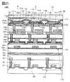
- FIG. 1 is a top view showing an example of a display device.
- 2A to 2E are top views showing examples of pixels.
- 3A and 3B are cross-sectional views showing an example of a display device.
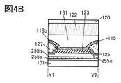
- 4A and 4B are cross-sectional views showing an example of the display device.
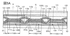
- 5A and 5B are cross-sectional views showing an example of the display device.
- 6A to 6C are cross-sectional views showing examples of display devices.
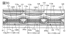
- 7A to 7C are cross-sectional views showing examples of display devices.
- 8A and 8B are cross-sectional views showing an example of a display device.
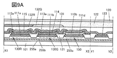
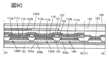
- 9A to 9C are cross-sectional views showing examples of display devices.
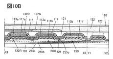
- 10A to 10C are cross-sectional views showing examples of display devices.
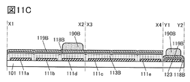
- 11A to 11D are cross-sectional views illustrating an example of a method for manufacturing a display device.
- 12A to 12C are cross-sectional views illustrating an example of a method for manufacturing a display device.
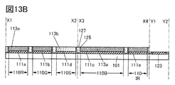
- 13A to 13C are cross-sectional views illustrating an example of a method for manufacturing a display device.
- 14A and 14B are perspective views showing an example of a display device.
- FIG. 15 is a cross-sectional view showing an example of a display device.
- FIG. 16 is a cross-sectional view showing an example of a display device.
- FIG. 17 is a cross-sectional view showing an example of a display device.
- FIG. 18 is a cross-sectional view showing an example of a display device.
- FIG. 15 is a cross-sectional view showing an example of a display device.
- FIG. 16 is a cross-sectional view showing an example of a display device.
- FIG. 17 is a cross-sectional view showing an example of a display device
- FIG. 19 is a cross-sectional view showing an example of a display device.
- FIG. 20 is a cross-sectional view showing an example of a display device.
- FIG. 21 is a perspective view showing an example of a display device.
- FIG. 22A is a cross-sectional view showing an example of a display device; 22B and 22C are cross-sectional views showing examples of transistors.
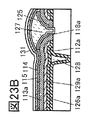
- 23A to 23D are cross-sectional views showing examples of display devices.
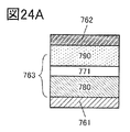
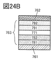
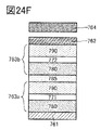
- 24A to 24F are diagrams showing configuration examples of light-emitting devices.
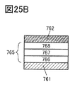
- 25A and 25B are diagrams showing configuration examples of light receiving devices.
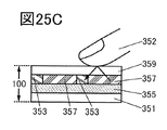
- 25C to 25E are diagrams showing configuration examples of display devices.
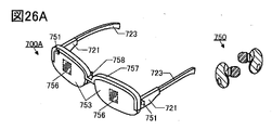
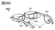
- 26A to 26D are diagrams illustrating examples of electronic devices.
- 27A to 27F are diagrams illustrating examples of electronic devices.
- 28A to 28G are diagrams illustrating examples of electronic devices.
- film and “layer” can be interchanged depending on the case or situation.
- conductive layer can be changed to the term “conductive film.”
- insulating film can be changed to the term “insulating layer”.
- a device manufactured using a metal mask or FMM may be referred to as a device with an MM (metal mask) structure.
- a device manufactured without using a metal mask or FMM may be referred to as a device with an MML (metal maskless) structure.
- an SBS side-by-side structure
- the material and structure can be optimized for each light-emitting device, so the degree of freedom in selecting the material and structure increases, and it becomes easy to improve luminance and reliability.
- holes or electrons are sometimes referred to as “carriers”.
- the hole injection layer or electron injection layer is referred to as a "carrier injection layer”
- the hole transport layer or electron transport layer is referred to as a “carrier transport layer”
- the hole blocking layer or electron blocking layer is referred to as a "carrier It is sometimes called a block layer.
- the carrier injection layer, the carrier transport layer, and the carrier block layer described above may not be clearly distinguished from each other due to their cross-sectional shape, characteristics, or the like.
- one layer may serve as two or three functions of the carrier injection layer, the carrier transport layer, and the carrier block layer.
- a display device of one embodiment of the present invention includes a display portion in which a first arrangement pattern and a second arrangement pattern are repeatedly arranged in a first direction.
- the first sub-pixels and the second sub-pixels are repeatedly arranged in the second direction.
- the third sub-pixel, fourth sub-pixel, and fifth sub-pixel are repeatedly arranged in the second direction.
- Each of the first to fourth sub-pixels has a light-emitting device
- the fifth sub-pixel has a light-receiving device.
- a display device of one embodiment of the present invention includes a display portion in which the first arrangement pattern and the second arrangement pattern are repeatedly arranged in the first direction.
- first sub-pixels, second sub-pixels, and third sub-pixels are repeatedly arranged in the second direction.
- the fourth sub-pixel and the fifth sub-pixel are repeatedly arranged in the second direction.
- Each of the first to fourth sub-pixels has a light-emitting device, and the fifth sub-pixel has a light-receiving device.
- a combination of the four sub-pixels also includes a configuration that respectively presents yellow (Y), cyan (C), magenta (M), and infrared (IR) light.
- a fifth sub-pixel may be configured to detect at least one of visible light and infrared light.
- a display device of one embodiment of the present invention includes a light-emitting device and a light-receiving device in a pixel.
- the display portion has a light receiving function, an image can be captured using the display portion.
- the display unit can capture an image while displaying the image.
- some of the sub-pixels can emit light as a light source, some of the other sub-pixels can detect light, and other sub-pixels can display an image.
- EL layers having the same structure are used for light-emitting devices that function as display devices, and colored layers are formed for each color of sub-pixels, whereby full-color display is realized. do.
- sub-pixels that emit R, G, and B light use light-emitting devices (e.g., white-light-emitting light-emitting devices) having EL layers with the same configuration, and color layers for R, G, and B are formed. This can be done by dividing. At this time, a light-emitting device that emits infrared light is used for the sub-pixel that emits IR light.
- light-emitting devices e.g., white-light-emitting light-emitting devices having EL layers with the same configuration, and color layers for R, G, and B are formed. This can be done by dividing. At this time, a light-emitting device that emits infrared light is used for the sub-pixel that emits IR light.
- one embodiment of the present invention includes a pixel having first to fifth subpixels, and the first subpixel includes a first light-emitting device and a first coloring layer.
- the first subpixel includes a first light-emitting device and a first coloring layer.
- a second subpixel having a second light emitting device and a second colored layer;
- a third subpixel having a third light emitting device and a third colored layer;
- a fourth subpixel having a third light emitting device and a third colored layer.
- Each pixel has a fourth light-emitting device, the first to third light-emitting devices all have EL layers with the same configuration, and the first to third colored layers are: each transmitting a different color of light, a fourth sub-pixel exhibiting infrared light, a fifth sub-pixel having a light receiving device, the light receiving device being the first to fourth sub-pixels is a display device capable of detecting light exhibited by at least one of
- light-emitting devices having EL layers having the same configuration may be used for sub-pixels that emit R, G, B, and IR light.
- sub-pixels that emit R, G, B, and IR light can all be realized by using light-emitting devices that emit both white light and infrared light, and separately creating colored layers for each of R, G, and B. can be done. Note that by stacking two or more colored layers of R, G, and B, a sub-pixel that blocks visible light and presents IR light can be realized.
- one embodiment of the present invention includes a pixel having first to fifth subpixels, and the first subpixel includes a first light-emitting device and a first coloring layer.
- a second subpixel having a second light emitting device and a second colored layer; a third subpixel having a third light emitting device and a third colored layer; and a fourth subpixel having a third light emitting device and a third colored layer.
- the pixel has a fourth light-emitting device and a fourth colored layer, the first to third colored layers transmit light of different colors, and the fourth colored layer Any two or more of the colored layers to the third colored layers are stacked, and the first to fourth light-emitting devices all have an EL layer with the same structure.
- a sub-pixel has a light-receiving device, and the light-receiving device has a function of detecting light exhibited by at least one of the first to fourth sub-pixels.
- an island-shaped light-emitting layer is provided in a subpixel having a light-emitting device
- an island-shaped active layer also referred to as a photoelectric conversion layer
- island-shaped light-emitting layers are formed according to the light-emitting device.
- the island-shaped light-emitting layer and the island-shaped active layer need to be separately formed according to the function of the subpixel.
- an island shape indicates a state in which two or more layers using the same material formed in the same step are physically separated.
- an island-shaped light-emitting layer means that the light-emitting layer is physically separated from an adjacent light-emitting layer.
- a layer other than the pixel electrode included in the light-emitting device can be shared by a plurality of sub-pixels.
- multiple sub-pixels can share a stretch of film.
- some of the layers included in light emitting devices are relatively highly conductive layers.
- a plurality of sub-pixels share a highly conductive layer as a continuous film, which may cause leakage current between sub-pixels.
- the display device has a high definition or a high aperture ratio and the distance between sub-pixels becomes small, the leak current becomes unignorable, and there is a possibility that the display quality of the display device is deteriorated.
- At least part of the layers included in the EL layer is formed in an island shape in each subpixel. At least part of the layers forming the EL layer are separated for each subpixel, so that crosstalk between adjacent subpixels can be suppressed. Accordingly, it is possible to achieve both high definition and high display quality of the display device.
- an island-shaped light-emitting layer can be formed by a vacuum deposition method using a metal mask.
- island-like formations occur due to various influences such as precision of the metal mask, misalignment between the metal mask and the substrate, bending of the metal mask, and broadening of the contour of the deposited film due to vapor scattering. Since the shape and position of the light-emitting layer deviate from the design, it is difficult to increase the definition and aperture ratio of the display device. Also, during deposition, the layer profile may be blurred and the edge thickness may be reduced. In other words, the thickness of the island-shaped light-emitting layer may vary depending on the location. In addition, when manufacturing a large-sized, high-resolution, or high-definition display device, there is a concern that the manufacturing yield will be low due to low dimensional accuracy of the metal mask and deformation due to heat or the like.
- the light-emitting layer is processed into a fine pattern by a photolithography method without using a shadow mask such as a metal mask. Specifically, after forming a pixel electrode for each sub-pixel, a light-emitting layer is formed over a plurality of pixel electrodes. After that, the light-emitting layer is processed by photolithography to form one island-shaped light-emitting layer for one pixel electrode. Thereby, the light-emitting layer is divided for each sub-pixel, and an island-shaped light-emitting layer can be formed for each sub-pixel.
- the light-emitting layer when processing the light-emitting layer into an island shape, a structure in which the light-emitting layer is processed using a photolithography method right above the light-emitting layer is conceivable. In the case of such a structure, the light-emitting layer may be damaged (damage due to processing, etc.) and the reliability may be significantly impaired.
- a layer located above the light-emitting layer for example, a carrier-transport layer or a carrier-injection layer, more specifically an electron-transport layer or an electron-injection layer
- a method of forming a sacrificial layer which may be referred to as a mask layer
- a highly reliable display device can be provided.
- the island-shaped light-emitting layer manufactured by the method for manufacturing a display device of one embodiment of the present invention is not formed using a metal mask having a fine pattern, but the light-emitting layer is formed over the entire surface. It is formed by processing after Specifically, the island-shaped light-emitting layer has a size obtained by dividing and miniaturizing using a photolithography method or the like. Therefore, the size can be made smaller than that which can be formed using a metal mask. Therefore, it is possible to realize a high-definition display device or a display device with a high aperture ratio, which has hitherto been difficult to achieve.
- the number of times of processing is small because the manufacturing cost can be reduced and the manufacturing yield can be improved.
- the light-emitting layer can be processed two or three times by photolithography; therefore, the display device can be manufactured with high yield.
- the distance between adjacent light-emitting devices can be narrowed down to Also, for example, by using an exposure apparatus for LSI, the distance between adjacent light emitting devices can be narrowed to 500 nm or less, 200 nm or less, 100 nm or less, or even 50 nm or less.
- the aperture ratio can be brought close to 100%.
- the aperture ratio can be 50% or more, 60% or more, 70% or more, 80% or more, or even 90% or more, and less than 100%.
- the pattern of the light-emitting layer itself (which can be said to be a processing size) can also be made much smaller than when a metal mask is used.
- the thickness of the light-emitting layer varies between the center and the edge. Become.
- the manufacturing method described above since a film having a uniform thickness is processed, an island-shaped light-emitting layer can be formed with a uniform thickness. Therefore, almost the entire area of even a fine pattern can be used as a light emitting region. Therefore, a display device having both high definition and high aperture ratio can be manufactured.
- the above-described manufacturing method can be applied to the light receiving device as well as the light emitting device.
- the island-shaped active layer of the light-receiving device is not formed using a metal mask with a fine pattern, but is formed by processing the film that will become the active layer over the entire surface.
- a shaped active layer can be formed with a uniform thickness. Further, by providing the sacrificial layer over the active layer, the damage to the active layer during the manufacturing process of the display device can be reduced, and the reliability of the light receiving device can be improved.
- FIG. 1 shows a top view of the display device 100.
- the display device 100 has a display section in which a plurality of pixels 110 are arranged in a matrix, and a connection section 140 outside the display section.
- One pixel 110 is composed of five sub-pixels 110R, 110G, 110B, 110IR, and 110S.
- FIG. 1 shows an example in which the connecting portion 140 is positioned below the display portion when viewed from above
- the connecting portion 140 may be provided at least one of the upper side, the right side, the left side, and the lower side of the display portion when viewed from above, and may be provided so as to surround the four sides of the display portion.
- the shape of the upper surface of the connecting portion 140 may be strip-shaped, L-shaped, U-shaped, frame-shaped, or the like.
- the number of connection parts 140 may be singular or plural.
- the top surface shape means a shape in plan view, that is, a shape seen from above.
- the top surface shape of the sub-pixel shown in FIG. 1 and the like corresponds to the top surface shape of the light emitting region or the light receiving region.
- top surface shapes of sub-pixels include triangles, quadrilaterals (including rectangles and squares), polygons such as pentagons, polygons with rounded corners, ellipses, and circles.
- the circuit layout forming the sub-pixels is not limited to the range of the sub-pixels shown in FIG.
- the transistors included in the sub-pixel 110R may be located within the sub-pixel 110R shown in FIG. 1, or some or all may be located outside the sub-pixel 110R.
- FIG. 1 shows an example in which one pixel 110 is composed of 3 rows and 2 columns.
- the pixel 110 has sub-pixels 110R in the first row, sub-pixels 110G in the second row, and sub-pixels 110B over the two rows.
- the third row has two sub-pixels (sub-pixels 110IR and 110S).
- the pixel 110 has three sub-pixels (sub-pixels 110R, 110G, 110S) in the left column (first column) and two sub-pixels (sub-pixels 110R, 110G, 110S) in the right column (second column). pixels 110B, 110IR).
- the first array pattern and the second array pattern are repeatedly arranged in the X direction.
- sub-pixels 110B and sub-pixels 110IR are repeatedly arranged in the Y direction.
- sub-pixels 110R, 110G, and 110S are repeatedly arranged in this order in the Y direction.
- the longitudinal direction (also referred to as the long-side direction) of the sub-pixel 110R, the sub-pixel 110G, and the sub-pixel 110S is the X direction.
- the longitudinal direction of the sub-pixel 110B is the Y direction.
- the sub-pixel 110R presents red light.
- the sub-pixel 110G presents green light.
- the sub-pixel 110B emits blue light.
- Sub-pixel 110IR exhibits infrared light.
- the sub-pixel 110S detects at least infrared light.
- the sub-pixel 110S may be capable of detecting both infrared light and visible light.
- Subpixels 110R, 110G, 110B, and 110IR each have a light emitting device and subpixel 110S has a light receiving device.
- an OLED Organic Light Emitting Diode
- a QLED Quadantum-dot Light Emitting Diode
- Light-emitting substances also referred to as light-emitting materials
- Light-emitting substances included in the light-emitting device include substances that emit fluorescence (fluorescent materials), substances that emit phosphorescence (phosphorescent materials), and substances that exhibit thermally activated delayed fluorescence (thermally activated delayed fluorescence). delayed fluorescence (TADF) material) and the like.
- an inorganic compound quantum dot material etc.
- LEDs such as micro LED (Light Emitting Diode), can also be used as a light emitting device.
- the emission color of the light emitting device can be infrared, red, green, blue, cyan, magenta, yellow, white, or the like.
- color purity can be enhanced by providing a light-emitting device with a microcavity structure.
- Embodiment Mode 4 can be referred to for the structure and material of the light-emitting device.
- a pn-type or pin-type photodiode can be used as the light receiving device.
- a light-receiving device functions as a photoelectric conversion device (also referred to as a photoelectric conversion element) that detects light incident on the light-receiving device and generates an electric charge. The amount of charge generated from the light receiving device is determined based on the amount of light incident on the light receiving device.
- the light receiving device can detect one or both of visible light and infrared light.
- visible light for example, one or more of blue, purple, blue-violet, green, yellow-green, yellow, orange, red, etc. light can be detected.
- infrared light it is possible to detect an object even in a dark place, which is preferable.
- organic photodiode having a layer containing an organic compound as the light receiving device.
- Organic photodiodes can be easily made thinner, lighter, and larger, and have a high degree of freedom in shape and design, so that they can be applied to various display devices.
- Embodiment 5 can be referred to for the configuration and material of the light receiving device.
- the pixel is capable of full color display using sub-pixels 110R, 110G and 110B.
- the layout of the sub-pixels 110R, 110G, and 110B is a so-called S-stripe arrangement. Thereby, high display quality can be realized.
- the sub-pixel 110IR can be used as a light source, and the infrared light emitted by the sub-pixel 110IR can be detected by the sub-pixel 110S.
- the sub-pixel 110IR may have the lowest aperture ratio among the five sub-pixels.
- the sub-pixels 110R, 110G, 110B, and 110S have equal or substantially equal aperture ratios (also referred to as sizes, sizes of light-emitting regions or light-receiving regions) in FIG. 1, one embodiment of the present invention is not limited thereto.
- the aperture ratios of the sub-pixels 110R, 110G, 110B, 110IR, and 110S can be determined as appropriate.
- the aperture ratios of the sub-pixels 110R, 110G, 110B, 110IR, and 110S may be different, and two or more may be equal or substantially equal.
- the sub-pixel 110S may have a higher aperture ratio than at least one of the sub-pixels 110R, 110G, and 110B.
- the size of the sub-pixel 110S may be larger than the size of the other sub-pixels depending on the resolution of the display device, the circuit configuration of the sub-pixels, and the like.
- the sub-pixel 110S may have a lower aperture ratio than at least one of the sub-pixels 110R, 110G, and 110B. If the light-receiving area of the sub-pixel 110S is narrow, the imaging range is narrowed, and blurring of the imaging result can be suppressed and the resolution can be improved. Therefore, high-definition or high-resolution imaging can be performed, which is preferable.
- FIG. 1 shows an example in which the aperture ratio of the sub-pixel 110IR is the lowest among the five sub-pixels.
- the light-emitting device may emit light using a passive matrix driving method. In other words, it is possible to reduce the size of the sub-pixel 110IR without providing a transistor or the like in the sub-pixel 110IR.
- FIG. 2A to 2E show other configuration examples of the pixel 110.
- FIG. 2A to 2E show other configuration examples of the pixel 110.
- Pixel 110 shown in FIGS. 2A-2E is composed of five sub-pixels, sub-pixels 110R, 110G, 110B, 110IR and 110S, respectively.
- a pixel 110 shown in FIG. 2A has a configuration in which the positions of the sub-pixel 110R and the sub-pixel 110G are exchanged in the pixel 110 shown in FIG.
- the pixel 110 shown in FIG. 2A has sub-pixels 110G in the first row, sub-pixels 110R in the second row, and sub-pixels 110B over the two rows. Also, the third row has two sub-pixels (sub-pixels 110IR and 110S). In other words, pixel 110 has three sub-pixels (sub-pixels 110G, 110R, 110S) in the left column (first column) and two sub-pixels (sub-pixels 110G, 110R, 110S) in the right column (second column). pixels 110B, 110IR).
- a pixel 110 shown in FIG. 2B has a configuration in which the sizes of the sub-pixel 110B and the sub-pixel 110IR are the same as in the pixel 110 shown in FIG.
- the pixel 110 shown in FIG. 2B has a sub-pixel 110R on the first row, a sub-pixel 110G on the second row, and a sub-pixel 110S on the third row.
- the sub-pixel 110B is provided from the middle of the first row to the second row
- the sub-pixel 110IR is provided from the middle of the second row to the third row.
- pixel 110 has three sub-pixels (sub-pixels 110G, 110R, 110S) in the left column (first column) and two sub-pixels (sub-pixels 110G, 110R, 110S) in the right column (second column). pixels 110B, 110IR).
- the pixel 110 shown in FIG. 2C has a configuration in which the sub-pixel 110S is larger than the sub-pixels 110R and 110G in the pixel 110 shown in FIG. 2A.
- the pixel 110 shown in FIG. 2C has sub-pixels 110R in the first row, sub-pixels 110G in the second row, and sub-pixels 110B over the two rows. Also, the third row has two sub-pixels (sub-pixels 110IR and 110S). In other words, the pixel 110 has three sub-pixels (sub-pixels 110R, 110G, 110S) in the left column (first column) and two sub-pixels (sub-pixels 110R, 110G, 110S) in the right column (second column). pixels 110B, 110IR).
- the first array pattern and the second array pattern are repeatedly arranged in the X direction, as in FIG. 1, 2B, and 2C, the sub-pixels 110R, 110G, and 110S are repeatedly arranged in this order in the Y direction, and in FIG. 2A, the sub-pixels 110G, 110R, and 110S are arranged in this order.
- the longitudinal direction of the sub-pixels 110R, 110G, and 110S is the X direction.
- the sub-pixels 110B and 110IR are repeatedly arranged in the Y direction, and the longitudinal direction of the sub-pixel 110B is the Y direction.
- the aperture ratio of the sub-pixel 110B and the aperture ratio of the sub-pixel 110IR are equal or approximately equal.
- the sub-pixel 110S has a higher aperture ratio than the sub-pixels 110R and 110G.
- the sub-pixel 110S has the highest aperture ratio among the sub-pixels 110R, 110G, 110B, 110IR, and 110S.
- FIG. 2B shows an example in which the aperture ratios of the sub-pixels 110G, 110R, and 110S are equal or approximately equal.
- 2D and 2E show an example in which one pixel 110 is configured in 2 rows and 3 columns.
- the pixel 110 has three sub-pixels (sub-pixels 110R, 110G, 110B) in the first row and two sub-pixels (sub-pixels 110IR, 110S) in the second row.
- pixel 110 has sub-pixel 110R in the left column (first column), sub-pixel 110G in the center column (second column), and sub-pixels from the left column to the center column. It has a pixel 110S.
- the right column third column
- the first array pattern and the second array pattern are repeatedly arranged in the Y direction.
- sub-pixels 110R, 110G, and 110B are repeatedly arranged in the X direction.
- sub-pixels 110IR and 110S are repeatedly arranged in the X direction.
- the longitudinal direction of the sub-pixels 110R, 110G, and 110B is the Y direction.
- the longitudinal direction of the sub-pixel 110S is the X direction.
- the pixel is capable of full color display using sub-pixels 110R, 110G and 110B.
- the layout of the sub-pixels 110R, 110G, and 110B is a so-called stripe arrangement. Thereby, high display quality can be realized.
- the sub-pixel 110IR can be used as a light source, and the infrared light emitted by the sub-pixel 110IR can be detected by the sub-pixel 110S.
- the sub-pixels 110R, 110G, 110B, and 110S all have the same or approximately the same aperture ratio. Further, among the sub-pixels 110R, 110G, 110B, 110IR, and 110S, the sub-pixel 110IR has the lowest aperture ratio.
- the aperture ratios of the sub-pixels 110R, 110G, 110B, and 110IR are all equal or substantially equal. Also, among the sub-pixels 110R, 110G, 110B, 110IR, and 110S, the sub-pixel 110S has the highest aperture ratio.
- the aperture ratios of the sub-pixels 110IR and 110S in FIG. 2D or FIG. 2E may be equal or substantially equal.
- Example of cross-sectional structure 3 to 10 illustrate examples of cross-sectional views of display devices of one embodiment of the present invention.
- FIG. 3A shows a cross-sectional view along the dashed-dotted line X1-X2 in FIG. 1
- FIG. 3B shows a cross-sectional view along the dashed-dotted line X3-X4 in FIG. 4A and 4B show cross-sectional views along the dashed-dotted line Y1-Y2 in FIG.
- the display device shown in FIGS. 3A and 3B includes a sub-pixel 110R that emits red light, a sub-pixel 110G that emits green light, a sub-pixel 110S that detects at least infrared light, a sub-pixel 110B that emits blue light, and , has a sub-pixel 110IR that exhibits infrared light.
- a display device of one embodiment of the present invention is a top emission type in which light is emitted in a direction opposite to a substrate over which a light-emitting device is formed, and light is emitted toward a substrate over which a light-emitting device is formed.
- a bottom emission type bottom emission type
- a double emission type dual emission type in which light is emitted from both sides may be used.
- a top emission display device is mainly described as an example.
- the sub-pixel 110R has a light-emitting device 130R and a colored layer 132R that transmits red light. As a result, light emitted from the light emitting device 130R is extracted as red light to the outside of the display device through the colored layer 132R.
- sub-pixel 110G has a light-emitting device 130G and a colored layer 132G that transmits green light. As a result, light emitted from the light emitting device 130G is extracted as green light to the outside of the display device through the colored layer 132G.
- the sub-pixel 110B has a light-emitting device 130B and a colored layer 132B that transmits blue light. Thereby, light emitted from the light emitting device 130B is extracted as blue light to the outside of the display device through the colored layer 132B.
- a full-color display can be performed using the sub-pixels 110R, 110G, and 110B.
- Subpixel 110IR has a light emitting device 130IR that emits infrared light. Therefore, light emitted from the light emitting device 130IR is extracted as infrared light to the outside of the display device without passing through the colored layer.
- the wavelength of the infrared light can be 750 nm or longer, preferably 780 nm or longer.
- infrared light it is particularly preferable to use near-infrared light with a wavelength of 750 nm or more and 2500 nm or less.
- the sub-pixel 110S has a light receiving device 150. As shown in FIG.
- the wavelength of light detected by the sub-pixel 110S is not particularly limited.
- the sub-pixel 110S detects at least one of visible light and infrared light.
- Light Lin enters the light receiving device 150 from the outside of the display device through the substrate 120 , the resin layer 122 and the protective layer 131 .
- the sub-pixel 110S preferably detects infrared light emitted by the sub-pixel 110IR.
- the sub-pixel 110IR can be used as a light source, and reflected light emitted by the light source can be detected by the sub-pixel 110S.
- an organic EL device is used as the light-emitting device and an organic photodiode is used as the light-receiving device.
- An organic EL device and an organic photodiode can be formed on the same substrate. Therefore, an organic photodiode can be incorporated in a display device using an organic EL device.
- a light-emitting device has an EL layer between a pair of electrodes.
- the EL layer has at least a light-emitting layer.
- a light receiving device has an active layer that functions at least as a photoelectric conversion layer between a pair of electrodes.
- one of a pair of electrodes may be referred to as a pixel electrode and the other may be referred to as a common electrode.
- each of the light-emitting device and the light-receiving device have, one electrode functions as an anode and the other electrode functions as a cathode.
- the light-receiving device can be driven by applying a reverse bias between the pixel electrode and the common electrode, thereby detecting light incident on the light-receiving device, generating electric charge, and extracting it as a current.
- the organic photodiode has many layers that can have the same configuration as the organic EL device, the layers that can have the same configuration can be formed at once, thereby suppressing an increase in the number of film forming steps.
- one of the pair of electrodes can be a layer common to the light receiving device and the light emitting device.
- at least one of a hole injection layer, a hole transport layer, a hole block layer, an electron block layer, an electron transport layer, and an electron injection layer can be used as a common layer in the light receiving device and the light emitting device. preferable.
- a layer shared by the light-receiving device and the light-emitting device may exist.
- Such layers may have different functions in light-emitting devices than in light-receiving devices.
- Components are sometimes referred to herein based on their function in the light emitting device.
- a hole-injecting layer functions as a hole-injecting layer in light-emitting devices and as a hole-transporting layer in light-receiving devices.
- an electron-injecting layer functions as an electron-injecting layer in light-emitting devices and as an electron-transporting layer in light-receiving devices.
- a layer shared by the light-receiving device and the light-emitting device may have the same function in the light-emitting device as in the light-receiving device.
- a hole-transporting layer functions as a hole-transporting layer in both a light-emitting device and a light-receiving device
- an electron-transporting layer functions as an electron-transporting layer in both a light-emitting device and a light-receiving device.
- the light emitting device 130R has a pixel electrode 111a, a first layer 113a, a common layer 114, and a common electrode 115.
- FIG. The light emitting device 130G also has a pixel electrode 111b, a first layer 113a, a common layer 114, and a common electrode 115.
- FIG. The light emitting device 130B also has a pixel electrode 111c, a first layer 113a, a common layer 114, and a common electrode 115.
- the light receiving device 150 has a pixel electrode 111 d, a second layer 113 b, a common layer 114 and a common electrode 115 .
- the light emitting device 130 IR also has a pixel electrode 111 e , a third layer 113 c , a common layer 114 and a common electrode 115 .
- the first layers 113a of the light emitting devices 130R, 130G, 130B are separated from each other.
- a layer provided in an island shape for each light-emitting device is referred to as a first layer 113a or a third layer 113c, which is shared by a plurality of light-emitting devices.
- the layer is shown as common layer 114 .
- the sub-pixels that emit R, G, and B light all use light-emitting devices having EL layers of the same configuration, and the sub-pixels that emit IR light use red EL layers. This is an example of using a light-emitting device that emits external light.
- the manufacturing steps of the display device can be reduced, and the manufacturing cost can be reduced and the manufacturing yield can be improved.
- a single structure or a tandem structure may be applied to the light-emitting device of this embodiment.
- the first layer 113a and the third layer 113c each have at least a light-emitting layer. Also, the first layer 113a and the third layer 113c are one of a hole injection layer, a hole transport layer, a hole blocking layer, a charge generation layer, an electron blocking layer, an electron transport layer, and an electron injection layer. You may have more than
- Light emitting devices 130R, 130G, 130B have a first layer 113a.
- the first layer 113a can have a luminescent material that emits blue light and a luminescent material that emits visible light at longer wavelengths than blue.
- the first layer 113a includes a luminescent material that emits blue light and a luminescent material that emits yellow light, or a luminescent material that emits blue light and a luminescent material that emits green light. , and a light-emitting material that emits red light.
- the light-emitting devices 130R, 130G, and 130B are, for example, single-structure light-emitting devices having two light-emitting layers, a light-emitting layer that emits yellow (Y) light and a light-emitting layer that emits blue (B) light, or A single-structure light-emitting device having three light-emitting layers, a light-emitting layer that emits red (R) light, a light-emitting layer that emits green (G) light, and a light-emitting layer that emits blue light, can be used.
- the order of the number of laminations and colors of the light-emitting layers may be a three-layer structure of R, G, and B or a three-layer structure of R, B, and G from the anode side.
- Another layer also referred to as a buffer layer
- the buffer layer can be formed using, for example, a material that can be used for the hole-transporting layer or the electron-transporting layer.
- a two-stage tandem structure having a light-emitting unit that emits yellow light and a light-emitting unit that emits blue light, a light-emitting unit that emits red and green light, and a light-emitting unit that emits blue light is used. or a light-emitting unit that emits blue light, a light-emitting unit that emits yellow, yellow-green, or green light, and red light, and a light-emitting unit that emits blue light.
- a three-stage tandem structure having, in this order, or the like can be applied.
- the number of stacked layers and the order of colors of the light emitting units are, from the anode side, a two-stage structure of B and Y, a two-stage structure of B and X, a three-stage structure of B, Y, and B, and a three-stage structure of B, X, and B.
- a three-stage structure is mentioned, and the order of the number of layers of light-emitting layers and the colors in the light-emitting unit X is, from the anode side, a two-layer structure of R and Y, a two-layer structure of R and G, and a two-layer structure of G and R. , G, R, and G, or a three-layer structure of R, G, and R, or the like.
- another layer may be provided between the two light-emitting layers.
- Light emitting device 130IR has a third layer 113c.
- the third layer 113c has a luminescent material that emits infrared light.
- the light-emitting device 130IR for example, a single-structure light-emitting device that emits infrared light or a tandem-structure light-emitting device having two or more light-emitting units that emit infrared light can be used.
- the light-emitting device 130IR can be configured to mainly emit infrared light. That is, the light emitting device 130IR can be configured to emit very weak or almost no visible light. Therefore, it is not necessary to provide the sub-pixel 110IR with a filter for blocking visible light.
- the first layer 113a or the third layer 113c has a plurality of light-emitting units.
- a charge generating layer is preferably provided between each light emitting unit.
- the light-emitting unit has at least one light-emitting layer.
- the light emitting device can emit white light.
- the light emitting unit may have one or more of a hole injection layer, a hole transport layer, a hole blocking layer, an electron blocking layer, an electron transport layer, and an electron injection layer.
- a light-emitting device configured to emit white light may emit light with a specific wavelength such as red, green, blue, or infrared light intensified.
- the first layer 113a and the third layer 113c may each have a hole injection layer, a hole transport layer, a light emitting layer, and an electron transport layer in that order. Moreover, you may have an electron block layer between a hole transport layer and a light emitting layer. Moreover, you may have an electron injection layer on the electron transport layer.
- each of the first layer 113a and the third layer 113c may have an electron injection layer, an electron transport layer, a light emitting layer, and a hole transport layer in this order.
- a hole blocking layer may be provided between the electron transport layer and the light emitting layer.
- a hole injection layer may be provided on the hole transport layer.
- Each of the first layer 113a and the third layer 113c preferably has a light-emitting layer and a carrier-transporting layer (electron-transporting layer or hole-transporting layer) over the light-emitting layer. Since the surfaces of the first layer 113a and the third layer 113c are exposed during the manufacturing process of the display device, the carrier-transporting layer is provided over the light-emitting layer to prevent the light-emitting layer from being exposed to the outermost surface. , the damage to the light-emitting layer can be reduced. This can improve the reliability of the light emitting device.
- the second layer 113b has at least an active layer. Since the second layer 113b of the light-receiving device can be manufactured independently of the first layer 113a and the third layer 113c of the light-emitting device, there is a wide range of materials that can be used. Note that various materials that can be used for the first layer 113a and the third layer 113c may be used for the second layer 113b.
- the second layer 113b includes a hole injection layer, a hole transport layer, a hole block layer, a charge generation layer, an electron block layer, an electron transport layer, which can be used in the first layer 113a and the third layer 113c. and an electron injection layer.
- the common layer 114 has, for example, an electron injection layer or a hole injection layer.
- the common layer 114 may have a laminate of an electron transport layer and an electron injection layer, or may have a laminate of a hole transport layer and a hole injection layer.
- Common layer 114 is shared by light emitting devices 130 R, 130 G, 130 B, 130 IR and light receiving device 150 .
- the end of the pixel electrode preferably has a tapered shape.
- the first layer 113a, the second layer 113b, and the third layer 113c provided along the side surface of the pixel electrode also have a tapered shape.
- the side surface of the pixel electrode coverage with the first layer 113a, the second layer 113b, and the third layer 113c provided along the side surface of the pixel electrode can be improved.
- the side surface of the pixel electrode is tapered because foreign matter (eg, dust or particles) in the manufacturing process can be easily removed by a treatment such as cleaning.
- a tapered shape refers to a shape in which at least part of a side surface of a structure is inclined with respect to a substrate surface or a formation surface.
- insulation is provided between the pixel electrode 111a and the first layer 113a, between the pixel electrode 111b and the first layer 113a, and between the pixel electrode 111d and the second layer 113b. not covered by a layer. Therefore, the distance between adjacent light-emitting devices and the distance between adjacent light-emitting devices and light-receiving devices can be made extremely narrow. Therefore, a high-definition or high-resolution display device can be obtained. Moreover, a mask for forming the insulating layer is not required, and the manufacturing cost of the display device can be reduced.
- the viewing angle dependency of the display device of one embodiment of the present invention can be extremely reduced. By reducing the viewing angle dependency, it is possible to improve the visibility of the image on the display device.
- the viewing angle (the maximum angle at which a constant contrast ratio is maintained when the screen is viewed obliquely) is 100° or more and less than 180°, preferably 150°. It can be in the range of 170° or more. It should be noted that the above viewing angle can be applied to each of the vertical and horizontal directions.
- the common electrode 115 is shared by the light emitting devices 130R, 130G, 130B, 130IR and the light receiving device 150.
- FIG. A common electrode 115 shared by a plurality of light-emitting devices and light-receiving devices is electrically connected to the conductive layer 123 provided in the connecting portion 140 (see FIGS. 4A and 4B).
- the conductive layer 123 is preferably formed using the same material and in the same process as the pixel electrode.
- FIG. 4A shows an example in which a common layer 114 is provided on the conductive layer 123 and the conductive layer 123 and the common electrode 115 are electrically connected through the common layer 114 .
- the common layer 114 may not be provided in the connection portion 140 .
- conductive layer 123 and common electrode 115 are directly connected.
- a mask also referred to as an area mask or a rough metal mask to distinguish from a fine metal mask
- the common layer 114 and the common electrode 115 are formed into a region where a film is formed. can be changed.
- FIG. 5A shows a cross-sectional view along the dashed-dotted line X1-X2 in FIG. 1
- FIG. 5B shows a cross-sectional view along the dashed-dotted line X3-X4 in FIG.
- the cross-sectional structure shown in FIG. 5A is the same as in FIG. 3A.
- the cross-sectional structure shown in FIG. 5B is that the light-emitting device 130IR does not have the third layer 113c but has the first layer 113a, and that the sub-pixel 110IR is provided with the colored layer 132V. Different from 3B.
- FIGS. 5A and 5B are examples in which light-emitting devices having EL layers with the same configuration are used for sub-pixels exhibiting R, G, B, and IR light.
- the manufacturing steps of the display device can be reduced, and the manufacturing cost can be reduced and the manufacturing yield can be improved.
- the sub-pixel 110IR has a light-emitting device 130IR and a colored layer 132V that transmits infrared light. Thereby, light emitted from the light emitting device 130IR is extracted as infrared light to the outside of the display device through the colored layer 132V.
- the colored layer 132V has a function as a visible light cut filter.
- FIG. 5B shows an example in which a colored layer 132G and a colored layer 132R are laminated as the colored layer 132V.
- the colored layer 132V is not particularly limited as long as it blocks visible light and transmits infrared light. For example, by stacking two or more of the colored layers 132R, 132G, and 132B, the number of steps can be reduced compared to the case of separately forming the colored layer 132V, which is preferable.
- the first layer 113a can have a luminescent material that emits blue light, a luminescent material that emits visible light with wavelengths longer than blue, and a luminescent material that emits infrared light.
- the first layer 113a includes a luminescent material that emits blue light, a luminescent material that emits yellow light, and a luminescent material that emits infrared light, or a luminescent material that emits blue light.
- a structure including a luminescent material that emits green light, a luminescent material that emits red light, and a luminescent material that emits infrared light, or the like can be applied.
- the light-emitting devices 130R, 130G, 130B, and 130IR include, for example, a light-emitting layer that emits yellow (Y) light, a light-emitting layer that emits blue (B) light, and a light-emitting layer that emits infrared light (IR).
- a single-structure light-emitting device having three light-emitting layers, or a light-emitting layer that emits red (R) light, a light-emitting layer that emits green (G) light, a light-emitting layer that emits blue light, and a light-emitting layer that emits infrared light A single structure light emitting device having four light emitting layers can be used.
- the number of luminescent layers and the order of colors may be a four-layer structure of IR, R, G, and B or a four-layer structure of IR, R, B, and G from the anode side.
- another layer may be provided between the two light-emitting layers.
- tandem structure light-emitting device In the case of using a tandem structure light-emitting device, a two-stage tandem structure having a light-emitting unit that emits infrared light and yellow light and a light-emitting unit that emits blue light, a light-emitting unit that emits infrared light, and a light-emitting unit that emits yellow light.
- a three-stage tandem structure or the like having a light-emitting unit that emits yellow-green or green light, red light, and infrared light, and a light-emitting unit that emits blue light in this order can be applied.
- a configuration in which an IR light-emitting unit is further added, or a configuration in which a light-emitting layer that emits IR light is added to the light-emitting unit X etc. can be applied.
- an insulating layer is provided on a layer 101 including a transistor, a light emitting device and a light receiving device are provided on the insulating layer, and the light emitting device and the light receiving device are provided.
- a protective layer 131 is provided to cover. Colored layers 132 R, 132 G, and 132 B are provided on the protective layer 131 , and the substrate 120 is bonded with the resin layer 122 . Also, an insulating layer 125 and an insulating layer 127 on the insulating layer 125 are provided in a region between adjacent light emitting devices and a region between the light emitting device and the light receiving device.
- 3A and 3B and the like show a plurality of cross sections of the insulating layer 125 and the insulating layer 127.
- the insulating layer 125 and the insulating layer 127 are each connected to one. . That is, the display device can have, for example, one insulating layer 125 and one insulating layer 127 .
- the display device may have a plurality of insulating layers 125 separated from each other, and may have a plurality of insulating layers 127 separated from each other.
- a stacked-layer structure in which a plurality of transistors are provided over a substrate and an insulating layer is provided to cover the transistors can be applied.
- An insulating layer over a transistor may have a single-layer structure or a stacked-layer structure.
- 3A and the like show an insulating layer 255a, an insulating layer 255b over the insulating layer 255a, and an insulating layer 255c over the insulating layer 255b among the insulating layers over the transistor.
- These insulating layers may have recesses between adjacent light-emitting devices and between light-emitting and light-receiving devices.
- the insulating layers (the insulating layers 255a to 255c) over the transistors may also be regarded as part of the layer 101 including the transistors.
- various inorganic insulating films such as an oxide insulating film, a nitride insulating film, an oxynitride insulating film, and a nitride oxide insulating film can be preferably used.
- an oxide insulating film or an oxynitride insulating film such as a silicon oxide film, a silicon oxynitride film, or an aluminum oxide film is preferably used.
- a nitride insulating film or a nitride oxide insulating film such as a silicon nitride film or a silicon nitride oxide film is preferably used. More specifically, a silicon oxide film is preferably used for the insulating layers 255a and 255c, and a silicon nitride film is preferably used for the insulating layer 255b.
- the insulating layer 255b preferably functions as an etching protection film.
- oxynitride refers to a material whose composition contains more oxygen than nitrogen
- nitride oxide refers to a material whose composition contains more nitrogen than oxygen. point to the material.
- silicon oxynitride refers to a material whose composition contains more oxygen than nitrogen
- silicon nitride oxide refers to a material whose composition contains more nitrogen than oxygen. indicates
- FIG. 1 A structural example of the layer 101 including a transistor will be described later in Embodiments 3 and 4.
- FIG. 1 A structural example of the layer 101 including a transistor will be described later in Embodiments 3 and 4.
- FIG. 1 A structural example of the layer 101 including a transistor will be described later in Embodiments 3 and 4.
- the protective layer 131 may have a single layer structure or a laminated structure of two or more layers.
- the conductivity of the protective layer 131 does not matter. At least one of an insulating film, a semiconductor film, and a conductive film can be used as the protective layer 131 .
- the protective layer 131 Since the protective layer 131 has an inorganic film, it prevents oxidation of the common electrode 115, prevents impurities (such as moisture and oxygen) from entering the light-emitting device and the light-receiving device, and suppresses deterioration of the light-emitting device. The reliability of the display device can be improved.
- an inorganic insulating film such as an oxide insulating film, a nitride insulating film, an oxynitride insulating film, or a nitride oxide insulating film can be used.
- oxide insulating films include silicon oxide films, aluminum oxide films, magnesium oxide films, gallium oxide films, germanium oxide films, yttrium oxide films, zirconium oxide films, lanthanum oxide films, neodymium oxide films, hafnium oxide films, and tantalum oxide films.
- the nitride insulating film include a silicon nitride film and an aluminum nitride film.
- Examples of the oxynitride insulating film include a silicon oxynitride film, an aluminum oxynitride film, and the like.
- Examples of the nitride oxide insulating film include a silicon nitride oxide film, an aluminum nitride oxide film, and the like.
- the protective layer 131 preferably includes a nitride insulating film or a nitride oxide insulating film, and more preferably includes a nitride insulating film.
- the protective layer 131 includes In—Sn oxide (also referred to as ITO), In—Zn oxide, Ga—Zn oxide, Al—Zn oxide, or indium gallium zinc oxide (In—Ga—Zn oxide).
- ITO In—Sn oxide
- In—Zn oxide Ga—Zn oxide
- Al—Zn oxide Al—Zn oxide
- indium gallium zinc oxide In—Ga—Zn oxide
- An inorganic film containing a material such as IGZO can also be used.
- the inorganic film preferably has a high resistance, and specifically, preferably has a higher resistance than the common electrode 115 .
- the inorganic film may further contain nitrogen.
- the protective layer 131 When the light emitted from the light-emitting device is taken out through the protective layer 131, the protective layer 131 preferably has high transparency to visible light.
- the protective layer 131 preferably has high transparency to visible light.
- ITO, IGZO, and aluminum oxide are preferable because they are inorganic materials with high transparency to visible light.
- the protective layer 131 for example, a stacked structure of an aluminum oxide film and a silicon nitride film over the aluminum oxide film, or a stacked structure of an aluminum oxide film and an IGZO film over the aluminum oxide film, or the like can be used. can be done. By using the stacked structure, entry of impurities (such as water and oxygen) into the EL layer can be suppressed.
- impurities such as water and oxygen
- the protective layer 131 may have an organic film.
- protective layer 131 may have both an organic film and an inorganic film.
- the protective layer 131 may have a two-layer structure formed using different film formation methods. Specifically, the first layer of the protective layer 131 may be formed using an atomic layer deposition (ALD) method, and the second layer of the protective layer 131 may be formed using a sputtering method. .
- ALD atomic layer deposition
- the insulating layer 125 can be in contact with side surfaces of the first layer 113a, the second layer 113b, and the third layer 113c.
- the insulating layer 125 or the insulating layer 127 is in contact with the first layer 113a, the second layer 113b, and the third layer 113c, so that the first layer 113a, the second layer 113b, and the third layer 113b are formed. It is possible to prevent peeling of the layer 113c.
- the insulating layer and the first layer 113a, the second layer 113b, or the third layer 113c are in close contact with each other, so that the adjacent first layers 113a and the like are fixed or bonded by the insulating layer. effective. Thereby, the reliability of the light-emitting device and the light-receiving device can be improved. Moreover, the manufacturing yield of the light-emitting device and the light-receiving device can be increased.
- the end of the pixel electrode is covered with the first layer 113a, the second layer 113b, or the third layer 113c, and the insulating layer 125 covers the first layer 113a or the second layer 113c.
- a structure in contact with the side surfaces of the layer 113b and the third layer 113c is shown.
- the insulating layer 127 is provided on the insulating layer 125 so as to fill the recesses of the insulating layer 125 .
- the insulating layer 127 can overlap with (it can be said to cover) side surfaces of the first layer 113a, the second layer 113b, and the third layer 113c with the insulating layer 125 interposed therebetween.
- the insulating layer 127 may further overlap the side surface of the pixel electrode with the insulating layer 125 interposed therebetween.
- the space between the adjacent island-shaped layers can be filled; can be reduced and made flatter. Therefore, it is possible to improve the coverage of the carrier injection layer, the common electrode, and the like, and prevent the common electrode from being disconnected.
- discontinuity refers to a phenomenon in which a layer, film, or electrode is divided due to the shape of a formation surface (for example, a step).
- the common layer 114 and the common electrode 115 are provided over the first layer 113 a , the second layer 113 b , the third layer 113 c , the insulating layer 125 and the insulating layer 127 .
- a region where the pixel electrode and the first layer 113a, the second layer 113b, or the third layer 113c are provided and a region where they are not provided ( (regions between light-emitting devices, regions between light-receiving devices, and regions between light-emitting devices and light-receiving devices).
- the steps can be planarized, and coverage with the common layer 114 and the common electrode 115 can be improved. Therefore, it is possible to suppress a connection failure due to step disconnection of the common electrode 115 . In addition, it is possible to prevent the common electrode 115 from being locally thinned due to the steps and increasing the electrical resistance.
- each of the insulating layer 125 and the insulating layer 127 can be applied to each of the insulating layer 125 and the insulating layer 127 .
- the top surface of the insulating layer 125 and the top surface of the insulating layer 127 are respectively higher than the first layer 113a and the second layer 113b.
- the third layer 113c (which can be called the height of the edge of the upper surface) at each edge of the upper surface, or substantially the same.
- the upper surface of the insulating layer 127 may have a flat shape, or may have a convex portion, a convex curved surface, a concave curved surface, or a concave portion.
- the sacrificial layer 118a is positioned on the first layer 113a
- the sacrificial layer 118b is positioned on the second layer 113b
- the sacrificial layer 118c is positioned on the third layer 113c.
- one end of the sacrificial layer 118a is aligned or substantially aligned with the end of the first layer 113a
- the other end of the sacrificial layer 118a is on the first layer 113a.
- part of the sacrificial layer used to protect the first layer 113a, the second layer 113b, and the third layer 113c used in manufacturing the display device remains.
- the sacrificial layer may remain, for example, between first layer 113a, second layer 113b, or third layer 113c and insulating layer 125 or insulating layer 127.
- FIG. The sacrificial layer will be described in detail in the second embodiment.
- 6A to 6C show cross-sectional structures of regions including the insulating layer 127 and its periphery.
- the pixel electrodes 111a and 111b have tapered shapes.
- a first layer 113a is provided to cover an end portion of the pixel electrode 111a, and the first layer 113a also has a tapered portion.
- a first layer 113a is provided to cover the end of the pixel electrode 111b, and the first layer 113a also has a tapered portion.
- a sacrificial layer 118a is provided over the first layer 113a, and the sacrificial layer 118a has a portion overlapping with the pixel electrode 111a or the pixel electrode 111b with the first layer 113a interposed therebetween. Note that the sacrificial layer 118a does not have to overlap with the pixel electrode 111a or the pixel electrode 111b.
- An insulating layer 125 is provided to cover the first layer 113a, the sacrificial layer 118a, and the insulating layer 255c.
- the insulating layer 125 is in contact with the top and side surfaces of the sacrificial layer 118a, the side surfaces of the first layer 113a, and the top surface of the insulating layer 255c.
- An insulating layer 127 is provided over the insulating layer 125 .
- the insulating layer 127 overlaps with the pixel electrodes 111a and 111b, the first layer 113a, and the sacrificial layer 118a with the insulating layer 125 interposed therebetween.
- One or both of the insulating layer 125 and the insulating layer 127 cover not only the side surface of the first layer 113a but also the top surface thereof, so that peeling of the first layer 113a can be further prevented, and reliability of the light-emitting device can be improved. can increase Moreover, the manufacturing yield of the light-emitting device can be further increased. Note that the insulating layers 125 and 127 do not have to overlap with the pixel electrodes 111a and 111b, the first layer 113a, and the sacrificial layer 118a.
- a common layer 114 and a common electrode 115 are provided over the first layer 113 a and the insulating layer 127 .
- FIG. 6A shows an example in which the edge of the sacrificial layer 118a and the edge of the insulating layer 125 are substantially perpendicular to the surface of the first layer 113a.
- the end of the sacrificial layer 118a and the end of the insulating layer 125 preferably have a tapered shape. Thereby, the coverage of the common layer 114 and the common electrode 115 can be further improved.
- FIG. 6A shows an example in which the upper surface of the insulating layer 127 has a convex curved surface.
- the top surface of the insulating layer 127 may have both convex and concave surfaces.
- Insulating layer 125 can be an insulating layer comprising an inorganic material.
- the insulating layer 125 may have a single-layer structure or a laminated structure.
- an inorganic insulating film such as an oxide insulating film, a nitride insulating film, an oxynitride insulating film, or a nitride oxide insulating film can be used, for example. Details of these inorganic insulating films are as described in the description of the protective layer 131 .
- aluminum oxide is preferable because it has a high etching selectivity with respect to the EL layer and has a function of protecting the EL layer when the insulating layer 127 is formed.
- an inorganic insulating film such as an aluminum oxide film, a hafnium oxide film, or a silicon oxide film formed by an ALD method to the insulating layer 125
- the insulating layer 125 has few pinholes and has an excellent function of protecting the EL layer. can be formed.
- the insulating layer 125 may have a layered structure of a film formed by an ALD method and a film formed by a sputtering method.
- the insulating layer 125 may have a laminated structure of, for example, an aluminum oxide film formed by ALD and a silicon nitride film formed by sputtering.
- the insulating layer 125 preferably functions as a barrier insulating layer against at least one of water and oxygen. Further, the insulating layer 125 preferably has a function of suppressing diffusion of at least one of water and oxygen. Further, the insulating layer 125 preferably has a function of capturing or fixing at least one of water and oxygen (also referred to as gettering).
- a barrier insulating layer means an insulating layer having a barrier property.
- barrier property refers to a function of suppressing diffusion of a corresponding substance (also referred to as low permeability).
- the corresponding substance has a function of capturing or fixing (also called gettering).
- the insulating layer 125 has a function as a barrier insulating layer or a gettering function, thereby suppressing entry of impurities (typically, at least one of water and oxygen) that can diffuse into the light-emitting device and the light-receiving device from the outside. It becomes a configuration that can be done. With such a structure, a highly reliable light-emitting device and a highly reliable light-receiving device as well as a highly reliable display device can be provided.
- impurities typically, at least one of water and oxygen
- the insulating layer 125 preferably has a low impurity concentration. Accordingly, it is possible to suppress deterioration of the EL layer due to entry of impurities from the insulating layer 125 into the EL layer. In addition, by reducing the impurity concentration in the insulating layer 125, the barrier property against at least one of water and oxygen can be improved.
- the insulating layer 125 preferably has a sufficiently low hydrogen concentration or carbon concentration, or preferably both.
- the insulating layer 127 provided on the insulating layer 125 has a function of planarizing recesses of the insulating layer 125 formed between adjacent light emitting devices and between a light emitting device and a light receiving device. In other words, the presence of the insulating layer 127 has the effect of improving the flatness of the surface on which the common electrode 115 is formed.
- an insulating layer containing an organic material can be preferably used.
- acrylic resin, polyimide resin, epoxy resin, imide resin, polyamide resin, polyimideamide resin, silicone resin, siloxane resin, benzocyclobutene-based resin, phenolic resin, and precursors of these resins are applied. can do.
- an organic material such as polyvinyl alcohol (PVA), polyvinyl butyral, polyvinylpyrrolidone, polyethylene glycol, polyglycerin, pullulan, water-soluble cellulose, or alcohol-soluble polyamide resin may be used as the insulating layer 127 .
- a photosensitive resin can be used as the insulating layer 127 .
- a photoresist may be used as the photosensitive resin.
- a positive material or a negative material can be used for the photosensitive resin.
- a material that absorbs visible light may be used for the insulating layer 127 . Since the insulating layer 127 absorbs light emitted from the light emitting device, leakage of light (stray light) from the light emitting device to an adjacent light emitting device via the insulating layer 127 can be suppressed. Thereby, the display quality of the display device can be improved. In addition, since the display quality can be improved without using a polarizing plate for the display device, the weight and thickness of the display device can be reduced. In addition, it is possible to suppress the incidence of light from the light-emitting device to the adjacent light-receiving device through the insulating layer 127 . Thereby, the accuracy of light detection of the display device can be improved.
- Materials that absorb visible light include materials containing pigments such as black, materials containing dyes, light-absorbing resin materials (e.g., polyimide), and resin materials that can be used for color filters (color filter materials ).
- materials containing pigments such as black, materials containing dyes, light-absorbing resin materials (e.g., polyimide), and resin materials that can be used for color filters (color filter materials ).
- resin materials that can be used for color filters color filter materials.
- a light shielding layer may be provided on the surface of the substrate 120 on the resin layer 122 side.
- various optical members can be arranged outside the substrate 120 .
- optical members include polarizing plates, retardation plates, light diffusion layers (diffusion films, etc.), antireflection layers, light collecting films, and the like.
- an antistatic film that suppresses adhesion of dust, a water-repellent film that prevents adhesion of dirt, a hard coat film that suppresses the occurrence of scratches due to use, a shock absorption layer, etc. Layers may be arranged.
- a glass layer or a silica layer (SiO x layer) as a surface protective layer, because surface contamination and scratching can be suppressed.
- the surface protective layer DLC (diamond-like carbon), aluminum oxide (AlO x ), polyester-based material, polycarbonate-based material, or the like may be used.
- a material having a high visible light transmittance is preferably used for the surface protective layer.
- Glass, quartz, ceramics, sapphire, resin, metal, alloy, semiconductor, or the like can be used for the substrate 120 .
- a material that transmits the light is used for the substrate on the side from which the light from the light-emitting device is extracted.
- a flexible material is used for the substrate 120, the flexibility of the display device can be increased and a flexible display can be realized.
- a polarizing plate may be used as the substrate 120 .
- polyester resins such as polyethylene terephthalate (PET) and polyethylene naphthalate (PEN), polyacrylonitrile resins, acrylic resins, polyimide resins, polymethyl methacrylate resins, polycarbonate (PC) resins, and polyethersulfone (PES) resins.
- polyamide resin nylon, aramid, etc.
- polysiloxane resin cycloolefin resin
- polystyrene resin polyamideimide resin
- polyurethane resin polyvinyl chloride resin
- polyvinylidene chloride resin polypropylene resin
- PTFE polytetrafluoroethylene
- ABS resin cellulose nanofiber, etc.
- glass having a thickness that is flexible may be used.
- a substrate having high optical isotropy is preferably used as the substrate of the display device.
- a substrate with high optical isotropy has small birefringence (it can be said that the amount of birefringence is small).
- the absolute value of the retardation (retardation) value of the substrate with high optical isotropy is preferably 30 nm or less, more preferably 20 nm or less, and even more preferably 10 nm or less.
- Films with high optical isotropy include triacetylcellulose (TAC, also called cellulose triacetate) films, cycloolefin polymer (COP) films, cycloolefin copolymer (COC) films, and acrylic films.
- TAC triacetylcellulose
- COP cycloolefin polymer
- COC cycloolefin copolymer
- the film when a film is used as the substrate, the film may absorb water, which may cause shape change such as wrinkles in the display device. Therefore, it is preferable to use a film having a low water absorption rate as the substrate. For example, it is preferable to use a film with a water absorption of 1% or less, more preferably 0.1% or less, and even more preferably 0.01% or less.
- various curable adhesives such as photocurable adhesives such as ultraviolet curable adhesives, reaction curable adhesives, thermosetting adhesives, and anaerobic adhesives can be used.
- These adhesives include epoxy resins, acrylic resins, silicone resins, phenol resins, polyimide resins, imide resins, PVC (polyvinyl chloride) resins, PVB (polyvinyl butyral) resins, EVA (ethylene vinyl acetate) resins, and the like.
- a material with low moisture permeability such as epoxy resin is preferable.
- a two-liquid mixed type resin may be used.
- an adhesive sheet or the like may be used.
- Examples of materials that can be used for conductive layers such as gates, sources and drains of transistors as well as various wirings and electrodes that constitute display devices include aluminum, titanium, chromium, nickel, copper, yttrium, zirconium, molybdenum, Metals such as silver, tantalum, and tungsten, and alloys based on these metals are included. Films containing one or more of these materials can be used in single layers or as laminated structures.
- a conductive oxide such as indium oxide, indium tin oxide, indium zinc oxide, zinc oxide, zinc oxide containing gallium, or graphene
- metal materials such as gold, silver, platinum, magnesium, nickel, tungsten, chromium, molybdenum, iron, cobalt, copper, palladium, and titanium, or alloy materials containing such metal materials can be used.
- a nitride of the metal material eg, titanium nitride
- it is preferably thin enough to have translucency.
- a stacked film of any of the above materials can be used as the conductive layer.
- a laminated film of a silver-magnesium alloy and indium tin oxide because the conductivity can be increased.
- conductive layers such as various wirings and electrodes that constitute a display device, and conductive layers (conductive layers functioning as pixel electrodes or counter electrodes) of light-emitting devices.
- Examples of insulating materials that can be used for each insulating layer include resins such as acrylic resins and epoxy resins, and inorganic insulating materials such as silicon oxide, silicon oxynitride, silicon nitride oxide, silicon nitride, and aluminum oxide.
- FIG. 3A and the like show examples in which colored layers 132R, 132G, and 132B are directly provided on light-emitting devices 130R, 130G, and 130B with a protective layer 131 interposed therebetween.
- a protective layer 131 interposed therebetween.
- FIG. 7A to 7C show cross-sectional views along the dashed-dotted line X1-X2 in FIG.
- a substrate 120 provided with a colored layer may be attached to a protective layer 131 with a resin layer 122 .
- the temperature of the heat treatment in the step of forming the colored layer can be increased.
- the display may be provided with a lens array 133, as shown in FIGS. 7B and 7C.
- the lens array 133 can be provided by stacking one or both of the light emitting device and the light receiving device.
- the colored layers 132R and 132G are provided on the light emitting devices 130R and 130G through the protective layer 131, the insulating layer 134 is provided on the colored layers 132R and 132G, and the lens array 133 is provided on the insulating layer 134.
- the lens array 133 is also provided on the light receiving device 150 with the protective layer 131 and the insulating layer 134 interposed therebetween.
- the colored layer 132R, the colored layer 132G, and the lens array 133 By forming the colored layer 132R, the colored layer 132G, and the lens array 133 directly on the substrate on which the light-emitting device and the light-receiving device are formed, alignment of the light-emitting device or the light-receiving device and the colored layer or the lens array can be performed. Accuracy can be improved.
- Either or both of an inorganic insulating film and an organic insulating film can be used for the insulating layer 134 .
- the insulating layer 134 may have a single-layer structure or a laminated structure.
- a material that can be used for the protective layer 131 can be used. Since the light emitted from the light-emitting device is extracted through the insulating layer 134, the insulating layer 134 preferably has high transparency to visible light.
- the light emitted from the light-emitting device is transmitted through the colored layer and then through the lens array 133 to be extracted to the outside of the display panel.
- the lens array 133 may be provided over the light-emitting device and the colored layer may be provided over the lens array 133 .
- FIG. 7C is an example in which the substrate 120 provided with the colored layer 132R, the colored layer 132G, and the lens array 133 is bonded onto the protective layer 131 with the resin layer 122.
- FIG. 7C By providing the colored layer 132R, the colored layer 132G, and the lens array 133 over the substrate 120, the temperature of the heat treatment in these formation steps can be increased.
- FIG. 7C shows an example in which colored layers 132R and 132G are provided in contact with the substrate 120, an insulating layer 134 is provided in contact with the colored layers 132R and 132G, and a lens array 133 is provided in contact with the insulating layer 134.
- the light emitted from the light emitting device passes through the lens array 133 and then through the colored layer, and is taken out of the display panel.
- the lens array 133 may be provided in contact with the substrate 120
- the insulating layer 134 may be provided in contact with the lens array 133
- the colored layer may be provided in contact with the insulating layer 134 .
- the light emitted from the light-emitting device is transmitted through the colored layer and then through the lens array 133 to be extracted to the outside of the display panel.
- FIG. By providing regions where colored layers of different colors overlap, color mixture of light emitted from the light-emitting device can be suppressed.
- the convex surface of the lens array 133 may face the substrate 120 side or the light emitting device side.
- the lens array 133 can be formed using at least one of an inorganic material and an organic material.
- a material containing resin can be used for the lens.
- a material containing at least one of an oxide and a sulfide can be used for the lens.
- a microlens array can be used as the lens array 133.
- the lens array 133 may be formed directly on the substrate or the light-emitting device, or may be bonded with a separately formed lens array.
- FIG. 3A and the like show an example in which the ends of the first layer 113a, the second layer 113b, and the third layer 113c are located outside the ends of the pixel electrodes. In FIG.
- the first layer 113a, the second layer 113b, and the third layer 113c are formed so as to cover the ends of the pixel electrodes.
- the end portion of the first layer 113a, the end portion of the second layer 113b, and the end portion of the third layer 113c are located inside the end portions of the pixel electrode. In comparison, the aperture ratio can be increased.
- the distance between the light emitting region of the first layer 113a (that is, the region overlapping with the pixel electrode) and the edge of the first layer 113a can be increased.
- An end portion of the first layer 113a includes a portion that may be damaged during the manufacturing process of the display device. By not using the portion as a light-emitting region, variation in characteristics of the light-emitting device can be suppressed, and reliability can be improved. The same can be said for the third layer 113c.
- the distance between the light receiving region of the second layer 113b (that is, the region overlapping with the pixel electrode) and the edge of the second layer 113b can be increased, so reliability can be improved.
- FIG. 8A and 8B show side by side a cross-sectional view between the dashed-dotted line X1-X2 and a cross-sectional view between the dashed-dotted line Y1-Y2 in FIG.
- FIG. 8A shows an example in which the edge of the upper surface of the pixel electrode, the edge of the first layer 113a, and the edge of the second layer 113b are aligned or substantially aligned.
- FIG. 8A shows an example in which the end portions of the first layer 113a and the end portions of the second layer 113b are located inside the bottom surface end portions of the pixel electrodes.
- FIG. 8B shows an example in which the end portions of the first layer 113a and the end portions of the second layer 113b are located inside the upper surface end portions of the pixel electrodes. 8A and 8B, the edge of the first layer 113a and the edge of the second layer 113b are located on the pixel electrode.
- the edge of the first layer 113a and the edge of the second layer 113b are located on the pixel electrode, the edge of the pixel electrode and the vicinity thereof are the first layer 113a. And the thickness of the second layer 113b can be suppressed from becoming thin, and the thickness of the first layer 113a and the thickness of the second layer 113b can be made uniform.
- the ends are aligned or substantially aligned, and when the top surface shapes are matched or substantially matched, at least part of the outline overlaps between the stacked layers when viewed from the top.
- the upper layer and the lower layer may be processed with the same mask pattern or partially with the same mask pattern.
- the outlines do not overlap, and the top layer may be located inside the bottom layer, or the top layer may be located outside the bottom layer, and in this case also the edges are roughly aligned, or the shape of the top surface are said to roughly match.
- end portion of the first layer 113a and the end portion of the second layer 113b are respectively a portion located outside the edge portion of the pixel electrode and a portion located inside the edge portion of the pixel electrode. , may have both.
- 9A to 9C show side by side a cross-sectional view along the dashed-dotted line X1-X2 in FIG. 1 and a cross-sectional view along the dashed-dotted line Y1-Y2.
- an insulating layer 121 may be provided to cover the edge of the upper surface of the pixel electrode.
- Each of the first layer 113 a and the second layer 113 b can have a portion in contact with the pixel electrode and a portion in contact with the insulating layer 121 .
- the insulating layer 121 can have a single-layer structure or a laminated structure using one or both of an inorganic insulating film and an organic insulating film.
- organic insulating materials that can be used for the insulating layer 121 include acrylic resins, epoxy resins, polyimide resins, polyamide resins, polyimideamide resins, polysiloxane resins, benzocyclobutene resins, and phenol resins.
- an inorganic insulating film that can be used for the insulating layer 121 an inorganic insulating film that can be used for the protective layer 131 can be used.
- the insulating layer 121 When an inorganic insulating film is used as the insulating layer 121, impurities are less likely to enter the light-emitting device and the light-receiving device, and the reliability of the light-emitting device and the light-receiving device can be improved compared to the case of using an organic insulating film. Furthermore, since the insulating layer 121 can be made thin, it is possible to easily achieve high definition. On the other hand, when an organic insulating film is used as the insulating layer 121, step coverage is better than when an inorganic insulating film is used, and it is less affected by the shape of the pixel electrode. Therefore, it is possible to prevent a short circuit between the light emitting device and the light receiving device. Specifically, when an organic insulating film is used as the insulating layer 121, the shape of the insulating layer 121 can be processed into a tapered shape or the like.
- the insulating layer 121 may not be provided. By not providing the insulating layer 121, the aperture ratio of the sub-pixel can be increased in some cases. Alternatively, the distance between sub-pixels can be reduced, which may increase the definition or resolution of the display.
- FIG. 9A shows an example in which the common layer 114 enters a region between the two first layers 113 a on the insulating layer 121 .
- a void 135 may be formed in the region, as shown in FIG. 9B.
- the air gap 135 contains, for example, one or more selected from air, nitrogen, oxygen, carbon dioxide, and Group 18 elements (typically, helium, neon, argon, xenon, krypton, etc.). have. Alternatively, the gap 135 may be filled with resin or the like.
- an insulating layer 125 is provided so as to cover the upper surface of the insulating layer 121, the side surface of the first layer 113a, and the side surface of the second layer 113b. may be provided.
- 10A to 10C show side by side a cross-sectional view along the dashed-dotted line X1-X2 and a cross-sectional view along the dashed-dotted line Y1-Y2 in FIG.
- the display device may not have insulating layer 125 and insulating layer 127 .
- FIG. 10A shows an example in which the common layer 114 is provided in contact with the top surface of the insulating layer 255c, the side surfaces and top surface of the first layer 113a, and the side surfaces and top surface of the second layer 113b.
- a gap 135 may be provided between adjacent first layers 113a.
- one of the insulating layer 125 and the insulating layer 127 may be omitted.
- the insulating layer 125 can be used as a protective insulating layer for the first layer 113a and the second layer 113b.
- the reliability of the display device can be improved.
- the insulating layer 127 using an organic material, a space between the adjacent first layers 113a and the like can be filled with the insulating layer 127 and planarized. Accordingly, coverage of the common electrode 115 (upper electrode) formed over the first layer 113a, the second layer 113b, and the insulating layer 127 can be improved.
- FIG. 10B shows an example in which the insulating layer 127 is not provided. Although FIG. 10B shows an example in which the common layer 114 enters the concave portion of the insulating layer 125, a gap may be formed in this region.
- FIG. 10C shows an example in which the insulating layer 125 is not provided.
- the insulating layer 127 can be in contact with side surfaces of the first layer 113a and the second layer 113b.
- the insulating layer 127 can be provided so as to fill a space between adjacent first layers 113a.
- the insulating layer 127 it is preferable to use an organic material that causes less damage to the first layer 113a and the second layer 113b.
- the insulating layer 127 is preferably made of an organic material such as polyvinyl alcohol (PVA), polyvinyl butyral, polyvinylpyrrolidone, polyethylene glycol, polyglycerin, pullulan, water-soluble cellulose, or alcohol-soluble polyamide resin.
- the display device of this embodiment includes subpixels each having a light-emitting device used for image display, subpixels having a light-emitting device used as a light source, and subpixels having a light-receiving device used for imaging. , has This makes it possible to increase the number of functions of the electronic device.
- Embodiment 2 a method for manufacturing a display device of one embodiment of the present invention will be described with reference to FIGS. Regarding the material and formation method of each element, the description of the same parts as those described in the first embodiment may be omitted. Further, details of the configurations of the light emitting device and the light receiving device will be described in Embodiments 4 and 5.
- FIG. 2 a method for manufacturing a display device of one embodiment of the present invention will be described with reference to FIGS. Regarding the material and formation method of each element, the description of the same parts as those described in the first embodiment may be omitted. Further, details of the configurations of the light emitting device and the light receiving device will be described in Embodiments 4 and 5.
- FIG. 1 a method for manufacturing a display device of one embodiment of the present invention will be described with reference to FIGS. Regarding the material and formation method of each element, the description of the same parts as those described in the first embodiment may be omitted. Further, details of the configurations of the light emitting device and the light
- FIGS. 12A to 12C, and FIGS. 13A to 13C are a cross-sectional view taken along the dashed line X1-X2 in FIG. 1A, a cross-sectional view taken along the dashed line X3-X4, and a dashed line Y1.
- ⁇ Y2 and a cross-sectional view are shown side by side.
- the thin films (insulating films, semiconductor films, conductive films, etc.) that make up the display device are formed by sputtering, chemical vapor deposition (CVD), vacuum deposition, pulsed laser deposition (PLD). ) method, Atomic Layer Deposition (ALD) method, or the like.
- CVD methods include a plasma enhanced CVD (PECVD) method, a thermal CVD method, and the like. Also, one of the thermal CVD methods is the metal organic CVD (MOCVD) method.
- the thin films (insulating film, semiconductor film, conductive film, etc.) constituting the display device can be applied by spin coating, dipping, spray coating, inkjet, dispensing, screen printing, offset printing, doctor knife method, slit coating, and roll coating. , curtain coating, or knife coating.
- a vacuum process such as a vapor deposition method and a solution process such as a spin coating method or an inkjet method can be used for manufacturing a light-emitting device.
- vapor deposition methods include physical vapor deposition (PVD) such as sputtering, ion plating, ion beam vapor deposition, molecular beam vapor deposition, and vacuum vapor deposition, and chemical vapor deposition (CVD).
- the functional layers included in the EL layer, vapor deposition ( vacuum deposition method, etc.), coating method (dip coating method, die coating method, bar coating method, spin coating method, spray coating method, etc.), printing method (inkjet method, screen (stencil printing) method, offset (lithographic printing) method, It can be formed by a method such as a flexographic (letterpress printing) method, a gravure method, or a microcontact method.
- a photolithography method or the like can be used when processing a thin film forming a display device.
- the thin film may be processed by a nanoimprint method, a sandblast method, a lift-off method, or the like.
- an island-shaped thin film may be directly formed by a film formation method using a shielding mask such as a metal mask.
- the photolithography method there are typically the following two methods.
- One is a method of forming a resist mask on a thin film to be processed, processing the thin film by etching or the like, and removing the resist mask.
- the other is a method of forming a thin film having photosensitivity and then exposing and developing the thin film to process the thin film into a desired shape.
- the light used for exposure can be, for example, i-line (wavelength 365 nm), g-line (wavelength 436 nm), h-line (wavelength 405 nm), or a mixture thereof.
- ultraviolet rays, KrF laser light, ArF laser light, or the like can also be used.
- extreme ultraviolet (EUV: Extreme Ultra-violet) light or X-rays may be used.
- An electron beam can also be used instead of the light used for exposure. The use of extreme ultraviolet light, X-rays, or electron beams is preferable because extremely fine processing is possible.
- a photomask is not necessary when exposure is performed by scanning a beam such as an electron beam.
- a dry etching method, a wet etching method, a sandblasting method, or the like can be used for etching the thin film.
- the pixel electrodes 111a, 111b, 111c, 111d, and 111e and the conductive layer 123 are formed over the layer 101 including the transistor. (FIG. 11A).
- a sputtering method or a vacuum deposition method can be used to form the pixel electrode.
- the pixel electrode 111a is provided in a region that will be the sub-pixel 110R that emits red light
- the pixel electrode 111b is provided in a region that will be the sub-pixel 110G that emits green light
- the pixel electrode 111c is provided.
- a pixel electrode 111d is provided in a region that serves as the sub-pixel 110S having a light detection function
- a pixel electrode 111e is provided in a region that serves as the sub-pixel 110IR that emits infrared light. It is provided in the area where
- a film 113B which later becomes the second layer 113b is formed over the pixel electrode and the layer 101 including the transistor (FIG. 11B).
- Either the first layer 113a of the light-emitting device or the second layer 113b of the light-receiving device may be formed first.
- the layer having higher adhesion to the pixel electrode first it is possible to suppress film peeling during the process.
- the first layer 113a is preferably formed first.
- the thin layer first it is possible to suppress the generation of a shadow due to the layer formed first, and to prevent the layer formed later from being formed unevenly.
- the first layer 113a is often thicker than the second layer 113b, so it is preferable to form the second layer 113b first.
- the second layer 113b first.
- the film 113B is not formed over the conductive layer 123 in the cross-sectional view along the dashed-dotted line Y1-Y2.
- the film 113B can be formed only in a desired region by using a mask 191 (also referred to as an area mask, a rough metal mask, or the like to be distinguished from a fine metal mask) for defining a film formation area.
- a mask 191 also referred to as an area mask, a rough metal mask, or the like to be distinguished from a fine metal mask
- the light-emitting device and the light-receiving device can be manufactured in a relatively simple process.
- the film 113B can be formed, for example, by a vapor deposition method, specifically a vacuum vapor deposition method.
- FIG. 11B shows a so-called face-down method of forming a film while the substrate is inverted so that the surface to be formed faces downward.
- the film 113B may be formed by a transfer method, a printing method, an inkjet method, a coating method, or the like.
- a sacrificial film 118B that will later become the sacrificial layer 118b and a sacrificial film 119B that will later become the sacrificial layer 119b are sequentially formed over the film 113B and the conductive layer 123 (FIG. 11C).
- the sacrificial film may have a single-layer structure or a laminated structure of three or more layers.
- a film having high resistance to the processing conditions of the film 113B specifically, a film having a high etching selectivity with respect to the film 113B is used.
- a film having a high etching selectivity with respect to the sacrificial film 118B is used for the sacrificial film 119B.
- the sacrificial films 118B and 119B are formed at a temperature lower than the heat-resistant temperature of the film 113B.
- the substrate temperature when forming the sacrificial film 118B and the sacrificial film 119B is typically 200° C. or lower, preferably 150° C. or lower, more preferably 120° C. or lower, more preferably 100° C. or lower, and still more preferably 100° C. or lower. is below 80°C.
- the heat-resistant temperature of the films 113A and 113B can be any of these temperatures, preferably the lowest temperature among them. Further, when the film 113A or the film 113B is composed of a plurality of layers, the lowest temperature among the heat-resistant temperatures of the layers can be set as the heat-resistant temperature of the film 113A or the film 113B.
- the heat resistant temperature of the material that is contained most, or the lowest temperature among the heat resistant temperatures of each material can be the heat resistant temperature of the layer.
- a film that can be removed by a wet etching method is preferably used for the sacrificial film 118B and the sacrificial film 119B.
- damage to the film 113B during processing of the sacrificial film 118B and the sacrificial film 119B can be reduced as compared with the case of using the dry etching method.
- a sputtering method for example, a sputtering method, an ALD method (including a thermal ALD method and a PEALD method), a CVD method, and a vacuum deposition method can be used. Alternatively, it may be formed using the wet film forming method described above.
- the sacrificial film 118B formed on and in contact with the film 113B is preferably formed using a formation method that causes less damage to the film 113B than the sacrificial film 119B.
- a formation method that causes less damage to the film 113B than the sacrificial film 119B.
- sacrificial film 118B and the sacrificial film 119B for example, one or more of metal films, alloy films, metal oxide films, semiconductor films, organic insulating films, and inorganic insulating films can be used.
- the sacrificial film 118B and the sacrificial film 119B are each made of, for example, gold, silver, platinum, magnesium, nickel, tungsten, chromium, molybdenum, iron, cobalt, copper, palladium, titanium, aluminum, yttrium, zirconium, and tantalum.
- a metallic material or an alloy material containing the metallic material can be used.
- it is preferable to use a low melting point material such as aluminum or silver.
- a metal material capable of blocking ultraviolet light for one or both of the sacrificial film 118B and the sacrificial film 119B, irradiation of the film 113B with ultraviolet light can be suppressed, and deterioration of the film 113B can be suppressed. ,preferable.
- the sacrificial film 118B and the sacrificial film 119B include In—Ga—Zn oxide, indium oxide, In—Zn oxide, In—Sn oxide, indium titanium oxide (In—Ti oxide), and indium oxide, respectively.
- element M is aluminum, silicon, boron, yttrium, copper, vanadium, beryllium, titanium, iron, nickel, germanium, zirconium, molybdenum, lanthanum, cerium, neodymium, hafnium, tantalum, tungsten , or one or more selected from magnesium
- M is aluminum, silicon, boron, yttrium, copper, vanadium, beryllium, titanium, iron, nickel, germanium, zirconium, molybdenum, lanthanum, cerium, neodymium, hafnium, tantalum, tungsten , or one or more selected from magnesium
- the sacrificial film 118B and the sacrificial film 119B various inorganic insulating films that can be used for the protective layer 131 can be used.
- an oxide insulating film is preferable because it has higher adhesion to the film 113B than a nitride insulating film.
- inorganic insulating materials such as aluminum oxide, hafnium oxide, and silicon oxide can be used for the sacrificial films 118B and 119B, respectively.
- an aluminum oxide film can be formed using the ALD method. The use of the ALD method is preferable because it can reduce damage to the underlying layer (especially the EL layer, the active layer, or the like).
- an inorganic insulating film eg, aluminum oxide film
- an inorganic film eg, In—Ga—Zn oxide film
- metal film, aluminum film, or tungsten film can be used.
- both the sacrificial film 118B and the insulating layer 125 can be formed using an aluminum oxide film using the ALD method.
- the same film formation conditions may be applied to the sacrificial film 118B and the insulating layer 125, or different film formation conditions may be applied.
- the sacrificial film 118B can be an insulating layer with high barrier properties against at least one of water and oxygen.
- the sacrificial film 118B is a layer from which most or all of which will be removed in a later step, it is preferably easy to process. Therefore, the sacrificial film 118B is preferably formed under the condition that the substrate temperature during film formation is lower than that of the insulating layer 125 .
- An organic material may be used for one or both of the sacrificial film 118B and the sacrificial film 119B.
- a material that can be dissolved in a solvent that is chemically stable with respect to at least the film positioned at the top of the film 113B may be used.
- materials that dissolve in water or alcohol can be preferably used.
- it is preferable to dissolve the material in a solvent such as water or alcohol apply the material by a wet film forming method, and then perform heat treatment to evaporate the solvent. At this time, heat treatment is preferably performed in a reduced-pressure atmosphere because the solvent can be removed at a low temperature in a short time, so that thermal damage to the film 113B can be reduced.
- the sacrificial film 118B and the sacrificial film 119B are each made of polyvinyl alcohol (PVA), polyvinyl butyral, polyvinylpyrrolidone, polyethylene glycol, polyglycerin, pullulan, water-soluble cellulose, alcohol-soluble polyamide resin, perfluoropolymer, or the like. You may use organic resins, such as a fluororesin.
- sacrificial film 118B an organic film (for example, PVA film) formed using either the vapor deposition method or the wet film forming method is used
- sacrificial film 119B an inorganic film (such as a PVA film) formed using a sputtering method is used.
- a silicon nitride film can be used.
- a resist mask 190B is formed on the sacrificial film 119B (FIG. 11C).
- the resist mask 190B can be formed by applying a photosensitive resin (photoresist) and performing exposure and development.
- the resist mask 190B may be manufactured using either a positive resist material or a negative resist material.
- the resist mask 190B is provided at a position overlapping with the pixel electrode 111d.
- the resist mask 190B is preferably provided also at a position overlapping with the conductive layer 123 . Accordingly, damage to the conductive layer 123 during the manufacturing process of the display device can be suppressed. Note that the resist mask 190B does not have to be provided over the conductive layer 123 .
- part of the sacrificial film 119B is removed to form a sacrificial layer 119b.
- the sacrificial layer 119b remains on the pixel electrode 111d and the conductive layer 123 .
- the resist mask 190B is removed.
- part of the sacrificial film 118B is removed to form a sacrificial layer 118b (FIG. 11D).
- the sacrificial film 118B and the sacrificial film 119B can each be processed by a wet etching method or a dry etching method.
- the sacrificial film 118B and the sacrificial film 119B are preferably processed by anisotropic etching.
- a wet etching method By using the wet etching method, damage to the film 113B during processing of the sacrificial film 118B and the sacrificial film 119B can be reduced as compared with the case of using the dry etching method.
- a wet etching method for example, a developer, a tetramethylammonium hydroxide (TMAH) aqueous solution, dilute hydrofluoric acid, oxalic acid, phosphoric acid, acetic acid, nitric acid, or a chemical solution using a mixed liquid thereof can be used. preferable.
- TMAH tetramethylammonium hydroxide
- the selection of processing methods is wider than in the processing of the sacrificial film 118B. Specifically, even when a gas containing oxygen is used as an etching gas when processing the sacrificial film 119B, deterioration of the film 113B can be further suppressed.
- a dry etching method when a dry etching method is used to process the sacrificial film 118B, deterioration of the film 113B can be suppressed by not using an oxygen-containing gas as the etching gas.
- a gas containing a noble gas such as CF 4 , C 4 F 8 , SF 6 , CHF 3 , Cl 2 , H 2 O, BCl 3 , or He is used for etching. Gases are preferred.
- the sacrificial film 118B can be processed by dry etching using CHF 3 and He.
- the sacrificial film 119B can be processed by a wet etching method using diluted phosphoric acid. Alternatively, it may be processed by a dry etching method using CH 4 and Ar. Alternatively, the sacrificial film 119B can be processed by a wet etching method using diluted phosphoric acid.
- the sacrificial film 119B is dry-etched using SF 6 , CF 4 and O 2 , or CF 4 and Cl 2 and O 2 . can be processed.
- the resist mask 190B can be removed by, for example, ashing using oxygen plasma.
- oxygen gas and a noble gas such as CF4, C4F8 , SF6 , CHF3 , Cl2 , H2O , BCl3 , or He may be used.
- the resist mask 190B may be removed by wet etching. At this time, since the sacrificial film 118B is positioned on the outermost surface and the film 113B is not exposed, damage to the film 113B can be suppressed in the process of removing the resist mask 190B. In addition, it is possible to widen the range of selection of methods for removing the resist mask 190B.
- the film 113B is processed to form the second layer 113b.
- the film 113B is processed to form the second layer 113b.
- part of film 113B is removed to form second layer 113b (FIG. 11D).
- the film 113B is preferably processed by anisotropic etching.
- Anisotropic dry etching is particularly preferred.
- wet etching may be used.
- a gas containing oxygen may be used as the etching gas.
- the etching gas contains oxygen, the etching rate can be increased. Therefore, etching can be performed under low power conditions while maintaining a sufficiently high etching rate. Therefore, damage to the film 113B can be suppressed. Furthermore, problems such as adhesion of reaction products that occur during etching can be suppressed.
- H 2 , CF 4 , C 4 F 8 , SF 6 , CHF 3 , Cl 2 , H 2 O, BCl 3 , or noble gases such as He and Ar are used.
- a gas containing such a material is preferable to use.
- a gas containing one or more of these and oxygen is preferably used as an etching gas.
- oxygen gas may be used as the etching gas.
- a gas containing H 2 and Ar or a gas containing CF 4 and He can be used as the etching gas.
- a gas containing CF 4 , He, and oxygen can be used as the etching gas.
- the resist mask 190B is formed over the sacrificial film 119B, and the sacrificial layer 119b is formed by removing part of the sacrificial film 119B using the resist mask 190B.
- the second layer 113b is formed by removing part of the film 113B. Therefore, it can be said that the second layer 113b is formed by processing the film 113B using the photolithography method. Note that part of the film 113B may be removed using the resist mask 190B. After that, the resist mask 190B may be removed.
- a film 113A that will later become the first layer 113a is formed over the pixel electrodes 111a, 111b, 111c, and 111e, over the sacrificial layer 119b, and over the layer 101 including the transistor (FIG. 12A).
- FIG. 12A shows an example in which the film 113A is not formed over the conductive layer 123 by using the mask 192.
- FIG. Membrane 113A can be formed by methods similar to those that can be used to form membrane 113B.
- a sacrificial film 118A that will later become the sacrificial layer 118a and a sacrificial film 119A that will later become the sacrificial layer 119a are sequentially formed on the film 113A and the conductive layer 123, and then a resist mask 190A is formed ( FIG. 12B).
- the materials and formation methods of the sacrificial films 118A and 119A are the same as the conditions applicable to the sacrificial films 118B and 119B.
- the material and formation method of the resist mask 190A are the same as the conditions applicable to the resist mask 190B.
- the resist mask 190A is provided at positions overlapping with the pixel electrodes 111a, 111b, 111c, and 111e.
- part of the sacrificial film 119A is removed to form a sacrificial layer 119a.
- the sacrificial layer 119a remains on the pixel electrodes 111a, 111b, 111c, and 111e.
- the resist mask 190A is removed.
- part of the sacrificial film 118A is removed to form a sacrificial layer 118a (FIG. 12C).
- the film 113A is processed to form the first layer 113a.
- first layer 113a For example, using sacrificial layer 119a and sacrificial layer 118a as a hard mask, part of film 113A is removed to form first layer 113a (FIG. 12C).
- a plurality of first layers 113a can be formed by processing the film 113A. That is, the film 113A can be divided into multiple first layers 113a.
- the first layer 113a is provided in an island shape for each sub-pixel.
- contact between the island-shaped first layers 113a or contact between the island-shaped first layers 113a and the island-shaped second layers 113b can be suppressed. Therefore, it is possible to suppress the occurrence of leakage current between sub-pixels. As a result, deterioration in display quality of the display device can be suppressed. Further, it is possible to achieve both high definition of the display device and high display quality.
- the method for forming the second layer 113b described above can be referred to as the method for forming the third layer 113c.
- the resist mask 190A is not provided over the pixel electrode 111e, and a resist mask is provided over the pixel electrode 111e when processing the film to be the third layer 113c. Note that the order of formation of the first layer 113a, the second layer 113b, and the third layer 113c does not matter.
- the sacrificial layers 119a, 119b may then be removed. Depending on subsequent steps, the sacrificial layers 118a, 118b, 119a, and 119b may remain in the display device. By removing the sacrificial layers 119a and 119b at this stage, it is possible to prevent the sacrificial layers 119a and 119b from remaining in the display device. For example, when a conductive material is used for the sacrificial layers 119a and 119b, the sacrificial layers 119a and 119b are removed in advance to suppress the occurrence of leakage current and the formation of capacitance due to the remaining sacrificial layers 119a and 119b. can.
- the same method as in the sacrificial layer processing step can be used.
- damage to the first layer 113a and the second layer 113b can be reduced in removing the sacrificial layer compared to the case of using a dry etching method.
- the sacrificial layer may be removed by dissolving it in a solvent such as water or alcohol.
- Alcohols include ethyl alcohol, methyl alcohol, isopropyl alcohol (IPA), glycerin, and the like.
- drying treatment is performed in order to remove water contained in the first layer 113a and the second layer 113b and water adsorbed to the surfaces of the first layer 113a and the second layer 113b.
- heat treatment can be performed in an inert gas atmosphere or a reduced pressure atmosphere.
- the heat treatment can be performed at a substrate temperature of 50° C. to 200° C., preferably 60° C. to 150° C., more preferably 70° C. to 120° C.
- a reduced-pressure atmosphere is preferable because drying can be performed at a lower temperature.
- an insulating film 125A that will later become the insulating layer 125 is formed so as to cover the pixel electrode, the first layer 113a, the second layer 113b, the sacrificial layer 118a, and the sacrificial layer 118b.
- an insulating film 127A is formed on the insulating film 125A (FIG. 13A).
- the insulating film 125A and the insulating film 127A are preferably formed by a formation method that causes less damage to the first layer 113a and the second layer 113b.
- the damage to the first layer 113a and the second layer 113b is less than that of the insulating film 127A. It is preferably formed by a forming method.
- the insulating film 125A and the insulating film 127A are formed at a temperature lower than the heat-resistant temperature of the first layer 113a and the second layer 113b, respectively.
- the insulating film 125A can have a low impurity concentration and a high barrier property against at least one of water and oxygen even if the film is thin by raising the substrate temperature when forming the insulating film 125A.
- the substrate temperature when forming the insulating film 125A and the insulating film 127A is 60° C. or higher, 80° C. or higher, 100° C. or higher, or 120° C. or higher and 200° C. or lower, 180° C. or lower, 160° C. or lower, respectively. , 150° C. or lower, or 140° C. or lower.
- the insulating film 125A is preferably formed using, for example, the ALD method.
- the use of the ALD method is preferable because film formation damage can be reduced and a film with high coverage can be formed.
- As the insulating film 125A for example, an aluminum oxide film is preferably formed using the ALD method.
- the insulating film 125A may be formed using a sputtering method, a CVD method, or a PECVD method, which has a higher deposition rate than the ALD method. Accordingly, a highly reliable display device can be manufactured with high productivity.
- the insulating film 127A is preferably formed using the wet film formation method described above.
- the insulating film 127A is preferably formed using a photosensitive resin, for example, by spin coating.
- the insulating film 127A is processed to form the insulating layer 127 (FIG. 13B).
- the insulating layer 127 can be formed by exposing and developing the insulating film 127A. Note that etching may be performed to adjust the height of the surface of the insulating layer 127 .
- the insulating layer 127 may be processed, for example, by ashing using oxygen plasma. Further, even when a non-photosensitive material is used for the insulating film 127A, the height of the surface of the insulating layer 127 can be adjusted by the ashing or the like.
- the insulating film 125A is preferably processed by a dry etching method.
- the insulating film 125A is preferably processed by anisotropic etching.
- the insulating film 125A can be processed using an etching gas that can be used for processing the sacrificial film.
- the sacrificial layers 118a and 118b are removed. As a result, at least part of the top surface of each of the first layer 113a, the second layer 113b, and the conductive layer 123 is exposed.
- the insulating film 125A and the sacrificial layers 118a and 118b may be removed in separate steps or may be removed in the same step.
- the sacrificial layers 118a and 118b and the insulating film 125A are films formed using the same material (for example, an aluminum oxide film), they can be removed in the same process, which is preferable.
- the common layer 114 is formed over the insulating layer 125, the insulating layer 127, the first layer 113a, and the second layer 113b. After that, a common electrode 115 is formed on the common layer 114 (FIG. 13C).
- the common layer 114 can be formed by a vapor deposition method (including a vacuum vapor deposition method), a transfer method, a printing method, an inkjet method, a coating method, or the like.
- a sputtering method or a vacuum deposition method can be used for forming the common electrode 115.
- a film formed by an evaporation method and a film formed by a sputtering method may be stacked.
- a protective layer 131 is formed on the common electrode 115, and colored layers 132R, 132G, and 132B are formed on the protective layer 131.
- the colored layer 132V shown in FIG. 13C is formed by stacking the colored layer 132G and the colored layer 132R.
- a display device can be manufactured by bonding the substrate 120 to the protective layer 131 and the colored layer using the resin layer 122 (FIG. 13C).
- Methods for forming the protective layer 131 include a vacuum deposition method, a sputtering method, a CVD method, an ALD method, and the like.
- the island-shaped first layer 113a and the island-shaped second layer 113b are formed by covering the entire surface of the film without using a shadow mask such as a metal mask.
- the island-shaped layer can be formed with a uniform thickness because it is formed by processing by the photolithography method. Then, a high-definition display device or a display device with a high aperture ratio can be realized.
- the island-shaped first layers 113a may be arranged with each other or between the island-shaped first layers 113a. contact with the second layer 113b can be suppressed.
- the display device of this embodiment can be a high-definition display device. Therefore, the display device of the present embodiment includes, for example, wristwatch-type and bracelet-type information terminal devices (wearable devices), VR devices such as head-mounted displays, and eyeglass-type AR devices. It can be used for the display part of wearable devices that can be worn on the head, such as devices for smartphones.
- wearable devices wearable devices
- VR devices such as head-mounted displays
- eyeglass-type AR devices eyeglass-type AR devices. It can be used for the display part of wearable devices that can be worn on the head, such as devices for smartphones.
- the display device of this embodiment can be a high-resolution display device or a large-sized display device. Therefore, the display device of the present embodiment can be used, for example, in televisions, desktop or notebook personal computers, monitors for computers, digital signage, and relatively large screens such as large game machines such as pachinko machines. It can be used for display portions of digital cameras, digital video cameras, digital photo frames, mobile phones, portable game machines, personal digital assistants, and sound reproducing devices, in addition to electronic devices equipped with
- Display module A perspective view of the display module 280 is shown in FIG. 14A.
- the display module 280 has a display device 100A and an FPC 290 .
- the display device included in the display module 280 is not limited to the display device 100A, and may be any one of the display devices 100B to 100F, which will be described later.
- the display module 280 has substrates 291 and 292 .
- the display module 280 has a display section 281 .
- the display unit 281 is an area for displaying an image in the display module 280, and is an area where light from each pixel provided in the pixel unit 284, which will be described later, can be visually recognized.
- FIG. 14B shows a perspective view schematically showing the configuration on the substrate 291 side.
- a circuit section 282 , a pixel circuit section 283 on the circuit section 282 , and a pixel section 284 on the pixel circuit section 283 are stacked on the substrate 291 .
- a terminal portion 285 for connecting to the FPC 290 is provided on a portion of the substrate 291 that does not overlap with the pixel portion 284 .
- the terminal portion 285 and the circuit portion 282 are electrically connected by a wiring portion 286 composed of a plurality of wirings.
- the pixel section 284 has a plurality of periodically arranged pixels 284a. An enlarged view of one pixel 284a is shown on the right side of FIG. 14B. Various structures described in Embodiment 1 can be applied to the pixel 284a.
- FIG. 14B shows an example of a configuration similar to that of the pixel 110 shown in FIG.
- the pixel circuit section 283 has a plurality of pixel circuits 283a arranged periodically.
- One pixel circuit 283a is a circuit that controls driving of a plurality of elements included in one pixel 284a.
- One pixel circuit 283a can have a structure in which five circuits for controlling driving of elements are provided.
- the pixel circuit 283a can have at least one selection transistor, one current control transistor (drive transistor), and a capacitor for each light emitting device. At this time, a gate signal is inputted to the gate of the selection transistor, and a source signal is inputted to the source thereof. This realizes an active matrix display device.
- the circuit section 282 has a circuit that drives each pixel circuit 283 a of the pixel circuit section 283 .
- a circuit that drives each pixel circuit 283 a of the pixel circuit section 283 For example, it is preferable to have one or both of a gate line driver circuit and a source line driver circuit.
- at least one of an arithmetic circuit, a memory circuit, a power supply circuit, and the like may be provided.
- the FPC 290 functions as wiring for supplying a video signal, power supply potential, or the like to the circuit section 282 from the outside. Also, an IC may be mounted on the FPC 290 .
- the aperture ratio (effective display area ratio) of the display portion 281 is can be very high.
- the aperture ratio of the display section 281 can be 40% or more and less than 100%, preferably 50% or more and 95% or less, more preferably 60% or more and 95% or less.
- the pixels 284a can be arranged at an extremely high density, and the definition of the display portion 281 can be extremely high.
- the pixels 284a may be arranged with a resolution of 2000 ppi or more, preferably 3000 ppi or more, more preferably 5000 ppi or more, and still more preferably 6000 ppi or more, and 20000 ppi or less, or 30000 ppi or less. preferable.
- a display module 280 has extremely high definition, it can be suitably used for a device for VR or a glasses-type device for AR. For example, even in the case of a configuration in which the display portion of the display module 280 is viewed through a lens, the display module 280 has an extremely high-definition display portion 281, so pixels cannot be viewed even if the display portion is enlarged with the lens. , a highly immersive display can be performed.
- the display module 280 is not limited to this, and can be suitably used for electronic equipment having a relatively small display unit. For example, it can be suitably used for a display part of a wearable electronic device such as a wristwatch.
- Display device 100A A display device 100A illustrated in FIG.
- Subpixel 110R shown in FIG. 14B has light emitting device 130R and color layer 132R
- subpixel 110G has light emitting device 130G and color layer 132G
- subpixel 110B has light emitting device 130B and color layer 132B.
- light emitted from the light-emitting device 130R is extracted as red light to the outside of the display device 100A through the colored layer 132R.
- light emitted from the light emitting device 130G is extracted as green light to the outside of the display device 100A through the colored layer 132G.
- the sub-pixel 110B In the sub-pixel 110B, light emitted from the light-emitting device 130B is extracted as blue light to the outside of the display device 100A through the colored layer 132B. Also, the configuration shown in FIG. 3B or 4B, for example, can be applied to the sub-pixel 110IR.
- the substrate 301 corresponds to the substrate 291 in FIGS. 14A and 14B.
- a stacked structure from the substrate 301 to the insulating layer 255c corresponds to the layer 101 including the transistor in Embodiment 1.
- a transistor 310 has a channel formation region in the substrate 301 .
- the substrate 301 for example, a semiconductor substrate such as a single crystal silicon substrate can be used.
- Transistor 310 includes a portion of substrate 301 , conductive layer 311 , low resistance region 312 , insulating layer 313 and insulating layer 314 .
- the conductive layer 311 functions as a gate electrode.
- An insulating layer 313 is located between the substrate 301 and the conductive layer 311 and functions as a gate insulating layer.
- the low-resistance region 312 is a region in which the substrate 301 is doped with impurities and functions as either a source or a drain.
- the insulating layer 314 is provided to cover the side surface of the conductive layer 311 .
- a device isolation layer 315 is provided between two adjacent transistors 310 so as to be embedded in the substrate 301 .
- An insulating layer 261 is provided to cover the transistor 310 and a capacitor 240 is provided over the insulating layer 261 .
- the capacitor 240 has a conductive layer 241, a conductive layer 245, and an insulating layer 243 positioned therebetween.
- the conductive layer 241 functions as one electrode of the capacitor 240
- the conductive layer 245 functions as the other electrode of the capacitor 240
- the insulating layer 243 functions as the dielectric of the capacitor 240 .
- the conductive layer 241 is provided over the insulating layer 261 and embedded in the insulating layer 254 .
- Conductive layer 241 is electrically connected to one of the source or drain of transistor 310 by plug 271 embedded in insulating layer 261 .
- An insulating layer 243 is provided over the conductive layer 241 .
- the conductive layer 245 is provided in a region overlapping with the conductive layer 241 with the insulating layer 243 provided therebetween.
- An insulating layer 255a is provided to cover the capacitor 240, an insulating layer 255b is provided over the insulating layer 255a, and an insulating layer 255c is provided over the insulating layer 255b.
- a light emitting device 130R, a light emitting device 130G, and a light receiving device 150 are provided on the insulating layer 255c.
- FIG. 15 shows an example in which the light-emitting device 130R, the light-emitting device 130G, and the light-receiving device 150 have a structure similar to the laminated structure shown in FIG. 3A. Insulators are provided in regions between adjacent light emitting devices and between adjacent light emitting devices and light receiving devices. In FIG. 15 and the like, the insulating layer 125 and the insulating layer 127 over the insulating layer 125 are provided in the region.
- a sacrificial layer 118 a is positioned on the first layer 113 a of the light emitting device 130 R and the light emitting device 130 G, and a sacrificial layer 118 b is positioned on the second layer 113 b of the light receiving device 150 .
- the pixel electrode 111a, the pixel electrode 111b, and the pixel electrode 111d are composed of the plug 256 embedded in the insulating layer 243, the insulating layer 255a, the insulating layer 255b, and the insulating layer 255c, the conductive layer 241 embedded in the insulating layer 254, and the It is electrically connected to one of the source and drain of transistor 310 by plug 271 embedded in insulating layer 261 .
- the height of the upper surface of the insulating layer 255c and the height of the upper surface of the plug 256 match or substantially match.
- Various conductive materials can be used for the plug. 15 and the like show an example in which the pixel electrode has a two-layer structure of a reflective electrode and a transparent electrode on the reflective electrode.
- a protective layer 131 is provided on the light-emitting device 130R, the light-emitting device 130G, and the light-receiving device 150.
- FIG. A substrate 120 is bonded onto the protective layer 131 with a resin layer 122 .
- Embodiment 1 can be referred to for details of the components from the light emitting device to the substrate 120 .
- Substrate 120 corresponds to substrate 292 in FIG. 14A.
- a display device 100B shown in FIG. 16 has a structure in which a transistor 310A and a transistor 310B each having a channel formed in a semiconductor substrate are stacked. In the following description of the display device, the description of the same parts as those of the previously described display device may be omitted.
- the display device 100B has a structure in which a substrate 301B provided with a transistor 310B, a capacitor 240, and a light emitting device and a substrate 301A provided with a transistor 310A are bonded together.
- an insulating layer 345 on the lower surface of the substrate 301B.
- an insulating layer 346 is preferably provided over the insulating layer 261 provided over the substrate 301A.
- the insulating layers 345 and 346 are insulating layers that function as protective layers and can suppress diffusion of impurities into the substrates 301B and 301A.
- an inorganic insulating film that can be used for the protective layer 131 or the insulating layer 332 can be used.
- the substrate 301B is provided with a plug 343 penetrating through the substrate 301B and the insulating layer 345 .
- an insulating layer 344 covering the side surface of the plug 343 .
- the insulating layer 344 is an insulating layer that functions as a protective layer and can suppress diffusion of impurities into the substrate 301B.
- an inorganic insulating film that can be used for the protective layer 131 can be used.
- a conductive layer 342 is provided under the insulating layer 345 on the back surface side (surface opposite to the substrate 120 side) of the substrate 301B.
- the conductive layer 342 is preferably embedded in the insulating layer 335 .
- the lower surfaces of the conductive layer 342 and the insulating layer 335 are preferably planarized.
- the conductive layer 342 is electrically connected with the plug 343 .
- the conductive layer 341 is provided on the insulating layer 346 on the substrate 301A.
- the conductive layer 341 is preferably embedded in the insulating layer 336 . It is preferable that top surfaces of the conductive layer 341 and the insulating layer 336 be planarized.
- the substrate 301A and the substrate 301B are electrically connected.
- the conductive layer 341 and the conductive layer 342 are bonded together. can be improved.
- the same conductive material is preferably used for the conductive layers 341 and 342 .
- a metal film containing an element selected from Al, Cr, Cu, Ta, Ti, Mo, and W, or a metal nitride film (titanium nitride film, molybdenum nitride film, tungsten nitride film) containing the above elements as components etc. can be used.
- copper is preferably used for the conductive layers 341 and 342 .
- a Cu—Cu (copper-copper) direct bonding technique (a technique for achieving electrical continuity by connecting Cu (copper) pads) can be applied.
- a display device 100 ⁇ /b>C shown in FIG. 17 has a configuration in which a conductive layer 341 and a conductive layer 342 are bonded via bumps 347 .
- the conductive layers 341 and 342 can be electrically connected.
- the bumps 347 can be formed using a conductive material containing, for example, gold (Au), nickel (Ni), indium (In), tin (Sn), or the like. Also, for example, solder may be used as the bumps 347 . Further, an adhesive layer 348 may be provided between the insulating layer 345 and the insulating layer 346 . Further, when the bump 347 is provided, the insulating layer 335 and the insulating layer 336 may not be provided.
- Display device 100D A display device 100D shown in FIG. 18 is mainly different from the display device 100A in that the configuration of transistors is different.
- the transistor 320 is a transistor (OS transistor) in which a metal oxide (also referred to as an oxide semiconductor) is applied to a semiconductor layer in which a channel is formed.
- OS transistor a transistor in which a metal oxide (also referred to as an oxide semiconductor) is applied to a semiconductor layer in which a channel is formed.
- the transistor 320 has a semiconductor layer 321 , an insulating layer 323 , a conductive layer 324 , a pair of conductive layers 325 , an insulating layer 326 , and a conductive layer 327 .
- the substrate 331 corresponds to the substrate 291 in FIGS. 14A and 14B.
- a stacked structure from the substrate 331 to the insulating layer 255c corresponds to the layer 101 including the transistor in Embodiment 1.
- the substrate 331 an insulating substrate or a semiconductor substrate can be used.
- An insulating layer 332 is provided over the substrate 331 .
- the insulating layer 332 functions as a barrier layer that prevents impurities such as water or hydrogen from diffusing from the substrate 331 into the transistor 320 and oxygen from the semiconductor layer 321 toward the insulating layer 332 side.
- a film into which hydrogen or oxygen is less likely to diffuse than a silicon oxide film such as an aluminum oxide film, a hafnium oxide film, or a silicon nitride film, can be used.
- a conductive layer 327 is provided over the insulating layer 332 and an insulating layer 326 is provided to cover the conductive layer 327 .
- the conductive layer 327 functions as a first gate electrode of the transistor 320, and part of the insulating layer 326 functions as a first gate insulating layer.
- An oxide insulating film such as a silicon oxide film is preferably used for at least a portion of the insulating layer 326 that is in contact with the semiconductor layer 321 .
- the upper surface of the insulating layer 326 is preferably planarized.
- the semiconductor layer 321 is provided over the insulating layer 326 .
- the semiconductor layer 321 preferably includes a metal oxide (also referred to as an oxide semiconductor) film having semiconductor characteristics.
- a pair of conductive layers 325 is provided on and in contact with the semiconductor layer 321 and functions as a source electrode and a drain electrode.
- An insulating layer 328 is provided to cover the top and side surfaces of the pair of conductive layers 325 , the side surface of the semiconductor layer 321 , and the like, and the insulating layer 264 is provided over the insulating layer 328 .
- the insulating layer 328 functions as a barrier layer that prevents impurities such as water or hydrogen from diffusing into the semiconductor layer 321 from the insulating layer 264 or the like and oxygen from leaving the semiconductor layer 321 .
- an insulating film similar to the insulating layer 332 can be used as the insulating layer 328.
- An opening reaching the semiconductor layer 321 is provided in the insulating layer 328 and the insulating layer 264 .
- the insulating layer 323 and the conductive layer 324 are buried in contact with the side surfaces of the insulating layer 264 , the insulating layer 328 , and the conductive layer 325 and the top surface of the semiconductor layer 321 .
- the conductive layer 324 functions as a second gate electrode, and the insulating layer 323 functions as a second gate insulating layer.
- the top surface of the conductive layer 324, the top surface of the insulating layer 323, and the top surface of the insulating layer 264 are planarized so that their heights are the same or substantially the same, and the insulating layers 329 and 265 are provided to cover them. ing.
- the insulating layers 264 and 265 function as interlayer insulating layers.
- the insulating layer 329 functions as a barrier layer that prevents impurities such as water or hydrogen from diffusing into the transistor 320 from the insulating layer 265 or the like.
- an insulating film similar to the insulating layers 328 and 332 can be used.
- a plug 274 electrically connected to one of the pair of conductive layers 325 is provided so as to be embedded in the insulating layers 265 , 329 , and 264 .
- the plug 274 includes a conductive layer 274a that covers the side surfaces of the openings of the insulating layers 265, the insulating layers 329, the insulating layers 264, and the insulating layer 328 and part of the top surface of the conductive layer 325, and the conductive layer 274a. It is preferable to have a conductive layer 274b in contact with the top surface. At this time, a conductive material into which hydrogen and oxygen are difficult to diffuse is preferably used for the conductive layer 274a.
- a display device 100E illustrated in FIG. 19 has a structure in which a transistor 320A and a transistor 320B each including an oxide semiconductor as a semiconductor in which a channel is formed are stacked.
- the display device 100D can be referred to for the structure of the transistor 320A, the transistor 320B, and the periphery thereof.
- transistors each including an oxide semiconductor are stacked here, the structure is not limited to this.
- a structure in which three or more transistors are stacked may be employed.
- a display device 100F illustrated in FIG. 20 has a structure in which a transistor 310 in which a channel is formed over a substrate 301 and a transistor 320 including a metal oxide in a semiconductor layer in which the channel is formed are stacked.
- An insulating layer 261 is provided to cover the transistor 310 , and a conductive layer 251 is provided over the insulating layer 261 .
- An insulating layer 262 is provided to cover the conductive layer 251 , and the conductive layer 252 is provided over the insulating layer 262 .
- the conductive layers 251 and 252 each function as wirings.
- An insulating layer 263 and an insulating layer 332 are provided to cover the conductive layer 252 , and the transistor 320 is provided over the insulating layer 332 .
- An insulating layer 265 is provided to cover the transistor 320 and a capacitor 240 is provided over the insulating layer 265 . Capacitor 240 and transistor 320 are electrically connected by plug 274 .
- the transistor 320 can be used as a transistor forming a pixel circuit. Further, the transistor 310 can be used as a transistor forming a pixel circuit or a transistor forming a driver circuit (a gate line driver circuit or a source line driver circuit) for driving the pixel circuit. Further, the transistors 310 and 320 can be used as transistors included in various circuits such as an arithmetic circuit and a memory circuit.
- FIG. 21 shows a perspective view of the display device 100G
- FIG. 22A shows a cross-sectional view of the display device 100G.
- the display device 100G has a configuration in which a substrate 152 and a substrate 151 are bonded together.
- the substrate 152 is indicated by dashed lines.
- the display device 100G includes a display portion 162, a connection portion 140, a circuit 164, wirings 165, and the like.
- FIG. 21 shows an example in which an IC 173 and an FPC 172 are mounted on the display device 100G. Therefore, the configuration shown in FIG. 21 can also be said to be a display module including the display device 100G, an IC (integrated circuit), and an FPC.
- the connecting portion 140 is provided outside the display portion 162 .
- the connection portion 140 can be provided along one side or a plurality of sides of the display portion 162 .
- the number of connection parts 140 may be singular or plural.
- FIG. 21 shows an example in which connecting portions 140 are provided so as to surround the four sides of the display portion.
- the connection part 140 the common electrode of the light emitting device and the conductive layer are electrically connected, and a potential can be supplied to the common electrode.
- a scanning line driver circuit can be used.
- the wiring 165 has a function of supplying signals and power to the display portion 162 and the circuit 164 .
- the signal and power are input to the wiring 165 from the outside through the FPC 172 or input to the wiring 165 from the IC 173 .
- FIG. 21 shows an example in which an IC 173 is provided on the substrate 151 by a COG (Chip On Glass) method, a COF (Chip On Film) method, or the like.
- a COG Chip On Glass
- COF Chip On Film
- the IC 173 for example, an IC having a scanning line driver circuit or a signal line driver circuit can be applied.
- the display device 100G and the display module may be configured without an IC.
- the IC may be mounted on the FPC by the COF method or the like.
- part of the area including the FPC 172, part of the circuit 164, part of the display part 162, part of the connection part 140, and part of the area including the end of the display device 100G are cut off.
- An example of a cross section is shown.
- the display device 100G illustrated in FIG. 22A includes a transistor 201 and a transistor 205, a light emitting device 130R that emits red light, a light emitting device 130G that emits green light, a light receiving device 150, and a light receiving device 150 that emit red light. It has a transparent colored layer 132R, a green colored layer 132G, and the like.
- the light-emitting devices 130R and 130G and the light-receiving device 150 each have a structure similar to the laminated structure shown in FIG. 1B, except that the pixel electrodes have different configurations.
- Embodiment 1 can be referred to for details of the light-emitting device and the light-receiving device.
- the light emitting device 130R has a conductive layer 112a, a conductive layer 126a on the conductive layer 112a, and a conductive layer 129a on the conductive layer 126a. All of the conductive layers 112a, 126a, and 129a can be called pixel electrodes, and some of them can be called pixel electrodes.
- Light emitting device 130G has conductive layer 112b, conductive layer 126b on conductive layer 112b, and conductive layer 129b on conductive layer 126b.
- the light receiving device 150 has a conductive layer 112c, a conductive layer 126c on the conductive layer 112c, and a conductive layer 129c on the conductive layer 126c.
- the conductive layer 112 a is connected to the conductive layer 222 b included in the transistor 205 through an opening provided in the insulating layer 214 .
- the end of the conductive layer 126a is located outside the end of the conductive layer 112a.
- the end of the conductive layer 126a and the end of the conductive layer 129a are aligned or substantially aligned.
- a conductive layer functioning as a reflective electrode can be used for the conductive layers 112a and 126a
- a conductive layer functioning as a transparent electrode can be used for the conductive layer 129a.
- the conductive layers 112b, 126b, and 129b in the light-emitting device 130G and the conductive layers 112c, 126c, and 129c in the light-receiving device 150 are the same as the conductive layers 112a, 126a, and 129a in the light-emitting device 130R, so detailed description thereof is omitted. .
- Conductive layers 112 a , 112 b , and 112 c are formed to cover openings provided in insulating layer 214 .
- a layer 128 is embedded in the recesses of the conductive layers 112a, 112b, and 112c.
- the layer 128 has the function of planarizing recesses of the conductive layers 112a, 112b, 112c.
- Conductive layers 126a, 126b, and 126c electrically connected to the conductive layers 112a, 112b, and 112c are provided over the conductive layers 112a, 112b, and 112c and the layer 128, respectively. Therefore, the regions overlapping the concave portions of the conductive layers 112a, 112b, and 112c can also be used as light-emitting regions or light-receiving regions, and the aperture ratio of pixels can be increased.
- Layer 128 may be an insulating layer or a conductive layer.
- Various inorganic insulating materials, organic insulating materials, and conductive materials can be used as appropriate for layer 128 .
- layer 128 is preferably formed using an insulating material, and particularly preferably formed using an organic insulating material.
- the material that can be used for the insulating layer 121 described above can be applied.
- the top and side surfaces of the conductive layers 126a, 126b, 129a, 129b are covered with the first layer 113a.
- the top and side surfaces of the conductive layers 126c, 129c are covered with the second layer 113b. Therefore, the entire regions where the conductive layers 126a, 126b, and 126c are provided can be used as the light emitting regions of the light emitting devices 130R and 130G and the light receiving regions of the light receiving device 150, so that the aperture ratio of the pixels can be increased.
- a sacrificial layer 118 a is located between the first layer 113 a and the insulating layer 125 .
- a sacrificial layer 118b is located between the second layer 113b and the insulating layer 125.
- a common layer 114 is provided over the first layer 113 a , the second layer 113 b , and the insulating layers 125 and 127 , and a common electrode 115 is provided over the common layer 114 .
- the common layer 114 and the common electrode 115 are a series of films that are commonly provided for a plurality of light emitting devices and light receiving devices, respectively.
- a protective layer 131 is provided on the light emitting devices 130R and 130G and the light receiving device 150.
- FIG. The protective layer 131 and the substrate 152 are adhered via the adhesive layer 142 .
- Colored layers 132R and 132G and a light shielding layer 117 are provided on the substrate 152 .
- a solid sealing structure, a hollow sealing structure, or the like can be applied to sealing the light-emitting device.
- the space between substrates 152 and 151 is filled with an adhesive layer 142 to apply a solid sealing structure.
- the space may be filled with an inert gas (such as nitrogen or argon) to apply a hollow sealing structure.
- the adhesive layer 142 may be provided so as not to overlap the light emitting device.
- the space may be filled with a resin different from the adhesive layer 142 provided in a frame shape.
- a conductive layer 123 is provided over the insulating layer 214 in the connection portion 140 .
- the conductive layer 123 includes a conductive film obtained by processing the same conductive film as the conductive layers 112a, 112b, and 112c and a conductive film obtained by processing the same conductive film as the conductive layers 126a, 126b, and 126c. , and a conductive film obtained by processing the same conductive film as the conductive layers 129a, 129b, and 129c.
- the ends of the conductive layer 123 are covered with a sacrificial layer 118b, an insulating layer 125, and an insulating layer 127.
- a common layer 114 is provided over the conductive layer 123 , and a common electrode 115 is provided over the common layer 114 .
- the conductive layer 123 and the common electrode 115 are electrically connected through the common layer 114 .
- the common layer 114 may not be formed in the connecting portion 140 . In this case, the conductive layer 123 and the common electrode 115 are directly contacted and electrically connected.
- the display device 100G is of a top emission type. Light emitted by the light emitting device is emitted to the substrate 152 side. A material having high visible light transmittance is preferably used for the substrate 152 .
- the pixel electrode contains a material that reflects visible light, and the counter electrode (common electrode 115) contains a material that transmits visible light.
- a stacked structure from the substrate 151 to the insulating layer 214 corresponds to the layer 101 including the transistor in Embodiment 1.
- FIG. 1 A stacked structure from the substrate 151 to the insulating layer 214 corresponds to the layer 101 including the transistor in Embodiment 1.
- Both the transistor 201 and the transistor 205 are formed over the substrate 151 . These transistors can be made with the same material and the same process.
- An insulating layer 211 , an insulating layer 213 , an insulating layer 215 , and an insulating layer 214 are provided in this order over the substrate 151 .
- Part of the insulating layer 211 functions as a gate insulating layer of each transistor.
- Part of the insulating layer 213 functions as a gate insulating layer of each transistor.
- An insulating layer 215 is provided over the transistor.
- An insulating layer 214 is provided over the transistor and functions as a planarization layer. Note that the number of gate insulating layers and the number of insulating layers covering a transistor are not limited, and each may have a single layer or two or more layers.
- a material into which impurities such as water and hydrogen are difficult to diffuse is preferably used for at least one insulating layer that covers the transistor. This allows the insulating layer to function as a barrier layer. With such a structure, diffusion of impurities from the outside into the transistor can be effectively suppressed, and the reliability of the display device can be improved.
- An inorganic insulating film is preferably used for each of the insulating layers 211 , 213 , and 215 .
- the inorganic insulating film for example, a silicon nitride film, a silicon oxynitride film, a silicon oxide film, a silicon oxynitride film, an aluminum oxide film, an aluminum nitride film, or the like can be used.
- a hafnium oxide film, an yttrium oxide film, a zirconium oxide film, a gallium oxide film, a tantalum oxide film, a magnesium oxide film, a lanthanum oxide film, a cerium oxide film, a neodymium oxide film, or the like may be used.
- two or more of the insulating films described above may be laminated and used.
- An organic insulating layer is suitable for the insulating layer 214 that functions as a planarization layer.
- Materials that can be used for the organic insulating layer include acrylic resins, polyimide resins, epoxy resins, polyamide resins, polyimideamide resins, siloxane resins, benzocyclobutene-based resins, phenolic resins, precursors of these resins, and the like.
- the insulating layer 214 may have a laminated structure of an organic insulating layer and an inorganic insulating layer. The outermost layer of the insulating layer 214 preferably functions as an etching protective layer.
- a recess in the insulating layer 214 can be suppressed when the conductive layer 112a, the conductive layer 126a, or the conductive layer 129a is processed.
- recesses may be provided in the insulating layer 214 when the conductive layers 112a, 126a, 129a, or the like are processed.
- the transistors 201 and 205 include a conductive layer 221 functioning as a gate, an insulating layer 211 functioning as a gate insulating layer, conductive layers 222a and 222b functioning as sources and drains, a semiconductor layer 231, and an insulating layer functioning as a gate insulating layer. It has a layer 213 and a conductive layer 223 that functions as a gate. Here, the same hatching pattern is applied to a plurality of layers obtained by processing the same conductive film.
- the insulating layer 211 is located between the conductive layer 221 and the semiconductor layer 231 .
- the insulating layer 213 is located between the conductive layer 223 and the semiconductor layer 231 .
- the structure of the transistor included in the display device of this embodiment there is no particular limitation on the structure of the transistor included in the display device of this embodiment.
- a planar transistor, a staggered transistor, an inverted staggered transistor, or the like can be used.
- the transistor structure may be either a top-gate type or a bottom-gate type.
- gates may be provided above and below a semiconductor layer in which a channel is formed.
- a structure in which a semiconductor layer in which a channel is formed is sandwiched between two gates is applied to the transistors 201 and 205 .
- a transistor may be driven by connecting two gates and applying the same signal to them.
- the threshold voltage of the transistor may be controlled by applying a potential for controlling the threshold voltage to one of the two gates and applying a potential for driving to the other.
- crystallinity of a semiconductor material used for a transistor there is no particular limitation on the crystallinity of a semiconductor material used for a transistor, and an amorphous semiconductor, a single crystal semiconductor, or a semiconductor having a crystallinity other than a single crystal (a microcrystalline semiconductor, a polycrystalline semiconductor, or a semiconductor having a crystal region in part) can be used. semiconductor) may be used. A single crystal semiconductor or a crystalline semiconductor is preferably used because deterioration in transistor characteristics can be suppressed.
- a semiconductor layer of a transistor preferably includes a metal oxide (also referred to as an oxide semiconductor).
- the display device of this embodiment preferably uses a transistor including a metal oxide for a channel formation region (hereinafter referred to as an OS transistor).
- crystalline oxide semiconductors examples include CAAC (c-axis-aligned crystalline)-OS, nc (nanocrystalline)-OS, and the like.
- a transistor using silicon for a channel formation region may be used.
- silicon examples include monocrystalline silicon, polycrystalline silicon, amorphous silicon, and the like.
- a transistor including low-temperature polysilicon (LTPS) in a semiconductor layer hereinafter also referred to as an LTPS transistor
- the LTPS transistor has high field effect mobility and good frequency characteristics.
- a Si transistor such as an LTPS transistor
- a circuit that needs to be driven at a high frequency for example, a source driver circuit
- OS transistors have much higher field-effect mobility than transistors using amorphous silicon.
- an OS transistor has extremely low source-drain leakage current (also referred to as an off-state current) in an off state, and can hold charge accumulated in a capacitor connected in series with the transistor for a long time. is. Further, by using the OS transistor, power consumption of the display device can be reduced.
- the amount of current flowing through the light emitting device it is necessary to increase the amount of current flowing through the light emitting device.
- the OS transistor when the transistor operates in the saturation region, the OS transistor can reduce the change in the source-drain current with respect to the change in the gate-source voltage as compared with the Si transistor. Therefore, by applying an OS transistor as a drive transistor included in a pixel circuit, the current flowing between the source and the drain can be finely determined according to the change in the voltage between the gate and the source. can be controlled. Therefore, the number of gradations in the pixel circuit can be increased.
- the OS transistor flows a more stable current (saturation current) than the Si transistor even when the source-drain voltage gradually increases. be able to. Therefore, by using the OS transistor as the driving transistor, a stable current can be supplied to the light-emitting device even when the current-voltage characteristics of the EL device vary, for example. That is, when the OS transistor operates in the saturation region, even if the source-drain voltage is increased, the source-drain current hardly changes, so that the light emission luminance of the light-emitting device can be stabilized.
- an OS transistor as a driving transistor included in a pixel circuit, it is possible to suppress black floating, increase emission luminance, provide multiple gradations, and suppress variations in light emitting devices. can be planned.
- Metal oxides used for the semiconductor layer include, for example, indium and M (M is gallium, aluminum, silicon, boron, yttrium, tin, copper, vanadium, beryllium, titanium, iron, nickel, germanium, zirconium, molybdenum, lanthanum , cerium, neodymium, hafnium, tantalum, tungsten, and magnesium) and zinc.
- M is preferably one or more selected from aluminum, gallium, yttrium, and tin.
- an oxide containing indium (In), gallium (Ga), and zinc (Zn) (also referred to as IGZO) is preferably used for the semiconductor layer.
- an oxide containing indium, tin, and zinc is preferably used.
- oxides containing indium, gallium, tin, and zinc are preferably used.
- an oxide containing indium (In), aluminum (Al), and zinc (Zn) (also referred to as IAZO) is preferably used.
- an oxide containing indium (In), aluminum (Al), gallium (Ga), and zinc (Zn) (also referred to as IAGZO) is preferably used.
- the In atomic ratio in the In-M-Zn oxide is preferably equal to or higher than the M atomic ratio.
- the transistors included in the circuit 164 and the transistors included in the display portion 162 may have the same structure or different structures.
- the plurality of transistors included in the circuit 164 may all have the same structure, or may have two or more types.
- the structures of the plurality of transistors included in the display portion 162 may all be the same, or may be of two or more types.
- All of the transistors in the display portion 162 may be OS transistors, all of the transistors in the display portion 162 may be Si transistors, or some of the transistors in the display portion 162 may be OS transistors and the rest may be Si transistors. good.
- LTPS transistors and OS transistors are combined in the display portion 162
- a structure in which an LTPS transistor and an OS transistor are combined is sometimes called an LTPO.
- an OS transistor is used as a transistor or the like that functions as a switch for controlling conduction or non-conduction between wirings
- an LTPS transistor is used as a transistor or the like that controls current.
- one of the transistors included in the display portion 162 functions as a transistor for controlling current flowing through the light-emitting device and can also be called a driving transistor.
- One of the source and drain of the driving transistor is electrically connected to the pixel electrode of the light emitting device.
- An LTPS transistor is preferably used as the driving transistor. This makes it possible to increase the current flowing through the light emitting device in the pixel circuit.
- the other transistor included in the display portion 162 functions as a switch for controlling selection/non-selection of pixels and can also be called a selection transistor.
- the gate of the selection transistor is electrically connected to the gate line, and one of the source and the drain is electrically connected to the source line (signal line).
- An OS transistor is preferably used as the selection transistor.
- the display device of one embodiment of the present invention can have high aperture ratio, high definition, high display quality, and low power consumption.
- the display device of one embodiment of the present invention includes an OS transistor and a light-emitting device with an MML (metal maskless) structure.
- MML metal maskless
- leakage current that can flow through the transistor and leakage current that can flow between adjacent light-emitting devices also referred to as lateral leakage current, side leakage current, or the like
- an observer can observe any one or more of sharpness of the image, sharpness of the image, high saturation, and high contrast ratio.
- 22B and 22C show other configuration examples of the transistor.
- the transistor 209 and the transistor 210 each include a conductive layer 221 functioning as a gate, an insulating layer 211 functioning as a gate insulating layer, a semiconductor layer 231 having a channel formation region 231i and a pair of low-resistance regions 231n, and one of the pair of low-resistance regions 231n.
- a conductive layer 222a connected to a pair of low-resistance regions 231n, a conductive layer 222b connected to the other of a pair of low-resistance regions 231n, an insulating layer 225 functioning as a gate insulating layer, a conductive layer 223 functioning as a gate, and an insulating layer 215 covering the conductive layer 223 have
- the insulating layer 211 is located between the conductive layer 221 and the channel formation region 231i.
- the insulating layer 225 is located at least between the conductive layer 223 and the channel formation region 231i.
- an insulating layer 218 may be provided to cover the transistor.
- the transistor 209 illustrated in FIG. 22B illustrates an example in which the insulating layer 225 covers the top surface and side surfaces of the semiconductor layer 231 .
- the conductive layers 222a and 222b are connected to the low-resistance region 231n through openings provided in the insulating layers 225 and 215, respectively.
- One of the conductive layers 222a and 222b functions as a source and the other functions as a drain.
- the insulating layer 225 overlaps with the channel formation region 231i of the semiconductor layer 231 and does not overlap with the low resistance region 231n.
- the structure shown in FIG. 22C can be manufactured by processing the insulating layer 225 using the conductive layer 223 as a mask.
- the insulating layer 215 is provided to cover the insulating layer 225 and the conductive layer 223, and the conductive layers 222a and 222b are connected to the low resistance region 231n through openings in the insulating layer 215, respectively.
- a connection portion 204 is provided in a region of the substrate 151 where the substrate 152 does not overlap.
- the wiring 165 is electrically connected to the FPC 172 via the conductive layer 166 and the connecting layer 242 .
- the conductive layer 166 includes a conductive film obtained by processing the same conductive film as the conductive layers 112a, 112b, and 112c and a conductive film obtained by processing the same conductive film as the conductive layers 126a, 126b, and 126c. , and a conductive film obtained by processing the same conductive film as the conductive layers 129a, 129b, and 129c.
- the conductive layer 166 is exposed on the upper surface of the connecting portion 204 . Thereby, the connecting portion 204 and the FPC 172 can be electrically connected via the connecting layer 242 .
- a light shielding layer 117 is preferably provided on the surface of the substrate 152 on the substrate 151 side.
- the light shielding layer 117 can be provided between adjacent light emitting devices, the connection portion 140, the circuit 164, and the like. Also, various optical members can be arranged outside the substrate 152 .
- Materials that can be used for the substrate 120 can be used for the substrates 151 and 152, respectively.
- the adhesive layer 142 a material that can be used for the resin layer 122 can be applied.
- connection layer 242 an anisotropic conductive film (ACF), an anisotropic conductive paste (ACP), or the like can be used.
- ACF anisotropic conductive film
- ACP anisotropic conductive paste
- Display device 100H A display device 100H shown in FIG. 23A is mainly different from the display device 100G in that it is a bottom emission type display device.
- Light emitted by the light emitting device is emitted to the substrate 151 side.
- a material having high visible light transmittance is preferably used for the substrate 151 .
- the material used for the substrate 152 may or may not be translucent.
- a light-blocking layer 117 is preferably formed between the substrate 151 and the transistor 201 and between the substrate 151 and the transistor 205 .
- FIG. 23A shows an example in which the light-blocking layer 117 is provided over the substrate 151 , the insulating layer 153 is provided over the light-blocking layer 117 , and the transistors 201 and 205 and the like are provided over the insulating layer 153 .
- the light emitting device 130R has a conductive layer 112a, a conductive layer 126a on the conductive layer 112a, and a conductive layer 129a on the conductive layer 126a.
- Light emitting device 130G has conductive layer 112b, conductive layer 126b on conductive layer 112b, and conductive layer 129b on conductive layer 126b.
- a material having high visible light transmittance is used for each of the conductive layers 112a, 112b, 126a, 126b, 129a, and 129b.
- a material that reflects visible light is preferably used for the common electrode 115 .
- FIGS. 22A and 23A show an example in which the upper surface of the layer 128 has a flat portion, but the shape of the layer 128 is not particularly limited.
- a variation of layer 128 is shown in Figures 23B-23D.
- the upper surface of the layer 128 can be configured to have a shape in which the center and the vicinity thereof are depressed in a cross-sectional view, that is, a shape having a concave curved surface.
- the upper surface of the layer 128 can be configured to have a shape in which the center and the vicinity thereof bulge in a cross-sectional view, that is, have a convex curved surface.
- the top surface of layer 128 may have one or both of convex and concave surfaces.
- the number of convex curved surfaces and concave curved surfaces that the upper surface of the layer 128 has is not limited, and may be one or more.
- the height of the top surface of the layer 128 and the height of the top surface of the conductive layer 112a may be the same or substantially the same, or may be different from each other.
- the height of the top surface of layer 128 may be lower or higher than the height of the top surface of conductive layer 112a.
- FIG. 23B can also be said to be an example in which the layer 128 is accommodated inside the concave portion of the conductive layer 112a.
- the layer 128 may exist outside the recess of the conductive layer 112a, that is, the upper surface of the layer 128 may be wider than the recess.
- the light emitting device has an EL layer 763 between a pair of electrodes (lower electrode 761 and upper electrode 762).
- EL layer 763 can be composed of multiple layers, such as layer 780 , light-emitting layer 771 , and layer 790 .
- the light-emitting layer 771 has at least a light-emitting substance.
- the layer 780 includes a layer containing a substance with high hole injection property (hole injection layer), a layer containing a substance with high hole transport property (positive hole-transporting layer) and a layer containing a highly electron-blocking substance (electron-blocking layer).
- the layer 790 includes a layer containing a substance with high electron injection properties (electron injection layer), a layer containing a substance with high electron transport properties (electron transport layer), and a layer containing a substance with high hole blocking properties (positive layer). pore blocking layer).
- a structure having layer 780, light-emitting layer 771, and layer 790 provided between a pair of electrodes can function as a single light-emitting unit, and the structure of FIG. 24A is referred to herein as a single structure.
- FIG. 24B is a modification of the EL layer 763 included in the light emitting device shown in FIG. 24A. Specifically, the light-emitting device shown in FIG. It has a top layer 792 and a top electrode 762 on layer 792 .
- layer 781 is a hole injection layer
- layer 782 is a hole transport layer
- layer 791 is an electron transport layer
- layer 792 is an electron injection layer.
- the layer 781 is an electron injection layer
- the layer 782 is an electron transport layer
- the layer 791 is a hole transport layer
- the layer 792 is a hole injection layer.
- a configuration in which a plurality of light-emitting layers (light-emitting layers 771, 772, and 773) are provided between layers 780 and 790 is also a variation of the single structure.
- tandem structure a structure in which a plurality of light-emitting units (EL layers 763a and 763b) are connected in series with a charge generation layer 785 interposed therebetween is referred to as a tandem structure in this specification.
- the tandem structure may also be called a stack structure. Note that the tandem structure enables a light-emitting device capable of emitting light with high luminance.
- the light-emitting layers 771, 772, and 773 may be made of light-emitting materials that emit light of the same color, or even the same light-emitting materials.
- a light-emitting substance that emits blue light may be used for the light-emitting layers 771 , 772 , and 773 .
- a color conversion layer may be provided as the layer 764 shown in FIG. 24D.
- light-emitting substances that emit light of different colors may be used for the light-emitting layers 771, 772, and 773, respectively.
- white light emission can be obtained.
- a color filter also referred to as a colored layer
- a desired color of light can be obtained by passing the white light through the color filter.
- a light-emitting device that emits white light preferably contains two or more types of light-emitting substances. For example, by making the emission color of the first light-emitting layer and the emission color of the second light-emitting layer have a complementary color relationship, it is possible to obtain a light-emitting device that emits white light as a whole. When three or more light-emitting layers are used to emit white light, the light-emitting device as a whole may emit white light by combining the light-emitting colors of the three or more light-emitting layers.
- the light-emitting layers 771 and 772 may be made of a light-emitting material that emits light of the same color, or may be the same light-emitting material. Alternatively, light-emitting substances that emit light of different colors may be used for the light-emitting layers 771 and 772 . When the light emitted from the light-emitting layer 771 and the light emitted from the light-emitting layer 772 are complementary colors, white light emission is obtained.
- FIG. 24F shows an example in which an additional layer 764 is provided. As the layer 764, one or both of a color conversion layer and a color filter (colored layer) can be used. 24D and 24F, a conductive film that transmits visible light is used for the upper electrode 762 in order to extract light to the upper electrode 762 side.
- the layers 780 and 790 may each independently have a laminated structure consisting of two or more layers.
- a conductive film that transmits visible light is used for the electrode on the light extraction side of the lower electrode 761 and the upper electrode 762 .
- a conductive film that reflects visible light is preferably used for the electrode on the side from which light is not extracted.
- the display device has a light-emitting device that emits infrared light
- a conductive film that transmits visible light and infrared light is used for the electrode on the side from which light is extracted
- a conductive film is used for the electrode on the side that does not extract light.
- a conductive film that reflects visible light and infrared light is preferably used.
- a conductive film that transmits visible light may also be used for the electrode on the side from which light is not extracted.
- the electrode is preferably placed between the reflective layer and the EL layer 763 . That is, the light emitted from the EL layer 763 may be reflected by the reflective layer and extracted from the display device.
- indium tin oxide also referred to as In—Sn oxide, ITO
- In—Si—Sn oxide also referred to as ITSO
- indium zinc oxide In—Zn oxide
- In—W— Zn oxide alloys containing aluminum (aluminum alloys) such as alloys of aluminum, nickel and lanthanum (Al-Ni-La), alloys of silver and magnesium, and alloys of silver, palladium and copper (Ag- alloys containing silver such as Pd—Cu and APC).
- elements belonging to Group 1 or Group 2 of the periodic table of elements not exemplified above e.g., lithium (Li), cesium (Cs), calcium (Ca), strontium (Sr)), europium (Eu), ytterbium
- Yb rare earth metal
- an alloy containing an appropriate combination thereof, graphene, or the like can be used.
- the light-emitting device preferably employs a micro-optical resonator (microcavity) structure. Therefore, one of the pair of electrodes of the light-emitting device preferably has an electrode (semi-transmissive/semi-reflective electrode) that is transparent and reflective to visible light, and the other is an electrode that is reflective to visible light ( reflective electrode). Since the light-emitting device has a microcavity structure, the light emitted from the light-emitting layer can be resonated between both electrodes, and the light emitted from the light-emitting device can be enhanced.
- microcavity micro-optical resonator
- the semi-transmissive/semi-reflective electrode can have a laminated structure of a reflective electrode and an electrode (also referred to as a transparent electrode) having transparency to visible light.
- the light transmittance of the transparent electrode is set to 40% or more.
- the light-emitting device preferably uses an electrode having a transmittance of 40% or more for visible light (light with a wavelength of 400 nm or more and less than 750 nm).
- the visible light reflectance of the semi-transmissive/semi-reflective electrode is 10% or more and 95% or less, preferably 30% or more and 80% or less.
- the visible light reflectance of the reflective electrode is 40% or more and 100% or less, preferably 70% or more and 100% or less.
- the resistivity of these electrodes is preferably 1 ⁇ 10 ⁇ 2 ⁇ cm or less.
- Both low-molecular-weight compounds and high-molecular-weight compounds can be used in the light-emitting device, and inorganic compounds may be included.
- Each of the layers constituting the light-emitting device can be formed by a vapor deposition method (including a vacuum vapor deposition method), a transfer method, a printing method, an inkjet method, a coating method, or the like.
- the emissive layer can have one or more emissive materials.
- a substance emitting light of blue, purple, blue-violet, green, yellow-green, yellow, orange, red, or the like is used as appropriate.
- a substance that emits near-infrared light can be used as the light-emitting substance.
- Luminescent materials include fluorescent materials, phosphorescent materials, TADF materials, quantum dot materials, and the like.
- fluorescent materials include pyrene derivatives, anthracene derivatives, triphenylene derivatives, fluorene derivatives, carbazole derivatives, dibenzothiophene derivatives, dibenzofuran derivatives, dibenzoquinoxaline derivatives, quinoxaline derivatives, pyridine derivatives, pyrimidine derivatives, phenanthrene derivatives, and naphthalene derivatives. mentioned.
- Examples of phosphorescent materials include organometallic complexes (especially iridium complexes) having a 4H-triazole skeleton, 1H-triazole skeleton, imidazole skeleton, pyrimidine skeleton, pyrazine skeleton, or pyridine skeleton, and phenylpyridine derivatives having an electron-withdrawing group.
- organometallic complexes especially iridium complexes
- platinum complexes, rare earth metal complexes, and the like, which serve as ligands, can be mentioned.
- the light-emitting layer may contain one or more organic compounds (host material, assist material, etc.) in addition to the light-emitting substance (guest material).
- organic compounds host material, assist material, etc.
- One or both of a highly hole-transporting substance (hole-transporting material) and a highly electron-transporting substance (electron-transporting material) can be used as the one or more organic compounds.
- Bipolar materials or TADF materials may also be used as one or more organic compounds.
- the light-emitting layer preferably includes, for example, a phosphorescent material and a combination of a hole-transporting material and an electron-transporting material that easily form an exciplex.
- ExTET Exciplex-Triplet Energy Transfer
- a combination that forms an exciplex that emits light that overlaps with the wavelength of the absorption band on the lowest energy side of the light-emitting substance energy transfer becomes smooth and light emission can be efficiently obtained. With this configuration, high efficiency, low-voltage driving, and long life of the light-emitting device can be realized at the same time.
- the EL layer 763 includes, as layers other than the light-emitting layer, a substance with a high hole-injection property, a substance with a high hole-transport property, a hole-blocking material, a substance with a high electron-transport property, a substance with a high electron-injection property, and an electron-blocking material. , a layer containing a bipolar substance (a substance with high electron-transport properties and high hole-transport properties), or the like.
- the hole-injecting layer is a layer that injects holes from the anode to the hole-transporting layer, and contains a substance having a high hole-injecting property.
- Substances with high hole-injection properties include aromatic amine compounds and composite materials containing a hole-transporting material and an acceptor material (electron-accepting material).
- the hole-transporting layer is a layer that transports the holes injected from the anode through the hole-injecting layer to the light-emitting layer.
- a hole-transporting layer is a layer containing a hole-transporting material.
- the hole-transporting material a substance having a hole mobility of 1 ⁇ 10 ⁇ 6 cm 2 /Vs or more is preferable. Note that substances other than these can be used as long as they have a higher hole-transport property than electron-transport property.
- hole-transporting materials include ⁇ -electron-rich heteroaromatic compounds (e.g., carbazole derivatives, thiophene derivatives, furan derivatives, etc.), aromatic amines (compounds having an aromatic amine skeleton), and other substances with high hole-transporting properties. is preferred.
- ⁇ -electron-rich heteroaromatic compounds e.g., carbazole derivatives, thiophene derivatives, furan derivatives, etc.
- aromatic amines compounds having an aromatic amine skeleton
- other substances with high hole-transporting properties is preferred.
- the electron-transporting layer is a layer that transports electrons injected from the cathode through the electron-injecting layer to the light-emitting layer.
- the electron-transporting layer is a layer containing an electron-transporting material.
- an electron-transporting material a substance having an electron mobility of 1 ⁇ 10 ⁇ 6 cm 2 /Vs or more is preferable. Note that substances other than these substances can be used as long as they have a higher electron-transport property than hole-transport property.
- electron-transporting materials include metal complexes having a quinoline skeleton, metal complexes having a benzoquinoline skeleton, metal complexes having an oxazole skeleton, metal complexes having a thiazole skeleton, oxadiazole derivatives, triazole derivatives, imidazole derivatives, ⁇ -electrons including oxazole derivatives, thiazole derivatives, phenanthroline derivatives, quinoline derivatives with quinoline ligands, benzoquinoline derivatives, quinoxaline derivatives, dibenzoquinoxaline derivatives, pyridine derivatives, bipyridine derivatives, pyrimidine derivatives, and other nitrogen-containing heteroaromatic compounds
- a substance having a high electron-transport property such as a deficient heteroaromatic compound can be used.
- the electron injection layer is a layer that injects electrons from the cathode to the electron transport layer, and is a layer that contains a substance with high electron injection properties.
- Alkali metals, alkaline earth metals, or compounds thereof can be used as the substance with a high electron-injecting property.
- a composite material containing an electron-transporting material and a donor material (electron-donating material) can also be used as the substance with high electron-injecting properties.
- the lowest unoccupied molecular orbital (LUMO) level of a substance with high electron injection properties has a small difference (specifically, 0.5 eV or less) from the value of the work function of the material used for the cathode. is preferred.
- the electron injection layer includes, for example, lithium, cesium, ytterbium, lithium fluoride (LiF), cesium fluoride (CsF), calcium fluoride (CaF x , X is an arbitrary number), 8-(quinolinolato)lithium (abbreviation: Liq), 2-(2-pyridyl)phenoratritium (abbreviation: LiPP), 2-(2-pyridyl)-3-pyridinolatritium (abbreviation: LiPPy), 4-phenyl-2-(2-pyridyl)pheno Alkali metals such as latolithium (abbreviation: LiPPP), lithium oxide (LiO x ), cesium carbonate, alkaline earth metals, or compounds thereof can be used.
- the electron injection layer may have a laminated structure of two or more layers. Examples of the laminated structure include a structure in which lithium fluoride is used for the first layer and ytterbium is provided for the second layer.
- the electron injection layer may have an electron-transporting material.
- a compound having a lone pair of electrons and an electron-deficient heteroaromatic ring can be used as the electron-transporting material.
- a compound having at least one of a pyridine ring, diazine ring (pyrimidine ring, pyrazine ring, pyridazine ring), and triazine ring can be used.
- the LUMO level of the organic compound having a lone pair of electrons is preferably ⁇ 3.6 eV or more and ⁇ 2.3 eV or less.
- CV cyclic voltammetry
- photoelectron spectroscopy optical absorption spectroscopy
- inverse photoelectron spectroscopy etc. are used to determine the highest occupied molecular orbital (HOMO: Highest Occupied Molecular Orbital) level and LUMO level of an organic compound. can be estimated.
- BPhen 4,7-diphenyl-1,10-phenanthroline
- NBPhen 2,9-di(naphthalen-2-yl)-4,7-diphenyl-1,10-phenanthroline
- HATNA diquinoxalino [2,3-a:2′,3′-c]phenazine
- TmPPPyTz 2,4,6-tris[3′-(pyridin-3-yl)biphenyl-3-yl]-1,3 , 5-triazine
- a charge-generating layer (also referred to as an intermediate layer) is provided between two light-emitting units.
- the intermediate layer has a function of injecting electrons into one of the two light-emitting units and holes into the other when a voltage is applied between the pair of electrodes.
- a material applicable to an electron injection layer such as lithium
- a material applicable to the hole injection layer can be preferably used.
- a layer containing a hole-transporting material and an acceptor material (electron-accepting material) can be used as the charge-generating layer.
- a layer containing an electron-transporting material and a donor material can be used for the charge generation layer.
- the light receiving device has a layer 765 between a pair of electrodes (lower electrode 761 and upper electrode 762).
- Layer 765 has at least one active layer and may have other layers.
- FIG. 25B is a modification of the layer 765 included in the light receiving device shown in FIG. 25A. Specifically, the light-receiving device shown in FIG. have.
- the active layer 767 functions as a photoelectric conversion layer.
- layer 766 comprises a hole transport layer and/or an electron blocking layer.
- Layer 768 also includes one or both of an electron-transporting layer and a hole-blocking layer.
- Either a low-molecular-weight compound or a high-molecular-weight compound can be used for the light-receiving device, and an inorganic compound may be included.
- the layers constituting the light-receiving device can be formed by methods such as a vapor deposition method (including a vacuum vapor deposition method), a transfer method, a printing method, an inkjet method, and a coating method.
- the active layer of the light receiving device contains a semiconductor.
- the semiconductor include inorganic semiconductors such as silicon and organic semiconductors including organic compounds.
- an organic semiconductor is used as the semiconductor included in the active layer.
- the light-emitting layer and the active layer can be formed by the same method (for example, a vacuum deposition method), and a manufacturing apparatus can be shared, which is preferable.
- Electron-accepting organic semiconductor materials such as fullerenes (eg, C 60 , C 70 , etc.) and fullerene derivatives can be used as n-type semiconductor materials for the active layer.
- fullerene derivatives include [6,6]-Phenyl-C71-butylic acid methyl ester (abbreviation: PC70BM), [6,6]-Phenyl-C61-butylic acid methyl ester (abbreviation: PC60BM), 1′, 1′′,4′,4′′-Tetrahydro-di[1,4]methanonaphthaleno[1,2:2′,3′,56,60:2′′,3′′][5,6]fullerene- C60 (abbreviation: ICBA) etc. are mentioned.
- n-type semiconductor materials include perylenetetracarboxylic acid derivatives such as N,N′-dimethyl-3,4,9,10-perylenetetracarboxylic acid diimide (abbreviation: Me-PTCDI), and 2 ,2′-(5,5′-(thieno[3,2-b]thiophene-2,5-diyl)bis(thiophene-5,2-diyl))bis(methan-1-yl-1-ylidene) Dimalononitrile (abbreviation: FT2TDMN) can be mentioned.
- Me-PTCDI N,N′-dimethyl-3,4,9,10-perylenetetracarboxylic acid diimide
- FT2TDMN 2 ,2′-(5,5′-(thieno[3,2-b]thiophene-2,5-diyl)bis(thiophene-5,2-diyl))bis(methan-1-yl-1-ylid
- Materials for the n-type semiconductor include metal complexes having a quinoline skeleton, metal complexes having a benzoquinoline skeleton, metal complexes having an oxazole skeleton, metal complexes having a thiazole skeleton, oxadiazole derivatives, triazole derivatives, imidazole derivatives, Oxazole derivatives, thiazole derivatives, phenanthroline derivatives, quinoline derivatives, benzoquinoline derivatives, quinoxaline derivatives, dibenzoquinoxaline derivatives, pyridine derivatives, bipyridine derivatives, pyrimidine derivatives, naphthalene derivatives, anthracene derivatives, coumarin derivatives, rhodamine derivatives, triazine derivatives, and quinones derivatives and the like.
- Materials for the p-type semiconductor of the active layer include copper (II) phthalocyanine (CuPc), tetraphenyldibenzoperiflanthene (DBP), zinc phthalocyanine (ZnPc), and tin phthalocyanine. (SnPc), quinacridone, and electron-donating organic semiconductor materials such as rubrene.
- Examples of p-type semiconductor materials include carbazole derivatives, thiophene derivatives, furan derivatives, and compounds having an aromatic amine skeleton.
- materials for p-type semiconductors include naphthalene derivatives, anthracene derivatives, pyrene derivatives, triphenylene derivatives, fluorene derivatives, pyrrole derivatives, benzofuran derivatives, benzothiophene derivatives, indole derivatives, dibenzofuran derivatives, dibenzothiophene derivatives, indolocarbazole derivatives, porphyrin derivatives, phthalocyanine derivatives, naphthalocyanine derivatives, quinacridone derivatives, rubrene derivatives, tetracene derivatives, polyphenylenevinylene derivatives, polyparaphenylene derivatives, polyfluorene derivatives, polyvinylcarbazole derivatives, and polythiophene derivatives.
- the HOMO level of the electron-donating organic semiconductor material is preferably shallower (higher) than the HOMO level of the electron-accepting organic semiconductor material.
- the LUMO level of the electron-donating organic semiconductor material is preferably shallower (higher) than the LUMO level of the electron-accepting organic semiconductor material.
- a spherical fullerene as the electron-accepting organic semiconductor material and an organic semiconductor material having a nearly planar shape as the electron-donating organic semiconductor material. Molecules with similar shapes tend to gather together, and when molecules of the same type aggregate, the energy levels of the molecular orbitals are close to each other, so the carrier transportability can be enhanced.
- 6-diyl]-2,5-thiophenediyl[5,7-bis(2-ethylhexyl)-4,8-dioxo-4H,8H-benzo[1,2-c:4,5-c′]dithiophene-1 ,3-diyl]]polymer (abbreviation: PBDB-T) or a polymer compound such as a PBDB-T derivative can be used.
- a method of dispersing an acceptor material in PBDB-T or a PBDB-T derivative can be used.
- the active layer is preferably formed by co-depositing an n-type semiconductor and a p-type semiconductor.
- the active layer may be formed by laminating an n-type semiconductor and a p-type semiconductor.
- three or more kinds of materials may be used for the active layer.
- a third material may be mixed in addition to the n-type semiconductor material and the p-type semiconductor material.
- the third material may be a low-molecular compound or a high-molecular compound.
- the light-receiving device further includes, as layers other than the active layer, a layer containing a highly hole-transporting substance, a highly electron-transporting substance, a bipolar substance (substances having high electron-transporting and hole-transporting properties), or the like. may have.
- the layer is not limited to the above, and may further include a layer containing a highly hole-injecting substance, a hole-blocking material, a highly electron-injecting substance, an electron-blocking material, or the like.
- materials that can be used in the above-described light-emitting device can be used.
- polymer compounds such as poly(3,4-ethylenedioxythiophene)/poly(styrenesulfonic acid) (PEDOT/PSS), molybdenum oxide, and iodide Inorganic compounds such as copper (CuI) can be used.
- Inorganic compounds such as zinc oxide (ZnO) and organic compounds such as polyethyleneimine ethoxylate (PEIE) can be used as the electron-transporting material or the hole-blocking material.
- the light receiving device may have, for example, a mixed film of PEIE and ZnO.
- Display Device Having Photodetection Function
- light-emitting devices are arranged in matrix in the display portion, and an image can be displayed on the display portion.
- light receiving devices are arranged in a matrix in the display section, and the display section has one or both of an imaging function and a sensing function in addition to an image display function.
- the display part can be used for an image sensor or a touch sensor. That is, by detecting light on the display portion, an image can be captured, or proximity or contact of an object (a finger, hand, pen, or the like) can be detected.
- the display device of one embodiment of the present invention can use a light-emitting device as a light source of a sensor.
- the light-receiving device can detect the reflected light (or scattered light).
- imaging or touch detection is possible.
- the display device can capture an image using the light receiving device.
- the display device of this embodiment can be used as a scanner.
- an image sensor can be used to capture an image for personal authentication using a fingerprint, palm print, iris, pulse shape (including vein shape and artery shape), face, or the like.
- an image sensor can be used to capture images around the eye, on the surface of the eye, or inside the eye (such as the fundus) of the user of the wearable device. Therefore, the wearable device can have a function of detecting any one or more selected from the user's blink, black eye movement, and eyelid movement.
- the degree of fatigue of the user can be estimated from one or both of the number of blinks and the time required for each blink.
- a system using AI Artificial Intelligence
- an eye tracking function may be added to the electronic device.
- the light receiving device can be used as a touch sensor (also referred to as a direct touch sensor) or a near touch sensor (also referred to as a hover sensor, hover touch sensor, non-contact sensor, or touchless sensor).
- a touch sensor also referred to as a direct touch sensor
- a near touch sensor also referred to as a hover sensor, hover touch sensor, non-contact sensor, or touchless sensor.
- a touch sensor or near-touch sensor can detect the proximity or contact of an object (such as a finger, hand, or pen).
- a touch sensor can detect an object by direct contact between the display device and the object. Also, the near-touch sensor can detect the object even if the object does not touch the display device. For example, it is preferable that the display device can detect the object when the distance between the display device and the object is 0.1 mm or more and 300 mm or less, preferably 3 mm or more and 50 mm or less. With this structure, the display device can be operated without direct contact with the object, in other words, the display device can be operated without contact. With the above configuration, the risk of staining or scratching the display device can be reduced, or the object can be displayed without directly touching the stain (for example, dust or virus) attached to the display device. It becomes possible to operate the device.
- the stain for example, dust or virus
- the display device of one embodiment of the present invention can have a variable refresh rate.
- the power consumption can be reduced by adjusting the refresh rate (for example, in the range of 1 Hz to 240 Hz) according to the content displayed on the display device.
- the drive frequency of the touch sensor or the near-touch sensor may be changed according to the refresh rate. For example, when the refresh rate of the display device is 120 Hz, the driving frequency of the touch sensor or the near-touch sensor can be higher than 120 Hz (typically 240 Hz). With this structure, low power consumption can be achieved and the response speed of the touch sensor or the near touch sensor can be increased.
- the display device 100 shown in FIGS. 25C to 25E has a layer 353 having light receiving devices, a functional layer 355 and a layer 357 having light emitting devices between substrates 351 and 359 .
- the functional layer 355 has circuitry for driving the light receiving device and circuitry for driving the light emitting device.
- One or more of switches, transistors, capacitors, resistors, wirings, terminals, and the like can be provided in the functional layer 355 . Note that in the case of driving the light-emitting device and the light-receiving device by a passive matrix method, a structure in which the switch and the transistor are not provided may be employed.
- a finger 352 touching the display device 100 reflects light emitted by a light-emitting device in a layer 357 having a light-emitting device, so that a light-receiving device in a layer 353 having a light-receiving device reflects the light. Detect light. Thereby, it is possible to detect that the finger 352 touches the display device 100 .
- FIGS. 25D and 25E it may have a function of detecting or imaging an object that is close to (that is, is not in contact with) the display device.
- FIG. 25D shows an example of detecting a finger of a person
- FIG. 25E shows an example of detecting information (number of blinks, eye movement, eyelid movement, etc.) around, on the surface of, or inside the human eye.
- the electronic devices of this embodiment each include the display device of one embodiment of the present invention in a display portion.
- the display device of one embodiment of the present invention can easily have high definition and high resolution. Therefore, it can be used for display portions of various electronic devices.
- Examples of electronic devices include televisions, desktop or notebook personal computers, monitors for computers, digital signage, large game machines such as pachinko machines, and other electronic devices with relatively large screens. Examples include cameras, digital video cameras, digital photo frames, mobile phones, mobile game machines, mobile information terminals, and sound reproducing devices.
- the display device of one embodiment of the present invention can have high definition, it can be suitably used for an electronic device having a relatively small display portion.
- electronic devices include wristwatch-type and bracelet-type information terminals (wearable devices), VR devices such as head-mounted displays, glasses-type AR devices, and MR devices.
- wearable devices include wristwatch-type and bracelet-type information terminals (wearable devices), VR devices such as head-mounted displays, glasses-type AR devices, and MR devices.
- a wearable device that can be attached to a part is exemplified.
- a display device of one embodiment of the present invention includes HD (1280 ⁇ 720 pixels), FHD (1920 ⁇ 1080 pixels), WQHD (2560 ⁇ 1440 pixels), WQXGA (2560 ⁇ 1600 pixels), 4K (2560 ⁇ 1600 pixels), 3840 ⁇ 2160) and 8K (7680 ⁇ 4320 pixels).
- the resolution it is preferable to set the resolution to 4K, 8K, or higher.
- the pixel density (definition) of the display device of one embodiment of the present invention is preferably 100 ppi or more, preferably 300 ppi or more, more preferably 500 ppi or more, more preferably 1000 ppi or more, more preferably 2000 ppi or more, and 3000 ppi or more.
- the display device can support various screen ratios such as 1:1 (square), 4:3, 16:9, 16:10.
- the electronic device of this embodiment includes sensors (force, displacement, position, velocity, acceleration, angular velocity, number of revolutions, distance, light, liquid, magnetism, temperature, chemical substance, sound, time, hardness, electric field, current, voltage , power, radiation, flow, humidity, gradient, vibration, odor or infrared).
- the electronic device of this embodiment can have various functions. For example, functions to display various information (still images, moving images, text images, etc.) on the display, touch panel functions, functions to display calendars, dates or times, functions to execute various software (programs), wireless communication function, a function of reading a program or data recorded on a recording medium, and the like.
- FIGS. 26A to 26D An example of a wearable device that can be worn on the head will be described with reference to FIGS. 26A to 26D.
- These wearable devices have at least one of a function of displaying AR content, a function of displaying VR content, a function of displaying SR content, and a function of displaying MR content.
- the electronic device has a function of displaying at least one content such as AR, VR, SR, and MR, it is possible to enhance the immersive feeling of the user.
- Electronic device 700A shown in FIG. 26A and electronic device 700B shown in FIG. It has a control section (not shown), an imaging section (not shown), a pair of optical members 753 , a frame 757 and a pair of nose pads 758 .
- the display device of one embodiment of the present invention can be applied to the display panel 751 . Therefore, the electronic device can display images with extremely high definition.
- Each of the electronic devices 700A and 700B can project an image displayed on the display panel 751 onto the display area 756 of the optical member 753 . Since the optical member 753 has translucency, the user can see the image displayed in the display area superimposed on the transmitted image visually recognized through the optical member 753 . Therefore, the electronic device 700A and the electronic device 700B are electronic devices capable of AR display.
- the electronic device 700A and the electronic device 700B may be provided with a camera capable of capturing an image of the front as an imaging unit. Further, the electronic devices 700A and 700B each include an acceleration sensor such as a gyro sensor to detect the orientation of the user's head and display an image corresponding to the orientation in the display area 756. You can also
- the communication unit has a wireless communication device, and can supply a video signal or the like by the wireless communication device.
- a connector to which a cable to which a video signal and a power supply potential are supplied may be provided.
- the electronic device 700A and the electronic device 700B are provided with batteries, and can be charged wirelessly and/or wiredly.
- the housing 721 may be provided with a touch sensor module.
- the touch sensor module has a function of detecting that the outer surface of the housing 721 is touched.
- the touch sensor module can detect a user's tap operation or slide operation and execute various processes. For example, it is possible to perform processing such as pausing or resuming a moving image by a tap operation, and fast-forward or fast-reverse processing can be performed by a slide operation. Further, by providing a touch sensor module for each of the two housings 721, the range of operations can be expanded.
- Various touch sensors can be applied as the touch sensor module.
- various methods such as a capacitance method, a resistive film method, an infrared method, an electromagnetic induction method, a surface acoustic wave method, and an optical method can be adopted.
- a photoelectric conversion device (also referred to as a photoelectric conversion element) can be used as a light receiving device (also referred to as a light receiving element).
- a light receiving device also referred to as a light receiving element.
- an inorganic semiconductor and an organic semiconductor can be used for the active layer of the photoelectric conversion device.
- Electronic device 800A shown in FIG. 26C and electronic device 800B shown in FIG. It has a pair of imaging units 825 and a pair of lenses 832 .
- the display device of one embodiment of the present invention can be applied to the display portion 820 . Therefore, the electronic device can display images with extremely high definition. This allows the user to feel a high sense of immersion.
- the display unit 820 is provided inside the housing 821 at a position where it can be viewed through the lens 832 . By displaying different images on the pair of display portions 820, three-dimensional display using parallax can be performed.
- Each of the electronic device 800A and the electronic device 800B can be said to be an electronic device for VR.
- a user wearing electronic device 800 ⁇ /b>A or electronic device 800 ⁇ /b>B can view an image displayed on display unit 820 through lens 832 .
- the electronic device 800A and the electronic device 800B each have a mechanism that can adjust the left and right positions of the lens 832 and the display unit 820 so that they are optimally positioned according to the position of the user's eyes. preferably. Further, it is preferable to have a mechanism for adjusting focus by changing the distance between the lens 832 and the display portion 820 .
- Mounting portion 823 allows the user to mount electronic device 800A or electronic device 800B on the head.
- the shape is illustrated as a temple of spectacles (also referred to as a temple), but the shape is not limited to this.
- the mounting portion 823 may be worn by the user, and may be, for example, a helmet-type or band-type shape.
- the imaging unit 825 has a function of acquiring external information. Data acquired by the imaging unit 825 can be output to the display unit 820 . An image sensor can be used for the imaging unit 825 . Also, a plurality of cameras may be provided so as to be able to deal with a plurality of angles of view such as telephoto and wide angle.
- a distance measuring sensor capable of measuring the distance to an object
- the imaging unit 825 is one aspect of the detection unit.
- the detection unit for example, an image sensor or a distance image sensor such as LIDAR (Light Detection and Ranging) can be used.
- LIDAR Light Detection and Ranging
- the electronic device 800A may have a vibration mechanism that functions as bone conduction earphones.
- a vibration mechanism that functions as bone conduction earphones.
- one or more of the display portion 820, the housing 821, and the mounting portion 823 can be provided with the vibration mechanism.
- the user can enjoy video and audio simply by wearing the electronic device 800A without the need for separate audio equipment such as headphones, earphones, or speakers.
- Each of the electronic device 800A and the electronic device 800B may have an input terminal.
- the input terminal can be connected to a cable that supplies a video signal from a video output device or the like, power for charging a battery provided in the electronic device, or the like.
- An electronic device of one embodiment of the present invention may have a function of wirelessly communicating with the earphone 750 .
- Earphone 750 has a communication unit (not shown) and has a wireless communication function.
- the earphone 750 can receive information (eg, audio data) from the electronic device by wireless communication function.
- information eg, audio data
- electronic device 700A shown in FIG. 26A has a function of transmitting information to earphone 750 by a wireless communication function.
- electronic device 800A shown in FIG. 26C has a function of transmitting information to earphone 750 by a wireless communication function.
- the electronic device may have an earphone section.
- Electronic device 700B shown in FIG. 26B has earphone section 727 .
- the earphone section 727 and the control section can be configured to be wired to each other.
- a part of the wiring connecting the earphone section 727 and the control section may be arranged inside the housing 721 or the mounting section 723 .
- electronic device 800B shown in FIG. 26D has earphone section 827.
- the earphone unit 827 and the control unit 824 can be configured to be wired to each other.
- a part of the wiring connecting the earphone section 827 and the control section 824 may be arranged inside the housing 821 or the mounting section 823 .
- the earphone section 827 and the mounting section 823 may have magnets. Accordingly, the earphone section 827 can be fixed to the mounting section 823 by magnetic force, which is preferable because it facilitates storage.
- the electronic device may have an audio output terminal to which earphones, headphones, or the like can be connected. Also, the electronic device may have one or both of an audio input terminal and an audio input mechanism.
- the voice input mechanism for example, a sound collecting device such as a microphone can be used.
- the electronic device may function as a so-called headset.
- the electronic device of one embodiment of the present invention includes both glasses type (electronic device 700A, electronic device 700B, etc.) and goggle type (electronic device 800A, electronic device 800B, etc.). preferred.
- the electronic device of one embodiment of the present invention can transmit information to the earphone by wire or wirelessly.
- An electronic device 6500 illustrated in FIG. 27A is a mobile information terminal that can be used as a smart phone.
- An electronic device 6500 includes a housing 6501, a display portion 6502, a power button 6503, a button 6504, a speaker 6505, a microphone 6506, a camera 6507, a light source 6508, and the like.
- a display portion 6502 has a touch panel function.
- the display device of one embodiment of the present invention can be applied to the display portion 6502 .
- FIG. 27B is a schematic cross-sectional view including the end of the housing 6501 on the microphone 6506 side.
- a light-transmitting protective member 6510 is provided on the display surface side of the housing 6501, and a display panel 6511, an optical member 6512, a touch sensor panel 6513, and a printer are placed in a space surrounded by the housing 6501 and the protective member 6510.
- a substrate 6517, a battery 6518, and the like are arranged.
- a display panel 6511, an optical member 6512, and a touch sensor panel 6513 are fixed to the protective member 6510 with an adhesive layer (not shown).
- a portion of the display panel 6511 is folded back in a region outside the display portion 6502, and the FPC 6515 is connected to the folded portion.
- An IC6516 is mounted on the FPC6515.
- the FPC 6515 is connected to terminals provided on the printed circuit board 6517 .
- the flexible display of one embodiment of the present invention can be applied to the display panel 6511 . Therefore, an extremely lightweight electronic device can be realized. In addition, since the display panel 6511 is extremely thin, the thickness of the electronic device can be reduced and the large-capacity battery 6518 can be mounted. In addition, by folding back part of the display panel 6511 and arranging a connection portion with the FPC 6515 on the back side of the pixel portion, an electronic device with a narrow frame can be realized.
- FIG. 27C shows an example of a television device.
- a television set 7100 has a display portion 7000 incorporated in a housing 7101 .
- a configuration in which a housing 7101 is supported by a stand 7103 is shown.
- the display device of one embodiment of the present invention can be applied to the display portion 7000 .
- the operation of the television apparatus 7100 shown in FIG. 27C can be performed using operation switches provided in the housing 7101 and a separate remote controller 7111 .
- the display portion 7000 may be provided with a touch sensor, and the television device 7100 may be operated by touching the display portion 7000 with a finger or the like.
- the remote controller 7111 may have a display section for displaying information output from the remote controller 7111 .
- a channel and a volume can be operated with operation keys or a touch panel provided in the remote controller 7111 , and an image displayed on the display portion 7000 can be operated.
- the television device 7100 is configured to include a receiver, a modem, and the like.
- the receiver can receive general television broadcasts. Also, by connecting to a wired or wireless communication network via a modem, one-way (from the sender to the receiver) or two-way (between the sender and the receiver, or between the receivers, etc.) information communication. is also possible.
- FIG. 27D shows an example of a notebook personal computer.
- a notebook personal computer 7200 has a housing 7211, a keyboard 7212, a pointing device 7213, an external connection port 7214, and the like.
- the display portion 7000 is incorporated in the housing 7211 .
- the display device of one embodiment of the present invention can be applied to the display portion 7000 .
- FIGS. 27E and 27F An example of digital signage is shown in FIGS. 27E and 27F.
- a digital signage 7300 illustrated in FIG. 27E includes a housing 7301, a display portion 7000, speakers 7303, and the like. Furthermore, it can have an LED lamp, an operation key (including a power switch or an operation switch), connection terminals, various sensors, a microphone, and the like.
- FIG. 27F is a digital signage 7400 mounted on a cylindrical post 7401.
- FIG. A digital signage 7400 has a display section 7000 provided along the curved surface of a pillar 7401 .
- the display device of one embodiment of the present invention can be applied to the display portion 7000 in FIGS. 27E and 27F.
- the display portion 7000 As the display portion 7000 is wider, the amount of information that can be provided at one time can be increased. In addition, the wider the display unit 7000, the more conspicuous it is, and the more effective the advertisement can be, for example.
- a touch panel By applying a touch panel to the display portion 7000, not only an image or a moving image can be displayed on the display portion 7000 but also the user can intuitively operate the display portion 7000, which is preferable. Further, when used for providing information such as route information or traffic information, usability can be enhanced by intuitive operation.
- the digital signage 7300 or 7400 can cooperate with the information terminal 7311 or 7411 such as a smart phone possessed by the user through wireless communication.
- advertisement information displayed on the display unit 7000 can be displayed on the screen of the information terminal 7311 or the information terminal 7411 .
- display on the display portion 7000 can be switched.
- the digital signage 7300 or the digital signage 7400 can execute a game using the screen of the information terminal 7311 or 7411 as an operation means (controller). This allows an unspecified number of users to simultaneously participate in and enjoy the game.
- the electronic device shown in FIGS. 28A to 28G includes a housing 9000, a display unit 9001, a speaker 9003, operation keys 9005 (including a power switch or an operation switch), connection terminals 9006, sensors 9007 (force, displacement, position, speed , acceleration, angular velocity, number of rotations, distance, light, liquid, magnetism, temperature, chemical substances, sound, time, hardness, electric field, current, voltage, power, radiation, flow rate, humidity, gradient, vibration, smell, or infrared rays function), a microphone 9008, and the like.
- the display device of one embodiment of the present invention can be applied to the display portion 9001 in FIGS. 28A to 28G.
- the electronic devices shown in FIGS. 28A to 28G have various functions. For example, a function to display various information (still images, moving images, text images, etc.) on the display unit, a touch panel function, a calendar, a function to display the date or time, a function to control processing by various software (programs), It can have a wireless communication function, a function of reading and processing programs or data recorded on a recording medium, and the like. Note that the functions of the electronic device are not limited to these, and can have various functions.
- the electronic device may have a plurality of display units.
- the electronic device is equipped with a camera, etc., and has the function of capturing still images or moving images and storing them in a recording medium (external or built into the camera), or the function of displaying the captured image on the display unit, etc. good.
- FIGS. 28A to 28G Details of the electronic device shown in FIGS. 28A to 28G are described below.
- FIG. 28A is a perspective view showing a mobile information terminal 9101.
- the mobile information terminal 9101 can be used as a smart phone, for example.
- the portable information terminal 9101 may be provided with a speaker 9003, a connection terminal 9006, a sensor 9007, and the like.
- the mobile information terminal 9101 can display text and image information on its multiple surfaces.
- FIG. 28A shows an example in which three icons 9050 are displayed.
- Information 9051 indicated by a dashed rectangle can also be displayed on another surface of the display portion 9001 . Examples of the information 9051 include notification of incoming e-mail, SNS, telephone call, title of e-mail or SNS, sender name, date and time, remaining battery power, radio wave intensity, and the like.
- an icon 9050 or the like may be displayed at the position where the information 9051 is displayed.
- FIG. 28B is a perspective view showing the mobile information terminal 9102.
- the portable information terminal 9102 has a function of displaying information on three or more sides of the display portion 9001 .
- information 9052, information 9053, and information 9054 are displayed on different surfaces.
- the user can confirm the information 9053 displayed at a position where the mobile information terminal 9102 can be viewed from above the mobile information terminal 9102 while the mobile information terminal 9102 is stored in the chest pocket of the clothes.
- the user can check the display without taking out the portable information terminal 9102 from the pocket, and can determine, for example, whether to receive a call.
- FIG. 28C is a perspective view showing the tablet terminal 9103.
- the tablet terminal 9103 can execute various applications such as mobile phone, e-mail, reading and creating text, playing music, Internet communication, and computer games.
- the tablet terminal 9103 has a display portion 9001, a camera 9002, a microphone 9008, and a speaker 9003 on the front of the housing 9000, operation keys 9005 as operation buttons on the left side of the housing 9000, and connection terminals on the bottom. 9006.
- FIG. 28D is a perspective view showing a wristwatch-type personal digital assistant 9200.
- the mobile information terminal 9200 can be used as a smart watch (registered trademark), for example.
- the display portion 9001 has a curved display surface, and display can be performed along the curved display surface.
- the mobile information terminal 9200 can also make hands-free calls by mutual communication with a headset capable of wireless communication, for example.
- the portable information terminal 9200 can transmit data to and from another information terminal through the connection terminal 9006, and can be charged. Note that the charging operation may be performed by wireless power supply.
- FIGS. 28E-28G are perspective views showing a foldable personal digital assistant 9201.
- FIG. 28E is a state in which the portable information terminal 9201 is unfolded
- FIG. 28G is a state in which it is folded
- FIG. 28F is a perspective view in the middle of changing from one of FIGS. 28E and 28G to the other.
- the portable information terminal 9201 has excellent portability in the folded state, and has excellent display visibility due to a seamless wide display area in the unfolded state.
- a display portion 9001 included in the portable information terminal 9201 is supported by three housings 9000 connected by hinges 9055 .
- the display portion 9001 can be bent with a curvature radius of 0.1 mm or more and 150 mm or less.
Landscapes
- Physics & Mathematics (AREA)
- General Physics & Mathematics (AREA)
- Engineering & Computer Science (AREA)
- Theoretical Computer Science (AREA)
- Electroluminescent Light Sources (AREA)
- Devices For Indicating Variable Information By Combining Individual Elements (AREA)
Abstract
光検出機能を有し、高精細な表示装置を提供する。 第1の配列パターンと第2の配列パターンとが、第1の方向に繰り返し配置された表示部を有し、第1の配列パターンでは、第1の副画素及び第2の副画素が、第2の方向に繰り返し配置されており、第2の配列パターンでは、第3の副画素、第4の副画素、及び、第5の副画素が、第2の方向に繰り返し配置されており、第1の副画素乃至第4の副画素は、それぞれ、発光デバイスを有し、第5の副画素は、受光デバイスを有する、表示装置である。4つの副画素が有する発光デバイスのうち、3つまたは全部が、同一の構成のEL層を有することができる。
Description
本発明の一態様は、表示装置、表示モジュール、及び電子機器に関する。
なお、本発明の一態様は、上記の技術分野に限定されない。本発明の一態様の技術分野としては、半導体装置、表示装置、発光装置、蓄電装置、記憶装置、電子機器、照明装置、入力装置(例えば、タッチセンサ)、入出力装置(例えば、タッチパネル)、それらの駆動方法、またはそれらの製造方法を一例として挙げることができる。
近年、表示装置の高精細化が求められている。高精細な表示装置が要求される機器として、例えば、仮想現実(VR:Virtual Reality)、拡張現実(AR:Augmented Reality)、代替現実(SR:Substitutional Reality)、または複合現実(MR:Mixed Reality)向けの機器があり、近年盛んに開発されている。これらの機器に用いる表示装置には、高精細化とあわせて小型化が要求されている。
表示装置としては、例えば、発光デバイス(発光素子)を有する発光装置が開発されている。エレクトロルミネッセンス(Electroluminescence、以下ELと記す)現象を利用した発光デバイス(ELデバイス、EL素子ともいう)は、薄型軽量化が容易である、入力信号に対し高速に応答可能である、及び、直流定電圧電源を用いて駆動可能である等の特徴を有し、表示装置に応用されている。
例えば、有機EL素子を用いた表示装置の一例が、特許文献1に記載されている。特許文献1の表示装置のように、高い表示品位が求められる場合、高画素数、高精細の表示装置が必要となる場合がある。
仮想現実(VR)向けの機器、及び、拡張現実(AR)向けの機器には、特許文献1に示すような、表示品位が高い表示装置が求められている。この場合、眼鏡型、またはゴーグル型のように、装着型の筐体において表示を行う構成となるため、表示装置の小型化及び軽量化が重要な要素となる。装着型の筐体では、例えば、表示装置のサイズを概ね2inch以下、または1inch以下などまでに小さくする必要がある。
また、VR向けの機器及びAR向けの機器では、センサを用いた多機能化も進められている。
本発明の一態様は、光検出機能を有し、高精細な表示装置を提供することを課題の一つとする。本発明の一態様は、光検出機能を有し、高解像度の表示装置を提供することを課題の一つとする。本発明の一態様は、光検出機能を有し、信頼性の高い表示装置を提供することを課題の一つとする。
なお、これらの課題の記載は、他の課題の存在を妨げるものではない。本発明の一態様は、必ずしも、これらの課題の全てを解決する必要はないものとする。明細書、図面、請求項の記載から、これら以外の課題を抽出することが可能である。
本発明の一態様は、第1の配列パターンと第2の配列パターンとが、第1の方向に繰り返し配置された表示部を有し、第1の配列パターンでは、第1の副画素及び第2の副画素が、第2の方向に繰り返し配置されており、第2の配列パターンでは、第3の副画素、第4の副画素、及び、第5の副画素が、第2の方向に繰り返し配置されており、第1の副画素乃至第4の副画素は、それぞれ、発光デバイスを有し、第5の副画素は、受光デバイスを有する、表示装置である。
第3の副画素、第4の副画素、及び、第5の副画素における長手方向は、第1の方向であることが好ましい。
第1の副画素における長手方向は、第2の方向であることが好ましい。
第2の副画素は、赤外光を呈し、第1の副画素乃至第5の副画素の中で開口率が最も低いことが好ましい。
本発明の一態様は、第1の配列パターンと第2の配列パターンとが、第1の方向に繰り返し配置された表示部を有し、第1の配列パターンでは、第1の副画素、第2の副画素、及び、第3の副画素が、第2の方向に繰り返し配置されており、第2の配列パターンでは、第4の副画素、及び、第5の副画素が、第2の方向に繰り返し配置されており、第1の副画素乃至第4の副画素は、それぞれ、発光デバイスを有し、第5の副画素は、受光デバイスを有する、表示装置である。
第1の副画素、第2の副画素、及び、第3の副画素における長手方向は、第1の方向であることが好ましい。
第5の副画素における長手方向は、第2の方向であることが好ましい。
第4の副画素は、赤外光を呈し、第1の副画素乃至第5の副画素の中で開口率が最も低いことが好ましい。
本発明の一態様は、第1の副画素、第2の副画素、第3の副画素、第4の副画素、及び、第5の副画素を有する画素を有し、第1の副画素は、第1の発光デバイス及び第1の着色層を有し、第2の副画素は、第2の発光デバイス及び第2の着色層を有し、第3の副画素は、第3の発光デバイス及び第3の着色層を有し、第4の副画素は、第4の発光デバイスを有し、第1の発光デバイスは、第1の画素電極と、第1の画素電極上の第1のEL層と、第1のEL層上の共通電極と、を有し、第2の発光デバイスは、第2の画素電極と、第2の画素電極上の第2のEL層と、第2のEL層上の共通電極と、を有し、第3の発光デバイスは、第3の画素電極と、第3の画素電極上の第3のEL層と、第3のEL層上の共通電極と、を有し、第4の発光デバイスは、第4の画素電極と、第4の画素電極上の第4のEL層と、第4のEL層上の共通電極と、を有し、第1のEL層乃至第3のEL層は、いずれも同一の構成を有し、かつ、互いに離隔されており、第1の着色層乃至第3の着色層は、それぞれ異なる色の光を透過し、第4の副画素は、赤外光を呈し、第5の副画素は、受光デバイスを有し、受光デバイスは、第1の副画素乃至第4の副画素のうち少なくとも一つが呈する光を検出する機能を有する、表示装置である。
本発明の一態様は、第1の副画素、第2の副画素、第3の副画素、第4の副画素、及び、第5の副画素を有する画素を有し、第1の副画素は、第1の発光デバイス及び第1の着色層を有し、第2の副画素は、第2の発光デバイス及び第2の着色層を有し、第3の副画素は、第3の発光デバイス及び第3の着色層を有し、第4の副画素は、第4の発光デバイス及び第4の着色層を有し、第1の発光デバイスは、第1の画素電極と、第1の画素電極上の第1のEL層と、第1のEL層上の共通電極と、を有し、第2の発光デバイスは、第2の画素電極と、第2の画素電極上の第2のEL層と、第2のEL層上の共通電極と、を有し、第3の発光デバイスは、第3の画素電極と、第3の画素電極上の第3のEL層と、第3のEL層上の共通電極と、を有し、第4の発光デバイスは、第4の画素電極と、第4の画素電極上の第4のEL層と、第4のEL層上の共通電極と、を有し、第1のEL層乃至第4のEL層は、いずれも同一の構成を有し、かつ、互いに離隔されており、第1の着色層乃至第3の着色層は、それぞれ異なる色の光を透過し、第4の着色層は、第1の着色層乃至第3の着色層のうちいずれか2つ以上を積層して有し、第5の副画素は、受光デバイスを有し、受光デバイスは、第1の副画素乃至第4の副画素のうち少なくとも一つが呈する光を検出する機能を有する、表示装置である。
本発明の一態様は、上記いずれかの構成の表示装置を有し、フレキシブルプリント回路基板(Flexible Printed Circuit、以下、FPCと記す)もしくはTCP(Tape Carrier Package)等のコネクタが取り付けられた表示モジュール、またはCOG(Chip On Glass)方式もしくはCOF(Chip On Film)方式等により集積回路(IC)が実装された表示モジュール等の表示モジュールである。
本発明の一態様は、上記の表示モジュールと、筐体、バッテリ、カメラ、スピーカ、及びマイクのうち少なくとも一つと、を有する電子機器である。
本発明の一態様により、光検出機能を有し、高精細な表示装置を提供できる。本発明の一態様により、光検出機能を有し、高解像度の表示装置を提供できる。本発明の一態様により、光検出機能を有し、信頼性の高い表示装置を提供できる。
なお、これらの効果の記載は、他の効果の存在を妨げるものではない。本発明の一態様は、必ずしも、これらの効果の全てを有する必要はない。明細書、図面、請求項の記載から、これら以外の効果を抽出することが可能である。
図1は、表示装置の一例を示す上面図である。
図2A乃至図2Eは、画素の一例を示す上面図である。
図3A及び図3Bは、表示装置の一例を示す断面図である。
図4A及び図4Bは、表示装置の一例を示す断面図である。
図5A及び図5Bは、表示装置の一例を示す断面図である。
図6A乃至図6Cは、表示装置の一例を示す断面図である。
図7A乃至図7Cは、表示装置の一例を示す断面図である。
図8A及び図8Bは、表示装置の一例を示す断面図である。
図9A乃至図9Cは、表示装置の一例を示す断面図である。
図10A乃至図10Cは、表示装置の一例を示す断面図である。
図11A乃至図11Dは、表示装置の作製方法の一例を示す断面図である。
図12A乃至図12Cは、表示装置の作製方法の一例を示す断面図である。
図13A乃至図13Cは、表示装置の作製方法の一例を示す断面図である。
図14A及び図14Bは、表示装置の一例を示す斜視図である。
図15は、表示装置の一例を示す断面図である。
図16は、表示装置の一例を示す断面図である。
図17は、表示装置の一例を示す断面図である。
図18は、表示装置の一例を示す断面図である。
図19は、表示装置の一例を示す断面図である。
図20は、表示装置の一例を示す断面図である。
図21は、表示装置の一例を示す斜視図である。
図22Aは、表示装置の一例を示す断面図である。図22B及び図22Cは、トランジスタの一例を示す断面図である。
図23A乃至図23Dは、表示装置の一例を示す断面図である。
図24A乃至図24Fは、発光デバイスの構成例を示す図である。
図25A及び図25Bは、受光デバイスの構成例を示す図である。図25C乃至図25Eは、表示装置の構成例を示す図である。
図26A乃至図26Dは、電子機器の一例を示す図である。
図27A乃至図27Fは、電子機器の一例を示す図である。
図28A乃至図28Gは、電子機器の一例を示す図である。
実施の形態について、図面を用いて詳細に説明する。但し、本発明は以下の説明に限定されず、本発明の趣旨及びその範囲から逸脱することなくその形態及び詳細を様々に変更し得ることは当業者であれば容易に理解される。従って、本発明は以下に示す実施の形態の記載内容に限定して解釈されるものではない。
なお、以下に説明する発明の構成において、同一部分又は同様な機能を有する部分には同一の符号を異なる図面間で共通して用い、その繰り返しの説明は省略する。また、同様の機能を指す場合には、ハッチングパターンを同じくし、特に符号を付さない場合がある。
また、図面において示す各構成の、位置、大きさ、及び、範囲などは、理解の簡単のため、実際の位置、大きさ、及び、範囲などを表していない場合がある。このため、開示する発明は、必ずしも、図面に開示された位置、大きさ、及び、範囲などに限定されない。
なお、「膜」という言葉と、「層」という言葉とは、場合によっては、または、状況に応じて、互いに入れ替えることが可能である。例えば、「導電層」という用語を、「導電膜」という用語に変更することが可能である。または、例えば、「絶縁膜」という用語を、「絶縁層」という用語に変更することが可能である。
本明細書等において、メタルマスク、またはFMM(ファインメタルマスク、高精細なメタルマスク)を用いて作製されるデバイスをMM(メタルマスク)構造のデバイスと呼称する場合がある。また、本明細書等において、メタルマスク、またはFMMを用いることなく作製されるデバイスをMML(メタルマスクレス)構造のデバイスと呼称する場合がある。
本明細書等では、発光波長が異なる発光デバイスで発光層を作り分ける構造をSBS(Side By Side)構造と呼ぶ場合がある。SBS構造は、発光デバイスごとに材料及び構成を最適化することができるため、材料及び構成の選択の自由度が高まり、輝度の向上及び信頼性の向上を図ることが容易となる。
本明細書等において、正孔または電子を、「キャリア」といって示す場合がある。具体的には、正孔注入層または電子注入層を「キャリア注入層」といい、正孔輸送層または電子輸送層を「キャリア輸送層」といい、正孔ブロック層または電子ブロック層を「キャリアブロック層」という場合がある。なお、上述のキャリア注入層、キャリア輸送層、及びキャリアブロック層は、それぞれ、断面形状、または特性などによって明確に区別できない場合がある。また、1つの層が、キャリア注入層、キャリア輸送層、及びキャリアブロック層のうち2つまたは3つの機能を兼ねる場合がある。
(実施の形態1)
本実施の形態では、本発明の一態様の表示装置について図1乃至図10を用いて説明する。
本実施の形態では、本発明の一態様の表示装置について図1乃至図10を用いて説明する。
本発明の一態様の表示装置は、第1の配列パターンと第2の配列パターンとが、第1の方向に繰り返し配置された表示部を有する。第1の配列パターンでは、第1の副画素及び第2の副画素が、第2の方向に繰り返し配置されている。第2の配列パターンでは、第3の副画素、第4の副画素、及び、第5の副画素が、第2の方向に繰り返し配置されている。第1の副画素乃至第4の副画素は、それぞれ、発光デバイスを有し、第5の副画素は、受光デバイスを有する。
また、本発明の一態様の表示装置は、第1の配列パターンと第2の配列パターンとが、第1の方向に繰り返し配置された表示部を有する。第1の配列パターンでは、第1の副画素、第2の副画素、及び、第3の副画素が、第2の方向に繰り返し配置されている。第2の配列パターンでは、第4の副画素、及び、第5の副画素が、第2の方向に繰り返し配置されている。第1の副画素乃至第4の副画素は、それぞれ、発光デバイスを有し、第5の副画素は、受光デバイスを有する。
例えば、第1の副画素乃至第4の副画素の組み合わせとしては、それぞれ、赤色(R)、緑色(G)、青色(B)、赤外(IR)の光を呈する構成が挙げられる。また、当該4つの副画素の組み合わせとしては、それぞれ、黄色(Y)、シアン(C)、マゼンタ(M)、赤外(IR)の光を呈する構成も挙げられる。
第5の副画素としては、可視光及び赤外光の少なくとも一方を検出する構成が挙げられる。
本発明の一態様の表示装置は、画素に、発光デバイス及び受光デバイスを有する。本発明の一態様の表示装置では、表示部が受光機能を有するため、表示部を用いて撮像を行うことができる。例えば、表示部では、画像を表示しながら、撮像を行うことができる。また、表示部では、一部の副画素で、光源としての光を呈し、他の一部の副画素で光検出を行い、他の副画素で画像を表示することもできる。
画素に5種類の副画素を有する場合、表示装置の作製工程が複雑となり、製造コストが増大することがある。そこで、本発明の一態様の表示装置では、表示デバイスとして機能する発光デバイスには、同一の構成のEL層を用い、副画素が呈する色ごとに着色層を作り分けることで、フルカラー表示を実現する。
例えば、R、G、Bの光を呈する副画素は、いずれも同一の構成のEL層を有する発光デバイス(例えば、白色発光の発光デバイス)を用い、R、G、Bそれぞれの着色層を作り分けることで実現することができる。このとき、IRの光を呈する副画素には、赤外光を発する発光デバイスを用いる。
具体的には、本発明の一態様は、第1の副画素乃至第5の副画素を有する画素を有し、第1の副画素は、第1の発光デバイス及び第1の着色層を有し、第2の副画素は、第2の発光デバイス及び第2の着色層を有し、第3の副画素は、第3の発光デバイス及び第3の着色層を有し、第4の副画素は、第4の発光デバイスを有し、第1の発光デバイス乃至第3の発光デバイスは、いずれも同一の構成のEL層を有し、第1の着色層乃至第3の着色層は、それぞれ異なる色の光を透過し、第4の副画素は、赤外光を呈し、第5の副画素は、受光デバイスを有し、受光デバイスは、第1の副画素乃至第4の副画素のうち少なくとも一つが呈する光を検出する機能を有する、表示装置である。
また、R、G、B、IRの光を呈する副画素に、同一の構成のEL層を有する発光デバイスを用いてもよい。例えば、R、G、B、IRの光を呈する副画素は、いずれも白色と赤外光の双方を発する発光デバイスを用い、R、G、Bそれぞれの着色層を作り分けることで実現することができる。なお、R、G、Bのうち2以上の着色層を積層することで可視光が遮られ、IRの光を呈する副画素を実現することができる。
具体的には、本発明の一態様は、第1の副画素乃至第5の副画素を有する画素を有し、第1の副画素は、第1の発光デバイス及び第1の着色層を有し、第2の副画素は、第2の発光デバイス及び第2の着色層を有し、第3の副画素は、第3の発光デバイス及び第3の着色層を有し、第4の副画素は、第4の発光デバイス及び第4の着色層を有し、第1の着色層乃至第3の着色層は、それぞれ異なる色の光を透過し、第4の着色層は、第1の着色層乃至第3の着色層のうちいずれか2つ以上を積層して有し、第1の発光デバイス乃至第4の発光デバイスは、いずれも同一の構成のEL層を有し、第5の副画素は、受光デバイスを有し、受光デバイスは、第1の副画素乃至第4の副画素のうち少なくとも一つが呈する光を検出する機能を有する、表示装置である。
ここで、発光デバイスを有する副画素には、島状の発光層を設け、受光デバイスを有する副画素には、島状の活性層(光電変換層ともいう)を設ける。また、R、G、Bの光を呈する副画素と、IRの光を呈する副画素で、異なる構成の発光デバイスを用いる場合は、発光デバイスによって島状の発光層を作り分ける。このように、本発明の一態様の表示装置においては、副画素の機能に応じて、島状の発光層と島状の活性層とを作り分ける必要がある。
なお、本明細書等において、島状とは、同一工程で形成された同一材料を用いた2以上の層が、物理的に分離されている状態であることを示す。例えば、島状の発光層とは、当該発光層と、隣接する発光層とが、物理的に分離されている状態であることを示す。
また、同一の構成のEL層を有する発光デバイスを用いる場合、発光デバイスに含まれる画素電極以外の層(例えば発光層など)を、複数の副画素で共通にすることができる。そのため、複数の副画素が一続きの膜を共有することができる。しかしながら、発光デバイスに含まれる層には、比較的導電性が高い層もある。複数の副画素が、導電性が高い層を一続きの膜として共有することで、副画素間にリーク電流が発生する場合がある。特に、表示装置が高精細化または高開口率化され、副画素間の距離が小さくなると、当該リーク電流は無視できない大きさになり、表示装置の表示品位の低下などを引き起こす恐れがある。
そこで、本発明の一態様の表示装置では、各副画素において、EL層を構成する層の少なくとも一部を島状に形成する。EL層を構成する層の少なくとも一部が、副画素ごとに分離されていることで、互いに隣接する副画素間のクロストークの発生を抑制することができる。これにより、表示装置の高精細化と高い表示品位の両立を図ることができる。
例えば、メタルマスクを用いた真空蒸着法により、島状の発光層を成膜することができる。しかし、この方法では、メタルマスクの精度、メタルマスクと基板との位置ずれ、メタルマスクのたわみ、及び蒸気の散乱などによる成膜される膜の輪郭の広がりなど、様々な影響により、島状の発光層の形状及び位置に設計からのずれが生じるため、表示装置の高精細化、及び高開口率化が困難である。また、蒸着の際に、層の輪郭がぼやけて、端部の厚さが薄くなることがある。つまり、島状の発光層は場所によって厚さにばらつきが生じることがある。また、大型、高解像度、または高精細な表示装置を作製する場合、メタルマスクの寸法精度の低さ、及び、熱等による変形により、製造歩留まりが低くなる懸念がある。
そこで、本発明の一態様の表示装置を作製する際には、発光層をメタルマスクなどのシャドーマスクを用いることなく、フォトリソグラフィ法により、微細なパターンに加工する。具体的には、副画素ごとに画素電極を形成した後、複数の画素電極にわたって発光層を成膜する。その後、当該発光層を、フォトリソグラフィ法を用いて加工し、1つの画素電極に対して1つの島状の発光層を形成する。これにより、発光層が副画素ごとに分割され、副画素ごとに島状の発光層を形成することができる。
なお、上記発光層を島状に加工する場合、発光層の直上でフォトリソグラフィ法を用いて加工する構造が考えられる。当該構造の場合、発光層にダメージ(加工によるダメージなど)が入り、信頼性が著しく損なわれる場合がある。そこで、本発明の一態様の表示装置を作製する際には、発光層よりも上方に位置する層(例えば、キャリア輸送層、またはキャリア注入層、より具体的には電子輸送層、または電子注入層など)の上に、犠牲層(マスク層と呼称してもよい)などを形成し、発光層を島状に加工する方法を用いることが好ましい。当該方法を適用することで、信頼性の高い表示装置を提供することができる。
このように、本発明の一態様の表示装置の作製方法で作製される島状の発光層は、精細なパターンを有するメタルマスクを用いて形成されるのではなく、発光層を一面に成膜した後に加工することで形成される。具体的には、当該島状の発光層は、フォトリソグラフィ法などを用いて分割され微細化されたサイズである。そのため、メタルマスクを用いて形成可能なサイズよりも小さくすることができる。したがって、これまで実現が困難であった高精細な表示装置または高開口率の表示装置を実現することができる。
なお、フォトリソグラフィ法を用いた発光層の加工については、回数が少ない方が、製造コストの削減及び製造歩留まりの向上が可能であるため好ましい。本発明の一態様の表示装置の作製方法では、フォトリソグラフィ法を用いた発光層の加工回数を2回または3回とすることができるため、歩留まりよく表示装置を作製できる。
隣り合う発光デバイスの間隔について、例えばメタルマスクを用いた形成方法では10μm未満にすることは困難であるが、上記方法によれば、10μm未満、5μm以下、3μm以下、2μm以下、または、1μm以下にまで狭めることができる。また、例えばLSI向けの露光装置を用いることで、500nm以下、200nm以下、100nm以下、さらには50nm以下にまで隣り合う発光デバイスの間隔を狭めることもできる。これにより、2つの発光デバイス間に存在しうる非発光領域の面積を大幅に縮小することができ、開口率を100%に近づけることが可能となる。例えば、開口率は、50%以上、60%以上、70%以上、80%以上、さらには90%以上であって、100%未満を実現することもできる。
また、発光層自体のパターン(加工サイズともいえる)についても、メタルマスクを用いた場合に比べて極めて小さくすることができる。また、例えば発光層の作り分けにメタルマスクを用いた場合では、発光層の中央と端で厚さのばらつきが生じるため、発光層の面積に対して、発光領域として使用できる有効な面積は小さくなる。一方、上記作製方法では、均一な厚さに成膜した膜を加工するため、島状の発光層を均一の厚さで形成することができる。したがって、微細なパターンであっても、そのほぼ全域を発光領域として用いることができる。そのため、高い精細度と高い開口率を兼ね備えた表示装置を作製することができる。
受光デバイスについても、発光デバイスと同様に前述の作製方法を適用することができる。受光デバイスが有する島状の活性層は、精細なパターンを有するメタルマスクを用いて形成されるのではなく、活性層となる膜を一面に成膜した後に加工することで形成されるため、島状の活性層を均一の厚さで形成することができる。また、活性層上に犠牲層を設けることで、表示装置の作製工程中に活性層が受けるダメージを低減し、受光デバイスの信頼性を高めることができる。
本発明の一態様の表示装置の作製方法については、実施の形態2で詳述する。
[画素レイアウト例]
図1に、表示装置100の上面図を示す。表示装置100は、複数の画素110がマトリクス状に配置された表示部と、表示部の外側の接続部140と、を有する。1つの画素110は、副画素110R、110G、110B、110IR、110Sの、5つの副画素から構成される。
図1に、表示装置100の上面図を示す。表示装置100は、複数の画素110がマトリクス状に配置された表示部と、表示部の外側の接続部140と、を有する。1つの画素110は、副画素110R、110G、110B、110IR、110Sの、5つの副画素から構成される。
図1では、上面視で、接続部140が表示部の下側に位置する例を示すが、接続部140の位置は特に限定されない。接続部140は、上面視で、表示部の上側、右側、左側、下側の少なくとも一箇所に設けられていればよく、表示部の四辺を囲むように設けられていてもよい。接続部140の上面形状としては、帯状、L字状、U字状、または枠状などとすることができる。また、接続部140は、単数であっても複数であってもよい。なお、本明細書等において、上面形状とは、平面視における形状、つまり、上から見た形状のことをいう。
図1等に示す副画素の上面形状は、発光領域または受光領域の上面形状に相当する。
なお、副画素の上面形状としては、例えば、三角形、四角形(長方形、正方形を含む)、五角形などの多角形、これら多角形の角が丸い形状、楕円形、または円形などが挙げられる。
また、副画素を構成する回路レイアウトは、図1等に示す副画素の範囲に限定されず、その外側に配置されていてもよい。例えば、副画素110Rが有するトランジスタは、図1に示す副画素110Rの範囲内に位置してもよく、一部または全てが副画素110Rの範囲外に位置してもよい。
図1では、1つの画素110が、3行2列で構成されている例を示す。画素110は、1行目に、副画素110Rを有し、2行目に、副画素110Gを有し、この2行にわたって副画素110Bを有する。また、3行目に、2つの副画素(副画素110IR、110S)を有する。言い換えると、画素110は、左の列(1列目)に、3つの副画素(副画素110R、110G、110S)を有し、右の列(2列目)に、2つの副画素(副画素110B、110IR)を有する。
図1に示す表示部では、第1の配列パターンと第2の配列パターンとが、X方向に繰り返し配置されているということもできる。第1の配列パターンでは、副画素110B及び副画素110IRが、Y方向に繰り返し配置されている。第2の配列パターンでは、副画素110R、副画素110G、及び、副画素110Sが、この順でY方向に繰り返し配置されている。
副画素110R、副画素110G、及び、副画素110Sにおける長手方向(長辺方向ともいう)は、X方向である。副画素110Bにおける長手方向は、Y方向である。
副画素110Rは、赤色の光を呈する。副画素110Gは、緑色の光を呈する。副画素110Bは、青色の光を呈する。副画素110IRは、赤外光を呈する。副画素110Sは、少なくとも赤外光を検出する。副画素110Sは、赤外光と可視光の双方を検出できてもよい。
副画素110R、110G、110B、110IRは、それぞれ、発光デバイスを有し、副画素110Sは、受光デバイスを有する。
発光デバイスとしては、例えば、OLED(Organic Light Emitting Diode)、またはQLED(Quantum−dot Light Emitting Diode)を用いることが好ましい。発光デバイスが有する発光物質(発光材料とも記す)としては、蛍光を発する物質(蛍光材料)、燐光を発する物質(燐光材料)、熱活性化遅延蛍光を示す物質(熱活性化遅延蛍光(Thermally activated delayed fluorescence:TADF)材料)等が挙げられる。また、発光物質として、無機化合物(量子ドット材料等)を用いることもできる。また、発光デバイスとして、マイクロLED(Light Emitting Diode)などのLEDを用いることもできる。
発光デバイスの発光色は、赤外、赤、緑、青、シアン、マゼンタ、黄、または白などとすることができる。また、発光デバイスにマイクロキャビティ構造を付与することにより色純度を高めることができる。
発光デバイスの構成及び材料については、実施の形態4を参照することができる。
受光デバイスとしては、例えば、pn型またはpin型のフォトダイオードを用いることができる。受光デバイスは、受光デバイスに入射する光を検出し電荷を発生させる光電変換デバイス(光電変換素子ともいう)として機能する。受光デバイスに入射する光量に基づき、受光デバイスから発生する電荷量が決まる。
受光デバイスは、可視光及び赤外光の一方または双方を検出することができる。可視光を検出する場合、例えば、青色、紫色、青紫色、緑色、黄緑色、黄色、橙色、赤色などの光のうち一つまたは複数を検出することができる。赤外光を検出する場合、暗い場所でも対象物の検出が可能となり、好ましい。
特に、受光デバイスとして、有機化合物を含む層を有する有機フォトダイオードを用いることが好ましい。有機フォトダイオードは、薄型化、軽量化、及び大面積化が容易であり、また、形状及びデザインの自由度が高いため、様々な表示装置に適用できる。
受光デバイスの構成及び材料については、実施の形態5を参照することができる。
画素は、副画素110R、110G、110Bを用いて、フルカラー表示を行うことができる。副画素110R、110G、110Bのレイアウトは、いわゆるSストライプ配列となっている。これにより、高い表示品位を実現することができる。
副画素110IRは、光源として用いることができ、副画素110IRが発する赤外光を、副画素110Sが検出できる。副画素110IRは、5つの副画素の中で開口率が最も低くてもよい。
図1では、副画素110R、110G、110B、110Sの開口率(サイズ、発光領域または受光領域のサイズともいえる)を等しくまたは概略等しく示すが、本発明の一態様はこれに限定されない。副画素110R、110G、110B、110IR、110Sの開口率は、それぞれ適宜決定することができる。副画素110R、110G、110B、110IR、110Sの開口率は、それぞれ、異なっていてもよく、2つ以上が等しいまたは概略等しくてもよい。
副画素110Sは、副画素110R、110G、110Bの少なくとも一つよりも開口率が高くてもよい。例えば、表示装置の精細度、及び、副画素の回路構成等によっては、副画素110Sのサイズが、他の副画素のサイズに比べて大きくなる場合がある。
また、副画素110Sは、副画素110R、110G、110Bの少なくとも一つよりも開口率が低くてもよい。副画素110Sの受光面積が狭いと、撮像範囲が狭くなり、撮像結果のボケの抑制、及び、解像度の向上が可能となる。そのため、高精細または高解像度の撮像を行うことができ、好ましい。
図1では、5つの副画素のうち、副画素110IRの開口率が最も低い例を示す。例えば、副画素110IRは光源として用いるため、パッシブマトリクス駆動方式で発光デバイスを発光させてもよい。つまり、副画素110IRにトランジスタなどを設けなくてもよく、副画素110IRのサイズを小さくすることができる。
図2A乃至図2Eに、画素110の他の構成例を示す。
図2A乃至図2Eに示す画素110は、それぞれ、副画素110R、110G、110B、110IR、110Sの、5つの副画素から構成される。
図2Aに示す画素110は、図1に示す画素110において、副画素110Rと副画素110Gの位置を入れ替えた構成である。
図2Aに示す画素110は、1行目に、副画素110Gを有し、2行目に、副画素110Rを有し、この2行にわたって副画素110Bを有する。また、3行目に、2つの副画素(副画素110IR、110S)を有する。言い換えると、画素110は、左の列(1列目)に、3つの副画素(副画素110G、110R、110S)を有し、右の列(2列目)に、2つの副画素(副画素110B、110IR)を有する。
図2Bに示す画素110は、図1に示す画素110において、副画素110Bと副画素110IRのサイズを等しくした構成である。
図2Bに示す画素110は、1行目に、副画素110Rを有し、2行目に、副画素110Gを有し、3行目に、副画素110Sを有する。副画素110Bは、1行目から2行目の途中にまで設けられ、副画素110IRは2行目の途中から3行目にまで設けられている。言い換えると、画素110は、左の列(1列目)に、3つの副画素(副画素110G、110R、110S)を有し、右の列(2列目)に、2つの副画素(副画素110B、110IR)を有する。
図2Cに示す画素110は、図2Aに示す画素110において、副画素110R、110Gに比べて、副画素110Sのサイズを大きくした構成である。
図2Cに示す画素110は、1行目に、副画素110Rを有し、2行目に、副画素110Gを有し、この2行にわたって副画素110Bを有する。また、3行目に、2つの副画素(副画素110IR、110S)を有する。言い換えると、画素110は、左の列(1列目)に、3つの副画素(副画素110R、110G、110S)を有し、右の列(2列目)に、2つの副画素(副画素110B、110IR)を有する。
図2A乃至図2Cに示す画素110を有する表示部では、図1と同様に、第1の配列パターンと第2の配列パターンとが、X方向に繰り返し配置されているということもできる。図1、図2B、及び図2Cでは、第1の配列パターンは、副画素110R、110G、110Sが、この順でY方向に繰り返し配置され、図2Aでは、副画素110G、110R、110Sの順で配置される。副画素110R、110G、110Sにおける長手方向は、X方向である。第2の配列パターンでは、副画素110B、110IRが、Y方向に繰り返し配置されており、副画素110Bにおける長手方向は、Y方向である。
図2B及び図2Cに示す画素110は、副画素110Bの開口率と副画素110IRの開口率とが等しいまたは概略等しい。また、図2Cでは、副画素110R、110Gに比べて、副画素110Sの開口率が高い。図2Cに示す画素110では、副画素110R、110G、110B、110IR、110Sのうち、副画素110Sの開口率が最も高い。一方、図2Bでは、副画素110G、110R、110Sの開口率が等しいまたは概略等しい例を示す。
図2D及び図2Eでは、1つの画素110が、2行3列で構成されている例を示す。画素110は、1行目に、3つの副画素(副画素110R、110G、110B)を有し、2行目に、2つの副画素(副画素110IR、110S)を有する。言い換えると、画素110は、左の列(1列目)に、副画素110Rを有し、中央の列(2列目)に、副画素110Gを有し、左の列から中央の列にわたって副画素110Sを有する。また、右の列(3列目)に、2つの副画素(副画素110B、110IR)を有する。
図2D及び図2Eに示す画素110を有する表示部では、第1の配列パターンと第2の配列パターンとが、Y方向に繰り返し配置されているということもできる。第1の配列パターンでは、副画素110R、110G、110Bが、X方向に繰り返し配置されている。第2の配列パターンでは、副画素110IR、110Sが、X方向に繰り返し配置されている。
副画素110R、110G、110Bにおける長手方向は、Y方向である。副画素110Sにおける長手方向は、X方向である。
画素は、副画素110R、110G、110Bを用いて、フルカラー表示を行うことができる。図2D及び図2Eに示す画素110において、副画素110R、110G、110Bのレイアウトは、いわゆるストライプ配列となっている。これにより、高い表示品位を実現することができる。
副画素110IRは、光源として用いることができ、副画素110IRが発する赤外光を、副画素110Sが検出できる。
図2Dに示す画素110は、副画素110R、110G、110B、110Sの開口率がいずれも等しいまたは概略等しい。また、副画素110R、110G、110B、110IR、110Sのうち、副画素110IRの開口率が最も低い。
図2Eに示す画素110は、副画素110R、110G、110B、110IRの開口率がいずれも等しいまたは概略等しい。また、副画素110R、110G、110B、110IR、110Sのうち、副画素110Sの開口率が最も高い。
なお、図2Bに示す副画素110B、110IRのように、図2Dまたは図2Eにおける副画素110IR、110Sの開口率を等しくまたは概略等しくしてもよい。
[断面構造例]
図3乃至図10に、本発明の一態様の表示装置の断面図の一例を示す。
図3乃至図10に、本発明の一態様の表示装置の断面図の一例を示す。
図3Aに、図1における一点鎖線X1−X2間の断面図を示し、図3Bに、図1における一点鎖線X3−X4間の断面図を示す。図4A及び図4Bに、図1における一点鎖線Y1−Y2間の断面図を示す。
図3A及び図3Bに示す表示装置は、赤色の光を呈する副画素110R、緑色の光を呈する副画素110G、少なくとも赤外光を検出する副画素110S、青色の光を呈する副画素110B、及び、赤外光を呈する副画素110IRを有する。
本発明の一態様の表示装置は、発光デバイスが形成されている基板とは反対方向に光を射出する上面射出型(トップエミッション型)、発光デバイスが形成されている基板側に光を射出する下面射出型(ボトムエミッション型)、両面に光を射出する両面射出型(デュアルエミッション型)のいずれであってもよい。本実施の形態では、主に、トップエミッション型の表示装置を例に挙げて説明する。
副画素110Rは、発光デバイス130Rと、赤色の光を透過する着色層132Rと、を有する。これにより、発光デバイス130Rの発光は、着色層132Rを介して表示装置の外部に赤色の光として取り出される。
同様に、副画素110Gは、発光デバイス130Gと、緑色の光を透過する着色層132Gと、を有する。これにより、発光デバイス130Gの発光は、着色層132Gを介して表示装置の外部に緑色の光として取り出される。
また、副画素110Bは、発光デバイス130Bと、青色の光を透過する着色層132Bと、を有する。これにより、発光デバイス130Bの発光は、着色層132Bを介して表示装置の外部に青色の光として取り出される。
副画素110R、110G、110Bを用いて、フルカラー表示を行うことができる。
副画素110IRは、赤外光を発する発光デバイス130IRを有する。そのため、発光デバイス130IRの発光は、着色層を介さなくとも、表示装置の外部に赤外光として取り出される。
ここで、赤外光の波長としては、750nm以上とすることができ、好ましくは780nm以上である。赤外光としては、特に750nm以上2500nm以下の波長の近赤外光を用いることが好ましい。
副画素110Sは、受光デバイス150を有する。副画素110Sが検出する光の波長は特に限定されない。副画素110Sは、可視光及び赤外光の少なくとも一方を検出する。光Linは、表示装置の外部から、基板120、樹脂層122、及び保護層131を介して、受光デバイス150に入射する。
副画素110Sは、特に、副画素110IRが発する赤外光を検出することが好ましい。例えば、副画素110R、110G、110Bを用いて画像を表示しながら、副画素110IRを光源として用いて、副画素110Sにて当該光源が発する光の反射光を検出することができる。
本発明の一態様では、発光デバイスとして有機ELデバイスを用い、受光デバイスとして有機フォトダイオードを用いる。有機ELデバイス及び有機フォトダイオードは、同一基板上に形成することができる。したがって、有機ELデバイスを用いた表示装置に有機フォトダイオードを内蔵することができる。
発光デバイスは、一対の電極間にEL層を有する。EL層は、少なくとも発光層を有する。受光デバイスは、一対の電極間に少なくとも光電変換層として機能する活性層を有する。本明細書等では、一対の電極の一方を画素電極と記し、他方を共通電極と記すことがある。
発光デバイス及び受光デバイスがそれぞれ有する一対の電極のうち、一方の電極は陽極として機能し、他方の電極は陰極として機能する。
受光デバイスは、画素電極と共通電極との間に逆バイアスをかけて駆動することで、受光デバイスに入射する光を検出し、電荷を発生させ、電流として取り出すことができる。
有機フォトダイオードは、有機ELデバイスと共通の構成にできる層が多いため、共通の構成にできる層は一括で成膜することで、成膜工程数の増加を抑制することができる。
例えば、一対の電極のうち一方(共通電極)を、受光デバイス及び発光デバイスで共通の層とすることができる。また、例えば、正孔注入層、正孔輸送層、正孔ブロック層、電子ブロック層、電子輸送層、及び電子注入層の少なくとも1つを、受光デバイス及び発光デバイスで共通の層とすることが好ましい。
ここで、本発明の一態様の表示装置では、受光デバイスと発光デバイスとが共通で有する層(受光デバイスと発光デバイスとが共有する一続きの層、ともいえる)が存在する場合がある。このような層は、発光デバイスにおける機能と受光デバイスにおける機能とが異なる場合がある。本明細書中では、発光デバイスにおける機能に基づいて構成要素を呼称することがある。例えば、正孔注入層は、発光デバイスにおいて正孔注入層として機能し、受光デバイスにおいて正孔輸送層として機能する。同様に、電子注入層は、発光デバイスにおいて電子注入層として機能し、受光デバイスにおいて電子輸送層として機能する。また、受光デバイスと発光デバイスが共通で有する層は、発光デバイスにおける機能と受光デバイスにおける機能とが同一である場合もある。正孔輸送層は、発光デバイス及び受光デバイスのいずれにおいても、正孔輸送層として機能し、電子輸送層は、発光デバイス及び受光デバイスのいずれにおいても、電子輸送層として機能する。
発光デバイス130Rは、画素電極111a、第1の層113a、共通層114、及び、共通電極115を有する。また、発光デバイス130Gは、画素電極111b、第1の層113a、共通層114、及び、共通電極115を有する。また、発光デバイス130Bは、画素電極111c、第1の層113a、共通層114、及び、共通電極115を有する。受光デバイス150は、画素電極111d、第2の層113b、共通層114、及び、共通電極115を有する。また、発光デバイス130IRは、画素電極111e、第3の層113c、共通層114、及び、共通電極115を有する。発光デバイス130R、130G、130Bが有する第1の層113aは、互いに離隔されている。
本明細書等では、発光デバイスが有するEL層のうち、発光デバイスごとに島状に設けられた層を第1の層113aまたは第3の層113cと示し、複数の発光デバイスが共有して有する層を共通層114と示す。
図3A及び図3Bに示す構成は、R、G、Bの光を呈する副画素には、いずれも同一の構成のEL層を有する発光デバイスを用い、IRの光を呈する副画素には、赤外光を発する発光デバイスを用いる場合の例である。
発光デバイス130R、130G、130Bにおいて、EL層の構成を同一とすることで、表示装置の作製工程を削減することができ、製造コストの低減及び製造歩留まりの向上が可能となる。
本実施の形態の発光デバイスには、シングル構造を適用してもよく、タンデム構造を適用してもよい。
第1の層113a及び第3の層113cは、それぞれ、少なくとも発光層を有する。また、第1の層113a及び第3の層113cは、正孔注入層、正孔輸送層、正孔ブロック層、電荷発生層、電子ブロック層、電子輸送層、及び電子注入層のうち1つ以上を有してもよい。
発光デバイス130R、130G、130Bは、第1の層113aを有する。
例えば、第1の層113aは、青色の光を発する発光材料と、青色よりも長波長の可視光を発する発光材料と、を有することができる。例えば、第1の層113aは、青色の光を発する発光材料と、黄色の光を発する発光材料と、を有する構成、または、青色の光を発する発光材料と、緑色の光を発する発光材料と、赤色の光を発する発光材料と、を有する構成などを適用することができる。
発光デバイス130R、130G、130Bとしては、例えば、黄色(Y)の光を発する発光層、及び、青色(B)の光を発する発光層の2つの発光層を有するシングル構造の発光デバイス、または、赤色(R)の光を発する発光層、緑色(G)の光を発する発光層、及び、青色の光を発する発光層の3つの発光層を有するシングル構造の発光デバイスを用いることができる。例えば、発光層の積層数と色の順番としては、陽極側から、R、G、Bの3層構造、または、R、B、Gの3層構造などとすることができる。また、2つの発光層の間に他の層(バッファ層ともいう)が設けられていてもよい。バッファ層は、例えば、正孔輸送層または電子輸送層に用いることができる材料を用いて形成することができる。
また、タンデム構造の発光デバイスを用いる場合、黄色の光を発する発光ユニットと、青色の光を発する発光ユニットとを有する2段タンデム構造、赤色と緑色の光を発する発光ユニットと、青色の光を発する発光ユニットとを有する2段タンデム構造、または、青色の光を発する発光ユニットと、黄色、黄緑色、または緑色の光と、赤色の光とを発する発光ユニットと、青色の光を発する発光ユニットとをこの順で有する3段タンデム構造などを適用することができる。例えば、発光ユニットの積層数と色の順番としては、陽極側から、B、Yの2段構造、B、Xの2段構造、B、Y、Bの3段構造、B、X、Bの3段構造が挙げられ、発光ユニットXにおける発光層の積層数と色の順番としては、陽極側から、R、Yの2層構造、R、Gの2層構造、G、Rの2層構造、G、R、Gの3層構造、または、R、G、Rの3層構造などとすることができる。また、2つの発光層の間に他の層が設けられていてもよい。
発光デバイス130IRは、第3の層113cを有する。第3の層113cは、赤外光を発する発光材料を有する。
発光デバイス130IRとしては、例えば、赤外光を発するシングル構造の発光デバイス、または、赤外光を発する発光ユニットを2以上有するタンデム構造の発光デバイスを用いることができる。
R、G、Bの光を呈する副画素と、IRの光を呈する副画素とで、発光デバイスを作り分ける場合、発光デバイス130IRを、主に赤外光を発する構成とすることができる。つまり、発光デバイス130IRは、可視光の発光が極めて弱い、または、ほとんど発しない構成とすることができる。そのため、副画素110IRに、可視光を遮るためのフィルタを設けなくてもよい。
タンデム構造の発光デバイスを用いる場合、第1の層113aまたは第3の層113cは、複数の発光ユニットを有する。各発光ユニットの間には、電荷発生層を設けることが好ましい。
発光ユニットは、少なくとも1層の発光層を有する。例えば、複数の発光ユニットが発する光が補色の関係であると、発光デバイスは、白色の光を発することができる。また、発光ユニットは、正孔注入層、正孔輸送層、正孔ブロック層、電子ブロック層、電子輸送層、及び電子注入層のうち1つ以上を有してもよい。
なお、マイクロキャビティ構造を適用することで、白色の光を発する構成の発光デバイスは、赤色、緑色、青色、または赤外光などの特定の波長の光が強められて発光する場合もある。
例えば、第1の層113a及び第3の層113cは、それぞれ、正孔注入層、正孔輸送層、発光層、及び、電子輸送層をこの順で有していてもよい。また、正孔輸送層と発光層との間に電子ブロック層を有していてもよい。また、電子輸送層上に電子注入層を有していてもよい。
また、例えば、第1の層113a及び第3の層113cは、それぞれ、電子注入層、電子輸送層、発光層、及び、正孔輸送層をこの順で有していてもよい。また、電子輸送層と発光層との間に正孔ブロック層を有していてもよい。また、正孔輸送層上に正孔注入層を有していてもよい。
第1の層113a及び第3の層113cは、それぞれ、発光層と、発光層上のキャリア輸送層(電子輸送層または正孔輸送層)と、を有することが好ましい。第1の層113a及び第3の層113cの表面は、表示装置の作製工程中に露出するため、キャリア輸送層を発光層上に設けることで、発光層が最表面に露出することを抑制し、発光層が受けるダメージを低減することができる。これにより、発光デバイスの信頼性を高めることができる。
第2の層113bは、少なくとも活性層を有する。受光デバイスが有する第2の層113bは、発光デバイスが有する第1の層113a及び第3の層113cとは独立して作製することができるため、用いることができる材料の選択の幅が広い。なお、第2の層113bには、第1の層113a及び第3の層113cに用いることができる各種材料を用いてもよい。第2の層113bは、第1の層113a及び第3の層113cに用いることができる正孔注入層、正孔輸送層、正孔ブロック層、電荷発生層、電子ブロック層、電子輸送層、及び電子注入層のうち1つ以上を有してもよい。
共通層114は、例えば電子注入層、または正孔注入層を有する。または、共通層114は、電子輸送層と電子注入層とを積層して有していてもよく、正孔輸送層と正孔注入層とを積層して有していてもよい。共通層114は、発光デバイス130R、130G、130B、130IR、及び受光デバイス150で共有されている。
画素電極の端部はテーパ形状を有することが好ましい。画素電極の端部がテーパ形状を有する場合、画素電極の側面に沿って設けられる第1の層113a、第2の層113b、及び、第3の層113cも、テーパ形状を有する。画素電極の側面をテーパ形状とすることで、画素電極の側面に沿って設けられる第1の層113a、第2の層113b、及び、第3の層113cの被覆性を高めることができる。また、画素電極の側面をテーパ形状とすることで、作製工程中の異物(例えば、ゴミ、またはパーティクルなどともいう)を、洗浄などの処理により除去することが容易となり好ましい。
なお、本明細書等において、テーパ形状とは、構造の側面の少なくとも一部が、基板面または被形成面に対して傾斜して設けられている形状のことを指す。例えば、傾斜した側面と基板面または被形成面とがなす角(テーパ角ともいう)が90°未満である領域を有すると好ましい。
図3A等において、画素電極111aと第1の層113aとの間、画素電極111bと第1の層113aとの間、及び、画素電極111dと第2の層113bとの間は、それぞれ、絶縁層によって覆われていない。そのため、隣り合う発光デバイスの間隔、及び、隣り合う発光デバイスと受光デバイスの間隔を極めて狭くすることができる。したがって、高精細、または、高解像度の表示装置とすることができる。また、当該絶縁層を形成するためのマスクも不要となり、表示装置の製造コストを削減することができる。
また、画素電極とEL層との間に、画素電極の端部を覆う絶縁層を設けない構成、別言すると、画素電極とEL層との間に絶縁層が設けられない構成とすることで、EL層からの発光を効率よく取り出すことができる。したがって、本発明の一態様の表示装置は、視野角依存性を極めて小さくすることができる。視野角依存性を小さくすることで、表示装置における画像の視認性を高めることができる。例えば、本発明の一態様の表示装置においては、視野角(斜め方向から画面を見たときの、一定のコントラスト比が維持される最大の角度)を100°以上180°未満、好ましくは150°以上170°以下の範囲とすることができる。なお、上記の視野角については、上下、及び左右のそれぞれに適用することができる。
また、共通電極115は、発光デバイス130R、130G、130B、130IR、及び受光デバイス150で共有されている。複数の発光デバイス及び受光デバイスが共通して有する共通電極115は、接続部140に設けられた導電層123と電気的に接続される(図4A及び図4B参照)。導電層123には、画素電極と同じ材料及び同じ工程で形成された導電層を用いることが好ましい。
なお、図4Aでは、導電層123上に共通層114が設けられ、共通層114を介して、導電層123と共通電極115とが電気的に接続されている例を示す。また、図4Bに示すように、接続部140には共通層114を設けなくてもよい。図4Bでは、導電層123と共通電極115とが直接、接続されている。例えば、成膜エリアを規定するためのマスク(ファインメタルマスクと区別して、エリアマスク、またはラフメタルマスクなどともいう)を用いることで、共通層114と、共通電極115とで成膜される領域を変えることができる。
図5Aに、図1における一点鎖線X1−X2間の断面図を示し、図5Bに、図1における一点鎖線X3−X4間の断面図を示す。
図5Aに示す断面構造は図3Aと同様である。図5Bに示す断面構造は、発光デバイス130IRが第3の層113cを有さず、第1の層113aを有する点と、副画素110IRに着色層132Vが設けられている点と、で、図3Bと異なる。
図5A及び図5Bに示す構成は、R、G、B、IRの光を呈する副画素に、いずれも同一の構成のEL層を有する発光デバイスを用いる場合の例である。
発光デバイス130R、130G、130B、130IRにおいて、EL層の構成を同一とすることで、表示装置の作製工程を削減することができ、製造コストの低減及び製造歩留まりの向上が可能となる。
副画素110R、110G、110B、110Sの構成について、図3A及び図3Bと同様である部分は詳細な説明を省略する。
副画素110IRは、発光デバイス130IRと、赤外光を透過する着色層132Vと、を有する。これにより、発光デバイス130IRの発光は、着色層132Vを介して表示装置の外部に赤外光として取り出される。
着色層132Vは、可視光カットフィルタとしての機能を有する。図5Bでは、着色層132Vとして、着色層132Gと着色層132Rとを積層して有する例を示す。着色層132Vは、可視光を遮り、赤外光を透過する構成であれば特に限定されない。例えば、着色層132R、132G、132Bのうち2以上を積層して形成することで、着色層132Vを別途形成する場合に比べて工程を削減でき好ましい。
例えば、第1の層113aは、青色の光を発する発光材料と、青色よりも長波長の可視光を発する発光材料と、赤外光を発する発光材料と、を有することができる。例えば、第1の層113aは、青色の光を発する発光材料と、黄色の光を発する発光材料と、赤外光を発する発光材料と、を有する構成、または、青色の光を発する発光材料と、緑色の光を発する発光材料と、赤色の光を発する発光材料と、赤外光を発する発光材料と、を有する構成などを適用することができる。
発光デバイス130R、130G、130B、130IRとしては、例えば、黄色(Y)の光を発する発光層、青色(B)の光を発する発光層、及び、赤外光(IR)を発する発光層の3つの発光層を有するシングル構造の発光デバイス、または、赤色(R)の光を発する発光層、緑色(G)の光を発する発光層、青色の光を発する発光層、及び、赤外光を発する発光層の4つの発光層を有するシングル構造の発光デバイスを用いることができる。例えば、発光層の積層数と色の順番としては、陽極側から、IR、R、G、Bの4層構造、または、IR、R、B、Gの4層構造などとすることができる。また、2つの発光層の間に他の層が設けられていてもよい。
また、タンデム構造の発光デバイスを用いる場合、赤外光と黄色の光を発する発光ユニットと、青色の光を発する発光ユニットとを有する2段タンデム構造、赤外光を発する発光ユニットと、黄色の光を発する発光ユニットと、青色の光を発する発光ユニットとを有する3段タンデム構造、赤外光と赤色と緑色の光を発する発光ユニットと、青色の光を発する発光ユニットとを有する2段タンデム構造、赤外光を発する発光ユニットと、赤色と緑色の光を発する発光ユニットと、青色の光を発する発光ユニットとを有する3段タンデム構造、または、青色の光を発する発光ユニットと、黄色、黄緑色、または緑色の光と、赤色の光と、赤外光とを発する発光ユニットと、青色の光を発する発光ユニットとをこの順で有する3段タンデム構造などを適用することができる。例えば、上述のタンデム構造の発光ユニットの積層数と色の順番の構成例において、さらに、IRの発光ユニットを追加した構成、または、発光ユニットXに、IRの光を発する発光層を追加した構成などを適用することができる。
図3A及び図3B等に示すように、表示装置には、トランジスタを含む層101上に、絶縁層が設けられ、絶縁層上に発光デバイス及び受光デバイスが設けられ、これら発光デバイス及び受光デバイスを覆うように保護層131が設けられている。保護層131上には、着色層132R、132G、132Bが設けられ、樹脂層122によって基板120が貼り合わされている。また、隣り合う発光デバイスの間の領域、及び、発光デバイスと受光デバイスとの間の領域には、絶縁層125と、絶縁層125上の絶縁層127と、が設けられている。
図3A及び図3B等では、絶縁層125及び絶縁層127の断面が複数示されているが、表示装置を上面から見た場合、絶縁層125及び絶縁層127は、それぞれ1つに繋がっている。つまり、表示装置は、例えば絶縁層125及び絶縁層127を1つずつ有する構成とすることができる。なお、表示装置は、互いに分離された複数の絶縁層125を有してもよく、また互いに分離された複数の絶縁層127を有してもよい。
トランジスタを含む層101には、例えば、基板に複数のトランジスタが設けられ、これらのトランジスタを覆うように絶縁層が設けられた積層構造を適用することができる。トランジスタ上の絶縁層は、単層構造であってもよく、積層構造であってもよい。図3A等では、トランジスタ上の絶縁層のうち、絶縁層255a、絶縁層255a上の絶縁層255b、及び、絶縁層255b上の絶縁層255cを示している。これらの絶縁層は、隣接する発光デバイスの間、及び、発光デバイスと受光デバイスとの間に凹部を有していてもよい。図3A等では、絶縁層255cに凹部が設けられている例を示す。なお、トランジスタ上の絶縁層(絶縁層255a乃至絶縁層255c)も、トランジスタを含む層101の一部とみなしてもよい。
絶縁層255a、絶縁層255b、及び絶縁層255cとしては、それぞれ、酸化絶縁膜、窒化絶縁膜、酸化窒化絶縁膜、及び窒化酸化絶縁膜などの各種無機絶縁膜を好適に用いることができる。絶縁層255a及び絶縁層255cとしては、それぞれ、酸化シリコン膜、酸化窒化シリコン膜、酸化アルミニウム膜などの酸化絶縁膜または酸化窒化絶縁膜を用いることが好ましい。絶縁層255bとしては、窒化シリコン膜、窒化酸化シリコン膜などの窒化絶縁膜または窒化酸化絶縁膜を用いることが好ましい。より具体的には、絶縁層255a及び絶縁層255cとして酸化シリコン膜を用い、絶縁層255bとして窒化シリコン膜を用いることが好ましい。絶縁層255bは、エッチング保護膜としての機能を有することが好ましい。
なお、本明細書等において、酸化窒化物とは、その組成として、窒素よりも酸素の含有量が多い材料を指し、窒化酸化物とは、その組成として、酸素よりも窒素の含有量が多い材料を指す。例えば、酸化窒化シリコンと記載した場合は、その組成として窒素よりも酸素の含有量が多い材料を指し、窒化酸化シリコンと記載した場合は、その組成として、酸素よりも窒素の含有量が多い材料を示す。
トランジスタを含む層101の構成例は、実施の形態3及び実施の形態4で後述する。
発光デバイス及び受光デバイス上に保護層131を有することが好ましい。保護層131を設けることで、発光デバイス及び受光デバイスの信頼性を高めることができる。保護層131は単層構造でもよく、2層以上の積層構造であってもよい。
保護層131の導電性は問わない。保護層131としては、絶縁膜、半導体膜、及び、導電膜の少なくとも一種を用いることができる。
保護層131が無機膜を有することで、共通電極115の酸化を防止する、発光デバイス及び受光デバイスに不純物(水分及び酸素等)が入り込むことを抑制する、等、発光デバイスの劣化を抑制し、表示装置の信頼性を高めることができる。
保護層131には、例えば、酸化絶縁膜、窒化絶縁膜、酸化窒化絶縁膜、及び窒化酸化絶縁膜等の無機絶縁膜を用いることができる。酸化絶縁膜としては、酸化シリコン膜、酸化アルミニウム膜、酸化マグネシウム膜、酸化ガリウム膜、酸化ゲルマニウム膜、酸化イットリウム膜、酸化ジルコニウム膜、酸化ランタン膜、酸化ネオジム膜、酸化ハフニウム膜、及び酸化タンタル膜等が挙げられる。窒化絶縁膜としては、窒化シリコン膜及び窒化アルミニウム膜等が挙げられる。酸化窒化絶縁膜としては、酸化窒化シリコン膜、及び酸化窒化アルミニウム膜等が挙げられる。窒化酸化絶縁膜としては、窒化酸化シリコン膜、及び窒化酸化アルミニウム膜等が挙げられる。
特に、保護層131は、窒化絶縁膜または窒化酸化絶縁膜を有することが好ましく、窒化絶縁膜を有することがより好ましい。
また、保護層131には、In−Sn酸化物(ITOともいう)、In−Zn酸化物、Ga−Zn酸化物、Al−Zn酸化物、またはインジウムガリウム亜鉛酸化物(In−Ga−Zn酸化物、IGZOともいう)等を含む無機膜を用いることもできる。当該無機膜は、高抵抗であることが好ましく、具体的には、共通電極115よりも高抵抗であることが好ましい。当該無機膜は、さらに窒素を含んでいてもよい。
発光デバイスの発光を、保護層131を介して取り出す場合、保護層131は、可視光に対する透過性が高いことが好ましい。例えば、ITO、IGZO、及び、酸化アルミニウムは、それぞれ、可視光に対する透過性が高い無機材料であるため、好ましい。
保護層131としては、例えば、酸化アルミニウム膜と、酸化アルミニウム膜上の窒化シリコン膜と、の積層構造、または、酸化アルミニウム膜と、酸化アルミニウム膜上のIGZO膜と、の積層構造等を用いることができる。当該積層構造を用いることで、不純物(水及び酸素等)がEL層側に入り込むことを抑制できる。
さらに、保護層131は、有機膜を有していてもよい。例えば、保護層131は、有機膜と無機膜の双方を有していてもよい。
保護層131は、異なる成膜方法を用いて形成された2層構造であってもよい。具体的には、原子層堆積(ALD:Atomic Layer Deposition)法を用いて保護層131の第1層目を形成し、スパッタリング法を用いて保護層131の第2層目を形成してもよい。
第1の層113a、第2の層113b、及び第3の層113cの側面は、絶縁層125及び絶縁層127によって覆われている。これにより、共通層114(または共通電極115)が、画素電極、第1の層113a、第2の層113b、及び第3の層113cのそれぞれの側面と接することを抑制し、発光デバイス及び受光デバイスのショートを抑制することができる。これにより、発光デバイス及び受光デバイスの信頼性を高めることができる。
絶縁層125は、第1の層113a、第2の層113b、及び第3の層113cのそれぞれの側面と接する構成とすることができる。絶縁層125または絶縁層127が第1の層113a、第2の層113b、及び第3の層113cと接する構成とすることで、第1の層113a、第2の層113b、及び第3の層113cの膜剥がれを防止することができる。絶縁層と第1の層113a、第2の層113b、または第3の層113cとが密着することで、隣り合う第1の層113aなどが、絶縁層によって固定される、または、接着される効果がある。これにより、発光デバイス及び受光デバイスの信頼性を高めることができる。また、発光デバイス及び受光デバイスの作製歩留まりを高めることができる。
図3A及び図3B等では、画素電極の端部を第1の層113a、第2の層113b、または第3の層113cが覆っており、絶縁層125が第1の層113a、第2の層113b、及び第3の層113cの側面と接する構成を示す。
絶縁層127は、絶縁層125の凹部を充填するように、絶縁層125上に設けられる。絶縁層127は、絶縁層125を介して、第1の層113a、第2の層113b、及び第3の層113cの側面と重なる(側面を覆う、ともいえる)構成とすることができる。絶縁層127は、さらに、絶縁層125を介して、画素電極の側面と重なっていてもよい。
絶縁層125及び絶縁層127を設けることで、隣り合う島状の層の間を埋めることができるため、島状の層上に設ける層(例えばキャリア注入層、及び共通電極など)の被形成面の凹凸を低減し、より平坦にすることができる。したがって、キャリア注入層、及び共通電極などの被覆性を高めることができ、共通電極の段切れを防止することができる。
なお、本明細書等において、段切れとは、層、膜、または電極が、被形成面の形状(例えば段差など)に起因して分断されてしまう現象を示す。
共通層114及び共通電極115は、第1の層113a、第2の層113b、第3の層113c、絶縁層125、及び絶縁層127上に設けられる。絶縁層125及び絶縁層127を設ける前の段階では、画素電極と、第1の層113a、第2の層113b、または第3の層113cとが設けられる領域と、これらが設けられない領域(発光デバイス間の領域、受光デバイス間の領域、及び、発光デバイスと受光デバイスとの間の領域)と、に起因する段差が生じている。本発明の一態様の表示装置は、絶縁層125及び絶縁層127を有することで当該段差を平坦化させることができ、共通層114及び共通電極115の被覆性を向上させることができる。したがって、共通電極115の段切れによる接続不良を抑制することができる。また、段差によって共通電極115が局所的に薄膜化して電気抵抗が上昇することを抑制することができる。
絶縁層125及び絶縁層127はそれぞれ様々な形状を適用することができる。共通層114及び共通電極115が形成される面の平坦性を向上させるために、絶縁層125の上面及び絶縁層127の上面の高さは、それぞれ、第1の層113a、第2の層113b、及び第3の層113cのそれぞれの端部における上面の高さ(上面の端部の高さともいえる)と一致または概略一致することが好ましい。また、絶縁層127の上面は平坦な形状を有していてもよく、凸部、凸曲面、凹曲面、または凹部を有していてもよい。
また、図3A及び図3B等では、第1の層113a上に犠牲層118aが位置し、第2の層113b上に犠牲層118bが位置し、第3の層113c上に犠牲層118cが位置する。図3A等において、犠牲層118aの一方の端部は、第1の層113aの端部と揃っている、または概略揃っており、犠牲層118aの他方の端部は、第1の層113a上に位置する。このように、本発明の一態様の表示装置は、その作製時に用いた第1の層113a、第2の層113b、及び第3の層113cを保護するために用いる犠牲層が一部残存していてもよい。犠牲層は、例えば、第1の層113a、第2の層113b、または第3の層113cと、絶縁層125または絶縁層127との間に残存することがある。犠牲層については、実施の形態2で詳述する。
図6A乃至図6Cに、絶縁層127とその周辺を含む領域の断面構造を示す。
図6A乃至図6Cに示すように、画素電極111a、111bはテーパ形状を有する。画素電極111aの端部を覆うように第1の層113aが設けられ、第1の層113aもテーパ部を有する。同様に、画素電極111bの端部を覆うように第1の層113aが設けられ、第1の層113aもテーパ部を有する。
第1の層113a上には、犠牲層118aが設けられており、犠牲層118aは、第1の層113aを介して、画素電極111aまたは画素電極111bと重なる部分を有する。なお、犠牲層118aは、画素電極111aまたは画素電極111bと重なる部分を有していなくてもよい。
第1の層113a、犠牲層118a、及び、絶縁層255cを覆うように、絶縁層125が設けられている。絶縁層125は、犠牲層118aの上面及び側面、第1の層113aの側面、並びに、絶縁層255cの上面に接している。そして、絶縁層125上に絶縁層127が設けられている。絶縁層127は、絶縁層125を介して、画素電極111a、111b、第1の層113a、及び犠牲層118aのそれぞれと重なる。
絶縁層125及び絶縁層127の一方または双方が、第1の層113aの側面だけでなく、上面も覆うことで、第1の層113aの膜剥がれをより防ぐことができ、発光デバイスの信頼性を高めることができる。また、発光デバイスの作製歩留まりをより高めることができる。なお、絶縁層125及び絶縁層127は、画素電極111a、111b、第1の層113a、及び犠牲層118aのそれぞれと重ならなくてもよい。
第1の層113a及び絶縁層127上に共通層114及び共通電極115が設けられる。
図6Aでは、犠牲層118aの端部及び絶縁層125の端部が第1の層113aの表面に対して概略垂直である例を示す。図6Bに示すように、犠牲層118aの端部及び絶縁層125の端部は、テーパ形状を有することが好ましい。これにより、共通層114及び共通電極115の被覆性をより高めることができる。
図6Aでは、絶縁層127の上面が凸曲面を有する例を示す。図6Cに示すように、絶縁層127の上面は凸曲面及び凹曲面の双方を有していてもよい。
絶縁層125は、無機材料を有する絶縁層とすることができる。絶縁層125は単層構造であってもよく積層構造であってもよい。絶縁層125には、例えば、酸化絶縁膜、窒化絶縁膜、酸化窒化絶縁膜、及び窒化酸化絶縁膜等の無機絶縁膜を用いることができる。これらの無機絶縁膜の詳細は、保護層131の説明で挙げた通りである。
特に、酸化アルミニウムは、エッチングにおいて、EL層との選択比が高く、絶縁層127の形成において、EL層を保護する機能を有するため、好ましい。特にALD法により形成した酸化アルミニウム膜、酸化ハフニウム膜、または酸化シリコン膜等の無機絶縁膜を絶縁層125に適用することで、ピンホールが少なく、EL層を保護する機能に優れた絶縁層125を形成することができる。また、絶縁層125は、ALD法により形成した膜と、スパッタリング法により形成した膜と、の積層構造としてもよい。絶縁層125は、例えば、ALD法によって形成された酸化アルミニウム膜と、スパッタリング法によって形成された窒化シリコン膜と、の積層構造であってもよい。
絶縁層125は、水及び酸素の少なくとも一方に対するバリア絶縁層としての機能を有することが好ましい。また、絶縁層125は、水及び酸素の少なくとも一方の拡散を抑制する機能を有することが好ましい。また、絶縁層125は、水及び酸素の少なくとも一方を捕獲、または固着する(ゲッタリングともいう)機能を有することが好ましい。
なお、本明細書等において、バリア絶縁層とは、バリア性を有する絶縁層のことを示す。また、本明細書等において、バリア性とは、対応する物質の拡散を抑制する機能(透過性が低いともいう)とする。または、対応する物質を、捕獲、または固着する(ゲッタリングともいう)機能とする。
絶縁層125が、バリア絶縁層としての機能、またはゲッタリング機能を有することで、外部から発光デバイス及び受光デバイスに拡散しうる不純物(代表的には、水及び酸素の少なくとも一方)の侵入を抑制することが可能な構成となる。当該構成とすることで、信頼性の高い発光デバイス及び受光デバイス、さらには、信頼性の高い表示装置を提供することができる。
また、絶縁層125は、不純物濃度が低いことが好ましい。これにより、絶縁層125からEL層に不純物が混入し、EL層が劣化することを抑制することができる。また、絶縁層125において、不純物濃度を低くすることで、水及び酸素の少なくとも一方に対するバリア性を高めることができる。例えば、絶縁層125は、水素濃度及び炭素濃度の一方、好ましくは双方が十分に低いことが望ましい。
絶縁層125上に設けられる絶縁層127は、隣接する発光デバイス間、及び、発光デバイスと受光デバイスとの間に形成された絶縁層125の凹部を平坦化する機能を有する。換言すると、絶縁層127を有することで共通電極115が形成される面の平坦性を向上させる効果を奏する。絶縁層127としては、有機材料を有する絶縁層を好適に用いることができる。例えば、絶縁層127として、アクリル樹脂、ポリイミド樹脂、エポキシ樹脂、イミド樹脂、ポリアミド樹脂、ポリイミドアミド樹脂、シリコーン樹脂、シロキサン樹脂、ベンゾシクロブテン系樹脂、フェノール樹脂、及びこれら樹脂の前駆体等を適用することができる。また、絶縁層127として、ポリビニルアルコール(PVA)、ポリビニルブチラル、ポリビニルピロリドン、ポリエチレングリコール、ポリグリセリン、プルラン、水溶性のセルロース、またはアルコール可溶性のポリアミド樹脂等の有機材料を用いてもよい。また、絶縁層127として、感光性の樹脂を用いることができる。感光性の樹脂としてはフォトレジストを用いてもよい。感光性の樹脂は、ポジ型の材料、またはネガ型の材料を用いることができる。
絶縁層127には可視光を吸収する材料を用いてもよい。絶縁層127が発光デバイスからの発光を吸収することで、発光デバイスから絶縁層127を介して隣接する発光デバイスに光が漏れること(迷光)を抑制することができる。これにより、表示装置の表示品位を高めることができる。また、表示装置に偏光板を用いなくても、表示品位を高めることができるため、表示装置の軽量化及び薄型化を図ることができる。また、発光デバイスから絶縁層127を介して隣接する受光デバイスに光が入射することを抑制することができる。これにより、表示装置の光検出の精度を高めることができる。
可視光を吸収する材料としては、黒色などの顔料を含む材料、染料を含む材料、光吸収性を有する樹脂材料(例えばポリイミドなど)、及び、カラーフィルタに用いることのできる樹脂材料(カラーフィルタ材料)が挙げられる。特に、2色以上のカラーフィルタ材料を積層または混合した樹脂材料を用いると、可視光の遮蔽効果を高めることができるため好ましい。
第1の層113a、第2の層113b、及び第3の層113cのそれぞれの側面が、有機樹脂膜と直接接する場合、有機樹脂膜に含まれうる有機溶媒などがこれらの層にダメージを与える可能性がある。絶縁層125(つまり、無機絶縁膜)を設けることで、有機樹脂膜と、第1の層113a、第2の層113b、及び第3の層113cの側面とが直接接しない構成とすることができる。これにより、第1の層113a、第2の層113b、及び第3の層113cが有機溶媒により溶解することなどを抑制することができる。
基板120の樹脂層122側の面には、遮光層を設けてもよい。また、基板120の外側には各種光学部材を配置することができる。光学部材としては、偏光板、位相差板、光拡散層(拡散フィルムなど)、反射防止層、及び集光フィルム等が挙げられる。また、基板120の外側には、ゴミの付着を抑制する帯電防止膜、汚れを付着しにくくする撥水性の膜、使用に伴う傷の発生を抑制するハードコート膜、衝撃吸収層等の表面保護層を配置してもよい。例えば、表面保護層として、ガラス層またはシリカ層(SiOx層)を設けることで、表面汚染及び傷の発生を抑制することができ、好ましい。また、表面保護層としては、DLC(ダイヤモンドライクカーボン)、酸化アルミニウム(AlOx)、ポリエステル系材料、またはポリカーボネート系材料などを用いてもよい。なお、表面保護層には、可視光に対する透過率が高い材料を用いることが好ましい。また、表面保護層には、硬度が高い材料を用いることが好ましい。
基板120には、ガラス、石英、セラミックス、サファイア、樹脂、金属、合金、半導体などを用いることができる。発光デバイスからの光を取り出す側の基板には、該光を透過する材料を用いる。基板120に可撓性を有する材料を用いると、表示装置の可撓性を高め、フレキシブルディスプレイを実現することができる。また、基板120として偏光板を用いてもよい。
基板120としては、ポリエチレンテレフタレート(PET)、ポリエチレンナフタレート(PEN)等のポリエステル樹脂、ポリアクリロニトリル樹脂、アクリル樹脂、ポリイミド樹脂、ポリメチルメタクリレート樹脂、ポリカーボネート(PC)樹脂、ポリエーテルスルホン(PES)樹脂、ポリアミド樹脂(ナイロン、アラミド等)、ポリシロキサン樹脂、シクロオレフィン樹脂、ポリスチレン樹脂、ポリアミドイミド樹脂、ポリウレタン樹脂、ポリ塩化ビニル樹脂、ポリ塩化ビニリデン樹脂、ポリプロピレン樹脂、ポリテトラフルオロエチレン(PTFE)樹脂、ABS樹脂、セルロースナノファイバー等を用いることができる。基板120に、可撓性を有する程度の厚さのガラスを用いてもよい。
なお、表示装置に円偏光板を重ねる場合、表示装置が有する基板には、光学等方性の高い基板を用いることが好ましい。光学等方性が高い基板は、複屈折が小さい(複屈折量が小さい、ともいえる)。
光学等方性が高い基板のリタデーション(位相差)値の絶対値は、30nm以下が好ましく、20nm以下がより好ましく、10nm以下がさらに好ましい。
光学等方性が高いフィルムとしては、トリアセチルセルロース(TAC、セルローストリアセテートともいう)フィルム、シクロオレフィンポリマー(COP)フィルム、シクロオレフィンコポリマー(COC)フィルム、及びアクリルフィルム等が挙げられる。
また、基板としてフィルムを用いる場合、フィルムが吸水することで、表示装置にしわが発生するなどの形状変化が生じる恐れがある。そのため、基板には、吸水率の低いフィルムを用いることが好ましい。例えば、吸水率が1%以下のフィルムを用いることが好ましく、0.1%以下のフィルムを用いることがより好ましく、0.01%以下のフィルムを用いることがさらに好ましい。
樹脂層122としては、紫外線硬化型等の光硬化型接着剤、反応硬化型接着剤、熱硬化型接着剤、嫌気型接着剤などの各種硬化型接着剤を用いることができる。これら接着剤としてはエポキシ樹脂、アクリル樹脂、シリコーン樹脂、フェノール樹脂、ポリイミド樹脂、イミド樹脂、PVC(ポリビニルクロライド)樹脂、PVB(ポリビニルブチラル)樹脂、EVA(エチレンビニルアセテート)樹脂等が挙げられる。特に、エポキシ樹脂等の透湿性が低い材料が好ましい。また、二液混合型の樹脂を用いてもよい。また、接着シート等を用いてもよい。
トランジスタのゲート、ソース及びドレインのほか、表示装置を構成する各種配線及び電極などの導電層に用いることのできる材料としては、例えば、アルミニウム、チタン、クロム、ニッケル、銅、イットリウム、ジルコニウム、モリブデン、銀、タンタル、及びタングステンなどの金属、並びに、当該金属を主成分とする合金が挙げられる。これらの材料のうち一つまたは複数を含む膜を単層で、または積層構造として用いることができる。
また、透光性を有する導電材料としては、酸化インジウム、インジウム錫酸化物、インジウム亜鉛酸化物、酸化亜鉛、ガリウムを含む酸化亜鉛などの導電性酸化物またはグラフェンを用いることができる。または、金、銀、白金、マグネシウム、ニッケル、タングステン、クロム、モリブデン、鉄、コバルト、銅、パラジウム、及びチタンなどの金属材料、または、該金属材料を含む合金材料を用いることができる。または、該金属材料の窒化物(例えば、窒化チタン)などを用いてもよい。なお、金属材料、または、合金材料(またはそれらの窒化物)を用いる場合には、透光性を有する程度に薄くすることが好ましい。また、上記材料の積層膜を導電層として用いることができる。例えば、銀とマグネシウムの合金とインジウムスズ酸化物の積層膜などを用いると、導電性を高めることができるため好ましい。これらは、表示装置を構成する各種配線及び電極などの導電層、及び、発光デバイスが有する導電層(画素電極または対向電極として機能する導電層)にも用いることができる。
各絶縁層に用いることのできる絶縁材料としては、例えば、アクリル樹脂、エポキシ樹脂などの樹脂、酸化シリコン、酸化窒化シリコン、窒化酸化シリコン、窒化シリコン、酸化アルミニウムなどの無機絶縁材料が挙げられる。
図3A等では、発光デバイス130R、130G、130B上に、保護層131を介して、直接、着色層132R、132G、132Bを設ける例を示す。このような構成とすることで、発光デバイスと着色層との位置合わせの精度を高めることができる。また、発光デバイスと着色層の位置を近づけることで、混色の抑制及び視野角特性の向上を図ることができ、好ましい。
図7A乃至図7Cに、図1における一点鎖線X1−X2間の断面図を示す。
図7Aに示すように、着色層を設けた基板120を、樹脂層122により、保護層131に貼り合わせてもよい。基板120に、着色層を設けることで、着色層の形成工程における加熱処理の温度を高めることができる。
図7B及び図7Cに示すように、表示装置にはレンズアレイ133を設けてもよい。レンズアレイ133は、発光デバイス及び受光デバイスの一方または双方を重ねて設けることができる。
図7Bでは、発光デバイス130R、130G上に、保護層131を介して、着色層132R、132Gを設け、着色層132R、132G上に絶縁層134を設け、絶縁層134上にレンズアレイ133を設ける例を示す。また、図7Bにおいて、レンズアレイ133は、受光デバイス150上にも、保護層131及び絶縁層134を介して設けられている。発光デバイス及び受光デバイスを形成した基板に、直接、着色層132R、着色層132G、及び、レンズアレイ133を形成することで、発光デバイスまたは受光デバイスと、着色層またはレンズアレイと、の位置合わせの精度を高めることができる。
絶縁層134には無機絶縁膜及び有機絶縁膜の一方または双方を用いることができる。絶縁層134は、単層構造であっても積層構造であってもよい。絶縁層134としては、例えば、保護層131に用いることができる材料を適用できる。発光デバイスの発光は、絶縁層134を介して取り出されるため、絶縁層134は、可視光に対する透過性が高いことが好ましい。
図7Bでは、発光デバイスの発光は、着色層を透過した後、レンズアレイ133を透過して、表示パネルの外部に取り出される。発光デバイスと着色層の位置を近づけることで、混色の抑制及び視野角特性の向上を図ることができ、好ましい。なお、発光デバイス上にレンズアレイ133を設け、レンズアレイ133上に着色層を設けてもよい。
図7Cは、着色層132R、着色層132G、及び、レンズアレイ133が設けられた基板120が、樹脂層122によって保護層131上に貼り合わされている例である。基板120に、着色層132R、着色層132G、及び、レンズアレイ133を設けることで、これらの形成工程における加熱処理の温度を高めることができる。
図7Cでは、基板120に接して着色層132R、132Gを設け、着色層132R、132Gに接して絶縁層134を設け、絶縁層134に接してレンズアレイ133を設ける例を示す。
図7Cでは、発光デバイスの発光は、レンズアレイ133を透過した後、着色層を透過して、表示パネルの外部に取り出される。なお、基板120に接してレンズアレイ133を設け、レンズアレイ133に接して絶縁層134を設け、絶縁層134に接して着色層を設けてもよい。この場合、発光デバイスの発光は、着色層を透過した後、レンズアレイ133を透過して、表示パネルの外部に取り出される。なお、図7B及び図7Cに示すように、レンズアレイ133と、隣接するレンズアレイ133との間に、着色層132Rと着色層132Gとが重なる領域が設けられると好適である。異なる色の着色層が重なる領域を設けることで、発光デバイスの発光の混色を抑制することができる。
レンズアレイ133は、凸面が基板120側を向いていてもよく、発光デバイス側を向いていてもよい。
レンズアレイ133は、無機材料及び有機材料の少なくとも一方を用いて形成することができる。例えば、樹脂を含む材料をレンズに用いることができる。また、酸化物及び硫化物の少なくとも一方を含む材料をレンズに用いることができる。レンズアレイ133としては、例えば、マイクロレンズアレイを用いることができる。レンズアレイ133は、基板上または発光デバイス上に直接形成してもよく、別途形成されたレンズアレイを貼り合わせてもよい。
画素電極111a、111b、111cと第1の層113aとの幅の大小関係は特に限定されない。また、画素電極111dと第2の層113bの幅の大小関係は特に限定されない。また、画素電極111eと第1の層113aまたは第3の層113cとの幅の大小関係は特に限定されない。図3A等では、画素電極の端部よりも第1の層113aの端部、第2の層113b、及び第3の層113cの端部が外側に位置する例を示す。図3A等において、第1の層113a、第2の層113b、及び第3の層113cは、画素電極の端部を覆うように形成されている。このような構成とすることで、第1の層113aの端部、第2の層113bの端部、及び第3の層113cの端部が画素電極の端部よりも内側に位置する構成に比べて、開口率を高めることができる。
また、画素電極の側面を第1の層113a、第2の層113b、または第3の層113cで覆うことで、画素電極と共通電極115とが接することを抑制できるため、発光デバイス及び受光デバイスのショートを抑制することができる。また、第1の層113aの発光領域(すなわち、画素電極と重なる領域)と、第1の層113aの端部との距離を大きくできる。第1の層113aの端部は、表示装置の作製工程中に、ダメージを受けている可能性がある部分を含む。当該部分を発光領域として用いないことで、発光デバイスの特性のばらつきを抑制することができ、信頼性を高めることができる。なお、第3の層113cについても同様のことがいえる。また、同様に、第2の層113bの受光領域(すなわち、画素電極と重なる領域)と、第2の層113bの端部との距離を大きくできるため、信頼性を高めることができる。
図8A及び図8Bに、図1における一点鎖線X1−X2間の断面図と一点鎖線Y1−Y2間の断面図を並べて示す。
図8Aでは、画素電極の上面端部と第1の層113aの端部及び第2の層113bの端部とが揃っている、または概略揃っている例を示す。図8Aでは、画素電極の下面端部よりも第1の層113aの端部及び第2の層113bの端部が内側に位置する例を示す。また、図8Bでは、画素電極の上面端部よりも第1の層113aの端部及び第2の層113bの端部が内側に位置する例を示す。図8A及び図8Bにおいて、画素電極上に第1の層113aの端部及び第2の層113bの端部が位置している。
図8A及び図8Bに示すように、画素電極上に第1の層113aの端部及び第2の層113bの端部が位置する場合、画素電極の端部とその近傍で第1の層113a及び第2の層113bの厚さが薄くなることを抑制でき、第1の層113a及び第2の層113bの厚さを均一にすることができる。
なお、端部が揃っている、または概略揃っている場合、及び、上面形状が一致または概略一致している場合、上面視において、積層した層と層との間で少なくとも輪郭の一部が重なっているといえる。例えば、上層と下層とが、同一のマスクパターン、または一部が同一のマスクパターンにより加工された場合を含む。ただし、厳密には輪郭が重なり合わず、上層が下層の内側に位置すること、または、上層が下層の外側に位置することもあり、この場合も端部が概略揃っている、または、上面形状が概略一致している、という。
また、第1の層113aの端部及び第2の層113bの端部は、それぞれ、画素電極の端部よりも外側に位置する部分と、画素電極の端部よりも内側に位置する部分と、の双方を有していてもよい。
図9A乃至図9Cに、図1における一点鎖線X1−X2間の断面図と一点鎖線Y1−Y2間の断面図を並べて示す。
図9A乃至図9Cに示すように、画素電極の上面端部を覆う絶縁層121を設けてもよい。第1の層113a及び第2の層113bは、それぞれ、画素電極上に接する部分と、絶縁層121上に接する部分と、を有する構成とすることができる。絶縁層121は、無機絶縁膜及び有機絶縁膜の一方または双方を用いた、単層構造または積層構造とすることができる。
絶縁層121に用いることができる有機絶縁材料としては、例えば、アクリル樹脂、エポキシ樹脂、ポリイミド樹脂、ポリアミド樹脂、ポリイミドアミド樹脂、ポリシロキサン樹脂、ベンゾシクロブテン系樹脂、及びフェノール樹脂等が挙げられる。また、絶縁層121に用いることができる無機絶縁膜としては、保護層131に用いることができる無機絶縁膜を用いることができる。
絶縁層121として、無機絶縁膜を用いると、有機絶縁膜を用いる場合に比べて、発光デバイス及び受光デバイスに不純物が入りにくく、発光デバイス及び受光デバイスの信頼性を高めることができる。さらに絶縁層121を薄くできるため、高精細化を容易にできる。一方、絶縁層121として、有機絶縁膜を用いると、無機絶縁膜を用いる場合に比べて、段差被覆性が良く、画素電極の形状の影響を受けにくい。そのため、発光デバイス及び受光デバイスのショートを防止できる。具体的には、絶縁層121として、有機絶縁膜を用いると、絶縁層121の形状をテーパ形状などに加工することができる。
なお、絶縁層121は、設けなくてもよい。絶縁層121を設けないことで、副画素の開口率を高められることがある。または、副画素間の距離を狭くすることができ、表示装置の精細度または解像度を高められることがある。
なお、図9Aでは、絶縁層121上において、共通層114が2つの第1の層113aの間の領域などに入り込んでいる例を示す。図9Bに示すように、当該領域に、空隙135が形成されてもよい。
空隙135は、例えば、空気、窒素、酸素、二酸化炭素、及び第18族元素(代表的には、ヘリウム、ネオン、アルゴン、キセノン、及び、クリプトン等)の中から選ばれるいずれか一または複数を有する。または、空隙135に樹脂などが埋め込まれていてもよい。
また、図9Cに示すように、絶縁層121の上面、第1の層113aの側面、及び第2の層113bの側面を覆うように、絶縁層125を設け、絶縁層125上に絶縁層127を設けてもよい。
図10A乃至図10Cに、図1における一点鎖線X1−X2間の断面図と一点鎖線Y1−Y2間の断面図を並べて示す。
図10Aに示すように、表示装置は、絶縁層125及び絶縁層127を有していなくてもよい。図10Aでは、共通層114が、絶縁層255cの上面、第1の層113aの側面及び上面、並びに、第2の層113bの側面及び上面に接して設けられる例を示す。なお、図9Bに示すように、隣り合う第1の層113aの間などに、空隙135が設けられていてもよい。
なお、絶縁層125及び絶縁層127のいずれか一方を設けなくてもよい。例えば、無機材料を用いた絶縁層125を形成することで、絶縁層125を第1の層113a及び第2の層113bの保護絶縁層として用いることができる。これにより、表示装置の信頼性を高めることができる。また、例えば、有機材料を用いた絶縁層127を形成することで、隣り合う第1の層113aの間などを絶縁層127で充填し、平坦化することができる。これにより、第1の層113a、第2の層113b、及び絶縁層127上に形成する共通電極115(上部電極)の被覆性を高めることができる。
図10Bには、絶縁層127を設けない場合の例を示す。なお、図10Bでは、共通層114が絶縁層125の凹部に入り込んでいる例を示すが、当該領域に、空隙が形成されてもよい。
図10Cには、絶縁層125を設けない場合の例を示す。絶縁層125を設けない場合、絶縁層127は、第1の層113a及び第2の層113bの側面と接する構成とすることができる。絶縁層127は、隣り合う第1の層113aの間などを充填するように設けることができる。
このとき、絶縁層127には、第1の層113a及び第2の層113bに与えるダメージの少ない有機材料を用いることが好ましい。例えば、絶縁層127には、ポリビニルアルコール(PVA)、ポリビニルブチラル、ポリビニルピロリドン、ポリエチレングリコール、ポリグリセリン、プルラン、水溶性のセルロース、またはアルコール可溶性のポリアミド樹脂などの有機材料を用いることが好ましい。
以上のように、本実施の形態の表示装置は、画素に、画像表示に用いる発光デバイスを有する副画素と、光源に用いる発光デバイスを有する副画素と、撮像に用いる受光デバイスを有する副画素と、を有する。これにより、電子機器の多機能化を図ることができる。
本実施の形態は、他の実施の形態と適宜組み合わせることができる。また、本明細書において、1つの実施の形態の中に、複数の構成例が示される場合は、構成例を適宜組み合わせることが可能である。
(実施の形態2)
本実施の形態では、本発明の一態様の表示装置の作製方法について図11乃至図13を用いて説明する。なお、各要素の材料及び形成方法について、先に実施の形態1で説明した部分と同様の部分については説明を省略することがある。また、発光デバイス及び受光デバイスの構成の詳細については実施の形態4及び実施の形態5で説明する。
本実施の形態では、本発明の一態様の表示装置の作製方法について図11乃至図13を用いて説明する。なお、各要素の材料及び形成方法について、先に実施の形態1で説明した部分と同様の部分については説明を省略することがある。また、発光デバイス及び受光デバイスの構成の詳細については実施の形態4及び実施の形態5で説明する。
図11A乃至図11D、図12A乃至図12C、及び、図13A乃至図13Cには、図1Aにおける一点鎖線X1−X2間の断面図と、一点鎖線X3−X4感の断面図と、一点鎖線Y1−Y2間の断面図と、を並べて示す。
表示装置を構成する薄膜(絶縁膜、半導体膜、及び、導電膜等)は、スパッタリング法、化学気相堆積(CVD:Chemical Vapor Deposition)法、真空蒸着法、パルスレーザー堆積(PLD:Pulsed Laser Deposition)法、原子層堆積(ALD:Atomic Layer Deposition)法等を用いて形成することができる。CVD法としては、プラズマ化学気相堆積(PECVD:Plasma Enhanced CVD)法、及び、熱CVD法などがある。また、熱CVD法のひとつに、有機金属化学気相堆積(MOCVD:Metal Organic CVD)法がある。
また、表示装置を構成する薄膜(絶縁膜、半導体膜、及び、導電膜等)は、スピンコート、ディップ、スプレー塗布、インクジェット、ディスペンス、スクリーン印刷、オフセット印刷、ドクターナイフ法、スリットコート、ロールコート、カーテンコート、またはナイフコート等の湿式の成膜方法により形成することができる。
特に、発光デバイスの作製には、蒸着法などの真空プロセス、及び、スピンコート法、インクジェット法などの溶液プロセスを用いることができる。蒸着法としては、スパッタリング法、イオンプレーティング法、イオンビーム蒸着法、分子線蒸着法、真空蒸着法などの物理蒸着法(PVD法)、及び、化学蒸着法(CVD法)等が挙げられる。特にEL層に含まれる機能層(正孔注入層、正孔輸送層、正孔ブロック層、発光層、電子ブロック層、電子輸送層、電子注入層、電荷発生層など)については、蒸着法(真空蒸着法等)、塗布法(ディップコート法、ダイコート法、バーコート法、スピンコート法、スプレーコート法等)、印刷法(インクジェット法、スクリーン(孔版印刷)法、オフセット(平版印刷)法、フレキソ(凸版印刷)法、グラビア法、または、マイクロコンタクト法等)などの方法により形成することができる。
また、表示装置を構成する薄膜を加工する際には、フォトリソグラフィ法等を用いることができる。または、ナノインプリント法、サンドブラスト法、リフトオフ法などにより薄膜を加工してもよい。また、メタルマスクなどの遮蔽マスクを用いた成膜方法により、島状の薄膜を直接形成してもよい。
フォトリソグラフィ法としては、代表的には以下の2つの方法がある。1つは、加工したい薄膜上にレジストマスクを形成して、エッチング等により当該薄膜を加工し、レジストマスクを除去する方法である。もう1つは、感光性を有する薄膜を成膜した後に、露光、現像を行って、当該薄膜を所望の形状に加工する方法である。
フォトリソグラフィ法において、露光に用いる光は、例えばi線(波長365nm)、g線(波長436nm)、h線(波長405nm)、またはこれらを混合させた光を用いることができる。そのほか、紫外線、KrFレーザ光、またはArFレーザ光等を用いることもできる。また、液浸露光技術により露光を行ってもよい。また、露光に用いる光として、極端紫外(EUV:Extreme Ultra−violet)光、またはX線を用いてもよい。また、露光に用いる光に換えて、電子ビームを用いることもできる。極端紫外光、X線または電子ビームを用いると、極めて微細な加工が可能となるため好ましい。なお、電子ビームなどのビームを走査することにより露光を行う場合には、フォトマスクは不要である。
薄膜のエッチングには、ドライエッチング法、ウェットエッチング法、サンドブラスト法などを用いることができる。
まず、トランジスタを含む層101上に、画素電極111a、111b、111c、111d、111e、及び導電層123を形成する。(図11A)。画素電極の形成には、例えば、スパッタリング法または真空蒸着法を用いることができる。
図11Aに示すように、画素電極111aは、赤色の光を呈する副画素110Rとなる領域に設けられ、画素電極111bは、緑色の光を呈する副画素110Gとなる領域に設けられ、画素電極111cは、青色の光を呈する副画素110Bとなる領域に設けられ、画素電極111dは、光検出機能を有する副画素110Sとなる領域に設けられ、画素電極111eは、赤外光を呈する副画素110IRとなる領域に設けられる。
続いて、後に第2の層113bとなる膜113Bを、画素電極上、及びトランジスタを含む層101上に形成する(図11B)。
発光デバイスが有する第1の層113aと受光デバイスが有する第2の層113bはどちらを先に形成してもよい。例えば、画素電極との密着性が高い方を先に形成することで、工程中の膜剥がれを抑制できる。例えば、第1の層113aの方が、第2の層113bに比べて画素電極との密着性が高い場合は、第1の層113aを先に形成することが好ましい。また、厚さが薄い方を先に形成することで、先に形成した層による陰が生じることを抑制し、後に形成する層が不均一に成膜されることを防止できる。例えば、タンデム構造の発光デバイスを形成する場合、第1の層113aは第2の層113bよりも厚くなることが多いため、第2の層113bを先に形成することが好ましい。また、高分子材料を用いて湿式法により膜を形成する場合は、当該膜を先に形成することが好ましい。例えば、活性層に高分子材料を用いるときは、第2の層113bを先に形成することが好ましい。以上のように、材料及び成膜方法等に応じて、形成順序を決定することで、表示装置の作製における歩留まりを高めることができる。
図11Bに示すように、一点鎖線Y1−Y2間の断面図において、導電層123上には、膜113Bを形成していない。例えば、成膜エリアを規定するためのマスク191(ファインメタルマスクと区別して、エリアマスク、またはラフメタルマスクなどともいう)を用いることで、膜113Bを所望の領域にのみ成膜することができる。エリアマスクを用いた成膜工程と、レジストマスクを用いた加工工程と、を採用することで、比較的簡単なプロセスにて発光デバイス及び受光デバイスを作製することができる。
膜113Bは、例えば、蒸着法、具体的には真空蒸着法により形成することができる。図11Bでは、被形成面が下側になるように基板を反転した状態で成膜する、いわゆるフェイスダウン方式で成膜している様子を示している。
また、膜113Bは、転写法、印刷法、インクジェット法、または塗布法等の方法で形成してもよい。
続いて、膜113B上、及び導電層123上に、後に犠牲層118bとなる犠牲膜118Bと、後に犠牲層119bとなる犠牲膜119Bと、を順に形成する(図11C)。
なお、本実施の形態では、犠牲膜118Bと犠牲膜119Bの2層構造で犠牲膜を形成する例を示すが、犠牲膜は単層構造であってもよく、3層以上の積層構造であってもよい。
膜113B上に犠牲層を設けることで、表示装置の作製工程中に膜113Bが受けるダメージを低減し、受光デバイスの信頼性を高めることができる。
犠牲膜118Bには、膜113Bの加工条件に対する耐性の高い膜、具体的には、膜113Bとのエッチングの選択比が大きい膜を用いる。犠牲膜119Bには、犠牲膜118Bとのエッチングの選択比が大きい膜を用いる。
また、犠牲膜118B及び犠牲膜119Bは、膜113Bの耐熱温度よりも低い温度で形成する。犠牲膜118B及び犠牲膜119Bを形成する際の基板温度としては、それぞれ、代表的には、200℃以下、好ましくは150℃以下、より好ましくは120℃以下、より好ましくは100℃以下、さらに好ましくは80℃以下である。
耐熱温度の指標としては、例えば、ガラス転移点、軟化点、融点、熱分解温度、及び、5%重量減少温度等が挙げられる。膜113A及び膜113B(つまり第1の層113a及び第2の層113b)の耐熱温度としては、これらのいずれかの温度、好ましくはこれらのうち最も低い温度とすることができる。また、膜113Aまたは膜113Bが複数の層から構成される場合、各層の耐熱温度のうち最も低い温度を、膜113Aまたは膜113Bの耐熱温度とすることができる。また、一つの層が複数の材料からなる混合層の場合、例えば、最も多く含まれる材料の耐熱温度、または、各材料の耐熱温度のうち最も低い温度を当該層の耐熱温度とすることができる。
犠牲膜118B及び犠牲膜119Bには、ウェットエッチング法により除去できる膜を用いることが好ましい。ウェットエッチング法を用いることで、ドライエッチング法を用いる場合に比べて、犠牲膜118B及び犠牲膜119Bの加工時に、膜113Bに加わるダメージを低減することができる。
犠牲膜118B及び犠牲膜119Bの形成には、例えば、スパッタリング法、ALD法(熱ALD法、PEALD法を含む)、CVD法、真空蒸着法を用いることができる。また、前述の湿式の成膜方法を用いて形成してもよい。
なお、膜113B上に接して形成される犠牲膜118Bは、犠牲膜119Bよりも、膜113Bへのダメージが少ない形成方法を用いて形成されることが好ましい。例えば、スパッタリング法よりも、ALD法または真空蒸着法を用いて、犠牲膜118Bを形成することが好ましい。
犠牲膜118B及び犠牲膜119Bとしては、それぞれ、例えば、金属膜、合金膜、金属酸化物膜、半導体膜、有機絶縁膜、及び、無機絶縁膜のうち一種または複数種を用いることができる。
犠牲膜118B及び犠牲膜119Bには、それぞれ、例えば、金、銀、白金、マグネシウム、ニッケル、タングステン、クロム、モリブデン、鉄、コバルト、銅、パラジウム、チタン、アルミニウム、イットリウム、ジルコニウム、及びタンタル等の金属材料、または該金属材料を含む合金材料を用いることができる。特に、アルミニウムまたは銀等の低融点材料を用いることが好ましい。犠牲膜118B及び犠牲膜119Bの一方または双方に紫外光を遮蔽することが可能な金属材料を用いることで、膜113Bに紫外光が照射されることを抑制でき、膜113Bの劣化を抑制できるため、好ましい。
また、犠牲膜118B及び犠牲膜119Bには、それぞれ、In−Ga−Zn酸化物、酸化インジウム、In−Zn酸化物、In−Sn酸化物、インジウムチタン酸化物(In−Ti酸化物)、インジウムスズ亜鉛酸化物(In−Sn−Zn酸化物)、インジウムチタン亜鉛酸化物(In−Ti−Zn酸化物)、インジウムガリウムスズ亜鉛酸化物(In−Ga−Sn−Zn酸化物)、シリコンを含むインジウムスズ酸化物等の金属酸化物を用いることができる。
なお、上記ガリウムに代えて元素M(Mは、アルミニウム、シリコン、ホウ素、イットリウム、銅、バナジウム、ベリリウム、チタン、鉄、ニッケル、ゲルマニウム、ジルコニウム、モリブデン、ランタン、セリウム、ネオジム、ハフニウム、タンタル、タングステン、またはマグネシウムから選ばれた一種または複数種)を用いてもよい。
また、犠牲膜118B及び犠牲膜119Bとしては、それぞれ、保護層131に用いることができる各種無機絶縁膜を用いることができる。特に、酸化絶縁膜は、窒化絶縁膜に比べて膜113Bとの密着性が高く好ましい。例えば、犠牲膜118B及び犠牲膜119Bには、それぞれ、酸化アルミニウム、酸化ハフニウム、酸化シリコン等の無機絶縁材料を用いることができる。犠牲膜118B及び犠牲膜119Bとして、例えば、ALD法を用いて、酸化アルミニウム膜を形成することができる。ALD法を用いることで、下地(特にEL層または活性層等)へのダメージを低減できるため好ましい。
例えば、犠牲膜118Bとして、ALD法を用いて形成した無機絶縁膜(例えば、酸化アルミニウム膜)を用い、犠牲膜119Bとして、スパッタリング法を用いて形成した無機膜(例えば、In−Ga−Zn酸化物膜、アルミニウム膜、またはタングステン膜)を用いることができる。
なお、犠牲膜118Bと、後に形成する絶縁層125との双方に、同じ無機絶縁膜を用いることができる。例えば、犠牲膜118Bと絶縁層125との双方に、ALD法を用いて形成した酸化アルミニウム膜を用いることができる。ここで、犠牲膜118Bと、絶縁層125とで、同じ成膜条件を適用してもよく、互いに異なる成膜条件を適用してもよい。例えば、犠牲膜118Bを、絶縁層125と同様の条件で成膜することで、犠牲膜118Bを、水及び酸素の少なくとも一方に対するバリア性の高い絶縁層とすることができる。一方で、犠牲膜118Bは後の工程で大部分または全部を除去する層であるため、加工が容易であることが好ましい。そのため、犠牲膜118Bは、絶縁層125と比べて、成膜時の基板温度が低い条件で成膜することが好ましい。
犠牲膜118B及び犠牲膜119Bの一方または双方に、有機材料を用いてもよい。例えば、有機材料として、少なくとも膜113Bの最上部に位置する膜に対して化学的に安定な溶媒に、溶解しうる材料を用いてもよい。特に、水またはアルコールに溶解する材料を好適に用いることができる。このような材料の成膜の際には、水またはアルコール等の溶媒に溶解させた状態で、湿式の成膜方法で塗布した後に、溶媒を蒸発させるための加熱処理を行うことが好ましい。このとき、減圧雰囲気下での加熱処理を行うことで、低温且つ短時間で溶媒を除去できるため、膜113Bへの熱的なダメージを低減することができ、好ましい。
犠牲膜118B及び犠牲膜119Bには、それぞれ、ポリビニルアルコール(PVA)、ポリビニルブチラル、ポリビニルピロリドン、ポリエチレングリコール、ポリグリセリン、プルラン、水溶性のセルロース、アルコール可溶性のポリアミド樹脂、または、パーフルオロポリマーなどのフッ素樹脂等の有機樹脂を用いてもよい。
例えば、犠牲膜118Bとして、蒸着法または上記湿式の成膜方法のいずれかを用いて形成した有機膜(例えば、PVA膜)を用い、犠牲膜119Bとして、スパッタリング法を用いて形成した無機膜(例えば、窒化シリコン膜)を用いることができる。
次に、犠牲膜119B上にレジストマスク190Bを形成する(図11C)。レジストマスク190Bは、感光性の樹脂(フォトレジスト)を塗布し、露光及び現像を行うことで形成することができる。
レジストマスク190Bは、ポジ型のレジスト材料及びネガ型のレジスト材料のどちらを用いて作製してもよい。
レジストマスク190Bは、画素電極111dと重なる位置に設ける。レジストマスク190Bは、導電層123と重なる位置にも設けることが好ましい。これにより、導電層123が表示装置の作製工程中にダメージを受けることを抑制できる。なお、導電層123上にレジストマスク190Bを設けなくてもよい。
続いて、レジストマスク190Bを用いて、犠牲膜119Bの一部を除去し、犠牲層119bを形成する。犠牲層119bは、画素電極111d上と、導電層123上と、に残存する。その後、レジストマスク190Bを除去する。次に、犠牲層119bをマスク(ハードマスクともいう)に用いて、犠牲膜118Bの一部を除去し、犠牲層118bを形成する(図11D)。
犠牲膜118B及び犠牲膜119Bは、それぞれ、ウェットエッチング法またはドライエッチング法により加工することができる。犠牲膜118B及び犠牲膜119Bの加工は、異方性エッチングにより行うことが好ましい。
ウェットエッチング法を用いることで、ドライエッチング法を用いる場合に比べて、犠牲膜118B及び犠牲膜119Bの加工時に、膜113Bに加わるダメージを低減することができる。ウェットエッチング法を用いる場合、例えば、現像液、水酸化テトラメチルアンモニウム(TMAH)水溶液、希フッ酸、シュウ酸、リン酸、酢酸、硝酸、またはこれらの混合液体を用いた薬液等を用いることが好ましい。
犠牲膜119Bの加工においては、膜113Bが露出しないため、犠牲膜118Bの加工よりも、加工方法の選択の幅は広い。具体的には、犠牲膜119Bの加工の際に、エッチングガスに酸素を含むガスを用いた場合でも、膜113Bの劣化をより抑制することができる。
また、犠牲膜118Bの加工においてドライエッチング法を用いる場合は、エッチングガスに酸素を含むガスを用いないことで、膜113Bの劣化を抑制することができる。ドライエッチング法を用いる場合、例えば、CF4、C4F8、SF6、CHF3、Cl2、H2O、BCl3、またはHe等の貴ガス(希ガスともいう)を含むガスをエッチングガスに用いることが好ましい。
例えば、犠牲膜118Bとして、ALD法を用いて形成した酸化アルミニウム膜を用いる場合、CHF3とHeを用いて、ドライエッチング法により犠牲膜118Bを加工することができる。また、犠牲膜119Bとして、スパッタリング法を用いて形成したIn−Ga−Zn酸化物膜を用いる場合、希釈リン酸を用いて、ウェットエッチング法により犠牲膜119Bを加工することができる。または、CH4とArを用いて、ドライエッチング法により加工してもよい。または、希釈リン酸を用いて、ウェットエッチング法により犠牲膜119Bを加工することができる。また、犠牲膜119Bとして、スパッタリング法を用いて形成したタングステン膜を用いる場合、SF6、CF4とO2、またはCF4とCl2とO2を用いて、ドライエッチング法により犠牲膜119Bを加工することができる。
レジストマスク190Bは、例えば、酸素プラズマを用いたアッシング等により除去することができる。または、酸素ガスと、CF4、C4F8、SF6、CHF3、Cl2、H2O、BCl3、またはHe等の貴ガスと、を用いてもよい。または、ウェットエッチングにより、レジストマスク190Bを除去してもよい。このとき、犠牲膜118Bが最表面に位置し、膜113Bは露出していないため、レジストマスク190Bの除去工程において、膜113Bにダメージが入ることを抑制することができる。また、レジストマスク190Bの除去方法の選択の幅を広げることができる。
次に、膜113Bを加工して、第2の層113bを形成する。例えば、犠牲層119b及び犠牲層118bをハードマスクに用いて、膜113Bの一部を除去し、第2の層113bを形成する(図11D)。
膜113Bの加工は、異方性エッチングにより行うことが好ましい。特に、異方性のドライエッチングが好ましい。または、ウェットエッチングを用いてもよい。
ドライエッチング法を用いる場合は、エッチングガスに酸素を含むガスを用いないことで、膜113Bの劣化を抑制することができる。
また、エッチングガスに酸素を含むガスを用いてもよい。エッチングガスが酸素を含むことで、エッチングの速度を速めることができる。したがって、エッチング速度を十分な速さに維持しつつ、低パワーの条件でエッチングを行うことができる。そのため、膜113Bに与えるダメージを抑制することができる。さらに、エッチング時に生じる反応生成物の付着等の不具合を抑制することができる。
ドライエッチング法を用いる場合、例えば、H2、CF4、C4F8、SF6、CHF3、Cl2、H2O、BCl3、またはHe、Ar等の貴ガスのうち、一種以上を含むガスをエッチングガスに用いることが好ましい。または、これらの一種以上と、酸素を含むガスをエッチングガスに用いることが好ましい。または、酸素ガスをエッチングガスに用いてもよい。具体的には、例えば、H2とArを含むガス、または、CF4とHeを含むガスをエッチングガスに用いることができる。また、例えば、CF4、He、及び酸素を含むガスをエッチングガスに用いることができる。
以上のように、本発明の一態様では、犠牲膜119B上にレジストマスク190Bを形成し、レジストマスク190Bを用いて、犠牲膜119Bの一部を除去することにより、犠牲層119bを形成する。その後、犠牲層119bをハードマスクに用いて、膜113Bの一部を除去することにより、第2の層113bを形成する。よって、フォトリソグラフィ法を用いて膜113Bを加工することにより、第2の層113bが形成されるということができる。なお、レジストマスク190Bを用いて、膜113Bの一部を除去してもよい。その後、レジストマスク190Bを除去してもよい。
続いて、後に第1の層113aとなる膜113Aを、画素電極111a、111b、111c、111e上、犠牲層119b上、及びトランジスタを含む層101上に形成する(図12A)。
図12Aでは、マスク192を用いることで、導電層123上に膜113Aが形成されない例を示している。膜113Aは、膜113Bの形成に用いることができる方法と同様の方法で形成することができる。
続いて、膜113A上、及び導電層123上に、後に犠牲層118aとなる犠牲膜118Aと、後に犠牲層119aとなる犠牲膜119Aと、を順に形成し、その後、レジストマスク190Aを形成する(図12B)。犠牲膜118A及び犠牲膜119Aの材料及び形成方法は、犠牲膜118B及び犠牲膜119Bに適用できる条件と同様である。レジストマスク190Aの材料及び形成方法は、レジストマスク190Bに適用できる条件と同様である。
膜113A上に犠牲層を設けることで、表示装置の作製工程中に膜113Aが受けるダメージを低減し、発光デバイスの信頼性を高めることができる。
レジストマスク190Aは、画素電極111a、111b、111c、111eと重なる位置に設ける。
続いて、レジストマスク190Aを用いて、犠牲膜119Aの一部を除去し、犠牲層119aを形成する。犠牲層119aは、画素電極111a、111b、111c、111e上に残存する。その後、レジストマスク190Aを除去する。次に、犠牲層119aをマスクに用いて、犠牲膜118Aの一部を除去し、犠牲層118aを形成する(図12C)。
次に、膜113Aを加工して、第1の層113aを形成する。例えば、犠牲層119a及び犠牲層118aをハードマスクに用いて、膜113Aの一部を除去し、第1の層113aを形成する(図12C)。
図12Cに示すように、膜113Aを加工することにより、複数の第1の層113aを形成することができる。つまり、膜113Aを、複数の第1の層113aに分割することができる。これにより、副画素ごとに第1の層113aが島状に設けられる。また、隣接する副画素において、島状の第1の層113a同士、または、島状の第1の層113aと島状の第2の層113bとが互いに接することを抑制できる。したがって、副画素間にリーク電流が発生することを抑制することができる。これにより、表示装置の表示品位の低下を抑制できる。また、表示装置の高精細化と高い表示品位の両立を図ることができる。
なお、第3の層113cを形成する場合、第3の層113cの形成方法としては、前述の第2の層113bの形成方法を参照することができる。第3の層113cを形成する場合、レジストマスク190Aは、画素電極111e上には設けず、第3の層113cとなる膜を加工する際に、画素電極111e上にレジストマスクを設ける。なお、第1の層113a、第2の層113b、及び、第3の層113cの形成順序は問わない。
次に、犠牲層119a、119bを除去してもよい。後の工程によっては、犠牲層118a、118b、119a、119bが表示装置に残存する場合がある。この段階で犠牲層119a、119bを除去することで、犠牲層119a、119bが表示装置に残存することを抑制できる。例えば、犠牲層119a、119bに導電材料を用いる場合、犠牲層119a、119bを事前に除去しておくことで、残存した犠牲層119a、119bによるリーク電流の発生、及び、容量の形成などを抑制できる。
犠牲層の除去工程には、犠牲層の加工工程と同様の方法を用いることができる。特に、ウェットエッチング法を用いることで、ドライエッチング法を用いる場合に比べて、犠牲層を除去する際に、第1の層113a及び第2の層113bに加わるダメージを低減することができる。
また、犠牲層を、水またはアルコールなどの溶媒に溶解させることで除去してもよい。アルコールとしては、エチルアルコール、メチルアルコール、イソプロピルアルコール(IPA)、またはグリセリンなどが挙げられる。
犠牲層を除去した後に、第1の層113a及び第2の層113bに含まれる水、及び第1の層113a及び第2の層113b表面に吸着する水を除去するため、乾燥処理を行ってもよい。例えば、不活性ガス雰囲気または減圧雰囲気下における加熱処理を行うことができる。加熱処理は、基板温度として50℃以上200℃以下、好ましくは60℃以上150℃以下、より好ましくは70℃以上120℃以下の温度で行うことができる。減圧雰囲気とすることで、より低温で乾燥が可能であるため好ましい。
続いて、画素電極、第1の層113a、第2の層113b、犠牲層118a及び犠牲層118bを覆うように、後に絶縁層125となる絶縁膜125Aを形成する。続いて、絶縁膜125A上に絶縁膜127Aを形成する(図13A)。
絶縁膜125A及び絶縁膜127Aは、第1の層113a及び第2の層113bへのダメージが少ない形成方法で成膜されることが好ましい。特に、絶縁膜125Aは、第1の層113a及び第2の層113bの側面に接して形成されるため、絶縁膜127Aよりも、第1の層113a及び第2の層113bへのダメージが少ない形成方法で成膜されることが好ましい。
また、絶縁膜125A及び絶縁膜127Aは、それぞれ、第1の層113a及び第2の層113bの耐熱温度よりも低い温度で形成する。また、絶縁膜125Aは成膜する際の基板温度を高くすることで、膜厚が薄くても、不純物濃度が低く、水及び酸素の少なくとも一方に対するバリア性の高い膜とすることができる。
絶縁膜125A及び絶縁膜127Aを形成する際の基板温度としては、それぞれ、60℃以上、80℃以上、100℃以上、または、120℃以上、かつ、200℃以下、180℃以下、160℃以下、150℃以下、または140℃以下であることが好ましい。
絶縁膜125Aとしては、上記の基板温度の範囲で、3nm以上、5nm以上、または、10nm以上、かつ、200nm以下、150nm以下、100nm以下、または、50nm以下の厚さの絶縁膜を形成することが好ましい。
絶縁膜125Aは、例えば、ALD法を用いて形成することが好ましい。ALD法を用いることで、成膜ダメージを小さくすることができ、また、被覆性の高い膜を成膜可能なため好ましい。絶縁膜125Aとしては、例えば、ALD法を用いて、酸化アルミニウム膜を形成することが好ましい。
そのほか、絶縁膜125Aは、ALD法よりも成膜速度が速いスパッタリング法、CVD法、または、PECVD法を用いて形成してもよい。これにより、信頼性の高い表示装置を生産性高く作製することができる。
絶縁膜127Aは、前述の湿式の成膜方法を用いて形成することが好ましい。絶縁膜127Aは、例えば、スピンコートにより、感光性の樹脂を用いて形成することが好ましい。
続いて、絶縁膜127Aを加工して、絶縁層127を形成する(図13B)。例えば、絶縁膜127Aとして感光性を有する材料を用いる場合、絶縁膜127Aに対して露光及び現像を行うことで、絶縁層127を形成することができる。なお、絶縁層127の表面の高さを調整するために、エッチングを行ってもよい。絶縁層127は、例えば、酸素プラズマを用いたアッシングにより加工してもよい。また、絶縁膜127Aとして非感光性の材料を用いる場合においても、当該アッシング等により、絶縁層127の表面の高さを調整することができる。
続いて、絶縁膜125Aの少なくとも一部を除去し、絶縁層125を形成する(図13B)。
絶縁膜125Aは、ドライエッチング法により加工することが好ましい。絶縁膜125Aの加工は、異方性エッチングにより行うことが好ましい。犠牲膜を加工する際に用いることができるエッチングガスを用いて、絶縁膜125Aを加工することができる。
その後、犠牲層118a、118bを除去する。これにより、第1の層113a、第2の層113b、及び導電層123それぞれの上面の少なくとも一部が露出される。
絶縁膜125Aと犠牲層118a、118bは、別々の工程で除去してもよく、同一の工程で除去してもよい。例えば、犠牲層118a、118bと絶縁膜125Aとが同一の材料を用いて形成された膜(例えば酸化アルミニウム膜)である場合は、同一の工程で除去することができ、好ましい。
続いて、絶縁層125上、絶縁層127上、第1の層113a上、及び第2の層113b上に、共通層114を形成する。その後、共通層114上に、共通電極115を形成する(図13C)。
共通層114は、蒸着法(真空蒸着法を含む)、転写法、印刷法、インクジェット法、塗布法等の方法で形成することができる。
共通電極115の形成には、例えば、スパッタリング法または真空蒸着法を用いることができる。または、蒸着法で形成した膜と、スパッタリング法で形成した膜を積層させてもよい。
その後、共通電極115上に保護層131を形成し、保護層131上に着色層132R、132G、132Bを形成する。なお、図13Cに示す着色層132Vは、着色層132Gと着色層132Rとを積層することで形成する。さらに、樹脂層122を用いて、保護層131及び着色層上に、基板120を貼り合わせることで、表示装置を作製することができる(図13C)。
保護層131の成膜方法としては、真空蒸着法、スパッタリング法、CVD法、及び、ALD法等が挙げられる。
以上のように、本実施の形態の表示装置の作製方法では、島状の第1の層113a及び島状の第2の層113bは、メタルマスクなどのシャドーマスクを用いることなく、膜を一面に成膜した後に、フォトリソグラフィ法により加工することで形成されるため、島状の層を均一の厚さで形成することができる。そして、高精細な表示装置または高開口率の表示装置を実現することができる。また、精細度または開口率が高く、副画素間の距離が極めて短くても、隣接する副画素において、島状の第1の層113a同士、または、島状の第1の層113aと島状の第2の層113bとが互いに接することを抑制できる。したがって、副画素間にリーク電流が発生することを抑制することができる。これにより、表示装置の表示品位の低下及び光検出精度の低下を抑制できる。また、表示装置の高精細化と高い表示品位の両立を図ることができる。
本実施の形態は、他の実施の形態と適宜組み合わせることができる。
(実施の形態3)
本実施の形態では、本発明の一態様の表示装置について図14乃至図23を用いて説明する。
本実施の形態では、本発明の一態様の表示装置について図14乃至図23を用いて説明する。
本実施の形態の表示装置は、高精細な表示装置とすることができる。したがって、本実施の形態の表示装置は、例えば、腕時計型、及び、ブレスレット型などの情報端末機(ウェアラブル機器)の表示部、並びに、ヘッドマウントディスプレイなどのVR向け機器、及び、メガネ型のAR向け機器などの頭部に装着可能なウェアラブル機器の表示部に用いることができる。
また、本実施の形態の表示装置は、高解像度な表示装置または大型な表示装置とすることができる。したがって、本実施の形態の表示装置は、例えば、テレビジョン装置、デスクトップ型もしくはノート型のパーソナルコンピュータ、コンピュータ用などのモニタ、デジタルサイネージ、及び、パチンコ機などの大型ゲーム機などの比較的大きな画面を備える電子機器の他、デジタルカメラ、デジタルビデオカメラ、デジタルフォトフレーム、携帯電話機、携帯型ゲーム機、携帯情報端末、及び、音響再生装置の表示部に用いることができる。
[表示モジュール]
図14Aに、表示モジュール280の斜視図を示す。表示モジュール280は、表示装置100Aと、FPC290と、を有する。なお、表示モジュール280が有する表示装置は表示装置100Aに限られず、後述する表示装置100B乃至表示装置100Fのいずれかであってもよい。
図14Aに、表示モジュール280の斜視図を示す。表示モジュール280は、表示装置100Aと、FPC290と、を有する。なお、表示モジュール280が有する表示装置は表示装置100Aに限られず、後述する表示装置100B乃至表示装置100Fのいずれかであってもよい。
表示モジュール280は、基板291及び基板292を有する。表示モジュール280は、表示部281を有する。表示部281は、表示モジュール280における画像を表示する領域であり、後述する画素部284に設けられる各画素からの光を視認できる領域である。
図14Bに、基板291側の構成を模式的に示した斜視図を示している。基板291上には、回路部282と、回路部282上の画素回路部283と、画素回路部283上の画素部284と、が積層されている。また、基板291上の画素部284と重ならない部分に、FPC290と接続するための端子部285が設けられている。端子部285と回路部282とは、複数の配線により構成される配線部286により電気的に接続されている。
画素部284は、周期的に配列した複数の画素284aを有する。図14Bの右側に、1つの画素284aの拡大図を示している。画素284aには、実施の形態1で説明した各種構成を適用することができる。図14Bでは、図1に示す画素110と同様の構成を有する場合を例に示す。
画素回路部283は、周期的に配列した複数の画素回路283aを有する。
1つの画素回路283aは、1つの画素284aが有する複数の素子の駆動を制御する回路である。1つの画素回路283aは、素子の駆動を制御する回路が5つ設けられる構成とすることができる。例えば、画素回路283aは、1つの発光デバイスにつき、1つの選択トランジスタと、1つの電流制御用トランジスタ(駆動トランジスタ)と、容量と、を少なくとも有する構成とすることができる。このとき、選択トランジスタのゲートにはゲート信号が、ソースにはソース信号が、それぞれ入力される。これにより、アクティブマトリクス型の表示装置が実現されている。
回路部282は、画素回路部283の各画素回路283aを駆動する回路を有する。例えば、ゲート線駆動回路、及び、ソース線駆動回路の一方または双方を有することが好ましい。このほか、演算回路、メモリ回路、及び電源回路等の少なくとも一つを有していてもよい。
FPC290は、外部から回路部282にビデオ信号または電源電位等を供給するための配線として機能する。また、FPC290上にICが実装されていてもよい。
表示モジュール280は、画素部284の下側に画素回路部283及び回路部282の一方または双方が重ねて設けられた構成とすることができるため、表示部281の開口率(有効表示面積比)を極めて高くすることができる。例えば表示部281の開口率は、40%以上100%未満、好ましくは50%以上95%以下、より好ましくは60%以上95%以下とすることができる。また、画素284aを極めて高密度に配置することが可能で、表示部281の精細度を極めて高くすることができる。例えば、表示部281には、2000ppi以上、好ましくは3000ppi以上、より好ましくは5000ppi以上、さらに好ましくは6000ppi以上であって、20000ppi以下、または30000ppi以下の精細度で、画素284aが配置されることが好ましい。
このような表示モジュール280は、極めて高精細であることから、VR向け機器またはメガネ型のAR向け機器に好適に用いることができる。例えば、レンズを通して表示モジュール280の表示部を視認する構成の場合であっても、表示モジュール280は極めて高精細な表示部281を有するためにレンズで表示部を拡大しても画素が視認されず、没入感の高い表示を行うことができる。また、表示モジュール280はこれに限られず、比較的小型の表示部を有する電子機器に好適に用いることができる。例えば腕時計などの装着型の電子機器の表示部に好適に用いることができる。
[表示装置100A]
図15に示す表示装置100Aは、基板301、発光デバイス130R、発光デバイス130G、受光デバイス150、着色層132R、着色層132G、容量240、及び、トランジスタ310を有する。
図15に示す表示装置100Aは、基板301、発光デバイス130R、発光デバイス130G、受光デバイス150、着色層132R、着色層132G、容量240、及び、トランジスタ310を有する。
図14Bに示す副画素110Rは発光デバイス130R及び着色層132Rを有し、副画素110Gは発光デバイス130G及び着色層132Gを有し、副画素110Bは発光デバイス130B及び着色層132Bを有する。副画素110Rにおいて、発光デバイス130Rの発光は、着色層132Rを介して表示装置100Aの外部に赤色の光として取り出される。同様に、副画素110Gにおいて、発光デバイス130Gの発光は、着色層132Gを介して表示装置100Aの外部に緑色の光として取り出される。副画素110Bにおいて、発光デバイス130Bの発光は、着色層132Bを介して表示装置100Aの外部に青色の光として取り出される。また、副画素110IRには、例えば、図3Bまたは図4Bに示す構成を適用することができる。
基板301は、図14A及び図14Bにおける基板291に相当する。基板301から絶縁層255cまでの積層構造が、実施の形態1におけるトランジスタを含む層101に相当する。
トランジスタ310は、基板301にチャネル形成領域を有するトランジスタである。基板301としては、例えば単結晶シリコン基板などの半導体基板を用いることができる。トランジスタ310は、基板301の一部、導電層311、低抵抗領域312、絶縁層313、及び、絶縁層314を有する。導電層311は、ゲート電極として機能する。絶縁層313は、基板301と導電層311の間に位置し、ゲート絶縁層として機能する。低抵抗領域312は、基板301に不純物がドープされた領域であり、ソースまたはドレインの一方として機能する。絶縁層314は、導電層311の側面を覆って設けられる。
また、基板301に埋め込まれるように、隣接する2つのトランジスタ310の間に素子分離層315が設けられている。
また、トランジスタ310を覆って絶縁層261が設けられ、絶縁層261上に容量240が設けられている。
容量240は、導電層241と、導電層245と、これらの間に位置する絶縁層243を有する。導電層241は、容量240の一方の電極として機能し、導電層245は、容量240の他方の電極として機能し、絶縁層243は、容量240の誘電体として機能する。
導電層241は絶縁層261上に設けられ、絶縁層254に埋め込まれている。導電層241は、絶縁層261に埋め込まれたプラグ271によってトランジスタ310のソースまたはドレインの一方と電気的に接続されている。絶縁層243は導電層241を覆って設けられる。導電層245は、絶縁層243を介して導電層241と重なる領域に設けられている。
容量240を覆って、絶縁層255aが設けられ、絶縁層255a上に絶縁層255bが設けられ、絶縁層255b上に絶縁層255cが設けられている。絶縁層255c上に発光デバイス130R、発光デバイス130G、及び、受光デバイス150が設けられている。図15では、発光デバイス130R、発光デバイス130G、及び、受光デバイス150が図3Aに示す積層構造と同様の構造を有する例を示す。隣り合う発光デバイスの間の領域、及び、隣り合う発光デバイスと受光デバイスの間の領域には、絶縁物が設けられる。図15などでは、当該領域に絶縁層125と、絶縁層125上の絶縁層127と、が設けられている。
発光デバイス130R及び発光デバイス130Gが有する第1の層113a上には、それぞれ、犠牲層118aが位置し、受光デバイス150が有する第2の層113b上には、犠牲層118bが位置する。
画素電極111a、画素電極111b、及び画素電極111dは、絶縁層243、絶縁層255a、絶縁層255b、及び絶縁層255cに埋め込まれたプラグ256、絶縁層254に埋め込まれた導電層241、及び、絶縁層261に埋め込まれたプラグ271によってトランジスタ310のソースまたはドレインの一方と電気的に接続されている。絶縁層255cの上面の高さと、プラグ256の上面の高さは、一致または概略一致している。プラグには各種導電材料を用いることができる。図15等では、画素電極が反射電極と、反射電極上の透明電極と、の2層構造である例を示す。
また、発光デバイス130R、発光デバイス130G、及び、受光デバイス150上には保護層131が設けられている。保護層131上には、樹脂層122によって基板120が貼り合わされている。発光デバイスから基板120までの構成要素についての詳細は、実施の形態1を参照することができる。基板120は、図14Aにおける基板292に相当する。
[表示装置100B]
図16に示す表示装置100Bは、それぞれ半導体基板にチャネルが形成されるトランジスタ310Aと、トランジスタ310Bとが積層された構成を有する。なお、以降の表示装置の説明では、先に説明した表示装置と同様の部分については説明を省略することがある。
図16に示す表示装置100Bは、それぞれ半導体基板にチャネルが形成されるトランジスタ310Aと、トランジスタ310Bとが積層された構成を有する。なお、以降の表示装置の説明では、先に説明した表示装置と同様の部分については説明を省略することがある。
表示装置100Bは、トランジスタ310B、容量240、発光デバイスが設けられた基板301Bと、トランジスタ310Aが設けられた基板301Aとが、貼り合された構成を有する。
ここで、基板301Bの下面に絶縁層345を設けることが好ましい。また、基板301A上に設けられた絶縁層261の上に絶縁層346を設けることが好ましい。絶縁層345、346は、保護層として機能する絶縁層であり、基板301B及び基板301Aに不純物が拡散するのを抑制することができる。絶縁層345、346としては、保護層131または絶縁層332に用いることができる無機絶縁膜を用いることができる。
基板301Bには、基板301B及び絶縁層345を貫通するプラグ343が設けられる。ここで、プラグ343の側面を覆って絶縁層344を設けることが好ましい。絶縁層344は、保護層として機能する絶縁層であり、基板301Bに不純物が拡散するのを抑制することができる。絶縁層344としては、保護層131に用いることができる無機絶縁膜を用いることができる。
また、基板301Bの裏面(基板120側とは反対側の表面)側、絶縁層345の下に、導電層342が設けられる。導電層342は、絶縁層335に埋め込まれるように設けられることが好ましい。また、導電層342と絶縁層335の下面は平坦化されていることが好ましい。ここで、導電層342はプラグ343と電気的に接続されている。
一方、基板301Aには、絶縁層346上に導電層341が設けられている。導電層341は、絶縁層336に埋め込まれるように設けられることが好ましい。また、導電層341と絶縁層336の上面は平坦化されていることが好ましい。
導電層341と、導電層342とが接合されることで、基板301Aと基板301Bとが電気的に接続される。ここで、導電層342と絶縁層335で形成される面と、導電層341と絶縁層336で形成される面の平坦性を向上させておくことで、導電層341と導電層342の貼り合わせを良好にすることができる。
導電層341及び導電層342としては、同じ導電材料を用いることが好ましい。例えば、Al、Cr、Cu、Ta、Ti、Mo、Wから選ばれた元素を含む金属膜、又は上述した元素を成分とする金属窒化物膜(窒化チタン膜、窒化モリブデン膜、窒化タングステン膜)等を用いることができる。特に、導電層341及び導電層342に、銅を用いることが好ましい。これにより、Cu−Cu(カッパー・カッパー)直接接合技術(Cu(銅)のパッド同士を接続することで電気的導通を図る技術)を適用することができる。
[表示装置100C]
図17に示す表示装置100Cは、導電層341と導電層342を、バンプ347を介して接合する構成を有する。
図17に示す表示装置100Cは、導電層341と導電層342を、バンプ347を介して接合する構成を有する。
図17に示すように、導電層341と導電層342の間にバンプ347を設けることで、導電層341と導電層342を電気的に接続することができる。バンプ347は、例えば、金(Au)、ニッケル(Ni)、インジウム(In)、錫(Sn)などを含む導電材料を用いて形成することができる。また例えば、バンプ347として半田を用いる場合がある。また、絶縁層345と絶縁層346の間に、接着層348を設けてもよい。また、バンプ347を設ける場合、絶縁層335及び絶縁層336を設けない構成にしてもよい。
[表示装置100D]
図18に示す表示装置100Dは、トランジスタの構成が異なる点で、表示装置100Aと主に相違する。
図18に示す表示装置100Dは、トランジスタの構成が異なる点で、表示装置100Aと主に相違する。
トランジスタ320は、チャネルが形成される半導体層に、金属酸化物(酸化物半導体ともいう)が適用されたトランジスタ(OSトランジスタ)である。
トランジスタ320は、半導体層321、絶縁層323、導電層324、一対の導電層325、絶縁層326、及び、導電層327を有する。
基板331は、図14A及び図14Bにおける基板291に相当する。基板331から絶縁層255cまでの積層構造が、実施の形態1におけるトランジスタを含む層101に相当する。基板331としては、絶縁性基板または半導体基板を用いることができる。
基板331上に、絶縁層332が設けられている。絶縁層332は、基板331から水または水素などの不純物がトランジスタ320に拡散すること、及び半導体層321から絶縁層332側に酸素が脱離することを防ぐバリア層として機能する。絶縁層332としては、例えば酸化アルミニウム膜、酸化ハフニウム膜、窒化シリコン膜などの、酸化シリコン膜よりも水素または酸素が拡散しにくい膜を用いることができる。
絶縁層332上に導電層327が設けられ、導電層327を覆って絶縁層326が設けられている。導電層327は、トランジスタ320の第1のゲート電極として機能し、絶縁層326の一部は、第1のゲート絶縁層として機能する。絶縁層326の少なくとも半導体層321と接する部分には、酸化シリコン膜等の酸化物絶縁膜を用いることが好ましい。絶縁層326の上面は、平坦化されていることが好ましい。
半導体層321は、絶縁層326上に設けられる。半導体層321は、半導体特性を有する金属酸化物(酸化物半導体ともいう)膜を有することが好ましい。一対の導電層325は、半導体層321上に接して設けられ、ソース電極及びドレイン電極として機能する。
一対の導電層325の上面及び側面、並びに半導体層321の側面等を覆って絶縁層328が設けられ、絶縁層328上に絶縁層264が設けられている。絶縁層328は、半導体層321に絶縁層264等から水または水素などの不純物が拡散すること、及び半導体層321から酸素が脱離することを防ぐバリア層として機能する。絶縁層328としては、上記絶縁層332と同様の絶縁膜を用いることができる。
絶縁層328及び絶縁層264に、半導体層321に達する開口が設けられている。当該開口の内部において、絶縁層264、絶縁層328、及び導電層325の側面、並びに半導体層321の上面に接する絶縁層323と、導電層324とが埋め込まれている。導電層324は、第2のゲート電極として機能し、絶縁層323は第2のゲート絶縁層として機能する。
導電層324の上面、絶縁層323の上面、及び絶縁層264の上面は、それぞれ高さが一致または概略一致するように平坦化処理され、これらを覆って絶縁層329及び絶縁層265が設けられている。
絶縁層264及び絶縁層265は、層間絶縁層として機能する。絶縁層329は、トランジスタ320に絶縁層265等から水または水素などの不純物が拡散することを防ぐバリア層として機能する。絶縁層329としては、上記絶縁層328及び絶縁層332と同様の絶縁膜を用いることができる。
一対の導電層325の一方と電気的に接続するプラグ274は、絶縁層265、絶縁層329、及び絶縁層264に埋め込まれるように設けられている。ここで、プラグ274は、絶縁層265、絶縁層329、絶縁層264、及び絶縁層328のそれぞれの開口の側面、及び導電層325の上面の一部を覆う導電層274aと、導電層274aの上面に接する導電層274bとを有することが好ましい。このとき、導電層274aとして、水素及び酸素が拡散しにくい導電材料を用いることが好ましい。
[表示装置100E]
図19に示す表示装置100Eは、それぞれチャネルが形成される半導体に酸化物半導体を有するトランジスタ320Aと、トランジスタ320Bとが積層された構成を有する。
図19に示す表示装置100Eは、それぞれチャネルが形成される半導体に酸化物半導体を有するトランジスタ320Aと、トランジスタ320Bとが積層された構成を有する。
トランジスタ320A、トランジスタ320B、及びその周辺の構成については、上記表示装置100Dを参照することができる。
なお、ここでは、酸化物半導体を有するトランジスタを2つ積層する構成としたが、これに限られない。例えば3つ以上のトランジスタを積層する構成としてもよい。
[表示装置100F]
図20に示す表示装置100Fは、基板301にチャネルが形成されるトランジスタ310と、チャネルが形成される半導体層に金属酸化物を含むトランジスタ320とが積層された構成を有する。
図20に示す表示装置100Fは、基板301にチャネルが形成されるトランジスタ310と、チャネルが形成される半導体層に金属酸化物を含むトランジスタ320とが積層された構成を有する。
トランジスタ310を覆って絶縁層261が設けられ、絶縁層261上に導電層251が設けられている。また導電層251を覆って絶縁層262が設けられ、絶縁層262上に導電層252が設けられている。導電層251及び導電層252は、それぞれ配線として機能する。また、導電層252を覆って絶縁層263及び絶縁層332が設けられ、絶縁層332上にトランジスタ320が設けられている。また、トランジスタ320を覆って絶縁層265が設けられ、絶縁層265上に容量240が設けられている。容量240とトランジスタ320とは、プラグ274により電気的に接続されている。
トランジスタ320は、画素回路を構成するトランジスタとして用いることができる。また、トランジスタ310は、画素回路を構成するトランジスタ、または当該画素回路を駆動するための駆動回路(ゲート線駆動回路、ソース線駆動回路)を構成するトランジスタとして用いることができる。また、トランジスタ310及びトランジスタ320は、演算回路または記憶回路などの各種回路を構成するトランジスタとして用いることができる。
このような構成とすることで、発光デバイスの直下に画素回路だけでなく駆動回路等を形成することができるため、表示領域の周辺に駆動回路を設ける場合に比べて、表示装置を小型化することが可能となる。
[表示装置100G]
図21に、表示装置100Gの斜視図を示し、図22Aに、表示装置100Gの断面図を示す。
図21に、表示装置100Gの斜視図を示し、図22Aに、表示装置100Gの断面図を示す。
表示装置100Gは、基板152と基板151とが貼り合わされた構成を有する。図21では、基板152を破線で示している。
表示装置100Gは、表示部162、接続部140、回路164、配線165等を有する。図21では表示装置100GにIC173及びFPC172が実装されている例を示している。そのため、図21に示す構成は、表示装置100Gと、IC(集積回路)と、FPCと、を有する表示モジュールということもできる。
接続部140は、表示部162の外側に設けられる。接続部140は、表示部162の一辺または複数の辺に沿って設けることができる。接続部140は、単数であっても複数であってもよい。図21では、表示部の四辺を囲むように接続部140が設けられている例を示す。接続部140では、発光デバイスの共通電極と、導電層とが電気的に接続されており、共通電極に電位を供給することができる。
回路164としては、例えば走査線駆動回路を用いることができる。
配線165は、表示部162及び回路164に信号及び電力を供給する機能を有する。当該信号及び電力は、外部からFPC172を介して配線165に入力される、またはIC173から配線165に入力される。
図21では、COG(Chip On Glass)方式またはCOF(Chip On Film)方式等により、基板151にIC173が設けられている例を示す。IC173は、例えば走査線駆動回路または信号線駆動回路などを有するICを適用できる。なお、表示装置100G及び表示モジュールは、ICを設けない構成としてもよい。また、ICを、COF方式等により、FPCに実装してもよい。
図22Aに、表示装置100Gの、FPC172を含む領域の一部、回路164の一部、表示部162の一部、接続部140の一部、及び、端部を含む領域の一部をそれぞれ切断したときの断面の一例を示す。
図22Aに示す表示装置100Gは、基板151と基板152の間に、トランジスタ201、トランジスタ205、赤色の光を発する発光デバイス130R、緑色の光を発する発光デバイス130G、受光デバイス150、赤色の光を透過する着色層132R、及び、緑色の光を透過する着色層132G等を有する。
発光デバイス130R、130G、及び、受光デバイス150は、画素電極の構成が異なる点以外は、それぞれ、図1Bに示す積層構造と同様の構造を有する。発光デバイス及び受光デバイスの詳細は実施の形態1を参照できる。
発光デバイス130Rは、導電層112aと、導電層112a上の導電層126aと、導電層126a上の導電層129aと、を有する。導電層112a、126a、129aの全てを画素電極と呼ぶこともでき、一部を画素電極と呼ぶこともできる。
発光デバイス130Gは、導電層112bと、導電層112b上の導電層126bと、導電層126b上の導電層129bと、を有する。
受光デバイス150は、導電層112cと、導電層112c上の導電層126cと、導電層126c上の導電層129cと、を有する。
導電層112aは、絶縁層214に設けられた開口を介して、トランジスタ205が有する導電層222bと接続されている。導電層112aの端部よりも外側に導電層126aの端部が位置している。導電層126aの端部と導電層129aの端部は、揃っている、または概略揃っている。例えば、導電層112a及び導電層126aに反射電極として機能する導電層を用い、導電層129aに、透明電極として機能する導電層を用いることができる。
発光デバイス130Gにおける導電層112b、126b、129b、及び、受光デバイス150における導電層112c、126c、129cについては、発光デバイス130Rにおける導電層112a、126a、129aと同様であるため詳細な説明は省略する。
導電層112a、112b、112cは、絶縁層214に設けられた開口を覆うように形成される。導電層112a、112b、112cの凹部には、層128が埋め込まれている。
層128は、導電層112a、112b、112cの凹部を平坦化する機能を有する。導電層112a、112b、112c及び層128上には、導電層112a、112b、112cと電気的に接続される導電層126a、126b、126cが設けられている。したがって、導電層112a、112b、112cの凹部と重なる領域も発光領域または受光領域として使用でき、画素の開口率を高めることができる。
層128は、絶縁層であってもよく、導電層であってもよい。層128には、各種無機絶縁材料、有機絶縁材料、及び導電材料を適宜用いることができる。特に、層128は、絶縁材料を用いて形成されることが好ましく、有機絶縁材料を用いて形成されることが特に好ましい。層128には、例えば前述の絶縁層121に用いることができる材料を適用することができる。
導電層126a、126b、129a、129bの上面及び側面は、第1の層113aによって覆われている。同様に、導電層126c、129cの上面及び側面は、第2の層113bによって覆われている。したがって、導電層126a、126b、126cが設けられている領域全体を、発光デバイス130R、130Gの発光領域及び受光デバイス150の受光領域として用いることができるため、画素の開口率を高めることができる。
第1の層113a及び第2の層113bの側面は、それぞれ、絶縁層125、127によって覆われている。第1の層113aと絶縁層125との間には犠牲層118aが位置する。また、第2の層113bと絶縁層125との間には犠牲層118bが位置する。第1の層113a、第2の層113b、及び、絶縁層125、127上に、共通層114が設けられ、共通層114上に共通電極115が設けられている。共通層114及び共通電極115は、それぞれ、複数の発光デバイス及び受光デバイスに共通して設けられる一続きの膜である。
また、発光デバイス130R、130G、及び、受光デバイス150上には保護層131が設けられている。保護層131と基板152は接着層142を介して接着されている。基板152には、着色層132R、132G及び遮光層117が設けられている。発光デバイスの封止には、固体封止構造または中空封止構造などが適用できる。図22Aでは、基板152と基板151との間の空間が、接着層142で充填されており、固体封止構造が適用されている。または、当該空間を不活性ガス(窒素またはアルゴンなど)で充填し、中空封止構造を適用してもよい。このとき、接着層142は、発光デバイスと重ならないように設けられていてもよい。また、当該空間を、枠状に設けられた接着層142とは異なる樹脂で充填してもよい。
接続部140においては、絶縁層214上に導電層123が設けられている。導電層123は、導電層112a、112b、112cと同一の導電膜を加工して得られた導電膜と、導電層126a、126b、126cと同一の導電膜を加工して得られた導電膜と、導電層129a、129b、129cと同一の導電膜を加工して得られた導電膜と、の積層構造である例を示す。導電層123の端部は、犠牲層118b、絶縁層125、及び、絶縁層127によって覆われている。また、導電層123上には共通層114が設けられ、共通層114上には共通電極115が設けられている。導電層123と共通電極115は共通層114を介して電気的に接続される。なお、接続部140には、共通層114が形成されていなくてもよい。この場合、導電層123と共通電極115とが直接接して電気的に接続される。
表示装置100Gは、トップエミッション型である。発光デバイスが発する光は、基板152側に射出される。基板152には、可視光に対する透過性が高い材料を用いることが好ましい。画素電極は可視光を反射する材料を含み、対向電極(共通電極115)は可視光を透過する材料を含む。
基板151から絶縁層214までの積層構造が、実施の形態1におけるトランジスタを含む層101に相当する。
トランジスタ201及びトランジスタ205は、いずれも基板151上に形成されている。これらのトランジスタは、同一の材料及び同一の工程により作製することができる。
基板151上には、絶縁層211、絶縁層213、絶縁層215、及び絶縁層214がこの順で設けられている。絶縁層211は、その一部が各トランジスタのゲート絶縁層として機能する。絶縁層213は、その一部が各トランジスタのゲート絶縁層として機能する。絶縁層215は、トランジスタを覆って設けられる。絶縁層214は、トランジスタを覆って設けられ、平坦化層としての機能を有する。なお、ゲート絶縁層の数及びトランジスタを覆う絶縁層の数は限定されず、それぞれ単層であっても2層以上であってもよい。
トランジスタを覆う絶縁層の少なくとも一層に、水及び水素などの不純物が拡散しにくい材料を用いることが好ましい。これにより、絶縁層をバリア層として機能させることができる。このような構成とすることで、トランジスタに外部から不純物が拡散することを効果的に抑制でき、表示装置の信頼性を高めることができる。
絶縁層211、絶縁層213、及び絶縁層215としては、それぞれ、無機絶縁膜を用いることが好ましい。無機絶縁膜としては、例えば、窒化シリコン膜、酸化窒化シリコン膜、酸化シリコン膜、窒化酸化シリコン膜、酸化アルミニウム膜、窒化アルミニウム膜などを用いることができる。また、酸化ハフニウム膜、酸化イットリウム膜、酸化ジルコニウム膜、酸化ガリウム膜、酸化タンタル膜、酸化マグネシウム膜、酸化ランタン膜、酸化セリウム膜、及び酸化ネオジム膜等を用いてもよい。また、上述の絶縁膜を2以上積層して用いてもよい。
平坦化層として機能する絶縁層214には、有機絶縁層が好適である。有機絶縁層に用いることができる材料としては、アクリル樹脂、ポリイミド樹脂、エポキシ樹脂、ポリアミド樹脂、ポリイミドアミド樹脂、シロキサン樹脂、ベンゾシクロブテン系樹脂、フェノール樹脂、及びこれら樹脂の前駆体等が挙げられる。また、絶縁層214を、有機絶縁層と、無機絶縁層との積層構造にしてもよい。絶縁層214の最表層は、エッチング保護層としての機能を有することが好ましい。これにより、導電層112a、導電層126a、または導電層129aなどの加工時に、絶縁層214に凹部が形成されることを抑制することができる。または、絶縁層214には、導電層112a、導電層126a、または導電層129aなどの加工時に、凹部が設けられてもよい。
トランジスタ201及びトランジスタ205は、ゲートとして機能する導電層221、ゲート絶縁層として機能する絶縁層211、ソース及びドレインとして機能する導電層222a及び導電層222b、半導体層231、ゲート絶縁層として機能する絶縁層213、並びに、ゲートとして機能する導電層223を有する。ここでは、同一の導電膜を加工して得られる複数の層に、同じハッチングパターンを付している。絶縁層211は、導電層221と半導体層231との間に位置する。絶縁層213は、導電層223と半導体層231との間に位置する。
本実施の形態の表示装置が有するトランジスタの構造は特に限定されない。例えば、プレーナ型のトランジスタ、スタガ型のトランジスタ、逆スタガ型のトランジスタ等を用いることができる。また、トップゲート型またはボトムゲート型のいずれのトランジスタ構造としてもよい。または、チャネルが形成される半導体層の上下にゲートが設けられていてもよい。
トランジスタ201及びトランジスタ205には、チャネルが形成される半導体層を2つのゲートで挟持する構成が適用されている。2つのゲートを接続し、これらに同一の信号を供給することによりトランジスタを駆動してもよい。または、2つのゲートのうち、一方に閾値電圧を制御するための電位を与え、他方に駆動のための電位を与えることで、トランジスタの閾値電圧を制御してもよい。
トランジスタに用いる半導体材料の結晶性についても特に限定されず、非晶質半導体、単結晶半導体、または単結晶以外の結晶性を有する半導体(微結晶半導体、多結晶半導体、または一部に結晶領域を有する半導体)のいずれを用いてもよい。単結晶半導体または結晶性を有する半導体を用いると、トランジスタ特性の劣化を抑制できるため好ましい。
トランジスタの半導体層は、金属酸化物(酸化物半導体ともいう)を有することが好ましい。つまり、本実施の形態の表示装置は、金属酸化物をチャネル形成領域に用いたトランジスタ(以下、OSトランジスタ)を用いることが好ましい。
結晶性を有する酸化物半導体としては、CAAC(c−axis−aligned crystalline)−OS、nc(nanocrystalline)−OS等が挙げられる。
または、シリコンをチャネル形成領域に用いたトランジスタ(Siトランジスタ)を用いてもよい。シリコンとしては、単結晶シリコン、多結晶シリコン、非晶質シリコン等が挙げられる。特に、半導体層に低温ポリシリコン(LTPS(Low Temperature Poly Silicon))を有するトランジスタ(以下、LTPSトランジスタともいう)を用いることができる。LTPSトランジスタは、電界効果移動度が高く、周波数特性が良好である。
LTPSトランジスタ等のSiトランジスタを適用することで、高周波数で駆動する必要のある回路(例えばソースドライバ回路)を表示部と同一基板上に作り込むことができる。これにより、表示装置に実装される外部回路を簡略化でき、部品コスト及び実装コストを削減することができる。
OSトランジスタは、非晶質シリコンを用いたトランジスタと比較して電界効果移動度が極めて高い。また、OSトランジスタは、オフ状態におけるソース−ドレイン間のリーク電流(オフ電流ともいう)が著しく小さく、当該トランジスタと直列に接続された容量に蓄積した電荷を長期間に亘って保持することが可能である。また、OSトランジスタを適用することで、表示装置の消費電力を低減することができる。
また、画素回路に含まれる発光デバイスの発光輝度を高くする場合、発光デバイスに流す電流量を大きくする必要がある。そのためには、画素回路に含まれている駆動トランジスタのソース−ドレイン間電圧を高くする必要がある。OSトランジスタは、Siトランジスタと比較して、ソース−ドレイン間において耐圧が高いため、OSトランジスタのソース−ドレイン間には高い電圧を印加することができる。したがって、画素回路に含まれる駆動トランジスタをOSトランジスタとすることで、発光デバイスに流れる電流量を大きくし、発光デバイスの発光輝度を高くすることができる。
また、トランジスタが飽和領域で動作する場合において、OSトランジスタは、Siトランジスタよりも、ゲート−ソース間電圧の変化に対して、ソース−ドレイン間電流の変化を小さくすることができる。このため、画素回路に含まれる駆動トランジスタとしてOSトランジスタを適用することによって、ゲート−ソース間電圧の変化によって、ソース−ドレイン間に流れる電流を細かく定めることができるため、発光デバイスに流れる電流量を制御することができる。このため、画素回路における階調数を多くすることができる。
また、トランジスタが飽和領域で動作するときに流れる電流の飽和特性において、OSトランジスタは、ソース−ドレイン間電圧が徐々に高くなった場合においても、Siトランジスタよりも安定した電流(飽和電流)を流すことができる。そのため、OSトランジスタを駆動トランジスタとして用いることで、例えば、ELデバイスの電流−電圧特性にばらつきが生じた場合においても、発光デバイスに安定した電流を流すことができる。つまり、OSトランジスタは、飽和領域で動作する場合において、ソース−ドレイン間電圧を高くしても、ソース−ドレイン間電流がほぼ変化しないため、発光デバイスの発光輝度を安定させることができる。
上記のとおり、画素回路に含まれる駆動トランジスタにOSトランジスタを用いることで、「黒浮きの抑制」、「発光輝度の上昇」、「多階調化」、「発光デバイスのばらつきの抑制」などを図ることができる。
半導体層に用いる金属酸化物は、例えば、インジウムと、M(Mは、ガリウム、アルミニウム、シリコン、ホウ素、イットリウム、スズ、銅、バナジウム、ベリリウム、チタン、鉄、ニッケル、ゲルマニウム、ジルコニウム、モリブデン、ランタン、セリウム、ネオジム、ハフニウム、タンタル、タングステン、及びマグネシウムから選ばれた一種または複数種)と、亜鉛と、を有することが好ましい。特に、Mは、アルミニウム、ガリウム、イットリウム、及びスズから選ばれた一種または複数種であることが好ましい。
特に、半導体層として、インジウム(In)、ガリウム(Ga)、及び亜鉛(Zn)を含む酸化物(IGZOとも記す)を用いることが好ましい。または、インジウム、スズ、及び亜鉛を含む酸化物を用いることが好ましい。または、インジウム、ガリウム、スズ、及び亜鉛を含む酸化物を用いることが好ましい。または、インジウム(In)、アルミニウム(Al)、及び亜鉛(Zn)を含む酸化物(IAZOとも記す)を用いることが好ましい。または、インジウム(In)、アルミニウム(Al)、ガリウム(Ga)、及び亜鉛(Zn)を含む酸化物(IAGZOとも記す)を用いることが好ましい。
半導体層がIn−M−Zn酸化物の場合、当該In−M−Zn酸化物におけるInの原子数比はMの原子数比以上であることが好ましい。このようなIn−M−Zn酸化物の金属元素の原子数比として、In:M:Zn=1:1:1またはその近傍の組成、In:M:Zn=1:1:1.2またはその近傍の組成、In:M:Zn=1:3:2またはその近傍の組成、In:M:Zn=1:3:4またはその近傍の組成、In:M:Zn=2:1:3またはその近傍の組成、In:M:Zn=3:1:2またはその近傍の組成、In:M:Zn=4:2:3またはその近傍の組成、In:M:Zn=4:2:4.1またはその近傍の組成、In:M:Zn=5:1:3またはその近傍の組成、In:M:Zn=5:1:6またはその近傍の組成、In:M:Zn=5:1:7またはその近傍の組成、In:M:Zn=5:1:8またはその近傍の組成、In:M:Zn=6:1:6またはその近傍の組成、In:M:Zn=5:2:5またはその近傍の組成、等が挙げられる。なお、近傍の組成とは、所望の原子数比の±30%の範囲を含む。
例えば、原子数比がIn:Ga:Zn=4:2:3またはその近傍の組成と記載する場合、Inを4としたとき、Gaが1以上3以下であり、Znが2以上4以下である場合を含む。また、原子数比がIn:Ga:Zn=5:1:6またはその近傍の組成と記載する場合、Inを5としたときに、Gaが0.1より大きく2以下であり、Znが5以上7以下である場合を含む。また、原子数比がIn:Ga:Zn=1:1:1またはその近傍の組成と記載する場合、Inを1としたときに、Gaが0.1より大きく2以下であり、Znが0.1より大きく2以下である場合を含む。
回路164が有するトランジスタと、表示部162が有するトランジスタは、同じ構造であってもよく、異なる構造であってもよい。回路164が有する複数のトランジスタの構造は、全て同じであってもよく、2種類以上あってもよい。同様に、表示部162が有する複数のトランジスタの構造は、全て同じであってもよく、2種類以上あってもよい。
表示部162が有するトランジスタの全てをOSトランジスタとしてもよく、表示部162が有するトランジスタの全てをSiトランジスタとしてもよく、表示部162が有するトランジスタの一部をOSトランジスタとし、残りをSiトランジスタとしてもよい。
例えば、表示部162にLTPSトランジスタとOSトランジスタとの双方を用いることで、消費電力が低く、駆動能力の高い表示装置を実現することができる。また、LTPSトランジスタと、OSトランジスタとを、組み合わせる構成をLTPOと呼称する場合がある。なお、より好適な例としては、配線間の導通、非導通を制御するためのスイッチとして機能するトランジスタ等にOSトランジスタを適用し、電流を制御するトランジスタ等にLTPSトランジスタを適用する構成が挙げられる。
例えば、表示部162が有するトランジスタの一は、発光デバイスに流れる電流を制御するためのトランジスタとして機能し、駆動トランジスタとも呼ぶことができる。駆動トランジスタのソース及びドレインの一方は、発光デバイスの画素電極と電気的に接続される。当該駆動トランジスタには、LTPSトランジスタを用いることが好ましい。これにより、画素回路において発光デバイスに流れる電流を大きくできる。
一方、表示部162が有するトランジスタの他の一は、画素の選択、非選択を制御するためのスイッチとして機能し、選択トランジスタとも呼ぶことができる。選択トランジスタのゲートはゲート線と電気的に接続され、ソース及びドレインの一方は、ソース線(信号線)と電気的に接続される。選択トランジスタには、OSトランジスタを適用することが好ましい。これにより、フレーム周波数を著しく小さく(例えば1fps以下)しても、画素の階調を維持することができるため、静止画を表示する際にドライバを停止することで、消費電力を低減することができる。
このように本発明の一態様の表示装置は、高い開口率と、高い精細度と、高い表示品位と、低い消費電力と、を兼ね備えることができる。
なお、本発明の一態様の表示装置は、OSトランジスタを有し、且つMML(メタルマスクレス)構造の発光デバイスを有する構成である。当該構成とすることで、トランジスタに流れうるリーク電流、及び隣接する発光デバイス間に流れうるリーク電流(横リーク電流、サイドリーク電流などともいう)を、極めて低くすることができる。また、上記構成とすることで、表示装置に画像を表示した場合に、観察者が画像のきれ、画像のするどさ、高い彩度、及び高いコントラスト比のいずれか一または複数を観測できる。なお、トランジスタに流れうるリーク電流、及び発光デバイス間の横リーク電流が極めて低い構成とすることで、黒表示時に生じうる光漏れ(いわゆる黒浮き)などが限りなく少ない表示とすることができる。
図22B及び図22Cに、トランジスタの他の構成例を示す。
トランジスタ209及びトランジスタ210は、ゲートとして機能する導電層221、ゲート絶縁層として機能する絶縁層211、チャネル形成領域231i及び一対の低抵抗領域231nを有する半導体層231、一対の低抵抗領域231nの一方と接続する導電層222a、一対の低抵抗領域231nの他方と接続する導電層222b、ゲート絶縁層として機能する絶縁層225、ゲートとして機能する導電層223、並びに、導電層223を覆う絶縁層215を有する。絶縁層211は、導電層221とチャネル形成領域231iとの間に位置する。絶縁層225は、少なくとも導電層223とチャネル形成領域231iとの間に位置する。さらに、トランジスタを覆う絶縁層218を設けてもよい。
図22Bに示すトランジスタ209では、絶縁層225が半導体層231の上面及び側面を覆う例を示す。導電層222a及び導電層222bは、それぞれ、絶縁層225及び絶縁層215に設けられた開口を介して低抵抗領域231nと接続される。導電層222a及び導電層222bのうち、一方はソースとして機能し、他方はドレインとして機能する。
一方、図22Cに示すトランジスタ210では、絶縁層225は、半導体層231のチャネル形成領域231iと重なり、低抵抗領域231nとは重ならない。例えば、導電層223をマスクとして絶縁層225を加工することで、図22Cに示す構造を作製できる。図22Cでは、絶縁層225及び導電層223を覆って絶縁層215が設けられ、絶縁層215の開口を介して、導電層222a及び導電層222bがそれぞれ低抵抗領域231nと接続されている。
基板151の、基板152が重ならない領域には、接続部204が設けられている。接続部204では、配線165が導電層166及び接続層242を介してFPC172と電気的に接続されている。導電層166は、導電層112a、112b、112cと同一の導電膜を加工して得られた導電膜と、導電層126a、126b、126cと同一の導電膜を加工して得られた導電膜と、導電層129a、129b、129cと同一の導電膜を加工して得られた導電膜と、の積層構造である例を示す。接続部204の上面では、導電層166が露出している。これにより、接続部204とFPC172とを接続層242を介して電気的に接続することができる。
基板152の基板151側の面には、遮光層117を設けることが好ましい。遮光層117は、隣り合う発光デバイスの間、接続部140、及び、回路164などに設けることができる。また、基板152の外側には各種光学部材を配置することができる。
基板151及び基板152としては、それぞれ、基板120に用いることができる材料を適用することができる。
接着層142としては、樹脂層122に用いることができる材料を適用することができる。
接続層242としては、異方性導電フィルム(ACF:Anisotropic Conductive Film)、異方性導電ペースト(ACP:Anisotropic Conductive Paste)などを用いることができる。
[表示装置100H]
図23Aに示す表示装置100Hは、ボトムエミッション型の表示装置である点で、表示装置100Gと主に相違する。
図23Aに示す表示装置100Hは、ボトムエミッション型の表示装置である点で、表示装置100Gと主に相違する。
発光デバイスが発する光は、基板151側に射出される。基板151には、可視光に対する透過性が高い材料を用いることが好ましい。一方、基板152に用いる材料の透光性は問わない。
基板151とトランジスタ201との間、基板151とトランジスタ205との間には、遮光層117を形成することが好ましい。図23Aでは、基板151上に遮光層117が設けられ、遮光層117上に絶縁層153が設けられ、絶縁層153上にトランジスタ201、205などが設けられている例を示す。
発光デバイス130Rは、導電層112aと、導電層112a上の導電層126aと、導電層126a上の導電層129aと、を有する。
発光デバイス130Gは、導電層112bと、導電層112b上の導電層126bと、導電層126b上の導電層129bと、を有する。
導電層112a、112b、126a、126b、129a、129bには、それぞれ、可視光に対する透過性が高い材料を用いる。共通電極115には可視光を反射する材料を用いることが好ましい。
また、図22A及び図23Aなどでは、層128の上面が平坦部を有する例を示すが、層128の形状は、特に限定されない。図23B乃至図23Dに、層128の変形例を示す。
図23B及び図23Dに示すように、層128の上面は、断面視において、中央及びその近傍が窪んだ形状、つまり、凹曲面を有する形状を有する構成とすることができる。
また、図23Cに示すように、層128の上面は、断面視において、中央及びその近傍が膨らんだ形状、つまり、凸曲面を有する形状を有する構成とすることができる。
また、層128の上面は、凸曲面及び凹曲面の一方または双方を有していてもよい。また、層128の上面が有する凸曲面及び凹曲面の数はそれぞれ限定されず、一つまたは複数とすることができる。
また、層128の上面の高さと、導電層112aの上面の高さと、は、一致または概略一致していてもよく、互いに異なっていてもよい。例えば、層128の上面の高さは、導電層112aの上面の高さより低くてもよく、高くてもよい。
また、図23Bは、導電層112aの凹部の内部に層128が収まっている例ともいえる。一方、図23Dのように、導電層112aの凹部の外側に層128が存在する、つまり、当該凹部よりも層128の上面の幅が広がって形成されていてもよい。
本実施の形態は、他の実施の形態と適宜組み合わせることができる。
(実施の形態4)
本実施の形態では、本発明の一態様の表示装置に用いることができる発光デバイスについて説明する。
本実施の形態では、本発明の一態様の表示装置に用いることができる発光デバイスについて説明する。
[発光デバイス]
図24Aに示すように、発光デバイスは、一対の電極(下部電極761及び上部電極762)の間に、EL層763を有する。EL層763は、層780、発光層771、及び、層790などの複数の層で構成することができる。
図24Aに示すように、発光デバイスは、一対の電極(下部電極761及び上部電極762)の間に、EL層763を有する。EL層763は、層780、発光層771、及び、層790などの複数の層で構成することができる。
発光層771は、少なくとも発光物質を有する。
下部電極761が陽極であり、上部電極762が陰極である場合、層780は、正孔注入性の高い物質を含む層(正孔注入層)、正孔輸送性の高い物質を含む層(正孔輸送層)、及び、電子ブロック性の高い物質を含む層(電子ブロック層)のうち一つまたは複数を有する。また、層790は、電子注入性の高い物質を含む層(電子注入層)、電子輸送性の高い物質を含む層(電子輸送層)、及び、正孔ブロック性の高い物質を含む層(正孔ブロック層)のうち一つまたは複数を有する。下部電極761が陰極であり、上部電極762が陽極である場合、層780と層790は互いに上記と逆の構成になる。
一対の電極間に設けられた層780、発光層771、及び層790を有する構成は単一の発光ユニットとして機能することができ、本明細書では図24Aの構成をシングル構造と呼ぶ。
また、図24Bは、図24Aに示す発光デバイスが有するEL層763の変形例である。具体的には、図24Bに示す発光デバイスは、下部電極761上の層781と、層781上の層782と、層782上の発光層771と、発光層771上の層791と、層791上の層792と、層792上の上部電極762と、を有する。
下部電極761が陽極であり、上部電極762が陰極である場合、例えば、層781を正孔注入層、層782を正孔輸送層、層791を電子輸送層、層792を電子注入層とすることができる。また、下部電極761が陰極であり、上部電極762が陽極である場合、層781を電子注入層、層782を電子輸送層、層791を正孔輸送層、層792を正孔注入層とすることができる。このような層構造とすることで、発光層771に効率よくキャリアを注入し、発光層771内におけるキャリアの再結合の効率を高めることができる。
なお、図24C及び図24Dに示すように、層780と層790との間に複数の発光層(発光層771、772、773)が設けられる構成もシングル構造のバリエーションである。
また、図24E及び図24Fに示すように、複数の発光ユニット(EL層763a及びEL層763b)が電荷発生層785を介して直列に接続された構成を本明細書ではタンデム構造と呼ぶ。なお、タンデム構造をスタック構造と呼んでもよい。なお、タンデム構造とすることで、高輝度発光が可能な発光デバイスとすることができる。
図24C及び図24Dにおいて、発光層771、発光層772、及び発光層773に、同じ色の光を発する発光物質、さらには、同じ発光物質を用いてもよい。例えば、発光層771、発光層772、及び発光層773に、青色の光を発する発光物質を用いてもよい。図24Dに示す層764として、色変換層を設けてもよい。
また、発光層771、発光層772、及び発光層773に、それぞれ異なる色の光を発する発光物質を用いてもよい。発光層771、発光層772、及び発光層773がそれぞれ発する光が補色の関係である場合、白色発光が得られる。図24Dに示す層764として、カラーフィルタ(着色層ともいう)を設けてもよい。白色光がカラーフィルタを透過することで、所望の色の光を得ることができる。
白色の光を発する発光デバイスは、2種類以上の発光物質を含むことが好ましい。例えば、第1の発光層の発光色と第2の発光層の発光色を補色の関係になるようにすることで、発光デバイス全体として白色発光する発光デバイスを得ることができる。また、3つ以上の発光層を用いて白色発光を得る場合、3つ以上の発光層の発光色が合わさることで、発光デバイス全体として白色発光する構成とすればよい。
また、図24E及び図24Fにおいて、発光層771と、発光層772とに、同じ色の光を発する発光物質、さらには、同じ発光物質を用いてもよい。または、発光層771と、発光層772とに、異なる色の光を発する発光物質を用いてもよい。発光層771が発する光と、発光層772が発する光が補色の関係である場合、白色発光が得られる。図24Fには、さらに層764を設ける例を示している。層764としては、色変換層及びカラーフィルタ(着色層)の一方または双方を用いることができる。なお、図24D及び図24Fでは、上部電極762側に光を取り出すため、上部電極762には、可視光を透過する導電膜を用いる。
なお、図24C、図24D、図24E、及び図24Fにおいても、図24Bに示すように、層780と、層790とを、それぞれ独立に、2層以上の層からなる積層構造としてもよい。
次に、発光デバイスに用いることができる材料について説明する。
下部電極761と上部電極762のうち、光を取り出す側の電極には、可視光を透過する導電膜を用いる。また、光を取り出さない側の電極には、可視光を反射する導電膜を用いることが好ましい。また、表示装置が赤外光を発する発光デバイスを有する場合には、光を取り出す側の電極には、可視光及び赤外光を透過する導電膜を用い、光を取り出さない側の電極には、可視光及び赤外光を反射する導電膜を用いることが好ましい。
また、光を取り出さない側の電極にも可視光を透過する導電膜を用いてもよい。この場合、反射層と、EL層763との間に当該電極を配置することが好ましい。つまり、EL層763の発光は、当該反射層によって反射されて、表示装置から取り出されてもよい。
発光デバイスの一対の電極を形成する材料としては、金属、合金、電気伝導性化合物、及びこれらの混合物などを適宜用いることができる。具体的には、インジウムスズ酸化物(In−Sn酸化物、ITOともいう)、In−Si−Sn酸化物(ITSOともいう)、インジウム亜鉛酸化物(In−Zn酸化物)、In−W−Zn酸化物、アルミニウム、ニッケル、及びランタンの合金(Al−Ni−La)等のアルミニウムを含む合金(アルミニウム合金)、並びに、銀とマグネシウムの合金、及び、銀とパラジウムと銅の合金(Ag−Pd−Cu、APCとも記す)等の銀を含む合金が挙げられる。その他、アルミニウム(Al)、マグネシウム(Mg)、チタン(Ti)、クロム(Cr)、マンガン(Mn)、鉄(Fe)、コバルト(Co)、ニッケル(Ni)、銅(Cu)、ガリウム(Ga)、亜鉛(Zn)、インジウム(In)、スズ(Sn)、モリブデン(Mo)、タンタル(Ta)、タングステン(W)、パラジウム(Pd)、金(Au)、白金(Pt)、銀(Ag)、イットリウム(Y)、ネオジム(Nd)などの金属、及びこれらを適宜組み合わせて含む合金を用いることもできる。その他、上記例示のない元素周期表の第1族または第2族に属する元素(例えば、リチウム(Li)、セシウム(Cs)、カルシウム(Ca)、ストロンチウム(Sr))、ユウロピウム(Eu)、イッテルビウム(Yb)などの希土類金属及びこれらを適宜組み合わせて含む合金、グラフェン等を用いることができる。
発光デバイスには、微小光共振器(マイクロキャビティ)構造が適用されていることが好ましい。したがって、発光デバイスが有する一対の電極の一方は、可視光に対する透過性及び反射性を有する電極(半透過・半反射電極)を有することが好ましく、他方は、可視光に対する反射性を有する電極(反射電極)を有することが好ましい。発光デバイスがマイクロキャビティ構造を有することで、発光層から得られる発光を両電極間で共振させ、発光デバイスから射出される光を強めることができる。
なお、半透過・半反射電極は、反射電極と可視光に対する透過性を有する電極(透明電極ともいう)との積層構造とすることができる。
透明電極の光の透過率は、40%以上とする。例えば、発光デバイスには、可視光(波長400nm以上750nm未満の光)の透過率が40%以上である電極を用いることが好ましい。半透過・半反射電極の可視光の反射率は、10%以上95%以下、好ましくは30%以上80%以下とする。反射電極の可視光の反射率は、40%以上100%以下、好ましくは70%以上100%以下とする。また、これらの電極の抵抗率は、1×10⁻²Ωcm以下が好ましい。
発光デバイスには低分子化合物及び高分子化合物のいずれを用いることもでき、無機化合物を含んでいてもよい。発光デバイスを構成する層は、それぞれ、蒸着法(真空蒸着法を含む)、転写法、印刷法、インクジェット法、塗布法等の方法で形成することができる。
発光層は、1種または複数種の発光物質を有することができる。発光物質としては、青色、紫色、青紫色、緑色、黄緑色、黄色、橙色、または赤色などの発光色を呈する物質を適宜用いる。また、発光物質として、近赤外光を発する物質を用いることもできる。
発光物質としては、蛍光材料、燐光材料、TADF材料、及び量子ドット材料などが挙げられる。
蛍光材料としては、例えば、ピレン誘導体、アントラセン誘導体、トリフェニレン誘導体、フルオレン誘導体、カルバゾール誘導体、ジベンゾチオフェン誘導体、ジベンゾフラン誘導体、ジベンゾキノキサリン誘導体、キノキサリン誘導体、ピリジン誘導体、ピリミジン誘導体、フェナントレン誘導体、及びナフタレン誘導体などが挙げられる。
燐光材料としては、例えば、4H−トリアゾール骨格、1H−トリアゾール骨格、イミダゾール骨格、ピリミジン骨格、ピラジン骨格、またはピリジン骨格を有する有機金属錯体(特にイリジウム錯体)、電子吸引基を有するフェニルピリジン誘導体を配位子とする有機金属錯体(特にイリジウム錯体)、白金錯体、及び希土類金属錯体等が挙げられる。
発光層は、発光物質(ゲスト材料)に加えて、1種または複数種の有機化合物(ホスト材料、アシスト材料等)を有していてもよい。1種または複数種の有機化合物としては、正孔輸送性の高い物質(正孔輸送性材料)及び電子輸送性の高い物質(電子輸送性材料)の一方または双方を用いることができる。また、1種または複数種の有機化合物として、バイポーラ性材料、またはTADF材料を用いてもよい。
発光層は、例えば、燐光材料と、励起錯体を形成しやすい組み合わせである正孔輸送性材料及び電子輸送性材料と、を有することが好ましい。このような構成とすることにより、励起錯体から発光物質(燐光材料)へのエネルギー移動であるExTET(Exciplex−Triplet Energy Transfer)を用いた発光を効率よく得ることができる。発光物質の最も低エネルギー側の吸収帯の波長と重なるような発光を呈する励起錯体を形成するような組み合わせを選択することで、エネルギー移動がスムーズとなり、効率よく発光を得ることができる。この構成により、発光デバイスの高効率、低電圧駆動、長寿命を同時に実現できる。
EL層763は、発光層以外の層として、正孔注入性の高い物質、正孔輸送性の高い物質、正孔ブロック材料、電子輸送性の高い物質、電子注入性の高い物質、電子ブロック材料、またはバイポーラ性の物質(電子輸送性及び正孔輸送性が高い物質)等を含む層をさらに有していてもよい。
正孔注入層は、陽極から正孔輸送層に正孔を注入する層であり、正孔注入性の高い物質を含む層である。正孔注入性の高い物質としては、芳香族アミン化合物、及び、正孔輸送性材料とアクセプター性材料(電子受容性材料)とを含む複合材料などが挙げられる。
正孔輸送層は、正孔注入層によって陽極から注入された正孔を、発光層に輸送する層である。正孔輸送層は、正孔輸送性材料を含む層である。正孔輸送性材料としては、1×10⁻⁶cm2/Vs以上の正孔移動度を有する物質が好ましい。なお、電子よりも正孔の輸送性の高い物質であれば、これら以外のものも用いることができる。正孔輸送性材料としては、π電子過剰型複素芳香族化合物(例えばカルバゾール誘導体、チオフェン誘導体、フラン誘導体など)、芳香族アミン(芳香族アミン骨格を有する化合物)等の正孔輸送性の高い物質が好ましい。
電子輸送層は、電子注入層によって陰極から注入された電子を、発光層に輸送する層である。電子輸送層は、電子輸送性材料を含む層である。電子輸送性材料としては、1×10⁻⁶cm2/Vs以上の電子移動度を有する物質が好ましい。なお、正孔よりも電子の輸送性の高い物質であれば、これら以外のものも用いることができる。電子輸送性材料としては、キノリン骨格を有する金属錯体、ベンゾキノリン骨格を有する金属錯体、オキサゾール骨格を有する金属錯体、チアゾール骨格を有する金属錯体等の他、オキサジアゾール誘導体、トリアゾール誘導体、イミダゾール誘導体、オキサゾール誘導体、チアゾール誘導体、フェナントロリン誘導体、キノリン配位子を有するキノリン誘導体、ベンゾキノリン誘導体、キノキサリン誘導体、ジベンゾキノキサリン誘導体、ピリジン誘導体、ビピリジン誘導体、ピリミジン誘導体、その他、含窒素複素芳香族化合物を含むπ電子不足型複素芳香族化合物等の電子輸送性の高い物質を用いることができる。
電子注入層は、陰極から電子輸送層に電子を注入する層であり、電子注入性の高い物質を含む層である。電子注入性の高い物質としては、アルカリ金属、アルカリ土類金属、またはそれらの化合物を用いることができる。電子注入性の高い物質としては、電子輸送性材料とドナー性材料(電子供与性材料)とを含む複合材料を用いることもできる。
また、電子注入性の高い物質の最低空軌道(LUMO:Lowest Unoccupied Molecular Orbital)準位は、陰極に用いる材料の仕事関数の値との差が小さい(具体的には0.5eV以下)であることが好ましい。
電子注入層には、例えば、リチウム、セシウム、イッテルビウム、フッ化リチウム(LiF)、フッ化セシウム(CsF)、フッ化カルシウム(CaFx、Xは任意数)、8−(キノリノラト)リチウム(略称:Liq)、2−(2−ピリジル)フェノラトリチウム(略称:LiPP)、2−(2−ピリジル)−3−ピリジノラトリチウム(略称:LiPPy)、4−フェニル−2−(2−ピリジル)フェノラトリチウム(略称:LiPPP)、リチウム酸化物(LiOx)、炭酸セシウム等のようなアルカリ金属、アルカリ土類金属、またはこれらの化合物を用いることができる。また、電子注入層は、2以上の積層構造としてもよい。当該積層構造としては、例えば、1層目にフッ化リチウムを用い、2層目にイッテルビウムを設ける構成が挙げられる。
電子注入層は、電子輸送性材料を有していてもよい。例えば、非共有電子対を備え、電子不足型複素芳香環を有する化合物を、電子輸送性材料に用いることができる。具体的には、ピリジン環、ジアジン環(ピリミジン環、ピラジン環、ピリダジン環)、トリアジン環の少なくとも1つを有する化合物を用いることができる。
なお、非共有電子対を備える有機化合物のLUMO準位は、−3.6eV以上−2.3eV以下であると好ましい。また、一般にCV(サイクリックボルタンメトリ)、光電子分光法、光吸収分光法、逆光電子分光法等により、有機化合物の最高被占有軌道(HOMO:Highest Occupied Molecular Orbital)準位及びLUMO準位を見積もることができる。
例えば、4,7−ジフェニル−1,10−フェナントロリン(略称:BPhen)、2,9−ジ(ナフタレン−2−イル)−4,7−ジフェニル−1,10−フェナントロリン(略称:NBPhen)、ジキノキサリノ[2,3−a:2’,3’−c]フェナジン(略称:HATNA)、2,4,6−トリス[3’−(ピリジン−3−イル)ビフェニル−3−イル]−1,3,5−トリアジン(略称:TmPPPyTz)等を、非共有電子対を備える有機化合物に用いることができる。なお、NBPhenはBPhenと比較して、高いガラス転移点(Tg)を備え、耐熱性に優れる。
また、タンデム構造の発光デバイスを作製する場合、2つの発光ユニットの間に、電荷発生層(中間層ともいう)を設ける。中間層は、一対の電極間に電圧を印加したときに、2つの発光ユニットの一方に電子を注入し、他方に正孔を注入する機能を有する。
電荷発生層としては、例えば、リチウムなどの電子注入層に適用可能な材料を好適に用いることができる。また、電荷発生層としては、例えば、正孔注入層に適用可能な材料を好適に用いることができる。また、電荷発生層には、正孔輸送性材料とアクセプター性材料(電子受容性材料)とを含む層を用いることができる。また、電荷発生層には、電子輸送性材料とドナー性材料とを含む層を用いることができる。このような電荷発生層を形成することにより、発光ユニットが積層された場合における駆動電圧の上昇を抑制することができる。
本実施の形態は、他の実施の形態と適宜組み合わせることができる。
(実施の形態5)
本実施の形態では、本発明の一態様の表示装置に用いることができる受光デバイスと、受発光機能を有する表示装置と、について説明する。
本実施の形態では、本発明の一態様の表示装置に用いることができる受光デバイスと、受発光機能を有する表示装置と、について説明する。
[受光デバイス]
図25Aに示すように、受光デバイスは、一対の電極(下部電極761及び上部電極762)の間に層765を有する。層765は、少なくとも1層の活性層を有し、さらに他の層を有していてもよい。
図25Aに示すように、受光デバイスは、一対の電極(下部電極761及び上部電極762)の間に層765を有する。層765は、少なくとも1層の活性層を有し、さらに他の層を有していてもよい。
また、図25Bは、図25Aに示す受光デバイスが有する層765の変形例である。具体的には、図25Bに示す受光デバイスは、下部電極761上の層766と、層766上の活性層767と、活性層767上の層768と、層768上の上部電極762と、を有する。
活性層767は、光電変換層として機能する。
下部電極761が陽極であり、上部電極762が陰極である場合、層766は、正孔輸送層、及び、電子ブロック層のうち一方または双方を有する。また、層768は、電子輸送層、及び、正孔ブロック層のうち一方または双方を有する。下部電極761が陰極であり、上部電極762が陽極である場合、層766と層768は互いに上記と逆の構成になる。
次に、受光デバイスに用いることができる材料について説明する。
受光デバイスには低分子化合物及び高分子化合物のいずれを用いることもでき、無機化合物を含んでいてもよい。受光デバイスを構成する層は、それぞれ、蒸着法(真空蒸着法を含む)、転写法、印刷法、インクジェット法、塗布法等の方法で形成することができる。
受光デバイスが有する活性層は、半導体を含む。当該半導体としては、シリコンなどの無機半導体、及び、有機化合物を含む有機半導体が挙げられる。本実施の形態では、活性層が有する半導体として、有機半導体を用いる例を示す。有機半導体を用いることで、発光層と、活性層と、を同じ方法(例えば、真空蒸着法)で形成することができ、製造装置を共通化できるため好ましい。
活性層が有するn型半導体の材料としては、フラーレン(例えばC60、C70等)、フラーレン誘導体等の電子受容性の有機半導体材料が挙げられる。フラーレン誘導体としては、例えば、[6,6]−Phenyl−C71−butyric acid methyl ester(略称:PC70BM)、[6,6]−Phenyl−C61−butyric acid methyl ester(略称:PC60BM)、1’,1’’,4’,4’’−Tetrahydro−di[1,4]methanonaphthaleno[1,2:2’,3’,56,60:2’’,3’’][5,6]fullerene−C60(略称:ICBA)などが挙げられる。
また、n型半導体の材料としては、例えば、N,N’−ジメチル−3,4,9,10−ペリレンテトラカルボン酸ジイミド(略称:Me−PTCDI)などのペリレンテトラカルボン酸誘導体、及び、2,2’−(5,5’−(チエノ[3,2−b]チオフェン−2,5−ジイル)ビス(チオフェン−5,2−ジイル))ビス(メタン−1−イル−1−イリデン)ジマロノニトリル(略称:FT2TDMN)が挙げられる。
また、n型半導体の材料としては、キノリン骨格を有する金属錯体、ベンゾキノリン骨格を有する金属錯体、オキサゾール骨格を有する金属錯体、チアゾール骨格を有する金属錯体、オキサジアゾール誘導体、トリアゾール誘導体、イミダゾール誘導体、オキサゾール誘導体、チアゾール誘導体、フェナントロリン誘導体、キノリン誘導体、ベンゾキノリン誘導体、キノキサリン誘導体、ジベンゾキノキサリン誘導体、ピリジン誘導体、ビピリジン誘導体、ピリミジン誘導体、ナフタレン誘導体、アントラセン誘導体、クマリン誘導体、ローダミン誘導体、トリアジン誘導体、及び、キノン誘導体等が挙げられる。
活性層が有するp型半導体の材料としては、銅(II)フタロシアニン(Copper(II)phthalocyanine;CuPc)、テトラフェニルジベンゾペリフランテン(Tetraphenyldibenzoperiflanthene;DBP)、亜鉛フタロシアニン(Zinc Phthalocyanine;ZnPc)、スズフタロシアニン(SnPc)、キナクリドン、及び、ルブレン等の電子供与性の有機半導体材料が挙げられる。
また、p型半導体の材料としては、カルバゾール誘導体、チオフェン誘導体、フラン誘導体、芳香族アミン骨格を有する化合物等が挙げられる。さらに、p型半導体の材料としては、ナフタレン誘導体、アントラセン誘導体、ピレン誘導体、トリフェニレン誘導体、フルオレン誘導体、ピロール誘導体、ベンゾフラン誘導体、ベンゾチオフェン誘導体、インドール誘導体、ジベンゾフラン誘導体、ジベンゾチオフェン誘導体、インドロカルバゾール誘導体、ポルフィリン誘導体、フタロシアニン誘導体、ナフタロシアニン誘導体、キナクリドン誘導体、ルブレン誘導体、テトラセン誘導体、ポリフェニレンビニレン誘導体、ポリパラフェニレン誘導体、ポリフルオレン誘導体、ポリビニルカルバゾール誘導体、及び、ポリチオフェン誘導体等が挙げられる。
電子供与性の有機半導体材料のHOMO準位は、電子受容性の有機半導体材料のHOMO準位よりも浅い(高い)ことが好ましい。電子供与性の有機半導体材料のLUMO準位は、電子受容性の有機半導体材料のLUMO準位よりも浅い(高い)ことが好ましい。
電子受容性の有機半導体材料として、球状のフラーレンを用い、電子供与性の有機半導体材料として、平面に近い形状の有機半導体材料を用いることが好ましい。似た形状の分子同士は集まりやすい傾向にあり、同種の分子が凝集すると、分子軌道のエネルギー準位が近いため、キャリア輸送性を高めることができる。
また、活性層に、ドナーとして機能するPoly[[4,8−bis[5−(2−ethylhexyl)−2−thienyl]benzo[1,2−b:4,5−b’]dithiophene−2,6−diyl]−2,5−thiophenediyl[5,7−bis(2−ethylhexyl)−4,8−dioxo−4H,8H−benzo[1,2−c:4,5−c’]dithiophene−1,3−diyl]]polymer(略称:PBDB−T)、または、PBDB−T誘導体などの高分子化合物を用いることができる。例えば、PBDB−TまたはPBDB−T誘導体にアクセプター材料を分散させる方法などが使用できる。
例えば、活性層は、n型半導体とp型半導体とを共蒸着して形成することが好ましい。または、活性層は、n型半導体とp型半導体とを積層して形成してもよい。
また、活性層には3種類以上の材料を用いてもよい。例えば、吸収波長域を拡大する目的で、n型半導体の材料と、p型半導体の材料と、に加えて、第3の材料を混合してもよい。このとき、第3の材料は、低分子化合物でも高分子化合物でもよい。
受光デバイスは、活性層以外の層として、正孔輸送性の高い物質、電子輸送性の高い物質、またはバイポーラ性の物質(電子輸送性及び正孔輸送性が高い物質)等を含む層をさらに有していてもよい。また、上記に限られず、正孔注入性の高い物質、正孔ブロック材料、電子注入性の高い物質、または電子ブロック材料などを含む層をさらに有していてもよい。受光デバイスが有する活性層以外の層には、例えば、上述の発光デバイスに用いることができる材料を用いることができる。
例えば、正孔輸送性材料または電子ブロック材料として、ポリ(3,4−エチレンジオキシチオフェン)/ポリ(スチレンスルホン酸)(PEDOT/PSS)などの高分子化合物、及び、モリブデン酸化物、ヨウ化銅(CuI)などの無機化合物を用いることができる。また、電子輸送性材料または正孔ブロック材料として、酸化亜鉛(ZnO)などの無機化合物、ポリエチレンイミンエトキシレート(PEIE)などの有機化合物を用いることができる。受光デバイスは、例えば、PEIEとZnOとの混合膜を有していてもよい。
[光検出機能を有する表示装置]
本発明の一態様の表示装置は、表示部に、発光デバイスがマトリクス状に配置されており、当該表示部で画像を表示することができる。また、当該表示部には、受光デバイスがマトリクス状に配置されており、表示部は、画像表示機能に加えて、撮像機能及びセンシング機能の一方または双方を有する。表示部は、イメージセンサまたはタッチセンサに用いることができる。つまり、表示部で光を検出することで、画像を撮像すること、または、対象物(指、手、またはペンなど)の近接もしくは接触を検出することができる。
本発明の一態様の表示装置は、表示部に、発光デバイスがマトリクス状に配置されており、当該表示部で画像を表示することができる。また、当該表示部には、受光デバイスがマトリクス状に配置されており、表示部は、画像表示機能に加えて、撮像機能及びセンシング機能の一方または双方を有する。表示部は、イメージセンサまたはタッチセンサに用いることができる。つまり、表示部で光を検出することで、画像を撮像すること、または、対象物(指、手、またはペンなど)の近接もしくは接触を検出することができる。
さらに、本発明の一態様の表示装置は、発光デバイスをセンサの光源として利用することができる。本発明の一態様の表示装置では、表示部が有する発光デバイスが発した光を対象物が反射(または散乱)した際、受光デバイスがその反射光(または散乱光)を検出できるため、暗い場所でも、撮像またはタッチ検出が可能である。
したがって、表示装置と別に受光部及び光源を設けなくてもよく、電子機器の部品点数を削減することができる。例えば、電子機器に設けられる生体認証装置、またはスクロールなどを行うための静電容量方式のタッチパネルなどを別途設ける必要がない。したがって、本発明の一態様の表示装置を用いることで、製造コストが低減された電子機器を提供することができる。
受光デバイスをイメージセンサに用いる場合、表示装置は、受光デバイスを用いて、画像を撮像することができる。例えば、本実施の形態の表示装置は、スキャナとして用いることができる。
例えば、イメージセンサを用いて、指紋、掌紋、虹彩、脈形状(静脈形状、動脈形状を含む)、または顔などを用いた個人認証のための撮像を行うことができる。
例えば、イメージセンサを用いて、ウェアラブル機器の使用者の、目の周辺、目の表面、または目の内部(眼底など)の撮像を行うことができる。したがって、ウェアラブル機器は、使用者の瞬き、黒目の動き、及び瞼の動きの中から選ばれるいずれか一または複数を検出する機能を備えることができる。
例えば、瞬きの回数及び一回の瞬きにかかる時間の一方または双方から、使用者の疲労度合いを推測することができる。また、AI(Artificial Intelligence)を利用したシステムを用いて目の疲労度を推定してもよい。また、電子機器にアイトラッキング機能を付加してもよい。
また、受光デバイスは、タッチセンサ(ダイレクトタッチセンサともいう)またはニアタッチセンサ(ホバーセンサ、ホバータッチセンサ、非接触センサ、タッチレスセンサともいう)などに用いることができる。
ここで、タッチセンサまたはニアタッチセンサは、対象物(指、手、またはペンなど)の近接もしくは接触を検出することができる。
タッチセンサは、表示装置と、対象物とが、直接接することで、対象物を検出できる。また、ニアタッチセンサは、対象物が表示装置に接触しなくても、当該対象物を検出することができる。例えば、表示装置と、対象物との間の距離が0.1mm以上300mm以下、好ましくは3mm以上50mm以下の範囲で表示装置が当該対象物を検出できる構成であると好ましい。当該構成とすることで、表示装置に対象物が直接触れずに操作することが可能となる、別言すると非接触(タッチレス)で表示装置を操作することが可能となる。上記構成とすることで、表示装置に汚れ、または傷がつくリスクを低減することができる、または対象物が表示装置に付着した汚れ(例えば、ゴミ、またはウィルスなど)に直接触れずに、表示装置を操作することが可能となる。
また、本発明の一態様の表示装置は、リフレッシュレートを可変にすることができる。例えば、表示装置に表示されるコンテンツに応じてリフレッシュレートを調整(例えば、1Hz以上240Hz以下の範囲で調整)して消費電力を低減させることができる。また、当該リフレッシュレートに応じて、タッチセンサ、またはニアタッチセンサの駆動周波数を変化させてもよい。例えば、表示装置のリフレッシュレートが120Hzの場合、タッチセンサ、またはニアタッチセンサの駆動周波数を120Hzよりも高い周波数(代表的には240Hz)とする構成とすることができる。当該構成とすることで、低消費電力が実現でき、かつタッチセンサ、またはニアタッチセンサの応答速度を高めることが可能となる。
図25C乃至図25Eに示す表示装置100は、基板351と基板359との間に、受光デバイスを有する層353、機能層355、及び、発光デバイスを有する層357を有する。
機能層355は、受光デバイスを駆動する回路、及び、発光デバイスを駆動する回路を有する。機能層355には、スイッチ、トランジスタ、容量、抵抗、配線、及び端子などのうち一つまたは複数を設けることができる。なお、発光デバイス及び受光デバイスをパッシブマトリクス方式で駆動させる場合には、スイッチ及びトランジスタを設けない構成としてもよい。
例えば、図25Cに示すように、発光デバイスを有する層357において発光デバイスが発した光を、表示装置100に接触した指352が反射することで、受光デバイスを有する層353における受光デバイスがその反射光を検出する。これにより、表示装置100に指352が接触したことを検出することができる。
また、図25D及び図25Eに示すように、表示装置に近接している(つまり、接触していない)対象物を検出または撮像する機能を有していてもよい。図25Dでは、人の指を検出する例を示し、図25Eでは人の目の周辺、表面、または内部の情報(瞬きの回数、眼球の動き、瞼の動きなど)を検出する例を示す。
本実施の形態は、他の実施の形態と適宜組み合わせることができる。
(実施の形態6)
本実施の形態では、本発明の一態様の電子機器について、図26乃至図28を用いて説明する。
本実施の形態では、本発明の一態様の電子機器について、図26乃至図28を用いて説明する。
本実施の形態の電子機器は、表示部に本発明の一態様の表示装置を有する。本発明の一態様の表示装置は、高精細化及び高解像度化が容易である。したがって、様々な電子機器の表示部に用いることができる。
電子機器としては、例えば、テレビジョン装置、デスクトップ型もしくはノート型のパーソナルコンピュータ、コンピュータ用などのモニタ、デジタルサイネージ、パチンコ機などの大型ゲーム機などの比較的大きな画面を備える電子機器の他、デジタルカメラ、デジタルビデオカメラ、デジタルフォトフレーム、携帯電話機、携帯型ゲーム機、携帯情報端末、音響再生装置、などが挙げられる。
特に、本発明の一態様の表示装置は、精細度を高めることが可能なため、比較的小さな表示部を有する電子機器に好適に用いることができる。このような電子機器としては、例えば、腕時計型及びブレスレット型の情報端末機(ウェアラブル機器)、並びに、ヘッドマウントディスプレイなどのVR向け機器、メガネ型のAR向け機器、及び、MR向け機器など、頭部に装着可能なウェアラブル機器等が挙げられる。
本発明の一態様の表示装置は、HD(画素数1280×720)、FHD(画素数1920×1080)、WQHD(画素数2560×1440)、WQXGA(画素数2560×1600)、4K(画素数3840×2160)、8K(画素数7680×4320)といった極めて高い解像度を有していることが好ましい。特に4K、8K、またはそれ以上の解像度とすることが好ましい。また、本発明の一態様の表示装置における画素密度(精細度)は、100ppi以上が好ましく、300ppi以上が好ましく、500ppi以上がより好ましく、1000ppi以上がより好ましく、2000ppi以上がより好ましく、3000ppi以上がより好ましく、5000ppi以上がより好ましく、7000ppi以上がさらに好ましい。このように高い解像度及び高い精細度の一方または双方を有する表示装置を用いることで、携帯型または家庭用途などのパーソナルユースの電子機器において、臨場感及び奥行き感などをより高めることが可能となる。また、本発明の一態様の表示装置の画面比率(アスペクト比)については、特に限定はない。例えば、表示装置は、1:1(正方形)、4:3、16:9、16:10など様々な画面比率に対応することができる。
本実施の形態の電子機器は、センサ(力、変位、位置、速度、加速度、角速度、回転数、距離、光、液、磁気、温度、化学物質、音声、時間、硬度、電場、電流、電圧、電力、放射線、流量、湿度、傾度、振動、においまたは赤外線を測定する機能を含むもの)を有していてもよい。
本実施の形態の電子機器は、様々な機能を有することができる。例えば、様々な情報(静止画、動画、テキスト画像など)を表示部に表示する機能、タッチパネル機能、カレンダー、日付または時刻などを表示する機能、様々なソフトウェア(プログラム)を実行する機能、無線通信機能、記録媒体に記録されているプログラムまたはデータを読み出す機能等を有することができる。
図26A乃至図26Dを用いて、頭部に装着可能なウェアラブル機器の一例を説明する。これらウェアラブル機器は、ARのコンテンツを表示する機能、VRのコンテンツを表示する機能、SRのコンテンツを表示する機能、MRのコンテンツを表示する機能のうち少なくとも一つを有する。電子機器が、AR、VR、SR、及びMRなどの少なくとも一つのコンテンツを表示する機能を有することで、使用者の没入感を高めることが可能となる。
図26Aに示す電子機器700A、及び、図26Bに示す電子機器700Bは、それぞれ、一対の表示パネル751と、一対の筐体721と、通信部(図示しない)と、一対の装着部723と、制御部(図示しない)と、撮像部(図示しない)と、一対の光学部材753と、フレーム757と、一対の鼻パッド758と、を有する。
表示パネル751には、本発明の一態様の表示装置を適用することができる。したがって極めて精細度の高い表示が可能な電子機器とすることができる。
電子機器700A、及び、電子機器700Bは、それぞれ、光学部材753の表示領域756に、表示パネル751で表示した画像を投影することができる。光学部材753は透光性を有するため、使用者は光学部材753を通して視認される透過像に重ねて、表示領域に表示された画像を見ることができる。したがって、電子機器700A、及び、電子機器700Bは、それぞれ、AR表示が可能な電子機器である。
電子機器700A、及び、電子機器700Bには、撮像部として、前方を撮像することのできるカメラが設けられていてもよい。また、電子機器700A、及び、電子機器700Bは、それぞれ、ジャイロセンサなどの加速度センサを備えることで、使用者の頭部の向きを検知して、その向きに応じた画像を表示領域756に表示することもできる。
通信部は無線通信機を有し、当該無線通信機により映像信号等を供給することができる。なお、無線通信機に代えて、または無線通信機に加えて、映像信号及び電源電位が供給されるケーブルを接続可能なコネクタを備えていてもよい。
また、電子機器700A、及び、電子機器700Bには、バッテリが設けられており、無線及び有線の一方または双方によって充電することができる。
筐体721には、タッチセンサモジュールが設けられていてもよい。タッチセンサモジュールは、筐体721の外側の面がタッチされることを検出する機能を有する。タッチセンサモジュールにより、使用者のタップ操作またはスライド操作などを検出し、様々な処理を実行することができる。例えば、タップ操作によって動画の一時停止または再開などの処理を実行することが可能となり、スライド操作により、早送りまたは早戻しの処理を実行することなどが可能となる。また、2つの筐体721のそれぞれにタッチセンサモジュールを設けることで、操作の幅を広げることができる。
タッチセンサモジュールとしては、様々なタッチセンサを適用することができる。例えば、静電容量方式、抵抗膜方式、赤外線方式、電磁誘導方式、表面弾性波方式、光学方式等、種々の方式を採用することができる。特に、静電容量方式または光学方式のセンサを、タッチセンサモジュールに適用することが好ましい。
光学方式のタッチセンサを用いる場合には、受光デバイス(受光素子ともいう)として、光電変換デバイス(光電変換素子ともいう)を用いることができる。光電変換デバイスの活性層には、無機半導体及び有機半導体の一方または双方を用いることができる。
図26Cに示す電子機器800A、及び、図26Dに示す電子機器800Bは、それぞれ、一対の表示部820と、筐体821と、通信部822と、一対の装着部823と、制御部824と、一対の撮像部825と、一対のレンズ832と、を有する。
表示部820には、本発明の一態様の表示装置を適用することができる。したがって極めて精細度の高い表示が可能な電子機器とすることができる。これにより、使用者に高い没入感を感じさせることができる。
表示部820は、筐体821の内部の、レンズ832を通して視認できる位置に設けられる。また、一対の表示部820に異なる画像を表示させることで、視差を用いた3次元表示を行うこともできる。
電子機器800A、及び、電子機器800Bは、それぞれ、VR向けの電子機器ということができる。電子機器800Aまたは電子機器800Bを装着した使用者は、レンズ832を通して、表示部820に表示される画像を視認することができる。
電子機器800A、及び、電子機器800Bは、それぞれ、レンズ832及び表示部820が、使用者の目の位置に応じて最適な位置となるように、これらの左右の位置を調整可能な機構を有していることが好ましい。また、レンズ832と表示部820との距離を変えることで、ピントを調整する機構を有していることが好ましい。
装着部823により、使用者は電子機器800Aまたは電子機器800Bを頭部に装着することができる。なお、図26Cなどにおいては、メガネのつる(テンプルなどともいう)のような形状として例示しているがこれに限定されない。装着部823は、使用者が装着できればよく、例えば、ヘルメット型またはバンド型の形状としてもよい。
撮像部825は、外部の情報を取得する機能を有する。撮像部825が取得したデータは、表示部820に出力することができる。撮像部825には、イメージセンサを用いることができる。また、望遠、広角などの複数の画角に対応可能なように複数のカメラを設けてもよい。
なお、ここでは撮像部825を有する例を示したが、対象物の距離を測定することのできる測距センサ(以下、検知部ともよぶ)を設ければよい。すなわち、撮像部825は、検知部の一態様である。検知部としては、例えばイメージセンサ、または、ライダー(LIDAR:Light Detection and Ranging)などの距離画像センサを用いることができる。カメラによって得られた画像と、距離画像センサによって得られた画像とを用いることにより、より多くの情報を取得し、より高精度なジェスチャー操作を可能とすることができる。
電子機器800Aは、骨伝導イヤフォンとして機能する振動機構を有していてもよい。例えば、表示部820、筐体821、及び装着部823のいずれか一または複数に、当該振動機構を有する構成を適用することができる。これにより、別途、ヘッドフォン、イヤフォン、またはスピーカなどの音響機器を必要とせず、電子機器800Aを装着しただけで映像と音声を楽しむことができる。
電子機器800A、及び、電子機器800Bは、それぞれ、入力端子を有していてもよい。入力端子には映像出力機器等からの映像信号、及び、電子機器内に設けられるバッテリを充電するための電力等を供給するケーブルを接続することができる。
本発明の一態様の電子機器は、イヤフォン750と無線通信を行う機能を有していてもよい。イヤフォン750は、通信部(図示しない)を有し、無線通信機能を有する。イヤフォン750は、無線通信機能により、電子機器から情報(例えば音声データ)を受信することができる。例えば、図26Aに示す電子機器700Aは、無線通信機能によって、イヤフォン750に情報を送信する機能を有する。また、例えば、図26Cに示す電子機器800Aは、無線通信機能によって、イヤフォン750に情報を送信する機能を有する。
また、電子機器がイヤフォン部を有していてもよい。図26Bに示す電子機器700Bは、イヤフォン部727を有する。例えば、イヤフォン部727と制御部とは、互いに有線接続されている構成とすることができる。イヤフォン部727と制御部とをつなぐ配線の一部は、筐体721または装着部723の内部に配置されていてもよい。
同様に、図26Dに示す電子機器800Bは、イヤフォン部827を有する。例えば、イヤフォン部827と制御部824とは、互いに有線接続されている構成とすることができる。イヤフォン部827と制御部824とをつなぐ配線の一部は、筐体821または装着部823の内部に配置されていてもよい。また、イヤフォン部827と装着部823とがマグネットを有していてもよい。これにより、イヤフォン部827を装着部823に磁力によって固定することができ、収納が容易となり好ましい。
なお、電子機器は、イヤフォンまたはヘッドフォンなどを接続することができる音声出力端子を有していてもよい。また、電子機器は、音声入力端子及び音声入力機構の一方または双方を有していてもよい。音声入力機構としては、例えば、マイクなどの集音装置を用いることができる。電子機器が音声入力機構を有することで、電子機器に、いわゆるヘッドセットとしての機能を付与してもよい。
このように、本発明の一態様の電子機器としては、メガネ型(電子機器700A、及び、電子機器700Bなど)と、ゴーグル型(電子機器800A、及び、電子機器800Bなど)と、のどちらも好適である。
また、本発明の一態様の電子機器は、有線または無線によって、イヤフォンに情報を送信することができる。
図27Aに示す電子機器6500は、スマートフォンとして用いることのできる携帯情報端末機である。
電子機器6500は、筐体6501、表示部6502、電源ボタン6503、ボタン6504、スピーカ6505、マイク6506、カメラ6507、及び光源6508等を有する。表示部6502はタッチパネル機能を備える。
表示部6502に、本発明の一態様の表示装置を適用することができる。
図27Bは、筐体6501のマイク6506側の端部を含む断面概略図である。
筐体6501の表示面側には透光性を有する保護部材6510が設けられ、筐体6501と保護部材6510に囲まれた空間内に、表示パネル6511、光学部材6512、タッチセンサパネル6513、プリント基板6517、バッテリ6518等が配置されている。
保護部材6510には、表示パネル6511、光学部材6512、及びタッチセンサパネル6513が接着層(図示しない)により固定されている。
表示部6502よりも外側の領域において、表示パネル6511の一部が折り返されており、当該折り返された部分にFPC6515が接続されている。FPC6515には、IC6516が実装されている。FPC6515は、プリント基板6517に設けられた端子に接続されている。
表示パネル6511には本発明の一態様のフレキシブルディスプレイを適用することができる。そのため、極めて軽量な電子機器を実現できる。また、表示パネル6511が極めて薄いため、電子機器の厚さを抑えつつ、大容量のバッテリ6518を搭載することもできる。また、表示パネル6511の一部を折り返して、画素部の裏側にFPC6515との接続部を配置することにより、狭額縁の電子機器を実現できる。
図27Cにテレビジョン装置の一例を示す。テレビジョン装置7100は、筐体7101に表示部7000が組み込まれている。ここでは、スタンド7103により筐体7101を支持した構成を示している。
表示部7000に、本発明の一態様の表示装置を適用することができる。
図27Cに示すテレビジョン装置7100の操作は、筐体7101が備える操作スイッチ、及び、別体のリモコン操作機7111により行うことができる。または、表示部7000にタッチセンサを備えていてもよく、指等で表示部7000に触れることでテレビジョン装置7100を操作してもよい。リモコン操作機7111は、当該リモコン操作機7111から出力する情報を表示する表示部を有していてもよい。リモコン操作機7111が備える操作キーまたはタッチパネルにより、チャンネル及び音量の操作を行うことができ、表示部7000に表示される映像を操作することができる。
なお、テレビジョン装置7100は、受信機及びモデムなどを備えた構成とする。受信機により一般のテレビ放送の受信を行うことができる。また、モデムを介して有線または無線による通信ネットワークに接続することにより、一方向(送信者から受信者)または双方向(送信者と受信者間、あるいは受信者同士など)の情報通信を行うことも可能である。
図27Dに、ノート型パーソナルコンピュータの一例を示す。ノート型パーソナルコンピュータ7200は、筐体7211、キーボード7212、ポインティングデバイス7213、外部接続ポート7214等を有する。筐体7211に、表示部7000が組み込まれている。
表示部7000に、本発明の一態様の表示装置を適用することができる。
図27E及び図27Fに、デジタルサイネージの一例を示す。
図27Eに示すデジタルサイネージ7300は、筐体7301、表示部7000、及びスピーカ7303等を有する。さらに、LEDランプ、操作キー(電源スイッチ、または操作スイッチを含む)、接続端子、各種センサ、マイクロフォン等を有することができる。
図27Fは円柱状の柱7401に取り付けられたデジタルサイネージ7400である。デジタルサイネージ7400は、柱7401の曲面に沿って設けられた表示部7000を有する。
図27E及び図27Fにおいて、表示部7000に、本発明の一態様の表示装置を適用することができる。
表示部7000が広いほど、一度に提供できる情報量を増やすことができる。また、表示部7000が広いほど、人の目につきやすく、例えば、広告の宣伝効果を高めることができる。
表示部7000にタッチパネルを適用することで、表示部7000に画像または動画を表示するだけでなく、使用者が直感的に操作することができ、好ましい。また、路線情報もしくは交通情報などの情報を提供するための用途に用いる場合には、直感的な操作によりユーザビリティを高めることができる。
また、図27E及び図27Fに示すように、デジタルサイネージ7300またはデジタルサイネージ7400は、使用者が所持するスマートフォン等の情報端末機7311または情報端末機7411と無線通信により連携可能であることが好ましい。例えば、表示部7000に表示される広告の情報を、情報端末機7311または情報端末機7411の画面に表示させることができる。また、情報端末機7311または情報端末機7411を操作することで、表示部7000の表示を切り替えることができる。
また、デジタルサイネージ7300またはデジタルサイネージ7400に、情報端末機7311または情報端末機7411の画面を操作手段(コントローラ)としたゲームを実行させることもできる。これにより、不特定多数の使用者が同時にゲームに参加し、楽しむことができる。
図28A乃至図28Gに示す電子機器は、筐体9000、表示部9001、スピーカ9003、操作キー9005(電源スイッチ、または操作スイッチを含む)、接続端子9006、センサ9007(力、変位、位置、速度、加速度、角速度、回転数、距離、光、液、磁気、温度、化学物質、音声、時間、硬度、電場、電流、電圧、電力、放射線、流量、湿度、傾度、振動、においまたは赤外線を測定する機能を含むもの)、マイクロフォン9008、等を有する。
図28A乃至図28Gにおいて、表示部9001に、本発明の一態様の表示装置を適用することができる。
図28A乃至図28Gに示す電子機器は、様々な機能を有する。例えば、様々な情報(静止画、動画、テキスト画像など)を表示部に表示する機能、タッチパネル機能、カレンダー、日付または時刻などを表示する機能、様々なソフトウェア(プログラム)によって処理を制御する機能、無線通信機能、記録媒体に記録されているプログラムまたはデータを読み出して処理する機能、等を有することができる。なお、電子機器の機能はこれらに限られず、様々な機能を有することができる。電子機器は、複数の表示部を有していてもよい。また、電子機器にカメラ等を設け、静止画または動画を撮影し、記録媒体(外部またはカメラに内蔵)に保存する機能、撮影した画像を表示部に表示する機能、等を有していてもよい。
図28A乃至図28Gに示す電子機器の詳細について、以下説明を行う。
図28Aは、携帯情報端末9101を示す斜視図である。携帯情報端末9101は、例えばスマートフォンとして用いることができる。なお、携帯情報端末9101は、スピーカ9003、接続端子9006、センサ9007等を設けてもよい。また、携帯情報端末9101は、文字及び画像情報をその複数の面に表示することができる。図28Aでは3つのアイコン9050を表示した例を示している。また、破線の矩形で示す情報9051を表示部9001の他の面に表示することもできる。情報9051の一例としては、電子メール、SNS、電話などの着信の通知、電子メールまたはSNSなどの題名、送信者名、日時、時刻、バッテリの残量、電波強度などがある。または、情報9051が表示されている位置にはアイコン9050などを表示してもよい。
図28Bは、携帯情報端末9102を示す斜視図である。携帯情報端末9102は、表示部9001の3面以上に情報を表示する機能を有する。ここでは、情報9052、情報9053、情報9054がそれぞれ異なる面に表示されている例を示す。例えば使用者は、洋服の胸ポケットに携帯情報端末9102を収納した状態で、携帯情報端末9102の上方から観察できる位置に表示された情報9053を確認することもできる。使用者は、携帯情報端末9102をポケットから取り出すことなく表示を確認し、例えば電話を受けるか否かを判断できる。
図28Cは、タブレット端末9103を示す斜視図である。タブレット端末9103は、一例として、移動電話、電子メール、文章閲覧及び作成、音楽再生、インターネット通信、コンピュータゲーム等の種々のアプリケーションの実行が可能である。タブレット端末9103は、筐体9000の正面に表示部9001、カメラ9002、マイクロフォン9008、スピーカ9003を有し、筐体9000の左側面には操作用のボタンとしての操作キー9005、底面には接続端子9006を有する。
図28Dは、腕時計型の携帯情報端末9200を示す斜視図である。携帯情報端末9200は、例えばスマートウォッチ(登録商標)として用いることができる。また、表示部9001はその表示面が湾曲して設けられ、湾曲した表示面に沿って表示を行うことができる。また、携帯情報端末9200は、例えば無線通信可能なヘッドセットと相互通信することによって、ハンズフリーで通話することもできる。また、携帯情報端末9200は、接続端子9006により、他の情報端末と相互にデータ伝送を行うこと、及び、充電を行うこともできる。なお、充電動作は無線給電により行ってもよい。
図28E乃至図28Gは、折り畳み可能な携帯情報端末9201を示す斜視図である。また、図28Eは携帯情報端末9201を展開した状態、図28Gは折り畳んだ状態、図28Fは図28Eと図28Gの一方から他方に変化する途中の状態の斜視図である。携帯情報端末9201は、折り畳んだ状態では可搬性に優れ、展開した状態では継ぎ目のない広い表示領域により表示の一覧性に優れる。携帯情報端末9201が有する表示部9001は、ヒンジ9055によって連結された3つの筐体9000に支持されている。例えば、表示部9001は、曲率半径0.1mm以上150mm以下で曲げることができる。
本実施の形態は、他の実施の形態と適宜組み合わせることができる。
Lin:光、100A:表示装置、100B:表示装置、100C:表示装置、100D:表示装置、100E:表示装置、100F:表示装置、100G:表示装置、100H:表示装置、100:表示装置、101:層、110B:副画素、110G:副画素、110IR:副画素、110R:副画素、110S:副画素、110:画素、111a:画素電極、111b:画素電極、111c:画素電極、111d:画素電極、111e:画素電極、112a:導電層、112b:導電層、112c:導電層、113a:第1の層、113A:膜、113b:第2の層、113B:膜、113c:第3の層、114:共通層、115:共通電極、117:遮光層、118a:犠牲層、118A:犠牲膜、118b:犠牲層、118B:犠牲膜、118c:犠牲層、119a:犠牲層、119A:犠牲膜、119b:犠牲層、119B:犠牲膜、120:基板、121:絶縁層、122:樹脂層、123:導電層、125A:絶縁膜、125:絶縁層、126a:導電層、126b:導電層、126c:導電層、127A:絶縁膜、127:絶縁層、128:層、129a:導電層、129b:導電層、129c:導電層、130B:発光デバイス、130G:発光デバイス、130IR:発光デバイス、130R:発光デバイス、131:保護層、132B:着色層、132G:着色層、132R:着色層、132V:着色層、133:レンズアレイ、134:絶縁層、135:空隙、140:接続部、142:接着層、150:受光デバイス、151:基板、152:基板、153:絶縁層、162:表示部、164:回路、165:配線、166:導電層、172:FPC、173:IC、190A:レジストマスク、190B:レジストマスク、191:マスク、192:マスク、201:トランジスタ、204:接続部、205:トランジスタ、209:トランジスタ、210:トランジスタ、211:絶縁層、213:絶縁層、214:絶縁層、215:絶縁層、218:絶縁層、221:導電層、222a:導電層、222b:導電層、223:導電層、225:絶縁層、231i:チャネル形成領域、231n:低抵抗領域、231:半導体層、240:容量、241:導電層、242:接続層、243:絶縁層、245:導電層、251:導電層、252:導電層、254:絶縁層、255a:絶縁層、255b:絶縁層、255c:絶縁層、256:プラグ、261:絶縁層、262:絶縁層、263:絶縁層、264:絶縁層、265:絶縁層、271:プラグ、274a:導電層、274b:導電層、274:プラグ、280:表示モジュール、281:表示部、282:回路部、283a:画素回路、283:画素回路部、284a:画素、284:画素部、285:端子部、286:配線部、290:FPC、291:基板、292:基板、301A:基板、301B:基板、301:基板、310A:トランジスタ、310B:トランジスタ、310:トランジスタ、311:導電層、312:低抵抗領域、313:絶縁層、314:絶縁層、315:素子分離層、320A:トランジスタ、320B:トランジスタ、320:トランジスタ、321:半導体層、323:絶縁層、324:導電層、325:導電層、326:絶縁層、327:導電層、328:絶縁層、329:絶縁層、331:基板、332:絶縁層、335:絶縁層、336:絶縁層、341:導電層、342:導電層、343:プラグ、344:絶縁層、345:絶縁層、346:絶縁層、347:バンプ、348:接着層、351:基板、352:指、353:層、355:機能層、357:層、359:基板、700A:電子機器、700B:電子機器、721:筐体、723:装着部、727:イヤフォン部、750:イヤフォン、751:表示パネル、753:光学部材、756:表示領域、757:フレーム、758:鼻パッド、761:下部電極、762:上部電極、763a:EL層、763b:EL層、763:EL層、764:層、765:層、766:層、767:活性層、768:層、771:発光層、772:発光層、773:発光層、780:層、781:層、782:層、785:電荷発生層、790:層、791:層、792:層、800A:電子機器、800B:電子機器、820:表示部、821:筐体、822:通信部、823:装着部、824:制御部、825:撮像部、827:イヤフォン部、832:レンズ、6500:電子機器、6501:筐体、6502:表示部、6503:電源ボタン、6504:ボタン、6505:スピーカ、6506:マイク、6507:カメラ、6508:光源、6510:保護部材、6511:表示パネル、6512:光学部材、6513:タッチセンサパネル、6515:FPC、6516:IC、6517:プリント基板、6518:バッテリ、7000:表示部、7100:テレビジョン装置、7101:筐体、7103:スタンド、7111:リモコン操作機、7200:ノート型パーソナルコンピュータ、7211:筐体、7212:キーボード、7213:ポインティングデバイス、7214:外部接続ポート、7300:デジタルサイネージ、7301:筐体、7303:スピーカ、7311:情報端末機、7400:デジタルサイネージ、7401:柱、7411:情報端末機、9000:筐体、9001:表示部、9002:カメラ、9003:スピーカ、9005:操作キー、9006:接続端子、9007:センサ、9008:マイクロフォン、9050:アイコン、9051:情報、9052:情報、9053:情報、9054:情報、9055:ヒンジ、9101:携帯情報端末、9102:携帯情報端末、9103:タブレット端末、9200:携帯情報端末、9201:携帯情報端末
Claims (12)
- 第1の配列パターンと第2の配列パターンとが、第1の方向に繰り返し配置された表示部を有し、
前記第1の配列パターンでは、第1の副画素及び第2の副画素が、第2の方向に繰り返し配置されており、
前記第2の配列パターンでは、第3の副画素、第4の副画素、及び、第5の副画素が、前記第2の方向に繰り返し配置されており、
前記第1の副画素乃至前記第4の副画素は、それぞれ、発光デバイスを有し、
前記第5の副画素は、受光デバイスを有する、表示装置。 - 請求項1において、
前記第3の副画素、前記第4の副画素、及び、前記第5の副画素における長手方向は、前記第1の方向である、表示装置。 - 請求項1または2において、
前記第1の副画素における長手方向は、前記第2の方向である、表示装置。 - 請求項1乃至3のいずれか一において、
前記第2の副画素は、赤外光を呈し、前記第1の副画素乃至前記第5の副画素の中で開口率が最も低い、表示装置。 - 第1の配列パターンと第2の配列パターンとが、第1の方向に繰り返し配置された表示部を有し、
前記第1の配列パターンでは、第1の副画素、第2の副画素、及び、第3の副画素が、第2の方向に繰り返し配置されており、
前記第2の配列パターンでは、第4の副画素、及び、第5の副画素が、前記第2の方向に繰り返し配置されており、
前記第1の副画素乃至前記第4の副画素は、それぞれ、発光デバイスを有し、
前記第5の副画素は、受光デバイスを有する、表示装置。 - 請求項5において、
前記第1の副画素、前記第2の副画素、及び、前記第3の副画素における長手方向は、前記第1の方向である、表示装置。 - 請求項5または6において、
前記第5の副画素における長手方向は、前記第2の方向である、表示装置。 - 請求項5乃至7のいずれか一において、
前記第4の副画素は、赤外光を呈し、前記第1の副画素乃至前記第5の副画素の中で開口率が最も低い、表示装置。 - 第1の副画素、第2の副画素、第3の副画素、第4の副画素、及び、第5の副画素を有する画素を有し、
前記第1の副画素は、第1の発光デバイス及び第1の着色層を有し、
前記第2の副画素は、第2の発光デバイス及び第2の着色層を有し、
前記第3の副画素は、第3の発光デバイス及び第3の着色層を有し、
前記第4の副画素は、第4の発光デバイスを有し、
前記第1の発光デバイスは、第1の画素電極と、前記第1の画素電極上の第1のEL層と、前記第1のEL層上の共通電極と、を有し、
前記第2の発光デバイスは、第2の画素電極と、前記第2の画素電極上の第2のEL層と、前記第2のEL層上の前記共通電極と、を有し、
前記第3の発光デバイスは、第3の画素電極と、前記第3の画素電極上の第3のEL層と、前記第3のEL層上の前記共通電極と、を有し、
前記第4の発光デバイスは、第4の画素電極と、前記第4の画素電極上の第4のEL層と、前記第4のEL層上の前記共通電極と、を有し、
前記第1のEL層乃至前記第3のEL層は、いずれも同一の構成を有し、かつ、互いに離隔されており、
前記第1の着色層乃至前記第3の着色層は、それぞれ異なる色の光を透過し、
前記第4の副画素は、赤外光を呈し、
前記第5の副画素は、受光デバイスを有し、
前記受光デバイスは、前記第1の副画素乃至前記第4の副画素のうち少なくとも一つが呈する光を検出する機能を有する、表示装置。 - 第1の副画素、第2の副画素、第3の副画素、第4の副画素、及び、第5の副画素を有する画素を有し、
前記第1の副画素は、第1の発光デバイス及び第1の着色層を有し、
前記第2の副画素は、第2の発光デバイス及び第2の着色層を有し、
前記第3の副画素は、第3の発光デバイス及び第3の着色層を有し、
前記第4の副画素は、第4の発光デバイス及び第4の着色層を有し、
前記第1の発光デバイスは、第1の画素電極と、前記第1の画素電極上の第1のEL層と、前記第1のEL層上の共通電極と、を有し、
前記第2の発光デバイスは、第2の画素電極と、前記第2の画素電極上の第2のEL層と、前記第2のEL層上の前記共通電極と、を有し、
前記第3の発光デバイスは、第3の画素電極と、前記第3の画素電極上の第3のEL層と、前記第3のEL層上の前記共通電極と、を有し、
前記第4の発光デバイスは、第4の画素電極と、前記第4の画素電極上の第4のEL層と、前記第4のEL層上の前記共通電極と、を有し、
前記第1のEL層乃至前記第4のEL層は、いずれも同一の構成を有し、かつ、互いに離隔されており、
前記第1の着色層乃至前記第3の着色層は、それぞれ異なる色の光を透過し、
前記第4の着色層は、前記第1の着色層乃至前記第3の着色層のうちいずれか2つ以上を積層して有し、
前記第5の副画素は、受光デバイスを有し、
前記受光デバイスは、前記第1の副画素乃至前記第4の副画素のうち少なくとも一つが呈する光を検出する機能を有する、表示装置。 - 請求項1乃至10のいずれか一に記載の表示装置と、
コネクタ及び集積回路のうち少なくとも一方と、を有する、表示モジュール。 - 請求項11に記載の表示モジュールと、
筐体、バッテリ、カメラ、スピーカ、及びマイクのうち少なくとも一つと、を有する、電子機器。
Priority Applications (3)
| Application Number | Priority Date | Filing Date | Title |
|---|---|---|---|
| CN202280044543.6A CN117546609A (zh) | 2021-06-30 | 2022-06-17 | 显示装置、显示模块及电子设备 |
| KR1020237044571A KR20240025544A (ko) | 2021-06-30 | 2022-06-17 | 표시 장치, 표시 모듈, 및 전자 기기 |
| JP2023531126A JPWO2023275654A1 (ja) | 2021-06-30 | 2022-06-17 |
Applications Claiming Priority (2)
| Application Number | Priority Date | Filing Date | Title |
|---|---|---|---|
| JP2021108864 | 2021-06-30 | ||
| JP2021-108864 | 2021-06-30 |
Publications (1)
| Publication Number | Publication Date |
|---|---|
| WO2023275654A1 true WO2023275654A1 (ja) | 2023-01-05 |
Family
ID=84690804
Family Applications (1)
| Application Number | Title | Priority Date | Filing Date |
|---|---|---|---|
| PCT/IB2022/055627 WO2023275654A1 (ja) | 2021-06-30 | 2022-06-17 | 表示装置、表示モジュール、及び電子機器 |
Country Status (4)
| Country | Link |
|---|---|
| JP (1) | JPWO2023275654A1 (ja) |
| KR (1) | KR20240025544A (ja) |
| CN (1) | CN117546609A (ja) |
| WO (1) | WO2023275654A1 (ja) |
Citations (10)
| Publication number | Priority date | Publication date | Assignee | Title |
|---|---|---|---|---|
| JP2006301864A (ja) * | 2005-04-19 | 2006-11-02 | Sony Corp | 画像表示装置および物体の検出方法 |
| JP2009288956A (ja) * | 2008-05-28 | 2009-12-10 | Canon Inc | タッチパネル機能付き有機el表示装置 |
| CN104009067A (zh) * | 2014-06-16 | 2014-08-27 | 信利(惠州)智能显示有限公司 | 集成触控功能的有机发光二极管显示装置及其制作方法 |
| WO2016009925A1 (ja) * | 2014-07-15 | 2016-01-21 | シャープ株式会社 | 撮像装置、及び解析装置 |
| WO2018159470A1 (ja) * | 2017-03-02 | 2018-09-07 | シャープ株式会社 | 表示装置およびヘッドマウントディスプレイ |
| JP2018147877A (ja) * | 2017-03-08 | 2018-09-20 | 三星ディスプレイ株式會社Samsung Display Co.,Ltd. | 発光表示装置 |
| US20190043932A1 (en) * | 2017-08-01 | 2019-02-07 | Zixu Optronics Technology (Shanghai) Limited | Pixel structure of organic light emitting diode display |
| WO2019085986A1 (en) * | 2017-11-03 | 2019-05-09 | Boe Technology Group Co., Ltd. | Display panel, method of driving display panel, display device containing display panel |
| WO2020021399A1 (ja) * | 2018-07-27 | 2020-01-30 | 株式会社半導体エネルギー研究所 | 表示装置、表示モジュール、及び電子機器 |
| US20210124441A1 (en) * | 2019-10-23 | 2021-04-29 | Boe Technology Group Co., Ltd. | Display substrate, display device and detection method by using display device |
Family Cites Families (1)
| Publication number | Priority date | Publication date | Assignee | Title |
|---|---|---|---|---|
| WO2019220278A1 (ja) | 2018-05-17 | 2019-11-21 | 株式会社半導体エネルギー研究所 | 表示装置、及び電子機器 |
-
2022
- 2022-06-17 JP JP2023531126A patent/JPWO2023275654A1/ja active Pending
- 2022-06-17 WO PCT/IB2022/055627 patent/WO2023275654A1/ja active Application Filing
- 2022-06-17 KR KR1020237044571A patent/KR20240025544A/ko unknown
- 2022-06-17 CN CN202280044543.6A patent/CN117546609A/zh active Pending
Patent Citations (10)
| Publication number | Priority date | Publication date | Assignee | Title |
|---|---|---|---|---|
| JP2006301864A (ja) * | 2005-04-19 | 2006-11-02 | Sony Corp | 画像表示装置および物体の検出方法 |
| JP2009288956A (ja) * | 2008-05-28 | 2009-12-10 | Canon Inc | タッチパネル機能付き有機el表示装置 |
| CN104009067A (zh) * | 2014-06-16 | 2014-08-27 | 信利(惠州)智能显示有限公司 | 集成触控功能的有机发光二极管显示装置及其制作方法 |
| WO2016009925A1 (ja) * | 2014-07-15 | 2016-01-21 | シャープ株式会社 | 撮像装置、及び解析装置 |
| WO2018159470A1 (ja) * | 2017-03-02 | 2018-09-07 | シャープ株式会社 | 表示装置およびヘッドマウントディスプレイ |
| JP2018147877A (ja) * | 2017-03-08 | 2018-09-20 | 三星ディスプレイ株式會社Samsung Display Co.,Ltd. | 発光表示装置 |
| US20190043932A1 (en) * | 2017-08-01 | 2019-02-07 | Zixu Optronics Technology (Shanghai) Limited | Pixel structure of organic light emitting diode display |
| WO2019085986A1 (en) * | 2017-11-03 | 2019-05-09 | Boe Technology Group Co., Ltd. | Display panel, method of driving display panel, display device containing display panel |
| WO2020021399A1 (ja) * | 2018-07-27 | 2020-01-30 | 株式会社半導体エネルギー研究所 | 表示装置、表示モジュール、及び電子機器 |
| US20210124441A1 (en) * | 2019-10-23 | 2021-04-29 | Boe Technology Group Co., Ltd. | Display substrate, display device and detection method by using display device |
Also Published As
| Publication number | Publication date |
|---|---|
| JPWO2023275654A1 (ja) | 2023-01-05 |
| KR20240025544A (ko) | 2024-02-27 |
| CN117546609A (zh) | 2024-02-09 |
Similar Documents
| Publication | Publication Date | Title |
|---|---|---|
| WO2023275654A1 (ja) | 表示装置、表示モジュール、及び電子機器 | |
| WO2023281347A1 (ja) | 表示装置、表示モジュール、及び電子機器 | |
| WO2023021360A1 (ja) | 表示装置、及び電子機器 | |
| WO2023285907A1 (ja) | 表示装置、表示モジュール、電子機器、及び、表示装置の作製方法 | |
| WO2022224080A1 (ja) | 表示装置、表示モジュール、電子機器、及び、表示装置の作製方法 | |
| WO2023285906A1 (ja) | 表示装置、表示モジュール、電子機器、及び、表示装置の作製方法 | |
| WO2023126742A1 (ja) | 表示装置、及び表示装置の作製方法 | |
| WO2022238806A1 (ja) | 表示装置、表示モジュール、電子機器、及び、表示装置の作製方法 | |
| WO2023012565A1 (ja) | 表示装置、表示モジュール、電子機器、及び、表示装置の作製方法 | |
| WO2023021365A1 (ja) | 表示装置の作製方法、表示装置、表示モジュール、及び、電子機器 | |
| WO2022259069A1 (ja) | 表示装置及び表示システム | |
| WO2023119050A1 (ja) | 表示装置 | |
| WO2023012564A1 (ja) | 表示装置、表示モジュール、電子機器、及び、表示装置の作製方法 | |
| WO2023144643A1 (ja) | 表示装置、及び表示装置の作製方法 | |
| WO2023002279A1 (ja) | 表示装置、表示モジュール、電子機器、及び、表示装置の作製方法 | |
| WO2023073489A1 (ja) | 表示装置、表示モジュール、及び、電子機器 | |
| WO2023089439A1 (ja) | 表示装置の作製方法 | |
| WO2022185149A1 (ja) | 表示装置、表示モジュール、電子機器、及び、表示装置の作製方法 | |
| WO2023012578A1 (ja) | 表示装置、および電子機器 | |
| WO2023031718A1 (ja) | 表示装置、および電子機器 | |
| WO2022185150A1 (ja) | 表示装置、表示モジュール、電子機器、及び、表示装置の作製方法 | |
| WO2023111754A1 (ja) | 表示装置、及び、表示装置の作製方法 | |
| WO2023057855A1 (ja) | 表示装置、表示モジュール、及び、電子機器 | |
| WO2022189882A1 (ja) | 表示装置、表示モジュール、電子機器、及び、表示装置の作製方法 | |
| WO2023139448A1 (ja) | 表示装置、及び表示装置の作製方法 |
Legal Events
| Date | Code | Title | Description |
|---|---|---|---|
| 121 | Ep: the epo has been informed by wipo that ep was designated in this application |
Ref document number: 22832275 Country of ref document: EP Kind code of ref document: A1 |
|
| WWE | Wipo information: entry into national phase |
Ref document number: 2023531126 Country of ref document: JP |
|
| WWE | Wipo information: entry into national phase |
Ref document number: 202280044543.6 Country of ref document: CN |
|
| WWE | Wipo information: entry into national phase |
Ref document number: 18574195 Country of ref document: US |
|
| NENP | Non-entry into the national phase |
Ref country code: DE |