WO2023199160A1 - 半導体装置、及び、半導体装置の作製方法 - Google Patents
半導体装置、及び、半導体装置の作製方法 Download PDFInfo
- Publication number
- WO2023199160A1 WO2023199160A1 PCT/IB2023/053329 IB2023053329W WO2023199160A1 WO 2023199160 A1 WO2023199160 A1 WO 2023199160A1 IB 2023053329 W IB2023053329 W IB 2023053329W WO 2023199160 A1 WO2023199160 A1 WO 2023199160A1
- Authority
- WO
- WIPO (PCT)
- Prior art keywords
- layer
- transistor
- semiconductor
- conductive layer
- insulating layer
- Prior art date
Links
- 239000004065 semiconductor Substances 0.000 title claims abstract description 597
- 238000000034 method Methods 0.000 title claims description 162
- 238000004519 manufacturing process Methods 0.000 title claims description 49
- 229910044991 metal oxide Inorganic materials 0.000 claims description 129
- 150000004706 metal oxides Chemical class 0.000 claims description 129
- 229910052760 oxygen Inorganic materials 0.000 claims description 80
- 239000001301 oxygen Substances 0.000 claims description 80
- QVGXLLKOCUKJST-UHFFFAOYSA-N atomic oxygen Chemical compound [O] QVGXLLKOCUKJST-UHFFFAOYSA-N 0.000 claims description 77
- 230000008569 process Effects 0.000 claims description 28
- 238000012545 processing Methods 0.000 claims description 19
- 238000009413 insulation Methods 0.000 abstract description 9
- 230000010354 integration Effects 0.000 abstract description 3
- 239000010410 layer Substances 0.000 description 2149
- 239000000463 material Substances 0.000 description 228
- 239000010408 film Substances 0.000 description 187
- 230000006870 function Effects 0.000 description 165
- 239000011701 zinc Substances 0.000 description 154
- 239000000758 substrate Substances 0.000 description 144
- 238000002347 injection Methods 0.000 description 79
- 239000007924 injection Substances 0.000 description 79
- 230000032258 transport Effects 0.000 description 71
- 239000000126 substance Substances 0.000 description 62
- 229910052751 metal Inorganic materials 0.000 description 59
- 229920005989 resin Polymers 0.000 description 57
- 239000011347 resin Substances 0.000 description 57
- 125000004429 atom Chemical group 0.000 description 54
- 230000005525 hole transport Effects 0.000 description 48
- 230000000903 blocking effect Effects 0.000 description 45
- APFVFJFRJDLVQX-UHFFFAOYSA-N indium atom Chemical compound [In] APFVFJFRJDLVQX-UHFFFAOYSA-N 0.000 description 40
- 239000002184 metal Substances 0.000 description 39
- GYHNNYVSQQEPJS-UHFFFAOYSA-N Gallium Chemical compound [Ga] GYHNNYVSQQEPJS-UHFFFAOYSA-N 0.000 description 38
- 229910052738 indium Inorganic materials 0.000 description 38
- 239000011135 tin Chemical group 0.000 description 38
- 238000005401 electroluminescence Methods 0.000 description 37
- 229910052733 gallium Inorganic materials 0.000 description 37
- 239000011241 protective layer Substances 0.000 description 37
- -1 polyethylene terephthalate Polymers 0.000 description 35
- IJGRMHOSHXDMSA-UHFFFAOYSA-N Atomic nitrogen Chemical compound N#N IJGRMHOSHXDMSA-UHFFFAOYSA-N 0.000 description 32
- 230000015572 biosynthetic process Effects 0.000 description 31
- HCHKCACWOHOZIP-UHFFFAOYSA-N Zinc Chemical compound [Zn] HCHKCACWOHOZIP-UHFFFAOYSA-N 0.000 description 28
- 229910052725 zinc Inorganic materials 0.000 description 28
- 230000003287 optical effect Effects 0.000 description 26
- 239000000203 mixture Substances 0.000 description 25
- 239000004020 conductor Substances 0.000 description 24
- 229910052782 aluminium Inorganic materials 0.000 description 23
- XAGFODPZIPBFFR-UHFFFAOYSA-N aluminium Chemical compound [Al] XAGFODPZIPBFFR-UHFFFAOYSA-N 0.000 description 23
- 239000012535 impurity Substances 0.000 description 23
- 239000003086 colorant Substances 0.000 description 22
- 150000001875 compounds Chemical class 0.000 description 22
- 239000001257 hydrogen Substances 0.000 description 22
- 229910052739 hydrogen Inorganic materials 0.000 description 22
- 238000012360 testing method Methods 0.000 description 21
- XLYOFNOQVPJJNP-UHFFFAOYSA-N water Substances O XLYOFNOQVPJJNP-UHFFFAOYSA-N 0.000 description 21
- 239000003990 capacitor Substances 0.000 description 20
- UFHFLCQGNIYNRP-UHFFFAOYSA-N Hydrogen Chemical compound [H][H] UFHFLCQGNIYNRP-UHFFFAOYSA-N 0.000 description 19
- 230000000694 effects Effects 0.000 description 19
- 238000010438 heat treatment Methods 0.000 description 19
- XLOMVQKBTHCTTD-UHFFFAOYSA-N Zinc monoxide Chemical compound [Zn]=O XLOMVQKBTHCTTD-UHFFFAOYSA-N 0.000 description 18
- 238000004891 communication Methods 0.000 description 18
- 239000011368 organic material Substances 0.000 description 18
- XUIMIQQOPSSXEZ-UHFFFAOYSA-N Silicon Chemical compound [Si] XUIMIQQOPSSXEZ-UHFFFAOYSA-N 0.000 description 17
- 150000004767 nitrides Chemical class 0.000 description 17
- 229910052710 silicon Inorganic materials 0.000 description 17
- 239000010703 silicon Substances 0.000 description 17
- 238000006243 chemical reaction Methods 0.000 description 16
- 239000007789 gas Substances 0.000 description 16
- 229910010272 inorganic material Inorganic materials 0.000 description 16
- 229910052757 nitrogen Inorganic materials 0.000 description 16
- 238000004544 sputter deposition Methods 0.000 description 16
- 239000012298 atmosphere Substances 0.000 description 14
- 230000004048 modification Effects 0.000 description 14
- 238000012986 modification Methods 0.000 description 14
- 238000000206 photolithography Methods 0.000 description 14
- 239000010936 titanium Substances 0.000 description 14
- 229910045601 alloy Inorganic materials 0.000 description 13
- 239000000956 alloy Substances 0.000 description 13
- 239000000872 buffer Substances 0.000 description 13
- PXHVJJICTQNCMI-UHFFFAOYSA-N Nickel Chemical compound [Ni] PXHVJJICTQNCMI-UHFFFAOYSA-N 0.000 description 12
- 238000004140 cleaning Methods 0.000 description 12
- 238000003384 imaging method Methods 0.000 description 12
- 239000011810 insulating material Substances 0.000 description 12
- 239000002346 layers by function Substances 0.000 description 12
- 238000009832 plasma treatment Methods 0.000 description 12
- VYPSYNLAJGMNEJ-UHFFFAOYSA-N silicon dioxide Inorganic materials O=[Si]=O VYPSYNLAJGMNEJ-UHFFFAOYSA-N 0.000 description 12
- 238000001039 wet etching Methods 0.000 description 12
- 229910052727 yttrium Inorganic materials 0.000 description 12
- 229920000178 Acrylic resin Polymers 0.000 description 11
- 239000004925 Acrylic resin Substances 0.000 description 11
- RYGMFSIKBFXOCR-UHFFFAOYSA-N Copper Chemical compound [Cu] RYGMFSIKBFXOCR-UHFFFAOYSA-N 0.000 description 11
- 229910052581 Si3N4 Inorganic materials 0.000 description 11
- RTAQQCXQSZGOHL-UHFFFAOYSA-N Titanium Chemical compound [Ti] RTAQQCXQSZGOHL-UHFFFAOYSA-N 0.000 description 11
- 238000000231 atomic layer deposition Methods 0.000 description 11
- 238000005229 chemical vapour deposition Methods 0.000 description 11
- 239000010949 copper Substances 0.000 description 11
- 238000010586 diagram Methods 0.000 description 11
- 239000011521 glass Substances 0.000 description 11
- HQVNEWCFYHHQES-UHFFFAOYSA-N silicon nitride Chemical compound N12[Si]34N5[Si]62N3[Si]51N64 HQVNEWCFYHHQES-UHFFFAOYSA-N 0.000 description 11
- 229910052719 titanium Inorganic materials 0.000 description 11
- XKRFYHLGVUSROY-UHFFFAOYSA-N Argon Chemical compound [Ar] XKRFYHLGVUSROY-UHFFFAOYSA-N 0.000 description 10
- 229910001111 Fine metal Inorganic materials 0.000 description 10
- GQPLMRYTRLFLPF-UHFFFAOYSA-N Nitrous Oxide Chemical compound [O-][N+]#N GQPLMRYTRLFLPF-UHFFFAOYSA-N 0.000 description 10
- 230000007547 defect Effects 0.000 description 10
- 229920001721 polyimide Polymers 0.000 description 10
- ATJFFYVFTNAWJD-UHFFFAOYSA-N Tin Chemical group [Sn] ATJFFYVFTNAWJD-UHFFFAOYSA-N 0.000 description 9
- 239000000853 adhesive Substances 0.000 description 9
- 230000001070 adhesive effect Effects 0.000 description 9
- 229910052796 boron Inorganic materials 0.000 description 9
- PMHQVHHXPFUNSP-UHFFFAOYSA-M copper(1+);methylsulfanylmethane;bromide Chemical compound Br[Cu].CSC PMHQVHHXPFUNSP-UHFFFAOYSA-M 0.000 description 9
- AJNVQOSZGJRYEI-UHFFFAOYSA-N digallium;oxygen(2-) Chemical compound [O-2].[O-2].[O-2].[Ga+3].[Ga+3] AJNVQOSZGJRYEI-UHFFFAOYSA-N 0.000 description 9
- 238000005530 etching Methods 0.000 description 9
- 229910001195 gallium oxide Inorganic materials 0.000 description 9
- 150000002894 organic compounds Chemical class 0.000 description 9
- 239000012044 organic layer Substances 0.000 description 9
- TWNQGVIAIRXVLR-UHFFFAOYSA-N oxo(oxoalumanyloxy)alumane Chemical compound O=[Al]O[Al]=O TWNQGVIAIRXVLR-UHFFFAOYSA-N 0.000 description 9
- 229910052715 tantalum Inorganic materials 0.000 description 9
- 229910052718 tin Inorganic materials 0.000 description 9
- 229910052721 tungsten Inorganic materials 0.000 description 9
- 239000010937 tungsten Substances 0.000 description 9
- 238000007740 vapor deposition Methods 0.000 description 9
- 239000011787 zinc oxide Substances 0.000 description 9
- KDLHZDBZIXYQEI-UHFFFAOYSA-N Palladium Chemical compound [Pd] KDLHZDBZIXYQEI-UHFFFAOYSA-N 0.000 description 8
- 239000012790 adhesive layer Substances 0.000 description 8
- 238000001514 detection method Methods 0.000 description 8
- 238000001312 dry etching Methods 0.000 description 8
- 239000011147 inorganic material Substances 0.000 description 8
- MRELNEQAGSRDBK-UHFFFAOYSA-N lanthanum(3+);oxygen(2-) Chemical compound [O-2].[O-2].[O-2].[La+3].[La+3] MRELNEQAGSRDBK-UHFFFAOYSA-N 0.000 description 8
- PLDDOISOJJCEMH-UHFFFAOYSA-N neodymium(3+);oxygen(2-) Chemical compound [O-2].[O-2].[O-2].[Nd+3].[Nd+3] PLDDOISOJJCEMH-UHFFFAOYSA-N 0.000 description 8
- 229910052814 silicon oxide Inorganic materials 0.000 description 8
- GUVRBAGPIYLISA-UHFFFAOYSA-N tantalum atom Chemical compound [Ta] GUVRBAGPIYLISA-UHFFFAOYSA-N 0.000 description 8
- WFKWXMTUELFFGS-UHFFFAOYSA-N tungsten Chemical compound [W] WFKWXMTUELFFGS-UHFFFAOYSA-N 0.000 description 8
- 238000010521 absorption reaction Methods 0.000 description 7
- 238000000576 coating method Methods 0.000 description 7
- 230000000295 complement effect Effects 0.000 description 7
- 229910052802 copper Inorganic materials 0.000 description 7
- 150000002484 inorganic compounds Chemical class 0.000 description 7
- 230000007246 mechanism Effects 0.000 description 7
- BASFCYQUMIYNBI-UHFFFAOYSA-N platinum Chemical compound [Pt] BASFCYQUMIYNBI-UHFFFAOYSA-N 0.000 description 7
- 229920006122 polyamide resin Polymers 0.000 description 7
- 239000002356 single layer Substances 0.000 description 7
- 238000001771 vacuum deposition Methods 0.000 description 7
- MYMOFIZGZYHOMD-UHFFFAOYSA-N Dioxygen Chemical compound O=O MYMOFIZGZYHOMD-UHFFFAOYSA-N 0.000 description 6
- WHXSMMKQMYFTQS-UHFFFAOYSA-N Lithium Chemical compound [Li] WHXSMMKQMYFTQS-UHFFFAOYSA-N 0.000 description 6
- 229910008355 Si-Sn Inorganic materials 0.000 description 6
- BQCADISMDOOEFD-UHFFFAOYSA-N Silver Chemical compound [Ag] BQCADISMDOOEFD-UHFFFAOYSA-N 0.000 description 6
- 229910006453 Si—Sn Inorganic materials 0.000 description 6
- 230000004888 barrier function Effects 0.000 description 6
- 239000011651 chromium Substances 0.000 description 6
- 229910001882 dioxygen Inorganic materials 0.000 description 6
- KPUWHANPEXNPJT-UHFFFAOYSA-N disiloxane Chemical class [SiH3]O[SiH3] KPUWHANPEXNPJT-UHFFFAOYSA-N 0.000 description 6
- 229910003437 indium oxide Inorganic materials 0.000 description 6
- PJXISJQVUVHSOJ-UHFFFAOYSA-N indium(iii) oxide Chemical compound [O-2].[O-2].[O-2].[In+3].[In+3] PJXISJQVUVHSOJ-UHFFFAOYSA-N 0.000 description 6
- 229910052744 lithium Inorganic materials 0.000 description 6
- 238000004768 lowest unoccupied molecular orbital Methods 0.000 description 6
- 239000011777 magnesium Substances 0.000 description 6
- 239000011159 matrix material Substances 0.000 description 6
- 229910052750 molybdenum Inorganic materials 0.000 description 6
- 229910052759 nickel Inorganic materials 0.000 description 6
- 238000000623 plasma-assisted chemical vapour deposition Methods 0.000 description 6
- 239000009719 polyimide resin Substances 0.000 description 6
- 229910052709 silver Inorganic materials 0.000 description 6
- 239000004332 silver Substances 0.000 description 6
- 238000012546 transfer Methods 0.000 description 6
- VWQVUPCCIRVNHF-UHFFFAOYSA-N yttrium atom Chemical compound [Y] VWQVUPCCIRVNHF-UHFFFAOYSA-N 0.000 description 6
- 229910018137 Al-Zn Inorganic materials 0.000 description 5
- 229910018573 Al—Zn Inorganic materials 0.000 description 5
- XMWRBQBLMFGWIX-UHFFFAOYSA-N C60 fullerene Chemical compound C12=C3C(C4=C56)=C7C8=C5C5=C9C%10=C6C6=C4C1=C1C4=C6C6=C%10C%10=C9C9=C%11C5=C8C5=C8C7=C3C3=C7C2=C1C1=C2C4=C6C4=C%10C6=C9C9=C%11C5=C5C8=C3C3=C7C1=C1C2=C4C6=C2C9=C5C3=C12 XMWRBQBLMFGWIX-UHFFFAOYSA-N 0.000 description 5
- FYYHWMGAXLPEAU-UHFFFAOYSA-N Magnesium Chemical compound [Mg] FYYHWMGAXLPEAU-UHFFFAOYSA-N 0.000 description 5
- ZOKXTWBITQBERF-UHFFFAOYSA-N Molybdenum Chemical compound [Mo] ZOKXTWBITQBERF-UHFFFAOYSA-N 0.000 description 5
- 238000004458 analytical method Methods 0.000 description 5
- 229910052786 argon Inorganic materials 0.000 description 5
- 229910052804 chromium Inorganic materials 0.000 description 5
- 238000009792 diffusion process Methods 0.000 description 5
- 239000003822 epoxy resin Substances 0.000 description 5
- 239000000284 extract Substances 0.000 description 5
- 210000001508 eye Anatomy 0.000 description 5
- 229910052732 germanium Inorganic materials 0.000 description 5
- GNPVGFCGXDBREM-UHFFFAOYSA-N germanium atom Chemical compound [Ge] GNPVGFCGXDBREM-UHFFFAOYSA-N 0.000 description 5
- 229910052735 hafnium Inorganic materials 0.000 description 5
- 229910000449 hafnium oxide Inorganic materials 0.000 description 5
- WIHZLLGSGQNAGK-UHFFFAOYSA-N hafnium(4+);oxygen(2-) Chemical compound [O-2].[O-2].[Hf+4] WIHZLLGSGQNAGK-UHFFFAOYSA-N 0.000 description 5
- AMGQUBHHOARCQH-UHFFFAOYSA-N indium;oxotin Chemical compound [In].[Sn]=O AMGQUBHHOARCQH-UHFFFAOYSA-N 0.000 description 5
- 239000012212 insulator Substances 0.000 description 5
- XEEYBQQBJWHFJM-UHFFFAOYSA-N iron Substances [Fe] XEEYBQQBJWHFJM-UHFFFAOYSA-N 0.000 description 5
- 239000007788 liquid Substances 0.000 description 5
- 150000002739 metals Chemical class 0.000 description 5
- 239000011733 molybdenum Substances 0.000 description 5
- 229960001730 nitrous oxide Drugs 0.000 description 5
- 235000013842 nitrous oxide Nutrition 0.000 description 5
- IEQIEDJGQAUEQZ-UHFFFAOYSA-N phthalocyanine Chemical compound N1C(N=C2C3=CC=CC=C3C(N=C3C4=CC=CC=C4C(=N4)N3)=N2)=C(C=CC=C2)C2=C1N=C1C2=CC=CC=C2C4=N1 IEQIEDJGQAUEQZ-UHFFFAOYSA-N 0.000 description 5
- 229910021420 polycrystalline silicon Inorganic materials 0.000 description 5
- 229920000647 polyepoxide Polymers 0.000 description 5
- 229910001316 Ag alloy Inorganic materials 0.000 description 4
- OKTJSMMVPCPJKN-UHFFFAOYSA-N Carbon Chemical compound [C] OKTJSMMVPCPJKN-UHFFFAOYSA-N 0.000 description 4
- VYZAMTAEIAYCRO-UHFFFAOYSA-N Chromium Chemical compound [Cr] VYZAMTAEIAYCRO-UHFFFAOYSA-N 0.000 description 4
- 229910052779 Neodymium Inorganic materials 0.000 description 4
- NBIIXXVUZAFLBC-UHFFFAOYSA-N Phosphoric acid Chemical compound OP(O)(O)=O NBIIXXVUZAFLBC-UHFFFAOYSA-N 0.000 description 4
- 239000004642 Polyimide Substances 0.000 description 4
- 239000004372 Polyvinyl alcohol Substances 0.000 description 4
- 229910052783 alkali metal Inorganic materials 0.000 description 4
- 150000001340 alkali metals Chemical class 0.000 description 4
- 229910052784 alkaline earth metal Inorganic materials 0.000 description 4
- 150000001342 alkaline earth metals Chemical class 0.000 description 4
- WZJYKHNJTSNBHV-UHFFFAOYSA-N benzo[h]quinoline Chemical class C1=CN=C2C3=CC=CC=C3C=CC2=C1 WZJYKHNJTSNBHV-UHFFFAOYSA-N 0.000 description 4
- XJHCXCQVJFPJIK-UHFFFAOYSA-M caesium fluoride Chemical compound [F-].[Cs+] XJHCXCQVJFPJIK-UHFFFAOYSA-M 0.000 description 4
- 239000001913 cellulose Substances 0.000 description 4
- 229920002678 cellulose Polymers 0.000 description 4
- 239000011248 coating agent Substances 0.000 description 4
- XCJYREBRNVKWGJ-UHFFFAOYSA-N copper(II) phthalocyanine Chemical compound [Cu+2].C12=CC=CC=C2C(N=C2[N-]C(C3=CC=CC=C32)=N2)=NC1=NC([C]1C=CC=CC1=1)=NC=1N=C1[C]3C=CC=CC3=C2[N-]1 XCJYREBRNVKWGJ-UHFFFAOYSA-N 0.000 description 4
- YBMRDBCBODYGJE-UHFFFAOYSA-N germanium oxide Inorganic materials O=[Ge]=O YBMRDBCBODYGJE-UHFFFAOYSA-N 0.000 description 4
- 239000010931 gold Substances 0.000 description 4
- VBJZVLUMGGDVMO-UHFFFAOYSA-N hafnium atom Chemical compound [Hf] VBJZVLUMGGDVMO-UHFFFAOYSA-N 0.000 description 4
- 210000003128 head Anatomy 0.000 description 4
- 238000004770 highest occupied molecular orbital Methods 0.000 description 4
- 229910052749 magnesium Inorganic materials 0.000 description 4
- 229910000476 molybdenum oxide Inorganic materials 0.000 description 4
- QEFYFXOXNSNQGX-UHFFFAOYSA-N neodymium atom Chemical compound [Nd] QEFYFXOXNSNQGX-UHFFFAOYSA-N 0.000 description 4
- SIWVEOZUMHYXCS-UHFFFAOYSA-N oxo(oxoyttriooxy)yttrium Chemical compound O=[Y]O[Y]=O SIWVEOZUMHYXCS-UHFFFAOYSA-N 0.000 description 4
- PVADDRMAFCOOPC-UHFFFAOYSA-N oxogermanium Chemical compound [Ge]=O PVADDRMAFCOOPC-UHFFFAOYSA-N 0.000 description 4
- PQQKPALAQIIWST-UHFFFAOYSA-N oxomolybdenum Chemical compound [Mo]=O PQQKPALAQIIWST-UHFFFAOYSA-N 0.000 description 4
- BPUBBGLMJRNUCC-UHFFFAOYSA-N oxygen(2-);tantalum(5+) Chemical compound [O-2].[O-2].[O-2].[O-2].[O-2].[Ta+5].[Ta+5] BPUBBGLMJRNUCC-UHFFFAOYSA-N 0.000 description 4
- RVTZCBVAJQQJTK-UHFFFAOYSA-N oxygen(2-);zirconium(4+) Chemical compound [O-2].[O-2].[Zr+4] RVTZCBVAJQQJTK-UHFFFAOYSA-N 0.000 description 4
- 229920002037 poly(vinyl butyral) polymer Polymers 0.000 description 4
- 229920000139 polyethylene terephthalate Polymers 0.000 description 4
- 239000005020 polyethylene terephthalate Substances 0.000 description 4
- 229940058401 polytetrafluoroethylene Drugs 0.000 description 4
- 229920001343 polytetrafluoroethylene Polymers 0.000 description 4
- 239000004810 polytetrafluoroethylene Substances 0.000 description 4
- 229920002451 polyvinyl alcohol Polymers 0.000 description 4
- 239000004800 polyvinyl chloride Substances 0.000 description 4
- 229920000915 polyvinyl chloride Polymers 0.000 description 4
- 238000007789 sealing Methods 0.000 description 4
- 229910001936 tantalum oxide Inorganic materials 0.000 description 4
- 239000010409 thin film Substances 0.000 description 4
- 238000002834 transmittance Methods 0.000 description 4
- YVTHLONGBIQYBO-UHFFFAOYSA-N zinc indium(3+) oxygen(2-) Chemical compound [O--].[Zn++].[In+3] YVTHLONGBIQYBO-UHFFFAOYSA-N 0.000 description 4
- 229910001928 zirconium oxide Inorganic materials 0.000 description 4
- XESMNQMWRSEIET-UHFFFAOYSA-N 2,9-dinaphthalen-2-yl-4,7-diphenyl-1,10-phenanthroline Chemical compound C1=CC=CC=C1C1=CC(C=2C=C3C=CC=CC3=CC=2)=NC2=C1C=CC1=C(C=3C=CC=CC=3)C=C(C=3C=C4C=CC=CC4=CC=3)N=C21 XESMNQMWRSEIET-UHFFFAOYSA-N 0.000 description 3
- DHDHJYNTEFLIHY-UHFFFAOYSA-N 4,7-diphenyl-1,10-phenanthroline Chemical compound C1=CC=CC=C1C1=CC=NC2=C1C=CC1=C(C=3C=CC=CC=3)C=CN=C21 DHDHJYNTEFLIHY-UHFFFAOYSA-N 0.000 description 3
- JBRZTFJDHDCESZ-UHFFFAOYSA-N AsGa Chemical compound [As]#[Ga] JBRZTFJDHDCESZ-UHFFFAOYSA-N 0.000 description 3
- 229910000881 Cu alloy Inorganic materials 0.000 description 3
- 229910001218 Gallium arsenide Inorganic materials 0.000 description 3
- MUBZPKHOEPUJKR-UHFFFAOYSA-N Oxalic acid Chemical compound OC(=O)C(O)=O MUBZPKHOEPUJKR-UHFFFAOYSA-N 0.000 description 3
- 229910001252 Pd alloy Inorganic materials 0.000 description 3
- OAICVXFJPJFONN-UHFFFAOYSA-N Phosphorus Chemical compound [P] OAICVXFJPJFONN-UHFFFAOYSA-N 0.000 description 3
- 229910000577 Silicon-germanium Inorganic materials 0.000 description 3
- 229910020994 Sn-Zn Inorganic materials 0.000 description 3
- 229910009069 Sn—Zn Inorganic materials 0.000 description 3
- NRTOMJZYCJJWKI-UHFFFAOYSA-N Titanium nitride Chemical compound [Ti]#N NRTOMJZYCJJWKI-UHFFFAOYSA-N 0.000 description 3
- 229910052769 Ytterbium Inorganic materials 0.000 description 3
- QCWXUUIWCKQGHC-UHFFFAOYSA-N Zirconium Chemical compound [Zr] QCWXUUIWCKQGHC-UHFFFAOYSA-N 0.000 description 3
- LEVVHYCKPQWKOP-UHFFFAOYSA-N [Si].[Ge] Chemical compound [Si].[Ge] LEVVHYCKPQWKOP-UHFFFAOYSA-N 0.000 description 3
- 230000001133 acceleration Effects 0.000 description 3
- 229910021417 amorphous silicon Inorganic materials 0.000 description 3
- 150000001454 anthracenes Chemical class 0.000 description 3
- 239000004760 aramid Substances 0.000 description 3
- 150000004982 aromatic amines Chemical class 0.000 description 3
- 229920003235 aromatic polyamide Polymers 0.000 description 3
- 239000002585 base Substances 0.000 description 3
- UMIVXZPTRXBADB-UHFFFAOYSA-N benzocyclobutene Chemical compound C1=CC=C2CCC2=C1 UMIVXZPTRXBADB-UHFFFAOYSA-N 0.000 description 3
- 150000001716 carbazoles Chemical class 0.000 description 3
- 239000000969 carrier Substances 0.000 description 3
- 239000000470 constituent Substances 0.000 description 3
- 239000013078 crystal Substances 0.000 description 3
- 230000006866 deterioration Effects 0.000 description 3
- 238000011161 development Methods 0.000 description 3
- 230000018109 developmental process Effects 0.000 description 3
- 239000000428 dust Substances 0.000 description 3
- 230000005684 electric field Effects 0.000 description 3
- 238000010894 electron beam technology Methods 0.000 description 3
- 230000005669 field effect Effects 0.000 description 3
- PCHJSUWPFVWCPO-UHFFFAOYSA-N gold Chemical compound [Au] PCHJSUWPFVWCPO-UHFFFAOYSA-N 0.000 description 3
- 229910052737 gold Inorganic materials 0.000 description 3
- 150000002431 hydrogen Chemical class 0.000 description 3
- 238000005286 illumination Methods 0.000 description 3
- 150000003949 imides Chemical class 0.000 description 3
- 238000007654 immersion Methods 0.000 description 3
- 238000001095 inductively coupled plasma mass spectrometry Methods 0.000 description 3
- 239000011229 interlayer Substances 0.000 description 3
- 229910052742 iron Inorganic materials 0.000 description 3
- 229910052746 lanthanum Inorganic materials 0.000 description 3
- FZLIPJUXYLNCLC-UHFFFAOYSA-N lanthanum atom Chemical compound [La] FZLIPJUXYLNCLC-UHFFFAOYSA-N 0.000 description 3
- 239000004973 liquid crystal related substance Substances 0.000 description 3
- PQXKHYXIUOZZFA-UHFFFAOYSA-M lithium fluoride Chemical compound [Li+].[F-] PQXKHYXIUOZZFA-UHFFFAOYSA-M 0.000 description 3
- 239000000395 magnesium oxide Substances 0.000 description 3
- CPLXHLVBOLITMK-UHFFFAOYSA-N magnesium oxide Inorganic materials [Mg]=O CPLXHLVBOLITMK-UHFFFAOYSA-N 0.000 description 3
- AXZKOIWUVFPNLO-UHFFFAOYSA-N magnesium;oxygen(2-) Chemical compound [O-2].[Mg+2] AXZKOIWUVFPNLO-UHFFFAOYSA-N 0.000 description 3
- 239000011572 manganese Substances 0.000 description 3
- 150000002790 naphthalenes Chemical class 0.000 description 3
- QGLKJKCYBOYXKC-UHFFFAOYSA-N nonaoxidotritungsten Chemical compound O=[W]1(=O)O[W](=O)(=O)O[W](=O)(=O)O1 QGLKJKCYBOYXKC-UHFFFAOYSA-N 0.000 description 3
- 230000003647 oxidation Effects 0.000 description 3
- 238000007254 oxidation reaction Methods 0.000 description 3
- 230000000737 periodic effect Effects 0.000 description 3
- 239000005011 phenolic resin Substances 0.000 description 3
- 229910052698 phosphorus Inorganic materials 0.000 description 3
- 239000011574 phosphorus Substances 0.000 description 3
- 229910052697 platinum Inorganic materials 0.000 description 3
- 239000004417 polycarbonate Substances 0.000 description 3
- 229920000515 polycarbonate Polymers 0.000 description 3
- 229920000642 polymer Polymers 0.000 description 3
- 238000007639 printing Methods 0.000 description 3
- 150000003222 pyridines Chemical class 0.000 description 3
- 229940083082 pyrimidine derivative acting on arteriolar smooth muscle Drugs 0.000 description 3
- 150000003230 pyrimidines Chemical class 0.000 description 3
- 239000002096 quantum dot Substances 0.000 description 3
- 150000003252 quinoxalines Chemical class 0.000 description 3
- 238000004151 rapid thermal annealing Methods 0.000 description 3
- 239000011342 resin composition Substances 0.000 description 3
- HBMJWWWQQXIZIP-UHFFFAOYSA-N silicon carbide Chemical compound [Si+]#[C-] HBMJWWWQQXIZIP-UHFFFAOYSA-N 0.000 description 3
- 229910010271 silicon carbide Inorganic materials 0.000 description 3
- 229920002050 silicone resin Polymers 0.000 description 3
- 238000004528 spin coating Methods 0.000 description 3
- 238000005477 sputtering target Methods 0.000 description 3
- MZLGASXMSKOWSE-UHFFFAOYSA-N tantalum nitride Chemical compound [Ta]#N MZLGASXMSKOWSE-UHFFFAOYSA-N 0.000 description 3
- 238000002230 thermal chemical vapour deposition Methods 0.000 description 3
- 229910001930 tungsten oxide Inorganic materials 0.000 description 3
- NAWDYIZEMPQZHO-UHFFFAOYSA-N ytterbium Chemical compound [Yb] NAWDYIZEMPQZHO-UHFFFAOYSA-N 0.000 description 3
- 229910052726 zirconium Inorganic materials 0.000 description 3
- 229910000838 Al alloy Inorganic materials 0.000 description 2
- ROFVEXUMMXZLPA-UHFFFAOYSA-N Bipyridyl Chemical class N1=CC=CC=C1C1=CC=CC=N1 ROFVEXUMMXZLPA-UHFFFAOYSA-N 0.000 description 2
- ZOXJGFHDIHLPTG-UHFFFAOYSA-N Boron Chemical compound [B] ZOXJGFHDIHLPTG-UHFFFAOYSA-N 0.000 description 2
- CURLTUGMZLYLDI-UHFFFAOYSA-N Carbon dioxide Chemical compound O=C=O CURLTUGMZLYLDI-UHFFFAOYSA-N 0.000 description 2
- 229920002284 Cellulose triacetate Polymers 0.000 description 2
- 229920000089 Cyclic olefin copolymer Polymers 0.000 description 2
- PXGOKWXKJXAPGV-UHFFFAOYSA-N Fluorine Chemical compound FF PXGOKWXKJXAPGV-UHFFFAOYSA-N 0.000 description 2
- VEXZGXHMUGYJMC-UHFFFAOYSA-N Hydrochloric acid Chemical compound Cl VEXZGXHMUGYJMC-UHFFFAOYSA-N 0.000 description 2
- GPXJNWSHGFTCBW-UHFFFAOYSA-N Indium phosphide Chemical compound [In]#P GPXJNWSHGFTCBW-UHFFFAOYSA-N 0.000 description 2
- 239000004677 Nylon Substances 0.000 description 2
- CBENFWSGALASAD-UHFFFAOYSA-N Ozone Chemical compound [O-][O+]=O CBENFWSGALASAD-UHFFFAOYSA-N 0.000 description 2
- 229920001609 Poly(3,4-ethylenedioxythiophene) Polymers 0.000 description 2
- 229920012266 Poly(ether sulfone) PES Polymers 0.000 description 2
- 239000004962 Polyamide-imide Substances 0.000 description 2
- 239000002202 Polyethylene glycol Substances 0.000 description 2
- 239000004743 Polypropylene Substances 0.000 description 2
- 239000004373 Pullulan Substances 0.000 description 2
- 229920001218 Pullulan Polymers 0.000 description 2
- JUJWROOIHBZHMG-UHFFFAOYSA-N Pyridine Chemical group C1=CC=NC=C1 JUJWROOIHBZHMG-UHFFFAOYSA-N 0.000 description 2
- NRCMAYZCPIVABH-UHFFFAOYSA-N Quinacridone Chemical compound N1C2=CC=CC=C2C(=O)C2=C1C=C1C(=O)C3=CC=CC=C3NC1=C2 NRCMAYZCPIVABH-UHFFFAOYSA-N 0.000 description 2
- SMWDFEZZVXVKRB-UHFFFAOYSA-N Quinoline Chemical compound N1=CC=CC2=CC=CC=C21 SMWDFEZZVXVKRB-UHFFFAOYSA-N 0.000 description 2
- FZWLAAWBMGSTSO-UHFFFAOYSA-N Thiazole Chemical group C1=CSC=N1 FZWLAAWBMGSTSO-UHFFFAOYSA-N 0.000 description 2
- GWEVSGVZZGPLCZ-UHFFFAOYSA-N Titan oxide Chemical compound O=[Ti]=O GWEVSGVZZGPLCZ-UHFFFAOYSA-N 0.000 description 2
- 235000005811 Viola adunca Nutrition 0.000 description 2
- 240000009038 Viola odorata Species 0.000 description 2
- 235000013487 Viola odorata Nutrition 0.000 description 2
- 235000002254 Viola papilionacea Nutrition 0.000 description 2
- 244000172533 Viola sororia Species 0.000 description 2
- 238000004833 X-ray photoelectron spectroscopy Methods 0.000 description 2
- NNLVGZFZQQXQNW-ADJNRHBOSA-N [(2r,3r,4s,5r,6s)-4,5-diacetyloxy-3-[(2s,3r,4s,5r,6r)-3,4,5-triacetyloxy-6-(acetyloxymethyl)oxan-2-yl]oxy-6-[(2r,3r,4s,5r,6s)-4,5,6-triacetyloxy-2-(acetyloxymethyl)oxan-3-yl]oxyoxan-2-yl]methyl acetate Chemical compound O([C@@H]1O[C@@H]([C@H]([C@H](OC(C)=O)[C@H]1OC(C)=O)O[C@H]1[C@@H]([C@@H](OC(C)=O)[C@H](OC(C)=O)[C@@H](COC(C)=O)O1)OC(C)=O)COC(=O)C)[C@@H]1[C@@H](COC(C)=O)O[C@@H](OC(C)=O)[C@H](OC(C)=O)[C@H]1OC(C)=O NNLVGZFZQQXQNW-ADJNRHBOSA-N 0.000 description 2
- 229920000122 acrylonitrile butadiene styrene Polymers 0.000 description 2
- 229910000147 aluminium phosphate Inorganic materials 0.000 description 2
- 150000001408 amides Chemical class 0.000 description 2
- 229940027991 antiseptic and disinfectant quinoline derivative Drugs 0.000 description 2
- 125000003118 aryl group Chemical group 0.000 description 2
- 230000008901 benefit Effects 0.000 description 2
- 229910052790 beryllium Inorganic materials 0.000 description 2
- ATBAMAFKBVZNFJ-UHFFFAOYSA-N beryllium atom Chemical compound [Be] ATBAMAFKBVZNFJ-UHFFFAOYSA-N 0.000 description 2
- DQXBYHZEEUGOBF-UHFFFAOYSA-N but-3-enoic acid;ethene Chemical compound C=C.OC(=O)CC=C DQXBYHZEEUGOBF-UHFFFAOYSA-N 0.000 description 2
- 229910052792 caesium Inorganic materials 0.000 description 2
- TVFDJXOCXUVLDH-UHFFFAOYSA-N caesium atom Chemical compound [Cs] TVFDJXOCXUVLDH-UHFFFAOYSA-N 0.000 description 2
- 229910052799 carbon Inorganic materials 0.000 description 2
- 229910017052 cobalt Inorganic materials 0.000 description 2
- 239000010941 cobalt Substances 0.000 description 2
- GUTLYIVDDKVIGB-UHFFFAOYSA-N cobalt atom Chemical compound [Co] GUTLYIVDDKVIGB-UHFFFAOYSA-N 0.000 description 2
- 239000002131 composite material Substances 0.000 description 2
- 238000012937 correction Methods 0.000 description 2
- 238000002484 cyclic voltammetry Methods 0.000 description 2
- 150000001925 cycloalkenes Chemical class 0.000 description 2
- 230000002950 deficient Effects 0.000 description 2
- 230000003111 delayed effect Effects 0.000 description 2
- 238000013461 design Methods 0.000 description 2
- 238000003795 desorption Methods 0.000 description 2
- 150000004826 dibenzofurans Chemical class 0.000 description 2
- IYYZUPMFVPLQIF-ALWQSETLSA-N dibenzothiophene Chemical class C1=CC=CC=2[34S]C3=C(C=21)C=CC=C3 IYYZUPMFVPLQIF-ALWQSETLSA-N 0.000 description 2
- 238000006073 displacement reaction Methods 0.000 description 2
- 238000002149 energy-dispersive X-ray emission spectroscopy Methods 0.000 description 2
- 239000005038 ethylene vinyl acetate Substances 0.000 description 2
- 230000001747 exhibiting effect Effects 0.000 description 2
- 210000000744 eyelid Anatomy 0.000 description 2
- 210000000887 face Anatomy 0.000 description 2
- 150000002220 fluorenes Chemical class 0.000 description 2
- 229910052731 fluorine Inorganic materials 0.000 description 2
- 239000011737 fluorine Substances 0.000 description 2
- 125000001153 fluoro group Chemical group F* 0.000 description 2
- 229910003472 fullerene Inorganic materials 0.000 description 2
- 150000002240 furans Chemical class 0.000 description 2
- 238000005247 gettering Methods 0.000 description 2
- 230000009477 glass transition Effects 0.000 description 2
- 230000012447 hatching Effects 0.000 description 2
- 150000002390 heteroarenes Chemical class 0.000 description 2
- AMWRITDGCCNYAT-UHFFFAOYSA-L hydroxy(oxo)manganese;manganese Chemical compound [Mn].O[Mn]=O.O[Mn]=O AMWRITDGCCNYAT-UHFFFAOYSA-L 0.000 description 2
- 150000002460 imidazoles Chemical class 0.000 description 2
- 239000011261 inert gas Substances 0.000 description 2
- 229940079865 intestinal antiinfectives imidazole derivative Drugs 0.000 description 2
- 238000005468 ion implantation Methods 0.000 description 2
- 229910052741 iridium Inorganic materials 0.000 description 2
- GKOZUEZYRPOHIO-UHFFFAOYSA-N iridium atom Chemical compound [Ir] GKOZUEZYRPOHIO-UHFFFAOYSA-N 0.000 description 2
- 239000003446 ligand Substances 0.000 description 2
- 230000005389 magnetism Effects 0.000 description 2
- 229910052748 manganese Inorganic materials 0.000 description 2
- 229910021424 microcrystalline silicon Inorganic materials 0.000 description 2
- 238000002156 mixing Methods 0.000 description 2
- 239000002121 nanofiber Substances 0.000 description 2
- 239000010955 niobium Substances 0.000 description 2
- 229920001778 nylon Polymers 0.000 description 2
- 238000007645 offset printing Methods 0.000 description 2
- 125000000962 organic group Chemical group 0.000 description 2
- 125000002524 organometallic group Chemical group 0.000 description 2
- 150000004866 oxadiazoles Chemical class 0.000 description 2
- 150000007978 oxazole derivatives Chemical class 0.000 description 2
- 125000002971 oxazolyl group Chemical class 0.000 description 2
- 230000035699 permeability Effects 0.000 description 2
- 150000005041 phenanthrolines Chemical class 0.000 description 2
- 229920002120 photoresistant polymer Polymers 0.000 description 2
- 229920001200 poly(ethylene-vinyl acetate) Polymers 0.000 description 2
- 229920003229 poly(methyl methacrylate) Polymers 0.000 description 2
- 229920006350 polyacrylonitrile resin Polymers 0.000 description 2
- 229920002312 polyamide-imide Polymers 0.000 description 2
- 229920001225 polyester resin Polymers 0.000 description 2
- 239000004645 polyester resin Substances 0.000 description 2
- 229920001223 polyethylene glycol Polymers 0.000 description 2
- 239000011112 polyethylene naphthalate Substances 0.000 description 2
- 239000004926 polymethyl methacrylate Substances 0.000 description 2
- 229920001155 polypropylene Polymers 0.000 description 2
- 229920001296 polysiloxane Polymers 0.000 description 2
- 229920005990 polystyrene resin Polymers 0.000 description 2
- 229920005749 polyurethane resin Polymers 0.000 description 2
- 229920000036 polyvinylpyrrolidone Polymers 0.000 description 2
- 239000001267 polyvinylpyrrolidone Substances 0.000 description 2
- 235000013855 polyvinylpyrrolidone Nutrition 0.000 description 2
- 239000011148 porous material Substances 0.000 description 2
- 239000002243 precursor Substances 0.000 description 2
- 230000001681 protective effect Effects 0.000 description 2
- 235000019423 pullulan Nutrition 0.000 description 2
- 238000004549 pulsed laser deposition Methods 0.000 description 2
- 125000003373 pyrazinyl group Chemical group 0.000 description 2
- 150000003220 pyrenes Chemical class 0.000 description 2
- 125000000714 pyrimidinyl group Chemical group 0.000 description 2
- 239000010453 quartz Substances 0.000 description 2
- 150000003248 quinolines Chemical class 0.000 description 2
- 125000002943 quinolinyl group Chemical class N1=C(C=CC2=CC=CC=C12)* 0.000 description 2
- 230000005855 radiation Effects 0.000 description 2
- 229910052761 rare earth metal Inorganic materials 0.000 description 2
- 150000002910 rare earth metals Chemical class 0.000 description 2
- YYMBJDOZVAITBP-UHFFFAOYSA-N rubrene Chemical compound C1=CC=CC=C1C(C1=C(C=2C=CC=CC=2)C2=CC=CC=C2C(C=2C=CC=CC=2)=C11)=C(C=CC=C2)C2=C1C1=CC=CC=C1 YYMBJDOZVAITBP-UHFFFAOYSA-N 0.000 description 2
- 238000005001 rutherford backscattering spectroscopy Methods 0.000 description 2
- 238000005488 sandblasting Methods 0.000 description 2
- 229910052594 sapphire Inorganic materials 0.000 description 2
- 239000010980 sapphire Substances 0.000 description 2
- 238000007650 screen-printing Methods 0.000 description 2
- 239000007787 solid Substances 0.000 description 2
- 239000000243 solution Substances 0.000 description 2
- 238000003860 storage Methods 0.000 description 2
- 229940042055 systemic antimycotics triazole derivative Drugs 0.000 description 2
- 150000007979 thiazole derivatives Chemical class 0.000 description 2
- 150000003577 thiophenes Chemical class 0.000 description 2
- OGIDPMRJRNCKJF-UHFFFAOYSA-N titanium oxide Inorganic materials [Ti]=O OGIDPMRJRNCKJF-UHFFFAOYSA-N 0.000 description 2
- 125000005580 triphenylene group Chemical group 0.000 description 2
- JYEUMXHLPRZUAT-UHFFFAOYSA-N 1,2,3-triazine Chemical group C1=CN=NN=C1 JYEUMXHLPRZUAT-UHFFFAOYSA-N 0.000 description 1
- FCEHBMOGCRZNNI-UHFFFAOYSA-N 1-benzothiophene Chemical class C1=CC=C2SC=CC2=C1 FCEHBMOGCRZNNI-UHFFFAOYSA-N 0.000 description 1
- QWENRTYMTSOGBR-UHFFFAOYSA-N 1H-1,2,3-Triazole Chemical group C=1C=NNN=1 QWENRTYMTSOGBR-UHFFFAOYSA-N 0.000 description 1
- GYUPAYHPAZQUMB-UHFFFAOYSA-N 2-phenyl-9-[3-(9-phenyl-1,10-phenanthrolin-2-yl)phenyl]-1,10-phenanthroline Chemical compound C1=CC=CC=C1C1=CC=C(C=CC=2C3=NC(=CC=2)C=2C=C(C=CC=2)C=2N=C4C5=NC(=CC=C5C=CC4=CC=2)C=2C=CC=CC=2)C3=N1 GYUPAYHPAZQUMB-UHFFFAOYSA-N 0.000 description 1
- DMEVMYSQZPJFOK-UHFFFAOYSA-N 3,4,5,6,9,10-hexazatetracyclo[12.4.0.02,7.08,13]octadeca-1(18),2(7),3,5,8(13),9,11,14,16-nonaene Chemical group N1=NN=C2C3=CC=CC=C3C3=CC=NN=C3C2=N1 DMEVMYSQZPJFOK-UHFFFAOYSA-N 0.000 description 1
- AEJARLYXNFRVLK-UHFFFAOYSA-N 4H-1,2,3-triazole Chemical group C1C=NN=N1 AEJARLYXNFRVLK-UHFFFAOYSA-N 0.000 description 1
- JWBHNEZMQMERHA-UHFFFAOYSA-N 5,6,11,12,17,18-hexaazatrinaphthylene Chemical compound C1=CC=C2N=C3C4=NC5=CC=CC=C5N=C4C4=NC5=CC=CC=C5N=C4C3=NC2=C1 JWBHNEZMQMERHA-UHFFFAOYSA-N 0.000 description 1
- RSRXYYMFVWHYBW-UHFFFAOYSA-N 9,10-bis(methylcarbamoyl)perylene-3,4-dicarboxylic acid Chemical compound C=12C3=CC=C(C(O)=O)C2=C(C(O)=O)C=CC=1C1=CC=C(C(=O)NC)C2=C1C3=CC=C2C(=O)NC RSRXYYMFVWHYBW-UHFFFAOYSA-N 0.000 description 1
- AZSFNTBGCTUQFX-UHFFFAOYSA-N C12=C3C(C4=C5C=6C7=C8C9=C(C%10=6)C6=C%11C=%12C%13=C%14C%11=C9C9=C8C8=C%11C%15=C%16C=%17C(C=%18C%19=C4C7=C8C%15=%18)=C4C7=C8C%15=C%18C%20=C(C=%178)C%16=C8C%11=C9C%14=C8C%20=C%13C%18=C8C9=%12)=C%19C4=C2C7=C2C%15=C8C=4C2=C1C12C3=C5C%10=C3C6=C9C=4C32C1(CCCC(=O)OC)C1=CC=CC=C1 Chemical compound C12=C3C(C4=C5C=6C7=C8C9=C(C%10=6)C6=C%11C=%12C%13=C%14C%11=C9C9=C8C8=C%11C%15=C%16C=%17C(C=%18C%19=C4C7=C8C%15=%18)=C4C7=C8C%15=C%18C%20=C(C=%178)C%16=C8C%11=C9C%14=C8C%20=C%13C%18=C8C9=%12)=C%19C4=C2C7=C2C%15=C8C=4C2=C1C12C3=C5C%10=C3C6=C9C=4C32C1(CCCC(=O)OC)C1=CC=CC=C1 AZSFNTBGCTUQFX-UHFFFAOYSA-N 0.000 description 1
- OYPRJOBELJOOCE-UHFFFAOYSA-N Calcium Chemical compound [Ca] OYPRJOBELJOOCE-UHFFFAOYSA-N 0.000 description 1
- 229910052684 Cerium Inorganic materials 0.000 description 1
- ZAMOUSCENKQFHK-UHFFFAOYSA-N Chlorine atom Chemical compound [Cl] ZAMOUSCENKQFHK-UHFFFAOYSA-N 0.000 description 1
- 229910052693 Europium Inorganic materials 0.000 description 1
- 229910018068 Li 2 O Inorganic materials 0.000 description 1
- 229910012294 LiPP Inorganic materials 0.000 description 1
- PWHULOQIROXLJO-UHFFFAOYSA-N Manganese Chemical compound [Mn] PWHULOQIROXLJO-UHFFFAOYSA-N 0.000 description 1
- 229910000861 Mg alloy Inorganic materials 0.000 description 1
- 229910002668 Pd-Cu Inorganic materials 0.000 description 1
- 229920002845 Poly(methacrylic acid) Polymers 0.000 description 1
- 239000004952 Polyamide Substances 0.000 description 1
- 229920002873 Polyethylenimine Polymers 0.000 description 1
- 229920000265 Polyparaphenylene Polymers 0.000 description 1
- 229920001328 Polyvinylidene chloride Polymers 0.000 description 1
- 229910002808 Si–O–Si Inorganic materials 0.000 description 1
- WGLPBDUCMAPZCE-UHFFFAOYSA-N Trioxochromium Chemical compound O=[Cr](=O)=O WGLPBDUCMAPZCE-UHFFFAOYSA-N 0.000 description 1
- 241000700605 Viruses Species 0.000 description 1
- MCEWYIDBDVPMES-UHFFFAOYSA-N [60]pcbm Chemical compound C123C(C4=C5C6=C7C8=C9C%10=C%11C%12=C%13C%14=C%15C%16=C%17C%18=C(C=%19C=%20C%18=C%18C%16=C%13C%13=C%11C9=C9C7=C(C=%20C9=C%13%18)C(C7=%19)=C96)C6=C%11C%17=C%15C%13=C%15C%14=C%12C%12=C%10C%10=C85)=C9C7=C6C2=C%11C%13=C2C%15=C%12C%10=C4C23C1(CCCC(=O)OC)C1=CC=CC=C1 MCEWYIDBDVPMES-UHFFFAOYSA-N 0.000 description 1
- GDFCWFBWQUEQIJ-UHFFFAOYSA-N [B].[P] Chemical compound [B].[P] GDFCWFBWQUEQIJ-UHFFFAOYSA-N 0.000 description 1
- YKTSYUJCYHOUJP-UHFFFAOYSA-N [O--].[Al+3].[Al+3].[O-][Si]([O-])([O-])[O-] Chemical compound [O--].[Al+3].[Al+3].[O-][Si]([O-])([O-])[O-] YKTSYUJCYHOUJP-UHFFFAOYSA-N 0.000 description 1
- DZLPZFLXRVRDAE-UHFFFAOYSA-N [O--].[O--].[O--].[O--].[Al+3].[Zn++].[In+3] Chemical compound [O--].[O--].[O--].[O--].[Al+3].[Zn++].[In+3] DZLPZFLXRVRDAE-UHFFFAOYSA-N 0.000 description 1
- XHCLAFWTIXFWPH-UHFFFAOYSA-N [O-2].[O-2].[O-2].[O-2].[O-2].[V+5].[V+5] Chemical compound [O-2].[O-2].[O-2].[O-2].[O-2].[V+5].[V+5] XHCLAFWTIXFWPH-UHFFFAOYSA-N 0.000 description 1
- 238000004847 absorption spectroscopy Methods 0.000 description 1
- NIXOWILDQLNWCW-UHFFFAOYSA-N acrylic acid group Chemical group C(C=C)(=O)O NIXOWILDQLNWCW-UHFFFAOYSA-N 0.000 description 1
- 239000002390 adhesive tape Substances 0.000 description 1
- 150000001339 alkali metal compounds Chemical class 0.000 description 1
- 150000001341 alkaline earth metal compounds Chemical class 0.000 description 1
- 125000000217 alkyl group Chemical group 0.000 description 1
- 239000005407 aluminoborosilicate glass Substances 0.000 description 1
- 229910052787 antimony Inorganic materials 0.000 description 1
- WATWJIUSRGPENY-UHFFFAOYSA-N antimony atom Chemical group [Sb] WATWJIUSRGPENY-UHFFFAOYSA-N 0.000 description 1
- 229940054051 antipsychotic indole derivative Drugs 0.000 description 1
- 210000001367 artery Anatomy 0.000 description 1
- 238000004380 ashing Methods 0.000 description 1
- 230000003190 augmentative effect Effects 0.000 description 1
- 229910052788 barium Inorganic materials 0.000 description 1
- DSAJWYNOEDNPEQ-UHFFFAOYSA-N barium atom Chemical compound [Ba] DSAJWYNOEDNPEQ-UHFFFAOYSA-N 0.000 description 1
- 125000005605 benzo group Chemical group 0.000 description 1
- 230000005540 biological transmission Effects 0.000 description 1
- 210000000988 bone and bone Anatomy 0.000 description 1
- 239000005380 borophosphosilicate glass Substances 0.000 description 1
- 239000005388 borosilicate glass Substances 0.000 description 1
- 210000005252 bulbus oculi Anatomy 0.000 description 1
- QHIWVLPBUQWDMQ-UHFFFAOYSA-N butyl prop-2-enoate;methyl 2-methylprop-2-enoate;prop-2-enoic acid Chemical compound OC(=O)C=C.COC(=O)C(C)=C.CCCCOC(=O)C=C QHIWVLPBUQWDMQ-UHFFFAOYSA-N 0.000 description 1
- YVVVSJAMVJMZRF-UHFFFAOYSA-N c1cncc(c1)-c1cccc(c1)-c1cccc(c1)-c1nc(nc(n1)-c1cccc(c1)-c1cccc(c1)-c1cccnc1)-c1cccc(c1)-c1cccc(c1)-c1cccnc1 Chemical compound c1cncc(c1)-c1cccc(c1)-c1cccc(c1)-c1nc(nc(n1)-c1cccc(c1)-c1cccc(c1)-c1cccnc1)-c1cccc(c1)-c1cccc(c1)-c1cccnc1 YVVVSJAMVJMZRF-UHFFFAOYSA-N 0.000 description 1
- FJDQFPXHSGXQBY-UHFFFAOYSA-L caesium carbonate Chemical compound [Cs+].[Cs+].[O-]C([O-])=O FJDQFPXHSGXQBY-UHFFFAOYSA-L 0.000 description 1
- 229910000024 caesium carbonate Inorganic materials 0.000 description 1
- 229910052791 calcium Inorganic materials 0.000 description 1
- 239000011575 calcium Substances 0.000 description 1
- WUKWITHWXAAZEY-UHFFFAOYSA-L calcium difluoride Chemical compound [F-].[F-].[Ca+2] WUKWITHWXAAZEY-UHFFFAOYSA-L 0.000 description 1
- 229910001634 calcium fluoride Inorganic materials 0.000 description 1
- 239000001569 carbon dioxide Substances 0.000 description 1
- 229910002092 carbon dioxide Inorganic materials 0.000 description 1
- 239000000919 ceramic Substances 0.000 description 1
- ZMIGMASIKSOYAM-UHFFFAOYSA-N cerium Chemical group [Ce][Ce][Ce][Ce][Ce][Ce][Ce][Ce][Ce][Ce][Ce][Ce][Ce][Ce][Ce][Ce][Ce][Ce][Ce][Ce][Ce][Ce][Ce][Ce][Ce][Ce][Ce][Ce][Ce][Ce][Ce][Ce][Ce][Ce][Ce][Ce][Ce][Ce] ZMIGMASIKSOYAM-UHFFFAOYSA-N 0.000 description 1
- 230000008859 change Effects 0.000 description 1
- 229910052801 chlorine Inorganic materials 0.000 description 1
- 239000000460 chlorine Substances 0.000 description 1
- 229910000423 chromium oxide Inorganic materials 0.000 description 1
- 238000011109 contamination Methods 0.000 description 1
- 150000004696 coordination complex Chemical class 0.000 description 1
- 229920001577 copolymer Polymers 0.000 description 1
- 150000001893 coumarin derivatives Chemical class 0.000 description 1
- 150000001907 coumarones Chemical class 0.000 description 1
- 238000007766 curtain coating Methods 0.000 description 1
- JAONJTDQXUSBGG-UHFFFAOYSA-N dialuminum;dizinc;oxygen(2-) Chemical compound [O-2].[O-2].[O-2].[O-2].[O-2].[Al+3].[Al+3].[Zn+2].[Zn+2] JAONJTDQXUSBGG-UHFFFAOYSA-N 0.000 description 1
- 125000005331 diazinyl group Chemical group N1=NC(=CC=C1)* 0.000 description 1
- 238000003618 dip coating Methods 0.000 description 1
- 239000002019 doping agent Substances 0.000 description 1
- 230000009977 dual effect Effects 0.000 description 1
- 239000000975 dye Substances 0.000 description 1
- 230000005674 electromagnetic induction Effects 0.000 description 1
- 125000006575 electron-withdrawing group Chemical group 0.000 description 1
- 238000005516 engineering process Methods 0.000 description 1
- 230000007613 environmental effect Effects 0.000 description 1
- 150000002148 esters Chemical class 0.000 description 1
- 125000002573 ethenylidene group Chemical group [*]=C=C([H])[H] 0.000 description 1
- OGPBJKLSAFTDLK-UHFFFAOYSA-N europium atom Chemical compound [Eu] OGPBJKLSAFTDLK-UHFFFAOYSA-N 0.000 description 1
- 238000001704 evaporation Methods 0.000 description 1
- YZZNJYQZJKSEER-UHFFFAOYSA-N gallium tin Chemical compound [Ga].[Sn] YZZNJYQZJKSEER-UHFFFAOYSA-N 0.000 description 1
- 229910021389 graphene Inorganic materials 0.000 description 1
- 229910002804 graphite Inorganic materials 0.000 description 1
- 239000010439 graphite Substances 0.000 description 1
- LNEPOXFFQSENCJ-UHFFFAOYSA-N haloperidol Chemical compound C1CC(O)(C=2C=CC(Cl)=CC=2)CCN1CCCC(=O)C1=CC=C(F)C=C1 LNEPOXFFQSENCJ-UHFFFAOYSA-N 0.000 description 1
- 239000001307 helium Substances 0.000 description 1
- 229910052734 helium Inorganic materials 0.000 description 1
- SWQJXJOGLNCZEY-UHFFFAOYSA-N helium atom Chemical compound [He] SWQJXJOGLNCZEY-UHFFFAOYSA-N 0.000 description 1
- 125000001072 heteroaryl group Chemical group 0.000 description 1
- 125000002883 imidazolyl group Chemical group 0.000 description 1
- RHZWSUVWRRXEJF-UHFFFAOYSA-N indium tin Chemical compound [In].[Sn] RHZWSUVWRRXEJF-UHFFFAOYSA-N 0.000 description 1
- BDVZHDCXCXJPSO-UHFFFAOYSA-N indium(3+) oxygen(2-) titanium(4+) Chemical compound [O-2].[Ti+4].[In+3] BDVZHDCXCXJPSO-UHFFFAOYSA-N 0.000 description 1
- 150000002475 indoles Chemical class 0.000 description 1
- VVVPGLRKXQSQSZ-UHFFFAOYSA-N indolo[3,2-c]carbazole Chemical class C1=CC=CC2=NC3=C4C5=CC=CC=C5N=C4C=CC3=C21 VVVPGLRKXQSQSZ-UHFFFAOYSA-N 0.000 description 1
- 238000002354 inductively-coupled plasma atomic emission spectroscopy Methods 0.000 description 1
- 230000003993 interaction Effects 0.000 description 1
- 238000002361 inverse photoelectron spectroscopy Methods 0.000 description 1
- 150000002500 ions Chemical class 0.000 description 1
- 238000010030 laminating Methods 0.000 description 1
- FUJCRWPEOMXPAD-UHFFFAOYSA-N lithium oxide Chemical compound [Li+].[Li+].[O-2] FUJCRWPEOMXPAD-UHFFFAOYSA-N 0.000 description 1
- 229910001947 lithium oxide Inorganic materials 0.000 description 1
- 238000004020 luminiscence type Methods 0.000 description 1
- WPBNNNQJVZRUHP-UHFFFAOYSA-L manganese(2+);methyl n-[[2-(methoxycarbonylcarbamothioylamino)phenyl]carbamothioyl]carbamate;n-[2-(sulfidocarbothioylamino)ethyl]carbamodithioate Chemical compound [Mn+2].[S-]C(=S)NCCNC([S-])=S.COC(=O)NC(=S)NC1=CC=CC=C1NC(=S)NC(=O)OC WPBNNNQJVZRUHP-UHFFFAOYSA-L 0.000 description 1
- 239000002923 metal particle Substances 0.000 description 1
- 239000000113 methacrylic resin Substances 0.000 description 1
- 238000004776 molecular orbital Methods 0.000 description 1
- 229910021421 monocrystalline silicon Inorganic materials 0.000 description 1
- LKKPNUDVOYAOBB-UHFFFAOYSA-N naphthalocyanine Chemical class N1C(N=C2C3=CC4=CC=CC=C4C=C3C(N=C3C4=CC5=CC=CC=C5C=C4C(=N4)N3)=N2)=C(C=C2C(C=CC=C2)=C2)C2=C1N=C1C2=CC3=CC=CC=C3C=C2C4=N1 LKKPNUDVOYAOBB-UHFFFAOYSA-N 0.000 description 1
- RUFLMLWJRZAWLJ-UHFFFAOYSA-N nickel silicide Chemical compound [Ni]=[Si]=[Ni] RUFLMLWJRZAWLJ-UHFFFAOYSA-N 0.000 description 1
- 229910021334 nickel silicide Inorganic materials 0.000 description 1
- 229910052758 niobium Inorganic materials 0.000 description 1
- GUCVJGMIXFAOAE-UHFFFAOYSA-N niobium atom Chemical compound [Nb] GUCVJGMIXFAOAE-UHFFFAOYSA-N 0.000 description 1
- 229910000484 niobium oxide Inorganic materials 0.000 description 1
- URLJKFSTXLNXLG-UHFFFAOYSA-N niobium(5+);oxygen(2-) Chemical compound [O-2].[O-2].[O-2].[O-2].[O-2].[Nb+5].[Nb+5] URLJKFSTXLNXLG-UHFFFAOYSA-N 0.000 description 1
- 239000003960 organic solvent Substances 0.000 description 1
- 230000001151 other effect Effects 0.000 description 1
- 235000006408 oxalic acid Nutrition 0.000 description 1
- 230000001590 oxidative effect Effects 0.000 description 1
- DYIZHKNUQPHNJY-UHFFFAOYSA-N oxorhenium Chemical compound [Re]=O DYIZHKNUQPHNJY-UHFFFAOYSA-N 0.000 description 1
- 125000004430 oxygen atom Chemical group O* 0.000 description 1
- NRNFFDZCBYOZJY-UHFFFAOYSA-N p-quinodimethane Chemical class C=C1C=CC(=C)C=C1 NRNFFDZCBYOZJY-UHFFFAOYSA-N 0.000 description 1
- 229910052763 palladium Inorganic materials 0.000 description 1
- 239000002245 particle Substances 0.000 description 1
- 238000005192 partition Methods 0.000 description 1
- 230000002093 peripheral effect Effects 0.000 description 1
- FVDOBFPYBSDRKH-UHFFFAOYSA-N perylene-3,4,9,10-tetracarboxylic acid Chemical class C=12C3=CC=C(C(O)=O)C2=C(C(O)=O)C=CC=1C1=CC=C(C(O)=O)C2=C1C3=CC=C2C(=O)O FVDOBFPYBSDRKH-UHFFFAOYSA-N 0.000 description 1
- 150000002987 phenanthrenes Chemical class 0.000 description 1
- 229920001568 phenolic resin Polymers 0.000 description 1
- 150000005359 phenylpyridines Chemical class 0.000 description 1
- 238000001420 photoelectron spectroscopy Methods 0.000 description 1
- 239000000049 pigment Substances 0.000 description 1
- 238000001637 plasma atomic emission spectroscopy Methods 0.000 description 1
- 238000001020 plasma etching Methods 0.000 description 1
- 150000003057 platinum Chemical class 0.000 description 1
- 238000005498 polishing Methods 0.000 description 1
- 229920003227 poly(N-vinyl carbazole) Polymers 0.000 description 1
- 229920000553 poly(phenylenevinylene) Chemical class 0.000 description 1
- 229920000172 poly(styrenesulfonic acid) Polymers 0.000 description 1
- 229920000058 polyacrylate Polymers 0.000 description 1
- 229920000728 polyester Polymers 0.000 description 1
- 229920002098 polyfluorene Polymers 0.000 description 1
- 229920005591 polysilicon Polymers 0.000 description 1
- 229920000123 polythiophene Polymers 0.000 description 1
- 239000005033 polyvinylidene chloride Substances 0.000 description 1
- 150000004032 porphyrins Chemical class 0.000 description 1
- 238000001556 precipitation Methods 0.000 description 1
- 238000003825 pressing Methods 0.000 description 1
- 230000002250 progressing effect Effects 0.000 description 1
- PBMFSQRYOILNGV-UHFFFAOYSA-N pyridazine Chemical group C1=CC=NN=C1 PBMFSQRYOILNGV-UHFFFAOYSA-N 0.000 description 1
- 150000003233 pyrroles Chemical class 0.000 description 1
- 150000004059 quinone derivatives Chemical class 0.000 description 1
- 239000002994 raw material Substances 0.000 description 1
- 230000006798 recombination Effects 0.000 description 1
- 238000005215 recombination Methods 0.000 description 1
- 230000009467 reduction Effects 0.000 description 1
- 238000002310 reflectometry Methods 0.000 description 1
- 239000005871 repellent Substances 0.000 description 1
- 230000004044 response Effects 0.000 description 1
- 230000002441 reversible effect Effects 0.000 description 1
- 229910003449 rhenium oxide Inorganic materials 0.000 description 1
- PYWVYCXTNDRMGF-UHFFFAOYSA-N rhodamine B Chemical class [Cl-].C=12C=CC(=[N+](CC)CC)C=C2OC2=CC(N(CC)CC)=CC=C2C=1C1=CC=CC=C1C(O)=O PYWVYCXTNDRMGF-UHFFFAOYSA-N 0.000 description 1
- 230000000630 rising effect Effects 0.000 description 1
- 229910052706 scandium Inorganic materials 0.000 description 1
- SIXSYDAISGFNSX-UHFFFAOYSA-N scandium atom Chemical compound [Sc] SIXSYDAISGFNSX-UHFFFAOYSA-N 0.000 description 1
- VSZWPYCFIRKVQL-UHFFFAOYSA-N selanylidenegallium;selenium Chemical compound [Se].[Se]=[Ga].[Se]=[Ga] VSZWPYCFIRKVQL-UHFFFAOYSA-N 0.000 description 1
- 238000000926 separation method Methods 0.000 description 1
- 230000035939 shock Effects 0.000 description 1
- 238000004904 shortening Methods 0.000 description 1
- 229910021332 silicide Inorganic materials 0.000 description 1
- FVBUAEGBCNSCDD-UHFFFAOYSA-N silicide(4-) Chemical compound [Si-4] FVBUAEGBCNSCDD-UHFFFAOYSA-N 0.000 description 1
- 239000000377 silicon dioxide Substances 0.000 description 1
- LIVNPJMFVYWSIS-UHFFFAOYSA-N silicon monoxide Chemical compound [Si-]#[O+] LIVNPJMFVYWSIS-UHFFFAOYSA-N 0.000 description 1
- 238000001179 sorption measurement Methods 0.000 description 1
- 125000006850 spacer group Chemical group 0.000 description 1
- 238000004611 spectroscopical analysis Methods 0.000 description 1
- 238000005507 spraying Methods 0.000 description 1
- 229910002076 stabilized zirconia Inorganic materials 0.000 description 1
- 239000007858 starting material Substances 0.000 description 1
- 229910052712 strontium Inorganic materials 0.000 description 1
- CIOAGBVUUVVLOB-UHFFFAOYSA-N strontium atom Chemical compound [Sr] CIOAGBVUUVVLOB-UHFFFAOYSA-N 0.000 description 1
- 125000001424 substituent group Chemical group 0.000 description 1
- 238000010897 surface acoustic wave method Methods 0.000 description 1
- 238000010345 tape casting Methods 0.000 description 1
- JBQYATWDVHIOAR-UHFFFAOYSA-N tellanylidenegermanium Chemical compound [Te]=[Ge] JBQYATWDVHIOAR-UHFFFAOYSA-N 0.000 description 1
- 150000003518 tetracenes Chemical class 0.000 description 1
- UGNWTBMOAKPKBL-UHFFFAOYSA-N tetrachloro-1,4-benzoquinone Chemical class ClC1=C(Cl)C(=O)C(Cl)=C(Cl)C1=O UGNWTBMOAKPKBL-UHFFFAOYSA-N 0.000 description 1
- 229920001187 thermosetting polymer Polymers 0.000 description 1
- 150000003918 triazines Chemical class 0.000 description 1
- 229910052720 vanadium Inorganic materials 0.000 description 1
- GPPXJZIENCGNKB-UHFFFAOYSA-N vanadium Chemical group [V]#[V] GPPXJZIENCGNKB-UHFFFAOYSA-N 0.000 description 1
- LEONUFNNVUYDNQ-UHFFFAOYSA-N vanadium atom Chemical compound [V] LEONUFNNVUYDNQ-UHFFFAOYSA-N 0.000 description 1
- 229910001935 vanadium oxide Inorganic materials 0.000 description 1
- 210000003462 vein Anatomy 0.000 description 1
- 230000037303 wrinkles Effects 0.000 description 1
- 229910052724 xenon Inorganic materials 0.000 description 1
- FHNFHKCVQCLJFQ-UHFFFAOYSA-N xenon atom Chemical compound [Xe] FHNFHKCVQCLJFQ-UHFFFAOYSA-N 0.000 description 1
- 229910001233 yttria-stabilized zirconia Inorganic materials 0.000 description 1
- TYHJXGDMRRJCRY-UHFFFAOYSA-N zinc indium(3+) oxygen(2-) tin(4+) Chemical compound [O-2].[Zn+2].[Sn+4].[In+3] TYHJXGDMRRJCRY-UHFFFAOYSA-N 0.000 description 1
- OPCPDIFRZGJVCE-UHFFFAOYSA-N zinc indium(3+) oxygen(2-) titanium(4+) Chemical compound [O-2].[Zn+2].[In+3].[Ti+4] OPCPDIFRZGJVCE-UHFFFAOYSA-N 0.000 description 1
Images


Classifications
-
- H—ELECTRICITY
- H01—ELECTRIC ELEMENTS
- H01L—SEMICONDUCTOR DEVICES NOT COVERED BY CLASS H10
- H01L21/00—Processes or apparatus adapted for the manufacture or treatment of semiconductor or solid state devices or of parts thereof
- H01L21/70—Manufacture or treatment of devices consisting of a plurality of solid state components formed in or on a common substrate or of parts thereof; Manufacture of integrated circuit devices or of parts thereof
- H01L21/77—Manufacture or treatment of devices consisting of a plurality of solid state components or integrated circuits formed in, or on, a common substrate
- H01L21/78—Manufacture or treatment of devices consisting of a plurality of solid state components or integrated circuits formed in, or on, a common substrate with subsequent division of the substrate into plural individual devices
- H01L21/82—Manufacture or treatment of devices consisting of a plurality of solid state components or integrated circuits formed in, or on, a common substrate with subsequent division of the substrate into plural individual devices to produce devices, e.g. integrated circuits, each consisting of a plurality of components
- H01L21/822—Manufacture or treatment of devices consisting of a plurality of solid state components or integrated circuits formed in, or on, a common substrate with subsequent division of the substrate into plural individual devices to produce devices, e.g. integrated circuits, each consisting of a plurality of components the substrate being a semiconductor, using silicon technology
- H01L21/8232—Field-effect technology
- H01L21/8234—MIS technology, i.e. integration processes of field effect transistors of the conductor-insulator-semiconductor type
-
- H—ELECTRICITY
- H01—ELECTRIC ELEMENTS
- H01L—SEMICONDUCTOR DEVICES NOT COVERED BY CLASS H10
- H01L27/00—Devices consisting of a plurality of semiconductor or other solid-state components formed in or on a common substrate
- H01L27/02—Devices consisting of a plurality of semiconductor or other solid-state components formed in or on a common substrate including semiconductor components specially adapted for rectifying, oscillating, amplifying or switching and having at least one potential-jump barrier or surface barrier; including integrated passive circuit elements with at least one potential-jump barrier or surface barrier
- H01L27/04—Devices consisting of a plurality of semiconductor or other solid-state components formed in or on a common substrate including semiconductor components specially adapted for rectifying, oscillating, amplifying or switching and having at least one potential-jump barrier or surface barrier; including integrated passive circuit elements with at least one potential-jump barrier or surface barrier the substrate being a semiconductor body
- H01L27/08—Devices consisting of a plurality of semiconductor or other solid-state components formed in or on a common substrate including semiconductor components specially adapted for rectifying, oscillating, amplifying or switching and having at least one potential-jump barrier or surface barrier; including integrated passive circuit elements with at least one potential-jump barrier or surface barrier the substrate being a semiconductor body including only semiconductor components of a single kind
- H01L27/085—Devices consisting of a plurality of semiconductor or other solid-state components formed in or on a common substrate including semiconductor components specially adapted for rectifying, oscillating, amplifying or switching and having at least one potential-jump barrier or surface barrier; including integrated passive circuit elements with at least one potential-jump barrier or surface barrier the substrate being a semiconductor body including only semiconductor components of a single kind including field-effect components only
- H01L27/088—Devices consisting of a plurality of semiconductor or other solid-state components formed in or on a common substrate including semiconductor components specially adapted for rectifying, oscillating, amplifying or switching and having at least one potential-jump barrier or surface barrier; including integrated passive circuit elements with at least one potential-jump barrier or surface barrier the substrate being a semiconductor body including only semiconductor components of a single kind including field-effect components only the components being field-effect transistors with insulated gate
-
- H—ELECTRICITY
- H01—ELECTRIC ELEMENTS
- H01L—SEMICONDUCTOR DEVICES NOT COVERED BY CLASS H10
- H01L29/00—Semiconductor devices adapted for rectifying, amplifying, oscillating or switching, or capacitors or resistors with at least one potential-jump barrier or surface barrier, e.g. PN junction depletion layer or carrier concentration layer; Details of semiconductor bodies or of electrodes thereof ; Multistep manufacturing processes therefor
- H01L29/66—Types of semiconductor device ; Multistep manufacturing processes therefor
- H01L29/68—Types of semiconductor device ; Multistep manufacturing processes therefor controllable by only the electric current supplied, or only the electric potential applied, to an electrode which does not carry the current to be rectified, amplified or switched
- H01L29/76—Unipolar devices, e.g. field effect transistors
- H01L29/772—Field effect transistors
- H01L29/78—Field effect transistors with field effect produced by an insulated gate
- H01L29/786—Thin film transistors, i.e. transistors with a channel being at least partly a thin film
-
- H—ELECTRICITY
- H05—ELECTRIC TECHNIQUES NOT OTHERWISE PROVIDED FOR
- H05B—ELECTRIC HEATING; ELECTRIC LIGHT SOURCES NOT OTHERWISE PROVIDED FOR; CIRCUIT ARRANGEMENTS FOR ELECTRIC LIGHT SOURCES, IN GENERAL
- H05B33/00—Electroluminescent light sources
- H05B33/02—Details
-
- H—ELECTRICITY
- H05—ELECTRIC TECHNIQUES NOT OTHERWISE PROVIDED FOR
- H05B—ELECTRIC HEATING; ELECTRIC LIGHT SOURCES NOT OTHERWISE PROVIDED FOR; CIRCUIT ARRANGEMENTS FOR ELECTRIC LIGHT SOURCES, IN GENERAL
- H05B33/00—Electroluminescent light sources
- H05B33/10—Apparatus or processes specially adapted to the manufacture of electroluminescent light sources
-
- H—ELECTRICITY
- H10—SEMICONDUCTOR DEVICES; ELECTRIC SOLID-STATE DEVICES NOT OTHERWISE PROVIDED FOR
- H10K—ORGANIC ELECTRIC SOLID-STATE DEVICES
- H10K50/00—Organic light-emitting devices
- H10K50/10—OLEDs or polymer light-emitting diodes [PLED]
-
- H—ELECTRICITY
- H10—SEMICONDUCTOR DEVICES; ELECTRIC SOLID-STATE DEVICES NOT OTHERWISE PROVIDED FOR
- H10K—ORGANIC ELECTRIC SOLID-STATE DEVICES
- H10K59/00—Integrated devices, or assemblies of multiple devices, comprising at least one organic light-emitting element covered by group H10K50/00
Definitions
- the technical field of one embodiment of the present invention includes semiconductor devices, display devices, light-emitting devices, power storage devices, storage devices, lighting devices, input devices (e.g., touch sensors), input/output devices (e.g., touch panels), and devices equipped with them. Examples include electronic devices, their driving methods, and their manufacturing methods.
- Semiconductor devices having transistors are widely applied to display devices and electronic devices, and there is a demand for higher integration and higher speed of semiconductor devices. For example, when applying a semiconductor device to a high-definition display device, a highly integrated semiconductor device is required. 2. Description of the Related Art As one means of increasing the degree of integration of transistors, the development of microsized transistors is progressing.
- VR virtual reality
- AR augmented reality
- SR substitute reality
- MR mixed reality
- XR Extended Reality
- Display devices for XR are desired to have high definition and high color reproducibility in order to enhance the sense of reality and immersion.
- Examples of devices that can be applied to the display device include a light emitting device including a light emitting device (also referred to as a light emitting element) such as a liquid crystal display device, an organic EL (Electro Luminescence) element, and a light emitting diode (LED).
- a light emitting device also referred to as a light emitting element
- a light emitting element such as a liquid crystal display device, an organic EL (Electro Luminescence) element, and a light emitting diode (LED).
- Patent Document 1 discloses a display device for VR using an organic EL device (also referred to as an organic EL element).
- An object of one embodiment of the present invention is to provide a semiconductor device having a microsized transistor and a method for manufacturing the same.
- an object of one embodiment of the present invention is to provide a semiconductor device in which transistors are arranged at high density, and a method for manufacturing the same.
- an object of one embodiment of the present invention is to provide a semiconductor device including a transistor with a large on-state current, and a method for manufacturing the same.
- Another object of one embodiment of the present invention is to provide a highly integrated semiconductor device and a method for manufacturing the same.
- Another object of one embodiment of the present invention is to provide a semiconductor device with good electrical characteristics and a method for manufacturing the same.
- Another object of one embodiment of the present invention is to provide a highly reliable semiconductor device and a method for manufacturing the same.
- an object of one embodiment of the present invention is to provide a method for manufacturing a semiconductor device with high productivity.
- an object of one embodiment of the present invention is to provide a novel semiconductor device and a method for manufacturing the same.
- One embodiment of the present invention includes a first transistor, a second transistor, and a first insulating layer
- the first transistor includes a first semiconductor layer, a second insulating layer
- the second transistor has a first conductive layer to a third conductive layer
- the second transistor includes a second semiconductor layer, a third insulating layer, a fourth conductive layer to a sixth conductive layer
- the first insulating layer is provided on the first conductive layer and has an opening reaching the first conductive layer
- the second conductive layer is provided on the first insulating layer.
- the first semiconductor layer is in contact with the upper surface of the first conductive layer, the inner wall of the opening, and the second conductive layer
- the third conductive layer is in contact with the second conductive layer through the second insulating layer.
- the third insulating layer is provided on the first semiconductor layer so as to have a region overlapping with the inner wall of the opening, the third insulating layer is provided on the fourth conductive layer, and the second semiconductor layer overlaps with the fourth conductive layer.
- the fifth conductive layer is provided on the third insulating layer so as to have a region, the fifth conductive layer is in contact with the side surface and the top surface of the second semiconductor layer at the first side end, and the sixth conductive layer is The second semiconductor layer is in contact with the side surface and top surface of the second side end opposite to the first side end, and is in contact with one of the source electrode, drain electrode, or gate electrode of the first transistor.
- a semiconductor device is electrically connected to any one of the source electrode, drain electrode, or gate electrode of the transistor No. 2.
- the second conductive layer and the fourth conductive layer are formed of the same conductive layer.
- the third conductive layer and the fifth conductive layer are formed of the same conductive layer.
- the second conductive layer and the fifth conductive layer are formed of the same conductive layer.
- one embodiment of the present invention includes a first transistor, a second transistor, and a first insulating layer
- the first transistor includes a first semiconductor layer and a second insulating layer. and a first conductive layer to a third conductive layer
- the second transistor has a second semiconductor layer, a third insulating layer, and a fourth conductive layer to a sixth conductive layer.
- the first insulating layer is provided on the second semiconductor layer and has an opening reaching the first conductive layer
- the second conductive layer is provided on the first insulating layer.
- the fifth conductive layer is provided on the third insulating layer so as to have a region overlapping with the second semiconductor layer, and the fifth conductive layer is in contact with the side surface and the top surface of the second semiconductor layer at the first side end, is in contact with the side surface and top surface of the second semiconductor layer at the second side end opposite to the first side end, and is in contact with one of the source electrode, drain electrode, or gate electrode of the first transistor.
- the first semiconductor layer and the second semiconductor layer each include an oxide semiconductor.
- the first conductive layer and the fifth conductive layer are formed of the same conductive layer.
- a first conductive film is formed, the first conductive film is processed to form a first conductive layer, and a first insulating layer is formed over the first conductive layer.
- a second conductive film is formed on the first insulating layer, and the second conductive film and the first insulating layer are processed to form the second conductive film and the first insulating layer.
- An opening is formed in the insulating layer, and a first metal oxide film is formed to cover the top surface of the first conductive layer, the inner wall of the opening, and the top surface of the second conductive film.
- a second semiconductor layer is formed by processing the film so as to have a region overlapping with the inner wall of the opening to form a first semiconductor layer, a second conductive film is processed to form a second conductive layer, the first semiconductor layer, a second insulating layer is formed on the second conductive layer and the first insulating layer; a second metal oxide film is formed on the second insulating layer; A second semiconductor layer is formed by processing the film so as to have a region overlapping with the second conductive layer, and a third conductive film is formed on the second semiconductor layer and the second insulating layer.
- a semiconductor device having a microsized transistor and a method for manufacturing the same can be provided.
- a semiconductor device in which transistors are arranged at high density and a method for manufacturing the same can be provided.
- a semiconductor device including a transistor with a large on-current and a method for manufacturing the same can be provided.
- a highly integrated semiconductor device and a method for manufacturing the same can be provided.
- a semiconductor device with good electrical characteristics and a method for manufacturing the same can be provided.
- a highly reliable semiconductor device and a method for manufacturing the same can be provided.
- a method for manufacturing a semiconductor device with high productivity can be provided.
- a novel semiconductor device and a method for manufacturing the same can be provided.
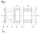
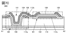
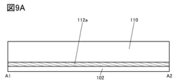
- FIG. 1A is a plan view showing an example of a semiconductor device.
- FIG. 1B is a cross-sectional view showing an example of a semiconductor device.
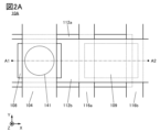
- FIG. 2A is a plan view showing an example of a semiconductor device.
- FIG. 2B is a cross-sectional view showing an example of a semiconductor device.
- FIG. 3A is a plan view showing an example of a semiconductor device.
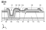
- FIG. 3B is a cross-sectional view showing an example of a semiconductor device.
- FIG. 4A is a plan view showing an example of a semiconductor device.
- FIG. 4B is a cross-sectional view showing an example of a semiconductor device.
- FIG. 5A is a plan view showing an example of a semiconductor device.
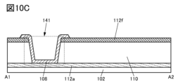
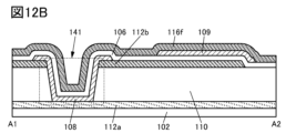
- FIGS. 12A to 12C are cross-sectional views illustrating an example of a method for manufacturing a semiconductor device.
- 13A to 13D are circuit diagrams of pixel circuits.
- 14A to 14D are circuit diagrams of pixel circuits.
- FIG. 15 is a perspective view showing an example of a display device.
- FIG. 16 is a cross-sectional view showing an example of a display device.
- FIG. 17 is a cross-sectional view showing an example of a display device.
- FIG. 18 is a cross-sectional view showing an example of a display device.
- FIG. 19 is a cross-sectional view showing an example of a display device.
- FIG. 20 is a cross-sectional view showing an example of a display device.
- 21A to 21H are diagrams showing examples of pixels.
- 22A to 22K are diagrams showing examples of pixels.
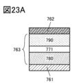
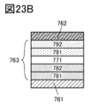
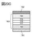
- 23A to 23F are diagrams illustrating configuration examples of light emitting devices.
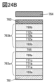
- 24A to 24C are diagrams showing configuration examples of light emitting devices.
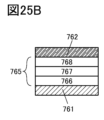
- 25A and 25B are diagrams illustrating a configuration example of a light receiving device.
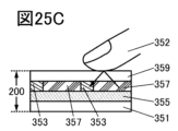
- 25C to 25E are diagrams illustrating configuration examples of a display device.
- 26A to 26D are diagrams illustrating an example of an electronic device.
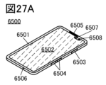
- 27A to 27F are diagrams illustrating an example of an electronic device.
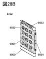
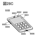
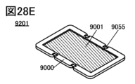
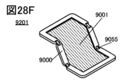
- 28A to 28G are diagrams illustrating an example of an electronic device.
- film and “layer” can be interchanged depending on the situation or circumstances.
- conductive layer can be changed to the term “conductive film.”
- insulating film can be changed to the term “insulating layer.”
- a device manufactured using a metal mask or FMM fine metal mask, high-definition metal mask
- a device with a MM (metal mask) structure is sometimes referred to as a device with an MML (metal maskless) structure.
- SBS Side By Side
- materials and configurations can be optimized for each light emitting device, which increases the degree of freedom in selecting materials and configurations, making it easier to improve brightness and reliability.
- holes or electrons may be referred to as “carriers”.
- a hole injection layer or an electron injection layer is called a “carrier injection layer”
- a hole transport layer or an electron transport layer is called a “carrier transport layer”
- a hole blocking layer or an electron blocking layer is called a “carrier injection layer.”
- the carrier injection layer, carrier transport layer, and carrier block layer described above may not be clearly distinguishable depending on their respective cross-sectional shapes or characteristics.
- one layer may serve as two or three functions among a carrier injection layer, a carrier transport layer, and a carrier block layer.
- a light emitting device has an EL layer between a pair of electrodes.
- the EL layer has at least a light emitting layer.
- the layers (also referred to as functional layers) included in the EL layer include a light emitting layer, a carrier injection layer (a hole injection layer and an electron injection layer), a carrier transport layer (a hole transport layer and an electron transport layer), and Examples include carrier block layers (hole block layers and electron block layers).
- a light-receiving device (also referred to as a light-receiving element) has an active layer that functions as at least a photoelectric conversion layer between a pair of electrodes.
- island-like refers to a state in which two or more layers formed in the same process and using the same material are physically separated.
- an island-shaped light emitting layer indicates that the light emitting layer and an adjacent light emitting layer are physically separated.
- a tapered shape refers to a shape in which at least a part of the side surface of the structure is inclined with respect to the substrate surface or the surface to be formed.
- it refers to a shape having a region in which the angle between the inclined side surface and the substrate surface or the surface to be formed (also referred to as a taper angle) is less than 90 degrees.
- the side surface of the structure, the substrate surface, or the surface to be formed does not necessarily have to be completely flat, and may be substantially planar with a minute curvature or may be substantially planar with minute irregularities.
- a mask layer (also referred to as a sacrificial layer) is a layer located above at least a light emitting layer (more specifically, a layer that is processed into an island shape among the layers constituting the EL layer). , has a function of protecting the light emitting layer during the manufacturing process.
- step breakage refers to a phenomenon in which a layer, film, or electrode is separated due to the shape of the surface on which it is formed (for example, a step difference).
- the planar shapes roughly match means that at least a portion of the outlines of the laminated layers overlap. For example, this includes a case where the upper layer and the lower layer are processed using the same mask pattern or partially the same mask pattern. However, strictly speaking, the contours may not overlap, and the upper layer may be located inside the lower layer, or the upper layer may be located outside the lower layer, and in this case, it is also said that the planar shapes roughly match.
- One embodiment of the present invention includes one horizontal channel transistor (described later) and one vertical channel transistor (described later), and includes a source electrode, a drain electrode, or a gate of the horizontal channel transistor.
- This is a semiconductor device in which one of the electrodes is electrically connected to one of the source electrode, drain electrode, or gate electrode of a vertical channel transistor.
- the semiconductor device can occupy a smaller area within the substrate plane than a semiconductor device having two lateral channel transistors.
- a semiconductor device of one embodiment of the present invention, a method for manufacturing the same, and the like will be described with reference to FIGS. 1A to 14D.
- FIG. 1A shows a plan view (also referred to as a top view) of the semiconductor device 10.
- FIG. 1B shows a cross-sectional view taken along the dashed line A1-A2 shown in FIG. 1A. Note that some components of the semiconductor device 10 are omitted in FIG. 1A. Regarding the plan view of the semiconductor device, some of the constituent elements are omitted in the subsequent drawings as well, similar to FIG. 1A.
- the semiconductor device 10 includes a transistor M1 and a transistor M2 on a substrate 102.
- the transistor M1 covers a conductive layer 112b provided on the conductive layer 112a and the insulating layer 110 stacked on the substrate 102, the side and top surfaces of the conductive layer 112b, and a part of the top surface of the insulating layer 110.
- the conductive layer 112b functions as a gate electrode.
- the insulating layer 106 functions as a gate insulating layer.
- the semiconductor layer 109 functions as a semiconductor layer in which a channel is formed.
- the conductive layer 116a functions as either a source electrode or a drain electrode, and the conductive layer 116b functions as the other source electrode or drain electrode.
- the gate electrode (conductive layer 112b) is located below the semiconductor layer (semiconductor layer 109) in which the channel is formed, and the upper surface of the semiconductor layer (semiconductor layer 109) in which the channel is formed is located.
- a source electrode and a drain electrode (the conductive layer 116a and the conductive layer 116b) are in contact with each other, which is a "bottom gate top contact type" transistor.
- the transistor M2 includes a conductive layer 112a on the substrate 102, a conductive layer 112b on the insulating layer 110 provided on the conductive layer 112a, and an inner wall of an opening 141 provided in the insulating layer 110 etc. (a top surface of the conductive layer 112a).
- the semiconductor layer 108 is in contact with a portion of the side surface of the insulating layer 110 and the side surface of the conductive layer 112b) and a portion of the top surface of the conductive layer 112b;
- the conductive layer 104 includes an insulating layer 106 having a region, and a conductive layer 104 provided on the insulating layer 106 so as to have a region overlapping with the inner wall of the opening 141.
- the conductive layer 112a functions as either a source electrode or a drain electrode, and the conductive layer 112b functions as the other source electrode or drain electrode.
- the semiconductor layer 108 functions as a semiconductor layer in which a channel is formed.
- the insulating layer 106 functions as a gate insulating layer.
- the conductive layer 104 functions as a gate electrode.
- the transistor M2 is located at a height between the upper surface of the conductive layer 112a and the lower surface of the conductive layer 112b in a cross-sectional view (see FIG. 1B), and overlaps with the conductive layer 104 via the insulating layer 106.
- a region of the semiconductor layer 108 functions as a channel formation region. That is, the length of this region becomes the channel length of transistor M2. Therefore, in the transistor M2, the channel length can be determined by adjusting the thickness of the insulating layer 110 provided between the conductive layer 112a and the conductive layer 112b. Therefore, a transistor with a short channel length can be manufactured with high precision. Furthermore, when a plurality of transistors M2 are manufactured, variations in characteristics among the transistors M2 can also be reduced.
- the transistor M2 is provided in a region where the semiconductor layer 108 overlaps with the opening 141 in a plan view (see FIG. 1A), the outer circumference of the opening 141, more precisely, the semiconductor layer 108 in the opening 141 ( The outer peripheral length of the channel forming region of the transistor M2 becomes the channel width of the transistor M2. Note that in FIG. 1B, the width of the opening 141 in the X direction is narrower toward the conductive layer 112a and wider toward the conductive layer 112b.
- the outer circumference of the channel forming region in the region where the width of the opening 141 in the X direction is the narrowest may be defined as the channel width of the transistor M2, or conversely, the width of the opening 141 in the X direction may be the narrowest.
- the outer circumferential length of the channel formation region in a wide area may be defined as the channel width of the transistor M2.
- an intermediate value between the two may be defined as the channel width of the transistor M2.
- the conductive layer 112b functions as the gate electrode in the transistor M1, and functions as the other of the source electrode and the drain electrode in the transistor M2. That is, the gate electrode of the transistor M1 and the other of the source electrode or the drain electrode of the transistor M2 are electrically connected. Therefore, it can be said that the semiconductor device 10 of one embodiment of the present invention includes two transistors (transistor M1 and transistor M2) that are electrically connected.
- the drain current flows through the region between the conductive layer 116a and the conductive layer 116b of the semiconductor layer 109, whereas in the transistor M2, the drain current flows between the conductive layer 112a and the conductive layer 112b of the semiconductor layer 108. Drain current flows through the region between the two. That is, in the transistor M1, the direction in which the drain current flows is approximately parallel to the substrate surface, whereas in the transistor M2, the direction in which the drain current flows is approximately perpendicular to the substrate surface (more More precisely, the direction along the side surface of the opening 141).
- a transistor like the transistor M1, in which the source electrode and the drain electrode are arranged in the lateral direction (the X direction or the Y direction shown in FIGS. 1A and 1B), and the drain current flows in the lateral direction, is referred to as a "lateral channel”. Also called a type transistor.
- a transistor in which the source electrode and the drain electrode are arranged in the vertical direction (Z direction shown in FIGS. 1A and 1B) and the drain current flows in the vertical direction is referred to as a "vertical channel type" transistor. Also called "transistor”.
- Vertical channel transistors have a source electrode and a drain electrode arranged in a direction perpendicular to the substrate surface (Z direction shown in FIGS. 1A and 1B), so compared to horizontal channel transistors, the substrate The in-plane area occupied by the transistor can be significantly reduced.
- one of the two transistors included in the semiconductor device is a vertical channel transistor. Therefore, in the semiconductor device 10 of one embodiment of the present invention, the area occupied by the semiconductor device in the substrate plane can be reduced compared to a semiconductor device in which two lateral channel transistors are arranged laterally.
- one of the two transistors included in the semiconductor device is a lateral channel transistor. Therefore, some transistor components such as a source electrode and a drain electrode can be manufactured all at once on the same plane. Therefore, the number of manufacturing steps can be reduced compared to vertical channel transistors.
- the transistor M1 is a bottom gate top contact type transistor. In a bottom-gate top-contact transistor, a region of the semiconductor layer that is sandwiched between a source electrode and a drain electrode and faces a gate electrode functions as a channel formation region. Therefore, in the bottom-gate top-contact transistor, the channel formation region in the semiconductor layer is not exposed during the transistor manufacturing process.
- a semiconductor device in which transistors having good characteristics are arranged at high density can be realized. Further, a highly integrated semiconductor device can be realized. For example, when the semiconductor device 10 of one embodiment of the present invention is used in a pixel circuit (described later) of a display device, the display device can have higher definition.
- Substrate 102 There are no major restrictions on the material used for the substrate 102. Depending on the purpose, it may be determined by taking into consideration the presence or absence of translucency and heat resistance to withstand heat treatment. For example, a glass substrate such as barium borosilicate glass or alumino borosilicate glass, a ceramic substrate, a quartz substrate, a sapphire substrate, etc. can be used. Further, a semiconductor substrate having an insulating surface, a flexible substrate, a bonding film, a base film, etc. may be used.
- a glass substrate such as barium borosilicate glass or alumino borosilicate glass, a ceramic substrate, a quartz substrate, a sapphire substrate, etc.
- a semiconductor substrate having an insulating surface, a flexible substrate, a bonding film, a base film, etc. may be used.
- the semiconductor substrate examples include a semiconductor substrate made of silicon or germanium, or a compound semiconductor substrate made of silicon carbide, silicon germanium, gallium arsenide, indium phosphide, zinc oxide, or gallium oxide.
- the semiconductor substrate may be a single crystal semiconductor or a polycrystalline semiconductor.
- the substrate 102 can be, for example, 6th generation (1500 mm x 1850 mm), 7th generation (1870 mm x 2200 mm), 8th generation (2200 mm x 2400 mm), A glass substrate with a large area, such as 9th generation (2400 mm x 2800 mm) or 10th generation (2950 mm x 3400 mm), can be used. Thereby, a large-sized display device can be manufactured. Furthermore, by increasing the size of the substrate, more display devices can be produced from one substrate, and production costs can be reduced.
- a flexible substrate, a bonded film, a base film, or the like may be used as the substrate 102.
- polyester resins such as polyethylene terephthalate (PET) and polyethylene naphthalate (PEN), polyacrylonitrile resins, acrylic resins, polyimide resins, and polymethyl methacrylate.
- a lightweight semiconductor device can be provided. Furthermore, by using the above material for the substrate 102, a semiconductor device that is resistant to impact can be provided. Furthermore, by using the above material for the substrate 102, a semiconductor device that is less likely to be damaged can be provided.
- the flexible substrate used for the substrate 102 may be made of a material having a coefficient of linear expansion of 1 ⁇ 10 ⁇ 3 /K or less, 5 ⁇ 10 ⁇ 5 /K or less, or 1 ⁇ 10 ⁇ 5 /K or less, for example.
- aramid is suitable as a flexible substrate used for the substrate 102 because it has a low coefficient of linear expansion.
- a conductive layer (conductive layer 116a, conductive layer 116b) functions as a source electrode and a drain electrode of transistor M1
- a conductive layer (conductive layer 112b) functions as a gate electrode of transistor M1
- a source electrode and drain electrode of transistor M2 In addition to the conductive layers (conductive layer 112a, conductive layer 112b) and the conductive layer (conductive layer 104) that functions as the gate electrode of transistor M2, various wirings, electrodes, etc.
- Conductive materials that can be used for the conductive layer include aluminum (Al), chromium (Cr), copper (Cu), silver (Ag), gold (Au), platinum (Pt), tantalum (Ta), and nickel ( Ni), titanium (Ti), molybdenum (Mo), tungsten (W), hafnium (Hf), vanadium (V), niobium (Nb), manganese (Mn), magnesium (Mg), zirconium (Zr), beryllium ( A metal element selected from Be), an alloy containing the above-mentioned metal elements, an alloy combining the above-mentioned metal elements, etc. can be used.
- a semiconductor such as polycrystalline silicon containing an impurity element such as phosphorus, or a silicide such as nickel silicide may be used.
- the method for forming the conductive material is not particularly limited, and various methods such as vapor deposition, chemical vapor deposition (CVD), sputtering, and spin coating can be used.
- a Cu-X alloy (X is Mn, Ni, Cr, Fe, Co, Mo, Ta, or Ti) may be applied as the conductive material. Since the layer formed of the Cu-X alloy can be processed by a wet etching process, it is possible to suppress manufacturing costs. Further, as the conductive material, an aluminum alloy containing one or more elements selected from titanium, tantalum, tungsten, molybdenum, chromium, neodymium, and scandium may be used.
- conductive materials that can be used for the conductive layer indium tin oxide, indium oxide containing tungsten oxide, indium zinc oxide containing tungsten oxide, indium oxide containing titanium oxide, indium tin containing titanium oxide, etc.
- Conductive materials with oxygen can also be used, such as oxides, indium zinc oxide, indium tin oxide doped with silicon oxide.
- conductive materials containing nitrogen such as titanium nitride, tantalum nitride, and tungsten nitride can also be used.
- the conductive layer can also have a laminated structure in which a conductive material containing oxygen, a conductive material containing nitrogen, and a material containing the metal element described above are appropriately combined.
- the conductive layer may have a single-layer structure of an aluminum layer containing silicon, a two-layer structure in which a titanium layer is stacked on an aluminum layer, a two-layer structure in which a titanium layer is stacked on a titanium nitride layer, or a tungsten layer on a titanium nitride layer.
- a two-layer structure in which a tungsten layer is laminated on a tantalum nitride layer a two-layer structure in which a tungsten layer is laminated on a tantalum nitride layer, and a three-layer structure in which a titanium layer is laminated, an aluminum layer is laminated on the titanium layer, and a titanium layer is laminated on top of that. good.
- the conductive layer may have a laminated structure in which a material containing the aforementioned metal element and a conductive material containing oxygen are combined.
- a layered structure may be used in which a material containing the aforementioned metal element and a conductive material containing nitrogen are combined.
- a laminated structure may be used in which a material containing the aforementioned metal element, a conductive material containing oxygen, and a conductive material containing nitrogen are combined.
- a conductive layer is formed by laminating a conductive layer containing copper on a conductive layer containing at least one of indium or zinc and oxygen, and further containing at least one of indium or zinc and oxygen on top of the conductive layer containing at least one of indium or zinc and oxygen. It may also have a three-layer structure in which conductive layers are laminated. In this case, it is preferable that the side surfaces of the conductive layer containing copper are also covered with a conductive layer containing at least one of indium or zinc and oxygen. Further, for example, a plurality of conductive layers containing at least one of indium or zinc and oxygen may be stacked and used as the conductive layer.
- the conductive layer 112a and the conductive layer 112b in contact with the semiconductor layer 108, and the conductive layer 116a and the conductive layer 116b in contact with the semiconductor layer 109 are oxidized.
- a conductive material that converts the semiconductor into an n-type semiconductor For example, a conductive material containing nitrogen may be used.
- a conductive material containing titanium or tantalum and nitrogen may be used.
- another conductive material may be provided over the conductive material containing nitrogen.
- various insulating layers that constitute the semiconductor device 10 of one embodiment of the present invention include aluminum nitride, aluminum nitride, Aluminum oxide, aluminum nitride oxide, aluminum oxide nitride, magnesium oxide, silicon nitride, silicon oxide, silicon nitride oxide, silicon oxynitride, gallium oxide, germanium oxide, yttrium oxide, zirconium oxide, lanthanum oxide, neodymium oxide, hafnium oxide, oxide
- a material selected from tantalum, aluminum silicate, etc. is used in a single layer or in a stacked manner.
- a mixture of a plurality of materials among oxide materials, nitride materials, oxynitride materials, and nitrided oxide materials may be used in a single layer or in a stacked manner.
- a mixture of a plurality of materials among oxide materials, nitride materials, oxynitride materials, and nitrided oxide materials may be
- oxynitride refers to a material containing more oxygen than nitrogen.
- nitrided oxide refers to a material containing more nitrogen than oxygen. Note that the content of each element can be measured using, for example, Rutherford Backscattering Spectrometry (RBS) method.
- RBS Rutherford Backscattering Spectrometry
- an oxide semiconductor for the semiconductor layer 108 and the semiconductor layer 109 it is preferable to use an insulating material containing reduced hydrogen and oxygen for the insulating layer 106 and the insulating layer 110.
- an insulating material containing reduced hydrogen and oxygen for the insulating layer 106 and the insulating layer 110 For example, it is preferable to use silicon oxide for each of the insulating layer 106 and the insulating layer 110.
- silicon oxide for the insulating layer 106 and the insulating layer 110 respectively, the semiconductor layer 108 and the semiconductor layer 109 having regions in contact with these insulating layers are unlikely to become n-type.
- oxygen can be efficiently supplied to the semiconductor layer 108 and the semiconductor layer 109 from these insulating layers.
- oxygen vacancies (V O ) in the semiconductor layer 108 and the semiconductor layer 109 are reduced, and the electrical characteristics and reliability of the transistors M1 and M2 can be improved at the same time.
- an insulating material that is difficult for impurities to pass through for an insulating layer located above or below the transistors M1 and M2 (none of which are shown).
- a single layer of an insulating material containing boron, carbon, nitrogen, oxygen, fluorine, magnesium, aluminum, silicon, phosphorus, chlorine, argon, gallium, germanium, yttrium, zirconium, lanthanum, neodymium, hafnium, or tantalum Alternatively, it may be used in a laminated manner.
- Examples of insulating materials that are difficult for impurities to pass through include aluminum oxide, aluminum nitride, aluminum oxynitride, aluminum nitride oxide, gallium oxide, germanium oxide, yttrium oxide, zirconium oxide, lanthanum oxide, neodymium oxide, hafnium oxide, tantalum oxide, Examples include silicon nitride.
- impurities can be prevented from entering the transistor M1 and M2 side from above and below the transistors M1 and M2. Since diffusion can be suppressed, the reliability of the semiconductor device 10 can be improved.
- an insulating layer that can function as a planarization layer may be used as the insulating layer located above or below the transistors M1 and M2.
- an insulating layer that can function as a planarization layer heat-resistant organic materials such as polyimide, acrylic resin, benzocyclobutene resin, polyamide, and epoxy resin can be used.
- heat-resistant organic materials such as polyimide, acrylic resin, benzocyclobutene resin, polyamide, and epoxy resin can be used.
- low dielectric constant materials low-k materials
- siloxane resins low-k materials
- PSG phosphorus glass
- BPSG phosphorus boron glass
- the siloxane resin corresponds to a resin containing Si-O-Si bonds formed using a siloxane-based material as a starting material.
- an organic group for example, an alkyl group or an aryl group
- a fluoro group may be used as a substituent. Further, the organic group may have a fluoro group.
- a chemical mechanical polishing (CMP) process may be performed on the surface of the insulating layer that can function as a planarization layer.
- CMP chemical mechanical polishing
- the semiconductor layer 109 that functions as a semiconductor layer in which the channel of the transistor M1 is formed, and the semiconductor layer 108 that functions as a semiconductor layer in which the channel of the transistor M2 is formed include a single crystal semiconductor, a polycrystalline semiconductor, a microcrystalline semiconductor, Alternatively, an amorphous semiconductor or the like can be used alone or in combination.
- the semiconductor material silicon, germanium, etc. can be used, for example. Further, a compound semiconductor such as silicon germanium, silicon carbide, gallium arsenide, or a nitride semiconductor may be used.
- an organic substance having semiconductor properties or a metal oxide having semiconductor properties also referred to as an oxide semiconductor
- these semiconductor materials may contain impurities as dopants.
- oxide semiconductors have a band gap of 2 eV or more
- transistors also referred to as "OS transistors”
- the off-state current is significantly smaller than when using this material. Therefore, the power consumption of the semiconductor device 10 can be reduced.
- OS transistors operate stably even in high-temperature environments, with little variation in characteristics. For example, even in a high-temperature environment, the off-state current hardly increases. Specifically, the off-state current hardly increases even under an environmental temperature of room temperature or higher and 200° C. or lower. Furthermore, the on-state current is less likely to decrease even in a high-temperature environment. Therefore, a semiconductor device using an OS transistor operates stably even in a high-temperature environment and has high reliability.
- examples of silicon that can be used for the semiconductor layer in which the channel is formed include single crystal silicon, polycrystalline silicon, microcrystalline silicon, amorphous silicon, and the like.
- examples of polycrystalline silicon include low temperature polysilicon (LTPS).
- a transistor using amorphous silicon for the semiconductor layer in which a channel is formed can be formed on a large glass substrate and can be manufactured at low cost.
- a transistor using polycrystalline silicon for a semiconductor layer in which a channel is formed has high field effect mobility and can operate at high speed.
- a transistor using microcrystalline silicon for a semiconductor layer in which a channel is formed has higher field effect mobility than a transistor using amorphous silicon, and can operate at high speed.
- OS transistors are used for both transistor M1 and transistor M2. That is, an oxide semiconductor is used for both the semiconductor layer 108 and the semiconductor layer 109. Since the OS transistor has a high dielectric strength voltage between the source and the drain, the channel length can be shortened. Therefore, the on-state current of the transistor can be increased.
- metal oxides that can be used in the semiconductor layer in which the channel of the OS transistor is formed include indium oxide, gallium oxide, and zinc oxide. It is preferable that the metal oxide contains at least indium (In) or zinc (Zn). Moreover, it is preferable that the metal oxide has two or three selected from indium, element M, and zinc.
- element M is gallium, aluminum, silicon, boron, yttrium, tin, antimony, copper, vanadium, beryllium, titanium, iron, nickel, germanium, zirconium, molybdenum, lanthanum, cerium, neodymium, hafnium, tantalum, tungsten, One or more selected from cobalt and magnesium.
- the element M is preferably one or more selected from aluminum, gallium, yttrium, and tin.
- indium tin oxide containing silicon or the like can be used.
- the element M is one or more selected from gallium, aluminum, yttrium, and tin.
- element M is preferably gallium.
- composition of the metal oxide used in the semiconductor layer in which the channel is formed greatly affects the electrical characteristics and reliability of the OS transistor.
- the atomic ratio of indium is greater than or equal to the atomic ratio of zinc.
- the atomic ratio of indium is greater than or equal to the atomic ratio of tin.
- a metal oxide in which the atomic ratio of indium is higher than the atomic ratio of tin can be used. Furthermore, it is preferable to use a metal oxide in which the atomic ratio of zinc is higher than the atomic ratio of tin.
- a metal oxide in which the atomic ratio of indium is higher than the atomic ratio of aluminum can be used. Furthermore, it is preferable to use a metal oxide in which the atomic ratio of zinc is higher than that of aluminum.
- In-Ga-Zn oxide for the semiconductor layer in which the channel of the OS transistor is formed, use a metal oxide in which the atomic ratio of indium to the number of atoms of the metal element is higher than the atomic ratio of gallium. I can do it. Furthermore, it is more preferable to use a metal oxide in which the atomic ratio of zinc is higher than the atomic ratio of gallium.
- a metal oxide is used in which the atomic ratio of indium to the number of atoms of the metal element is higher than the atomic ratio of element M. be able to. Furthermore, it is more preferable to use a metal oxide in which the atomic ratio of zinc is higher than the atomic ratio of element M.
- the sum of the atomic ratios of the metal elements can be the atomic ratio of the element M.
- the atomic ratio of the element M can be the sum of the atomic ratio of gallium and the atomic ratio of aluminum.
- the atomic ratio of indium, element M, and zinc is within the above-mentioned range.
- the ratio of the number of indium atoms to the number of atoms of the metal element contained in the metal oxide is 30 atom % or more and 100 atom % or less, preferably 30 atom % or more and 95 atom % or less, more preferably 35 atom % or more and 95 atom %. % or less, more preferably 35 atom % or more and 90 atom % or less, more preferably 40 atom % or more and 90 atom % or less, more preferably 45 atom % or more and 90 atom % or less, more preferably 50 atom % or more and 80 atom % or less.
- a metal oxide whose content is more preferably 60 atom % or more and 80 atom % or less, more preferably 70 atom % or more and 80 atom % or less.
- the ratio of the number of indium atoms to the total number of atoms of indium, element M, and zinc is within the above range.
- the ratio of the number of atoms of indium to the number of atoms of the metal element contained is sometimes referred to as the content rate of indium.
- a transistor with a large on-current can be obtained.
- a circuit that can operate at high speed can be manufactured. Furthermore, it becomes possible to reduce the area occupied by the circuit. For example, when applying the transistor to a large display device or a high-definition display device, even if the number of wires increases, signal delay in each wire can be reduced, and display unevenness can be suppressed. . Furthermore, since the area occupied by the circuit can be reduced, the frame of the display device can be made narrower.
- the composition of metal oxides can be analyzed using, for example, energy dispersive X-ray spectroscopy (EDX), X-ray photoelectron spectroscopy (XPS), or inductively coupled plasma mass spectroscopy.
- Analysis method ICP-MS: Inductively Coupled Plasma-Mass Spectrometry
- ICP-AES Inductively Coupled Plasma-Atomic Em Spectrometry
- analysis may be performed by combining two or more of these methods. Note that for elements with low content rates, the actual content rate and the content rate obtained by analysis may differ due to the influence of analysis accuracy. For example, when the content of element M is low, the content of element M obtained by analysis may be lower than the actual content.
- the nearby composition includes a range of ⁇ 30% of the desired atomic ratio.
- the atomic ratio of indium when the atomic ratio of indium is 1, the atomic ratio of M is greater than 0.1. 2 or less, including cases where the atomic ratio of zinc is greater than 0.1 and 2 or less.
- a sputtering method or an atomic layer deposition (ALD) method can be preferably used to form the metal oxide.
- the atomic ratio of the target and the atomic ratio of the metal oxide may be different.
- the atomic ratio of the metal oxide may be smaller than the atomic ratio of the target.
- the atomic ratio of zinc contained in the target may be about 40% or more and 90% or less.
- GBT Gate Bias Temperature
- PBTS Positive Bias Temperature Stress
- NBTS Negative Bias Temperature Stress
- the PBTS test and NBTS test performed under light irradiation are respectively PBTIS (Positive Bias Temperature Illumination Stress) test and NBTIS (Negative Bias Temperature Illumination Stress) test. It is called the Illumination Stress test.
- n-type transistor In an n-type transistor, a positive potential is applied to the gate when the transistor is turned on (state where current flows), so the amount of variation in threshold voltage in the PBTS test is an indicator of the reliability of the transistor. This is one of the important items to pay attention to.
- the transistor By using a metal oxide that does not contain gallium or has a low gallium content in the semiconductor layer in which the channel of the transistor is formed, the transistor can have high reliability against application of a positive bias. In other words, a transistor with a small threshold voltage variation in the PBTS test can be obtained. Further, when using a metal oxide containing gallium, it is preferable that the gallium content is lower than the indium content. Thereby, a highly reliable transistor can be realized.
- One of the factors that causes the threshold voltage to fluctuate in the PBTS test is defect levels at or near the interface between the semiconductor layer where the channel of the transistor is formed and the gate insulating layer.
- the greater the defect level density the more significant the deterioration in the PBTS test.
- threshold voltage fluctuations in PBTS tests can be suppressed by using metal oxides that do not contain gallium or have a low gallium content in the semiconductor layer where the transistor channel is formed.
- gallium contained in metal oxides has a property of attracting oxygen more easily than other metal elements (for example, indium or zinc). Therefore, it is presumed that at the interface between the metal oxide containing a large amount of gallium and the gate insulating layer, gallium combines with excess oxygen in the gate insulating layer, making it easier to generate carrier (electron in this case) trap sites. . Therefore, when a positive potential is applied to the gate, carriers are trapped at the interface between the semiconductor layer where the channel of the transistor is formed and the gate insulating layer, causing the threshold voltage to fluctuate. .
- In-Ga-Zn oxide for the semiconductor layer in which the channel of the transistor is formed, it is preferable to use a metal oxide in which the atomic ratio of indium is higher than the atomic ratio of gallium. Further, it is more preferable to use a metal oxide in which the atomic ratio of zinc is higher than the atomic ratio of gallium. In other words, it is preferable to apply a metal oxide in which the atomic ratio of metal elements satisfies In>Ga and Zn>Ga to the semiconductor layer in which the channel of the transistor is formed.
- the ratio of the number of gallium atoms to the number of atoms of the metal elements contained is greater than 0 atom % and less than 50 atom %, preferably 0.1 atom % or more and 40 atom %.
- the following is more preferably 0.1 atomic % or more and 35 atomic % or less, more preferably 0.1 atomic % or more and 30 atomic % or less, more preferably 0.1 atomic % or more and 25 atomic % or less, and more preferably 0.1 It is preferable to use a metal oxide whose content is 0.1 atomic % or more and 15 atomic % or less, more preferably 0.1 atomic % or more and 10 atomic % or less, more preferably 0.1 atomic % or more and 15 atomic % or less.
- a metal oxide that does not contain gallium may be applied to the semiconductor layer in which the channel of the OS transistor is formed.
- In--Zn oxide can be applied to the semiconductor layer.
- the field effect mobility of the transistor can be increased by increasing the ratio of the number of atoms of indium to the number of atoms of the metal element contained in the metal oxide.
- the metal oxide becomes highly crystalline, which suppresses fluctuations in the electrical characteristics of the transistor and increases reliability. be able to.
- a metal oxide that does not contain gallium and zinc, such as indium oxide may be applied to the semiconductor layer. By using a metal oxide that does not contain gallium, it is possible to make threshold voltage fluctuations extremely small, especially in PBTS tests.
- an oxide containing indium and zinc can be used for the semiconductor layer in which the channel of the OS transistor is formed.
- the present invention can also be applied to the case where element M is used instead of gallium. It is preferable to use a metal oxide in which the atomic ratio of indium is higher than the atomic ratio of element M to the semiconductor layer in which the channel of the OS transistor is formed. Further, it is preferable to use a metal oxide in which the atomic ratio of zinc is higher than the atomic ratio of element M.
- the electrical characteristics of the transistor may change.
- a transistor applied to a region where light can enter has small fluctuations in electrical characteristics under light irradiation and high reliability against light. Reliability with respect to light can be evaluated, for example, by the amount of variation in threshold voltage in an NBTIS test.
- a transistor with high reliability against light can be realized.
- a metal oxide in which the atomic ratio of element M is greater than or equal to that of indium has a larger band gap, making it possible to reduce the amount of variation in threshold voltage in transistor NBTIS tests.
- the band gap of the metal oxide of the semiconductor layer in which the channel of the transistor is formed is preferably 2.0 eV or more, more preferably 2.5 eV or more, further preferably 3.0 eV or more, and even more preferably 3.2 eV or more. is preferable, more preferably 3.3 eV or more, further preferably 3.4 eV or more, even more preferably 3.5 eV or more.
- the ratio of the number of atoms of element M to the number of atoms of metal elements contained is 20 atom % or more and 70 atom % or less, preferably 30 atom % or more and 70 atom % or less. , more preferably 30 atom % or more and 60 atom % or less, more preferably 40 atom % or more and 60 atom % or less, and even more preferably 50 atom % or more and 60 atom % or less.
- In-Ga-Zn oxide is used for the semiconductor layer in which the channel of the transistor is formed, it is possible to use a metal oxide in which the atomic ratio of indium to the number of atoms of the metal element is equal to or lower than the atomic ratio of gallium.
- the ratio of the number of gallium atoms to the number of atoms of the metal element contained is 20 atom % or more and 60 atom % or less, preferably 30 atom % or more and 60 atom % or less, A metal oxide having a content of more preferably 40 atom % or more and 60 atom % or less, more preferably 50 atom % or more and 60 atom % or less can be suitably used.
- the electrical characteristics and reliability of the transistor vary depending on the composition of the metal oxide applied to the semiconductor layer in which the channel of the transistor is formed. Therefore, by changing the composition of the metal oxide depending on the electrical characteristics and reliability required of the transistor, a display device that has both excellent electrical characteristics and high reliability can be realized.
- the semiconductor layer in which the channel of the transistor is formed may have a stacked structure having two or more metal oxide layers.
- the two or more metal oxide layers included in the semiconductor layer may have the same or approximately the same composition.
- the two or more metal oxide layers included in the semiconductor layer in which the channel of the transistor is formed may have different compositions.
- a first metal oxide layer having a composition of In:M:Zn 1:3:4 [atomic ratio] or a composition close to that, and In:M:Zn provided on the first metal oxide layer.
- a stacked structure including a second metal oxide layer having an atomic ratio of 1:1:1 or a composition close to this can be suitably used.
- the element M it is particularly preferable to use gallium or aluminum. For example, using a laminated structure of one selected from indium oxide, indium gallium oxide, and IGZO and one selected from IAZO, IAGZO, and ITZO (registered trademark), etc. Good too.
- a metal oxide layer with crystallinity As the semiconductor layer in which the channel of the transistor is formed.
- a metal oxide layer having a CAAC (C-Axis Aligned Crystal) structure, a polycrystalline structure, a nano-crystalline (NC) structure, or the like can be used.
- CAAC C-Axis Aligned Crystal
- NC nano-crystalline
- the semiconductor layer in which the channel of the OS transistor is formed may have a stacked structure of two or more metal oxide layers with different crystallinities.
- the layered structure includes a first metal oxide layer and a second metal oxide layer provided on the first metal oxide layer, and the second metal oxide layer
- the structure can include a region having higher crystallinity than the oxide layer.
- the second metal oxide layer can have a region having lower crystallinity than the first metal oxide layer.
- the two or more metal oxide layers included in the semiconductor layer may have the same or approximately the same composition.
- a stacked structure of two or more metal oxide layers having different crystallinity can be formed.
- the two or more metal oxide layers included in the semiconductor layer may have different compositions.
- the semiconductor device 10A shown in FIGS. 2A and 2B differs from the semiconductor device 10 shown in FIGS. 1A and 1B in that the transistor M1 is provided below the insulating layer 110.
- an insulating layer 107 that functions as the gate insulating layer of the transistor M1 is provided on the conductive layer 112a that functions as either the source electrode or the drain electrode of the transistor M2.
- a semiconductor layer 109 functioning as a semiconductor layer in which a channel of transistor M1 is formed is provided thereover.
- the semiconductor layer 109 is provided so as to have a region covering the side surface of the conductive layer 112a with the insulating layer 107 interposed therebetween.
- the conductive layer 116a functioning as one of the source electrode and the drain electrode of the transistor M1 is located on the side surface and top surface of one of the side ends of the semiconductor layer 109, and on the insulating layer 107.
- a conductive layer 116b, which is provided in contact with the upper surface and functions as the other of the source electrode or the drain electrode of the transistor M1, is connected to the side surface and the upper surface of the other side end portion facing one of the side end portions of the semiconductor layer 109, and to the insulating layer 116b. It is provided in contact with the upper surface of layer 107.
- the conductive layer 112a functions as the gate electrode of the transistor M1, and also functions as either the source electrode or the drain electrode of the transistor M2. That is, the semiconductor device 10A has a configuration in which the gate electrode of the transistor M1 and one of the source electrode or the drain electrode of the transistor M2 are electrically connected. With this configuration, effects similar to those obtained with the semiconductor device 10 can be obtained.
- an insulating layer 110 is provided to cover the transistor M1. That is, a semiconductor layer 109 functioning as a semiconductor layer in which a channel of the transistor M1 is formed is covered with an insulating layer 110 and an insulating layer 107 functioning as a gate insulating layer of the transistor M1.
- the same material as the insulating layer 106 that functions as the gate insulating layer of the transistor M2 can be used for the insulating layer 107.
- an insulating material containing reduced hydrogen and oxygen can be used, respectively.
- the semiconductor layer 109 is covered with the insulating layer 110 and the insulating layer 107, oxygen can be efficiently supplied from the insulating layer 110 and the insulating layer 107 to the semiconductor layer 109. can. Thereby, oxygen vacancies (V O ) in the semiconductor layer 109 and V OH generated by hydrogen entering the oxygen vacancies can be reduced, and the electrical characteristics and reliability of the transistor M1 can be improved.
- the conductive layer 112b functioning as the other of the source electrode and the drain electrode of the transistor M2 is located above the transistor M1 with the insulating layer 110 interposed therebetween.
- the conductive layer 112b can also be used as the second gate electrode of the transistor M1, for example.
- the threshold voltage of the transistor M1 can be controlled more reliably than when the transistor M1 has one gate electrode (conductive layer 112a).
- the conductive layer 112b serves both as the other of the source electrode and the drain electrode of the transistor M2, and as the second gate electrode of the transistor M1.
- one end of the conductive layer 104 that functions as the gate electrode of the transistor M2 extends toward the transistor M1, and functions as a semiconductor layer in which the channel of the transistor M1 is formed.
- the semiconductor layer 109 has a structure in which it is in contact with the side surface and top surface of one side end portion of the semiconductor layer 109 .
- the conductive layer functioning as the other of the source electrode or the drain electrode of the transistor M2 and the conductive layer functioning as the gate electrode of the transistor M1 have an independent configuration. are doing.
- the conductive layer 112c functions as a gate electrode of the transistor M1.
- the conductive layer 104 functions as one of a source electrode or a drain electrode of the transistor M1, and also functions as a gate electrode of the transistor M2. That is, the semiconductor device 10B has a configuration in which one of the source electrode or the drain electrode of the transistor M1 and the gate electrode of the transistor M2 are electrically connected. It can also be said that the transistor M1 in the semiconductor device 10B corresponds to the transistor M2 of the semiconductor device 10A, and the transistor M2 in the semiconductor device 10B corresponds to the transistor M1 of the semiconductor device 10A. With this configuration, effects similar to those obtained with the semiconductor device 10 can be obtained.
- the semiconductor device 10C shown in FIGS. 4A and 4B has a configuration of the gate electrode of the transistor M1, a configuration of one of the source electrode or the drain electrode of the transistor M1, a configuration of the other source electrode or the drain electrode of the transistor M2, and a configuration of the gate electrode of the transistor M1, a configuration of the other source electrode or the drain electrode of the transistor M2, and The configuration of the gate insulating layer of M1 is different from that of the semiconductor device 10 shown in FIGS. 1A and 1B.
- the conductive layer 112b that functions as either the source electrode or the drain electrode of the transistor M1 extends to the transistor M2 side, and functions as a semiconductor layer in which the channel of the transistor M2 is formed.
- the lower surface of the semiconductor layer 108 is in contact with the lower surface of the semiconductor layer 108.
- an insulating layer 107 that functions as a gate insulating layer of the transistor M1 is provided separately from an insulating layer 106 that functions as a gate insulating layer of the transistor M2.
- the insulating layer 106 that functions as a gate insulating layer of the transistor M2 extends toward the transistor M1 side, and includes a conductive layer 112b, a semiconductor layer 109 that functions as a semiconductor layer in which a channel of the transistor M1 is formed, and a source of the transistor M1. 112d of conductive layers which function as the other electrode or drain electrode.
- the conductive layer 103 functions as a gate electrode of the transistor M1. Further, the conductive layer 112b functions as one of the source electrode and the drain electrode of the transistor M1, and also functions as the other source electrode and the drain electrode of the transistor M2. That is, in the semiconductor device 10C, one of the source electrode or the drain electrode of the transistor M1 and the other of the source electrode or the drain electrode of the transistor M2 are electrically connected. With this configuration, effects similar to those obtained with the semiconductor device 10 can be obtained.
- the semiconductor layer 109 that functions as a semiconductor layer in which the channel of the transistor M1 is formed has an insulating layer 106 that functions as a gate insulating layer of the transistor M2, and an insulating layer that functions as a gate insulating layer of the transistor M1. 107. Therefore, by using an insulating material containing reduced hydrogen and oxygen for the insulating layer 106 and the insulating layer 107, oxygen is efficiently supplied from the insulating layer 106 and the insulating layer 107 to the semiconductor layer 109. be able to. Thereby, oxygen vacancies (V O ) in the semiconductor layer 109 and V OH generated by hydrogen entering the oxygen vacancies can be reduced, and the electrical characteristics and reliability of the transistor M1 can be improved.
- V O oxygen vacancies
- the semiconductor device 10D shown in FIGS. 5A and 5B differs from the semiconductor device 10 shown in FIG. 1 in that the transistor M1 is provided below the insulating layer 110. Further, the structure of the gate electrode of the transistor M1, the structure of one of the source electrodes or the drain electrode of the transistor M1, and the structure of the other source electrode or the drain electrode of the transistor M2 are the semiconductor devices shown in FIGS. 1A and 1B. It is different from 10.
- a conductive layer 103 functioning as a gate electrode of the transistor M1 is provided on the substrate 102, and serves as a gate insulating layer of the transistor M1 so as to cover the conductive layer 103 and the substrate 102.
- a functional insulating layer 107 is provided.
- a semiconductor layer 109 that functions as a semiconductor layer in which a channel of the transistor M1 is formed is provided on the insulating layer 107 so as to cover the conductive layer 103.
- the conductive layer 112a functioning as one of the source electrode and the drain electrode of the transistor M1 has a side surface and a top surface at one of the side ends of the semiconductor layer 109, a top surface of the insulating layer 107,
- a conductive layer 112e which is provided in contact with the lower surface of the semiconductor layer 108 which functions as a semiconductor layer in which a channel of the transistor M2 is formed, and which functions as the other of the source electrode or the drain electrode of the transistor M1, It is provided in contact with the side surface and top surface of the other side end portion opposite to one of the side end portions, and the top surface of the insulating layer 107 .
- the conductive layer 112a functions as one of the source electrode and the drain electrode of the transistor M1, and also functions as one of the source electrode and the drain electrode of the transistor M2. That is, the semiconductor device 10D has a configuration in which one of the source electrode or the drain electrode of the transistor M1 and one of the source electrode or the drain electrode of the transistor M2 are electrically connected. With this configuration, effects similar to those obtained with the semiconductor device 10 can be obtained.
- an insulating layer 110 is provided to cover the transistor M1. That is, a semiconductor layer 109 functioning as a semiconductor layer in which a channel of the transistor M1 is formed is covered with an insulating layer 110 and an insulating layer 107 functioning as a gate insulating layer of the transistor M1.
- the same material as the insulating layer 106 that functions as the gate insulating layer of the transistor M2 can be used for the insulating layer 107.
- an insulating material containing reduced hydrogen and oxygen can be used, respectively.
- the semiconductor layer 109 is covered with the insulating layer 110 and the insulating layer 107, oxygen can be efficiently supplied from the insulating layer 110 and the insulating layer 107 to the semiconductor layer 109. can. Thereby, oxygen vacancies (V O ) in the semiconductor layer 109 and V OH generated by hydrogen entering the oxygen vacancies can be reduced, and the electrical characteristics and reliability of the transistor M1 can be improved.
- the conductive layer 112b functioning as the other of the source electrode and the drain electrode of the transistor M2 is located above the transistor M1 with the insulating layer 110 interposed therebetween.
- the conductive layer 112b can also be used as the second gate electrode of the transistor M1, for example.
- the threshold voltage of the transistor M1 can be controlled more reliably than when the transistor M1 has one gate electrode (conductive layer 103).
- the conductive layer 112b serves both as the other of the source electrode and the drain electrode of the transistor M2, and as the second gate electrode of the transistor M1.
- the semiconductor device 10E shown in FIGS. 6A and 6B has a configuration of the gate electrode of the transistor M1, a configuration of the gate insulating layer of the transistor M1, a configuration of one of the source electrode or the drain electrode of the transistor M1, and a source electrode of the transistor M2.
- the configuration of one of the drain electrodes and the configuration of the other source or drain electrode of the transistor M2 are different from the semiconductor device 10 shown in FIGS. 1A and 1B.
- a conductive layer 112a that functions as one of the source electrode or the drain electrode of the transistor M2 and a conductive layer 112g that functions as the gate electrode of the transistor M1 are provided on the substrate 102, respectively. It is set up independently.
- An insulating layer 110 functioning as a gate insulating layer of the transistor M1 is provided on the conductive layer 112a and the conductive layer 112g, and a channel of the transistor M1 is formed on the insulating layer 110 so as to have a region overlapping with the conductive layer 112g.
- a semiconductor layer 109 is provided which functions as a semiconductor layer to be formed.
- the conductive layer 112b functioning as one of the source electrode and the drain electrode of the transistor M1 has a side surface and a top surface at one of the side ends of the semiconductor layer 109, a top surface of the insulating layer 110,
- a conductive layer 112d which is provided in contact with the lower surface of the semiconductor layer 108 which functions as a semiconductor layer in which a channel of the transistor M2 is formed, and which functions as the other of the source electrode or the drain electrode of the transistor M1, is provided on the lower surface of the semiconductor layer 109. It is provided in contact with the side surface and top surface of the other side end portion opposite to one of the side end portions, and the top surface of the insulating layer 110 .
- an insulating layer 106 functioning as a gate insulating layer of the transistor M2 extends toward the transistor M1 and covers the conductive layer 112b, the semiconductor layer 109, and the conductive layer 112d, respectively.
- the conductive layer 112b functions as one of the source electrode or the drain electrode of the transistor M1, and also functions as the other source electrode or the drain electrode of the transistor M2. That is, in the semiconductor device 10E, one of the source electrode or the drain electrode of the transistor M1 and the other of the source electrode or the drain electrode of the transistor M2 are electrically connected. With this configuration, effects similar to those obtained with the semiconductor device 10 can be obtained. Furthermore, in the semiconductor device 10E, the insulating layer 110 has both the function of an interlayer film and the function of a gate insulating layer of the transistor M1. As described above, the insulating layer 110 that functions as an interlayer film is also a layer that determines the channel length of the transistor M2 depending on its thickness.
- the thickness of the insulating layer 110 in the manufacturing process of the semiconductor device 10E it is possible to simultaneously control both the thickness of the gate insulating layer of the transistor M1 and the channel length of the transistor M2. , the total number of steps can be reduced.
- the insulating layer 106 is provided to cover the transistor M1. Furthermore, the lower surface of the semiconductor layer 109 is in contact with the upper surface of the insulating layer 110. That is, the semiconductor layer 109 functioning as a semiconductor layer in which the channel of the transistor M1 is formed is covered with the insulating layer 106 and the insulating layer 110. As described above, an insulating material containing reduced hydrogen and oxygen can be used for the insulating layer 106 and the insulating layer 110, respectively. Therefore, since the semiconductor layer 109 is covered with the insulating layer 106 and the insulating layer 110, oxygen can be efficiently supplied from the insulating layer 106 and the insulating layer 110 to the semiconductor layer 109. can. Thereby, oxygen vacancies (V O ) in the semiconductor layer 109 and V OH generated by hydrogen entering the oxygen vacancies can be reduced, and the electrical characteristics and reliability of the transistor M1 can be improved.
- V O oxygen vacancies
- the semiconductor device 10F shown in FIG. 7A has the following points: the other of the source electrode or the drain electrode (conductive layer 112b) of the transistor M2 is in contact with the upper surface of the semiconductor layer (semiconductor layer 108) in which the channel of the transistor M2 is formed; , differs from the semiconductor device 10 shown in FIGS. 1A and 1B in that the lower surface of the semiconductor layer and the upper surface of the insulating layer 110 are in contact with each other.
- the other configurations are the same as those of the semiconductor device 10. With this configuration, effects similar to those obtained with the semiconductor device 10 can be obtained.
- the semiconductor device 10G shown in FIG. 7B has the following points: the other of the source electrode or the drain electrode (conductive layer 112b) of the transistor M2 is in contact with the upper surface of the semiconductor layer (semiconductor layer 108) in which the channel of the transistor M2 is formed; , differs from the semiconductor device 10A shown in FIGS. 2A and 2B in that the lower surface of the semiconductor layer and the upper surface of the insulating layer 110 are in contact with each other.
- the other configurations are the same as those of the semiconductor device 10A. With this configuration, effects similar to those obtained with the semiconductor device 10A can be obtained.
- the semiconductor device 10H shown in FIG. 7C has the following points: the other of the source electrode or the drain electrode (conductive layer 112b) of the transistor M2 is in contact with the upper surface of the semiconductor layer (semiconductor layer 108) in which the channel of the transistor M2 is formed; This differs from the semiconductor device 10B shown in FIGS. 3A and 3B in that the lower surface of the semiconductor layer and the upper surface of the insulating layer 110 are in contact with each other.
- the other configurations are the same as those of the semiconductor device 10B. With this configuration, effects similar to those obtained with the semiconductor device 10B can be obtained.
- the semiconductor device 10I shown in FIG. 8A has the following points: the other of the source electrode or the drain electrode (conductive layer 112b) of the transistor M2 is in contact with the upper surface of the semiconductor layer (semiconductor layer 108) in which the channel of the transistor M2 is formed; , differs from the semiconductor device 10C shown in FIGS. 4A and 4B in that the lower surface of the semiconductor layer is in contact with the upper surface of the gate insulating layer (insulating layer 107) of the transistor M1.
- the other configurations are the same as those of the semiconductor device 10C. With this configuration, effects similar to those obtained with the semiconductor device 10C can be obtained.
- the semiconductor device 10J shown in FIG. 8B has the following points: the other of the source electrode or the drain electrode (conductive layer 112b) of the transistor M2 is in contact with the upper surface of the semiconductor layer (semiconductor layer 108) in which the channel of the transistor M2 is formed; , differs from the semiconductor device 10D shown in FIGS. 5A and 5B in that the lower surface of the semiconductor layer and the upper surface of the insulating layer 110 are in contact with each other.
- the other configurations are the same as those of the semiconductor device 10D. With this configuration, effects similar to those obtained with the semiconductor device 10D can be obtained.
- the semiconductor device 10K shown in FIG. 8C has the following points: the other of the source electrode or the drain electrode (conductive layer 112b) of the transistor M2 is in contact with the upper surface of the semiconductor layer (semiconductor layer 108) in which the channel of the transistor M2 is formed; This differs from the semiconductor device 10E shown in FIGS. 6A and 6B in that the lower surface of the semiconductor layer and the upper surface of the insulating layer 110 are in contact with each other.
- the other configurations are the same as those of the semiconductor device 10E. With this configuration, effects similar to those obtained with the semiconductor device 10E can be obtained.
- Insulating layers, semiconductor layers, conductive layers for forming electrodes or wiring, etc. may be formed using a sputtering method, a CVD method, a vacuum evaporation method, a pulsed laser deposition (PLD) method, an ALD method, etc. I can do it.
- the CVD method may be a plasma enhanced CVD (PECVD) method or a thermal CVD method.
- PECVD plasma enhanced CVD
- thermal CVD method a metal organic chemical vapor deposition (MOCVD) method may be used.
- Insulating layers, semiconductor layers, conductive layers, etc. that make up semiconductor devices can be coated using spin coating, dip coating, spray coating, inkjet coating, dispensing, screen printing, offset printing, slit coating, roll coating, curtain coating, knife coating, etc. It may be formed by a method.
- the PECVD method can obtain high-quality films at relatively low temperatures.
- a film formation method that does not use plasma during film formation such as MOCVD, ALD, or thermal CVD
- damage is less likely to occur on the surface on which the film is formed.
- wiring, electrodes, elements (transistors, capacitors, etc.) included in a semiconductor device may be charged up by receiving charges from plasma. At this time, the accumulated charges may destroy wiring, electrodes, elements, etc. included in the semiconductor device.
- a film forming method that does not use plasma such plasma damage does not occur, so that the yield of semiconductor devices can be increased. Furthermore, since no plasma damage occurs during film formation, a film with fewer defects can be obtained.
- the CVD method and the ALD method are film-forming methods in which a film is formed by a reaction on the surface of an object, unlike film-forming methods in which particles emitted from a target or the like are deposited. Therefore, this is a film forming method that is not easily affected by the shape of the object to be processed and has good step coverage.
- the ALD method has excellent step coverage and excellent thickness uniformity, and is therefore suitable for coating the surface of an opening with a high aspect ratio.
- the ALD method since the ALD method has a relatively slow film formation rate, it may be preferable to use it in combination with other film formation methods such as the CVD method, which has a fast film formation rate.
- the composition of the obtained film can be controlled by the flow rate ratio of source gases.
- a film having an arbitrary composition can be formed by changing the flow rate ratio of source gases.
- by changing the flow rate ratio of the raw material gas while forming the film it is possible to form a film in which the composition changes continuously.
- a photolithography method or the like can be used when processing the layers (thin films) that constitute the semiconductor device.
- an island-shaped layer may be formed by a film formation method using a shielding mask.
- the layer may be processed by a nanoimprint method, a sandblasting method, a lift-off method, or the like.
- a resist mask is formed on the layer (thin film) to be processed, a part of the layer (thin film) is selectively removed using the resist mask as a mask, and then the resist mask is removed.
- One method is to form a photosensitive layer and then perform exposure and development to process the layer into a desired shape.
- the light used for exposure can be, for example, i-line (wavelength 365 nm), g-line (wavelength 436 nm), h-line (wavelength 405 nm), or a mixture of these.
- ultraviolet light, KrF laser light, ArF laser light, etc. can also be used.
- exposure may be performed using immersion exposure technology.
- extreme ultraviolet (EUV) light or X-rays may be used.
- an electron beam can be used instead of the light used for exposure. It is preferable to use extreme ultraviolet light, X-rays, or electron beams because extremely fine processing becomes possible. Note that when exposure is performed by scanning a beam such as an electron beam, a photomask is not necessary.
- Dry etching, wet etching, sandblasting, etc. can be used to remove (etch) the layer (thin film). Further, a combination of these etching methods may be used.
- a conductive layer 112a is formed on the substrate 102, and an insulating layer 110 is formed on the conductive layer 112a (see FIG. 9A).
- an insulating substrate having an insulating surface is used as the substrate 102.
- the insulating substrate include a glass substrate, a quartz substrate, a sapphire substrate, a stabilized zirconia substrate (such as an yttria-stabilized zirconia substrate), and a resin substrate.
- a semiconductor substrate or a conductive substrate may be used as the substrate 102, if necessary.
- the semiconductor substrate include a semiconductor substrate made of silicon or germanium, or a compound semiconductor substrate made of silicon carbide, silicon germanium, gallium arsenide, indium phosphide, zinc oxide, or gallium oxide.
- a semiconductor substrate having an insulator region inside the semiconductor substrate described above such as an SOI (Silicon On Insulator) substrate.
- conductive substrates include graphite substrates, metal substrates, alloy substrates, and conductive resin substrates.
- substrates in which a conductor or a semiconductor is provided on an insulator substrate a substrate in which a conductor or an insulator is provided in a semiconductor substrate, a substrate in which a semiconductor or an insulator is provided in a conductor substrate, and the like.
- these substrates provided with elements may be used.
- Elements provided on the substrate include capacitive elements, resistive elements, switch elements, light emitting elements, memory elements, and the like.
- the conductive film that becomes the conductive layer 112a can be formed, for example, by a sputtering method using the above-mentioned material. Furthermore, after forming a resist mask (not shown) on the conductive film by a photolithography process, the conductive film is processed to form the conductive layer 112a, which will later become either the source electrode or the drain electrode of the transistor M2. Form. One or both of a wet etching method and a dry etching method may be used to process the conductive film.
- the wiring is preferably formed of a material with low electrical resistance. Therefore, it is preferable that the conductive layer 112a be formed of a material with low electrical resistance. Alternatively, it is preferable that a conductive layer formed of a material having lower electrical resistance than the conductive layer 112a be stacked above or below the conductive layer 112a.
- a conductive oxide material for the conductive layer 112a, and to use a metal, an alloy, or a nitride thereof that can be used for the above-mentioned conductive layer 104 etc. for the conductive layer laminated with the conductive layer 112a.
- a conductive layer having lower electrical resistance than the conductive layer 112a in contact with the conductive layer 112a when the conductive layer 112a is used as a wiring, the wiring resistance can be reduced.
- the insulating layer 110 can be formed by PECVD using the above-mentioned materials, for example.
- the insulating layer 110 may have a laminated structure of two or more layers. In this case, it is preferable that the surfaces of each layer be formed successively in a vacuum without exposing them to the atmosphere. This makes it possible to suppress atmospheric impurities from adhering to the surface of each layer. Examples of the impurities include water and organic substances.
- the substrate temperature during formation of the insulating layer 110 is preferably 180°C or more and 450°C or less, more preferably 200°C or more and 450°C or less, further preferably 250°C or more and 450°C or less, and even more preferably 300°C or more and 450°C or less. is preferable, more preferably 300°C or more and 400°C or less, and even more preferably 350°C or more and 400°C or less.
- impurities for example, water and hydrogen
- the insulating layer 110 is formed before the semiconductor layer 108 and the semiconductor layer 109, there is a need to be concerned that oxygen may be desorbed from the semiconductor layer 108 and the semiconductor layer 109 due to the heat applied during the formation of the insulating layer 110. There isn't.
- Heat treatment may be performed after forming the insulating layer 110. By performing the heat treatment, water and hydrogen can be released from the surface and inside of the insulating layer 110.
- the temperature of the heat treatment is preferably 150°C or higher and lower than the strain point of the substrate, more preferably 200°C or higher and 450°C or lower, further preferably 250°C or higher and 450°C or lower, and even more preferably 300°C or higher and 450°C or lower. Further, the temperature is preferably 300°C or more and 400°C or less, and even more preferably 350°C or more and 400°C or less.
- the heat treatment can be performed in an atmosphere containing one or more of a rare gas, nitrogen, or oxygen. Dry air (CDA: Clean Dry Air) may be used as the atmosphere containing nitrogen or the atmosphere containing oxygen. Note that it is preferable that the content of hydrogen, water, etc. in the atmosphere is as low as possible.
- the atmosphere it is preferable to use a high-purity gas having a dew point of -60°C or lower, preferably -100°C or lower.
- a high-purity gas having a dew point of -60°C or lower, preferably -100°C or lower.
- a process of supplying oxygen 160 to the insulating layer 110 is performed (see FIG. 9B).
- the oxygen 160 include oxygen radicals, oxygen atoms, oxygen atom ions, oxygen molecular ions, and the like.
- a method for supplying the oxygen 160 for example, an ion implantation method, an ion doping method, a plasma immersion ion implantation method, or a plasma treatment can be used.
- a device also referred to as a plasma etching device or a plasma ashing device
- plasma treatment may be performed in an atmosphere containing oxygen.
- oxygen may be supplied to the insulating layer 110 by plasma treatment in an atmosphere containing an oxidizing gas such as dinitrogen monoxide (N 2 O).
- an oxidizing gas such as dinitrogen monoxide (N 2 O).
- a conductive film 112f that will later become a conductive layer 112b is formed on the insulating layer 110 (see FIG. 9C).
- the conductive film 112f can be formed, for example, by a sputtering method using the above-mentioned material.
- a resist mask is formed by a photolithography process (not shown) on the conductive film 112f that does not overlap with the position where the transistor M2 will be formed later, and then the conductive film 112f and the insulating layer 110 are processed respectively.
- An opening 141 is formed that reaches layer 112a (see FIG. 10A).
- a wet etching method and a dry etching method can be used.
- a dry etching method can be suitably used to form the opening 141.
- the semiconductor layer 108 which will later become the semiconductor layer 108, is placed so as to cover the inner wall of the opening 141 (part of the upper surface of the conductive layer 112a, the side surface of the insulating layer 110, and the side surface of the conductive film 112f) and the upper surface of the conductive film 112f.
- a metal oxide film 108f is formed (see FIG. 10B).
- the metal oxide film 108f is preferably formed by a sputtering method using a metal oxide target.
- the metal oxide film 108f is preferably a dense film with as few defects as possible. Further, it is preferable that the metal oxide film 108f is a highly pure film in which impurities containing hydrogen elements are reduced as much as possible. In particular, it is preferable to use a crystalline metal oxide film as the metal oxide film 108f.
- oxygen gas when forming the metal oxide film 108f.
- oxygen gas when forming the metal oxide film 108f oxygen can be suitably supplied into the insulating layer 110 from the inner wall of the opening 141.
- oxygen vacancies (V O ) in the semiconductor layer 108 and V generated by hydrogen entering the oxygen vacancies are removed. OH can be reduced.
- oxygen gas and an inert gas for example, helium gas, argon gas, xenon gas, etc.
- an inert gas for example, helium gas, argon gas, xenon gas, etc.
- oxygen gas and an inert gas for example, helium gas, argon gas, xenon gas, etc.
- oxygen flow rate ratio oxygen flow rate ratio
- the lower the oxygen flow rate ratio the lower the crystallinity of the metal oxide film 108f may become. Thereby, it may be possible to realize a transistor M2 with a high on-state current.
- the substrate temperature during formation of the metal oxide film 108f may be at least room temperature and at most 250°C, preferably at least room temperature and at most 200°C, more preferably at least room temperature and at most 140°C. For example, it is preferable to set the substrate temperature at room temperature or higher and 140° C. or lower because productivity increases.
- the semiconductor layer 108 has a laminated structure, after the first metal oxide film is formed, the next metal oxide film is formed continuously without exposing the surface to the atmosphere. is preferred.
- Heat treatment may be performed after forming the metal oxide film 108f.
- water and hydrogen can be desorbed from the surface and inside of the metal oxide film 108f.
- oxygen can be supplied from the insulating layer 110 to the metal oxide film 108f.
- the heat treatment may improve the film quality of the metal oxide film 108f (for example, reduce defects, improve crystallinity, etc.). Note that the heat treatment conditions that can be used after forming the insulating layer 110 described above can be applied as the conditions for the heat treatment.
- the heat treatment does not need to be performed if unnecessary. Further, the heat treatment may not be performed here, but may also serve as the heat treatment performed in a later step. Further, in some cases, the heat treatment can also be used as a treatment at a high temperature in a later process (for example, a film forming process).
- the metal oxide film 108f is processed into an island shape so as to have a region overlapping with the inner wall of the opening 141, and the semiconductor layer 108 is formed (see FIG. 10C).
- a wet etching method and a dry etching method can be used.
- a wet etching method can be suitably used to form the semiconductor layer 108.
- a resist mask is formed by a photolithography process (not shown) on the conductive film 112f that will overlap with the position that will later become the gate electrode of the transistor M1, and then the conductive layer 112b is formed by processing the conductive film.
- a wet etching method and a dry etching method can be used to form the conductive layer 112b.
- a wet etching method can be suitably used to form the conductive layer 112b.
- the insulating layer 106 which will later become the gate insulating layer of the transistor M1 and the transistor M2, is formed on the semiconductor layer 108, the conductive layer 112b, and the insulating layer 110 (see FIG. 11B).
- the insulating layer 106 can be formed, for example, using the above-mentioned materials by PECVD.
- the insulating layer 106 is preferably made of an insulating material containing reduced hydrogen and oxygen. This makes it difficult for the semiconductor layer 108 and the semiconductor layer 109, each of which has a region in contact with the insulating layer 106, to become n-type. Further, since oxygen can be efficiently supplied from the insulating layer 106 to the semiconductor layer 108 and the semiconductor layer 109, oxygen vacancies (V O ) in the semiconductor layer 108 and the semiconductor layer 109 can be reduced.
- the semiconductor layer 108 is a layer that functions as a semiconductor layer in which a channel of the transistor M2 will be formed later
- the semiconductor layer 109 is a layer that functions as a semiconductor layer in which a channel of the transistor M1 will be formed later. Therefore, by using the above-described material for the insulating layer 106, it is possible to realize the transistor M2 and the transistor M1, which exhibit good electrical characteristics and are highly reliable.
- the insulating layer 106 By increasing the temperature during formation of the insulating layer 106 that functions as the gate insulating layer of the transistor M1 and the transistor M2, the insulating layer can have fewer defects. However, if the temperature during formation of the insulating layer 106 is high, oxygen is desorbed from the semiconductor layer 108, and oxygen vacancies (V O ) in the semiconductor layer 108 and V O generated by hydrogen entering the oxygen vacancies are generated. H may increase.
- the substrate temperature during formation of the insulating layer 106 is preferably 180°C or more and 450°C or less, more preferably 200°C or more and 450°C or less, further preferably 250°C or more and 450°C or less, and even more preferably 300°C or more and 450°C or less.
- the substrate temperature during the formation of the insulating layer 106 is preferable, and more preferably 300°C or more and 400°C or less.
- the surface of the semiconductor layer 108 may be subjected to plasma treatment.
- plasma treatment Through the plasma treatment, impurities such as water adsorbed on the surface of the semiconductor layer 108 can be reduced. Therefore, impurities at the interface between the semiconductor layer 108 and the insulating layer 106 can be reduced, and a highly reliable transistor M2 can be realized. This is particularly suitable when the surface of the semiconductor layer 108 is exposed to the atmosphere between the formation of the semiconductor layer 108 and the formation of the insulating layer 106.
- Plasma treatment can be performed, for example, in an atmosphere of oxygen, ozone, nitrogen, dinitrogen monoxide, argon, or the like. Further, it is preferable that the plasma treatment and the formation of the insulating layer 106 are performed continuously without exposure to the atmosphere.
- a metal oxide film 109f that will later become the semiconductor layer 109 is formed on the insulating layer 106 (see FIG. 11C).
- the metal oxide film 109f is preferably formed by a sputtering method using a metal oxide target.
- the conditions for forming the metal oxide film 109f and the conditions for the heat treatment performed after forming the metal oxide film 109f are as described above.
- the conditions of the heat treatment to be performed can be referred to.
- the metal oxide film 109f is processed into an island shape, and the semiconductor layer 109 is formed so as to have a region overlapping with the conductive layer 112b (see FIG. 12A).
- a wet etching method and a dry etching method can be used for forming the semiconductor layer 109.
- a wet etching method can be suitably used to form the semiconductor layer 109.
- a portion of the insulating layer 106 in a region that does not overlap with the semiconductor layer 109 may be etched and the film thickness may become thinner. Note that in etching the metal oxide film 109f, by using a material with a high selectivity for the insulating layer 106, it is possible to prevent the thickness of the insulating layer 106 from becoming thin.
- a conductive film 116f which will later become the conductive layer 104, the conductive layer 116a, and the conductive layer 116b, is formed on the semiconductor layer 109 and the insulating layer 106 (see FIG. 12B).
- the conductive film 116f can be formed, for example, by a sputtering method using the above-mentioned material.
- a resist mask is formed on the conductive film 116f by a photolithography process (not shown).
- the resist mask has at least a region that overlaps with the opening 141, a region that covers one of the side edges of the semiconductor layer 109 in a cross-sectional view, and a region that faces one of the side edges of the semiconductor layer 109 in a cross-sectional view. Provided in each area covering the other side end.
- a conductive layer 104 having a region overlapping with the opening 141, a conductive layer 116a covering one of the side edges of the semiconductor layer 109 in a cross-sectional view, and a conductive layer 116a that covers one side end of the semiconductor layer 109 in a cross-sectional view
- a conductive layer 116b covering one side end portion and the other opposing side end portion of the semiconductor layer 109 is formed in the step (see FIG. 12C).
- the conductive layer 104 is a conductive layer that becomes the gate electrode of the transistor M2.
- the conductive layer 116a is a conductive layer that serves as either a source electrode or a drain electrode of the transistor M1.
- the conductive layer 116b is a conductive layer that serves as the other of the source electrode and the drain electrode of the transistor M1.
- One or both of a wet etching method and a dry etching method can be used to form the conductive layer 104, the conductive layer 116a, and the conductive layer 116b.
- a wet etching method can be suitably used to form the conductive layer 104, the conductive layer 116a, and the conductive layer 116b.
- the thickness of the insulating layer 106 in a region that does not overlap with the conductive layer 116a, the conductive layer 116b, and the semiconductor layer 109 may become thinner. Further, the thickness of the semiconductor layer 109 in a region that does not overlap with the conductive layer 116a and the conductive layer 116b may be thinner than the thickness of the semiconductor layer 109 in a region that overlaps with the conductive layer 116a and the conductive layer 116b.
- a cleaning process may be performed after forming the conductive layer 104, the conductive layer 116a, and the conductive layer 116b.
- As the cleaning process wet cleaning using a cleaning liquid or the like, or cleaning by plasma processing using plasma can be used. The above-mentioned cleaning may be performed in combination as appropriate.
- impurities for example, metals and organic substances attached to the surfaces of the insulating layer 106 and the semiconductor layer 109 during the formation of the conductive layer 104, the conductive layer 116a, and the conductive layer 116b can be removed. I can do it.
- a cleaning liquid containing one or more of phosphoric acid, oxalic acid, and hydrochloric acid can be used.
- a cleaning solution containing phosphoric acid can be suitably used for wet cleaning.
- the concentration of the cleaning solution is preferably determined in consideration of the etching rate for the insulating layer 106 and the semiconductor layer 109.
- a gas containing one or more of oxygen, ozone, nitrogen, dinitrogen monoxide (N 2 O), and argon can be used for the plasma treatment. It is preferable to use a gas containing oxygen for the plasma treatment.
- a gas containing dinitrogen monoxide (N 2 O) organic substances on the surfaces of the insulating layer 106 and the semiconductor layer 109 can be suitably removed.
- a PECVD device or an etching device can be used for the plasma treatment.
- the transistor M1 and the transistor M2 are respectively formed.
- the semiconductor device 10 (FIGS. 1A and 1B) which is one embodiment of the present invention and includes the transistor M1 and the transistor M2 can be manufactured.
- the semiconductor device of one embodiment of the present invention can be applied to, for example, a pixel circuit of a display device.
- a pixel circuit of a display device A configuration example of a pixel circuit to which a semiconductor device of one embodiment of the present invention can be applied will be described below.
- FIGS. 14A to 14D illustrate configuration examples of a pixel 230 of a display device to which the semiconductor device of one embodiment of the present invention can be applied.
- the pixel 230 includes a pixel circuit 51 (pixel circuit 51A, pixel circuit 51B, pixel circuit 51C, or pixel circuit 51D) and a light emitting device 61.
- a "light-emitting device” described in this embodiment mode and the like refers to a self-emitting display device (also referred to as a display element) such as an organic EL element (also referred to as an OLED (Organic LED)).
- the light emitting element electrically connected to the pixel circuit can be a self-emitting type light emitting element such as an LED, a micro LED, a QLED (Quantum-dot LED), or a semiconductor laser.
- the pixel circuit 51A shown in FIG. 13A is a 2Tr1C type pixel circuit having a transistor 52A, a transistor 52B, and a capacitor 53.
- One of the source and drain of the transistor 52A is electrically connected to the wiring SL, and the gate of the transistor 52A is electrically connected to the wiring GL.
- the other of the source and drain of transistor 52A is electrically connected to the gate of transistor 52B.
- One of the source and drain of the transistor 52B and one terminal of the capacitor 53 are electrically connected to the wiring ANO.
- the other terminal of capacitor 53 is electrically connected to the gate of transistor 52B.
- the other of the source and drain of transistor 52B is electrically connected to the anode of light emitting device 61.
- the cathode of the light emitting device 61 is electrically connected to the wiring VCOM.
- the wiring GL corresponds to the conductive layer 104 of the semiconductor device 10
- the wiring SL corresponds to the conductive layer 112a of the semiconductor device 10.
- the wiring VCOM is a wiring that provides a potential for supplying current to the light emitting device 61.
- the transistor 52A has a function of controlling the conducting state or non-conducting state between the wiring SL and the gate of the transistor 52B based on the potential of the wiring GL. For example, VDD is supplied to the wiring ANO, and VSS is supplied to the wiring VCOM.
- the transistor 52B has a function of controlling the amount of current flowing to the light emitting device 61.
- Capacitor 53 has a function of holding the gate potential of transistor 52B. The intensity of the light emitted by the light emitting device 61 is controlled according to the image signal supplied to the gate of the transistor 52B.
- an n-channel transistor is used as the transistor 52A, and a p-channel transistor is used as the transistor 52B.
- an n-channel transistor may be used as the transistor 52B.
- one terminal of the capacitor 53 may be electrically connected to the other of the source or drain of the transistor 52B.
- the semiconductor device of one embodiment of the present invention can be used for the pixel circuit 51A shown in FIG. 13B.
- the transistor M2 included in each semiconductor device shown in FIGS. 1A to 2B and FIGS. 7A and 7B can be used as the transistor 52A included in the pixel circuit 51A, and the transistor M2 included in each semiconductor device shown in FIGS.
- the transistor M1 included in each semiconductor device shown in FIGS. 1A to 2B and FIGS. 7A and 7B can be used.
- the transistor M1 included in each of the semiconductor devices shown in FIGS. 3A, 3B, and 7C can be used as the transistor 52A included in the pixel circuit 51A, and the transistor M1 included in each of the semiconductor devices shown in FIGS.
- the transistor M2 included in each semiconductor device shown in FIG. 3B and FIG. 7C can be used.
- the pixel circuit 51B shown in FIG. 13C is a 3Tr1C type pixel circuit including a transistor 52A, a transistor 52B, a transistor 52C, and a capacitor 53.
- a pixel circuit 51B shown in FIG. 13C has a configuration in which a transistor 52C is added to the pixel circuit 51A shown in FIG. 13A.
- a pixel circuit 51B shown in FIG. 13D has a configuration in which a transistor 52C is added to the pixel circuit 51A shown in FIG. 13B.
- one of the source or drain of the transistor 52C is electrically connected to the other of the source or drain of the transistor 52B.
- the other of the source and drain of the transistor 52C is electrically connected to the wiring V0.
- a reference potential is supplied to the wiring V0.
- the transistor 52C has a function of controlling the conducting state or non-conducting state between the other of the source or drain of the transistor 52B and the wiring V0 based on the potential of the wiring GL.
- the wiring V0 is a wiring for applying a reference potential.
- variations in the gate-source voltage of the transistor 52B can be suppressed by the reference potential of the wiring V0 applied via the transistor 52C.
- the wiring V0 can function as a monitor line for outputting the current flowing through the transistor 52B or the current flowing through the light emitting device 61 to the outside.
- the current output to the wiring V0 is converted into a voltage by a source follower circuit or the like, and can be output to the outside. Alternatively, it can be converted into a digital signal by an A-D converter or the like and output to the outside.
- the semiconductor device of one embodiment of the present invention can be used for the pixel circuit 51B shown in FIG. 13D.
- the transistor M2 included in each of the semiconductor devices shown in FIGS. 1A to 2B and FIGS. 7A and 7B can be used as the transistor 52A included in the pixel circuit 51B, and The transistor M1 included in each semiconductor device shown in FIGS. 1A to 2B and FIGS. 7A and 7B can be used.
- the transistor M1 included in each of the semiconductor devices shown in FIGS. 3A, 3B, and 7C can be used as the transistor 52A included in the pixel circuit 51B, and the transistor M1 included in each semiconductor device shown in FIGS.
- the transistor M2 included in each semiconductor device shown in FIG. 3B and FIG. 7C can be used.
- the transistor M1 (transistor M2) included in each semiconductor device shown in FIGS. 4A to 6B and FIGS. 8A to 8C can be used as the transistor 52B included in the pixel circuit 51B, and the pixel circuit 51B
- the transistor M2 (transistor M1) included in each of the semiconductor devices shown in FIGS. 4A to 6B and FIGS. 8A to 8C can be used as the transistor 52C.
- a pixel circuit 51C shown in FIG. 14A has a configuration in which a transistor 52D is added to the pixel circuit 51B shown in FIG. 13C.
- the pixel circuit 51C shown in FIG. 14A is a 4Tr1C type pixel circuit including a transistor 52A, a transistor 52B, a transistor 52C, a transistor 52D, and a capacitor 53.
- One of the source and the drain of the transistor 52D is electrically connected to the wiring ANO, and the other is electrically connected to the other of the source and the drain of the transistor 52A, the other terminal of the capacitor 53, and the gate of the transistor 52B. .
- a wiring GL1, a wiring GL2, and a wiring GL3 are electrically connected to the pixel circuit 51C.
- the wiring GL1, the wiring GL2, and the wiring GL3 may be collectively referred to as the wiring GL. Therefore, the number of wiring GL is not limited to one, but may be multiple.
- the wiring GL1 is electrically connected to the gate of the transistor 52A
- the wiring GL2 is electrically connected to the gate of the transistor 52C
- the wiring GL3 is electrically connected to the gate of the transistor 52D.
- the source and gate of the transistor 52B are at the same potential, and the transistor 52B can be turned off. Thereby, the current flowing through the light emitting device 61 can be forcibly interrupted.
- Such a pixel circuit is suitable when using a display method in which display periods and light-off periods are provided alternately.
- the transistor 52C may be turned on at the same time as the transistor 52D is turned on.
- the semiconductor device of one embodiment of the present invention can be used for the pixel circuit 51C shown in FIG. 14A.
- the transistor M1 (transistor M2) included in each semiconductor device shown in FIGS. 4A to 6B and FIGS. 8A to 8C can be used as the transistor 52A included in the pixel circuit 51C.
- the transistor M2 (transistor M1) included in each semiconductor device shown in FIGS. 4A to 6B and FIGS. 8A to 8C can be used.
- n-channel transistors are used for the transistor 52A, transistor 52C, and transistor 52D, and a p-channel transistor is used for the transistor 52B.
- an n-channel transistor may be used as the transistor 52B.
- one terminal of the capacitor 53 may be electrically connected to the other of the source or drain of the transistor 52B.
- either the source or the drain of the transistor 52D may be electrically connected to the wiring V0.
- the semiconductor device of one embodiment of the present invention can be used for the pixel circuit 51C shown in FIG. 14B.
- the transistor M1 (transistor M2) included in each semiconductor device shown in FIGS. 4A to 6B and FIGS. 8A to 8C can be used as the transistor 52A included in the pixel circuit 51C.
- 52D the transistor M2 (transistor M1) included in each semiconductor device shown in FIGS. 4A to 6B and FIGS. 8A to 8C can be used.
- the transistor M1 (transistor M2) included in each semiconductor device shown in FIGS. 4A to 6B and FIGS. 8A to 8C can be used as the transistor 52B included in the pixel circuit 51C, and the pixel circuit 51C
- the transistor M2 (transistor M1) included in each of the semiconductor devices shown in FIGS. 4A to 6B and FIGS. 8A to 8C can be used as the transistor 52C.
- the transistor M2 included in each of the semiconductor devices shown in FIGS. 1A to 2B and FIGS. 7A and 7B can be used as the transistor 52A included in the pixel circuit 51C, and the transistor M2 included in each semiconductor device shown in FIGS. , FIGS. 1A to 2B, and the transistor M1 included in each semiconductor device shown in FIGS. 7A and 7B.
- the transistor M1 included in each of the semiconductor devices shown in FIGS. 3A, 3B, and 7C can be used as the transistor 52A included in the pixel circuit 51C, and the transistor M1 included in each semiconductor device shown in FIGS.
- the transistor M2 included in each semiconductor device shown in FIG. 3B and FIG. 7C can be used.
- the transistor M2 included in each semiconductor device shown in FIGS. 1A to 2B and FIGS. 7A and 7B can be used as the transistor 52D included in the pixel circuit 51C, and the transistor M2 included in each semiconductor device shown in FIGS. , FIGS. 1A to 2B, and the transistor M1 included in each semiconductor device shown in FIGS. 7A and 7B.
- the transistor M1 included in each of the semiconductor devices shown in FIGS. 3A, 3B, and 7C can be used as the transistor 52D included in the pixel circuit 51C, and the transistor M1 included in each semiconductor device shown in FIGS.
- the transistor M2 included in each semiconductor device shown in FIG. 3B and FIG. 7C can be used.
- a pixel circuit 51D shown in FIG. 14C has a configuration in which a capacitor 53A is added to the pixel circuit 51C shown in FIG. 14A.
- one terminal of the capacitor 53A is electrically connected to the other of the source or drain of the transistor 52B, and the other terminal is electrically connected to the gate of the transistor 52B.
- the semiconductor device of one embodiment of the present invention can be used for the pixel circuit 51D shown in FIG. 14C.
- the transistor M1 (transistor M2) included in each semiconductor device shown in FIGS. 4A to 6B and FIGS. 8A to 8C can be used as the transistor 52A included in the pixel circuit 51D.
- the transistor M2 (transistor M1) included in each semiconductor device shown in FIGS. 4A to 6B and FIGS. 8A to 8C can be used.
- a pixel circuit 51D shown in FIG. 14D has a configuration in which a capacitor 53A is added to the pixel circuit 51C shown in FIG. 14B.
- one terminal of the capacitor 53A is electrically connected to the wiring ANO, and the other terminal is electrically connected to the gate of the transistor 52B.
- the capacitor 53 and the capacitor 53A each function as a holding capacitor.
- the pixel circuit 51D shown in FIGS. 14C and 14D is a 4Tr2C type pixel circuit.
- the semiconductor device of one embodiment of the present invention can be used for the pixel circuit 51D shown in FIG. 14D.
- the transistor M1 (transistor M2) included in each semiconductor device shown in FIGS. 4A to 6B and FIGS. 8A to 8C can be used as the transistor 52A included in the pixel circuit 51D.
- the transistor M2 (transistor M1) included in each semiconductor device shown in FIGS. 4A to 6B and FIGS. 8A to 8C can be used.
- the transistor M1 (transistor M2) included in each semiconductor device shown in FIGS. 4A to 6B and FIGS. 8A to 8C can be used as the transistor 52B included in the pixel circuit 51D, and the pixel circuit 51D
- the transistor M2 (transistor M1) included in each of the semiconductor devices shown in FIGS. 4A to 6B and FIGS. 8A to 8C can be used as the transistor 52C.
- the transistor M2 included in each semiconductor device shown in FIGS. 1A to 2B and FIGS. 7A and 7B can be used as the transistor 52A included in the pixel circuit 51D, and the transistor M2 included in each semiconductor device shown in FIGS. , FIGS. 1A to 2B, and the transistor M1 included in each semiconductor device shown in FIGS. 7A and 7B.
- the transistor M1 included in each of the semiconductor devices shown in FIGS. 3A, 3B, and 7C can be used as the transistor 52A included in the pixel circuit 51D, and the transistor M1 included in each semiconductor device shown in FIGS.
- the transistor M2 included in each semiconductor device shown in FIG. 3B and FIG. 7C can be used.
- the transistor M2 included in each semiconductor device shown in FIGS. 1A to 2B and FIGS. 7A and 7B can be used as the transistor 52D included in the pixel circuit 51D, and the transistor M2 included in each semiconductor device shown in FIGS. , FIGS. 1A to 2B, and the transistor M1 included in each semiconductor device shown in FIGS. 7A and 7B.
- the transistor M1 included in each of the semiconductor devices shown in FIGS. 3A, 3B, and 7C can be used as the transistor 52D included in the pixel circuit 51D, and the transistor M1 included in each semiconductor device shown in FIGS.
- the transistor M2 included in each semiconductor device shown in FIG. 3B and FIG. 7C can be used.
- Each of the transistors 52A, 52B, 52C, and 52D preferably includes a back gate electrode (second gate electrode), and in this case, the back gate electrode has a configuration in which the same signal as the gate electrode is given; A configuration can be adopted in which a signal different from that of the gate electrode is given to the back gate electrode.
- P-channel transistors may be used not only as the transistor 52B but also as the transistor 52A, the transistor 52C, and the transistor 52D.
- the semiconductor device of one embodiment of the present invention can be applied to a pixel circuit of a display device.
- transistors are arranged at high density and can be highly integrated; therefore, a display device in which the semiconductor device is applied to a pixel circuit can achieve high definition.
- the display device of this embodiment can be a high-definition display device. Therefore, the display device of this embodiment can be used, for example, in display units of information terminals (wearable devices) such as wristwatch-type and bracelet-type devices, VR devices such as head-mounted displays (HMD), and glasses-type display devices. It can be used in the display section of wearable devices that can be worn on the head, such as AR devices.
- wearable devices such as wristwatch-type and bracelet-type devices
- VR devices such as head-mounted displays (HMD)
- HMD head-mounted displays
- AR devices such as AR devices.
- the display device of this embodiment can be a high-resolution display device or a large-sized display device. Therefore, the display device of this embodiment can be used, for example, on relatively large screens such as television devices, desktop or notebook personal computers, computer monitors, digital signage, and large game machines such as pachinko machines.
- the present invention can be used in display units of digital cameras, digital video cameras, digital photo frames, mobile phones, portable game machines, personal digital assistants, and sound reproduction devices.
- FIG. 15 shows a perspective view of the display device 200A.
- the display device 200A has a configuration in which a substrate 152 and a substrate 151 are bonded together.
- the substrate 152 is clearly indicated by a broken line.
- the display device 200A includes a display section 162, a connection section 140, a circuit 164, wiring 165, and the like.
- FIG. 15 shows an example in which an IC 173 and an FPC 172 are mounted on the display device 200A. Therefore, the configuration shown in FIG. 15 can also be called a display module that includes the display device 200A, an IC (integrated circuit), and an FPC.
- a plurality of pixels are arranged in a matrix. Each pixel has multiple subpixels.
- Each subpixel has a display device.
- display devices include liquid crystal devices (also referred to as liquid crystal elements) and light emitting devices.
- OLED or QLED as the light emitting device.
- light-emitting substances included in a light-emitting device include a substance that emits fluorescence (fluorescent material), a substance that emits phosphorescence (phosphorescent material), and a substance that exhibits thermally activated delayed fluorescence (thermally activated delayed fluorescence (TADF)). materials), and inorganic compounds (quantum dot materials, etc.).
- an LED such as a micro LED can also be used as the light emitting device.
- the emitted light color of the light emitting device can be infrared, red, green, blue, cyan, magenta, yellow, white, or the like. Further, color purity can be increased by providing a light emitting device with a microcavity structure.
- a display device has light-emitting devices made separately for each emission color, and is capable of full-color display.
- the display device of one embodiment of the present invention is a top emission type display device that emits light in the opposite direction to the substrate on which the light-emitting device is formed, and a display device that emits light in the opposite direction to the substrate on which the light-emitting device is formed. It may be either a bottom emission type (bottom emission type) or a double emission type (dual emission type) that emits light on both sides.
- the connecting section 140 is provided outside the display section 162.
- the connecting portion 140 can be provided along one side or a plurality of sides of the display portion 162, for example.
- the planar shape of the connecting portion 140 is not particularly limited, and may be a band shape, an L shape, a U shape, a frame shape, or the like.
- the connecting portion 140 may be singular or plural.
- FIG. 15 shows an example in which the connection portions 140 are provided so as to surround the four sides of the display portion 162.
- the connection part 140 the common electrode of the light emitting device and the conductive layer are electrically connected, and a potential can be supplied to the common electrode.
- the connecting portion 140 can also be called a cathode contact portion.
- a scanning line drive circuit can be used.
- the wiring 165 has a function of supplying signals and power to the display section 162 and the circuit 164.
- the signal and power are input to the wiring 165 from the outside via the FPC 172 or input to the wiring 165 from the IC 173.
- FIG. 15 shows an example in which the IC 173 is provided on the substrate 151 using a COG (Chip On Glass) method, a COF (Chip On Film) method, or the like.
- a COG Chip On Glass
- COF Chip On Film
- an IC having a scanning line drive circuit or a signal line drive circuit can be applied to the IC 173.
- the display device 200A and the display module may have a configuration in which no IC is provided.
- the IC may be mounted on the FPC using a COF method or the like.
- An example is shown in FIG.
- a display device 200A shown in FIG. 16 includes a transistor 201, a transistor 205R (not shown), a transistor 205G, a transistor 205B, a transistor 206R (not shown), a transistor 206G, and a transistor 206B (not shown) between a substrate 151 and a substrate 152. ), a light emitting device 130R (not shown), a light emitting device 130G, a light emitting device 130B, etc.
- a transistor 201, a transistor 205R, a transistor 205G, a transistor 205B, a transistor 206R, a transistor 206G, and a transistor 206B are provided on the substrate 151.
- An insulating layer 218 and an insulating layer 235 over the insulating layer 218 are provided so as to cover the transistor 201, the transistor 205R, the transistor 205G, the transistor 205B, the transistor 206R, the transistor 206G, and the transistor 206B.
- a light emitting device 130R, a light emitting device 130G, and a light emitting device 130B are provided on the insulating layer 235.
- the alphabet that distinguishes them may be omitted and the light-emitting device 130 may be written.
- constituent elements such as the transistor 205R, the transistor 205G, and the transistor 205B, which are distinguished by alphabets, when describing common items, the symbols omitting the alphabet may be used in the description.
- the transistor 201, the transistor 205R, the transistor 205G, and the transistor 205B can be manufactured using the same material and the same process. Further, the transistor 206R, the transistor 206G, and the transistor 206B can be manufactured using the same material and using the same process. Note that although FIG. 16 shows an example in which the transistor 201 has the same structure as the transistor 205 (the transistor 205R, the transistor 205G, and the transistor 205B), the present invention is not limited to this.
- the transistor 201 may have the same structure as the transistor 206 (transistor 206R, transistor 206G, and transistor 206B).
- FIG. 16 shows a structure in which the transistor M2 in the semiconductor device 10 shown in FIGS. 1A and 1B is applied to the transistor 201, the transistor 205R, the transistor 205G, and the transistor 205B. Further, a structure is shown in which the transistor M1 in the semiconductor device 10 shown in FIGS. 1A and 1B is applied to the transistor 206R, the transistor 206G, and the transistor 206B.
- the transistor 205R and the transistor 206R constitute a semiconductor device in a subpixel that emits red (R) light
- the transistor 205G and the transistor 206G constitute a semiconductor device in a subpixel that emits green (G) light
- the transistor 205B and the transistor 206B form a semiconductor device in a subpixel that emits blue (B) light.
- FIG. 16 shows an example in which the insulating layer 110 has a three-layer stacked structure of an insulating layer 110c, an insulating layer 110a, and an insulating layer 110b.
- All of the transistors included in the display section 162 may be OS transistors, all of the transistors included in the display section 162 may be Si transistors, or some of the transistors included in the display section 162 may be OS transistors and the rest may be Si transistors. good.
- a transistor using LTPS hereinafter referred to as an LTPS transistor may be used as the Si transistor.
- an LTPS transistor for example, by using both an LTPS transistor and an OS transistor in the display section 162, a display device with low power consumption and high driving ability can be realized. Furthermore, a configuration in which an LTPS transistor and an OS transistor are combined is sometimes referred to as an LTPO.
- an OS transistor as a transistor that functions as a switch for controlling conduction and non-conduction between wirings, and to use an LTPS transistor as a transistor that controls current.
- one of the transistors (transistor 206) included in the display portion 162 functions as a transistor for controlling the current flowing to the light emitting device, and can also be called a drive transistor.
- One of the source and drain of the drive transistor is electrically connected to a pixel electrode of the light emitting device. It is preferable to use an LTPS transistor as the drive transistor. Thereby, it is possible to increase the current flowing to the light emitting device in the pixel circuit.
- the other transistor (transistor 205) included in the display portion 162 functions as a switch for controlling selection and non-selection of pixels, and can also be called a selection transistor.
- the gate of the selection transistor is electrically connected to the gate line, and one of the source and drain is electrically connected to the source line (signal line). It is preferable to use an OS transistor as the selection transistor. This allows the pixel gradation to be maintained even if the frame frequency is significantly reduced (for example, 1 fps or less), so power consumption can be reduced by stopping the driver when displaying still images. can.
- the light emitting device 130R, the light emitting device 130G, and the light emitting device 130B each have a pair of electrodes and a layer sandwiched between the pair of electrodes.
- the layer has at least a light emitting layer.
- one electrode functions as an anode and the other electrode functions as a cathode.
- the pixel electrode functions as an anode and the common electrode functions as a cathode may be described as an example.
- the light emitting device 130R includes a pixel electrode 111R on the insulating layer 235, an island-shaped layer 113R (not shown) on the pixel electrode 111R, and a common electrode 115 on the island-shaped layer 113R.
- the light emitting device 130G includes a pixel electrode 111G on the insulating layer 235, an island-shaped layer 113G on the pixel electrode 111G, and a common electrode 115 on the island-shaped layer 113G.
- the light emitting device 130B includes a pixel electrode 111B on the insulating layer 235, an island-shaped layer 113B on the pixel electrode 111B, and a common electrode 115 on the island-shaped layer 113B.
- the layer 113R, the layer 113G, or the layer 113B each has at least a light emitting layer.
- the light emitting device 130R may be configured to emit red (R) light
- the light emitting device 130G may be configured to emit green (G) light
- the light emitting device 130B may be configured to emit blue (B) light.
- the layer 113R has a light emitting layer that emits red light
- the layer 113G has a light emitting layer that emits green light
- the layer 113B has a light emitting layer that emits blue light.
- layer 113R has a luminescent material that emits red light
- layer 113G has a luminescent material that emits green light
- layer 113B has a luminescent material that emits blue light.
- Layer 113R, layer 113G, or layer 113B may each have one or more functional layers.
- the functional layer include a carrier injection layer (a hole injection layer and an electron injection layer), a carrier transport layer (a hole transport layer and an electron transport layer), and a carrier block layer (a hole block layer and an electron block layer).
- the layers 113R, 113G, and 113B are all shown to have the same thickness in FIG. 16, the present invention is not limited to this.
- the layer 113R, layer 113G, and layer 113B may have different thicknesses.
- the layer 113R, the layer 113G, and the layer 113B can each be formed, for example, by a vacuum evaporation method using a fine metal mask.
- the layers 113R, 113G, and 113B can be formed in a wider area than the opening of the fine metal mask.
- the end portions of the layer 113R, the layer 113G, and the layer 113B each have a tapered shape.
- a sputtering method using a fine metal mask or an inkjet method may be used to form the layers 113R, 113G, and 113B.
- the light emitting device of this embodiment may have a single structure (a structure having only one light emitting unit) or a tandem structure (a structure having a plurality of light emitting units).
- the light emitting unit has at least one light emitting layer.
- the layer 113R has a structure that has a plurality of light emitting units that emit red light
- the layer 113G has a structure that has a plurality of light emitting units that emit green light
- the layer 113B has a structure that has a plurality of light emitting units that emit green light. It is preferable that the structure has a plurality of light emitting units that emit light of . It is preferable to provide a charge generation layer (also referred to as an intermediate layer) between each light emitting unit.
- the common electrode 115 is shared by the light emitting device 130R, the light emitting device 130G, and the light emitting device 130B.
- the common electrode 115 is electrically connected to the conductive layer 123 provided in the connection part 140. It is preferable to use a conductive layer formed of the same material and in the same process as the pixel electrode 111R, pixel electrode 111G, and pixel electrode 111B for the conductive layer 123. It is preferable that the layer 113R, the layer 113G, and the layer 113B not be formed over the conductive layer 123.
- a common electrode 115 is provided on the conductive layer 123.
- a sputtering method or a vacuum evaporation method can be used.
- a film formed by vapor deposition and a film formed by sputtering may be stacked.
- a mask also referred to as an area mask or a rough metal mask, to be distinguished from a fine metal mask for defining a region where the common electrode 115 is to be formed may be used.
- the insulating layer 218 provided over the transistor 205R, transistor 205G, transistor 205B, transistor 206R, transistor 206G, and transistor 206B functions as a protective layer for the transistor 205R, transistor 205G, transistor 205B, transistor 206R, transistor 206G, and transistor 206B. do.
- the insulating layer 218 it is preferable to use a material in which impurities are difficult to diffuse.
- the insulating layer 218 functions as a blocking film that suppresses impurities from diffusing into the transistor from the outside. Examples of impurities include water and hydrogen.
- the insulating layer 218 can be an insulating layer containing an inorganic material or an insulating layer containing an organic material.
- An inorganic material can be suitably used for the insulating layer 218.
- the inorganic material one or more of oxides, oxynitrides, nitrided oxides, and nitrides can be used. More specifically, one or more of silicon nitride, silicon nitride oxide, silicon oxynitride, aluminum oxide, aluminum oxynitride, aluminum nitride, hafnium oxide, and hafnium aluminate can be used.
- silicon nitride oxide releases little impurity (e.g., water and hydrogen) from itself, and can function as a blocking film that suppresses impurities from diffusing into the transistor from above the transistor. It can be suitably used as the layer 218.
- the organic material for example, one or more of acrylic resin and polyimide resin can be used.
- a photosensitive material may be used as the organic material.
- two or more of the above-mentioned insulating films may be stacked and used.
- the insulating layer 218 may have a stacked structure of an insulating layer containing an inorganic material and an insulating layer containing an organic material.
- the substrate temperature during formation of the insulating film is preferably 180°C or more and 450°C or less, more preferably 200°C or more and 450°C or less, further preferably 250°C or more and 450°C or less, and even more preferably 300°C or more and 450°C or less. is preferable, and more preferably 300°C or more and 400°C or less.
- the insulating layer 235 has a function of reducing unevenness caused by the transistors 205R, 205G, 205B, 206R, 206G, and 206B, and making the surface on which the light-emitting device 130 is formed more flat. Note that in this specification and the like, the insulating layer 235 is sometimes referred to as a planarization layer.
- An organic material can be suitably used for the insulating layer 235. It is preferable to use a photosensitive organic resin as the organic material, and for example, it is preferable to use a photosensitive resin composition containing an acrylic resin. Note that in this specification and the like, acrylic resin does not refer only to polymethacrylic acid ester or methacrylic resin, but may refer to the entire acrylic polymer in a broad sense.
- the insulating layer 235 acrylic resin, polyimide resin, epoxy resin, imide resin, polyamide resin, polyimide amide resin, silicone resin, siloxane resin, benzocyclobutene resin, phenol resin, precursors of these resins, etc. are used. It's okay. Further, the insulating layer 235 may be made of an organic material such as polyvinyl alcohol (PVA), polyvinyl butyral, polyvinylpyrrolidone, polyethylene glycol, polyglycerin, pullulan, water-soluble cellulose, or alcohol-soluble polyamide resin. Furthermore, a photoresist may be used as the photosensitive resin. As the photosensitive organic resin, either a positive type material or a negative type material may be used.
- PVA polyvinyl alcohol
- a photoresist may be used as the photosensitive resin.
- the photosensitive organic resin either a positive type material or a negative type material may be used.
- the insulating layer 235 may have a laminated structure of an organic insulating layer and an inorganic insulating layer.
- the insulating layer 235 can have a stacked structure of an organic insulating layer and an inorganic insulating layer on the organic insulating layer.
- an inorganic insulating layer on the outermost surface of the insulating layer 235, it can function as an etching protection layer. This can prevent a portion of the insulating layer 235 from being etched when forming the pixel electrode 111 and reducing the flatness of the insulating layer 235.
- the flatness of the upper surface of the insulating layer 235 which is the surface on which the light emitting device 130 is formed, is low, for example, there may be a connection failure due to a break in the common electrode 115, or the film thickness of the common electrode 115 may become locally thin, resulting in an increase in electrical resistance. Problems such as rising may occur. Further, if the flatness of the upper surface of the insulating layer 235 is low, the processing accuracy of a layer formed on the insulating layer 235 may be reduced. By making the upper surface of the insulating layer 235 flat, the processing accuracy of the light emitting device 130 and the like provided on the insulating layer 235 is increased, and a display device with high definition can be obtained. In addition, it is possible to prevent problems such as poor connection due to disconnection of the common electrode 115 and an increase in electrical resistance due to local thinning of the common electrode 115, resulting in high display quality. It can be a display device.
- part of the insulating layer 235 may be removed when forming the pixel electrode 111R, the pixel electrode 111G, and the pixel electrode 111B.
- the insulating layer 235 may have a recess in a region that does not overlap with any of the pixel electrodes 111R, 111G, and 111B.
- the structure of the pixel electrode that can be applied to the display device that is one embodiment of the present invention is not limited to the structure of the pixel electrode 111 shown in FIG. 16 and the like.
- the insulating layer 237 covers the upper end portions of the pixel electrode 111R, the pixel electrode 111G, and the pixel electrode 111B.
- the insulating layer 237 functions as a partition wall (also referred to as a bank, bank, or spacer).
- the insulating layer 237 can be an insulating layer containing an inorganic material or an insulating layer containing an organic material.
- a material that can be used for the insulating layer 218 or a material that can be used for the insulating layer 235 can be used.
- the insulating layer 237 may have a stacked structure of an inorganic insulating layer and an organic insulating layer.
- the end portion of the insulating layer 237 has a tapered shape.
- the coverage of the film formed later can be improved.
- the insulating layer 237 may be an inorganic insulating layer. By using an inorganic insulating layer for the insulating layer 237, a high-definition display device can be obtained.
- the insulating layer 237 can be formed by applying a composition containing the organic material by spin coating, and then selectively exposing and developing the composition. I can do it.
- a photosensitive organic material is used for the film serving as the insulating layer 237
- a positive type photosensitive resin or a negative type photosensitive resin may be used.
- the light used for exposure includes i-line.
- the light used for exposure may include at least one of the g-line and the h-line. By adjusting the exposure amount, the width of the aperture can be controlled.
- sputtering method, vapor deposition method, droplet discharge method (inkjet method), screen printing, and offset printing may be used.
- the pixel electrode 111R, the pixel electrode 111G, and the pixel electrode 111B are formed to cover the openings of the insulating layer 218 and the insulating layer 235.
- An insulating layer 237 is embedded in the recesses of the pixel electrode 111R, pixel electrode 111G, and pixel electrode 111B.
- the island-shaped layer 113R, layer 113G, and layer 113B can be formed using a fine metal mask.
- a layer 113R, a layer 113G, and a layer 113B may be provided on the insulating layer 237.
- FIG. 16 shows a structure in which adjacent layers 113 are not in contact with each other, one embodiment of the present invention is not limited to this.
- Adjacent layers 113 may be in contact with each other on the insulating layer 237. Further, adjacent layers 113 may overlap on the insulating layer 237.
- the layer 113R and the layer 113G may be in contact with each other, or the layer 113R and the layer 113G may be overlapped.
- insulating layer 237 can also be applied to other configuration examples.
- a protective layer 131 is provided on the light emitting device 130R, the light emitting device 130G, and the light emitting device 130B.
- the protective layer 131 and the substrate 152 are bonded to each other via an adhesive layer 142.
- a light shielding layer 117 is provided on the substrate 152.
- a solid sealing structure, a hollow sealing structure, or the like can be applied to seal the light emitting device.
- a space between a substrate 152 and a substrate 151 is filled with an adhesive layer 142, and a solid sealing structure is applied.
- the space may be filled with an inert gas (such as nitrogen or argon) and a hollow sealing structure may be applied.
- the adhesive layer 142 may be provided so as not to overlap the light emitting device.
- the space may be filled with a resin different from that of the adhesive layer 142 provided in a frame shape.
- a protective layer 131 on the light emitting device 130R, the light emitting device 130G, and the light emitting device 130B.
- the protective layer 131 may have a single layer structure or a laminated structure of two or more layers. The conductivity of the protective layer 131 does not matter.
- the protective layer 131 at least one of an insulating layer, a semiconductor layer, and a conductive layer can be used.
- An inorganic material can be used for the protective layer 131.
- one or more of an oxide, an oxynitride, a nitride oxide, or a nitride can be used, for example. Specific examples include silicon oxide, silicon oxynitride, silicon nitride oxide, silicon nitride, aluminum oxide, aluminum oxynitride, and hafnium oxide.
- the protective layer 131 preferably contains nitride or nitride oxide, and more preferably contains nitride.
- a layer containing In-Sn oxide (ITO), In-Zn oxide, Ga-Zn oxide, Al-Zn oxide, or In-Ga-Zn oxide (IGZO) may be used. You can also do it.
- the layer preferably has a high resistance, and specifically, preferably has a higher resistance than the common electrode 115.
- the layer may further contain nitrogen.
- the protective layer 131 When emitting light from a light emitting device is extracted through the protective layer 131, the protective layer 131 preferably has high transparency to visible light.
- the protective layer 131 preferably has high transparency to visible light.
- In-Sn oxide, In-Ga-Zn oxide, and aluminum oxide are preferable because they each have high transparency to visible light.
- the protective layer 131 may include an organic film.
- the protective layer 131 may include both an organic film and an inorganic film.
- Examples of the method for forming the protective layer 131 include a vacuum evaporation method, a sputtering method, a CVD method, and an ALD method.
- the protective layer 131 may have a laminated structure formed using different film formation methods.
- the protective layer 131 is provided at least on the display section 162, and is preferably provided so as to cover the entire display section 162. It is preferable that the protective layer 131 is provided so as to cover not only the display section 162 but also the connection section 140 and the circuit 164. Moreover, it is preferable that the protective layer 131 is provided up to the end of the display device 200A.
- a connecting portion 204 is provided in a region of the substrate 151 where the substrate 152 does not overlap.
- the wiring 165 is electrically connected to the FPC 172 via the conductive layer 166 and the connection layer 242.
- the conductive layer 166 can be formed in the same process as the pixel electrode 111R, the pixel electrode 111G, and the pixel electrode 111B.
- the conductive layer 166 is exposed on the upper surface of the connection portion 204. Thereby, the connecting portion 204 and the FPC 172 can be electrically connected via the connecting layer 242.
- connection layer 242 for example, an anisotropic conductive film (ACF) or anisotropic conductive paste (ACP) can be used.
- ACF anisotropic conductive film
- ACP anisotropic conductive paste
- the connecting portion 204 there is a portion where the protective layer 131 is not provided in order to electrically connect the FPC 172 and the conductive layer 166.
- the conductive layer 166 can be exposed by removing a region of the protective layer 131 that overlaps with the conductive layer 166 using a mask.
- a stacked structure of at least one organic layer and a conductive layer may be provided on the conductive layer 166, and the protective layer 131 may be provided on the stacked structure. Then, a laser or a sharp blade (for example, a needle or a cutter) is used to form a starting point for peeling (a part that triggers peeling) on the laminated structure, and the laminated structure and its top
- the protective layer 131 may be selectively removed to expose the conductive layer 166.
- the protective layer 131 can be selectively removed by pressing an adhesive roller against the substrate 151 and moving the roller relatively while rotating.
- an adhesive tape may be attached to the substrate 151 and then peeled off.
- the adhesion between the organic layer and the conductive layer or the adhesion between the organic layers is low, separation occurs at the interface between the organic layer and the conductive layer or within the organic layer. Thereby, the region of the protective layer 131 that overlaps with the conductive layer 166 can be selectively removed. Note that if an organic layer or the like remains on the conductive layer 166, it can be removed using an organic solvent or the like.
- the organic layer for example, at least one organic layer (a layer functioning as a light emitting layer, a carrier block layer, a carrier transport layer, or a carrier injection layer) used in any of the layers 113B, 113G, and 113R is used. be able to.
- the organic layer may be formed when forming any of the layers 113B, 113G, and 113R, or may be provided separately.
- the conductive layer can be formed using the same process and the same material as the common electrode 115. For example, it is preferable to form an ITO film as the common electrode 115 and the conductive layer. Note that when a stacked structure is used for the common electrode 115, at least one layer among the layers constituting the common electrode 115 is provided as a conductive layer.
- the upper surface of the conductive layer 166 may be covered with a mask so that the protective layer 131 is not formed on the conductive layer 166.
- a mask for example, a metal mask (area metal mask) may be used, or a tape or film having adhesiveness or adsorption properties may be used.
- connection portion 204 a region where the protective layer 131 is not provided is formed in the connection portion 204, and the conductive layer 166 and the FPC 172 are electrically connected in this region via the connection layer 242. be able to.
- connection portion 140 a conductive layer 123 is provided on the insulating layer 235. The ends of the conductive layer 123 are covered with an insulating layer 237. Further, a common electrode 115 is provided on the conductive layer 123.
- the display device 200A shown in FIG. 16 is a top emission type. Light emitted by the light emitting device is emitted to the substrate 152 side.
- the substrate 152 is preferably made of a material that is highly transparent to visible light.
- the pixel electrode 111 includes a material that reflects visible light, and the common electrode 115 includes a material that transmits visible light.
- light G and light B emitted from the light emitting device 130G and the light emitting device 130B toward the substrate 152 are indicated by broken arrows, respectively.
- the light shielding layer 117 can be provided between adjacent light emitting devices, at the connection portion 140, and at the circuit 164.
- the light blocking layer 117 By providing the light blocking layer 117, light emitted from adjacent subpixels is blocked, and color mixing can be prevented. Further, external light can be suppressed from reaching the transistor 201, the transistor 205R, the transistor 205G, the transistor 205B, the transistor 206R, the transistor 206G, and the transistor 206B. Deterioration of the transistor 206R, the transistor 206G, and the transistor 206B due to the external light can be suppressed. Note that a configuration may be adopted in which the light shielding layer 117 is not provided.
- optical members can be arranged on the outside of the substrate 152.
- optical members include polarizing plates, retardation plates, light diffusion layers (for example, diffusion films), antireflection layers, and light-condensing films.
- surface protection is provided such as an antistatic film that suppresses the adhesion of dust, a water-repellent film that prevents dirt from adhering, a hard coat film that suppresses the occurrence of scratches due to use, and a shock absorption layer.
- Layers may be arranged. For example, it is preferable to provide a glass layer or a silica layer (SiO x layer) as the surface protective layer, since surface contamination and scratches can be suppressed.
- DLC diamond-like carbon
- AlO x aluminum oxide
- polyester material a polycarbonate material, or the like
- polycarbonate material a material with high transmittance to visible light.
- Materials that can be used for the substrate 102 shown in FIG. 1B etc. can be used for the substrate 151 and the substrate 152, respectively.
- a material that transmits the light is used for the substrate on the side from which the light from the light emitting device is extracted.
- a polarizing plate may be used as the substrate from which light from the light emitting device is extracted.
- the substrate 151 and the substrate 152 are each made of, for example, polyester resin such as polyethylene terephthalate (PET) or polyethylene naphthalate (PEN), polyacrylonitrile resin, acrylic resin, polyimide resin, polymethyl methacrylate resin, polycarbonate (PC) resin, Polyethersulfone (PES) resin, polyamide resin (nylon, aramid, etc.), polysiloxane resin, cycloolefin resin, polystyrene resin, polyamideimide resin, polyurethane resin, polyvinyl chloride resin, polyvinylidene chloride resin, polypropylene resin, polytetra Fluoroethylene (PTFE) resin, ABS resin, or cellulose nanofibers can be used.
- the substrate 151 and the substrate 152 may each be made of glass having a thickness sufficient to have flexibility.
- a substrate with high optical isotropy has small birefringence (it can also be said that the amount of birefringence is small).
- the absolute value of the retardation (phase difference) value of the substrate with high optical isotropy is preferably 30 nm or less, more preferably 20 nm or less, and even more preferably 10 nm or less.
- films with high optical isotropy examples include triacetyl cellulose (TAC, also referred to as cellulose triacetate) film, cycloolefin polymer (COP) film, cycloolefin copolymer (COC) film, and acrylic film.
- TAC triacetyl cellulose
- COP cycloolefin polymer
- COC cycloolefin copolymer
- a film with low water absorption for the substrate.
- a film with a water absorption rate of 1% or less more preferably a film with a water absorption rate of 0.1% or less, and even more preferably a film with a water absorption rate of 0.01% or less.
- various curable adhesives can be used, such as a photo-curable adhesive such as an ultraviolet curable adhesive, a reaction-curable adhesive, a thermosetting adhesive, and an anaerobic adhesive.
- these adhesives include epoxy resins, acrylic resins, silicone resins, phenolic resins, polyimide resins, imide resins, PVC (polyvinyl chloride) resins, PVB (polyvinyl butyral) resins, EVA (ethylene vinyl acetate) resins, and the like.
- materials with low moisture permeability such as epoxy resin are preferred.
- a two-liquid mixed type resin may be used.
- an adhesive sheet or the like may be used.
- the display device 200B shown in FIG. 17 mainly differs from the display device 200A shown in FIG. 16 in that the configurations of a light-emitting device 130R (not shown), a light-emitting device 130G, and a light-emitting device 130B are different.
- the light emitting device 130R has a layer 113W instead of the layer 113R.
- Light emitting device 130G has layer 113W instead of layer 113G.
- Light emitting device 130B has layer 113W instead of layer 113B.
- the layer 113W can be configured to emit white light.
- a vacuum evaporation method or a sputtering method can be used to form the layer 113W.
- the layer 113W can be configured to be shared by the light emitting device 130R, the light emitting device 130G, and the light emitting device 130B. By sharing the layer 113W among a plurality of light emitting devices 130, the layer 113W can be formed without using a fine metal mask.
- the layer 113W is provided in the display section 162. For example, an area mask can be used to form the layer 113W.
- An optical adjustment layer (not shown) may be provided between the pixel electrode 111 and the layer 113.
- a conductive layer that is transparent to visible light can be used.
- the thickness of the optical adjustment layer may be made different between the light emitting device 130R, the light emitting device 130G, and the light emitting device 130B.
- a colored layer 132R (not shown) that transmits red light, a colored layer 132G that transmits green light, and a colored layer 132B that transmits blue light are provided on the surface of the substrate 152 on the adhesive layer 142 side. It's okay.
- the colored layer 132R is provided in a region overlapping with the light emitting device 130R.
- the colored layer 132G is provided in a region overlapping with the light emitting device 130G.
- the colored layer 132B is provided in a region overlapping with the light emitting device 130B.
- the colored layer 132R can block unnecessary wavelength light emitted from the red light emitting device 130R. With such a configuration, the color purity of light emitted from each light emitting device can be increased. Note that the same effects can be achieved also in the combination of the light emitting device 130G and the colored layer 132G, and in the combination of the light emitting device 130B and the colored layer 132B.
- the colored layer 132R, the colored layer 132G, and the colored layer 132B can also be applied to other configuration examples.
- the display device 200C shown in FIG. 18 differs in the configurations of a pixel electrode 111R (not shown), a pixel electrode 111G, a pixel electrode 111B, a conductive layer 123, and a conductive layer 166, and does not have an insulating layer 237.
- the main difference from the display device 200A shown in FIG. 16 is that the display device 113 covers the top and side surfaces of the pixel electrode 111, and that it includes a common layer 114, an insulating layer 125, and an insulating layer 127.
- the light emitting device 130R (not shown) includes a pixel electrode 111R on the insulating layer 235, an island-like layer 113R (not shown) on the pixel electrode 111R, a common layer 114 on the island-like layer 113R, and a common layer 114 on the island-like layer 113R. a common electrode 115 on layer 114;
- layer 113R and common layer 114 can be collectively referred to as an EL layer.
- the light emitting device 130G includes a pixel electrode 111G on the insulating layer 235, an island-like layer 113G on the pixel electrode 111G, a common layer 114 on the island-like layer 113G, and a common electrode 115 on the common layer 114.
- layer 113G and common layer 114 can be collectively referred to as an EL layer.
- the light emitting device 130B includes a pixel electrode 111B on an insulating layer 235, an island-like layer 113B on the pixel electrode 111B, a common layer 114 on the island-like layer 113B, and a common electrode 115 on the common layer 114.
- layer 113B and common layer 114 may be collectively referred to as an EL layer.
- a layer provided in an island shape for each light-emitting device is referred to as a layer 113R, a layer 113G, or a layer 113B
- a layer shared by multiple light-emitting devices is referred to as a layer 113R, a layer 113G, or a layer 113B.
- the layers 113R, 113G, and 113B may be referred to as an island-shaped EL layer, an island-shaped EL layer, or the like, without including the common layer 114.
- the layer 113R, the layer 113G, and the layer 113B may each include a hole injection layer, a hole transport layer, a light emitting layer, and an electron transport layer in this order.
- an electron blocking layer may be provided between the hole transport layer and the light emitting layer.
- a hole blocking layer may be provided between the electron transport layer and the light emitting layer.
- an electron injection layer may be provided on the electron transport layer.
- the layer 113R, the layer 113G, and the layer 113B may each have an electron injection layer, an electron transport layer, a light emitting layer, and a hole transport layer in this order.
- a hole blocking layer may be provided between the electron transport layer and the light emitting layer.
- an electron blocking layer may be provided between the hole transport layer and the light emitting layer.
- a hole injection layer may be provided on the hole transport layer.
- the layer 113R, the layer 113G, and the layer 113B each have a light emitting layer and a carrier transport layer (electron transport layer or hole transport layer) on the light emitting layer.
- each of the layers 113R, 113G, and 113B preferably includes a light-emitting layer and a carrier block layer (hole block layer or electron block layer) on the light-emitting layer.
- each of the layers 113R, 113G, and 113B preferably includes a light-emitting layer, a carrier block layer on the light-emitting layer, and a carrier transport layer on the carrier block layer.
- a tandem structure may be applied to the light emitting device 130R, the light emitting device 130G, and the light emitting device 130B.
- the layer 113R has a structure that has a plurality of light emitting units that emit red light
- the layer 113G has a structure that has a plurality of light emitting units that emit green light
- the layer 113B has a structure that has a plurality of light emitting units that emit blue light. It is preferable that the structure has a plurality of light emitting units that emit light. It is preferable to provide a charge generation layer between each light emitting unit.
- the layer 113R, the layer 113G, and the layer 113B may include, for example, a first light-emitting unit, a charge generation layer on the first light-emission unit, and a second light-emission unit on the charge generation layer. .
- the second light emitting unit preferably has a light emitting layer and a carrier transport layer (electron transport layer or hole transport layer) on the light emitting layer.
- the second light-emitting unit preferably includes a light-emitting layer and a carrier block layer (hole block layer or electron block layer) on the light-emitting layer.
- the second light-emitting unit preferably includes a light-emitting layer, a carrier block layer on the light-emitting layer, and a carrier transport layer on the carrier block layer.
- the surface of the second light-emitting unit is exposed during the manufacturing process of the display device, by providing one or both of the carrier transport layer and the carrier block layer on the light-emitting layer, it is possible to prevent the light-emitting layer from being exposed on the outermost surface. damage to the light emitting layer can be reduced. Thereby, the reliability of the light emitting device can be improved.
- the light-emitting unit provided in the uppermost layer includes a light-emitting layer and one or both of a carrier transport layer and a carrier block layer on the light-emitting layer.
- the common layer 114 includes, for example, an electron injection layer or a hole injection layer. Alternatively, the common layer 114 may have an electron transport layer and an electron injection layer stacked together, or may have a hole transport layer and a hole injection layer stacked together. .
- the common layer 114 is shared by the light emitting device 130R, the light emitting device 130G, and the light emitting device 130B.
- a vapor deposition method including a vacuum vapor deposition method
- a transfer method a printing method, an inkjet method, or a coating method can be used.
- FIG. 18 shows a configuration in which the common electrode 115 is provided directly on the conductive layer 123. Note that a common layer 114 may be provided on the conductive layer 123, and the conductive layer 123 and the common electrode 115 may be electrically connected via the common layer 114. For example, by using an area mask, the regions where the common layer 114 and the common electrode 115 are formed can be changed.
- the pixel electrode 111G included in the light emitting device 130G has a stacked structure of a conductive layer 124G, a conductive layer 126G on the conductive layer 124G, and a conductive layer 129G on the conductive layer 126G.
- the conductive layer 124G is electrically connected to the conductive layer 116b of the transistor 206G through openings provided in the insulating layer 218 and the insulating layer 235.
- the end of the conductive layer 124G is located outside the end of the conductive layer 126G.
- the end of the conductive layer 126G is located inside the end of the conductive layer 129G.
- the end of the conductive layer 124G is located outside the end of the conductive layer 129G.
- the end of the conductive layer 126G is located on the conductive layer 124G.
- an end portion of the conductive layer 129G is located on the conductive layer 124G.
- the upper surface and side surfaces of the conductive layer 126G are covered with a conductive layer 129G.
- the transmittance and reflectivity of the conductive layer 124G to visible light are not particularly limited.
- a conductive layer that is transparent to visible light or a conductive layer that is reflective to visible light can be used.
- a conductive layer that is transparent to visible light for example, a conductive layer containing an oxide conductor (also referred to as an oxide conductive layer) can be used.
- In-Si-Sn oxide also referred to as ITSO
- ITSO can be suitably used as the conductive layer 124G.
- a conductive layer that is reflective to visible light metals such as aluminum, titanium, chromium, nickel, copper, yttrium, zirconium, tin, zinc, silver, platinum, gold, molybdenum, tantalum, or tungsten, or An alloy containing this as a main component (for example, an alloy of silver, palladium, and copper (APC: Ag-Pd-Cu)) can be used.
- the conductive layer 124G may have a laminated structure of a conductive layer that is transparent to visible light and a conductive layer that is reflective over the conductive layer.
- a material that has high adhesion to the surface on which the conductive layer 124G is formed here, the insulating layer 235
- peeling of the conductive layer 124G can be suppressed.
- a conductive layer that is reflective to visible light can be used for the conductive layer 126G.
- the conductive layer 126G may have a laminated structure of a conductive layer that is transparent to visible light and a conductive layer that is reflective over the conductive layer.
- the same material as the conductive layer 124G can be applied to the conductive layer 126G.
- a laminated structure of In-Si-Sn oxide (ITSO) and an alloy of silver, palladium, and copper (APC) on the In-Si-Sn oxide (ITSO) is preferably used. Can be used.
- the same material as the conductive layer 124G can be applied to the conductive layer 129G.
- a conductive layer that is transparent to visible light can be used.
- In-Si-Sn oxide (ITSO) can be used as the conductive layer 129G.
- oxidation of the conductive layer 126G can be suppressed by applying a material that is not easily oxidized to the conductive layer 129G and covering the conductive layer 126G with the conductive layer 129G. can. Further, it is possible to suppress the metal components contained in the conductive layer 126G from being deposited. For example, when a material containing silver is used for the conductive layer 126G, In-Si-Sn oxide (ITSO) can be suitably used for the conductive layer 129G. Thereby, oxidation of the conductive layer 126G can be suppressed, and silver precipitation can be suppressed.
- ITSO In-Si-Sn oxide
- Conductive layer 124R (not shown), conductive layer 126R (not shown), and conductive layer 129R (not shown) in light emitting device 130R, and conductive layer 124B, conductive layer 126B, and conductive layer 129B in light emitting device 130B. are the same as the conductive layer 124G, the conductive layer 126G, and the conductive layer 129G in the light emitting device 130G, respectively, so detailed description thereof will be omitted.
- pixel electrode 111R pixel electrode 111G
- pixel electrode 111B conductive layer 123
- conductive layer 166 shown in FIG. 18 etc. can also be applied to other configuration examples.
- the conductive layer 124R, the conductive layer 124G, and the conductive layer 124B are formed to cover the openings provided in the insulating layer 218 and the insulating layer 235.
- a layer 128 is embedded in the recesses of the conductive layer 124R, the conductive layer 124G, and the conductive layer 124B.
- the layer 128 has a function of flattening the concave portions of the conductive layer 124R, the conductive layer 124G, and the conductive layer 124B.
- a conductive layer 126R, a conductive layer 126G, and a conductive layer are electrically connected to the conductive layer 124R, the conductive layer 124G, and the conductive layer 124B, respectively. 126B is provided.
- the regions of the conductive layer 124R, the conductive layer 124G, and the conductive layer 124B that overlap with the recesses also function as light emitting regions, and the aperture ratio of the pixel can be increased.
- the layer 128 may be an insulating layer or a conductive layer.
- various inorganic insulating materials, organic insulating materials, and conductive materials can be used as appropriate.
- layer 128 is formed using an organic material. It is particularly preferable to use a photosensitive organic resin as the organic material.
- a photosensitive resin composition containing an acrylic resin can be suitably used for the layer 128.
- the layer 128 when the layer 128 is a conductive layer, the layer 128 can function as a part of the pixel electrode.
- an organic resin in which metal particles are dispersed can be used for the layer 128.
- FIG. 18 shows an example in which the end of the layer 113G is located outside the end of the pixel electrode 111G.
- the layer 113G is formed to cover the end of the pixel electrode 111G.
- the aperture ratio can be increased.
- by covering the side surfaces of the pixel electrode 111 with the EL layer it is possible to prevent the pixel electrode 111 and the common electrode 115 from coming into contact with each other, thereby suppressing short circuits in the light emitting device 130.
- the pixel electrode 111G and the layer 113G are described here as an example, the same can be said for the pixel electrode 111R and the layer 113R, and the pixel electrode 111B and the layer 113B.
- An insulating layer (see insulating layer 237 in FIG. 16) that covers the upper end of the pixel electrode 111G is not provided between the pixel electrode 111G and the layer 113G. Further, an insulating layer covering the upper end of the pixel electrode 111B is not provided between the pixel electrode 111B and the layer 113B. Therefore, the interval between adjacent light emitting devices can be reduced. Therefore, a high definition or high resolution display device can be realized. Further, a mask for forming the insulating layer is not required, and the manufacturing cost of the display device can be reduced.
- the EL layer can be formed using, for example, a photolithography method. Specifically, after a pixel electrode is formed for each subpixel, a film that will become a light emitting layer is formed over a plurality of pixel electrodes. Thereafter, the film is processed using a photolithography method to form one island-shaped light emitting layer for one pixel electrode. Thereby, the light-emitting layer is divided into sub-pixels, and an island-shaped light-emitting layer can be formed for each sub-pixel. By using a photolithography method, an EL layer with a fine size can be formed. By providing the EL layer in an island shape for each light emitting device, leakage current between adjacent light emitting devices can be suppressed. Thereby, crosstalk caused by unintended light emission can be prevented, and a display device with extremely high contrast can be realized. In particular, a display device with high current efficiency at low brightness can be realized.
- the heat resistance temperature of the compounds contained in the layer 113R, the layer 113G, and the layer 113B is preferably 100°C or more and 180°C or less, preferably 120°C or more and 180°C or less, and more preferably 140°C or more and 180°C or less.
- the glass transition point (Tg) of each of these compounds is preferably 100°C or more and 180°C or less, preferably 120°C or more and 180°C or less, and more preferably 140°C or more and 180°C or less.
- an insulating layer 125 and an insulating layer 127 on the insulating layer 125 are provided.
- a plurality of cross sections of the insulating layer 125 and the insulating layer 127 are shown in FIG. 18, when the display device 200C is viewed from the top, the insulating layer 125 and the insulating layer 127 are each connected to one.
- the display device 200C can have, for example, one insulating layer 125 and one insulating layer 127.
- the display device 200C may have a plurality of insulating layers 125 separated from each other, or may have a plurality of insulating layers 127 separated from each other.
- the insulating layer 125 is in contact with each side surface of the layer 113R, the layer 113G, and the layer 113B.
- peeling of the layer 113R, the layer 113G, and the layer 113B can be prevented.
- the insulating layer 125 and the layer 113R, the layer 113G, or the layer 113B are in close contact with each other, the adjacent layers 113 and the like are fixed or bonded together by the insulating layer 125. Thereby, the reliability of the light emitting device can be improved. Furthermore, the manufacturing yield of light emitting devices can be increased.
- An inorganic material can be used for the insulating layer 125.
- the insulating layer 125 one or more of an oxide, an oxynitride, a nitride oxide, and a nitride can be used, for example.
- the insulating layer 125 may have a single layer structure or a laminated structure.
- the oxide include silicon oxide, aluminum oxide, magnesium oxide, indium gallium zinc oxide, gallium oxide, germanium oxide, yttrium oxide, zirconium oxide, lanthanum oxide, neodymium oxide, hafnium oxide, and tantalum oxide.
- nitrides include silicon nitride and aluminum nitride.
- Examples of oxynitrides include silicon oxynitride and aluminum oxynitride.
- Examples of nitrided oxides include silicon nitrided oxide and aluminum nitrided oxide.
- aluminum oxide is preferable because it has a high etching selectivity with respect to the EL layer and has a function of protecting the EL layer.
- the insulating layer 125 preferably has a function as a barrier insulating layer against at least one of water and oxygen. Further, the insulating layer 125 preferably has a function of suppressing diffusion of at least one of water and oxygen. Further, the insulating layer 125 preferably has a function of capturing or fixing (also referred to as gettering) at least one of water and oxygen.
- a barrier insulating layer refers to an insulating layer having barrier properties. Further, in this specification and the like, barrier property refers to a function of suppressing the diffusion of a corresponding substance (also referred to as low permeability).
- the insulating layer 125 has a function as a barrier insulating layer or a gettering function, thereby suppressing the intrusion of impurities (typically, at least one of water and oxygen) that can diffuse into each light emitting device from the outside.
- impurities typically, at least one of water and oxygen
- the insulating layer 127 is provided on the insulating layer 125 so as to fill the recessed portion of the insulating layer 125.
- the insulating layer 127 can be configured to overlap with a part of the upper surface and side surfaces of each of the layer 113R, the layer 113G, and the layer 113B with the insulating layer 125 interposed therebetween.
- the insulating layer 127 covers at least a portion of the side surface of the insulating layer 125.
- the space between adjacent island-like layers can be filled, so that the surface on which layers (for example, carrier injection layer, common electrode, etc.) to be provided on the island-like layer are formed can be It is possible to reduce the unevenness of the layer and improve the coverage of the layer.
- the upper surface of the insulating layer 127 preferably has a shape with higher flatness, but may have a convex portion, a convex curved surface, a concave curved surface, or a concave portion.
- an insulating layer containing an organic material can be suitably used. It is preferable to use a photosensitive organic resin as the organic material, and for example, it is preferable to use a photosensitive resin composition containing an acrylic resin.
- acrylic resin, polyimide resin, epoxy resin, imide resin, polyamide resin, polyimide amide resin, silicone resin, siloxane resin, benzocyclobutene resin, phenol resin, precursors of these resins, etc. may be used. good.
- an organic material such as polyvinyl alcohol (PVA), polyvinyl butyral, polyvinylpyrrolidone, polyethylene glycol, polyglycerin, pullulan, water-soluble cellulose, or alcohol-soluble polyamide resin may be used.
- a photoresist may be used as the photosensitive resin.
- the photosensitive organic resin either a positive type material or a negative type material may be used.
- the insulating layer 127 may be made of a material that absorbs visible light. Since the insulating layer 127 absorbs light emitted from the light emitting device, light leakage (stray light) from the light emitting device to an adjacent light emitting device via the insulating layer 127 can be suppressed. Thereby, the display quality of the display device can be improved. Furthermore, since display quality can be improved without using a polarizing plate in the display device, the display device can be made lighter and thinner.
- Materials that absorb visible light include materials that contain pigments such as black, materials that contain dyes, resin materials that have light-absorbing properties (for example, polyimide, etc.), and resin materials that can be used for color filters (color filter materials).
- pigments such as black
- resin materials that contain dyes for example, polyimide, etc.
- resin materials that can be used for color filters color filter materials.
- by mixing color filter materials of three or more colors it is possible to form a black or nearly black resin layer.
- a mask layer 118R and a mask layer 119R are located on the layer 113R of the light emitting device 130R, a mask layer 118G and a mask layer 119G are located on the layer 113G of the light emitting device 130G, and a layer 113B of the light emitting device 130B is located.
- Mask layer 118B and mask layer 119B are located at.
- Mask layer 118 and mask layer 119 are provided so as to surround the light emitting region. In other words, mask layer 118 and mask layer 119 have openings in portions that overlap with the light emitting regions. In the mask layer 118R and the mask layer 119R, a portion of the mask layer provided on the layer 113R remains when forming the layer 113R.
- the common layer 114 and the common electrode 115 are provided on the layer 113R, the layer 113G, the layer 113B, the mask layer 118, the mask layer 119, the insulating layer 125, and the insulating layer 127.
- the insulating layer 125 and the insulating layer 127 there are a region where the pixel electrode and the island-shaped EL layer are provided, a region where the pixel electrode and the island-like EL layer are not provided (a region between the light emitting devices), There is a step caused by this.
- the step difference can be reduced and the coverage of the common layer 114 and the common electrode 115 can be improved. Therefore, connection failures due to disconnection between the common layer 114 and the common electrode 115 can be suppressed. Further, due to the step difference, the film thickness of the common electrode 115 is locally reduced, and it is possible to suppress an increase in the electrical resistance of the common electrode 115.
- the insulating layer 127 covers the side surfaces of the insulating layer 125, the mask layer 118R, the mask layer 119R, the mask layer 118G, the mask layer 119G, the mask layer 118B, and the mask layer 119B. It may be at least partially covered. Further, the insulating layer 127 may have a region in contact with the layer 113R, the layer 113G, and the layer 113B.
- the display device 200D shown in FIG. 19 differs from the display device 200C shown in FIG. 18 mainly in that it includes an insulating layer 239.
- the insulating layer 239 is provided on the insulating layer 235 and has an opening in a region that overlaps with the opening that the insulating layer 235 has.
- the pixel electrode 111 is provided so as to cover the openings provided in the insulating layer 239, the insulating layer 235, and the insulating layer 218.
- the insulating layer 239 can function as an etching protection film when forming the layer 113, the mask layer 118, and the mask layer 119.
- the insulating layer 239 when forming the layer 113, the mask layer 118, and the mask layer 119, part of the insulating layer 235 can be prevented from being etched and unevenness can be prevented from occurring in the insulating layer 235.
- the level difference on the surface on which the insulating layer 125 is formed becomes smaller, and the coverage of the insulating layer 125 can be improved. Therefore, the side surfaces of the layer 113 are covered with the insulating layer 125, and peeling of the layer 113 can be prevented.
- the insulating layer 239 can be an insulating layer containing an inorganic material.
- an inorganic insulating film such as an oxide insulating film, a nitride insulating film, an oxynitride insulating film, a nitride oxide insulating film, etc. can be used, for example.
- the insulating layer 239 may have a single layer structure or a laminated structure.
- oxide insulating films include silicon oxide film, aluminum oxide film, magnesium oxide film, indium gallium zinc oxide film, gallium oxide film, germanium oxide film, yttrium oxide film, zirconium oxide film, lanthanum oxide film, neodymium oxide film, and oxide film.
- Examples include a hafnium film and a tantalum oxide film.
- Examples of the nitride insulating film include a silicon nitride film and an aluminum nitride film.
- Examples of the oxynitride insulating film include a silicon oxynitride film, an aluminum oxynitride film, and the like.
- Examples of the nitride oxide insulating film include a silicon nitride oxide film, an aluminum nitride oxide film, and the like.
- a silicon oxide film or a silicon oxynitride film can be suitably used for the insulating layer 239.
- the insulating layer 239 when etching the layer 113, the mask layer 118, and the film that will become the mask layer 119, it is possible to select a material that has a high etching rate ratio (also referred to as a high selectivity) with respect to the film. preferable.
- the flatness of the surface on which the light emitting device 130 is formed is low, for example, there may be a connection failure due to a break in the common electrode 115, or the film thickness of the common electrode 115 may locally become thinner, resulting in an increase in electrical resistance. Failure may occur. Furthermore, there is a possibility that the processing accuracy of the layer formed on the surface to be formed may be reduced.
- the surface on which the light-emitting device 130 is formed can be made flatter. Therefore, the processing accuracy of the light emitting device 130 and the like provided on the insulating layer 239 is increased, and a display device with high definition can be obtained. In addition, it is possible to prevent problems such as poor connection due to disconnection of the common electrode 115 and an increase in electrical resistance due to local thinning of the film thickness of the common electrode 115, resulting in high display quality. It can be a display device.
- the insulating layer 239 is shown to have a single-layer structure in FIG. 19, one embodiment of the present invention is not limited to this.
- the insulating layer 239 may have a laminated structure.
- a portion of the insulating layer 239 may be removed in a region that does not overlap with any of the layers 113R, 113G, and 113B.
- the thickness of the insulating layer 239 in a region that does not overlap with any of the layer 113R, the layer 113G, and the layer 113B may be thinner than the thickness of the insulating layer 239 in a region that overlaps with the layer 113R, the layer 113G, or the layer 113B.
- insulating layer 239 can also be applied to other configuration examples.
- the display device 200E shown in FIG. 20 is mainly different from the display device 200D shown in FIG. 19 in that it includes a light receiving device 150.
- the light receiving device 150 for example, a pn type or pin type photodiode can be used.
- the light receiving device 150 functions as a photoelectric conversion device (also referred to as a photoelectric conversion element) that detects light incident on the light receiving device and generates an electric charge. Based on the amount of light incident on the light receiving device 150, the amount of charge generated from the light receiving device 150 is determined.
- the light receiving device 150 can detect one or both of visible light and infrared light.
- visible light one or more of light such as blue, violet, blue-violet, green, yellow-green, yellow, orange, and red can be detected.
- infrared light it is possible to detect an object even in a dark place, which is preferable.
- organic photodiode having a layer containing an organic compound as the light receiving device 150.
- Organic photodiodes can be easily made thinner, lighter, and larger in area, and have a high degree of freedom in shape and design, so they can be applied to various display devices.
- an organic EL device is used as the light emitting device 130, and an organic photodiode is used as the light receiving device 150.
- the organic EL device and the organic photodiode can be formed on the same substrate. Therefore, an organic photodiode can be built into a display device using an organic EL device.
- FIG. 20 the light G emitted from the light emitting device 130G to the substrate 152 side and the light Lin entering the light receiving device 150 from the substrate 152 side are shown by broken line arrows, respectively.
- a manufacturing method similar to that for the light emitting device 130 can be applied to the light receiving device 150.
- the island-shaped active layer (also referred to as a photoelectric conversion layer) included in the light receiving device can be formed using, for example, a fine metal mask.
- the active layer can be formed using photolithography instead of using a fine metal mask.
- the photolithography method the active layer is formed by forming a film over one surface and then processing it, so that the island-shaped active layer can be formed with a uniform thickness. Further, by providing a mask layer over the active layer, damage to the active layer during the manufacturing process of the display device can be reduced, and the reliability of the light receiving device can be improved.
- a configuration in which the active layer is formed using a photolithography method will be described as an example.
- the light receiving device 150 includes a pixel electrode 111S, a layer 113S, a common layer 114, and a common electrode 115.
- Layer 113S includes at least an active layer.
- the pixel electrode 111S has a laminated structure of a conductive layer 124S, a conductive layer 126S on the conductive layer 124S, and a conductive layer 129S on the conductive layer 126S.
- the pixel electrode 111S can be formed in the same process as the pixel electrode 111R (not shown), the pixel electrode 111G, and the pixel electrode 111B (not shown).
- the pixel electrode 111S is electrically connected to the conductive layer 116b of the transistor 206S.
- the transistor 205S can be formed in the same process as the transistor 205R, the transistor 205G, and the transistor 205B. Further, the transistor 206S can be formed in the same process as the transistor 206R, the transistor 206G, and the transistor 206B.
- the insulating layer 235 and the insulating layer 218 each have an opening in a region overlapping with the conductive layer 116b of the transistor 206S.
- a pixel electrode 111S included in the light receiving device 150 is provided so as to cover the opening.
- the conductive layer 116b of the transistor 206S is electrically connected to the pixel electrode 111S through the opening.
- the layer 113S is provided on the pixel electrode 111S.
- a common layer 114 is provided on the layer 113S, and a common electrode 115 is provided on the common layer 114.
- the common layer 114 is a continuous layer provided in common to the light receiving device 150 and the light emitting device 130.
- the layer 113S includes at least an active layer, and preferably has a plurality of functional layers.
- the functional layer include a carrier transport layer (a hole transport layer and an electron transport layer), a carrier block layer (a hole block layer and an electron block layer), and the like.
- the layer 113S is a layer provided in the light receiving device 150 and not provided in the light emitting device 130.
- the functional layers other than the active layer included in the layer 113S may have the same material as the functional layers other than the light emitting layer included in the layer 113R, the layer 113G, and the layer 113B.
- the common layer 114 is a continuous layer shared by the light emitting device 130 and the light receiving device 150.
- a layer that the light-receiving device and the light-emitting device have in common may have different functions in the light-emitting device and in the light-receiving device.
- components may be referred to based on their functions in a light emitting device.
- the hole injection layer functions as a hole injection layer in a light emitting device and as a hole transport layer in a light receiving device.
- the electron injection layer functions as an electron injection layer in a light emitting device and as an electron transport layer in a light receiving device.
- a layer that the light-receiving device and the light-emitting device have in common may have the same function in the light-emitting device and in the light-receiving device.
- a hole transport layer functions as a hole transport layer in both a light emitting device and a light receiving device
- an electron transport layer functions as an electron transport layer in both a light emitting device and a light receiving device.
- An insulating layer 125 and an insulating layer 127 on the insulating layer 125 are provided in a region between the adjacent light emitting device 130 and the light receiving device 150. Although not shown, an insulating layer 125 and an insulating layer 127 on the insulating layer 125 are also provided in a region between adjacent light emitting devices.
- a mask layer 118R and a mask layer 119R are located between the layer 113R and the insulating layer 125, and a mask layer 118S and a mask layer 119S are located between the layer 113S and the insulating layer 125.
- a portion of the mask layer provided on the layer 113R remains when the layer 113R is processed.
- a portion of the mask layer provided in contact with the upper surface of the layer 113S remains when the layer 113S, which is a layer including an active layer, is processed.
- the mask layer 118R and the mask layer 118S may have the same material or different materials.
- the mask layer 119R and the mask layer 119S may have the same material or different materials.
- the pixel layout will be explained. There are no particular limitations on the arrangement of subpixels, and various methods can be applied. Examples of the sub-pixel arrangement include a stripe arrangement, an S-stripe arrangement, a matrix arrangement, a delta arrangement, a Bayer arrangement, and a pentile arrangement.
- planar shape of the subpixel examples include polygons such as triangles, quadrilaterals (including rectangles and squares), and pentagons, shapes with rounded corners of these polygons, ellipses, and circles.
- the planar shape of the subpixel corresponds to the planar shape of a light emitting region of a light emitting device or a light receiving region of a light receiving device.
- the pixel 210 is composed of three types of subpixels: a subpixel 11a, a subpixel 11b, and a subpixel 11c.
- the subpixel 11a, the subpixel 11b, and the subpixel 11c each exhibit different colors of light.
- the subpixels 11a, 11b, and 11c are subpixels of three colors: red (R), green (G), and blue (B), yellow (Y), cyan (C), and magenta (M). ) and three-color subpixels.
- the number of subpixel colors is not limited to three, but may be four or more.
- subpixels of four colors subpixels of four colors of R, G, B, and white (W), subpixels of four colors of R, G, B, and Y, and subpixels of four colors of R, G, B, and red.
- Examples include subpixels for four colors of external light (IR).
- Each subpixel has a pixel circuit that controls a light emitting device.
- the pixel circuit is not limited to the subpixel range shown in FIG. 21A, and may be placed outside the subpixel range.
- the transistor included in the pixel circuit of the subpixel 11a may be located within the range of the subpixel 11a shown in FIG. 21A, or some or all of the transistors may be located outside the range of the subpixel 11a.
- the subpixel 11a, the subpixel 11b, and the subpixel 11c have the same or approximately the same aperture ratio (size, which can also be called the size of the light emitting region), but one embodiment of the present invention is not limited to this.
- the aperture ratios of the sub-pixel 11a, the sub-pixel 11b, and the sub-pixel 11c can be determined as appropriate.
- the aperture ratios of the subpixel 11a, the subpixel 11b, and the subpixel 11c may be different from each other, or two or more may be equal or approximately equal.
- the S stripe arrangement is applied to the pixel 210 shown in FIG. 21B.
- the pixel 210 shown in FIG. 21B is composed of three types of subpixels: a subpixel 11a, a subpixel 11b, and a subpixel 11c, and two subpixels (subpixel 11a, One sub-pixel (sub-pixel 11c) is provided in the right column (second column).
- the pixel 210 shown in FIG. 21C includes a subpixel 11a having a substantially trapezoidal planar shape with rounded corners, a subpixel 11b having a substantially triangular planar shape with rounded corners, and a substantially quadrangular or substantially hexagonal planar shape with rounded corners. and a sub-pixel 11c. Further, the subpixel 11a has a smaller light emitting area than the subpixel 11b. In this way, the shape and size of each subpixel can be determined independently. For example, a subpixel having a more reliable light emitting device can be made smaller in size.
- FIG. 21D shows an example in which a pixel 210a having a subpixel 11a and a subpixel 11b and a pixel 210b having a subpixel 11b and a subpixel 11c are arranged alternately.
- a delta arrangement is applied to the pixels 210a and 210b shown in FIGS. 21E to 21G.
- the pixel 210a has two subpixels (subpixel 11a and subpixel 11b) in the top row (first row), and one subpixel (subpixel 11c) in the bottom row (second row). has.
- the pixel 210b has one subpixel (subpixel 11c) in the top row (first row), and two subpixels (subpixel 11a and subpixel 11b) in the bottom row (second row). has.
- FIG. 21E shows an example in which each subpixel has a substantially rectangular planar shape with rounded corners
- FIG. 21F shows an example in which each subpixel has a circular planar shape
- FIG. 21G shows an example in which each subpixel has a substantially rectangular planar shape with rounded corners.
- each subpixel is arranged inside a hexagonal area that is most densely arranged.
- Each subpixel is arranged so as to be surrounded by six subpixels when focusing on that one subpixel.
- sub-pixels exhibiting the same color of light are provided so as not to be adjacent to each other. For example, when focusing on the sub-pixel 11a, three sub-pixels 11b and three sub-pixels 11c are provided so as to be alternately arranged so as to surround it.
- FIG. 21H is an example in which sub-pixels of each color are arranged in a zigzag pattern. Specifically, in plan view, the positions of the upper sides of two subpixels (for example, subpixel 11a and subpixel 11b, or subpixel 11b and subpixel 11c) aligned in the column direction are shifted.
- the subpixel 11a is a subpixel R that emits red light
- the subpixel 11b is a subpixel G that emits green light
- the subpixel 11c is a subpixel that emits blue light. It is preferable to use subpixel B.
- the configuration of the subpixels is not limited to this, and the colors exhibited by the subpixels and the order in which they are arranged can be determined as appropriate.
- the subpixel 11b may be a subpixel R that emits red light
- the subpixel 11a may be a subpixel G that emits green light.
- the planar shape of the subpixel may be a polygon with rounded corners, an ellipse, or a circle.
- a technique (Optical Proximity Correction) technique is used to correct the mask pattern in advance so that the design pattern and the transferred pattern match. ) may be used. Specifically, in the OPC technique, a correction pattern is added to a corner of a figure on a mask pattern.
- a pixel can be configured to have four types of subpixels.
- a stripe arrangement is applied to the pixels 210 shown in FIGS. 22A to 22C.
- FIG. 22A is an example in which each subpixel has a rectangular planar shape
- FIG. 22B is an example in which each subpixel has a planar shape in which two semicircles and a rectangle are connected
- FIG. 22C is an example in which each subpixel has a planar shape in which two semicircles and a rectangle are connected. This is an example in which the subpixel has an elliptical planar shape.
- a matrix arrangement is applied to the pixels 210 shown in FIGS. 22D to 22F.
- FIG. 22D shows an example in which each subpixel has a square planar shape
- FIG. 22E shows an example in which each subpixel has a substantially square planar shape with rounded corners
- FIG. 22F shows an example in which each subpixel has a substantially square planar shape with rounded corners.
- FIGS. 22G and 22H show an example in which one pixel 210 is arranged in two rows and three columns.
- the pixel 210 shown in FIG. 22G has three subpixels (subpixel 11a, subpixel 11b, and subpixel 11c) in the top row (first row), and has three subpixels (subpixel 11a, subpixel 11b, and subpixel 11c) in the bottom row (second row). It has one subpixel (subpixel 11d).
- the pixel 210 has the subpixel 11a in the left column (first column), the subpixel 11b in the center column (second column), and the subpixel 11b in the right column (third column). It has a pixel 11c, and further has sub-pixels 11d across these three columns.
- the pixel 210 shown in FIG. 22H has three subpixels (subpixel 11a, subpixel 11b, and subpixel 11c) in the top row (first row), and three subpixels (subpixel 11a, subpixel 11b, and subpixel 11c) in the bottom row (second row). It has three sub-pixels 11d.
- the pixel 210 has a subpixel 11a and a subpixel 11d in the left column (first column), a subpixel 11b and a subpixel 11d in the center column (second column), and a subpixel 11b and a subpixel 11d in the center column (second column).
- the column (third column) has a subpixel 11c and a subpixel 11d.
- FIG. 22H by aligning the arrangement of the subpixels in the upper row and the lower row, it is possible to efficiently remove dust and the like that may occur during the manufacturing process. Therefore, a display device with high display quality can be provided.
- FIG. 22I shows an example in which one pixel 210 is arranged in three rows and two columns.
- the pixel 210 shown in FIG. 22I has a subpixel 11a in the upper row (first row), a subpixel 11b in the middle row (second row), and extends from the first row to the second row. It has a subpixel 11c, and one subpixel (subpixel 11d) in the lower row (third row). In other words, the pixel 210 has the sub-pixel 11a and the sub-pixel 11b in the left column (first column), the sub-pixel 11c in the right column (second column), and the sub-pixel 11c in the right column (second column). A sub-pixel 11d is provided throughout the area.
- the pixel 210 shown in FIGS. 22A to 22I is composed of four sub-pixels: a sub-pixel 11a, a sub-pixel 11b, a sub-pixel 11c, and a sub-pixel 11d.
- the sub-pixel 11a, the sub-pixel 11b, the sub-pixel 11c, and the sub-pixel 11d can each have a configuration including a light-emitting device that emits light of a different color.
- the subpixel 11a, the subpixel 11b, the subpixel 11c, and the subpixel 11d are subpixels of four colors R, G, B, and white (W), and subpixels of four colors R, G, B, and Y. , or four-color subpixels of R, G, B, and infrared light (IR).
- the subpixel 11a is a subpixel R that emits red light
- the subpixel 11b is a subpixel G that emits green light
- the subpixel 11c is a subpixel G that emits a blue light.
- the subpixel B be the subpixel B that emits light
- the subpixel 11d be one of the subpixel W that emits white light, the subpixel Y that emits yellow light, or the subpixel IR that emits near infrared light.
- the layout of R, G, and B becomes a stripe arrangement, so that display quality can be improved.
- the layout of R, G, and B is a so-called S stripe arrangement, so that display quality can be improved.
- the pixel 210 may have a subpixel having a light receiving device.
- any one of the subpixels 11a to 11d may be a subpixel having a light receiving device.
- the subpixel 11a is a subpixel R that emits red light
- the subpixel 11b is a subpixel G that emits green light
- the subpixel 11c is a subpixel that emits blue light.
- the sub-pixel B has a light-receiving device
- the sub-pixel 11d is a sub-pixel S that has a light-receiving device.
- the layout of R, G, and B becomes a stripe arrangement, so that display quality can be improved.
- the layout of R, G, and B is a so-called S stripe arrangement, so that display quality can be improved.
- a pixel can be configured to have five types of subpixels.
- FIG. 22J shows an example in which one pixel 210 is arranged in two rows and three columns.
- the pixel 210 shown in FIG. 22J has three subpixels (subpixel 11a, subpixel 11b, and subpixel 11c) in the top row (first row), and three subpixels (subpixel 11a, subpixel 11b, and subpixel 11c) in the bottom row (second row). It has two subpixels (subpixel 11d and subpixel 11e).
- the pixel 210 has a sub-pixel 11a and a sub-pixel 11d in the left column (first column), a sub-pixel 11b in the center column (second column), and a sub-pixel 11b in the center column (second column). It has a sub-pixel 11c in the second column), and further has a sub-pixel 11e from the second column to the third column.
- the pixel 210 shown in FIG. 22K has a subpixel 11a in the upper row (first row), a subpixel 11b in the middle row (second row), and extends from the first row to the second row. It has a subpixel 11c, and two subpixels (subpixel 11d and subpixel 11e) in the lower row (third row). In other words, the pixel 210 has subpixel 11a, subpixel 11b, and subpixel 11d in the left column (first column), and subpixel 11c and subpixel 11e in the right column (second column). has.
- the subpixel 11a is a subpixel R that emits red light
- the subpixel 11b is a subpixel G that emits green light
- the subpixel 11c is a subpixel that emits blue light.
- the sub-pixel B be the sub-pixel B.
- the layout of R, G, and B becomes a stripe arrangement, so that display quality can be improved.
- the layout of R, G, and B is a so-called S stripe arrangement, so that display quality can be improved.
- each pixel 210 shown in FIGS. 22J and 22K it is preferable to apply a subpixel S having a light receiving device to at least one of the subpixel 11d and the subpixel 11e.
- the structures of the light receiving devices may be different from each other.
- at least some of the wavelength ranges of the lights detected may be different from each other.
- one of the sub-pixels 11d and 11e may have a light-receiving device that mainly detects visible light, and the other may have a light-receiving device that mainly detects infrared light. .
- a subpixel S having a light receiving device is applied to one of the subpixel 11d and the subpixel 11e, and the other is a light emitting device that can be used as a light source. It is preferable to apply a subpixel having .
- one of the subpixels 11d and 11e be a subpixel IR that emits infrared light, and the other be a subpixel S that has a light receiving device that detects infrared light.
- subpixel S In a pixel having subpixel R, subpixel G, subpixel B, subpixel IR, and subpixel S, while displaying an image using subpixel R, subpixel G, and subpixel B, subpixel IR is By using it as a light source, the subpixel S can detect reflected infrared light emitted by the subpixel IR.
- each pixel includes both a light-emitting device and a light-receiving device. Even in this case, various layouts can be applied.
- the light-emitting layer 771 has at least a light-emitting substance (also referred to as a light-emitting material).
- a structure having layer 780, light emitting layer 771, and layer 790 provided between a pair of electrodes can function as a single light emitting unit, and in this specification, the structure of FIG. 23A is referred to as a single structure.
- FIG. 23B shows a modification of the EL layer 763 included in the light emitting device shown in FIG. 23A.
- the light emitting device shown in FIG. 23B includes a layer 781 on the lower electrode 761, a layer 782 on the layer 781, a light emitting layer 771 on the layer 782, a layer 791 on the light emitting layer 771, and a layer 791 on the layer 781. an upper layer 792 and an upper electrode 762 on layer 792.
- the layer 781 is a hole injection layer
- the layer 782 is a hole transport layer
- the layer 791 is an electron transport layer
- the layer 792 is an electron injection layer.
- the layer 781 is an electron injection layer
- the layer 782 is an electron transport layer
- the layer 791 is a hole transport layer
- the layer 792 is a hole injection layer.
- a structure in which a plurality of light emitting layers (a light emitting layer 771, a light emitting layer 772, and a light emitting layer 773) are provided between a layer 780 and a layer 790 is also a variation of the single structure. It is. Note that although FIGS. 23C and 23D show an example having three light emitting layers, the light emitting layer in a single structure light emitting device may have two layers, or four or more layers. Furthermore, a single structure light emitting device may have a buffer layer between two light emitting layers. As the buffer layer, for example, a carrier transport layer (hole transport layer or electron transport layer) can be used.
- a carrier transport layer hole transport layer or electron transport layer
- FIGS. 23D and 23F are examples in which the display device includes a layer 764 that overlaps with the light-emitting device.
- FIG. 23D is an example in which layer 764 overlaps the light emitting device shown in FIG. 23C
- FIG. 23F is an example in which layer 764 overlaps the light emitting device shown in FIG. 23E.
- a conductive film that transmits visible light is used for the upper electrode 762 in order to extract light to the upper electrode 762 side.
- the light-emitting layer 771, the light-emitting layer 772, and the light-emitting layer 773 may use a light-emitting substance that emits light of the same color, or even the same light-emitting substance.
- a light-emitting substance that emits blue light may be used for the light-emitting layer 771, the light-emitting layer 772, and the light-emitting layer 773.
- a subpixel that emits blue light can extract blue light emitted by a light emitting device.
- a color conversion layer is provided as a layer 764 shown in FIG.
- the light-emitting layer 771, the light-emitting layer 772, and the light-emitting layer 773 may each use light-emitting substances that emit light of different colors.
- the lights emitted by the light-emitting layer 771, the light-emitting layer 772, and the light-emitting layer 773 are of complementary colors, the respective lights are mixed and white light emission is obtained as a whole.
- a single structure light emitting device preferably has a light emitting layer containing a light emitting substance that emits blue light and a light emitting layer containing a light emitting substance that emits visible light with a longer wavelength than blue light.
- a light-emitting layer containing a light-emitting substance that emits red (R) light a light-emitting layer containing a light-emitting substance that emits green (G) light, and a light-emitting layer containing a light-emitting substance that emits green (G) light
- R red
- G green
- G light-emitting layer
- B light-emitting layer containing a light-emitting substance that emits light
- the stacking order of the light emitting layers can be R, G, B from the anode side, or R, B, G from the anode side.
- a buffer layer may be provided between R and G or B.
- a single-structure light-emitting device when it has two light-emitting layers, it has a light-emitting layer containing a light-emitting substance that emits blue (B) light, and a light-emitting layer containing a light-emitting substance that emits yellow (Y) light.
- B blue
- Y yellow
- configuration is preferred. This configuration may be referred to as a BY single structure.
- a light emitting device that emits white light preferably contains two or more types of light emitting substances.
- two or more light-emitting substances may be selected such that each of the light-emitting substances has a complementary color relationship.
- a luminescent device that emits white light can be obtained as a whole. The same applies to a light emitting device having three or more light emitting layers.
- the layer 780 and the layer 790 may each independently have a laminated structure consisting of two or more layers, as shown in FIG. 23B.
- the light-emitting layer 771 and the light-emitting layer 772 may use a light-emitting substance that emits light of the same color, or even the same light-emitting substance.
- a light-emitting substance that emits blue light may be used for the light-emitting layer 771 and the light-emitting layer 772, respectively.
- a subpixel that emits blue light can extract blue light emitted by a light emitting device.
- a color conversion layer is provided as a layer 764 shown in FIG. 23F to convert the blue light emitted by the light emitting device into light with a longer wavelength. It can extract red or green light. Further, as the layer 764, it is preferable to use both a color conversion layer and a colored layer.
- a light emitting device having the configuration shown in FIG. 23E or 23F for subpixels that emit light of each color
- different light emitting substances may be used depending on the subpixel.
- a light emitting substance that emits red light may be used for the light emitting layer 771 and the light emitting layer 772, respectively.
- a light emitting substance that emits green light may be used for the light emitting layer 771 and the light emitting layer 772, respectively.
- a light-emitting substance that emits blue light may be used for the light-emitting layer 771 and the light-emitting layer 772, respectively.
- a display device having such a configuration uses a tandem structure light emitting device and can be said to have an SBS structure. Therefore, it is possible to have both the advantages of the tandem structure and the advantages of the SBS structure. Thereby, it is possible to realize a highly reliable light emitting device that can emit light with high brightness.
- the light-emitting layer 771 and the light-emitting layer 772 may use light-emitting substances that emit light of different colors.
- the respective lights are mixed and white light emission is obtained as a whole.
- a color filter may be provided as the layer 764 shown in FIG. 23F. By transmitting white light through a color filter, light of a desired color can be obtained.
- FIGS. 23E and 23F show an example in which the light emitting unit 763a has one layer of light emitting layer 771 and the light emitting unit 763b has one layer of light emitting layer 772, the present invention is not limited to this.
- the light emitting unit 763a and the light emitting unit 763b may each have two or more light emitting layers.
- the light emitting device may have three or more light emitting units. Note that a configuration having two light emitting units may be referred to as a two-stage tandem structure, and a configuration having three light emitting units may be referred to as a three-stage tandem structure.
- the light emitting unit 763a has a layer 780a, a light emitting layer 771, and a layer 790a
- the light emitting unit 763b has a layer 780b, a light emitting layer 772, and a layer 790b.
- the layer 780a and the layer 780b each have one or more of a hole injection layer, a hole transport layer, and an electron blocking layer. Furthermore, each of the layers 790a and 790b includes one or more of an electron injection layer, an electron transport layer, and a hole blocking layer.
- the layers 780a and 790a have the opposite configurations, and the layers 780b and 790b also have the opposite configurations.
- the layer 780a has a hole injection layer and a hole transport layer on the hole injection layer, and further has a hole transport layer. It may have an electronic blocking layer on top of the layer.
- the layer 790a includes an electron transport layer, and may further include a hole blocking layer between the light emitting layer 771 and the electron transport layer.
- the layer 780b includes a hole transport layer and may further include an electron blocking layer on the hole transport layer.
- the layer 790b includes an electron transport layer, an electron injection layer on the electron transport layer, and may further include a hole blocking layer between the light emitting layer 772 and the electron transport layer.
- the layer 780a has an electron injection layer, an electron transport layer on the electron injection layer, and a positive electrode on the electron transport layer. It may also have a pore blocking layer.
- the layer 790a includes a hole transport layer, and may further include an electron blocking layer between the light emitting layer 771 and the hole transport layer.
- the layer 780b includes an electron transport layer and may further include a hole blocking layer on the electron transport layer.
- the layer 790b may include a hole transport layer, a hole injection layer on the hole transport layer, and may further include an electron blocking layer between the light emitting layer 772 and the hole transport layer. good.
- charge generation layer 785 When producing a light emitting device with a tandem structure, two light emitting units are stacked with the charge generation layer 785 interposed in between.
- Charge generation layer 785 has at least a charge generation region.
- the charge generation layer 785 has a function of injecting electrons into one of the two light emitting units and injecting holes into the other when a voltage is applied between the pair of electrodes.
- An example of a light emitting device with a tandem structure includes the configurations shown in FIGS. 24A to 24C.
- FIG. 24A shows a configuration having three light emitting units.
- a plurality of light emitting units (light emitting unit 763a, light emitting unit 763b, and light emitting unit 763c) are connected in series through charge generation layers 785, respectively.
- the light emitting unit 763a includes a layer 780a, a light emitting layer 771, and a layer 790a
- the light emitting unit 763b includes a layer 780b, a light emitting layer 772, and a layer 790b
- the light emitting unit 763c includes a layer 780b, a light emitting layer 772, and a layer 790b.
- a layer 780c a structure applicable to the layers 780a and 780b can be used
- a structure applicable to the layers 790a and 790b can be used.
- the light-emitting layer 771, the light-emitting layer 772, and the light-emitting layer 773 preferably contain light-emitting substances that emit light of the same color.
- the light-emitting layer 771, the light-emitting layer 772, and the light-emitting layer 773 each have a red (R) light-emitting substance (so-called R ⁇ R ⁇ R three-stage tandem structure)
- the light-emitting layer 771, the light-emitting layer 772 and the light-emitting layer 773 each have a green (G) light-emitting substance (so-called G ⁇ G ⁇ G three-stage tandem structure)
- the light-emitting layer 771, the light-emitting layer 772, and the light-emitting layer 773 each have a green (G) light-emitting substance.
- a structure having the light emitting substance (B) (so-called B ⁇ B ⁇ B three-stage tandem structure) can be used.
- a ⁇ b means that a light-emitting unit having a light-emitting substance that emits light b is provided on a light-emitting unit having a light-emitting substance emitting light b, with a charge generation layer interposed therebetween.
- a, b mean color.
- a light-emitting substance that emits light of different colors may be used for some or all of the light-emitting layer 771, the light-emitting layer 772, and the light-emitting layer 773.
- the combinations of the emitted light colors of the light-emitting layer 771, the light-emitting layer 772, and the light-emitting layer 773 include, for example, two of them are blue (B) and the other one is yellow (Y), and one of them is red (R). ), the other one is green (G), and the remaining one is blue (B).
- FIG. 24B shows a configuration in which two light emitting units (a light emitting unit 763a and a light emitting unit 763b) are connected in series via a charge generation layer 785.
- the light emitting unit 763a includes a layer 780a, a light emitting layer 771a, a light emitting layer 771b, a light emitting layer 771c, and a layer 790a
- the light emitting unit 763b includes a layer 780b, a light emitting layer 772a, a light emitting layer 772b, and a light emitting layer 772c and a layer 790b.
- light-emitting substances having complementary colors are selected for the light-emitting layer 771a, the light-emitting layer 771b, and the light-emitting layer 771c, and the light-emitting unit 763a is configured to be capable of emitting white light (W).
- the light-emitting layer 772a, the light-emitting layer 772b, and the light-emitting layer 772c light-emitting substances having complementary colors are selected, and the light-emitting unit 763b is configured to be capable of emitting white light (W). That is, the configuration shown in FIG. 24B is a two-stage tandem structure of W ⁇ W.
- the stacking order of the luminescent substances that have a complementary color relationship.
- the operator can select the optimal stacking order as appropriate.
- a three-stage tandem structure of W ⁇ W ⁇ W or a tandem structure of four or more stages may also be used.
- a two-stage tandem structure of B ⁇ Y or Y ⁇ B having a light emitting unit that emits yellow (Y) light and a light emitting unit that emits blue (B) light, a red ( R/G ⁇ B or B ⁇ R/G two-stage tandem structure having a light emitting unit that emits R) and green (G) light, and a light emitting unit that emits blue (B) light, blue (B)
- B ⁇ Y ⁇ B which has a light-emitting unit that emits yellow (Y) light, and a light-emitting unit that emits blue (B) light, in this order.
- a three-stage tandem structure of B ⁇ YG ⁇ B which has a light-emitting unit that emits light of B), a light-emitting unit that emits yellow-green (YG) light, and a light-emitting unit that emits blue (B) light in this order.
- a three-stage B ⁇ G ⁇ B having a light emitting unit that emits blue (B) light, a light emitting unit that emits green (G) light, and a light emitting unit that emits blue (B) light in this order.
- Examples include a tandem structure.
- a/b means that one light emitting unit has a light emitting substance that emits light of a and a light emitting substance that emits light of b.
- a light emitting unit having one light emitting layer and a light emitting unit having multiple light emitting layers may be combined.
- a plurality of light emitting units (light emitting unit 763a, light emitting unit 763b, and light emitting unit 763c) are connected in series through charge generation layers 785.
- the light emitting unit 763a includes a layer 780a, a light emitting layer 771, and a layer 790a
- the light emitting unit 763b includes a layer 780b, a light emitting layer 772a, a light emitting layer 772b, a light emitting layer 772c, and a layer 790b
- the light emitting unit 763c has a layer 780c, a light emitting layer 773, and a layer 790c.
- the light emitting unit 763a is a light emitting unit that emits blue (B) light
- the light emitting unit 763b is a light emitting unit that emits red (R), green (G), and yellow-green (YG) light
- the light emitting unit 763c is a light emitting unit that emits blue (B) light, and a three-stage tandem structure of B ⁇ R, G, YG ⁇ B, etc. can be applied.
- the order of the number of stacked layers and colors of the light emitting units is, from the anode side, a two-tier structure of B and Y, a two-tier structure of B and light-emitting unit X, a three-tier structure of B, Y, and B, B, X,
- the three-layer structure of B is mentioned, and the order of the number of laminated layers and the color of the light-emitting layers in the light-emitting unit
- the structure can be a three-layer structure of G, R, and G, or a three-layer structure of R, G, and R. Further, another layer may be provided between the two light emitting layers.
- a conductive film that transmits visible light is used for the electrode on the side from which light is taken out. Further, it is preferable to use a conductive film that reflects visible light for the electrode on the side from which light is not extracted.
- the display device has a light emitting device that emits infrared light
- a conductive film that transmits visible light and infrared light is used for the electrode on the side from which light is extracted
- a conductive film that transmits visible light and infrared light is used for the electrode on the side from which light is not extracted. It is preferable to use a conductive film that reflects visible light and infrared light.
- a conductive film that transmits visible light may also be used for the electrode on the side from which light is not extracted.
- the electrode is preferably disposed between the reflective layer and the EL layer 763. That is, the light emitted from the EL layer 763 may be reflected by the reflective layer and extracted from the display device.
- Metals, alloys, electrically conductive compounds, mixtures thereof, and the like can be used as appropriate as materials for forming the pair of electrodes of the light emitting device.
- the materials include aluminum, magnesium, titanium, chromium, manganese, iron, cobalt, nickel, copper, gallium, zinc, indium, tin, molybdenum, tantalum, tungsten, palladium, gold, platinum, silver, and yttrium. , metals such as neodymium, and alloys containing these in appropriate combinations.
- such materials include indium tin oxide (In-Sn oxide, also referred to as ITO), In-Si-Sn oxide (also referred to as ITSO), indium zinc oxide (In-Zn oxide), and Examples include In-W-Zn oxide.
- such materials include alloys containing aluminum (aluminum alloys) such as alloys of aluminum, nickel, and lanthanum (Al-Ni-La), alloys of silver and magnesium, and alloys of silver, palladium, and copper ( Examples include alloys containing silver such as APC).
- such materials include elements belonging to Group 1 or Group 2 of the Periodic Table of Elements (for example, lithium, cesium, calcium, strontium), rare earth metals such as europium and ytterbium, and appropriate combinations of these.
- Examples include alloys containing carbon dioxide, graphene, etc.
- a micro optical resonator (microcavity) structure is applied to the light emitting device. Therefore, it is preferable that one of the pair of electrodes included in the light emitting device has an electrode that is transparent and reflective to visible light (semi-transparent/semi-reflective electrode), and the other is an electrode that is reflective to visible light ( It is preferable to have a reflective electrode). Since the light emitting device has a microcavity structure, the light emitted from the light emitting layer can resonate between both electrodes, and the light emitted from the light emitting device can be intensified.
- the light transmittance of the transparent electrode is 40% or more.
- an electrode that has a transmittance of visible light (light with a wavelength of 400 nm or more and less than 750 nm) of 40% or more as a transparent electrode of a light-emitting device.
- the visible light reflectance of the semi-transparent/semi-reflective electrode is 10% or more and 95% or less, preferably 30% or more and 80% or less.
- the visible light reflectance of the reflective electrode is 40% or more and 100% or less, preferably 70% or more and 100% or less.
- the resistivity of these electrodes is preferably 1 ⁇ 10 ⁇ 2 ⁇ cm or less.
- the light emitting device has at least a light emitting layer.
- the light-emitting device may include a material with high hole injection property, a material with high hole transport property, a hole blocking material, a material with high electron transport property, an electron block material, a material with high electron injection property, as a layer other than the light emitting layer. It may further include a layer containing a material or a bipolar material (a material with high electron transporting properties and hole transporting properties).
- a light-emitting device may include one or more of the following: a hole injection layer, a hole transport layer, a hole block layer, a charge generation layer, an electron block layer, an electron transport layer, and an electron injection layer. It is possible to have a configuration having the following.
- the light-emitting device can use either a low-molecular compound or a high-molecular compound, and may also contain an inorganic compound.
- the layers constituting the light emitting device can be formed by a vapor deposition method (including a vacuum vapor deposition method), a transfer method, a printing method, an inkjet method, a coating method, or the like.
- the light-emitting layer contains one or more types of light-emitting substances.
- a substance exhibiting a luminescent color such as blue, violet, blue-violet, green, yellow-green, yellow, orange, or red is appropriately used.
- a substance that emits near-infrared light can also be used as the light-emitting substance.
- Examples of light-emitting substances include fluorescent materials, phosphorescent materials, TADF materials, quantum dot materials, and the like.
- fluorescent materials include pyrene derivatives, anthracene derivatives, triphenylene derivatives, fluorene derivatives, carbazole derivatives, dibenzothiophene derivatives, dibenzofuran derivatives, dibenzoquinoxaline derivatives, quinoxaline derivatives, pyridine derivatives, pyrimidine derivatives, phenanthrene derivatives, and naphthalene derivatives. It will be done.
- an organometallic complex (especially an iridium complex) having a 4H-triazole skeleton, 1H-triazole skeleton, imidazole skeleton, pyrimidine skeleton, pyrazine skeleton, or pyridine skeleton, or a phenylpyridine derivative having an electron-withdrawing group
- organometallic complexes especially iridium complexes
- platinum complexes platinum complexes
- rare earth metal complexes rare earth metal complexes.
- the light emitting layer may contain one or more types of organic compounds (host material, assist material, etc.) in addition to the light emitting substance (guest material).
- organic compounds host material, assist material, etc.
- one or both of a material with high hole transport properties (hole transport material) and a material with high electron transport property (electron transport material) can be used.
- hole transport material a material with high hole-transporting properties that can be used for a hole-transporting layer, which will be described later
- the electron-transporting material a material with high electron-transporting properties that can be used for an electron-transporting layer, which will be described later, can be used.
- a bipolar material or a TADF material may be used as one or more kinds of organic compounds.
- the light-emitting layer preferably includes, for example, a phosphorescent material and a hole-transporting material and an electron-transporting material that are a combination that tends to form an exciplex.
- ExTET Exciplex-Triplet Energy Transfer
- a combination that forms an exciplex that emits light that overlaps with the wavelength of the lowest energy absorption band of the light-emitting substance energy transfer becomes smoother and luminescence can be efficiently obtained.
- high efficiency, low voltage drive, and long life of the light emitting device can be achieved at the same time.
- the hole injection layer is a layer that injects holes from the anode to the hole transport layer, and is a layer containing a material with high hole injection properties.
- materials with high hole-injecting properties include aromatic amine compounds and composite materials containing a hole-transporting material and an acceptor material (electron-accepting material).
- hole-transporting material a material with high hole-transporting properties that can be used for a hole-transporting layer, which will be described later, can be used.
- oxides of metals belonging to Groups 4 to 8 in the periodic table of elements can be used.
- specific examples include molybdenum oxide, vanadium oxide, niobium oxide, tantalum oxide, chromium oxide, tungsten oxide, manganese oxide, and rhenium oxide.
- molybdenum oxide is particularly preferred because it is stable in the atmosphere, has low hygroscopicity, and is easy to handle.
- an organic acceptor material containing fluorine can also be used.
- organic acceptor materials such as quinodimethane derivatives, chloranil derivatives, and hexaazatriphenylene derivatives can also be used.
- a material with high hole injection properties a material containing a hole transporting material and an oxide of a metal belonging to Group 4 to Group 8 in the periodic table of elements (typically, molybdenum oxide) is used. may also be used.
- the hole transport layer is a layer that transports holes injected from the anode by the hole injection layer to the light emitting layer.
- the hole transport layer is a layer containing a hole transporting material.
- a hole transporting material a substance having a hole mobility of 1 ⁇ 10 ⁇ 6 cm 2 /Vs or more is preferable. Note that materials other than these can also be used as long as they have a higher transportability for holes than for electrons.
- hole-transporting materials materials with high hole-transporting properties such as ⁇ -electron-rich heteroaromatic compounds (e.g., carbazole derivatives, thiophene derivatives, furan derivatives, etc.), aromatic amines (compounds having an aromatic amine skeleton), etc. is preferred.
- the electron block layer is provided in contact with the light emitting layer.
- the electron blocking layer is a layer containing a material that has hole transport properties and is capable of blocking electrons.
- a material having electron blocking properties among the above-mentioned hole transporting materials can be used.
- the electron block layer has hole transport properties, it can also be called a hole transport layer. Further, among the hole transport layers, a layer having electron blocking properties can also be referred to as an electron blocking layer.
- the electron transport layer is a layer that transports electrons injected from the cathode by the electron injection layer to the light emitting layer.
- the electron transport layer is a layer containing an electron transport material.
- As the electron transporting material a substance having an electron mobility of 1 ⁇ 10 ⁇ 6 cm 2 /Vs or more is preferable. Note that materials other than these can also be used as long as they have a higher ability to transport electrons than holes.
- metal complexes having a quinoline skeleton metal complexes having a benzoquinoline skeleton, metal complexes having an oxazole skeleton, metal complexes having a thiazole skeleton, etc., as well as oxadiazole derivatives, triazole derivatives, imidazole derivatives, oxazole derivatives, thiazole derivatives, phenanthroline derivatives, quinoline derivatives with quinoline ligands, benzoquinoline derivatives, quinoxaline derivatives, dibenzoquinoxaline derivatives, pyridine derivatives, bipyridine derivatives, pyrimidine derivatives, and other ⁇ -electron deficient compounds, including nitrogen-containing heteroaromatic compounds Materials with high electron transport properties such as heteroaromatic compounds can be used.
- the hole blocking layer is provided in contact with the light emitting layer.
- the hole blocking layer is a layer containing a material that has electron transport properties and is capable of blocking holes.
- a material having hole blocking properties among the above electron transporting materials can be used.
- the hole blocking layer has electron transporting properties, it can also be called an electron transporting layer. Further, among the electron transport layers, a layer having hole blocking properties can also be referred to as a hole blocking layer.
- the electron injection layer is a layer that injects electrons from the cathode to the electron transport layer, and is a layer containing a material with high electron injection properties.
- Alkali metals, alkaline earth metals, or compounds thereof can be used as materials with high electron injection properties.
- a composite material containing an electron transport material and a donor material (electron donating material) can also be used as a material with high electron injection properties.
- the lowest unoccupied molecular orbital (LUMO) level of a material with high electron injection properties should have a small difference from the work function value of the material used for the cathode (specifically, 0.5 eV or less). preferable.
- the electron injection layer examples include lithium, cesium, ytterbium, lithium fluoride (LiF), cesium fluoride (CsF), calcium fluoride (CaF x , where X is an arbitrary number), and 8-(quinolinolato) lithium (abbreviation: Liq), 2-(2-pyridyl)phenolatlithium (abbreviation: LiPP), 2-(2-pyridyl)-3-pyridinolatlithium (abbreviation: LiPPy), 4-phenyl-2-(2-pyridyl)pheno Alkali metals, alkaline earth metals, or compounds thereof, such as latium (abbreviation: LiPPP), lithium oxide (LiO x ), cesium carbonate, etc., can be used.
- the electron injection layer may have a laminated structure of two or more layers.
- the laminated structure includes, for example, a structure in which lithium fluoride is used in the first layer and ytterbium is provided
- the electron injection layer may include an electron transporting material.
- an electron transporting material for example, a compound having a lone pair of electrons and an electron-deficient heteroaromatic ring can be used as the electron-transporting material.
- a compound having at least one of a pyridine ring, a diazine ring (pyrimidine ring, pyrazine ring, pyridazine ring), and a triazine ring can be used.
- the LUMO level of the organic compound having a lone pair of electrons is preferably ⁇ 3.6 eV or more and ⁇ 2.3 eV or less.
- the highest occupied molecular orbital (HOMO) level and LUMO level of organic compounds can be determined by CV (cyclic voltammetry), photoelectron spectroscopy, optical absorption spectroscopy, inverse photoelectron spectroscopy, etc. can be estimated.
- BPhen 4,7-diphenyl-1,10-phenanthroline
- NBPhen 2,9-di(naphthalen-2-yl)-4,7-diphenyl-1,10-phenanthroline
- mPPhen2P 2,9-di(naphthalen-2-yl)-4,7-diphenyl-1,10-phenanthroline
- mPPhen2P 2,9-di(naphthalen-2-yl)-4,7-diphenyl-1,10-phenanthroline
- mPPhen2P 2,9-di(naphthalen-2-yl)-4,7-diphenyl-1,10-phenanthroline
- mPPhen2P 2,4-tris[3'-(pyridin-3-yl)biphenyl-3-yl]-1,3,5-triazine
- TmPPPyTz 2,4,6-tris[3'-(pyridin-3-yl)biphenyl-3-yl]
- the charge generation layer has at least a charge generation region.
- the charge generation region preferably contains an acceptor material, for example, preferably contains a hole transport material and an acceptor material that can be applied to the hole injection layer described above.
- the charge generation layer preferably has a layer containing a material with high electron injection properties. This layer can also be called an electron injection buffer layer.
- the electron injection buffer layer is preferably provided between the charge generation region and the electron transport layer. By providing the electron injection buffer layer, the injection barrier between the charge generation region and the electron transport layer can be relaxed, so that electrons generated in the charge generation region can be easily injected into the electron transport layer.
- the electron injection buffer layer preferably contains an alkali metal or an alkaline earth metal, and can be configured to contain an alkali metal compound or an alkaline earth metal compound, for example.
- the electron injection buffer layer preferably has an inorganic compound containing an alkali metal and oxygen, or an inorganic compound containing an alkaline earth metal and oxygen, and an inorganic compound containing lithium and oxygen (oxidized It is more preferable to include lithium (such as lithium (Li 2 O)).
- materials applicable to the above-mentioned electron injection layer can be suitably used for the electron injection buffer layer.
- the charge generation layer preferably has a layer containing a material with high electron transport properties. This layer can also be called an electronic relay layer.
- the electron relay layer is provided between the charge generation region and the electron injection buffer layer.
- an electron relay layer is preferably provided between the charge generation region and the electron transport layer.
- the electron relay layer has the function of preventing interaction between the charge generation region and the electron injection buffer layer (or electron transport layer) and smoothly transferring electrons.
- the electron relay layer preferably uses a phthalocyanine-based material such as copper (II) phthalocyanine (abbreviation: CuPc), or a metal complex having a metal-oxygen bond and an aromatic ligand.
- a phthalocyanine-based material such as copper (II) phthalocyanine (abbreviation: CuPc)
- CuPc copper phthalocyanine
- metal complex having a metal-oxygen bond and an aromatic ligand.
- charge generation region electron injection buffer layer, and electron relay layer described above may not be clearly distinguishable depending on their cross-sectional shape or characteristics.
- the charge generation layer may have a donor material instead of an acceptor material.
- the charge generation layer may include a layer containing an electron transporting material and a donor material, which is applicable to the above-described electron injection layer.
- the light receiving device has a layer 765 between a pair of electrodes (a lower electrode 761 and an upper electrode 762).
- Layer 765 has at least one active layer and may have additional layers.
- FIG. 25B shows a modification of the layer 765 included in the light receiving device shown in FIG. 25A.
- the light receiving device shown in FIG. 25B includes a layer 766 on the lower electrode 761, an active layer 767 on the layer 766, a layer 768 on the active layer 767, and an upper electrode 762 on the layer 768.
- the active layer 767 functions as a photoelectric conversion layer.
- the layer 766 has one or both of a hole transport layer and an electron blocking layer.
- layer 768 includes one or both of an electron transport layer and a hole blocking layer.
- the light-receiving device can use either a low-molecular compound or a high-molecular compound, and may also contain an inorganic compound.
- the layers constituting the light-receiving device can be formed by a vapor deposition method (including a vacuum vapor deposition method), a transfer method, a printing method, an inkjet method, a coating method, or the like.
- the active layer of the light receiving device includes a semiconductor.
- the semiconductor include inorganic semiconductors such as silicon, and organic semiconductors containing organic compounds.
- an organic semiconductor is used as the semiconductor included in the active layer.
- the light-emitting layer and the active layer can be formed by the same method (eg, vacuum evaporation method), and manufacturing equipment can be shared, which is preferable.
- n-type semiconductor material included in the active layer examples include electron-accepting organic semiconductor materials such as fullerene (eg, C 60 , C 70 , etc.) and fullerene derivatives.
- fullerene derivatives include [6,6]-Phenyl-C71-butyric acid methyl ester (abbreviation: PC70BM), [6,6]-Phenyl-C61-butyric acid methyl ester (abbreviation: PC60BM), 1',1 '',4',4''-Tetrahydro-di[1,4]methanonaphthaleno[1,2:2',3',56,60:2'',3''][5,6]fullerene-C60 (abbreviation: ICBA), etc.
- PC70BM [6,6]-Phenyl-C71-butyric acid methyl ester
- PC60BM [6,6]-Phenyl-C61-butyric acid methyl ester
- n-type semiconductor materials include perylenetetracarboxylic acid derivatives such as N,N'-dimethyl-3,4,9,10-perylenetetracarboxylic acid diimide (abbreviation: Me-PTCDI), and 2,2' -(5,5'-(thieno[3,2-b]thiophene-2,5-diyl)bis(thiophene-5,2-diyl))bis(methane-1-yl-1-ylidene)dimalononitrile (abbreviation) :FT2TDMN).
- Me-PTCDI N,N'-dimethyl-3,4,9,10-perylenetetracarboxylic acid diimide
- T2TDMN 2,2' -(5,5'-(thieno[3,2-b]thiophene-2,5-diyl)bis(thiophene-5,2-diyl))bis(methane-1-yl-1-ylidene)
- metal complexes having a quinoline skeleton As materials for the n-type semiconductor, metal complexes having a quinoline skeleton, metal complexes having a benzoquinoline skeleton, metal complexes having an oxazole skeleton, metal complexes having a thiazole skeleton, oxadiazole derivatives, triazole derivatives, imidazole derivatives, oxazole derivatives, Thiazole derivatives, phenanthroline derivatives, quinoline derivatives, benzoquinoline derivatives, quinoxaline derivatives, dibenzoquinoxaline derivatives, pyridine derivatives, bipyridine derivatives, pyrimidine derivatives, naphthalene derivatives, anthracene derivatives, coumarin derivatives, rhodamine derivatives, triazine derivatives, quinone derivatives, etc. Can be mentioned.
- CuPc copper
- DBP tetraphenyldibenzoperiflanthene
- Zinc Phthalocyanine zinc phthalocyanine
- Examples of materials for the p-type semiconductor include carbazole derivatives, thiophene derivatives, furan derivatives, and compounds having an aromatic amine skeleton.
- p-type semiconductor materials include naphthalene derivatives, anthracene derivatives, pyrene derivatives, triphenylene derivatives, fluorene derivatives, pyrrole derivatives, benzofuran derivatives, benzothiophene derivatives, indole derivatives, dibenzofuran derivatives, dibenzothiophene derivatives, indolocarbazole derivatives, and porphyrins.
- phthalocyanine derivatives phthalocyanine derivatives, naphthalocyanine derivatives, quinacridone derivatives, rubrene derivatives, tetracene derivatives, polyphenylene vinylene derivatives, polyparaphenylene derivatives, polyfluorene derivatives, polyvinylcarbazole derivatives, polythiophene derivatives, and the like.
- the HOMO level of the electron-donating organic semiconductor material is preferably shallower (higher) than the HOMO level of the electron-accepting organic semiconductor material.
- the LUMO level of the electron-donating organic semiconductor material is preferably shallower (higher) than the LUMO level of the electron-accepting organic semiconductor material.
- a spherical fullerene as the electron-accepting organic semiconductor material, and to use a nearly flat organic semiconductor material as the electron-donating organic semiconductor material.
- Molecules with similar shapes tend to aggregate together, and when molecules of the same type aggregate, their molecular orbital energy levels are close, which can improve carrier transport performance.
- PBDB-T polymer
- a polymer compound such as a PBDB-T derivative
- a method of dispersing an acceptor material in PBDB-T or a PBDB-T derivative can be used.
- the active layer is preferably formed by co-evaporating an n-type semiconductor and a p-type semiconductor.
- the active layer may be formed by stacking an n-type semiconductor and a p-type semiconductor.
- the active layer may include three or more types of materials.
- a third material may be mixed for the purpose of expanding the absorption wavelength range.
- the third material may be a low molecular compound or a high molecular compound.
- the light receiving device further includes a layer containing a material with high hole transport properties, a material with high electron transport properties, a bipolar material (a material with high electron transport properties and high hole transport properties), etc. as a layer other than the active layer. May have.
- the material is not limited to the above, and may further include a layer containing a material with high hole injection property, a hole blocking material, a material with high electron injection property, an electron blocking material, or the like.
- materials that can be used in the above-mentioned light-emitting device can be used, for example.
- hole transport materials or electronic block materials polymer compounds such as poly(3,4-ethylenedioxythiophene)/poly(styrene sulfonic acid) (PEDOT/PSS), molybdenum oxide, iodide Inorganic compounds such as copper (CuI) can be used.
- PEDOT/PSS poly(3,4-ethylenedioxythiophene)/poly(styrene sulfonic acid)
- CuI iodide Inorganic compounds
- an inorganic compound such as zinc oxide (ZnO) or an organic compound such as polyethyleneimine ethoxylate (PEIE) can be used.
- the light receiving device may have a mixed film of PEIE and ZnO, for example.
- Display device with light detection function In a display device according to one embodiment of the present invention, light-emitting devices are arranged in a matrix in a display portion, and images can be displayed on the display portion. Moreover, the light receiving devices are arranged in a matrix in the display section, and the display section has one or both of an imaging function and a sensing function in addition to an image display function.
- the display unit can be used as an image sensor or a touch sensor. That is, by detecting light on the display unit, it is possible to capture an image or detect the proximity or contact of an object (such as a finger, hand, or pen).
- a light-emitting device can be used as a light source of a sensor.
- the light-receiving device can detect the reflected light (or scattered light). Therefore, imaging or touch detection is possible even in a dark place.
- a display device of one embodiment of the present invention includes a light-emitting device and a light-receiving device in a pixel.
- an organic EL device is used as a light-emitting device
- an organic photodiode is used as a light-receiving device.
- the organic EL device and the organic photodiode can be formed on the same substrate. Therefore, an organic photodiode can be built into a display device using an organic EL device.
- a display device that includes a light-emitting device and a light-receiving device in a pixel
- contact or proximity of an object can be detected while displaying an image.
- some subpixels provide light as a light source, some other subpixels perform light detection, and the remaining subpixels You can also display images.
- the display device can capture an image using the light-receiving device.
- the display device of this embodiment can be used as a scanner.
- an image sensor can be used to capture images for personal authentication using fingerprints, palm prints, iris, pulse shapes (including vein shapes and artery shapes), or faces.
- an image sensor can be used to image the periphery of the eye, the surface of the eye, or the inside of the eye (fundus, etc.) of the wearable device user. Therefore, the wearable device can be equipped with a function of detecting one or more of the user's blinks, movements of the iris, and movements of the eyelids.
- the light receiving device can be used as a touch sensor (also referred to as a direct touch sensor), a near touch sensor (also referred to as a hover sensor, a hover touch sensor, a non-contact sensor, a touchless sensor), or the like.
- a touch sensor also referred to as a direct touch sensor
- a near touch sensor also referred to as a hover sensor, a hover touch sensor, a non-contact sensor, a touchless sensor
- the touch sensor or near touch sensor can detect the proximity or contact of an object (such as a finger, hand, or pen).
- a touch sensor can detect an object when the display device and the object come into direct contact. Furthermore, the near touch sensor can detect an object even if the object does not come into contact with the display device.
- the display device be configured to be able to detect the target object when the distance between the display device and the target object is in a range of 0.1 mm or more and 300 mm or less, preferably 3 mm or more and 50 mm or less.
- a display device can have a variable refresh rate. For example, power consumption can be reduced by adjusting the refresh rate (for example, within a range of 1 Hz or more and 240 Hz or less) depending on the content displayed on the display device. Further, the drive frequency of the touch sensor or the near touch sensor may be changed depending on the refresh rate. For example, when the refresh rate of the display device is 120 Hz, the drive frequency of the touch sensor or near touch sensor can be configured to be higher than 120 Hz (typically, 240 Hz). With this configuration, low power consumption can be achieved and the response speed of the touch sensor or near touch sensor can be increased.
- the display device 200 shown in FIGS. 25C to 25E has a layer 353 having a light receiving device, a functional layer 355, and a layer 357 having a light emitting device between a substrate 351 and a substrate 359.
- the functional layer 355 has a circuit that drives the light receiving device and a circuit that drives the light emitting device.
- the functional layer 355 can be provided with one or more of a switch, a transistor, a capacitor, a resistor, a wiring, a terminal, and the like. Note that when the light-emitting device and the light-receiving device are driven by a passive matrix method, a configuration may be adopted in which the switch and the transistor are not provided.
- the transistor provided in the functional layer 355 the transistor described in Embodiment 1 can be suitably used.
- the finger 352 in contact with the display device 200 reflects the light emitted by the light emitting device in the layer 357 having the light emitting device
- the light receiving device in the layer 353 having the light receiving device reflects the light emitted by the light emitting device. Detect reflected light. Thereby, it is possible to detect that the finger 352 has touched the display device 200.
- FIGS. 25D and 25E it may have a function of detecting or imaging an object that is close to (not in contact with) the display device.
- FIG. 25D shows an example of detecting a person's finger
- FIG. 25E shows an example of detecting information around, on the surface, or inside a person's eyes (number of blinks, eyeball movement, eyelid movement, etc.) .
- the electronic device of this embodiment includes the display device of one embodiment of the present invention in the display portion.
- the display device of one embodiment of the present invention can easily achieve high definition and high resolution. Therefore, it can be used in display units of various electronic devices.
- Examples of electronic devices include electronic devices with relatively large screens such as television devices, desktop or notebook personal computers, computer monitors, digital signage, large game machines such as pachinko machines, and digital cameras. , digital video cameras, digital photo frames, mobile phones, portable game machines, personal digital assistants, sound reproduction devices, and the like.
- the display device of one embodiment of the present invention can improve definition, so it can be suitably used for electronic devices having a relatively small display portion.
- electronic devices include wristwatch-type and bracelet-type information terminals (wearable devices), VR devices such as head-mounted displays, glasses-type AR devices, MR devices, and other head-mounted devices. Examples include wearable devices that can be attached to the device.
- the display device of one embodiment of the present invention includes HD (number of pixels 1280 x 720), FHD (number of pixels 1920 x 1080), WQHD (number of pixels 2560 x 1440), WQXGA (number of pixels 2560 x 1600), and 4K (number of pixels It is preferable to have an extremely high resolution such as 3840 ⁇ 2160) or 8K (pixel count 7680 ⁇ 4320). In particular, it is preferable to set the resolution to 4K, 8K, or higher.
- the pixel density (definition) in the display device of one embodiment of the present invention is preferably 100 ppi or more, preferably 300 ppi or more, more preferably 500 ppi or more, more preferably 1000 ppi or more, more preferably 2000 ppi or more, and 3000 ppi or more. More preferably, it is 5000 ppi or more, and even more preferably 7000 ppi or more.
- the display device can support various screen ratios such as 1:1 (square), 4:3, 16:9, and 16:10.
- the electronic device of this embodiment includes sensors (force, displacement, position, speed, acceleration, angular velocity, rotation speed, distance, light, liquid, magnetism, temperature, chemical substance, sound, time, hardness, electric field, current, voltage). , power, radiation, flow rate, humidity, tilt, vibration, odor, or infrared rays).
- the electronic device of this embodiment can have various functions. For example, functions that display various information (still images, videos, text images, etc.) on the display, touch panel functions, calendars, functions that display date or time, etc., functions that execute various software (programs), wireless communication. It can have a function, a function of reading a program or data recorded on a recording medium, etc.
- FIGS. 26A to 26D An example of a wearable device that can be worn on the head will be described with reference to FIGS. 26A to 26D.
- These wearable devices have at least one of a function of displaying AR content, a function of displaying VR content, a function of displaying SR content, and a function of displaying MR content.
- an electronic device has a function of displaying at least one content such as AR, VR, SR, and MR, it becomes possible to enhance the user's immersive feeling.
- An electronic device 700A shown in FIG. 26A and an electronic device 700B shown in FIG. 26B each include a pair of display panels 751, a pair of casings 721, a communication section (not shown), and a pair of mounting sections 723. , a control section (not shown), an imaging section (not shown), a pair of optical members 753, a frame 757, and a pair of nose pads 758.
- a display device of one embodiment of the present invention can be applied to the display panel 751. Therefore, an electronic device capable of extremely high definition display can be achieved.
- the electronic device 700A and the electronic device 700B can each project the image displayed on the display panel 751 onto the display area 756 of the optical member 753. Since the optical member 753 has translucency, the user can see the image displayed in the display area superimposed on the transmitted image visually recognized through the optical member 753. Therefore, the electronic device 700A and the electronic device 700B are each electronic devices capable of AR display.
- the electronic device 700A and the electronic device 700B may be provided with a camera capable of capturing an image of the front as an imaging unit. Further, the electronic device 700A and the electronic device 700B are each equipped with an acceleration sensor such as a gyro sensor to detect the direction of the user's head and display an image corresponding to the direction in the display area 756. You can also.
- an acceleration sensor such as a gyro sensor to detect the direction of the user's head and display an image corresponding to the direction in the display area 756. You can also.
- the communication unit has a wireless communication device, and the wireless communication device can supply video signals and the like. Note that instead of or in addition to the wireless communication device, a connector to which a cable to which a video signal and a power supply potential are supplied may be connected may be provided.
- the electronic device 700A and the electronic device 700B are provided with batteries, and can be charged wirelessly and/or by wire.
- the housing 721 may be provided with a touch sensor module.
- the touch sensor module has a function of detecting that the outer surface of the housing 721 is touched.
- the touch sensor module can detect a user's tap operation, slide operation, etc., and execute various processes. For example, a tap operation can be used to pause or restart a video, and a slide operation can be used to fast forward or rewind. Further, by providing a touch sensor module in each of the two housings 721, the range of operations can be expanded.
- Various touch sensors can be applied to the touch sensor module.
- various methods such as a capacitance method, a resistive film method, an infrared method, an electromagnetic induction method, a surface acoustic wave method, an optical method, etc. can be adopted.
- a photoelectric conversion device (also referred to as a photoelectric conversion element) can be used as the light receiving device.
- a photoelectric conversion device also referred to as a photoelectric conversion element
- One or both of an inorganic semiconductor and an organic semiconductor can be used in the active layer of a photoelectric conversion device.
- the electronic device 800A shown in FIG. 26C and the electronic device 800B shown in FIG. 26D each include a pair of display sections 820, a housing 821, a communication section 822, a pair of mounting sections 823, and a control section 824. It has a pair of imaging units 825 and a pair of lenses 832.
- a display device of one embodiment of the present invention can be applied to the display portion 820. Therefore, an electronic device capable of extremely high definition display can be achieved. This allows the user to feel highly immersive.
- the display section 820 is provided inside the housing 821 at a position where it can be visually recognized through the lens 832. Furthermore, by displaying different images on the pair of display units 820, three-dimensional display using parallax can be performed.
- the electronic device 800A and the electronic device 800B can each be said to be an electronic device for VR.
- a user wearing the electronic device 800A or the electronic device 800B can view the image displayed on the display unit 820 through the lens 832.
- the electronic device 800A and the electronic device 800B each have a mechanism that can adjust the left and right positions of the lens 832 and the display unit 820 so that they are in optimal positions according to the position of the user's eyes. It is preferable that you do so. Further, it is preferable to have a mechanism for adjusting the focus by changing the distance between the lens 832 and the display section 820.
- the mounting portion 823 allows the user to wear the electronic device 800A or the electronic device 800B on the head.
- the shape is illustrated as a temple (also referred to as a joint or temple) of glasses, but the shape is not limited to this.
- the mounting portion 823 only needs to be worn by the user, and may have a helmet-shaped or band-shaped shape, for example.
- the imaging unit 825 has a function of acquiring external information.
- the data acquired by the imaging unit 825 can be output to the display unit 820.
- An image sensor can be used for the imaging unit 825.
- a plurality of cameras may be provided so as to be able to support a plurality of angles of view such as telephoto and wide-angle.
- a distance measuring sensor (hereinafter also referred to as a detection unit) that can measure the distance to an object may be provided. That is, the imaging unit 825 is one aspect of a detection unit.
- the detection unit for example, an image sensor or a distance image sensor such as a LIDAR (Light Detection and Ranging) can be used.
- LIDAR Light Detection and Ranging
- the electronic device 800A may have a vibration mechanism in order to function as a bone conduction earphone.
- a configuration having the vibration mechanism can be applied to one or more of the display section 820, the housing 821, and the mounting section 823.
- the electronic device 800A and the electronic device 800B may each have an input terminal.
- a cable for supplying a video signal from a video output device or the like and power for charging a battery provided in the electronic device can be connected to the input terminal.
- An electronic device may have a function of wirelessly communicating with the earphone 750.
- Earphone 750 includes a communication section (not shown) and has a wireless communication function.
- Earphone 750 can receive information (eg, audio data) from an electronic device using a wireless communication function.
- electronic device 700A shown in FIG. 26A has a function of transmitting information to earphone 750 using a wireless communication function.
- electronic device 800A shown in FIG. 26C has a function of transmitting information to earphone 750 using a wireless communication function.
- the electronic device may have an earphone section.
- Electronic device 700B shown in FIG. 26B includes earphone section 727.
- the earphone section 727 and the control section can be configured to be connected to each other by wire.
- a portion of the wiring connecting the earphone section 727 and the control section may be arranged inside the housing 721 or the mounting section 723.
- the electronic device 800B shown in FIG. 26D has an earphone section 827.
- the earphone section 827 and the control section 824 can be configured to be connected to each other by wire.
- a portion of the wiring connecting the earphone section 827 and the control section 824 may be arranged inside the housing 821 or the mounting section 823.
- the earphone section 827 and the mounting section 823 may include magnets. Thereby, the earphone section 827 can be fixed to the mounting section 823 by magnetic force, which is preferable because it can be easily stored.
- the electronic device may have an audio output terminal to which earphones, headphones, or the like can be connected. Further, the electronic device may have one or both of an audio input terminal and an audio input mechanism.
- the audio input mechanism for example, a sound collection device such as a microphone can be used.
- the electronic device may be provided with a function as a so-called headset.
- the electronic device can be either a glasses type (electronic device 700A, electronic device 700B, etc.) or a goggle type (electronic device 800A, electronic device 800B, etc.). It is also suitable for application.
- An electronic device can transmit information to earphones by wire or wirelessly.
- An electronic device 6500 shown in FIG. 27A is a portable information terminal that can be used as a smartphone.
- the electronic device 6500 includes a housing 6501, a display portion 6502, a power button 6503, a button 6504, a speaker 6505, a microphone 6506, a camera 6507, a light source 6508, and the like.
- the display section 6502 has a touch panel function.
- a display device of one embodiment of the present invention can be applied to the display portion 6502.
- FIG. 27B is a schematic cross-sectional view including the end of the housing 6501 on the microphone 6506 side.
- a light-transmitting protection member 6510 is provided on the display surface side of the housing 6501, and a display panel 6511, an optical member 6512, a touch sensor panel 6513, A printed circuit board 6517, a battery 6518, etc. are arranged.
- a display panel 6511, an optical member 6512, and a touch sensor panel 6513 are fixed to the protective member 6510 with an adhesive layer (not shown).
- a part of the display panel 6511 is folded back, and an FPC 6515 is connected to the folded part.
- An IC6516 is mounted on the FPC6515.
- the FPC 6515 is connected to a terminal provided on a printed circuit board 6517.
- a flexible display device of one embodiment of the present invention can be applied to the display panel 6511. Therefore, an extremely lightweight electronic device can be realized. Furthermore, since the display panel 6511 is extremely thin, a large-capacity battery 6518 can be mounted while suppressing the thickness of the electronic device. Further, by folding back a part of the display panel 6511 and arranging the connection portion with the FPC 6515 on the back side of the display portion 6502, an electronic device with a narrow frame can be realized.
- FIG. 27C shows an example of a television device.
- a television device 7100 has a display section 7000 built into a housing 7101. Here, a configuration in which a casing 7101 is supported by a stand 7103 is shown.
- a display device of one embodiment of the present invention can be applied to the display portion 7000.
- the television device 7100 shown in FIG. 27C can be operated using an operation switch included in the housing 7101 and a separate remote controller 7111.
- the display section 7000 may include a touch sensor, and the television device 7100 may be operated by touching the display section 7000 with a finger or the like.
- the remote control device 7111 may have a display unit that displays information output from the remote control device 7111. Using operation keys or a touch panel included in the remote controller 7111, the channel and volume can be controlled, and the video displayed on the display section 7000 can be controlled.
- the television device 7100 is configured to include a receiver, a modem, and the like.
- the receiver can receive general television broadcasts. Also, by connecting to a wired or wireless communication network via a modem, information can be communicated in one direction (from a sender to a receiver) or in two directions (between a sender and a receiver, or between receivers, etc.). is also possible.
- FIG. 27D shows an example of a notebook personal computer.
- the notebook personal computer 7200 includes a housing 7211, a keyboard 7212, a pointing device 7213, an external connection port 7214, and the like.
- a display section 7000 is incorporated into the housing 7211.
- a display device of one embodiment of the present invention can be applied to the display portion 7000.
- FIGS. 27E and 27F An example of digital signage is shown in FIGS. 27E and 27F.
- the digital signage 7300 shown in FIG. 27E includes a housing 7301, a display section 7000, a speaker 7303, and the like. Furthermore, it can have an LED lamp, an operation key (including a power switch or an operation switch), a connection terminal, various sensors, a microphone, and the like.
- FIG. 27F shows a digital signage 7400 attached to a cylindrical pillar 7401.
- Digital signage 7400 has a display section 7000 provided along the curved surface of pillar 7401.
- the display device of one embodiment of the present invention can be applied to the display portion 7000.
- the wider the display section 7000 is, the more information that can be provided at once can be increased. Furthermore, the wider the display section 7000 is, the easier it is to attract people's attention, and for example, the effectiveness of advertising can be increased.
- a touch panel By applying a touch panel to the display section 7000, not only images or videos can be displayed on the display section 7000, but also the user can operate it intuitively, which is preferable. Further, when used for providing information such as route information or traffic information, usability can be improved by intuitive operation.
- the digital signage 7300 or the digital signage 7400 can cooperate with an information terminal 7311 or an information terminal 7411 such as a smartphone owned by the user through wireless communication.
- advertisement information displayed on the display unit 7000 can be displayed on the screen of the information terminal 7311 or the information terminal 7411.
- the display on the display unit 7000 can be switched.
- the digital signage 7300 or the digital signage 7400 can execute a game using the screen of the information terminal 7311 or the information terminal 7411 as an operation means (controller). This allows an unspecified number of users to participate in and enjoy the game at the same time.
- the electronic device shown in FIGS. 28A to 28G includes a housing 9000, a display portion 9001, a speaker 9003, an operation key 9005 (including a power switch or an operation switch), a connection terminal 9006, and a sensor 9007 (force, displacement, position, Speed, acceleration, angular velocity, rotational speed, distance, light, liquid, magnetism, temperature, chemical substances, sound, time, hardness, electric field, current, voltage, power, radiation, flow rate, humidity, tilt, vibration, odor, or infrared rays. (including a function of detecting, detecting, or measuring), a microphone 9008, and the like.
- the display device of one embodiment of the present invention can be applied to the display portion 9001.
- the electronic devices shown in FIGS. 28A to 28G have various functions. For example, functions to display various information (still images, videos, text images, etc.) on a display unit, touch panel functions, functions to display a calendar, date or time, etc., functions to control processing using various software (programs), It can have a wireless communication function, a function of reading and processing programs or data recorded on a recording medium, and the like. Note that the functions of the electronic device are not limited to these, and can have various functions.
- the electronic device may have multiple display units. Furthermore, the electronic device may be equipped with a camera, etc., and have the function of taking still images or videos and saving them on a recording medium (external or built into the camera), the function of displaying the taken images on a display unit, etc. .
- FIGS. 28A to 28G The details of the electronic device shown in FIGS. 28A to 28G will be described below.
- FIG. 28A is a perspective view showing the mobile information terminal 9101.
- the mobile information terminal 9101 can be used as a smartphone, for example.
- the mobile information terminal 9101 may be provided with a speaker 9003, a connection terminal 9006, a sensor 9007, and the like.
- the mobile information terminal 9101 can display text and image information on multiple surfaces thereof.
- FIG. 28A shows an example in which three icons 9050 are displayed.
- information 9051 indicated by a dashed rectangle can also be displayed on another surface of the display section 9001. Examples of the information 9051 include notification of incoming e-mail, SNS, telephone, etc., title of e-mail or SNS, sender's name, date and time, remaining battery level, radio field strength, and the like.
- an icon 9050 or the like may be displayed at the position where the information 9051 is displayed.
- FIG. 28B is a perspective view showing the mobile information terminal 9102.
- the mobile information terminal 9102 has a function of displaying information on three or more sides of the display unit 9001.
- information 9052, information 9053, and information 9054 are displayed on different surfaces.
- the user can check the information 9053 displayed at a position visible from above the mobile information terminal 9102 while storing the mobile information terminal 9102 in the chest pocket of clothes.
- the user can check the display without taking out the mobile information terminal 9102 from his pocket, and can, for example, determine whether or not to accept a call.
- FIG. 28C is a perspective view showing the tablet terminal 9103.
- the tablet terminal 9103 is capable of executing various applications such as mobile phone calls, e-mail, text viewing and creation, music playback, Internet communication, and computer games, for example.
- the tablet terminal 9103 has a display section 9001, a camera 9002, a microphone 9008, and a speaker 9003 on the front of the housing 9000, operation keys 9005 as operation buttons on the side of the housing 9000, and connection buttons on the bottom. It has a terminal 9006.
- FIG. 28D is a perspective view showing a wristwatch-type mobile information terminal 9200.
- the mobile information terminal 9200 can be used, for example, as a smart watch (registered trademark).
- the display portion 9001 is provided with a curved display surface, and can perform display along the curved display surface.
- the mobile information terminal 9200 can also make a hands-free call by mutually communicating with a headset capable of wireless communication, for example.
- the mobile information terminal 9200 can also perform data transmission and charging with other information terminals through the connection terminal 9006. Note that the charging operation may be performed by wireless power supply.
- FIGS. 28E to 28G are perspective views showing a foldable portable information terminal 9201. Further, FIG. 28E is a perspective view of the portable information terminal 9201 in an expanded state, FIG. 28G is a folded state, and FIG. 28F is a perspective view of a state in the middle of changing from one of FIGS. 28E and 28G to the other.
- the portable information terminal 9201 has excellent portability in a folded state, and has excellent visibility in display due to its wide seamless display area in an unfolded state.
- a display portion 9001 included in a mobile information terminal 9201 is supported by three casings 9000 connected by hinges 9055. For example, the display portion 9001 can be bent with a radius of curvature of 0.1 mm or more and 150 mm or less.
Abstract
集積度の高い半導体装置(10)を提供する。互いに電気的に接続する第1及び第2のトランジスタと、第1の絶縁層(110)と、を有し、第1のトランジスタ(M2)は、第1の半導体層(108)、第2の絶縁層(106)、第1乃至第3の導電層、を有し、第2のトランジスタ(M1)は、第2の半導体層(109)、第3の絶縁層(106)、第4乃至第6の導電層、を有し、第1の絶縁層は、第1の導電層(112a)上に位置し、第1の導電層に達する開口を有し、第2の導電層(112b)は、第1の絶縁層上に位置し、第1の半導体層は、第1の導電層の上面、開口の内壁、第2の導電層、に接し、第3の導電層(104)は、第2の絶縁層上に開口の内壁と重なるように位置し、第3の絶縁層は、第4の導電層(112b)上に位置し、第2の半導体層は、第4の導電層と重なるように第3の絶縁層上に位置し、断面視において、第2の半導体層の側端部の一方の上面とは、第5の導電層(116a)が、側端部の一方と対向する側端部の他方の上面とは、第6の導電層(116b)が、それぞれ接する。
Description
本発明の一態様は、半導体装置、表示装置、表示モジュール、及び電子機器に関する。本発明の一態様は、半導体装置の作製方法、及び、表示装置の作製方法に関する。
なお、本発明の一態様は、上記の技術分野に限定されない。本発明の一態様の技術分野として、半導体装置、表示装置、発光装置、蓄電装置、記憶装置、照明装置、入力装置(例えば、タッチセンサ)、入出力装置(例えば、タッチパネル)、それらを搭載した電子機器、それらの駆動方法、又はそれらの製造方法を一例として挙げることができる。
トランジスタを有する半導体装置は、表示装置及び電子機器に広く適用されており、半導体装置の高集積化、及び高速化が求められている。例えば、高精細な表示装置に半導体装置を適用する場合、高集積の半導体装置が求められる。トランジスタの集積度を高める手段の一つとして、微細なサイズのトランジスタの開発が進められている。
近年、仮想現実(VR:Virtual Reality)、拡張現実(AR:Augmented Reality)、代替現実(SR:Substitutional Reality)、又は複合現実(MR:Mixed Reality)に適用可能な表示装置が求められている。VR、AR、SR、及びMRは総称してXR(Extended Reality)とも呼ばれる。XR向けの表示装置は、現実感、及び没入感を高めるために、精細度の高いこと、及び色再現性の高いことが望まれている。当該表示装置に適用可能なものとして、例えば、液晶表示装置、有機EL(Electro Luminescence)素子、発光ダイオード(LED:Light Emitting Diode)等の発光デバイス(発光素子ともいう。)を備える発光装置などが挙げられる。
特許文献1には、有機ELデバイス(有機EL素子ともいう。)を用いた、VR向けの表示装置が開示されている。
本発明の一態様は、微細なサイズのトランジスタを有する半導体装置、及び、その作製方法を提供することを課題の一とする。又は、本発明の一態様は、高密度にトランジスタを配置した半導体装置、及び、その作製方法を提供することを課題の一とする。又は、本発明の一態様は、オン電流の大きいトランジスタを有する半導体装置、及び、その作製方法を提供することを課題の一とする。又は、本発明の一態様は、集積度の高い半導体装置、及び、その作製方法を提供することを課題の一とする。又は、本発明の一態様は、電気特性の良好な半導体装置、及び、その作製方法を提供することを課題の一とする。又は、本発明の一態様は、信頼性の高い半導体装置、及び、その作製方法を提供することを課題の一とする。又は、本発明の一態様は、生産性の高い半導体装置の作製方法を提供することを課題の一とする。又は、本発明の一態様は、新規な半導体装置、及び、その作製方法を提供することを課題の一とする。
なお、これらの課題の記載は、他の課題の存在を妨げるものではない。なお、本発明の一態様は、必ずしも、これらの課題の全てを解決する必要はない。なお、これら以外の課題は、明細書、図面、請求項などの記載から、自ずと明らかとなるものであり、明細書、図面、請求項などの記載から、これら以外の課題を抽出することが可能である。
本発明の一態様は、第1のトランジスタと、第2のトランジスタと、第1の絶縁層と、を有し、第1のトランジスタは、第1の半導体層と、第2の絶縁層と、第1の導電層乃至第3の導電層と、を有し、第2のトランジスタは、第2の半導体層と、第3の絶縁層と、第4の導電層乃至第6の導電層と、を有し、第1の絶縁層は、第1の導電層上に設けられ、かつ、第1の導電層に達する開口を有し、第2の導電層は、第1の絶縁層上に設けられ、第1の半導体層は、第1の導電層の上面と、開口の内壁と、第2の導電層と、に接し、第3の導電層は、第2の絶縁層を介して、第1の半導体層上に開口の内壁と重なる領域を有するように設けられ、第3の絶縁層は、第4の導電層上に設けられ、第2の半導体層は、第4の導電層と重なる領域を有するように、第3の絶縁層上に設けられ、第5の導電層は、第2の半導体層の、第1の側端部における側面及び上面と接し、第6の導電層は、第2の半導体層の、第1の側端部と対向する第2の側端部における側面及び上面と接し、第1のトランジスタのソース電極、ドレイン電極、又はゲート電極のいずれか一つと、第2のトランジスタのソース電極、ドレイン電極、又はゲート電極のいずれか一つと、は電気的に接続している半導体装置である。
また上記において、第1の半導体層及び第2の半導体層は、それぞれ酸化物半導体を有していることが好ましい。
また上記において、第2の導電層と、第4の導電層と、は同じ導電層で形成されていることが好ましい。
また上記において、第3の導電層と、第5の導電層と、は同じ導電層で形成されていることが好ましい。
また上記において、第2の導電層と、第5の導電層と、は同じ導電層で形成されていることが好ましい。
また、本発明の一態様は、第1のトランジスタと、第2のトランジスタと、第1の絶縁層と、を有し、第1のトランジスタは、第1の半導体層と、第2の絶縁層と、第1の導電層乃至第3の導電層と、を有し、第2のトランジスタは、第2の半導体層と、第3の絶縁層と、第4の導電層乃至第6の導電層と、を有し、第1の絶縁層は、第2の半導体層上に設けられ、かつ、第1の導電層に達する開口を有し、第2の導電層は、第1の絶縁層上に設けられ、第1の半導体層は、第1の導電層の上面と、開口の内壁と、第2の導電層と、に接し、第3の導電層は、第2の絶縁層を介して、第1の半導体層上に開口の内壁と重なる領域を有するように設けられ、第3の絶縁層は、第4の導電層上に設けられ、第2の半導体層は、第4の導電層と重なる領域を有するように、第3の絶縁層上に設けられ、第5の導電層は、第2の半導体層の、第1の側端部における側面及び上面と接し、第6の導電層は、第2の半導体層の、第1の側端部と対向する第2の側端部における側面及び上面と接し、第1のトランジスタのソース電極、ドレイン電極、又はゲート電極のいずれか一つと、第2のトランジスタのソース電極、ドレイン電極、又はゲート電極のいずれか一つと、は電気的に接続している半導体装置である。
また上記において、第1の半導体層及び第2の半導体層は、それぞれ酸化物半導体を有していることが好ましい。
また上記において、第1の導電層と、第4の導電層と、は同じ導電層で形成されていることが好ましい。
また上記において、第1の導電層と、第5の導電層と、は同じ導電層で形成されていることが好ましい。
また、本発明の一態様は、第1の導電膜を形成し、第1の導電膜を加工して、第1の導電層を形成し、第1の導電層上に、第1の絶縁層を形成し、第1の絶縁層上に、第2の導電膜を形成し、第2の導電膜、及び、第1の絶縁層を加工して、第2の導電膜、及び、第1の絶縁層に開口を形成し、第1の導電層の上面、開口の内壁、第2の導電膜の上面を覆うように、第1の金属酸化物膜を形成し、第1の金属酸化物膜を、開口の内壁と重なる領域を有するように加工して、第1の半導体層を形成し、第2の導電膜を加工して、第2の導電層を形成し、第1の半導体層、第2の導電層、及び、第1の絶縁層上に、第2の絶縁層を形成し、第2の絶縁層上に、第2の金属酸化物膜を形成し、第2の金属酸化物膜を加工して、第2の導電層と重なる領域を有するように、第2の半導体層を形成し、第2の半導体層、及び、第2の絶縁層上に、第3の導電膜を形成し、第3の導電膜を加工して、開口と重なる領域を有する第3の導電層と、第2の半導体層の第1の側端部を覆う第4の導電層と、第2の半導体層の第2の側端部を覆う第5の導電層と、を形成する半導体装置の作製方法である。
また上記において、第1の絶縁層を形成後に、第1の絶縁層に酸素を供給する処理を行うことが好ましい。
本発明の一態様により、微細なサイズのトランジスタを有する半導体装置、及び、その作製方法を提供することができる。又は、本発明の一態様により、高密度にトランジスタを配置した半導体装置、及び、その作製方法を提供することができる。又は、本発明の一態様により、オン電流の大きいトランジスタを有する半導体装置、及び、その作製方法を提供することができる。又は、本発明の一態様により、集積度の高い半導体装置、及び、その作製方法を提供することができる。又は、本発明の一態様により、電気特性の良好な半導体装置、及び、その作製方法を提供することができる。又は、本発明の一態様により、信頼性の高い半導体装置、及び、その作製方法を提供することができる。又は、本発明の一態様により、生産性の高い半導体装置の作製方法を提供することができる。又は、本発明の一態様により、新規な半導体装置、及び、その作製方法を提供することができる。
なお、これらの効果の記載は、他の効果の存在を妨げるものではない。なお、本発明の一態様は、必ずしも、これらの効果の全てを有する必要はない。なお、これら以外の効果は、明細書、図面、請求項などの記載から、自ずと明らかとなるものであり、明細書、図面、請求項などの記載から、これら以外の効果を抽出することが可能である。
図1Aは、半導体装置の一例を示す平面図である。図1Bは、半導体装置の一例を示す断面図である。
図2Aは、半導体装置の一例を示す平面図である。図2Bは、半導体装置の一例を示す断面図である。
図3Aは、半導体装置の一例を示す平面図である。図3Bは、半導体装置の一例を示す断面図である。
図4Aは、半導体装置の一例を示す平面図である。図4Bは、半導体装置の一例を示す断面図である。
図5Aは、半導体装置の一例を示す平面図である。図5Bは、半導体装置の一例を示す断面図である。
図6Aは、半導体装置の一例を示す平面図である。図6Bは、半導体装置の一例を示す断面図である。
図7A乃至図7Cは、半導体装置の一例を示す断面図である。
図8A乃至図8Cは、半導体装置の一例を示す断面図である。
図9A乃至図9Cは、半導体装置の作製方法の一例を示す断面図である。
図10A乃至図10Cは、半導体装置の作製方法の一例を示す断面図である。
図11A乃至図11Cは、半導体装置の作製方法の一例を示す断面図である。
図12A乃至図12Cは、半導体装置の作製方法の一例を示す断面図である。
図13A乃至図13Dは画素回路の回路図である。
図14A乃至図14Dは画素回路の回路図である。
図15は、表示装置の一例を示す斜視図である。
図16は、表示装置の一例を示す断面図である。
図17は、表示装置の一例を示す断面図である。
図18は、表示装置の一例を示す断面図である。
図19は、表示装置の一例を示す断面図である。
図20は、表示装置の一例を示す断面図である。
図21A乃至図21Hは、画素の一例を示す図である。
図22A乃至図22Kは、画素の一例を示す図である。
図23A乃至図23Fは、発光デバイスの構成例を示す図である。
図24A乃至図24Cは、発光デバイスの構成例を示す図である。
図25A及び図25Bは、受光デバイスの構成例を示す図である。図25C乃至図25Eは、表示装置の構成例を示す図である。
図26A乃至図26Dは、電子機器の一例を示す図である。
図27A乃至図27Fは、電子機器の一例を示す図である。
図28A乃至図28Gは、電子機器の一例を示す図である。
実施の形態について、図面を用いて詳細に説明する。ただし、本発明は以下の説明に限定されず、本発明の趣旨及びその範囲から逸脱することなくその形態及び詳細を様々に変更し得ることは、当業者であれば容易に理解される。したがって、本発明は以下に示す実施の形態の記載内容に限定して解釈されるものではない。
なお、以下に説明する発明の構成において、同一部分又は同様な機能を有する部分には同一の符号を異なる図面間で共通して用い、その繰り返しの説明は省略する。また、同様の機能を指す場合には、ハッチングパターンを同じくし、特に符号を付さない場合がある。
図面において示す各構成の、位置、大きさ、及び、範囲などは、理解の簡単のため、実際の位置、大きさ、及び、範囲などを表していない場合がある。このため、開示する発明は、必ずしも、図面に開示された位置、大きさ、及び、範囲などに限定されない。
なお、「膜」という言葉と、「層」という言葉とは、場合によっては、又は、状況に応じて、互いに入れ替えることが可能である。例えば、「導電層」という用語を、「導電膜」という用語に変更することが可能である。又は、例えば、「絶縁膜」という用語を、「絶縁層」という用語に変更することが可能である。
本明細書等において、メタルマスク、又はFMM(ファインメタルマスク、高精細なメタルマスク)を用いて作製されるデバイスをMM(メタルマスク)構造のデバイスと呼称する場合がある。また、本明細書等において、メタルマスク、又はFMMを用いることなく作製されるデバイスをMML(メタルマスクレス)構造のデバイスと呼称する場合がある。
本明細書等では、発光波長が異なる発光デバイスで少なくとも発光層を作り分ける構造をSBS(Side By Side)構造と呼ぶ場合がある。SBS構造は、発光デバイスごとに材料及び構成を最適化することができるため、材料及び構成の選択の自由度が高まり、輝度の向上及び信頼性の向上を図ることが容易となる。
本明細書等において、正孔又は電子を、「キャリア」といって示す場合がある。具体的には、正孔注入層又は電子注入層を「キャリア注入層」といい、正孔輸送層又は電子輸送層を「キャリア輸送層」といい、正孔ブロック層又は電子ブロック層を「キャリアブロック層」という場合がある。なお、上述のキャリア注入層、キャリア輸送層、及びキャリアブロック層は、それぞれ、断面形状、又は特性などによって明確に区別できない場合がある。また、1つの層が、キャリア注入層、キャリア輸送層、及びキャリアブロック層のうち、2つ又は3つの機能を兼ねる場合がある。
本明細書等において、発光デバイスは、一対の電極間にEL層を有する。EL層は、少なくとも発光層を有する。ここで、EL層が有する層(機能層ともいう。)として、発光層、キャリア注入層(正孔注入層及び電子注入層)、キャリア輸送層(正孔輸送層及び電子輸送層)、及び、キャリアブロック層(正孔ブロック層及び電子ブロック層)などが挙げられる。
本明細書等において、受光デバイス(受光素子ともいう。)は、一対の電極間に少なくとも光電変換層として機能する活性層を有する。
本明細書等において、島状とは、同一工程で形成された同一材料を用いた2以上の層が、物理的に分離されている状態であることを示す。例えば、島状の発光層とは、当該発光層と、隣接する発光層とが、物理的に分離されている状態であることを示す。
本明細書等において、テーパ形状とは、構造の側面の少なくとも一部が、基板面又は被形成面に対して傾斜して設けられている形状のことを指す。例えば、傾斜した側面と基板面又は被形成面とがなす角(テーパ角ともいう。)が、90度未満である領域を有する形状のことを指す。なお、構造の側面、基板面又は被形成面は、必ずしも完全に平坦である必要はなく、微細な曲率を有する略平面状、又は微細な凹凸を有する略平面状であってもよい。
本明細書等において、マスク層(犠牲層ともいう。)とは、少なくとも発光層(より具体的には、EL層を構成する層のうち、島状に加工される層)の上方に位置し、製造工程中において、当該発光層を保護する機能を有する。
本明細書等において、段切れとは、層、膜、又は電極が、被形成面の形状(例えば段差など)に起因して分断されてしまう現象を示す。
本明細書等において「平面形状が概略一致」とは、積層した層と層との間で少なくとも輪郭の一部が重なることをいう。例えば、上層と下層とが、同一のマスクパターン、又は一部が同一のマスクパターンにより加工された場合を含む。ただし、厳密には輪郭が重なり合わず、上層が下層の内側に位置すること、又は、上層が下層の外側に位置することもあり、この場合も「平面形状が概略一致」という。
(実施の形態1)
本発明の一態様は、1つの横チャネル型トランジスタ(後述する。)と、1つの縦チャネル型トランジスタ(後述する。)と、を有し、横チャネル型トランジスタのソース電極、ドレイン電極、又はゲート電極のいずれか一つと、縦チャネル型トランジスタのソース電極、ドレイン電極、又はゲート電極のいずれか一つと、が電気的に接続している半導体装置である。当該半導体装置は、2つの横チャネル型トランジスタを有する半導体装置よりも、基板面内における半導体装置の占有面積を低減させることができる。本実施の形態では、本発明の一態様の半導体装置、及びその作製方法等について、図1A乃至図14Dを用いて説明する。
本発明の一態様は、1つの横チャネル型トランジスタ(後述する。)と、1つの縦チャネル型トランジスタ(後述する。)と、を有し、横チャネル型トランジスタのソース電極、ドレイン電極、又はゲート電極のいずれか一つと、縦チャネル型トランジスタのソース電極、ドレイン電極、又はゲート電極のいずれか一つと、が電気的に接続している半導体装置である。当該半導体装置は、2つの横チャネル型トランジスタを有する半導体装置よりも、基板面内における半導体装置の占有面積を低減させることができる。本実施の形態では、本発明の一態様の半導体装置、及びその作製方法等について、図1A乃至図14Dを用いて説明する。
<構成例>
本発明の一態様の半導体装置10について説明する。図1Aに、半導体装置10の平面図(上面図ともいう。)を示す。図1Bに、図1Aに示す一点鎖線A1−A2における断面図を示す。なお、図1Aでは、半導体装置10の構成要素の一部を省略している。半導体装置の平面図については、以降の図面においても、図1Aと同様に、構成要素の一部を省略する。
本発明の一態様の半導体装置10について説明する。図1Aに、半導体装置10の平面図(上面図ともいう。)を示す。図1Bに、図1Aに示す一点鎖線A1−A2における断面図を示す。なお、図1Aでは、半導体装置10の構成要素の一部を省略している。半導体装置の平面図については、以降の図面においても、図1Aと同様に、構成要素の一部を省略する。
半導体装置10は、基板102上に、トランジスタM1と、トランジスタM2と、を有する。
トランジスタM1は、基板102上に積層された導電層112aと絶縁層110との上に設けられた導電層112bと、導電層112bの側面及び上面、並びに、絶縁層110の上面の一部を覆う絶縁層106と、導電層112bと重なる領域を有するように絶縁層106上に設けられた半導体層109と、断面視(図1B参照)にて、半導体層109の側端部の一方における側面及び上面、並びに、絶縁層106の上面と接する導電層116aと、半導体層109の側端部の一方と対向する側端部の他方における側面及び上面、並びに、絶縁層106の上面と接する導電層116bと、を有する。
トランジスタM1において、導電層112bは、ゲート電極として機能する。絶縁層106は、ゲート絶縁層として機能する。半導体層109は、チャネルが形成される半導体層として機能する。導電層116aは、ソース電極又はドレイン電極の一方として機能し、導電層116bは、ソース電極又はドレイン電極の他方として機能する。
すなわち、トランジスタM1は、チャネルが形成される半導体層(半導体層109)よりも下層にゲート電極(導電層112b)が位置し、かつ、チャネルが形成される半導体層(半導体層109)の上面と、ソース電極及びドレイン電極(導電層116a及び導電層116b)のそれぞれと、が接する「ボトムゲートトップコンタクト型」のトランジスタである。
トランジスタM2は、基板102上の導電層112aと、導電層112a上に設けられた絶縁層110上の導電層112bと、絶縁層110等に設けられた開口141の内壁(導電層112aの上面の一部、絶縁層110の側面、及び、導電層112bの側面)及び導電層112bの上面の一部に接する半導体層108と、半導体層108の上面及び側面、並びに、導電層112bの上面と接する領域を有する絶縁層106と、絶縁層106上に、開口141の内壁と重なる領域を有するように設けられた導電層104と、を有する。
トランジスタM2において、導電層112aは、ソース電極又はドレイン電極の一方として機能し、導電層112bは、ソース電極又はドレイン電極の他方として機能する。半導体層108は、チャネルが形成される半導体層として機能する。絶縁層106は、ゲート絶縁層として機能する。導電層104は、ゲート電極として機能する。
トランジスタM2では、断面視(図1B参照)にて、導電層112aの上面と、導電層112bの下面と、の間の高さに位置し、かつ、絶縁層106を介して導電層104と重なる半導体層108の領域が、チャネル形成領域として機能する。すなわち、当該領域の長さが、トランジスタM2のチャネル長となる。したがって、トランジスタM2では、導電層112aと、導電層112bと、の間に設けられる絶縁層110の厚さを調整することで、チャネル長を決定することができる。そのため、短いチャネル長のトランジスタを精度よく作製することができる。また、複数のトランジスタM2を作製する場合、各トランジスタM2間の特性ばらつきを低減させることもできる。
また、トランジスタM2は、平面視(図1A参照)にて、半導体層108が開口141と重なる領域に設けられているため、開口141の外周長、より正確には、開口141における半導体層108(トランジスタM2のチャネル形成領域)の外周長が、トランジスタM2のチャネル幅となる。なお、図1Bでは、開口141のX方向における幅が、導電層112a側ほど狭く、導電層112b側ほど広い構成となっている。当該構成の場合、開口141のX方向における幅が最も狭い領域におけるチャネル形成領域の外周長を、トランジスタM2のチャネル幅として定義してもよいし、逆に、開口141のX方向における幅が最も広い領域におけるチャネル形成領域の外周長を、トランジスタM2のチャネル幅として定義してもよい。あるいは、両者の中間値を、トランジスタM2のチャネル幅として定義してもよい。
前述のように、導電層112bは、トランジスタM1においては、ゲート電極として機能し、トランジスタM2においては、ソース電極又はドレイン電極の他方として機能する。すなわち、トランジスタM1のゲート電極と、トランジスタM2のソース電極又はドレイン電極の他方とは、電気的に接続している。したがって、本発明の一態様の半導体装置10は、電気的に接続する2つのトランジスタ(トランジスタM1及びトランジスタM2)を有しているといえる。
ここで、トランジスタM1では、半導体層109の、導電層116aと導電層116bとの間の領域をドレイン電流が流れるのに対し、トランジスタM2では、半導体層108の、導電層112aと導電層112bとの間の領域をドレイン電流が流れる。すなわち、トランジスタM1では、ドレイン電流が流れる方向が、基板面に対して略平行な方向であるのに対し、トランジスタM2では、ドレイン電流が流れる方向が、基板面に対して略垂直な方向(より正確には、開口141の側面に沿った方向)となる。
トランジスタM1のように、ソース電極と、ドレイン電極と、がそれぞれ横方向(図1A及び図1Bに示すX方向又はY方向)に配置され、ドレイン電流が横方向に流れるトランジスタのことを「横チャネル型トランジスタ」ともいう。一方、トランジスタM2のように、ソース電極と、ドレイン電極と、がそれぞれ縦方向(図1A及び図1Bに示すZ方向)に配置され、ドレイン電流が縦方向に流れるトランジスタのことを「縦チャネル型トランジスタ」ともいう。
縦チャネル型トランジスタは、ソース電極と、ドレイン電極と、が基板面に対して垂直な方向(図1A及び図1Bに示すZ方向)に配置されるため、横チャネル型トランジスタと比較して、基板面内におけるトランジスタの占有面積を著しく低減させることができる。本発明の一態様の半導体装置10においては、当該半導体装置が有する2つのトランジスタのうち、1つ(トランジスタM2)が縦チャネル型トランジスタである。そのため、本発明の一態様の半導体装置10は、2つの横チャネル型トランジスタを横方向に配置した半導体装置よりも、基板面内における半導体装置の占有面積を低減させることができる。また、本発明の一態様の半導体装置10においては、当該半導体装置が有する2つのトランジスタのうち、1つ(トランジスタM1)が横チャネル型トランジスタである。そのため、ソース電極、ドレイン電極等の一部のトランジスタの構成要素については、同一平面上に一括で作製することができる。したがって、縦チャネル型トランジスタよりも工程数を削減することができる。また、前述したように、トランジスタM1は、ボトムゲートトップコンタクト型のトランジスタである。ボトムゲートトップコンタクト型のトランジスタでは、半導体層において、ソース電極とドレイン電極とに挟まれ、ゲート電極と対向する側の領域が、チャネル形成領域として機能する。したがって、ボトムゲートトップコンタクト型のトランジスタは、トランジスタの作製工程中に、半導体層におけるチャネル形成領域が露出することがない。そのため、当該領域にトランジスタ作製工程時のダメージが入ることを抑制することができる。以上のように、本発明の一態様では、良好な特性を有するトランジスタを、高密度に配置した半導体装置を実現することができる。また、集積度の高い半導体装置を実現することができる。例えば、本発明の一態様の半導体装置10を、表示装置の画素回路(後述する。)に用いる場合、当該表示装置の高精細化を図ることができる。
以下では、本発明の一態様の半導体装置10に用いることができる材料について説明する。
[基板102]
基板102に用いる材料に大きな制限はない。目的に応じて、透光性の有無及び加熱処理に耐え得る程度の耐熱性などを勘案して決定すればよい。例えば、バリウムホウケイ酸ガラス及びアルミノホウケイ酸ガラスなどのガラス基板、セラミック基板、石英基板、サファイア基板などを用いることができる。また、絶縁表面を有する半導体基板、可撓性基板(フレキシブル基板)、貼り合わせフィルム、基材フィルムなどを用いてもよい。
基板102に用いる材料に大きな制限はない。目的に応じて、透光性の有無及び加熱処理に耐え得る程度の耐熱性などを勘案して決定すればよい。例えば、バリウムホウケイ酸ガラス及びアルミノホウケイ酸ガラスなどのガラス基板、セラミック基板、石英基板、サファイア基板などを用いることができる。また、絶縁表面を有する半導体基板、可撓性基板(フレキシブル基板)、貼り合わせフィルム、基材フィルムなどを用いてもよい。
半導体基板としては、例えば、シリコン、若しくはゲルマニウムなどを材料とした半導体基板、又は炭化シリコン、シリコンゲルマニウム、ヒ化ガリウム、リン化インジウム、酸化亜鉛、若しくは酸化ガリウムを材料とした化合物半導体基板などがある。また、半導体基板は、単結晶半導体であってもよいし、多結晶半導体であってもよい。
本発明の一態様の半導体装置10を表示装置に用いる場合の基板102として、例えば、第6世代(1500mm×1850mm)、第7世代(1870mm×2200mm)、第8世代(2200mm×2400mm)、第9世代(2400mm×2800mm)、第10世代(2950mm×3400mm)等の、面積が大きなガラス基板を用いることができる。これにより、大型の表示装置を作製することができる。また、基板が大型化されることで、1枚の基板からより多くの表示装置を生産することができ、生産コストを削減することができる。
なお、半導体装置の可撓性を高めるため、基板102として、可撓性基板、貼り合わせフィルム、基材フィルムなどを用いてもよい。
可撓性基板、貼り合わせフィルム、基材フィルムなどの材料としては、例えば、ポリエチレンテレフタレート(PET)、ポリエチレンナフタレート(PEN)等のポリエステル樹脂、ポリアクリロニトリル樹脂、アクリル樹脂、ポリイミド樹脂、ポリメチルメタクリレート樹脂、ポリカーボネート(PC)樹脂、ポリエーテルスルホン(PES)樹脂、ポリアミド樹脂(ナイロン、アラミド等)、ポリシロキサン樹脂、シクロオレフィン樹脂、ポリスチレン樹脂、ポリアミドイミド樹脂、ポリウレタン樹脂、ポリ塩化ビニル樹脂、ポリ塩化ビニリデン樹脂、ポリプロピレン樹脂、ポリテトラフルオロエチレン(PTFE)樹脂、ABS樹脂、セルロースナノファイバーなどを用いることができる。
基板102として上記材料を用いることにより、軽量な半導体装置を提供することができる。また、基板102として上記材料を用いることにより、衝撃に強い半導体装置を提供することができる。また、基板102として上記材料を用いることにより、破損しにくい半導体装置を提供することができる。
基板102に可撓性基板を用いる場合、当該可撓性基板の線膨張率が低いほど、環境による変形が抑制されて好ましい。基板102に用いる可撓性基板は、例えば、線膨張率が1×10⁻³/K以下、5×10−5/K以下、又は1×10−5/K以下である材質を用いればよい。特に、アラミドは、線膨張率が低いため、基板102に用いる可撓性基板として好適である。
[導電層104、導電層112a、導電層112b、導電層116a、導電層116b]
トランジスタM1のソース電極及びドレイン電極として機能する導電層(導電層116a、導電層116b)、トランジスタM1のゲート電極として機能する導電層(導電層112b)、トランジスタM2のソース電極及びドレイン電極として機能する導電層(導電層112a、導電層112b)、及び、トランジスタM2のゲート電極として機能する導電層(導電層104)の他、本発明の一態様の半導体装置10を構成する各種配線及び電極などの導電層に用いることのできる導電性材料としては、アルミニウム(Al)、クロム(Cr)、銅(Cu)、銀(Ag)、金(Au)、白金(Pt)、タンタル(Ta)、ニッケル(Ni)、チタン(Ti)、モリブデン(Mo)、タングステン(W)、ハフニウム(Hf)、バナジウム(V)、ニオブ(Nb)、マンガン(Mn)、マグネシウム(Mg)、ジルコニウム(Zr)、ベリリウム(Be)等から選ばれた金属元素、上述した金属元素を成分とする合金、又は上述した金属元素を組み合わせた合金などを用いることができる。また、リン等の不純物元素を含有させた多結晶シリコンに代表される半導体、ニッケルシリサイドなどのシリサイドを用いてもよい。導電性材料の形成方法は特に限定されず、蒸着法、化学気相堆積(CVD:Chemical Vapor Deposition)法、スパッタリング法、スピンコート法などの各種形成方法を用いることができる。
トランジスタM1のソース電極及びドレイン電極として機能する導電層(導電層116a、導電層116b)、トランジスタM1のゲート電極として機能する導電層(導電層112b)、トランジスタM2のソース電極及びドレイン電極として機能する導電層(導電層112a、導電層112b)、及び、トランジスタM2のゲート電極として機能する導電層(導電層104)の他、本発明の一態様の半導体装置10を構成する各種配線及び電極などの導電層に用いることのできる導電性材料としては、アルミニウム(Al)、クロム(Cr)、銅(Cu)、銀(Ag)、金(Au)、白金(Pt)、タンタル(Ta)、ニッケル(Ni)、チタン(Ti)、モリブデン(Mo)、タングステン(W)、ハフニウム(Hf)、バナジウム(V)、ニオブ(Nb)、マンガン(Mn)、マグネシウム(Mg)、ジルコニウム(Zr)、ベリリウム(Be)等から選ばれた金属元素、上述した金属元素を成分とする合金、又は上述した金属元素を組み合わせた合金などを用いることができる。また、リン等の不純物元素を含有させた多結晶シリコンに代表される半導体、ニッケルシリサイドなどのシリサイドを用いてもよい。導電性材料の形成方法は特に限定されず、蒸着法、化学気相堆積(CVD:Chemical Vapor Deposition)法、スパッタリング法、スピンコート法などの各種形成方法を用いることができる。
また、導電性材料として、Cu−X合金(Xは、Mn、Ni、Cr、Fe、Co、Mo、Ta、又はTi)を適用してもよい。Cu−X合金で形成した層は、ウェットエッチングプロセスで加工することができるため、製造コストを抑制することが可能となる。また、導電性材料として、チタン、タンタル、タングステン、モリブデン、クロム、ネオジム、スカンジウムから選ばれた一又は複数の元素を含むアルミニウム合金を用いてもよい。
また、導電層に用いることのできる導電性材料として、インジウムスズ酸化物、酸化タングステンを含むインジウム酸化物、酸化タングステンを含むインジウム亜鉛酸化物、酸化チタンを含むインジウム酸化物、酸化チタンを含むインジウムスズ酸化物、インジウム亜鉛酸化物、酸化ケイ素を添加したインジウムスズ酸化物などの、酸素を有する導電性材料を用いることもできる。また、窒化チタン、窒化タンタル、窒化タングステンなどの、窒素を含む導電性材料を用いることもできる。また、導電層を、酸素を有する導電性材料、窒素を含む導電性材料、前述した金属元素を含む材料を適宜組み合わせた積層構造とすることもできる。
例えば、導電層を、シリコンを含むアルミニウム層の単層構造、アルミニウム層上にチタン層を積層する二層構造、窒化チタン層上にチタン層を積層する二層構造、窒化チタン層上にタングステン層を積層する二層構造、窒化タンタル層上にタングステン層を積層する二層構造、チタン層と、そのチタン層上にアルミニウム層を積層し、さらにその上にチタン層を積層する三層構造としてもよい。
また、上記の導電性材料で形成される導電層を複数積層して用いてもよい。例えば、導電層を前述した金属元素を含む材料と、酸素を含む導電性材料を組み合わせた積層構造としてもよい。また、前述した金属元素を含む材料と、窒素を含む導電性材料を組み合わせた積層構造としてもよい。また、前述した金属元素を含む材料、酸素を含む導電性材料、及び窒素を含む導電性材料を組み合わせた積層構造としてもよい。
例えば、導電層を、インジウム又は亜鉛の少なくとも一方と、酸素と、を含む導電層上に、銅を含む導電層を積層し、さらにその上にインジウム又は亜鉛の少なくとも一方と、酸素と、を含む導電層を積層する三層構造としてもよい。この場合、銅を含む導電層の側面もインジウム又は亜鉛の少なくとも一方と、酸素と、を含む導電層で覆うことが好ましい。また、例えば、導電層としてインジウム又は亜鉛の少なくとも一方と、酸素と、を含む導電層を複数積層して用いてもよい。
例えば、半導体層108及び半導体層109に酸化物半導体を用いる場合、半導体層108と接する導電層112a及び導電層112b、及び、半導体層109と接する導電層116a及び導電層116bには、それぞれ、酸化物半導体をn型化する導電性材料を用いることが好ましい。例えば、窒素を含む導電性材料を用いればよい。例えば、チタン又はタンタルと、窒素と、を含む導電性材料を用いればよい。また、窒素を含む導電性材料に重ねて、他の導電性材料を設けてもよい。
[絶縁層106、絶縁層110]
トランジスタM1及びトランジスタM2のゲート絶縁層として機能する絶縁層106、並びに、層間膜として機能する絶縁層110の他、本発明の一態様の半導体装置10を構成する各種絶縁層には、窒化アルミニウム、酸化アルミニウム、窒化酸化アルミニウム、酸化窒化アルミニウム、酸化マグネシウム、窒化シリコン、酸化シリコン、窒化酸化シリコン、酸化窒化シリコン、酸化ガリウム、酸化ゲルマニウム、酸化イットリウム、酸化ジルコニウム、酸化ランタン、酸化ネオジム、酸化ハフニウム、酸化タンタル、アルミニウムシリケートなどから選ばれた材料を、単層で又は積層して用いる。また、酸化物材料、窒化物材料、酸化窒化物材料、窒化酸化物材料のうち、複数の材料を混合した材料を用いてもよい。
トランジスタM1及びトランジスタM2のゲート絶縁層として機能する絶縁層106、並びに、層間膜として機能する絶縁層110の他、本発明の一態様の半導体装置10を構成する各種絶縁層には、窒化アルミニウム、酸化アルミニウム、窒化酸化アルミニウム、酸化窒化アルミニウム、酸化マグネシウム、窒化シリコン、酸化シリコン、窒化酸化シリコン、酸化窒化シリコン、酸化ガリウム、酸化ゲルマニウム、酸化イットリウム、酸化ジルコニウム、酸化ランタン、酸化ネオジム、酸化ハフニウム、酸化タンタル、アルミニウムシリケートなどから選ばれた材料を、単層で又は積層して用いる。また、酸化物材料、窒化物材料、酸化窒化物材料、窒化酸化物材料のうち、複数の材料を混合した材料を用いてもよい。
なお、本明細書などにおいて、酸化窒化物とは、窒素よりも酸素の含有量が多い材料をいう。また、窒化酸化物とは、酸素よりも窒素の含有量が多い材料をいう。なお、各元素の含有量は、例えば、ラザフォード後方散乱(RBS:Rutherford Backscattering Spectrometry)法等を用いて測定することができる。
例えば、半導体層108及び半導体層109に酸化物半導体を用いる場合、絶縁層106及び絶縁層110には、水素が低減され、酸素を含む絶縁性材料を用いることが好ましい。例えば、絶縁層106及び絶縁層110には、それぞれ酸化シリコンを用いることが好ましい。絶縁層106及び絶縁層110に、それぞれ酸化シリコンを用いることで、これらの絶縁層と接する領域を有する半導体層108及び半導体層109がn型化しにくくなる。また、これらの絶縁層から、半導体層108及び半導体層109に、効率的に酸素を供給することができる。これにより、半導体層108及び半導体層109の酸素欠損(VO:Oxygen Vacancy)が低減され、トランジスタM1及びトランジスタM2の電気特性向上と、信頼性向上と、を両立させることができる。
一方、例えば、トランジスタM1及びトランジスタM2よりも上層又は下層に位置する絶縁層(いずれも図示しない。)には、不純物が透過しにくい絶縁性材料を用いることが好ましい。例えば、ホウ素、炭素、窒素、酸素、フッ素、マグネシウム、アルミニウム、シリコン、リン、塩素、アルゴン、ガリウム、ゲルマニウム、イットリウム、ジルコニウム、ランタン、ネオジム、ハフニウム又はタンタルを含む絶縁性材料を、単層で、又は積層で用いればよい。不純物が透過しにくい絶縁性材料の一例として、酸化アルミニウム、窒化アルミニウム、酸化窒化アルミニウム、窒化酸化アルミニウム、酸化ガリウム、酸化ゲルマニウム、酸化イットリウム、酸化ジルコニウム、酸化ランタン、酸化ネオジム、酸化ハフニウム、酸化タンタル、窒化シリコンなどを挙げることができる。
トランジスタM1及びトランジスタM2よりも上層又は下層に位置する絶縁層に、不純物が透過しにくい絶縁性材料を用いることで、トランジスタM1及びトランジスタM2の上方及び下方から、トランジスタM1及びトランジスタM2側に不純物が拡散することを抑制することができるため、半導体装置10の信頼性を高めることができる。
また、トランジスタM1及びトランジスタM2よりも上層又は下層に位置する絶縁層として、平坦化層として機能できる絶縁層を用いてもよい。平坦化層として機能できる絶縁層としては、ポリイミド、アクリル樹脂、ベンゾシクロブテン樹脂、ポリアミド、エポキシ樹脂等の、耐熱性を有する有機材料を用いることができる。また上記有機材料の他に、低誘電率材料(low−k材料)、シロキサン樹脂、PSG(リンガラス)、BPSG(リンボロンガラス)等を用いることができる。なお、これらの材料で形成される絶縁層を複数積層してもよい。
なお、シロキサン樹脂とは、シロキサン系材料を出発材料として形成されたSi−O−Si結合を含む樹脂に相当する。シロキサン樹脂は置換基としては有機基(例えば、アルキル基又はアリール基)又はフルオロ基を用いてもよい。また、有機基はフルオロ基を有していてもよい。
平坦化層として機能できる絶縁層に対し、表面に化学機械研磨(CMP:Chemical Mechanical Polishing)処理を行ってもよい。CMP処理を行うことにより、試料表面の凹凸を低減し、この後形成される絶縁層及び導電層の被覆性を高めることができる。
[半導体層108、半導体層109]
トランジスタM1のチャネルが形成される半導体層として機能する半導体層109、及び、トランジスタM2のチャネルが形成される半導体層として機能する半導体層108には、単結晶半導体、多結晶半導体、微結晶半導体、又は非晶質半導体などを、単体で又は組み合わせて用いることができる。半導体材料としては、例えば、シリコン、ゲルマニウムなどを用いることができる。また、シリコンゲルマニウム、炭化シリコン、ヒ化ガリウム、窒化物半導体などの化合物半導体を用いてもよい。化合物半導体としては、半導体特性を有する有機物、又は半導体特性を有する金属酸化物(酸化物半導体ともいう。)を用いることができる。なお、これらの半導体材料に、ドーパントとして不純物が含まれてもよい。
トランジスタM1のチャネルが形成される半導体層として機能する半導体層109、及び、トランジスタM2のチャネルが形成される半導体層として機能する半導体層108には、単結晶半導体、多結晶半導体、微結晶半導体、又は非晶質半導体などを、単体で又は組み合わせて用いることができる。半導体材料としては、例えば、シリコン、ゲルマニウムなどを用いることができる。また、シリコンゲルマニウム、炭化シリコン、ヒ化ガリウム、窒化物半導体などの化合物半導体を用いてもよい。化合物半導体としては、半導体特性を有する有機物、又は半導体特性を有する金属酸化物(酸化物半導体ともいう。)を用いることができる。なお、これらの半導体材料に、ドーパントとして不純物が含まれてもよい。
特に、酸化物半導体は、バンドギャップが2eV以上であるため、チャネルが形成される半導体層に金属酸化物の一種である酸化物半導体を用いたトランジスタ(「OSトランジスタ」ともいう。)は、他の材料を用いる場合に比べて、オフ電流が著しく小さくなる。よって、半導体装置10の消費電力を低減させることができる。また、OSトランジスタは、高温環境下においても動作が安定であり、特性変動が少ない。例えば、高温環境下でも、オフ電流がほとんど増加しない。具体的には、室温以上200℃以下の環境温度下でも、オフ電流がほとんど増加しない。また、高温環境下でも、オン電流が低下しにくい。よって、OSトランジスタを用いた半導体装置は、高温環境下においても動作が安定し、高い信頼性が得られる。
また、チャネルが形成される半導体層に用いることができるシリコンとしては、単結晶シリコン、多結晶シリコン、微結晶シリコン、非晶質シリコン等が挙げられる。多結晶シリコンとして、例えば、低温ポリシリコン(LTPS:Low Temperature Poly Silicon)が挙げられる。
チャネルが形成される半導体層に非晶質シリコンを用いたトランジスタは、大型のガラス基板上に形成することができ、低コストで作製することができる。チャネルが形成される半導体層に多結晶シリコンを用いたトランジスタは、電界効果移動度が高く、高速動作が可能である。また、チャネルが形成される半導体層に微結晶シリコンを用いたトランジスタは、非晶質シリコンを用いたトランジスタより電界効果移動度が高く、高速動作が可能である。
本実施の形態では、トランジスタM1とトランジスタM2の双方に、OSトランジスタを用いる。すなわち、半導体層108と半導体層109の双方に、酸化物半導体を用いる。OSトランジスタはソースとドレイン間の絶縁耐圧が高いため、チャネル長を短くすることができる。よって、トランジスタのオン電流を大きくすることができる。
OSトランジスタのチャネルが形成される半導体層に用いることができる金属酸化物としては、例えば、インジウム酸化物、ガリウム酸化物、及び亜鉛酸化物が挙げられる。金属酸化物は、少なくともインジウム(In)又は亜鉛(Zn)を含むことが好ましい。また、金属酸化物は、インジウムと、元素Mと、亜鉛と、の中から選ばれる二又は三を有することが好ましい。なお、元素Mは、ガリウム、アルミニウム、シリコン、ホウ素、イットリウム、スズ、アンチモン、銅、バナジウム、ベリリウム、チタン、鉄、ニッケル、ゲルマニウム、ジルコニウム、モリブデン、ランタン、セリウム、ネオジム、ハフニウム、タンタル、タングステン、コバルト、及びマグネシウムから選ばれた一種又は複数種である。特に、元素Mは、アルミニウム、ガリウム、イットリウム、及びスズから選ばれた一種又は複数種であることが好ましい。
例えば、酸化インジウム、インジウムガリウム酸化物(In−Ga酸化物)、インジウム亜鉛酸化物(In−Zn酸化物)、インジウムスズ酸化物(In−Sn酸化物)、インジウムチタン酸化物(In−Ti酸化物)、ガリウム亜鉛酸化物(Ga−Zn酸化物)、インジウムアルミニウム亜鉛酸化物(In−Al−Zn酸化物、IAZOとも記す。)、インジウムスズ亜鉛酸化物(In−Sn−Zn酸化物)、インジウムチタン亜鉛酸化物(In−Ti−Zn酸化物)、インジウムガリウム亜鉛酸化物(In−Ga−Zn酸化物、IGZOとも記す。)、インジウムガリウムスズ亜鉛酸化物(In−Ga−Sn−Zn酸化物)、インジウムガリウムアルミニウム亜鉛酸化物(In−Ga−Al−Zn酸化物、IGAZO又はIAGZOとも記す。)などを用いることができる。又は、シリコンを含むインジウムスズ酸化物などを用いることができる。
元素Mは、特に、ガリウム、アルミニウム、イットリウム、及びスズから選ばれた一種又は複数種であることが好ましい。特に、元素Mは、ガリウムが好ましい。
ここで、チャネルが形成される半導体層に用いる金属酸化物の組成は、OSトランジスタの電気的特性、及び信頼性に大きく影響する。
例えば、金属酸化物のインジウムの含有率を高くすることにより、オン電流の大きいトランジスタを実現することができる。
OSトランジスタのチャネルが形成される半導体層にIn−Zn酸化物を用いる場合、インジウムの原子数比が亜鉛の原子数比以上である金属酸化物を適用することが好ましい。例えば、金属元素の原子数比が、In:Zn=1:1、In:Zn=2:1、In:Zn=3:1、In:Zn=4:1、In:Zn=5:1、In:Zn=7:1、又はIn:Zn=10:1、又はこれらの近傍の金属酸化物を用いることができる。
OSトランジスタのチャネルが形成される半導体層にIn−Sn酸化物を用いる場合、インジウムの原子数比がスズの原子数比以上である金属酸化物を適用することが好ましい。例えば、金属元素の原子数比が、In:Sn=1:1、In:Sn=2:1、In:Sn=3:1、In:Sn=4:1、In:Sn=5:1、In:Sn=7:1、又はIn:Sn=10:1、又はこれらの近傍の金属酸化物を用いることができる。
OSトランジスタのチャネルが形成される半導体層にIn−Sn−Zn酸化物を用いる場合、インジウムの原子数比が、スズの原子数比よりも高い金属酸化物を適用することができる。さらには、亜鉛の原子数比が、スズの原子数比よりも高い金属酸化物を用いることが好ましい。例えば、金属元素の原子数比が、In:Sn:Zn=2:1:3、In:Sn:Zn=3:1:2、In:Sn:Zn=4:2:3、In:Sn:Zn=4:2:4.1、In:Sn:Zn=5:1:3、In:Sn:Zn=5:1:6、In:Sn:Zn=5:1:7、In:Sn:Zn=5:1:8、In:Sn:Zn=6:1:6、In:Sn:Zn=10:1:3、In:Sn:Zn=10:1:6、In:Sn:Zn=10:1:7、In:Sn:Zn=10:1:8、In:Sn:Zn=5:2:5、In:Sn:Zn=10:1:10、In:Sn:Zn=20:1:10、In:Sn:Zn=40:1:10、又はこれらの近傍の金属酸化物を用いることができる。
OSトランジスタのチャネルが形成される半導体層にIn−Al−Zn酸化物を用いる場合、インジウムの原子数比が、アルミニウムの原子数比よりも高い金属酸化物を適用することができる。さらには、亜鉛の原子数比が、アルミニウムの原子数比よりも高い金属酸化物を用いることが好ましい。例えば、金属元素の原子数比が、In:Al:Zn=2:1:3、In:Al:Zn=3:1:2、In:Al:Zn=4:2:3、In:Al:Zn=4:2:4.1、In:Al:Zn=5:1:3、In:Al:Zn=5:1:6、In:Al:Zn=5:1:7、In:Al:Zn=5:1:8、In:Al:Zn=6:1:6、In:Al:Zn=10:1:3、In:Al:Zn=10:1:6、In:Al:Zn=10:1:7、In:Al:Zn=10:1:8、In:Al:Zn=5:2:5、In:Al:Zn=10:1:10、In:Al:Zn=20:1:10、In:Al:Zn=40:1:10、又はこれらの近傍の金属酸化物を用いることができる。
OSトランジスタのチャネルが形成される半導体層にIn−Ga−Zn酸化物を用いる場合、金属元素の原子数に対するインジウムの原子数比が、ガリウムの原子数比よりも高い金属酸化物を適用することができる。さらには、亜鉛の原子数比が、ガリウムの原子数比よりも高い金属酸化物を用いることが、より好ましい。例えば、半導体層は、金属元素の原子数比が、In:Ga:Zn=2:1:3、In:Ga:Zn=3:1:2、In:Ga:Zn=4:2:3、In:Ga:Zn=4:2:4.1、In:Ga:Zn=5:1:3、In:Ga:Zn=5:1:6、In:Ga:Zn=5:1:7、In:Ga:Zn=5:1:8、In:Ga:Zn=6:1:6、In:Ga:Zn=10:1:3、In:Ga:Zn=10:1:6、In:Ga:Zn=10:1:7、In:Ga:Zn=10:1:8、In:Ga:Zn=5:2:5、In:Ga:Zn=10:1:10、In:Ga:Zn=20:1:10、In:Ga:Zn=40:1:10、又はこれらの近傍の金属酸化物を用いることができる。
OSトランジスタのチャネルが形成される半導体層にIn−M−Zn酸化物を用いる場合、金属元素の原子数に対するインジウムの原子数比が、元素Mの原子数比よりも高い金属酸化物を適用することができる。さらには、亜鉛の原子数比が、元素Mの原子数比よりも高い金属酸化物を用いることが、より好ましい。例えば、半導体層は、金属元素の原子数比が、In:M:Zn=2:1:3、In:M:Zn=3:1:2、In:M:Zn=4:2:3、In:M:Zn=4:2:4.1、In:M:Zn=5:1:3、In:M:Zn=5:1:6、In:M:Zn=5:1:7、In:M:Zn=5:1:8、In:M:Zn=6:1:6、In:M:Zn=10:1:3、In:M:Zn=10:1:6、In:M:Zn=10:1:7、In:M:Zn=10:1:8、In:M:Zn=5:2:5、In:M:Zn=10:1:10、In:M:Zn=20:1:10、In:M:Zn=40:1:10、又はこれらの近傍の金属酸化物を用いることができる。
なお、元素Mとして複数の金属元素を有する場合は、当該金属元素の原子数比の合計を、元素Mの原子数比とすることができる。例えば、元素Mとしてガリウムとアルミニウムを有するIn−Ga−Al−Zn酸化物の場合、ガリウムの原子数比とアルミニウムの原子数比の合計を元素Mの原子数比とすることができる。また、インジウム、元素M、及び亜鉛の原子数比が前述の範囲であることが好ましい。
金属酸化物に含有される金属元素の原子数に対するインジウムの原子数の割合が、30原子%以上100原子%以下、好ましくは30原子%以上95原子%以下、より好ましくは35原子%以上95原子%以下、より好ましくは35原子%以上90原子%以下、より好ましくは40原子%以上90原子%以下、より好ましくは45原子%以上90原子%以下、より好ましくは50原子%以上80原子%以下、より好ましくは60原子%以上80原子%以下、より好ましくは70原子%以上80原子%以下である金属酸化物を用いることが好ましい。例えば、半導体層にIn−Ga−Zn酸化物を用いる場合、インジウム、元素M、及び亜鉛の原子数の合計に対する、インジウムの原子数の割合が前述の範囲であることが好ましい。
本明細書等において、含有される金属元素の原子数に対するインジウムの原子数の割合を、インジウムの含有率と記す場合がある。他の金属元素においても同様である。
金属酸化物のインジウムの含有率を高くすることにより、オン電流の大きいトランジスタとすることができる。当該トランジスタを用いることにより、高速動作が可能な回路を作製することができる。さらには回路の占有面積を縮小することが可能となる。例えば、当該トランジスタを大型の表示装置、又は高精細な表示装置に適用する際、配線数が増加した場合においても、各配線における信号遅延を低減することができ、表示ムラを抑制することができる。また、回路の占有面積を縮小できるため、表示装置の額縁を狭くすることができる。
金属酸化物の組成の分析は、例えば、エネルギー分散型X線分光法(EDX:Energy Dispersive X−ray spectroscopy)、X線光電子分光法(XPS:X−ray Photoelectron Spectroscopy)、誘導結合プラズマ質量分析法(ICP−MS:Inductively Coupled Plasma−Mass Spectrometry)、又は誘導結合高周波プラズマ発光分光法(ICP−AES:Inductively Coupled Plasma−Atomic Emission Spectrometry)を用いることができる。又は、これらの手法を複数組み合わせて分析を行ってもよい。なお、含有率が低い元素は、分析精度の影響により、実際の含有率と分析によって得られた含有率が異なる場合がある。例えば、元素Mの含有率が低い場合、分析によって得られた元素Mの含有率が、実際の含有率より低くなる場合がある。
本明細書等において、近傍の組成とは、所望の原子数比の±30%の範囲を含む。例えば、原子数比がIn:M:Zn=4:2:3又はその近傍の組成と記載する場合、インジウムの原子数比を4としたとき、Mの原子数比が1以上3以下であり、亜鉛の原子数比が2以上4以下である場合を含む。また、原子数比がIn:M:Zn=5:1:6又はその近傍の組成と記載する場合、インジウムの原子数比を5としたときに、Mの原子数比が0.1より大きく2以下であり、亜鉛の原子数比が5以上7以下である場合を含む。また、原子数比がIn:M:Zn=1:1:1又はその近傍の組成と記載する場合、インジウムの原子数比を1としたときに、Mの原子数比が0.1より大きく2以下であり、亜鉛の原子数比が0.1より大きく2以下である場合を含む。
金属酸化物の形成には、スパッタリング法、又は原子層堆積(ALD:Atomic Layer Deposition)法を好適に用いることができる。なお、金属酸化物をスパッタリング法で形成する場合、ターゲットの原子数比と、当該金属酸化物の原子数比が異なる場合がある。特に、亜鉛は、ターゲットの原子数比よりも金属酸化物の原子数比が小さくなる場合がある。具体的には、ターゲットに含まれる亜鉛の原子数比の40%以上90%以下程度となる場合がある。
ここで、トランジスタの信頼性について、説明する。トランジスタの信頼性を評価する指標の1つとして、ゲートに電界を印加した状態で保持する、GBT(Gate Bias Temperature)ストレス試験がある。その中でも、ソース電位及びドレイン電位に対して、ゲートに正の電位(正バイアス)を与えた状態で、高温下で保持する試験をPBTS(Positive Bias Temperature Stress)試験、ゲートに負の電位(負バイアス)を与えた状態で、高温下で保持する試験をNBTS(Negative Bias Temperature Stress)試験と呼ぶ。また、光を照射した状態で行うPBTS試験及びNBTS試験をそれぞれ、PBTIS(Positive Bias Temperature Illumination Stress)試験、NBTIS(Negative Bias Temperature Illumination Stress)試験と呼ぶ。
n型のトランジスタにおいては、トランジスタをオン状態(電流を流す状態)とする際にゲートに正の電位が与えられるため、PBTS試験でのしきい値電圧の変動量が、トランジスタの信頼性の指標として着目すべき重要な項目の1つとなる。
トランジスタのチャネルが形成される半導体層に、ガリウムを含まない、又は、ガリウムの含有率の低い金属酸化物を用いることにより、正バイアス印加に対する信頼性が高いトランジスタとすることができる。つまり、PBTS試験でのしきい値電圧の変動量が小さいトランジスタとすることができる。また、ガリウムを含む金属酸化物を用いる場合は、インジウムの含有率よりも、ガリウムの含有率を低くすることが好ましい。これにより、信頼性の高いトランジスタを実現することができる。
PBTS試験でのしきい値電圧の変動の1つの要因として、トランジスタのチャネルが形成される半導体層とゲート絶縁層との界面、又は、界面近傍における欠陥準位が挙げられる。欠陥準位密度が大きいほど、PBTS試験での劣化が顕著になる。トランジスタのチャネルが形成される半導体層の、ゲート絶縁層と接する領域におけるガリウムの含有率を低くすることにより、当該欠陥準位の生成を抑制することができる。
ガリウムを含まない、又は、ガリウムの含有率の低い金属酸化物を、トランジスタのチャネルが形成される半導体層に用いることにより、PBTS試験でのしきい値電圧の変動を抑制することができる理由としては、例えば、以下のようなことが考えられる。金属酸化物に含まれるガリウムは、他の金属元素(例えば、インジウム又は亜鉛)と比較して、酸素を誘引しやすい性質を有する。そのため、ガリウムを多く含む金属酸化物と、ゲート絶縁層との界面において、ガリウムがゲート絶縁層中の余剰酸素と結合することにより、キャリア(ここでは電子)トラップサイトを生じさせやすくなると推察される。そのため、ゲートに正の電位を与えた際に、トランジスタのチャネルが形成される半導体層と、ゲート絶縁層との界面にキャリアがトラップされることにより、しきい値電圧が変動することが考えられる。
より具体的には、トランジスタのチャネルが形成される半導体層にIn−Ga−Zn酸化物を用いる場合、インジウムの原子数比がガリウムの原子数比よりも高い金属酸化物を用いることが好ましい。また、亜鉛の原子数比がガリウムの原子数比よりも高い金属酸化物を用いることが、より好ましい。言い換えると、金属元素の原子数比が、In>Ga、かつZn>Gaを満たす金属酸化物を、トランジスタのチャネルが形成される半導体層に適用することが好ましい。
例えば、OSトランジスタのチャネルが形成される半導体層に、金属元素の原子数比が、In:Ga:Zn=2:1:3、In:Ga:Zn=3:1:2、In:Ga:Zn=4:2:3、In:Ga:Zn=4:2:4.1、In:Ga:Zn=5:1:3、In:Ga:Zn=5:1:6、In:Ga:Zn=5:1:7、In:Ga:Zn=5:1:8、In:Ga:Zn=6:1:6、In:Ga:Zn=10:1:3、In:Ga:Zn=10:1:6、In:Ga:Zn=10:1:7、In:Ga:Zn=10:1:8、In:Ga:Zn=5:2:5、In:Ga:Zn=10:1:10、In:Ga:Zn=20:1:10、In:Ga:Zn=40:1:10、又はこれらの近傍の金属酸化物を用いることができる。
OSトランジスタのチャネルが形成される半導体層は、含有される金属元素の原子数に対するガリウムの原子数の割合が、0原子%より高く50原子%以下、好ましくは0.1原子%以上40原子%以下、より好ましくは0.1原子%以上35原子%以下、より好ましくは0.1原子%以上30原子%以下、より好ましくは0.1原子%以上25原子%以下、より好ましくは0.1原子%以上20原子%以下、より好ましくは0.1原子%以上15原子%以下、より好ましくは0.1原子%以上10原子%以下である金属酸化物を用いることが好ましい。当該半導体層中のガリウムの含有率を低くすることにより、PBTS試験に対する耐性の高いトランジスタとすることができる。なお、金属酸化物にガリウムを含有させることにより、金属酸化物に酸素欠損(VO)が生じにくくなるといった効果を奏する。
OSトランジスタのチャネルが形成される半導体層に、ガリウムを含まない金属酸化物を適用してもよい。例えば、In−Zn酸化物を当該半導体層に適用することができる。このとき、金属酸化物に含まれる金属元素の原子数に対するインジウムの原子数比を高くすることにより、トランジスタの電界効果移動度を高めることができる。一方、金属酸化物に含まれる金属元素の原子数に対する亜鉛の原子数比を高くすることにより、結晶性の高い金属酸化物となるため、トランジスタの電気特性の変動が抑制され、信頼性を高めることができる。また、当該半導体層には、酸化インジウムなどの、ガリウム及び亜鉛を含まない金属酸化物を適用してもよい。ガリウムを含まない金属酸化物を用いることにより、特に、PBTS試験におけるしきい値電圧の変動を極めて小さなものとすることができる。
例えば、OSトランジスタのチャネルが形成される半導体層に、インジウムと亜鉛を含む酸化物を用いることができる。このとき、金属元素の原子数比が、例えばIn:Zn=2:3、In:Zn=4:1、又はこれらの近傍である金属酸化物を用いることができる。
なお、代表的にガリウムを挙げて説明したが、ガリウムに代えて元素Mを用いた場合にも適用することができる。OSトランジスタのチャネルが形成される半導体層には、インジウムの原子数比が元素Mの原子数比よりも高い金属酸化物を適用することが好ましい。また、亜鉛の原子数比が元素Mの原子数比よりも高い金属酸化物を適用することが好ましい。
OSトランジスタのチャネルが形成される半導体層に、元素Mの含有率が低い金属酸化物を適用することにより、正バイアス印加に対する信頼性が高いトランジスタを実現することができる。当該トランジスタを、正バイアス印加に対する高い信頼性が求められるトランジスタに適用することにより、高い信頼性を有する半導体装置を実現することができる。
続いて、光に対するトランジスタの信頼性について、説明する。
トランジスタに光が入射することにより、トランジスタの電気特性が変動してしまう場合がある。特に、光が入射し得る領域に適用されるトランジスタは、光照射下での電気特性の変動が小さく、光に対する信頼性が高いことが好ましい。光に対する信頼性は、例えば、NBTIS試験でのしきい値電圧の変動量により評価することができる。
トランジスタのチャネルが形成される半導体層に用いる金属酸化物の元素Mの含有率を高くすることにより、光に対する信頼性の高いトランジスタを実現することができる。つまり、NBTIS試験でのしきい値電圧の変動量が小さいトランジスタを実現することができる。具体的には、元素Mの原子数比がインジウムの原子数比以上である金属酸化物は、バンドギャップがより大きくなり、トランジスタのNBTIS試験でのしきい値電圧の変動量を小さくすることができる。トランジスタのチャネルが形成される半導体層が有する金属酸化物のバンドギャップは、2.0eV以上が好ましく、さらには2.5eV以上が好ましく、さらには3.0eV以上が好ましく、さらには3.2eV以上が好ましく、さらには3.3eV以上が好ましく、さらには3.4eV以上が好ましく、さらには3.5eV以上が好ましい。
例えば、トランジスタのチャネルが形成される半導体層に、金属元素の原子数比が、In:M:Zn=1:1:1、In:M:Zn=1:1:1.2、In:M:Zn=1:3:2、In:M:Zn=1:3:3、In:M:Zn=1:3:4、又はこれらの近傍の金属酸化物を用いることができる。
特に、トランジスタのチャネルが形成される半導体層として、含有される金属元素の原子数に対する元素Mの原子数の割合が、20原子%以上70原子%以下、好ましくは30原子%以上70原子%以下、より好ましくは30原子%以上60原子%以下、より好ましくは40原子%以上60原子%以下、より好ましくは50原子%以上60原子%以下である金属酸化物を好適に用いることができる。
トランジスタのチャネルが形成される半導体層にIn−Ga−Zn酸化物を用いた場合、金属元素の原子数に対するインジウムの原子数比が、ガリウムの原子数比以下の金属酸化物を適用することができる。例えば、金属元素の原子数比が、In:Ga:Zn=1:1:1、In:Ga:Zn=1:1:1.2、In:Ga:Zn=1:3:2、In:Ga:Zn=1:3:3、In:Ga:Zn=1:3:4、又はこれらの近傍の金属酸化物を用いることができる。
トランジスタのチャネルが形成される半導体層として、特に、含有される金属元素の原子数に対するガリウムの原子数の割合が、20原子%以上60原子%以下、好ましくは30原子%以上60原子%以下、より好ましくは40原子%以上60原子%以下、より好ましくは50原子%以上60原子%以下である金属酸化物を好適に用いることができる。
トランジスタのチャネルが形成される半導体層に元素Mの含有率が高い金属酸化物を適用することにより、光に対する信頼性が高いトランジスタを実現することができる。当該トランジスタを、光に対する高い信頼性が求められるトランジスタに適用することにより、高い信頼性を有する半導体装置を実現することができる。
前述したように、トランジスタのチャネルが形成される半導体層に適用する金属酸化物の組成により、トランジスタの電気特性、及び信頼性が異なる。したがって、トランジスタに求められる電気特性、及び信頼性に応じて金属酸化物の組成を異ならせることにより、優れた電気特性と、高い信頼性と、を両立した表示装置を実現することができる。
トランジスタのチャネルが形成される半導体層は、2以上の金属酸化物層を有する積層構造としてもよい。当該半導体層が有する2以上の金属酸化物層は、組成が互いに同じ、又は概略同じであってもよい。組成が同じ金属酸化物層の積層構造とすることで、例えば、同じスパッタリングターゲットを用いて形成することができるため、製造コストを削減することができる。
トランジスタのチャネルが形成される半導体層が有する2以上の金属酸化物層は、組成が互いに異なってもよい。例えば、In:M:Zn=1:3:4[原子数比]若しくはその近傍の組成の第1の金属酸化物層と、当該第1の金属酸化物層上に設けられるIn:M:Zn=1:1:1[原子数比]若しくはその近傍の組成の第2の金属酸化物層と、の積層構造を好適に用いることができる。また、元素Mとして、ガリウム又はアルミニウムを用いることが特に好ましい。例えば、インジウム酸化物、インジウムガリウム酸化物、及びIGZOの中から選ばれるいずれか一と、IAZO、IAGZO、及びITZO(登録商標)の中から選ばれるいずれか一と、の積層構造などを用いてもよい。
トランジスタのチャネルが形成される半導体層は、結晶性を有する金属酸化物層を用いることが好ましい。例えば、CAAC(C−Axis Aligned Crystal)構造、多結晶構造、微結晶(nc:nano−crystal)構造等を有する金属酸化物層を用いることができる。結晶性を有する金属酸化物層を当該半導体層に用いることにより、半導体層中の欠陥準位密度を低減でき、信頼性の高い表示装置を実現することができる。
トランジスタのチャネルが形成される半導体層に用いる金属酸化物層の結晶性が高いほど、当該半導体層中の欠陥準位密度を低減することができる。一方、結晶性の低い金属酸化物層を用いることで、大きな電流を流すことができるトランジスタを実現することができる。
金属酸化物層をスパッタリング法により形成する場合、形成時の基板温度(ステージ温度)が高いほど、結晶性の高い金属酸化物層を形成することができる。また、形成時に用いる成膜ガス全体に対する酸素ガスの流量の割合(以下、酸素流量比ともいう。)が高いほど、結晶性の高い金属酸化物層を形成することができる。
OSトランジスタのチャネルが形成される半導体層は、結晶性が異なる2以上の金属酸化物層の積層構造であってもよい。例えば、第1の金属酸化物層と、当該第1の金属酸化物層上に設けられる第2の金属酸化物層と、の積層構造とし、第2の金属酸化物層は、第1の金属酸化物層より結晶性が高い領域を有する構成とすることができる。又は、第2の金属酸化物層は、第1の金属酸化物層より結晶性が低い領域を有する構成とすることができる。当該半導体層が有する2以上の金属酸化物層は、組成が互いに同じ、又は概略同じであってもよい。組成が同じ金属酸化物層の積層構造とすることで、例えば、同じスパッタリングターゲットを用いて形成することができるため、製造コストを削減することができる。例えば、同じスパッタリングターゲットを用いて、酸素流量比を異ならせることにより、結晶性が異なる2以上の金属酸化物層の積層構造を形成することができる。なお、当該半導体層が有する2以上の金属酸化物層は、組成が互いに異なってもよい。
以下では、上記構成例の変形例について説明する。なお、上記と重複する部分については、これを参照し、説明を省略する場合がある。
<変形例1>
図2A及び図2Bに示す半導体装置10Aは、トランジスタM1が、絶縁層110の下方に設けられている点が、図1A及び図1Bで示した半導体装置10とは異なる。
図2A及び図2Bに示す半導体装置10Aは、トランジスタM1が、絶縁層110の下方に設けられている点が、図1A及び図1Bで示した半導体装置10とは異なる。
図2Bに示すように、半導体装置10Aでは、トランジスタM2のソース電極又はドレイン電極の一方として機能する導電層112a上に、トランジスタM1のゲート絶縁層として機能する絶縁層107が設けられ、絶縁層107上に、トランジスタM1のチャネルが形成される半導体層として機能する半導体層109が設けられている。半導体層109は、絶縁層107を介して、導電層112aの側面を覆う領域を有するように設けられている。また、断面視(図2B参照)にて、トランジスタM1のソース電極又はドレイン電極の一方として機能する導電層116aが、半導体層109の側端部の一方における側面及び上面、並びに、絶縁層107の上面に接して設けられ、トランジスタM1のソース電極又はドレイン電極の他方として機能する導電層116bが、半導体層109の側端部の一方と対向する側端部の他方における側面及び上面、並びに、絶縁層107の上面に接して設けられている。
半導体装置10Aでは、導電層112aが、トランジスタM1のゲート電極として機能するとともに、トランジスタM2のソース電極又はドレイン電極の一方としても機能する。すなわち、半導体装置10Aでは、トランジスタM1のゲート電極と、トランジスタM2のソース電極又はドレイン電極の一方と、が電気的に接続した構成となっている。当該構成とすることで、半導体装置10で得られる効果と同様の効果を得ることができる。
また、半導体装置10Aでは、絶縁層110がトランジスタM1を覆うように設けられている。すなわち、トランジスタM1のチャネルが形成される半導体層として機能する半導体層109が、絶縁層110と、トランジスタM1のゲート絶縁層として機能する絶縁層107と、に覆われた構成を有している。絶縁層107には、例えば、トランジスタM2のゲート絶縁層として機能する絶縁層106と同じ材料を用いることができる。上述したように、絶縁層106(絶縁層107)及び絶縁層110には、それぞれ、水素が低減され、酸素を含む絶縁性材料を用いることができる。したがって、半導体層109が、絶縁層110及び絶縁層107に覆われた構成を有していることにより、絶縁層110及び絶縁層107から、半導体層109へ、効率的に酸素を供給することができる。これにより、半導体層109中の酸素欠損(VO)、及び、酸素欠損に水素が入ることで生成されるVOHを低減し、トランジスタM1の電気特性及び信頼性を向上させることができる。
また、トランジスタM2のソース電極又はドレイン電極の他方として機能する導電層112bが、絶縁層110を介して、トランジスタM1の上方に位置する構成を有している。当該構成の場合、例えば、導電層112bを、トランジスタM1の第2のゲート電極として用いることもできる。これにより、トランジスタM1が1つのゲート電極(導電層112a)を有する場合よりも、トランジスタM1のしきい値電圧の制御をより確実に行うことができる。この場合、導電層112bは、トランジスタM2のソース電極又はドレイン電極の他方としての機能と、トランジスタM1の第2のゲート電極としての機能と、を兼ねることになる。
<変形例2>
図3A及び図3Bに示す半導体装置10Bは、トランジスタM1のゲート電極の構成と、トランジスタM1のソース電極又はドレイン電極の一方の構成と、トランジスタM2のゲート電極の構成と、が図1A及び図1Bで示した半導体装置10とは異なる。
図3A及び図3Bに示す半導体装置10Bは、トランジスタM1のゲート電極の構成と、トランジスタM1のソース電極又はドレイン電極の一方の構成と、トランジスタM2のゲート電極の構成と、が図1A及び図1Bで示した半導体装置10とは異なる。
図3Bに示すように、半導体装置10Bでは、トランジスタM2のゲート電極として機能する導電層104の一方の端部が、トランジスタM1の側に延伸し、トランジスタM1のチャネルが形成される半導体層として機能する半導体層109の一方の側端部の側面及び上面と接する構成を有している。また、図1で示した半導体装置10とは異なり、トランジスタM2のソース電極又はドレイン電極の他方として機能する導電層と、トランジスタM1のゲート電極として機能する導電層と、がそれぞれ独立した構成を有している。
半導体装置10Bでは、導電層112cが、トランジスタM1のゲート電極として機能する。また、導電層104が、トランジスタM1のソース電極又はドレイン電極の一方として機能するとともに、トランジスタM2のゲート電極としても機能する。すなわち、半導体装置10Bでは、トランジスタM1のソース電極又はドレイン電極の一方と、トランジスタM2のゲート電極と、が電気的に接続した構成となっている。半導体装置10BにおけるトランジスタM1が、半導体装置10AのトランジスタM2に相当し、半導体装置10BにおけるトランジスタM2が、半導体装置10AのトランジスタM1に相当しているともいえる。当該構成とすることで、半導体装置10で得られる効果と同様の効果を得ることができる。
<変形例3>
図4A及び図4Bに示す半導体装置10Cは、トランジスタM1のゲート電極の構成と、トランジスタM1のソース電極又はドレイン電極の一方の構成と、トランジスタM2のソース電極又はドレイン電極の他方の構成と、トランジスタM1のゲート絶縁層の構成と、が図1A及び図1Bで示した半導体装置10とは異なる。
図4A及び図4Bに示す半導体装置10Cは、トランジスタM1のゲート電極の構成と、トランジスタM1のソース電極又はドレイン電極の一方の構成と、トランジスタM2のソース電極又はドレイン電極の他方の構成と、トランジスタM1のゲート絶縁層の構成と、が図1A及び図1Bで示した半導体装置10とは異なる。
図4Bに示すように、半導体装置10Cでは、トランジスタM1のソース電極又はドレイン電極の一方として機能する導電層112bが、トランジスタM2の側に延伸し、トランジスタM2のチャネルが形成される半導体層として機能する半導体層108の下面に接している。また、トランジスタM1のゲート絶縁層として機能する絶縁層107が、トランジスタM2のゲート絶縁層として機能する絶縁層106とは別に設けられている。また、トランジスタM2のゲート絶縁層として機能する絶縁層106が、トランジスタM1側に延伸し、導電層112bと、トランジスタM1のチャネルが形成される半導体層として機能する半導体層109と、トランジスタM1のソース電極又はドレイン電極の他方として機能する導電層112dと、をそれぞれ覆う構成を有している。
半導体装置10Cでは、導電層103が、トランジスタM1のゲート電極として機能する。また、導電層112bが、トランジスタM1のソース電極又はドレイン電極の一方として機能するとともに、トランジスタM2のソース電極又はドレイン電極の他方としても機能する。すなわち、半導体装置10Cでは、トランジスタM1のソース電極又はドレイン電極の一方と、トランジスタM2のソース電極又はドレイン電極の他方と、が電気的に接続した構成となっている。当該構成とすることで、半導体装置10で得られる効果と同様の効果を得ることができる。
また、半導体装置10Cでは、トランジスタM1のチャネルが形成される半導体層として機能する半導体層109が、トランジスタM2のゲート絶縁層として機能する絶縁層106と、トランジスタM1のゲート絶縁層として機能する絶縁層107と、に覆われた構成を有している。そのため、絶縁層106及び絶縁層107に、それぞれ、水素が低減され、酸素を含む絶縁性材料を用いることにより、絶縁層106及び絶縁層107から、半導体層109へ、効率的に酸素を供給することができる。これにより、半導体層109中の酸素欠損(VO)、及び、酸素欠損に水素が入ることで生成されるVOHを低減し、トランジスタM1の電気特性及び信頼性を向上させることができる。
<変形例4>
図5A及び図5Bに示す半導体装置10Dは、トランジスタM1が、絶縁層110の下方に設けられている点が、図1で示した半導体装置10とは異なる。また、トランジスタM1のゲート電極の構成と、トランジスタM1のソース電極又はドレイン電極の一方の構成と、トランジスタM2のソース電極又はドレイン電極の他方の構成と、が図1A及び図1Bで示した半導体装置10とは異なる。
図5A及び図5Bに示す半導体装置10Dは、トランジスタM1が、絶縁層110の下方に設けられている点が、図1で示した半導体装置10とは異なる。また、トランジスタM1のゲート電極の構成と、トランジスタM1のソース電極又はドレイン電極の一方の構成と、トランジスタM2のソース電極又はドレイン電極の他方の構成と、が図1A及び図1Bで示した半導体装置10とは異なる。
図5Bに示すように、半導体装置10Dでは、基板102上に、トランジスタM1のゲート電極として機能する導電層103が設けられ、導電層103及び基板102を覆うように、トランジスタM1のゲート絶縁層として機能する絶縁層107が設けられている。絶縁層107上には、導電層103を覆うように、トランジスタM1のチャネルが形成される半導体層として機能する半導体層109が設けられている。また、断面視(図5B参照)にて、トランジスタM1のソース電極又はドレイン電極の一方として機能する導電層112aが、半導体層109の側端部の一方における側面及び上面、絶縁層107の上面、及び、トランジスタM2のチャネルが形成される半導体層として機能する半導体層108の下面、にそれぞれ接して設けられ、トランジスタM1のソース電極又はドレイン電極の他方として機能する導電層112eが、半導体層109の側端部の一方と対向する側端部の他方における側面及び上面、並びに、絶縁層107の上面に接して設けられている。
半導体装置10Dでは、導電層112aが、トランジスタM1のソース電極又はドレイン電極の一方として機能するとともに、トランジスタM2のソース電極又はドレイン電極の一方としても機能する。すなわち、半導体装置10Dでは、トランジスタM1のソース電極又はドレイン電極の一方と、トランジスタM2のソース電極又はドレイン電極の一方と、が電気的に接続した構成となっている。当該構成とすることで、半導体装置10で得られる効果と同様の効果を得ることができる。
また、半導体装置10Dでは、絶縁層110がトランジスタM1を覆うように設けられている。すなわち、トランジスタM1のチャネルが形成される半導体層として機能する半導体層109が、絶縁層110と、トランジスタM1のゲート絶縁層として機能する絶縁層107と、に覆われた構成を有している。絶縁層107には、例えば、トランジスタM2のゲート絶縁層として機能する絶縁層106と同じ材料を用いることができる。上述したように、絶縁層106(絶縁層107)及び絶縁層110には、それぞれ、水素が低減され、酸素を含む絶縁性材料を用いることができる。したがって、半導体層109が、絶縁層110及び絶縁層107に覆われた構成を有していることにより、絶縁層110及び絶縁層107から、半導体層109へ、効率的に酸素を供給することができる。これにより、半導体層109中の酸素欠損(VO)、及び、酸素欠損に水素が入ることで生成されるVOHを低減し、トランジスタM1の電気特性及び信頼性を向上させることができる。
また、トランジスタM2のソース電極又はドレイン電極の他方として機能する導電層112bが、絶縁層110を介して、トランジスタM1の上方に位置する構成を有している。当該構成の場合、例えば、導電層112bを、トランジスタM1の第2のゲート電極として用いることもできる。これにより、トランジスタM1が1つのゲート電極(導電層103)を有する場合よりも、トランジスタM1のしきい値電圧の制御をより確実に行うことができる。この場合、導電層112bは、トランジスタM2のソース電極又はドレイン電極の他方としての機能と、トランジスタM1の第2のゲート電極としての機能と、を兼ねることになる。
<変形例5>
図6A及び図6Bに示す半導体装置10Eは、トランジスタM1のゲート電極の構成と、トランジスタM1のゲート絶縁層の構成と、トランジスタM1のソース電極又はドレイン電極の一方の構成と、トランジスタM2のソース電極又はドレイン電極の一方の構成と、トランジスタM2のソース電極又はドレイン電極の他方の構成と、が図1A及び図1Bで示した半導体装置10とは異なる。
図6A及び図6Bに示す半導体装置10Eは、トランジスタM1のゲート電極の構成と、トランジスタM1のゲート絶縁層の構成と、トランジスタM1のソース電極又はドレイン電極の一方の構成と、トランジスタM2のソース電極又はドレイン電極の一方の構成と、トランジスタM2のソース電極又はドレイン電極の他方の構成と、が図1A及び図1Bで示した半導体装置10とは異なる。
図6Bに示すように、半導体装置10Eでは、基板102上に、トランジスタM2のソース電極又はドレイン電極の一方として機能する導電層112aと、トランジスタM1のゲート電極として機能する導電層112gと、がそれぞれ独立して設けられている。導電層112a及び導電層112g上には、トランジスタM1のゲート絶縁層として機能する絶縁層110が設けられ、絶縁層110上には、導電層112gと重なる領域を有するように、トランジスタM1のチャネルが形成される半導体層として機能する半導体層109が設けられている。また、断面視(図6B参照)にて、トランジスタM1のソース電極又はドレイン電極の一方として機能する導電層112bが、半導体層109の側端部の一方における側面及び上面、絶縁層110の上面、及び、トランジスタM2のチャネルが形成される半導体層として機能する半導体層108の下面、にそれぞれ接して設けられ、トランジスタM1のソース電極又はドレイン電極の他方として機能する導電層112dが、半導体層109の側端部の一方と対向する側端部の他方における側面及び上面、並びに、絶縁層110の上面に接して設けられている。また、トランジスタM2のゲート絶縁層として機能する絶縁層106が、トランジスタM1側に延伸し、導電層112bと、半導体層109と、導電層112dと、をそれぞれ覆う構成を有している。
半導体装置10Eでは、導電層112bが、トランジスタM1のソース電極又はドレイン電極の一方として機能するとともに、トランジスタM2のソース電極又はドレイン電極の他方としても機能する。すなわち、半導体装置10Eでは、トランジスタM1のソース電極又はドレイン電極の一方と、トランジスタM2のソース電極又はドレイン電極の他方と、が電気的に接続した構成となっている。当該構成とすることで、半導体装置10で得られる効果と同様の効果を得ることができる。また、半導体装置10Eでは、絶縁層110が、層間膜としての機能と、トランジスタM1のゲート絶縁層としての機能と、を兼ね備える。前述したように、層間膜として機能する絶縁層110は、その膜厚によって、トランジスタM2のチャネル長を決定する層でもある。したがって、半導体装置10Eの作製工程において、絶縁層110の膜厚を調整することによって、トランジスタM1のゲート絶縁層の膜厚と、トランジスタM2のチャネル長と、の双方を同時に制御することが可能となり、全体の工程数を削減することができる。
また、半導体装置10Eでは、前述したように、絶縁層106がトランジスタM1を覆うように設けられている。さらに、半導体層109の下面が、絶縁層110の上面と接する構成を有している。すなわち、トランジスタM1のチャネルが形成される半導体層として機能する半導体層109が、絶縁層106と、絶縁層110と、に覆われた構成を有している。上述したように、絶縁層106及び絶縁層110には、それぞれ、水素が低減され、酸素を含む絶縁性材料を用いることができる。したがって、半導体層109が、絶縁層106及び絶縁層110に覆われた構成を有していることにより、絶縁層106及び絶縁層110から、半導体層109へ、効率的に酸素を供給することができる。これにより、半導体層109中の酸素欠損(VO)、及び、酸素欠損に水素が入ることで生成されるVOHを低減し、トランジスタM1の電気特性及び信頼性を向上させることができる。
<変形例6>
図7Aに示す半導体装置10Fは、トランジスタM2のソース電極又はドレイン電極の他方(導電層112b)が、トランジスタM2のチャネルが形成される半導体層(半導体層108)の上面と接している点、及び、当該半導体層の下面と、絶縁層110の上面と、が接している点が、図1A及び図1Bで示した半導体装置10と異なる。その他の構成については、半導体装置10と同様である。当該構成とすることで、半導体装置10で得られる効果と同様の効果を得ることができる。
図7Aに示す半導体装置10Fは、トランジスタM2のソース電極又はドレイン電極の他方(導電層112b)が、トランジスタM2のチャネルが形成される半導体層(半導体層108)の上面と接している点、及び、当該半導体層の下面と、絶縁層110の上面と、が接している点が、図1A及び図1Bで示した半導体装置10と異なる。その他の構成については、半導体装置10と同様である。当該構成とすることで、半導体装置10で得られる効果と同様の効果を得ることができる。
<変形例7>
図7Bに示す半導体装置10Gは、トランジスタM2のソース電極又はドレイン電極の他方(導電層112b)が、トランジスタM2のチャネルが形成される半導体層(半導体層108)の上面と接している点、及び、当該半導体層の下面と、絶縁層110の上面と、が接している点が、図2A及び図2Bで示した半導体装置10Aと異なる。その他の構成については、半導体装置10Aと同様である。当該構成とすることで、半導体装置10Aで得られる効果と同様の効果を得ることができる。
図7Bに示す半導体装置10Gは、トランジスタM2のソース電極又はドレイン電極の他方(導電層112b)が、トランジスタM2のチャネルが形成される半導体層(半導体層108)の上面と接している点、及び、当該半導体層の下面と、絶縁層110の上面と、が接している点が、図2A及び図2Bで示した半導体装置10Aと異なる。その他の構成については、半導体装置10Aと同様である。当該構成とすることで、半導体装置10Aで得られる効果と同様の効果を得ることができる。
<変形例8>
図7Cに示す半導体装置10Hは、トランジスタM2のソース電極又はドレイン電極の他方(導電層112b)が、トランジスタM2のチャネルが形成される半導体層(半導体層108)の上面と接している点、及び、当該半導体層の下面と、絶縁層110の上面と、が接している点が、図3A及び図3Bで示した半導体装置10Bと異なる。その他の構成については、半導体装置10Bと同様である。当該構成とすることで、半導体装置10Bで得られる効果と同様の効果を得ることができる。
図7Cに示す半導体装置10Hは、トランジスタM2のソース電極又はドレイン電極の他方(導電層112b)が、トランジスタM2のチャネルが形成される半導体層(半導体層108)の上面と接している点、及び、当該半導体層の下面と、絶縁層110の上面と、が接している点が、図3A及び図3Bで示した半導体装置10Bと異なる。その他の構成については、半導体装置10Bと同様である。当該構成とすることで、半導体装置10Bで得られる効果と同様の効果を得ることができる。
<変形例9>
図8Aに示す半導体装置10Iは、トランジスタM2のソース電極又はドレイン電極の他方(導電層112b)が、トランジスタM2のチャネルが形成される半導体層(半導体層108)の上面と接している点、及び、当該半導体層の下面と、トランジスタM1のゲート絶縁層(絶縁層107)の上面と、が接している点が、図4A及び図4Bで示した半導体装置10Cと異なる。その他の構成については、半導体装置10Cと同様である。当該構成とすることで、半導体装置10Cで得られる効果と同様の効果を得ることができる。
図8Aに示す半導体装置10Iは、トランジスタM2のソース電極又はドレイン電極の他方(導電層112b)が、トランジスタM2のチャネルが形成される半導体層(半導体層108)の上面と接している点、及び、当該半導体層の下面と、トランジスタM1のゲート絶縁層(絶縁層107)の上面と、が接している点が、図4A及び図4Bで示した半導体装置10Cと異なる。その他の構成については、半導体装置10Cと同様である。当該構成とすることで、半導体装置10Cで得られる効果と同様の効果を得ることができる。
<変形例10>
図8Bに示す半導体装置10Jは、トランジスタM2のソース電極又はドレイン電極の他方(導電層112b)が、トランジスタM2のチャネルが形成される半導体層(半導体層108)の上面と接している点、及び、当該半導体層の下面と、絶縁層110の上面と、が接している点が、図5A及び図5Bで示した半導体装置10Dと異なる。その他の構成については、半導体装置10Dと同様である。当該構成とすることで、半導体装置10Dで得られる効果と同様の効果を得ることができる。
図8Bに示す半導体装置10Jは、トランジスタM2のソース電極又はドレイン電極の他方(導電層112b)が、トランジスタM2のチャネルが形成される半導体層(半導体層108)の上面と接している点、及び、当該半導体層の下面と、絶縁層110の上面と、が接している点が、図5A及び図5Bで示した半導体装置10Dと異なる。その他の構成については、半導体装置10Dと同様である。当該構成とすることで、半導体装置10Dで得られる効果と同様の効果を得ることができる。
<変形例11>
図8Cに示す半導体装置10Kは、トランジスタM2のソース電極又はドレイン電極の他方(導電層112b)が、トランジスタM2のチャネルが形成される半導体層(半導体層108)の上面と接している点、及び、当該半導体層の下面と、絶縁層110の上面と、が接している点が、図6A及び図6Bで示した半導体装置10Eと異なる。その他の構成については、半導体装置10Eと同様である。当該構成とすることで、半導体装置10Eで得られる効果と同様の効果を得ることができる。
図8Cに示す半導体装置10Kは、トランジスタM2のソース電極又はドレイン電極の他方(導電層112b)が、トランジスタM2のチャネルが形成される半導体層(半導体層108)の上面と接している点、及び、当該半導体層の下面と、絶縁層110の上面と、が接している点が、図6A及び図6Bで示した半導体装置10Eと異なる。その他の構成については、半導体装置10Eと同様である。当該構成とすることで、半導体装置10Eで得られる効果と同様の効果を得ることができる。
<作製方法例>
次に、半導体装置10の作製方法の一例を説明する。まず、各層の構成材料、及び各層の形成方法について説明する。
次に、半導体装置10の作製方法の一例を説明する。まず、各層の構成材料、及び各層の形成方法について説明する。
[各層の形成方法]
絶縁層、半導体層、電極又は配線を形成するための導電層などは、スパッタリング法、CVD法、真空蒸着法、パルスレーザー堆積(PLD:Pulsed Laser Deposition)法、ALD法などを用いて形成することができる。CVD法としては、プラズマ化学気相堆積(PECVD:Plasma Enhanced CVD)法又は熱CVD法でもよい。熱CVD法の例として、有機金属化学気相堆積(MOCVD:Metal Organic CVD)法を用いてもよい。
絶縁層、半導体層、電極又は配線を形成するための導電層などは、スパッタリング法、CVD法、真空蒸着法、パルスレーザー堆積(PLD:Pulsed Laser Deposition)法、ALD法などを用いて形成することができる。CVD法としては、プラズマ化学気相堆積(PECVD:Plasma Enhanced CVD)法又は熱CVD法でもよい。熱CVD法の例として、有機金属化学気相堆積(MOCVD:Metal Organic CVD)法を用いてもよい。
また、半導体装置を構成する絶縁層、半導体層、及び導電層などは、スピンコート、ディップ、スプレー塗布、インクジェット、ディスペンス、スクリーン印刷、オフセット印刷、スリットコート、ロールコート、カーテンコート、ナイフコート等の方法により形成してもよい。
PECVD法は、比較的低温で高品質の膜が得られる。MOCVD法、ALD法、又は熱CVD法などの、成膜時にプラズマを用いない成膜方法を用いると、被形成面にダメージが生じにくい。例えば、半導体装置に含まれる配線、電極、素子(トランジスタ、容量素子など)などは、プラズマから電荷を受け取ることでチャージアップする場合がある。このとき、蓄積した電荷によって、半導体装置に含まれる配線、電極、素子などが破壊される場合がある。一方、プラズマを用いない成膜方法の場合、こういったプラズマダメージが生じないため、半導体装置の歩留まりを高くすることができる。また、成膜中のプラズマダメージが生じないため、欠陥の少ない膜が得られる。
CVD法及びALD法は、ターゲットなどから放出される粒子が堆積する成膜方法とは異なり、被処理物の表面における反応により膜が形成される成膜方法である。したがって、被処理物の形状の影響を受けにくく、良好な段差被覆性を有する成膜方法である。特に、ALD法は、優れた段差被覆性と、優れた厚さの均一性を有するため、アスペクト比の高い開口部の表面を被覆する場合などに好適である。ただし、ALD法は、比較的成膜速度が遅いため、成膜速度の速いCVD法などの他の成膜方法と組み合わせて用いることが好ましい場合もある。
CVD法及びALD法は、原料ガスの流量比によって、得られる膜の組成を制御することができる。例えば、CVD法及びALD法では、原料ガスの流量比によって、任意の組成の膜を成膜することができる。また、例えば、CVD法及びALD法では、成膜しながら原料ガスの流量比を変化させることによって、組成が連続的に変化した膜を成膜することができる。原料ガスの流量比を変化させながら成膜する場合、複数の成膜室を用いて成膜する場合と比べて、搬送及び圧力調整にかかる時間が不要になる分、成膜工程全体にかかる時間を短くすることができる。したがって、半導体装置の生産性を高めることができる場合がある。
半導体装置を構成する層(薄膜)を加工する際には、フォトリソグラフィ法等を用いることができる。又は、遮蔽マスクを用いた成膜方法により、島状の層を形成してもよい。又は、ナノインプリント法、サンドブラスト法、リフトオフ法などにより層を加工してもよい。フォトリソグラフィ法としては、加工したい層(薄膜)上にレジストマスクを形成して、レジストマスクをマスクとして用いて、当該層(薄膜)の一部を選択的に除去し、その後レジストマスクを除去する方法と、感光性を有する層を成膜した後に、露光、現像を行って、当該層を所望の形状に加工する方法と、がある。
フォトリソグラフィ法において光を用いる場合、露光に用いる光は、例えば、i線(波長365nm)、g線(波長436nm)、h線(波長405nm)、又はこれらを混合させた光を用いることができる。その他、紫外光、KrFレーザー光、又はArFレーザー光等を用いることもできる。また、液浸露光技術により露光を行ってもよい。また、露光に用いる光として、極端紫外(EUV:Extreme Ultra−Violet)光又はX線を用いてもよい。また、露光に用いる光に換えて、電子ビームを用いることもできる。極端紫外光、X線又は電子ビームを用いると、極めて微細な加工が可能となるため好ましい。なお、電子ビームなどのビームを走査することにより露光を行う場合には、フォトマスクは不要である。
層(薄膜)の除去(エッチング)には、ドライエッチング法、ウェットエッチング法、サンドブラスト法などを用いることができる。また、これらのエッチング方法を組み合わせて用いてもよい。
以下では、半導体装置10の作製方法の一例について説明する。
まず、基板102上に導電層112aを形成し、導電層112a上に絶縁層110を形成する(図9A参照)。
基板102として、例えば、絶縁表面を有する絶縁体基板を用いる。絶縁体基板として、例えば、ガラス基板、石英基板、サファイア基板、安定化ジルコニア基板(イットリア安定化ジルコニア基板等)、樹脂基板等がある。
また、必要に応じて、基板102として、半導体基板又は導電体基板を用いてもよい。半導体基板として、例えば、シリコン、ゲルマニウム等の半導体基板、又は炭化シリコン、シリコンゲルマニウム、ヒ化ガリウム、リン化インジウム、酸化亜鉛、酸化ガリウムからなる化合物半導体基板等がある。さらには、前述の半導体基板内部に絶縁体領域を有する半導体基板、例えば、SOI(Silicon On Insulator)基板等がある。導電体基板として、黒鉛基板、金属基板、合金基板、導電性樹脂基板等がある。又は、金属の窒化物を有する基板、金属の酸化物を有する基板等がある。さらには、絶縁体基板に導電体又は半導体が設けられた基板、半導体基板に導電体又は絶縁体が設けられた基板、導電体基板に半導体又は絶縁体が設けられた基板等がある。又は、これらの基板に素子が設けられたものを用いてもよい。基板に設けられる素子として、容量素子、抵抗素子、スイッチ素子、発光素子、記憶素子等がある。
導電層112aとなる導電膜は、例えば、上述した材料を用いて、スパッタリング法により形成することができる。さらに、当該導電膜上にフォトリソグラフィ工程によりレジストマスクを形成(図示しない。)した後、当該導電膜を加工することにより、後のトランジスタM2のソース電極又はドレイン電極の一方となる導電層112aを形成する。当該導電膜の加工には、ウェットエッチング法及びドライエッチング法の一方又は双方を用いればよい。
なお、トランジスタM2のソース電極又はドレイン電極の一方としての機能を有する導電層112aに、配線としての機能も持たせる場合、当該配線は電気抵抗が低い材料で形成されていることが好ましい。したがって、導電層112aを、電気抵抗の低い材料で形成することが好ましい。又は、導電層112aよりも電気抵抗の低い材料で形成した導電層を、導電層112aの上又は下に積層して設けることが好ましい。
例えば、導電層112aに導電性酸化物材料を用い、導電層112aと積層する導電層には、上述した導電層104等に用いることのできる金属、合金、又はこれらの窒化物を用いることが好ましい。導電層112aよりも電気抵抗の低い導電層を導電層112aに接して設けることにより、導電層112aを配線として用いる場合に、その配線抵抗を低減することが可能となる。
絶縁層110は、例えば、上述した材料を用いて、PECVD法により形成することができる。絶縁層110は、2層以上の積層構造であってもよい。この場合、それぞれの層の表面を、大気に曝すことなく、真空中で連続して形成することが好ましい。これにより、それぞれの層の表面に、大気由来の不純物が付着するのを抑制することができる。当該不純物としては、例えば、水、及び、有機物が挙げられる。
絶縁層110の形成時の基板温度は、180℃以上450℃以下が好ましく、さらには200℃以上450℃以下が好ましく、さらには250℃以上450℃以下が好ましく、さらには300℃以上450℃以下が好ましく、さらには300℃以上400℃以下が好ましく、さらには350℃以上400℃以下が好ましい。絶縁層110の形成時の基板温度を前述の範囲とすることで、自身からの不純物(例えば、水及び水素)の放出を少なくすることができ、不純物が、後に形成する半導体層108及び半導体層109に拡散するのを抑制することができる。これにより、良好な電気特性を示し、かつ信頼性の高い半導体装置を実現することができる。
なお、絶縁層110は、半導体層108及び半導体層109より先に形成されるため、絶縁層110の形成時に加わる熱によって、半導体層108及び半導体層109から酸素が脱離することを懸念する必要はない。
絶縁層110を形成した後に、加熱処理を行ってもよい。当該加熱処理を行うことで、絶縁層110の表面及び膜中から、水及び水素を脱離させることができる。
加熱処理の温度は、150℃以上基板の歪み点未満が好ましく、さらには200℃以上450℃以下が好ましく、さらには250℃以上450℃以下が好ましく、さらには300℃以上450℃以下が好ましく、さらには300℃以上400℃以下が好ましく、さらには350℃以上400℃以下が好ましい。加熱処理は、希ガス、窒素又は酸素の一以上を含む雰囲気で行うことができる。窒素を含む雰囲気、又は酸素を含む雰囲気として、乾燥空気(CDA:Clean Dry Air)を用いてもよい。なお、当該雰囲気に水素、水などの含有量が極力少ないことが好ましい。当該雰囲気として、露点が−60℃以下、好ましくは−100℃以下の高純度ガスを用いることが好ましい。水素、水などの含有量が極力少ない雰囲気を用いることで、絶縁層110に水素、水などが取り込まれることを可能な限り防ぐことができる。加熱処理には、オーブン、急速加熱(RTA:Rapid Thermal Annealing)装置等を用いることができる。RTA装置を用いることで、加熱処理時間を短縮することができる。
次に、絶縁層110に対して、酸素160を供給する処理を行う(図9B参照)。酸素160としては、酸素ラジカル、酸素原子、酸素原子イオン、酸素分子イオン等が挙げられる。酸素160の供給方法としては、例えば、イオン注入法、イオンドーピング法、プラズマイマージョンイオン注入法、又はプラズマ処理を用いることができる。
プラズマ処理としては、酸素ガスを高周波電力によってプラズマ化させる装置(プラズマエッチング装置又はプラズマアッシング装置ともいう。)を好適に用いることができる。例えば、酸素を含む雰囲気におけるプラズマ処理を行ってもよい。又は、一酸化二窒素(N2O)などの酸化性気体を含む雰囲気におけるプラズマ処理により、絶縁層110に酸素を供給してもよい。一酸化二窒素ガスを含むプラズマ処理を行うと、絶縁層110の表面の有機物を好適に除去しつつ、酸素を供給することができる。
次に、絶縁層110上に、後に導電層112bとなる導電膜112fを形成する(図9C参照)。導電膜112fは、例えば、上述した材料を用いて、スパッタリング法により形成することができる。
次に、後にトランジスタM2を形成する位置と重ならない導電膜112f上に、フォトリソグラフィ工程によりレジストマスクを形成(図示しない。)した後、導電膜112f及び絶縁層110をそれぞれ加工することにより、導電層112aに達する開口141を形成する(図10A参照)。開口141の形成には、ウェットエッチング法及びドライエッチング法の一方又は双方を用いることができる。開口141の形成には、例えば、ドライエッチング法を好適に用いることができる。
次に、開口141の内壁(導電層112aの上面の一部、絶縁層110の側面、及び、導電膜112fの側面)、及び、導電膜112fの上面を覆うように、後に半導体層108となる金属酸化物膜108fを形成する(図10B参照)。金属酸化物膜108fは、金属酸化物ターゲットを用いたスパッタリング法により形成することが好ましい。
金属酸化物膜108fは、可能な限り欠陥の少ない緻密な膜とすることが好ましい。また、金属酸化物膜108fは、可能な限り水素元素を含む不純物が低減され、高純度な膜であることが好ましい。特に、金属酸化物膜108fとして、結晶性を有する金属酸化物膜を用いることが好ましい。
金属酸化物膜108fを形成する際に、酸素ガスを用いることが好ましい。金属酸化物膜108fの形成時に酸素ガスを用いることで、開口141の内壁から、絶縁層110中に好適に酸素を供給することができる。
絶縁層110に酸素を供給することにより、後の工程で半導体層108に酸素が供給され、半導体層108中の酸素欠損(VO)、及び、酸素欠損に水素が入ることで生成されるVOHを低減することができる。
金属酸化物膜108fを成膜する際に、酸素ガスと、不活性ガス(例えば、ヘリウムガス、アルゴンガス、キセノンガスなど)とを混合させてもよい。金属酸化物膜108fを成膜する際の成膜ガス全体に占める酸素ガスの割合(酸素流量比)が高いほど、金属酸化物膜108fの結晶性を高めることができる場合がある。これにより、信頼性の高いトランジスタM2を実現することができる場合がある。一方、酸素流量比が低いほど、金属酸化物膜108fの結晶性が低くなる場合がある。これにより、オン電流の高いトランジスタM2を実現することができる場合がある。
金属酸化物膜108fを形成する際の基板温度が高いほど、結晶性が高く、緻密な金属酸化物膜とすることができる場合がある。一方、基板温度が低いほど、結晶性が低く、電気伝導性の高い金属酸化物膜108fとすることができる場合がある。
金属酸化物膜108fの形成時の基板温度は、室温以上250℃以下、好ましくは室温以上200℃以下、より好ましくは室温以上140℃以下とすればよい。例えば、基板温度を、室温以上140℃以下とすると、生産性が高くなり好ましい。
半導体層108を積層構造とする場合には、先に形成する金属酸化物膜を成膜した後に、その表面を大気に曝すことなく、連続して、次の金属酸化物膜を成膜することが好ましい。
金属酸化物膜108fの形成後に、加熱処理を行ってもよい。当該加熱処理を行うことで、金属酸化物膜108fの表面及び膜中から、水及び水素を脱離させることができる。また、当該加熱処理により、絶縁層110から金属酸化物膜108fに酸素を供給することができる。さらに、当該加熱処理により、金属酸化物膜108fの膜質が向上する(例えば、欠陥の低減、結晶性の向上など)場合がある。なお、加熱処理の条件については、前述の絶縁層110の形成後に用いることのできる加熱処理の条件を適用することができる。
なお、当該加熱処理は、不要であれば、行わなくてもよい。また、ここでは加熱処理は行わず、後の工程で行われる加熱処理と兼ねてもよい。また、後の工程での高温下の処理(例えば、成膜工程など)などで、当該加熱処理と兼ねることができる場合もある。
次に、開口141の内壁と重なる領域を有するように金属酸化物膜108fを島状に加工し、半導体層108を形成する(図10C参照)。
半導体層108の形成には、ウェットエッチング法及びドライエッチング法の一方又は双方を用いることができる。半導体層108の形成には、例えば、ウェットエッチング法を好適に用いることができる。
次に、後にトランジスタM1のゲート電極となる位置と重なる導電膜112f上に、フォトリソグラフィ工程によりレジストマスクを形成(図示しない。)した後、当該導電膜を加工することにより、導電層112bを形成する(図11A参照)。導電層112bの形成には、ウェットエッチング法及びドライエッチング法の一方又は双方を用いることができる。導電層112bの形成には、例えば、ウェットエッチング法を好適に用いることができる。
次に、半導体層108、導電層112b、及び絶縁層110上に、後にトランジスタM1及びトランジスタM2のゲート絶縁層となる絶縁層106を形成する(図11B参照)。絶縁層106は、例えば、上述した材料を用いて、PECVD法により形成することができる。
半導体層108、及び、後に形成する半導体層109に、それぞれ酸化物半導体を用いる場合、絶縁層106には、水素が低減され、酸素を含む絶縁性材料を用いることが好ましい。これにより、絶縁層106と接する領域を有する半導体層108及び半導体層109が、それぞれn型化しにくくなる。また、絶縁層106から、半導体層108及び半導体層109に、それぞれ効率的に酸素を供給することができるため、半導体層108及び半導体層109の酸素欠損(VO)を低減させることができる。半導体層108は、後にトランジスタM2のチャネルが形成される半導体層として機能する層であり、半導体層109は、後にトランジスタM1のチャネルが形成される半導体層として機能する層である。したがって、絶縁層106に上述したような材料を用いることで、良好な電気特性を示し、かつ信頼性の高いトランジスタM2及びトランジスタM1を、それぞれ実現することができる。
トランジスタM1及びトランジスタM2のゲート絶縁層として機能する絶縁層106の形成時の温度を高くすることにより、欠陥の少ない絶縁層とすることができる。しかしながら、絶縁層106の形成時の温度が高いと、半導体層108から酸素が脱離し、半導体層108中の酸素欠損(VO)、及び、酸素欠損に水素が入ることで生成されるVOHが増加してしまう場合がある。絶縁層106の形成時の基板温度は、180℃以上450℃以下が好ましく、さらには200℃以上450℃以下が好ましく、さらには250℃以上450℃以下が好ましく、さらには300℃以上450℃以下が好ましく、さらには300℃以上400℃以下が好ましい。絶縁層106の形成時の基板温度を前述の範囲とすることで、絶縁層106の欠陥を少なくするとともに、半導体層108から酸素が脱離することを抑制することができる。したがって、良好な電気特性を示し、かつ信頼性の高いトランジスタM2を実現することができる。
絶縁層106を形成する前に、半導体層108の表面に対してプラズマ処理を行ってもよい。当該プラズマ処理により、半導体層108の表面に吸着する水などの不純物を低減することができる。そのため、半導体層108と絶縁層106との界面における不純物を低減することができ、信頼性の高いトランジスタM2を実現することができる。特に、半導体層108の形成から絶縁層106の形成までの間に、半導体層108の表面が大気に曝される場合には好適である。プラズマ処理は、例えば、酸素、オゾン、窒素、一酸化二窒素、アルゴンなどの雰囲気で行うことができる。また、プラズマ処理と、絶縁層106の成膜とは、大気に曝すことなく連続して行われることが好ましい。
次に、絶縁層106上に、後に半導体層109となる金属酸化物膜109fを形成する(図11C参照)。金属酸化物膜109fは、金属酸化物ターゲットを用いたスパッタリング法により形成することが好ましい。
なお、金属酸化物膜109fの形成条件、及び、金属酸化物膜109fの形成後に行う加熱処理の条件については、上述した金属酸化物膜108fの形成条件、及び、金属酸化物膜108fの形成後に行う加熱処理の条件を参照することができる。
次に、金属酸化物膜109fを島状に加工し、導電層112bと重なる領域を有するように、半導体層109を形成する(図12A参照)。
半導体層109の形成には、ウェットエッチング法及びドライエッチング法の一方又は双方を用いることができる。半導体層109の形成には、例えば、ウェットエッチング法を好適に用いることができる。このとき、半導体層109と重ならない領域の絶縁層106の一部がエッチングされ、膜厚が薄くなる場合がある。なお、金属酸化物膜109fのエッチングにおいて、絶縁層106に選択比の高い材料を用いることで、絶縁層106の膜厚が薄くなることを抑制することができる。
次に、半導体層109及び絶縁層106上に、後に導電層104、導電層116a、及び導電層116bとなる導電膜116fを形成する(図12B参照)。導電膜116fは、例えば、上述した材料を用いて、スパッタリング法により形成することができる。
次に、導電膜116f上に、フォトリソグラフィ工程によりレジストマスクを形成する(図示しない。)。なお、当該レジストマスクは、少なくとも、開口141と重なる領域と、断面視にて半導体層109の側端部の一方を覆う領域と、断面視にて半導体層109の側端部の一方と対向する側端部の他方を覆う領域の、それぞれに設ける。その後、当該レジストマスク越しに導電膜116fを加工することにより、開口141と重なる領域を有する導電層104と、断面視にて半導体層109の側端部の一方を覆う導電層116aと、断面視にて半導体層109の側端部の一方と対向する側端部の他方を覆う導電層116bと、をそれぞれ形成する(図12C参照)。導電層104は、トランジスタM2のゲート電極となる導電層である。導電層116aは、トランジスタM1のソース電極又はドレイン電極の一方となる導電層である。導電層116bは、トランジスタM1のソース電極又はドレイン電極の他方となる導電層である。導電層104、導電層116a、及び導電層116bの形成には、ウェットエッチング法及びドライエッチング法の一方又は双方を用いることができる。導電層104、導電層116a、及び導電層116bの形成には、例えば、ウェットエッチング法を好適に用いることができる。
なお、導電層104、導電層116a、及び導電層116bの形成の際に、導電層104、導電層116a、導電層116b、及び半導体層109と重なる領域の絶縁層106の膜厚より、導電層104、導電層116a、導電層116b、及び半導体層109と重ならない領域の絶縁層106の膜厚が薄くなる場合がある。また、導電層116a及び導電層116bと重なる領域の半導体層109の膜厚より、導電層116a及び導電層116bと重ならない領域の半導体層109の膜厚が薄くなる場合がある。
導電層104、導電層116a、及び導電層116bを形成した後に、洗浄処理を行ってもよい。当該洗浄処理として、洗浄液などを用いたウェット洗浄、又はプラズマを用いたプラズマ処理による洗浄を用いることができる。前述の洗浄を適宜組み合わせて行ってもよい。当該洗浄処理を行うことで、導電層104、導電層116a、及び導電層116bの形成の際に絶縁層106及び半導体層109の表面に付着した不純物(例えば、金属、及び有機物)を除去することができる。
ウェット洗浄には、例えば、リン酸、シュウ酸、及び塩酸のいずれか一以上を含む洗浄液を用いることができる。ウェット洗浄には、リン酸を含む洗浄液を好適に用いることができる。洗浄液の濃度は、絶縁層106及び半導体層109に対するエッチング速度を考慮して決定することが好ましい。
プラズマ処理には、例えば、酸素、オゾン、窒素、一酸化二窒素(N2O)、及びアルゴンの一以上を含むガスを用いることができる。プラズマ処理には、酸素を含むガスを用いることが好ましい。特に、一酸化二窒素(N2O)を含むガスを用いることにより、絶縁層106及び半導体層109の表面の有機物を好適に除去することができる。プラズマ処理には、例えば、PECVD装置、又はエッチング装置を用いることができる。
以上により、トランジスタM1と、トランジスタM2が、それぞれ形成される。
以上により、トランジスタM1及びトランジスタM2を有する、本発明の一態様である半導体装置10(図1A及び図1B)を作製することができる。
上述したように、本発明の一態様の半導体装置は、例えば、表示装置の画素回路に適用することができる。以下では、本発明の一態様の半導体装置を適用することができる、画素回路の構成例について説明する。
<画素回路の構成例>
図13A乃至図13D、及び、図14A乃至図14Dに、本発明の一態様の半導体装置を適用することができる表示装置の画素230の構成例を示す。画素230は、画素回路51(画素回路51A、画素回路51B、画素回路51C、又は画素回路51D)及び発光デバイス61を有する。
図13A乃至図13D、及び、図14A乃至図14Dに、本発明の一態様の半導体装置を適用することができる表示装置の画素230の構成例を示す。画素230は、画素回路51(画素回路51A、画素回路51B、画素回路51C、又は画素回路51D)及び発光デバイス61を有する。
本実施の形態などで説明する「発光デバイス」とは、有機EL素子(OLED(Organic LED)ともいう。)などの自発光型の表示デバイス(表示素子ともいう。)をいう。なお、画素回路に電気的に接続される発光素子は、LED、マイクロLED、QLED(Quantum−dot LED)、半導体レーザー等の、自発光型の発光素子とすることが可能である。
図13Aに示す画素回路51Aは、トランジスタ52A、トランジスタ52B、及び容量53を有する2Tr1C型の画素回路である。
トランジスタ52Aのソース又はドレインの一方は、配線SLと電気的に接続され、トランジスタ52Aのゲートは、配線GLと電気的に接続される。トランジスタ52Aのソース又はドレインの他方は、トランジスタ52Bのゲートと電気的に接続される。トランジスタ52Bのソース又はドレインの一方と、容量53の一方の端子と、は配線ANOと電気的に接続される。容量53の他方の端子は、トランジスタ52Bのゲートと電気的に接続される。トランジスタ52Bのソース又はドレインの他方は、発光デバイス61のアノードと電気的に接続される。発光デバイス61のカソードは、配線VCOMと電気的に接続される。
配線GLは、半導体装置10の導電層104に相当し、配線SLは、半導体装置10の導電層112aに相当する。配線VCOMは、発光デバイス61に電流を供給するための電位を与える配線である。トランジスタ52Aは、配線GLの電位に基づいて、配線SLと、トランジスタ52Bのゲートと、の間の導通状態又は非導通状態を制御する機能を有する。例えば、配線ANOには、VDDが供給され、配線VCOMには、VSSが供給される。
トランジスタ52Bは、発光デバイス61に流れる電流量を制御する機能を有する。容量53は、トランジスタ52Bのゲート電位を保持する機能を有する。発光デバイス61が射出する光の強度は、トランジスタ52Bのゲートに供給される画像信号に応じて制御される。
図13Aに示す画素回路51Aでは、トランジスタ52Aにnチャネル型トランジスタを用い、トランジスタ52Bにpチャネル型トランジスタを用いている。だだし、図13Bに示す画素回路51Aのように、トランジスタ52Bにnチャネル型トランジスタを用いてもよい。トランジスタ52Bにnチャネル型トランジスタを用いる場合は、容量53の一方の端子をトランジスタ52Bのソース又はドレインの他方と電気的に接続すればよい。
図13Bに示す画素回路51Aに、本発明の一態様の半導体装置を用いることができる。例えば、画素回路51Aが有するトランジスタ52Aに、図1A乃至図2B、並びに、図7A及び図7Bで示した各半導体装置が有するトランジスタM2を用いることができ、画素回路51Aが有するトランジスタ52Bに、図1A乃至図2B、並びに、図7A及び図7Bで示した各半導体装置が有するトランジスタM1を用いることができる。また、例えば、画素回路51Aが有するトランジスタ52Aに、図3A及び図3B、並びに図7Cで示した各半導体装置が有するトランジスタM1を用いることができ、画素回路51Aが有するトランジスタ52Bに、図3A及び図3B、並びに図7Cで示した各半導体装置が有するトランジスタM2を用いることができる。
トランジスタ52Bにpチャネル型トランジスタを用いる場合は、図13Cに示す画素回路51Bの回路構成にしてもよい。図13Cに示す画素回路51Bは、トランジスタ52A、トランジスタ52B、トランジスタ52C、及び容量53を有する3Tr1C型の画素回路である。図13Cに示す画素回路51Bは、図13Aに示す画素回路51Aにトランジスタ52Cを追加した構成を有する。
同様に、トランジスタ52Bにnチャネル型トランジスタを用いる場合は、図13Dに示す画素回路51Bの回路構成にしてもよい。図13Dに示す画素回路51Bは、図13Bに示す画素回路51Aにトランジスタ52Cを追加した構成を有する。
図13Cに示す画素回路51B、及び、図13Dに示す画素回路51Bにおいて、トランジスタ52Cのソース又はドレインの一方は、トランジスタ52Bのソース又はドレインの他方と電気的に接続される。トランジスタ52Cのソース又はドレインの他方は、配線V0と電気的に接続される。例えば、配線V0には、基準電位が供給される。
トランジスタ52Cは、配線GLの電位に基づいて、トランジスタ52Bのソース又はドレインの他方と、配線V0と、の間の導通状態又は非導通状態を制御する機能を有する。配線V0は、基準電位を与えるための配線である。トランジスタ52Bにnチャネル型トランジスタを用いる場合は、トランジスタ52Cを介して与えられる配線V0の基準電位によって、トランジスタ52Bのゲート−ソース間電圧のばらつきを抑制することができる。
また、配線V0を用いて、画素パラメータの設定に用いることのできる電流値を取得することができる。より具体的には、配線V0は、トランジスタ52Bに流れる電流、又は発光デバイス61に流れる電流を、外部に出力するためのモニタ線として機能させることができる。配線V0に出力された電流は、ソースフォロア回路などにより電圧に変換され、外部に出力することができる。又は、A−Dコンバータなどによりデジタル信号に変換され、外部に出力することができる。
図13Dに示す画素回路51Bに、本発明の一態様の半導体装置を用いることができる。例えば、画素回路51Bが有するトランジスタ52Aに、図1A乃至図2B、並びに、図7A及び図7Bで示した各半導体装置が有するトランジスタM2を用いることができ、画素回路51Bが有するトランジスタ52Bに、図1A乃至図2B、並びに、図7A及び図7Bで示した各半導体装置が有するトランジスタM1を用いることができる。また、例えば、画素回路51Bが有するトランジスタ52Aに、図3A及び図3B、並びに図7Cで示した各半導体装置が有するトランジスタM1を用いることができ、画素回路51Bが有するトランジスタ52Bに、図3A及び図3B、並びに図7Cで示した各半導体装置が有するトランジスタM2を用いることができる。
また、例えば、画素回路51Bが有するトランジスタ52Bに、図4A乃至図6B、並びに、図8A乃至図8Cで示した各半導体装置が有するトランジスタM1(トランジスタM2)を用いることができ、画素回路51Bが有するトランジスタ52Cに、図4A乃至図6B、並びに、図8A乃至図8Cで示した各半導体装置が有するトランジスタM2(トランジスタM1)を用いることができる。
図14Aに示す画素回路51Cは、図13Cに示す画素回路51Bにトランジスタ52Dを追加した構成を有する。図14Aに示す画素回路51Cは、トランジスタ52A、トランジスタ52B、トランジスタ52C、トランジスタ52D、及び容量53を有する4Tr1C型の画素回路である。
トランジスタ52Dのソース又はドレインの一方は、配線ANOと電気的に接続され、他方は、トランジスタ52Aのソース又はドレインの他方、容量53の他方の端子、及びトランジスタ52Bのゲートと電気的に接続される。
また、画素回路51Cには、配線GL1、配線GL2、及び配線GL3が電気的に接続されている。なお、本実施の形態などにおいて、配線GL1、配線GL2、及び配線GL3をまとめて配線GLと呼ぶ場合がある。よって、配線GLは1本に限らず、複数本の場合がある。
配線GL1は、トランジスタ52Aのゲートと電気的に接続され、配線GL2は、トランジスタ52Cのゲートと電気的に接続され、配線GL3は、トランジスタ52Dのゲートと電気的に接続される。
トランジスタ52Dをオン状態にすることで、トランジスタ52Bのソースと、ゲートと、が同電位となり、トランジスタ52Bを非導通状態とすることができる。これにより、発光デバイス61に流れる電流を強制的に遮断することができる。このような画素回路は、表示期間と消灯期間を交互に設ける表示方法を用いる場合に適している。トランジスタ52Dをオン状態にすると同時に、トランジスタ52Cをオン状態にしてもよい。
図14Aに示す画素回路51Cに、本発明の一態様の半導体装置を用いることができる。例えば、画素回路51Cが有するトランジスタ52Aに、図4A乃至図6B、並びに、図8A乃至図8Cで示した各半導体装置が有するトランジスタM1(トランジスタM2)を用いることができ、画素回路51Cが有するトランジスタ52Dに、図4A乃至図6B、並びに、図8A乃至図8Cで示した各半導体装置が有するトランジスタM2(トランジスタM1)を用いることができる。
図14Aに示す画素回路51Cでは、トランジスタ52A、トランジスタ52C、及びトランジスタ52Dにnチャネル型トランジスタを用い、トランジスタ52Bにpチャネル型トランジスタを用いている。ただし、図14Bに示す画素回路51Cのように、トランジスタ52Bにnチャネル型トランジスタを用いてもよい。トランジスタ52Bにnチャネル型トランジスタを用いる場合は、容量53の一方の端子をトランジスタ52Bのソース又はドレインの他方と電気的に接続すればよい。また、トランジスタ52Dのソース又はドレインの一方を配線V0と電気的に接続すればよい。
図14Bに示す画素回路51Cに、本発明の一態様の半導体装置を用いることができる。例えば、画素回路51Cが有するトランジスタ52Aに、図4A乃至図6B、並びに、図8A乃至図8Cで示した各半導体装置が有するトランジスタM1(トランジスタM2)を用いることができ、画素回路51Cが有するトランジスタ52Dに、図4A乃至図6B、並びに、図8A乃至図8Cで示した各半導体装置が有するトランジスタM2(トランジスタM1)を用いることができる。
また、例えば、画素回路51Cが有するトランジスタ52Bに、図4A乃至図6B、並びに、図8A乃至図8Cで示した各半導体装置が有するトランジスタM1(トランジスタM2)を用いることができ、画素回路51Cが有するトランジスタ52Cに、図4A乃至図6B、並びに、図8A乃至図8Cで示した各半導体装置が有するトランジスタM2(トランジスタM1)を用いることができる。
また、例えば、画素回路51Cが有するトランジスタ52Aに、図1A乃至図2B、並びに、図7A及び図7Bで示した各半導体装置が有するトランジスタM2を用いることができ、画素回路51Cが有するトランジスタ52Bに、図1A乃至図2B、並びに、図7A及び図7Bで示した各半導体装置が有するトランジスタM1を用いることができる。また、例えば、画素回路51Cが有するトランジスタ52Aに、図3A及び図3B、並びに図7Cで示した各半導体装置が有するトランジスタM1を用いることができ、画素回路51Cが有するトランジスタ52Bに、図3A及び図3B、並びに図7Cで示した各半導体装置が有するトランジスタM2を用いることができる。
また、例えば、画素回路51Cが有するトランジスタ52Dに、図1A乃至図2B、並びに、図7A及び図7Bで示した各半導体装置が有するトランジスタM2を用いることができ、画素回路51Cが有するトランジスタ52Bに、図1A乃至図2B、並びに、図7A及び図7Bで示した各半導体装置が有するトランジスタM1を用いることができる。また、例えば、画素回路51Cが有するトランジスタ52Dに、図3A及び図3B、並びに図7Cで示した各半導体装置が有するトランジスタM1を用いることができ、画素回路51Cが有するトランジスタ52Bに、図3A及び図3B、並びに図7Cで示した各半導体装置が有するトランジスタM2を用いることができる。
図14Cに示す画素回路51Dは、図14Aに示す画素回路51Cに容量53Aを追加した構成を有する。図14Cに示す画素回路51Dでは、容量53Aの一方の端子が、トランジスタ52Bのソース又はドレインの他方と電気的に接続され、他方の端子が、トランジスタ52Bのゲートと電気的に接続される。
図14Cに示す画素回路51Dに、本発明の一態様の半導体装置を用いることができる。例えば、画素回路51Dが有するトランジスタ52Aに、図4A乃至図6B、並びに、図8A乃至図8Cで示した各半導体装置が有するトランジスタM1(トランジスタM2)を用いることができ、画素回路51Dが有するトランジスタ52Dに、図4A乃至図6B、並びに、図8A乃至図8Cで示した各半導体装置が有するトランジスタM2(トランジスタM1)を用いることができる。
図14Dに示す画素回路51Dは、図14Bに示す画素回路51Cに容量53Aを追加した構成を有する。図14Dに示す画素回路51Dでは、容量53Aの一方の端子が、配線ANOと電気的に接続され、他方の端子が、トランジスタ52Bのゲートと電気的に接続される。容量53及び容量53Aは、それぞれ保持容量として機能する。図14C及び図14Dに示す画素回路51Dは、4Tr2C型の画素回路である。
図14Dに示す画素回路51Dに、本発明の一態様の半導体装置を用いることができる。例えば、画素回路51Dが有するトランジスタ52Aに、図4A乃至図6B、並びに、図8A乃至図8Cで示した各半導体装置が有するトランジスタM1(トランジスタM2)を用いることができ、画素回路51Dが有するトランジスタ52Dに、図4A乃至図6B、並びに、図8A乃至図8Cで示した各半導体装置が有するトランジスタM2(トランジスタM1)を用いることができる。
また、例えば、画素回路51Dが有するトランジスタ52Bに、図4A乃至図6B、並びに、図8A乃至図8Cで示した各半導体装置が有するトランジスタM1(トランジスタM2)を用いることができ、画素回路51Dが有するトランジスタ52Cに、図4A乃至図6B、並びに、図8A乃至図8Cで示した各半導体装置が有するトランジスタM2(トランジスタM1)を用いることができる。
また、例えば、画素回路51Dが有するトランジスタ52Aに、図1A乃至図2B、並びに、図7A及び図7Bで示した各半導体装置が有するトランジスタM2を用いることができ、画素回路51Dが有するトランジスタ52Bに、図1A乃至図2B、並びに、図7A及び図7Bで示した各半導体装置が有するトランジスタM1を用いることができる。また、例えば、画素回路51Dが有するトランジスタ52Aに、図3A及び図3B、並びに図7Cで示した各半導体装置が有するトランジスタM1を用いることができ、画素回路51Dが有するトランジスタ52Bに、図3A及び図3B、並びに図7Cで示した各半導体装置が有するトランジスタM2を用いることができる。
また、例えば、画素回路51Dが有するトランジスタ52Dに、図1A乃至図2B、並びに、図7A及び図7Bで示した各半導体装置が有するトランジスタM2を用いることができ、画素回路51Dが有するトランジスタ52Bに、図1A乃至図2B、並びに、図7A及び図7Bで示した各半導体装置が有するトランジスタM1を用いることができる。また、例えば、画素回路51Dが有するトランジスタ52Dに、図3A及び図3B、並びに図7Cで示した各半導体装置が有するトランジスタM1を用いることができ、画素回路51Dが有するトランジスタ52Bに、図3A及び図3B、並びに図7Cで示した各半導体装置が有するトランジスタM2を用いることができる。
トランジスタ52A、トランジスタ52B、トランジスタ52C、トランジスタ52Dの各トランジスタは、バックゲート電極(第2のゲート電極)を備えていることが好ましく、この場合、バックゲート電極にゲート電極と同じ信号を与える構成、バックゲート電極にゲート電極と異なる信号を与える構成とすることができる。
トランジスタ52Bだけでなく、トランジスタ52A、トランジスタ52C、及びトランジスタ52Dとして、pチャネル型トランジスタを用いてもよい。
上述してきたように、本発明の一態様の半導体装置は、表示装置の画素回路に適用することができる。本発明の一態様の半導体装置は、トランジスタが高密度に配置され、高集積化が可能であるため、当該半導体装置を画素回路に適用した表示装置は、高精細化を図ることができる。
本実施の形態は、他の実施の形態と適宜組み合わせることができる。また、本明細書において、1つの実施の形態の中に、複数の構成例が示される場合は、構成例を適宜組み合わせることが可能である。
(実施の形態2)
本実施の形態では、本発明の一態様の半導体装置を適用した表示装置について、説明する。
本実施の形態では、本発明の一態様の半導体装置を適用した表示装置について、説明する。
本実施の形態の表示装置は、高精細な表示装置とすることができる。したがって、本実施の形態の表示装置は、例えば、腕時計型、及び、ブレスレット型などの情報端末機(ウェアラブル機器)の表示部、並びにヘッドマウントディスプレイ(HMD)などのVR向け機器、及び、メガネ型のAR向け機器などの頭部に装着可能なウェアラブル機器の表示部に用いることができる。
本実施の形態の表示装置は、高解像度の表示装置又は大型の表示装置とすることができる。したがって、本実施の形態の表示装置は、例えば、テレビジョン装置、デスクトップ型若しくはノート型のパーソナルコンピュータ、コンピュータ用などのモニタ、デジタルサイネージ、及び、パチンコ機などの大型ゲーム機などの比較的大きな画面を備える電子機器の他、デジタルカメラ、デジタルビデオカメラ、デジタルフォトフレーム、携帯電話機、携帯型ゲーム機、携帯情報端末、及び、音響再生装置の表示部に用いることができる。
<表示装置200A>
図15に、表示装置200Aの斜視図を示す。
図15に、表示装置200Aの斜視図を示す。
表示装置200Aは、基板152と、基板151と、が貼り合わされた構成を有する。図15では、基板152を破線で明示している。
表示装置200Aは、表示部162、接続部140、回路164、配線165等を有する。図15では、表示装置200Aに、IC173及びFPC172が実装されている例を示している。そのため、図15に示す構成は、表示装置200Aと、IC(集積回路)と、FPCと、を有する表示モジュールということもできる。
表示部162は、複数の画素がマトリクス状に配置される。画素はそれぞれ、複数の副画素を有する。
副画素はそれぞれ、表示デバイスを有する。表示デバイスとして、例えば、液晶デバイス(液晶素子ともいう。)及び発光デバイスが挙げられる。発光デバイスとして、例えば、OLED、又はQLEDを用いることが好ましい。発光デバイスが有する発光物質として、例えば、蛍光を発する物質(蛍光材料)、燐光を発する物質(燐光材料)、熱活性化遅延蛍光を示す物質(熱活性化遅延蛍光(Thermally Activated Delayed Fluorescence:TADF)材料)、及び、無機化合物(量子ドット材料等)が挙げられる。また、発光デバイスとして、マイクロLEDなどのLEDを用いることもできる。
発光デバイスの発光色は、赤外、赤、緑、青、シアン、マゼンタ、黄、又は白などとすることができる。また、発光デバイスにマイクロキャビティ構造を付与することにより、色純度を高めることができる。
以降では、表示デバイスとして発光デバイスを用いる構成を例に挙げて、説明する。
本発明の一態様の表示装置は、発光色ごとに作り分けられた発光デバイスを有し、フルカラー表示が可能である。
本発明の一態様の表示装置は、発光デバイスが形成されている基板とは反対方向に光を射出する上面射出型(トップエミッション型)、発光デバイスが形成されている基板側に光を射出する下面射出型(ボトムエミッション型)、両面に光を射出する両面射出型(デュアルエミッション型)のいずれであってもよい。
接続部140は、表示部162の外側に設けられる。接続部140は、例えば、表示部162の一辺又は複数の辺に沿って設けることができる。接続部140の平面形状は特に限定されず、帯状、L字状、U字状、又は枠状等とすることができる。接続部140は、単数であっても複数であってもよい。図15では、表示部162の四辺を囲むように接続部140が設けられている例を示す。接続部140では、発光デバイスの共通電極と、導電層と、が電気的に接続されており、共通電極に電位を供給することができる。接続部140は、カソードコンタクト部と呼ぶこともできる。
回路164には、例えば、走査線駆動回路を用いることができる。
配線165は、表示部162及び回路164に信号及び電力を供給する機能を有する。当該信号及び電力は、FPC172を介して外部から配線165に入力される、又はIC173から配線165に入力される。
図15では、COG(Chip On Glass)方式又はCOF(Chip On Film)方式等により、基板151にIC173が設けられている例を示す。IC173には、例えば、走査線駆動回路又は信号線駆動回路などを有するICを適用することができる。なお、表示装置200A及び表示モジュールは、ICを設けない構成としてもよい。また、ICを、COF方式等により、FPCに実装してもよい。
表示装置200Aの、FPC172を含む領域の一部、回路164の一部、表示部162の一部、接続部140の一部、及び、端部を含む領域の一部をそれぞれ切断したときの断面の一例を、図16に示す。
図16に示す表示装置200Aは、基板151と基板152の間に、トランジスタ201、トランジスタ205R(図示しない。)、トランジスタ205G、トランジスタ205B、トランジスタ206R(図示しない。)、トランジスタ206G、トランジスタ206B(図示しない。)、発光デバイス130R(図示しない。)、発光デバイス130G、及び発光デバイス130B等を有する。
基板151上に、トランジスタ201、トランジスタ205R、トランジスタ205G、トランジスタ205B、トランジスタ206R、トランジスタ206G、及びトランジスタ206Bが設けられる。トランジスタ201、トランジスタ205R、トランジスタ205G、トランジスタ205B、トランジスタ206R、トランジスタ206G、及びトランジスタ206Bを覆うように、絶縁層218と、絶縁層218上の絶縁層235と、が設けられる。絶縁層235上に、発光デバイス130R、発光デバイス130G、及び発光デバイス130Bが設けられる。
なお、発光デバイス130R、発光デバイス130G、及び発光デバイス130Bに共通する事項を説明する場合には、これらを区別するアルファベットを省略し、発光デバイス130と記す場合がある。同様に、トランジスタ205R、トランジスタ205G、及びトランジスタ205Bなど、アルファベットで区別する構成要素についても、これらに共通する事項を説明する場合には、アルファベットを省略した符号を用いて説明する場合がある。
トランジスタ201、トランジスタ205R、トランジスタ205G、及びトランジスタ205Bは、同一の材料及び同一の工程により作製することができる。また、トランジスタ206R、トランジスタ206G、及びトランジスタ206Bは、同一の材料及び同一の工程により作製することができる。なお、図16では、トランジスタ201が、トランジスタ205(トランジスタ205R、トランジスタ205G、及びトランジスタ205B)と同じ構成である例を示しているが、この限りではない。トランジスタ201は、トランジスタ206(トランジスタ206R、トランジスタ206G、及びトランジスタ206B)と同じ構成であってもよい。
トランジスタ201、トランジスタ205R、トランジスタ205G、トランジスタ205B、トランジスタ206R、トランジスタ206G、及びトランジスタ206Bには、実施の形態1に示したトランジスタを好適に用いることができる。図16では、トランジスタ201、トランジスタ205R、トランジスタ205G、及びトランジスタ205Bに、図1A及び図1Bに示した半導体装置10におけるトランジスタM2を適用した構成を示している。また、トランジスタ206R、トランジスタ206G、及びトランジスタ206Bに、図1A及び図1Bに示した半導体装置10におけるトランジスタM1を適用した構成を示している。
すなわち、トランジスタ205R及びトランジスタ206Rが、赤色(R)の光を呈する副画素における半導体装置を構成し、トランジスタ205G及びトランジスタ206Gが、緑色(G)の光を呈する副画素における半導体装置を構成し、トランジスタ205B及びトランジスタ206Bが、青色(B)の光を呈する副画素における半導体装置を構成している、ともいうことができる。なお、図16では、絶縁層110が、絶縁層110c、絶縁層110a、及び絶縁層110bの3層積層構造である例を示している。実施の形態1に示したトランジスタを、表示部162に用いることにより、高精細な表示装置とすることができる。また、実施の形態1に示したトランジスタを、回路164に用いることにより、狭額縁の表示装置とすることができる。
表示部162が有するトランジスタの全てをOSトランジスタとしてもよく、表示部162が有するトランジスタの全てをSiトランジスタとしてもよく、表示部162が有するトランジスタの一部をOSトランジスタとし、残りをSiトランジスタとしてもよい。Siトランジスタとして、LTPSを用いたトランジスタ(以下、LTPSトランジスタと記す。)を用いてもよい。
例えば、表示部162に、LTPSトランジスタと、OSトランジスタと、の双方を用いることで、消費電力が低く、駆動能力の高い表示装置を実現することができる。また、LTPSトランジスタと、OSトランジスタと、を組み合わせる構成を、LTPOと呼称する場合がある。例えば、配線間の導通、非導通を制御するためのスイッチとして機能するトランジスタにOSトランジスタを適用し、電流を制御するトランジスタにLTPSトランジスタを適用すると好適である。
例えば、表示部162が有するトランジスタの一(トランジスタ206)は、発光デバイスに流れる電流を制御するためのトランジスタとして機能し、駆動トランジスタとも呼ぶことができる。駆動トランジスタのソース及びドレインの一方は、発光デバイスの画素電極と電気的に接続される。当該駆動トランジスタには、LTPSトランジスタを用いることが好ましい。これにより、画素回路において発光デバイスに流れる電流を大きくすることができる。一方、表示部162が有するトランジスタの他の一(トランジスタ205)は、画素の選択、非選択を制御するためのスイッチとして機能し、選択トランジスタとも呼ぶことができる。選択トランジスタのゲートはゲート線と電気的に接続され、ソース及びドレインの一方は、ソース線(信号線)と電気的に接続される。選択トランジスタには、OSトランジスタを適用することが好ましい。これにより、フレーム周波数を著しく小さく(例えば1fps以下)しても、画素の階調を維持することができるため、静止画を表示する際にドライバを停止することで、消費電力を低減することができる。
発光デバイス130R、発光デバイス130G、及び発光デバイス130Bは、それぞれ、一対の電極と、一対の電極に挟持される層を有する。層は少なくとも発光層を有する。発光デバイスが有する一対の電極のうち、一方の電極は陽極として機能し、他方の電極は陰極として機能する。以下では、画素電極が陽極として機能し、共通電極が陰極として機能する場合を例に挙げて説明する場合がある。
発光デバイス130Rは、絶縁層235上の画素電極111Rと、画素電極111R上の島状の層113R(図示しない。)と、島状の層113R上の共通電極115と、を有する。
発光デバイス130Gは、絶縁層235上の画素電極111Gと、画素電極111G上の島状の層113Gと、島状の層113G上の共通電極115と、を有する。
発光デバイス130Bは、絶縁層235上の画素電極111Bと、画素電極111B上の島状の層113Bと、島状の層113B上の共通電極115と、を有する。
層113R、層113G、又は層113Bは、それぞれ、少なくとも発光層を有する。例えば、発光デバイス130Rは、赤色(R)の光を発し、発光デバイス130Gは、緑色(G)の光を発し、発光デバイス130Bは、青色(B)の光を発する構成とすることができる。層113Rは、赤色の光を発する発光層を有し、層113Gは、緑色の光を発する発光層を有し、層113Bは、青色の光を発する発光層を有する。言い換えると、層113Rは、赤色の光を発する発光材料を有し、層113Gは、緑色の光を発する発光材料を有し、層113Bは、青色の光を発する発光材料を有する。層113R、層113G、又は層113Bは、それぞれ、1以上の機能層を有してもよい。機能層として、キャリア注入層(正孔注入層及び電子注入層)、キャリア輸送層(正孔輸送層及び電子輸送層)、及びキャリアブロック層(正孔ブロック層及び電子ブロック層)が挙げられる。
図16では、層113R、層113G、及び層113Bを全て同じ膜厚で示すが、本発明はこれに限られない。層113R、層113G、及び層113Bのそれぞれの膜厚は、異なっていてもよい。例えば、層113R、層113G、及び層113Bそれぞれの発する光を強める光路長に対応して、膜厚を設定することが好ましい。これにより、マイクロキャビティ構造を実現し、それぞれの発光デバイス130から射出される光の色純度を高めることができる。
層113R、層113G、及び層113Bは、それぞれ、例えば、ファインメタルマスクを用いた真空蒸着法により形成することができる。ファインメタルマスクを用いた真空蒸着法では、ファインメタルマスクの開口よりも広い範囲に層113R、層113G、及び層113Bが形成され得る。また、層113R、層113G、及び層113Bの端部は、それぞれ、テーパ形状となる。なお、層113R、層113G、及び層113Bの形成に、ファインメタルマスクを用いたスパッタリング法、又はインクジェット法を用いてもよい。
本実施の形態の発光デバイスには、シングル構造(発光ユニットを1つだけ有する構造)を適用してもよく、タンデム構造(発光ユニットを複数有する構造)を適用してもよい。発光ユニットは、少なくとも1層の発光層を有する。
タンデム構造の発光デバイスを用いる場合、層113Rは、赤色の光を発する発光ユニットを複数有する構造であり、層113Gは、緑色の光を発する発光ユニットを複数有する構造であり、層113Bは、青色の光を発する発光ユニットを複数有する構造であると好ましい。各発光ユニットの間には、電荷発生層(中間層ともいう。)を設けることが好ましい。
共通電極115は、発光デバイス130R、発光デバイス130G、及び発光デバイス130Bで共有されている。共通電極115は、接続部140に設けられた導電層123と電気的に接続される。導電層123には、画素電極111R、画素電極111G、及び画素電極111Bと同じ材料及び同じ工程で形成された導電層を用いることが好ましい。導電層123上には、層113R、層113G、及び層113Bを形成しないことが好ましい。
接続部140において、導電層123上に共通電極115が設けられる。共通電極115の形成には、例えば、スパッタリング法又は真空蒸着法を用いることができる。又は、蒸着法で形成した膜と、スパッタリング法で形成した膜を積層させてもよい。共通電極115を形成する際、共通電極115を形成する領域を規定するためのマスク(ファインメタルマスクと区別して、エリアマスク、又はラフメタルマスクともいう。)を用いてもよい。
トランジスタ205R、トランジスタ205G、トランジスタ205B、トランジスタ206R、トランジスタ206G、及びトランジスタ206B上に設けられる絶縁層218は、トランジスタ205R、トランジスタ205G、トランジスタ205B、トランジスタ206R、トランジスタ206G、及びトランジスタ206Bの保護層として機能する。絶縁層218には、不純物が拡散しにくい材料を用いることが好ましい。絶縁層218は、不純物が外部からトランジスタに拡散することを抑制するブロッキング膜として機能する。不純物として、例えば、水及び水素が挙げられる。絶縁層218を設けることにより、表示装置の信頼性を高めることができる。
絶縁層218は、無機材料を有する絶縁層、又は有機材料を有する絶縁層とすることができる。絶縁層218には、無機材料を好適に用いることができる。無機材料として、酸化物、酸化窒化物、窒化酸化物、及び窒化物の一又は複数を用いることができる。より具体的には、窒化シリコン、窒化酸化シリコン、酸化窒化シリコン、酸化アルミニウム、酸化窒化アルミニウム、窒化アルミニウム、酸化ハフニウム、及びハフニウムアルミネートの一又は複数を用いることができる。例えば、窒化酸化シリコンは自身からの不純物(例えば、水及び水素)の放出が少なく、また、トランジスタより上側から、トランジスタへ不純物が拡散することを抑制するブロッキング膜として機能することができるため、絶縁層218として好適に用いることができる。有機材料としては、例えば、アクリル樹脂、及びポリイミド樹脂の一又は複数を用いることができる。有機材料として、感光性の材料を用いてもよい。また、上述の絶縁膜を2以上積層して用いてもよい。絶縁層218は、無機材料を有する絶縁層と、有機材料を有する絶縁層との積層構造としてもよい。
絶縁層218となる絶縁膜の形成時の温度を高くすることにより、不純物(例えば、水及び水素)のブロッキング性を高めることができる。しかしながら、トランジスタ205及びトランジスタ206のチャネルが形成される半導体層としてそれぞれ機能する半導体層108及び半導体層109に酸化物半導体を用いる場合、当該絶縁膜の形成時の温度が高いと半導体層108及び半導体層109から酸素が脱離し、半導体層108中及び半導体層109中の酸素欠損(VO)及びVOHが増加してしまう場合がある。当該絶縁膜の形成時の基板温度は、180℃以上450℃以下が好ましく、さらには200℃以上450℃以下が好ましく、さらには250℃以上450℃以下が好ましく、さらには300℃以上450℃以下が好ましく、さらには300℃以上400℃以下が好ましい。当該絶縁膜の形成時の基板温度を前述の範囲とすることで、絶縁層218の不純物に対するブロッキング性を高めるとともに、半導体層108及び半導体層109から酸素が脱離することを抑制することができる。したがって、良好な電気特性を示し、かつ信頼性の高いトランジスタ205及びトランジスタ206を実現することができる。
絶縁層235は、トランジスタ205R、トランジスタ205G、トランジスタ205B、トランジスタ206R、トランジスタ206G、及びトランジスタ206Bに起因する凹凸を小さくし、発光デバイス130の被形成面をより平坦にする機能を有する。なお、本明細書等において、絶縁層235を平坦化層と記す場合がある。
絶縁層235には、有機材料を好適に用いることができる。有機材料として、感光性の有機樹脂を用いることが好ましく、例えば、アクリル樹脂を含む感光性の樹脂組成物を用いることが好ましい。なお、本明細書などにおいて、アクリル樹脂とは、ポリメタクリル酸エステル、又はメタクリル樹脂だけを指すものではなく、広義のアクリル系ポリマー全体を指す場合がある。
絶縁層235には、アクリル樹脂、ポリイミド樹脂、エポキシ樹脂、イミド樹脂、ポリアミド樹脂、ポリイミドアミド樹脂、シリコーン樹脂、シロキサン樹脂、ベンゾシクロブテン系樹脂、フェノール樹脂、及び、これら樹脂の前駆体等を用いてもよい。また、絶縁層235には、ポリビニルアルコール(PVA)、ポリビニルブチラル、ポリビニルピロリドン、ポリエチレングリコール、ポリグリセリン、プルラン、水溶性のセルロース、又はアルコール可溶性のポリアミド樹脂等の有機材料を用いてもよい。また、感光性の樹脂としてフォトレジストを用いてもよい。感光性の有機樹脂として、ポジ型の材料及びネガ型の材料のどちらを用いてもよい。
絶縁層235を、有機絶縁層と、無機絶縁層との積層構造にしてもよい。例えば、絶縁層235を、有機絶縁層と、当該有機絶縁層上の無機絶縁層との積層構造とすることができる。絶縁層235の最表面に無機絶縁層を設けることにより、エッチング保護層として機能させることができる。これにより、画素電極111を形成する際に絶縁層235の一部がエッチングされ、絶縁層235の平坦性が低くなってしまうことを抑制することができる。
発光デバイス130の被形成面である絶縁層235の上面の平坦性が低い場合、例えば、共通電極115の段切れによる接続不良、又は共通電極115の膜厚が局所的に薄くなり、電気抵抗が上昇する等の不具合が発生する場合がある。また、絶縁層235の上面の平坦性が低い場合、絶縁層235上に形成される層の加工精度が低くなる場合がある。絶縁層235の上面を平坦にすることにより、絶縁層235上に設けられる発光デバイス130等の加工精度が高まり、精細度の高い表示装置とすることができる。また、共通電極115の段切れによる接続不良、及び、共通電極115の膜厚が局所的に薄くなって電気抵抗が上昇する等の不具合が発生することを防止することができ、表示品位の高い表示装置とすることができる。
なお、画素電極111R、画素電極111G、及び画素電極111Bを形成する際に、絶縁層235の一部が除去される場合がある。絶縁層235は、画素電極111R、画素電極111G、及び画素電極111Bのいずれとも重ならない領域に凹部を有してもよい。
なお、本発明の一態様である表示装置に適用することができる画素電極の構成は、図16等に示す画素電極111の構成に限定されない。
絶縁層237は、画素電極111R、画素電極111G、及び画素電極111Bの上面端部を覆う。絶縁層237は、隔壁(土手、バンク、スペーサともいう。)として機能する。絶縁層237は、無機材料を有する絶縁層、又は有機材料を有する絶縁層とすることができる。絶縁層237には、絶縁層218に用いることができる材料、又は絶縁層235に用いることができる材料を用いることができる。絶縁層237は、無機絶縁層と、有機絶縁層との積層構造としてもよい。
絶縁層237を設けることにより、画素電極111と、共通電極115と、が接し、発光デバイス130がショートしてしまうことを抑制することができる。絶縁層237の端部は、テーパ形状であることが好ましい。絶縁層237の端部をテーパ形状とすることにより、後に形成される膜の被覆性を高めることができる。特に、絶縁層237に、有機絶縁層として感光性の材料を用いる場合は、露光及び現像の条件により、端部の形状を制御しやすいため好ましい。なお、絶縁層237には、無機絶縁層を用いてもよい。絶縁層237に無機絶縁層を用いることにより、高精細な表示装置とすることができる。
絶縁層237となる膜に、感光性の有機材料を用いる場合、有機材料を含む組成物をスピンコート法により塗布した後、選択的に露光、現像を行うことにより、絶縁層237を形成することができる。絶縁層237となる膜に、感光性の有機材料を用いる場合、ポジ型の感光性の樹脂を用いてもよく、ネガ型の感光性の樹脂を用いてもよい。露光に用いる光は、i線を含むことが好ましい。また、露光に用いる光は、g線、及びh線の少なくとも一方を含んでいてもよい。露光量を調整することにより、開口の幅を制御することができる。この他の形成方法として、スパッタリング法、蒸着法、液滴吐出法(インクジェット法)、スクリーン印刷、又はオフセット印刷の一又は複数を用いてもよい。
画素電極111R、画素電極111G、及び画素電極111Bは、絶縁層218及び絶縁層235が有する開口を覆うように形成される。画素電極111R、画素電極111G、及び画素電極111Bの凹部には、絶縁層237が埋め込まれている。例えば、画素電極111の上面端部及び当該開口を覆う絶縁層237を形成した後に、ファインメタルマスクを用いて、島状の層113R、層113G、及び層113Bを、それぞれ形成することができる。
絶縁層237上に、層113R、層113G、及び層113Bが設けられてもよい。なお、図16は、隣り合う層113が接しない構成を示しているが、本発明の一態様はこれに限られない。絶縁層237上において、隣り合う層113が接してもよい。また、絶縁層237上において、隣り合う層113が重なってもよい。例えば、絶縁層237上において、層113Rと、層113Gと、が接してもよく、また、層113Rと、層113Gと、が重なってもよい。
なお、絶縁層237は、他の構成例にも適用することができる。
発光デバイス130R、発光デバイス130G、及び発光デバイス130B上には、保護層131が設けられている。保護層131と、基板152とは、接着層142を介して、接着されている。基板152には、遮光層117が設けられている。発光デバイスの封止には、固体封止構造又は中空封止構造などを適用することができる。図16では、基板152と、基板151と、の間の空間が、接着層142で充填されており、固体封止構造が適用されている。又は、当該空間を不活性ガス(窒素又はアルゴンなど)で充填し、中空封止構造を適用してもよい。このとき、接着層142は、発光デバイスと重ならないように設けられていてもよい。また、当該空間を、枠状に設けられた接着層142とは異なる樹脂で充填してもよい。
発光デバイス130R、発光デバイス130G、及び発光デバイス130B上に、保護層131を設けることが好ましい。保護層131を設けることで、共通電極115が酸化されること、及び、発光デバイスに不純物(水及び酸素等)が入り込むことを抑制することができる。したがって、発光デバイスの劣化が抑制され、表示装置の信頼性を高めることができる。保護層131は、単層構造でもよく、2層以上の積層構造であってもよい。保護層131の導電性は問わない。保護層131は、絶縁層、半導体層、及び導電層の少なくとも一種を用いることができる。
保護層131には、無機物を用いることができる。保護層131には、例えば、酸化物、酸化窒化物、窒化酸化物、又は窒化物の一又は複数を用いることができる。具体的には、酸化シリコン、酸化窒化シリコン、窒化酸化シリコン、窒化シリコン、酸化アルミニウム、酸化窒化アルミニウム、及び酸化ハフニウムが挙げられる。特に、保護層131は、窒化物又は窒化酸化物を有することが好ましく、窒化物を有することがより好ましい。
保護層131には、In−Sn酸化物(ITO)、In−Zn酸化物、Ga−Zn酸化物、Al−Zn酸化物、又はIn−Ga−Zn酸化物(IGZO)を含む層を用いることもできる。当該層は、高抵抗であることが好ましく、具体的には、共通電極115よりも高抵抗であることが好ましい。当該層は、さらに窒素を含んでいてもよい。
発光デバイスの発光を、保護層131を介して取り出す場合、保護層131は、可視光に対する透過性が高いことが好ましい。例えば、In−Sn酸化物、In−Ga−Zn酸化物、及び酸化アルミニウムは、それぞれ、可視光に対する透過性が高いため、好ましい。
さらに、保護層131は、有機膜を有してもよい。例えば、保護層131は、有機膜と無機膜の双方を有してもよい。
保護層131の成膜方法として、真空蒸着法、スパッタリング法、CVD法、及びALD法が挙げられる。保護層131は、異なる成膜方法を用いて形成された積層構造であってもよい。
保護層131は、少なくとも表示部162に設けられており、表示部162全体を覆うように設けられていることが好ましい。保護層131は、表示部162だけでなく、接続部140及び回路164を覆うように設けられていることが好ましい。また、保護層131は、表示装置200Aの端部にまで設けられていることが好ましい。
基板151の、基板152が重ならない領域には、接続部204が設けられている。接続部204では、配線165が、導電層166及び接続層242を介して、FPC172と電気的に接続されている。導電層166は、画素電極111R、画素電極111G、及び画素電極111Bと同じ工程で形成することができる。接続部204の上面では、導電層166が露出している。これにより、接続部204と、FPC172とを、接続層242を介して、電気的に接続することができる。
接続層242には、例えば、異方性導電フィルム(ACF:Anisotropic Conductive Film)、又は異方性導電ペースト(ACP:Anisotropic Conductive Paste)を用いることができる。
なお、接続部204には、FPC172と、導電層166と、を電気的に接続させるため、保護層131が設けられていない部分が生じる。例えば、保護層131を表示装置200Aの一面全体に成膜した後、マスクを用いて、保護層131の導電層166と重なる領域を除去することで、導電層166を露出させることができる。
導電層166上に、少なくとも、1層の有機層と、導電層と、の積層構造を設け、当該積層構造上に、保護層131を設けてもよい。そして、当該積層構造に対して、レーザ、又は、鋭利な刃物(例えば、針又はカッター)を用いて、剥離の起点(剥離のきっかけとなる部分)を形成し、当該積層構造、及び、その上の保護層131を選択的に除去し、導電層166を露出させてもよい。例えば、粘着性のローラーを基板151に押し付け、ローラーを回転させながら相対的に移動させることで、保護層131を選択的に除去することができる。又は、粘着性のテープを基板151に貼り付け、剥してもよい。有機層と導電層との密着性、又は、有機層同士の密着性が低いため、有機層と導電層の界面、又は、有機層中で分離が生じる。これにより、保護層131の導電層166と重なる領域を選択的に除去することができる。なお、導電層166上に有機層等が残存した場合は、有機溶剤等により除去することができる。
有機層には、例えば、層113B、層113G、及び層113Rのいずれかに用いる少なくとも1層の有機層(発光層、キャリアブロック層、キャリア輸送層、又はキャリア注入層として機能する層)を用いることができる。有機層は、層113B、層113G、及び層113Rのいずれかの形成時に形成してもよく、別途設けてもよい。導電層は、共通電極115と同一工程及び同一材料で形成することができる。例えば、共通電極115及び導電層として、ITO膜を形成することが好ましい。なお、共通電極115に積層構造を用いる場合、導電層として、共通電極115を構成する層のうち、少なくとも1層を設ける。
導電層166上に保護層131が成膜されないように、導電層166の上面をマスクで覆ってもよい。マスクは、例えば、メタルマスク(エリアメタルマスク)を用いてもよく、粘着性又は吸着性を有するテープ又はフィルムを用いてもよい。当該マスクを配置した状態で保護層131を形成し、その後、マスクを取り除くことで、保護層131を形成した後でも、導電層166が露出した状態を保つことができる。
このような方法を用いて、接続部204に保護層131が設けられていない領域を形成し、当該領域において、導電層166と、FPC172とを、接続層242を介して、電気的に接続することができる。
接続部140において、絶縁層235上に導電層123が設けられている。導電層123の端部は、絶縁層237によって覆われている。また、導電層123上に、共通電極115が設けられている。
図16に示す表示装置200Aは、トップエミッション型である。発光デバイスが発する光は、基板152側に射出される。基板152には、可視光に対する透過性が高い材料を用いることが好ましい。画素電極111は、可視光を反射する材料を含み、共通電極115は、可視光を透過する材料を含む。図16では、発光デバイス130G及び発光デバイス130Bから基板152側に射出される光G及び光Bを、それぞれ、破線の矢印で示している。
基板152の基板151側の面には、遮光層117を設けることが好ましい。遮光層117は、隣り合う発光デバイスの間、接続部140、及び回路164に設けることができる。遮光層117を設けることで、隣り合う副画素から発せられる光が遮られ、混色を防ぐことができる。また、外光が、トランジスタ201、トランジスタ205R、トランジスタ205G、トランジスタ205B、トランジスタ206R、トランジスタ206G、及びトランジスタ206Bに到達することを抑制することができ、トランジスタ201、トランジスタ205R、トランジスタ205G、トランジスタ205B、トランジスタ206R、トランジスタ206G、及びトランジスタ206Bが、当該外光によって劣化することを抑制することができる。なお、遮光層117を設けない構成としてもよい。
基板152の外側には、各種光学部材を配置することができる。光学部材として、偏光板、位相差板、光拡散層(例えば、拡散フィルム)、反射防止層、及び集光フィルムが挙げられる。また、基板152の外側には、ゴミの付着を抑制する帯電防止膜、汚れを付着しにくくする撥水性の膜、使用に伴う傷の発生を抑制するハードコート膜、衝撃吸収層等の表面保護層を配置してもよい。例えば、表面保護層として、ガラス層又はシリカ層(SiOx層)を設けることで、表面汚染及び傷の発生を抑制することができ、好ましい。また、表面保護層として、DLC(ダイヤモンドライクカーボン)、酸化アルミニウム(AlOx)、ポリエステル系材料、又はポリカーボネート系材料などを用いてもよい。なお、表面保護層には、可視光に対する透過率が高い材料を用いることが好ましい。また、表面保護層には、硬度が高い材料を用いることが好ましい。
基板151及び基板152には、それぞれ、図1B等に示す基板102に用いることができる材料を用いることができる。発光デバイスからの光を取り出す側の基板には、当該光を透過する材料を用いる。また、発光デバイスからの光を取り出す側の基板として偏光板を用いてもよい。
基板151及び基板152に可撓性を有する材料を用いると、表示装置の可撓性を高めることができる。基板151及び基板152には、それぞれ、例えば、ポリエチレンテレフタレート(PET)、ポリエチレンナフタレート(PEN)等のポリエステル樹脂、ポリアクリロニトリル樹脂、アクリル樹脂、ポリイミド樹脂、ポリメチルメタクリレート樹脂、ポリカーボネート(PC)樹脂、ポリエーテルスルホン(PES)樹脂、ポリアミド樹脂(ナイロン、アラミド等)、ポリシロキサン樹脂、シクロオレフィン樹脂、ポリスチレン樹脂、ポリアミドイミド樹脂、ポリウレタン樹脂、ポリ塩化ビニル樹脂、ポリ塩化ビニリデン樹脂、ポリプロピレン樹脂、ポリテトラフルオロエチレン(PTFE)樹脂、ABS樹脂、又はセルロースナノファイバーを用いることができる。基板151及び基板152には、それぞれ、可撓性を有する程度の厚さのガラスを用いてもよい。
なお、表示装置に円偏光板を重ねる場合、表示装置が有する基板には、光学等方性の高い基板を用いることが好ましい。光学等方性が高い基板は、複屈折が小さい(複屈折量が小さい、ともいえる)。
光学等方性が高い基板のリタデーション(位相差)値の絶対値は、30nm以下が好ましく、20nm以下がより好ましく、10nm以下がさらに好ましい。
光学等方性が高いフィルムとして、トリアセチルセルロース(TAC、セルローストリアセテートともいう。)フィルム、シクロオレフィンポリマー(COP)フィルム、シクロオレフィンコポリマー(COC)フィルム、及びアクリルフィルム等が挙げられる。
基板としてフィルムを用いる場合、フィルムが吸水することで、表示装置にしわが発生するなどの形状変化が生じる恐れがある。そのため、基板には、吸水率の低いフィルムを用いることが好ましい。例えば、吸水率が1%以下のフィルムを用いることが好ましく、0.1%以下のフィルムを用いることがより好ましく、0.01%以下のフィルムを用いることがさらに好ましい。
接着層142には、紫外線硬化型等の光硬化型接着剤、反応硬化型接着剤、熱硬化型接着剤、嫌気型接着剤などの各種硬化型接着剤を用いることができる。これら接着剤として、エポキシ樹脂、アクリル樹脂、シリコーン樹脂、フェノール樹脂、ポリイミド樹脂、イミド樹脂、PVC(ポリビニルクロライド)樹脂、PVB(ポリビニルブチラル)樹脂、EVA(エチレンビニルアセテート)樹脂等が挙げられる。特に、エポキシ樹脂等の透湿性が低い材料が好ましい。また、二液混合型の樹脂を用いてもよい。また、接着シート等を用いてもよい。
以下では、前述の表示装置と異なる構成例について、説明する。なお、前述の表示装置と重複する部分は、説明を省略する場合がある。また、以下で示す図面において、前述の表示装置と同様の機能を有する部分については、ハッチングパターンを同じくし、符号を付さない場合もある。
<表示装置200B>
図17に示す表示装置200Bは、発光デバイス130R(図示しない。)、発光デバイス130G、及び発光デバイス130Bの構成が異なる点で、図16に示す表示装置200Aと主に異なる。
図17に示す表示装置200Bは、発光デバイス130R(図示しない。)、発光デバイス130G、及び発光デバイス130Bの構成が異なる点で、図16に示す表示装置200Aと主に異なる。
発光デバイス130Rは、層113Rに代わり、層113Wを有する。発光デバイス130Gは、層113Gに代わり、層113Wを有する。発光デバイス130Bは、層113Bに代わり、層113Wを有する。層113Wは、例えば、白色の光を発する構成とすることができる。層113Wの形成には、例えば、真空蒸着法又はスパッタリング法を用いることができる。層113Wは、発光デバイス130R、発光デバイス130G、及び発光デバイス130Bで共有される構成とすることができる。複数の発光デバイス130で層113Wを共有させることにより、ファインメタルマスクを用いずに層113Wを形成することができる。層113Wは、表示部162に設けられる。層113Wの形成に、例えば、エリアマスクを用いることができる。
画素電極111と、層113と、の間に光学調整層(図示しない。)を設けてもよい。光学調整層として、可視光に対して透過性を有する導電層を用いることができる。発光デバイス130R、発光デバイス130G、及び発光デバイス130Bで、それぞれ、光学調整層の膜厚を異ならせてもよい。光学調整層の膜厚を最適な光路長となるように調整することで、白色の光を発する層113Wを用いた場合であっても、発光デバイス130から、所望の波長の光が強められた光を得ることができる。
基板152の接着層142側の面には、赤色の光を透過する着色層132R(図示しない。)、緑色の光を透過する着色層132G、及び、青色の光を透過する着色層132Bを設けてもよい。着色層132Rは、発光デバイス130Rと重なる領域に設けられる。着色層132Gは、発光デバイス130Gと重なる領域に設けられる。着色層132Bは、発光デバイス130Bと重なる領域に設けられる。例えば、赤色の発光デバイス130Rから射出される不要な波長の光を、着色層132Rで遮光することができる。このような構成とすることで、各発光デバイスから射出される光の色純度を高めることができる。なお、発光デバイス130Gと着色層132Gの組み合わせ、及び発光デバイス130Bと着色層132Bの組み合わせにおいても、それぞれ同様の効果を奏する。
なお、着色層132R、着色層132G、及び着色層132Bは、他の構成例にも適用することができる。
<表示装置200C>
図18に示す表示装置200Cは、画素電極111R(図示しない。)、画素電極111G、画素電極111B、導電層123、及び導電層166の構成が異なる点、絶縁層237を有さない点、層113が画素電極111の上面及び側面を覆う点、並びに、共通層114、絶縁層125、及び絶縁層127を有する点で、図16に示す表示装置200Aと主に異なる。
図18に示す表示装置200Cは、画素電極111R(図示しない。)、画素電極111G、画素電極111B、導電層123、及び導電層166の構成が異なる点、絶縁層237を有さない点、層113が画素電極111の上面及び側面を覆う点、並びに、共通層114、絶縁層125、及び絶縁層127を有する点で、図16に示す表示装置200Aと主に異なる。
発光デバイス130R(図示しない。)は、絶縁層235上の画素電極111Rと、画素電極111R上の島状の層113R(図示しない。)と、島状の層113R上の共通層114と、共通層114上の共通電極115と、を有する。発光デバイス130Rにおいて、層113R及び共通層114を、まとめてEL層と呼ぶことができる。
発光デバイス130Gは、絶縁層235上の画素電極111Gと、画素電極111G上の島状の層113Gと、島状の層113G上の共通層114と、共通層114上の共通電極115と、を有する。発光デバイス130Gにおいて、層113G及び共通層114を、まとめてEL層と呼ぶことができる。
発光デバイス130Bは、絶縁層235上の画素電極111Bと、画素電極111B上の島状の層113Bと、島状の層113B上の共通層114と、共通層114上の共通電極115と、を有する。発光デバイス130Bにおいて、層113B及び共通層114を、まとめてEL層と呼ぶことができる。
本明細書等では、発光デバイスが有するEL層のうち、発光デバイスごとに島状に設けられた層を層113R、層113G、又は層113Bと示し、複数の発光デバイスが共有して有する層を共通層114と示す。なお、本明細書等において、共通層114を含めず、層113R、層113G、及び層113Bを指して、島状のEL層、島状に形成されたEL層などと呼ぶ場合もある。
例えば、層113R、層113G、及び層113Bは、それぞれ、正孔注入層、正孔輸送層、発光層、及び、電子輸送層を、この順で有してもよい。また、正孔輸送層と発光層との間に、電子ブロック層を有してもよい。また、電子輸送層と発光層との間に、正孔ブロック層を有してもよい。また、電子輸送層上に、電子注入層を有してもよい。
例えば、層113R、層113G、及び層113Bは、それぞれ、電子注入層、電子輸送層、発光層、及び、正孔輸送層を、この順で有してもよい。また、電子輸送層と発光層との間に、正孔ブロック層を有してもよい。また、正孔輸送層と発光層との間に、電子ブロック層を有してもよい。また、正孔輸送層上に、正孔注入層を有してもよい。
このように、層113R、層113G、及び層113Bは、それぞれ、発光層と、発光層上のキャリア輸送層(電子輸送層又は正孔輸送層)と、を有することが好ましい。又は、層113R、層113G、及び層113Bは、それぞれ、発光層と、発光層上のキャリアブロック層(正孔ブロック層又は電子ブロック層)と、を有することが好ましい。又は、層113R、層113G、及び層113Bは、それぞれ、発光層と、発光層上のキャリアブロック層と、キャリアブロック層上のキャリア輸送層と、を有することが好ましい。
発光デバイス130R、発光デバイス130G、及び発光デバイス130Bにタンデム構造を適用してもよい。タンデム構造を適用する場合、層113Rは、赤色の光を発する発光ユニットを複数有する構造であり、層113Gは、緑色の光を発する発光ユニットを複数有する構造であり、層113Bは、青色の光を発する発光ユニットを複数有する構造であると好ましい。各発光ユニットの間には、電荷発生層を設けることが好ましい。層113R、層113G、及び層113Bは、例えば、第1の発光ユニットと、第1の発光ユニット上の電荷発生層と、電荷発生層上の第2の発光ユニットと、を有してもよい。
第2の発光ユニットは、発光層と、発光層上のキャリア輸送層(電子輸送層又は正孔輸送層)と、を有することが好ましい。又は、第2の発光ユニットは、発光層と、発光層上のキャリアブロック層(正孔ブロック層又は電子ブロック層)と、を有することが好ましい。又は、第2の発光ユニットは、発光層と、発光層上のキャリアブロック層と、キャリアブロック層上のキャリア輸送層と、を有することが好ましい。第2の発光ユニットの表面は、表示装置の作製工程中に露出するため、キャリア輸送層及びキャリアブロック層の一方又は双方を発光層上に設けることで、発光層が最表面に露出することを抑制し、発光層が受けるダメージを低減することができる。これにより、発光デバイスの信頼性を高めることができる。なお、発光ユニットを3つ以上有する場合は、最も上層に設けられる発光ユニットにおいて、発光層と、発光層上のキャリア輸送層及びキャリアブロック層の一方又は双方と、を有することが好ましい。
共通層114は、例えば、電子注入層、又は正孔注入層を有する。又は、共通層114は、電子輸送層と、電子注入層と、を積層して有していてもよく、正孔輸送層と、正孔注入層と、を積層して有していてもよい。共通層114は、発光デバイス130R、発光デバイス130G、及び発光デバイス130Bで共有されている。共通層114の形成には、例えば、蒸着法(真空蒸着法を含む。)、転写法、印刷法、インクジェット法、又は塗布法を用いることができる。
接続部140には、共通層114を設けなくてもよい。図18では、導電層123上に直接共通電極115が設けられる構成を示している。なお、導電層123上に共通層114が設けられ、共通層114を介して、導電層123と共通電極115とが電気的に接続される構成としてもよい。例えば、エリアマスクを用いることで、共通層114と、共通電極115とで、成膜される領域を変えることができる。
図18に示すように、発光デバイス130Gが有する画素電極111Gは、導電層124Gと、導電層124G上の導電層126Gと、導電層126G上の導電層129Gと、の積層構造を有する。
導電層124Gは、絶縁層218及び絶縁層235に設けられた開口を介して、トランジスタ206Gが有する導電層116bと電気的に接続される。
導電層124Gの端部は、導電層126Gの端部より外側に位置している。導電層126Gの端部は、導電層129Gの端部より内側に位置している。導電層124Gの端部は、導電層129Gの端部より外側に位置している。つまり、導電層126Gの端部は、導電層124G上に位置する。また、導電層129Gの端部は、導電層124G上に位置する。導電層126Gの上面及び側面は、導電層129Gで覆われる。
導電層124Gの、可視光に対する透過性及び反射性については、特に限定されない。導電層124Gには、可視光に対して透過性を有する導電層、又は可視光に対して反射性を有する導電層を用いることができる。可視光に対して透過性を有する導電層として、例えば、酸化物導電体を含む導電層(酸化物導電層ともいう。)を用いることができる。具体的には、導電層124Gとして、In−Si−Sn酸化物(ITSOともいう。)を好適に用いることができる。可視光に対して反射性を有する導電層として、例えば、アルミニウム、チタン、クロム、ニッケル、銅、イットリウム、ジルコニウム、スズ、亜鉛、銀、白金、金、モリブデン、タンタル、又はタングステンなどの金属、又はこれを主成分とする合金(例えば、銀とパラジウムと銅の合金(APC:Ag−Pd−Cu))を用いることができる。導電層124Gは、可視光に対して透過性を有する導電層と、当該導電層上の反射性を有する導電層との積層構造としてもよい。導電層124Gには、導電層124Gの被形成面(ここでは、絶縁層235)との密着性が高い材料を適用することが好ましい。これにより、導電層124Gの膜剥がれを抑制することができる。
導電層126Gには、可視光に対して反射性を有する導電層を用いることができる。導電層126Gは、可視光に対して透過性を有する導電層と、当該導電層上の反射性を有する導電層との積層構造としてもよい。導電層126Gには、導電層124Gと同じ材料を適用することができる。具体的には、導電層126Gとして、In−Si−Sn酸化物(ITSO)と、In−Si−Sn酸化物(ITSO)上の銀とパラジウムと銅の合金(APC)の積層構造を好適に用いることができる。
導電層129Gには、導電層124Gと同じ材料を適用することができる。導電層129Gには、例えば、可視光に対して透過性を有する導電層を用いることができる。具体的には、導電層129Gとして、In−Si−Sn酸化物(ITSO)を用いることができる。
導電層126Gに酸化されやすい材料を用いる場合、導電層129Gに酸化されにくい材料を適用し、導電層129Gで導電層126Gを覆うことにより、導電層126Gが酸化されてしまうことを抑制することができる。また、導電層126Gに含まれる金属成分が析出してしまうことを抑制することができる。例えば、導電層126Gに銀を含む材料を適用する場合、導電層129Gには、In−Si−Sn酸化物(ITSO)を好適に用いることができる。これにより、導電層126Gが酸化されることを抑制することができ、銀の析出を抑制することができる。
発光デバイス130Rにおける導電層124R(図示しない。)、導電層126R(図示しない。)、及び導電層129R(図示しない。)、並びに、発光デバイス130Bにおける導電層124B、導電層126B、及び導電層129Bについては、それぞれ、発光デバイス130Gにおける導電層124G、導電層126G、及び導電層129Gと同様であるため、詳細な説明は省略する。
なお、図18等に示す画素電極111R、画素電極111G、画素電極111B、導電層123、及び導電層166は、他の構成例にも適用することができる。
導電層124R、導電層124G、及び導電層124Bは、絶縁層218及び絶縁層235に設けられた開口を覆うように形成される。導電層124R、導電層124G、及び導電層124Bの凹部には、層128が埋め込まれている。
層128は、導電層124R、導電層124G、及び導電層124Bの凹部を平坦にする機能を有する。導電層124R、導電層124G、導電層124B、及び層128上には、導電層124R、導電層124G、及び導電層124Bとそれぞれ電気的に接続される導電層126R、導電層126G、及び導電層126Bが設けられている。したがって、発光デバイス130において、導電層124R、導電層124G、及び導電層124Bの凹部と重なる領域も発光領域として機能し、画素の開口率を高めることができる。
層128は、絶縁層であってもよく、導電層であってもよい。層128には、各種無機絶縁材料、有機絶縁材料、及び導電材料を適宜用いることができる。層128は、有機材料を用いて形成されることが好ましい。有機材料として、感光性の有機樹脂を用いることが特に好ましい。層128には、例えば、アクリル樹脂を含む感光性の樹脂組成物を好適に用いることができる。
なお、層128を導電層とする場合、層128は、画素電極の一部として機能することができる。層128には、例えば、金属粒子を分散させた有機樹脂を用いることができる。
なお、図18等に示す層128は、他の構成例にも適用することができる。
図18では、画素電極111Gの端部よりも、層113Gの端部の方が、外側に位置する例を示している。層113Gは、画素電極111Gの端部を覆うように形成される。このような構成とすることで、画素電極の上面全体を発光領域とすることも可能となり、島状のEL層の端部が、画素電極の端部よりも内側に位置する構成に比べて、開口率を高めることができる。また、画素電極111の側面をEL層で覆うことにより、画素電極111と、共通電極115と、が接することを抑制することができるため、発光デバイス130のショートを抑制することができる。なお、ここでは、画素電極111Gと、層113Gと、を例に挙げて説明するが、画素電極111Rと層113R、及び、画素電極111Bと層113Bにおいても、同様のことがいえる。
画素電極111Gと、層113Gと、の間には、画素電極111Gの上面端部を覆う絶縁層(図16の絶縁層237参照)が設けられていない。また、画素電極111Bと、層113Bと、の間には、画素電極111Bの上面端部を覆う絶縁層が設けられていない。そのため、隣り合う発光デバイスの間隔を小さくすることができる。したがって、高精細、又は高解像度の表示装置を実現することができる。また、当該絶縁層を形成するためのマスクも不要となり、表示装置の製造コストを削減することができる。
EL層は、例えば、フォトリソグラフィ法を用いて形成することができる。具体的には、副画素ごとに画素電極を形成した後、複数の画素電極にわたって発光層となる膜を成膜する。その後、当該膜を、フォトリソグラフィ法を用いて加工し、1つの画素電極に対して1つの島状の発光層を形成する。これにより、発光層が副画素ごとに分割され、副画素ごとに島状の発光層を形成することができる。フォトリソグラフィ法を用いることにより、微細なサイズのEL層を形成することができる。EL層を発光デバイスごとに島状に設けることで、隣接する発光デバイス間のリーク電流を抑制することができる。これにより、意図しない発光に起因したクロストークを防ぐことができ、コントラストの極めて高い表示装置を実現することができる。特に、低輝度における電流効率の高い表示装置を実現することができる。
層113R、層113G、及び層113Bに含まれる化合物の耐熱温度は、それぞれ、100℃以上180℃以下であることが好ましく、120℃以上180℃以下が好ましく、140℃以上180℃以下がより好ましい。例えば、これらの化合物のガラス転移点(Tg)は、それぞれ、100℃以上180℃以下であることが好ましく、120℃以上180℃以下が好ましく、140℃以上180℃以下がより好ましい。これにより、工程中に加わる熱により、層113R、層113G、及び層113Bがダメージを受けて発光効率が低下すること、及び、寿命が短くなることを抑制することができる。
隣り合う発光デバイス130の間の領域には、絶縁層125と、絶縁層125上の絶縁層127と、が設けられている。図18では、絶縁層125及び絶縁層127の断面が、複数示されているが、表示装置200Cを上面から見た場合、絶縁層125及び絶縁層127は、それぞれ1つに繋がっている。つまり、表示装置200Cは、例えば、絶縁層125及び絶縁層127を1つずつ有する構成とすることができる。なお、表示装置200Cは、互いに分離された複数の絶縁層125を有してもよく、また互いに分離された複数の絶縁層127を有してもよい。
絶縁層125は、層113R、層113G、及び層113Bのそれぞれの側面と接することが好ましい。絶縁層125が、層113R、層113G、及び層113Bと接する構成とすることで、層113R、層113G、及び層113Bの膜剥がれを防止することができる。絶縁層125と、層113R、層113G、又は層113Bと、が密着することで、隣り合う層113などが、絶縁層125によって固定される、又は、接着される効果を奏する。これにより、発光デバイスの信頼性を高めることができる。また、発光デバイスの作製歩留まりを高めることができる。
絶縁層125には、無機材料を用いることができる。絶縁層125には、例えば、酸化物、酸化窒化物、窒化酸化物、及び窒化物の一又は複数を用いることができる。絶縁層125は、単層構造であってもよく、積層構造であってもよい。酸化物として、酸化シリコン、酸化アルミニウム、酸化マグネシウム、インジウムガリウム亜鉛酸化物、酸化ガリウム、酸化ゲルマニウム、酸化イットリウム、酸化ジルコニウム、酸化ランタン、酸化ネオジム、酸化ハフニウム、及び酸化タンタルが挙げられる。窒化物として、窒化シリコン及び窒化アルミニウムが挙げられる。酸化窒化物として、酸化窒化シリコン、及び酸化窒化アルミニウムが挙げられる。窒化酸化物として、窒化酸化シリコン、及び窒化酸化アルミニウムが挙げられる。特に、酸化アルミニウムは、エッチングにおいて、EL層との選択比が高く、EL層を保護する機能を有するため、好ましい。
絶縁層125は、水及び酸素の少なくとも一方に対するバリア絶縁層としての機能を有することが好ましい。また、絶縁層125は、水及び酸素の少なくとも一方の拡散を抑制する機能を有することが好ましい。また、絶縁層125は、水及び酸素の少なくとも一方を捕獲、又は固着する(ゲッタリングともいう。)機能を有することが好ましい。なお、本明細書等において、バリア絶縁層とは、バリア性を有する絶縁層を指す。また、本明細書等において、バリア性とは、対応する物質の拡散を抑制する機能(透過性が低いともいう。)を指す。
絶縁層125が、バリア絶縁層としての機能、又はゲッタリング機能を有することで、外部から各発光デバイスに拡散し得る不純物(代表的には、水及び酸素の少なくとも一方)の侵入を抑制することが可能な構成となる。当該構成とすることで、信頼性の高い発光デバイス、さらには、信頼性の高い表示装置を提供することができる。
絶縁層127は、絶縁層125の凹部を充填するように、絶縁層125上に設けられる。絶縁層127は、絶縁層125を介して、層113R、層113G、及び層113Bのそれぞれの上面の一部及び側面と重なる構成とすることができる。絶縁層127は、絶縁層125の側面の少なくとも一部を覆うことが好ましい。絶縁層125及び絶縁層127を設けることで、隣り合う島状の層の間を埋めることができるため、島状の層上に設ける層(例えばキャリア注入層、及び共通電極など)の被形成面の凹凸を低減し、当該層の被覆性を高めることができる。絶縁層127の上面は、より平坦性の高い形状を有することが好ましいが、凸部、凸曲面、凹曲面、又は凹部を有してもよい。
絶縁層127として、有機材料を有する絶縁層を好適に用いることができる。有機材料として、感光性の有機樹脂を用いることが好ましく、例えば、アクリル樹脂を含む感光性の樹脂組成物を用いることが好ましい。
絶縁層127として、アクリル樹脂、ポリイミド樹脂、エポキシ樹脂、イミド樹脂、ポリアミド樹脂、ポリイミドアミド樹脂、シリコーン樹脂、シロキサン樹脂、ベンゾシクロブテン系樹脂、フェノール樹脂、及びこれら樹脂の前駆体等を用いてもよい。また、絶縁層127として、ポリビニルアルコール(PVA)、ポリビニルブチラル、ポリビニルピロリドン、ポリエチレングリコール、ポリグリセリン、プルラン、水溶性のセルロース、又はアルコール可溶性のポリアミド樹脂等の有機材料を用いてもよい。また、感光性の樹脂として、フォトレジストを用いてもよい。感光性の有機樹脂として、ポジ型の材料及びネガ型の材料のどちらを用いてもよい。
絶縁層127には、可視光を吸収する材料を用いてもよい。絶縁層127が発光デバイスからの発光を吸収することで、発光デバイスから、絶縁層127を介して、隣接する発光デバイスに光が漏れること(迷光)を抑制することができる。これにより、表示装置の表示品位を高めることができる。また、表示装置に偏光板を用いなくても、表示品位を高めることができるため、表示装置の軽量化及び薄型化を図ることができる。
可視光を吸収する材料として、黒色などの顔料を含む材料、染料を含む材料、光吸収性を有する樹脂材料(例えばポリイミドなど)、及び、カラーフィルタに用いることのできる樹脂材料(カラーフィルタ材料)が挙げられる。特に、2色、又は3色以上のカラーフィルタ材料を積層又は混合した樹脂材料を用いると、可視光の遮蔽効果を高めることができるため好ましい。特に、3色以上のカラーフィルタ材料を混合させることで、黒色又は黒色近傍の樹脂層とすることが可能となる。
発光デバイス130Rが有する層113R上に、マスク層118R及びマスク層119Rが位置し、発光デバイス130Gが有する層113G上に、マスク層118G及びマスク層119Gが位置し、発光デバイス130Bが有する層113B上に、マスク層118B及びマスク層119Bが位置する。マスク層118及びマスク層119は、発光領域を囲むように設けられる。言い換えると、マスク層118及びマスク層119は、発光領域と重なる部分に開口を有する。マスク層118R及びマスク層119Rは、層113Rを形成する際に、層113R上に設けたマスク層の一部が残存しているものである。同様に、マスク層118G及びマスク層119Gは、層113Gを形成する際に、また、マスク層118B及びマスク層119Bは、層113Bを形成する際に、それぞれ設けたマスク層の一部が残存しているものである。このように、本発明の一態様の表示装置は、その作製時にEL層を保護するために用いるマスク層が、一部残存していてもよい。
共通層114及び共通電極115は、層113R、層113G、層113B、マスク層118、マスク層119、絶縁層125、及び絶縁層127上に設けられる。絶縁層125及び絶縁層127を設ける前の段階では、画素電極及び島状のEL層が設けられる領域と、画素電極及び島状のEL層が設けられない領域(発光デバイス間の領域)と、に起因する段差が生じている。本発明の一態様の表示装置は、絶縁層125及び絶縁層127を有することで、当該段差を小さくすることができ、共通層114及び共通電極115の被覆性を向上させることができる。したがって、共通層114及び共通電極115の段切れによる接続不良を抑制することができる。また、当該段差によって、共通電極115の膜厚が局所的に薄くなり、共通電極115の電気抵抗が上昇することを抑制することができる。
なお、絶縁層127は、絶縁層125の側面、マスク層118Rの側面、マスク層119Rの側面、マスク層118Gの側面、マスク層119Gの側面、マスク層118Bの側面、及びマスク層119Bの側面の少なくとも一部を覆ってもよい。また、絶縁層127は、層113R、層113G、及び層113Bと接する領域を有してもよい。
<表示装置200D>
図19に示す表示装置200Dは、絶縁層239を有する点で、図18に示す表示装置200Cと主に異なる。
図19に示す表示装置200Dは、絶縁層239を有する点で、図18に示す表示装置200Cと主に異なる。
絶縁層239は、絶縁層235上に設けられ、絶縁層235が有する開口と重なる領域に開口を有する。画素電極111は、絶縁層239、絶縁層235、及び絶縁層218に設けられた開口を覆うように設けられる。
絶縁層239は、層113、マスク層118、及びマスク層119を形成する際にエッチング保護膜として機能することができる。絶縁層239を設けることにより、層113、マスク層118、及びマスク層119を形成する際に、絶縁層235の一部がエッチングされ、絶縁層235に凹凸が生じることを防止することができる。つまり、絶縁層125の被形成面の段差が小さくなり、絶縁層125の被覆性を高めることができる。したがって、層113の側面が絶縁層125で覆われ、層113の膜剥がれを防止することができる。
絶縁層239は、無機材料を有する絶縁層とすることができる。絶縁層239には、例えば、酸化絶縁膜、窒化絶縁膜、酸化窒化絶縁膜、及び窒化酸化絶縁膜等の無機絶縁膜を用いることができる。絶縁層239は、単層構造であってもよく、積層構造であってもよい。酸化絶縁膜としては、酸化シリコン膜、酸化アルミニウム膜、酸化マグネシウム膜、インジウムガリウム亜鉛酸化物膜、酸化ガリウム膜、酸化ゲルマニウム膜、酸化イットリウム膜、酸化ジルコニウム膜、酸化ランタン膜、酸化ネオジム膜、酸化ハフニウム膜、及び酸化タンタル膜等が挙げられる。窒化絶縁膜としては、窒化シリコン膜及び窒化アルミニウム膜等が挙げられる。酸化窒化絶縁膜としては、酸化窒化シリコン膜、及び酸化窒化アルミニウム膜等が挙げられる。窒化酸化絶縁膜としては、窒化酸化シリコン膜、及び窒化酸化アルミニウム膜等が挙げられる。絶縁層239には、例えば、酸化シリコン膜又は酸化窒化シリコン膜を好適に用いることができる。
絶縁層239には、層113、マスク層118、及びマスク層119となる膜をエッチングする際に、当該膜とエッチングレートの比が大きい(選択比が大きいともいう。)材料を選択することが好ましい。
ここで、発光デバイス130の被形成面の平坦性が低い場合、例えば、共通電極115の段切れによる接続不良、又は共通電極115の膜厚が局所的に薄くなり、電気抵抗が上昇する等の不具合が生じる恐れがある。また、当該被形成面に形成される層の加工精度が低くなる恐れがある。
本発明の一態様である表示装置は、絶縁層239を設けることにより、発光デバイス130の被形成面をより平坦にすることができる。したがって、絶縁層239上に設けられる発光デバイス130等の加工精度が高まり、精細度の高い表示装置とすることができる。また、共通電極115の段切れによる接続不良、及び、共通電極115の膜厚が局所的に薄くなり、電気抵抗が上昇する等の不具合が発生することを防止することができ、表示品位の高い表示装置とすることができる。
なお、図19では、絶縁層239を単層構造で示しているが、本発明の一態様はこれに限られない。絶縁層239は、積層構造であってもよい。
層113R、層113G、及び層113Bのいずれとも重ならない領域において、絶縁層239の一部が除去されてもよい。層113R、層113G、及び層113Bのいずれとも重ならない領域の絶縁層239の膜厚が、層113R、層113G、又は層113Bと重なる領域の絶縁層239の膜厚より薄くなってもよい。
なお、絶縁層239は、他の構成例にも適用することができる。
<表示装置200E>
図20に示す表示装置200Eは、受光デバイス150を有する点で、図19に示す表示装置200Dと主に異なる。
図20に示す表示装置200Eは、受光デバイス150を有する点で、図19に示す表示装置200Dと主に異なる。
受光デバイス150として、例えば、pn型又はpin型のフォトダイオードを用いることができる。受光デバイス150は、受光デバイスに入射する光を検出し、電荷を発生させる光電変換デバイス(光電変換素子ともいう。)として機能する。受光デバイス150に入射する光量に基づき、受光デバイス150から発生する電荷量が決まる。
受光デバイス150は、可視光及び赤外光の一方又は双方を検出することができる。可視光を検出する場合、例えば、青色、紫色、青紫色、緑色、黄緑色、黄色、橙色、赤色などの光のうち、一つ又は複数を検出することができる。赤外光を検出する場合、暗い場所でも対象物の検出が可能となり、好ましい。
特に、受光デバイス150として、有機化合物を含む層を有する有機フォトダイオードを用いることが好ましい。有機フォトダイオードは、薄型化、軽量化、及び大面積化が容易であり、また、形状及びデザインの自由度が高いため、様々な表示装置に適用することができる。
本発明の一態様では、発光デバイス130として、有機ELデバイスを用い、受光デバイス150として、有機フォトダイオードを用いる。有機ELデバイス及び有機フォトダイオードは、同一基板上に形成することができる。したがって、有機ELデバイスを用いた表示装置に、有機フォトダイオードを内蔵することができる。
受光デバイス150は、画素電極111Sと、共通電極115と、の間に逆バイアスをかけて駆動することで、受光デバイスに入射する光を検出し、電荷を発生させ、電流として取り出すことができる。
図20は、発光デバイス130Gから基板152側に射出される光G、及び、基板152側から受光デバイス150に入射する光Linを、それぞれ、破線の矢印で示している。
受光デバイス150には、発光デバイス130と同様の作製方法を適用することができる。受光デバイスが有する島状の活性層(光電変換層ともいう。)は、例えば、ファインメタルマスクを用いて形成することができる。又は、活性層はファインメタルマスクを用いて形成されるのではなく、フォトリソグラフィ法を用いて形成することができる。フォトリソグラフィ法を用いる場合、活性層となる膜を一面に成膜した後に加工することで形成されるため、島状の活性層を均一の厚さで形成することができる。また、活性層上にマスク層を設けることで、表示装置の作製工程中に活性層が受けるダメージを低減し、受光デバイスの信頼性を高めることができる。ここでは、フォトリソグラフィ法を用いて活性層を形成する構成を例に挙げて、説明する。
受光デバイス150は、画素電極111Sと、層113Sと、共通層114と、共通電極115と、を有する。層113Sは、少なくとも活性層を有する。画素電極111Sは、導電層124Sと、導電層124S上の導電層126Sと、導電層126S上の導電層129Sと、の積層構造を有する。画素電極111Sは、画素電極111R(図示しない。)、画素電極111G、及び画素電極111B(図示しない。)と同じ工程で形成することができる。
画素電極111Sは、トランジスタ206Sが有する導電層116bと、電気的に接続される。トランジスタ205Sは、トランジスタ205R、トランジスタ205G、及びトランジスタ205Bと同じ工程で形成することができる。また、トランジスタ206Sは、トランジスタ206R、トランジスタ206G、及びトランジスタ206Bと同じ工程で形成することができる。絶縁層235及び絶縁層218は、それぞれ、トランジスタ206Sが有する導電層116bと重なる領域に開口を有する。当該開口を覆うように、受光デバイス150が有する画素電極111Sが設けられる。トランジスタ206Sが有する導電層116bは、当該開口を介して画素電極111Sと電気的に接続される。層113Sは、画素電極111S上に設けられる。層113S上に、共通層114が設けられ、共通層114上に共通電極115が設けられている。共通層114は、受光デバイス150と、発光デバイス130と、に共通して設けられる一続きの層である。
層113Sは、少なくとも活性層を含み、好ましくは複数の機能層を有する。例えば、機能層として、キャリア輸送層(正孔輸送層及び電子輸送層)、及び、キャリアブロック層(正孔ブロック層及び電子ブロック層)などが挙げられる。また、活性層上に1層以上の層を有することが好ましい。活性層と、マスク層と、の間に他の層を有することで、表示装置の作製工程中に活性層が最表面に露出することを抑制し、活性層が受けるダメージを低減することができる。これにより、受光デバイス150の信頼性を高めることができる。したがって、層113Sは、活性層と、活性層上のキャリアブロック層(正孔ブロック層又は電子ブロック層)、若しくはキャリア輸送層(電子輸送層又は正孔輸送層)と、を有することが好ましい。
層113Sは、受光デバイス150に設けられ、発光デバイス130には設けられない層である。ただし、層113Sに含まれる活性層以外の機能層は、層113R、層113G、及び層113Bに含まれる発光層以外の機能層と同じ材料を有する場合がある。一方、共通層114は、発光デバイス130と、受光デバイス150と、が共有する一続きの層である。
ここで、受光デバイスと、発光デバイスと、が共通で有する層は、発光デバイスにおける機能と、受光デバイスにおける機能と、が異なる場合がある。本明細書中では、発光デバイスにおける機能に基づいて構成要素を呼称することがある。例えば、正孔注入層は、発光デバイスにおいて正孔注入層として機能し、受光デバイスにおいて正孔輸送層として機能する。同様に、電子注入層は、発光デバイスにおいて電子注入層として機能し、受光デバイスにおいて電子輸送層として機能する。また、受光デバイスと、発光デバイスと、が共通で有する層は、発光デバイスにおける機能と、受光デバイスにおける機能と、が同一である場合もある。例えば、正孔輸送層は、発光デバイス及び受光デバイスのいずれにおいても、正孔輸送層として機能し、電子輸送層は、発光デバイス及び受光デバイスのいずれにおいても、電子輸送層として機能する。
隣り合う発光デバイス130と、受光デバイス150と、の間の領域には、絶縁層125と、絶縁層125上の絶縁層127と、が設けられている。また、図示していないが、隣り合う発光デバイス同士の間の領域にも、絶縁層125と、絶縁層125上の絶縁層127と、が設けられている。
層113Rと、絶縁層125と、の間には、マスク層118R及びマスク層119Rが位置し、層113Sと、絶縁層125と、の間には、マスク層118S及びマスク層119Sが位置する。マスク層118R及びマスク層119Rは、層113Rを加工する際に、層113R上に設けたマスク層の一部が残存しているものである。また、マスク層118S及びマスク層119Sは、活性層を含む層である層113Sを加工する際に、層113Sの上面に接して設けたマスク層の一部が残存しているものである。マスク層118Rと、マスク層118Sと、は同じ材料を有していてもよく、異なる材料を有してもよい。マスク層119Rと、マスク層119Sと、は同じ材料を有していてもよく、異なる材料を有してもよい。
本実施の形態は、他の実施の形態と適宜組み合わせることができる。
(実施の形態3)
本実施の形態では、本発明の一態様の表示装置について、図21A乃至図22Kを用いて説明する。
本実施の形態では、本発明の一態様の表示装置について、図21A乃至図22Kを用いて説明する。
画素レイアウトについて説明する。副画素の配列に特に限定はなく、様々な方法を適用することができる。副画素の配列として、例えば、ストライプ配列、Sストライプ配列、マトリクス配列、デルタ配列、ベイヤー配列、及びペンタイル配列が挙げられる。
副画素の平面形状として、例えば、三角形、四角形(長方形、正方形を含む。)、五角形などの多角形、これら多角形の角が丸い形状、楕円形、及び円形が挙げられる。副画素の平面形状は、発光デバイスの発光領域、又は受光デバイスの受光領域の平面形状に相当する。
図21Aに示す画素210には、ストライプ配列が適用されている。画素210は、副画素11a、副画素11b、及び副画素11cの3種類の副画素で構成される。副画素11a、副画素11b、及び副画素11cは、それぞれ異なる色の光を呈する。副画素11a、副画素11b、及び副画素11cとして、赤色(R)、緑色(G)、及び青色(B)の3色の副画素、黄色(Y)、シアン(C)、及びマゼンタ(M)の3色の副画素などが挙げられる。また、副画素の色の種類は3つに限られず、4つ以上としてもよい。4色の副画素として、R、G、B、及び白色(W)の4色の副画素、R、G、B、及びYの4色の副画素、並びに、R、G、B、及び赤外光(IR)の4色の副画素が挙げられる。
副画素は、それぞれ、発光デバイスを制御する画素回路を有する。画素回路は、図21Aに示す副画素の範囲に限定されず、その外側に配置されてもよい。例えば、副画素11aの画素回路が有するトランジスタは、図21Aに示す副画素11aの範囲内に位置してもよく、一部又は全てが副画素11aの範囲外に位置してもよい。
図21Aでは、副画素11a、副画素11b、及び副画素11cの開口率(サイズ、発光領域のサイズともいえる。)を等しく又は概略等しく示すが、本発明の一態様はこれに限定されない。副画素11a、副画素11b、及び副画素11cの開口率は、それぞれ適宜決定することができる。副画素11a、副画素11b、及び副画素11cの開口率は、それぞれ異なっていてもよく、2つ以上が等しい又は概略等しくてもよい。
図21Bに示す画素210には、Sストライプ配列が適用されている。図21Bに示す画素210は、副画素11a、副画素11b、及び副画素11cの3種類の副画素で構成され、左の列(1列目)に、2つの副画素(副画素11a、及び副画素11b)を有し、右の列(2列目)に、1つの副画素(副画素11c)を有する。
図21Cに示す画素210は、角が丸い略台形の平面形状を有する副画素11aと、角が丸い略三角形の平面形状を有する副画素11bと、角が丸い略四角形又は略六角形の平面形状を有する副画素11cと、を有する。また、副画素11aは、副画素11bよりも発光面積が小さい。このように、各副画素の形状及びサイズは、それぞれ、独立に決定することができる。例えば、信頼性の高い発光デバイスを有する副画素ほど、サイズを小さくすることができる。
図21Dに示す画素210a、及び画素210bには、ペンタイル配列が適用されている。図21Dでは、副画素11a及び副画素11bを有する画素210aと、副画素11b及び副画素11cを有する画素210bと、が交互に配置されている例を示す。
図21E乃至図21Gに示す画素210a、及び画素210bには、デルタ配列が適用されている。画素210aは上の行(1行目)に、2つの副画素(副画素11a、及び副画素11b)を有し、下の行(2行目)に、1つの副画素(副画素11c)を有する。画素210bは上の行(1行目)に、1つの副画素(副画素11c)を有し、下の行(2行目)に、2つの副画素(副画素11a、及び副画素11b)を有する。
図21Eは、各副画素が、角が丸い略四角形の平面形状を有する例であり、図21Fは、各副画素が、円形の平面形状を有する例であり、図21Gは、各副画素が、角が丸い略六角形の平面形状を有する例である。
図21Gでは、各副画素が、最密に配列した六角形の領域の内側に配置されている。各副画素は、その1つの副画素に着目したとき、6つの副画素に囲まれるように、配置されている。また、同じ色の光を呈する副画素が隣り合わないように設けられている。例えば、副画素11aに着目したとき、これを囲むように3つの副画素11bと3つの副画素11cが、交互に配置されるように、それぞれの副画素が設けられている。
図21Hは、各色の副画素がジグザグに配置されている例である。具体的には、平面視において、列方向に並ぶ2つの副画素(例えば、副画素11aと副画素11b、又は、副画素11bと副画素11c)の上辺の位置がずれている。
図21A乃至図21Hに示す各画素において、例えば、副画素11aを赤色の光を呈する副画素Rとし、副画素11bを緑色の光を呈する副画素Gとし、副画素11cを青色の光を呈する副画素Bとすることが好ましい。なお、副画素の構成はこれに限定されず、副画素が呈する色とその並び順は、適宜決定することができる。例えば、副画素11bを赤色の光を呈する副画素Rとし、副画素11aを緑色の光を呈する副画素Gとしてもよい。
フォトリソグラフィ法では、加工するパターンが微細になるほど、光の回折の影響を無視できなくなるため、露光によりフォトマスクのパターンを転写する際に忠実性が損なわれ、レジストマスクを所望の形状に加工することが困難になる。そのため、フォトマスクのパターンが矩形であっても、角が丸まったパターンが形成されやすい。したがって、副画素の平面形状が、多角形の角が丸い形状、楕円形、又は円形などになることがある。
なお、副画素の平面形状を所望の形状とするために、設計パターンと、転写パターンとが、一致するように、あらかじめマスクパターンを補正する技術(OPC(Optical Proximity Correction:光近接効果補正)技術)を用いてもよい。具体的には、OPC技術では、マスクパターン上の図形コーナー部などに、補正用のパターンを追加する。
図22A乃至図22Iに示すように、画素は副画素を4種類有する構成とすることができる。
図22A乃至図22Cに示す画素210には、ストライプ配列が適用されている。
図22Aは、各副画素が、長方形の平面形状を有する例であり、図22Bは、各副画素が、2つの半円と長方形をつなげた平面形状を有する例であり、図22Cは、各副画素が、楕円形の平面形状を有する例である。
図22D乃至図22Fに示す画素210には、マトリクス配列が適用されている。
図22Dは、各副画素が、正方形の平面形状を有する例であり、図22Eは、各副画素が、角が丸い略正方形の平面形状を有する例であり、図22Fは、各副画素が、円形の平面形状を有する例である。
図22G及び図22Hでは、1つの画素210が、2行3列で構成されている例を示す。
図22Gに示す画素210は、上の行(1行目)に、3つの副画素(副画素11a、副画素11b、及び副画素11c)を有し、下の行(2行目)に、1つの副画素(副画素11d)を有する。言い換えると、画素210は、左の列(1列目)に、副画素11aを有し、中央の列(2列目)に副画素11bを有し、右の列(3列目)に副画素11cを有し、さらに、この3列にわたって、副画素11dを有する。
図22Hに示す画素210は、上の行(1行目)に、3つの副画素(副画素11a、副画素11b、及び副画素11c)を有し、下の行(2行目)に、3つの副画素11dを有する。言い換えると、画素210は、左の列(1列目)に、副画素11a及び副画素11dを有し、中央の列(2列目)に副画素11b及び副画素11dを有し、右の列(3列目)に副画素11c及び副画素11dを有する。図22Hに示すように、上の行と下の行との副画素の配置を揃える構成とすることで、製造プロセスで生じ得るゴミなどを効率よく除去することが可能となる。したがって、表示品位の高い表示装置を提供することができる。
図22Iでは、1つの画素210が、3行2列で構成されている例を示す。
図22Iに示す画素210は、上の行(1行目)に、副画素11aを有し、中央の行(2行目)に、副画素11bを有し、1行目から2行目にわたって副画素11cを有し、下の行(3行目)に、1つの副画素(副画素11d)を有する。言い換えると、画素210は、左の列(1列目)に、副画素11a、及び副画素11bを有し、右の列(2列目)に副画素11cを有し、さらに、この2列にわたって、副画素11dを有する。
図22A乃至図22Iに示す画素210は、副画素11a、副画素11b、副画素11c、及び副画素11dの4つの副画素で構成される。
副画素11a、副画素11b、副画素11c、及び副画素11dは、それぞれ異なる色の光を発する発光デバイスを有する構成とすることができる。副画素11a、副画素11b、副画素11c、及び副画素11dとして、R、G、B、及び白色(W)の4色の副画素、R、G、B、及びYの4色の副画素、又は、R、G、B、及び赤外光(IR)の4色の副画素などが挙げられる。
図22A乃至図22Iに示す各画素210において、例えば、副画素11aを、赤色の光を呈する副画素Rとし、副画素11bを、緑色の光を呈する副画素Gとし、副画素11cを、青色の光を呈する副画素Bとし、副画素11dを、白色の光を呈する副画素W、黄色の光を呈する副画素Y、又は近赤外光を呈する副画素IRのいずれかとすることが好ましい。このような構成とする場合、図22G及び図22Hに示す画素210では、R、G、Bのレイアウトがストライプ配列となるため、表示品位を高めることができる。また、図22Iに示す画素210では、R、G、BのレイアウトがいわゆるSストライプ配列となるため、表示品位を高めることができる。
画素210は、受光デバイスを有する副画素を有してもよい。
図22A乃至図22Iに示す各画素210において、副画素11a乃至副画素11dのいずれか一つを、受光デバイスを有する副画素としてもよい。
図22A乃至図22Iに示す各画素210において、例えば、副画素11aを赤色の光を呈する副画素Rとし、副画素11bを緑色の光を呈する副画素Gとし、副画素11cを青色の光を呈する副画素Bとし、副画素11dを、受光デバイスを有する副画素Sとすることが好ましい。このような構成とする場合、図22G及び図22Hに示す画素210では、R、G、Bのレイアウトがストライプ配列となるため、表示品位を高めることができる。また、図22Iに示す画素210では、R、G、BのレイアウトがいわゆるSストライプ配列となるため、表示品位を高めることができる。
受光デバイスを有する副画素Sが検出する光の波長は、特に限定されない。副画素Sは、可視光及び赤外光の一方又は双方を検出する構成とすることができる。
図22J及び図22Kに示すように、画素は副画素を5種類有する構成とすることができる。
図22Jでは、1つの画素210が、2行3列で構成されている例を示す。
図22Jに示す画素210は、上の行(1行目)に、3つの副画素(副画素11a、副画素11b、及び副画素11c)を有し、下の行(2行目)に、2つの副画素(副画素11d、及び副画素11e)を有する。言い換えると、画素210は、左の列(1列目)に、副画素11a、及び副画素11dを有し、中央の列(2列目)に副画素11bを有し、右の列(3列目)に副画素11cを有し、さらに、2列目から3列目にわたって、副画素11eを有する。
図22Kでは、1つの画素210が、3行2列で構成されている例を示す。
図22Kに示す画素210は、上の行(1行目)に、副画素11aを有し、中央の行(2行目)に、副画素11bを有し、1行目から2行目にわたって副画素11cを有し、下の行(3行目)に、2つの副画素(副画素11d、及び副画素11e)を有する。言い換えると、画素210は、左の列(1列目)に、副画素11a、副画素11b、及び副画素11dを有し、右の列(2列目)に副画素11c、及び副画素11eを有する。
図22J及び図22Kに示す各画素210において、例えば、副画素11aを赤色の光を呈する副画素Rとし、副画素11bを緑色の光を呈する副画素Gとし、副画素11cを青色の光を呈する副画素Bとすることが好ましい。このような構成とする場合、図22Jに示す画素210では、R、G、Bのレイアウトがストライプ配列となるため、表示品位を高めることができる。また、図22Kに示す画素210では、R、G、BのレイアウトがいわゆるSストライプ配列となるため、表示品位を高めることができる。
図22J及び図22Kに示す各画素210において、例えば、副画素11dと副画素11eのうち、少なくとも一方に、受光デバイスを有する副画素Sを適用することが好ましい。副画素11dと副画素11eの両方に受光デバイスを用いる場合、受光デバイスの構成が互いに異なっていてもよい。例えば、互いに検出する光の波長域の少なくとも一部が、異なっていてもよい。具体的には、副画素11dと副画素11eのうち、一方は、主に可視光を検出する受光デバイスを有し、他方は、主に赤外光を検出する受光デバイスを有してもよい。
図22J及び図22Kに示す各画素210において、例えば、副画素11dと副画素11eのうち、一方に、受光デバイスを有する副画素Sを適用し、他方に、光源として用いることが可能な発光デバイスを有する副画素を適用することが好ましい。例えば、副画素11dと副画素11eのうち、一方は、赤外光を呈する副画素IRとし、他方は、赤外光を検出する受光デバイスを有する副画素Sとすることが好ましい。
副画素R、副画素G、副画素B、副画素IR、及び副画素Sを有する画素では、副画素R、副画素G、及び副画素Bを用いて画像を表示しながら、副画素IRを光源として用いて、副画素Sにて副画素IRが発する赤外光の反射光を検出することができる。
以上のように、本発明の一態様の表示装置は、発光デバイスを有する副画素からなる構成の画素について、様々なレイアウトを適用することができる。また、本発明の一態様の表示装置は、画素に発光デバイスと、受光デバイスと、の双方を有する構成を適用することができる。この場合においても、様々なレイアウトを適用することができる。
本実施の形態は、他の実施の形態と適宜組み合わせることができる。
(実施の形態4)
本実施の形態では、本発明の一態様の表示装置に用いることができる発光デバイスについて、説明する。
本実施の形態では、本発明の一態様の表示装置に用いることができる発光デバイスについて、説明する。
[発光デバイス]
図23Aに示すように、発光デバイスは、一対の電極(下部電極761及び上部電極762)の間に、EL層763を有する。EL層763は、層780、発光層771、及び、層790などの複数の層で構成することができる。
図23Aに示すように、発光デバイスは、一対の電極(下部電極761及び上部電極762)の間に、EL層763を有する。EL層763は、層780、発光層771、及び、層790などの複数の層で構成することができる。
発光層771は、少なくとも発光物質(発光材料ともいう。)を有する。
下部電極761が陽極であり、上部電極762が陰極である場合、層780は、正孔注入性の高い材料を含む層(正孔注入層)、正孔輸送性の高い材料を含む層(正孔輸送層)、及び、電子ブロック性の高い材料を含む層(電子ブロック層)のうち一つ又は複数を有する。また、層790は、電子注入性の高い材料を含む層(電子注入層)、電子輸送性の高い材料を含む層(電子輸送層)、及び、正孔ブロック性の高い材料を含む層(正孔ブロック層)のうち一つ又は複数を有する。下部電極761が陰極であり、上部電極762が陽極である場合、層780と層790は互いに上記と逆の構成になる。
一対の電極間に設けられた層780、発光層771、及び層790を有する構成は単一の発光ユニットとして機能することができ、本明細書では図23Aの構成をシングル構造と呼ぶ。
図23Bは、図23Aに示す発光デバイスが有するEL層763の変形例である。具体的には、図23Bに示す発光デバイスは、下部電極761上の層781と、層781上の層782と、層782上の発光層771と、発光層771上の層791と、層791上の層792と、層792上の上部電極762と、を有する。
下部電極761が陽極であり、上部電極762が陰極である場合、例えば、層781を正孔注入層、層782を正孔輸送層、層791を電子輸送層、層792を電子注入層とすることができる。また、下部電極761が陰極であり、上部電極762が陽極である場合、層781を電子注入層、層782を電子輸送層、層791を正孔輸送層、層792を正孔注入層とすることができる。このような層構造とすることで、発光層771に効率よくキャリアを注入し、発光層771内におけるキャリアの再結合の効率を高めることができる。
なお、図23C及び図23Dに示すように、層780と、層790と、の間に複数の発光層(発光層771、発光層772、及び発光層773)が設けられる構成もシングル構造のバリエーションである。なお、図23C及び図23Dでは、発光層を3層有する例を示すが、シングル構造の発光デバイスにおける発光層は、2層であってもよく、4層以上であってもよい。また、シングル構造の発光デバイスは、2つの発光層の間に、バッファ層を有してもよい。バッファ層として、例えば、キャリア輸送層(正孔輸送層又は電子輸送層)を用いることができる。
図23E及び図23Fに示すように、複数の発光ユニット(発光ユニット763a及び発光ユニット763b)が、電荷発生層785を介して、直列に接続された構成を、本明細書ではタンデム構造と呼ぶ。なお、タンデム構造を、スタック構造と呼んでもよい。タンデム構造とすることで、高輝度発光が可能な発光デバイスとすることができる。また、タンデム構造は、シングル構造と比べて、同じ輝度を得るために必要な電流を低減することができるため、信頼性を高めることができる。
なお、図23D及び図23Fは、表示装置が、発光デバイスと重なる層764を有する例である。図23Dは、層764が、図23Cに示す発光デバイスと重なる例であり、図23Fは、層764が、図23Eに示す発光デバイスと重なる例である。図23D及び図23Fでは、上部電極762側に光を取り出すため、上部電極762には、可視光を透過する導電膜を用いる。
層764として、色変換層及びカラーフィルタ(着色層)の一方又は双方を用いることができる。
図23C及び図23Dにおいて、発光層771、発光層772、及び発光層773に、同じ色の光を発する発光物質、さらには、同じ発光物質を用いてもよい。例えば、発光層771、発光層772、及び発光層773に、青色の光を発する発光物質を用いてもよい。青色の光を呈する副画素においては、発光デバイスが発する青色の光を取り出すことができる。また、赤色の光を呈する副画素及び緑色の光を呈する副画素においては、図23Dに示す層764として色変換層を設けることで、発光デバイスが発する青色の光をより長波長の光に変換し、赤色又は緑色の光を取り出すことができる。また、層764として、色変換層と着色層との双方を用いることが好ましい。発光デバイスが発する光の一部は、色変換層で変換されずにそのまま透過してしまうことがある。色変換層を透過した光を、着色層を介して取り出すことで、所望の色の光以外を着色層で吸収し、副画素が呈する光の色純度を高めることができる。
図23C及び図23Dにおいて、発光層771、発光層772、及び発光層773に、それぞれ異なる色の光を発する発光物質を用いてもよい。発光層771、発光層772、及び発光層773がそれぞれ発する光が補色の関係である場合、それぞれの光が混ざり合って、全体として白色発光が得られる。例えば、シングル構造の発光デバイスは、青色の光を発する発光物質を有する発光層、及び、青色よりも長波長の可視光を発する発光物質を有する発光層を有することが好ましい。
図23Dに示す層764として、カラーフィルタを設けてもよい。白色光がカラーフィルタを透過することで、所望の色の光を得ることができる。
例えば、シングル構造の発光デバイスが3層の発光層を有する場合、赤色(R)の光を発する発光物質を有する発光層、緑色(G)の光を発する発光物質を有する発光層、及び、青色(B)の光を発する発光物質を有する発光層を有することが好ましい。発光層の積層順は、陽極側から、R、G、B、又は、陽極側からR、B、Gなどとすることができる。このとき、RとG又はBとの間に、バッファ層が設けられていてもよい。
例えば、シングル構造の発光デバイスが2層の発光層を有する場合、青色(B)の光を発する発光物質を有する発光層、及び、黄色(Y)の光を発する発光物質を有する発光層を有する構成が好ましい。当該構成をBYシングル構造と呼称する場合がある。
白色の光を発する発光デバイスは、2種類以上の発光物質を含むことが好ましい。白色発光を得るには、2以上の発光物質の各々の発光が補色の関係となるような発光物質を選択すればよい。例えば、第1の発光層の発光色と、第2の発光層の発光色と、を補色の関係になるようにすることで、発光デバイス全体として、白色発光する発光デバイスを得ることができる。また、発光層を3つ以上有する発光デバイスの場合も同様である。
なお、図23C、図23Dにおいても、図23Bに示すように、層780と、層790とを、それぞれ独立に、2層以上の層からなる積層構造としてもよい。
図23E及び図23Fにおいて、発光層771と、発光層772とに、同じ色の光を発する発光物質、さらには、同じ発光物質を用いてもよい。例えば、各色の光を呈する副画素が有する発光デバイスにおいて、発光層771と、発光層772に、それぞれ青色の光を発する発光物質を用いてもよい。青色の光を呈する副画素においては、発光デバイスが発する青色の光を取り出すことができる。また、赤色の光を呈する副画素及び緑色の光を呈する副画素においては、図23Fに示す層764として色変換層を設けることで、発光デバイスが発する青色の光をより長波長の光に変換し、赤色又は緑色の光を取り出すことができる。また、層764として、色変換層と着色層との双方を用いることが好ましい。
各色の光を呈する副画素に、図23E又は図23Fに示す構成の発光デバイスを用いる場合、副画素によって、異なる発光物質を用いてもよい。具体的には、赤色の光を呈する副画素が有する発光デバイスにおいて、発光層771と、発光層772に、それぞれ赤色の光を発する発光物質を用いてもよい。同様に、緑色の光を呈する副画素が有する発光デバイスにおいて、発光層771と、発光層772に、それぞれ緑色の光を発する発光物質を用いてもよい。青色の光を呈する副画素が有する発光デバイスにおいて、発光層771と、発光層772に、それぞれ青色の光を発する発光物質を用いてもよい。このような構成の表示装置は、タンデム構造の発光デバイスが適用されており、かつ、SBS構造であるといえる。そのため、タンデム構造のメリットと、SBS構造のメリットの両方を併せ持つことができる。これにより、高輝度発光が可能であり、信頼性の高い発光デバイスを実現することができる。
図23E及び図23Fにおいて、発光層771と、発光層772とに、異なる色の光を発する発光物質を用いてもよい。発光層771が発する光と、発光層772が発する光と、が補色の関係である場合、それぞれの光が混ざり合って、全体として白色発光が得られる。図23Fに示す層764として、カラーフィルタを設けてもよい。白色光がカラーフィルタを透過することで、所望の色の光を得ることができる。
なお、図23E及び図23Fにおいて、発光ユニット763aが、1層の発光層771を有し、発光ユニット763bが、1層の発光層772を有する例を示すが、これに限られない。発光ユニット763a及び発光ユニット763bは、それぞれ、2層以上の発光層を有してもよい。
図23E及び図23Fでは、発光ユニットを2つ有する発光デバイスを例示したが、これに限られない。発光デバイスは、発光ユニットを3つ以上有してもよい。なお、発光ユニットを2つ有する構成を2段タンデム構造と、発光ユニットを3つ有する構成を3段タンデム構造と、それぞれ呼称してもよい。
図23E及び図23Fにおいて、発光ユニット763aは、層780a、発光層771、及び、層790aを有し、発光ユニット763bは、層780b、発光層772、及び、層790bを有する。
下部電極761が陽極であり、上部電極762が陰極である場合、層780a及び層780bは、それぞれ、正孔注入層、正孔輸送層、及び、電子ブロック層のうち一つ又は複数を有する。また、層790a及び層790bは、それぞれ、電子注入層、電子輸送層、及び、正孔ブロック層のうち一つ又は複数を有する。下部電極761が陰極であり、上部電極762が陽極である場合、層780aと層790aは、互いに上記と逆の構成になり、層780bと層790bも、互いに上記と逆の構成になる。
下部電極761が陽極であり、上部電極762が陰極である場合、例えば、層780aは、正孔注入層と、正孔注入層上の正孔輸送層と、を有し、さらに、正孔輸送層上の電子ブロック層を有してもよい。また、層790aは、電子輸送層を有し、さらに、発光層771と電子輸送層との間の正孔ブロック層を有してもよい。また、層780bは、正孔輸送層を有し、さらに、正孔輸送層上の電子ブロック層を有してもよい。また、層790bは、電子輸送層と、電子輸送層上の電子注入層と、を有し、さらに、発光層772と電子輸送層との間の正孔ブロック層を有してもよい。下部電極761が陰極であり、上部電極762が陽極である場合、例えば、層780aは、電子注入層と、電子注入層上の電子輸送層と、を有し、さらに、電子輸送層上の正孔ブロック層を有してもよい。また、層790aは、正孔輸送層を有し、さらに、発光層771と正孔輸送層との間の電子ブロック層を有してもよい。また、層780bは、電子輸送層を有し、さらに、電子輸送層上の正孔ブロック層を有してもよい。また、層790bは、正孔輸送層と、正孔輸送層上の正孔注入層と、を有し、さらに、発光層772と正孔輸送層との間の電子ブロック層を有してもよい。
タンデム構造の発光デバイスを作製する場合、2つの発光ユニットは、電荷発生層785を介して積層される。電荷発生層785は、少なくとも電荷発生領域を有する。電荷発生層785は、一対の電極間に電圧を印加したときに、2つの発光ユニットの一方に電子を注入し、他方に正孔を注入する機能を有する。
タンデム構造の発光デバイスの一例として、図24A乃至図24Cに示す構成が挙げられる。
図24Aは、発光ユニットを3つ有する構成である。図24Aでは、複数の発光ユニット(発光ユニット763a、発光ユニット763b、及び発光ユニット763c)が、それぞれ電荷発生層785を介して、直列に接続されている。また、発光ユニット763aは、層780aと、発光層771と、層790aと、を有し、発光ユニット763bは、層780bと、発光層772と、層790bと、を有し、発光ユニット763cは、層780cと、発光層773と、層790cと、を有する。なお、層780cは、層780a及び層780bに適用可能な構成を用いることができ、層790cは、層790a及び層790bに適用可能な構成を用いることができる。
図24Aにおいて、発光層771、発光層772、及び発光層773は、同じ色の光を発する発光物質を有すると好ましい。具体的には、発光層771、発光層772、及び発光層773が、それぞれ赤色(R)の発光物質を有する構成(いわゆるR\R\Rの3段タンデム構造)、発光層771、発光層772、及び発光層773が、それぞれ緑色(G)の発光物質を有する構成(いわゆるG\G\Gの3段タンデム構造)、又は発光層771、発光層772、及び発光層773が、それぞれ青色(B)の発光物質を有する構成(いわゆるB\B\Bの3段タンデム構造)とすることができる。なお、「a\b」は、aの光を発する発光物質を有する発光ユニット上に、電荷発生層を介して、bの光を発する発光物質を有する発光ユニットが設けられていることを意味し、a、bは、色を意味する。
図24Aにおいて、発光層771、発光層772、及び発光層773のうち、一部又は全てに異なる色の光を発する発光物質を用いてもよい。発光層771、発光層772、及び発光層773の発光色の組み合わせは、例えば、いずれか2つが青色(B)、残りの一つが黄色(Y)の構成、並びに、いずれか一つが赤色(R)、他の一つが緑色(G)、残りの一つが青色(B)の構成が挙げられる。
なお、それぞれ同じ色の光を発する発光物質は、上記の構成に限定されない。例えば、図24Bに示すように、複数の発光層を有する発光ユニットを積層したタンデム型の発光デバイスとしてもよい。図24Bは、2つの発光ユニット(発光ユニット763a、及び発光ユニット763b)が、電荷発生層785を介して、直列に接続された構成である。また、発光ユニット763aは、層780aと、発光層771a、発光層771b、及び発光層771cと、層790aと、を有し、発光ユニット763bは、層780bと、発光層772a、発光層772b、及び発光層772cと、層790bと、を有する。
図24Bにおいては、発光層771a、発光層771b、及び発光層771cについて、補色の関係となる発光物質を選択し、発光ユニット763aを、白色発光(W)が可能な構成とする。また、発光層772a、発光層772b、及び発光層772cについても、補色の関係となる発光物質を選択し、発光ユニット763bを、白色発光(W)が可能な構成とする。すなわち、図24Bに示す構成は、W\Wの2段タンデム構造である。なお、補色の関係となる発光物質の積層順については、特に限定はない。実施者が適宜最適な積層順を選択することができる。また、図示しないが、W\W\Wの3段タンデム構造、又は4段以上のタンデム構造としてもよい。
タンデム構造の発光デバイスを用いる場合、黄色(Y)の光を発する発光ユニットと、青色(B)の光を発する発光ユニットと、を有するB\Y又はY\Bの2段タンデム構造、赤色(R)と緑色(G)の光を発する発光ユニットと、青色(B)の光を発する発光ユニットと、を有するR・G\B又はB\R・Gの2段タンデム構造、青色(B)の光を発する発光ユニットと、黄色(Y)の光を発する発光ユニットと、青色(B)の光を発する発光ユニットと、をこの順で有するB\Y\Bの3段タンデム構造、青色(B)の光を発する発光ユニットと、黄緑色(YG)の光を発する発光ユニットと、青色(B)の光を発する発光ユニットと、をこの順で有するB\YG\Bの3段タンデム構造、青色(B)の光を発する発光ユニットと、緑色(G)の光を発する発光ユニットと、青色(B)の光を発する発光ユニットと、をこの順で有するB\G\Bの3段タンデム構造などが挙げられる。なお、「a・b」は、1つの発光ユニットが、aの光を発する発光物質と、bの光を発する発光物質と、を有することを意味する。
図24Cに示すように、1つの発光層を有する発光ユニットと、複数の発光層を有する発光ユニットと、を組み合わせてもよい。
具体的には、図24Cに示す構成においては、複数の発光ユニット(発光ユニット763a、発光ユニット763b、及び発光ユニット763c)が、それぞれ電荷発生層785を介して、直列に接続された構成である。また、発光ユニット763aは、層780aと、発光層771と、層790aと、を有し、発光ユニット763bは、層780bと、発光層772a、発光層772b、及び発光層772cと、層790bと、を有し、発光ユニット763cは、層780cと、発光層773と、層790cと、を有する。
例えば、図24Cに示す構成において、発光ユニット763aが、青色(B)の光を発する発光ユニットであり、発光ユニット763bが、赤色(R)、緑色(G)、及び黄緑色(YG)の光を発する発光ユニットであり、発光ユニット763cが、青色(B)の光を発する発光ユニットである、B\R・G・YG\Bの3段タンデム構造などを適用することができる。
例えば、発光ユニットの積層数と色の順番は、陽極側から、B、Yの2段構造、Bと発光ユニットXとの2段構造、B、Y、Bの3段構造、B、X、Bの3段構造が挙げられ、発光ユニットXにおける発光層の積層数と色の順番は、陽極側から、R、Yの2層構造、R、Gの2層構造、G、Rの2層構造、G、R、Gの3層構造、又は、R、G、Rの3層構造などとすることができる。また、2つの発光層の間に、他の層が設けられていてもよい。
次に、発光デバイスに用いることができる材料について説明する。
下部電極761と上部電極762のうち、光を取り出す側の電極には、可視光を透過する導電膜を用いる。また、光を取り出さない側の電極には、可視光を反射する導電膜を用いることが好ましい。また、表示装置が赤外光を発する発光デバイスを有する場合には、光を取り出す側の電極には、可視光及び赤外光を透過する導電膜を用い、光を取り出さない側の電極には、可視光及び赤外光を反射する導電膜を用いることが好ましい。
光を取り出さない側の電極にも、可視光を透過する導電膜を用いてもよい。この場合、反射層と、EL層763との間に、当該電極を配置することが好ましい。つまり、EL層763の発光は、当該反射層によって反射されて、表示装置から取り出されてもよい。
発光デバイスの一対の電極を形成する材料として、金属、合金、電気伝導性化合物、及び、これらの混合物などを適宜用いることができる。当該材料として、具体的には、アルミニウム、マグネシウム、チタン、クロム、マンガン、鉄、コバルト、ニッケル、銅、ガリウム、亜鉛、インジウム、スズ、モリブデン、タンタル、タングステン、パラジウム、金、白金、銀、イットリウム、ネオジムなどの金属、及び、これらを適宜組み合わせて含む合金が挙げられる。また、当該材料として、インジウムスズ酸化物(In−Sn酸化物、ITOともいう。)、In−Si−Sn酸化物(ITSOともいう。)、インジウム亜鉛酸化物(In−Zn酸化物)、及びIn−W−Zn酸化物などを挙げることができる。また、当該材料として、アルミニウム、ニッケル、及びランタンの合金(Al−Ni−La)等のアルミニウムを含む合金(アルミニウム合金)、並びに、銀とマグネシウムの合金、及び、銀とパラジウムと銅の合金(APC)等の銀を含む合金が挙げられる。その他、当該材料として、上記例示のない元素周期表の第1族又は第2族に属する元素(例えば、リチウム、セシウム、カルシウム、ストロンチウム)、ユウロピウム、イッテルビウムなどの希土類金属、及び、これらを適宜組み合わせて含む合金、グラフェン等が挙げられる。
発光デバイスには、微小光共振器(マイクロキャビティ)構造が適用されていることが好ましい。したがって、発光デバイスが有する一対の電極の一方は、可視光に対する透過性及び反射性を有する電極(半透過・半反射電極)を有することが好ましく、他方は、可視光に対する反射性を有する電極(反射電極)を有することが好ましい。発光デバイスがマイクロキャビティ構造を有することで、発光層から得られる発光を両電極間で共振させ、発光デバイスから射出される光を強めることができる。
透明電極の光の透過率は、40%以上とする。例えば、発光デバイスの透明電極には、可視光(波長400nm以上750nm未満の光)の透過率が40%以上である電極を用いることが好ましい。半透過・半反射電極の可視光の反射率は、10%以上95%以下、好ましくは30%以上80%以下とする。反射電極の可視光の反射率は、40%以上100%以下、好ましくは70%以上100%以下とする。また、これらの電極の抵抗率は、1×10⁻²Ωcm以下が好ましい。
発光デバイスは、少なくとも発光層を有する。また、発光デバイスは、発光層以外の層として、正孔注入性の高い材料、正孔輸送性の高い材料、正孔ブロック材料、電子輸送性の高い材料、電子ブロック材料、電子注入性の高い材料、又はバイポーラ性の材料(電子輸送性及び正孔輸送性が高い材料)等を含む層を、さらに有してもよい。例えば、発光デバイスは、発光層の他に、正孔注入層、正孔輸送層、正孔ブロック層、電荷発生層、電子ブロック層、電子輸送層、及び電子注入層のうち、1層以上を有する構成とすることができる。
発光デバイスには、低分子化合物及び高分子化合物のいずれを用いることもでき、無機化合物を含んでいてもよい。発光デバイスを構成する層は、それぞれ、蒸着法(真空蒸着法を含む。)、転写法、印刷法、インクジェット法、塗布法等の方法で形成することができる。
発光層は、1種又は複数種の発光物質を有する。発光物質として、青色、紫色、青紫色、緑色、黄緑色、黄色、橙色、又は赤色などの発光色を呈する物質を適宜用いる。また、発光物質として、近赤外光を発する物質を用いることもできる。
発光物質として、蛍光材料、燐光材料、TADF材料、及び量子ドット材料などが挙げられる。
蛍光材料として、例えば、ピレン誘導体、アントラセン誘導体、トリフェニレン誘導体、フルオレン誘導体、カルバゾール誘導体、ジベンゾチオフェン誘導体、ジベンゾフラン誘導体、ジベンゾキノキサリン誘導体、キノキサリン誘導体、ピリジン誘導体、ピリミジン誘導体、フェナントレン誘導体、及びナフタレン誘導体などが挙げられる。
燐光材料として、例えば、4H−トリアゾール骨格、1H−トリアゾール骨格、イミダゾール骨格、ピリミジン骨格、ピラジン骨格、又はピリジン骨格を有する有機金属錯体(特にイリジウム錯体)、電子吸引基を有するフェニルピリジン誘導体を配位子とする有機金属錯体(特にイリジウム錯体)、白金錯体、及び希土類金属錯体等が挙げられる。
発光層は、発光物質(ゲスト材料)に加えて、1種又は複数種の有機化合物(ホスト材料、アシスト材料等)を有してもよい。1種又は複数種の有機化合物として、正孔輸送性の高い材料(正孔輸送性材料)及び電子輸送性の高い材料(電子輸送性材料)の一方又は双方を用いることができる。正孔輸送性材料として、後述の、正孔輸送層に用いることができる正孔輸送性の高い材料を用いることができる。電子輸送性材料として、後述の、電子輸送層に用いることができる電子輸送性の高い材料を用いることができる。また、1種又は複数種の有機化合物として、バイポーラ性材料、又はTADF材料を用いてもよい。
発光層は、例えば、燐光材料と、励起錯体を形成しやすい組み合わせである正孔輸送性材料及び電子輸送性材料と、を有することが好ましい。このような構成とすることにより、励起錯体から発光物質(燐光材料)へのエネルギー移動であるExTET(Exciplex−Triplet Energy Transfer)を用いた発光を効率よく得ることができる。発光物質の最も低エネルギー側の吸収帯の波長と重なるような発光を呈する励起錯体を形成するような組み合わせを選択することで、エネルギー移動がスムーズとなり、効率よく発光を得ることができる。この構成により、発光デバイスの高効率、低電圧駆動、長寿命を同時に実現することができる。
正孔注入層は、陽極から正孔輸送層に正孔を注入する層であり、正孔注入性の高い材料を含む層である。正孔注入性の高い材料として、芳香族アミン化合物、及び、正孔輸送性材料とアクセプター性材料(電子受容性材料)とを含む複合材料などが挙げられる。
正孔輸送性材料として、後述の、正孔輸送層に用いることができる正孔輸送性の高い材料を用いることができる。
アクセプター性材料として、例えば、元素周期表における第4族乃至第8族に属する金属の酸化物を用いることができる。具体的には、酸化モリブデン、酸化バナジウム、酸化ニオブ、酸化タンタル、酸化クロム、酸化タングステン、酸化マンガン、及び、酸化レニウムが挙げられる。中でも特に、酸化モリブデンは大気中でも安定であり、吸湿性が低く、扱いやすいため好ましい。また、フッ素を含む有機アクセプター性材料を用いることもできる。また、キノジメタン誘導体、クロラニル誘導体、及び、ヘキサアザトリフェニレン誘導体などの有機アクセプター性材料を用いることもできる。
例えば、正孔注入性の高い材料として、正孔輸送性材料と、上述の元素周期表における第4族乃至第8族に属する金属の酸化物(代表的には、酸化モリブデン)とを含む材料を用いてもよい。
正孔輸送層は、正孔注入層によって陽極から注入された正孔を、発光層に輸送する層である。正孔輸送層は、正孔輸送性材料を含む層である。正孔輸送性材料として、1×10⁻⁶cm2/Vs以上の正孔移動度を有する物質が好ましい。なお、電子よりも正孔の輸送性の高い材料であれば、これら以外のものも用いることができる。正孔輸送性材料として、π電子過剰型複素芳香族化合物(例えば、カルバゾール誘導体、チオフェン誘導体、フラン誘導体など)、芳香族アミン(芳香族アミン骨格を有する化合物)等の正孔輸送性の高い材料が好ましい。
電子ブロック層は、発光層に接して設けられる。電子ブロック層は、正孔輸送性を有し、かつ、電子をブロックすることが可能な材料を含む層である。電子ブロック層には、上記正孔輸送性材料のうち、電子ブロック性を有する材料を用いることができる。
電子ブロック層は、正孔輸送性を有するため、正孔輸送層と呼ぶこともできる。また、正孔輸送層のうち、電子ブロック性を有する層を、電子ブロック層と呼ぶこともできる。
電子輸送層は、電子注入層によって陰極から注入された電子を、発光層に輸送する層である。電子輸送層は、電子輸送性材料を含む層である。電子輸送性材料として、1×10⁻⁶cm2/Vs以上の電子移動度を有する物質が好ましい。なお、正孔よりも電子の輸送性の高い材料であれば、これら以外のものも用いることができる。電子輸送性材料として、キノリン骨格を有する金属錯体、ベンゾキノリン骨格を有する金属錯体、オキサゾール骨格を有する金属錯体、チアゾール骨格を有する金属錯体等の他、オキサジアゾール誘導体、トリアゾール誘導体、イミダゾール誘導体、オキサゾール誘導体、チアゾール誘導体、フェナントロリン誘導体、キノリン配位子を有するキノリン誘導体、ベンゾキノリン誘導体、キノキサリン誘導体、ジベンゾキノキサリン誘導体、ピリジン誘導体、ビピリジン誘導体、ピリミジン誘導体、その他、含窒素複素芳香族化合物を含むπ電子不足型複素芳香族化合物等の電子輸送性の高い材料を用いることができる。
正孔ブロック層は、発光層に接して設けられる。正孔ブロック層は、電子輸送性を有し、かつ、正孔をブロックすることが可能な材料を含む層である。正孔ブロック層には、上記電子輸送性材料のうち、正孔ブロック性を有する材料を用いることができる。
正孔ブロック層は、電子輸送性を有するため、電子輸送層と呼ぶこともできる。また、電子輸送層のうち、正孔ブロック性を有する層を、正孔ブロック層と呼ぶこともできる。
電子注入層は、陰極から電子輸送層に電子を注入する層であり、電子注入性の高い材料を含む層である。電子注入性の高い材料として、アルカリ金属、アルカリ土類金属、又はそれらの化合物を用いることができる。電子注入性の高い材料として、電子輸送性材料とドナー性材料(電子供与性材料)とを含む複合材料を用いることもできる。
電子注入性の高い材料の最低空軌道(LUMO:Lowest Unoccupied Molecular Orbital)準位は、陰極に用いる材料の仕事関数の値との差が小さい(具体的には0.5eV以下)であることが好ましい。
電子注入層には、例えば、リチウム、セシウム、イッテルビウム、フッ化リチウム(LiF)、フッ化セシウム(CsF)、フッ化カルシウム(CaFx、Xは任意数)、8−(キノリノラト)リチウム(略称:Liq)、2−(2−ピリジル)フェノラトリチウム(略称:LiPP)、2−(2−ピリジル)−3−ピリジノラトリチウム(略称:LiPPy)、4−フェニル−2−(2−ピリジル)フェノラトリチウム(略称:LiPPP)、リチウム酸化物(LiOx)、炭酸セシウム等のようなアルカリ金属、アルカリ土類金属、又はこれらの化合物を用いることができる。また、電子注入層は、2以上の積層構造としてもよい。当該積層構造として、例えば、1層目にフッ化リチウムを用い、2層目にイッテルビウムを設ける構成が挙げられる。
電子注入層は、電子輸送性材料を有してもよい。例えば、非共有電子対を備え、電子不足型複素芳香環を有する化合物を、電子輸送性材料に用いることができる。具体的には、ピリジン環、ジアジン環(ピリミジン環、ピラジン環、ピリダジン環)、トリアジン環の少なくとも1つを有する化合物を用いることができる。
なお、非共有電子対を備える有機化合物のLUMO準位は、−3.6eV以上−2.3eV以下であると好ましい。また、一般にCV(サイクリックボルタンメトリ)、光電子分光法、光吸収分光法、逆光電子分光法等により、有機化合物の最高被占有軌道(HOMO:Highest Occupied Molecular Orbital)準位及びLUMO準位を見積もることができる。
例えば、4,7−ジフェニル−1,10−フェナントロリン(略称:BPhen)、2,9−ジ(ナフタレン−2−イル)−4,7−ジフェニル−1,10−フェナントロリン(略称:NBPhen)、2,2’−(1,3−フェニレン)ビス(9−フェニル−1,10−フェナントロリン)(略称:mPPhen2P)、ジキノキサリノ[2,3−a:2’,3’−c]フェナジン(略称:HATNA)、2,4,6−トリス[3’−(ピリジン−3−イル)ビフェニル−3−イル]−1,3,5−トリアジン(略称:TmPPPyTz)等を、非共有電子対を備える有機化合物に用いることができる。なお、NBPhenはBPhenと比較して、高いガラス転移点(Tg)を備え、耐熱性に優れる。
電荷発生層は、上述の通り、少なくとも電荷発生領域を有する。電荷発生領域は、アクセプター性材料を含むことが好ましく、例えば、上述の正孔注入層に適用可能な、正孔輸送性材料とアクセプター性材料とを含むことが好ましい。
電荷発生層は、電子注入性の高い材料を含む層を有することが好ましい。当該層は、電子注入バッファ層と呼ぶこともできる。電子注入バッファ層は、電荷発生領域と電子輸送層との間に設けられることが好ましい。電子注入バッファ層を設けることで、電荷発生領域と電子輸送層との間の注入障壁を緩和することができるため、電荷発生領域で生じた電子を電子輸送層に容易に注入することができる。
電子注入バッファ層は、アルカリ金属又はアルカリ土類金属を含むことが好ましく、例えば、アルカリ金属の化合物又はアルカリ土類金属の化合物を含む構成とすることができる。具体的には、電子注入バッファ層は、アルカリ金属と酸素とを含む無機化合物、又は、アルカリ土類金属と酸素とを含む無機化合物を有することが好ましく、リチウムと酸素とを含む無機化合物(酸化リチウム(Li2O)など)を有することがより好ましい。その他、電子注入バッファ層には、上述の電子注入層に適用可能な材料を好適に用いることができる。
電荷発生層は、電子輸送性の高い材料を含む層を有することが好ましい。当該層は、電子リレー層と呼ぶこともできる。電子リレー層は、電荷発生領域と電子注入バッファ層との間に設けられることが好ましい。電荷発生層が電子注入バッファ層を有さない場合、電子リレー層は、電荷発生領域と電子輸送層との間に設けられることが好ましい。電子リレー層は、電荷発生領域と電子注入バッファ層(又は電子輸送層)との相互作用を防いで、電子をスムーズに受け渡す機能を有する。
電子リレー層は、銅(II)フタロシアニン(略称:CuPc)などのフタロシアニン系の材料、又は、金属−酸素結合と芳香族配位子を有する金属錯体を用いることが好ましい。
なお、上述の電荷発生領域、電子注入バッファ層、及び電子リレー層は、断面形状、又は特性などによって明確に区別できない場合がある。
なお、電荷発生層は、アクセプター性材料の代わりに、ドナー性材料を有してもよい。例えば、電荷発生層として、上述の電子注入層に適用可能な、電子輸送性材料とドナー性材料とを含む層を有してもよい。
発光ユニットを積層する際、2つの発光ユニットの間に電荷発生層を設けることで、駆動電圧の上昇を抑制することができる。
本実施の形態は、他の実施の形態と適宜組み合わせることができる。
(実施の形態5)
本実施の形態では、本発明の一態様の表示装置に用いることができる受光デバイスと、光検出機能を有する表示装置と、について説明する。
本実施の形態では、本発明の一態様の表示装置に用いることができる受光デバイスと、光検出機能を有する表示装置と、について説明する。
[受光デバイス]
図25Aに示すように、受光デバイスは、一対の電極(下部電極761及び上部電極762)の間に層765を有する。層765は、少なくとも1層の活性層を有し、さらに他の層を有してもよい。
図25Aに示すように、受光デバイスは、一対の電極(下部電極761及び上部電極762)の間に層765を有する。層765は、少なくとも1層の活性層を有し、さらに他の層を有してもよい。
図25Bは、図25Aに示す受光デバイスが有する層765の変形例である。具体的には、図25Bに示す受光デバイスは、下部電極761上の層766と、層766上の活性層767と、活性層767上の層768と、層768上の上部電極762と、を有する。
活性層767は、光電変換層として機能する。
下部電極761が陽極であり、上部電極762が陰極である場合、層766は、正孔輸送層、及び、電子ブロック層のうち、一方又は双方を有する。また、層768は、電子輸送層、及び、正孔ブロック層のうち、一方又は双方を有する。下部電極761が陰極であり、上部電極762が陽極である場合、層766と層768は、互いに上記と逆の構成になる。
次に、受光デバイスに用いることができる材料について説明する。
受光デバイスには低分子化合物及び高分子化合物のいずれを用いることもでき、無機化合物を含んでいてもよい。受光デバイスを構成する層は、それぞれ、蒸着法(真空蒸着法を含む。)、転写法、印刷法、インクジェット法、塗布法等の方法で形成することができる。
受光デバイスが有する活性層は、半導体を含む。当該半導体として、シリコンなどの無機半導体、及び、有機化合物を含む有機半導体が挙げられる。本実施の形態では、活性層が有する半導体として、有機半導体を用いる例を示す。有機半導体を用いることで、発光層と、活性層と、を同じ方法(例えば、真空蒸着法)で形成することができ、製造装置を共通化できるため好ましい。
活性層が有するn型半導体の材料として、フラーレン(例えばC60、C70等)、フラーレン誘導体等の電子受容性の有機半導体材料が挙げられる。フラーレン誘導体として、例えば、[6,6]−Phenyl−C71−butyric acid methyl ester(略称:PC70BM)、[6,6]−Phenyl−C61−butyric acid methyl ester(略称:PC60BM)、1’,1’’,4’,4’’−Tetrahydro−di[1,4]methanonaphthaleno[1,2:2’,3’,56,60:2’’,3’’][5,6]fullerene−C60(略称:ICBA)などが挙げられる。
n型半導体の材料として、例えば、N,N’−ジメチル−3,4,9,10−ペリレンテトラカルボン酸ジイミド(略称:Me−PTCDI)などのペリレンテトラカルボン酸誘導体、及び、2,2’−(5,5’−(チエノ[3,2−b]チオフェン−2,5−ジイル)ビス(チオフェン−5,2−ジイル))ビス(メタン−1−イル−1−イリデン)ジマロノニトリル(略称:FT2TDMN)が挙げられる。
n型半導体の材料として、キノリン骨格を有する金属錯体、ベンゾキノリン骨格を有する金属錯体、オキサゾール骨格を有する金属錯体、チアゾール骨格を有する金属錯体、オキサジアゾール誘導体、トリアゾール誘導体、イミダゾール誘導体、オキサゾール誘導体、チアゾール誘導体、フェナントロリン誘導体、キノリン誘導体、ベンゾキノリン誘導体、キノキサリン誘導体、ジベンゾキノキサリン誘導体、ピリジン誘導体、ビピリジン誘導体、ピリミジン誘導体、ナフタレン誘導体、アントラセン誘導体、クマリン誘導体、ローダミン誘導体、トリアジン誘導体、及び、キノン誘導体等が挙げられる。
活性層が有するp型半導体の材料として、銅(II)フタロシアニン(Copper(II)phthalocyanine;CuPc)、テトラフェニルジベンゾペリフランテン(Tetraphenyldibenzoperiflanthene;DBP)、亜鉛フタロシアニン(Zinc Phthalocyanine;ZnPc)、スズフタロシアニン(SnPc)、キナクリドン、及び、ルブレン等の電子供与性の有機半導体材料が挙げられる。
p型半導体の材料として、カルバゾール誘導体、チオフェン誘導体、フラン誘導体、芳香族アミン骨格を有する化合物等が挙げられる。さらに、p型半導体の材料として、ナフタレン誘導体、アントラセン誘導体、ピレン誘導体、トリフェニレン誘導体、フルオレン誘導体、ピロール誘導体、ベンゾフラン誘導体、ベンゾチオフェン誘導体、インドール誘導体、ジベンゾフラン誘導体、ジベンゾチオフェン誘導体、インドロカルバゾール誘導体、ポルフィリン誘導体、フタロシアニン誘導体、ナフタロシアニン誘導体、キナクリドン誘導体、ルブレン誘導体、テトラセン誘導体、ポリフェニレンビニレン誘導体、ポリパラフェニレン誘導体、ポリフルオレン誘導体、ポリビニルカルバゾール誘導体、及び、ポリチオフェン誘導体等が挙げられる。
電子供与性の有機半導体材料のHOMO準位は、電子受容性の有機半導体材料のHOMO準位よりも浅い(高い)ことが好ましい。電子供与性の有機半導体材料のLUMO準位は、電子受容性の有機半導体材料のLUMO準位よりも浅い(高い)ことが好ましい。
電子受容性の有機半導体材料として、球状のフラーレンを用い、電子供与性の有機半導体材料として、平面に近い形状の有機半導体材料を用いることが好ましい。似た形状の分子同士は集まりやすい傾向にあり、同種の分子が凝集すると、分子軌道のエネルギー準位が近いため、キャリア輸送性を高めることができる。
活性層に、ドナーとして機能するPoly[[4,8−bis[5−(2−ethylhexyl)−2−thienyl]benzo[1,2−b:4,5−b’]dithiophene−2,6−diyl]−2,5−thiophenediyl[5,7−bis(2−ethylhexyl)−4,8−dioxo−4H,8H−benzo[1,2−c:4,5−c’]dithiophene−1,3−diyl]]polymer(略称:PBDB−T)、又は、PBDB−T誘導体などの高分子化合物を用いることができる。例えば、PBDB−T又はPBDB−T誘導体にアクセプター材料を分散させる方法などを使用することができる。
例えば、活性層は、n型半導体とp型半導体とを共蒸着して形成することが好ましい。又は、活性層は、n型半導体とp型半導体とを積層して形成してもよい。
活性層は、3種類以上の材料を有していてもよい。例えば、吸収波長域を拡大する目的で、n型半導体の材料と、p型半導体の材料と、に加えて、第3の材料を混合してもよい。このとき、第3の材料は、低分子化合物でも高分子化合物でもよい。
受光デバイスは、活性層以外の層として、正孔輸送性の高い材料、電子輸送性の高い材料、又はバイポーラ性の材料(電子輸送性及び正孔輸送性が高い材料)等を含む層をさらに有してもよい。また、上記に限られず、正孔注入性の高い材料、正孔ブロック材料、電子注入性の高い材料、又は電子ブロック材料などを含む層をさらに有してもよい。受光デバイスが有する活性層以外の層には、例えば、上述の発光デバイスに用いることができる材料を用いることができる。
例えば、正孔輸送性材料又は電子ブロック材料として、ポリ(3,4−エチレンジオキシチオフェン)/ポリ(スチレンスルホン酸)(PEDOT/PSS)などの高分子化合物、及び、モリブデン酸化物、ヨウ化銅(CuI)などの無機化合物を用いることができる。また、電子輸送性材料又は正孔ブロック材料として、酸化亜鉛(ZnO)などの無機化合物、ポリエチレンイミンエトキシレート(PEIE)などの有機化合物を用いることができる。受光デバイスは、例えば、PEIEと、ZnOと、の混合膜を有してもよい。
[光検出機能を有する表示装置]
本発明の一態様の表示装置は、表示部に、発光デバイスがマトリクス状に配置されており、当該表示部で画像を表示することができる。また、当該表示部には、受光デバイスがマトリクス状に配置されており、表示部は、画像表示機能に加えて、撮像機能及びセンシング機能の一方又は双方を有する。表示部は、イメージセンサ又はタッチセンサに用いることができる。つまり、表示部で光を検出することで、画像を撮像すること、又は、対象物(指、手、又はペンなど)の近接若しくは接触を検出することができる。
本発明の一態様の表示装置は、表示部に、発光デバイスがマトリクス状に配置されており、当該表示部で画像を表示することができる。また、当該表示部には、受光デバイスがマトリクス状に配置されており、表示部は、画像表示機能に加えて、撮像機能及びセンシング機能の一方又は双方を有する。表示部は、イメージセンサ又はタッチセンサに用いることができる。つまり、表示部で光を検出することで、画像を撮像すること、又は、対象物(指、手、又はペンなど)の近接若しくは接触を検出することができる。
さらに、本発明の一態様の表示装置は、発光デバイスを、センサの光源として利用することができる。本発明の一態様の表示装置では、表示部が有する発光デバイスが発した光を対象物が反射(又は散乱)した際、受光デバイスが、その反射光(又は散乱光)を検出することができるため、暗い場所でも、撮像又はタッチ検出が可能である。
したがって、表示装置と別に、受光部及び光源を設けなくてもよく、電子機器の部品点数を削減することができる。例えば、電子機器に設けられる生体認証装置、又はスクロールなどを行うための静電容量方式のタッチパネルなどを、別途設ける必要がない。したがって、本発明の一態様の表示装置を用いることで、製造コストが低減された電子機器を提供することができる。
具体的には、本発明の一態様の表示装置は、画素に、発光デバイスと受光デバイスを有する。本発明の一態様の表示装置では、発光デバイスとして有機ELデバイスを用い、受光デバイスとして有機フォトダイオードを用いる。有機ELデバイス及び有機フォトダイオードは、同一基板上に形成することができる。したがって、有機ELデバイスを用いた表示装置に有機フォトダイオードを内蔵することができる。
画素に、発光デバイス及び受光デバイスを有する表示装置では、画素が受光機能を有するため、画像を表示しながら、対象物の接触又は近接を検出することができる。例えば、表示装置が有する副画素全てで画像を表示するだけでなく、一部の副画素は、光源としての光を呈し、他の一部の副画素は、光検出を行い、残りの副画素で、画像を表示することもできる。
受光デバイスをイメージセンサに用いる場合、表示装置は、受光デバイスを用いて、画像を撮像することができる。例えば、本実施の形態の表示装置は、スキャナとして用いることができる。
例えば、イメージセンサを用いて、指紋、掌紋、虹彩、脈形状(静脈形状、動脈形状を含む。)、又は顔などを用いた個人認証のための撮像を行うことができる。
例えば、イメージセンサを用いて、ウェアラブル機器の使用者の、目の周辺、目の表面、又は目の内部(眼底など)の撮像を行うことができる。したがって、ウェアラブル機器は、使用者の瞬き、黒目の動き、及び瞼の動きの中から選ばれるいずれか一又は複数を検出する機能を備えることができる。
受光デバイスは、タッチセンサ(ダイレクトタッチセンサともいう。)又はニアタッチセンサ(ホバーセンサ、ホバータッチセンサ、非接触センサ、タッチレスセンサともいう。)などに用いることができる。
ここで、タッチセンサ又はニアタッチセンサは、対象物(指、手、又はペンなど)の近接若しくは接触を検出することができる。
タッチセンサは、表示装置と、対象物とが、直接接することで、対象物を検出することができる。また、ニアタッチセンサは、対象物が表示装置に接触しなくても、当該対象物を検出することができる。例えば、表示装置と、対象物との間の距離が0.1mm以上300mm以下、好ましくは3mm以上50mm以下の範囲で、表示装置が当該対象物を検出することができる構成であると好ましい。当該構成とすることで、表示装置に対象物が直接触れずに操作することが可能となる、別言すると、非接触(タッチレス)で表示装置を操作することが可能となる。上記構成とすることで、表示装置に汚れ、又は傷がつくリスクを低減することができる、又は対象物が表示装置に付着した汚れ(例えば、ゴミ、又はウィルスなど)に直接触れずに、表示装置を操作することが可能となる。
本発明の一態様の表示装置は、リフレッシュレートを可変にすることができる。例えば、表示装置に表示されるコンテンツに応じてリフレッシュレートを調整(例えば、1Hz以上240Hz以下の範囲で調整)して、消費電力を低減させることができる。また、当該リフレッシュレートに応じて、タッチセンサ、又はニアタッチセンサの駆動周波数を変化させてもよい。例えば、表示装置のリフレッシュレートが120Hzの場合、タッチセンサ、又はニアタッチセンサの駆動周波数を120Hzよりも高い周波数(代表的には、240Hz)とする構成とすることができる。当該構成とすることで、低消費電力を実現することができ、かつ、タッチセンサ又はニアタッチセンサの応答速度を高めることが可能となる。
図25C乃至図25Eに示す表示装置200は、基板351と、基板359と、の間に、受光デバイスを有する層353、機能層355、及び、発光デバイスを有する層357を有する。
機能層355は、受光デバイスを駆動する回路、及び、発光デバイスを駆動する回路を有する。機能層355には、スイッチ、トランジスタ、容量、抵抗、配線、及び端子などのうち、一つ又は複数を設けることができる。なお、発光デバイス及び受光デバイスをパッシブマトリクス方式で駆動させる場合には、スイッチ及びトランジスタを設けない構成としてもよい。機能層355に設けるトランジスタは、実施の形態1に示したトランジスタを好適に用いることができる。
例えば、図25Cに示すように、発光デバイスを有する層357において発光デバイスが発した光を、表示装置200に接触した指352が反射することで、受光デバイスを有する層353における受光デバイスが、その反射光を検出する。これにより、表示装置200に指352が接触したことを検出することができる。
図25D及び図25Eに示すように、表示装置に近接している(接触していない)対象物を検出又は撮像する機能を有してもよい。図25Dでは、人の指を検出する例を示し、図25Eでは、人の目の周辺、表面、又は内部の情報(瞬きの回数、眼球の動き、瞼の動きなど)を検出する例を示す。
本実施の形態は、他の実施の形態と適宜組み合わせることができる。
(実施の形態6)
本実施の形態では、本発明の一態様の電子機器について、図26A乃至図28Gを用いて説明する。
本実施の形態では、本発明の一態様の電子機器について、図26A乃至図28Gを用いて説明する。
本実施の形態の電子機器は、表示部に本発明の一態様の表示装置を有する。本発明の一態様の表示装置は、高精細化及び高解像度化が容易である。したがって、様々な電子機器の表示部に用いることができる。
電子機器として、例えば、テレビジョン装置、デスクトップ型若しくはノート型のパーソナルコンピュータ、コンピュータ用などのモニタ、デジタルサイネージ、パチンコ機などの大型ゲーム機などの比較的大きな画面を備える電子機器の他、デジタルカメラ、デジタルビデオカメラ、デジタルフォトフレーム、携帯電話機、携帯型ゲーム機、携帯情報端末、音響再生装置、などが挙げられる。
特に、本発明の一態様の表示装置は、精細度を高めることが可能なため、比較的小さな表示部を有する電子機器に好適に用いることができる。このような電子機器として、例えば、腕時計型及びブレスレット型の情報端末機(ウェアラブル機器)、並びに、ヘッドマウントディスプレイなどのVR向け機器、メガネ型のAR向け機器、及び、MR向け機器など、頭部に装着可能なウェアラブル機器等が挙げられる。
本発明の一態様の表示装置は、HD(画素数1280×720)、FHD(画素数1920×1080)、WQHD(画素数2560×1440)、WQXGA(画素数2560×1600)、4K(画素数3840×2160)、8K(画素数7680×4320)といった極めて高い解像度を有していることが好ましい。特に4K、8K、又はそれ以上の解像度とすることが好ましい。また、本発明の一態様の表示装置における画素密度(精細度)は、100ppi以上が好ましく、300ppi以上が好ましく、500ppi以上がより好ましく、1000ppi以上がより好ましく、2000ppi以上がより好ましく、3000ppi以上がより好ましく、5000ppi以上がより好ましく、7000ppi以上がさらに好ましい。このように高い解像度及び高い精細度の一方又は双方を有する表示装置を用いることで、臨場感及び奥行き感などをより高めることが可能となる。また、本発明の一態様の表示装置の画面比率(アスペクト比)については、特に限定はない。例えば、表示装置は、1:1(正方形)、4:3、16:9、16:10など様々な画面比率に対応することができる。
本実施の形態の電子機器は、センサ(力、変位、位置、速度、加速度、角速度、回転数、距離、光、液、磁気、温度、化学物質、音声、時間、硬度、電場、電流、電圧、電力、放射線、流量、湿度、傾度、振動、におい又は赤外線を検知、検出、又は測定する機能を含むもの)を有してもよい。
本実施の形態の電子機器は、様々な機能を有することができる。例えば、様々な情報(静止画、動画、テキスト画像など)を表示部に表示する機能、タッチパネル機能、カレンダー、日付又は時刻などを表示する機能、様々なソフトウェア(プログラム)を実行する機能、無線通信機能、記録媒体に記録されているプログラム又はデータを読み出す機能等を有することができる。
図26A乃至図26Dを用いて、頭部に装着可能なウェアラブル機器の一例を説明する。これらウェアラブル機器は、ARのコンテンツを表示する機能、VRのコンテンツを表示する機能、SRのコンテンツを表示する機能、MRのコンテンツを表示する機能のうち、少なくとも一つを有する。電子機器が、AR、VR、SR、及びMRなどの少なくとも一つのコンテンツを表示する機能を有することで、使用者の没入感を高めることが可能となる。
図26Aに示す電子機器700A、及び、図26Bに示す電子機器700Bは、それぞれ、一対の表示パネル751と、一対の筐体721と、通信部(図示しない。)と、一対の装着部723と、制御部(図示しない。)と、撮像部(図示しない。)と、一対の光学部材753と、フレーム757と、一対の鼻パッド758と、を有する。
表示パネル751には、本発明の一態様の表示装置を適用することができる。したがって極めて精細度の高い表示が可能な電子機器とすることができる。
電子機器700A、及び、電子機器700Bは、それぞれ、光学部材753の表示領域756に、表示パネル751で表示した画像を投影することができる。光学部材753は透光性を有するため、使用者は、光学部材753を通して視認される透過像に重ねて、表示領域に表示された画像を見ることができる。したがって、電子機器700A、及び、電子機器700Bは、それぞれ、AR表示が可能な電子機器である。
電子機器700A、及び、電子機器700Bには、撮像部として、前方を撮像することのできるカメラが設けられていてもよい。また、電子機器700A、及び、電子機器700Bは、それぞれ、ジャイロセンサなどの加速度センサを備えることで、使用者の頭部の向きを検知して、その向きに応じた画像を表示領域756に表示することもできる。
通信部は無線通信機を有し、当該無線通信機により、映像信号等を供給することができる。なお、無線通信機に代えて、又は無線通信機に加えて、映像信号及び電源電位が供給されるケーブルを接続可能なコネクタを備えていてもよい。
電子機器700A、及び、電子機器700Bには、バッテリが設けられており、無線及び有線の一方又は双方によって充電することができる。
筐体721には、タッチセンサモジュールが設けられていてもよい。タッチセンサモジュールは、筐体721の外側の面がタッチされることを検出する機能を有する。タッチセンサモジュールにより、使用者のタップ操作又はスライド操作などを検出し、様々な処理を実行することができる。例えば、タップ操作によって、動画の一時停止又は再開などの処理を実行することが可能となり、スライド操作により、早送り又は早戻しの処理を実行することなどが可能となる。また、2つの筐体721のそれぞれにタッチセンサモジュールを設けることで、操作の幅を広げることができる。
タッチセンサモジュールは、様々なタッチセンサを適用することができる。例えば、静電容量方式、抵抗膜方式、赤外線方式、電磁誘導方式、表面弾性波方式、光学方式等、種々の方式を採用することができる。特に、静電容量方式又は光学方式のセンサを、タッチセンサモジュールに適用することが好ましい。
光学方式のタッチセンサを用いる場合には、受光デバイスとして、光電変換デバイス(光電変換素子ともいう。)を用いることができる。光電変換デバイスの活性層には、無機半導体及び有機半導体の一方又は双方を用いることができる。
図26Cに示す電子機器800A、及び、図26Dに示す電子機器800Bは、それぞれ、一対の表示部820と、筐体821と、通信部822と、一対の装着部823と、制御部824と、一対の撮像部825と、一対のレンズ832と、を有する。
表示部820には、本発明の一態様の表示装置を適用することができる。したがって、極めて精細度の高い表示が可能な電子機器とすることができる。これにより、使用者に高い没入感を感じさせることができる。
表示部820は、筐体821の内部の、レンズ832を通して視認することができる位置に設けられる。また、一対の表示部820に異なる画像を表示させることで、視差を用いた3次元表示を行うこともできる。
電子機器800A、及び、電子機器800Bは、それぞれ、VR向けの電子機器ということができる。電子機器800A又は電子機器800Bを装着した使用者は、レンズ832を通して、表示部820に表示される画像を視認することができる。
電子機器800A、及び、電子機器800Bは、それぞれ、レンズ832及び表示部820が、使用者の目の位置に応じて最適な位置となるように、これらの左右の位置を調整可能な機構を有していることが好ましい。また、レンズ832と表示部820との距離を変えることで、ピントを調整する機構を有していることが好ましい。
装着部823により、使用者は電子機器800A又は電子機器800Bを頭部に装着することができる。なお、図26Cなどにおいては、メガネのつる(ジョイント、テンプルともいう。)のような形状として例示しているが、これに限定されない。装着部823は、使用者が装着できればよく、例えば、ヘルメット型又はバンド型の形状としてもよい。
撮像部825は、外部の情報を取得する機能を有する。撮像部825が取得したデータは、表示部820に出力することができる。撮像部825には、イメージセンサを用いることができる。また、望遠、広角などの複数の画角に対応可能なように、複数のカメラを設けてもよい。
なお、ここでは撮像部825を有する例を示したが、対象物の距離を測定することのできる測距センサ(以下、検知部とも呼ぶ。)を設ければよい。すなわち、撮像部825は、検知部の一態様である。検知部には、例えば、イメージセンサ、又は、ライダー(LIDAR:Light Detection And Ranging)などの距離画像センサを用いることができる。カメラによって得られた画像と、距離画像センサによって得られた画像と、を用いることにより、より多くの情報を取得し、より高精度なジェスチャー操作を可能にすることができる。
電子機器800Aは、骨伝導イヤフォンとして機能するために、振動機構を有してもよい。例えば、表示部820、筐体821、及び装着部823のいずれか一又は複数に、当該振動機構を有する構成を適用することができる。これにより、別途、ヘッドフォン、イヤフォン、又はスピーカなどの音響機器を必要とせず、電子機器800Aを装着しただけで映像と音声を楽しむことができる。
電子機器800A、及び、電子機器800Bは、それぞれ、入力端子を有してもよい。入力端子には、映像出力機器等からの映像信号、及び、電子機器内に設けられるバッテリを充電するための電力等を供給するケーブルを接続することができる。
本発明の一態様の電子機器は、イヤフォン750と無線通信を行う機能を有してもよい。イヤフォン750は、通信部(図示しない。)を有し、無線通信機能を有する。イヤフォン750は、無線通信機能により、電子機器から情報(例えば、音声データ)を受信することができる。例えば、図26Aに示す電子機器700Aは、無線通信機能によって、イヤフォン750に情報を送信する機能を有する。また、例えば、図26Cに示す電子機器800Aは、無線通信機能によって、イヤフォン750に情報を送信する機能を有する。
電子機器がイヤフォン部を有してもよい。図26Bに示す電子機器700Bは、イヤフォン部727を有する。例えば、イヤフォン部727と制御部とは、互いに有線接続されている構成とすることができる。イヤフォン部727と制御部とをつなぐ配線の一部は、筐体721又は装着部723の内部に配置されていてもよい。
同様に、図26Dに示す電子機器800Bは、イヤフォン部827を有する。例えば、イヤフォン部827と制御部824とは、互いに有線接続されている構成とすることができる。イヤフォン部827と制御部824とをつなぐ配線の一部は、筐体821又は装着部823の内部に配置されていてもよい。また、イヤフォン部827と装着部823とが、マグネットを有してもよい。これにより、イヤフォン部827を、装着部823に磁力によって固定することができ、収納が容易となり好ましい。
なお、電子機器は、イヤフォン又はヘッドフォンなどを接続することができる音声出力端子を有してもよい。また、電子機器は、音声入力端子及び音声入力機構の一方又は双方を有してもよい。音声入力機構は、例えば、マイクなどの集音装置を用いることができる。電子機器が音声入力機構を有することで、電子機器に、いわゆるヘッドセットとしての機能を付与してもよい。
このように、本発明の一態様の電子機器は、メガネ型(電子機器700A、及び、電子機器700Bなど)と、ゴーグル型(電子機器800A、及び、電子機器800Bなど)の、どちらに対して適用しても好適である。
本発明の一態様の電子機器は、有線又は無線によって、イヤフォンに情報を送信することができる。
図27Aに示す電子機器6500は、スマートフォンとして用いることのできる携帯情報端末機である。
電子機器6500は、筐体6501、表示部6502、電源ボタン6503、ボタン6504、スピーカ6505、マイク6506、カメラ6507、及び光源6508等を有する。表示部6502はタッチパネル機能を備える。
表示部6502に、本発明の一態様の表示装置を適用することができる。
図27Bは、筐体6501のマイク6506側の端部を含む断面概略図である。
筐体6501の表示面側には、透光性を有する保護部材6510が設けられ、筐体6501と保護部材6510に囲まれた空間内に、表示パネル6511、光学部材6512、タッチセンサパネル6513、プリント基板6517、バッテリ6518等が配置されている。
保護部材6510には、表示パネル6511、光学部材6512、及びタッチセンサパネル6513が、接着層(図示しない。)により固定されている。
表示部6502よりも外側の領域において、表示パネル6511の一部が折り返されており、当該折り返された部分にFPC6515が接続されている。FPC6515には、IC6516が実装されている。FPC6515は、プリント基板6517に設けられた端子に接続されている。
表示パネル6511には、本発明の一態様の可撓性を有する表示装置を適用することができる。そのため、極めて軽量な電子機器を実現することができる。また、表示パネル6511が極めて薄いため、電子機器の厚さを抑えつつ、大容量のバッテリ6518を搭載することもできる。また、表示パネル6511の一部を折り返して、表示部6502の裏側にFPC6515との接続部を配置することにより、狭額縁の電子機器を実現することができる。
図27Cにテレビジョン装置の一例を示す。テレビジョン装置7100は、筐体7101に表示部7000が組み込まれている。ここでは、スタンド7103により、筐体7101を支持した構成を示している。
表示部7000に、本発明の一態様の表示装置を適用することができる。
図27Cに示すテレビジョン装置7100の操作は、筐体7101が備える操作スイッチ、及び、別体のリモコン操作機7111により行うことができる。又は、表示部7000にタッチセンサを備えていてもよく、指等で表示部7000に触れることでテレビジョン装置7100を操作してもよい。リモコン操作機7111は、当該リモコン操作機7111から出力する情報を表示する表示部を有してもよい。リモコン操作機7111が備える操作キー又はタッチパネルにより、チャンネル及び音量の操作を行うことができ、表示部7000に表示される映像を操作することができる。
なお、テレビジョン装置7100は、受信機及びモデムなどを備えた構成とする。受信機により一般のテレビ放送の受信を行うことができる。また、モデムを介して有線又は無線による通信ネットワークに接続することにより、一方向(送信者から受信者)又は双方向(送信者と受信者間、あるいは受信者同士など)の情報通信を行うことも可能である。
図27Dに、ノート型パーソナルコンピュータの一例を示す。ノート型パーソナルコンピュータ7200は、筐体7211、キーボード7212、ポインティングデバイス7213、外部接続ポート7214等を有する。筐体7211に、表示部7000が組み込まれている。
表示部7000に、本発明の一態様の表示装置を適用することができる。
図27E及び図27Fに、デジタルサイネージの一例を示す。
図27Eに示すデジタルサイネージ7300は、筐体7301、表示部7000、及びスピーカ7303等を有する。さらに、LEDランプ、操作キー(電源スイッチ、又は操作スイッチを含む。)、接続端子、各種センサ、マイクロフォン等を有することができる。
図27Fは、円柱状の柱7401に取り付けられたデジタルサイネージ7400である。デジタルサイネージ7400は、柱7401の曲面に沿って設けられた表示部7000を有する。
図27E及び図27Fにおいて、表示部7000に、本発明の一態様の表示装置を適用することができる。
表示部7000が広いほど、一度に提供できる情報量を増やすことができる。また、表示部7000が広いほど、人の目につきやすく、例えば、広告の宣伝効果を高めることができる。
表示部7000にタッチパネルを適用することで、表示部7000に画像又は動画を表示するだけでなく、使用者が直感的に操作することができ、好ましい。また、路線情報若しくは交通情報などの情報を提供するための用途に用いる場合には、直感的な操作によりユーザビリティを高めることができる。
図27E及び図27Fに示すように、デジタルサイネージ7300又はデジタルサイネージ7400は、使用者が所持するスマートフォン等の情報端末機7311又は情報端末機7411との無線通信により、連携可能であることが好ましい。例えば、表示部7000に表示される広告の情報を、情報端末機7311又は情報端末機7411の画面に表示させることができる。また、情報端末機7311又は情報端末機7411を操作することで、表示部7000の表示を切り替えることができる。
デジタルサイネージ7300又はデジタルサイネージ7400に、情報端末機7311又は情報端末機7411の画面を操作手段(コントローラ)としたゲームを実行させることもできる。これにより、不特定多数の使用者が同時にゲームに参加し、楽しむことができる。
図28A乃至図28Gに示す電子機器は、筐体9000、表示部9001、スピーカ9003、操作キー9005(電源スイッチ、又は操作スイッチを含む。)、接続端子9006、センサ9007(力、変位、位置、速度、加速度、角速度、回転数、距離、光、液、磁気、温度、化学物質、音声、時間、硬度、電場、電流、電圧、電力、放射線、流量、湿度、傾度、振動、におい又は赤外線を検知、検出、又は測定する機能を含むもの)、マイクロフォン9008、等を有する。
図28A乃至図28Gにおいて、表示部9001に、本発明の一態様の表示装置を適用することができる。
図28A乃至図28Gに示す電子機器は、様々な機能を有する。例えば、様々な情報(静止画、動画、テキスト画像など)を表示部に表示する機能、タッチパネル機能、カレンダー、日付又は時刻などを表示する機能、様々なソフトウェア(プログラム)によって処理を制御する機能、無線通信機能、記録媒体に記録されているプログラム又はデータを読み出して処理する機能、等を有することができる。なお、電子機器の機能はこれらに限られず、様々な機能を有することができる。電子機器は、複数の表示部を有してもよい。また、電子機器にカメラ等を設け、静止画又は動画を撮影し、記録媒体(外部又はカメラに内蔵)に保存する機能、撮影した画像を表示部に表示する機能、等を有してもよい。
図28A乃至図28Gに示す電子機器の詳細について、以下説明を行う。
図28Aは、携帯情報端末9101を示す斜視図である。携帯情報端末9101は、例えば、スマートフォンとして用いることができる。なお、携帯情報端末9101は、スピーカ9003、接続端子9006、センサ9007等を設けてもよい。また、携帯情報端末9101は、文字及び画像情報をその複数の面に表示することができる。図28Aでは、3つのアイコン9050を表示した例を示している。また、破線の矩形で示す情報9051を、表示部9001の他の面に表示することもできる。情報9051の一例として、電子メール、SNS、電話などの着信の通知、電子メール又はSNSなどの題名、送信者名、日時、時刻、バッテリの残量、電波強度などがある。又は、情報9051が表示されている位置には、アイコン9050などを表示してもよい。
図28Bは、携帯情報端末9102を示す斜視図である。携帯情報端末9102は、表示部9001の3面以上に情報を表示する機能を有する。ここでは、情報9052、情報9053、情報9054が、それぞれ異なる面に表示されている例を示す。例えば、使用者は、洋服の胸ポケットに携帯情報端末9102を収納した状態で、携帯情報端末9102の上方から観察できる位置に表示された情報9053を確認することもできる。使用者は、携帯情報端末9102をポケットから取り出すことなく表示を確認し、例えば、電話を受けるか否かを判断することができる。
図28Cは、タブレット端末9103を示す斜視図である。タブレット端末9103は、一例として、移動電話、電子メール、文章閲覧及び作成、音楽再生、インターネット通信、コンピュータゲーム等の種々のアプリケーションの実行が可能である。タブレット端末9103は、筐体9000の正面に表示部9001、カメラ9002、マイクロフォン9008、スピーカ9003を有し、筐体9000の側面には、操作用のボタンとしての操作キー9005、底面には、接続端子9006を有する。
図28Dは、腕時計型の携帯情報端末9200を示す斜視図である。携帯情報端末9200は、例えば、スマートウォッチ(登録商標)として用いることができる。また、表示部9001は、その表示面が湾曲して設けられ、湾曲した表示面に沿って表示を行うことができる。また、携帯情報端末9200は、例えば、無線通信可能なヘッドセットと相互通信することによって、ハンズフリーで通話することもできる。また、携帯情報端末9200は、接続端子9006により、他の情報端末と相互にデータ伝送を行うこと、及び、充電を行うこともできる。なお、充電動作は無線給電により行ってもよい。
図28E乃至図28Gは、折り畳み可能な携帯情報端末9201を示す斜視図である。また、図28Eは、携帯情報端末9201を展開した状態、図28Gは、折り畳んだ状態、図28Fは、図28Eと図28Gの一方から他方に変化する途中の状態の斜視図である。携帯情報端末9201は、折り畳んだ状態では、可搬性に優れ、展開した状態では、継ぎ目のない広い表示領域により表示の一覧性に優れる。携帯情報端末9201が有する表示部9001は、ヒンジ9055によって連結された3つの筐体9000に支持されている。例えば、表示部9001は、曲率半径0.1mm以上150mm以下で曲げることができる。
本実施の形態は、他の実施の形態と適宜組み合わせることができる。
10A:半導体装置、10B:半導体装置、10C:半導体装置、10D:半導体装置、10E:半導体装置、10F:半導体装置、10G:半導体装置、10H:半導体装置、10I:半導体装置、10J:半導体装置、10K:半導体装置、10:半導体装置、11a:副画素、11b:副画素、11c:副画素、11d:副画素、11e:副画素、51A:画素回路、51B:画素回路、51C:画素回路、51D:画素回路、51:画素回路、52A:トランジスタ、52B:トランジスタ、52C:トランジスタ、52D:トランジスタ、53A:容量、53:容量、61:発光デバイス、102:基板、103:導電層、104:導電層、106:絶縁層、107:絶縁層、108f:金属酸化物膜、108:半導体層、109f:金属酸化物膜、109:半導体層、110a:絶縁層、110b:絶縁層、110c:絶縁層、110:絶縁層、111B:画素電極、111G:画素電極、111R:画素電極、111S:画素電極、111:画素電極、112a:導電層、112b:導電層、112c:導電層、112d:導電層、112e:導電層、112f:導電膜、112g:導電層、113B:層、113G:層、113R:層、113S:層、113W:層、113:層、114:共通層、115:共通電極、116a:導電層、116b:導電層、116f:導電膜、117:遮光層、118B:マスク層、118G:マスク層、118R:マスク層、118S:マスク層、118:マスク層、119B:マスク層、119G:マスク層、119R:マスク層、119S:マスク層、119:マスク層、123:導電層、124B:導電層、124G:導電層、124R:導電層、124S:導電層、125:絶縁層、126B:導電層、126G:導電層、126R:導電層、126S:導電層、127:絶縁層、128:層、129B:導電層、129G:導電層、129R:導電層、129S:導電層、130B:発光デバイス、130G:発光デバイス、130R:発光デバイス、130:発光デバイス、131:保護層、132B:着色層、132G:着色層、132R:着色層、140:接続部、141:開口、142:接着層、150:受光デバイス、151:基板、152:基板、160:酸素、162:表示部、164:回路、165:配線、166:導電層、172:FPC、173:IC、200A:表示装置、200B:表示装置、200C:表示装置、200D:表示装置、200E:表示装置、200:表示装置、201:トランジスタ、204:接続部、205B:トランジスタ、205G:トランジスタ、205R:トランジスタ、205S:トランジスタ、205:トランジスタ、206B:トランジスタ、206G:トランジスタ、206R:トランジスタ、206S:トランジスタ、206:トランジスタ、210a:画素、210b:画素、210:画素、218:絶縁層、230:画素、235:絶縁層、237:絶縁層、239:絶縁層、242:接続層、351:基板、352:指、353:層、355:機能層、357:層、359:基板、700A:電子機器、700B:電子機器、721:筐体、723:装着部、727:イヤフォン部、750:イヤフォン、751:表示パネル、753:光学部材、756:表示領域、757:フレーム、758:鼻パッド、761:下部電極、762:上部電極、763a:発光ユニット、763b:発光ユニット、763c:発光ユニット、763:EL層、764:層、765:層、766:層、767:活性層、768:層、771a:発光層、771b:発光層、771c:発光層、771:発光層、772a:発光層、772b:発光層、772c:発光層、772:発光層、773:発光層、780a:層、780b:層、780c:層、780:層、781:層、782:層、785:電荷発生層、790a:層、790b:層、790c:層、790:層、791:層、792:層、800A:電子機器、800B:電子機器、820:表示部、821:筐体、822:通信部、823:装着部、824:制御部、825:撮像部、827:イヤフォン部、832:レンズ、6500:電子機器、6501:筐体、6502:表示部、6503:電源ボタン、6504:ボタン、6505:スピーカ、6506:マイク、6507:カメラ、6508:光源、6510:保護部材、6511:表示パネル、6512:光学部材、6513:タッチセンサパネル、6515:FPC、6516:IC、6517:プリント基板、6518:バッテリ、7000:表示部、7100:テレビジョン装置、7101:筐体、7103:スタンド、7111:リモコン操作機、7200:ノート型パーソナルコンピュータ、7211:筐体、7212:キーボード、7213:ポインティングデバイス、7214:外部接続ポート、7300:デジタルサイネージ、7301:筐体、7303:スピーカ、7311:情報端末機、7400:デジタルサイネージ、7401:柱、7411:情報端末機、9000:筐体、9001:表示部、9002:カメラ、9003:スピーカ、9005:操作キー、9006:接続端子、9007:センサ、9008:マイクロフォン、9050:アイコン、9051:情報、9052:情報、9053:情報、9054:情報、9055:ヒンジ、9101:携帯情報端末、9102:携帯情報端末、9103:タブレット端末、9200:携帯情報端末、9201:携帯情報端末
Claims (11)
- 第1のトランジスタと、第2のトランジスタと、第1の絶縁層と、を有し、
前記第1のトランジスタは、第1の半導体層と、第2の絶縁層と、第1の導電層乃至第3の導電層と、を有し、
前記第2のトランジスタは、第2の半導体層と、第3の絶縁層と、第4の導電層乃至第6の導電層と、を有し、
前記第1の絶縁層は、前記第1の導電層上に設けられ、かつ、前記第1の導電層に達する開口を有し、
前記第2の導電層は、前記第1の絶縁層上に設けられ、
前記第1の半導体層は、前記第1の導電層の上面と、前記開口の内壁と、前記第2の導電層と、に接し、
前記第3の導電層は、前記第2の絶縁層を介して、前記第1の半導体層上に前記開口の内壁と重なる領域を有するように設けられ、
前記第3の絶縁層は、前記第4の導電層上に設けられ、
前記第2の半導体層は、前記第4の導電層と重なる領域を有するように、前記第3の絶縁層上に設けられ、
前記第5の導電層は、前記第2の半導体層の、第1の側端部における側面及び上面と接し、
前記第6の導電層は、前記第2の半導体層の、前記第1の側端部と対向する第2の側端部における側面及び上面と接し、
前記第1のトランジスタのソース電極、ドレイン電極、又はゲート電極のいずれか一つと、前記第2のトランジスタのソース電極、ドレイン電極、又はゲート電極のいずれか一つと、は電気的に接続している、
半導体装置。 - 請求項1において、
前記第1の半導体層及び前記第2の半導体層は、それぞれ酸化物半導体を有する、
半導体装置。 - 請求項1又は請求項2において、
前記第2の導電層と、前記第4の導電層と、は同一の導電層で形成されている、
半導体装置。 - 請求項1又は請求項2において、
前記第3の導電層と、前記第5の導電層と、は同一の導電層で形成されている、
半導体装置。 - 請求項1又は請求項2において、
前記第2の導電層と、前記第5の導電層と、は同一の導電層で形成されている、
半導体装置。 - 第1のトランジスタと、第2のトランジスタと、第1の絶縁層と、を有し、
前記第1のトランジスタは、第1の半導体層と、第2の絶縁層と、第1の導電層乃至第3の導電層と、を有し、
前記第2のトランジスタは、第2の半導体層と、第3の絶縁層と、第4の導電層乃至第6の導電層と、を有し、
前記第1の絶縁層は、前記第2の半導体層上に設けられ、かつ、前記第1の導電層に達する開口を有し、
前記第2の導電層は、前記第1の絶縁層上に設けられ、
前記第1の半導体層は、前記第1の導電層の上面と、前記開口の内壁と、前記第2の導電層と、に接し、
前記第3の導電層は、前記第2の絶縁層を介して、前記第1の半導体層上に前記開口の内壁と重なる領域を有するように設けられ、
前記第3の絶縁層は、前記第4の導電層上に設けられ、
前記第2の半導体層は、前記第4の導電層と重なる領域を有するように、前記第3の絶縁層上に設けられ、
前記第5の導電層は、前記第2の半導体層の、第1の側端部における側面及び上面と接し、
前記第6の導電層は、前記第2の半導体層の、前記第1の側端部と対向する第2の側端部における側面及び上面と接し、
前記第1のトランジスタのソース電極、ドレイン電極、又はゲート電極のいずれか一つと、前記第2のトランジスタのソース電極、ドレイン電極、又はゲート電極のいずれか一つと、は電気的に接続している、
半導体装置。 - 請求項6において、
前記第1の半導体層及び前記第2の半導体層は、それぞれ酸化物半導体を有する、
半導体装置。 - 請求項6又は請求項7において、
前記第1の導電層と、前記第4の導電層と、は同一の導電層で形成されている、
半導体装置。 - 請求項6又は請求項7において、
前記第1の導電層と、前記第5の導電層と、は同一の導電層で形成されている、
半導体装置。 - 第1の導電膜を形成し、
前記第1の導電膜を加工して、第1の導電層を形成し、
前記第1の導電層上に、第1の絶縁層を形成し、
前記第1の絶縁層上に、第2の導電膜を形成し、
前記第2の導電膜、及び、前記第1の絶縁層を加工して、前記第2の導電膜、及び、前記第1の絶縁層に開口を形成し、
前記第1の導電層の上面、前記開口の内壁、前記第2の導電膜の上面を覆うように、第1の金属酸化物膜を形成し、
前記第1の金属酸化物膜を、前記開口の内壁と重なる領域を有するように加工して、第1の半導体層を形成し、
前記第2の導電膜を加工して、第2の導電層を形成し、
前記第1の半導体層、前記第2の導電層、及び、前記第1の絶縁層上に、第2の絶縁層を形成し、
前記第2の絶縁層上に、第2の金属酸化物膜を形成し、
前記第2の金属酸化物膜を加工して、前記第2の導電層と重なる領域を有するように、第2の半導体層を形成し、
前記第2の半導体層、及び、前記第2の絶縁層上に、第3の導電膜を形成し、
前記第3の導電膜を加工して、前記開口と重なる領域を有する第3の導電層と、前記第2の半導体層の第1の側端部を覆う第4の導電層と、前記第2の半導体層の第2の側端部を覆う第5の導電層と、を形成する、
半導体装置の作製方法。 - 請求項10において、
前記第1の絶縁層を形成後に、前記第1の絶縁層に酸素を供給する処理を行う、
半導体装置の作製方法。
Applications Claiming Priority (2)
| Application Number | Priority Date | Filing Date | Title |
|---|---|---|---|
| JP2022-066782 | 2022-04-14 | ||
| JP2022066782 | 2022-04-14 |
Publications (1)
| Publication Number | Publication Date |
|---|---|
| WO2023199160A1 true WO2023199160A1 (ja) | 2023-10-19 |
Family
ID=88329172
Family Applications (1)
| Application Number | Title | Priority Date | Filing Date |
|---|---|---|---|
| PCT/IB2023/053329 WO2023199160A1 (ja) | 2022-04-14 | 2023-04-03 | 半導体装置、及び、半導体装置の作製方法 |
Country Status (1)
| Country | Link |
|---|---|
| WO (1) | WO2023199160A1 (ja) |
Citations (6)
| Publication number | Priority date | Publication date | Assignee | Title |
|---|---|---|---|---|
| JP2013211537A (ja) * | 2012-02-29 | 2013-10-10 | Semiconductor Energy Lab Co Ltd | 半導体装置 |
| US20160268382A1 (en) * | 2015-03-13 | 2016-09-15 | Taiwan Semiconductor Manufacturing Company, Ltd. | Devices having a semiconductor material that is semimetal in bulk and methods of forming the same |
| JP2018078344A (ja) * | 2012-10-17 | 2018-05-17 | 株式会社半導体エネルギー研究所 | 半導体装置の作製方法 |
| JP2019220516A (ja) * | 2018-06-15 | 2019-12-26 | 株式会社半導体エネルギー研究所 | 半導体装置、および半導体装置の作製方法 |
| US20200161312A1 (en) * | 2018-11-16 | 2020-05-21 | International Business Machines Corporation | Buried conductive layer supplying digital circuits |
| JP2022153051A (ja) * | 2021-03-29 | 2022-10-12 | 株式会社ジャパンディスプレイ | 表示装置 |
-
2023
- 2023-04-03 WO PCT/IB2023/053329 patent/WO2023199160A1/ja unknown
Patent Citations (6)
| Publication number | Priority date | Publication date | Assignee | Title |
|---|---|---|---|---|
| JP2013211537A (ja) * | 2012-02-29 | 2013-10-10 | Semiconductor Energy Lab Co Ltd | 半導体装置 |
| JP2018078344A (ja) * | 2012-10-17 | 2018-05-17 | 株式会社半導体エネルギー研究所 | 半導体装置の作製方法 |
| US20160268382A1 (en) * | 2015-03-13 | 2016-09-15 | Taiwan Semiconductor Manufacturing Company, Ltd. | Devices having a semiconductor material that is semimetal in bulk and methods of forming the same |
| JP2019220516A (ja) * | 2018-06-15 | 2019-12-26 | 株式会社半導体エネルギー研究所 | 半導体装置、および半導体装置の作製方法 |
| US20200161312A1 (en) * | 2018-11-16 | 2020-05-21 | International Business Machines Corporation | Buried conductive layer supplying digital circuits |
| JP2022153051A (ja) * | 2021-03-29 | 2022-10-12 | 株式会社ジャパンディスプレイ | 表示装置 |
Similar Documents
| Publication | Publication Date | Title |
|---|---|---|
| WO2023199160A1 (ja) | 半導体装置、及び、半導体装置の作製方法 | |
| WO2023203428A1 (ja) | 半導体装置、及び、半導体装置の作製方法 | |
| WO2023175437A1 (ja) | 半導体装置、及び、半導体装置の作製方法 | |
| JP2023152884A (ja) | 半導体装置、及び、半導体装置の作製方法 | |
| WO2023156876A1 (ja) | 半導体装置、及び半導体装置の作製方法 | |
| WO2023144643A1 (ja) | 表示装置、及び表示装置の作製方法 | |
| WO2023139447A1 (ja) | 半導体装置、及び半導体装置の作製方法 | |
| WO2023275654A1 (ja) | 表示装置、表示モジュール、及び電子機器 | |
| WO2023073489A1 (ja) | 表示装置、表示モジュール、及び、電子機器 | |
| WO2023281347A1 (ja) | 表示装置、表示モジュール、及び電子機器 | |
| WO2022224080A1 (ja) | 表示装置、表示モジュール、電子機器、及び、表示装置の作製方法 | |
| WO2023094943A1 (ja) | 表示装置、及び、表示装置の作製方法 | |
| WO2023119050A1 (ja) | 表示装置 | |
| WO2023089439A1 (ja) | 表示装置の作製方法 | |
| WO2023073478A1 (ja) | 表示装置 | |
| WO2023180857A1 (ja) | 表示装置の作製方法 | |
| WO2023139448A1 (ja) | 表示装置、及び表示装置の作製方法 | |
| WO2022185149A1 (ja) | 表示装置、表示モジュール、電子機器、及び、表示装置の作製方法 | |
| WO2023100022A1 (ja) | 表示装置、及び表示装置の作製方法 | |
| WO2022238806A1 (ja) | 表示装置、表示モジュール、電子機器、及び、表示装置の作製方法 | |
| WO2023111754A1 (ja) | 表示装置、及び、表示装置の作製方法 | |
| WO2023021360A1 (ja) | 表示装置、及び電子機器 | |
| WO2023057851A1 (ja) | 表示装置、及び表示装置の作製方法 | |
| WO2022189882A1 (ja) | 表示装置、表示モジュール、電子機器、及び、表示装置の作製方法 | |
| WO2023073473A1 (ja) | 表示装置、及び表示装置の作製方法 |
Legal Events
| Date | Code | Title | Description |
|---|---|---|---|
| 121 | Ep: the epo has been informed by wipo that ep was designated in this application |
Ref document number: 23787893 Country of ref document: EP Kind code of ref document: A1 |