WO2021028750A1 - 半導体装置、および半導体装置の作製方法 - Google Patents
半導体装置、および半導体装置の作製方法 Download PDFInfo
- Publication number
- WO2021028750A1 WO2021028750A1 PCT/IB2020/057052 IB2020057052W WO2021028750A1 WO 2021028750 A1 WO2021028750 A1 WO 2021028750A1 IB 2020057052 W IB2020057052 W IB 2020057052W WO 2021028750 A1 WO2021028750 A1 WO 2021028750A1
- Authority
- WO
- WIPO (PCT)
- Prior art keywords
- region
- insulating layer
- layer
- film
- transistor
- Prior art date
Links
- 239000004065 semiconductor Substances 0.000 title claims abstract description 381
- 238000004519 manufacturing process Methods 0.000 title claims description 39
- 238000000034 method Methods 0.000 claims description 153
- 239000011701 zinc Substances 0.000 claims description 101
- 229910052739 hydrogen Inorganic materials 0.000 claims description 63
- 239000001257 hydrogen Substances 0.000 claims description 62
- IJGRMHOSHXDMSA-UHFFFAOYSA-N Atomic nitrogen Chemical compound N#N IJGRMHOSHXDMSA-UHFFFAOYSA-N 0.000 claims description 57
- 239000012298 atmosphere Substances 0.000 claims description 48
- 150000004767 nitrides Chemical class 0.000 claims description 44
- -1 element M Chemical compound 0.000 claims description 40
- 238000005530 etching Methods 0.000 claims description 39
- 229910052733 gallium Inorganic materials 0.000 claims description 32
- GYHNNYVSQQEPJS-UHFFFAOYSA-N Gallium Chemical compound [Ga] GYHNNYVSQQEPJS-UHFFFAOYSA-N 0.000 claims description 31
- 229910052757 nitrogen Inorganic materials 0.000 claims description 28
- 229910052738 indium Inorganic materials 0.000 claims description 22
- APFVFJFRJDLVQX-UHFFFAOYSA-N indium atom Chemical compound [In] APFVFJFRJDLVQX-UHFFFAOYSA-N 0.000 claims description 21
- 230000008569 process Effects 0.000 claims description 15
- 229910052782 aluminium Inorganic materials 0.000 claims description 14
- XAGFODPZIPBFFR-UHFFFAOYSA-N aluminium Chemical compound [Al] XAGFODPZIPBFFR-UHFFFAOYSA-N 0.000 claims description 14
- 229910052725 zinc Inorganic materials 0.000 claims description 13
- ZOXJGFHDIHLPTG-UHFFFAOYSA-N Boron Chemical compound [B] ZOXJGFHDIHLPTG-UHFFFAOYSA-N 0.000 claims description 12
- 229910052796 boron Inorganic materials 0.000 claims description 12
- 238000001312 dry etching Methods 0.000 claims description 12
- HCHKCACWOHOZIP-UHFFFAOYSA-N Zinc Chemical compound [Zn] HCHKCACWOHOZIP-UHFFFAOYSA-N 0.000 claims description 11
- 238000001039 wet etching Methods 0.000 claims description 11
- 229910052698 phosphorus Inorganic materials 0.000 claims description 10
- 239000011574 phosphorus Substances 0.000 claims description 10
- OAICVXFJPJFONN-UHFFFAOYSA-N Phosphorus Chemical compound [P] OAICVXFJPJFONN-UHFFFAOYSA-N 0.000 claims description 9
- ATJFFYVFTNAWJD-UHFFFAOYSA-N Tin Chemical compound [Sn] ATJFFYVFTNAWJD-UHFFFAOYSA-N 0.000 claims description 8
- 229910052718 tin Inorganic materials 0.000 claims description 8
- 229910052727 yttrium Inorganic materials 0.000 claims description 4
- VWQVUPCCIRVNHF-UHFFFAOYSA-N yttrium atom Chemical compound [Y] VWQVUPCCIRVNHF-UHFFFAOYSA-N 0.000 claims description 4
- 125000004435 hydrogen atom Chemical class [H]* 0.000 claims description 3
- 239000010410 layer Substances 0.000 description 1172
- 239000010408 film Substances 0.000 description 659
- 229910044991 metal oxide Inorganic materials 0.000 description 243
- 150000004706 metal oxides Chemical class 0.000 description 234
- QVGXLLKOCUKJST-UHFFFAOYSA-N atomic oxygen Chemical compound [O] QVGXLLKOCUKJST-UHFFFAOYSA-N 0.000 description 144
- 229910052760 oxygen Inorganic materials 0.000 description 144
- 239000001301 oxygen Substances 0.000 description 144
- 239000000758 substrate Substances 0.000 description 110
- 230000006870 function Effects 0.000 description 102
- 238000010438 heat treatment Methods 0.000 description 81
- 239000000463 material Substances 0.000 description 67
- 230000015572 biosynthetic process Effects 0.000 description 64
- 239000007789 gas Substances 0.000 description 63
- 229910052814 silicon oxide Inorganic materials 0.000 description 59
- 238000009832 plasma treatment Methods 0.000 description 53
- 239000004973 liquid crystal related substance Substances 0.000 description 51
- 239000000523 sample Substances 0.000 description 43
- UFHFLCQGNIYNRP-UHFFFAOYSA-N Hydrogen Chemical compound [H][H] UFHFLCQGNIYNRP-UHFFFAOYSA-N 0.000 description 42
- 239000013078 crystal Substances 0.000 description 36
- 229910052581 Si3N4 Inorganic materials 0.000 description 35
- VYPSYNLAJGMNEJ-UHFFFAOYSA-N Silicium dioxide Chemical compound O=[Si]=O VYPSYNLAJGMNEJ-UHFFFAOYSA-N 0.000 description 35
- 229910052751 metal Inorganic materials 0.000 description 32
- HQVNEWCFYHHQES-UHFFFAOYSA-N silicon nitride Chemical compound N12[Si]34N5[Si]62N3[Si]51N64 HQVNEWCFYHHQES-UHFFFAOYSA-N 0.000 description 32
- 239000012535 impurity Substances 0.000 description 31
- 230000007547 defect Effects 0.000 description 29
- 239000000203 mixture Substances 0.000 description 29
- 230000001965 increasing effect Effects 0.000 description 28
- 239000002184 metal Substances 0.000 description 27
- 238000012545 processing Methods 0.000 description 26
- XLYOFNOQVPJJNP-UHFFFAOYSA-N water Substances O XLYOFNOQVPJJNP-UHFFFAOYSA-N 0.000 description 26
- 229910001868 water Inorganic materials 0.000 description 26
- 238000004544 sputter deposition Methods 0.000 description 24
- 150000002500 ions Chemical class 0.000 description 22
- 206010021143 Hypoxia Diseases 0.000 description 21
- 238000009413 insulation Methods 0.000 description 21
- XUIMIQQOPSSXEZ-UHFFFAOYSA-N Silicon Chemical compound [Si] XUIMIQQOPSSXEZ-UHFFFAOYSA-N 0.000 description 20
- 125000004429 atom Chemical group 0.000 description 20
- 239000011347 resin Substances 0.000 description 20
- 229920005989 resin Polymers 0.000 description 20
- 229910052710 silicon Inorganic materials 0.000 description 20
- 239000010703 silicon Substances 0.000 description 20
- 239000010949 copper Substances 0.000 description 19
- 238000010586 diagram Methods 0.000 description 18
- RYGMFSIKBFXOCR-UHFFFAOYSA-N Copper Chemical compound [Cu] RYGMFSIKBFXOCR-UHFFFAOYSA-N 0.000 description 17
- 229910052802 copper Inorganic materials 0.000 description 17
- 230000005684 electric field Effects 0.000 description 17
- 150000002431 hydrogen Chemical class 0.000 description 17
- 238000005477 sputtering target Methods 0.000 description 15
- 238000012360 testing method Methods 0.000 description 15
- GQPLMRYTRLFLPF-UHFFFAOYSA-N Nitrous Oxide Chemical compound [O-][N+]#N GQPLMRYTRLFLPF-UHFFFAOYSA-N 0.000 description 14
- 238000005229 chemical vapour deposition Methods 0.000 description 14
- 238000005268 plasma chemical vapour deposition Methods 0.000 description 14
- 239000010409 thin film Substances 0.000 description 14
- 238000004458 analytical method Methods 0.000 description 13
- XKRFYHLGVUSROY-UHFFFAOYSA-N Argon Chemical compound [Ar] XKRFYHLGVUSROY-UHFFFAOYSA-N 0.000 description 12
- ZOKXTWBITQBERF-UHFFFAOYSA-N Molybdenum Chemical compound [Mo] ZOKXTWBITQBERF-UHFFFAOYSA-N 0.000 description 12
- 238000004380 ashing Methods 0.000 description 12
- 239000011521 glass Substances 0.000 description 12
- 229910052750 molybdenum Inorganic materials 0.000 description 12
- 239000011733 molybdenum Substances 0.000 description 12
- 238000004140 cleaning Methods 0.000 description 11
- 230000005669 field effect Effects 0.000 description 11
- 239000011241 protective layer Substances 0.000 description 11
- 230000007423 decrease Effects 0.000 description 10
- 229910000449 hafnium oxide Inorganic materials 0.000 description 10
- WIHZLLGSGQNAGK-UHFFFAOYSA-N hafnium(4+);oxygen(2-) Chemical compound [O-2].[O-2].[Hf+4] WIHZLLGSGQNAGK-UHFFFAOYSA-N 0.000 description 10
- 238000004833 X-ray photoelectron spectroscopy Methods 0.000 description 9
- 229910045601 alloy Inorganic materials 0.000 description 9
- 239000000956 alloy Substances 0.000 description 9
- 239000004020 conductor Substances 0.000 description 9
- 239000002159 nanocrystal Substances 0.000 description 9
- 230000003287 optical effect Effects 0.000 description 9
- 238000000851 scanning transmission electron micrograph Methods 0.000 description 9
- QGZKDVFQNNGYKY-UHFFFAOYSA-N Ammonia Chemical compound N QGZKDVFQNNGYKY-UHFFFAOYSA-N 0.000 description 8
- MYMOFIZGZYHOMD-UHFFFAOYSA-N Dioxygen Chemical compound O=O MYMOFIZGZYHOMD-UHFFFAOYSA-N 0.000 description 8
- XEEYBQQBJWHFJM-UHFFFAOYSA-N Iron Chemical group [Fe] XEEYBQQBJWHFJM-UHFFFAOYSA-N 0.000 description 8
- PXHVJJICTQNCMI-UHFFFAOYSA-N Nickel Chemical group [Ni] PXHVJJICTQNCMI-UHFFFAOYSA-N 0.000 description 8
- 238000000231 atomic layer deposition Methods 0.000 description 8
- 230000004888 barrier function Effects 0.000 description 8
- 230000005540 biological transmission Effects 0.000 description 8
- 229910001882 dioxygen Inorganic materials 0.000 description 8
- 230000000694 effects Effects 0.000 description 8
- TWNQGVIAIRXVLR-UHFFFAOYSA-N oxo(oxoalumanyloxy)alumane Chemical compound O=[Al]O[Al]=O TWNQGVIAIRXVLR-UHFFFAOYSA-N 0.000 description 8
- 230000009467 reduction Effects 0.000 description 8
- CBENFWSGALASAD-UHFFFAOYSA-N Ozone Chemical compound [O-][O+]=O CBENFWSGALASAD-UHFFFAOYSA-N 0.000 description 7
- 238000005468 ion implantation Methods 0.000 description 7
- 239000001272 nitrous oxide Substances 0.000 description 7
- 239000002096 quantum dot Substances 0.000 description 7
- 238000001004 secondary ion mass spectrometry Methods 0.000 description 7
- QTBSBXVTEAMEQO-UHFFFAOYSA-N Acetic acid Chemical compound CC(O)=O QTBSBXVTEAMEQO-UHFFFAOYSA-N 0.000 description 6
- NBIIXXVUZAFLBC-UHFFFAOYSA-N Phosphoric acid Chemical compound OP(O)(O)=O NBIIXXVUZAFLBC-UHFFFAOYSA-N 0.000 description 6
- XLOMVQKBTHCTTD-UHFFFAOYSA-N Zinc monoxide Chemical compound [Zn]=O XLOMVQKBTHCTTD-UHFFFAOYSA-N 0.000 description 6
- 229910052786 argon Inorganic materials 0.000 description 6
- 239000002131 composite material Substances 0.000 description 6
- 230000006378 damage Effects 0.000 description 6
- 230000006866 deterioration Effects 0.000 description 6
- 238000009792 diffusion process Methods 0.000 description 6
- 238000010894 electron beam technology Methods 0.000 description 6
- 229910052735 hafnium Inorganic materials 0.000 description 6
- PLDDOISOJJCEMH-UHFFFAOYSA-N neodymium(3+);oxygen(2-) Chemical compound [O-2].[O-2].[O-2].[Nd+3].[Nd+3] PLDDOISOJJCEMH-UHFFFAOYSA-N 0.000 description 6
- 239000010936 titanium Chemical group 0.000 description 6
- 229910052721 tungsten Inorganic materials 0.000 description 6
- 239000010937 tungsten Substances 0.000 description 6
- BLRPTPMANUNPDV-UHFFFAOYSA-N Silane Chemical compound [SiH4] BLRPTPMANUNPDV-UHFFFAOYSA-N 0.000 description 5
- RTAQQCXQSZGOHL-UHFFFAOYSA-N Titanium Chemical group [Ti] RTAQQCXQSZGOHL-UHFFFAOYSA-N 0.000 description 5
- 230000001133 acceleration Effects 0.000 description 5
- 239000012790 adhesive layer Substances 0.000 description 5
- 229910021417 amorphous silicon Inorganic materials 0.000 description 5
- 239000000969 carrier Substances 0.000 description 5
- 239000011777 magnesium Substances 0.000 description 5
- 239000012528 membrane Substances 0.000 description 5
- 230000001590 oxidative effect Effects 0.000 description 5
- 238000004549 pulsed laser deposition Methods 0.000 description 5
- 229910000077 silane Inorganic materials 0.000 description 5
- 239000002356 single layer Substances 0.000 description 5
- 229910052715 tantalum Inorganic materials 0.000 description 5
- GUVRBAGPIYLISA-UHFFFAOYSA-N tantalum atom Chemical compound [Ta] GUVRBAGPIYLISA-UHFFFAOYSA-N 0.000 description 5
- 229910052719 titanium Inorganic materials 0.000 description 5
- WFKWXMTUELFFGS-UHFFFAOYSA-N tungsten Chemical compound [W] WFKWXMTUELFFGS-UHFFFAOYSA-N 0.000 description 5
- FYYHWMGAXLPEAU-UHFFFAOYSA-N Magnesium Chemical compound [Mg] FYYHWMGAXLPEAU-UHFFFAOYSA-N 0.000 description 4
- 230000000903 blocking effect Effects 0.000 description 4
- 238000004891 communication Methods 0.000 description 4
- PMHQVHHXPFUNSP-UHFFFAOYSA-M copper(1+);methylsulfanylmethane;bromide Chemical compound Br[Cu].CSC PMHQVHHXPFUNSP-UHFFFAOYSA-M 0.000 description 4
- AJNVQOSZGJRYEI-UHFFFAOYSA-N digallium;oxygen(2-) Chemical compound [O-2].[O-2].[O-2].[Ga+3].[Ga+3] AJNVQOSZGJRYEI-UHFFFAOYSA-N 0.000 description 4
- 230000005685 electric field effect Effects 0.000 description 4
- 229910001195 gallium oxide Inorganic materials 0.000 description 4
- AMGQUBHHOARCQH-UHFFFAOYSA-N indium;oxotin Chemical compound [In].[Sn]=O AMGQUBHHOARCQH-UHFFFAOYSA-N 0.000 description 4
- 239000011810 insulating material Substances 0.000 description 4
- 229910052742 iron Inorganic materials 0.000 description 4
- MRELNEQAGSRDBK-UHFFFAOYSA-N lanthanum(3+);oxygen(2-) Chemical compound [O-2].[O-2].[O-2].[La+3].[La+3] MRELNEQAGSRDBK-UHFFFAOYSA-N 0.000 description 4
- 229910052749 magnesium Inorganic materials 0.000 description 4
- 229910052759 nickel Inorganic materials 0.000 description 4
- 230000001681 protective effect Effects 0.000 description 4
- 239000000126 substance Substances 0.000 description 4
- 238000002230 thermal chemical vapour deposition Methods 0.000 description 4
- MUBZPKHOEPUJKR-UHFFFAOYSA-N Oxalic acid Chemical compound OC(=O)C(O)=O MUBZPKHOEPUJKR-UHFFFAOYSA-N 0.000 description 3
- 230000009471 action Effects 0.000 description 3
- 229910000147 aluminium phosphate Inorganic materials 0.000 description 3
- 229910000420 cerium oxide Inorganic materials 0.000 description 3
- 239000000470 constituent Substances 0.000 description 3
- 238000001514 detection method Methods 0.000 description 3
- 238000002003 electron diffraction Methods 0.000 description 3
- 210000003128 head Anatomy 0.000 description 3
- 229910052734 helium Inorganic materials 0.000 description 3
- 239000001307 helium Substances 0.000 description 3
- SWQJXJOGLNCZEY-UHFFFAOYSA-N helium atom Chemical compound [He] SWQJXJOGLNCZEY-UHFFFAOYSA-N 0.000 description 3
- 229910003437 indium oxide Inorganic materials 0.000 description 3
- PJXISJQVUVHSOJ-UHFFFAOYSA-N indium(iii) oxide Chemical compound [O-2].[O-2].[O-2].[In+3].[In+3] PJXISJQVUVHSOJ-UHFFFAOYSA-N 0.000 description 3
- 239000000395 magnesium oxide Substances 0.000 description 3
- CPLXHLVBOLITMK-UHFFFAOYSA-N magnesium oxide Inorganic materials [Mg]=O CPLXHLVBOLITMK-UHFFFAOYSA-N 0.000 description 3
- AXZKOIWUVFPNLO-UHFFFAOYSA-N magnesium;oxygen(2-) Chemical compound [O-2].[Mg+2] AXZKOIWUVFPNLO-UHFFFAOYSA-N 0.000 description 3
- 239000013081 microcrystal Substances 0.000 description 3
- 238000005121 nitriding Methods 0.000 description 3
- 239000012299 nitrogen atmosphere Substances 0.000 description 3
- BMMGVYCKOGBVEV-UHFFFAOYSA-N oxo(oxoceriooxy)cerium Chemical compound [Ce]=O.O=[Ce]=O BMMGVYCKOGBVEV-UHFFFAOYSA-N 0.000 description 3
- SIWVEOZUMHYXCS-UHFFFAOYSA-N oxo(oxoyttriooxy)yttrium Chemical compound O=[Y]O[Y]=O SIWVEOZUMHYXCS-UHFFFAOYSA-N 0.000 description 3
- BPUBBGLMJRNUCC-UHFFFAOYSA-N oxygen(2-);tantalum(5+) Chemical compound [O-2].[O-2].[O-2].[O-2].[O-2].[Ta+5].[Ta+5] BPUBBGLMJRNUCC-UHFFFAOYSA-N 0.000 description 3
- RVTZCBVAJQQJTK-UHFFFAOYSA-N oxygen(2-);zirconium(4+) Chemical compound [O-2].[O-2].[Zr+4] RVTZCBVAJQQJTK-UHFFFAOYSA-N 0.000 description 3
- 238000000206 photolithography Methods 0.000 description 3
- 239000002994 raw material Substances 0.000 description 3
- 239000003566 sealing material Substances 0.000 description 3
- 229910052709 silver Inorganic materials 0.000 description 3
- 239000004332 silver Substances 0.000 description 3
- 238000009751 slip forming Methods 0.000 description 3
- 239000000243 solution Substances 0.000 description 3
- 229910001936 tantalum oxide Inorganic materials 0.000 description 3
- 238000007740 vapor deposition Methods 0.000 description 3
- 239000011787 zinc oxide Substances 0.000 description 3
- 229910001928 zirconium oxide Inorganic materials 0.000 description 3
- YLZOPXRUQYQQID-UHFFFAOYSA-N 3-(2,4,6,7-tetrahydrotriazolo[4,5-c]pyridin-5-yl)-1-[4-[2-[[3-(trifluoromethoxy)phenyl]methylamino]pyrimidin-5-yl]piperazin-1-yl]propan-1-one Chemical compound N1N=NC=2CN(CCC=21)CCC(=O)N1CCN(CC1)C=1C=NC(=NC=1)NCC1=CC(=CC=C1)OC(F)(F)F YLZOPXRUQYQQID-UHFFFAOYSA-N 0.000 description 2
- DEXFNLNNUZKHNO-UHFFFAOYSA-N 6-[3-[4-[2-(2,3-dihydro-1H-inden-2-ylamino)pyrimidin-5-yl]piperidin-1-yl]-3-oxopropyl]-3H-1,3-benzoxazol-2-one Chemical compound C1C(CC2=CC=CC=C12)NC1=NC=C(C=N1)C1CCN(CC1)C(CCC1=CC2=C(NC(O2)=O)C=C1)=O DEXFNLNNUZKHNO-UHFFFAOYSA-N 0.000 description 2
- OKTJSMMVPCPJKN-UHFFFAOYSA-N Carbon Chemical compound [C] OKTJSMMVPCPJKN-UHFFFAOYSA-N 0.000 description 2
- 229910052684 Cerium Inorganic materials 0.000 description 2
- KRHYYFGTRYWZRS-UHFFFAOYSA-N Fluorane Chemical compound F KRHYYFGTRYWZRS-UHFFFAOYSA-N 0.000 description 2
- VEXZGXHMUGYJMC-UHFFFAOYSA-N Hydrochloric acid Chemical compound Cl VEXZGXHMUGYJMC-UHFFFAOYSA-N 0.000 description 2
- MHAJPDPJQMAIIY-UHFFFAOYSA-N Hydrogen peroxide Chemical compound OO MHAJPDPJQMAIIY-UHFFFAOYSA-N 0.000 description 2
- 229910052779 Neodymium Inorganic materials 0.000 description 2
- GRYLNZFGIOXLOG-UHFFFAOYSA-N Nitric acid Chemical compound O[N+]([O-])=O GRYLNZFGIOXLOG-UHFFFAOYSA-N 0.000 description 2
- 239000004983 Polymer Dispersed Liquid Crystal Substances 0.000 description 2
- BQCADISMDOOEFD-UHFFFAOYSA-N Silver Chemical compound [Ag] BQCADISMDOOEFD-UHFFFAOYSA-N 0.000 description 2
- QAOWNCQODCNURD-UHFFFAOYSA-N Sulfuric acid Chemical compound OS(O)(=O)=O QAOWNCQODCNURD-UHFFFAOYSA-N 0.000 description 2
- 238000002441 X-ray diffraction Methods 0.000 description 2
- QCWXUUIWCKQGHC-UHFFFAOYSA-N Zirconium Chemical group [Zr] QCWXUUIWCKQGHC-UHFFFAOYSA-N 0.000 description 2
- 229910021529 ammonia Inorganic materials 0.000 description 2
- 229910052790 beryllium Inorganic materials 0.000 description 2
- ATBAMAFKBVZNFJ-UHFFFAOYSA-N beryllium atom Chemical group [Be] ATBAMAFKBVZNFJ-UHFFFAOYSA-N 0.000 description 2
- 210000005252 bulbus oculi Anatomy 0.000 description 2
- ZMIGMASIKSOYAM-UHFFFAOYSA-N cerium Chemical compound [Ce][Ce][Ce][Ce][Ce][Ce][Ce][Ce][Ce][Ce][Ce][Ce][Ce][Ce][Ce][Ce][Ce][Ce][Ce][Ce][Ce][Ce][Ce][Ce][Ce][Ce][Ce][Ce][Ce][Ce][Ce][Ce][Ce][Ce][Ce][Ce][Ce][Ce] ZMIGMASIKSOYAM-UHFFFAOYSA-N 0.000 description 2
- 238000006243 chemical reaction Methods 0.000 description 2
- 238000003776 cleavage reaction Methods 0.000 description 2
- 238000012937 correction Methods 0.000 description 2
- 230000008878 coupling Effects 0.000 description 2
- 238000010168 coupling process Methods 0.000 description 2
- 238000005859 coupling reaction Methods 0.000 description 2
- 238000000151 deposition Methods 0.000 description 2
- 230000008021 deposition Effects 0.000 description 2
- 238000007865 diluting Methods 0.000 description 2
- 238000006073 displacement reaction Methods 0.000 description 2
- 230000001747 exhibiting effect Effects 0.000 description 2
- 229910052732 germanium Inorganic materials 0.000 description 2
- GNPVGFCGXDBREM-UHFFFAOYSA-N germanium atom Chemical group [Ge] GNPVGFCGXDBREM-UHFFFAOYSA-N 0.000 description 2
- PCHJSUWPFVWCPO-UHFFFAOYSA-N gold Chemical compound [Au] PCHJSUWPFVWCPO-UHFFFAOYSA-N 0.000 description 2
- 229910052737 gold Inorganic materials 0.000 description 2
- 239000010931 gold Substances 0.000 description 2
- VBJZVLUMGGDVMO-UHFFFAOYSA-N hafnium atom Chemical compound [Hf] VBJZVLUMGGDVMO-UHFFFAOYSA-N 0.000 description 2
- 238000010884 ion-beam technique Methods 0.000 description 2
- 238000010030 laminating Methods 0.000 description 2
- 229910052746 lanthanum Inorganic materials 0.000 description 2
- FZLIPJUXYLNCLC-UHFFFAOYSA-N lanthanum atom Chemical compound [La] FZLIPJUXYLNCLC-UHFFFAOYSA-N 0.000 description 2
- 239000007788 liquid Substances 0.000 description 2
- 239000011159 matrix material Substances 0.000 description 2
- 239000011156 metal matrix composite Substances 0.000 description 2
- 238000002156 mixing Methods 0.000 description 2
- QEFYFXOXNSNQGX-UHFFFAOYSA-N neodymium atom Chemical compound [Nd] QEFYFXOXNSNQGX-UHFFFAOYSA-N 0.000 description 2
- 229910017604 nitric acid Inorganic materials 0.000 description 2
- 150000002894 organic compounds Chemical class 0.000 description 2
- 230000003647 oxidation Effects 0.000 description 2
- 238000007254 oxidation reaction Methods 0.000 description 2
- 230000003071 parasitic effect Effects 0.000 description 2
- 229910021420 polycrystalline silicon Inorganic materials 0.000 description 2
- 229920000642 polymer Polymers 0.000 description 2
- 238000002360 preparation method Methods 0.000 description 2
- 230000007017 scission Effects 0.000 description 2
- 238000007789 sealing Methods 0.000 description 2
- 125000006850 spacer group Chemical group 0.000 description 2
- 238000003860 storage Methods 0.000 description 2
- MZLGASXMSKOWSE-UHFFFAOYSA-N tantalum nitride Chemical compound [Ta]#N MZLGASXMSKOWSE-UHFFFAOYSA-N 0.000 description 2
- 229910052720 vanadium Inorganic materials 0.000 description 2
- GPPXJZIENCGNKB-UHFFFAOYSA-N vanadium Chemical group [V]#[V] GPPXJZIENCGNKB-UHFFFAOYSA-N 0.000 description 2
- 229910052724 xenon Inorganic materials 0.000 description 2
- FHNFHKCVQCLJFQ-UHFFFAOYSA-N xenon atom Chemical compound [Xe] FHNFHKCVQCLJFQ-UHFFFAOYSA-N 0.000 description 2
- YVTHLONGBIQYBO-UHFFFAOYSA-N zinc indium(3+) oxygen(2-) Chemical compound [O--].[Zn++].[In+3] YVTHLONGBIQYBO-UHFFFAOYSA-N 0.000 description 2
- 229910052726 zirconium Inorganic materials 0.000 description 2
- VZSRBBMJRBPUNF-UHFFFAOYSA-N 2-(2,3-dihydro-1H-inden-2-ylamino)-N-[3-oxo-3-(2,4,6,7-tetrahydrotriazolo[4,5-c]pyridin-5-yl)propyl]pyrimidine-5-carboxamide Chemical compound C1C(CC2=CC=CC=C12)NC1=NC=C(C=N1)C(=O)NCCC(N1CC2=C(CC1)NN=N2)=O VZSRBBMJRBPUNF-UHFFFAOYSA-N 0.000 description 1
- MGWGWNFMUOTEHG-UHFFFAOYSA-N 4-(3,5-dimethylphenyl)-1,3-thiazol-2-amine Chemical compound CC1=CC(C)=CC(C=2N=C(N)SC=2)=C1 MGWGWNFMUOTEHG-UHFFFAOYSA-N 0.000 description 1
- VHUUQVKOLVNVRT-UHFFFAOYSA-N Ammonium hydroxide Chemical compound [NH4+].[OH-] VHUUQVKOLVNVRT-UHFFFAOYSA-N 0.000 description 1
- VYZAMTAEIAYCRO-UHFFFAOYSA-N Chromium Chemical compound [Cr] VYZAMTAEIAYCRO-UHFFFAOYSA-N 0.000 description 1
- PXGOKWXKJXAPGV-UHFFFAOYSA-N Fluorine Chemical compound FF PXGOKWXKJXAPGV-UHFFFAOYSA-N 0.000 description 1
- MKYBYDHXWVHEJW-UHFFFAOYSA-N N-[1-oxo-1-(2,4,6,7-tetrahydrotriazolo[4,5-c]pyridin-5-yl)propan-2-yl]-2-[[3-(trifluoromethoxy)phenyl]methylamino]pyrimidine-5-carboxamide Chemical compound O=C(C(C)NC(=O)C=1C=NC(=NC=1)NCC1=CC(=CC=C1)OC(F)(F)F)N1CC2=C(CC1)NN=N2 MKYBYDHXWVHEJW-UHFFFAOYSA-N 0.000 description 1
- NIPNSKYNPDTRPC-UHFFFAOYSA-N N-[2-oxo-2-(2,4,6,7-tetrahydrotriazolo[4,5-c]pyridin-5-yl)ethyl]-2-[[3-(trifluoromethoxy)phenyl]methylamino]pyrimidine-5-carboxamide Chemical compound O=C(CNC(=O)C=1C=NC(=NC=1)NCC1=CC(=CC=C1)OC(F)(F)F)N1CC2=C(CC1)NN=N2 NIPNSKYNPDTRPC-UHFFFAOYSA-N 0.000 description 1
- AFCARXCZXQIEQB-UHFFFAOYSA-N N-[3-oxo-3-(2,4,6,7-tetrahydrotriazolo[4,5-c]pyridin-5-yl)propyl]-2-[[3-(trifluoromethoxy)phenyl]methylamino]pyrimidine-5-carboxamide Chemical compound O=C(CCNC(=O)C=1C=NC(=NC=1)NCC1=CC(=CC=C1)OC(F)(F)F)N1CC2=C(CC1)NN=N2 AFCARXCZXQIEQB-UHFFFAOYSA-N 0.000 description 1
- 239000004642 Polyimide Substances 0.000 description 1
- 229910000577 Silicon-germanium Inorganic materials 0.000 description 1
- 229910008813 Sn—Si Inorganic materials 0.000 description 1
- NINIDFKCEFEMDL-UHFFFAOYSA-N Sulfur Chemical compound [S] NINIDFKCEFEMDL-UHFFFAOYSA-N 0.000 description 1
- 239000004974 Thermotropic liquid crystal Substances 0.000 description 1
- NRTOMJZYCJJWKI-UHFFFAOYSA-N Titanium nitride Chemical compound [Ti]#N NRTOMJZYCJJWKI-UHFFFAOYSA-N 0.000 description 1
- 229910010967 Ti—Sn Inorganic materials 0.000 description 1
- LEVVHYCKPQWKOP-UHFFFAOYSA-N [Si].[Ge] Chemical compound [Si].[Ge] LEVVHYCKPQWKOP-UHFFFAOYSA-N 0.000 description 1
- 239000002253 acid Substances 0.000 description 1
- NIXOWILDQLNWCW-UHFFFAOYSA-N acrylic acid group Chemical group C(C=C)(=O)O NIXOWILDQLNWCW-UHFFFAOYSA-N 0.000 description 1
- 229910052783 alkali metal Inorganic materials 0.000 description 1
- 150000001340 alkali metals Chemical class 0.000 description 1
- 229910052784 alkaline earth metal Inorganic materials 0.000 description 1
- 150000001342 alkaline earth metals Chemical class 0.000 description 1
- 238000013459 approach Methods 0.000 description 1
- 229910052785 arsenic Inorganic materials 0.000 description 1
- RQNWIZPPADIBDY-UHFFFAOYSA-N arsenic atom Chemical compound [As] RQNWIZPPADIBDY-UHFFFAOYSA-N 0.000 description 1
- GPBUGPUPKAGMDK-UHFFFAOYSA-N azanylidynemolybdenum Chemical compound [Mo]#N GPBUGPUPKAGMDK-UHFFFAOYSA-N 0.000 description 1
- 238000005452 bending Methods 0.000 description 1
- 239000003990 capacitor Substances 0.000 description 1
- 229910052799 carbon Inorganic materials 0.000 description 1
- 239000000919 ceramic Substances 0.000 description 1
- 229910052804 chromium Inorganic materials 0.000 description 1
- 239000011651 chromium Substances 0.000 description 1
- 239000011248 coating agent Substances 0.000 description 1
- 238000000576 coating method Methods 0.000 description 1
- 229910017052 cobalt Inorganic materials 0.000 description 1
- 239000010941 cobalt Substances 0.000 description 1
- GUTLYIVDDKVIGB-UHFFFAOYSA-N cobalt atom Chemical compound [Co] GUTLYIVDDKVIGB-UHFFFAOYSA-N 0.000 description 1
- 239000003086 colorant Substances 0.000 description 1
- 238000004040 coloring Methods 0.000 description 1
- 230000000295 complement effect Effects 0.000 description 1
- 150000001875 compounds Chemical class 0.000 description 1
- 239000011258 core-shell material Substances 0.000 description 1
- 229910021419 crystalline silicon Inorganic materials 0.000 description 1
- 238000011161 development Methods 0.000 description 1
- 230000018109 developmental process Effects 0.000 description 1
- 238000002050 diffraction method Methods 0.000 description 1
- 229910001873 dinitrogen Inorganic materials 0.000 description 1
- PZPGRFITIJYNEJ-UHFFFAOYSA-N disilane Chemical compound [SiH3][SiH3] PZPGRFITIJYNEJ-UHFFFAOYSA-N 0.000 description 1
- 239000004815 dispersion polymer Substances 0.000 description 1
- 238000009826 distribution Methods 0.000 description 1
- 230000009977 dual effect Effects 0.000 description 1
- 238000001962 electrophoresis Methods 0.000 description 1
- 238000005538 encapsulation Methods 0.000 description 1
- 230000002708 enhancing effect Effects 0.000 description 1
- 238000007687 exposure technique Methods 0.000 description 1
- 210000001508 eye Anatomy 0.000 description 1
- 210000000744 eyelid Anatomy 0.000 description 1
- 238000007667 floating Methods 0.000 description 1
- 239000012530 fluid Substances 0.000 description 1
- 229910052731 fluorine Inorganic materials 0.000 description 1
- 239000011737 fluorine Substances 0.000 description 1
- 229910002804 graphite Inorganic materials 0.000 description 1
- 239000010439 graphite Substances 0.000 description 1
- 125000001475 halogen functional group Chemical group 0.000 description 1
- 230000012447 hatching Effects 0.000 description 1
- 230000020169 heat generation Effects 0.000 description 1
- 238000007654 immersion Methods 0.000 description 1
- 230000001771 impaired effect Effects 0.000 description 1
- 230000006872 improvement Effects 0.000 description 1
- 230000001939 inductive effect Effects 0.000 description 1
- 239000011261 inert gas Substances 0.000 description 1
- 238000002347 injection Methods 0.000 description 1
- 239000007924 injection Substances 0.000 description 1
- 150000002484 inorganic compounds Chemical class 0.000 description 1
- 229910010272 inorganic material Inorganic materials 0.000 description 1
- 229910052743 krypton Inorganic materials 0.000 description 1
- DNNSSWSSYDEUBZ-UHFFFAOYSA-N krypton atom Chemical compound [Kr] DNNSSWSSYDEUBZ-UHFFFAOYSA-N 0.000 description 1
- 230000005389 magnetism Effects 0.000 description 1
- 230000007257 malfunction Effects 0.000 description 1
- WPBNNNQJVZRUHP-UHFFFAOYSA-L manganese(2+);methyl n-[[2-(methoxycarbonylcarbamothioylamino)phenyl]carbamothioyl]carbamate;n-[2-(sulfidocarbothioylamino)ethyl]carbamodithioate Chemical compound [Mn+2].[S-]C(=S)NCCNC([S-])=S.COC(=O)NC(=S)NC1=CC=CC=C1NC(=S)NC(=O)OC WPBNNNQJVZRUHP-UHFFFAOYSA-L 0.000 description 1
- 238000005259 measurement Methods 0.000 description 1
- 239000002905 metal composite material Substances 0.000 description 1
- 239000007769 metal material Substances 0.000 description 1
- 238000002488 metal-organic chemical vapour deposition Methods 0.000 description 1
- 239000003094 microcapsule Substances 0.000 description 1
- 238000012544 monitoring process Methods 0.000 description 1
- 229910021421 monocrystalline silicon Inorganic materials 0.000 description 1
- 239000002105 nanoparticle Substances 0.000 description 1
- 229910052754 neon Inorganic materials 0.000 description 1
- GKAOGPIIYCISHV-UHFFFAOYSA-N neon atom Chemical compound [Ne] GKAOGPIIYCISHV-UHFFFAOYSA-N 0.000 description 1
- JCXJVPUVTGWSNB-UHFFFAOYSA-N nitrogen dioxide Inorganic materials O=[N]=O JCXJVPUVTGWSNB-UHFFFAOYSA-N 0.000 description 1
- QJGQUHMNIGDVPM-UHFFFAOYSA-N nitrogen group Chemical group [N] QJGQUHMNIGDVPM-UHFFFAOYSA-N 0.000 description 1
- 239000011368 organic material Substances 0.000 description 1
- 125000002524 organometallic group Chemical group 0.000 description 1
- 230000001151 other effect Effects 0.000 description 1
- 235000006408 oxalic acid Nutrition 0.000 description 1
- 238000010422 painting Methods 0.000 description 1
- 230000002093 peripheral effect Effects 0.000 description 1
- 229920002120 photoresistant polymer Polymers 0.000 description 1
- 230000000704 physical effect Effects 0.000 description 1
- 238000000623 plasma-assisted chemical vapour deposition Methods 0.000 description 1
- 239000004033 plastic Substances 0.000 description 1
- 229920001721 polyimide Polymers 0.000 description 1
- 229920005591 polysilicon Polymers 0.000 description 1
- 239000000843 powder Substances 0.000 description 1
- 238000003825 pressing Methods 0.000 description 1
- 230000009993 protective function Effects 0.000 description 1
- 239000010453 quartz Substances 0.000 description 1
- 230000005855 radiation Effects 0.000 description 1
- 238000004151 rapid thermal annealing Methods 0.000 description 1
- 238000005546 reactive sputtering Methods 0.000 description 1
- 239000003870 refractory metal Substances 0.000 description 1
- 230000002040 relaxant effect Effects 0.000 description 1
- 238000005488 sandblasting Methods 0.000 description 1
- 229910052594 sapphire Inorganic materials 0.000 description 1
- 239000010980 sapphire Substances 0.000 description 1
- 238000000926 separation method Methods 0.000 description 1
- HBMJWWWQQXIZIP-UHFFFAOYSA-N silicon carbide Chemical compound [Si+]#[C-] HBMJWWWQQXIZIP-UHFFFAOYSA-N 0.000 description 1
- 229910010271 silicon carbide Inorganic materials 0.000 description 1
- 239000007787 solid Substances 0.000 description 1
- 239000007921 spray Substances 0.000 description 1
- 238000012916 structural analysis Methods 0.000 description 1
- 229910052717 sulfur Inorganic materials 0.000 description 1
- 239000011593 sulfur Substances 0.000 description 1
- 238000010897 surface acoustic wave method Methods 0.000 description 1
- JBQYATWDVHIOAR-UHFFFAOYSA-N tellanylidenegermanium Chemical compound [Te]=[Ge] JBQYATWDVHIOAR-UHFFFAOYSA-N 0.000 description 1
- 238000001771 vacuum deposition Methods 0.000 description 1
- 238000005406 washing Methods 0.000 description 1
Images


Classifications
-
- H—ELECTRICITY
- H01—ELECTRIC ELEMENTS
- H01L—SEMICONDUCTOR DEVICES NOT COVERED BY CLASS H10
- H01L29/00—Semiconductor devices adapted for rectifying, amplifying, oscillating or switching, or capacitors or resistors with at least one potential-jump barrier or surface barrier, e.g. PN junction depletion layer or carrier concentration layer; Details of semiconductor bodies or of electrodes thereof ; Multistep manufacturing processes therefor
- H01L29/02—Semiconductor bodies ; Multistep manufacturing processes therefor
- H01L29/06—Semiconductor bodies ; Multistep manufacturing processes therefor characterised by their shape; characterised by the shapes, relative sizes, or dispositions of the semiconductor regions ; characterised by the concentration or distribution of impurities within semiconductor regions
- H01L29/0684—Semiconductor bodies ; Multistep manufacturing processes therefor characterised by their shape; characterised by the shapes, relative sizes, or dispositions of the semiconductor regions ; characterised by the concentration or distribution of impurities within semiconductor regions characterised by the shape, relative sizes or dispositions of the semiconductor regions or junctions between the regions
-
- H—ELECTRICITY
- H01—ELECTRIC ELEMENTS
- H01L—SEMICONDUCTOR DEVICES NOT COVERED BY CLASS H10
- H01L29/00—Semiconductor devices adapted for rectifying, amplifying, oscillating or switching, or capacitors or resistors with at least one potential-jump barrier or surface barrier, e.g. PN junction depletion layer or carrier concentration layer; Details of semiconductor bodies or of electrodes thereof ; Multistep manufacturing processes therefor
- H01L29/66—Types of semiconductor device ; Multistep manufacturing processes therefor
- H01L29/68—Types of semiconductor device ; Multistep manufacturing processes therefor controllable by only the electric current supplied, or only the electric potential applied, to an electrode which does not carry the current to be rectified, amplified or switched
- H01L29/76—Unipolar devices, e.g. field effect transistors
- H01L29/772—Field effect transistors
- H01L29/78—Field effect transistors with field effect produced by an insulated gate
- H01L29/786—Thin film transistors, i.e. transistors with a channel being at least partly a thin film
- H01L29/7869—Thin film transistors, i.e. transistors with a channel being at least partly a thin film having a semiconductor body comprising an oxide semiconductor material, e.g. zinc oxide, copper aluminium oxide, cadmium stannate
-
- G—PHYSICS
- G09—EDUCATION; CRYPTOGRAPHY; DISPLAY; ADVERTISING; SEALS
- G09F—DISPLAYING; ADVERTISING; SIGNS; LABELS OR NAME-PLATES; SEALS
- G09F9/00—Indicating arrangements for variable information in which the information is built-up on a support by selection or combination of individual elements
- G09F9/30—Indicating arrangements for variable information in which the information is built-up on a support by selection or combination of individual elements in which the desired character or characters are formed by combining individual elements
-
- H—ELECTRICITY
- H01—ELECTRIC ELEMENTS
- H01L—SEMICONDUCTOR DEVICES NOT COVERED BY CLASS H10
- H01L27/00—Devices consisting of a plurality of semiconductor or other solid-state components formed in or on a common substrate
- H01L27/02—Devices consisting of a plurality of semiconductor or other solid-state components formed in or on a common substrate including semiconductor components specially adapted for rectifying, oscillating, amplifying or switching and having at least one potential-jump barrier or surface barrier; including integrated passive circuit elements with at least one potential-jump barrier or surface barrier
- H01L27/12—Devices consisting of a plurality of semiconductor or other solid-state components formed in or on a common substrate including semiconductor components specially adapted for rectifying, oscillating, amplifying or switching and having at least one potential-jump barrier or surface barrier; including integrated passive circuit elements with at least one potential-jump barrier or surface barrier the substrate being other than a semiconductor body, e.g. an insulating body
- H01L27/1214—Devices consisting of a plurality of semiconductor or other solid-state components formed in or on a common substrate including semiconductor components specially adapted for rectifying, oscillating, amplifying or switching and having at least one potential-jump barrier or surface barrier; including integrated passive circuit elements with at least one potential-jump barrier or surface barrier the substrate being other than a semiconductor body, e.g. an insulating body comprising a plurality of TFTs formed on a non-semiconducting substrate, e.g. driving circuits for AMLCDs
- H01L27/1222—Devices consisting of a plurality of semiconductor or other solid-state components formed in or on a common substrate including semiconductor components specially adapted for rectifying, oscillating, amplifying or switching and having at least one potential-jump barrier or surface barrier; including integrated passive circuit elements with at least one potential-jump barrier or surface barrier the substrate being other than a semiconductor body, e.g. an insulating body comprising a plurality of TFTs formed on a non-semiconducting substrate, e.g. driving circuits for AMLCDs with a particular composition, shape or crystalline structure of the active layer
- H01L27/1225—Devices consisting of a plurality of semiconductor or other solid-state components formed in or on a common substrate including semiconductor components specially adapted for rectifying, oscillating, amplifying or switching and having at least one potential-jump barrier or surface barrier; including integrated passive circuit elements with at least one potential-jump barrier or surface barrier the substrate being other than a semiconductor body, e.g. an insulating body comprising a plurality of TFTs formed on a non-semiconducting substrate, e.g. driving circuits for AMLCDs with a particular composition, shape or crystalline structure of the active layer with semiconductor materials not belonging to the group IV of the periodic table, e.g. InGaZnO
-
- H—ELECTRICITY
- H01—ELECTRIC ELEMENTS
- H01L—SEMICONDUCTOR DEVICES NOT COVERED BY CLASS H10
- H01L27/00—Devices consisting of a plurality of semiconductor or other solid-state components formed in or on a common substrate
- H01L27/02—Devices consisting of a plurality of semiconductor or other solid-state components formed in or on a common substrate including semiconductor components specially adapted for rectifying, oscillating, amplifying or switching and having at least one potential-jump barrier or surface barrier; including integrated passive circuit elements with at least one potential-jump barrier or surface barrier
- H01L27/12—Devices consisting of a plurality of semiconductor or other solid-state components formed in or on a common substrate including semiconductor components specially adapted for rectifying, oscillating, amplifying or switching and having at least one potential-jump barrier or surface barrier; including integrated passive circuit elements with at least one potential-jump barrier or surface barrier the substrate being other than a semiconductor body, e.g. an insulating body
- H01L27/1214—Devices consisting of a plurality of semiconductor or other solid-state components formed in or on a common substrate including semiconductor components specially adapted for rectifying, oscillating, amplifying or switching and having at least one potential-jump barrier or surface barrier; including integrated passive circuit elements with at least one potential-jump barrier or surface barrier the substrate being other than a semiconductor body, e.g. an insulating body comprising a plurality of TFTs formed on a non-semiconducting substrate, e.g. driving circuits for AMLCDs
- H01L27/1259—Multistep manufacturing methods
- H01L27/127—Multistep manufacturing methods with a particular formation, treatment or patterning of the active layer specially adapted to the circuit arrangement
-
- H—ELECTRICITY
- H01—ELECTRIC ELEMENTS
- H01L—SEMICONDUCTOR DEVICES NOT COVERED BY CLASS H10
- H01L29/00—Semiconductor devices adapted for rectifying, amplifying, oscillating or switching, or capacitors or resistors with at least one potential-jump barrier or surface barrier, e.g. PN junction depletion layer or carrier concentration layer; Details of semiconductor bodies or of electrodes thereof ; Multistep manufacturing processes therefor
- H01L29/02—Semiconductor bodies ; Multistep manufacturing processes therefor
- H01L29/12—Semiconductor bodies ; Multistep manufacturing processes therefor characterised by the materials of which they are formed
- H01L29/24—Semiconductor bodies ; Multistep manufacturing processes therefor characterised by the materials of which they are formed including, apart from doping materials or other impurities, only semiconductor materials not provided for in groups H01L29/16, H01L29/18, H01L29/20, H01L29/22
-
- H—ELECTRICITY
- H01—ELECTRIC ELEMENTS
- H01L—SEMICONDUCTOR DEVICES NOT COVERED BY CLASS H10
- H01L29/00—Semiconductor devices adapted for rectifying, amplifying, oscillating or switching, or capacitors or resistors with at least one potential-jump barrier or surface barrier, e.g. PN junction depletion layer or carrier concentration layer; Details of semiconductor bodies or of electrodes thereof ; Multistep manufacturing processes therefor
- H01L29/40—Electrodes ; Multistep manufacturing processes therefor
- H01L29/41—Electrodes ; Multistep manufacturing processes therefor characterised by their shape, relative sizes or dispositions
- H01L29/423—Electrodes ; Multistep manufacturing processes therefor characterised by their shape, relative sizes or dispositions not carrying the current to be rectified, amplified or switched
- H01L29/42312—Gate electrodes for field effect devices
- H01L29/42316—Gate electrodes for field effect devices for field-effect transistors
- H01L29/4232—Gate electrodes for field effect devices for field-effect transistors with insulated gate
- H01L29/42384—Gate electrodes for field effect devices for field-effect transistors with insulated gate for thin film field effect transistors, e.g. characterised by the thickness or the shape of the insulator or the dimensions, the shape or the lay-out of the conductor
-
- H—ELECTRICITY
- H01—ELECTRIC ELEMENTS
- H01L—SEMICONDUCTOR DEVICES NOT COVERED BY CLASS H10
- H01L29/00—Semiconductor devices adapted for rectifying, amplifying, oscillating or switching, or capacitors or resistors with at least one potential-jump barrier or surface barrier, e.g. PN junction depletion layer or carrier concentration layer; Details of semiconductor bodies or of electrodes thereof ; Multistep manufacturing processes therefor
- H01L29/40—Electrodes ; Multistep manufacturing processes therefor
- H01L29/43—Electrodes ; Multistep manufacturing processes therefor characterised by the materials of which they are formed
- H01L29/49—Metal-insulator-semiconductor electrodes, e.g. gates of MOSFET
- H01L29/4908—Metal-insulator-semiconductor electrodes, e.g. gates of MOSFET for thin film semiconductor, e.g. gate of TFT
-
- H—ELECTRICITY
- H01—ELECTRIC ELEMENTS
- H01L—SEMICONDUCTOR DEVICES NOT COVERED BY CLASS H10
- H01L29/00—Semiconductor devices adapted for rectifying, amplifying, oscillating or switching, or capacitors or resistors with at least one potential-jump barrier or surface barrier, e.g. PN junction depletion layer or carrier concentration layer; Details of semiconductor bodies or of electrodes thereof ; Multistep manufacturing processes therefor
- H01L29/66—Types of semiconductor device ; Multistep manufacturing processes therefor
- H01L29/66007—Multistep manufacturing processes
- H01L29/66075—Multistep manufacturing processes of devices having semiconductor bodies comprising group 14 or group 13/15 materials
- H01L29/66227—Multistep manufacturing processes of devices having semiconductor bodies comprising group 14 or group 13/15 materials the devices being controllable only by the electric current supplied or the electric potential applied, to an electrode which does not carry the current to be rectified, amplified or switched, e.g. three-terminal devices
- H01L29/66409—Unipolar field-effect transistors
- H01L29/66477—Unipolar field-effect transistors with an insulated gate, i.e. MISFET
- H01L29/66742—Thin film unipolar transistors
-
- H—ELECTRICITY
- H01—ELECTRIC ELEMENTS
- H01L—SEMICONDUCTOR DEVICES NOT COVERED BY CLASS H10
- H01L29/00—Semiconductor devices adapted for rectifying, amplifying, oscillating or switching, or capacitors or resistors with at least one potential-jump barrier or surface barrier, e.g. PN junction depletion layer or carrier concentration layer; Details of semiconductor bodies or of electrodes thereof ; Multistep manufacturing processes therefor
- H01L29/66—Types of semiconductor device ; Multistep manufacturing processes therefor
- H01L29/66007—Multistep manufacturing processes
- H01L29/66969—Multistep manufacturing processes of devices having semiconductor bodies not comprising group 14 or group 13/15 materials
-
- H—ELECTRICITY
- H01—ELECTRIC ELEMENTS
- H01L—SEMICONDUCTOR DEVICES NOT COVERED BY CLASS H10
- H01L29/00—Semiconductor devices adapted for rectifying, amplifying, oscillating or switching, or capacitors or resistors with at least one potential-jump barrier or surface barrier, e.g. PN junction depletion layer or carrier concentration layer; Details of semiconductor bodies or of electrodes thereof ; Multistep manufacturing processes therefor
- H01L29/66—Types of semiconductor device ; Multistep manufacturing processes therefor
- H01L29/68—Types of semiconductor device ; Multistep manufacturing processes therefor controllable by only the electric current supplied, or only the electric potential applied, to an electrode which does not carry the current to be rectified, amplified or switched
- H01L29/76—Unipolar devices, e.g. field effect transistors
- H01L29/772—Field effect transistors
- H01L29/78—Field effect transistors with field effect produced by an insulated gate
- H01L29/786—Thin film transistors, i.e. transistors with a channel being at least partly a thin film
- H01L29/78606—Thin film transistors, i.e. transistors with a channel being at least partly a thin film with supplementary region or layer in the thin film or in the insulated bulk substrate supporting it for controlling or increasing the safety of the device
- H01L29/78618—Thin film transistors, i.e. transistors with a channel being at least partly a thin film with supplementary region or layer in the thin film or in the insulated bulk substrate supporting it for controlling or increasing the safety of the device characterised by the drain or the source properties, e.g. the doping structure, the composition, the sectional shape or the contact structure
- H01L29/78621—Thin film transistors, i.e. transistors with a channel being at least partly a thin film with supplementary region or layer in the thin film or in the insulated bulk substrate supporting it for controlling or increasing the safety of the device characterised by the drain or the source properties, e.g. the doping structure, the composition, the sectional shape or the contact structure with LDD structure or an extension or an offset region or characterised by the doping profile
-
- H—ELECTRICITY
- H01—ELECTRIC ELEMENTS
- H01L—SEMICONDUCTOR DEVICES NOT COVERED BY CLASS H10
- H01L29/00—Semiconductor devices adapted for rectifying, amplifying, oscillating or switching, or capacitors or resistors with at least one potential-jump barrier or surface barrier, e.g. PN junction depletion layer or carrier concentration layer; Details of semiconductor bodies or of electrodes thereof ; Multistep manufacturing processes therefor
- H01L29/66—Types of semiconductor device ; Multistep manufacturing processes therefor
- H01L29/68—Types of semiconductor device ; Multistep manufacturing processes therefor controllable by only the electric current supplied, or only the electric potential applied, to an electrode which does not carry the current to be rectified, amplified or switched
- H01L29/76—Unipolar devices, e.g. field effect transistors
- H01L29/772—Field effect transistors
- H01L29/78—Field effect transistors with field effect produced by an insulated gate
- H01L29/786—Thin film transistors, i.e. transistors with a channel being at least partly a thin film
- H01L29/78645—Thin film transistors, i.e. transistors with a channel being at least partly a thin film with multiple gate
- H01L29/78648—Thin film transistors, i.e. transistors with a channel being at least partly a thin film with multiple gate arranged on opposing sides of the channel
-
- H—ELECTRICITY
- H01—ELECTRIC ELEMENTS
- H01L—SEMICONDUCTOR DEVICES NOT COVERED BY CLASS H10
- H01L29/00—Semiconductor devices adapted for rectifying, amplifying, oscillating or switching, or capacitors or resistors with at least one potential-jump barrier or surface barrier, e.g. PN junction depletion layer or carrier concentration layer; Details of semiconductor bodies or of electrodes thereof ; Multistep manufacturing processes therefor
- H01L29/66—Types of semiconductor device ; Multistep manufacturing processes therefor
- H01L29/68—Types of semiconductor device ; Multistep manufacturing processes therefor controllable by only the electric current supplied, or only the electric potential applied, to an electrode which does not carry the current to be rectified, amplified or switched
- H01L29/76—Unipolar devices, e.g. field effect transistors
- H01L29/772—Field effect transistors
- H01L29/78—Field effect transistors with field effect produced by an insulated gate
- H01L29/786—Thin film transistors, i.e. transistors with a channel being at least partly a thin film
- H01L29/78696—Thin film transistors, i.e. transistors with a channel being at least partly a thin film characterised by the structure of the channel, e.g. multichannel, transverse or longitudinal shape, length or width, doping structure, or the overlap or alignment between the channel and the gate, the source or the drain, or the contacting structure of the channel
-
- H—ELECTRICITY
- H05—ELECTRIC TECHNIQUES NOT OTHERWISE PROVIDED FOR
- H05B—ELECTRIC HEATING; ELECTRIC LIGHT SOURCES NOT OTHERWISE PROVIDED FOR; CIRCUIT ARRANGEMENTS FOR ELECTRIC LIGHT SOURCES, IN GENERAL
- H05B33/00—Electroluminescent light sources
- H05B33/12—Light sources with substantially two-dimensional radiating surfaces
- H05B33/14—Light sources with substantially two-dimensional radiating surfaces characterised by the chemical or physical composition or the arrangement of the electroluminescent material, or by the simultaneous addition of the electroluminescent material in or onto the light source
-
- H—ELECTRICITY
- H10—SEMICONDUCTOR DEVICES; ELECTRIC SOLID-STATE DEVICES NOT OTHERWISE PROVIDED FOR
- H10K—ORGANIC ELECTRIC SOLID-STATE DEVICES
- H10K50/00—Organic light-emitting devices
-
- H—ELECTRICITY
- H10—SEMICONDUCTOR DEVICES; ELECTRIC SOLID-STATE DEVICES NOT OTHERWISE PROVIDED FOR
- H10K—ORGANIC ELECTRIC SOLID-STATE DEVICES
- H10K59/00—Integrated devices, or assemblies of multiple devices, comprising at least one organic light-emitting element covered by group H10K50/00
-
- H—ELECTRICITY
- H01—ELECTRIC ELEMENTS
- H01L—SEMICONDUCTOR DEVICES NOT COVERED BY CLASS H10
- H01L29/00—Semiconductor devices adapted for rectifying, amplifying, oscillating or switching, or capacitors or resistors with at least one potential-jump barrier or surface barrier, e.g. PN junction depletion layer or carrier concentration layer; Details of semiconductor bodies or of electrodes thereof ; Multistep manufacturing processes therefor
- H01L29/66—Types of semiconductor device ; Multistep manufacturing processes therefor
- H01L29/68—Types of semiconductor device ; Multistep manufacturing processes therefor controllable by only the electric current supplied, or only the electric potential applied, to an electrode which does not carry the current to be rectified, amplified or switched
- H01L29/76—Unipolar devices, e.g. field effect transistors
- H01L29/772—Field effect transistors
- H01L29/78—Field effect transistors with field effect produced by an insulated gate
- H01L29/786—Thin film transistors, i.e. transistors with a channel being at least partly a thin film
- H01L29/78606—Thin film transistors, i.e. transistors with a channel being at least partly a thin film with supplementary region or layer in the thin film or in the insulated bulk substrate supporting it for controlling or increasing the safety of the device
- H01L29/78618—Thin film transistors, i.e. transistors with a channel being at least partly a thin film with supplementary region or layer in the thin film or in the insulated bulk substrate supporting it for controlling or increasing the safety of the device characterised by the drain or the source properties, e.g. the doping structure, the composition, the sectional shape or the contact structure
- H01L29/78621—Thin film transistors, i.e. transistors with a channel being at least partly a thin film with supplementary region or layer in the thin film or in the insulated bulk substrate supporting it for controlling or increasing the safety of the device characterised by the drain or the source properties, e.g. the doping structure, the composition, the sectional shape or the contact structure with LDD structure or an extension or an offset region or characterised by the doping profile
- H01L2029/7863—Thin film transistors, i.e. transistors with a channel being at least partly a thin film with supplementary region or layer in the thin film or in the insulated bulk substrate supporting it for controlling or increasing the safety of the device characterised by the drain or the source properties, e.g. the doping structure, the composition, the sectional shape or the contact structure with LDD structure or an extension or an offset region or characterised by the doping profile with an LDD consisting of more than one lightly doped zone or having a non-homogeneous dopant distribution, e.g. graded LDD
Definitions
- One aspect of the present invention relates to a semiconductor device.
- One aspect of the present invention relates to a display device.
- One aspect of the present invention relates to a method for manufacturing a semiconductor device or a display device.
- one aspect of the present invention is not limited to the above technical fields.
- a method for producing them can be given as an example.
- a semiconductor device refers to a device in general that can function by utilizing semiconductor characteristics.
- Oxide semiconductors using metal oxides are attracting attention as semiconductor materials applicable to transistors.
- a plurality of oxide semiconductor layers are laminated, and among the plurality of oxide semiconductor layers, the oxide semiconductor layer serving as a channel contains indium and gallium, and the ratio of indium is the ratio of gallium.
- the electric field effect mobility (sometimes referred to simply as mobility or ⁇ FE) is increased by making it larger than the above.
- the metal oxide that can be used for the semiconductor layer can be formed by using a sputtering method or the like, it can be used for the semiconductor layer of a transistor that constitutes a large display device.
- the transistor using the metal oxide has a higher field effect mobility than the case using amorphous silicon, it is possible to realize a high-performance display device provided with a drive circuit.
- the screen size tends to increase, and development is being carried out with a screen size of 60 inches or more diagonally and 120 inches or more diagonally in view.
- the screen resolution is also full high-definition (also referred to as 1920 ⁇ 1080 pixels or “2K”), ultra high-definition (also referred to as 3840 ⁇ 2160 pixels or “4K”), super high-definition (also referred to as “4K”).
- the number of pixels is 7680 ⁇ 4320, or it is also called “8K”), and there is a tendency for higher definition.
- Patent Document 2 discloses a technique for forming a low-resistance wiring layer using copper (Cu) in a liquid crystal display device using an amorphous silicon transistor in order to suppress an increase in wiring resistance.
- One aspect of the present invention is to provide a semiconductor device having good electrical characteristics. Alternatively, one aspect of the present invention is to provide a highly reliable semiconductor device. Alternatively, one aspect of the present invention is to provide a novel semiconductor device. Alternatively, one aspect of the present invention is to provide a method for manufacturing a semiconductor device having good electrical characteristics. Alternatively, one aspect of the present invention is to provide a method for manufacturing a highly reliable semiconductor device. Alternatively, one aspect of the present invention is to provide a method for manufacturing a novel semiconductor device.
- One aspect of the present invention is a semiconductor device having a semiconductor layer, a first insulating layer on the semiconductor layer, and a conductive layer on the first insulating layer.
- the semiconductor layer has a first region, a pair of second regions, a pair of third regions, and a pair of fourth regions.
- the second region sandwiches the first region
- the third region sandwiches the first region and the second region
- the fourth region is the first region, the second region and the third region. Sandwich the area.
- the first region has a region overlapping the first insulating layer and the conductive layer
- each of the second region and the third region has a region overlapping the first insulating layer and overlaps with the conductive layer.
- the fourth region does not overlap with either the first insulating layer or the conductive layer.
- the film thickness of the first insulating layer in the region overlapping the second region is approximately equal to the film thickness of the first insulating layer in the region overlapping the first region.
- the film thickness of the first insulating layer in the region overlapping the third region is thinner than the film thickness of the first insulating layer in the region overlapping the second region.
- the semiconductor device further has a second insulating layer, and the second insulating layer is in contact with the upper surface and the side surface of the first insulating layer and the upper surface of the fourth region.
- the first insulating layer has an oxide or an oxide nitride and the second insulating layer has an oxide or an oxide nitride.
- the first insulating layer has an oxide or an oxide nitride
- the second insulating layer has a nitride or a nitride oxide
- each of the third region and the fourth region has a first element.
- the concentration of the first element in the third region is higher than the concentration of the first element in the second region, and the concentration of the first element in the fourth region is that of the first element in the third region. It is preferably higher than the concentration.
- the first element is preferably any one or more of hydrogen, boron, nitrogen and phosphorus.
- the resistance in the second region is lower than the resistance in the first region
- the resistance in the third region is lower than the resistance in the second region
- the resistance in the fourth region is the third. It is preferably lower than the resistance in the region of.
- the resistance in the third region is preferably 2 times or more and 1 ⁇ 10 3 times or less the resistance in the second region.
- the film thickness of the first insulating layer in the portion overlapping the third region is 0.2 times or more and 0.9 times the film thickness of the first insulating layer in the portion overlapping the second region. The following is preferable.
- the width of the second region and the width of the third region are preferably 50 nm or more and 1 ⁇ m or less, respectively.
- the semiconductor layer preferably has indium, element M, and zinc, and the element M is one or more of aluminum, gallium, yttrium, and tin.
- One aspect of the present invention includes a step of forming an island-shaped semiconductor layer, a step of forming an insulating film on the semiconductor layer, a step of forming a conductive film on the insulating film, and an edge on the conductive film.
- the step of forming the first resist mask whose portion is located inside the end portion of the semiconductor layer and the step of etching the conductive film using the first resist mask, the end portion is from the end portion of the first resist mask.
- the step of forming the second resist mask located outside the end of the conductive layer and the second resist mask are used to etch a part of the upper part of the first insulating layer to form the second insulating layer.
- a step of forming, a step of removing the second resist mask, a step of forming a third insulating layer on the conductive layer, the second insulating layer, and the semiconductor layer, and a second insulating layer and a third This is a method for manufacturing a semiconductor device, which comprises a step of supplying a first element to a semiconductor layer via an insulating layer of the above.
- the first element is one or more of hydrogen, boron, nitrogen, and phosphorus.
- the step of supplying the first element is continuously performed after the step of forming the third insulating layer without being exposed to the atmosphere.
- a wet etching method is used for the step of forming the conductive layer, and a dry etching method is used for each of the steps of forming the first insulating layer and the second insulating layer. Is preferable.
- a semiconductor device having good electrical characteristics it is possible to provide a semiconductor device having good electrical characteristics.
- a highly reliable semiconductor device can be provided.
- a new semiconductor device can be provided.
- a method for manufacturing a highly reliable semiconductor device can be provided.
- a method for manufacturing a novel semiconductor device can be provided.
- FIG. 1A, 1B, and 1C are diagrams showing a configuration example of a semiconductor device.
- 2A, 2B, and 2C are diagrams showing a configuration example of a semiconductor device.
- 3A and 3B are diagrams showing a configuration example of a semiconductor device.
- 4A and 4B are diagrams showing a configuration example of a semiconductor device.
- FIG. 5A is a top view of the semiconductor device.
- 5B and 5C are cross-sectional views of the semiconductor device.
- 6A and 6B are cross-sectional views of the semiconductor device.
- FIG. 7A is a top view of the semiconductor device.
- 7B and 7C are cross-sectional views of the semiconductor device.
- 8A, 8B, and 8C are cross-sectional views of the semiconductor device.
- 9A is a top view of the semiconductor device.
- 9B and 9C are cross-sectional views of the semiconductor device.
- 10A and 10B are cross-sectional views of the semiconductor device.
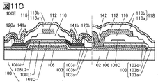
- 11A, 11B, and 11C are cross-sectional views of the semiconductor device.
- FIG. 12 is a cross-sectional view of the semiconductor device.
- FIG. 13A is a top view of the semiconductor device.
- 13B and 13C are cross-sectional views of the semiconductor device.
- FIG. 14 is a cross-sectional view of the semiconductor device.
- 15A, 15B, 15C, and 15D are cross-sectional views illustrating a method for manufacturing a semiconductor device.
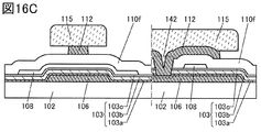
- 16A, 16B, and 16C are cross-sectional views illustrating a method for manufacturing a semiconductor device.
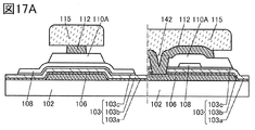
- 17A, 17B, and 17C are cross-sectional views illustrating a method for manufacturing a semiconductor device.
- 18A, 18B, and 18C are cross-sectional views illustrating a method for manufacturing a semiconductor device.
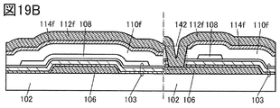
- 19A, 19B, 19C, and 19D are cross-sectional views illustrating a method for manufacturing a semiconductor device.
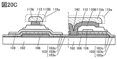
- 20A, 20B, and 20C are cross-sectional views illustrating a method for manufacturing a semiconductor device.
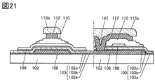
- FIG. 21 is a cross-sectional view illustrating a method for manufacturing a semiconductor device.
- 22A, 22B, and 22C are top views of the display device.
- FIG. 23 is a cross-sectional view of the display device.
- FIG. 24 is a cross-sectional view of the display device.
- FIG. 25 is a cross-sectional view of the display device.
- FIG. 26 is a cross-sectional view of the display device.
- FIG. 27A is a block diagram of the display device.
- 27B and 27C are circuit diagrams of the display device.
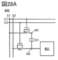
- 28A, 28C, and 28D are circuit diagrams of the display device.
- FIG. 28B is a timing chart of the display device.
- FIG. 29A is a diagram showing a configuration example of the display module.
- FIG. 29B is a schematic cross-sectional view of the display module.
- FIG. 30A is a diagram showing a configuration example of an electronic device.
- FIG. 30B is a schematic cross-sectional view of the electronic device.
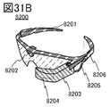
- 31A, 31B, 31C, 31D, and 31E are diagrams showing configuration examples of electronic devices.
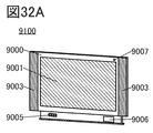
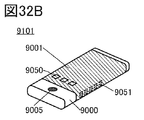
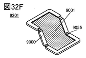
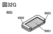
- 32A, 32B, 32C, 32D, 32E, 32F, and 32G are diagrams showing configuration examples of electronic devices.
- 33A, 33B, 33C, and 33D are diagrams showing configuration examples of electronic devices.
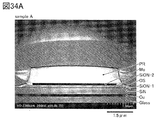
- 34A and 34B are cross-sectional STEM images.
- 35A and 35B are cross-sectional STEM images.
- 36A and 36B are cross-sectional STEM images.
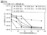
- 37A and 37B are diagrams showing the resistance of the metal oxide film.
- 38A and 38B are diagrams showing the resistance of the metal oxide film.
- 39A and 39B are diagrams showing the resistance of the metal oxide film.
- the source and drain functions of the transistors may be interchanged when transistors having different polarities are adopted or when the direction of the current changes in the circuit operation. Therefore, the terms source and drain can be interchanged.
- the channel length direction of the transistor means one of the directions parallel to the straight line connecting the source region and the drain region at the shortest distance. That is, the channel length direction corresponds to one of the directions of the current flowing through the semiconductor layer when the transistor is on. Further, the channel width direction means a direction orthogonal to the channel length direction. Depending on the structure and shape of the transistor, the channel length direction and the channel width direction may not be fixed to one.
- “electrically connected” includes the case of being connected via "something having some electrical action”.
- the “thing having some kind of electrical action” is not particularly limited as long as it enables the exchange of electric signals between the connection targets.
- “things having some kind of electrical action” include electrodes, wirings, switching elements such as transistors, resistance elements, inductors, capacitors, and other elements having various functions.
- membrane and the term “layer” can be interchanged with each other.
- conductive layer and “insulating layer” may be interchangeable with the terms “conductive film” and “insulating film”.
- the top surface shapes are substantially the same.
- the contours do not overlap, and the end of the upper layer may be located inside the end of the lower layer, or the end of the upper layer may be located outside the end of the lower layer.
- the top surface shape is roughly the same.
- the off current means a drain current when the transistor is in an off state (also referred to as a non-conducting state or a cutoff state).
- the off state is a state in which the voltage V gs between the gate and the source is lower than the threshold voltage V th in the n-channel transistor (higher than V th in the p-channel transistor) unless otherwise specified. To say.
- the display panel which is one aspect of the display device, has a function of displaying (outputting) an image or the like on the display surface. Therefore, the display panel is one aspect of the output device.
- an IC is mounted on a display panel board with a connector such as FPC (Flexible Printed Circuit) or TCP (Tape Carrier Package) attached, or on the board by a COG (Chip On Glass) method or the like. It may be referred to as a display panel module, a display module, or simply a display panel.
- a connector such as FPC (Flexible Printed Circuit) or TCP (Tape Carrier Package) attached, or on the board by a COG (Chip On Glass) method or the like.
- COG Chip On Glass
- the touch panel which is one aspect of the display device, has a function of displaying an image or the like on a display surface, and a touched object such as a finger or a stylus touches, presses, or approaches the display surface. It has a function as a touch sensor for detecting. Therefore, the touch panel is one aspect of the input / output device.
- the touch panel can also be called, for example, a display panel with a touch sensor (or a display device) or a display panel with a touch sensor function (or a display device).
- the touch panel may also have a configuration including a display panel and a touch sensor panel. Alternatively, it may be configured to have a function as a touch sensor inside or on the surface of the display panel.
- a touch panel board on which a connector or an IC is mounted may be referred to as a touch panel module, a display module, or simply a touch panel.
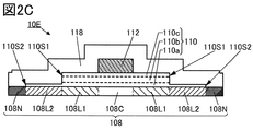
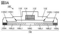
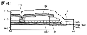
- the transistor 10 has a semiconductor layer 108, an insulating layer 110, and a conductive layer 112.
- the insulating layer 110 functions as a gate insulating layer.
- the conductive layer 112 functions as a gate electrode.
- the transistor 10 is a so-called top gate type transistor in which a gate electrode is provided on the semiconductor layer 108.
- the semiconductor layer 108 has a region 108C, a pair of regions 108L1, a pair of regions 108L2, and a pair of regions 108N.
- the region 108C has a region overlapping the conductive layer 112 and the insulating layer 110, and functions as a channel forming region.
- the pair of regions 108L1 are provided so as to sandwich the region 108C.
- the pair of regions 108L2 are provided so as to sandwich the region 108C and the pair of regions 108L1.
- the region 108L1 and the region 108L2 have a region that does not overlap with the conductive layer 112 and overlaps with the insulating layer 110.
- the pair of regions 108N are provided with the region 108C, the pair of regions 108L1 and the pair of regions 108L2 interposed therebetween.
- the region 108N does not overlap with either the conductive layer 112 or the insulating layer 110.
- the region 108N has a lower resistance than the region 108C and functions as a source region and a drain region. It is preferable that the regions 108L1 and 108L2 each have a lower resistance than the region 108C and a higher resistance than the region 108N, respectively.
- the region 108L1 and the region 108L2 have a function as a buffer region for relaxing the drain electric field.
- the region 108L1 and the region 108L2 function as a so-called LDD (Lightly Doped Drain) region.
- the electric field in the drain region can be relaxed. , It is possible to reduce the fluctuation of the threshold voltage of the transistor due to the electric field in the drain region.
- the value of the sheet resistance of the region 108N is preferably 1 ⁇ / ⁇ or more and less than 1 ⁇ 10 3 ⁇ / ⁇ , and further preferably 1 ⁇ / ⁇ or more and 8 ⁇ 10 2 ⁇ / ⁇ or less. preferable.
- the value of the sheet resistance in the region 108C is preferably 1 ⁇ 10 7 ⁇ / ⁇ or more, more preferably 1 ⁇ 10 8 ⁇ / ⁇ or more, and further preferably 1 ⁇ 10 9 ⁇ / ⁇ or more.
- the sheet resistance values of the region 108L1 and the region 108L2 are preferably, for example, 1 ⁇ 10 3 ⁇ / ⁇ or more and 1 ⁇ 10 9 ⁇ / ⁇ or less, and further 1 ⁇ 10 3 ⁇ / ⁇ or more and 1 ⁇ 10 8 ⁇ / ⁇ or less is preferable, 1 ⁇ 10 3 ⁇ / ⁇ or more and 1 ⁇ 10 7 ⁇ / ⁇ or less are preferable, and 1 ⁇ 10 3 ⁇ / ⁇ or more and 1 ⁇ 10 6 ⁇ / ⁇ or less are preferable, and further 1 It is preferably ⁇ 10 3 ⁇ / ⁇ or more and 1 ⁇ 10 5 ⁇ / ⁇ or less.
- the sheet resistance can be calculated from the resistance value.
- the electric resistance of the region 108C in the state where the channel is not formed is preferably 1 ⁇ 10 6 times or more and 1 ⁇ 10 12 times or less, and further 1 ⁇ 10 6 times or more and 1 ⁇ 10 11 times or less of the electric resistance of the region 108N. Is preferable, and more preferably 1 ⁇ 10 6 times or more and 1 ⁇ 10 10 times or less.
- the electrical resistance of the region 108C in a state that is not a channel is formed, 1 ⁇ 10 9 times or less are preferred 1 ⁇ 10 0 times the electrical resistance of each region 108L1 and the region 108L2, more 1 ⁇ 10 1 ⁇ to 1 ⁇ preferably 10 8 times or less, more preferably 1 ⁇ 10 2 times or more 1 ⁇ 10 7 times or less.
- Each resistance region 108L1 and region 108L2 preferably 1 ⁇ 10 0 times or more 1 ⁇ 10 9 times the electrical resistance of the region 108N, more preferably 1 ⁇ 10 1 times or more 1 ⁇ 10 8 times or less, further Is preferably 1 ⁇ 10 1 times or more and 1 ⁇ 10 7 times or less.
- the carrier concentration in the semiconductor layer 108 is preferably the lowest in the region 108C and the highest in the region 108N.
- the carrier concentration of the region 108C can be kept extremely low even when impurities such as hydrogen diffuse from the region 108N during the manufacturing process, for example. Can be done.
- the lower the carrier concentration in the region 108C that functions as the channel forming region the more preferably, 1 ⁇ 10 18 cm -3 or less, more preferably 1 ⁇ 10 17 cm -3 or less, and 1 ⁇ 10 16 cm. It is more preferably -3 or less, further preferably 1 ⁇ 10 13 cm -3 or less, and even more preferably 1 ⁇ 10 12 cm -3 or less.
- the lower limit of the carrier concentration in the region 108C is not particularly limited, but may be, for example, 1 ⁇ 10 -9 cm -3 .
- the carrier concentration in the region 108N can be, for example, 5 ⁇ 10 18 cm -3 or more, preferably 1 ⁇ 10 19 cm -3 or more, and more preferably 5 ⁇ 10 19 cm -3 or more.
- the upper limit of the carrier concentration in the region 108N is not particularly limited, but may be, for example, 5 ⁇ 10 21 cm -3 , 1 ⁇ 10 22 cm -3 , or the like.
- the carrier concentrations in regions 108L1 and 108L2 can be values between regions 108C and 108N, respectively.
- the value may be in the range of 1 ⁇ 10 14 cm -3 or more and less than 1 ⁇ 10 20 cm -3 .
- the carrier concentrations in the regions 108L1 and 108L2 do not have to be uniform, and may have a gradient such that the carrier concentrations decrease from the region 108N side to the region 108C side. Further, the hydrogen concentration in the region 108L1 and the region 108L2 may have a gradient such that the hydrogen concentration decreases from the region 108N side to the region 108C side.
- the region 108L2 has a lower resistance than the region 108L1. That is, it is preferable that the resistance of the semiconductor layer 108 gradually decreases from the region 108C side toward the region 108N side.
- the value of the sheet resistance of the region 108L1 is, for example, preferably 1 ⁇ 10 4 ⁇ / ⁇ or more and 1 ⁇ 10 9 ⁇ / ⁇ or less, and further 1 ⁇ 10 4 ⁇ / ⁇ or more and 1 ⁇ 10 8 ⁇ / ⁇ or less are preferable, and 1 ⁇ 10 4 ⁇ / ⁇ or more and 1 ⁇ 10 7 ⁇ / ⁇ or less are preferable, and further, 1 ⁇ 10 4 ⁇ / ⁇ or more and 1 ⁇ 10 6 It is preferably ⁇ / ⁇ or less, and more preferably 1 ⁇ 10 4 ⁇ / ⁇ or more and 1 ⁇ 10 5 ⁇ / ⁇ or less.
- the value of the sheet resistance in the region 108L2 is, for example, preferably 1 ⁇ 10 3 ⁇ / ⁇ or more and 1 ⁇ 10 8 ⁇ / ⁇ or less, and further preferably 1 ⁇ 10 3 ⁇ / ⁇ or more and 1 ⁇ 10 7 ⁇ / ⁇ or less.
- the resistance of the region 108L1 with respect to the resistance of the region 108L2 is preferably 2 times or more and 1 ⁇ 10 3 times or less, further preferably 3 times or more and 1 ⁇ 10 2 times or less, and further preferably 4 times or more and 10 times or less.
- Region 108L1, region 108L2, and region 108N are regions containing the first element, respectively.
- the first element for example, one or more of hydrogen, boron, carbon, nitrogen, fluorine, phosphorus, sulfur, arsenic, aluminum, magnesium, helium, neon, argon, krypton, and xenon can be used.
- the first element one or more of hydrogen, boron, nitrogen and phosphorus can be preferably used.
- the region 108L1, the region 108L2, and the region 108N may each have a plurality of first elements.
- the concentration of the first element in the semiconductor layer 108 is preferably higher in the order of region 108C, region 108L1, region 108L2, and region 108N.
- the concentration of the first element in the semiconductor layer 108 is determined by, for example, an analytical method such as secondary ion mass spectrometry (SIMS: Secondary Ion Mass Spectrometry) or X-ray photoelectron spectroscopy (XPS: X-ray Photoelectron Spectroscopy). Can be analyzed.
- an analytical method such as secondary ion mass spectrometry (SIMS: Secondary Ion Mass Spectrometry) or X-ray photoelectron spectroscopy (XPS: X-ray Photoelectron Spectroscopy).
- SIMS Secondary Ion Mass Spectrometry
- XPS X-ray Photoelectron Spectroscopy
- the first element may not be detected in the analysis, or it may be below the lower limit of detection. In particular, since the concentration of the first element is low in the region 108C, the first element may not be detected in the analysis or may be below the lower limit of detection. Similarly, in the region 108L1, the first element may not be detected in the analysis or may be below the detection lower limit.
- the film thickness of the insulating layer 110 in the region overlapping the region 108L1 is substantially equal to the film thickness of the insulating layer 110 in the region overlapping the region 108C.
- the film thickness of the insulating layer 110 in the region overlapping the region 108L2 is preferably thinner than the film thickness of the insulating layer 110 in the region overlapping the region 108L1. That is, the film thickness of the insulating layer 110 is preferably a shape having a step (hereinafter, also referred to as a stepped shape) in which the film thickness gradually decreases from the region 108C side toward the region 108N side.
- the insulating layer 110 has a stepped shape, the amount of the first element added to the region 108C, the region 108L1, the region 108L2, and the region 108N can be controlled, and the resistance of the semiconductor layer 108 can be controlled by the region 108C, the region 108L1, and the region 108N. It can be lowered in the order of 108L2 and region 108N. Further, since the insulating layer 110 has a stepped shape, the covering property of the layer (for example, the insulating layer 118) formed on the insulating layer 110 is improved, and problems such as step breakage and voids occur in the layer. Can be suppressed.
- the fact that the film thickness of A is substantially equal to the film thickness of B means that the ratio of the film thickness of B to the film thickness of A is 0.8 or more and 1.2 or less.
- the end portion of the insulating layer 110 is located inside the end portion of the semiconductor layer 108.
- the insulating layer 110 has a first side surface 110S1 and a second side surface 110S2.
- the first side surface 110S1 and the second side surface 110S2 are located on the semiconductor layer 108, respectively.
- the first side surface 110S1 is located outside the end portion of the conductive layer 112, and the second side surface 110S2 is located outside the first side surface 110S1.
- the insulating layer 110 in contact with the semiconductor layer 108 preferably has an oxide or an oxide nitride. Further, it is more preferable that the insulating layer 110 has a region containing oxygen in excess of the stoichiometric composition. In other words, the insulating layer 110 has an insulating film capable of releasing oxygen. For example, forming the insulating layer 110 in an oxygen atmosphere, performing heat treatment in an oxygen atmosphere after forming the insulating layer 110, performing plasma treatment in an oxygen atmosphere after forming the insulating layer 110, and the like. Alternatively, oxygen can be supplied into the insulating layer 110 by forming an oxide film or an oxide nitride film on the insulating layer 110 in an oxygen atmosphere. In each treatment for supplying oxygen, an oxidizing gas (for example, nitrous oxide, ozone, etc.) may be used instead of or in addition to oxygen.
- an oxidizing gas for example, nitrous oxide, ozone, etc.
- the insulating layer 110 includes, for example, a sputtering method, a chemical vapor deposition (CVD) method, a vacuum vapor deposition method, a pulsed laser deposition (PLD) method, an atomic layer deposition (ALD) method, and an atomic layer deposition (ALD) method. Etc. can be formed. Further, the CVD method includes a plasma chemical vapor deposition (PECVD: Plasma Enhanced CVD) method, a thermal CVD method, and the like.
- PECVD plasma chemical vapor deposition
- the insulating layer 110 is preferably formed by the PECVD (plasma CVD) method.
- the semiconductor layer 108 contains a metal oxide exhibiting semiconductor characteristics (hereinafter, also referred to as an oxide semiconductor).
- the semiconductor layer 108 preferably contains at least indium and oxygen.
- the carrier mobility can be increased. For example, it is possible to realize a transistor capable of passing a larger current than when amorphous silicon is used.
- the crystallinity of the semiconductor material used for the semiconductor layer 108 is not particularly limited, and is an amorphous semiconductor, a single crystal semiconductor, or a semiconductor having a crystallinity other than a single crystal (microcrystalline semiconductor, polycrystalline semiconductor, or partially crystallized). Any of the semiconductors having a region) may be used. It is preferable to use a single crystal semiconductor or a semiconductor having crystallinity because deterioration of transistor characteristics can be suppressed.
- the semiconductor layer 108 preferably has a metal oxide.
- the semiconductor layer 108 may have silicon. Examples of silicon include amorphous silicon and crystalline silicon (low temperature polysilicon, single crystal silicon, etc.).
- the semiconductor layer 108 When a metal oxide is used as the semiconductor layer 108, for example, indium and the element M (M is gallium, aluminum, silicon, boron, yttrium, tin, copper, vanadium, beryllium, titanium, iron, nickel, germanium, zirconium). , Molybdenum, lanthanum, cerium, neodymium, hafnium, tantalum, tungsten, and one or more of gallium) and zinc.
- the element M is preferably one or more of aluminum, gallium, yttrium, and tin. Further, it is more preferable that the element M has either one or both of gallium and tin.
- an oxide containing indium (In), gallium (Ga), and zinc (Zn) (hereinafter, also referred to as IGZO) can be preferably used.
- the semiconductor layer 108 in addition to indium, gallium, and zinc, aluminum, silicon, boron, ittrium, tin, copper, vanadium, beryllium, titanium, iron, nickel, germanium, zirconium, molybdenum, lantern, cerium, neodymium, and hafnium. , Tantalum, tungsten, or magnesium, and oxides containing one or more of them can also be used. In particular, it is preferable to use an oxide containing tin, aluminum, or silicon in addition to indium, gallium, and zinc as the semiconductor layer because a transistor having high field-effect mobility can be obtained.
- the sputtering target used for forming the In-M-Zn oxide preferably has an atomic number ratio of In to the element M of 1 or more.
- the atomic number ratio of the semiconductor layer to be formed includes a fluctuation of plus or minus 40% of the atomic number ratio of the metal element contained in the sputtering target.
- the semiconductor layer 108 preferably contains a metal oxide containing at least indium and oxygen. Further, the semiconductor layer 108 may contain zinc in addition to these. Further, the semiconductor layer 108 may contain gallium.
- the composition of the semiconductor layer 108 greatly affects the electrical characteristics and reliability of the transistor 10. For example, by increasing the content of indium in the semiconductor layer 108, the carrier mobility is improved, and a transistor having a high field effect mobility can be realized.
- GBT Gate Bias Stress Test
- PBTS Positive Bias Temperature Stress
- the PBTS test and the NBTS test conducted in a state of being irradiated with light such as white LED light are called PBTIS (Positive Bias Temperature Temperature) test and NBTIS (Negative Bias Temperature Temperature) test, respectively.
- the composition of the semiconductor layer 108 preferably has a gallium content smaller than that of indium. As a result, a highly reliable transistor can be realized.
- One factor of the fluctuation of the threshold voltage in the PBTS test is the defect level at or near the interface between the semiconductor layer and the gate insulating layer.
- the higher the defect level density the more remarkable the deterioration in the PBTS test.
- the gallium content in the portion of the semiconductor layer in contact with the gate insulating layer the formation of the defect level can be suppressed.
- Gallium contained in the semiconductor layer 108 has a property of easily attracting oxygen as compared with other metal elements (for example, indium and zinc). Therefore, at the interface between the metal oxide film containing a large amount of gallium and the insulating layer 110 containing oxide, gallium combines with excess oxygen in the insulating layer 110 to generate carrier (here, electron) trap sites. It is inferred that it will be easier. Therefore, when a positive potential is applied to the gate, the carrier may be trapped at the interface between the semiconductor layer and the gate insulating layer, so that the threshold voltage may fluctuate.
- carrier here, electron
- a metal oxide film in which the atomic number ratio of In is higher than the atomic number ratio of Ga is applied to the semiconductor layer 108.
- the ratio of the number of gallium atoms (atomic number ratio) to the number of atoms of the metal element contained in the metal oxide is greater than 0 and 50%. It can be less than, preferably 0.05% or more and 30% or less, more preferably 0.1% or more and 15% or less, and more preferably 0.1% or more and 5% or less. Note that by the inclusion of gallium in the semiconductor layer 108, oxygen deficiency (hereinafter, referred to as V O) achieves the effect that is less likely to occur.
- V O oxygen deficiency
- a metal oxide film containing no gallium may be applied to the semiconductor layer 108.
- In—Zn oxide can be applied to the semiconductor layer 108.
- the electric field effect mobility of the transistor can be increased by increasing the atomic number ratio of In to the atomic number of the metal element contained in the metal oxide film.
- a highly crystalline metal oxide film is obtained, so that fluctuations in the electrical characteristics of the transistor are suppressed and reliability is improved.
- a metal oxide film containing no gallium and zinc such as indium oxide may be applied to the semiconductor layer 108.
- an oxide containing indium and zinc can be used for the semiconductor layer 108.
- a metal oxide film having an atomic number ratio of In higher than that of the element M it is preferable to apply a metal oxide film having an atomic number ratio of In higher than that of the element M to the semiconductor layer 108. Further, it is preferable to apply a metal oxide film in which the atomic number ratio of Zn is higher than the atomic number ratio of the element M.
- a crystalline metal oxide film for the semiconductor layer 108 It is preferable to use a crystalline metal oxide film for the semiconductor layer 108.
- a metal oxide film having a CAAC (c-axis aligned crystal) structure, an nc (nano crystal) structure, a polycrystalline structure, a microcrystal structure, etc., which will be described later, can be used.
- CAAC c-axis aligned crystal
- nc nano crystal
- the semiconductor layer 108 may have a laminated structure in which layers having different compositions, layers having different crystallinity, or layers having different impurity concentrations are laminated.
- the parasitic resistance can be reduced, a transistor having a high on-current can be obtained, and a semiconductor device having a high on-current can be obtained.
- a conductive film containing a metal or an alloy as the conductive layer 112 because the electric resistance can be suppressed.
- a conductive film containing an oxide in the conductive layer 112 may be used.
- signal delay is suppressed by reducing the wiring resistance, and high-speed driving becomes possible.
- Copper, silver, gold, aluminum, or the like can be used as the conductive layer 112. In particular, copper is preferable because it has low resistance and excellent mass productivity.
- the conductive layer 112 may have a laminated structure.
- the second conductive layer is provided on the upper part, the lower part, or both of the low resistance first conductive layer.
- the second conductive layer it is preferable to use a conductive material that is less likely to be oxidized (has oxidation resistance) than the first conductive layer. Further, as the second conductive layer, it is preferable to use a material that suppresses the diffusion of the components of the first conductive layer.
- indium oxide indium zinc oxide, indium tin oxide (ITO), silicon-containing indium tin oxide (ITSO), metal oxide such as zinc oxide, or titanium nitride, nitride.
- Metal nitrides such as tantalum, molybdenum nitride, and tungsten nitride can be preferably used.
- the transistor 10 preferably further has an insulating layer 118.
- the insulating layer 118 functions as a protective layer that protects the transistor 10.
- an inorganic insulating material such as an oxide, an oxide nitride, a nitride oxide or a nitride can be used. More specifically, inorganic insulating materials such as silicon oxide, silicon oxide nitride, silicon nitride, silicon nitride oxide, aluminum oxide, aluminum nitride, aluminum nitride, hafnium oxide, and hafnium aluminate can be used. Further, the insulating layer 118 may have a laminated structure of two or more layers.
- the oxidative nitride refers to a material whose composition has a higher oxygen content than nitrogen
- the nitride oxide refers to a material whose composition has a higher nitrogen content than oxygen.
- the description of silicon oxide nitride refers to a material having a higher oxygen content than nitrogen as its composition
- the description of silicon nitride oxide refers to a material having a higher nitrogen content than oxygen as its composition. Is shown.
- oxide nitride and a nitride oxide containing the same element when an oxide nitride and a nitride oxide containing the same element are described, the oxide nitride has a higher oxygen content than the nitride oxide, and Materials that satisfy either or both of the low nitrogen contents are included.
- nitride oxides include materials that satisfy either or both of lower oxygen content and higher nitrogen content than oxide nitrides.
- silicon oxide and silicon nitride silicon oxide contains a material having a higher oxygen content and a lower nitrogen content than silicon nitride.
- silicon nitride contains a material having a lower oxygen content and a higher nitrogen content than silicon oxide.
- the insulating layer 118 may function as a source of the first element for the regions 108L1, the region 108L2, and the region 108N.
- the insulating layer 118 can function as a source of hydrogen for the regions 108L1, the region 108L2, and the region 108N. Since the regions 108L1, the region 108L2, and the region 108N have different distances from the insulating layer 118, the amount of hydrogen supplied from the insulating layer 118 can be different. Specifically, the distance from the insulating layer 118 is shortened in the order of region 108L1, region 108L2, and region 108N, and the amount of hydrogen added can be increased in this order.
- the resistance can be reduced in the order of region 108L1, region 108L2, and region 108N.
- the insulating layer 118 is in contact with the region 108N of the semiconductor layer 108.
- the resistance of the region 108N can be particularly reduced. Since the region 108C has the conductive layer 112 and the insulating layer 110 between the region 108C and the insulating layer 118, it is difficult for hydrogen to be added and the resistance of the region 108C can be suppressed from being lowered.
- the insulating layer 118 may be formed by using a mixed gas having a gas containing hydrogen.
- a gas containing hydrogen for example, hydrogen (H 2 ), ammonia (NH 3 ), silane (SiH 4 ) and the like can be used.
- the transistor 10 which is one aspect of the present invention, has a region 108L1 and a region 108L2 between the region 108C and the region 108N, so that the transistor 10 has a high drain withstand voltage and a high on-current, and is a highly reliable transistor. Can be done.
- FIG. 1B is a schematic cross-sectional view of the transistor 10A in the channel length direction.
- the transistor 10A is mainly different from the transistor 10 in that it has a conductive layer 106.
- the conductive layer 106 has a region that overlaps with the semiconductor layer 108, the insulating layer 110, and the conductive layer 112 via the insulating layer 103.
- the conductive layer 106 functions as a first gate electrode (also referred to as a back gate electrode).
- the insulating layer 103 functions as a first gate insulating layer.
- the conductive layer 112 functions as a second gate electrode (also referred to as a top gate electrode), and the insulating layer 110 functions as a second gate insulating layer.
- the transistor 10A can increase the current that can be passed when it is in the ON state by applying the same potential to the conductive layer 112 and the conductive layer 106. Further, the transistor 10A can give one of the conductive layer 112 and the conductive layer 106 a potential for controlling the threshold voltage, and give the other a potential for controlling the on state and the off state of the transistor 10A. Further, the electrical characteristics of the transistor 10A can be stabilized by electrically connecting one of the conductive layer 112 and the conductive layer 106 to the source.
- the insulating layer 103 that functions as the second gate insulating layer preferably functions as a barrier layer that suppresses the diffusion of impurities from the formed surface side of the insulating layer 103 to the semiconductor layer 108 or the like.
- the impurity for example, there is a metal component contained in the conductive layer 106.
- the insulating layer 103 satisfies one or more of high pressure resistance, low stress of the film, difficulty in releasing hydrogen and water, difficulty in diffusing hydrogen and water, and few defects. It is preferable, and it is more preferable to satisfy all of these.
- an insulating film that can be used for the insulating layer 110 can be used.
- a conductive film that can be used for the conductive layer 112 can be used.
- FIG. 1B shows an example in which the end portion of the conductive layer 106 substantially coincides with the end portion of the conductive layer 112, but one aspect of the present invention is not limited to this.
- the end portion of the conductive layer 106 may be located outside the end portion of the conductive layer 112. Further, the end portion of the conductive layer 106 may be located inside the end portion of the conductive layer 112.
- “the end part roughly coincides” means that at least a part of the contour overlaps between the laminated layers. For example, the case where the upper layer and the lower layer are processed by the same mask pattern or a part of the same mask pattern is included. However, strictly speaking, the contours do not overlap, and the end of the upper layer may be located inside the end of the lower layer, or the end of the upper layer may be located outside the end of the lower layer. The ends are roughly the same. "
- FIG. 1C is a schematic cross-sectional view of the transistor 10B in the channel length direction.
- the transistor 10B is mainly different from the transistor 10A in that the insulating layer 103 has a laminated structure.
- FIG. 1C shows a configuration example in which the insulating layer 103 has a three-layer structure in which the insulating layer 103a, the insulating layer 103b, and the insulating layer 103c are laminated in this order from the conductive layer 106 side.
- the insulating layer 103a is in contact with the conductive layer 106. Further, the insulating layer 103c is in contact with the semiconductor layer 108.
- the three insulating films of the insulating layer 103 it is preferable to use a nitrogen-containing insulating film for the insulating layer 103a located on the surface to be formed side of the insulating layer 103.
- the three insulating films included in the insulating layer 103 are continuously formed by using a plasma CVD apparatus without being exposed to the atmosphere.
- the insulating layer 103a is preferably a dense film capable of preventing the diffusion of impurities from below this.
- the insulating layer 103a is preferably a film capable of blocking metal elements, hydrogen, water, etc. contained in a member (for example, a substrate) on the surface to be formed side of the insulating layer 103a. Therefore, an insulating film formed under conditions having a lower film forming speed than the insulating layer 103b can be applied to the insulating layer 103a.
- an insulating film containing nitrogen such as a silicon nitride film, a silicon oxide film, an aluminum nitride film, or a hafnium nitride film can be used.
- a dense silicon nitride film formed by using a plasma CVD apparatus By using such an insulating film containing nitrogen, it is possible to suitably suppress the diffusion of impurities from the surface to be formed side even when the thickness is thin.
- the insulating layer 103c in contact with the semiconductor layer 108 is preferably formed of an insulating film containing an oxide or an oxide nitride.
- an oxide film or an oxide nitride film for the insulating layer 103c.
- a dense insulating film for the insulating layer 103c which does not easily adsorb impurities such as water on its surface.
- the insulating layer 103c has a region containing oxygen in excess of the stoichiometric composition.
- the insulating layer 103c is preferably an insulating film capable of releasing oxygen by heating.
- Oxygen can also be supplied into the insulating layer 103c by performing this or by forming an oxide film or an oxide nitride film on the insulating layer 103c in an oxygen atmosphere.
- an oxidizing gas for example, nitrous oxide, ozone, etc.
- oxygen may be supplied from the insulating film into the insulating layer 103c by forming an insulating film capable of releasing oxygen by heating on the insulating layer 103c and then performing a heat treatment.
- oxygen can be supplied into the insulating layer 103c. Then, after forming the metal oxide film to be the semiconductor layer, heat treatment is performed to supply oxygen in the insulating layer 103c to the metal oxide film, resulting in oxygen deficiency ( VO ) in the metal oxide film. Can be reduced.
- the insulating layer 103c for example, silicon oxide film, silicon nitride film, silicon nitride film, aluminum oxide film, hafnium oxide film, yttrium oxide film, zirconium oxide film, gallium oxide film, tantalum oxide film, magnesium oxide film, oxidation.
- An insulating layer containing at least one lanthanum film, cerium oxide film, and neodymium oxide film can be used.
- the insulating layer 103b located between the insulating layer 103a and the insulating layer 103c it is preferable to use an insulating film formed under conditions of low stress and high film forming speed.
- the insulating layer 103b is preferably a film having less stress than the insulating layer 103a and the insulating layer 103c.
- the insulating layer 103b is preferably a film formed under conditions having a higher film forming speed than the insulating layer 103a and the insulating layer 103c.
- an insulating film for the insulating layer 103b that does not release hydrogen or water as much as possible.
- an insulating film it is possible to prevent hydrogen and water from diffusing from the insulating layer 103b to the semiconductor layer 108 via the insulating layer 103c due to heat treatment or heat applied during the process, and the carrier concentration in the region 108C. Can be lowered.
- an insulating film for the insulating layer 103b which does not easily suck oxygen.
- an insulating film in which oxygen does not easily diffuse As a result, when the heat treatment for supplying oxygen from the insulating layer 103c to the semiconductor layer 108 (or the metal oxide film to be the semiconductor layer 108) is performed, oxygen diffuses from the insulating layer 103c to the insulating layer 103b side. It is possible to prevent the amount of oxygen supplied to the semiconductor layer 108 from being reduced.
- an insulating layer containing at least one silicon nitride film, silicon nitride film, aluminum oxide film, hafnium oxide film, aluminum nitride film, and hafnium nitride film can be used.
- the thickness of the insulating layer 103b is the thickest.
- the thickness (total thickness) of the insulating layer 103 is the relative permittivity of each insulating film in consideration of the value of the relative permittivity required for the insulating layer 103 and the dielectric strength performance required for the insulating layer 103. It can be determined based on the value of the rate and the thickness of each insulating film. That is, the thickness of each insulating film can be adjusted to each other within a range satisfying the above requirements.
- the insulating layer 103b is preferably thicker than the insulating layer 103a.
- the insulating layer 103b thicker than the insulating layer 103a, it is possible to reduce the amount of hydrogen that can reach the insulating layer 103c even when a film that easily releases hydrogen by heating is used as the insulating layer 103a. it can.
- the insulating layer 103a thinner than the insulating layer 103b, the volume of the insulating layer 103a can be made relatively small, so that the amount of hydrogen that can be released by the insulating layer 103a itself can be reduced.
- the insulating layer 103b is preferably thicker than the insulating layer 103c.
- the insulating layer 103c is too thick, when the treatment of supplying oxygen into the insulating layer 103c is performed, the amount of oxygen remaining without being released from the insulating layer 103c due to heating increases, and as a result, the semiconductor layer 108 ( Alternatively, the amount of oxygen that can be supplied to the metal oxide film (the metal oxide film that becomes the semiconductor layer 108) may decrease. Therefore, by making the insulating layer 103c thinner (reducing the volume) than the insulating layer 103b, the amount of oxygen remaining in the insulating layer 103c after heating can be reduced. As a result, the proportion of oxygen supplied to the semiconductor layer 108 can be increased from the oxygen supplied to the insulating layer 103c, so that the amount of oxygen supplied to the semiconductor layer 108 can be effectively increased.
- the thickest insulating layer 103b is formed under the condition of high film forming speed, and the thinner insulating layer 103a and the insulating layer 103c are formed so as to be a dense film under the condition of low film forming rate.
- the film formation time of the insulating layer 103 can be shortened and the productivity can be improved without impairing the reliability.
- an insulating film containing at least silicon and nitrogen typically a silicon nitride film, or a silicon nitride oxide film
- an insulating film containing at least silicon, nitrogen, and oxygen typically a silicon nitride oxide film or a silicon nitride nitride film
- an insulating film containing at least silicon and oxygen typically a silicon oxide film or a silicon nitride nitride film.
- the amount of oxygen contained in the insulating layer 103b is preferably larger than that of the insulating layer 103a and smaller than that of the insulating layer 103c. Further, the amount of nitrogen contained in the insulating layer 103b is preferably less than that of the insulating layer 103a and larger than that of the insulating layer 103c.
- the contents of oxygen and nitrogen contained in the insulating layer 103a, the insulating layer 103b, and the insulating layer 103c shall be analyzed by an analytical method such as secondary ion mass spectrometry (SIMS) or X-ray photoelectron spectroscopy (XPS). Can be done.
- XPS is suitable when the content of the target element in the membrane is high (for example, 0.5 atoms / cm 3 or more, or 1 atoms / cm 3 or more).
- SIMS is suitable when the content of the target element in the membrane is low (for example, 0.5 atoms / cm 3 or less, or 1 atoms / cm 3 or less).
- SIMS When comparing the content of elements in the membrane, it is more preferable to perform a composite analysis using both SIMS and XPS analysis methods.
- the film densities of the insulating layer 103a, the insulating layer 103b, and the insulating layer 103c are different, they are observed as a difference in contrast in a transmission electron microscope (TEM: Transmission Electron Microscope) image in the cross section of the insulating layer 103, and these are distinguished. It may be possible. In addition, when the composition and the film density are close to each other, these boundaries may become unclear.
- TEM Transmission Electron Microscope
- the insulating layer 103 may be two layers or four or more layers.
- the insulating layer 103 can have a two-layer structure of the insulating layer 103a and the insulating layer 103c.
- FIG. 2A is a schematic cross-sectional view of the transistor 10C in the channel length direction.
- the transistor 10C is mainly different from the transistor 10 in that the insulating layer 110 has a laminated structure.
- FIG. 2A shows an example in which the insulating layer 110 has a three-layer structure in which the insulating layer 110a, the insulating layer 110b, and the insulating layer 110c are laminated in this order from the semiconductor layer 108 side.
- the insulating layer 110a has a region in contact with the region 108C, the region 108L1 and the region 108L2.
- the insulating layer 110c has a region in contact with the conductive layer 112.
- the insulating layer 110b is located between the insulating layer 110a and the insulating layer 110c.
- the insulating layer 110a, the insulating layer 110b, and the insulating layer 110c are preferably insulating films containing oxides or oxide nitrides, respectively. Further, it is preferable that the insulating layer 110a, the insulating layer 110b and the insulating layer 110c are continuously formed by using the same film forming apparatus without being exposed to the atmosphere. By continuously forming the film, it is possible to prevent impurities such as water from adhering to the interfaces of the insulating layer 110a, the insulating layer 110b, and the insulating layer 110c.
- the insulating layer 110a, the insulating layer 110b, and the insulating layer 110c for example, a silicon oxide film, a silicon nitride film, a silicon nitride film, an aluminum oxide film, a hafnium oxide film, an yttrium oxide film, a zirconium oxide film, a gallium oxide film, An insulating layer containing at least one tantalum oxide film, magnesium oxide film, lanthanum oxide film, cerium oxide film, and neodymium oxide film can be used.
- the insulating layer 110a, the insulating layer 110b, and the insulating layer 110c can be formed by using, for example, a sputtering method, a CVD method, a vacuum deposition method, a PLD method, an ALD method, or the like. Further, the CVD method includes a plasma CVD method, a thermal CVD method and the like.
- the insulating layer 110a, the insulating layer 110b and the insulating layer 110c are preferably formed by the plasma CVD method.
- the insulating layer 110a is formed on the semiconductor layer 108, it is preferable that the insulating layer 110a is formed under conditions that do not damage the semiconductor layer 108 as much as possible.
- the film can be formed under a condition where the film formation rate (also referred to as the film formation rate) is sufficiently low.
- the damage given to the semiconductor layer 108 can be extremely reduced by forming the silicon oxide film under low power conditions.
- the film forming gas used for forming the silicon oxide film is a raw material containing, for example, a sedimentary gas containing silicon such as silane and disilane, and an oxidizing gas such as oxygen, ozone, nitrous oxide and nitrogen dioxide. Gas can be used. Further, in addition to the raw material gas, a diluting gas such as argon, helium, or nitrogen may be contained.
- the film-forming rate can be lowered, and a dense film with few defects can be formed. it can.
- the insulating layer 110b is preferably a film formed under conditions having a higher film forming speed than the insulating layer 110a. As a result, productivity can be improved.
- the insulating layer 110b can be formed under the condition that the film forming rate is increased by setting the flow rate ratio of the sedimentary gas to be larger than that of the insulating layer 110a.
- the insulating layer 110c is preferably an extremely dense film in which defects on its surface are reduced and impurities contained in the atmosphere such as water are not easily adsorbed.
- the film can be formed under a condition that the film forming rate is sufficiently low.
- the insulating layer 110c is formed on the insulating layer 110b, the influence on the semiconductor layer 108 when the insulating layer 110c is formed is smaller than that of the insulating layer 110a. Therefore, the insulating layer 110c can be formed under conditions of higher power than the insulating layer 110a. By reducing the flow rate ratio of the sedimentary gas and forming a film with a relatively high electric power, it is possible to obtain a film having a high density and reduced surface defects.
- a laminated film formed under the condition that the film forming rate of the insulating layer 110b is the fastest and the insulating layer 110a and the insulating layer 110c are slowed down in this order can be used for the insulating layer 110.
- the etching rate under the same conditions in wet etching or dry etching is highest in the insulating layer 110b, and decreases in the order of the insulating layer 110a and the insulating layer 110c.
- the insulating layer 110b is formed thicker than the insulating layer 110a and the insulating layer 110c. By forming the insulating layer 110b having the fastest film forming speed thickly, the time required for the film forming process of the insulating layer 110 can be shortened.
- the boundary between the insulating layer 110a and the insulating layer 110b and the boundary between the insulating layer 110b and the insulating layer 110c are clarified. It may not be possible to confirm. Therefore, in FIG. 2A and the like, these boundaries are clearly indicated by broken lines. Since the insulating layer 110a and the insulating layer 110b have different film densities, the boundary between them can be observed as a difference in contrast in a transmission electron microscope (TEM: Transmission Electron Microscope) image in the cross section of the insulating layer 110. It may be possible. Similarly, the boundary between the insulating layer 110b and the insulating layer 110c may be observed as a difference in contrast.
- TEM Transmission Electron Microscope
- the insulating layer 110 in the region in contact with the region 108C and the insulating layer 110 in the region in contact with the region 108L1 each have a laminated structure of the insulating layer 110a, the insulating layer 110b, and the insulating layer 110c, and the region 108L2
- the insulating layer 110 in the overlapping region has a structure in which the insulating layer 110a and the insulating layer 110b are laminated, one aspect of the present invention is not limited to this.
- the insulating layer 110 in the region overlapping the region 108L2 may have a laminated structure of the insulating layer 110a, the insulating layer 110b, and the insulating layer 110c.
- the insulating layer 110 in the region overlapping the region 108L2 may have a single-layer structure of the insulating layer 110a.
- the insulating layer 110 may have a two-layer structure consisting of an insulating layer 110a and an insulating layer 110c on the insulating layer 110a. Alternatively, the insulating layer 110 may have a single-layer structure. As the insulating layer 110, any of the above-mentioned insulating layer 110a, insulating layer 110b, or insulating layer 110c can be appropriately selected depending on the purpose.
- FIG. 3A is a schematic cross-sectional view of the transistor 10F in the channel length direction.
- the transistor 10F is mainly different from the transistor 10 in that the metal oxide layer 114 is provided between the insulating layer 110 and the conductive layer 112.
- the metal oxide layer 114 has a function of supplying oxygen into the insulating layer 110. Further, when a conductive film containing a metal or alloy easily oxidized is used for the conductive layer 112, the metal oxide layer 114 functions as a barrier layer for preventing the conductive layer 112 from being oxidized by oxygen in the insulating layer 110. ..
- the metal oxide layer 114 also functions as a barrier film that prevents hydrogen and water contained in the conductive layer 112 from diffusing toward the insulating layer 110.
- a material that is less permeable to oxygen and hydrogen than the insulating layer 110 can be used.
- the metal oxide layer 114 can prevent oxygen from diffusing from the insulating layer 110 to the conductive layer 112 even when a metal material such as aluminum or copper that easily absorbs oxygen is used for the conductive layer 112. .. Further, even when the conductive layer 112 contains hydrogen, it is possible to prevent hydrogen from diffusing from the conductive layer 112 to the semiconductor layer 108 via the insulating layer 110. As a result, the carrier concentration in the region 108C can be made extremely low.
- An insulating material or a conductive material can be used for the metal oxide layer 114.
- the metal oxide layer 114 has an insulating property, the metal oxide layer 114 functions as a part of the gate insulating layer.
- the metal oxide layer 114 has conductivity, the metal oxide layer 114 functions as a part of the gate electrode.
- the metal oxide layer 114 it is preferable to use an insulating material having a higher dielectric constant than silicon oxide.
- an aluminum oxide film, a hafnium oxide film, a hafnium aluminate film, or the like because the driving voltage can be reduced.
- a metal oxide can be used as the metal oxide layer 114.
- oxides having indium such as indium oxide, indium zinc oxide, indium tin oxide (ITO), and silicon-containing indium tin oxide (ITSO) can be used.
- Conductive oxides containing indium are preferable because they have high conductivity.
- ITSO contains silicon, it is difficult to crystallize and has high flatness, so that the adhesion to the film formed on ITSO is high.
- a metal oxide such as zinc oxide or zinc oxide containing gallium can be used. Further, as the metal oxide layer 114, a structure in which these are laminated may be used.
- the metal oxide layer 114 it is preferable to use an oxide material containing one or more of the same elements as the semiconductor layer 108. In particular, it is preferable to use an oxide semiconductor material applicable to the semiconductor layer 108. At this time, it is preferable to apply a metal oxide film formed by using the same sputtering target as the semiconductor layer 108 as the metal oxide layer 114 because the apparatus can be shared.
- the electric field effect mobility of the transistor 100 can be increased by using a material having a higher indium composition than the metal oxide layer 114 for the semiconductor layer 108.
- the metal oxide layer 114 is preferably formed by using a sputtering apparatus.
- oxygen can be suitably added to the insulating layer 110 and the semiconductor layer 108 by forming the oxide film in an atmosphere containing oxygen gas.
- the metal oxide layer 114 When the metal oxide layer 114 is formed for the purpose of supplying oxygen to the insulating layer 110, it may be removed after forming the metal oxide film to be the metal oxide layer 114. Further, the metal oxide layer 114 may not be provided if it is unnecessary.
- FIG. 3B is a schematic cross-sectional view of the transistor 10G in the channel length direction.
- the transistor 10G is mainly different from the transistor 10 in that the region 108L3 is provided between the region 108N and the region 108L2.
- the semiconductor layer 108 has a region 108C, a pair of regions 108L1, a pair of regions 108L2, a pair of regions 108L3, and a pair of regions 108N.
- the region 108L3 is provided with the region 108C, the pair of regions 108L1 and the pair of regions 108L2 interposed therebetween. Further, the region 108L3 has a region that does not overlap with the conductive layer 112 and overlaps with the insulating layer 110. Since the above description can be referred to for the area 108C, the area 108L1, and the area 108L2, detailed description thereof will be omitted.
- the regions 108L1, the region 108L2, and the region 108L3 each have a lower resistance than the region 108C and a higher resistance than the region 108N, respectively.
- the area 108L1, the area 108L2 and the area 108L3 function as an LDD area.
- the region 108L3 has a lower resistance than the region 108L2.
- the film thickness of the insulating layer 110 in the region overlapping the region 108L3 is preferably thinner than the film thickness of the insulating layer 110 in the region overlapping the region 108L2. That is, the insulating layer 110 preferably has a stepped shape in which the film thickness gradually decreases from the region 108C side toward the region 108N side. Since the insulating layer 110 has a stepped shape, the resistance of the semiconductor layer 108 can be reduced in the order of region 108C, region 108L1, region 108L2, region 108L3, and region 108N.
- the insulating layer 110 has a first side surface 110S1, a second side surface 110S2, and a third side surface 110S3.
- the first side surface 110S1, the second side surface 110S2, and the third side surface 110S3 are located on the semiconductor layer 108, respectively.
- the first side surface 110S1 is located outside the end of the conductive layer 112
- the second side surface 110S2 is located outside the first side surface 110S1, and the third side surface 110S3. Is located outside the second side surface 110S2.
- FIG. 1A to 1C, 2A to 2C, and 3A have a configuration having two LDD regions (regions 108L1 and 108L2) between regions 108C and 108N, and FIG. 3B has three LDD regions (regions 108L1 and 108L2).
- FIG. 3B has three LDD regions (regions 108L1 and 108L2).
- a configuration may be configured in which p (2 or more p) LDD regions are provided between the regions 108C and 108N.
- FIG. 4A is a schematic cross-sectional view of the transistor 10H in the channel length direction.
- the transistor 10H shows a configuration having a region 108L1 to a region 108Lp between the region 108C and the region 108N.
- the insulating layer 110 has a first side surface 110S1 to a first side surface 110Sp.
- the first side surface 110S1 to the first side surface 110Sp are located on the semiconductor layer 108, respectively.
- the first side surface 110S1 is located outside the end of the conductive layer 112
- the second side surface 110S2 is located outside the first side surface 110S1, and the first side surface 110Sp. Is located outside the side surface 110Sp-1 of the first p-1.
- FIG. 4B is a schematic cross-sectional view of the transistor 101 in the channel length direction. As shown in FIG. 4B, the side surface 110S of the insulating layer 110 may have a slope-like shape. Further, the transistor 101 shows a configuration in which the film thickness of the insulating layer 110 is continuously reduced from the region 108C side to the region 108N side, and the resistance is continuously reduced from the region 108L1 to the region 108Lp. There is.
- FIG. 5A is a top view of the transistor 100
- FIG. 5B corresponds to a cross-sectional view of a cut surface at the alternate long and short dash line A1-A2 shown in FIG. 5A
- FIG. 5C is a sectional view taken along the alternate long and short dash line B1-B2 shown in FIG. 5A.
- a part (protective layer and the like) of the constituent elements of the transistor 100 is omitted.
- the alternate long and short dash line A1-A2 direction corresponds to the channel length direction
- the alternate long and short dash line B1-B2 direction corresponds to the channel width direction.
- the top view of the transistor will be shown in the following drawings by omitting some of the components as in FIG. 5A.
- FIG. 6A An enlarged view of the region P surrounded by the alternate long and short dash line in FIG. 5B is shown in FIG. 6A.
- FIG. 6B An enlarged view of the region R surrounded by the alternate long and short dash line in FIG. 5C is shown in FIG. 6B.
- the transistor 100 is provided on the substrate 102 and has a semiconductor layer 108, an insulating layer 110, a conductive layer 112, an insulating layer 118, and the like.
- the island-shaped semiconductor layer 108 is provided on the substrate 102.
- the insulating layer 110 is provided so as to cover a part of the upper surface of the substrate 102, the side surface of the semiconductor layer 108, and a part of the upper surface of the semiconductor layer 108.
- the conductive layer 112 is provided on the insulating layer 110 and has a portion that overlaps with the semiconductor layer 108.
- the end of the conductive layer 112 is located inside the end of the insulating layer 110.
- the insulating layer 110 has a portion protruding outward from the end portion of the conductive layer 112, at least on the semiconductor layer 108.
- the insulating layer 110 has a portion that overlaps with the conductive layer 112 and functions as a gate insulating layer, and a portion that does not overlap with the conductive layer 112 (that is, a portion that overlaps with the region 108L1 or the region 108L2).
- the semiconductor layer 108 has a region 108C, a pair of regions 108L1, a pair of regions 108L2, and a pair of regions 108N.
- the region 108C has a region overlapping the conductive layer 112 and the insulating layer 110, and functions as a channel forming region.
- the area 108L1 is provided so as to sandwich the area 108C.
- the region 108L2 is provided with the region 108C and the pair of regions 108L1 interposed therebetween. Further, the region 108L1 and the region 108L2 have a region that does not overlap with the conductive layer 112 and overlaps with the insulating layer 110.
- the region 108N is provided with the region 108C, the pair of regions 108L1 and the pair of regions 108L2 interposed therebetween. The region 108N does not overlap with either the conductive layer 112 or the insulating layer 110.
- the region 108L1 and the region 108L2 are regions of the semiconductor layer 108 that overlap with the insulating layer 110 and do not overlap with the conductive layer 112.
- the width of the region 108C in the channel length direction of the transistor 100 is shown by the width L0
- the width of the region 108L1 is shown by the width L1
- the width of the region 108L2 is shown by the width L2.
- the film thickness of the insulating layer 110 in the region overlapping the region 108C is the film thickness TN0
- the film thickness of the insulating layer 110 in the region overlapping the region 108L1 is the film thickness TN1
- the film thickness of the insulating layer 110 in the region overlapping the region 108L2 is the film thickness. It is indicated by the thickness TN2.
- the film thickness TN1 is substantially equal to the film thickness TN0.
- the film thickness TN2 is preferably 0.2 times or more and 0.9 times or less, more preferably 0.3 times or more and 0.8 times or less, and further 0.4 times or more and 0.7 times or less with respect to the film thickness TN1. preferable.
- the region 108L1 and the region 108L2 can be formed in a self-aligned manner, a photomask for forming the region 108L1 and the region 108L2 is not required, and the production cost can be reduced. Further, by forming the region 108L1 and the region 108L2 in a self-aligned manner, the relative misalignment of the region 108L1, the region 108L2 and the conductive layer 112 does not occur, so that the region 108L1 and the region 108L2 in the semiconductor layer 108 The widths can be roughly matched.
- the region 108C that functions as the channel formation region and the region 108N with low resistance the region 108L1 and the region 108L2 that function as offset regions where the gate electric field is not applied (or is less likely to be applied than the region 108C) are stably formed without variation. it can.
- the source-drain withstand voltage of the transistor can be improved, and a highly reliable transistor can be realized.
- the current density at the boundary between the region 108C and the region 108N can be relaxed, heat generation at the boundary between the channel and the source or drain is suppressed, and a highly reliable transistor or semiconductor device can be obtained.
- the width L1 of the region 108L1 and the width L2 of the region 108L2 are preferably 50 nm or more and 1 ⁇ m or less, more preferably 70 nm or more and 700 nm or less, and further preferably 100 nm or more and 500 nm or less.
- the width L1 and the width L2 can be determined according to the thickness of the semiconductor layer 108, the thickness of the insulating layer 110, and the magnitude of the voltage applied between the source and the drain when driving the transistor 100, respectively. ..
- the first side surface 110S1 and the second side surface 110S2 of the insulating layer 110 each have a tapered shape. Since the first side surface 110S1 and the second side surface 110S2 have a tapered shape, the coverage of the layer (for example, the insulating layer 118) formed on the insulating layer 110 is improved, and the layer is cut off or voided. It is possible to suppress the occurrence of such a problem.
- the end portion of the insulating layer 110, the first side surface 110S1, and the second side surface 110S2 are shown by broken lines.
- the angle ⁇ 1 and the angle ⁇ 2 shown in FIGS. 6A and 6B will be described.
- the angle ⁇ 1 is an angle formed by the surface extending the upper surface of the insulating layer 110 in contact with the lower end of the first side surface 110S1 into the inside of the insulating layer 110 and the first side surface 110S1.
- the angle ⁇ 2 is an angle formed by the bottom surface of the insulating layer 110 and the second side surface 110S2.
- the angle ⁇ 1 and the angle ⁇ 2 are preferably 30 degrees or more and less than 90 degrees, more preferably 35 degrees or more and 85 degrees or less, further preferably 40 degrees or more and 80 degrees or less, further preferably 45 degrees or more and 80 degrees or less, and further. Is preferably 50 degrees or more and 80 degrees or less.
- the taper angle is the inclination angle formed by the side surface and the bottom surface of the target layer when the target layer is observed from a direction perpendicular to the cross section (for example, a surface orthogonal to the surface of the substrate).
- the concentration of the first element in the region 108N has a concentration gradient such that the concentration becomes higher as it is closer to the insulating layer 118.
- the total amount of the first element in the region 108N can be reduced as compared with the case where the concentration is uniform over the entire region 108N, so that the concentration can be diffused into the region 108C due to the influence of heat during the manufacturing process.
- the amount of one element can be kept low. Further, since the resistance becomes lower toward the upper part of the region 108N, the contact resistance with the conductive layer 120a (or the conductive layer 120b) can be reduced more effectively.
- the process of adding the first element to the region 108L1, the region 108L2, and the region 108N can be performed using the conductive layer 112 and the insulating layer 110 as masks. As a result, the region 108L1, the region 108L2, and the region 108N can be formed in a self-aligned manner.
- the concentration of the first element is 1 ⁇ 10 19 atoms / cm 3 or more, 1 ⁇ 10 23 atoms / cm 3 or less, preferably 5 ⁇ 10 19 atoms / cm 3 or more, 5 ⁇ 10 22 atoms / cm. It preferably includes a region of cm 3 or less, more preferably 1 ⁇ 10 20 atoms / cm 3 or more, and 1 ⁇ 10 22 atoms / cm 3 or less.
- the first element exists in an oxidized state in each of the region 108L1, the region 108L2, and the region 108N. Is preferable. Since such an easily oxidizable element can stably exist in an oxidized state by being combined with oxygen in the semiconductor layer 108, it can be stably present at a high temperature (for example, 400 ° C. or higher, 600 ° C. or higher, or 800 ° C. or higher) in a later step. ) Is applied, the detachment is suppressed.
- a high temperature for example, 400 ° C. or higher, 600 ° C. or higher, or 800 ° C. or higher
- the first element by depriving of oxygen in the semiconductor layer 108, region 108L1, oxygen deficiency in the region 108L2, and the region 108N (V O) is produced.
- the oxygen vacancy (V O) containing hydrogen in the film defects (hereinafter, referred to as V O H) becomes a carrier source region 108L1, resistance regions 108L2, and the region 108N is lowered.
- Oxygen deficiency formed in the channel formation region of the semiconductor layer 108 affects the transistor characteristics, which is a problem. For example, when an oxygen deficiency is formed in the semiconductor layer 108, hydrogen is bonded to the oxygen deficiency and can serve as a carrier supply source. When a carrier supply source is generated in the channel formation region, fluctuations in the electrical characteristics of the transistor 100, typically a shift in the threshold voltage, occur. Therefore, in the channel formation region, it is preferable that there is less oxygen deficiency.
- the insulating film near the channel forming region of the semiconductor layer 108 specifically, the insulating layer 110 located above the channel forming region and the insulating layer 103 located below the channel forming region are oxidized. It is a structure including a material film or an oxide nitride film.
- the semiconductor layer 108 preferably has a region in which the atomic number ratio of In to the element M is larger than 1. The higher the In content, the higher the field effect mobility of the transistor.
- the binding force between In and oxygen is weaker than the binding force between Ga and oxygen. Therefore, when the content of In is high, the metal oxide film contains Oxygen deficiency is likely to be formed. Further, there is a similar tendency even when the element M is used instead of Ga. When a large amount of oxygen deficiency is present in the metal oxide film, the electrical characteristics of the transistor are deteriorated and the reliability is lowered.
- the present invention since an extremely large amount of oxygen can be supplied into the channel forming region of the semiconductor layer 108 containing the metal oxide, it is possible to use a metal oxide material having a high In content. As a result, it is possible to realize a transistor having extremely high field effect mobility, stable electrical characteristics, and high reliability.
- a metal oxide having an atomic number ratio of In to element M of 1.5 or more, 2 or more, 3 or more, 3.5 or more, or 4 or more can be preferably used.
- the above-mentioned transistor having high field effect mobility for a gate driver that generates a gate signal it is possible to provide a display device having a narrow frame width (also referred to as a narrow frame). Further, by using the above-mentioned transistor having high field effect mobility for the source driver (particularly, the demultiplexer connected to the output terminal of the shift register of the source driver), a display in which the number of wires connected to the display device is small is displayed. Equipment can be provided.
- the semiconductor layer 108 has a region in which the atomic number ratio of In to the element M is larger than 1, if the crystallinity of the semiconductor layer 108 is high, the electric field effect mobility may be low.
- the crystallinity of the semiconductor layer 108 can be analyzed by, for example, analysis using X-ray diffraction (XRD: X-Ray Diffraction) or analysis using a transmission electron microscope (TEM).
- the impurity concentration is low, and the carrier concentration in the film can be lowered by lowering the defect level density (less oxygen deficiency).
- a transistor using such a metal oxide film in the channel forming region of the semiconductor layer rarely has electrical characteristics (also referred to as normal on) in which the threshold voltage becomes negative. Further, a transistor using such a metal oxide film can obtain a characteristic that the off-current is remarkably small.
- the semiconductor layer 108 is a metal oxide film having a CAAC (c-axis aligned crystal) structure, which will be described later, a metal oxide film having an nc (nano crystal) structure, or a metal oxide film in which a CAAC structure and an nc structure are mixed. It is preferable to use.
- the semiconductor layer 108 may have a laminated structure of two or more layers.
- a semiconductor layer 108 in which two or more metal oxide films having different compositions are laminated can be used.
- a semiconductor layer 108 in which two or more metal oxide films having different crystallinities are laminated can be used. In that case, it is preferable that the same oxide target is used and the film formation conditions are different so that the oxide targets are continuously formed without being exposed to the atmosphere.
- the semiconductor layer 108 can have a laminated structure of a metal oxide film having an nc structure and a metal oxide film having a CAAC structure.
- a metal oxide film having an nc structure and a metal oxide film having an nc structure may be laminated.
- CAC Cloud-Aligned Composite
- the oxygen flow rate ratio at the time of film formation of the first metal oxide film formed first is made smaller than the oxygen flow rate ratio at the time of film formation of the second metal oxide film formed later.
- the condition is such that oxygen does not flow when the first metal oxide film is formed.
- oxygen can be effectively supplied when the second metal oxide film is formed.
- the first metal oxide film has lower crystallinity than the second metal oxide film, and can be a film having high electrical conductivity.
- the second metal oxide film provided on the upper part a film having a higher crystallinity than the first metal oxide film, damage is caused during processing of the semiconductor layer 108 or film formation of the insulating layer 110. Can be suppressed.
- the oxygen flow rate ratio at the time of forming the first metal oxide film is 0% or more and less than 50%, preferably 0% or more and 30% or less, more preferably 0% or more and 20% or less.
- the target is 10%.
- the oxygen flow rate ratio at the time of film formation of the second metal oxide film is 50% or more and 100% or less, preferably 60% or more and 100% or less, more preferably 80% or more and 100% or less, and further preferably 90% or more. 100% or less, typically 100%.
- the conditions such as pressure, temperature, and electric power at the time of film formation may be different between the first metal oxide film and the second metal oxide film, but the conditions other than the oxygen flow rate ratio are the same. This is preferable because the time required for the film forming process can be shortened.
- the transistor 100 may have the conductive layer 120a and the conductive layer 120b on the insulating layer 118.
- the conductive layer 120a and the conductive layer 120b function as a source electrode or a drain electrode.
- the conductive layer 120a and the conductive layer 120b are electrically connected to the region 108N via an opening 141a or an opening 141b provided in the insulating layer 118, respectively.
- FIG. 7A is a top view of the transistor 100A
- FIG. 7B is a cross-sectional view of the transistor 100A in the channel length direction
- FIG. 7C is a cross-sectional view of the transistor 100A in the channel width direction.
- An enlarged view of the region P surrounded by the alternate long and short dash line in FIG. 7B is shown in FIG. 8A
- an enlarged view of the region Q is shown in FIG. 8B.
- FIG. 8C An enlarged view of the region R surrounded by the alternate long and short dash line in FIG. 7C is shown in FIG. 8C.
- the transistor 100A is mainly different from the transistor 100 in that the insulating layer 103 and the conductive layer 106 are provided between the substrate 102 and the semiconductor layer 108.
- the conductive layer 106 has a region that overlaps with the region 108C.
- the conductive layer 106 has a function as a first gate electrode (also referred to as a bottom gate electrode), and the conductive layer 112 has a function as a second gate electrode (also referred to as a top gate electrode). .. Further, a part of the insulating layer 103 functions as a first gate insulating layer, and a part of the insulating layer 110 functions as a second gate insulating layer.
- the portion of the semiconductor layer 108 that overlaps with at least one of the conductive layer 112 and the conductive layer 106 functions as a channel forming region.
- the portion of the semiconductor layer 108 that overlaps with the conductive layer 112 may be referred to as a channel forming region, but in reality, it does not overlap with the conductive layer 112 but overlaps with the conductive layer 106. Channels can also be formed in the parts.
- the conductive layer 106 may be electrically connected to the conductive layer 112 via the insulating layer 110 and the openings 142 provided in the insulating layer 103. As a result, the same potential can be applied to the conductive layer 106 and the conductive layer 112.
- the conductive layer 106 a material that can be used for the conductive layer 112, the conductive layer 120a, or the conductive layer 120b can be used. In particular, it is preferable to use a material containing copper for the conductive layer 106 because the wiring resistance can be reduced. Further, if a material containing a refractory metal such as tungsten or molybdenum is used for the conductive layer 106, the treatment can be performed at a high temperature in a later step.
- a material containing a refractory metal such as tungsten or molybdenum
- the conductive layer 112 and the conductive layer 106 project outward from the end portion of the semiconductor layer 108 in the channel width direction.
- the entire semiconductor layer 108 in the channel width direction is covered with the conductive layer 112 and the conductive layer 106 via the insulating layer 110 and the insulating layer 103.
- the semiconductor layer 108 can be electrically surrounded by the electric field generated by the pair of gate electrodes. At this time, it is particularly preferable to give the same potential to the conductive layer 106 and the conductive layer 112. As a result, an electric field for inducing a channel can be effectively applied to the semiconductor layer 108, so that the on-current of the transistor 100A can be increased. Therefore, the transistor 100A can be miniaturized.
- the conductive layer 112 and the conductive layer 106 may not be connected to each other. At this time, a constant potential may be given to one of the pair of gate electrodes, and a signal for driving the transistor 100A may be given to the other. At this time, the threshold voltage when the transistor 100A is driven by the other gate electrode can be controlled by the potential given to one gate electrode.
- the insulating layer 103 can have a laminated structure.
- 7B and 7C show an example in which the insulating layer 103 has a three-layer structure in which the insulating layer 103a, the insulating layer 103b, and the insulating layer 103c are laminated in this order from the conductive layer 106 side.
- the insulating layer 103a is in contact with the conductive layer 106.
- the insulating layer 103c is in contact with the semiconductor layer 108. Since the above description can be referred to for the insulating layer 103, detailed description thereof will be omitted.
- the insulating layer 103a and the insulating layer 103b may not be provided and the insulating layer 103c may have a single layer configuration.
- the transistor 100A has a region where the insulating layer 103c and the insulating layer 118 are in contact with each other.
- the oxygen contained in the insulating layer 118 is diffused to the semiconductor layer 108 via the insulating layer 103c, and oxygen defects in the semiconductor layer 108 can be reduced.
- FIGS. 9A to 9C The configuration different from that of the transistor 100A is shown in FIGS. 9A to 9C.
- 9A is a top view of the transistor 100B
- FIG. 9B is a cross-sectional view of the transistor 100B in the channel length direction
- FIG. 9C is a cross-sectional view of the transistor 100B in the channel width direction.
- An enlarged view of the region Q surrounded by the alternate long and short dash line in FIG. 9B is shown in FIG. 10A.
- An enlarged view of the region R surrounded by the alternate long and short dash line in FIG. 9C is shown in FIG. 10B.
- An enlarged view of the region P surrounded by the alternate long and short dash line in FIG. 9B can be referred to FIG. 8A.
- the transistor 100B is mainly different from the transistor 100A in that it has a region where the insulating layer 118 and the insulating layer 103b are in contact with each other.
- the insulating layer 118 in a region that does not overlap with the semiconductor layer 108 is provided in contact with the insulating layer 103c. Further, the end portion of the insulating layer 103c substantially coincides with the end portion of the semiconductor layer 108.
- the insulating layer 110 when the insulating layer 110 is formed, a part of the insulating film to be the insulating layer 103c is removed to form the insulating layer 103c, so that the end portion of the insulating layer 103c and the end portion of the semiconductor layer 108 are substantially matched. be able to.
- FIG. 11A is a cross-sectional view of the transistor 100C.
- the cross section in the channel length direction is shown side by side on the left side of the alternate long and short dash line, and the cross section in the channel width direction is shown on the right side.
- the transistor 100C is mainly different from the transistor 100B in that the insulating layer 118 has a laminated structure.
- the insulating layer 118 can have a laminated structure of two or more layers. When the insulating layer 118 has a laminated structure, it is not limited to the laminated structure made of the same material, and may be a laminated structure made of different materials.
- FIG. 11A shows an example in which the insulating layer 118 has a two-layer structure of an insulating layer 118a and an insulating layer 118b on the insulating layer 118a.
- the insulating layer 118a and 118b materials that can be used for the insulating layer 118 can be used. The same material may be used for the insulating layer 118a and the insulating layer 118b, or different materials may be used. Since an insulating film made of the same material can be used for the insulating layer 118a and the insulating layer 118b, the interface between the insulating layer 118a and the insulating layer 118b may not be clearly confirmed. Therefore, in FIG. 11A, the interface between the insulating layer 118a and the insulating layer 118b is shown by a broken line.
- FIGS. 11B and 11C The configuration different from that of the transistor 100C is shown in FIGS. 11B and 11C.
- FIG. 11B is a cross-sectional view of the transistor 100D.
- FIG. 11C is a cross-sectional view of the transistor 100E.
- the cross section in the channel length direction is shown side by side on the left side of the alternate long and short dash line, and the cross section in the channel width direction is shown on the right side, respectively.
- the transistor 100D and the transistor 100E show a configuration in which different materials are used for the insulating layer 118a and the insulating layer 118b.
- the transistor 100D shows a configuration in which the barrier property of the insulating layer 118a against oxygen is higher than that of the insulating layer 118b.
- a nitride or a nitride oxide can be used for the insulating layer 118a, and an oxide or an oxide nitride can be used for the insulating layer 118b.
- the transistor 100E shows a configuration in which the barrier property of the insulating layer 118b against oxygen is higher than that of the insulating layer 118a.
- an oxide or an oxide nitride can be used for the insulating layer 118a, and a nitride or a nitride oxide can be used for the insulating layer 118b.
- a large amount of oxygen may be supplied to the region 108N from the outside of the transistor or a film in the vicinity of the region 108N, and the resistance of the region 108N may increase. .. Therefore, when performing a treatment at a high temperature, it is preferable to cover the semiconductor layer 108 with an insulating layer having a high barrier property against oxygen.
- FIG. 12 is a cross-sectional view of the transistor 100F.
- the cross section in the channel length direction is shown side by side on the left side of the alternate long and short dash line, and the cross section in the channel width direction is shown on the right side.
- the transistor 100F is mainly different from the transistor 100C in that the metal oxide layer 114 is provided between the insulating layer 110 and the conductive layer 112.
- the metal oxide layer 114 As for the material that can be used as the metal oxide layer 114, the above description can be referred to, and detailed description thereof will be omitted.
- FIG. 12 shows an example in which the end portion of the conductive layer 112 and the end portion of the metal oxide layer 114 substantially coincide with each other.
- the end portion of the conductive layer 112 and the end portion of the metal oxide layer 114 can be substantially aligned with each other. It is not necessary that the end portion of the conductive layer 112 and the end portion of the metal oxide layer 114 substantially coincide with each other.
- the end of the conductive layer 112 may be located inside the end of the metal oxide layer 114.
- FIGS. 13A to 13C The configuration different from that of the transistor 100B is shown in FIGS. 13A to 13C.
- 13A is a top view of the transistor 100G
- FIG. 13B is a cross-sectional view of the transistor 100G in the channel length direction
- FIG. 13C is a cross-sectional view of the transistor 100G in the channel width direction.
- An enlarged view of the region P surrounded by the alternate long and short dash line in FIG. 13B is shown in FIG.
- the transistor 100B is mainly different from the transistor 100B in that the region 108L3 is provided between the region 108N and the region 108L2.
- the width of the region 108C in the channel length direction of the transistor 100G is shown by the width L0
- the width of the region 108L1 is shown by the width L1
- the width of the region 108L2 is shown by the width L2
- the width of the region 108L3 is shown by the width L3.
- the film thickness of the insulating layer 110 in the region overlapping the region 108C is the film thickness TN0
- the film thickness of the insulating layer 110 in the region overlapping the region 108L1 is the film thickness TN1
- the film thickness of the insulating layer 110 in the region overlapping the region 108L2 is the film thickness.
- the film thickness of the insulating layer 110 in the region overlapping the thickness TN2 and the region 108L3 is indicated by the film thickness TN3.
- the film thickness TN0 is substantially equal to the film thickness TN1.
- the film thickness TN2 is preferably 0.2 times or more and 0.9 times or less, more preferably 0.3 times or more and 0.8 times or less, and further 0.4 times or more and 0.7 times the film thickness TN1.
- the film thickness TN3 is preferably 0.1 times or more and 0.6 times or less, more preferably 0.15 times or more and 0.5 times or less, and further 0.2 times or more and 0.4 times or less with respect to the film thickness TN1. preferable.
- the width L1, width L2 and width L3 are preferably 50 nm or more and 1 ⁇ m or less, more preferably 70 nm or more and 700 nm or less, and further preferably 100 nm or more and 500 nm or less.
- the total width of the width L1, the width L2, and the width L3 is longer than 2 ⁇ m, the source-drain resistance may increase and the driving speed of the transistor may slow down.
- the width L1, the width L2, and the width L3 are determined according to the thickness of the semiconductor layer 108, the thickness of the insulating layer 110, and the magnitude of the voltage applied between the source and the drain when driving the transistor 100, respectively. be able to.
- the first side surface 110S1, the second side surface 110S2, and the third side surface 110S3 of the insulating layer 110 each have a tapered shape. Since the first side surface 110S1, the second side surface 110S2, and the third side surface 110S3 have a tapered shape, the coverage of the layer (for example, the insulating layer 118) formed on the insulating layer 110 is improved. It is possible to suppress the occurrence of defects such as step breaks and voids in the layers.
- FIG. 14 shows an angle ⁇ 1 formed by the lower end of the first side surface 110S1 and the first side surface 110S1, a surface contacted by the lower end of the second side surface 110S2, an angle ⁇ 2 formed by the second side surface 110S2, and a second surface.
- the angle ⁇ 3 formed by the surface in contact with the lower end of the side surface 110S3 of 3 and the third side surface 110S3 is shown.
- the angles ⁇ 1, angle ⁇ 2, and angle ⁇ 3 are preferably 30 degrees or more and less than 90 degrees, more preferably 35 degrees or more and 85 degrees or less, further preferably 40 degrees or more and 80 degrees or less, and further 45 degrees or more and 75 degrees or less. Is preferable.
- the covering property of the insulating layer 118 provided on the insulating layer 110 can be improved.
- the angle ⁇ 1, the angle ⁇ 2, and the angle ⁇ 3 shown in FIG. 14 will be described.
- the angle ⁇ 1 is an angle formed by the surface extending the upper surface of the insulating layer 110 in contact with the lower end of the first side surface 110S1 into the inside of the insulating layer 110 and the first side surface 110S1.
- the angle ⁇ 2 is an angle formed by the surface extending the upper surface of the insulating layer 110 in contact with the lower end of the second side surface 110S2 into the inside of the insulating layer 110 and the second side surface 110S2.
- the angle ⁇ 3 is an angle formed by the bottom surface of the insulating layer 110 and the third side surface 110S3.
- angles ⁇ 1, angle ⁇ 2, and angle ⁇ 3 are preferably 30 degrees or more and less than 90 degrees, more preferably 35 degrees or more and 85 degrees or less, further preferably 40 degrees or more and 80 degrees or less, and further 45 degrees or more and 75 degrees or less. Is preferable.
- the angle in the above range the covering property of the insulating layer 118 provided on the insulating layer 110 can be improved.
- the thin films (insulating film, semiconductor film, conductive film, etc.) constituting the semiconductor device include a sputtering method, a chemical vapor deposition (CVD) method, a vacuum vapor deposition method, a pulse laser deposition (PLD) method, and an atomic layer deposition (ALD). ) Can be formed using the method or the like.
- the CVD method includes a plasma chemical vapor deposition (PECVD) method, a thermal CVD method, and the like. Further, one of the thermal CVD methods is an organometallic chemical vapor deposition (MOCVD: Metalorganic CVD) method.
- the thin films (insulating film, semiconductor film, conductive film, etc.) that make up a semiconductor device are spin-coated, dip, spray-coated, inkjet, dispense, screen-printed, offset-printed, doctor knife, slit coat, roll coat, curtain coat, knife. It can be formed by a method such as coating.
- the thin film When processing a thin film that constitutes a semiconductor device, it can be processed using a photolithography method or the like.
- the thin film may be processed by a nanoimprint method, a sandblast method, a lift-off method, or the like.
- the island-shaped thin film may be directly formed by a film forming method using a shielding mask such as a metal mask.
- the photolithography method is typically the following two methods. One is a method of forming a resist mask on a thin film to be processed, processing the thin film by etching or the like, and removing the resist mask. The other is a method in which a photosensitive thin film is formed and then exposed and developed to process the thin film into a desired shape.
- the light used for exposure for example, i-line (wavelength 365 nm), g-line (wavelength 436 nm), h-line (wavelength 405 nm), or a mixture of these can be used.
- ultraviolet rays, KrF laser light, ArF laser light, or the like can also be used.
- the exposure may be performed by the immersion exposure technique.
- extreme ultraviolet (EUV: Extreme Ultra-violet) light or X-rays may be used.
- an electron beam can be used instead of the light used for exposure. It is preferable to use extreme ultraviolet light, X-rays, or an electron beam because extremely fine processing is possible.
- a photomask is not required when exposure is performed by scanning a beam such as an electron beam.
- a dry etching method, a wet etching method, a sandblasting method, etc. can be used for etching the thin film.
- 15A to 15D, 16A to 16C, 17A to 17C, and 18A to 18C show cross sections at each stage of the manufacturing process of the transistor 100C.
- the cross sections in the channel length direction are shown side by side on the left side of the broken line in the center, and the cross sections in the channel width direction are shown side by side on the right side.
- a conductive film is formed on the substrate 102 and processed by etching to form a conductive layer 106 that functions as a first gate electrode. At this time, it is preferable to process the conductive layer 106 so that the end portion has a tapered shape. Thereby, the step covering property of the insulating layer 103 to be formed next can be improved.
- the wiring resistance can be reduced by using a conductive film containing copper as the conductive film to be the conductive layer 106.
- a conductive film containing copper As the conductive film to be the conductive layer 106, it is preferable to use a conductive film containing copper.
- the insulating layer 103 suppresses the diffusion of copper toward the semiconductor layer 108, so that a highly reliable transistor can be realized.
- the insulating layer 103 is formed by covering the substrate 102 and the conductive layer 106 (FIG. 15A).
- the insulating layer 103 can be formed by using a PECVD method, an ALD method, a sputtering method, or the like.
- each insulating layer constituting the insulating layer 103 is preferably formed by the PECVD method. Since the description of the above-mentioned configuration example 1 can be referred to for the formation of the insulating layer 103, detailed description thereof will be omitted.
- a process of supplying oxygen to the insulating layer 103 may be performed.
- plasma treatment or heat treatment in an oxygen atmosphere can be performed.
- oxygen may be supplied to the insulating layer 103 by a plasma ion doping method or an ion implantation method.
- the metal oxide film 108f is preferably formed by a sputtering method using a metal oxide target.
- the metal oxide film 108f is preferably a dense film with as few defects as possible. Further, the metal oxide film 108f is preferably a high-purity film in which impurities such as hydrogen and water are reduced as much as possible. In particular, it is preferable to use a crystalline metal oxide film as the metal oxide film 108f.
- oxygen gas and an inert gas for example, helium gas, argon gas, xenon gas, etc.
- oxygen flow rate ratio the ratio of oxygen gas to the entire film formation gas
- a high-quality transistor can be realized.
- the lower the oxygen flow rate ratio the lower the crystallinity of the metal oxide film, and the transistor can be made with an increased on-current.
- the semiconductor layer 108 has a laminated structure, it is preferable to continuously form a film in the same film forming chamber using the same sputtering target because the interface can be improved.
- the film forming conditions for each metal oxide film conditions such as pressure, temperature, and electric power at the time of film forming may be different, but by making the conditions other than the oxygen flow rate ratio the same, the film forming process This is preferable because the time required can be shortened.
- the film forming conditions are set so that the metal oxide film 108f is a metal oxide film having a CAAC structure, a metal oxide film having an nc structure, or a metal oxide film in which a CAAC structure and an nc structure are mixed. Is preferable. Since the film forming conditions in which the metal oxide film to be formed has a CAAC structure and the film forming conditions in which the nc structure is formed differ depending on the composition of the sputtering target used, the substrate temperature and oxygen are used according to the composition. In addition to the flow rate ratio, pressure, power, etc. may be set as appropriate.
- the substrate temperature of the metal oxide film 108f at the time of film formation is preferably room temperature or higher and 450 ° C. or lower, more preferably room temperature or higher and 300 ° C. or lower, further preferably room temperature or higher and 200 ° C. or lower, and further preferably room temperature or higher and 140 ° C. or lower. preferable.
- the substrate temperature is room temperature or higher and lower than 140 ° C. because the productivity is high.
- the crystallinity can be lowered by forming a metal oxide film with the substrate temperature at room temperature or without heating.
- the metal oxide film 108f Before forming the metal oxide film 108f, it is preferable to perform a treatment for desorbing water, hydrogen, organic substances, etc. adsorbed on the surface of the insulating layer 103, or a treatment for supplying oxygen into the insulating layer 103. ..
- the heat treatment can be performed at a temperature of 70 ° C. or higher and 200 ° C. or lower in a reduced pressure atmosphere.
- the plasma treatment may be performed in an atmosphere containing oxygen.
- Oxygen can be supplied to the insulating layer 103 by performing the plasma treatment in an atmosphere containing oxygen, for example, an atmosphere containing nitrous oxide gas.
- the metal oxide film 108f is processed to form an island-shaped semiconductor layer 108 (FIG. 15C).
- either one or both of the wet etching method and the dry etching method may be used.
- a part of the insulating layer 103c that does not overlap with the semiconductor layer 108 may be etched and removed.
- the semiconductor layer 108 and the insulating layer 103c have substantially the same upper surface shapes.
- the insulating layer 118 and the insulating layer 103b formed later can be in contact with each other.
- heat treatment may be performed to remove hydrogen or water in the metal oxide film or the semiconductor layer 108. ..
- heat treatment hydrogen or water contained in or adsorbed on the surface of the metal oxide film 108f or the semiconductor layer 108 can be removed. Further, the heat treatment may improve the film quality of the metal oxide film 108f or the semiconductor layer 108 (for example, reduction of defects, improvement of crystallinity, etc.).
- Oxygen can also be supplied from the insulating layer 103 to the metal oxide film 108f or the semiconductor layer 108 by heat treatment.
- oxygen is supplied from the insulating layer 103, it is more preferable to perform heat treatment before processing the semiconductor layer 108.
- the temperature of the heat treatment can be typically 150 ° C. or higher and lower than the strain point of the substrate, 250 ° C. or higher and 450 ° C. or lower, or 300 ° C. or higher and 450 ° C. or lower. It is not necessary to perform the heat treatment after the metal oxide film 108f is formed or the metal oxide film 108f is processed into the semiconductor layer 108. Further, the heat treatment may be performed at any stage as long as it is after the metal oxide film is formed. Further, it may also serve as a subsequent heat treatment or a step of applying heat.
- the heat treatment can be performed in an atmosphere containing rare gas or nitrogen. Alternatively, after heating in the atmosphere, heating may be performed in an atmosphere containing oxygen. Ultra-dry air (CDA: Clean Dry Air) may be used as an atmosphere containing nitrogen or an atmosphere containing oxygen. It is preferable that the atmosphere of the heat treatment does not contain hydrogen, water or the like. By using a gas whose dew point is -60 ° C. or lower, preferably -100 ° C. or lower, it is possible to prevent hydrogen, water, etc. from being taken into the semiconductor layer 108 as much as possible. For the heat treatment, an electric furnace, a rapid heating (RTA: Rapid Thermal Annealing) device, or the like can be used. By using the RTA device, the heat treatment time can be shortened.
- RTA Rapid Thermal Annealing
- the insulating film 110f it is preferable to form the insulating film 110f immediately after the semiconductor layer 108 is formed.
- water may be adsorbed on the surface of the semiconductor layer 108.
- V O H is formed. Since V O H is capable of being a carrier generation source, water adsorbed semiconductor layer 108 is preferably small.
- the insulating film 110f is a film that will later become the insulating layer 110.
- the insulating film 110f is preferably formed by forming an oxide film or a nitride film such as a silicon oxide film or a silicon nitride film using a plasma chemical vapor deposition apparatus (referred to as a PECVD apparatus or a plasma CVD apparatus). .. Further, it may be formed by using a PECVD method using microwaves.
- heat treatment may be performed.
- impurities in the insulating film 110f and adsorbed water on the surface of the insulating film 110f can be removed.
- the heat treatment can be performed at a temperature of 200 ° C. or higher and 400 ° C. or lower in an atmosphere containing one or more of nitrogen, oxygen, and a rare gas. It is not necessary to perform the heat treatment after the insulating film 110f is formed. Further, the heat treatment may be performed at any stage after the insulating film 110f is formed. Further, it may also serve as a subsequent heat treatment or a step of applying heat.
- the plasma treatment can be performed on the surface of the semiconductor layer 108 before forming the insulating film 110f.
- impurities such as water adsorbed on the surface of the semiconductor layer 108 can be reduced. Therefore, impurities at the interface between the semiconductor layer 108 and the insulating film 110f can be reduced, so that a highly reliable transistor can be realized.
- the plasma treatment can be performed in an atmosphere such as oxygen, ozone, nitrogen, nitrous oxide, or argon. Further, it is preferable that the plasma treatment and the film formation of the insulating film 110f are continuously performed without being exposed to the atmosphere.
- heat treatment it is preferable to perform heat treatment after forming the insulating film 110f.
- heat treatment hydrogen or water contained in the insulating film 110f or adsorbed on the surface can be removed.
- defects in the insulating film 110f can be reduced.
- the above can be used as the conditions for heat treatment.
- the insulating film 110f may be subjected to a treatment of supplying oxygen.
- a treatment of supplying oxygen for example, plasma treatment or heat treatment can be performed in an atmosphere containing oxygen.
- oxygen may be supplied to the insulating film 110f by a plasma ion doping method, an ion implantation method, or the like.
- a PECVD apparatus can be preferably used.
- the plasma treatment is continuously performed in a vacuum after the forming of the insulating film 110f.
- Productivity can be improved by continuously forming the insulating film 110f and performing plasma treatment in a vacuum.
- the heat treatment is performed after the treatment of supplying oxygen to the insulating film 110f
- the heat treatment after the film (for example, the metal oxide film 114f) is formed on the insulating film 110f, it is possible to prevent the oxygen supplied to the insulating film 110f from desorbing from the insulating film 110f.
- opening 142 a part of the insulating layer 110 and the insulating layer 103 is removed to form an opening 142 that reaches the conductive layer 106 (FIG. 16A). As a result, the conductive layer 106 and the conductive layer 112 to be formed later can be electrically connected via the opening 142.
- a conductive film 112f to be a conductive layer 112 is formed (FIG. 16B).
- the conductive film 112f is preferably formed by a sputtering method using a metal or alloy sputtering target.
- the wet etching method can be preferably used for forming the conductive layer 112.
- an etchant having hydrogen peroxide can be used.
- an etchant having one or more of phosphoric acid, acetic acid, nitric acid, hydrochloric acid or sulfuric acid can be used.
- an etchant having phosphoric acid, acetic acid and nitric acid can be preferably used.
- the end portion of the conductive layer 112 is processed so as to be located inside the contour of the resist mask 115. It is preferable to use a wet etching method for forming the conductive layer 112. By adjusting the etching time, the width L0 of the region 108C can be controlled.
- the conductive layer 112 may be formed by etching at least twice using different etching conditions or methods. For example, after etching the conductive film 112f using an anisotropic etching method, the side surface of the conductive film 112f may be etched using an isotropic etching method to retract the end face (also referred to as side etching). ). As a result, the conductive layer 112 located inside the insulating layer 110 can be formed in a plan view.
- the insulating film 110f is removed in the region not covered by the resist mask 115 to form the insulating layer 110A (FIG. 17A).
- Anisotropic etching is preferably used to form the insulating layer 110A.
- the dry etching method can be preferably used. By using the dry etching method, the end portion of the resist mask 115 and the end portion of the insulating layer 110A can be substantially aligned.
- the resist mask 115 is reduced to form the resist mask 115a (FIG. 17B).
- the resist mask 115a after reduction and the resist mask 115 before reduction are shown by broken lines.
- the end portion of the resist mask 115a is preferably located outside the end portion of the conductive layer 112. That is, the end portion of the resist mask 115a is preferably located between the end portion of the conductive layer 112 and the end portion of the insulating layer 110A.
- the ashing method can be preferably used for forming the resist mask 115a.
- a plasma ashing method may be used in which a gas such as oxygen or ozone is turned into plasma at a high frequency or the like and the plasma is used to react with a resist mask.
- photoexcited ashing may be used in which a gas such as oxygen or ozone is irradiated with light such as ultraviolet rays to promote the reaction between the gas and the resist mask.
- a part of the insulating layer 110A is removed to form the insulating layer 110 (FIG. 17C).
- Anisotropic etching is preferably used to form the insulating layer 110.
- the dry etching method can be preferably used.
- the film thickness is reduced by removing a part of the upper part of the insulating layer 110A in the region (hereinafter, also referred to as half etching) without removing all the exposed region of the insulating layer 110A. It is preferable to do so.
- the resist mask used for processing the insulating layer is reduced, and the insulating layer is processed again using the reduced resist mask, whereby the insulating layer 110 having a stepped shape can be formed.
- the width L2 of the region 108L2 can be controlled by adjusting the amount of reducing the resist mask.
- half etching is used to form the insulating layer 110, it is preferable to confirm the etching rate of the film to be the insulating layer 110A in advance and calculate the etching time until the desired film thickness TN2 is reached. By performing half etching with the calculated etching time, the insulating layer 110 can be formed with high accuracy. Further, by using the dry etching method for forming the insulating layer 110, the film thickness TN2 can be finely adjusted, so that a transistor having good electrical characteristics and high reliability can be obtained.
- the resist mask 115 is removed.
- cleaning may be performed to remove impurities.
- impurities include, for example, an etching gas or etchant component, a conductive film 112f component, a metal oxide film 114f component, and the like that adhere to the insulating film 110f during etching.
- wet cleaning using a cleaning solution or plasma treatment can be used. Moreover, you may perform these washings in combination as appropriate.
- a cleaning solution containing oxalic acid, phosphoric acid, aqueous ammonia, hydrofluoric acid, or the like can be used.
- insulating layer 118 [Formation of insulating layer 118] Subsequently, the insulating layer 103, the semiconductor layer 108, the insulating layer 110, and the conductive layer 112 are covered to form the insulating layer 118.
- the insulating layer 118 has a laminated structure of the insulating layer 118a and the insulating layer 118b will be described.
- the insulating layer 103, the semiconductor layer 108, the insulating layer 110, and the conductive layer 112 are covered to form the insulating layer 118a (FIG. 18A).
- the insulating layer 118a is preferably formed by a plasma CVD method using a film-forming gas containing hydrogen.
- a silicon nitride film is formed by using a film-forming gas containing silane gas and ammonia gas.
- ammonia gas in addition to silane gas, a large amount of hydrogen can be contained in the membrane.
- hydrogen can be supplied to the exposed portion of the semiconductor layer 108. By supplying hydrogen, an extremely low resistance region 108N can be formed in the semiconductor layer 108.
- the first element 140 is supplied (also referred to as addition or injection) to the semiconductor layer 108 via the insulating layer 110 and the insulating layer 118a (FIG. 18B).
- the resistance of the semiconductor layer 108 in the region not covered by the conductive layer 112 is reduced, and the region 108L1, the region 108L2 and the region 108N can be formed.
- the total film thickness of the insulating layer 118a and the insulating layer 110 provided on the region 108L1, the region 108L2, and the region 108N becomes thinner in the order of the region 108L1, the region 108L2, and the region 108N.
- the amount of the first element 140 supplied increases in the order of region 108L1, region 108L2, and region 108N, and the resistance can be reduced in this order.
- the film thickness of the insulating layer 110, the film thickness of the insulating layer 118a, and the conditions for supplying the first element 140, the resistance of each of the regions 108L1, the region 108L2, and the region 108N can be controlled.
- the conditions for supplying the first element 140 are determined in consideration of the material and thickness of the conductive layer 112 so that the first element 140 is not supplied to the region 108C overlapping the conductive layer 112 of the semiconductor layer 108 as much as possible. Is preferable. As a result, the region 108C in which the impurity concentration is sufficiently reduced can be formed in the region overlapping the conductive layer 112 of the semiconductor layer 108.
- the above description can be referred to, so detailed description thereof will be omitted.
- Plasma treatment can be preferably used for the supply of the first element 140.
- the first element 140 can be added by generating plasma in a gas atmosphere containing the first element 140 to be added and performing the plasma treatment.
- an apparatus for generating plasma a dry etching apparatus, an ashing apparatus, a plasma CVD apparatus, a high-density plasma CVD apparatus, and the like can be used.
- the supply of the first element 140 may be continuously performed without exposing to the atmosphere after forming the insulating layer 118a.
- the first element 140 can be continuously supplied without being exposed to the atmosphere after the insulating layer 118a is formed. By performing this continuously, the productivity of the semiconductor device can be increased.
- a gas containing the first element can be used as the gas for supplying the first element 140.
- a gas containing hydrogen it is preferable to use a gas containing hydrogen, and the resistance of each can be controlled by adding hydrogen to the regions 108L1, the region 108L2, and the region 108N.
- the gas containing the first element 140 for example, hydrogen (H 2 ), ammonia (NH 3 ), and silane (SiH 4 ) can be preferably used.
- the substrate temperature during plasma treatment is preferably room temperature or higher and 450 ° C. or lower, more preferably 150 ° C. or higher and 400 ° C. or lower, and further preferably 200 ° C. or higher and 350 ° C. or lower.
- the pressure in the processing chamber during plasma treatment is preferably 50 Pa or more and 1500 Pa or less, more preferably 100 Pa or more and 1000 Pa or less, further preferably 120 Pa or more and 500 Pa or less, and further preferably 150 Pa or more and 300 Pa or less. By setting the pressure in the above range, plasma can be stably generated.
- the amount of the first element 140 added to the semiconductor layer 108 can be adjusted and the resistance value can be controlled. Further, since the first element 140 is added to the semiconductor layer 108 via the insulating layer 118a and the insulating layer 110, the thickness of the insulating layer 118a and the thickness of the insulating layer 110 are obtained so as to obtain a desired resistance. It is preferable to adjust.
- the supply of the first element 140 may use a treatment utilizing heat diffusion by heating with a gas containing the first element 140.
- the plasma ion doping method or the ion implantation method may be used to supply the first element 140.
- the concentration profile in the depth direction can be controlled with high accuracy by the accelerating voltage of ions, the dose amount, and the like.
- Productivity can be increased by using the plasma ion doping method.
- the ion implantation method using mass separation the purity of the supplied first element can be increased.
- the first element 140 one or more of boron, phosphorus, aluminum, magnesium, or silicon can be preferably used as the first element 140.
- the highest concentration is obtained at the interface between the semiconductor layer 108 and the insulating layer 110, or the portion of the semiconductor layer 108 near the interface, or the portion of the insulating layer 110 near the interface. It is preferable to control the processing conditions so as to be. As a result, the first element 140 having the optimum concentration can be supplied to both the semiconductor layer 108 and the insulating layer 110 in one treatment.
- a gas containing the above-mentioned first element can be used as the gas for supplying the first element 140.
- boron B 2 H 6 gas, BF 3 gas, or the like can be typically used.
- PH 3 gas when supplying phosphorus, PH 3 gas can be typically used.
- a mixed gas obtained by diluting these raw material gases with a rare gas may be used.
- the gas that supplies the first element 140 CH 4 , N 2 , NH 3 , AlH 3 , AlCl 3 , SiH 4 , Si 2 H 6 , F 2 , HF, H 2 , (C 5 H 5 ). 2 Mg, rare gas and the like can be used.
- the ion source is not limited to gas, and a solid or liquid may be heated and vaporized.
- the addition of the first element 140 can be controlled by setting conditions such as the acceleration voltage and the dose amount in consideration of the composition, density, thickness and the like of the insulating layer 110 and the semiconductor layer 108.
- the acceleration voltage can be, for example, in the range of 5 kV or more and 100 kV or less, preferably 7 kV or more and 70 kV or less, and more preferably 10 kV or more and 50 kV or less.
- the dose amount is, for example, 1 ⁇ 10 13 ions / cm 2 or more and 1 ⁇ 10 17 ions / cm 2 or less, preferably 1 ⁇ 10 14 ions / cm 2 or more and 5 ⁇ 10 16 ions / cm 2 or less, more preferably 1. It can be in the range of ⁇ 10 15 ions / cm 2 or more and 3 ⁇ 10 16 ions / cm 2 or less.
- the acceleration voltage can be, for example, in the range of 10 kV or more and 100 kV or less, preferably 30 kV or more and 90 kV or less, and more preferably 40 kV or more and 80 kV or less.
- the dose amount is, for example, 1 ⁇ 10 13 ions / cm 2 or more and 1 ⁇ 10 17 ions / cm 2 or less, preferably 1 ⁇ 10 14 ions / cm 2 or more and 5 ⁇ 10 16 ions / cm 2 or less, more preferably 1. It can be in the range of ⁇ 10 15 ions / cm 2 or more and 3 ⁇ 10 16 ions / cm 2 or less.
- the first element 140 can be supplied to the semiconductor layer 108 via the insulating layer 110 and the insulating layer 118a. Therefore, even when the semiconductor layer 108 has crystallinity, the damage received by the semiconductor layer 108 when the first element 140 is supplied can be reduced, and the crystallinity can be suppressed from being impaired. Therefore, it is suitable when the electrical resistance increases due to the decrease in crystallinity.
- the first element 140 may be supplied to the semiconductor layer 108 before forming the insulating layer 118a. Further, the first element 140 may be supplied to the semiconductor layer 108 after the insulating layer 118b is formed.
- the insulating layer 118a is covered to form the insulating layer 118b (FIG. 18C).
- the film formation temperature of the insulating layer 118 is, for example, preferably 150 ° C. or higher and 400 ° C. or lower, more preferably 180 ° C. or higher and 360 ° C. or lower, and further preferably 200 ° C. or higher and 250 ° C. or lower.
- Heat treatment may be performed after the insulating layer 118 is formed.
- Transistor 100C can be manufactured by the above steps.
- the process is the same as in ⁇ Manufacturing Method Example 1> described above up to the point where the insulating film 110f is formed (see FIGS. 15A to 15D).
- the metal oxide film 114f is a film that will later become the metal oxide layer 114.
- the metal oxide film 114f is preferably formed by a sputtering method in an atmosphere containing oxygen, for example. As a result, oxygen can be supplied to the insulating film 110f when the metal oxide film 114f is formed.
- the above can be incorporated when the metal oxide film 114f is formed by a sputtering method using an oxide target containing a metal oxide similar to that of the semiconductor layer 108.
- the metal oxide film 114f may be formed by a reactive sputtering method using oxygen as a film forming gas and a metal target.
- oxygen as a film forming gas
- metal target aluminum oxide film can be formed.
- the oxygen flow rate ratio or oxygen partial pressure is, for example, higher than 0% and 100% or less, preferably 10% or more and 100% or less, more preferably 20% or more and 100% or less, still more preferably 30% or more and 100% or less, still more preferably. Is 40% or more and 100% or less. In particular, it is preferable that the oxygen flow rate ratio is 100% and the oxygen partial pressure is as close as possible to 100%.
- the metal oxide film 114f By forming the metal oxide film 114f by the sputtering method in an atmosphere containing oxygen in this way, oxygen is supplied to the insulating film 110f and oxygen is released from the insulating film 110f when the metal oxide film 114f is formed. It can be prevented from detaching. As a result, an extremely large amount of oxygen can be trapped in the insulating film 110f. Then, by the subsequent heat treatment, a large amount of oxygen is supplied to the channel forming region of the semiconductor layer 108, oxygen deficiency in the channel forming region can be reduced, and a highly reliable transistor can be realized.
- the substrate temperature at the time of film formation of the metal oxide film 114f is preferably room temperature or higher and 450 ° C. or lower, more preferably room temperature or higher and 300 ° C. or lower, further preferably room temperature or higher and 200 ° C. or lower, and further preferably room temperature or higher and 140 ° C. or lower. preferable.
- the substrate temperature is room temperature or higher and lower than 140 ° C. because the productivity is high.
- the substrate temperature at the time of forming the metal oxide film 114f is high, the crystallinity of the metal oxide film 114f becomes high, and the etching rate may become slow.
- the etching rate may be high.
- the film formation temperature of the metal oxide film 114f may be appropriately selected so as to obtain a desirable etching rate for the etchant used when processing the metal oxide film 114f.
- Oxygen may be supplied from the insulating film 110f to the semiconductor layer 108 by performing a heat treatment after the formation of the metal oxide film 114f.
- the heat treatment can be performed at a temperature of 200 ° C. or higher and 400 ° C. or lower in an atmosphere containing one or more of nitrogen, oxygen, and a rare gas. It is not necessary to perform the heat treatment after the formation of the metal oxide film 114f. Further, the heat treatment may be performed at any stage after the formation of the metal oxide film 114f. Further, it may also serve as a subsequent heat treatment or a step of applying heat.
- opening 142 a part of the metal oxide film 114f, the insulating layer 110f, and the insulating layer 103 is removed to form an opening 142 that reaches the conductive layer 106.
- the conductive layer 106 and the conductive layer 112 to be formed later can be electrically connected via the opening 142.
- a conductive film 112f to be a conductive layer 112 is formed (FIG. 19B). Since the above description can be referred to for the conductive film 112f, detailed description thereof will be omitted.
- the wet etching method can be preferably used for forming the conductive layer 112 and the metal oxide layer 114. Since the above description can be referred to for the wet etching method, detailed description thereof will be omitted.
- the conductive layer 112 and the metal oxide layer 114 may be formed by etching at least twice using different etching conditions or methods. For example, after etching the conductive film 112f and the metal oxide film 114f using an anisotropic etching method, the side surfaces of the conductive film 112f and the metal oxide film 114f are etched using an isotropic etching method. The end face may be retracted (also referred to as side etching). As a result, the conductive layer 112 and the metal oxide film 114 located inside the insulating layer 110 can be formed in a plan view.
- the insulating film 110f is removed to form the insulating layer 110 in the region not covered by the resist mask (FIG. 19D). Since the above description can be referred to for the formation of the insulating layer 110, detailed description thereof will be omitted.
- the resist mask is removed.
- cleaning may be performed to remove impurities. Since the above description can be referred to for cleaning, detailed description thereof will be omitted.
- the steps after the formation of the insulating layer 118 can refer to the description of ⁇ Manufacturing Method Example 1>, and thus the details will be omitted.
- Transistor 100F can be manufactured by the above steps.
- the process is the same as in ⁇ Manufacturing Method Example 1> described above up to the point where the insulating layer 110A is formed (see FIGS. 15A to 15D, FIGS. 16A to 16C, and FIG. 17A).
- the resist mask 115 is reduced in size to form the resist mask 115a (FIG. 20A).
- the resist mask 115a after reduction and the resist mask 115 before reduction are shown by broken lines.
- the end portion of the resist mask 115a is preferably located outside the end portion of the conductive layer 112. That is, the end portion of the resist mask 115a is preferably located between the end portion of the conductive layer 112 and the end portion of the insulating layer 110A.
- the ashing method can be preferably used for forming the resist mask 115a.
- the area of the resist mask 115 in a plan view may be reduced, and the film thickness of the resist mask 115 may be reduced.
- a part of the upper part of the insulating layer 110A is removed to form the insulating layer 110B (FIG. 20B).
- Anisotropic etching is preferably used to form the insulating layer 110B.
- the dry etching method can be preferably used.
- the resist mask 115a is reduced to form the resist mask 115b (FIG. 20C).
- FIG. 20C the resist mask 115b after reduction and the resist mask 115a before reduction are shown by broken lines.
- the end of the resist mask 115b is preferably located outside the end of the conductive layer 112. That is, the end of the resist mask 115b is preferably located between the end of the conductive layer 112 and the end of the insulating layer 110B.
- the ashing method can be preferably used for forming the resist mask 115b.
- the area of the resist mask 115a in a plan view may be reduced, and the film thickness of the resist mask 115a may be reduced.
- a part of the upper part of the insulating layer 110B is removed to form the insulating layer 110 (FIG. 21).
- Anisotropic etching is preferably used to form the insulating layer 110.
- the dry etching method can be preferably used.
- the width L1 of the region 108L1, the width L2 of the region 108L2, and the width L3 of the region 108L3 can be controlled.
- the resist mask 115b is removed.
- cleaning may be performed to remove impurities. Since the above description can be referred to for cleaning, detailed description thereof will be omitted.
- the steps after the formation of the insulating layer 118 can refer to the description of ⁇ Manufacturing Method Example 1>, and thus the details will be omitted.
- Transistor 100G can be manufactured by the above steps.
- ⁇ substrate ⁇ There are no major restrictions on the material of the substrate 102, but at least it must have heat resistance sufficient to withstand the subsequent heat treatment.
- a single crystal semiconductor substrate made of silicon or silicon carbide, a polycrystalline semiconductor substrate, a compound semiconductor substrate such as silicon germanium, an SOI substrate, a glass substrate, a ceramic substrate, a quartz substrate, a sapphire substrate, or the like is used as the substrate 102. May be good. Further, those in which semiconductor elements are provided on these substrates may be used as the substrate 102.
- a flexible substrate may be used as the substrate 102, and the transistor 100 or the like may be formed directly on the flexible substrate.
- a release layer may be provided between the substrate 102 and the transistor 100 or the like. The release layer can be used for separating from the substrate 102 and reprinting it on another substrate after partially or completely completing the semiconductor device on the release layer. At that time, the transistor 100 and the like can be reprinted on a substrate having poor heat resistance or a flexible substrate.
- the insulating layer 103 can be formed by appropriately using a sputtering method, a CVD method, a vapor deposition method, a pulse laser deposition (PLD) method, or the like. Further, the insulating layer 103 can be formed, for example, by forming a single layer or a laminated oxide insulating film, an oxide nitride insulating film, a nitride insulating film or a nitride insulating film. In order to improve the interface characteristics with the semiconductor layer 108, it is preferable that at least the region of the insulating layer 103 in contact with the semiconductor layer 108 is formed of an oxide insulating film or an oxide nitride film. Further, it is preferable to use a film that releases oxygen by heating for the insulating layer 103.
- the insulating layer 103 for example, silicon oxide, silicon oxide nitride, silicon nitride oxide, silicon nitride, aluminum oxide, hafnium oxide, gallium oxide, Ga-Zn oxide, or the like may be used, and the insulating layer 103 may be provided as a single layer or laminated.
- an oxide film such as a silicon nitride film or a film other than an oxide nitride film is used on the side of the insulating layer 103 in contact with the semiconductor layer 108
- a pretreatment such as oxygen plasma treatment is performed on the surface in contact with the semiconductor layer 108.
- the surface, or the vicinity of the surface is preferably oxidized.
- the conductive layer 106 which functions as one of the source electrode or the drain electrode, and the conductive layer 120b, which functions as the other of the source electrode or the drain electrode, are composed of chromium, copper, aluminum, gold, silver, zinc, molybdenum, tantalum, and the like. It can be formed by using a metal element selected from titanium, tungsten, manganese, nickel, iron, and cobalt, an alloy containing the above-mentioned metal element as a component, an alloy combining the above-mentioned metal elements, and the like.
- the conductive layer 106, the conductive layer 120a, and the conductive layer 120b have In-Sn oxide, In-W oxide, In-W-Zn oxide, In-Ti oxide, In-Ti-Sn oxide, and In.
- Oxide conductors such as ⁇ Zn oxide, In—Sn—Si oxide, and In—Ga—Zn oxide or metal oxide films can also be applied.
- an oxide conductor (OC: OxideConductor)
- OC OxideConductor
- a donor level is formed in the vicinity of the conduction band.
- the metal oxide becomes highly conductive and becomes a conductor.
- a metal oxide that has been made into a conductor can be called an oxide conductor.
- the conductive layer 106 or the like may have a laminated structure of a conductive film containing the oxide conductor (metal oxide) and a conductive film containing a metal or alloy. Wiring resistance can be reduced by using a conductive film containing a metal or alloy. At this time, it is preferable to apply a conductive film containing an oxide conductor to the side in contact with the insulating layer that functions as a gate insulating film.
- the conductive layer 106, the conductive layer 120a, and the conductive layer 120b have one or more of the above-mentioned metal elements, particularly selected from titanium, tungsten, tantalum, and molybdenum.
- metal elements particularly selected from titanium, tungsten, tantalum, and molybdenum.
- the insulating layer 110 that functions as a gate insulating film of the transistor 100 or the like can be formed by a PECVD method, a sputtering method, or the like.
- the insulating layer 110 includes a silicon oxide film, a silicon nitride film, a silicon nitride film, a silicon nitride film, an aluminum oxide film, a hafnium oxide film, an yttrium oxide film, a zirconium oxide film, a gallium oxide film, a tantalum oxide film, and a magnesium oxide film.
- An insulating layer containing at least one lanthanum oxide film, cerium oxide film and neodymium oxide film can be used.
- the insulating layer 110 may have a laminated structure of two layers or a laminated structure of three or more layers.
- the insulating layer 110 in contact with the semiconductor layer 108 is preferably an oxide insulating film or an oxide nitride film, and more preferably has a region containing oxygen in excess of the stoichiometric composition.
- the insulating layer 110 is an insulating film capable of releasing oxygen.
- forming the insulating layer 110 in an oxygen atmosphere performing heat treatment on the insulating layer 110 after film formation in an oxygen atmosphere, plasma treatment in an oxygen atmosphere after forming the insulating layer 110, etc.
- oxygen can be supplied into the insulating layer 110.
- an oxidizing gas for example, nitrous oxide, ozone, etc.
- an oxidizing gas for example, nitrous oxide, ozone, etc.
- the insulating layer 110 a material such as hafnium oxide having a higher relative permittivity than silicon oxide or silicon oxide can also be used. As a result, the film thickness of the insulating layer 110 can be increased and the leakage current due to the tunnel current can be suppressed.
- crystalline hafnium oxide is preferable because it has a higher relative permittivity than amorphous hafnium oxide.
- the sputtering target used for forming the In—M—Zn oxide preferably has an atomic number ratio of In to element M of 1 or more.
- the atomic number ratio of the semiconductor layer 108 to be formed includes a variation of plus or minus 40% of the atomic number ratio of the metal element contained in the sputtering target.
- the semiconductor layer 108 has an energy gap of 2 eV or more, preferably 2.5 eV or more. In this way, by using a metal oxide having a wider energy gap than silicon, the off-current of the transistor can be reduced.
- a metal oxide having a low carrier concentration for the semiconductor layer 108 it is preferable to use a metal oxide having a low carrier concentration for the semiconductor layer 108.
- the impurity concentration in the metal oxide may be lowered to lower the defect level density.
- a low impurity concentration and a low defect level density is referred to as high-purity intrinsic or substantially high-purity intrinsic.
- Impurities in the metal oxide include, for example, hydrogen, nitrogen, alkali metal, alkaline earth metal, iron, nickel, silicon and the like.
- hydrogen contained in a metal oxide reacts with oxygen bonded to a metal atom to become water, which may form an oxygen deficiency in the metal oxide. If the channel formation region in the metal oxide contains oxygen deficiency, the transistor may have normally-on characteristics. Furthermore, a defect containing hydrogen in an oxygen deficiency may function as a donor and generate electrons as carriers. In addition, a part of hydrogen may be combined with oxygen that is bonded to a metal atom to generate an electron as a carrier. Therefore, a transistor using a metal oxide containing a large amount of hydrogen tends to have a normally-on characteristic.
- a defect containing hydrogen in an oxygen deficiency can function as a donor of a metal oxide.
- the carrier concentration may be evaluated instead of the donor concentration. Therefore, in the present specification and the like, as a parameter of the metal oxide, a carrier concentration assuming a state in which an electric field is not applied may be used instead of the donor concentration. That is, the "carrier concentration" described in the present specification and the like may be paraphrased as the "donor concentration".
- the hydrogen concentration obtained by secondary ion mass spectrometry is less than 1 ⁇ 10 20 atoms / cm 3 , preferably less than 1 ⁇ 10 19 atoms / cm 3 , more preferably. Is less than 5 ⁇ 10 18 atoms / cm 3 , more preferably less than 1 ⁇ 10 18 atoms / cm 3 .
- Stable electrical characteristics can be imparted by using a metal oxide in which impurities such as hydrogen are sufficiently reduced in the channel formation region of the transistor.
- the carrier concentration of the metal oxide in the channel formation region is preferably 1 ⁇ 10 18 cm -3 or less, more preferably less than 1 ⁇ 10 17 cm -3, and less than 1 ⁇ 10 16 cm -3 . It is more preferably less than 1 ⁇ 10 13 cm -3 , even more preferably less than 1 ⁇ 10 12 cm -3 .
- the lower limit of the carrier concentration of the metal oxide in the channel formation region is not particularly limited, but may be, for example, 1 ⁇ 10 -9 cm - 3 .
- the semiconductor layer 108 preferably has a non-single crystal structure.
- the non-single crystal structure includes, for example, a CAAC structure, a polycrystalline structure, a microcrystal structure, or an amorphous structure described later.
- the amorphous structure has the highest defect level density
- the CAAC structure has the lowest defect level density.
- CAAC c-axis aligned critical
- the CAAC structure is one of crystal structures such as a thin film having a plurality of nanocrystals (crystal regions having a maximum diameter of less than 10 nm), and each nanocrystal has a c-axis oriented in a specific direction and an a-axis.
- the b-axis has a crystal structure having no orientation and having a feature that nanocrystals are continuously connected to each other without forming grain boundaries.
- a thin film having a CAAC structure has a feature that the c-axis of each nanocrystal tends to be oriented in the thickness direction of the thin film, the normal direction of the surface to be formed, or the normal direction of the surface of the thin film.
- CAAC-OS Oxide Semiconductor
- CAAC-OS Oxide Semiconductor
- CAAC-OS since a clear crystal grain boundary cannot be confirmed, it can be said that a decrease in electron mobility due to the crystal grain boundary is unlikely to occur. Further, since the crystallinity of the oxide semiconductor may be lowered due to the mixing of impurities or the generation of defects, CAAC-OS can be said to be an oxide semiconductor having few impurities and defects (oxygen deficiency, etc.). Therefore, the oxide semiconductor having CAAC-OS has stable physical properties. Therefore, the oxide semiconductor having CAAC-OS is resistant to heat and has high reliability.
- crystallography it is common to take a unit cell with a specific axis as the c axis for the three axes (crystal axes) of the a-axis, b-axis, and c-axis that compose the unit cell. ..
- crystal axes the three axes
- b-axis the axis
- c-axis the axis intersecting the layers.
- a typical example of a crystal having such a layered structure is graphite classified into a hexagonal system, in which the a-axis and b-axis of the unit cell are parallel to the cleavage plane and the c-axis is orthogonal to the cleavage plane.
- the crystal of InGaZnO 4 having a layered structure of YbFe 2 O 4 type can be classified into a hexagonal system, and the a-axis and b-axis of the unit cell are parallel to the plane direction of the layer and the c-axis. Is orthogonal to the layers (ie, a-axis and b-axis).
- the crystal part may not be clearly confirmed in the observation image by TEM.
- the crystal portion contained in the microcrystalline oxide semiconductor film often has a size of 1 nm or more and 100 nm or less, or 1 nm or more and 10 nm or less.
- an oxide semiconductor film having nanocrystals nc: nanocrystal
- nc-OS nanocrystalline Oxide Semiconductor
- the crystal grain boundary may not be clearly confirmed in the observation image by TEM.
- the nc-OS film has periodicity in the atomic arrangement in a minute region (for example, a region of 1 nm or more and 10 nm or less, particularly a region of 1 nm or more and 3 nm or less).
- the nc-OS film does not show regularity in crystal orientation between different crystal portions. Therefore, no orientation is observed in the entire film. Therefore, the nc-OS film may be indistinguishable from the amorphous oxide semiconductor film depending on the analysis method. For example, when structural analysis is performed on an nc-OS film using an XRD apparatus using an X-ray having a diameter larger than that of the crystal portion, a peak indicating a crystal plane is not detected in the analysis by the out-of-plane method.
- electron beam diffraction also referred to as limited field electron diffraction
- a diffraction pattern such as a halo pattern is performed. Is observed.
- electron diffraction also referred to as nanobeam electron diffraction
- a probe diameter for example, 1 nm or more and 30 nm or less
- the nc-OS film has a lower defect level density than the amorphous oxide semiconductor film.
- the nc-OS film there is no regularity in crystal orientation between different crystal portions. Therefore, the nc-OS film has a higher defect level density than the CAAC-OS film. Therefore, the nc-OS film may have a higher carrier concentration and higher electron mobility than the CAAC-OS film. Therefore, a transistor using an nc-OS film may exhibit high field effect mobility.
- the nc-OS film can be formed by reducing the oxygen flow rate ratio at the time of film formation as compared with the CAAC-OS film.
- the nc-OS film can also be formed by lowering the substrate temperature at the time of film formation as compared with the CAAC-OS film.
- the nc-OS film can be formed even when the substrate temperature is relatively low (for example, a temperature of 130 ° C. or lower) or the substrate is not heated. Therefore, when a large glass substrate or a resin substrate is used. It is suitable for and can increase productivity.
- the metal oxide formed by the sputtering method using the above target at a substrate temperature of 100 ° C. or higher and 130 ° C. or lower has a crystal structure of either an nc (nano crystal) structure or a CAAC structure, or a structure in which these are mixed. Easy to take.
- the metal oxide formed by the sputtering method with the substrate temperature at room temperature (RT) tends to have an nc crystal structure.
- the room temperature (RT) referred to here includes the temperature when the substrate is not heated.
- CAAC c-axis aligned composite
- CAC Cloud-Aligned Composite
- the CAC-OS or CAC-metal oxide has a conductive function in a part of the material and an insulating function in a part of the material, and has a function as a semiconductor in the whole material.
- the conductive function is the function of flowing electrons (or holes) that serve as carriers
- the insulating function is the function of flowing electrons (or holes) that serve as carriers. It is a function that does not shed.
- CAC-OS or CAC-metal oxide has a conductive region and an insulating region.
- the conductive region has the above-mentioned conductive function
- the insulating region has the above-mentioned insulating function.
- the conductive region and the insulating region may be separated at the nanoparticle level. Further, the conductive region and the insulating region may be unevenly distributed in the material. In addition, the conductive region may be observed with the periphery blurred and connected in a cloud shape.
- the conductive region and the insulating region may be dispersed in the material in a size of 0.5 nm or more and 10 nm or less, preferably 0.5 nm or more and 3 nm or less, respectively. ..
- CAC-OS or CAC-metal oxide is composed of components having different band gaps.
- CAC-OS or CAC-metal oxide is composed of a component having a wide gap due to an insulating region and a component having a narrow gap due to a conductive region.
- the carriers when the carriers flow, the carriers mainly flow in the components having a narrow gap.
- the component having a narrow gap acts complementarily to the component having a wide gap, and the carrier flows to the component having a wide gap in conjunction with the component having a narrow gap. Therefore, when the CAC-OS or CAC-metal oxide is used in the channel formation region of the transistor, a high current driving force, that is, a large on-current and a high field effect mobility can be obtained in the ON state of the transistor.
- CAC-OS or the CAC-metal composite can also be referred to as a matrix composite material (matrix composite) or a metal matrix composite material (metal matrix composite).
- This embodiment can be carried out by appropriately combining at least a part thereof with other embodiments described in the present specification.
- FIG. 22A shows a top view of the display device 700.
- the display device 700 has a first substrate 701 and a second substrate 705 bonded by the sealing material 712. Further, in the region sealed by the first substrate 701, the second substrate 705, and the sealing material 712, the pixel portion 702, the source driver circuit portion 704, and the gate driver circuit portion 706 are provided on the first substrate 701. Be done. Further, the pixel unit 702 is provided with a plurality of display elements.
- An FPC terminal portion 708 to which an FPC 716 (FPC: Flexible printed circuit board) is connected is provided in a portion of the first substrate 701 that does not overlap with the second substrate 705.
- FPC 716 Flexible printed circuit board
- Various signals and the like are supplied by the FPC 716 to the pixel unit 702, the source driver circuit unit 704, and the gate driver circuit unit 706 via the FPC terminal unit 708 and the signal line 710.
- a plurality of gate driver circuit units 706 may be provided. Further, the gate driver circuit unit 706 and the source driver circuit unit 704 may be in the form of an IC chip separately formed and packaged on a semiconductor substrate or the like. The IC chip can be mounted on the first substrate 701 or on the FPC 716.
- the transistor which is the semiconductor device of one aspect of the present invention can be applied to the transistor included in the pixel unit 702, the source driver circuit unit 704, and the gate driver circuit unit 706.
- Examples of the display element provided in the pixel unit 702 include a liquid crystal element and a light emitting element.
- a liquid crystal element a transmissive type liquid crystal element, a reflective type liquid crystal element, a semi-transmissive type liquid crystal element, or the like can be used.
- the light emitting element include self-luminous light emitting elements such as LED (Light Emitting Diode), OLED (Organic LED), QLED (Quantum-dot LED), and semiconductor laser.
- a shutter type or optical interference type MEMS (Micro Electro Electro Mechanical Systems) element a display element to which a microcapsule method, an electrophoresis method, an electrowetting method, an electronic powder fluid (registered trademark) method, or the like is applied is used. You can also do it.
- MEMS Micro Electro Electro Mechanical Systems
- the display device 700A shown in FIG. 22B is an example of a display device to which a flexible resin layer 743 is applied instead of the first substrate 701 and can be used as a flexible display.
- the pixel portion 702 is not rectangular, but the corners are arcuate. Further, as shown in the region P1 in FIG. 22B, it has a pixel portion 702 and a notch portion in which a part of the resin layer 743 is cut off.
- the pair of gate driver circuit units 706 are provided on both sides of the pixel unit 702. Further, the gate driver circuit unit 706 is provided along the arcuate contour at the corner portion of the pixel unit 702.
- the resin layer 743 has a shape in which the portion where the FPC terminal portion 708 is provided protrudes. Further, a part of the resin layer 743 including the FPC terminal portion 708 can be folded back in the region P2 in FIG. 22B. By folding back a part of the resin layer 743, the display device 700A can be mounted on an electronic device in a state where the FPC 716 is placed on the back side of the pixel portion 702, and the space of the electronic device can be saved. ..
- the IC717 is mounted on the FPC716 connected to the display device 700A.
- the IC717 has a function as, for example, a source driver circuit.
- the source driver circuit unit 704 in the display device 700A can be configured to include at least one of a protection circuit, a buffer circuit, a demultiplexer circuit, and the like.
- the display device 700B shown in FIG. 22C is a display device that can be suitably used for an electronic device having a large screen.
- the display device 700B can be suitably used for, for example, a television device, a monitor device, a personal computer (including a notebook type or a desktop type), a tablet terminal, a digital signage, and the like.
- the display device 700B has a plurality of source driver ICs 721 and a pair of gate driver circuit units 722.
- a plurality of source drivers IC721 are attached to FPC723, respectively. Further, in the plurality of FPC723s, one terminal is connected to the first board 701 and the other terminal is connected to the printed circuit board 724. By bending the FPC 723, the printed circuit board 724 can be arranged on the back side of the pixel portion 702 and mounted on an electronic device, so that the space of the electronic device can be saved.
- the gate driver circuit unit 722 is formed on the first substrate 701. As a result, an electronic device having a narrow frame can be realized.
- a large-sized and high-resolution display device can be realized.
- an extremely high resolution display device having a resolution of 4K2K or 8K4K it is possible to realize an extremely high resolution display device having a resolution of 4K2K or 8K4K.
- FIGS. 23 to 26 are cross-sectional views taken along the alternate long and short dash line QR shown in FIG. 22A, respectively.
- FIG. 26 is a cross-sectional view taken along the alternate long and short dash line ST in the display device 700A shown in FIG. 22B.
- 23 and 24 are configurations using a liquid crystal element as a display element
- FIGS. 25 and 26 are configurations using an EL element.
- the display device shown in FIGS. 23 to 26 includes a routing wiring unit 711, a pixel unit 702, a source driver circuit unit 704, and an FPC terminal unit 708.
- the routing wiring unit 711 has a signal line 710.
- the pixel unit 702 includes a transistor 750 and a capacitive element 790.
- the source driver circuit unit 704 has a transistor 752.
- FIG. 24 shows a case where the capacitance element 790 is not provided.
- the transistor illustrated in the first embodiment can be applied.
- the transistor used in this embodiment has an oxide semiconductor film that is highly purified and suppresses the formation of oxygen deficiency.
- the transistor can reduce the off-current. Therefore, the holding time of the electric signal such as the image signal can be lengthened, and the writing interval of the image signal or the like can be set long. Therefore, the frequency of refresh operations can be reduced, which has the effect of reducing power consumption.
- the transistor used in this embodiment can obtain a relatively high field effect mobility, it can be driven at high speed.
- a switching transistor in a pixel portion and a driver transistor used in a drive circuit portion can be formed on the same substrate. That is, a configuration in which a drive circuit formed of a silicon wafer or the like is not applied is also possible, and the number of parts of the display device can be reduced. Further, even in the pixel portion, a high-quality image can be provided by using a transistor capable of high-speed driving.
- the capacitive element 790 shown in FIGS. 23, 25, and 26 is formed by processing a lower electrode formed by processing the same film as the first gate electrode of the transistor 750 and processing the same metal oxide as the semiconductor layer. It has an upper electrode formed in the above.
- the upper electrode has a low resistance as in the source region and drain region of the transistor 750. Further, a part of an insulating film that functions as a first gate insulating layer of the transistor 750 is provided between the lower electrode and the upper electrode. That is, the capacitive element 790 has a laminated structure in which an insulating film functioning as a dielectric film is sandwiched between a pair of electrodes. Further, wiring obtained by processing the same film as the source electrode and drain electrode of the transistor is connected to the upper electrode.
- a flattening insulating film 770 is provided on the transistor 750, the transistor 752, and the capacitive element 790.
- the transistor 750 included in the pixel unit 702 and the transistor 752 included in the source driver circuit unit 704 may use transistors having different structures. For example, a top gate type transistor may be applied to either one, and a bottom gate type transistor may be applied to the other.
- the gate driver circuit unit 706 is the same as the source driver circuit unit 704.
- the signal line 710 is formed of the same conductive film as the source electrode and drain electrode of the transistors 750 and 752. At this time, it is preferable to use a material having a low resistance such as a material containing a copper element because the signal delay due to the wiring resistance is small and the display on a large screen becomes possible.
- the FPC terminal portion 708 has a wiring 760, an anisotropic conductive film 780, and an FPC 716, part of which functions as a connection electrode.
- the wiring 760 is electrically connected to the terminal of the FPC 716 via the anisotropic conductive film 780.
- the wiring 760 is formed of the same conductive film as the source electrodes and drain electrodes of the transistors 750 and 752.
- a flexible substrate such as a glass substrate or a plastic substrate can be used.
- a flexible substrate it is preferable to provide an insulating layer having a barrier property against water and hydrogen between the first substrate 701 and the transistor 750 and the like.
- a light-shielding film 738, a colored film 736, and an insulating film 734 in contact with these are provided.
- the display device 700 shown in FIG. 23 has a liquid crystal element 775 and a spacer 778.
- the liquid crystal element 775 has a conductive layer 772, a conductive layer 774, and a liquid crystal layer 776 between them.
- the conductive layer 774 is provided on the side of the second substrate 705 and has a function as a common electrode. Further, the conductive layer 772 is electrically connected to the source electrode or the drain electrode of the transistor 750.
- the conductive layer 772 is formed on the flattening insulating film 770 and functions as a pixel electrode.
- a material that is transparent to visible light or a material that is reflective can be used.
- the translucent material for example, an oxide material containing indium, zinc, tin and the like may be used.
- the reflective material for example, a material containing aluminum, silver, or the like may be used.
- the display device 700 becomes a reflective liquid crystal display device.
- a translucent material is used for the conductive layer 772, a transmissive liquid crystal display device is obtained.
- a polarizing plate is provided on the viewing side.
- a pair of polarizing plates are provided so as to sandwich the liquid crystal element.
- the display device 700 shown in FIG. 24 shows an example in which a liquid crystal element 775 of a transverse electric field method (for example, FFS mode) is used.
- a conductive layer 774 that functions as a common electrode is provided on the conductive layer 772 via an insulating layer 773.
- the orientation state of the liquid crystal layer 776 can be controlled by the electric field generated between the conductive layer 772 and the conductive layer 774.
- the holding capacity can be configured by the laminated structure of the conductive layer 774, the insulating layer 773, and the conductive layer 772. Therefore, it is not necessary to separately provide a capacitance element, and the aperture ratio can be increased.
- an alignment film in contact with the liquid crystal layer 776 may be provided.
- an optical member optical substrate
- a polarizing member such as a polarizing member, a retardation member, and an antireflection member
- a light source such as a backlight and a side light
- the liquid crystal layer 776 includes a thermotropic liquid crystal, a low molecular weight liquid crystal, a high molecular weight liquid crystal, a high molecular weight dispersed liquid crystal (PDLC: Polymer Dispersed Liquid Crystal), a high molecular weight network type liquid crystal (PNLC: Polymer Network Liquid Crystal), and a strong dielectric liquid crystal. , Anti-strong dielectric liquid crystal and the like can be used. Further, when the transverse electric field method is adopted, a liquid crystal showing a blue phase without using an alignment film may be used.
- the modes of the liquid crystal element are TN (Twisted Nematic) mode, VA (Vertical Birefringence) mode, IPS (In-Plane-Switching) mode, FFS (Fringe Field Switching) mode, ASM (Axially symmetric) mode, ASM (Axially symmetric) (Optically Compensated Birefringence) mode, ECB (Electrically Controlled Birefringence) mode, guest host mode and the like can be used.
- TN Transmission Nematic
- VA Very Birefringence
- IPS In-Plane-Switching
- FFS Frringe Field Switching
- ASM Axially symmetric
- ASM Axially symmetric
- ECB Electrically Controlled Birefringence
- a scattering type liquid crystal in which a polymer dispersion type liquid crystal or a polymer network type liquid crystal is used for the liquid crystal layer 776.
- a black-and-white display may be performed without providing the colored film 736, or a color display may be performed using the colored film 736.
- a time division display method (also referred to as a field sequential driving method) in which color display is performed based on the time-addition color mixing method may be applied.
- the structure may be such that the colored film 736 is not provided.
- the time division display method it is not necessary to provide sub-pixels exhibiting the respective colors of R (red), G (green), and B (blue), so that the aperture ratio of the pixels can be improved and the definition can be improved. There are advantages such as increasing the degree.
- the display device 700 shown in FIG. 25 has a light emitting element 782.
- the light emitting element 782 has a conductive layer 772, an EL layer 786, and a conductive film 788.
- the EL layer 786 has an organic compound or an inorganic compound such as a quantum dot.
- Examples of materials that can be used for organic compounds include fluorescent materials and phosphorescent materials.
- Examples of materials that can be used for quantum dots include colloidal quantum dot materials, alloy-type quantum dot materials, core-shell type quantum dot materials, and core-type quantum dot materials.
- the display device 700 shown in FIG. 25 is provided with an insulating film 730 that covers a part of the conductive layer 772 on the flattening insulating film 770.
- the light emitting element 782 has a translucent conductive film 788 and is a top emission type light emitting element.
- the light emitting element 782 may have a bottom emission structure that emits light to the conductive layer 772 side or a dual emission structure that emits light to both the conductive layer 772 side and the conductive film 788 side.
- the colored film 736 is provided at a position where it overlaps with the light emitting element 782, and the light shielding film 738 is provided at a position where it overlaps with the insulating film 730, the routing wiring portion 711, and the source driver circuit portion 704.
- the colored film 736 and the light-shielding film 738 are covered with an insulating film 734. Further, the space between the light emitting element 782 and the insulating film 734 is filled with a sealing film 732.
- the EL layer 786 is formed in an island shape for each pixel or in a striped shape for each pixel row, that is, it is formed by painting separately, the colored film 736 may not be provided.
- FIG. 26 shows a configuration of a display device that can be suitably applied to a flexible display.
- FIG. 26 is a cross-sectional view taken along the alternate long and short dash line ST in the display device 700A shown in FIG. 22B.
- the display device 700A shown in FIG. 26 has a configuration in which a support substrate 745, an adhesive layer 742, a resin layer 743, and an insulating layer 744 are laminated in place of the first substrate 701 shown in FIG. 25.
- the transistor 750, the capacitive element 790, and the like are provided on the insulating layer 744 provided on the resin layer 743.
- the support substrate 745 is a substrate that contains organic resin, glass, etc., and is thin enough to have flexibility.
- the resin layer 743 is a layer containing an organic resin such as polyimide or acrylic.
- the insulating layer 744 includes an inorganic insulating film such as silicon oxide, silicon nitriding, and silicon nitride.
- the resin layer 743 and the support substrate 745 are attached to each other by the adhesive layer 742.
- the resin layer 743 is preferably thinner than the support substrate 745.
- the display device 700 shown in FIG. 26 has a protective layer 740 in place of the second substrate 705 shown in FIG. 25.
- the protective layer 740 is attached to the sealing film 732.
- a glass substrate, a resin film, or the like can be used as the protective layer 740.
- an optical member such as a polarizing plate or a scattering plate, an input device such as a touch sensor panel, or a configuration in which two or more of these are laminated may be applied.
- the EL layer 786 of the light emitting element 782 is provided in an island shape on the insulating film 730 and the conductive layer 772. By forming the EL layer 786 so that the emission color is different for each sub-pixel, color display can be realized without using the coloring film 736. Further, a protective layer 741 is provided so as to cover the light emitting element 782.
- the protective layer 741 has a function of preventing impurities such as water from diffusing into the light emitting element 782. It is preferable to use an inorganic insulating film for the protective layer 741. Further, it is more preferable to have a laminated structure including one or more inorganic insulating films and one or more organic insulating films.
- FIG. 26 shows a bendable region P2.
- the region P2 has a support substrate 745, an adhesive layer 742, and a portion in which an inorganic insulating film such as an insulating layer 744 is not provided. Further, in the region P2, a resin layer 746 is provided so as to cover the wiring 760.
- An input device may be provided in the display device shown in FIGS. 23 to 26.
- Examples of the input device include a touch sensor and the like.
- various methods such as a capacitance method, a resistance film method, a surface acoustic wave method, an infrared method, an optical method, and a pressure sensitive method can be used. Alternatively, two or more of these may be used in combination.
- the touch panel configuration is a so-called in-cell type touch panel in which an input device is formed between a pair of substrates, a so-called on-cell type touch panel in which an input device is formed on a display device, or a display device.
- This embodiment can be carried out by appropriately combining at least a part thereof with other embodiments described in the present specification.
- the display device shown in FIG. 27A has a pixel unit 502, a drive circuit unit 504, a protection circuit 506, and a terminal unit 507.
- the protection circuit 506 may not be provided.
- the transistor of one aspect of the present invention can be applied to the transistor included in the pixel unit 502 and the drive circuit unit 504. Further, the transistor of one aspect of the present invention may be applied to the protection circuit 506.
- the pixel unit 502 has a plurality of pixel circuits 501 for driving a plurality of display elements arranged in X rows and Y columns (X and Y are independently two or more natural numbers).
- the drive circuit unit 504 has a drive circuit such as a gate driver 504a that outputs a scanning signal to the gate lines GL_1 to GL_X and a source driver 504b that supplies a data signal to the data lines DL_1 to DL_Y.
- the gate driver 504a may be configured to have at least a shift register.
- the source driver 504b is configured by using, for example, a plurality of analog switches. Further, the source driver 504b may be configured by using a shift register or the like.
- the terminal portion 507 refers to a portion provided with a terminal for inputting a power supply, a control signal, an image signal, etc. from an external circuit to the display device.
- the protection circuit 506 is a circuit that makes the wiring connected to itself in a conductive state when a potential outside a certain range is applied to the wiring and another wiring.
- the protection circuit 506 shown in FIG. 27A is, for example, the gate lines GL_1 to GL_X which are the wirings between the gate driver 504a and the pixel circuit 501, or the data lines DL_1 to DL_Y which are the wirings between the source driver 504b and the pixel circuit 501. It is connected to various wirings.
- the gate driver 504a and the source driver 504b may be provided on the same substrate as the pixel portion 502, respectively, or may be a substrate on which a gate driver circuit or a source driver circuit is separately formed (for example, a single crystal semiconductor or a polycrystalline semiconductor).
- the formed drive circuit board may be mounted on the board by COG or TAB (Tape Automated Bonding).
- the plurality of pixel circuits 501 shown in FIG. 27A can have, for example, the configurations shown in FIGS. 27B and 27C.
- the pixel circuit 501 shown in FIG. 27B includes a liquid crystal element 570, a transistor 550, and a capacitance element 560. Further, a data line DL_n, a gate line GL_m, a potential supply line VL, and the like are connected to the pixel circuit 501.
- the potential of one of the pair of electrodes of the liquid crystal element 570 is appropriately set according to the specifications of the pixel circuit 501.
- the orientation state of the liquid crystal element 570 is set according to the written data.
- a common potential (common potential) may be applied to one of the pair of electrodes of the liquid crystal element 570 of each of the plurality of pixel circuits 501. Further, different potentials may be applied to one of the pair of electrodes of the liquid crystal element 570 of the pixel circuit 501 of each row.
- the pixel circuit 501 shown in FIG. 27C has a transistor 552, a transistor 554, a capacitance element 562, and a light emitting element 57 2. Further, a data line DL_n, a gate line GL_m, a potential supply line VL_a, a potential supply line VL_b, and the like are connected to the pixel circuit 501.
- one of the potential supply line VL_a and the potential supply line VL_b is given a high power supply potential (VDD), and the other is given a low power supply potential (VSS).
- VDD high power supply potential
- VSS low power supply potential
- This embodiment can be carried out by appropriately combining at least a part thereof with other embodiments described in the present specification.
- FIG. 28A shows a circuit diagram of the pixel circuit 400.
- the pixel circuit 400 includes a transistor M1, a transistor M2, a capacitance C1, and a circuit 401. Further, wiring S1, wiring S2, wiring G1 and wiring G2 are connected to the pixel circuit 400.
- the gate is connected to the wiring G1
- one of the source and drain is connected to the wiring S1
- the other of the source and drain is connected to one electrode of the capacitance C1.
- the transistor M2 connects the gate to the wiring G2, one of the source and the drain to the wiring S2, the other of the source and the drain to the other electrode of the capacitance C1, and the circuit 401, respectively.
- the circuit 401 is a circuit including at least one display element.
- Various elements can be used as the display element, and typically, a light emitting element such as an organic EL element or an LED element, a liquid crystal element, a MEMS (Micro Electro Mechanical Systems) element or the like can be applied.
- node N1 The node connecting the transistor M1 and the capacitance C1 is referred to as node N1, and the node connecting the transistor M2 and the circuit 401 is referred to as node N2.
- the pixel circuit 400 can hold the potential of the node N1 by turning off the transistor M1. Further, by turning off the transistor M2, the potential of the node N2 can be maintained. Further, by writing a predetermined potential to the node N1 via the transistor M1 with the transistor M2 turned off, the potential of the node N2 is changed according to the displacement of the potential of the node N1 by the capacitive coupling via the capacitance C1. Can be changed.
- the transistor to which the oxide semiconductor illustrated in the first embodiment is applied can be applied to one or both of the transistor M1 and the transistor M2. Therefore, the potential of the node N1 and the node N2 can be maintained for a long period of time due to the extremely low off current.
- a transistor to which a semiconductor such as silicon is applied may be used.
- FIG. 28B is a timing chart relating to the operation of the pixel circuit 400.
- the effects of various resistors such as wiring resistance, parasitic capacitance of transistors and wiring, and the threshold voltage of transistors are not considered here.
- one frame period is divided into a period T1 and a period T2.
- the period T1 is a period for writing the potential to the node N2
- the period T2 is a period for writing the potential to the node N1.
- Period T1 During the period T1, both the wiring G1 and the wiring G2 are given a potential to turn on the transistor. Further, the potential V ref , which is a fixed potential, is supplied to the wiring S1, and the first data potential V w is supplied to the wiring S2.
- the potential V ref is given to the node N1 from the wiring S1 via the transistor M1. Further, the node N2 is given a first data potential V w from the wiring S2 via the transistor M2. Therefore, the capacitance C1 is in a state where the potential difference V w ⁇ V ref is held.
- the wiring G1 is given a potential for turning on the transistor M1, and the wiring G2 is given a potential for turning off the transistor M2. Further, a second data potential V data is supplied to the wiring S1.
- a predetermined constant potential may be applied to the wiring S2, or the wiring S2 may be in a floating state.
- a second data potential V data is given to the node N1 from the wiring S1 via the transistor M1.
- the potential of the node N2 changes by the potential dV according to the second data potential V data due to the capacitive coupling by the capacitance C1. That is, the potential obtained by adding the first data potential V w and the potential dV is input to the circuit 401.
- FIG. 28B shows that the potential dV is a positive value, it may be a negative value. That is, the second data potential V data may be lower than the potential V ref .
- the potential dV is roughly determined by the capacitance value of the capacitance C1 and the capacitance value of the circuit 401.
- the potential dV becomes a potential close to the second data potential V data .
- the pixel circuit 400 can generate a potential to be supplied to the circuit 401 including the display element by combining two types of data signals, it is possible to correct the gradation in the pixel circuit 400.
- the pixel circuit 400 can also generate a potential that exceeds the maximum potential that can be supplied to the wiring S1 and the wiring S2. For example, when a light emitting element is used, high dynamic range (HDR) display and the like can be performed. Further, when a liquid crystal element is used, overdrive drive and the like can be realized.
- HDR high dynamic range
- the pixel circuit 400LC shown in FIG. 28C has a circuit 401LC.
- the circuit 401LC has a liquid crystal element LC and a capacitance C2.
- the liquid crystal element LC has a wiring in which one electrode is connected to the other electrode of the capacitance C1, the other electrode of the source and drain of the transistor M2, and one electrode of the capacitance C2, and the other electrode is given the potential V com2. Connecting.
- the capacitance C2 is connected to a wiring in which the other electrode is provided with the potential V com1 .
- Capacity C2 functions as a holding capacity.
- the capacity C2 can be omitted if it is unnecessary.
- the pixel circuit 400LC can supply a high voltage to the liquid crystal element LC, for example, it is possible to realize a high-speed display by overdrive driving, or to apply a liquid crystal material having a high driving voltage. Further, by supplying the correction signal to the wiring S1 or the wiring S2, the gradation can be corrected according to the operating temperature, the deterioration state of the liquid crystal element LC, and the like.
- the pixel circuit 400EL shown in FIG. 28D has a circuit 401EL.
- the circuit 401EL has a light emitting element EL, a transistor M3, and a capacitance C2.
- the gate is connected to one electrode of the capacitance C2, one of the source and the drain is connected to the wiring to which the potential VH is given, and the other is connected to one electrode of the light emitting element EL.
- the capacitance C2 connects the other electrode to a wiring to which the potential V com is given.
- the light emitting element EL is connected to a wiring in which the other electrode is given the potential VL .
- the transistor M3 has a function of controlling the current supplied to the light emitting element EL.
- the capacity C2 functions as a holding capacity. The capacity C2 can be omitted if it is unnecessary.
- the transistor M3 may be connected to the cathode side. At that time, the values of the potential V H and the potential VL can be changed as appropriate.
- the pixel circuit 400EL can pass a large current through the light emitting element EL by giving a high potential to the gate of the transistor M3, for example, HDR display can be realized. Further, by supplying the correction signal to the wiring S1 or the wiring S2, it is possible to correct the variation in the electrical characteristics of the transistor M3 and the light emitting element EL.
- circuit is not limited to the circuit illustrated in FIGS. 28C and 28D, and a transistor or capacitance may be added separately.
- This embodiment can be carried out by appropriately combining at least a part thereof with other embodiments described in the present specification.
- the display module 6000 shown in FIG. 29A has a display device 6006, a frame 6009, a printed circuit board 6010, and a battery 6011 to which an FPC 6005 is connected between the upper cover 6001 and the lower cover 6002.
- a display device manufactured using one aspect of the present invention can be used for the display device 6006.
- the display device 6006 can realize a display module having extremely low power consumption.
- the shape and dimensions of the upper cover 6001 and the lower cover 6002 can be appropriately changed according to the size of the display device 6006.
- the display device 6006 may have a function as a touch panel.
- the frame 6009 may have a protective function of the display device 6006, a function of blocking electromagnetic waves generated by the operation of the printed circuit board 6010, a function of a heat radiating plate, and the like.
- the printed circuit board 6010 has a power supply circuit, a signal processing circuit for outputting a video signal and a clock signal, a battery control circuit, and the like.
- FIG. 29B is a schematic cross-sectional view of the display module 6000 including an optical touch sensor.
- the display module 6000 has a light emitting unit 6015 and a light receiving unit 6016 provided on the printed circuit board 6010. Further, a pair of light guide portions (light guide portion 6017a, light guide portion 6017b) are provided in a region surrounded by the upper cover 6001 and the lower cover 6002.
- the display device 6006 is provided so as to be overlapped with the printed circuit board 6010 and the battery 6011 with the frame 6009 in between.
- the display device 6006 and the frame 6009 are fixed to the light guide unit 6017a and the light guide unit 6017b.
- the light 6018 emitted from the light emitting unit 6015 reaches the light receiving unit 6016 through the light guide unit 6017b via the upper part of the display device 6006 by the light guide unit 6017a.
- the touch operation can be detected by blocking the light 6018 by a detected object such as a finger or a stylus.
- a plurality of light emitting units 6015 are provided, for example, along two adjacent sides of the display device 6006.
- a plurality of light receiving units 6016 are provided at positions facing the light emitting unit 6015. As a result, the information on the position where the touch operation is performed can be acquired.
- the light emitting unit 6015 can use a light source such as an LED element, and it is particularly preferable to use a light source that emits infrared rays.
- a light source such as an LED element
- a photoelectric element that receives the light emitted by the light emitting unit 6015 and converts it into an electric signal can be used.
- a photodiode capable of receiving infrared rays can be used.
- the light emitting unit 6015 and the light receiving unit 6016 can be arranged under the display device 6006 by the light guide unit 6017a and the light guide unit 6017b that transmit the light 6018, and the external light reaches the light receiving unit 6016 and the touch sensor. Can be suppressed from malfunctioning. In particular, if a resin that absorbs visible light and transmits infrared rays is used, the malfunction of the touch sensor can be suppressed more effectively.
- This embodiment can be carried out by appropriately combining at least a part thereof with other embodiments described in the present specification.
- the electronic device 6500 shown in FIG. 30A is a portable information terminal that can be used as a smartphone.
- the electronic device 6500 includes a housing 6501, a display unit 6502, a power button 6503, a button 6504, a speaker 6505, a microphone 6506, a camera 6507, a light source 6508, and the like.
- the display unit 6502 has a touch panel function.
- a display device can be applied to the display unit 6502.
- FIG. 30B is a schematic cross-sectional view including the end of the housing 6501 on the microphone 6506 side.
- a translucent protective member 6510 is provided on the display surface side of the housing 6501, and the display panel 6511, the optical member 6512, the touch sensor panel 6513, and the printed circuit board are provided in the space surrounded by the housing 6501 and the protective member 6510.
- a substrate 6517, a battery 6518, and the like are arranged.
- the display panel 6511, the optical member 6512, and the touch sensor panel 6513 are fixed to the protective member 6510 by an adhesive layer (not shown).
- a part of the display panel 6511 is folded back in the area outside the display unit 6502.
- FPC6515 is connected to the folded portion.
- IC6516 is mounted on FPC6515.
- the FPC 6515 is connected to a terminal provided on the printed circuit board 6517.
- a flexible display panel according to one aspect of the present invention can be applied to the display panel 6511. Therefore, an extremely lightweight electronic device can be realized. Further, since the display panel 6511 is extremely thin, it is possible to mount a large-capacity battery 6518 while suppressing the thickness of the electronic device. Further, by folding back a part of the display panel 6511 and arranging the connection portion with the FPC 6515 on the back side of the pixel portion, an electronic device having a narrow frame can be realized.
- This embodiment can be carried out by appropriately combining at least a part thereof with other embodiments described in the present specification.
- the electronic device illustrated below is provided with a display device according to an aspect of the present invention in the display unit. Therefore, it is an electronic device in which high resolution is realized. In addition, it can be an electronic device that has both high resolution and a large screen.
- An image having a resolution of, for example, full high-definition, 4K2K, 8K4K, 16K8K, or higher can be displayed on the display unit of the electronic device of one aspect of the present invention.
- Electronic devices include, for example, television devices, notebook personal computers, monitor devices, digital signage, pachinko machines, game machines, and other electronic devices with relatively large screens, as well as digital cameras, digital video cameras, and digital photo frames. , Mobile phones, portable game machines, personal digital assistants, sound reproduction devices, and the like.
- An electronic device to which one aspect of the present invention is applied can be incorporated along a flat surface or a curved surface of an inner wall or an outer wall of a house or a building, an interior or an exterior of an automobile or the like.
- FIG. 31A is a diagram showing the appearance of the camera 8000 with the finder 8100 attached.
- the camera 8000 has a housing 8001, a display unit 8002, an operation button 8003, a shutter button 8004, and the like.
- a removable lens 8006 is attached to the camera 8000.
- the lens 8006 and the housing may be integrated.
- the camera 8000 can take an image by pressing the shutter button 8004 or touching the display unit 8002 that functions as a touch panel.
- the housing 8001 has a mount having electrodes, and a strobe device or the like can be connected in addition to the finder 8100.
- the finder 8100 has a housing 8101, a display unit 8102, a button 8103, and the like.
- the housing 8101 is attached to the camera 8000 by a mount that engages with the mount of the camera 8000.
- the finder 8100 can display an image or the like received from the camera 8000 on the display unit 8102.
- Button 8103 has a function as a power button or the like.
- the display device of one aspect of the present invention can be applied to the display unit 8002 of the camera 8000 and the display unit 8102 of the finder 8100.
- the camera 8000 with a built-in finder may be used.
- FIG. 31B is a diagram showing the appearance of the head-mounted display 8200.
- the head-mounted display 8200 has a mounting unit 8201, a lens 8202, a main body 8203, a display unit 8204, a cable 8205, and the like. Further, the mounting portion 8201 has a built-in battery 8206.
- the cable 8205 supplies power from the battery 8206 to the main body 8203.
- the main body 8203 is provided with a wireless receiver or the like, and the received video information can be displayed on the display unit 8204. Further, the main body 8203 is provided with a camera, and information on the movements of the user's eyeballs and eyelids can be used as input means.
- the mounting unit 8201 may be provided with a plurality of electrodes capable of detecting the current flowing with the movement of the user's eyeball at a position where it touches the user, and may have a function of recognizing the line of sight. Further, it may have a function of monitoring the pulse of the user by the current flowing through the electrode. Further, the mounting unit 8201 may have various sensors such as a temperature sensor, a pressure sensor, and an acceleration sensor, and has a function of displaying the biometric information of the user on the display unit 8204 and the movement of the head of the user. It may have a function of changing the image displayed on the display unit 8204 according to the above.
- a display device can be applied to the display unit 8204.
- the head-mounted display 8300 includes a housing 8301, a display unit 8302, a band-shaped fixture 8304, and a pair of lenses 8305.
- the user can visually recognize the display of the display unit 8302 through the lens 8305. It is preferable that the display unit 8302 is arranged in a curved shape because the user can feel a high sense of presence. Further, by visually recognizing another image displayed in a different area of the display unit 8302 through the lens 8305, a three-dimensional display using parallax or the like can be performed.
- the configuration is not limited to the configuration in which one display unit 8302 is provided, and two display units 8302 may be provided and one display unit may be arranged for one eye of the user.
- the display device of one aspect of the present invention can be applied to the display unit 8302. Since the display device having the semiconductor device of one aspect of the present invention has extremely high definition, even if the display device is enlarged by using the lens 8305 as shown in FIG. 31E, the pixels are not visually recognized by the user, and the display device has a more realistic feeling. Can display high-quality images.
- the electronic devices shown in FIGS. 32A to 32G include a housing 9000, a display unit 9001, a speaker 9003, an operation key 9005 (including a power switch or an operation switch), a connection terminal 9006, and a sensor 9007 (force, displacement, position, speed). , Acceleration, angular velocity, rotation speed, distance, light, liquid, magnetism, temperature, chemical substance, voice, time, hardness, electric field, current, voltage, power, radiation, flow rate, humidity, gradient, vibration, odor or infrared (Including the function of), microphone 9008, and the like.
- the electronic devices shown in FIGS. 32A to 32G have various functions. For example, a function to display various information (still images, moving images, text images, etc.) on the display unit, a touch panel function, a function to display a calendar, date or time, etc., a function to control processing by various software (programs), It can have a wireless communication function, a function of reading and processing a program or data recorded on a recording medium, and the like.
- the functions of the electronic device are not limited to these, and can have various functions.
- the electronic device may have a plurality of display units.
- the electronic device even if the electronic device is provided with a camera or the like, it has a function of shooting a still image or a moving image and saving it on a recording medium (external or built in the camera), a function of displaying the shot image on a display unit, and the like. Good.
- FIGS. 32A to 32G The details of the electronic devices shown in FIGS. 32A to 32G will be described below.
- FIG. 32A is a perspective view showing the television device 9100.
- the television device 9100 can incorporate a large screen, for example, a display unit 9001 having a size of 50 inches or more, or 100 inches or more.
- FIG. 32B is a perspective view showing a mobile information terminal 9101.
- the mobile information terminal 9101 can be used as, for example, a smartphone.
- the mobile information terminal 9101 may be provided with a speaker 9003, a connection terminal 9006, a sensor 9007, and the like. Further, the mobile information terminal 9101 can display character and image information on a plurality of surfaces thereof.
- FIG. 32B shows an example in which three icons 9050 are displayed. Further, the information 9051 indicated by the broken line rectangle can be displayed on another surface of the display unit 9001. Examples of information 9051 include notification of incoming calls such as e-mail, SNS, and telephone, titles such as e-mail and SNS, sender name, date and time, time, remaining battery level, and antenna reception strength. Alternatively, an icon 9050 or the like may be displayed at the position where the information 9051 is displayed.
- FIG. 32C is a perspective view showing a mobile information terminal 9102.
- the mobile information terminal 9102 has a function of displaying information on three or more surfaces of the display unit 9001.
- information 9052, information 9053, and information 9054 are displayed on different surfaces.
- the user can check the information 9053 displayed at a position that can be observed from above the mobile information terminal 9102 with the mobile information terminal 9102 stored in the chest pocket of the clothes. The user can check the display without taking out the mobile information terminal 9102 from the pocket, and can determine, for example, whether or not to receive a call.
- FIG. 32D is a perspective view showing a wristwatch-type portable information terminal 9200.
- the mobile information terminal 9200 can be used as, for example, a smart watch (registered trademark).
- the display unit 9001 is provided with a curved display surface, and can display along the curved display surface.
- the mobile information terminal 9200 can also make a hands-free call by communicating with a headset capable of wireless communication, for example.
- the mobile information terminal 9200 can also perform data transmission and charge with other information terminals by means of the connection terminal 9006.
- the charging operation may be performed by wireless power supply.
- 32E, 32F and 32G are perspective views showing a foldable mobile information terminal 9201.
- 32E is a perspective view of the mobile information terminal 9201 in an unfolded state
- FIG. 32G is a folded state
- FIG. 32F is a perspective view of a state in which one of FIGS. 32E and 32G is in the process of changing to the other.
- the mobile information terminal 9201 is excellent in portability in the folded state, and is excellent in display listability due to a wide seamless display area in the unfolded state.
- the display unit 9001 included in the personal digital assistant terminal 9201 is supported by three housings 9000 connected by a hinge 9055.
- the display unit 9001 can be bent with a radius of curvature of 1 mm or more and 150 mm or less.
- FIG. 33A shows an example of a television device.
- the display unit 7500 is incorporated in the housing 7101.
- a configuration in which the housing 7101 is supported by the stand 7103 is shown.
- the operation of the television device 7100 shown in FIG. 33A can be performed by an operation switch provided in the housing 7101 or a separate remote control operation machine 7111.
- a touch panel may be applied to the display unit 7500, and the television device 7100 may be operated by touching the touch panel.
- the remote controller 7111 may have a display unit in addition to the operation buttons.
- the television device 7100 may have a receiver for television broadcasting and a communication device for network connection.
- FIG. 33B shows a notebook personal computer 7200.
- the notebook personal computer 7200 has a housing 7211, a keyboard 7212, a pointing device 7213, an external connection port 7214, and the like.
- a display unit 7500 is incorporated in the housing 7211.
- FIGS. 33C and 33D show an example of digital signage (electronic signage).
- the digital signage 7300 shown in FIG. 33C has a housing 7301, a display unit 7500, a speaker 7303, and the like. Further, it may have an LED lamp, an operation key (including a power switch or an operation switch), a connection terminal, various sensors, a microphone, and the like.
- FIG. 33D is a digital signage 7400 attached to a columnar pillar 7401.
- the digital signage 7400 has a display unit 7500 provided along the curved surface of the pillar 7401.
- a touch panel to the display unit 7500 so that the user can operate it.
- it can be used not only for advertising purposes but also for providing information required by users such as route information, traffic information, and guidance information for commercial facilities.
- the digital signage 7300 or the digital signage 7400 can be linked with the information terminal 7311 such as a smartphone owned by the user by wireless communication.
- the display of the display unit 7500 can be switched by displaying the information of the advertisement displayed on the display unit 7500 on the screen of the information terminal unit 7311 or by operating the information terminal unit 7311.
- the display device of one aspect of the present invention can be applied to the display unit 7500 in FIGS. 33A to 33D.
- the electronic device of the present embodiment has a configuration having a display unit
- one aspect of the present invention can be applied to an electronic device having no display unit.
- This embodiment can be carried out by appropriately combining at least a part thereof with other embodiments described in the present specification.
- sample A imitating the shape of the transistor 100A shown in FIG. 7
- sample (sample B) imitating the shape of the transistor 100G shown in FIG. 13 were prepared, and the cross-sectional shape was evaluated.
- a titanium film having a thickness of 30 nm and a copper film having a thickness of 100 nm were formed on a glass substrate in this order by a sputtering method, and this was processed to obtain a first gate electrode (bottom gate).
- a silicon nitride layer having a thickness of 300 nm and a first silicon oxide layer having a thickness of 100 nm were formed in this order.
- the first gate insulating layer was formed by using a PECVD apparatus.
- a metal oxide film having a thickness of 25 nm was formed on the first silicon oxide nitride layer.
- the pressure at the time of film formation was 0.6 Pa
- the power supply power was 2.5 kW
- the substrate temperature was room temperature.
- a mixed gas of oxygen gas and argon gas was used as the film forming gas, and the ratio of the flow rate of the oxygen gas to the total flow rate of the film forming gas (oxygen flow rate ratio) was set to 30%.
- the metal oxide film was processed into an island shape to form a metal oxide layer.
- a second silicon oxide nitride film having a thickness of 130 nm was formed as a second gate insulating layer.
- the second gate insulating layer was formed by using a PECVD apparatus.
- a molybdenum film having a thickness of 100 nm was formed on the second silicon oxide film.
- the molybdenum film was formed by a sputtering method.
- a first resist mask was formed on the molybdenum film to form a molybdenum layer.
- a wet etching method was used to form the molybdenum layer.
- a mixed acid Al etching solution was used as the etchant. At this time, the etching time was adjusted so that the end portion of the molybdenum layer was inside the end portion of the first resist mask.
- the second silicon oxide film was processed using the first resist mask as a mask.
- the first resist mask was reduced to form the second resist mask.
- An ashing method was used to reduce the first resist mask.
- sample A The sample prepared in the steps up to this point was designated as sample A.
- sample B reduced the second resist mask to form the third resist mask.
- An ashing method was used to reduce the second resist mask.
- sample B processed the second silicon oxide nitride film using the third resist mask as a mask to obtain a second silicon oxide nitride layer.
- sample A and sample B were obtained.
- sample A and sample B were sliced by a focused ion beam (FIB: Focused Ion Beam), and the cross section was observed by STEM.
- FIB Focused Ion Beam
- FIG. 34A A STEM image of a cross section of sample A is shown in FIG. 34A, and a STEM image of a cross section of sample B is shown in FIG. 34B.
- 34A and 34B are transmission electron (TE) images at a magnification of 1800, respectively.
- FIGS. 35A and 35B An enlarged STEM image near the end of the second silicon oxide nitride layer of sample A is shown in FIGS. 35A and 35B.
- the enlarged STEM images near the end of the second silicon oxide nitride layer of sample B are shown in FIGS. 36A and 36B.
- 35A, 35B, 36A and 36B are transmission electron (TE) images at a magnification of 100,000, respectively.
- FIG. 35B shows the same STEM image as in FIG. 35A
- FIG. 36B shows the same STEM image as in FIG. 36A
- 35B and 36B show the width L1 of the region 108L1, the width L2 of the region 108L2, the width L3 of the region 108L3, the film thickness TN1 of the second silicon oxide layer overlapping the region 108L1, and the region overlapping the region 108L2, respectively.
- the film thickness TN2 of the second silicon oxide nitride layer and the film thickness TN3 of the second silicon oxide nitride layer in the region overlapping the region 108L3 are shown.
- the glass substrate is Glass
- the copper layer is Cu
- the silicon nitride layer is SiN
- the first silicon oxide nitride layer is SiON-1
- the metal oxide is described as OS
- the second silicon oxide nitride layer is described as SiON-2
- the molybdenum layer is described as Mo
- the photoresist is described as PR.
- Table 1 shows the film thickness TN2 of the silicon oxide layer of 2 and the film thickness TN3 of the second silicon oxide layer in the region overlapping the region 108L3. In Table 1, since sample A does not provide the region 108L3, the values of the width L3 and the film thickness TN3 are not shown.
- the shape of the transistor having the region 108L3 could be confirmed.
- the ratio of the film thickness TN1 to the film thickness TN0 was 0.97, and it was confirmed that the film thickness TN0 and the film thickness TN1 were substantially equal.
- the ratio of the film thickness TN1 to the film thickness TN0 was 0.99, and it was confirmed that the film thickness TN0 and the film thickness TN1 were substantially equal.
- samples corresponding to the region 108C, the region 108L1, the region 108L2, the region 108L3, and the region 108N were prepared, and their resistances were evaluated.
- a first silicon nitride film having a thickness of 240 nm, a second silicon nitride film having a thickness of 60 nm, and a first silicon oxide film having a thickness of 100 nm were formed on a glass substrate in this order.
- a metal oxide film having a thickness of 25 nm was formed on the first silicon oxide film.
- the pressure at the time of film formation was 0.6 Pa, the power supply power was 2.5 kW, and the substrate temperature was room temperature.
- a mixed gas of oxygen gas and argon gas was used as the film forming gas, and the oxygen flow rate ratio was set to 30%.
- a second silicon oxide nitride film was formed on the metal oxide film.
- the film thickness of the second silicon oxide nitride film was made different between the samples.
- the film thickness of the second silicon oxide nitride was 20 nm, 40 nm, 60 nm, 80 nm, 100 nm, and 140 nm.
- a sample that does not form a second silicon oxide nitride film was also prepared.
- the second silicon oxide nitriding film corresponds to an insulating layer provided on the semiconductor layer 108 when the first element 140 shown in the first embodiment is supplied.
- the second silicon oxide nitride film corresponds to, for example, the insulating layer 110 and the insulating layer 118a shown in FIG. 18B.
- plasma treatment was performed using ammonia gas.
- the substrate temperature during the plasma treatment was 240 ° C. and 350 ° C.
- the processing time of the plasma treatment was 15 sec, 30 sec, 60 sec, and 90 sec.
- a sample not subjected to plasma treatment was also prepared.
- heat treatment was performed for 1 hour in a nitrogen atmosphere.
- An oven device was used for the heat treatment.
- the temperature of the heat treatment was made different between the samples.
- the temperature of the heat treatment was 250 ° C., 300 ° C., and 350 ° C.
- a sample not subjected to heat treatment was also prepared.
- the sheet resistance values of the metal oxide film of each sample are shown in FIGS. 37A, 37B, 38A, 38B, 39A, and 39B.
- FIGS. 37A, 37B, 38A, and 38B the horizontal axis represents the processing time of the plasma treatment, and the vertical axis represents the sheet resistance Rs of the metal oxide film.
- FIG. 37A shows an excerpt of the results of a sample in which the substrate temperature during plasma treatment was 350 ° C. and the heat treatment after plasma treatment was not performed.
- FIG. 37B shows an excerpt of the results of a sample in which the substrate temperature during plasma treatment was 240 ° C. and the heat treatment after plasma treatment was not performed.
- FIG. 38A shows an excerpt of the results of a sample in which the substrate temperature during the plasma treatment was 350 ° C. and the temperature of the heat treatment after the plasma treatment was 250 ° C.
- FIG. 38B shows an excerpt of the results of a sample in which the substrate temperature during plasma treatment was 240 ° C. and the temperature of heat treatment after plasma treatment was 250 ° C.
- FIGS. 39A and 39B the horizontal axis represents the film thickness (SiON film thickness) of the second silicon oxide film, and the vertical axis represents the sheet resistance Rs of the metal oxide film.
- FIG. 39A shows an excerpt of the results of a sample in which the substrate temperature during plasma treatment was 350 ° C. and the processing time for plasma treatment was 60 sec.
- FIG. 39B shows an excerpt of the results of a sample in which the substrate temperature during plasma treatment was 240 ° C. and the processing time for plasma treatment was 60 sec.
- FIGS. 37A, 37B, 38A and 38B it was confirmed that the longer the plasma treatment time, the lower the resistance of the metal oxide film. Further, it was found that the resistance of the metal oxide film was lower in the sample at 350 ° C. than in the sample in which the substrate temperature during the plasma treatment was 240 ° C. As shown in FIGS. 39A and 39B, it was confirmed that the resistance of the metal oxide film was increased by performing the heat treatment after the plasma treatment, and the resistance of the metal oxide film was increased when the temperature of the heat treatment was high. .. It was also confirmed that the thinner the film thickness of the second silicon oxide nitriding film, the lower the resistance of the metal oxide film.
- the resistance of the metal oxide film tended to be high. It is probable that the sample that did not form the second silicon oxide film was subjected to plasma treatment with the metal oxide film exposed, and the resistance increased due to the damage to the metal oxide film.
- the resistance of the metal oxide film can be controlled by adjusting the film thickness of the second silicon oxide film and the processing conditions of the plasma treatment.
- the heat treatment is performed after the plasma treatment, but the heat treatment can be replaced with a heat-added treatment.
- the resistance of the metal oxide film differs depending on the temperature of the heat treatment after the plasma treatment. Therefore, the temperature of the treatment to which heat is applied after the plasma treatment is taken into consideration, and the second silicon oxide film is used. It was found that the resistance of the metal oxide film can be controlled by adjusting the film thickness and the processing conditions of the plasma treatment.
Abstract
Description
図2A、図2B、図2Cは半導体装置の構成例を示す図である。
図3A、図3Bは半導体装置の構成例を示す図である。
図4A、図4Bは半導体装置の構成例を示す図である。
図5Aは半導体装置の上面図である。図5B、図5Cは半導体装置の断面図である。
図6A、図6Bは半導体装置の断面図である。
図7Aは半導体装置の上面図である。図7B、図7Cは半導体装置の断面図である。
図8A、図8B、図8Cは半導体装置の断面図である。
図9Aは半導体装置の上面図である。図9B、図9Cは半導体装置の断面図である。
図10A、図10Bは半導体装置の断面図である。
図11A、図11B、図11Cは半導体装置の断面図である。
図12は半導体装置の断面図である。
図13Aは半導体装置の上面図である。図13B、図13Cは半導体装置の断面図である。
図14は半導体装置の断面図である。
図15A、図15B、図15C、図15Dは半導体装置の作製方法を説明する断面図である。
図16A、図16B、図16Cは半導体装置の作製方法を説明する断面図である。
図17A、図17B、図17Cは半導体装置の作製方法を説明する断面図である。
図18A、図18B、図18Cは半導体装置の作製方法を説明する断面図である。
図19A、図19B、図19C、図19Dは半導体装置の作製方法を説明する断面図である。
図20A、図20B、図20Cは半導体装置の作製方法を説明する断面図である。
図21は半導体装置の作製方法を説明する断面図である。
図22A、図22B、図22Cは表示装置の上面図である。
図23は表示装置の断面図である。
図24は表示装置の断面図である。
図25は表示装置の断面図である。
図26は表示装置の断面図である。
図27Aは表示装置のブロック図である。図27B、図27Cは表示装置の回路図である。
図28A、図28C、図28Dは表示装置の回路図である。図28Bは表示装置のタイミングチャートである。
図29Aは表示モジュールの構成例を示す図である。図29Bは表示モジュールの断面概略図である。
図30Aは電子機器の構成例を示す図である。図30Bは電子機器の断面概略図である。
図31A、図31B、図31C、図31D、図31Eは電子機器の構成例を示す図である。
図32A、図32B、図32C、図32D、図32E、図32F、図32Gは電子機器の構成例を示す図である。
図33A、図33B、図33C、図33Dは電子機器の構成例を示す図である。
図34A、図34Bは断面STEM像である。
図35A、図35Bは断面STEM像である。
図36A、図36Bは断面STEM像である。
図37A、図37Bは金属酸化物膜の抵抗を示す図である。
図38A、図38Bは金属酸化物膜の抵抗を示す図である。
図39A、図39Bは金属酸化物膜の抵抗を示す図である。
本実施の形態では、本発明の一態様の半導体装置、及びその作製方法について説明する。以下では半導体装置の一例として、チャネル形成領域に酸化物半導体を用いたトランジスタの構成例及びその作製方法例について説明する。
〔構成例1−1〕
トランジスタ10のチャネル長方向の断面概略図を、図1Aに示す。
前述のトランジスタ10と異なる構成例を、図1Bに示す。図1Bは、トランジスタ10Aのチャネル長方向の断面概略図である。トランジスタ10Aは、導電層106を有する点で、トランジスタ10と主に相違している。
前述のトランジスタ10Aと異なる構成例を、図1Cに示す。図1Cは、トランジスタ10Bのチャネル長方向の断面概略図である。トランジスタ10Bは、絶縁層103が積層構造を有する点で、トランジスタ10Aと主に相違している。
前述のトランジスタ10と異なる構成例を、図2Aに示す。図2Aは、トランジスタ10Cのチャネル長方向の断面概略図である。トランジスタ10Cは、絶縁層110が積層構造を有する点で、トランジスタ10と主に相違している。
前述のトランジスタ10と異なる構成例を、図3Aに示す。図3Aは、トランジスタ10Fのチャネル長方向の断面概略図である。トランジスタ10Fは、絶縁層110と導電層112の間に金属酸化物層114を有する点で、トランジスタ10と主に相違している。
前述のトランジスタ10と異なる構成例を、図3Bに示す。図3Bは、トランジスタ10Gのチャネル長方向の断面概略図である。トランジスタ10Gは、領域108Nと領域108L2の間に、領域108L3を有する点で、トランジスタ10と主に相違している。
図1A乃至図1C、図2A乃至図2C、及び図3Aでは領域108Cと領域108Nの間に2個のLDD領域(領域108L1及び領域108L2)を有する構成を、図3Bでは3個のLDD領域(領域108L1、領域108L2及び領域108L3)を有する構成を示したが、本発明の一態様はこれに限られない。領域108Cと領域108Nの間に、p個(pは2以上)のLDD領域を有する構成とすることができる。
以下では、より具体的なトランジスタの構成例について、説明する。
図5Aは、トランジスタ100の上面図であり、図5Bは、図5Aに示す一点鎖線A1−A2における切断面の断面図に相当し、図5Cは、図5Aに示す一点鎖線B1−B2における切断面の断面図に相当する。なお、図5Aにおいて、トランジスタ100の構成要素の一部(保護層等)を省略して図示している。また、一点鎖線A1−A2方向はチャネル長方向、一点鎖線B1−B2方向はチャネル幅方向に相当する。また、トランジスタの上面図については、以降の図面においても図5Aと同様に、構成要素の一部を省略して図示するものとする。
図7Aは、トランジスタ100Aの上面図であり、図7Bはトランジスタ100Aのチャネル長方向の断面図であり、図7Cはトランジスタ100Aのチャネル幅方向の断面図である。図7B中の一点鎖線で囲った領域Pの拡大図を図8A、領域Qの拡大図を図8Bに示す。図7C中の一点鎖線で囲った領域Rの拡大図を図8Cに示す。
トランジスタ100Aと異なる構成を、図9A乃至図9Cに示す。図9Aは、トランジスタ100Bの上面図であり、図9Bはトランジスタ100Bのチャネル長方向の断面図であり、図9Cはトランジスタ100Bのチャネル幅方向の断面図である。図9B中の一点鎖線で囲った領域Qの拡大図を図10Aに示す。図9C中の一点鎖線で囲った領域Rの拡大図を、図10Bに示す。図9B中の一点鎖線で囲った領域Pの拡大図は、図8Aを参照できる。
図11Aは、トランジスタ100Cの断面図である。図11Aでは、一点鎖線よりも左側にチャネル長方向の断面を、右側にチャネル幅方向の断面を並べて明示している。
図12は、トランジスタ100Fの断面図である。図12では、一点鎖線よりも左側にチャネル長方向の断面を、右側にチャネル幅方向の断面を並べて明示している。
トランジスタ100Bと異なる構成を、図13A乃至図13Cに示す。図13Aは、トランジスタ100Gの上面図であり、図13Bはトランジスタ100Gのチャネル長方向の断面図であり、図13Cはトランジスタ100Gのチャネル幅方向の断面図である。図13B中の一点鎖線で囲った領域Pの拡大図を図14に示す。
以下では、本発明の一態様の半導体装置の作製方法について、図面を参照して説明する。ここでは、上記構成例で例示したトランジスタ100Cを例に挙げて説明する。
基板102上に導電膜を成膜し、これをエッチングにより加工して、第1のゲート電極として機能する導電層106を形成する。このとき、導電層106の端部がテーパ形状となるように加工することが好ましい。これにより、次に形成する絶縁層103の段差被覆性を高めることができる。
続いて、基板102及び導電層106を覆って絶縁層103を形成する(図15A)。絶縁層103は、PECVD法、ALD法、スパッタリング法等を用いて形成できる。
続いて、絶縁層103上に、半導体層108となる金属酸化物膜108fを成膜する(図15B)。
続いて、絶縁層103及び半導体層108を覆って、絶縁膜110fを形成する(図15D)。
続いて、絶縁層110、及び絶縁層103の一部を除去し、導電層106に達する開口部142を形成する(図16A)。これにより開口部142を介して、導電層106と、後に形成する導電層112とを電気的に接続することができる。
続いて、導電層112となる導電膜112fを成膜する(図16B)。導電膜112fは、金属または合金のスパッタリングターゲットを用いたスパッタリング法により成膜することが好ましい。
続いて、導電膜112f上にレジストマスク115を形成する(図16B)。その後、レジストマスク115に覆われていない領域の導電膜112fを除去し、導電層112を形成する(図16C)。
続いて、絶縁層103、半導体層108、絶縁層110及び導電層112を覆って、絶縁層118を形成する。ここでは、絶縁層118が、絶縁層118aと、絶縁層118bとの積層構造を有する構成について、説明する。
続いて、絶縁層118の一部を除去することで、領域108Nに達する開口部141a及び開口部141bを形成する。
続いて、開口部141a及び開口部141bを覆うように、絶縁層118上に導電膜を成膜し、当該導電膜を加工することで、導電層120a及び導電層120bを形成する(図11A)。
以下では、トランジスタ100Fで例示した、導電層112と絶縁層110の間に金属酸化物層114を有する構成を例に挙げて説明する。
続いて、絶縁膜110fを覆って、金属酸化物膜114fを形成する(図19A)。
続いて、金属酸化物膜114f、絶縁層110f、及び絶縁層103の一部を除去し、導電層106に達する開口部142を形成する。これにより開口部142を介して、導電層106と、後に形成する導電層112とを電気的に接続することができる。
続いて、導電層112となる導電膜112fを成膜する(図19B)。導電膜112fについては前述の記載を参照できるため、詳細な説明は省略する。
続いて、導電膜112f上にレジストマスク(図示せず)を形成し、当該レジストマスクに覆われていない領域の導電膜112f及び金属酸化物膜114fを除去し、導電層112及び金属酸化物層114を形成する(図19C)。
以下では、トランジスタ100Gで例示した、領域108Nと領域108Cの間に、領域108L1、領域108L2、及び領域108L3を有する構成を例に挙げて説明する。
続いて、レジストマスク115を縮小させ、レジストマスク115aを形成する(図20A)。図20Aでは、縮小させた後のレジストマスク115aとともに、縮小させる前のレジストマスク115を破線で示している。レジストマスク115aの端部は、導電層112の端部より外側に位置することが好ましい。つまり、レジストマスク115aの端部は、導電層112の端部と絶縁層110Aの端部の間に位置することが好ましい。
次に、本実施の形態の半導体装置に含まれる構成要素について、詳細に説明する。
基板102の材質などに大きな制限はないが、少なくとも、後の熱処理に耐えうる程度の耐熱性を有している必要がある。例えば、シリコンや炭化シリコンを材料とした単結晶半導体基板、多結晶半導体基板、シリコンゲルマニウム等の化合物半導体基板、SOI基板、ガラス基板、セラミック基板、石英基板、サファイア基板等を、基板102として用いてもよい。また、これらの基板上に半導体素子が設けられたものを、基板102として用いてもよい。
絶縁層103は、スパッタリング法、CVD法、蒸着法、パルスレーザー堆積(PLD)法等を適宜用いて形成できる。また、絶縁層103は、例えば、酸化物絶縁膜、酸化窒化物絶縁膜、窒化酸化物絶縁膜または窒化物絶縁膜を単層または積層して形成できる。なお、半導体層108との界面特性を向上させるため、絶縁層103において少なくとも半導体層108と接する領域は酸化物絶縁膜または酸化窒化物膜で形成することが好ましい。また、絶縁層103には、加熱により酸素を放出する膜を用いることが好ましい。
導電層106、ソース電極またはドレイン電極の一方として機能する導電層120a、及びソース電極またはドレイン電極の他方として機能する導電層120bは、クロム、銅、アルミニウム、金、銀、亜鉛、モリブデン、タンタル、チタン、タングステン、マンガン、ニッケル、鉄、コバルトから選ばれた金属元素、または上述した金属元素を成分とする合金か、上述した金属元素を組み合わせた合金等を用いてそれぞれ形成できる。
トランジスタ100等のゲート絶縁膜として機能する絶縁層110は、PECVD法、スパッタリング法等により形成できる。絶縁層110は、酸化シリコン膜、酸化窒化シリコン膜、窒化酸化シリコン膜、窒化シリコン膜、酸化アルミニウム膜、酸化ハフニウム膜、酸化イットリウム膜、酸化ジルコニウム膜、酸化ガリウム膜、酸化タンタル膜、酸化マグネシウム膜、酸化ランタン膜、酸化セリウム膜および酸化ネオジム膜を一種以上含む絶縁層を用いることができる。なお、絶縁層110を、2層の積層構造または3層以上の積層構造としてもよい。
半導体層108がIn−M−Zn酸化物の場合、In−M−Zn酸化物を成膜するために用いるスパッタリングターゲットは、元素Mに対するInの原子数比が1以上であることが好ましい。このようなスパッタリングターゲットの金属元素の原子数比として、In:M:Zn=1:1:1、In:M:Zn=1:1:1.2、In:M:Zn=2:1:3、In:M:Zn=3:1:2、In:M:Zn=4:2:3、In:M:Zn=4:2:4.1、In:M:Zn=5:1:6、In:M:Zn=5:1:7、In:M:Zn=5:1:8、In:M:Zn=6:1:6、In:M:Zn=5:2:5等が挙げられる。
以下では、本発明の一態様で開示されるトランジスタに用いることができるCAC(Cloud−Aligned Composite)−OSの構成について説明する。
本実施の形態では、先の実施の形態で例示したトランジスタを有する表示装置の一例について説明する。
図22Aに、表示装置700の上面図を示す。表示装置700は、シール材712により貼り合された第1の基板701と第2の基板705を有する。また第1の基板701、第2の基板705、及びシール材712で封止される領域において、第1の基板701上に画素部702、ソースドライバ回路部704、及びゲートドライバ回路部706が設けられる。また画素部702には、複数の表示素子が設けられる。
以下では、表示素子として液晶素子を用いる構成、及びEL素子を用いる構成について、図23乃至図26を用いて説明する。なお、図23乃至図25は、それぞれ図22Aに示す一点鎖線Q−Rにおける断面図である。また図26は、図22Bに示した表示装置700A中の一点鎖線S−Tにおける断面図である。図23及び図24は、表示素子として液晶素子を用いた構成であり、図25及び図26は、EL素子を用いた構成である。
図23乃至図26に示す表示装置は、引き回し配線部711と、画素部702と、ソースドライバ回路部704と、FPC端子部708と、を有する。引き回し配線部711は、信号線710を有する。画素部702は、トランジスタ750及び容量素子790を有する。ソースドライバ回路部704は、トランジスタ752を有する。図24では、容量素子790が無い場合を示している。
図23に示す表示装置700は、液晶素子775及びスペーサ778を有する。液晶素子775は、導電層772、導電層774、及びこれらの間に液晶層776を有する。導電層774は、第2の基板705側に設けられ、共通電極としての機能を有する。また、導電層772は、トランジスタ750が有するソース電極またはドレイン電極と電気的に接続される。導電層772は、平坦化絶縁膜770上に形成され、画素電極として機能する。
図25に示す表示装置700は、発光素子782を有する。発光素子782は、導電層772、EL層786、及び導電膜788を有する。EL層786は、有機化合物、または量子ドットなどの無機化合物を有する。
図23乃至図26に示す表示装置に入力装置を設けてもよい。当該入力装置として、例えば、タッチセンサ等が挙げられる。
本実施の形態では、本発明の一態様の半導体装置を有する表示装置について、図27を用いて説明を行う。
以下では、画素に表示される階調を補正するためのメモリを備える画素回路と、これを有する表示装置について説明する。実施の形態1で例示したトランジスタは、以下で例示する画素回路に用いられるトランジスタに適用できる。
図28Aに、画素回路400の回路図を示す。画素回路400は、トランジスタM1、トランジスタM2、容量C1、及び回路401を有する。また画素回路400には、配線S1、配線S2、配線G1、及び配線G2が接続される。
続いて、図28Bを用いて、画素回路400の動作方法の一例を説明する。図28Bは、画素回路400の動作に係るタイミングチャートである。なおここでは説明を容易にするため、配線抵抗などの各種抵抗や、トランジスタや配線などの寄生容量、及びトランジスタのしきい値電圧などの影響は考慮しない。
期間T1では、配線G1と配線G2の両方に、トランジスタをオン状態にする電位を与える。また、配線S1には固定電位である電位Vrefを供給し、配線S2には第1データ電位Vwを供給する。
続いて期間T2では、配線G1にはトランジスタM1をオン状態とする電位を与え、配線G2にはトランジスタM2をオフ状態とする電位を与える。また、配線S1には第2データ電位Vdataを供給する。配線S2には所定の定電位を与える、またはフローティング状態としてもよい。
〔液晶素子を用いた例〕
図28Cに示す画素回路400LCは、回路401LCを有する。回路401LCは、液晶素子LCと、容量C2とを有する。
図28Dに示す画素回路400ELは、回路401ELを有する。回路401ELは、発光素子EL、トランジスタM3、及び容量C2を有する。
本実施の形態では、本発明の一態様を用いて作製できる表示モジュールについて説明する。
本実施の形態では、本発明の一態様の表示装置を適用可能な、電子機器の例について説明する。
本実施の形態では、本発明の一態様を用いて作製された表示装置を備える電子機器について説明する。
まず、ガラス基板上に厚さ30nmのチタン膜と、厚さ100nmの銅膜をこの順にスパッタリング法により形成し、これを加工して第1のゲート電極(ボトムゲート)を得た。
次に、sample A及びsample Bを集束イオンビーム(FIB:Focused Ion Beam)により薄片化し、断面をSTEMで観察した。

まず、ガラス基板上に、厚さ240nmの第1の窒化シリコン膜と、厚さ60nmの第2の窒化シリコン膜と、厚さ100nmの第1の酸化窒化シリコン膜をこの順に成膜した。
続いて、上記で作製した試料のシート抵抗を測定し、金属酸化物膜の抵抗を評価した。
Claims (13)
- 半導体層と、前記半導体層上の第1の絶縁層と、前記第1の絶縁層上の導電層と、を有し、
前記半導体層は、第1の領域と、一対の第2の領域と、一対の第3の領域と、一対の第4の領域と、を有し、
前記第2の領域は、前記第1の領域を挟み、
前記第3の領域は、前記第1の領域及び前記第2の領域を挟み、
前記第4の領域は、前記第1の領域、前記第2の領域及び前記第3の領域を挟み、
前記第1の領域は、前記第1の絶縁層及び前記導電層と重なる領域を有し、
前記第2の領域及び前記第3の領域はそれぞれ、前記第1の絶縁層と重なる領域を有し、かつ前記導電層と重ならず、
前記第4の領域は、前記第1の絶縁層及び前記導電層のいずれとも重ならず、
前記第2の領域と重なる領域の前記第1の絶縁層の膜厚は、前記第1の領域と重なる領域の前記第1の絶縁層の膜厚と概略等しく、
前記第3の領域と重なる領域の前記第1の絶縁層の膜厚は、前記第2の領域と重なる領域の前記第1の絶縁層の膜厚より薄い半導体装置。 - 請求項1において、
さらに第2の絶縁層を有し、
前記第2の絶縁層は、前記第1の絶縁層の上面及び側面、並びに前記第4の領域の上面と接する半導体装置。 - 請求項2において、
前記第1の絶縁層は、酸化物または酸化窒化物を有し、
前記第2の絶縁層は、酸化物または酸化窒化物を有する半導体装置。 - 請求項2において、
前記第1の絶縁層は、酸化物または酸化窒化物を有し、
前記第2の絶縁層は、窒化物または窒化酸化物を有する半導体装置。 - 請求項1乃至請求項4のいずれか一において、
前記第3の領域及び前記第4の領域はそれぞれ、第1の元素を有し、
前記第3の領域の前記第1の元素の濃度は、前記第2の領域の前記第1の元素の濃度より高く、
前記第4の領域の前記第1の元素の濃度は、前記第3の領域の前記第1の元素の濃度より高く、
前記第1の元素は、水素、ホウ素、窒素、リンのいずれか一以上である半導体装置。 - 請求項1乃至請求項5のいずれか一において、
前記第2の領域の抵抗は、前記第1の領域の抵抗より低く、
前記第3の領域の抵抗は、前記第2の領域の抵抗より低く、
前記第4の領域の抵抗は、前記第3の領域の抵抗より低い半導体装置。 - 請求項1乃至請求項6のいずれか一において、
前記第3の領域の抵抗は、前記第2の領域の抵抗の2倍以上1×10³倍以下である半導体装置。 - 請求項1乃至請求項7のいずれか一において、
前記第3の領域と重なる部分の前記第1の絶縁層の膜厚は、前記第2の領域と重なる部分の前記第1の絶縁層の膜厚の0.2倍以上0.9倍以下である半導体装置。 - 請求項1乃至請求項8のいずれか一において、
前記第2の領域の幅及び前記第3の領域の幅はそれぞれ、50nm以上1μm以下である半導体装置。 - 請求項1乃至請求項9のいずれか一において、
前記半導体層は、インジウムと、元素Mと、亜鉛と、を有し、
前記元素Mは、アルミニウム、ガリウム、イットリウム、及びスズの一以上である半導体装置。 - 島状の半導体層を形成する工程と、
前記半導体層上に、絶縁膜を形成する工程と、
前記絶縁膜上に、導電膜を形成する工程と、
前記導電膜上に、端部が前記半導体層の端部より内側に位置する第1のレジストマスクを形成する工程と、
前記第1のレジストマスクを用いて、前記導電膜をエッチングし、端部が前記第1のレジストマスクの端部より内側に位置する導電層を形成する工程と、
前記第1のレジストマスクを用いて、前記絶縁膜をエッチングし、第1の絶縁層を形成する工程と、
前記第1のレジストマスクを縮小させ、端部が前記導電層の端部より外側に位置する第2のレジストマスクを形成する工程と、
前記第2のレジストマスクを用いて、前記第1の絶縁層の上部の一部をエッチングし、第2の絶縁層を形成する工程と、
前記第2のレジストマスクを除去する工程と、
前記導電層、前記第2の絶縁層、及び前記半導体層上に、第3の絶縁層を形成する工程と、
前記第2の絶縁層及び前記第3の絶縁層を介して、前記半導体層に第1の元素を供給する工程と、を有し、
前記第1の元素は、水素、ホウ素、窒素、リンの一以上である半導体装置の作製方法。 - 請求項11において、
前記第1の元素を供給する工程は、前記第3の絶縁層を形成する工程の後に大気暴露することなく連続して行われる半導体装置の作製方法。 - 請求項11または請求項12において、
前記導電層を形成する工程は、ウェットエッチング法を用い、
前記第1の絶縁層を形成する工程及び前記第2の絶縁層を形成する工程はそれぞれ、ドライエッチング法を用いる半導体装置の作製方法。
Priority Applications (4)
| Application Number | Priority Date | Filing Date | Title |
|---|---|---|---|
| US17/629,802 US20220320340A1 (en) | 2019-08-09 | 2020-07-27 | Semiconductor device and method for manufacturing semiconductor device |
| CN202080055599.2A CN114207832A (zh) | 2019-08-09 | 2020-07-27 | 半导体装置及半导体装置的制造方法 |
| JP2021539687A JPWO2021028750A1 (ja) | 2019-08-09 | 2020-07-27 | |
| KR1020227007411A KR20220044557A (ko) | 2019-08-09 | 2020-07-27 | 반도체 장치 및 반도체 장치의 제작 방법 |
Applications Claiming Priority (2)
| Application Number | Priority Date | Filing Date | Title |
|---|---|---|---|
| JP2019-147798 | 2019-08-09 | ||
| JP2019147798 | 2019-08-09 |
Publications (1)
| Publication Number | Publication Date |
|---|---|
| WO2021028750A1 true WO2021028750A1 (ja) | 2021-02-18 |
Family
ID=74570234
Family Applications (1)
| Application Number | Title | Priority Date | Filing Date |
|---|---|---|---|
| PCT/IB2020/057052 WO2021028750A1 (ja) | 2019-08-09 | 2020-07-27 | 半導体装置、および半導体装置の作製方法 |
Country Status (6)
| Country | Link |
|---|---|
| US (1) | US20220320340A1 (ja) |
| JP (1) | JPWO2021028750A1 (ja) |
| KR (1) | KR20220044557A (ja) |
| CN (1) | CN114207832A (ja) |
| TW (1) | TW202121692A (ja) |
| WO (1) | WO2021028750A1 (ja) |
Cited By (1)
| Publication number | Priority date | Publication date | Assignee | Title |
|---|---|---|---|---|
| US11423204B1 (en) * | 2021-04-14 | 2022-08-23 | Taiwan Semiconductor Manufacturing Company Limited | System and method for back side signal routing |
Citations (5)
| Publication number | Priority date | Publication date | Assignee | Title |
|---|---|---|---|---|
| JPH10104663A (ja) * | 1996-09-27 | 1998-04-24 | Semiconductor Energy Lab Co Ltd | 電気光学装置およびその作製方法 |
| JPH11121757A (ja) * | 1997-10-20 | 1999-04-30 | Toshiba Corp | 半導体装置およびその製造方法 |
| JP2003203919A (ja) * | 2001-12-28 | 2003-07-18 | Fujitsu Display Technologies Corp | 薄膜トランジスタ装置及びその製造方法 |
| JP2015179822A (ja) * | 2014-02-05 | 2015-10-08 | 株式会社半導体エネルギー研究所 | 半導体装置、該半導体装置を用いた表示装置、該表示装置を用いた表示モジュール、並びに該半導体装置、該表示装置、及び該表示モジュールを用いた電子機器 |
| US20170179164A1 (en) * | 2015-12-21 | 2017-06-22 | Samsung Display Co., Ltd. | Method of manufacturing thin-film transistor, thin-film transistor substrate, and flat panel display apparatus |
Family Cites Families (2)
| Publication number | Priority date | Publication date | Assignee | Title |
|---|---|---|---|---|
| KR100883769B1 (ko) | 2002-11-08 | 2009-02-18 | 엘지디스플레이 주식회사 | 액정표시장치용 어레이기판 제조방법 |
| WO2013180040A1 (en) | 2012-05-31 | 2013-12-05 | Semiconductor Energy Laboratory Co., Ltd. | Semiconductor device |
-
2020
- 2020-07-27 JP JP2021539687A patent/JPWO2021028750A1/ja active Pending
- 2020-07-27 KR KR1020227007411A patent/KR20220044557A/ko unknown
- 2020-07-27 CN CN202080055599.2A patent/CN114207832A/zh active Pending
- 2020-07-27 WO PCT/IB2020/057052 patent/WO2021028750A1/ja active Application Filing
- 2020-07-27 US US17/629,802 patent/US20220320340A1/en active Pending
- 2020-07-29 TW TW109125507A patent/TW202121692A/zh unknown
Patent Citations (5)
| Publication number | Priority date | Publication date | Assignee | Title |
|---|---|---|---|---|
| JPH10104663A (ja) * | 1996-09-27 | 1998-04-24 | Semiconductor Energy Lab Co Ltd | 電気光学装置およびその作製方法 |
| JPH11121757A (ja) * | 1997-10-20 | 1999-04-30 | Toshiba Corp | 半導体装置およびその製造方法 |
| JP2003203919A (ja) * | 2001-12-28 | 2003-07-18 | Fujitsu Display Technologies Corp | 薄膜トランジスタ装置及びその製造方法 |
| JP2015179822A (ja) * | 2014-02-05 | 2015-10-08 | 株式会社半導体エネルギー研究所 | 半導体装置、該半導体装置を用いた表示装置、該表示装置を用いた表示モジュール、並びに該半導体装置、該表示装置、及び該表示モジュールを用いた電子機器 |
| US20170179164A1 (en) * | 2015-12-21 | 2017-06-22 | Samsung Display Co., Ltd. | Method of manufacturing thin-film transistor, thin-film transistor substrate, and flat panel display apparatus |
Cited By (2)
| Publication number | Priority date | Publication date | Assignee | Title |
|---|---|---|---|---|
| US11423204B1 (en) * | 2021-04-14 | 2022-08-23 | Taiwan Semiconductor Manufacturing Company Limited | System and method for back side signal routing |
| US11748546B2 (en) | 2021-04-14 | 2023-09-05 | Taiwan Semiconductor Manufacturing Company, Limited | System and method for back side signal routing |
Also Published As
| Publication number | Publication date |
|---|---|
| US20220320340A1 (en) | 2022-10-06 |
| TW202121692A (zh) | 2021-06-01 |
| JPWO2021028750A1 (ja) | 2021-02-18 |
| KR20220044557A (ko) | 2022-04-08 |
| CN114207832A (zh) | 2022-03-18 |
Similar Documents
| Publication | Publication Date | Title |
|---|---|---|
| WO2020089726A1 (ja) | 半導体装置 | |
| JP7344707B2 (ja) | 半導体装置の作製方法 | |
| JP7242633B2 (ja) | 半導体装置、および半導体装置の作製方法 | |
| JP2021166313A (ja) | トランジスタ | |
| TW202032242A (zh) | 半導體裝置 | |
| JP2023166508A (ja) | 半導体装置の作製方法 | |
| JPWO2019087002A1 (ja) | 半導体装置 | |
| JP2023118763A (ja) | 半導体装置の作製方法 | |
| WO2020089733A1 (ja) | 半導体装置 | |
| JPWO2019142080A1 (ja) | 半導体装置の作製方法 | |
| JP2024037777A (ja) | 半導体装置の作製方法 | |
| WO2020089762A1 (ja) | 半導体装置 | |
| WO2021028750A1 (ja) | 半導体装置、および半導体装置の作製方法 | |
| JPWO2019186315A1 (ja) | 半導体装置、および半導体装置の作製方法 | |
| JPWO2019135137A1 (ja) | 半導体装置、及び半導体装置の作製方法 | |
| JP2021019197A (ja) | 半導体装置 | |
| WO2020074993A1 (ja) | 半導体装置 | |
| WO2022130086A1 (ja) | 半導体装置 | |
| WO2019202430A1 (ja) | 半導体装置 | |
| WO2020012276A1 (ja) | 半導体装置 |
Legal Events
| Date | Code | Title | Description |
|---|---|---|---|
| 121 | Ep: the epo has been informed by wipo that ep was designated in this application |
Ref document number: 20853133 Country of ref document: EP Kind code of ref document: A1 |
|
| ENP | Entry into the national phase |
Ref document number: 2021539687 Country of ref document: JP Kind code of ref document: A |
|
| NENP | Non-entry into the national phase |
Ref country code: DE |
|
| ENP | Entry into the national phase |
Ref document number: 20227007411 Country of ref document: KR Kind code of ref document: A |
|
| 122 | Ep: pct application non-entry in european phase |
Ref document number: 20853133 Country of ref document: EP Kind code of ref document: A1 |