WO2019186315A1 - Dispositif à semi-conducteur et procédé de production de dispositif à semi-conducteur - Google Patents
Dispositif à semi-conducteur et procédé de production de dispositif à semi-conducteur Download PDFInfo
- Publication number
- WO2019186315A1 WO2019186315A1 PCT/IB2019/052105 IB2019052105W WO2019186315A1 WO 2019186315 A1 WO2019186315 A1 WO 2019186315A1 IB 2019052105 W IB2019052105 W IB 2019052105W WO 2019186315 A1 WO2019186315 A1 WO 2019186315A1
- Authority
- WO
- WIPO (PCT)
- Prior art keywords
- layer
- region
- insulating layer
- semiconductor layer
- film
- Prior art date
Links
- 239000004065 semiconductor Substances 0.000 title claims abstract description 329
- 238000004519 manufacturing process Methods 0.000 title claims description 23
- 229910044991 metal oxide Inorganic materials 0.000 claims abstract description 176
- 150000004706 metal oxides Chemical class 0.000 claims abstract description 166
- 150000004767 nitrides Chemical class 0.000 claims abstract description 19
- 238000000034 method Methods 0.000 claims description 89
- 238000010438 heat treatment Methods 0.000 claims description 52
- 239000001257 hydrogen Substances 0.000 claims description 48
- 229910052739 hydrogen Inorganic materials 0.000 claims description 48
- UFHFLCQGNIYNRP-UHFFFAOYSA-N Hydrogen Chemical compound [H][H] UFHFLCQGNIYNRP-UHFFFAOYSA-N 0.000 claims description 42
- IJGRMHOSHXDMSA-UHFFFAOYSA-N Atomic nitrogen Chemical compound N#N IJGRMHOSHXDMSA-UHFFFAOYSA-N 0.000 claims description 34
- XUIMIQQOPSSXEZ-UHFFFAOYSA-N Silicon Chemical compound [Si] XUIMIQQOPSSXEZ-UHFFFAOYSA-N 0.000 claims description 20
- 229910052782 aluminium Inorganic materials 0.000 claims description 20
- XAGFODPZIPBFFR-UHFFFAOYSA-N aluminium Chemical compound [Al] XAGFODPZIPBFFR-UHFFFAOYSA-N 0.000 claims description 20
- 229910052710 silicon Inorganic materials 0.000 claims description 20
- 239000010703 silicon Substances 0.000 claims description 20
- 239000010936 titanium Substances 0.000 claims description 17
- 229910052738 indium Inorganic materials 0.000 claims description 16
- 229910052757 nitrogen Inorganic materials 0.000 claims description 16
- RTAQQCXQSZGOHL-UHFFFAOYSA-N Titanium Chemical compound [Ti] RTAQQCXQSZGOHL-UHFFFAOYSA-N 0.000 claims description 15
- APFVFJFRJDLVQX-UHFFFAOYSA-N indium atom Chemical compound [In] APFVFJFRJDLVQX-UHFFFAOYSA-N 0.000 claims description 15
- 229910052719 titanium Inorganic materials 0.000 claims description 15
- WFKWXMTUELFFGS-UHFFFAOYSA-N tungsten Chemical compound [W] WFKWXMTUELFFGS-UHFFFAOYSA-N 0.000 claims description 14
- 229910052721 tungsten Inorganic materials 0.000 claims description 14
- 239000010937 tungsten Substances 0.000 claims description 14
- 229910052715 tantalum Inorganic materials 0.000 claims description 12
- GUVRBAGPIYLISA-UHFFFAOYSA-N tantalum atom Chemical compound [Ta] GUVRBAGPIYLISA-UHFFFAOYSA-N 0.000 claims description 12
- VYZAMTAEIAYCRO-UHFFFAOYSA-N Chromium Chemical compound [Cr] VYZAMTAEIAYCRO-UHFFFAOYSA-N 0.000 claims description 8
- 229910052804 chromium Inorganic materials 0.000 claims description 8
- 239000011651 chromium Substances 0.000 claims description 8
- 229910052707 ruthenium Inorganic materials 0.000 claims description 7
- KJTLSVCANCCWHF-UHFFFAOYSA-N Ruthenium Chemical compound [Ru] KJTLSVCANCCWHF-UHFFFAOYSA-N 0.000 claims description 6
- 239000010410 layer Substances 0.000 description 698
- 239000010408 film Substances 0.000 description 359
- QVGXLLKOCUKJST-UHFFFAOYSA-N atomic oxygen Chemical compound [O] QVGXLLKOCUKJST-UHFFFAOYSA-N 0.000 description 104
- 229910052760 oxygen Inorganic materials 0.000 description 104
- 239000001301 oxygen Substances 0.000 description 104
- 108091006146 Channels Proteins 0.000 description 93
- 239000000758 substrate Substances 0.000 description 89
- 230000006870 function Effects 0.000 description 77
- 230000015572 biosynthetic process Effects 0.000 description 76
- 239000000463 material Substances 0.000 description 49
- 239000011701 zinc Substances 0.000 description 47
- 239000004973 liquid crystal related substance Substances 0.000 description 43
- 239000013078 crystal Substances 0.000 description 41
- 239000003990 capacitor Substances 0.000 description 31
- 229910052751 metal Inorganic materials 0.000 description 30
- 238000005530 etching Methods 0.000 description 26
- 239000007789 gas Substances 0.000 description 22
- 230000001965 increasing effect Effects 0.000 description 21
- 239000002184 metal Substances 0.000 description 20
- 239000011347 resin Substances 0.000 description 18
- 229920005989 resin Polymers 0.000 description 18
- 239000010409 thin film Substances 0.000 description 17
- 230000005669 field effect Effects 0.000 description 16
- 238000004544 sputter deposition Methods 0.000 description 16
- 239000000203 mixture Substances 0.000 description 15
- 238000012545 processing Methods 0.000 description 15
- 229910052581 Si3N4 Inorganic materials 0.000 description 14
- HQVNEWCFYHHQES-UHFFFAOYSA-N silicon nitride Chemical compound N12[Si]34N5[Si]62N3[Si]51N64 HQVNEWCFYHHQES-UHFFFAOYSA-N 0.000 description 14
- 238000000151 deposition Methods 0.000 description 12
- 230000008021 deposition Effects 0.000 description 12
- 230000008569 process Effects 0.000 description 12
- PMHQVHHXPFUNSP-UHFFFAOYSA-M copper(1+);methylsulfanylmethane;bromide Chemical compound Br[Cu].CSC PMHQVHHXPFUNSP-UHFFFAOYSA-M 0.000 description 11
- 238000005477 sputtering target Methods 0.000 description 11
- 230000005684 electric field Effects 0.000 description 10
- VYPSYNLAJGMNEJ-UHFFFAOYSA-N Silicium dioxide Chemical compound O=[Si]=O VYPSYNLAJGMNEJ-UHFFFAOYSA-N 0.000 description 9
- 229910052733 gallium Inorganic materials 0.000 description 9
- 239000011521 glass Substances 0.000 description 9
- 230000003287 optical effect Effects 0.000 description 9
- 239000011241 protective layer Substances 0.000 description 9
- GYHNNYVSQQEPJS-UHFFFAOYSA-N Gallium Chemical compound [Ga] GYHNNYVSQQEPJS-UHFFFAOYSA-N 0.000 description 8
- 239000004020 conductor Substances 0.000 description 8
- 239000012535 impurity Substances 0.000 description 8
- 239000002159 nanocrystal Substances 0.000 description 8
- 229910045601 alloy Inorganic materials 0.000 description 7
- 239000000956 alloy Substances 0.000 description 7
- 230000007547 defect Effects 0.000 description 7
- 238000001312 dry etching Methods 0.000 description 7
- 230000000694 effects Effects 0.000 description 7
- 229910000449 hafnium oxide Inorganic materials 0.000 description 7
- WIHZLLGSGQNAGK-UHFFFAOYSA-N hafnium(4+);oxygen(2-) Chemical compound [O-2].[O-2].[Hf+4] WIHZLLGSGQNAGK-UHFFFAOYSA-N 0.000 description 7
- 239000002096 quantum dot Substances 0.000 description 7
- 229910052814 silicon oxide Inorganic materials 0.000 description 7
- RYGMFSIKBFXOCR-UHFFFAOYSA-N Copper Chemical group [Cu] RYGMFSIKBFXOCR-UHFFFAOYSA-N 0.000 description 6
- 230000000903 blocking effect Effects 0.000 description 6
- 238000005229 chemical vapour deposition Methods 0.000 description 6
- 229910052802 copper Inorganic materials 0.000 description 6
- 239000010949 copper Chemical group 0.000 description 6
- 238000010586 diagram Methods 0.000 description 6
- 238000010894 electron beam technology Methods 0.000 description 6
- TWNQGVIAIRXVLR-UHFFFAOYSA-N oxo(oxoalumanyloxy)alumane Chemical compound O=[Al]O[Al]=O TWNQGVIAIRXVLR-UHFFFAOYSA-N 0.000 description 6
- 238000000623 plasma-assisted chemical vapour deposition Methods 0.000 description 6
- XLYOFNOQVPJJNP-UHFFFAOYSA-N water Substances O XLYOFNOQVPJJNP-UHFFFAOYSA-N 0.000 description 6
- UQZIWOQVLUASCR-UHFFFAOYSA-N alumane;titanium Chemical compound [AlH3].[Ti] UQZIWOQVLUASCR-UHFFFAOYSA-N 0.000 description 5
- 125000004429 atom Chemical group 0.000 description 5
- 238000004040 coloring Methods 0.000 description 5
- 150000002431 hydrogen Chemical class 0.000 description 5
- 238000009832 plasma treatment Methods 0.000 description 5
- 230000001681 protective effect Effects 0.000 description 5
- 229910052725 zinc Inorganic materials 0.000 description 5
- MYMOFIZGZYHOMD-UHFFFAOYSA-N Dioxygen Chemical compound O=O MYMOFIZGZYHOMD-UHFFFAOYSA-N 0.000 description 4
- XEEYBQQBJWHFJM-UHFFFAOYSA-N Iron Chemical group [Fe] XEEYBQQBJWHFJM-UHFFFAOYSA-N 0.000 description 4
- ZOKXTWBITQBERF-UHFFFAOYSA-N Molybdenum Chemical group [Mo] ZOKXTWBITQBERF-UHFFFAOYSA-N 0.000 description 4
- PXHVJJICTQNCMI-UHFFFAOYSA-N Nickel Chemical group [Ni] PXHVJJICTQNCMI-UHFFFAOYSA-N 0.000 description 4
- 239000004983 Polymer Dispersed Liquid Crystal Substances 0.000 description 4
- ATJFFYVFTNAWJD-UHFFFAOYSA-N Tin Chemical compound [Sn] ATJFFYVFTNAWJD-UHFFFAOYSA-N 0.000 description 4
- HCHKCACWOHOZIP-UHFFFAOYSA-N Zinc Chemical compound [Zn] HCHKCACWOHOZIP-UHFFFAOYSA-N 0.000 description 4
- 230000009471 action Effects 0.000 description 4
- 239000012790 adhesive layer Substances 0.000 description 4
- -1 aluminum or copper Chemical compound 0.000 description 4
- 238000000231 atomic layer deposition Methods 0.000 description 4
- 230000004888 barrier function Effects 0.000 description 4
- 238000004891 communication Methods 0.000 description 4
- 239000002131 composite material Substances 0.000 description 4
- 229910001882 dioxygen Inorganic materials 0.000 description 4
- 230000002349 favourable effect Effects 0.000 description 4
- 239000011810 insulating material Substances 0.000 description 4
- 229910052750 molybdenum Inorganic materials 0.000 description 4
- 239000011733 molybdenum Chemical group 0.000 description 4
- 238000005268 plasma chemical vapour deposition Methods 0.000 description 4
- 229910052718 tin Inorganic materials 0.000 description 4
- NRTOMJZYCJJWKI-UHFFFAOYSA-N Titanium nitride Chemical compound [Ti]#N NRTOMJZYCJJWKI-UHFFFAOYSA-N 0.000 description 3
- 238000004458 analytical method Methods 0.000 description 3
- 238000012937 correction Methods 0.000 description 3
- 230000006378 damage Effects 0.000 description 3
- 238000009792 diffusion process Methods 0.000 description 3
- 238000002003 electron diffraction Methods 0.000 description 3
- 230000001747 exhibiting effect Effects 0.000 description 3
- 229910052735 hafnium Inorganic materials 0.000 description 3
- 239000011156 metal matrix composite Substances 0.000 description 3
- 238000000206 photolithography Methods 0.000 description 3
- 229920000642 polymer Polymers 0.000 description 3
- 238000004549 pulsed laser deposition Methods 0.000 description 3
- 238000000926 separation method Methods 0.000 description 3
- 238000001039 wet etching Methods 0.000 description 3
- QGZKDVFQNNGYKY-UHFFFAOYSA-N Ammonia Chemical compound N QGZKDVFQNNGYKY-UHFFFAOYSA-N 0.000 description 2
- XKRFYHLGVUSROY-UHFFFAOYSA-N Argon Chemical compound [Ar] XKRFYHLGVUSROY-UHFFFAOYSA-N 0.000 description 2
- ZOXJGFHDIHLPTG-UHFFFAOYSA-N Boron Chemical compound [B] ZOXJGFHDIHLPTG-UHFFFAOYSA-N 0.000 description 2
- MWUXSHHQAYIFBG-UHFFFAOYSA-N Nitric oxide Chemical compound O=[N] MWUXSHHQAYIFBG-UHFFFAOYSA-N 0.000 description 2
- BLRPTPMANUNPDV-UHFFFAOYSA-N Silane Chemical compound [SiH4] BLRPTPMANUNPDV-UHFFFAOYSA-N 0.000 description 2
- 238000002441 X-ray diffraction Methods 0.000 description 2
- 238000004833 X-ray photoelectron spectroscopy Methods 0.000 description 2
- 230000001133 acceleration Effects 0.000 description 2
- 229910021417 amorphous silicon Inorganic materials 0.000 description 2
- 230000005540 biological transmission Effects 0.000 description 2
- 229910052796 boron Inorganic materials 0.000 description 2
- 210000005252 bulbus oculi Anatomy 0.000 description 2
- 239000000969 carrier Substances 0.000 description 2
- 238000003776 cleavage reaction Methods 0.000 description 2
- 230000000295 complement effect Effects 0.000 description 2
- 230000008878 coupling Effects 0.000 description 2
- 238000010168 coupling process Methods 0.000 description 2
- 238000005859 coupling reaction Methods 0.000 description 2
- 238000003795 desorption Methods 0.000 description 2
- AJNVQOSZGJRYEI-UHFFFAOYSA-N digallium;oxygen(2-) Chemical compound [O-2].[O-2].[O-2].[Ga+3].[Ga+3] AJNVQOSZGJRYEI-UHFFFAOYSA-N 0.000 description 2
- 229910001873 dinitrogen Inorganic materials 0.000 description 2
- 238000006073 displacement reaction Methods 0.000 description 2
- 229910001195 gallium oxide Inorganic materials 0.000 description 2
- 229910052732 germanium Inorganic materials 0.000 description 2
- GNPVGFCGXDBREM-UHFFFAOYSA-N germanium atom Chemical compound [Ge] GNPVGFCGXDBREM-UHFFFAOYSA-N 0.000 description 2
- AMGQUBHHOARCQH-UHFFFAOYSA-N indium;oxotin Chemical compound [In].[Sn]=O AMGQUBHHOARCQH-UHFFFAOYSA-N 0.000 description 2
- 230000001939 inductive effect Effects 0.000 description 2
- 239000011261 inert gas Substances 0.000 description 2
- 238000005468 ion implantation Methods 0.000 description 2
- 150000002500 ions Chemical class 0.000 description 2
- 229910052742 iron Inorganic materials 0.000 description 2
- MRELNEQAGSRDBK-UHFFFAOYSA-N lanthanum(3+);oxygen(2-) Chemical compound [O-2].[O-2].[O-2].[La+3].[La+3] MRELNEQAGSRDBK-UHFFFAOYSA-N 0.000 description 2
- 239000012528 membrane Substances 0.000 description 2
- 238000002156 mixing Methods 0.000 description 2
- PLDDOISOJJCEMH-UHFFFAOYSA-N neodymium(3+);oxygen(2-) Chemical compound [O-2].[O-2].[O-2].[Nd+3].[Nd+3] PLDDOISOJJCEMH-UHFFFAOYSA-N 0.000 description 2
- 229910052759 nickel Inorganic materials 0.000 description 2
- 150000002894 organic compounds Chemical class 0.000 description 2
- CNRZQDQNVUKEJG-UHFFFAOYSA-N oxo-bis(oxoalumanyloxy)titanium Chemical compound O=[Al]O[Ti](=O)O[Al]=O CNRZQDQNVUKEJG-UHFFFAOYSA-N 0.000 description 2
- 238000003825 pressing Methods 0.000 description 2
- 238000005546 reactive sputtering Methods 0.000 description 2
- 239000000523 sample Substances 0.000 description 2
- 230000007017 scission Effects 0.000 description 2
- 239000000565 sealant Substances 0.000 description 2
- 238000007789 sealing Methods 0.000 description 2
- 229910000077 silane Inorganic materials 0.000 description 2
- 229910052709 silver Inorganic materials 0.000 description 2
- 239000004332 silver Substances 0.000 description 2
- 239000002356 single layer Substances 0.000 description 2
- 238000003860 storage Methods 0.000 description 2
- 239000000126 substance Substances 0.000 description 2
- MZLGASXMSKOWSE-UHFFFAOYSA-N tantalum nitride Chemical compound [Ta]#N MZLGASXMSKOWSE-UHFFFAOYSA-N 0.000 description 2
- 238000002230 thermal chemical vapour deposition Methods 0.000 description 2
- 229910052727 yttrium Inorganic materials 0.000 description 2
- VWQVUPCCIRVNHF-UHFFFAOYSA-N yttrium atom Chemical group [Y] VWQVUPCCIRVNHF-UHFFFAOYSA-N 0.000 description 2
- 229910017150 AlTi Inorganic materials 0.000 description 1
- OKTJSMMVPCPJKN-UHFFFAOYSA-N Carbon Chemical group [C] OKTJSMMVPCPJKN-UHFFFAOYSA-N 0.000 description 1
- 229910052684 Cerium Inorganic materials 0.000 description 1
- 229910002601 GaN Inorganic materials 0.000 description 1
- JMASRVWKEDWRBT-UHFFFAOYSA-N Gallium nitride Chemical compound [Ga]#N JMASRVWKEDWRBT-UHFFFAOYSA-N 0.000 description 1
- 239000005264 High molar mass liquid crystal Substances 0.000 description 1
- 206010021143 Hypoxia Diseases 0.000 description 1
- FYYHWMGAXLPEAU-UHFFFAOYSA-N Magnesium Chemical compound [Mg] FYYHWMGAXLPEAU-UHFFFAOYSA-N 0.000 description 1
- 229910052779 Neodymium Inorganic materials 0.000 description 1
- 206010034972 Photosensitivity reaction Diseases 0.000 description 1
- 239000004642 Polyimide Substances 0.000 description 1
- 206010037660 Pyrexia Diseases 0.000 description 1
- 229910000577 Silicon-germanium Inorganic materials 0.000 description 1
- BQCADISMDOOEFD-UHFFFAOYSA-N Silver Chemical compound [Ag] BQCADISMDOOEFD-UHFFFAOYSA-N 0.000 description 1
- 229910008813 Sn—Si Inorganic materials 0.000 description 1
- 239000004974 Thermotropic liquid crystal Substances 0.000 description 1
- QCWXUUIWCKQGHC-UHFFFAOYSA-N Zirconium Chemical group [Zr] QCWXUUIWCKQGHC-UHFFFAOYSA-N 0.000 description 1
- LEVVHYCKPQWKOP-UHFFFAOYSA-N [Si].[Ge] Chemical compound [Si].[Ge] LEVVHYCKPQWKOP-UHFFFAOYSA-N 0.000 description 1
- NIXOWILDQLNWCW-UHFFFAOYSA-N acrylic acid group Chemical group C(C=C)(=O)O NIXOWILDQLNWCW-UHFFFAOYSA-N 0.000 description 1
- 239000000654 additive Substances 0.000 description 1
- 230000000996 additive effect Effects 0.000 description 1
- 229910052786 argon Inorganic materials 0.000 description 1
- 238000005452 bending Methods 0.000 description 1
- 229910052790 beryllium Inorganic materials 0.000 description 1
- ATBAMAFKBVZNFJ-UHFFFAOYSA-N beryllium atom Chemical group [Be] ATBAMAFKBVZNFJ-UHFFFAOYSA-N 0.000 description 1
- 239000000919 ceramic Substances 0.000 description 1
- ZMIGMASIKSOYAM-UHFFFAOYSA-N cerium Chemical group [Ce][Ce][Ce][Ce][Ce][Ce][Ce][Ce][Ce][Ce][Ce][Ce][Ce][Ce][Ce][Ce][Ce][Ce][Ce][Ce][Ce][Ce][Ce][Ce][Ce][Ce][Ce][Ce][Ce][Ce][Ce][Ce][Ce][Ce][Ce][Ce][Ce][Ce] ZMIGMASIKSOYAM-UHFFFAOYSA-N 0.000 description 1
- 229910000420 cerium oxide Inorganic materials 0.000 description 1
- 230000008859 change Effects 0.000 description 1
- 239000011248 coating agent Substances 0.000 description 1
- 238000000576 coating method Methods 0.000 description 1
- 229910017052 cobalt Inorganic materials 0.000 description 1
- 239000010941 cobalt Substances 0.000 description 1
- GUTLYIVDDKVIGB-UHFFFAOYSA-N cobalt atom Chemical compound [Co] GUTLYIVDDKVIGB-UHFFFAOYSA-N 0.000 description 1
- 239000003086 colorant Substances 0.000 description 1
- 150000001875 compounds Chemical class 0.000 description 1
- 239000000470 constituent Substances 0.000 description 1
- 238000001514 detection method Methods 0.000 description 1
- 230000006866 deterioration Effects 0.000 description 1
- 238000002050 diffraction method Methods 0.000 description 1
- 239000002019 doping agent Substances 0.000 description 1
- 230000009977 dual effect Effects 0.000 description 1
- 238000001962 electrophoresis Methods 0.000 description 1
- 238000001704 evaporation Methods 0.000 description 1
- 238000007687 exposure technique Methods 0.000 description 1
- 210000001508 eye Anatomy 0.000 description 1
- 210000000744 eyelid Anatomy 0.000 description 1
- 239000005262 ferroelectric liquid crystals (FLCs) Substances 0.000 description 1
- 238000007667 floating Methods 0.000 description 1
- 239000012530 fluid Substances 0.000 description 1
- PCHJSUWPFVWCPO-UHFFFAOYSA-N gold Chemical compound [Au] PCHJSUWPFVWCPO-UHFFFAOYSA-N 0.000 description 1
- 229910052737 gold Inorganic materials 0.000 description 1
- 239000010931 gold Substances 0.000 description 1
- 229910002804 graphite Inorganic materials 0.000 description 1
- 239000010439 graphite Substances 0.000 description 1
- VBJZVLUMGGDVMO-UHFFFAOYSA-N hafnium atom Chemical compound [Hf] VBJZVLUMGGDVMO-UHFFFAOYSA-N 0.000 description 1
- 125000005843 halogen group Chemical group 0.000 description 1
- 230000012447 hatching Effects 0.000 description 1
- 210000003128 head Anatomy 0.000 description 1
- 230000017525 heat dissipation Effects 0.000 description 1
- 239000001307 helium Substances 0.000 description 1
- 229910052734 helium Inorganic materials 0.000 description 1
- SWQJXJOGLNCZEY-UHFFFAOYSA-N helium atom Chemical compound [He] SWQJXJOGLNCZEY-UHFFFAOYSA-N 0.000 description 1
- 125000004435 hydrogen atom Chemical group [H]* 0.000 description 1
- 238000007654 immersion Methods 0.000 description 1
- 230000001771 impaired effect Effects 0.000 description 1
- 229910003437 indium oxide Inorganic materials 0.000 description 1
- PJXISJQVUVHSOJ-UHFFFAOYSA-N indium(iii) oxide Chemical compound [O-2].[O-2].[O-2].[In+3].[In+3] PJXISJQVUVHSOJ-UHFFFAOYSA-N 0.000 description 1
- 150000002484 inorganic compounds Chemical class 0.000 description 1
- 229910010272 inorganic material Inorganic materials 0.000 description 1
- 238000009413 insulation Methods 0.000 description 1
- 229910052746 lanthanum Inorganic materials 0.000 description 1
- FZLIPJUXYLNCLC-UHFFFAOYSA-N lanthanum atom Chemical group [La] FZLIPJUXYLNCLC-UHFFFAOYSA-N 0.000 description 1
- 239000007788 liquid Substances 0.000 description 1
- 238000001459 lithography Methods 0.000 description 1
- 229910052749 magnesium Inorganic materials 0.000 description 1
- 239000011777 magnesium Substances 0.000 description 1
- 239000000395 magnesium oxide Substances 0.000 description 1
- CPLXHLVBOLITMK-UHFFFAOYSA-N magnesium oxide Inorganic materials [Mg]=O CPLXHLVBOLITMK-UHFFFAOYSA-N 0.000 description 1
- AXZKOIWUVFPNLO-UHFFFAOYSA-N magnesium;oxygen(2-) Chemical compound [O-2].[Mg+2] AXZKOIWUVFPNLO-UHFFFAOYSA-N 0.000 description 1
- 230000005389 magnetism Effects 0.000 description 1
- 230000007257 malfunction Effects 0.000 description 1
- WPBNNNQJVZRUHP-UHFFFAOYSA-L manganese(2+);methyl n-[[2-(methoxycarbonylcarbamothioylamino)phenyl]carbamothioyl]carbamate;n-[2-(sulfidocarbothioylamino)ethyl]carbamodithioate Chemical compound [Mn+2].[S-]C(=S)NCCNC([S-])=S.COC(=O)NC(=S)NC1=CC=CC=C1NC(=S)NC(=O)OC WPBNNNQJVZRUHP-UHFFFAOYSA-L 0.000 description 1
- 239000011159 matrix material Substances 0.000 description 1
- 239000007769 metal material Substances 0.000 description 1
- 239000003094 microcapsule Substances 0.000 description 1
- 239000002105 nanoparticle Substances 0.000 description 1
- QEFYFXOXNSNQGX-UHFFFAOYSA-N neodymium atom Chemical group [Nd] QEFYFXOXNSNQGX-UHFFFAOYSA-N 0.000 description 1
- 238000005121 nitriding Methods 0.000 description 1
- 238000007645 offset printing Methods 0.000 description 1
- 239000011368 organic material Substances 0.000 description 1
- 230000001151 other effect Effects 0.000 description 1
- 230000001590 oxidative effect Effects 0.000 description 1
- BMMGVYCKOGBVEV-UHFFFAOYSA-N oxo(oxoceriooxy)cerium Chemical compound [Ce]=O.O=[Ce]=O BMMGVYCKOGBVEV-UHFFFAOYSA-N 0.000 description 1
- SIWVEOZUMHYXCS-UHFFFAOYSA-N oxo(oxoyttriooxy)yttrium Chemical compound O=[Y]O[Y]=O SIWVEOZUMHYXCS-UHFFFAOYSA-N 0.000 description 1
- BPUBBGLMJRNUCC-UHFFFAOYSA-N oxygen(2-);tantalum(5+) Chemical compound [O-2].[O-2].[O-2].[O-2].[O-2].[Ta+5].[Ta+5] BPUBBGLMJRNUCC-UHFFFAOYSA-N 0.000 description 1
- RVTZCBVAJQQJTK-UHFFFAOYSA-N oxygen(2-);zirconium(4+) Chemical compound [O-2].[O-2].[Zr+4] RVTZCBVAJQQJTK-UHFFFAOYSA-N 0.000 description 1
- 230000003071 parasitic effect Effects 0.000 description 1
- 230000002093 peripheral effect Effects 0.000 description 1
- 239000012466 permeate Substances 0.000 description 1
- 230000036211 photosensitivity Effects 0.000 description 1
- 230000000704 physical effect Effects 0.000 description 1
- 239000004033 plastic Substances 0.000 description 1
- 229910021420 polycrystalline silicon Inorganic materials 0.000 description 1
- 229920001721 polyimide Polymers 0.000 description 1
- 239000000843 powder Substances 0.000 description 1
- 239000010453 quartz Substances 0.000 description 1
- 230000005855 radiation Effects 0.000 description 1
- 238000002310 reflectometry Methods 0.000 description 1
- 239000003870 refractory metal Substances 0.000 description 1
- 239000004576 sand Substances 0.000 description 1
- 238000005488 sandblasting Methods 0.000 description 1
- 229910052594 sapphire Inorganic materials 0.000 description 1
- 239000010980 sapphire Substances 0.000 description 1
- 238000007650 screen-printing Methods 0.000 description 1
- HBMJWWWQQXIZIP-UHFFFAOYSA-N silicon carbide Chemical compound [Si+]#[C-] HBMJWWWQQXIZIP-UHFFFAOYSA-N 0.000 description 1
- 229910010271 silicon carbide Inorganic materials 0.000 description 1
- 238000009751 slip forming Methods 0.000 description 1
- 238000005507 spraying Methods 0.000 description 1
- 238000012916 structural analysis Methods 0.000 description 1
- 238000010897 surface acoustic wave method Methods 0.000 description 1
- 229910001936 tantalum oxide Inorganic materials 0.000 description 1
- 238000010345 tape casting Methods 0.000 description 1
- 238000012546 transfer Methods 0.000 description 1
- 230000005641 tunneling Effects 0.000 description 1
- 238000001771 vacuum deposition Methods 0.000 description 1
- 229910052720 vanadium Inorganic materials 0.000 description 1
- GPPXJZIENCGNKB-UHFFFAOYSA-N vanadium Chemical group [V]#[V] GPPXJZIENCGNKB-UHFFFAOYSA-N 0.000 description 1
- 239000011800 void material Substances 0.000 description 1
- 229910052724 xenon Inorganic materials 0.000 description 1
- FHNFHKCVQCLJFQ-UHFFFAOYSA-N xenon atom Chemical compound [Xe] FHNFHKCVQCLJFQ-UHFFFAOYSA-N 0.000 description 1
- 229910052726 zirconium Inorganic materials 0.000 description 1
- 229910001928 zirconium oxide Inorganic materials 0.000 description 1
Images


Classifications
-
- H—ELECTRICITY
- H01—ELECTRIC ELEMENTS
- H01L—SEMICONDUCTOR DEVICES NOT COVERED BY CLASS H10
- H01L29/00—Semiconductor devices adapted for rectifying, amplifying, oscillating or switching, or capacitors or resistors with at least one potential-jump barrier or surface barrier, e.g. PN junction depletion layer or carrier concentration layer; Details of semiconductor bodies or of electrodes thereof ; Multistep manufacturing processes therefor
- H01L29/66—Types of semiconductor device ; Multistep manufacturing processes therefor
- H01L29/66007—Multistep manufacturing processes
- H01L29/66969—Multistep manufacturing processes of devices having semiconductor bodies not comprising group 14 or group 13/15 materials
-
- H—ELECTRICITY
- H01—ELECTRIC ELEMENTS
- H01L—SEMICONDUCTOR DEVICES NOT COVERED BY CLASS H10
- H01L27/00—Devices consisting of a plurality of semiconductor or other solid-state components formed in or on a common substrate
- H01L27/15—Devices consisting of a plurality of semiconductor or other solid-state components formed in or on a common substrate including semiconductor components with at least one potential-jump barrier or surface barrier specially adapted for light emission
- H01L27/153—Devices consisting of a plurality of semiconductor or other solid-state components formed in or on a common substrate including semiconductor components with at least one potential-jump barrier or surface barrier specially adapted for light emission in a repetitive configuration, e.g. LED bars
- H01L27/156—Devices consisting of a plurality of semiconductor or other solid-state components formed in or on a common substrate including semiconductor components with at least one potential-jump barrier or surface barrier specially adapted for light emission in a repetitive configuration, e.g. LED bars two-dimensional arrays
-
- H—ELECTRICITY
- H01—ELECTRIC ELEMENTS
- H01L—SEMICONDUCTOR DEVICES NOT COVERED BY CLASS H10
- H01L29/00—Semiconductor devices adapted for rectifying, amplifying, oscillating or switching, or capacitors or resistors with at least one potential-jump barrier or surface barrier, e.g. PN junction depletion layer or carrier concentration layer; Details of semiconductor bodies or of electrodes thereof ; Multistep manufacturing processes therefor
- H01L29/66—Types of semiconductor device ; Multistep manufacturing processes therefor
- H01L29/68—Types of semiconductor device ; Multistep manufacturing processes therefor controllable by only the electric current supplied, or only the electric potential applied, to an electrode which does not carry the current to be rectified, amplified or switched
- H01L29/76—Unipolar devices, e.g. field effect transistors
- H01L29/772—Field effect transistors
- H01L29/78—Field effect transistors with field effect produced by an insulated gate
- H01L29/786—Thin film transistors, i.e. transistors with a channel being at least partly a thin film
- H01L29/78645—Thin film transistors, i.e. transistors with a channel being at least partly a thin film with multiple gate
- H01L29/78648—Thin film transistors, i.e. transistors with a channel being at least partly a thin film with multiple gate arranged on opposing sides of the channel
-
- H—ELECTRICITY
- H01—ELECTRIC ELEMENTS
- H01L—SEMICONDUCTOR DEVICES NOT COVERED BY CLASS H10
- H01L29/00—Semiconductor devices adapted for rectifying, amplifying, oscillating or switching, or capacitors or resistors with at least one potential-jump barrier or surface barrier, e.g. PN junction depletion layer or carrier concentration layer; Details of semiconductor bodies or of electrodes thereof ; Multistep manufacturing processes therefor
- H01L29/66—Types of semiconductor device ; Multistep manufacturing processes therefor
- H01L29/68—Types of semiconductor device ; Multistep manufacturing processes therefor controllable by only the electric current supplied, or only the electric potential applied, to an electrode which does not carry the current to be rectified, amplified or switched
- H01L29/76—Unipolar devices, e.g. field effect transistors
- H01L29/772—Field effect transistors
- H01L29/78—Field effect transistors with field effect produced by an insulated gate
- H01L29/786—Thin film transistors, i.e. transistors with a channel being at least partly a thin film
- H01L29/7869—Thin film transistors, i.e. transistors with a channel being at least partly a thin film having a semiconductor body comprising an oxide semiconductor material, e.g. zinc oxide, copper aluminium oxide, cadmium stannate
-
- H—ELECTRICITY
- H10—SEMICONDUCTOR DEVICES; ELECTRIC SOLID-STATE DEVICES NOT OTHERWISE PROVIDED FOR
- H10K—ORGANIC ELECTRIC SOLID-STATE DEVICES
- H10K59/00—Integrated devices, or assemblies of multiple devices, comprising at least one organic light-emitting element covered by group H10K50/00
- H10K59/10—OLED displays
- H10K59/12—Active-matrix OLED [AMOLED] displays
- H10K59/131—Interconnections, e.g. wiring lines or terminals
Abstract
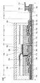
Afin de fournir un dispositif à semi-conducteur ayant à la fois de bonnes caractéristiques électriques et des caractéristiques électriques stables, ce dispositif à semi-conducteur de la présente invention comprend : une couche semi-conductrice comprenant un oxyde métallique ; une première couche isolante ; une deuxième couche isolante ; une troisième couche isolante comprenant du nitrure ; et une première couche conductrice. La première couche isolante chevauche la couche semi-conductrice et comporte : une première région convexe ; et une deuxième région qui ne chevauche pas la couche semi-conductrice et est plus mince que la première région. La deuxième couche isolante recouvre une surface supérieure de la deuxième région, une surface latérale de la première région, et la couche semi-conductrice. La première couche conductrice est disposée sur la deuxième couche isolante et sa surface inférieure sur la deuxième région a une section positionnée plus bas que la surface inférieure de la couche semi-conductrice. La couche semi-conductrice comprend : une troisième région qui chevauche la deuxième couche isolante et la première couche conductrice ; et une quatrième région qui ne chevauche pas la première couche conductrice ou la deuxième couche isolante. La troisième couche isolante est disposée en butée contre la quatrième région de la couche semi-conductrice.
Priority Applications (4)
| Application Number | Priority Date | Filing Date | Title |
|---|---|---|---|
| US16/982,182 US11482626B2 (en) | 2018-03-29 | 2019-03-15 | Semiconductor device and manufacturing method of semiconductor device |
| JP2020510161A JP7245230B2 (ja) | 2018-03-29 | 2019-03-15 | 半導体装置、および半導体装置の作製方法 |
| US17/949,632 US20230020210A1 (en) | 2018-03-29 | 2022-09-21 | Semiconductor device and manufacturing method of semiconductor device |
| JP2023037708A JP7462087B2 (ja) | 2018-03-29 | 2023-03-10 | 半導体装置 |
Applications Claiming Priority (2)
| Application Number | Priority Date | Filing Date | Title |
|---|---|---|---|
| JP2018064931 | 2018-03-29 | ||
| JP2018-064931 | 2018-03-29 |
Related Child Applications (2)
| Application Number | Title | Priority Date | Filing Date |
|---|---|---|---|
| US16/982,182 A-371-Of-International US11482626B2 (en) | 2018-03-29 | 2019-03-15 | Semiconductor device and manufacturing method of semiconductor device |
| US17/949,632 Division US20230020210A1 (en) | 2018-03-29 | 2022-09-21 | Semiconductor device and manufacturing method of semiconductor device |
Publications (1)
| Publication Number | Publication Date |
|---|---|
| WO2019186315A1 true WO2019186315A1 (fr) | 2019-10-03 |
Family
ID=68059349
Family Applications (1)
| Application Number | Title | Priority Date | Filing Date |
|---|---|---|---|
| PCT/IB2019/052105 WO2019186315A1 (fr) | 2018-03-29 | 2019-03-15 | Dispositif à semi-conducteur et procédé de production de dispositif à semi-conducteur |
Country Status (3)
| Country | Link |
|---|---|
| US (2) | US11482626B2 (fr) |
| JP (2) | JP7245230B2 (fr) |
| WO (1) | WO2019186315A1 (fr) |
Families Citing this family (2)
| Publication number | Priority date | Publication date | Assignee | Title |
|---|---|---|---|---|
| US11211501B2 (en) * | 2019-07-19 | 2021-12-28 | Semiconductor Energy Laboratory Co., Ltd. | Semiconductor device |
| CN111584426B (zh) * | 2020-05-14 | 2023-03-28 | 深圳市华星光电半导体显示技术有限公司 | 一种显示面板的制备方法、显示面板及显示装置 |
Citations (7)
| Publication number | Priority date | Publication date | Assignee | Title |
|---|---|---|---|---|
| US20080254613A1 (en) * | 2007-04-10 | 2008-10-16 | Applied Materials, Inc. | Methods for forming metal interconnect structure for thin film transistor applications |
| US20150205194A1 (en) * | 2014-01-17 | 2015-07-23 | Taiwan Semiconductor Manufacturing Company, Ltd. | Lithography Mask |
| JP2015216369A (ja) * | 2014-04-23 | 2015-12-03 | 株式会社半導体エネルギー研究所 | 撮像装置 |
| JP2016074580A (ja) * | 2014-02-21 | 2016-05-12 | 株式会社半導体エネルギー研究所 | 半導体膜、トランジスタ及び半導体装置、並びに表示装置、電子機器 |
| WO2017085591A1 (fr) * | 2015-11-20 | 2017-05-26 | 株式会社半導体エネルギー研究所 | Dispositif à semi-conducteurs, dispositif d'affichage mettant en oeuvre ce dispositif à semi-conducteurs et dispositif électronique mettant en oeuvre ce dispositif à semi-conducteurs |
| JP2017112374A (ja) * | 2015-12-16 | 2017-06-22 | 株式会社半導体エネルギー研究所 | トランジスタ、半導体装置、および電子機器 |
| JP2018006734A (ja) * | 2016-03-11 | 2018-01-11 | 株式会社半導体エネルギー研究所 | 半導体装置、当該半導体装置の作製方法、及び当該半導体装置を有する表示装置 |
Family Cites Families (7)
| Publication number | Priority date | Publication date | Assignee | Title |
|---|---|---|---|---|
| JP5708910B2 (ja) | 2010-03-30 | 2015-04-30 | ソニー株式会社 | 薄膜トランジスタおよびその製造方法、並びに表示装置 |
| US8936965B2 (en) | 2010-11-26 | 2015-01-20 | Semiconductor Energy Laboratory Co., Ltd. | Semiconductor device and manufacturing method thereof |
| KR102071545B1 (ko) | 2012-05-31 | 2020-01-30 | 가부시키가이샤 한도오따이 에네루기 켄큐쇼 | 반도체 장치 |
| JP6400336B2 (ja) * | 2013-06-05 | 2018-10-03 | 株式会社半導体エネルギー研究所 | 半導体装置 |
| US20150008428A1 (en) | 2013-07-08 | 2015-01-08 | Semiconductor Energy Laboratory Co., Ltd. | Semiconductor device and method for manufacturing semiconductor device |
| WO2015145292A1 (fr) | 2014-03-28 | 2015-10-01 | Semiconductor Energy Laboratory Co., Ltd. | Transistor et dispositif à semi-conducteur |
| JP6650888B2 (ja) | 2015-02-06 | 2020-02-19 | 株式会社半導体エネルギー研究所 | 半導体装置 |
-
2019
- 2019-03-15 US US16/982,182 patent/US11482626B2/en active Active
- 2019-03-15 WO PCT/IB2019/052105 patent/WO2019186315A1/fr active Application Filing
- 2019-03-15 JP JP2020510161A patent/JP7245230B2/ja active Active
-
2022
- 2022-09-21 US US17/949,632 patent/US20230020210A1/en active Pending
-
2023
- 2023-03-10 JP JP2023037708A patent/JP7462087B2/ja active Active
Patent Citations (7)
| Publication number | Priority date | Publication date | Assignee | Title |
|---|---|---|---|---|
| US20080254613A1 (en) * | 2007-04-10 | 2008-10-16 | Applied Materials, Inc. | Methods for forming metal interconnect structure for thin film transistor applications |
| US20150205194A1 (en) * | 2014-01-17 | 2015-07-23 | Taiwan Semiconductor Manufacturing Company, Ltd. | Lithography Mask |
| JP2016074580A (ja) * | 2014-02-21 | 2016-05-12 | 株式会社半導体エネルギー研究所 | 半導体膜、トランジスタ及び半導体装置、並びに表示装置、電子機器 |
| JP2015216369A (ja) * | 2014-04-23 | 2015-12-03 | 株式会社半導体エネルギー研究所 | 撮像装置 |
| WO2017085591A1 (fr) * | 2015-11-20 | 2017-05-26 | 株式会社半導体エネルギー研究所 | Dispositif à semi-conducteurs, dispositif d'affichage mettant en oeuvre ce dispositif à semi-conducteurs et dispositif électronique mettant en oeuvre ce dispositif à semi-conducteurs |
| JP2017112374A (ja) * | 2015-12-16 | 2017-06-22 | 株式会社半導体エネルギー研究所 | トランジスタ、半導体装置、および電子機器 |
| JP2018006734A (ja) * | 2016-03-11 | 2018-01-11 | 株式会社半導体エネルギー研究所 | 半導体装置、当該半導体装置の作製方法、及び当該半導体装置を有する表示装置 |
Also Published As
| Publication number | Publication date |
|---|---|
| US20230020210A1 (en) | 2023-01-19 |
| JP2023060345A (ja) | 2023-04-27 |
| JPWO2019186315A1 (ja) | 2021-04-15 |
| US20210028313A1 (en) | 2021-01-28 |
| US11482626B2 (en) | 2022-10-25 |
| JP7462087B2 (ja) | 2024-04-04 |
| JP7245230B2 (ja) | 2023-03-23 |
Similar Documents
| Publication | Publication Date | Title |
|---|---|---|
| JP7183184B2 (ja) | 半導体装置 | |
| JP7344707B2 (ja) | 半導体装置の作製方法 | |
| WO2019175708A1 (fr) | Dispositif à semi-conducteur et procédé de fabrication de dispositif à semi-conducteur | |
| JP7462087B2 (ja) | 半導体装置 | |
| US20220359691A1 (en) | Semiconductor device | |
| WO2020089726A1 (fr) | Dispositif à semi-conducteurs | |
| JP2023166508A (ja) | 半導体装置の作製方法 | |
| JP7475282B2 (ja) | 半導体装置 | |
| JP7300442B2 (ja) | 半導体装置の作製方法 | |
| JP2024037777A (ja) | 半導体装置の作製方法 | |
| WO2020089762A1 (fr) | Dispositif à semi-conducteur | |
| WO2020074993A1 (fr) | Dispositif à semi-conducteur | |
| JP2021019197A (ja) | 半導体装置 | |
| KR20230056797A (ko) | 반도체 장치의 제작 방법 | |
| WO2019202430A1 (fr) | Dispositif à semi-conducteur | |
| JPWO2020012276A1 (ja) | 半導体装置 |
Legal Events
| Date | Code | Title | Description |
|---|---|---|---|
| 121 | Ep: the epo has been informed by wipo that ep was designated in this application |
Ref document number: 19776611 Country of ref document: EP Kind code of ref document: A1 |
|
| ENP | Entry into the national phase |
Ref document number: 2020510161 Country of ref document: JP Kind code of ref document: A |
|
| NENP | Non-entry into the national phase |
Ref country code: DE |
|
| 122 | Ep: pct application non-entry in european phase |
Ref document number: 19776611 Country of ref document: EP Kind code of ref document: A1 |