JP4783692B2 - キャパシタ内蔵基板及びその製造方法と電子部品装置 - Google Patents
キャパシタ内蔵基板及びその製造方法と電子部品装置 Download PDFInfo
- Publication number
- JP4783692B2 JP4783692B2 JP2006217955A JP2006217955A JP4783692B2 JP 4783692 B2 JP4783692 B2 JP 4783692B2 JP 2006217955 A JP2006217955 A JP 2006217955A JP 2006217955 A JP2006217955 A JP 2006217955A JP 4783692 B2 JP4783692 B2 JP 4783692B2
- Authority
- JP
- Japan
- Prior art keywords
- electrode
- capacitor
- layer
- metal
- base resin
- Prior art date
- Legal status (The legal status is an assumption and is not a legal conclusion. Google has not performed a legal analysis and makes no representation as to the accuracy of the status listed.)
- Expired - Fee Related
Links
- 239000000758 substrate Substances 0.000 title claims description 60
- 238000004519 manufacturing process Methods 0.000 title claims description 22
- 239000003990 capacitor Substances 0.000 claims description 147
- RYGMFSIKBFXOCR-UHFFFAOYSA-N Copper Chemical compound [Cu] RYGMFSIKBFXOCR-UHFFFAOYSA-N 0.000 claims description 115
- 229910052802 copper Inorganic materials 0.000 claims description 115
- 239000010949 copper Substances 0.000 claims description 115
- 229910052751 metal Inorganic materials 0.000 claims description 101
- 239000002184 metal Substances 0.000 claims description 101
- 239000011347 resin Substances 0.000 claims description 96
- 229920005989 resin Polymers 0.000 claims description 96
- 238000007747 plating Methods 0.000 claims description 40
- 239000004065 semiconductor Substances 0.000 claims description 37
- 229910000679 solder Inorganic materials 0.000 claims description 32
- 238000000034 method Methods 0.000 claims description 21
- 238000009713 electroplating Methods 0.000 claims description 16
- ATJFFYVFTNAWJD-UHFFFAOYSA-N Tin Chemical compound [Sn] ATJFFYVFTNAWJD-UHFFFAOYSA-N 0.000 claims description 13
- 230000015572 biosynthetic process Effects 0.000 claims description 6
- 230000000149 penetrating effect Effects 0.000 claims description 5
- 238000003825 pressing Methods 0.000 claims description 2
- 239000010410 layer Substances 0.000 description 228
- PCHJSUWPFVWCPO-UHFFFAOYSA-N gold Chemical compound [Au] PCHJSUWPFVWCPO-UHFFFAOYSA-N 0.000 description 12
- 239000010931 gold Substances 0.000 description 12
- 229910052737 gold Inorganic materials 0.000 description 12
- 239000011229 interlayer Substances 0.000 description 7
- QGZKDVFQNNGYKY-UHFFFAOYSA-N Ammonia Chemical compound N QGZKDVFQNNGYKY-UHFFFAOYSA-N 0.000 description 4
- 238000005530 etching Methods 0.000 description 4
- 238000004544 sputter deposition Methods 0.000 description 4
- 229910052581 Si3N4 Inorganic materials 0.000 description 3
- 239000000654 additive Substances 0.000 description 3
- PNEYBMLMFCGWSK-UHFFFAOYSA-N aluminium oxide Inorganic materials [O-2].[O-2].[O-2].[Al+3].[Al+3] PNEYBMLMFCGWSK-UHFFFAOYSA-N 0.000 description 3
- 230000000694 effects Effects 0.000 description 3
- 238000000206 photolithography Methods 0.000 description 3
- HQVNEWCFYHHQES-UHFFFAOYSA-N silicon nitride Chemical compound N12[Si]34N5[Si]62N3[Si]51N64 HQVNEWCFYHHQES-UHFFFAOYSA-N 0.000 description 3
- 229910021529 ammonia Inorganic materials 0.000 description 2
- 239000011248 coating agent Substances 0.000 description 2
- 238000000576 coating method Methods 0.000 description 2
- 238000007772 electroless plating Methods 0.000 description 2
- 238000009434 installation Methods 0.000 description 2
- 229910044991 metal oxide Inorganic materials 0.000 description 2
- 150000004706 metal oxides Chemical class 0.000 description 2
- 238000001020 plasma etching Methods 0.000 description 2
- 229920001721 polyimide Polymers 0.000 description 2
- 239000000843 powder Substances 0.000 description 2
- OGIDPMRJRNCKJF-UHFFFAOYSA-N titanium oxide Inorganic materials [Ti]=O OGIDPMRJRNCKJF-UHFFFAOYSA-N 0.000 description 2
- 229910017107 AlOx Inorganic materials 0.000 description 1
- GRYLNZFGIOXLOG-UHFFFAOYSA-N Nitric acid Chemical compound O[N+]([O-])=O GRYLNZFGIOXLOG-UHFFFAOYSA-N 0.000 description 1
- 239000004642 Polyimide Substances 0.000 description 1
- VYPSYNLAJGMNEJ-UHFFFAOYSA-N Silicium dioxide Chemical compound O=[Si]=O VYPSYNLAJGMNEJ-UHFFFAOYSA-N 0.000 description 1
- 229910002367 SrTiO Inorganic materials 0.000 description 1
- 229910003087 TiOx Inorganic materials 0.000 description 1
- GWEVSGVZZGPLCZ-UHFFFAOYSA-N Titan oxide Chemical compound O=[Ti]=O GWEVSGVZZGPLCZ-UHFFFAOYSA-N 0.000 description 1
- NRTOMJZYCJJWKI-UHFFFAOYSA-N Titanium nitride Chemical compound [Ti]#N NRTOMJZYCJJWKI-UHFFFAOYSA-N 0.000 description 1
- 230000000996 additive effect Effects 0.000 description 1
- 239000004760 aramid Substances 0.000 description 1
- 229920003235 aromatic polyamide Polymers 0.000 description 1
- 239000003985 ceramic capacitor Substances 0.000 description 1
- 239000011247 coating layer Substances 0.000 description 1
- 238000000151 deposition Methods 0.000 description 1
- 238000009826 distribution Methods 0.000 description 1
- 238000005516 engineering process Methods 0.000 description 1
- 239000000945 filler Substances 0.000 description 1
- 230000004907 flux Effects 0.000 description 1
- 238000010438 heat treatment Methods 0.000 description 1
- 238000002488 metal-organic chemical vapour deposition Methods 0.000 description 1
- 229910000484 niobium oxide Inorganic materials 0.000 description 1
- URLJKFSTXLNXLG-UHFFFAOYSA-N niobium(5+);oxygen(2-) Chemical compound [O-2].[O-2].[O-2].[O-2].[O-2].[Nb+5].[Nb+5] URLJKFSTXLNXLG-UHFFFAOYSA-N 0.000 description 1
- 229910017604 nitric acid Inorganic materials 0.000 description 1
- 125000002524 organometallic group Chemical group 0.000 description 1
- 230000003647 oxidation Effects 0.000 description 1
- 238000007254 oxidation reaction Methods 0.000 description 1
- 230000002093 peripheral effect Effects 0.000 description 1
- 229910052710 silicon Inorganic materials 0.000 description 1
- 239000010703 silicon Substances 0.000 description 1
- 229910052814 silicon oxide Inorganic materials 0.000 description 1
- HLLICFJUWSZHRJ-UHFFFAOYSA-N tioxidazole Chemical compound CCCOC1=CC=C2N=C(NC(=O)OC)SC2=C1 HLLICFJUWSZHRJ-UHFFFAOYSA-N 0.000 description 1
- 239000010936 titanium Substances 0.000 description 1
- 229910052719 titanium Inorganic materials 0.000 description 1
- 229910052726 zirconium Inorganic materials 0.000 description 1
Images


Classifications
-
- H—ELECTRICITY
- H01—ELECTRIC ELEMENTS
- H01L—SEMICONDUCTOR DEVICES NOT COVERED BY CLASS H10
- H01L23/00—Details of semiconductor or other solid state devices
- H01L23/48—Arrangements for conducting electric current to or from the solid state body in operation, e.g. leads, terminal arrangements ; Selection of materials therefor
- H01L23/50—Arrangements for conducting electric current to or from the solid state body in operation, e.g. leads, terminal arrangements ; Selection of materials therefor for integrated circuit devices, e.g. power bus, number of leads
-
- H—ELECTRICITY
- H01—ELECTRIC ELEMENTS
- H01G—CAPACITORS; CAPACITORS, RECTIFIERS, DETECTORS, SWITCHING DEVICES OR LIGHT-SENSITIVE DEVICES, OF THE ELECTROLYTIC TYPE
- H01G4/00—Fixed capacitors; Processes of their manufacture
- H01G4/002—Details
- H01G4/228—Terminals
- H01G4/236—Terminals leading through the housing, i.e. lead-through
-
- H—ELECTRICITY
- H01—ELECTRIC ELEMENTS
- H01G—CAPACITORS; CAPACITORS, RECTIFIERS, DETECTORS, SWITCHING DEVICES OR LIGHT-SENSITIVE DEVICES, OF THE ELECTROLYTIC TYPE
- H01G4/00—Fixed capacitors; Processes of their manufacture
- H01G4/33—Thin- or thick-film capacitors
-
- H—ELECTRICITY
- H01—ELECTRIC ELEMENTS
- H01G—CAPACITORS; CAPACITORS, RECTIFIERS, DETECTORS, SWITCHING DEVICES OR LIGHT-SENSITIVE DEVICES, OF THE ELECTROLYTIC TYPE
- H01G4/00—Fixed capacitors; Processes of their manufacture
- H01G4/38—Multiple capacitors, i.e. structural combinations of fixed capacitors
-
- H—ELECTRICITY
- H01—ELECTRIC ELEMENTS
- H01L—SEMICONDUCTOR DEVICES NOT COVERED BY CLASS H10
- H01L21/00—Processes or apparatus adapted for the manufacture or treatment of semiconductor or solid state devices or of parts thereof
- H01L21/02—Manufacture or treatment of semiconductor devices or of parts thereof
- H01L21/04—Manufacture or treatment of semiconductor devices or of parts thereof the devices having at least one potential-jump barrier or surface barrier, e.g. PN junction, depletion layer or carrier concentration layer
- H01L21/48—Manufacture or treatment of parts, e.g. containers, prior to assembly of the devices, using processes not provided for in a single one of the subgroups H01L21/06 - H01L21/326
- H01L21/4814—Conductive parts
- H01L21/4846—Leads on or in insulating or insulated substrates, e.g. metallisation
- H01L21/486—Via connections through the substrate with or without pins
-
- H—ELECTRICITY
- H01—ELECTRIC ELEMENTS
- H01L—SEMICONDUCTOR DEVICES NOT COVERED BY CLASS H10
- H01L23/00—Details of semiconductor or other solid state devices
- H01L23/48—Arrangements for conducting electric current to or from the solid state body in operation, e.g. leads, terminal arrangements ; Selection of materials therefor
- H01L23/488—Arrangements for conducting electric current to or from the solid state body in operation, e.g. leads, terminal arrangements ; Selection of materials therefor consisting of soldered or bonded constructions
- H01L23/498—Leads, i.e. metallisations or lead-frames on insulating substrates, e.g. chip carriers
- H01L23/49822—Multilayer substrates
-
- H—ELECTRICITY
- H01—ELECTRIC ELEMENTS
- H01L—SEMICONDUCTOR DEVICES NOT COVERED BY CLASS H10
- H01L23/00—Details of semiconductor or other solid state devices
- H01L23/48—Arrangements for conducting electric current to or from the solid state body in operation, e.g. leads, terminal arrangements ; Selection of materials therefor
- H01L23/488—Arrangements for conducting electric current to or from the solid state body in operation, e.g. leads, terminal arrangements ; Selection of materials therefor consisting of soldered or bonded constructions
- H01L23/498—Leads, i.e. metallisations or lead-frames on insulating substrates, e.g. chip carriers
- H01L23/49827—Via connections through the substrates, e.g. pins going through the substrate, coaxial cables
-
- H—ELECTRICITY
- H01—ELECTRIC ELEMENTS
- H01L—SEMICONDUCTOR DEVICES NOT COVERED BY CLASS H10
- H01L23/00—Details of semiconductor or other solid state devices
- H01L23/58—Structural electrical arrangements for semiconductor devices not otherwise provided for, e.g. in combination with batteries
- H01L23/64—Impedance arrangements
- H01L23/642—Capacitive arrangements
-
- H—ELECTRICITY
- H05—ELECTRIC TECHNIQUES NOT OTHERWISE PROVIDED FOR
- H05K—PRINTED CIRCUITS; CASINGS OR CONSTRUCTIONAL DETAILS OF ELECTRIC APPARATUS; MANUFACTURE OF ASSEMBLAGES OF ELECTRICAL COMPONENTS
- H05K1/00—Printed circuits
- H05K1/16—Printed circuits incorporating printed electric components, e.g. printed resistor, capacitor, inductor
- H05K1/162—Printed circuits incorporating printed electric components, e.g. printed resistor, capacitor, inductor incorporating printed capacitors
-
- H—ELECTRICITY
- H01—ELECTRIC ELEMENTS
- H01L—SEMICONDUCTOR DEVICES NOT COVERED BY CLASS H10
- H01L2221/00—Processes or apparatus adapted for the manufacture or treatment of semiconductor or solid state devices or of parts thereof covered by H01L21/00
- H01L2221/67—Apparatus for handling semiconductor or electric solid state devices during manufacture or treatment thereof; Apparatus for handling wafers during manufacture or treatment of semiconductor or electric solid state devices or components; Apparatus not specifically provided for elsewhere
- H01L2221/683—Apparatus for handling semiconductor or electric solid state devices during manufacture or treatment thereof; Apparatus for handling wafers during manufacture or treatment of semiconductor or electric solid state devices or components; Apparatus not specifically provided for elsewhere for supporting or gripping
- H01L2221/68304—Apparatus for handling semiconductor or electric solid state devices during manufacture or treatment thereof; Apparatus for handling wafers during manufacture or treatment of semiconductor or electric solid state devices or components; Apparatus not specifically provided for elsewhere for supporting or gripping using temporarily an auxiliary support
- H01L2221/68345—Apparatus for handling semiconductor or electric solid state devices during manufacture or treatment thereof; Apparatus for handling wafers during manufacture or treatment of semiconductor or electric solid state devices or components; Apparatus not specifically provided for elsewhere for supporting or gripping using temporarily an auxiliary support used as a support during the manufacture of self supporting substrates
-
- H—ELECTRICITY
- H01—ELECTRIC ELEMENTS
- H01L—SEMICONDUCTOR DEVICES NOT COVERED BY CLASS H10
- H01L2224/00—Indexing scheme for arrangements for connecting or disconnecting semiconductor or solid-state bodies and methods related thereto as covered by H01L24/00
- H01L2224/01—Means for bonding being attached to, or being formed on, the surface to be connected, e.g. chip-to-package, die-attach, "first-level" interconnects; Manufacturing methods related thereto
- H01L2224/10—Bump connectors; Manufacturing methods related thereto
- H01L2224/15—Structure, shape, material or disposition of the bump connectors after the connecting process
- H01L2224/16—Structure, shape, material or disposition of the bump connectors after the connecting process of an individual bump connector
- H01L2224/161—Disposition
- H01L2224/16151—Disposition the bump connector connecting between a semiconductor or solid-state body and an item not being a semiconductor or solid-state body, e.g. chip-to-substrate, chip-to-passive
- H01L2224/16221—Disposition the bump connector connecting between a semiconductor or solid-state body and an item not being a semiconductor or solid-state body, e.g. chip-to-substrate, chip-to-passive the body and the item being stacked
- H01L2224/16265—Disposition the bump connector connecting between a semiconductor or solid-state body and an item not being a semiconductor or solid-state body, e.g. chip-to-substrate, chip-to-passive the body and the item being stacked the item being a discrete passive component
-
- H—ELECTRICITY
- H01—ELECTRIC ELEMENTS
- H01L—SEMICONDUCTOR DEVICES NOT COVERED BY CLASS H10
- H01L2924/00—Indexing scheme for arrangements or methods for connecting or disconnecting semiconductor or solid-state bodies as covered by H01L24/00
- H01L2924/01—Chemical elements
- H01L2924/01078—Platinum [Pt]
-
- H—ELECTRICITY
- H01—ELECTRIC ELEMENTS
- H01L—SEMICONDUCTOR DEVICES NOT COVERED BY CLASS H10
- H01L2924/00—Indexing scheme for arrangements or methods for connecting or disconnecting semiconductor or solid-state bodies as covered by H01L24/00
- H01L2924/01—Chemical elements
- H01L2924/01079—Gold [Au]
-
- H—ELECTRICITY
- H01—ELECTRIC ELEMENTS
- H01L—SEMICONDUCTOR DEVICES NOT COVERED BY CLASS H10
- H01L2924/00—Indexing scheme for arrangements or methods for connecting or disconnecting semiconductor or solid-state bodies as covered by H01L24/00
- H01L2924/049—Nitrides composed of metals from groups of the periodic table
- H01L2924/0494—4th Group
- H01L2924/04941—TiN
-
- H—ELECTRICITY
- H01—ELECTRIC ELEMENTS
- H01L—SEMICONDUCTOR DEVICES NOT COVERED BY CLASS H10
- H01L2924/00—Indexing scheme for arrangements or methods for connecting or disconnecting semiconductor or solid-state bodies as covered by H01L24/00
- H01L2924/15—Details of package parts other than the semiconductor or other solid state devices to be connected
- H01L2924/151—Die mounting substrate
- H01L2924/153—Connection portion
- H01L2924/1531—Connection portion the connection portion being formed only on the surface of the substrate opposite to the die mounting surface
- H01L2924/15311—Connection portion the connection portion being formed only on the surface of the substrate opposite to the die mounting surface being a ball array, e.g. BGA
-
- H—ELECTRICITY
- H05—ELECTRIC TECHNIQUES NOT OTHERWISE PROVIDED FOR
- H05K—PRINTED CIRCUITS; CASINGS OR CONSTRUCTIONAL DETAILS OF ELECTRIC APPARATUS; MANUFACTURE OF ASSEMBLAGES OF ELECTRICAL COMPONENTS
- H05K1/00—Printed circuits
- H05K1/02—Details
- H05K1/11—Printed elements for providing electric connections to or between printed circuits
- H05K1/111—Pads for surface mounting, e.g. lay-out
- H05K1/112—Pads for surface mounting, e.g. lay-out directly combined with via connections
- H05K1/113—Via provided in pad; Pad over filled via
-
- H—ELECTRICITY
- H05—ELECTRIC TECHNIQUES NOT OTHERWISE PROVIDED FOR
- H05K—PRINTED CIRCUITS; CASINGS OR CONSTRUCTIONAL DETAILS OF ELECTRIC APPARATUS; MANUFACTURE OF ASSEMBLAGES OF ELECTRICAL COMPONENTS
- H05K2201/00—Indexing scheme relating to printed circuits covered by H05K1/00
- H05K2201/01—Dielectrics
- H05K2201/0137—Materials
- H05K2201/0179—Thin film deposited insulating layer, e.g. inorganic layer for printed capacitor
-
- H—ELECTRICITY
- H05—ELECTRIC TECHNIQUES NOT OTHERWISE PROVIDED FOR
- H05K—PRINTED CIRCUITS; CASINGS OR CONSTRUCTIONAL DETAILS OF ELECTRIC APPARATUS; MANUFACTURE OF ASSEMBLAGES OF ELECTRICAL COMPONENTS
- H05K2201/00—Indexing scheme relating to printed circuits covered by H05K1/00
- H05K2201/09—Shape and layout
- H05K2201/09209—Shape and layout details of conductors
- H05K2201/09654—Shape and layout details of conductors covering at least two types of conductors provided for in H05K2201/09218 - H05K2201/095
- H05K2201/09763—Printed component having superposed conductors, but integrated in one circuit layer
-
- H—ELECTRICITY
- H05—ELECTRIC TECHNIQUES NOT OTHERWISE PROVIDED FOR
- H05K—PRINTED CIRCUITS; CASINGS OR CONSTRUCTIONAL DETAILS OF ELECTRIC APPARATUS; MANUFACTURE OF ASSEMBLAGES OF ELECTRICAL COMPONENTS
- H05K2203/00—Indexing scheme relating to apparatus or processes for manufacturing printed circuits covered by H05K3/00
- H05K2203/01—Tools for processing; Objects used during processing
- H05K2203/0147—Carriers and holders
- H05K2203/0152—Temporary metallic carrier, e.g. for transferring material
-
- H—ELECTRICITY
- H05—ELECTRIC TECHNIQUES NOT OTHERWISE PROVIDED FOR
- H05K—PRINTED CIRCUITS; CASINGS OR CONSTRUCTIONAL DETAILS OF ELECTRIC APPARATUS; MANUFACTURE OF ASSEMBLAGES OF ELECTRICAL COMPONENTS
- H05K2203/00—Indexing scheme relating to apparatus or processes for manufacturing printed circuits covered by H05K3/00
- H05K2203/07—Treatments involving liquids, e.g. plating, rinsing
- H05K2203/0703—Plating
- H05K2203/0733—Method for plating stud vias, i.e. massive vias formed by plating the bottom of a hole without plating on the walls
-
- H—ELECTRICITY
- H05—ELECTRIC TECHNIQUES NOT OTHERWISE PROVIDED FOR
- H05K—PRINTED CIRCUITS; CASINGS OR CONSTRUCTIONAL DETAILS OF ELECTRIC APPARATUS; MANUFACTURE OF ASSEMBLAGES OF ELECTRICAL COMPONENTS
- H05K3/00—Apparatus or processes for manufacturing printed circuits
- H05K3/007—Manufacture or processing of a substrate for a printed circuit board supported by a temporary or sacrificial carrier
-
- H—ELECTRICITY
- H05—ELECTRIC TECHNIQUES NOT OTHERWISE PROVIDED FOR
- H05K—PRINTED CIRCUITS; CASINGS OR CONSTRUCTIONAL DETAILS OF ELECTRIC APPARATUS; MANUFACTURE OF ASSEMBLAGES OF ELECTRICAL COMPONENTS
- H05K3/00—Apparatus or processes for manufacturing printed circuits
- H05K3/10—Apparatus or processes for manufacturing printed circuits in which conductive material is applied to the insulating support in such a manner as to form the desired conductive pattern
- H05K3/20—Apparatus or processes for manufacturing printed circuits in which conductive material is applied to the insulating support in such a manner as to form the desired conductive pattern by affixing prefabricated conductor pattern
-
- H—ELECTRICITY
- H05—ELECTRIC TECHNIQUES NOT OTHERWISE PROVIDED FOR
- H05K—PRINTED CIRCUITS; CASINGS OR CONSTRUCTIONAL DETAILS OF ELECTRIC APPARATUS; MANUFACTURE OF ASSEMBLAGES OF ELECTRICAL COMPONENTS
- H05K3/00—Apparatus or processes for manufacturing printed circuits
- H05K3/40—Forming printed elements for providing electric connections to or between printed circuits
- H05K3/4007—Surface contacts, e.g. bumps
-
- H—ELECTRICITY
- H05—ELECTRIC TECHNIQUES NOT OTHERWISE PROVIDED FOR
- H05K—PRINTED CIRCUITS; CASINGS OR CONSTRUCTIONAL DETAILS OF ELECTRIC APPARATUS; MANUFACTURE OF ASSEMBLAGES OF ELECTRICAL COMPONENTS
- H05K3/00—Apparatus or processes for manufacturing printed circuits
- H05K3/46—Manufacturing multilayer circuits
- H05K3/4644—Manufacturing multilayer circuits by building the multilayer layer by layer, i.e. build-up multilayer circuits
-
- Y—GENERAL TAGGING OF NEW TECHNOLOGICAL DEVELOPMENTS; GENERAL TAGGING OF CROSS-SECTIONAL TECHNOLOGIES SPANNING OVER SEVERAL SECTIONS OF THE IPC; TECHNICAL SUBJECTS COVERED BY FORMER USPC CROSS-REFERENCE ART COLLECTIONS [XRACs] AND DIGESTS
- Y10—TECHNICAL SUBJECTS COVERED BY FORMER USPC
- Y10T—TECHNICAL SUBJECTS COVERED BY FORMER US CLASSIFICATION
- Y10T29/00—Metal working
- Y10T29/43—Electric condenser making
- Y10T29/435—Solid dielectric type
Description
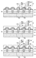
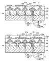
図2〜図7は本発明の第1実施形態のキャパシタ内蔵基板の製造方法を示す断面図、図8は同じくキャパシタ内蔵基板を示す断面図である。
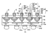
図10は本発明の第2実施形態のキャパシタ内蔵基板を示す断面図、図11は同じくキャパシタ内蔵基板に半導体チップが実装して構成される電子部品装置を示す断面図である。図10に示すように、第2実施形態のキャパシタ内蔵基板2では、複数のキャパシタC及び貫通電極Tの他に、抵抗部Rが内蔵されている。図10の例では、第1実施形態の図8の右側の貫通電極Tが抵抗部Rとなっている。
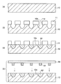
図12〜図14は本発明の第3実施形態のキャパシタ内蔵基板の製造方法を示す断面図である。図15は同じくキャパシタ内蔵基板を示す断面図である。第3実施形態の特徴は、銅板に設けた凹部にはんだ層を充填しておき、はんだ層に銅ポストを埋め込むことに基づいて、最終的にはんだ層を銅ポストの被覆層として利用することにある。第3実施形態では、第1実施形態と同一工程においてはその詳しい説明を省略する。
Claims (10)
- 厚み方向に貫通する開口部を備えたベース樹脂層と、
前記ベース樹脂層を貫通して設けられて前記開口部に埋め込まれ、前記開口部から上側及び下側に突出する突出部をそれぞれ備え、前記ベース樹脂層の一方の面側の前記突出部が接続部となる第1電極と、前記ベース樹脂層の他方の面側の前記第1電極の前記突出部を被覆する誘電体層と、前記誘電体層を被覆する第2電極とから構成されて、前記ベース樹脂層を貫通した状態で横方向に並んで配置された複数のキャパシタと、
前記ベース樹脂層を貫通して設けられ、前記ベース樹脂層の両面側から突出する突出部をそれぞれ備えた貫通電極と、
ベース樹脂層の前記他方の面側に形成され、前記キャパシタの前記第2電極及び前記貫通電極の一端側に電気的に接続されたビルドアップ配線とを有することを特徴とするキャパシタ内蔵基板。 - 前記ベース樹脂層を貫通して設けられ、前記ベース樹脂層の両面側から突出する突出部をそれぞれ備え、前記ベース樹脂層の一方の面側の前記突出部が接続部となる第1電極と、前記ベース樹脂層の他方の面側の前記第1電極を被覆する絶縁層と、前記絶縁層を被覆する第2電極とにより構成される抵抗部をさらに有し、前記抵抗部の前記第2電極が前記ビルドアップ配線に接続されていることを特徴とする請求項1に記載のキャパシタ内蔵基板。
- 前記ベース樹脂層の他方の面側に配置された前記突出部は、先端部が凸状曲面となっていることを特徴とする請求項1又は2に記載のキャパシタ内蔵配線基板。
- 請求項1乃至3のいずれか一項に記載のキャパシタ内蔵基板と、
前記第1電極の前記接続部及び前記貫通電極の他端側に接続されて実装された半導体チップとを有することを特徴とする電子部品装置。 - 一方の面に複数の金属ポストが立設されたベース樹脂層と、一方の面に柔軟金属層が形成された金属支持体とを用意する工程と、
前記金属支持体上の前記柔軟金属層に、前記ベース樹脂層上の前記金属ポストを押し込んで前記金属支持体と前記ベース樹脂層とを貼り合わせることにより、前記金属ポストを前記柔軟金属層に埋め込む工程と、
所要の金属ポスト上の前記ベース樹脂層の部分に第1めっき用開口部を形成する工程と、
前記金属支持体、前記柔軟金属層及び前記金属ポストをめっき給電経路に利用する電解めっきにより、前記第1めっき開口部に前記ベース樹脂層の上面から突出する金属バンプを形成して前記金属ポスト及び前記金属バンプから構成される第1電極を得る工程と、
前記第1電極を被覆する誘電体層を形成する工程と、
前記誘電体層を被覆する第2電極を形成してキャパシタを得る工程と、
前記キャパシタの上方に、前記キャパシタの第2電極に電気的に接続されるビルドアップ配線を形成する工程と、
前記金属支持体及び前記柔軟金属層を除去して前記金属ポストを露出させる工程とを有することを特徴とするキャパシタ内蔵基板の製造方法。 - 一方の面側に金属ポストが立設されたベース樹脂層と、前記金属ポストに対応する部分に凹部が形成され、前記凹部に柔軟金属層が埋め込まれた金属支持体とを用意する工程と、
前記金属支持体に形成された前記柔軟金属層に、前記ベース樹脂層上の前記金属ポストを押し込んで前記金属支持体と前記ベース樹脂層とを貼り合わせることにより、前記金属ポストを前記柔軟金属に埋め込む工程と、
所要の前記金属ポスト上の前記ベース樹脂層の部分にキャパシタ形成用の第1めっき用開口部を形成する工程と、
前記金属支持体、前記柔軟金属層及び前記金属ポストをめっき給電経路に利用する電解めっきにより、前記第1めっき開口部に前記ベース樹脂層の上面から突出する金属バンプを形成して前記金属ポスト及び前記金属バンプから構成される第1電極を得る工程と、
前記第1電極を被覆する誘電体層を形成する工程と、
前記誘電体層を被覆する第2電極を形成してキャパシタを得る工程と、
前記キャパシタの上方に、前記キャパシタの前記第2電極に接続されるビルドアップ配線を形成する工程と、
前記金属支持体を除去して前記柔軟金属層で被覆された前記金属ポストを露出させる工程とを有することを特徴とするキャパシタ内蔵基板の製造方法。 - 前記複数の金属ポスト上の前記ベース樹脂層の各部分には前記キャパシタの形成領域の他に貫通電極の形成領域が画定されており、
前記キャパシタを得る工程の後であって、ビルドアップ配線を形成する工程の前に、
前記金属ポスト上の前記貫通電極を形成するための前記ベース樹脂層の部分に第2めっき用開口部を形成する工程と、
前記第2めっき用開口部を含む領域に開口部が設けられたレジストを形成して前記キャパシタを前記レジストで被覆する工程と、
前記金属支持体、前記柔軟金属層及び前記金属ポストをめっき給電経路に利用する電解めっきにより、前記第2めっき用開口部に前記ベース樹脂層の上面から突出する金属バンプを形成して前記金属ポスト及び前記金属バンプから構成される前記貫通電極を得る工程と、
前記レジストを除去する工程とをさらに有し、
前記ビルドアップ配線は前記貫通電極の一端側に接続されることを特徴とする請求項5又は6に記載のキャパシタ内蔵基板の製造方法。 - 前記複数の金属ポスト上の前記ベース樹脂層の各部分には前記キャパシタの形成領域の他に抵抗部の形成領域が画定されており、
前記キャパシタを得る工程の後であって、ビルドアップ配線を形成する工程の前に、
前記金属ポスト上の前記抵抗部を形成するための前記ベース樹脂層の部分に第2めっき用開口部を形成する工程と、
前記第2めっき用開口部を含む領域に開口部が設けられたレジストを形成して前記キャパシタを前記レジストで被覆する工程と、
前記金属支持体、前記柔軟金属層及び前記金属ポストをめっき給電経路に利用する電解めっきにより、前記第2めっき用開口部に前記ベース樹脂層の上面から突出する金属バンプを形成して前記金属ポスト及び前記金属バンプから構成される第1電極を得る工程と、
前記第1電極を被覆する絶縁層を形成する工程と、
前記絶縁層を被覆する第2電極を形成して前記抵抗部を得る工程と、
前記レジストを除去する工程とをさらに有し、
前記ビルドアップ配線は前記抵抗部の前記第2電極に接続されることを特徴とする請求項5又は6に記載のキャパシタ内蔵基板の製造方法。 - 前記金属支持体は銅からなって、前記柔軟金属層は錫からなり、
前記金属支持体及び前記柔軟金属層を除去する工程の後に、露出する前記金属ポストを被覆するはんだ層を形成する工程をさらに有することを特徴とする請求項5に記載のキャパシタ内蔵基板の製造方法。 - 前記金属支持体は銅からなり、前記柔軟金属層ははんだからなることを特徴とする請求項6に記載のキャパシタ内蔵基板の製造方法。
Priority Applications (4)
| Application Number | Priority Date | Filing Date | Title |
|---|---|---|---|
| JP2006217955A JP4783692B2 (ja) | 2006-08-10 | 2006-08-10 | キャパシタ内蔵基板及びその製造方法と電子部品装置 |
| US11/882,645 US7936568B2 (en) | 2006-08-10 | 2007-08-03 | Capacitor built-in substrate and method of manufacturing the same and electronic component device |
| CNA200710140290XA CN101123854A (zh) | 2006-08-10 | 2007-08-08 | 电容器内置基板及其制造方法和电子元件装置 |
| EP07114115A EP1887622A3 (en) | 2006-08-10 | 2007-08-09 | Capacitor built-in substrate and method of manufacturing the same and electronic component device |
Applications Claiming Priority (1)
| Application Number | Priority Date | Filing Date | Title |
|---|---|---|---|
| JP2006217955A JP4783692B2 (ja) | 2006-08-10 | 2006-08-10 | キャパシタ内蔵基板及びその製造方法と電子部品装置 |
Publications (3)
| Publication Number | Publication Date |
|---|---|
| JP2008042118A JP2008042118A (ja) | 2008-02-21 |
| JP2008042118A5 JP2008042118A5 (ja) | 2009-07-30 |
| JP4783692B2 true JP4783692B2 (ja) | 2011-09-28 |
Family
ID=38666852
Family Applications (1)
| Application Number | Title | Priority Date | Filing Date |
|---|---|---|---|
| JP2006217955A Expired - Fee Related JP4783692B2 (ja) | 2006-08-10 | 2006-08-10 | キャパシタ内蔵基板及びその製造方法と電子部品装置 |
Country Status (4)
| Country | Link |
|---|---|
| US (1) | US7936568B2 (ja) |
| EP (1) | EP1887622A3 (ja) |
| JP (1) | JP4783692B2 (ja) |
| CN (1) | CN101123854A (ja) |
Families Citing this family (29)
| Publication number | Priority date | Publication date | Assignee | Title |
|---|---|---|---|---|
| JP4920335B2 (ja) * | 2006-08-07 | 2012-04-18 | 新光電気工業株式会社 | キャパシタ内蔵インターポーザ及びその製造方法と電子部品装置 |
| JP4783692B2 (ja) | 2006-08-10 | 2011-09-28 | 新光電気工業株式会社 | キャパシタ内蔵基板及びその製造方法と電子部品装置 |
| JP4337949B2 (ja) * | 2007-09-06 | 2009-09-30 | 株式会社村田製作所 | 回路基板及び回路基板の製造方法 |
| EP2259669A4 (en) * | 2008-03-24 | 2011-12-28 | Ngk Spark Plug Co | INTEGRATED COMPONENT CONNECTION TABLE |
| KR101006619B1 (ko) * | 2008-10-20 | 2011-01-07 | 삼성전기주식회사 | 라운드형 솔더범프를 갖는 인쇄회로기판 및 그 제조방법 |
| WO2010073800A1 (ja) * | 2008-12-22 | 2010-07-01 | 富士通株式会社 | 電子部品とその製造方法 |
| US8389870B2 (en) * | 2010-03-09 | 2013-03-05 | International Business Machines Corporation | Coreless multi-layer circuit substrate with minimized pad capacitance |
| TWI446497B (zh) * | 2010-08-13 | 2014-07-21 | Unimicron Technology Corp | 嵌埋被動元件之封裝基板及其製法 |
| JP6081044B2 (ja) | 2010-09-16 | 2017-02-15 | 富士通株式会社 | パッケージ基板ユニットの製造方法 |
| US10433421B2 (en) * | 2012-12-26 | 2019-10-01 | Intel Corporation | Reduced capacitance land pad |
| JP2015049985A (ja) * | 2013-08-30 | 2015-03-16 | 富士通株式会社 | Icソケット及び接続端子 |
| WO2015053356A1 (ja) * | 2013-10-09 | 2015-04-16 | 学校法人早稲田大学 | 電極接続方法及び電極接続構造 |
| US9642261B2 (en) * | 2014-01-24 | 2017-05-02 | Zhuhai Advanced Chip Carriers & Electronic Substrate Solutions Technologies Co. Ltd. | Composite electronic structure with partially exposed and protruding copper termination posts |
| KR102281460B1 (ko) * | 2015-01-22 | 2021-07-27 | 삼성전기주식회사 | 임베디드 기판 및 임베디드 기판의 제조 방법 |
| JP6672705B2 (ja) * | 2015-10-30 | 2020-03-25 | 大日本印刷株式会社 | インターポーザ及びインターポーザの製造方法 |
| EP3174094B1 (en) * | 2015-11-25 | 2018-09-26 | IMEC vzw | Integrated circuit comprising a metal-insulator-metal capacitor and fabrication method thereof |
| WO2018038094A1 (ja) * | 2016-08-22 | 2018-03-01 | 重信 三浦 | キャパシタの製造方法及びキャパシタ内蔵基板の製造方法並びにキャパシタ内蔵基板及び半導体装置実装部品 |
| US10297494B2 (en) * | 2017-01-26 | 2019-05-21 | Taiwan Semiconductor Manufacturing Company, Ltd. | Raised via for terminal connections on different planes |
| DE102017127920A1 (de) | 2017-01-26 | 2018-07-26 | Taiwan Semiconductor Manufacturing Company, Ltd. | Erhöhte Durchkontaktierung für Anschlüsse auf unterschiedlichen Ebenen |
| US10622302B2 (en) | 2018-02-14 | 2020-04-14 | Taiwan Semiconductor Manufacturing Company, Ltd. | Via for semiconductor device connection and methods of forming the same |
| US10373866B1 (en) * | 2018-05-04 | 2019-08-06 | International Business Machines Corporation | Method of forming metal insulator metal capacitor with extended capacitor plates |
| DE102018126130B4 (de) | 2018-06-08 | 2023-08-10 | Taiwan Semiconductor Manufacturing Co., Ltd. | Halbleitervorrichtung und -verfahren |
| US11158775B2 (en) | 2018-06-08 | 2021-10-26 | Taiwan Semiconductor Manufacturing Company, Ltd. | Semiconductor device and method |
| CN110660584B (zh) * | 2018-06-29 | 2023-06-27 | 浙江清华柔性电子技术研究院 | 柔性储能薄膜的制备方法 |
| US10992100B2 (en) | 2018-07-06 | 2021-04-27 | Taiwan Semiconductor Manufacturing Company, Ltd. | Semiconductor device and method |
| WO2020085380A1 (ja) * | 2018-10-25 | 2020-04-30 | 株式会社村田製作所 | 電子部品モジュール及び電子部品モジュールの製造方法 |
| JP7279538B2 (ja) * | 2019-06-19 | 2023-05-23 | 富士フイルムビジネスイノベーション株式会社 | 発光装置 |
| CN113451279B (zh) * | 2020-03-26 | 2023-09-12 | 群创光电股份有限公司 | 电容器及电子装置 |
| US20240107665A1 (en) * | 2022-09-23 | 2024-03-28 | Qualcomm Incorporated | Providing a lower inductance path in a routing substrate for a capacitor, and related electronic devices and fabrication methods |
Family Cites Families (75)
| Publication number | Priority date | Publication date | Assignee | Title |
|---|---|---|---|---|
| US5177670A (en) * | 1991-02-08 | 1993-01-05 | Hitachi, Ltd. | Capacitor-carrying semiconductor module |
| JPH06268141A (ja) | 1993-03-15 | 1994-09-22 | Hitachi Ltd | 電子回路装置の実装方法 |
| JP3246166B2 (ja) | 1994-03-03 | 2002-01-15 | 株式会社村田製作所 | 薄膜コンデンサ |
| JP2830845B2 (ja) * | 1996-06-26 | 1998-12-02 | 日本電気株式会社 | 半導体記憶装置 |
| JPH11111884A (ja) * | 1997-10-07 | 1999-04-23 | Toppan Printing Co Ltd | 電子部材作製用基板及びそれを用いた電子部材の製造方法 |
| US6274224B1 (en) * | 1999-02-01 | 2001-08-14 | 3M Innovative Properties Company | Passive electrical article, circuit articles thereof, and circuit articles comprising a passive electrical article |
| JP3635219B2 (ja) * | 1999-03-11 | 2005-04-06 | 新光電気工業株式会社 | 半導体装置用多層基板及びその製造方法 |
| JP3792445B2 (ja) * | 1999-03-30 | 2006-07-05 | 日本特殊陶業株式会社 | コンデンサ付属配線基板 |
| KR20080111567A (ko) * | 1999-09-02 | 2008-12-23 | 이비덴 가부시키가이샤 | 프린트배선판 및 그 제조방법 |
| CN101232776B (zh) * | 1999-09-02 | 2011-04-20 | 揖斐电株式会社 | 印刷布线板 |
| US6573584B1 (en) * | 1999-10-29 | 2003-06-03 | Kyocera Corporation | Thin film electronic device and circuit board mounting the same |
| US6525921B1 (en) * | 1999-11-12 | 2003-02-25 | Matsushita Electric Industrial Co., Ltd | Capacitor-mounted metal foil and a method for producing the same, and a circuit board and a method for producing the same |
| US6871396B2 (en) * | 2000-02-09 | 2005-03-29 | Matsushita Electric Industrial Co., Ltd. | Transfer material for wiring substrate |
| JP2001291637A (ja) | 2000-04-10 | 2001-10-19 | Shinko Electric Ind Co Ltd | 球状キャパシタと該キャパシタの製造方法と球状キャパシタの実装構造と配線基板と該配線基板の製造方法 |
| US20030086248A1 (en) * | 2000-05-12 | 2003-05-08 | Naohiro Mashino | Interposer for semiconductor, method for manufacturing same, and semiconductor device using same |
| CN1196392C (zh) * | 2000-07-31 | 2005-04-06 | 日本特殊陶业株式会社 | 布线基板及其制造方法 |
| US6577490B2 (en) * | 2000-12-12 | 2003-06-10 | Ngk Spark Plug Co., Ltd. | Wiring board |
| US6740411B2 (en) * | 2001-02-21 | 2004-05-25 | Ngk Spark Plug Co. Ltd. | Embedding resin, wiring substrate using same and process for producing wiring substrate using same |
| US6512182B2 (en) * | 2001-03-12 | 2003-01-28 | Ngk Spark Plug Co., Ltd. | Wiring circuit board and method for producing same |
| JP3817463B2 (ja) * | 2001-11-12 | 2006-09-06 | 新光電気工業株式会社 | 多層配線基板の製造方法 |
| JP3492348B2 (ja) * | 2001-12-26 | 2004-02-03 | 新光電気工業株式会社 | 半導体装置用パッケージの製造方法 |
| US6943056B2 (en) * | 2002-04-16 | 2005-09-13 | Renesas Technology Corp. | Semiconductor device manufacturing method and electronic equipment using same |
| JP4019837B2 (ja) * | 2002-07-19 | 2007-12-12 | 松下電器産業株式会社 | 固体電解コンデンサ及びその製造方法 |
| US7102367B2 (en) * | 2002-07-23 | 2006-09-05 | Fujitsu Limited | Probe card and testing method of semiconductor chip, capacitor and manufacturing method thereof |
| JP2004064052A (ja) * | 2002-07-27 | 2004-02-26 | Samsung Electro Mech Co Ltd | ノイズ遮蔽型積層基板とその製造方法 |
| JP2004079701A (ja) * | 2002-08-14 | 2004-03-11 | Sony Corp | 半導体装置及びその製造方法 |
| JP4243117B2 (ja) * | 2002-08-27 | 2009-03-25 | 新光電気工業株式会社 | 半導体パッケージとその製造方法および半導体装置 |
| TW560001B (en) * | 2002-10-22 | 2003-11-01 | Toppoly Optoelectronics Corp | Method of forming reflective liquid crystal display and driving circuit |
| JP3910907B2 (ja) * | 2002-10-29 | 2007-04-25 | 新光電気工業株式会社 | キャパシタ素子及びこの製造方法、半導体装置用基板、並びに半導体装置 |
| JP3910908B2 (ja) * | 2002-10-29 | 2007-04-25 | 新光電気工業株式会社 | 半導体装置用基板及びこの製造方法、並びに半導体装置 |
| US7161793B2 (en) * | 2002-11-14 | 2007-01-09 | Fujitsu Limited | Layer capacitor element and production process as well as electronic device |
| KR100455890B1 (ko) * | 2002-12-24 | 2004-11-06 | 삼성전기주식회사 | 커패시터 내장형 인쇄회로기판 및 그 제조 방법 |
| JP4342174B2 (ja) * | 2002-12-27 | 2009-10-14 | 新光電気工業株式会社 | 電子デバイス及びその製造方法 |
| JP2004214258A (ja) * | 2002-12-27 | 2004-07-29 | Renesas Technology Corp | 半導体モジュール |
| US6995322B2 (en) * | 2003-01-30 | 2006-02-07 | Endicott Interconnect Technologies, Inc. | High speed circuitized substrate with reduced thru-hole stub, method for fabrication and information handling system utilizing same |
| US6909592B2 (en) * | 2003-01-30 | 2005-06-21 | Dongbuanam Semiconductor Inc. | Thin film capacitor and fabrication method thereof |
| TW556452B (en) * | 2003-01-30 | 2003-10-01 | Phoenix Prec Technology Corp | Integrated storage plate with embedded passive components and method for fabricating electronic device with the plate |
| JP5000071B2 (ja) * | 2003-02-26 | 2012-08-15 | 新光電気工業株式会社 | 半導体装置用基板及び半導体装置 |
| US7327554B2 (en) * | 2003-03-19 | 2008-02-05 | Ngk Spark Plug Co., Ltd. | Assembly of semiconductor device, interposer and substrate |
| JP4016340B2 (ja) * | 2003-06-13 | 2007-12-05 | ソニー株式会社 | 半導体装置及びその実装構造、並びにその製造方法 |
| JP4377617B2 (ja) * | 2003-06-20 | 2009-12-02 | 日本特殊陶業株式会社 | コンデンサ、コンデンサ付き半導体素子、コンデンサ付き配線基板、および、半導体素子とコンデンサと配線基板とを備える電子ユニット |
| JP2005039243A (ja) * | 2003-06-24 | 2005-02-10 | Ngk Spark Plug Co Ltd | 中間基板 |
| JP4365166B2 (ja) * | 2003-08-26 | 2009-11-18 | 新光電気工業株式会社 | キャパシタ、多層配線基板及び半導体装置 |
| TWI251916B (en) * | 2003-08-28 | 2006-03-21 | Phoenix Prec Technology Corp | Semiconductor assembled heat sink structure for embedding electronic components |
| WO2005045925A1 (ja) * | 2003-11-07 | 2005-05-19 | Shinko Electric Industries Co., Ltd. | 電子装置及びその製造方法 |
| KR100535181B1 (ko) * | 2003-11-18 | 2005-12-09 | 삼성전자주식회사 | 디커플링 커패시터를 갖는 반도체 칩 패키지와 그 제조 방법 |
| JP4547164B2 (ja) * | 2004-02-27 | 2010-09-22 | 日本特殊陶業株式会社 | 配線基板の製造方法 |
| JP2005317943A (ja) * | 2004-03-29 | 2005-11-10 | Sumitomo Bakelite Co Ltd | プリント回路基板およびその製造方法 |
| JP4387231B2 (ja) * | 2004-03-31 | 2009-12-16 | 新光電気工業株式会社 | キャパシタ実装配線基板及びその製造方法 |
| TWI255491B (en) * | 2004-03-31 | 2006-05-21 | Sanyo Electric Co | Substrate for mounting elements, manufacturing method therefor and semiconductor device using the same |
| JP4260672B2 (ja) * | 2004-04-16 | 2009-04-30 | 富士通マイクロエレクトロニクス株式会社 | 半導体装置の製造方法及び中継基板の製造方法 |
| TW200605169A (en) * | 2004-06-29 | 2006-02-01 | Sanyo Electric Co | Circuit device and process for manufacture thereof |
| KR100680504B1 (ko) * | 2004-06-30 | 2007-02-08 | 동부일렉트로닉스 주식회사 | 반도체 소자의 캐패시터의 제조방법 |
| KR100645643B1 (ko) * | 2004-07-14 | 2006-11-15 | 삼성전기주식회사 | 수동소자칩 내장형의 인쇄회로기판의 제조방법 |
| US7186919B2 (en) * | 2004-08-16 | 2007-03-06 | Samsung Electro-Mechanics Co., Ltd. | Printed circuit board including embedded capacitors and method of manufacturing the same |
| JP5208349B2 (ja) * | 2004-09-03 | 2013-06-12 | 富士通株式会社 | 容量素子とその製造方法 |
| KR100598275B1 (ko) * | 2004-09-15 | 2006-07-10 | 삼성전기주식회사 | 수동소자 내장형 인쇄회로기판 및 그 제조 방법 |
| JP2006120696A (ja) | 2004-10-19 | 2006-05-11 | Shinko Electric Ind Co Ltd | キャパシタ装置及びそれが内蔵された半導体装置 |
| JP2006147606A (ja) * | 2004-11-16 | 2006-06-08 | Nec Toppan Circuit Solutions Inc | シート状コンデンサとその製造方法 |
| JP4602208B2 (ja) * | 2004-12-15 | 2010-12-22 | 新光電気工業株式会社 | 電子部品実装構造体及びその製造方法 |
| JP4499548B2 (ja) * | 2004-12-24 | 2010-07-07 | 新光電気工業株式会社 | キャパシタ部品 |
| JP4351148B2 (ja) * | 2004-12-28 | 2009-10-28 | 新光電気工業株式会社 | 配線基板の製造方法 |
| KR100688768B1 (ko) * | 2004-12-30 | 2007-03-02 | 삼성전기주식회사 | 칩 내장형 인쇄회로기판 및 그 제조 방법 |
| JP2006253631A (ja) * | 2005-02-14 | 2006-09-21 | Fujitsu Ltd | 半導体装置及びその製造方法、キャパシタ構造体及びその製造方法 |
| KR100688743B1 (ko) * | 2005-03-11 | 2007-03-02 | 삼성전기주식회사 | 멀티 레이어 커패시터 내장형의 인쇄회로기판의 제조방법 |
| KR100716810B1 (ko) * | 2005-03-18 | 2007-05-09 | 삼성전기주식회사 | 블라인드 비아홀을 구비한 커패시터 내장형 인쇄회로기판및 그 제조 방법 |
| JP2006269764A (ja) * | 2005-03-24 | 2006-10-05 | Toshiba Corp | 強誘電体記憶装置および製造方法 |
| JP4638768B2 (ja) * | 2005-05-20 | 2011-02-23 | 三井金属鉱業株式会社 | キャパシタ回路付フィルムキャリアテープ及びその製造方法、キャパシタ回路付表面実装フィルムキャリアテープ及びその製造方法 |
| TWI396481B (zh) * | 2005-06-03 | 2013-05-11 | Ngk Spark Plug Co | 配線基板及其製造方法 |
| JP2007149730A (ja) * | 2005-11-24 | 2007-06-14 | Shinko Electric Ind Co Ltd | 薄膜キャパシタ、実装基板、実装基板の製造方法、半導体装置、および半導体装置の製造方法 |
| US20080017407A1 (en) * | 2006-07-24 | 2008-01-24 | Ibiden Co., Ltd. | Interposer and electronic device using the same |
| US7662694B2 (en) * | 2006-07-31 | 2010-02-16 | Ibiden Co., Ltd. | Capacitor having adjustable capacitance, and printed wiring board having the same |
| JP4920335B2 (ja) * | 2006-08-07 | 2012-04-18 | 新光電気工業株式会社 | キャパシタ内蔵インターポーザ及びその製造方法と電子部品装置 |
| JP4783692B2 (ja) | 2006-08-10 | 2011-09-28 | 新光電気工業株式会社 | キャパシタ内蔵基板及びその製造方法と電子部品装置 |
| JP2010004028A (ja) * | 2008-05-23 | 2010-01-07 | Shinko Electric Ind Co Ltd | 配線基板及びその製造方法、及び半導体装置 |
-
2006
- 2006-08-10 JP JP2006217955A patent/JP4783692B2/ja not_active Expired - Fee Related
-
2007
- 2007-08-03 US US11/882,645 patent/US7936568B2/en not_active Expired - Fee Related
- 2007-08-08 CN CNA200710140290XA patent/CN101123854A/zh active Pending
- 2007-08-09 EP EP07114115A patent/EP1887622A3/en not_active Withdrawn
Also Published As
| Publication number | Publication date |
|---|---|
| EP1887622A2 (en) | 2008-02-13 |
| JP2008042118A (ja) | 2008-02-21 |
| CN101123854A (zh) | 2008-02-13 |
| US7936568B2 (en) | 2011-05-03 |
| EP1887622A3 (en) | 2008-05-07 |
| US20080291649A1 (en) | 2008-11-27 |
Similar Documents
| Publication | Publication Date | Title |
|---|---|---|
| JP4783692B2 (ja) | キャパシタ内蔵基板及びその製造方法と電子部品装置 | |
| JP4920335B2 (ja) | キャパシタ内蔵インターポーザ及びその製造方法と電子部品装置 | |
| US8810007B2 (en) | Wiring board, semiconductor device, and method for manufacturing wiring board | |
| JP4790297B2 (ja) | 半導体装置およびその製造方法 | |
| US8389414B2 (en) | Method of manufacturing a wiring board | |
| JP5423874B2 (ja) | 半導体素子内蔵基板およびその製造方法 | |
| JP5460155B2 (ja) | キャパシタ及び配線基板 | |
| US8669643B2 (en) | Wiring board, semiconductor device, and method for manufacturing wiring board | |
| US20020190371A1 (en) | Semiconductor device and method of production of same | |
| JP4912992B2 (ja) | キャパシタ内蔵基板及びその製造方法 | |
| KR20090042753A (ko) | 인터포저 | |
| JP2001326305A (ja) | 半導体装置用インターポーザー、その製造方法および半導体装置 | |
| US8114772B2 (en) | Method of manufacturing the semiconductor device | |
| JP4584700B2 (ja) | 配線基板の製造方法 | |
| US8039967B2 (en) | Wiring substrate with a wire terminal | |
| JP5934154B2 (ja) | 電子部品が実装された基板構造及びその製造方法 | |
| JP6600573B2 (ja) | 配線基板及び半導体パッケージ | |
| JP2005109486A (ja) | マルチチップモジュールの製造方法及びマルチチップモジュール | |
| TWI742075B (zh) | 於半導體封裝中之電容性互連件 | |
| JP4759981B2 (ja) | 電子部品内蔵モジュールの製造方法 | |
| JP6704129B2 (ja) | 回路基板、回路基板の製造方法及び電子装置 | |
| JP4784142B2 (ja) | 半導体装置およびその製造方法 | |
| JP4110161B2 (ja) | 半導体装置および半導体装置の製造方法 |
Legal Events
| Date | Code | Title | Description |
|---|---|---|---|
| A521 | Request for written amendment filed |
Free format text: JAPANESE INTERMEDIATE CODE: A523 Effective date: 20090615 |
|
| A621 | Written request for application examination |
Free format text: JAPANESE INTERMEDIATE CODE: A621 Effective date: 20090615 |
|
| A977 | Report on retrieval |
Free format text: JAPANESE INTERMEDIATE CODE: A971007 Effective date: 20110623 |
|
| TRDD | Decision of grant or rejection written | ||
| A01 | Written decision to grant a patent or to grant a registration (utility model) |
Free format text: JAPANESE INTERMEDIATE CODE: A01 Effective date: 20110705 |
|
| A01 | Written decision to grant a patent or to grant a registration (utility model) |
Free format text: JAPANESE INTERMEDIATE CODE: A01 |
|
| A61 | First payment of annual fees (during grant procedure) |
Free format text: JAPANESE INTERMEDIATE CODE: A61 Effective date: 20110711 |
|
| FPAY | Renewal fee payment (event date is renewal date of database) |
Free format text: PAYMENT UNTIL: 20140715 Year of fee payment: 3 |
|
| R150 | Certificate of patent or registration of utility model |
Free format text: JAPANESE INTERMEDIATE CODE: R150 |
|
| LAPS | Cancellation because of no payment of annual fees |