JP4783692B2 - Capacitor-embedded substrate, manufacturing method thereof, and electronic component device - Google Patents
Capacitor-embedded substrate, manufacturing method thereof, and electronic component device Download PDFInfo
- Publication number
- JP4783692B2 JP4783692B2 JP2006217955A JP2006217955A JP4783692B2 JP 4783692 B2 JP4783692 B2 JP 4783692B2 JP 2006217955 A JP2006217955 A JP 2006217955A JP 2006217955 A JP2006217955 A JP 2006217955A JP 4783692 B2 JP4783692 B2 JP 4783692B2
- Authority
- JP
- Japan
- Prior art keywords
- electrode
- capacitor
- layer
- metal
- base resin
- Prior art date
- Legal status (The legal status is an assumption and is not a legal conclusion. Google has not performed a legal analysis and makes no representation as to the accuracy of the status listed.)
- Expired - Fee Related
Links
- 239000000758 substrate Substances 0.000 title claims description 60
- 238000004519 manufacturing process Methods 0.000 title claims description 22
- 239000003990 capacitor Substances 0.000 claims description 147
- RYGMFSIKBFXOCR-UHFFFAOYSA-N Copper Chemical compound [Cu] RYGMFSIKBFXOCR-UHFFFAOYSA-N 0.000 claims description 115
- 229910052802 copper Inorganic materials 0.000 claims description 115
- 239000010949 copper Substances 0.000 claims description 115
- 229910052751 metal Inorganic materials 0.000 claims description 101
- 239000002184 metal Substances 0.000 claims description 101
- 239000011347 resin Substances 0.000 claims description 96
- 229920005989 resin Polymers 0.000 claims description 96
- 238000007747 plating Methods 0.000 claims description 40
- 239000004065 semiconductor Substances 0.000 claims description 37
- 229910000679 solder Inorganic materials 0.000 claims description 32
- 238000000034 method Methods 0.000 claims description 21
- 238000009713 electroplating Methods 0.000 claims description 16
- ATJFFYVFTNAWJD-UHFFFAOYSA-N Tin Chemical compound [Sn] ATJFFYVFTNAWJD-UHFFFAOYSA-N 0.000 claims description 13
- 230000015572 biosynthetic process Effects 0.000 claims description 6
- 230000000149 penetrating effect Effects 0.000 claims description 5
- 238000003825 pressing Methods 0.000 claims description 2
- 239000010410 layer Substances 0.000 description 228
- PCHJSUWPFVWCPO-UHFFFAOYSA-N gold Chemical compound [Au] PCHJSUWPFVWCPO-UHFFFAOYSA-N 0.000 description 12
- 239000010931 gold Substances 0.000 description 12
- 229910052737 gold Inorganic materials 0.000 description 12
- 239000011229 interlayer Substances 0.000 description 7
- QGZKDVFQNNGYKY-UHFFFAOYSA-N Ammonia Chemical compound N QGZKDVFQNNGYKY-UHFFFAOYSA-N 0.000 description 4
- 238000005530 etching Methods 0.000 description 4
- 238000004544 sputter deposition Methods 0.000 description 4
- 229910052581 Si3N4 Inorganic materials 0.000 description 3
- 239000000654 additive Substances 0.000 description 3
- PNEYBMLMFCGWSK-UHFFFAOYSA-N aluminium oxide Inorganic materials [O-2].[O-2].[O-2].[Al+3].[Al+3] PNEYBMLMFCGWSK-UHFFFAOYSA-N 0.000 description 3
- 230000000694 effects Effects 0.000 description 3
- 238000000206 photolithography Methods 0.000 description 3
- HQVNEWCFYHHQES-UHFFFAOYSA-N silicon nitride Chemical compound N12[Si]34N5[Si]62N3[Si]51N64 HQVNEWCFYHHQES-UHFFFAOYSA-N 0.000 description 3
- 229910021529 ammonia Inorganic materials 0.000 description 2
- 239000011248 coating agent Substances 0.000 description 2
- 238000000576 coating method Methods 0.000 description 2
- 238000007772 electroless plating Methods 0.000 description 2
- 238000009434 installation Methods 0.000 description 2
- 229910044991 metal oxide Inorganic materials 0.000 description 2
- 150000004706 metal oxides Chemical class 0.000 description 2
- 238000001020 plasma etching Methods 0.000 description 2
- 229920001721 polyimide Polymers 0.000 description 2
- 239000000843 powder Substances 0.000 description 2
- OGIDPMRJRNCKJF-UHFFFAOYSA-N titanium oxide Inorganic materials [Ti]=O OGIDPMRJRNCKJF-UHFFFAOYSA-N 0.000 description 2
- 229910017107 AlOx Inorganic materials 0.000 description 1
- GRYLNZFGIOXLOG-UHFFFAOYSA-N Nitric acid Chemical compound O[N+]([O-])=O GRYLNZFGIOXLOG-UHFFFAOYSA-N 0.000 description 1
- 239000004642 Polyimide Substances 0.000 description 1
- VYPSYNLAJGMNEJ-UHFFFAOYSA-N Silicium dioxide Chemical compound O=[Si]=O VYPSYNLAJGMNEJ-UHFFFAOYSA-N 0.000 description 1
- 229910002367 SrTiO Inorganic materials 0.000 description 1
- 229910003087 TiOx Inorganic materials 0.000 description 1
- GWEVSGVZZGPLCZ-UHFFFAOYSA-N Titan oxide Chemical compound O=[Ti]=O GWEVSGVZZGPLCZ-UHFFFAOYSA-N 0.000 description 1
- NRTOMJZYCJJWKI-UHFFFAOYSA-N Titanium nitride Chemical compound [Ti]#N NRTOMJZYCJJWKI-UHFFFAOYSA-N 0.000 description 1
- 230000000996 additive effect Effects 0.000 description 1
- 239000004760 aramid Substances 0.000 description 1
- 229920003235 aromatic polyamide Polymers 0.000 description 1
- 239000003985 ceramic capacitor Substances 0.000 description 1
- 239000011247 coating layer Substances 0.000 description 1
- 238000000151 deposition Methods 0.000 description 1
- 238000009826 distribution Methods 0.000 description 1
- 238000005516 engineering process Methods 0.000 description 1
- 239000000945 filler Substances 0.000 description 1
- 230000004907 flux Effects 0.000 description 1
- 238000010438 heat treatment Methods 0.000 description 1
- 238000002488 metal-organic chemical vapour deposition Methods 0.000 description 1
- 229910000484 niobium oxide Inorganic materials 0.000 description 1
- URLJKFSTXLNXLG-UHFFFAOYSA-N niobium(5+);oxygen(2-) Chemical compound [O-2].[O-2].[O-2].[O-2].[O-2].[Nb+5].[Nb+5] URLJKFSTXLNXLG-UHFFFAOYSA-N 0.000 description 1
- 229910017604 nitric acid Inorganic materials 0.000 description 1
- 125000002524 organometallic group Chemical group 0.000 description 1
- 230000003647 oxidation Effects 0.000 description 1
- 238000007254 oxidation reaction Methods 0.000 description 1
- 230000002093 peripheral effect Effects 0.000 description 1
- 229910052710 silicon Inorganic materials 0.000 description 1
- 239000010703 silicon Substances 0.000 description 1
- 229910052814 silicon oxide Inorganic materials 0.000 description 1
- HLLICFJUWSZHRJ-UHFFFAOYSA-N tioxidazole Chemical compound CCCOC1=CC=C2N=C(NC(=O)OC)SC2=C1 HLLICFJUWSZHRJ-UHFFFAOYSA-N 0.000 description 1
- 239000010936 titanium Substances 0.000 description 1
- 229910052719 titanium Inorganic materials 0.000 description 1
- 229910052726 zirconium Inorganic materials 0.000 description 1
Images


Classifications
-
- H—ELECTRICITY
- H01—ELECTRIC ELEMENTS
- H01L—SEMICONDUCTOR DEVICES NOT COVERED BY CLASS H10
- H01L23/00—Details of semiconductor or other solid state devices
- H01L23/48—Arrangements for conducting electric current to or from the solid state body in operation, e.g. leads, terminal arrangements ; Selection of materials therefor
- H01L23/50—Arrangements for conducting electric current to or from the solid state body in operation, e.g. leads, terminal arrangements ; Selection of materials therefor for integrated circuit devices, e.g. power bus, number of leads
-
- H—ELECTRICITY
- H01—ELECTRIC ELEMENTS
- H01G—CAPACITORS; CAPACITORS, RECTIFIERS, DETECTORS, SWITCHING DEVICES OR LIGHT-SENSITIVE DEVICES, OF THE ELECTROLYTIC TYPE
- H01G4/00—Fixed capacitors; Processes of their manufacture
- H01G4/002—Details
- H01G4/228—Terminals
- H01G4/236—Terminals leading through the housing, i.e. lead-through
-
- H—ELECTRICITY
- H01—ELECTRIC ELEMENTS
- H01G—CAPACITORS; CAPACITORS, RECTIFIERS, DETECTORS, SWITCHING DEVICES OR LIGHT-SENSITIVE DEVICES, OF THE ELECTROLYTIC TYPE
- H01G4/00—Fixed capacitors; Processes of their manufacture
- H01G4/33—Thin- or thick-film capacitors
-
- H—ELECTRICITY
- H01—ELECTRIC ELEMENTS
- H01G—CAPACITORS; CAPACITORS, RECTIFIERS, DETECTORS, SWITCHING DEVICES OR LIGHT-SENSITIVE DEVICES, OF THE ELECTROLYTIC TYPE
- H01G4/00—Fixed capacitors; Processes of their manufacture
- H01G4/38—Multiple capacitors, i.e. structural combinations of fixed capacitors
-
- H—ELECTRICITY
- H01—ELECTRIC ELEMENTS
- H01L—SEMICONDUCTOR DEVICES NOT COVERED BY CLASS H10
- H01L21/00—Processes or apparatus adapted for the manufacture or treatment of semiconductor or solid state devices or of parts thereof
- H01L21/02—Manufacture or treatment of semiconductor devices or of parts thereof
- H01L21/04—Manufacture or treatment of semiconductor devices or of parts thereof the devices having at least one potential-jump barrier or surface barrier, e.g. PN junction, depletion layer or carrier concentration layer
- H01L21/48—Manufacture or treatment of parts, e.g. containers, prior to assembly of the devices, using processes not provided for in a single one of the subgroups H01L21/06 - H01L21/326
- H01L21/4814—Conductive parts
- H01L21/4846—Leads on or in insulating or insulated substrates, e.g. metallisation
- H01L21/486—Via connections through the substrate with or without pins
-
- H—ELECTRICITY
- H01—ELECTRIC ELEMENTS
- H01L—SEMICONDUCTOR DEVICES NOT COVERED BY CLASS H10
- H01L23/00—Details of semiconductor or other solid state devices
- H01L23/48—Arrangements for conducting electric current to or from the solid state body in operation, e.g. leads, terminal arrangements ; Selection of materials therefor
- H01L23/488—Arrangements for conducting electric current to or from the solid state body in operation, e.g. leads, terminal arrangements ; Selection of materials therefor consisting of soldered or bonded constructions
- H01L23/498—Leads, i.e. metallisations or lead-frames on insulating substrates, e.g. chip carriers
- H01L23/49822—Multilayer substrates
-
- H—ELECTRICITY
- H01—ELECTRIC ELEMENTS
- H01L—SEMICONDUCTOR DEVICES NOT COVERED BY CLASS H10
- H01L23/00—Details of semiconductor or other solid state devices
- H01L23/48—Arrangements for conducting electric current to or from the solid state body in operation, e.g. leads, terminal arrangements ; Selection of materials therefor
- H01L23/488—Arrangements for conducting electric current to or from the solid state body in operation, e.g. leads, terminal arrangements ; Selection of materials therefor consisting of soldered or bonded constructions
- H01L23/498—Leads, i.e. metallisations or lead-frames on insulating substrates, e.g. chip carriers
- H01L23/49827—Via connections through the substrates, e.g. pins going through the substrate, coaxial cables
-
- H—ELECTRICITY
- H01—ELECTRIC ELEMENTS
- H01L—SEMICONDUCTOR DEVICES NOT COVERED BY CLASS H10
- H01L23/00—Details of semiconductor or other solid state devices
- H01L23/58—Structural electrical arrangements for semiconductor devices not otherwise provided for, e.g. in combination with batteries
- H01L23/64—Impedance arrangements
- H01L23/642—Capacitive arrangements
-
- H—ELECTRICITY
- H05—ELECTRIC TECHNIQUES NOT OTHERWISE PROVIDED FOR
- H05K—PRINTED CIRCUITS; CASINGS OR CONSTRUCTIONAL DETAILS OF ELECTRIC APPARATUS; MANUFACTURE OF ASSEMBLAGES OF ELECTRICAL COMPONENTS
- H05K1/00—Printed circuits
- H05K1/16—Printed circuits incorporating printed electric components, e.g. printed resistor, capacitor, inductor
- H05K1/162—Printed circuits incorporating printed electric components, e.g. printed resistor, capacitor, inductor incorporating printed capacitors
-
- H—ELECTRICITY
- H01—ELECTRIC ELEMENTS
- H01L—SEMICONDUCTOR DEVICES NOT COVERED BY CLASS H10
- H01L2221/00—Processes or apparatus adapted for the manufacture or treatment of semiconductor or solid state devices or of parts thereof covered by H01L21/00
- H01L2221/67—Apparatus for handling semiconductor or electric solid state devices during manufacture or treatment thereof; Apparatus for handling wafers during manufacture or treatment of semiconductor or electric solid state devices or components; Apparatus not specifically provided for elsewhere
- H01L2221/683—Apparatus for handling semiconductor or electric solid state devices during manufacture or treatment thereof; Apparatus for handling wafers during manufacture or treatment of semiconductor or electric solid state devices or components; Apparatus not specifically provided for elsewhere for supporting or gripping
- H01L2221/68304—Apparatus for handling semiconductor or electric solid state devices during manufacture or treatment thereof; Apparatus for handling wafers during manufacture or treatment of semiconductor or electric solid state devices or components; Apparatus not specifically provided for elsewhere for supporting or gripping using temporarily an auxiliary support
- H01L2221/68345—Apparatus for handling semiconductor or electric solid state devices during manufacture or treatment thereof; Apparatus for handling wafers during manufacture or treatment of semiconductor or electric solid state devices or components; Apparatus not specifically provided for elsewhere for supporting or gripping using temporarily an auxiliary support used as a support during the manufacture of self supporting substrates
-
- H—ELECTRICITY
- H01—ELECTRIC ELEMENTS
- H01L—SEMICONDUCTOR DEVICES NOT COVERED BY CLASS H10
- H01L2224/00—Indexing scheme for arrangements for connecting or disconnecting semiconductor or solid-state bodies and methods related thereto as covered by H01L24/00
- H01L2224/01—Means for bonding being attached to, or being formed on, the surface to be connected, e.g. chip-to-package, die-attach, "first-level" interconnects; Manufacturing methods related thereto
- H01L2224/10—Bump connectors; Manufacturing methods related thereto
- H01L2224/15—Structure, shape, material or disposition of the bump connectors after the connecting process
- H01L2224/16—Structure, shape, material or disposition of the bump connectors after the connecting process of an individual bump connector
- H01L2224/161—Disposition
- H01L2224/16151—Disposition the bump connector connecting between a semiconductor or solid-state body and an item not being a semiconductor or solid-state body, e.g. chip-to-substrate, chip-to-passive
- H01L2224/16221—Disposition the bump connector connecting between a semiconductor or solid-state body and an item not being a semiconductor or solid-state body, e.g. chip-to-substrate, chip-to-passive the body and the item being stacked
- H01L2224/16265—Disposition the bump connector connecting between a semiconductor or solid-state body and an item not being a semiconductor or solid-state body, e.g. chip-to-substrate, chip-to-passive the body and the item being stacked the item being a discrete passive component
-
- H—ELECTRICITY
- H01—ELECTRIC ELEMENTS
- H01L—SEMICONDUCTOR DEVICES NOT COVERED BY CLASS H10
- H01L2924/00—Indexing scheme for arrangements or methods for connecting or disconnecting semiconductor or solid-state bodies as covered by H01L24/00
- H01L2924/01—Chemical elements
- H01L2924/01078—Platinum [Pt]
-
- H—ELECTRICITY
- H01—ELECTRIC ELEMENTS
- H01L—SEMICONDUCTOR DEVICES NOT COVERED BY CLASS H10
- H01L2924/00—Indexing scheme for arrangements or methods for connecting or disconnecting semiconductor or solid-state bodies as covered by H01L24/00
- H01L2924/01—Chemical elements
- H01L2924/01079—Gold [Au]
-
- H—ELECTRICITY
- H01—ELECTRIC ELEMENTS
- H01L—SEMICONDUCTOR DEVICES NOT COVERED BY CLASS H10
- H01L2924/00—Indexing scheme for arrangements or methods for connecting or disconnecting semiconductor or solid-state bodies as covered by H01L24/00
- H01L2924/049—Nitrides composed of metals from groups of the periodic table
- H01L2924/0494—4th Group
- H01L2924/04941—TiN
-
- H—ELECTRICITY
- H01—ELECTRIC ELEMENTS
- H01L—SEMICONDUCTOR DEVICES NOT COVERED BY CLASS H10
- H01L2924/00—Indexing scheme for arrangements or methods for connecting or disconnecting semiconductor or solid-state bodies as covered by H01L24/00
- H01L2924/15—Details of package parts other than the semiconductor or other solid state devices to be connected
- H01L2924/151—Die mounting substrate
- H01L2924/153—Connection portion
- H01L2924/1531—Connection portion the connection portion being formed only on the surface of the substrate opposite to the die mounting surface
- H01L2924/15311—Connection portion the connection portion being formed only on the surface of the substrate opposite to the die mounting surface being a ball array, e.g. BGA
-
- H—ELECTRICITY
- H05—ELECTRIC TECHNIQUES NOT OTHERWISE PROVIDED FOR
- H05K—PRINTED CIRCUITS; CASINGS OR CONSTRUCTIONAL DETAILS OF ELECTRIC APPARATUS; MANUFACTURE OF ASSEMBLAGES OF ELECTRICAL COMPONENTS
- H05K1/00—Printed circuits
- H05K1/02—Details
- H05K1/11—Printed elements for providing electric connections to or between printed circuits
- H05K1/111—Pads for surface mounting, e.g. lay-out
- H05K1/112—Pads for surface mounting, e.g. lay-out directly combined with via connections
- H05K1/113—Via provided in pad; Pad over filled via
-
- H—ELECTRICITY
- H05—ELECTRIC TECHNIQUES NOT OTHERWISE PROVIDED FOR
- H05K—PRINTED CIRCUITS; CASINGS OR CONSTRUCTIONAL DETAILS OF ELECTRIC APPARATUS; MANUFACTURE OF ASSEMBLAGES OF ELECTRICAL COMPONENTS
- H05K2201/00—Indexing scheme relating to printed circuits covered by H05K1/00
- H05K2201/01—Dielectrics
- H05K2201/0137—Materials
- H05K2201/0179—Thin film deposited insulating layer, e.g. inorganic layer for printed capacitor
-
- H—ELECTRICITY
- H05—ELECTRIC TECHNIQUES NOT OTHERWISE PROVIDED FOR
- H05K—PRINTED CIRCUITS; CASINGS OR CONSTRUCTIONAL DETAILS OF ELECTRIC APPARATUS; MANUFACTURE OF ASSEMBLAGES OF ELECTRICAL COMPONENTS
- H05K2201/00—Indexing scheme relating to printed circuits covered by H05K1/00
- H05K2201/09—Shape and layout
- H05K2201/09209—Shape and layout details of conductors
- H05K2201/09654—Shape and layout details of conductors covering at least two types of conductors provided for in H05K2201/09218 - H05K2201/095
- H05K2201/09763—Printed component having superposed conductors, but integrated in one circuit layer
-
- H—ELECTRICITY
- H05—ELECTRIC TECHNIQUES NOT OTHERWISE PROVIDED FOR
- H05K—PRINTED CIRCUITS; CASINGS OR CONSTRUCTIONAL DETAILS OF ELECTRIC APPARATUS; MANUFACTURE OF ASSEMBLAGES OF ELECTRICAL COMPONENTS
- H05K2203/00—Indexing scheme relating to apparatus or processes for manufacturing printed circuits covered by H05K3/00
- H05K2203/01—Tools for processing; Objects used during processing
- H05K2203/0147—Carriers and holders
- H05K2203/0152—Temporary metallic carrier, e.g. for transferring material
-
- H—ELECTRICITY
- H05—ELECTRIC TECHNIQUES NOT OTHERWISE PROVIDED FOR
- H05K—PRINTED CIRCUITS; CASINGS OR CONSTRUCTIONAL DETAILS OF ELECTRIC APPARATUS; MANUFACTURE OF ASSEMBLAGES OF ELECTRICAL COMPONENTS
- H05K2203/00—Indexing scheme relating to apparatus or processes for manufacturing printed circuits covered by H05K3/00
- H05K2203/07—Treatments involving liquids, e.g. plating, rinsing
- H05K2203/0703—Plating
- H05K2203/0733—Method for plating stud vias, i.e. massive vias formed by plating the bottom of a hole without plating on the walls
-
- H—ELECTRICITY
- H05—ELECTRIC TECHNIQUES NOT OTHERWISE PROVIDED FOR
- H05K—PRINTED CIRCUITS; CASINGS OR CONSTRUCTIONAL DETAILS OF ELECTRIC APPARATUS; MANUFACTURE OF ASSEMBLAGES OF ELECTRICAL COMPONENTS
- H05K3/00—Apparatus or processes for manufacturing printed circuits
- H05K3/007—Manufacture or processing of a substrate for a printed circuit board supported by a temporary or sacrificial carrier
-
- H—ELECTRICITY
- H05—ELECTRIC TECHNIQUES NOT OTHERWISE PROVIDED FOR
- H05K—PRINTED CIRCUITS; CASINGS OR CONSTRUCTIONAL DETAILS OF ELECTRIC APPARATUS; MANUFACTURE OF ASSEMBLAGES OF ELECTRICAL COMPONENTS
- H05K3/00—Apparatus or processes for manufacturing printed circuits
- H05K3/10—Apparatus or processes for manufacturing printed circuits in which conductive material is applied to the insulating support in such a manner as to form the desired conductive pattern
- H05K3/20—Apparatus or processes for manufacturing printed circuits in which conductive material is applied to the insulating support in such a manner as to form the desired conductive pattern by affixing prefabricated conductor pattern
-
- H—ELECTRICITY
- H05—ELECTRIC TECHNIQUES NOT OTHERWISE PROVIDED FOR
- H05K—PRINTED CIRCUITS; CASINGS OR CONSTRUCTIONAL DETAILS OF ELECTRIC APPARATUS; MANUFACTURE OF ASSEMBLAGES OF ELECTRICAL COMPONENTS
- H05K3/00—Apparatus or processes for manufacturing printed circuits
- H05K3/40—Forming printed elements for providing electric connections to or between printed circuits
- H05K3/4007—Surface contacts, e.g. bumps
-
- H—ELECTRICITY
- H05—ELECTRIC TECHNIQUES NOT OTHERWISE PROVIDED FOR
- H05K—PRINTED CIRCUITS; CASINGS OR CONSTRUCTIONAL DETAILS OF ELECTRIC APPARATUS; MANUFACTURE OF ASSEMBLAGES OF ELECTRICAL COMPONENTS
- H05K3/00—Apparatus or processes for manufacturing printed circuits
- H05K3/46—Manufacturing multilayer circuits
- H05K3/4644—Manufacturing multilayer circuits by building the multilayer layer by layer, i.e. build-up multilayer circuits
-
- Y—GENERAL TAGGING OF NEW TECHNOLOGICAL DEVELOPMENTS; GENERAL TAGGING OF CROSS-SECTIONAL TECHNOLOGIES SPANNING OVER SEVERAL SECTIONS OF THE IPC; TECHNICAL SUBJECTS COVERED BY FORMER USPC CROSS-REFERENCE ART COLLECTIONS [XRACs] AND DIGESTS
- Y10—TECHNICAL SUBJECTS COVERED BY FORMER USPC
- Y10T—TECHNICAL SUBJECTS COVERED BY FORMER US CLASSIFICATION
- Y10T29/00—Metal working
- Y10T29/43—Electric condenser making
- Y10T29/435—Solid dielectric type
Landscapes
- Engineering & Computer Science (AREA)
- Power Engineering (AREA)
- Microelectronics & Electronic Packaging (AREA)
- Physics & Mathematics (AREA)
- Condensed Matter Physics & Semiconductors (AREA)
- General Physics & Mathematics (AREA)
- Computer Hardware Design (AREA)
- Manufacturing & Machinery (AREA)
- Ceramic Engineering (AREA)
- Production Of Multi-Layered Print Wiring Board (AREA)
- Fixed Capacitors And Capacitor Manufacturing Machines (AREA)
- Structures For Mounting Electric Components On Printed Circuit Boards (AREA)
Description
本発明はキャパシタ内蔵基板及びその製造方法と電子部品装置に係り、さらに詳しくは、半導体チップが実装されてデカップリングキャパシタとして機能するキャパシタを内蔵する配線基板に適用できるキャパシタ内蔵基板及びその製造方法とそれを利用する電子部品装置に関する。 The present invention relates to a capacitor-embedded substrate, a manufacturing method thereof, and an electronic component device, and more particularly, a capacitor-embedded substrate that can be applied to a wiring substrate in which a semiconductor chip is mounted and functions as a decoupling capacitor. The present invention relates to an electronic component device using the same.
従来、デカップリングキャパシタが内蔵された配線基板に半導体チップが実装されて構成される電子部品装置がある。図1に示すように、そのような電子部品装置の一例では、第1配線層100がその下面が露出した状態で第1層間絶縁層200に埋設されており、第1層間絶縁層200の上にはそれに設けられた第1ビアホールVH1を介して第1配線層100に接続された第2配線層120が形成されている。
Conventionally, there is an electronic component device configured by mounting a semiconductor chip on a wiring board in which a decoupling capacitor is built. As shown in FIG. 1, in one example of such an electronic component device, the
第2配線層120上には、支持体350の下に第1電極310、誘電体320及び第2電極330が形成されて構成されるキャパシタ部品300の接続端子340が接続されており、キャパシタ部品300の下部にはダイアタッチテープ400が配置されている。さらに、キャパシタ部品300の上には第2層間絶縁層220が形成されており、キャパシタ部品300が第2層間絶縁層220に埋設されている。
On the
さらに、第2層間絶縁層220の上にはそれに形成された第2ビアホールVH2を介して第2配線層120に接続された第3配線層140が形成されている。第3配線層140の上にはその接続部に開口部500xが設けられたソルダレジスト500が形成されている。そして、第3配線層140の接続部に半導体チップ600のバンプ600aがフリップチップ接続されている。
Furthermore, a
特許文献1には、球状のコアの表面に第1電極、誘電体及び第2電極が積層して形成され、第1電極の電極部が露出した構造の球状キャパシタを配線基板の電線回路に接続して設けることが記載されている。
In
また、特許文献2には、内面から外面にかけて複数の気泡が設けられたポーラス金属層からなる内部電極と、気泡の内面及び内部電極の外面に設けられた誘電体層と、誘電体層に接触して形成された外部電極とによって構成されるキャパシタが作り込まれた回路基板に半導体チップを実装することが記載されている。
上記した図1の従来技術の電子部品装置では、下側に接続端子340が設けられたキャパシタ部品300が配線基板に平面実装される。このため、キャパシタ部品300に半導体チップ600を接続するには、キャパシタ部品300の接続端子340を第2配線層120に接続し、第2層間絶縁層220で埋め込んだ後に、第2ビアホールVH2を介して上方の第3配線層140までもち上げる必要があり、キャパシタ部品300から半導体チップ600までの配線経路が比較的長くなってしまう。
In the above-described conventional electronic component device of FIG. 1, the capacitor component 300 having the
従って、キャパシタ部品300と半導体チップ600のリード間では比較的大きなインダクタンスが存在することになり、デカップリングコンデンサの効果を十分に奏することができない場合がある。
Therefore, a relatively large inductance exists between the leads of the capacitor component 300 and the
また、従来技術では、キャパシタ部品の接続端子の位置が限定されているため、配線経路を変更することは困難であると共に、ダイアタッチテープを使用する必要があることなどから、設計デザインが制約されて設計の自由度が低いといった問題もある。 In addition, in the conventional technology, the position of the connection terminal of the capacitor component is limited, so that it is difficult to change the wiring route, and it is necessary to use a die attach tape. There is also a problem that the degree of freedom of design is low.
さらに、側面側に接続端子を備える2端子型の積層セラミックキャパシタを配線基板に内蔵させる場合も同様に配線の引き回しが必要になり、同様な問題が発生する。 Further, when a two-terminal type multilayer ceramic capacitor having a connection terminal on the side surface is built in the wiring board, the wiring needs to be routed in the same manner, and the same problem occurs.
本発明は以上の課題を鑑みて創作されたものであり、キャパシタを半導体チップからより近い位置に配置してそれに接続できると共に、設計の自由度が高いキャパシタ内蔵基板及びそれを利用した電子部品装置を提供することを目的とする。 The present invention has been created in view of the above problems, and a capacitor can be disposed at a position closer to a semiconductor chip and connected thereto, and a substrate with a built-in capacitor having a high degree of design freedom, and an electronic component device using the same The purpose is to provide.
上記課題を解決するため、本発明はキャパシタ内蔵基板に係り、ベース樹脂層と、前記ベース樹脂層を貫通して設けられ、前記ベース樹脂層の両面側から突出する突出部をそれぞれ備え、前記ベース樹脂層の一方の面側の前記突出部が接続部となる第1電極と、前記ベース樹脂層の他方の面側の前記第1電極の前記突出部を被覆する誘電体層と、前記誘電体層を被覆する第2電極とから構成されて、前記ベース樹脂層を貫通した状態で横方向に並んで配置された複数のキャパシタと、前記ベース樹脂層を貫通して設けられ、前記ベース樹脂層の両面側から突出する突出部をそれぞれ備えた貫通電極と、ベース樹脂層の前記他方の面側に形成され、前記キャパシタの前記第2電極及び前記貫通電極の一端側に電気的に接続されたビルドアップ配線とを有することを特徴とする。 In order to solve the above problems, the present invention relates to a capacitor-embedded substrate, and includes a base resin layer and projecting portions provided through the base resin layer and projecting from both sides of the base resin layer. A first electrode in which the protruding portion on one surface side of the resin layer serves as a connecting portion; a dielectric layer covering the protruding portion of the first electrode on the other surface side of the base resin layer; and the dielectric A plurality of capacitors arranged in a lateral direction in a state of penetrating the base resin layer, the base resin layer being provided through the base resin layer, Formed on the other surface side of the base resin layer, and electrically connected to one end side of the second electrode and the through electrode of the capacitor. Build-up distribution Characterized in that it has and.
本発明のキャパシタ内蔵基板では、ベース樹脂層に複数のキャパシタ及び貫通電極が貫通した状態で横方向に並んで配置されている。キャパシタの第1電極はベース樹脂層を貫通して形成され、ベース樹脂層の両面側から突出する突出部それぞれ備えている。ベース樹脂層の上面側に突出する第1電極の突出部が接続部となっている。 In the capacitor built-in substrate of the present invention, a plurality of capacitors and through electrodes are penetrated through the base resin layer and arranged side by side. The first electrode of the capacitor is formed through the base resin layer, and includes a protruding portion that protrudes from both sides of the base resin layer. A protruding portion of the first electrode protruding to the upper surface side of the base resin layer is a connection portion.
そして、ベース樹脂層の下面側の第1電極の突出部を被覆する誘電体層と第2電極が順に形成されてキャパシタが構成されている。また、貫通電極においてもベース樹脂層の両面から突出する突出部を備えている。さらに、ベース樹脂層の下面側には、キャパシタの第2電極及び貫通電極の一端側に接続されたビルドアップ配線が形成されている。 A dielectric layer and a second electrode that cover the protruding portion of the first electrode on the lower surface side of the base resin layer are sequentially formed to constitute a capacitor. Further, the through electrode also includes protruding portions that protrude from both surfaces of the base resin layer. Furthermore, a buildup wiring connected to one end side of the second electrode and the through electrode of the capacitor is formed on the lower surface side of the base resin layer.
このように、本発明のキャパシタ内蔵基板では、キャパシタの第1、第2電極及び貫通電極の接続部がベース樹脂層の上下面側にそれぞれ突出して配置されて、キャパシタ及び貫通電極が上下方向に電気接続される構造となっている。 As described above, in the capacitor-embedded substrate according to the present invention, the connection portions of the first and second electrodes and the through electrode of the capacitor are arranged so as to protrude from the upper and lower surfaces of the base resin layer, and the capacitor and the through electrode are arranged in the vertical direction. It is structured to be electrically connected.
そして、本発明のキャパシタ内蔵基板の上面側に突出するキャパシタの第1電極の接続部及び貫通電極の接続部に半導体チップが接続されて電子部品装置が構成される。複数のキャパシタは電気的に並列に接続されてデカップリングキャパシタとして機能する。また、貫通電極は、半導体チップと配線基板との間の信号ラインなどの導通経路として利用される。 Then, a semiconductor chip is connected to the connection portion of the first electrode of the capacitor and the connection portion of the through electrode protruding to the upper surface side of the capacitor built-in substrate of the present invention to constitute an electronic component device. The plurality of capacitors are electrically connected in parallel to function as a decoupling capacitor. The through electrode is used as a conduction path such as a signal line between the semiconductor chip and the wiring board.
本発明のキャパシタ内蔵基板では、ベース樹脂層を貫通して設けたキャパシタの第1電極の接続部が半導体チップに直接接続されるので、従来技術と違って、キャパシタに接続される配線を配線基板内で引き回して半導体チップに接続する必要はない。これにより、半導体チップとキャパシタとの間のインダクタンスを低減することができるので、高速動作する半導体チップに対してのデカップリングキャパシタとして十分な性能を奏するようになる。また、任意の位置に信号ラインなどに利用される貫通電極を配置できるので、半導体チップと配線基板との間に特別にバンプを配置する必要がないと共に、電子部品装置の設計の自由度を高くすることができる。 In the capacitor built-in substrate according to the present invention, the connection portion of the capacitor first electrode provided through the base resin layer is directly connected to the semiconductor chip. Therefore, unlike the prior art, the wiring connected to the capacitor is connected to the wiring substrate. There is no need to route and connect to the semiconductor chip. As a result, the inductance between the semiconductor chip and the capacitor can be reduced, so that sufficient performance as a decoupling capacitor for a semiconductor chip operating at high speed can be achieved. In addition, since a through electrode used for a signal line or the like can be arranged at an arbitrary position, it is not necessary to arrange a bump between the semiconductor chip and the wiring board, and the degree of freedom in designing the electronic component device is increased. can do.
また、高靭性弾性体(ポリイミドなど)からなるベース樹脂層に高さの高い金属ポストを設けてそれを接続バンプとして利用するので、ベース樹脂層及び金属ポストが半導体チップをフリップチップ接続する際の応力緩和層として機能し、電子部品装置の信頼性を向上させることができる。 In addition, since a metal post having a high height is provided on a base resin layer made of a high-toughness elastic body (polyimide or the like) and used as a connection bump, the base resin layer and the metal post are used for flip-chip connection of a semiconductor chip. It functions as a stress relaxation layer and can improve the reliability of the electronic component device.
さらに、第1電極の突出部(凸状曲面など)に誘電体層と第2電極を被覆してキャパシタを構成するので、平面状にキャパシタを構成する場合よりも、同じ設置面積において容量の大きなキャパシタを形成することができる。 Further, since the capacitor is configured by covering the projecting portion (such as a convex curved surface) of the first electrode with the dielectric layer and the second electrode, the capacitance is larger in the same installation area than when the capacitor is configured in a planar shape. A capacitor can be formed.
また、上記課題を解決するため、本発明はキャパシタ内蔵基板の製造方法に係り、一方の面に複数の金属ポストが立設されたベース樹脂層と、一方の面に柔軟金属層が形成された金属支持体とを用意する工程と、前記金属支持体上の前記柔軟金属層に、前記ベース樹脂層上の前記金属ポストを押し込んで前記金属支持体と前記ベース樹脂層とを貼り合わせることにより、前記金属ポストを前記柔軟金属層に埋め込む工程と、所要の金属ポスト上の前記ベース樹脂層の部分に第1めっき用開口部を形成する工程と、前記金属支持体、前記柔軟金属層及び前記金属ポストをめっき給電経路に利用する電解めっきにより、前記第1めっき開口部に前記ベース樹脂層の上面から突出する金属バンプを形成して前記金属ポスト及び前記金属バンプから構成される第1電極を得る工程と、前記第1電極を被覆する誘電体層を形成する工程と、前記誘電体層を被覆する第2電極を形成してキャパシタを得る工程と、前記キャパシタの第2電極に電気的に接続されるビルドアップ配線を形成する工程と、前記金属支持体及び前記柔軟金属層を除去して前記金属ポストを露出させる工程とを有することを特徴とする。 In addition, in order to solve the above-described problems, the present invention relates to a method for manufacturing a capacitor-embedded substrate, in which a base resin layer having a plurality of metal posts standing on one surface and a flexible metal layer on one surface are formed. A step of preparing a metal support, and pressing the metal post on the base resin layer into the flexible metal layer on the metal support to bond the metal support and the base resin layer together, Embedding the metal post in the flexible metal layer, forming a first plating opening in a portion of the base resin layer on a required metal post, the metal support, the flexible metal layer, and the metal A metal bump protruding from the upper surface of the base resin layer is formed in the first plating opening by electrolytic plating using a post as a plating power feeding path, and the metal post and the metal bump are formed. Obtaining a first electrode to be formed; forming a dielectric layer covering the first electrode; forming a second electrode covering the dielectric layer; obtaining a capacitor; The method includes a step of forming a build-up wiring electrically connected to the two electrodes, and a step of removing the metal support and the flexible metal layer to expose the metal post.
本発明では、まず、金属支持体(銅など)上の柔軟金属層(錫など)に、ベース樹脂層上の金属ポストを押し込んで金属ポストを柔軟金属層に埋め込む。次いで、所要の金属ポスト上のベース樹脂層の部分に第1めっき用開口部を形成し、電解めっきにより第1めっき開口部の底からベース樹脂層の上側に突出して金属ポストに接続される金属バンプを形成してキャパシタ用の第1電極を得る。このとき、金属バンプの先端部が凸状曲面となって形成される。続いて、第1電極を被覆する誘電体層と第2電極を形成してキャパシタを得る。さらに、キャパシタの第2電極に接続されるビルドアップ配線を形成する。その後に、金属支持体及び柔軟金属層を除去して第1電極の接続部となる金属ポストを露出させる。 In the present invention, first, a metal post on a base resin layer is pushed into a flexible metal layer (such as tin) on a metal support (such as copper) to embed the metal post in the flexible metal layer. Next, a first plating opening is formed in a portion of the base resin layer on the required metal post, and the metal that protrudes from the bottom of the first plating opening to the upper side of the base resin layer by electrolytic plating and is connected to the metal post A bump is formed to obtain a first electrode for a capacitor. At this time, the tip of the metal bump is formed as a convex curved surface. Subsequently, a dielectric layer covering the first electrode and a second electrode are formed to obtain a capacitor. Further, a buildup wiring connected to the second electrode of the capacitor is formed. Thereafter, the metal support and the flexible metal layer are removed to expose the metal post that becomes the connection portion of the first electrode.
以上のような製造方法を使用することにより、上記した発明のキャパシタ内蔵基板を容易に製造することができる。貫通電極を内蔵させるときは、キャパシタを形成した後に、別の金属ポスト上のベース樹脂層の部分にめっき開口部を形成し、金属バンプを形成すればよい。さらには、同様な方法で抵抗部を内蔵させることができる。 By using the manufacturing method as described above, the capacitor-embedded substrate of the above-described invention can be easily manufactured. When the through electrode is built-in, after forming the capacitor, a plating opening may be formed in a portion of the base resin layer on another metal post to form a metal bump. Furthermore, the resistor portion can be built in the same way.
以上説明したように、本発明では、半導体チップからより近い位置にキャパシタを配置して接続できると共に、設計の自由度が高い電子部品装置を構成できるようになる。 As described above, according to the present invention, it is possible to arrange and connect a capacitor closer to the semiconductor chip, and to configure an electronic component device having a high degree of design freedom.
以下、本発明の実施の形態について、添付の図面を参照して説明する。 Hereinafter, embodiments of the present invention will be described with reference to the accompanying drawings.
(第1の実施の形態)
図2〜図7は本発明の第1実施形態のキャパシタ内蔵基板の製造方法を示す断面図、図8は同じくキャパシタ内蔵基板を示す断面図である。
(First embodiment)
2 to 7 are cross-sectional views showing a method for manufacturing a capacitor built-in substrate according to the first embodiment of the present invention, and FIG.
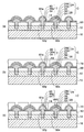
第1実施形態のキャパシタ内蔵基板の製造方法は、図2(a)に示すように、まず、ポリイミドフィルムやアラミドフィルムなどの高靭性弾性体からなる膜厚が50μm程度のベース樹脂層50を用意する。ベース樹脂層50は、最終的に複数のキャパシタなどを支持するための弾性基板となる。その後に、図2(b)に示すように、ベース樹脂層50の上(図2(b)では下)に、銅などからなるシード層52をスパッタリングによって形成する。
As shown in FIG. 2A, the manufacturing method of the capacitor-embedded substrate according to the first embodiment first prepares a
次いで、銅ポストを形成する部分に開口部が設けられたレジスト膜(不図示)を形成し、シード層52をめっき給電経路として利用する電解めっきによってレジスト膜の開口部かに銅層を形成する。その後に、レジスト膜が除去される。これにより、ベース樹脂層50上のシード層52の上(図8(b)では下)に銅ポスト54(金属ポスト)が形成される。
Next, a resist film (not shown) provided with an opening is formed in a portion where a copper post is to be formed, and a copper layer is formed in the opening of the resist film by electrolytic plating using the
続いて、図8(c)に示すように、銅ポスト54をマスクにしてシード層52をエッチングすることにより、各銅ポスト54を電気的に分離する。例えば、銅ポスト54の高さは30μm程度であり、銅ポスト54の配置間隔は40μm程度である。なお、銅ポスト54の表面に無電解めっきなどによって金層を形成してもよい。
Subsequently, as shown in FIG. 8C, the
さらに、図2(d)に示すように、金属支持体としての銅板10を用意し、銅板10の上に錫めっきを施して柔軟金属層として機能する錫層12を形成する。銅板10の厚みは0.3〜0.4mmであり、錫層12の膜厚は60μm程度である。
Further, as shown in FIG. 2D, a
続いて、図2(c)の構造体の銅ポスト54を銅板10上の錫層12に対向させて押し込むことにより、両者を貼り合わせる。これにより、図3(a)に示すように、ベース樹脂層50上の銅ポスト54が銅板10上の錫層12の中に埋め込まれた状態となる。
Subsequently, the
本実施形態では、配線基板にキャパシタ、信号ラインなどに利用される貫通電極及び抵抗部が内蔵されるので、複数の銅ポスト54上には、キャパシタ、貫通電極及び抵抗部の形成領域がそれぞれ画定されている。
In the present embodiment, since the through electrode and the resistor used for the capacitor, the signal line, and the like are built in the wiring board, the formation region of the capacitor, the through electrode, and the resistor is defined on the plurality of
そして、図3(b)に示すように、複数の銅ポスト54上のベース樹脂層50のうちのキャパシタが形成されるベース樹脂層50の部分をレーザ、又はフォトリソグラフィ及びプラズマエッチングによって加工することにより、第1のめっき用開口部50xを形成する。
Then, as shown in FIG. 3B, a portion of the
続いて、図3(c)に示すように、銅板10、錫層12及び銅ポスト54をめっき給電経路とする電解めっきによって、第1のめっき用開口部50xの底部から上側にかけて銅めっきを施すことにより、第1のめっき開口部50x内に充填されてベース樹脂層50の上面から突出する第1銅バンプ56(金属バンプ(突出部))を形成する。第1銅バンプ56の先端部は凸状曲面(半球面など)となって形成され、第1銅バンプ56のベース樹脂層50の上面からの高さは例えば30μm程度に設定される。なお、第1銅バンプ56の突出部が柱状になるように形成してもよい。
Subsequently, as shown in FIG. 3C, copper plating is performed from the bottom to the upper side of the first plating opening 50x by electrolytic plating using the
この工程で形成される複数の第1銅バンプ56は、銅ポスト54に接続されてキャパシタの第1電極を構成するものであり、エリアアレイ型で配置された銅ポスト54に対してジグザグ状の千鳥配置となって所定の銅ポスト54の上に形成される。
The plurality of first copper bumps 56 formed in this step are connected to the
次いで、図3(d)に示すように、ベース樹脂層50及び第1銅バンプ56の上に誘電体層22を形成して第1銅バンプ56の凸状曲面を誘電体層22で被覆する。誘電体層22としては、BST((Ba,Sr)TiO3)、STO(SrTiO3)、PZT(Pb(Zr,Ti)O3)、BTO(BaTiO3)、AlOx(アルミナ)、SiOx(酸化シリコン)、SiN(窒化シリコン)、NbOx(酸化ニオブ)、又はTiOx(酸化チタン)などの金属酸化物層、もしくはそれらの金属酸化物のフィラーを含有する樹脂が使用される。これらの誘電体層は、スパッタ法、MOCVD(有機金属CVD)法などによって成膜される。
Next, as shown in FIG. 3D, the
続いて、同じく図3(d)に示すように、フォトリソグラフィによって複数の第1銅バンプ56の間の領域にレジストをパターニングし、それを硬化させることにより、中間樹脂層14を形成する。
Subsequently, as shown in FIG. 3D, a resist is patterned in a region between the plurality of first copper bumps 56 by photolithography, and the
さらに、図4(a)に示すように、電解めっきによって第1銅バンプ56上の誘電体層22の上に金層24a及びはんだ層24bを順次形成して第2電極24を得る。このとき、電解めっきのめっき給電経路に誘電体層22が介在するので、誘電体層22に影響されないパルスタイプの電解めっきが採用される。これにより、銅ポスト54及び第1銅バンプ56からなる第1電極20と、誘電体層22と、金層24a及びはんだ層24bからなる第2電極24とにより基本構成されるキャパシタCが銅板10の上に形成される。
Further, as shown in FIG. 4A, a
次いで、図4(b)に示すように、複数の銅ポスト54上の領域のうちの信号ラインなどに利用される貫通電極が形成されるベース樹脂層50、誘電体層22及び中間樹脂14の部分を加工することにより第2のめっき用開口部50yを形成する。さらに、図4(c)に示すように、第2のめっき用開口部50yからその周辺部に開口部59xが設けられたドライフィルムレジスト59を形成する。
Next, as shown in FIG. 4B, the
続いて、図4(d)に示すように、銅板10、錫層12及び銅ポスト54をめっき給電経路とする電解めっきによって、第2のめっき用開口部50yの底部から上側にかけて銅めっきを施すことにより、第2のめっき用開口部50yに充填されてベース樹脂層50の上面から突出する第2銅バンプ56aを得る。第2銅バンプ56aもその先端部が凸状曲面となって形成される。このとき、キャパシタCはドライフィルムレジスト59で被覆されているので、第2のめっき用開口部50yのみに銅めっきが選択的に施される。
Subsequently, as shown in FIG. 4D, copper plating is performed from the bottom to the upper side of the
次いで、同じく図4(d)に示すように、電解めっきにより、第2銅バンプ56aの上に金層及びはんだ層を順次成膜してコンタクト層60を形成し、その先端部を第1接続部61aとする。これにより、銅ポスト54とそれに接続された第2銅バンプ56aとコンタクト層60によって基本構成される貫通電極Tが銅板10の上に形成される。その後に、図5(a)に示すように、ドライフィルムレジスト59が除去される。
Next, as shown in FIG. 4 (d), a gold layer and a solder layer are sequentially formed on the second copper bumps 56a by electrolytic plating to form a
このように、複数の銅ポスト54のうちの所定の銅ポスト54の上にめっき用開口部及び銅バンプを形成することに基づいて、キャパシタCや貫通電極Tを容易に作り込むことができる。キャパシタCと貫通電極Tを別のプロセスで形成するようにしたので、歩留りよく安定してキャパシタCを形成することができる。さらには、後の第2実施形態で説明するように、別の銅ポスト54の上にめっき用開口部を形成することに基づいて抵抗部を形成することも可能である。
As described above, the capacitor C and the through electrode T can be easily formed on the basis of the formation of the plating opening and the copper bump on the
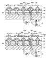
次いで、図5(b)に示すように、図5(a)の構造体の上面に樹脂フィルムを貼着するなどしてキャパシタC及び貫通電極Tを被覆する第1絶縁層70を形成する。このとき、第1樹脂層70は、キャパシタC及び貫通電極Tの段差を解消してその上面が平坦になって形成される。さらに、図5(c)に示すように、レーザ、又はフォトリソグラフィ及びプラズマエッチングにより、キャパシタCの第2電極24及び貫通電極Tのコンタクト層60に到達する深さの第1ビアホールVH1を形成する。
Next, as shown in FIG. 5B, a first insulating
続いて、図6(a)に示すように、セミアディティブ法などによりキャパシタCの第2電極24及び貫通電極Tのコンタクト層60に接続される第1配線層72を第1絶縁層70の上に形成する。詳しく説明すると、まず、第1ビアホールVH1の内面上及び第1絶縁層70上に無電解めっきやスパッタ法により銅などのシード層(不図示)を形成する。その後に、シード層上に第1配線層70に対応する開口部を有するレジスト(不図示)を形成する。続いて、シード層をめっき給電層に利用した電解めっきによりレジストの開口部に銅などの金属パターン層(不図示)を形成する。
Subsequently, as shown in FIG. 6A, the
さらに、レジストを除去した後に、金属パターン層をマスクにしてシード層をエッチングすることにより、第1配線層72を得る。なお、セミアディティブ法の代わりに、サブトラクティブ法又はフルアディティブ法を用いてもよい。
Further, after removing the resist, the
次いで、図6(b)に示すように、第1配線層72を被覆する第2絶縁層70aを形成した後に、第2絶縁層70aを加工することにより、第1配線層72に到達する深さの第2ビアホールVH2を形成する。さらに、第2ビアホールVH2を介して第1配線層72に接続される第2配線層72aを第2絶縁層70aの上に形成する。
Next, as shown in FIG. 6B, after forming the second insulating
これにより、キャパシタCの第2電極24及び貫通電極Tのコンタクト層60に接続される2層のビルドアップ配線がそれらの上に形成される。図6では、2層のビルドアップ配線を形成する形態を例示するが、n層(nは1以上の整数)のn層のビルドアップ配線を適宜形成することができる。
As a result, two layers of build-up wiring connected to the
次いで、図7(a)に示すように、図6(b)の構造体から銅板10をアンモニア系アルカリエッチング液でエッチングすることにより、銅板10を錫層12に対して選択的に除去する。さらに、7(b)に示すように、硝酸系エッチング液によって錫層12をエッチングすることにより、錫層12を銅ポスト54及びベース樹脂層50に対して選択的に除去する。これによって、下面側にベース樹脂層50と銅ポスト54が露出する。
Next, as shown in FIG. 7A, the
続いて、図8に示すように、図7(b)の構造体を上下反転させ、キャパシタC及び貫通電極Tの各銅ポスト54にフラックスを塗布し、はんだを粉体塗布によって銅ポスト54に選択的に付着させ、リフロー加熱することにより、銅ポスト54を被覆するはんだ層62を形成する。銅ポスト54の表面に金層が形成されている方が、粉体塗布によってはんだ層62を銅ポスト54に安定して付着させることができる。
Subsequently, as shown in FIG. 8, the structure of FIG. 7B is turned upside down, a flux is applied to each
これにより、キャパシタCでは、銅ポスト54がはんだ層62で被覆されてその先端部が第1電極20の接続部21となる。また、貫通電極Tでは、銅ポスト54がはんだ層62で被覆されてその先端部が第2接続部61bとなる。さらに、最下に露出する第2配線層72aにはんだボールを搭載するなどして外部接続端子74を設ける。なお、一つの基板から複数のキャパシタ内蔵基板を得る場合は、外部接続端子74を設ける前又は後に基板が切断される。
As a result, in the capacitor C, the
以上により、第1実施形態のキャパシタ内蔵基板1が得られる。
Thus, the capacitor built-in
図8に示すように、第1実施形態のキャパシタ内蔵基板1では、最上層として配置されたベース樹脂層50の中に複数のキャパシタCと貫通電極Tとが貫通した状態で横方向に並んで配置されている。キャパシタCは、銅ポスト54及び第1銅バンプ56から形成された第1電極20と、誘電体層22と、金層24a及びはんだ層24bから形成された第2電極24とによって基本構成されている。第1電極20を構成する銅ポスト54(突出部)はベース樹脂層50の上面から突出して形成され、その上にはんだ層62が被覆されてその先端部が第1電極20の接続部21となっている。
As shown in FIG. 8, in the capacitor built-in
また、銅ポスト54に接続された第1銅バンプ56(突出部)はベース樹脂層50を貫通して形成され、ベース樹脂層50の下面から突出してその先端部が凸状曲面(半球面など)となっている。このように、キャパシタCの第1電極20は、ベース樹脂層50の上面から突出する接続部21と、接続部21に接続されてベース樹脂層50の下面から突出し、先端部が凸状曲面となった第1銅バンプ56とにより構成される。さらに、第1電極20の凸状曲面を被覆する誘電体層22が形成され、誘電体層22を被覆する金層24a及びはんだ層24bからなる第2電極24が形成されている。
The first copper bump 56 (protruding portion) connected to the
また、ベース樹脂層50にはキャパシタCの他に貫通電極Tが設けられている。貫通電極Tは、ベース樹脂層50の上面から突出する銅ポスト54とそれに接続されてベース樹脂層50を貫通してベース樹脂層50の下面から突出して先端部が凸状曲面となった第2銅バンプ56aとによって基本構成される。第2銅バンプ56aは金層及びはんだ層から形成されたコンタクト層60で被覆されており、その先端部が第1接続部61aとなっている。また、銅ポスト54ははんだ層62で被覆されており、その先端部が第2接続部61bとなっている。
In addition to the capacitor C, the
また、キャパシタC及び貫通電極Tは第1絶縁層70で被覆されており、第1絶縁層70にはキャパシタCの第2電極24及び貫通電極Tの下側のコンタクト層60の第1接続部61aに到達する深さの第1ビアホールVH1が形成されている。そして、第1ビアホールVH1を介してキャパシタCの第2電極24及び貫通電極Tの第2接続部61aにそれぞれ接続される第1配線層72が第1絶縁層70の上(図8では下)に形成されている。
The capacitor C and the through electrode T are covered with a first insulating
さらに、第1配線層72の上(図8では下)に第2絶縁層70aが形成され、第2絶縁層70aには第1配線層72に到達する深さの第2ビアホールVH2が設けられている。そして、第2ビアホールVH2を介して第1配線層72に接続される第2配線層72aが第2絶縁層70aの上(図8では下)に形成されている。第2配線層72aには外部接続端子74が設けられている。
Further, a second
このようにして、本実施形態のキャパシタ内蔵基板1は、ベース樹脂層50を貫通して横方向に並んで配置された複数のキャパシタC及び貫通電極Tの上(図8では下)にそれらに電気的に接続された2層のビルドアップ配線が形成されて基本構成されている。
In this manner, the capacitor-embedded
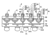
図9には、本実施形態のキャパシタ内蔵基板に半導体チップが実装されて構成される電子部品装置が示されている。図9に示すように、本実施形態の電子部品装置5は、キャパシタ内蔵基板2のベース樹脂層50の上面から突出するキャパシタCの第1電極24の接続部21及び貫通電極Tの第2接続部61bに半導体チップ45の電極(又はバンプ)が接続されて構成される。
FIG. 9 shows an electronic component device configured by mounting a semiconductor chip on the capacitor built-in substrate of the present embodiment. As shown in FIG. 9, the
本実施形態のキャパシタ内蔵基板1では、キャパシタCの第1電極24の接続部21及び貫通電極Tの第2接続部61bは半導体チップ45を接続するためのバンプとして機能するようになっている。キャパシタCの第1電極20の接続部21と第2電極24、及び貫通電極Tの第1、第2接続部61a,61bは上下方向に配置されて半導体チップ45とビルドアップ配線に直接接続されている。キャパシタ内蔵基板1に内蔵された複数のキャパシタCは、半導体チップ45とビルドアップ配線との間に電気的に並列に接続されてデカップリングキャパシタとして機能する。
In the capacitor built-in
このようにして電子部品装置5を構成することにより、従来技術と違って、各キャパシタCに接続される配線層を引き回して半導体チップ45に接続する必要がないので、キャパシタCと半導体チップとの電気経路が最短になり、インダクタンスを減少させることができる。これにより、高速動作する半導体チップに対してのデカップリングキャパシタとして十分な性能を奏するようになる。
By configuring the
しかも、本実施形態のキャパシタ内蔵基板1では、キャパシタCの他に、信号ラインなどの導通経路となる貫通電極Tを内蔵しているので、特別にバンプを配置して信号ラインなどを配線基板に接続する必要もない。
In addition, since the capacitor built-in
また、凸状曲面をもつ第1銅バンプ56の上に誘電体層22と第2電極24を被覆してキャパシタCを構成するので、平面状にキャパシタを構成する場合よりも、同じ設置面積において容量の大きなキャパシタを形成することができる。
Further, since the capacitor C is formed by covering the
さらには、本実施形態のキャパシタ内蔵基板1では、半導体チップ45がフリップチップ接続されるバンプとして、キャパシタ内蔵基板1に内蔵された銅ポスト54が使用される。銅ポスト54は、レジストの開口部に電解めっきによって形成されるので、一般的なはんだバンプを使用する場合よりも狭小ピッチ(100μm以下)でその高さを高く形成することができる。これにより、狭小ピッチの電極をもつ半導体チップに対応する配線基板として使用できるようになる。
Furthermore, in the capacitor built-in
さらには、高靭性弾性体であるベース樹脂層50に高さの高い銅ポスト54を設けるようにしたことから、ベース樹脂層50及び銅ポスト54が半導体チップ45をフリップチップ接続する際の応力緩和層として機能するので、電子部品装置の信頼性を向上させることができる。
Furthermore, since the
(第2の実施の形態)
図10は本発明の第2実施形態のキャパシタ内蔵基板を示す断面図、図11は同じくキャパシタ内蔵基板に半導体チップが実装して構成される電子部品装置を示す断面図である。図10に示すように、第2実施形態のキャパシタ内蔵基板2では、複数のキャパシタC及び貫通電極Tの他に、抵抗部Rが内蔵されている。図10の例では、第1実施形態の図8の右側の貫通電極Tが抵抗部Rとなっている。
(Second Embodiment)
FIG. 10 is a cross-sectional view showing a capacitor built-in substrate according to a second embodiment of the present invention, and FIG. As shown in FIG. 10, in the capacitor built-in
抵抗部Rは、キャパシタCの第1電極20と同様に銅ポスト54と第1銅バンプ56から構成される第1電極20と、第1電極20の凸状曲面の上に形成されたアルミナ層、窒化シリコン層又は窒化チタンなどの絶縁層64と、絶縁層64の上に形成された金などからなる第2電極66とにより構成される。
The resistor portion R includes a
さらに、キャパシタCと同様に、銅ポスト54がはんだ層62で被覆されており、その先端部が第1電極20の接続部21となっている。そして、抵抗部Rの第2電極66が第1ビアホールVH1を介して配線基板の第1配線層72に接続されている。その他の構成は、第1実施形態の図8と同一であるので同一符号を付してその説明を省略する。
Further, like the capacitor C, the
第2実施形態のキャパシタ内蔵基板2の抵抗部Rを形成するには、前述した第1実施形態の図4(d)の工程において、抵抗部を形成する部分に第2銅バンプ56aを形成した後に、スパッタリングによってアルミナなどの絶縁層と金層を順次形成した後に、ドライフィルムレジスト59を除去して銅バンプ56上に絶縁層と金層を部分的に形成して抵抗部Rとすればよい。
In order to form the resistance portion R of the capacitor built-in
図11には、第2実施形態のキャパシタ内蔵基板2の上に半導体チップが実装された電子部品装置6が示されている。図11に示すように、第2実施形態の電子部品装置6は、キャパシタCと同様に、抵抗部Rの第1電極20の接続部21と第2電極66が上下方向に配置され、半導体チップ45の電極がキャパシタC及び貫通電極Tの他に抵抗部Rの第1電極20の接続部21に直接接続されている。
FIG. 11 shows an
キャパシタCと同様に、抵抗部Rは半導体チップ45の直下に配置され、半導体チップ45と抵抗部Rとを配線基板内の配線で引き回すことなく直接接続することができる。このようにして、半導体チップ45と配線基板の第2配線層72aとの間に抵抗部Rが接続される。その他の構成は、図9と同一であるので同一符号を付してその説明を省略する。
Similar to the capacitor C, the resistance portion R is disposed immediately below the
第2実施形態のキャパシタ内蔵基板2は、第1実施形態と同様な効果を奏する。
The capacitor built-in
(第3の実施の形態)
図12〜図14は本発明の第3実施形態のキャパシタ内蔵基板の製造方法を示す断面図である。図15は同じくキャパシタ内蔵基板を示す断面図である。第3実施形態の特徴は、銅板に設けた凹部にはんだ層を充填しておき、はんだ層に銅ポストを埋め込むことに基づいて、最終的にはんだ層を銅ポストの被覆層として利用することにある。第3実施形態では、第1実施形態と同一工程においてはその詳しい説明を省略する。
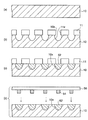
(Third embodiment)
12 to 14 are sectional views showing a method for manufacturing a capacitor built-in substrate according to a third embodiment of the present invention. FIG. 15 is a cross-sectional view showing the capacitor built-in substrate. A feature of the third embodiment is that the solder layer is filled in the concave portion provided in the copper plate and the copper post is embedded in the solder layer, and finally the solder layer is used as a coating layer of the copper post. is there. In the third embodiment, detailed description thereof is omitted in the same steps as those in the first embodiment.
第3実施形態の製造方法では、図12(a)及び(b)に示すように、金属支持体としての銅板10を用意し、銅板10の上に開口部11xを備えたレジスト11を形成する。次いで、レジスト11の開口部11xを通して銅板10をウェットエッチングすることにより、銅板10に凹部10xを形成する。さらに、図12(c)に示すように、銅板10をめっき給電経路として利用する電解めっきにより、銅板10の凹部10xにはんだ層62を形成する。その後に、レジスト11が除去される。
In the manufacturing method of the third embodiment, as shown in FIGS. 12A and 12B, a
次いで、図12(d)に示すように、第1実施形態と同様に、銅ポスト54が立設するベース樹脂層50を用意し、銅ポスト54を銅板10の凹部10x内に形成されたはんだ層62に押し込む。銅板10の凹部10xに充填されたはんだ層62は、銅ポスト54に対応する部分に配置されている。これにより、図13(a)に示すように、銅板10の凹部10x内のはんだ層62内に銅ポスト54が埋め込まれた状態で、銅板10の上にベース樹脂層50が貼り付けられる。
Next, as shown in FIG. 12 (d), as in the first embodiment, a
次いで、図13(b)に示すように、第1実施形態の図3(b)の工程から図5(a)までの工程を遂行することにより、銅板10の上にキャパシタCと貫通電極Tを形成する。さらに、図14(a)に示すように、1実施形態の図5(b)〜図6(b)の工程を遂行することにより、キャパシタCと貫通電極Tに接続される2層のビルドアップ配線(第1、第2配線層72,72a及び第1、第2層間絶縁層70,70a)を形成する。
Next, as shown in FIG. 13B, the capacitor C and the through electrode T are formed on the
その後に、図14(b)に示すように、図14(a)の構造体から銅板10をアンモニア系アルカリエッチング液でエッチングして除去する。これにより、銅板10ははんだ層62及びベース樹脂層50に対して選択的に除去されて銅ポスト54を被覆するはんだ層62が露出して、キャパシタCの第1電極20の接続部21と貫通電極Tの第2接続部61bが得られる。さらに、図15に示すように、図14(b)の構造体を上下反転させ、最下に露出する第2配線層72aに外部接続端子74を設ける。
Thereafter, as shown in FIG. 14B, the
以上により、第1実施形態と同一構造の第3実施形態のキャパシタ内蔵基板3が得られる。第3実施形態の製造方法では、銅板10の凹部10xに充填されたはんだ層62が銅ポスト54を被覆するはんだ層62となるので、銅ポスト54を露出させてからはんだ層62を被覆する必要がない。また、第1実施形態と違って錫層12の形成工程と除去工程が不要なので、コスト的に有利になる。
Thus, the capacitor built-in
第3実施形態のキャパシタ内蔵基板3は、第1実施形態と同様に半導体チップが実装され、第1実施形態と同様な効果を奏する。
The capacitor-embedded
1〜3…キャパシタ内蔵基板、5,6…電子部品装置、10…銅板、10x…凹部、12…錫層、14…中間樹脂層、20…第1電極、21,61a,61b…接続部、22…誘電体層、24…第2電極、24a…金層、24b,62…はんだ層、45…半導体チップ、50…ベース樹脂層、50x,50y…めっき用開口部、54…銅ポスト、56,56a…銅バンプ、59…ドライフィルムレジスト、59x…開口部、60…コンタクト層、70,70a…層間絶縁層、72,72a…配線層、74…外部接続端子、C…キャパシタ、T…貫通電極、R…抵抗部。 DESCRIPTION OF SYMBOLS 1-3 ... Capacitor built-in board | substrate, 5, 6 ... Electronic component apparatus, 10 ... Copper plate, 10x ... Recessed part, 12 ... Tin layer, 14 ... Intermediate resin layer, 20 ... 1st electrode, 21, 61a, 61b ... Connection part, 22 ... Dielectric layer, 24 ... Second electrode, 24a ... Gold layer, 24b, 62 ... Solder layer, 45 ... Semiconductor chip, 50 ... Base resin layer, 50x, 50y ... Opening for plating, 54 ... Copper post, 56 56a ... copper bump, 59 ... dry film resist, 59x ... opening, 60 ... contact layer, 70,70a ... interlayer insulating layer, 72,72a ... wiring layer, 74 ... external connection terminal, C ... capacitor, T ... through Electrode, R: resistance portion.
Claims (10)
前記ベース樹脂層を貫通して設けられて前記開口部に埋め込まれ、前記開口部から上側及び下側に突出する突出部をそれぞれ備え、前記ベース樹脂層の一方の面側の前記突出部が接続部となる第1電極と、前記ベース樹脂層の他方の面側の前記第1電極の前記突出部を被覆する誘電体層と、前記誘電体層を被覆する第2電極とから構成されて、前記ベース樹脂層を貫通した状態で横方向に並んで配置された複数のキャパシタと、
前記ベース樹脂層を貫通して設けられ、前記ベース樹脂層の両面側から突出する突出部をそれぞれ備えた貫通電極と、
ベース樹脂層の前記他方の面側に形成され、前記キャパシタの前記第2電極及び前記貫通電極の一端側に電気的に接続されたビルドアップ配線とを有することを特徴とするキャパシタ内蔵基板。 A base resin layer having an opening penetrating in the thickness direction ;
Protrusions provided through the base resin layer , embedded in the opening, and projecting upward and downward from the opening are provided, and the protrusion on one surface side of the base resin layer is connected A first electrode serving as a part, a dielectric layer covering the protruding portion of the first electrode on the other surface side of the base resin layer, and a second electrode covering the dielectric layer, A plurality of capacitors arranged side by side in a state penetrating the base resin layer;
A through electrode provided through the base resin layer and provided with protrusions protruding from both sides of the base resin layer;
A substrate with a built-in capacitor, comprising a build-up wiring formed on the other surface side of the base resin layer and electrically connected to one end side of the second electrode and the through electrode of the capacitor.
前記第1電極の前記接続部及び前記貫通電極の他端側に接続されて実装された半導体チップとを有することを特徴とする電子部品装置。 A capacitor-embedded substrate according to any one of claims 1 to 3,
An electronic component device comprising: a semiconductor chip mounted and connected to the connection portion of the first electrode and the other end side of the through electrode.
前記金属支持体上の前記柔軟金属層に、前記ベース樹脂層上の前記金属ポストを押し込んで前記金属支持体と前記ベース樹脂層とを貼り合わせることにより、前記金属ポストを前記柔軟金属層に埋め込む工程と、
所要の金属ポスト上の前記ベース樹脂層の部分に第1めっき用開口部を形成する工程と、
前記金属支持体、前記柔軟金属層及び前記金属ポストをめっき給電経路に利用する電解めっきにより、前記第1めっき開口部に前記ベース樹脂層の上面から突出する金属バンプを形成して前記金属ポスト及び前記金属バンプから構成される第1電極を得る工程と、
前記第1電極を被覆する誘電体層を形成する工程と、
前記誘電体層を被覆する第2電極を形成してキャパシタを得る工程と、
前記キャパシタの上方に、前記キャパシタの第2電極に電気的に接続されるビルドアップ配線を形成する工程と、
前記金属支持体及び前記柔軟金属層を除去して前記金属ポストを露出させる工程とを有することを特徴とするキャパシタ内蔵基板の製造方法。 Preparing a base resin layer in which a plurality of metal posts are erected on one surface and a metal support having a flexible metal layer formed on one surface;
The metal post is embedded in the flexible metal layer by pressing the metal post on the base resin layer into the flexible metal layer on the metal support and bonding the metal support and the base resin layer together. Process,
Forming a first plating opening in a portion of the base resin layer on a required metal post;
A metal bump protruding from the upper surface of the base resin layer is formed in the first plating opening by electrolytic plating using the metal support, the flexible metal layer, and the metal post as a plating power feeding path. Obtaining a first electrode composed of the metal bump;
Forming a dielectric layer covering the first electrode;
Forming a second electrode covering the dielectric layer to obtain a capacitor;
Forming a buildup wiring electrically connected to the second electrode of the capacitor above the capacitor;
And a step of removing the metal support and the flexible metal layer to expose the metal post.
前記金属支持体に形成された前記柔軟金属層に、前記ベース樹脂層上の前記金属ポストを押し込んで前記金属支持体と前記ベース樹脂層とを貼り合わせることにより、前記金属ポストを前記柔軟金属に埋め込む工程と、
所要の前記金属ポスト上の前記ベース樹脂層の部分にキャパシタ形成用の第1めっき用開口部を形成する工程と、
前記金属支持体、前記柔軟金属層及び前記金属ポストをめっき給電経路に利用する電解めっきにより、前記第1めっき開口部に前記ベース樹脂層の上面から突出する金属バンプを形成して前記金属ポスト及び前記金属バンプから構成される第1電極を得る工程と、
前記第1電極を被覆する誘電体層を形成する工程と、
前記誘電体層を被覆する第2電極を形成してキャパシタを得る工程と、
前記キャパシタの上方に、前記キャパシタの前記第2電極に接続されるビルドアップ配線を形成する工程と、
前記金属支持体を除去して前記柔軟金属層で被覆された前記金属ポストを露出させる工程とを有することを特徴とするキャパシタ内蔵基板の製造方法。 Preparing a base resin layer in which a metal post is erected on one surface side, and a metal support in which a recess is formed in a portion corresponding to the metal post and a flexible metal layer is embedded in the recess;
By pushing the metal post on the base resin layer into the flexible metal layer formed on the metal support and bonding the metal support and the base resin layer together, the metal post is attached to the flexible metal. An embedding step;
Forming a first plating opening for forming a capacitor in a portion of the base resin layer on the required metal post;
A metal bump protruding from the upper surface of the base resin layer is formed in the first plating opening by electrolytic plating using the metal support, the flexible metal layer, and the metal post as a plating power feeding path. Obtaining a first electrode composed of the metal bump;
Forming a dielectric layer covering the first electrode;
Forming a second electrode covering the dielectric layer to obtain a capacitor;
Forming a build-up wiring connected to the second electrode of the capacitor above the capacitor;
And a step of removing the metal support to expose the metal post covered with the flexible metal layer.
前記キャパシタを得る工程の後であって、ビルドアップ配線を形成する工程の前に、
前記金属ポスト上の前記貫通電極を形成するための前記ベース樹脂層の部分に第2めっき用開口部を形成する工程と、
前記第2めっき用開口部を含む領域に開口部が設けられたレジストを形成して前記キャパシタを前記レジストで被覆する工程と、
前記金属支持体、前記柔軟金属層及び前記金属ポストをめっき給電経路に利用する電解めっきにより、前記第2めっき用開口部に前記ベース樹脂層の上面から突出する金属バンプを形成して前記金属ポスト及び前記金属バンプから構成される前記貫通電極を得る工程と、
前記レジストを除去する工程とをさらに有し、
前記ビルドアップ配線は前記貫通電極の一端側に接続されることを特徴とする請求項5又は6に記載のキャパシタ内蔵基板の製造方法。 In each part of the base resin layer on the plurality of metal posts, a through electrode formation region is defined in addition to the capacitor formation region,
After the step of obtaining the capacitor and before the step of forming the build-up wiring,
Forming a second plating opening in a portion of the base resin layer for forming the through electrode on the metal post;
Forming a resist provided with an opening in a region including the second plating opening and covering the capacitor with the resist;
A metal bump protruding from the upper surface of the base resin layer is formed in the second plating opening by electrolytic plating using the metal support, the flexible metal layer, and the metal post as a plating power feeding path. And obtaining the through electrode composed of the metal bump,
Further removing the resist,
The method for manufacturing a capacitor built-in substrate according to claim 5, wherein the build-up wiring is connected to one end side of the through electrode.
前記キャパシタを得る工程の後であって、ビルドアップ配線を形成する工程の前に、
前記金属ポスト上の前記抵抗部を形成するための前記ベース樹脂層の部分に第2めっき用開口部を形成する工程と、
前記第2めっき用開口部を含む領域に開口部が設けられたレジストを形成して前記キャパシタを前記レジストで被覆する工程と、
前記金属支持体、前記柔軟金属層及び前記金属ポストをめっき給電経路に利用する電解めっきにより、前記第2めっき用開口部に前記ベース樹脂層の上面から突出する金属バンプを形成して前記金属ポスト及び前記金属バンプから構成される第1電極を得る工程と、
前記第1電極を被覆する絶縁層を形成する工程と、
前記絶縁層を被覆する第2電極を形成して前記抵抗部を得る工程と、
前記レジストを除去する工程とをさらに有し、
前記ビルドアップ配線は前記抵抗部の前記第2電極に接続されることを特徴とする請求項5又は6に記載のキャパシタ内蔵基板の製造方法。 In each portion of the base resin layer on the plurality of metal posts, a resistor formation region is defined in addition to the capacitor formation region.
After the step of obtaining the capacitor and before the step of forming the build-up wiring,
Forming a second plating opening in a portion of the base resin layer for forming the resistance portion on the metal post;
Forming a resist provided with an opening in a region including the second plating opening and covering the capacitor with the resist;
A metal bump protruding from the upper surface of the base resin layer is formed in the second plating opening by electrolytic plating using the metal support, the flexible metal layer, and the metal post as a plating power feeding path. And obtaining a first electrode composed of the metal bumps;
Forming an insulating layer covering the first electrode;
Forming a second electrode covering the insulating layer to obtain the resistance portion;
Further removing the resist,
The method of manufacturing a capacitor built-in substrate according to claim 5, wherein the build-up wiring is connected to the second electrode of the resistance portion.
前記金属支持体及び前記柔軟金属層を除去する工程の後に、露出する前記金属ポストを被覆するはんだ層を形成する工程をさらに有することを特徴とする請求項5に記載のキャパシタ内蔵基板の製造方法。 The metal support is made of copper, the flexible metal layer is made of tin,
6. The method of manufacturing a capacitor built-in substrate according to claim 5, further comprising a step of forming a solder layer covering the exposed metal post after the step of removing the metal support and the flexible metal layer. .
Priority Applications (4)
| Application Number | Priority Date | Filing Date | Title |
|---|---|---|---|
| JP2006217955A JP4783692B2 (en) | 2006-08-10 | 2006-08-10 | Capacitor-embedded substrate, manufacturing method thereof, and electronic component device |
| US11/882,645 US7936568B2 (en) | 2006-08-10 | 2007-08-03 | Capacitor built-in substrate and method of manufacturing the same and electronic component device |
| CNA200710140290XA CN101123854A (en) | 2006-08-10 | 2007-08-08 | Capacitor built-in substrate and method of manufacturing the same and electronic component device |
| EP07114115A EP1887622A3 (en) | 2006-08-10 | 2007-08-09 | Capacitor built-in substrate and method of manufacturing the same and electronic component device |
Applications Claiming Priority (1)
| Application Number | Priority Date | Filing Date | Title |
|---|---|---|---|
| JP2006217955A JP4783692B2 (en) | 2006-08-10 | 2006-08-10 | Capacitor-embedded substrate, manufacturing method thereof, and electronic component device |
Publications (3)
| Publication Number | Publication Date |
|---|---|
| JP2008042118A JP2008042118A (en) | 2008-02-21 |
| JP2008042118A5 JP2008042118A5 (en) | 2009-07-30 |
| JP4783692B2 true JP4783692B2 (en) | 2011-09-28 |
Family
ID=38666852
Family Applications (1)
| Application Number | Title | Priority Date | Filing Date |
|---|---|---|---|
| JP2006217955A Expired - Fee Related JP4783692B2 (en) | 2006-08-10 | 2006-08-10 | Capacitor-embedded substrate, manufacturing method thereof, and electronic component device |
Country Status (4)
| Country | Link |
|---|---|
| US (1) | US7936568B2 (en) |
| EP (1) | EP1887622A3 (en) |
| JP (1) | JP4783692B2 (en) |
| CN (1) | CN101123854A (en) |
Families Citing this family (29)
| Publication number | Priority date | Publication date | Assignee | Title |
|---|---|---|---|---|
| JP4920335B2 (en) * | 2006-08-07 | 2012-04-18 | 新光電気工業株式会社 | Capacitor built-in interposer, manufacturing method thereof, and electronic component device |
| JP4783692B2 (en) | 2006-08-10 | 2011-09-28 | 新光電気工業株式会社 | Capacitor-embedded substrate, manufacturing method thereof, and electronic component device |
| EP2184960B1 (en) * | 2007-09-06 | 2012-08-15 | Murata Manufacturing Co. Ltd. | Circuit board and method for manufacturing circuit board |
| WO2009119875A1 (en) * | 2008-03-24 | 2009-10-01 | 日本特殊陶業株式会社 | Component-incorporating wiring board |
| KR101006619B1 (en) * | 2008-10-20 | 2011-01-07 | 삼성전기주식회사 | A printed circuit board comprising a round solder bump and a method of manufacturing the same |
| EP2421342B1 (en) * | 2008-12-22 | 2013-09-11 | Fujitsu Limited | Method of manufacturing an electronic component |
| US8389870B2 (en) | 2010-03-09 | 2013-03-05 | International Business Machines Corporation | Coreless multi-layer circuit substrate with minimized pad capacitance |
| TWI446497B (en) * | 2010-08-13 | 2014-07-21 | Unimicron Technology Corp | Package substrate having a passive element embedded therein and fabrication method thereof |
| JP6081044B2 (en) | 2010-09-16 | 2017-02-15 | 富士通株式会社 | Manufacturing method of package substrate unit |
| US10433421B2 (en) * | 2012-12-26 | 2019-10-01 | Intel Corporation | Reduced capacitance land pad |
| JP2015049985A (en) * | 2013-08-30 | 2015-03-16 | 富士通株式会社 | Ic socket and connection terminal |
| JP6551909B2 (en) * | 2013-10-09 | 2019-07-31 | 学校法人早稲田大学 | Electrode connection method and electrode connection structure |
| US9642261B2 (en) * | 2014-01-24 | 2017-05-02 | Zhuhai Advanced Chip Carriers & Electronic Substrate Solutions Technologies Co. Ltd. | Composite electronic structure with partially exposed and protruding copper termination posts |
| KR102281460B1 (en) * | 2015-01-22 | 2021-07-27 | 삼성전기주식회사 | Embedded board and method of manufacturing the same |
| JP6672705B2 (en) * | 2015-10-30 | 2020-03-25 | 大日本印刷株式会社 | Interposer and method of manufacturing interposer |
| EP3174094B1 (en) * | 2015-11-25 | 2018-09-26 | IMEC vzw | Integrated circuit comprising a metal-insulator-metal capacitor and fabrication method thereof |
| WO2018038094A1 (en) * | 2016-08-22 | 2018-03-01 | 重信 三浦 | Method for manufacturing capacitor, method for manufacturing substrate with built-in capacitor, substrate with built-in capacitor, and semiconductor device mounting component |
| US10297494B2 (en) | 2017-01-26 | 2019-05-21 | Taiwan Semiconductor Manufacturing Company, Ltd. | Raised via for terminal connections on different planes |
| DE102017127920A1 (en) | 2017-01-26 | 2018-07-26 | Taiwan Semiconductor Manufacturing Company, Ltd. | Increased through-hole for connections on different levels |
| US10622302B2 (en) | 2018-02-14 | 2020-04-14 | Taiwan Semiconductor Manufacturing Company, Ltd. | Via for semiconductor device connection and methods of forming the same |
| US10373866B1 (en) * | 2018-05-04 | 2019-08-06 | International Business Machines Corporation | Method of forming metal insulator metal capacitor with extended capacitor plates |
| US11158775B2 (en) | 2018-06-08 | 2021-10-26 | Taiwan Semiconductor Manufacturing Company, Ltd. | Semiconductor device and method |
| DE102018126130B4 (en) | 2018-06-08 | 2023-08-10 | Taiwan Semiconductor Manufacturing Co., Ltd. | semiconductor device and method |
| CN110660582A (en) * | 2018-06-29 | 2020-01-07 | 浙江清华柔性电子技术研究院 | Flexible energy storage film, preparation method thereof and film capacitor |
| US10992100B2 (en) | 2018-07-06 | 2021-04-27 | Taiwan Semiconductor Manufacturing Company, Ltd. | Semiconductor device and method |
| JP7131626B2 (en) * | 2018-10-25 | 2022-09-06 | 株式会社村田製作所 | ELECTRONIC COMPONENT MODULE AND METHOD FOR MANUFACTURING ELECTRONIC COMPONENT MODULE |
| JP7279538B2 (en) * | 2019-06-19 | 2023-05-23 | 富士フイルムビジネスイノベーション株式会社 | light emitting device |
| CN113451279B (en) * | 2020-03-26 | 2023-09-12 | 群创光电股份有限公司 | Capacitor and electronic device |
| US20240107665A1 (en) * | 2022-09-23 | 2024-03-28 | Qualcomm Incorporated | Providing a lower inductance path in a routing substrate for a capacitor, and related electronic devices and fabrication methods |
Family Cites Families (75)
| Publication number | Priority date | Publication date | Assignee | Title |
|---|---|---|---|---|
| US5177670A (en) * | 1991-02-08 | 1993-01-05 | Hitachi, Ltd. | Capacitor-carrying semiconductor module |
| JPH06268141A (en) | 1993-03-15 | 1994-09-22 | Hitachi Ltd | Mounting method for electronic circuit device |
| JP3246166B2 (en) | 1994-03-03 | 2002-01-15 | 株式会社村田製作所 | Thin film capacitors |
| JP2830845B2 (en) | 1996-06-26 | 1998-12-02 | 日本電気株式会社 | Semiconductor storage device |
| JPH11111884A (en) * | 1997-10-07 | 1999-04-23 | Toppan Printing Co Ltd | Substrate for manufacturing electronic components and manufacturing electronic components using the same |
| US6274224B1 (en) * | 1999-02-01 | 2001-08-14 | 3M Innovative Properties Company | Passive electrical article, circuit articles thereof, and circuit articles comprising a passive electrical article |
| JP3635219B2 (en) * | 1999-03-11 | 2005-04-06 | 新光電気工業株式会社 | Multilayer substrate for semiconductor device and manufacturing method thereof |
| JP3792445B2 (en) * | 1999-03-30 | 2006-07-05 | 日本特殊陶業株式会社 | Wiring board with capacitor |
| CN101232779B (en) * | 1999-09-02 | 2013-03-27 | 揖斐电株式会社 | Printed circuit board and method for producing the printed circuit board |
| US6876554B1 (en) * | 1999-09-02 | 2005-04-05 | Ibiden Co., Ltd. | Printing wiring board and method of producing the same and capacitor to be contained in printed wiring board |
| US6573584B1 (en) * | 1999-10-29 | 2003-06-03 | Kyocera Corporation | Thin film electronic device and circuit board mounting the same |
| US6525921B1 (en) | 1999-11-12 | 2003-02-25 | Matsushita Electric Industrial Co., Ltd | Capacitor-mounted metal foil and a method for producing the same, and a circuit board and a method for producing the same |
| US6871396B2 (en) | 2000-02-09 | 2005-03-29 | Matsushita Electric Industrial Co., Ltd. | Transfer material for wiring substrate |
| JP2001291637A (en) | 2000-04-10 | 2001-10-19 | Shinko Electric Ind Co Ltd | Spherical capacitor, its manufacturing method, its mounting structure, and wiring board and its manufacturing method |
| US20030086248A1 (en) | 2000-05-12 | 2003-05-08 | Naohiro Mashino | Interposer for semiconductor, method for manufacturing same, and semiconductor device using same |
| CN1196392C (en) * | 2000-07-31 | 2005-04-06 | 日本特殊陶业株式会社 | Wiring baseplate and its manufacture method |
| US6577490B2 (en) * | 2000-12-12 | 2003-06-10 | Ngk Spark Plug Co., Ltd. | Wiring board |
| US6740411B2 (en) * | 2001-02-21 | 2004-05-25 | Ngk Spark Plug Co. Ltd. | Embedding resin, wiring substrate using same and process for producing wiring substrate using same |
| US6512182B2 (en) * | 2001-03-12 | 2003-01-28 | Ngk Spark Plug Co., Ltd. | Wiring circuit board and method for producing same |
| JP3817463B2 (en) * | 2001-11-12 | 2006-09-06 | 新光電気工業株式会社 | Manufacturing method of multilayer wiring board |
| JP3492348B2 (en) * | 2001-12-26 | 2004-02-03 | 新光電気工業株式会社 | Method of manufacturing package for semiconductor device |
| US6943056B2 (en) * | 2002-04-16 | 2005-09-13 | Renesas Technology Corp. | Semiconductor device manufacturing method and electronic equipment using same |
| JP4019837B2 (en) * | 2002-07-19 | 2007-12-12 | 松下電器産業株式会社 | Solid electrolytic capacitor and manufacturing method thereof |
| US7102367B2 (en) * | 2002-07-23 | 2006-09-05 | Fujitsu Limited | Probe card and testing method of semiconductor chip, capacitor and manufacturing method thereof |
| JP2004064052A (en) * | 2002-07-27 | 2004-02-26 | Samsung Electro Mech Co Ltd | Noise shielding type laminated substrate and its manufacturing method |
| JP2004079701A (en) * | 2002-08-14 | 2004-03-11 | Sony Corp | Semiconductor device and its manufacturing method |
| JP4243117B2 (en) * | 2002-08-27 | 2009-03-25 | 新光電気工業株式会社 | Semiconductor package, manufacturing method thereof, and semiconductor device |
| TW560001B (en) * | 2002-10-22 | 2003-11-01 | Toppoly Optoelectronics Corp | Method of forming reflective liquid crystal display and driving circuit |
| JP3910908B2 (en) * | 2002-10-29 | 2007-04-25 | 新光電気工業株式会社 | Semiconductor device substrate, manufacturing method thereof, and semiconductor device |
| JP3910907B2 (en) * | 2002-10-29 | 2007-04-25 | 新光電気工業株式会社 | Capacitor element and manufacturing method thereof, substrate for semiconductor device, and semiconductor device |
| US7161793B2 (en) * | 2002-11-14 | 2007-01-09 | Fujitsu Limited | Layer capacitor element and production process as well as electronic device |
| KR100455890B1 (en) * | 2002-12-24 | 2004-11-06 | 삼성전기주식회사 | A printed circuit board with embedded capacitors, and a manufacturing process thereof |
| JP4342174B2 (en) * | 2002-12-27 | 2009-10-14 | 新光電気工業株式会社 | Electronic device and manufacturing method thereof |
| JP2004214258A (en) * | 2002-12-27 | 2004-07-29 | Renesas Technology Corp | Semiconductor module |
| US6909592B2 (en) * | 2003-01-30 | 2005-06-21 | Dongbuanam Semiconductor Inc. | Thin film capacitor and fabrication method thereof |
| TW556452B (en) * | 2003-01-30 | 2003-10-01 | Phoenix Prec Technology Corp | Integrated storage plate with embedded passive components and method for fabricating electronic device with the plate |
| US6995322B2 (en) * | 2003-01-30 | 2006-02-07 | Endicott Interconnect Technologies, Inc. | High speed circuitized substrate with reduced thru-hole stub, method for fabrication and information handling system utilizing same |
| JP5000071B2 (en) * | 2003-02-26 | 2012-08-15 | 新光電気工業株式会社 | Semiconductor device substrate and semiconductor device |
| US7327554B2 (en) * | 2003-03-19 | 2008-02-05 | Ngk Spark Plug Co., Ltd. | Assembly of semiconductor device, interposer and substrate |
| JP4016340B2 (en) * | 2003-06-13 | 2007-12-05 | ソニー株式会社 | Semiconductor device, mounting structure thereof, and manufacturing method thereof |
| JP4377617B2 (en) * | 2003-06-20 | 2009-12-02 | 日本特殊陶業株式会社 | Capacitor, semiconductor element with capacitor, wiring board with capacitor, and electronic unit including semiconductor element, capacitor, and wiring board |
| JP2005039243A (en) * | 2003-06-24 | 2005-02-10 | Ngk Spark Plug Co Ltd | Intermediate substrate |
| JP4365166B2 (en) * | 2003-08-26 | 2009-11-18 | 新光電気工業株式会社 | Capacitor, multilayer wiring board, and semiconductor device |
| TWI251916B (en) * | 2003-08-28 | 2006-03-21 | Phoenix Prec Technology Corp | Semiconductor assembled heat sink structure for embedding electronic components |
| EP1681717B1 (en) * | 2003-11-07 | 2017-03-29 | Shinko Electric Industries Co., Ltd. | Electronic device |
| KR100535181B1 (en) * | 2003-11-18 | 2005-12-09 | 삼성전자주식회사 | Semiconductor chip package having decoupling capacitor and manufacturing method thereof |
| JP4547164B2 (en) * | 2004-02-27 | 2010-09-22 | 日本特殊陶業株式会社 | Wiring board manufacturing method |
| JP2005317943A (en) * | 2004-03-29 | 2005-11-10 | Sumitomo Bakelite Co Ltd | Printed circuit board and manufacturing method therefor |
| TWI255491B (en) * | 2004-03-31 | 2006-05-21 | Sanyo Electric Co | Substrate for mounting elements, manufacturing method therefor and semiconductor device using the same |
| JP4387231B2 (en) * | 2004-03-31 | 2009-12-16 | 新光電気工業株式会社 | Capacitor-mounted wiring board and manufacturing method thereof |
| JP4260672B2 (en) * | 2004-04-16 | 2009-04-30 | 富士通マイクロエレクトロニクス株式会社 | Manufacturing method of semiconductor device and manufacturing method of relay substrate |
| TW200605169A (en) * | 2004-06-29 | 2006-02-01 | Sanyo Electric Co | Circuit device and process for manufacture thereof |
| KR100680504B1 (en) | 2004-06-30 | 2007-02-08 | 동부일렉트로닉스 주식회사 | Method of manufacturing capacitor of semiconudctor device |
| KR100645643B1 (en) * | 2004-07-14 | 2006-11-15 | 삼성전기주식회사 | Manufacturing method of PCB having embedded passive-chips |
| US7186919B2 (en) * | 2004-08-16 | 2007-03-06 | Samsung Electro-Mechanics Co., Ltd. | Printed circuit board including embedded capacitors and method of manufacturing the same |
| JP5208349B2 (en) * | 2004-09-03 | 2013-06-12 | 富士通株式会社 | Capacitance element and manufacturing method thereof |
| KR100598275B1 (en) * | 2004-09-15 | 2006-07-10 | 삼성전기주식회사 | Embedded passive-device printed circuit board and method for manufacturing the same |
| JP2006120696A (en) | 2004-10-19 | 2006-05-11 | Shinko Electric Ind Co Ltd | Capacitor device and semiconductor device incorporating the same |
| JP2006147606A (en) * | 2004-11-16 | 2006-06-08 | Nec Toppan Circuit Solutions Inc | Sheet-like capacitor and its manufacturing method |
| JP4602208B2 (en) * | 2004-12-15 | 2010-12-22 | 新光電気工業株式会社 | Electronic component mounting structure and manufacturing method thereof |
| JP4499548B2 (en) * | 2004-12-24 | 2010-07-07 | 新光電気工業株式会社 | Capacitor parts |
| JP4351148B2 (en) * | 2004-12-28 | 2009-10-28 | 新光電気工業株式会社 | Wiring board manufacturing method |
| KR100688768B1 (en) * | 2004-12-30 | 2007-03-02 | 삼성전기주식회사 | Embedded chip print circuit board and method for fabricating the same |
| JP2006253631A (en) * | 2005-02-14 | 2006-09-21 | Fujitsu Ltd | Semiconductor device, method of manufacturing the same, capacitor structure, and method of manufacturing the same |
| KR100688743B1 (en) * | 2005-03-11 | 2007-03-02 | 삼성전기주식회사 | Manufacturing method of PCB having multilayer embedded passive-chips |
| KR100716810B1 (en) * | 2005-03-18 | 2007-05-09 | 삼성전기주식회사 | Print circuit board embedded capacitor having blind via hole and method for manufacturing thereof |
| JP2006269764A (en) * | 2005-03-24 | 2006-10-05 | Toshiba Corp | Ferroelectric storage device and manufacturing method therefor |
| JP4638768B2 (en) * | 2005-05-20 | 2011-02-23 | 三井金属鉱業株式会社 | Film carrier tape with capacitor circuit and manufacturing method thereof, surface mount film carrier tape with capacitor circuit and manufacturing method thereof |
| US7696442B2 (en) * | 2005-06-03 | 2010-04-13 | Ngk Spark Plug Co., Ltd. | Wiring board and manufacturing method of wiring board |
| JP2007149730A (en) * | 2005-11-24 | 2007-06-14 | Shinko Electric Ind Co Ltd | Thin-film capacitor, mounting substrate, process for producing mounting substrate, semiconductor device, and method of manufacturing the semiconductor device |
| US20080017407A1 (en) * | 2006-07-24 | 2008-01-24 | Ibiden Co., Ltd. | Interposer and electronic device using the same |
| US7662694B2 (en) * | 2006-07-31 | 2010-02-16 | Ibiden Co., Ltd. | Capacitor having adjustable capacitance, and printed wiring board having the same |
| JP4920335B2 (en) * | 2006-08-07 | 2012-04-18 | 新光電気工業株式会社 | Capacitor built-in interposer, manufacturing method thereof, and electronic component device |
| JP4783692B2 (en) | 2006-08-10 | 2011-09-28 | 新光電気工業株式会社 | Capacitor-embedded substrate, manufacturing method thereof, and electronic component device |
| JP2010004028A (en) * | 2008-05-23 | 2010-01-07 | Shinko Electric Ind Co Ltd | Wiring board, method of manufacturing the same, and semiconductor device |
-
2006
- 2006-08-10 JP JP2006217955A patent/JP4783692B2/en not_active Expired - Fee Related
-
2007
- 2007-08-03 US US11/882,645 patent/US7936568B2/en not_active Expired - Fee Related
- 2007-08-08 CN CNA200710140290XA patent/CN101123854A/en active Pending
- 2007-08-09 EP EP07114115A patent/EP1887622A3/en not_active Withdrawn
Also Published As
| Publication number | Publication date |
|---|---|
| EP1887622A2 (en) | 2008-02-13 |
| US7936568B2 (en) | 2011-05-03 |
| US20080291649A1 (en) | 2008-11-27 |
| CN101123854A (en) | 2008-02-13 |
| JP2008042118A (en) | 2008-02-21 |
| EP1887622A3 (en) | 2008-05-07 |
Similar Documents
| Publication | Publication Date | Title |
|---|---|---|
| JP4783692B2 (en) | Capacitor-embedded substrate, manufacturing method thereof, and electronic component device | |
| JP4920335B2 (en) | Capacitor built-in interposer, manufacturing method thereof, and electronic component device | |
| US8810007B2 (en) | Wiring board, semiconductor device, and method for manufacturing wiring board | |
| JP4790297B2 (en) | Semiconductor device and manufacturing method thereof | |
| US8389414B2 (en) | Method of manufacturing a wiring board | |
| JP5423874B2 (en) | Semiconductor element-embedded substrate and manufacturing method thereof | |
| JP5460155B2 (en) | Capacitor and wiring board | |
| US8669643B2 (en) | Wiring board, semiconductor device, and method for manufacturing wiring board | |
| US20020190371A1 (en) | Semiconductor device and method of production of same | |
| JP4912992B2 (en) | Capacitor-embedded substrate and manufacturing method thereof | |
| KR20090042753A (en) | Interposer | |
| JP2001326305A (en) | Interposer for semiconductor device, its manufacturing method, and semiconductor device | |
| US8114772B2 (en) | Method of manufacturing the semiconductor device | |
| JP5934154B2 (en) | Substrate structure on which electronic components are mounted and method for manufacturing the same | |
| JP4584700B2 (en) | Wiring board manufacturing method | |
| US8039967B2 (en) | Wiring substrate with a wire terminal | |
| JP6600573B2 (en) | Wiring board and semiconductor package | |
| JP2005109486A (en) | Multichip module and manufacturing method therefor | |
| TWI742075B (en) | Capacitive interconnect in a semiconductor package | |
| JP4759981B2 (en) | Manufacturing method of electronic component built-in module | |
| JP6704129B2 (en) | Circuit board, method of manufacturing circuit board, and electronic device | |
| JP4784142B2 (en) | Semiconductor device and manufacturing method thereof | |
| JP4110161B2 (en) | Semiconductor device and manufacturing method of semiconductor device |
Legal Events
| Date | Code | Title | Description |
|---|---|---|---|
| A521 | Request for written amendment filed |
Free format text: JAPANESE INTERMEDIATE CODE: A523 Effective date: 20090615 |
|
| A621 | Written request for application examination |
Free format text: JAPANESE INTERMEDIATE CODE: A621 Effective date: 20090615 |
|
| A977 | Report on retrieval |
Free format text: JAPANESE INTERMEDIATE CODE: A971007 Effective date: 20110623 |
|
| TRDD | Decision of grant or rejection written | ||
| A01 | Written decision to grant a patent or to grant a registration (utility model) |
Free format text: JAPANESE INTERMEDIATE CODE: A01 Effective date: 20110705 |
|
| A01 | Written decision to grant a patent or to grant a registration (utility model) |
Free format text: JAPANESE INTERMEDIATE CODE: A01 |
|
| A61 | First payment of annual fees (during grant procedure) |
Free format text: JAPANESE INTERMEDIATE CODE: A61 Effective date: 20110711 |
|
| FPAY | Renewal fee payment (event date is renewal date of database) |
Free format text: PAYMENT UNTIL: 20140715 Year of fee payment: 3 |
|
| R150 | Certificate of patent or registration of utility model |
Free format text: JAPANESE INTERMEDIATE CODE: R150 |
|
| LAPS | Cancellation because of no payment of annual fees |