EP4258333A2 - Trou d'interconnexion métallisé hermétique à fiabilité améliorée - Google Patents
Trou d'interconnexion métallisé hermétique à fiabilité améliorée Download PDFInfo
- Publication number
- EP4258333A2 EP4258333A2 EP23192617.1A EP23192617A EP4258333A2 EP 4258333 A2 EP4258333 A2 EP 4258333A2 EP 23192617 A EP23192617 A EP 23192617A EP 4258333 A2 EP4258333 A2 EP 4258333A2
- Authority
- EP
- European Patent Office
- Prior art keywords
- equal
- glass
- less
- article
- major surface
- Prior art date
- Legal status (The legal status is an assumption and is not a legal conclusion. Google has not performed a legal analysis and makes no representation as to the accuracy of the status listed.)
- Pending
Links
- 239000011521 glass Substances 0.000 claims abstract description 301
- 239000002241 glass-ceramic Substances 0.000 claims abstract description 216
- 229910052751 metal Inorganic materials 0.000 claims abstract description 169
- 239000002184 metal Substances 0.000 claims abstract description 169
- 239000000758 substrate Substances 0.000 claims abstract description 143
- 230000004323 axial length Effects 0.000 claims abstract description 80
- 239000010949 copper Substances 0.000 claims description 103
- RYGMFSIKBFXOCR-UHFFFAOYSA-N Copper Chemical compound [Cu] RYGMFSIKBFXOCR-UHFFFAOYSA-N 0.000 claims description 90
- 239000011248 coating agent Substances 0.000 claims description 90
- 238000000576 coating method Methods 0.000 claims description 90
- 229910052802 copper Inorganic materials 0.000 claims description 90
- VYPSYNLAJGMNEJ-UHFFFAOYSA-N Silicium dioxide Chemical compound O=[Si]=O VYPSYNLAJGMNEJ-UHFFFAOYSA-N 0.000 claims description 51
- 239000000463 material Substances 0.000 claims description 38
- 239000000377 silicon dioxide Substances 0.000 claims description 23
- 229910052681 coesite Inorganic materials 0.000 claims description 10
- 229910052906 cristobalite Inorganic materials 0.000 claims description 10
- 229910052682 stishovite Inorganic materials 0.000 claims description 10
- 229910052905 tridymite Inorganic materials 0.000 claims description 10
- 238000010438 heat treatment Methods 0.000 abstract description 167
- 239000001307 helium Substances 0.000 abstract description 119
- 229910052734 helium Inorganic materials 0.000 abstract description 119
- SWQJXJOGLNCZEY-UHFFFAOYSA-N helium atom Chemical compound [He] SWQJXJOGLNCZEY-UHFFFAOYSA-N 0.000 abstract description 119
- 230000035939 shock Effects 0.000 abstract description 39
- 238000001816 cooling Methods 0.000 abstract description 13
- 238000000034 method Methods 0.000 description 120
- 230000035882 stress Effects 0.000 description 104
- 230000008569 process Effects 0.000 description 77
- 238000000151 deposition Methods 0.000 description 29
- 235000012431 wafers Nutrition 0.000 description 27
- 230000015572 biosynthetic process Effects 0.000 description 26
- 238000012360 testing method Methods 0.000 description 22
- 238000000137 annealing Methods 0.000 description 16
- 238000005382 thermal cycling Methods 0.000 description 16
- FSVCQIDHPKZJSO-UHFFFAOYSA-L nitro blue tetrazolium dichloride Chemical compound [Cl-].[Cl-].COC1=CC(C=2C=C(OC)C(=CC=2)[N+]=2N(N=C(N=2)C=2C=CC=CC=2)C=2C=CC(=CC=2)[N+]([O-])=O)=CC=C1[N+]1=NC(C=2C=CC=CC=2)=NN1C1=CC=C([N+]([O-])=O)C=C1 FSVCQIDHPKZJSO-UHFFFAOYSA-L 0.000 description 15
- 230000008021 deposition Effects 0.000 description 14
- 230000007246 mechanism Effects 0.000 description 13
- 238000001465 metallisation Methods 0.000 description 13
- 238000005336 cracking Methods 0.000 description 12
- 239000010936 titanium Substances 0.000 description 11
- 239000003112 inhibitor Substances 0.000 description 10
- 238000007747 plating Methods 0.000 description 10
- 230000032798 delamination Effects 0.000 description 9
- 230000007423 decrease Effects 0.000 description 8
- 238000011049 filling Methods 0.000 description 8
- 238000004519 manufacturing process Methods 0.000 description 8
- 150000002739 metals Chemical class 0.000 description 8
- 238000004544 sputter deposition Methods 0.000 description 8
- 238000009713 electroplating Methods 0.000 description 7
- 150000003839 salts Chemical class 0.000 description 7
- VCESGVLABVSDRO-UHFFFAOYSA-L 2-[4-[4-[3,5-bis(4-nitrophenyl)tetrazol-2-ium-2-yl]-3-methoxyphenyl]-2-methoxyphenyl]-3,5-bis(4-nitrophenyl)tetrazol-2-ium;dichloride Chemical compound [Cl-].[Cl-].COC1=CC(C=2C=C(OC)C(=CC=2)[N+]=2N(N=C(N=2)C=2C=CC(=CC=2)[N+]([O-])=O)C=2C=CC(=CC=2)[N+]([O-])=O)=CC=C1[N+]1=NC(C=2C=CC(=CC=2)[N+]([O-])=O)=NN1C1=CC=C([N+]([O-])=O)C=C1 VCESGVLABVSDRO-UHFFFAOYSA-L 0.000 description 6
- AZKSAVLVSZKNRD-UHFFFAOYSA-M 3-(4,5-dimethylthiazol-2-yl)-2,5-diphenyltetrazolium bromide Chemical compound [Br-].S1C(C)=C(C)N=C1[N+]1=NC(C=2C=CC=CC=2)=NN1C1=CC=CC=C1 AZKSAVLVSZKNRD-UHFFFAOYSA-M 0.000 description 6
- 230000001419 dependent effect Effects 0.000 description 6
- 229910044991 metal oxide Inorganic materials 0.000 description 6
- 150000004706 metal oxides Chemical class 0.000 description 6
- PXHVJJICTQNCMI-UHFFFAOYSA-N nickel Substances [Ni] PXHVJJICTQNCMI-UHFFFAOYSA-N 0.000 description 6
- NRTOMJZYCJJWKI-UHFFFAOYSA-N Titanium nitride Chemical compound [Ti]#N NRTOMJZYCJJWKI-UHFFFAOYSA-N 0.000 description 5
- 239000004020 conductor Substances 0.000 description 5
- 230000000694 effects Effects 0.000 description 5
- 239000004033 plastic Substances 0.000 description 5
- 229920003023 plastic Polymers 0.000 description 5
- 230000002829 reductive effect Effects 0.000 description 5
- MZLGASXMSKOWSE-UHFFFAOYSA-N tantalum nitride Chemical compound [Ta]#N MZLGASXMSKOWSE-UHFFFAOYSA-N 0.000 description 5
- 208000014903 transposition of the great arteries Diseases 0.000 description 5
- 230000008859 change Effects 0.000 description 4
- 230000006870 function Effects 0.000 description 4
- 239000006112 glass ceramic composition Substances 0.000 description 4
- AMWRITDGCCNYAT-UHFFFAOYSA-L hydroxy(oxo)manganese;manganese Chemical compound [Mn].O[Mn]=O.O[Mn]=O AMWRITDGCCNYAT-UHFFFAOYSA-L 0.000 description 4
- 230000000670 limiting effect Effects 0.000 description 4
- 229910052759 nickel Inorganic materials 0.000 description 4
- 230000035699 permeability Effects 0.000 description 4
- 238000001878 scanning electron micrograph Methods 0.000 description 4
- 229910052710 silicon Inorganic materials 0.000 description 4
- 239000010703 silicon Substances 0.000 description 4
- WSFSSNUMVMOOMR-UHFFFAOYSA-N Formaldehyde Chemical compound O=C WSFSSNUMVMOOMR-UHFFFAOYSA-N 0.000 description 3
- XUIMIQQOPSSXEZ-UHFFFAOYSA-N Silicon Chemical compound [Si] XUIMIQQOPSSXEZ-UHFFFAOYSA-N 0.000 description 3
- 229910008599 TiW Inorganic materials 0.000 description 3
- RTAQQCXQSZGOHL-UHFFFAOYSA-N Titanium Chemical compound [Ti] RTAQQCXQSZGOHL-UHFFFAOYSA-N 0.000 description 3
- 230000008901 benefit Effects 0.000 description 3
- 239000003054 catalyst Substances 0.000 description 3
- 229910052804 chromium Inorganic materials 0.000 description 3
- 238000011065 in-situ storage Methods 0.000 description 3
- 239000003550 marker Substances 0.000 description 3
- 239000011159 matrix material Substances 0.000 description 3
- 239000000203 mixture Substances 0.000 description 3
- 150000004767 nitrides Chemical class 0.000 description 3
- 230000003287 optical effect Effects 0.000 description 3
- 230000036961 partial effect Effects 0.000 description 3
- 230000000149 penetrating effect Effects 0.000 description 3
- 229910052719 titanium Inorganic materials 0.000 description 3
- VYZAMTAEIAYCRO-UHFFFAOYSA-N Chromium Chemical compound [Cr] VYZAMTAEIAYCRO-UHFFFAOYSA-N 0.000 description 2
- XLOMVQKBTHCTTD-UHFFFAOYSA-N Zinc monoxide Chemical compound [Zn]=O XLOMVQKBTHCTTD-UHFFFAOYSA-N 0.000 description 2
- 229910045601 alloy Inorganic materials 0.000 description 2
- 239000000956 alloy Substances 0.000 description 2
- 238000000277 atomic layer chemical vapour deposition Methods 0.000 description 2
- 238000000231 atomic layer deposition Methods 0.000 description 2
- 238000005229 chemical vapour deposition Methods 0.000 description 2
- 238000002591 computed tomography Methods 0.000 description 2
- 150000001879 copper Chemical class 0.000 description 2
- 230000003247 decreasing effect Effects 0.000 description 2
- 230000007547 defect Effects 0.000 description 2
- 238000006073 displacement reaction Methods 0.000 description 2
- 238000005530 etching Methods 0.000 description 2
- 239000010408 film Substances 0.000 description 2
- 239000005350 fused silica glass Substances 0.000 description 2
- 239000007789 gas Substances 0.000 description 2
- 230000006872 improvement Effects 0.000 description 2
- 230000000977 initiatory effect Effects 0.000 description 2
- 238000007737 ion beam deposition Methods 0.000 description 2
- 239000007788 liquid Substances 0.000 description 2
- 238000005259 measurement Methods 0.000 description 2
- 239000007769 metal material Substances 0.000 description 2
- 238000012545 processing Methods 0.000 description 2
- 238000005086 pumping Methods 0.000 description 2
- 239000007787 solid Substances 0.000 description 2
- GUVRBAGPIYLISA-UHFFFAOYSA-N tantalum atom Chemical compound [Ta] GUVRBAGPIYLISA-UHFFFAOYSA-N 0.000 description 2
- 238000013519 translation Methods 0.000 description 2
- 238000011282 treatment Methods 0.000 description 2
- LEONUFNNVUYDNQ-UHFFFAOYSA-N vanadium atom Chemical compound [V] LEONUFNNVUYDNQ-UHFFFAOYSA-N 0.000 description 2
- JPVYNHNXODAKFH-UHFFFAOYSA-N Cu2+ Chemical compound [Cu+2] JPVYNHNXODAKFH-UHFFFAOYSA-N 0.000 description 1
- 229920002430 Fibre-reinforced plastic Polymers 0.000 description 1
- BLRPTPMANUNPDV-UHFFFAOYSA-N Silane Chemical compound [SiH4] BLRPTPMANUNPDV-UHFFFAOYSA-N 0.000 description 1
- QAOWNCQODCNURD-UHFFFAOYSA-N Sulfuric acid Chemical compound OS(O)(=O)=O QAOWNCQODCNURD-UHFFFAOYSA-N 0.000 description 1
- GWEVSGVZZGPLCZ-UHFFFAOYSA-N Titan oxide Chemical compound O=[Ti]=O GWEVSGVZZGPLCZ-UHFFFAOYSA-N 0.000 description 1
- 230000004913 activation Effects 0.000 description 1
- 230000006978 adaptation Effects 0.000 description 1
- 239000000654 additive Substances 0.000 description 1
- 230000000996 additive effect Effects 0.000 description 1
- 238000004458 analytical method Methods 0.000 description 1
- 238000003491 array Methods 0.000 description 1
- 230000009286 beneficial effect Effects 0.000 description 1
- 230000015556 catabolic process Effects 0.000 description 1
- 239000003638 chemical reducing agent Substances 0.000 description 1
- 238000004140 cleaning Methods 0.000 description 1
- 238000009675 coating thickness measurement Methods 0.000 description 1
- 239000000084 colloidal system Substances 0.000 description 1
- 239000002131 composite material Substances 0.000 description 1
- 238000011109 contamination Methods 0.000 description 1
- 230000008602 contraction Effects 0.000 description 1
- 229910001431 copper ion Inorganic materials 0.000 description 1
- ARUVKPQLZAKDPS-UHFFFAOYSA-L copper(II) sulfate Chemical compound [Cu+2].[O-][S+2]([O-])([O-])[O-] ARUVKPQLZAKDPS-UHFFFAOYSA-L 0.000 description 1
- 229910000366 copper(II) sulfate Inorganic materials 0.000 description 1
- 238000006731 degradation reaction Methods 0.000 description 1
- 238000009792 diffusion process Methods 0.000 description 1
- 239000013013 elastic material Substances 0.000 description 1
- 230000001747 exhibiting effect Effects 0.000 description 1
- 239000000835 fiber Substances 0.000 description 1
- 239000011151 fibre-reinforced plastic Substances 0.000 description 1
- PCHJSUWPFVWCPO-UHFFFAOYSA-N gold Chemical compound [Au] PCHJSUWPFVWCPO-UHFFFAOYSA-N 0.000 description 1
- 229910052737 gold Inorganic materials 0.000 description 1
- 239000010931 gold Substances 0.000 description 1
- 238000003384 imaging method Methods 0.000 description 1
- 238000007641 inkjet printing Methods 0.000 description 1
- 229910010272 inorganic material Inorganic materials 0.000 description 1
- 239000011147 inorganic material Substances 0.000 description 1
- 238000007689 inspection Methods 0.000 description 1
- 238000000691 measurement method Methods 0.000 description 1
- 238000012986 modification Methods 0.000 description 1
- 230000004048 modification Effects 0.000 description 1
- QGLKJKCYBOYXKC-UHFFFAOYSA-N nonaoxidotritungsten Chemical compound O=[W]1(=O)O[W](=O)(=O)O[W](=O)(=O)O1 QGLKJKCYBOYXKC-UHFFFAOYSA-N 0.000 description 1
- 230000037361 pathway Effects 0.000 description 1
- 239000006089 photosensitive glass Substances 0.000 description 1
- 238000005498 polishing Methods 0.000 description 1
- 229920000642 polymer Polymers 0.000 description 1
- 230000000644 propagated effect Effects 0.000 description 1
- 239000000565 sealant Substances 0.000 description 1
- 229910000077 silane Inorganic materials 0.000 description 1
- 229910052709 silver Inorganic materials 0.000 description 1
- 239000004332 silver Substances 0.000 description 1
- 238000005245 sintering Methods 0.000 description 1
- 229910000679 solder Inorganic materials 0.000 description 1
- 238000001179 sorption measurement Methods 0.000 description 1
- 238000005507 spraying Methods 0.000 description 1
- 238000009662 stress testing Methods 0.000 description 1
- 230000001629 suppression Effects 0.000 description 1
- 238000004381 surface treatment Methods 0.000 description 1
- 229910052715 tantalum Inorganic materials 0.000 description 1
- 229910001936 tantalum oxide Inorganic materials 0.000 description 1
- 230000008646 thermal stress Effects 0.000 description 1
- 230000000930 thermomechanical effect Effects 0.000 description 1
- 239000010409 thin film Substances 0.000 description 1
- 230000036962 time dependent Effects 0.000 description 1
- OGIDPMRJRNCKJF-UHFFFAOYSA-N titanium oxide Inorganic materials [Ti]=O OGIDPMRJRNCKJF-UHFFFAOYSA-N 0.000 description 1
- 238000012876 topography Methods 0.000 description 1
- WFKWXMTUELFFGS-UHFFFAOYSA-N tungsten Chemical compound [W] WFKWXMTUELFFGS-UHFFFAOYSA-N 0.000 description 1
- 229910052721 tungsten Inorganic materials 0.000 description 1
- 239000010937 tungsten Substances 0.000 description 1
- 229910001930 tungsten oxide Inorganic materials 0.000 description 1
- 229910001935 vanadium oxide Inorganic materials 0.000 description 1
- 230000000007 visual effect Effects 0.000 description 1
- -1 zinc oxide Chemical class 0.000 description 1
- 239000011787 zinc oxide Substances 0.000 description 1
Images


Classifications
-
- C—CHEMISTRY; METALLURGY
- C03—GLASS; MINERAL OR SLAG WOOL
- C03C—CHEMICAL COMPOSITION OF GLASSES, GLAZES OR VITREOUS ENAMELS; SURFACE TREATMENT OF GLASS; SURFACE TREATMENT OF FIBRES OR FILAMENTS MADE FROM GLASS, MINERALS OR SLAGS; JOINING GLASS TO GLASS OR OTHER MATERIALS
- C03C17/00—Surface treatment of glass, not in the form of fibres or filaments, by coating
- C03C17/06—Surface treatment of glass, not in the form of fibres or filaments, by coating with metals
-
- H—ELECTRICITY
- H01—ELECTRIC ELEMENTS
- H01L—SEMICONDUCTOR DEVICES NOT COVERED BY CLASS H10
- H01L23/00—Details of semiconductor or other solid state devices
- H01L23/48—Arrangements for conducting electric current to or from the solid state body in operation, e.g. leads, terminal arrangements ; Selection of materials therefor
- H01L23/488—Arrangements for conducting electric current to or from the solid state body in operation, e.g. leads, terminal arrangements ; Selection of materials therefor consisting of soldered or bonded constructions
- H01L23/498—Leads, i.e. metallisations or lead-frames on insulating substrates, e.g. chip carriers
- H01L23/49827—Via connections through the substrates, e.g. pins going through the substrate, coaxial cables
-
- C—CHEMISTRY; METALLURGY
- C03—GLASS; MINERAL OR SLAG WOOL
- C03C—CHEMICAL COMPOSITION OF GLASSES, GLAZES OR VITREOUS ENAMELS; SURFACE TREATMENT OF GLASS; SURFACE TREATMENT OF FIBRES OR FILAMENTS MADE FROM GLASS, MINERALS OR SLAGS; JOINING GLASS TO GLASS OR OTHER MATERIALS
- C03C15/00—Surface treatment of glass, not in the form of fibres or filaments, by etching
-
- C—CHEMISTRY; METALLURGY
- C03—GLASS; MINERAL OR SLAG WOOL
- C03C—CHEMICAL COMPOSITION OF GLASSES, GLAZES OR VITREOUS ENAMELS; SURFACE TREATMENT OF GLASS; SURFACE TREATMENT OF FIBRES OR FILAMENTS MADE FROM GLASS, MINERALS OR SLAGS; JOINING GLASS TO GLASS OR OTHER MATERIALS
- C03C17/00—Surface treatment of glass, not in the form of fibres or filaments, by coating
- C03C17/06—Surface treatment of glass, not in the form of fibres or filaments, by coating with metals
- C03C17/10—Surface treatment of glass, not in the form of fibres or filaments, by coating with metals by deposition from the liquid phase
-
- C—CHEMISTRY; METALLURGY
- C03—GLASS; MINERAL OR SLAG WOOL
- C03C—CHEMICAL COMPOSITION OF GLASSES, GLAZES OR VITREOUS ENAMELS; SURFACE TREATMENT OF GLASS; SURFACE TREATMENT OF FIBRES OR FILAMENTS MADE FROM GLASS, MINERALS OR SLAGS; JOINING GLASS TO GLASS OR OTHER MATERIALS
- C03C23/00—Other surface treatment of glass not in the form of fibres or filaments
- C03C23/0005—Other surface treatment of glass not in the form of fibres or filaments by irradiation
- C03C23/0025—Other surface treatment of glass not in the form of fibres or filaments by irradiation by a laser beam
-
- C—CHEMISTRY; METALLURGY
- C03—GLASS; MINERAL OR SLAG WOOL
- C03C—CHEMICAL COMPOSITION OF GLASSES, GLAZES OR VITREOUS ENAMELS; SURFACE TREATMENT OF GLASS; SURFACE TREATMENT OF FIBRES OR FILAMENTS MADE FROM GLASS, MINERALS OR SLAGS; JOINING GLASS TO GLASS OR OTHER MATERIALS
- C03C3/00—Glass compositions
- C03C3/04—Glass compositions containing silica
- C03C3/06—Glass compositions containing silica with more than 90% silica by weight, e.g. quartz
-
- C—CHEMISTRY; METALLURGY
- C03—GLASS; MINERAL OR SLAG WOOL
- C03C—CHEMICAL COMPOSITION OF GLASSES, GLAZES OR VITREOUS ENAMELS; SURFACE TREATMENT OF GLASS; SURFACE TREATMENT OF FIBRES OR FILAMENTS MADE FROM GLASS, MINERALS OR SLAGS; JOINING GLASS TO GLASS OR OTHER MATERIALS
- C03C3/00—Glass compositions
- C03C3/04—Glass compositions containing silica
- C03C3/076—Glass compositions containing silica with 40% to 90% silica, by weight
-
- C—CHEMISTRY; METALLURGY
- C23—COATING METALLIC MATERIAL; COATING MATERIAL WITH METALLIC MATERIAL; CHEMICAL SURFACE TREATMENT; DIFFUSION TREATMENT OF METALLIC MATERIAL; COATING BY VACUUM EVAPORATION, BY SPUTTERING, BY ION IMPLANTATION OR BY CHEMICAL VAPOUR DEPOSITION, IN GENERAL; INHIBITING CORROSION OF METALLIC MATERIAL OR INCRUSTATION IN GENERAL
- C23C—COATING METALLIC MATERIAL; COATING MATERIAL WITH METALLIC MATERIAL; SURFACE TREATMENT OF METALLIC MATERIAL BY DIFFUSION INTO THE SURFACE, BY CHEMICAL CONVERSION OR SUBSTITUTION; COATING BY VACUUM EVAPORATION, BY SPUTTERING, BY ION IMPLANTATION OR BY CHEMICAL VAPOUR DEPOSITION, IN GENERAL
- C23C14/00—Coating by vacuum evaporation, by sputtering or by ion implantation of the coating forming material
- C23C14/06—Coating by vacuum evaporation, by sputtering or by ion implantation of the coating forming material characterised by the coating material
- C23C14/14—Metallic material, boron or silicon
- C23C14/18—Metallic material, boron or silicon on other inorganic substrates
-
- C—CHEMISTRY; METALLURGY
- C23—COATING METALLIC MATERIAL; COATING MATERIAL WITH METALLIC MATERIAL; CHEMICAL SURFACE TREATMENT; DIFFUSION TREATMENT OF METALLIC MATERIAL; COATING BY VACUUM EVAPORATION, BY SPUTTERING, BY ION IMPLANTATION OR BY CHEMICAL VAPOUR DEPOSITION, IN GENERAL; INHIBITING CORROSION OF METALLIC MATERIAL OR INCRUSTATION IN GENERAL
- C23C—COATING METALLIC MATERIAL; COATING MATERIAL WITH METALLIC MATERIAL; SURFACE TREATMENT OF METALLIC MATERIAL BY DIFFUSION INTO THE SURFACE, BY CHEMICAL CONVERSION OR SUBSTITUTION; COATING BY VACUUM EVAPORATION, BY SPUTTERING, BY ION IMPLANTATION OR BY CHEMICAL VAPOUR DEPOSITION, IN GENERAL
- C23C18/00—Chemical coating by decomposition of either liquid compounds or solutions of the coating forming compounds, without leaving reaction products of surface material in the coating; Contact plating
- C23C18/16—Chemical coating by decomposition of either liquid compounds or solutions of the coating forming compounds, without leaving reaction products of surface material in the coating; Contact plating by reduction or substitution, e.g. electroless plating
- C23C18/31—Coating with metals
- C23C18/38—Coating with copper
-
- C—CHEMISTRY; METALLURGY
- C23—COATING METALLIC MATERIAL; COATING MATERIAL WITH METALLIC MATERIAL; CHEMICAL SURFACE TREATMENT; DIFFUSION TREATMENT OF METALLIC MATERIAL; COATING BY VACUUM EVAPORATION, BY SPUTTERING, BY ION IMPLANTATION OR BY CHEMICAL VAPOUR DEPOSITION, IN GENERAL; INHIBITING CORROSION OF METALLIC MATERIAL OR INCRUSTATION IN GENERAL
- C23C—COATING METALLIC MATERIAL; COATING MATERIAL WITH METALLIC MATERIAL; SURFACE TREATMENT OF METALLIC MATERIAL BY DIFFUSION INTO THE SURFACE, BY CHEMICAL CONVERSION OR SUBSTITUTION; COATING BY VACUUM EVAPORATION, BY SPUTTERING, BY ION IMPLANTATION OR BY CHEMICAL VAPOUR DEPOSITION, IN GENERAL
- C23C28/00—Coating for obtaining at least two superposed coatings either by methods not provided for in a single one of groups C23C2/00 - C23C26/00 or by combinations of methods provided for in subclasses C23C and C25C or C25D
- C23C28/02—Coating for obtaining at least two superposed coatings either by methods not provided for in a single one of groups C23C2/00 - C23C26/00 or by combinations of methods provided for in subclasses C23C and C25C or C25D only coatings only including layers of metallic material
-
- H—ELECTRICITY
- H01—ELECTRIC ELEMENTS
- H01L—SEMICONDUCTOR DEVICES NOT COVERED BY CLASS H10
- H01L21/00—Processes or apparatus adapted for the manufacture or treatment of semiconductor or solid state devices or of parts thereof
- H01L21/70—Manufacture or treatment of devices consisting of a plurality of solid state components formed in or on a common substrate or of parts thereof; Manufacture of integrated circuit devices or of parts thereof
- H01L21/71—Manufacture of specific parts of devices defined in group H01L21/70
- H01L21/768—Applying interconnections to be used for carrying current between separate components within a device comprising conductors and dielectrics
- H01L21/76838—Applying interconnections to be used for carrying current between separate components within a device comprising conductors and dielectrics characterised by the formation and the after-treatment of the conductors
- H01L21/76877—Filling of holes, grooves or trenches, e.g. vias, with conductive material
-
- H—ELECTRICITY
- H01—ELECTRIC ELEMENTS
- H01L—SEMICONDUCTOR DEVICES NOT COVERED BY CLASS H10
- H01L23/00—Details of semiconductor or other solid state devices
- H01L23/12—Mountings, e.g. non-detachable insulating substrates
- H01L23/14—Mountings, e.g. non-detachable insulating substrates characterised by the material or its electrical properties
- H01L23/15—Ceramic or glass substrates
-
- H—ELECTRICITY
- H01—ELECTRIC ELEMENTS
- H01L—SEMICONDUCTOR DEVICES NOT COVERED BY CLASS H10
- H01L23/00—Details of semiconductor or other solid state devices
- H01L23/48—Arrangements for conducting electric current to or from the solid state body in operation, e.g. leads, terminal arrangements ; Selection of materials therefor
- H01L23/481—Internal lead connections, e.g. via connections, feedthrough structures
-
- H—ELECTRICITY
- H01—ELECTRIC ELEMENTS
- H01L—SEMICONDUCTOR DEVICES NOT COVERED BY CLASS H10
- H01L23/00—Details of semiconductor or other solid state devices
- H01L23/48—Arrangements for conducting electric current to or from the solid state body in operation, e.g. leads, terminal arrangements ; Selection of materials therefor
- H01L23/488—Arrangements for conducting electric current to or from the solid state body in operation, e.g. leads, terminal arrangements ; Selection of materials therefor consisting of soldered or bonded constructions
- H01L23/492—Bases or plates or solder therefor
- H01L23/4924—Bases or plates or solder therefor characterised by the materials
-
- H—ELECTRICITY
- H01—ELECTRIC ELEMENTS
- H01L—SEMICONDUCTOR DEVICES NOT COVERED BY CLASS H10
- H01L23/00—Details of semiconductor or other solid state devices
- H01L23/48—Arrangements for conducting electric current to or from the solid state body in operation, e.g. leads, terminal arrangements ; Selection of materials therefor
- H01L23/488—Arrangements for conducting electric current to or from the solid state body in operation, e.g. leads, terminal arrangements ; Selection of materials therefor consisting of soldered or bonded constructions
- H01L23/498—Leads, i.e. metallisations or lead-frames on insulating substrates, e.g. chip carriers
- H01L23/49838—Geometry or layout
-
- H—ELECTRICITY
- H01—ELECTRIC ELEMENTS
- H01L—SEMICONDUCTOR DEVICES NOT COVERED BY CLASS H10
- H01L23/00—Details of semiconductor or other solid state devices
- H01L23/48—Arrangements for conducting electric current to or from the solid state body in operation, e.g. leads, terminal arrangements ; Selection of materials therefor
- H01L23/488—Arrangements for conducting electric current to or from the solid state body in operation, e.g. leads, terminal arrangements ; Selection of materials therefor consisting of soldered or bonded constructions
- H01L23/498—Leads, i.e. metallisations or lead-frames on insulating substrates, e.g. chip carriers
- H01L23/49866—Leads, i.e. metallisations or lead-frames on insulating substrates, e.g. chip carriers characterised by the materials
-
- H—ELECTRICITY
- H05—ELECTRIC TECHNIQUES NOT OTHERWISE PROVIDED FOR
- H05K—PRINTED CIRCUITS; CASINGS OR CONSTRUCTIONAL DETAILS OF ELECTRIC APPARATUS; MANUFACTURE OF ASSEMBLAGES OF ELECTRICAL COMPONENTS
- H05K1/00—Printed circuits
- H05K1/02—Details
- H05K1/0271—Arrangements for reducing stress or warp in rigid printed circuit boards, e.g. caused by loads, vibrations or differences in thermal expansion
-
- H—ELECTRICITY
- H05—ELECTRIC TECHNIQUES NOT OTHERWISE PROVIDED FOR
- H05K—PRINTED CIRCUITS; CASINGS OR CONSTRUCTIONAL DETAILS OF ELECTRIC APPARATUS; MANUFACTURE OF ASSEMBLAGES OF ELECTRICAL COMPONENTS
- H05K1/00—Printed circuits
- H05K1/02—Details
- H05K1/03—Use of materials for the substrate
- H05K1/0306—Inorganic insulating substrates, e.g. ceramic, glass
-
- H—ELECTRICITY
- H05—ELECTRIC TECHNIQUES NOT OTHERWISE PROVIDED FOR
- H05K—PRINTED CIRCUITS; CASINGS OR CONSTRUCTIONAL DETAILS OF ELECTRIC APPARATUS; MANUFACTURE OF ASSEMBLAGES OF ELECTRICAL COMPONENTS
- H05K1/00—Printed circuits
- H05K1/02—Details
- H05K1/11—Printed elements for providing electric connections to or between printed circuits
- H05K1/115—Via connections; Lands around holes or via connections
-
- H—ELECTRICITY
- H05—ELECTRIC TECHNIQUES NOT OTHERWISE PROVIDED FOR
- H05K—PRINTED CIRCUITS; CASINGS OR CONSTRUCTIONAL DETAILS OF ELECTRIC APPARATUS; MANUFACTURE OF ASSEMBLAGES OF ELECTRICAL COMPONENTS
- H05K3/00—Apparatus or processes for manufacturing printed circuits
- H05K3/38—Improvement of the adhesion between the insulating substrate and the metal
- H05K3/388—Improvement of the adhesion between the insulating substrate and the metal by the use of a metallic or inorganic thin film adhesion layer
-
- C—CHEMISTRY; METALLURGY
- C03—GLASS; MINERAL OR SLAG WOOL
- C03C—CHEMICAL COMPOSITION OF GLASSES, GLAZES OR VITREOUS ENAMELS; SURFACE TREATMENT OF GLASS; SURFACE TREATMENT OF FIBRES OR FILAMENTS MADE FROM GLASS, MINERALS OR SLAGS; JOINING GLASS TO GLASS OR OTHER MATERIALS
- C03C2218/00—Methods for coating glass
- C03C2218/10—Deposition methods
- C03C2218/11—Deposition methods from solutions or suspensions
- C03C2218/115—Deposition methods from solutions or suspensions electro-enhanced deposition
-
- C—CHEMISTRY; METALLURGY
- C25—ELECTROLYTIC OR ELECTROPHORETIC PROCESSES; APPARATUS THEREFOR
- C25D—PROCESSES FOR THE ELECTROLYTIC OR ELECTROPHORETIC PRODUCTION OF COATINGS; ELECTROFORMING; APPARATUS THEREFOR
- C25D3/00—Electroplating: Baths therefor
- C25D3/02—Electroplating: Baths therefor from solutions
- C25D3/38—Electroplating: Baths therefor from solutions of copper
-
- C—CHEMISTRY; METALLURGY
- C25—ELECTROLYTIC OR ELECTROPHORETIC PROCESSES; APPARATUS THEREFOR
- C25D—PROCESSES FOR THE ELECTROLYTIC OR ELECTROPHORETIC PRODUCTION OF COATINGS; ELECTROFORMING; APPARATUS THEREFOR
- C25D7/00—Electroplating characterised by the article coated
- C25D7/12—Semiconductors
- C25D7/123—Semiconductors first coated with a seed layer or a conductive layer
-
- H—ELECTRICITY
- H01—ELECTRIC ELEMENTS
- H01L—SEMICONDUCTOR DEVICES NOT COVERED BY CLASS H10
- H01L21/00—Processes or apparatus adapted for the manufacture or treatment of semiconductor or solid state devices or of parts thereof
- H01L21/02—Manufacture or treatment of semiconductor devices or of parts thereof
- H01L21/04—Manufacture or treatment of semiconductor devices or of parts thereof the devices having potential barriers, e.g. a PN junction, depletion layer or carrier concentration layer
- H01L21/48—Manufacture or treatment of parts, e.g. containers, prior to assembly of the devices, using processes not provided for in a single one of the subgroups H01L21/06 - H01L21/326
- H01L21/4814—Conductive parts
- H01L21/4846—Leads on or in insulating or insulated substrates, e.g. metallisation
- H01L21/486—Via connections through the substrate with or without pins
-
- H—ELECTRICITY
- H01—ELECTRIC ELEMENTS
- H01L—SEMICONDUCTOR DEVICES NOT COVERED BY CLASS H10
- H01L23/00—Details of semiconductor or other solid state devices
- H01L23/564—Details not otherwise provided for, e.g. protection against moisture
-
- H—ELECTRICITY
- H05—ELECTRIC TECHNIQUES NOT OTHERWISE PROVIDED FOR
- H05K—PRINTED CIRCUITS; CASINGS OR CONSTRUCTIONAL DETAILS OF ELECTRIC APPARATUS; MANUFACTURE OF ASSEMBLAGES OF ELECTRICAL COMPONENTS
- H05K2201/00—Indexing scheme relating to printed circuits covered by H05K1/00
- H05K2201/06—Thermal details
- H05K2201/068—Thermal details wherein the coefficient of thermal expansion is important
-
- H—ELECTRICITY
- H05—ELECTRIC TECHNIQUES NOT OTHERWISE PROVIDED FOR
- H05K—PRINTED CIRCUITS; CASINGS OR CONSTRUCTIONAL DETAILS OF ELECTRIC APPARATUS; MANUFACTURE OF ASSEMBLAGES OF ELECTRICAL COMPONENTS
- H05K2201/00—Indexing scheme relating to printed circuits covered by H05K1/00
- H05K2201/09—Shape and layout
- H05K2201/09209—Shape and layout details of conductors
- H05K2201/095—Conductive through-holes or vias
- H05K2201/09545—Plated through-holes or blind vias without lands
-
- H—ELECTRICITY
- H05—ELECTRIC TECHNIQUES NOT OTHERWISE PROVIDED FOR
- H05K—PRINTED CIRCUITS; CASINGS OR CONSTRUCTIONAL DETAILS OF ELECTRIC APPARATUS; MANUFACTURE OF ASSEMBLAGES OF ELECTRICAL COMPONENTS
- H05K2201/00—Indexing scheme relating to printed circuits covered by H05K1/00
- H05K2201/09—Shape and layout
- H05K2201/09209—Shape and layout details of conductors
- H05K2201/095—Conductive through-holes or vias
- H05K2201/09563—Metal filled via
-
- H—ELECTRICITY
- H05—ELECTRIC TECHNIQUES NOT OTHERWISE PROVIDED FOR
- H05K—PRINTED CIRCUITS; CASINGS OR CONSTRUCTIONAL DETAILS OF ELECTRIC APPARATUS; MANUFACTURE OF ASSEMBLAGES OF ELECTRICAL COMPONENTS
- H05K2201/00—Indexing scheme relating to printed circuits covered by H05K1/00
- H05K2201/09—Shape and layout
- H05K2201/09209—Shape and layout details of conductors
- H05K2201/095—Conductive through-holes or vias
- H05K2201/09609—Via grid, i.e. two-dimensional array of vias or holes in a single plane
-
- H—ELECTRICITY
- H05—ELECTRIC TECHNIQUES NOT OTHERWISE PROVIDED FOR
- H05K—PRINTED CIRCUITS; CASINGS OR CONSTRUCTIONAL DETAILS OF ELECTRIC APPARATUS; MANUFACTURE OF ASSEMBLAGES OF ELECTRICAL COMPONENTS
- H05K2201/00—Indexing scheme relating to printed circuits covered by H05K1/00
- H05K2201/09—Shape and layout
- H05K2201/09818—Shape or layout details not covered by a single group of H05K2201/09009 - H05K2201/09809
- H05K2201/09827—Tapered, e.g. tapered hole, via or groove
-
- H—ELECTRICITY
- H05—ELECTRIC TECHNIQUES NOT OTHERWISE PROVIDED FOR
- H05K—PRINTED CIRCUITS; CASINGS OR CONSTRUCTIONAL DETAILS OF ELECTRIC APPARATUS; MANUFACTURE OF ASSEMBLAGES OF ELECTRICAL COMPONENTS
- H05K2201/00—Indexing scheme relating to printed circuits covered by H05K1/00
- H05K2201/09—Shape and layout
- H05K2201/09818—Shape or layout details not covered by a single group of H05K2201/09009 - H05K2201/09809
- H05K2201/09854—Hole or via having special cross-section, e.g. elliptical
-
- H—ELECTRICITY
- H05—ELECTRIC TECHNIQUES NOT OTHERWISE PROVIDED FOR
- H05K—PRINTED CIRCUITS; CASINGS OR CONSTRUCTIONAL DETAILS OF ELECTRIC APPARATUS; MANUFACTURE OF ASSEMBLAGES OF ELECTRICAL COMPONENTS
- H05K2201/00—Indexing scheme relating to printed circuits covered by H05K1/00
- H05K2201/09—Shape and layout
- H05K2201/09818—Shape or layout details not covered by a single group of H05K2201/09009 - H05K2201/09809
- H05K2201/0989—Coating free areas, e.g. areas other than pads or lands free of solder resist
-
- H—ELECTRICITY
- H05—ELECTRIC TECHNIQUES NOT OTHERWISE PROVIDED FOR
- H05K—PRINTED CIRCUITS; CASINGS OR CONSTRUCTIONAL DETAILS OF ELECTRIC APPARATUS; MANUFACTURE OF ASSEMBLAGES OF ELECTRICAL COMPONENTS
- H05K2201/00—Indexing scheme relating to printed circuits covered by H05K1/00
- H05K2201/10—Details of components or other objects attached to or integrated in a printed circuit board
- H05K2201/10227—Other objects, e.g. metallic pieces
- H05K2201/10378—Interposers
-
- H—ELECTRICITY
- H05—ELECTRIC TECHNIQUES NOT OTHERWISE PROVIDED FOR
- H05K—PRINTED CIRCUITS; CASINGS OR CONSTRUCTIONAL DETAILS OF ELECTRIC APPARATUS; MANUFACTURE OF ASSEMBLAGES OF ELECTRICAL COMPONENTS
- H05K2203/00—Indexing scheme relating to apparatus or processes for manufacturing printed circuits covered by H05K3/00
- H05K2203/11—Treatments characterised by their effect, e.g. heating, cooling, roughening
- H05K2203/1194—Thermal treatment leading to a different chemical state of a material, e.g. annealing for stress-relief, aging
-
- H—ELECTRICITY
- H05—ELECTRIC TECHNIQUES NOT OTHERWISE PROVIDED FOR
- H05K—PRINTED CIRCUITS; CASINGS OR CONSTRUCTIONAL DETAILS OF ELECTRIC APPARATUS; MANUFACTURE OF ASSEMBLAGES OF ELECTRICAL COMPONENTS
- H05K2203/00—Indexing scheme relating to apparatus or processes for manufacturing printed circuits covered by H05K3/00
- H05K2203/13—Moulding and encapsulation; Deposition techniques; Protective layers
- H05K2203/1333—Deposition techniques, e.g. coating
- H05K2203/1361—Coating by immersion in coating bath
-
- H—ELECTRICITY
- H05—ELECTRIC TECHNIQUES NOT OTHERWISE PROVIDED FOR
- H05K—PRINTED CIRCUITS; CASINGS OR CONSTRUCTIONAL DETAILS OF ELECTRIC APPARATUS; MANUFACTURE OF ASSEMBLAGES OF ELECTRICAL COMPONENTS
- H05K2203/00—Indexing scheme relating to apparatus or processes for manufacturing printed circuits covered by H05K3/00
- H05K2203/14—Related to the order of processing steps
- H05K2203/143—Treating holes before another process, e.g. coating holes before coating the substrate
-
- H—ELECTRICITY
- H05—ELECTRIC TECHNIQUES NOT OTHERWISE PROVIDED FOR
- H05K—PRINTED CIRCUITS; CASINGS OR CONSTRUCTIONAL DETAILS OF ELECTRIC APPARATUS; MANUFACTURE OF ASSEMBLAGES OF ELECTRICAL COMPONENTS
- H05K2203/00—Indexing scheme relating to apparatus or processes for manufacturing printed circuits covered by H05K3/00
- H05K2203/14—Related to the order of processing steps
- H05K2203/1438—Treating holes after another process, e.g. coating holes after coating the substrate
-
- H—ELECTRICITY
- H05—ELECTRIC TECHNIQUES NOT OTHERWISE PROVIDED FOR
- H05K—PRINTED CIRCUITS; CASINGS OR CONSTRUCTIONAL DETAILS OF ELECTRIC APPARATUS; MANUFACTURE OF ASSEMBLAGES OF ELECTRICAL COMPONENTS
- H05K2203/00—Indexing scheme relating to apparatus or processes for manufacturing printed circuits covered by H05K3/00
- H05K2203/16—Inspection; Monitoring; Aligning
- H05K2203/162—Testing a finished product, e.g. heat cycle testing of solder joints
-
- H—ELECTRICITY
- H05—ELECTRIC TECHNIQUES NOT OTHERWISE PROVIDED FOR
- H05K—PRINTED CIRCUITS; CASINGS OR CONSTRUCTIONAL DETAILS OF ELECTRIC APPARATUS; MANUFACTURE OF ASSEMBLAGES OF ELECTRICAL COMPONENTS
- H05K3/00—Apparatus or processes for manufacturing printed circuits
- H05K3/0011—Working of insulating substrates or insulating layers
- H05K3/0017—Etching of the substrate by chemical or physical means
- H05K3/002—Etching of the substrate by chemical or physical means by liquid chemical etching
-
- H—ELECTRICITY
- H05—ELECTRIC TECHNIQUES NOT OTHERWISE PROVIDED FOR
- H05K—PRINTED CIRCUITS; CASINGS OR CONSTRUCTIONAL DETAILS OF ELECTRIC APPARATUS; MANUFACTURE OF ASSEMBLAGES OF ELECTRICAL COMPONENTS
- H05K3/00—Apparatus or processes for manufacturing printed circuits
- H05K3/0011—Working of insulating substrates or insulating layers
- H05K3/0017—Etching of the substrate by chemical or physical means
- H05K3/0026—Etching of the substrate by chemical or physical means by laser ablation
- H05K3/0029—Etching of the substrate by chemical or physical means by laser ablation of inorganic insulating material
-
- H—ELECTRICITY
- H05—ELECTRIC TECHNIQUES NOT OTHERWISE PROVIDED FOR
- H05K—PRINTED CIRCUITS; CASINGS OR CONSTRUCTIONAL DETAILS OF ELECTRIC APPARATUS; MANUFACTURE OF ASSEMBLAGES OF ELECTRICAL COMPONENTS
- H05K3/00—Apparatus or processes for manufacturing printed circuits
- H05K3/0011—Working of insulating substrates or insulating layers
- H05K3/0055—After-treatment, e.g. cleaning or desmearing of holes
-
- H—ELECTRICITY
- H05—ELECTRIC TECHNIQUES NOT OTHERWISE PROVIDED FOR
- H05K—PRINTED CIRCUITS; CASINGS OR CONSTRUCTIONAL DETAILS OF ELECTRIC APPARATUS; MANUFACTURE OF ASSEMBLAGES OF ELECTRICAL COMPONENTS
- H05K3/00—Apparatus or processes for manufacturing printed circuits
- H05K3/40—Forming printed elements for providing electric connections to or between printed circuits
- H05K3/42—Plated through-holes or plated via connections
- H05K3/423—Plated through-holes or plated via connections characterised by electroplating method
-
- H—ELECTRICITY
- H05—ELECTRIC TECHNIQUES NOT OTHERWISE PROVIDED FOR
- H05K—PRINTED CIRCUITS; CASINGS OR CONSTRUCTIONAL DETAILS OF ELECTRIC APPARATUS; MANUFACTURE OF ASSEMBLAGES OF ELECTRICAL COMPONENTS
- H05K3/00—Apparatus or processes for manufacturing printed circuits
- H05K3/40—Forming printed elements for providing electric connections to or between printed circuits
- H05K3/42—Plated through-holes or plated via connections
- H05K3/425—Plated through-holes or plated via connections characterised by the sequence of steps for plating the through-holes or via connections in relation to the conductive pattern
- H05K3/428—Plated through-holes or plated via connections characterised by the sequence of steps for plating the through-holes or via connections in relation to the conductive pattern initial plating of through-holes in substrates having a metal pattern
-
- Y—GENERAL TAGGING OF NEW TECHNOLOGICAL DEVELOPMENTS; GENERAL TAGGING OF CROSS-SECTIONAL TECHNOLOGIES SPANNING OVER SEVERAL SECTIONS OF THE IPC; TECHNICAL SUBJECTS COVERED BY FORMER USPC CROSS-REFERENCE ART COLLECTIONS [XRACs] AND DIGESTS
- Y10—TECHNICAL SUBJECTS COVERED BY FORMER USPC
- Y10T—TECHNICAL SUBJECTS COVERED BY FORMER US CLASSIFICATION
- Y10T428/00—Stock material or miscellaneous articles
- Y10T428/24—Structurally defined web or sheet [e.g., overall dimension, etc.]
- Y10T428/24273—Structurally defined web or sheet [e.g., overall dimension, etc.] including aperture
-
- Y—GENERAL TAGGING OF NEW TECHNOLOGICAL DEVELOPMENTS; GENERAL TAGGING OF CROSS-SECTIONAL TECHNOLOGIES SPANNING OVER SEVERAL SECTIONS OF THE IPC; TECHNICAL SUBJECTS COVERED BY FORMER USPC CROSS-REFERENCE ART COLLECTIONS [XRACs] AND DIGESTS
- Y10—TECHNICAL SUBJECTS COVERED BY FORMER USPC
- Y10T—TECHNICAL SUBJECTS COVERED BY FORMER US CLASSIFICATION
- Y10T428/00—Stock material or miscellaneous articles
- Y10T428/24—Structurally defined web or sheet [e.g., overall dimension, etc.]
- Y10T428/24479—Structurally defined web or sheet [e.g., overall dimension, etc.] including variation in thickness
-
- Y—GENERAL TAGGING OF NEW TECHNOLOGICAL DEVELOPMENTS; GENERAL TAGGING OF CROSS-SECTIONAL TECHNOLOGIES SPANNING OVER SEVERAL SECTIONS OF THE IPC; TECHNICAL SUBJECTS COVERED BY FORMER USPC CROSS-REFERENCE ART COLLECTIONS [XRACs] AND DIGESTS
- Y10—TECHNICAL SUBJECTS COVERED BY FORMER USPC
- Y10T—TECHNICAL SUBJECTS COVERED BY FORMER US CLASSIFICATION
- Y10T428/00—Stock material or miscellaneous articles
- Y10T428/24—Structurally defined web or sheet [e.g., overall dimension, etc.]
- Y10T428/24802—Discontinuous or differential coating, impregnation or bond [e.g., artwork, printing, retouched photograph, etc.]
- Y10T428/24851—Intermediate layer is discontinuous or differential
-
- Y—GENERAL TAGGING OF NEW TECHNOLOGICAL DEVELOPMENTS; GENERAL TAGGING OF CROSS-SECTIONAL TECHNOLOGIES SPANNING OVER SEVERAL SECTIONS OF THE IPC; TECHNICAL SUBJECTS COVERED BY FORMER USPC CROSS-REFERENCE ART COLLECTIONS [XRACs] AND DIGESTS
- Y10—TECHNICAL SUBJECTS COVERED BY FORMER USPC
- Y10T—TECHNICAL SUBJECTS COVERED BY FORMER US CLASSIFICATION
- Y10T428/00—Stock material or miscellaneous articles
- Y10T428/24—Structurally defined web or sheet [e.g., overall dimension, etc.]
- Y10T428/24802—Discontinuous or differential coating, impregnation or bond [e.g., artwork, printing, retouched photograph, etc.]
- Y10T428/24917—Discontinuous or differential coating, impregnation or bond [e.g., artwork, printing, retouched photograph, etc.] including metal layer
-
- Y—GENERAL TAGGING OF NEW TECHNOLOGICAL DEVELOPMENTS; GENERAL TAGGING OF CROSS-SECTIONAL TECHNOLOGIES SPANNING OVER SEVERAL SECTIONS OF THE IPC; TECHNICAL SUBJECTS COVERED BY FORMER USPC CROSS-REFERENCE ART COLLECTIONS [XRACs] AND DIGESTS
- Y10—TECHNICAL SUBJECTS COVERED BY FORMER USPC
- Y10T—TECHNICAL SUBJECTS COVERED BY FORMER US CLASSIFICATION
- Y10T428/00—Stock material or miscellaneous articles
- Y10T428/24—Structurally defined web or sheet [e.g., overall dimension, etc.]
- Y10T428/24802—Discontinuous or differential coating, impregnation or bond [e.g., artwork, printing, retouched photograph, etc.]
- Y10T428/24926—Discontinuous or differential coating, impregnation or bond [e.g., artwork, printing, retouched photograph, etc.] including ceramic, glass, porcelain or quartz layer
Definitions
- This description pertains to vias in glass and glass ceramic substrates.
- Glass and glass ceramic substrates with vias are desirable for many applications, including for use as in interposers used as an electrical interface, RF filters, and RF switches. Glass substrates have become an attractive alternative to silicon and fiber reinforced polymers for such applications.
- an article comprises: a glass or glass-ceramic substrate having a first major surface and a second major surface opposite the first major surface, and at least one via extending through the substrate from the first major surface to the second major surface over an axial length in an axial dimension.
- the via defines: an interior surface, a first axial portion, a second axial portion and a third axial portion, wherein the second axial portion is disposed between the first axial portion and the third axial portion along the axial dimension.
- An adhesion layer is disposed on the interior surface in the first and third axial portions. The adhesion layer is not disposed on the interior surface in the second axial portion.
- a metal connector is disposed within the via.
- the metal connector is adhered to the adhesion layer in the first axial portion and the third axial portion.
- the metal connector coats the interior surface of the via along the axial length of the via from the first major surface to a first cavity length to define a first cavity, with a coating thickness at each position along the axial length of the first cavity that is less than 50% of the via diameter at the first major surface.
- the metal connector coats the interior surface of the via along the axial length of the via from the second major surface to a second cavity length to define a second cavity, with a coating thickness at each position along the axial length of the second cavity that is less than 50% of the via diameter at the second major surface.
- the first cavity length is 5% to 45% of the axial length of the via.
- the second cavity length is 5% to 45% of the axial length of the via.
- the metal connector fully fills the via for at least 10% of the axial length of the via between the first cavity and the second cavity.
- the via has a diameter of 10 to 200 microns.
- the via has a diameter of 40 to 60 microns.
- the via has a length of 10 microns to 2 mm.
- the via has a length of 240 microns to 360 microns.
- the first axial portion has a length that is 2% to 40% of the length of the via; the second axial portion has a length that is 2% to 40% of the depth of the via; and the third axial portion has a length that is 20% to 96% of the depth of the via.
- the first axial portion includes the intersection of the via with the first major surface
- the second axial portion includes the intersection of the via with the second major surface
- the adhesion layer is disposed along the entire perimeter of at least one of the first axial portion and the third axial portion.
- the substrate comprises a material.
- the material comprises 50 mol% to 100 mol% SiO 2 on an oxide basis.
- the material comprises 75 mol% to 100 mol% SiO 2 on an oxide basis.
- the adhesion layer comprises Ti.
- the metal connector consists essentially of copper.
- the metal connector hermetically seals the via.
- the via has: a first diameter at the first major surface; a second diameter at the second major surface; a via waist between the first major surface and the second major surface.
- the via waist has the smallest diameter along the axial length of the via.
- the diameter of the via waist is 75% of the first diameter or less, and the diameter of the via waist is 75% of the second diameter or less.
- the coating thickness is 5% to 40% of the via diameter at the first major surface, and, at each point along the second cavity length, the coating thickness is 5% to 40% of the via diameter at the second major surface.
- a method of fabricating the article of any of the first through fifteenth embodiments comprises depositing the adhesion layer on the first and third portions of the interior surface of the via using a line of sight technique at a deposition angle different from the direction of the axial length of the via.
- an article comprises a glass or glass-ceramic substrate having a first major surface and a second major surface opposite the first major surface, and a via extending through the substrate from the first major surface to the second major surface over an axial length in an axial direction, the via defining an interior surface; and a first axial portion, a third axial portion, and a second axial portion disposed between the first axial portion and the third axial portion along the axial direction.
- the article further comprises a helium hermetic adhesion layer disposed on the interior surface; and a metal connector disposed within the via, wherein the metal connector is adhered to the helium hermetic adhesion layer, wherein: the metal connector coats the interior surface of the via along the axial length of the via from a first major surface to a first cavity length to define a first, the metal connector comprising a coating thickness of less than 12 ⁇ m at the first major surface; the metal connector coats the interior surface of the via along the axial length of the via from the second major surface to a second cavity length to define a second cavity, the metal connector comprising a coating thickness of less than 12 ⁇ m at the second major surface; and the metal connector fully fills the via between the first cavity and the second cavity.
- the glass article comprises the glass article of the seventeenth embodiment, wherein the metal connector comprises an average coating thickness of less than 12 ⁇ m in the first axial portion and the third axial portion.
- the glass article comprises the glass article of any of the seventeenth or eighteenth embodiments, wherein the coating thickness within the via at the first major surface and the coating thickness within the via at the second major surface are each less than a coating thickness in the second axial portion.
- the glass article comprises the glass article of any of the seventeenth to nineteenth embodiments, wherein the first cavity length and the second cavity length are each greater than or equal to 3% of the axial length of the via and less than or equal to 97% of the axial length of the via.
- the glass article comprises the glass article of any of the seventeenth to twentieth embodiments, wherein the via has a first diameter at the first major surface, a second diameter at the second major surface, and a third diameter in the second axial portion, and wherein the third diameter is less than the first diameter and the second diameter.
- the glass article comprises the glass article of twenty-first embodiment, wherein the first diameter and the second diameter are each greater than or equal to 30 ⁇ m and less than or equal to 80 ⁇ m.
- the glass article comprises the glass article of the twenty-second embodiment, wherein the first diameter and the second diameter are each greater than or equal to 40 ⁇ m and less than or equal to 60 ⁇ m.
- the glass article comprises the glass article of the twenty-third embodiment, wherein the first diameter and the second diameter are each greater than or equal to 45 ⁇ m and less than or equal to 55 ⁇ m.
- the glass article comprises the glass article of any of the twenty-first to twenty-fourth embodiments, wherein the third diameter is greater than or equal to 10 ⁇ m and less than or equal to 40 ⁇ m.
- the glass article comprises the glass article of the twenty-fifth embodiment, wherein the third diameter is greater than or equal to 17 ⁇ m and less than or equal to 20 ⁇ m.
- the glass article comprises the glass article of the twenty-sixth embodiment, wherein the third diameter is greater than or equal to 18 ⁇ m and less than or equal to 20 ⁇ m.
- the glass article comprises the glass article of any of the twenty-first through twenty-seventh embodiments, wherein a ratio of the third diameter to the first diameter and a ratio of the third diameter to the second diameter is less than or equal to 1:6.
- the glass article comprises the glass article of any of the twenty-first through twenty-eighth embodiments, wherein the coating thickness within the via at the first major surface and the coating thickness within the via at the second major surface are each less than one half of the third diameter.
- the glass article comprises the glass article of any of the seventeenth through twenty-ninth embodiments, wherein the helium hermetic adhesion layer is disposed on the interior surface in the first axial portion and the third axial portion, and wherein the helium hermetic adhesion layer is not disposed on the interior surface in the second axial portion.
- the glass article comprises the glass article of the thirtieth embodiment, wherein the helium hermetic adhesion layer is disposed along an entire perimeter of at least one of the first axial portion and the third axial portion.
- the glass article comprises the glass article of any of the seventeenth through thirty-first embodiments, wherein the helium hermetic adhesion layer comprises one or more of Ti, TiN, Ta, TaN, Cr, Ni, TiW, W, and a metal oxide.
- the glass article comprises the glass article of any of the seventeenth through thirty-second embodiments, wherein the helium hermetic adhesion layer has a thickness of greater than or equal to 1 nm and less than or equal to 500 nm.
- the glass article comprises the glass article of any of the seventeenth through thirty-third embodiments, wherein the metal connector consists essentially of copper.
- the glass article comprises the glass article of any of the seventeenth through thirty-fourth embodiments, wherein the metal connector hermetically seals the via.
- the glass article comprises the glass article of any of the seventeenth through the thirty-fifth embodiments, wherein at least one of the first cavity and the second cavity is filled with one or more materials that are not copper.
- the glass article comprises the glass article of any of the seventeenth through the thirty-sixth embodiments, wherein the article is free of cracks and has a helium permeability of less than 10-5 atm-cc/s before and after being heated to a temperature of 450 °C and cooled to a temperature of 23 °C.
- the glass article comprises the glass article of any of the seventeenth through thirty-seventh embodiments, wherein the substrate comprises at least 90 mol% silica.
- a method of fabricating a glass article comprises depositing a helium hermetic adhesion layer on portions of an interior surface of a via extending through a glass or glass-ceramic substrate, the substrate having a first major surface and a second major surface opposite the first major surface with the via extending through the substrate from the first major surface to the second major surface in an axial direction, the via comprising a first axial portion, a third axial portion, and a second axial portion disposed between the first axial portion and the third axial portion, wherein the helium hermetic adhesion layer is deposited on the interior surface of the via; depositing a metal connector on the first, second, and third axial portions of the via with an electroplating bath comprising a metal salt and a metal deposition inhibitor, wherein: the metal connector is adhered to the helium hermetic adhesion layer; the metal connector coats the interior surface of the via along the axial length of the via from a first major surface to
- the method comprises the method of the thirty-ninth embodiment, wherein a plating rate of the metal connector is higher in the second axial portion than in the first axial portion and the third axial portion.
- the method comprises the method of any of the thirty-ninth or fortieth embodiments, wherein the metal salt comprises a copper salt.
- the method comprises the method of any of the thirty-ninth through forty-first embodiments, wherein depositing the metal connector comprises applying a current at a current density of greater than or equal to 1.5 mA/cm 2 and less than or equal to 5 mA/ cm 2 .
- the method comprises the method of any of the thirty-ninth through forty-second embodiments, wherein the metal deposition inhibitor comprises nitroblue tetrazolium chloride (NTBC), methylthiazole tetrazolium (MTT), or tetranitroblue tetrazolium chloride (TNBT).
- NTBC nitroblue tetrazolium chloride
- MTT methylthiazole tetrazolium
- TNBT tetranitroblue tetrazolium chloride
- the method comprises the method of any of the thirty-ninth through forty-third embodiments, and further comprises filling at least one of the first cavity and the second cavity with one or more materials that are not copper.
- the method comprises the method of any of the thirty-ninth through forty-third embodiments, wherein the helium hermetic adhesion layer is deposited on the interior surface of the via in the first axial portion and the third axial portion and the helium hermetic adhesion layer is not disposed on the interior surface of the via in the second axial portion.
- a process comprises heating a glass or glass ceramic article comprising copper-metallized through vias from a first temperature to a second temperature, wherein the first temperature is greater than or equal to 200 °C and less than or equal to 300 °C, and wherein the second temperature is greater than or equal to 350 °C and less than or equal to 450 °C, wherein an average heating rate during the heating of the glass or glass ceramic article comprising copper-metallized through vias from the first temperature to the second temperature is greater than 0.0 °C/min and less than 8.7 °C/min.
- the process comprises the process of the forty-sixth embodiment, wherein the heating of the glass or glass ceramic article comprising copper-metallized through vias from the first temperature to the second temperature does not cause radial cracks in the glass or glass ceramic article comprising copper-metallized through vias.
- the process comprises the process of any of the forty-sixth or forty-seventh embodiments, further comprising heating the glass or glass ceramic article comprising copper-metallized through vias from room temperature to the first temperature.
- the process comprises the process of any of the forty-eighth embodiment, wherein an average heating rate during the heating of the glass or glass ceramic article comprising copper-metallized through vias from room temperature to a first temperature is greater than 0.0 °C/min and less than 8.7 °C/min.
- the process comprises a process of any of the forty-sixth through forty-ninth embodiments, wherein the first temperature is from greater than or equal to 225 °C and less than or equal to 275 °C.
- the process comprises a process of any of the forty-sixth through fiftieth embodiments, wherein the second temperature is from greater than or equal to 375 °C and less than or equal to 425 °C.
- the process comprises a process of any of the forty-sixth through fifty-first embodiments, wherein the average heating rate during the heating of the glass or glass ceramic article comprising copper-metallized through vias from the first temperature to a second temperature is greater than or equal to 1.0 °C/min and less than or equal to 6.5 °C/min.
- the process comprises a process of any of the forty-sixth through fifty-second embodiments, wherein the average heating rate during the heating of the glass or glass ceramic article comprising copper-metallized through vias from the first temperature to a second temperature is substantially constant.
- the process comprises a process of any of the forty-sixth through fifty-third embodiments, wherein the average heating rate during the heating of the glass or glass ceramic article comprising copper-metallized through vias from the first temperature to a second temperature is variable
- the process comprises a process of any of the forty-sixth through fifty-fourth embodiments, wherein the process further comprises holding the glass or glass ceramic article comprising copper-metallized through vias at the first temperature for a duration of greater than or equal to 10 minutes and less than or equal to an hour.
- the process comprises a process of any of the forty-sixth through fifty-fifth embodiments, wherein the process further comprises holding the glass or glass ceramic article comprising copper-metallized through vias at the second temperature for a duration of greater than or equal to 10 minutes and less than or equal to an hour.
- the process comprises a process of any of the forty-sixth through fifty-sixth embodiments, wherein the heating of the glass or glass ceramic article comprising copper-metallized through vias from the first temperature to a second temperature comprises holding the glass or glass ceramic article comprising copper-metallized through vias at a constant temperature for a duration that is greater than or equal to 10 minutes and less than or equal to 45 minutes.
- the process comprises a process of any of the forty-sixth through fifty-seventh embodiments, wherein a diameter of the through vias in the glass or glass ceramic article comprising copper-metallized through vias is greater than or equal to 25 ⁇ m and less than or equal to 75 ⁇ m.
- the process comprises a process of any of the forty-sixth through fifty-eighth embodiments, wherein a pitch of the through vias in the glass or glass ceramic article comprising copper-metallized through vias is greater than or equal to 60 ⁇ m and less than or equal to 800 ⁇ m.
- the process comprises process of any of the forty-sixth through fifty-ninth embodiments, wherein a depth of the through vias in the glass or glass ceramic article comprising copper-metallized through vias is greater than or equal to 50 ⁇ m and less than or equal to 600 ⁇ m.
- the process comprises a process of any of the forty-sixth through sixtieth embodiments, wherein the glass or glass ceramic article comprises at least 90 mol% silica.
- a sixty-second embodiment includes a process, comprising: heating the glass or glass ceramic article comprising copper-metallized through vias from a first temperature to a second temperature, wherein the first temperature is greater than or equal to 240 °C and less than or equal to 260 °C, and wherein the second temperature is greater than or equal to 400 °C and less than or equal to 450 °C, wherein an average heating rate during the heating of the glass or glass ceramic article comprising copper-metallized through vias from the first temperature to a second temperature is greater than 0.0 °C/min and less than or equal to 6.5 °C/min.
- a sixty-third embodiment includes a glass or glass ceramic article comprising: a glass or glass ceramic substrate comprising at least one through via penetrating the glass or glass ceramic substrate in a thickness direction; and copper present in the at least one through via, wherein the glass or glass ceramic article does not comprise radial cracks after annealing to ⁇ 450 °C.
- a glass or glass ceramic article comprises a glass or glass ceramic article of the sixty-third embodiment, wherein the glass or glass ceramic substrate comprises at least 90 mol% silica.
- a glass or glass ceramic article comprises a glass or glass ceramic article of any one of the sixty-third or sixty-fourth embodiments, wherein a diameter of the at least one hole in the glass or glass ceramic substrate is greater than or equal to 25 ⁇ m and less than or equal to 75 ⁇ m.
- a glass or glass ceramic article comprises a glass or glass ceramic article of any one of the sixty-third to sixty-fifth embodiments, wherein a pitch of at least one through via in the glass or glass ceramic article is greater than or equal to 60 ⁇ m and less than or equal to 800 ⁇ m.
- a glass or glass ceramic article comprises a glass or glass ceramic article of any one of the sixty-third through sixty-sixth embodiments, wherein a depth of at least one through via in the glass or glass ceramic substrate is greater than or equal to 50 ⁇ m and less than or equal to 600 ⁇ m.
- a sixty-eighth embodiment comprises: a glass or glass-ceramic substrate having a first major surface and a second major surface opposite the first major surface, and at least one via extending through the substrate from the first major surface to the second major surface over an axial length in an axial dimension; and a metal connector disposed within the via that hermetically seals the via, wherein the article has a helium hermeticity of less than or equal to 1.0 x 10 -8 atm-cc/s after 1000 thermal shock cycles, each of the thermal shock cycle comprises cooling the article to a temperature of -40 °C and heating the article to a temperature of 125 °C, and the article has a helium hermeticity of less than or equal to 1.0 x 10 -8 atm-cc/s after 100 hours of highly accelerated stress test (HAST) at a temperature of 130 °C and a relative humidity of 85%.
- HAST highly accelerated stress test
- a glass or glass ceramic article according to the sixty-eighth embodiment has a helium hermeticity of less than or equal to 1.0 x 10 -8 atm-cc/s after 3000 thermal shock cycles.
- a glass or glass ceramic article according to any one of the sixty-eighth embodiment or the sixty-ninth embodiment has a helium hermeticity of less than or equal to 1.0 x 10 -8 atm-cc/s after 300 hours of HAST.
- a glass or glass ceramic article according to any one of the sixty-eighth through seventieth embodiments has a helium hermeticity of less than or equal to 1.0 x 10 -8 atm-cc/s after 2000 thermal shock cycles, and a helium hermeticity of less than or equal to 1.0 x 10 -8 atm-cc/s after 200 hours of HAST.
- a glass or glass ceramic article according to any one of the sixty-eighth through seventy-first embodiments has a helium hermeticity of less than or equal to 1.0 x 10 -8 atm-cc/s after 3000 thermal shock cycles, and a helium hermeticity of less than or equal to 1.0 x 10 -8 atm-cc/s after 300 hours of HAST.
- a glass or glass ceramic article according to any one of the sixty-eighth through seventy-second embodiments has a helium hermeticity of less than or equal to 1.0 x 10 -8 atm-cc/s after 4000 thermal shock cycles, and a helium hermeticity of less than or equal to 1.0 x 10 -8 atm-cc/s after 400 hours of HAST.
- a glass or glass ceramic article according to any one of the sixty-eighth through seventy-third embodiments includes a via having a diameter of 10 to 200 microns.
- a glass or glass ceramic article according to any one of the sixty-eighth through seventy-fourth embodiments includes a via having a diameter of 40 to 60 microns.
- a glass or glass ceramic article according to any one of the sixty-eighth through seventy-fifth embodiments includes a via having a length of 10 microns to 2 mm.
- a glass or glass ceramic article according to any one of the sixty-eighth through seventy-sixth embodiments includes a via having a length of 240 microns to 360 microns.
- a glass or glass ceramic article according to any one of the sixty-eighth through seventy-seventh embodiments includes a substrate comprising a material, the material comprising 50 mol% to 100 mol% SiO 2 on an oxide basis.
- a glass or glass ceramic article according to the seventy-eighth embodiment wherein the material comprises 75 mol% to 100 mol% SiO 2 on an oxide basis.
- the limitations of the various embodiments may be combined in any permutation that does not include mutually exclusive limitations.
- the first through twentieth embodiments may be incorporated into the twenty-first embodiment in any permutation.
- Glass and glass ceramic substrates with vias are desirable for a number of applications.
- 3D interposers with through package via (TPV) interconnects that connect the logic device on one side and memory on the other side are desirable for high bandwidth devices.
- the current substrate of choice is organic or silicon.
- Organic interposers suffer from poor dimensional stability while silicon wafers are expensive and suffer from high dielectric loss due to semiconducting property.
- Glass and glass ceramic may be a superior substrate material due to its low dielectric constant, thermal stability, and low cost.
- TSV through glass vias
- These vias typically need to be fully or conformally filled by conducting metals such as copper to form a metal connector that provides an electrical pathway. Copper is a particularly desirable conducting metal.
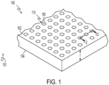
- FIG. 1 shows an article comprising a substrate 100, schematically depicted in a partial perspective view.
- Substrate 100 comprises a first major surface 102 and a second major surface 104 opposite first major surface 102.
- a plurality of vias 110 extend through the bulk of substrate 100 from first major surface 102 to second major surface 104.
- Metal connectors 150 fill vias 110. It should be understood that any number of vias 110 may extend through substrate 100 in any arrangement.
- Coordinate marker 101 shows the direction of axial dimension z, which is normal to the plane of first major surface 102 and second major surface 104. Unless otherwise specified, the "length" of a via or metal connector is in the axial dimension z.
- the thickness t of substrate 100 which is in the axial dimension, may be any appropriate thickness depending on the application.
- the substrate 100 may comprise any suitable glass or glass ceramic substrate.
- high silica glass or glass ceramic substrates are desirable for certain applications due to their dielectric properties.
- a glass or glass ceramic material having a silica content of 50 mol%, 55 mol%, 60 mol%, 65 mol%, 70 mol%, 75 mol%, 80 mol%, 85 mol%, 90 mol%, 95 mol%, or 100 mol%, or any range having any two of these values as endpoints, including endpoints, may be used.
- a glass or glass ceramic material having a silica content of 50 mol% to 100 mol%, or 75 mol% to 100 mol% may be used.
- the substrate comprises at least 90 mol% silica.
- FIG. 2 shows an article comprising substrate 100, schematically depicted as a cross section of FIG. 1 along line 2-2'.
- FIG. 2 shows substrate 100, coordinate marker 101, first major surface 102, second major surface 104, via 110 and metal connector 150 of FIG. 1 .
- Interior surface 114 of via 110 is divided into a first axial portion 116, a second axial portion 118 and a third axial portion 120.
- An adhesion layer 122 is disposed on interior surface 114 in first axial portion 116 and third axial portion 120. Adhesion layer 122 is not present in second axial portion 118.
- first axial portion 116 and third axial portion 120 may be referred to as the "adhesion length," because it is the length into via 110 for which metal connector 150 adheres strongly to substrate 100.
- adhesion layer 122 is not present, so metal connector 150 does not bond to strongly to interior surface 114.
- Via 110 has a via length 130 in the axial direction. Via 110 has a first diameter 132a at the first major surface, and a second diameter 132b at the second major surface.
- FIG. 2 shows an article comprising the substrate 100, schematically depicted as a cross section of FIG. 1 along line 2-2'.
- FIG. 2 shows the substrate 100, the coordinate marker 101, the first major surface 102, the second major surface 104, the via 110 and the metal connector 150 of FIG. 1 .
- the interior surface 114 of the via 110 is divided into a first axial portion 116, a second axial portion 118 and a third axial portion 120.
- a helium hermetic adhesion layer 122 is disposed on the interior surface 114 of the via 110 in the first axial portion 116 and the third axial portion 120.
- the helium hermetic adhesion layer 122 is disposed on the interior surface 114 of the via 110 along an entire perimeter of at least one of the first axial portion 116 and the third axial portion 120.
- the helium hermetic adhesion layer 122 is not present in the second axial portion 118.
- helium hermetic adhesion layer means an adhesion layer that provides helium hermeticity to helium at a permeability of less than 10-5 atm-cc/s, or even less than 10-8 atm-cc/s as measured using a vacuum-based helium leak testing system by adhering the metal connector 150 to the interior surface 114 of the via 110.
- Suitable helium hermetic adhesion layer materials include metals, like titanium (Ti), chrome (Cr), tantalum (Ta), vanadium (V), nickel (Ni), tungsten (W), or metal oxides, like titanium oxide, tungsten oxide, and manganese oxide, or nitrides, like titanium nitride (TiN) and tantalum nitride (TaN).
- the helium hermetic adhesion layer comprises titanium (Ti).
- the helium hermetic adhesion layer has a thickness of greater than or equal to 1 nm and less than or equal to 500 nm. For example, in some particular embodiments, the helium hermetic adhesion layer has a thickness of about 100 nm.
- the axial length of the first axial portion 116 or the third axial portion 120 may be referred to as the "adhesion length," because it is the length into the via 110 along which the metal connector 150 adheres strongly to the substrate 100.
- the adhesion length is greater than or equal to 5 ⁇ m and less than or equal to 148 ⁇ m.
- the adhesion length may be greater than or equal to 10 ⁇ m and less than or equal to 135 ⁇ m, greater than or equal to 10 ⁇ m and less than or equal to 130 ⁇ m, greater than or equal to 10 ⁇ m and less than or equal to 125 ⁇ m, greater than or equal to 10 ⁇ m and less than or equal to 120 ⁇ m, greater than or equal to 10 ⁇ m and less than or equal to 115 ⁇ m, greater than or equal to 15 ⁇ m and less than or equal to 140 ⁇ m, greater than or equal to 15 ⁇ m and less than or equal to 135 ⁇ m, greater than or equal to 15 ⁇ m and less than or equal to 130 ⁇ m, greater than or equal to 15 ⁇ m and less than or equal to 125 ⁇ m, greater than or equal to 15 ⁇ m and less than or equal to 120 ⁇ m, greater than or equal to 20 ⁇ m and less than or equal to 140 ⁇ m, greater than or equal to 20 ⁇ m and less than or equal to 135 ⁇ m, greater
- the adhesion length is greater than or equal to 40 ⁇ m and less than or equal to 140 ⁇ m, greater than or equal to 40 ⁇ m and less than or equal to 130 ⁇ m, greater than or equal to 40 ⁇ m and less than or equal to 120 ⁇ m, greater than or equal to 40 ⁇ m and less than or equal to 110 ⁇ m, greater than or equal to 40 ⁇ m and less than or equal to 100 ⁇ m, greater than or equal to 40 ⁇ m and less than or equal to 90 ⁇ m, greater than or equal to 40 ⁇ m and less than or equal to 80 ⁇ m, greater than or equal to 40 ⁇ m and less than or equal to 70 ⁇ m, or greater than or equal to 40 ⁇ m and less than or equal to 60 ⁇ m.
- the adhesion length may be about 40 ⁇ m, 50 ⁇ m, 60 ⁇ m or 70 ⁇ m. It is contemplated that other adhesion lengths may be employed in various embodiments.
- the via 110 has a via length 130 in the axial direction.
- the via 110 has a first diameter 132a at the first major surface 102, a second diameter 132b at the second major surface 104, and a third diameter 132c in the second axial portion 118.
- Via 110 of FIG. 2 has a tapered interior surface 114 that tapers or narrows from first diameter 132a at first major surface 102, and from second diameter 132b at second major surface 104, to a waist 125 having a waist diameter.
- the "waist" of a via refers to the part of a variable-diameter via having the smallest diameter.
- the diameter of via 110 changes as a function of axial position.
- the overall “diameter” of via 110 is the maximum diameter.
- via diameter refers to the maximum diameter.
- the "diameter” of via 100 is the diameter of a circle having the same cross-sectional area as via 110, in a plane normal to the axial direction.
- the via waist 125 has the smallest diameter along the axial length of the via.
- the diameter of the via waist as a percentage of the first diameter may be 10%, 15%, 20%, 25%, 30%, 35%, 40%, 45%, 50%, 55%, 60%, 65%, 70%, 75%, 80%, or any range having any two of these values as endpoints, including endpoints.
- the diameter of the via waist as a percentage of the second diameter may be 10%, 15%, 20%, 25%, 30%, 35%, 40%, 45%, 50%, 55%, 60%, 65%, 70%, 75%, 80%, or any range having any two of these values as endpoints, including endpoints.
- the diameter of the via waist may be 75% of the first diameter or less, and the diameter of the via waist may be 75% of the second diameter or less.
- the diameter of the via waist may be 20% to 50% of the first diameter or less, and the diameter of the via waist may be 20% to 50% of the second diameter or less.
- the third diameter 132c, or the via waist is greater than or equal to 10 ⁇ m and less than or equal to 40 ⁇ m.
- the third diameter 132c may be greater than or equal to 20 ⁇ m and less than or equal to 30 ⁇ m, or greater than or equal to 22 ⁇ m and less than or equal to 27 ⁇ m.
- the third diameter 132c may be 10 ⁇ m, 15 ⁇ m, 20 ⁇ m, 22 ⁇ m, 25 ⁇ m, 27 ⁇ m, 30 ⁇ m, 35 ⁇ m, or 40 ⁇ m.
- a ratio of the third diameter 132c to the first diameter 132a is less than or equal to 1:6, less than or equal to 1:5, less than or equal to 1:4, less than or equal to 1:3, or less than or equal to 1:2 and/or a ratio of the third diameter 132c to the second diameter 132b is less than or equal to 1:6, less than or equal to 1:5, less than or equal to 1:4, less than or equal to 1:3, or less than or equal to 1:2.
- Via 110 may have any suitable via length 130.
- the thicknesses of substrate 100 may be 10 ⁇ m, 60 ⁇ m, 120 ⁇ m, 180 ⁇ m, 240 ⁇ m, 300 ⁇ m, 360 ⁇ m, 420 ⁇ m, 480 ⁇ m, 540 ⁇ m, 600 ⁇ m, 720 ⁇ m, 840 ⁇ m, 960 ⁇ m, 1080 ⁇ m, 1500 ⁇ m, 2000 ⁇ m, or any range having any two of these values as endpoints, including endpoints.
- thickness t and via length is 10 ⁇ m to 2000 ⁇ m, or 240 ⁇ m to 360 ⁇ m.
- the via 110 may have any suitable first diameter 132a and second diameter 132b. As non-limiting examples, these diameters may be 30 ⁇ m, 40 ⁇ m, 50 ⁇ m, 60 ⁇ m, 70 ⁇ m, 80 ⁇ m, or any range having any two of these values as endpoints, including endpoints. In some embodiments, the via diameter may be greater than or equal to 30 ⁇ m and less than or equal to 80 ⁇ m, greater than or equal to 40 ⁇ m and less than or equal to 60 ⁇ m, or greater than or equal to 45 ⁇ m and less than or equal to 55 ⁇ m.
- First diameter 132a may be the same as or different from second diameter 132b. As described hereinabove, the first diameter 132a and the second diameter 132b are each greater than the third diameter 132c.
- the axial length of first, second and third axial portions may be any suitable length. It is desirable to choose lengths that achieve a combination of low maximum principle stress and helium hermeticity. Lower lengths for the first and third axial portions reduce stress, as demonstrated by the models described herein, such that the glass does not crack resulting in loss of helium hermeticity. But, if the lengths of the first and third axial portions are too low, helium hermeticity may be lost because there is inadequate bonding, even in the absence of cracking.
- the first and third axial portions have lengths that are independently chosen from 1%, 2%, 3%, 4%, 5%, 6%, 7%, 8%, 9%, 10%, 15%, 20%, 25%, 30%, 35% and 40% of the length of the via, or any range having any two of these values as endpoints, including endpoints.
- the second axial portion has a length that is 20%, 25%, 30%, 35%, 40%, 45%, 50%, 55%, 60%, 65%, 70%, 75%, 80%, 81%, 82%, 83%, 84%, 85%, 86%, 87%, 88%, 89%, 90%, 91%, 92%, 93%, 94%, 95%, 96%, 97%, or 98%, of the length of the via, or any range having any two of these values as endpoints, including endpoints.
- the first and third axial portions may have lengths that are 2% to 40% of the length of the via, while the second axial portion has a length that is 20% to 96% of the length of the via. while the second axial portion has a length that is 20% to 96% of the length of the via. It is desirable, in embodiments, to choose the smallest length for first and third axial portions that reliably provides a hermetic seal.
- the vias are high aspect ratio vias with a via length of 240 ⁇ m to 360 ⁇ m and a via diameter of 40 ⁇ m to 60 ⁇ m.
- an “aspect ratio” refers to the ratio of the average thickness of the glass substrate to the average diameter of the vias.
- a “high aspect ratio” refers to aspect ratios of greater than 3.
- first and third axial portions having lengths of 20 ⁇ m, 25 ⁇ m, 30 ⁇ m, 35 ⁇ m and 40 ⁇ m, or any range having any two of these values as endpoints, including endpoints, may be desired to achieve a reduced stress, although other lengths are contemplated.
- the length of the second axial portion makes up the remainder of the via length.
- the first axial portion includes the intersection of the via with the first major surface
- the second axial portion includes the intersection of the via with the second major surface. This geometry is well matched with fabrication methods described herein.
- the via 110 optionally has rounded fillets 124 at interior edges to reduce stress concentration, including at the via waist 125.
- fillets refers to a rounded corner along an interior corner of the via 110.
- Such rounded fillets may be used at any edge in a via shape.
- the rounded fillets 124 may have any suitable diameter, such as 3 mm, 4 mm, 5 mm, 6 mm, 7 mm, 8 mm, or any or any range having any two of these values as endpoints, including endpoints. Other diameters may be used.
- Via 110 has an interior surface 114 with two distinct slopes, with a slope change at fillet 124.
- Via 110 may have a single slope from each of first major surface 102 and second major surface 104 to waist 125, two slopes as illustrated in FIG. 2 , or more complex shapes. One or more of the slopes may be perpendicular to first major surface 102 and second major surface 104, as illustrated in FIG. 2 .
- FIG. 3 shows the same via 110 as FIG. 2 , but is labeled to illustrate the parts of the metal connector 150.
- the metal connector 150 defines a first cavity 152 spanning the first axial portion 116 and a second cavity 154 spanning the third axial portion 120.
- the first cavity 152 is separated from the second cavity 154 by a filled portion 156 within the second axial portion 118.
- the first cavity 152 has a first cavity length 153 in the axial dimension
- the second cavity 154 has a second cavity length 155 in the axial dimension.
- the metal connector 150 coats the interior surface 114 without completely filling the via 110.
- the filled portion 156 has a filled length 157 in the axial dimension.
- the metal connector 150 has a coating thickness 158 along the first cavity length 153 and the second cavity length 155. Although illustrated as a constant thickness (a conformal layer), coating thickness 158 may vary with axial position and distance from the first major surface and/or second major surface.
- the metal connector 150 has a coating thickness 158 of less than 12 ⁇ m at the first major surface 102 and at the second major surface 104.
- the metal connector 150 may have a coating thickness 158 of 5 ⁇ m, 6 ⁇ m, 7 ⁇ m, 8 ⁇ m, 9 ⁇ m, 10 ⁇ m, or 11 ⁇ m at the first major surface 102 and at the second major surface 104.
- the metal connector 150 has an average coating thickness of less than 12 ⁇ m in the first axial portion and in the second axial portion.
- the metal connector 150 has an average coating thickness of less than 12 ⁇ m over the length from the first major surface 102 to the adjacent rounded fillet 124 and over the length from the second major surface 104 to the adjacent rounded fillet 124.
- a via 110 with a tapered shape i.e., a waist 125 with a diameter narrower than the first diameter 132a and the second diameter 132b
- metal connector 150 with the unique geometry shown in FIGS. 2 and 3 .
- that shape has the first cavity 152 and the second cavity 154 extending from the first major surface 102 and the second major surface 104, respectively.
- the metal connector 150 includes a filled portion 156 in proximity to the waist 125.
- the geometry of the metal connector 150 allows for a hermetic seal to the substrate 100 with degrees of freedom for stress relief not available with other geometries.
- the helium hermetic adhesion layer 122 forms a hermetic seal between the metal connector 150 and the substrate 100 at the first major surface 102 and the second major surface 104, for the axial lengths of the first axial portion 116 and the third axial portion 120, respectively.
- the filled portion 156 completes the hermetic seal, such that gas and liquid cannot pass through the via 110 between the first major surface 102 and the second major surface 104.
- the lack of adhesion in the second axial portion 118 provides an extra degree of freedom for the metal connector 150 to relieve stress during thermal cycling.
- the first cavity 152 and the second cavity 154 provide yet another degree of freedom for stress relief.
- first cavity 152 and second cavity 154 extend sufficiently far into via 110 that they overlap with second axial portion 118. This overlap results in axial portions of metal connector 150 that are neither bonded to substrate 100 nor filled. Such a geometry provides further avenues for stress relief.
- the first cavity length may be 3%, 5%, 10%, 15%, 20%, 25%, 30%, 35%, 40%, 45%, 50%, 60%, 70%, 80%, 90%, 95%, or 97% of the axial length of the via 110, or any range having any two of these values as endpoints, including endpoints.
- the second cavity length 155 may be 3%, 5%, 10%, 15%, 20%, 25%, 30%, 35%, 40%, 45%, 50%, 60%, 70%, 80%, 90%, 95%, or 97% of the axial length of the via 110, or any range having any two of these values as endpoints, including endpoints.
- the second cavity length 155 may be the same as or different from the first cavity length 153.
- the first cavity length 153 and the second cavity length 155 are each greater than or equal to 10 ⁇ m and less than or equal to 150 ⁇ m.
- the first cavity length 153 and the second cavity length 155 may each be 10 ⁇ m, 15 ⁇ m, 20 ⁇ m, 25 ⁇ m, 30 ⁇ m, 35 ⁇ m, 40 ⁇ m, 45 ⁇ m, 50 ⁇ m, 60 ⁇ m, 70 ⁇ m, 80 ⁇ m, 90 ⁇ m, 100 ⁇ m, 110 ⁇ m, 120 ⁇ m, 130 ⁇ m, 140 ⁇ m, 150 ⁇ m, or any range having any two of these values as endpoints, including endpoints.
- the filled portion 156 has an axial length that makes up the difference between the axial via length 130 on one hand, and the first cavity length 153 and the second cavity length 155 on the other.
- the metal conductor fully fills the via for at least 10% of the axial length of the via 110.
- the coating thickness 158 is less than 50% of the via diameter at each point along the axial length.
- the coating thickness 158 is measured as the thickness of the metal connector, and does not include the thickness of the helium hermetic adhesion layer. As a result, the coating thickness does not extend to the center of the via 110, such that the first cavity 152 and the second cavity 154 may be formed.
- the coating thickness 158 may be 5%, 10%, 15%, 20%, 25%, 30%, 35%, 40%, 45% or 49% of the via diameter at each point along the axial length, or any range having any two of these values as endpoints, including endpoints.
- the coating thickness 158 may be constant with the axial position, or may change with the axial position.
- the coating thickness 158 may be, along the axial length of the via where the first cavity 152 and the second cavity 154 are present, 1 ⁇ m, 2 ⁇ m, 3 ⁇ m, 4 ⁇ m, 5 ⁇ m, 6 ⁇ m, 8 ⁇ m, 10 ⁇ m, or less than 12 ⁇ m, or any range having any two of these values as endpoints, including endpoints, so long as the coating thickness 158 is sufficiently small to not completely fill the via where the first cavity 152 and the second cavity 154 are present. However, as will be described in greater detail below, the coating thickness 158 of various embodiments is less than 12 ⁇ m.
- the coating thickness 158 within the via at the first maj or surface and the coating thickness 158 within the via at the second major surface are each less than the coating thickness in the second axial portion. In some embodiments, the coating thickness 158 is less than one half of the diameter of the third diameter 153c within the via at each of the first major surface 102 and the second major surface 104.
- the first cavity 152 and/or the second cavity 154 may be filled with one or more materials that are not copper. Such filling of the first cavity 152 and/or the second cavity 154 may reduce or eliminate contamination or degradation of the metal connector 150 as a result of corrosive materials used in processing of the glass article.
- the material may have a CTE that is lower than the CTE of the metal connector 150, have plasticity, and/or have one or more degrees of freedom beyond the degrees of freedom of the metal connector 150.
- the material may further reduce the stress of the glass article, or even result in a net zero stress of the glass article.
- the material does not covalently bind the metal connector 150.
- Suitable materials that may be used to fill the first cavity 152 and/or the second cavity 154 can include, by way of example and not limitation, materials that do not degrade at temperatures of greater than or equal to 400 °C or even 500 °C.
- sol gel silica, sol gel metal oxides, polymers, composites, alloys, or other types of inorganic materials may be used depending on the particular embodiment.
- the first cavity 152 and/or the second cavity 154 may be filled using any one of a variety of methods known and used in the art, including, but not limited to, inkjet printing, spray coating, or another deposition method. It is contemplated that the particular method for filling the first cavity 152 and/or the second cavity 154 may depend on the particular material to be used.
- Through-glass vias with a tapered shape may be fabricated by any suitable method.
- One method is to form a damage track in substrate 100 with a laser, followed by etching. Exemplary methods are described in US Patent 9,656,909 , and US Patent Application 62/588,615 , which are incorporated herein by reference in their entireties.
- Another method is to modify photosensitive glass with a laser, followed by etching.
- FIG. 4 shows a flowchart illustrating a process for metallizing a through glass via.
- a step 410 an adhesion layer is deposited on the interior surface of a via in first axial portion and third axial portion, but not the second axial portion.
- a metal connector is deposited within the via, such that the metal connector adheres to the adhesion layer in the first axial portion and the third axial portion.
- An adhesion layer may be deposited on first and third axial portions, but not second axial portion, by any suitable method.
- the length of first and third axial portions in the z dimension may be readily controlled using line of sight deposition methods such as sputtering, and adjusting deposition angle.
- the substrate may be rotated during deposition to ensure that the length of the first and third axial portions are constant around the entire perimeter of the interior surface of the via in the first axial portion and the third axial portion.
- Suitable adhesion layer materials include metals, like titanium, chrome, tantalum, vanadium or metal oxides, like zinc oxide, and manganese oxide, or nitrides, like titanium nitride and tantalum nitride. These adhesion films can be applied to the glass surface using many different methods, like sputtering, ebeam deposition, ion beam deposition, atomic layer deposition, chemical vapor deposition and solution coating.
- Helium hermetic adhesion layers in the form of films formed from metals, metal oxides, or metal nitrides can also be applied to the glass surface using many different methods, like sputtering, ebeam deposition, ion beam deposition, atomic layer deposition, chemical vapor deposition and solution coating.
- the metal connector may be fabricated from any suitable metal.
- copper may be a desirable metal due to its particularly high conductivity.
- Gold, silver, and other conductive metals may be used, as well as alloys of conductive metals.
- the metal connector comprises copper.
- the metal connector consists essentially of copper.
- the metal connector may be deposited by any suitable means.
- One suitable method for depositing copper (and other metals) is depositing a catalyst such as Pd on the helium hermetic adhesion layer, followed by electroless deposition of copper, followed by electroplating copper.
- the catalyst, such as Pd may be deposited on components other than, or in addition to the helium hermetic adhesion layer as desired.
- the electroplating process includes the use of an electroplating bath comprising a metal salt and a metal deposition inhibitor and application of a current at a current density of greater than or equal to 1.5 mA/cm 2 and less than or equal to 5 mA/cm 2 , or greater than or equal to 1.5 mA/cm 2 and less than or equal to 2.5 mA/cm 2 .
- the metal salt can be a salt of the metal forming the metal connector, such as CuSOa.
- the metal deposition inhibitor may be selected to specifically inhibit or slow the plating rate of the metal at or near the first and second major surfaces, enabling the formation of a metal connector with a coating thickness that is thinner within the via at the first and second major surfaces than at the waist of the via.
- NTBC nitroblue tetrazolium chloride
- NTBC nitroblue tetrazolium chloride
- the preferential adsorption of NTBC also leads to a concentration gradient of adsorbed NTBC along the axial length of the via, with more NTBC near the first and second major surfaces and very little NTBC near the waist of the via. Accordingly, copper may be deposited faster near the waist of the via as compared to near and on the first and second major surfaces. Therefore, by maintaining the differential plating rate, the via center may be plugged while the coating thickness at the first and second major surfaces is less than one half of the diameter of the waist.
- NTBC n-B
- MTT methylthiazole tetrazolium
- TNBT tetranitroblue tetrazolium chloride
- Suitable methods for depositing the metal connector include filling the via with metal paste and sintering or chemical vapor deposition (CVD). Suitable methods for depositing copper are further described in US Patent Publication US 2017-0287728 (see, for example, paragraphs [0004] - [0005], which is incorporated by reference in its entirety.
- Delamination is one failure mechanism. Delamination occurs when a conductive metal, such as copper, detaches from the interior of a via. When there is a weak bond between the conductor and the substrate, the stress caused by thermal cycling can lead to delamination. If delaminated, the metal may plastically deform out the end of the vias during thermal cycling. In the printed circuit board industry, this expansion is called metal pumping or pistoning. In many applications for TGVs, a thin film metal redistribution layer (RDL) is subsequently applied to the metallized TGVs. These RDLs are used to route power or signals coming through the metal TGVs to electronic components. Any metal pumping or pistoning will rip apart the electrical connection between the metal TGV and the RDL.
- RDL thin film metal redistribution layer
- Delamination can also lead to loss of helium hermeticity, as gas and liquid may penetrate the substrate along the boundary between the delaminated metal connector and the interior surface of the via.
- Delamination may be reduced or eliminated by forming a sufficiently strong bond between the substrate and the metal connector.
- An adhesion layer disposed on the interior surface of the via, between the substrate and the metal connector, may be used to form such a bond.
- adhesion layer refers to any layer or surface treatment that leads to a bond between the metal connector and the substrate sufficiently strong to survive thermal cycling from 400 °C to 25 °C.
- Any suitable adhesion layer may be used, an adhesion layers may be deposited by any suitable means. For example, oxide adhesion layers may be deposited by sputtering. Deposition parameters may be adjusted to control where the adhesion layer deposits.
- the angle of deposition during a sputtering process may be adjusted to control the length of first axial portion 116 and third axial portion 120, where material is deposited by sputtering. This same adjustment controls the length of second axial portion 118, where material is not deposited by sputtering.
- Delamination may be prevented by forming a strong bond between the metal connector and substrate. But, this stronger bond prevents the metal connector from moving relative to the substrate during thermal cycling. As a result, thermal cycling may cause stress in the substrate that leads to cracking and loss of helium hermeticity.
- ⁇ r, ⁇ , and ⁇ z are the radial, circumferential, and axial stresses, respectively
- ⁇ T ( ⁇ f - ⁇ m) ⁇ T is the mismatch strain due to a thermal load ⁇ T.
- the material properties ⁇ , E, and ⁇ are the CTE, Young's modulus, and Poisson's ratio, with the subscripts f and m for the via (fiber) and Glass (matrix), respectively.
- metal connector 150 Toward the end of a cooling part of thermal cycling, metal connector 150 has shrunk more than substrate 100 due to the difference in CTE. Because metal connector 150 is adhered to substrate 100. The shrinkage of metal connector 150 pulls on substrate 100, placing substrate 100 in tensile stress. Without sufficient degrees of freedom for stress relief, this tensile stress will cause microcracks in substrate 100. These microcracks cause loss of helium hermeticity.
- Various embodiments described herein may exhibit helium hermeticity and no cracking after being subjected to thermal cycling.
- the presence of the conformal copper coating having a limited coating thickness at the major surfaces of the substrate and with a fully filled midsection, and the absence of a helium hermetic adhesion layer along the second axial portion of the via provides helium hermeticity while enabling the substrate and the metal connector to shrink at different rates without generating an amount of tensile stress sufficient to generate microcracks.
- FIGS. 2 and 3 For modeling, the geometry of FIGS. 2 and 3 was used, where the interior surface of the via is conformally coated with copper everywhere except for 75 ⁇ m of axial length, 37.5 ⁇ m on each side of waist 125, where the via is filled all the way through.
- Via length 130 was 300 ⁇ m.
- First diameter 132a and second diameter 132b were each 50 ⁇ m. The 50 ⁇ m diameter is maintained for a distance of 50 ⁇ m along the axial length from both surfaces. Starting at 50 ⁇ m from the surfaces, the via tapers inwards to a diameter of 20 ⁇ m at waist 125, halfway along the axial length. On both the top and bottom surfaces, a 20 ⁇ m thick, flat copper overburden 151 (shown in FIGS. 2 and 3 ) is included. It is expected that the modeling results will extent to other via and metal connector shapes having cavities in the metal connector and a second axial portion without strong bonding between the metal connector and substrate.
- the geometry of FIG. 2 and FIG. 3 including copper overburden 151, is present when the most severe thermal cycling occurs. Afterwards, the overburden is removed and further processing may occur. But, the geometry of FIG. 2 and FIG. 3 has relevance to the thermal cycling modeled herein.
- FIG. 5A shows graph 500, which illustrates the stress-strain relationship for an elastically perfect plastic material.
- FIG. 5B shows graph 510, which illustrates the temperature dependent copper yield stress.
- the glass will crack first where the first principal stress is largest, i.e., the "maximum first principal stress.”
- the maximum first principal stress With reference to FIG. 3 , modeling showed the highest first principal stress at two points. First, there was a high maximum principal stress on the surface of substrate 100 along line 190, a short distance from the interface between adhesion layer 122 and substrate 100. This first point of high stress corresponds to a failure mechanism observed in the samples, microcracks in the surface.
- FIG. 6 shows a plot of modeled maximum principal stress vs. radial position along line 190 of FIG. 3 for different adhesion lengths.
- coating thickness 158 was held constant at 10 ⁇ m.
- Table 1 shows the maximum first principal stress from each of the lines plotted in FIG. 6 .
- TABLE 1 Adhesion depth from both surfaces Max 1 st Principal Stress on surface 150 ⁇ m (full adhesion) 602.76 MPa 100 ⁇ m 603.94 MPa 50 ⁇ m 607.02 MPa 30 ⁇ m 557.8 MPa 10 ⁇ m 338.77 MPa
- FIG. 6 and Table 1 show that the maximum principal stress corresponding to microcracks decreases as adhesion length decreases.
- Microcracks are expected when the maximum first principal stress of Table 1 exceeds a threshold value. If the fabricated real system was perfect without defects, such as flaws, scratches, and interior voids, and if the modeling were perfect, this threshold strength would be the tensile yield strength of glass. However, cracks may be generated at much lower stress than the tensile yield strength of glass because of defects of the system. And, the modeled values depend in part on model parameters such as mesh size. So, the values in Table 1 are significantly higher than the tensile yield strength. So, the values of Table 1 are useful to show trends and to demonstrate the surprising improvement achieved by the geometries described herein. The modeling also allows one of skill in the art to determine an adhesion length sufficiently short to reduce stress, while also enabling consideration of an adhesion length sufficiently large to provide a hermetic seal.
- FIG. 7 shows a plot of maximum principal stress vs. radial position along line 190 of FIG. 3 for different coating thicknesses 158.
- adhesion length was held constant at 50 ⁇ m.
- Table 2 shows the maximum first principal stress from each of the lines plotted in FIG. 7 .
- FIG. 7 and Table 2 show that the maximum principal stress corresponding to microcracks decreases as coating thickness 158 decreases.
- the data of FIG. 7 and table 2 allow one of skill in the art to make informed choices about a metal connector parameter, in this case coating thickness 158.
- coating thickness should not be reduced too much, as some coating thickness is needed to form a hermetic seal, and to achieve the desired conductivity through metal connector 150.
- Tables 1 and 2 illustrate that the maximum first principal stress may be reduced by including in the via structure a second axial portion where the metal connector is not adhered to the interior surface of the via, between first and third axial portions where the metal connector is adhered to the interior surface of the via.
- FIG. 8 shows a plot of modeled maximum first principal stress and maximum radial stress along line 190 for different copper wall thicknesses. As shown in FIG. 8 , at a coating thickness of 12 ⁇ m, both the maximum first principal stress and maximum radial stress meet or exceed threshold values (140 MPa for maximum first principal stress and 80 MPa for maximum radial stress for the configurations depicted in FIGS. 2 and 3 ).
- FIG. 9 shows a plot of the percentage of vias with cracks for different copper coating thicknesses after the wafer was annealed to a maximum temperature of 400 °C, with the dashed lines representing 95% confidence boundaries for the regression fit.
- the coating thickness was measured at the first or second major surface, and groups were formed based on the integer of the coating thickness measurement.
- the group “8 ⁇ m” includes coating thicknesses of from 8.00 ⁇ m to 8.99 ⁇ m
- the group “9 ⁇ m” includes coating thicknesses of from 9.00 ⁇ m to 9.99 ⁇ m, and so on.
- cracking does not occur in vias until the coating thickness is greater than or equal to 12 ⁇ m.
- the modeling allows one of skill in the art to make informed choices about a metal connector parameter, in this case the coating thickness 158.
- the coating thickness should not be reduced too much, as some coating thickness is needed to form a hermetic seal, and to achieve the desired conductivity through the metal connector 150.
- FIG. 10A and 10B are cross-section images of metallized through-glass vias having different copper coating thicknesses. As shown in FIG. 10A , if the coating thickness of the copper is less than 12 ⁇ m, there are no cracks, whereas circumferential microcracks are shown in FIG. 10B , where the coating thickness of the copper is greater than or equal to 12 ⁇ m.
- Glass and glass ceramic substrates with filled vias are often subject to thermal cycling. This thermal cycling may occur during device operation, or during fabrication steps subsequent to via filling. In some embodiments, for example, the glass substrate may be subjected to thermal cycling for annealing.
- CTE coefficient of thermal expansion
- glass and glass ceramic materials there is a large mismatch between the coefficient of thermal expansion (CTE) of copper and other metals, and the CTE of many glass and glass ceramic materials. Because of the CTE mismatch, upon heating, the metal connector expands more quickly than the surrounding glass or glass ceramic substrate. Similarly, upon cooling, the metal connector contracts more quickly than the surrounding substrate. This difference in expansion and contraction causes stress which can lead to a number of failure mechanisms, such as delamination or cracking. These failure mechanisms can cause loss of helium hermeticity and other problems.
- processes according to embodiments disclosed and described herein comprise heating a glass or glass ceramic article comprising copper-metallized through vias from a first temperature to a second temperature, wherein the first temperature is greater than or equal to 200 °C and less than or equal to 300 °C, and wherein the second temperature is greater than or equal to 350 °C and less than or equal to 450 °C, wherein an average heating rate during the heating of the glass or glass ceramic article comprising copper-metallized through vias from the first temperature to the second temperature is greater than 0.0 °C/min and less than 8.7 °C/min.
- Embodiments also include a glass or glass ceramic article comprising a glass or glass ceramic substrate comprising at least one through via penetrating the glass or glass ceramic substrate in a thickness direction, and copper present in the at least one through via, wherein the glass or glass ceramic article does not comprise radial cracks.
- a glass or glass ceramic article 1300 comprise a glass or glass ceramic substrate 1320 and a copper-metallized through via 1320.
- the copper-metallized through via 1320 is cylindrical in shape and comprises a copper metal in at least a portion of the through via. It should be understood that any through via geometry can be used according to embodiments disclosed and described herein. Such geometries include, but are not limited to conical through vias, frustoconical through vias, or pinched through vias ( e.g ., through vias with an hour-glass type shape).
- the copper-metallized through via 1320 has a radius "r".
- the CTE mismatch between the glass or glass ceramic substrate 1310 and the CTE of the copper that is present in the through via may cause the formation of cracks 130 that extend in a radial direction from the copper-metallized through via 1320.
- These cracks 130 that extend in a radial direction from the copper-metallized through via 1320 are referred to herein as radial cracks.
- radial cracks are referred to herein as radial cracks.
- embodiments are directed to copper-metallized through vias
- processes disclosed and described herein may be used on through vias that are metallized with any metallic material.
- processes disclosed and described herein are directed to glass and glass ceramic substrates having a CTE mismatch with the material present in a through via, radial cracks can be minimized or eliminated in glass or glass ceramic substrates having through vias that are metallized with any metal material.
- the glass or glass ceramic substrate 1310 may comprise a plurality of copper-metallized through vias 1320a-1320f that are positioned along a straight line in the glass or glass ceramic substrate 1310.
- a plurality of radial cracks 1330a-1330e may be formed in the glass or glass ceramic substrate 1310 such that the radial cracks 1330a-1330e span the distance between adjacent copper-metallized through vias 1320a-1320f.
- a radial crack 1330a may extend between adjacent copper-metallized through vias 1320a and 1320b and a radial crack 1330b may extend between adjacent copper-metallized through vias 1320b and 1320c.
- radial cracks 1330a-1330e can, span between each of the copper-metallized through vias 1320a-1320f in the glass or glass ceramic substrate 1310.
- stresses present in the glass or glass ceramic article 1300 with copper-metallized through vias may cause radial cracks 1330 to form upon heating the glass or glass ceramic article 1300.
- These stresses that may cause the radial cracks 1330 can be approximated theoretically as shown below and, according to embodiments disclosed and described herein, processes that control the stresses and minimize or eliminate radial cracks in the glass or glass ceramic article 1300 with copper-metallized through vias can be developed.
- ⁇ Cu is the CTE for copper (16.7 ppm/°C)
- ⁇ glass is the CTE of glass or glass ceramic (0.6 ppm/°C)
- ⁇ glass and ⁇ Cu are the Poisson ratios for the glass or glass ceramic (0.26) and copper (0.35), respectively; r is the distance in glass or glass ceramic from the center of the hole.
- r is the radius of the metallized through via.
- D Cu is the diameter of the through via (50 ⁇ m);
- E Cu and E glass are the elastic modulus of copper (120 GPa) and the glass or glass ceramic (70 GPa), respectively; and
- ⁇ T is the change in temperature.
- the circumferential and the radial stresses are equal in magnitude but opposite in direction.
- the tensile circumferential stress in glass or glass ceramic is expected to be a primary cause for the formation of radial cracks during heating, as cracks are known to form due to tensile stress field.
- the maximum stresses occur at the edge of the via, which exponentially decays away from the through via edge, where the through via is not closely adjacent to another through via.
- FIG. 16 shows a plot of heat treatment temperature (°C) versus circumferential stress (MPa).
- the plot in FIG. 16 shows that an increase in the temperature during a heat treatment results in an essentially linear increase in circumferential stress, which shows that the probability for forming radial cracks increases as the temperature of a heat treatment increases. Thus, at higher temperatures, radial cracks are more likely to occur.
- the glass or glass ceramic article comprising copper-metallized through vias can be heated to the first temperature using any average heating rate. Therefore, embodiments of processes for heating glass or glass ceramic articles comprising copper-metallized through vias are directed to controlling the average heating rate during the process where the temperature of the glass or glass ceramic article comprising the copper-metallized through vias is greater than or equal to the first temperature and less than or equal to a second temperature where heat treatments are usually concluded. It should be understood that the temperatures disclosed herein refer to the measured atmospheric temperature of the device used to heat the glass or glass ceramic article comprising copper-metallized through vias, such as an oven, furnace, kiln, lehr, or the like.
- heat treatments were conducted on glass or glass ceramic articles comprising copper-metallized through vias to determine the temperature at which radial cracks form.
- temperatures greater than or equal to 200 °C such as at temperatures greater than or equal to 210 °C, temperatures greater than or equal to 220 °C, temperatures greater than or equal to 230 °C, temperatures greater than or equal to 240 °C, temperatures greater than or equal to 250 °C, temperatures greater than or equal to 260 °C, temperatures greater than or equal to 270 °C, temperatures greater than or equal to 280 °C, or temperatures greater than or equal to 290 °C.
- the heating rate at temperatures below the first temperature do not need to be controlled because the probability of radial crack formation at temperatures below the first temperature is low.
- the first temperature is greater than or equal to 200 °C and less than or equal to 300 °C, such as greater than or equal to 210 °C and less than or equal to 300 °C, greater than or equal to 220 °C and less than or equal to 300 °C, greater than or equal to 230 °C and less than or equal to 300 °C, greater than or equal to 240 °C and less than or equal to 300 °C, greater than or equal to 250 °C and less than or equal to 300 °C, greater than or equal to 260 °C and less than or equal to 300 °C, greater than or equal to 270 °C and less than or equal to 300 °C, greater than or equal to 280 °C and less than or equal to 300
- the first temperature is greater than or equal to 200 °C and less than or equal to 290 °C, such as greater than or equal to 200 °C and less than or equal to 280 °C, greater than or equal to 200 °C and less than or equal to 270 °C, greater than or equal to 200 °C and less than or equal to 260 °C, greater than or equal to 200 °C and less than or equal to 250 °C, greater than or equal to 200 °C and less than or equal to 240 °C, greater than or equal to 200 °C and less than or equal to 230 °C, greater than or equal to 200 °C and less than or equal to 220 °C, or greater than or equal to 200 °C and less than or equal to 210 °C.
- the first temperature is greater than or equal to 220 °C and less than or equal to 280 °C, such as greater than or equal to 225 °C and less than or equal to 275 °C, or greater than or equal to 240 °C and less than or equal to 260 °C.
- the second temperature is greater than or equal to 350 °C and less than or equal to 450 °C, such as greater than or equal to 360 °C and less than or equal to 450 °C, greater than or equal to 370 °C and less than or equal to 450 °C, greater than or equal to 380 °C and less than or equal to 450 °C, greater than or equal to 390 °C and less than or equal to 450 °C, greater than or equal to 400 °C and less than or equal to 450 °C, greater than or equal to 410 °C and less than or equal to 450 °C, greater than or equal to 420 °C and less than or equal to 450 °C, greater than or equal to 430 °C and less than or equal to 450 °C, or greater than or greater than or greater
- the second temperature is greater than or equal to 350 °C and less than or equal to 440 °C, such as greater than or equal to 350 °C and less than or equal to 430 °C, greater than or equal to 350 °C and less than or equal to 420 °C, greater than or equal to 350 °C and less than or equal to 410 °C, greater than or equal to 350 °C and less than or equal to 400 °C, greater than or equal to 350 °C and less than or equal to 390 °C, greater than or equal to 350 °C and less than or equal to 380 °C, greater than or equal to 350 °C and less than or equal to 370 °C, or greater than or equal to 350 °C and less than or equal to 360 °C.
- the second temperature is greater than or equal to 375 °C and less than or equal to 450 °C, such as greater than or equal to 375 °C to less than or equal to 425 °C.
- processes for heating glass or glass ceramic articles comprising copper-metallized through vias control the average heating rate when the glass or glass ceramic article comprising copper-metallized through vias is at temperatures greater than or equal to the first temperature and less than or equal to the second temperature-where the probability for crack formation is high.
- the average heating rate is the difference between the second temperature and the first temperature divided by the amount of time it takes to heat the glass or glass ceramic article comprising copper-metallized through vias from the first temperature to the second temperature.
- the average heating rate includes any temperature holds where the glass or glass ceramic article comprising copper-metallized through vias is at a temperature greater than or equal to the first temperature and less than or equal to the second temperature.
- the average heating rate is 3.33 °C/min ( i.e. , 400 ° C ⁇ 300 ° C 30 min ).
- the average heating rate from the first temperature to the second temperature is greater than 0.0 °C/min and less than 8.7 °C/min, such as greater than 0.0 °C/min and less than or equal to 8.5 °C/min, greater than 0.0 °C/min and less than or equal to 8.2 °C/min, greater than 0.0 °C/min and less than or equal to 8.0 °C/min, greater than 0.0 °C/min and less than or equal to 7.8 °C/min, greater than 0.0 °C/min and less than or equal to 7.5 °C/min, greater than 0.0 °C/min and less than or equal to 7.2 °C/min, greater than 0.0 °C/min and less than or equal to 7.0 °C/min, greater than 0.0 °C/min and less than or equal to 6.8 °C/min, greater than 0.0 °C/min and less than or equal to 6.5 °C/min, greater than 0.0 °C/min, such as
- the average heating rate from the first temperature to the second temperature is greater than or equal to 2.0 °C/min and less than 8.7 °C/min, such as greater than or equal to 2.2 °C/min and less than 8.7 °C/min, greater than or equal to 2.5 °C/min and less than 8.7 °C/min, greater than or equal to 2.8 °C/min and less than 8.7 °C/min, greater than or equal to 3.0 °C/min and less than 8.7 °C/min.
- the average heating rate from the first temperature to the second temperature is greater than or equal to 2.0 °C/min and less than or equal to 6.5 °C/min, such as greater than or equal to 2.2 °C/min and less than or equal to 6.5 °C/min, greater than or equal to 2.5 °C/min and less than 6.5 °C/min, greater than or equal to 2.8 °C/min and less than 6.5 °C/min, or greater than or equal to 3.0 °C/min and less than 6.5 °C/min. Heating of the glass or glass ceramic article comprising copper-metallized through vias from the first temperature to the second temperature at the above average heating rates does not cause radial cracks in the glass or glass ceramic article comprising copper-metallized through vias.
- the heating rate from the first temperature to the second temperature is kept substantially constant such that a uniform heating rate is used in the entire temperature range from the first temperature to the second temperature.
- a substantially constant heating rate refers to a heating rate that is maintained as close the heating rate set point as can be controlled by the device used to heat the glass or glass ceramic article comprising the copper-metallized through vias. For instance, it may be determined that the heating rate in a temperature range from the first temperature to the second temperature should be constant and set at 6.5 °C/min.
- the heating rate may decrease to, for example, 6.2 °C/min or increase to, for example 6.8 °C/min even though the heating rate is intended to be constant at 6.5 °C/min. As used herein, this situation would be a "substantially constant” heating rate.
- the heating rate from the first temperature to the second temperature may be variable.
- a “variable” heating rate refers to a heating rate that is intentionally changed in a temperature range from the first temperature to the second temperature.
- An example of an embodiment having a variable heating rate would be where the glass or glass ceramic article comprising copper-metallized through vias is heated from the first temperature of 300 °C to a temperature of 350 °C at a heating rate of 6.5 °C/min and then intentionally heated from 350 °C to a second temperature of 400 °C at a heating rate of 2.3 °C/min.
- the average heating rate where the glass or glass ceramic article comprising copper-metallized through vias is at a temperature from room temperature (about 25 °C) to the first temperature is not limited, in some embodiments the average heating rate the average heating rate where the glass or glass ceramic article comprising copper-metallized through vias is at a temperature from room temperature (about 25 °C) to the first temperature is also kept low to help ensure that radial cracks do not form.
- the average heating rate from room temperature to the first temperature is greater than 0.0 °C/min and less than 8.7 °C/min, such as greater than 0.0 °C/min and less than or equal to 8.5 °C/min, greater than 0.0 °C/min and less than or equal to 8.2 °C/min, greater than 0.0 °C/min and less than or equal to 8.0 °C/min, greater than 0.0 °C/min and less than or equal to 7.8 °C/min, greater than 0.0 °C/min and less than or equal to 7.5 °C/min, greater than 0.0 °C/min and less than or equal to 7.2 °C/min, greater than 0.0 °C/min and less than or equal to 7.0 °C/min, greater than 0.0 °C/min and less than or equal to 6.8 °C/min, greater than 0.0 °C/min and less than or equal to 6.5 °C/min, greater than 0.0 °C,
- the average heating rate from room temperature to the first temperature is greater than or equal to 1.0 °C/min and less than 8.7 °C/min, such as greater than or equal to 2.0 °C/min and less than 8.7 °C/min, greater than or equal to 2.5 °C/min and less than 8.7 °C/min, greater than or equal to 2.8 °C/min and less than 8.7 °C/min, greater than or equal to 3.0 °C/min and less than 8.7 °C/min.
- the average heating rate from room temperature to the first temperature is greater than or equal to 1.0 °C/min and less than or equal to 6.5 °C/min, such as greater than or equal to 2.0 °C/min and less than or equal to 6.5 °C/min, greater than or equal to 2.2 °C/min and less than 6.5 °C/min, greater than or equal to 2.5 °C/min and less than 6.5 °C/min, greater than or equal to 2.7 °C/min and less than 6.5 °C/min, or greater than or equal to 3.0 °C/min and less than 6.5 °C/min.
- processes for heating a glass or glass ceramic article comprising copper-metallized through vias from the first temperature to the second temperature may include various temperature holds, where the temperature is held constant for a period of time. Without being bound to any particular theory, it is believed that by holding the glass or glass ceramic article comprising copper-metallized through vias at a constant temperature, relaxation occurs during the temperature hold, and the stress in the glass or glass ceramic article comprising copper-metallized through vias may decrease. Accordingly, if a temperature hold is conducted before crack formation occurs, relaxation resulting from the temperature hold may reduce the stresses in the glass or glass ceramic article comprising copper-metallized through vias enough that there is no crack formation. In addition, temperature holds may be used at one or more of the first temperature and the second temperature to allow the stresses in the glass or glass ceramic article comprising copper-metallized through vias to relax.
- the glass or glass ceramic article comprising copper-metallized through vias may be held at the first temperature for a duration greater than or equal to ten (10) minutes and less than or equal to 120 minutes, such as greater than or equal to fifteen (15) minutes and less than or equal to 120 minutes, greater than or equal to thirty (30) minutes and less than or equal to 120 minutes, greater than or equal to forty five (45) minutes and less than or equal to 120 minutes, greater than or equal to sixty (60) minutes and less than or equal to 120 minutes, greater than or equal to seventy five (75) minutes and less than or equal to 120 minutes, greater than or equal to ninety (90) minutes and less than or equal to 120 minutes, or greater than or equal to 105 minutes and less than or equal to 120 minutes.
- ten (10) minutes and less than or equal to 120 minutes such as greater than or equal to fifteen (15) minutes and less than or equal to 120 minutes, greater than or equal to thirty (30) minutes and less than or equal to 120 minutes, greater than or equal to forty five (45) minutes and less than or equal to 120
- the glass or glass ceramic article comprising copper-metallized through vias may be held at the first temperature for a duration greater than or equal to ten (10) minutes and less than or equal to 105 minutes, such as greater than or equal to ten (10) minutes and less than or equal to ninety (90) minutes, greater than or equal to ten (10) minutes and less than or equal to seventy five (75) minutes, greater than or equal to ten (10) minutes and less than or equal to sixty (60) minutes, greater than or equal to ten (10) minutes and less than or equal to forty five (45) minutes, greater than or equal to ten (10) minutes and less than or equal to thirty (30) minutes, or greater than or equal to ten (10) minutes and less than or equal to fifteen (15) minutes.
- ten (10) minutes and less than or equal to 105 minutes such as greater than or equal to ten (10) minutes and less than or equal to ninety (90) minutes, greater than or equal to ten (10) minutes and less than or equal to seventy five (75) minutes, greater than
- the glass or glass ceramic article comprising copper-metallized through vias may be held at the second temperature for a duration greater than or equal to ten (10) minutes and less than or equal to 120 minutes, such as greater than or equal to fifteen (15) minutes and less than or equal to 120 minutes, greater than or equal to thirty (30) minutes and less than or equal to 120 minutes, greater than or equal to forty five (45) minutes and less than or equal to 120 minutes, greater than or equal to sixty (60) minutes and less than or equal to 120 minutes, greater than or equal to seventy five (75) minutes and less than or equal to 120 minutes, greater than or equal to ninety (90) minutes and less than or equal to 120 minutes, or greater than or equal to 105 minutes and less than or equal to 120 minutes.
- ten (10) minutes and less than or equal to 120 minutes such as greater than or equal to fifteen (15) minutes and less than or equal to 120 minutes, greater than or equal to thirty (30) minutes and less than or equal to 120 minutes, greater than or equal to forty five (45) minutes and less than or equal to 120
- the glass or glass ceramic article comprising copper-metallized through vias may be held at the second temperature for a duration greater than or equal to ten (10) minutes and less than or equal to 105 minutes, such as greater than or equal to ten (10) minutes and less than or equal to ninety (90) minutes, greater than or equal to ten (10) minutes and less than or equal to seventy five (75) minutes, greater than or equal to ten (10) minutes and less than or equal to sixty (60) minutes, greater than or equal to ten (10) minutes and less than or equal to forty five (45) minutes, greater than or equal to ten (10) minutes and less than or equal to thirty (30) minutes, or greater than or equal to ten (10) minutes and less than or equal to fifteen (15) minutes.
- ten (10) minutes and less than or equal to 105 minutes such as greater than or equal to ten (10) minutes and less than or equal to ninety (90) minutes, greater than or equal to ten (10) minutes and less than or equal to seventy five (75) minutes, greater than
- the glass or glass ceramic article comprising copper-metallized through vias may be held at a constant temperature between the first temperature and the second temperature for a duration greater than or equal to ten (10) minutes and less than or equal to 120 minutes, such as greater than or equal to fifteen (15) minutes and less than or equal to 120 minutes, greater than or equal to thirty (30) minutes and less than or equal to 120 minutes, greater than or equal to forty five (45) minutes and less than or equal to 120 minutes, greater than or equal to sixty (60) minutes and less than or equal to 120 minutes, greater than or equal to seventy five (75) minutes and less than or equal to 120 minutes, greater than or equal to ninety (90) minutes and less than or equal to 120 minutes, or greater than or equal to 105 minutes and less than or equal to 120 minutes.
- ten (10) minutes and less than or equal to 120 minutes such as greater than or equal to fifteen (15) minutes and less than or equal to 120 minutes, greater than or equal to thirty (30) minutes and less than or equal to 120 minutes, greater than or equal to forty five (45
- the glass or glass ceramic article comprising copper-metallized through vias may be held at a constant temperature between the first temperature and the second temperature for a duration greater than or equal to ten (10) minutes and less than or equal to 105 minutes, such as greater than or equal to ten (10) minutes and less than or equal to ninety (90) minutes, greater than or equal to ten (10) minutes and less than or equal to seventy five (75) minutes, greater than or equal to ten (10) minutes and less than or equal to sixty (60) minutes, greater than or equal to ten (10) minutes and less than or equal to forty five (45) minutes, greater than or equal to ten (10) minutes and less than or equal to thirty (30) minutes, or greater than or equal to ten (10) minutes and less than or equal to fifteen (15) minutes.
- ten (10) minutes and less than or equal to 105 minutes such as greater than or equal to ten (10) minutes and less than or equal to ninety (90) minutes, greater than or equal to ten (10) minutes and less than or equal to sevent
- the processes disclosed herein may be used on glass or glass ceramic articles comprising any sized copper-metallized through vias, the processes disclosed herein may be particularly suitable for use on glass or glass ceramic articles comprising relatively small copper-metallized through vias.
- the copper-metallized through vias may have a diameter greater than or equal to 25 ⁇ m and less than or equal to 75 ⁇ m, such as greater than or equal to 30 ⁇ m and less than or equal to 70 ⁇ m, greater than or equal to 35 ⁇ m and less than or equal to 70 ⁇ m, greater than or equal to 40 ⁇ m and less than or equal to 70 ⁇ m, greater than or equal to 45 ⁇ m and less than or equal to 70 ⁇ m, greater than or equal to 50 ⁇ m and less than or equal to 70 ⁇ m, greater than or equal to 55 ⁇ m and less than or equal to 70 ⁇ m, greater than or equal to 60 ⁇ m and less than or equal to 70 ⁇ m, or greater than or equal to 65 ⁇ m and less than or equal to 70 ⁇ m
- the copper-metallized through vias may have a diameter greater than or equal to 25 ⁇ m and less than or equal to 65 ⁇ m, such as greater than or equal to 25 ⁇ m and less than or equal to 60 ⁇ m, greater than or equal to 25 ⁇ m and less than or equal to 55 ⁇ m, greater than or equal to 25 ⁇ m and less than or equal to 50 ⁇ m, greater than or equal to 25 ⁇ m and less than or equal to 45 ⁇ m, greater than or equal to 25 ⁇ m and less than or equal to 40 ⁇ m, greater than or equal to 25 ⁇ m and less than or equal to 35 ⁇ m, or greater than or equal to 25 ⁇ m and less than or equal to 30 ⁇ m.
- the copper-metallized through vias may have a diameter greater than or equal to 35 ⁇ m and less than or equal to 65 ⁇ m, such as greater than or equal to 40 ⁇ m and less than or equal to 60 ⁇ m.
- the copper-metallized through vias may have a pitch greater than or equal to 60 ⁇ m and less than or equal to 800 ⁇ m, such as greater than or equal to 100 ⁇ m and less than or equal to 750 ⁇ m, greater than or equal to 150 ⁇ m and less than or equal to 700 ⁇ m, greater than or equal to 200 ⁇ m and less than or equal to 650 ⁇ m, greater than or equal to 250 ⁇ m and less than or equal to 600 ⁇ m, greater than or equal to 300 ⁇ m and less than or equal to 550 ⁇ m, greater than or equal to 350 ⁇ m and less than or equal to 500 ⁇ m, or greater than or equal to 400 ⁇ m and less than or equal to 450 ⁇ m.
- the copper-metallized through vias may have a pitch greater than or equal to 60 ⁇ m and less than or equal to 140 ⁇ m, such as greater than or equal to 60 ⁇ m and less than or equal to 130 ⁇ m, greater than or equal to 60 ⁇ m and less than or equal to 120 ⁇ m, greater than or equal to 60 ⁇ m and less than or equal to 110 ⁇ m, greater than or equal to 60 ⁇ m and less than or equal to 100 ⁇ m, greater than or equal to 60 ⁇ m and less than or equal to 90 ⁇ m, greater than or equal to 60 ⁇ m and less than or equal to 80 ⁇ m, or greater than or equal to 60 ⁇ m and less than or equal to 70 ⁇ m.
- the copper-metallized through vias may have a depth greater than or equal to 50 ⁇ m and less than or equal to 600 ⁇ m, such as greater than or equal to 75 ⁇ m and less than or equal to 575 ⁇ m, greater than or equal to 100 ⁇ m and less than or equal to 550 ⁇ m, greater than or equal to 125 ⁇ m and less than or equal to 525 ⁇ m, greater than or equal to 150 ⁇ m and less than or equal to 500 ⁇ m, greater than or equal to 175 ⁇ m and less than or equal to 475 ⁇ m, greater than or equal to 200 ⁇ m and less than or equal to 450 ⁇ m, greater than or equal to 225 ⁇ m and less than or equal to 425 ⁇ m, greater than or equal to 250 ⁇ m and less than or equal to 400 ⁇ m, greater than or equal to 275 ⁇ m and less than or equal to 375 ⁇ m, or greater than or equal to 300 ⁇ m and less than or equal to 350 ⁇ m.
- the copper-metallized through vias may have a depth greater than or equal to 200 ⁇ m and less than or equal to 400 ⁇ m, such as greater than or equal to 200 ⁇ m and less than or equal to 375 ⁇ m, greater than or equal to 200 ⁇ m and less than or equal to 350 ⁇ m, greater than or equal to 200 ⁇ m and less than or equal to 325 ⁇ m, greater than or equal to 200 ⁇ m and less than or equal to 300 ⁇ m, greater than or equal to 200 ⁇ m and less than or equal to 275 ⁇ m, greater than or equal to 200 ⁇ m and less than or equal to 250 ⁇ m, or greater than or equal to 200 ⁇ m and less than or equal to 225 ⁇ m.
- Glass or glass ceramic articles comprising copper-metallized through vias made according to processes disclosed and described herein may be free of radial cracks after the heat treatment when viewed at 50x magnification or more.
- Various embodiments comprising structures and methods that can be combined to improve the helium hermeticity of glass or glass ceramic substrates comprising filled through vias.
- using substrates having the via shape, partial adhesion, conformal coating (including the thickness of the conformal coating), partial adhesion, thermal cycling, and metal connector described above can improve the helium hermeticity of glass or glass ceramic substrates comprising vias.
- the helium hermeticity that is achieved by combining the above embodiments is a significant improvement over the helium hermeticity of conventional glass or glass ceramic substrates comprising vias.
- thermal shock testing and highly accelerated stress tests were conducted.
- the thermal shock tests used herein involve cooling the glass or glass ceramic substrates to -40 °C and then rapidly heating the glass or glass ceramic substrates to 125 °C. This comprises one "cycle" of the thermal shock test.
- the helium hermeticity of the glass or glass ceramic substrate was tested after numerous cycles of the shock test.
- HAST were conducted on the glass or glass ceramic substrates by exposing the glass or glass ceramic substrates to 130 °C temperatures and relative humidity of 85% for hundreds of hours.
- the helium hermeticity of the glass or glass ceramic substrates was tested using a helium hermeticity testing technique after various thermal shock cycles and many hours of HAST. As used herein, exceeding a baseline helium hermeticity of 1.0 ⁇ 10 -8 atm-cc/s is considered a failure. Put differently, the helium hermeticity of glass or glass ceramic substrates described herein is less than or equal to 1.0 ⁇ 10 -8 atm-cc/s after a prescribed number of thermal shock cycles and/or hours of HAST.
- glass or glass ceramic substrates having filled vias have a helium hermeticity of less than or equal to 1.0 ⁇ 10 -8 atm-cc/s after 1000 thermal shock cycles, such as a helium hermeticity of less than or equal to 1.0 ⁇ 10 -8 atm-cc/s after 1200 thermal shock cycles, a helium hermeticity of less than or equal to 1.0 ⁇ 10 -8 atm-cc/s after 1400 thermal shock cycles, a helium hermeticity of less than or equal to 1.0 ⁇ 10 -8 atm-cc/s after 1500 thermal shock cycles, a helium hermeticity of less than or equal to 1.0 ⁇ 10 -8 atm-cc/s after 1800 thermal shock cycles, a helium hermeticity of less than or equal to 1.0 ⁇ 10 -8 atm-cc/s after 2000 thermal shock cycles, a helium hermeticity of less than or equal to 1.0 ⁇ 10 -8 atm-cc/s
- the helium hermeticity of the glass or glass ceramic substrates having filled vias is also measured after hours of HAST.
- the glass or glass ceramic substrates having through vias have a helium hermeticity of less than or equal to 1.0 x 10 -8 atm-cc/s after 100 hours of HAST, such as after 120 hours of HAST, after 150 hours of HAST, after 180 hours of HAST, after 200 hours of HAST, after 220 hours of HAST, after 250 hours of HAST, after 280 hours of HAST, after 300 hours of HAST, after 320 hours of HAST, after 350 hours of HAST, after 380 hours of HAST, after 400 hours of HAST, after 420 hours of HAST, after 450 hours of HAST, after 480 hours of HAST, after 500 hours of HAST, after 520 hours of HAST, after 550 hours of HAST, after 580 hours of HAST, or after 600 hours of HAST.
- 100 hours as an example, "after 100 hours as an example, "after 100 hours as an
- a Ti/Cu was first deposited using sputtering as the sealant layer.
- electroless Cu deposition was carried out to create a continuous seed layer.
- the TGV samples underwent SC1 cleaning process followed by application of a silane as the adhesion layer.
- the electroless copper deposition was carried out in a commercial "Uyemura electroless” bath using Pd/Sn colloid as the catalyst and formaldehyde as the reducing agent.
- the thickness of the seed layer was about 400 nm.
- the TGV substrate was electroplated with Cu.
- a conformal plating of copper was carried out using a commercial Cupracid TP bath to ensure a good and uniform conductivity inside the vias.
- the thickness of the conformal plating layer was about 3 ⁇ m.
- metallization using a NTBC additive bath was performed.
- the bath composition was 0.88 M CuSO 4 , 45 ppm NTBC, 0.56 M H 2 SO 4 , and 45 ppm Cl - ions.
- the plating was done at a constant current density of 1.5 mA/cm 2 .
- the X-ray CT scan of metallized TGVs with this process is shown in FIG. 9 .
- All the TGVs are metallized with a structure that resemble the schematic of the inventive article in FIG. 2 .
- FIG. 10A -C the SEM images which validate the plating thickness profile are provided. As shown in FIGS. 10A and 10B , it is evident that the center of the via is fully plugged with Cu while the coating thickness is about 8 ⁇ m (FIG. 10C).
- a fully filled cylindrical bottom-up electroplated copper-metallized through vias in a glass substrate comprising at least 90 mol% silica was used.
- CMP chemical-mechanical-polishing
- the substrate was diced into die size of 14 mm by 14 mm, resulting in a die area of 196 mm 2 .
- Each die contained four columns of copper-metallized through via arrays, with a total of 952 copper-metallized through vias.
- the copper-metallized through via diameter, pitch and depth were 50 ⁇ m, 100 ⁇ m and 300 ⁇ m respectively.
- FIG. 17A graphically depicts the annealing profile of four samples having substantially constant heating rates at 6.5 °C/min, 8.7 °C/min, 13.0 °C/min, and 26.0 °C/min.
- FIG. 17B graphically depicts the annealing profile having a variable heating rate, with an average heating rate of 2.3 °C/min. Accordingly, heating rates from 2.3 °C/min to 26.0 °C/min were studied and their full details are presented in Table 3.
- a constant temperature hold for a duration of 30 min at 420 °C was used for all test conditions with the exception of the test condition having an average heating rate of 2.3 °C/min, which had a constant temperature hold for a duration of 60 min.
- the cooling, which is achieved by oven cooling was not varied and took about 120 min.
- Zygo topography measurement method determine how much copper protrusion occurred with respect to the used annealing heating rate. Based on this measurement, the height of the protruding copper was determined.
- FIG 18 presents a 50x optical image of a sample having a heating /ramp-up rate of 26.0 °C/min. It was observed that using this fast heating rate results in the formation of cracks in the sample.
- the radial cracks are shown to form crack chains all through the sample, as they were found to link up with cracks from the adjacent copper-metallized through vias, leading to a network of radial cracks.
- the total number of radial cracks on the 14 mm by 14 mm die was 375 cracks; yielding a crack density of 1.91 cracks/mm 2 .
- the total number of radial cracks for the 13.0 °C/min heating rate was found to be only 8 cracks, and the total number of cracks for the 8.7 °C/min heating rate was only 4 cracks; yielded densities of 0.04 cracks/mm 2 and 0.02 cracks/mm 2 , respectively.
- Table 4 summarizes the results of the above tests. Table 4 Total Heating Time to 420 °C (min) Average Heating Rate (°C/min) Number of Radial Cracks on Die Radial Crack Density (cracks/mm 2 ) 15 26.0 375 1.91 30 13.0 8 0.04 45 8.7 4 0.02 60 6.5 0 0 180 2.3 0 0
- FIG. 23 clearly indicates that the formation of radial cracks is a rate-dependent phenomenon. This also shows that radial crack formation is stress driven, emanating from the mismatch in the CTE of copper and its surrounding glass matrix. As such, the absence of cracks for heating rates ⁇ 6.5 °C/min, suggests sufficient activation of rate-controlled stress relaxation mechanisms in the copper-metallized through vias.
- FIGS. 24A-24C are in-situ, temperature-dependent images of copper-metallized through vias.
- FIG. 24A Visually, at 317 °C, no radial cracks were observed ( FIG. 24A ). However, after 10 seconds, a crack is observed to propagate from the third copper-metallized through via from the left, which corresponds to a temperature of 321 °C ( FIG. 24B ). Further increases in temperature resulted in growth of the crack until it finally connected to the adjacent copper-metallized through via ( i.e., the fourth copper-metallized through via from the left) sixty seconds later, as shown in FIG 24C . Although the radial crack was first observed at 321 °C, it may have developed at lower temperatures due to the setup of the testing protocol. For instance, images were only capture every 10 seconds.
- Copper protrusion is the inelastic out-of-plane deformation. It occurs during heating due to the buildup of high compressive stresses in the copper due to the mismatch in the CTE of the copper and the surrounding glass substrate. Copper protrusion is a combination of plastically deformed copper, as well as hillock formation. Plastic deformation occurs due to the attainment of the yield strength of copper, which decreases with increasing temperature.
- hillock formation is a preferential out-of-plane displacement of Cu grain by grain boundary sliding (GBS) phenomenon.
- GBS grain boundary sliding
- GBS is a stress relaxation mechanism which is a diffusion controlled mechanism that results in the approximate translation of one grain over another, parallel to the boundary interface. GBS leads to the formation of copper protrusion due to the vertical displacement of grains during translation.
- FIG. 25 it was measured that the copper protrusion height increased with increasing heating time, in order words, the copper protrusion increased with decreasing heating rates.
- the amount of Cu protrusion at a heating rate of 26.0 °C/min was measured to be 400 nm, however, when a heating rate of 6.5 °C/min was used, the copper protrusion height was measured to be about 1100 nm.
- FIG. 25 shows a strong dependence of copper protrusion on the used annealing heating rate. Based on Table 2 and FIG. 25 , it can be inferred that the increase in copper protrusion results in the decrease in the number of formed radial cracks. This is due to the increased activity of stress relaxation mechanisms with increased heating time or decreased heating rate.
- GBS is known to be a rate-controlled stress relaxation mechanism that is also accompanied by the formation of micro-voids, as such, its activity increases with lower annealing heating rate. This means that the activity of GBS and plastic deformation sufficiently relaxes the built up stresses in copper below the critical stress threshold needed for the formation of radial cracks when ramp-up rates ⁇ 8.7 °C/min, such as ⁇ 6.5 °C/min were used.
- Thermal shock testing was conducted on four different glass wafers-Wafer 1, Wafer 2, Wafer 3, and Wafer 4-with filled vias that were conformally plated as shown in FIGS. 2 and 3 .
- This conformal plating was achieved by electroplating and the glass wafer comprised at least 90 mol% silica.
- a thermal shock cycle includes cooling the glass wafer to -40 °C and then heating the glass wafer to 125 °C in 20 seconds with a dwell time (or hold) of 10 minutes at each temperature.
- the helium hermeticity of the metallized glass wafers was tested using helium leak hermeticity test at 250 cycle intervals ( e.g. , 250 cycles, 500 cycles, 750 cycles, etc.).
- the helium leak test was conducted by placing the wafer under a vacuum at 2.3e -3 Torr. Helium was then sprayed on the top surface of the metallized glass wafer and helium permeability through the metallized glass wafer (from the top surface to the bottom surface) was determined with a commercial helium detector gauge. The thermal shock testing was terminated when the glass wafers with filled vias had a helium hermeticity of greater than 1.0 x 10 -8 atm-cc/s. As shown in FIG. 26 all four of the glass wafers with metallized through vias tested in this example maintained a helium hermeticity of less than 1.0 x 10 -8 atm-cc/s for at least 2250 thermal shock cycles.
- Wafer 3 was able to maintain a helium hermeticity of less than 1.0 x 10 -8 atm-cc/s for at least 3250 thermal shock cycles.
- Wafer 1, Wafer 2, and Wafer 4 were also subjected to highly accelerated stress test (HAST), where the wafers were subjected to a temperature of 130 °C and a relative humidity of 85% for a number of hours until the helium hermeticity of the wafers was greater than 1.0 x 10 -8 atm-cc/s.
- HAST highly accelerated stress test
- the helium hermeticity of the glass wafers was tested using helium leak helium hermeticity test was conducted as described above at 100 hour intervals ( e.g ., 100 hours, 200 hours, 300 hours, etc.). As shown in FIG.
Landscapes
- Chemical & Material Sciences (AREA)
- Engineering & Computer Science (AREA)
- Microelectronics & Electronic Packaging (AREA)
- Physics & Mathematics (AREA)
- Organic Chemistry (AREA)
- Chemical Kinetics & Catalysis (AREA)
- Materials Engineering (AREA)
- Condensed Matter Physics & Semiconductors (AREA)
- General Physics & Mathematics (AREA)
- Computer Hardware Design (AREA)
- Power Engineering (AREA)
- General Chemical & Material Sciences (AREA)
- Life Sciences & Earth Sciences (AREA)
- Geochemistry & Mineralogy (AREA)
- Metallurgy (AREA)
- Mechanical Engineering (AREA)
- Inorganic Chemistry (AREA)
- Ceramic Engineering (AREA)
- Manufacturing & Machinery (AREA)
- Geometry (AREA)
- Toxicology (AREA)
- Health & Medical Sciences (AREA)
- Optics & Photonics (AREA)
- Glass Compositions (AREA)
- Printing Elements For Providing Electric Connections Between Printed Circuits (AREA)
- Production Of Multi-Layered Print Wiring Board (AREA)
- Connections Arranged To Contact A Plurality Of Conductors (AREA)
- Casings For Electric Apparatus (AREA)
- Electroplating Methods And Accessories (AREA)
- Internal Circuitry In Semiconductor Integrated Circuit Devices (AREA)
- Fixed Capacitors And Capacitor Manufacturing Machines (AREA)
Applications Claiming Priority (5)
| Application Number | Priority Date | Filing Date | Title |
|---|---|---|---|
| US201862654869P | 2018-04-09 | 2018-04-09 | |
| US201962801408P | 2019-02-05 | 2019-02-05 | |
| US201962808566P | 2019-02-21 | 2019-02-21 | |
| EP19719045.7A EP3774682B1 (fr) | 2018-04-09 | 2019-04-08 | Trou d'interconnexion métallisé hermétique à fiabilité améliorée |
| PCT/US2019/026342 WO2019199677A2 (fr) | 2018-04-09 | 2019-04-08 | Trou d'interconnexion métallisé hermétique à fiabilité améliorée |
Related Parent Applications (2)
| Application Number | Title | Priority Date | Filing Date |
|---|---|---|---|
| EP19719045.7A Division EP3774682B1 (fr) | 2018-04-09 | 2019-04-08 | Trou d'interconnexion métallisé hermétique à fiabilité améliorée |
| EP19719045.7A Division-Into EP3774682B1 (fr) | 2018-04-09 | 2019-04-08 | Trou d'interconnexion métallisé hermétique à fiabilité améliorée |
Publications (2)
| Publication Number | Publication Date |
|---|---|
| EP4258333A2 true EP4258333A2 (fr) | 2023-10-11 |
| EP4258333A3 EP4258333A3 (fr) | 2024-01-03 |
Family
ID=66248777
Family Applications (2)
| Application Number | Title | Priority Date | Filing Date |
|---|---|---|---|
| EP19719045.7A Active EP3774682B1 (fr) | 2018-04-09 | 2019-04-08 | Trou d'interconnexion métallisé hermétique à fiabilité améliorée |
| EP23192617.1A Pending EP4258333A3 (fr) | 2018-04-09 | 2019-04-08 | Trou d'interconnexion métallisé hermétique à fiabilité améliorée |
Family Applications Before (1)
| Application Number | Title | Priority Date | Filing Date |
|---|---|---|---|
| EP19719045.7A Active EP3774682B1 (fr) | 2018-04-09 | 2019-04-08 | Trou d'interconnexion métallisé hermétique à fiabilité améliorée |
Country Status (7)
| Country | Link |
|---|---|
| US (3) | US11152294B2 (fr) |
| EP (2) | EP3774682B1 (fr) |
| JP (1) | JP7304886B2 (fr) |
| KR (1) | KR102616802B1 (fr) |
| CN (1) | CN112292360B (fr) |
| TW (1) | TWI808151B (fr) |
| WO (1) | WO2019199677A2 (fr) |
Families Citing this family (11)
| Publication number | Priority date | Publication date | Assignee | Title |
|---|---|---|---|---|
| CN110381902A (zh) * | 2017-03-31 | 2019-10-25 | 金伯利-克拉克环球有限公司 | 具有流出物管理层的吸收制品 |
| CN110494110B (zh) | 2017-03-31 | 2022-07-15 | 金伯利-克拉克环球有限公司 | 具有流出物管理层的吸收制品 |
| WO2018183627A1 (fr) | 2017-03-31 | 2018-10-04 | Kimberly-Clark Worldwide, Inc. | Article absorbant doté d'une couche de gestion d'exsudat |
| US20190357364A1 (en) * | 2018-05-17 | 2019-11-21 | At&S Austria Technologie & Systemtechnik Aktiengesellschaft | Component Carrier With Only Partially Filled Thermal Through-Hole |
| CN111508925B (zh) * | 2019-01-31 | 2024-04-23 | 奥特斯奥地利科技与系统技术有限公司 | 部件承载件以及制造部件承载件的方法 |
| US11171094B2 (en) | 2019-02-05 | 2021-11-09 | Corning Incorporated | Hermetic fully-filled metallized through-hole vias |
| CN210928127U (zh) * | 2019-10-23 | 2020-07-03 | 奥特斯(中国)有限公司 | 部件承载件 |
| WO2021141720A1 (fr) * | 2020-01-06 | 2021-07-15 | Corning Incorporated | Procédé de métallisation d'un article en verre |
| EP4147541A1 (fr) * | 2020-05-08 | 2023-03-15 | Corning Incorporated | Recouvrement biseauté pour trous d'interconnexion et son procédé de fabrication |
| US11676872B2 (en) * | 2020-06-10 | 2023-06-13 | Menlo Microsystems, Inc. | Materials and methods for passivation of metal-plated through glass vias |
| KR20230146557A (ko) * | 2021-02-15 | 2023-10-19 | 다이니폰 인사츠 가부시키가이샤 | 관통 전극 기판 |
Citations (2)
| Publication number | Priority date | Publication date | Assignee | Title |
|---|---|---|---|---|
| US9656909B2 (en) | 2013-08-29 | 2017-05-23 | Corning Incorporated | Methods for forming vias in glass substrates |
| US20170287728A1 (en) | 2016-03-30 | 2017-10-05 | Corning Incorporated | Methods for metalizing vias within a substrate |
Family Cites Families (254)
| Publication number | Priority date | Publication date | Assignee | Title |
|---|---|---|---|---|
| US237571A (en) | 1881-02-08 | messier | ||
| US208387A (en) | 1878-09-24 | Improvement in stocking-supporters | ||
| JPS5417765B1 (fr) | 1971-04-26 | 1979-07-03 | ||
| US4214886A (en) | 1979-04-05 | 1980-07-29 | Corning Glass Works | Forming laminated sheet glass |
| US4395271A (en) | 1979-04-13 | 1983-07-26 | Corning Glass Works | Method for making porous magnetic glass and crystal-containing structures |
| AT384802B (de) | 1986-05-28 | 1988-01-11 | Avl Verbrennungskraft Messtech | Verfahren zur herstellung von traegermaterialien fuer optische sensoren |
| JPS63203775A (ja) | 1987-02-19 | 1988-08-23 | インターナシヨナル・ビジネス・マシーンズ・コーポレーシヨン | 基板のメツキ処理方法 |
| JP2678511B2 (ja) * | 1989-12-26 | 1997-11-17 | 京セラ株式会社 | 半導体素子収納用パッケージ |
| US5166037A (en) | 1991-02-14 | 1992-11-24 | International Business Machines Corporation | Method of additive circuitization of circuit boards with high adhesion, voidless copper leads |
| GB9218482D0 (en) | 1992-09-01 | 1992-10-14 | Dixon Arthur E | Apparatus and method for scanning laser imaging of macroscopic samples |
| US5340947A (en) | 1992-06-22 | 1994-08-23 | Cirqon Technologies Corporation | Ceramic substrates with highly conductive metal vias |
| JP3385442B2 (ja) | 1994-05-31 | 2003-03-10 | 株式会社ニュークリエイション | 検査用光学系および検査装置 |
| US5746884A (en) | 1996-08-13 | 1998-05-05 | Advanced Micro Devices, Inc. | Fluted via formation for superior metal step coverage |
| JP3196664B2 (ja) | 1996-10-01 | 2001-08-06 | 村田機械株式会社 | 通信端末装置 |
| JP3227106B2 (ja) | 1997-04-23 | 2001-11-12 | 株式会社ミツトヨ | 内径測定方法および内径測定装置 |
| US5933230A (en) | 1997-04-28 | 1999-08-03 | International Business Machines Corporation | Surface inspection tool |
| US5969422A (en) | 1997-05-15 | 1999-10-19 | Advanced Micro Devices, Inc. | Plated copper interconnect structure |
| US6077780A (en) | 1997-12-03 | 2000-06-20 | Advanced Micro Devices, Inc. | Method for filling high aspect ratio openings of an integrated circuit to minimize electromigration failure |
| US7244677B2 (en) | 1998-02-04 | 2007-07-17 | Semitool. Inc. | Method for filling recessed micro-structures with metallization in the production of a microelectronic device |
| JP2001044197A (ja) * | 1999-08-04 | 2001-02-16 | Sharp Corp | 半導体装置及びその製造方法 |
| US6344242B1 (en) | 1999-09-10 | 2002-02-05 | Mcdonnell Douglas Corporation | Sol-gel catalyst for electroless plating |
| US6234755B1 (en) | 1999-10-04 | 2001-05-22 | General Electric Company | Method for improving the cooling effectiveness of a gaseous coolant stream, and related articles of manufacture |
| US6906795B2 (en) | 2000-04-27 | 2005-06-14 | Seiko Epson Corporation | Method and apparatus for examining foreign matters in through holes |
| TW502111B (en) | 2000-04-27 | 2002-09-11 | Seiko Epson Corp | Inspection method for foreign matters inside through hole |
| US6406777B1 (en) | 2000-06-14 | 2002-06-18 | The United States Of America As Represented By The Secretary Of The Navy | Metal and glass structure for use in surface enhanced Raman spectroscopy and method for fabricating same |
| JP2002134659A (ja) * | 2000-10-24 | 2002-05-10 | Tateyama Kagaku Kogyo Kk | 電子素子用基板とその製造方法並びに電子素子とその製造方法 |
| JP4092890B2 (ja) | 2001-05-31 | 2008-05-28 | 株式会社日立製作所 | マルチチップモジュール |
| WO2003021004A1 (fr) | 2001-08-30 | 2003-03-13 | The University Of Dundee | Procede pour produire des composites en ceramique-metal en films minces poreux et composites obtenus par ce procede |
| JP3967239B2 (ja) * | 2001-09-20 | 2007-08-29 | 株式会社フジクラ | 充填金属部付き部材の製造方法及び充填金属部付き部材 |
| US6734101B1 (en) | 2001-10-31 | 2004-05-11 | Taiwan Semiconductor Manufacturing Company | Solution to the problem of copper hillocks |
| JP2003148931A (ja) | 2001-11-16 | 2003-05-21 | Sefa Technology Kk | 中空透明体の内径測定方法およびその装置 |
| JP2003213489A (ja) | 2002-01-15 | 2003-07-30 | Learonal Japan Inc | ビアフィリング方法 |
| JP3998984B2 (ja) | 2002-01-18 | 2007-10-31 | 富士通株式会社 | 回路基板及びその製造方法 |
| DE10211760A1 (de) | 2002-03-14 | 2003-10-02 | Werth Messtechnik Gmbh | Anordnung und Verfahren zum Messen von Geometrien bzw. Strukturen von im Wesentlichen zweidimensionalen Objekten mittels Bildverarbeitungssenorik |
| US7179741B2 (en) | 2002-04-23 | 2007-02-20 | Nikko Materials Co., Ltd. | Electroless plating method and semiconductor wafer on which metal plating layer is formed |
| AU2003268537A1 (en) | 2002-09-10 | 2004-04-30 | University Of Maryland, Baltimore | Use of metallic particles to improve fluorescence imaging |
| US6822326B2 (en) | 2002-09-25 | 2004-11-23 | Ziptronix | Wafer bonding hermetic encapsulation |
| JP4057399B2 (ja) * | 2002-11-07 | 2008-03-05 | 株式会社フジクラ | 微細孔への金属充填方法 |
| GB2395157B (en) | 2002-11-15 | 2005-09-07 | Rolls Royce Plc | Laser driliing shaped holes |
| DE10302644B3 (de) | 2003-01-23 | 2004-11-25 | Advanced Micro Devices, Inc., Sunnyvale | Verfahren zur Herstellung einer Metallschicht über einem strukturierten Dielektrikum mittels stromloser Abscheidung unter Verwendung eines Katalysators |
| JP2004311919A (ja) | 2003-02-21 | 2004-11-04 | Shinko Electric Ind Co Ltd | スルーホールフィル方法 |
| US7407889B2 (en) | 2003-03-03 | 2008-08-05 | Nippon Sheet Glass Company, Limited | Method of manufacturing article having uneven surface |
| US7514149B2 (en) | 2003-04-04 | 2009-04-07 | Corning Incorporated | High-strength laminated sheet for optical applications |
| US6887776B2 (en) | 2003-04-11 | 2005-05-03 | Applied Materials, Inc. | Methods to form metal lines using selective electrochemical deposition |
| JP2004363212A (ja) | 2003-06-03 | 2004-12-24 | Hitachi Metals Ltd | スルーホール導体を持った配線基板 |
| JP4270517B2 (ja) | 2003-06-09 | 2009-06-03 | 日鉱金属株式会社 | 無電解めっき方法及び金属めっき物 |
| JP2005011920A (ja) | 2003-06-18 | 2005-01-13 | Hitachi Displays Ltd | 表示装置とその製造方法 |
| TWI269684B (en) | 2003-08-08 | 2007-01-01 | Hon Hai Prec Ind Co Ltd | A process for laser machining |
| US7345350B2 (en) | 2003-09-23 | 2008-03-18 | Micron Technology, Inc. | Process and integration scheme for fabricating conductive components, through-vias and semiconductor components including conductive through-wafer vias |
| US20050067295A1 (en) * | 2003-09-25 | 2005-03-31 | Dory Thomas S. | Deep via seed repair using electroless plating chemistry |
| US6992371B2 (en) | 2003-10-09 | 2006-01-31 | Freescale Semiconductor, Inc. | Device including an amorphous carbon layer for improved adhesion of organic layers and method of fabrication |
| ES2247890B1 (es) | 2003-10-10 | 2006-11-16 | Universitat Politecnica De Catalunya | Procedimiento y equipo de metrologia optica para la determinacion de la topografia tridimensional de un orificio, en particular para la medicion de boquillas micrometricas troncoconicas y similares. |
| DE10359884A1 (de) | 2003-12-19 | 2005-07-21 | Ferro Gmbh | Substrate mit einer transparenten, spiegelnden Metalloxid-Teilbeschichtung, deren Herstellung und Anwendung |
| US7894870B1 (en) * | 2004-02-13 | 2011-02-22 | Glysens, Incorporated | Hermetic implantable sensor |
| JP2005257339A (ja) | 2004-03-09 | 2005-09-22 | Heureka Co Ltd | 半導体ウエハ検査装置 |
| JP2005340835A (ja) | 2004-05-28 | 2005-12-08 | Hoya Corp | 電子線露光用マスクブランクおよびマスク |
| KR100786166B1 (ko) * | 2004-07-06 | 2007-12-21 | 동경 엘렉트론 주식회사 | 인터포저 및 인터포저의 제조 방법 |
| US7164465B2 (en) | 2004-07-13 | 2007-01-16 | Anvik Corporation | Versatile maskless lithography system with multiple resolutions |
| US20080087549A1 (en) | 2004-08-18 | 2008-04-17 | Ebara-Udylite Co.,Ltd. | Additive For Copper Plating And Process For Producing Electronic Circiut Substrate Therewith |
| JP4065959B2 (ja) | 2004-08-31 | 2008-03-26 | 国立大学法人東北大学 | 液晶表示装置、スパッタリングターゲット材および銅合金 |
| US7940361B2 (en) | 2004-08-31 | 2011-05-10 | Advanced Interconnect Materials, Llc | Copper alloy and liquid-crystal display device |
| US20060093732A1 (en) | 2004-10-29 | 2006-05-04 | David Schut | Ink-jet printing of coupling agents for trace or circuit deposition templating |
| JP2006287019A (ja) * | 2005-04-01 | 2006-10-19 | Hitachi Metals Ltd | 貫通電極付基板およびその製造方法 |
| CN101189921A (zh) | 2005-06-01 | 2008-05-28 | 松下电器产业株式会社 | 电路基板和其制造方法以及使用该电路基板的电子部件 |
| JP4199820B2 (ja) | 2005-06-01 | 2008-12-24 | フェトン株式会社 | レーザー加工装置及びレーザー加工方法 |
| JP4728708B2 (ja) | 2005-06-17 | 2011-07-20 | 日本電気株式会社 | 配線基板及びその製造方法 |
| US7683370B2 (en) | 2005-08-17 | 2010-03-23 | Kobe Steel, Ltd. | Source/drain electrodes, transistor substrates and manufacture methods, thereof, and display devices |
| JP4581915B2 (ja) * | 2005-08-26 | 2010-11-17 | パナソニック電工株式会社 | 貫通孔配線の製造方法 |
| GB0605576D0 (en) | 2006-03-20 | 2006-04-26 | Oligon Ltd | MEMS device |
| WO2008018490A1 (fr) | 2006-08-10 | 2008-02-14 | Ulvac, Inc. | Procédé de formation d'un film conducteur, transistor à film mince, panneau avec un transistor à film mince, et procédé de fabrication d'un transistor à film mince |
| DE102006040115A1 (de) * | 2006-08-26 | 2008-03-20 | X-Fab Semiconductor Foundries Ag | Verfahren und Anordnung zur hermetisch dichten vertikalen elektrischen Durchkontaktierung von Deckscheiben der Mikrosystemtechnik |
| EP1894966A1 (fr) | 2006-08-31 | 2008-03-05 | Sika Technology AG | Composition promotrice d'adhérence comprenant de l'aminosilane et du mercaptosilane |
| KR100803004B1 (ko) | 2006-09-01 | 2008-02-14 | 삼성전기주식회사 | 관통홀 충진방법 |
| JP4321570B2 (ja) | 2006-09-06 | 2009-08-26 | ソニー株式会社 | 半導体装置の製造方法 |
| JP4355743B2 (ja) | 2006-12-04 | 2009-11-04 | 株式会社神戸製鋼所 | Cu合金配線膜とそのCu合金配線膜を用いたフラットパネルディスプレイ用TFT素子、及びそのCu合金配線膜を作製するためのCu合金スパッタリングターゲット |
| US20080296768A1 (en) | 2006-12-14 | 2008-12-04 | Chebiam Ramanan V | Copper nucleation in interconnects having ruthenium layers |
| DE102006060205B3 (de) * | 2006-12-18 | 2008-04-17 | Forschungszentrum Jülich GmbH | Verfahren zur Herstellung von Durchkontaktierungen und Leiterbahnen |
| US7521358B2 (en) | 2006-12-26 | 2009-04-21 | Lam Research Corporation | Process integration scheme to lower overall dielectric constant in BEoL interconnect structures |
| CN101021490B (zh) | 2007-03-12 | 2012-11-14 | 3i系统公司 | 平面基板自动检测系统及方法 |
| US8110425B2 (en) | 2007-03-20 | 2012-02-07 | Luminus Devices, Inc. | Laser liftoff structure and related methods |
| JP2008288577A (ja) | 2007-04-18 | 2008-11-27 | Fujikura Ltd | 基板の処理方法、貫通配線基板及びその製造方法、並びに電子部品 |
| JP5172203B2 (ja) | 2007-05-16 | 2013-03-27 | 大塚電子株式会社 | 光学特性測定装置および測定方法 |
| CA2692595A1 (fr) | 2007-07-05 | 2009-01-08 | Peter Nilsson | Trou d'interconnexion de faible resistance traversant une tranche |
| US20090029189A1 (en) | 2007-07-25 | 2009-01-29 | Fujifilm Corporation | Imprint mold structure, and imprinting method using the same, as well as magnetic recording medium, and method for manufacturing magnetic recording medium |
| CN100494879C (zh) | 2007-10-08 | 2009-06-03 | 天津大学 | 基于线结构光视觉传感器实现空间圆孔几何参数测量方法 |
| IL188029A0 (en) | 2007-12-10 | 2008-11-03 | Nova Measuring Instr Ltd | Optical method and system |
| US7749809B2 (en) | 2007-12-17 | 2010-07-06 | National Semiconductor Corporation | Methods and systems for packaging integrated circuits |
| JP5264187B2 (ja) | 2008-01-08 | 2013-08-14 | パナソニック株式会社 | 半導体装置及びその製造方法 |
| JP5366235B2 (ja) | 2008-01-28 | 2013-12-11 | 東京エレクトロン株式会社 | 半導体装置の製造方法、半導体製造装置及び記憶媒体 |
| WO2009117670A2 (fr) | 2008-03-21 | 2009-09-24 | President And Fellows Of Harvard College | Couches barrières à alignement automatique pour interconnexions |
| JP4423379B2 (ja) | 2008-03-25 | 2010-03-03 | 合同会社先端配線材料研究所 | 銅配線、半導体装置および銅配線の形成方法 |
| FR2929449A1 (fr) | 2008-03-28 | 2009-10-02 | Stmicroelectronics Tours Sas S | Procede de formation d'une couche d'amorcage de depot d'un metal sur un substrat |
| TWI525773B (zh) | 2008-07-03 | 2016-03-11 | Kobe Steel Ltd | Wiring structure, thin film transistor substrate, manufacturing method thereof, and display device |
| JP5353109B2 (ja) | 2008-08-15 | 2013-11-27 | 富士通セミコンダクター株式会社 | 半導体装置の製造方法 |
| JP5339830B2 (ja) | 2008-09-22 | 2013-11-13 | 三菱マテリアル株式会社 | 密着性に優れた薄膜トランジスター用配線膜およびこの配線膜を形成するためのスパッタリングターゲット |
| WO2010041165A1 (fr) * | 2008-10-10 | 2010-04-15 | Nxp B.V. | Procédé de placage à travers les trous d’interconnexion d’une plaquette dans une plaquette pour l’emballage 3d |
| CN102246299B (zh) | 2008-10-15 | 2014-12-10 | Aac微技术有限公司 | 用于制作通路互连的方法 |
| JP5360959B2 (ja) | 2008-10-24 | 2013-12-04 | 三菱マテリアル株式会社 | バリア膜とドレイン電極膜およびソース電極膜が高い密着強度を有する薄膜トランジスター |
| JP4567091B1 (ja) | 2009-01-16 | 2010-10-20 | 株式会社神戸製鋼所 | 表示装置用Cu合金膜および表示装置 |
| JP5307072B2 (ja) | 2009-06-17 | 2013-10-02 | 東京エレクトロン株式会社 | 金属酸化物膜の形成方法及び成膜装置 |
| US8134234B2 (en) | 2009-06-18 | 2012-03-13 | Kabushiki Kaisha Toshiba | Application of Mn for damage restoration after etchback |
| JP5585909B2 (ja) | 2010-02-16 | 2014-09-10 | 合同会社先端配線材料研究所 | コンタクトプラグ、配線、半導体装置およびコンタクトプラグ形成方法 |
| KR101770537B1 (ko) | 2009-10-23 | 2017-08-22 | 프레지던트 앤드 펠로우즈 오브 하바드 칼리지 | 상호 접속부를 위한 자기―정렬 배리어 및 캡핑 층 |
| US20110132883A1 (en) | 2009-12-07 | 2011-06-09 | Panasonic Corporation | Methods for precise laser micromachining |
| JP5547212B2 (ja) | 2009-12-11 | 2014-07-09 | シャープ株式会社 | 半導体装置の製造方法 |
| US8207453B2 (en) * | 2009-12-17 | 2012-06-26 | Intel Corporation | Glass core substrate for integrated circuit devices and methods of making the same |
| US9913726B2 (en) | 2010-02-24 | 2018-03-13 | Globus Medical, Inc. | Expandable intervertebral spacer and method of posterior insertion thereof |
| JP2011178642A (ja) | 2010-03-03 | 2011-09-15 | Nippon Sheet Glass Co Ltd | 貫通電極付きガラス板の製造方法および電子部品 |
| CN102947931A (zh) * | 2010-03-03 | 2013-02-27 | 佐治亚技术研究公司 | 无机中介片上的贯通封装过孔(tpv)结构及其加工方法 |
| US9476842B2 (en) | 2010-05-03 | 2016-10-25 | United Technologies Corporation | On-the-fly dimensional imaging inspection |
| US8778820B2 (en) | 2010-05-27 | 2014-07-15 | Corning Incorporated | Glasses having low softening temperatures and high toughness |
| US8411459B2 (en) | 2010-06-10 | 2013-04-02 | Taiwan Semiconductor Manufacturing Company, Ltd | Interposer-on-glass package structures |
| SG177021A1 (en) | 2010-06-16 | 2012-01-30 | Univ Nanyang Tech | Micoelectrode array sensor for detection of heavy metals in aqueous solutions |
| DE102010025965A1 (de) * | 2010-07-02 | 2012-01-05 | Schott Ag | Verfahren zur spannungsarmen Herstellung von gelochten Werkstücken |
| US8647920B2 (en) | 2010-07-16 | 2014-02-11 | Imec Vzw | Method for forming 3D-interconnect structures with airgaps |
| JP2012027159A (ja) | 2010-07-21 | 2012-02-09 | Kobe Steel Ltd | 表示装置 |
| JP5476476B2 (ja) | 2010-07-26 | 2014-04-23 | 浜松ホトニクス株式会社 | レーザ加工方法 |
| US8961806B2 (en) | 2010-07-26 | 2015-02-24 | Hamamatsu Photonics K.K. | Laser processing method |
| US8584354B2 (en) * | 2010-08-26 | 2013-11-19 | Corning Incorporated | Method for making glass interposer panels |
| FR2965749B1 (fr) | 2010-10-12 | 2014-02-14 | Univ Troyes Technologie | Structure multicouche comprenant un métal précieux accroche sur un substrat diélectrique procédé et utilisation associes |
| GB201017506D0 (en) | 2010-10-15 | 2010-12-01 | Rolls Royce Plc | Hole inspection |
| US9278886B2 (en) | 2010-11-30 | 2016-03-08 | Corning Incorporated | Methods of forming high-density arrays of holes in glass |
| EP2463896B1 (fr) | 2010-12-07 | 2020-04-15 | IMEC vzw | Procédé de fabrication des interconnexions verticales entourées par des tranchées d'isolement à entrefer et dispositif correspondant |
| US9512041B2 (en) | 2010-12-17 | 2016-12-06 | General Electric Company | Ceramic membranes |
| US20120168412A1 (en) | 2011-01-05 | 2012-07-05 | Electro Scientific Industries, Inc | Apparatus and method for forming an aperture in a substrate |
| TW201238387A (en) * | 2011-01-06 | 2012-09-16 | Asahi Glass Co Ltd | Method and device for manufacturing glass members with sealing material layer, and method for manufacturing electronic devices |
| US8539794B2 (en) | 2011-02-01 | 2013-09-24 | Corning Incorporated | Strengthened glass substrate sheets and methods for fabricating glass panels from glass substrate sheets |
| US8580100B2 (en) | 2011-02-24 | 2013-11-12 | Massachusetts Institute Of Technology | Metal deposition using seed layers |
| US20120235969A1 (en) * | 2011-03-15 | 2012-09-20 | Qualcomm Mems Technologies, Inc. | Thin film through-glass via and methods for forming same |
| KR101186464B1 (ko) | 2011-04-13 | 2012-09-27 | 에스엔유 프리시젼 주식회사 | Tsv 측정용 간섭계 및 이를 이용한 측정방법 |
| US20120276743A1 (en) | 2011-04-26 | 2012-11-01 | Jai-Hyung Won | Methods of forming a carbon type hard mask layer using induced coupled plasma and methods of forming patterns using the same |
| US8816505B2 (en) * | 2011-07-29 | 2014-08-26 | Tessera, Inc. | Low stress vias |
| US8670829B2 (en) | 2011-08-02 | 2014-03-11 | Medtronic, Inc. | Insulator for a feedthrough |
| US20130050226A1 (en) * | 2011-08-30 | 2013-02-28 | Qualcomm Mems Technologies, Inc. | Die-cut through-glass via and methods for forming same |
| US20130062210A1 (en) * | 2011-09-13 | 2013-03-14 | Hoya Corporation | Manufacturing method of substrate and manufacturing method of wiring substrate |
| US8492897B2 (en) | 2011-09-14 | 2013-07-23 | International Business Machines Corporation | Microstructure modification in copper interconnect structures |
| JP2013080904A (ja) * | 2011-09-22 | 2013-05-02 | Hoya Corp | 基板製造方法、配線基板の製造方法、ガラス基板および配線基板 |
| US8894868B2 (en) * | 2011-10-06 | 2014-11-25 | Electro Scientific Industries, Inc. | Substrate containing aperture and methods of forming the same |
| US9368429B2 (en) * | 2011-10-25 | 2016-06-14 | Intel Corporation | Interposer for hermetic sealing of sensor chips and for their integration with integrated circuit chips |
| TWI476888B (zh) | 2011-10-31 | 2015-03-11 | Unimicron Technology Corp | 嵌埋穿孔中介層之封裝基板及其製法 |
| US9337060B1 (en) * | 2011-11-01 | 2016-05-10 | Triton Microtechnologies | Filling materials and methods of filling through holes for improved adhesion and hermeticity in glass substrates and other electronic components |
| US9374892B1 (en) * | 2011-11-01 | 2016-06-21 | Triton Microtechnologies | Filling materials and methods of filling through holes for improved adhesion and hermeticity in glass substrates and other electronic components |
| US9236274B1 (en) * | 2011-11-01 | 2016-01-12 | Triton Microtechnologies | Filling materials and methods of filling through holes for improved adhesion and hermeticity in glass substrates and other electronic components |
| JP2013106015A (ja) * | 2011-11-17 | 2013-05-30 | Taiyo Yuden Co Ltd | 半導体装置、及びその製造方法 |
| KR20130074432A (ko) | 2011-12-26 | 2013-07-04 | 삼성디스플레이 주식회사 | 휴대형 장치용 투명패널, 이의 제조방법 및 이를 이용한 휴대형 장치 |
| WO2013123025A1 (fr) | 2012-02-14 | 2013-08-22 | Vytran, Llc | Appareils et procédés de division et de raccordement d'élément optique |
| WO2013130374A1 (fr) * | 2012-02-27 | 2013-09-06 | Corning Incorporated | Joint d'étanchéité en verre à faible température de transition vitreuse pour applications de scellement hermétique |
| US9359251B2 (en) | 2012-02-29 | 2016-06-07 | Corning Incorporated | Ion exchanged glasses via non-error function compressive stress profiles |
| US9082764B2 (en) | 2012-03-05 | 2015-07-14 | Corning Incorporated | Three-dimensional integrated circuit which incorporates a glass interposer and method for fabricating the same |
| WO2013153777A1 (fr) | 2012-04-11 | 2013-10-17 | 東京エレクトロン株式会社 | Procédé de fabrication de dispositif semi-conducteur, dispositif semi-conducteur, et appareil de fabrication de semi-conducteur |
| JP5942558B2 (ja) | 2012-04-13 | 2016-06-29 | 並木精密宝石株式会社 | 微小空洞形成方法 |
| SE537874C2 (sv) * | 2012-04-13 | 2015-11-03 | Silex Microsystems Ab | CTE-anpassad interposer och metod att tillverka en sådan |
| JP6003194B2 (ja) * | 2012-04-27 | 2016-10-05 | セイコーエプソン株式会社 | ベース基板、電子デバイスおよびベース基板の製造方法 |
| KR20130139106A (ko) | 2012-06-12 | 2013-12-20 | 삼성디스플레이 주식회사 | 커버 글라스 가공 방법 |
| WO2014020700A1 (fr) | 2012-07-31 | 2014-02-06 | 株式会社牧野フライス製作所 | Procédé d'usinage à décharge électrique |
| JP5835696B2 (ja) | 2012-09-05 | 2015-12-24 | 株式会社東芝 | 半導体装置およびその製造方法 |
| JP2014062312A (ja) | 2012-09-24 | 2014-04-10 | Tokyo Electron Ltd | マンガンシリケート膜の形成方法、処理システム、半導体デバイスの製造方法および半導体デバイス |
| JP6056386B2 (ja) | 2012-11-02 | 2017-01-11 | 凸版印刷株式会社 | 貫通電極付き配線基板及びその製造方法 |
| US20140144681A1 (en) * | 2012-11-27 | 2014-05-29 | Qualcomm Mems Technologies, Inc. | Adhesive metal nitride on glass and related methods |
| CN105228788A (zh) | 2012-11-29 | 2016-01-06 | 康宁股份有限公司 | 用于激光钻孔基材的牺牲覆盖层及其方法 |
| KR102157750B1 (ko) | 2012-11-29 | 2020-09-21 | 코닝 인코포레이티드 | 레이저 손상 및 에칭에 의한 유리 제품의 제조방법 |
| US20140154439A1 (en) | 2012-11-30 | 2014-06-05 | Corning Incorporated | Methods for glass strengthening |
| US10014177B2 (en) | 2012-12-13 | 2018-07-03 | Corning Incorporated | Methods for processing electronic devices |
| TWI617437B (zh) | 2012-12-13 | 2018-03-11 | 康寧公司 | 促進控制薄片與載體間接合之處理 |
| US10086584B2 (en) | 2012-12-13 | 2018-10-02 | Corning Incorporated | Glass articles and methods for controlled bonding of glass sheets with carriers |
| WO2014093775A1 (fr) | 2012-12-13 | 2014-06-19 | Corning Incorporated | Verre et procédés de fabrication d'articles en verre |
| US8859093B2 (en) | 2012-12-27 | 2014-10-14 | Intermolecular, Inc. | Low-emissivity coatings |
| EP2754524B1 (fr) | 2013-01-15 | 2015-11-25 | Corning Laser Technologies GmbH | Procédé et dispositif destinés au traitement basé sur laser de substrats plats, galette ou élément en verre, utilisant un faisceau laser en ligne |
| US8673779B1 (en) | 2013-02-27 | 2014-03-18 | Lam Research Corporation | Interconnect with self-formed barrier |
| US9784961B2 (en) | 2013-03-08 | 2017-10-10 | Church & Dwight Co., Inc. | Sperm motility test device and method |
| US20140262801A1 (en) | 2013-03-14 | 2014-09-18 | Rohm And Haas Electronic Materials Llc | Method of filling through-holes |
| CN104112696B (zh) * | 2013-04-18 | 2017-07-14 | 中芯国际集成电路制造(上海)有限公司 | 一种解决硅通孔分层和cmp后铜表面凹陷问题的方法 |
| JP2014236192A (ja) | 2013-06-05 | 2014-12-15 | 東京エレクトロン株式会社 | 酸化マンガン膜の形成方法 |
| CN105473522B (zh) | 2013-06-21 | 2019-12-03 | 康宁股份有限公司 | 低温下的蚀刻速率提高 |
| US9984270B2 (en) | 2013-08-05 | 2018-05-29 | Apple Inc. | Fingerprint sensor in an electronic device |
| US20160204126A1 (en) | 2013-08-27 | 2016-07-14 | Joled Inc. | Thin-film transistor substrate and method for fabricating the same |
| JP2015060981A (ja) | 2013-09-19 | 2015-03-30 | イビデン株式会社 | プリント配線板 |
| CN114107984A (zh) | 2013-09-26 | 2022-03-01 | 德国艾托特克公司 | 用于衬底表面金属化的新颖粘着促进方法 |
| JP6286169B2 (ja) * | 2013-09-26 | 2018-02-28 | 新光電気工業株式会社 | 配線基板及びその製造方法 |
| CN105579621B (zh) | 2013-09-26 | 2018-07-13 | 德国艾托特克公司 | 用于衬底表面金属化的新颖粘着促进剂 |
| US10510576B2 (en) | 2013-10-14 | 2019-12-17 | Corning Incorporated | Carrier-bonding methods and articles for semiconductor and interposer processing |
| JP6213143B2 (ja) * | 2013-10-23 | 2017-10-18 | 富士電機株式会社 | 半導体基板、及び、半導体基板の製造方法 |
| JP6201663B2 (ja) * | 2013-11-13 | 2017-09-27 | 大日本印刷株式会社 | 貫通電極基板の製造方法、貫通電極基板、および半導体装置 |
| US20150166393A1 (en) | 2013-12-17 | 2015-06-18 | Corning Incorporated | Laser cutting of ion-exchangeable glass substrates |
| US9850160B2 (en) | 2013-12-17 | 2017-12-26 | Corning Incorporated | Laser cutting of display glass compositions |
| US10293436B2 (en) | 2013-12-17 | 2019-05-21 | Corning Incorporated | Method for rapid laser drilling of holes in glass and products made therefrom |
| KR20150080881A (ko) | 2014-01-02 | 2015-07-10 | 삼성전기주식회사 | 인쇄회로기판 및 그 제조방법 |
| US10060723B2 (en) | 2014-01-17 | 2018-08-28 | Harbin Institute Of Technology | Method and equipment based on multi-core fiber Bragg grating probe for measuring structures of a micro part |
| TW201529511A (zh) | 2014-01-27 | 2015-08-01 | Corning Inc | 用於受控接合薄板與載具的表面改質層的處理 |
| EP3099483B1 (fr) | 2014-01-27 | 2022-06-01 | Corning Incorporated | Articles et procédés pour la liaison contrôlée de feuilles minces avec des supports |
| JP6273873B2 (ja) | 2014-02-04 | 2018-02-07 | 大日本印刷株式会社 | ガラスインターポーザー基板の製造方法 |
| US10118858B2 (en) | 2014-02-24 | 2018-11-06 | Corning Incorporated | Strengthened glass with deep depth of compression |
| EP3111162A1 (fr) | 2014-02-24 | 2017-01-04 | Renishaw Plc. | Procédé d'inspection d'un objet à l'aide d'une sonde visuelle |
| US9618331B2 (en) | 2014-03-20 | 2017-04-11 | Harbin Institute Of Technology | Method and equipment based on detecting the polarization property of a polarization maintaining fiber probe for measuring structures of a micro part |
| KR102269921B1 (ko) | 2014-03-31 | 2021-06-28 | 삼성디스플레이 주식회사 | 유리 강화용 조성물 및 이를 이용한 터치 스크린 글래스의 제조 방법 |
| EP3129221A1 (fr) | 2014-04-09 | 2017-02-15 | Corning Incorporated | Article de substrat modifié de dispositif et procédés de fabrication |
| US9688529B2 (en) | 2014-06-10 | 2017-06-27 | Qorvo Us, Inc. | Glass wafer assembly |
| CN105448809B (zh) | 2014-06-12 | 2019-01-22 | 中芯国际集成电路制造(上海)有限公司 | 铜互连结构的形成方法 |
| EP3169477B1 (fr) | 2014-07-14 | 2020-01-29 | Corning Incorporated | Systèmes et procédés de traitement de matériaux transparents utilisant des lignes focales de faisceau laser réglable |
| JP5972317B2 (ja) | 2014-07-15 | 2016-08-17 | 株式会社マテリアル・コンセプト | 電子部品およびその製造方法 |
| US9558390B2 (en) | 2014-07-25 | 2017-01-31 | Qualcomm Incorporated | High-resolution electric field sensor in cover glass |
| US20160201474A1 (en) | 2014-10-17 | 2016-07-14 | United Technologies Corporation | Gas turbine engine component with film cooling hole feature |
| US20160111380A1 (en) | 2014-10-21 | 2016-04-21 | Georgia Tech Research Corporation | New structure of microelectronic packages with edge protection by coating |
| WO2016063460A1 (fr) | 2014-10-22 | 2016-04-28 | 日本板硝子株式会社 | Procédé de fabrication d'un substrat de verre et verre de type plaque |
| KR102251985B1 (ko) | 2014-11-19 | 2021-05-17 | 트룸프 레이저-운트 시스템테크닉 게엠베하 | 비대칭 광학 빔 정형을 위한 시스템 |
| DE102014116958B9 (de) | 2014-11-19 | 2017-10-05 | Trumpf Laser- Und Systemtechnik Gmbh | Optisches System zur Strahlformung eines Laserstrahls, Laserbearbeitungsanlage, Verfahren zur Materialbearbeitung und Verwenden einer gemeinsamen langgezogenen Fokuszone zur Lasermaterialbearbeitung |
| US9548273B2 (en) | 2014-12-04 | 2017-01-17 | Invensas Corporation | Integrated circuit assemblies with rigid layers used for protection against mechanical thinning and for other purposes, and methods of fabricating such assemblies |
| DE102014119594B9 (de) * | 2014-12-23 | 2020-06-18 | Schott Ag | Borosilikatglas mit niedriger Sprödigkeit und hoher intrinsischer Festigkeit, seine Herstellung und seine Verwendung |
| EP3102358A4 (fr) | 2015-01-13 | 2017-10-25 | Rofin-Sinar Technologies, Inc. | Procédé et système de découpe d'un matériau fragile suivie d'une attaque chimique |
| WO2016114133A1 (fr) * | 2015-01-15 | 2016-07-21 | 凸版印刷株式会社 | Interposeur, dispositif à semi-conducteur et leur procédé de fabrication |
| WO2016118683A1 (fr) | 2015-01-23 | 2016-07-28 | Corning Incorporated | Substrat revêtu destiné à une utilisation dans des capteurs |
| US20160219704A1 (en) * | 2015-01-28 | 2016-07-28 | Rf Micro Devices, Inc. | Hermetically sealed through vias (tvs) |
| US10082383B2 (en) | 2015-03-05 | 2018-09-25 | Harbin Institute Of Technology | Method and equipment for dimensional measurement of a micro part based on fiber laser with multi-core FBG probe |
| KR102546692B1 (ko) | 2015-03-24 | 2023-06-22 | 코닝 인코포레이티드 | 디스플레이 유리 조성물의 레이저 절단 및 가공 |
| US10203476B2 (en) | 2015-03-25 | 2019-02-12 | Microsoft Technology Licensing, Llc | Lens assembly |
| US20170301585A1 (en) * | 2015-04-02 | 2017-10-19 | Abexl, Inc. | Method for creating through-connected vias and conductors on a substrate |
| US20160312365A1 (en) | 2015-04-24 | 2016-10-27 | Kanto Gakuin School Corporation | Electroless plating method and electroless plating film |
| CN107810083A (zh) | 2015-04-28 | 2018-03-16 | 康宁股份有限公司 | 使用出口牺牲覆盖层在衬底中激光钻取通孔的工件和方法 |
| JP6596906B2 (ja) * | 2015-04-30 | 2019-10-30 | 大日本印刷株式会社 | 貫通電極基板並びに貫通電極基板を用いたインターポーザ及び半導体装置 |
| CN106298467B (zh) | 2015-05-28 | 2019-10-18 | 联华电子股份有限公司 | 半导体元件图案的制作方法 |
| CN104897062B (zh) | 2015-06-26 | 2017-10-27 | 北方工业大学 | 一种零件异面平行孔形位偏差的视觉测量方法及装置 |
| JP6511166B2 (ja) | 2015-06-26 | 2019-05-15 | コーニング インコーポレイテッド | 表面強度が高いガラス |
| JP6561635B2 (ja) * | 2015-07-09 | 2019-08-21 | 大日本印刷株式会社 | 貫通電極基板及びその製造方法 |
| WO2017011296A1 (fr) | 2015-07-10 | 2017-01-19 | Corning Incorporated | Procédés de fabrication en continu de trous dans des feuilles de substrat flexible et produits associés |
| US9832868B1 (en) | 2015-08-26 | 2017-11-28 | Apple Inc. | Electronic device display vias |
| US20180340262A1 (en) * | 2015-08-31 | 2018-11-29 | Nippon Sheet Glass Company, Limited | Method for producing glass with fine structure |
| JP6541530B2 (ja) | 2015-09-24 | 2019-07-10 | 三ツ星ベルト株式会社 | ビア充填基板並びにその製造方法及び前駆体 |
| US20170103249A1 (en) | 2015-10-09 | 2017-04-13 | Corning Incorporated | Glass-based substrate with vias and process of forming the same |
| US9760986B2 (en) | 2015-11-11 | 2017-09-12 | General Electric Company | Method and system for automated shaped cooling hole measurement |
| JP2017098466A (ja) | 2015-11-26 | 2017-06-01 | 京セラ株式会社 | 回路基板およびこれを備える電子装置 |
| US10453786B2 (en) * | 2016-01-19 | 2019-10-22 | General Electric Company | Power electronics package and method of manufacturing thereof |
| US10475202B2 (en) | 2016-02-05 | 2019-11-12 | Mitutoyo Corporation | Image measuring device and program |
| JP6840935B2 (ja) * | 2016-05-10 | 2021-03-10 | 凸版印刷株式会社 | 配線回路基板の製造方法 |
| US10410883B2 (en) | 2016-06-01 | 2019-09-10 | Corning Incorporated | Articles and methods of forming vias in substrates |
| US10522963B2 (en) | 2016-08-30 | 2019-12-31 | Corning Incorporated | Laser cutting of materials with intensity mapping optical system |
| US10366904B2 (en) | 2016-09-08 | 2019-07-30 | Corning Incorporated | Articles having holes with morphology attributes and methods for fabricating the same |
| US10730783B2 (en) | 2016-09-30 | 2020-08-04 | Corning Incorporated | Apparatuses and methods for laser processing transparent workpieces using non-axisymmetric beam spots |
| JPWO2018092480A1 (ja) * | 2016-11-17 | 2019-10-17 | 大日本印刷株式会社 | 貫通電極基板、貫通電極基板を用いた半導体装置、および貫通電極基板の製造方法 |
| CN110402490B (zh) * | 2016-11-18 | 2024-03-12 | 申泰公司 | 填充材料以及基板通孔的填充方法 |
| JP7080579B2 (ja) | 2016-12-02 | 2022-06-06 | 凸版印刷株式会社 | 電子部品製造方法 |
| JP6790847B2 (ja) * | 2017-01-13 | 2020-11-25 | 凸版印刷株式会社 | 配線基板、多層配線基板および配線基板の製造方法 |
| DE102018100299A1 (de) | 2017-01-27 | 2018-08-02 | Schott Ag | Strukturiertes plattenförmiges Glaselement und Verfahren zu dessen Herstellung |
| CN110382160B (zh) | 2017-03-06 | 2022-09-27 | Lpkf激光电子股份公司 | 用于借助电磁射线和随后的蚀刻过程将至少一个凹空开设到材料中的方法 |
| JP7022365B2 (ja) * | 2017-03-24 | 2022-02-18 | 大日本印刷株式会社 | 貫通電極基板及びその製造方法 |
| US11078112B2 (en) * | 2017-05-25 | 2021-08-03 | Corning Incorporated | Silica-containing substrates with vias having an axially variable sidewall taper and methods for forming the same |
| US10580725B2 (en) | 2017-05-25 | 2020-03-03 | Corning Incorporated | Articles having vias with geometry attributes and methods for fabricating the same |
| KR101980871B1 (ko) * | 2017-06-30 | 2019-05-23 | 한국과학기술원 | 관통형 tgv 금속 배선 형성 방법 |
| US10454571B2 (en) | 2017-07-20 | 2019-10-22 | Corning Optical Communications LLC | Dynamic determination of threshold power level for use in distinguishing between downlink and uplink periods in time-division duplexed (TDD) communications |
| US11548810B2 (en) | 2017-09-14 | 2023-01-10 | Corning Incorporated | Textured glass-based articles with scratch resistance and methods of making the same |
| US10917966B2 (en) * | 2018-01-29 | 2021-02-09 | Corning Incorporated | Articles including metallized vias |
| WO2019191621A1 (fr) * | 2018-03-30 | 2019-10-03 | Samtec, Inc. | Trous d'interconnexion électroconducteur et leurs procédés de production |
| TW201943671A (zh) * | 2018-04-20 | 2019-11-16 | 美商康寧公司 | 具有貫穿玻璃通孔的三維中介層,增加銅與玻璃表面之間黏附的方法及來自此方法的物件 |
| US20200227277A1 (en) * | 2019-01-10 | 2020-07-16 | Corning Incorporated | Interposer with manganese oxide adhesion layer |
| US10440835B1 (en) | 2019-01-31 | 2019-10-08 | At&S Austria Technologie & Systemtechnik Aktiengesellschaft | Forming through holes through exposed dielectric material of component carrier |
-
2019
- 2019-04-05 US US16/376,467 patent/US11152294B2/en active Active
- 2019-04-08 CN CN201980038563.0A patent/CN112292360B/zh active Active
- 2019-04-08 EP EP19719045.7A patent/EP3774682B1/fr active Active
- 2019-04-08 JP JP2020555106A patent/JP7304886B2/ja active Active
- 2019-04-08 EP EP23192617.1A patent/EP4258333A3/fr active Pending
- 2019-04-08 KR KR1020207032070A patent/KR102616802B1/ko active IP Right Grant
- 2019-04-08 WO PCT/US2019/026342 patent/WO2019199677A2/fr unknown
- 2019-04-09 TW TW108112299A patent/TWI808151B/zh active
-
2020
- 2020-01-30 US US16/776,663 patent/US11201109B2/en active Active
-
2021
- 2021-09-09 US US17/470,519 patent/US20210407896A1/en active Pending
Patent Citations (2)
| Publication number | Priority date | Publication date | Assignee | Title |
|---|---|---|---|---|
| US9656909B2 (en) | 2013-08-29 | 2017-05-23 | Corning Incorporated | Methods for forming vias in glass substrates |
| US20170287728A1 (en) | 2016-03-30 | 2017-10-05 | Corning Incorporated | Methods for metalizing vias within a substrate |
Non-Patent Citations (1)
| Title |
|---|
| RYU SKLU KHZHANG XIM JHHO PSHUANG R: "Impact of near-surface thermal stresses on interfαciαl reliability of through-silicon vias for 3-D interconnects", IEEE TRANSACTIONS ON DEVICE AND MATERIALS RELIABILITY, no. 1, March 2011 (2011-03-01), pages 35, XP011350829, DOI: 10.1109/TDMR.2010.2068572 |
Also Published As
| Publication number | Publication date |
|---|---|
| US11152294B2 (en) | 2021-10-19 |
| EP4258333A3 (fr) | 2024-01-03 |
| CN112292360B (zh) | 2022-10-14 |
| US20200165160A1 (en) | 2020-05-28 |
| US20210407896A1 (en) | 2021-12-30 |
| WO2019199677A2 (fr) | 2019-10-17 |
| EP3774682A2 (fr) | 2021-02-17 |
| KR102616802B1 (ko) | 2023-12-22 |
| US20190313524A1 (en) | 2019-10-10 |
| JP7304886B2 (ja) | 2023-07-07 |
| JP2021521635A (ja) | 2021-08-26 |
| TWI808151B (zh) | 2023-07-11 |
| EP3774682B1 (fr) | 2023-10-25 |
| CN112292360A (zh) | 2021-01-29 |
| KR20200143412A (ko) | 2020-12-23 |
| TW201946508A (zh) | 2019-12-01 |
| US11201109B2 (en) | 2021-12-14 |
| WO2019199677A3 (fr) | 2019-11-21 |
Similar Documents
| Publication | Publication Date | Title |
|---|---|---|
| US11152294B2 (en) | Hermetic metallized via with improved reliability | |
| US20170287728A1 (en) | Methods for metalizing vias within a substrate | |
| US20050045585A1 (en) | Method of electrochemically fabricating multilayer structures having improved interlayer adhesion | |
| US11171094B2 (en) | Hermetic fully-filled metallized through-hole vias | |
| KR20170081226A (ko) | 상향식 전해 도금 방법 | |
| Demir et al. | First demonstration of reliable copper-plated 30μm diameter through-package-vias in ultra-thin bare glass interposers | |
| JP7492969B2 (ja) | 銅金属化貫通孔を有するガラスまたはガラスセラミック物品およびその製造方法 | |
| JP7487212B2 (ja) | 改善された信頼性を有する気密な金属化ビア | |
| Somaiah et al. | Effects of an interfacial layer on stress relaxation mechanisms active in the Cu–Si thin film system during thermal cycling | |
| Konstantin et al. | A novel manufacturing technology for tensile test specimens for the characterization of copper in plated through holes (PTH) | |
| WO2016053390A1 (fr) | Couvercle à métallisation sélective et du bord | |
| Zhu | Planar metallization failure modes in integrated power electronics modules | |
| WO2004101862A1 (fr) | Procede de fabrication electrochimique de structures multicouches presentant une adherence entre couches amelioree |
Legal Events
| Date | Code | Title | Description |
|---|---|---|---|
| PUAI | Public reference made under article 153(3) epc to a published international application that has entered the european phase |
Free format text: ORIGINAL CODE: 0009012 |
|
| STAA | Information on the status of an ep patent application or granted ep patent |
Free format text: STATUS: THE APPLICATION HAS BEEN PUBLISHED |
|
| AC | Divisional application: reference to earlier application |
Ref document number: 3774682 Country of ref document: EP Kind code of ref document: P |
|
| AK | Designated contracting states |
Kind code of ref document: A2 Designated state(s): AL AT BE BG CH CY CZ DE DK EE ES FI FR GB GR HR HU IE IS IT LI LT LU LV MC MK MT NL NO PL PT RO RS SE SI SK SM TR |
|
| REG | Reference to a national code |
Ref country code: DE Ref legal event code: R079 Free format text: PREVIOUS MAIN CLASS: H01L0021768000 Ipc: C03C0017060000 |
|
| PUAL | Search report despatched |
Free format text: ORIGINAL CODE: 0009013 |
|
| AK | Designated contracting states |
Kind code of ref document: A3 Designated state(s): AL AT BE BG CH CY CZ DE DK EE ES FI FR GB GR HR HU IE IS IT LI LT LU LV MC MK MT NL NO PL PT RO RS SE SI SK SM TR |
|
| RIC1 | Information provided on ipc code assigned before grant |
Ipc: H01L 21/768 20060101ALI20231130BHEP Ipc: H01L 23/498 20060101ALI20231130BHEP Ipc: H01L 23/15 20060101ALI20231130BHEP Ipc: C03C 17/06 20060101AFI20231130BHEP |
|
| STAA | Information on the status of an ep patent application or granted ep patent |
Free format text: STATUS: REQUEST FOR EXAMINATION WAS MADE |