EP2843939B1 - Imaging apparatus, imaging system, and method for driving imaging apparatus - Google Patents
Imaging apparatus, imaging system, and method for driving imaging apparatus Download PDFInfo
- Publication number
- EP2843939B1 EP2843939B1 EP14180934.3A EP14180934A EP2843939B1 EP 2843939 B1 EP2843939 B1 EP 2843939B1 EP 14180934 A EP14180934 A EP 14180934A EP 2843939 B1 EP2843939 B1 EP 2843939B1
- Authority
- EP
- European Patent Office
- Prior art keywords
- signal
- signals
- pixels
- combining
- imaging apparatus
- Prior art date
- Legal status (The legal status is an assumption and is not a legal conclusion. Google has not performed a legal analysis and makes no representation as to the accuracy of the status listed.)
- Active
Links
Images


Classifications
-
- H—ELECTRICITY
- H04—ELECTRIC COMMUNICATION TECHNIQUE
- H04N—PICTORIAL COMMUNICATION, e.g. TELEVISION
- H04N25/00—Circuitry of solid-state image sensors [SSIS]; Control thereof
- H04N25/40—Extracting pixel data from image sensors by controlling scanning circuits, e.g. by modifying the number of pixels sampled or to be sampled
- H04N25/44—Extracting pixel data from image sensors by controlling scanning circuits, e.g. by modifying the number of pixels sampled or to be sampled by partially reading an SSIS array
-
- H—ELECTRICITY
- H04—ELECTRIC COMMUNICATION TECHNIQUE
- H04N—PICTORIAL COMMUNICATION, e.g. TELEVISION
- H04N23/00—Cameras or camera modules comprising electronic image sensors; Control thereof
- H04N23/60—Control of cameras or camera modules
- H04N23/67—Focus control based on electronic image sensor signals
-
- H—ELECTRICITY
- H04—ELECTRIC COMMUNICATION TECHNIQUE
- H04N—PICTORIAL COMMUNICATION, e.g. TELEVISION
- H04N25/00—Circuitry of solid-state image sensors [SSIS]; Control thereof
- H04N25/40—Extracting pixel data from image sensors by controlling scanning circuits, e.g. by modifying the number of pixels sampled or to be sampled
- H04N25/46—Extracting pixel data from image sensors by controlling scanning circuits, e.g. by modifying the number of pixels sampled or to be sampled by combining or binning pixels
-
- H—ELECTRICITY
- H04—ELECTRIC COMMUNICATION TECHNIQUE
- H04N—PICTORIAL COMMUNICATION, e.g. TELEVISION
- H04N25/00—Circuitry of solid-state image sensors [SSIS]; Control thereof
- H04N25/70—SSIS architectures; Circuits associated therewith
- H04N25/703—SSIS architectures incorporating pixels for producing signals other than image signals
- H04N25/704—Pixels specially adapted for focusing, e.g. phase difference pixel sets
-
- H—ELECTRICITY
- H04—ELECTRIC COMMUNICATION TECHNIQUE
- H04N—PICTORIAL COMMUNICATION, e.g. TELEVISION
- H04N25/00—Circuitry of solid-state image sensors [SSIS]; Control thereof
- H04N25/70—SSIS architectures; Circuits associated therewith
- H04N25/76—Addressed sensors, e.g. MOS or CMOS sensors
- H04N25/77—Pixel circuitry, e.g. memories, A/D converters, pixel amplifiers, shared circuits or shared components
- H04N25/778—Pixel circuitry, e.g. memories, A/D converters, pixel amplifiers, shared circuits or shared components comprising amplifiers shared between a plurality of pixels, i.e. at least one part of the amplifier must be on the sensor array itself
-
- H—ELECTRICITY
- H04—ELECTRIC COMMUNICATION TECHNIQUE
- H04N—PICTORIAL COMMUNICATION, e.g. TELEVISION
- H04N25/00—Circuitry of solid-state image sensors [SSIS]; Control thereof
- H04N25/70—SSIS architectures; Circuits associated therewith
- H04N25/76—Addressed sensors, e.g. MOS or CMOS sensors
- H04N25/78—Readout circuits for addressed sensors, e.g. output amplifiers or A/D converters
-
- H—ELECTRICITY
- H10—SEMICONDUCTOR DEVICES; ELECTRIC SOLID-STATE DEVICES NOT OTHERWISE PROVIDED FOR
- H10F—INORGANIC SEMICONDUCTOR DEVICES SENSITIVE TO INFRARED RADIATION, LIGHT, ELECTROMAGNETIC RADIATION OF SHORTER WAVELENGTH OR CORPUSCULAR RADIATION
- H10F39/00—Integrated devices, or assemblies of multiple devices, comprising at least one element covered by group H10F30/00, e.g. radiation detectors comprising photodiode arrays
- H10F39/80—Constructional details of image sensors
- H10F39/806—Optical elements or arrangements associated with the image sensors
- H10F39/8063—Microlenses
Definitions
- the present invention relates to an imaging apparatus according to the preamble of claim 1, an imaging system comprising such an imaging apparatus, and a driving method of an imaging apparatus according to the preamble of claim 8.
- An imaging apparatus which has a plurality of pixels containing a plurality of photoelectric conversion units arranged under the same microlens, and outputs a signal based on one photoelectric conversion unit and a signal based on another photoelectric conversion unit.
- This imaging apparatus uses signals of at least two photoelectric conversion units provided under the same microlens, measures a phase difference, detects a focus. Furthermore, the imaging apparatus adds up the signals of the above described two photoelectric conversion units, and thereby obtains an imaging signal.
- JP 2013-090160 A discloses a technology of adding and reading out signals per pixel unit and solely reading out a signal from each photoelectric conversion unit, in an imaging element in which each pixel has a plurality of photoelectric conversion units and which reads out signals sent from the respective pixels.
- JP 2013-090160 A a study has not sufficiently been conducted for increasing the speed of reading out an added signal of signals based on the plurality of photoelectric conversion units, and reading out a signal for measuring a phase difference, which is sent from a part of the plurality of photoelectric conversion units.
- EP 1 085 751 A2 shows a generic imaging apparatus according to the preamble of claim 1, which comprises a plurality of pixels, arranged in rows and columns, each including a plurality of photoelectric conversion units generating an electric charge based on an incident light; and a controlling unit configured to control each of the plurality of pixels to output a first signal based on an electric charge accumulated in one of the plurality of photoelectric conversion units for each of the plurality of pixels, and a second signal based on a sum of electric charges accumulated in the plurality of photoelectric conversion units for each of the plurality of pixels.
- EP 1 085 751 A2 also shows a generic driving method of an imaging apparatus according to the preamble of claim 8, the apparatus having a plurality of pixels, arranged in rows and columns, each including a plurality of photoelectric conversion units generating an electric charge based on an incident light.
- the method comprises outputting a first signal based on an electric charge accumulated in one of the plurality of photoelectric conversion units for each of the plurality of pixels, and a second signal based on a sum of electric charges accumulated in the plurality of photoelectric conversion units for each of the plurality of pixels.
- the object of the present invention is achieved by an imaging apparatus having the features of claim 1 and by a driving method of an imaging apparatus having the features of claim 8.
- FIG. 1 is a block diagram illustrating a configuration example of an imaging apparatus according to a first embodiment of the present invention
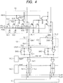
- FIG. 4 is a circuit diagram illustrating a configuration example of the imaging apparatus.
- a pixel unit 100 is an imaging region, and has a plurality of pixels 10 which are arranged in a matrix form. As is illustrated in FIG. 4 , each of the plurality of pixels 10 has photoelectric conversion units 10-1 and 10-2, a floating diffusion 10-5, a pixel amplifier (pixel amplifying unit) 10-7, transfer switches 10-3 and 10-4, a reset switch 10-6, and a selecting switch 10-8.
- the plurality of photoelectric conversion units 10-1 and 10-2 are connected to the same floating diffusion 10-5 through the plurality of transfer switches 10-3 and 10-4, respectively.
- the first photoelectric conversion unit 10-1 and the second photoelectric conversion unit 10-2 are, for instance, photodiodes, each of which converts incident light into an electric charge (electron) and accumulates the converted electric charge therein.
- the first transfer switch 10-3 is turned on when a transfer signal PTX_A becomes a high level, and transfers the electric charge of the first photoelectric conversion unit 10-1 to the floating diffusion 10-5.
- the second transfer switch 10-4 is turned on when a transfer signal PTX_B becomes a high level, and transfers the electric charge of the second photoelectric conversion unit 10-2 to the floating diffusion 10-5.
- the pixel amplifier 10-7 amplifies the voltage of the floating diffusion 10-5, and outputs the amplified voltage from an output terminal (source terminal).
- the selecting switch 10-8 is turned on when a selecting signal PSEL becomes a high level, and connects the output terminal of the pixel amplifier 10-7 with a vertical output line VL_1.
- the pixel 100 in the first column is connected to a common vertical output line VL_1.
- the pixel 100 in the second column is connected to a common vertical output line VL_2.
- the reset switch 10-6 is turned on when a reset signal PRES becomes a high level, and resets the photoelectric conversion units 10-1 and 10-2 and the floating diffusion 10-5 to a power source voltage.
- a vertical scanning circuit 11 supplies the reset signal PRES, the transfer signals PTX_A and PTX_B, and the selecting signal PSEL, to the pixels 100 in a matrix form one row by one row.
- the pixel 10 outputs a signal according to the voltage of the floating diffusion 10-5.
- An adding circuit 12 has a capacitor 12-1 and a switch SW4; and adds signals of the vertical output lines VL_1 and VL_2 of two columns based on a signal of a driving circuit 15 and outputs the added signal, or does not add the signals and outputs the intact signal.
- a first column signal processing circuit 13 has an amplifier 13-1, a feedback capacitor 13-2, an input capacitor 13-3, a feedback switch SW2 and an input switch SW1.
- a second column signal processing circuit 13 has switches SW3 and SW2' in place of the switches SW1 and SW2 in the column signal processing circuit 13 of the first column.
- the column signal processing circuit 13 may be a circuit which simply amplifies a signal, or may also be a circuit which performs correlated double sampling (CDS) that performs differential processing between a pixel signal and a noise signal.
- CDS correlated double sampling
- a negative input terminal is connected to the input capacitor 13-3, and a positive input terminal is connected to a node of a reference voltage VREF.
- the differential amplifier 13-1 outputs a signal obtained by inverting and amplifying a signal which is input into the negative input terminal.
- An output signal amp_out of the column signal processing circuit 13 is input into a column ADC circuit (column analog to digital conversion unit) 14.
- a column ADC circuit 14 converts an analog signal amp_out which is input from the column signal processing circuit 13 into a digital signal, based on a signal sent from a driving circuit 15.
- the column ADC circuit 14 has a comparator 14-1, a ramp source 14-2 which is common to each column, and a common counter 14-3 that is common to each of the columns.
- the comparator 14-1 compares the signal amp_out with a ramp signal (reference signal) RAMP of the ramp source 14-2, and outputs an inverted signal when the ramp signal RAMP becomes larger than the signal amp_out.
- the counter 14-3 counts a count value "count” from the time when the generation of the ramp signal RAMP has been started, until the output signal of the comparator 14-1 is inverted.
- the count value (digital value) "count” of the counter 14-3 is retained in an N-memory 16-1 or an S-memory 16-2.
- the noise signal is retained which is based on the noise level of the pixel 10.
- the S-memory 16-2 the pixel signal is retained which is based on a photoelectrically converted signal that has been generated by the pixel 10.
- the N-memory 16-1 and the S-memory 16-2 each have a memory for writing information sent from the comparator 14-1 therein, and memories for read-out, which are connected to horizontal read-out lines S_out and N_out, respectively.
- the signal retained in the memory for writing is transferred to the memory for read-out, and then is horizontally transferred and output to the horizontal read-out lines S_out and N_out, by the scan of a horizontal scanning circuit 17.
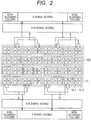
- FIG. 2 is a conceptual view of the imaging apparatus.
- the pixel 10 has the two photoelectric conversion units 10-1 and 10-2 which have been divided into two in a horizontal direction under one microlens, and are described as photoelectric conversion units A and B respectively.
- the photoelectric conversion unit A corresponds to the photoelectric conversion unit 10-1
- the photoelectric conversion unit B corresponds to the photoelectric conversion unit 10-2.
- the pixel signal of the photoelectric conversion unit A is referred to as an A signal
- the pixel signal of the photoelectric conversion unit B is referred to as a B signal.
- a signal based on an added signal of photoelectrically converted signals of the two photoelectric conversion units A and B is expressed as an A+B signal.
- the A signal and the A+B signal are read out, and the B signal is extracted from a difference between the A+B signal and the A signal, by a not-shown processing circuit.
- the proximate A signals and proximate A+B signals are added up by the adding circuit 12. The sum of electric charges is obtained which are accumulated in one photoelectric conversion unit in each of the pixels. Specifically, a horizontal scanning period can be shortened, by reducing the number of data to be scanned by the horizontal scanning circuit 17. In FIG.
- a solid line which connects the photoelectric conversion units A and B to each other shows a combination of signals to be added.
- the specific method will be described later.
- two A signals and two A+B signals are added to each other, but the number is not limited to two, but more than two signals may be added to each other.
- the A signal is necessary for measuring the phase difference, and accordingly is read out only from a region in which the phase difference is detected. Specifically, the A signal is output from a part of columns. Thereby, the number of signals to be read out can be reduced, and the horizontal scanning period of the horizontal scanning circuit 17 can be shortened.
- the A signal is a first signal which is output by the pixel 10
- the A+B signal is a second signal which is output by the pixel 10.
- FIG. 3 is a view illustrating an example of a focus detection region 21 in which a phase difference is measured and a focus is detected, in a pixel unit 100.
- the pixel unit 100 has an OB region (optical black region) 22 in which the pixel 10 is light-shielded, and an aperture region 20 that can receive incident light.
- the focus detection region 21 is a region which is sandwiched between the dotted lines, and has pixels in a part of the OB region 22 and pixels in a part of the aperture region 20.
- An (A+A) signal is read out in the focus detection region 21.
- the (A+A) signal is a first combined signal obtained by combining the A signals of the two pixels 10 with each other.
- the (A+A) signal is not read out from another region than the focus detection region 21.
- the above described imaging signal does not necessarily need to be read out from the whole region of the pixel unit 100 but may be read out from a part of a region containing the OB region 22 and the aperture region 20.
- a focus detection region 21 is provided which is narrower than the region in the part, and the (A+A) signal is read out therefrom.
- the imaging signal which is a signal obtained by adding the A+B signals of the two close pixels 10.
- the (A+B)+(A+B) signal is a second combined signal obtained by combining the A+B signals of the pixels 10 with each other.
- FIG. 5 is a timing chart illustrating a method for driving the imaging apparatus.
- a timing example will be described below in the case where the two pixels 10 provided in the vicinity in the horizontal direction are added by the adding circuit 12.
- the switch SW4 in order to add the signals of the two pixels 10, the switch SW4 shall be turned on, and the switch SW3 shall be turned off.
- the switch SW4 when the signals of the two pixels 10 are not added and the signal of each of the pixels 10 is read out, the switch SW4 shall be turned off, and the switch SW3 shall be turned on.
- the selecting signal PSEL becomes a high level
- the selecting switch 10-8 is turned on, and the row of the pixel 10 to be output is selected.
- the reset signal PRES is set at a high level, and thereby the floating diffusion 10-5 is reset to a power source potential.
- the switches SW2 and SW2' shall be also turned on, and the amplifier 13-1 shall be set at a reset state.
- the reset signal PRES transitions to a low level, and the reset switch 10-6 is turned off. Then, the noise signals of the pixels 10 in the reset state are output to the vertical output lines VL_1 and VL_2.
- both of the switch SW1 and switch SW4 are turned on, and accordingly two signals which are the signal of the vertical output line VL_1 and the signal of the vertical output line VL_2 are added through the capacitors 13-3 and 12-1, respectively.
- the switches SW2 and SW2' are turned off, and thereby the column signal processing circuit 13 retains a signal obtained by adding the noise signals of the two pixels 10 in the reset state, and outputs the signal amp_out to the column ADC circuit 14.
- the ramp source 14-2 starts the generation of the ramp signal RAMP, and the counter 14-3 starts the count-up of the count value "count”.
- the comparator 14-1 inverts the output signal.
- the count value "count” of the counter 14-3 is written in the N-memory 16-1.
- the digital signal based on the signal obtained by adding the signals of the two pixels 10 in the reset state is retained in the N-memory 16-1. After that, the switches SW1 and SW4 are turned off.
- the counter 14-3 resets the ramp signal RAMP to an initial value, and resets the count value "count”.
- the transfer signal PTX_A is set at a high level, and the transfer switch 10-3 is turned on.
- the electric charge which has been accumulated in the photoelectric conversion unit 10-1 is transferred to the floating diffusion 10-5.
- the PTX_A is set at a low level, and the transfer switch 10-3 is turned off.
- the A signals based on the amounts of the electric charges which have been accumulated in the photoelectric conversion units 10-1 in the two pixels 10 are output to the vertical output lines VL_1 and VL_2, respectively.
- the switches SW1 and SW4 are turned on.
- the A signals of the vertical output lines VL_1 and VL_2 are added by the adding circuit 12 and the column signal processing circuit 13, and the (A+A) signal is generated.
- the generated (A+A) signal is input into the column ADC circuit 14.
- the ramp source 14-2 starts the generation of the ramp signal RAMP, and the counter 14-3 starts the count-up of the count value "count”.
- the comparator 14-1 inverts the output signal.
- the count value "count” of the counter 14-3 is written in the S-memory 16-2.
- the digital signal based on the (A+A) signal is retained in the S-memory 16-2.
- the digital signals in the S-memories 16-2 in each of the columns are sequentially horizontally transferred to the horizontal read-out line S_out, and the digital signals in the N-memories 16-1 in each of the columns are sequentially horizontally transferred to the horizontal read-out line N_out. After that, the switches SW1 and SW4 are turned off.
- the transfer signals PTX_A and PTX_B are simultaneously set at a high level, and the transfer switches 10-3 and 10-4 are turned on. At this time, an electric charge obtained by adding an electric charge which has been accumulated in the photoelectric conversion unit 10-1 to an electric charge which has been accumulated in the photoelectric conversion unit 10-2 is retained in the floating diffusion 10-5.
- the transfer signals PTX_A and PTX_B are simultaneously set at a low level, and the transfer switches 10-3 and 10-4 are turned off. Signals based on the A+B signals obtained by adding the photoelectrically converted signals of the two photoelectric conversion units 10-1 and 10-2 on the floating diffusions 10-5 are output to the vertical output lines VL_1 and VL_2, respectively.
- the switches SW1 and SW4 are turned on.
- the two A+B signals of the vertical output lines VL_1 and VL_2 are added by the adding circuit 12 and the column signal processing circuit 13, and the (A+B)+(A+B) signal is generated.
- the generated (A+B)+(A+B) signal is input into the column ADC circuit 14.
- the ramp source 14-2 starts the generation of the ramp signal RAMP, and the counter 14-3 starts the count-up of the count value "count”.
- the comparator 14-1 inverts the output signal.
- the count value "count” of the counter 14-3 is written in the S-memory 16-2.
- the digital signal based on the (A+B)+(A+B) signal is retained in the S-memory 16-1.
- the digital signals in the S-memories 16-2 in each of the columns are sequentially horizontally transferred to the horizontal read-out line S_out, and the digital signals in the N-memories 16-1 in each of the columns are sequentially horizontally transferred to the horizontal read-out line N_out.
- the operations in between the times t4 and t8, which have been described above, are operations of a first mode.
- the vertical scanning circuit (controlling unit) 11 makes the plurality of pixels 10 output the A signal, in the state in which one photoelectric conversion unit 10-1 out of the plurality of photoelectric conversion units 10-1 and 10-2 is connected to the floating diffusion 10-5.
- the adding circuit (combining unit) 12 adds (combines) the output signals in every pixel 10 in a plurality of columns in the same row, and outputs the (A+A) signal.
- the adding circuit 12 connects the output lines VL_1 and VL_2 of the pixels 10 in the plurality of columns to the same node through the capacitors 13-3 and 12-1 respectively, and thereby adds (combines) the signals.
- the horizontal scanning circuit (output unit) 17 selects and outputs a part (signal based on focus detection region 21) of the (A+A) signals which have been added by the adding circuit 12.
- Operations after the time t8 are operations of a second mode.
- the vertical scanning circuit (controlling unit) 11 makes the plurality of pixels 10 output the A+B signal, in the state in which the plurality of photoelectric conversion units 10-1 and 10-2 are connected to the floating diffusion 10-5.
- the adding circuit (combining unit) 12 adds (combines) the output signals in every pixel 10 in a plurality of columns in the same row, and outputs the (A+B)+(A+B) signal.
- the horizontal scanning circuit (output unit) 17 outputs the (A+B)+(A+B) signals (signals of whole region in pixel unit 100) which have been added by the adding circuit 12.
- the feature of the present embodiment exists in a point that the (A+A) signal is generated by adding the A signals which have been read out from the pixels 10 in the plurality of columns to each other, and that the (A+B)+(A+B) signal is generated by adding the A+B signals which have been read out from the pixels 10 in the plurality of columns to each other.
- the feature of the present embodiment exists in a point that added signals of the A signals in the whole region of the pixel unit 100 are not output but added signals of the A signals only in the focus detection region 21 are output.
- a procedure for obtaining the A+B signal is not limited to the adding operation to be carried out on the floating diffusion 10-5.
- the S-memory 16-2 may have individual memories for the A signal and the A+B signal, or may use a common memory in a time-division fashion.
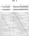
- FIG. 6 is a timing chart of the horizontal transfer read-out of the horizontal scanning circuit 17.
- the horizontal read-out lines N_out and S_out show each 1 bit of the digital data.
- the transfer pulses pt1 to pt26 are pulses which are input to the N-memory 16-1 and the S-memory 16-2 in each of the columns from the horizontal scanning circuit 17.
- the subscript of a pulse name pt designates the number of the column.
- the transfer pulses pt7 to pt19 show a horizontal zone of the focus detection region 21 which is sandwiched between the dotted lines in FIG. 3 .
- the digital value of the A+A signal is retained in the S-memory 16-2.
- the digital value of the (A+B)+(A+B) signal is retained in the S-memory 16-2.
- the period p1 is a period in which the A+A signal is output.
- the horizontal scanning circuit 17 scans only the columns corresponding to the focus detection region 21, and accordingly sequentially scans the transfer pulses pt7 to pt19 of the corresponding columns. Thereby, the digital values of the A+A signals only in the focus detection region 21 are sequentially output, and accordingly the read-out speed becomes fast.
- the period p2 is a period in which the digital value of the (A+B)+(A+B) signal is output.
- the horizontal scanning circuit 12 in order to scan all the columns in the pixel unit 100, sequentially scans the transfer pulses pt1 to pt26 of the corresponding columns. Thereby, the digital values of the (A+B)+(A+B) signals in the whole region in the pixel unit 100 are sequentially output.
- the digital values of the (A+A) signals and the digital values of the (A+B)+(A+B) signals can be retained in the common S-memory 16-2 in a time-division fashion.
- the A signals in the plurality of columns are added thereby to generate the (A+A) signals
- the (A+B) signals in the plurality of columns are added thereby to generate the (A+B)+(A+B) signals.
- the (A+A) signal is generated, the A signal only in the pixel 10 in the focus detection region 21 is read out, thereby the number of the data to be read out is reduced, and the read-out speed can be increased.
- such a method has been described above that an analog signal in every column is converted into a digital signal and the digital signal is read out, but the method may be a form of outputting the analog signal without converting the analog signal to the digital signal.
- the imaging apparatus shows an effect capable of reading out a signal having a high S/N in a short period of time, by combining the following operations (1) to (3).
- the imaging apparatus can reduce the amount of the data, and can increase the read-out speed.
- a signal of the A signal is small compared to that of the A+B signal, and the B signal which is obtained by subtracting the A signal from the A+B signal has a further degraded S/N. Accordingly, those signals become the factor of degrading a focus detection accuracy, when the illuminance is low.
- the imaging apparatus according to the present embodiment enhances the S/N of the A signal by adding the A signals in the plurality of columns, and can enhance the focus detection accuracy when the illuminance is low.
- the imaging apparatus can obtain an imaging signal having a high S/N ratio by adding the A+B signals in the plurality of columns.
- the position of the focus detection region 21 may be differentiated according to each frame.
- FIG. 7 is a conceptual view of an imaging apparatus according to a second embodiment of the present invention, which corresponds to FIG. 2 .
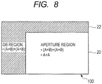
- FIG. 8 is a view illustrating an example of a focus detection region 21 in a pixel unit 100, similarly to FIG. 3 .
- An imaging apparatus according to the present embodiment has the same configuration and driving timing as those in that of the first embodiment, and has a different focus detection region from that in the first embodiment.
- a focus detection region in which the focus is detected is the aperture region 20, and a region in which the focus is not detected is the OB region 22.
- the (A+B)+(A+B) signals are generated based on the pixels in the whole region of the pixel unit 100.
- the A+A signal is generated only based on the pixels in the aperture region 20, and is not generated in the OB region 22.
- the (A+B)+(A+B) signal is generated which is obtained by adding the A+B signals in the plurality of columns.
- the (A+B)+(A+B) signal which is obtained by adding the A+B signals in the plurality of columns, and the (A+A) signal that is obtained by adding the A signals in the plurality of columns are generated.
- the A+A signal is not read out in the OB region 22 in which the focus is not detected, accordingly the amount of the data is reduced and the data can be read out at high speed.
- the imaging apparatuses according to the first and second embodiments combine the signals which have been output from the respective pixel amplifiers 10-7 in the pixels 10 to each other and generate the (A+A) signal and the (A+B)+(A+B) signal.
- the pixel amplifier 10-7 may combine the electric charges of the floating diffusions 10-5 in the plurality of pixels 10 with each other, and output each of the (A+A) signal and the (A+B)+(A+B) signal.
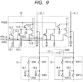
- FIG. 9 is a view illustrating a configuration example of a part of an imaging apparatus according to a third embodiment of the present invention, similarly to FIG. 4 .
- the present embodiment is different from the first embodiment in a method for combined signals of the pixels in the plurality of columns.
- the imaging apparatus according to the present embodiment averages the signals in a capacitor, as a method for combining the signals of the pixels in the plurality of columns. The point will be described below in which the present embodiment is different from the first embodiment.
- a first signal holding circuit 18 is connected to the vertical output line VL_1, and has capacitors 18-1 and 18-2, and switches SW6 to SW9.
- a second signal holding circuit 18 is connected to the vertical output line VL_2, and has capacitors 18-1 and 18-2, and switches SW10 to SW13.
- the adding circuit 12 has a switch SW5.
- the switch SW5 When the switch SW5 is turned on, the signal of the vertical output line VL1 and the signal of the vertical output line VL2 are averaged (combined).
- the output terminals of the signal holding circuits 18 are connected to the column signal processing circuit 13 in FIG. 4 .
- the switches SW8 and SW12 may be each connected to the comparator 14-1 or to the N-memory 16-1 in FIG. 4 .
- the switches SW9 and SW13 may be each connected to the comparator 14-1 or to the S-memory 16-2 in FIG. 4 .
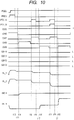
- FIG. 10 is a timing chart illustrating a method for driving an imaging apparatus of FIG. 9 .
- An example will be described below in which signals of two pixels 10 are averaged (combined).
- the switch SW5 is turned on, and the switches SW10 and SW11 are turned off.
- a signal out_n corresponds to an output signal amp_out of the column signal processing circuit 13 which is connected to the switch SW8.
- a signal out_s corresponds to the output signal amp_out of the column signal processing circuit 13 which is connected to the switch SW9.
- the selecting signal PSEL becomes a high level
- the selecting switch 10-8 is turned on, and the row of a pixel 10 is selected.
- the reset signal PRES is set at a high level
- the reset switch 10-6 is turned on, and the floating diffusion 10-5 is reset to a power source voltage.
- the reset signal PRES is transited to a low level, then the reset switch 10-6 is turned off, and signals of the pixels 10 based on the reset state are output to the vertical output lines VL_1 and VL_2.
- the switches SW6 and SW5 are turned on, and accordingly the vertical output lines VL_1 and VL_2 are connected to each other.
- the approximately average value of the voltages of the vertical output lines VL_1 and VL_2 based on the effective resistance value of the transistors 10-7 and 10-8 is accumulated in a capacitor 18-1.
- the switch SW6 is turned off, and the electric charge is retained in the capacitor 18-1.
- the switch SW8 is turned on, and the signal retained in the capacitor 18-1 is output. After that, the switch SW8 is turned off.
- the transfer signal PTX_A is set at a high level, and the transfer switch 10-3 is turned on.
- the electric charge which has been accumulated in the photoelectric conversion unit 10-1 is transferred to the floating diffusion 10-5.
- the transfer signal PTX_A is set at a low level, then the transfer switch 10-3 is turned off, and the above described transfer is ended.
- a switch SW7 is turned on, and thereby an (A+A)/2 signal which is an approximately average value of the voltages of the vertical output lines VL_1 and VL_2 is retained in a capacitor 18-2.
- the switch SW9 is turned on, and the signal retained in the capacitor 18-2 is output.
- the transfer signals PTX_A and PTX_B are simultaneously set at a high level, and the transfer switches 10-3 and 10-4 are turned on. At this time, an electric charge obtained by adding the electric charge which has been accumulated in the photoelectric conversion unit 10-1 and the electric charge which has been accumulated in the photoelectric conversion unit 10-2 results in being retained in the floating diffusion 10-5.
- each of the A+B signals is output which has been obtained by adding the photoelectrically converted signals of the two photoelectric conversion units 10-1 and 10-2 on the floating diffusion 10-5.
- a signal obtained by averaging the voltages of the vertical output lines VL_1 and VL_2, specifically, an [(A+B)+(A+B)]/2 signal is written in the capacitor 18-2.
- the transfer signals PTX_A and PTX_B are set at a low level, then the transfer switches 10-3 and 10-4 are turned off, and the above described transfer is ended.
- the switch SW7 is turned off, and the capacitor 18-2 retains the signal [(A+B)+(A+B)]/2.
- the switch SW9 is turned on, and the signal retained in the capacitor 18-2 is output.
- the operations in between the times t15 and t19, which have been described above, are operations of the first mode.
- the vertical scanning circuit (controlling unit) 11 makes the plurality of pixels 10 output the A signal in the state in which one photoelectric conversion unit 10-1 out of the plurality of photoelectric conversion units 10-1 and 10-2 is connected to the floating diffusion 10-5.
- the adding circuit (combining unit) 12 averages (combines) the output signals in every pixel 10 in the plurality of columns in the same row, and outputs an (A+A)/2 signal. Specifically, the adding circuit 12 connects the output lines VL_1 and VL_2 of the pixels in the plurality of columns to each other, and thereby averages (combines) the signals.
- the horizontal scanning circuit (output unit) 17 selects a part of the (A+A)/2 signals (signals based on focus detection region 21) which have been averaged by the adding circuit 12, and outputs the signal.
- Operations after the time t19 are the operations of the second mode.
- the vertical scanning circuit (controlling unit) 11 makes the plurality of pixels 10 output the A+B signal in the state in which the plurality of photoelectric conversion units 10-1 and 10-2 are connected to the floating diffusion 10-5.
- the adding circuit (combining unit) 12 averages (combines) the output signals in every pixel 10 in the plurality of columns in the same row, and outputs the [(A+B)+(A+B)]/2 signal.
- the horizontal scanning circuit (output unit) 17 outputs the [(A+B)+(A+B)]/2 signals (signals of whole region in pixel unit 100) which have been averaged by the adding circuit 12.
- the imaging apparatus generates the average value of the A signals only in the focus detection region 21, similarly to the first embodiment, thereby reduces the number of the data to be read out, and can read out the data at high speed.
- the imaging apparatus according to the present embodiment can obtain an effect of reducing the number of data, by the averaging process.
- the imaging apparatus according to the present embodiment can carry out the adding or averaging process without arranging an active circuit for the adding or averaging process.
- the averaging process in the present embodiment has been performed by connecting the vertical output lines VL_1 and VL_2, but may also be performed by reading out the signals to the capacitors for the vertical output line VL_1 and the capacitors for the vertical output line VL_2 respectively, and short-circuiting each pair of capacitors.
- the adding circuit 12 in FIG. 9 has an effect of reducing a time period in which each pair of capacitors are short-circuited, reducing the number of the capacitors necessary for the averaging process, and assigning the reduced capacitors to another process, compared to the above described case where each pair of capacitors are short-circuited.
- the A signals of the pixels 10 in the same row have been combined with each other and the A+B signals similarly have been combined with each other.
- the vertical scanning circuit 11 simultaneously selects the pixels 10 in the plurality of rows, and the pixels 10 in the plurality of rows are simultaneously output to the vertical output line VL_1.
- FIG. 11 is a view illustrating a configuration example of an imaging apparatus according to a fourth embodiment of the present invention.
- digital data in the plurality of columns is added.
- the point will be described below in which the present embodiment is different from the first embodiment.
- the present embodiment is different from the first embodiment in the point that digital data after an analog signal has been converted to a digital signal is added to each other.
- FIG. 11 is a view of an imaging apparatus in which the capacitor 12-1 and the switch SW4 are deleted from, and an adding circuit 19 is added to the imaging apparatus in FIG. 4 .
- a memory 16-1a for writing and a memory 16-1b for read-out correspond to an N-memory 16-1 in FIG. 4 .
- a memory 16-2a for writing and a memory 16-2b for read-out correspond to an S-memory 16-2 in FIG. 4 .
- the adding circuit (combining unit) 19 adds (combines) digital data of the memories 16-1a for writing in the plurality of columns, and writes the added digital data in the memory 16-1b for read-out.
- the adding circuit (combining unit) 19 adds (combines) digital data of the memories 16-2a for writing in the plurality of columns, and writes the added digital data in the memory 16-2b for read-out.
- the imaging apparatus when the A+B signals have been read out from the pixels 10, the (A+B)+(A+B) signal obtained by adding the A+B signals in the plurality of columns is retained in the memory 16-2b for read-out.
- the imaging apparatus according to the present embodiment generates the A+A signal only in the focus detection region 21, similarly to that in the first embodiment, thereby reduces the number of the data to be read out, and can read out the data at high speed.
- the A signals of the pixels 10 in the same row have been combined with each other and the A+B signals have been similarly combined with each other.
- the adding circuit 19 may combine the A signals of digital data of the pixels 10 in the plurality of rows with each other, and similarly combine the A+B signals to each other.
- the digital signals are added to each other, as one example of combination of the digital signals.
- the combination of the digital signals may be the averaging of the digital signals.
- FIG. 12 is a view illustrating a configuration example of an imaging system according to a fifth embodiment of the present invention.
- the imaging system has the imaging apparatus 154 according to the first to fourth embodiments.
- Examples of the imaging system include a digital camera, a digital camcorder and a monitoring camera.
- FIG. 12 illustrates the case where the imaging apparatus 154 is applied to the digital camera, as an example of the imaging system.
- the imaging system has a lens 152 for making the imaging apparatus 154 form an optical image of an object thereon, a barrier 151 for protecting the lens 152, and a diaphragm 153 for varying the quantity of light which has passed through the lens 152.
- the lens 152 and the diaphragm 153 form an optical system which guides the light to the imaging apparatus 154.
- the imaging system also has an output signal processing unit 155 which performs the process of the output signal which the imaging apparatus 154 outputs.
- the output signal processing unit 155 has a digital signal processing unit, and performs an operation of variously correcting the signals which the imaging apparatus 154 outputs, compressing the signals, as needed, and outputting the compressed signals.
- the imaging system also has a buffer memory unit 156 for temporarily memorizing image data, and a recording medium controlling interface unit 158 for recording signals in or reading signals from a recording medium.
- the imaging system further has a releasable recording medium 159 such as a semiconductor memory, for recording the image data therein or reading the image data therefrom.
- the imaging system further has an external interface unit 157 for communicating with an external computer or the like, an overall control/calculation unit 1510 which performs various calculations and controls the whole digital camera, and the imaging apparatus 154.
- the imaging system further has a timing generator 1511 which outputs various timing signals to the imaging apparatus 154 and the output signal processing unit 155.
- the timing signal and the like may be input from the outside.
- the imaging system may have at least the imaging apparatus 154 and the output signal processing unit 155 which processes an output signal that has been output from the imaging apparatus 154.
- the output signal processing unit 155 can detect a focus of the optical system by using the (A+A) signal or the (A+A)/2 signal for phase difference detection, which the imaging apparatus 154 outputs.
- the output signal processing unit 155 can generate an image by using the (A+B)+(A+B) signal or the [(A+B)+(A+B)]/2 signal which the imaging apparatus 154 outputs.
- the imaging system of the present embodiment has the imaging apparatus 154 applied thereto, and can detect the focus of the optical system and generate the image.
- a checkered filter of RGBG can be used as a color filter for the pixels 10.
- the color filter is provided on each of the pixels 10 of the imaging apparatus, the photoelectrically converted signals sent from the pixels of the same color can be added to each other.
- the present invention can provide an imaging apparatus which has an increased speed of an operation.
Landscapes
- Engineering & Computer Science (AREA)
- Multimedia (AREA)
- Signal Processing (AREA)
- Transforming Light Signals Into Electric Signals (AREA)
- Focusing (AREA)
- Automatic Focus Adjustment (AREA)
- Solid State Image Pick-Up Elements (AREA)
Applications Claiming Priority (1)
| Application Number | Priority Date | Filing Date | Title |
|---|---|---|---|
| JP2013176799A JP6274788B2 (ja) | 2013-08-28 | 2013-08-28 | 撮像装置、撮像システム及び撮像装置の駆動方法 |
Publications (3)
| Publication Number | Publication Date |
|---|---|
| EP2843939A2 EP2843939A2 (en) | 2015-03-04 |
| EP2843939A3 EP2843939A3 (en) | 2015-05-20 |
| EP2843939B1 true EP2843939B1 (en) | 2017-05-10 |
Family
ID=51357761
Family Applications (1)
| Application Number | Title | Priority Date | Filing Date |
|---|---|---|---|
| EP14180934.3A Active EP2843939B1 (en) | 2013-08-28 | 2014-08-14 | Imaging apparatus, imaging system, and method for driving imaging apparatus |
Country Status (7)
| Country | Link |
|---|---|
| US (1) | US9549139B2 (enExample) |
| EP (1) | EP2843939B1 (enExample) |
| JP (1) | JP6274788B2 (enExample) |
| KR (1) | KR101711702B1 (enExample) |
| CN (1) | CN104427265B (enExample) |
| PH (1) | PH12014000223A1 (enExample) |
| RU (1) | RU2589489C2 (enExample) |
Families Citing this family (48)
| Publication number | Priority date | Publication date | Assignee | Title |
|---|---|---|---|---|
| JP6234054B2 (ja) * | 2013-04-25 | 2017-11-22 | キヤノン株式会社 | 撮像装置および撮像装置の制御方法 |
| JP5886806B2 (ja) | 2013-09-17 | 2016-03-16 | キヤノン株式会社 | 固体撮像装置 |
| JP6239975B2 (ja) * | 2013-12-27 | 2017-11-29 | キヤノン株式会社 | 固体撮像装置及びそれを用いた撮像システム |
| JP6412328B2 (ja) * | 2014-04-01 | 2018-10-24 | キヤノン株式会社 | 固体撮像装置およびカメラ |
| JP2015216625A (ja) * | 2014-04-22 | 2015-12-03 | キヤノン株式会社 | 撮像素子及び撮像装置 |
| JP6389685B2 (ja) | 2014-07-30 | 2018-09-12 | キヤノン株式会社 | 撮像装置、および、撮像システム |
| JP6587380B2 (ja) | 2014-09-12 | 2019-10-09 | キヤノン株式会社 | 画像処理装置、撮像装置、画像処理方法、プログラム、記憶媒体 |
| US9979916B2 (en) | 2014-11-21 | 2018-05-22 | Canon Kabushiki Kaisha | Imaging apparatus and imaging system |
| JP6218799B2 (ja) * | 2015-01-05 | 2017-10-25 | キヤノン株式会社 | 撮像素子及び撮像装置 |
| US10070088B2 (en) * | 2015-01-05 | 2018-09-04 | Canon Kabushiki Kaisha | Image sensor and image capturing apparatus for simultaneously performing focus detection and image generation |
| JP6700673B2 (ja) * | 2015-05-15 | 2020-05-27 | キヤノン株式会社 | 撮像装置、撮像システム |
| KR102382183B1 (ko) * | 2015-05-20 | 2022-04-01 | 삼성전자주식회사 | 신호대 잡음비 및 랜덤 노이즈를 개선하는 이미지 센서 및 이를 포함하는 이미지 처리 시스템 |
| JP6525727B2 (ja) * | 2015-05-21 | 2019-06-05 | キヤノン株式会社 | 画像処理装置及び方法、及び撮像装置 |
| WO2016203974A1 (ja) * | 2015-06-15 | 2016-12-22 | ソニー株式会社 | イメージセンサ、および電子機器 |
| JP6632242B2 (ja) * | 2015-07-27 | 2020-01-22 | キヤノン株式会社 | 撮像装置及び撮像システム |
| KR102497812B1 (ko) | 2015-08-10 | 2023-02-09 | 삼성전자주식회사 | 이미지 센서 |
| GB2596028B (en) * | 2015-09-16 | 2022-04-20 | Canon Kk | Image sensor and image capturing apparatus |
| DE112016004211T5 (de) | 2015-09-16 | 2018-06-14 | Canon Kabushiki Kaisha | Bildsensor und Bildaufnahmevorrichtung |
| JP6711634B2 (ja) | 2016-02-16 | 2020-06-17 | キヤノン株式会社 | 撮像装置、撮像装置の駆動方法、及び撮像システム |
| JP6650779B2 (ja) | 2016-02-19 | 2020-02-19 | キヤノン株式会社 | 撮像装置、撮像システム、撮像装置の駆動方法 |
| US9955096B2 (en) * | 2016-03-22 | 2018-04-24 | Taiwan Semiconductor Manufacturing Co., Ltd. | System and method for high-speed down-sampled CMOS image sensor readout |
| JP6753169B2 (ja) | 2016-06-28 | 2020-09-09 | セイコーエプソン株式会社 | 画像読取装置及び半導体装置 |
| JP2018072390A (ja) | 2016-10-24 | 2018-05-10 | オリンパス株式会社 | 撮像装置 |
| JP6903417B2 (ja) * | 2016-11-07 | 2021-07-14 | ソニーセミコンダクタソリューションズ株式会社 | 固体撮像素子および制御方法、並びに電子機器 |
| JP6918517B2 (ja) * | 2017-02-21 | 2021-08-11 | キヤノン株式会社 | 撮像素子及びその制御方法、及び撮像装置 |
| JP6904772B2 (ja) | 2017-04-26 | 2021-07-21 | キヤノン株式会社 | 固体撮像装置及びその駆動方法 |
| CN108958555B (zh) * | 2017-05-25 | 2021-06-22 | 旭景科技有限公司 | 电容式影像传感器与操作该电容式影像传感器的方法 |
| JP2019012968A (ja) * | 2017-06-30 | 2019-01-24 | ソニーセミコンダクタソリューションズ株式会社 | 固体撮像装置、及び電子機器 |
| EP3525449B1 (en) * | 2017-08-30 | 2021-09-29 | Sony Semiconductor Solutions Corporation | Image-capturing element and image-capturing device |
| JP2019106634A (ja) | 2017-12-13 | 2019-06-27 | オリンパス株式会社 | 撮像素子及び撮像装置 |
| JP7077029B2 (ja) * | 2018-01-26 | 2022-05-30 | キヤノン株式会社 | 光電変換装置、撮像システム、移動体 |
| JP2019140528A (ja) | 2018-02-09 | 2019-08-22 | ソニーセミコンダクタソリューションズ株式会社 | 撮像装置、及び電子機器 |
| JP7089390B2 (ja) | 2018-03-30 | 2022-06-22 | キヤノン株式会社 | 光電変換装置及びその駆動方法 |
| WO2019225668A1 (ja) * | 2018-05-23 | 2019-11-28 | 株式会社ニコン | 撮像素子および撮像装置 |
| JP6766095B2 (ja) * | 2018-06-08 | 2020-10-07 | キヤノン株式会社 | 撮像装置、撮像システム、移動体、および積層用の半導体基板 |
| JP7161317B2 (ja) * | 2018-06-14 | 2022-10-26 | キヤノン株式会社 | 撮像装置、撮像システム及び移動体 |
| JP7245014B2 (ja) | 2018-09-10 | 2023-03-23 | キヤノン株式会社 | 固体撮像装置、撮像システム、および固体撮像装置の駆動方法 |
| KR102538220B1 (ko) * | 2018-10-02 | 2023-06-01 | 삼성전자주식회사 | 이미지 센싱 시스템 및 이의 동작 방법 |
| US11683606B2 (en) * | 2018-10-19 | 2023-06-20 | Sony Semiconductor Solutions Corporation | Imaging device and electronic equipment |
| KR102600681B1 (ko) * | 2019-03-26 | 2023-11-13 | 삼성전자주식회사 | 비닝을 수행하는 테트라셀 이미지 센서 |
| RU2728949C1 (ru) * | 2019-10-09 | 2020-08-03 | федеральное государственное бюджетное образовательное учреждение высшего образования "Южно-Российский государственный политехнический университет (НПИ) имени М.И. Платова" | Способ построения и обработки изображений и система его реализующая |
| JP7455588B2 (ja) * | 2020-01-17 | 2024-03-26 | キヤノン株式会社 | 撮像装置 |
| JP7444664B2 (ja) * | 2020-03-24 | 2024-03-06 | キヤノン株式会社 | 撮像装置及び撮像システム |
| JP7538618B2 (ja) | 2020-05-01 | 2024-08-22 | キヤノン株式会社 | 光電変換装置及び光電変換システム |
| JP7614742B2 (ja) * | 2020-05-28 | 2025-01-16 | キヤノン株式会社 | 光電変換装置、光電変換システム、移動体及び信号処理方法 |
| EP4178198A1 (en) * | 2021-11-05 | 2023-05-10 | Teledyne Innovaciones Microelectrónicas, SLU | Column sharing adc for image sensors and method of operation |
| JP2023125844A (ja) | 2022-02-28 | 2023-09-07 | キヤノン株式会社 | 光電変換装置、光電変換システムおよび移動体 |
| US20240430596A1 (en) * | 2023-06-23 | 2024-12-26 | Canon Kabushiki Kaisha | Image capturing apparatus, control method thereof, and storage medium |
Family Cites Families (63)
| Publication number | Priority date | Publication date | Assignee | Title |
|---|---|---|---|---|
| TW421962B (en) | 1997-09-29 | 2001-02-11 | Canon Kk | Image sensing device using mos type image sensing elements |
| JP3571909B2 (ja) | 1998-03-19 | 2004-09-29 | キヤノン株式会社 | 固体撮像装置及びその製造方法 |
| JP3774597B2 (ja) | 1999-09-13 | 2006-05-17 | キヤノン株式会社 | 撮像装置 |
| JP4908668B2 (ja) | 2000-04-19 | 2012-04-04 | キヤノン株式会社 | 焦点検出装置 |
| US7429764B2 (en) | 2002-02-27 | 2008-09-30 | Canon Kabushiki Kaisha | Signal processing device and image pickup apparatus using the same |
| JP3728260B2 (ja) | 2002-02-27 | 2005-12-21 | キヤノン株式会社 | 光電変換装置及び撮像装置 |
| JP4514188B2 (ja) | 2003-11-10 | 2010-07-28 | キヤノン株式会社 | 光電変換装置及び撮像装置 |
| JP4508619B2 (ja) | 2003-12-03 | 2010-07-21 | キヤノン株式会社 | 固体撮像装置の製造方法 |
| JP3793202B2 (ja) | 2004-02-02 | 2006-07-05 | キヤノン株式会社 | 固体撮像装置 |
| JP4067054B2 (ja) | 2004-02-13 | 2008-03-26 | キヤノン株式会社 | 固体撮像装置および撮像システム |
| JP4290066B2 (ja) * | 2004-05-20 | 2009-07-01 | キヤノン株式会社 | 固体撮像装置および撮像システム |
| JP5089017B2 (ja) | 2004-09-01 | 2012-12-05 | キヤノン株式会社 | 固体撮像装置及び固体撮像システム |
| JP4971586B2 (ja) | 2004-09-01 | 2012-07-11 | キヤノン株式会社 | 固体撮像装置 |
| JP4804254B2 (ja) | 2006-07-26 | 2011-11-02 | キヤノン株式会社 | 光電変換装置及び撮像装置 |
| JP5123601B2 (ja) | 2006-08-31 | 2013-01-23 | キヤノン株式会社 | 光電変換装置 |
| JP5188080B2 (ja) | 2007-03-06 | 2013-04-24 | キヤノン株式会社 | 撮像装置、撮像装置の駆動方法、及び読み出し装置 |
| JP4110193B1 (ja) | 2007-05-02 | 2008-07-02 | キヤノン株式会社 | 固体撮像装置および撮像システム |
| JP5063234B2 (ja) | 2007-07-20 | 2012-10-31 | キヤノン株式会社 | 撮像装置、撮像システム、及び、撮像装置の動作方法 |
| JP5045350B2 (ja) * | 2007-10-01 | 2012-10-10 | 株式会社ニコン | 撮像素子および撮像装置 |
| JP4403435B2 (ja) | 2007-11-16 | 2010-01-27 | ソニー株式会社 | 固体撮像装置、駆動制御方法、および撮像装置 |
| JP5268389B2 (ja) | 2008-02-28 | 2013-08-21 | キヤノン株式会社 | 固体撮像装置、その駆動方法及び撮像システム |
| JP5173493B2 (ja) | 2008-02-29 | 2013-04-03 | キヤノン株式会社 | 撮像装置及び撮像システム |
| JP5178266B2 (ja) | 2008-03-19 | 2013-04-10 | キヤノン株式会社 | 固体撮像装置 |
| JP5094498B2 (ja) | 2008-03-27 | 2012-12-12 | キヤノン株式会社 | 固体撮像装置及び撮像システム |
| JP5279352B2 (ja) | 2008-06-06 | 2013-09-04 | キヤノン株式会社 | 固体撮像装置 |
| JP5188292B2 (ja) | 2008-06-30 | 2013-04-24 | キヤノン株式会社 | 撮像システムおよび撮像システムの駆動方法 |
| JP5274166B2 (ja) | 2008-09-10 | 2013-08-28 | キヤノン株式会社 | 光電変換装置及び撮像システム |
| JP4891308B2 (ja) | 2008-12-17 | 2012-03-07 | キヤノン株式会社 | 固体撮像装置及び固体撮像装置を用いた撮像システム |
| JP5539104B2 (ja) | 2009-09-24 | 2014-07-02 | キヤノン株式会社 | 光電変換装置およびそれを用いた撮像システム |
| JP4547462B1 (ja) * | 2009-11-16 | 2010-09-22 | アキュートロジック株式会社 | 撮像素子、撮像素子の駆動装置、撮像素子の駆動方法、画像処理装置、プログラム、及び、撮像装置 |
| JP5679653B2 (ja) | 2009-12-09 | 2015-03-04 | キヤノン株式会社 | 光電変換装置およびそれを用いた撮像システム |
| JP5885401B2 (ja) | 2010-07-07 | 2016-03-15 | キヤノン株式会社 | 固体撮像装置および撮像システム |
| JP5645513B2 (ja) | 2010-07-07 | 2014-12-24 | キヤノン株式会社 | 固体撮像装置及び撮像システム |
| JP5643555B2 (ja) | 2010-07-07 | 2014-12-17 | キヤノン株式会社 | 固体撮像装置及び撮像システム |
| JP2012034350A (ja) | 2010-07-07 | 2012-02-16 | Canon Inc | 固体撮像装置及び撮像システム |
| JP5697371B2 (ja) | 2010-07-07 | 2015-04-08 | キヤノン株式会社 | 固体撮像装置および撮像システム |
| JP5610961B2 (ja) | 2010-09-30 | 2014-10-22 | キヤノン株式会社 | 固体撮像装置及び固体撮像装置の駆動方法 |
| CN103119928B (zh) | 2010-09-30 | 2016-05-25 | 佳能株式会社 | 固态成像装置 |
| JP5739640B2 (ja) * | 2010-10-20 | 2015-06-24 | キヤノン株式会社 | 撮像素子及び撮像装置 |
| KR101758090B1 (ko) | 2010-12-06 | 2017-07-17 | 삼성전자주식회사 | 이미지 센서 및 이미지 센서를 포함하는 카메라 시스템 |
| JP5791338B2 (ja) | 2011-04-07 | 2015-10-07 | キヤノン株式会社 | 固体撮像装置及びその駆動方法 |
| JP5895355B2 (ja) * | 2011-04-25 | 2016-03-30 | 株式会社ニコン | 撮像装置 |
| JP5808162B2 (ja) | 2011-06-23 | 2015-11-10 | キヤノン株式会社 | 撮像素子、撮像装置及び撮像素子の駆動方法 |
| JP2013021616A (ja) * | 2011-07-13 | 2013-01-31 | Olympus Imaging Corp | 撮像装置 |
| JP5762199B2 (ja) | 2011-07-28 | 2015-08-12 | キヤノン株式会社 | 固体撮像装置 |
| JP5901186B2 (ja) | 2011-09-05 | 2016-04-06 | キヤノン株式会社 | 固体撮像装置及びその駆動方法 |
| JP5858695B2 (ja) | 2011-09-08 | 2016-02-10 | キヤノン株式会社 | 固体撮像装置及び固体撮像装置の駆動方法 |
| JP5806566B2 (ja) | 2011-09-15 | 2015-11-10 | キヤノン株式会社 | A/d変換器および固体撮像装置 |
| JP5930651B2 (ja) | 2011-10-07 | 2016-06-08 | キヤノン株式会社 | 固体撮像装置 |
| JP5901212B2 (ja) | 2011-10-07 | 2016-04-06 | キヤノン株式会社 | 光電変換システム |
| JP5926529B2 (ja) * | 2011-10-18 | 2016-05-25 | キヤノン株式会社 | 撮像素子及び撮像装置 |
| JP5959829B2 (ja) | 2011-11-09 | 2016-08-02 | キヤノン株式会社 | 固体撮像装置 |
| JP5893573B2 (ja) | 2012-02-09 | 2016-03-23 | キヤノン株式会社 | 固体撮像装置 |
| JP5893572B2 (ja) * | 2012-03-01 | 2016-03-23 | キヤノン株式会社 | 撮像装置、撮像システム、撮像装置の駆動方法 |
| JP5914055B2 (ja) * | 2012-03-06 | 2016-05-11 | キヤノン株式会社 | 撮像装置 |
| JP5893550B2 (ja) | 2012-04-12 | 2016-03-23 | キヤノン株式会社 | 撮像装置及び撮像システム |
| KR101889932B1 (ko) * | 2012-07-25 | 2018-09-28 | 삼성전자주식회사 | 촬영 장치 및 이에 적용되는 촬영 방법 |
| JP5968146B2 (ja) | 2012-07-31 | 2016-08-10 | キヤノン株式会社 | 固体撮像装置およびカメラ |
| JP6149369B2 (ja) * | 2012-09-27 | 2017-06-21 | 株式会社ニコン | 撮像素子 |
| WO2014118868A1 (ja) | 2013-01-30 | 2014-08-07 | パナソニック株式会社 | 撮像装置及び固体撮像装置 |
| JP6319946B2 (ja) | 2013-04-18 | 2018-05-09 | キヤノン株式会社 | 固体撮像装置及び撮像システム |
| JP6100074B2 (ja) | 2013-04-25 | 2017-03-22 | キヤノン株式会社 | 光電変換装置及び撮像システム |
| KR102025935B1 (ko) * | 2013-06-21 | 2019-09-26 | 삼성전자주식회사 | 이미지 생성 장치 및 이미지 생성 방법 |
-
2013
- 2013-08-28 JP JP2013176799A patent/JP6274788B2/ja active Active
-
2014
- 2014-08-06 US US14/452,945 patent/US9549139B2/en active Active
- 2014-08-11 PH PH12014000223A patent/PH12014000223A1/en unknown
- 2014-08-14 EP EP14180934.3A patent/EP2843939B1/en active Active
- 2014-08-20 KR KR1020140108217A patent/KR101711702B1/ko not_active Expired - Fee Related
- 2014-08-25 CN CN201410419618.1A patent/CN104427265B/zh active Active
- 2014-08-27 RU RU2014135151/28A patent/RU2589489C2/ru active
Also Published As
| Publication number | Publication date |
|---|---|
| RU2014135151A (ru) | 2016-03-27 |
| US9549139B2 (en) | 2017-01-17 |
| EP2843939A2 (en) | 2015-03-04 |
| JP6274788B2 (ja) | 2018-02-07 |
| EP2843939A3 (en) | 2015-05-20 |
| RU2589489C2 (ru) | 2016-07-10 |
| JP2015046761A (ja) | 2015-03-12 |
| PH12014000223B1 (en) | 2016-02-22 |
| KR20150026851A (ko) | 2015-03-11 |
| KR101711702B1 (ko) | 2017-03-02 |
| US20150062394A1 (en) | 2015-03-05 |
| CN104427265A (zh) | 2015-03-18 |
| CN104427265B (zh) | 2018-05-25 |
| PH12014000223A1 (en) | 2016-02-22 |
Similar Documents
| Publication | Publication Date | Title |
|---|---|---|
| EP2843939B1 (en) | Imaging apparatus, imaging system, and method for driving imaging apparatus | |
| US9438841B2 (en) | Solid-state imaging apparatus and imaging system | |
| US8553114B2 (en) | Image sensing apparatus and image sensing system | |
| US9538110B2 (en) | Driving method of imaging device and driving method of imaging system | |
| JP6164846B2 (ja) | 撮像装置、撮像システム、撮像装置の駆動方法 | |
| US8264580B2 (en) | Solid state imaging device, signal processing method of solid-state imaging device and imaging apparatus capable of removing vertical smears | |
| US8208055B2 (en) | Solid-state imaging apparatus and imaging system | |
| EP3389259B1 (en) | Solid-state image-capturing device and method for driving solid-state image-capturing device | |
| EP2750376B1 (en) | Photoelectric conversion device, image pickup system, and driving method of photoelectric conversion device | |
| US9258505B2 (en) | Imaging apparatus, imaging system, method for driving imaging apparatus, and method for driving imaging system | |
| JP2017147700A (ja) | 撮像装置、撮像システム、撮像装置の駆動方法 | |
| JP6245856B2 (ja) | 光電変換装置、光電変換システム | |
| JP2024097946A (ja) | 光電変換装置 | |
| US9288412B2 (en) | Image pickup apparatus, method for driving image pickup apparatus, image pickup system | |
| JP2023084647A (ja) | 光電変換装置 | |
| JP2023084272A (ja) | 光電変換装置 |
Legal Events
| Date | Code | Title | Description |
|---|---|---|---|
| 17P | Request for examination filed |
Effective date: 20140814 |
|
| AK | Designated contracting states |
Kind code of ref document: A2 Designated state(s): AL AT BE BG CH CY CZ DE DK EE ES FI FR GB GR HR HU IE IS IT LI LT LU LV MC MK MT NL NO PL PT RO RS SE SI SK SM TR |
|
| AX | Request for extension of the european patent |
Extension state: BA ME |
|
| PUAI | Public reference made under article 153(3) epc to a published international application that has entered the european phase |
Free format text: ORIGINAL CODE: 0009012 |
|
| PUAL | Search report despatched |
Free format text: ORIGINAL CODE: 0009013 |
|
| AK | Designated contracting states |
Kind code of ref document: A3 Designated state(s): AL AT BE BG CH CY CZ DE DK EE ES FI FR GB GR HR HU IE IS IT LI LT LU LV MC MK MT NL NO PL PT RO RS SE SI SK SM TR |
|
| AX | Request for extension of the european patent |
Extension state: BA ME |
|
| RIC1 | Information provided on ipc code assigned before grant |
Ipc: H04N 5/347 20110101ALI20150416BHEP Ipc: H04N 5/378 20110101AFI20150416BHEP Ipc: H04N 5/345 20110101ALI20150416BHEP Ipc: H01L 27/146 20060101ALI20150416BHEP Ipc: H04N 5/3745 20110101ALI20150416BHEP |
|
| R17P | Request for examination filed (corrected) |
Effective date: 20151120 |
|
| RBV | Designated contracting states (corrected) |
Designated state(s): AL AT BE BG CH CY CZ DE DK EE ES FI FR GB GR HR HU IE IS IT LI LT LU LV MC MK MT NL NO PL PT RO RS SE SI SK SM TR |
|
| GRAP | Despatch of communication of intention to grant a patent |
Free format text: ORIGINAL CODE: EPIDOSNIGR1 |
|
| INTG | Intention to grant announced |
Effective date: 20160708 |
|
| RIN1 | Information on inventor provided before grant (corrected) |
Inventor name: ARISHIMA, YU Inventor name: HIYAMA, HIROKI Inventor name: HASHIMOTO, SEIJI Inventor name: IKEDA, YASUJI |
|
| GRAJ | Information related to disapproval of communication of intention to grant by the applicant or resumption of examination proceedings by the epo deleted |
Free format text: ORIGINAL CODE: EPIDOSDIGR1 |
|
| GRAP | Despatch of communication of intention to grant a patent |
Free format text: ORIGINAL CODE: EPIDOSNIGR1 |
|
| INTC | Intention to grant announced (deleted) | ||
| INTG | Intention to grant announced |
Effective date: 20161124 |
|
| GRAS | Grant fee paid |
Free format text: ORIGINAL CODE: EPIDOSNIGR3 |
|
| GRAA | (expected) grant |
Free format text: ORIGINAL CODE: 0009210 |
|
| AK | Designated contracting states |
Kind code of ref document: B1 Designated state(s): AL AT BE BG CH CY CZ DE DK EE ES FI FR GB GR HR HU IE IS IT LI LT LU LV MC MK MT NL NO PL PT RO RS SE SI SK SM TR |
|
| REG | Reference to a national code |
Ref country code: GB Ref legal event code: FG4D |
|
| REG | Reference to a national code |
Ref country code: AT Ref legal event code: REF Ref document number: 893428 Country of ref document: AT Kind code of ref document: T Effective date: 20170515 Ref country code: CH Ref legal event code: EP |
|
| REG | Reference to a national code |
Ref country code: IE Ref legal event code: FG4D |
|
| REG | Reference to a national code |
Ref country code: DE Ref legal event code: R096 Ref document number: 602014009588 Country of ref document: DE |
|
| REG | Reference to a national code |
Ref country code: NL Ref legal event code: MP Effective date: 20170510 |
|
| REG | Reference to a national code |
Ref country code: LT Ref legal event code: MG4D |
|
| REG | Reference to a national code |
Ref country code: AT Ref legal event code: MK05 Ref document number: 893428 Country of ref document: AT Kind code of ref document: T Effective date: 20170510 |
|
| PG25 | Lapsed in a contracting state [announced via postgrant information from national office to epo] |
Ref country code: AT Free format text: LAPSE BECAUSE OF FAILURE TO SUBMIT A TRANSLATION OF THE DESCRIPTION OR TO PAY THE FEE WITHIN THE PRESCRIBED TIME-LIMIT Effective date: 20170510 Ref country code: FI Free format text: LAPSE BECAUSE OF FAILURE TO SUBMIT A TRANSLATION OF THE DESCRIPTION OR TO PAY THE FEE WITHIN THE PRESCRIBED TIME-LIMIT Effective date: 20170510 Ref country code: HR Free format text: LAPSE BECAUSE OF FAILURE TO SUBMIT A TRANSLATION OF THE DESCRIPTION OR TO PAY THE FEE WITHIN THE PRESCRIBED TIME-LIMIT Effective date: 20170510 Ref country code: ES Free format text: LAPSE BECAUSE OF FAILURE TO SUBMIT A TRANSLATION OF THE DESCRIPTION OR TO PAY THE FEE WITHIN THE PRESCRIBED TIME-LIMIT Effective date: 20170510 Ref country code: GR Free format text: LAPSE BECAUSE OF FAILURE TO SUBMIT A TRANSLATION OF THE DESCRIPTION OR TO PAY THE FEE WITHIN THE PRESCRIBED TIME-LIMIT Effective date: 20170811 Ref country code: NO Free format text: LAPSE BECAUSE OF FAILURE TO SUBMIT A TRANSLATION OF THE DESCRIPTION OR TO PAY THE FEE WITHIN THE PRESCRIBED TIME-LIMIT Effective date: 20170810 Ref country code: LT Free format text: LAPSE BECAUSE OF FAILURE TO SUBMIT A TRANSLATION OF THE DESCRIPTION OR TO PAY THE FEE WITHIN THE PRESCRIBED TIME-LIMIT Effective date: 20170510 |
|
| PG25 | Lapsed in a contracting state [announced via postgrant information from national office to epo] |
Ref country code: PL Free format text: LAPSE BECAUSE OF FAILURE TO SUBMIT A TRANSLATION OF THE DESCRIPTION OR TO PAY THE FEE WITHIN THE PRESCRIBED TIME-LIMIT Effective date: 20170510 Ref country code: SE Free format text: LAPSE BECAUSE OF FAILURE TO SUBMIT A TRANSLATION OF THE DESCRIPTION OR TO PAY THE FEE WITHIN THE PRESCRIBED TIME-LIMIT Effective date: 20170510 Ref country code: IS Free format text: LAPSE BECAUSE OF FAILURE TO SUBMIT A TRANSLATION OF THE DESCRIPTION OR TO PAY THE FEE WITHIN THE PRESCRIBED TIME-LIMIT Effective date: 20170910 Ref country code: NL Free format text: LAPSE BECAUSE OF FAILURE TO SUBMIT A TRANSLATION OF THE DESCRIPTION OR TO PAY THE FEE WITHIN THE PRESCRIBED TIME-LIMIT Effective date: 20170510 Ref country code: RS Free format text: LAPSE BECAUSE OF FAILURE TO SUBMIT A TRANSLATION OF THE DESCRIPTION OR TO PAY THE FEE WITHIN THE PRESCRIBED TIME-LIMIT Effective date: 20170510 Ref country code: BG Free format text: LAPSE BECAUSE OF FAILURE TO SUBMIT A TRANSLATION OF THE DESCRIPTION OR TO PAY THE FEE WITHIN THE PRESCRIBED TIME-LIMIT Effective date: 20170810 Ref country code: LV Free format text: LAPSE BECAUSE OF FAILURE TO SUBMIT A TRANSLATION OF THE DESCRIPTION OR TO PAY THE FEE WITHIN THE PRESCRIBED TIME-LIMIT Effective date: 20170510 |
|
| PG25 | Lapsed in a contracting state [announced via postgrant information from national office to epo] |
Ref country code: SK Free format text: LAPSE BECAUSE OF FAILURE TO SUBMIT A TRANSLATION OF THE DESCRIPTION OR TO PAY THE FEE WITHIN THE PRESCRIBED TIME-LIMIT Effective date: 20170510 Ref country code: CZ Free format text: LAPSE BECAUSE OF FAILURE TO SUBMIT A TRANSLATION OF THE DESCRIPTION OR TO PAY THE FEE WITHIN THE PRESCRIBED TIME-LIMIT Effective date: 20170510 Ref country code: RO Free format text: LAPSE BECAUSE OF FAILURE TO SUBMIT A TRANSLATION OF THE DESCRIPTION OR TO PAY THE FEE WITHIN THE PRESCRIBED TIME-LIMIT Effective date: 20170510 Ref country code: EE Free format text: LAPSE BECAUSE OF FAILURE TO SUBMIT A TRANSLATION OF THE DESCRIPTION OR TO PAY THE FEE WITHIN THE PRESCRIBED TIME-LIMIT Effective date: 20170510 Ref country code: DK Free format text: LAPSE BECAUSE OF FAILURE TO SUBMIT A TRANSLATION OF THE DESCRIPTION OR TO PAY THE FEE WITHIN THE PRESCRIBED TIME-LIMIT Effective date: 20170510 |
|
| REG | Reference to a national code |
Ref country code: DE Ref legal event code: R097 Ref document number: 602014009588 Country of ref document: DE |
|
| PG25 | Lapsed in a contracting state [announced via postgrant information from national office to epo] |
Ref country code: SM Free format text: LAPSE BECAUSE OF FAILURE TO SUBMIT A TRANSLATION OF THE DESCRIPTION OR TO PAY THE FEE WITHIN THE PRESCRIBED TIME-LIMIT Effective date: 20170510 Ref country code: IT Free format text: LAPSE BECAUSE OF FAILURE TO SUBMIT A TRANSLATION OF THE DESCRIPTION OR TO PAY THE FEE WITHIN THE PRESCRIBED TIME-LIMIT Effective date: 20170510 |
|
| PLBE | No opposition filed within time limit |
Free format text: ORIGINAL CODE: 0009261 |
|
| STAA | Information on the status of an ep patent application or granted ep patent |
Free format text: STATUS: NO OPPOSITION FILED WITHIN TIME LIMIT |
|
| REG | Reference to a national code |
Ref country code: CH Ref legal event code: PL |
|
| PG25 | Lapsed in a contracting state [announced via postgrant information from national office to epo] |
Ref country code: MC Free format text: LAPSE BECAUSE OF FAILURE TO SUBMIT A TRANSLATION OF THE DESCRIPTION OR TO PAY THE FEE WITHIN THE PRESCRIBED TIME-LIMIT Effective date: 20170510 |
|
| 26N | No opposition filed |
Effective date: 20180213 |
|
| PG25 | Lapsed in a contracting state [announced via postgrant information from national office to epo] |
Ref country code: LI Free format text: LAPSE BECAUSE OF NON-PAYMENT OF DUE FEES Effective date: 20170831 Ref country code: CH Free format text: LAPSE BECAUSE OF NON-PAYMENT OF DUE FEES Effective date: 20170831 |
|
| REG | Reference to a national code |
Ref country code: FR Ref legal event code: ST Effective date: 20180430 |
|
| REG | Reference to a national code |
Ref country code: IE Ref legal event code: MM4A |
|
| PG25 | Lapsed in a contracting state [announced via postgrant information from national office to epo] |
Ref country code: SI Free format text: LAPSE BECAUSE OF FAILURE TO SUBMIT A TRANSLATION OF THE DESCRIPTION OR TO PAY THE FEE WITHIN THE PRESCRIBED TIME-LIMIT Effective date: 20170510 |
|
| REG | Reference to a national code |
Ref country code: BE Ref legal event code: MM Effective date: 20170831 |
|
| PG25 | Lapsed in a contracting state [announced via postgrant information from national office to epo] |
Ref country code: LU Free format text: LAPSE BECAUSE OF NON-PAYMENT OF DUE FEES Effective date: 20170814 |
|
| PG25 | Lapsed in a contracting state [announced via postgrant information from national office to epo] |
Ref country code: IE Free format text: LAPSE BECAUSE OF NON-PAYMENT OF DUE FEES Effective date: 20170814 |
|
| PG25 | Lapsed in a contracting state [announced via postgrant information from national office to epo] |
Ref country code: FR Free format text: LAPSE BECAUSE OF NON-PAYMENT OF DUE FEES Effective date: 20170831 Ref country code: BE Free format text: LAPSE BECAUSE OF NON-PAYMENT OF DUE FEES Effective date: 20170831 |
|
| PG25 | Lapsed in a contracting state [announced via postgrant information from national office to epo] |
Ref country code: MT Free format text: LAPSE BECAUSE OF NON-PAYMENT OF DUE FEES Effective date: 20170814 |
|
| GBPC | Gb: european patent ceased through non-payment of renewal fee |
Effective date: 20180814 |
|
| PG25 | Lapsed in a contracting state [announced via postgrant information from national office to epo] |
Ref country code: HU Free format text: LAPSE BECAUSE OF FAILURE TO SUBMIT A TRANSLATION OF THE DESCRIPTION OR TO PAY THE FEE WITHIN THE PRESCRIBED TIME-LIMIT; INVALID AB INITIO Effective date: 20140814 |
|
| PG25 | Lapsed in a contracting state [announced via postgrant information from national office to epo] |
Ref country code: CY Free format text: LAPSE BECAUSE OF FAILURE TO SUBMIT A TRANSLATION OF THE DESCRIPTION OR TO PAY THE FEE WITHIN THE PRESCRIBED TIME-LIMIT Effective date: 20170510 Ref country code: GB Free format text: LAPSE BECAUSE OF NON-PAYMENT OF DUE FEES Effective date: 20180814 |
|
| PG25 | Lapsed in a contracting state [announced via postgrant information from national office to epo] |
Ref country code: MK Free format text: LAPSE BECAUSE OF FAILURE TO SUBMIT A TRANSLATION OF THE DESCRIPTION OR TO PAY THE FEE WITHIN THE PRESCRIBED TIME-LIMIT Effective date: 20170510 |
|
| PG25 | Lapsed in a contracting state [announced via postgrant information from national office to epo] |
Ref country code: TR Free format text: LAPSE BECAUSE OF FAILURE TO SUBMIT A TRANSLATION OF THE DESCRIPTION OR TO PAY THE FEE WITHIN THE PRESCRIBED TIME-LIMIT Effective date: 20170510 |
|
| PG25 | Lapsed in a contracting state [announced via postgrant information from national office to epo] |
Ref country code: PT Free format text: LAPSE BECAUSE OF FAILURE TO SUBMIT A TRANSLATION OF THE DESCRIPTION OR TO PAY THE FEE WITHIN THE PRESCRIBED TIME-LIMIT Effective date: 20170510 |
|
| PG25 | Lapsed in a contracting state [announced via postgrant information from national office to epo] |
Ref country code: AL Free format text: LAPSE BECAUSE OF FAILURE TO SUBMIT A TRANSLATION OF THE DESCRIPTION OR TO PAY THE FEE WITHIN THE PRESCRIBED TIME-LIMIT Effective date: 20170510 |
|
| REG | Reference to a national code |
Ref country code: DE Ref legal event code: R079 Ref document number: 602014009588 Country of ref document: DE Free format text: PREVIOUS MAIN CLASS: H04N0005378000 Ipc: H04N0025780000 |
|
| PGFP | Annual fee paid to national office [announced via postgrant information from national office to epo] |
Ref country code: DE Payment date: 20250724 Year of fee payment: 12 |