JP5188080B2 - 撮像装置、撮像装置の駆動方法、及び読み出し装置 - Google Patents
撮像装置、撮像装置の駆動方法、及び読み出し装置 Download PDFInfo
- Publication number
- JP5188080B2 JP5188080B2 JP2007055769A JP2007055769A JP5188080B2 JP 5188080 B2 JP5188080 B2 JP 5188080B2 JP 2007055769 A JP2007055769 A JP 2007055769A JP 2007055769 A JP2007055769 A JP 2007055769A JP 5188080 B2 JP5188080 B2 JP 5188080B2
- Authority
- JP
- Japan
- Prior art keywords
- image
- partial
- pixel
- reading
- thinned
- Prior art date
- Legal status (The legal status is an assumption and is not a legal conclusion. Google has not performed a legal analysis and makes no representation as to the accuracy of the status listed.)
- Active
Links
- 238000003384 imaging method Methods 0.000 title claims description 80
- 238000000034 method Methods 0.000 title claims description 23
- 230000003287 optical effect Effects 0.000 claims description 6
- 238000012545 processing Methods 0.000 description 17
- 238000009825 accumulation Methods 0.000 description 14
- 238000010586 diagram Methods 0.000 description 14
- 238000012546 transfer Methods 0.000 description 10
- 238000004891 communication Methods 0.000 description 9
- 230000006870 function Effects 0.000 description 5
- 238000012544 monitoring process Methods 0.000 description 3
- 230000005540 biological transmission Effects 0.000 description 2
- 238000006243 chemical reaction Methods 0.000 description 2
- 238000012937 correction Methods 0.000 description 2
- 239000011159 matrix material Substances 0.000 description 2
- 230000003321 amplification Effects 0.000 description 1
- 230000000295 complement effect Effects 0.000 description 1
- 230000006866 deterioration Effects 0.000 description 1
- 238000009792 diffusion process Methods 0.000 description 1
- 230000001771 impaired effect Effects 0.000 description 1
- 238000003199 nucleic acid amplification method Methods 0.000 description 1
- 239000013307 optical fiber Substances 0.000 description 1
- 230000001902 propagating effect Effects 0.000 description 1
- 230000035945 sensitivity Effects 0.000 description 1
- 238000000926 separation method Methods 0.000 description 1
- 238000004904 shortening Methods 0.000 description 1
Images


Classifications
-
- H—ELECTRICITY
- H01—ELECTRIC ELEMENTS
- H01L—SEMICONDUCTOR DEVICES NOT COVERED BY CLASS H10
- H01L27/00—Devices consisting of a plurality of semiconductor or other solid-state components formed in or on a common substrate
- H01L27/14—Devices consisting of a plurality of semiconductor or other solid-state components formed in or on a common substrate including semiconductor components sensitive to infrared radiation, light, electromagnetic radiation of shorter wavelength or corpuscular radiation and specially adapted either for the conversion of the energy of such radiation into electrical energy or for the control of electrical energy by such radiation
- H01L27/144—Devices controlled by radiation
- H01L27/146—Imager structures
- H01L27/14601—Structural or functional details thereof
- H01L27/14603—Special geometry or disposition of pixel-elements, address-lines or gate-electrodes
-
- H—ELECTRICITY
- H04—ELECTRIC COMMUNICATION TECHNIQUE
- H04N—PICTORIAL COMMUNICATION, e.g. TELEVISION
- H04N25/00—Circuitry of solid-state image sensors [SSIS]; Control thereof
- H04N25/40—Extracting pixel data from image sensors by controlling scanning circuits, e.g. by modifying the number of pixels sampled or to be sampled
- H04N25/42—Extracting pixel data from image sensors by controlling scanning circuits, e.g. by modifying the number of pixels sampled or to be sampled by switching between different modes of operation using different resolutions or aspect ratios, e.g. switching between interlaced and non-interlaced mode
-
- H—ELECTRICITY
- H04—ELECTRIC COMMUNICATION TECHNIQUE
- H04N—PICTORIAL COMMUNICATION, e.g. TELEVISION
- H04N25/00—Circuitry of solid-state image sensors [SSIS]; Control thereof
- H04N25/40—Extracting pixel data from image sensors by controlling scanning circuits, e.g. by modifying the number of pixels sampled or to be sampled
- H04N25/44—Extracting pixel data from image sensors by controlling scanning circuits, e.g. by modifying the number of pixels sampled or to be sampled by partially reading an SSIS array
- H04N25/443—Extracting pixel data from image sensors by controlling scanning circuits, e.g. by modifying the number of pixels sampled or to be sampled by partially reading an SSIS array by reading pixels from selected 2D regions of the array, e.g. for windowing or digital zooming
-
- H—ELECTRICITY
- H04—ELECTRIC COMMUNICATION TECHNIQUE
- H04N—PICTORIAL COMMUNICATION, e.g. TELEVISION
- H04N25/00—Circuitry of solid-state image sensors [SSIS]; Control thereof
- H04N25/40—Extracting pixel data from image sensors by controlling scanning circuits, e.g. by modifying the number of pixels sampled or to be sampled
- H04N25/44—Extracting pixel data from image sensors by controlling scanning circuits, e.g. by modifying the number of pixels sampled or to be sampled by partially reading an SSIS array
- H04N25/445—Extracting pixel data from image sensors by controlling scanning circuits, e.g. by modifying the number of pixels sampled or to be sampled by partially reading an SSIS array by skipping some contiguous pixels within the read portion of the array
-
- H—ELECTRICITY
- H04—ELECTRIC COMMUNICATION TECHNIQUE
- H04N—PICTORIAL COMMUNICATION, e.g. TELEVISION
- H04N25/00—Circuitry of solid-state image sensors [SSIS]; Control thereof
- H04N25/50—Control of the SSIS exposure
- H04N25/53—Control of the integration time
- H04N25/533—Control of the integration time by using differing integration times for different sensor regions
-
- H—ELECTRICITY
- H04—ELECTRIC COMMUNICATION TECHNIQUE
- H04N—PICTORIAL COMMUNICATION, e.g. TELEVISION
- H04N25/00—Circuitry of solid-state image sensors [SSIS]; Control thereof
- H04N25/70—SSIS architectures; Circuits associated therewith
- H04N25/76—Addressed sensors, e.g. MOS or CMOS sensors
- H04N25/77—Pixel circuitry, e.g. memories, A/D converters, pixel amplifiers, shared circuits or shared components
- H04N25/778—Pixel circuitry, e.g. memories, A/D converters, pixel amplifiers, shared circuits or shared components comprising amplifiers shared between a plurality of pixels, i.e. at least one part of the amplifier must be on the sensor array itself
Description
まず、特許文献1では、低解像度での画像読み出しと高解像度での画像読み出しの際に、同一画素を用いている。そのため、低解像度のフレームと高解像度のフレームを交互に読み出す場合にも、蓄積と画素読み出しとをフレームごとに時系列で行う必要があり、実効的なフレームレートが低下するという問題があった。
本発明の読み出し装置は、複数の画素を含む画素部から信号を読み出す読み出し装置であって、前記読み出し装置は、前記画素部から画素を間引いて間引き画像を読み出すとともに、前記画素部の複数の部分領域から前記間引き画像よりも高解像度の部分画像を読み出し、さらに、前記間引き画像と前記部分画像とをそれぞれ異なる前記画素部の画素から排他的に読み出し、かつ、前記間引き画像と前記部分画像とを異なる撮像フレームとして読み出し、さらに、複数の部分画像を読み出す場合に、前記複数の部分画像を互いに異なるフレームとして読み出し、前記間引き画像と前記複数の部分画像とを交互に読み出すことを特徴とする。
図1に示すように、撮像装置100は、例えば、光学部110、センサ部(撮像素子)120、信号処理回路部130、記録・通信部140、タイミング制御回路部150、システムコントロール回路部160、及び、再生・表示部170を有して構成されている。
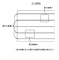
図2は、本発明の実施形態に係る撮像装置による実施イメージの一例を説明する模式図である。ここで、図2には、センサ部(撮像素子)120に設けられた画素部121と、画素部121の各画素から読み出された後の部分画像A及びB、並びに間引き画像Cとの関係を模式的に示している。すなわち、図2では、画素部121に構成された画素のうち、間引き画像(C)用の画素と部分画像(A,B)用の画素が示されている。
図6に示す単位画素121aでは、光電変換部であるフォトダイオードPDと、フォトダイオードPDの信号電荷を画素アンプMSFMのゲート部(フローティングディフュジョン)へ転送制御する転送スイッチMTXと、転送スイッチMVXが接続されている。転送スイッチMTXにより当該画素の水平選択を、転送スイッチMVXで当該画素の垂直選択を転送制御することで画素のランダムアクセスが可能となる。フォトダイオードPDの残留電荷は、転送スイッチMTXと転送スイッチMVX及びリセットスイッチMRESを同時に導通させることで除去される。画素アンプMSFMのゲート部のリセット後のリセット信号、あるいは、フォトダイオードPDからの信号電荷は、セレクトスイッチMSELを導通制御することで、画素アンプMSFMで増幅されて垂直信号線Vhに出力される。画素アンプMSFMの電流源スイッチMRVは、画素の撮像領域の外部に設けられている。後段のCDS回路部(不図示)により、リセット信号と信号電荷の差分処理を行うことで、ゲート部及び画素アンプMSFMのバラツキを除去し、低ノイズを達成している。尚、図6において、制御パルスφSELとφTXは共通の制御線でもあっても良い。
図7に示す単位画素121aには、1つのフォトダイオードPDに対して1つの画素アンプMSFMが構成されている。しかしながら、この場合、画素のランダムアクセス走査はできないが、本発明の主旨を損なうことはない。
図9に示すように、センサ部(撮像素子)120は、画素部121と、画素部121を水平方向(行方向)に走査するための水平シフトレジスタ122と、画素部121を垂直方向(列方向)に走査するための垂直シフトレジスタ123を備えて構成されている。画素部121は、複数の単位画素(121a)を2次元行列状に備えて構成されており、入射した被写体光を画像として撮像する。図9に示す例では、説明を分かり易くするために、画素部121が32行×48列の単位画素から構成されている例を示している。
まず、最大の蓄積時間は、前フレームでの行の読み出しから、次フレームでの読み出しまでである。例えば、図10中に矢印で示したように、行1では、前フレームの読み出しと次フレームの読み出しまでである。その期間中に、他の行で高解像度の部分画像の読み出しを2フレーム分行っているが、その期間中も行1では蓄積動作を継続している。
図11(a)に示す場合は蓄積時間が最大の場合であり、前フレーム読み出しの直後にリセットパルスを入力してリセットを行って蓄積動作を開始し、次フレームの読み出しまで蓄積を継続している例である。図11(b)では、読み出しの途中でリセットパルスを入力しているため、実質の蓄積時間は、当該リセットパルスによるリセット動作の終了後から次フレームの読み出しまでに短縮される例である。
図12に示す例では、具体的に、低解像度の間引き画像の読み出しの駆動周波数に対して、高解像度の部分画像の読み出しの駆動周波数を2倍にした例である。これにより、図11に示した高解像度の第1及び第2の部分画像の読み出し時間と同じ時間に、当該第1及び第2の部分画像の読み出しに加えて、更に、第3及び第4の部分画像の読み出しを追加することも可能である。
かかる構成によれば、低解像度の画像の読み出しと高解像度の画像の読み出しが複雑化すること無く、かつ、フレームレートの低下を防止することができる。
110:光学部
120:センサ部(撮像素子)
130:信号処理回路部
140:記録・通信部
150:タイミング制御回路部
160:システムコントロール回路部
170:再生・表示部
121:画素部
122:水平シフトレジスタ
123:垂直シフトレジスタ
1211:第1の部分画像用の画素
1212:第2の部分画像用の画素
1213:間引き画像用の画素
Claims (11)
- 複数の画素を備えて構成され、入射した被写体光を画像として撮像する画素部と、
前記画素部から画素を間引いて間引き画像を読み出すとともに、前記画素部の複数の部分領域から前記間引き画像よりも高解像度の部分画像を読み出す読み出し手段とを有し、
前記読み出し手段は、前記間引き画像と前記部分画像とをそれぞれ異なる前記画素部の画素から排他的に読み出し、かつ、前記間引き画像と前記部分画像とを異なる撮像フレームとして読み出し、さらに、複数の部分画像を読み出す場合に、前記複数の部分画像を互いに異なるフレームとして読み出し、前記間引き画像と前記複数の部分画像とを交互に読み出すことを特徴とする撮像装置。 - 前記読み出し手段は、前記間引き画像を前記画素部から任意の周期で画素を間引いて読み出しを行い、前記部分画像を前記画素部の間引かれた画素から読み出すことを特徴とする請求項1に記載の撮像装置。
- 前記間引き画像と前記部分画像の露光を独立に制御する制御手段を更に有することを特徴とする請求項1または2に記載の撮像装置。
- 前記読み出し手段は、前記間引き画像の読み出しと、前記部分画像の読み出しとを異なる駆動周波数で行い、前記部分画像の読み出しに係る駆動周波数が、前記間引き画像の読み出しに係る駆動周波数よりも高いことを特徴とする請求項1から3のいずれか1項に記載の撮像装置。
- 前記読み出し手段が、前記間引き画像と前記部分画像とを、互いに連続したフレームとして読み出すことを特徴とする請求項1から4のいずれか1項に記載の撮像装置。
- 前記複数の画素に入射光を結像する光学部をさらに有することを特徴とする請求項1から5のいずれか1項に記載の撮像装置。
- 前記部分領域は、前記間引き画像よりも狭い領域に対応することを特徴とする請求項1から6のいずれか1項に記載の撮像装置。
- 複数の画素を備えて構成され、入射した被写体光を画像として撮像する画素部を有する撮像装置の駆動方法であって、
前記画素部から画素を間引いて間引き画像を読み出すとともに、前記画素部の複数の部分領域から前記間引き画像よりも高解像度の部分画像を読み出す際に、
前記間引き画像と前記部分画像とをそれぞれ異なる前記画素部の画素から排他的に読み出し、かつ、前記間引き画像と前記部分画像とを異なる撮像フレームとして読み出し、さらに、複数の部分画像を読み出す場合に、前記複数の部分画像を互いに異なるフレームとして読み出し、前記間引き画像と前記複数の部分画像とを交互に読み出すことを特徴とする撮像装置の駆動方法。 - 前記間引き画像と前記部分画像とを、互いに連続したフレームとして読み出すことを特徴とする請求項8に記載の撮像装置の駆動方法。
- 複数の画素を含む画素部から信号を読み出す読み出し装置であって、
前記読み出し装置は、前記画素部から画素を間引いて間引き画像を読み出すとともに、前記画素部の複数の部分領域から前記間引き画像よりも高解像度の部分画像を読み出し、
さらに、前記間引き画像と前記部分画像とをそれぞれ異なる前記画素部の画素から排他的に読み出し、かつ、前記間引き画像と前記部分画像とを異なる撮像フレームとして読み出し、さらに、複数の部分画像を読み出す場合に、前記複数の部分画像を互いに異なるフレームとして読み出し、前記間引き画像と前記複数の部分画像とを交互に読み出すことを特徴とする読み出し装置。 - 前記間引き画像と前記部分画像とを、互いに連続したフレームとして読み出すことを特徴とする請求項10に記載の読み出し装置。
Priority Applications (4)
| Application Number | Priority Date | Filing Date | Title |
|---|---|---|---|
| JP2007055769A JP5188080B2 (ja) | 2007-03-06 | 2007-03-06 | 撮像装置、撮像装置の駆動方法、及び読み出し装置 |
| US12/035,804 US7859575B2 (en) | 2007-03-06 | 2008-02-22 | Imaging device and driving method thereof |
| CN2008100852133A CN101262552B (zh) | 2007-03-06 | 2008-03-06 | 成像装置及其驱动方法 |
| US12/945,993 US8624992B2 (en) | 2007-03-06 | 2010-11-15 | Imaging device and driving method thereof |
Applications Claiming Priority (1)
| Application Number | Priority Date | Filing Date | Title |
|---|---|---|---|
| JP2007055769A JP5188080B2 (ja) | 2007-03-06 | 2007-03-06 | 撮像装置、撮像装置の駆動方法、及び読み出し装置 |
Publications (3)
| Publication Number | Publication Date |
|---|---|
| JP2008219594A JP2008219594A (ja) | 2008-09-18 |
| JP2008219594A5 JP2008219594A5 (ja) | 2011-07-07 |
| JP5188080B2 true JP5188080B2 (ja) | 2013-04-24 |
Family
ID=39839081
Family Applications (1)
| Application Number | Title | Priority Date | Filing Date |
|---|---|---|---|
| JP2007055769A Active JP5188080B2 (ja) | 2007-03-06 | 2007-03-06 | 撮像装置、撮像装置の駆動方法、及び読み出し装置 |
Country Status (3)
| Country | Link |
|---|---|
| US (2) | US7859575B2 (ja) |
| JP (1) | JP5188080B2 (ja) |
| CN (1) | CN101262552B (ja) |
Families Citing this family (42)
| Publication number | Priority date | Publication date | Assignee | Title |
|---|---|---|---|---|
| JP5063234B2 (ja) * | 2007-07-20 | 2012-10-31 | キヤノン株式会社 | 撮像装置、撮像システム、及び、撮像装置の動作方法 |
| JP5106052B2 (ja) * | 2007-11-08 | 2012-12-26 | キヤノン株式会社 | 固体撮像素子、撮像システム、及び固体撮像素子の駆動方法 |
| US8390710B2 (en) * | 2007-12-19 | 2013-03-05 | Canon Kabushiki Kaisha | Image pickup system, method for driving image pickup elements, and recording medium |
| JP5288823B2 (ja) * | 2008-02-18 | 2013-09-11 | キヤノン株式会社 | 光電変換装置、及び光電変換装置の製造方法 |
| JP5188292B2 (ja) | 2008-06-30 | 2013-04-24 | キヤノン株式会社 | 撮像システムおよび撮像システムの駆動方法 |
| JP5315039B2 (ja) * | 2008-12-19 | 2013-10-16 | キヤノン株式会社 | 撮像センサ、撮像システム、および、撮像センサの駆動方法 |
| TW201032175A (en) * | 2009-02-18 | 2010-09-01 | Altek Corp | Method of acceleration image capturing process and digital image-capturing device |
| JP5550253B2 (ja) * | 2009-04-22 | 2014-07-16 | キヤノン株式会社 | マーク位置検出装置及びマーク位置検出方法、それを用いた露光装置及びデバイスの製造方法 |
| JP5423125B2 (ja) * | 2009-04-24 | 2014-02-19 | ソニー株式会社 | 固体撮像素子およびその駆動方法、並びにカメラシステム |
| JP5404194B2 (ja) * | 2009-06-05 | 2014-01-29 | キヤノン株式会社 | 固体撮像素子、撮像システム、および固体撮像素子の駆動方法 |
| JP5219962B2 (ja) * | 2009-08-13 | 2013-06-26 | キヤノン株式会社 | 固体撮像素子、その駆動方法、及び撮像システム |
| JP5398846B2 (ja) * | 2009-12-01 | 2014-01-29 | キヤノン株式会社 | 撮像装置及び撮像システム、それらの制御方法及びそのプログラム |
| US8928789B2 (en) | 2010-09-30 | 2015-01-06 | Canon Kabushiki Kaisha | Solid-state imaging apparatus |
| JP5610961B2 (ja) | 2010-09-30 | 2014-10-22 | キヤノン株式会社 | 固体撮像装置及び固体撮像装置の駆動方法 |
| JP5808162B2 (ja) | 2011-06-23 | 2015-11-10 | キヤノン株式会社 | 撮像素子、撮像装置及び撮像素子の駆動方法 |
| GB2492387B (en) * | 2011-06-30 | 2017-07-19 | Cmosis Nv | Pixel array with individual exposure control for a pixel or pixel region |
| EP2800376B1 (en) * | 2011-12-27 | 2016-10-05 | Fujifilm Corporation | Imaging device, method for controlling imaging device, and control program |
| JP5893550B2 (ja) | 2012-04-12 | 2016-03-23 | キヤノン株式会社 | 撮像装置及び撮像システム |
| JP6136170B2 (ja) * | 2012-10-02 | 2017-05-31 | 株式会社ソシオネクスト | 画像処理装置、画像処理方法、及び撮像装置 |
| JP2014197832A (ja) | 2013-03-07 | 2014-10-16 | キヤノン株式会社 | 撮像装置及びその駆動方法 |
| JP2015029259A (ja) | 2013-07-03 | 2015-02-12 | キヤノン株式会社 | 撮像装置、撮像システム、センサおよび撮像装置の動作方法 |
| JP6274788B2 (ja) | 2013-08-28 | 2018-02-07 | キヤノン株式会社 | 撮像装置、撮像システム及び撮像装置の駆動方法 |
| US9924094B2 (en) | 2013-11-25 | 2018-03-20 | Canon Kabushiki Kaisha | Image pickup apparatus capable of changing drive mode and image signal control method |
| JP6230395B2 (ja) | 2013-12-06 | 2017-11-15 | キヤノン株式会社 | 撮像装置およびその駆動方法 |
| JP2015186234A (ja) * | 2014-03-26 | 2015-10-22 | ソニー株式会社 | イメージセンサ、および電子装置 |
| JP6389685B2 (ja) | 2014-07-30 | 2018-09-12 | キヤノン株式会社 | 撮像装置、および、撮像システム |
| US9979916B2 (en) | 2014-11-21 | 2018-05-22 | Canon Kabushiki Kaisha | Imaging apparatus and imaging system |
| US9912886B2 (en) | 2014-12-17 | 2018-03-06 | Canon Kabushiki Kaisha | Image capturing apparatus and driving method of image sensor |
| JP6545013B2 (ja) * | 2015-06-17 | 2019-07-17 | キヤノン株式会社 | 画像形成方法、画像形成装置、および画像形成プログラム |
| US9900539B2 (en) | 2015-09-10 | 2018-02-20 | Canon Kabushiki Kaisha | Solid-state image pickup element, and image pickup system |
| JP6674219B2 (ja) | 2015-10-01 | 2020-04-01 | キヤノン株式会社 | 固体撮像装置及び撮像システム |
| DE102016213494A1 (de) | 2016-07-22 | 2018-01-25 | Conti Temic Microelectronic Gmbh | Kameravorrichtung sowie Verfahren zur Erfassung eines Umgebungsbereichs eines eigenen Fahrzeugs |
| DE102016213493A1 (de) | 2016-07-22 | 2018-01-25 | Conti Temic Microelectronic Gmbh | Kameravorrichtung zur Aufnahme eines Umgebungsbereichs eines eigenen Fahrzeugs sowie Verfahren zur Bereitstellung einer Fahrerassistenzfunktion |
| JP6832155B2 (ja) * | 2016-12-28 | 2021-02-24 | ソニーセミコンダクタソリューションズ株式会社 | 画像処理装置、画像処理方法、及び画像処理システム |
| JP6929671B2 (ja) | 2017-03-17 | 2021-09-01 | キヤノン株式会社 | 撮像装置及び撮像システム |
| JP7150469B2 (ja) | 2018-05-17 | 2022-10-11 | キヤノン株式会社 | 撮像装置及び撮像システム |
| JP7204480B2 (ja) | 2018-12-27 | 2023-01-16 | キヤノン株式会社 | 撮像装置、撮像システム、移動体及び撮像装置の制御方法 |
| US11310451B1 (en) | 2019-09-05 | 2022-04-19 | Waymo Llc | Smart sensor with region of interest capabilities |
| US11252366B2 (en) * | 2019-11-19 | 2022-02-15 | Waymo Llc | Sensor read out mode for high resolution and low light imaging in-sync with LIDAR timing |
| US11428550B2 (en) | 2020-03-03 | 2022-08-30 | Waymo Llc | Sensor region of interest selection based on multisensor data |
| US11950002B2 (en) * | 2020-04-28 | 2024-04-02 | Telefonaktiebolaget Lm Ericsson (Publ) | Analog resolution adjustment for CMOS image sensor |
| US11756283B2 (en) | 2020-12-16 | 2023-09-12 | Waymo Llc | Smart sensor implementations of region of interest operating modes |
Family Cites Families (21)
| Publication number | Priority date | Publication date | Assignee | Title |
|---|---|---|---|---|
| FR2533056B1 (fr) * | 1982-09-14 | 1987-05-15 | Thomson Csf | Imageur a transfert de lignes et camera de television comportant un tel imageur |
| CA1270058A (en) * | 1984-12-28 | 1990-06-05 | Seiji Hashimoto | Image sensing apparatus |
| EP0277016B1 (en) * | 1987-01-29 | 1998-04-15 | Canon Kabushiki Kaisha | Photoelectric conversion apparatus |
| US4959723A (en) * | 1987-11-06 | 1990-09-25 | Canon Kabushiki Kaisha | Solid state image pickup apparatus having multi-phase scanning pulse to read out accumulated signal |
| US5146339A (en) * | 1989-11-21 | 1992-09-08 | Canon Kabushiki Kaisha | Photoelectric converting apparatus employing Darlington transistor readout |
| US5493335A (en) * | 1993-06-30 | 1996-02-20 | Eastman Kodak Company | Single sensor color camera with user selectable image record size |
| JPH09214836A (ja) | 1996-02-07 | 1997-08-15 | Olympus Optical Co Ltd | 撮像装置 |
| US6463178B1 (en) * | 1997-06-16 | 2002-10-08 | Sony Corporation | Image processing device and method, and transmission medium, transmission method and image format |
| JP3965237B2 (ja) * | 1997-12-25 | 2007-08-29 | オリンパス株式会社 | 撮像装置 |
| JP4049896B2 (ja) | 1998-07-09 | 2008-02-20 | オリンパス株式会社 | 画像入力装置 |
| JP4518616B2 (ja) * | 2000-04-13 | 2010-08-04 | ソニー株式会社 | 固体撮像装置およびその駆動方法並びにカメラシステム |
| JP4503878B2 (ja) * | 2001-04-27 | 2010-07-14 | オリンパス株式会社 | 撮像装置及び撮像方法 |
| US7499091B2 (en) * | 2002-03-20 | 2009-03-03 | Sony Corporation | Solid-state imaging device and method for driving same |
| JP4190805B2 (ja) * | 2002-06-12 | 2008-12-03 | オリンパス株式会社 | 撮像装置 |
| US7554590B2 (en) * | 2003-02-26 | 2009-06-30 | Digital Imaging Systems Gmbh | Simultaneous readout of CMOS APS imagers |
| JP4426885B2 (ja) * | 2004-03-23 | 2010-03-03 | オリンパス株式会社 | 固体撮像装置 |
| US7592645B2 (en) * | 2004-12-08 | 2009-09-22 | Canon Kabushiki Kaisha | Photoelectric conversion device and method for producing photoelectric conversion device |
| JP4756960B2 (ja) * | 2005-09-02 | 2011-08-24 | キヤノン株式会社 | 撮像装置及びその制御方法、コンピュータプログラム及び記憶媒体 |
| JP2007110639A (ja) * | 2005-10-17 | 2007-04-26 | Fujifilm Corp | 固体撮像素子、その駆動方法および撮像装置 |
| JP4887750B2 (ja) * | 2005-11-16 | 2012-02-29 | カシオ計算機株式会社 | 画像処理装置、制御方法及びプログラム |
| JP4018727B2 (ja) * | 2006-02-14 | 2007-12-05 | キヤノン株式会社 | 撮像装置及びその制御方法及びプログラム及び記憶媒体 |
-
2007
- 2007-03-06 JP JP2007055769A patent/JP5188080B2/ja active Active
-
2008
- 2008-02-22 US US12/035,804 patent/US7859575B2/en not_active Expired - Fee Related
- 2008-03-06 CN CN2008100852133A patent/CN101262552B/zh active Active
-
2010
- 2010-11-15 US US12/945,993 patent/US8624992B2/en active Active
Also Published As
| Publication number | Publication date |
|---|---|
| US20110058079A1 (en) | 2011-03-10 |
| CN101262552B (zh) | 2011-06-22 |
| JP2008219594A (ja) | 2008-09-18 |
| CN101262552A (zh) | 2008-09-10 |
| US7859575B2 (en) | 2010-12-28 |
| US20080291304A1 (en) | 2008-11-27 |
| US8624992B2 (en) | 2014-01-07 |
Similar Documents
| Publication | Publication Date | Title |
|---|---|---|
| JP5188080B2 (ja) | 撮像装置、撮像装置の駆動方法、及び読み出し装置 | |
| US8836832B2 (en) | Image pickup system, method for driving image pickup elements, and recording medium | |
| JP5106052B2 (ja) | 固体撮像素子、撮像システム、及び固体撮像素子の駆動方法 | |
| JP5063234B2 (ja) | 撮像装置、撮像システム、及び、撮像装置の動作方法 | |
| JP4208904B2 (ja) | 撮像装置及びその制御方法並びに撮像システム | |
| JP4424753B2 (ja) | 固体撮像装置及びその駆動方法 | |
| JP5101946B2 (ja) | 撮像装置及び撮像システム | |
| JP4018727B2 (ja) | 撮像装置及びその制御方法及びプログラム及び記憶媒体 | |
| JP6222915B2 (ja) | 撮像装置、撮像装置の駆動方法、プログラム及び記録媒体 | |
| JP4497872B2 (ja) | 撮像装置 | |
| JP4609092B2 (ja) | 物理情報取得方法および物理情報取得装置 | |
| US7633536B2 (en) | Image capturing apparatus | |
| JP2007150643A (ja) | 固体撮像素子、固体撮像素子の駆動方法および撮像装置 | |
| JP2007104178A (ja) | 撮像素子および撮像装置 | |
| JP5721518B2 (ja) | 撮像素子及び撮像装置 | |
| JP2007129581A (ja) | 撮像装置及び撮像システム | |
| JP2004140479A (ja) | 固体撮像装置、カメラ装置、及びその制御方法 | |
| JP4678849B2 (ja) | 撮像装置及びその制御方法及びプログラム及び記憶媒体 | |
| JP5207905B2 (ja) | 撮像システム、撮像素子の駆動方法、プログラム、及び記録媒体 | |
| JP2002057943A (ja) | 撮像装置 | |
| JP2014017551A (ja) | 撮像装置及びその制御方法 | |
| JP5072466B2 (ja) | 撮像装置 | |
| JP2009225341A (ja) | 固体撮像装置及びその駆動方法 | |
| JP2008300931A (ja) | 撮像装置 | |
| JP5173862B2 (ja) | 撮像装置及びその制御方法 |
Legal Events
| Date | Code | Title | Description |
|---|---|---|---|
| A521 | Request for written amendment filed |
Free format text: JAPANESE INTERMEDIATE CODE: A523 Effective date: 20100302 |
|
| A621 | Written request for application examination |
Free format text: JAPANESE INTERMEDIATE CODE: A621 Effective date: 20100302 |
|
| A521 | Request for written amendment filed |
Free format text: JAPANESE INTERMEDIATE CODE: A523 Effective date: 20110518 |
|
| A977 | Report on retrieval |
Free format text: JAPANESE INTERMEDIATE CODE: A971007 Effective date: 20120201 |
|
| A131 | Notification of reasons for refusal |
Free format text: JAPANESE INTERMEDIATE CODE: A131 Effective date: 20120207 |
|
| A521 | Request for written amendment filed |
Free format text: JAPANESE INTERMEDIATE CODE: A523 Effective date: 20120405 |
|
| A131 | Notification of reasons for refusal |
Free format text: JAPANESE INTERMEDIATE CODE: A131 Effective date: 20120731 |
|
| A521 | Request for written amendment filed |
Free format text: JAPANESE INTERMEDIATE CODE: A523 Effective date: 20120927 |
|
| TRDD | Decision of grant or rejection written | ||
| A01 | Written decision to grant a patent or to grant a registration (utility model) |
Free format text: JAPANESE INTERMEDIATE CODE: A01 Effective date: 20130115 |
|
| A61 | First payment of annual fees (during grant procedure) |
Free format text: JAPANESE INTERMEDIATE CODE: A61 Effective date: 20130122 |
|
| FPAY | Renewal fee payment (event date is renewal date of database) |
Free format text: PAYMENT UNTIL: 20160201 Year of fee payment: 3 |
|
| R151 | Written notification of patent or utility model registration |
Ref document number: 5188080 Country of ref document: JP Free format text: JAPANESE INTERMEDIATE CODE: R151 |
|
| FPAY | Renewal fee payment (event date is renewal date of database) |
Free format text: PAYMENT UNTIL: 20160201 Year of fee payment: 3 |