EP2752078B1 - Système de chauffage haute définition à milieu fluide - Google Patents
Système de chauffage haute définition à milieu fluide Download PDFInfo
- Publication number
- EP2752078B1 EP2752078B1 EP12769785.2A EP12769785A EP2752078B1 EP 2752078 B1 EP2752078 B1 EP 2752078B1 EP 12769785 A EP12769785 A EP 12769785A EP 2752078 B1 EP2752078 B1 EP 2752078B1
- Authority
- EP
- European Patent Office
- Prior art keywords
- heater
- tuning layer
- tuning
- layer
- base member
- Prior art date
- Legal status (The legal status is an assumption and is not a legal conclusion. Google has not performed a legal analysis and makes no representation as to the accuracy of the status listed.)
- Active
Links
- 239000012530 fluid Substances 0.000 title claims description 21
- 238000010438 heat treatment Methods 0.000 claims description 26
- 239000000758 substrate Substances 0.000 claims description 23
- 239000000463 material Substances 0.000 claims description 20
- 238000004891 communication Methods 0.000 claims description 10
- 238000001816 cooling Methods 0.000 claims description 7
- RYGMFSIKBFXOCR-UHFFFAOYSA-N Copper Chemical compound [Cu] RYGMFSIKBFXOCR-UHFFFAOYSA-N 0.000 claims description 4
- 239000004642 Polyimide Substances 0.000 claims description 4
- XAGFODPZIPBFFR-UHFFFAOYSA-N aluminium Chemical compound [Al] XAGFODPZIPBFFR-UHFFFAOYSA-N 0.000 claims description 4
- 229910052782 aluminium Inorganic materials 0.000 claims description 4
- 229910052802 copper Inorganic materials 0.000 claims description 4
- 239000010949 copper Substances 0.000 claims description 4
- 239000007788 liquid Substances 0.000 claims description 4
- 229920001721 polyimide Polymers 0.000 claims description 4
- 239000003507 refrigerant Substances 0.000 claims description 4
- OKTJSMMVPCPJKN-UHFFFAOYSA-N Carbon Chemical compound [C] OKTJSMMVPCPJKN-UHFFFAOYSA-N 0.000 claims description 3
- 229910002804 graphite Inorganic materials 0.000 claims description 3
- 239000010439 graphite Substances 0.000 claims description 3
- 238000010276 construction Methods 0.000 claims description 2
- NJPPVKZQTLUDBO-UHFFFAOYSA-N novaluron Chemical compound C1=C(Cl)C(OC(F)(F)C(OC(F)(F)F)F)=CC=C1NC(=O)NC(=O)C1=C(F)C=CC=C1F NJPPVKZQTLUDBO-UHFFFAOYSA-N 0.000 claims description 2
- PMHQVHHXPFUNSP-UHFFFAOYSA-M copper(1+);methylsulfanylmethane;bromide Chemical compound Br[Cu].CSC PMHQVHHXPFUNSP-UHFFFAOYSA-M 0.000 claims 1
- 239000010410 layer Substances 0.000 description 92
- 238000012545 processing Methods 0.000 description 17
- 239000004065 semiconductor Substances 0.000 description 13
- 238000000034 method Methods 0.000 description 9
- 230000004907 flux Effects 0.000 description 5
- 239000012790 adhesive layer Substances 0.000 description 3
- 239000013464 silicone adhesive Substances 0.000 description 3
- PXHVJJICTQNCMI-UHFFFAOYSA-N Nickel Chemical compound [Ni] PXHVJJICTQNCMI-UHFFFAOYSA-N 0.000 description 2
- 239000010408 film Substances 0.000 description 2
- 239000011888 foil Substances 0.000 description 2
- 239000007789 gas Substances 0.000 description 2
- 239000002346 layers by function Substances 0.000 description 2
- 238000012986 modification Methods 0.000 description 2
- 230000004048 modification Effects 0.000 description 2
- 229910001030 Iron–nickel alloy Inorganic materials 0.000 description 1
- 239000004820 Pressure-sensitive adhesive Substances 0.000 description 1
- XUIMIQQOPSSXEZ-UHFFFAOYSA-N Silicon Chemical compound [Si] XUIMIQQOPSSXEZ-UHFFFAOYSA-N 0.000 description 1
- 238000009825 accumulation Methods 0.000 description 1
- 239000000853 adhesive Substances 0.000 description 1
- 230000001070 adhesive effect Effects 0.000 description 1
- 230000000712 assembly Effects 0.000 description 1
- 238000000429 assembly Methods 0.000 description 1
- 230000015556 catabolic process Effects 0.000 description 1
- 239000012809 cooling fluid Substances 0.000 description 1
- 239000000112 cooling gas Substances 0.000 description 1
- 238000012937 correction Methods 0.000 description 1
- 230000007423 decrease Effects 0.000 description 1
- 238000006731 degradation reaction Methods 0.000 description 1
- 230000001419 dependent effect Effects 0.000 description 1
- 230000008021 deposition Effects 0.000 description 1
- 238000013461 design Methods 0.000 description 1
- 230000009977 dual effect Effects 0.000 description 1
- 229910001026 inconel Inorganic materials 0.000 description 1
- 238000012423 maintenance Methods 0.000 description 1
- 238000004519 manufacturing process Methods 0.000 description 1
- 238000005259 measurement Methods 0.000 description 1
- 239000000203 mixture Substances 0.000 description 1
- 229910052759 nickel Inorganic materials 0.000 description 1
- 230000003287 optical effect Effects 0.000 description 1
- TWNQGVIAIRXVLR-UHFFFAOYSA-N oxo(oxoalumanyloxy)alumane Chemical compound O=[Al]O[Al]=O TWNQGVIAIRXVLR-UHFFFAOYSA-N 0.000 description 1
- 230000035945 sensitivity Effects 0.000 description 1
- 229910052710 silicon Inorganic materials 0.000 description 1
- 239000010703 silicon Substances 0.000 description 1
- 239000007787 solid Substances 0.000 description 1
- 230000000153 supplemental effect Effects 0.000 description 1
- 230000008542 thermal sensitivity Effects 0.000 description 1
- 238000007751 thermal spraying Methods 0.000 description 1
- 239000010409 thin film Substances 0.000 description 1
- 238000012546 transfer Methods 0.000 description 1
- 239000011800 void material Substances 0.000 description 1
Images


Classifications
-
- H—ELECTRICITY
- H01—ELECTRIC ELEMENTS
- H01L—SEMICONDUCTOR DEVICES NOT COVERED BY CLASS H10
- H01L21/00—Processes or apparatus adapted for the manufacture or treatment of semiconductor or solid state devices or of parts thereof
- H01L21/67—Apparatus specially adapted for handling semiconductor or electric solid state devices during manufacture or treatment thereof; Apparatus specially adapted for handling wafers during manufacture or treatment of semiconductor or electric solid state devices or components ; Apparatus not specifically provided for elsewhere
- H01L21/67005—Apparatus not specifically provided for elsewhere
- H01L21/67011—Apparatus for manufacture or treatment
- H01L21/67098—Apparatus for thermal treatment
- H01L21/67103—Apparatus for thermal treatment mainly by conduction
-
- H—ELECTRICITY
- H01—ELECTRIC ELEMENTS
- H01L—SEMICONDUCTOR DEVICES NOT COVERED BY CLASS H10
- H01L21/00—Processes or apparatus adapted for the manufacture or treatment of semiconductor or solid state devices or of parts thereof
- H01L21/67—Apparatus specially adapted for handling semiconductor or electric solid state devices during manufacture or treatment thereof; Apparatus specially adapted for handling wafers during manufacture or treatment of semiconductor or electric solid state devices or components ; Apparatus not specifically provided for elsewhere
- H01L21/67005—Apparatus not specifically provided for elsewhere
- H01L21/67011—Apparatus for manufacture or treatment
- H01L21/67098—Apparatus for thermal treatment
- H01L21/67109—Apparatus for thermal treatment mainly by convection
-
- H—ELECTRICITY
- H01—ELECTRIC ELEMENTS
- H01L—SEMICONDUCTOR DEVICES NOT COVERED BY CLASS H10
- H01L21/00—Processes or apparatus adapted for the manufacture or treatment of semiconductor or solid state devices or of parts thereof
- H01L21/67—Apparatus specially adapted for handling semiconductor or electric solid state devices during manufacture or treatment thereof; Apparatus specially adapted for handling wafers during manufacture or treatment of semiconductor or electric solid state devices or components ; Apparatus not specifically provided for elsewhere
- H01L21/67005—Apparatus not specifically provided for elsewhere
- H01L21/67242—Apparatus for monitoring, sorting or marking
- H01L21/67248—Temperature monitoring
-
- H—ELECTRICITY
- H01—ELECTRIC ELEMENTS
- H01L—SEMICONDUCTOR DEVICES NOT COVERED BY CLASS H10
- H01L21/00—Processes or apparatus adapted for the manufacture or treatment of semiconductor or solid state devices or of parts thereof
- H01L21/67—Apparatus specially adapted for handling semiconductor or electric solid state devices during manufacture or treatment thereof; Apparatus specially adapted for handling wafers during manufacture or treatment of semiconductor or electric solid state devices or components ; Apparatus not specifically provided for elsewhere
- H01L21/683—Apparatus specially adapted for handling semiconductor or electric solid state devices during manufacture or treatment thereof; Apparatus specially adapted for handling wafers during manufacture or treatment of semiconductor or electric solid state devices or components ; Apparatus not specifically provided for elsewhere for supporting or gripping
- H01L21/6831—Apparatus specially adapted for handling semiconductor or electric solid state devices during manufacture or treatment thereof; Apparatus specially adapted for handling wafers during manufacture or treatment of semiconductor or electric solid state devices or components ; Apparatus not specifically provided for elsewhere for supporting or gripping using electrostatic chucks
- H01L21/6833—Details of electrostatic chucks
-
- H—ELECTRICITY
- H01—ELECTRIC ELEMENTS
- H01L—SEMICONDUCTOR DEVICES NOT COVERED BY CLASS H10
- H01L21/00—Processes or apparatus adapted for the manufacture or treatment of semiconductor or solid state devices or of parts thereof
- H01L21/67—Apparatus specially adapted for handling semiconductor or electric solid state devices during manufacture or treatment thereof; Apparatus specially adapted for handling wafers during manufacture or treatment of semiconductor or electric solid state devices or components ; Apparatus not specifically provided for elsewhere
- H01L21/683—Apparatus specially adapted for handling semiconductor or electric solid state devices during manufacture or treatment thereof; Apparatus specially adapted for handling wafers during manufacture or treatment of semiconductor or electric solid state devices or components ; Apparatus not specifically provided for elsewhere for supporting or gripping
- H01L21/6835—Apparatus specially adapted for handling semiconductor or electric solid state devices during manufacture or treatment thereof; Apparatus specially adapted for handling wafers during manufacture or treatment of semiconductor or electric solid state devices or components ; Apparatus not specifically provided for elsewhere for supporting or gripping using temporarily an auxiliary support
-
- H—ELECTRICITY
- H05—ELECTRIC TECHNIQUES NOT OTHERWISE PROVIDED FOR
- H05B—ELECTRIC HEATING; ELECTRIC LIGHT SOURCES NOT OTHERWISE PROVIDED FOR; CIRCUIT ARRANGEMENTS FOR ELECTRIC LIGHT SOURCES, IN GENERAL
- H05B1/00—Details of electric heating devices
-
- H—ELECTRICITY
- H05—ELECTRIC TECHNIQUES NOT OTHERWISE PROVIDED FOR
- H05B—ELECTRIC HEATING; ELECTRIC LIGHT SOURCES NOT OTHERWISE PROVIDED FOR; CIRCUIT ARRANGEMENTS FOR ELECTRIC LIGHT SOURCES, IN GENERAL
- H05B1/00—Details of electric heating devices
- H05B1/02—Automatic switching arrangements specially adapted to apparatus ; Control of heating devices
- H05B1/0202—Switches
-
- H—ELECTRICITY
- H05—ELECTRIC TECHNIQUES NOT OTHERWISE PROVIDED FOR
- H05B—ELECTRIC HEATING; ELECTRIC LIGHT SOURCES NOT OTHERWISE PROVIDED FOR; CIRCUIT ARRANGEMENTS FOR ELECTRIC LIGHT SOURCES, IN GENERAL
- H05B1/00—Details of electric heating devices
- H05B1/02—Automatic switching arrangements specially adapted to apparatus ; Control of heating devices
- H05B1/0227—Applications
- H05B1/023—Industrial applications
- H05B1/0233—Industrial applications for semiconductors manufacturing
-
- H—ELECTRICITY
- H05—ELECTRIC TECHNIQUES NOT OTHERWISE PROVIDED FOR
- H05B—ELECTRIC HEATING; ELECTRIC LIGHT SOURCES NOT OTHERWISE PROVIDED FOR; CIRCUIT ARRANGEMENTS FOR ELECTRIC LIGHT SOURCES, IN GENERAL
- H05B3/00—Ohmic-resistance heating
- H05B3/02—Details
-
- H—ELECTRICITY
- H05—ELECTRIC TECHNIQUES NOT OTHERWISE PROVIDED FOR
- H05B—ELECTRIC HEATING; ELECTRIC LIGHT SOURCES NOT OTHERWISE PROVIDED FOR; CIRCUIT ARRANGEMENTS FOR ELECTRIC LIGHT SOURCES, IN GENERAL
- H05B3/00—Ohmic-resistance heating
- H05B3/02—Details
- H05B3/06—Heater elements structurally combined with coupling elements or holders
-
- H—ELECTRICITY
- H05—ELECTRIC TECHNIQUES NOT OTHERWISE PROVIDED FOR
- H05B—ELECTRIC HEATING; ELECTRIC LIGHT SOURCES NOT OTHERWISE PROVIDED FOR; CIRCUIT ARRANGEMENTS FOR ELECTRIC LIGHT SOURCES, IN GENERAL
- H05B3/00—Ohmic-resistance heating
- H05B3/20—Heating elements having extended surface area substantially in a two-dimensional plane, e.g. plate-heater
-
- H—ELECTRICITY
- H05—ELECTRIC TECHNIQUES NOT OTHERWISE PROVIDED FOR
- H05B—ELECTRIC HEATING; ELECTRIC LIGHT SOURCES NOT OTHERWISE PROVIDED FOR; CIRCUIT ARRANGEMENTS FOR ELECTRIC LIGHT SOURCES, IN GENERAL
- H05B2203/00—Aspects relating to Ohmic resistive heating covered by group H05B3/00
- H05B2203/002—Heaters using a particular layout for the resistive material or resistive elements
- H05B2203/005—Heaters using a particular layout for the resistive material or resistive elements using multiple resistive elements or resistive zones isolated from each other
-
- H—ELECTRICITY
- H05—ELECTRIC TECHNIQUES NOT OTHERWISE PROVIDED FOR
- H05B—ELECTRIC HEATING; ELECTRIC LIGHT SOURCES NOT OTHERWISE PROVIDED FOR; CIRCUIT ARRANGEMENTS FOR ELECTRIC LIGHT SOURCES, IN GENERAL
- H05B2203/00—Aspects relating to Ohmic resistive heating covered by group H05B3/00
- H05B2203/013—Heaters using resistive films or coatings
-
- H—ELECTRICITY
- H05—ELECTRIC TECHNIQUES NOT OTHERWISE PROVIDED FOR
- H05B—ELECTRIC HEATING; ELECTRIC LIGHT SOURCES NOT OTHERWISE PROVIDED FOR; CIRCUIT ARRANGEMENTS FOR ELECTRIC LIGHT SOURCES, IN GENERAL
- H05B2213/00—Aspects relating both to resistive heating and to induction heating, covered by H05B3/00 and H05B6/00
- H05B2213/03—Heating plates made out of a matrix of heating elements that can define heating areas adapted to cookware randomly placed on the heating plate
-
- Y—GENERAL TAGGING OF NEW TECHNOLOGICAL DEVELOPMENTS; GENERAL TAGGING OF CROSS-SECTIONAL TECHNOLOGIES SPANNING OVER SEVERAL SECTIONS OF THE IPC; TECHNICAL SUBJECTS COVERED BY FORMER USPC CROSS-REFERENCE ART COLLECTIONS [XRACs] AND DIGESTS
- Y10—TECHNICAL SUBJECTS COVERED BY FORMER USPC
- Y10T—TECHNICAL SUBJECTS COVERED BY FORMER US CLASSIFICATION
- Y10T156/00—Adhesive bonding and miscellaneous chemical manufacture
- Y10T156/10—Methods of surface bonding and/or assembly therefor
Definitions
- the present disclosure relates to heater systems, and in particular, heater systems that can deliver a precise temperature profile to a heating target during operation in order to compensate for heat loss and/or other variations, in such applications as chucks or susceptors for use in semiconductor processing.
- a chuck or susceptor is used to hold a substrate (or wafer) and to provide a uniform temperature profile to the substrate during processing.
- a support assembly 10 for an electrostatic chuck is illustrated, which includes the electrostatic chuck 12 with an embedded electrode 14, and a heater plate 16 that is bonded to the electrostatic chuck 12 through an adhesive layer 18, which is typically a silicone adhesive.
- a heater 20 is secured to the heater plate 16, which may be an etched-foil heater, by way of example.
- This heater assembly is bonded to a cooling plate 22, again through an adhesive layer 24 that is typically a silicone adhesive.
- the substrate 26 is disposed on the electrostatic chuck 12, and the electrode 14 is connected to a voltage source (not shown) such that electrostatic power is generated, which holds the substrate 26 in place.
- a radio frequency (RF) or microwave power source may be coupled to the electrostatic chuck 12 within a plasma reactor chamber that surrounds the support assembly 10.
- the heater 20 thus provides requisite heat to maintain temperature on the substrate 26 during various in-chamber plasma semiconductor processing steps, including plasma-enhanced film deposition or etch.
- the invention concerns an apparatus according to claim 1.
- one form of the present disclosure is a heater 50 that includes a base heater layer 52 having at least one heater circuit 54 embedded therein.
- the base heater layer 52 has at least one aperture 56 (or via) formed therethrough for connecting the heater circuit 54 to a power supply (not shown).
- the base heater layer 52 provides primary heating while a tuning heater layer 60 disposed proximate the heater layer 52 as shown provides for fine tuning of a heat distribution provided by the heater 50.
- the tuning layer 60 includes a plurality of individual heating elements 62 embedded therein, which are independently controlled. At least one aperture 64 is formed through the tuning layer 60 for connecting the plurality of individual heating elements 62 to the power supply and controller (not shown).
- a routing layer 66 is disposed between the base heater layer 52 and the tuning layer 60 and defines an internal cavity 68.
- a first set of electrical leads 70 connects the heater circuit 54 to the power supply, which extend through the heater layer aperture 56.
- a second set of electrical leads 72 connects a plurality of heating elements 62 to the power supply and extend through the internal cavity 68 of the routing layer 66, in addition to the aperture 55 in the base heater layer 52.
- the routing layer 66 is optional, and the heater 50 could be employed without the routing layer 66 and instead having only the base heater layer 52 and the tuning heater layer 60.
- the tuning layer 60 may alternately be used to measure temperature in the chuck 12.
- This form provides for a plurality of area-specific or discreet locations, of temperature dependent resistance circuits.
- Each of these temperature sensors can be individually read via a multiplexing switching arrangement, exemplary forms of which are set forth in greater detail below, that allows substantially more sensors to be used relative to the number of signal wires required to measure each individual sensor.
- the temperature sensing feedback can provide necessary information for control decisions, for instance, to control a specific zone of backside cooling gas pressure to regulate heat flux from the substrate 26 to the chuck 12.
- This same feedback can also be used to replace or augment temperature sensors installed near the base heater 50 for temperature control of base heating zones 54 or balancing plate cooling fluid temperature (not shown) via ancillary cool fluid heat exchangers.
- the base heater layer 50 and the tuning heater layer 60 are formed from enclosing heater circuit 54 and tuning layer heating elements 62 in a polyimide material for medium temperature applications, which are generally below 250° C. Further, the polyimide material may be doped with materials in order to increase thermal conductivity.
- the base heater layer 50 and/or the tuning heater layer 60 are formed by a layered process, wherein the layer is formed through application or accumulation of a material to a substrate or another layer using processes associated with thick film, thin film, thermal spraying, or sol-gel, among others.
- the base heating circuit 54 is formed from Inconel® and the tuning layer heating elements 62 are a Nickel material.
- the tuning layer heating elements 62 are formed of a material having sufficient temperature coefficient of resistance such that the elements function as both heaters and temperature sensors, commonly referred to as "two-wire control.” Such heaters and their materials are disclosed in U.S. Patent No. 7,196,295 and pending U.S. patent application serial no. 11/475,534 .
- various forms of the present disclosure include temperature, power, and/or thermal impedence based control over the layer heating elements 62 through knowledge or measurement of voltage and/or current applied to each of the individual elements in the thermal impedance tuning layer 60, converted to electrical power and resistance through multiplication and division, corresponding in the first instance, identically to the heat flux output from each of these elements and in the second, a known relationship to the element temperature.
- these can be used to calculate and monitor the thermal impedance load on each element to allow an operator or control system to detect and compensate for area-specific thermal changes that may result from, but are not limited to, physical changes in the chamber or chuck due to use or maintenance, processing errors, and equipment degradation.
- each of the individually controlled heating elements in the thermal impedance tuning layer 60 can be assigned a setpoint resistance corresponding to the same or different specific temperatures which then modify or gate the heat flux originating from corresponding areas on a substrate through to the base heater layer 52 to control the substrate temperature during semiconductor processing.
- the base heater 50 is bonded to a chuck 51, for example, by using a silicone adhesive or even a pressure sensitive adhesive. Therefore, the heater layer 52 provides primary heating, and the tuning layer 60 fine tunes, or adjusts, the heating profile such that a uniform or desired temperature profile is provided to the chuck 51, and thus the substrate (not shown).
- the coefficient of thermal expansion (CTE) of the tuning layer heating elements 62 is matched to the CTE of the tuning heating layer substrate 60 in order to improve thermal sensitivity of the tuning layer heating elements 62 when exposed to strain loads.
- CTE coefficient of thermal expansion
- Many suitable materials for two-wire control exhibit similar characteristics to Resistor Temperature Devices (RTDs), including resistance sensitivity to both temperature and strain. Matching the CTE of the tuning layer heating elements 62 to the tuning heater layer substrate 60 reduces strain on the actual heating element. And as the operating temperatures increase, strain levels tend to increase, and thus CTE matching becomes more of a factor.
- the tuning layer heating elements 62 are a high purity Nickel-Iron alloy having a CTE of approximately 15 ppm/°C, and the polyimide material that encloses it has a CTE of approximately 16 ppm/°C.
- materials that bond the tuning heater layer 60 to the other layers exhibit elastic characteristics that physically decouple the tuning heater layer 60 from other members of the chuck 12. It should be understood that other materials with comparable CTEs may also be employed while remaining within the scope of the present disclosure.
- the heater 80 includes a base plate 82, (also referred to as a cooling plate), which in one form is an Aluminum plate approximately 16mm in thickness.
- a base heater 84 is secured to the base plate 82, in one form using an elastomeric bond layer 86 as shown.
- the elastomeric bond may be one disclosed in U.S. Patent No. 6,073,577 .
- a substrate 88 is disposed on top of the base heater 84 and is an Aluminum material approximately 1mm in thickness according to one form of the present disclosure.
- the substrate 88 is designed to have a thermal conductivity to dissipate a requisite amount of power from the base heater 84. Because the base heater 84 has relatively high power, without a requisite amount of thermal conductivity, this base heater 84 would leave "witness" marks (from the resistive circuit trace) on adjacent components, thereby reducing the performance of the overall heater system.
- a tuning heater 90 is disposed on top of the substrate 88 and is secured to a chuck 92 using an elastomeric bond layer 94, as set forth above.
- the chuck 92 in one form is an Aluminum Oxide material having a thickness of approximately 2.5mm. It should be understood that the materials and dimensions as set forth herein are merely exemplary and thus the present disclosure is not limited to the specific forms as set forth herein.
- the tuning heater 90 has lower power than the base heater 84, and as set forth above, the substrate 88 functions to dissipate power from the base heater 84 such that "witness" marks do not form on the tuning heater 90.
- the base heater 84 and the tuning heater 90 are shown in greater detail in FIG. 4 , in which an exemplary four (4) zones are shown for the base heater 84, and eighteen (18) zones for the tuning heater 90.
- the heater 80 is adapted for use with chuck sizes of 450mm, however, the heater 80 may be employed with larger or smaller chuck sizes due to its ability to highly tailor the heat distribution.
- the high definition heater 80 may be employed around a periphery (shown by area P) of the chuck (across a horizonal plane), or along a vertical location, FIG.
- tuning layer 90' or in discrete predetermined locations across or along the chuck, or around the periphery other components or combinations of components, rather than in a stacked/planar configuration as illustrated herein.
- the high definition heater 80 may be employed in process kits, chamber walls, lids, gas lines, and showerheads, among other components within semiconductor processing equipment. It should also be understood that the heaters and control systems illustrated and described herein may be employed in any number of applications, and thus the exemplary semiconductor heater chuck application should not be construed as limiting the scope of the present disclosure.
- the base heater 84 and the tuning heater 90 not be limited to a heating function. It should be understood that one or more of these members, referred to as a "base functional layer” and a “tuning layer,” respectively, may alternately be a temperature sensor layer or other functional member while remaining within the scope of the present disclosure. Other functions may include, by way of example, a cooling layer or a a diagnostic layer that would collect sensor input such as various electrical characteristics, among others.
- a dual tuning capability may be provided with the inclusion of a secondary tuning layer heater 120 on the top surface of the chuck 12.
- the secondary tuning layer may alternately be used as a temperature sensing layer rather than a heating layer while remaining within the scope of the present disclosure. Accordingly, any number of tuning layer heaters may be employed and should not be limited to those illustrated and described herein.
- the base functional layer may include a plurality of thermoelectric elements rather than the base heater 84 construction as set forth above. These thermoelectric elements may also be arranged in zones and are generally disposed on top of, or proximate, the base plate or cooling plate 82.
- the multiple tuning layers may be employed in a "stacked" configuration, or configured vertically such that individual resistive traces are offset from adjacent resistive traces on opposed layers to compensate for the gaps that exist between traces.
- a first tuning layer 130 is offset from a second tuning layer 140 such that the traces 142 of tuning layer 140 are aligned adjacent the gaps 132 between the traces 134 of the first tuning layer 130, and vice versa.
- a "checkerboard" design may be employed in order to compensate for gaps or hot spots between adjacent layers.
- the threshold voltage switching circuits which in one form comprise discrete solid state devices that electrically conduct in one direction when the voltage threshold across the circuit is exceeded and which, are embedded into or attached to the body of the heater chuck, which may be in a packaged form or generally embedded as bare die components.
- the control elements are embedded in the bond layer 86 as illustrated above. It should be understood that the control elements may be embedded within any of the components or assemblies thereof while remaining within the scope of the present disclosure.
- the threshold voltage switching circuits on a single package silicon controls device (ASIC) may be embedded into or attached to the chuck in one form of the present disclosure. Additional controls devices may also be employed in order to provide redundancy should any of the components fail during operation.
- FIGS. 8-12 One exemplary form of embedding controls is illustrated in FIGS. 8-12 .
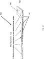
- the heater system 200 comprises a plurality of independently controllable heater elements 202, the operation of which is set forth in greater detail below, in order to provide a highly tailored temperature profile to a heating target, such as a uniform temperature profile to a substrate in semiconductor processing as set forth above.
- An upper base 204 is disposed proximate the heater elements 202, and in one form, the heater elements 202 are disposed on the upper base 204, such as an etched foil bonded to or a layered heater deposited onto the upper base 204.
- the upper base 204 defines a plurality of tapered cavities 206, which are aligned with each of the heater elements.
- the tapered cavities 206 in this form include an upper wall 208 and tapered side walls 210 as shown.
- the upper base 204 further comprises a plurality of power vias 212 in order to provide a passageway for power and control lines, as set forth below.
- a lower base 220 is adjacent the upper base 204 and defines a plurality of reverse tapered cavities 222 aligned with the tapered cavities 206 of the upper base 204.
- the reverse tapered cavities 222 similarly define a lower wall 224 and tapered sidewalls 226.
- the lower base 220 further comprises a plurality of power vias 228 in communication with the power vias 212 of the upper base 204, which also serve as passageways for power and control lines.
- the shape of the cavities 206, 222 are configured to provide for an efficient transfer of heat from the heater elements 202 to a cooling plate (shown as element 22 in FIG. 1 ) and also to reduce the thermal impact of the cavities and their components on the performance and temperature profile provided by the heater elements 202. Accordingly, the "footprint" of the cavity is smaller near the heater elements 202, and the cavity gradually increases in size to direct the heat flux around the cavity 206, and then gradually decreases in size to direct the heat flux around the cavity 222 towards the cooling plate 22. It should be understood that other geometries for the cavities 206 and 222 may be provided by the present disclosure, and thus the tapered configurations should not be construed as limiting the scope of the present disclosure.
- a plurality of pairs of switching elements 230 and control elements 232 are disposed within the reverse tapered cavities 222 of the lower base 220 and in communication with the plurality of heater elements 202.
- the switching elements 230 and control elements 232 control operation of the heater elements 202 in order to provide a requisite temperature profile, and in one application, a uniform temperature profile to the substrate in semiconductor processing equipment as set forth above.
- the control element is a microprocessor.
- the control element is a circuit in accordance with the raster boost heater as set forth above.
- the control elements 232 communicate across a digital bus 234 for temperature control of the heater elements 202.
- the heater system 200 further comprises a multiplexer 240 in communication with each of the control elements 232, which sends the appropriate control signals to each of the heater elements 202 for a desired temperature profile.
- the multiplexer 240 communicates with a power supply (not shown) through an optical bus 242.
- the heater system 200 may also include a plurality of discrete temperature sensors 250 disposed proximate the plurality of heater elements 202.
- the heater elements 202 comprise a resistive material having sufficient temperature coefficient of resistance characteristics such that the resistive material functions as both a heater and a temperature sensor, as set forth herein in other forms of the present disclosure.
- the heater system 200 further comprises an RF filter 260, which in one form is in communication with a digital bus 262.
- Temperature calibration of any of the systems set forth herein may be performed by first measuring the individual resistances of the tuning layer heaters using a standard resistance meter.
- the tuning layer heater elements 62 may be held at a constant temperature and pulsed as in normal operation but for short duration only, and then the resistance is calculated and set into the control system. An iterative technique of this at the same or multiple temperature points will calibrate the system for control.
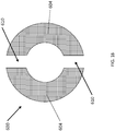
- the apparatus 300 which is a heater in one form of the present disclosure, includes a base member 310 having at least one fluid passageway 320. Multiple fluid passageways 320 are illustrated in this form, and the passageways 320 may further define zones (such as the heater zones as set forth above) in another form of the present disclosure.
- a two-phase fluid 325 is disposed within the fluid passageways 320, and a pressure of the two-phase fluid 325 is controlled such that the two-phase fluid 325 provides heating to the base member 310.
- This system is described in greater detail, for example, in U.S. Patent Nos. 7,178,353 and 7,415,835 and also in published U.S.
- pressurized refrigerant is provided as a condensed liquid and also in a gaseous state.
- the condensed liquid is expanded to a vaporous mix, and the gaseous refrigerant is added to reach a target temperature determined by its pressure. Temperature corrections can thus be made very rapidly by gas pressure adjustments.
- Such systems are provided by Advanced Thermal Sciences Corporation and may be employed with the teachings of the present disclosure.
- a tuning layer 330 is secured to the base member 310, for example with an adhesive layer 332, wherein the tuning layer 330 comprising a plurality of zones 335.
- This tuning layer 330 is similar to the tuning layers and heaters set forth above, and as such, will not be described again in detail for purposes of clarity. Similar to the forms set forth above, the tuning layer 335 has lower power than the base member 310.
- a component 340 such as by way of example, a chuck, a pedestal, a wafer table, a substrate support, or a showerhead, is secured to the tuning layer 330.
- a "component” should be construed to mean any member or assembly on which a wafer is supported, either directly or indirectly, for processing.
- the tuning layer 330 is a heater, and yet in another form, the tuning layer 330 is a temperature sensor, as set forth in detail above.
- This tuning layer 330, and also the base member 310, may be designed with a material having sufficient TCR characteristics such that they function as both a heater and as a temperature sensor.
- a secondary tuning layer (shown in FIG. 5 ) is secured to a top surface of the component 340, and it should also be understood that any number of tuning layers, functioning as heaters and/or temperature sensors, may be employed while remaining within the scope of the present disclosure. With the secondary tuning layer secured to the top surface of the component 340, the wafer would be supported indirectly, versus directly when the wafer is on the top surface of the component 340.
- the apparatus 300 may also employ the routing layer 66 as shown in FIG. 2 in order to accommodate a number of power lines. Additional features as set forth herein throughout the figures may also be employed with this form of the present disclosure having a base member 310 with fluid passageways 320 while remaining within the scope of the present disclosure.
- FIGS. 14-16 another form of the present disclosure includes a plurality of support elements 600 are provided between the tuning heater layer and the boost heater layer in order to provide the requisite flatness during manufacture, which in this form is a press process. More specifically, in this form of the present disclosure, the support elements 600 are etched into a copper layer 602 having a heater circuit. As shown in FIG. 14 , relatively large space is present between traces in the copper layer 602, which is somewhat of a void that contributes to a non-flat laminate, or a laminate that has an undesirable flatness. By providing support elements 600, additional structure is provided in order to improve flatness. And as shown in FIG.
- the support elements 600 are in a "split" configuration, or are comprised of two portions 602 and 604 having an opening 610 therebetween. As such, the adhesive 620 (shown in FIG. 15 ) is allowed to flow more evenly between each of the support elements 600.
- the tuning heater 700 is illustrated, wherein a corresponding plurality of heat spreaders 710 are disposed on each of the elements 720 to provide temperature uniformity across the individual elements 720.
- the heat spreaders can be a variety of materials, including but not limited to, Aluminum, Copper, and Pyrolytic Graphite, including PGS (Pyrolytic Graphite Sheet).
- the heat spreaders 710 are a monolithic and constant thickness configuration as shown.
- other configurations, including integral grooves, or heat guides, 730 may also be provided while remaining within the scope of the present disclosure.
- control systems have a plurality of sets of power lines in communication with the tuning layer and a plurality of addressable control elements in electrical communication with the power lines and with the tuning layer, the control elements providing selective control of the tuning layer zones.
- the control elements may be, by way of example, threshold voltage switching circuits, which may be semiconductor switches.
- the threshold voltage switching circuits may be packaged, for example in an ASIC (Application Specific Integrated Circuit).
- the control elements may be embedded within the component, such as the chuck, as set forth above.
Landscapes
- Engineering & Computer Science (AREA)
- Manufacturing & Machinery (AREA)
- Physics & Mathematics (AREA)
- Condensed Matter Physics & Semiconductors (AREA)
- General Physics & Mathematics (AREA)
- Computer Hardware Design (AREA)
- Microelectronics & Electronic Packaging (AREA)
- Power Engineering (AREA)
- Control Of Resistance Heating (AREA)
- Container, Conveyance, Adherence, Positioning, Of Wafer (AREA)
- Surface Heating Bodies (AREA)
- Drying Of Semiconductors (AREA)
- Resistance Heating (AREA)
- Transforming Light Signals Into Electric Signals (AREA)
- Chemical Vapour Deposition (AREA)
- Physical Vapour Deposition (AREA)
- Control Of Temperature (AREA)
- Small-Scale Networks (AREA)
- General Induction Heating (AREA)
- Non-Silver Salt Photosensitive Materials And Non-Silver Salt Photography (AREA)
Claims (20)
- Appareil ayant un élément de base (310) comprenant au moins un passage pour fluide (325), comprenant en outre
un fluide diphasique disposé à l'intérieur du passage pour fluide (325) et constitué d'un fluide frigorigène sous pression fourni sous la forme d'un liquide condensé et d'un gaz, une pression du fluide diphasique étant commandée de sorte que le fluide diphasique fournisse au moins l'un parmi le chauffage et le refroidissement à l'élément de base (310) ;
une couche de réglage (330) fixée à l'élément de base (310), la couche de réglage (330) comprenant une pluralité de zones (335) ; et
un composant (340) fixé à la couche de réglage (330) ;
caractérisé en ce que le fluide diphasique est constitué d'un fluide frigorigène sous pression fourni sous la forme d'un liquide condensé et d'un gaz, et en ce que l'élément de base (310) fournit un chauffage primaire au composant (340), et la couche de réglage (330) a une puissance inférieure à celle de l'élément de base (310) pour régler avec précision et ajuster une distribution de chaleur fournie par l'élément de base (310) au composant (340). - Appareil selon la revendication 1, dans lequel l'élément de base (310) comprend une pluralité de passages pour fluide (325) contenant le fluide diphasique, la pluralité de passages (325) définissant des zones, où le nombre de zones de l'élément de base (310) est inférieur au nombre de zones (335) de la couche de réglage (330).
- Appareil selon la revendication 1, dans lequel la couche de réglage (330) est l'un d'un dispositif chauffant et d'un capteur de température.
- Appareil selon la revendication 1, dans lequel le composant (340) est choisi dans le groupe constitué par un mandrin, un socle, un porte-plaquettes, un support de substrat et une pomme de douche.
- Appareil selon la revendication 1, dans lequel la couche de réglage (330) comprend un matériau résistif ayant des caractéristiques de TCR (coefficient thermique de résistance) suffisantes pour que la couche de réglage (330) fonctionne à la fois comme un dispositif chauffant et comme un capteur de température.
- Appareil selon la revendication 1 comprenant en outre une couche de réglage secondaire (120) fixée à une surface supérieure du composant.
- Appareil selon la revendication 1 comprenant en outre une pluralité de couches de réglage (330).
- Appareil selon la revendication 1 comprenant en outre une couche d'acheminement (66) disposée entre l'élément de base (310) et la couche de réglage (330) et définissant une cavité interne (68) pour l'acheminement de lignes électriques.
- Appareil selon la revendication 1, dans lequel au moins l'un des passages pour fluide (325) et la couche de réglage (330) sont disposés autour d'une périphérie du composant (340).
- Appareil selon la revendication 1, comprenant en outre :un élément supérieur (204) disposé à proximité de la couche de réglage (330), l'élément supérieur définissant une pluralité de cavités coniques (206) alignées avec chacune des zones (335), l'élément supérieur comprenant en outre une pluralité de trous d'interconnexion électrique (212) ;un élément inférieur (220) adjacent à l'élément supérieur et définissant une pluralité de cavités coniques inversées (222) alignées avec les cavités coniques (206) de l'élément supérieur, l'élément inférieur comprenant en outre une pluralité de trous d'interconnexion électrique (228) en communication avec les trous d'interconnexion électrique (212) de l'élément supérieur,où des éléments de commande (232) sont disposés à l'intérieur des cavités coniques inversées (222) de l'élément inférieur (220) et sont en communication avec au moins l'un(e) de la couche de réglage (330) et d'un dispositif de commande pour le fluide diphasique à l'intérieur de l'élément de base (310).
- Appareil selon la revendication 10, dans lequel les éléments de commande (232) communiquent à travers un bus numérique (234).
- Appareil selon la revendication 1, dans lequel le composant (340) est un mandrin fixé à la couche de réglage (330) de manière opposée à l'élément de base (310).
- Appareil selon la revendication 12, dans lequel la couche de réglage (330) définit une structure en couches ou dans lequel la couche de réglage (330) définit un dispositif chauffant en polyimide.
- Appareil selon la revendication 12 comprenant en outre une pluralité de couches de réglage définissant des circuits résistifs qui sont décalés par rapport à des circuits résistifs de dispositifs chauffants de réglage adjacents.
- Appareil selon la revendication 12 comprenant en outre une pluralité de dissipateurs de chaleur (710) disposés à proximité de chacune des zones (335) du dispositif chauffant de réglage.
- Appareil selon la revendication 15, dans lequel les dissipateurs de chaleur sont un matériau choisi dans le groupe constitué par l'Aluminium, le Cuivre, le Graphite Pyrolytique et le Nitrure d'Aluminium.
- Appareil selon la revendication 1, l'appareil comprenant en outre un système de commande ayant :une pluralité d'ensembles de lignes électriques en communication avec la couche de réglage (330) ; etune pluralité d'éléments de commande adressables en communication électrique avec les lignes électriques et avec la couche de réglage (330), les éléments de commande fournissant une commande sélective des zones de couche de réglage (335).
- Appareil selon la revendication 17, dans lequel les éléments de commande sont des circuits de commutation de tension seuil.
- Appareil selon la revendication 18, dans lequel les circuits de commutation de tension seuil sont mis en boîtier.
- Appareil selon la revendication 17, dans lequel les éléments de commande sont intégrés dans le composant (340).
Applications Claiming Priority (3)
| Application Number | Priority Date | Filing Date | Title |
|---|---|---|---|
| US201161528939P | 2011-08-30 | 2011-08-30 | |
| US201261635310P | 2012-04-19 | 2012-04-19 | |
| PCT/US2012/053137 WO2013033394A2 (fr) | 2011-08-30 | 2012-08-30 | Système de chauffage haute définition à milieu fluide |
Publications (2)
| Publication Number | Publication Date |
|---|---|
| EP2752078A2 EP2752078A2 (fr) | 2014-07-09 |
| EP2752078B1 true EP2752078B1 (fr) | 2017-11-15 |
Family
ID=47003204
Family Applications (8)
| Application Number | Title | Priority Date | Filing Date |
|---|---|---|---|
| EP12773421.8A Active EP2752082B1 (fr) | 2011-08-30 | 2012-08-30 | Système de réseau thermique |
| EP12772556.2A Active EP2752081B2 (fr) | 2011-08-30 | 2012-08-30 | Système de matrice thermique |
| EP12772150.4A Active EP2752079B1 (fr) | 2011-08-30 | 2012-08-30 | Système de réseau thermique |
| EP12769784.5A Active EP2769597B1 (fr) | 2011-08-30 | 2012-08-30 | Dispositif de chauffe à haute définition et procédé permettant de faire fonctionner ledit dispositif |
| EP12772555.4A Active EP2752080B1 (fr) | 2011-08-30 | 2012-08-30 | Système et procédé de commande d'un réseau thermique |
| EP12772154.6A Active EP2752085B1 (fr) | 2011-08-30 | 2012-08-30 | Procédé de fabrication d'un haute défintion système de chauffage |
| EP12769785.2A Active EP2752078B1 (fr) | 2011-08-30 | 2012-08-30 | Système de chauffage haute définition à milieu fluide |
| EP12773422.6A Pending EP2752083A1 (fr) | 2011-08-30 | 2012-08-30 | Système et procédé permettant de contrôler une matrice thermique |
Family Applications Before (6)
| Application Number | Title | Priority Date | Filing Date |
|---|---|---|---|
| EP12773421.8A Active EP2752082B1 (fr) | 2011-08-30 | 2012-08-30 | Système de réseau thermique |
| EP12772556.2A Active EP2752081B2 (fr) | 2011-08-30 | 2012-08-30 | Système de matrice thermique |
| EP12772150.4A Active EP2752079B1 (fr) | 2011-08-30 | 2012-08-30 | Système de réseau thermique |
| EP12769784.5A Active EP2769597B1 (fr) | 2011-08-30 | 2012-08-30 | Dispositif de chauffe à haute définition et procédé permettant de faire fonctionner ledit dispositif |
| EP12772555.4A Active EP2752080B1 (fr) | 2011-08-30 | 2012-08-30 | Système et procédé de commande d'un réseau thermique |
| EP12772154.6A Active EP2752085B1 (fr) | 2011-08-30 | 2012-08-30 | Procédé de fabrication d'un haute défintion système de chauffage |
Family Applications After (1)
| Application Number | Title | Priority Date | Filing Date |
|---|---|---|---|
| EP12773422.6A Pending EP2752083A1 (fr) | 2011-08-30 | 2012-08-30 | Système et procédé permettant de contrôler une matrice thermique |
Country Status (11)
| Country | Link |
|---|---|
| US (13) | US9196513B2 (fr) |
| EP (8) | EP2752082B1 (fr) |
| JP (13) | JP6133871B2 (fr) |
| KR (10) | KR101731566B1 (fr) |
| CN (9) | CN104067691B (fr) |
| AU (8) | AU2012301869A1 (fr) |
| BR (8) | BR112014004901A2 (fr) |
| CA (9) | CA2847342C (fr) |
| IL (8) | IL231254A (fr) |
| MX (8) | MX338215B (fr) |
| WO (8) | WO2013033336A1 (fr) |
Families Citing this family (124)
| Publication number | Priority date | Publication date | Assignee | Title |
|---|---|---|---|---|
| US20120154974A1 (en) * | 2010-12-16 | 2012-06-21 | Applied Materials, Inc. | High efficiency electrostatic chuck assembly for semiconductor wafer processing |
| US10163668B2 (en) | 2011-08-30 | 2018-12-25 | Watlow Electric Manufacturing Company | Thermal dynamic response sensing systems for heaters |
| US9196513B2 (en) | 2011-08-30 | 2015-11-24 | Watlow Electric Manufacturing Company | System and method for controlling a thermal array |
| JP5973731B2 (ja) * | 2012-01-13 | 2016-08-23 | 東京エレクトロン株式会社 | プラズマ処理装置及びヒータの温度制御方法 |
| US8937800B2 (en) * | 2012-04-24 | 2015-01-20 | Applied Materials, Inc. | Electrostatic chuck with advanced RF and temperature uniformity |
| US9345068B2 (en) * | 2012-07-26 | 2016-05-17 | Hewlett-Packard Development Company, L.P. | Electrical resistor heating |
| US10049948B2 (en) * | 2012-11-30 | 2018-08-14 | Lam Research Corporation | Power switching system for ESC with array of thermal control elements |
| WO2014164910A1 (fr) | 2013-03-12 | 2014-10-09 | Applied Materials, Inc. | Mandrin électrostatique de refroidissement et de chauffage multizone pour chambre de traitement au plasma |
| WO2014164449A1 (fr) | 2013-03-13 | 2014-10-09 | Applied Materials, Inc. | Mandrin électrostatique (esc) chauffé multizone ayant zones de bord indépendantes |
| FR3007229B1 (fr) * | 2013-06-17 | 2015-06-19 | Valeo Systemes Thermiques | Commande d'un circuit de chauffage electrique, notamment pour vehicule automobile |
| US20150016083A1 (en) * | 2013-07-05 | 2015-01-15 | Stephen P. Nootens | Thermocompression bonding apparatus and method |
| JP6100672B2 (ja) * | 2013-10-25 | 2017-03-22 | 東京エレクトロン株式会社 | 温度制御機構、温度制御方法及び基板処理装置 |
| TW201518538A (zh) | 2013-11-11 | 2015-05-16 | Applied Materials Inc | 像素化冷卻溫度控制的基板支撐組件 |
| US10460968B2 (en) | 2013-12-02 | 2019-10-29 | Applied Materials, Inc. | Electrostatic chuck with variable pixelated magnetic field |
| US9518946B2 (en) * | 2013-12-04 | 2016-12-13 | Watlow Electric Manufacturing Company | Thermographic inspection system |
| US9716022B2 (en) | 2013-12-17 | 2017-07-25 | Lam Research Corporation | Method of determining thermal stability of a substrate support assembly |
| US9520315B2 (en) | 2013-12-31 | 2016-12-13 | Applied Materials, Inc. | Electrostatic chuck with internal flow adjustments for improved temperature distribution |
| US9622375B2 (en) | 2013-12-31 | 2017-04-11 | Applied Materials, Inc. | Electrostatic chuck with external flow adjustments for improved temperature distribution |
| US11158526B2 (en) * | 2014-02-07 | 2021-10-26 | Applied Materials, Inc. | Temperature controlled substrate support assembly |
| US9472410B2 (en) | 2014-03-05 | 2016-10-18 | Applied Materials, Inc. | Pixelated capacitance controlled ESC |
| JP6219227B2 (ja) * | 2014-05-12 | 2017-10-25 | 東京エレクトロン株式会社 | ヒータ給電機構及びステージの温度制御方法 |
| US9543171B2 (en) | 2014-06-17 | 2017-01-10 | Lam Research Corporation | Auto-correction of malfunctioning thermal control element in a temperature control plate of a semiconductor substrate support assembly that includes deactivating the malfunctioning thermal control element and modifying a power level of at least one functioning thermal control element |
| KR102164611B1 (ko) | 2014-07-02 | 2020-10-12 | 어플라이드 머티어리얼스, 인코포레이티드 | 매립형 광섬유들 및 에폭시 광학 확산기들을 사용하는 기판들의 온도 제어를 위한 장치, 시스템들, 및 방법들 |
| WO2016007462A1 (fr) | 2014-07-08 | 2016-01-14 | Watlow Electric Manufacturing Company | Ensemble lié avec détection de température intégrée dans la couche de liaison |
| CN106971964A (zh) * | 2014-07-23 | 2017-07-21 | 应用材料公司 | 可调谐温度受控的基板支撑组件 |
| WO2016069808A1 (fr) * | 2014-10-31 | 2016-05-06 | Watlow Electric Manufacturing Company | Systèmes de détection thermique à réponse dynamique pour appareils de chauffage |
| CN104466840B (zh) * | 2014-11-18 | 2017-01-18 | 河南省通信电缆有限公司 | 室内布线结构及使用该室内布线结构的布线系统 |
| US10475687B2 (en) * | 2014-11-20 | 2019-11-12 | Sumitomo Osaka Cement Co., Ltd. | Electrostatic chuck device |
| JP6325424B2 (ja) * | 2014-11-21 | 2018-05-16 | 日本特殊陶業株式会社 | 静電チャック |
| JP6513938B2 (ja) * | 2014-11-21 | 2019-05-15 | 日本特殊陶業株式会社 | 静電チャックの製造方法 |
| US20160149733A1 (en) * | 2014-11-26 | 2016-05-26 | Applied Materials, Inc. | Control architecture for devices in an rf environment |
| JP6530220B2 (ja) * | 2015-03-30 | 2019-06-12 | 日本特殊陶業株式会社 | セラミックヒータ及びその制御方法、並びに、静電チャック及びその制御方法 |
| JP6806704B2 (ja) * | 2015-05-22 | 2021-01-06 | アプライド マテリアルズ インコーポレイテッドApplied Materials,Incorporated | 方位角方向に調整可能なマルチゾーン静電チャック |
| US10763142B2 (en) | 2015-06-22 | 2020-09-01 | Lam Research Corporation | System and method for determining field non-uniformities of a wafer processing chamber using a wafer processing parameter |
| US10381248B2 (en) * | 2015-06-22 | 2019-08-13 | Lam Research Corporation | Auto-correction of electrostatic chuck temperature non-uniformity |
| US9779974B2 (en) | 2015-06-22 | 2017-10-03 | Lam Research Corporation | System and method for reducing temperature transition in an electrostatic chuck |
| US10386821B2 (en) | 2015-06-22 | 2019-08-20 | Lam Research Corporation | Systems and methods for calibrating scalar field contribution values for a limited number of sensors including a temperature value of an electrostatic chuck and estimating temperature distribution profiles based on calibrated values |
| US10074512B2 (en) * | 2015-07-09 | 2018-09-11 | Applied Materials Israel Ltd. | System and method for setting a temperature of an object within a chamber |
| US10237916B2 (en) | 2015-09-30 | 2019-03-19 | Tokyo Electron Limited | Systems and methods for ESC temperature control |
| US10186437B2 (en) * | 2015-10-05 | 2019-01-22 | Lam Research Corporation | Substrate holder having integrated temperature measurement electrical devices |
| US10631370B2 (en) * | 2015-10-30 | 2020-04-21 | Ngk Insulators, Ltd. | Member for semiconductor manufacturing apparatus, method for producing the same, and heater including shaft |
| US9826574B2 (en) | 2015-10-28 | 2017-11-21 | Watlow Electric Manufacturing Company | Integrated heater and sensor system |
| US9623679B1 (en) * | 2015-11-18 | 2017-04-18 | Xerox Corporation | Electrostatic platen for conductive pet film printing |
| US9812342B2 (en) * | 2015-12-08 | 2017-11-07 | Watlow Electric Manufacturing Company | Reduced wire count heater array block |
| US10690414B2 (en) * | 2015-12-11 | 2020-06-23 | Lam Research Corporation | Multi-plane heater for semiconductor substrate support |
| US10582570B2 (en) * | 2016-01-22 | 2020-03-03 | Applied Materials, Inc. | Sensor system for multi-zone electrostatic chuck |
| US10619888B2 (en) | 2016-03-02 | 2020-04-14 | Watlow Electric Manufacturing Company | Heater bundle for adaptive control and method of reducing current leakage |
| US10470247B2 (en) * | 2016-03-02 | 2019-11-05 | Watlow Electric Manufacturing Company | Susceptor for use in a fluid flow system |
| US10247445B2 (en) | 2016-03-02 | 2019-04-02 | Watlow Electric Manufacturing Company | Heater bundle for adaptive control |
| JP6226092B2 (ja) * | 2016-03-14 | 2017-11-08 | Toto株式会社 | 静電チャック |
| KR102513443B1 (ko) * | 2016-03-15 | 2023-03-24 | 삼성전자주식회사 | 정전 척 및 그를 포함하는 기판 처리 장치 |
| US10973088B2 (en) | 2016-04-18 | 2021-04-06 | Applied Materials, Inc. | Optically heated substrate support assembly with removable optical fibers |
| JP6982126B2 (ja) * | 2016-05-06 | 2021-12-17 | 日本特殊陶業株式会社 | 加熱部材及び静電チャック |
| KR102329513B1 (ko) * | 2016-05-10 | 2021-11-23 | 램 리써치 코포레이션 | 적층된 히터와 히터 전압 입력부들 사이의 연결부들 |
| EP3472858B1 (fr) * | 2016-06-15 | 2022-01-12 | Watlow Electric Manufacturing Company | Convertisseur d'énergie pour système thermique |
| TWI664873B (zh) | 2016-07-07 | 2019-07-01 | 美商瓦特洛威電子製造公司 | 用於適應性控制之加熱器束及減少電流洩漏之方法 |
| US11069553B2 (en) * | 2016-07-07 | 2021-07-20 | Lam Research Corporation | Electrostatic chuck with features for preventing electrical arcing and light-up and improving process uniformity |
| JP6238097B1 (ja) * | 2016-07-20 | 2017-11-29 | Toto株式会社 | 静電チャック |
| US20180053666A1 (en) * | 2016-08-19 | 2018-02-22 | Applied Materials, Inc. | Substrate carrier with array of independently controllable heater elements |
| US10366867B2 (en) * | 2016-08-19 | 2019-07-30 | Applied Materials, Inc. | Temperature measurement for substrate carrier using a heater element array |
| US10685861B2 (en) | 2016-08-26 | 2020-06-16 | Applied Materials, Inc. | Direct optical heating of substrates through optical guide |
| US10679873B2 (en) * | 2016-09-30 | 2020-06-09 | Ngk Spark Plug Co., Ltd. | Ceramic heater |
| US10708979B2 (en) | 2016-10-07 | 2020-07-07 | De-Ice Technologies | Heating a bulk medium |
| JP2018063974A (ja) * | 2016-10-11 | 2018-04-19 | 東京エレクトロン株式会社 | 温度制御装置、温度制御方法、および載置台 |
| KR102202432B1 (ko) * | 2016-10-21 | 2021-01-13 | 와틀로 일렉트릭 매뉴팩츄어링 컴파니 | 낮은 드리프트 저항 피드백을 가지는 전기 히터 |
| ES2673130B1 (es) * | 2016-12-19 | 2019-03-28 | Bsh Electrodomesticos Espana Sa | Dispositivo de aparato domestico de coccion por induccion con una matriz de elementos de calentamiento |
| ES2673131B1 (es) * | 2016-12-19 | 2019-03-28 | Bsh Electrodomesticos Espana Sa | Dispositivo de aparato domestico de coccion por induccion con una matriz de elementos de calentamiento |
| US10910195B2 (en) | 2017-01-05 | 2021-02-02 | Lam Research Corporation | Substrate support with improved process uniformity |
| WO2018190257A1 (fr) * | 2017-04-10 | 2018-10-18 | 日本特殊陶業株式会社 | Dispositif de maintien |
| US11276590B2 (en) * | 2017-05-17 | 2022-03-15 | Applied Materials, Inc. | Multi-zone semiconductor substrate supports |
| JP7158131B2 (ja) * | 2017-05-30 | 2022-10-21 | 東京エレクトロン株式会社 | ステージ及びプラズマ処理装置 |
| US10363845B2 (en) * | 2017-05-30 | 2019-07-30 | Ford Global Technologies, Llc | Conductive system |
| JP6905399B2 (ja) * | 2017-06-23 | 2021-07-21 | 新光電気工業株式会社 | 基板固定装置 |
| CN107300426B (zh) * | 2017-06-23 | 2019-06-25 | 北京金风科创风电设备有限公司 | 温度检测系统和温度检测方法 |
| KR102435888B1 (ko) * | 2017-07-04 | 2022-08-25 | 삼성전자주식회사 | 정전 척, 기판 처리 장치 및 그를 이용한 반도체 소자의 제조방법 |
| CN109429382A (zh) * | 2017-08-24 | 2019-03-05 | 江苏威能电气有限公司 | 快速升降温加热器 |
| CN109561526B (zh) * | 2017-09-26 | 2023-04-25 | 杜邦电子公司 | 加热元件和加热装置 |
| TWI829367B (zh) * | 2017-11-16 | 2024-01-11 | 日商東京威力科創股份有限公司 | 電漿處理裝置、溫度控制方法及溫度控制程式 |
| US11236422B2 (en) | 2017-11-17 | 2022-02-01 | Lam Research Corporation | Multi zone substrate support for ALD film property correction and tunability |
| US10681778B2 (en) * | 2017-11-21 | 2020-06-09 | Watlow Electric Manufacturing Company | Integrated heater and method of manufacture |
| US10761041B2 (en) * | 2017-11-21 | 2020-09-01 | Watlow Electric Manufacturing Company | Multi-parallel sensor array system |
| US11083050B2 (en) | 2017-11-21 | 2021-08-03 | Watlow Electric Manufacturing Company | Integrated heater and method of manufacture |
| CN212542359U (zh) | 2017-11-21 | 2021-02-12 | 沃特洛电气制造公司 | 一种支撑基座 |
| KR20200108490A (ko) * | 2018-02-09 | 2020-09-18 | 어플라이드 머티어리얼스, 인코포레이티드 | 개선된 온도 제어를 갖는 반도체 프로세싱 장치 |
| WO2019159862A1 (fr) * | 2018-02-16 | 2019-08-22 | 日本特殊陶業株式会社 | Dispositif de maintien |
| JP7379372B2 (ja) | 2018-04-17 | 2023-11-14 | ワトロー エレクトリック マニュファクチュアリング カンパニー | オールアルミニウムヒーター |
| US10633742B2 (en) | 2018-05-07 | 2020-04-28 | Lam Research Foundation | Use of voltage and current measurements to control dual zone ceramic pedestals |
| WO2019231502A1 (fr) * | 2018-05-31 | 2019-12-05 | Valmet, Inc. | Systèmes et procédés de séchage et de liaison à air traversant |
| US11908715B2 (en) | 2018-07-05 | 2024-02-20 | Lam Research Corporation | Dynamic temperature control of substrate support in substrate processing system |
| US11209878B2 (en) * | 2018-07-31 | 2021-12-28 | Taiwan Semiconductor Manufacturing Co., Ltd. | Discrete time loop based thermal control |
| US11183400B2 (en) | 2018-08-08 | 2021-11-23 | Lam Research Corporation | Progressive heating of components of substrate processing systems using TCR element-based heaters |
| US10872747B2 (en) | 2018-08-08 | 2020-12-22 | Lam Research Corporation | Controlling showerhead heating via resistive thermal measurements |
| AU2019333261A1 (en) * | 2018-08-27 | 2021-03-18 | De-Ice Technologies, Inc. | De-icing systems |
| JP7112915B2 (ja) * | 2018-09-07 | 2022-08-04 | 東京エレクトロン株式会社 | 温調システム |
| WO2020076441A1 (fr) * | 2018-10-12 | 2020-04-16 | Applied Materials, Inc. | Couvercle de chambre doté d'un dispositif de chauffage intégré |
| CN111383891B (zh) * | 2018-12-29 | 2023-03-10 | 中微半导体设备(上海)股份有限公司 | 用于半导体处理设备的温度控制装置及其温度控制方法 |
| JP7299756B2 (ja) * | 2019-05-24 | 2023-06-28 | 日本特殊陶業株式会社 | 保持装置 |
| JP7292115B2 (ja) * | 2019-06-07 | 2023-06-16 | 東京エレクトロン株式会社 | 温度調整装置及び温度制御方法。 |
| US11533783B2 (en) * | 2019-07-18 | 2022-12-20 | Applied Materials, Inc. | Multi-zone heater model-based control in semiconductor manufacturing |
| US11515190B2 (en) * | 2019-08-27 | 2022-11-29 | Watlow Electric Manufacturing Company | Thermal diffuser for a semiconductor wafer holder |
| KR102612972B1 (ko) * | 2019-10-11 | 2023-12-13 | 한온시스템 주식회사 | 냉각수 히터 및 냉각수 히터의 전류를 측정하기 위한 방법 |
| CN110940695B (zh) * | 2019-11-28 | 2022-04-26 | 航天特种材料及工艺技术研究所 | 一种热量汇聚装置 |
| DE102020000642A1 (de) * | 2019-12-17 | 2021-06-17 | Mahle International Gmbh | Elektrische Heizeinrichtung und Verfahren zum Betreiben der elektrischen Heizeinrichtung |
| US11937516B2 (en) * | 2020-03-04 | 2024-03-19 | International Business Machines Corporation | Fabrication of a flux bias line local heating device |
| CN111372336B (zh) * | 2020-03-25 | 2021-10-26 | 广州智慧医疗科技有限公司 | 一种红外电热膜及其制备方法 |
| US11551951B2 (en) * | 2020-05-05 | 2023-01-10 | Applied Materials, Inc. | Methods and systems for temperature control for a substrate |
| KR102440415B1 (ko) * | 2020-05-07 | 2022-09-13 | 주식회사 유진테크 | 다구역 온도 제어를 위한 기판 지지 어셈블리 및 그 기판 지지 어셈블리를 포함하는 플라즈마 프로세싱 시스템 |
| WO2021236812A1 (fr) * | 2020-05-19 | 2021-11-25 | Watlow Electric Manufacturing Company | Procédés d'étalonnage passif et actif pour appareil de chauffage ohmique |
| CN114496692B (zh) * | 2020-11-11 | 2024-03-12 | 中微半导体设备(上海)股份有限公司 | 加热组件、基片承载组件及其等离子体处理装置 |
| KR102578703B1 (ko) * | 2020-11-24 | 2023-09-18 | 세메스 주식회사 | 지지 유닛 및 이를 포함하는 기판 처리 장치 및 온도 제어 방법 |
| KR20220089390A (ko) * | 2020-12-21 | 2022-06-28 | 세메스 주식회사 | 온도 조절 장치 |
| KR102287443B1 (ko) * | 2020-12-22 | 2021-08-09 | 주식회사 오토콘시스템 | 정전척 히터의 온도 제어 시스템 |
| JP2024504017A (ja) * | 2020-12-31 | 2024-01-30 | デルタ・デザイン・インコーポレイテッド | 熱的システムの連動制御を備えた集積回路試験装置 |
| US20220248500A1 (en) * | 2021-02-04 | 2022-08-04 | Applied Materials, Inc. | Multi-zone heater control for wafer processing equipment |
| CN112986983B (zh) * | 2021-02-06 | 2023-12-19 | 中国人民解放军国防科技大学 | 一种全息穿透成像雷达杂波抑制方法 |
| KR20220127171A (ko) | 2021-03-10 | 2022-09-19 | 와틀로 일렉트릭 매뉴팩츄어링 컴파니 | 구역들 내부에서 가변 출력을 가지는 히터 번들 |
| KR20220127173A (ko) | 2021-03-10 | 2022-09-19 | 와틀로 일렉트릭 매뉴팩츄어링 컴파니 | 로컬 파워 스위치를 가진 히터 번들 |
| KR20220127174A (ko) | 2021-03-10 | 2022-09-19 | 와틀로 일렉트릭 매뉴팩츄어링 컴파니 | 열적 그래디언트 보상을 위한 가상 감지를 가진 히트 번들 |
| KR20220127170A (ko) | 2021-03-10 | 2022-09-19 | 와틀로 일렉트릭 매뉴팩츄어링 컴파니 | 열구배 보상을 위한 히터 번들 |
| KR102654892B1 (ko) * | 2021-07-28 | 2024-04-05 | 세메스 주식회사 | 지지 유닛, 가열 유닛 및 이를 포함하는 기판 처리 장치 |
| KR102654890B1 (ko) * | 2021-08-27 | 2024-04-05 | 세메스 주식회사 | 기판 처리 장치 및 발열체의 온도 제어 방법 |
| JP2023146610A (ja) | 2022-03-29 | 2023-10-12 | Toto株式会社 | 静電チャック |
| WO2023235492A1 (fr) * | 2022-06-01 | 2023-12-07 | Ignik Outdoors, Inc. | Système et procédé de commande d'un produit chauffé portable |
| WO2024048273A1 (fr) * | 2022-08-29 | 2024-03-07 | 東京エレクトロン株式会社 | Dispositif de traitement au plasma et procédé de mesure de température |
Citations (1)
| Publication number | Priority date | Publication date | Assignee | Title |
|---|---|---|---|---|
| US5802856A (en) * | 1996-07-31 | 1998-09-08 | Stanford University | Multizone bake/chill thermal cycling module |
Family Cites Families (163)
| Publication number | Priority date | Publication date | Assignee | Title |
|---|---|---|---|---|
| US1631484A (en) * | 1925-03-30 | 1927-06-07 | Hudson Heating Systems Inc | Electric heater |
| US2008541A (en) * | 1933-02-28 | 1935-07-16 | Drury T Boyd | Electric heating device |
| US2108964A (en) * | 1936-02-03 | 1938-02-22 | Nestle Lemur Company | Electrical circuit for hair waving machines |
| US2237808A (en) * | 1939-09-07 | 1941-04-08 | Edison General Elec Appliance | Water heater and control therefor |
| GB1256694A (fr) * | 1968-03-18 | 1971-12-15 | ||
| US3659155A (en) * | 1969-03-03 | 1972-04-25 | Robertshaw Controls Co | Current sensing apparatus |
| US3584291A (en) * | 1969-07-30 | 1971-06-08 | Powers Regulator Co | Proportional electric heat control system |
| US3745308A (en) * | 1971-07-01 | 1973-07-10 | Heinemann Electric Co | Temperature control circuits |
| US3774151A (en) * | 1971-09-02 | 1973-11-20 | Allied Chem | Diagnostic firing circuit adapted for use with inflatable restraint systems in vehicles |
| US3752956A (en) | 1972-05-03 | 1973-08-14 | Du Pont | Electrical resistance heating control circuit |
| SE373963B (fr) * | 1973-06-14 | 1975-02-17 | Janson Sven Olof | |
| US3953711A (en) * | 1973-11-06 | 1976-04-27 | E.G.O. Elektro-Geraete Blanc Und Fischer | Cooking units |
| SE7806238L (sv) * | 1977-07-02 | 1979-01-03 | Fischer Karl | Elektriskt stralningsvermeelement, serskilt for glaskeramikkokhell |
| US4316078A (en) * | 1978-01-09 | 1982-02-16 | Sweetheart Plastics, Inc. | Food serving system |
| DE2844650A1 (de) * | 1978-10-13 | 1980-04-17 | Schickedanz Willi | Brotroester |
| US4320285A (en) * | 1979-05-10 | 1982-03-16 | Koether Bernard G | Primary thermostat using cooking computer temperature probe with control transfer upon probe failure |
| US4339649A (en) * | 1980-06-03 | 1982-07-13 | Emhart Industries, Inc. | Apparatus and method for R-C time constant circuit |
| JPS58145084A (ja) * | 1981-09-18 | 1983-08-29 | 国際技術開発株式会社 | 発熱体の温度制御方式 |
| DE3204598A1 (de) * | 1982-02-10 | 1983-08-18 | Bosch Siemens Hausgeraete | Schaltungsanordnung fuer heizungselemente in kochherdmulden |
| DE3303449A1 (de) * | 1983-02-02 | 1984-08-02 | Siemens AG, 1000 Berlin und 8000 München | Schutzeinrichtung fuer eine supraleitende magnetspulenanordnung |
| US4748445A (en) * | 1983-07-13 | 1988-05-31 | Citizen Watch Co., Ltd. | Matrix display panel having a diode ring structure as a resistive element |
| EP0176027B1 (fr) * | 1984-09-22 | 1989-02-01 | E.G.O. Elektro-Geräte Blanc u. Fischer | Elément chauffant à rayons pour appareils de cuisson |
| EP0205669B1 (fr) | 1985-06-18 | 1990-04-04 | Agfa-Gevaert N.V. | Circuit de chauffage électrique |
| US4713525A (en) * | 1986-07-23 | 1987-12-15 | Kowah, Inc. | Microcomputer controlled instant electric water heating and delivery system |
| JP2659363B2 (ja) * | 1986-09-09 | 1997-09-30 | 三菱電機株式会社 | 緊急消磁装置付き超電導マグネツト装置 |
| JP2587233B2 (ja) | 1987-04-24 | 1997-03-05 | 四国化工機株式会社 | 焼印装置 |
| WO1988009054A1 (fr) * | 1987-05-06 | 1988-11-17 | Labtam Limited | Mandrin electrostatique utilisant une excitation de champ a courant alternatif |
| JP2779950B2 (ja) * | 1989-04-25 | 1998-07-23 | 東陶機器株式会社 | 静電チャックの電圧印加方法および電圧印加装置 |
| US5001594A (en) * | 1989-09-06 | 1991-03-19 | Mcnc | Electrostatic handling device |
| US5023430A (en) * | 1989-09-08 | 1991-06-11 | Environwear, Inc. | Hybrid electronic control system and method for cold weather garment |
| US5105067A (en) * | 1989-09-08 | 1992-04-14 | Environwear, Inc. | Electronic control system and method for cold weather garment |
| US5280422A (en) * | 1990-11-05 | 1994-01-18 | Watlow/Winona, Inc. | Method and apparatus for calibrating and controlling multiple heaters |
| US5446576A (en) * | 1990-11-26 | 1995-08-29 | Donnelly Corporation | Electrochromic mirror for vehicles with illumination and heating control |
| US5325261A (en) * | 1991-05-17 | 1994-06-28 | Unisearch Limited | Electrostatic chuck with improved release |
| US5280434A (en) * | 1991-07-01 | 1994-01-18 | Thermoforming Technologies, Inc. | Heating system for thermoforming |
| JPH05326112A (ja) * | 1992-05-21 | 1993-12-10 | Shin Etsu Chem Co Ltd | 複層セラミックスヒーター |
| US5684669A (en) * | 1995-06-07 | 1997-11-04 | Applied Materials, Inc. | Method for dechucking a workpiece from an electrostatic chuck |
| US5493101A (en) * | 1993-12-15 | 1996-02-20 | Eaton Corporation | Positive temperature coefficient transition sensor |
| JP2651793B2 (ja) * | 1993-12-20 | 1997-09-10 | 坂口電熱株式会社 | セラミックファイバーヒーター |
| JPH07199722A (ja) * | 1993-12-29 | 1995-08-04 | Nippon Dennetsu Co Ltd | 抵抗変化を利用した温度制御装置 |
| US5459632A (en) * | 1994-03-07 | 1995-10-17 | Applied Materials, Inc. | Releasing a workpiece from an electrostatic chuck |
| IT1281843B1 (it) † | 1995-01-25 | 1998-03-03 | Meneghetti Ampelio & C S N C | Dispositivo di controllo particolarmente per fornelli ad induzione multipiastra |
| JP3364063B2 (ja) * | 1995-08-25 | 2003-01-08 | 本田技研工業株式会社 | 車輌の電気負荷異常検出装置 |
| US5796074A (en) * | 1995-11-28 | 1998-08-18 | Applied Materials, Inc. | Wafer heater assembly |
| JPH09270454A (ja) * | 1996-04-01 | 1997-10-14 | Kyocera Corp | ウエハ保持装置 |
| AT1469U1 (de) | 1996-04-10 | 1997-05-26 | E & E Elektronik Gmbh | Verfahren zum ermitteln der absoluten luftfeuchtigkeit |
| US6108189A (en) * | 1996-04-26 | 2000-08-22 | Applied Materials, Inc. | Electrostatic chuck having improved gas conduits |
| JPH09326555A (ja) * | 1996-06-05 | 1997-12-16 | Nippon Avionics Co Ltd | 接合装置 |
| JPH10116887A (ja) | 1996-08-26 | 1998-05-06 | Applied Materials Inc | ワークピースの冷却装置及び方法 |
| DE19650038A1 (de) * | 1996-12-03 | 1998-06-04 | Bosch Gmbh Robert | Verfahren zum Betreiben eines Widerstandsheizelementes und Vorrichtung zum Durchführen des Verfahrens |
| JP3502233B2 (ja) * | 1997-03-10 | 2004-03-02 | シャープ株式会社 | ヒーター制御装置 |
| JP3437410B2 (ja) * | 1997-06-02 | 2003-08-18 | シャープ株式会社 | ヒータ制御装置 |
| JPH11111823A (ja) * | 1997-10-06 | 1999-04-23 | Dainippon Screen Mfg Co Ltd | 基板熱処理装置 |
| EP1027637B1 (fr) | 1997-11-07 | 2002-09-11 | Shell Oil Company | Commande d'elements chauffants |
| US5880924A (en) * | 1997-12-01 | 1999-03-09 | Applied Materials, Inc. | Electrostatic chuck capable of rapidly dechucking a substrate |
| US6342997B1 (en) * | 1998-02-11 | 2002-01-29 | Therm-O-Disc, Incorporated | High sensitivity diode temperature sensor with adjustable current source |
| US6073577A (en) | 1998-06-30 | 2000-06-13 | Lam Research Corporation | Electrode for plasma processes and method for manufacture and use thereof |
| US7218503B2 (en) * | 1998-09-30 | 2007-05-15 | Lam Research Corporation | Method of determining the correct average bias compensation voltage during a plasma process |
| US6361645B1 (en) * | 1998-10-08 | 2002-03-26 | Lam Research Corporation | Method and device for compensating wafer bias in a plasma processing chamber |
| JP4040814B2 (ja) * | 1998-11-30 | 2008-01-30 | 株式会社小松製作所 | 円盤状ヒータ及び温度制御装置 |
| JP2000235886A (ja) * | 1998-12-14 | 2000-08-29 | Tokyo Electron Ltd | 加熱手段の温度制御装置および温度制御方法 |
| US20020036881A1 (en) * | 1999-05-07 | 2002-03-28 | Shamouil Shamouilian | Electrostatic chuck having composite base and method |
| US6490146B2 (en) * | 1999-05-07 | 2002-12-03 | Applied Materials Inc. | Electrostatic chuck bonded to base with a bond layer and method |
| JP2001059694A (ja) | 1999-08-20 | 2001-03-06 | Zexel Valeo Climate Control Corp | 熱交換器 |
| EP1219141B1 (fr) | 1999-09-29 | 2010-12-15 | Tokyo Electron Limited | Plaques de chauffage multizone a resistance |
| JP2001126851A (ja) | 1999-10-26 | 2001-05-11 | Keihin Sokki Kk | 半導体ウエハーにおけるヒータ装置およびその製造方法 |
| WO2002091457A1 (fr) * | 1999-12-09 | 2002-11-14 | Ibiden Co., Ltd. | Plaque ceramique pour appareil de production/controle de semi-conducteurs |
| US6307728B1 (en) * | 2000-01-21 | 2001-10-23 | Applied Materials, Inc. | Method and apparatus for dechucking a workpiece from an electrostatic chuck |
| US6444957B1 (en) * | 2000-04-26 | 2002-09-03 | Sumitomo Osaka Cement Co., Ltd | Heating apparatus |
| US20020105009A1 (en) * | 2000-07-13 | 2002-08-08 | Eden Richard C. | Power semiconductor switching devices, power converters, integrated circuit assemblies, integrated circuitry, power current switching methods, methods of forming a power semiconductor switching device, power conversion methods, power semiconductor switching device packaging methods, and methods of forming a power transistor |
| JP4415467B2 (ja) * | 2000-09-06 | 2010-02-17 | 株式会社日立製作所 | 画像表示装置 |
| US6632523B1 (en) * | 2000-09-28 | 2003-10-14 | Sumitomo Bakelite Company Limited | Low temperature bonding adhesive composition |
| US6581275B2 (en) * | 2001-01-22 | 2003-06-24 | Applied Materials Inc. | Fabricating an electrostatic chuck having plasma resistant gas conduits |
| US6508062B2 (en) * | 2001-01-31 | 2003-01-21 | Applied Materials, Inc. | Thermal exchanger for a wafer chuck |
| US20050211385A1 (en) * | 2001-04-30 | 2005-09-29 | Lam Research Corporation, A Delaware Corporation | Method and apparatus for controlling spatial temperature distribution |
| JP3713220B2 (ja) * | 2001-06-15 | 2005-11-09 | 日本特殊陶業株式会社 | セラミックヒータ |
| KR100431658B1 (ko) | 2001-10-05 | 2004-05-17 | 삼성전자주식회사 | 기판 가열 장치 및 이를 갖는 장치 |
| ES2567796T3 (es) * | 2001-10-12 | 2016-04-26 | Whirlpool Corporation | Placa de cocina con elementos de calentamiento discretos distribuidos |
| JP3856293B2 (ja) * | 2001-10-17 | 2006-12-13 | 日本碍子株式会社 | 加熱装置 |
| JP3982674B2 (ja) * | 2001-11-19 | 2007-09-26 | 日本碍子株式会社 | セラミックヒーター、その製造方法および半導体製造装置用加熱装置 |
| CN100505514C (zh) * | 2001-11-30 | 2009-06-24 | Nxp股份有限公司 | 包括具有用于调整调制信号的至少一个特征信号值的调整装置的电路的设备 |
| KR20040068154A (ko) * | 2001-11-30 | 2004-07-30 | 이비덴 가부시키가이샤 | 세라믹 히터 |
| DE10392293T5 (de) | 2002-02-15 | 2005-09-22 | Lm Glasfiber A/S | Verfahren und Vorrichtung zum Erfassen des Vorhandenseins von Polymer in einem Windturbinenblatt |
| JP2003258065A (ja) * | 2002-02-27 | 2003-09-12 | Kyocera Corp | ウエハ載置ステージ |
| US7279831B2 (en) | 2002-04-10 | 2007-10-09 | Flexcon Company, Inc. | Hydro-insensitive electroluminescent devices and methods of manufacture thereof |
| US7060991B2 (en) | 2002-04-11 | 2006-06-13 | Reilly Thomas L | Method and apparatus for the portable identification of material thickness and defects along uneven surfaces using spatially controlled heat application |
| US6884973B2 (en) * | 2002-08-09 | 2005-04-26 | Sunbeam Products, Inc. | Heating pad controller with multiple position switch and diodes |
| JP3833974B2 (ja) * | 2002-08-21 | 2006-10-18 | 日本碍子株式会社 | 加熱装置の製造方法 |
| JP4323232B2 (ja) * | 2002-12-04 | 2009-09-02 | 芝浦メカトロニクス株式会社 | 静電吸着方法、静電吸着装置及び貼り合せ装置 |
| ES2335981T3 (es) * | 2003-01-20 | 2010-04-07 | Whirlpool Corporation | Placa de cocina electrica y metodo para determinar la posicion de utensilios de cocina sobre esta. |
| KR100890493B1 (ko) * | 2003-04-18 | 2009-03-26 | 가부시키가이샤 히다치 고쿠사이 덴키 | 반도체 제조 장치 |
| JP2005012172A (ja) | 2003-05-23 | 2005-01-13 | Dainippon Screen Mfg Co Ltd | 熱処理装置 |
| CN2634776Y (zh) * | 2003-08-12 | 2004-08-18 | 刘键 | 电热毯 |
| US7053560B1 (en) * | 2003-11-17 | 2006-05-30 | Dr. Led (Holdings), Inc. | Bi-directional LED-based light |
| US7196295B2 (en) | 2003-11-21 | 2007-03-27 | Watlow Electric Manufacturing Company | Two-wire layered heater system |
| US8680443B2 (en) * | 2004-01-06 | 2014-03-25 | Watlow Electric Manufacturing Company | Combined material layering technologies for electric heaters |
| US7178353B2 (en) | 2004-02-19 | 2007-02-20 | Advanced Thermal Sciences Corp. | Thermal control system and method |
| US7697260B2 (en) * | 2004-03-31 | 2010-04-13 | Applied Materials, Inc. | Detachable electrostatic chuck |
| JP4761723B2 (ja) * | 2004-04-12 | 2011-08-31 | 日本碍子株式会社 | 基板加熱装置 |
| US7116535B2 (en) * | 2004-04-16 | 2006-10-03 | General Electric Company | Methods and apparatus for protecting an MR imaging system |
| US7460604B2 (en) * | 2004-06-03 | 2008-12-02 | Silicon Laboratories Inc. | RF isolator for isolating voltage sensing and gate drivers |
| JP2005347612A (ja) | 2004-06-04 | 2005-12-15 | Matsushita Electric Ind Co Ltd | ウェハトレイ及びウェハバーンインユニット、それを用いたウェハレベルバーンイン装置並びに半導体ウェハの温度制御方法 |
| US8071916B2 (en) * | 2004-06-28 | 2011-12-06 | Kyocera Corporation | Wafer heating apparatus and semiconductor manufacturing apparatus |
| US20060000551A1 (en) * | 2004-06-30 | 2006-01-05 | Saldana Miguel A | Methods and apparatus for optimal temperature control in a plasma processing system |
| JP4319602B2 (ja) * | 2004-08-31 | 2009-08-26 | 株式会社日立製作所 | クエンチ保護回路を備える超電導マグネット装置 |
| US7544251B2 (en) * | 2004-10-07 | 2009-06-09 | Applied Materials, Inc. | Method and apparatus for controlling temperature of a substrate |
| US8038796B2 (en) | 2004-12-30 | 2011-10-18 | Lam Research Corporation | Apparatus for spatial and temporal control of temperature on a substrate |
| US7126092B2 (en) * | 2005-01-13 | 2006-10-24 | Watlow Electric Manufacturing Company | Heater for wafer processing and methods of operating and manufacturing the same |
| TWI469465B (zh) * | 2005-03-28 | 2015-01-11 | 太可電子公司 | 一種可表面安裝之電路保護裝置及其製造方法和具有可表面安裝之電路保護裝置之電路 |
| US7332692B2 (en) * | 2005-05-06 | 2008-02-19 | Illinois Tool Works Inc. | Redundant control circuit for hot melt adhesive assembly heater circuits and temperature sensors |
| US7287902B2 (en) | 2005-06-07 | 2007-10-30 | The Boeing Company | Systems and methods for thermographic inspection of composite structures |
| US20060289447A1 (en) | 2005-06-20 | 2006-12-28 | Mohamed Zakaria A | Heating chuck assembly |
| JP4964238B2 (ja) * | 2005-06-29 | 2012-06-27 | ワトロウ エレクトリック マニュファクチュアリング カンパニー | スマート積層ヒーター面 |
| JP4763380B2 (ja) * | 2005-08-25 | 2011-08-31 | 株式会社アルバック | 吸着装置の製造方法 |
| US7551960B2 (en) * | 2005-09-08 | 2009-06-23 | Medtronic, Inc. | External presentation of electrical stimulation parameters |
| US20080260583A1 (en) * | 2005-09-23 | 2008-10-23 | Koninklijke Philips Electronics, N.V. | Micro-Fluidic Device Based Upon Active Matrix Principles |
| US8519566B2 (en) * | 2006-03-28 | 2013-08-27 | Wireless Environment, Llc | Remote switch sensing in lighting devices |
| US7669426B2 (en) * | 2006-05-11 | 2010-03-02 | Bio-Rad Laboratories, Inc. | Shared switching for multiple loads |
| WO2007132881A1 (fr) * | 2006-05-17 | 2007-11-22 | Sekisui Chemical Co., Ltd. | Ruban adhésif double face pour la fixation d'un tampon à polir |
| JP2007317772A (ja) * | 2006-05-24 | 2007-12-06 | Shinko Electric Ind Co Ltd | 静電チャック装置 |
| NL1031878C2 (nl) | 2006-05-24 | 2007-11-27 | Netherlands Inst For Metals Re | Niet-destructief onderzoek. |
| JP2007329008A (ja) | 2006-06-07 | 2007-12-20 | Tokyo Electron Ltd | 熱板及びその製造方法 |
| US7501605B2 (en) * | 2006-08-29 | 2009-03-10 | Lam Research Corporation | Method of tuning thermal conductivity of electrostatic chuck support assembly |
| US7901509B2 (en) * | 2006-09-19 | 2011-03-08 | Momentive Performance Materials Inc. | Heating apparatus with enhanced thermal uniformity and method for making thereof |
| JP2008085283A (ja) | 2006-09-26 | 2008-04-10 | Momentive Performance Materials Inc | 熱均一性が強化された加熱装置及びその製造方法 |
| US7445446B2 (en) * | 2006-09-29 | 2008-11-04 | Tokyo Electron Limited | Method for in-line monitoring and controlling in heat-treating of resist coated wafers |
| JP2008118052A (ja) | 2006-11-07 | 2008-05-22 | Shinko Electric Ind Co Ltd | 基板加熱装置 |
| TW200836625A (en) | 2007-03-13 | 2008-09-16 | Otsuka Pharma Co Ltd | Evaluation method for tissue-preserving liquid |
| CN101269790B (zh) | 2007-03-21 | 2010-08-25 | 台达电子工业股份有限公司 | 微机电元件及其制造方法 |
| US8049112B2 (en) * | 2007-04-13 | 2011-11-01 | 3M Innovative Properties Company | Flexible circuit with cover layer |
| JP4898556B2 (ja) | 2007-05-23 | 2012-03-14 | 株式会社日立ハイテクノロジーズ | プラズマ処理装置 |
| JP2009054932A (ja) | 2007-08-29 | 2009-03-12 | Shinko Electric Ind Co Ltd | 静電チャック |
| JP2009087928A (ja) * | 2007-09-13 | 2009-04-23 | Semiconductor Energy Lab Co Ltd | 半導体装置およびその作製方法 |
| US8680440B2 (en) * | 2007-09-14 | 2014-03-25 | T-Ink, Inc. | Control circuit for controlling heating element power |
| US9533006B2 (en) * | 2007-11-19 | 2017-01-03 | University Of Washington | Marine coatings |
| KR20100103627A (ko) * | 2007-12-21 | 2010-09-27 | 어플라이드 머티어리얼스, 인코포레이티드 | 기판의 온도를 제어하기 위한 방법 및 장치 |
| JP5426892B2 (ja) * | 2008-02-08 | 2014-02-26 | 日本碍子株式会社 | 基板加熱装置 |
| US8092637B2 (en) * | 2008-02-28 | 2012-01-10 | Hitachi High-Technologies Corporation | Manufacturing method in plasma processing apparatus |
| CN101572850A (zh) * | 2008-04-11 | 2009-11-04 | 王文 | 在低温下制作的带应力释放膜的电容式麦克风及其制作方法 |
| JP5163349B2 (ja) * | 2008-08-01 | 2013-03-13 | 住友大阪セメント株式会社 | 静電チャック装置 |
| JP5037465B2 (ja) | 2008-09-12 | 2012-09-26 | 株式会社オートネットワーク技術研究所 | グロープラグ制御装置、制御方法及びコンピュータプログラム |
| US8532832B2 (en) | 2008-09-23 | 2013-09-10 | Be Aerospace, Inc. | Method and apparatus for thermal exchange with two-phase media |
| TW201017790A (en) * | 2008-10-17 | 2010-05-01 | Inotera Memories Inc | A furnace temperature flip method for thermal budget balance and minimum electric parameter variation |
| WO2010061740A1 (fr) * | 2008-11-25 | 2010-06-03 | 京セラ株式会社 | Appareil de chauffage de plaquette, support électrostatique et procédé de fabrication d'un appareil de chauffage de plaquette |
| JP5185790B2 (ja) * | 2008-11-27 | 2013-04-17 | 株式会社日立ハイテクノロジーズ | プラズマ処理装置 |
| JP5250408B2 (ja) * | 2008-12-24 | 2013-07-31 | 新光電気工業株式会社 | 基板温調固定装置 |
| JP2010153730A (ja) * | 2008-12-26 | 2010-07-08 | Omron Corp | 配線構造、ヒータ駆動装置、計測装置および制御システム |
| US8092000B2 (en) * | 2009-01-19 | 2012-01-10 | Xerox Corporation | Heat element configuration for a reservoir heater |
| KR101638646B1 (ko) * | 2009-02-20 | 2016-07-11 | 엔지케이 인슐레이터 엘티디 | 세라믹스-금속 접합체 및 그 제조 방법 |
| US8400178B2 (en) * | 2009-04-29 | 2013-03-19 | Taiwan Semiconductor Manufacturing Company, Ltd. | Method and system of testing a semiconductor device |
| US7956653B1 (en) * | 2009-05-04 | 2011-06-07 | Supertex, Inc. | Complementary high voltage switched current source integrated circuit |
| US8785821B2 (en) | 2009-07-06 | 2014-07-22 | Sokudo Co., Ltd. | Substrate processing apparatus with heater element held by vacuum |
| CN101662888B (zh) | 2009-09-28 | 2011-02-16 | 深南电路有限公司 | 带有阶梯槽的pcb板的制备方法 |
| US8637794B2 (en) * | 2009-10-21 | 2014-01-28 | Lam Research Corporation | Heating plate with planar heating zones for semiconductor processing |
| US20120247641A1 (en) * | 2009-10-22 | 2012-10-04 | Datec Coating Corporation | Method of melt bonding high-temperature thermoplastic based heating element to a substrate |
| US8642480B2 (en) * | 2009-12-15 | 2014-02-04 | Lam Research Corporation | Adjusting substrate temperature to improve CD uniformity |
| ES2388303B1 (es) † | 2010-03-03 | 2013-08-23 | BSH Electrodomésticos España S.A. | Encimera de cocción con al menos una zona de cocción, y procedimiento para accionar una encimera de cocción. |
| US8791392B2 (en) * | 2010-10-22 | 2014-07-29 | Lam Research Corporation | Methods of fault detection for multiplexed heater array |
| US8546732B2 (en) * | 2010-11-10 | 2013-10-01 | Lam Research Corporation | Heating plate with planar heater zones for semiconductor processing |
| US9196513B2 (en) * | 2011-08-30 | 2015-11-24 | Watlow Electric Manufacturing Company | System and method for controlling a thermal array |
| US9324589B2 (en) * | 2012-02-28 | 2016-04-26 | Lam Research Corporation | Multiplexed heater array using AC drive for semiconductor processing |
| US8809747B2 (en) * | 2012-04-13 | 2014-08-19 | Lam Research Corporation | Current peak spreading schemes for multiplexed heated array |
| US20150016083A1 (en) * | 2013-07-05 | 2015-01-15 | Stephen P. Nootens | Thermocompression bonding apparatus and method |
-
2012
- 2012-08-30 US US13/598,985 patent/US9196513B2/en active Active
- 2012-08-30 KR KR1020147008066A patent/KR101731566B1/ko active IP Right Grant
- 2012-08-30 MX MX2014002431A patent/MX338215B/es active IP Right Grant
- 2012-08-30 CA CA2847342A patent/CA2847342C/fr active Active
- 2012-08-30 KR KR1020147008065A patent/KR101785503B1/ko active IP Right Grant
- 2012-08-30 CN CN201280052655.2A patent/CN104067691B/zh active Active
- 2012-08-30 CN CN201280052548.XA patent/CN103931270B/zh active Active
- 2012-08-30 US US13/599,692 patent/US9553006B2/en active Active
- 2012-08-30 WO PCT/US2012/053054 patent/WO2013033336A1/fr active Application Filing
- 2012-08-30 WO PCT/US2012/053058 patent/WO2013033340A1/fr active Application Filing
- 2012-08-30 US US13/598,995 patent/US10002779B2/en active Active
- 2012-08-30 BR BR112014004901A patent/BR112014004901A2/pt not_active IP Right Cessation
- 2012-08-30 CN CN201280052543.7A patent/CN103918347B/zh active Active
- 2012-08-30 KR KR1020147008411A patent/KR101778718B1/ko active IP Right Grant
- 2012-08-30 CA CA2847596A patent/CA2847596C/fr active Active
- 2012-08-30 US US13/599,781 patent/US10049903B2/en active Active
- 2012-08-30 MX MX2014002426A patent/MX338005B/es active IP Right Grant
- 2012-08-30 EP EP12773421.8A patent/EP2752082B1/fr active Active
- 2012-08-30 JP JP2014528603A patent/JP6133871B2/ja active Active
- 2012-08-30 BR BR112014004907A patent/BR112014004907A2/pt not_active IP Right Cessation
- 2012-08-30 JP JP2014528585A patent/JP6133868B2/ja active Active
- 2012-08-30 JP JP2014528589A patent/JP6133870B2/ja active Active
- 2012-08-30 BR BR112014004909A patent/BR112014004909A2/pt not_active Application Discontinuation
- 2012-08-30 EP EP12772556.2A patent/EP2752081B2/fr active Active
- 2012-08-30 BR BR112014004903A patent/BR112014004903A2/pt not_active IP Right Cessation
- 2012-08-30 JP JP2014528599A patent/JP6199865B2/ja active Active
- 2012-08-30 US US13/599,648 patent/US9263305B2/en active Active
- 2012-08-30 AU AU2012301869A patent/AU2012301869A1/en not_active Abandoned
- 2012-08-30 EP EP12772150.4A patent/EP2752079B1/fr active Active
- 2012-08-30 AU AU2012301936A patent/AU2012301936A1/en not_active Abandoned
- 2012-08-30 US US13/598,977 patent/US9177840B2/en active Active
- 2012-08-30 AU AU2012301952A patent/AU2012301952A1/en not_active Abandoned
- 2012-08-30 CN CN201280052551.1A patent/CN103959897B/zh active Active
- 2012-08-30 KR KR1020177025252A patent/KR101868130B1/ko active IP Right Grant
- 2012-08-30 WO PCT/US2012/053069 patent/WO2013033350A1/fr active Application Filing
- 2012-08-30 CA CA2847279A patent/CA2847279C/fr active Active
- 2012-08-30 KR KR1020177027998A patent/KR101941245B1/ko active IP Right Grant
- 2012-08-30 WO PCT/US2012/053137 patent/WO2013033394A2/fr active Application Filing
- 2012-08-30 AU AU2012301816A patent/AU2012301816B2/en not_active Ceased
- 2012-08-30 CA CA2847435A patent/CA2847435C/fr active Active
- 2012-08-30 MX MX2014002427A patent/MX340786B/es active IP Right Grant
- 2012-08-30 AU AU2012301940A patent/AU2012301940A1/en not_active Abandoned
- 2012-08-30 BR BR112014004913A patent/BR112014004913A2/pt not_active IP Right Cessation
- 2012-08-30 EP EP12769784.5A patent/EP2769597B1/fr active Active
- 2012-08-30 WO PCT/US2012/053049 patent/WO2013033332A1/fr active Application Filing
- 2012-08-30 MX MX2014002429A patent/MX344029B/es active IP Right Grant
- 2012-08-30 JP JP2014528587A patent/JP6133869B2/ja active Active
- 2012-08-30 MX MX2014002435A patent/MX2014002435A/es active IP Right Grant
- 2012-08-30 CA CA2847429A patent/CA2847429C/fr active Active
- 2012-08-30 AU AU2012301944A patent/AU2012301944A1/en not_active Abandoned
- 2012-08-30 KR KR1020147008383A patent/KR101813635B1/ko active IP Right Grant
- 2012-08-30 KR KR1020147008412A patent/KR101966305B1/ko active IP Right Grant
- 2012-08-30 EP EP12772555.4A patent/EP2752080B1/fr active Active
- 2012-08-30 WO PCT/US2012/053067 patent/WO2013033348A1/fr active Application Filing
- 2012-08-30 EP EP12772154.6A patent/EP2752085B1/fr active Active
- 2012-08-30 JP JP2014528582A patent/JP6118322B2/ja active Active
- 2012-08-30 US US13/598,941 patent/US9123755B2/en active Active
- 2012-08-30 CA CA2847437A patent/CA2847437C/fr active Active
- 2012-08-30 BR BR112014004906A patent/BR112014004906A2/pt not_active IP Right Cessation
- 2012-08-30 AU AU2012301890A patent/AU2012301890A1/en not_active Abandoned
- 2012-08-30 MX MX2014002425A patent/MX337204B/es active IP Right Grant
- 2012-08-30 BR BR112014004912A patent/BR112014004912A2/pt not_active Application Discontinuation
- 2012-08-30 BR BR112014004911A patent/BR112014004911A2/pt not_active IP Right Cessation
- 2012-08-30 CN CN201280052769.7A patent/CN103999545B/zh active Active
- 2012-08-30 EP EP12769785.2A patent/EP2752078B1/fr active Active
- 2012-08-30 KR KR1020147008413A patent/KR101750406B1/ko active IP Right Grant
- 2012-08-30 CA CA2847444A patent/CA2847444C/fr active Active
- 2012-08-30 CN CN201710705400.6A patent/CN107507791B/zh active Active
- 2012-08-30 KR KR1020147008067A patent/KR101914731B1/ko active IP Right Grant
- 2012-08-30 CN CN201280052496.6A patent/CN104025702B/zh active Active
- 2012-08-30 CN CN201280052730.5A patent/CN103907395B/zh active Active
- 2012-08-30 CA CA2847284A patent/CA2847284C/fr active Active
- 2012-08-30 WO PCT/US2012/053117 patent/WO2013033381A2/fr active Application Filing
- 2012-08-30 JP JP2014528579A patent/JP5945327B2/ja active Active
- 2012-08-30 JP JP2014528598A patent/JP6184958B2/ja active Active
- 2012-08-30 CA CA2991157A patent/CA2991157C/fr active Active
- 2012-08-30 MX MX2014002424A patent/MX338214B/es active IP Right Grant
- 2012-08-30 AU AU2012301903A patent/AU2012301903B2/en not_active Ceased
- 2012-08-30 CN CN201280052498.5A patent/CN103947287B/zh active Active
- 2012-08-30 EP EP12773422.6A patent/EP2752083A1/fr active Pending
- 2012-08-30 WO PCT/US2012/053148 patent/WO2013033402A1/fr active Application Filing
- 2012-08-30 US US13/598,956 patent/US9123756B2/en active Active
- 2012-08-30 KR KR1020147008410A patent/KR101831439B1/ko active IP Right Grant
- 2012-08-30 MX MX2014002432A patent/MX337205B/es active IP Right Grant
-
2014
- 2014-03-02 IL IL231254A patent/IL231254A/en active IP Right Grant
- 2014-03-02 IL IL231256A patent/IL231256A/en active IP Right Grant
- 2014-03-02 IL IL231259A patent/IL231259B/en active IP Right Grant
- 2014-03-02 IL IL231260A patent/IL231260A/en active IP Right Grant
- 2014-03-02 IL IL231261A patent/IL231261A/en active IP Right Grant
- 2014-03-02 IL IL231257A patent/IL231257B/en active IP Right Grant
- 2014-03-02 IL IL231258A patent/IL231258A/en active IP Right Grant
- 2014-03-02 IL IL231255A patent/IL231255A/en active IP Right Grant
-
2016
- 2016-01-07 US US14/990,118 patent/US10734256B2/en active Active
- 2016-01-07 US US14/990,109 patent/US10043685B2/en active Active
- 2016-12-13 US US15/377,088 patent/US11133201B2/en active Active
- 2016-12-13 US US15/377,110 patent/US10361103B2/en active Active
-
2017
- 2017-04-19 JP JP2017082475A patent/JP6556781B2/ja active Active
- 2017-04-19 JP JP2017082474A patent/JP6498718B2/ja active Active
- 2017-04-19 JP JP2017082476A patent/JP6389917B2/ja active Active
- 2017-04-20 JP JP2017083515A patent/JP6389918B2/ja active Active
- 2017-05-02 JP JP2017091551A patent/JP6655044B2/ja active Active
-
2018
- 2018-03-02 US US15/910,687 patent/US20180197757A1/en not_active Abandoned
Patent Citations (1)
| Publication number | Priority date | Publication date | Assignee | Title |
|---|---|---|---|---|
| US5802856A (en) * | 1996-07-31 | 1998-09-08 | Stanford University | Multizone bake/chill thermal cycling module |
Also Published As
Similar Documents
| Publication | Publication Date | Title |
|---|---|---|
| US10361103B2 (en) | High definition heater system having a fluid medium | |
| AU2015203558B2 (en) | High definition heater and method of operation |
Legal Events
| Date | Code | Title | Description |
|---|---|---|---|
| PUAI | Public reference made under article 153(3) epc to a published international application that has entered the european phase |
Free format text: ORIGINAL CODE: 0009012 |
|
| 17P | Request for examination filed |
Effective date: 20140328 |
|
| AK | Designated contracting states |
Kind code of ref document: A2 Designated state(s): AL AT BE BG CH CY CZ DE DK EE ES FI FR GB GR HR HU IE IS IT LI LT LU LV MC MK MT NL NO PL PT RO RS SE SI SK SM TR |
|
| DAX | Request for extension of the european patent (deleted) | ||
| 17Q | First examination report despatched |
Effective date: 20150827 |
|
| REG | Reference to a national code |
Ref country code: DE Ref legal event code: R079 Ref document number: 602012039852 Country of ref document: DE Free format text: PREVIOUS MAIN CLASS: H05B0001020000 Ipc: H05B0001000000 |
|
| GRAP | Despatch of communication of intention to grant a patent |
Free format text: ORIGINAL CODE: EPIDOSNIGR1 |
|
| RIC1 | Information provided on ipc code assigned before grant |
Ipc: H01L 21/683 20060101ALI20170703BHEP Ipc: H05B 1/00 20060101AFI20170703BHEP Ipc: H05B 3/20 20060101ALI20170703BHEP Ipc: H01L 21/67 20060101ALI20170703BHEP Ipc: H05B 1/02 20060101ALI20170703BHEP Ipc: H05B 3/26 20060101ALI20170703BHEP |
|
| INTG | Intention to grant announced |
Effective date: 20170724 |
|
| GRAS | Grant fee paid |
Free format text: ORIGINAL CODE: EPIDOSNIGR3 |
|
| GRAA | (expected) grant |
Free format text: ORIGINAL CODE: 0009210 |
|
| AK | Designated contracting states |
Kind code of ref document: B1 Designated state(s): AL AT BE BG CH CY CZ DE DK EE ES FI FR GB GR HR HU IE IS IT LI LT LU LV MC MK MT NL NO PL PT RO RS SE SI SK SM TR |
|
| REG | Reference to a national code |
Ref country code: AT Ref legal event code: REF Ref document number: 947473 Country of ref document: AT Kind code of ref document: T Effective date: 20171115 Ref country code: GB Ref legal event code: FG4D Ref country code: CH Ref legal event code: EP |
|
| REG | Reference to a national code |
Ref country code: IE Ref legal event code: FG4D |
|
| REG | Reference to a national code |
Ref country code: DE Ref legal event code: R096 Ref document number: 602012039852 Country of ref document: DE |
|
| REG | Reference to a national code |
Ref country code: NL Ref legal event code: FP |
|
| REG | Reference to a national code |
Ref country code: LT Ref legal event code: MG4D |
|
| REG | Reference to a national code |
Ref country code: AT Ref legal event code: MK05 Ref document number: 947473 Country of ref document: AT Kind code of ref document: T Effective date: 20171115 |
|
| PG25 | Lapsed in a contracting state [announced via postgrant information from national office to epo] |
Ref country code: NO Free format text: LAPSE BECAUSE OF FAILURE TO SUBMIT A TRANSLATION OF THE DESCRIPTION OR TO PAY THE FEE WITHIN THE PRESCRIBED TIME-LIMIT Effective date: 20180215 Ref country code: SE Free format text: LAPSE BECAUSE OF FAILURE TO SUBMIT A TRANSLATION OF THE DESCRIPTION OR TO PAY THE FEE WITHIN THE PRESCRIBED TIME-LIMIT Effective date: 20171115 Ref country code: FI Free format text: LAPSE BECAUSE OF FAILURE TO SUBMIT A TRANSLATION OF THE DESCRIPTION OR TO PAY THE FEE WITHIN THE PRESCRIBED TIME-LIMIT Effective date: 20171115 Ref country code: LT Free format text: LAPSE BECAUSE OF FAILURE TO SUBMIT A TRANSLATION OF THE DESCRIPTION OR TO PAY THE FEE WITHIN THE PRESCRIBED TIME-LIMIT Effective date: 20171115 Ref country code: ES Free format text: LAPSE BECAUSE OF FAILURE TO SUBMIT A TRANSLATION OF THE DESCRIPTION OR TO PAY THE FEE WITHIN THE PRESCRIBED TIME-LIMIT Effective date: 20171115 |
|
| PG25 | Lapsed in a contracting state [announced via postgrant information from national office to epo] |
Ref country code: RS Free format text: LAPSE BECAUSE OF FAILURE TO SUBMIT A TRANSLATION OF THE DESCRIPTION OR TO PAY THE FEE WITHIN THE PRESCRIBED TIME-LIMIT Effective date: 20171115 Ref country code: HR Free format text: LAPSE BECAUSE OF FAILURE TO SUBMIT A TRANSLATION OF THE DESCRIPTION OR TO PAY THE FEE WITHIN THE PRESCRIBED TIME-LIMIT Effective date: 20171115 Ref country code: AT Free format text: LAPSE BECAUSE OF FAILURE TO SUBMIT A TRANSLATION OF THE DESCRIPTION OR TO PAY THE FEE WITHIN THE PRESCRIBED TIME-LIMIT Effective date: 20171115 Ref country code: LV Free format text: LAPSE BECAUSE OF FAILURE TO SUBMIT A TRANSLATION OF THE DESCRIPTION OR TO PAY THE FEE WITHIN THE PRESCRIBED TIME-LIMIT Effective date: 20171115 Ref country code: GR Free format text: LAPSE BECAUSE OF FAILURE TO SUBMIT A TRANSLATION OF THE DESCRIPTION OR TO PAY THE FEE WITHIN THE PRESCRIBED TIME-LIMIT Effective date: 20180216 Ref country code: BG Free format text: LAPSE BECAUSE OF FAILURE TO SUBMIT A TRANSLATION OF THE DESCRIPTION OR TO PAY THE FEE WITHIN THE PRESCRIBED TIME-LIMIT Effective date: 20180215 |
|
| PG25 | Lapsed in a contracting state [announced via postgrant information from national office to epo] |
Ref country code: CZ Free format text: LAPSE BECAUSE OF FAILURE TO SUBMIT A TRANSLATION OF THE DESCRIPTION OR TO PAY THE FEE WITHIN THE PRESCRIBED TIME-LIMIT Effective date: 20171115 Ref country code: SK Free format text: LAPSE BECAUSE OF FAILURE TO SUBMIT A TRANSLATION OF THE DESCRIPTION OR TO PAY THE FEE WITHIN THE PRESCRIBED TIME-LIMIT Effective date: 20171115 Ref country code: EE Free format text: LAPSE BECAUSE OF FAILURE TO SUBMIT A TRANSLATION OF THE DESCRIPTION OR TO PAY THE FEE WITHIN THE PRESCRIBED TIME-LIMIT Effective date: 20171115 Ref country code: CY Free format text: LAPSE BECAUSE OF FAILURE TO SUBMIT A TRANSLATION OF THE DESCRIPTION OR TO PAY THE FEE WITHIN THE PRESCRIBED TIME-LIMIT Effective date: 20171115 Ref country code: DK Free format text: LAPSE BECAUSE OF FAILURE TO SUBMIT A TRANSLATION OF THE DESCRIPTION OR TO PAY THE FEE WITHIN THE PRESCRIBED TIME-LIMIT Effective date: 20171115 |
|
| REG | Reference to a national code |
Ref country code: DE Ref legal event code: R097 Ref document number: 602012039852 Country of ref document: DE |
|
| REG | Reference to a national code |
Ref country code: FR Ref legal event code: PLFP Year of fee payment: 7 |
|
| PG25 | Lapsed in a contracting state [announced via postgrant information from national office to epo] |
Ref country code: RO Free format text: LAPSE BECAUSE OF FAILURE TO SUBMIT A TRANSLATION OF THE DESCRIPTION OR TO PAY THE FEE WITHIN THE PRESCRIBED TIME-LIMIT Effective date: 20171115 Ref country code: PL Free format text: LAPSE BECAUSE OF FAILURE TO SUBMIT A TRANSLATION OF THE DESCRIPTION OR TO PAY THE FEE WITHIN THE PRESCRIBED TIME-LIMIT Effective date: 20171115 Ref country code: SM Free format text: LAPSE BECAUSE OF FAILURE TO SUBMIT A TRANSLATION OF THE DESCRIPTION OR TO PAY THE FEE WITHIN THE PRESCRIBED TIME-LIMIT Effective date: 20171115 Ref country code: IT Free format text: LAPSE BECAUSE OF FAILURE TO SUBMIT A TRANSLATION OF THE DESCRIPTION OR TO PAY THE FEE WITHIN THE PRESCRIBED TIME-LIMIT Effective date: 20171115 |
|
| PLBE | No opposition filed within time limit |
Free format text: ORIGINAL CODE: 0009261 |
|
| STAA | Information on the status of an ep patent application or granted ep patent |
Free format text: STATUS: NO OPPOSITION FILED WITHIN TIME LIMIT |
|
| 26N | No opposition filed |
Effective date: 20180817 |
|
| PG25 | Lapsed in a contracting state [announced via postgrant information from national office to epo] |
Ref country code: SI Free format text: LAPSE BECAUSE OF FAILURE TO SUBMIT A TRANSLATION OF THE DESCRIPTION OR TO PAY THE FEE WITHIN THE PRESCRIBED TIME-LIMIT Effective date: 20171115 |
|
| PG25 | Lapsed in a contracting state [announced via postgrant information from national office to epo] |
Ref country code: MC Free format text: LAPSE BECAUSE OF FAILURE TO SUBMIT A TRANSLATION OF THE DESCRIPTION OR TO PAY THE FEE WITHIN THE PRESCRIBED TIME-LIMIT Effective date: 20171115 |
|
| REG | Reference to a national code |
Ref country code: CH Ref legal event code: PL |
|
| PG25 | Lapsed in a contracting state [announced via postgrant information from national office to epo] |
Ref country code: CH Free format text: LAPSE BECAUSE OF NON-PAYMENT OF DUE FEES Effective date: 20180831 Ref country code: LI Free format text: LAPSE BECAUSE OF NON-PAYMENT OF DUE FEES Effective date: 20180831 Ref country code: LU Free format text: LAPSE BECAUSE OF NON-PAYMENT OF DUE FEES Effective date: 20180830 |
|
| REG | Reference to a national code |
Ref country code: BE Ref legal event code: MM Effective date: 20180831 |
|
| PG25 | Lapsed in a contracting state [announced via postgrant information from national office to epo] |
Ref country code: BE Free format text: LAPSE BECAUSE OF NON-PAYMENT OF DUE FEES Effective date: 20180831 |
|
| PG25 | Lapsed in a contracting state [announced via postgrant information from national office to epo] |
Ref country code: MT Free format text: LAPSE BECAUSE OF NON-PAYMENT OF DUE FEES Effective date: 20180830 |
|
| PG25 | Lapsed in a contracting state [announced via postgrant information from national office to epo] |
Ref country code: TR Free format text: LAPSE BECAUSE OF FAILURE TO SUBMIT A TRANSLATION OF THE DESCRIPTION OR TO PAY THE FEE WITHIN THE PRESCRIBED TIME-LIMIT Effective date: 20171115 |
|
| PG25 | Lapsed in a contracting state [announced via postgrant information from national office to epo] |
Ref country code: HU Free format text: LAPSE BECAUSE OF FAILURE TO SUBMIT A TRANSLATION OF THE DESCRIPTION OR TO PAY THE FEE WITHIN THE PRESCRIBED TIME-LIMIT; INVALID AB INITIO Effective date: 20120830 Ref country code: PT Free format text: LAPSE BECAUSE OF FAILURE TO SUBMIT A TRANSLATION OF THE DESCRIPTION OR TO PAY THE FEE WITHIN THE PRESCRIBED TIME-LIMIT Effective date: 20171115 |
|
| PG25 | Lapsed in a contracting state [announced via postgrant information from national office to epo] |
Ref country code: IE Free format text: LAPSE BECAUSE OF NON-PAYMENT OF DUE FEES Effective date: 20180830 Ref country code: MK Free format text: LAPSE BECAUSE OF NON-PAYMENT OF DUE FEES Effective date: 20171115 |
|
| PG25 | Lapsed in a contracting state [announced via postgrant information from national office to epo] |
Ref country code: IS Free format text: LAPSE BECAUSE OF FAILURE TO SUBMIT A TRANSLATION OF THE DESCRIPTION OR TO PAY THE FEE WITHIN THE PRESCRIBED TIME-LIMIT Effective date: 20180315 Ref country code: AL Free format text: LAPSE BECAUSE OF FAILURE TO SUBMIT A TRANSLATION OF THE DESCRIPTION OR TO PAY THE FEE WITHIN THE PRESCRIBED TIME-LIMIT Effective date: 20171115 |
|
| P01 | Opt-out of the competence of the unified patent court (upc) registered |
Effective date: 20230526 |
|
| PGFP | Annual fee paid to national office [announced via postgrant information from national office to epo] |
Ref country code: NL Payment date: 20230826 Year of fee payment: 12 |
|
| PGFP | Annual fee paid to national office [announced via postgrant information from national office to epo] |
Ref country code: GB Payment date: 20230828 Year of fee payment: 12 |
|
| PGFP | Annual fee paid to national office [announced via postgrant information from national office to epo] |
Ref country code: FR Payment date: 20230825 Year of fee payment: 12 Ref country code: DE Payment date: 20230829 Year of fee payment: 12 |