EP2226853B1 - Nitride semiconductor element and method for manufacturing the same - Google Patents
Nitride semiconductor element and method for manufacturing the same Download PDFInfo
- Publication number
- EP2226853B1 EP2226853B1 EP09815447.9A EP09815447A EP2226853B1 EP 2226853 B1 EP2226853 B1 EP 2226853B1 EP 09815447 A EP09815447 A EP 09815447A EP 2226853 B1 EP2226853 B1 EP 2226853B1
- Authority
- EP
- European Patent Office
- Prior art keywords
- layer
- gan
- plane
- electrode
- nitride
- Prior art date
- Legal status (The legal status is an assumption and is not a legal conclusion. Google has not performed a legal analysis and makes no representation as to the accuracy of the status listed.)
- Not-in-force
Links
- 239000004065 semiconductor Substances 0.000 title claims description 131
- 238000000034 method Methods 0.000 title claims description 50
- 150000004767 nitrides Chemical class 0.000 title claims description 40
- 238000004519 manufacturing process Methods 0.000 title description 5
- 238000010438 heat treatment Methods 0.000 claims description 96
- 239000000758 substrate Substances 0.000 claims description 77
- 229910052751 metal Inorganic materials 0.000 claims description 64
- 239000002184 metal Substances 0.000 claims description 64
- IJGRMHOSHXDMSA-UHFFFAOYSA-N Atomic nitrogen Chemical compound N#N IJGRMHOSHXDMSA-UHFFFAOYSA-N 0.000 claims description 22
- 229910052749 magnesium Inorganic materials 0.000 claims description 22
- 229910052697 platinum Inorganic materials 0.000 claims description 19
- 229910052763 palladium Inorganic materials 0.000 claims description 18
- 238000001704 evaporation Methods 0.000 claims description 16
- 229910052757 nitrogen Inorganic materials 0.000 claims description 15
- 238000010894 electron beam technology Methods 0.000 claims description 12
- 230000008020 evaporation Effects 0.000 claims description 12
- 229910045601 alloy Inorganic materials 0.000 claims description 11
- 239000000956 alloy Substances 0.000 claims description 11
- 229910001092 metal group alloy Inorganic materials 0.000 claims description 11
- 229910052750 molybdenum Inorganic materials 0.000 claims description 8
- 238000000151 deposition Methods 0.000 claims description 5
- OAICVXFJPJFONN-UHFFFAOYSA-N Phosphorus Chemical compound [P] OAICVXFJPJFONN-UHFFFAOYSA-N 0.000 claims description 4
- 230000001678 irradiating effect Effects 0.000 claims description 3
- 239000011777 magnesium Substances 0.000 description 311
- 229910002601 GaN Inorganic materials 0.000 description 237
- JMASRVWKEDWRBT-UHFFFAOYSA-N Gallium nitride Chemical compound [Ga]#N JMASRVWKEDWRBT-UHFFFAOYSA-N 0.000 description 45
- 125000004429 atom Chemical group 0.000 description 42
- 239000010931 gold Substances 0.000 description 29
- 230000008569 process Effects 0.000 description 20
- 239000013078 crystal Substances 0.000 description 19
- 125000004433 nitrogen atom Chemical group N* 0.000 description 19
- 239000010409 thin film Substances 0.000 description 18
- 239000000463 material Substances 0.000 description 12
- 230000003247 decreasing effect Effects 0.000 description 11
- 239000002019 doping agent Substances 0.000 description 8
- 239000010408 film Substances 0.000 description 8
- 229910052782 aluminium Inorganic materials 0.000 description 7
- 230000010287 polarization Effects 0.000 description 7
- 230000004888 barrier function Effects 0.000 description 6
- 238000002474 experimental method Methods 0.000 description 6
- 229910052733 gallium Inorganic materials 0.000 description 6
- 238000005424 photoluminescence Methods 0.000 description 6
- 230000007423 decrease Effects 0.000 description 5
- 230000000694 effects Effects 0.000 description 5
- 229910052737 gold Inorganic materials 0.000 description 5
- 230000003287 optical effect Effects 0.000 description 5
- 229910052594 sapphire Inorganic materials 0.000 description 5
- 239000010980 sapphire Substances 0.000 description 5
- 238000004458 analytical method Methods 0.000 description 4
- 230000005540 biological transmission Effects 0.000 description 4
- 150000002739 metals Chemical class 0.000 description 4
- 239000011347 resin Substances 0.000 description 4
- 229920005989 resin Polymers 0.000 description 4
- 239000013598 vector Substances 0.000 description 4
- 229910052984 zinc sulfide Inorganic materials 0.000 description 4
- 229910002704 AlGaN Inorganic materials 0.000 description 3
- 230000000052 comparative effect Effects 0.000 description 3
- 230000006866 deterioration Effects 0.000 description 3
- 239000007789 gas Substances 0.000 description 3
- 229910052738 indium Inorganic materials 0.000 description 3
- 238000005259 measurement Methods 0.000 description 3
- 229910052759 nickel Inorganic materials 0.000 description 3
- 238000007788 roughening Methods 0.000 description 3
- 229910052719 titanium Inorganic materials 0.000 description 3
- 229910016420 Ala Inb Inorganic materials 0.000 description 2
- 239000000370 acceptor Substances 0.000 description 2
- JNDMLEXHDPKVFC-UHFFFAOYSA-N aluminum;oxygen(2-);yttrium(3+) Chemical compound [O-2].[O-2].[O-2].[Al+3].[Y+3] JNDMLEXHDPKVFC-UHFFFAOYSA-N 0.000 description 2
- 239000000969 carrier Substances 0.000 description 2
- 238000006243 chemical reaction Methods 0.000 description 2
- 230000007547 defect Effects 0.000 description 2
- 230000008021 deposition Effects 0.000 description 2
- 238000005566 electron beam evaporation Methods 0.000 description 2
- 238000005530 etching Methods 0.000 description 2
- 239000012467 final product Substances 0.000 description 2
- 238000002248 hydride vapour-phase epitaxy Methods 0.000 description 2
- 238000013507 mapping Methods 0.000 description 2
- QJGQUHMNIGDVPM-UHFFFAOYSA-N nitrogen group Chemical group [N] QJGQUHMNIGDVPM-UHFFFAOYSA-N 0.000 description 2
- 239000000243 solution Substances 0.000 description 2
- 238000004627 transmission electron microscopy Methods 0.000 description 2
- XLYOFNOQVPJJNP-UHFFFAOYSA-N water Substances O XLYOFNOQVPJJNP-UHFFFAOYSA-N 0.000 description 2
- 229910019901 yttrium aluminum garnet Inorganic materials 0.000 description 2
- MHYQBXJRURFKIN-UHFFFAOYSA-N C1(C=CC=C1)[Mg] Chemical compound C1(C=CC=C1)[Mg] MHYQBXJRURFKIN-UHFFFAOYSA-N 0.000 description 1
- ZAMOUSCENKQFHK-UHFFFAOYSA-N Chlorine atom Chemical compound [Cl] ZAMOUSCENKQFHK-UHFFFAOYSA-N 0.000 description 1
- DGAQECJNVWCQMB-PUAWFVPOSA-M Ilexoside XXIX Chemical compound C[C@@H]1CC[C@@]2(CC[C@@]3(C(=CC[C@H]4[C@]3(CC[C@@H]5[C@@]4(CC[C@@H](C5(C)C)OS(=O)(=O)[O-])C)C)[C@@H]2[C@]1(C)O)C)C(=O)O[C@H]6[C@@H]([C@H]([C@@H]([C@H](O6)CO)O)O)O.[Na+] DGAQECJNVWCQMB-PUAWFVPOSA-M 0.000 description 1
- 229910001260 Pt alloy Inorganic materials 0.000 description 1
- 230000005699 Stark effect Effects 0.000 description 1
- 230000009286 beneficial effect Effects 0.000 description 1
- 230000008859 change Effects 0.000 description 1
- 238000005229 chemical vapour deposition Methods 0.000 description 1
- 239000000460 chlorine Substances 0.000 description 1
- 229910052801 chlorine Inorganic materials 0.000 description 1
- 229910052804 chromium Inorganic materials 0.000 description 1
- 150000001875 compounds Chemical class 0.000 description 1
- 239000010432 diamond Substances 0.000 description 1
- 238000009792 diffusion process Methods 0.000 description 1
- AJNVQOSZGJRYEI-UHFFFAOYSA-N digallium;oxygen(2-) Chemical compound [O-2].[O-2].[O-2].[Ga+3].[Ga+3] AJNVQOSZGJRYEI-UHFFFAOYSA-N 0.000 description 1
- 238000009826 distribution Methods 0.000 description 1
- 238000001312 dry etching Methods 0.000 description 1
- 238000005516 engineering process Methods 0.000 description 1
- 238000000407 epitaxy Methods 0.000 description 1
- 230000004907 flux Effects 0.000 description 1
- 229910001195 gallium oxide Inorganic materials 0.000 description 1
- 239000011521 glass Substances 0.000 description 1
- PCHJSUWPFVWCPO-UHFFFAOYSA-N gold Chemical compound [Au] PCHJSUWPFVWCPO-UHFFFAOYSA-N 0.000 description 1
- 229910021478 group 5 element Inorganic materials 0.000 description 1
- 238000005286 illumination Methods 0.000 description 1
- 230000006872 improvement Effects 0.000 description 1
- 239000012535 impurity Substances 0.000 description 1
- 230000010365 information processing Effects 0.000 description 1
- 238000002347 injection Methods 0.000 description 1
- 239000007924 injection Substances 0.000 description 1
- 239000007791 liquid phase Substances 0.000 description 1
- 230000008018 melting Effects 0.000 description 1
- 238000002844 melting Methods 0.000 description 1
- 230000005012 migration Effects 0.000 description 1
- 238000013508 migration Methods 0.000 description 1
- 238000001451 molecular beam epitaxy Methods 0.000 description 1
- 230000003647 oxidation Effects 0.000 description 1
- 238000007254 oxidation reaction Methods 0.000 description 1
- 239000002245 particle Substances 0.000 description 1
- 238000000103 photoluminescence spectrum Methods 0.000 description 1
- 230000000704 physical effect Effects 0.000 description 1
- 238000005498 polishing Methods 0.000 description 1
- 238000012545 processing Methods 0.000 description 1
- 239000000047 product Substances 0.000 description 1
- 238000006862 quantum yield reaction Methods 0.000 description 1
- 230000005855 radiation Effects 0.000 description 1
- 230000009467 reduction Effects 0.000 description 1
- 238000011160 research Methods 0.000 description 1
- 239000011734 sodium Substances 0.000 description 1
- 229910052708 sodium Inorganic materials 0.000 description 1
- 239000007787 solid Substances 0.000 description 1
- 238000001228 spectrum Methods 0.000 description 1
- 238000002230 thermal chemical vapour deposition Methods 0.000 description 1
- JLTRXTDYQLMHGR-UHFFFAOYSA-N trimethylaluminium Chemical compound C[Al](C)C JLTRXTDYQLMHGR-UHFFFAOYSA-N 0.000 description 1
- 230000005641 tunneling Effects 0.000 description 1
- 229910052725 zinc Inorganic materials 0.000 description 1
Images


Classifications
-
- H—ELECTRICITY
- H10—SEMICONDUCTOR DEVICES; ELECTRIC SOLID-STATE DEVICES NOT OTHERWISE PROVIDED FOR
- H10H—INORGANIC LIGHT-EMITTING SEMICONDUCTOR DEVICES HAVING POTENTIAL BARRIERS
- H10H20/00—Individual inorganic light-emitting semiconductor devices having potential barriers, e.g. light-emitting diodes [LED]
- H10H20/80—Constructional details
- H10H20/81—Bodies
- H10H20/822—Materials of the light-emitting regions
- H10H20/824—Materials of the light-emitting regions comprising only Group III-V materials, e.g. GaP
- H10H20/825—Materials of the light-emitting regions comprising only Group III-V materials, e.g. GaP containing nitrogen, e.g. GaN
-
- H—ELECTRICITY
- H10—SEMICONDUCTOR DEVICES; ELECTRIC SOLID-STATE DEVICES NOT OTHERWISE PROVIDED FOR
- H10D—INORGANIC ELECTRIC SEMICONDUCTOR DEVICES
- H10D62/00—Semiconductor bodies, or regions thereof, of devices having potential barriers
- H10D62/80—Semiconductor bodies, or regions thereof, of devices having potential barriers characterised by the materials
- H10D62/85—Semiconductor bodies, or regions thereof, of devices having potential barriers characterised by the materials being Group III-V materials, e.g. GaAs
- H10D62/8503—Nitride Group III-V materials, e.g. AlN or GaN
-
- H—ELECTRICITY
- H10—SEMICONDUCTOR DEVICES; ELECTRIC SOLID-STATE DEVICES NOT OTHERWISE PROVIDED FOR
- H10H—INORGANIC LIGHT-EMITTING SEMICONDUCTOR DEVICES HAVING POTENTIAL BARRIERS
- H10H20/00—Individual inorganic light-emitting semiconductor devices having potential barriers, e.g. light-emitting diodes [LED]
- H10H20/80—Constructional details
- H10H20/81—Bodies
- H10H20/822—Materials of the light-emitting regions
- H10H20/824—Materials of the light-emitting regions comprising only Group III-V materials, e.g. GaP
-
- H—ELECTRICITY
- H10—SEMICONDUCTOR DEVICES; ELECTRIC SOLID-STATE DEVICES NOT OTHERWISE PROVIDED FOR
- H10H—INORGANIC LIGHT-EMITTING SEMICONDUCTOR DEVICES HAVING POTENTIAL BARRIERS
- H10H20/00—Individual inorganic light-emitting semiconductor devices having potential barriers, e.g. light-emitting diodes [LED]
- H10H20/80—Constructional details
- H10H20/83—Electrodes
- H10H20/832—Electrodes characterised by their material
-
- H—ELECTRICITY
- H10—SEMICONDUCTOR DEVICES; ELECTRIC SOLID-STATE DEVICES NOT OTHERWISE PROVIDED FOR
- H10H—INORGANIC LIGHT-EMITTING SEMICONDUCTOR DEVICES HAVING POTENTIAL BARRIERS
- H10H20/00—Individual inorganic light-emitting semiconductor devices having potential barriers, e.g. light-emitting diodes [LED]
- H10H20/80—Constructional details
- H10H20/84—Coatings, e.g. passivation layers or antireflective coatings
-
- H—ELECTRICITY
- H01—ELECTRIC ELEMENTS
- H01L—SEMICONDUCTOR DEVICES NOT COVERED BY CLASS H10
- H01L2224/00—Indexing scheme for arrangements for connecting or disconnecting semiconductor or solid-state bodies and methods related thereto as covered by H01L24/00
- H01L2224/01—Means for bonding being attached to, or being formed on, the surface to be connected, e.g. chip-to-package, die-attach, "first-level" interconnects; Manufacturing methods related thereto
- H01L2224/10—Bump connectors; Manufacturing methods related thereto
- H01L2224/12—Structure, shape, material or disposition of the bump connectors prior to the connecting process
- H01L2224/14—Structure, shape, material or disposition of the bump connectors prior to the connecting process of a plurality of bump connectors
-
- H—ELECTRICITY
- H01—ELECTRIC ELEMENTS
- H01L—SEMICONDUCTOR DEVICES NOT COVERED BY CLASS H10
- H01L2224/00—Indexing scheme for arrangements for connecting or disconnecting semiconductor or solid-state bodies and methods related thereto as covered by H01L24/00
- H01L2224/01—Means for bonding being attached to, or being formed on, the surface to be connected, e.g. chip-to-package, die-attach, "first-level" interconnects; Manufacturing methods related thereto
- H01L2224/10—Bump connectors; Manufacturing methods related thereto
- H01L2224/15—Structure, shape, material or disposition of the bump connectors after the connecting process
- H01L2224/16—Structure, shape, material or disposition of the bump connectors after the connecting process of an individual bump connector
- H01L2224/161—Disposition
- H01L2224/16151—Disposition the bump connector connecting between a semiconductor or solid-state body and an item not being a semiconductor or solid-state body, e.g. chip-to-substrate, chip-to-passive
- H01L2224/16221—Disposition the bump connector connecting between a semiconductor or solid-state body and an item not being a semiconductor or solid-state body, e.g. chip-to-substrate, chip-to-passive the body and the item being stacked
- H01L2224/16225—Disposition the bump connector connecting between a semiconductor or solid-state body and an item not being a semiconductor or solid-state body, e.g. chip-to-substrate, chip-to-passive the body and the item being stacked the item being non-metallic, e.g. insulating substrate with or without metallisation
-
- H—ELECTRICITY
- H01—ELECTRIC ELEMENTS
- H01L—SEMICONDUCTOR DEVICES NOT COVERED BY CLASS H10
- H01L2924/00—Indexing scheme for arrangements or methods for connecting or disconnecting semiconductor or solid-state bodies as covered by H01L24/00
- H01L2924/15—Details of package parts other than the semiconductor or other solid state devices to be connected
- H01L2924/181—Encapsulation
-
- H—ELECTRICITY
- H10—SEMICONDUCTOR DEVICES; ELECTRIC SOLID-STATE DEVICES NOT OTHERWISE PROVIDED FOR
- H10H—INORGANIC LIGHT-EMITTING SEMICONDUCTOR DEVICES HAVING POTENTIAL BARRIERS
- H10H20/00—Individual inorganic light-emitting semiconductor devices having potential barriers, e.g. light-emitting diodes [LED]
- H10H20/01—Manufacture or treatment
-
- H—ELECTRICITY
- H10—SEMICONDUCTOR DEVICES; ELECTRIC SOLID-STATE DEVICES NOT OTHERWISE PROVIDED FOR
- H10H—INORGANIC LIGHT-EMITTING SEMICONDUCTOR DEVICES HAVING POTENTIAL BARRIERS
- H10H20/00—Individual inorganic light-emitting semiconductor devices having potential barriers, e.g. light-emitting diodes [LED]
- H10H20/80—Constructional details
- H10H20/81—Bodies
- H10H20/817—Bodies characterised by the crystal structures or orientations, e.g. polycrystalline, amorphous or porous
Definitions
- the present invention relates to a nitride-based semiconductor device and a method for fabricating such a device. More particularly, the present invention relates to a GaN-based semiconductor light-emitting device such as a light-emitting diode or a laser diode that operates at wavelengths over the entire visible radiation range, which covers the ultraviolet, blue, green, orange and white parts of the spectrum. Such a light-emitting device is expected to be applied to various fields of technologies including display, illumination and optical information processing in the near future. The present invention also relates to a method of making an electrode for use in such a nitride-based semiconductor device.
- a GaN-based semiconductor light-emitting device such as a light-emitting diode or a laser diode that operates at wavelengths over the entire visible radiation range, which covers the ultraviolet, blue, green, orange and white parts of the spectrum.
- a light-emitting device is expected to be applied to various fields of technologies including display, illumination and optical information processing in the
- a nitride semiconductor including nitrogen (N) as a Group V element is a prime candidate for a material to make a short-wave light-emitting device because its bandgap is sufficiently wide.
- LEDs blue light-emitting diodes
- green LEDs green LEDs
- semiconductor laser diodes made of GaN-based semiconductors have already been used in actual products (see Patent Documents Nos. 1 and 2, for example).
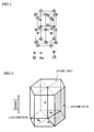
- FIG. 1 schematically illustrates a unit cell of GaN.
- FIG. 2 shows four fundamental vectors a 1 , a 2 , a 3 and c, which are generally used to represent planes of a wurtzite crystal structure with four indices (i.e., hexagonal indices).
- the fundamental vector c runs in the [0001] direction, which is called a " c -axis".
- a plane that intersects with the c -axis at right angles is called either a " c -plane” or a "(0001) plane”.
- the " c -axis” and the " c- plane” are sometimes referred to as " C -axis” and " C -plane".
- those axes and planes are identified by the capital letter to make them recognizable more easily.
- a c -plane substrate i.e., a substrate of which the principal surface is a (0001) plane
- a substrate on which GaN semiconductor crystals will be grown In a c -plane, however, there is a slight shift in the c -axis direction between a Ga atom layer and a nitrogen atom layer, thus producing electrical polarization there. That is why the c -plane is also called a "polar plane".
- a piezoelectric field is generated in the InGaN quantum well of the active layer in the c -axis direction.
- a substrate of which the principal surface is a non-polar plane such as a (10-10) plane that is perpendicular to the [10-10] direction and that is called an " m -plane", be used.
- "-" attached on the left-hand side of a Miller-Bravais index in the parentheses means a "bar” (a negative direction index).
- the m -plane is parallel to the c -axis (i.e., the fundamental vector c) and intersects with the c -plane at right angles.
- Ga atoms and nitrogen atoms are on the same atomic-plane.
- the " m -plane” is a generic term that collectively refers to a family of planes including (10-10), (-1010), (1-100), (-1100), (01-10) and (0-110) planes.
- the X plane will be sometimes referred to herein as a "growing plane”.
- a layer of semiconductor crystals that have been formed as a result of the X-plane growth will be sometimes referred to herein as an "X-plane semiconductor layer".
- US 2005/0145875 A1 is directed to a flip chip type nitride semiconductor light emitting device and manufacturing method thereof.
- US 2008/179607 A1 relates to non-polar and semi-polar light emitting devices.
- a GaN-based semiconductor device that has been grown on an m -plane substrate would achieve far more beneficial effects than what has been grown on a c -plane substrate but still has the following drawback.
- a GaN-based semiconductor device that has been grown on an m -plane substrate has higher contact resistance than what has been grown on a c -plane substrate, which constitutes a serious technical obstacle to using such a GaN-based semiconductor device that has been grown on an m -plane substrate.
- a nitride-based semiconductor device includes features of claim 1.
- a metal alloy layer including Mg and the at least one metal selected from the group consisting of Pt, Mo and Pd, is sandwiched between the Mg layer and the metal layer.
- the electrode includes the Mg layer and a metal alloy layer that has been formed on the Mg layer.
- the metal alloy layer is made of an alloy of Mg and at least one metal selected from the group consisting of Pt, Mo and Pd.
- the Mg layer is made up of a film that is present on the surface of the p-type semiconductor region.
- the Mg layer is made up of islands of Mg portions that are dispersed on the surface of the p-type semiconductor region.
- the Mg layer has a thickness of 2 nm to 45 nm.
- the Mg layer has a thickness of 2 nm to 15 nm.
- the thickness of the Mg layer is equal to or smaller than that of the metal layer.
- the concentration of Ga is ten times or more as high as that of nitrogen.
- the nitride-based semiconductor device further includes a semiconductor substrate that supports the semiconductor multilayer structure.
- the p-type semiconductor region is made of GaN.
- a light source includes a nitride-based semiconductor light-emitting device according to claim 1, and a wavelength converter including a phosphor that changes the wavelength of the light that has been emitted from the nitride-based semiconductor light-emitting device.
- the p-type semiconductor region is made of GaN.
- a method for fabricating a nitride-based semiconductor device according to the present invention includes the features of claim 11.
- the heat treatment is carried out at a temperature of 550 °C to 650 °C.
- the step of forming the Mg layer includes depositing Mg by evaporation onto the surface of the p-type semiconductor region by irradiating the surface with pulses of an electron beam.
- the method includes the step of adjusting the thickness of the Mg layer to the range of 2 nm to 45 nm after the heat treatment.
- the method includes the step of removing the substrate after the step (b) has been performed.
- the concentration of Ga is ten times or more as high as that of nitrogen.
- the p-type semiconductor region is made of GaN.
- the Mg thin film is formed by irradiating Mg with pulses of an electron beam and evaporating Mg.
- the Mg thin film is formed without heating a supporting member on which the Mg thin film is going to be formed.
- an electrode on a semiconductor multilayer structure includes an Mg layer that is in contact with the surface (which is an m -plane) of a p-type semiconductor region. As a result, the contact resistance can be reduced.
- FIG. 3(a) schematically illustrates the cross-sectional structure of a nitride-based semiconductor light-emitting device 100 as a preferred embodiment of the present invention. What is illustrated in FIG. 3(a) is a semiconductor device made of GaN semiconductors and has a nitride-based semiconductor multilayer structure.
- the nitride-based semiconductor light-emitting device 100 of this preferred embodiment includes a GaN-based substrate 10, of which the principal surface 12 is an m -plane, a semiconductor multilayer structure 20 that has been formed on the GaN-based substrate 10, and an electrode 30 arranged on the semiconductor multilayer structure 20.
- the semiconductor multilayer structure 20 is an m- plane semiconductor multilayer structure that has been formed through an m -plane crystal growth and its principal surface is an m -plane. It should be noted, however, that a-plane GaN could grow on an r -plane sapphire substrate in some instances. That is why according to the growth conditions, the principal surface of the GaN-based substrate 10 does not always have to be an m -plane.
- the semiconductor multilayer structure 20 of the present invention at least the surface of its p-type semiconductor region that is in contact with an electrode needs to be an m -plane.
- the nitride-based semiconductor light-emitting device 100 of this preferred embodiment includes the GaN-based substrate 10 to support the semiconductor multilayer structure 20.
- the device 100 may have any other substrate instead of the GaN-based substrate 10 and could also be used without the substrate.
- FIG. 3(b) schematically illustrates the crystal structure of a nitride-based semiconductor, of which the principal surface is an m -plane, as viewed on a cross section thereof that intersects with the principal surface of the substrate at right angles. Since Ga atoms and nitrogen atoms are present on the same atomic-plane that is parallel to the m -plane, no electrical polarization will be produced perpendicularly to the m -plane. That is to say, the m -plane is a non-polar plane and no piezoelecrtric field will be produced in an active layer that grows perpendicularly to the m -plane.
- In and Al atoms that have been added will be located at Ga sites and will replace the Ga atoms. Even if at least some of the Ga atoms are replaced with those In or Al atoms, no electrical polarization will still be produced perpendicularly to the m -plane.
- Such a GaN-based substrate of which the principal surface is an m -plane, will be referred to herein as an " m- plane GaN-based substrate".
- m- plane GaN-based substrate typically such an m -plane GaN-based substrate may be used and semiconductors may be grown on the m -plane of that substrate. This is because the crystallographic-plane orientation of the semiconductor multilayer structure should be identical with that of the principal surface of the GaN-based substrate.
- the principal surface of the substrate does not always have to be an m -plane as described above, and the device as a final product could already have its substrate removed.
- FIG. 3(c) The crystal structure of a nitride-based semiconductor, of which the principal surface is a c -plane, as viewed on a cross section thereof that intersects with the principal surface of the substrate at right angles is illustrated schematically in FIG. 3(c) just for a reference.
- Ga atoms and nitrogen atoms are not present on the same atomic-plane, and therefore, electrical polarization will be produced perpendicularly to the c -plane.
- Such a GaN-based substrate, of which the principal surface is a c -plane will be referred to herein as a " c -plane GaN-based substrate".
- a c -plane GaN-based substrate is generally used to grow GaN-based semiconductor crystals thereon.
- a Ga atom layer and a nitrogen atom layer that extend parallel to the c -plane are slightly misaligned from each other in the c -axis direction, and therefore, electrical polarization will be produced in the c -axis direction.
- the active layer 24 is an electron injection region of the nitride-based semiconductor light-emitting device 100.
- the Al u Ga v In w N layer 22 of this preferred embodiment has first conductivity type, which may be n-type, for example.
- an undoped GaN layer could be inserted between the active layer 24 and the Al d Ga e N layer 26.
- the mole fraction d of Al does not have to be uniform, but could vary either continuously or stepwise, in the thickness direction.
- the Al d Ga e N layer 26 could have a multilayer structure in which a number of layers with mutually different Al mole fractions d are stacked one upon the other, or could have its dopant concentration varied in the thickness direction.
- the uppermost portion of the Al d Ga e N layer 26 i.e., the upper surface region of the semiconductor multilayer structure 20
- the Al mole fraction d does not have to be zero.
- an Al 0.05 Ga 0.95 N layer of which the Al mole fraction d is approximately 0.05, could also be used. Then, the Mg layer 32 to be described later will be in contact with that Al 0.05 Ga 0.95 N layer.
- the electrode 30 of this preferred embodiment includes an Mg layer 32 consisting essentially of Mg, on which stacked is a Pt layer consisting essentially of Pt.
- the Mg layer 32 is in contact with the p-type semiconductor region of the semiconductor multilayer structure 20 and functions as a portion of a p-(or p-side) electrode.
- the Mg layer 32 is in contact with the Al d Ga e N layer 26 that is doped with a dopant of a second conductivity type (e.g., p-type), which may be Mg.
- a dopant of a second conductivity type e.g., p-type
- Examples of other preferred p-type dopants include Zn and Be.
- the metal layer 34 that is in contact with the surface of the Mg layer 32 does not have to be a Pt layer but may also be a layer of a metal that would make an alloy with Mg less easily than Au. Stated otherwise, the metal layer 34 to be in contact with the Mg layer 32 should not be made of Au (gold) that would make an alloy with Mg easily.
- the Mg layer 32 does not make an alloy with Pt or any other suitable metal that constitutes the metal layer 34. It should be noted, however, that "does not make an alloy with Pt or any other suitable metal” could also refer to a situation where Mg includes a metal such as Pt at a concentration of less than a few percent (which may be less than one percent).
- make an alloy with a metal such as Pt refers to a situation where Mg includes a metal such as Pt at a concentration of at least a few percent (which may be equal to or greater than one percent).
- the Mg layer 32 and the metal layer 34 could also contain some impurities to be inevitably included during the process steps of forming those layers.
- metal alloy layer containing Mg between the Mg layer 32 and the metal layer 34.
- Pt, Mo and Pd are metals that would make an alloy with Mg less easily than Au. But a metal alloy layer could still be produced through a reaction to a portion of the Mg layer 32 as a result of the heat treatment to be described later.
- the electrode 30 may have a thickness of 10 nm to 200 nm, for example.
- the Mg layer 32 may have a thickness of 2 nm to 45 nm. It should be noted that in this case, the thickness of the Mg layer 32 is supposed to be that of the Mg layer that has already been thermally treated.
- the metal layer 34 which is made of at least one metal selected from the group consisting of Pt, Mo and Pd and which has been stacked on the Mg layer 32, may have a thickness of 200 nm or less (or fall within the range of 10 nm to 200 nm). It should be noted that the Mg layer 32 is preferably thinner than the metal layer 34. This is because if the strain balance were lost between the Mg layer 32 and the metal layer 34, the Mg layer 32 could peel off from the Al d Ga e N layer 26.
- the GaN-based substrate 10, of which the principal surface 12 is an m -plane may have a thickness of 100 ⁇ m to 400 ⁇ m, for example. This is because if the wafer has a thickness of at least approximately 100 ⁇ m, then there will be no trouble handling such a wafer.
- the substrate 10 of this preferred embodiment has an m -plane principal surface 12 made of a GaN-based material, the substrate 10 could have a multilayer structure. That is to say, the GaN-based substrate 10 of this preferred embodiment could also refer to a substrate, at least the principal surface 12 of which is an m -plane. That is why the entire substrate could be made of a GaN-based material. Or the substrate may also be made of the GaN-based material and another material in any combination.
- an electrode 40 has been formed as an n-side electrode on a portion of an n-type Al u Ga v In w N layer 22 (with a thickness of 0.2 ⁇ m to 2 ⁇ m, for example) on the substrate 10.
- a recess 42 has been cut so as to expose a portion of the n-type Al u Ga v In w N layer 22.
- the electrode 40 has been formed on the exposed surface of the n-type Al u Ga v In w N layer 22 at the bottom of the recess 42.
- the electrode 40 may have a multilayer structure consisting of Ti, Al and Ti layers and may have a thickness of 100 nm to 200 nm, for example.
- the active layer 24 has a GaInN/GaN multi-quantum well (MQW) structure (with a thickness of 81 nm, for example) in which Ga 0.9 In 0.1 N well layers (each having a thickness of 9 nm, for example) and GaN barrier layers (each having a thickness of 9 nm, for example) are alternately stacked one upon the other.
- MQW multi-quantum well
- the active layer 24 On the active layer 24, stacked is the p-type Al d Ga e N layer 26, which may have a thickness of 0.2 ⁇ m to 2 ⁇ m.
- an undoped GaN layer could be inserted between the active layer 24 and the Al d Ga e N layer 26 as described above.
- a GaN layer of the second conductivity type (which may be p-type, for example) could be formed on the Al d Ga e N layer 26.
- a contact layer of p + -GaN and the Mg layer 32 could be stacked in this order on that GaN layer.
- the GaN contact layer could also be regarded as forming part of the Al d Ga e N layer 26, not a layer that has been stacked separately from the Al d Ga e N layer 26.
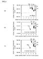
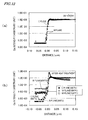
- FIGS. 4(a) and 4(b) are graphs showing how the specific contact resistance ( ⁇ ⁇ cm 2 ) changes with the work function of the metal that is in contact with m -plane GaN. More specifically, the results shown in FIGS. 4(a) and 4(b) were obtained by forming various metal layers (consisting of an Mg layer with a thickness of 2 nm and the other metal layers with a thickness of 200 nm) on an Mg-doped p-type GaN layer (with an Mg concentration of approximately 1 ⁇ 10 19 cm -3 ) and then estimating their contact resistances by TLM (transmission line method).
- TLM transmission line method
- the contact resistance is inversely proportional to the area S (cm 2 ) of the contact.
- supposing R ( ⁇ ) is contact resistance
- the constant of proportionality Rc is called "specific contact resistance” and corresponds to contact resistance R when the contact area S is 1 cm 2 . That is to say, the magnitude of the specific contact resistance does not depend on the contact area S and can be used as an index to evaluating the characteristics of a contact.
- the "specific contact resistance” will sometimes be referred to herein as just "contact resistance”.
- FIG. 4(a) shows the results that were obtained in a situation where the metal layer was just deposited and subjected to no heat treatment at all (i.e., in the case of "as-deposited").
- FIG. 4(b) shows the results that were obtained in a situation where an Mg layer deposited was thermally treated at 600 °C for 10 minutes within a nitrogen ambient and in a situation where an Al, Au, Pd, Ni or Pt layer deposited was thermally treated at 500 °C for 10 minutes within the nitrogen ambient. This difference in temperature was caused because a non-Mg metal, having a different best heat treatment temperature from Mg, had the lowest contact resistance at 500 °C.
- FIG. 4(b) shows a dotted line on the graph shown in FIG. 4(b) to indicate the tendency of various metals other than Mg.
- Mg having the smallest work function among the metals tested, would have increased contact resistance. Contrary to such a popular misconception, the present inventors discovered that Mg did cause a steep decrease in contact resistance as a result of the heat treatment.
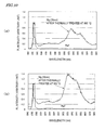
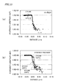
- FIG. 5(a) is a graph showing the relationship between the specific contact resistance and the thickness of an Mg layer in an Mg/Pt electrode (in which a Pt layer was stacked on the Mg layer). In this case, the thickness of the Pt layer yet to be thermally treated was fixed at 75 nm.
- FIG. 5(b) is a graph showing the specific contact resistance of a Pd/Pt electrode (of which the Pd layer has a thickness of 40 nm and the Pt layer has a thickness of 35 nm) as a comparative example. In this graph, the ordinate represents the heat treatment temperature. The thicknesses of the metal layers other than the Mg layer were measured before the heat treatment.
- the data shown in FIG. 5(a) were collected from samples in which the Mg layer was deposited by pulse evaporation process (to be described in detail later).
- the data shown in FIG. 5(b) were collected from samples in which the Pd or Pt layer was deposited by normal electron beam evaporation process.
- the Mg layer was deposited by the pulse evaporation process.
- an Mg layer is also deposited on a c -plane GaN layer by the pulse evaporation process.
- every other non-Mg metal layer (such as a Pd, Pt or Au layer) was deposited by normal electron beam evaporation process.
- the Mg/Pt electrode and the Pd/Pt electrode are both in contact with the Mg-doped m -plane GaN layer.
- the m -plane GaN layer that is in contact with these electrodes is doped with 7 ⁇ 10 19 cm -3 Mg to a depth of 20 nm as measured from the surface (i.e., the uppermost surface region with a thickness of 20 nm).
- the rest of the m -plane GaN layer, of which the depth exceeds 20 nm as measured from the surface is doped with 1 ⁇ 10 19 cm -3 Mg.
- the contact resistance can be reduced to the lowest possible level.
- the in-plane non-uniformity of the current-voltage characteristic can also be reduced.
- the variation in drive voltage between respective chips can also be reduced. That is why in every experimental example disclosed in this application, the surface region of the p-type GaN layer that is in contact with the electrode is doped with 7 ⁇ 10 19 cm -3 Mg to a depth of 20 nm as measured from the surface, while the other deeper region is doped with 1 ⁇ 10 19 cm -3 Mg.
- the contact resistance of Mg shown in FIG. 4(b) is higher than that of Mg shown in FIG. 5(a) because in the example shown in FIG. 4(b) , the process of locally increasing the doping level of Mg in the surface region was not carried out.
- the abscissa represents the thickness of the thermally treated Mg layer.
- the thermally treated Mg layer had a decreased thickness compared to the Mg layer yet to be thermally treated. Specifically, an Mg layer that had had a thickness of 7 nm before being subjected to a heat treatment at 600 °C for 10 minutes had its thickness decreased to 2 nm after having been subjected to the heat treatment.
- the graph of FIG. 5(a) shows the results of experiments that were carried out on samples that had been thermally treated at 600 °C for 10 minutes to show the correlation between the measured value of the contact resistance and the thickness of the Mg layer.
- the present inventors confirmed via experiments that the contact resistance tended to have a similar Mg layer thickness dependence even under any other heat treatment condition.
- the present inventors confirmed that in a range where the Mg layer had a thickness of 45 nm or less, the thinner the Mg layer, the lower the contact resistance.
- the Mg layer thickness decreased to the vicinity of 15 nm, the contact resistance started to drop steeply with the decrease in the thickness of the Mg layer. And when the Mg layer thickness was around 2 nm, the lowest possible contact resistance was achieved.
- the Mg layer 32 preferably has a thickness of 45 nm or less, and more preferably falls within the range of 2 nm to 15 nm.
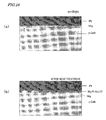
- FIGS. 6(a) through 6(c) are photographs showing the surface states of a thermally treated electrode in situations where the Mg layer had thicknesses of 2 nm, 15 nm and 45 nm, respectively. In this case, the thickness of the Mg layer was measured after having been thermally treated at 600 °C for 10 minutes.
- the thickness of the Mg layer is preferably set to be 45 nm or less.
- the Mg layer had a thickness of approximately 15 nm or less, the surface of the electrode had an extremely high degree of planarity. That is why the Mg layer more preferably has a thickness of 15 nm or less.
- FIG. 7 is a graph showing how the (measured values of) contact resistances of the Mg/Pt electrode and the Pd/Pt electrode changed depending on whether the contact surface was an m -plane or a c -plane.
- the electrode was in contact with the p-type GaN layer, which had been doped with Mg having the concentration profile described above.
- Table 1 Plane orientation p-electrode Thickness (before heat treatment) m -plane Mg/Pt 7 nm/75 nm m -plane Pd/Pt 40 nm/35 nm c -plane Mg/Pt 7 nm/75 nm c -plane Pd/Pt 40 nm/35 nm
- FIG. 8 shows the results that were obtained in a situation where an Mg layer and then a Pt layer were stacked in this order on the m -plane of a p-type GaN layer (which will be referred to herein as an " m -plane GaN"). Those results are identified by m -plane GaN (Mg/Pt) in FIG. 8 .
- FIG. 8 also shows the results that were obtained in a situation where a Pd layer and then a Pt layer were stacked in this order on the p-type m -plane GaN layer.
- FIG. 8 further shows the results that were obtained in a situation where a Pd layer and then a Pt layer were stacked in this order on the c -plane of a p-type GaN layer (which will be referred to herein as a "c-plane GaN").
- c-plane GaN a p-type GaN layer
- c-plane GaN a p-type GaN layer
- the p-type GaN layer was doped with Mg so as to have the concentration profile described above.
- Table 3 Plane orientation p-electrode Thickness m -plane Mg/Pt 7 nm/75 nm m -plane Pd/Pt 40 nm/35 nm c -plane Pd/Pt 40 nm/35 nm
- the m -plane GaN had higher contact resistance than the c -plane GaN. Also, in both of the m- and c -plane GaN, the contact resistance increased at a heat treatment temperature exceeding 500 °C.
- the electrode of the m -plane GaN (Mg/Pt) had higher contact resistance than the electrode consisting of the Pd/Pt layers.
- This result conforms to a technical commonplace that the smaller the work function of a metal is, the higher its contact resistance will be.
- the higher the heat treatment temperature the lower the contact resistance.
- the contact resistance of the m -plane GaN (Mg/Pt) was equal to or lower than that of the m- plane GaN (Pd/Pt).
- the contact resistance of the m -plane GaN (Mg/Pt) further decreased to get equal to, or even lower than, that of the c -plane GaN (Mg/Pt).
- the contact resistance of the m -plane GaN (Mg/Pt) was equal to, or even lower than, that of the c -plane GaN (Mg/Pt).
- the contact resistance of the m -plane GaN (Mg/Pt) was lower than those of the m- and c -plane GaN (Mg/Pt) at 600 °C and more specifically decreased to approximately 1.0E-02 ⁇ cm -2 or the vicinity thereof. Furthermore, at a heat treatment temperature of 700 °C, the contact resistance of the m -plane GaN (Mg/Pt) had increased from its resistance at 600 °C but was still lower than the contact resistances of the m- and c- plane GaN (Mg/Pt) at 700 °C.
- the heat treatment temperature of the m -plane GaN is preferably equal to or higher than 500 °C , for example.
- the heat treatment temperature exceeded 700 °C to reach a predetermined temperature of 800 °C, for example, then the film quality of the electrode and the GaN layer would start to deteriorate noticeably. That is why the upper limit is preferably set to be 700 °C or less, and the heat treatment temperature is more preferably in the vicinity of 600 °C (e.g., 600 °C ⁇ 50 °C).
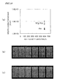
- FIG. 9 shows photographs representing the surface states of the electrode that had been thermally treated at respective temperatures. Specifically, the results that were obtained in the as-deposited state (without being subjected to the heat treatment) and at heat treatment temperatures of 500 °C, 600 °C and 700 °C are shown in FIG. 9 .
- the present inventors confirmed that a very small degree of unevenness was seen at the heat treatment temperature of 700 °C but that the electrode never deteriorated at any of these heat treatment temperatures of 500 °C, 600 °C and 700 °C.
- the surface had Ra of about 1.5 nm, about 1.5 nm and about 4.5 nm at 500 °C, 600 °C and 700 °C, respectively.
- the electrode surface preferably has an Ra of about 4.5 nm or less, more preferably about 1.5 nm or less.
- the present inventors deposited an Mg layer to a thickness of 30 nm on a GaN layer, thermally treated it at 800 °C and at 900 °C for 10 minutes, and then measured the photoluminescence of the GaN layer.
- the results are shown in FIG. 10 .
- FIG. 10(a) shows the results of a heat treatment that was carried out at 800 °C
- FIG. 10(b) shows the results of a heat treatment that was carried out at 900 °C.
- the ordinate represents the PL intensity, which stands for "photoluminescence intensity”.
- the curve identified by Ref represents the PL intensity that was obtained before the heat treatment.
- the present inventors discovered and confirmed via experiments that if the heat treatment was carried out at 700 °C or less, the photoluminescence spectrum after the heat treatment remained virtually the same as the one before the heat treatment.
- the heat treatment was carried out at 800 °C, a photoluminescence called "yellow band", which would have been caused due to the presence of vacancy defects, appeared around 530 nm as shown in FIG. 10(a) .
- the photoluminescence around 530 nm further increased its intensity as shown in FIG. 10(b) , which indicates that the density of such vacancy defects increased.
- FIG. 11 shows the profile of Mg atoms in the depth direction, which was measured in an electrode structure (Mg/Pt) with an SIMS (Secondary Ion-microprobe Mass Spectrometer). Specifically, FIG. 11(a) shows the results that were obtained in a situation where an Mg/Pt electrode, in which an Mg layer was stacked on the GaN layer, was not subjected to heat treatment (i.e., in the as-deposited state). On the other hand, FIG. 11(b) shows the results that were obtained after a heat treatment. The heat treatment was carried out on c -plane GaN at 600 °C for 10 minutes and on m- plane GaN at 600 °C for 10 minutes and at 630 °C for 10 minutes.
- the Mg layer had a thickness of 7 nm and the Pt layer had a thickness of 75 nm.
- the ordinate represents the Mg concentration and the abscissa represents the distance in the depth direction.
- negative abscissas represent sites closer to the electrode, while positive ones represent sites closer to the p-type GaN.
- the origin (of 0 ⁇ m) on the axis of abscissas represents a site where Mg has a peak concentration and substantially corresponds to the interface between the p-type GaN layer and the Mg layer.
- the solid diamonds ⁇ represent data about samples that were formed on the c -plane GaN and that were thermally treated at 600 °C
- the open triangles ⁇ represent data about samples that were formed on the m -plane GaN and that were thermally treated at 600 °C
- the open circles ⁇ represent data about samples that were formed on the m -plane GaN and that were thermally treated at 630 °C.
- the p-type GaN layer yet to be thermally treated had been doped with 7 ⁇ 10 19 cm -3 Mg to a depth of 20 nm as measured from the surface that was in contact with the electrode and had been doped with 1 ⁇ 10 19 cm -3 Mg in deeper regions as described above.
- the Mg profiles were no different, no matter whether the underlying layer was m -plane GaN or c -plane GaN.
- the resultant Mg profiles were quite different as shown in FIG. 11(b) .
- Mg on the c- plane GaN was seen to have diffused into the p-type GaN layer at rather high concentrations as shown in FIG. 11(b) , and was also seen to have diffused into the Pt layer.
- Mg on the m -plane GaN hardly diffused into the p-type GaN layer or the Pt layer. More specifically, in the case of the c -plane GaN, Mg diffused deep into not only the Pt layer but also the GaN itself as a result of the heat treatment.
- FIG. 12 shows the profile of Ga atoms in the depth direction, which was measured in the electrode structure (Mg/Pt) with an SIMS.
- the Mg layer had a thickness of 7 nm and the Pt layer had a thickness of 75 nm.
- the ordinate of this graph represents the signal intensity of the SIMS's detector, which is proportional to the atomic concentration.
- the abscissa representing a distance of 0 ⁇ m substantially corresponds to the interface between the p-type GaN layer and the Mg layer. It should be noted that the origin (of 0 ⁇ m) on the axis of abscissas represents a site where Mg has a peak concentration.
- negative abscissas represent sites closer to the electrode, while positive ones represent sites closer to the p-type GaN.
- the ordinate is normalized with respect to the concentration of Ga in as-deposited GaN crystals as a unity. Also, if calculations are made based on the atomic density of the base, an ordinate representing an intensity of 1 ⁇ 10 -3 substantially corresponds to a concentration of 1 ⁇ 10 19 cm -3 .
- FIG. 12(a) shows the results that were obtained in a situation where an Mg/Pt electrode, in which an Mg layer was stacked on the GaN layer, was not subjected to heat treatment (i.e., in the as-deposited state).
- FIG. 12(b) shows the results that were obtained after a heat treatment that had been carried out at temperatures of 600 °C and 630 °C. Specifically, the heat treatment was carried out on c -plane GaN at 600 °C for 10 minutes and on m -plane GaN at 600 °C for 10 minutes and at 630 °C for 10 minutes.
- the Ga profiles were no different, no matter whether the underlying layer was m -plane GaN or c -plane GaN.
- the resultant Ga profiles were quite different as shown in FIG. 12(b) .
- the present inventors confirmed that if the heat treatment was carried out, Ga diffused into the Mg layer as shown in FIG. 12(b) .
- Ga was seen to have diffused into the Mg layer and the contact resistance decreased. The reason has not been quite clear yet but the present inventors did confirm that there was a correlation between the number of Ga atoms diffused into the Mg layer and the contact resistance.
- Ga diffused into both the Mg and Pt layers and moved into the electrode even from deep inside GaN crystals.
- Ga atoms diffused significantly almost everywhere from the GaN layer into the electrode.
- the heat treatment temperature was 600 °C, it seems that Ga atoms moved only in the vicinity of the interface unlike the c -plane GaN. Compared to a c -plane, it would be less easy for the atoms to move freely from an m -plane.
- FIG. 13(a) is a graph showing the profile of nitrogen atoms in the depth direction in an Mg/Pt electrode yet to be subjected to a heat treatment
- FIG. 13(b) is a graph showing the profile of nitrogen atoms in the depth direction in the Mg/Pt electrode that has been subjected to the heat treatment.
- the Mg layer had a thickness of 7 nm and the Pt layer had a thickness of 75 nm.
- the ordinate represents the N intensity
- the abscissa represents the distance in the depth direction.
- an N intensity of 1 ⁇ 10 -3 substantially corresponds to an N concentration of 1 ⁇ 10 19 cm -3 .
- negative abscissas represent sites closer to the electrode, while positive ones represent sites closer to the p-type GaN.
- the origin of the axis of abscissas (0 ⁇ m) substantially corresponds to the interface between the p-type GaN layer and the Mg layer.
- the electrode structure and the p-type GaN doping conditions are the same as what has already been described for the samples with reference to FIG. 11 .
- Ga atoms diffuse toward the electrode from p-type GaN then the number of Ga atoms will be insufficient on the uppermost surface of p-type GaN, thus producing Ga vacancies there.
- Such Ga vacancies will act as a sort of acceptors. That is why if the number of Ga vacancies increases in the vicinity of the interface between the electrode and the p-type GaN, then holes will pass through the Schottky barrier of that interface more easily due to a so-called "tunneling" phenomenon.
- the number of nitrogen atoms will also be insufficient on the uppermost surface of the p-type GaN. That is to say, nitrogen vacancies will also be produced there. Those nitrogen vacancies will act like donors and will produce charge compensation with respect to the Ga vacancies. That is why if not just Ga atoms but also nitrogen atoms diffuse toward the electrode as in the c -plane GaN, the contact resistance will no longer decrease.
- the concentration of Ga that was detected in the Mg layer on the m -plane GaN with an SIMS was 4 ⁇ 1.0 E-02.
- the SIMS detected intensity is proportional to its atomic concentration. That is why supposing the base of the GaN layer has a Ga concentration of approximately 1 ⁇ 10 22 cm -3 , Ga atoms would be contained in a concentration of approximately 4 ⁇ 10 19 cm -3 in the Mg layer.
- the SIMS detected intensity was 3 ⁇ 1.0 E-02. According to the same supposition, Ga atoms would be contained in a concentration of approximately 3 ⁇ 10 19 cm -3 in the Mg layer on the m -plane GaN.
- the concentration of N (nitrogen) atoms that was detected in the Mg layer on the m- plane GaN with an SIMS was 1 ⁇ 1.0 E-03, which is the limit of responsivity, as shown in FIG. 13(b) .
- N (nitrogen) atoms would be contained in a concentration of 1 ⁇ 10 18 cm -3 or less in the Mg layer on the m- plane GaN.
- both Ga and N had an SIMS detected intensity of 1E-2, and therefore, would have been contained there in a concentration of approximately 1 ⁇ 10 19 cm -3 . That is to say, in the Mg layer on the c -plane GaN layer, the Ga atoms and N atoms had approximately the same concentration.
- Mg, Ga, N and Pt would behave in a similar manner even if part of Ga is replaced with Al or In in the GaN layer that is in contact with the Mg layer. Their behavior would also be the same even if the GaN-based semiconductor layer that is in contact with the Mg layer is doped with a non-Mg element as a dopant.
- FIG. 14 shows cross-sectional transmission electron microscope (TEM) photographs of an (Mg/Pt) electrode structure in which an Mg layer was deposited on an m -plane GaN layer.
- FIG. 14(a) shows the result that was obtained without conducting a heat treatment (i.e., in the as-deposited state), while FIG. 14(b) shows the result that was obtained after a heat treatment had been carried out at 600 °C for 10 minutes.
- the Mg layer was deposited to a thickness of 7 nm on GaN crystals as shown in FIG. 14(a) .
- the Pt layer corroded the Mg layer, thus reducing the thickness of the Mg layer to 2 nm as shown in FIG. 14 (b) .
- the Mg layer i.e., the layer 32 shown in FIG. 3(a)
- the presence of the Mg layer i.e., the layer 32 shown in FIG. 3(a) ), consisting essentially of Mg that had neither been alloyed nor absorbed by the Pt layer (i.e., the layer 34 shown in FIG. 3(a) ), was still confirmed.
- the presence of this thin Mg layer 32 would be one of major factors contributing to a reduction in the contact resistance of an m -plane GaN that has been extremely high in the prior art.
- FIG. 15 shows the profile of Pt atoms in the depth direction, which was measured in an electrode structure (Mg/Pt) with an SIMS.
- FIGS. 15(a) and 15(b) show the results that were obtained without conducting a heat treatment (i.e., in the as-deposited state) and the results that were obtained after a heat treatment.
- the Mg layer had a thickness of 7 nm and the Pt layer had a thickness of 75 nm.
- the ordinate represents the Pt intensity
- the abscissa represents the distance in the depth direction.
- a Pt intensity of 1 ⁇ 10 -3 substantially corresponds to a Pt concentration of 1 ⁇ 10 19 cm -3 .
- negative abscissas represent sites closer to the electrode, while positive ones represent sites closer to the p-type GaN.
- the origin of the axis of abscissas (0 ⁇ m) substantially corresponds to the interface between the p-type GaN layer and the Mg layer.
- the electrode structure and the p-type GaN doping conditions are the same as what has already been described for the samples with reference to FIG. 11 .
- FIG. 16(a) is a schematic representation illustrating the structure of an Mg/Pt electrode yet to be subjected to a heat treatment
- FIG. 16(b) is a schematic representation illustrating the structure of the Mg/Pt electrode thermally treated.
- the Mg layer as deposited was thicker than 5 nm, the thickness of the Mg decreased after having been thermally treated at 600 °C for 10 minutes. However, the Mg layer was still present as a substantially continuous film even after the heat treatment. On the other hand, it was confirmed that if the Mg layer as deposited had a thickness of approximately 2 nm, sometimes there were islands of Mg, which had not been absorbed into an Mg-Pt alloy, after the heat treatment had been carried out at 600 °C for 10 minutes as shown in FIG. 16(b) . Also, if the thickness of the Mg layer as-deposited is as small as approximately 2 nm, the Mg layer eventually obtained could have any of various morphologies according to the conditions of the heat treatment conducted.
- the "Mg layer” could also refer herein to a group of such a huge number of islands of Mg on the surface of a p-type semiconductor region.
- the "Mg layer” could even be a film with a lot of openings (such as a porous film). In this manner, as long as Mg that has not been corroded by Pt contacts with the surface of a p-type semiconductor region (that is an m -plane), the contact resistance can be reduced sufficiently effectively.
- the contact resistance could also be reduced substantially no less effectively.
- an Mg layer and a GaN-based semiconductor should contact with each other and that a metal on the Mg layer should be a material that would produce an alloy with Mg less easily than Au.
- the m -plane GaN substrate 10 is an n-type GaN substrate with a thickness of 100 ⁇ m, for example
- the Al u Ga v In w N layer 22 is an n-type GaN layer with a thickness of 2 ⁇ m, for example.
- a semiconductor multilayer structure 20 including at least the active layer 24 has been formed on the m -plane GaN substrate 10.
- the active layer 24 consists of InGaN well layers with an In mole fraction of approximately 25% and GaN barrier layers, both the well layers and the barrier layers may have a thickness of 9 nm each, and the well layers may have a well layer period of three.
- an Al d Ga e N layer (where d+e 1,d ⁇ 0 and e ⁇ 0) 26 of the second conductivity type (which may be p-type, for example), which may be an AlGaN layer with an Al mole fraction of 10% and may have a thickness of 0.2 ⁇ m.
- the Al d Ga e N layer 26 is doped with Mg as a p-type dopant to a level of approximately 10 18 cm -3 , for example.
- an undoped GaN layer (not shown) is interposed between the active layer 24 and the Al d Ga e N layer 26.
- a GaN layer (not shown) of the second conductivity type (which may be p-type, for example).
- the contact layer of p + -GaN stacked in this order are an Mg layer 32 and a Pt layer 34. And this stack of the Mg layer 32 and the Pt layer 34 is used as an electrode (i.e., a p-electrode) 30.
- This semiconductor multilayer structure 20 further has a recess 42 that exposes the surface of the Al u Ga v In w N layer 22.
- an electrode 40 (n-electrode) has been formed on the Al u Ga v In w N layer 22 at the bottom of the recess 42, which may have a width (or diameter) of 20 ⁇ m and a depth of 1 ⁇ m, for example.
- the electrode 40 may have a multilayer structure consisting of Ti, Al and Pt layers, which may have thicknesses of 5 nm, 100 nm and 10 nm, respectively.
- the nitride-based semiconductor light-emitting device 100 of this preferred embodiment could have an operating voltage Vop that was approximately 1.5 V lower than that of a conventional m- plane LED with a Pd/Pt electrode, and therefore, could cut down the power dissipation as a result.
- an m -plane substrate 10 is prepared.
- a GaN substrate is used as the substrate 10.
- the GaN substrate of this preferred embodiment is obtained by HVPE (hydride vapor phase epitaxy).
- a thick GaN film is grown to a thickness of several nanometers on a c -plane sapphire substrate, and then diced perpendicularly to the c -plane (i.e., parallel to the m -plane), thereby obtaining m -plane GaN substrates.
- the GaN substrate does not have to be prepared by this particular method.
- an ingot of bulk GaN may be made by a liquid phase growth process such as a sodium flux process or a melt-growth method such as an ammonothermal process and then diced parallel to the m-plane.
- the substrate 10 does not have to be a GaN substrate but may also be a gallium oxide substrate, an SiC substrate, an Si substrate or a sapphire substrate, for example.
- the principal surface of the SiC or sapphire substrate is preferably also an m -plane.
- a-plane GaN could grow on an r-plane sapphire substrate. That is why according to the growth conditions, the surface on which the crystal growth should take place does not always have to be an m -plane.
- at least the surface of the semiconductor multilayer structure 20 should be an m -plane.
- crystal layers are formed one after another on the substrate 10 by MOCVD (metalorganic chemical vapor deposition) process.
- AlGaN may be deposited to a thickness of 3 ⁇ m, for example.
- a GaN layer may be deposited by supplying TMG(Ga(CH 3 ) 3 ), TMA(Al(CH 3 ) 3 ) and NH 3 gases onto the m -plane GaN substrate 10 at 1,100 °C, for example.
- an active layer 24 is formed on the Al u Ga v In w N layer 22.
- the active layer 24 has a GaInN/GaN multi-quantum well (MQW) structure in which Ga 0.9 In 0.1 N well layers and GaN barrier layers, each having a thickness of 9 nm, have been stacked alternately to have an overall thickness of 81 nm.
- MQW multi-quantum well
- the growth temperature is preferably lowered to 800 °C to introduced In.
- an undoped GaN layer is deposited to a thickness of 30 nm, for example, on the active layer 24, and then an Al d Ga e N layer 26 is formed on the undoped GaN layer.
- Al d Ga e N layer 26 p-Al 0.14 Ga 0.86 N is deposited to a thickness of 70 nm by supplying TMG, NH 3 , TMA, TMI gases and Cp 2 Mg (cyclopentadienyl magnesium) gas as a p-type dopant.
- a p-GaN contact layer is deposited to a thickness of 0.5 ⁇ m, for example, on the Al d Ga e N layer 26.
- Cp 2 Mg is supplied as a p-type dopant.
- respective portions of the p-GaN contact layer, the Al d Ga e N layer 26, the undoped GaN layer, and the active layer 24 are removed by performing a chlorine-based dry etching process, thereby making a recess 42 and exposing a region of the Al x Ga y In z N layer 22 where an n-electrode will be formed.
- Ti/Pt layers are deposited as an n-electrode 40 on the region reserved for an n-type electrode at the bottom of the recess 42.
- an Mg layer 32 is formed on the p-GaN contact layer and then a Pt layer 34 is stacked on the Mg layer 32, thereby forming a p-electrode 40.
- a technique for performing an evaporation process while evaporating the material metal in pulses i.e., a so-called "pulse evaporation process" is used to form the Mg layer 32. More specifically, metal Mg contained in a crucible in a vacuum (of 5 ⁇ 10 -6 Torr, for example) is irradiated with pulses of electron beam, thereby evaporating the material metal in pulses.
- Some of the molecules or atoms of that material metal are deposited on the p-GaN contact layer, thereby forming an Mg layer 32.
- Those pulses may have a pulse width of 0.5 seconds and may be applied repeatedly at a frequency of 1 Hz.
- the pulse width preferably falls within the range of 0.005 seconds through 5 seconds and the pulse frequency preferably falls within the range of 0.1 Hz through 100 Hz.
- a dense film of quality could be formed as the Mg layer 32.
- the Mg layer had such high density probably because by performing such a pulse evaporation, Mg atoms or a cluster of Mg atoms that collided against the p-GaN contact layer would have their kinetic energy increased.
- the electron beam preferably has a peak intensity that is high enough to supply the Mg atoms such kinetic energy that would cause those Mg atoms adsorbed to migrate easily.
- the driving power of the electron gun is preferably determined so that the Mg thin film is deposited to a thickness of 20 atomic layers (corresponding to approximately 5 nm) or less per pulse of an electron beam. This is because if the Mg thin film deposited per pulse of the electron beam were thicker than 20 atomic layers, then it would be difficult to obtain a dense and homogenous Mg thin film.
- the deposition rate is more preferably five atomic layers or less per pulse of the electron beam. The reason is that if there were too many Mg atoms, those Mg atoms would collide against each other while migrating and would lose their kinetic energy.
- Mg is an element that gets oxidized easily when exposed to water or the air.
- an Mg thin film that has been deposited on a supporting substrate by a normal evaporation process will get oxidized quickly.
- the Mg thin film will gradually lose its metallic gloss and will eventually get crumbly and peel off from its supporting member.
- the Mg layer 32 that has been formed by the method of this preferred embodiment i.e., the pulse evaporation process
- the Mg layer 32 that has been formed by the method of this preferred embodiment i.e., the pulse evaporation process
- the layer 32 that has been formed by the method of this preferred embodiment (i.e., the pulse evaporation process) is highly dense and homogenous at an atomic level and has a structure, of which the atomic ordering is so aligned that it looks as if it had been grown epitaxially.
- the layer will get hardly oxidized. That is why even if left in the air for a few months, the layer can still maintain a shiny mirror surface.
- Mg will vaporize instantaneously by nature once its temperature has exceeded its melting point. For that reason, it is very difficult to precisely control the thickness of an Mg thin film to deposit on the order of nanometers by adjusting the deposition rate of the Mg thin film.
- the Mg layer 32 that has been formed by the method of this preferred embodiment can have its thickness controlled very precisely on the order of nanometers by appropriately setting the duration of a pulsed electron beam radiated.
- the method of this preferred embodiment could also be used effectively to deposit an Mg thin film on an Si substrate or a glass substrate. That is why the method of this preferred embodiment can be used to form an Mg thin film on not just GaN but also any of various other substrates. And the method of this preferred embodiment can be used effectively to form an electrode in the field of semiconductor processing, among other things. Also, according to the method of this preferred embodiment, there is no need to heat either the substrate or the supporting member while an Mg thin film is being deposited by evaporation. For that reason, a highly dense and homogenous Mg thin film can be deposited at around room temperature even on a substrate or supporting member that has been formed in a shape that makes it difficult to heat it.
- the Mg layer 32 that has been formed by the method of this preferred embodiment can still maintain good stability even when thermally treated at a temperature of 600 °C or more.
- This preferred embodiment uses a technique for depositing an Mg layer 32 while evaporating the material metal (i.e., metal Mg) in pulses.
- the material metal i.e., metal Mg
- any other technique can also be adopted.
- a thermal CVD process or a molecular beam epitaxy (MBE) could also be used.
- the substrate 10 and a portion of the Al u Ga v In w N layer 22 could be removed after that by some technique such as laser lift-off, etching or polishing. In that case, either only the substrate 10 or the substrate 10 and a portion of the Al u Ga v In w N layer 22 could be removed selectively. It is naturally possible to leave the substrate 10 and the Al u Ga v In w N layer 22 as they are without removing them. By performing these process steps, the nitride-based semiconductor light-emitting device 100 of this preferred embodiment is completed.
- nitride-based semiconductor light-emitting device 100 of this preferred embodiment when a voltage is applied to between the n- and p-electrodes 40 and 30, holes are injected from the p-electrode 30 into the active layer 24 and electrons are injected from the n-electrode 40 into the active layer 24, thus producing photoluminescence with a wavelength of about 450 nm.
- FIG. 17(a) shows the current-voltage characteristic of a light-emitting diode that uses an electrode consisting of Mg/Pt layers on m -plane GaN.
- FIG. 17(a) shows the current-voltage characteristic of a light-emitting diode that uses an electrode consisting of Mg/Pt layers on m -plane GaN.
- Table 4 Plane orientation p-electrode Thickness (before heat treatment) Heat treatment temperature and process time m -plane Mg/Pt 7 nm/75 nm 600 °C, 10 min. m -plane Pd/Pt 40 nm/35 nm 500 °C, 10 min. c -plane Mg/Pt 7 nm/75 nm 600 °C, 10 min.
- an n-type GaN layer In each of these light-emitting diodes, an n-type GaN layer, an active layer in which three InGaN well layers and two GaN barrier layers are alternately stacked one upon the other, and a p-type GaN layer are stacked in this order on either an m -plane GaN substrate or a c -plane GaN substrate.
- a p-electrode On the p-type GaN layer, arranged as a p-electrode is either an Mg/Pt electrode or a Pd/Pt electrode.
- an n-electrode is formed on the n-type GaN layer by etching the p-type GaN layer and the active layer and exposing the n-type GaN layer.
- the current value will still remain substantially zero for a while. However, once the applied voltage exceeds a certain level (which will be referred to herein as a "rise voltage"), the current value increases with the voltage.
- the electrode consisting of Pd/Pt layers (on the m -plane GaN) has a rise voltage of approximately 3.1 V.
- the electrode consisting of Mg/Pt layers (on the m -plane GaN) has a rise voltage of approximately 2.5 V, which is lower than the former one.
- a light-emitting diode that uses an electrode consisting of Mg/Pt layers on m -plane GaN (which will be referred to herein as an " m -plane light-emitting diode") and a light-emitting diode that uses an electrode consisting of Mg/Pt layers on c -plane GaN (which will be referred to herein as a "c-plane light-emitting diode”) will be compared to each other.
- the m -plane light-emitting diode had a lower rise voltage than the c -plane light-emitting diode, which allowed us to confirm that the contact resistance was certainly reduced.
- a current value of 20 mA could be obtained for a drive voltage of 3.2 V.
- a current value of 4.8 mA was achieved for the same drive voltage. Since the optical power of a light-emitting diode will depend on the current value, it can be seen that the optical power produced by the m -plane light-emitting diode was approximately four times as much as the one produced by the c -plane light-emitting diode at a drive voltage of 3.2 V.
- a light-emitting diode is a diode that has a p-n junction inside.
- the light-emitting diode with the electrode consisting of Mg/Pt layers had a contact resistance of 3.8 ⁇ 10 -4 ⁇ cm 2 .
- This is an amazing achievement because that low contact resistance on the order of 10 -4 has never been achieved by a p-type m -plane GaN.
- the present inventors discovered that the power dissipation could be reduced significantly as a result. And we also discovered that our invention would have great technical significance for an m -plane GaN device.
- an electrode consisting of Pd/Pt layers had a contact resistance of approximately 1 ⁇ 10 -2 ⁇ cm 2 .
- FIG. 18(a) shows the specific contact resistances ( ⁇ cm 2 ) of such an electrode consisting of an Au layer and such an electrode consisting of Mg/Au layers that were formed on an m -plane GaN layer. It should be noted that these specific contact resistances were measured after the electrode had been formed and thermally treated.
- FIG. 18(b) is a photograph representing the surface of a thermally treated electrode consisting of Mg/Au layers as a substitute for a drawing
- FIG. 18(c) is a photograph representing the surface of a thermally treated electrode consisting of an Au layer as a substitute for a drawing. Comparing these photographs to each other, the present inventors discovered that the electrode consisting of the Mg/Au layers had inferior film quality to the electrode consisting of only the Au layer.
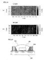
- FIG. 19 illustrates the results of hardness mapping by a conical chip (5mN, 1 ⁇ m conical).
- FIG. 19(a) shows the results that were obtained on a c -plane GaN substrate (C-GaN)
- FIG. 19(b) shows the results that were obtained on an m -plane GaN substrate (M-GaN). Comparing these results to each other, the present inventors discovered that the m -plane GaN substrate had the lower hardness than the c -plane GaN substrate. Such a difference in physical property between the m- and c -plane GaN substrates could have affected the characteristic of the electrode structure (consisting of Mg/Pt layers, for example) of this preferred embodiment.
- Patent Documents Nos. 3 and 4 do not mention at all that the crystallographic-plane of their gallium nitride-based semiconductor layer is an m -plane but just disclose a technique for forming an electrode on a c- plane gallium nitride-based semiconductor layer. More specifically, Patent Document No. 3 discloses a structure in which an Au layer is stacked on an Mg layer. And even if an electrode with such a multilayer structure were formed on an m -plane, the effect of the electrode of this preferred embodiment would never be achieved. Meanwhile, Patent Document No.
- Patent Documents Nos. 3 and 4 mentions metal layers of Ni, Cr and Mg but discloses only a specific example about an electrode structure that uses an Ni layer as the lower layer. Both of these Patent Documents Nos. 3 and 4 relate to an electrode structure that has been formed on a c -plane gallium nitride-based semiconductor layer and teach neither a problem nor a solution about the contact resistance with respect to an m -plane gallium nitride-based semiconductor layer.
- the light-emitting device of the present invention described above could be used as it is as a light source.
- the light-emitting device of the present invention is combined with a resin including a phosphor that produces wavelength conversion, for example, the device of the present invention can be used effectively as a light source with an expanded operating wavelength range (such as a white light source).
- FIG. 20 is a schematic representation illustrating an example of such a white light source.
- the light source shown in FIG. 20 includes a light-emitting device 100 with the structure shown in FIG. 3(a) and a resin layer 200 in which particles of a phosphor such as YAG (yttrium aluminum garnet) are dispersed to change the wavelength of the light emitted from the light-emitting device 100 into a longer one.
- the light-emitting device 100 is mounted on a supporting member 220 on which a wiring pattern has been formed. And on the supporting member 220, a reflective member 240 is arranged so as to surround the light-emitting device 100.
- the resin layer 200 has been formed so as to cover the light-emitting device 100.
- the p-type semiconductor region that is in contact with the Mg layer 32 is supposed to be made of GaN or AlGaN.
- the p-type semiconductor region could also be a layer including In such as InGaN.
- the contact layer to be in contact with the electrode 30 could be made of In 0.2 Ga 0.8 N with an In mole fraction of 0.2, for example.
- the effect of reducing the contact resistance can naturally be achieved by a non-LED light-emitting device (such as a semiconductor laser diode) or a device other than a light-emitting device (such as a transistor or a photodetector).
- a non-LED light-emitting device such as a semiconductor laser diode
- a device other than a light-emitting device such as a transistor or a photodetector
- the actual m -plane does not always have to be a plane that is exactly parallel to an m -plane but may be slightly tilted from the m -plane by 0 ⁇ 1 degree.
- the present invention it is possible to reduce the contact resistance of a GaN-based semiconductor device fabricated by producing crystal growth on an m -plane substrate or a GaN-based semiconductor multilayer structure, of which the principal surface is an m -plane.
- a GaN-based semiconductor device fabricated by producing crystal growth on an m -plane substrate or a GaN-based semiconductor multilayer structure, of which the principal surface is an m -plane
- its industrial applicability can be expanded significantly by the present invention.
Landscapes
- Semiconductor Lasers (AREA)
- Led Devices (AREA)
- Electrodes Of Semiconductors (AREA)
- Physical Vapour Deposition (AREA)
- Chemical Vapour Deposition (AREA)
Applications Claiming Priority (4)
| Application Number | Priority Date | Filing Date | Title |
|---|---|---|---|
| JP2008285155 | 2008-11-06 | ||
| JP2009030147 | 2009-02-12 | ||
| JP2009097684 | 2009-04-14 | ||
| PCT/JP2009/002532 WO2010052810A1 (ja) | 2008-11-06 | 2009-06-04 | 窒化物系半導体素子およびその製造方法 |
Publications (3)
| Publication Number | Publication Date |
|---|---|
| EP2226853A1 EP2226853A1 (en) | 2010-09-08 |
| EP2226853A4 EP2226853A4 (en) | 2012-05-02 |
| EP2226853B1 true EP2226853B1 (en) | 2014-02-26 |
Family
ID=42152624
Family Applications (1)
| Application Number | Title | Priority Date | Filing Date |
|---|---|---|---|
| EP09815447.9A Not-in-force EP2226853B1 (en) | 2008-11-06 | 2009-06-04 | Nitride semiconductor element and method for manufacturing the same |
Country Status (6)
Families Citing this family (21)
| Publication number | Priority date | Publication date | Assignee | Title |
|---|---|---|---|---|
| KR101220042B1 (ko) | 2006-02-20 | 2013-01-18 | 엘지이노텍 주식회사 | 질화물 반도체 발광소자 및 그 제조 방법 |
| JP4486701B1 (ja) | 2008-11-06 | 2010-06-23 | パナソニック株式会社 | 窒化物系半導体素子およびその製造方法 |
| EP2273573A4 (en) | 2009-03-11 | 2012-11-14 | Panasonic Corp | NITRIDE SEMICONDUCTOR ELEMENT AND MANUFACTURING METHOD THEREFOR |
| US8058639B2 (en) | 2009-04-06 | 2011-11-15 | Panasonic Corporation | Nitride semiconductor element and method for production thereof |
| KR101171722B1 (ko) * | 2009-12-25 | 2012-08-06 | 파나소닉 주식회사 | 질화물계 반도체 소자 및 그의 제조방법 |
| EP2555257A1 (en) | 2010-04-01 | 2013-02-06 | Panasonic Corporation | Nitride semiconductor element and manufacturing method therefor |
| JP4843123B2 (ja) | 2010-04-01 | 2011-12-21 | パナソニック株式会社 | 窒化物系半導体素子およびその製造方法 |
| JP4820465B1 (ja) | 2010-04-02 | 2011-11-24 | パナソニック株式会社 | 窒化物系半導体素子およびその製造方法 |
| WO2011135866A1 (ja) | 2010-04-28 | 2011-11-03 | パナソニック株式会社 | 窒化物系半導体素子およびその製造方法 |
| CN102754226B (zh) * | 2010-04-28 | 2015-07-15 | 松下电器产业株式会社 | 氮化物系半导体元件及其制造方法 |
| WO2012073410A1 (ja) | 2010-12-01 | 2012-06-07 | 日本電気株式会社 | 無線基地局、中継基地局、移動端末、移動通信システム及び動作制御方法 |
| EP2667421A1 (en) * | 2011-01-21 | 2013-11-27 | Panasonic Corporation | Gallium nitride compound semiconductor light emitting element and light source provided with said light emitting element |
| CN103283043A (zh) | 2011-04-08 | 2013-09-04 | 松下电器产业株式会社 | 氮化物系半导体元件及其制造方法 |
| WO2012140844A1 (ja) * | 2011-04-12 | 2012-10-18 | パナソニック株式会社 | 窒化ガリウム系化合物半導体発光素子およびその製造方法 |
| JP2012231087A (ja) * | 2011-04-27 | 2012-11-22 | Mitsubishi Chemicals Corp | 窒化物系ledの製造方法 |
| WO2012157198A1 (ja) | 2011-05-18 | 2012-11-22 | パナソニック株式会社 | 窒化物系半導体発光素子およびその製造方法 |
| WO2013054916A1 (ja) * | 2011-10-13 | 2013-04-18 | 株式会社タムラ製作所 | 結晶積層構造体及びその製造方法、並びに半導体素子 |
| US20150280057A1 (en) * | 2013-03-15 | 2015-10-01 | James R. Grandusky | Methods of forming planar contacts to pseudomorphic electronic and optoelectronic devices |
| KR102111140B1 (ko) * | 2013-08-30 | 2020-05-14 | 서울바이오시스 주식회사 | 발광 다이오드 및 그것을 제조하는 방법 |
| KR101439064B1 (ko) | 2013-12-02 | 2014-09-05 | 단국대학교 산학협력단 | 이종 접합 구조를 가지는 발광 다이오드 및 이의 제조방법 |
| JP2024106734A (ja) * | 2023-01-27 | 2024-08-08 | 国立大学法人東海国立大学機構 | 半導体装置および半導体装置の製造方法 |
Family Cites Families (66)
| Publication number | Priority date | Publication date | Assignee | Title |
|---|---|---|---|---|
| JPH0711429A (ja) | 1993-06-23 | 1995-01-13 | Toshiba Corp | 金属蒸気発生方法および装置 |
| JPH0711430A (ja) * | 1993-06-29 | 1995-01-13 | Mitsubishi Electric Corp | 電子ビーム蒸着装置と電子ビームを用いた溶接装置及び自由電子レーザ装置 |
| US5708301A (en) * | 1994-02-28 | 1998-01-13 | Sumitomo Chemical Company, Limited | Electrode material and electrode for III-V group compound semiconductor |
| JP3494478B2 (ja) * | 1994-08-22 | 2004-02-09 | 日亜化学工業株式会社 | 窒化ガリウム系化合物半導体素子 |
| US6900465B2 (en) * | 1994-12-02 | 2005-05-31 | Nichia Corporation | Nitride semiconductor light-emitting device |
| US6072197A (en) * | 1996-02-23 | 2000-06-06 | Fujitsu Limited | Semiconductor light emitting device with an active layer made of semiconductor having uniaxial anisotropy |
| JP3735960B2 (ja) * | 1996-09-06 | 2006-01-18 | 松下電器産業株式会社 | 半導体発光素子 |
| JPH10341039A (ja) | 1997-04-10 | 1998-12-22 | Toshiba Corp | 半導体発光素子およびその製造方法 |
| JP4013288B2 (ja) | 1997-06-25 | 2007-11-28 | 住友化学株式会社 | 3−5族化合物半導体用電極の製造方法と3−5族化合物半導体素子 |
| JP3299145B2 (ja) | 1997-07-15 | 2002-07-08 | 日本電気株式会社 | 窒化ガリウム系半導体のp型電極およびその形成方法 |
| JPH11233890A (ja) | 1998-02-12 | 1999-08-27 | Matsushita Electric Ind Co Ltd | 窒化ガリウム系化合物半導体素子 |
| JP4183299B2 (ja) * | 1998-03-25 | 2008-11-19 | 株式会社東芝 | 窒化ガリウム系化合物半導体発光素子 |
| JP3494880B2 (ja) * | 1998-03-26 | 2004-02-09 | 株式会社東芝 | 窒化物系半導体発光素子のp側電極及び窒化物系半導体発光素子 |
| JP2000049114A (ja) * | 1998-07-30 | 2000-02-18 | Sony Corp | 電極およびその形成方法ならびに半導体装置およびその製造方法 |
| JP3525061B2 (ja) | 1998-09-25 | 2004-05-10 | 株式会社東芝 | 半導体発光素子の製造方法 |
| JP2000174333A (ja) | 1998-12-02 | 2000-06-23 | Toshiba Corp | 窒化ガリウム系化合物半導体発光素子及び製造方法 |
| JP4627850B2 (ja) | 1999-09-09 | 2011-02-09 | シャープ株式会社 | Iii族窒化物半導体の電極形成方法 |
| JP2001160656A (ja) | 1999-12-01 | 2001-06-12 | Sharp Corp | 窒化物系化合物半導体装置 |
| JP3929008B2 (ja) | 2000-01-14 | 2007-06-13 | シャープ株式会社 | 窒化物系化合物半導体発光素子およびその製造方法 |
| JP2001308462A (ja) | 2000-04-21 | 2001-11-02 | Matsushita Electric Ind Co Ltd | 窒化物半導体素子の製造方法 |
| JP2002170989A (ja) | 2000-12-04 | 2002-06-14 | Sharp Corp | 窒化物系化合物半導体発光素子 |
| JP3453558B2 (ja) | 2000-12-25 | 2003-10-06 | 松下電器産業株式会社 | 窒化物半導体素子 |
| US6649942B2 (en) * | 2001-05-23 | 2003-11-18 | Sanyo Electric Co., Ltd. | Nitride-based semiconductor light-emitting device |
| KR100583243B1 (ko) * | 2001-05-28 | 2006-05-25 | 쇼와 덴코 가부시키가이샤 | 반도체 소자, 반도체층 및 그 제조방법 |
| JP2003332697A (ja) | 2002-05-09 | 2003-11-21 | Sony Corp | 窒化物半導体素子及びその製造方法 |
| JP2004335559A (ja) * | 2003-04-30 | 2004-11-25 | Nichia Chem Ind Ltd | Iii族窒化物基板を用いる半導体素子 |
| US8350384B2 (en) * | 2009-11-24 | 2013-01-08 | Stats Chippac, Ltd. | Semiconductor device and method of forming electrical interconnect with stress relief void |
| KR100590532B1 (ko) * | 2003-12-22 | 2006-06-15 | 삼성전자주식회사 | 플립칩형 질화물계 발광소자 및 그 제조방법 |
| KR100506741B1 (ko) * | 2003-12-24 | 2005-08-08 | 삼성전기주식회사 | 플립칩용 질화물 반도체 발광소자 및 그 제조방법 |
| KR100586943B1 (ko) * | 2003-12-26 | 2006-06-07 | 삼성전기주식회사 | 질화갈륨계 반도체 발광소자의 제조방법 |
| JP4439955B2 (ja) | 2004-03-15 | 2010-03-24 | パナソニック株式会社 | 半導体装置及び半導体レーザ装置の製造方法 |
| JP2005290510A (ja) * | 2004-04-02 | 2005-10-20 | Sodick Co Ltd | 電子ビーム蒸着方法及びその装置 |
| KR100773538B1 (ko) * | 2004-10-07 | 2007-11-07 | 삼성전자주식회사 | 반사 전극 및 이를 구비하는 화합물 반도체 발광소자 |
| TW200711171A (en) | 2005-04-05 | 2007-03-16 | Toshiba Kk | Gallium nitride based semiconductor device and method of manufacturing same |
| DE102005061828B4 (de) * | 2005-06-23 | 2017-05-24 | Osram Opto Semiconductors Gmbh | Wellenlängenkonvertierendes Konvertermaterial, lichtabstrahlendes optisches Bauelement und Verfahren zu dessen Herstellung |
| US7329907B2 (en) * | 2005-08-12 | 2008-02-12 | Avago Technologies, Ecbu Ip Pte Ltd | Phosphor-converted LED devices having improved light distribution uniformity |
| JP2007116076A (ja) * | 2005-09-22 | 2007-05-10 | Matsushita Electric Ind Co Ltd | 半導体素子 |
| JP4137936B2 (ja) * | 2005-11-16 | 2008-08-20 | 昭和電工株式会社 | 窒化ガリウム系化合物半導体発光素子 |
| KR100742988B1 (ko) | 2005-11-25 | 2007-07-26 | (주)더리즈 | p형 질화갈륨계 디바이스 제조방법 |
| KR101625224B1 (ko) * | 2006-02-09 | 2016-05-27 | 큐디 비젼, 인크. | 반도체 나노결정 및 도핑된 유기 물질을 포함하는 층을 포함하는 소자 및 방법 |
| JP2007329418A (ja) * | 2006-06-09 | 2007-12-20 | Rohm Co Ltd | 窒化物半導体発光素子 |
| WO2007149487A2 (en) | 2006-06-21 | 2007-12-27 | The Regents Of The University Of California | Opto-electronic and electronic devices using n-face or m-plane gan substrate prepared with ammonothermal growth |
| JP4984119B2 (ja) * | 2006-08-28 | 2012-07-25 | スタンレー電気株式会社 | 窒化物半導体結晶ないしそれを用いた発光素子及びその製造方法 |
| JP2008109066A (ja) | 2006-09-29 | 2008-05-08 | Rohm Co Ltd | 発光素子 |
| WO2008073384A1 (en) * | 2006-12-11 | 2008-06-19 | The Regents Of University Of California | Non-polar and semi-polar light emitting devices |
| TWI533351B (zh) | 2006-12-11 | 2016-05-11 | 美國加利福尼亞大學董事會 | 高效能非極性第三族氮化物光學裝置之金屬有機化學氣相沈積生長 |
| JP2008153285A (ja) | 2006-12-14 | 2008-07-03 | Rohm Co Ltd | 窒化物半導体装置および窒化物半導体製造方法 |
| US7547908B2 (en) | 2006-12-22 | 2009-06-16 | Philips Lumilieds Lighting Co, Llc | III-nitride light emitting devices grown on templates to reduce strain |
| WO2008111222A1 (ja) * | 2007-03-15 | 2008-09-18 | Fujitsu Limited | キャリッジアセンブリの組立方法および組立装置 |
| JP2008235804A (ja) * | 2007-03-23 | 2008-10-02 | Rohm Co Ltd | 発光素子 |
| JP2008258503A (ja) * | 2007-04-06 | 2008-10-23 | Sumitomo Electric Ind Ltd | 窒化物系半導体発光素子、および窒化物系半導体発光素子を作製する方法 |
| KR100835116B1 (ko) | 2007-04-16 | 2008-06-05 | 삼성전기주식회사 | 질화물 반도체 발광 소자 |
| JP4924185B2 (ja) | 2007-04-27 | 2012-04-25 | 住友電気工業株式会社 | 窒化物半導体発光素子 |
| JP2009043613A (ja) | 2007-08-09 | 2009-02-26 | Toyota Motor Corp | パルス電子ビーム発生装置およびパルス電子ビーム成膜装置 |
| US7652301B2 (en) | 2007-08-16 | 2010-01-26 | Philips Lumileds Lighting Company, Llc | Optical element coupled to low profile side emitting LED |
| KR100889956B1 (ko) | 2007-09-27 | 2009-03-20 | 서울옵토디바이스주식회사 | 교류용 발광다이오드 |
| US20100308357A1 (en) | 2007-10-29 | 2010-12-09 | Mitsubishi Chemical Corporation | Semiconductor light emitting element and method for manufacturing the same |
| US7781780B2 (en) | 2008-03-31 | 2010-08-24 | Bridgelux, Inc. | Light emitting diodes with smooth surface for reflective electrode |
| WO2010029720A1 (ja) | 2008-09-09 | 2010-03-18 | パナソニック株式会社 | 窒化物系半導体発光素子およびその製造方法 |
| JP2012507874A (ja) | 2008-10-31 | 2012-03-29 | ザ リージェンツ オブ ザ ユニバーシティ オブ カリフォルニア | 無極性または半極性AlInNおよびAlInGaN合金に基づく光電子デバイス |
| US20100109025A1 (en) | 2008-11-05 | 2010-05-06 | Koninklijke Philips Electronics N.V. | Over the mold phosphor lens for an led |
| JP4486701B1 (ja) | 2008-11-06 | 2010-06-23 | パナソニック株式会社 | 窒化物系半導体素子およびその製造方法 |
| EP2273573A4 (en) | 2009-03-11 | 2012-11-14 | Panasonic Corp | NITRIDE SEMICONDUCTOR ELEMENT AND MANUFACTURING METHOD THEREFOR |
| WO2010113238A1 (ja) | 2009-04-03 | 2010-10-07 | パナソニック株式会社 | 窒化物系半導体素子およびその製造方法 |
| US8058639B2 (en) | 2009-04-06 | 2011-11-15 | Panasonic Corporation | Nitride semiconductor element and method for production thereof |
| EP2369645A4 (en) | 2010-01-18 | 2012-11-14 | Panasonic Corp | NITRIDE SEMICONDUCTOR ELEMENT AND MANUFACTURING METHOD THEREFOR |
-
2009
- 2009-06-04 JP JP2009536554A patent/JP4486701B1/ja active Active
- 2009-06-04 EP EP09815447.9A patent/EP2226853B1/en not_active Not-in-force
- 2009-06-04 KR KR1020107012782A patent/KR101139142B1/ko not_active Expired - Fee Related
- 2009-06-04 WO PCT/JP2009/002532 patent/WO2010052810A1/ja active Application Filing
- 2009-06-04 US US12/679,347 patent/US20110156048A1/en not_active Abandoned
- 2009-06-04 CN CN2009801017261A patent/CN101971364B/zh not_active Expired - Fee Related
- 2009-12-18 JP JP2009287740A patent/JP2010267950A/ja active Pending
-
2011
- 2011-07-26 US US13/191,026 patent/US8110851B2/en not_active Expired - Fee Related
-
2012
- 2012-12-07 US US13/708,136 patent/US8686561B2/en not_active Expired - Fee Related
- 2012-12-07 US US13/708,097 patent/US8648378B2/en not_active Expired - Fee Related
Also Published As
| Publication number | Publication date |
|---|---|
| JP2010267950A (ja) | 2010-11-25 |
| KR101139142B1 (ko) | 2012-04-26 |
| US20110156048A1 (en) | 2011-06-30 |
| JP4486701B1 (ja) | 2010-06-23 |
| JPWO2010052810A1 (ja) | 2012-03-29 |
| KR20100087372A (ko) | 2010-08-04 |
| US8686561B2 (en) | 2014-04-01 |
| US20130119398A1 (en) | 2013-05-16 |
| US20130092968A1 (en) | 2013-04-18 |
| CN101971364B (zh) | 2013-05-15 |
| EP2226853A1 (en) | 2010-09-08 |
| US20110284905A1 (en) | 2011-11-24 |
| US8110851B2 (en) | 2012-02-07 |
| EP2226853A4 (en) | 2012-05-02 |
| WO2010052810A1 (ja) | 2010-05-14 |
| US8648378B2 (en) | 2014-02-11 |
| CN101971364A (zh) | 2011-02-09 |
Similar Documents
| Publication | Publication Date | Title |
|---|---|---|
| EP2226853B1 (en) | Nitride semiconductor element and method for manufacturing the same | |
| US8058639B2 (en) | Nitride semiconductor element and method for production thereof | |
| US8357607B2 (en) | Method for fabricating nitride-based semiconductor device having electrode on m-plane | |
| EP2352165B1 (en) | Nitride-based semiconductor element | |
| US8124986B2 (en) | Nitride-based semiconductor device and method for fabricating the same | |
| US8890175B2 (en) | Nitride-based semiconductor element and method for fabricating the same | |
| US20140054636A1 (en) | Nitride semiconductor light-emitting element and method for fabricating the same | |
| EP2555258B1 (en) | Nitride semiconductor element and manufacturing method therefor | |
| US8729587B2 (en) | Nitride semiconductor element and manufacturing method therefor | |
| EP2416387A1 (en) | Nitride semiconductor element and method for producing the same | |
| US20130040411A1 (en) | Nitride-based semiconductor device and method for fabricating the same | |
| EP2479807B1 (en) | Nitride semiconductor light emitting diode |
Legal Events
| Date | Code | Title | Description |
|---|---|---|---|
| PUAI | Public reference made under article 153(3) epc to a published international application that has entered the european phase |
Free format text: ORIGINAL CODE: 0009012 |
|
| 17P | Request for examination filed |
Effective date: 20100324 |
|
| AK | Designated contracting states |
Kind code of ref document: A1 Designated state(s): AT BE BG CH CY CZ DE DK EE ES FI FR GB GR HR HU IE IS IT LI LT LU LV MC MK MT NL NO PL PT RO SE SI SK TR |
|
| AX | Request for extension of the european patent |
Extension state: AL BA RS |
|
| DAX | Request for extension of the european patent (deleted) | ||
| REG | Reference to a national code |
Ref country code: DE Ref legal event code: R079 Ref document number: 602009022086 Country of ref document: DE Free format text: PREVIOUS MAIN CLASS: H01L0033000000 Ipc: H01L0033400000 |
|
| A4 | Supplementary search report drawn up and despatched |
Effective date: 20120330 |
|
| RIC1 | Information provided on ipc code assigned before grant |
Ipc: H01L 33/40 20100101AFI20120326BHEP |
|
| 17Q | First examination report despatched |
Effective date: 20121011 |
|
| GRAP | Despatch of communication of intention to grant a patent |
Free format text: ORIGINAL CODE: EPIDOSNIGR1 |
|
| INTG | Intention to grant announced |
Effective date: 20130903 |
|
| RIN1 | Information on inventor provided before grant (corrected) |
Inventor name: YAMADA, ATSUSHI Inventor name: OYA, MITSUAKI Inventor name: YOKOGAWA, TOSHIYA Inventor name: KATO, RYOU |
|
| GRAS | Grant fee paid |
Free format text: ORIGINAL CODE: EPIDOSNIGR3 |
|
| GRAA | (expected) grant |
Free format text: ORIGINAL CODE: 0009210 |
|
| AK | Designated contracting states |
Kind code of ref document: B1 Designated state(s): AT BE BG CH CY CZ DE DK EE ES FI FR GB GR HR HU IE IS IT LI LT LU LV MC MK MT NL NO PL PT RO SE SI SK TR |
|
| REG | Reference to a national code |
Ref country code: GB Ref legal event code: FG4D |
|
| REG | Reference to a national code |
Ref country code: CH Ref legal event code: EP |
|
| REG | Reference to a national code |
Ref country code: AT Ref legal event code: REF Ref document number: 654034 Country of ref document: AT Kind code of ref document: T Effective date: 20140315 |
|
| REG | Reference to a national code |
Ref country code: IE Ref legal event code: FG4D |
|
| REG | Reference to a national code |
Ref country code: DE Ref legal event code: R096 Ref document number: 602009022086 Country of ref document: DE Effective date: 20140410 |
|
| REG | Reference to a national code |
Ref country code: NL Ref legal event code: VDEP Effective date: 20140226 |
|
| REG | Reference to a national code |
Ref country code: AT Ref legal event code: MK05 Ref document number: 654034 Country of ref document: AT Kind code of ref document: T Effective date: 20140226 |
|
| REG | Reference to a national code |
Ref country code: LT Ref legal event code: MG4D |
|
| PG25 | Lapsed in a contracting state [announced via postgrant information from national office to epo] |
Ref country code: LT Free format text: LAPSE BECAUSE OF FAILURE TO SUBMIT A TRANSLATION OF THE DESCRIPTION OR TO PAY THE FEE WITHIN THE PRESCRIBED TIME-LIMIT Effective date: 20140226 Ref country code: NO Free format text: LAPSE BECAUSE OF FAILURE TO SUBMIT A TRANSLATION OF THE DESCRIPTION OR TO PAY THE FEE WITHIN THE PRESCRIBED TIME-LIMIT Effective date: 20140526 Ref country code: IS Free format text: LAPSE BECAUSE OF FAILURE TO SUBMIT A TRANSLATION OF THE DESCRIPTION OR TO PAY THE FEE WITHIN THE PRESCRIBED TIME-LIMIT Effective date: 20140626 |
|
| PG25 | Lapsed in a contracting state [announced via postgrant information from national office to epo] |
Ref country code: NL Free format text: LAPSE BECAUSE OF FAILURE TO SUBMIT A TRANSLATION OF THE DESCRIPTION OR TO PAY THE FEE WITHIN THE PRESCRIBED TIME-LIMIT Effective date: 20140226 Ref country code: SE Free format text: LAPSE BECAUSE OF FAILURE TO SUBMIT A TRANSLATION OF THE DESCRIPTION OR TO PAY THE FEE WITHIN THE PRESCRIBED TIME-LIMIT Effective date: 20140226 Ref country code: FI Free format text: LAPSE BECAUSE OF FAILURE TO SUBMIT A TRANSLATION OF THE DESCRIPTION OR TO PAY THE FEE WITHIN THE PRESCRIBED TIME-LIMIT Effective date: 20140226 Ref country code: PT Free format text: LAPSE BECAUSE OF FAILURE TO SUBMIT A TRANSLATION OF THE DESCRIPTION OR TO PAY THE FEE WITHIN THE PRESCRIBED TIME-LIMIT Effective date: 20140626 Ref country code: AT Free format text: LAPSE BECAUSE OF FAILURE TO SUBMIT A TRANSLATION OF THE DESCRIPTION OR TO PAY THE FEE WITHIN THE PRESCRIBED TIME-LIMIT Effective date: 20140226 Ref country code: CY Free format text: LAPSE BECAUSE OF FAILURE TO SUBMIT A TRANSLATION OF THE DESCRIPTION OR TO PAY THE FEE WITHIN THE PRESCRIBED TIME-LIMIT Effective date: 20140226 |
|
| PG25 | Lapsed in a contracting state [announced via postgrant information from national office to epo] |
Ref country code: LV Free format text: LAPSE BECAUSE OF FAILURE TO SUBMIT A TRANSLATION OF THE DESCRIPTION OR TO PAY THE FEE WITHIN THE PRESCRIBED TIME-LIMIT Effective date: 20140226 Ref country code: BE Free format text: LAPSE BECAUSE OF FAILURE TO SUBMIT A TRANSLATION OF THE DESCRIPTION OR TO PAY THE FEE WITHIN THE PRESCRIBED TIME-LIMIT Effective date: 20140226 Ref country code: HR Free format text: LAPSE BECAUSE OF FAILURE TO SUBMIT A TRANSLATION OF THE DESCRIPTION OR TO PAY THE FEE WITHIN THE PRESCRIBED TIME-LIMIT Effective date: 20140226 |
|
| PG25 | Lapsed in a contracting state [announced via postgrant information from national office to epo] |
Ref country code: EE Free format text: LAPSE BECAUSE OF FAILURE TO SUBMIT A TRANSLATION OF THE DESCRIPTION OR TO PAY THE FEE WITHIN THE PRESCRIBED TIME-LIMIT Effective date: 20140226 Ref country code: DK Free format text: LAPSE BECAUSE OF FAILURE TO SUBMIT A TRANSLATION OF THE DESCRIPTION OR TO PAY THE FEE WITHIN THE PRESCRIBED TIME-LIMIT Effective date: 20140226 Ref country code: RO Free format text: LAPSE BECAUSE OF FAILURE TO SUBMIT A TRANSLATION OF THE DESCRIPTION OR TO PAY THE FEE WITHIN THE PRESCRIBED TIME-LIMIT Effective date: 20140226 Ref country code: CZ Free format text: LAPSE BECAUSE OF FAILURE TO SUBMIT A TRANSLATION OF THE DESCRIPTION OR TO PAY THE FEE WITHIN THE PRESCRIBED TIME-LIMIT Effective date: 20140226 |
|
| REG | Reference to a national code |
Ref country code: DE Ref legal event code: R097 Ref document number: 602009022086 Country of ref document: DE |
|
| PG25 | Lapsed in a contracting state [announced via postgrant information from national office to epo] |
Ref country code: ES Free format text: LAPSE BECAUSE OF FAILURE TO SUBMIT A TRANSLATION OF THE DESCRIPTION OR TO PAY THE FEE WITHIN THE PRESCRIBED TIME-LIMIT Effective date: 20140226 Ref country code: PL Free format text: LAPSE BECAUSE OF FAILURE TO SUBMIT A TRANSLATION OF THE DESCRIPTION OR TO PAY THE FEE WITHIN THE PRESCRIBED TIME-LIMIT Effective date: 20140226 Ref country code: SK Free format text: LAPSE BECAUSE OF FAILURE TO SUBMIT A TRANSLATION OF THE DESCRIPTION OR TO PAY THE FEE WITHIN THE PRESCRIBED TIME-LIMIT Effective date: 20140226 |
|
| PLBE | No opposition filed within time limit |
Free format text: ORIGINAL CODE: 0009261 |
|
| STAA | Information on the status of an ep patent application or granted ep patent |
Free format text: STATUS: NO OPPOSITION FILED WITHIN TIME LIMIT |
|
| PG25 | Lapsed in a contracting state [announced via postgrant information from national office to epo] |
Ref country code: MC Free format text: LAPSE BECAUSE OF FAILURE TO SUBMIT A TRANSLATION OF THE DESCRIPTION OR TO PAY THE FEE WITHIN THE PRESCRIBED TIME-LIMIT Effective date: 20140226 Ref country code: LU Free format text: LAPSE BECAUSE OF FAILURE TO SUBMIT A TRANSLATION OF THE DESCRIPTION OR TO PAY THE FEE WITHIN THE PRESCRIBED TIME-LIMIT Effective date: 20140604 |
|
| REG | Reference to a national code |
Ref country code: CH Ref legal event code: PL |
|
| 26N | No opposition filed |
Effective date: 20141127 |
|
| GBPC | Gb: european patent ceased through non-payment of renewal fee |
Effective date: 20140604 |
|
| REG | Reference to a national code |
Ref country code: DE Ref legal event code: R097 Ref document number: 602009022086 Country of ref document: DE Effective date: 20141127 |
|
| REG | Reference to a national code |
Ref country code: IE Ref legal event code: MM4A |
|
| REG | Reference to a national code |
Ref country code: FR Ref legal event code: ST Effective date: 20150227 |
|
| PG25 | Lapsed in a contracting state [announced via postgrant information from national office to epo] |
Ref country code: IT Free format text: LAPSE BECAUSE OF FAILURE TO SUBMIT A TRANSLATION OF THE DESCRIPTION OR TO PAY THE FEE WITHIN THE PRESCRIBED TIME-LIMIT Effective date: 20140226 |
|
| PG25 | Lapsed in a contracting state [announced via postgrant information from national office to epo] |
Ref country code: LI Free format text: LAPSE BECAUSE OF NON-PAYMENT OF DUE FEES Effective date: 20140630 Ref country code: CH Free format text: LAPSE BECAUSE OF NON-PAYMENT OF DUE FEES Effective date: 20140630 Ref country code: IE Free format text: LAPSE BECAUSE OF NON-PAYMENT OF DUE FEES Effective date: 20140604 |
|
| PG25 | Lapsed in a contracting state [announced via postgrant information from national office to epo] |
Ref country code: SI Free format text: LAPSE BECAUSE OF FAILURE TO SUBMIT A TRANSLATION OF THE DESCRIPTION OR TO PAY THE FEE WITHIN THE PRESCRIBED TIME-LIMIT Effective date: 20140226 Ref country code: FR Free format text: LAPSE BECAUSE OF NON-PAYMENT OF DUE FEES Effective date: 20140630 Ref country code: GB Free format text: LAPSE BECAUSE OF NON-PAYMENT OF DUE FEES Effective date: 20140604 |
|
| PG25 | Lapsed in a contracting state [announced via postgrant information from national office to epo] |
Ref country code: MT Free format text: LAPSE BECAUSE OF FAILURE TO SUBMIT A TRANSLATION OF THE DESCRIPTION OR TO PAY THE FEE WITHIN THE PRESCRIBED TIME-LIMIT Effective date: 20140226 |
|
| PG25 | Lapsed in a contracting state [announced via postgrant information from national office to epo] |
Ref country code: GR Free format text: LAPSE BECAUSE OF FAILURE TO SUBMIT A TRANSLATION OF THE DESCRIPTION OR TO PAY THE FEE WITHIN THE PRESCRIBED TIME-LIMIT Effective date: 20140527 Ref country code: BG Free format text: LAPSE BECAUSE OF FAILURE TO SUBMIT A TRANSLATION OF THE DESCRIPTION OR TO PAY THE FEE WITHIN THE PRESCRIBED TIME-LIMIT Effective date: 20140226 |
|
| PG25 | Lapsed in a contracting state [announced via postgrant information from national office to epo] |
Ref country code: HU Free format text: LAPSE BECAUSE OF FAILURE TO SUBMIT A TRANSLATION OF THE DESCRIPTION OR TO PAY THE FEE WITHIN THE PRESCRIBED TIME-LIMIT; INVALID AB INITIO Effective date: 20090604 Ref country code: TR Free format text: LAPSE BECAUSE OF FAILURE TO SUBMIT A TRANSLATION OF THE DESCRIPTION OR TO PAY THE FEE WITHIN THE PRESCRIBED TIME-LIMIT Effective date: 20140226 |
|
| PG25 | Lapsed in a contracting state [announced via postgrant information from national office to epo] |
Ref country code: MK Free format text: LAPSE BECAUSE OF FAILURE TO SUBMIT A TRANSLATION OF THE DESCRIPTION OR TO PAY THE FEE WITHIN THE PRESCRIBED TIME-LIMIT Effective date: 20140226 |
|
| PGFP | Annual fee paid to national office [announced via postgrant information from national office to epo] |
Ref country code: DE Payment date: 20190619 Year of fee payment: 11 |
|
| REG | Reference to a national code |
Ref country code: DE Ref legal event code: R119 Ref document number: 602009022086 Country of ref document: DE |
|
| PG25 | Lapsed in a contracting state [announced via postgrant information from national office to epo] |
Ref country code: DE Free format text: LAPSE BECAUSE OF NON-PAYMENT OF DUE FEES Effective date: 20210101 |