EP2209124A2 - Registre de déphasage - Google Patents
Registre de déphasage Download PDFInfo
- Publication number
- EP2209124A2 EP2209124A2 EP09179144A EP09179144A EP2209124A2 EP 2209124 A2 EP2209124 A2 EP 2209124A2 EP 09179144 A EP09179144 A EP 09179144A EP 09179144 A EP09179144 A EP 09179144A EP 2209124 A2 EP2209124 A2 EP 2209124A2
- Authority
- EP
- European Patent Office
- Prior art keywords
- pull
- electrically coupled
- input
- circuit
- transistor
- Prior art date
- Legal status (The legal status is an assumption and is not a legal conclusion. Google has not performed a legal analysis and makes no representation as to the accuracy of the status listed.)
- Granted
Links
- 239000003990 capacitor Substances 0.000 claims description 6
- 238000010586 diagram Methods 0.000 description 22
- 239000004973 liquid crystal related substance Substances 0.000 description 4
- 238000012986 modification Methods 0.000 description 4
- 230000004048 modification Effects 0.000 description 4
- 239000000758 substrate Substances 0.000 description 4
- 229910021417 amorphous silicon Inorganic materials 0.000 description 3
- 210000002858 crystal cell Anatomy 0.000 description 3
- 239000011521 glass Substances 0.000 description 3
- 230000002457 bidirectional effect Effects 0.000 description 1
- 230000007812 deficiency Effects 0.000 description 1
- 238000004519 manufacturing process Methods 0.000 description 1
- 239000000463 material Substances 0.000 description 1
- 239000011159 matrix material Substances 0.000 description 1
- 229910021420 polycrystalline silicon Inorganic materials 0.000 description 1
- 238000005070 sampling Methods 0.000 description 1
- 239000010409 thin film Substances 0.000 description 1
- 238000002834 transmittance Methods 0.000 description 1
Images


Classifications
-
- G—PHYSICS
- G11—INFORMATION STORAGE
- G11C—STATIC STORES
- G11C19/00—Digital stores in which the information is moved stepwise, e.g. shift registers
- G11C19/28—Digital stores in which the information is moved stepwise, e.g. shift registers using semiconductor elements
Definitions
- the present invention relates generally to a shift register, and in particular to a shift register having a plurality of stages with each pair of stages sharing a single pull-down control circuit.
- a liquid crystal display includes an LCD panel formed with liquid crystal cells and pixel elements with each associating with a corresponding liquid crystal cell. These pixel elements are substantially arranged in the form of a matrix having gate lines in rows and data lines in columns.
- the LCD panel is driven by a driving circuit including a gate driver and a data driver.
- the gate driver generates a plurality of gate signals (scanning signals) sequentially applied to the gate lines for sequentially turning on the pixel elements row-by-row.
- the data driver generates a plurality of source signals (data signals), i.e., sequentially sampling image signals, simultaneously applied to the data lines in conjunction with the gate signals applied to the gate lines for aligning states of the liquid crystal cells on the LCD panel to control light transmittance therethrough, thereby displaying an image on the LCD.
- data signals data signals
- the data driver generates a plurality of source signals (data signals), i.e., sequentially sampling image signals, simultaneously applied to the data lines in conjunction with the gate signals applied to the gate lines for aligning states of the liquid crystal cells on the LCD panel to control light transmittance therethrough, thereby displaying an image on the LCD.
- a shift register is utilized in the gate driver to generate the plurality of gate signals for sequentially driving the gate lines.
- One of the efforts is to fabricate the shift register and the gate driver on a glass substrate of the LCD panel, namely, the gate on array (GOA) arrangement, using amorphous silicon (a-Si) thin film transistors (TFTs), and/or low temperature polycrystalline silicon (LTPS) TFTs.
- a-Si amorphous silicon
- TFTs thin film transistors
- LTPS low temperature polycrystalline silicon
- a shift register having multiple stages is designed such that in operation there are some TFTs that are turned on for a long period of time for the purpose of discharges. Additionally, such a shift register is usually supplied with two or more clock signals to substantially shift an output signal of a stage from its input signal that is an output signal of its immediately prior stage, thereby generating of a plurality of sequentially shifted output signals. If the two or more clock signals have a same frequency that is very high, some TFTs in the shift register may frequently be turned on during operation.
- Each stage S n comprises a first input, IN1, for receiving one of a first clock signal, CK1, and a second clock signal, XCK1, a second input, IN2, for receiving a third clock signal, CK2, if the first input IN1 receives the first clock signal CK1, or a fourth clock signal, XCK2, if the first input IN1 receives the second clock signal XCK1, a third input, IN3, for receiving a supply voltage, VSS, a fourth input, IN4, a fifth input, IN5, a sixth input, IN6, a seventh input, IN7, and an eighth input, IN8.
- each stage S n comprises a first output, OUT1, for outputting an output signal, O n , and a second output, OUT2, for outputting a pull-down signal, K n .
- each stage S n comprises a pull-up circuit electrically coupled between the first input IN1 and the first output OUT1, a pull-up control circuit electrically coupled between the fifth inputs IN5 and the pull-up circuit, a first pull-down circuit electrically coupled to the pull-up circuit, a first pull-down control circuit electrically coupled to the second input IN2, the second output OUT2, and the first pull-down circuit, a second pull-down circuit electrically coupled to the fourth input IN4, the first pull-down control circuit and the pull-up circuit; and a third pull-down circuit electrically coupled to the sixth input IN6, and the second pull-down circuit and the pull-up circuit.
- the plurality of stages ⁇ S n ⁇ is electrically coupled in serial.
- the fourth input IN4 of the n-th stage S n is electrically coupled to the second output OUT2 of the (n-1)-th stage S n-1 , for receiving a corresponding pull-down output signal K n-1 therefrom, or the second output OUT2 of the (n+1)-th stage S n+1 , for receiving a corresponding pull-down output signal K n+1 therefrom.
- the fifth input IN5 of the n-th stage S n is electrically coupled to the first output OUT1 of the (n-1)-th stage S n-1 , for receiving a corresponding output signal O n-1 therefrom.
- the sixth input IN6 of the n-th stage S n is electrically coupled to the first output OUT1 of the (n+1)-th stage S n+1 , for receiving a corresponding output signal O n+1 therefrom.
- the seventh input IN7 of the n-th stage S n is electrically coupled to the first output OUT1 of the (n+2)-th stage S n+2 , for receiving a corresponding output signal O n+2 therefrom.
- the eighth input IN8 of the n-th stage S n is electrically coupled to the first output OUT1 of the (n-2)-th stage S n-2 , for receiving a corresponding output signal O n-2 therefrom.
- the shift register also has a first clock signal line for providing the first clock signal, CK1, a second clock signal line for providing the second clock signal, XCK2, a third clock signal line for providing the third clock signal, CK1, a fourth clock signal line for providing the forth clock signal, XCK2, and a reference line for providing a supply voltage, VSS.
- each of the first, second, third and fourth clock signals is characterized with a frequency and a phase.
- the frequency of the first clock signal and the frequency of the second clock signal are substantially identical and the phase of the first clock signal and the phase of the second clock signal are substantially reversed.
- the frequency of the third clock signal and the frequency of the fourth clock signal are substantially identical and the phase of the third clock signal and the phase of the fourth clock signal are substantially reversed, respectively.
- the frequency of the first clock signal is higher than the frequency of the third clock signal.
- the pull-up control circuit comprises a first transistor T1 having a gate electrically coupled to the fifth input IN5, a source electrically coupled to the gate and a drain.
- the pull-up circuit comprises a second transistor T2 having a gate electrically coupled to the drain of the first transistor T1 of the pull-up control circuit, a source electrically coupled to the first input IN1 and a drain electrically coupled to the first output OUT1, and at least one capacitor electrically coupled between the source and the drain of the second transistor T2.
- the first pull-down control circuit comprises a fourth transistor T4 having a gate electrically coupled to the second input IN2, a source electrically coupled to the gate and a drain electrically coupled to the second output OUT2, and an eighth transistor T8 having a gate electrically coupled to the gate of the second transistor T2 of the pull-up circuit, a source electrically coupled to the drain of the fourth transistor T4 and a drain electrically coupled to the reference line.
- the first pull-down circuit comprises a sixth transistor T6 having a gate electrically coupled to the drain of the fourth transistor T4 of the first pull-down control circuit, a source electrically coupled to the gate of the second transistor T2 of the pull-up circuit and a drain electrically coupled to the drain of the second transistor T2 of the pull-up circuit, and a seventh transistor T7 having a gate electrically coupled to the drain of the fourth transistor T4 of the first pull-down control circuit, a source electrically coupled to the drain of the second transistor T2 of the pull-up circuit and a drain electrically coupled the reference line.
- the second pull-down circuit comprises a ninth transistor T9 having a gate electrically coupled to the fourth input IN4, a source electrically coupled to the drain of the second transistor T2 of the pull-up circuit and a drain electrically coupled the reference line, a tenth transistor T10 having a gate electrically coupled to the fourth input IN4, a source electrically coupled to the gate of the second transistor T2 of the pull-up circuit and a drain electrically coupled to the drain of the second transistor T2 of the pull-up circuit, and an eleventh transistor T11 having a gate electrically coupled to the gate of the second transistor T2 of the pull-up circuit, a source electrically coupled to the fourth input IN4 and a drain electrically coupled the reference line.
- the third pull-down circuit comprises a twelfth transistor T12 having a gate electrically coupled to the sixth input IN6, a source electrically coupled to the gate of the second transistor T2 of the pull-up circuit and a drain electrically coupled the reference line; and a thirteenth transistor T13 having a gate electrically coupled to the sixth input IN6, a source electrically coupled to the drain of the second transistor T2 of the pull-up circuit and a drain electrically coupled the reference line.
- each stage S n further comprises a third transistor T3 having a gate electrically coupled to the seventh input IN7, a source electrically coupled to the reference line and a drain electrically coupled to the drain of the first transistor T1 of the pull-up control circuit, and a fifth transistor T5 having a gate electrically coupled to the eighth input IN8, a source electrically coupled to the reference line and a drain electrically coupled to the drain of the first transistor T1 of the pull-up control circuit.
- Each stage S n includes a first input, IN1, for receiving one of a first clock signal, CK1, and a second clock signal, XCK1, a second input, IN2, for receiving a third clock signal, CK2, if the first input IN1 receives the first clock signal CK1, or a fourth clock signal, XCK2, if the first input IN1 receives the second clock signal XCK1, a third input, IN3, for receiving a supply voltage, VSS, a fourth input, IN4, for receiving a fourth input signal, a fifth input, IN5, for receiving a fifth input signal, a sixth input, IN6, for receiving a sixth input signal, a first output, OUT1, for outputting an output signal, O n , and a second output, OUT2, for outputting a pull-down signal, K n .
- Each stage S n also includes a pull-up circuit electrically coupled between the first input IN1 and the first output OUT1, a pull-up control circuit electrically coupled between the fifth inputs IN5 and the pull-up circuit, a first pull-down circuit electrically coupled to the pull-up circuit, a first pull-down control circuit electrically coupled to the second input IN2, the second output OUT2, and the first pull-down circuit, a second pull-down circuit electrically coupled to the fourth input IN4, the first pull-down control circuit and the pull-up circuit, and a third pull-down circuit electrically coupled to the eighth input IN8, the second pull-down circuit and the pull-up circuit.
- the fourth input signal is corresponding to one of the pull-down signal K n-1 of the (n-1)-th stage S n-1 and the pull-down signal K n+1 of the (n+1)-th stage S n+1 , wherein the fifth input signal is corresponding to the output signal O n-1 of the (n-1)-th stage S n-1 , and wherein the sixth input signal is corresponding to the output signal O n+1 of the (n+1)-th stage S n+1 .
- the pull-up control circuit comprises a first transistor T1 having a gate electrically coupled to the fifth input IN5, a source electrically coupled to the gate and a drain.
- the pull-up circuit comprises a second transistor T2 having a gate electrically coupled to the drain of the first transistor T1 of the pull-up control circuit, a source electrically coupled to the first input IN1 and a drain electrically coupled to the first output OUT1, and at least one capacitor electrically coupled between the source and the drain of the second transistor T2.
- the first pull-down control circuit comprises a fourth transistor T4 having a gate electrically coupled to the second input IN2, a source electrically coupled to the gate and a drain electrically coupled to the second output OUT2, and an eighth transistor T8 having a gate electrically coupled to the gate of the second transistor T2 of the pull-up circuit, a source electrically coupled to the drain of the fourth transistor T4 and a drain configured to receive the supply voltage VSS.
- the first pull-down circuit comprises a sixth transistor T6 having a gate electrically coupled to the drain of the fourth transistor T4 of the first pull-down control circuit, a source electrically coupled to the gate of the second transistor T2 of the pull-up circuit and a drain electrically coupled to the drain of the second transistor T2 of the pull-up circuit, and a seventh transistor T7 having a gate electrically coupled to the drain of the fourth transistor T4 of the first pull-down control circuit, a source electrically coupled to the drain of the second transistor T2 of the pull-up circuit and a drain configured to receive the supply voltage VSS.
- the second pull-down circuit comprises a ninth transistor T9 having a gate electrically coupled to the fourth input IN4, a source electrically coupled to the drain of the second transistor T2 of the pull-up circuit and a drain configured to receive the supply voltage VSS, a tenth transistor T10 having a gate electrically coupled to the fourth input IN4, a source electrically coupled to the gate of the second transistor T2 of the pull-up circuit and a drain electrically coupled to the drain of the second transistor T2 of the pull-up circuit, and an eleventh transistor T11 having a gate electrically coupled to the gate of the second transistor T2 of the pull-up circuit, a source electrically coupled to the fourth input IN4 and a drain configured to receive the supply voltage VSS.
- the third pull-down circuit comprises a twelfth transistor T12 having a gate electrically coupled to the sixth input IN6, a source electrically coupled to the gate of the second transistor T2 of the pull-up circuit and a drain configured to receive the supply voltage VSS, and a thirteenth transistor T13 having a gate electrically coupled to the sixth input IN6, a source electrically coupled to the drain of the second transistor T2 of the pull-up circuit and a drain configured to receive the supply voltage VSS
- each stage S n comprises a seventh input, IN7, for receiving a seventh input signal, an eighth input, IN8, for receiving a eighth input signal, a third transistor T3 having a gate electrically coupled to the seventh input IN7, a source configured to receive the supply voltage VSS and a drain electrically coupled to the drain of the first transistor T1 of the pull-up control circuit, and a fifth transistor T5 having a gate electrically coupled to the eighth input IN8, a source configured to receive the supply voltage VSS and a drain electrically coupled to the drain of the first transistor T1 of the pull-up control circuit.
- the seventh input signal is corresponding to the output signal O n+2 of the (n+2)-th stage S n+2 .
- the eighth input signal is corresponding to the output signal O n-2 of the (n-2)-th stage S n-2 .
- each stage S n comprises a pull-up circuit having an input for receiving one of a first clock signal, CK1, and a second clock signal, XCK1, an output for responsively outputting an output signal, O n , and an input node Q n , a pull-up control circuit electrically coupled to the input node Q n of the pull-up circuit and configured such that when receiving a first input signal, the pull-up control circuit responsively generates a signal that is provided to the input node Q n of the pull-up circuit to turn on the pull-up circuit, a pull-down circuit electrically coupled to the input node Q n of the pull-up circuit and configured to provide a first voltage to one of the input node Q n and the output of the pull-up circuit, a pull-down control circuit configured to receive one
- the pull-up circuit 1010 comprises a first transistor T1 having a gate electrically coupled to the input node Q n , a source electrically coupled to the input for receiving one of the first clock signal CK1 and the second clock signal XCK1 and a drain electrically coupled to the output for outputting the output signal O n .
- the pull-up control circuit 1020 comprises a third transistor T3 having a gate, a source electrically coupled to the output of the stage S n-1 for receiving the output signal O n-1 therefrom and a drain electrically coupled to the input node Q n of the pull-up circuit 1010, and a fourth transistor T4 having gate electrically coupled to the input node Q n-1 of the pull-up circuit of the stage S n-1 , a source configured to receive the second clock signal XCK1 if the input of the pull-up circuit receives the first clock signal CK1 or the first clock signal CK1 if the input of the pull-up circuit receives the second clock signal XCK1 and a drain electrically coupled to the gate of the third transistor T3.
- the pull-down control circuit comprises a seventh transistor T7 having a gate configured to receive a third clock signal CK2, a source electrically coupled to the gate and a drain electrically coupled to a node K, an eighth transistor T8 having a gate electrically coupled to the input node Q n-1 of the pull-up circuit of the stage S n-1 , a source electrically coupled to the node K and a drain configured to receive a supply voltage VSS, and a ninth transistor T9 having a gate electrically coupled to the input node Q n of the pull-up circuit, a source electrically coupled to the node K and a drain configured to receive the supply voltage VSS.
- the pull-down circuit comprises a thirteenth transistor T13 having a gate electrically coupled to the node K of the pull-down control circuit, a source electrically coupled to the input node Q n and a drain configured to receive the supply voltage VSS; and a fourteenth transistor T14 having a gate electrically coupled to the node K of the pull-down control circuit, a source electrically coupled to the output of the pull-up circuit and a drain configured to receive the supply voltage VSS.
- the key pull-down circuit comprises a twenty-first transistor T21 having a gate electrically coupled to the output of the stage S n+1 for receiving the output signal O n+1 therefrom, a source electrically coupled to the input node Q n of the pull-up circuit and a drain configured to receive the supply voltage VSS, and a twenty-second transistor T22 having a gate electrically coupled to the output of the stage S n+1 for receiving the output signal O n+1 therefrom, a source electrically coupled to the output of the pull-up circuit and a drain configured to receive the supply voltage VSS.
- each stage S n also comprises a twenty-fifth transistor T25 having a gate configured to receive the output signal O n-2 of the (n-2)-th stage S n-2 , a source configured to receive the supply voltage VSS and a drain electrically coupled to the input node Q n of the pull-up circuit; and a twenty-sixth transistor T26 having a gate configured to receive the output signal O n+2 of the (n+2)-th stage S n+2 , a source configured to receive the supply voltage VSS and a drain electrically coupled to the input node Q n of the pull-up circuit.
- the present invention relates to a shift register.
- Each stage S n includes a pull-up circuit having an input for receiving a corresponding clock signal Cn, an output for responsively outputting an output signal, O n , and an input node, Q n , between the input and the output, a pull-up control circuit electrically coupled to the input node Q n of the pull-up circuit 810 and configured such that when receiving a first input signal, the pull-up control circuit responsively generates a signal that is identical to the first input signal and is provided to the input node Q n of the pull-up circuit to turn on the pull-up circuit, a first pull-down circuit electrically coupled to the input node Q n and the output of the pull-up circuit and configured to receive a pull-down signal K n , a second pull-down circuit electrically coupled to
- the second input signal is corresponding to the pull-down signal K n-1 of the stage S n-1 or the pull-down signal K n+1 of the stage S n+1
- the third input signal is corresponding to the output signal O n+2 of the stage S n+2
- the first input signal is corresponding to a start signal.
- this invention in one aspect, relates to a shift register with embedded bidirectional scanning function.
- the shift register includes a first clock signal line 111 for providing the first clock signal, CK1, a second clock signal line 112 for providing the second clock signal, XCK2, a third clock signal line 113 for providing the third clock signal, CK1, a fourth clock signal line 114 for providing the forth clock signal, XCK2, and a reference line 115 for providing a supply voltage, VSS.
- each of the first, second, third and fourth clock signals, CK1, XCK1, CK2 and XCK2 is characterized with a frequency and a phase.
- the frequency of the first clock signal CK1 and the frequency of the second clock signal XCK1 are substantially identical and the phase of the first clock signal CK1 and the phase of the second clock signal XCK1 are substantially reversed.
- the frequency of the third clock signal CK2 and the frequency of the fourth clock signal XCK2 are substantially identical and the phase of the third clock signal CK2 and the phase of the fourth clock signal XCK2 are substantially reversed, respectively.
- the frequency of the first clock signal CK1 is higher than the frequency of the third clock signal CK2.
- Each stage S n has a first input, IN1, for receiving one of a first clock signal, CK1, and a second clock signal, XCK1, a second input, IN2, for receiving a third clock signal, CK2, if the first input IN1 receives the first clock signal CK1, or a fourth clock signal, XCK2, if the first input IN1 receives the second clock signal XCK1, a third input, IN3, for receiving a supply voltage, VSS, a fourth input, IN4, a fifth input, IN5, a sixth input, IN6, a seventh input, IN7, and an eighth input, IN8.
- Each stage S n also has a first output, OUT1, for outputting an output signal, O n , and a second output, OUT2, for outputting a pull-down signal, K n .
- the plurality of stages ⁇ S n ⁇ is electrically coupled in serial.
- the fourth input IN4 of the n-th stage S n is electrically coupled to the second output OUT2 of the (n+1)-th stage S n+1 , for receiving a corresponding pull-down output signal K n+1 therefrom.
- the fifth input IN5 of the n-th stage S n is electrically coupled to the first output OUT1 of the (n-1)-th stage S n-1 , for receiving a corresponding output signal O n-1 therefrom.
- the sixth input IN6 of the n-th stage S n is electrically coupled to the first output OUT1 of the (n+1)-th stage S n+1 , for receiving a corresponding output signal O n+1 therefrom.
- the seventh input IN7 of the n-th stage S n is electrically coupled to the first output OUT1 of the (n+2)-th stage S n+2 , for receiving a corresponding output signal O n+2 therefrom.
- the eighth input IN8 of the n-th stage S n is electrically coupled to the first output OUT1 of the (n-2)-th stage S n-2 , for receiving a corresponding output signal O n-2 therefrom.
- Fig. 2 shows a shift register 200 according to another embodiment of the present invention.
- the shift register 200 has the same design as the shift register 100, except that the fourth input IN4 of the n-th stage S n is electrically coupled to the second output OUT2 of the (n-1)-th stage S n-1 , for receiving a corresponding pull-down output signal K n-1 therefrom.
- Fig. 3 shows schematically a GOA architecture of a shift register 300 according to one embodiment of the present invention.
- the shift register 300 has multiple stages ⁇ S n ⁇ that are deposited/formed on a glass substrate (not shown).
- Fig. 3 shows only four stages S n , S n+1 , S n+2 , and S n+3 .
- Each stage has a pull-up control circuit 320 and a pull-up circuit 310 formed adjacent to the pull-up control circuit 320 on the glass substrate along a first row 380.
- Each stage also has a first pull-down control circuit 340, a first pull-down circuit 330, a second pull-down circuit 350 and a key pull-down circuit 360 formed on the substrate, in turn, along a second row 390 that is adjacent to the first row 380.
- the first pull-down control circuit 340 can be a CK pull-down control circuit or an XCK pull-down control circuit; the first pull-down circuit 330 can be a CK pull-down circuit or an XCK pull-down circuit; and the second pull-down circuit 350 can be an XCK pull-down control circuit or a CK pull-down circuit.
- the first pull-down control circuit 340, the first pull-down circuit 330 and the second pull-down circuit 350 are corresponding to a CK pull-down control circuit, a CK pull-down circuit and an XCK pull-down control circuit, respectively.
- the first pull-down control circuit 340, the first pull-down circuit 330 and the second pull-down circuit 350 are corresponding to an XCK pull-down control circuit, an XCK pull-down circuit and a CK pull-down control circuit, respectively.
- a single pull-down control circuit 340 is utilized to control the first pull-up circuit of the stage S n , and a pull-up circuit of the stage S n-1 .
- Each stage S n includes a first input IN1 for receiving one of the first clock signal CK1 and the second clock signal XCK, a second input IN2 for receiving the third clock signal CK2 if the first input IN1 receives the first clock signal CK1, or the fourth clock signal XCK2 if the first input IN1 receives the second clock signal XCK1, a third input IN3 for receiving the supply voltage VSS a fourth input IN4 for receiving a fourth input signal, a fifth input IN5 for receiving a fifth input signal, a sixth input IN6 for receiving a sixth input signal, a first output OUT1 for outputting an output signal O n , and a second output OUT2 for outputting a pull-down signal K n .
- Each stage S n includes a pull-up circuit 310, a pull-up control circuit 320, a first pull-down circuit 330, a first pull-down control circuit 340, a second pull-down circuit 350 a third pull-down circuit 360.
- the pull-up circuit 310 is electrically coupled between the first input IN1 and the first output OUT1.
- the pull-up control circuit 320 is electrically coupled between the fifth inputs IN5 and the pull-up circuit 310.
- the first pull-down circuit 330 is electrically coupled to the pull-up circuit 310.
- the first pull-down control circuit 340 is electrically coupled to the second input IN2, the second output OUT2, and the first pull-down circuit 330.
- the second pull-down circuit 350 is electrically coupled to the fourth input IN4, the first pull-down control circuit 340 and the pull-up circuit 310.
- the third pull-down circuit 360 electrically coupled to the eighth input IN8, the second pull-down circuit 350 and the pull-up circuit 310.
- the fourth input signal is corresponding to the pull-down signal K n+1 of the (n+1)-th stage S n+1 .
- the fifth input signal is corresponding to the output signal O n-1 of the (n-1)-th stage S n-1 .
- the sixth input signal is corresponding to the output signal O n+1 of the (n+1)-th stage S n+1 .
- the pull-up control circuit 320 has a first transistor T1 having a gate electrically coupled to the fifth input IN5 for receiving the output signal O n-1 of the stage S n-1 , a source electrically coupled to the gate and a drain electrically coupled to a node Q.
- the pull-up circuit 310 has a second transistor T2 having a gate electrically coupled to the node Q, a source electrically coupled to the first input IN1 for receiving the first clock signal CK1 or the second clock signal XCK1, and a drain electrically coupled to the first output OUT1 for outputting an stage output signal O n in response to the received first clock signal CK1 or second clock signal XCK1 in the source. Additionally, the pull-up circuit 310 also has two serial-connected capacitors are electrically coupled between the source and the drain of the second transistor T2.
- the first pull-down control circuit 340 has a fourth transistor T4 having a gate electrically coupled to the second input IN2 for receiving the third clock signal CK2 if the source of the second transistor T2 receives the first clock signal CK1 or the fourth clock signal XCK2 if the source of the second transistor T2 receives the second clock signal XCK1, a source electrically coupled to the gate and a drain electrically coupled to the second output OUT2 for outputting the pull-down signal K n , which is provided to the second pull-down circuit 350 of the stage S n+1 or S n-1 .
- the first pull-down control circuit 340 also has an eighth transistor T8 having a gate electrically coupled to the node Q that is eclectically connected to the gate of the second transistor T2 of the pull-up circuit 310, a source electrically coupled to the drain of the fourth transistor T4 and a drain configured to receive the supply voltage VSS.
- the first pull-down circuit 330 includes a sixth transistor T6 and a seventh transistor T7.
- the sixth transistor T6 has a gate electrically coupled to the drain of the fourth transistor T4 of the first pull-down control circuit 340, a source electrically coupled to the node Q or the gate of the second transistor T2 of the pull-up circuit 310 and a drain electrically coupled to the drain of the second transistor T2 of the pull-up circuit 310 which is electrically connected to the first output OUT1.
- the seventh transistor T7 having a gate electrically coupled to the drain of the fourth transistor T4 of the first pull-down control circuit 340, a source electrically coupled to the drain of the second transistor T2 of the pull-up circuit 310 and a drain configured to receive the supply voltage VSS.
- the second pull-down circuit 350 has a ninth transistor T9, a tenth transistor T10 and an eleventh transistor T11.
- the ninth transistor T9 has a gate electrically coupled to the fourth input IN4 for receiving the pull-down signal K n+1 of the stage S n+1 or the pull-down signal K n+1 of the stage S n-1 , a source electrically coupled to the drain of the second transistor T2 of the pull-up circuit 310 and a drain configured to receive the supply voltage VSS.
- the tenth transistor T10 has a gate electrically coupled to the fourth input IN4 for receiving the pull-down signal K n+1 of the stage S n+1 or the pull-down signal K n+1 of the stage S n-1 , a source electrically coupled to the node Q or the gate of the second transistor T2 of the pull-up circuit 310 and a drain electrically coupled to the drain of the second transistor T2 of the pull-up circuit 310.
- the eleventh transistor T11 has a gate electrically coupled to the gate of the second transistor T2 of the pull-up circuit 310, a source electrically coupled to the fourth input IN4 and a drain configured to receive the supply voltage VSS.
- the third pull-down circuit 360 has a twelfth transistor T12 and a thirteenth transistor T13.
- the twelfth transistor T12 has a gate electrically coupled to the sixth input IN6 for receiving the output signal O n+1 of the stage S n+1 , a source electrically coupled to the node Q or the gate of the second transistor T2 of the pull-up circuit 310 and a drain configured to receive the supply voltage VSS.
- the thirteenth transistor T13 has a gate electrically coupled to the sixth input IN6 or receiving the output signal O n+1 of the stage S n+1 , a source electrically coupled to the drain of the second transistor T2 of the pull-up circuit 310 and a drain configured to receive the supply voltage VSS.
- each stage S n include a seventh input, IN7 for receiving a seventh input signal, an eighth input, IN8, for receiving a eighth input signal, a third transistor T3 and a fifth transistor T5.
- the seventh input signal is corresponding to the output signal O n+2 of the (n+2)-th stage S n+2 .
- the eighth input signal is corresponding to the output signal O n-2 of the (n-2)-th stage S n-2 .
- the third transistor T3 has a gate electrically coupled to the seventh input IN7, a source configured to receive the supply voltage VSS and a drain electrically coupled to the drain of the first transistor T1 of the pull-up control circuit 320.
- the fifth transistor T5 has a gate electrically coupled to the eighth input IN8, a source configured to receive the supply voltage VSS and a drain electrically coupled to the drain of the first transistor T1 of the pull-up control circuit 320.
- the first pull-down control circuit 340, the first pull-down circuit 330, the second pull-down circuit 350, and the third pull-down circuit 360 are corresponding to the CK pull-down control circuit, the CK pull-down circuit, XCK pull-down circuit and Key pull-down circuit shown in Fig. 3 , respectively.
- the first pull-down control circuit 340, the first pull-down circuit 330, the second pull-down circuit 350, and the third pull-down circuit 360 are corresponding to the XCK pull-down control circuit, the XCK pull-down circuit, CK pull-down circuit and Key pull-down circuit shown in Fig. 3 , respectively.
- Fig. 5 shows a timing chart of input and output signals for the shift register as shown in Fig. 4 .
- the first, second, third and fourth clock signals, CK1, XCK1, CK2 and XCK2 are the input signals.
- Each of the first, second, third and fourth clock signals, CK1, XCK1, CK2 and XCK2 is characterized with a frequency and a phase.
- the frequency of the first clock signal CK1 and the frequency of the second clock signal XCK1 are substantially identical and the phase of the first clock signal CK1 and the phase of the second clock signal XCK1 are substantially reversed.
- the frequency of the third clock signal CK2 and the frequency of the fourth clock signal XCK2 are substantially identical and the phase of the third clock signal CK2 and the phase of the fourth clock signal XCK2 are substantially reversed, respectively.
- the frequency of the first clock signal CK1 is higher than the frequency of the third clock signal CK2.
- Signals O n and O n-1 are respectively the output signals from the stages S n and S n-1 , in response to the input signals received in the stages S n and S n-1 .
- Signal K1 is the pull-down signal output from the second output OUT2 of the stage S n-1 or S n+1 .
- Signals Q n and Q n+1 are the voltage at the node Q of the stages S n and S n+1 , respectively.
- Fig. 6 shows schematically a GOA architecture of a shift register 400 according to another embodiment of the present invention.
- the GOA architecture of the shift register 400 is same as that of the shift register 300 shown in Fig. 3 , except that a single CK/XCK pull-down control circuit is used to control the CK/XCK pull-up circuit of the stage S n , and a XCK/CK pull-up circuit of the stage S n+1 .
- Fig. 7 shows a circuit diagram of two neighboring stages S n and S n+1 of the shift register 400.
- the circuit diagram is same as that of the shift register 300 shown in Fig. 4 , except that the fourth input signal is corresponding to the pull-down signal K n-1 of the (n-1)-the stage S n-1 .
- a GOA architecture of a shift register 500 is shown according to yet another embodiment of the present invention.
- FIG. 9 A circuit diagram of a pair of two neighboring stages S n and S n+1 of the shift register 500 is shown in Fig. 9 .
- the pair of stages S n and S n+1 includes pull-up circuits 510a and 510b, pull-up control circuits 420a and 520b, pull-down control circuits 540a and 540b, pull-down circuits 530a, 530b, 530c and 530d, and key pull-down circuits 560a and 560b.
- the pull-up circuit 510va has a first transistor T1 having a gate electrically coupled to the input node Q n , a source electrically coupled to the input for receiving the first clock signal CK1 and a drain electrically coupled to the output for outputting the output signal O n .
- the pull-up circuit 510b has a first transistor T2 having a gate electrically coupled to the input node Q n+1 , a source electrically coupled to the input for receiving the second clock signal XCK1 and a drain electrically coupled to the output for outputting the output signal O n+1 .
- the pull-up control circuit 520a includes a third transistor T3 and a fourth transistor T4.
- the third transistor T3 has a gate, a source electrically coupled to the output of the stage S n-1 for receiving the output signal O n-1 therefrom and a drain electrically coupled to the input node Q n or the gate of the pull-up circuit 510a.
- the fourth transistor T4 has a gate electrically coupled to the input node Q n-1 of the stage S n-1 , a source configured to receive the second clock signal XCK1 and a drain electrically coupled to the gate of the third transistor T3.
- the pull-up control circuit 520b includes a fifth transistor T5 and a sixth transistor T6.
- the fifth transistor T5 has a gate, a source electrically coupled to the output of the stage S n for receiving the output signal O n therefrom and a drain electrically coupled to the input node Q n+1 or the gate of the pull-up circuit 510b.
- the sixth transistor T6 has a gate electrically coupled to the input node Q n of the stage S n , a source configured to receive the first clock signal CK1 and a drain electrically coupled to the gate of the fifth transistor T5.
- the pull-down control circuit 540a comprises a seventh transistor T7, an eighth transistor T8 and a ninth transistor T9.
- the seventh transistor T7 has a gate configured to receive the third clock signal CK2, a source electrically coupled to the gate and a drain electrically coupled to a node K.
- the eighth transistor T8 has a gate electrically coupled to the input node Q n+1 or the gate of the second transistor T2 of the pull-up circuit 510b of the stage S n+1 , a source electrically coupled to the node K and a drain configured to receive a supply voltage VSS.
- the ninth transistor T9 has a gate electrically coupled to the input node Q n , a source electrically coupled to the node K and a drain configured to receive the supply voltage VSS.
- the pull-down control circuit 540b includes a tenth transistor T10, an eleventh transistor T11 and a twelfth transistor T12.
- the tenth transistor T10 has a gate configured to receive the fourth clock signal XCK2, a source electrically coupled to the gate and a drain electrically coupled to a node P.
- the eleventh transistor T11 has a gate electrically coupled to the input node Q n+1 or the gate of the second transistor T2 of the pull-up circuit 510b of the stage S n+1 , a source electrically coupled to the node P and a drain configured to receive a supply voltage VSS.
- the twelfth transistor T12 has a gate electrically coupled to the input node Q n or the gate of the first transistor T1 of the pull-up circuit 510a of the stage S n , a source electrically coupled to the node P and a drain configured to receive the supply voltage VSS.
- the pull-down circuit 530a has a thirteenth transistor T13 and a fourteenth transistor T14.
- the thirteenth transistor T13 has a gate electrically coupled to the node K of the pull-down control circuit 540a, a source electrically coupled to the input node Q n and a drain configured to receive the supply voltage VSS.
- the fourteenth transistor T14 has a gate electrically coupled to the node K of the pull-down control circuit 540a, a source electrically coupled to the output of the pull-up circuit 510a and a drain configured to receive the supply voltage VSS.
- the pull-down circuit 530b has a fifteenth transistor T15 and a sixteenth transistor T16.
- the fifteenth transistor T15 has a gate electrically coupled to the node K of the pull-down control circuit 540a, a source electrically coupled to the input node Q n+1 and a drain configured to receive the supply voltage VSS.
- the sixteenth transistor T16 has a gate electrically coupled to the node K of the pull-down control circuit 540a, a source electrically coupled to the output of the pull-up circuit 510b and a drain configured to receive the supply voltage VSS.
- the pull-down circuit 530c has a seventeenth transistor T17 and an eighteenth transistor T18.
- the seventeenth transistor T17 has a gate electrically coupled to the node P of the pull-down control circuit 540b, a source electrically coupled to the input node Q n of the stage S n and a drain.
- the eighteenth transistor T18 has a gate electrically coupled to the node P of the pull-down control circuit 540b, a source electrically coupled to the input node of the stage S n+1 or receiving the output signal O n+1 therefrom and a drain electrically coupled to the drain of the seventeenth transistor T17.
- the pull-down circuit 530d has a nineteenth transistor T19 and a twentieth transistor T20.
- the nineteenth transistor T19 has a gate electrically coupled to the node P of the pull-down control circuit 540b, a source electrically coupled to the output Q n of the stage S n and a drain configured to receive the supply voltage VSS.
- the twentieth transistor T20 has a gate electrically coupled to the node P of the pull-down control circuit 540b, a source electrically coupled to the output of the stage S n+1 or receiving the output signal O n+1 therefrom and a drain configured to receive the supply voltage VSS.
- the key pull-down circuit 560a includes a twenty-first transistor T21 and a twenty-second transistor T22.
- the twenty-first transistor T21 has a gate electrically coupled to the output of the stage S n+1 for receiving the output signal O n+1 therefrom, a source electrically coupled to the input node Q n of the stage S n and a drain configured to receive the supply voltage VSS.
- the twenty-second transistor T22 has a gate electrically coupled to the output of the stage S n+1 for receiving the output signal O n+1 therefrom, a source electrically coupled to the output of the pull-up circuit 510a for receiving the output signal O n therefrom and a drain configured to receive the supply voltage VSS.
- the key pull-down circuit 560b includes a twenty-third transistor T23 and a twenty-fourth transistor T24.
- the twenty-third transistor T23 has a gate electrically coupled to the output of the stage S n+2 for receiving the output signal O n+2 therefrom, a source electrically coupled to the gate of the sixteenth transistor T16 of the pull-down circuit 530b and a drain configured to receive the supply voltage VSS.
- the twenty-fourth transistor T24 has a gate electrically coupled to the output of the stage S n+2 for receiving the output signal O n+2 therefrom, a source electrically coupled to the output of the stage S n+1 for receiving the output signal O n+1 therefrom and a drain configured to receive the supply voltage VSS.
- the stage S n also includes a twenty-fifth transistor T25 and a twenty-sixth transistor T26.
- the twenty-fifth transistor T25 has a gate configured to receive the output signal O n-2 of the (n-2)-th stage S n-2 , a source configured to receive the supply voltage VSS and a drain electrically coupled to the input node Q n or the gate of the first transistor T1 of the pull-up circuit 510a.
- the twenty-sixth transistor T26 has a gate configured to receive the output signal O n+2 of the (n+2)-th stage S n+2 , a source configured to receive the supply voltage VSS and a drain electrically coupled to the input node Q n or the gate of the first transistor T1 of the pull-up circuit 510a.
- the stage S n+1 also includes a twenty-seventh transistor T27 and a twenty-eighth transistor T28.
- the twenty-seventh transistor T27 has a gate configured to receive the output signal O n+3 of the (n+3)-th stage S n-2 , a source configured to receive the supply voltage VSS and a drain electrically coupled to the input node Q n+1 or the gate of the first transistor T2 of the pull-up circuit 510b.
- the twenty-eighth transistor T28 has a gate configured to receive the output signal O n-1 of the (n-1)-th stage S n-1 , a source configured to receive the supply voltage VSS and a drain electrically coupled to the input node Q n+1 or the gate of the first transistor T2 of the pull-up circuit 510b.
- Fig. 10 shows a timing chart of input and output signals for the shift register 500 shown in Fig. 9 .
- the first, second, third and fourth clock signals, CK1, XCK1, CK2 and XCK2 are the input signals.
- Signals O n and O n-1 are respectively the output signals from the stages S n and S n-1 , in response to the input signals received in the stages S n and S n-1 .
- Signals K and P is the voltage at the node K and P, respectively.
- Signals Q n and Q n+1 are the voltage at the node Q n of the stages S n and the node Q n+1 of the stages S n+1 , respectively.
- a shift register 600 is shown schematically according to one embodiment of the present invention.
- the plurality of stages ⁇ Sn ⁇ is electrically connected in serial.
- Fig. 11 only the first to fourth stages S 1, S 2 , S 3 and S 4 of the shift register 600 are shown.
- Each of the stages S 1 , S 2 , S 3 and S 4 is configured to receive a corresponding clock signal, C1, C2, C3 or C4, and a supply voltage, VDDa or VDDb, and responsively output an output signal, O 1 , O 2 , O 3 or O 4 .
- each stage S n is also configured to receive the output signal O n-1 of the stage S n-1 and the output signal O n+2 of the stage S n+2 .
- the stage S 2 is electrically connected to the stage S 1 and the stage S 2 for receiving the output signals O1 and O4 therefrom, respectively.
- a start signal, ST is applied thereto.
- each stage S 1 , S 2 , S 3 or S 4 also outputs a corresponding pull-down signal K 1 , K 2 , K 3 or K 4 , that is provided to its immediately next stage.
- Fig. 12 shows a circuit diagram of the first and second stages S 1 , S 2 of a shift register 700 according to one embodiment of the present invention.
- Each stage S 1 or S 2 includes a pull-up circuit 710, a pull-up control circuit 720, a first pull-down circuit 730, a second pull-down circuit 750, a third pull-down circuit 760 and a first pull-down control circuit 740 electrically coupled to each other.
- the pull-up circuit 710 is configured to receive a first clock signal C1 and responsively output an output signal, O 1 .
- the pull-up control circuit 720 is configured such that when receiving the start signal ST, the pull-up control circuit 720 generates a signal that is provided to the pull-up circuit 710 to turn on the pull-up circuit 710.
- the first pull-down control circuit 740 is configured to receive the first supply voltage signal VDDa and responsively generate the pull-down signal K 1 that is provided to the first pull-down circuit 730 of this stage, and the second pull-down circuit 750 of the next stage S 2 , respectively.
- the third pull-down circuit 760 of the stage S 1 is configured to receive the output signal O 3 of the stage S 3 .
- the pull-up circuit 710 is configured to receive a second clock signal C2 and responsively output an output signal, O 2 .
- the pull-up control circuit 720 is configured such that when receiving the output signal O 1 of the stage S 1 , the pull-up control circuit 720 generates a signal that is provided to the pull-up circuit 710 to turn on the pull-up circuit 710.
- the first pull-down control circuit 740 is configured to receive the second supply voltage signal VDDb and responsively generate the pull-down signal K 2 that is provided to the first pull-down circuit 730 of this stage, and the second pull-down circuit 750 of the next stage S 3 , respectively.
- the second pull-down circuit 750 of the stage S 2 is configured to receive the pull-down signal K 1 of the stage S 1 .
- the third pull-down circuit 760 is configured to receive the output signal O 4 of the stage S 4 .
- the pull-up control circuit 720 has a first transistor T1 having a gate adapted for receiving the start pulse ST, a source electrically coupled to the gate and a drain electrically coupled to the node Q 1 , as shown in Fig. 12 .
- the pull-up circuit 710 has a second transistor T2 having a gate electrically coupled to the node Q 1 , a source adapted for receiving the first clock signal C1, and a drain electrically coupled to the output for outputting the stage output signal O 1 in response to the received first clock signal C1 in the source. Additionally, the pull-up circuit 710 also has two serial-connected capacitors are electrically coupled between the source and the drain of the second transistor T2.
- the first pull-down control circuit 740 has a fourth transistor T4 having a gate adapted for receiving the first supply voltage signal VDDa, a source electrically coupled to the gate and a drain adapted for outputting the pull-down signal K 1 , which is provided to the second pull-down circuit 750 of the stage S 2 .
- the first pull-down control circuit 740 also has an eighth transistor T8 having a gate electrically coupled to the node Q 1 that is eclectically connected to the gate of the second transistor T2 of the pull-up circuit 710, a source electrically coupled to the drain of the fourth transistor T4 and a drain configured to receive the supply voltage VSS.
- the first pull-down circuit 730 includes a sixth transistor T6 and a seventh transistor T7.
- the sixth transistor T6 has a gate electrically coupled to the drain of the fourth transistor T4 of the first pull-down control circuit 740, a source electrically coupled to the node Q 1 or the gate of the second transistor T2 of the pull-up circuit 710 and a drain electrically coupled to the drain of the second transistor T2 of the pull-up circuit 710.
- the seventh transistor T7 has a gate electrically coupled to the drain of the fourth transistor T4 of the first pull-down control circuit 740, a source electrically coupled to the drain of the second transistor T2 of the pull-up circuit 710 and a drain configured to receive the supply voltage VSS.
- the second pull-down circuit 750 has a ninth transistor T9, a tenth transistor T10 and an eleventh transistor T11.
- the ninth transistor T9 has a gate, a source electrically coupled to the drain of the second transistor T2 of the pull-up circuit 710 and a drain configured to receive the supply voltage VSS.
- the tenth transistor T10 has a gate, a source electrically coupled to the node Q 1 or the gate of the second transistor T2 of the pull-up circuit 710 and a drain electrically coupled to the drain of the second transistor T2 of the pull-up circuit 710.
- the eleventh transistor T11 has a gate electrically coupled to the gate of the second transistor T2 of the pull-up circuit 710, a source electrically coupled to the fourth input IN4 and a drain configured to receive the supply voltage VSS.
- the third pull-down circuit 760 has a twelfth transistor T12 and a thirteenth transistor T13.
- the twelfth transistor T12 has a gate adapted for receiving the output signal O 3 of the stage S 3 , a source electrically coupled to the node Q 1 or the gate of the second transistor T2 of the pull-up circuit 710 and a drain configured to receive the supply voltage VSS.
- the thirteenth transistor T13 has a gate adapted for receiving the output signal O 3 of the stage S 3 , a source electrically coupled to the drain of the second transistor T2 of the pull-up circuit 710 and a drain configured to receive the supply voltage VSS.
- the circuit diagram is same as that of the stage S 1 , except that the gate of the first transistor T1 of the pull-up control circuit 720 is adapted for receiving the output signal O 1 of the stage S 1 .
- the source of the transistor T2 of the pull-up circuit 710 is configured to receive the second clock signal C2
- the gate of transistor T4 of the first pull-down control circuit 740 is configured to receive the second supply voltage signal VDDb.
- the gates of the transistors T12 and T13 of the third pull-down circuit 760 is configured to receive the output signal O 4 of the stage S 4 .
- the pull-down signal K 1 generated from the first pull-down control circuit 740 of the stage S 1 is provided to the gates of the transistors T9 and T10 of the second pull-down circuit 750 of the stage S 2 .
- Fig. 13 shows a timing chart of input and output signals for the shift register as shown in Fig. 12 .
- ST is the start signal that is provided to the gate of the transistor T1 of the pull-up control circuit 720 of the stage S 1 .
- the clock signals C1, C2, C3 and C4 are provided to the source of the transistor T2 of the pull-up circuit 710 of the stages S 1 , S 2 , S 3 and S 4 , respectively.
- the frequency of each of the clock signals C1, C2, C3 and C4 is identical, while the phase of each of the clock signals C1, C2, C3 and C4 is sequentially shifted from each other.
- the first supply voltage signal VDDa is provided to the gate of the transistor T4 of the first pull-down control circuit 740 of the stages S 1 and S 3
- the second supply voltage signal VDDb is provided to the gate of the transistor T4 of the first pull-down control circuit 740 of the stages S 2 and S 4 .
- the frequencies of the first supply voltage signal VDDa and the second supply voltage signal VDDb are substantially identical, and the phases of the first supply voltage signal VDDa and the second supply voltage signal VDDb are substantially reversed, respectively.
- Signals O 1 , O 2 , O 3 and O 4 are respectively the output signals from the stages S 1 , S 2 , S 3 and S 4 .
- Signal K 1 and K 2 are the pull-down signal output from the first pull-down control circuit 740 of the stages S 1 or S 2 -
- Signals Q 1 , Q 2 , Q 3 and Q 4 are the voltage potentials at the node Q 1 of the stage S 1 , the node Q 2 of the stage S 2 , the node Q 3 of the stage S 3 and the node Q 4 of the stage S 4 , respectively.
- the stage S 2 is electrically connected to the stage S 1 and the stage S 2 for receiving the output signals O1 and O4 therefrom, respectively.
- a start signal, ST is applied thereto.
- each stage S 2 , S 3 or S 4 outputs a corresponding pull-down signal K 1 , K 2 or K 3 that is fedback to its immediately prior stage.
- Fig. 15 shows a circuit diagram of the first and second stages S 1 , S 2 of a shift register 900 according to one embodiment of the present invention.
- the circuit of the shift register 900 is same as that of shift register 700 as shown in Fig. 12 , except that the pull-down signal K 1 generated from the first pull-down control circuit of the stage S 2 is provided to the gates of the transistors T9 and T10 of the second pull-down circuit of the stage S 1 .
- the timing chart of input and output signals for the shift register 900 are same these shown in Fig. 13 .
- a shift register 1000 is shown schematically according to one embodiment of the present invention.
- the shift register 1000 has a plurality of stages, ⁇ S n ⁇ , electrically connected in serial.
- Fig. 16 only the first to fourth stages S 1 , S 2 , S 3 and S 4 of the shift register 1000 are shown.
- Each of the stages S 1 , S 2 , S 3 and S 4 is configured to receive a corresponding clock signal, C1, C2, C3 or C4, and a supply voltage, VDDa or VDDb, and responsively output an output signal, O 1 , O 2 , O 3 or O 4 .
- the stage S 3 is electrically connected to the stage S 1 for receiving the output signal O 1 therefrom.
- a start signal ST is applied thereto.
- each stage S 1 , S 2 , S 3 or S 4 also outputs a corresponding pull-down signal K 1 , K 2 , K 3 or K 4 , that is provided to its immediately next stage.
- Fig. 17 shows a circuit diagram of the first and second stages S 1 , S 2 of a shift register 1100 according to an alternative embodiment of the present invention.
- the circuit of the shift register 1100 is same as that of shift register 700 as shown in Fig. 12 , except that the start signal ST is applied to the gate of the transistor T1 of the pull-up control circuit of the stage S 1 and S 2 , respectively.
- the output signal O n-2 is provided to the stage S n-2 is provided to the gate of the transistor T1 of the pull-up control circuit of the stage S n .
- Fig. 18 shows a timing chart of input and output signals for the shift register 1100 as shown in Fig. 17 .
- ST is the start signal that is provided to the gate of the transistor T1 of the pull-up control circuit of the stage S 1 .
- the clock signals C1, C2, C3 and C4 are provided to the source of the transistor T2 of the pull-up circuit of the stages S 1 , S 2 , S 3 and S 4 , respectively.
- the frequency of each of the clock signals C1, C2, C3 and C4 is identical, while the phase of each of the clock signals C1, C2, C3 and C4 is sequentially shifted from each other.
- the first supply voltage signal VDDa is provided to the gate of the transistor T4 of the first pull-down control circuit of the stages S 1 and S 3
- the second supply voltage signal VDDb is provided to the gate of the transistor T4 of the first pull-down control circuit of the stages S 2 and S 4 .
- the frequencies of the first supply voltage signal VDDa and the second supply voltage signal VDDb are substantially identical, and the phases of the first supply voltage signal VDDa and the second supply voltage signal VDDb are substantially reversed, respectively.
- Signals O 1 , O 2 , O 3 and O 4 are respectively the output signals from the stages S 1 , S 2 , S 3 and S 4 .
- Signal K 1 , K 2 and K 2 are the pull-down signal output from the first pull-down control circuit of the stages S 1 S 2 and S 2 .
- Signals Q 1 , Q 2 , Q 3 and Q 4 are the voltage potentials at the node Q 1 of the stage S 1 , the node Q 2 of the stage S 2 , the node Q 3 of the stage S 3 and the node Q 4 of the stage S 4 , respectively.
- the stage S 3 is electrically connected to the stage S 1 for receiving the output signal O1 therefrom.
- a start signal ST is applied thereto.
- each stage S 1 , S 2 , S 3 or S 4 outputs a corresponding pull-down signal K 1 , K 2 , K 3 or K 4 , that is fedback to its immediately prior stage.
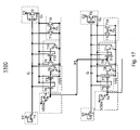
- Fig. 20 shows a circuit diagram of the first and second stages S 1 , S 2 of a shift register 1300 according to another embodiment of the present invention.
- the circuit of the shift register 1200 is same as that of shift register 1100 as shown in Fig. 17 , except that the pull-down signal K 1 generated from the first pull-down control circuit of the stage S 2 is provided to the gates of the transistors T9 and T10 of the second pull-down circuit of the stage S 1 .
- the timing chart of input and output signals for the shift register are same these shown in Fig. 18 .
- ⁇ S n ⁇ , n 1, 2, ..., N, N being a positive integer.
- Each pair of two neighboring stages S n and S n+1 or S n-1 and S n shares a single pull-down control circuit, Accordingly, it simplifies the GOA design and reduces the manufacturing cost of an LCD panel. Furthermore, it can reduce the stress and improves the reliability of operation of the LCD panel.
Applications Claiming Priority (1)
| Application Number | Priority Date | Filing Date | Title |
|---|---|---|---|
| US12/334,874 US7817771B2 (en) | 2008-12-15 | 2008-12-15 | Shift register |
Publications (3)
| Publication Number | Publication Date |
|---|---|
| EP2209124A2 true EP2209124A2 (fr) | 2010-07-21 |
| EP2209124A3 EP2209124A3 (fr) | 2010-12-01 |
| EP2209124B1 EP2209124B1 (fr) | 2012-11-14 |
Family
ID=41371941
Family Applications (1)
| Application Number | Title | Priority Date | Filing Date |
|---|---|---|---|
| EP09179144A Active EP2209124B1 (fr) | 2008-12-15 | 2009-12-14 | Registre de déphasage |
Country Status (5)
| Country | Link |
|---|---|
| US (3) | US7817771B2 (fr) |
| EP (1) | EP2209124B1 (fr) |
| JP (1) | JP5119227B2 (fr) |
| CN (2) | CN101587752B (fr) |
| TW (2) | TWI491175B (fr) |
Families Citing this family (77)
| Publication number | Priority date | Publication date | Assignee | Title |
|---|---|---|---|---|
| KR101579082B1 (ko) * | 2008-12-23 | 2015-12-22 | 삼성디스플레이 주식회사 | 게이트 구동회로 및 이의 구동 방법 |
| US9741309B2 (en) | 2009-01-22 | 2017-08-22 | Semiconductor Energy Laboratory Co., Ltd. | Method for driving display device including first to fourth switches |
| US8872751B2 (en) * | 2009-03-26 | 2014-10-28 | Semiconductor Energy Laboratory Co., Ltd. | Liquid crystal display device having interconnected transistors and electronic device including the same |
| TWI400686B (zh) * | 2009-04-08 | 2013-07-01 | Au Optronics Corp | 液晶顯示器之移位暫存器 |
| TWI413986B (zh) * | 2009-07-01 | 2013-11-01 | Au Optronics Corp | 移位暫存器 |
| US8068577B2 (en) * | 2009-09-23 | 2011-11-29 | Au Optronics Corporation | Pull-down control circuit and shift register of using same |
| TWI465039B (zh) * | 2009-10-15 | 2014-12-11 | Au Optronics Corp | 移位暫存器電路 |
| JP5132818B2 (ja) * | 2009-12-15 | 2013-01-30 | シャープ株式会社 | 走査信号線駆動回路およびそれを備えた表示装置 |
| TWI384756B (zh) * | 2009-12-22 | 2013-02-01 | Au Optronics Corp | 移位暫存器 |
| US8098792B2 (en) * | 2009-12-30 | 2012-01-17 | Au Optronics Corp. | Shift register circuit |
| US8331524B2 (en) * | 2009-12-30 | 2012-12-11 | Au Optronics Corp. | Shift register circuit |
| TWI397259B (zh) * | 2010-05-10 | 2013-05-21 | Au Optronics Corp | 移位暫存器電路 |
| JP5669453B2 (ja) * | 2010-06-22 | 2015-02-12 | 株式会社ジャパンディスプレイ | 双方向シフトレジスタ、及びこれを用いた画像表示装置 |
| JP5485811B2 (ja) | 2010-06-23 | 2014-05-07 | 株式会社ジャパンディスプレイ | 双方向シフトレジスタ、及びこれを用いた画像表示装置 |
| TWI440308B (zh) * | 2010-10-13 | 2014-06-01 | Au Optronics Corp | 閘極陣列移位暫存器 |
| CN102467891B (zh) * | 2010-10-29 | 2013-10-09 | 京东方科技集团股份有限公司 | 移位寄存器单元、栅极驱动装置及液晶显示器 |
| TWI431585B (zh) | 2010-11-30 | 2014-03-21 | Au Optronics Corp | 多工式驅動電路 |
| TW201222779A (en) * | 2010-11-30 | 2012-06-01 | Au Optronics Corp | Layout structure of shift register circuit |
| TWI426486B (zh) * | 2010-12-16 | 2014-02-11 | Au Optronics Corp | 運用於電荷分享畫素的整合面板型閘極驅動電路 |
| TWI437824B (zh) * | 2010-12-29 | 2014-05-11 | Au Optronics Corp | 移位暫存器及其驅動方法 |
| TWI415052B (zh) * | 2010-12-29 | 2013-11-11 | Au Optronics Corp | 開關裝置與應用該開關裝置之移位暫存器電路 |
| CN102651186B (zh) * | 2011-04-07 | 2015-04-01 | 北京京东方光电科技有限公司 | 移位寄存器及栅线驱动装置 |
| CN102760495B (zh) * | 2011-04-25 | 2015-07-08 | 群创光电股份有限公司 | 影像显示系统、移位寄存器与移位寄存器控制方法 |
| TWI515707B (zh) | 2011-04-25 | 2016-01-01 | 群創光電股份有限公司 | 影像顯示系統、移位暫存器與移位暫存器控制方法 |
| TWI425471B (zh) | 2011-06-17 | 2014-02-01 | Au Optronics Corp | 顯示面板及其閘極驅動電路以及閘極驅動電路驅動方法 |
| CN102629444B (zh) | 2011-08-22 | 2014-06-25 | 北京京东方光电科技有限公司 | 栅极集成驱动电路、移位寄存器及显示屏 |
| CN102681273A (zh) * | 2011-09-22 | 2012-09-19 | 京东方科技集团股份有限公司 | Tft-lcd面板及其驱动方法 |
| TWI493872B (zh) | 2012-07-05 | 2015-07-21 | Au Optronics Corp | 移位暫存器 |
| CN103578433B (zh) * | 2012-07-24 | 2015-10-07 | 北京京东方光电科技有限公司 | 一种栅极驱动电路、方法及液晶显示器 |
| TWI511459B (zh) * | 2012-10-11 | 2015-12-01 | Au Optronics Corp | 可防止漏電之閘極驅動電路 |
| CN103077690B (zh) * | 2013-01-15 | 2015-09-02 | 深圳市华星光电技术有限公司 | 栅极驱动器及液晶显示器 |
| US9117419B2 (en) | 2013-01-15 | 2015-08-25 | Shenzhen China Star Optoelectronics Technology Co., Ltd | Gate driver and liquid crystal display device |
| TWI533606B (zh) * | 2013-06-14 | 2016-05-11 | 友達光電股份有限公司 | 移位暫存器電路 |
| CN103426414B (zh) * | 2013-07-16 | 2015-12-09 | 北京京东方光电科技有限公司 | 移位寄存器单元及其驱动方法、栅极驱动电路及显示装置 |
| CN103680451B (zh) * | 2013-12-18 | 2015-12-30 | 深圳市华星光电技术有限公司 | 用于液晶显示的goa电路及显示装置 |
| CN103730094B (zh) * | 2013-12-30 | 2016-02-24 | 深圳市华星光电技术有限公司 | Goa电路结构 |
| TWI521494B (zh) | 2014-01-06 | 2016-02-11 | 友達光電股份有限公司 | 顯示面板及其製作方法 |
| CN104036714B (zh) * | 2014-05-26 | 2017-02-01 | 京东方科技集团股份有限公司 | Goa电路、显示基板及显示装置 |
| TWI595472B (zh) * | 2014-06-23 | 2017-08-11 | 友達光電股份有限公司 | 顯示面板 |
| TWI541779B (zh) | 2014-07-18 | 2016-07-11 | 友達光電股份有限公司 | 移位暫存器及移位暫存器的驅動方法 |
| US10473958B2 (en) * | 2014-09-22 | 2019-11-12 | Sharp Kabushiki Kaisha | Shift register, display device provided with same, and method for driving shift register |
| CN104464661B (zh) * | 2014-11-03 | 2016-09-21 | 深圳市华星光电技术有限公司 | 基于低温多晶硅半导体薄膜晶体管的goa电路 |
| CN104409054B (zh) * | 2014-11-03 | 2017-02-15 | 深圳市华星光电技术有限公司 | 低温多晶硅薄膜晶体管goa电路 |
| CN104464660B (zh) * | 2014-11-03 | 2017-05-03 | 深圳市华星光电技术有限公司 | 基于低温多晶硅半导体薄膜晶体管的goa电路 |
| TWI553621B (zh) * | 2015-03-19 | 2016-10-11 | 友達光電股份有限公司 | 移位暫存器 |
| CN104766575B (zh) * | 2015-04-07 | 2017-10-17 | 深圳市华星光电技术有限公司 | 一种goa电路及液晶显示器 |
| TWI553623B (zh) * | 2015-05-11 | 2016-10-11 | 友達光電股份有限公司 | 驅動電路及其控制方法 |
| CN105159488B (zh) * | 2015-08-04 | 2018-11-20 | 京东方科技集团股份有限公司 | 触控驱动电极的驱动单元、方法、电路和触控显示面板 |
| CN105185345B (zh) * | 2015-10-23 | 2018-09-07 | 京东方科技集团股份有限公司 | 一种栅极驱动电路及其驱动方法、显示面板 |
| KR102407980B1 (ko) * | 2015-10-27 | 2022-06-14 | 엘지디스플레이 주식회사 | 쉬프트레지스터 및 이를 포함하는 표시장치 |
| TWI574276B (zh) * | 2015-12-23 | 2017-03-11 | 友達光電股份有限公司 | 移位暫存器及其控制方法 |
| CN105469763B (zh) * | 2015-12-28 | 2018-09-11 | 深圳市华星光电技术有限公司 | 栅极驱动单元、栅极驱动电路及显示装置 |
| KR102555084B1 (ko) | 2015-12-30 | 2023-07-13 | 엘지디스플레이 주식회사 | 게이트 구동 모듈 및 게이트 인 패널 |
| CN107316616A (zh) | 2016-04-26 | 2017-11-03 | 中华映管股份有限公司 | 显示面板 |
| KR102578837B1 (ko) * | 2016-09-30 | 2023-09-15 | 엘지디스플레이 주식회사 | 게이트 구동 회로와 이를 이용한 표시장치 |
| CN108022560B (zh) * | 2016-11-01 | 2023-10-10 | 合肥鑫晟光电科技有限公司 | 栅极驱动电路及其驱动方法、显示基板和显示装置 |
| CN106548740A (zh) * | 2016-12-02 | 2017-03-29 | 京东方科技集团股份有限公司 | 移位寄存电路及其驱动方法、栅极驱动电路及显示装置 |
| CN106548759B (zh) * | 2017-01-14 | 2018-09-18 | 深圳市华星光电技术有限公司 | 一种goa电路及液晶显示器 |
| CN108417170A (zh) * | 2017-02-09 | 2018-08-17 | 京东方科技集团股份有限公司 | 移位寄存器单元及其驱动方法、栅极驱动电路及显示装置 |
| CN108428425B (zh) * | 2017-02-15 | 2022-03-08 | 上海和辉光电股份有限公司 | 一种扫描驱动电路、移位寄存器及其驱动方法 |
| TWI631544B (zh) * | 2017-03-03 | 2018-08-01 | 友達光電股份有限公司 | 顯示面板及驅動方法 |
| CN106847221A (zh) * | 2017-03-20 | 2017-06-13 | 京东方科技集团股份有限公司 | 移位寄存器单元、栅极驱动电路以及驱动方法 |
| TWI617966B (zh) | 2017-04-17 | 2018-03-11 | 友達光電股份有限公司 | 觸控面板 |
| TWI625710B (zh) * | 2017-04-28 | 2018-06-01 | 友達光電股份有限公司 | 閘極驅動電路與採用其之顯示裝置 |
| CN108932933B (zh) * | 2017-05-27 | 2020-01-21 | 京东方科技集团股份有限公司 | 移位寄存器、栅极驱动电路、显示装置 |
| CN107180618B (zh) * | 2017-06-30 | 2019-06-11 | 深圳市华星光电技术有限公司 | 基于goa电路的hva接线方法 |
| TWI627633B (zh) * | 2017-07-27 | 2018-06-21 | 友達光電股份有限公司 | 移位暫存器 |
| CN107492338A (zh) * | 2017-10-13 | 2017-12-19 | 京东方科技集团股份有限公司 | 一种栅极驱动电路及显示装置 |
| CN107799083B (zh) * | 2017-11-17 | 2020-02-07 | 武汉华星光电技术有限公司 | 一种goa电路 |
| TWI689816B (zh) * | 2018-03-06 | 2020-04-01 | 群聯電子股份有限公司 | 區塊管理方法、記憶體控制電路單元與記憶體儲存裝置 |
| TWI671747B (zh) * | 2018-11-12 | 2019-09-11 | 友達光電股份有限公司 | 移位暫存器 |
| KR20200085976A (ko) * | 2019-01-07 | 2020-07-16 | 삼성디스플레이 주식회사 | 주사 구동부 |
| CN112447141B (zh) | 2019-08-30 | 2022-04-08 | 京东方科技集团股份有限公司 | 移位寄存器及其驱动方法、栅极驱动电路、显示面板 |
| CN111724750A (zh) * | 2020-04-23 | 2020-09-29 | 福建华佳彩有限公司 | 一种gip电路及其控制方法和gip输出信号检测电路 |
| CN111933083B (zh) * | 2020-08-21 | 2023-04-07 | 京东方科技集团股份有限公司 | 移位寄存器单元、驱动方法和显示装置 |
| CN112216240A (zh) * | 2020-09-17 | 2021-01-12 | 福建华佳彩有限公司 | 一种新型双输出gip电路 |
| CN114677964B (zh) * | 2022-04-12 | 2024-04-05 | Tcl华星光电技术有限公司 | 移位寄存器、栅极驱动电路和显示面板 |
Family Cites Families (20)
| Publication number | Priority date | Publication date | Assignee | Title |
|---|---|---|---|---|
| JP3823614B2 (ja) * | 1999-07-01 | 2006-09-20 | カシオ計算機株式会社 | シフトレジスタ及び電子装置 |
| KR100797522B1 (ko) * | 2002-09-05 | 2008-01-24 | 삼성전자주식회사 | 쉬프트 레지스터와 이를 구비하는 액정 표시 장치 |
| KR20050117303A (ko) * | 2004-06-10 | 2005-12-14 | 삼성전자주식회사 | 표시 장치 |
| TWI316219B (en) * | 2005-08-11 | 2009-10-21 | Au Optronics Corp | A three-level driving shift register |
| US7310402B2 (en) * | 2005-10-18 | 2007-12-18 | Au Optronics Corporation | Gate line drivers for active matrix displays |
| US7529333B2 (en) * | 2005-10-27 | 2009-05-05 | Lg Display Co., Ltd. | Shift register |
| KR101192777B1 (ko) * | 2005-12-02 | 2012-10-18 | 엘지디스플레이 주식회사 | 쉬프트 레지스터 |
| TWI325132B (en) * | 2006-02-10 | 2010-05-21 | Au Optronics Corp | Shift register capable of self feedback |
| TWI323869B (en) * | 2006-03-14 | 2010-04-21 | Au Optronics Corp | Shift register circuit |
| TWI349245B (en) * | 2006-03-22 | 2011-09-21 | Au Optronics Corp | Liquid crystal display and shift register unit thereof |
| US7283603B1 (en) * | 2006-04-07 | 2007-10-16 | Au Optronics Corporation | Shift register with four phase clocks |
| KR101252572B1 (ko) * | 2006-06-15 | 2013-04-09 | 엘지디스플레이 주식회사 | 액정표시장치의 게이트구동회로 및 그 구동방법 |
| TWI338275B (en) * | 2006-08-24 | 2011-03-01 | Au Optronics Corp | Shift register with lower coupling effect and the related lcd |
| TWI336870B (en) * | 2006-09-01 | 2011-02-01 | Au Optronics Corp | Signal-driving system and shift register unit thereof |
| CN100583295C (zh) * | 2007-02-09 | 2010-01-20 | 群康科技(深圳)有限公司 | 移位寄存器及液晶显示装置 |
| KR101296645B1 (ko) * | 2007-03-12 | 2013-08-14 | 엘지디스플레이 주식회사 | 쉬프트 레지스터 |
| TWI373019B (en) * | 2007-05-09 | 2012-09-21 | Chunghwa Picture Tubes Ltd | Shift register and shift register apparatus therein |
| TWI337735B (en) * | 2007-05-18 | 2011-02-21 | Au Optronics Corp | Liquid crystal display and shift register with individual driving node |
| TWI398852B (zh) * | 2008-06-06 | 2013-06-11 | Au Optronics Corp | 可降低時脈偶合效應之移位暫存器及移位暫存器單元 |
| TWI390499B (zh) * | 2008-12-01 | 2013-03-21 | Au Optronics Corp | 移位暫存裝置 |
-
2008
- 2008-12-15 US US12/334,874 patent/US7817771B2/en active Active
-
2009
- 2009-05-27 TW TW101133016A patent/TWI491175B/zh active
- 2009-05-27 TW TW098117806A patent/TWI376098B/zh active
- 2009-06-26 CN CN200910150047.5A patent/CN101587752B/zh active Active
- 2009-06-26 CN CN201310054321.5A patent/CN103208311B/zh active Active
- 2009-09-16 JP JP2009214122A patent/JP5119227B2/ja active Active
- 2009-12-14 EP EP09179144A patent/EP2209124B1/fr active Active
-
2010
- 2010-09-08 US US12/877,748 patent/US7924967B2/en active Active
-
2011
- 2011-03-07 US US13/041,794 patent/US8031827B2/en active Active
Non-Patent Citations (1)
| Title |
|---|
| None |
Also Published As
| Publication number | Publication date |
|---|---|
| US8031827B2 (en) | 2011-10-04 |
| JP5119227B2 (ja) | 2013-01-16 |
| CN101587752B (zh) | 2013-02-27 |
| US7924967B2 (en) | 2011-04-12 |
| CN103208311B (zh) | 2015-12-02 |
| US20100150302A1 (en) | 2010-06-17 |
| TW201023516A (en) | 2010-06-16 |
| EP2209124A3 (fr) | 2010-12-01 |
| US7817771B2 (en) | 2010-10-19 |
| TWI376098B (en) | 2012-11-01 |
| CN101587752A (zh) | 2009-11-25 |
| US20110007863A1 (en) | 2011-01-13 |
| US20110158376A1 (en) | 2011-06-30 |
| TW201301765A (zh) | 2013-01-01 |
| JP2010140593A (ja) | 2010-06-24 |
| EP2209124B1 (fr) | 2012-11-14 |
| TWI491175B (zh) | 2015-07-01 |
| CN103208311A (zh) | 2013-07-17 |
Similar Documents
| Publication | Publication Date | Title |
|---|---|---|
| EP2209124A2 (fr) | Registre de déphasage | |
| EP2395512B1 (fr) | Registre à décalage doté d'une fonction de balayage bidirectionnel intégré | |
| EP2544186B1 (fr) | Registre de déphasage bidirectionnel et son procédé de commande | |
| KR101182770B1 (ko) | 게이트 구동회로 및 이를 갖는 표시장치 | |
| JP5230853B2 (ja) | 走査信号線駆動回路およびそれを備えた表示装置 | |
| EP2302617B1 (fr) | Circuit de contrôle de la mise en régime et registre de déphasage l'utilisant | |
| CN100389452C (zh) | 移位寄存器电路与改善稳定的方法及栅极线驱动电路 | |
| KR101300038B1 (ko) | 게이트 구동회로 및 이를 포함하는 표시 장치 | |
| US10438676B2 (en) | Bidirectional shift register units, bidirectional shift registers, and display panels | |
| JP5718040B2 (ja) | ゲート駆動回路及びそれを有する表示装置 | |
| CN101939777B (zh) | 显示装置及显示装置的驱动方法 | |
| CN103943076A (zh) | 栅极驱动器和包括该栅极驱动器的显示装置 | |
| JP4970552B2 (ja) | 補助容量配線駆動回路および表示装置 | |
| KR20070017600A (ko) | 쉬프트 레지스터 및 이를 갖는 표시장치 | |
| CN110660368A (zh) | 图像显示装置 | |
| US11557359B2 (en) | Shift register and gate driver circuit | |
| KR20130012392A (ko) | 게이트 구동회로 및 이를 포함하는 표시 장치 | |
| KR20060091465A (ko) | 게이트 구동회로 및 이를 갖는 표시장치 | |
| KR101377463B1 (ko) | 노이즈 제거회로와, 이를 구비한 게이트 구동회로 및 표시장치 | |
| JP2012252747A (ja) | シフトレジスター、及び電気光学装置 | |
| KR20080040847A (ko) | 표시 장치 |
Legal Events
| Date | Code | Title | Description |
|---|---|---|---|
| PUAI | Public reference made under article 153(3) epc to a published international application that has entered the european phase |
Free format text: ORIGINAL CODE: 0009012 |
|
| 17P | Request for examination filed |
Effective date: 20100114 |
|
| AK | Designated contracting states |
Kind code of ref document: A2 Designated state(s): AT BE BG CH CY CZ DE DK EE ES FI FR GB GR HR HU IE IS IT LI LT LU LV MC MK MT NL NO PL PT RO SE SI SK SM TR |
|
| AX | Request for extension of the european patent |
Extension state: AL BA RS |
|
| PUAL | Search report despatched |
Free format text: ORIGINAL CODE: 0009013 |
|
| AK | Designated contracting states |
Kind code of ref document: A3 Designated state(s): AT BE BG CH CY CZ DE DK EE ES FI FR GB GR HR HU IE IS IT LI LT LU LV MC MK MT NL NO PL PT RO SE SI SK SM TR |
|
| AX | Request for extension of the european patent |
Extension state: AL BA RS |
|
| 17Q | First examination report despatched |
Effective date: 20110609 |
|
| GRAP | Despatch of communication of intention to grant a patent |
Free format text: ORIGINAL CODE: EPIDOSNIGR1 |
|
| GRAS | Grant fee paid |
Free format text: ORIGINAL CODE: EPIDOSNIGR3 |
|
| GRAA | (expected) grant |
Free format text: ORIGINAL CODE: 0009210 |
|
| AK | Designated contracting states |
Kind code of ref document: B1 Designated state(s): AT BE BG CH CY CZ DE DK EE ES FI FR GB GR HR HU IE IS IT LI LT LU LV MC MK MT NL NO PL PT RO SE SI SK SM TR |
|
| REG | Reference to a national code |
Ref country code: GB Ref legal event code: FG4D |
|
| REG | Reference to a national code |
Ref country code: AT Ref legal event code: REF Ref document number: 584352 Country of ref document: AT Kind code of ref document: T Effective date: 20121115 Ref country code: CH Ref legal event code: EP |
|
| REG | Reference to a national code |
Ref country code: IE Ref legal event code: FG4D |
|
| REG | Reference to a national code |
Ref country code: DE Ref legal event code: R096 Ref document number: 602009011155 Country of ref document: DE Effective date: 20130110 |
|
| REG | Reference to a national code |
Ref country code: NL Ref legal event code: VDEP Effective date: 20121114 |
|
| REG | Reference to a national code |
Ref country code: AT Ref legal event code: MK05 Ref document number: 584352 Country of ref document: AT Kind code of ref document: T Effective date: 20121114 |
|
| REG | Reference to a national code |
Ref country code: LT Ref legal event code: MG4D |
|
| PG25 | Lapsed in a contracting state [announced via postgrant information from national office to epo] |
Ref country code: FI Free format text: LAPSE BECAUSE OF FAILURE TO SUBMIT A TRANSLATION OF THE DESCRIPTION OR TO PAY THE FEE WITHIN THE PRESCRIBED TIME-LIMIT Effective date: 20121114 Ref country code: ES Free format text: LAPSE BECAUSE OF FAILURE TO SUBMIT A TRANSLATION OF THE DESCRIPTION OR TO PAY THE FEE WITHIN THE PRESCRIBED TIME-LIMIT Effective date: 20130225 Ref country code: NO Free format text: LAPSE BECAUSE OF FAILURE TO SUBMIT A TRANSLATION OF THE DESCRIPTION OR TO PAY THE FEE WITHIN THE PRESCRIBED TIME-LIMIT Effective date: 20130214 Ref country code: HR Free format text: LAPSE BECAUSE OF FAILURE TO SUBMIT A TRANSLATION OF THE DESCRIPTION OR TO PAY THE FEE WITHIN THE PRESCRIBED TIME-LIMIT Effective date: 20121114 Ref country code: SE Free format text: LAPSE BECAUSE OF FAILURE TO SUBMIT A TRANSLATION OF THE DESCRIPTION OR TO PAY THE FEE WITHIN THE PRESCRIBED TIME-LIMIT Effective date: 20121114 Ref country code: LT Free format text: LAPSE BECAUSE OF FAILURE TO SUBMIT A TRANSLATION OF THE DESCRIPTION OR TO PAY THE FEE WITHIN THE PRESCRIBED TIME-LIMIT Effective date: 20121114 |
|
| PG25 | Lapsed in a contracting state [announced via postgrant information from national office to epo] |
Ref country code: PL Free format text: LAPSE BECAUSE OF FAILURE TO SUBMIT A TRANSLATION OF THE DESCRIPTION OR TO PAY THE FEE WITHIN THE PRESCRIBED TIME-LIMIT Effective date: 20121114 Ref country code: SI Free format text: LAPSE BECAUSE OF FAILURE TO SUBMIT A TRANSLATION OF THE DESCRIPTION OR TO PAY THE FEE WITHIN THE PRESCRIBED TIME-LIMIT Effective date: 20121114 Ref country code: PT Free format text: LAPSE BECAUSE OF FAILURE TO SUBMIT A TRANSLATION OF THE DESCRIPTION OR TO PAY THE FEE WITHIN THE PRESCRIBED TIME-LIMIT Effective date: 20130314 Ref country code: LV Free format text: LAPSE BECAUSE OF FAILURE TO SUBMIT A TRANSLATION OF THE DESCRIPTION OR TO PAY THE FEE WITHIN THE PRESCRIBED TIME-LIMIT Effective date: 20121114 Ref country code: GR Free format text: LAPSE BECAUSE OF FAILURE TO SUBMIT A TRANSLATION OF THE DESCRIPTION OR TO PAY THE FEE WITHIN THE PRESCRIBED TIME-LIMIT Effective date: 20130215 Ref country code: BE Free format text: LAPSE BECAUSE OF FAILURE TO SUBMIT A TRANSLATION OF THE DESCRIPTION OR TO PAY THE FEE WITHIN THE PRESCRIBED TIME-LIMIT Effective date: 20121114 |
|
| PG25 | Lapsed in a contracting state [announced via postgrant information from national office to epo] |
Ref country code: AT Free format text: LAPSE BECAUSE OF FAILURE TO SUBMIT A TRANSLATION OF THE DESCRIPTION OR TO PAY THE FEE WITHIN THE PRESCRIBED TIME-LIMIT Effective date: 20121114 |
|
| PG25 | Lapsed in a contracting state [announced via postgrant information from national office to epo] |
Ref country code: BG Free format text: LAPSE BECAUSE OF FAILURE TO SUBMIT A TRANSLATION OF THE DESCRIPTION OR TO PAY THE FEE WITHIN THE PRESCRIBED TIME-LIMIT Effective date: 20130214 Ref country code: DK Free format text: LAPSE BECAUSE OF FAILURE TO SUBMIT A TRANSLATION OF THE DESCRIPTION OR TO PAY THE FEE WITHIN THE PRESCRIBED TIME-LIMIT Effective date: 20121114 Ref country code: SK Free format text: LAPSE BECAUSE OF FAILURE TO SUBMIT A TRANSLATION OF THE DESCRIPTION OR TO PAY THE FEE WITHIN THE PRESCRIBED TIME-LIMIT Effective date: 20121114 Ref country code: MC Free format text: LAPSE BECAUSE OF NON-PAYMENT OF DUE FEES Effective date: 20121231 Ref country code: CZ Free format text: LAPSE BECAUSE OF FAILURE TO SUBMIT A TRANSLATION OF THE DESCRIPTION OR TO PAY THE FEE WITHIN THE PRESCRIBED TIME-LIMIT Effective date: 20121114 Ref country code: EE Free format text: LAPSE BECAUSE OF FAILURE TO SUBMIT A TRANSLATION OF THE DESCRIPTION OR TO PAY THE FEE WITHIN THE PRESCRIBED TIME-LIMIT Effective date: 20121114 |
|
| PG25 | Lapsed in a contracting state [announced via postgrant information from national office to epo] |
Ref country code: RO Free format text: LAPSE BECAUSE OF FAILURE TO SUBMIT A TRANSLATION OF THE DESCRIPTION OR TO PAY THE FEE WITHIN THE PRESCRIBED TIME-LIMIT Effective date: 20121114 Ref country code: NL Free format text: LAPSE BECAUSE OF FAILURE TO SUBMIT A TRANSLATION OF THE DESCRIPTION OR TO PAY THE FEE WITHIN THE PRESCRIBED TIME-LIMIT Effective date: 20121114 Ref country code: IT Free format text: LAPSE BECAUSE OF FAILURE TO SUBMIT A TRANSLATION OF THE DESCRIPTION OR TO PAY THE FEE WITHIN THE PRESCRIBED TIME-LIMIT Effective date: 20121114 |
|
| PLBE | No opposition filed within time limit |
Free format text: ORIGINAL CODE: 0009261 |
|
| STAA | Information on the status of an ep patent application or granted ep patent |
Free format text: STATUS: NO OPPOSITION FILED WITHIN TIME LIMIT |
|
| REG | Reference to a national code |
Ref country code: IE Ref legal event code: MM4A |
|
| 26N | No opposition filed |
Effective date: 20130815 |
|
| PG25 | Lapsed in a contracting state [announced via postgrant information from national office to epo] |
Ref country code: IE Free format text: LAPSE BECAUSE OF NON-PAYMENT OF DUE FEES Effective date: 20121214 |
|
| PG25 | Lapsed in a contracting state [announced via postgrant information from national office to epo] |
Ref country code: CY Free format text: LAPSE BECAUSE OF FAILURE TO SUBMIT A TRANSLATION OF THE DESCRIPTION OR TO PAY THE FEE WITHIN THE PRESCRIBED TIME-LIMIT Effective date: 20121114 Ref country code: MT Free format text: LAPSE BECAUSE OF FAILURE TO SUBMIT A TRANSLATION OF THE DESCRIPTION OR TO PAY THE FEE WITHIN THE PRESCRIBED TIME-LIMIT Effective date: 20121114 |
|
| REG | Reference to a national code |
Ref country code: DE Ref legal event code: R097 Ref document number: 602009011155 Country of ref document: DE Effective date: 20130815 |
|
| PG25 | Lapsed in a contracting state [announced via postgrant information from national office to epo] |
Ref country code: TR Free format text: LAPSE BECAUSE OF FAILURE TO SUBMIT A TRANSLATION OF THE DESCRIPTION OR TO PAY THE FEE WITHIN THE PRESCRIBED TIME-LIMIT Effective date: 20121114 |
|
| PG25 | Lapsed in a contracting state [announced via postgrant information from national office to epo] |
Ref country code: SM Free format text: LAPSE BECAUSE OF FAILURE TO SUBMIT A TRANSLATION OF THE DESCRIPTION OR TO PAY THE FEE WITHIN THE PRESCRIBED TIME-LIMIT Effective date: 20121114 Ref country code: LU Free format text: LAPSE BECAUSE OF NON-PAYMENT OF DUE FEES Effective date: 20121214 |
|
| PG25 | Lapsed in a contracting state [announced via postgrant information from national office to epo] |
Ref country code: HU Free format text: LAPSE BECAUSE OF FAILURE TO SUBMIT A TRANSLATION OF THE DESCRIPTION OR TO PAY THE FEE WITHIN THE PRESCRIBED TIME-LIMIT Effective date: 20091214 |
|
| REG | Reference to a national code |
Ref country code: CH Ref legal event code: PL |
|
| PG25 | Lapsed in a contracting state [announced via postgrant information from national office to epo] |
Ref country code: CH Free format text: LAPSE BECAUSE OF NON-PAYMENT OF DUE FEES Effective date: 20131231 Ref country code: LI Free format text: LAPSE BECAUSE OF NON-PAYMENT OF DUE FEES Effective date: 20131231 |
|
| PG25 | Lapsed in a contracting state [announced via postgrant information from national office to epo] |
Ref country code: MK Free format text: LAPSE BECAUSE OF FAILURE TO SUBMIT A TRANSLATION OF THE DESCRIPTION OR TO PAY THE FEE WITHIN THE PRESCRIBED TIME-LIMIT Effective date: 20121114 |
|
| REG | Reference to a national code |
Ref country code: FR Ref legal event code: PLFP Year of fee payment: 7 |
|
| PG25 | Lapsed in a contracting state [announced via postgrant information from national office to epo] |
Ref country code: IS Free format text: LAPSE BECAUSE OF FAILURE TO SUBMIT A TRANSLATION OF THE DESCRIPTION OR TO PAY THE FEE WITHIN THE PRESCRIBED TIME-LIMIT Effective date: 20121114 |
|
| REG | Reference to a national code |
Ref country code: FR Ref legal event code: PLFP Year of fee payment: 8 |
|
| REG | Reference to a national code |
Ref country code: FR Ref legal event code: PLFP Year of fee payment: 9 |
|
| P01 | Opt-out of the competence of the unified patent court (upc) registered |
Effective date: 20230516 |
|
| REG | Reference to a national code |
Ref country code: DE Ref legal event code: R081 Ref document number: 602009011155 Country of ref document: DE Owner name: AUO CORPORATION, TW Free format text: FORMER OWNER: AU OPTRONICS CORPORATION, HSIN-CHU, TW Ref country code: DE Ref legal event code: R081 Ref document number: 602009011155 Country of ref document: DE Owner name: OPTRONIC SCIENCES LLC, ALLEN, US Free format text: FORMER OWNER: AU OPTRONICS CORPORATION, HSIN-CHU, TW |
|
| REG | Reference to a national code |
Ref country code: GB Ref legal event code: 732E Free format text: REGISTERED BETWEEN 20231109 AND 20231115 |
|
| REG | Reference to a national code |
Ref country code: DE Ref legal event code: R082 Ref document number: 602009011155 Country of ref document: DE Representative=s name: KELLER SCHNEIDER PATENTANWALTS GMBH, DE Ref country code: DE Ref legal event code: R081 Ref document number: 602009011155 Country of ref document: DE Owner name: OPTRONIC SCIENCES LLC, ALLEN, US Free format text: FORMER OWNER: AUO CORPORATION, HSINCHU, TW |
|
| PGFP | Annual fee paid to national office [announced via postgrant information from national office to epo] |
Ref country code: GB Payment date: 20231220 Year of fee payment: 15 |
|
| PGFP | Annual fee paid to national office [announced via postgrant information from national office to epo] |
Ref country code: FR Payment date: 20231221 Year of fee payment: 15 Ref country code: DE Payment date: 20231214 Year of fee payment: 15 |