EP1605030A2 - Lichtemittierende Vorrichtung - Google Patents
Lichtemittierende Vorrichtung Download PDFInfo
- Publication number
- EP1605030A2 EP1605030A2 EP04106882A EP04106882A EP1605030A2 EP 1605030 A2 EP1605030 A2 EP 1605030A2 EP 04106882 A EP04106882 A EP 04106882A EP 04106882 A EP04106882 A EP 04106882A EP 1605030 A2 EP1605030 A2 EP 1605030A2
- Authority
- EP
- European Patent Office
- Prior art keywords
- light emitting
- combination
- emitting device
- lead
- phosphors
- Prior art date
- Legal status (The legal status is an assumption and is not a legal conclusion. Google has not performed a legal analysis and makes no representation as to the accuracy of the status listed.)
- Granted
Links
- 239000010949 copper Substances 0.000 claims abstract description 178
- 229910052802 copper Inorganic materials 0.000 claims abstract description 116
- RYGMFSIKBFXOCR-UHFFFAOYSA-N Copper Chemical compound [Cu] RYGMFSIKBFXOCR-UHFFFAOYSA-N 0.000 claims abstract description 114
- OAICVXFJPJFONN-UHFFFAOYSA-N Phosphorus Chemical compound [P] OAICVXFJPJFONN-UHFFFAOYSA-N 0.000 claims abstract description 49
- 150000001875 compounds Chemical class 0.000 claims abstract description 39
- 150000004645 aluminates Chemical class 0.000 claims abstract description 21
- 229910019142 PO4 Inorganic materials 0.000 claims abstract description 12
- 239000000758 substrate Substances 0.000 claims abstract description 10
- 235000021317 phosphate Nutrition 0.000 claims abstract description 9
- 150000003013 phosphoric acid derivatives Chemical class 0.000 claims abstract description 9
- 150000004760 silicates Chemical class 0.000 claims abstract description 8
- 239000000463 material Substances 0.000 claims description 74
- PNEYBMLMFCGWSK-UHFFFAOYSA-N aluminium oxide Inorganic materials [O-2].[O-2].[O-2].[Al+3].[Al+3] PNEYBMLMFCGWSK-UHFFFAOYSA-N 0.000 claims description 26
- VYPSYNLAJGMNEJ-UHFFFAOYSA-N Silicium dioxide Chemical compound O=[Si]=O VYPSYNLAJGMNEJ-UHFFFAOYSA-N 0.000 claims description 22
- 229910052693 Europium Inorganic materials 0.000 claims description 20
- 229910052692 Dysprosium Inorganic materials 0.000 claims description 16
- 229910052688 Gadolinium Inorganic materials 0.000 claims description 16
- 229910052748 manganese Inorganic materials 0.000 claims description 16
- 229910052712 strontium Inorganic materials 0.000 claims description 16
- 229910052788 barium Inorganic materials 0.000 claims description 15
- 229910052791 calcium Inorganic materials 0.000 claims description 15
- 229910052725 zinc Inorganic materials 0.000 claims description 15
- 229910052777 Praseodymium Inorganic materials 0.000 claims description 14
- 229910052772 Samarium Inorganic materials 0.000 claims description 14
- 229910052790 beryllium Inorganic materials 0.000 claims description 14
- 229910052797 bismuth Inorganic materials 0.000 claims description 14
- 229910052793 cadmium Inorganic materials 0.000 claims description 14
- 229910052746 lanthanum Inorganic materials 0.000 claims description 14
- 229910052745 lead Inorganic materials 0.000 claims description 14
- 229910052749 magnesium Inorganic materials 0.000 claims description 14
- 229910052706 scandium Inorganic materials 0.000 claims description 14
- 229910052718 tin Inorganic materials 0.000 claims description 14
- 229910052727 yttrium Inorganic materials 0.000 claims description 14
- 229910052771 Terbium Inorganic materials 0.000 claims description 12
- 229910052792 caesium Inorganic materials 0.000 claims description 12
- 229910052737 gold Inorganic materials 0.000 claims description 12
- 229910052738 indium Inorganic materials 0.000 claims description 12
- 229910052744 lithium Inorganic materials 0.000 claims description 12
- 229910052700 potassium Inorganic materials 0.000 claims description 12
- 229910052701 rubidium Inorganic materials 0.000 claims description 12
- 229910052709 silver Inorganic materials 0.000 claims description 12
- 229910052708 sodium Inorganic materials 0.000 claims description 12
- 229910052681 coesite Inorganic materials 0.000 claims description 11
- 229910052906 cristobalite Inorganic materials 0.000 claims description 11
- 239000000377 silicon dioxide Substances 0.000 claims description 11
- 229910052682 stishovite Inorganic materials 0.000 claims description 11
- 229910052905 tridymite Inorganic materials 0.000 claims description 11
- QVGXLLKOCUKJST-UHFFFAOYSA-N atomic oxygen Chemical compound [O] QVGXLLKOCUKJST-UHFFFAOYSA-N 0.000 claims description 10
- 229910052733 gallium Inorganic materials 0.000 claims description 10
- YBMRDBCBODYGJE-UHFFFAOYSA-N germanium dioxide Chemical compound O=[Ge]=O YBMRDBCBODYGJE-UHFFFAOYSA-N 0.000 claims description 10
- 229910052760 oxygen Inorganic materials 0.000 claims description 10
- 239000001301 oxygen Substances 0.000 claims description 10
- 229910052710 silicon Inorganic materials 0.000 claims description 10
- 229910052719 titanium Inorganic materials 0.000 claims description 10
- 229910052726 zirconium Inorganic materials 0.000 claims description 10
- 229910052684 Cerium Inorganic materials 0.000 claims description 8
- 229910052691 Erbium Inorganic materials 0.000 claims description 8
- 229910052689 Holmium Inorganic materials 0.000 claims description 8
- 229910052765 Lutetium Inorganic materials 0.000 claims description 8
- 229910052779 Neodymium Inorganic materials 0.000 claims description 8
- 229910052775 Thulium Inorganic materials 0.000 claims description 8
- 229910052769 Ytterbium Inorganic materials 0.000 claims description 8
- 229910052787 antimony Inorganic materials 0.000 claims description 8
- 229910052750 molybdenum Inorganic materials 0.000 claims description 8
- 229910052758 niobium Inorganic materials 0.000 claims description 8
- 229910052715 tantalum Inorganic materials 0.000 claims description 8
- 229910052721 tungsten Inorganic materials 0.000 claims description 8
- 229910052796 boron Inorganic materials 0.000 claims description 7
- 229910052782 aluminium Inorganic materials 0.000 claims description 6
- 229910052593 corundum Inorganic materials 0.000 claims description 6
- 229910052732 germanium Inorganic materials 0.000 claims description 6
- 229910052735 hafnium Inorganic materials 0.000 claims description 6
- 229910052720 vanadium Inorganic materials 0.000 claims description 6
- 229910001845 yogo sapphire Inorganic materials 0.000 claims description 6
- LJCFOYOSGPHIOO-UHFFFAOYSA-N antimony pentoxide Inorganic materials O=[Sb](=O)O[Sb](=O)=O LJCFOYOSGPHIOO-UHFFFAOYSA-N 0.000 claims description 4
- 239000003566 sealing material Substances 0.000 claims description 4
- QZQVBEXLDFYHSR-UHFFFAOYSA-N gallium(III) oxide Inorganic materials O=[Ga]O[Ga]=O QZQVBEXLDFYHSR-UHFFFAOYSA-N 0.000 claims description 2
- 230000005284 excitation Effects 0.000 description 32
- 239000007858 starting material Substances 0.000 description 30
- 239000000203 mixture Substances 0.000 description 29
- -1 compound Compound Chemical class 0.000 description 21
- 238000002360 preparation method Methods 0.000 description 21
- QPLDLSVMHZLSFG-UHFFFAOYSA-N Copper oxide Chemical compound [Cu]=O QPLDLSVMHZLSFG-UHFFFAOYSA-N 0.000 description 14
- 230000004907 flux Effects 0.000 description 14
- 150000004649 carbonic acid derivatives Chemical class 0.000 description 13
- RSEIMSPAXMNYFJ-UHFFFAOYSA-N europium(III) oxide Inorganic materials O=[Eu]O[Eu]=O RSEIMSPAXMNYFJ-UHFFFAOYSA-N 0.000 description 10
- 229910052909 inorganic silicate Inorganic materials 0.000 description 9
- 229910000018 strontium carbonate Inorganic materials 0.000 description 9
- LEDMRZGFZIAGGB-UHFFFAOYSA-L strontium carbonate Chemical compound [Sr+2].[O-]C([O-])=O LEDMRZGFZIAGGB-UHFFFAOYSA-L 0.000 description 9
- VTYYLEPIZMXCLO-UHFFFAOYSA-L Calcium carbonate Chemical compound [Ca+2].[O-]C([O-])=O VTYYLEPIZMXCLO-UHFFFAOYSA-L 0.000 description 8
- 238000010304 firing Methods 0.000 description 7
- NLXLAEXVIDQMFP-UHFFFAOYSA-N Ammonia chloride Chemical compound [NH4+].[Cl-] NLXLAEXVIDQMFP-UHFFFAOYSA-N 0.000 description 6
- AYJRCSIUFZENHW-UHFFFAOYSA-L barium carbonate Chemical compound [Ba+2].[O-]C([O-])=O AYJRCSIUFZENHW-UHFFFAOYSA-L 0.000 description 6
- YEXPOXQUZXUXJW-UHFFFAOYSA-N lead(II) oxide Inorganic materials [Pb]=O YEXPOXQUZXUXJW-UHFFFAOYSA-N 0.000 description 6
- CPLXHLVBOLITMK-UHFFFAOYSA-N Magnesium oxide Chemical compound [Mg]=O CPLXHLVBOLITMK-UHFFFAOYSA-N 0.000 description 5
- 238000006243 chemical reaction Methods 0.000 description 5
- HTUMBQDCCIXGCV-UHFFFAOYSA-N lead oxide Chemical compound [O-2].[Pb+2] HTUMBQDCCIXGCV-UHFFFAOYSA-N 0.000 description 5
- 238000003801 milling Methods 0.000 description 5
- 230000003287 optical effect Effects 0.000 description 5
- KLZUFWVZNOTSEM-UHFFFAOYSA-K Aluminium flouride Chemical compound F[Al](F)F KLZUFWVZNOTSEM-UHFFFAOYSA-K 0.000 description 4
- 239000005084 Strontium aluminate Substances 0.000 description 4
- XLOMVQKBTHCTTD-UHFFFAOYSA-N Zinc monoxide Chemical compound [Zn]=O XLOMVQKBTHCTTD-UHFFFAOYSA-N 0.000 description 4
- 229910000019 calcium carbonate Inorganic materials 0.000 description 4
- 229910021502 aluminium hydroxide Inorganic materials 0.000 description 3
- WNROFYMDJYEPJX-UHFFFAOYSA-K aluminium hydroxide Chemical compound [OH-].[OH-].[OH-].[Al+3] WNROFYMDJYEPJX-UHFFFAOYSA-K 0.000 description 3
- KGBXLFKZBHKPEV-UHFFFAOYSA-N boric acid Chemical compound OB(O)O KGBXLFKZBHKPEV-UHFFFAOYSA-N 0.000 description 3
- 229910001679 gibbsite Inorganic materials 0.000 description 3
- 150000004679 hydroxides Chemical class 0.000 description 3
- 238000005286 illumination Methods 0.000 description 3
- 239000011656 manganese carbonate Substances 0.000 description 3
- 229910000016 manganese(II) carbonate Inorganic materials 0.000 description 3
- 238000009877 rendering Methods 0.000 description 3
- 229920005989 resin Polymers 0.000 description 3
- 239000011347 resin Substances 0.000 description 3
- XEEYBQQBJWHFJM-UHFFFAOYSA-N Iron Chemical compound [Fe] XEEYBQQBJWHFJM-UHFFFAOYSA-N 0.000 description 2
- BPQQTUXANYXVAA-UHFFFAOYSA-N Orthosilicate Chemical compound [O-][Si]([O-])([O-])[O-] BPQQTUXANYXVAA-UHFFFAOYSA-N 0.000 description 2
- 229910003669 SrAl2O4 Inorganic materials 0.000 description 2
- 150000001805 chlorine compounds Chemical class 0.000 description 2
- 238000000295 emission spectrum Methods 0.000 description 2
- 238000005516 engineering process Methods 0.000 description 2
- 239000003822 epoxy resin Substances 0.000 description 2
- 238000004519 manufacturing process Methods 0.000 description 2
- 229910052751 metal Inorganic materials 0.000 description 2
- 239000002184 metal Substances 0.000 description 2
- 239000002798 polar solvent Substances 0.000 description 2
- 229920000647 polyepoxide Polymers 0.000 description 2
- 229910052761 rare earth metal Inorganic materials 0.000 description 2
- 230000001105 regulatory effect Effects 0.000 description 2
- 230000003595 spectral effect Effects 0.000 description 2
- 238000001228 spectrum Methods 0.000 description 2
- 239000000126 substance Substances 0.000 description 2
- XLYOFNOQVPJJNP-UHFFFAOYSA-N water Substances O XLYOFNOQVPJJNP-UHFFFAOYSA-N 0.000 description 2
- NAWXUBYGYWOOIX-SFHVURJKSA-N (2s)-2-[[4-[2-(2,4-diaminoquinazolin-6-yl)ethyl]benzoyl]amino]-4-methylidenepentanedioic acid Chemical compound C1=CC2=NC(N)=NC(N)=C2C=C1CCC1=CC=C(C(=O)N[C@@H](CC(=C)C(O)=O)C(O)=O)C=C1 NAWXUBYGYWOOIX-SFHVURJKSA-N 0.000 description 1
- UXVMQQNJUSDDNG-UHFFFAOYSA-L Calcium chloride Chemical compound [Cl-].[Cl-].[Ca+2] UXVMQQNJUSDDNG-UHFFFAOYSA-L 0.000 description 1
- 229910005835 GeO6 Inorganic materials 0.000 description 1
- FUJCRWPEOMXPAD-UHFFFAOYSA-N Li2O Inorganic materials [Li+].[Li+].[O-2] FUJCRWPEOMXPAD-UHFFFAOYSA-N 0.000 description 1
- XUIMIQQOPSSXEZ-UHFFFAOYSA-N Silicon Chemical compound [Si] XUIMIQQOPSSXEZ-UHFFFAOYSA-N 0.000 description 1
- 239000001110 calcium chloride Substances 0.000 description 1
- 229910001628 calcium chloride Inorganic materials 0.000 description 1
- 229910052589 chlorapatite Inorganic materials 0.000 description 1
- XUCJHNOBJLKZNU-UHFFFAOYSA-M dilithium;hydroxide Chemical compound [Li+].[Li+].[OH-] XUCJHNOBJLKZNU-UHFFFAOYSA-M 0.000 description 1
- 238000010438 heat treatment Methods 0.000 description 1
- 239000012535 impurity Substances 0.000 description 1
- 239000011261 inert gas Substances 0.000 description 1
- 229910052742 iron Inorganic materials 0.000 description 1
- 235000015250 liver sausages Nutrition 0.000 description 1
- 238000000034 method Methods 0.000 description 1
- 229910052756 noble gas Inorganic materials 0.000 description 1
- NBIIXXVUZAFLBC-UHFFFAOYSA-K phosphate Chemical compound [O-]P([O-])([O-])=O NBIIXXVUZAFLBC-UHFFFAOYSA-K 0.000 description 1
- 239000010452 phosphate Substances 0.000 description 1
- 150000002910 rare earth metals Chemical class 0.000 description 1
- 239000010703 silicon Substances 0.000 description 1
- 238000003746 solid phase reaction Methods 0.000 description 1
- 238000010671 solid-state reaction Methods 0.000 description 1
- 229910001631 strontium chloride Inorganic materials 0.000 description 1
- AHBGXTDRMVNFER-UHFFFAOYSA-L strontium dichloride Chemical compound [Cl-].[Cl-].[Sr+2] AHBGXTDRMVNFER-UHFFFAOYSA-L 0.000 description 1
- QORWJWZARLRLPR-UHFFFAOYSA-H tricalcium bis(phosphate) Chemical compound [Ca+2].[Ca+2].[Ca+2].[O-]P([O-])([O-])=O.[O-]P([O-])([O-])=O QORWJWZARLRLPR-UHFFFAOYSA-H 0.000 description 1
- 229910000391 tricalcium phosphate Inorganic materials 0.000 description 1
- 238000001429 visible spectrum Methods 0.000 description 1
Images

Classifications
-
- C—CHEMISTRY; METALLURGY
- C09—DYES; PAINTS; POLISHES; NATURAL RESINS; ADHESIVES; COMPOSITIONS NOT OTHERWISE PROVIDED FOR; APPLICATIONS OF MATERIALS NOT OTHERWISE PROVIDED FOR
- C09K—MATERIALS FOR MISCELLANEOUS APPLICATIONS, NOT PROVIDED FOR ELSEWHERE
- C09K11/00—Luminescent, e.g. electroluminescent, chemiluminescent materials
- C09K11/08—Luminescent, e.g. electroluminescent, chemiluminescent materials containing inorganic luminescent materials
- C09K11/77—Luminescent, e.g. electroluminescent, chemiluminescent materials containing inorganic luminescent materials containing rare earth metals
- C09K11/7728—Luminescent, e.g. electroluminescent, chemiluminescent materials containing inorganic luminescent materials containing rare earth metals containing europium
- C09K11/7734—Aluminates
-
- C—CHEMISTRY; METALLURGY
- C09—DYES; PAINTS; POLISHES; NATURAL RESINS; ADHESIVES; COMPOSITIONS NOT OTHERWISE PROVIDED FOR; APPLICATIONS OF MATERIALS NOT OTHERWISE PROVIDED FOR
- C09K—MATERIALS FOR MISCELLANEOUS APPLICATIONS, NOT PROVIDED FOR ELSEWHERE
- C09K11/00—Luminescent, e.g. electroluminescent, chemiluminescent materials
- C09K11/08—Luminescent, e.g. electroluminescent, chemiluminescent materials containing inorganic luminescent materials
- C09K11/66—Luminescent, e.g. electroluminescent, chemiluminescent materials containing inorganic luminescent materials containing germanium, tin or lead
- C09K11/664—Halogenides
- C09K11/665—Halogenides with alkali or alkaline earth metals
-
- C—CHEMISTRY; METALLURGY
- C09—DYES; PAINTS; POLISHES; NATURAL RESINS; ADHESIVES; COMPOSITIONS NOT OTHERWISE PROVIDED FOR; APPLICATIONS OF MATERIALS NOT OTHERWISE PROVIDED FOR
- C09K—MATERIALS FOR MISCELLANEOUS APPLICATIONS, NOT PROVIDED FOR ELSEWHERE
- C09K11/00—Luminescent, e.g. electroluminescent, chemiluminescent materials
- C09K11/08—Luminescent, e.g. electroluminescent, chemiluminescent materials containing inorganic luminescent materials
- C09K11/66—Luminescent, e.g. electroluminescent, chemiluminescent materials containing inorganic luminescent materials containing germanium, tin or lead
- C09K11/666—Aluminates; Silicates
-
- C—CHEMISTRY; METALLURGY
- C09—DYES; PAINTS; POLISHES; NATURAL RESINS; ADHESIVES; COMPOSITIONS NOT OTHERWISE PROVIDED FOR; APPLICATIONS OF MATERIALS NOT OTHERWISE PROVIDED FOR
- C09K—MATERIALS FOR MISCELLANEOUS APPLICATIONS, NOT PROVIDED FOR ELSEWHERE
- C09K11/00—Luminescent, e.g. electroluminescent, chemiluminescent materials
- C09K11/08—Luminescent, e.g. electroluminescent, chemiluminescent materials containing inorganic luminescent materials
- C09K11/74—Luminescent, e.g. electroluminescent, chemiluminescent materials containing inorganic luminescent materials containing arsenic, antimony or bismuth
- C09K11/75—Luminescent, e.g. electroluminescent, chemiluminescent materials containing inorganic luminescent materials containing arsenic, antimony or bismuth containing antimony
- C09K11/751—Chalcogenides
- C09K11/753—Chalcogenides with alkaline earth metals
-
- C—CHEMISTRY; METALLURGY
- C09—DYES; PAINTS; POLISHES; NATURAL RESINS; ADHESIVES; COMPOSITIONS NOT OTHERWISE PROVIDED FOR; APPLICATIONS OF MATERIALS NOT OTHERWISE PROVIDED FOR
- C09K—MATERIALS FOR MISCELLANEOUS APPLICATIONS, NOT PROVIDED FOR ELSEWHERE
- C09K11/00—Luminescent, e.g. electroluminescent, chemiluminescent materials
- C09K11/08—Luminescent, e.g. electroluminescent, chemiluminescent materials containing inorganic luminescent materials
- C09K11/74—Luminescent, e.g. electroluminescent, chemiluminescent materials containing inorganic luminescent materials containing arsenic, antimony or bismuth
- C09K11/75—Luminescent, e.g. electroluminescent, chemiluminescent materials containing inorganic luminescent materials containing arsenic, antimony or bismuth containing antimony
- C09K11/755—Halogenides
- C09K11/756—Halogenides with alkali or alkaline earth metals
-
- C—CHEMISTRY; METALLURGY
- C09—DYES; PAINTS; POLISHES; NATURAL RESINS; ADHESIVES; COMPOSITIONS NOT OTHERWISE PROVIDED FOR; APPLICATIONS OF MATERIALS NOT OTHERWISE PROVIDED FOR
- C09K—MATERIALS FOR MISCELLANEOUS APPLICATIONS, NOT PROVIDED FOR ELSEWHERE
- C09K11/00—Luminescent, e.g. electroluminescent, chemiluminescent materials
- C09K11/08—Luminescent, e.g. electroluminescent, chemiluminescent materials containing inorganic luminescent materials
- C09K11/77—Luminescent, e.g. electroluminescent, chemiluminescent materials containing inorganic luminescent materials containing rare earth metals
- C09K11/7728—Luminescent, e.g. electroluminescent, chemiluminescent materials containing inorganic luminescent materials containing rare earth metals containing europium
- C09K11/77342—Silicates
-
- C—CHEMISTRY; METALLURGY
- C09—DYES; PAINTS; POLISHES; NATURAL RESINS; ADHESIVES; COMPOSITIONS NOT OTHERWISE PROVIDED FOR; APPLICATIONS OF MATERIALS NOT OTHERWISE PROVIDED FOR
- C09K—MATERIALS FOR MISCELLANEOUS APPLICATIONS, NOT PROVIDED FOR ELSEWHERE
- C09K11/00—Luminescent, e.g. electroluminescent, chemiluminescent materials
- C09K11/08—Luminescent, e.g. electroluminescent, chemiluminescent materials containing inorganic luminescent materials
- C09K11/77—Luminescent, e.g. electroluminescent, chemiluminescent materials containing inorganic luminescent materials containing rare earth metals
- C09K11/7728—Luminescent, e.g. electroluminescent, chemiluminescent materials containing inorganic luminescent materials containing rare earth metals containing europium
- C09K11/77344—Aluminosilicates
-
- C—CHEMISTRY; METALLURGY
- C09—DYES; PAINTS; POLISHES; NATURAL RESINS; ADHESIVES; COMPOSITIONS NOT OTHERWISE PROVIDED FOR; APPLICATIONS OF MATERIALS NOT OTHERWISE PROVIDED FOR
- C09K—MATERIALS FOR MISCELLANEOUS APPLICATIONS, NOT PROVIDED FOR ELSEWHERE
- C09K11/00—Luminescent, e.g. electroluminescent, chemiluminescent materials
- C09K11/08—Luminescent, e.g. electroluminescent, chemiluminescent materials containing inorganic luminescent materials
- C09K11/77—Luminescent, e.g. electroluminescent, chemiluminescent materials containing inorganic luminescent materials containing rare earth metals
- C09K11/7728—Luminescent, e.g. electroluminescent, chemiluminescent materials containing inorganic luminescent materials containing rare earth metals containing europium
- C09K11/7735—Germanates
-
- C—CHEMISTRY; METALLURGY
- C09—DYES; PAINTS; POLISHES; NATURAL RESINS; ADHESIVES; COMPOSITIONS NOT OTHERWISE PROVIDED FOR; APPLICATIONS OF MATERIALS NOT OTHERWISE PROVIDED FOR
- C09K—MATERIALS FOR MISCELLANEOUS APPLICATIONS, NOT PROVIDED FOR ELSEWHERE
- C09K11/00—Luminescent, e.g. electroluminescent, chemiluminescent materials
- C09K11/08—Luminescent, e.g. electroluminescent, chemiluminescent materials containing inorganic luminescent materials
- C09K11/77—Luminescent, e.g. electroluminescent, chemiluminescent materials containing inorganic luminescent materials containing rare earth metals
- C09K11/7728—Luminescent, e.g. electroluminescent, chemiluminescent materials containing inorganic luminescent materials containing rare earth metals containing europium
- C09K11/7737—Phosphates
- C09K11/7738—Phosphates with alkaline earth metals
- C09K11/7739—Phosphates with alkaline earth metals with halogens
-
- C—CHEMISTRY; METALLURGY
- C09—DYES; PAINTS; POLISHES; NATURAL RESINS; ADHESIVES; COMPOSITIONS NOT OTHERWISE PROVIDED FOR; APPLICATIONS OF MATERIALS NOT OTHERWISE PROVIDED FOR
- C09K—MATERIALS FOR MISCELLANEOUS APPLICATIONS, NOT PROVIDED FOR ELSEWHERE
- C09K11/00—Luminescent, e.g. electroluminescent, chemiluminescent materials
- C09K11/08—Luminescent, e.g. electroluminescent, chemiluminescent materials containing inorganic luminescent materials
- C09K11/77—Luminescent, e.g. electroluminescent, chemiluminescent materials containing inorganic luminescent materials containing rare earth metals
- C09K11/7728—Luminescent, e.g. electroluminescent, chemiluminescent materials containing inorganic luminescent materials containing rare earth metals containing europium
- C09K11/774—Borates
-
- C—CHEMISTRY; METALLURGY
- C09—DYES; PAINTS; POLISHES; NATURAL RESINS; ADHESIVES; COMPOSITIONS NOT OTHERWISE PROVIDED FOR; APPLICATIONS OF MATERIALS NOT OTHERWISE PROVIDED FOR
- C09K—MATERIALS FOR MISCELLANEOUS APPLICATIONS, NOT PROVIDED FOR ELSEWHERE
- C09K11/00—Luminescent, e.g. electroluminescent, chemiluminescent materials
- C09K11/08—Luminescent, e.g. electroluminescent, chemiluminescent materials containing inorganic luminescent materials
- C09K11/77—Luminescent, e.g. electroluminescent, chemiluminescent materials containing inorganic luminescent materials containing rare earth metals
- C09K11/7743—Luminescent, e.g. electroluminescent, chemiluminescent materials containing inorganic luminescent materials containing rare earth metals containing terbium
- C09K11/7751—Vanadates; Chromates; Molybdates; Tungstates
-
- C—CHEMISTRY; METALLURGY
- C09—DYES; PAINTS; POLISHES; NATURAL RESINS; ADHESIVES; COMPOSITIONS NOT OTHERWISE PROVIDED FOR; APPLICATIONS OF MATERIALS NOT OTHERWISE PROVIDED FOR
- C09K—MATERIALS FOR MISCELLANEOUS APPLICATIONS, NOT PROVIDED FOR ELSEWHERE
- C09K11/00—Luminescent, e.g. electroluminescent, chemiluminescent materials
- C09K11/08—Luminescent, e.g. electroluminescent, chemiluminescent materials containing inorganic luminescent materials
- C09K11/77—Luminescent, e.g. electroluminescent, chemiluminescent materials containing inorganic luminescent materials containing rare earth metals
- C09K11/7756—Luminescent, e.g. electroluminescent, chemiluminescent materials containing inorganic luminescent materials containing rare earth metals containing neodynium
-
- C—CHEMISTRY; METALLURGY
- C09—DYES; PAINTS; POLISHES; NATURAL RESINS; ADHESIVES; COMPOSITIONS NOT OTHERWISE PROVIDED FOR; APPLICATIONS OF MATERIALS NOT OTHERWISE PROVIDED FOR
- C09K—MATERIALS FOR MISCELLANEOUS APPLICATIONS, NOT PROVIDED FOR ELSEWHERE
- C09K11/00—Luminescent, e.g. electroluminescent, chemiluminescent materials
- C09K11/08—Luminescent, e.g. electroluminescent, chemiluminescent materials containing inorganic luminescent materials
- C09K11/77—Luminescent, e.g. electroluminescent, chemiluminescent materials containing inorganic luminescent materials containing rare earth metals
- C09K11/7783—Luminescent, e.g. electroluminescent, chemiluminescent materials containing inorganic luminescent materials containing rare earth metals containing two or more rare earth metals one of which being europium
- C09K11/7795—Phosphates
- C09K11/7796—Phosphates with alkaline earth metals
-
- H—ELECTRICITY
- H01—ELECTRIC ELEMENTS
- H01L—SEMICONDUCTOR DEVICES NOT COVERED BY CLASS H10
- H01L2224/00—Indexing scheme for arrangements for connecting or disconnecting semiconductor or solid-state bodies and methods related thereto as covered by H01L24/00
- H01L2224/01—Means for bonding being attached to, or being formed on, the surface to be connected, e.g. chip-to-package, die-attach, "first-level" interconnects; Manufacturing methods related thereto
- H01L2224/42—Wire connectors; Manufacturing methods related thereto
- H01L2224/47—Structure, shape, material or disposition of the wire connectors after the connecting process
- H01L2224/48—Structure, shape, material or disposition of the wire connectors after the connecting process of an individual wire connector
- H01L2224/4805—Shape
- H01L2224/4809—Loop shape
- H01L2224/48091—Arched
-
- H—ELECTRICITY
- H01—ELECTRIC ELEMENTS
- H01L—SEMICONDUCTOR DEVICES NOT COVERED BY CLASS H10
- H01L2224/00—Indexing scheme for arrangements for connecting or disconnecting semiconductor or solid-state bodies and methods related thereto as covered by H01L24/00
- H01L2224/01—Means for bonding being attached to, or being formed on, the surface to be connected, e.g. chip-to-package, die-attach, "first-level" interconnects; Manufacturing methods related thereto
- H01L2224/42—Wire connectors; Manufacturing methods related thereto
- H01L2224/47—Structure, shape, material or disposition of the wire connectors after the connecting process
- H01L2224/48—Structure, shape, material or disposition of the wire connectors after the connecting process of an individual wire connector
- H01L2224/481—Disposition
- H01L2224/48151—Connecting between a semiconductor or solid-state body and an item not being a semiconductor or solid-state body, e.g. chip-to-substrate, chip-to-passive
- H01L2224/48221—Connecting between a semiconductor or solid-state body and an item not being a semiconductor or solid-state body, e.g. chip-to-substrate, chip-to-passive the body and the item being stacked
- H01L2224/48245—Connecting between a semiconductor or solid-state body and an item not being a semiconductor or solid-state body, e.g. chip-to-substrate, chip-to-passive the body and the item being stacked the item being metallic
- H01L2224/48247—Connecting between a semiconductor or solid-state body and an item not being a semiconductor or solid-state body, e.g. chip-to-substrate, chip-to-passive the body and the item being stacked the item being metallic connecting the wire to a bond pad of the item
-
- H—ELECTRICITY
- H01—ELECTRIC ELEMENTS
- H01L—SEMICONDUCTOR DEVICES NOT COVERED BY CLASS H10
- H01L2224/00—Indexing scheme for arrangements for connecting or disconnecting semiconductor or solid-state bodies and methods related thereto as covered by H01L24/00
- H01L2224/73—Means for bonding being of different types provided for in two or more of groups H01L2224/10, H01L2224/18, H01L2224/26, H01L2224/34, H01L2224/42, H01L2224/50, H01L2224/63, H01L2224/71
- H01L2224/732—Location after the connecting process
- H01L2224/73251—Location after the connecting process on different surfaces
- H01L2224/73265—Layer and wire connectors
-
- H—ELECTRICITY
- H01—ELECTRIC ELEMENTS
- H01L—SEMICONDUCTOR DEVICES NOT COVERED BY CLASS H10
- H01L33/00—Semiconductor devices having potential barriers specially adapted for light emission; Processes or apparatus specially adapted for the manufacture or treatment thereof or of parts thereof; Details thereof
- H01L33/48—Semiconductor devices having potential barriers specially adapted for light emission; Processes or apparatus specially adapted for the manufacture or treatment thereof or of parts thereof; Details thereof characterised by the semiconductor body packages
- H01L33/50—Wavelength conversion elements
- H01L33/501—Wavelength conversion elements characterised by the materials, e.g. binder
- H01L33/502—Wavelength conversion materials
Definitions
- the invention relates to light emitting devices and more particularly to light emitting devices including at least one light-emitting diode and phosphor, the phosphor including lead and/or copper doped chemical compounds and converting the wavelength of light.
- LEDs Light emitting devices
- LEDs which used to be used for electronic devices, are now used for automobiles and illumination products. Since light emitting devices have superior electrical and mechanical characteristics, demands for light emitting devices have been increased. In connection to this, interests in white LEDs are increasing as an alternative to fluorescent lamps and incandescent lamps.
- LED technology solution for realization of white light is proposed variously.
- realization of white LED technology is to put the phosphor on the light- emitting diode, and mix the primary emission from the light emitting diode and the secondary emission from the phosphor, which converts the wavelength.
- a blue light emitting diode which is capable of emitting a peak wavelength at 450-490 nm
- YAG group material which absorbs light from the blue light emitting diode and emits yellowish light (mostly), which may have different wavelength from that of the absorbed light
- Wavelength conversion light emitting device are provided.
- a device for emitting light.
- the device can include a substrate, a plurality of electrodes provided on the substrate, a light emitting diode configured to emit light, the light emitting diode being provided on one of the plurality of electrodes, phosphors configured to change a wavelength of the light, the phosphors substantially covering at least a portion of the light emitting diode, and an electrically conductive device configured to connect the light emitting diode with another of the plurality of electrodes.
- a light emitting device can include a plurality of leads, a diode holder provided at the end of one of the plurality of lead, a light emitting diode provided in the diode holder, the light emitting diode including a plurality of electrodes, phosphors configured to change a wavelength of the light, the phosphors substantially covering at least a portion of the light emitting diode; and an electrically conductive device configured to connect the light emitting device with another of the plurality of leads.
- a light emitting device may include a housing, a heat sink at least partially provided in the housing, a plurality of lead frames provided on the heat sink, a light emitting diode mounted on one of the plurality of lead frames, phosphors configured to change a wavelength of the light, the phosphors substantially covering at least a portion of the light emitting diode, and an electrically conductive device configured to connect the light emitting diode with another of the plurality of lead frames.
- the phosphor in consistent with this invention may include aluminate type compounds, lead and/or copper doped silicates, lead and/or copper doped antimonates, lead and/or copper doped germanates, lead and/or copper doped germanate-silicates, lead and/or copper doped phosphates, or any combination thereof.
- Formulas for phosphors consistent with this invention are also provided.
- the wavelength conversion light emitting device is going to be explained in detail, and the light emitting device and the phosphor are separately explained for easiness of explanation as below.
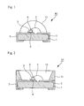
- Fig. 1 shows a side cross-sectional view of an illustrative embodiment of a portion of a chip-type package light emitting device consistent with this invention.
- the chip-type package light emitting device may comprise at least one light emitting diode and a phosphorescent substance. Electrodes 5 may be formed on both sides of substrate 1. Light emitting diode 6 emitting light may be mounted on one of the electrodes 5. Light emitting diode 6 may be mounted on electrode 5 through electrically conductive paste 9. An electrode of light emitting diode 6 may be connected to electrode pattern 5 via an electrically conductive wire 2.
- Light emitting diodes may emit light with a wide range of wavelengths, for example, from ultraviolet light to visible light.
- a UV light emitting diode and/or blue light emitting diode may be use.
- Phosphor i.e., a phosphorescent substance, 3 may be placed on the top and side faces of the light emitting diode 6.
- the phosphor in consistent with this invention may include lead and/or copper doped aluminate type compounds, lead and/or copper doped silicates, lead and/or copper doped antimonates, lead and/or copper doped germanates, lead and/or copper doped germanate-silicates, lead and/or copper doped phosphates, or any combination thereof.
- Phosphor 3 converts the wavelength of the light from the light emitting diode 6 to another wavelength or other wavelengths. In one embodiment consistent with this invention, the light is in a visible light range after the conversion.
- Phosphor 3 may be applied to light emitting diode 6 after mixing phosphor 3 with a hardening resin.
- the hardening resin including phosphor 3 may also be applied to the bottom of light emitting diode 6 after mixing phosphor 3 with electrically conductive paste 9.
- the light emitting diode 6 mounted on substrate 1 may be sealed with one or more sealing materials 10.
- Phosphor 3 may be placed on the top and side faces of light emitting diode 6.
- Phosphor 3 can also be distributed in the hardened sealing material during the production. Such a manufacturing method is described in U.S. Patent No. 6,482,664, which is hereby incorporated by reference in its entirety.
- Phosphor 3 may comprise lead and/or copper doped chemical compound(s).
- Phosphor 3 may include one or more single chemical compounds.
- the single compound may have an emission peak of, for example, from about 440nm to about 500nm, from about 500nm to about 590nm, or from about 580nm to 700nm.
- Phosphor 3 may include one or more single phosphors, which may have an emission peak as exemplified above.
- light emitting diode 6 may emit primary light when light emitting diode 6 receives power from a power supply.
- the primary light then may stimulate phosphor(s) 3, and phosphor(s) 3 may convert the primary light to a light with longer wavelength(s) (a secondary light).
- the primary light from the light emitting diode 6 and the secondary light from the phosphors 3 are diffused and mixed together so that a predetermined color of light in visible spectrum may be emitted from light emitting diode 6.
- more than one light emitting diodes that have different emission peaks can be mounted together.
- specific color of light, color temperature, and CRI can be provided.
- the light emitting diode 6 and the compound included in phosphor 3 are properly controlled then desired color temperature or specific color coordination can be provided, especially, wide range of color temperature, for example, from about 2,000K to about 8,000K or about 10,000K and/or color rendering index of greater than about 90. Therefore, the light emitting devices consistent with this invention may be used for electronic devices such as home appliances, stereos, telecommunication devices, and for interior/exterior custom displays. The light emitting devices consistent with this invention may also be used for automobiles and illumination products because they provide similar color temperatures and CRI to those of the visible light.
- Fig. 2 shows a side cross-sectional view of an illustrative embodiment of a portion of a top-type package light emitting device consistent with this invention.
- a top-type package light emitting device consistent with this invention may have a similar structure as that of the chip type package light emitting device 40 of Fig. 1.
- the top-type package device may have reflector 31 which may reflect the light from the light emitting diode 6 to the desire direction.
- top-type package light emitting device 50 more than one light emitting diodes can be mounted. Each of such light emitting diodes may have a different peak wavelength from that of others.
- Phosphor 3 may comprise a plurality of single compounds with different emission peak. The proportion of each of such plurality of compounds may be regulated. Such a phosphor may be applied to the light emitting diode and/or uniformly distributed in the hardening material of the reflector 31.
- the phosphor in consistent with this invention may include lead and/or copper doped aluminate type compounds, lead and/or copper doped silicates, lead and/or copper doped antimonates, lead and/or copper doped germanates, lead and/or copper doped germanate-silicates, lead and/or copper doped phosphates, or any combination thereof.
- the light emitting device of the Fig. 1 or Fig. 2 can include a metal substrate, which may have good heat conductivity. Such a light emitting device may easily dissipate the heat from the light emitting diode. Therefore, light emitting devices for high power may be manufactured. If a heat sink is provided beneath the metal substrate, the heat from the light emitting diode may be dissipated more effectively.
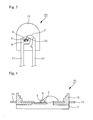
- Fig. 3 shows a side cross-sectional view of an illustrative embodiment of a portion of a lamp-type package light emitting device consistent with this invention.
- Lamp type light emitting device 60 may have a pair of leads 51, 52, and a diode holder 53 may be formed at the end of one lead.
- Diode holder 53 may have a shape of cup, and one or more light emitting diodes 6 may provided in the diode holder 53. When a number of light emitting diodes are provided in the diode holder 53, each of them may have a different peak wavelength from that of others.
- An electrode of light emitting diode 6 may be connected to lead 52 by, for example, electrically conductive wire 2.
- phosphor 3 Regular volume of phosphor 3, which may be mixed in the epoxy resin, may be provided in diode holder 53. As explained more fully below, phosphor 3 may include lead and/or copper doped components.
- the diode holder may include the light emitting diode 6 and the phosphor 3 may be sealed with hardening material such as epoxy resin or silicon resin.
- the lamp type package light emitting device may have more than one pair of electrode pair leads.
- Fig. 4 shows a side cross-sectional view of an illustrative embodiment of a portion of a light emitting device for high power consistent with this invention.
- Heat sink 71 may be provided inside of housing 73 of the light emitting device for high power 70, and it may be partially exposed to outside.
- a pair of lead frame 74 may protrude from housing 73.
- One or more light emitting diodes may be mounted one lead frame 74, and an electrode of the light emitting diode 6 and another lead frame 74 may be connected via electrically conductive wire. Electrically conductive pate 9 may be provided between light emitting diode 6 and lead frame 74. The phosphor 3 may be placed on top and side faces of light emitting diode 6.
- Fig. 5 shows a side cross-sectional view of another illustrative embodiment of a portion of a light emitting device for high power consistent with this invention.
- Light emitting device for high power 80 may have housing 63, which may contain light emitting diodes 6, 7, phosphor 3 arranged on the top and side faces of light emitting diodes 6, 7, one or more heat sinks 61, 62, and one or more lead frames 64.
- the lead frames 64 may receive power from a power supplier and may protrude from housing 63.
- the phosphor 3 can be added to the paste, which may be provided between heat sink and light emitting devices.
- a lens may be combined with housing 63, 73.
- one or more light emitting diodes can be used selectively and the phosphor can be regulated depending on the light emitting diode.
- the phosphor may include lead and/or copper doped components.
- a light emitting device for high power consistent with this invention may have a radiator (not shown) and/or heat sink(s). Air or a fan may be used to cool the radiator.
- the light emitting devices consistent with this invention is not limited to the structures described above, and the structures can be modified depending on the characteristics of light emitting diodes, phosphor, wavelength of light, and also applications. Moreover, new part can be added to the structures.
- An exemplary phosphor consistent with this invention is as follows.
- Phosphor in consistence with this invention may include lead and/or copper doped chemical compounds.
- the phosphor may be excited by UV and/or visible light, for example, blue light.
- the compound may include Aluminate, Silicate, Antimonate, Germanate, Germanate-silicate, or Phosphate type compounds.
- Aluminate type compounds may comprise compounds having formula (1), (2), and/or (5) a(M'O) ⁇ b(M" 2 O) ⁇ c(M"X) ⁇ dAl 2 O 3 ⁇ e(M"'O) ⁇ f(M"" 2 O 3 ) ⁇ g(M'"" o O p ) ⁇ h(M'"" x O y ) wherein M' may be Pb, Cu, and/or any combination thereof; M" may be one or more monovalent elements, for example, Li, Na, K, Rb, Cs, Au, Ag, and/or any combination thereof; M"' may be one or more divalent elements, for example, Be, Mg, Ca, Sr, Ba, Zn, Cd, Mn, and/or any combination thereof; M"" may be one or more trivalent elements, for example, Sc, B, Ga, In, and/or any combination thereof; M""' may be Si, Ge, Ti, Zr, Mn, V, Nb, Ta, W, Mo,
- M' may be Pb, Cu, and/or any combination thereof;
- M" may be one or more monovalent elements, for example, Li, Na, K, Rb, Cs, Au, Ag, and/or any combination thereof;
- M"' may be one or more divalent elements, for example, Be, Mg, Ca, Sr, Ba, Zn, Cd, Mn, and/or any combination thereof;
- M"" may be Bi, Sn, Sb, Sc, Y, La, In, Ce, Pr, Nd, Pm, Sm, Eu, Gd, Tb, Dy, Ho, Er, Tm, Yb, Lu, and any combination thereof;
- X may be F, Cl, Br, J, and any combination thereof; 0 ⁇ a ⁇ 4; 0 ⁇ b ⁇ 2; 0 ⁇ c ⁇ 2; 0 ⁇ d ⁇ 1; 0 ⁇ e ⁇ 1; 0 ⁇ f ⁇ 1; 0 ⁇ g ⁇ 1;0 ⁇ h ⁇ 2;1 ⁇ x ⁇ 2;and 1 ⁇ y ⁇ 5.
- the preparation of copper as well as lead doped luminescent materials may be a basic solid state reaction. Pure starting materials without any impurities, e.g. iron, may be used. Any starting material which may transfer into oxides via a heating process may be used to form oxygen dominated phosphors.
- the starting materials in the form of oxides, hydroxides, and/or carbonates may be mixed in stoichiometric proportions together with small amounts of flux, e.g., H 3 BO 3 .
- the mixture may be fired in an alumina crucible in a first step at about 1,200 °C for about one hour. After milling the pre-fired materials a second firing step at about 1,450°C in a reduced atmosphere for about 4 hours may be followed. After that the material may be milled, washed, dried and sieved.
- the resulting luminescent material may have an emission maximum of about 494 nm.
- the starting materials in form of very pure oxides, carbonates, or other components which may decompose thermically into oxides may be mixed in stoichiometric proportion together with small amounts of flux, for example, H 3 BO 3 .
- the mixture may be fired in an alumina crucible at about 1,200 °C for about one hour in the air. After milling the pre-fired materials a second firing step at about 1,450°C in air for about 2 hours and in a reduced atmosphere for about 2 hours may be followed. Then the material may be milled, washed, dried, and sieved.
- the resulting luminescent material may have an emission maximum of from about 494.5 nm.
- the starting materials in the form of, for example, pure oxides and/or as carbonates may be mixed in stoichiometric proportions together with small amounts of flux, for example, AlF 3 .
- the mixture may be fired in an alumina crucible at about 1,250°C in a reduced atmosphere for about 3 hours. After that the material may be milled, washed, dried and sieved.
- the resulting luminescent material may have an emission maximum of about 521.5 nm.
- the starting materials in the form of, for example, pure oxides, hydroxides, and/or carbonates may be mixed in stoichiometric proportions together with small amounts of flux, for example, AlF 3 .
- the mixture may be fired in an alumina crucible at about 1,420°C in a reduced atmosphere for about 2 hours. After that the material may be milled, washed, dried, and sieved.
- the resulting luminescent material may have an emission maximum of about 452 nm.
- the starting materials in form of, for example, pure oxides, hydroxides, and/or carbonates may be mixed in stochiometric proportions together with small amounts of flux, for example, H 3 BO 3 .
- the mixture may be fired in an alumina crucible at about 1,000 °C for about 2 hours in the air. After milling the pre-fired materials a second firing step at about 1,420°C in the air for about 1 hour and in a reduced atmosphere for about 2 hours may be followed. After that the material may be milled, washed, dried and sieved.
- the resulting luminescent material may have an emission maximum of about 521 nm.
- results obtained in regard to copper and/or lead doped aluminates are shown in table 7. optical properties of some copper and/or lead doped aluminates excitable by long wave ultraviolet and/or by visible light and their luminous density in % at 400 nm excitation wavelength Composition Possible excitation range (nm) Luminous density at 400 nm excitation compared with copper/lead not doped compounds (%) Peak wave length of lead/copper doped materials (nm) Peak wave length of materials without lead/copper (nm) Cu 0.05 Sr 0.95 Al 1.9997 Si 0.0003 O 4 : Eu 360 - 440 106 521.5 519 Cu 0.2 Mg 0.7995 Li 0.0005 Al 1.9 Ga 0.1 O 4 : Eu, Dy 360 - 440 101.2 482 480 Pb 0.1 Sr 0.9 Al 2 O 4 : Eu 360 - 440 102 521 519 Cu 0.05 BaMg 1.95 Al 16 O 27 : Eu, Mn 360 - 400 100.5 451,515 450,5
- a lead and/or copper doped silicates having formula (9) a(M'O) ⁇ b(M"O) ⁇ c(M'"X) ⁇ d(M"' 2 O) ⁇ e(M"'' 2 O 3 ) ⁇ f(M"''' o O p ) ⁇ g(SiO 2 ).
- the starting materials in the form of pure oxides and/or carbonates may be mixed in stoichiometric proportions together with small amounts of flux, for example, NH 4 Cl.
- the mixture may be fired in an alumina crucible at about 1,200°C in an inert gas atmosphere (e.g., N 2 or noble gas) for about 2 hours. Then the material may be milled. After that, the material may be fired in an alumina crucible at about 1,200°C in a slightly reduced atmosphere for about 2 hours. Then, the material may be milled, washed, dried, and sieved.
- the resulting luminescent material may have an emission maximum at about 592 nm.
- the starting materials in the form of very pure oxides and carbonates may be mixed in stoichiometric proportions together with small amounts of flux, for example, NH 4 Cl.
- the mixture may be fired in an alumina crucible at about 1,100°C in a reduced atmosphere for about 2 hours. Then the material may be milled. After that the material may be fired in an alumina crucible at about 1,235°C in a reduced atmosphere for about 2 hours. Then that the material may be milled, washed, dried and sieved.
- the resulting luminescent material may have an emission maximum at about 467 nm.
- the starting materials in the form of oxides and/or carbonates may be mixed in stoichiometric proportions together with small amounts of flux, for example, NH 4 Cl.
- the mixture may be fired in an alumina crucible at about 1,000 °C for about 2 hours in the air. After milling the pre-fired materials a second firing step at 1,220°C in air for 4 hours and in reducing atmosphere for 2 hours may be followed. After that the material may be milled, washed, dried and sieved.
- the resulting luminescent material may have an emission maximum at about 527 nm.
- the starting materials in the form of oxides, chlorides, and/or carbonates may be mixed in stoichiometric proportions together with small amounts of flux, for example, NH 4 Cl.
- the mixture may be fired in an alumina crucible in a first step at about 1,100 °C for about 2 hours in the air. After milling the pre-fired materials a second firing step at about 1,220°C in the air for about 4 hours and in a reduced atmosphere for about 1 hour may be followed. After that the material may be milled, washed, dried and sieved.
- the resulting luminescent material may have an emission maximum at about 492 nm.
- results obtained with respect to copper and/or lead doped silicates are shown in table 12. optical properties of some copper and/or lead doped rare earth activated silicates excitable by long wave ultraviolet and/or by visible light and their luminous density in % at about 400 nm excitation wavelength Composition Possible excitation range (nm) Luminous density at 400nm excitation compared with copper/lead not doped compounds (%) Peak wave length of lead/copper doped materials (nm) Peak wave length of materials without lead/copper (nm) Pb 0.1 Ba 0.95 Sr 0.95 Si 0.998 Ge 0.002 O 4 : Eu 360 - 470 101.3 527 525 Cu 0.02 (Ba,Sr,Ca,Zn) 1.98 SiO 4 :Eu 360 - 500 108.2 565 560 Cu 0.05 Sr 1.7 Ca 0.25 SiO 4 : Eu 360 - 470 104 592 588 Cu 0.05 Li 0.002 Sr 1.5 Ba 0.448 SiO 4 : Gd, Eu 360
- M' may be Pb, Cu, and/or any combination thereof; M" may be Li, Na, K, Rb, Cs, Au, Ag, and/or any combination thereof; M"' may be Be, Mg, Ca, Sr, Ba, Zn, Cd, Mn, and/or any combination thereof; M"" may be Bi, Sn, Sc, Y, La, Pr, Sm, Eu, Tb, Dy, Gd, and/or any combination thereof; X may be F, Cl, Br, J, and/or any combination thereof; 0 ⁇ a ⁇ 2; 0 ⁇ b ⁇ 2; 0 ⁇ c ⁇ 4; 0 ⁇ d ⁇ 8; 0 ⁇ e ⁇ 8; 0 ⁇
- the starting materials in the form of oxides may be mixed in stoichiometric proportion together with small amounts of flux.
- the mixture may be fired in an alumina crucible at about 985°C in the air for about 2 hours. After pre-firing the material may be milled again.
- the mixture may be fired in an alumina crucible at about 1,200°C in an atmosphere containing oxygen for about 8 hours. After that the material may be milled, washed, dried and sieved.
- the resulting luminescent material may have an emission maximum at about 626 nm.
- the starting materials in the form of oxides and/or carbonates may be mixed in stoichiometric proportions together with small amounts of flux.
- the mixture may be fired in an alumina crucible at about 975°C in the air for about 2 hours. After pre-firing the material may be milled again.
- the mixture may be fired in an alumina crucible at about 1,175°C in the air for about 4 hours and then in an oxygen-containing atmosphere for about 4 hours. After that the material may be milled, washed, dried and sieved.
- the resulting luminescent material may have an emission maximum at about 637 nm.
- results obtained in respect to copper and/or lead doped antimonates are shown in table 15. optical properties of some copper and/or lead doped antimonates excitable by long wave ultraviolet and/or by visible light and their luminous density in % at about 400 nm excitation wavelength Composition Possible excitation range (nm) Luminous density at 400 nm excitation compared with copper/lead not doped compounds (%) Peak wave length of lead/copper doped materials (nm) Peak wave length of materials without lead/copper (nm) Pb 0.2 Mg 0.002 Ca 1.798 Sb 2 O 6 F 2 : Mn 360 - 400 102 645 649 Cu 0.15 Ca 1.845 Sr 0.005 Sb 1.998 Si 0.002 O 7 : Mn 360 - 400 101.5 660 658 Cu 0.2 Mg 1.7 Li 0.2 Sb 2 O 7 : Mn 360 - 400 101.8 652 650 Cu 0.2 Pb 0.01 Ca 0.79 Sb 1.98 Nb 0.02 O 6 : Mn 360
- the starting materials in the form of oxides and/or carbonates may be mixed in stoichiometric proportions together with small amounts of flux, for example, NH 4 Cl.
- the mixture may be fired in an alumina crucible at about 1,200°C in an oxygen-containing atmosphere for about 2 hours. Then, the material may be milled again.
- the mixture may be fired in an alumina crucible at about 1,200°C in oxygen containing atmosphere for about 2 hours. After that the material may be milled, washed, dried and sieved.
- the resulting luminescent material may have an emission maximum at about 655 nm.
- the starting materials in the form of oxides and/or carbonates may be mixed in stoichiometric proportions together with small amounts of flux, for example, NH 4 Cl.
- the mixture may be fired in an alumina crucible at about 1,100°C in an oxygen-containing atmosphere for about 2 hours. Then, the material may be milled again.
- the mixture may be fired in an alumina crucible at about 1,180°C in an oxygen-containing atmosphere for about 4 hours. After that the material may be milled, washed, dried and sieved.
- the resulting luminescent material may have an emission maximum at about 658 nm.
- Lead and/or copper doped phosphates having formula (20) a(M'O) ⁇ b(M" 2 O) ⁇ c(M"X) ⁇ dP 2 O 5 ⁇ e(M"'O) ⁇ f(M"" 2 O 3 ) ⁇ g(M""'O 2 ) ⁇ h(M"''' x O y )
- M' may be Pb, Cu, and/or any combination thereof
- M may be Li, Na, K, Rb, Cs, Au, Ag, and/or any combination thereof
- M"' may be Be, Mg, Ca, Sr, Ba, Zn, Cd, Mn, and/or any combination thereof
- M" may be Sc, Y, B, Al, La, Ga, In, and/or any combination thereof
- M""' may be Si, Ge, Ti, Zr, Hf, V, Nb, Ta, W, Mo, and/or any combination thereof
- M""" may be Bi,
- the starting materials in the form of oxides, phosphates, and/or carbonates and chlorides may be mixed in stoichiometric proportions together with small amounts of flux.
- the mixture may be fired in an alumina crucible at about 1,240°C in reducing atmosphere for about 2 hours. After that the material may be milled, washed, dried and sieved.
- the luminescent material may have an emission maximum at about 450 nm.
- the phosphor of the light emitting device consistent with this invention can comprise aluminate, silicate, antimonate, germanate, phosphate type chemical compound, and any combination thereof.
- Fig. 6 is a one of the embodiment's emission spectrum according to the invention, which the phosphor is used for the light emitting device.
- the embodiment may have a light emitting diode with 405nm wavelength and the phosphor, which is mixture of the selected multiple chemical compounds in proper ratio.
- the phosphor may be composed of Cu 0.05 BaMg 1.95 Al 16 O 27 : Eu which may have peak wavelength at about 451nm, Cu 0.03 Sr 1.5 Ca 0.47 SiO 4 : Eu which may have peak wavelength at 586nm, Pb 0.006 Ca 0.6 Sr 0.394 Sb 2 O 6 : Mn 4+ which may have peak wavelength at about 637nm, Pb 0.15 Ba 1.84 Zn 0.01 Si 0.99 Zr 0.01 O 4 : Eu which may have peak wavelength at around 512nm, and Cu 0.2 Sr 3.8 Al 14 O 25 : Eu which may have peak wavelength at about 494nm.
- part of the initial about 405nm wavelength emission light from the light emitting diode is absorbed by the phosphor, and it is converted to longer 2 nd wavelength.
- the 1 st and 2 nd light is mixed together and the desire emission is produced.
- the light emitting device convert the 1 st UV light of 405nm wavelength to wide spectral range of visible light, that is, white light, and at this time the color temperature is about 3,000K and CRI is about 90 to about 95.
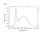
- Fig. 7 is another embodiment's emission spectrum according to the invention, which the phosphor is applied for the light emitting device.
- the embodiment may have a light emitting diode with about 455nm wavelength and the phosphor, which is mixture of the selected multiple chemical compounds in proper ratio.
- the phosphor is composed of Cu 0.05 Sr 1.7 Ca 0.25 SiO 4 : Eu which may have peak wavelength at about 592nm, Pb 0.1 Ba 0.95 Sr 0.95 Si 0.998 Ge 0.002 O 4 : Eu which may have peak wavelength at about 527nm, and Cu 0.05 Li 0.002 Sr 1.5 Ba 0.448 SiO 4 : Gd, Eu which may have peak wavelength at about 557nm.
- part of the initial about 455nm wavelength emission light from the light emitting diode is absorbed by the phosphor, and it is converted to longer 2 nd wavelength.
- the 1 st and 2 nd light is mixed together and the desire emission is produced.
- the light emitting device convert the 1 st blue light of about 455nm wavelength to wide spectral range of visible light, that is, white light, and at this time the color temperature is about 4,000K to about 6,500K and CRI is about 86 to about 93.
- the phosphor of the light emitting device according to the invention can be applied by single chemical compound or mixture of plurality of single chemical compound besides the embodiments in relation to Fig. 6 and Fig. 7, which are explained above.
- light emitting device with wide range of color temperature about 2,000K or about 8,000K or about 10,000K and superior color rendering index more than about 90 can be realized by using the lead and/or copper doped chemical compounds containing rare earth elements.
- wavelength conversion light emitting device is capable of applying on mobile phone, note book and electronic devices such as home appliance, stereo, telecommunication products, but also for custom display's key pad and back light application. Moreover, it can be applied for automobile, medical instrument and illumination products.
- the invention is also able to provide a wavelength conversion light emitting device with stability against water, humidity, vapor as well as other polar solvents.
Landscapes
- Chemical & Material Sciences (AREA)
- Inorganic Chemistry (AREA)
- Engineering & Computer Science (AREA)
- Materials Engineering (AREA)
- Organic Chemistry (AREA)
- Luminescent Compositions (AREA)
- Led Device Packages (AREA)
- Led Devices (AREA)
- Surgical Instruments (AREA)
Priority Applications (11)
| Application Number | Priority Date | Filing Date | Title |
|---|---|---|---|
| EP08166716.4A EP2025734B1 (de) | 2004-06-10 | 2004-12-22 | Lichtemittierende Vorrichtung |
| EP10177830A EP2253690A3 (de) | 2004-06-10 | 2004-12-22 | Lichtemittierende Vorrichtung |
| CA2592096A CA2592096C (en) | 2004-12-22 | 2005-07-20 | Light emitting device |
| PCT/KR2005/002332 WO2006068359A1 (en) | 2004-12-22 | 2005-07-20 | Light emitting device |
| AU2005319965A AU2005319965B2 (en) | 2004-12-22 | 2005-07-20 | Light emitting device |
| RU2007127910/28A RU2359362C2 (ru) | 2004-12-22 | 2005-07-20 | Светоизлучающее устройство |
| SG201001939-6A SG161205A1 (en) | 2004-12-22 | 2005-07-20 | Light emitting device |
| BRPI0517584-4A BRPI0517584B1 (pt) | 2004-12-22 | 2005-07-20 | Lighting device |
| MX2007007648A MX2007007648A (es) | 2004-06-10 | 2005-07-20 | Dispositivo emisor de luz. |
| NO20073682A NO341529B1 (no) | 2004-12-22 | 2007-07-17 | Lysemmitterende anordning |
| RU2009105655/28A RU2485633C2 (ru) | 2004-12-22 | 2009-02-18 | Светоизлучающее устройство |
Applications Claiming Priority (2)
| Application Number | Priority Date | Filing Date | Title |
|---|---|---|---|
| KR1020040042396A KR100665298B1 (ko) | 2004-06-10 | 2004-06-10 | 발광장치 |
| KR2004042396 | 2004-06-10 |
Related Child Applications (2)
| Application Number | Title | Priority Date | Filing Date |
|---|---|---|---|
| EP08166716.4A Division EP2025734B1 (de) | 2004-06-10 | 2004-12-22 | Lichtemittierende Vorrichtung |
| EP08166716.4 Division-Into | 2008-10-15 |
Publications (3)
| Publication Number | Publication Date |
|---|---|
| EP1605030A2 true EP1605030A2 (de) | 2005-12-14 |
| EP1605030A3 EP1605030A3 (de) | 2007-09-19 |
| EP1605030B1 EP1605030B1 (de) | 2010-08-18 |
Family
ID=34930126
Family Applications (3)
| Application Number | Title | Priority Date | Filing Date |
|---|---|---|---|
| EP04106882A Active EP1605030B1 (de) | 2004-06-10 | 2004-12-22 | Lichtemittierende Vorrichtung |
| EP08166716.4A Active EP2025734B1 (de) | 2004-06-10 | 2004-12-22 | Lichtemittierende Vorrichtung |
| EP10177830A Withdrawn EP2253690A3 (de) | 2004-06-10 | 2004-12-22 | Lichtemittierende Vorrichtung |
Family Applications After (2)
| Application Number | Title | Priority Date | Filing Date |
|---|---|---|---|
| EP08166716.4A Active EP2025734B1 (de) | 2004-06-10 | 2004-12-22 | Lichtemittierende Vorrichtung |
| EP10177830A Withdrawn EP2253690A3 (de) | 2004-06-10 | 2004-12-22 | Lichtemittierende Vorrichtung |
Country Status (11)
| Country | Link |
|---|---|
| US (4) | US7554129B2 (de) |
| EP (3) | EP1605030B1 (de) |
| JP (1) | JP4159542B2 (de) |
| KR (1) | KR100665298B1 (de) |
| CN (2) | CN100442553C (de) |
| AT (1) | ATE478126T1 (de) |
| DE (2) | DE602004028710D1 (de) |
| ES (2) | ES2490603T3 (de) |
| MX (1) | MX2007007648A (de) |
| PT (1) | PT1605030E (de) |
| TW (2) | TWI328885B (de) |
Cited By (11)
| Publication number | Priority date | Publication date | Assignee | Title |
|---|---|---|---|---|
| WO2007069869A1 (en) | 2005-12-15 | 2007-06-21 | Seoul Semiconductor.Co., Ltd. | Light emitting device |
| WO2007114614A1 (en) | 2006-03-31 | 2007-10-11 | Seoul Semiconductor Co., Ltd. | Light emitting device and lighting system having the same |
| EP1908810A1 (de) * | 2006-10-06 | 2008-04-09 | Nemoto & Co., Ltd. | Phosphor |
| EP1951843A1 (de) * | 2005-11-11 | 2008-08-06 | Seoul Semiconductor Co., Ltd | Kupfer-erdalkalisilicat-mischkristall-leuchtstoffe |
| US7554129B2 (en) | 2004-06-10 | 2009-06-30 | Seoul Semiconductor Co., Ltd. | Light emitting device |
| US8070984B2 (en) | 2004-06-10 | 2011-12-06 | Seoul Semiconductor Co., Ltd. | Luminescent material |
| EP2407527A1 (de) * | 2007-08-22 | 2012-01-18 | Seoul Semiconductor Co., Ltd. | Nichtstöchiometrische tetragonale Kupfer-Alkali-Erdalkalisilicatphosphore und Verfahren zu ihrer Herstellung |
| US9209162B2 (en) | 2004-05-13 | 2015-12-08 | Seoul Semiconductor Co., Ltd. | Light emitting device including RGB light emitting diodes and phosphor |
| EP2915861A4 (de) * | 2012-10-31 | 2016-06-15 | Ocean S King Lighting Science&Technology Co Ltd | Lumineszentes germanatmaterial und herstellungsverfahren dafür |
| US9401467B2 (en) | 2009-04-28 | 2016-07-26 | Lg Innotek Co., Ltd. | Light emitting device package having a package body including a recess and lighting system including the same |
| US9537056B2 (en) | 2010-02-18 | 2017-01-03 | Lg Innotek Co., Ltd. | Light emitting device |
Families Citing this family (94)
| Publication number | Priority date | Publication date | Assignee | Title |
|---|---|---|---|---|
| EP1598450B1 (de) * | 2003-02-24 | 2011-09-21 | Waseda University | VERFAHREN ZUM ZIEHEN VON Beta-Ga2O3 EINKRISTALLEN |
| US7145125B2 (en) | 2003-06-23 | 2006-12-05 | Advanced Optical Technologies, Llc | Integrating chamber cone light using LED sources |
| US7521667B2 (en) | 2003-06-23 | 2009-04-21 | Advanced Optical Technologies, Llc | Intelligent solid state lighting |
| JP3931239B2 (ja) * | 2004-02-18 | 2007-06-13 | 独立行政法人物質・材料研究機構 | 発光素子及び照明器具 |
| KR100655894B1 (ko) | 2004-05-06 | 2006-12-08 | 서울옵토디바이스주식회사 | 색온도 및 연색성이 우수한 파장변환 발광장치 |
| US8308980B2 (en) | 2004-06-10 | 2012-11-13 | Seoul Semiconductor Co., Ltd. | Light emitting device |
| US7564180B2 (en) | 2005-01-10 | 2009-07-21 | Cree, Inc. | Light emission device and method utilizing multiple emitters and multiple phosphors |
| US8125137B2 (en) | 2005-01-10 | 2012-02-28 | Cree, Inc. | Multi-chip light emitting device lamps for providing high-CRI warm white light and light fixtures including the same |
| KR100724591B1 (ko) | 2005-09-30 | 2007-06-04 | 서울반도체 주식회사 | 발광 소자 및 이를 포함한 led 백라이트 |
| US8514210B2 (en) | 2005-11-18 | 2013-08-20 | Cree, Inc. | Systems and methods for calibrating solid state lighting panels using combined light output measurements |
| JP5249773B2 (ja) * | 2005-11-18 | 2013-07-31 | クリー インコーポレイテッド | 可変電圧ブースト電流源を有する固体照明パネル |
| US7926300B2 (en) | 2005-11-18 | 2011-04-19 | Cree, Inc. | Adaptive adjustment of light output of solid state lighting panels |
| EP1963743B1 (de) * | 2005-12-21 | 2016-09-07 | Cree, Inc. | Beleuchtungsvorrichtung |
| BRPI0620413A2 (pt) | 2005-12-21 | 2011-11-08 | Cree Led Lighting Solutions | dispositivo de iluminação e método de iluminação |
| EP1969633B1 (de) | 2005-12-22 | 2018-08-29 | Cree, Inc. | Beleuchtungsvorrichtung |
| RU2315135C2 (ru) | 2006-02-06 | 2008-01-20 | Владимир Семенович Абрамов | Метод выращивания неполярных эпитаксиальных гетероструктур на основе нитридов элементов iii группы |
| US8323529B2 (en) | 2006-03-16 | 2012-12-04 | Seoul Semiconductor Co., Ltd. | Fluorescent material and light emitting diode using the same |
| KR101274044B1 (ko) * | 2006-03-31 | 2013-06-12 | 서울반도체 주식회사 | 발광 소자 및 이를 포함한 led 백라이트 |
| BRPI0711255A2 (pt) | 2006-04-18 | 2011-08-30 | Cree Led Lighting Solutions | dispositivo de iluminação e método de iluminação |
| US9084328B2 (en) | 2006-12-01 | 2015-07-14 | Cree, Inc. | Lighting device and lighting method |
| US8513875B2 (en) | 2006-04-18 | 2013-08-20 | Cree, Inc. | Lighting device and lighting method |
| US7997745B2 (en) | 2006-04-20 | 2011-08-16 | Cree, Inc. | Lighting device and lighting method |
| US7777166B2 (en) | 2006-04-21 | 2010-08-17 | Cree, Inc. | Solid state luminaires for general illumination including closed loop feedback control |
| US7648257B2 (en) | 2006-04-21 | 2010-01-19 | Cree, Inc. | Light emitting diode packages |
| US7625103B2 (en) | 2006-04-21 | 2009-12-01 | Cree, Inc. | Multiple thermal path packaging for solid state light emitting apparatus and associated assembling methods |
| EP2021688B1 (de) | 2006-05-05 | 2016-04-27 | Cree, Inc. | Beleuchtungsvorrichtung |
| KR101263934B1 (ko) * | 2006-05-23 | 2013-05-10 | 엘지디스플레이 주식회사 | 발광다이오드 및 그의 제조방법 |
| JP2009538536A (ja) | 2006-05-26 | 2009-11-05 | クリー エル イー ディー ライティング ソリューションズ インコーポレイテッド | 固体発光デバイス、および、それを製造する方法 |
| US7969097B2 (en) * | 2006-05-31 | 2011-06-28 | Cree, Inc. | Lighting device with color control, and method of lighting |
| WO2007142946A2 (en) | 2006-05-31 | 2007-12-13 | Cree Led Lighting Solutions, Inc. | Lighting device and method of lighting |
| KR101258229B1 (ko) * | 2006-06-30 | 2013-04-25 | 서울반도체 주식회사 | 발광 소자 |
| JP5205724B2 (ja) * | 2006-08-04 | 2013-06-05 | 日亜化学工業株式会社 | 発光装置 |
| KR101258227B1 (ko) | 2006-08-29 | 2013-04-25 | 서울반도체 주식회사 | 발광 소자 |
| US7665862B2 (en) | 2006-09-12 | 2010-02-23 | Cree, Inc. | LED lighting fixture |
| US7766508B2 (en) * | 2006-09-12 | 2010-08-03 | Cree, Inc. | LED lighting fixture |
| US8029155B2 (en) | 2006-11-07 | 2011-10-04 | Cree, Inc. | Lighting device and lighting method |
| US9441793B2 (en) | 2006-12-01 | 2016-09-13 | Cree, Inc. | High efficiency lighting device including one or more solid state light emitters, and method of lighting |
| JP2008140704A (ja) * | 2006-12-04 | 2008-06-19 | Stanley Electric Co Ltd | Ledバックライト |
| US7918581B2 (en) | 2006-12-07 | 2011-04-05 | Cree, Inc. | Lighting device and lighting method |
| CN100503776C (zh) * | 2006-12-19 | 2009-06-24 | 上海师范大学 | 一种CaSiO3:Pb,Mn纳米红色荧光材料的制备方法 |
| JP2008166782A (ja) | 2006-12-26 | 2008-07-17 | Seoul Semiconductor Co Ltd | 発光素子 |
| KR101423456B1 (ko) | 2006-12-28 | 2014-07-29 | 서울반도체 주식회사 | 형광막 구조를 포함하는 백라이팅 유닛 |
| WO2008082136A1 (en) * | 2006-12-28 | 2008-07-10 | Seoul Semiconductor Co., Ltd. | Back lighting unit having phosphor film structure |
| US8258682B2 (en) * | 2007-02-12 | 2012-09-04 | Cree, Inc. | High thermal conductivity packaging for solid state light emitting apparatus and associated assembling methods |
| JP5476128B2 (ja) | 2007-02-22 | 2014-04-23 | クリー インコーポレイテッド | 照明装置、照明方法、光フィルタ、および光をフィルタリングする方法 |
| KR101396588B1 (ko) * | 2007-03-19 | 2014-05-20 | 서울반도체 주식회사 | 다양한 색온도를 갖는 발광 장치 |
| US7824070B2 (en) * | 2007-03-22 | 2010-11-02 | Cree, Inc. | LED lighting fixture |
| CN101720402B (zh) | 2007-05-08 | 2011-12-28 | 科锐公司 | 照明装置和照明方法 |
| CN101755164B (zh) | 2007-05-08 | 2013-03-27 | 科锐公司 | 照明装置和照明方法 |
| TWI489648B (zh) | 2007-05-08 | 2015-06-21 | Cree Inc | 照明裝置及照明方法 |
| JP2010527156A (ja) | 2007-05-08 | 2010-08-05 | クリー エル イー ディー ライティング ソリューションズ インコーポレイテッド | 照明デバイスおよび照明方法 |
| CN101711325B (zh) | 2007-05-08 | 2013-07-10 | 科锐公司 | 照明装置和照明方法 |
| US20090002979A1 (en) * | 2007-06-27 | 2009-01-01 | Cree, Inc. | Light emitting device (led) lighting systems for emitting light in multiple directions and related methods |
| US8042971B2 (en) * | 2007-06-27 | 2011-10-25 | Cree, Inc. | Light emitting device (LED) lighting systems for emitting light in multiple directions and related methods |
| JP5431320B2 (ja) | 2007-07-17 | 2014-03-05 | クリー インコーポレイテッド | 内部光学機能を備えた光学素子およびその製造方法 |
| US7863635B2 (en) | 2007-08-07 | 2011-01-04 | Cree, Inc. | Semiconductor light emitting devices with applied wavelength conversion materials |
| KR101055769B1 (ko) | 2007-08-28 | 2011-08-11 | 서울반도체 주식회사 | 비화학양론적 정방정계 알칼리 토류 실리케이트 형광체를채택한 발광 장치 |
| JP2011501417A (ja) | 2007-10-10 | 2011-01-06 | クリー エル イー ディー ライティング ソリューションズ インコーポレイテッド | 照明デバイスおよび製作方法 |
| CN100546058C (zh) * | 2007-10-15 | 2009-09-30 | 佛山市国星光电股份有限公司 | 功率发光二极管封装结构 |
| US8866410B2 (en) | 2007-11-28 | 2014-10-21 | Cree, Inc. | Solid state lighting devices and methods of manufacturing the same |
| TWM337834U (en) * | 2007-12-10 | 2008-08-01 | Everlight Electronics Co Ltd | Package structure for light emitting diode |
| US8240875B2 (en) | 2008-06-25 | 2012-08-14 | Cree, Inc. | Solid state linear array modules for general illumination |
| TW201019006A (en) * | 2008-11-06 | 2010-05-16 | Chunghwa Picture Tubes Ltd | LED light module |
| JP2010171379A (ja) * | 2008-12-25 | 2010-08-05 | Seiko Instruments Inc | 発光デバイス |
| TWI376043B (en) * | 2009-01-23 | 2012-11-01 | Everlight Electronics Co Ltd | Light emitting device package structure and manufacturing method thereof |
| KR101047603B1 (ko) * | 2009-03-10 | 2011-07-07 | 엘지이노텍 주식회사 | 발광 소자 패키지 및 그 제조방법 |
| US8610156B2 (en) * | 2009-03-10 | 2013-12-17 | Lg Innotek Co., Ltd. | Light emitting device package |
| US8568615B2 (en) * | 2009-05-11 | 2013-10-29 | Oceans King Lighting Science & Technology Co., Ltd. | Full-color light-emitting material and preparation method thereof |
| US8921876B2 (en) | 2009-06-02 | 2014-12-30 | Cree, Inc. | Lighting devices with discrete lumiphor-bearing regions within or on a surface of remote elements |
| KR101055762B1 (ko) | 2009-09-01 | 2011-08-11 | 서울반도체 주식회사 | 옥시오소실리케이트 발광체를 갖는 발광 물질을 채택한 발광 장치 |
| DE102009030205A1 (de) | 2009-06-24 | 2010-12-30 | Litec-Lp Gmbh | Leuchtstoffe mit Eu(II)-dotierten silikatischen Luminophore |
| WO2011035292A2 (en) | 2009-09-21 | 2011-03-24 | University Of Georgia Research Foundation, Inc. | Near infrared doped phosphors having a zinc, germanium, gallate matrix |
| EP2480626A4 (de) | 2009-09-21 | 2013-04-03 | Univ Georgia | Nahinfrarot-dotierte phosphore mit einer alkali-gallat-matrix |
| KR20120094477A (ko) | 2009-09-25 | 2012-08-24 | 크리, 인코포레이티드 | 낮은 눈부심 및 높은 광도 균일성을 갖는 조명 장치 |
| JP5748769B2 (ja) | 2009-12-21 | 2015-07-15 | ソウル セミコンダクター カンパニー リミテッド | ストロンチウムオキシオルトシリケート型の蛍光体を有する発光装置 |
| DE102009059798A1 (de) * | 2009-12-21 | 2011-06-22 | LITEC-LP GmbH, 17489 | Mittel zur Verbesserung der Stabilität gegenüber der auftretenden Strahlenbelastung sowie Resistenz gegenüber dem Einfluß von Luftfeuchtigkeit bei Strontiumoxyorthosilikat-Leuchtstoffen |
| US9275979B2 (en) | 2010-03-03 | 2016-03-01 | Cree, Inc. | Enhanced color rendering index emitter through phosphor separation |
| WO2011115515A1 (ru) * | 2010-03-16 | 2011-09-22 | Общество с ограниченной ответственностью "ДиС ПЛЮС" | Способ управления цветностью светового потока белого светодиода и устройство для его осуществления способа |
| US20110309393A1 (en) * | 2010-06-21 | 2011-12-22 | Micron Technology, Inc. | Packaged leds with phosphor films, and associated systems and methods |
| US11251164B2 (en) | 2011-02-16 | 2022-02-15 | Creeled, Inc. | Multi-layer conversion material for down conversion in solid state lighting |
| TWI418742B (zh) * | 2011-06-30 | 2013-12-11 | Lextar Electronics Corp | 發光元件的封裝結構 |
| JP2014532103A (ja) * | 2011-09-28 | 2014-12-04 | ヘンケル・アクチェンゲゼルシャフト・ウント・コムパニー・コマンディットゲゼルシャフト・アウフ・アクチェンHenkel AG & Co.KGaA | オキセタン含有化合物およびその組成物 |
| CN102560659B (zh) * | 2012-03-21 | 2015-01-07 | 新疆紫晶光电技术有限公司 | 一种非线性光学晶体及其制备方法和用途 |
| WO2014025345A1 (en) * | 2012-08-08 | 2014-02-13 | University Of South Carolina | Stable phosphors for lighting applications |
| CN104241262B (zh) | 2013-06-14 | 2020-11-06 | 惠州科锐半导体照明有限公司 | 发光装置以及显示装置 |
| EP3070146B1 (de) * | 2013-11-13 | 2018-02-14 | LG Innotek Co., Ltd. | Blau-grün-leuchtstoff und verkapselung einer lichtemittierenden vorrichtung sowie lichtemittierende vorrichtung damit |
| JP6519746B2 (ja) * | 2014-10-23 | 2019-05-29 | パナソニックIpマネジメント株式会社 | 蛍光体材料及び発光装置 |
| KR102100213B1 (ko) * | 2016-03-14 | 2020-04-13 | 미쓰이금속광업주식회사 | 형광체 |
| US20200093238A1 (en) * | 2016-06-16 | 2020-03-26 | Harsh Kumar | Mobile phone case having mirrored surface and lighting |
| JP7227922B2 (ja) * | 2017-01-13 | 2023-02-22 | カリクスピュア インコーポレイテッド | Led構造及び連続消毒用照明器具 |
| US11856858B2 (en) | 2017-10-16 | 2023-12-26 | Akoustis, Inc. | Methods of forming doped crystalline piezoelectric thin films via MOCVD and related doped crystalline piezoelectric thin films |
| CN110444644B (zh) * | 2019-07-26 | 2022-10-14 | 浙江大学 | 一种增强硅基铒掺杂ZnO薄膜电致发光的器件及制备方法 |
| KR102205984B1 (ko) * | 2019-12-03 | 2021-01-21 | 에스지에너지주식회사 | 자정작용 특성을 갖는 칼라 태양광 모듈 제조방법 |
| US12102010B2 (en) | 2020-03-05 | 2024-09-24 | Akoustis, Inc. | Methods of forming films including scandium at low temperatures using chemical vapor deposition to provide piezoelectric resonator devices and/or high electron mobility transistor devices |
Family Cites Families (159)
| Publication number | Priority date | Publication date | Assignee | Title |
|---|---|---|---|---|
| US2110162A (en) * | 1938-03-08 | Luminescent material | ||
| US2402760A (en) * | 1942-06-27 | 1946-06-25 | Rca Corp | Luminescent material |
| US2617773A (en) | 1948-09-10 | 1952-11-11 | Westinghouse Electric Corp | Lead activated calcium tungstate phosphor |
| US2570136A (en) * | 1949-12-22 | 1951-10-02 | Du Pont | Infrared phosphors |
| US2719128A (en) | 1950-06-21 | 1955-09-27 | Patent Treuhand Ges Fuer Elektrische Gluehlampen Mbh | Luminescent material |
| US2780600A (en) | 1955-01-24 | 1957-02-05 | Westinghouse Electric Corp | Lead-and manganese-activated cadmium-sodium fluorophosphate phosphor |
| US3143510A (en) | 1959-06-12 | 1964-08-04 | Philips Corp | Copper and tin activated orthophosphate phosphors |
| US3598752A (en) * | 1967-04-14 | 1971-08-10 | Itt | Ultraviolet emitting cathodoluminescent material |
| NL7013516A (de) * | 1970-09-12 | 1972-03-14 | ||
| JPS476258U (de) | 1971-02-18 | 1972-09-21 | ||
| US3644212A (en) | 1971-02-18 | 1972-02-22 | Westinghouse Electric Corp | Zinc-magnesium silico-germanate phosphor composition and method of preparing same |
| JPS4938994A (de) | 1972-08-19 | 1974-04-11 | ||
| US3893939A (en) | 1973-01-04 | 1975-07-08 | Us Energy | Activated phosphors having matrices of yttrium-transition metal compound |
| US3905911A (en) | 1974-09-25 | 1975-09-16 | Gte Sylvania Inc | Copper activated hafnium phosphate phosphors and method of making |
| JPS51119388A (en) * | 1975-03-19 | 1976-10-19 | Gte Sylvania Inc | Fluorescent substances |
| NL7807274A (nl) * | 1978-03-10 | 1979-09-12 | Philips Nv | Luminescerende stof, luminescerend scherm voorzien van een dergelijke stof en lagedrukkwikdampontladingslamp voorzien van een dergelijk scherm. |
| JPS55135190A (en) * | 1979-04-06 | 1980-10-21 | Dainippon Toryo Co Ltd | Fluorescent substance and its manufacture |
| DE3029389C2 (de) * | 1979-08-03 | 1986-04-24 | Kasei Optonix, Ltd., Tokio/Tokyo | Borat-Leuchtstoff |
| NL8006223A (nl) | 1980-11-14 | 1982-06-01 | Philips Nv | Luminescerend scherm en lagedrukkwikdampontladingslamp voorzien van een dergelijk scherm. |
| NL8201943A (nl) | 1982-05-12 | 1983-12-01 | Philips Nv | Luminescerend scherm. |
| JPS61258892A (ja) * | 1985-05-13 | 1986-11-17 | Matsushita Electronics Corp | 螢光ランプ |
| JPS62197487A (ja) | 1986-02-25 | 1987-09-01 | Hitachi Ltd | 蛍光体の製造方法 |
| JPS62218476A (ja) | 1986-03-18 | 1987-09-25 | Murata Mfg Co Ltd | 薄膜el素子 |
| US5188763A (en) * | 1986-08-29 | 1993-02-23 | Gte Products Corporation | Method for preparing zinc orthosilicate phosphor |
| JPH07110941B2 (ja) | 1987-10-19 | 1995-11-29 | 化成オプトニクス株式会社 | 発光組成物 |
| US4972086A (en) | 1989-02-03 | 1990-11-20 | Eastman Kodak Company | X-ray intensifying screen including a titanium activated hafnium dioxide phosphor containing erbium to reduce afterglow |
| DE69002470T2 (de) | 1989-02-07 | 1994-03-03 | Agfa Gevaert Nv | Reproduktion von Röntgenbildern mit photostimulierbarem Leuchtstoff. |
| US5060118A (en) * | 1989-04-06 | 1991-10-22 | Frank A. Arone | Apparatus for daylight color duplication |
| JPH0578659A (ja) * | 1991-09-18 | 1993-03-30 | Toshiba Corp | 蛍光体および蛍光ランプ |
| US5518808A (en) | 1992-12-18 | 1996-05-21 | E. I. Du Pont De Nemours And Company | Luminescent materials prepared by coating luminescent compositions onto substrate particles |
| KR940019586A (ko) * | 1993-02-04 | 1994-09-14 | 휴고 라이히무트, 한스 블뢰흐레 | 엘리베이터용 표시소자 |
| TW353678B (en) | 1994-08-17 | 1999-03-01 | Mitsubishi Chem Corp | Aluminate phosphor |
| US5472636A (en) * | 1994-09-14 | 1995-12-05 | Osram Sylvania Inc. | Method of preparing manganese and lead coactivated calcium silicate phosphor |
| US5770111A (en) * | 1995-04-14 | 1998-06-23 | Kabushiki Kaisha Tokyo Kagaku Kenkyusho | Phosphor with afterglow characteristic |
| JPH0940946A (ja) | 1995-07-28 | 1997-02-10 | Tokyo Kagaku Kenkyusho:Kk | 残光特性を有する蛍光成形体 |
| DE19539315A1 (de) | 1995-10-23 | 1997-04-24 | Hoechst Ag | UV-aktive Regeneratcellulosefasern |
| JPH09153644A (ja) | 1995-11-30 | 1997-06-10 | Toyoda Gosei Co Ltd | 3族窒化物半導体表示装置 |
| KR200150839Y1 (ko) | 1995-12-11 | 1999-07-15 | 정몽규 | 버스차량의 사이드 고정 유리 장착구조 |
| DE19638667C2 (de) | 1996-09-20 | 2001-05-17 | Osram Opto Semiconductors Gmbh | Mischfarbiges Licht abstrahlendes Halbleiterbauelement mit Lumineszenzkonversionselement |
| TW383508B (en) | 1996-07-29 | 2000-03-01 | Nichia Kagaku Kogyo Kk | Light emitting device and display |
| US5965192A (en) | 1996-09-03 | 1999-10-12 | Advanced Vision Technologies, Inc. | Processes for oxide based phosphors |
| DE69627334T2 (de) | 1996-10-10 | 2003-12-11 | Agfa-Gevaert, Mortsel | Neuer Photostimulierbarer Leuchtstoff |
| US5853614A (en) * | 1996-12-17 | 1998-12-29 | Beijing Hongye Coating Materials Company | Long decay luminescent material |
| EP0907970B1 (de) * | 1997-03-03 | 2007-11-07 | Koninklijke Philips Electronics N.V. | Weisse lumineszenzdiode |
| JP2992254B2 (ja) | 1997-08-11 | 1999-12-20 | 北京市豊台区宏業塗装輔料廠 | 高速励起・高輝度低減衰性発光材料の製造方法 |
| CN1085719C (zh) | 1997-11-21 | 2002-05-29 | 中国科学院长春应用化学研究所 | 镝、铅共掺高压汞灯用荧光粉的制备方法 |
| US5952681A (en) | 1997-11-24 | 1999-09-14 | Chen; Hsing | Light emitting diode emitting red, green and blue light |
| US6278832B1 (en) | 1998-01-12 | 2001-08-21 | Tasr Limited | Scintillating substance and scintillating wave-guide element |
| US6855515B1 (en) * | 1998-04-22 | 2005-02-15 | Merck & Co., Inc. | Autoantigenic fragments, methods and assays |
| JP2907286B1 (ja) | 1998-06-26 | 1999-06-21 | サンケン電気株式会社 | 蛍光カバーを有する樹脂封止型半導体発光装置 |
| EP1046196B9 (de) | 1998-09-28 | 2013-01-09 | Koninklijke Philips Electronics N.V. | Beleuchtungsanordnung |
| KR100355456B1 (ko) | 1999-07-30 | 2002-10-11 | 한국전자통신연구원 | 형광 디스플레이용 적색 형광체와 그것의 제조방법 |
| JP2001144331A (ja) * | 1999-09-02 | 2001-05-25 | Toyoda Gosei Co Ltd | 発光装置 |
| US6686691B1 (en) | 1999-09-27 | 2004-02-03 | Lumileds Lighting, U.S., Llc | Tri-color, white light LED lamps |
| TWI272299B (en) | 1999-10-06 | 2007-02-01 | Sumitomo Chemical Co | A process for producing aluminate-based phosphor |
| JP2001115157A (ja) | 1999-10-15 | 2001-04-24 | Nippon Sheet Glass Co Ltd | 蛍光体およびその製造方法 |
| US6513949B1 (en) | 1999-12-02 | 2003-02-04 | Koninklijke Philips Electronics N.V. | LED/phosphor-LED hybrid lighting systems |
| JP3809760B2 (ja) | 2000-02-18 | 2006-08-16 | 日亜化学工業株式会社 | 発光ダイオード |
| GB0012377D0 (en) | 2000-05-22 | 2000-07-12 | Isis Innovation | Oxide based phosphors |
| JP2002057376A (ja) | 2000-05-31 | 2002-02-22 | Matsushita Electric Ind Co Ltd | Ledランプ |
| CN100567447C (zh) | 2000-06-27 | 2009-12-09 | 住友化学工业株式会社 | 铝酸盐荧光物质的制法、荧光物质和含荧光物质的装置 |
| US6737801B2 (en) * | 2000-06-28 | 2004-05-18 | The Fox Group, Inc. | Integrated color LED chip |
| JP4432275B2 (ja) | 2000-07-13 | 2010-03-17 | パナソニック電工株式会社 | 光源装置 |
| DE10036940A1 (de) | 2000-07-28 | 2002-02-07 | Patent Treuhand Ges Fuer Elektrische Gluehlampen Mbh | Lumineszenz-Konversions-LED |
| TW459403B (en) | 2000-07-28 | 2001-10-11 | Lee Jeong Hoon | White light-emitting diode |
| JP4396016B2 (ja) | 2000-09-21 | 2010-01-13 | 三菱化学株式会社 | アルミン酸塩蛍光体、蛍光体ペースト組成物及び真空紫外線励起発光装置 |
| US7205256B2 (en) * | 2000-10-17 | 2007-04-17 | Sharp Kabushiki Kaisha | Oxide material, method for preparing oxide thin film and element using said material |
| JP2002173677A (ja) | 2000-12-04 | 2002-06-21 | Tokin Corp | 真空紫外線励起蛍光体及びそれを用いた蛍光体ペースト |
| KR100392363B1 (ko) | 2000-12-26 | 2003-07-22 | 한국전자통신연구원 | 형광체 및 그 제조방법 |
| AT410266B (de) * | 2000-12-28 | 2003-03-25 | Tridonic Optoelectronics Gmbh | Lichtquelle mit einem lichtemittierenden element |
| CN1187428C (zh) | 2001-02-12 | 2005-02-02 | 湖南师范大学 | 单基双能转光剂及其制造方法和应用方法 |
| JP2002254273A (ja) | 2001-02-23 | 2002-09-10 | Mori Seiki Co Ltd | 切削工機の制御装置、切削工機及びその切削方法 |
| JP3783572B2 (ja) | 2001-03-05 | 2006-06-07 | 日亜化学工業株式会社 | 発光装置 |
| JP4101468B2 (ja) * | 2001-04-09 | 2008-06-18 | 豊田合成株式会社 | 発光装置の製造方法 |
| JP3891115B2 (ja) * | 2001-04-17 | 2007-03-14 | 日亜化学工業株式会社 | 発光装置 |
| KR100419611B1 (ko) | 2001-05-24 | 2004-02-25 | 삼성전기주식회사 | 발광다이오드 및 이를 이용한 발광장치와 그 제조방법 |
| JP4055373B2 (ja) | 2001-05-31 | 2008-03-05 | 日亜化学工業株式会社 | 発光装置の製造方法 |
| JP2002368277A (ja) | 2001-06-05 | 2002-12-20 | Rohm Co Ltd | チップ型半導体発光装置 |
| US20030030063A1 (en) * | 2001-07-27 | 2003-02-13 | Krzysztof Sosniak | Mixed color leds for auto vanity mirrors and other applications where color differentiation is critical |
| KR200253975Y1 (ko) | 2001-08-18 | 2001-11-23 | 허성유 | 곤충관찰통 |
| US6737681B2 (en) | 2001-08-22 | 2004-05-18 | Nichia Corporation | Light emitting device with fluorescent member excited by semiconductor light emitting element |
| US7189340B2 (en) | 2004-02-12 | 2007-03-13 | Mitsubishi Chemical Corporation | Phosphor, light emitting device using phosphor, and display and lighting system using light emitting device |
| JP4032682B2 (ja) | 2001-08-28 | 2008-01-16 | 三菱化学株式会社 | 蛍光体 |
| KR100923804B1 (ko) * | 2001-09-03 | 2009-10-27 | 파나소닉 주식회사 | 반도체발광소자, 발광장치 및 반도체발광소자의 제조방법 |
| US6770398B1 (en) | 2001-09-11 | 2004-08-03 | The United States Of America As Represented By The Secretary Of The Army | Potassium stabilized manganese dioxide for lithium rechargeable batteries |
| JPWO2003034508A1 (ja) | 2001-10-12 | 2005-02-03 | 日亜化学工業株式会社 | 発光装置及びその製造方法 |
| CN1152114C (zh) | 2001-10-26 | 2004-06-02 | 中国科学院长春应用化学研究所 | 蓝紫色、绿色硅铝锌体系长余辉发光材料的制备方法 |
| JP2003152229A (ja) | 2001-11-16 | 2003-05-23 | Rohm Co Ltd | 半導体発光装置 |
| JP4092911B2 (ja) | 2001-12-21 | 2008-05-28 | 松下電器産業株式会社 | プラズマディスプレイ装置の製造方法 |
| CN1266776C (zh) | 2002-01-21 | 2006-07-26 | 诠兴开发科技股份有限公司 | 白色发光二极管的制造方法 |
| TWI243339B (en) * | 2002-03-19 | 2005-11-11 | Casio Computer Co Ltd | Image reading apparatus and drive control method |
| SG173925A1 (en) * | 2002-03-22 | 2011-09-29 | Nichia Corp | Nitride phosphor and production process thereof, and light emitting device |
| JP2003321675A (ja) * | 2002-04-26 | 2003-11-14 | Nichia Chem Ind Ltd | 窒化物蛍光体及びその製造方法 |
| JP4280038B2 (ja) | 2002-08-05 | 2009-06-17 | 日亜化学工業株式会社 | 発光装置 |
| JP4868685B2 (ja) | 2002-06-07 | 2012-02-01 | 日亜化学工業株式会社 | 蛍光体 |
| JP2003306674A (ja) * | 2002-04-15 | 2003-10-31 | Sumitomo Chem Co Ltd | 白色led用蛍光体とそれを用いた白色led |
| DE10233050B4 (de) | 2002-07-19 | 2012-06-14 | Osram Opto Semiconductors Gmbh | Lichtquelle auf LED-Basis für die Erzeugung von Licht unter Ausnutzung des Farbmischprinzips |
| US7224000B2 (en) * | 2002-08-30 | 2007-05-29 | Lumination, Llc | Light emitting diode component |
| US7244965B2 (en) * | 2002-09-04 | 2007-07-17 | Cree Inc, | Power surface mount light emitting die package |
| JP4263453B2 (ja) | 2002-09-25 | 2009-05-13 | パナソニック株式会社 | 無機酸化物及びこれを用いた発光装置 |
| JP2004127988A (ja) | 2002-09-30 | 2004-04-22 | Toyoda Gosei Co Ltd | 白色発光装置 |
| JP2004134699A (ja) | 2002-10-15 | 2004-04-30 | Toyoda Gosei Co Ltd | 発光装置 |
| MY149573A (en) * | 2002-10-16 | 2013-09-13 | Nichia Corp | Oxynitride phosphor and production process thereof, and light-emitting device using oxynitride phosphor |
| US7009199B2 (en) | 2002-10-22 | 2006-03-07 | Cree, Inc. | Electronic devices having a header and antiparallel connected light emitting diodes for producing light from AC current |
| JP4072632B2 (ja) * | 2002-11-29 | 2008-04-09 | 豊田合成株式会社 | 発光装置及び発光方法 |
| JP3929885B2 (ja) | 2002-12-06 | 2007-06-13 | シーケーディ株式会社 | Led照明装置、led照明装置の製造装置、及び、led照明装置の製造方法 |
| DE10259946A1 (de) | 2002-12-20 | 2004-07-15 | Tews, Walter, Dipl.-Chem. Dr.rer.nat.habil. | Leuchtstoffe zur Konversion der ultravioletten oder blauen Emission eines lichtemittierenden Elementes in sichtbare weiße Strahlung mit sehr hoher Farbwiedergabe |
| CN2624578Y (zh) | 2003-01-21 | 2004-07-07 | 夏志清 | 一种交直流两用的led灯 |
| KR100499079B1 (ko) | 2003-02-10 | 2005-07-01 | 엘지전자 주식회사 | 녹색 산화물 형광체 |
| JP4387119B2 (ja) * | 2003-03-27 | 2009-12-16 | 三菱電機株式会社 | 半導体装置 |
| KR100574546B1 (ko) | 2003-03-28 | 2006-04-27 | 한국화학연구원 | 스트론튬실리케이트계 형광체, 그 제조방법 및 이를이용한 발광다이오드 |
| US7320531B2 (en) | 2003-03-28 | 2008-01-22 | Philips Lumileds Lighting Company, Llc | Multi-colored LED array with improved brightness profile and color uniformity |
| US20040206970A1 (en) | 2003-04-16 | 2004-10-21 | Martin Paul S. | Alternating current light emitting device |
| TW200501456A (en) | 2003-04-23 | 2005-01-01 | Hoya Corp | Light-emitting diode |
| US6982045B2 (en) | 2003-05-17 | 2006-01-03 | Phosphortech Corporation | Light emitting device having silicate fluorescent phosphor |
| AU2003902422A0 (en) * | 2003-05-19 | 2003-06-05 | Intellirad Solutions Pty. Ltd | Access security system |
| ES2284031T3 (es) * | 2003-07-08 | 2007-11-01 | Viasystems Group, Inc. | Metodo para fabricar un plano medio. |
| US6987353B2 (en) | 2003-08-02 | 2006-01-17 | Phosphortech Corporation | Light emitting device having sulfoselenide fluorescent phosphor |
| US7026755B2 (en) | 2003-08-07 | 2006-04-11 | General Electric Company | Deep red phosphor for general illumination applications |
| CN100395897C (zh) | 2003-08-08 | 2008-06-18 | 厦门三安电子有限公司 | 一种氮化物器件倒装的方法 |
| US7204607B2 (en) * | 2003-09-16 | 2007-04-17 | Matsushita Electric Industrial Co., Ltd. | LED lamp |
| TWI263356B (en) | 2003-11-27 | 2006-10-01 | Kuen-Juei Li | Light-emitting device |
| US7066623B2 (en) * | 2003-12-19 | 2006-06-27 | Soo Ghee Lee | Method and apparatus for producing untainted white light using off-white light emitting diodes |
| KR100586944B1 (ko) * | 2003-12-26 | 2006-06-07 | 삼성전기주식회사 | 고출력 발광다이오드 패키지 및 제조방법 |
| US7608200B2 (en) * | 2004-01-16 | 2009-10-27 | Mitsubishi Chemical Corporation | Phosphor and including the same, light emitting apparatus, illuminating apparatus and image display |
| CN2690724Y (zh) | 2004-03-05 | 2005-04-06 | 深圳市蓝科电子有限公司 | 高亮度发光二极管照明装置 |
| KR100605211B1 (ko) * | 2004-04-07 | 2006-07-31 | 엘지이노텍 주식회사 | 형광체 및 이를 이용한 백색 발광다이오드 |
| KR100655894B1 (ko) | 2004-05-06 | 2006-12-08 | 서울옵토디바이스주식회사 | 색온도 및 연색성이 우수한 파장변환 발광장치 |
| KR100658700B1 (ko) | 2004-05-13 | 2006-12-15 | 서울옵토디바이스주식회사 | Rgb 발광소자와 형광체를 조합한 발광장치 |
| JP2006012770A (ja) * | 2004-05-27 | 2006-01-12 | Hitachi Ltd | 発光装置及び該発光装置を用いた画像表示装置 |
| CN100397544C (zh) | 2004-05-27 | 2008-06-25 | 株式会社日立制作所 | 发光装置以及使用该发光装置的图像显示装置 |
| KR100665298B1 (ko) | 2004-06-10 | 2007-01-04 | 서울반도체 주식회사 | 발광장치 |
| US8308980B2 (en) * | 2004-06-10 | 2012-11-13 | Seoul Semiconductor Co., Ltd. | Light emitting device |
| KR100665299B1 (ko) * | 2004-06-10 | 2007-01-04 | 서울반도체 주식회사 | 발광물질 |
| US7601276B2 (en) | 2004-08-04 | 2009-10-13 | Intematix Corporation | Two-phase silicate-based yellow phosphor |
| JP5081370B2 (ja) | 2004-08-31 | 2012-11-28 | 日亜化学工業株式会社 | 発光装置 |
| EP1811009A4 (de) * | 2004-09-07 | 2008-10-22 | Sumitomo Chemical Co | Leuchtstoff, leuchtstoffpaste und lichtemittierende vorrichtung |
| JP4880892B2 (ja) | 2004-10-18 | 2012-02-22 | 株式会社東芝 | 蛍光体,蛍光体の製造方法およびこれを用いた発光装置 |
| JP4836429B2 (ja) * | 2004-10-18 | 2011-12-14 | 株式会社東芝 | 蛍光体およびこれを用いた発光装置 |
| JP2006173433A (ja) | 2004-12-17 | 2006-06-29 | Ube Ind Ltd | 光変換用セラミック複合体およびそれを用いた発光装置 |
| AU2005319965B2 (en) | 2004-12-22 | 2011-02-10 | Seoul Semiconductor Co., Ltd. | Light emitting device |
| US7138770B2 (en) * | 2004-12-27 | 2006-11-21 | Top Union Globaltek Inc. | LED driving circuit |
| US7541728B2 (en) * | 2005-01-14 | 2009-06-02 | Intematix Corporation | Display device with aluminate-based green phosphors |
| KR200382395Y1 (ko) | 2005-01-20 | 2005-04-20 | 한일이화주식회사 | 자동차용 도어포켓의 칸막이장치 |
| DE102005005263A1 (de) | 2005-02-04 | 2006-08-10 | Patent-Treuhand-Gesellschaft für elektrische Glühlampen mbH | Gelb emittierender Leuchtstoff und Lichtquelle mit derartigem Leuchtstoff |
| JP4868499B2 (ja) * | 2005-04-08 | 2012-02-01 | 独立行政法人産業技術総合研究所 | 応力発光体とその製造方法およびそれを含む複合材料、並びに応力発光体の母体構造 |
| KR100927154B1 (ko) | 2005-08-03 | 2009-11-18 | 인터매틱스 코포레이션 | 실리케이트계 오렌지 형광체 |
| KR100666211B1 (ko) | 2005-09-22 | 2007-01-09 | 한국화학연구원 | 자외선 및 장파장 여기용 규산염계 형광체 |
| US20070069869A1 (en) * | 2005-09-29 | 2007-03-29 | Arnold Vaughn R | Automobile security and reporting system |
| KR101258397B1 (ko) | 2005-11-11 | 2013-04-30 | 서울반도체 주식회사 | 구리 알칼리토 실리케이트 혼성 결정 형광체 |
| KR101055772B1 (ko) | 2005-12-15 | 2011-08-11 | 서울반도체 주식회사 | 발광장치 |
| KR100626272B1 (ko) | 2006-01-20 | 2006-09-20 | 씨엠에스테크놀로지(주) | 바륨실리케이트계 형광체, 그의 제조 방법, 및 이를 이용한백색 발광소자 및 발광필름 |
| KR100875443B1 (ko) | 2006-03-31 | 2008-12-23 | 서울반도체 주식회사 | 발광 장치 |
| US7820075B2 (en) * | 2006-08-10 | 2010-10-26 | Intematix Corporation | Phosphor composition with self-adjusting chromaticity |
| KR101396588B1 (ko) * | 2007-03-19 | 2014-05-20 | 서울반도체 주식회사 | 다양한 색온도를 갖는 발광 장치 |
| JP5521273B2 (ja) | 2007-06-01 | 2014-06-11 | 日立化成株式会社 | シンチレータ用単結晶、シンチレータ用単結晶を製造するための熱処理方法、及びシンチレータ用単結晶の製造方法 |
| CN101784636B (zh) | 2007-08-22 | 2013-06-12 | 首尔半导体株式会社 | 非化学计量四方铜碱土硅酸盐磷光体及其制备方法 |
| KR101055769B1 (ko) * | 2007-08-28 | 2011-08-11 | 서울반도체 주식회사 | 비화학양론적 정방정계 알칼리 토류 실리케이트 형광체를채택한 발광 장치 |
| WO2009028818A2 (en) | 2007-08-28 | 2009-03-05 | Seoul Semiconductor Co., Ltd. | Light emitting device employing non-stoichiometric tetragonal alkaline earth silicate phosphors |
-
2004
- 2004-06-10 KR KR1020040042396A patent/KR100665298B1/ko active IP Right Grant
- 2004-12-22 EP EP04106882A patent/EP1605030B1/de active Active
- 2004-12-22 PT PT04106882T patent/PT1605030E/pt unknown
- 2004-12-22 ES ES08166716.4T patent/ES2490603T3/es active Active
- 2004-12-22 EP EP08166716.4A patent/EP2025734B1/de active Active
- 2004-12-22 DE DE602004028710T patent/DE602004028710D1/de active Active
- 2004-12-22 AT AT04106882T patent/ATE478126T1/de active
- 2004-12-22 ES ES04106882T patent/ES2350830T3/es active Active
- 2004-12-22 EP EP10177830A patent/EP2253690A3/de not_active Withdrawn
- 2004-12-22 DE DE202004021351U patent/DE202004021351U1/de not_active Expired - Lifetime
- 2004-12-27 JP JP2004376611A patent/JP4159542B2/ja not_active Expired - Fee Related
- 2004-12-28 TW TW093140901A patent/TWI328885B/zh not_active IP Right Cessation
- 2004-12-28 TW TW098123458A patent/TWI344228B/zh not_active IP Right Cessation
- 2004-12-30 US US11/024,702 patent/US7554129B2/en active Active
-
2005
- 2005-01-17 CN CNB2005100059133A patent/CN100442553C/zh not_active Expired - Fee Related
- 2005-01-17 CN CN2008101776688A patent/CN101424388B/zh active Active
- 2005-07-20 MX MX2007007648A patent/MX2007007648A/es active IP Right Grant
-
2007
- 2007-11-30 US US11/948,845 patent/US8066909B2/en not_active Expired - Fee Related
-
2008
- 2008-04-04 US US12/098,263 patent/US8089084B2/en not_active Expired - Fee Related
-
2010
- 2010-08-10 US US12/854,001 patent/US20100301371A1/en not_active Abandoned
Non-Patent Citations (1)
| Title |
|---|
| None |
Cited By (30)
| Publication number | Priority date | Publication date | Assignee | Title |
|---|---|---|---|---|
| US9209162B2 (en) | 2004-05-13 | 2015-12-08 | Seoul Semiconductor Co., Ltd. | Light emitting device including RGB light emitting diodes and phosphor |
| US10672956B2 (en) | 2004-05-13 | 2020-06-02 | Seoul Semiconductor Co., Ltd. | Light emitting device including RGB light emitting diodes and phosphor |
| US10186642B2 (en) | 2004-05-13 | 2019-01-22 | Seoul Semiconductor Co., Ltd. | Light emitting device including RGB light emitting diodes and phosphor |
| US10916684B2 (en) | 2004-05-13 | 2021-02-09 | Seoul Semiconductor Co., Ltd. | Light emitting device including RGB light emitting diodes and phosphor |
| US11605762B2 (en) | 2004-05-13 | 2023-03-14 | Seoul Semiconductor Co., Ltd. | Light emitting device including RGB light emitting diodes and phosphor |
| US7554129B2 (en) | 2004-06-10 | 2009-06-30 | Seoul Semiconductor Co., Ltd. | Light emitting device |
| US8066909B2 (en) | 2004-06-10 | 2011-11-29 | Seoul Semiconductor Co., Ltd. | Light emitting device |
| US8070984B2 (en) | 2004-06-10 | 2011-12-06 | Seoul Semiconductor Co., Ltd. | Luminescent material |
| US8070983B2 (en) | 2004-06-10 | 2011-12-06 | Seoul Semiconductor Co., Ltd. | Luminescent material |
| EP1951843A4 (de) * | 2005-11-11 | 2008-12-03 | Seoul Semiconductor Co Ltd | Kupfer-erdalkalisilicat-mischkristall-leuchtstoffe |
| EP1951843A1 (de) * | 2005-11-11 | 2008-08-06 | Seoul Semiconductor Co., Ltd | Kupfer-erdalkalisilicat-mischkristall-leuchtstoffe |
| US8273266B2 (en) | 2005-11-11 | 2012-09-25 | Seoul Semiconductor Co., Ltd. | Copper-alkaline-earth-silicate mixed crystal phosphors |
| EP1964185A1 (de) * | 2005-12-15 | 2008-09-03 | Seoul Semiconductor Co., Ltd | Lichtemittierendes bauelement |
| TWI419353B (zh) * | 2005-12-15 | 2013-12-11 | Seoul Semiconductor Co Ltd | 發光元件 |
| WO2007069869A1 (en) | 2005-12-15 | 2007-06-21 | Seoul Semiconductor.Co., Ltd. | Light emitting device |
| EP1964185A4 (de) * | 2005-12-15 | 2012-06-20 | Seoul Semiconductor Co Ltd | Lichtemittierendes bauelement |
| EP2005489A1 (de) * | 2006-03-31 | 2008-12-24 | Seoul Semiconductor Co., Ltd. | Lichtemittierende vorrichtung und beleuchtungssystem damit |
| US12009348B2 (en) | 2006-03-31 | 2024-06-11 | Seoul Semiconductor Co., Ltd. | Light emitting device and lighting system having the same |
| EP2402415A1 (de) * | 2006-03-31 | 2012-01-04 | Seoul Semiconductor Co., Ltd. | Lichtemittierende Vorrichtung und Beleuchtungssystem damit |
| EP2005489A4 (de) * | 2006-03-31 | 2010-11-03 | Seoul Semiconductor Co Ltd | Lichtemittierende vorrichtung und beleuchtungssystem damit |
| US11322484B2 (en) | 2006-03-31 | 2022-05-03 | Seoul Semiconductor Co., Ltd. | Light emitting device and lighting system having the same |
| EP3922697A1 (de) * | 2006-03-31 | 2021-12-15 | Seoul Semiconductor Co., Ltd. | Lichtemittierende vorrichtung und beleuchtungssystem damit |
| WO2007114614A1 (en) | 2006-03-31 | 2007-10-11 | Seoul Semiconductor Co., Ltd. | Light emitting device and lighting system having the same |
| EP1908810A1 (de) * | 2006-10-06 | 2008-04-09 | Nemoto & Co., Ltd. | Phosphor |
| US8137589B2 (en) | 2007-08-22 | 2012-03-20 | Seoul Semiconductor Co., Ltd. | Non stoichiometric tetragonal copper alkaline earth silicate phosphors and method of preparing the same |
| EP2407527A1 (de) * | 2007-08-22 | 2012-01-18 | Seoul Semiconductor Co., Ltd. | Nichtstöchiometrische tetragonale Kupfer-Alkali-Erdalkalisilicatphosphore und Verfahren zu ihrer Herstellung |
| EP2246913B1 (de) * | 2009-04-28 | 2019-06-12 | LG Innotek Co., Ltd. | Gehäuse für lichtemittierende Diode und Beleuchtungssystem damit |
| US9401467B2 (en) | 2009-04-28 | 2016-07-26 | Lg Innotek Co., Ltd. | Light emitting device package having a package body including a recess and lighting system including the same |
| US9537056B2 (en) | 2010-02-18 | 2017-01-03 | Lg Innotek Co., Ltd. | Light emitting device |
| EP2915861A4 (de) * | 2012-10-31 | 2016-06-15 | Ocean S King Lighting Science&Technology Co Ltd | Lumineszentes germanatmaterial und herstellungsverfahren dafür |
Also Published As
| Publication number | Publication date |
|---|---|
| DE202004021351U1 (de) | 2007-10-11 |
| US20080224163A1 (en) | 2008-09-18 |
| KR100665298B1 (ko) | 2007-01-04 |
| US20050274972A1 (en) | 2005-12-15 |
| US8089084B2 (en) | 2012-01-03 |
| TWI328885B (en) | 2010-08-11 |
| CN1707819A (zh) | 2005-12-14 |
| KR20050117164A (ko) | 2005-12-14 |
| JP2005354027A (ja) | 2005-12-22 |
| EP2025734B1 (de) | 2014-05-14 |
| TW200541105A (en) | 2005-12-16 |
| EP1605030A3 (de) | 2007-09-19 |
| ES2490603T3 (es) | 2014-09-04 |
| EP1605030B1 (de) | 2010-08-18 |
| US20100301371A1 (en) | 2010-12-02 |
| US20080067920A1 (en) | 2008-03-20 |
| DE602004028710D1 (de) | 2010-09-30 |
| EP2025734A2 (de) | 2009-02-18 |
| CN100442553C (zh) | 2008-12-10 |
| EP2253690A3 (de) | 2012-02-15 |
| US7554129B2 (en) | 2009-06-30 |
| CN101424388B (zh) | 2011-04-13 |
| TW200952225A (en) | 2009-12-16 |
| MX2007007648A (es) | 2007-09-18 |
| ATE478126T1 (de) | 2010-09-15 |
| US8066909B2 (en) | 2011-11-29 |
| CN101424388A (zh) | 2009-05-06 |
| PT1605030E (pt) | 2010-11-22 |
| JP4159542B2 (ja) | 2008-10-01 |
| EP2253690A2 (de) | 2010-11-24 |
| TWI344228B (en) | 2011-06-21 |
| ES2350830T3 (es) | 2011-01-27 |
| EP2025734A3 (de) | 2009-06-10 |
Similar Documents
| Publication | Publication Date | Title |
|---|---|---|
| US7554129B2 (en) | Light emitting device | |
| CA2592096C (en) | Light emitting device | |
| US8318044B2 (en) | Light emitting device | |
| US7615797B2 (en) | Phosphor composition and method for producing the same, and light-emitting device using the same | |
| KR100968844B1 (ko) | 발광장치 |
Legal Events
| Date | Code | Title | Description |
|---|---|---|---|
| PUAI | Public reference made under article 153(3) epc to a published international application that has entered the european phase |
Free format text: ORIGINAL CODE: 0009012 |
|
| AK | Designated contracting states |
Kind code of ref document: A2 Designated state(s): AT BE BG CH CY CZ DE DK EE ES FI FR GB GR HU IE IS IT LI LT LU MC NL PL PT RO SE SI SK TR |
|
| AX | Request for extension of the european patent |
Extension state: AL BA HR LV MK YU |
|
| PUAL | Search report despatched |
Free format text: ORIGINAL CODE: 0009013 |
|
| AK | Designated contracting states |
Kind code of ref document: A3 Designated state(s): AT BE BG CH CY CZ DE DK EE ES FI FR GB GR HU IE IS IT LI LT LU MC NL PL PT RO SE SI SK TR |
|
| AX | Request for extension of the european patent |
Extension state: AL BA HR LV MK YU |
|
| RIC1 | Information provided on ipc code assigned before grant |
Ipc: C09K 11/75 20060101ALI20070814BHEP Ipc: C09K 11/80 20060101ALI20070814BHEP Ipc: C09K 11/81 20060101ALI20070814BHEP Ipc: H01L 33/00 20060101ALI20070814BHEP Ipc: C09K 11/78 20060101AFI20070814BHEP Ipc: C09K 11/79 20060101ALI20070814BHEP Ipc: C09K 11/66 20060101ALI20070814BHEP Ipc: C09K 11/86 20060101ALI20070814BHEP |
|
| 17P | Request for examination filed |
Effective date: 20070825 |
|
| AKX | Designation fees paid |
Designated state(s): AT BE BG CH CY CZ DE DK EE ES FI FR GB GR HU IE IS IT LI LT LU MC NL PL PT RO SE SI SK TR |
|
| 17Q | First examination report despatched |
Effective date: 20080521 |
|
| GRAP | Despatch of communication of intention to grant a patent |
Free format text: ORIGINAL CODE: EPIDOSNIGR1 |
|
| GRAC | Information related to communication of intention to grant a patent modified |
Free format text: ORIGINAL CODE: EPIDOSCIGR1 |
|
| GRAC | Information related to communication of intention to grant a patent modified |
Free format text: ORIGINAL CODE: EPIDOSCIGR1 |
|
| GRAS | Grant fee paid |
Free format text: ORIGINAL CODE: EPIDOSNIGR3 |
|
| GRAA | (expected) grant |
Free format text: ORIGINAL CODE: 0009210 |
|
| RAP1 | Party data changed (applicant data changed or rights of an application transferred) |
Owner name: SEOUL SEMICONDUCTOR CO., LTD |
|
| AK | Designated contracting states |
Kind code of ref document: B1 Designated state(s): AT BE BG CH CY CZ DE DK EE ES FI FR GB GR HU IE IS IT LI LT LU MC NL PL PT RO SE SI SK TR |
|
| REG | Reference to a national code |
Ref country code: GB Ref legal event code: FG4D |
|
| REG | Reference to a national code |
Ref country code: CH Ref legal event code: EP |
|
| REG | Reference to a national code |
Ref country code: IE Ref legal event code: FG4D |
|
| REF | Corresponds to: |
Ref document number: 602004028710 Country of ref document: DE Date of ref document: 20100930 Kind code of ref document: P |
|
| REG | Reference to a national code |
Ref country code: PT Ref legal event code: SC4A Free format text: AVAILABILITY OF NATIONAL TRANSLATION Effective date: 20101115 |
|
| REG | Reference to a national code |
Ref country code: SE Ref legal event code: TRGR |
|
| REG | Reference to a national code |
Ref country code: NL Ref legal event code: T3 |
|
| LTIE | Lt: invalidation of european patent or patent extension |
Effective date: 20100818 |
|
| REG | Reference to a national code |
Ref country code: ES Ref legal event code: FG2A Effective date: 20110117 |
|
| PG25 | Lapsed in a contracting state [announced via postgrant information from national office to epo] |
Ref country code: FI Free format text: LAPSE BECAUSE OF FAILURE TO SUBMIT A TRANSLATION OF THE DESCRIPTION OR TO PAY THE FEE WITHIN THE PRESCRIBED TIME-LIMIT Effective date: 20100818 Ref country code: LT Free format text: LAPSE BECAUSE OF FAILURE TO SUBMIT A TRANSLATION OF THE DESCRIPTION OR TO PAY THE FEE WITHIN THE PRESCRIBED TIME-LIMIT Effective date: 20100818 |
|
| PG25 | Lapsed in a contracting state [announced via postgrant information from national office to epo] |
Ref country code: PL Free format text: LAPSE BECAUSE OF FAILURE TO SUBMIT A TRANSLATION OF THE DESCRIPTION OR TO PAY THE FEE WITHIN THE PRESCRIBED TIME-LIMIT Effective date: 20100818 Ref country code: CY Free format text: LAPSE BECAUSE OF FAILURE TO SUBMIT A TRANSLATION OF THE DESCRIPTION OR TO PAY THE FEE WITHIN THE PRESCRIBED TIME-LIMIT Effective date: 20100818 Ref country code: BG Free format text: LAPSE BECAUSE OF FAILURE TO SUBMIT A TRANSLATION OF THE DESCRIPTION OR TO PAY THE FEE WITHIN THE PRESCRIBED TIME-LIMIT Effective date: 20101118 Ref country code: IS Free format text: LAPSE BECAUSE OF FAILURE TO SUBMIT A TRANSLATION OF THE DESCRIPTION OR TO PAY THE FEE WITHIN THE PRESCRIBED TIME-LIMIT Effective date: 20101218 Ref country code: SI Free format text: LAPSE BECAUSE OF FAILURE TO SUBMIT A TRANSLATION OF THE DESCRIPTION OR TO PAY THE FEE WITHIN THE PRESCRIBED TIME-LIMIT Effective date: 20100818 |
|
| PG25 | Lapsed in a contracting state [announced via postgrant information from national office to epo] |
Ref country code: GR Free format text: LAPSE BECAUSE OF FAILURE TO SUBMIT A TRANSLATION OF THE DESCRIPTION OR TO PAY THE FEE WITHIN THE PRESCRIBED TIME-LIMIT Effective date: 20101119 |
|
| PG25 | Lapsed in a contracting state [announced via postgrant information from national office to epo] |
Ref country code: DK Free format text: LAPSE BECAUSE OF FAILURE TO SUBMIT A TRANSLATION OF THE DESCRIPTION OR TO PAY THE FEE WITHIN THE PRESCRIBED TIME-LIMIT Effective date: 20100818 |
|
| PG25 | Lapsed in a contracting state [announced via postgrant information from national office to epo] |
Ref country code: RO Free format text: LAPSE BECAUSE OF FAILURE TO SUBMIT A TRANSLATION OF THE DESCRIPTION OR TO PAY THE FEE WITHIN THE PRESCRIBED TIME-LIMIT Effective date: 20100818 Ref country code: CZ Free format text: LAPSE BECAUSE OF FAILURE TO SUBMIT A TRANSLATION OF THE DESCRIPTION OR TO PAY THE FEE WITHIN THE PRESCRIBED TIME-LIMIT Effective date: 20100818 Ref country code: SK Free format text: LAPSE BECAUSE OF FAILURE TO SUBMIT A TRANSLATION OF THE DESCRIPTION OR TO PAY THE FEE WITHIN THE PRESCRIBED TIME-LIMIT Effective date: 20100818 Ref country code: EE Free format text: LAPSE BECAUSE OF FAILURE TO SUBMIT A TRANSLATION OF THE DESCRIPTION OR TO PAY THE FEE WITHIN THE PRESCRIBED TIME-LIMIT Effective date: 20100818 |
|
| PLBE | No opposition filed within time limit |
Free format text: ORIGINAL CODE: 0009261 |
|
| STAA | Information on the status of an ep patent application or granted ep patent |
Free format text: STATUS: NO OPPOSITION FILED WITHIN TIME LIMIT |
|
| 26N | No opposition filed |
Effective date: 20110519 |
|
| PG25 | Lapsed in a contracting state [announced via postgrant information from national office to epo] |
Ref country code: MC Free format text: LAPSE BECAUSE OF NON-PAYMENT OF DUE FEES Effective date: 20101231 |
|
| REG | Reference to a national code |
Ref country code: CH Ref legal event code: PL |
|
| REG | Reference to a national code |
Ref country code: DE Ref legal event code: R097 Ref document number: 602004028710 Country of ref document: DE Effective date: 20110519 |
|
| PG25 | Lapsed in a contracting state [announced via postgrant information from national office to epo] |
Ref country code: CH Free format text: LAPSE BECAUSE OF NON-PAYMENT OF DUE FEES Effective date: 20101231 Ref country code: LI Free format text: LAPSE BECAUSE OF NON-PAYMENT OF DUE FEES Effective date: 20101231 Ref country code: IE Free format text: LAPSE BECAUSE OF NON-PAYMENT OF DUE FEES Effective date: 20101222 |
|
| PG25 | Lapsed in a contracting state [announced via postgrant information from national office to epo] |
Ref country code: HU Free format text: LAPSE BECAUSE OF FAILURE TO SUBMIT A TRANSLATION OF THE DESCRIPTION OR TO PAY THE FEE WITHIN THE PRESCRIBED TIME-LIMIT Effective date: 20110219 Ref country code: LU Free format text: LAPSE BECAUSE OF NON-PAYMENT OF DUE FEES Effective date: 20101222 |
|
| PG25 | Lapsed in a contracting state [announced via postgrant information from national office to epo] |
Ref country code: TR Free format text: LAPSE BECAUSE OF FAILURE TO SUBMIT A TRANSLATION OF THE DESCRIPTION OR TO PAY THE FEE WITHIN THE PRESCRIBED TIME-LIMIT Effective date: 20100818 |
|
| REG | Reference to a national code |
Ref country code: FR Ref legal event code: PLFP Year of fee payment: 13 |
|
| REG | Reference to a national code |
Ref country code: FR Ref legal event code: PLFP Year of fee payment: 14 |
|
| REG | Reference to a national code |
Ref country code: FR Ref legal event code: PLFP Year of fee payment: 15 |
|
| PGFP | Annual fee paid to national office [announced via postgrant information from national office to epo] |
Ref country code: NL Payment date: 20220822 Year of fee payment: 19 |
|
| PGFP | Annual fee paid to national office [announced via postgrant information from national office to epo] |
Ref country code: SE Payment date: 20220822 Year of fee payment: 19 Ref country code: PT Payment date: 20220823 Year of fee payment: 19 Ref country code: IT Payment date: 20220823 Year of fee payment: 19 |
|
| PGFP | Annual fee paid to national office [announced via postgrant information from national office to epo] |
Ref country code: FR Payment date: 20220822 Year of fee payment: 19 Ref country code: BE Payment date: 20220822 Year of fee payment: 19 |
|
| PGFP | Annual fee paid to national office [announced via postgrant information from national office to epo] |
Ref country code: GB Payment date: 20221005 Year of fee payment: 19 Ref country code: DE Payment date: 20220620 Year of fee payment: 19 Ref country code: AT Payment date: 20221005 Year of fee payment: 19 |
|
| PGFP | Annual fee paid to national office [announced via postgrant information from national office to epo] |
Ref country code: ES Payment date: 20230113 Year of fee payment: 19 |
|
| REG | Reference to a national code |
Ref country code: DE Ref legal event code: R119 Ref document number: 602004028710 Country of ref document: DE |
|
| REG | Reference to a national code |
Ref country code: SE Ref legal event code: EUG |
|
| PG25 | Lapsed in a contracting state [announced via postgrant information from national office to epo] |
Ref country code: PT Free format text: LAPSE BECAUSE OF NON-PAYMENT OF DUE FEES Effective date: 20240624 |
|
| REG | Reference to a national code |
Ref country code: NL Ref legal event code: MM Effective date: 20240101 |
|
| REG | Reference to a national code |
Ref country code: AT Ref legal event code: MM01 Ref document number: 478126 Country of ref document: AT Kind code of ref document: T Effective date: 20231222 |
|
| GBPC | Gb: european patent ceased through non-payment of renewal fee |
Effective date: 20231222 |
|
| REG | Reference to a national code |
Ref country code: BE Ref legal event code: MM Effective date: 20231231 |
|
| PG25 | Lapsed in a contracting state [announced via postgrant information from national office to epo] |
Ref country code: PT Free format text: LAPSE BECAUSE OF NON-PAYMENT OF DUE FEES Effective date: 20240624 |
|
| PG25 | Lapsed in a contracting state [announced via postgrant information from national office to epo] |
Ref country code: NL Free format text: LAPSE BECAUSE OF NON-PAYMENT OF DUE FEES Effective date: 20240101 |
|
| PG25 | Lapsed in a contracting state [announced via postgrant information from national office to epo] |
Ref country code: NL Free format text: LAPSE BECAUSE OF NON-PAYMENT OF DUE FEES Effective date: 20240101 |
|
| PG25 | Lapsed in a contracting state [announced via postgrant information from national office to epo] |
Ref country code: DE Free format text: LAPSE BECAUSE OF NON-PAYMENT OF DUE FEES Effective date: 20240702 |
|
| PG25 | Lapsed in a contracting state [announced via postgrant information from national office to epo] |
Ref country code: GB Free format text: LAPSE BECAUSE OF NON-PAYMENT OF DUE FEES Effective date: 20231222 |
|
| PG25 | Lapsed in a contracting state [announced via postgrant information from national office to epo] |
Ref country code: BE Free format text: LAPSE BECAUSE OF NON-PAYMENT OF DUE FEES Effective date: 20231231 |
|
| PG25 | Lapsed in a contracting state [announced via postgrant information from national office to epo] |
Ref country code: FR Free format text: LAPSE BECAUSE OF NON-PAYMENT OF DUE FEES Effective date: 20231231 |