EP1521206B1 - Weiterleitungsvorrichtung und Kommunikationssystem - Google Patents
Weiterleitungsvorrichtung und Kommunikationssystem Download PDFInfo
- Publication number
- EP1521206B1 EP1521206B1 EP04023231A EP04023231A EP1521206B1 EP 1521206 B1 EP1521206 B1 EP 1521206B1 EP 04023231 A EP04023231 A EP 04023231A EP 04023231 A EP04023231 A EP 04023231A EP 1521206 B1 EP1521206 B1 EP 1521206B1
- Authority
- EP
- European Patent Office
- Prior art keywords
- antenna coil
- writer
- reader
- tuning circuit
- contact
- Prior art date
- Legal status (The legal status is an assumption and is not a legal conclusion. Google has not performed a legal analysis and makes no representation as to the accuracy of the status listed.)
- Expired - Lifetime
Links
Images


Classifications
-
- H—ELECTRICITY
- H04—ELECTRIC COMMUNICATION TECHNIQUE
- H04B—TRANSMISSION
- H04B7/00—Radio transmission systems, i.e. using radiation field
- H04B7/14—Relay systems
-
- G—PHYSICS
- G06—COMPUTING OR CALCULATING; COUNTING
- G06K—GRAPHICAL DATA READING; PRESENTATION OF DATA; RECORD CARRIERS; HANDLING RECORD CARRIERS
- G06K19/00—Record carriers for use with machines and with at least a part designed to carry digital markings
- G06K19/06—Record carriers for use with machines and with at least a part designed to carry digital markings characterised by the kind of the digital marking, e.g. shape, nature, code
- G06K19/067—Record carriers with conductive marks, printed circuits or semiconductor circuit elements, e.g. credit or identity cards also with resonating or responding marks without active components
- G06K19/07—Record carriers with conductive marks, printed circuits or semiconductor circuit elements, e.g. credit or identity cards also with resonating or responding marks without active components with integrated circuit chips
- G06K19/0723—Record carriers with conductive marks, printed circuits or semiconductor circuit elements, e.g. credit or identity cards also with resonating or responding marks without active components with integrated circuit chips the record carrier comprising an arrangement for non-contact communication, e.g. wireless communication circuits on transponder cards, non-contact smart cards or RFIDs
- G06K19/0726—Record carriers with conductive marks, printed circuits or semiconductor circuit elements, e.g. credit or identity cards also with resonating or responding marks without active components with integrated circuit chips the record carrier comprising an arrangement for non-contact communication, e.g. wireless communication circuits on transponder cards, non-contact smart cards or RFIDs the arrangement including a circuit for tuning the resonance frequency of an antenna on the record carrier
-
- G—PHYSICS
- G06—COMPUTING OR CALCULATING; COUNTING
- G06K—GRAPHICAL DATA READING; PRESENTATION OF DATA; RECORD CARRIERS; HANDLING RECORD CARRIERS
- G06K19/00—Record carriers for use with machines and with at least a part designed to carry digital markings
- G06K19/06—Record carriers for use with machines and with at least a part designed to carry digital markings characterised by the kind of the digital marking, e.g. shape, nature, code
- G06K19/067—Record carriers with conductive marks, printed circuits or semiconductor circuit elements, e.g. credit or identity cards also with resonating or responding marks without active components
- G06K19/07—Record carriers with conductive marks, printed circuits or semiconductor circuit elements, e.g. credit or identity cards also with resonating or responding marks without active components with integrated circuit chips
- G06K19/0723—Record carriers with conductive marks, printed circuits or semiconductor circuit elements, e.g. credit or identity cards also with resonating or responding marks without active components with integrated circuit chips the record carrier comprising an arrangement for non-contact communication, e.g. wireless communication circuits on transponder cards, non-contact smart cards or RFIDs
-
- G—PHYSICS
- G06—COMPUTING OR CALCULATING; COUNTING
- G06K—GRAPHICAL DATA READING; PRESENTATION OF DATA; RECORD CARRIERS; HANDLING RECORD CARRIERS
- G06K7/00—Methods or arrangements for sensing record carriers, e.g. for reading patterns
- G06K7/0008—General problems related to the reading of electronic memory record carriers, independent of its reading method, e.g. power transfer
-
- G—PHYSICS
- G06—COMPUTING OR CALCULATING; COUNTING
- G06K—GRAPHICAL DATA READING; PRESENTATION OF DATA; RECORD CARRIERS; HANDLING RECORD CARRIERS
- G06K7/00—Methods or arrangements for sensing record carriers, e.g. for reading patterns
- G06K7/10—Methods or arrangements for sensing record carriers, e.g. for reading patterns by electromagnetic radiation, e.g. optical sensing; by corpuscular radiation
- G06K7/10009—Methods or arrangements for sensing record carriers, e.g. for reading patterns by electromagnetic radiation, e.g. optical sensing; by corpuscular radiation sensing by radiation using wavelengths larger than 0.1 mm, e.g. radio-waves or microwaves
- G06K7/10158—Methods or arrangements for sensing record carriers, e.g. for reading patterns by electromagnetic radiation, e.g. optical sensing; by corpuscular radiation sensing by radiation using wavelengths larger than 0.1 mm, e.g. radio-waves or microwaves methods and means used by the interrogation device for reliably powering the wireless record carriers using an electromagnetic interrogation field
- G06K7/10178—Methods or arrangements for sensing record carriers, e.g. for reading patterns by electromagnetic radiation, e.g. optical sensing; by corpuscular radiation sensing by radiation using wavelengths larger than 0.1 mm, e.g. radio-waves or microwaves methods and means used by the interrogation device for reliably powering the wireless record carriers using an electromagnetic interrogation field including auxiliary means for focusing, repeating or boosting the electromagnetic interrogation field
Definitions
- This invention relates to an RFID (Radio Frequency IDentification) employing a non-contact information medium, such as a non-contact IC (Integrated Circuit) tag or a non-contact IC card. More particularly, it relates to a relaying apparatus and a communication system as known from EP-A1-1 031 939 and from US 5 270 717 .
- the RFID system as the communication system employing a non-contact information medium, such as a non-contact IC card or a non-contact IC tag, has been devised and put to practical use.
- the RFID system allows information communication to be performed between an IC chip enclosed in the non-contact information medium, and a reader/ writer, and is utilized in an automatic ticket checker in a railroad station or for book lending in a lending library. It is estimated that, in near future, the system will be used for exchanging the private information in a wide variety of fields.
- the non-contact IC card is a generic term for a card-shaped non-contact information medium, such as a so-called credit card.
- the non-contact IC tag is a generic term for a non-contact information medium of a shape other than the card shape, a non-contact information medium of a label size smaller than the credit card size, such as a stamp size or a size smaller than the stamp size, or a non-contact information medium of a round or a star shape.
- the non-contact information medium receives electrical waves, transmitted from the reader/ writer, to obtain the operating power from the received electrical waves by electro-magnetic induction, and effects data communication with the reader/ writer by exploiting the received electrical waves.
- the non-contact information medium and the reader/ writer each include an antenna coil for transmitting/ receiving the electrical waves.
- the optimum communication distance between the reader/ writer of the electro-magnetic coupling system and the non-contact information medium is usually several cm to tens of cm.
- Patent Publication 1 Japanese Laid-Open Patent Publication 2000-315908
- the non-contact information medium is a non-contact IC card
- the card size of the same size as the credit card size (54 mm in length, 85.6 mm in width and 0.76 mm in thickness), as provided for by the ISO (International Organization for Standardization), is generally used.
- the antenna coil 100 enclosed in the non-contact IC card, is sized to approximately the size of the non-contact IC card, in order to permit the largest amount possible of the flux from the reader/ writer as possible to traverse the inside of the coil, as shown in Fig. 17A .
- the antenna coil is of such a shape as to permit the largest amount possible of the flux to traverse the inside of the coil, depending on the standard or the size of the non-contact IC tag.
- the shape of the antenna coil of the non-contact information medium is determined to a more or less extent by e.g. the relevant standard.
- the shape of the antenna coil of the reader/writer is appreciably influenced by the structure of the equipment carrying the reader/writer thereon.
- the antenna coil area is decreased compared to the available space in the casing, or the reader/writer is mounted on the back side of the casing of the carrying device, in order to exploit the small space left in the casing.
- an aperture must be formed in a portion of the casing in order to pass the magnetic flux emanating from the magnetic field generated by the antenna coil of the reader/ writer to the antenna coil of the non-contact information medium.
- the casing is provided for protecting the circuitry in the casing against impacts from outside, or for shielding the electro-magnetic noise, emanating from the electronic circuit in the casing and hence the processing such as perforating the casing is to be avoided as far as is possible. If the casing is to be perforated, out of necessity, the area of an aperture produced needs to be as small as possible.
- the antenna coil of the reader/writer is of an extremely small size as compared the size of the antenna coil enclosed in the non-contact information medium.
- an antenna coil 200 of the reader/writer shown in Fig. 17B , is of a size appreciably smaller than the size of the antenna coil 100 enclosed in the inside of the non-contact IC card shown in Fig. 17A .
- the size of the antenna coil on the reader/writer side is this small, the amount of the magnetic flux generated by the current flowing in the antenna coil is also extremely small, so that, if the non-contact information medium is moved to the vicinity of the antenna coil of the reader/ writer, the amount of the magnetic flux necessary to operate the non-contact information medium cannot be generated.
- Fig.18 shows the manner in which the magnetic flux by the magnetic field generated by the antenna coil 200 provided to the reader/writer traverses the inside of the antenna coil 100 enclosed within the non-contact IC card.
- the antenna coil 100 since it is the magnetic flux by the magnetic field at the center of the antenna coil 200 that traverses the inside of the antenna coil 100, the antenna coil 100 must be moved to a position closer to the antenna coil 200 in order to procure an appropriate amount of the magnetic flux.
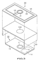
- Fig. 19 shows a communication system 150, made up by a reader/ writer 201 having an antenna coil 200, mounted to the back side of the metal casing 205, and by a non-contact IC card 101, having an antenna coil 100.
- the reader/writer 201 includes an antenna coil 200, as an inductor arranged on a substrate 204, a tuning capacitor 203, connected in series with the antenna coil 200, to form a parallel resonance circuit, and an IC for a reader/writer 202 for controlling the data transmission/ receipt with the non-contact IC card 101.
- the casing 205 of the equipment adapted for loading the reader/ writer 201 thereon, is formed of metal for procuring the strength or for preventing leakage to outside of the electro-magnetic noise caused by the internal electronic circuitry.
- the magnetic flux of the magnetic filed, generated by the antenna coil 200 is lost in the casing 205, such that it is only the small amount of the magnetic flux generated at the center of the antenna coil 200 that is allowed to pass through the inside of the antenna coil of the non-contact IC card 101.
- the non-contact IC card 101 and the reader/writer 201 cannot communicate with each other.
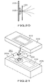
- the antenna coil of the reader/ writer 201 is designed as an antenna coil 210 substantially coextensive as the antenna coil of the non-contact IC card, and is mounted on the back side of a resin cover 220, fitted to the casing 205, so as to operate as a relaying antenna, as shown in Fig.21 . In this manner, it is possible to cope with the constraint of the antenna area or to eliminate the adverse effect from the metal casing 205.
- the antenna coil 210 is connected to the substrate 204 by fitting a jack 212, mounted to the distal end of a lead wire 211, extending from the antenna coil 210, into a plug 213 provided to the substrate 202 exposed through the aperture 205A formed in the casing 205.
- the antenna coil 210 is inconvenient to mount or dismantle, especially for maintenance, such that, in the worst of cases, the lead wire 211 may be ruptured, or the reader/ writer 201 may be destroyed.
- the first antennae coil and a second coupler coil as well as the capacitor forming a resonance circuit of the relaying apparatus are arranged altogether on an IC module forming an IC card together with a first coupler coil which is connected directly to an IC chip of the IC card.
- the first coupler coil and the second coupler coil are transformer coupled and the antennae coil is proposed to have a large area that is this document does not disclose any relation of the size and shape of the antennae coil and a transmission/reception coil of an external read/write apparatus 100.
- the common arrangement of the relaying apparatus together with the first coupling coil and the IC on the same substrate in the known communication system may enhance the electric power consumption within the IC card and enlarge the size thereof.
- EP-A1-1 385 120 being a prior art document according to Art. 54(3) EPC proposed to arrange a booster coil being a part of a resonance circuit of a relaying apparatus not on the IC card itself but in a fixed distance to the latter. This document proposes to use a very large booster coil and also does not disclose a relation of the size of the booster coil and the coil of the external information read/write device.
- the object is achieved by a communication system according to claim 1.
- the position of the third antennae coil of the third resonance circuit is fixedly mounted in a predetermined distance to the position of the first antennae coil of the first resonance circuit so that a magnetic flux generated by the magnetic field generated by the first antennae coil of the first resonance circuit always traverses the third antennae coil of the third resonance circuit.
- the relaying device and the communication system of the present invention assure optimum wireless communication even in cases wherein the antenna coil of the information read/ write device has a shape and a size differing appreciably from those of the antenna coil of the non-contact information medium.
- the wireless communication between the non-contact information medium and a wide variety of use configurations of the read/ write device may be optimized by a simple technique of changing the size/ shape of the first and second antenna coils of the relaying device so that the first and second antenna coils may be electro-magnetically coupled to the antenna coils of the information read/ write device and the non-contact information medium, respectively.
- the third antenna coil is changed in shape/ size so as to be electrically coupled to the first antenna coil.
- the size of the first antenna coil or the aperture formed in the casing may be of the smallest size possible to assure the strength of the casing as well as to avoid adverse effects by the metal components.
- the relaying device of the communication system of the present invention performs wireless communication of the electromagnetic coupling system with the information read/ write device, no laborious processing, such as wiring, is needed, and is able to relay the wireless communication with the non-contact information medium by fitting the relaying device on a removable cover or to a door that may be opened/closed.
- a communication system 1 is explained.
- the communication system 1, shown in Fig.1 is an RFID (Radio Frequency Identification), by the electromagnetic coupling system, provided with a reader/writer 10, a non-contact IC card 20, and a matching tuning circuit 30.
- RFID Radio Frequency Identification
- the non-contact IC card 20 receives electrical waves, transmitted from the reader/writer 10 through the matching tuning circuit 30, to obtain the power by electromagnetic induction, and has data communication with the reader/writer 10, with use of the electrical waves, through the matching tuning circuit 30.
- the reader/ writer 10 includes a parallel resonance circuit 13, comprised of a serial connection of an antenna coil 11, as an inductor, and a tuning capacitor 12.
- a reader/writer for IC 14 is connected in parallel with this parallel resonance circuit 13.
- the reader/writer 10 is tuned to a frequency fc in the vicinity of, for example, 13.56MHz, as the a.c. voltage is applied to the parallel resonance circuit 13, under control by the reader/writer for IC 14.
- the reader/writer 10 has wireless communication with the non-contact IC card 20, using the electrical waves, which have modulated a carrier having this frequency fc as the carrier frequency.
- the carrier frequency is the frequency fc, in the following explanation, the carrier frequency fc is not limited to 13.56MHz.
- the reader/writer for IC 14 is provided with an interfacing circuit, not shown, and is connected to and controlled by a CPU (central processing unit) of a counterpart device, having loaded thereon the reader/writer 10.
- a CPU central processing unit
- the reader/writer for IC 14 controls the operation in sending data from the reader/ writer 10 to the non-contact IC card 20 and in receiving data sent from the non-contact IC card 20.
- the reader/writer for IC 14 modulates the carrier wave of the carrier frequency fc with data being transmitted to generate transmission signals.
- ASK amplitude shift keying
- PWM pulse width modulation
- PSK phase shift keying
- the transmission signals, generated on modulation, are sent to the antenna coil 11 to generate a magnetic field.
- the magnetic field, generated in the antenna coil 11, is changed in keeping with the transmission signals, such that data carried by the carrier wave with the carrier frequency fc is transmitted, as changes in the magnetic flux, to an antenna coil 31 of the matching tuning circuit 30, electro-magnetically coupled to the antenna coil 11.
- the reader/writer for IC 14 demodulates the data, transmitted from the non-contact IC card 20 through the matching tuning circuit 30 and received as changes in the magnetic flux by the antenna coil 11.
- the induced current is generated in the antenna coil 11 as a result of changes in the magnetic flux in the antenna coil 31 of the matching tuning circuit 30 electro-magnetically coupled with the antenna coil 11.
- the induced current, generated in the antenna coil 11 is changed with the magnetic flux, the data carried by the carrier wave with the carrier frequency fc is transmitted to the antenna coil 11 as changes in the induced current.
- the reader/ writer for IC 14 demodulates this induced current to acquire data transmitted from the non-contact IC card 20.
- the non-contact IC card 20 includes a parallel resonance circuit 23, which is a serial connection of an antenna coil 21, as an inductor, and a tuning capacitor 22.
- An IC for a card 24 is connected in parallel with this parallel resonance circuit 23.
- the antenna coil 21 receives the electrical waves, transmitted from the reader/ writer 10 through the matching tuning circuit 30, as changes in the magnetic flux.
- the parallel resonance circuit 23 there is generated the induced electromotive force operating in a direction of obstructing changes in the magnetic flux of the electrical waves received by the antenna coil 11.
- the IC for a card 24, connected in parallel with the parallel resonance circuit 23, is operated with this induced electromotive force as the operating power.
- the IC for a card 24 demodulates the electrical waves, transmitted from the reader/writer 10 through the matching tuning circuit 30 and received as changed in the magnetic flux in the antenna coil 21.
- the IC for a card 24 modulates the carrier wave, with the carrier frequency fc, with data to be transmitted, to generate transmission signals.
- the IC for a card 24 changes the load of the antenna coil 21, responsive to data to be transmitted, to modulate the carrier wave, by way of load modulation.
- the transmission signals, generated on modulation, are sent to the antenna coil 21 to generate a magnetic field.
- the magnetic field, generated in the antenna coil 21 is changed with the transmission signals, the data carried by the carrier wave, with the carrier frequency fc, is transmitted, as changes in the magnetic flux, to an antenna coil 32 of the matching tuning circuit 30, electro-magnetically coupled with the antenna coil 21.
- the matching tuning circuit 30 includes a parallel resonance circuit 34, comprised of a series connection of an antenna coil 31, as a first inductor, an antenna coil 32, as a second inductor, and a tuning capacitor 33.
- the matching tuning circuit 30 is comprised of the antenna coils 31, 32, arranged on a substrate 35, so as to be connected in series with the tuning capacitor 33.
- the antenna coil 31 is electro-magnetically coupled, in a non-contact fashion, with the antenna coil 11, forming the parallel resonance circuit 13 in the reader/writer 10, and is shaped for communicating with the reader/writer 10.
- the antenna coil 31 may be of any suitable shape, on the condition that it may communicate with the reader/ writer 10.
- the antenna coil 31 may be of an elliptical or a square shape, to say nothing of the circular shape shown in Fig.1 .
- the antenna coil 31 does not have to be of the same shape as the antenna coil 11, on the condition that the antenna coil 31 is able to communicate with the reader/writer 10. However, in case the antenna coil 31 is approximately of the same shape and of the same size as the antenna coil 11, the electro-magnetic coupling may be stronger to achieve stable and highly efficient data communication.
- the antenna coil 32 is electro-magnetically coupled, in a non-contact fashion, with the antenna coil 21 on the non-contact IC card 20, forming the parallel resonance circuit 23, such as to communicate with the non-contact IC card 20.
- the antenna coil 32 may be of any suitable shape, on the condition that it may communicate with the reader/ writer 10.
- the antenna coil 31 may be of an elliptical or a circular shape, to say nothing of the square shape shown in Fig.1 .
- the antenna coil 32 is desirably larger in size than the antenna coil 21, provided to the non-contact IC card 20, since then a sufficient amount of the magnetic flux can be passed through the antenna coil 21 even in case the center of the antenna coil 21 is offset from the center of the antenna coil 32.
- the non-contact information medium is a non-contact IC card, and is used as a commutation ticket for railway or bus
- the non-contact IC card cannot be placed at a constant fixed position at all times with respect to the antenna coil 32 of the matching tuning circuit 30 for data communication.
- the antenna coil 32 is larger in size than the antenna coil of the non-contact IC card to assure more reliable data communication.
- the non-contact information medium is a non-contact IC tag affixed to a toner cartridge of a printer, as a consumable commodity, and is to have data communication with the reader/writer 10 mounted to a preset inner chassis in a printer casing, in order to manage the residual toner quantity, the non-contact IC tag may be placed in a fixed position relative to the antenna coil 32 of the matching tuning circuit 30 for data communication.
- the antenna coil 32 sized to be approximately equal to the size of the antenna coil of the non-contact IC tag.
- the antenna coil 32 is slightly smaller in size than the antenna coil 21, communication may be had by adjusting the output of the reader/writer 10.
- the antenna coil 32 does not have to be of the same size and shape as the antenna coil 21, on the condition that the antenna coil 32 is able to communicate with the non-contact IC card 20, as discussed above. However, if the antenna coil 32 is of the same size and shape as the antenna coil 21, the electro-magnetic coupling becomes stronger to realize more efficient stable data communication.
- the size as well as the shape of the antenna coils 31, 32 of the matching tuning circuit 30 is limited to a more or less extent by the shape of the antenna coil 11 of the reader/writer 10 and by the shape of the antenna coil 21 of the non-contact IC card 20, respectively, for the realization of the efficient stable wireless communication.
- the non-contact IC card 20 is used as the non-contact information medium.
- the shape and the size of the antenna coil 32 are approximately the same as those of the antenna coil 21 of the non-contact IC card 20, and also that the shape and the size of the antenna coil 31 are approximately the same as those of the antenna coil 11 of the reader/ writer 10.
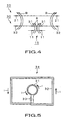
- FIG.3 an embodiment of the reader/writer 10 and the matching tuning circuit 30 of the invention is shown and, based on this embodiment, the operating principle of the matching tuning circuit 30 is explained.
- the reader/writer 10 provided on a substrate 15, is mounted on the back side of a metal chassis 50, as a casing of an apparatus on which to mount the reader/ writer 10.
- the metal chassis 50, on which the reader/writer 10 is mounted in this manner, has an aperture 50A in a location which is to be register with the mounting position of the antenna coil 11 of the reader/ writer 10.
- the opening area of the aperture 50A is selected to be such that the strength of the metal chassis 50 is not impaired and such that there is no risk of leakage of the electromagnetic noise produced by e.g. an electronic circuit within the metal chassis 50.
- the shape and the size of the antenna coil 11 of the reader/writer 10 are selected so that the antenna coil will be housed within this aperture 50A.
- the shape of the antenna coil 31 is determined to a more or less extent if once the shape of the antenna coil 11 is determined.
- the matching tuning circuit 30 is mounted for facing the reader/ writer 10, mounted on the metal chassis 50, with the metal chassis 50 in-between.
- the matching tuning circuit 30 is mounted at this time so that the antenna coil 31 overlies the aperture 50A formed in the metal chassis 50.
- the antenna coil 11 of the reader/writer 10 and the antenna coil 31 of the matching tuning circuit 30 may be electromagnetically coupled to each other in a non-contact fashion.
- the reader/writer 10 mounted to the metal chassis 50 and the matching tuning circuit 30 may have wireless communication by the antenna coils 11,31 being electromagnetically coupled to each other in a non-contact fashion, no physical connection between the reader/writer 10 and the matching tuning circuit 30 is needed and hence the matching tuning circuit 30 may be mounted in position by a simplified technique of directly bonding the substrate 30 to the metal chassis 50 with e.g. a double-sided adhesive tape.
- the matching tuning circuit 30, mounted to the metal chassis 50 operates as follows, by the electrical waves, transmitted from the reader/writer 10.
- the antenna coil 31 of the parallel resonance circuit 34 of the matching tuning circuit 30 is traversed by a magnetic flux A, generated by a magnetic field, generated in turn by the antenna coil 11 of the reader/ writer 10, for electromagnetically coupling the antenna coils 11, 31 to each other.
- the induced electromotive force is generated in the parallel resonance circuit 34 by the magnetic flux A traversing the antenna coil 31, so that the induced current I by the induced electromotive force flows through the entire circuit.
- the non-contact IC card 20 may be moved to the vicinity of the matching tuning circuit 30.
- the magnetic flux B generated by the magnetic field, generated in turn in the antenna coil 32, is passed through the inside of the antenna coil 21, as shown in Fig.4 .
- the non-contact IC card 20 is activated so that the reader/writer 10 and the non-contact IC card 20 are now able to have wireless communication with each other through the matching tuning circuit 30.
- the reader/writer 10 is mounted on the back-side surface of a metal chassis 51, as a casing of a device, adapted for being loaded with the reader/ writer 10, so that the antenna coil 11 will be in register with an aperture 51A of the metal chassis 51.
- a metal component 52 such as a screw, such that the matching tuning circuit 30 cannot directly be mounted thereon, as shown in Fig.6 .
- the matching tuning circuit 30 is mounted in position by bonding the substrate 35 of the matching tuning circuit 30 on the back side surface of a resin cover 53 overlying the aperture 51A of the metal chassis 51.
- the matching tuning circuit 30 is bonded to the back-side surface of the resin cover 53, so that, when the resin cover 53 is mounted to the metal chassis 51, the antenna coil 31 of the matching tuning circuit 30 is in register with the antenna coil 11 of the reader/ writer 10.
- the cover 53, to which is bonded the matching tuning circuit 30, is formed of non-magnetic resin, in order to cause no loss of the magnetic flux by the magnetic field generated in the antenna coil 32 of the matching tuning circuit 30.
- the substrate 35 of the matching tuning circuit 30 is of an extremely thin thickness, and is e.g. a flexible substrate, so as not to affect the magnetic field generated in the antenna coil 32.
- a shield plate 54 may also be provided in order to prevent the effect of the electromagnetic noise generated in the device designed for carrying the reader/writer 10.
- the shield plate 54 needs only to be mounted to overlie the antenna coil 11. At this time, caution should be exercised so that the shield plate 54 is kept aloof from the reader/writer 10 in order to prevent the function of the antenna coil 11 from being impaired.
- the matching tuning circuit 30, mounted to the resin cover 53 may also be mounted to the inner side of a rotatable door, provided to e.g. a casing of the device loaded with the reader/writer 10, in a manner not shown, for saving the spacing.
- the matching tuning circuit 30 may be separated from the reader/ writer 10 and mounted freely to any place within the sphere of electro-magnetic coupling.
- the result is the communication system 1 with an extremely high degree of mounting freedom.
- the antenna coils 31, 32 are connected in series with each other.
- a matching tuning circuit 40 in which a parallel resonance circuit 41 is made up by a parallel connection of the antenna coils 31, 32 and the tuning capacitor 33, as shown in Fig.7 , may be used in place of the matching tuning circuit 30.
- the case of using the matching tuning circuit 40 is not explained in detail because the operation of the communication system 1 gives the identical effect in case the matching tuning circuit 40 is used in place of the matching tuning circuit 30.
- the tuning capacitor 33 is connected in series with both the antenna coils 31, 32, as shown in Fig.7 .
- the area which allows for communication for the case of using the matching tuning circuit 30 and that for the case of not using the matching tuning circuit 30, in the wireless communication between the reader/writer 10 and the non-contact IC card 20, were measured and compared to each other.
- the antenna coil 11 of the reader/writer 10 was circular in shape, with a diameter on the order of 25 mm.
- the antenna coil 31 of the matching tuning circuit 30 was of approximately the same shape.
- the non-contact IC card 20 used was of the size of 54 mm in length, 85.6 mm in width and 0.76 mm in thickness, as provided for in the ISO (International Organization for Standardization).
- the antenna coil 21, enclosed in the non-contact IC card 20, was wound to approximate the size of the non-contact IC card 20.
- the antenna coil 32 of the matching tuning circuit 30 was approximately of the same shape as the antenna coil 21.
- the area which allows for communication, and which is to be measured is now explained.
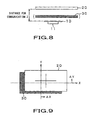
- the area which allows for communication, and which is now to be measured is defined by a distance for communication Z, representing the distance which allows for communication, in case the non-contact IC card 20 is moved vertically relative to the reader/writer 10, and by a distance for communication XY, representing the distance which allows for communication, in case the non-contact IC card 20 is moved horizontally relative to the reader/writer 10.
- the distance for communication Z is a distance up to which the communication is possible when the center of the antenna coil 11 of the reader/writer 10, placed horizontally, is confounded with the center of the major plane surface of the non-contact IC card 20, and when the non-contact IC card 20 is moved in the vertical direction, as it is kept parallel to the antenna coil 11.
- the distance for communication XY is a distance up to which the communication is possible when the non-contact IC card 20, placed horizontally at a preset distance with respect to the antenna coil 11 of the reader/writer 10, is optionally moved along the X-axis direction and along the Y-axis direction within the X-Y coordinate plane shown in Fig.9 .
- This distance for communication may be found by measuring the trajectory of the center point of the non-contact IC card 20.
- This distance for communication Z and the distance for communication XY, thus measured, may be used as indexes for the effect of the matching tuning circuit 30.
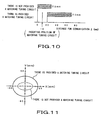
- Fig. 10 shows the results of measurement of the distance for communication Z without the matching tuning circuit 30 and the results of measurement of the distance for communication Z with the matching tuning circuit 30 placed in position. Meanwhile, since the matching tuning circuit 30 is mounted at a distance of 10 mm from the antenna coil 11 of the non-contact IC card 10, the distance for communication for the case the matching tuning circuit 30 is placed in position was measured from the position of the intervening matching tuning circuit 30.
- the distance for communication Z without the matching tuning circuit 30 was 10 to 25 mm, as shown in Fig. 10 .
- the same distance Z with the matching tuning circuit 30 interposed in position was 20 to 75 mm.
- the non-contact IC card 20 is at a distance of 10 to 20 mm from the antenna coil 11, the communication becomes infeasible because the non-contact IC card 20 and the matching tuning circuit 30 interfere with each other and become unstable in operation.
- This inconvenience may be overcome by strictly matching the resonance frequency of the non-contact IC card 20 to that of the matching tuning circuit 30 or by significantly separating the two resonance frequencies from each other.
- Fig. 11 shows the results of measurement of the distance for communication XY without the matching tuning circuit 30 and the results of measurement of the distance for communication XY with the matching tuning circuit 30 placed in position.
- the distance for communication XY was measured at a location separated in the vertical direction by 10 mm from the center of the antenna coil 11 of the reader/writer 10. In case the matching tuning circuit 30 is used, the distance for communication XY was measured at a location separated 10 mm in the vertical direction from the center of the antenna coil 32 of the matching tuning circuit 30.
- the location of insertion of the matching tuning circuit 30 is 10 mm away from the reader/writer 10, as set forth above.
- the distance for communication XY is such that -30 ⁇ X (mm) ⁇ 30 and -15 ⁇ Y (mm) ⁇ 15, as shown in Fig. 11 . That is, the distance for communication XY is defined to be the inside of an ellipsis, with a long axis of 60 mm and a short axis of 30 mm, as indicated by a broken line.
- the distance for communication XY is such that -50 ⁇ X (mm) ⁇ 50 and -40 ⁇ Y (mm) ⁇ 40, as shown in Fig. 11 . That is, in Fig. 11 , the distance for communication XY is defined to be the inside of an ellipsis, with a long axis of 100 mm and a short axis of 80 mm, as indicated by a solid line.
- the distance for communication XY is quadrupled.
- the reader/writer 10 was bonded to an iron plate 60, which iron plate, stuck to the reader/writer 10, was placed so as to prove an obstacle between the reader/writer 10 and the non-contact IC card 20 to approximate the actual use state, as shown in Fig.12 .
- the distance for communication Z and the distance for communication XY were measured for the case in which the matching tuning circuit 30 was used and for the case in which the matching tuning circuit 30 was not used.
- the reader/writer 10, non-contact IC card 20 and the matching tuning circuit 30 used are to be exactly the same as those used in the experiment 1.
- a spacer 61 is interposed between the iron plate 60 and the matching tuning circuit 30, and the separation between the antenna coil 11 of the reader/ writer 10 and the matching tuning circuit 30 is set to 5 mm, as shown in Fig.12 .
- Fig. 15 shows the measured results of the distance for communication Z, in the absence of the matching tuning circuit 30, and those of the distance for communication Z with the matching tuning circuit 30 placed in position. Meanwhile, since the matching tuning circuit 30 in the experiment 2 is placed at a separation of 5 mm from the antenna coil 11 of the reader/writer 10, the distance for communication Z was measured from the position of the matching tuning circuit 30.
- the wireless communication by the reader/ writer 10 and the non-contact IC card 20 may be improved from the communication disabled state to a practically satisfactory state.
- Fig. 16 shows the measured results of the distance for communication XY in the absence of the matching tuning circuit 30 and those of the same distance with the matching tuning circuit 30 placed in position.
- the distance for communication XY was measured at a position 5mm spaced apart in the vertical direction from the center of the antenna coil 11 of the reader/writer 10 and, in case the matching tuning circuit 30 was placed in position, the same distance XY was measured at a location 5 mm spaced apart from the center of the antenna coil 32 of the matching tuning circuit 30.
- the matching tuning circuit 30 is introduced at a position 5 mm spaced apart from the antenna coil 11 of the reader/writer 10, as noted previously.
- the distance for communication XY is such that -35 ⁇ X (mm) ⁇ 35 and -20 ⁇ Y (mm) ⁇ 20. That is, as shown in Fig.16 , the distance for communication XY is defined to be the inside of an ellipsis, with a long axis of 70 mm and a short axis of 40 mm, as indicated by a solid line in Fig.16 .
- the matching tuning circuit 30 between the reader/ writer 10 and the non-contact IC card 20
- the wireless communication by the reader/ writer 10 and the non-contact IC card 20 may be improved from the communication disabled state to a practically satisfactory state.
Landscapes
- Engineering & Computer Science (AREA)
- Physics & Mathematics (AREA)
- General Physics & Mathematics (AREA)
- Theoretical Computer Science (AREA)
- Computer Networks & Wireless Communication (AREA)
- Electromagnetism (AREA)
- Microelectronics & Electronic Packaging (AREA)
- Artificial Intelligence (AREA)
- Computer Vision & Pattern Recognition (AREA)
- Computer Hardware Design (AREA)
- Health & Medical Sciences (AREA)
- Toxicology (AREA)
- General Health & Medical Sciences (AREA)
- Signal Processing (AREA)
- Near-Field Transmission Systems (AREA)
Claims (1)
- Kommunikationssystem zur Drahtloskommunikation, die vermittelt wird durch eine Trägerwelle einer vorgegebenen Frequenz, wobei das Kommunikationssystem aufweist:eine Informationslese-/-schreibeinrichtung (10) mit einem ersten Resonanzschaltkreis (13), der gebildet wird von einer ersten Antennenspule (11) und von einem ersten Abstimmkondensator (12), welcher in Reihe geschaltet ist mit der ersten Antennenspule (11), wobei die Informationsschreib-/-leseeinrichtung (10) sich in Drahtloskommunikation mit einer Weiterleitungseinrichtung (30) befindet, die so ausgebildet ist, dass sie mit der ersten Antennenspule (11) elektromagnetisch gekoppelt ist, und zwar mit der Resonanzfrequenz des ersten Resonanzschaltkreises (13) als Frequenz der Trägerwelle,ein kontaktfreies Informationsmedium (20) mit einem zweiten Resonanzschaltkreis (23), der gebildet wird von einer zweiten Antennenspule (21) und von einem zweiten Abstimmkondensator (22), der in Reihe geschaltet ist mit der zweiten Antennenspule (21), wobei der zweite Resonanzschaltkreis (23) ausgebildet ist zum Mitschwingen mit einer Resonanzfrequenz, welche dieselbe ist wie die Resonanzfrequenz des ersten Resonanzschaltkreises (13), und welcher dazu ausgebildet ist, in Drahtloskommunikation zu stehen mit einem Schaltkreis, der elektromagnetisch gekoppelt ist mit der zweiten Antennenspule (21),wobei die Weiterleitungseinrichtung (30) einen dritten Resonanzschaltkreis (34), welcher gebildet wird von einer dritten Antennenspule (31), welche ausgebildet ist, mit der ersten Antennenspule (11) der Informationsschreibeinrichtung elektromagnetisch gekoppelt zu sein, eine vierte Antennenspule (32), welche in Reihe geschaltet ist mit oder parallel zu der dritten Antennenspule (31) und welche elektromagnetisch gekoppelt ist mit der Antennenspule (21) des kontaktfreien Informationsmediums (20), und einen dritten Abstimmkondensator (33) aufweist, welcher in Reihe geschaltet ist mit den dritten und vierten Antennenspulen (31, 32), wobei der dritte Resonanzschaltkreis (34) ausgebildet ist zum Mitschwingen mit derselben Resonanzfrequenz wie der Resonanzfrequenz des ersten Resonanzschaltkreises (13) und des zweiten Resonanzschaltkreises (23), und wobei die Weiterleitungseinrichtung (30) ausgebildet ist zum Weiterleiten der Drahtloskommunikation zwischen der Informationslese-/-schreibeinrichtung und dem kontaktfreien Informationsmedium (20),
bei welchem die dritte Antennenspule (31) der Weiterleitungseinrichtung (30) von derselben Größe und Form ist, wie die erste Antennenspule (11) der Informationslese-/-schreibeinrichtung (10),
bei welchem die zweite Antennenspule (32) der Weiterleitungseinrichtung (30) von derselben Größe und Form ist wie die zweite Antennenspule (21) des kontaktfreien Informationsmediums (20),
bei welchem die Informationslese-/-schreibeinrichtung (10) auf der Rückseite eines Metallchassis (50) montiert ist, welches eine Öffnung (50A) aufweist, wobei die Informationslese-/-schreibeinrichtung (10) derart montiert ist, dass die erste Antennenspule (11) mit der Öffnung (50A) in Eingriff steht, und
bei welchem die Weiterleitungseinrichtung (30) derart montiert ist, dass sie der Informationslese-/-schreibeinrichtung (10) mit dem Metallchassis (50) dazwischen gegenüberliegt.
Applications Claiming Priority (2)
| Application Number | Priority Date | Filing Date | Title |
|---|---|---|---|
| JP2003343616 | 2003-10-01 | ||
| JP2003343616A JP3982476B2 (ja) | 2003-10-01 | 2003-10-01 | 通信システム |
Publications (3)
| Publication Number | Publication Date |
|---|---|
| EP1521206A2 EP1521206A2 (de) | 2005-04-06 |
| EP1521206A3 EP1521206A3 (de) | 2006-12-13 |
| EP1521206B1 true EP1521206B1 (de) | 2009-07-01 |
Family
ID=34309117
Family Applications (1)
| Application Number | Title | Priority Date | Filing Date |
|---|---|---|---|
| EP04023231A Expired - Lifetime EP1521206B1 (de) | 2003-10-01 | 2004-09-29 | Weiterleitungsvorrichtung und Kommunikationssystem |
Country Status (6)
| Country | Link |
|---|---|
| US (1) | US7333786B2 (de) |
| EP (1) | EP1521206B1 (de) |
| JP (1) | JP3982476B2 (de) |
| KR (1) | KR101095378B1 (de) |
| CN (1) | CN1291556C (de) |
| DE (1) | DE602004021757D1 (de) |
Cited By (48)
| Publication number | Priority date | Publication date | Assignee | Title |
|---|---|---|---|---|
| DE102011056323A1 (de) * | 2011-12-13 | 2013-06-13 | Infineon Technologies Ag | Booster-Antennenstruktur für eine Chipkarte |
| US8760008B2 (en) | 2005-07-12 | 2014-06-24 | Massachusetts Institute Of Technology | Wireless energy transfer over variable distances between resonators of substantially similar resonant frequencies |
| US8836172B2 (en) | 2008-10-01 | 2014-09-16 | Massachusetts Institute Of Technology | Efficient near-field wireless energy transfer using adiabatic system variations |
| US8847548B2 (en) | 2008-09-27 | 2014-09-30 | Witricity Corporation | Wireless energy transfer for implantable devices |
| US8875086B2 (en) | 2011-11-04 | 2014-10-28 | Witricity Corporation | Wireless energy transfer modeling tool |
| US8901779B2 (en) | 2008-09-27 | 2014-12-02 | Witricity Corporation | Wireless energy transfer with resonator arrays for medical applications |
| US8901778B2 (en) | 2008-09-27 | 2014-12-02 | Witricity Corporation | Wireless energy transfer with variable size resonators for implanted medical devices |
| US8907531B2 (en) | 2008-09-27 | 2014-12-09 | Witricity Corporation | Wireless energy transfer with variable size resonators for medical applications |
| US8912687B2 (en) | 2008-09-27 | 2014-12-16 | Witricity Corporation | Secure wireless energy transfer for vehicle applications |
| US8922066B2 (en) | 2008-09-27 | 2014-12-30 | Witricity Corporation | Wireless energy transfer with multi resonator arrays for vehicle applications |
| US8928276B2 (en) | 2008-09-27 | 2015-01-06 | Witricity Corporation | Integrated repeaters for cell phone applications |
| US8933594B2 (en) | 2008-09-27 | 2015-01-13 | Witricity Corporation | Wireless energy transfer for vehicles |
| US8937408B2 (en) | 2008-09-27 | 2015-01-20 | Witricity Corporation | Wireless energy transfer for medical applications |
| US8947186B2 (en) | 2008-09-27 | 2015-02-03 | Witricity Corporation | Wireless energy transfer resonator thermal management |
| US8946938B2 (en) | 2008-09-27 | 2015-02-03 | Witricity Corporation | Safety systems for wireless energy transfer in vehicle applications |
| US8957549B2 (en) | 2008-09-27 | 2015-02-17 | Witricity Corporation | Tunable wireless energy transfer for in-vehicle applications |
| US8963488B2 (en) | 2008-09-27 | 2015-02-24 | Witricity Corporation | Position insensitive wireless charging |
| US9035499B2 (en) | 2008-09-27 | 2015-05-19 | Witricity Corporation | Wireless energy transfer for photovoltaic panels |
| US9065423B2 (en) | 2008-09-27 | 2015-06-23 | Witricity Corporation | Wireless energy distribution system |
| US9093853B2 (en) | 2008-09-27 | 2015-07-28 | Witricity Corporation | Flexible resonator attachment |
| US9095729B2 (en) | 2007-06-01 | 2015-08-04 | Witricity Corporation | Wireless power harvesting and transmission with heterogeneous signals |
| US9105959B2 (en) | 2008-09-27 | 2015-08-11 | Witricity Corporation | Resonator enclosure |
| US9106203B2 (en) | 2008-09-27 | 2015-08-11 | Witricity Corporation | Secure wireless energy transfer in medical applications |
| US9160203B2 (en) | 2008-09-27 | 2015-10-13 | Witricity Corporation | Wireless powered television |
| US9184595B2 (en) | 2008-09-27 | 2015-11-10 | Witricity Corporation | Wireless energy transfer in lossy environments |
| US9246336B2 (en) | 2008-09-27 | 2016-01-26 | Witricity Corporation | Resonator optimizations for wireless energy transfer |
| US9287607B2 (en) | 2012-07-31 | 2016-03-15 | Witricity Corporation | Resonator fine tuning |
| US9306635B2 (en) | 2012-01-26 | 2016-04-05 | Witricity Corporation | Wireless energy transfer with reduced fields |
| US9318922B2 (en) | 2008-09-27 | 2016-04-19 | Witricity Corporation | Mechanically removable wireless power vehicle seat assembly |
| US9318257B2 (en) | 2011-10-18 | 2016-04-19 | Witricity Corporation | Wireless energy transfer for packaging |
| US9343922B2 (en) | 2012-06-27 | 2016-05-17 | Witricity Corporation | Wireless energy transfer for rechargeable batteries |
| US9369182B2 (en) | 2008-09-27 | 2016-06-14 | Witricity Corporation | Wireless energy transfer using variable size resonators and system monitoring |
| US9384885B2 (en) | 2011-08-04 | 2016-07-05 | Witricity Corporation | Tunable wireless power architectures |
| US9396867B2 (en) | 2008-09-27 | 2016-07-19 | Witricity Corporation | Integrated resonator-shield structures |
| US9404954B2 (en) | 2012-10-19 | 2016-08-02 | Witricity Corporation | Foreign object detection in wireless energy transfer systems |
| US9421388B2 (en) | 2007-06-01 | 2016-08-23 | Witricity Corporation | Power generation for implantable devices |
| US9442172B2 (en) | 2011-09-09 | 2016-09-13 | Witricity Corporation | Foreign object detection in wireless energy transfer systems |
| US9444265B2 (en) | 2005-07-12 | 2016-09-13 | Massachusetts Institute Of Technology | Wireless energy transfer |
| US9444520B2 (en) | 2008-09-27 | 2016-09-13 | Witricity Corporation | Wireless energy transfer converters |
| US9449757B2 (en) | 2012-11-16 | 2016-09-20 | Witricity Corporation | Systems and methods for wireless power system with improved performance and/or ease of use |
| US9515494B2 (en) | 2008-09-27 | 2016-12-06 | Witricity Corporation | Wireless power system including impedance matching network |
| US9544683B2 (en) | 2008-09-27 | 2017-01-10 | Witricity Corporation | Wirelessly powered audio devices |
| US9595378B2 (en) | 2012-09-19 | 2017-03-14 | Witricity Corporation | Resonator enclosure |
| US9602168B2 (en) | 2010-08-31 | 2017-03-21 | Witricity Corporation | Communication in wireless energy transfer systems |
| US9601261B2 (en) | 2008-09-27 | 2017-03-21 | Witricity Corporation | Wireless energy transfer using repeater resonators |
| US9601266B2 (en) | 2008-09-27 | 2017-03-21 | Witricity Corporation | Multiple connected resonators with a single electronic circuit |
| US9601270B2 (en) | 2008-09-27 | 2017-03-21 | Witricity Corporation | Low AC resistance conductor designs |
| EP4113361A1 (de) | 2021-06-28 | 2023-01-04 | Thales DIS France SA | Verfahren zur verwaltung einer kontaktlosen karte |
Families Citing this family (233)
| Publication number | Priority date | Publication date | Assignee | Title |
|---|---|---|---|---|
| GB2390509A (en) * | 2002-07-03 | 2004-01-07 | Marconi Information Systems Lt | Smart label reader interfacing device |
| JP4054319B2 (ja) * | 2004-03-29 | 2008-02-27 | オリンパス株式会社 | 電力供給装置 |
| US7158032B2 (en) * | 2004-05-20 | 2007-01-02 | Xerox Corporation | Diagnosis of programmable modules |
| JP4596837B2 (ja) * | 2004-07-14 | 2010-12-15 | 株式会社シービーエヌ | 非接触データキャリア読み取りシステム |
| US7411507B2 (en) * | 2004-08-20 | 2008-08-12 | Soundcraft, Inc. | Metal housing with integral antenna for RFID reader/writer |
| JP4649183B2 (ja) * | 2004-11-30 | 2011-03-09 | 株式会社東芝 | 無線通信端末 |
| JP4639857B2 (ja) * | 2005-03-07 | 2011-02-23 | 富士ゼロックス株式会社 | Rfidタグが取り付けられた物品を収納する収納箱、その配置方法、通信方法、通信確認方法および包装構造。 |
| JP2006277178A (ja) * | 2005-03-29 | 2006-10-12 | Aruze Corp | ゲーム用カード |
| JP2006271596A (ja) * | 2005-03-29 | 2006-10-12 | Aruze Corp | ゲーム用カード |
| ATE515891T1 (de) * | 2005-04-07 | 2011-07-15 | Virtual Extension Ltd | Synchronisierte weitergeleitete übertragungen in rfid-netzwerken |
| AU2013203947B2 (en) * | 2005-07-12 | 2016-02-18 | Massachusetts Institute Of Technology | Wireless non-radiative energy transfer |
| JP4677845B2 (ja) * | 2005-07-27 | 2011-04-27 | 凸版印刷株式会社 | 搬送制御管理システムおよびアダプタコイル |
| US20070057795A1 (en) * | 2005-09-12 | 2007-03-15 | Wakahiro Kawai | Inspection method of RFID tag |
| US8447234B2 (en) * | 2006-01-18 | 2013-05-21 | Qualcomm Incorporated | Method and system for powering an electronic device via a wireless link |
| US9130602B2 (en) | 2006-01-18 | 2015-09-08 | Qualcomm Incorporated | Method and apparatus for delivering energy to an electrical or electronic device via a wireless link |
| US7519328B2 (en) | 2006-01-19 | 2009-04-14 | Murata Manufacturing Co., Ltd. | Wireless IC device and component for wireless IC device |
| US20070171992A1 (en) * | 2006-01-26 | 2007-07-26 | Broadcom Corporation, A California Corporation | Near field RFID system with multiple reader coils |
| JP5105198B2 (ja) * | 2006-02-03 | 2012-12-19 | ワン2タッチ エーエス | 外付けキーボード |
| CN101385039B (zh) * | 2006-03-15 | 2012-03-21 | 株式会社半导体能源研究所 | 半导体器件 |
| EP2002383B1 (de) | 2006-03-15 | 2012-04-25 | Semiconductor Energy Laboratory Co., Ltd. | Halbleiterbauelement |
| US7642916B2 (en) | 2006-03-23 | 2010-01-05 | Xerox Corporation | RFID bridge antenna |
| US7432817B2 (en) * | 2006-03-23 | 2008-10-07 | Xerox Corporation | Module with RFID tag and associated bridge antenna |
| US8063746B2 (en) * | 2006-03-31 | 2011-11-22 | Assa Abloy Ab | Transponder detector for an RFID system generating a progression of detection signals |
| JP4684152B2 (ja) * | 2006-04-06 | 2011-05-18 | 東芝Itコントロールシステム株式会社 | 磁界ループアンテナ |
| WO2007122870A1 (ja) | 2006-04-10 | 2007-11-01 | Murata Manufacturing Co., Ltd. | 無線icデバイス |
| CN102780085A (zh) * | 2006-04-14 | 2012-11-14 | 株式会社村田制作所 | 天线 |
| JP5016252B2 (ja) * | 2006-04-14 | 2012-09-05 | 株式会社タムラ製作所 | コネクタ一体型rfidリーダライタ |
| WO2007119304A1 (ja) | 2006-04-14 | 2007-10-25 | Murata Manufacturing Co., Ltd. | 無線icデバイス |
| US9064198B2 (en) | 2006-04-26 | 2015-06-23 | Murata Manufacturing Co., Ltd. | Electromagnetic-coupling-module-attached article |
| JP4803253B2 (ja) * | 2006-04-26 | 2011-10-26 | 株式会社村田製作所 | 給電回路基板付き物品 |
| DE112007001222B4 (de) | 2006-05-26 | 2017-10-05 | Murata Manufacturing Co., Ltd. | Datenkoppler |
| EP2023499A4 (de) * | 2006-05-30 | 2011-04-20 | Murata Manufacturing Co | Informationsendgerät |
| EP2023275B1 (de) | 2006-06-01 | 2011-04-27 | Murata Manufacturing Co. Ltd. | Hochfrequenz-ic-anordnung und zusammengesetzte komponente für eine hochfrequenz-ic-anordnung |
| WO2007145053A1 (ja) * | 2006-06-12 | 2007-12-21 | Murata Manufacturing Co., Ltd. | 電磁結合モジュール、無線icデバイスの検査システム及びそれを用いた電磁結合モジュール、無線icデバイスの製造方法 |
| JP4281850B2 (ja) | 2006-06-30 | 2009-06-17 | 株式会社村田製作所 | 光ディスク |
| JP4957724B2 (ja) * | 2006-07-11 | 2012-06-20 | 株式会社村田製作所 | アンテナ及び無線icデバイス |
| WO2008023636A1 (en) | 2006-08-24 | 2008-02-28 | Murata Manufacturing Co., Ltd. | Wireless ic device inspecting system and wireless ic device manufacturing method using the same |
| JP4915849B2 (ja) * | 2006-09-06 | 2012-04-11 | 鹿島建設株式会社 | 磁気通信アンテナ及び装置 |
| US7561107B2 (en) * | 2006-09-07 | 2009-07-14 | Intelleflex Corporation | RFID device with microstrip antennas |
| JP2008078777A (ja) * | 2006-09-19 | 2008-04-03 | Brother Ind Ltd | 印刷物管理装置 |
| JP2008074068A (ja) * | 2006-09-25 | 2008-04-03 | Brother Ind Ltd | 画像形成装置 |
| JP2008074067A (ja) * | 2006-09-25 | 2008-04-03 | Brother Ind Ltd | 画像形成装置 |
| DE112007002024B4 (de) | 2006-09-26 | 2010-06-10 | Murata Mfg. Co., Ltd., Nagaokakyo-shi | Induktiv gekoppeltes Modul und Element mit induktiv gekoppeltem Modul |
| JP2008085844A (ja) * | 2006-09-28 | 2008-04-10 | Brother Ind Ltd | データ処理装置及び被記録媒体 |
| JP4197027B2 (ja) * | 2006-09-28 | 2008-12-17 | ブラザー工業株式会社 | 画像形成装置及びプログラム |
| JP2008084152A (ja) * | 2006-09-28 | 2008-04-10 | Brother Ind Ltd | 画像形成装置及びプログラム |
| JP2008090340A (ja) * | 2006-09-29 | 2008-04-17 | Brother Ind Ltd | 文書データ編集装置、文書作成システム、及びプログラム |
| US7839124B2 (en) * | 2006-09-29 | 2010-11-23 | Semiconductor Energy Laboratory Co., Ltd. | Wireless power storage device comprising battery, semiconductor device including battery, and method for operating the wireless power storage device |
| EP2056488B1 (de) * | 2006-10-27 | 2014-09-03 | Murata Manufacturing Co. Ltd. | Artikel mit elektromagnetisch gekoppeltem modul |
| FR2908201B1 (fr) * | 2006-11-03 | 2009-02-06 | Raisonance Soc Par Actions Sim | Systeme d'analyse de communications radiofrequence |
| FR2910746B1 (fr) * | 2006-12-20 | 2009-01-23 | Smart Packaging Solutions Sps | Interface de communication radiofrequence locale entre un telephone mobile et un lecteur sans contact |
| JP2008171965A (ja) * | 2007-01-11 | 2008-07-24 | Fuji Electric Device Technology Co Ltd | 超小型電力変換装置 |
| WO2008090943A1 (ja) | 2007-01-26 | 2008-07-31 | Murata Manufacturing Co., Ltd. | 電磁結合モジュール付き容器 |
| WO2008096576A1 (ja) | 2007-02-06 | 2008-08-14 | Murata Manufacturing Co., Ltd. | 電磁結合モジュール付き包装材 |
| DE202007002838U1 (de) * | 2007-02-27 | 2008-07-03 | Robert Bosch Gmbh | Werkstückidentifikationssystem |
| US9774086B2 (en) * | 2007-03-02 | 2017-09-26 | Qualcomm Incorporated | Wireless power apparatus and methods |
| JP4253359B2 (ja) * | 2007-03-16 | 2009-04-08 | アルプス電気株式会社 | 通信システム |
| KR101356409B1 (ko) * | 2007-03-27 | 2014-01-27 | 메사추세츠 인스티튜트 오브 테크놀로지 | 무선 에너지 전달 |
| JP2008246104A (ja) * | 2007-03-30 | 2008-10-16 | Angel Shoji Kk | Rfidを内蔵したゲームカードおよびその製造方法 |
| FR2914800B1 (fr) * | 2007-04-04 | 2010-09-17 | Jacek Kowalski | Module nfc, notamment pour telephone mobile |
| JP5024372B2 (ja) | 2007-04-06 | 2012-09-12 | 株式会社村田製作所 | 無線icデバイス |
| US8009101B2 (en) | 2007-04-06 | 2011-08-30 | Murata Manufacturing Co., Ltd. | Wireless IC device |
| WO2008126649A1 (ja) * | 2007-04-09 | 2008-10-23 | Murata Manufacturing Co., Ltd. | 無線icデバイス |
| US7762472B2 (en) | 2007-07-04 | 2010-07-27 | Murata Manufacturing Co., Ltd | Wireless IC device |
| US8235299B2 (en) | 2007-07-04 | 2012-08-07 | Murata Manufacturing Co., Ltd. | Wireless IC device and component for wireless IC device |
| WO2008136226A1 (ja) * | 2007-04-26 | 2008-11-13 | Murata Manufacturing Co., Ltd. | 無線icデバイス |
| WO2008136220A1 (ja) | 2007-04-27 | 2008-11-13 | Murata Manufacturing Co., Ltd. | 無線icデバイス |
| JP4433097B2 (ja) | 2007-04-27 | 2010-03-17 | 株式会社村田製作所 | 無線icデバイス |
| DE112008000065B4 (de) | 2007-05-10 | 2011-07-07 | Murata Manufacturing Co., Ltd., Kyoto-fu | Drahtloses IC-Bauelement |
| JP4666102B2 (ja) | 2007-05-11 | 2011-04-06 | 株式会社村田製作所 | 無線icデバイス |
| US9124120B2 (en) * | 2007-06-11 | 2015-09-01 | Qualcomm Incorporated | Wireless power system and proximity effects |
| WO2009001814A1 (ja) * | 2007-06-27 | 2008-12-31 | Murata Manufacturing Co., Ltd. | 無線icデバイス |
| EP2168207B1 (de) * | 2007-07-03 | 2012-12-05 | Allflex Usa, Inc. | Induktiv gekoppelte schleifenantenne für einen hochfrequenzidentifikationsleser |
| WO2009008296A1 (ja) * | 2007-07-09 | 2009-01-15 | Murata Manufacturing Co., Ltd. | 無線icデバイス |
| CN104540317B (zh) * | 2007-07-17 | 2018-11-02 | 株式会社村田制作所 | 印制布线基板 |
| JP5104865B2 (ja) * | 2007-07-18 | 2012-12-19 | 株式会社村田製作所 | 無線icデバイス |
| US20090021352A1 (en) * | 2007-07-18 | 2009-01-22 | Murata Manufacturing Co., Ltd. | Radio frequency ic device and electronic apparatus |
| US7830311B2 (en) | 2007-07-18 | 2010-11-09 | Murata Manufacturing Co., Ltd. | Wireless IC device and electronic device |
| JP4434311B2 (ja) | 2007-07-18 | 2010-03-17 | 株式会社村田製作所 | 無線icデバイスおよびその製造方法 |
| EP2086052B1 (de) * | 2007-07-18 | 2012-05-02 | Murata Manufacturing Co. Ltd. | Drahtloses ic-gerät |
| CN101842962B (zh) | 2007-08-09 | 2014-10-08 | 高通股份有限公司 | 增加谐振器的q因数 |
| CN103560811A (zh) * | 2007-08-13 | 2014-02-05 | 高通股份有限公司 | 远程低频率谐振器和材料 |
| CN101377808B (zh) * | 2007-08-31 | 2012-02-29 | 天时电子股份有限公司 | 射频辨识定位装置及其方法 |
| KR20120102173A (ko) * | 2007-09-13 | 2012-09-17 | 퀄컴 인코포레이티드 | 무선 전력 인가를 위한 안테나 |
| EP2188863A1 (de) * | 2007-09-13 | 2010-05-26 | QUALCOMM Incorporated | Maximierung des pulverertrags aus drahtlosen leistungsmagnetresonatoren |
| EP2201641A1 (de) | 2007-09-17 | 2010-06-30 | Qualcomm Incorporated | Sender und empfänger für drahtlosen energietransfer |
| EP2208279A4 (de) | 2007-10-11 | 2016-11-30 | Qualcomm Inc | Drahtloser stromtransfer unter verwendung von magnetomechanischen systemen |
| JP5118462B2 (ja) * | 2007-12-12 | 2013-01-16 | 日本発條株式会社 | コイルアンテナおよび非接触情報媒体 |
| CN101595599B (zh) | 2007-12-20 | 2013-05-01 | 株式会社村田制作所 | 无线ic器件 |
| EP2557528A3 (de) | 2007-12-26 | 2017-01-18 | Murata Manufacturing Co., Ltd. | Antennenvorrichtung und drahtlose integrierte Schaltung |
| US8294300B2 (en) * | 2008-01-14 | 2012-10-23 | Qualcomm Incorporated | Wireless powering and charging station |
| DE102008005233A1 (de) * | 2008-01-19 | 2009-07-23 | Mtu Aero Engines Gmbh | Funkmodul und Verfahren zum Betreiben eines Funkmoduls |
| EP2251934B1 (de) | 2008-03-03 | 2018-05-02 | Murata Manufacturing Co. Ltd. | Drahtlose integrierte schaltung und drahtloses kommunikationssystem |
| JP4518211B2 (ja) * | 2008-03-03 | 2010-08-04 | 株式会社村田製作所 | 複合アンテナ |
| JP4404166B2 (ja) * | 2008-03-26 | 2010-01-27 | 株式会社村田製作所 | 無線icデバイス |
| US8629576B2 (en) | 2008-03-28 | 2014-01-14 | Qualcomm Incorporated | Tuning and gain control in electro-magnetic power systems |
| EP2107495B1 (de) * | 2008-04-01 | 2012-09-19 | Assa Abloy Ab | Schaltkapazitätsverfahren zur Detektion von und darauffolgender Kommunikation mit einer drahtlosen Transpondervorrichtung unter Verwendung einer Einzelantenne |
| JP4535209B2 (ja) * | 2008-04-14 | 2010-09-01 | 株式会社村田製作所 | 無線icデバイス、電子機器及び無線icデバイスの共振周波数の調整方法 |
| US8712323B2 (en) * | 2008-04-21 | 2014-04-29 | Tagarray, Inc. | Inductive antenna coupling |
| CN103295056B (zh) * | 2008-05-21 | 2016-12-28 | 株式会社村田制作所 | 无线ic器件 |
| WO2009142068A1 (ja) * | 2008-05-22 | 2009-11-26 | 株式会社村田製作所 | 無線icデバイス及びその製造方法 |
| CN104077622B (zh) * | 2008-05-26 | 2016-07-06 | 株式会社村田制作所 | 无线ic器件系统及无线ic器件的真伪判定方法 |
| EP2282372B1 (de) * | 2008-05-28 | 2019-09-11 | Murata Manufacturing Co. Ltd. | Drahtlose ic-vorrichtung und bauteil für drahtlose ic-vorrichtung |
| JP4557186B2 (ja) * | 2008-06-25 | 2010-10-06 | 株式会社村田製作所 | 無線icデバイスとその製造方法 |
| EP2306586B1 (de) * | 2008-07-04 | 2014-04-02 | Murata Manufacturing Co. Ltd. | Drahtlose integrierte schaltung |
| US8278784B2 (en) | 2008-07-28 | 2012-10-02 | Qualcomm Incorporated | Wireless power transmission for electronic devices |
| WO2010021217A1 (ja) * | 2008-08-19 | 2010-02-25 | 株式会社村田製作所 | 無線icデバイス及びその製造方法 |
| US20100259110A1 (en) * | 2008-09-27 | 2010-10-14 | Kurs Andre B | Resonator optimizations for wireless energy transfer |
| US8643326B2 (en) | 2008-09-27 | 2014-02-04 | Witricity Corporation | Tunable wireless energy transfer systems |
| US9744858B2 (en) | 2008-09-27 | 2017-08-29 | Witricity Corporation | System for wireless energy distribution in a vehicle |
| US8598743B2 (en) | 2008-09-27 | 2013-12-03 | Witricity Corporation | Resonator arrays for wireless energy transfer |
| JP5433199B2 (ja) * | 2008-10-21 | 2014-03-05 | 学校法人慶應義塾 | 電子回路 |
| WO2010047214A1 (ja) * | 2008-10-24 | 2010-04-29 | 株式会社村田製作所 | 無線icデバイス |
| DE112009002399B4 (de) * | 2008-10-29 | 2022-08-18 | Murata Manufacturing Co., Ltd. | Funk-IC-Bauelement |
| DE112009002384B4 (de) * | 2008-11-17 | 2021-05-06 | Murata Manufacturing Co., Ltd. | Antenne und Drahtlose-IC-Bauelement |
| WO2010071027A1 (ja) | 2008-12-15 | 2010-06-24 | 株式会社村田製作所 | 高周波結合器及び通信装置 |
| CN102273012B (zh) | 2009-01-09 | 2013-11-20 | 株式会社村田制作所 | 无线ic器件及无线ic模块 |
| JP5041077B2 (ja) * | 2009-01-16 | 2012-10-03 | 株式会社村田製作所 | 高周波デバイス及び無線icデバイス |
| JP4868000B2 (ja) * | 2009-01-26 | 2012-02-01 | ブラザー工業株式会社 | 画像形成装置及び交換品 |
| EP2385580B1 (de) | 2009-01-30 | 2014-04-09 | Murata Manufacturing Co., Ltd. | Antenne und drahtlose ic-vorrichtung |
| JP5316638B2 (ja) | 2009-03-13 | 2013-10-16 | 株式会社村田製作所 | アンテナ装置 |
| JP5510450B2 (ja) | 2009-04-14 | 2014-06-04 | 株式会社村田製作所 | 無線icデバイス |
| EP2424041B1 (de) | 2009-04-21 | 2018-11-21 | Murata Manufacturing Co., Ltd. | Antennenvorrichtung und resonanzfrequenz-einstellverfahren dafür |
| US10276899B2 (en) | 2009-05-12 | 2019-04-30 | Auckland Uniservices Limited | Inductive power transfer apparatus and electric autocycle charger including the inductive power transfer apparatus |
| WO2010140429A1 (ja) | 2009-06-03 | 2010-12-09 | 株式会社村田製作所 | 無線icデバイス及びその製造方法 |
| KR101052115B1 (ko) * | 2009-06-10 | 2011-07-26 | 엘지이노텍 주식회사 | 이중 공진을 이용한 nfc 안테나 |
| JP5516580B2 (ja) | 2009-06-19 | 2014-06-11 | 株式会社村田製作所 | 無線icデバイス及び給電回路と放射板との結合方法 |
| DE102009027123A1 (de) * | 2009-06-23 | 2010-12-30 | Bundesdruckerei Gmbh | RFID-Lesegerät und RFID-System |
| WO2011001709A1 (ja) | 2009-07-03 | 2011-01-06 | 株式会社村田製作所 | アンテナおよびアンテナモジュール |
| JP5263890B2 (ja) * | 2009-08-18 | 2013-08-14 | Necトーキン株式会社 | 非接触情報媒体の通信システム |
| JP4807463B2 (ja) * | 2010-03-17 | 2011-11-02 | パナソニック株式会社 | アンテナ装置 |
| JP5182431B2 (ja) | 2009-09-28 | 2013-04-17 | 株式会社村田製作所 | 無線icデバイスおよびそれを用いた環境状態検出方法 |
| CN102577646B (zh) | 2009-09-30 | 2015-03-04 | 株式会社村田制作所 | 电路基板及其制造方法 |
| JP5304580B2 (ja) * | 2009-10-02 | 2013-10-02 | 株式会社村田製作所 | 無線icデバイス |
| CN102576939B (zh) | 2009-10-16 | 2015-11-25 | 株式会社村田制作所 | 天线及无线ic器件 |
| JP5418600B2 (ja) | 2009-10-27 | 2014-02-19 | 株式会社村田製作所 | 送受信装置及び無線タグ読み取り装置 |
| WO2011055702A1 (ja) | 2009-11-04 | 2011-05-12 | 株式会社村田製作所 | 無線icタグ、リーダライタ及び情報処理システム |
| CN102576930A (zh) | 2009-11-04 | 2012-07-11 | 株式会社村田制作所 | 通信终端及信息处理系统 |
| JP5327334B2 (ja) | 2009-11-04 | 2013-10-30 | 株式会社村田製作所 | 通信端末及び情報処理システム |
| GB2487491B (en) | 2009-11-20 | 2014-09-03 | Murata Manufacturing Co | Antenna device and mobile communication terminal |
| FR2953314B1 (fr) * | 2009-12-01 | 2012-10-26 | Schneider Electric Ind Sas | Prolongateur d'antenne rfid auto-parametrable |
| JP4978756B2 (ja) | 2009-12-24 | 2012-07-18 | 株式会社村田製作所 | 通信端末 |
| JP5652470B2 (ja) | 2010-03-03 | 2015-01-14 | 株式会社村田製作所 | 無線通信モジュール及び無線通信デバイス |
| WO2011108341A1 (ja) | 2010-03-03 | 2011-09-09 | 株式会社村田製作所 | 無線通信デバイス及び無線通信端末 |
| CN102576940B (zh) | 2010-03-12 | 2016-05-04 | 株式会社村田制作所 | 无线通信器件及金属制物品 |
| CN102668241B (zh) | 2010-03-24 | 2015-01-28 | 株式会社村田制作所 | Rfid系统 |
| JP5630499B2 (ja) | 2010-03-31 | 2014-11-26 | 株式会社村田製作所 | アンテナ装置及び無線通信デバイス |
| JP5299351B2 (ja) | 2010-05-14 | 2013-09-25 | 株式会社村田製作所 | 無線icデバイス |
| JP5170156B2 (ja) | 2010-05-14 | 2013-03-27 | 株式会社村田製作所 | 無線icデバイス |
| US8983529B2 (en) | 2010-06-07 | 2015-03-17 | Dai Nippon Printing Co., Ltd. | Communication system, information recording medium, and relay communication device |
| US8281983B2 (en) * | 2010-06-28 | 2012-10-09 | Xerox Corporation | Method and apparatus for storing and verifying serial numbers using smart labels in an image production device |
| JP5376060B2 (ja) | 2010-07-08 | 2013-12-25 | 株式会社村田製作所 | アンテナ及びrfidデバイス |
| GB2495418B (en) | 2010-07-28 | 2017-05-24 | Murata Manufacturing Co | Antenna apparatus and communication terminal instrument |
| WO2012020748A1 (ja) | 2010-08-10 | 2012-02-16 | 株式会社村田製作所 | プリント配線板及び無線通信システム |
| JP5234071B2 (ja) | 2010-09-03 | 2013-07-10 | 株式会社村田製作所 | Rficモジュール |
| CN103038939B (zh) | 2010-09-30 | 2015-11-25 | 株式会社村田制作所 | 无线ic器件 |
| CN105226382B (zh) | 2010-10-12 | 2019-06-11 | 株式会社村田制作所 | 天线装置及终端装置 |
| GB2501385B (en) | 2010-10-21 | 2015-05-27 | Murata Manufacturing Co | Communication terminal device |
| WO2012081572A1 (ja) * | 2010-12-13 | 2012-06-21 | 大日本印刷株式会社 | 通信システム、中継通信装置、中継通信装置及び電磁誘導通信装置の組み合わせ、電磁誘導通信装置、情報記憶媒体、情報記憶媒体製造方法 |
| CN105048058B (zh) | 2011-01-05 | 2017-10-27 | 株式会社村田制作所 | 无线通信器件 |
| JP5304956B2 (ja) | 2011-01-14 | 2013-10-02 | 株式会社村田製作所 | Rfidチップパッケージ及びrfidタグ |
| JP5594178B2 (ja) * | 2011-02-21 | 2014-09-24 | 大日本印刷株式会社 | 通信システム |
| CN104899639B (zh) | 2011-02-28 | 2018-08-07 | 株式会社村田制作所 | 无线通信器件 |
| JP5630566B2 (ja) | 2011-03-08 | 2014-11-26 | 株式会社村田製作所 | アンテナ装置及び通信端末機器 |
| JP5273326B2 (ja) | 2011-04-05 | 2013-08-28 | 株式会社村田製作所 | 無線通信デバイス |
| WO2012141070A1 (ja) | 2011-04-13 | 2012-10-18 | 株式会社村田製作所 | 無線icデバイス及び無線通信端末 |
| KR101249242B1 (ko) * | 2011-05-04 | 2013-04-01 | 한국전기연구원 | 자계 공진 무선전력전송을 위한 다중 루프를 갖는 자기 공진코일 |
| WO2012157596A1 (ja) | 2011-05-16 | 2012-11-22 | 株式会社村田製作所 | 無線icデバイス |
| US9948145B2 (en) | 2011-07-08 | 2018-04-17 | Witricity Corporation | Wireless power transfer for a seat-vest-helmet system |
| WO2013008874A1 (ja) | 2011-07-14 | 2013-01-17 | 株式会社村田製作所 | 無線通信デバイス |
| JP5333707B2 (ja) | 2011-07-15 | 2013-11-06 | 株式会社村田製作所 | 無線通信デバイス |
| WO2013011865A1 (ja) | 2011-07-19 | 2013-01-24 | 株式会社村田製作所 | アンテナモジュール、アンテナ装置、rfidタグおよび通信端末装置 |
| JP5928768B2 (ja) * | 2011-08-10 | 2016-06-01 | ソニー株式会社 | 非接触通信装置 |
| JP5418737B2 (ja) | 2011-09-09 | 2014-02-19 | 株式会社村田製作所 | アンテナ装置および無線デバイス |
| US20130062966A1 (en) | 2011-09-12 | 2013-03-14 | Witricity Corporation | Reconfigurable control architectures and algorithms for electric vehicle wireless energy transfer systems |
| JP5665710B2 (ja) * | 2011-09-26 | 2015-02-04 | 株式会社東芝 | 無線電力伝送システム、送電装置及び受電装置 |
| CN103380432B (zh) | 2011-12-01 | 2016-10-19 | 株式会社村田制作所 | 无线ic器件及其制造方法 |
| DE102011055970A1 (de) * | 2011-12-02 | 2013-06-06 | Feig Electronic Gmbh | RFID-Reader sowie Vorrichtung mit einem RFID-Reader |
| JP5354137B1 (ja) | 2012-01-30 | 2013-11-27 | 株式会社村田製作所 | 無線icデバイス |
| WO2013125610A1 (ja) | 2012-02-24 | 2013-08-29 | 株式会社村田製作所 | アンテナ装置および無線通信装置 |
| WO2013153697A1 (ja) | 2012-04-13 | 2013-10-17 | 株式会社村田製作所 | Rfidタグの検査方法及び検査装置 |
| GB2519247B (en) * | 2012-06-28 | 2017-11-29 | Murata Manufacturing Co | Antenna device, feed element, and communication terminal device |
| US10032103B2 (en) * | 2012-07-13 | 2018-07-24 | Sato Holdings Corporation | Antenna design and interrogator system |
| US8981907B1 (en) * | 2012-07-19 | 2015-03-17 | Disney Enterprises, Inc. | RFID antenna multiplexing |
| KR102144360B1 (ko) * | 2012-12-05 | 2020-08-13 | 삼성전자주식회사 | 스마트 근거리무선통신 안테나 매칭 네트워크 시스템 및 그것을 포함한 유저 장치 |
| US9575156B2 (en) | 2013-01-15 | 2017-02-21 | Disney Enterprises, Inc. | Spatial recognition of RFID tag placement using antenna multiplexing |
| CN104981968A (zh) * | 2013-02-12 | 2015-10-14 | 株式会社村田制作所 | 旋转电机 |
| AT14310U1 (de) * | 2013-03-08 | 2015-08-15 | Markus Ing Schriebl | NFC-Kopplungsantenne |
| EP2775561A1 (de) * | 2013-03-08 | 2014-09-10 | Andreas Pensold | NFC-Kopplungsantenne |
| US9601267B2 (en) | 2013-07-03 | 2017-03-21 | Qualcomm Incorporated | Wireless power transmitter with a plurality of magnetic oscillators |
| EP3039770B1 (de) | 2013-08-14 | 2020-01-22 | WiTricity Corporation | Impedanzabstimmung |
| US20150097735A1 (en) * | 2013-10-04 | 2015-04-09 | Samsung Electro-Mechanics Co., Ltd. | Antenna assembly and electronic device |
| CN105850052B (zh) | 2013-10-18 | 2019-05-14 | 基萨公司 | 用于极高频(ehf)近距离无线连接的容忍未对准的高密度多发送器/接收器模块 |
| TWI532351B (zh) * | 2013-11-07 | 2016-05-01 | 國立交通大學 | 寬頻連接結構及其連接方法、傳輸裝置及傳輸寬頻訊號的方法 |
| DE102014200524A1 (de) * | 2014-01-14 | 2015-07-16 | Siemens Medical Instruments Pte. Ltd. | Antenneneinrichtung für Hörinstrumente |
| US9842686B2 (en) | 2014-01-22 | 2017-12-12 | Electrochem Solutions, Inc. | Split winding repeater |
| US9780573B2 (en) | 2014-02-03 | 2017-10-03 | Witricity Corporation | Wirelessly charged battery system |
| US9952266B2 (en) | 2014-02-14 | 2018-04-24 | Witricity Corporation | Object detection for wireless energy transfer systems |
| WO2015161035A1 (en) | 2014-04-17 | 2015-10-22 | Witricity Corporation | Wireless power transfer systems with shield openings |
| US9842687B2 (en) | 2014-04-17 | 2017-12-12 | Witricity Corporation | Wireless power transfer systems with shaped magnetic components |
| KR102152694B1 (ko) | 2014-04-29 | 2020-09-07 | 엘지이노텍 주식회사 | 케이스 장치 |
| US9837860B2 (en) | 2014-05-05 | 2017-12-05 | Witricity Corporation | Wireless power transmission systems for elevators |
| WO2015171910A1 (en) | 2014-05-07 | 2015-11-12 | Witricity Corporation | Foreign object detection in wireless energy transfer systems |
| US9954375B2 (en) | 2014-06-20 | 2018-04-24 | Witricity Corporation | Wireless power transfer systems for surfaces |
| US10574091B2 (en) | 2014-07-08 | 2020-02-25 | Witricity Corporation | Enclosures for high power wireless power transfer systems |
| WO2016007674A1 (en) | 2014-07-08 | 2016-01-14 | Witricity Corporation | Resonator balancing in wireless power transfer systems |
| US9843217B2 (en) | 2015-01-05 | 2017-12-12 | Witricity Corporation | Wireless energy transfer for wearables |
| JP6062486B2 (ja) * | 2015-05-13 | 2017-01-18 | ルネサスエレクトロニクス株式会社 | 半導体装置 |
| JP5896582B1 (ja) * | 2015-08-28 | 2016-03-30 | 太平洋工業株式会社 | 通信中継器 |
| US10248899B2 (en) | 2015-10-06 | 2019-04-02 | Witricity Corporation | RFID tag and transponder detection in wireless energy transfer systems |
| EP3362804B1 (de) | 2015-10-14 | 2024-01-17 | WiTricity Corporation | Phasen- und amplitudendetektion in systemen zur drahtlosen energieübertragung |
| WO2017070227A1 (en) | 2015-10-19 | 2017-04-27 | Witricity Corporation | Foreign object detection in wireless energy transfer systems |
| WO2017070009A1 (en) | 2015-10-22 | 2017-04-27 | Witricity Corporation | Dynamic tuning in wireless energy transfer systems |
| US10075019B2 (en) | 2015-11-20 | 2018-09-11 | Witricity Corporation | Voltage source isolation in wireless power transfer systems |
| KR102426701B1 (ko) * | 2015-12-16 | 2022-07-29 | 삼성전자주식회사 | 전자 장치 및 그의 동작 방법 |
| JP6561858B2 (ja) * | 2016-01-25 | 2019-08-21 | 株式会社村田製作所 | ジャケット型デバイス及びジャケット型デバイス付き携帯通信端末 |
| CN109075613B (zh) | 2016-02-02 | 2022-05-31 | 韦特里西提公司 | 控制无线电力传输系统 |
| WO2017139406A1 (en) | 2016-02-08 | 2017-08-17 | Witricity Corporation | Pwm capacitor control |
| US9887169B2 (en) * | 2016-03-11 | 2018-02-06 | Keyssa Systems, Inc. | Signal isolation structures for EM communication |
| US10250066B2 (en) | 2016-05-11 | 2019-04-02 | Greatbatch Ltd. | Wireless charging autoclavable batteries inside a sterilizable tray |
| CN210123792U (zh) * | 2016-09-26 | 2020-03-03 | 株式会社村田制作所 | 天线装置以及电子设备 |
| WO2019006376A1 (en) | 2017-06-29 | 2019-01-03 | Witricity Corporation | PROTECTION AND CONTROL OF WIRELESS POWER SYSTEMS |
| FR3071988B1 (fr) * | 2017-10-03 | 2020-11-06 | Continental Automotive France | Dispositif de communication en champ proche |
| CN110334557A (zh) * | 2019-08-14 | 2019-10-15 | 深圳市华士精成科技有限公司 | 一种rfid读卡器增加读卡距离的方法和rfid读卡器 |
| US11871517B1 (en) | 2020-05-11 | 2024-01-09 | Apple Inc. | Electronic devices with stacked circuitry |
| US11551050B2 (en) * | 2020-11-12 | 2023-01-10 | Advanide Holdings Pte. Ltd. | Card inlay for direct connection or inductive coupling technology |
| EP4002210A1 (de) | 2020-11-12 | 2022-05-25 | AdvanIDe Holdings Pte. Ltd. | Karteneinlage für direkte verbindung oder induktive kopplungstechnik |
| DE102021000383A1 (de) | 2021-01-26 | 2022-07-28 | Giesecke+Devrient Mobile Security Gmbh | Chipmodul für eine Chipkarte und Chipkarte |
| JP7604957B2 (ja) | 2021-03-09 | 2024-12-24 | オムロン株式会社 | リーダライタおよびアンテナサイズ切替方法 |
| FR3123765A1 (fr) * | 2021-06-07 | 2022-12-09 | Centiloc | Dispositif répéteur de champ magnétique de communication en champ proche |
| US12024039B2 (en) | 2021-12-07 | 2024-07-02 | Arnold Chase | Vehicle self-centered charging system |
| US12524756B2 (en) * | 2023-04-20 | 2026-01-13 | Stmicroelectronics International N.V. | Personalization device and method for integrated circuit card |
| EP4567665A1 (de) * | 2023-12-05 | 2025-06-11 | Linxens Holding | Antennenanordnung und smarttag oder smartcard mit einer solchen antennenanordnung |
Family Cites Families (22)
| Publication number | Priority date | Publication date | Assignee | Title |
|---|---|---|---|---|
| US5084699A (en) * | 1989-05-26 | 1992-01-28 | Trovan Limited | Impedance matching coil assembly for an inductively coupled transponder |
| NL9100111A (nl) * | 1991-01-23 | 1992-08-17 | Texas Instruments Holland | Antennestelsel voor een ondervraagstation voor het identificeren van objecten. |
| US5970398A (en) * | 1996-07-30 | 1999-10-19 | Micron Communications, Inc. | Radio frequency antenna with current controlled sensitivity |
| WO1999026195A1 (en) * | 1997-11-14 | 1999-05-27 | Toppan Printing Co., Ltd. | Composite ic module and composite ic card |
| JP2000137779A (ja) | 1998-10-30 | 2000-05-16 | Hitachi Maxell Ltd | 非接触情報媒体とその製造方法 |
| JP2000138621A (ja) | 1998-10-30 | 2000-05-16 | Hitachi Maxell Ltd | 非接触情報媒体を利用する通信システム及びかかる通信システムに使用される通信補助装置 |
| JP2000216715A (ja) | 1999-01-26 | 2000-08-04 | Hitachi Maxell Ltd | 非接触情報媒体を利用する通信システム及びかかる通信システムに使用される通信補助装置 |
| JP2000315908A (ja) | 1999-04-30 | 2000-11-14 | Toppan Forms Co Ltd | アンテナ接続体とその製造方法 |
| US6307517B1 (en) * | 2000-06-13 | 2001-10-23 | Applied Wireless Identifications Group, Inc. | Metal compensated radio frequency identification reader |
| JP4641096B2 (ja) * | 2000-12-07 | 2011-03-02 | 大日本印刷株式会社 | 非接触式データキャリア装置とブースターアンテナ部用配線部材 |
| DE60228636D1 (de) * | 2001-11-21 | 2008-10-09 | Mineral Lassen Llc | Zusammenschaltung drahtloser Kommunikationsvorrichtungen |
| JP2003187195A (ja) | 2001-12-13 | 2003-07-04 | Sony Corp | 非接触通信システムおよび方法、並びに非接触通信カード |
| JP3915092B2 (ja) * | 2002-01-21 | 2007-05-16 | 株式会社エフ・イー・シー | Icカード用のブースタアンテナ |
| JP4058300B2 (ja) * | 2002-06-21 | 2008-03-05 | 株式会社日立製作所 | 携帯情報装置 |
| JP4232474B2 (ja) * | 2002-09-27 | 2009-03-04 | ソニー株式会社 | 通信機能付き電子機器 |
| US7019617B2 (en) * | 2002-10-02 | 2006-03-28 | Battelle Memorial Institute | Radio frequency identification devices, backscatter communication device wake-up methods, communication device wake-up methods and a radio frequency identification device wake-up method |
| US7155172B2 (en) * | 2002-10-10 | 2006-12-26 | Battelle Memorial Institute | RFID receiver apparatus and method |
| US7106173B2 (en) * | 2003-01-03 | 2006-09-12 | Battelle Memorial Institute | Tags, wireless communication systems, tag communication methods, and wireless communications methods |
| JP3874007B2 (ja) * | 2004-01-27 | 2007-01-31 | オムロン株式会社 | Rfidタグ用の読み書き処理装置および読み書き処理方法 |
| US7421245B2 (en) * | 2004-02-20 | 2008-09-02 | 3M Innovative Properties Company | Field-shaping shielding for radio frequency identification (RFID) system |
| US7098794B2 (en) * | 2004-04-30 | 2006-08-29 | Kimberly-Clark Worldwide, Inc. | Deactivating a data tag for user privacy or tamper-evident packaging |
| JP2006024087A (ja) * | 2004-07-09 | 2006-01-26 | Nec Corp | 無線デバイス、その製造方法、その検査方法及び検査装置並びに無線装置及びその製造方法 |
-
2003
- 2003-10-01 JP JP2003343616A patent/JP3982476B2/ja not_active Expired - Fee Related
-
2004
- 2004-09-21 US US10/944,915 patent/US7333786B2/en not_active Expired - Fee Related
- 2004-09-22 KR KR1020040075834A patent/KR101095378B1/ko not_active Expired - Fee Related
- 2004-09-29 CN CNB2004100832625A patent/CN1291556C/zh not_active Expired - Fee Related
- 2004-09-29 DE DE602004021757T patent/DE602004021757D1/de not_active Expired - Lifetime
- 2004-09-29 EP EP04023231A patent/EP1521206B1/de not_active Expired - Lifetime
Cited By (67)
| Publication number | Priority date | Publication date | Assignee | Title |
|---|---|---|---|---|
| US9065286B2 (en) | 2005-07-12 | 2015-06-23 | Massachusetts Institute Of Technology | Wireless non-radiative energy transfer |
| US8760008B2 (en) | 2005-07-12 | 2014-06-24 | Massachusetts Institute Of Technology | Wireless energy transfer over variable distances between resonators of substantially similar resonant frequencies |
| US8760007B2 (en) | 2005-07-12 | 2014-06-24 | Massachusetts Institute Of Technology | Wireless energy transfer with high-Q to more than one device |
| US8766485B2 (en) | 2005-07-12 | 2014-07-01 | Massachusetts Institute Of Technology | Wireless energy transfer over distances to a moving device |
| US8772971B2 (en) | 2005-07-12 | 2014-07-08 | Massachusetts Institute Of Technology | Wireless energy transfer across variable distances with high-Q capacitively-loaded conducting-wire loops |
| US8772972B2 (en) | 2005-07-12 | 2014-07-08 | Massachusetts Institute Of Technology | Wireless energy transfer across a distance to a moving device |
| US8791599B2 (en) | 2005-07-12 | 2014-07-29 | Massachusetts Institute Of Technology | Wireless energy transfer to a moving device between high-Q resonators |
| US9509147B2 (en) | 2005-07-12 | 2016-11-29 | Massachusetts Institute Of Technology | Wireless energy transfer |
| US9450421B2 (en) | 2005-07-12 | 2016-09-20 | Massachusetts Institute Of Technology | Wireless non-radiative energy transfer |
| US9450422B2 (en) | 2005-07-12 | 2016-09-20 | Massachusetts Institute Of Technology | Wireless energy transfer |
| US9444265B2 (en) | 2005-07-12 | 2016-09-13 | Massachusetts Institute Of Technology | Wireless energy transfer |
| US9421388B2 (en) | 2007-06-01 | 2016-08-23 | Witricity Corporation | Power generation for implantable devices |
| US9318898B2 (en) | 2007-06-01 | 2016-04-19 | Witricity Corporation | Wireless power harvesting and transmission with heterogeneous signals |
| US9101777B2 (en) | 2007-06-01 | 2015-08-11 | Witricity Corporation | Wireless power harvesting and transmission with heterogeneous signals |
| US9095729B2 (en) | 2007-06-01 | 2015-08-04 | Witricity Corporation | Wireless power harvesting and transmission with heterogeneous signals |
| US9246336B2 (en) | 2008-09-27 | 2016-01-26 | Witricity Corporation | Resonator optimizations for wireless energy transfer |
| US9601270B2 (en) | 2008-09-27 | 2017-03-21 | Witricity Corporation | Low AC resistance conductor designs |
| US8937408B2 (en) | 2008-09-27 | 2015-01-20 | Witricity Corporation | Wireless energy transfer for medical applications |
| US8947186B2 (en) | 2008-09-27 | 2015-02-03 | Witricity Corporation | Wireless energy transfer resonator thermal management |
| US8946938B2 (en) | 2008-09-27 | 2015-02-03 | Witricity Corporation | Safety systems for wireless energy transfer in vehicle applications |
| US8957549B2 (en) | 2008-09-27 | 2015-02-17 | Witricity Corporation | Tunable wireless energy transfer for in-vehicle applications |
| US8963488B2 (en) | 2008-09-27 | 2015-02-24 | Witricity Corporation | Position insensitive wireless charging |
| US9035499B2 (en) | 2008-09-27 | 2015-05-19 | Witricity Corporation | Wireless energy transfer for photovoltaic panels |
| US9065423B2 (en) | 2008-09-27 | 2015-06-23 | Witricity Corporation | Wireless energy distribution system |
| US8928276B2 (en) | 2008-09-27 | 2015-01-06 | Witricity Corporation | Integrated repeaters for cell phone applications |
| US9093853B2 (en) | 2008-09-27 | 2015-07-28 | Witricity Corporation | Flexible resonator attachment |
| US8922066B2 (en) | 2008-09-27 | 2014-12-30 | Witricity Corporation | Wireless energy transfer with multi resonator arrays for vehicle applications |
| US8912687B2 (en) | 2008-09-27 | 2014-12-16 | Witricity Corporation | Secure wireless energy transfer for vehicle applications |
| US9105959B2 (en) | 2008-09-27 | 2015-08-11 | Witricity Corporation | Resonator enclosure |
| US9106203B2 (en) | 2008-09-27 | 2015-08-11 | Witricity Corporation | Secure wireless energy transfer in medical applications |
| US9160203B2 (en) | 2008-09-27 | 2015-10-13 | Witricity Corporation | Wireless powered television |
| US9184595B2 (en) | 2008-09-27 | 2015-11-10 | Witricity Corporation | Wireless energy transfer in lossy environments |
| US8847548B2 (en) | 2008-09-27 | 2014-09-30 | Witricity Corporation | Wireless energy transfer for implantable devices |
| US9601266B2 (en) | 2008-09-27 | 2017-03-21 | Witricity Corporation | Multiple connected resonators with a single electronic circuit |
| US9601261B2 (en) | 2008-09-27 | 2017-03-21 | Witricity Corporation | Wireless energy transfer using repeater resonators |
| US9596005B2 (en) | 2008-09-27 | 2017-03-14 | Witricity Corporation | Wireless energy transfer using variable size resonators and systems monitoring |
| US9318922B2 (en) | 2008-09-27 | 2016-04-19 | Witricity Corporation | Mechanically removable wireless power vehicle seat assembly |
| US8907531B2 (en) | 2008-09-27 | 2014-12-09 | Witricity Corporation | Wireless energy transfer with variable size resonators for medical applications |
| US9584189B2 (en) | 2008-09-27 | 2017-02-28 | Witricity Corporation | Wireless energy transfer using variable size resonators and system monitoring |
| US9577436B2 (en) | 2008-09-27 | 2017-02-21 | Witricity Corporation | Wireless energy transfer for implantable devices |
| US9369182B2 (en) | 2008-09-27 | 2016-06-14 | Witricity Corporation | Wireless energy transfer using variable size resonators and system monitoring |
| US9544683B2 (en) | 2008-09-27 | 2017-01-10 | Witricity Corporation | Wirelessly powered audio devices |
| US9396867B2 (en) | 2008-09-27 | 2016-07-19 | Witricity Corporation | Integrated resonator-shield structures |
| US9515495B2 (en) | 2008-09-27 | 2016-12-06 | Witricity Corporation | Wireless energy transfer in lossy environments |
| US8901778B2 (en) | 2008-09-27 | 2014-12-02 | Witricity Corporation | Wireless energy transfer with variable size resonators for implanted medical devices |
| US9515494B2 (en) | 2008-09-27 | 2016-12-06 | Witricity Corporation | Wireless power system including impedance matching network |
| US8901779B2 (en) | 2008-09-27 | 2014-12-02 | Witricity Corporation | Wireless energy transfer with resonator arrays for medical applications |
| US9444520B2 (en) | 2008-09-27 | 2016-09-13 | Witricity Corporation | Wireless energy transfer converters |
| US8933594B2 (en) | 2008-09-27 | 2015-01-13 | Witricity Corporation | Wireless energy transfer for vehicles |
| US9496719B2 (en) | 2008-09-27 | 2016-11-15 | Witricity Corporation | Wireless energy transfer for implantable devices |
| US8836172B2 (en) | 2008-10-01 | 2014-09-16 | Massachusetts Institute Of Technology | Efficient near-field wireless energy transfer using adiabatic system variations |
| US9602168B2 (en) | 2010-08-31 | 2017-03-21 | Witricity Corporation | Communication in wireless energy transfer systems |
| US9384885B2 (en) | 2011-08-04 | 2016-07-05 | Witricity Corporation | Tunable wireless power architectures |
| US9442172B2 (en) | 2011-09-09 | 2016-09-13 | Witricity Corporation | Foreign object detection in wireless energy transfer systems |
| US9318257B2 (en) | 2011-10-18 | 2016-04-19 | Witricity Corporation | Wireless energy transfer for packaging |
| US8875086B2 (en) | 2011-11-04 | 2014-10-28 | Witricity Corporation | Wireless energy transfer modeling tool |
| DE102011056323A1 (de) * | 2011-12-13 | 2013-06-13 | Infineon Technologies Ag | Booster-Antennenstruktur für eine Chipkarte |
| US9275324B2 (en) | 2011-12-13 | 2016-03-01 | Infineon Technologies Ag | Booster antenna structure for a chip card |
| US9306635B2 (en) | 2012-01-26 | 2016-04-05 | Witricity Corporation | Wireless energy transfer with reduced fields |
| US9343922B2 (en) | 2012-06-27 | 2016-05-17 | Witricity Corporation | Wireless energy transfer for rechargeable batteries |
| US9287607B2 (en) | 2012-07-31 | 2016-03-15 | Witricity Corporation | Resonator fine tuning |
| US9595378B2 (en) | 2012-09-19 | 2017-03-14 | Witricity Corporation | Resonator enclosure |
| US9465064B2 (en) | 2012-10-19 | 2016-10-11 | Witricity Corporation | Foreign object detection in wireless energy transfer systems |
| US9404954B2 (en) | 2012-10-19 | 2016-08-02 | Witricity Corporation | Foreign object detection in wireless energy transfer systems |
| US9449757B2 (en) | 2012-11-16 | 2016-09-20 | Witricity Corporation | Systems and methods for wireless power system with improved performance and/or ease of use |
| EP4113361A1 (de) | 2021-06-28 | 2023-01-04 | Thales DIS France SA | Verfahren zur verwaltung einer kontaktlosen karte |
| WO2023274673A1 (en) | 2021-06-28 | 2023-01-05 | Thales Dis France Sas | Method for managing a contactless card |
Also Published As
| Publication number | Publication date |
|---|---|
| CN1604117A (zh) | 2005-04-06 |
| CN1291556C (zh) | 2006-12-20 |
| JP2005110131A (ja) | 2005-04-21 |
| EP1521206A3 (de) | 2006-12-13 |
| US20050125093A1 (en) | 2005-06-09 |
| DE602004021757D1 (de) | 2009-08-13 |
| KR20050032471A (ko) | 2005-04-07 |
| US7333786B2 (en) | 2008-02-19 |
| JP3982476B2 (ja) | 2007-09-26 |
| EP1521206A2 (de) | 2005-04-06 |
| KR101095378B1 (ko) | 2011-12-16 |
Similar Documents
| Publication | Publication Date | Title |
|---|---|---|
| EP1521206B1 (de) | Weiterleitungsvorrichtung und Kommunikationssystem | |
| EP0886232B1 (de) | Schreib-/Lesevorrichtung, Stromversorgungssystem und Kommunikationssystem | |
| US6840448B2 (en) | Portable information processing apparatus | |
| EP2669995B1 (de) | Modulationsantenne mit aktiver Ladung | |
| US6837438B1 (en) | Non-contact information medium and communication system utilizing the same | |
| EP1477927B1 (de) | Antenneneinrichtung und kommunikationseinrichtung mit der antenneneinrichtung | |
| JP4232474B2 (ja) | 通信機能付き電子機器 | |
| US20050092836A1 (en) | Loop coilantenna | |
| US6584301B1 (en) | Inductive reader device and method with integrated antenna and signal coupler | |
| JPH11149536A (ja) | 複合icカード | |
| JP2001043340A (ja) | 複合icカード | |
| CA2573773A1 (en) | Reference equipment for testing contactless payment devices | |
| JP4955465B2 (ja) | ブースターアンテナ | |
| JP3619676B2 (ja) | リーダまたは/およびライタ装置、電力伝送システム並びに通信システム | |
| EP2490294B1 (de) | Übertragungs-/Empfangsantenne und Übertragungs-/Empfangsvorrichtung damit | |
| JP4264534B2 (ja) | データ通信装置、非接触データ送受信システム、及びアンテナ装置 | |
| JP2006129003A (ja) | Rfidタグの取付方法、取付構造、アンテナ構造体及びrfidタグ付き装置 | |
| JP4289113B2 (ja) | 情報読み出し書き込み装置 | |
| US20190157744A1 (en) | Antenna device | |
| JP3632894B2 (ja) | アンテナ装置及びカード状記憶媒体 | |
| JP2005062908A (ja) | 複合icモジュール | |
| JP4452583B2 (ja) | ループアンテナ装置 | |
| JP2001216485A (ja) | 非接触情報媒体及び通信システム | |
| JP2000057282A (ja) | 記憶装置 | |
| JP2005174101A (ja) | 非接触icメディアリーダライタ装置 |
Legal Events
| Date | Code | Title | Description |
|---|---|---|---|
| PUAI | Public reference made under article 153(3) epc to a published international application that has entered the european phase |
Free format text: ORIGINAL CODE: 0009012 |
|
| AK | Designated contracting states |
Kind code of ref document: A2 Designated state(s): AT BE BG CH CY CZ DE DK EE ES FI FR GB GR HU IE IT LI LU MC NL PL PT RO SE SI SK TR |
|
| AX | Request for extension of the european patent |
Extension state: AL HR LT LV MK |
|
| PUAL | Search report despatched |
Free format text: ORIGINAL CODE: 0009013 |
|
| AK | Designated contracting states |
Kind code of ref document: A3 Designated state(s): AT BE BG CH CY CZ DE DK EE ES FI FR GB GR HU IE IT LI LU MC NL PL PT RO SE SI SK TR |
|
| AX | Request for extension of the european patent |
Extension state: AL HR LT LV MK |
|
| 17P | Request for examination filed |
Effective date: 20070601 |
|
| AKX | Designation fees paid |
Designated state(s): DE FR GB |
|
| 17Q | First examination report despatched |
Effective date: 20070911 |
|
| GRAP | Despatch of communication of intention to grant a patent |
Free format text: ORIGINAL CODE: EPIDOSNIGR1 |
|
| GRAS | Grant fee paid |
Free format text: ORIGINAL CODE: EPIDOSNIGR3 |
|
| GRAA | (expected) grant |
Free format text: ORIGINAL CODE: 0009210 |
|
| AK | Designated contracting states |
Kind code of ref document: B1 Designated state(s): DE FR GB |
|
| REG | Reference to a national code |
Ref country code: GB Ref legal event code: FG4D |
|
| REF | Corresponds to: |
Ref document number: 602004021757 Country of ref document: DE Date of ref document: 20090813 Kind code of ref document: P |
|
| PLBE | No opposition filed within time limit |
Free format text: ORIGINAL CODE: 0009261 |
|
| STAA | Information on the status of an ep patent application or granted ep patent |
Free format text: STATUS: NO OPPOSITION FILED WITHIN TIME LIMIT |
|
| 26N | No opposition filed |
Effective date: 20100406 |
|
| PGFP | Annual fee paid to national office [announced via postgrant information from national office to epo] |
Ref country code: FR Payment date: 20110928 Year of fee payment: 8 Ref country code: GB Payment date: 20110920 Year of fee payment: 8 Ref country code: DE Payment date: 20110923 Year of fee payment: 8 |
|
| GBPC | Gb: european patent ceased through non-payment of renewal fee |
Effective date: 20120929 |
|
| REG | Reference to a national code |
Ref country code: FR Ref legal event code: ST Effective date: 20130531 |
|
| PG25 | Lapsed in a contracting state [announced via postgrant information from national office to epo] |
Ref country code: GB Free format text: LAPSE BECAUSE OF NON-PAYMENT OF DUE FEES Effective date: 20120929 Ref country code: DE Free format text: LAPSE BECAUSE OF NON-PAYMENT OF DUE FEES Effective date: 20130403 |
|
| PG25 | Lapsed in a contracting state [announced via postgrant information from national office to epo] |
Ref country code: FR Free format text: LAPSE BECAUSE OF NON-PAYMENT OF DUE FEES Effective date: 20121001 |
|
| REG | Reference to a national code |
Ref country code: DE Ref legal event code: R119 Ref document number: 602004021757 Country of ref document: DE Effective date: 20130403 |