EP1341372A1 - Dispositif de conversion photoélectrique - Google Patents
Dispositif de conversion photoélectrique Download PDFInfo
- Publication number
- EP1341372A1 EP1341372A1 EP03004155A EP03004155A EP1341372A1 EP 1341372 A1 EP1341372 A1 EP 1341372A1 EP 03004155 A EP03004155 A EP 03004155A EP 03004155 A EP03004155 A EP 03004155A EP 1341372 A1 EP1341372 A1 EP 1341372A1
- Authority
- EP
- European Patent Office
- Prior art keywords
- circuit
- photoelectric conversion
- diffusion layer
- conversion device
- signal
- Prior art date
- Legal status (The legal status is an assumption and is not a legal conclusion. Google has not performed a legal analysis and makes no representation as to the accuracy of the status listed.)
- Granted
Links
- 238000006243 chemical reaction Methods 0.000 title claims abstract description 88
- 239000004065 semiconductor Substances 0.000 claims abstract description 65
- 239000000758 substrate Substances 0.000 claims abstract description 22
- 238000012545 processing Methods 0.000 claims abstract description 20
- 238000009792 diffusion process Methods 0.000 claims description 51
- 230000005669 field effect Effects 0.000 claims description 25
- 238000000034 method Methods 0.000 claims description 10
- 230000008569 process Effects 0.000 claims description 8
- 238000012546 transfer Methods 0.000 description 16
- 230000000694 effects Effects 0.000 description 15
- 230000003321 amplification Effects 0.000 description 14
- 238000003199 nucleic acid amplification method Methods 0.000 description 14
- 238000010586 diagram Methods 0.000 description 12
- 230000008859 change Effects 0.000 description 6
- 239000002184 metal Substances 0.000 description 5
- 230000003287 optical effect Effects 0.000 description 3
- 238000000926 separation method Methods 0.000 description 3
- XUIMIQQOPSSXEZ-UHFFFAOYSA-N Silicon Chemical compound [Si] XUIMIQQOPSSXEZ-UHFFFAOYSA-N 0.000 description 2
- 230000004888 barrier function Effects 0.000 description 2
- 238000012937 correction Methods 0.000 description 2
- 230000008878 coupling Effects 0.000 description 2
- 238000010168 coupling process Methods 0.000 description 2
- 238000005859 coupling reaction Methods 0.000 description 2
- 229910044991 metal oxide Inorganic materials 0.000 description 2
- 150000004706 metal oxides Chemical class 0.000 description 2
- 230000002093 peripheral effect Effects 0.000 description 2
- 230000009467 reduction Effects 0.000 description 2
- 230000004044 response Effects 0.000 description 2
- 229910052710 silicon Inorganic materials 0.000 description 2
- 239000010703 silicon Substances 0.000 description 2
- 230000015572 biosynthetic process Effects 0.000 description 1
- 230000006866 deterioration Effects 0.000 description 1
- 230000006870 function Effects 0.000 description 1
- 239000012212 insulator Substances 0.000 description 1
- 238000005259 measurement Methods 0.000 description 1
- 230000001012 protector Effects 0.000 description 1
- 238000012795 verification Methods 0.000 description 1
Images


Classifications
-
- H—ELECTRICITY
- H01—ELECTRIC ELEMENTS
- H01L—SEMICONDUCTOR DEVICES NOT COVERED BY CLASS H10
- H01L27/00—Devices consisting of a plurality of semiconductor or other solid-state components formed in or on a common substrate
- H01L27/02—Devices consisting of a plurality of semiconductor or other solid-state components formed in or on a common substrate including semiconductor components specially adapted for rectifying, oscillating, amplifying or switching and having at least one potential-jump barrier or surface barrier; including integrated passive circuit elements with at least one potential-jump barrier or surface barrier
- H01L27/12—Devices consisting of a plurality of semiconductor or other solid-state components formed in or on a common substrate including semiconductor components specially adapted for rectifying, oscillating, amplifying or switching and having at least one potential-jump barrier or surface barrier; including integrated passive circuit elements with at least one potential-jump barrier or surface barrier the substrate being other than a semiconductor body, e.g. an insulating body
-
- H—ELECTRICITY
- H01—ELECTRIC ELEMENTS
- H01L—SEMICONDUCTOR DEVICES NOT COVERED BY CLASS H10
- H01L27/00—Devices consisting of a plurality of semiconductor or other solid-state components formed in or on a common substrate
- H01L27/14—Devices consisting of a plurality of semiconductor or other solid-state components formed in or on a common substrate including semiconductor components sensitive to infrared radiation, light, electromagnetic radiation of shorter wavelength or corpuscular radiation and specially adapted either for the conversion of the energy of such radiation into electrical energy or for the control of electrical energy by such radiation
- H01L27/144—Devices controlled by radiation
- H01L27/146—Imager structures
- H01L27/14601—Structural or functional details thereof
- H01L27/14609—Pixel-elements with integrated switching, control, storage or amplification elements
-
- H—ELECTRICITY
- H01—ELECTRIC ELEMENTS
- H01L—SEMICONDUCTOR DEVICES NOT COVERED BY CLASS H10
- H01L27/00—Devices consisting of a plurality of semiconductor or other solid-state components formed in or on a common substrate
- H01L27/14—Devices consisting of a plurality of semiconductor or other solid-state components formed in or on a common substrate including semiconductor components sensitive to infrared radiation, light, electromagnetic radiation of shorter wavelength or corpuscular radiation and specially adapted either for the conversion of the energy of such radiation into electrical energy or for the control of electrical energy by such radiation
- H01L27/144—Devices controlled by radiation
- H01L27/146—Imager structures
- H01L27/14643—Photodiode arrays; MOS imagers
-
- H—ELECTRICITY
- H01—ELECTRIC ELEMENTS
- H01L—SEMICONDUCTOR DEVICES NOT COVERED BY CLASS H10
- H01L2924/00—Indexing scheme for arrangements or methods for connecting or disconnecting semiconductor or solid-state bodies as covered by H01L24/00
- H01L2924/0001—Technical content checked by a classifier
- H01L2924/0002—Not covered by any one of groups H01L24/00, H01L24/00 and H01L2224/00
Definitions
- the present invention relates to a photoelectric conversion device used for a scanner, a video camera, a digital still camera etc.
- CMOS sensor provided using a CMOS process
- CMOS process has been a focus of attention.
- Use of the CMOS sensor particularly in a field of portable information devices is expected because of its easy loading together with peripheral circuits, low voltage driving etc.
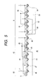
- Fig. 8 shows an equivalent circuit of a photoelectric conversion device according to a conventional art. In the drawing, pixels are arranged in 2 x 2 array, but the pixels are not particularly limited to this array. In Fig.
- a unit pixel includes a photodiode 1 which is a photoelectric conversion element, an amplification metal oxide silicon field effect transistor (MOSFET) 2 for amplifying a signal generated at the photodiode 1, a reset switch 4 for resetting an input of the amplification MOSFET 2 to predetermined voltage, and a select switch 5 for controlling electrical connection between a source electrode of the amplification MOSFET 2 and a vertical output line 7. Additionally, a transfer switch 3 is installed to control electrical connection between the photodiode 1 and a gate electrode of the amplification MOSFET 2.
- MOSFET metal oxide silicon field effect transistor
- a vertical scanning circuit 6 selects a given line (referred to as n line hereinafter), first, a reset signal ⁇ RES(n) becomes low to turn OFF the reset switch. Then, a select signal ⁇ SEL(n) becomes high to turn ON the select switch 5, whereby a source of the amplification MOSFET 2 is electrically connected to the vertical output line 7, a source follower circuit is constituted of a selected pixel and a constant current load 9, and an output corresponding to a pixel reset state appears on the vertical output line 7.
- a potential of the vertical output line is clamped by a clamp capacity (C0) 12.
- a transfer signal ⁇ TX becomes high for a fixed period, photoelectric charge is transferred from the photodiode 1 to a gate of the amplification MOSFET 2, and the potential of the vertical output line 7 is changed in accordance with the amount of photoelectric charge.
- This change is accompanied by a change of a potential of a line holding capacity (CT) 10 from an initial potential VCLP, the amount of which becomes a gain ratio of C0/(C0+CT).
- CT line holding capacity
- the potential change at the line holding capacity CT is established at a point of time when a ⁇ CT becomes low to turn OFF a switch 8. Then, signals held by the line holding capacity 10 are sequentially read out to a horizontal output line 15 by horizontal scanning pulses ⁇ H1, H2 generated from a horizontal scanning circuit 11. Accordingly, output signals of one line are outputted through an output amplifier 16.
- An object of the present invention is to obtain high-quality images.
- a photoelectric conversion device formed on a single semiconductor substrate, comprising: a plurality of photoelectric conversion elements; a read-out circuit including a switch for reading out analog signals from the photoelectric conversion elements; a buffer circuit which drives the switch; and a logic circuit which processes digital signals, wherein a first semiconductor area to which a ground level for the buffer circuit is supplied and a second semiconductor area to which a ground level for the logic circuit is supplied are electrically separated from each other.
- a photoelectric conversion device formed on a single semiconductor substrate, comprising: a plurality of photoelectric conversion elements; a read-out circuit including a switch for reading out analog signals from the photoelectric conversion elements; a buffer circuit which drives the switch; and a logic circuit which processes digital signals, wherein a third semiconductor area to which a power supply level for the buffer circuit is supplied and a fourth semiconductor area to which a power supply level for the logic circuit is supplied are electrically separated from each other.
- Fig. 1 is a conceptual diagram showing an equivalent circuit of a photoelectric conversion device of the first embodiment.
- This photoelectric conversion device is formed on a single semiconductor substrate by, for example a CMOS process.
- a unit pixel includes a photodiode 1 which is a photoelectric conversion element, an amplification metal oxide semiconductor field effect transistor (MOSFET) 2 for amplifying a signal generated by the photodiode 1, a reset switch 4 for resetting an input of the amplification MOSFET 2 to predetermined voltage, and a select switch 5 for controlling electrical connection between a source electrode of the amplification MOSFET 2 and a vertical output line 7. Additionally, a transfer switch 3 is installed to control electrical connection between the photodiode 1 and a gate electrode of the amplification MOSFET 2.
- MOSFET metal oxide semiconductor field effect transistor
- a reference numeral 6 denotes a vertical scanning circuit for sequential scanning in a vertical direction, 7 a vertical output line to which a signal from a pixel is outputted, and 9 a constant current load constituting a source follower circuit with the amplification MOSFET 2.
- a reference numeral 12 denotes a clamp capacity serially connected to the vertical output line, and 13 a switch for fixing one potential of the capacity to a predetermined potential.
- the components 12 and 13 constitute a clamp circuit.
- a reference numeral 8 denotes a transfer switch for transferring a signal from the clamp circuit, 10 a holding capacity for holding a signal from the transfer switch, 14 a transfer switch for transferring a signal from the holding capacity 10 to a horizontal output line, and 16 an output amplifier for amplifying a signal from the horizontal output line and outputting it to the outside of the photoelectric conversion device.
- a reference numeral 17 denotes a buffer circuit including inverters 18, 19, which drives the transfer switch 3, the reset switch 4, the amplification MOSFET 2, the select switch 5, the vertical output line 7, the constant current load 9, the clamp circuits 12, 13, the switch 8, the holding capacity 10, the switch 14, the horizontal output line 15, and the transfer switch 14 included in a read-out circuit including the output amplifier 16 in order to read out an analog signal from the photoelectric conversion element.
- a reference numeral 11 denotes a shift register (logic circuit) for processing a digital signal for sequentially supplying pulses to the buffer circuit 9 based on a supplied clock signal, which is constituted by serially connecting a flip-flop 8.
- the shift register 11 and the buffer circuit 19 constitute a horizontal scanning circuit.
- the buffer circuit has an impedance conversion function for setting impedance to drive the transfer switch.
- a select signal ⁇ SEL(n) becomes high to turn ON the select switch 5.
- a source of the amplification MOSFET 2 is electrically connected to the vertical output line 7
- a source follower circuit is constituted of a selected pixel and the constant current load 9, and an output corresponding to a pixel reset state appears on the vertical output line 7.
- a potential of the vertical output line is clamped by the clamp capacity (C0) 12.
- a transfer signal ⁇ TX becomes high for a fixed period, photoelectric charge is transferred from the photodiode 1 to a gate of the amplification MOSFET 2.
- the potential of the vertical output line 7 is changed in accordance with the photoelectric charge. This change is accompanied by a change of a potential of the line holding capacity (CT) 10 from an initial potential VCLP, the amount of which becomes a gain ratio of C0/(C0+CT).
- CT line holding capacity
- the potential change of the line holding capacity CT is established at a point of time when the ⁇ CT becomes low to turn OFF the switch 8. Then, signals held in the line holding capacity 10 are sequentially read out to the horizontal output line 15 by horizontal scanning pulses ⁇ H1, ⁇ H2 generated from the shift register 11, whereby output signals of one line are outputted through the output amplifier 16.
- ground potential supply paths (GND 1, GND 2). As described later, these are independent ground potential supply paths which do not interfere with each other electrically.
- a ground potential of the buffer circuit 17 is supplied from the supply path GND 1, i.e., from the path different from the ground potential supply path GND 2 of the shift register 11. Thus, there are no effects of fluctuation in the ground potential caused by through-current during the operation of the shift register 11.
- the buffer circuit 17 of the embodiment is constituted of the inverters. However, it may be constituted of a NAND gate etc. That is, the buffer circuit can employ any constitution as long as it can carry out impedance conversion necessary for driving the horizontal transfer gate 14.
- Fig. 2 is a conceptual diagram showing a partial sectional structure of the switch 14, the buffer circuit 17 and the shift register 11.
- the switch 14 is constituted of an NMOS formed in a first P type well 22.
- a ground potential is supplied to the first P type well 22 through a P type diffusion layer 26 from the outside.
- An N type diffusion layer 27 which is a source or a drain of the switch 14 is connected to the horizontal output line 15.
- An NMOS 18 constituting the buffer circuit 17 is formed in the first P type well 22, and a PMOS 19 is formed in a first N type well 24.
- a power supply potential VDD is supplied to the first N type well 24 through an N type diffusion layer 28 from the outside.
- An NMOS 20 and a PMOS 21 constituting the shift register 11 for generating a signal to the buffer circuit 17 are respectively formed in a second P type well 23 and the first N type well 24.
- a ground potential is supplied to the second P type well 23 through a P type diffusion layer 29 from the outside.
- the NMOS 18 constituting the buffer circuit 17 and the NMOS 20 constituting the shift register 11 are formed in the different P type wells, and separated from each other by the first N type well 24. Accordingly, an effect of through-current flowing into the second P type well is not mixed in a low level of a control signal ⁇ H supplied to the switch 14.
- Fig. 3A is a partial plan view of the photoelectric conversion device of the embodiment, showing an optimum structure for preventing the effect of noise.
- the N type well 24 is connected to an external input pad 31 through a metal wiring 30.
- a power supply potential VDD is supplied to the external input pad 31 from a not-shown external voltage source of low impedance.
- the first P type well 22 is connected to an external input pad 33 through a metal wiring 32.
- the external input pad 33 is connected to a not-shown external ground line.
- the second P type well 23 is connected to an external input pad 35 through a metal wiring 34.
- the external input pad 35 is connected to a not-shown external ground line.
- the first P type well 22 and the second P type well 23 are connected to the external ground lines through the different metal wirings of low resistance and the different external input pads to prevent mutual interferences. Therefore, the through-current flowing into the second P type well 23 has no effects on the potential of the first P type well 22.
- Fig. 4 is a conceptual diagram showing an equivalent circuit of a photoelectric conversion device of the second embodiment.
- the photoelectric conversion device shown in Fig. 4 is formed on a single semiconductor substrate by, for example a CMOS process. Description of circuit components having roles similar to those of Fig. 1 will be omitted.
- a difference from Fig. 1 is that ⁇ TX, ⁇ RES, ⁇ SEL supplied to a transfer switch 3, a reset switch 4 and a select switch 5 of a pixel are generated by a buffer circuit 40 to which a scanning signal of a shift register 6 as a logic circuit is inputted.
- the shift register 6 and the buffer circuit 40 constitute a vertical scanning circuit.
- a power source VDD two kinds of supply paths of a power source VDD are shown. As described later, these are power supply voltage supply paths which do not interfere with each other. Additionally, an A/D converter circuit 41 for subjecting an output signal from an output amplifier 16 to analog/digital conversion, and a digital signal processor (DSP) 42 which is a logic circuit for subjecting a digital image signal to a predetermined arithmetic operation are disposed in the same semiconductor substrate.
- the DSP 42 is connected to a power supply potential supply path VDD 2 and a ground potential supply path GND 2. During the operation of the DSP 42, a voltage reduction occurs due to through-current, generating noise in actually supplied power supply and ground potentials.
- a power source of a buffer circuit 40 is connected to a power supply potential supply path VDD 1 and a ground potential supply path GND 1 different from those of the DSP 42, there are no effects of noise generated in the DSP 42. If noise is mixed in to lower a high level in a high period of the ⁇ TX, there is a danger of a reduction in transfer efficiency of photoelectric charge. This problem is solved by employing the constitution of the embodiment. Similarly, since there are no effects of DSP operation noise on the ⁇ RES, ⁇ SEL, a signal can be normally read out from the pixel.
- Fig. 5 is a conceptual diagram showing a partial sectional structure of the select switch 5, the buffer circuit 40 and the shift register 6.
- the select switch 5 is constituted of an NMOS formed in a first P type well 43.
- a ground potential is supplied to the first P type well 43 through a P type diffusion layer 47 from the outside.
- An N type diffusion layer 48 which is a source or a drain of the select switch 5 is connected to a vertical output line 7.
- An NMOS 44 of the buffer circuit is formed in the first P type well 43, and a PMOS 45 is formed in a first N type well 46.
- a power supply potential VDD is supplied to the first N type well 46 through an N type diffusion layer 49.
- An NMOS 50 and a PMOS 51 constituting the shift register 6 are respectively formed in a second P type well 53 and a second N type well 52.
- a ground potential is supplied to the second P type well 53 through a P type diffusion layer 54.
- a power supply potential is supplied to the second N type well 52 through an N type diffusion layer 55.
- the NMOS 44 constituting the buffer circuit and the NMOS 50 constituting the shift register are formed in the different P type wells, and the PMOS 45 constituting the buffer circuit and the PMOS 51 constituting the shift register are formed in the different N type wells.
- the first and second N type wells are separated from each other by the reverse conductive well 53, and connected to external voltage sources through wirings of low resistance by a method similar to that of the first embodiment. Accordingly, there are no electrical interferences with each other. The same can be said about the first and second P type wells.
- the P type diffusion layer 26 to which a ground level for the buffer circuit 19 is supplied and the semiconductor area to which a ground level for the DSP 42 is supplied are electrically separated from each other, it is possible to prevent an effect of noise.
- ground potentials supplied to the first and second N type wells need not be equal, but may be completely different. Also in this case, the effects of the embodiment are apparently obtained.
- FIG. 6 is a conceptual diagram showing a partial sectional structure of a select switch 5, a buffer circuit 40 and a shift register 6 of the embodiment.
- the components are separated from one another in a horizontal direction by an insulating layer 58 of trench processing.
- a first P type well 43, a second P type well 53 and a third P type well 59 are connected to external ground potentials through wirings of low resistance. Accordingly, there are no electrical interferences. The same can be attained to a first N type well 46 and a second N type well 52.
- the semiconductor area to which the ground potential for the buffer circuit is supplied and the semiconductor area to which the ground level for the logic circuit is supplied are electrically separated from each other.
- a constitution may be employed where a semiconductor area to which power supply voltage for the buffer circuit is supplied and a semiconductor area to which power supply voltage for the logic circuit is supplied are electrically separated from each other.
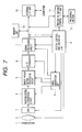
- a reference numeral 101 denotes a barrier serving both as a lens protector and a main switch, 102 a lens for forming an optical image of an object in a photoelectric conversion device 104, 103 an iris for varying the amount of light passed through a lens 2, 104 the photoelectric conversion device for picking up the object image-formed by the lens 102 as an image signal, 105 an image pickup signal processing circuit including a gain variable amplifier for amplifying the image signal outputted from the photoelectric conversion device 104 and a gain correction circuit for correcting a gain value, 106 an A/D converter for subjecting the image signal outputted from the photoelectric conversion device 104 to analog/digital conversion, 107 a signal processing circuit for making various corrections for image data outputted from the A/D converter 106 or compressing the data, 108 a timing generation unit for outputting various timing signals to the photoelectric conversion device 104, the image pickup signal processing circuit 105, the A/D converter 106, and the signal processing circuit 107, 109 a system control
- the image pickup signal processing circuit 105, the A/D converter 6 and the signal processing circuit 7 (DSP) are formed in the photoelectric conversion device.
- a main power source is turned ON, then a power source of a control system is turned ON, and further a power source of an image pickup system circuit such as the A/D converter 106 is turned ON.
- the system control and operation unit 109 releases the iris 103, and a signal outputted from the photoelectric conversion device 104 is converted by the A/D converter 106, and then inputted to the signal processing circuit 107.
- An exposure arithmetic operation is carried out by the system control and operation unit 109 based on the data of the above.
- Brightness is determined based on a result of the photometric operation.
- the system control and operation unit 109 controls the iris in accordance with a result of the determination.
- a highfrequency component is taken out to calculate a distance to the object at the system control and operation unit 109. Then, the lens is driven to determine an in-focus or out-of focus state. When the out-of focus state is determined, the lens is driven again to carry out distance measurement.
- the image signal outputted from the photoelectric conversion device 104 is subjected to A/D conversion at the A/D converter 106, passed through the signal processing circuit 107, and written in the memory unit by the system control and operation unit 109.
- the data stored in the memory unit 110 is passed through the recording medium control I/F unit and recorded in the detachable recording medium 112 such as a semiconductor memory under control of the system control and operation unit 109.
- the data may be directly inputted through the external I/F unit 113 to the computer or the like to process the image.
- a photoelectric conversion device formed on a single semiconductor substrate including: a plurality of photoelectric conversion elements; a read-out circuit including a switch for reading out analog signals from the photoelectric conversion elements; a buffer circuit for driving the switch; and a logic circuit for processing digital signals.
- a first semiconductor area to which a ground level for the buffer circuit is supplied and a second semiconductor area to which a ground level for the logic circuit is supplied are electrically separated from each other.
Priority Applications (1)
| Application Number | Priority Date | Filing Date | Title |
|---|---|---|---|
| EP05027002A EP1635555B1 (fr) | 2002-02-27 | 2003-02-26 | Dispositif de conversion photoélectrique |
Applications Claiming Priority (2)
| Application Number | Priority Date | Filing Date | Title |
|---|---|---|---|
| JP2002051492 | 2002-02-27 | ||
| JP2002051492A JP3728260B2 (ja) | 2002-02-27 | 2002-02-27 | 光電変換装置及び撮像装置 |
Related Child Applications (1)
| Application Number | Title | Priority Date | Filing Date |
|---|---|---|---|
| EP05027002A Division EP1635555B1 (fr) | 2002-02-27 | 2003-02-26 | Dispositif de conversion photoélectrique |
Publications (2)
| Publication Number | Publication Date |
|---|---|
| EP1341372A1 true EP1341372A1 (fr) | 2003-09-03 |
| EP1341372B1 EP1341372B1 (fr) | 2006-02-01 |
Family
ID=27678516
Family Applications (2)
| Application Number | Title | Priority Date | Filing Date |
|---|---|---|---|
| EP05027002A Expired - Lifetime EP1635555B1 (fr) | 2002-02-27 | 2003-02-26 | Dispositif de conversion photoélectrique |
| EP03004155A Expired - Lifetime EP1341372B1 (fr) | 2002-02-27 | 2003-02-26 | Dispositif de conversion photoélectrique |
Family Applications Before (1)
| Application Number | Title | Priority Date | Filing Date |
|---|---|---|---|
| EP05027002A Expired - Lifetime EP1635555B1 (fr) | 2002-02-27 | 2003-02-26 | Dispositif de conversion photoélectrique |
Country Status (5)
| Country | Link |
|---|---|
| US (2) | US6960751B2 (fr) |
| EP (2) | EP1635555B1 (fr) |
| JP (1) | JP3728260B2 (fr) |
| AT (1) | ATE317200T1 (fr) |
| DE (2) | DE60303399T2 (fr) |
Families Citing this family (95)
| Publication number | Priority date | Publication date | Assignee | Title |
|---|---|---|---|---|
| US7429764B2 (en) | 2002-02-27 | 2008-09-30 | Canon Kabushiki Kaisha | Signal processing device and image pickup apparatus using the same |
| JP4514188B2 (ja) * | 2003-11-10 | 2010-07-28 | キヤノン株式会社 | 光電変換装置及び撮像装置 |
| JP4508619B2 (ja) * | 2003-12-03 | 2010-07-21 | キヤノン株式会社 | 固体撮像装置の製造方法 |
| JP3793202B2 (ja) * | 2004-02-02 | 2006-07-05 | キヤノン株式会社 | 固体撮像装置 |
| JP3890333B2 (ja) * | 2004-02-06 | 2007-03-07 | キヤノン株式会社 | 固体撮像装置 |
| JP4067054B2 (ja) * | 2004-02-13 | 2008-03-26 | キヤノン株式会社 | 固体撮像装置および撮像システム |
| DE102004010396A1 (de) * | 2004-03-03 | 2005-09-29 | Infineon Technologies Ag | Sende-/Empfangsfilter und ein Verfahren zum Herstellen desselben |
| JP5089017B2 (ja) * | 2004-09-01 | 2012-12-05 | キヤノン株式会社 | 固体撮像装置及び固体撮像システム |
| JP2006073736A (ja) * | 2004-09-01 | 2006-03-16 | Canon Inc | 光電変換装置、固体撮像装置及び固体撮像システム |
| JP4971586B2 (ja) * | 2004-09-01 | 2012-07-11 | キヤノン株式会社 | 固体撮像装置 |
| JP4756839B2 (ja) | 2004-09-01 | 2011-08-24 | キヤノン株式会社 | 固体撮像装置及びカメラ |
| JP4641166B2 (ja) * | 2004-09-15 | 2011-03-02 | ルネサスエレクトロニクス株式会社 | 固体撮像装置の電荷転送デバイスおよび固体撮像装置の電荷転送デバイスの駆動方法 |
| JP2006094249A (ja) * | 2004-09-27 | 2006-04-06 | Olympus Corp | 固体撮像装置 |
| JP4416668B2 (ja) | 2005-01-14 | 2010-02-17 | キヤノン株式会社 | 固体撮像装置、その制御方法及びカメラ |
| JP2006197392A (ja) * | 2005-01-14 | 2006-07-27 | Canon Inc | 固体撮像装置、カメラ、及び固体撮像装置の駆動方法 |
| JP4459064B2 (ja) * | 2005-01-14 | 2010-04-28 | キヤノン株式会社 | 固体撮像装置、その制御方法及びカメラ |
| JP4794877B2 (ja) * | 2005-03-18 | 2011-10-19 | キヤノン株式会社 | 固体撮像装置及びカメラ |
| JP4459099B2 (ja) * | 2005-03-18 | 2010-04-28 | キヤノン株式会社 | 固体撮像装置及びカメラ |
| JP4677258B2 (ja) | 2005-03-18 | 2011-04-27 | キヤノン株式会社 | 固体撮像装置及びカメラ |
| JP4459098B2 (ja) | 2005-03-18 | 2010-04-28 | キヤノン株式会社 | 固体撮像装置及びカメラ |
| JP4827508B2 (ja) | 2005-12-02 | 2011-11-30 | キヤノン株式会社 | 撮像システム |
| JP4723994B2 (ja) * | 2005-12-19 | 2011-07-13 | 株式会社東芝 | 固体撮像装置 |
| US7804475B2 (en) * | 2006-02-09 | 2010-09-28 | Toppoly Optoelectronics Corp. | Systems for displaying images utilizing two clock signals |
| JP2007242697A (ja) * | 2006-03-06 | 2007-09-20 | Canon Inc | 撮像装置および撮像システム |
| KR101255334B1 (ko) * | 2006-05-08 | 2013-04-16 | 페어차일드코리아반도체 주식회사 | 저 열저항 파워 모듈 및 그 제조방법 |
| JP5190185B2 (ja) * | 2006-07-05 | 2013-04-24 | パナソニック株式会社 | 固体撮像装置および撮像装置 |
| JP4804254B2 (ja) * | 2006-07-26 | 2011-11-02 | キヤノン株式会社 | 光電変換装置及び撮像装置 |
| JP4185949B2 (ja) | 2006-08-08 | 2008-11-26 | キヤノン株式会社 | 光電変換装置及び撮像装置 |
| JP5123601B2 (ja) * | 2006-08-31 | 2013-01-23 | キヤノン株式会社 | 光電変換装置 |
| JP5043388B2 (ja) * | 2006-09-07 | 2012-10-10 | キヤノン株式会社 | 固体撮像装置および撮像システム |
| JP4928199B2 (ja) * | 2006-09-07 | 2012-05-09 | キヤノン株式会社 | 信号検出装置、信号検出装置の信号読み出し方法及び信号検出装置を用いた撮像システム |
| JP5173171B2 (ja) | 2006-09-07 | 2013-03-27 | キヤノン株式会社 | 光電変換装置、撮像装置及び信号読出方法 |
| JP4054839B1 (ja) * | 2007-03-02 | 2008-03-05 | キヤノン株式会社 | 光電変換装置およびそれを用いた撮像システム |
| JP4110193B1 (ja) | 2007-05-02 | 2008-07-02 | キヤノン株式会社 | 固体撮像装置および撮像システム |
| EP2037667B1 (fr) * | 2007-09-14 | 2017-08-23 | Canon Kabushiki Kaisha | Appareil de détection d'images et système d'imagerie |
| JP5174434B2 (ja) * | 2007-11-16 | 2013-04-03 | ルネサスエレクトロニクス株式会社 | 半導体装置 |
| JP5142696B2 (ja) | 2007-12-20 | 2013-02-13 | キヤノン株式会社 | 光電変換装置、及び光電変換装置を用いた撮像システム |
| JP5111140B2 (ja) * | 2008-02-06 | 2012-12-26 | キヤノン株式会社 | 固体撮像装置の駆動方法、固体撮像装置、及び撮像システム |
| JP5142749B2 (ja) | 2008-02-14 | 2013-02-13 | キヤノン株式会社 | 撮像装置、撮像装置の制御方法及び撮像システム |
| JP5268389B2 (ja) * | 2008-02-28 | 2013-08-21 | キヤノン株式会社 | 固体撮像装置、その駆動方法及び撮像システム |
| JP5094498B2 (ja) | 2008-03-27 | 2012-12-12 | キヤノン株式会社 | 固体撮像装置及び撮像システム |
| JP5328207B2 (ja) * | 2008-04-01 | 2013-10-30 | キヤノン株式会社 | 固体撮像装置 |
| JP5161676B2 (ja) * | 2008-07-07 | 2013-03-13 | キヤノン株式会社 | 撮像装置及び撮像システム |
| JP5288955B2 (ja) * | 2008-09-09 | 2013-09-11 | キヤノン株式会社 | 固体撮像装置、撮像システム、および固体撮像装置の駆動方法 |
| JP5264379B2 (ja) | 2008-09-12 | 2013-08-14 | キヤノン株式会社 | 撮像装置、撮像システム及び撮像装置の動作方法 |
| JP5203913B2 (ja) * | 2008-12-15 | 2013-06-05 | キヤノン株式会社 | 光電変換装置、撮像システム、及び光電変換装置の駆動方法 |
| JP4891308B2 (ja) * | 2008-12-17 | 2012-03-07 | キヤノン株式会社 | 固体撮像装置及び固体撮像装置を用いた撮像システム |
| JP5478905B2 (ja) * | 2009-01-30 | 2014-04-23 | キヤノン株式会社 | 固体撮像装置 |
| JP5257183B2 (ja) * | 2009-03-25 | 2013-08-07 | セイコーエプソン株式会社 | センシング装置および電子機器 |
| US8901541B2 (en) * | 2009-04-07 | 2014-12-02 | Rohm Co., Ltd. | Photoelectric conversion device and image pick-up device |
| JP5529613B2 (ja) | 2009-04-17 | 2014-06-25 | キヤノン株式会社 | 光電変換装置及び撮像システム |
| JP5511220B2 (ja) | 2009-05-19 | 2014-06-04 | キヤノン株式会社 | 固体撮像装置 |
| JP5679653B2 (ja) | 2009-12-09 | 2015-03-04 | キヤノン株式会社 | 光電変換装置およびそれを用いた撮像システム |
| JP5780711B2 (ja) | 2010-04-06 | 2015-09-16 | キヤノン株式会社 | 固体撮像装置 |
| JP5631050B2 (ja) * | 2010-05-10 | 2014-11-26 | キヤノン株式会社 | 固体撮像装置およびカメラ |
| JP5484208B2 (ja) * | 2010-06-14 | 2014-05-07 | キヤノン株式会社 | 撮像装置 |
| JP5697371B2 (ja) | 2010-07-07 | 2015-04-08 | キヤノン株式会社 | 固体撮像装置および撮像システム |
| JP5656484B2 (ja) | 2010-07-07 | 2015-01-21 | キヤノン株式会社 | 固体撮像装置および撮像システム |
| JP5885401B2 (ja) | 2010-07-07 | 2016-03-15 | キヤノン株式会社 | 固体撮像装置および撮像システム |
| JP5643555B2 (ja) | 2010-07-07 | 2014-12-17 | キヤノン株式会社 | 固体撮像装置及び撮像システム |
| JP5751766B2 (ja) | 2010-07-07 | 2015-07-22 | キヤノン株式会社 | 固体撮像装置および撮像システム |
| JP5645513B2 (ja) | 2010-07-07 | 2014-12-24 | キヤノン株式会社 | 固体撮像装置及び撮像システム |
| JP5506586B2 (ja) | 2010-07-30 | 2014-05-28 | キヤノン株式会社 | 固体撮像装置及び固体撮像装置の駆動方法 |
| JP5762199B2 (ja) | 2011-07-28 | 2015-08-12 | キヤノン株式会社 | 固体撮像装置 |
| JP5901186B2 (ja) | 2011-09-05 | 2016-04-06 | キヤノン株式会社 | 固体撮像装置及びその駆動方法 |
| JP5858695B2 (ja) | 2011-09-08 | 2016-02-10 | キヤノン株式会社 | 固体撮像装置及び固体撮像装置の駆動方法 |
| JP5806566B2 (ja) | 2011-09-15 | 2015-11-10 | キヤノン株式会社 | A/d変換器および固体撮像装置 |
| JP5801665B2 (ja) | 2011-09-15 | 2015-10-28 | キヤノン株式会社 | 固体撮像装置、a/d変換器およびその制御方法 |
| JP5901212B2 (ja) | 2011-10-07 | 2016-04-06 | キヤノン株式会社 | 光電変換システム |
| JP5930651B2 (ja) | 2011-10-07 | 2016-06-08 | キヤノン株式会社 | 固体撮像装置 |
| JP6025316B2 (ja) * | 2011-10-07 | 2016-11-16 | キヤノン株式会社 | 光電変換装置 |
| JP5484422B2 (ja) | 2011-10-07 | 2014-05-07 | キヤノン株式会社 | 固体撮像装置 |
| US8896082B1 (en) * | 2012-03-23 | 2014-11-25 | Actlight, S.A. | Solar cell systems and integration with CMOS circuitry |
| JP6319946B2 (ja) | 2013-04-18 | 2018-05-09 | キヤノン株式会社 | 固体撮像装置及び撮像システム |
| JP6100074B2 (ja) | 2013-04-25 | 2017-03-22 | キヤノン株式会社 | 光電変換装置及び撮像システム |
| JP6274788B2 (ja) | 2013-08-28 | 2018-02-07 | キヤノン株式会社 | 撮像装置、撮像システム及び撮像装置の駆動方法 |
| JP6230343B2 (ja) | 2013-09-06 | 2017-11-15 | キヤノン株式会社 | 固体撮像装置、その駆動方法及び撮像システム |
| JP5886806B2 (ja) | 2013-09-17 | 2016-03-16 | キヤノン株式会社 | 固体撮像装置 |
| JP6239975B2 (ja) | 2013-12-27 | 2017-11-29 | キヤノン株式会社 | 固体撮像装置及びそれを用いた撮像システム |
| JP6541347B2 (ja) | 2014-03-27 | 2019-07-10 | キヤノン株式会社 | 固体撮像装置および撮像システム |
| TWI656631B (zh) * | 2014-03-28 | 2019-04-11 | 日商半導體能源研究所股份有限公司 | 攝像裝置 |
| JP6548391B2 (ja) | 2014-03-31 | 2019-07-24 | キヤノン株式会社 | 光電変換装置および撮像システム |
| JP6412328B2 (ja) | 2014-04-01 | 2018-10-24 | キヤノン株式会社 | 固体撮像装置およびカメラ |
| JP6612492B2 (ja) * | 2014-10-16 | 2019-11-27 | 株式会社リコー | 光電変換素子、画像読取装置及び画像形成装置 |
| US9979916B2 (en) | 2014-11-21 | 2018-05-22 | Canon Kabushiki Kaisha | Imaging apparatus and imaging system |
| JP6478717B2 (ja) * | 2014-11-21 | 2019-03-06 | キヤノン株式会社 | 撮像装置及び撮像システム |
| US9787928B2 (en) * | 2015-01-06 | 2017-10-10 | Forza Silicon Corporation | Layout and timing schemes for ping-pong readout architecture |
| JP6736318B2 (ja) * | 2015-09-10 | 2020-08-05 | キヤノン株式会社 | 固体撮像素子、固体撮像素子の製造方法および撮像システム |
| US9900539B2 (en) | 2015-09-10 | 2018-02-20 | Canon Kabushiki Kaisha | Solid-state image pickup element, and image pickup system |
| JP6740067B2 (ja) | 2016-09-16 | 2020-08-12 | キヤノン株式会社 | 固体撮像装置及びその駆動方法 |
| JP6750876B2 (ja) | 2016-10-07 | 2020-09-02 | キヤノン株式会社 | 固体撮像装置及びその駆動方法 |
| JP2018082261A (ja) | 2016-11-15 | 2018-05-24 | キヤノン株式会社 | 撮像素子 |
| JP7299680B2 (ja) | 2018-08-23 | 2023-06-28 | キヤノン株式会社 | 撮像装置及び撮像システム |
| US11425365B2 (en) | 2018-12-14 | 2022-08-23 | Canon Kabushiki Kaisha | Photoelectric conversion device, method of manufacturing photoelectric conversion device, and method of manufacturing semiconductor device |
| JP7090581B2 (ja) * | 2019-06-26 | 2022-06-24 | 株式会社リコー | 光電変換素子、画像読取装置及び画像形成装置 |
Citations (4)
| Publication number | Priority date | Publication date | Assignee | Title |
|---|---|---|---|---|
| EP0541332A1 (fr) * | 1991-11-04 | 1993-05-12 | Xerox Corporation | Architecture pour des réseaux capteurs d'image analogiques et numériques |
| US5264727A (en) * | 1991-06-29 | 1993-11-23 | Kabushiki Kaisha Toshiba | Semiconductor integrated circuit device |
| US5537075A (en) * | 1993-12-17 | 1996-07-16 | Sony Corporation | Semiconductor integrated circuit having isolated supply paths for circuit blocks |
| EP0905788A2 (fr) * | 1997-09-29 | 1999-03-31 | Canon Kabushiki Kaisha | Capteur d'images de type MOS |
Family Cites Families (8)
| Publication number | Priority date | Publication date | Assignee | Title |
|---|---|---|---|---|
| JPS58120379A (ja) * | 1982-01-11 | 1983-07-18 | Olympus Optical Co Ltd | 固体撮像装置 |
| JPS6355980A (ja) * | 1986-08-26 | 1988-03-10 | Matsushita Electric Works Ltd | フオトダイオ−ドアレイの製法 |
| US4959723A (en) * | 1987-11-06 | 1990-09-25 | Canon Kabushiki Kaisha | Solid state image pickup apparatus having multi-phase scanning pulse to read out accumulated signal |
| JP3017809B2 (ja) * | 1991-01-09 | 2000-03-13 | 株式会社東芝 | アナログ・デジタル混載半導体集積回路装置 |
| JP2849301B2 (ja) * | 1993-03-25 | 1999-01-20 | 株式会社日立製作所 | 撮像装置 |
| US6452632B1 (en) * | 1997-01-31 | 2002-09-17 | Kabushiki Kaisha Toshiba | Solid state image sensor and video system using the same |
| US20010023949A1 (en) * | 1999-01-14 | 2001-09-27 | International Business Machines Corporation | SOI active pixel cell design with grounded body contact |
| US7429764B2 (en) * | 2002-02-27 | 2008-09-30 | Canon Kabushiki Kaisha | Signal processing device and image pickup apparatus using the same |
-
2002
- 2002-02-27 JP JP2002051492A patent/JP3728260B2/ja not_active Expired - Fee Related
-
2003
- 2003-02-25 US US10/372,286 patent/US6960751B2/en not_active Expired - Lifetime
- 2003-02-26 DE DE60303399T patent/DE60303399T2/de not_active Expired - Lifetime
- 2003-02-26 EP EP05027002A patent/EP1635555B1/fr not_active Expired - Lifetime
- 2003-02-26 EP EP03004155A patent/EP1341372B1/fr not_active Expired - Lifetime
- 2003-02-26 DE DE60324845T patent/DE60324845D1/de not_active Expired - Lifetime
- 2003-02-26 AT AT03004155T patent/ATE317200T1/de not_active IP Right Cessation
-
2005
- 2005-08-17 US US11/205,060 patent/US7547871B2/en not_active Expired - Fee Related
Patent Citations (4)
| Publication number | Priority date | Publication date | Assignee | Title |
|---|---|---|---|---|
| US5264727A (en) * | 1991-06-29 | 1993-11-23 | Kabushiki Kaisha Toshiba | Semiconductor integrated circuit device |
| EP0541332A1 (fr) * | 1991-11-04 | 1993-05-12 | Xerox Corporation | Architecture pour des réseaux capteurs d'image analogiques et numériques |
| US5537075A (en) * | 1993-12-17 | 1996-07-16 | Sony Corporation | Semiconductor integrated circuit having isolated supply paths for circuit blocks |
| EP0905788A2 (fr) * | 1997-09-29 | 1999-03-31 | Canon Kabushiki Kaisha | Capteur d'images de type MOS |
Non-Patent Citations (1)
| Title |
|---|
| PATENT ABSTRACTS OF JAPAN vol. 013, no. 243 (E - 768) 7 June 1989 (1989-06-07) * |
Also Published As
| Publication number | Publication date |
|---|---|
| DE60303399T2 (de) | 2006-10-05 |
| EP1635555A1 (fr) | 2006-03-15 |
| JP2003258228A (ja) | 2003-09-12 |
| US20030218117A1 (en) | 2003-11-27 |
| US6960751B2 (en) | 2005-11-01 |
| EP1635555B1 (fr) | 2008-11-19 |
| DE60324845D1 (de) | 2009-01-02 |
| US20050268960A1 (en) | 2005-12-08 |
| US7547871B2 (en) | 2009-06-16 |
| DE60303399D1 (de) | 2006-04-13 |
| EP1341372B1 (fr) | 2006-02-01 |
| ATE317200T1 (de) | 2006-02-15 |
| JP3728260B2 (ja) | 2005-12-21 |
Similar Documents
| Publication | Publication Date | Title |
|---|---|---|
| US6960751B2 (en) | Photoelectric conversion device | |
| JP4956084B2 (ja) | 光電変換装置及びそれを用いた撮像システム | |
| JP4818018B2 (ja) | 光電変換装置及びそれを用いた撮像システム | |
| US8218048B2 (en) | Amplifying solid-state imaging device, and method for driving the same | |
| TW201911855A (zh) | 具有堆疊基板的光感測器的偵測電路 | |
| US7352400B2 (en) | Solid-state image pickup apparatus having a differential output | |
| US9549138B2 (en) | Imaging device, imaging system, and driving method of imaging device using comparator in analog-to-digital converter | |
| US20010033337A1 (en) | Image pickup apparatus | |
| US7423680B2 (en) | Apparatus and method for clamping reset voltage in image sensor | |
| US7116367B2 (en) | Solid-state image pickup apparatus having a reset transistor controlled by an output line | |
| US20160014356A1 (en) | Solid-state imaging device and method of driving solid-state imaging device | |
| US10897591B2 (en) | Image sensors with testing capabilities | |
| JP4661212B2 (ja) | 物理情報取得方法および物理情報取得装置並びに半導体装置 | |
| US11317083B2 (en) | Pixel control signal verification in a stacked image sensor | |
| JP2008060269A (ja) | 光電変換装置及び撮像装置 | |
| JP4241692B2 (ja) | 光電変換装置用の走査回路 | |
| JP3697164B2 (ja) | 走査回路とそれを用いた撮像装置 | |
| US20010030699A1 (en) | Signal processing apparatus | |
| US7893980B2 (en) | CMOS image sensor having directly output transfer gate signal | |
| JP2005039741A (ja) | 固体撮像装置 | |
| JP2006060294A (ja) | 固体撮像素子 | |
| JP2003324191A (ja) | 光電変換装置及び撮像装置 | |
| TW202345587A (zh) | 固態攝像元件及電子機器 | |
| WO2009128194A1 (fr) | Dispositif d'imagerie à semi-conducteur, système d'imagerie et procédé de pilotage de dispositif d'imagerie à semi-conducteur | |
| JP2010056401A (ja) | 固体撮像装置及び撮像システム |
Legal Events
| Date | Code | Title | Description |
|---|---|---|---|
| PUAI | Public reference made under article 153(3) epc to a published international application that has entered the european phase |
Free format text: ORIGINAL CODE: 0009012 |
|
| AK | Designated contracting states |
Kind code of ref document: A1 Designated state(s): AT BE BG CH CY CZ DE DK EE ES FI FR GB GR HU IE IT LI LU MC NL PT SE SI SK TR |
|
| AX | Request for extension of the european patent |
Extension state: AL LT LV MK RO |
|
| 17P | Request for examination filed |
Effective date: 20040114 |
|
| 17Q | First examination report despatched |
Effective date: 20040218 |
|
| AKX | Designation fees paid |
Designated state(s): AT BE BG CH CY CZ DE DK EE ES FI FR GB GR HU IE IT LI LU MC NL PT SE SI SK TR |
|
| GRAP | Despatch of communication of intention to grant a patent |
Free format text: ORIGINAL CODE: EPIDOSNIGR1 |
|
| GRAS | Grant fee paid |
Free format text: ORIGINAL CODE: EPIDOSNIGR3 |
|
| GRAA | (expected) grant |
Free format text: ORIGINAL CODE: 0009210 |
|
| AK | Designated contracting states |
Kind code of ref document: B1 Designated state(s): AT BE BG CH CY CZ DE DK EE ES FI FR GB GR HU IE IT LI LU MC NL PT SE SI SK TR |
|
| PG25 | Lapsed in a contracting state [announced via postgrant information from national office to epo] |
Ref country code: BE Free format text: LAPSE BECAUSE OF FAILURE TO SUBMIT A TRANSLATION OF THE DESCRIPTION OR TO PAY THE FEE WITHIN THE PRESCRIBED TIME-LIMIT Effective date: 20060201 Ref country code: SK Free format text: LAPSE BECAUSE OF FAILURE TO SUBMIT A TRANSLATION OF THE DESCRIPTION OR TO PAY THE FEE WITHIN THE PRESCRIBED TIME-LIMIT Effective date: 20060201 Ref country code: CH Free format text: LAPSE BECAUSE OF FAILURE TO SUBMIT A TRANSLATION OF THE DESCRIPTION OR TO PAY THE FEE WITHIN THE PRESCRIBED TIME-LIMIT Effective date: 20060201 Ref country code: LI Free format text: LAPSE BECAUSE OF FAILURE TO SUBMIT A TRANSLATION OF THE DESCRIPTION OR TO PAY THE FEE WITHIN THE PRESCRIBED TIME-LIMIT Effective date: 20060201 Ref country code: FI Free format text: LAPSE BECAUSE OF FAILURE TO SUBMIT A TRANSLATION OF THE DESCRIPTION OR TO PAY THE FEE WITHIN THE PRESCRIBED TIME-LIMIT Effective date: 20060201 Ref country code: AT Free format text: LAPSE BECAUSE OF FAILURE TO SUBMIT A TRANSLATION OF THE DESCRIPTION OR TO PAY THE FEE WITHIN THE PRESCRIBED TIME-LIMIT Effective date: 20060201 Ref country code: SI Free format text: LAPSE BECAUSE OF FAILURE TO SUBMIT A TRANSLATION OF THE DESCRIPTION OR TO PAY THE FEE WITHIN THE PRESCRIBED TIME-LIMIT Effective date: 20060201 |
|
| REG | Reference to a national code |
Ref country code: GB Ref legal event code: FG4D |
|
| REG | Reference to a national code |
Ref country code: CH Ref legal event code: EP |
|
| PG25 | Lapsed in a contracting state [announced via postgrant information from national office to epo] |
Ref country code: IE Free format text: LAPSE BECAUSE OF NON-PAYMENT OF DUE FEES Effective date: 20060227 |
|
| PG25 | Lapsed in a contracting state [announced via postgrant information from national office to epo] |
Ref country code: MC Free format text: LAPSE BECAUSE OF NON-PAYMENT OF DUE FEES Effective date: 20060228 |
|
| REG | Reference to a national code |
Ref country code: IE Ref legal event code: FG4D |
|
| REF | Corresponds to: |
Ref document number: 60303399 Country of ref document: DE Date of ref document: 20060413 Kind code of ref document: P |
|
| PG25 | Lapsed in a contracting state [announced via postgrant information from national office to epo] |
Ref country code: BG Free format text: LAPSE BECAUSE OF FAILURE TO SUBMIT A TRANSLATION OF THE DESCRIPTION OR TO PAY THE FEE WITHIN THE PRESCRIBED TIME-LIMIT Effective date: 20060501 Ref country code: SE Free format text: LAPSE BECAUSE OF FAILURE TO SUBMIT A TRANSLATION OF THE DESCRIPTION OR TO PAY THE FEE WITHIN THE PRESCRIBED TIME-LIMIT Effective date: 20060501 Ref country code: DK Free format text: LAPSE BECAUSE OF FAILURE TO SUBMIT A TRANSLATION OF THE DESCRIPTION OR TO PAY THE FEE WITHIN THE PRESCRIBED TIME-LIMIT Effective date: 20060501 |
|
| PG25 | Lapsed in a contracting state [announced via postgrant information from national office to epo] |
Ref country code: ES Free format text: LAPSE BECAUSE OF FAILURE TO SUBMIT A TRANSLATION OF THE DESCRIPTION OR TO PAY THE FEE WITHIN THE PRESCRIBED TIME-LIMIT Effective date: 20060512 |
|
| PG25 | Lapsed in a contracting state [announced via postgrant information from national office to epo] |
Ref country code: PT Free format text: LAPSE BECAUSE OF FAILURE TO SUBMIT A TRANSLATION OF THE DESCRIPTION OR TO PAY THE FEE WITHIN THE PRESCRIBED TIME-LIMIT Effective date: 20060703 |
|
| REG | Reference to a national code |
Ref country code: CH Ref legal event code: PL |
|
| ET | Fr: translation filed | ||
| PLBE | No opposition filed within time limit |
Free format text: ORIGINAL CODE: 0009261 |
|
| STAA | Information on the status of an ep patent application or granted ep patent |
Free format text: STATUS: NO OPPOSITION FILED WITHIN TIME LIMIT |
|
| 26N | No opposition filed |
Effective date: 20061103 |
|
| PG25 | Lapsed in a contracting state [announced via postgrant information from national office to epo] |
Ref country code: CZ Free format text: LAPSE BECAUSE OF FAILURE TO SUBMIT A TRANSLATION OF THE DESCRIPTION OR TO PAY THE FEE WITHIN THE PRESCRIBED TIME-LIMIT Effective date: 20060201 Ref country code: GR Free format text: LAPSE BECAUSE OF FAILURE TO SUBMIT A TRANSLATION OF THE DESCRIPTION OR TO PAY THE FEE WITHIN THE PRESCRIBED TIME-LIMIT Effective date: 20060502 |
|
| PG25 | Lapsed in a contracting state [announced via postgrant information from national office to epo] |
Ref country code: EE Free format text: LAPSE BECAUSE OF FAILURE TO SUBMIT A TRANSLATION OF THE DESCRIPTION OR TO PAY THE FEE WITHIN THE PRESCRIBED TIME-LIMIT Effective date: 20060201 |
|
| PG25 | Lapsed in a contracting state [announced via postgrant information from national office to epo] |
Ref country code: LU Free format text: LAPSE BECAUSE OF NON-PAYMENT OF DUE FEES Effective date: 20060226 Ref country code: HU Free format text: LAPSE BECAUSE OF FAILURE TO SUBMIT A TRANSLATION OF THE DESCRIPTION OR TO PAY THE FEE WITHIN THE PRESCRIBED TIME-LIMIT Effective date: 20060802 Ref country code: TR Free format text: LAPSE BECAUSE OF FAILURE TO SUBMIT A TRANSLATION OF THE DESCRIPTION OR TO PAY THE FEE WITHIN THE PRESCRIBED TIME-LIMIT Effective date: 20060201 |
|
| PG25 | Lapsed in a contracting state [announced via postgrant information from national office to epo] |
Ref country code: CY Free format text: LAPSE BECAUSE OF FAILURE TO SUBMIT A TRANSLATION OF THE DESCRIPTION OR TO PAY THE FEE WITHIN THE PRESCRIBED TIME-LIMIT Effective date: 20060201 |
|
| PG25 | Lapsed in a contracting state [announced via postgrant information from national office to epo] |
Ref country code: IT Free format text: LAPSE BECAUSE OF NON-PAYMENT OF DUE FEES Effective date: 20080226 |
|
| PGFP | Annual fee paid to national office [announced via postgrant information from national office to epo] |
Ref country code: FR Payment date: 20120312 Year of fee payment: 10 |
|
| PGFP | Annual fee paid to national office [announced via postgrant information from national office to epo] |
Ref country code: IT Payment date: 20120209 Year of fee payment: 10 |
|
| PGFP | Annual fee paid to national office [announced via postgrant information from national office to epo] |
Ref country code: NL Payment date: 20120227 Year of fee payment: 10 |
|
| REG | Reference to a national code |
Ref country code: NL Ref legal event code: V1 Effective date: 20130901 |
|
| PG25 | Lapsed in a contracting state [announced via postgrant information from national office to epo] |
Ref country code: NL Free format text: LAPSE BECAUSE OF NON-PAYMENT OF DUE FEES Effective date: 20130901 |
|
| REG | Reference to a national code |
Ref country code: FR Ref legal event code: ST Effective date: 20131031 |
|
| PG25 | Lapsed in a contracting state [announced via postgrant information from national office to epo] |
Ref country code: IT Free format text: LAPSE BECAUSE OF NON-PAYMENT OF DUE FEES Effective date: 20130226 |
|
| PG25 | Lapsed in a contracting state [announced via postgrant information from national office to epo] |
Ref country code: FR Free format text: LAPSE BECAUSE OF NON-PAYMENT OF DUE FEES Effective date: 20130228 |
|
| PGFP | Annual fee paid to national office [announced via postgrant information from national office to epo] |
Ref country code: GB Payment date: 20150220 Year of fee payment: 13 |
|
| GBPC | Gb: european patent ceased through non-payment of renewal fee |
Effective date: 20160226 |
|
| PG25 | Lapsed in a contracting state [announced via postgrant information from national office to epo] |
Ref country code: GB Free format text: LAPSE BECAUSE OF NON-PAYMENT OF DUE FEES Effective date: 20160226 |
|
| PGFP | Annual fee paid to national office [announced via postgrant information from national office to epo] |
Ref country code: DE Payment date: 20180430 Year of fee payment: 16 |
|
| REG | Reference to a national code |
Ref country code: DE Ref legal event code: R119 Ref document number: 60303399 Country of ref document: DE |
|
| PG25 | Lapsed in a contracting state [announced via postgrant information from national office to epo] |
Ref country code: DE Free format text: LAPSE BECAUSE OF NON-PAYMENT OF DUE FEES Effective date: 20190903 |