EP0779643B1 - Plasmaanzeigetafel geeignet für Anzeige hoher Qualität - Google Patents
Plasmaanzeigetafel geeignet für Anzeige hoher Qualität Download PDFInfo
- Publication number
- EP0779643B1 EP0779643B1 EP96309148A EP96309148A EP0779643B1 EP 0779643 B1 EP0779643 B1 EP 0779643B1 EP 96309148 A EP96309148 A EP 96309148A EP 96309148 A EP96309148 A EP 96309148A EP 0779643 B1 EP0779643 B1 EP 0779643B1
- Authority
- EP
- European Patent Office
- Prior art keywords
- layer
- discharge
- oxide
- gas
- face orientation
- Prior art date
- Legal status (The legal status is an assumption and is not a legal conclusion. Google has not performed a legal analysis and makes no representation as to the accuracy of the status listed.)
- Expired - Lifetime
Links
Images


Classifications
-
- C—CHEMISTRY; METALLURGY
- C23—COATING METALLIC MATERIAL; COATING MATERIAL WITH METALLIC MATERIAL; CHEMICAL SURFACE TREATMENT; DIFFUSION TREATMENT OF METALLIC MATERIAL; COATING BY VACUUM EVAPORATION, BY SPUTTERING, BY ION IMPLANTATION OR BY CHEMICAL VAPOUR DEPOSITION, IN GENERAL; INHIBITING CORROSION OF METALLIC MATERIAL OR INCRUSTATION IN GENERAL
- C23C—COATING METALLIC MATERIAL; COATING MATERIAL WITH METALLIC MATERIAL; SURFACE TREATMENT OF METALLIC MATERIAL BY DIFFUSION INTO THE SURFACE, BY CHEMICAL CONVERSION OR SUBSTITUTION; COATING BY VACUUM EVAPORATION, BY SPUTTERING, BY ION IMPLANTATION OR BY CHEMICAL VAPOUR DEPOSITION, IN GENERAL
- C23C16/00—Chemical coating by decomposition of gaseous compounds, without leaving reaction products of surface material in the coating, i.e. chemical vapour deposition [CVD] processes
- C23C16/22—Chemical coating by decomposition of gaseous compounds, without leaving reaction products of surface material in the coating, i.e. chemical vapour deposition [CVD] processes characterised by the deposition of inorganic material, other than metallic material
- C23C16/30—Deposition of compounds, mixtures or solid solutions, e.g. borides, carbides, nitrides
- C23C16/40—Oxides
- C23C16/404—Oxides of alkaline earth metals
-
- C—CHEMISTRY; METALLURGY
- C23—COATING METALLIC MATERIAL; COATING MATERIAL WITH METALLIC MATERIAL; CHEMICAL SURFACE TREATMENT; DIFFUSION TREATMENT OF METALLIC MATERIAL; COATING BY VACUUM EVAPORATION, BY SPUTTERING, BY ION IMPLANTATION OR BY CHEMICAL VAPOUR DEPOSITION, IN GENERAL; INHIBITING CORROSION OF METALLIC MATERIAL OR INCRUSTATION IN GENERAL
- C23C—COATING METALLIC MATERIAL; COATING MATERIAL WITH METALLIC MATERIAL; SURFACE TREATMENT OF METALLIC MATERIAL BY DIFFUSION INTO THE SURFACE, BY CHEMICAL CONVERSION OR SUBSTITUTION; COATING BY VACUUM EVAPORATION, BY SPUTTERING, BY ION IMPLANTATION OR BY CHEMICAL VAPOUR DEPOSITION, IN GENERAL
- C23C16/00—Chemical coating by decomposition of gaseous compounds, without leaving reaction products of surface material in the coating, i.e. chemical vapour deposition [CVD] processes
- C23C16/22—Chemical coating by decomposition of gaseous compounds, without leaving reaction products of surface material in the coating, i.e. chemical vapour deposition [CVD] processes characterised by the deposition of inorganic material, other than metallic material
- C23C16/30—Deposition of compounds, mixtures or solid solutions, e.g. borides, carbides, nitrides
- C23C16/40—Oxides
- C23C16/403—Oxides of aluminium, magnesium or beryllium
-
- H—ELECTRICITY
- H01—ELECTRIC ELEMENTS
- H01J—ELECTRIC DISCHARGE TUBES OR DISCHARGE LAMPS
- H01J11/00—Gas-filled discharge tubes with alternating current induction of the discharge, e.g. alternating current plasma display panels [AC-PDP]; Gas-filled discharge tubes without any main electrode inside the vessel; Gas-filled discharge tubes with at least one main electrode outside the vessel
- H01J11/10—AC-PDPs with at least one main electrode being out of contact with the plasma
- H01J11/12—AC-PDPs with at least one main electrode being out of contact with the plasma with main electrodes provided on both sides of the discharge space
-
- H—ELECTRICITY
- H01—ELECTRIC ELEMENTS
- H01J—ELECTRIC DISCHARGE TUBES OR DISCHARGE LAMPS
- H01J11/00—Gas-filled discharge tubes with alternating current induction of the discharge, e.g. alternating current plasma display panels [AC-PDP]; Gas-filled discharge tubes without any main electrode inside the vessel; Gas-filled discharge tubes with at least one main electrode outside the vessel
- H01J11/20—Constructional details
- H01J11/34—Vessels, containers or parts thereof, e.g. substrates
- H01J11/38—Dielectric or insulating layers
-
- H—ELECTRICITY
- H01—ELECTRIC ELEMENTS
- H01J—ELECTRIC DISCHARGE TUBES OR DISCHARGE LAMPS
- H01J11/00—Gas-filled discharge tubes with alternating current induction of the discharge, e.g. alternating current plasma display panels [AC-PDP]; Gas-filled discharge tubes without any main electrode inside the vessel; Gas-filled discharge tubes with at least one main electrode outside the vessel
- H01J11/20—Constructional details
- H01J11/34—Vessels, containers or parts thereof, e.g. substrates
- H01J11/40—Layers for protecting or enhancing the electron emission, e.g. MgO layers
-
- H—ELECTRICITY
- H01—ELECTRIC ELEMENTS
- H01J—ELECTRIC DISCHARGE TUBES OR DISCHARGE LAMPS
- H01J11/00—Gas-filled discharge tubes with alternating current induction of the discharge, e.g. alternating current plasma display panels [AC-PDP]; Gas-filled discharge tubes without any main electrode inside the vessel; Gas-filled discharge tubes with at least one main electrode outside the vessel
- H01J11/20—Constructional details
- H01J11/50—Filling, e.g. selection of gas mixture
-
- H—ELECTRICITY
- H01—ELECTRIC ELEMENTS
- H01J—ELECTRIC DISCHARGE TUBES OR DISCHARGE LAMPS
- H01J9/00—Apparatus or processes specially adapted for the manufacture, installation, removal, maintenance of electric discharge tubes, discharge lamps, or parts thereof; Recovery of material from discharge tubes or lamps
- H01J9/02—Manufacture of electrodes or electrode systems
-
- H—ELECTRICITY
- H01—ELECTRIC ELEMENTS
- H01J—ELECTRIC DISCHARGE TUBES OR DISCHARGE LAMPS
- H01J2211/00—Plasma display panels with alternate current induction of the discharge, e.g. AC-PDPs
- H01J2211/20—Constructional details
- H01J2211/34—Vessels, containers or parts thereof, e.g. substrates
- H01J2211/38—Dielectric or insulating layers
-
- H—ELECTRICITY
- H01—ELECTRIC ELEMENTS
- H01J—ELECTRIC DISCHARGE TUBES OR DISCHARGE LAMPS
- H01J2211/00—Plasma display panels with alternate current induction of the discharge, e.g. AC-PDPs
- H01J2211/20—Constructional details
- H01J2211/34—Vessels, containers or parts thereof, e.g. substrates
- H01J2211/40—Layers for protecting or enhancing the electron emission, e.g. MgO layers
-
- H—ELECTRICITY
- H01—ELECTRIC ELEMENTS
- H01J—ELECTRIC DISCHARGE TUBES OR DISCHARGE LAMPS
- H01J2211/00—Plasma display panels with alternate current induction of the discharge, e.g. AC-PDPs
- H01J2211/20—Constructional details
- H01J2211/50—Filling, e.g. selection of gas mixture
-
- Y—GENERAL TAGGING OF NEW TECHNOLOGICAL DEVELOPMENTS; GENERAL TAGGING OF CROSS-SECTIONAL TECHNOLOGIES SPANNING OVER SEVERAL SECTIONS OF THE IPC; TECHNICAL SUBJECTS COVERED BY FORMER USPC CROSS-REFERENCE ART COLLECTIONS [XRACs] AND DIGESTS
- Y10—TECHNICAL SUBJECTS COVERED BY FORMER USPC
- Y10T—TECHNICAL SUBJECTS COVERED BY FORMER US CLASSIFICATION
- Y10T117/00—Single-crystal, oriented-crystal, and epitaxy growth processes; non-coating apparatus therefor
- Y10T117/10—Apparatus
- Y10T117/1004—Apparatus with means for measuring, testing, or sensing
- Y10T117/1008—Apparatus with means for measuring, testing, or sensing with responsive control means
Definitions
- This invention relates to a plasma display panel used as a display device, specifically to a plasma display panel suitable for a high-quality display.
- CTR Cathode Ray Tube
- LCD Liquid Crystal Display
- PDP Plasma Display Panel
- CRTs have been widely used as TV displays and excel in resolution and picture quality.
- the depth and weight increase as the screen size increases. Therefore, CRTs are not suitable for large screen sizes exceeding 40 inch (102cm).
- LCDs consume a small amount of electricity and operate on a low voltage.
- producing a large LCD screen is technically difficult, and the viewing angles of LCDs are limited.
- PDPs are divided into two types: Direct Current (DC) and Alternating Current (AC).
- DC Direct Current
- AC Alternating Current
- PDPs are mainly AC-type since they are suitable for large screens.
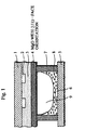
- Fig. 1 is a sectional view of a conventional AC PDP.
- front cover plate 1 with display electrodes 2 put thereon, is covered by dielectrics glass layer 3 which is lead glass, namely, PbO-B 2 O 3 -SiO 2 glass.
- Set on back plate 5 are address electrode 6, partition walls 7, and fluorescent substance layer 8 consisting of red, green, or blue ultraviolet excited fluorescent substance. Discharge gas is charged in discharge space 9 which is sealed with dielectrics glass layer 3, back plate 5, and partition walls 7.
- the discharge gas is generally helium (He), xenon ( Xe ), or mixture of neon (Ne) and Xe.
- the amount of Xe is generally set to a range from 0.1 to 5% by volume, preventing the drive voltage of the circuit from becoming too high.
- the charging pressure of the discharge gas is generally set to a range from 100 Torr (13kPa) to 500Torr (66 ⁇ 5kPa) so that the discharge voltage is stable (e.x., M. Nobrio, T. Yoshioka, Y. Sano, K. Nunomura, SID94' Digest, pp727-730, 1994).
- PDPs have the following problems concerning brightness and life.
- PDPs for 40-42-inch (102-107cm) TV screens generally have a brightness of about 150-250cd/m 2 for National Television System Committee (NTSC) standard (number of pixels being 640X480, cell pitch 0.43mmX1.29mm, square of one cell 0.55mm 2 ) (Function & Materials, Feb., 1996, Vol.16, No. 2. page 7).
- NSC National Television System Committee
- the brightness of each cell should be increased about 12-15 times.
- the light-emission principle in PDP is basically the same as that in fluorescent light: a discharge lets the discharge gas emit ultraviolet light; the ultraviolet light excites fluorescent substances; and the excited fluorescent substances emit red, green, and blue lights.
- a discharge lets the discharge gas emit ultraviolet light; the ultraviolet light excites fluorescent substances; and the excited fluorescent substances emit red, green, and blue lights.
- discharge energy is not effectively converted to ultraviolet light and conversion ratio in fluorescent substance is low, it is difficult for PDPs to provide brightness as high as that of fluorescent lights.
- the fluorescent substance layer deteriorates since plasma is confined to a small discharge space to generate ultraviolet light; and (2) the dielectrics glass layer deteriorates due to sputtering by gas discharges.
- the fluorescent substance life or preventing the deterioration of dielectrics glass layer are studied.
- protecting layer 4 consisting of magnesium oxide (MgO) is formed on the surface of dielectrics glass layer 3 with a vacuum vapor deposition method to prevent the dielectrics glass layer from deteriorating.
- MgO magnesium oxide
- protecting layer 4 has high sputtering resistance and emits a large amount of secondary electron.
- magnesium oxide layer formed by the vacuum vapor deposition method it is difficult for magnesium oxide layer formed by the vacuum vapor deposition method to obtain a protective layer having enough sputtering resistance.
- discharges decrease the amount of secondary electron emitted.
- JP 06-342631 A discloses a plasma display panel designed so as to restrict drive voltage and to improve emission efficiency by providing a three-element mixed gas, formed by adding a specific ratio of xenon to a mixed gas of helium and neon at a specific ratio, as a discharge gas to be sealed in a discharge gas space, in which a phosphor layer is provided.
- the phosphor layer is provided on the inner surface of a discharge gas space and emits light by means of ultraviolet light generated by discharging a discharge gas.
- a three-element mixed gas formed of 1.5-10 volume % of xenon, helium, and neon, is provided as the discharge gas.
- the volume ratio of helium to neon ranges from 6 to 4, to 9 to 1.
- EP 0 649 159 A discloses a DC type gas-discharge display panel, and discusses the use of Ne-Xe, Ne-Xe-Kr, He-Xe and He-Xe-Kr filling gases at various charging pressures up to 760 Torr (101 kPa).
- GB 2 109 628 A discloses a gas discharge display device using Ne-Xe-Cl 2 gas mixtures at pressures below or reasonably close to atmospheric.
- JP 05-234519 A discloses the use of a [111] face orientation film, formed by a vacuum deposition method, as a protecting film for covering a dielectric layer against a discharging space in an AC type plasma display panel.
- the present invention provides a plasma display panel comprising:
- the present invention sets the amount of Xe in the discharge gas to the range from greater than 10% by volume to less than 100% by volume, and sets the charging pressure for the discharge gas to the range of greater than 550 Torr (73,2kpa) to less than or equal to 760 Torr (101kPa) which is higher than conventional charging pressures.
- the panel brightness increases.
- the assumed reasons for it are as follows: the increase in the amount of Xe in the discharge space increases the amount of ultra violet light emitted; the ratio of excitation wavelength (173nm wavelength) by molecular Xe in the emitted ultra violet light increases; and this increases the efficiency of a conversion from fluorescent substance to visible rays.
- a preferred embodiment of the present invention has, on the surface of the dielectrics glass layer, a protecting layer consisting of an alkaline earth oxide with (100)-face or (110)-face orientation.
- the conventional protecting layer of magnesium oxide formed by vacuum vapor deposition method has (111)-crystal-face orientation.
- the protecting layer of an alkaline earth oxide with (100)-face or (110)-face orientation is dense, has high sputtering resistance, and emits a great amount of secondary electron.
- the preferred embodiment of the present invention prevents deterioration of the dielectrics glass layer and keeps the discharge voltage low.
- Fig.2 is a sectional view of a discharge PDP of the present embodiment. Though Fig.2 shows only one cell, a PDP includes a number of cells each of which emits red, green, or blue light.
- the present PDP includes: a front panel which is made up of front glass substrate 11 with display electrodes 12 and dielectrics glass layer 13 thereon; and a back panel which is made up of back glass substrate 15 with address electrode 16, partition walls 17, and fluorescent substance layer 18, the front panel and back panel being bonded together. Discharge space 19, which is sealed with the front panel and back panel, is charged with a discharge gas.
- the present PDP may be made as follows.
- the front panel is made by forming display electrodes 12 onto front glass substrate 11, covering it with dielectrics glass layer 13, then forming protecting layer 14 on the surface of dielectrics glass layer 13.
- discharge electrodes 12 are silver electrodes which are formed by transferring a paste for the silver electrodes onto front glass substrate 11 with screen printing then baking them.
- Dielectrics glass layer 13 being lead glass, is composed of 75% by weight of lead oxide (PbO), 15% by weight of boron oxide (B 2 O 3 ), and 10% by weight of silicon oxide (SiO 2 ).
- Dielectrics glass layer 13 is also formed with screen printing and baking.
- Protecting layer 14 consists of an alkaline earth oxide with (100)-face orientation and is dense.
- a CVD method thermal CVD method or plasma enhanced CVD method
- the back panel is made by transferring the paste for the silver electrodes onto back glass substrate 15 by screen printing then baking back glass substrate 15 to form address electrodes 16 and by attaching partition walls 17 made of glass to back glass substrate 15 with a certain pitch.
- Fluorescent substance layer 18 is formed by inserting one of a red fluorescent substance, a green fluorescent substance, a blue fluorescent substance into each space surrounded by partition walls 17. Any fluorescent substance generally used for PDPs can be used for each color.
- the present embodiment uses the following fluorescent substances:
- a PDP is made by bonding the above front panel and back panel with sealing glass, at the same time excluding the air from discharge space 19 partitioned by partition walls 17 to high vacuum (8X10 -7 Torr), then charging a discharge gas with a certain composition into discharge space 19 at a certain charging pressure.
- cell pitch is under 0.2mm and distance between electrodes "d" is under 0.1mm, making the cell size of the PDP conform to 40-inch high-vision TVs.
- the discharge gas is composed of Ne-Xe gas, which has been used conventionally. However, the amount of Xe is set to 10% by volume or more and the charging pressure to the range of 550 to 700Torr (73,2 -93,3 kPa).
- Fig.3 shows a CVD apparatus used for forming protecting layer 14.
- CVD apparatus 25 includes heater 26 for heating glass substrate 27 (equivalent to front glass substrate 11 with display electrodes 12 and dielectrics glass layer 13 as shown in Fig.2). The pressure inside CVD apparatus 25 can be reduced by venting apparatus 29.
- CVD apparatus 25 also includes high-frequency power 28 for generating plasma in CVD apparatus 25.
- Ar-gas cylinders 21a and 21b supply argon (Ar) gas, which is used as a carrier, to CVD apparatus 25 respectively via bubblers 22 and 23.
- Ar argon
- Bubbler 22 stores a metal chelate of alkaline earth oxide used as the source and heats it.
- the metal chelate is transferred to CVD apparatus 25 when it is evaporated by the argon gas blown on it through Ar-gas cylinder 21a.
- Bubbler 23 stores a cyclopentadienyl compound of alkaline earth oxide used as the source and heats it.
- the cyclopentadienyl compound is transferred to CVD apparatus 25 when it is evaporated by the argon gas blown on it through Ar-gas cylinder 21b.
- Oxygen cylinder 24 supplies oxygen (O 2 ) used as a reaction gas to CVD apparatus 25.
- glass substrate 27 is put on heating unit 26 with the dielectrics glass layer on glass substrate 27 to be heated with a certain temperature (350 to 400°C. See Table 1 "HEATING TEMPERATURE FOR GLASS SUBSTRATE").
- the pressure in the reaction container is reduced by venting apparatus 29 (by about several tens Torr, ten Torr being equipment to 1.3 kPa).
- Bubbler 22 or 23 is used to heat the metal chelate or cyclopentadienyl compound of alkaline earth oxide used as the source to a certain temperature (See Table 1, "TEMPERATURE OF BUBBLER"). At the same time, Ar gas is sent to bubbler 22 or 23 through Ar-gas cylinder 21a or 21b and oxygen is sent through cylinder 24.
- the metal chelate or cyclopentadienyl compound reacts with oxygen in CVD apparatus 25 to form a protecting layer consisting of an alkaline earth oxide on the surface of glass substrate 27.
- the thermal CVD method or plasma enhanced CVD method has not been used for forming a protecting layer.
- One of the reasons for not using these methods is that no appropriate source for these methods was found.
- the present inventors have made it possible to form a protecting layer with the thermal CVD method or plasma enhanced CVD method by using the sources described below.
- the source metal chelate or cyclopentadienyl compound supplied through bubblers 22 and 23:
- the alkaline earth is magnesium. Therefore, the sources are as follows: magnesium dipivaloyl methane Mg(C 11 H 19 O 2 ) 2 , magnesium acetylacetone Mg(C 5 H 7 O 2 ) 2 , magnesium trifluoroacetylacetone Mg(C 5 H 5 F 3 O 2 ) 2 , and cyclopentadienyl magnesium Mg(C 5 H 5 ) 2 .
- the protecting layer formed with the thermal CVD method or plasma enhanced CVD method allows the crystals of the alkaline earth oxides to grow slowly to form a dense protecting layer consisting of an alkaline earth oxide with (100)-face orientation.
- the conventional protecting layer of magnesium oxide formed by vacuum vapor deposition method has (111)-crystal-face orientation according to X-ray analysis (See No.15 in Table 2 and Nos.67 and 69 in Table 4). Compared to this, the protecting layer of a magnesium oxide with (100)-face orientation has the following characteristics and effects:
- the panel brightness improves by setting the amount of Xe in the discharge gas to 10% by volume or more and by setting the charging pressure for the discharge gas to the range of 550 to 760Torr (73,2-101 kPa). The following are considered to be the reasons.
- Fig.4 is a graph showing the change in relation between the wavelength and amount of the ultraviolet light for each charging pressure, the ultraviolet light being emitted from Xe in He-Xe gas used as a discharge gas in a PDP. This graph is introduced in 0 Plus E, No.195, 1996, page 99.
- Figs.5(a)-(c) show relation between excitation wavelength and relative radiation efficiency for each color of fluorescent substance. This graph is included in O Plus E, No.195, 1996, page 99. It is apparent from this drawing that the relative radiation efficiency is higher at a 173nm wavelength than at 147nm for every color of fluorescent substrate.
- the amount of Xe in the discharge gas and the charging pressure for the discharge gas are set to higher levels in the present embodiment.
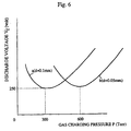
- this is considered to bring an inconvenience in that the PDP driving voltage increases since discharge start voltage "Vf" increases as the amount of Xe in the discharge gas or the charging pressure increases (see Japanese Laid-Open Patent Application No.6-342631, column 2, pp 8-16 and 1996 Electrical Engineers of Japan National Conference Symposium, S3-1, Plasma Display Discharge, March, 1996).
- the driving voltage may be low even if the charging pressure is set to a high level when distance "d" between discharge electrodes is set to a comparatively small value.
- the discharge start voltage Vf may be represented as a function of P multiplied by d which is called the Paschen's Law.
- discharge start voltage Vf corresponding to charging pressure P of the discharge gas is represented by a curve including a minimum.
- Charging pressure P being equal to the minimum, increases as d decreases.
- distance d between discharge electrodes is set to 0.1mm or less (desirably to about 0.05mm), PDP driving voltage is kept low even if the charging pressure for the discharge gas is set to the range of 550 to 760Torr (73,2 - 101 kPa).
- the PDP of the present embodiment shows high panel brightness since the amount of Xe in the discharge gas is set to 10% by volume or more and the charging pressure for the discharge gas is set to the range of 550 to 760Torr (73,2 - 101 kPa). Also, the driving voltage of the PDP of the present embodiment is kept low since distance d between discharge electrodes is set to 0.1mm or less. Furthermore, the PDP of the present embodiment has a long life since it includes a protecting layer of a dense magnesium oxide with (100)-face orientation which shows good effects in protection.
- the cell size of the PDP was set as follows: the height of partition walls 7 is 0.15mm, the distance between partition walls 7 (cell pitch) 0.15mm, and distance d between discharge electrodes 12 0.05mm.
- Dielectrics glass layer 13 being lead glass, was formed by transferring a mixture of 75% by weight of lead oxide (PbO), 15% by weight of boron oxide (B 2 O 3 ), 10% by weight of silicon oxide (SiO 2 ), and organic binder (made by dissolving 10% ethyl cellulose in ⁇ -terpineol) onto front glass substrate 11 with display electrodes 12 by screen printing and baking them for 10 minutes at 520°C.
- the thickness of dielectrics glass layer 13 was set to 20 ⁇ m.
- the ratio of He to Xe in the discharge gas and the charging pressure were set as shown in Table 1 except that the ratio of He in the discharge gas was set to less than 10% by volume for Examples 7 and 9 and that the charging pressure for the discharge gas was set to less than 500Torr (66 ⁇ 5kPa) for Examples 7 and 8.
- the thermal CVD method was applied to Examples 1, 3, 5, and 7-9, and the plasma enhanced CVD method to Examples 2, 4, and 6. Also, magnesium dipivaloyl methane Mg(C 11 H 19 O 2 ) 2 was used as the source for Examples 1, 2, 7, 8, and 9, magnesium acetylacetone Mg(C 5 H 7 O 2 ) 2 for Examples 3 and 4, and cyclopentadienyl magnesium Mg(C 5 H 5 ) 2 for Examples 5 and 6.
- the temperature of bubblers 22 and 23 and the heating temperature of glass substrate 27 were set as shown in Table 1.
- Ar gas was provided for one minute with the flow rate of 1 l/min., oxygen for one minute with the flow rate of 2 l/min.
- High-frequency wave was applied for one minute with 300W.
- the layer forming speed was adjusted to 0.9 ⁇ m/min., the thickness of magnesium oxide protecting layer to 0.9 ⁇ m.
- the overall structure and suitable production method of the PDP of the present embodiment are the same as those of Embodiment 1 except that a dense protecting layer consisting of magnesium oxide with (100)-face orientation is formed with a printing method shown below.
- a dense protecting layer consisting of magnesium oxide with (100)-face orientation is formed by transferring magnesium salt paste with a plate-shaped crystal structure onto the dielectrics glass layer and baking it.
- the magnesium salts with a plate-shaped crystal structure for use are magnesium carbonate (MgCO 3 ), magnesium hydroxide (MgCOH) 2 ), magnesium oxalate (MgC 2 O 4 ), etc.
- MgCO 3 magnesium carbonate
- MgCOH magnesium hydroxide
- MgC 2 O 4 magnesium oxalate
- the dense protecting layer consisting of magnesium oxide with (100)-face orientation formed by the printing method has the same effects as that formed with the method described in relation to Embodiment 1.
- Table 2 shows PDP Examples 10-15 whose cell size and distance d between discharge electrodes 12 were set in the same way as PDP Examples 1-9.
- Example 15 includes a protecting layer formed by a conventional vacuum vapor deposition method.
- the magnesium oxalate (MgC 2 O 4 ) with a plate-shaped crystal structure used for Example 10 was produced by dissolving ammonium oxalate (NH 4 HC 2 O 4 ) in magnesium chloride (MgCl 2 ) aqueous solution to make magnesium oxalate aqueous solution then heating it at 150°C.
- the magnesium carbonate with a plate-shaped crystal structure used for Example 11 was produced by dissolving ammonium carbonate ((NH 4 ) 2 CO 3 ) in magnesium chloride (MgCl 2 ) aqueous solution to make magnesium carbonate (MgCO 3 ), then heating it in carbonic acid gas to 900°C.
- the magnesium hydroxide with a plate-shaped crystal structure used for Examples 12-14 was produced by dissolving sodium hydroxide (NaOH) in magnesium chloride (MgCl 2 ) aqueous solution to make magnesium hydroxide (Mg(OH) 2 ), then pressurizing and heating it in sodium hydroxide at 5 atmosphere pressures and 900°C.
- Each of the magnesium salts with a plate-shaped crystal structure made as described above was mixed with an organic binder (made by dissolving 10% ethyl cellulose in 90% by weight of terpineol) by using a three-roller mill to establish a paste, then the paste was transferred onto the dielectrics glass layer by screen printing with a thickness of 3.5 ⁇ m.
- an organic binder made by dissolving 10% ethyl cellulose in 90% by weight of terpineol
- Example 15 a protecting layer was formed by the vacuum vapor deposition method, that is, by heating magnesium oxide with electron beam. With the X-ray analysis of the protecting layer, it was confirmed that the crystals of magnesium oxides had (111)-face orientation.
- the overall structure and suitable production method of the PDP of the present example is the same as that of Embodiment 1 except that a gas including Ar or Kr, namely Ar-Xe, Kr-Xe, Ar-Ne-Xe, Ar-He-Xe, Kr-Ne-Xe, or kr-He-Xe gas is used as the discharge gas, which therefore does not form part of the present invention.
- a gas including Ar or Kr namely Ar-Xe, Kr-Xe, Ar-Ne-Xe, Ar-He-Xe, Kr-Ne-Xe, or kr-He-Xe gas is used as the discharge gas, which therefore does not form part of the present invention.
- the amount of Xe is set to the range from 10 to 70% by volume since the driving voltage tends to rise if the amount exceeds 70% by volume.
- the amount of Kr, Ar, He, or Ne should be in the range of 10 to 50% by volume.
- a method for evaporating a magnesium oxide with (110)-face orientation onto the dielectrics glass layer with irradiation of ion or electron beam may be used as well as the thermal CVD or plasma enhanced CVD method for forming magnesium oxide with (100)-face orientation as described in Embodiment
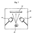
- Fig. 7 shows an ion/electron beam irradiating apparatus which may be used for forming a protecting layer in the PDP of the present embodiment.
- the ion/electron beam irradiating apparatus includes vacuum chamber 45 to which glass substrate 41 with a dielectrics glass layer is attached.
- Vacuum chamber 45 also includes electron gun 42 for evaporating an alkaline earth oxide (in the present embodiment, magnesium oxide).
- Ion gun 43 irradiates ion beam to vapor of the alkaline earth oxide which has been evaporated by electron gun 42.
- Electron gun 44 irradiates electron beam to vapor of the alkaline earth oxide evaporated by electron gun 42.
- the following description shows how to evaporate the alkaline earth oxide onto the dielectrics glass layer by irradiating ion or electron beam to vapor using the ion/electron beam irradiating apparatus described above.
- glass substrate 41 with a dielectrics glass layer is set in chamber 45 then crystals of an alkaline earth oxide are put in electron gun 42.
- chamber 45 is evacuated then substrate 41 is heated (150°C).
- Electron gun 42 is used to evaporate the alkaline earth oxide.
- ion gun 43 or electron gun 44 is used to irradiate argon ion or electron beam towards substrate 41. It forms a protecting layer of an alkaline earth oxide.
- the crystals of the alkaline earth oxide grow slowly and a dense protecting layer consisting of an alkaline earth oxide with (110)-face orientation is formed when, as is described above, the alkaline earth oxide is evaporated onto the dielectrics glass layer by irradiation of the ion or electron beam.
- the formed protecting layer shows almost the same effects as the dense protecting layer of an alkaline earth oxide with (100)-face orientation formed in Embodiment 1.
- Table 3 shows PDP Examples 16-34 which do not fall within the invention, and which were made according to the description above. Refer to "DISCHARGE GAS TYPE AND RATIO” column in the table for the discharge gas compositions, and “GAS CHARGING PRESSURE” column for charging pressures.
- the protecting layer of Examples 16 and 27 were formed as described in Embodiment 1 using magnesium dipivaloyl methane Mg(C 11 H 19 O 2 ) 2 as the source with the thermal CVD method, and Examples 17, 23, 24, 28, 32, and 33 with the plasma enhanced CVD method.
- ion beam current of 10mA was irradiated, and for Examples 19, 20, 30, and 31, electron beam (10mA), to evaporate a magnesium oxide onto the dielectrics glass layer to form a protecting layer with a layer thickness of 5000 ⁇ (0,5nm).
- the overall structure and suitable production method of the PDP of the present example which does not fall within the present invention is the same as that of Embodiment 1 except that the cell pitch is set to a larger value and the amount of Xe in a He-Xe gas used as the discharge gas is set to less than 10% by volume. Note that the distance between electrodes "d" is set to an equal or larger value.
- alkaline earth oxides with (100)-face orientation other than magnesium oxide (MgO) are formed as the protecting layers, such as beryllium oxide (BeO), calcium oxide (CaO), strontium oxide (SrO), and barium oxide (BaO).
- BeO beryllium oxide
- CaO calcium oxide
- SrO strontium oxide
- BaO barium oxide
- These protecting layers are formed by using appropriate sources for respective alkaline earths with the thermal or plasma enhanced CVD method described in connection with Embodiment 1.
- the discharge electrodes formed on the front glass substrate includes a tin oxide-antimony oxide or an indium oxide-tin oxide.
- the protecting layer of beryllium oxide, calcium oxide, strontium oxide, or barium oxide with (100)-face orientation has almost the same effects as the magnesium oxide with (100)-face orientation formed in Embodiment 1.
- Table 4 shows PDP Examples 35-66 which were made according to the present example.
- the height of the partition walls was set to 0.2mm, the distance between partition walls (cell pitch) 0.3mm, and distance d between discharge electrodes 0.05mm.
- the discharge gas was a He-Xe mixture gas including 5% by volume of Xe, and the charging pressure was set to 500Torr (66.5kPa).
- the discharge electrodes which were made with sputtering and photo-lithography methods, consist of indium oxide (In 2 O 3 ) including 10% by weight of tin oxide (SnO 2 ).
- the protecting layers were made with the thermal or plasma enhanced CVD method from metal chelate or cyclopentadienyl compounds of the alkaline earth oxides shown in Table 4 "CVD SOURCE” column.
- the formed layers were of magnesium oxide, beryllium oxide, calcium oxide, strontium oxide, or barium oxide as shown in "ALKALINE EARTH OXIDE” column.
- each Example had (100)-face orientation.
- Examples 67-69 shown in Table 4 were made in the same way as Examples 35-66. However, the protecting layers of Examples 67-69 were formed with different methods: for Example 67, the vacuum vapor deposition method for evaporating magnesium oxide onto the dielectrics glass layer by heating magnesium oxide with electron beam was used; for Example 68, the sputtering performed on magnesium oxide as the target; and for Example 69, the screen printing with magnesium oxide paste.
- magnesium oxide protecting layers of Examples 67 and 69 had (111)-face orientation. It was also confirmed that magnesium oxide protecting layer of Examples 68 had (100)-face orientation. However, the protecting layer of Example 68 is not considered as dense since it was formed with the sputtering.
- the ultraviolet light wavelength and panel brightness were measured when they were operated on 150V of discharge maintenance voltage and 30KHz of frequency.
- the panel brightness is improved by setting the amount of Xe in discharge gas to 10% by volume or more, charging pressure to 550Torr (73,2kPa) or more,
- the panel brightness of example 15 is slightly lower than those of Examples 1-6 and 10-14. The reason is considered that the protecting layer of Example 15 consisting of magnesium oxide with (111)-face orientation emits less secondary electron than that with (100)-face orientation.
- the panel brightness change rates of examples 1-6 and 10-14 are smaller than those of examples 7-9. Also, as shown in Table 3, the change rates of panel brightness and discharge maintenance voltage of examples 16-34 were small as a whole.
- the panel brightness change rate reduces by setting the amount of Xe in discharge gas to 10% by volume or more, charging pressure to 550 Torr (73,2 kPa) or more.
- the change rates of panel brightness and discharge maintenance voltage of examples 1-14 are smaller than those of Example 15.
- the reason is considered that the protecting layer of magnesium oxide with (111)-face orientation has higher sputtering resistance and higher efficiency in protecting dielectrics glass layer than that with (100)-face orientation.
- the above results show that generally the protecting layer of alkaline earth oxide with (100)-face or (110)-face orientation formed with the thermal CVD method, plasma enhanced CVD method, or vapor deposition method with ion or electron beam irradiation has higher sputtering resistance and higher efficiency in protecting dielectrics glass layer than that with (111)-face orientation.
- the results of example 67 show that the protecting layer consisting of alkaline earth oxide with (100)-face orientation formed with the sputtering method has high change rates of panel brightness and discharge maintenance voltage and low efficiency in protecting dielectrics glass layer.
- the reason for the above results is considered that for the alkaline earth oxide of the protecting layer which has been formed by the thermal CVD, plasma enhanced CVD, or a method of evaporating the oxide onto a layer by irradiating ion or electron beam, the crystals grow slowly to form a dense protecting layer with (100)-face or (110)-face orientation; for the protecting layer formed by the sputtering method, the crystals do not grow slowly and the protecting layer does not become dense though it has (100)-face orientation.
Landscapes
- Chemical & Material Sciences (AREA)
- Engineering & Computer Science (AREA)
- Plasma & Fusion (AREA)
- Physics & Mathematics (AREA)
- Mechanical Engineering (AREA)
- Inorganic Chemistry (AREA)
- General Chemical & Material Sciences (AREA)
- Chemical Kinetics & Catalysis (AREA)
- Materials Engineering (AREA)
- Metallurgy (AREA)
- Organic Chemistry (AREA)
- Manufacturing & Machinery (AREA)
- Gas-Filled Discharge Tubes (AREA)
- Manufacture Of Electron Tubes, Discharge Lamp Vessels, Lead-In Wires, And The Like (AREA)
Claims (5)
- Plasmaanzeigetafel bzw. Plasmadisplaypanel umfassend:wobei das Gasmedium aus Neon und Xenon zusammengesetzt ist, dadurch gekennzeichnet, dass das Gasmedium Xenon in einem Bereich von wenigstens 10 Vol-% bis weniger als 100Vol.-% umfasst, der Ladedruck des Gasmediums wenigstens 550 Torr (73,2 kPa) und weniger als oder 760 Torr (101 kPa) entspricht,eine vordere Abdeckplatte, welche ein vorderes Glassubstrat (11) mit voneinander beabstandeten Paaren erster Elektroden (12) und eine dielektrische Glassschicht umfasst, wobei die ersten Elektroden unddie dielektrische Glasschicht (13) auf dem vorderen Glassubstrat ausgebildet sind; undeine hintere Platte, welche ein Glassubstrat (15), eine zweite Elektrode (16) und eine Schicht aus einer fluoreszierenden Substanz umfasst, wobei die zweite Elektrode und die Schicht aus der fluoreszierenden Substanz auf dem hinteren Glassubstrat ausgebildet sind, wobei die dielektrische Glasschicht und die Schicht aus der fluoreszierenden Substanz aufeinander liegen, wobeieine Vielzahl von Entladungsräumen zwischen einer Vielzahl von Trennungswänden (17) gebildet werden, welche zwischen der vorderen Abdeckplatte und der hinteren Platte angeordnet sind, wobei ein Gasmedium in die Vielzahl von Entladungsräumen (19) eingeführt ist, und
dass der Abstand (d) zwischen jedem Paar der benachbarten ersten Elektroden nicht mehr als 0,1 mm beträgt. - Plasmaanzeigetafel nach Anspruch 1, wobei das Gasmedium Xenon umfasst, in dem Bereich von mehr als 10 Vol.-% bis 70 Vol.-% .
- Plasmaanzeigetafel nach Anspruch 1, wobei die dielektrische Glasschicht (13) mit einer Schutzschicht (14) aus einem Erdalkalioxid ist, mit einer (100)-Orientierung.
- Plasmaanzeigetafel nach Anspruch 1, wobei die dielektrische Glassschicht (13) mit einer Schutzschicht (14) aus einem Erdalkalioxid ist, mit einer (110)-Orientierung.
- Plasmaanzeigetafel nach Anspruch 3 oder 4, wobei die Schutzschicht (14) aus Magnesiumoxid besteht.
Priority Applications (5)
| Application Number | Priority Date | Filing Date | Title |
|---|---|---|---|
| EP02006619A EP1221709A3 (de) | 1995-12-15 | 1996-12-13 | Plasmaanzeigetafel geeignet für Anzeige hoher Qualität und Herstellungsverfahren |
| EP02006618A EP1221708A3 (de) | 1995-12-15 | 1996-12-13 | Plasmaanzeigetafel geeignet für Anzeige hoher Qualität und Herstellungsverfahren |
| EP03075897A EP1333462A3 (de) | 1995-12-15 | 1996-12-13 | Plasmaanzeigetafel geeignet für Anzeige hoher Qualität und Herstellungsverfahren |
| EP02006620A EP1221711B1 (de) | 1995-12-15 | 1996-12-13 | Plasmaanzeigetafel geeignet für Anzeige hoher Qualität und Herstellungsverfahren |
| EP01116788A EP1164620B1 (de) | 1995-12-15 | 1996-12-13 | Für Anzeigen von hoher Qualität geeignete Plasmaanzeigetafel und zugehöriges Herstellungsverfahren |
Applications Claiming Priority (12)
| Application Number | Priority Date | Filing Date | Title |
|---|---|---|---|
| JP326766/95 | 1995-12-15 | ||
| JP32676695 | 1995-12-15 | ||
| JP32676695 | 1995-12-15 | ||
| JP16326/96 | 1996-02-01 | ||
| JP1632696 | 1996-02-01 | ||
| JP1632696 | 1996-02-01 | ||
| JP162639/96 | 1996-06-24 | ||
| JP16263996 | 1996-06-24 | ||
| JP16263996 | 1996-06-24 | ||
| JP22342896 | 1996-08-26 | ||
| JP223428/96 | 1996-08-26 | ||
| JP22342896 | 1996-08-26 |
Related Child Applications (2)
| Application Number | Title | Priority Date | Filing Date |
|---|---|---|---|
| EP01116788A Division EP1164620B1 (de) | 1995-12-15 | 1996-12-13 | Für Anzeigen von hoher Qualität geeignete Plasmaanzeigetafel und zugehöriges Herstellungsverfahren |
| EP03075897A Division EP1333462A3 (de) | 1995-12-15 | 1996-12-13 | Plasmaanzeigetafel geeignet für Anzeige hoher Qualität und Herstellungsverfahren |
Publications (3)
| Publication Number | Publication Date |
|---|---|
| EP0779643A2 EP0779643A2 (de) | 1997-06-18 |
| EP0779643A3 EP0779643A3 (de) | 1999-03-10 |
| EP0779643B1 true EP0779643B1 (de) | 2003-09-17 |
Family
ID=27456557
Family Applications (6)
| Application Number | Title | Priority Date | Filing Date |
|---|---|---|---|
| EP03075897A Withdrawn EP1333462A3 (de) | 1995-12-15 | 1996-12-13 | Plasmaanzeigetafel geeignet für Anzeige hoher Qualität und Herstellungsverfahren |
| EP02006619A Withdrawn EP1221709A3 (de) | 1995-12-15 | 1996-12-13 | Plasmaanzeigetafel geeignet für Anzeige hoher Qualität und Herstellungsverfahren |
| EP02006620A Expired - Lifetime EP1221711B1 (de) | 1995-12-15 | 1996-12-13 | Plasmaanzeigetafel geeignet für Anzeige hoher Qualität und Herstellungsverfahren |
| EP02006618A Withdrawn EP1221708A3 (de) | 1995-12-15 | 1996-12-13 | Plasmaanzeigetafel geeignet für Anzeige hoher Qualität und Herstellungsverfahren |
| EP01116788A Expired - Lifetime EP1164620B1 (de) | 1995-12-15 | 1996-12-13 | Für Anzeigen von hoher Qualität geeignete Plasmaanzeigetafel und zugehöriges Herstellungsverfahren |
| EP96309148A Expired - Lifetime EP0779643B1 (de) | 1995-12-15 | 1996-12-13 | Plasmaanzeigetafel geeignet für Anzeige hoher Qualität |
Family Applications Before (5)
| Application Number | Title | Priority Date | Filing Date |
|---|---|---|---|
| EP03075897A Withdrawn EP1333462A3 (de) | 1995-12-15 | 1996-12-13 | Plasmaanzeigetafel geeignet für Anzeige hoher Qualität und Herstellungsverfahren |
| EP02006619A Withdrawn EP1221709A3 (de) | 1995-12-15 | 1996-12-13 | Plasmaanzeigetafel geeignet für Anzeige hoher Qualität und Herstellungsverfahren |
| EP02006620A Expired - Lifetime EP1221711B1 (de) | 1995-12-15 | 1996-12-13 | Plasmaanzeigetafel geeignet für Anzeige hoher Qualität und Herstellungsverfahren |
| EP02006618A Withdrawn EP1221708A3 (de) | 1995-12-15 | 1996-12-13 | Plasmaanzeigetafel geeignet für Anzeige hoher Qualität und Herstellungsverfahren |
| EP01116788A Expired - Lifetime EP1164620B1 (de) | 1995-12-15 | 1996-12-13 | Für Anzeigen von hoher Qualität geeignete Plasmaanzeigetafel und zugehöriges Herstellungsverfahren |
Country Status (5)
| Country | Link |
|---|---|
| US (5) | US5770921A (de) |
| EP (6) | EP1333462A3 (de) |
| JP (4) | JP3339554B2 (de) |
| KR (1) | KR100439878B1 (de) |
| DE (3) | DE69633311T2 (de) |
Families Citing this family (92)
| Publication number | Priority date | Publication date | Assignee | Title |
|---|---|---|---|---|
| KR100186540B1 (ko) * | 1996-04-25 | 1999-03-20 | 구자홍 | 피디피의 전극 및 그 형성방법 |
| KR19980065367A (ko) * | 1996-06-02 | 1998-10-15 | 오평희 | 액정표시소자용 백라이트 |
| JPH10247474A (ja) * | 1997-01-06 | 1998-09-14 | Sony Corp | 平面照明灯及びその製造方法 |
| US6013309A (en) | 1997-02-13 | 2000-01-11 | Lg Electronics Inc. | Protection layer of plasma display panel and method of forming the same |
| EP0916128B1 (de) * | 1997-05-09 | 2002-07-03 | Koninklijke Philips Electronics N.V. | Anzeigevorrichtung |
| JPH117895A (ja) * | 1997-06-05 | 1999-01-12 | Lg Electron Inc | プラズマディスプレイパネル及びその隔壁の形成方法 |
| US6291943B1 (en) * | 1997-08-14 | 2001-09-18 | Matsushita Electric Industrial Co., Ltd. | Gas discharge panel and gas light-emitting device |
| US6150030A (en) * | 1997-11-20 | 2000-11-21 | Balzers Hochvakuum Ag | Substrate coated with an MgO-layer |
| TW494428B (en) | 1998-06-25 | 2002-07-11 | Matsushita Electric Industrial Co Ltd | A plasma display panel |
| JP3481142B2 (ja) * | 1998-07-07 | 2003-12-22 | 富士通株式会社 | ガス放電表示デバイス |
| JP4011746B2 (ja) * | 1998-08-26 | 2007-11-21 | 株式会社日立製作所 | プラズマディスプレイパネル |
| EP2043077A3 (de) * | 1998-09-04 | 2009-06-24 | Panasonic Corporation | Verfahren zur Ansteuerung von Plasmaanzeigetafeln und Plasmaanzeigetafelvorrichtung zum Anzeigen von Hochqualitätsbildern mit hoher Leuchteffizienz |
| DE69932337T2 (de) | 1998-09-08 | 2007-07-12 | Matsushita Electric Industrial Co., Ltd., Kadoma | Herstellungsverfahren einer anzeigetafel unter verwendung eines klebemittelauftragungsverfahren |
| JP4587567B2 (ja) | 1998-10-20 | 2010-11-24 | 三星エスディアイ株式会社 | プラズマ表示パネル |
| JP2000357462A (ja) * | 1998-10-23 | 2000-12-26 | Sony Corp | 平面型プラズマ放電表示装置と駆動方法 |
| DE19851348A1 (de) * | 1998-11-06 | 2000-05-25 | Philips Corp Intellectual Pty | Lumineszierender Schirm mit oxidhaltiger Leuchtstoffzubereitung |
| JP3327858B2 (ja) * | 1999-01-28 | 2002-09-24 | 松下電器産業株式会社 | プラズマディスプレイパネルおよびその製造方法 |
| US6541913B1 (en) | 1999-07-02 | 2003-04-01 | Sony Corporation | Flat display apparatus |
| TW452812B (en) | 1999-08-04 | 2001-09-01 | Koninkl Philips Electronics Nv | Plasma display panel |
| EP1150322A4 (de) * | 1999-10-19 | 2008-05-28 | Matsushita Electric Industrial Co Ltd | Plasmaanzeige und herstellungsverfahren derselben |
| JP2001228823A (ja) * | 1999-12-07 | 2001-08-24 | Pioneer Electronic Corp | プラズマディスプレイ装置 |
| JP4614609B2 (ja) * | 1999-12-07 | 2011-01-19 | パナソニック株式会社 | プラズマディスプレイパネル |
| KR20020062656A (ko) * | 1999-12-14 | 2002-07-26 | 마츠시타 덴끼 산교 가부시키가이샤 | 고정밀하며 고휘도로 화상표시할 수 있는 에이씨형플라즈마 디스플레이 패널 및 그 구동방법 |
| JP3384390B2 (ja) | 2000-01-12 | 2003-03-10 | ソニー株式会社 | 交流駆動型プラズマ表示装置 |
| TW509960B (en) | 2000-04-04 | 2002-11-11 | Matsushita Electric Industrial Co Ltd | Highly productive method of producing plasma display panel |
| KR100769414B1 (ko) | 2000-05-11 | 2007-10-22 | 마츠시타 덴끼 산교 가부시키가이샤 | 전자 방출성 박막, 이를 이용한 플라즈마 디스플레이 패널및 이들의 제조 방법 |
| DE10023341A1 (de) * | 2000-05-12 | 2001-11-29 | Philips Corp Intellectual Pty | Plasmabildschirm mit Schutzschicht |
| US6873106B2 (en) * | 2000-06-01 | 2005-03-29 | Pioneer Corporation | Plasma display panel that inhibits false discharge |
| JP4153983B2 (ja) * | 2000-07-17 | 2008-09-24 | パイオニア株式会社 | 保護膜、その成膜方法、プラズマディスプレイパネル及びその製造方法 |
| FR2812125A1 (fr) * | 2000-07-21 | 2002-01-25 | Thomson Plasma | Dalle en verre munie d'electrodes en un materiau conducteur |
| JP2002110050A (ja) * | 2000-09-29 | 2002-04-12 | Hitachi Ltd | プラズマ表示パネル |
| DE10123235A1 (de) * | 2001-05-12 | 2002-11-14 | Philips Corp Intellectual Pty | Plasmafarbbildschirm mit Pixelmatrix-Array |
| CN101515528B (zh) | 2001-06-01 | 2011-05-11 | 松下电器产业株式会社 | 气体放电屏及其制造方法 |
| JP4271902B2 (ja) * | 2002-05-27 | 2009-06-03 | 株式会社日立製作所 | プラズマディスプレイパネル及びそれを用いた画像表示装置 |
| KR100468416B1 (ko) * | 2002-07-12 | 2005-01-27 | 엘지전자 주식회사 | 플라즈마 디스플레이 패널의 구동방법 |
| JP3624234B2 (ja) * | 2002-07-17 | 2005-03-02 | パイオニアプラズマディスプレイ株式会社 | プラズマディスプレイパネルの製造装置及びプラズマディスプレイパネルの製造方法 |
| JP4097480B2 (ja) * | 2002-08-06 | 2008-06-11 | 株式会社日立製作所 | ガス放電パネル用基板構体、その製造方法及びac型ガス放電パネル |
| JP4056357B2 (ja) * | 2002-10-31 | 2008-03-05 | 富士通日立プラズマディスプレイ株式会社 | ガス放電パネル及びその製造方法 |
| US7605537B2 (en) | 2003-06-19 | 2009-10-20 | Samsung Sdi Co., Ltd. | Plasma display panel having bus electrodes extending across areas of non-discharge regions |
| US7425797B2 (en) | 2003-07-04 | 2008-09-16 | Samsung Sdi Co., Ltd. | Plasma display panel having protrusion electrode with indentation and aperture |
| US7208876B2 (en) | 2003-07-22 | 2007-04-24 | Samsung Sdi Co., Ltd. | Plasma display panel |
| US7466079B2 (en) * | 2003-09-18 | 2008-12-16 | Lg Electronics Inc. | Plasma display panel and method for manufacturing the same |
| WO2005031782A1 (ja) | 2003-09-26 | 2005-04-07 | Pioneer Corporation | プラズマディスプレイパネルおよびその製造方法 |
| KR20050036450A (ko) * | 2003-10-16 | 2005-04-20 | 삼성에스디아이 주식회사 | 플라즈마 디스플레이 패널 |
| US7084567B2 (en) * | 2003-10-20 | 2006-08-01 | .Au Optronics Corporation | Plasma display panel performing high luminance and luminous efficiency |
| KR100522613B1 (ko) * | 2003-10-22 | 2005-10-19 | 삼성전자주식회사 | 플라즈마 디스플레이 패널 |
| KR100589369B1 (ko) | 2003-11-29 | 2006-06-14 | 삼성에스디아이 주식회사 | 플라즈마 디스플레이 패널 |
| JP4541832B2 (ja) * | 2004-03-19 | 2010-09-08 | パナソニック株式会社 | プラズマディスプレイパネル |
| JP4396832B2 (ja) | 2004-04-26 | 2010-01-13 | パナソニック株式会社 | プラズマディスプレイパネル |
| JP4764615B2 (ja) * | 2004-05-07 | 2011-09-07 | 富士フイルム株式会社 | 塗布装置、塗布方法及び塗布膜付きウエブの製造方法 |
| EP1640946A3 (de) * | 2004-09-24 | 2008-05-14 | Pioneer Corporation | Plasmaanzeigevorrichtung |
| JP2006120356A (ja) * | 2004-10-19 | 2006-05-11 | Fujitsu Hitachi Plasma Display Ltd | プラズマディスプレイパネル及びその製造方法 |
| EP1808881B1 (de) * | 2004-11-05 | 2012-09-26 | Ulvac, Inc. | Schutzfilm für eine plasmaanzeigetafel, herstellungsverfahren für den schutzfilm, plasmaanzeigetafel und herstellungsverfahren dafür |
| JP4399344B2 (ja) | 2004-11-22 | 2010-01-13 | パナソニック株式会社 | プラズマディスプレイパネルおよびその製造方法 |
| JP2006222034A (ja) * | 2005-02-14 | 2006-08-24 | Fujitsu Hitachi Plasma Display Ltd | プラズマディスプレイパネル |
| JP4650829B2 (ja) * | 2005-03-22 | 2011-03-16 | パナソニック株式会社 | プラズマディスプレイパネルおよびその製造方法 |
| JP2006286324A (ja) * | 2005-03-31 | 2006-10-19 | Fujitsu Hitachi Plasma Display Ltd | プラズマディスプレイパネル |
| WO2006129754A1 (ja) * | 2005-06-02 | 2006-12-07 | Matsushita Electric Industrial Co., Ltd. | プラズマディスプレイパネルおよびプラズマディスプレイパネル装置 |
| KR100726937B1 (ko) * | 2005-06-08 | 2007-06-14 | 엘지전자 주식회사 | 플라즈마 디스플레이 패널 |
| JP2007012436A (ja) * | 2005-06-30 | 2007-01-18 | Nippon Hoso Kyokai <Nhk> | プラズマディスプレイパネル |
| JP4829888B2 (ja) * | 2005-07-08 | 2011-12-07 | パナソニック株式会社 | プラズマディスプレイパネルおよびプラズマディスプレイパネル装置 |
| RU2290712C1 (ru) * | 2005-07-18 | 2006-12-27 | Государственное образовательное учреждение высшего профессионального образования "Санкт-Петербургский Государственный политехнический университет" (ГОУ "СПбГПУ") | Газоразрядное устройство |
| JP2007095436A (ja) * | 2005-09-28 | 2007-04-12 | Matsushita Electric Ind Co Ltd | プラズマディスプレイパネル |
| KR100659101B1 (ko) * | 2005-10-12 | 2006-12-21 | 삼성에스디아이 주식회사 | 기체 방전 표시 장치와 이의 제조 방법 |
| JP4894234B2 (ja) * | 2005-11-15 | 2012-03-14 | パナソニック株式会社 | プラズマディスプレイパネル |
| JP2007141483A (ja) * | 2005-11-15 | 2007-06-07 | Matsushita Electric Ind Co Ltd | プラズマディスプレイパネル |
| JPWO2007072565A1 (ja) * | 2005-12-22 | 2009-05-28 | 篠田プラズマ株式会社 | カラー表示装置 |
| US7638074B2 (en) * | 2006-03-10 | 2009-12-29 | Advanced Technology Materials, Inc. | Precursor compositions for atomic layer deposition and chemical vapor deposition of titanate, lanthanate, and tantalate dielectric films |
| JP4777827B2 (ja) * | 2006-05-25 | 2011-09-21 | 株式会社アルバック | プラズマディスプレイパネル、プラズマディスプレイパネルの製造方法及びプラズマディスプレイパネルの製造装置 |
| JP4148985B2 (ja) | 2006-05-31 | 2008-09-10 | 松下電器産業株式会社 | プラズマディスプレイパネル |
| US7902096B2 (en) | 2006-07-31 | 2011-03-08 | 3M Innovative Properties Company | Monocomponent monolayer meltblown web and meltblowing apparatus |
| US9770058B2 (en) | 2006-07-17 | 2017-09-26 | 3M Innovative Properties Company | Flat-fold respirator with monocomponent filtration/stiffening monolayer |
| US7905973B2 (en) * | 2006-07-31 | 2011-03-15 | 3M Innovative Properties Company | Molded monocomponent monolayer respirator |
| US7858163B2 (en) * | 2006-07-31 | 2010-12-28 | 3M Innovative Properties Company | Molded monocomponent monolayer respirator with bimodal monolayer monocomponent media |
| US7947142B2 (en) | 2006-07-31 | 2011-05-24 | 3M Innovative Properties Company | Pleated filter with monolayer monocomponent meltspun media |
| RU2404306C2 (ru) * | 2006-07-31 | 2010-11-20 | 3М Инновейтив Пропертиз Компани | Способ изготовления формованных фильтрующих изделий |
| US7754041B2 (en) * | 2006-07-31 | 2010-07-13 | 3M Innovative Properties Company | Pleated filter with bimodal monolayer monocomponent media |
| BRPI0714088B1 (pt) | 2006-07-31 | 2017-04-04 | 3M Innovative Properties Co | método para a produção de artigos de filtração com formato |
| KR100768333B1 (ko) | 2006-08-14 | 2007-10-17 | (주)씨앤켐 | 피디피 보호막 재료 및 그 제조방법 |
| KR20090067190A (ko) | 2006-10-20 | 2009-06-24 | 파나소닉 주식회사 | 플라스마 디스플레이 패널과 그 제조방법 |
| KR20090067145A (ko) | 2006-10-20 | 2009-06-24 | 파나소닉 주식회사 | 플라스마 디스플레이 패널과 그 제조방법 |
| JP4542080B2 (ja) * | 2006-11-10 | 2010-09-08 | パナソニック株式会社 | プラズマディスプレイパネル及びその製造方法 |
| KR20090017266A (ko) * | 2007-08-14 | 2009-02-18 | 엘지전자 주식회사 | MgO 보호막 및 이를 포함한 플라즈마 디스플레이 패널용상부패널 |
| JP4818318B2 (ja) * | 2008-06-13 | 2011-11-16 | 宇部マテリアルズ株式会社 | 酸化マグネシウム蒸着材及びその製造方法 |
| JP5363918B2 (ja) * | 2009-08-31 | 2013-12-11 | エア・ウォーター株式会社 | 酸化マグネシウム膜およびその成膜方法、ならびにプラズマ生成電極 |
| JP4598154B2 (ja) * | 2010-03-17 | 2010-12-15 | パナソニック株式会社 | プラズマディスプレイパネル |
| WO2012005957A2 (en) | 2010-07-07 | 2012-01-12 | Advanced Technology Materials, Inc. | Doping of zro2 for dram applications |
| CN103943436A (zh) * | 2011-12-31 | 2014-07-23 | 四川虹欧显示器件有限公司 | 提高掺杂型MgO介质保护层稳定性的方法及等离子显示屏 |
| US9443736B2 (en) | 2012-05-25 | 2016-09-13 | Entegris, Inc. | Silylene compositions and methods of use thereof |
| US9024526B1 (en) | 2012-06-11 | 2015-05-05 | Imaging Systems Technology, Inc. | Detector element with antenna |
| WO2014124056A1 (en) | 2013-02-08 | 2014-08-14 | Advanced Technology Materials, Inc. | Ald processes for low leakage current and low equivalent oxide thickness bitao films |
| CN112630288B (zh) * | 2020-11-17 | 2021-10-12 | 燕山大学 | 一种基于放电的二次电子发射系数测量装置及方法 |
Citations (3)
| Publication number | Priority date | Publication date | Assignee | Title |
|---|---|---|---|---|
| US4419605A (en) * | 1980-01-28 | 1983-12-06 | Siemens Aktiengesellschaft | Gas discharge display device |
| EP0500084A2 (de) * | 1991-02-20 | 1992-08-26 | Sony Corporation | Elektrooptische Vorrichtung |
| EP0566997A1 (de) * | 1992-04-21 | 1993-10-27 | Sony Corporation | Plasmaadressierte elektrooptische Vorrichtung |
Family Cites Families (51)
| Publication number | Priority date | Publication date | Assignee | Title |
|---|---|---|---|---|
| US3863089A (en) * | 1970-09-28 | 1975-01-28 | Owens Illinois Inc | Gas discharge display and memory panel with magnesium oxide coatings |
| US3916245A (en) * | 1970-12-07 | 1975-10-28 | Owens Illinois Inc | Multiple gaseous discharge display/memory panel comprising rare gas medium and photoluminescent phosphor |
| US4048533A (en) * | 1971-10-12 | 1977-09-13 | Owens-Illinois, Inc. | Phosphor overcoat |
| JPS5263663A (en) * | 1975-11-19 | 1977-05-26 | Fujitsu Ltd | Gas electric discharge panel |
| JPS5388566A (en) * | 1977-01-14 | 1978-08-04 | Hitachi Ltd | Gas discharge display unit |
| US4320418A (en) * | 1978-12-08 | 1982-03-16 | Pavliscak Thomas J | Large area display |
| JPS5638729A (en) * | 1979-08-18 | 1981-04-14 | Fujitsu Ltd | Manufacture of gas discharge panel |
| GB2109628B (en) * | 1981-11-16 | 1985-04-17 | United Technologies Corp | Optical display with excimer flurorescence |
| JPS60219548A (ja) * | 1984-04-16 | 1985-11-02 | Ngk Spark Plug Co Ltd | 自動車排気ガス用酸素濃度検出器 |
| US4717584A (en) | 1985-02-07 | 1988-01-05 | Matsushita Electric Industrial Co., Ltd. | Method of manufacturing a magnetic thin film |
| JPH0664738B2 (ja) * | 1985-06-12 | 1994-08-22 | 松下電器産業株式会社 | 磁性体薄膜の製造方法 |
| JPS63205031A (ja) * | 1987-02-19 | 1988-08-24 | Fujitsu Ltd | ガス放電パネル |
| JPH01104774A (ja) * | 1987-10-14 | 1989-04-21 | Matsushita Electric Ind Co Ltd | 酸化物超伝導体薄膜の製造方法 |
| JPH0788271B2 (ja) * | 1988-03-14 | 1995-09-27 | 松下電器産業株式会社 | 酸化物薄膜の製造方法 |
| EP0364068A3 (de) * | 1988-10-14 | 1990-05-30 | Westinghouse Electric Corporation | Methode zur Abscheidung eines oxidischen Supraleiters auf ein Substrat |
| JPH0315136A (ja) * | 1989-06-12 | 1991-01-23 | Mitsubishi Electric Corp | プラズマディスプレイ装置およびプラズマディスプレイ装置の製造方法 |
| US5179318A (en) * | 1989-07-05 | 1993-01-12 | Nippon Sheet Glass Co., Ltd. | Cathode-ray tube with interference filter |
| JPH0686657B2 (ja) * | 1989-09-11 | 1994-11-02 | 松下電工株式会社 | 薄膜形成装置 |
| US5108983A (en) * | 1989-11-21 | 1992-04-28 | Georgia Tech Research Corporation | Method for the rapid deposition with low vapor pressure reactants by chemical vapor deposition |
| JP2984015B2 (ja) | 1990-02-01 | 1999-11-29 | 富士通株式会社 | プラズマディスプレイパネルの製造方法 |
| US5139999A (en) * | 1990-03-08 | 1992-08-18 | President And Fellows Of Harvard College | Chemical vapor deposition process where an alkaline earth metal organic precursor material is volatilized in the presence of an amine or ammonia and deposited onto a substrate |
| JP3007117B2 (ja) | 1990-04-27 | 2000-02-07 | 沖電気工業株式会社 | ガス放電表示装置およびその製造方法 |
| JPH04170394A (ja) * | 1990-11-05 | 1992-06-18 | Matsushita Electric Ind Co Ltd | 超伝導薄膜およびその製造方法 |
| JP2731480B2 (ja) * | 1992-01-28 | 1998-03-25 | 富士通株式会社 | 面放電型プラズマディスプレイパネル |
| JP3190714B2 (ja) * | 1991-11-21 | 2001-07-23 | 日本放送協会 | 直流型放電パネルとそれをパルスメモリ駆動する表示装置 |
| EP0524005B1 (de) | 1991-07-18 | 1996-09-25 | Nippon Hoso Kyokai | Gleichfeld-Gasentladungsanzeigeeinrichtung und diese verwendende Gasentladungsanzeigevorrichtung |
| JP3126756B2 (ja) * | 1991-07-18 | 2001-01-22 | 日本放送協会 | 直流型放電パネルと表示装置 |
| EP0554172B1 (de) | 1992-01-28 | 1998-04-29 | Fujitsu Limited | Plasma Farbanzeige-Vorrichtung von Oberflächenentladungs-Typ |
| JP3149249B2 (ja) * | 1992-02-25 | 2001-03-26 | 富士通株式会社 | Ac型プラズマディスプレイパネル及びその製造方法 |
| JP3236665B2 (ja) * | 1992-06-05 | 2001-12-10 | 富士通株式会社 | Ac型プラズマディスプレイパネルのエージング方法 |
| US5438343A (en) * | 1992-07-28 | 1995-08-01 | Philips Electronics North America Corporation | Gas discharge displays and methodology for fabricating same by micromachining technology |
| JP3459933B2 (ja) | 1993-05-10 | 2003-10-27 | 平樹 内池 | ac形プラズマディスプレイおよびその製造方法 |
| JP2616538B2 (ja) * | 1993-06-01 | 1997-06-04 | 日本電気株式会社 | ガス放電型表示装置 |
| US5469021A (en) | 1993-06-02 | 1995-11-21 | Btl Fellows Company, Llc | Gas discharge flat-panel display and method for making the same |
| EP0638625B1 (de) * | 1993-07-30 | 2002-09-11 | Toshiba Lighting & Technology Corporation | Lumineszentes Material für Quecksilberentladungslampe |
| JPH07111134A (ja) * | 1993-10-13 | 1995-04-25 | Oki Electric Ind Co Ltd | ガス放電表示パネル及びその電極形成方法 |
| US5458086A (en) * | 1993-10-13 | 1995-10-17 | Superconductor Technologies, Inc. | Apparatus for growing metal oxides using organometallic vapor phase epitaxy |
| JP3194454B2 (ja) * | 1994-01-17 | 2001-07-30 | 日本放送協会 | 気体放電型表示装置 |
| JPH07220640A (ja) * | 1994-02-02 | 1995-08-18 | Oki Electric Ind Co Ltd | ガス放電パネルの保護膜、その形成方法、そのガス放電パネルの保護膜を用いたガス放電パネルおよび表示装置 |
| JPH07300397A (ja) * | 1994-05-10 | 1995-11-14 | Matsushita Electric Ind Co Ltd | 強誘電体薄膜素子およびその製造方法 |
| JPH0877932A (ja) * | 1994-09-02 | 1996-03-22 | Oki Electric Ind Co Ltd | ガス放電パネルの保護膜及びその形成方法 |
| US5818168A (en) * | 1994-09-07 | 1998-10-06 | Hitachi, Ltd. | Gas discharge display panel having communicable main and auxiliary discharge spaces and manufacturing method therefor |
| JPH08111177A (ja) | 1994-10-12 | 1996-04-30 | Dainippon Printing Co Ltd | 交流型プラズマディスプレイ及びその製造方法 |
| JPH08115673A (ja) * | 1994-10-17 | 1996-05-07 | Kasei Optonix Co Ltd | 真空紫外線励起発光素子 |
| JPH08236025A (ja) * | 1995-02-28 | 1996-09-13 | Oki Electric Ind Co Ltd | ガス充填方法、ガス充填構造およびガス放電表示パネルの製造方法 |
| JPH08248917A (ja) * | 1995-03-08 | 1996-09-27 | Nippon Hoso Kyokai <Nhk> | 気体放電型表示装置の駆動方法 |
| AU5483196A (en) * | 1995-04-14 | 1996-10-30 | Spectra-Physics Lasers, Inc. | Method for producing dielectric coatings |
| EP0753985B1 (de) * | 1995-07-14 | 2000-03-01 | Matsushita Electric Industrial Co., Ltd. | Lumineszenzelement, Methode zur Herstellung desselben, und beleuchtetes Schaltelement damit |
| KR19980065367A (ko) * | 1996-06-02 | 1998-10-15 | 오평희 | 액정표시소자용 백라이트 |
| JP2001104774A (ja) | 1999-10-05 | 2001-04-17 | Sony Corp | プラズマ処理装置 |
| JP2004170394A (ja) | 2002-10-29 | 2004-06-17 | Toppan Printing Co Ltd | 刷版検査装置及び刷版検査システム |
-
1996
- 1996-12-09 JP JP32845896A patent/JP3339554B2/ja not_active Expired - Fee Related
- 1996-12-13 EP EP03075897A patent/EP1333462A3/de not_active Withdrawn
- 1996-12-13 EP EP02006619A patent/EP1221709A3/de not_active Withdrawn
- 1996-12-13 DE DE1996633311 patent/DE69633311T2/de not_active Expired - Fee Related
- 1996-12-13 DE DE69630004T patent/DE69630004T2/de not_active Expired - Fee Related
- 1996-12-13 DE DE69633148T patent/DE69633148T2/de not_active Expired - Fee Related
- 1996-12-13 EP EP02006620A patent/EP1221711B1/de not_active Expired - Lifetime
- 1996-12-13 KR KR1019960065163A patent/KR100439878B1/ko not_active Expired - Fee Related
- 1996-12-13 EP EP02006618A patent/EP1221708A3/de not_active Withdrawn
- 1996-12-13 EP EP01116788A patent/EP1164620B1/de not_active Expired - Lifetime
- 1996-12-13 EP EP96309148A patent/EP0779643B1/de not_active Expired - Lifetime
- 1996-12-16 US US08/766,030 patent/US5770921A/en not_active Expired - Lifetime
-
1997
- 1997-07-09 US US08/890,577 patent/US5993543A/en not_active Ceased
-
2001
- 2001-07-26 JP JP2001226563A patent/JP2002093327A/ja active Pending
- 2001-11-29 US US09/997,988 patent/USRE40647E1/en not_active Expired - Lifetime
- 2001-11-29 US US09/997,536 patent/USRE40871E1/en not_active Expired - Lifetime
-
2006
- 2006-05-18 US US11/437,004 patent/USRE41503E1/en not_active Expired - Lifetime
-
2007
- 2007-01-26 JP JP2007017154A patent/JP4505474B2/ja not_active Expired - Fee Related
-
2009
- 2009-11-06 JP JP2009255320A patent/JP4569933B2/ja not_active Expired - Fee Related
Patent Citations (3)
| Publication number | Priority date | Publication date | Assignee | Title |
|---|---|---|---|---|
| US4419605A (en) * | 1980-01-28 | 1983-12-06 | Siemens Aktiengesellschaft | Gas discharge display device |
| EP0500084A2 (de) * | 1991-02-20 | 1992-08-26 | Sony Corporation | Elektrooptische Vorrichtung |
| EP0566997A1 (de) * | 1992-04-21 | 1993-10-27 | Sony Corporation | Plasmaadressierte elektrooptische Vorrichtung |
Also Published As
Similar Documents
| Publication | Publication Date | Title |
|---|---|---|
| EP0779643B1 (de) | Plasmaanzeigetafel geeignet für Anzeige hoher Qualität | |
| JP3331907B2 (ja) | プラズマディスプレイパネルおよびその製造方法 | |
| JP3425063B2 (ja) | プラズマディスプレイパネル及びその製造方法 | |
| EP0935276B1 (de) | Gasentladungstafel und lichterzeugende gasvorrichtung | |
| JP3499751B2 (ja) | ガス放電パネル及びガス発光デバイス | |
| KR100697495B1 (ko) | 플라즈마 디스플레이 패널 | |
| JP3546987B2 (ja) | プラズマディスプレイパネルおよびプラズマディスプレイパネルの製造方法 | |
| JPH11135023A (ja) | プラズマディスプレイパネルおよびその製造方法 | |
| JP3988515B2 (ja) | プラズマディスプレイパネルおよびその製造方法 | |
| JP4184222B2 (ja) | ガス放電パネル及びガス発光デバイス | |
| KR100361450B1 (ko) | 교류형 플라즈마디스플레이패널용 보호막재료 | |
| JPH1154048A (ja) | プラズマディスプレイパネル及びその製造方法 | |
| JP3412570B2 (ja) | プラズマディスプレイパネルおよびその製造方法 | |
| JPH11172241A (ja) | 蛍光体材料,蛍光体膜およびプラズマディスプレイパネル | |
| JP2000294145A (ja) | ガス放電パネル及びガス発光デバイス | |
| JP2003346663A (ja) | プラズマディスプレイパネル | |
| JP2002134029A (ja) | ガス放電表示装置 | |
| JP2002352735A (ja) | プラズマディスプレイパネルおよびプラズマディスプレイパネルの製造方法 | |
| KR20080070919A (ko) | 화학 기상 증착 장치, 이를 이용한 플라즈마 디스플레이패널 및 그 제조방법 |
Legal Events
| Date | Code | Title | Description |
|---|---|---|---|
| PUAI | Public reference made under article 153(3) epc to a published international application that has entered the european phase |
Free format text: ORIGINAL CODE: 0009012 |
|
| AK | Designated contracting states |
Kind code of ref document: A2 Designated state(s): DE FR GB IT |
|
| PUAL | Search report despatched |
Free format text: ORIGINAL CODE: 0009013 |
|
| AK | Designated contracting states |
Kind code of ref document: A3 Designated state(s): DE FR GB IT |
|
| 17P | Request for examination filed |
Effective date: 19990527 |
|
| 17Q | First examination report despatched |
Effective date: 20000728 |
|
| RTI1 | Title (correction) |
Free format text: PLASMA DISPLAY PANEL SUITABLE FOR HIGH-QUALITY DISPLAY |
|
| GRAP | Despatch of communication of intention to grant a patent |
Free format text: ORIGINAL CODE: EPIDOSNIGR1 |
|
| GRAS | Grant fee paid |
Free format text: ORIGINAL CODE: EPIDOSNIGR3 |
|
| GRAA | (expected) grant |
Free format text: ORIGINAL CODE: 0009210 |
|
| AK | Designated contracting states |
Kind code of ref document: B1 Designated state(s): DE FR GB IT |
|
| PG25 | Lapsed in a contracting state [announced via postgrant information from national office to epo] |
Ref country code: IT Free format text: LAPSE BECAUSE OF FAILURE TO SUBMIT A TRANSLATION OF THE DESCRIPTION OR TO PAY THE FEE WITHIN THE PRE;WARNING: LAPSES OF ITALIAN PATENTS WITH EFFECTIVE DATE BEFORE 2007 MAY HAVE OCCURRED AT ANY TIME BEFORE 2007. THE CORRECT EFFECTIVE DATE MAY BE DIFFERENT FROM THE ONE RECORDED.SCRIBED TIME-LIMIT Effective date: 20030917 |
|
| REG | Reference to a national code |
Ref country code: GB Ref legal event code: FG4D |
|
| REF | Corresponds to: |
Ref document number: 69630004 Country of ref document: DE Date of ref document: 20031023 Kind code of ref document: P |
|
| ET | Fr: translation filed | ||
| PLBE | No opposition filed within time limit |
Free format text: ORIGINAL CODE: 0009261 |
|
| STAA | Information on the status of an ep patent application or granted ep patent |
Free format text: STATUS: NO OPPOSITION FILED WITHIN TIME LIMIT |
|
| 26N | No opposition filed |
Effective date: 20040618 |
|
| PGFP | Annual fee paid to national office [announced via postgrant information from national office to epo] |
Ref country code: DE Payment date: 20061207 Year of fee payment: 11 |
|
| PGFP | Annual fee paid to national office [announced via postgrant information from national office to epo] |
Ref country code: FR Payment date: 20061208 Year of fee payment: 11 |
|
| PGFP | Annual fee paid to national office [announced via postgrant information from national office to epo] |
Ref country code: GB Payment date: 20061213 Year of fee payment: 11 |
|
| GBPC | Gb: european patent ceased through non-payment of renewal fee |
Effective date: 20071213 |
|
| PG25 | Lapsed in a contracting state [announced via postgrant information from national office to epo] |
Ref country code: DE Free format text: LAPSE BECAUSE OF NON-PAYMENT OF DUE FEES Effective date: 20080701 |
|
| REG | Reference to a national code |
Ref country code: FR Ref legal event code: ST Effective date: 20081020 |
|
| PG25 | Lapsed in a contracting state [announced via postgrant information from national office to epo] |
Ref country code: GB Free format text: LAPSE BECAUSE OF NON-PAYMENT OF DUE FEES Effective date: 20071213 |
|
| PG25 | Lapsed in a contracting state [announced via postgrant information from national office to epo] |
Ref country code: FR Free format text: LAPSE BECAUSE OF NON-PAYMENT OF DUE FEES Effective date: 20071231 |