EP0524005B1 - Gleichfeld-Gasentladungsanzeigeeinrichtung und diese verwendende Gasentladungsanzeigevorrichtung - Google Patents
Gleichfeld-Gasentladungsanzeigeeinrichtung und diese verwendende Gasentladungsanzeigevorrichtung Download PDFInfo
- Publication number
- EP0524005B1 EP0524005B1 EP92306554A EP92306554A EP0524005B1 EP 0524005 B1 EP0524005 B1 EP 0524005B1 EP 92306554 A EP92306554 A EP 92306554A EP 92306554 A EP92306554 A EP 92306554A EP 0524005 B1 EP0524005 B1 EP 0524005B1
- Authority
- EP
- European Patent Office
- Prior art keywords
- discharge
- gas
- display panel
- dce
- gas mixture
- Prior art date
- Legal status (The legal status is an assumption and is not a legal conclusion. Google has not performed a legal analysis and makes no representation as to the accuracy of the status listed.)
- Expired - Lifetime
Links
Images


Classifications
-
- H—ELECTRICITY
- H01—ELECTRIC ELEMENTS
- H01J—ELECTRIC DISCHARGE TUBES OR DISCHARGE LAMPS
- H01J17/00—Gas-filled discharge tubes with solid cathode
- H01J17/38—Cold-cathode tubes
- H01J17/48—Cold-cathode tubes with more than one cathode or anode, e.g. sequence-discharge tube, counting tube, dekatron
- H01J17/49—Display panels, e.g. with crossed electrodes, e.g. making use of direct current
- H01J17/492—Display panels, e.g. with crossed electrodes, e.g. making use of direct current with crossed electrodes
-
- H—ELECTRICITY
- H01—ELECTRIC ELEMENTS
- H01J—ELECTRIC DISCHARGE TUBES OR DISCHARGE LAMPS
- H01J17/00—Gas-filled discharge tubes with solid cathode
- H01J17/02—Details
- H01J17/20—Selection of substances for gas fillings; Specified operating pressures or temperatures
Definitions
- the present invention relates to a DC type gas-discharge display panel and a gas-discharge display apparatus using the DC type gas-discharge display panel.
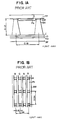
- a first conventional DC type gas-discharge panel (citation 1) has structure thereof as shown in Figs. 1A and 1B.
- Fig. 1A is a sectional view of this first conventional gas-discharge panel
- Fig. 1B is a plan view thereof, as viewed from a display side.
- symbol “FP” indicates a front plate (glass); symbol “BM”, shows a black grid (black matrix); symbol “BA” is a partition; symbol “A” shows an anode (indium tin oxide); symbol “Ph” denotes phosphor; symbol “C” shows a cathode (Ni); symbol “D” indicates a dielectric material; symbol “TH” denotes a third electrode; and symbol “RP” shows a rear plate (glass).
- symbol “FP” indicates a front plate (glass); symbol “BM”, shows a black grid (black matrix); symbol “BA” is a partition; symbol “A” shows an anode (indium tin oxide); symbol “Ph” denotes phosphor; symbol “C” shows a cathode (Ni); symbol “D” indicates a dielectric material; symbol “TH” denotes a third electrode; and symbol “RP” shows a rear plate (glass).
- a detailed explanation of this gas-display panel is described in above-mentioned publication (1).
- the display panel of the X-Y matrix is driven by the 1-line at-a-time drive method, and a relatively large current (about 490 ⁇ A) flows therethrough.
- the light-emission efficiency is 0.025 lm/W (white), which implies a low efficiency, and therefore this display panel is not utilized as a color television receiver panel except for a TV receiver panel for special purposes.
- He partial pressure ratio of 93%) - Kr (5%) - Xe (2%) gas is employed as the filling gas, and the total pressure thereof is 53 kPa (400 Torr).
- a second conventional DC type gas-discharge display panel (citation 2).
- the same reference symbols shown in Figs. 1A and 1B are employed to denote the same constructive elements shown in Fig. 2.
- symbol “AA” indicates an auxiliary anode
- symbol “R-Ph” shows red phosphor
- symbol “G-Ph” indicates green phosphor
- symbol “B-Ph” is blue-phosphor
- symbol “PS” shows a priming slit
- symbol “DC” is a display cell
- symbol “W” represents a wall
- symbol "ACE” indicates an auxiliary cell.
- the operation of this second display panel is described in above-mentioned publication (2).
- a third conventional DC type gas-discharge panel In Fig. 3, there is shown a third conventional DC type gas-discharge panel. It should be noted that the same reference symbols shown in Figs. 1A, 1B and 2 are employed to denote the same constructive elements shown in Fig. 3. Of the other reference symbols, symbol “F” indicates a filter; symbol “CB” denotes a cathode bus line; symbol “WB” shows a white back; symbol “AAL” is an auxiliary anode line; and symbol “DAL” denotes a display anode line.
- a detailed description of this third conventional display panel is found in above-mentioned publication (3).
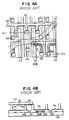
- Figs. 4A and 4B represent a fourth conventional DC type display panel (citation 5).
- Fig. 4A is a plan view of this display panel, as viewed at a display side, and
- Fig. 4B is a sectional view thereof cut away along a cutting line X 1 - X 2 shown in Fig. 4A.
- the structure of this fourth display panel is most similar to that of a DC type gas-discharge display panel according to the present invention.
- the same reference symbols shown in Figs. 1A to 3 are employed to denote the same constructive elements shown in Figs. 4A and 4B.
- reference symbol “AC” denotes an auxiliary cathode
- symbol “DAB” shows a display anode bus line
- symbol “R” indicates a current limiting resistor
- the above-described second to fourth conventional display panels are driven by the pulse memory drive method, the cathodes "C" of which are made of such materials as Ni, Al and LaB 6 , and in which He-Xe (1.5 to 5%) gas is employed as the filling gas.
- the total pressure of the display panel is from 27 to 33 kPa (200 to 250 Torr).
- peak luminance of an image of the first conventional gas-discharge display panel is about 33 cd/m 2 , namely dark. Moreover, since the light-emission efficiency is not so high, this first display panel is not adequate to a display panel for a large-screen sized television receiver.
- the practical lifetimes may be predicted as 1,000 hours to 2,000 hours since luminance thereof is increased due to the memory function, and also peak luminance is from 50 to 100 cd/m 2 . Since when luminance is 100 cd/m 2 10,000 hours are required for a practical display, the predicted lifetimes of the second and third conventional display panels constitute a big problem.
- the most important factor determining the lifetime of a display panel is that luminance of this display panel is reduced because sputtered cathode material adheres to the inside of the cells.
- the discharge current can be reduced so as to suppress the sputtering, so that the sustaining discharge currents of the second and third conventional display panels are suppressed to about 100 ⁇ A, but the lifetimes thereof are still short.
- a current limiting resistor is connected to the fourth conventional display tube, so that the sustaining current thereof is lowered and then the lifetime thereof becomes approximately 2 times longer than that of the second or third conventional display panel.
- this longer lifetime is not a practically sufficient lifetime.
- resistors for each of the discharge cells are employed in order to limit the discharge currents flowing through the respective discharge cells.
- This resistor functions to limit the discharge current of the discharge cell to the normal glow discharge region, to dissipate sputtering, and maintain the memory effect in the DC memory type discharge display panel.
- Figs. 5A and 5B are schematic diagrams of a structure of this discharge display panel.
- Fig. 5A is a plan view of a portion of this discharge panel
- Fig. 5B is a sectional view thereof, taken along a cutting line X 3 - X 4 .
- Fig. 5B a cutting sectional plane X 5 - X 6 in Fig. 5B.
- Fig. 1A to 4B are employed to denote the same constructive elements in Figs. 5A and 5B.
- a cathode “C” is formed on a front plate "FP"
- an auxiliary anode “AA” are formed on a rear plate “RP” and positioned perpendicular to the cathode “C”
- a discharge cell “DCE” surrounded by walls “W” are formed on the respective cross points between the anode bus line “AB” and the cathode “C”.
- a resistive material "RM” having an L-shaped form is furthermore fabricated between the anode bus line "AB” and the anode "A”.
- the function of the white glass back "WB” is to electrically insulate the electrode and also to derive the emitted light at the high efficiency.
- a discharge is previously induced between the auxiliary anode “AA” and the cathode “C” so that the commencement of the discharge in the discharge cell is emphasized via the priming slit "PS".
- the L-shaped resistive materials to constitute the resistors have been separately formed with the respective cells.
- a large-sized display panel is manufactured by way of, for instance, the thick-film printing method and the like.
- the conventional panel manufacturing method has a drawback that large fluctuation occurs in the resistance values, depending upon the manufacturing precision, e.g., the dimension and thickness of the resistive materials. Also, the resistance values vary in accordance with the positions and dimensions of the electrodes for terminating this resistor. If the resistance value varies, there are problems that the discharge currents of the respective cells change, and therefore the light-emitting outputs vary, and the variable light appears as fixed pattern noise on a displayed image. In other words, there is a problem that a lack of luminous uniformity, or luminous fluctuation occurs in the respective discharge cells.
- An object of the present invention is to provide a high luminous DC type gas-discharge display panel having a long lifetime, and a gas-discharge display apparatus using this display panel.
- Another object of the present invention is to provide a DC type gas-discharge display panel, with low luminous variation in each of discharge cells.
- a DC type gas-discharge display panel comprises: a DC (direct current) type gas-discharge display panel comprising: a plurality of discharge cells; discharge current limiting means provided for each of the discharge cells, for limiting the discharge current of each of said discharge cell; and a filling gas filling each of said discharge cells, and including an inert gas mixture, wherein the partial pressure ratio of said inert gas mixture to the total pressure of said filling gas is at least 0.95; said inert gas mixture is selected from the group consisting of (1) a first gas mixture consisting of a He gas and a Xe gas, (2) a second gas mixture consisting of a He gas, a Xe gas, and a Kr gas, (3) a third gas mixture consisting of a Ne gas and a Xe gas, and (4) a fourth gas mixture consisting of a Ne gas, a Xe gas and a Kr gas; assuming that the total pressure of said filling gas is "p" x 133.3
- the present invention also provides a gas-discharge display apparatus which includes: a DC type gas-discharge display panel as described above and a drive device for driving the DC type gas-discharge display panel in a memory drive scheme, an active cathode area of each of said discharge cells is S mm 2 , and also a sustaining discharge current based on the drive of said drive device is I ⁇ A; when said inert gas mixture corresponds to said first gas mixture, a condition of xp 5 (S/I) 2 ⁇ 6.3 ⁇ 10 4 is satisfied; when said inert gas mixture corresponds to said second gas mixture, a condition of ⁇ 1+700xk 2 /(p/200) 4 )xp 5 (S/I) 2 ⁇ 6.3 ⁇ 10 4 is satisfied; when said inert gas mixture corresponds to said third gas mixture, a condition of xp 5 (S/I) 3 ⁇ 2.4 is satisfied; and also when said inert gas mixture corresponds to said fourth gas mixture, a condition of max ⁇ 80xk(
- Fig. 6A is a plan view of this DC type gas-discharge display panel
- Fig. 6B is a sectional view thereof, taken along a line X 7 - X 8 of Fig. 6A.
- the same reference numerals shown in Figs. 1A to 4B will be employed to denote the same elements in Figs. 6A and 6B.
- the cathode material of this panel Al, Ni, BaAl 4 and the like were employed.
- the cathodes "C” were formed by directly utilizing a portion of a bus line “CB", or an adhesion of the cathode material on the bus line "CB".
- a white glass material was employed as the cell partition "BA” and a white over-glaze layer "WB” was provided.
- Zn 2 SiO 4 :Mn was pasted and printed/burned
- BaMg Al 14 O 23 :Eu was pasted and printed/burned.
- the conditions of the present invention namely the conditions such as the compositions of the filling gas and total pressure thereof, were confirmed by performing various measurements, while changing the composition of the filling gases and the like in the DC type gas-discharge display panel shown in Figs. 6A and 6B, which has substantially the same construction as that of the fourth preferred embodiment.
- a He - Xe (10%) filling gas namely, a filling gas composed by a He gas with partial pressure of 90% and a Xe gas with partial pressure of 10%
- a lifetime of a display panel is considerably prolonged.
- the total pressure of 33 kPa (250 Torr) of the filling gas is increased only by 10%, the lifetime of the display panel is increased about two times and thus exceeds 10,000 hrs.
- the luminance of this panel was substantially constant at approximately 50 cd/m 2 .
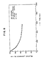
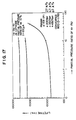
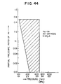
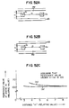
- a graphic representation as shown in Fig. 10 is obtained.
- This figure also includes measurement data for values of the current I of not only 60 ⁇ A, but also 100 ⁇ A, 150 ⁇ A, and 200 ⁇ A. It can be seen from the gradient of the curves shown in Fig. 10 that the lifetime of the panel is substantially proportional to between p 5 and p 6 , ("p" indicates total pressure of filling gas).
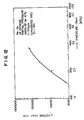
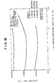
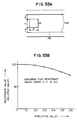
- Fig. 11 represents a lifetime-to-pressure characteristic of the display panel, as shown in Figs.
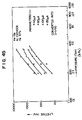
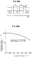
- Figs. 15 to 42 show further experimental data.
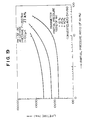
- the characteristics obtained under such conditions that the total pressure "p" of the filling gas is used as the parameter, and the total pressure "P" is selected to be 60 kPa (450 Torr), 40 kPa (300 Torr), and 27 kPa (200 Torr). It should be noted that the lifetimes of the display panel in Fig. 15 have been converted into the lifetimes under D 1/60.
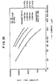
- the characteristics obtained under such conditions that the total pressure "p" of the filling gas is used as the parameter, and the total pressure "P" is selected to be 20 kPa (150 Torr), 27 kPa (200 Torr), and 40 kPa (300 Torr). It should be noted that the lifetimes of the display panel in Fig. 18 have been converted into the lifetimes under D 1/60.
- Fig. 25 there are shown characteristics obtained when the partial pressure ratio of the Xe gas is used as the parameter, and this partial pressure ratio is selected to be 4%, 10%, 20% and 40%.
- Fig. 26 there are shown characteristic obtained when the partial pressure ratio of the kr gas is used as the parameter, and this partial pressure is selected to be 0%, 1%, 4% 10% and 45%.
- Fig. 29 there are shown characteristics obtained when the partial pressure ratio of the Xe gas is used as the parameter, and this partial pressure is selected to be 20%, 10% and 4%.
- Fig. 30 there are shown characteristics obtained when the partial pressure ratio of the Xe gas is used as the parameter, and this partial pressure is selected to be 40%, 20%, 10% and 4%.
- the total pressure "p" of the filling gas is used as the parameter, and the total pressure "P" is selected to be 20, 27, 33, 40, 47 and 60 kPa (150, 200, 250, 300, 350 and 450 Torr).
- Fig. 33 there are shown characteristic obtained when the partial pressure ratio of the Xe gas is used as the parameter, and this partial pressure ratio is selected to be 40%, 20%, 10% and 4%.
- Fig. 34 there are shown characteristics obtained when the partial pressure ratio of the Xe gas is used as the parameter, and this partial pressure ratio is selected to be 10% and 4%.
- Fig. 38 there are shown characteristics obtained when the partial pressure ratio of the Xe gas is used as the parameter, and this partial pressure ratio is selected to be 20%, 10% and 4%.
- Fig. 40 there are shown characteristics obtained when the partial pressure ratio of the Xe gas is used as the parameter, and this partial pressure ratio is selected to be 4%, 10%, 20% and 40%.
- Fig. 40 represents how to change luminance of visible Ne light in response to variations in the Kr partial pressure when only the auxiliary discharge cell of the display panel is discharged.
- Fig. 41 there are shown characteristics obtained when the partial pressure ratio of the Kr gas is used as the parameter, and this partial pressure is selected to be 0%, 4%, 10% and 40%.
- Fig. 41 indicates how to change luminance of visible Ne light in response to the Kr-partial pressure ratio when only the auxiliary discharge cell of the above-described display panel is discharged.
- the visible Ne light is contained in the above-described measurements of the luminance and the light-emission efficiency when Ne gas is contained in the filling gas.
- T max ⁇ 80xk(1-3.3x), 1 ⁇ 2.7 ⁇ 10 -7 xp 5 (100/I) 3 [hour] where symbol "x” indicates a partial pressure ratio of Xe gas, symbol “k” denotes a partial pressure ratio of Kr gas, symbol “p” shows total pressure (133 Pa or 1 Torr), and symbol "I” is a current value ( ⁇ A).
- the value of the discharge current must be considered as a discharge current density. To this end, an active cathode area must be considered.
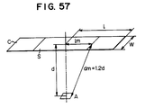
- the interval between the cathode and the anode of the display panel as shown in Figs. 6A and 6B is not constant, the places actually operating as the normal glow-discharge regions are generally different from each other, depending upon the pd-product. In this case, the interval is set to be 1.2 times the minimum distance "d".
- a relatively high sustain voltage e.g. 20 V
- the discharge occurring at the place of the minimum distance "d" is an abnormal glow discharge, and sputtering is rapidly increased. This may also be seen from Figs.
- the maximum pressure values of the display panel are preferably selected to be 80 kPa (600 Torr) in case of He-Xe and He-Xe-Kr filling gases, and 67 kPa (500 Torr) in case of Ne-Xe and Ne-Xe-Kr filling gases.
- the pd-product may be preferably selected to be 1 to 10 (1.3 Pa.m, 1 Torr. cm) when He-Xe and He-Xe-Kr filling gases are filled, and 0.5 to 10 (1.3 Pa.m, 1 Torr. cm) when Ne-Xe and Ne-Xe-Kr filling gases are filled. Also, taking account of the light-emission efficiency, it is preferable to set: 0.01 ⁇ x.
- a write voltage for a memory drive of a display panel must be higher than a sustain voltage by several tens of Volts, for example, 50 V, such a write voltage may cause a large current flow in this display panel, as apparent from Figs. 31 and 32, thus shortening the lifetime thereof. Therefore, a certain type of current limiting element must be connected in series with the display panel. Normally, since a resistor is employed, this resistor may be connected as shown in Figs. 4A and 4B.
- characteristics when the current I is used as the parameter and is selected to be 40 ⁇ A, 60 ⁇ A, 100 ⁇ A and 150 ⁇ A. Note that the lifetimes shown in Fig. 45 have been converted into those of D 1/60.
- the lifetime of a display panel having a Ni cathode is shorter than that having an Al cathode.
- mercury Hg
- Other cathode materials include BaAl 4 , LaB 6 , BaB 6 , Ba(N 3 ) 2 , an alkali metal, Y 2 O 3 , ZnO, RuO 2 , Cr, Co, graphite, Ca 0.2 La 0.8 BCrO 3 , Mg, BaLa 2 O 4 , BaAl 2 O 4 , and LaCrO 3 , and there are substantially similar effects.
- Adhesive methods usable for the above-described cathode materials include printing, plasma melt-injection, vapour deposition and sputtering methods etc.
- the red phosphor comprises: Y 2 O 3 : Eu, YVO 3 : Eu, YP 0.65 V 0.35 O 4 ,: Eu, YBO 3 : Eu, or (YGa)BO 3 : Eu.
- green phosphor the following may be employed Zn 2 SiO 4 : Mn, BaMg 2 Al 14 O 24 : Eu, Mn, or BaAl 12 O 19 : Mn.
- blue phosphor the following may be used: Y 2 SiO 4 : Ce, YP 0.85 V 0.15 O 4 ,: Eu, BaMg 2 Al 14 O 24 ,: Eu, or BaMgAl 14 ,O 23 : Eu.
- the adhesive methods used for the above-described phosphor materials include printing, photoetching, photo-tacking, and spray methods etc.
- the place to which the phosphor is adhered determines the display panel type; a reflection type display panel has phosphor adhered to the back plate or cell wall plate, whilst a transmission type display panel has phosphor adhered to the front plate.
- the positioning of the resistor depends upon the type of display panel. When the phosphor is attached to the front plate there are limitations as to where the resistor can be connected, thus there is greater design freedom in the reflection type display panel than in the transmission type display panel.
- a filter to achieve high contrast may be included in the panel as described more in detail in publication (3).
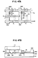
- the structures of the display panels may be realized as shown in publications (4) and (5). There are shown other structure examples in Figs. 46A and 46B., In Figs. 46A and 46B, the same reference numerals as used in Figs. 1A to 4B are employed as those to denote the same elements.
- This cell structure has a feature that a resistor "R" is connected to a front plate "FG", and the remaining structures are substantially identical to those of Figs. 4A and 4B.
- Figs. 47A and 47B there is shown another example in which a resistor is connected only to a write electrode. It should be noted that the same reference numerals are employed to denote the same elements as shown in Figs. 47A and 47B.
- a cathode is provided on the front plate, and a write anode bus line (WAB) extends vertically over a back plate which is connected via a resistor (R) to a write anode (WA).
- WAB write anode bus line
- WA write anode
- the display anode (DA) projects from a bus line (DAB) thereof toward a cell center unit.
- This bus line “DAB” is positioned either parallel to "C”, or parallel to the write anode bus line (WAB), and since a sustain discharge operation is carried out between the bus line (DAB) and "C". In this case, the display panel is driven only in the pulse memory mode.
- Display panels are classified based upon a combination of (1) whether the resistor is connected to the front plate, or the back plate; (2) whether the electrode to which the resistor is connected is an anode, a cathode, or a write electrode; and (3) whether or not an auxiliary discharge is present. These combinations may be conceived as the above-described two examples, or as other examples. If these display panels are combined with other display panels as shown in Figs. 48A to 51B (will be discussed later), display panels with conspicuous characteristics may be obtained.
- the display panels according to the present invention may be driven in either drive mode.
- the power consumption of a sustain pulse is small in structure in which the cathode is positioned parallel to a display anode bus line.
- Fig. 48A is a plan view for showing a portion of a DC type gas-discharge display panel according to another preferred embodiment of the present invention
- Fig. 48B is a sectional view of this display panel, taken along a line X 13 to X 14 shown in Fig. 48A.
- a resistive material "RM” is formed in a band shape in such a manner that under one pair of parallel anode bus lines "AB", the size of this resistive material is larger than the size of the anode bus line "AB”, and the band-shaped resistive material is positioned over a plurality of discharge cells "DCE” in common to the anode bus line "AB".
- An anode “A” is formed at substantially the center of two anode bus lines "AB”, and a resistor "R” is terminated by this anode together with the anode bus line "AB".
- Figs. 52A to 52C conditions on the distances between the adjoining anodes “A” positioned along a direction of the anode bus line "AB” will be described.
- Figs. 52A and 52B if the sizes of the anodes A1 and A2 are 2x2, the distance between the anodes A1 and A2, and the anode bus line "AB" is 1, and the distance between the adjoining anodes A1 and A2 is "m", resistance values of a resistor terminated by the anode A1 and the anode bus line "AB” are calculated if (a) the potential of the adjoining anode A2 is the same as that of the anode bus line "AB" (0V), and (b) the potential of the adjoining anode A2 is equal to that of the anode A1 (1V).
- the calculated resistance values are shown in Fig. 52C. As a consequence, if the distance "m", is greater than, or equal to 6, it can be seen that the influence of
- resistor "R” is not adversely influenced by fluctuations appearing in the shape or size of the resistive material "RM”. Also, this resistance value is not adversely influenced by the edges or end portions of the resistive material where the thickness of the resistive material RM fluctuates most. As a consequence, a lack of luminous uniformity, or luminous variation of each gas-discharge cell can be reduced without requiring high precision during production.
- Figs. 54A to 55B represent calculation results with respect to the adverse influences of the sizes of the anode "A" to the resistance values, variations parallel to the anode bus line "AB", and variation perpendicular thereto.
- precision along the parallel direction to the anode bus line AB should be below 2%
- precision along the direction perpendicular to the anode bus line should be below 1.3%.
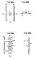
- the shape of the resistor employed in the discharge display panel according to the present invention is not limited to that shown in Figs. 48A and 48B, but may be such a shape that, for instance, the anode bus line AB is located under the resistive material RM as shown in Figs. 49A and 49B.
- the resistive material RM may be formed in such a manner that this resistive material "RM" extends outside of the anode bus line "AB".
- the resistive material "RM" may extend only to the outer edge or the central portion of the anode bus line "AB" thereon.
- a resistor "R” may be formed by being terminated by a comb-shaped branch anode bus line ABO branched from the anode bus line AB and an anode formed near the center thereof.
- a resistive material "RM” is printed in a band shape along a longitudinal direction thereof by way of the thick-film printing operation, this resistive material can be easily made uniform except for the starting and ending portions of the printing operation.
- Figs. 56A and 56B the positional precision with respect to the branch anode bus line ABO of the anode A will be explained in the preferred embodiment shown in Figs. 50A and 50B.
- Fig. 56A when a distance between the anode "A" and the branch anode bus line ABO is equal to 1, and also a positional shift is "g", variations in the resistance values of the resistor R caused by the positional shift "g" are represented in Fig. 56B.
- the positional shift is 0.1 (equivalent to 10%)
- the variations in the resistance values are below 1%.
- the anode bus line "AB” may be formed under the resistive material "RM”, which is similar to the previous embodiment of Figs. 49A and 49B.
- a branch anode bus line ABC may be formed in the shape of a ladder, and an anode "A" positioned adjacent to the bus line may be separate therefrom.
- the positionsal precision between the anode "A", anode bus line “AB” and branch anode bus line ABC is up to 10% in any direction, then the variations in the resistance values are below 1%.
- the distance between the adjoining anodes "A” may be shortened, as compared with that of the preferred embodiment shown in Figs. 48A and 48B.
- the anode bus line AB may be formed under the resistive material "RM".
- resistors are formed at the anode side of the discharge cells in all of the above-described preferred embodiments, these resistors may be, of course, formed at the cathode sides.
- the cathode may be formed on the electrode for terminating the resistor. This may be applied to the anode, and material such as Ni which has high resistance against mercury which is usually employed to prolong the lifetime of a gas-discharge display panel may be stacked.
- the above-described inventive idea may be applied not only to the gas-discharge display panel as shown in Figs. 48A and 48B, but also a display panel from which luminous color of a gas discharge such as a Ne gas is directly output from the display panel, and such a display panel without an auxiliary anode.
- the present invention is not limited to the display panel having such a structure as shown in Figs. 48A and 48B, but may be applied to display panels in which, for instance, the anode is arranged in an offset relationship with the cathode, namely the anode is not positioned directly opposite to the cathode.
- the thick-film printing method is employed to manufacture the resistive materials, the bus lines for terminating the resistive materials, and the electrodes, however these parts may be manufactured by various patterning methods, for example, vapour deposition/ photolithography, and chemical etching or lift off.
- the resistive material As the resistive material, the following may be used: RuO 2 , a Nichrome (TM) alloy, tin oxide, Ta 2 N, Cr-SiO, ITO, carbon and the like. It is presently preferred to employ a thick film paste made of RuO 2 .
- TM Nichrome
- the electrode material to terminate the resistive material there are employed Au, Pd, Ag, Al, Ni, Cu, or alloys thereof. Au was found to be best for thick-film 20 printing.
- the filling gas utilized in the present embodiment may be the filling gas as employed in the previously described embodiment.
- Al and Ni and the like may be readily utilized.
- Ni cathode is solely employed in a display panel, the lifetime of this display panel is shorter than one with an Al cathode.
- mercury "Hg" is included in the Ni cathode, the lifetime thereof may be prolonged approximately 100 times longer than the lifetime of the display panel with only the Ni cathode, which becomes longer than that of the display panel with the Al cathode.
- cathode materials, phosphor materials and filters described regarding the first described embodiment may be utilized in the present embodiment.
Landscapes
- Gas-Filled Discharge Tubes (AREA)
- Control Of Indicators Other Than Cathode Ray Tubes (AREA)
Claims (8)
- Gleichstrom-Plasmaanzeigetafel, mit:mehreren Entladungszellen (DCE);einer Entladungsstrom-Begrenzungseinrichtung (R), die für jede der Entladungszellen (DCE) vorgesehen ist, um den Entladungsstrom jeder der Entladungszellen (DCE) zu begrenzen; undeinem Füllgas, mit dem jede der Entladungszellen (DCE) gefüllt ist und das ein Inertgasgemisch enthält,wobei das Partialdruckverhältnis des Inertgasgemischs zum Gesamtdruck des Füllgases wenigstens 0,95 beträgt;wobei das Inertgasgemisch aus der Gruppe gewählt ist, die (1) aus einem ersten Gasgemisch, das aus einem He-Gas und einem Xe-Gas besteht, (2) aus einem zweiten Gasgemisch, das aus einem He-Gas, einem Xe-Gas und einem Kr-Gas besteht, (3) aus einem dritten Gasgemisch, das aus einem Ne-Gas und einem Xe-Gas besteht, sowie (4) aus einem vierten Gasgemisch besteht, das seinerseits aus einem Ne-Gas, einem Xe-Gas und einem Kr-Gas besteht;wobei unter den Annahmen, daß der Gesamtdruck des Füllgases "p" · 133,3 Pascal (Pa) (p Torr) ist, daß ein Partialdruckverhältnis des Xe-Gases zum Gesamtdruck des Füllgases "x" ist und daß außerdem ein Partialdruckverhältnis des Kr-Gases zum Gesamtdruck des Füllgases "k" ist;dann, wenn das Inertgasgemisch das erste Gasgemisch ist, gilt: 0,01 ≤ x ≤ 0,5, p ≤ 600 und xp5 ≥ 1,4 · 1011;dann, wenn das Inertgasgemisch das zweite Gasgemisch ist, gilt: 0,01 ≤ x ≤ 0,5, 0 < k ≤ 0,5 und p ≤ 600 und {1 + 700xk2/(p/200)4} xp5 ≥ 1,4 · 1011;dann, wenn das Inertgasmisch das dritte Gasgemisch ist, gilt: 0,01 ≤ x ≤ 0,5, p ≤ 500 und xp5 ≥ 8,0 · 109; und außerdemdann, wenn das Inertgasgemisch das vierte Gasgemisch ist, gilt: 0,01 ≤ x ≤ 0,5, 0 < k ≤ 0,5, p ≤ 500 und max{80xk(1 - 3,3x), 1}xp5 ≥ 8,0 · 109.
- Anzeigetafel nach Anspruch 1, bei der die Entladungsstrom-Begrenzungseinrichtung ein Widerstand (R) ist.
- Anzeigetafel nach Anspruch 2, bei der die mehreren Entladungszellen (DCE) in einer Zeilenrichtung und in einer Spaltenrichtung in Matrixform angeordnet sind;die Gleichstrom-Plasmaanzeigetafel ferner enthält:mehrere erste stromführende Leitungen (C), die in Zeilenrichtung verlaufen und an die eines von gewünschten Entladungssteuerpotentialen angelegt wird, wobei jede der ersten stromführenden Leitungen (C) gemeinsam in jeder der Entladungszellen (DCE) der entsprechenden Zeilen angeordnet ist, um eine erste Entladungselektrode (C) zu bilden;mehrere zweite stromführende Leitungen (AB), die in Spaltenrichtung verlaufen und an die das andere der erwünschten Entladungssteuerpotentiale angelegt wird, wobei zwei benachbarte Leitungen der zweiten stromführenden Leitungen (AB) gemeinsam mit den entsprechenden Entladungszellen (DCE) angeordnet sind;mehrere zweite Entladungselektroden (A), die an einer im wesentlichen mittigen Position zwischen zwei benachbarten Leitungen der zweiten stromführenden Leitungen (AB) vorgesehen sind, die jeder dieser Entladungszellen (DCE) entspricht, um zwischen den ersten Entladungselektroden (C), die diesen Entladungszellen (DCE) entsprechen, eine Entladung zu erzeugen; undmehrere Widerstandsmaterialien (RM), die in Spaltenrichtung verlaufen, wovon jedes in der Weise angeordnet ist, daß die Entladungszellen (DCE) an der Spalte durch jedes der Widerstandsmaterialien (RM) überbrückt werden, und daß es mit den beiden benachbarten Leitungen der zweiten stromführenden Leitungen (AB) und der zweiten Elektrode (A), die den Entladungszellen (DCE) jeder Spalte entsprechen, in Kontakt ist; undwobei jeder der Widerstände (R) dadurch gebildet ist, daß er durch zwei benachbarte Leitungen der zweiten stromführenden Leitungen (AB) und der zweiten Elektroden (A), die den jeweiligen Entladungszellen (DCE) entsprechen, abgeschlossen ist.
- Anzeigetafel nach Anspruch 3, bei der die erste Entladungselektrode eine Katode (C) ist und die zweite Entladungselektrode eine Anode (A) ist.
- Anzeigetafel nach Anspruch 3, bei der die erste Entladungselektrode eine Anode ist und die zweite Entladungselektrode eine Katode ist.
- Anzeigetafel nach Anspruch 3, wobei die Gleichstrom-Plasmaanzeigetafel ferner enthält:mehrere Paare von abgezweigten stromführenden Leitungen (ABC), die die zwei benachbarten Leitungen der zweiten stromführenden Leitungen (AB) überbrücken, wobei jedes Paar von abgezweigten stromführenden Leitungen (ABC) beiderseits der jeweiligen zweiten Entladungselektroden (A) in Spaltenrichtung relativ zu den Entladungszellen (DCE) angeordnet ist;wobei jedes der Widerstandsmaterialien (RM) außerdem mit jeder der abgezweigten stromführenden Leitungen (ABC), die den Entladungszellen (DCE) an den entsprechenden Spalten entsprechen, in Kontakt ist; undwobei jeder der Widerstände (R) außerdem durch die beiden abgezweigten stromführenden Leitungen (ABC) abgeschlossen sind, die den jeweiligen Entladungszellen (DCE) entsprechen.
- Anzeigetafel nach Anspruch 2, bei der die mehreren Entladungszellen (DCE) in einer Zeilenrichtung und in einer Spaltenrichtung in Matrixform angeordnet sind;wobei die Gleichstrom-Plasmaanzeigetafel ferner enthält:mehrere erste stromführende Leitungen (C), die in Zeilenrichtung angeordnet sind und an die eines von gewünschten Entladungssteuerpotentialen angelegt wird, wobei jede der ersten stromführenden Leitungen (C) gemeinsam in jeder der Entladungszellen (DCE) in den jeweiligen Zeilen angeordnet ist, um eine erste Entladungselektrode (C) zu bilden;mehrere zweite stromführende Leitungen (AB), die in Spaltenrichtung angeordnet sind und an die das andere der gewünschten Entladungssteuerpotentiale angelegt wird, wobei jede der zweiten stromführenden Leitungen (AB) gemeinsam mit den jeweiligen Entladungszellen (DCE), die an den jeweiligen Spalten positioniert sind, angeordnet ist;mehrere Paare von abgezweigten stromführenden Leitungen (ABO), die von jeder der zweiten stromführenden Leitungen (AB) in Zeilenrichtung kammförmig abgezweigt sind, wobei jede der beiden abgezweigten stromführenden Leitungen (AB) an einer Position angeordnet ist, die jeder der Entladungszellen (DCE) entspricht;mehrere zweite Entladungselektroden (A), die an einer im wesentlichen mittigen Position zwischen den Paaren von abgezweigten stromführenden Leitungen (ABO) vorgesehen sind, um zwischen den ersten Entladungselektroden (C), die den Entladungszellen (DCE) entsprechen, eine Entladung zu erzeugen;mehrere Widerstandsmaterialien (RM), die in Spaltenrichtung angeordnet sind, wobei jedes der Widerstandsmaterialien (RM) in der Weise angeordnet ist, daß die Entladungszellen (DCE) an dieser Spalte durch jedes der Widerstandsmaterialien (RM) überbrückt sind, und es mit jeder der beiden abgezweigten stromführenden Leitungen (AB0) und der zweiten Elektrode (A), die den Entladungszellen (DCE) an jeder Spalte entspricht, in Kontakt ist; undwobei jeder der Widerstände (R) durch Abschließen der beiden abgezweigten stromführenden Leitungen (ABO) und der zweiten Elektroden (A), die den jeweiligen Entladungszellen (DCE) entsprechen, gebildet ist.
- Plasmaanzeigevorrichtung, mit einer Gleichstrom-Plasmaanzeigetafel nach irgendeinem der vorangehenden Ansprüche und einer Treibervorrichtung zum Ansteuern der Gleichstrom-Plasmaanzeigetafel in einem Speichertreiberschema;wobei unter den Annahmen, daß eine aktive Katodenfläche jeder der Entladungszellen S mm2 beträgt und außerdem ein Dauerentladungsstrom, der auf der Ansteuerung der Treibereinrichtung basiert, I µA beträgt;dann, wenn das Inertgasgemisch dem ersten Gasgemisch entspricht, die Bedingung xp5(S/I)2 ≥ 6,3 · 104 erfüllt ist;dann, wenn das Inertgasgemisch dem zweiten Gasgemisch entspricht, die Bedingung {1+ 700xk2/(p/200)4}. xp5 · (S/I)2 ≥ 6,3 · 104 erfüllt ist;dann, wenn das Inertgasgemisch dem dritten Gasgemisch entspricht, die Bedingung xp5 · (S/I)3 > 2,4 erfüllt ist; und außerdemdann, wenn das Inertgasgemisch das vierte Gasgemisch ist, die Bedingung max{80xk(1 - 3,3x), 1} · xp5 · (S/I)3 ≥ 2,4 erfüllt ist.
Priority Applications (1)
| Application Number | Priority Date | Filing Date | Title |
|---|---|---|---|
| EP94120109A EP0649159B1 (de) | 1991-07-18 | 1992-07-16 | Gleichstromgasentladungsanzeigetafel |
Applications Claiming Priority (6)
| Application Number | Priority Date | Filing Date | Title |
|---|---|---|---|
| JP202135/91 | 1991-07-18 | ||
| JP20213591A JP3126756B2 (ja) | 1991-07-18 | 1991-07-18 | 直流型放電パネルと表示装置 |
| JP301832/91 | 1991-11-18 | ||
| JP30183291A JP3096113B2 (ja) | 1991-11-18 | 1991-11-18 | 気体放電表示パネル |
| JP306247/91 | 1991-11-21 | ||
| JP30624791A JP3190714B2 (ja) | 1991-11-21 | 1991-11-21 | 直流型放電パネルとそれをパルスメモリ駆動する表示装置 |
Related Child Applications (2)
| Application Number | Title | Priority Date | Filing Date |
|---|---|---|---|
| EP94120109.7 Division-Into | 1992-07-16 | ||
| EP94120109A Division EP0649159B1 (de) | 1991-07-18 | 1992-07-16 | Gleichstromgasentladungsanzeigetafel |
Publications (3)
| Publication Number | Publication Date |
|---|---|
| EP0524005A2 EP0524005A2 (de) | 1993-01-20 |
| EP0524005A3 EP0524005A3 (de) | 1993-02-24 |
| EP0524005B1 true EP0524005B1 (de) | 1996-09-25 |
Family
ID=27328046
Family Applications (2)
| Application Number | Title | Priority Date | Filing Date |
|---|---|---|---|
| EP94120109A Expired - Lifetime EP0649159B1 (de) | 1991-07-18 | 1992-07-16 | Gleichstromgasentladungsanzeigetafel |
| EP92306554A Expired - Lifetime EP0524005B1 (de) | 1991-07-18 | 1992-07-16 | Gleichfeld-Gasentladungsanzeigeeinrichtung und diese verwendende Gasentladungsanzeigevorrichtung |
Family Applications Before (1)
| Application Number | Title | Priority Date | Filing Date |
|---|---|---|---|
| EP94120109A Expired - Lifetime EP0649159B1 (de) | 1991-07-18 | 1992-07-16 | Gleichstromgasentladungsanzeigetafel |
Country Status (3)
| Country | Link |
|---|---|
| US (2) | US5510678A (de) |
| EP (2) | EP0649159B1 (de) |
| DE (2) | DE69214040T2 (de) |
Families Citing this family (23)
| Publication number | Priority date | Publication date | Assignee | Title |
|---|---|---|---|---|
| CA2127850C (en) * | 1993-07-19 | 1999-03-16 | Takio Okamoto | Luminescent panel for color video display and its driving system, and a color video display apparatus utilizing the same |
| JP3339554B2 (ja) * | 1995-12-15 | 2002-10-28 | 松下電器産業株式会社 | プラズマディスプレイパネル及びその製造方法 |
| US5877589A (en) * | 1997-03-18 | 1999-03-02 | International Business Machines Corporation | Gas discharge devices including matrix materials with ionizable gas filled sealed cavities |
| JPH1125863A (ja) * | 1997-06-30 | 1999-01-29 | Fujitsu Ltd | プラズマディスプレイパネル |
| US6329749B1 (en) | 1998-02-16 | 2001-12-11 | Sony Corporation | Planar type plasma discharge display device |
| US6255777B1 (en) | 1998-07-01 | 2001-07-03 | Plasmion Corporation | Capillary electrode discharge plasma display panel device and method of fabricating the same |
| JP2002033058A (ja) * | 2000-07-14 | 2002-01-31 | Sony Corp | 電界放出型表示装置用の前面板 |
| US6822626B2 (en) * | 2000-10-27 | 2004-11-23 | Science Applications International Corporation | Design, fabrication, testing, and conditioning of micro-components for use in a light-emitting panel |
| US6545422B1 (en) | 2000-10-27 | 2003-04-08 | Science Applications International Corporation | Socket for use with a micro-component in a light-emitting panel |
| US6620012B1 (en) | 2000-10-27 | 2003-09-16 | Science Applications International Corporation | Method for testing a light-emitting panel and the components therein |
| US6801001B2 (en) * | 2000-10-27 | 2004-10-05 | Science Applications International Corporation | Method and apparatus for addressing micro-components in a plasma display panel |
| US6764367B2 (en) * | 2000-10-27 | 2004-07-20 | Science Applications International Corporation | Liquid manufacturing processes for panel layer fabrication |
| US6935913B2 (en) * | 2000-10-27 | 2005-08-30 | Science Applications International Corporation | Method for on-line testing of a light emitting panel |
| US6796867B2 (en) * | 2000-10-27 | 2004-09-28 | Science Applications International Corporation | Use of printing and other technology for micro-component placement |
| JP2002132208A (ja) * | 2000-10-27 | 2002-05-09 | Fujitsu Ltd | プラズマディスプレイパネルの駆動方法および駆動回路 |
| US6570335B1 (en) | 2000-10-27 | 2003-05-27 | Science Applications International Corporation | Method and system for energizing a micro-component in a light-emitting panel |
| US7288014B1 (en) | 2000-10-27 | 2007-10-30 | Science Applications International Corporation | Design, fabrication, testing, and conditioning of micro-components for use in a light-emitting panel |
| US6762566B1 (en) | 2000-10-27 | 2004-07-13 | Science Applications International Corporation | Micro-component for use in a light-emitting panel |
| US6612889B1 (en) | 2000-10-27 | 2003-09-02 | Science Applications International Corporation | Method for making a light-emitting panel |
| JP3704068B2 (ja) * | 2001-07-27 | 2005-10-05 | ザ ウエステイム コーポレイション | Elパネル |
| US20050189164A1 (en) * | 2004-02-26 | 2005-09-01 | Chang Chi L. | Speaker enclosure having outer flared tube |
| EP1569254A1 (de) | 2004-02-27 | 2005-08-31 | ABB Technology AG | Schaltgerät mit Trenn-und/oder Erdungsfunktion |
| US9024526B1 (en) | 2012-06-11 | 2015-05-05 | Imaging Systems Technology, Inc. | Detector element with antenna |
Family Cites Families (6)
| Publication number | Priority date | Publication date | Assignee | Title |
|---|---|---|---|---|
| JPS52143987A (en) * | 1976-05-26 | 1977-11-30 | Dainippon Toryo Co Ltd | Gas discharge luminous eleme nt |
| JPS5830038A (ja) * | 1981-08-17 | 1983-02-22 | Sony Corp | 放電表示装置 |
| FR2559602B1 (fr) * | 1984-02-10 | 1991-02-15 | Japan Broadcasting Corp | Panneau d'affichage a decharge de gaz muni d'au moins une enveloppe scellee |
| US4703229A (en) * | 1985-10-10 | 1987-10-27 | United Technologies Corporation | Optical display from XeF excimer fluorescence |
| JPS63205031A (ja) * | 1987-02-19 | 1988-08-24 | Fujitsu Ltd | ガス放電パネル |
| JP2820491B2 (ja) * | 1990-03-30 | 1998-11-05 | 松下電子工業株式会社 | 気体放電型表示装置 |
-
1992
- 1992-07-16 EP EP94120109A patent/EP0649159B1/de not_active Expired - Lifetime
- 1992-07-16 DE DE69214040T patent/DE69214040T2/de not_active Expired - Fee Related
- 1992-07-16 EP EP92306554A patent/EP0524005B1/de not_active Expired - Lifetime
- 1992-07-16 DE DE69228709T patent/DE69228709T2/de not_active Expired - Fee Related
-
1995
- 1995-01-27 US US08/379,969 patent/US5510678A/en not_active Expired - Lifetime
- 1995-04-06 US US08/418,155 patent/US5559403A/en not_active Expired - Fee Related
Also Published As
| Publication number | Publication date |
|---|---|
| DE69214040D1 (de) | 1996-10-31 |
| EP0649159A1 (de) | 1995-04-19 |
| DE69228709T2 (de) | 1999-07-29 |
| EP0649159B1 (de) | 1999-03-17 |
| EP0524005A2 (de) | 1993-01-20 |
| US5510678A (en) | 1996-04-23 |
| EP0524005A3 (de) | 1993-02-24 |
| DE69228709D1 (de) | 1999-04-22 |
| DE69214040T2 (de) | 1997-03-06 |
| US5559403A (en) | 1996-09-24 |
Similar Documents
| Publication | Publication Date | Title |
|---|---|---|
| EP0524005B1 (de) | Gleichfeld-Gasentladungsanzeigeeinrichtung und diese verwendende Gasentladungsanzeigevorrichtung | |
| US20050179383A1 (en) | Plasma display device having barrier ribs | |
| JP3384390B2 (ja) | 交流駆動型プラズマ表示装置 | |
| US4780644A (en) | Gas discharge display panel | |
| JPS63205031A (ja) | ガス放電パネル | |
| JP3169628B2 (ja) | プラズマディスプレイパネル | |
| US20050041001A1 (en) | Plasma display panel and manufacturing method | |
| JP3126756B2 (ja) | 直流型放電パネルと表示装置 | |
| US20020180355A1 (en) | Plasma display device | |
| US6737805B2 (en) | Plasma display device and method of producing the same | |
| JP3096113B2 (ja) | 気体放電表示パネル | |
| EP1093148A1 (de) | Plasma-Anzeigevorrichtung | |
| JP3190714B2 (ja) | 直流型放電パネルとそれをパルスメモリ駆動する表示装置 | |
| JPH02223133A (ja) | 直流型放電表示装置 | |
| JP3481988B2 (ja) | 気体放電表示パネル | |
| JP4281155B2 (ja) | 表示パネル及び表示装置 | |
| JP3460596B2 (ja) | プラズマディスプレイパネル | |
| US20040038615A1 (en) | Production method for plasma display panel unit-use panel and production method for plasma display unit | |
| US20080258603A1 (en) | Color display device | |
| JP2623405B2 (ja) | カラープラズマディスプレイパネル | |
| JPH0721928A (ja) | 気体放電型表示装置 | |
| JPH09120779A (ja) | ガス放電型表示パネル | |
| JP4742872B2 (ja) | プラズマディスプレイパネル | |
| JP4299922B2 (ja) | 放電式表示パネル及び表示装置 | |
| JPH06325697A (ja) | カラー・プラズマディスプレイパネル |
Legal Events
| Date | Code | Title | Description |
|---|---|---|---|
| PUAI | Public reference made under article 153(3) epc to a published international application that has entered the european phase |
Free format text: ORIGINAL CODE: 0009012 |
|
| PUAL | Search report despatched |
Free format text: ORIGINAL CODE: 0009013 |
|
| AK | Designated contracting states |
Kind code of ref document: A2 Designated state(s): DE FR GB |
|
| AK | Designated contracting states |
Kind code of ref document: A3 Designated state(s): DE FR GB |
|
| 17P | Request for examination filed |
Effective date: 19930414 |
|
| 17Q | First examination report despatched |
Effective date: 19940811 |
|
| GRAH | Despatch of communication of intention to grant a patent |
Free format text: ORIGINAL CODE: EPIDOS IGRA |
|
| GRAH | Despatch of communication of intention to grant a patent |
Free format text: ORIGINAL CODE: EPIDOS IGRA |
|
| GRAA | (expected) grant |
Free format text: ORIGINAL CODE: 0009210 |
|
| AK | Designated contracting states |
Kind code of ref document: B1 Designated state(s): DE FR GB |
|
| DX | Miscellaneous (deleted) | ||
| ET | Fr: translation filed | ||
| REF | Corresponds to: |
Ref document number: 69214040 Country of ref document: DE Date of ref document: 19961031 |
|
| PLBE | No opposition filed within time limit |
Free format text: ORIGINAL CODE: 0009261 |
|
| STAA | Information on the status of an ep patent application or granted ep patent |
Free format text: STATUS: NO OPPOSITION FILED WITHIN TIME LIMIT |
|
| 26N | No opposition filed | ||
| REG | Reference to a national code |
Ref country code: GB Ref legal event code: IF02 |
|
| PGFP | Annual fee paid to national office [announced via postgrant information from national office to epo] |
Ref country code: FR Payment date: 20030711 Year of fee payment: 12 |
|
| PGFP | Annual fee paid to national office [announced via postgrant information from national office to epo] |
Ref country code: GB Payment date: 20030716 Year of fee payment: 12 |
|
| PGFP | Annual fee paid to national office [announced via postgrant information from national office to epo] |
Ref country code: DE Payment date: 20030724 Year of fee payment: 12 |
|
| PG25 | Lapsed in a contracting state [announced via postgrant information from national office to epo] |
Ref country code: GB Free format text: LAPSE BECAUSE OF NON-PAYMENT OF DUE FEES Effective date: 20040716 |
|
| PG25 | Lapsed in a contracting state [announced via postgrant information from national office to epo] |
Ref country code: DE Free format text: LAPSE BECAUSE OF NON-PAYMENT OF DUE FEES Effective date: 20050201 |
|
| GBPC | Gb: european patent ceased through non-payment of renewal fee |
Effective date: 20040716 |
|
| PG25 | Lapsed in a contracting state [announced via postgrant information from national office to epo] |
Ref country code: FR Free format text: LAPSE BECAUSE OF NON-PAYMENT OF DUE FEES Effective date: 20050331 |
|
| REG | Reference to a national code |
Ref country code: FR Ref legal event code: ST |