EP0557415B1 - Process for achieving controlled precipitation profiles in silicon wafers - Google Patents
Process for achieving controlled precipitation profiles in silicon wafers Download PDFInfo
- Publication number
- EP0557415B1 EP0557415B1 EP92900331A EP92900331A EP0557415B1 EP 0557415 B1 EP0557415 B1 EP 0557415B1 EP 92900331 A EP92900331 A EP 92900331A EP 92900331 A EP92900331 A EP 92900331A EP 0557415 B1 EP0557415 B1 EP 0557415B1
- Authority
- EP
- European Patent Office
- Prior art keywords
- wafers
- treatment
- silicon wafers
- thermal
- silicon
- Prior art date
- Legal status (The legal status is an assumption and is not a legal conclusion. Google has not performed a legal analysis and makes no representation as to the accuracy of the status listed.)
- Expired - Lifetime
Links
- XUIMIQQOPSSXEZ-UHFFFAOYSA-N Silicon Chemical compound [Si] XUIMIQQOPSSXEZ-UHFFFAOYSA-N 0.000 title claims abstract description 26
- 229910052710 silicon Inorganic materials 0.000 title claims abstract description 26
- 239000010703 silicon Substances 0.000 title claims abstract description 26
- 235000012431 wafers Nutrition 0.000 title claims description 62
- 238000000034 method Methods 0.000 title claims description 21
- 238000001556 precipitation Methods 0.000 title description 8
- QVGXLLKOCUKJST-UHFFFAOYSA-N atomic oxygen Chemical compound [O] QVGXLLKOCUKJST-UHFFFAOYSA-N 0.000 claims abstract description 24
- 239000001301 oxygen Substances 0.000 claims abstract description 24
- 229910052760 oxygen Inorganic materials 0.000 claims abstract description 24
- 239000002244 precipitate Substances 0.000 claims abstract description 16
- 230000006911 nucleation Effects 0.000 claims abstract description 9
- 238000010899 nucleation Methods 0.000 claims abstract description 9
- 230000007547 defect Effects 0.000 claims description 20
- 238000007669 thermal treatment Methods 0.000 claims description 9
- 238000010168 coupling process Methods 0.000 claims description 5
- IJGRMHOSHXDMSA-UHFFFAOYSA-N Atomic nitrogen Chemical compound N#N IJGRMHOSHXDMSA-UHFFFAOYSA-N 0.000 claims description 4
- 238000004151 rapid thermal annealing Methods 0.000 claims description 4
- 239000010453 quartz Substances 0.000 claims description 3
- VYPSYNLAJGMNEJ-UHFFFAOYSA-N silicon dioxide Inorganic materials O=[Si]=O VYPSYNLAJGMNEJ-UHFFFAOYSA-N 0.000 claims description 3
- 238000003486 chemical etching Methods 0.000 claims description 2
- 238000010438 heat treatment Methods 0.000 claims description 2
- 229910052757 nitrogen Inorganic materials 0.000 claims description 2
- 238000005498 polishing Methods 0.000 claims description 2
- 230000003247 decreasing effect Effects 0.000 abstract 1
- 238000009828 non-uniform distribution Methods 0.000 abstract 1
- 238000004519 manufacturing process Methods 0.000 description 10
- 239000002243 precursor Substances 0.000 description 8
- 238000000137 annealing Methods 0.000 description 5
- 230000015572 biosynthetic process Effects 0.000 description 4
- 238000001816 cooling Methods 0.000 description 4
- 230000008878 coupling Effects 0.000 description 4
- 238000005859 coupling reaction Methods 0.000 description 4
- 230000000694 effects Effects 0.000 description 4
- 239000013078 crystal Substances 0.000 description 3
- 239000012535 impurity Substances 0.000 description 3
- 239000004065 semiconductor Substances 0.000 description 3
- 239000003795 chemical substances by application Substances 0.000 description 2
- 238000011109 contamination Methods 0.000 description 2
- 238000004090 dissolution Methods 0.000 description 2
- 238000009826 distribution Methods 0.000 description 2
- 238000005516 engineering process Methods 0.000 description 2
- 238000005247 gettering Methods 0.000 description 2
- 230000009931 harmful effect Effects 0.000 description 2
- 239000002184 metal Substances 0.000 description 2
- 239000007787 solid Substances 0.000 description 2
- 238000002231 Czochralski process Methods 0.000 description 1
- 230000007423 decrease Effects 0.000 description 1
- 238000000605 extraction Methods 0.000 description 1
- 239000000463 material Substances 0.000 description 1
- 229910021421 monocrystalline silicon Inorganic materials 0.000 description 1
- 238000005204 segregation Methods 0.000 description 1
- 230000006641 stabilisation Effects 0.000 description 1
- 238000011105 stabilization Methods 0.000 description 1
- 239000007858 starting material Substances 0.000 description 1
- 239000000758 substrate Substances 0.000 description 1
- 230000003407 synthetizing effect Effects 0.000 description 1
Images
Classifications
-
- H—ELECTRICITY
- H01—ELECTRIC ELEMENTS
- H01L—SEMICONDUCTOR DEVICES NOT COVERED BY CLASS H10
- H01L21/00—Processes or apparatus adapted for the manufacture or treatment of semiconductor or solid state devices or of parts thereof
- H01L21/02—Manufacture or treatment of semiconductor devices or of parts thereof
- H01L21/04—Manufacture or treatment of semiconductor devices or of parts thereof the devices having potential barriers, e.g. a PN junction, depletion layer or carrier concentration layer
- H01L21/18—Manufacture or treatment of semiconductor devices or of parts thereof the devices having potential barriers, e.g. a PN junction, depletion layer or carrier concentration layer the devices having semiconductor bodies comprising elements of Group IV of the Periodic Table or AIIIBV compounds with or without impurities, e.g. doping materials
- H01L21/30—Treatment of semiconductor bodies using processes or apparatus not provided for in groups H01L21/20 - H01L21/26
- H01L21/322—Treatment of semiconductor bodies using processes or apparatus not provided for in groups H01L21/20 - H01L21/26 to modify their internal properties, e.g. to produce internal imperfections
- H01L21/3221—Treatment of semiconductor bodies using processes or apparatus not provided for in groups H01L21/20 - H01L21/26 to modify their internal properties, e.g. to produce internal imperfections of silicon bodies, e.g. for gettering
- H01L21/3225—Thermally inducing defects using oxygen present in the silicon body for intrinsic gettering
Definitions
- the present invention generally relates to the processes for the fabrication of semiconductor material substrates, especially the so-called silicon "slices" or wafers, for the manufacture of electronic components. More particularly, the present invention relates to a process for the treatment of silicon wafers under conditions suitable for the control of the concentration and of the distribution profile of the "gettering" or internal trapping sites.
- single crystal silicon which is the starting material for most processes for the fabrication of semiconductor electronic components, is commonly prepared with the so-called Czochralski process wherein a single seed crystal is immersed into molten silicon and then grown by slow extraction.
- molten silicon is contained in a quartz crucible, it is contaminated with various impurities, among which mainly oxygen.
- oxygen comes into the crystal lattice until it reaches a concentration determined by the solubility of oxygen in silicon at the temperature of the molten mass and by the actual segregation coefficient of oxygen in solidified silicon.
- concentrations are greater than the solubility of oxygen in solid silicon at the temperatures typical for the processes for the fabrication of integrated circuits.
- the precipitation of oxygen can cause useful effects and harmful effects.
- the useful effects are connected with the capability of oxygen precipitates (and of the "defects" connected thereto) to trap the undesired metal impurities that could subsequently come into contact with the wafer during the subsequent manufacture for the fabrication of the electronic component and compromise the performance of the latter.
- the harmful effects derive from the fact that such precipitates themselves will be contamination agents if they are situated in the active region of the wafer, where, on the contrary, a very high purity for the fabrication e.g. of an integrated circuit is necessary.
- the object of the present invention is to indicate a process for controlling the concentration of the trapping centres present in silicon wafers and, more particularly, for realizing the defect density profile necessary to achieve a good denuded zone and a good intrinsic trapping effect.
- a first aspect of the invention relates to the control of the level of precipitation of oxygen in silicon wafers.
- a second aspect relates to the control of the density profiled of oxygen precipitates, in such a manner that the peak of the profile can act as a trapping region distinct and far from the active region of the device.
- a third aspect relates, therefore, to the fabrication of controlled precipitation wafers having an effective denuded zone in correspondence with the active region of the device and a highly effective trapping zone in the remaining volume.
- the treatment according to the invention initially produces high temperature nucleation centres, named the “precursors” during the thermal fast annealing operation and these precursors subsequently give rise to the classic "defects".
- this thermal rapid annealing treatment at a high temperature involves the formation of the so-called defects which act as precursors for the subsequent nucleation and growing of the precipitates of oxygen.
- a further observation at the basis of the present invention is that a thermal treatement at temperatures of 900 to 1000 °C of the wafers already subjected to a rapid thermal annealing does not favour a further nucleation, and on the contrary it involves a dissolution of a certain fraction of the aforementioned precursors generated at a high temperature. Indeed, it has been proved that such precursors present a certain instability when they are cooled at temperatures lower than those whereat they have been generated. As a compensation, this treatment at 900 to 1000 °C involves a growing of eventual already existing precipitation nuclei and a general stabilization of the defects created by the rapid thermal annealing treatment.
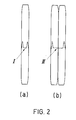
- the wafers In a second operation the wafers, after having undergone a standard chemical etching treatment, are subjected two by two in a close reciprocal contact to a rapid thermal annealing treatment in which they receive a thermal pulse of the duration of some tens of seconds, at a temperature comprised within the approximative interval between 1200 °C and 1275 °C.
- a rapid thermal annealing treatment in which they receive a thermal pulse of the duration of some tens of seconds, at a temperature comprised within the approximative interval between 1200 °C and 1275 °C.
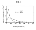
- a further thermal treatement follows subdivided into two stages (a first stage at 900 °C and a second stage at 1000 °C, for time intervals of 4 hours and of 16 hours respectively).
- the aim of this operation is to stabilize and to grow the precipitation precursors that have been generated in the preceding operation, eliminating at the same time their unstable fraction.
- the wafers are removed from the furnace and the surfaces that were in a close reciprocal contact during the high temperature thermal rapid annealing treatment are polished in a standard way.
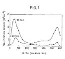
- the peak-plateau profile created in the two preceding operations ensures that there is a very low defect density (plateau) in proximity to the polished surface, so realizing a denuded zone perfectly suitable for the fabrication of integrated circuits, and a high and well controlled defect density in proximity to the rear surface of the wafer, far from the active region, perfectly suitable for the desired function of trapping the contamination agents.
Landscapes
- Engineering & Computer Science (AREA)
- Microelectronics & Electronic Packaging (AREA)
- Condensed Matter Physics & Semiconductors (AREA)
- General Physics & Mathematics (AREA)
- Manufacturing & Machinery (AREA)
- Computer Hardware Design (AREA)
- Physics & Mathematics (AREA)
- Power Engineering (AREA)
- Crystals, And After-Treatments Of Crystals (AREA)
- Formation Of Insulating Films (AREA)
- Silicon Compounds (AREA)
- Surgical Instruments (AREA)
- Safety Valves (AREA)
- Vessels, Lead-In Wires, Accessory Apparatuses For Cathode-Ray Tubes (AREA)
- Insulated Gate Type Field-Effect Transistor (AREA)
Applications Claiming Priority (3)
| Application Number | Priority Date | Filing Date | Title |
|---|---|---|---|
| IT48481A IT1242014B (it) | 1990-11-15 | 1990-11-15 | Procedimento per il trattamento di fette di silicio per ottenere in esse profili di precipitazione controllati per la produzione di componenti elettronici. |
| IT4848190 | 1990-11-15 | ||
| PCT/IT1991/000095 WO1992009101A1 (en) | 1990-11-15 | 1991-11-11 | Process for achieving controlled precipitation profiles in silicon wafers |
Publications (2)
| Publication Number | Publication Date |
|---|---|
| EP0557415A1 EP0557415A1 (en) | 1993-09-01 |
| EP0557415B1 true EP0557415B1 (en) | 1999-01-20 |
Family
ID=11266818
Family Applications (1)
| Application Number | Title | Priority Date | Filing Date |
|---|---|---|---|
| EP92900331A Expired - Lifetime EP0557415B1 (en) | 1990-11-15 | 1991-11-11 | Process for achieving controlled precipitation profiles in silicon wafers |
Country Status (17)
| Country | Link |
|---|---|
| US (1) | US5403406A (ja) |
| EP (1) | EP0557415B1 (ja) |
| JP (2) | JP3412636B2 (ja) |
| KR (1) | KR100247464B1 (ja) |
| AT (1) | ATE176084T1 (ja) |
| AU (1) | AU9033591A (ja) |
| CZ (1) | CZ84993A3 (ja) |
| DE (1) | DE69130802T2 (ja) |
| FI (1) | FI932024A (ja) |
| IL (1) | IL99979A (ja) |
| IT (1) | IT1242014B (ja) |
| MY (1) | MY110258A (ja) |
| SG (1) | SG64901A1 (ja) |
| SK (1) | SK47093A3 (ja) |
| TW (1) | TW205110B (ja) |
| WO (1) | WO1992009101A1 (ja) |
| ZA (1) | ZA918831B (ja) |
Families Citing this family (48)
| Publication number | Priority date | Publication date | Assignee | Title |
|---|---|---|---|---|
| JPH0574782A (ja) * | 1991-09-10 | 1993-03-26 | Mitsubishi Materials Corp | シリコン基板の製造方法 |
| JPH0684925A (ja) * | 1992-07-17 | 1994-03-25 | Toshiba Corp | 半導体基板およびその処理方法 |
| JP2874834B2 (ja) * | 1994-07-29 | 1999-03-24 | 三菱マテリアル株式会社 | シリコンウェーハのイントリンシックゲッタリング処理法 |
| US5788763A (en) * | 1995-03-09 | 1998-08-04 | Toshiba Ceramics Co., Ltd. | Manufacturing method of a silicon wafer having a controlled BMD concentration |
| US5593494A (en) * | 1995-03-14 | 1997-01-14 | Memc Electronic Materials, Inc. | Precision controlled precipitation of oxygen in silicon |
| US6503594B2 (en) * | 1997-02-13 | 2003-01-07 | Samsung Electronics Co., Ltd. | Silicon wafers having controlled distribution of defects and slip |
| US6485807B1 (en) | 1997-02-13 | 2002-11-26 | Samsung Electronics Co., Ltd. | Silicon wafers having controlled distribution of defects, and methods of preparing the same |
| SG64470A1 (en) | 1997-02-13 | 1999-04-27 | Samsung Electronics Co Ltd | Methods of manufacturing monocrystalline silicon ingots and wafers by controlling pull rate profiles in a hot zone furnace and ingots and wafers manufactured thereby |
| US5994761A (en) * | 1997-02-26 | 1999-11-30 | Memc Electronic Materials Spa | Ideal oxygen precipitating silicon wafers and oxygen out-diffusion-less process therefor |
| DE69841714D1 (de) | 1997-04-09 | 2010-07-22 | Memc Electronic Materials | Silicium mit niedriger Fehlerdichte und idealem Sauerstoffniederschlag |
| TW429478B (en) * | 1997-08-29 | 2001-04-11 | Toshiba Corp | Semiconductor device and method for manufacturing the same |
| US5882989A (en) * | 1997-09-22 | 1999-03-16 | Memc Electronic Materials, Inc. | Process for the preparation of silicon wafers having a controlled distribution of oxygen precipitate nucleation centers |
| US6340392B1 (en) | 1997-10-24 | 2002-01-22 | Samsung Electronics Co., Ltd. | Pulling methods for manufacturing monocrystalline silicone ingots by controlling temperature at the center and edge of an ingot-melt interface |
| JPH11150119A (ja) * | 1997-11-14 | 1999-06-02 | Sumitomo Sitix Corp | シリコン半導体基板の熱処理方法とその装置 |
| JP3746153B2 (ja) * | 1998-06-09 | 2006-02-15 | 信越半導体株式会社 | シリコンウエーハの熱処理方法 |
| US6828690B1 (en) * | 1998-08-05 | 2004-12-07 | Memc Electronic Materials, Inc. | Non-uniform minority carrier lifetime distributions in high performance silicon power devices |
| JP4405083B2 (ja) | 1998-09-02 | 2010-01-27 | エムイーエムシー・エレクトロニック・マテリアルズ・インコーポレイテッド | 理想的な酸素析出シリコンウエハの製造方法 |
| JP2002524845A (ja) * | 1998-09-02 | 2002-08-06 | エムイーエムシー・エレクトロニック・マテリアルズ・インコーポレイテッド | 欠陥密度が低い単結晶シリコンから得られるシリコン・オン・インシュレーター構造体 |
| JP4405082B2 (ja) | 1998-09-02 | 2010-01-27 | エムイーエムシー・エレクトロニック・マテリアルズ・インコーポレイテッド | 内部ゲッタリング性の改良された熱アニーリングされたウエハ |
| US6336968B1 (en) | 1998-09-02 | 2002-01-08 | Memc Electronic Materials, Inc. | Non-oxygen precipitating czochralski silicon wafers |
| JP4875800B2 (ja) | 1998-10-14 | 2012-02-15 | エムイーエムシー・エレクトロニック・マテリアルズ・インコーポレイテッド | 単結晶シリコンウエハの製造方法 |
| JP2000154070A (ja) * | 1998-11-16 | 2000-06-06 | Suminoe Textile Co Ltd | セラミックス三次元構造体及びその製造方法 |
| US6284384B1 (en) | 1998-12-09 | 2001-09-04 | Memc Electronic Materials, Inc. | Epitaxial silicon wafer with intrinsic gettering |
| DE19924649B4 (de) * | 1999-05-28 | 2004-08-05 | Siltronic Ag | Halbleiterscheiben mit Kristallgitter-Defekten und Verfahren zur Herstellung derselben |
| US20030051656A1 (en) | 1999-06-14 | 2003-03-20 | Charles Chiun-Chieh Yang | Method for the preparation of an epitaxial silicon wafer with intrinsic gettering |
| US6635587B1 (en) | 1999-09-23 | 2003-10-21 | Memc Electronic Materials, Inc. | Method for producing czochralski silicon free of agglomerated self-interstitial defects |
| KR100378184B1 (ko) * | 1999-11-13 | 2003-03-29 | 삼성전자주식회사 | 제어된 결함 분포를 갖는 실리콘 웨이퍼, 그의 제조공정및 단결정 실리콘 잉곳의 제조를 위한 초크랄스키 풀러 |
| JP2001308101A (ja) * | 2000-04-19 | 2001-11-02 | Mitsubishi Materials Silicon Corp | シリコンウェーハの熱処理方法及びシリコンウェーハ |
| DE10024710A1 (de) | 2000-05-18 | 2001-12-20 | Steag Rtp Systems Gmbh | Einstellung von Defektprofilen in Kristallen oder kristallähnlichen Strukturen |
| US6599815B1 (en) | 2000-06-30 | 2003-07-29 | Memc Electronic Materials, Inc. | Method and apparatus for forming a silicon wafer with a denuded zone |
| CN1441961A (zh) * | 2000-06-30 | 2003-09-10 | Memc电子材料有限公司 | 形成具有洁净区的硅片的方法和装置 |
| US6339016B1 (en) | 2000-06-30 | 2002-01-15 | Memc Electronic Materials, Inc. | Method and apparatus for forming an epitaxial silicon wafer with a denuded zone |
| JP4055343B2 (ja) * | 2000-09-26 | 2008-03-05 | 株式会社Sumco | シリコン半導体基板の熱処理方法 |
| JP4106862B2 (ja) * | 2000-10-25 | 2008-06-25 | 信越半導体株式会社 | シリコンウェーハの製造方法 |
| US6897084B2 (en) * | 2001-04-11 | 2005-05-24 | Memc Electronic Materials, Inc. | Control of oxygen precipitate formation in high resistivity CZ silicon |
| US20020179006A1 (en) * | 2001-04-20 | 2002-12-05 | Memc Electronic Materials, Inc. | Method for the preparation of a semiconductor substrate with a non-uniform distribution of stabilized oxygen precipitates |
| FR2827078B1 (fr) * | 2001-07-04 | 2005-02-04 | Soitec Silicon On Insulator | Procede de diminution de rugosite de surface |
| US7883628B2 (en) * | 2001-07-04 | 2011-02-08 | S.O.I.Tec Silicon On Insulator Technologies | Method of reducing the surface roughness of a semiconductor wafer |
| US7749910B2 (en) * | 2001-07-04 | 2010-07-06 | S.O.I.Tec Silicon On Insulator Technologies | Method of reducing the surface roughness of a semiconductor wafer |
| JP4567251B2 (ja) * | 2001-09-14 | 2010-10-20 | シルトロニック・ジャパン株式会社 | シリコン半導体基板およびその製造方法 |
| US6955718B2 (en) * | 2003-07-08 | 2005-10-18 | Memc Electronic Materials, Inc. | Process for preparing a stabilized ideal oxygen precipitating silicon wafer |
| JP2005051040A (ja) * | 2003-07-29 | 2005-02-24 | Matsushita Electric Ind Co Ltd | 半導体装置の製造方法及び半導体基板 |
| KR100531552B1 (ko) * | 2003-09-05 | 2005-11-28 | 주식회사 하이닉스반도체 | 실리콘 웨이퍼 및 그 제조방법 |
| US7485928B2 (en) * | 2005-11-09 | 2009-02-03 | Memc Electronic Materials, Inc. | Arsenic and phosphorus doped silicon wafer substrates having intrinsic gettering |
| US20090004458A1 (en) * | 2007-06-29 | 2009-01-01 | Memc Electronic Materials, Inc. | Diffusion Control in Heavily Doped Substrates |
| US20090004426A1 (en) * | 2007-06-29 | 2009-01-01 | Memc Electronic Materials, Inc. | Suppression of Oxygen Precipitation in Heavily Doped Single Crystal Silicon Substrates |
| JP2009177194A (ja) * | 2009-03-19 | 2009-08-06 | Sumco Corp | シリコンウェーハの製造方法、シリコンウェーハ |
| WO2018125565A1 (en) * | 2016-12-28 | 2018-07-05 | Sunedison Semiconductor Limited | Method of treating silicon wafers to have intrinsic gettering and gate oxide integrity yield |
Family Cites Families (13)
| Publication number | Priority date | Publication date | Assignee | Title |
|---|---|---|---|---|
| JPS5680139A (en) * | 1979-12-05 | 1981-07-01 | Chiyou Lsi Gijutsu Kenkyu Kumiai | Manufacture of semiconductor device |
| JPS56158431A (en) * | 1980-05-13 | 1981-12-07 | Meidensha Electric Mfg Co Ltd | Forming of oxidized film of semiconductor element for electric power |
| JPS5787119A (en) * | 1980-11-19 | 1982-05-31 | Toshiba Corp | Manufacture of semiconductor device |
| US4430995A (en) * | 1981-05-29 | 1984-02-14 | Hilton Joseph R | Power assisted air-purifying respirators |
| JPS57197827A (en) * | 1981-05-29 | 1982-12-04 | Hitachi Ltd | Semiconductor substrate |
| US4548654A (en) * | 1983-06-03 | 1985-10-22 | Motorola, Inc. | Surface denuding of silicon wafer |
| JPS60133734A (ja) * | 1983-12-21 | 1985-07-16 | Mitsubishi Electric Corp | 半導体装置の製造方法 |
| JPH0697664B2 (ja) * | 1984-05-11 | 1994-11-30 | 住友電気工業株式会社 | 化合物半導体のアニ−ル法 |
| US4622082A (en) * | 1984-06-25 | 1986-11-11 | Monsanto Company | Conditioned semiconductor substrates |
| US4868133A (en) * | 1988-02-11 | 1989-09-19 | Dns Electronic Materials, Inc. | Semiconductor wafer fabrication with improved control of internal gettering sites using RTA |
| US4851358A (en) * | 1988-02-11 | 1989-07-25 | Dns Electronic Materials, Inc. | Semiconductor wafer fabrication with improved control of internal gettering sites using rapid thermal annealing |
| US5228927A (en) * | 1988-03-25 | 1993-07-20 | Shin-Etsu Handotai Company Limited | Method for heat-treating gallium arsenide monocrystals |
| US5096839A (en) * | 1989-09-20 | 1992-03-17 | Kabushiki Kaisha Toshiba | Silicon wafer with defined interstitial oxygen concentration |
-
1990
- 1990-11-15 IT IT48481A patent/IT1242014B/it active IP Right Grant
-
1991
- 1991-11-07 IL IL9997991A patent/IL99979A/en not_active IP Right Cessation
- 1991-11-07 ZA ZA918831A patent/ZA918831B/xx unknown
- 1991-11-08 MY MYPI91002071A patent/MY110258A/en unknown
- 1991-11-11 WO PCT/IT1991/000095 patent/WO1992009101A1/en active IP Right Grant
- 1991-11-11 US US08/064,013 patent/US5403406A/en not_active Expired - Lifetime
- 1991-11-11 AU AU90335/91A patent/AU9033591A/en not_active Abandoned
- 1991-11-11 AT AT92900331T patent/ATE176084T1/de not_active IP Right Cessation
- 1991-11-11 DE DE69130802T patent/DE69130802T2/de not_active Expired - Lifetime
- 1991-11-11 SK SK47093A patent/SK47093A3/sk unknown
- 1991-11-11 JP JP50121392A patent/JP3412636B2/ja not_active Expired - Lifetime
- 1991-11-11 KR KR1019930701407A patent/KR100247464B1/ko not_active IP Right Cessation
- 1991-11-11 CZ CZ93849A patent/CZ84993A3/cs unknown
- 1991-11-11 EP EP92900331A patent/EP0557415B1/en not_active Expired - Lifetime
- 1991-11-11 SG SG1996006807A patent/SG64901A1/en unknown
- 1991-11-19 TW TW080109066A patent/TW205110B/zh not_active IP Right Cessation
-
1993
- 1993-05-05 FI FI932024A patent/FI932024A/fi unknown
-
2002
- 2002-12-25 JP JP2002373700A patent/JP2003243402A/ja active Pending
Non-Patent Citations (1)
| Title |
|---|
| 101; SWAROOP: 'Advances in silicon technology for the semiconductor industry - Part II-' see abstract * |
Also Published As
| Publication number | Publication date |
|---|---|
| US5403406A (en) | 1995-04-04 |
| DE69130802T2 (de) | 1999-08-19 |
| EP0557415A1 (en) | 1993-09-01 |
| KR100247464B1 (ko) | 2000-03-15 |
| TW205110B (ja) | 1993-05-01 |
| FI932024A (fi) | 1993-06-29 |
| MY110258A (en) | 1998-03-31 |
| JP2003243402A (ja) | 2003-08-29 |
| JP3412636B2 (ja) | 2003-06-03 |
| IT9048481A0 (it) | 1990-11-15 |
| CZ84993A3 (en) | 1993-11-17 |
| IT9048481A1 (it) | 1992-05-15 |
| FI932024A0 (fi) | 1993-05-05 |
| WO1992009101A1 (en) | 1992-05-29 |
| IL99979A0 (en) | 1992-08-18 |
| ATE176084T1 (de) | 1999-02-15 |
| IT1242014B (it) | 1994-02-02 |
| JPH06504878A (ja) | 1994-06-02 |
| ZA918831B (en) | 1992-08-26 |
| SG64901A1 (en) | 1999-05-25 |
| IL99979A (en) | 1995-07-31 |
| DE69130802D1 (de) | 1999-03-04 |
| AU9033591A (en) | 1992-06-11 |
| SK47093A3 (en) | 1993-08-11 |
Similar Documents
| Publication | Publication Date | Title |
|---|---|---|
| EP0557415B1 (en) | Process for achieving controlled precipitation profiles in silicon wafers | |
| US5401669A (en) | Process for the preparation of silicon wafers having controlled distribution of oxygen precipitate nucleation centers | |
| US4868133A (en) | Semiconductor wafer fabrication with improved control of internal gettering sites using RTA | |
| US4851358A (en) | Semiconductor wafer fabrication with improved control of internal gettering sites using rapid thermal annealing | |
| US6537655B2 (en) | Epitaxial silicon wafer with intrinsic gettering and a method for the preparation thereof | |
| JP2874834B2 (ja) | シリコンウェーハのイントリンシックゲッタリング処理法 | |
| KR100770190B1 (ko) | 무산소석출 초크랄스키 실리콘 웨이퍼 | |
| US5219632A (en) | Compound semiconductor single crystals and the method for making the crystals, and semiconductor devices employing the crystals | |
| US20020127766A1 (en) | Semiconductor wafer manufacturing process | |
| KR20030019471A (ko) | 디누디드 존을 갖는 실리콘 웨이퍼를 형성하는 방법 및장치 | |
| GB2080780A (en) | Heat treatment of silicon slices | |
| US6339016B1 (en) | Method and apparatus for forming an epitaxial silicon wafer with a denuded zone | |
| US5882989A (en) | Process for the preparation of silicon wafers having a controlled distribution of oxygen precipitate nucleation centers | |
| JPH0741399A (ja) | シリコン単結晶の熱処理方法 | |
| KR930004120B1 (ko) | 화합물 반도체 웨이퍼의 열처리방법 | |
| JPH01122999A (ja) | 化合物半導体単結晶の熱処理方法 | |
| JPH01148800A (ja) | 半導体結晶基板の改善方法 | |
| JPH03193698A (ja) | シリコン単結晶及びその製造方法 | |
| JPH0550480B2 (ja) | ||
| JPH02293399A (ja) | GaAsインゴットの熱処理方法 | |
| JPH0798720B2 (ja) | InP単結晶の製造方法および半導体装置の製造方法 | |
| JPH01301598A (ja) | 化合物半導体単結晶の特性を均質化させる方法 | |
| JPH01192796A (ja) | イントリンシックゲッタリング方法 | |
| JPS6213034A (ja) | 半導体結晶の熱処理方法 | |
| JPH02112236A (ja) | 化合物半導体装置の製造方法 |
Legal Events
| Date | Code | Title | Description |
|---|---|---|---|
| PUAI | Public reference made under article 153(3) epc to a published international application that has entered the european phase |
Free format text: ORIGINAL CODE: 0009012 |
|
| 17P | Request for examination filed |
Effective date: 19930508 |
|
| AK | Designated contracting states |
Kind code of ref document: A1 Designated state(s): AT BE CH DE DK ES FR GB GR LI NL |
|
| 17Q | First examination report despatched |
Effective date: 19950807 |
|
| GRAG | Despatch of communication of intention to grant |
Free format text: ORIGINAL CODE: EPIDOS AGRA |
|
| GRAG | Despatch of communication of intention to grant |
Free format text: ORIGINAL CODE: EPIDOS AGRA |
|
| GRAH | Despatch of communication of intention to grant a patent |
Free format text: ORIGINAL CODE: EPIDOS IGRA |
|
| GRAH | Despatch of communication of intention to grant a patent |
Free format text: ORIGINAL CODE: EPIDOS IGRA |
|
| GRAA | (expected) grant |
Free format text: ORIGINAL CODE: 0009210 |
|
| AK | Designated contracting states |
Kind code of ref document: B1 Designated state(s): AT BE CH DE DK ES FR GB GR LI NL |
|
| PG25 | Lapsed in a contracting state [announced via postgrant information from national office to epo] |
Ref country code: NL Free format text: LAPSE BECAUSE OF FAILURE TO SUBMIT A TRANSLATION OF THE DESCRIPTION OR TO PAY THE FEE WITHIN THE PRESCRIBED TIME-LIMIT Effective date: 19990120 Ref country code: LI Free format text: LAPSE BECAUSE OF FAILURE TO SUBMIT A TRANSLATION OF THE DESCRIPTION OR TO PAY THE FEE WITHIN THE PRESCRIBED TIME-LIMIT Effective date: 19990120 Ref country code: GR Free format text: LAPSE BECAUSE OF NON-PAYMENT OF DUE FEES Effective date: 19990120 Ref country code: ES Free format text: THE PATENT HAS BEEN ANNULLED BY A DECISION OF A NATIONAL AUTHORITY Effective date: 19990120 Ref country code: CH Free format text: LAPSE BECAUSE OF FAILURE TO SUBMIT A TRANSLATION OF THE DESCRIPTION OR TO PAY THE FEE WITHIN THE PRESCRIBED TIME-LIMIT Effective date: 19990120 Ref country code: BE Free format text: LAPSE BECAUSE OF FAILURE TO SUBMIT A TRANSLATION OF THE DESCRIPTION OR TO PAY THE FEE WITHIN THE PRESCRIBED TIME-LIMIT Effective date: 19990120 Ref country code: AT Free format text: LAPSE BECAUSE OF FAILURE TO SUBMIT A TRANSLATION OF THE DESCRIPTION OR TO PAY THE FEE WITHIN THE PRESCRIBED TIME-LIMIT Effective date: 19990120 |
|
| REF | Corresponds to: |
Ref document number: 176084 Country of ref document: AT Date of ref document: 19990215 Kind code of ref document: T |
|
| REG | Reference to a national code |
Ref country code: CH Ref legal event code: EP |
|
| REF | Corresponds to: |
Ref document number: 69130802 Country of ref document: DE Date of ref document: 19990304 |
|
| PG25 | Lapsed in a contracting state [announced via postgrant information from national office to epo] |
Ref country code: DK Free format text: LAPSE BECAUSE OF FAILURE TO SUBMIT A TRANSLATION OF THE DESCRIPTION OR TO PAY THE FEE WITHIN THE PRESCRIBED TIME-LIMIT Effective date: 19990420 |
|
| PG25 | Lapsed in a contracting state [announced via postgrant information from national office to epo] |
Ref country code: DE Free format text: LAPSE BECAUSE OF FAILURE TO SUBMIT A TRANSLATION OF THE DESCRIPTION OR TO PAY THE FEE WITHIN THE PRESCRIBED TIME-LIMIT Effective date: 19990421 |
|
| ET | Fr: translation filed | ||
| NLV1 | Nl: lapsed or annulled due to failure to fulfill the requirements of art. 29p and 29m of the patents act | ||
| REG | Reference to a national code |
Ref country code: CH Ref legal event code: PL |
|
| PLBE | No opposition filed within time limit |
Free format text: ORIGINAL CODE: 0009261 |
|
| STAA | Information on the status of an ep patent application or granted ep patent |
Free format text: STATUS: NO OPPOSITION FILED WITHIN TIME LIMIT |
|
| 26N | No opposition filed | ||
| REG | Reference to a national code |
Ref country code: GB Ref legal event code: IF02 |
|
| PGFP | Annual fee paid to national office [announced via postgrant information from national office to epo] |
Ref country code: FR Payment date: 20101202 Year of fee payment: 20 |
|
| PGFP | Annual fee paid to national office [announced via postgrant information from national office to epo] |
Ref country code: DE Payment date: 20101126 Year of fee payment: 20 |
|
| PGFP | Annual fee paid to national office [announced via postgrant information from national office to epo] |
Ref country code: GB Payment date: 20101124 Year of fee payment: 20 |
|
| REG | Reference to a national code |
Ref country code: DE Ref legal event code: R071 Ref document number: 69130802 Country of ref document: DE |
|
| REG | Reference to a national code |
Ref country code: DE Ref legal event code: R071 Ref document number: 69130802 Country of ref document: DE |
|
| REG | Reference to a national code |
Ref country code: GB Ref legal event code: PE20 Expiry date: 20111110 |
|
| PG25 | Lapsed in a contracting state [announced via postgrant information from national office to epo] |
Ref country code: GB Free format text: LAPSE BECAUSE OF EXPIRATION OF PROTECTION Effective date: 20111110 |
|
| PG25 | Lapsed in a contracting state [announced via postgrant information from national office to epo] |
Ref country code: DE Free format text: LAPSE BECAUSE OF EXPIRATION OF PROTECTION Effective date: 20111112 |