WO2018212296A1 - 半導体焼結体、電気・電子部材、及び半導体焼結体の製造方法 - Google Patents
半導体焼結体、電気・電子部材、及び半導体焼結体の製造方法 Download PDFInfo
- Publication number
- WO2018212296A1 WO2018212296A1 PCT/JP2018/019160 JP2018019160W WO2018212296A1 WO 2018212296 A1 WO2018212296 A1 WO 2018212296A1 JP 2018019160 W JP2018019160 W JP 2018019160W WO 2018212296 A1 WO2018212296 A1 WO 2018212296A1
- Authority
- WO
- WIPO (PCT)
- Prior art keywords
- sintered body
- silicon
- semiconductor sintered
- particles
- semiconductor
- Prior art date
- Legal status (The legal status is an assumption and is not a legal conclusion. Google has not performed a legal analysis and makes no representation as to the accuracy of the status listed.)
- Ceased
Links
Images

Classifications
-
- H—ELECTRICITY
- H10—SEMICONDUCTOR DEVICES; ELECTRIC SOLID-STATE DEVICES NOT OTHERWISE PROVIDED FOR
- H10N—ELECTRIC SOLID-STATE DEVICES NOT OTHERWISE PROVIDED FOR
- H10N10/00—Thermoelectric devices comprising a junction of dissimilar materials, i.e. devices exhibiting Seebeck or Peltier effects
- H10N10/80—Constructional details
- H10N10/85—Thermoelectric active materials
- H10N10/851—Thermoelectric active materials comprising inorganic compositions
- H10N10/8556—Thermoelectric active materials comprising inorganic compositions comprising compounds containing germanium or silicon
-
- H—ELECTRICITY
- H10—SEMICONDUCTOR DEVICES; ELECTRIC SOLID-STATE DEVICES NOT OTHERWISE PROVIDED FOR
- H10N—ELECTRIC SOLID-STATE DEVICES NOT OTHERWISE PROVIDED FOR
- H10N10/00—Thermoelectric devices comprising a junction of dissimilar materials, i.e. devices exhibiting Seebeck or Peltier effects
- H10N10/01—Manufacture or treatment
-
- B—PERFORMING OPERATIONS; TRANSPORTING
- B22—CASTING; POWDER METALLURGY
- B22F—WORKING METALLIC POWDER; MANUFACTURE OF ARTICLES FROM METALLIC POWDER; MAKING METALLIC POWDER; APPARATUS OR DEVICES SPECIALLY ADAPTED FOR METALLIC POWDER
- B22F3/00—Manufacture of workpieces or articles from metallic powder characterised by the manner of compacting or sintering; Apparatus specially adapted therefor ; Presses and furnaces
- B22F3/10—Sintering only
- B22F3/1003—Use of special medium during sintering, e.g. sintering aid
-
- B—PERFORMING OPERATIONS; TRANSPORTING
- B22—CASTING; POWDER METALLURGY
- B22F—WORKING METALLIC POWDER; MANUFACTURE OF ARTICLES FROM METALLIC POWDER; MAKING METALLIC POWDER; APPARATUS OR DEVICES SPECIALLY ADAPTED FOR METALLIC POWDER
- B22F3/00—Manufacture of workpieces or articles from metallic powder characterised by the manner of compacting or sintering; Apparatus specially adapted therefor ; Presses and furnaces
- B22F3/10—Sintering only
- B22F3/105—Sintering only by using electric current other than for infrared radiant energy, laser radiation or plasma ; by ultrasonic bonding
-
- B—PERFORMING OPERATIONS; TRANSPORTING
- B28—WORKING CEMENT, CLAY, OR STONE
- B28B—SHAPING CLAY OR OTHER CERAMIC COMPOSITIONS; SHAPING SLAG; SHAPING MIXTURES CONTAINING CEMENTITIOUS MATERIAL, e.g. PLASTER
- B28B11/00—Apparatus or processes for treating or working the shaped or preshaped articles
- B28B11/24—Apparatus or processes for treating or working the shaped or preshaped articles for curing, setting or hardening
- B28B11/243—Setting, e.g. drying, dehydrating or firing ceramic articles
-
- B—PERFORMING OPERATIONS; TRANSPORTING
- B82—NANOTECHNOLOGY
- B82Y—SPECIFIC USES OR APPLICATIONS OF NANOSTRUCTURES; MEASUREMENT OR ANALYSIS OF NANOSTRUCTURES; MANUFACTURE OR TREATMENT OF NANOSTRUCTURES
- B82Y30/00—Nanotechnology for materials or surface science, e.g. nanocomposites
-
- C—CHEMISTRY; METALLURGY
- C01—INORGANIC CHEMISTRY
- C01B—NON-METALLIC ELEMENTS; COMPOUNDS THEREOF; METALLOIDS OR COMPOUNDS THEREOF NOT COVERED BY SUBCLASS C01C
- C01B33/00—Silicon; Compounds thereof
- C01B33/06—Metal silicides
-
- H—ELECTRICITY
- H10—SEMICONDUCTOR DEVICES; ELECTRIC SOLID-STATE DEVICES NOT OTHERWISE PROVIDED FOR
- H10N—ELECTRIC SOLID-STATE DEVICES NOT OTHERWISE PROVIDED FOR
- H10N10/00—Thermoelectric devices comprising a junction of dissimilar materials, i.e. devices exhibiting Seebeck or Peltier effects
- H10N10/10—Thermoelectric devices comprising a junction of dissimilar materials, i.e. devices exhibiting Seebeck or Peltier effects operating with only the Peltier or Seebeck effects
-
- H—ELECTRICITY
- H10—SEMICONDUCTOR DEVICES; ELECTRIC SOLID-STATE DEVICES NOT OTHERWISE PROVIDED FOR
- H10N—ELECTRIC SOLID-STATE DEVICES NOT OTHERWISE PROVIDED FOR
- H10N10/00—Thermoelectric devices comprising a junction of dissimilar materials, i.e. devices exhibiting Seebeck or Peltier effects
- H10N10/80—Constructional details
- H10N10/85—Thermoelectric active materials
- H10N10/851—Thermoelectric active materials comprising inorganic compositions
- H10N10/852—Thermoelectric active materials comprising inorganic compositions comprising tellurium, selenium or sulfur
-
- H—ELECTRICITY
- H10—SEMICONDUCTOR DEVICES; ELECTRIC SOLID-STATE DEVICES NOT OTHERWISE PROVIDED FOR
- H10N—ELECTRIC SOLID-STATE DEVICES NOT OTHERWISE PROVIDED FOR
- H10N10/00—Thermoelectric devices comprising a junction of dissimilar materials, i.e. devices exhibiting Seebeck or Peltier effects
- H10N10/80—Constructional details
- H10N10/85—Thermoelectric active materials
- H10N10/851—Thermoelectric active materials comprising inorganic compositions
- H10N10/853—Thermoelectric active materials comprising inorganic compositions comprising arsenic, antimony or bismuth
-
- H—ELECTRICITY
- H10—SEMICONDUCTOR DEVICES; ELECTRIC SOLID-STATE DEVICES NOT OTHERWISE PROVIDED FOR
- H10N—ELECTRIC SOLID-STATE DEVICES NOT OTHERWISE PROVIDED FOR
- H10N10/00—Thermoelectric devices comprising a junction of dissimilar materials, i.e. devices exhibiting Seebeck or Peltier effects
- H10N10/80—Constructional details
- H10N10/85—Thermoelectric active materials
- H10N10/856—Thermoelectric active materials comprising organic compositions
-
- H—ELECTRICITY
- H10—SEMICONDUCTOR DEVICES; ELECTRIC SOLID-STATE DEVICES NOT OTHERWISE PROVIDED FOR
- H10N—ELECTRIC SOLID-STATE DEVICES NOT OTHERWISE PROVIDED FOR
- H10N10/00—Thermoelectric devices comprising a junction of dissimilar materials, i.e. devices exhibiting Seebeck or Peltier effects
- H10N10/80—Constructional details
- H10N10/85—Thermoelectric active materials
- H10N10/857—Thermoelectric active materials comprising compositions changing continuously or discontinuously inside the material
-
- C—CHEMISTRY; METALLURGY
- C01—INORGANIC CHEMISTRY
- C01P—INDEXING SCHEME RELATING TO STRUCTURAL AND PHYSICAL ASPECTS OF SOLID INORGANIC COMPOUNDS
- C01P2002/00—Crystal-structural characteristics
- C01P2002/50—Solid solutions
- C01P2002/52—Solid solutions containing elements as dopants
- C01P2002/54—Solid solutions containing elements as dopants one element only
-
- C—CHEMISTRY; METALLURGY
- C01—INORGANIC CHEMISTRY
- C01P—INDEXING SCHEME RELATING TO STRUCTURAL AND PHYSICAL ASPECTS OF SOLID INORGANIC COMPOUNDS
- C01P2002/00—Crystal-structural characteristics
- C01P2002/60—Compounds characterised by their crystallite size
-
- C—CHEMISTRY; METALLURGY
- C01—INORGANIC CHEMISTRY
- C01P—INDEXING SCHEME RELATING TO STRUCTURAL AND PHYSICAL ASPECTS OF SOLID INORGANIC COMPOUNDS
- C01P2004/00—Particle morphology
- C01P2004/01—Particle morphology depicted by an image
- C01P2004/04—Particle morphology depicted by an image obtained by TEM, STEM, STM or AFM
-
- C—CHEMISTRY; METALLURGY
- C01—INORGANIC CHEMISTRY
- C01P—INDEXING SCHEME RELATING TO STRUCTURAL AND PHYSICAL ASPECTS OF SOLID INORGANIC COMPOUNDS
- C01P2004/00—Particle morphology
- C01P2004/60—Particles characterised by their size
- C01P2004/61—Micrometer sized, i.e. from 1-100 micrometer
-
- C—CHEMISTRY; METALLURGY
- C01—INORGANIC CHEMISTRY
- C01P—INDEXING SCHEME RELATING TO STRUCTURAL AND PHYSICAL ASPECTS OF SOLID INORGANIC COMPOUNDS
- C01P2006/00—Physical properties of inorganic compounds
- C01P2006/32—Thermal properties
-
- C—CHEMISTRY; METALLURGY
- C01—INORGANIC CHEMISTRY
- C01P—INDEXING SCHEME RELATING TO STRUCTURAL AND PHYSICAL ASPECTS OF SOLID INORGANIC COMPOUNDS
- C01P2006/00—Physical properties of inorganic compounds
- C01P2006/40—Electric properties
Definitions
- silicon among semiconductors has advantages such as easy electrical control of electrical characteristics, availability at low cost, and low toxicity and environmental friendliness. It has been.
- Silicon is a material with relatively high thermal conductivity. For this reason, it has been difficult to put silicon-based materials into practical use where low thermal conductivity is required.
- a technique for reducing the thermal conductivity has been developed by forming silicon into a nanostructure by sintering nano-sized silicon particles (Patent Document 1, Non-Patent Document 1).
- an object of one embodiment of the present invention is to provide a semiconductor material having high thermal conductivity while having low thermal conductivity.
- One embodiment of the present invention is a semiconductor sintered body including a polycrystal, and the polycrystal includes silicon or a silicon alloy, and an average grain size of crystal grains constituting the polycrystal is 1 ⁇ m or less.
- nanoparticles containing one or more of silicon carbide, nitride, and oxide exist in the grain boundaries of the crystal grains.
- the semiconductor sintered body according to one embodiment of the present invention is a polycrystalline body containing silicon or a silicon alloy, and the average grain size of the crystal grains constituting the polycrystalline body is 1 ⁇ m or less, and the grain boundaries of the crystal grains are Have nanoparticles containing at least one of silicon carbide, nitride, and oxide.
- the semiconductor sintered body is a polycrystalline body containing a silicon alloy
- it may be a solid solution, an eutectic body, or an intermetallic compound of silicon and an element other than silicon.
- the elements other than silicon contained in the silicon alloy are not particularly limited as long as they do not hinder the effect of the present invention to improve the electrical conductivity while maintaining the low thermal conductivity of the sintered body, Ge, Fe , Cr, Ta, Nb, Cu, Mn, Mo, W, Ni, Ti, Zr, Hf, Co, Ir, Pt, Ru, Mg, Ba, C, Sn and the like.
- One or more of these elements may be contained in the silicon alloy.
- the silicon alloy preferably contains 2 to 20% by mass of one or more elements other than silicon.
- the silicon alloy is preferably a silicon-germanium alloy, a silicon-tin alloy, or a silicon-lead alloy. Among these, a silicon-germanium alloy is more preferable from the viewpoint of lowering the thermal conductivity.
- the lower limit of the average grain size of the crystal grains is not particularly limited, but can be 1 nm or more due to manufacturing restrictions.
- the average particle diameter of crystal grains refers to a scanning electron microscope (Scanning Electron Microscope (SEM)) or a transmission electron microscope (Transmission Electron Microscope ( It is the median value of the longest diameter of each crystal grain constituting the crystal body, which is measured by directly observing with a microscope such as TEM)).
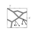
- FIG. 1A schematically shows the structure of a silicon sintered body according to the present embodiment
- FIG. 1B schematically shows the structure of a conventional silicon sintered body.
- silicon oxide silicon dioxide
- Etc. is formed along the interface between the crystal grains 2 due to the oxidation of silicon that occurs during the sintering process.
- Etc. is formed in such a conventional silicon sintered body.
- the passage of electrons is obstructed by the silicon oxide film 5 at the grain boundaries, and thus it is difficult for electricity to pass.
- the case where the said nanoparticle whole exists in a grain boundary is included.
- a case where a part of the nanoparticle is present at the grain boundary includes a case where the whole nanoparticle is present near the grain boundary.
- silicon is less toxic than Bi 2 Te 3 and PbTe materials and is available at a low cost. Therefore, when the semiconductor sintered body according to this embodiment is used, an environmentally friendly electric / electronic member is used. It can be provided at low cost.
- thermoelectric material thermoelectric conversion material
- thermoelectric performance also referred to as thermoelectric conversion performance
- thermoelectric conversion performance thermoelectric conversion performance
- ZT dimensionless thermoelectric figure of merit
- Silicon is known to have a high Seebeck coefficient ⁇ . Therefore, by further increasing the electrical conductivity ⁇ by containing the dopant as described above, it is possible to obtain a higher value of the thermoelectric figure of merit ZT in the formula (1) as a result.
- an n-type or p-type dopant can be included depending on the application. It is preferable that the dopant is uniformly dispersed throughout the sintered body. As an n-type dopant, it is preferable to contain one of phosphorus, arsenic, antimony, and bismuth alone or in combination of two or more.
- the p-type dopant preferably contains one of boron, aluminum, gallium, indium, and thallium alone or in combination of two or more.
- the conductivity type of the dopant element is an exemplification, and whether the dopant element functions as an n-type or p-type dopant depends on the type of element constituting the mother crystal in the obtained sintered body, It depends on the structure.
- the n-type dopant is preferably contained at a concentration such that the Seebeck coefficient of the semiconductor sintered body is ⁇ 185 to ⁇ 60 ⁇ V / K, and the p-type dopant is preferably 60 to 185 ⁇ V / K of the semiconductor sintered body. It is preferable that it is contained at a concentration of K.
- the electrical conductivity of the doped semiconductor sintered body is preferably 10,000 S / m or more, more preferably 50,000 S / m or more, and further preferably 100,000 S / m or more. 110,000 S / m or more.
- the electrical conductivity can be a value at 27 ° C.
- the thermoelectric performance of a sintered compact can be improved because a sintered compact has the electrical conductivity improved.
- the upper limit of the electrical conductivity of the semiconductor sintered body can be 600,000 S / m or less, and can be 400,000 S / m or less.
- the thermoelectric performance ZT of the semiconductor sintered body can be 0.2 or more, preferably 0.3 or more, and more preferably 0.4 or more.
- the semiconductor sintered body according to the present embodiment is used for a power generation device using exhaust heat, for example, a power generation device mounted on an engine and an exhaust system of an automobile, a ship, etc. It can be suitably used in a power generation device to be mounted.
- the average particle size of the particles obtained in the particle preparation step is preferably less than 1 ⁇ m, more preferably 800 nm, even more preferably 500 nm, and even more preferably 300 nm.
- grains is preferable in it being 1 micrometer or less, it is more preferable in it being 500 nm or less, and it is further more preferable in it being 200 nm or less.
- grain preparation step is not limited, It is preferable to set it as 10 nm or more from restrictions on manufacture.
- the average particle diameter of the particles can be a volume-based median diameter measured by a laser diffraction particle size distribution measuring device.
- a film forming step of forming a film containing an aromatic compound on the surface of the particles obtained in the particle preparation step is performed.
- This coating formation step can be performed, for example, by dispersing the particles obtained in the particle preparation step in a solvent, mixing the above aromatic compound, and mixing with a bead mill or the like. Thereafter, the solvent is removed by reduced pressure or the like and dried, whereby particles having an aromatic compound film formed on the surface can be obtained.
- the thickness of the coating may be 0.5 to 5 nm, and is preferably a monomolecular film of an aromatic compound.
- the aromatic compound By forming an aromatic compound film on the surface of the particles obtained in the particle preparation step, the aromatic compound is oxidized in the subsequent sintering step, and oxygen is consumed on the particle surface. Thereby, it can prevent that the oxide of silicon is formed along a grain boundary by reaction of silicon and oxygen. In that case, a structure as shown in FIG. 1A is obtained in which nanoparticles produced by the reaction of an aromatic compound and silicon are present at and near the grain boundary.
- aromatic compound examples include hydrocarbons such as toluene, xylene, mesitylene, naphthalene, methylnaphthalene, vinylnaphthalene, anthracene, phenanthrene, and acenaphthylene.
- aromatic compounds containing a nitrogen atom such as phenanthroline, quinoline, isoquinoline, pyridine, methylpyridine and the like can be given. These aromatic compounds can be used alone or in combination of two or more.
- nanoparticles containing silicon oxide such as silicon dioxide at the grain boundaries and / or in the vicinity thereof are generated by the subsequent firing step.
- carbon contained in the aromatic compound can also react with silicon to produce silicon carbide.
- the aromatic compound contains a hetero atom
- the hetero atom reacts with silicon, and therefore, a compound containing a hetero atom and silicon can be produced in the produced nanoparticles.
- the aromatic compound is preferably added in an amount of 10 to 60 parts by mass, more preferably 30 to 50 parts by mass with respect to 100 parts by mass of the particles prepared in the particle preparation step. .
- the sintering temperature in the sintering step can be selected according to the composition of the main crystal that is silicon or a silicon alloy, but is preferably 900 ° C. or higher, and more preferably 1000 ° C. or higher.
- the sintering temperature is preferably 1400 ° C. or lower, and more preferably 1300 ° C. or lower.
- the temperature increase rate in the sintering step is preferably 10 to 100 ° C./min, more preferably 20 to 60 ° C./min.
- uniform sintering can be promoted, and excessively rapid grain growth can be suppressed to maintain the average grain size of polycrystalline grains at 1 ⁇ m or less.
- formation of nanoparticles by oxidation of the aromatic compound can be promoted, and the formation of silicon oxide at the grain boundary can be prevented.
- the pressurizing pressure is preferably 10 to 120 MPa, more preferably 30 to 100 MPa.
- the organic compound containing the dopant element may be a polymer or a low molecule.
- the organic compound may be a hydride containing a dopant element, an oxide, an oxo acid, or the like.
- phosphoric acid alkylphosphonic acid, alkylphosphinic acid and esters thereof
- trialkylphosphine such as polyvinylphosphonic acid, phosphine, triethylphosphine, and tributylphosphine
- arsenic arsine or the like can be used
- antimony when used, antimony trioxide or the like can be used
- bismuth bismuth acid can be used.
- the addition amount of the organic compound containing the dopant element is preferably 10 to 50 parts by mass and more preferably 20 to 40 parts by mass with respect to 100 parts by mass of the film-formed particles.
- the dopant addition step can be included in the film formation step. That is, after dispersing the particles obtained in the particle preparation step in a solvent, both the aromatic compound and the organic compound containing the dopant element are mixed and mixed with a bead mill or the like.
- the dopant addition step is performed in this way, the dopant element is present on or in the coating formed on the surface of the particle. Therefore, when such particles are sintered, the doping element thermally diffuses from the particle interface to the inside of the particles during sintering. By such doping by thermal diffusion from the particle interface, the electric conductivity of the resultant sintered body can be improved.
- the semiconductor sintered body obtained by the method according to the present embodiment has an equivalent dopant concentration, but even when compared with a sintered body doped without using thermal diffusion from the particle interface, Can exhibit high electrical conductivity.
- particles containing silicon or a silicon alloy and having an average particle diameter of less than 1 ⁇ m are prepared, an aromatic compound film is formed on the surface of the particles, and the film is formed on the surface.
- a semiconductor sintered body produced by obtaining a semiconductor sintered body. Since such a semiconductor sintered body has high electrical conductivity while maintaining low thermal conductivity, it is necessary to increase the ease of conducting electricity while maintaining the difficulty of conducting heat. It can be used in various applications such as electric / electronic members used below.
- Example 1 [N-type semiconductor sintered body] ⁇ Example 1> (Preparation of silicon particles) 28 g of simple silicon (purity 99.99% or more) and 1.0 g of simple phosphorus (purity 99.9%) were melted in an argon atmosphere by an arc melting apparatus, and then cooled. The lump obtained by cooling was rolled to melt again and cooled. This melting and cooling was repeated for a total of 4 cycles to obtain a dopant-containing silicon material as a base material. This silicon material was coarsely pulverized to 45 ⁇ m or less using a hammer crusher and a planetary ball mill. Furthermore, it grind
- isopropyl alcohol was used as a medium, and zirconia beads having a diameter of 0.05 mm were used as beads. Isopropyl alcohol was removed from the obtained slurry under reduced pressure, and further dried to obtain silicon particles.
- the obtained silicon particles were dispersed in heptane, and a mixture obtained by adding 2.0 g of phenanthrene to 25 g of silicon particles was put into the bead mill, and the mixing process was performed for 300 minutes. Thereafter, heptane and excess phenanthrene were removed under reduced pressure, and further dried to obtain silicon particles coated with a monomolecular film.
- the silicon powder coated with the monomolecular film was placed in a graphite die / punch jig and heated to 1200 ° C. using a discharge plasma sintering apparatus to obtain a sintered body.
- the pressurization pressure was 80 MPa, and the temperature elevation rate was 50 ° C./min.
- the outer surface of the obtained sintered body was roughly polished to remove an impurity layer derived from graphite or the like. Furthermore, it cut
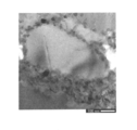
- the density of the sintered body measured by the Archimedes method was 98.5% of pure silicon. Further, when the cross section of the sintered body was observed with a transmission electron microscope (TEM), a structure in which silicon particles having an average of 100 nm were closely joined was observed. Further, a particulate dispersion of silicon carbide was found near the silicon grain boundary, and the particle size was about 20 nm. A photomicrograph of Example 1 is shown in FIG.
- the sintered body had an electric conductivity at 27 ° C. of 1.0 ⁇ 10 5 S / m and a thermal conductivity of 11.0 W / m ⁇ K.
- the dopant concentration was calculated based on the Seebeck coefficient (-95.7 ⁇ V / K) of the sintered body, it was 2.0 with [10 20 atoms / cm 3 ] as a unit.
- the thermoelectric figure of merit ZT at 527 ° C. was 0.30.
- Example 2 (Preparation of silicon particles) Silicon particles were prepared in the same manner as in Example 1.
- Silicon particles coated with a monomolecular film were obtained in the same manner as in Example 1 except that a mixture in which 2.0 g of anthracene was added instead of 2.0 g of phenanthrene was used.
- the density of the sintered body measured by the Archimedes method was 98.5% of pure silicon.
- TEM transmission electron microscope
- Silicon particles coated with a monomolecular film were obtained in the same manner as in Example 1 except that a mixture in which 1.5 g of isoquinoline was added instead of 2.0 g of phenanthrene was used.
- the density of the sintered body measured by the Archimedes method was 98% of that of pure silicon.
- TEM transmission electron microscope
- a structure in which silicon grains having an average of 100 nm were closely joined was observed.
- a particulate dispersion composed of silicon carbide and silicon nitride was observed in the vicinity of the silicon grain boundary, and the particle size was about 20 nm.
- the sintered body had an electric conductivity at 27 ° C. of 1.0 ⁇ 10 5 S / m and a thermal conductivity of 9.5 W / m ⁇ K.
- the dopant concentration was calculated based on the Seebeck coefficient (-95.8 ⁇ V / K) of the sintered body, it was 2.0 with [10 20 atoms / cm 3 ] as a unit.
- the thermoelectric figure of merit ZT at 527 ° C. was 0.30.
- Example 4 (Preparation of silicon particles) Silicon particles were prepared in the same manner as in Example 2.
- the sintered body had an electric conductivity at 27 ° C. of 1.2 ⁇ 10 5 S / m and a thermal conductivity of 9.5 W / m ⁇ K.
- the dopant concentration was calculated based on the Seebeck coefficient ( ⁇ 97.9 ⁇ V / K) of the sintered body, it was 1.9 with [10 20 atoms / cm 3 ] as a unit.
- the thermoelectric figure of merit ZT at 527 ° C. was 0.36.
- Example 5 (Preparation of silicon particles) Silicon particles were prepared in the same manner as in Example 3.
- the density of the sintered body measured by the Archimedes method was 98% of that of pure silicon.
- TEM transmission electron microscope
- a structure in which silicon grains having an average of 100 nm were closely joined was observed.
- a particulate dispersion composed of silicon carbide and silicon nitride was observed in the vicinity of the silicon grain boundary, and the particle size was about 20 nm.
- the sintered body had an electric conductivity of 1.1 ⁇ 10 5 S / m at 27 ° C. and a thermal conductivity of 9.5 W / m ⁇ K.
- the dopant concentration was calculated based on the Seebeck coefficient ( ⁇ 91.4 ⁇ V / K) of the sintered body, it was 2.3 with [10 20 atoms / cm 3 ] as a unit.
- the thermoelectric figure of merit ZT at 527 ° C. was 0.30.
- Example 6> (Preparation of silicon alloy particles)
- Example 1 except that 28 g of simple silicon (purity 99.99% or more) and 3.0 g of simple germanium (purity 99.99% or more) were used instead of 28 g of simple silicon (purity 99.99% or more). Particles were prepared in the same manner as above to obtain silicon alloy particles.
- the sintered body had an electric conductivity at 27 ° C. of 1.0 ⁇ 10 5 S / m and a thermal conductivity of 11.0 W / m ⁇ K.
- the dopant concentration was calculated based on the Seebeck coefficient ( ⁇ 83.0 ⁇ V / K) of the sintered body, it was 3.0 based on [10 20 atoms / cm 3 ].
- the thermoelectric figure of merit ZT at 527 ° C. was 0.40.
- Example 7 (Preparation of silicon alloy particles) In the same manner as in Example 6, silicon alloy particles were obtained.
- the sintered body had an electric conductivity at 27 ° C. of 1.2 ⁇ 10 5 S / m and a thermal conductivity of 6.2 W / m ⁇ K.
- the dopant concentration was calculated based on the Seebeck coefficient ( ⁇ 82.0 ⁇ V / K) of the sintered body, it was 3.1 with [10 20 atoms / cm 3 ] as a unit.
- the thermoelectric figure of merit ZT at 527 ° C. was 0.45.
- the density of the sintered body measured by the Archimedes method was 98% of the silicon alloy before pulverization.
- TEM transmission electron microscope
- a structure in which silicon alloy grains having an average of 100 nm were closely joined was observed.
- a particulate dispersion composed of silicon carbide and silicon nitride was observed near the grain boundary of the silicon alloy, and the particle size was about 20 nm.
- the sintered body had an electric conductivity of 1.1 ⁇ 10 5 S / m at 27 ° C. and a thermal conductivity of 5.5 W / m ⁇ K.
- the dopant concentration was calculated based on the Seebeck coefficient ( ⁇ 82.7 ⁇ V / K) of the sintered body, it was 3.0 with [10 20 atoms / cm 3 ] as a unit.
- the thermoelectric figure of merit ZT at 527 ° C. was 0.40.
- isopropyl alcohol was used as a medium, and zirconia beads having a diameter of 0.05 mm were used as beads. Isopropyl alcohol was removed from the obtained slurry under reduced pressure, and further dried to obtain silicon particles.
- the silicon powder coated with the monomolecular film was placed in a graphite die / punch jig and heated to 1200 ° C. using a discharge plasma sintering apparatus to obtain a sintered body.
- the pressurization pressure was 80 MPa, and the temperature elevation rate was 50 ° C./min.
- the outer surface of the obtained sintered body was roughly polished to remove an impurity layer derived from graphite or the like. Furthermore, it cut
- the density of the sintered body measured by the Archimedes method was 98.5% of pure silicon.
- the sintered body had an electric conductivity at 27 ° C. of 1.0 ⁇ 10 5 S / m and a thermal conductivity of 11.0 W / m ⁇ K.
- the dopant concentration was calculated based on the Seebeck coefficient (95.7 ⁇ V / K) of the sintered body, it was 2.0 with [10 20 atoms / cm 3 ] as a unit.
- the thermoelectric figure of merit ZT at 527 ° C. was 0.30.
- Example 10 (Preparation of silicon particles) Silicon particles were prepared in the same manner as in Example 9.
- Silicon particles coated with a single molecule were obtained in the same manner as in Example 9, except that a mixture in which 2.0 g of anthracene was added instead of 2.0 g of phenanthrene was used.
- Example 11 (Preparation of silicon particles) Using 100 mole equivalents of monosilane (SiH 4 , purity 99.9%) and 3 mole equivalents of diborane (B 2 H 4 , purity 99.9%) as raw materials, they were reacted in a microwave plasma reactor through an argon / hydrogen mixture. Nanoparticles were synthesized and collected with an in-line filter. Silicon nanoparticles were obtained as an aggregate having an average particle diameter of about 150 nm, and the average diameter of the crystallites was 10 nm.
- Example 12 (Preparation of silicon particles) Silicon particles were prepared in the same manner as in Example 9.
- the density of the sintered body measured by the Archimedes method was 98% of that of pure silicon.
- TEM transmission electron microscope
- the sintered body had an electric conductivity at 27 ° C. of 1.2 ⁇ 10 5 S / m and a thermal conductivity of 11.3 W / m ⁇ K.
- the dopant concentration was calculated based on the Seebeck coefficient (95.4 ⁇ V / K) of the sintered body, it was 2.0 with [10 20 atoms / cm 3 ] as a unit.
- the thermoelectric figure of merit ZT at 527 ° C. was 0.36.
- the density of the sintered body measured by the Archimedes method was 98% of that of pure silicon.
- TEM transmission electron microscope
- a structure in which silicon grains having an average of 100 nm were closely joined was observed.
- a particulate dispersion composed of silicon carbide and silicon nitride was observed in the vicinity of the silicon grain boundary, and the particle size was about 20 nm.
- the electrical conductivity of the sintered body at 27 ° C. was 1.1 ⁇ 10 5 S / m, and the thermal conductivity was 9.6 W / m ⁇ K.
- the dopant concentration was calculated based on the Seebeck coefficient (90.3 ⁇ V / K) of the sintered body, it was 2.2 with [10 20 atoms / cm 3 ] as a unit.
- the thermoelectric figure of merit ZT at 527 ° C. was 0.35.
- Example 14 (Preparation of silicon alloy particles)
- Example 9 except that 28 g of simple silicon (purity 99.99% or more) and 3.0 g of simple germanium (purity 99.99% or more) were used instead of 28 g of simple silicon (purity 99.99% or more). The same treatment was performed to obtain silicon alloy particles.
- the density of the sintered body measured by the Archimedes method was 98.5% of the silicon alloy before pulverization.
- TEM transmission electron microscope
- the sintered body had an electric conductivity at 27 ° C. of 1.0 ⁇ 10 5 S / m and a thermal conductivity of 5.5 W / m ⁇ K.
- the dopant concentration was calculated based on the Seebeck coefficient (84.6 ⁇ V / K) of the sintered body, it was 3.0 based on [10 20 atoms / cm 3 ].
- the thermoelectric figure of merit ZT at 527 ° C. was 0.40.
- Example 15 (Preparation of silicon alloy particles) In the same manner as in Example 14, silicon alloy particles were obtained.
- the density of the sintered body measured by the Archimedes method was 98% of the silicon alloy before pulverization.
- TEM transmission electron microscope
- the sintered body had an electric conductivity at 27 ° C. of 1.2 ⁇ 10 5 S / m and a thermal conductivity of 6.2 W / m ⁇ K.
- the dopant concentration was calculated based on the Seebeck coefficient (80.9 ⁇ V / K) of the sintered body, it was 3.3 with [10 20 atoms / cm 3 ] as a unit.
- the thermoelectric figure of merit ZT at 527 ° C. was 0.36.
- Example 16> (Preparation of silicon alloy particles) Monosilane instead of (SiH 4, purity 99.9) 100 mol%, monosilane (SiH 4, purity 99.9) 95 mol% and tetraethyl germanium (Geet 4, purity 99.9%) that was used 5 mol% Except for this, silicon alloy particles were obtained in the same manner as in Example 11. The silicon alloy particles were obtained as an aggregate having an average particle size of about 150 nm, and the average diameter of the crystallites was 10 nm.
- the density of the sintered body measured by the Archimedes method was 98% of the silicon alloy before pulverization.
- TEM transmission electron microscope
- a structure in which silicon alloy grains having an average of 100 nm were closely joined was observed.
- a particulate dispersion composed of silicon carbide and silicon nitride was observed near the grain boundary of the silicon alloy, and the particle size was about 20 nm.
- the sintered body had an electric conductivity of 1.1 ⁇ 10 5 S / m at 27 ° C. and a thermal conductivity of 5.7 W / m ⁇ K.
- the dopant concentration was calculated based on the Seebeck coefficient (84.2 ⁇ V / K) of the sintered body, it was 3.0 based on [10 20 atoms / cm 3 ].
- the thermoelectric figure of merit ZT at 527 ° C. was 0.40.
- the present application includes Japanese Patent Application No. 2017-100107 filed with the Japan Patent Office on May 19, 2017, Japanese Patent Application No. 2017-100108 filed with the Japan Patent Office on May 19, 2017, and 2017.
- This application claims priority based on Japanese Patent Application No. 2017-199057 filed with the Japan Patent Office on October 13, 2000, the entire contents of which are incorporated herein by reference.
Landscapes
- Chemical & Material Sciences (AREA)
- Engineering & Computer Science (AREA)
- Inorganic Chemistry (AREA)
- Manufacturing & Machinery (AREA)
- Nanotechnology (AREA)
- Mechanical Engineering (AREA)
- Physics & Mathematics (AREA)
- Organic Chemistry (AREA)
- Ceramic Engineering (AREA)
- Crystallography & Structural Chemistry (AREA)
- Materials Engineering (AREA)
- General Physics & Mathematics (AREA)
- Condensed Matter Physics & Semiconductors (AREA)
- Composite Materials (AREA)
- Structural Engineering (AREA)
- Optics & Photonics (AREA)
- Silicon Compounds (AREA)
- Powder Metallurgy (AREA)
- Thermistors And Varistors (AREA)
- Ceramic Capacitors (AREA)
- Ceramic Products (AREA)
Priority Applications (4)
| Application Number | Priority Date | Filing Date | Title |
|---|---|---|---|
| KR1020197033740A KR102579987B1 (ko) | 2017-05-19 | 2018-05-17 | 반도체 소결체, 전기·전자 부재 및 반도체 소결체 제조방법 |
| US16/612,850 US11616182B2 (en) | 2017-05-19 | 2018-05-17 | Method of producing semiconductor sintered body, electrical/electronic member, and semiconductor sintered body |
| EP18802437.6A EP3627571B1 (en) | 2017-05-19 | 2018-05-17 | Method of producing semiconductor sintered body, electrical/electronic member and semiconductor sintered body |
| CN201880031777.0A CN110622326B (zh) | 2017-05-19 | 2018-05-17 | 半导体烧结体、电气电子部件及半导体烧结体的制造方法 |
Applications Claiming Priority (6)
| Application Number | Priority Date | Filing Date | Title |
|---|---|---|---|
| JP2017-100107 | 2017-05-19 | ||
| JP2017100107 | 2017-05-19 | ||
| JP2017100108 | 2017-05-19 | ||
| JP2017-100108 | 2017-05-19 | ||
| JP2017199057 | 2017-10-13 | ||
| JP2017-199057 | 2017-10-13 |
Publications (1)
| Publication Number | Publication Date |
|---|---|
| WO2018212296A1 true WO2018212296A1 (ja) | 2018-11-22 |
Family
ID=64273988
Family Applications (3)
| Application Number | Title | Priority Date | Filing Date |
|---|---|---|---|
| PCT/JP2018/019160 Ceased WO2018212296A1 (ja) | 2017-05-19 | 2018-05-17 | 半導体焼結体、電気・電子部材、及び半導体焼結体の製造方法 |
| PCT/JP2018/019159 Ceased WO2018212295A1 (ja) | 2017-05-19 | 2018-05-17 | 半導体焼結体、電気・電子部材、及び半導体焼結体の製造方法 |
| PCT/JP2018/019161 Ceased WO2018212297A1 (ja) | 2017-05-19 | 2018-05-17 | 半導体焼結体、電気・電子部材、及び半導体焼結体の製造方法 |
Family Applications After (2)
| Application Number | Title | Priority Date | Filing Date |
|---|---|---|---|
| PCT/JP2018/019159 Ceased WO2018212295A1 (ja) | 2017-05-19 | 2018-05-17 | 半導体焼結体、電気・電子部材、及び半導体焼結体の製造方法 |
| PCT/JP2018/019161 Ceased WO2018212297A1 (ja) | 2017-05-19 | 2018-05-17 | 半導体焼結体、電気・電子部材、及び半導体焼結体の製造方法 |
Country Status (7)
| Country | Link |
|---|---|
| US (3) | US11404620B2 (https=) |
| EP (3) | EP3627573B1 (https=) |
| JP (3) | JP2019068037A (https=) |
| KR (3) | KR102579987B1 (https=) |
| CN (3) | CN110622327B (https=) |
| TW (3) | TWI802573B (https=) |
| WO (3) | WO2018212296A1 (https=) |
Families Citing this family (6)
| Publication number | Priority date | Publication date | Assignee | Title |
|---|---|---|---|---|
| JP7010474B2 (ja) * | 2018-01-10 | 2022-02-10 | 国立研究開発法人物質・材料研究機構 | 断熱材料、その製造方法および内燃機関 |
| KR102183258B1 (ko) | 2019-04-18 | 2020-11-26 | 주식회사 티씨케이 | SiC 소재 및 이의 제조방법 |
| JP7506388B2 (ja) * | 2019-12-18 | 2024-06-26 | 株式会社テックスイージー | 熱電素子の製造方法 |
| JP7449549B2 (ja) * | 2019-12-25 | 2024-03-14 | 株式会社テックスイージー | 熱電素子及びその製造方法 |
| JP7588811B2 (ja) * | 2020-07-16 | 2024-11-25 | 国立研究開発法人物質・材料研究機構 | 熱電変換用の半導体材料およびそれを用いた熱電変換素子 |
| CN117069500A (zh) * | 2023-08-14 | 2023-11-17 | 陕西科技大学 | 一种硅化镁热电半导体材料及其制备方法和应用 |
Citations (8)
| Publication number | Priority date | Publication date | Assignee | Title |
|---|---|---|---|---|
| JP2006176859A (ja) * | 2004-12-24 | 2006-07-06 | Canon Anelva Corp | シリコンナノ結晶構造体の作製方法 |
| WO2014118959A1 (ja) * | 2013-01-31 | 2014-08-07 | 株式会社日立製作所 | 熱電変換素子および熱電変換モジュール |
| US20140360546A1 (en) | 2013-06-08 | 2014-12-11 | Alphabet Energy, Inc. | Silicon-based thermoelectric materials including isoelectronic impurities, thermoelectric devices based on such materials, and methods of making and using same |
| JP2016131232A (ja) * | 2014-08-28 | 2016-07-21 | 小林 光 | 半導体基板、半導体装置の製造方法、半導体装置の製造装置、太陽電池および太陽電池の製造方法並びに太陽電池の製造装置。 |
| WO2017057237A1 (ja) * | 2015-10-02 | 2017-04-06 | セントラル硝子株式会社 | 熱電変換材料及びその製造方法 |
| JP2017100108A (ja) | 2015-12-04 | 2017-06-08 | 株式会社日本トリム | 電解水生成装置 |
| JP2017100107A (ja) | 2015-12-04 | 2017-06-08 | 太陽工業株式会社 | 廃棄物処分場、廃棄物処分場の遮水シートの破損検知システム |
| JP2017199057A (ja) | 2016-04-25 | 2017-11-02 | 京セラ株式会社 | 電子機器、電子機器の制御方法、電子機器の制御装置、制御プログラムおよび電子機器システム |
Family Cites Families (44)
| Publication number | Priority date | Publication date | Assignee | Title |
|---|---|---|---|---|
| JPS5941562B2 (ja) * | 1977-06-23 | 1984-10-08 | 松下電器産業株式会社 | 赤外線フイルタ |
| JPH0738156A (ja) | 1993-07-20 | 1995-02-07 | Mitsubishi Materials Corp | 熱発電材料およびその製造方法 |
| AU8560198A (en) * | 1997-10-24 | 1999-05-17 | Sumitomo Special Metals Co., Ltd. | Thermoelectric transducing material and method of producing the same |
| JP2000261045A (ja) | 1999-03-10 | 2000-09-22 | Sumitomo Special Metals Co Ltd | 熱電変換材料の製造方法 |
| JP2000261044A (ja) * | 1999-03-10 | 2000-09-22 | Sumitomo Special Metals Co Ltd | 熱電変換材料とその製造方法 |
| JP2001068744A (ja) | 1999-08-30 | 2001-03-16 | Sumitomo Special Metals Co Ltd | 熱電変換材料と熱電変換素子 |
| EP1083610A4 (en) | 1999-03-10 | 2007-02-21 | Neomax Co Ltd | THERMOELECTRIC CONVERSION MATERIAL AND MANUFACTURING METHOD THEREFOR |
| JP4296236B2 (ja) * | 2001-04-27 | 2009-07-15 | 学校法人東京理科大学 | 熱電材料及び熱電素子並びに熱電材料の製造方法 |
| US6759587B2 (en) | 2001-04-27 | 2004-07-06 | Hokushin Corporation | Thermoelectric materials, thermoelectric device, and method for producing thermoelectric materials |
| US8865995B2 (en) | 2004-10-29 | 2014-10-21 | Trustees Of Boston College | Methods for high figure-of-merit in nanostructured thermoelectric materials |
| US7465871B2 (en) * | 2004-10-29 | 2008-12-16 | Massachusetts Institute Of Technology | Nanocomposites with high thermoelectric figures of merit |
| US9865790B2 (en) | 2004-12-07 | 2018-01-09 | Toyota Motor Engineering & Manufacturing North America, Inc. | Nanostructured bulk thermoelectric material |
| JP4726747B2 (ja) * | 2005-10-25 | 2011-07-20 | 独立行政法人物質・材料研究機構 | マグネシウム、珪素、スズからなる金属間化合物の焼結体およびその製造方法 |
| CN101589480B (zh) * | 2006-12-20 | 2011-08-24 | 昭和Kde株式会社 | 热电转换材料、其制造方法及热电转换元件 |
| JP2009117729A (ja) * | 2007-11-09 | 2009-05-28 | Nippon Electric Glass Co Ltd | ドーパントホストおよびその製造方法 |
| CN101226983B (zh) | 2008-02-22 | 2010-06-02 | 浙江大学 | 一种原位纳米复合Mg-Si-Sn基热电材料及其制备方法 |
| TWI485266B (zh) | 2009-07-27 | 2015-05-21 | Univ Tokyo Sci Educ Found | Aluminum-magnesium-silicon composite material and method for manufacturing the same, and thermoelectric conversion material, thermoelectric conversion element and thermoelectric conversion module using the composite material |
| JP2011116575A (ja) * | 2009-12-01 | 2011-06-16 | Sumitomo Electric Ind Ltd | マグネシウムシリサイドの製造方法、マグネシウムシリサイド、電極部材および熱電素子 |
| JP5598792B2 (ja) * | 2010-05-28 | 2014-10-01 | 株式会社三徳 | マグネシウム−シリコン系熱電変換材料およびその製造方法 |
| US8435429B2 (en) * | 2010-07-22 | 2013-05-07 | Toyota Motor Engineering & Manufacturing North America, Inc. | Process for optimum thermoelectric properties |
| JP5206768B2 (ja) * | 2010-11-08 | 2013-06-12 | トヨタ自動車株式会社 | ナノコンポジット熱電変換材料、その製造方法および熱電変換素子 |
| JP6099304B2 (ja) * | 2010-12-10 | 2017-03-22 | 帝人株式会社 | 半導体積層体、半導体デバイス、及びそれらの製造方法 |
| JP5737566B2 (ja) | 2011-03-10 | 2015-06-17 | 日立化成株式会社 | マグネシウムシリサイド焼結体の製造方法及びそれを用いた熱電変換素子の製造方法 |
| US20120282435A1 (en) | 2011-03-24 | 2012-11-08 | University Of Massachusetts | Nanostructured Silicon with Useful Thermoelectric Properties |
| US10811160B2 (en) * | 2011-05-27 | 2020-10-20 | Toyota Motor Engineering & Manufacturing North America, Inc. | Method of producing thermoelectric material |
| US10672966B2 (en) * | 2011-05-27 | 2020-06-02 | Toyota Motor Engineering & Manufacturing North America, Inc. | Method of producing thermoelectric material |
| JP5637075B2 (ja) | 2011-06-03 | 2014-12-10 | トヨタ自動車株式会社 | ナノ複合材料の製造方法 |
| JP5838050B2 (ja) * | 2011-06-24 | 2015-12-24 | 直江津電子工業株式会社 | マグネシウムシリコン合金の製造方法 |
| KR102001062B1 (ko) * | 2012-01-16 | 2019-10-01 | 삼성전자주식회사 | 나노복합체형 열전재료, 이를 포함하는 열전모듈과 열전장치 |
| JP6054606B2 (ja) * | 2012-01-26 | 2016-12-27 | トヨタ自動車株式会社 | 熱電半導体 |
| JP6189582B2 (ja) * | 2012-04-05 | 2017-08-30 | トヨタ自動車株式会社 | ナノコンポジット熱電変換材料の製造方法 |
| JP2014022731A (ja) * | 2012-07-13 | 2014-02-03 | Toyota Motor Engineering & Manufacturing North America Inc | 熱電材料 |
| US20140116491A1 (en) | 2012-10-29 | 2014-05-01 | Alphabet Energy, Inc. | Bulk-size nanostructured materials and methods for making the same by sintering nanowires |
| JP2015056491A (ja) | 2013-09-11 | 2015-03-23 | トヨタ自動車株式会社 | ナノコンポジット熱電変換材料及びその製造方法 |
| JP2015115476A (ja) * | 2013-12-12 | 2015-06-22 | パナソニックIpマネジメント株式会社 | 熱電材料とその製造方法 |
| CN104103750B (zh) * | 2014-07-23 | 2017-01-25 | 太原理工大学 | 镁硅基硅纳米线复合热电材料的制备方法 |
| US9793461B2 (en) * | 2014-09-05 | 2017-10-17 | Mossey Creek Technologies, Inc. | Nano-structured porous thermoelectric generators |
| US9472745B2 (en) * | 2015-02-20 | 2016-10-18 | The United States Of America, As Represented By The Secretary Of The Navy | CVD nanocrystalline silicon as thermoelectric material |
| JP2016219666A (ja) | 2015-05-22 | 2016-12-22 | トヨタ自動車株式会社 | 熱電材料及びその製造方法 |
| JP6504602B2 (ja) * | 2015-06-25 | 2019-04-24 | 国立大学法人広島大学 | 熱電変換薄膜形成用組成物及び熱電変換薄膜の製造方法 |
| KR101997203B1 (ko) | 2015-07-21 | 2019-07-05 | 주식회사 엘지화학 | 화합물 반도체 열전 재료 및 그 제조방법 |
| JP6417050B2 (ja) | 2015-08-31 | 2018-10-31 | 富士フイルム株式会社 | 熱電変換モジュール |
| JP2017057237A (ja) * | 2015-09-14 | 2017-03-23 | 日油株式会社 | 熱可塑性エラストマー |
| KR101774649B1 (ko) * | 2015-10-14 | 2017-09-04 | 현대자동차주식회사 | 나노복합체형 열전소재 및 이의 제조방법 |
-
2018
- 2018-05-17 WO PCT/JP2018/019160 patent/WO2018212296A1/ja not_active Ceased
- 2018-05-17 EP EP18803228.8A patent/EP3627573B1/en active Active
- 2018-05-17 CN CN201880031799.7A patent/CN110622327B/zh active Active
- 2018-05-17 JP JP2018095172A patent/JP2019068037A/ja active Pending
- 2018-05-17 JP JP2018095173A patent/JP2019068038A/ja active Pending
- 2018-05-17 US US16/613,561 patent/US11404620B2/en active Active
- 2018-05-17 EP EP18802437.6A patent/EP3627571B1/en active Active
- 2018-05-17 JP JP2018095174A patent/JP7137963B2/ja active Active
- 2018-05-17 WO PCT/JP2018/019159 patent/WO2018212295A1/ja not_active Ceased
- 2018-05-17 US US16/612,850 patent/US11616182B2/en active Active
- 2018-05-17 US US16/612,466 patent/US11508893B2/en active Active
- 2018-05-17 CN CN201880031803.XA patent/CN110622328B/zh active Active
- 2018-05-17 WO PCT/JP2018/019161 patent/WO2018212297A1/ja not_active Ceased
- 2018-05-17 CN CN201880031777.0A patent/CN110622326B/zh active Active
- 2018-05-17 KR KR1020197033740A patent/KR102579987B1/ko active Active
- 2018-05-17 KR KR1020197033738A patent/KR102579525B1/ko active Active
- 2018-05-17 EP EP18803227.0A patent/EP3627572B1/en active Active
- 2018-05-17 KR KR1020197033739A patent/KR102579986B1/ko active Active
- 2018-05-18 TW TW107117012A patent/TWI802573B/zh not_active IP Right Cessation
- 2018-05-18 TW TW107117015A patent/TWI822679B/zh active
- 2018-05-18 TW TW107117013A patent/TWI776897B/zh active
Patent Citations (9)
| Publication number | Priority date | Publication date | Assignee | Title |
|---|---|---|---|---|
| JP2006176859A (ja) * | 2004-12-24 | 2006-07-06 | Canon Anelva Corp | シリコンナノ結晶構造体の作製方法 |
| WO2014118959A1 (ja) * | 2013-01-31 | 2014-08-07 | 株式会社日立製作所 | 熱電変換素子および熱電変換モジュール |
| US20140360546A1 (en) | 2013-06-08 | 2014-12-11 | Alphabet Energy, Inc. | Silicon-based thermoelectric materials including isoelectronic impurities, thermoelectric devices based on such materials, and methods of making and using same |
| JP2016528716A (ja) * | 2013-06-08 | 2016-09-15 | アルファベット エナジー インコーポレイテッドAlphabet Energy,Inc. | 等電子不純物を含有するシリコン系熱電材料 |
| JP2016131232A (ja) * | 2014-08-28 | 2016-07-21 | 小林 光 | 半導体基板、半導体装置の製造方法、半導体装置の製造装置、太陽電池および太陽電池の製造方法並びに太陽電池の製造装置。 |
| WO2017057237A1 (ja) * | 2015-10-02 | 2017-04-06 | セントラル硝子株式会社 | 熱電変換材料及びその製造方法 |
| JP2017100108A (ja) | 2015-12-04 | 2017-06-08 | 株式会社日本トリム | 電解水生成装置 |
| JP2017100107A (ja) | 2015-12-04 | 2017-06-08 | 太陽工業株式会社 | 廃棄物処分場、廃棄物処分場の遮水シートの破損検知システム |
| JP2017199057A (ja) | 2016-04-25 | 2017-11-02 | 京セラ株式会社 | 電子機器、電子機器の制御方法、電子機器の制御装置、制御プログラムおよび電子機器システム |
Non-Patent Citations (1)
| Title |
|---|
| BUX ET AL., ADV. FUNCT. MATER., vol. 19, 2009, pages 2445 - 2452 |
Also Published As
Similar Documents
| Publication | Publication Date | Title |
|---|---|---|
| KR102579987B1 (ko) | 반도체 소결체, 전기·전자 부재 및 반도체 소결체 제조방법 | |
| JP2010512011A (ja) | ナノ構造をもつ熱電材料における高い示性数のための方法 | |
| Yi et al. | Synthesis and characterization of Mg 2 Si/Si nanocomposites prepared from MgH 2 and silicon, and their thermoelectric properties | |
| Liu et al. | Thermoelectric properties of Ge doped n-type Ti x Zr 1− x NiSn 0.975 Ge 0.025 half-Heusler alloys | |
| JP2014165247A (ja) | 熱電変換材料の製造方法 | |
| JP2011210845A (ja) | GaあるいはSnでドーピングされたバルク状マンガンシリサイド単結晶体あるいは多結晶体およびその製造方法 | |
| Alinejad et al. | Activated Reactive Consolidation Method as a New Approach to Enhanced Thermoelectric Properties of n-Type Nanostructured Mg2Si | |
| JP2025063339A (ja) | n型半導体焼結体、電気・電子部材、熱電発電装置、及びn型半導体焼結体の製造方法 | |
| EP4131436B1 (en) | Method for producing thermoelectric conversion element | |
| Schierning et al. | Nanocrystalline silicon compacted by spark-plasma sintering: Microstructure and thermoelectric properties | |
| Wang | Synthesis, Characterization and Applications of Doped Zintl Phase Sodium Silicide | |
| JP2019029664A (ja) | 熱電変換用高マンガン珪素基テルル化物複合材料及びその製造方法 |
Legal Events
| Date | Code | Title | Description |
|---|---|---|---|
| 121 | Ep: the epo has been informed by wipo that ep was designated in this application |
Ref document number: 18802437 Country of ref document: EP Kind code of ref document: A1 |
|
| ENP | Entry into the national phase |
Ref document number: 20197033740 Country of ref document: KR Kind code of ref document: A |
|
| NENP | Non-entry into the national phase |
Ref country code: DE |
|
| WWE | Wipo information: entry into national phase |
Ref document number: 2018802437 Country of ref document: EP |
|
| ENP | Entry into the national phase |
Ref document number: 2018802437 Country of ref document: EP Effective date: 20191219 |