WO2013111812A1 - 微細凹凸構造体、ドライエッチング用熱反応型レジスト材料、モールドの製造方法及びモールド - Google Patents
微細凹凸構造体、ドライエッチング用熱反応型レジスト材料、モールドの製造方法及びモールド Download PDFInfo
- Publication number
- WO2013111812A1 WO2013111812A1 PCT/JP2013/051432 JP2013051432W WO2013111812A1 WO 2013111812 A1 WO2013111812 A1 WO 2013111812A1 JP 2013051432 W JP2013051432 W JP 2013051432W WO 2013111812 A1 WO2013111812 A1 WO 2013111812A1
- Authority
- WO
- WIPO (PCT)
- Prior art keywords
- dry etching
- pattern
- etching
- heat
- convex structure
- Prior art date
Links
Images


Classifications
-
- B—PERFORMING OPERATIONS; TRANSPORTING
- B81—MICROSTRUCTURAL TECHNOLOGY
- B81C—PROCESSES OR APPARATUS SPECIALLY ADAPTED FOR THE MANUFACTURE OR TREATMENT OF MICROSTRUCTURAL DEVICES OR SYSTEMS
- B81C99/00—Subject matter not provided for in other groups of this subclass
- B81C99/0075—Manufacture of substrate-free structures
- B81C99/0085—Manufacture of substrate-free structures using moulds and master templates, e.g. for hot-embossing
-
- B—PERFORMING OPERATIONS; TRANSPORTING
- B29—WORKING OF PLASTICS; WORKING OF SUBSTANCES IN A PLASTIC STATE IN GENERAL
- B29C—SHAPING OR JOINING OF PLASTICS; SHAPING OF MATERIAL IN A PLASTIC STATE, NOT OTHERWISE PROVIDED FOR; AFTER-TREATMENT OF THE SHAPED PRODUCTS, e.g. REPAIRING
- B29C33/00—Moulds or cores; Details thereof or accessories therefor
- B29C33/38—Moulds or cores; Details thereof or accessories therefor characterised by the material or the manufacturing process
- B29C33/3842—Manufacturing moulds, e.g. shaping the mould surface by machining
-
- B—PERFORMING OPERATIONS; TRANSPORTING
- B29—WORKING OF PLASTICS; WORKING OF SUBSTANCES IN A PLASTIC STATE IN GENERAL
- B29C—SHAPING OR JOINING OF PLASTICS; SHAPING OF MATERIAL IN A PLASTIC STATE, NOT OTHERWISE PROVIDED FOR; AFTER-TREATMENT OF THE SHAPED PRODUCTS, e.g. REPAIRING
- B29C33/00—Moulds or cores; Details thereof or accessories therefor
- B29C33/38—Moulds or cores; Details thereof or accessories therefor characterised by the material or the manufacturing process
-
- B—PERFORMING OPERATIONS; TRANSPORTING
- B29—WORKING OF PLASTICS; WORKING OF SUBSTANCES IN A PLASTIC STATE IN GENERAL
- B29C—SHAPING OR JOINING OF PLASTICS; SHAPING OF MATERIAL IN A PLASTIC STATE, NOT OTHERWISE PROVIDED FOR; AFTER-TREATMENT OF THE SHAPED PRODUCTS, e.g. REPAIRING
- B29C33/00—Moulds or cores; Details thereof or accessories therefor
- B29C33/42—Moulds or cores; Details thereof or accessories therefor characterised by the shape of the moulding surface, e.g. ribs or grooves
-
- B—PERFORMING OPERATIONS; TRANSPORTING
- B29—WORKING OF PLASTICS; WORKING OF SUBSTANCES IN A PLASTIC STATE IN GENERAL
- B29C—SHAPING OR JOINING OF PLASTICS; SHAPING OF MATERIAL IN A PLASTIC STATE, NOT OTHERWISE PROVIDED FOR; AFTER-TREATMENT OF THE SHAPED PRODUCTS, e.g. REPAIRING
- B29C59/00—Surface shaping of articles, e.g. embossing; Apparatus therefor
- B29C59/002—Component parts, details or accessories; Auxiliary operations
-
- C—CHEMISTRY; METALLURGY
- C09—DYES; PAINTS; POLISHES; NATURAL RESINS; ADHESIVES; COMPOSITIONS NOT OTHERWISE PROVIDED FOR; APPLICATIONS OF MATERIALS NOT OTHERWISE PROVIDED FOR
- C09K—MATERIALS FOR MISCELLANEOUS APPLICATIONS, NOT PROVIDED FOR ELSEWHERE
- C09K13/00—Etching, surface-brightening or pickling compositions
-
- C—CHEMISTRY; METALLURGY
- C23—COATING METALLIC MATERIAL; COATING MATERIAL WITH METALLIC MATERIAL; CHEMICAL SURFACE TREATMENT; DIFFUSION TREATMENT OF METALLIC MATERIAL; COATING BY VACUUM EVAPORATION, BY SPUTTERING, BY ION IMPLANTATION OR BY CHEMICAL VAPOUR DEPOSITION, IN GENERAL; INHIBITING CORROSION OF METALLIC MATERIAL OR INCRUSTATION IN GENERAL
- C23F—NON-MECHANICAL REMOVAL OF METALLIC MATERIAL FROM SURFACE; INHIBITING CORROSION OF METALLIC MATERIAL OR INCRUSTATION IN GENERAL; MULTI-STEP PROCESSES FOR SURFACE TREATMENT OF METALLIC MATERIAL INVOLVING AT LEAST ONE PROCESS PROVIDED FOR IN CLASS C23 AND AT LEAST ONE PROCESS COVERED BY SUBCLASS C21D OR C22F OR CLASS C25
- C23F1/00—Etching metallic material by chemical means
-
- G—PHYSICS
- G03—PHOTOGRAPHY; CINEMATOGRAPHY; ANALOGOUS TECHNIQUES USING WAVES OTHER THAN OPTICAL WAVES; ELECTROGRAPHY; HOLOGRAPHY
- G03F—PHOTOMECHANICAL PRODUCTION OF TEXTURED OR PATTERNED SURFACES, e.g. FOR PRINTING, FOR PROCESSING OF SEMICONDUCTOR DEVICES; MATERIALS THEREFOR; ORIGINALS THEREFOR; APPARATUS SPECIALLY ADAPTED THEREFOR
- G03F7/00—Photomechanical, e.g. photolithographic, production of textured or patterned surfaces, e.g. printing surfaces; Materials therefor, e.g. comprising photoresists; Apparatus specially adapted therefor
- G03F7/0002—Lithographic processes using patterning methods other than those involving the exposure to radiation, e.g. by stamping
-
- G—PHYSICS
- G03—PHOTOGRAPHY; CINEMATOGRAPHY; ANALOGOUS TECHNIQUES USING WAVES OTHER THAN OPTICAL WAVES; ELECTROGRAPHY; HOLOGRAPHY
- G03F—PHOTOMECHANICAL PRODUCTION OF TEXTURED OR PATTERNED SURFACES, e.g. FOR PRINTING, FOR PROCESSING OF SEMICONDUCTOR DEVICES; MATERIALS THEREFOR; ORIGINALS THEREFOR; APPARATUS SPECIALLY ADAPTED THEREFOR
- G03F7/00—Photomechanical, e.g. photolithographic, production of textured or patterned surfaces, e.g. printing surfaces; Materials therefor, e.g. comprising photoresists; Apparatus specially adapted therefor
- G03F7/004—Photosensitive materials
- G03F7/04—Chromates
-
- G—PHYSICS
- G03—PHOTOGRAPHY; CINEMATOGRAPHY; ANALOGOUS TECHNIQUES USING WAVES OTHER THAN OPTICAL WAVES; ELECTROGRAPHY; HOLOGRAPHY
- G03F—PHOTOMECHANICAL PRODUCTION OF TEXTURED OR PATTERNED SURFACES, e.g. FOR PRINTING, FOR PROCESSING OF SEMICONDUCTOR DEVICES; MATERIALS THEREFOR; ORIGINALS THEREFOR; APPARATUS SPECIALLY ADAPTED THEREFOR
- G03F7/00—Photomechanical, e.g. photolithographic, production of textured or patterned surfaces, e.g. printing surfaces; Materials therefor, e.g. comprising photoresists; Apparatus specially adapted therefor
- G03F7/004—Photosensitive materials
- G03F7/075—Silicon-containing compounds
- G03F7/0755—Non-macromolecular compounds containing Si-O, Si-C or Si-N bonds
-
- B—PERFORMING OPERATIONS; TRANSPORTING
- B29—WORKING OF PLASTICS; WORKING OF SUBSTANCES IN A PLASTIC STATE IN GENERAL
- B29K—INDEXING SCHEME ASSOCIATED WITH SUBCLASSES B29B, B29C OR B29D, RELATING TO MOULDING MATERIALS OR TO MATERIALS FOR MOULDS, REINFORCEMENTS, FILLERS OR PREFORMED PARTS, e.g. INSERTS
- B29K2905/00—Use of metals, their alloys or their compounds, as mould material
- B29K2905/06—Tin
-
- B—PERFORMING OPERATIONS; TRANSPORTING
- B29—WORKING OF PLASTICS; WORKING OF SUBSTANCES IN A PLASTIC STATE IN GENERAL
- B29L—INDEXING SCHEME ASSOCIATED WITH SUBCLASS B29C, RELATING TO PARTICULAR ARTICLES
- B29L2031/00—Other particular articles
- B29L2031/757—Moulds, cores, dies
-
- H—ELECTRICITY
- H01—ELECTRIC ELEMENTS
- H01L—SEMICONDUCTOR DEVICES NOT COVERED BY CLASS H10
- H01L21/00—Processes or apparatus adapted for the manufacture or treatment of semiconductor or solid state devices or of parts thereof
- H01L21/02—Manufacture or treatment of semiconductor devices or of parts thereof
- H01L21/027—Making masks on semiconductor bodies for further photolithographic processing not provided for in group H01L21/18 or H01L21/34
- H01L21/033—Making masks on semiconductor bodies for further photolithographic processing not provided for in group H01L21/18 or H01L21/34 comprising inorganic layers
- H01L21/0334—Making masks on semiconductor bodies for further photolithographic processing not provided for in group H01L21/18 or H01L21/34 comprising inorganic layers characterised by their size, orientation, disposition, behaviour, shape, in horizontal or vertical plane
- H01L21/0337—Making masks on semiconductor bodies for further photolithographic processing not provided for in group H01L21/18 or H01L21/34 comprising inorganic layers characterised by their size, orientation, disposition, behaviour, shape, in horizontal or vertical plane characterised by the process involved to create the mask, e.g. lift-off masks, sidewalls, or to modify the mask, e.g. pre-treatment, post-treatment
-
- Y—GENERAL TAGGING OF NEW TECHNOLOGICAL DEVELOPMENTS; GENERAL TAGGING OF CROSS-SECTIONAL TECHNOLOGIES SPANNING OVER SEVERAL SECTIONS OF THE IPC; TECHNICAL SUBJECTS COVERED BY FORMER USPC CROSS-REFERENCE ART COLLECTIONS [XRACs] AND DIGESTS
- Y10—TECHNICAL SUBJECTS COVERED BY FORMER USPC
- Y10T—TECHNICAL SUBJECTS COVERED BY FORMER US CLASSIFICATION
- Y10T428/00—Stock material or miscellaneous articles
- Y10T428/24—Structurally defined web or sheet [e.g., overall dimension, etc.]
- Y10T428/24479—Structurally defined web or sheet [e.g., overall dimension, etc.] including variation in thickness
- Y10T428/24612—Composite web or sheet
Definitions
- the present invention relates to a fine concavo-convex structure, a heat-reactive resist material for dry etching, a mold manufacturing method using the same, and a mold.
- phase shift mask For example, in the mask / stepper process, a special mask called a phase shift mask is used to provide a phase difference to the light and improve the precision of fine pattern processing by the effect of interference, or between the stepper lens and the wafer.
- An immersion technique that enables fine pattern processing by filling a liquid and largely refracting light that has passed through a lens has been studied.
- it is very difficult to reduce the manufacturing cost because the former requires an enormous cost for mask development and the latter requires an expensive apparatus.
- resist materials are a photoreactive organic resist (hereinafter also referred to as “photoresist”) that reacts with an exposure light source such as ultraviolet light, electron beam, or X-ray (Patent Document 1, Non-Patent Document). 1).
- photoresist a photoreactive organic resist
- an exposure light source such as ultraviolet light, electron beam, or X-ray
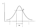
- FIG. 1 is a graph showing the relationship between the spot diameter of laser light and the laser intensity.
- the horizontal axis represents the spot diameter (Rs) of the laser beam
- the vertical axis represents the laser beam intensity (E).
- the intensity (E) of the laser light normally focused by the lens shows a Gaussian distribution with respect to the spot diameter (Rs) as shown in FIG.
- the spot diameter (Rs) is defined by 1 / e 2 .
- the photoreaction does not strongly depend on the intensity of the light, but rather depends on the wavelength of the light, so that almost all the photoreaction occurs in the region irradiated with light (hereinafter referred to as an exposure region). .
- an exposure region irradiated with light
- the method using a photoresist is a very effective method for forming a fine pattern of about several hundred nm, but the photoreaction proceeds in a region corresponding to the spot diameter. For this reason, in order to form a fine pattern, it is necessary to expose with a spot diameter smaller than the pattern required in principle. Therefore, a KrF or ArF laser having a short wavelength must be used as the exposure light source. However, since these light source devices are very large and expensive, they are not suitable from the viewpoint of manufacturing cost reduction. Further, when using an exposure light source such as an electron beam or an X-ray, the exposure atmosphere needs to be in a vacuum state. Therefore, it is necessary to use a vacuum chamber, which is limited from the viewpoint of cost and size.
- FIG. 2 is a graph showing the relationship between the laser light exposure region and temperature.
- the horizontal axis indicates the exposure area (Ae)
- the vertical axis indicates the temperature (T).
- WO X In the field of optical recording, WO X , MoO X , other chalcogenide glasses (Ag-As-S series), etc. are used as thermal reaction resists, and a technique for forming fine patterns by exposure with a semiconductor laser or 476 nm laser is proposed.
- These optical disks used in the field of optical recording are generic names of media that read information recorded on fine irregularities provided on the disk surface by irradiating a disk coated with a resist material with a laser.
- the smaller the recording unit interval called track pitch the higher the recording density and the larger the data capacity that can be recorded for each area. For this reason, in order to improve the recording density, research on processing technology for fine concavo-convex patterns using a resist material has been conducted.
- etching layer a method of previously forming a film having a thickness corresponding to a desired groove depth (hereinafter also referred to as an “etching layer”) under these thermal reaction type resists.
- a heat-reactive resist provided with a pattern shape by exposure and development is used as a mask.
- a deep groove is formed by etching the etching layer using this mask.
- dry etching is used to uniformly etch in the film thickness direction.
- SiO 2 is used for the etching layer
- dry etching can be performed with a fluorine-based gas.
- the heat-reactive resist used as a mask is required to be resistant to fluorine gas dry etching in addition to being capable of fine pattern processing.
- etching gas for example, CF 4 gas or SF 6 gas
- side wall protecting gas for example, a gas having an F / C of 3 or less such as C 4 F 8 gas
- Non-Patent Document 3 A technique for forming a deep groove in the film thickness direction by performing dry etching while switching between the two is reported using a photoresist (see Non-Patent Document 3).
- a fluorocarbon protective film is formed on the sidewall of an etching layer formed by dry etching.
- a technique for achieving a desired etching angle (taper angle) by changing the dry etching rate in the film thickness direction and the dry etching rate in the film surface direction with this protective film has been reported for both photoresists.
- the thermal reaction type resist layer has a high resistance to the sidewall protection gas in addition to the dry etching resistance to the etching gas. Dry etching resistance is required.
- the present invention has been made in view of the above points, a fine concavo-convex structure having a fine pattern suitable for application in many fields, a thermal reaction resist material for dry etching suitable for the production of a fine concavo-convex structure, And it aims at providing the manufacturing method and mold of a mold using the same.
- the fine concavo-convex structure of the present invention comprises an etching layer and a resist layer made of a thermally reactive resist material for dry etching provided on the etching layer, and an opening formed in the resist layer Is formed in the etching layer, the pattern pitch P of the fine pattern of the concavo-convex structure is 1 nm to 10 ⁇ m, the pattern depth H of the fine pattern is 1 nm to 10 ⁇ m, and the fine pattern
- the pattern cross-sectional shape of the pattern is trapezoidal, triangular, or a mixture thereof.
- the heat-reactive resist material for dry etching according to the present invention is described above using a fluorine-based gas having a ratio (F / C) of the number of fluorine atoms to the number of carbon atoms of 3 or less, or 2.7 or less.
- a heat-reactive resist material for dry etching for forming a fine concavo-convex structure selected from the group consisting of Cr, Fe, Co, Al, Ga, In, Hf, and Pb, and oxides and nitrides thereof It is characterized in that at least one of these is a main constituent element.
- the mold manufacturing method of the present invention includes a step of providing a resist layer containing the above-described heat-reactive resist material for dry etching of the present invention on the base material to be the etching layer, and developing after exposing the resist layer. And a step of dry etching through the mask, and a step of manufacturing a mold by removing the resist layer.
- the mold of the present invention is manufactured by the above-described mold manufacturing method of the present invention.
- the pattern pitch P of a fine pattern with a concavo-convex structure is 1 nm to 10 ⁇ m
- the pattern depth H of the fine pattern is 1 nm to 10 ⁇ m
- the pattern cross-sectional shape of the fine pattern is Further, since trapezoids or triangles or a mixture of them, a fine pattern can be freely designed so as to be suitable for application of a substrate with fine irregularities.
- a substrate having a concavo-convex structure having a fine pattern (hereinafter referred to as a substrate with fine concavo-convex) has been studied in many fields.
- the application of a substrate with fine unevenness having a fine structure in which the depth of the concave portion of the uneven structure of a fine pattern is deep is increasing.
- the present inventor considers development to antireflection, light collection, light extraction, water repellency, hydrophilicity, medium, substrate for film growth, etc., and the pattern pitch is about 1 nm to 10 ⁇ m. It is very important that the pattern depth is as small as 1 nm or more and 10 ⁇ m or less, and that it is possible to design a fine pattern with a taper angle, that is, an inclination in the pattern depth direction. I found.
- a mold having an uneven structure having a fine pattern is prepared, and a resin is applied to the surface of this mold to fill the uneven structure with resin, thereby forming an uneven structure.
- the resin layer provided with is transferred onto a substrate.
- the pattern depth and the taper angle can be freely designed by controlling the cutting blade.
- the pattern pitch depends on the size of the cutting blade, it is difficult to make the minimum pattern pitch 10 ⁇ m or less.
- the inventor of the present invention has a pattern pitch of the concavo-convex structure of 1 nm to 10 ⁇ m, a pattern depth of 1 nm to 10 ⁇ m, and an etching angle (taper angle) in the pattern depth direction.
- a thermal reaction resist material and etch etching material for dry etching that can design the fine pattern shape. Using these resist materials and etching materials, a mold having a fine pattern suitable for various applications could be realized.
- the fine concavo-convex structure according to the present invention includes an etching layer and a resist layer made of a thermally reactive resist material for dry etching provided on the surface of the etching layer, and is formed in the resist layer.
- a fine pattern corresponding to the opening is formed in the etching layer, and the pitch of the concavo-convex structure constituting the fine pattern (hereinafter referred to as pattern pitch P) is 1 nm or more and 10 ⁇ m or less, and the depth of the concavo-convex structure constituting the fine pattern.
- pattern depth H is 1 nm or more and 10 nm
- pattern cross-sectional shape is a trapezoid or a triangle, or these It is characterized by being mixed.
- the pattern pitch P is a distance between adjacent convex portions or concave portions in a plurality of convex portions and concave portions constituting the concave-convex structure.
- the pattern depth H is a difference ⁇ H between any one of the highest point (H 1 ) and the deepest point (H 2 ) among the plurality of convex portions and concave portions constituting the concavo-convex structure.
- a fine pattern can be freely designed so as to be suitable for application of a substrate with fine concavo-convex.
- the substrate with fine irregularities include, for example, antireflection, light collection, light extraction, water repellency, hydrophilicity, medium, and substrate for film growth.
- the pattern pitch P, the pattern depth H, and the pattern cross-sectional shape can be optimized as appropriate according to the wavelength of light to be applied.
- the substrate with fine unevenness according to the present embodiment is optimal.
- the substrate with fine unevenness according to the present embodiment can be used as a mold, and the fine unevenness can be transferred to the film and used.
- the medium use can be used as a substrate (template) for culturing cells in fields such as regenerative medicine. Since cells grow three-dimensionally, it is important to appropriately optimize the pattern pitch P, pattern depth H, and pattern cross-sectional shape.
- the substrate with fine irregularities according to the present embodiment having a taper angle is optimal for the culture medium field.
- the thermal reaction resist material for dry etching according to the present embodiment is used for the fine concavo-convex structure according to the present embodiment described above, and the ratio between the number of fluorine atoms and the number of carbon atoms ( (Hereinafter referred to as F / C) is a thermally reactive resist material for dry etching using a fluorine-based gas having 3 or less, including Cr, Fe, Co, Al, Ga, In, Hf and Pb, and their
- the main constituent element is at least one selected from the group consisting of oxides and nitrides.
- the boiling point of the main fluoride becomes 200 ° C. or more during dry etching, it is possible to reduce dry etching due to a chemical phenomenon in which constituent elements are removed by fluorination. Further, since sputtering by a fluorine-based gas having F / C of 3 or less or F / C of 2.7 or less can be reduced, dry etching due to a physical phenomenon in which constituent elements are removed by sputtering can be reduced.
- the thermal reaction resist material for dry etching and the etching material according to the present embodiment the fine pattern as described above can be formed on the fine concavo-convex structure according to the present embodiment.
- an etching angle tapeer angle
- the boiling point of the fluoride of the main element used in the thermal reaction type resist material for dry etching is preferably 200 ° C. or higher.
- the boiling point of the fluoride is preferably 200 ° C. or lower.
- the mold manufacturing method includes a step of providing a resist layer containing the above-described dry etching thermal reaction resist material according to the present embodiment on a base material, and exposing the resist layer.
- the method includes a step of forming a mask by development, a step of dry etching the base material through the mask, and a step of removing the resist layer to obtain a mold.
- a fluorine-based gas having F / C of 3 or less or F / C of 2.7 or less for dry etching.
- the mold according to the present embodiment is manufactured by the mold manufacturing method according to the present embodiment described above.
- the mold according to the present embodiment is characterized in that the resist layer is removed from the fine concavo-convex structure.
- a resist layer made of a thermally reactive resist material for dry etching is provided on an etching layer made of an etching material, and the resist layer is exposed and developed to form a desired resist layer. This is obtained by forming a mask having an opening and dry etching the etching layer through this mask.
- the mask is designed to correspond to the fine pattern described below.
- a mold is obtained by removing the resist from the fine concavo-convex structure. Resin is applied to the surface of the obtained mold to fill the uneven structure with the resin, and thereby the resin layer with the uneven structure is transferred onto the substrate, thereby obtaining a substrate with fine unevenness. Can do.
- the pattern pitch P is a distance between adjacent ridges among a plurality of ridges constituting the concavo-convex structure having a fine pattern.
- the pattern pitch P does not necessarily need to be a distance between adjacent convex portions of the concavo-convex structure, and may be a distance between adjacent concave portions.
- the pattern pitch P is 1 nm or more and 10 ⁇ m or less, more preferably 1 nm or more and 5 ⁇ m or less, further preferably 1 nm or more and 1 ⁇ m or less, and most preferably 10 nm or more and 950 ⁇ m or less.
- the thermal reaction resist material for dry etching and the etching material according to the present embodiment can be efficiently and inexpensively manufactured for applications requiring a fine pattern. It is possible to form a fine pattern.
- the thermal reaction resist material for dry etching and the etching material according to the present embodiment are used. Thus, it is possible to form a fine pattern at low cost in production.
- the pattern depth H is, for example, the difference between any one of the highest point (H 1 ) and the lowest point (H 2 ) among the plurality of concave portions constituting the concavo-convex structure. It can be defined by ⁇ H.
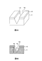
- FIG. 3 is a schematic perspective view and a schematic cross-sectional view showing the fine concavo-convex structure according to the present embodiment.
- the fine concavo-convex structure 10 is provided with a resist layer 12 on the surface of a substantially flat etching layer 11.
- the resist layer 12 has a line-and-space-shaped opening 12a.
- the etching layer 11 has a recess 11a having a trapezoidal cross section.
- the difference ⁇ H between the highest point H 1 and the deepest point H 2 of the etching layer 11 in the cross-sectional shape of the recess 11 a is defined as a pattern depth H.
- FIG. 4 is a schematic perspective view and a schematic cross-sectional view showing the fine concavo-convex structure according to the present embodiment.
- the resist layer 12 has a line-and-space-shaped opening 12a.
- the etching layer 11 has a recess 11a having a triangular cross section.
- the difference ⁇ H between the highest point H 1 and the deepest point H 2 of the etching layer 11 in the cross-sectional shape of the recess 11 a is defined as the pattern depth H.
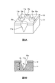
- FIG. 5 is a schematic perspective view and a schematic cross-sectional view showing the fine concavo-convex structure according to the present embodiment.
- the resist layer 12 has a plurality of dot-shaped openings 12a.
- the etching layer 11 has a plurality of concave portions 11a having a triangular cross section corresponding to the plurality of openings 12a.
- the cross-sectional shape of the recess 11a, the difference ⁇ H between the highest point H 1 and the deepest point of H 2 etch layer 11, is defined as a pattern depth H.
- the pattern depth H is preferably 1 nm or more and 10 ⁇ m or less.
- the pattern depth can be selected according to the application that requires a fine pattern.
- the pattern depth H divided by the pattern pitch P is used in the range of 0.1 to 100. Possible, preferably in the range of 0.2 to 10, more preferably in the range of 0.3 to 5.
- the heat-reactive resist material for dry etching and the etching material of the present invention can efficiently and inexpensively form patterns for applications that require fine patterns. It is possible to form.
- the pattern pitch P becomes smaller, it becomes difficult to form the pattern depth H deeper.
- the thermal reaction resist material for dry etching and the etching material of the present invention the pattern depth within the above range can be obtained.
- the height H can be formed at low cost in manufacturing.
- the cross section of the pattern cross-sectional shape is, for example, two boundary lines (that is, edges) between the opening of the concave portion and the upper surface (resist layer side) of the etching layer in one concave portion, such as a line and space shape. And when the two lines do not intersect each other, the two highest points are the one point on one side of the two lines and the other point on the other side that are closest to each other.
- the cross section of the pattern cross-sectional shape is, for example, a hole shape, and a boundary line (that is, an edge) between the opening of the recess and the upper surface (resist layer side) of the etching layer is a single line, and both ends thereof When the two are connected and closed, the two points on the one line and the distance between them being the longest are the two highest points, and the fine relief structure includes the two highest points.
- the shape drawn by connecting is called a pattern cross-sectional shape.
- the pattern cross-sectional shape includes the one highest point when the convex portion has one highest point, or the convex portion When the highest point of the part is two or more, when the boundary line between the upper surface and the side wall surface of the etching layer is one line and both ends thereof are connected and closed,
- the cross section when the fine concavo-convex structure is cut along the thickness direction of the etching layer so as to include two highest points that are two points and the distance between them is the farthest the one highest point or the It is a shape drawn by connecting the two highest points and the two points with the longest distance between the two lowest points of the convex portion with a straight line.
- the pattern cross-sectional shape is a shape of an arbitrary cross section among a plurality of concave portions formed in the etching layer of the fine concavo-convex structure.
- the pattern cross-sectional shape is a trapezoid, a triangle, or a mixture thereof.
- the cross-sectional shape can be selected according to the application of the substrate with fine irregularities.
- the surface shape of the concavo-convex structure is not particularly limited, and examples thereof include a line and space shape, a dot shape (hole shape), and a long hole shape, and these may be mixed.
- the pattern cross-sectional shape is a shape satisfying the formula (1) or the formula (2).
- T 0 width of the opening of the resist layer before dry etching
- T 1 width on the highest side of the recess formed in the etching layer after dry etching
- B 1 deepest side of the recess formed in the etching layer after dry etching Width of
- FIG. 6 is a schematic cross-sectional view showing a recess of the fine concavo-convex structure according to the present embodiment.
- FIG. 6A shows a laminated structure including an etching layer and a resist layer before dry etching. A part of the resist layer 12 is removed, and an opening 12a is formed. The width of the opening 12a is defined as T 0.
- FIG. 6B is a schematic cross-sectional view showing the concave portion of the fine concavo-convex structure after dry etching, and shows a case where the pattern cross-sectional shape is a trapezoid.
- T 1 is equal to T 0 . That is, Expression (2) is satisfied.
- FIG. 6C is a schematic cross-sectional view showing the concave portion of the fine concavo-convex structure after dry etching, and shows a case where the pattern cross-sectional shape is a triangle.
- B 1 0, that is, the deepest portion is pointed.
- T 1 is equal to T 0 . That is, Expression (2) is satisfied.
- FIG. 6D is a schematic cross-sectional view showing a concave portion of the fine concavo-convex structure after dry etching, and shows a case where the pattern cross-sectional shape is a trapezoid.
- T 1 is greater than T 0, B 1 is equal to T 0. That is, Formula (1) is satisfy
- the pattern cross-sectional shape formed using the method (A) has a width T 0 of the opening 12a of the resist layer 12 before dry etching and a width T on the highest portion side of the recess 11a. located 1 are equal relationship, it can be seen that the resist layer 12 is not etched during the dry etching.
- the pattern depth H is determined according to the etching depth, and the etching angle (taper angle) is further determined by dry etching.
- B 1 can take a value from 0 to less than T 0 .
- the pattern cross-sectional shape formed using the method (A) is represented by the formula (2).
- the pattern cross-sectional shape formed using the method (B) has a width T 1 on the highest portion side of the recess 11a rather than the width T 0 of the opening 12a of the resist layer 12 before etching. Is large (T 1 > T 0 ), and it can be seen that the resist layer 12 is etched and the opening 12a is enlarged during dry etching.
- the pattern depth H is determined according to the etching depth, and the etching angle (taper angle) is further determined by etching the resist layer 12.
- the width of the deepest side of the recess 11a B 1 is not dependent on the pattern depth and etch angle, the same value as the width T 0 of the opening 12a of the resist layer 12.
- the pattern cross-sectional shape formed using the method (B) satisfies the formula (1).
- Which method (A) or (B) is selected can be determined according to the application of the substrate with fine unevenness and the heat-reactive resist material for dry etching.
- those having a pattern cross-sectional shape satisfying the formula (1) are those in which the thermal reaction resist material for dry etching is Cu, Nb, Sn, Mn, or an oxide thereof.
- the main constituent element is at least one selected from the group consisting of nitride and NiBi.
- fills Formula (1) can be manufactured efficiently.
- the heat-reactive resist material for dry etching is selected from the main constituent elements of Cu oxide.
- the one having a pattern cross-sectional shape satisfying the formula (2) is a thermal reaction resist material for dry etching, which is Cr, Fe, Co, Al, Ga, In, Hf,
- the main constituent element is at least one selected from the group consisting of Pb or oxides and nitrides thereof.
- the present inventor shows that an element having a main fluoride boiling point of 200 ° C. or higher has a high dry etching resistance, and the dry etching resistance increases as the boiling point of the main fluoride increases. It has already been found that there is a tendency to be higher (WO 2010/044400 pamphlet).
- etching gas etching fluorine gas
- side wall protecting gas Fluorine-based gas
- the inventor of the present invention has an element whose boiling point of the main fluoride is 200 ° C. or higher, and has a relatively high dry etching resistance against the side wall protective gas, while the side wall protective gas has a tendency to have a large and small protective effect. We focused on the fact that the tendency of the resistance to dry etching by the side wall protective gas does not match.
- the present inventor has found that (2) the dry etching due to a physical phenomenon does not necessarily correlate the boiling point of the main fluoride with the dry etching resistance.
- the inventors of the present invention (2) correlates with the magnitude of dry etching resistance due to a physical phenomenon with the magnitude of sputtering resistance against a fluorine-based gas, and by using an element with high sputtering resistance, The idea was that high dry etching resistance could be obtained.
- the present inventor investigated the relationship between the sputtering rate, which is an index related to sputtering resistance (see “Sputtering Technology”, pages 15 to 18 published by Kyoritsu Publishing Co., Ltd.) and dry etching due to the physical phenomenon in which sputtering occurs. It was. As a result, dry etching resistance to dry etching due to physical phenomena changes periodically according to atomic number as well as sputtering rate, and the tendency of dry etching resistance to dry etching due to physical phenomena is large for sputtering elements. I found out not to rely on it.
- the present inventor has performed etching by using an element satisfying both of (1) dry etching resistance to chemical etching and (2) dry etching resistance to physical etching.
- the present inventors have found that a heat-reactive resist having high resistance to working gas and high dry etching resistance to side wall protecting gas can be realized, and the present invention has been completed.
- the ratio of the number of fluorine atoms to the number of carbon atoms (hereinafter also simply referred to as “F / C”) is 3.0 or less, or 2.
- the thermally reactive resist material for dry etching according to the present embodiment is suitable for dry etching using a fluorine-based gas having an F / C of 3 or less, more preferably a fluorine-based gas having an F / C of 2.7 or less.
- a fluorine-based gas having an F / C of 3 or less is a value obtained by dividing the number of fluorine atoms constituting the fluorine gas used by the number of carbon atoms: F [Fluorine] / C [Carbon]) is 3
- the following gases is 3
- the use of fluorine gas having an F / C of 3 or less produces a side wall protection effect.
- the fluorine gas whose F / C is 3 or less can be used as a sidewall protecting gas.
- the fluorine gas whose F / C is 3 or less increases the side wall protection effect as the F / C value becomes smaller (hereinafter, “the fluorine gas whose F / C is 3 or less” is referred to as “the side wall protective gas”). ”).
- the fluorine-based gas having F / C of 2.7 or less has a greater side wall protection effect.
- the thermally reactive resist material for dry etching mainly includes at least one selected from the group consisting of Cr, Fe, Co, Al, Ga, In, Hf, and Pb, and oxides and nitrides. Constituent elements. Since these elements have a boiling point of the main fluoride of 200 ° C. or more, each element reacts with a fluorine-based gas to become a fluoride gas, and dry etching is performed by a chemical phenomenon in which the fluoride gas is removed. Can be reduced. In addition, since the boiling point of the main fluorides of the element groups Cr, Fe, Co, Al, Ga, In, Hf, and Pb used in the dry etching material of the present invention is 950 ° C.
- the element with a low sputtering rate is selected when Ar gas is used in the sputtering rate data (see “Sputtering Technology”, pages 15 to 18 published by Kyoritsu Publishing Co., Ltd.), which is an index related to sputtering resistance. It is preferable to select an element of 1/2 or less of the sputtering rate of Ag.
- the element group Cr, Fe, Co, Al, Ga, In, Hf, and Pb used in the dry etching material of the present invention has a main fluoride boiling point of 950 ° C. or more and Ar gas. It is characterized by being made of an element that is 1 ⁇ 2 or less of the sputtering rate of Ag at the time. Therefore, according to the thermal reaction type resist material for dry etching according to the present embodiment, the dry type thermal reaction type resist material having excellent dry etching resistance can be obtained even when performing dry etching using the side wall protection gas. realizable.
- the main constituent elements in the thermal reaction type resist material are Cr, Fe, Co, Al, Ga, In, Hf and Pb, and their oxidation among all the elements constituting the thermal reaction type resist material.
- the content of an element selected from the group consisting of a material and a nitride is 50 mol% or more.
- the content of these elements is preferably 60 mol% or more, more preferably 65 mol% or more, further preferably 70 mol% or more, still more preferably 75 mol% or more, and 80 mol%. % Or more is most preferable, and 85 mol% or more is most preferable.
- the higher the content of these elements the higher the dry etching resistance against dry etching using the side wall protecting gas.
- the fine concavo-convex structure is preferably coated with fluorine-based carbon (also referred to as fluorocarbon) on the side surfaces of the plurality of recesses.
- fluorine-based carbon also referred to as fluorocarbon
- the fine concavo-convex structure of the present invention is formed by dry etching.
- the fine concavo-convex structure of the present invention that is, the fine concavo-convex structure having a taper angle, can be formed by coating the side surfaces of the concave portions of the fine concavo-convex structure with fluorine-based carbon. Therefore, in the fine concavo-convex structure of the present invention, it is preferable that the side surface of the concave portion is coated with fluorine-based carbon.
- the side wall protecting gas is not particularly limited as long as the ratio of fluorine atoms to carbon atoms (F / C) is 3 or less, but the F / C is 2.7 or less. Is more effective.
- the side wall protecting gas include CHF 3 , CH 2 F 2 , C 2 F 6 , C 3 F 8 , C 4 F 6 , C 4 F 8 , C 4 F 10 , C 5 F 10 , and CCl 2 F. 2 , fluorine-based gas such as CF 3 I, CF 3 Br, CHF 2 COF, CF 3 COF, and the like.
- fluorine-based gases may be used alone as a side wall protecting gas, or a mixed gas obtained by mixing these gases may be used as the side wall protecting gas.
- fluorine-based gas and CF 4 May also be used these fluorine-based gas and CF 4, other fluorine-based gas mixed with mixed gas such as SF 6 as a sidewall protective gas.
- Any gas can be used as a side wall protecting gas as long as the side wall protecting effect can be achieved in dry etching.
- dry etching using the thermally reactive resist material for dry etching according to the present invention as a mask enables deep dry etching in the film thickness direction and control of the etching angle (taper angle). Is possible.
- the dry etching depth in the film thickness direction can of course be shallow by using the thermal reaction resist material for dry etching according to the present invention, but a deep pattern exceeding 500 nm can also be formed. In addition, it can also be used in dry etching using a fluorine-based gas with F / C exceeding 3.
- fluorine-based gases such as CHF 3 , C 3 F 8 and C 4 F 8 , and CHF 3 , C 3 F 8, or a mixed gas of C 4 F 8 and CF 4 are used as the side wall protecting gas.
- a gas it is preferable that at least one selected from the group consisting of Cr, Co, Ga, Pb, and oxides thereof is a main constituent element as a thermally reactive resist material for dry etching.
- the heat-reactive resist material for dry etching it is more preferable that at least one selected from the group consisting of Cr, Co, Pb oxide and Ga is a main constituent element. Furthermore, from the viewpoint of simplicity in manufacturing, it is most preferable that the heat-reactive resist material for dry etching has at least one selected from the group consisting of oxides of Cr, Co, and Pb as a main constituent element. .
- the fluorine-based gas (side wall protecting gas) can be used for dry etching using, for example, RIE (reactive ion etching), ECR (electron cyclotron resonance) plasma etching, and microwave etching.
- fluorine-type gas is not restrict
- the thermal reaction type resist material for dry etching preferably contains a thermal reaction type resist material that can be patterned by any of oxidation, decomposition, melting, phase change, aggregation, and sublimation.
- a thermal reaction type resist material that can be patterned by any of oxidation, decomposition, melting, phase change, aggregation, and sublimation.
- the thermally reactive resist material for dry etching according to the present embodiment is different from the photoresist material.
- the thermally reactive resist material when exposed to a laser beam, the thermally reactive resist material is heated in the laser beam spot system (irradiated region). A reacted thermal reaction region and an unreacted unreacted region can be formed.
- FIG. 7 is an explanatory diagram showing the relationship between the spot diameter (irradiation region) of laser light and the temperature distribution within the spot diameter when the heat-reactive resist material is irradiated with laser light.
- the spot diameter Rs of the laser light is that of the heat-reactive resist material centered on the focus of the laser light. It is formed in a substantially circular shape with respect to the main surface.
- the temperature distribution T within the spot diameter Rs of the laser beam becomes lower as it goes toward the outer periphery of the irradiation area Ae, with the vicinity of the focal point of the laser beam as a vertex.
- the vicinity of the focal point of the laser beam can be selectively exposed by using a heat-reactive resist material that reacts at a predetermined temperature. That is, the reaction occurs in the region 71 where the temperature is high, and the reaction does not occur in the region 72 where the temperature is low.
- the heat-reactive resist material has a region (71 in FIG. 7) that reacts at a predetermined temperature (Tr; resist reaction temperature) or higher with respect to the temperature distribution T generated within the spot diameter of the laser.
- Tr resist reaction temperature
- a short-wavelength semiconductor laser currently on the market has a wavelength of about 405 nm and a spot diameter of about 420 nm (numerical aperture: 0.85).
- microfabrication of 420 nm or less is impossible in principle as long as a photoresist material is used, but this limit can be exceeded by using a heat-reactive resist material, and microfabrication below the wavelength of a semiconductor laser. It can be performed.
- the thermally reactive resist material for dry etching includes CrO X (0 ⁇ X ⁇ 3) and an additive, and the additive includes CrO X (0 ⁇ X ⁇ 3) and a compound. It preferably comprises at least one selected from materials that do not form.
- the material that does not form a compound CrO X (0 ⁇ X ⁇ 3 ) does not form a chemical bond with CrO X (0 ⁇ X ⁇ 3 ). Whether or not to form a compound with CrO X (0 ⁇ X ⁇ 3) can be confirmed from the phase diagram of the oxide material.
- the heat-reactive resist material for dry etching can exhibit performance as a resist material.
- the thermal reaction type resist material for dry etching is a thermal reaction type resist material for dry etching comprising CrO X (0 ⁇ X ⁇ 3) and an additive. Selected from the group consisting of Al, Si, Ni, Ge, Mo, Ru, Rh, Pd, Ag, In, Sn, Ta, Ir, Pt, Au and Bi, their oxides and nitrides, and mixtures thereof It is preferable that at least one is included. Since the additive is a material that does not form a compound with CrO X (0 ⁇ X ⁇ 3), the heat-reactive resist material for dry etching can exhibit performance as a resist material.
- the additive CrO X by heating at the time of exposure (0 ⁇ X ⁇ 3) and the additive material is preferably not forming a compound, the compound any at all CrO even under conditions X (0 ⁇ X ⁇ 3) Additives that do not form are more preferred.
- the additive material is Al, Si, Ni, Ru, Rh, Pd, Ag, In, Sn, Ta, Ir, Pt, Au, and Bi, when dry etching resistance is important.
- it comprises at least one selected from the group consisting of oxides and nitrides and mixtures thereof.
- the additive is at least selected from the group consisting of Al, Si, Ni, Ge, Mo and Ta, oxides and nitrides thereof, and mixtures thereof when importance is given to the ability to form a fine pattern. It is preferable that it comprises one, more preferably at least one selected from the group consisting of Si, Ge, Mo and Ta, oxides and nitrides thereof, and mixtures thereof. More preferably, it comprises at least one selected from the group consisting of Ta, oxides and nitrides thereof, and mixtures thereof, and an oxide of Si is most preferred.
- CrO X (0 ⁇ X ⁇ 3) used in the thermally reactive resist material for dry etching according to the present embodiment has a boiling point of main fluoride of 200 ° C. or higher during dry etching, Dry etching due to a chemical phenomenon in which the fluoride gas reacts to remove the fluoride gas can be reduced. Further, since CrO X (0 ⁇ X ⁇ 3) has a low sputtering rate, it is possible to reduce the sputtering by the side wall protection gas and to reduce dry etching due to a physical phenomenon in which the constituent elements are removed by sputtering.
- CrO X (0 ⁇ X ⁇ 3) used for the heat-reactive resist material in the present embodiment is not limited to the case where dry etching is performed using a side wall protecting gas, but also an etching gas or various dry gases. Excellent dry etching resistance against etching gas species.
- the X range of CrO X is preferably (0 ⁇ X ⁇ 2).
- the range of X of CrO X is more preferably (0.2 ⁇ X ⁇ 1.5), more preferably (0.35 ⁇ X ⁇ 1.5), and (0.35 ⁇ Most preferably, X ⁇ 1.0).
- This degree of oxidation X can be determined using Rutherford backscattering analysis (RBS) or the like. Incidentally, when obtaining the oxidation degree X, in order to eliminate the influence from the additional material, it is preferable to perform the measurement only by CrO X.
- the thermally reactive resist material for dry etching according to the present embodiment may include a state in which the oxidation degree X is different in the material.
- a thermal reaction type resist material for dry etching is formed using sputtering
- a mold resist material can be produced.
- the method for changing the oxygen concentration may be continuous or discontinuous.
- the dry etching thermal reaction type resist material according to the present embodiment has different development rates depending on the degree of oxidation X. Therefore, by forming films having different degrees of oxidation X, materials having different development rates in the film thickness direction can be obtained. For example, in the case where a residue is easily formed on the substrate surface, the residue can be suppressed by disposing a material having an oxidation degree X that increases the development speed on the substrate surface side.
- the dry etching thermal reaction type resist material according to the present embodiment is amorphous because it contains an additive. Therefore, since the growth of the crystal
- silicon oxide is included as an additive. By including silicon oxide, it becomes possible to form a better fine pattern.
- the addition amount of the additive is 2.0 mol% or more and 35.0 mol% or less in terms of mole. By making the addition amount 2.0 mol% or more and 35.0 mol% or less, it has resist resistance excellent in dry etching resistance and can easily form a fine pattern.
- the addition amount of the additive is preferably 2.0 mol% or more and 25.0 mol% or less, more preferably 5.0 mol% or more and 15.0 mol% or less, and most preferably 6.0 mol% or more and 12.0 mol% or less. By setting the additive amount in the above range, it is possible to form a fine pattern having a clear pattern shape.
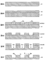
- FIG. 8 is a schematic cross-sectional view showing each step of the mold manufacturing method according to the present embodiment.
- the thermal reaction type resist layer 82 containing the thermal reaction type resist material for dry etching is formed on the base material 81.
- a heat-reactive resist layer 82 containing the heat-reactive resist material for dry etching according to the above embodiment is formed on the substrate 81 (FIGS. 8A and 8B).
- the base material 81 a material that can be dry-etched is used from the viewpoint of manufacturing the mold 80 by dry-etching the base material 81 in the step (3) described later.
- the base material 81 for example, silicon or quartz is preferable, and quartz is more preferable.
- the substrate 81 either a flat plate shape or a sleeve (roll, drum) shape can be used.
- a flat mold 80 is obtained, and when the sleeve substrate 81 is used, a sleeve mold 80 is obtained.
- many molds generally used for an optical disc master or nanoimprint are small and have a flat plate shape, they can be transferred by a simple apparatus.
- a conventional sleeve-shaped mold can easily transfer a pattern to a large area, but it has been difficult to form a submicron (1 ⁇ m or less) pattern by laser processing or machining.
- the mold manufacturing method according to the present embodiment not only the plate-shaped mold 80 can be manufactured, but also when the sleeve-shaped mold 80 is manufactured, a pattern having a submicron size is formed. Therefore, it is possible to transfer a fine pattern of a submicron size to a large area.
- a material that is difficult to dry-etch can be used as the base material 81.
- a dry etching layer (not shown) is provided between the base material 81 and the thermal reaction type resist layer 82.
- the dry etching layer is not particularly limited as long as it can be dry etched.
- Si, Ta, Ge, Te and P, oxides, nitrides and carbides thereof, and oxides of Mo and W and Silicides can be used.
- the heat-reactive resist layer 82 and the dry etching layer provided as necessary are preferably provided using a sputtering method, a vapor deposition method or a CVD method.
- the thermal reaction type resist material for dry etching that constitutes the thermal reaction type resist layer 82 can be processed with a fine pattern of several tens of nanometers. Therefore, depending on the size of the fine pattern, the thermal reaction type for dry etching at the time of film formation It can be considered that the film thickness distribution of the resist material and the unevenness of the surface have a great influence.
- the film thickness of the thermally responsive resist material for dry etching according to the present invention is preferably 150 nm or less, more preferably 100 nm or less, further preferably 60 nm or less, and 40 nm or less. Most preferred.
- a heat absorption layer (not shown) may be laminated on the heat reaction type resist layer 82.
- the selection range of the light absorption characteristics in the heat-reactive resist layer 82 can be expanded.
- the thermal reaction type resist layer 82 is often composed of a material having absorption in a wide wavelength range, but depending on the thermal reaction type resist material for dry etching, it is optically absorbed at the wavelength of the semiconductor laser, for example, around 405 nm. May not have. In that case, the heat-reactive resist layer 82 can be reacted with the heat by absorbing the energy of the laser in the heat-absorbing layer and converting it into heat.
- a material used for the heat absorption layer a material having a light absorption property in a laser wavelength region, for example, C, Mg, Al, Si, Ti, V, Cr, Mn, Fe, Co, Ni, Cu, Zn, Ge
- An element selected from the group consisting of Se, Zr, Nb, Mo, Pd, Ag, In, Sn, Sb, Te, Hf, Ta, W, Pt, Au, Pb, and Bi, or an alloy thereof is preferable.
- oxides, nitrides, sulfides or carbides containing these elements, or a mixture thereof may be used.
- the heat-reactive resist layer 82 can be designed for heat dissipation or heat insulation.
- the heat radiation design is designed when it is necessary to release the heat energy of the portion heated by the laser irradiation as soon as possible.
- the heat radiation design is effective when the heat is generated and the reaction by heat proceeds in a region wider than the spot shape of the heat reaction by exposure, and a desired shape cannot be obtained.
- the heat insulation design is designed when it is necessary to prevent the dissipation of the heat energy of the portion heated by the laser irradiation.
- the mold is made of a metal or glass having high workability.
- step (2) the heat-reactive resist material for dry etching of the heat-reactive resist layer 82 is thermally reacted by exposure to form a heat-reactive region 82a in a part of the heat-reactive resist layer 82.
- the region other than the thermal reaction region 82a of the thermal reaction type resist layer 82 becomes an unreacted region 82b (FIG. 8C).
- a mask 82c fine pattern is formed by dissolving and removing either the thermal reaction region 82a or the unreacted region 82b with a developer (FIG. 8D).
- the developer is not particularly limited, and for example, an acid, an alkali solution, or the like can be used.
- the acid solution general solutions such as hydrochloric acid, sulfuric acid, nitric acid, phosphoric acid, acetic acid, oxalic acid, and hydrofluoric acid can be used alone or as a mixed solution.
- common solutions such as sodium hydroxide, potassium hydroxide, sodium carbonate, ammonia, TMAH (tetramethylammonium hydroxide), can be used individually or as a mixed solution as an alkaline solution.
- a potential adjusting agent such as hydrogen peroxide or manganese peroxide to the developer.
- the developer when removing the thermal reaction region 82a, a developer in which the thermal reaction region 82a is soluble in the developer used and the unreacted region 82b is resistant is used. Further, when the unreacted region 82b is removed, the unreacted region 82b is soluble in the developer used and the heat-reactive region 82a is resistant.
- the base material 81 is dry-etched through the mask 82c formed by patterning the heat-reactive resist layer 82 to form the recess 81a in the base material 81 (FIG. 8E).
- the mask 82c thermal reaction type resist layer 82
- the number of fluorine atoms and the number of carbon atoms are as follows. Even when a fluorine-based gas (side wall protecting gas) having a ratio (F / C) of 3 or less or 2.7 or less is used, the mask 82c has high dry etching resistance.
- the etching amount of the mask 82c can be reduced, so that a fine pattern with a high aspect ratio can be formed.
- the dry etching conditions are such that the base material 81 can be etched using a fluorine-based gas having a ratio of the number of fluorine atoms to the number of carbon atoms (F / C) of 3 or less, or 2.7 or less. If there is, there is no particular limitation.
- step (4) the mask 82c (thermal reaction type resist layer 82) is removed, and the mold 80 is manufactured (FIG. 8F).
- the mask 82c (thermal reaction type resist layer 82) is not particularly limited as long as it does not affect the base material 81 (dry etching layer), and wet etching, dry etching, or the like can be used.
- the base material 81 has resistance
- the thermal reaction region 82a or the unreacted region 82b is soluble or reactive. Use reactive gas.
- FIGS. 8A to 8F are diagrams showing an outline of the method for manufacturing the mold 80 according to the present embodiment. As shown in FIGS.
- a thermal reaction resist material for dry etching containing CrO X (0 ⁇ X ⁇ 3) and an additive is formed on the base material 81 by sputtering or the like, and then heated.
- a reactive resist layer 82 is provided (FIGS. 8A and 8B).
- the film formation of the thermal reaction type resist layer 82 is not limited to the sputtering method, and various film formation methods can be applied.
- the base material 81 a material that can be dry-etched is used from the viewpoint of manufacturing the mold 80 by dry-etching the base material 81 in the step (3) described later.
- the substrate 81 for example, silicon or quartz is preferable, and quartz is particularly preferable.
- the heat-reactive resist material for dry etching of the heat-reactive resist layer 82 is thermally reacted by exposure to form a heat-reactive region 82a in a part of the heat-reactive resist layer 82.
- the region other than the thermal reaction region 82a of the thermal reaction type resist layer 82 becomes an unreacted region 82b (FIG. 8C).
- the heat-reactive resist layer 82 includes a heat-reactive resist material containing CrO X (0 ⁇ X ⁇ 3) and an additive, so that a heat-reactive region 82a during exposure is obtained.
- a mask 82c (fine pattern) is formed by dissolving and removing either the thermal reaction region 82a or the unreacted region 82b with a developer (FIG. 8D).
- a developer FOG. 8D
- the boundary between the thermal reaction region 82a and the unreacted region 82b becomes clear, and a clear pattern is obtained by exposure and development. It is possible to form a mask 82c having
- Development in the step (2) is preferably performed by wet etching.
- a commonly used acidic etchant mixed liquid of ceric ammonium nitrate and hydrogen peroxide, an alkaline etchant, or the like can be used. Furthermore, it is possible to improve the wettability by adding a surfactant or the like to the developer.
- the base material 81 is dry-etched with a fluorine-based gas through the mask 82c formed by patterning the thermal reaction type resist layer 82 to form the recess 81a in the base material 81 ( FIG. 8E).
- the mask 82c thermal reaction type resist layer 82
- the sidewall protective gas is used as the fluorine-based gas.
- the mask 82c has high dry etching resistance not only when dry etching is performed using the etching gas but also when etching gas and various fluorine-based gases are used.
- the etching amount of the mask 82c can be reduced, so that a fine pattern with a high aspect ratio can be formed.
- a mold 80 provided with an arbitrary pattern such as deep dry etching in the film thickness direction and control of the etching angle (taper angle).
- the dry etching conditions are not particularly limited as long as the substrate 81 can be dry etched with a fluorine-based gas.
- the fluorine-based gas used for dry etching of the substrate 81 is a value obtained by dividing the number of fluorine atoms by the number of carbon atoms (F) from the viewpoint of facilitating control of the pattern shape of the uneven structure of the mold 80 to be obtained (F) It is preferable to use a fluorine-based gas (side wall protecting gas) having a / C) of 3 or less.
- F / C is more preferably 2.7 or less from the viewpoint of obtaining a side wall protection effect. In this condition, the structure can be easily controlled to have a taper angle.
- step (4) the mask 82c (thermal reaction type resist layer 82) is removed, and the mold 80 is manufactured (FIG. 8F).
- the mask 82c is not particularly limited as long as it does not affect the base material 81 or a dry etching layer described later, and wet etching, dry etching, or the like can be used.
- an etching solution or a reactive gas in which the substrate 81 is resistant and the thermal reaction region 82a or the unreacted region 82b is soluble or reactive is used.
- the removal of the mask 82c in the step (4) is not particularly limited as long as it does not affect the base material 81 or a dry etching layer described later.
- wet etching or dry etching can be used.
- the mask 82c can be removed by wet etching, the mask 82c can be removed by changing the potential of the developer used for developing the thermal reaction type resist layer 82.
- the substrate 81 either a flat plate shape or a sleeve shape can be used.
- the sleeve-shaped substrate may be a roll or a drum.
- a flat mold 80 is obtained, and when the sleeve substrate 81 is used, a sleeve mold 80 is obtained.
- many molds generally used for an optical disc master or nanoimprint are small and have a flat plate shape, they can be transferred by a simple apparatus.
- a conventional sleeve-shaped mold can easily transfer a pattern to a large area, but it has been difficult to form a submicron (1 ⁇ m or less) pattern by laser processing or machining.
- the mold manufacturing method according to the present embodiment not only the plate-shaped mold 80 can be manufactured, but also when the sleeve-shaped mold 80 is manufactured, a pattern having a submicron size is formed. Therefore, it is possible to transfer a fine pattern of a submicron size to a large area.
- the base material 81 As the base material 81, as described above, it is preferable to use a material that can be dry etched from the viewpoint of manufacturing a mold by dry etching.
- a material that can be dry etched from the viewpoint of manufacturing a mold by dry etching As the substrate, silicon or quartz is preferable, and quartz is more preferable from the viewpoint of manufacturing a sleeve-shaped mold.
- a material that is difficult to dry-etch can be used as the base material 81.
- a dry etching layer (not shown) is provided between the substrate 81 and the thermal reaction type resist layer 82 as necessary.
- the dry etching layer is not particularly limited as long as it can be dry etched.
- Si, Ta, Ge, Te and P, and oxides, nitrides and carbides thereof, and oxides of Mo and W and Silicides can be used.
- Si, Ta, Ge, Te and P, and oxides, nitrides and carbides thereof, and oxides of Mo and W and Silicides can be used.
- the heat-reactive resist layer 82 and the dry etching layer provided as necessary are preferably provided by using any method selected from a sputtering method, a vapor deposition method, and a CVD method.
- the thermal reaction type resist material for dry etching that constitutes the thermal reaction type resist layer 82 can be processed with a fine pattern of several tens of nanometers. Therefore, depending on the size of the fine pattern, the thermal reaction type for dry etching at the time of film formation It can be considered that the film thickness distribution of the resist material and the unevenness of the surface have a great influence.
- the sputtering method, the vapor deposition method and the CVD method are selected from the film formation method by the coating method or the spray method which is somewhat difficult to control the uniformity of the film thickness. It is preferable to form the heat-reactive resist material by any film forming method.
- a heat absorption layer (not shown) may be laminated on the heat reaction type resist layer 82.
- the selection range of the light absorption characteristics in the heat reaction type resist layer 82 can be expanded, and the temperature of the heat reaction type resist layer can be increased efficiently.
- the thermal reaction type resist layer 82 is often composed of a material having absorption in a wide wavelength range, but depending on the thermal reaction type resist material for dry etching, it is optically absorbed at the wavelength of the semiconductor laser, for example, around 405 nm. May not have. In that case, the heat-reactive resist layer 82 can be reacted with the heat by absorbing the energy of the laser in the heat-absorbing layer and converting it into heat.
- a material used for the heat absorption layer a material having a light absorption property in a laser wavelength region, for example, C, Mg, Al, Si, Ti, V, Cr, Mn, Fe, Co, Ni, Cu, Zn, Ge
- An element selected from the group consisting of Se, Zr, Nb, Mo, Pd, Ag, In, Sn, Sb, Te, Hf, Ta, W, Pt, Au, Pb, and Bi, or an alloy thereof is preferable.
- oxides, nitrides, sulfides or carbides containing these elements, or a mixture thereof may be used.
- the heat-reactive resist layer 82 can have a heat radiation design or a heat insulation design.
- the heat radiation design is designed when it is necessary to release the heat energy of the portion heated by the laser irradiation as soon as possible.
- the heat radiation design is effective when the heat is generated and the reaction by heat proceeds in a region wider than the spot shape of the heat reaction by exposure, and a desired shape cannot be obtained.
- the heat insulation design is designed when it is necessary to prevent the dissipation of the heat energy of the portion heated by the laser irradiation.
- the mold is made of a metal or glass having high workability.
- the thickness of the thermal reaction type resist layer 82 is preferably not less than 10 nm and not more than 80 nm.
- a thicker film is advantageous because it has higher resistance to dry etching, but as the film thickness increases, uniformity in the film thickness direction due to exposure is lost. As a result, there arises a problem that the processing accuracy of the fine pattern is lowered.
- the film thickness of the thermal reaction resist material for dry etching according to the present embodiment is preferably 80 nm or less, more preferably 50 nm or less, further preferably 40 nm or less, and 30 nm or less. Most preferably.
- the film thickness is 10 nm or more, it is possible to prevent the heat absorption efficiency from being lowered by the laser.
- the heat-reactive resist material according to the present embodiment it is sufficiently resistant to dry etching, so that the film thickness can be reduced and the processing accuracy of a fine pattern can be increased.
- an excimer laser such as a KrF laser or an ArF laser
- a semiconductor laser an electron beam, an X-ray, or the like
- Excimer lasers such as KrF lasers and ArF lasers are very large and expensive, and electron beams, X-rays and the like need to use a vacuum chamber, so there are considerable limitations in terms of cost and size. Therefore, it is preferable to use a semiconductor laser that can be made very compact and inexpensive.
- the thermally reactive resist material for dry etching according to the present embodiment is a semiconductor laser. However, a sufficiently fine pattern can be formed.
- an etching gas used for general dry etching may be used as the fluorine-based gas used for dry etching of the substrate 81.
- the etching gas include fluorine-based gases such as CF 4 and SF 6 , and these gases may be used alone or in combination with a plurality of gases.
- a mixture in which the above-described fluorine-based gas and a gas such as O 2 , H 2 , Ar, N 2 , CO, HBr, NF 3 , HCl, HI, BBr 3 , BCl 3 , Cl 2 , SiCl 4 are mixed.
- the gas is also within the range of fluorine-based gas.
- the fluorine-based gas can be used for dry etching using, for example, RIE (reactive ion etching), ECR (electron cyclotron resonance) plasma etching, and microwave etching.
- fluorine-type gas is not restrict
- the developer is not particularly limited, and for example, an acid, an alkali solution, or the like can be used.
- the acid solution general solutions such as hydrochloric acid, sulfuric acid, nitric acid, phosphoric acid, acetic acid, oxalic acid, hydrofluoric acid, and ceric ammonium nitrate can be used alone or as a mixed solution.
- common solutions such as sodium hydroxide, potassium hydroxide, sodium carbonate, ammonia, TMAH (tetramethylammonium hydroxide), can be used individually or as a mixed solution as an alkaline solution.
- a potential adjusting agent such as hydrogen peroxide or manganese peroxide to the developer.
- the developer when removing the thermal reaction region 82a, a developer in which the thermal reaction region 82a is soluble in the developer used and the unreacted region 82b is resistant is used. Further, when the unreacted region 82b is removed, the unreacted region 82b is soluble in the developer used and the heat-reactive region 82a is resistant.
- the mold 80 is formed of the thermally reactive resist material for dry etching including CrO X (0 ⁇ X ⁇ 3) and the additive. Since the heat-reactive resist layer 82 is in an amorphous state, it is possible to prevent crystal growth between the heat-reactive region 82a and the unreacted region 82b formed in the heat-reactive resist layer 82 by exposure. As a result, the boundary between the thermal reaction region 82a and the unreacted region 82b becomes clear, so that a mask 82c having a clear pattern can be formed by exposure and development.
- the mask 82c contains CrO X (0 ⁇ X ⁇ 3) as a thermal reaction resist material for dry etching.
- the mask 82c is not limited to a gas for protecting the side walls, but is used for all fluorine-based gases used for dry etching. Since excellent dry etching resistance is obtained, the amount of etching of the mask can be reduced even if dry etching is performed for a long time in the step (3). As a result, it is possible to realize a method of manufacturing the mold 80 in which a groove having a sufficient depth in the film thickness direction can be formed and the etching angle can be easily controlled.
- the mold according to the present embodiment is manufactured by the above-described mold manufacturing method. According to the mold manufacturing method of the present embodiment, it is possible to manufacture a mold having a fine pattern in which the pitch of the concavo-convex structure (pitch P between adjacent convex portions 80a) is 1 nm or more and 1 ⁇ m or less (FIG. 8F). reference).
- the pitch does not necessarily need to be the pitch between the adjacent convex portions 80a of the concavo-convex structure, and may be the pitch between the adjacent concave portions.
- the shape of the concavo-convex structure is not particularly limited, and examples thereof include a line and space shape, a dot shape, and a long hole shape, and these may be mixed.
- examples of the cross-sectional structure of the concavo-convex structure include a triangular shape, a dome shape, and a lens shape.
- Example 1 CrO and Co 3 O 4 were used as the thermal reaction resist material for dry etching.
- As the base material 50 mm ⁇ plate-shaped quartz was used.
- thermal reaction resist layer containing a thermal reaction resist material for dry etching was formed on a substrate by sputtering. CrO and Co 3 O 4 were used as targets. The conditions for film formation are shown in Table 1 below.
- the heat-reactive resist layer for dry etching that was formed was exposed to form a heat-reactive region in the heat-reactive resist layer.
- the exposure conditions are shown below.
- exposure was performed so that the heat-reactive resist layer had a continuous groove shape pattern.
- the heat-reactive resist pattern can be formed into various patterns such as a circular shape and an oval shape by modulating the laser intensity during exposure depending on the application of the mold to be manufactured.
- Semiconductor laser wavelength for exposure 405 nm
- Lens numerical aperture 0.85
- the exposed heat-reactive resist layer was developed.
- a wet process was used for development.
- the heat-reactive region of the heat-reactive resist layer was dissolved and removed at room temperature with a developer and developed.
- Table 1 below shows the development conditions.
- the substrate was dry-etched using the heat-reactive resist layer with the pattern as a mask.
- F / C 2.7
- CF 4 and C 4 F 8 are mixed at a ratio of 70 vol%: 30 vol% as an etching gas, a processing gas pressure of 5 Pa, a processing power of 300 W, It implemented on the conditions for processing time 60 minutes.
- a fine pattern with an opening width B shown in Table 2 below was formed.
- an etching shape having a taper angle due to the side wall protection effect was formed while maintaining the opening width A of the pattern of the thermal reaction type resist layer.
- Example 2 GaSb was used as the thermal reaction resist material for dry etching.
- As a substrate ⁇ 80 mm sleeve-shaped quartz was used.
- a thermal reaction type resist layer containing a thermal reaction type resist material for dry etching was formed to 40 nm on a sleeve-shaped substrate by a sputtering method.
- a GaSb target was used as the target.
- the conditions for film formation are shown in Table 1 below.
- the heat-reactive resist layer for dry etching formed on the sleeve-shaped substrate was exposed to form a heat-reactive region in the heat-reactive resist layer.
- the exposure conditions are shown below.
- Semiconductor laser wavelength for exposure 405 nm
- Lens numerical aperture 0.85
- Exposure laser power 1mW to 25mW
- Feed pitch 120 nm to 350 nm
- Rotation speed 210rpm-1670rpm
- the exposed heat-reactive resist layer was developed.
- a wet process was used for development.
- the heat-reactive region of the heat-reactive resist layer was dissolved and removed at room temperature with a developer and developed.
- Table 1 below shows the development conditions.
- the pattern shape of the heat-reactive resist layer developed using a UV curable resin was transferred to a film.
- a pattern with an opening width A shown in Table 2 below was formed.
- the thermally responsive resist material for dry etching according to the present invention is suitable for dry etching using a fluorine-based gas (side wall protecting gas) in which the ratio of the number of fluorine atoms to the number of carbons is 3 or less. Since it has high tolerance, the opening width A and the opening width B before and after dry etching are substantially the same. From this result, by using the thermal reaction resist material for dry etching according to the present invention, high dry etching resistance can be obtained even for fluorine-based gas whose ratio of fluorine atom number to carbon number is 3 or less. It can be seen that deep digging and dapper angle control in dry etching are facilitated.
- the base material 50 mm ⁇ plate-shaped quartz was used as the base material.
- a thermal reaction type resist layer containing a thermal reaction type resist material for dry etching was formed to a thickness of 25 nm on a substrate by sputtering.
- a mixed target of Cr and SiO 2 was used as a target. The film forming conditions are shown in Table 3 below.
- the heat-reactive resist layer for dry etching that was formed was exposed to form a heat-reactive region in the heat-reactive resist layer.
- the exposure conditions are shown below.
- the thermal reaction type resist layer was exposed so as to form a continuous groove-shaped pattern, but the thermal reaction type resist pattern modulates the laser intensity during the exposure.
- various patterns such as a circular shape and an elliptical shape can be formed depending on the application of the mold to be manufactured.
- Semiconductor laser wavelength for exposure 405 nm
- Lens numerical aperture 0.85
- Exposure laser power 1mW ⁇ 10mW Feed pitch: 120 nm to 350 nm
- the exposed heat-reactive resist layer was developed by a wet process.
- the heat-reactive region of the heat-reactive resist layer was dissolved and removed at room temperature with a developer and developed.
- Table 3 below shows the development conditions.
- a pattern having an opening width A shown in Table 4 below was formed.
- the substrate was dry-etched using the heat-reactive resist layer with the pattern as a mask.
- CF 4 and C 4 F 8 are mixed in a ratio of 70 vol%: 30 vol%, respectively, as a fluorine-based gas, a processing gas pressure of 5 Pa and a processing power is used.
- the test was performed under the conditions of 200 W and a processing time of 60 minutes.
- a fine pattern with an opening width B shown in Table 4 below was formed.
- an etching shape with a taper angle due to the side wall protection effect was formed while the opening width A of the pattern of the thermal reaction type resist layer was maintained.
- a substrate ⁇ 80 mm sleeve-shaped quartz was used.
- a thermal reaction type resist layer containing a thermal reaction type resist material for dry etching was formed to a thickness of 25 nm on a sleeve-shaped substrate by a sputtering method.
- a target a mixed target of Cr and SiO 2 was used.
- the film forming conditions are shown in Table 3 below.
- the heat-reactive resist layer for dry etching formed on the sleeve-shaped substrate was exposed to form a heat-reactive region in the heat-reactive resist layer.
- the exposure conditions are shown below.
- Semiconductor laser wavelength for exposure 405 nm
- Lens numerical aperture 0.85
- Exposure laser power 1mW to 25mW
- Feed pitch 120 nm to 350 nm
- Rotation speed 210rpm-1670rpm
- the exposed heat-reactive resist layer was developed by a wet process.
- the heat-reactive region of the heat-reactive resist layer was dissolved and removed at room temperature with a developer and developed.
- Table 3 below shows the development conditions.
- a pattern having an opening width A shown in Table 4 below was formed.
- the pattern shape of the heat-reactive resist layer developed using a UV curable resin was transferred to a film.
- a pattern with an opening width A shown in Table 4 below was formed.
- a rectangular etching shape was formed in a cross-sectional view while maintaining the opening width A of the pattern of the thermal reaction type resist layer.
- the substrate was dry-etched using the heat-reactive resist layer with the pattern as a mask.
- the surface shape was transferred to a film using a UV curable resin.
- a pattern with an opening width B shown in Table 4 was formed, and a rectangular etching shape was formed while maintaining the opening width A of the thermal reaction type resist layer. It was.
- Example 5 Using the heat-reactive resist material for dry etching prepared in Example 3, exposure was performed under the following conditions.
- the exposed heat-reactive resist layer was developed by a wet process.
- the heat-reactive region of the heat-reactive resist layer was dissolved and removed at room temperature with a developer and developed.
- Table 3 below shows the development conditions.
- a pattern having an opening width A shown in Table 4 below was formed.
- the substrate was dry-etched using the heat-reactive resist layer with the pattern as a mask.
- a fine pattern with an opening width B shown in Table 4 below was formed.
- a pattern having an opening width B shown in Table 4 was formed, and a rectangular etching shape was formed while maintaining the opening width A of the thermal reaction type resist layer.
- As the base material 50 mm ⁇ plate-shaped quartz was used.
- a thermal reaction type resist layer containing a thermal reaction type resist material for dry etching was formed to a thickness of 25 nm on a substrate by sputtering.
- a mixed target of Cr and Ta 2 O 5 was used as a target. The film forming conditions are shown in Table 3 below.
- the heat-reactive resist layer for dry etching that was formed was exposed to form a heat-reactive region in the heat-reactive resist layer.
- the exposure conditions are shown below.
- the thermal reaction type resist layer was exposed so as to form a continuous groove-shaped pattern, but the thermal reaction type resist pattern modulates the laser intensity during the exposure.
- various patterns such as a circular shape and an elliptical shape can be formed depending on the application of the mold to be manufactured.
- Semiconductor laser wavelength for exposure 405 nm
- Lens numerical aperture 0.85
- Exposure laser power 1mW ⁇ 10mW Feed pitch: 100 nm to 350 nm
- the exposed heat-reactive resist layer was developed by a wet process.
- the heat-reactive region of the heat-reactive resist layer was dissolved and removed at room temperature with a developer and developed.
- Table 3 below shows the development conditions.
- a pattern having an opening width A shown in Table 4 below was formed.
- the substrate was dry-etched using the heat-reactive resist layer with the pattern as a mask.
- CF 4 and C 4 F 8 are mixed in a ratio of 70 vol%: 30 vol%, respectively, as a fluorine-based gas, a processing gas pressure of 5 Pa and a processing power is used.
- the test was performed under the conditions of 200 W and a processing time of 60 minutes.
- a fine pattern with an opening width B shown in Table 4 below was formed. While the opening width A of the pattern of the heat-reactive resist layer was maintained, an etching shape with a taper angle due to the side wall protection effect was formed.
- As the base material 50 mm ⁇ plate-shaped quartz was used.
- a thermal reaction type resist layer containing a thermal reaction type resist material for dry etching was formed to a thickness of 25 nm on a substrate by sputtering.
- CuO / SiO 2 was a mixed target of CuO and SiO 2
- CrO 0.5 / SiO 2 was a mixed target of Cr and SiO 2 .
- Table 3 The film forming conditions are shown in Table 3 below.
- the heat-reactive resist layer for dry etching that was formed was exposed to form a heat-reactive region in the heat-reactive resist layer.
- the exposure conditions are shown below.
- the thermal reaction type resist layer was exposed so as to form a continuous groove-shaped pattern, but the thermal reaction type resist pattern modulates the laser intensity during the exposure.
- various patterns such as a circular shape and an elliptical shape can be formed depending on the application of the mold to be manufactured.
- Semiconductor laser wavelength for exposure 405 nm
- Lens numerical aperture 0.85
- Exposure laser power 1mW to 25mW
- Feed pitch 100 nm to 10 ⁇ m
- the exposed heat-reactive resist layer was developed by a wet process.
- the heat-reactive region of the heat-reactive resist layer was dissolved and removed at room temperature with a developer and developed.
- Table 3 below shows the development conditions.
- a pattern having a pattern pitch and an opening width A shown in Table 5 below was formed.
- the substrate was dry-etched using the heat-reactive resist layer with the pattern as a mask.
- CF 4 and C 4 F 8 are mixed in a ratio of 70 vol% and 30 vol%, respectively, is used as the fluorine-based gas, and dry etching is performed under the conditions shown in Table 5. Carried out.
- the heat-reactive resist layer for dry etching that was formed was exposed to form a heat-reactive region in the heat-reactive resist layer.
- the exposure conditions are shown below.
- Semiconductor laser wavelength for exposure 405 nm
- Lens numerical aperture 0.85
- Exposure laser power 1mW ⁇ 10mW
- Feed pitch 120 nm to 350 nm
- the exposed heat-reactive resist layer was developed.
- a wet process was used for development.
- the heat-reactive region of the heat-reactive resist layer was dissolved and removed at room temperature with a developer and developed.
- Table 3 below shows the development conditions.
- SEM scanning electron microscope
- the substrate was dry-etched using the heat-reactive resist layer on which the pattern was formed as a mask. Dry etching was performed under the same conditions as in Example 3.
- a fine pattern with an opening width B shown in Table 4 below was formed. The opening width was significantly increased compared to the opening width A of the pattern of the thermal reaction type resist layer, and the thermal reaction The mold resist layer was dry etched.
- Table 3 As seen from to Table 5, a CrO X (0 ⁇ X ⁇ 3 ), CrO X (0 ⁇ X ⁇ 3) and the resist material for dry etching containing the additional material, the containing not form a compound material Is used, the opening width A and the opening width B are the same (Example 3 to Example 7). From this result, when a resist material for dry etching containing CrO X (0 ⁇ X ⁇ 3) and an additive is used, it has high resistance to fluorine-based gas and functions as a mask. It can be seen that a sufficiently deep groove can be formed in the film thickness direction (Example 3 to Example 7).
- a taper angle pattern can be formed, and when an etching gas is used, a rectangular pattern can be formed, so that the etching angle can be easily controlled. I understand that I can do it.
- the present invention can be suitably applied to the production of a substrate with fine irregularities, and can be applied to, for example, substrates for antireflection, light collection, light extraction, water repellency, hydrophilicity, medium, and film growth. It can utilize suitably for manufacture of a substrate with fine unevenness.
Landscapes
- Engineering & Computer Science (AREA)
- Physics & Mathematics (AREA)
- Chemical & Material Sciences (AREA)
- General Physics & Mathematics (AREA)
- Manufacturing & Machinery (AREA)
- Mechanical Engineering (AREA)
- Microelectronics & Electronic Packaging (AREA)
- Organic Chemistry (AREA)
- Materials Engineering (AREA)
- Chemical Kinetics & Catalysis (AREA)
- General Chemical & Material Sciences (AREA)
- Metallurgy (AREA)
- Spectroscopy & Molecular Physics (AREA)
- Exposure Of Semiconductors, Excluding Electron Or Ion Beam Exposure (AREA)
- Photosensitive Polymer And Photoresist Processing (AREA)
- Moulds For Moulding Plastics Or The Like (AREA)
- Drying Of Semiconductors (AREA)
- Micromachines (AREA)
Priority Applications (7)
| Application Number | Priority Date | Filing Date | Title |
|---|---|---|---|
| CN201380006584.7A CN104067171A (zh) | 2012-01-27 | 2013-01-24 | 微细凹凸结构体、干式蚀刻用热反应型抗蚀剂材料、模具的制造方法及模具 |
| KR1020147005988A KR101614628B1 (ko) | 2012-01-27 | 2013-01-24 | 미세 요철 구조체, 건식 에칭용 열반응형 레지스트 재료, 몰드의 제조 방법 및 몰드 |
| JP2013555301A JP6105490B2 (ja) | 2012-01-27 | 2013-01-24 | ドライエッチング用熱反応型レジスト材料、及びモールドの製造方法 |
| EP13741525.3A EP2808735B1 (en) | 2012-01-27 | 2013-01-24 | Fine concavo-convex structure product, mold fabrication method, and use of a heat-reactive resist material |
| US14/374,686 US9623590B2 (en) | 2012-01-27 | 2013-01-24 | Fine concavo-convex structure product, heat-reactive resist material for dry etching, mold manufacturing method and mold |
| US14/656,012 US9701044B2 (en) | 2012-01-27 | 2015-03-12 | Fine concavo-convex structure product, heat-reactive resist material for dry etching, mold manufacturing method and mold |
| US14/656,091 US9597822B2 (en) | 2012-01-27 | 2015-03-12 | Fine concavo-convex structure product, heat-reactive resist material for dry etching, mold manufacturing method and mold |
Applications Claiming Priority (6)
| Application Number | Priority Date | Filing Date | Title |
|---|---|---|---|
| JP2012014820 | 2012-01-27 | ||
| JP2012-014820 | 2012-01-27 | ||
| JP2012-128275 | 2012-06-05 | ||
| JP2012128275 | 2012-06-05 | ||
| JP2012185252 | 2012-08-24 | ||
| JP2012-185252 | 2012-08-24 |
Related Child Applications (3)
| Application Number | Title | Priority Date | Filing Date |
|---|---|---|---|
| US14/374,686 A-371-Of-International US9623590B2 (en) | 2012-01-27 | 2013-01-24 | Fine concavo-convex structure product, heat-reactive resist material for dry etching, mold manufacturing method and mold |
| US14/656,091 Division US9597822B2 (en) | 2012-01-27 | 2015-03-12 | Fine concavo-convex structure product, heat-reactive resist material for dry etching, mold manufacturing method and mold |
| US14/656,012 Division US9701044B2 (en) | 2012-01-27 | 2015-03-12 | Fine concavo-convex structure product, heat-reactive resist material for dry etching, mold manufacturing method and mold |
Publications (1)
| Publication Number | Publication Date |
|---|---|
| WO2013111812A1 true WO2013111812A1 (ja) | 2013-08-01 |
Family
ID=48873524
Family Applications (1)
| Application Number | Title | Priority Date | Filing Date |
|---|---|---|---|
| PCT/JP2013/051432 WO2013111812A1 (ja) | 2012-01-27 | 2013-01-24 | 微細凹凸構造体、ドライエッチング用熱反応型レジスト材料、モールドの製造方法及びモールド |
Country Status (7)
| Country | Link |
|---|---|
| US (3) | US9623590B2 (ko) |
| EP (1) | EP2808735B1 (ko) |
| JP (1) | JP6105490B2 (ko) |
| KR (1) | KR101614628B1 (ko) |
| CN (2) | CN104067171A (ko) |
| TW (1) | TWI511854B (ko) |
| WO (1) | WO2013111812A1 (ko) |
Cited By (2)
| Publication number | Priority date | Publication date | Assignee | Title |
|---|---|---|---|---|
| CN114025496A (zh) * | 2021-11-11 | 2022-02-08 | 江苏普诺威电子股份有限公司 | Pcb等边三角形的制作方法 |
| WO2023089946A1 (ja) * | 2021-11-16 | 2023-05-25 | Jsr株式会社 | 半導体基板の製造方法 |
Families Citing this family (11)
| Publication number | Priority date | Publication date | Assignee | Title |
|---|---|---|---|---|
| KR20140109105A (ko) * | 2013-03-05 | 2014-09-15 | 에스케이하이닉스 주식회사 | 반도체 소자 및 이의 제조 방법 |
| JP6497849B2 (ja) * | 2014-04-15 | 2019-04-10 | キヤノン株式会社 | インプリント装置、および物品の製造方法 |
| JP6396819B2 (ja) * | 2015-02-03 | 2018-09-26 | 東京エレクトロン株式会社 | プラズマ処理方法及びプラズマ処理装置 |
| US11366296B2 (en) * | 2015-11-24 | 2022-06-21 | President And Fellows Of Harvard College | Atomic layer deposition process for fabricating dielectric metasurfaces for wavelengths in the visible spectrum |
| WO2018204856A1 (en) | 2017-05-04 | 2018-11-08 | President And Fellows Of Harvard College | Meta-lens doublet for aberration correction |
| KR20200047612A (ko) | 2017-08-31 | 2020-05-07 | 메탈렌츠 인코포레이티드 | 투과성 메타표면 렌즈 통합 |
| KR102492733B1 (ko) | 2017-09-29 | 2023-01-27 | 삼성디스플레이 주식회사 | 구리 플라즈마 식각 방법 및 디스플레이 패널 제조 방법 |
| CN112399908B (zh) * | 2018-06-25 | 2023-04-07 | 考里安公司 | 形成主模、铸模的方法以及制备微结构阵列的方法 |
| US11927769B2 (en) | 2022-03-31 | 2024-03-12 | Metalenz, Inc. | Polarization sorting metasurface microlens array device |
| CN115372409B (zh) * | 2022-08-22 | 2023-08-25 | 中南大学 | 同时测量相变材料固、液两相温变热导率的装置及方法 |
| WO2024047256A1 (de) * | 2022-09-02 | 2024-03-07 | Fusion Bionic Gmbh | Substrat mit anti-fogging-eigenschaften |
Citations (5)
| Publication number | Priority date | Publication date | Assignee | Title |
|---|---|---|---|---|
| JP2005100602A (ja) * | 2003-08-26 | 2005-04-14 | Matsushita Electric Ind Co Ltd | 記録媒体の原盤製造方法、スタンパ製造方法、記録媒体製造方法、記録媒体の原盤、記録媒体のスタンパ、記録媒体 |
| JP2007144995A (ja) | 2005-10-25 | 2007-06-14 | Dainippon Printing Co Ltd | 光硬化ナノインプリント用モールド及びその製造方法 |
| JP2007315988A (ja) | 2006-05-29 | 2007-12-06 | Sumikou Junkatsuzai Kk | 潤滑剤中のサリチレートの分析方法 |
| WO2010044400A1 (ja) | 2008-10-14 | 2010-04-22 | 旭化成株式会社 | 熱反応型レジスト材料、それを用いた熱リソグラフィ用積層体及びそれらを用いたモールドの製造方法 |
| WO2011002060A1 (ja) * | 2009-07-03 | 2011-01-06 | Hoya株式会社 | 機能傾斜型無機レジスト、機能傾斜型無機レジスト付き基板、機能傾斜型無機レジスト付き円筒基材、機能傾斜型無機レジストの形成方法及び微細パターン形成方法、並びに無機レジストとその製造方法 |
Family Cites Families (58)
| Publication number | Priority date | Publication date | Assignee | Title |
|---|---|---|---|---|
| US4810547A (en) * | 1986-03-26 | 1989-03-07 | Nippon Sheet Glass Co., Ltd. | Substrate with fine grooves and method for manufacturing the same |
| US5312514A (en) * | 1991-11-07 | 1994-05-17 | Microelectronics And Computer Technology Corporation | Method of making a field emitter device using randomly located nuclei as an etch mask |
| JPH09115190A (ja) * | 1995-10-13 | 1997-05-02 | Victor Co Of Japan Ltd | 光ディスク用スタンパの製造方法 |
| JPH09325486A (ja) * | 1996-05-31 | 1997-12-16 | Nippon Synthetic Chem Ind Co Ltd:The | 感光性樹脂組成物及びこれを用いた積層体 |
| US6156243A (en) * | 1997-04-25 | 2000-12-05 | Hoya Corporation | Mold and method of producing the same |
| US6417112B1 (en) * | 1998-07-06 | 2002-07-09 | Ekc Technology, Inc. | Post etch cleaning composition and process for dual damascene system |
| US20020155389A1 (en) * | 2000-10-24 | 2002-10-24 | Bharath Rangarajan | Inverse resist coating process |
| US6819650B2 (en) * | 2001-01-12 | 2004-11-16 | Victor Company Of Japan, Ltd. | Optical disc having land pre-pits and variable groove depths |
| EP1324134B1 (en) * | 2001-12-27 | 2010-10-20 | Shin-Etsu Chemical Co., Ltd. | Resist composition and patterning process |
| US6876559B1 (en) * | 2002-02-01 | 2005-04-05 | Netlogic Microsystems, Inc. | Block-writable content addressable memory device |
| JP4055543B2 (ja) | 2002-02-22 | 2008-03-05 | ソニー株式会社 | レジスト材料及び微細加工方法 |
| US20040115537A1 (en) * | 2002-04-19 | 2004-06-17 | Carcia Peter Francis | Ion-beam deposition process for manufacturing attenuated phase shift photomask blanks |
| KR100445707B1 (ko) * | 2002-07-06 | 2004-08-21 | 삼성전자주식회사 | 반도체 장치의 평탄막 형성방법 |
| AU2003257547A1 (en) * | 2002-08-19 | 2004-03-03 | Hoya Corporation | Mask blank manufacturing method, transfer mask manufacturing method, sputtering target for manufacturing mask blank |
| US7314688B2 (en) * | 2002-09-11 | 2008-01-01 | Hoya Corporation | Method of producing a reflection mask blank, method of producing a reflection mask, and method of producing a semiconductor device |
| US20040159538A1 (en) * | 2003-02-13 | 2004-08-19 | Hans Becker | Photo mask blank, photo mask, method and apparatus for manufacturing of a photo mask blank |
| EP1513144A2 (en) * | 2003-08-26 | 2005-03-09 | Matsushita Electric Industrial Co., Ltd. | Method for producing a master disk of a recording medium, method for producing a stamper, method for producing a recording medium, master disk of a recording medium, stamper of a recording medium, and recording medium |
| JP2005100608A (ja) * | 2003-09-01 | 2005-04-14 | Matsushita Electric Ind Co Ltd | 光情報記録媒体用スタンパの製造方法、光情報記録媒体用スタンパ、光情報記録媒体用スタンパの原盤および光情報記録媒体 |
| JP2005100526A (ja) * | 2003-09-25 | 2005-04-14 | Hitachi Ltd | デバイスの製造方法及び観察方法 |
| US7112286B2 (en) * | 2003-12-04 | 2006-09-26 | Texas Instruments Incorporated | Thin film resistor structure and method of fabricating a thin film resistor structure |
| JP2005174425A (ja) * | 2003-12-09 | 2005-06-30 | Ricoh Co Ltd | 光記録媒体、光記録媒体の再生方法、及び光記録媒体の作製方法 |
| JP2005332452A (ja) * | 2004-05-18 | 2005-12-02 | Ricoh Co Ltd | 多値romディスク原盤の製造方法、製造装置及び多値romディスク |
| JP2006012332A (ja) * | 2004-06-28 | 2006-01-12 | Tdk Corp | ドライエッチング方法、磁気記録媒体の製造方法及び磁気記録媒体 |
| KR100630692B1 (ko) * | 2004-07-22 | 2006-10-02 | 삼성전자주식회사 | 포토마스크 및 포토마스크의 투과율 보정 방법 |
| JP4696113B2 (ja) * | 2005-05-30 | 2011-06-08 | パイオニア株式会社 | レジスト材料および電子線記録用レジスト材料 |
| KR100772639B1 (ko) * | 2005-10-18 | 2007-11-02 | 한국기계연구원 | 다이아몬드상 카본 박막을 이용한 미세 임프린트리소그래피용 스탬프 및 그 제조방법 |
| US20070267764A1 (en) | 2005-10-25 | 2007-11-22 | Dai Nippon Printing Co., Ltd. | Mold for photocuring nano-imprint and its fabrication process |
| CN101075090A (zh) * | 2006-05-19 | 2007-11-21 | 旭化成电子材料元件株式会社 | 干膜抗蚀剂 |
| US20080118697A1 (en) * | 2006-05-24 | 2008-05-22 | Sony Corporation | Stamper, read-only optical disk, and method of making read-only optical disk |
| JP4940784B2 (ja) | 2006-06-28 | 2012-05-30 | 凸版印刷株式会社 | インプリント用モールドおよびインプリント用モールド製造方法 |
| JP5009649B2 (ja) * | 2007-02-28 | 2012-08-22 | Hoya株式会社 | マスクブランク、露光用マスクの製造方法、反射型マスクの製造方法、及びインプリント用テンプレートの製造方法 |
| JP2009020962A (ja) * | 2007-07-12 | 2009-01-29 | Canon Inc | 微細パターンの形成方法及びスタンパ |
| TWI437358B (zh) * | 2007-09-27 | 2014-05-11 | Hoya Corp | 空白光罩、空白光罩之製造方法及壓印用模型之製造方法 |
| WO2009060862A1 (ja) * | 2007-11-07 | 2009-05-14 | Showa Denko K.K. | エポキシ基含有オルガノシロキサン化合物、転写材料用硬化性組成物および該組成物を用いた微細パターン形成方法 |
| TWI417181B (zh) * | 2008-01-25 | 2013-12-01 | Asahi Kasei E Materials Corp | The manufacturing method of seamless mold |
| US20090200266A1 (en) * | 2008-02-08 | 2009-08-13 | Molecular Imprints, Inc. | Template Pillar Formation |
| JP4815464B2 (ja) * | 2008-03-31 | 2011-11-16 | 株式会社日立製作所 | 微細構造転写スタンパ及び微細構造転写装置 |
| JP4990835B2 (ja) * | 2008-04-09 | 2012-08-01 | パイオニア株式会社 | 凸状構造体作製方法 |
| US7976715B2 (en) * | 2008-06-17 | 2011-07-12 | Hitachi Global Storage Technologies Netherlands B.V. | Method using block copolymers for making a master mold with high bit-aspect-ratio for nanoimprinting patterned magnetic recording disks |
| WO2009153926A1 (ja) * | 2008-06-18 | 2009-12-23 | 株式会社ニコン | テンプレートの製造方法、テンプレートの検査方法及び検査装置、ナノインプリント装置、ナノインプリントシステム、並びにデバイス製造方法 |
| CN102089427B (zh) * | 2008-07-10 | 2014-03-12 | 希森美康株式会社 | 细胞分散方法、细胞分散剂及细胞测定方法 |
| JP5326404B2 (ja) * | 2008-07-29 | 2013-10-30 | 富士通株式会社 | モールドの製造方法 |
| JP5117318B2 (ja) * | 2008-08-07 | 2013-01-16 | 株式会社日立ハイテクノロジーズ | ナノインプリント用スタンパ及び該スタンパを使用する微細構造転写装置 |
| JP5621982B2 (ja) * | 2008-08-18 | 2014-11-12 | 日産化学工業株式会社 | オニウム基を有するシリコン含有レジスト下層膜形成組成物 |
| JP2010049745A (ja) * | 2008-08-21 | 2010-03-04 | Fuji Electric Device Technology Co Ltd | ナノインプリント用モールドおよびこれを用いて作製された磁気記録媒体 |
| JP2010170019A (ja) * | 2009-01-26 | 2010-08-05 | Toshiba Corp | リソグラフィ原版の異物除去方法及びリソグラフィ原版の製造方法 |
| JP2010225223A (ja) * | 2009-03-23 | 2010-10-07 | Toshiba Corp | ガラススタンパの製造方法、ガラススタンパ、および磁気記録媒体の製造方法 |
| US8912097B2 (en) * | 2009-08-20 | 2014-12-16 | Varian Semiconductor Equipment Associates, Inc. | Method and system for patterning a substrate |
| JP5655296B2 (ja) * | 2009-12-01 | 2015-01-21 | セントラル硝子株式会社 | エッチングガス |
| JP4869396B2 (ja) * | 2009-12-07 | 2012-02-08 | 株式会社東芝 | 電鋳用原盤、及びその製造方法 |
| JP5677987B2 (ja) * | 2010-01-29 | 2015-02-25 | Hoya株式会社 | インプリント用モールド及びその製造方法、並びにインプリント用モールド基材 |
| JP5453616B2 (ja) * | 2010-04-16 | 2014-03-26 | Hoya株式会社 | インプリント用モールドの製造方法 |
| US8841152B2 (en) * | 2011-05-19 | 2014-09-23 | Massachusetts Institute Of Technology | Method of lift-off patterning thin films in situ employing phase change resists |
| WO2012173699A1 (en) * | 2011-06-15 | 2012-12-20 | Applied Materials, Inc. | Methods and apparatus for performing multiple photoresist layer development and etching processes |
| CN103718111B (zh) * | 2011-07-20 | 2017-06-23 | 日产化学工业株式会社 | 含钛和硅的光刻用薄膜形成用组合物 |
| US20130026136A1 (en) * | 2011-07-29 | 2013-01-31 | Qualcomm Mems Technologies, Inc. | Sputter-etch tool and liners |
| TWI489522B (zh) * | 2012-03-12 | 2015-06-21 | Asahi Kasei E Materials Corp | Mold, resist layer and its manufacturing method and concave and convex structure |
| WO2014092132A1 (ja) * | 2012-12-13 | 2014-06-19 | 王子ホールディングス株式会社 | 光学素子作製用金型及びその製造方法、光学素子 |
-
2013
- 2013-01-24 WO PCT/JP2013/051432 patent/WO2013111812A1/ja active Application Filing
- 2013-01-24 JP JP2013555301A patent/JP6105490B2/ja not_active Expired - Fee Related
- 2013-01-24 CN CN201380006584.7A patent/CN104067171A/zh active Pending
- 2013-01-24 KR KR1020147005988A patent/KR101614628B1/ko active IP Right Grant
- 2013-01-24 US US14/374,686 patent/US9623590B2/en not_active Expired - Fee Related
- 2013-01-24 CN CN201710427919.2A patent/CN107255905A/zh active Pending
- 2013-01-24 EP EP13741525.3A patent/EP2808735B1/en not_active Not-in-force
- 2013-01-25 TW TW102102990A patent/TWI511854B/zh not_active IP Right Cessation
-
2015
- 2015-03-12 US US14/656,091 patent/US9597822B2/en not_active Expired - Fee Related
- 2015-03-12 US US14/656,012 patent/US9701044B2/en not_active Expired - Fee Related
Patent Citations (5)
| Publication number | Priority date | Publication date | Assignee | Title |
|---|---|---|---|---|
| JP2005100602A (ja) * | 2003-08-26 | 2005-04-14 | Matsushita Electric Ind Co Ltd | 記録媒体の原盤製造方法、スタンパ製造方法、記録媒体製造方法、記録媒体の原盤、記録媒体のスタンパ、記録媒体 |
| JP2007144995A (ja) | 2005-10-25 | 2007-06-14 | Dainippon Printing Co Ltd | 光硬化ナノインプリント用モールド及びその製造方法 |
| JP2007315988A (ja) | 2006-05-29 | 2007-12-06 | Sumikou Junkatsuzai Kk | 潤滑剤中のサリチレートの分析方法 |
| WO2010044400A1 (ja) | 2008-10-14 | 2010-04-22 | 旭化成株式会社 | 熱反応型レジスト材料、それを用いた熱リソグラフィ用積層体及びそれらを用いたモールドの製造方法 |
| WO2011002060A1 (ja) * | 2009-07-03 | 2011-01-06 | Hoya株式会社 | 機能傾斜型無機レジスト、機能傾斜型無機レジスト付き基板、機能傾斜型無機レジスト付き円筒基材、機能傾斜型無機レジストの形成方法及び微細パターン形成方法、並びに無機レジストとその製造方法 |
Non-Patent Citations (5)
| Title |
|---|
| "Etching technology of micro - nano device", CMC PUBLISHING CO., LTD., pages: 159 - 169 |
| "Latest Resist Materials", JOHOKIKO CO., LTD., pages: 59,76 |
| "Sputter Technology", KYORITSU SHUPPAN CO., LTD., pages: 15,18 |
| See also references of EP2808735A4 |
| SPIE, vol. 3424, 1998, pages 20 |
Cited By (3)
| Publication number | Priority date | Publication date | Assignee | Title |
|---|---|---|---|---|
| CN114025496A (zh) * | 2021-11-11 | 2022-02-08 | 江苏普诺威电子股份有限公司 | Pcb等边三角形的制作方法 |
| CN114025496B (zh) * | 2021-11-11 | 2023-11-07 | 江苏普诺威电子股份有限公司 | Pcb等边三角形的制作方法 |
| WO2023089946A1 (ja) * | 2021-11-16 | 2023-05-25 | Jsr株式会社 | 半導体基板の製造方法 |
Also Published As
| Publication number | Publication date |
|---|---|
| US20150183136A1 (en) | 2015-07-02 |
| TW201334937A (zh) | 2013-09-01 |
| US20150017275A1 (en) | 2015-01-15 |
| US9623590B2 (en) | 2017-04-18 |
| CN104067171A (zh) | 2014-09-24 |
| JPWO2013111812A1 (ja) | 2015-05-11 |
| JP6105490B2 (ja) | 2017-03-29 |
| KR101614628B1 (ko) | 2016-04-21 |
| KR20140047154A (ko) | 2014-04-21 |
| TWI511854B (zh) | 2015-12-11 |
| EP2808735A4 (en) | 2015-07-01 |
| CN107255905A (zh) | 2017-10-17 |
| EP2808735B1 (en) | 2017-03-22 |
| US20150183152A1 (en) | 2015-07-02 |
| US9701044B2 (en) | 2017-07-11 |
| EP2808735A1 (en) | 2014-12-03 |
| US9597822B2 (en) | 2017-03-21 |
Similar Documents
| Publication | Publication Date | Title |
|---|---|---|
| JP6105490B2 (ja) | ドライエッチング用熱反応型レジスト材料、及びモールドの製造方法 | |
| CN103123443B (zh) | 热反应型抗蚀剂材料、使用它的热光刻用层压体以及使用它们的模具的制造方法 | |
| JP5679281B2 (ja) | 積層体、及び積層体を用いたモールドの製造方法 | |
| JP5693914B2 (ja) | 熱反応型レジスト材料 | |
| JP6307269B2 (ja) | 微細パターン形成用積層体、モールドの製造方法 | |
| JP2010199115A (ja) | パターン形成方法 | |
| JP5718613B2 (ja) | 熱反応型レジスト材料 | |
| Zhang et al. | Laser heat-mode patterning with improved aspect-ratio | |
| JP5466468B2 (ja) | ドライエッチング方法 | |
| JP6580344B2 (ja) | 積層体の製造方法、及びモールドの製造方法 | |
| JP2012068453A (ja) | 積層体及び積層体の製造方法並びに積層体を用いたモールドの製造方法 | |
| JP2014241183A (ja) | ドライエッチング用積層体、モールドの製造方法及びモールド | |
| JP2020042281A (ja) | 熱反応型レジスト材料、及びそれを用いたモールドの製造方法、並びにモールド | |
| JP5990375B2 (ja) | 積層体及びこの積層体を用いたモールドの製造方法 | |
| TWI646392B (zh) | Thermal reaction resist material, manufacturing method of mold using the same, and mold | |
| JP5661343B2 (ja) | パターン構造の製造方法 | |
| JP6522989B2 (ja) | 熱反応型レジスト薄膜、及びそれを用いたモールドの製造方法 | |
| JP6532703B2 (ja) | 熱反応型レジスト材料、熱反応型レジスト薄膜、及びそれを用いたモールドの製造方法 | |
| WO2017145260A1 (ja) | 熱反応型レジスト材料、及びそれを用いたモールドの製造方法、並びにモールド |
Legal Events
| Date | Code | Title | Description |
|---|---|---|---|
| 121 | Ep: the epo has been informed by wipo that ep was designated in this application |
Ref document number: 13741525 Country of ref document: EP Kind code of ref document: A1 |
|
| ENP | Entry into the national phase |
Ref document number: 2013555301 Country of ref document: JP Kind code of ref document: A |
|
| ENP | Entry into the national phase |
Ref document number: 20147005988 Country of ref document: KR Kind code of ref document: A |
|
| WWE | Wipo information: entry into national phase |
Ref document number: 14374686 Country of ref document: US |
|
| NENP | Non-entry into the national phase |
Ref country code: DE |
|
| REEP | Request for entry into the european phase |
Ref document number: 2013741525 Country of ref document: EP |
|
| WWE | Wipo information: entry into national phase |
Ref document number: 2013741525 Country of ref document: EP |