WO2011135995A1 - Dispositif semiconducteur - Google Patents
Dispositif semiconducteur Download PDFInfo
- Publication number
- WO2011135995A1 WO2011135995A1 PCT/JP2011/058805 JP2011058805W WO2011135995A1 WO 2011135995 A1 WO2011135995 A1 WO 2011135995A1 JP 2011058805 W JP2011058805 W JP 2011058805W WO 2011135995 A1 WO2011135995 A1 WO 2011135995A1
- Authority
- WO
- WIPO (PCT)
- Prior art keywords
- region
- well
- well region
- semiconductor device
- drift layer
- Prior art date
Links
- 239000004065 semiconductor Substances 0.000 title claims abstract description 141
- 239000000758 substrate Substances 0.000 claims abstract description 41
- 239000012535 impurity Substances 0.000 claims description 61
- 230000002093 peripheral effect Effects 0.000 claims description 20
- 238000009826 distribution Methods 0.000 claims description 11
- 239000010410 layer Substances 0.000 description 107
- HBMJWWWQQXIZIP-UHFFFAOYSA-N silicon carbide Chemical compound [Si+]#[C-] HBMJWWWQQXIZIP-UHFFFAOYSA-N 0.000 description 88
- 229910010271 silicon carbide Inorganic materials 0.000 description 88
- 238000000034 method Methods 0.000 description 35
- 238000002513 implantation Methods 0.000 description 28
- 230000004048 modification Effects 0.000 description 27
- 238000012986 modification Methods 0.000 description 27
- 238000004519 manufacturing process Methods 0.000 description 21
- 230000000694 effects Effects 0.000 description 20
- 238000003892 spreading Methods 0.000 description 17
- 230000007480 spreading Effects 0.000 description 17
- 230000005684 electric field Effects 0.000 description 11
- 238000010438 heat treatment Methods 0.000 description 11
- 230000008569 process Effects 0.000 description 11
- 238000005468 ion implantation Methods 0.000 description 10
- 239000002184 metal Substances 0.000 description 10
- 229910052751 metal Inorganic materials 0.000 description 9
- 238000000206 photolithography Methods 0.000 description 9
- 239000011229 interlayer Substances 0.000 description 8
- IJGRMHOSHXDMSA-UHFFFAOYSA-N Atomic nitrogen Chemical compound N#N IJGRMHOSHXDMSA-UHFFFAOYSA-N 0.000 description 7
- 238000009792 diffusion process Methods 0.000 description 7
- 238000000605 extraction Methods 0.000 description 6
- 229910021420 polycrystalline silicon Inorganic materials 0.000 description 6
- 230000002441 reversible effect Effects 0.000 description 5
- 229910052782 aluminium Inorganic materials 0.000 description 4
- 230000015556 catabolic process Effects 0.000 description 4
- 238000010586 diagram Methods 0.000 description 4
- 238000000635 electron micrograph Methods 0.000 description 4
- 238000005530 etching Methods 0.000 description 4
- 229910000765 intermetallic Inorganic materials 0.000 description 4
- 229910052757 nitrogen Inorganic materials 0.000 description 4
- 230000003647 oxidation Effects 0.000 description 4
- 238000007254 oxidation reaction Methods 0.000 description 4
- 229920005591 polysilicon Polymers 0.000 description 4
- 229910052710 silicon Inorganic materials 0.000 description 4
- 239000010703 silicon Substances 0.000 description 4
- ZOXJGFHDIHLPTG-UHFFFAOYSA-N Boron Chemical compound [B] ZOXJGFHDIHLPTG-UHFFFAOYSA-N 0.000 description 3
- OAICVXFJPJFONN-UHFFFAOYSA-N Phosphorus Chemical compound [P] OAICVXFJPJFONN-UHFFFAOYSA-N 0.000 description 3
- 229910052796 boron Inorganic materials 0.000 description 3
- 238000004364 calculation method Methods 0.000 description 3
- 238000005229 chemical vapour deposition Methods 0.000 description 3
- 229910052698 phosphorus Inorganic materials 0.000 description 3
- 239000011574 phosphorus Substances 0.000 description 3
- 230000009467 reduction Effects 0.000 description 3
- QGZKDVFQNNGYKY-UHFFFAOYSA-N Ammonia Chemical compound N QGZKDVFQNNGYKY-UHFFFAOYSA-N 0.000 description 2
- XKRFYHLGVUSROY-UHFFFAOYSA-N Argon Chemical compound [Ar] XKRFYHLGVUSROY-UHFFFAOYSA-N 0.000 description 2
- KRHYYFGTRYWZRS-UHFFFAOYSA-N Fluorane Chemical compound F KRHYYFGTRYWZRS-UHFFFAOYSA-N 0.000 description 2
- VEXZGXHMUGYJMC-UHFFFAOYSA-N Hydrochloric acid Chemical compound Cl VEXZGXHMUGYJMC-UHFFFAOYSA-N 0.000 description 2
- MHAJPDPJQMAIIY-UHFFFAOYSA-N Hydrogen peroxide Chemical compound OO MHAJPDPJQMAIIY-UHFFFAOYSA-N 0.000 description 2
- VYPSYNLAJGMNEJ-UHFFFAOYSA-N Silicium dioxide Chemical compound O=[Si]=O VYPSYNLAJGMNEJ-UHFFFAOYSA-N 0.000 description 2
- QAOWNCQODCNURD-UHFFFAOYSA-N Sulfuric acid Chemical compound OS(O)(=O)=O QAOWNCQODCNURD-UHFFFAOYSA-N 0.000 description 2
- 230000004913 activation Effects 0.000 description 2
- 230000001154 acute effect Effects 0.000 description 2
- XAGFODPZIPBFFR-UHFFFAOYSA-N aluminium Chemical compound [Al] XAGFODPZIPBFFR-UHFFFAOYSA-N 0.000 description 2
- 230000005484 gravity Effects 0.000 description 2
- 238000009499 grossing Methods 0.000 description 2
- 229910052759 nickel Inorganic materials 0.000 description 2
- 238000000059 patterning Methods 0.000 description 2
- 230000000149 penetrating effect Effects 0.000 description 2
- 229910021332 silicide Inorganic materials 0.000 description 2
- FVBUAEGBCNSCDD-UHFFFAOYSA-N silicide(4-) Chemical compound [Si-4] FVBUAEGBCNSCDD-UHFFFAOYSA-N 0.000 description 2
- 229910052814 silicon oxide Inorganic materials 0.000 description 2
- 229910052719 titanium Inorganic materials 0.000 description 2
- OKTJSMMVPCPJKN-UHFFFAOYSA-N Carbon Chemical compound [C] OKTJSMMVPCPJKN-UHFFFAOYSA-N 0.000 description 1
- VYZAMTAEIAYCRO-UHFFFAOYSA-N Chromium Chemical compound [Cr] VYZAMTAEIAYCRO-UHFFFAOYSA-N 0.000 description 1
- GRYLNZFGIOXLOG-UHFFFAOYSA-N Nitric acid Chemical compound O[N+]([O-])=O GRYLNZFGIOXLOG-UHFFFAOYSA-N 0.000 description 1
- 239000004642 Polyimide Substances 0.000 description 1
- 229910052581 Si3N4 Inorganic materials 0.000 description 1
- 229910045601 alloy Inorganic materials 0.000 description 1
- 239000000956 alloy Substances 0.000 description 1
- 229910021529 ammonia Inorganic materials 0.000 description 1
- 229910052786 argon Inorganic materials 0.000 description 1
- QVGXLLKOCUKJST-UHFFFAOYSA-N atomic oxygen Chemical compound [O] QVGXLLKOCUKJST-UHFFFAOYSA-N 0.000 description 1
- 230000015572 biosynthetic process Effects 0.000 description 1
- 230000000903 blocking effect Effects 0.000 description 1
- 229910052799 carbon Inorganic materials 0.000 description 1
- 239000002131 composite material Substances 0.000 description 1
- 229910052802 copper Inorganic materials 0.000 description 1
- 239000013078 crystal Substances 0.000 description 1
- 230000003247 decreasing effect Effects 0.000 description 1
- 238000000151 deposition Methods 0.000 description 1
- 230000006866 deterioration Effects 0.000 description 1
- 229910003460 diamond Inorganic materials 0.000 description 1
- 239000010432 diamond Substances 0.000 description 1
- 229910001873 dinitrogen Inorganic materials 0.000 description 1
- 238000011038 discontinuous diafiltration by volume reduction Methods 0.000 description 1
- 238000001312 dry etching Methods 0.000 description 1
- 239000007772 electrode material Substances 0.000 description 1
- 238000005516 engineering process Methods 0.000 description 1
- 239000011261 inert gas Substances 0.000 description 1
- 238000009413 insulation Methods 0.000 description 1
- 239000011259 mixed solution Substances 0.000 description 1
- 229910052750 molybdenum Inorganic materials 0.000 description 1
- 229910017604 nitric acid Inorganic materials 0.000 description 1
- 150000004767 nitrides Chemical class 0.000 description 1
- 239000001301 oxygen Substances 0.000 description 1
- 229910052760 oxygen Inorganic materials 0.000 description 1
- 229920002120 photoresistant polymer Polymers 0.000 description 1
- 239000011295 pitch Substances 0.000 description 1
- 229920001721 polyimide Polymers 0.000 description 1
- 230000001681 protective effect Effects 0.000 description 1
- 230000036632 reaction speed Effects 0.000 description 1
- HQVNEWCFYHHQES-UHFFFAOYSA-N silicon nitride Chemical compound N12[Si]34N5[Si]62N3[Si]51N64 HQVNEWCFYHHQES-UHFFFAOYSA-N 0.000 description 1
- 229910052709 silver Inorganic materials 0.000 description 1
- 239000000243 solution Substances 0.000 description 1
- 238000004544 sputter deposition Methods 0.000 description 1
- 239000000126 substance Substances 0.000 description 1
- 229910052715 tantalum Inorganic materials 0.000 description 1
- 229910052721 tungsten Inorganic materials 0.000 description 1
- 238000007740 vapor deposition Methods 0.000 description 1
- 238000001039 wet etching Methods 0.000 description 1
Images
Classifications
-
- H—ELECTRICITY
- H01—ELECTRIC ELEMENTS
- H01L—SEMICONDUCTOR DEVICES NOT COVERED BY CLASS H10
- H01L29/00—Semiconductor devices specially adapted for rectifying, amplifying, oscillating or switching and having potential barriers; Capacitors or resistors having potential barriers, e.g. a PN-junction depletion layer or carrier concentration layer; Details of semiconductor bodies or of electrodes thereof ; Multistep manufacturing processes therefor
- H01L29/02—Semiconductor bodies ; Multistep manufacturing processes therefor
- H01L29/12—Semiconductor bodies ; Multistep manufacturing processes therefor characterised by the materials of which they are formed
- H01L29/16—Semiconductor bodies ; Multistep manufacturing processes therefor characterised by the materials of which they are formed including, apart from doping materials or other impurities, only elements of Group IV of the Periodic Table
- H01L29/1608—Silicon carbide
-
- H—ELECTRICITY
- H01—ELECTRIC ELEMENTS
- H01L—SEMICONDUCTOR DEVICES NOT COVERED BY CLASS H10
- H01L29/00—Semiconductor devices specially adapted for rectifying, amplifying, oscillating or switching and having potential barriers; Capacitors or resistors having potential barriers, e.g. a PN-junction depletion layer or carrier concentration layer; Details of semiconductor bodies or of electrodes thereof ; Multistep manufacturing processes therefor
- H01L29/66—Types of semiconductor device ; Multistep manufacturing processes therefor
- H01L29/66007—Multistep manufacturing processes
- H01L29/66015—Multistep manufacturing processes of devices having a semiconductor body comprising semiconducting carbon, e.g. diamond, diamond-like carbon, graphene
- H01L29/66037—Multistep manufacturing processes of devices having a semiconductor body comprising semiconducting carbon, e.g. diamond, diamond-like carbon, graphene the devices being controllable only by the electric current supplied or the electric potential applied, to an electrode which does not carry the current to be rectified, amplified or switched, e.g. three-terminal devices
- H01L29/66045—Field-effect transistors
-
- H—ELECTRICITY
- H01—ELECTRIC ELEMENTS
- H01L—SEMICONDUCTOR DEVICES NOT COVERED BY CLASS H10
- H01L29/00—Semiconductor devices specially adapted for rectifying, amplifying, oscillating or switching and having potential barriers; Capacitors or resistors having potential barriers, e.g. a PN-junction depletion layer or carrier concentration layer; Details of semiconductor bodies or of electrodes thereof ; Multistep manufacturing processes therefor
- H01L29/02—Semiconductor bodies ; Multistep manufacturing processes therefor
- H01L29/06—Semiconductor bodies ; Multistep manufacturing processes therefor characterised by their shape; characterised by the shapes, relative sizes, or dispositions of the semiconductor regions ; characterised by the concentration or distribution of impurities within semiconductor regions
- H01L29/0603—Semiconductor bodies ; Multistep manufacturing processes therefor characterised by their shape; characterised by the shapes, relative sizes, or dispositions of the semiconductor regions ; characterised by the concentration or distribution of impurities within semiconductor regions characterised by particular constructional design considerations, e.g. for preventing surface leakage, for controlling electric field concentration or for internal isolations regions
- H01L29/0607—Semiconductor bodies ; Multistep manufacturing processes therefor characterised by their shape; characterised by the shapes, relative sizes, or dispositions of the semiconductor regions ; characterised by the concentration or distribution of impurities within semiconductor regions characterised by particular constructional design considerations, e.g. for preventing surface leakage, for controlling electric field concentration or for internal isolations regions for preventing surface leakage or controlling electric field concentration
- H01L29/0611—Semiconductor bodies ; Multistep manufacturing processes therefor characterised by their shape; characterised by the shapes, relative sizes, or dispositions of the semiconductor regions ; characterised by the concentration or distribution of impurities within semiconductor regions characterised by particular constructional design considerations, e.g. for preventing surface leakage, for controlling electric field concentration or for internal isolations regions for preventing surface leakage or controlling electric field concentration for increasing or controlling the breakdown voltage of reverse biased devices
- H01L29/0615—Semiconductor bodies ; Multistep manufacturing processes therefor characterised by their shape; characterised by the shapes, relative sizes, or dispositions of the semiconductor regions ; characterised by the concentration or distribution of impurities within semiconductor regions characterised by particular constructional design considerations, e.g. for preventing surface leakage, for controlling electric field concentration or for internal isolations regions for preventing surface leakage or controlling electric field concentration for increasing or controlling the breakdown voltage of reverse biased devices by the doping profile or the shape or the arrangement of the PN junction, or with supplementary regions, e.g. junction termination extension [JTE]
-
- H—ELECTRICITY
- H01—ELECTRIC ELEMENTS
- H01L—SEMICONDUCTOR DEVICES NOT COVERED BY CLASS H10
- H01L29/00—Semiconductor devices specially adapted for rectifying, amplifying, oscillating or switching and having potential barriers; Capacitors or resistors having potential barriers, e.g. a PN-junction depletion layer or carrier concentration layer; Details of semiconductor bodies or of electrodes thereof ; Multistep manufacturing processes therefor
- H01L29/02—Semiconductor bodies ; Multistep manufacturing processes therefor
- H01L29/06—Semiconductor bodies ; Multistep manufacturing processes therefor characterised by their shape; characterised by the shapes, relative sizes, or dispositions of the semiconductor regions ; characterised by the concentration or distribution of impurities within semiconductor regions
- H01L29/10—Semiconductor bodies ; Multistep manufacturing processes therefor characterised by their shape; characterised by the shapes, relative sizes, or dispositions of the semiconductor regions ; characterised by the concentration or distribution of impurities within semiconductor regions with semiconductor regions connected to an electrode not carrying current to be rectified, amplified or switched and such electrode being part of a semiconductor device which comprises three or more electrodes
- H01L29/1095—Body region, i.e. base region, of DMOS transistors or IGBTs
-
- H—ELECTRICITY
- H01—ELECTRIC ELEMENTS
- H01L—SEMICONDUCTOR DEVICES NOT COVERED BY CLASS H10
- H01L29/00—Semiconductor devices specially adapted for rectifying, amplifying, oscillating or switching and having potential barriers; Capacitors or resistors having potential barriers, e.g. a PN-junction depletion layer or carrier concentration layer; Details of semiconductor bodies or of electrodes thereof ; Multistep manufacturing processes therefor
- H01L29/02—Semiconductor bodies ; Multistep manufacturing processes therefor
- H01L29/12—Semiconductor bodies ; Multistep manufacturing processes therefor characterised by the materials of which they are formed
- H01L29/16—Semiconductor bodies ; Multistep manufacturing processes therefor characterised by the materials of which they are formed including, apart from doping materials or other impurities, only elements of Group IV of the Periodic Table
- H01L29/1602—Diamond
-
- H—ELECTRICITY
- H01—ELECTRIC ELEMENTS
- H01L—SEMICONDUCTOR DEVICES NOT COVERED BY CLASS H10
- H01L29/00—Semiconductor devices specially adapted for rectifying, amplifying, oscillating or switching and having potential barriers; Capacitors or resistors having potential barriers, e.g. a PN-junction depletion layer or carrier concentration layer; Details of semiconductor bodies or of electrodes thereof ; Multistep manufacturing processes therefor
- H01L29/02—Semiconductor bodies ; Multistep manufacturing processes therefor
- H01L29/12—Semiconductor bodies ; Multistep manufacturing processes therefor characterised by the materials of which they are formed
- H01L29/20—Semiconductor bodies ; Multistep manufacturing processes therefor characterised by the materials of which they are formed including, apart from doping materials or other impurities, only AIIIBV compounds
- H01L29/2003—Nitride compounds
-
- H—ELECTRICITY
- H01—ELECTRIC ELEMENTS
- H01L—SEMICONDUCTOR DEVICES NOT COVERED BY CLASS H10
- H01L29/00—Semiconductor devices specially adapted for rectifying, amplifying, oscillating or switching and having potential barriers; Capacitors or resistors having potential barriers, e.g. a PN-junction depletion layer or carrier concentration layer; Details of semiconductor bodies or of electrodes thereof ; Multistep manufacturing processes therefor
- H01L29/66—Types of semiconductor device ; Multistep manufacturing processes therefor
- H01L29/66007—Multistep manufacturing processes
- H01L29/66053—Multistep manufacturing processes of devices having a semiconductor body comprising crystalline silicon carbide
- H01L29/66068—Multistep manufacturing processes of devices having a semiconductor body comprising crystalline silicon carbide the devices being controllable only by the electric current supplied or the electric potential applied, to an electrode which does not carry the current to be rectified, amplified or switched, e.g. three-terminal devices
-
- H—ELECTRICITY
- H01—ELECTRIC ELEMENTS
- H01L—SEMICONDUCTOR DEVICES NOT COVERED BY CLASS H10
- H01L29/00—Semiconductor devices specially adapted for rectifying, amplifying, oscillating or switching and having potential barriers; Capacitors or resistors having potential barriers, e.g. a PN-junction depletion layer or carrier concentration layer; Details of semiconductor bodies or of electrodes thereof ; Multistep manufacturing processes therefor
- H01L29/66—Types of semiconductor device ; Multistep manufacturing processes therefor
- H01L29/66007—Multistep manufacturing processes
- H01L29/66075—Multistep manufacturing processes of devices having semiconductor bodies comprising group 14 or group 13/15 materials
- H01L29/66227—Multistep manufacturing processes of devices having semiconductor bodies comprising group 14 or group 13/15 materials the devices being controllable only by the electric current supplied or the electric potential applied, to an electrode which does not carry the current to be rectified, amplified or switched, e.g. three-terminal devices
- H01L29/66409—Unipolar field-effect transistors
- H01L29/66477—Unipolar field-effect transistors with an insulated gate, i.e. MISFET
- H01L29/66674—DMOS transistors, i.e. MISFETs with a channel accommodating body or base region adjoining a drain drift region
- H01L29/66712—Vertical DMOS transistors, i.e. VDMOS transistors
-
- H—ELECTRICITY
- H01—ELECTRIC ELEMENTS
- H01L—SEMICONDUCTOR DEVICES NOT COVERED BY CLASS H10
- H01L29/00—Semiconductor devices specially adapted for rectifying, amplifying, oscillating or switching and having potential barriers; Capacitors or resistors having potential barriers, e.g. a PN-junction depletion layer or carrier concentration layer; Details of semiconductor bodies or of electrodes thereof ; Multistep manufacturing processes therefor
- H01L29/66—Types of semiconductor device ; Multistep manufacturing processes therefor
- H01L29/68—Types of semiconductor device ; Multistep manufacturing processes therefor controllable by only the electric current supplied, or only the electric potential applied, to an electrode which does not carry the current to be rectified, amplified or switched
- H01L29/76—Unipolar devices, e.g. field effect transistors
- H01L29/772—Field effect transistors
- H01L29/78—Field effect transistors with field effect produced by an insulated gate
- H01L29/7801—DMOS transistors, i.e. MISFETs with a channel accommodating body or base region adjoining a drain drift region
- H01L29/7802—Vertical DMOS transistors, i.e. VDMOS transistors
- H01L29/781—Inverted VDMOS transistors, i.e. Source-Down VDMOS transistors
-
- H—ELECTRICITY
- H01—ELECTRIC ELEMENTS
- H01L—SEMICONDUCTOR DEVICES NOT COVERED BY CLASS H10
- H01L29/00—Semiconductor devices specially adapted for rectifying, amplifying, oscillating or switching and having potential barriers; Capacitors or resistors having potential barriers, e.g. a PN-junction depletion layer or carrier concentration layer; Details of semiconductor bodies or of electrodes thereof ; Multistep manufacturing processes therefor
- H01L29/66—Types of semiconductor device ; Multistep manufacturing processes therefor
- H01L29/68—Types of semiconductor device ; Multistep manufacturing processes therefor controllable by only the electric current supplied, or only the electric potential applied, to an electrode which does not carry the current to be rectified, amplified or switched
- H01L29/76—Unipolar devices, e.g. field effect transistors
- H01L29/772—Field effect transistors
- H01L29/78—Field effect transistors with field effect produced by an insulated gate
- H01L29/7801—DMOS transistors, i.e. MISFETs with a channel accommodating body or base region adjoining a drain drift region
- H01L29/7802—Vertical DMOS transistors, i.e. VDMOS transistors
- H01L29/7811—Vertical DMOS transistors, i.e. VDMOS transistors with an edge termination structure
-
- H—ELECTRICITY
- H01—ELECTRIC ELEMENTS
- H01L—SEMICONDUCTOR DEVICES NOT COVERED BY CLASS H10
- H01L29/00—Semiconductor devices specially adapted for rectifying, amplifying, oscillating or switching and having potential barriers; Capacitors or resistors having potential barriers, e.g. a PN-junction depletion layer or carrier concentration layer; Details of semiconductor bodies or of electrodes thereof ; Multistep manufacturing processes therefor
- H01L29/02—Semiconductor bodies ; Multistep manufacturing processes therefor
- H01L29/06—Semiconductor bodies ; Multistep manufacturing processes therefor characterised by their shape; characterised by the shapes, relative sizes, or dispositions of the semiconductor regions ; characterised by the concentration or distribution of impurities within semiconductor regions
- H01L29/08—Semiconductor bodies ; Multistep manufacturing processes therefor characterised by their shape; characterised by the shapes, relative sizes, or dispositions of the semiconductor regions ; characterised by the concentration or distribution of impurities within semiconductor regions with semiconductor regions connected to an electrode carrying current to be rectified, amplified or switched and such electrode being part of a semiconductor device which comprises three or more electrodes
- H01L29/0843—Source or drain regions of field-effect devices
- H01L29/0847—Source or drain regions of field-effect devices of field-effect transistors with insulated gate
- H01L29/0852—Source or drain regions of field-effect devices of field-effect transistors with insulated gate of DMOS transistors
- H01L29/0873—Drain regions
- H01L29/0878—Impurity concentration or distribution
Definitions
- the present invention relates to a semiconductor device, and more particularly to reduction of feedback capacity, on loss, and switching loss of a silicon carbide semiconductor device.
- Patent Document 1 there is a method of reducing the area between the p base layer and the p base layer (JFET region) constituting each unit cell by inserting a p extraction region.
- an n-channel DMOS which is a silicon carbide semiconductor device disclosed in Patent Document 1
- a p base layer constituting each unit cell to each other in a p extraction region. Shorted to the source electrode through the extraction region.
- noise applied to the element can be passed through a path that passes through the p extraction region to the source electrode, and the breakdown resistance of the element can be improved.
- the p region continuously forms one region in the entire device, the local potential increase of the p base layer can be suppressed, and the breakdown resistance of the device can be improved.
- the p extraction region is connected in the vicinity of the surface of the p base layer and extends from the drift layer surface toward the depth of the drift layer, the effective channel width of each unit cell is reduced, and the JFET Although a part of the region is reduced and the feedback capacitance can be reduced as compared with the case where the p extraction region is not provided, there is a problem that the channel resistance and the JFET resistance are increased.
- the present invention has been made to solve the above-described problems, and is a semiconductor device capable of reducing feedback loss and reducing on-loss and switching loss without increasing channel resistance and JFET resistance.
- the purpose is to provide.
- a semiconductor device includes a first conductivity type semiconductor substrate, a first conductivity type drift layer formed on the surface of the semiconductor substrate, and a plurality of selectively formed on the drift layer surface.
- a source region of a first conductivity type defined as follows: a gate electrode formed through an insulating film from above the channel region to the drift layer; and buried in the drift layer under the gate electrode; A plurality of second conductivity type second well regions formed in connection with each of the first well regions adjacent to each other and covering a part of the region between the plurality of first well regions in plan view;
- the source It is connected with the band, including the source electrode, which are connected directly only to the said first well region of the first and second well regions, and a drain electrode formed on the rear surface of the semiconductor substrate.
- a first conductivity type semiconductor substrate, a first conductivity type drift layer formed on the surface of the semiconductor substrate, and a plurality of selectively formed on the surface of the drift layer are formed.
- FIG. 3 is a top view of the silicon carbide semiconductor device in the first embodiment.
- FIG. 3 is a top view of the vicinity of the surface inside the substrate of the silicon carbide semiconductor device in the first embodiment.
- FIG. 3 is a top view of the inside of the substrate of the silicon carbide semiconductor device in the first embodiment.
- FIG. 3 is a longitudinal sectional view of an element end surface of the silicon carbide semiconductor device in the first embodiment.
- FIG. 3 is a longitudinal sectional view of an element end surface of the silicon carbide semiconductor device in the first embodiment.
- FIG. 5 is a longitudinal sectional view in the method for manufacturing the silicon carbide semiconductor device in the first embodiment.
- FIG. FIG. 12 is a longitudinal sectional view of a modification of the method for manufacturing the silicon carbide semiconductor device in the first embodiment.
- FIG. 12 is a longitudinal sectional view of a modification of the method for manufacturing the silicon carbide semiconductor device in the first embodiment.
- 5 is a longitudinal sectional view in the method for manufacturing the silicon carbide semiconductor device in the first embodiment.
- FIG. FIG. 12 is a longitudinal sectional view of a modification of the method for manufacturing the silicon carbide semiconductor device in the first embodiment.
- 5 is a longitudinal sectional view in the method for manufacturing the silicon carbide semiconductor device in the first embodiment.
- FIG. FIG. 12 is a longitudinal sectional view of a modification of the method for manufacturing the silicon carbide semiconductor device in the first embodiment.
- FIG. 12 is a longitudinal sectional view of a modification of the method for manufacturing the silicon carbide semiconductor device in the first embodiment.
- FIG. 5 is a longitudinal sectional view in the method for manufacturing the silicon carbide semiconductor device in the first embodiment.
- FIG. 5 is a longitudinal sectional view in the method for manufacturing the silicon carbide semiconductor device in the first embodiment.
- FIG. 3 is a top view of the silicon carbide semiconductor device in the first embodiment.
- FIG. 11 is a top view of a modification of the silicon carbide semiconductor device in the first embodiment.
- FIG. 11 is a top view of a modification of the silicon carbide semiconductor device in the first embodiment.
- FIG. 11 is a top view of a modification of the silicon carbide semiconductor device in the first embodiment.
- FIG. 11 is a top view of a modification of the silicon carbide semiconductor device in the first embodiment.
- FIG. 11 is a top view of a modification of the silicon carbide semiconductor device in the first embodiment.
- FIG. 11 is a top view of a modification of the silicon carbide semiconductor device in the first embodiment.
- FIG. 11 is a top view of a modification of the silicon carbide semiconductor device in the first embodiment.
- 3 is a top view of the silicon carbide semiconductor device in the first embodiment.
- FIG. FIG. 11 is a top view of a modification of the silicon carbide semiconductor device in the first embodiment.
- FIG. 11 is a top view of a modification of the silicon carbide semiconductor device in the first embodiment.
- FIG. 11 is a top view of a modification of the silicon carbide semiconductor device in the first embodiment.
- 3 is a top view of the silicon carbide semiconductor device in the first embodiment.
- FIG. FIG. 11 is a top view of a modification of the silicon carbide semiconductor device in the first embodiment.
- FIG. 11 is a top view of a modification of the silicon carbide semiconductor device in the first embodiment.
- FIG. 3 is an electron micrograph of the upper surface of the silicon carbide semiconductor device in the first embodiment.
- 3 is an electron micrograph of the upper surface of the silicon carbide semiconductor device in the first embodiment.
- FIG. 6 is a diagram showing an impurity concentration distribution in a silicon carbide semiconductor device manufactured according to the first embodiment.
- FIG. 6 is a top view of a silicon carbide semiconductor device in a second embodiment.
- FIG. 11 is a top view of a modification of the silicon carbide semiconductor device in the second embodiment.
- FIG. 11 is a top view of a modification of the silicon carbide semiconductor device in the second embodiment.
- FIG. 6 is a top view of a silicon carbide semiconductor device in a second embodiment.
- FIG. 11 is a top view of a modification of the silicon carbide semiconductor device in the second embodiment.
- FIG. 6 is a top view of a silicon carbide semiconductor device in a second embodiment.
- FIG. 11 is a top view of a modification of the silicon carbide semiconductor device in the second embodiment
- FIG. 11 is a top view of a modification of the silicon carbide semiconductor device in the second embodiment.
- FIG. 11 is a top view of a modification of the silicon carbide semiconductor device in the second embodiment.
- FIG. 11 is a top view of a modification of the silicon carbide semiconductor device in the second embodiment.
- FIG. 7 is a top view of a silicon carbide semiconductor device in a third embodiment.
- FIG. 14 is a top view of a modification of the silicon carbide semiconductor device in the third embodiment.
- FIG. 14 is a top view of a modification of the silicon carbide semiconductor device in the third embodiment.
- FIG. 11 is a longitudinal sectional view in the method for manufacturing the silicon carbide semiconductor device in the third embodiment.
- FIG. 11 is a longitudinal sectional view in the method for manufacturing the silicon carbide semiconductor device in the third embodiment.
- FIG. 11 is a longitudinal sectional view in the method for manufacturing the silicon carbide semiconductor device in the third embodiment.
- FIG. 14 is a longitudinal sectional view of the method for manufacturing the silicon carbide semiconductor device in the fourth embodiment. It is a figure which shows the impurity concentration distribution in the silicon carbide semiconductor device produced by Embodiment 4.
- FIG. 11 is a longitudinal sectional view in the method for manufacturing the silicon carbide semiconductor device in the third embodiment.
- FIG. 11 is a longitudinal sectional view in the method for manufacturing the silicon carbide semiconductor device in the third embodiment.
- FIG. 14 is a longitudinal sectional view of the method for manufacturing the silicon carbide semiconductor device in the fourth embodiment. It is a figure which shows
- the n-type is generally defined as “first conductivity type” and the p-type is defined as “second conductivity type”, but the opposite definition may be used.
- FIG. 1 is a top view schematically showing a top structure of a silicon carbide semiconductor device according to the first embodiment, specifically, a silicon carbide MOSFET having a switching element having a MOS structure having a cell structure.
- a gate pad 78 to which a gate voltage is applied from an external control circuit (not shown) is formed at the center of the upper end of one of the four side surfaces of the apparatus. Further, a source pad 75 in which source electrodes of unit cells are connected in parallel is formed in an active region in which a plurality of unit cells, which are the minimum unit structure of the MOSFET, are arranged in parallel. A gate wiring 76 is formed around the source pad 75 so as to be connected to the gate pad 78. A gate voltage applied to the gate pad 78 is supplied to the gate electrode (not shown) of each unit cell through the gate pad 78 and the gate wiring 76.
- electrodes for temperature sensors and current sensors are often formed on semiconductor elements, but the presence or absence of these electrodes has any effect on the effect of the element described later. Not.
- the position and number of the gate pads 78 and the shape of the source pad 75 may have a wide variety of cases depending on the MOSFET. It has no effect.
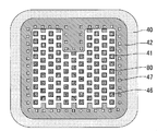
- FIG. 2 is a top view schematically showing the vicinity of the outermost surface inside the silicon carbide of the silicon carbide MOSFET according to the first embodiment.
- a source region 80 of the first conductivity type and a well contact region 46 of the second conductivity type are provided in the first well region 41 of the second conductivity type isolated from each other.
- the first well region 41 group is surrounded by a peripheral region 42 of the second conductivity type so as to surround it, and the peripheral region 42 is surrounded by a JTE region 40 of the second conductivity type at the end of the element.
- a well contact region 47 of a second conductivity type for ohmic connection with a source electrode (not shown) is provided.
- a JFET region exists in the gap region of the first well region 41, which is one of the paths through which an on-current flows when the device is turned on. This gap region is formed above the gate electrode (see FIG. This is one of the factors that determine the size of the capacitance (feedback capacitance) between the drain electrode (not shown) formed on the back surface and the drain electrode (not shown).
- the unit cells are quadrangular and are alternately arranged with a half-cycle shift with respect to the column.
- the present invention is not limited to this, and the unit cells are rectangular. Even if it is a hexagonal shape or arranged at equal pitches in the vertical and horizontal directions, the effect of the present invention is not changed.
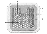
- FIG. 3 is a top view schematically showing a certain distance from the silicon carbide surface of the silicon carbide MOSFET according to the first embodiment, that is, a depth of about the first well region 41.
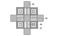
- a second well region 43 of the second conductivity type is formed so as to connect the first well regions 41 to each other.
- the second well region 43 is installed only inside the semiconductor substrate, and is installed in a part of the JFET region. By providing the second well region 43, the opening area of the JFET region is reduced, so that the feedback capacitance is reduced.
- the second well region 43 is disposed so as to cover at least the position where the gate electric field intensity is highest on the projection surface onto the substrate surface when a reverse bias is applied to the element, and the planar structure is There are various forms as will be described later.
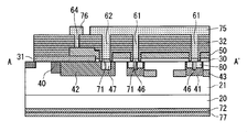
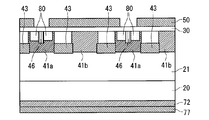
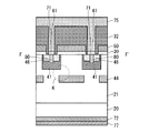
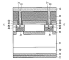
- FIG. 4 is a vertical cross-sectional view schematically showing a cross section taken along the line A-A 'shown in FIG. 3
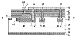
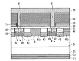
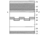
- FIG. 5 is a schematic cross-sectional view taken along the line B-B' shown in FIG.
- the silicon carbide MOSFET according to the present invention is formed on the first conductivity type drift layer 21 formed on the surface of the first conductivity type semiconductor substrate 20 and on the back side of the semiconductor substrate 20.
- the first conductivity type source region 80 defining the surface of the first well region 41 sandwiched between the region and the drift layer 21 as the channel region, and the first well region 41 and the first region formed in the source region 80.
- the well-conducting well contact region 46 and the first well region 41 buried in the drift layer 21 below the gate electrode 50 and connected to each other are formed.
- a second well region 43 of the second conductivity type and a cell region including the first well region 41 are selectively formed on the surface of the drift layer 21 in plan view and connected to the source electrode (source pad 75).
- a source contact hole 61 reaching the ohmic electrode 71 formed on the well contact region 46 and a source pad 75 formed on the source contact hole 61 are provided.
- the source pad 75 is a source electrode that is connected to the source region 80 and directly connected only to the first well region 41 and the peripheral region 42.
- the second well region 43 is connected to the first well region 41 and the peripheral region 42 at a position away from the surface of the first conductivity type drift layer 21.
- the unit cell arrangement shown in FIG. 2 has different cross-sectional shapes as shown in FIGS. 4 and 5 depending on the cross-sectional direction.
- the cross-sectional direction shown in FIG. 5 is different from that shown in FIG. 4 except that the second well region 43 does not appear in the cross-section.
- FIGS. 6 to 15 show vertical cross-sectional views at arbitrary positions where a large number of unit cells are arranged, for example, at the position CC ′ in FIG. It is.
- a semiconductor substrate 20 made of silicon carbide of the first conductivity type is prepared.
- silicon carbide other wide band gap semiconductors having a larger band gap than silicon may be used for the semiconductor substrate 20.
- the wide band gap semiconductor include GaN and diamond in addition to silicon carbide.
- the semiconductor substrate 20 may be tilted to 8 ° or less with respect to the c-axis direction, or may not be tilted, and may have any plane orientation. Does not affect the effect of.
- the semiconductor substrate 20 is a drift layer of the first conductivity type comprising an epitaxial crystal growth layer (impurity concentration is in the range of 1 ⁇ 10 13 cm ⁇ 3 to 1 ⁇ 10 18 cm ⁇ 3 and thickness is 4 ⁇ m to 200 ⁇ m, for example). 21.
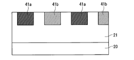
- impurity ion implantation is performed using a resist mask or an oxide film mask processed by photolithography to form a first well region 41a of the second conductivity type.
- the cross section is described for the purpose of facilitating understanding of the first well region 41 b existing where the unit cell row is shifted by a half cycle.
- the semiconductor substrate 20 at the time of implantation may not be positively heated or may be heated at 200 ° C. to 800 ° C.
- the implanted impurity nitrogen or phosphorus is preferable when the conductivity type is n-type, and aluminum or boron is preferable when the conductivity type is p-type.
- the depth of the first well region 41a needs to be set so as not to exceed the bottom surface of the drift layer 21, and is set to a value in the range of 0.3 ⁇ m to 2.0 ⁇ m, for example.
- the impurity concentration of the first well region 41a exceeds the impurity concentration of the drift layer 21, and is set within a range of, for example, 1 ⁇ 10 15 cm ⁇ 3 to 1 ⁇ 10 19 cm ⁇ 3.
- the impurity concentration of first well region 41 a may be lower than the impurity concentration of drift layer 21 in order to increase the conductivity in the channel region of the silicon carbide semiconductor device. .
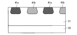
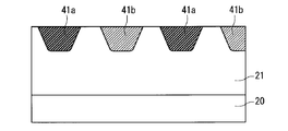
- the distribution of the first well region 41a is laterally widened in the depth direction as shown in FIG. 8 even if the first well region 41a has a shape having a large lateral extent in the depth direction as shown in FIG. 7 (reverse taper shape).
- the shape may be small (tapered shape).
- the impurity concentration on the outermost surface is thin and the deep side is deeply distributed as the distribution of the first well region 41a, the lateral diffusion of the implanted impurities on the deep side increases.
- the structure as shown in FIG. 7 can be easily obtained.
- the second conductivity type peripheral region 42 and the second conductivity type JTE region 40 are similarly formed by impurity ion implantation. If the impurity concentration and the implantation depth of the first well region 41 and the peripheral region 42 are the same, patterning may be performed by one photolithography process. In this case, the number of processing steps and the chip cost can be reduced. Connected, but not necessarily the same. That is, in the peripheral region 42 that does not contribute to channel conduction, the second conductivity is increased at a higher concentration for the purpose of increasing the conductivity of the second conductivity type in order to prevent element breakdown due to potential generation due to charges induced by element switching. Conductive impurities may be implanted.
- the peripheral region 42 and the JTE region 40 are connected within the drift layer 21.
- the first well region 41 and the peripheral region 42 are not directly connected within the drift layer 21.
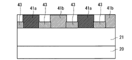
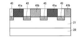
- impurity ion implantation is performed using a resist mask or an oxide film mask processed by photolithography to form a second well region 43 of the second conductivity type.
- the depth of the second well region 43 is set so as not to exceed the bottom surface of the drift layer 21, and is set to a value in the range of 0.3 ⁇ m to 3.0 ⁇ m, for example.
- the impurity concentration of the second well region 43 exceeds the impurity concentration of the drift layer 21 and is set within a range of, for example, 1 ⁇ 10 15 cm ⁇ 3 to 1 ⁇ 10 21 cm ⁇ 3, more preferably 1 ⁇ 10 16 cm ⁇ . It is set within the range of 3 to 1 ⁇ 10 19 cm ⁇ 3.
- the impurity concentration of the second well region 43 may be different from the impurity concentration of the first well region 41.
- the second well region 43 may be formed at the same depth as the first well region 41 as shown in FIG. 9, and is formed deeper than the first well region 41a as shown in FIG. Also good. However, also in FIG. 10, the first well region 41a and the second well region 43 are connected to each other under the first well region 41a.
- the second well region 43 is formed in the JFET region between the first well regions 41a and 41b.
- the planar arrangement and structure will be described later.
- the second well region 43 is not formed simultaneously with the first well region 41a.
- the second well region 43 is formed so as to connect the first well region 41 a and the peripheral region 42.
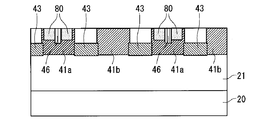
- impurity ion implantation is performed using a resist mask or an oxide film mask processed by photolithography, so that a first conductivity type source region 80 and a first conductivity type field stopper are formed. Regions (not shown) are formed.
- the depth of the first conductivity type source region 80 is set so that the bottom surface thereof does not exceed the bottom surface of the first well region 41, and the value of the impurity concentration is the value of the impurity concentration of the first well region 41.
- the value is set in a range of 1 ⁇ 10 17 cm ⁇ 3 to 1 ⁇ 10 21 cm ⁇ 3.
- the impurity concentration of the second conductivity type higher than the impurity concentration of the first well region 41 and the peripheral region 42 is set.
- a well contact region 46 and a well contact region 47 are formed by ion implantation.
- the ion implantation is desirably performed at a substrate temperature of 150 ° C. or higher. By setting it to such a temperature range, a second conductivity type layer having a low sheet resistance is formed. 11 to 15, the source region 80 and the well contact region 46 are formed in the first well region 41b as well as the first well region 41a, but are not shown here for the sake of understanding. .
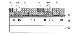
- the first conductivity type impurity is ion-implanted into the entire surface of the substrate as shown in FIG.
- a high concentration layer 85 as a second impurity region of the first conductivity type having an impurity concentration higher than the impurity concentration of the drift layer 21 may be formed, as shown in FIG.
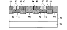
- ion implantation of the first conductivity type impurity is performed in the JFET region using a resist mask or an oxide film mask processed by photolithography to form the current control layer 86 as the second impurity region of the first conductivity type. You may do it. Since both of these can reduce the resistance in the JFET region, the on-resistance of the device can be reduced.
- the impurity concentration of the high concentration layer 85 and the current control layer 86 is lower than the maximum impurity concentration of the second conductivity type in the first well region 41 and is higher than the maximum impurity concentration of the second conductivity type in the second well region 43. And is higher than the impurity concentration of the first conductivity type in the drift layer 21.
- the value is set, for example, within a range of 1 ⁇ 10 16 cm ⁇ 3 to 1 ⁇ 10 18 cm ⁇ 3, and the concentration distribution in the depth direction may not be uniform.
- the high concentration layer 85 and the current control layer 86 have an effect of reducing the JFET resistance even when the depth is smaller than the outermost surface depth of the second well region 43, the first well region 41 as shown in FIGS.
- the on resistance of the silicon carbide semiconductor device is reduced by reducing the spreading resistance of the JFET region as the JFET resistance is reduced.
- the high-concentration layer 85 shown in FIG. 12 is formed deeper than the depth of the first well region 41, the avalanche breakdown between the first well region 41 and the drift layer 21 during reverse bias application. It also has the effect of causing
- the high concentration layer 85 may be epitaxially grown on the drift layer 21 before the ion implantation shown in FIG. Furthermore, both the high concentration layer 85 and the current control layer 86 may be formed.
- heat treatment is carried out in an inert gas atmosphere such as argon or nitrogen, or in a vacuum at a temperature in the range of 1500 ° C. to 2200 ° C. for a time in the range of 0.5 to 60 minutes, so that implantation is performed.
- the doped impurities are electrically activated.
- the surface of the drift layer 21 or the surface of the drift layer 21 and the back surface and end surface of the semiconductor substrate 20 may be covered with a film made of carbon. By doing so, it is possible to prevent the surface of the drift layer 21 from being roughened by etching due to residual moisture or residual oxygen in the apparatus during the heat treatment.
- a field oxide film 31 covered with the film is deposited by a CVD method or the like and patterned (not shown).
- the film thickness of the field oxide film 31 may be 0.5 ⁇ m to 2 ⁇ m.
- the gate insulating film 30 is formed by, for example, a thermal oxidation method or a deposition method, or a heat treatment in a nitrogen gas atmosphere such as NO or N2O, or an ammonia atmosphere thereafter.
- polysilicon as a gate electrode material is deposited by the CVD method, and the gate electrode 50 is patterned by photolithography and dry etching to obtain the structure shown in the figure.
- the polysilicon preferably contains phosphorus and boron and has a low sheet resistance. Phosphorus and boron may be incorporated into the polysilicon film or may be activated by ion implantation and subsequent heat treatment.
- the gate electrode may be a multilayer film of polysilicon, metal, and intermetallic compound.
- the source contact hole 61 and the well contact hole 62 (see FIG. (Not shown).
- a gate contact hole 64 (not shown) to be filled thereafter may be simultaneously formed by the gate wiring 76 (not shown).
- an ohmic electrode 71 is formed in the portion of the source contact hole 61 and the well contact hole 62 (not shown) where the interlayer insulating film 32 is opened, where silicon carbide appears.
- the ohmic electrode 71 is used for forming an ohmic contact between the source region 80, the well contact region 46, and the well contact region 47 (not shown).
- the ohmic electrode 71 is formed by forming a metal film mainly composed of Ni on the entire surface of the substrate and then forming a silicide with silicon carbide by heat treatment at 600 to 1100 ° C.
- the metal film mainly composed of Ni remaining on the surface can be formed by removing the metal film by wet etching using nitric acid, sulfuric acid, hydrochloric acid, a mixed solution thereof with hydrogen peroxide, or the like.
- a similar metal film may be formed on the back surface of the semiconductor substrate 20, and then heat treatment may be performed to form the ohmic electrode 72 on the back surface. In this way, a good ohmic contact is formed between the silicon carbide semiconductor substrate 20 and the drain electrode 77 to be formed later.
- the ohmic electrode 71 may be made of the same intermetallic compound everywhere, or may be made of different intermetallic compounds suitable for each of the p-type and n-type. That is, it is important for the ohmic electrode 71 to have a sufficiently low ohmic contact resistance with respect to the source region 80 of the first conductivity type in order to reduce the on-resistance of the fabricated MOSFET. This is because the well contact region 46 and the well contact region 47 (not shown) are required to have low contact resistance in order to improve the forward characteristics of the body diode built in the MOSFET. This can be realized by performing patterning of the metal film using photolithography technology.
- the heat treatment may be performed again after removing the metal film mainly composed of Ni remaining on the interlayer insulating film 32.
- an ohmic contact with even lower contact resistance is formed by performing the process at a higher temperature than the previous heat treatment.
- a silicide layer is formed on the gate electrode 50 existing on the bottom surface of the gate contact hole 64. If the gate contact hole 64 is not formed in the previous step, the gate contact hole 64 to be filled later by the gate wiring 76 (not shown) is formed by photolithography and etching.
- a wiring metal made of Al, Cu, Ti, Ni, Mo, W, Ta, nitrides thereof, a laminated film thereof or an alloy thereof is formed by sputtering or vapor deposition, and then patterned.
- the gate wiring 76, the gate pad 78 (see FIG. 1), and the source pad 75 are formed.
- a drain electrode 77 is formed by forming a metal film such as Ti, Ni, Ag, or Au on the ohmic electrode 72 on the back surface, thereby completing the silicon carbide MOSFET shown in FIG.
- FIGS. The cross-sectional structure including the termination region in this process is shown in FIGS.
- the surface side may be covered with a protective film such as a silicon nitride film or polyimide. They are opened at appropriate positions of the gate pad 78 and the source pad 75 so that they can be connected to an external control circuit.
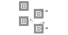
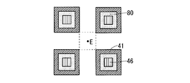
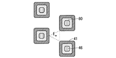
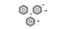
- FIGS. 16 to 18 show a part of the vicinity of the outermost surface of the drift layer 21, FIG. 16 shows the rectangular cells shown in FIGS. 1 to 5 arranged alternately, and FIG. 17 shows the rectangular cells arranged at equal intervals.
- FIG. 18 shows a hexagonal cell arranged in a close-packed configuration.
- the drift layer 21 is present in the gap of the first well region 41, and the gate insulating film 30 and the gate electrode 50 are present immediately above (see FIG. 4).
- the feedback capacitance between the gate electrode and the drain electrode is roughly proportional to the area of the gap region, and that the loss (switching loss) during the switching operation of the MOSFET increases as the feedback capacitance increases.
- the existence of the second well region 43 in the gap between the paired first well regions 41a and 41b reduces the effective area of the gap region and increases the feedback capacitance. There is an effect of decreasing. That is, switching loss can be reduced.
- the planar arrangement of the second well region 43 will be described.
- the gate insulation of the MOS structure existing immediately above the JFET region is maintained when the drain electrode 77 is maintained in the off state with a reverse bias applied.
- a high electric field is induced in the film 30.
- the place where the electric field is the highest is a point indicated by E in each of FIGS. 16 to 18 where the shielding effect by the depletion layer extending from the first well region 41 to the JFET region is weakened. That is, it is a point that covers a position in plan view in which the total sum of the distances between the plurality of adjacent first well regions 41 is minimized.
- FIG. 30 is an electron micrograph of the surface of the silicon carbide semiconductor immediately after Al implantation for forming the first well region 41.
- a square chrome mask (extracted) pattern with rounded corners is used, the first well region 41 also reflects this because the corner of the resist pattern after photoengraving is rounded with a radius of about 0.5 ⁇ m. It can be seen that a rounded structure is formed.
- covering the vicinity including E with the second conductivity type layer weakens the electric field applied to the gate insulating film 30 and is preferable from the viewpoint of securing the reliability of the gate insulating film 30.
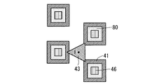
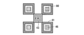
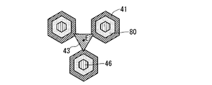
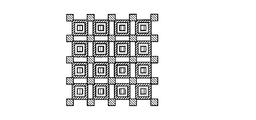
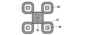
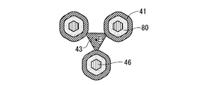
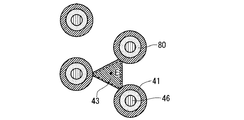
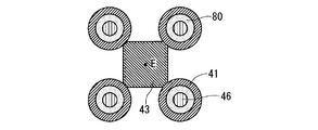
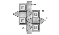
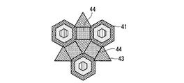
- FIGS. 22 to 25 show a planar arrangement (projected view on the substrate surface) of the second well region 43 that connects the first well regions 41 to each other while covering the point E.
- FIG. The actual arrangement corresponding to these is shown in FIGS.
- FIG. 24 and the hexagonal cell in FIG. 25 are shown in FIG. 24 so as to include the center of gravity of a quadrangle or triangle connecting the vertices of four to three regions adjacent to each other in the first well region 41.
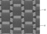
- FIG. 31 shows an electron micrograph of the silicon carbide semiconductor surface on which the structure of FIG. 27 was actually fabricated.
- a triangular second well region 43 is formed between the adjacent first well regions 41 with respect to the rounded quadrangular first well region 41, and the second well region 43 connects the first well regions 41 to each other. I am letting.
- a characteristic feature of the present invention is that, as shown in FIGS. 22 to 25, the first well region 41 is connected by the second well region 43, thereby reducing the feedback capacitance and increasing the electric field applied to the gate insulating film 30. This is to improve the reliability by suppressing the application, and to increase the forward current due to the increase in the junction area of the body diode. Further, as shown in FIGS. 4, 5 and 15, the second well region 43 is not present on the outermost surface of the drift layer 21, thereby reducing the feedback capacitance without causing a large increase in on-resistance. It can be done.
- the second well region 43 shown in FIGS. 22 to 25 extends to the outermost surface of the drift layer 21, a part of the channel formed on the surface by the first well region 41, the source region 80, and the JFET region is formed.
- the channel width per unit cell area is reduced, and further, the on-resistance is eliminated by depriving the JFET region of the carrier generation region induced by the gate electric field during the on-operation. Increase.
- the second well region 43 does not exist on the surface of the drift layer 21 according to the present invention, such a problem does not occur, so that the feedback capacitance can be reduced without causing a large increase in on-resistance.
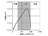
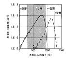
- Such a structure of the second well region 43 has an n-type layer in the JFET region by implanting, for example, 700 keV of Al into the drift layer 21 made of silicon carbide, as shown in the numerical calculation results of FIG.
- the vertical axis in the figure represents the Al concentration
- the horizontal axis represents the depth (nm) from the surface.
- a p-type layer is formed so as not to extend to the outermost surface of drift layer 21.
- the impurity concentration of the drift layer is 2 ⁇ 10 16 cm ⁇ 3.
- the thermal diffusion of impurities in silicon carbide is less than conventional thermal diffusion in silicon, and the distribution at the time of implantation is almost maintained even when a high-temperature activation heat treatment is applied, and smoothing of the impurity concentration due to thermal diffusion is suppressed. Therefore, the structure of the second well region 43 shown in FIGS. 1 to 5 and FIGS. 6 to 15 is easily manufactured.
- a source region 80 of the first conductivity type that defines the surface of each first well region 41 as a channel region, and a gate insulating film 30 that is an insulating film is formed from the channel region to the drift layer 21.
- the gate electrode 50 is formed to be buried in the drift layer 21 below the gate electrode 50 and connected to each of the first well regions 41 adjacent to each other, and between the plurality of first well regions 41 in plan view.
- a plurality of second conductivity type second well regions 43 covering a part of the region are connected to the source region 80 and are directly connected only to the first well region 41 of the first and second well regions 41, 43.
- the second well region 43 is formed at a position that does not become the channel region by including the source electrode thus formed and the drain electrode 77 formed on the back surface of the semiconductor substrate 20. It is possible to reduce the feedback capacitance without increasing the resistance, and to reduce the on-loss and switching loss of the semiconductor device.
- the first well region 41 and the second well region 43 have an influence on the channel characteristics because the impurity concentration distribution of the second conductivity type is different.
- the feedback capacitance can be reduced without giving.
- the second well region 43 is a position in plan view where the sum of the distances from the plurality of first well regions 41 to which the second well region 43 is connected is minimized.
- the second impurity of the first conductivity type having an impurity concentration higher than the impurity concentration of the drift layer 21 on the surface of the drift layer 21 below the gate electrode 50.
- the semiconductor substrate 20 is composed of a wide band gap semiconductor, the voltage resistance is improved and the allowable current density is increased. Can be reduced in size. In addition, since the power loss is reduced, the efficiency of the semiconductor device can be increased.
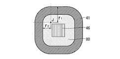
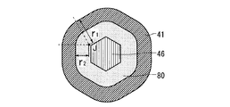
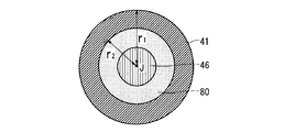
- FIGS. 33 to 35 are diagrams showing a silicon carbide semiconductor device according to the second embodiment, specifically, a unit cell of a silicon carbide MOSFET, and FIGS. 36 to 40 are silicon carbide semiconductors according to the second embodiment. It is a figure (projection figure to a substrate surface) which shows plane arrangement of a device, specifically, a unit cell of silicon carbide MOSFET, and the 2nd well field 43.
- the channel length defined by the gap between the first well region 41 and the source region 80 on the surface of the drift layer 21 is the same throughout the unit cell.
- the first well region 41 and the source region 80 are formed by 90 ° arc patterns (radius r1 and radius r2) centered on the point J, respectively.
- the first well region 41 and the source region 80 are formed by a 60 ° arc pattern (radius r1 and radius r2) around the point J, respectively. .
- the first well region 41 and the source region 80 are formed by arc patterns (radius r 1 and radius r 2) centering on the point J that is the center of the unit cell, respectively.
- the channel length in the unit cell is made uniform.
- the gap between the first well region 41 and the source region 80 is 1.41 times longer than the portion other than the corner portion.
- the channel resistance at was high.
- the distance from the two sides (two directions) forming the corner is the shortest and current concentration occurs. That is, the distribution of on-current is not uniform at the corners, which is a problem from the viewpoint of device reliability.
- the channel length is constant everywhere in the unit cell, excessive current concentration does not occur, and the element reliability is improved.
- the first well region 41 and the source region 80 may be formed by ion implantation of impurities using different masks, but after the well implantation process using the mask of the first well region 41.
- the mask may be thickened by the channel length to be a source implantation mask, or after the source implantation process using the mask of the source region 80, the channel length may be thinned to be a well implantation mask.
- a well implantation mask using polycrystalline silicon an oxidation process is performed after the implantation process to form a thermal oxide film around the polycrystalline silicon, and source implantation is performed as a composite mask to cope with the volume increase. Channel length can be realized.
- the source implantation mask using silicon oxide film or photoresist well implantation is performed after the isotropic etching of the oxide film and resist after the implantation process, so that the channel length corresponding to the volume reduction is obtained. Can be realized.
- Such a self-alignment method for determining the channel length is more effective in realizing a constant channel length in the circular unit cell structure shown in FIG. 35 having excellent symmetry with respect to the center of the unit cell. This is because, when the structure of the implantation mask is deformed by a chemical method such as oxidation or etching, the reaction speed often differs between the corner and the straight portion, so the volume is not necessarily the same length in all directions. It does not increase or decrease in volume, but results in channel length imbalance.
- the radius of curvature of the square and hexagonal corners shown in FIGS. 33 and 34 is 0.5 ⁇ m or more in the source region 80 smaller than the first well region 41, it is sufficiently resolved by the conventional photoengraving technique.
- the radius of curvature is excessively large, the width of reduction becomes larger than the original channel width of the square and hexagon, and the channel resistance is increased. Therefore, the radius of curvature of the source region 80 may be about 2.0 ⁇ m. .
- the corner of the rectangular source region 80 is left at 90 °, or the corner of the hexagonal source region is left at 120 °, and the first well region 41 is not rounded.
- a unit cell structure in which only the corners are rounded is also conceivable.
- it is not easy to produce the acute angle pattern as described above as an implantation mask and it is often rounded as shown in FIG. 30, resulting in a constant channel length. It will not be. Even if an implantation mask having an acute angle pattern can be formed, the on-current is concentrated at the corner of the source region 80, which is not preferable from the viewpoint of reliability.
- the first well region is compared with the structure having no roundness as shown in FIGS.
- the gap JFET length
- the electric field applied to the JFET opening region increases.
- this structure reduces the feedback capacitance and increases the junction area of the body diode, thereby increasing the forward current of the body diode.
- the semiconductor device when the first well region 41 is circular, the symmetry with respect to the center of the unit cell is excellent, so that the mask using the self-alignment technique is used.
- a constant channel length can be realized by forming.
- FIGS. 41 to 43 are diagrams (projections onto the substrate surface) showing the planar arrangement of the silicon carbide semiconductor device according to the third embodiment, specifically, the unit cell of silicon carbide MOSFET.
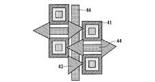
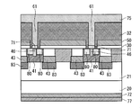
- a third well region buried in the drift layer 21 between a plurality of isolated second well regions 43 and connected to each of the second well regions 43 adjacent to each other. 44 is further provided.
- the third well region 44 exists in or below the JFET region and does not exist on the surface of the drift layer 21. Further, it exists at the same depth as the second well region 43 or deeper than the second well region 43.
- the third well region 44 is not directly connected to the first well region 41. Further, the third well region 44 is not directly connected to the peripheral region 42.
- the third well region 44 is inserted by adopting a structure in which the second well region 43 is in contact with the first well region 41 near the bottom surface and the third well region 44 is in contact with the bottom surface of the second well region 43.
- the narrowing of the JFET region is alleviated. That is, since the gap between the first well region 41 and the third well region 44 widens in the depth direction of the substrate, it is possible to prevent a significant increase in JFET resistance.
- the arrangement of the third well region 44 as seen in the projections on the substrate surface shown in FIGS. 44 to 46 that is, the structure in which the JFET region is entirely filled with the third well region 44 can be used. It is effective for the further reduction of.
- FIG. 47 to 49 show cross-sectional structures between F-F ', G-G', and H-H 'in FIG. That is, as shown in FIG. 48, the second well region 43 is connected to the first well region 41 below this. As shown in FIG. 49, the third well region 44 is connected to the second well region 43 below this. As shown in FIG. 47, the projection surface of the JFET opening region is covered by the third well region 44 below the JFET opening region. However, as shown by K in FIG. 47, the first well region 41 and the third well region 44 are covered. It is also possible to provide a gap between them.
- FIGS. 47 to 49 is the same as the configuration shown in Embodiment 1 except that the third well region 44 is provided, and the detailed description of the other configurations is omitted.
- the second well regions 43 are provided in plural, the second wells buried in the drift layer 21 between the plurality of first well regions 41 and adjacent to each other.
- the second conductivity type third well region 44 formed in connection with each of the regions 43, the feedback capacitance and the switching loss can be reduced, and the ON current of the body diode can be increased.
- the upper surface of the third well region 44 is formed below the lower surface of the first well region 41, so that the opening region of the JFET region can be reduced. Since it can be expanded three-dimensionally, the on-resistance can be reduced.
- the second well region 43 and the third well region 44 are formed so as to cover all the regions between the plurality of first well regions 41 in plan view. As a result, the feedback capacity can be further reduced.
- FIG. 50 is a diagram showing a cross-sectional structure of a silicon carbide semiconductor device according to the fourth embodiment, specifically, a unit cell of silicon carbide MOSFET.
- the first conductivity type impurity is continuously implanted using the implantation mask used here as it is, so that the first conductivity
- a feature is that a current spreading layer 83 is provided as a first impurity region of the type.
- the current spreading layer 83 has a higher impurity concentration than the drift layer 21, specifically, for example, in the range of 2 ⁇ 10 13 cm ⁇ 3 to 2 ⁇ 10 18 cm ⁇ 3, and its depth does not exceed the drift layer 21, The maximum is 1 ⁇ m.
- the configuration shown in FIG. 50 is the same as the configuration shown in Embodiment 1 except that the current spreading layer 83 is provided, and detailed description of other configurations is omitted.
- the first conductivity type impurity when implanted, it is implanted at an angle slightly inclined from the vertical direction to the horizontal direction with respect to the substrate surface (inclined implantation), so that the current spreading layer 83 has a further lateral spread. May be produced.
- Such a spreading structure of the current spreading layer 83 is, as shown in the numerical calculation result of FIG. 51, in the drift layer 21 made of silicon carbide, for example, a p-type layer by aluminum 700 keV implantation and n + by nitrogen 1.3 MeV implantation.
- the vertical structure of the second well region 43 having a depth of approximately 0.3 ⁇ m to 1.0 ⁇ m and the current spreading layer 83 having a depth of approximately 1.3 ⁇ m can be formed.
- the vertical axis in the figure indicates the Al or N concentration
- the horizontal axis indicates the depth (nm) from the surface.
- the thermal diffusion of impurities in silicon carbide is less than conventional thermal diffusion in silicon, and the distribution at the time of implantation is almost maintained even when a high-temperature activation heat treatment is applied, and smoothing of the impurity concentration due to thermal diffusion is suppressed. Therefore, the structure as shown in FIG. 51 is easily manufactured.
- the first impurity concentration that is higher than the impurity concentration of drift layer 21 formed below second well region 43 and / or third well region 44.
- the current spreading layer 83 that is a first impurity region of one conductivity type, the spreading resistance of the JFET region can be reduced.
- the semiconductor element is a vertical MOSFET.
- the second conductive type is used between the semiconductor substrate 20 and the back side ohmic electrode 72 shown in FIG.
- the collector layer By providing the collector layer, the above-described effects of the present invention can be obtained in the same manner even when a semiconductor element having an IGBT cell region is configured. Therefore, it can be said that the range of the scope of the present invention is a semiconductor element as a switching element having a MOS structure such as MOSFET or IGBT.
- the semiconductor element itself having the MOS structure described in the first, second, third, and fourth embodiments is defined as a “semiconductor device” in a narrow sense.
- the semiconductor such as an inverter module that is mounted on a lead frame and sealed together with a freewheel diode connected in antiparallel to the semiconductor element and a control circuit that generates and applies the gate voltage of the semiconductor element.
- the power module itself that is formed by applying the element is also defined as a “semiconductor device” in a broad sense.
- the present invention is suitable for application to a power converter such as an inverter.
Landscapes
- Engineering & Computer Science (AREA)
- Microelectronics & Electronic Packaging (AREA)
- Power Engineering (AREA)
- Condensed Matter Physics & Semiconductors (AREA)
- General Physics & Mathematics (AREA)
- Physics & Mathematics (AREA)
- Ceramic Engineering (AREA)
- Computer Hardware Design (AREA)
- Manufacturing & Machinery (AREA)
- Chemical & Material Sciences (AREA)
- Crystallography & Structural Chemistry (AREA)
- Electrodes Of Semiconductors (AREA)
- Junction Field-Effect Transistors (AREA)
Abstract
Priority Applications (6)
| Application Number | Priority Date | Filing Date | Title |
|---|---|---|---|
| JP2012512749A JP5619152B2 (ja) | 2010-04-26 | 2011-04-07 | 半導体装置 |
| KR1020127027337A KR101464846B1 (ko) | 2010-04-26 | 2011-04-07 | 반도체 장치 |
| CN201180020961.3A CN102859696B (zh) | 2010-04-26 | 2011-04-07 | 半导体装置 |
| DE112011101442.2T DE112011101442B4 (de) | 2010-04-26 | 2011-04-07 | Halbleitervorrichtung |
| US13/638,970 US8860039B2 (en) | 2010-04-26 | 2011-04-07 | Semiconductor device |
| US14/463,286 US10062758B2 (en) | 2010-04-26 | 2014-08-19 | Semiconductor device |
Applications Claiming Priority (4)
| Application Number | Priority Date | Filing Date | Title |
|---|---|---|---|
| JP2010100553 | 2010-04-26 | ||
| JP2010-100553 | 2010-04-26 | ||
| JP2010-195358 | 2010-09-01 | ||
| JP2010195358 | 2010-09-01 |
Related Child Applications (2)
| Application Number | Title | Priority Date | Filing Date |
|---|---|---|---|
| US13/638,970 A-371-Of-International US8860039B2 (en) | 2010-04-26 | 2011-04-07 | Semiconductor device |
| US14/463,286 Division US10062758B2 (en) | 2010-04-26 | 2014-08-19 | Semiconductor device |
Publications (1)
| Publication Number | Publication Date |
|---|---|
| WO2011135995A1 true WO2011135995A1 (fr) | 2011-11-03 |
Family
ID=44861309
Family Applications (1)
| Application Number | Title | Priority Date | Filing Date |
|---|---|---|---|
| PCT/JP2011/058805 WO2011135995A1 (fr) | 2010-04-26 | 2011-04-07 | Dispositif semiconducteur |
Country Status (6)
| Country | Link |
|---|---|
| US (2) | US8860039B2 (fr) |
| JP (2) | JP5619152B2 (fr) |
| KR (1) | KR101464846B1 (fr) |
| CN (1) | CN102859696B (fr) |
| DE (1) | DE112011101442B4 (fr) |
| WO (1) | WO2011135995A1 (fr) |
Cited By (10)
| Publication number | Priority date | Publication date | Assignee | Title |
|---|---|---|---|---|
| JP2014038963A (ja) * | 2012-08-17 | 2014-02-27 | Rohm Co Ltd | 半導体装置 |
| WO2015019732A1 (fr) * | 2013-08-06 | 2015-02-12 | 住友電気工業株式会社 | Dispositif à semi-conducteur au carbure de silicium et son procédé de fabrication |
| WO2015198468A1 (fr) * | 2014-06-27 | 2015-12-30 | 三菱電機株式会社 | Dispositif semiconducteur au carbure de silicium |
| JP2016004966A (ja) * | 2014-06-19 | 2016-01-12 | 富士電機株式会社 | 半導体装置および半導体装置の製造方法 |
| JP2016058530A (ja) * | 2014-09-09 | 2016-04-21 | 住友電気工業株式会社 | 炭化珪素半導体装置の製造方法 |
| JP2016058661A (ja) * | 2014-09-11 | 2016-04-21 | 国立研究開発法人産業技術総合研究所 | 半導体装置 |
| JP2018182197A (ja) * | 2017-04-19 | 2018-11-15 | 株式会社豊田中央研究所 | 窒化物半導体装置とその製造方法 |
| JP2019519916A (ja) * | 2016-05-23 | 2019-07-11 | ゼネラル・エレクトリック・カンパニイ | 炭化ケイ素金属酸化物半導体(mos)デバイスセルにおける電界シールド |
| JP2020102596A (ja) * | 2018-12-25 | 2020-07-02 | トヨタ自動車株式会社 | 半導体装置 |
| JP2021530878A (ja) * | 2018-07-13 | 2021-11-11 | クリー インコーポレイテッドCree Inc. | ワイドバンドギャップ半導体デバイス |
Families Citing this family (22)
| Publication number | Priority date | Publication date | Assignee | Title |
|---|---|---|---|---|
| KR101230680B1 (ko) | 2009-04-30 | 2013-02-07 | 미쓰비시덴키 가부시키가이샤 | 반도체 장치 및 그 제조 방법 |
| DE112012005039B4 (de) * | 2011-12-01 | 2021-01-14 | Mitsubishi Electric Corp. | Halbleitervorrichtung |
| US9991376B2 (en) | 2013-09-20 | 2018-06-05 | Monolith Semiconductor Inc. | High voltage MOSFET devices and methods of making the devices |
| US9214572B2 (en) | 2013-09-20 | 2015-12-15 | Monolith Semiconductor Inc. | High voltage MOSFET devices and methods of making the devices |
| JP6119564B2 (ja) * | 2013-11-08 | 2017-04-26 | 住友電気工業株式会社 | 炭化珪素半導体装置の製造方法 |
| JP6183200B2 (ja) * | 2013-12-16 | 2017-08-23 | 住友電気工業株式会社 | 炭化珪素半導体装置およびその製造方法 |
| US9293533B2 (en) * | 2014-06-20 | 2016-03-22 | Infineon Technologies Austria Ag | Semiconductor switching devices with different local transconductance |
| WO2016052261A1 (fr) * | 2014-10-01 | 2016-04-07 | 三菱電機株式会社 | Dispositif à semiconducteurs |
| CN106158650A (zh) * | 2015-04-16 | 2016-11-23 | 中芯国际集成电路制造(上海)有限公司 | 晶体管及其形成方法 |
| CN108140674B (zh) * | 2015-10-16 | 2021-02-19 | 三菱电机株式会社 | 半导体装置 |
| JP1555473S (fr) * | 2015-10-26 | 2016-08-08 | ||
| JP1555474S (fr) * | 2015-10-26 | 2016-08-08 | ||
| CN108463885A (zh) | 2015-12-11 | 2018-08-28 | 罗姆股份有限公司 | 半导体装置 |
| JP7018394B2 (ja) * | 2016-08-19 | 2022-02-10 | ローム株式会社 | 半導体装置 |
| DE112017004237B4 (de) * | 2016-08-25 | 2023-12-14 | Mitsubishi Electric Corporation | Halbleitereinheit |
| JP6844228B2 (ja) * | 2016-12-02 | 2021-03-17 | 富士電機株式会社 | 半導体装置および半導体装置の製造方法 |
| BR112019016822A2 (pt) * | 2017-02-14 | 2020-04-07 | Nissan Motor | dispositivo semicondutor e método de fabricação do mesmo |
| JP7026314B2 (ja) * | 2018-02-07 | 2022-02-28 | パナソニックIpマネジメント株式会社 | 炭化珪素半導体装置 |
| JP2020072214A (ja) * | 2018-11-01 | 2020-05-07 | 富士電機株式会社 | 窒化ガリウム系半導体装置 |
| JP6973422B2 (ja) * | 2019-01-21 | 2021-11-24 | 株式会社デンソー | 半導体装置の製造方法 |
| CN113644124B (zh) * | 2021-08-20 | 2024-03-22 | 深圳市伟安特电子有限公司 | 新型的低噪声低损耗igbt |
| TWI819771B (zh) * | 2022-09-01 | 2023-10-21 | 鴻揚半導體股份有限公司 | 半導體裝置 |
Citations (7)
| Publication number | Priority date | Publication date | Assignee | Title |
|---|---|---|---|---|
| JP2003086800A (ja) * | 2001-09-12 | 2003-03-20 | Toshiba Corp | 半導体装置及びその製造方法 |
| JP2004241768A (ja) * | 2003-01-16 | 2004-08-26 | Fuji Electric Device Technology Co Ltd | 半導体素子 |
| JP2004537162A (ja) * | 2001-04-11 | 2004-12-09 | シリコン・セミコンダクター・コーポレイション | パワーデバイスとその製造方法 |
| JP2007150142A (ja) * | 2005-11-30 | 2007-06-14 | Toshiba Corp | 半導体装置 |
| JP2007243092A (ja) * | 2006-03-13 | 2007-09-20 | Toyota Motor Corp | 半導体装置とその製造方法 |
| JP2007281034A (ja) * | 2006-04-03 | 2007-10-25 | Toshiba Corp | 電力用半導体素子 |
| JP2008258313A (ja) * | 2007-04-03 | 2008-10-23 | Denso Corp | 半導体装置およびその製造方法 |
Family Cites Families (19)
| Publication number | Priority date | Publication date | Assignee | Title |
|---|---|---|---|---|
| JPS6439069A (en) | 1987-04-14 | 1989-02-09 | Nec Corp | Field-effect transistor |
| JP2857200B2 (ja) | 1990-02-06 | 1999-02-10 | 松下電子工業株式会社 | 半導体装置 |
| JP3156300B2 (ja) | 1991-10-07 | 2001-04-16 | 株式会社デンソー | 縦型半導体装置 |
| JP4540146B2 (ja) * | 1998-12-24 | 2010-09-08 | ルネサスエレクトロニクス株式会社 | 半導体装置の製造方法 |
| DE10008570B4 (de) | 2000-02-24 | 2006-05-04 | Infineon Technologies Ag | Kompensations-Halbleiterbauelement |
| US6781194B2 (en) | 2001-04-11 | 2004-08-24 | Silicon Semiconductor Corporation | Vertical power devices having retrograded-doped transition regions and insulated trench-based electrodes therein |
| US6784486B2 (en) | 2000-06-23 | 2004-08-31 | Silicon Semiconductor Corporation | Vertical power devices having retrograded-doped transition regions therein |
| EP1267415A3 (fr) | 2001-06-11 | 2009-04-15 | Kabushiki Kaisha Toshiba | Dispositif semi-conducteur de puissance ayant une région de type RESURF |
| JP4537646B2 (ja) | 2002-06-14 | 2010-09-01 | 株式会社東芝 | 半導体装置 |
| WO2004093192A1 (fr) * | 2003-04-10 | 2004-10-28 | Fujitsu Limited | Dispositif a semi-conducteurs et son procede de fabrication |
| JP2005333068A (ja) | 2004-05-21 | 2005-12-02 | Toshiba Corp | 半導体装置 |
| KR101007478B1 (ko) | 2006-02-07 | 2011-01-12 | 미쓰비시덴키 가부시키가이샤 | 반도체 장치 및 그 제조 방법 |
| JP2009004668A (ja) * | 2007-06-25 | 2009-01-08 | Toshiba Corp | 半導体装置 |
| JP4786621B2 (ja) | 2007-09-20 | 2011-10-05 | 株式会社東芝 | 半導体装置およびその製造方法 |
| JP5046886B2 (ja) | 2007-11-27 | 2012-10-10 | 三菱電機株式会社 | 半導体装置 |
| WO2009099182A1 (fr) | 2008-02-06 | 2009-08-13 | Rohm Co., Ltd. | Dispositif à semi-conducteur |
| KR101230680B1 (ko) | 2009-04-30 | 2013-02-07 | 미쓰비시덴키 가부시키가이샤 | 반도체 장치 및 그 제조 방법 |
| JP5616665B2 (ja) | 2010-03-30 | 2014-10-29 | ローム株式会社 | 半導体装置 |
| DE112011101254B4 (de) | 2010-04-06 | 2017-04-06 | Mitsubishi Electric Corporation | Leistungshalbleiterbauteile und Verfahren zu deren Herstellung |
-
2011
- 2011-04-07 JP JP2012512749A patent/JP5619152B2/ja active Active
- 2011-04-07 US US13/638,970 patent/US8860039B2/en active Active
- 2011-04-07 WO PCT/JP2011/058805 patent/WO2011135995A1/fr active Application Filing
- 2011-04-07 KR KR1020127027337A patent/KR101464846B1/ko active IP Right Grant
- 2011-04-07 CN CN201180020961.3A patent/CN102859696B/zh active Active
- 2011-04-07 DE DE112011101442.2T patent/DE112011101442B4/de active Active
-
2014
- 2014-08-19 US US14/463,286 patent/US10062758B2/en active Active
- 2014-09-11 JP JP2014185212A patent/JP5931149B2/ja active Active
Patent Citations (7)
| Publication number | Priority date | Publication date | Assignee | Title |
|---|---|---|---|---|
| JP2004537162A (ja) * | 2001-04-11 | 2004-12-09 | シリコン・セミコンダクター・コーポレイション | パワーデバイスとその製造方法 |
| JP2003086800A (ja) * | 2001-09-12 | 2003-03-20 | Toshiba Corp | 半導体装置及びその製造方法 |
| JP2004241768A (ja) * | 2003-01-16 | 2004-08-26 | Fuji Electric Device Technology Co Ltd | 半導体素子 |
| JP2007150142A (ja) * | 2005-11-30 | 2007-06-14 | Toshiba Corp | 半導体装置 |
| JP2007243092A (ja) * | 2006-03-13 | 2007-09-20 | Toyota Motor Corp | 半導体装置とその製造方法 |
| JP2007281034A (ja) * | 2006-04-03 | 2007-10-25 | Toshiba Corp | 電力用半導体素子 |
| JP2008258313A (ja) * | 2007-04-03 | 2008-10-23 | Denso Corp | 半導体装置およびその製造方法 |
Cited By (17)
| Publication number | Priority date | Publication date | Assignee | Title |
|---|---|---|---|---|
| JP2014038963A (ja) * | 2012-08-17 | 2014-02-27 | Rohm Co Ltd | 半導体装置 |
| WO2015019732A1 (fr) * | 2013-08-06 | 2015-02-12 | 住友電気工業株式会社 | Dispositif à semi-conducteur au carbure de silicium et son procédé de fabrication |
| JP2015053462A (ja) * | 2013-08-06 | 2015-03-19 | 住友電気工業株式会社 | 炭化珪素半導体装置およびその製造方法 |
| US9722027B2 (en) | 2013-08-06 | 2017-08-01 | Sumitomo Electric Industries, Ltd. | Silicon carbide semiconductor device and method for manufacturing the same |
| JP2016004966A (ja) * | 2014-06-19 | 2016-01-12 | 富士電機株式会社 | 半導体装置および半導体装置の製造方法 |
| JPWO2015198468A1 (ja) * | 2014-06-27 | 2017-04-20 | 三菱電機株式会社 | 炭化珪素半導体装置 |
| WO2015198468A1 (fr) * | 2014-06-27 | 2015-12-30 | 三菱電機株式会社 | Dispositif semiconducteur au carbure de silicium |
| US9985124B2 (en) | 2014-06-27 | 2018-05-29 | Mitsubishi Electric Corporation | Silicon carbide semiconductor device |
| JP2016058530A (ja) * | 2014-09-09 | 2016-04-21 | 住友電気工業株式会社 | 炭化珪素半導体装置の製造方法 |
| JP2016058661A (ja) * | 2014-09-11 | 2016-04-21 | 国立研究開発法人産業技術総合研究所 | 半導体装置 |
| JP2019519916A (ja) * | 2016-05-23 | 2019-07-11 | ゼネラル・エレクトリック・カンパニイ | 炭化ケイ素金属酸化物半導体(mos)デバイスセルにおける電界シールド |
| JP7080536B2 (ja) | 2016-05-23 | 2022-06-06 | ゼネラル・エレクトリック・カンパニイ | 炭化ケイ素金属酸化物半導体(mos)デバイスセルにおける電界シールド |
| JP2018182197A (ja) * | 2017-04-19 | 2018-11-15 | 株式会社豊田中央研究所 | 窒化物半導体装置とその製造方法 |
| JP2021530878A (ja) * | 2018-07-13 | 2021-11-11 | クリー インコーポレイテッドCree Inc. | ワイドバンドギャップ半導体デバイス |
| JP7165822B2 (ja) | 2018-07-13 | 2022-11-04 | ウルフスピード インコーポレイテッド | ワイドバンドギャップ半導体デバイス |
| JP2020102596A (ja) * | 2018-12-25 | 2020-07-02 | トヨタ自動車株式会社 | 半導体装置 |
| JP7070393B2 (ja) | 2018-12-25 | 2022-05-18 | 株式会社デンソー | 半導体装置 |
Also Published As
| Publication number | Publication date |
|---|---|
| JP2014225713A (ja) | 2014-12-04 |
| DE112011101442B4 (de) | 2022-05-12 |
| DE112011101442T5 (de) | 2013-04-25 |
| US20140353686A1 (en) | 2014-12-04 |
| KR101464846B1 (ko) | 2014-11-25 |
| JP5619152B2 (ja) | 2014-11-05 |
| CN102859696A (zh) | 2013-01-02 |
| JP5931149B2 (ja) | 2016-06-08 |
| KR20120131221A (ko) | 2012-12-04 |
| JPWO2011135995A1 (ja) | 2013-07-18 |
| US10062758B2 (en) | 2018-08-28 |
| CN102859696B (zh) | 2015-07-22 |
| US20130020586A1 (en) | 2013-01-24 |
| US8860039B2 (en) | 2014-10-14 |
Similar Documents
| Publication | Publication Date | Title |
|---|---|---|
| JP5931149B2 (ja) | 半導体装置 | |
| JP6759563B2 (ja) | 半導体装置および半導体装置の製造方法 | |
| JP6144674B2 (ja) | 半導体装置及びその製造方法 | |
| JP5687364B2 (ja) | 半導体装置 | |
| JP5776610B2 (ja) | 炭化珪素半導体装置およびその製造方法 | |
| JP4900662B2 (ja) | ショットキーダイオードを内蔵した炭化ケイ素mos電界効果トランジスタおよびその製造方法 | |
| CN107078160B (zh) | 半导体装置 | |
| JP6120756B2 (ja) | 炭化珪素半導体装置とその製造方法 | |
| US9825164B2 (en) | Silicon carbide semiconductor device and manufacturing method for same | |
| JP7029710B2 (ja) | 半導体装置 | |
| JP6345378B1 (ja) | 半導体装置 | |
| JP4876419B2 (ja) | 半導体素子の製造方法 | |
| WO2019123601A1 (fr) | Dispositif à semi-conducteur | |
| WO2017169777A1 (fr) | Convertisseur d'énergie électrique | |
| JP5751763B2 (ja) | 半導体装置 | |
| WO2017183375A1 (fr) | Dispositif à semi-conducteurs | |
| WO2017187856A1 (fr) | Dispositif à semi-conducteur | |
| JP7404722B2 (ja) | 半導体装置 | |
| JP6289600B2 (ja) | 半導体装置 | |
| JP2021044274A (ja) | 半導体装置 | |
| JP2015057851A (ja) | 半導体装置 | |
| JP5784860B1 (ja) | 炭化ケイ素半導体装置 |
Legal Events
| Date | Code | Title | Description |
|---|---|---|---|
| WWE | Wipo information: entry into national phase |
Ref document number: 201180020961.3 Country of ref document: CN |
|
| 121 | Ep: the epo has been informed by wipo that ep was designated in this application |
Ref document number: 11774779 Country of ref document: EP Kind code of ref document: A1 |
|
| WWE | Wipo information: entry into national phase |
Ref document number: 2012512749 Country of ref document: JP |
|
| WWE | Wipo information: entry into national phase |
Ref document number: 13638970 Country of ref document: US |
|
| ENP | Entry into the national phase |
Ref document number: 20127027337 Country of ref document: KR Kind code of ref document: A |
|
| WWE | Wipo information: entry into national phase |
Ref document number: 112011101442 Country of ref document: DE Ref document number: 1120111014422 Country of ref document: DE |
|
| 122 | Ep: pct application non-entry in european phase |
Ref document number: 11774779 Country of ref document: EP Kind code of ref document: A1 |

