WO2011024690A1 - フレキシブル基材-支持体の積層構造体、支持体付き電子デバイス用パネル、および電子デバイス用パネルの製造方法 - Google Patents
フレキシブル基材-支持体の積層構造体、支持体付き電子デバイス用パネル、および電子デバイス用パネルの製造方法 Download PDFInfo
- Publication number
- WO2011024690A1 WO2011024690A1 PCT/JP2010/063947 JP2010063947W WO2011024690A1 WO 2011024690 A1 WO2011024690 A1 WO 2011024690A1 JP 2010063947 W JP2010063947 W JP 2010063947W WO 2011024690 A1 WO2011024690 A1 WO 2011024690A1
- Authority
- WO
- WIPO (PCT)
- Prior art keywords
- resin layer
- glass
- silicone resin
- support
- base material
- Prior art date
- Legal status (The legal status is an assumption and is not a legal conclusion. Google has not performed a legal analysis and makes no representation as to the accuracy of the status listed.)
- Ceased
Links
Images




Classifications
-
- B—PERFORMING OPERATIONS; TRANSPORTING
- B32—LAYERED PRODUCTS
- B32B—LAYERED PRODUCTS, i.e. PRODUCTS BUILT-UP OF STRATA OF FLAT OR NON-FLAT, e.g. CELLULAR OR HONEYCOMB, FORM
- B32B27/00—Layered products comprising a layer of synthetic resin
- B32B27/06—Layered products comprising a layer of synthetic resin as the main or only constituent of a layer, which is next to another layer of the same or of a different material
-
- B—PERFORMING OPERATIONS; TRANSPORTING
- B32—LAYERED PRODUCTS
- B32B—LAYERED PRODUCTS, i.e. PRODUCTS BUILT-UP OF STRATA OF FLAT OR NON-FLAT, e.g. CELLULAR OR HONEYCOMB, FORM
- B32B15/00—Layered products comprising a layer of metal
- B32B15/04—Layered products comprising a layer of metal comprising metal as the main or only constituent of a layer, which is next to another layer of the same or of a different material
- B32B15/08—Layered products comprising a layer of metal comprising metal as the main or only constituent of a layer, which is next to another layer of the same or of a different material of synthetic resin
-
- B—PERFORMING OPERATIONS; TRANSPORTING
- B32—LAYERED PRODUCTS
- B32B—LAYERED PRODUCTS, i.e. PRODUCTS BUILT-UP OF STRATA OF FLAT OR NON-FLAT, e.g. CELLULAR OR HONEYCOMB, FORM
- B32B17/00—Layered products essentially comprising sheet glass, or glass, slag, or like fibres
- B32B17/06—Layered products essentially comprising sheet glass, or glass, slag, or like fibres comprising glass as the main or only constituent of a layer, next to another layer of a specific material
-
- B—PERFORMING OPERATIONS; TRANSPORTING
- B32—LAYERED PRODUCTS
- B32B—LAYERED PRODUCTS, i.e. PRODUCTS BUILT-UP OF STRATA OF FLAT OR NON-FLAT, e.g. CELLULAR OR HONEYCOMB, FORM
- B32B17/00—Layered products essentially comprising sheet glass, or glass, slag, or like fibres
- B32B17/06—Layered products essentially comprising sheet glass, or glass, slag, or like fibres comprising glass as the main or only constituent of a layer, next to another layer of a specific material
- B32B17/10—Layered products essentially comprising sheet glass, or glass, slag, or like fibres comprising glass as the main or only constituent of a layer, next to another layer of a specific material of synthetic resin
-
- B—PERFORMING OPERATIONS; TRANSPORTING
- B32—LAYERED PRODUCTS
- B32B—LAYERED PRODUCTS, i.e. PRODUCTS BUILT-UP OF STRATA OF FLAT OR NON-FLAT, e.g. CELLULAR OR HONEYCOMB, FORM
- B32B7/00—Layered products characterised by the relation between layers; Layered products characterised by the relative orientation of features between layers, or by the relative values of a measurable parameter between layers, i.e. products comprising layers having different physical, chemical or physicochemical properties; Layered products characterised by the interconnection of layers
- B32B7/04—Interconnection of layers
- B32B7/06—Interconnection of layers permitting easy separation
-
- C—CHEMISTRY; METALLURGY
- C08—ORGANIC MACROMOLECULAR COMPOUNDS; THEIR PREPARATION OR CHEMICAL WORKING-UP; COMPOSITIONS BASED THEREON
- C08G—MACROMOLECULAR COMPOUNDS OBTAINED OTHERWISE THAN BY REACTIONS ONLY INVOLVING UNSATURATED CARBON-TO-CARBON BONDS
- C08G77/00—Macromolecular compounds obtained by reactions forming a linkage containing silicon with or without sulfur, nitrogen, oxygen or carbon in the main chain of the macromolecule
- C08G77/04—Polysiloxanes
- C08G77/12—Polysiloxanes containing silicon bound to hydrogen
-
- C—CHEMISTRY; METALLURGY
- C08—ORGANIC MACROMOLECULAR COMPOUNDS; THEIR PREPARATION OR CHEMICAL WORKING-UP; COMPOSITIONS BASED THEREON
- C08G—MACROMOLECULAR COMPOUNDS OBTAINED OTHERWISE THAN BY REACTIONS ONLY INVOLVING UNSATURATED CARBON-TO-CARBON BONDS
- C08G77/00—Macromolecular compounds obtained by reactions forming a linkage containing silicon with or without sulfur, nitrogen, oxygen or carbon in the main chain of the macromolecule
- C08G77/04—Polysiloxanes
- C08G77/20—Polysiloxanes containing silicon bound to unsaturated aliphatic groups
-
- C—CHEMISTRY; METALLURGY
- C09—DYES; PAINTS; POLISHES; NATURAL RESINS; ADHESIVES; COMPOSITIONS NOT OTHERWISE PROVIDED FOR; APPLICATIONS OF MATERIALS NOT OTHERWISE PROVIDED FOR
- C09D—COATING COMPOSITIONS, e.g. PAINTS, VARNISHES OR LACQUERS; FILLING PASTES; CHEMICAL PAINT OR INK REMOVERS; INKS; CORRECTING FLUIDS; WOODSTAINS; PASTES OR SOLIDS FOR COLOURING OR PRINTING; USE OF MATERIALS THEREFOR
- C09D183/00—Coating compositions based on macromolecular compounds obtained by reactions forming in the main chain of the macromolecule a linkage containing silicon, with or without sulfur, nitrogen, oxygen, or carbon only; Coating compositions based on derivatives of such polymers
- C09D183/04—Polysiloxanes
-
- G—PHYSICS
- G02—OPTICS
- G02F—OPTICAL DEVICES OR ARRANGEMENTS FOR THE CONTROL OF LIGHT BY MODIFICATION OF THE OPTICAL PROPERTIES OF THE MEDIA OF THE ELEMENTS INVOLVED THEREIN; NON-LINEAR OPTICS; FREQUENCY-CHANGING OF LIGHT; OPTICAL LOGIC ELEMENTS; OPTICAL ANALOGUE/DIGITAL CONVERTERS
- G02F1/00—Devices or arrangements for the control of the intensity, colour, phase, polarisation or direction of light arriving from an independent light source, e.g. switching, gating or modulating; Non-linear optics
- G02F1/01—Devices or arrangements for the control of the intensity, colour, phase, polarisation or direction of light arriving from an independent light source, e.g. switching, gating or modulating; Non-linear optics for the control of the intensity, phase, polarisation or colour
- G02F1/13—Devices or arrangements for the control of the intensity, colour, phase, polarisation or direction of light arriving from an independent light source, e.g. switching, gating or modulating; Non-linear optics for the control of the intensity, phase, polarisation or colour based on liquid crystals, e.g. single liquid crystal display cells
- G02F1/133—Constructional arrangements; Operation of liquid crystal cells; Circuit arrangements
- G02F1/1333—Constructional arrangements; Manufacturing methods
-
- G—PHYSICS
- G02—OPTICS
- G02F—OPTICAL DEVICES OR ARRANGEMENTS FOR THE CONTROL OF LIGHT BY MODIFICATION OF THE OPTICAL PROPERTIES OF THE MEDIA OF THE ELEMENTS INVOLVED THEREIN; NON-LINEAR OPTICS; FREQUENCY-CHANGING OF LIGHT; OPTICAL LOGIC ELEMENTS; OPTICAL ANALOGUE/DIGITAL CONVERTERS
- G02F1/00—Devices or arrangements for the control of the intensity, colour, phase, polarisation or direction of light arriving from an independent light source, e.g. switching, gating or modulating; Non-linear optics
- G02F1/01—Devices or arrangements for the control of the intensity, colour, phase, polarisation or direction of light arriving from an independent light source, e.g. switching, gating or modulating; Non-linear optics for the control of the intensity, phase, polarisation or colour
- G02F1/13—Devices or arrangements for the control of the intensity, colour, phase, polarisation or direction of light arriving from an independent light source, e.g. switching, gating or modulating; Non-linear optics for the control of the intensity, phase, polarisation or colour based on liquid crystals, e.g. single liquid crystal display cells
- G02F1/133—Constructional arrangements; Operation of liquid crystal cells; Circuit arrangements
- G02F1/1333—Constructional arrangements; Manufacturing methods
- G02F1/133305—Flexible substrates, e.g. plastics, organic film
-
- H—ELECTRICITY
- H05—ELECTRIC TECHNIQUES NOT OTHERWISE PROVIDED FOR
- H05B—ELECTRIC HEATING; ELECTRIC LIGHT SOURCES NOT OTHERWISE PROVIDED FOR; CIRCUIT ARRANGEMENTS FOR ELECTRIC LIGHT SOURCES, IN GENERAL
- H05B33/00—Electroluminescent light sources
- H05B33/02—Details
-
- H—ELECTRICITY
- H10—SEMICONDUCTOR DEVICES; ELECTRIC SOLID-STATE DEVICES NOT OTHERWISE PROVIDED FOR
- H10K—ORGANIC ELECTRIC SOLID-STATE DEVICES
- H10K77/00—Constructional details of devices covered by this subclass and not covered by groups H10K10/80, H10K30/80, H10K50/80 or H10K59/80
- H10K77/10—Substrates, e.g. flexible substrates
- H10K77/111—Flexible substrates
-
- Y—GENERAL TAGGING OF NEW TECHNOLOGICAL DEVELOPMENTS; GENERAL TAGGING OF CROSS-SECTIONAL TECHNOLOGIES SPANNING OVER SEVERAL SECTIONS OF THE IPC; TECHNICAL SUBJECTS COVERED BY FORMER USPC CROSS-REFERENCE ART COLLECTIONS [XRACs] AND DIGESTS
- Y10—TECHNICAL SUBJECTS COVERED BY FORMER USPC
- Y10T—TECHNICAL SUBJECTS COVERED BY FORMER US CLASSIFICATION
- Y10T428/00—Stock material or miscellaneous articles
- Y10T428/24—Structurally defined web or sheet [e.g., overall dimension, etc.]
- Y10T428/24942—Structurally defined web or sheet [e.g., overall dimension, etc.] including components having same physical characteristic in differing degree
- Y10T428/2495—Thickness [relative or absolute]
- Y10T428/24967—Absolute thicknesses specified
-
- Y—GENERAL TAGGING OF NEW TECHNOLOGICAL DEVELOPMENTS; GENERAL TAGGING OF CROSS-SECTIONAL TECHNOLOGIES SPANNING OVER SEVERAL SECTIONS OF THE IPC; TECHNICAL SUBJECTS COVERED BY FORMER USPC CROSS-REFERENCE ART COLLECTIONS [XRACs] AND DIGESTS
- Y10—TECHNICAL SUBJECTS COVERED BY FORMER USPC
- Y10T—TECHNICAL SUBJECTS COVERED BY FORMER US CLASSIFICATION
- Y10T428/00—Stock material or miscellaneous articles
- Y10T428/26—Web or sheet containing structurally defined element or component, the element or component having a specified physical dimension
Definitions
- the present invention relates to a laminated structure of a flexible substrate and a support, an electronic device panel with a support, and a method for manufacturing an electronic device panel.
- the application is not limited to small devices and can be used for large displays.
- a flexible solar cell using a resin as a base material has begun to attract attention for the purpose of reducing the weight and the limitation of the installation location.
- LCDs liquid crystal displays
- organic ELs organic electroluminescence displays
- photovoltaic panels and the like that are currently widely used.
- Many manufacturers have manufacturing facilities for these glass substrates.
- the base material itself has low rigidity and cannot be manufactured using a manufacturing process made on the basis of a normal glass substrate.
- Patent Document 1 A method for manufacturing an element substrate for LCD by forming a transfer layer and then transferring and forming the transfer layer on a resin base material is known (Patent Document 1).
- Patent Document 1 has a drawback in that adhesion at each interface is poor because a device to be formed is manufactured on the premise of later transfer.
- Patent Document 2 a special pressure-sensitive adhesive layer whose adhesive strength is reduced by light irradiation is formed on the supporting glass, and a flexible substrate is laminated thereon to form an electronic device.
- Patent Document 2 A method of peeling the material is also known (Patent Document 2).
- the present invention has been made in view of the above-described problems, and has an object to provide a laminated structure that is excellent in heat resistance and can easily separate a closely contacted flexible substrate and its support. To do.
- a flexible base material having a first main surface and a second main surface and a thickness of 0.3 mm or less, a support substrate, and a flexible base material and a support substrate are provided and peeled.
- the cured structure includes a cured silicone resin layer having a porous surface, the cured silicone resin layer being fixed to the first main surface of the support substrate, and easily peelable from the first main surface of the flexible substrate. And a laminated structure that is in close contact with the first main surface of the flexible substrate.
- a display with a support for manufacturing a panel for a display device, wherein at least a part of constituent members of the panel for a display device is formed on the surface of the flexible base material of the laminated structure.
- a device panel is provided.
- At least a part of constituent members of the display device panel is formed on the surface of the flexible base material of the laminated structure, and then the flexible base material and the cured silicone resin layer are formed.
- a method for manufacturing a panel for a flexible display device which includes separating a support substrate with a cover.
- a support for manufacturing a photovoltaic device panel wherein at least a part of a constituent member of the photovoltaic device panel is formed on the surface of the flexible base material of the laminated structure.
- a panel for a photovoltaic device is provided.
- At least a part of constituent members of the photovoltaic device panel is formed on the surface of the flexible base material of the laminated structure, and then the flexible base material and the cured silicone resin
- a method for producing a panel for a photovoltaic device, comprising separating a supporting glass with a layer is provided.
- the present invention is not limited to flexible electronic displays and flexible solar cells, but can be preferably applied to the overall structure and partial structure of other general-purpose electronic devices. For example, it can also be used as an internal component that needs to be bent in a small size in a home appliance.
- the present invention it is possible to provide a laminated structure that is excellent in heat resistance and can easily separate a closely contacted flexible substrate and its support. Moreover, the panel for electronic devices with a support body obtained using this laminated structure can be provided. Furthermore, the manufacturing method of the panel for electronic devices which uses said laminated structure can also be provided.
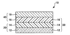
- FIG. 1 is typical sectional drawing of one Embodiment of the panel for electronic devices with a support which concerns on this invention.
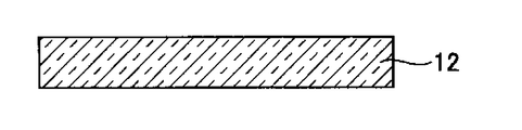
- FIG. 2A is an explanatory view (1) of the method for manufacturing the electronic device panel according to the embodiment of the present invention.
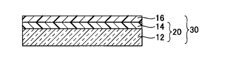
- FIG. 2B is an explanatory diagram (2) of the method for manufacturing the electronic device panel according to the embodiment of the present invention.
- FIG. 2C is an explanatory view (3) of the method for manufacturing the electronic device panel according to the embodiment of the present invention.
- FIG. 2D is an explanatory view (4) of the method for manufacturing the electronic device panel according to the embodiment of the present invention.
- FIG. 2E is an explanatory diagram (5) of the method for manufacturing the electronic device panel according to the embodiment of the present invention.
- FIG. 2F is an explanatory diagram (6) of the method for manufacturing the electronic device panel according to the embodiment of the present invention.
- FIG. 3 is a schematic diagram showing a modification of FIG. 2F.
- FIG. 1 is a schematic cross-sectional view of one embodiment of a panel for an electronic device with a support according to the present invention.
- the support-equipped electronic device panel 10 shown in the figure includes a support 20 according to the present invention, and includes a support glass 12, a resin layer 14, a flexible substrate 16, and a component 18 of the electronic device panel. It has a laminated structure laminated in this order.
- 2A to 2F are explanatory views of a method for manufacturing an electronic device panel according to an embodiment of the present invention
- FIG. 3 is a schematic view showing a modification of FIG. 2F and showing a peeling method.
- the support glass 12 and the resin layer 14 constitute a support 20 according to the present invention
- the support 20 and the flexible substrate 16 constitute a glass laminate (glass laminate structure) 30 according to the present invention
- the flexible substrate 16 and the electronic device panel constituent member 18 constitute an electronic device panel 40 (without the support 20) according to the present invention.
- each layer constituting the support 20, the glass laminate 30, the electronic device panel 40, and the support-equipped electronic device panel 10 according to the present invention will be described.
- the supporting glass 12 used in the present invention is not particularly limited as long as the supporting glass 12 supports the flexible base 16 via a resin layer 14 described later and reinforces the strength of the flexible base 16. Although it does not restrict
- the thickness of the support glass 12 is not particularly limited, it is preferable that the glass laminate 30 of the present invention has a thickness that can be processed on the current production line for electronic device panels.
- the thickness of a glass substrate currently used for LCDs is mainly in the range of 0.4 to 1.2 mm, particularly 0.7 mm.
- a flexible substrate made of a film thinner than this is used. At this time, if the total thickness of the glass laminate 30 is about the same as the current glass substrate, it can be easily adapted to the current production line.
- the current production line is designed to process a substrate having a thickness of 0.5 mm
- the flexible substrate 16 has a thickness of 0.1 mm
- the thickness of the support glass 12 and the resin layer The sum of the thickness of 14 is 0.4 mm.
- the current production line is most commonly designed to process a glass substrate having a thickness of 0.7 mm.
- the thickness of the flexible substrate 16 is 0.2 mm
- the sum of the thickness of the support glass 12 and the thickness of the resin layer 14 is 0.5 mm.
- the flexible base material 16 in the present invention is not limited to a liquid crystal display device, but also aims to make a photovoltaic power generation panel flexible. Accordingly, the thickness of the supporting glass 12 is not limited, but is preferably 0.1 to 1.1 mm. Furthermore, the thickness of the support glass 12 is preferably thicker than the flexible substrate 16 in order to ensure rigidity. Further, the thickness of the support glass 12 is preferably 0.3 mm or more, the thickness is more preferably 0.3 to 0.8 mm, and further preferably 0.4 to 0.7 mm. .
- the surface of the support glass 12 may be a polished surface subjected to mechanical polishing or chemical polishing, or may be a non-etched surface (fabric surface) that has not been polished. From the viewpoint of productivity and cost, a non-etched surface (fabric surface) is preferable.
- the support glass 12 has a first main surface and a second main surface, and the shape thereof is not limited, but is preferably rectangular.
- the rectangle is substantially a rectangle and includes a shape obtained by cutting off the corners of the peripheral portion (corner cut).
- the size of the supporting glass 12 is not limited. For example, in the case of a rectangular shape, it may be 100 to 2000 mm ⁇ 100 to 2000 mm, and preferably 500 to 1000 mm ⁇ 500 to 1000 mm.
- the support glass 12 corresponds to the support substrate of the present invention.
- the type of support substrate is not limited, and may be a metal substrate or a resin substrate, for example. .
- the resin layer 14 according to the present invention is fixed on the first main surface of the support glass 12 described above, and the glass laminate 30 laminated with the flexible base material 16 has a first main surface and a second main surface.
- the substrate 16 is in close contact with the first main surface.
- the resin material 14A is discharged from the die 80 by a die coating method or the like, applied to the support glass 12 in a thin film shape, and then dried to obtain a resin layer 14 having a desired thickness (reference numeral 14 in FIG. 1, FIG. 2B, FIG. 2C).
- the peel strength between the first main surface of the flexible substrate 16 and the resin layer 14 needs to be lower than the peel strength between the first main surface of the support glass 12 and the resin layer 14.
- the flexible substrate 16 is peeled off at the interface between the first main surface of the flexible substrate 16 and the resin layer 14, and the first main surface of the support glass 12 and the resin layer 14 are separated. It must be difficult to peel off at the interface.
- the resin layer 14 is in close contact with the first main surface of the flexible substrate 16, but has a surface characteristic that allows the flexible substrate 16 to be easily peeled off. That is, the resin layer 14 is bonded to the first main surface of the flexible base material 16 with a certain amount of binding force to limit the positional deviation of the flexible base material 16 and at the same time, peels off the flexible base material 16.
- the flexible base material 16 is bonded with a binding force that can be easily peeled without breaking.
- the property which can peel this resin layer surface easily is called easy peelability.
- the 1st main surface of the support glass 12 and the resin layer 14 are couple
- the resin layer 14 and the flexible base material 16 are not attached by the adhesive force that the adhesive has, and the force caused by the van der Waals force between the solid molecules, that is, the adhesion It is preferable that it is attached by force. However, if it is necessary to increase the bonding force between the resin layer 14 and the flexible substrate 16 according to the use of the glass laminate 30 (for example, the type of electronic device) or the type of the electronic device manufacturing process, the adhesive strength is increased. May be used.
- the bonding force of the resin layer 14 to the first main surface of the support glass 12 is relatively higher than the bonding force of the flexible substrate 16 to the first main surface.
- bonding with respect to the 1st main surface of the flexible base material 16 is called close_contact
- fixation the coupling
- the resin layer 14 has high flexibility, even if foreign matter such as bubbles or dust is mixed between the flexible base material 16 and the resin layer 14, the occurrence of distortion defects in the flexible base material 16 is suppressed. Can do.
- curable silicone Resin composition (resin material) 14A is cured on the first main surface of support glass 12 to form resin layer 14 made of a cured silicone resin (see FIGS. 2B and 2C), and then a resin made of cured silicone resin. It is preferable that the flexible base material 16 is laminated and adhered to the layer 14 (see FIG. 2D).
- the cured silicone resin in the present invention is the same resin as the non-adhesive cured silicone resin used for release paper and the like, and the peel strength is low even when it is in close contact with the flexible substrate 16.
- the curable silicone resin composition 14A to be a cured silicone resin is cured on the surface of the support glass 12, it adheres by interaction with the surface of the support glass during the curing reaction, and the cured silicone resin and the surface of the support glass after curing It is considered that the peel strength of the is increased.
- the formation of the resin layer 14 with a difference between the peel strength with respect to the first main surface of the flexible substrate 16 and the peel strength with respect to the first main surface of the support glass 12 is not limited to the above method.
- the flexible base material 16 and the supporting glass 12 are laminated simultaneously with a cured silicone resin film interposed. Can do.
- curable silicone resin composition 14A when the adhesiveness by hardening of curable silicone resin composition 14A is sufficiently low with respect to the flexible base material 16 and the adhesiveness is sufficiently high with respect to the support glass 12, it is between the flexible base material 16 and the support glass 12.
- the resin layer 14 can be formed by curing the curable silicone resin composition 14A.
- the process which raises the adhesiveness of the support glass 12 surface can be given, and the peeling strength with respect to the resin layer 14 can also be raised.
- the surface of the support glass 12 can be treated to increase the concentration of silanol groups to increase the bonding strength with the resin layer 14.
- curable silicone resin composition 14A used for forming the resin layer 14 will be described in detail.
- the curable silicone resin composition 14A in the present invention includes a linear polyorganosiloxane having vinyl groups at both ends and / or side chains, an organohydrogenpolysiloxane having hydrosilyl groups in the molecule, a catalyst, and the like. It may be a curable composition containing an additive and is cured by heating to become a cured silicone resin.
- This cured silicone resin has a very high heat resistance because of highly advanced three-dimensional crosslinking. In addition, it has a surface characteristic that the surface tension is low and other substances are difficult to adhere. Because of these characteristics, for example, after progressing the electronic device manufacturing process, by applying a force in a direction perpendicular to the plane of the glass laminate 30, the support 20 composed of the resin layer 14 and the support glass 12 can be smoothly formed. 16 can be peeled off.
- this cured silicone resin has an appropriate elasticity, a flat base material such as the flexible base material 16 for forming a flexible electronic device is held on the surface thereof, and the flat surface of the laminated structure is obtained. A large resistance is exerted against the shear force in the parallel direction. Therefore, the flexible base material 16 for forming the flexible electronic device can be kept without being displaced.
- the curable silicone resin composition 14A includes a linear organopolysiloxane (a) which is a linear organovinylpolysiloxane represented by the following formula (1) and an organohydrogenpolysiloxane represented by the formula (2). And a linear organopolysiloxane (b).
- a linear organopolysiloxane (a) which is a linear organovinylpolysiloxane represented by the following formula (1) and an organohydrogenpolysiloxane represented by the formula (2).
- b linear organopolysiloxane
- M and n in the formula represent integers and may be 0.
- m a linear polyorganosiloxane having vinyl groups at both ends is obtained.
- m an integer of 1 or more, it becomes a linear polyorganosiloxane having vinyl groups at both ends and side chains.
- linear polyorganosiloxane you may use what has a vinyl group only in a side chain.
- a in the formula represents an integer
- b represents an integer of 1 or more.
- a part of the methyl group at the terminal of the organohydrogenpolysiloxane may be a hydrogen atom or a hydroxyl group.
- addition-reactive curable silicone resins are more susceptible to curing reaction, have lower curing shrinkage, and have a good degree of peelability of cured products.
- the cured product of the addition reaction type curable silicone resin composition 14A in the present invention is particularly excellent in heat resistance, with particularly little change in peel strength with time.
- the addition reaction type curable silicone resin composition is morphologically used as a solvent type, emulsion type, or solventless type composition.
- the curable silicone resin composition 14A in the present invention any type of composition can be used.
- the mixing ratio of the linear organopolysiloxane (a) and the linear organopolysiloxane (b) in the curable silicone resin composition 14A is not particularly limited, but is bonded to the silicon atom in the linear organopolysiloxane (b). Adjusted so that the molar ratio (hydrosilyl group / vinyl group) of hydrogen atoms (hydrosilyl group) and all vinyl groups in linear organopolysiloxane (a) is 1.3 / 1 to 0.7 / 1. It is preferable to do. In particular, the mixing ratio is preferably adjusted so as to be 1.0 / 1 to 0.8 / 1.
- the peel strength of the cured silicone resin after standing for a long time tends to increase, and the peelability may not be sufficient.
- the molar ratio (hydrosilyl group / vinyl group) is less than 0.7 / 1, the crosslinking density of the cured silicone resin is lowered, which may cause a problem in chemical resistance.
- each of the linear organopolysiloxane (a) and the linear organopolysiloxane (b) in the curable silicone resin composition 14A may be a mixture of compounds having a plurality of molecular weights / structures.
- the thickness of the resin layer 14 made of the cured silicone resin is not particularly limited, and an optimum thickness is appropriately selected depending on the type of the flexible substrate 16 and the like.
- the thickness is preferably 5 to 50 ⁇ m, more preferably 5 to 30 ⁇ m, and even more preferably 7 to 20 ⁇ m.
- the thickness of the resin layer 14 is in such a range, the adhesion between the surface of the flexible substrate 16 and the resin layer 14 becomes better. Moreover, even if air bubbles or foreign substances are present, the occurrence of distortion defects in the flexible substrate 16 can be further suppressed.
- the thickness of the resin layer 14 is too thick, it takes time and materials to form the resin layer 14 and is not economical.
- the resin layer 14 may be composed of two or more layers.
- “the thickness of the resin layer” means the total thickness of all the layers.
- the kind of resin which forms each layer may differ.
- the resin layer 14 has a surface tension of preferably 30 mN / m or less, more preferably 25 mN / m or less, and even more preferably 22 mN / m or less. Although there is no limitation in particular about a minimum, it is preferred that it is 15mN / m or more.
- the surface tension is such, the surface of the flexible substrate 16 can be more easily peeled off.
- the resin layer 14 is preferably made of a material having a glass transition point lower than room temperature (about 25 ° C.) or having no glass transition point. If the glass transition point is as described above, it can have moderate elasticity while maintaining non-adhesiveness, and can be more easily peeled off from the surface of the flexible base material 16. This is because the close contact is also sufficient.
- the resin layer 14 preferably has excellent heat resistance.
- the glass laminated body 30 of this invention can be used for the heat processing on high temperature conditions.
- the cured silicone resin in the present invention has sufficient heat resistance to withstand this heat treatment.
- the thermal decomposition start temperature of the resin layer 14 made of the cured silicone resin in the present invention can be set to 400 ° C. or higher in a state where glass is laminated on the surface of the resin layer.
- the heat resistant temperature is more preferably 420 ° C. or higher, and particularly preferably 430 ° C. to 450 ° C.
- the glass laminate 30 in which the flexible base material 16 is laminated on the surface of the resin layer 14 suppresses decomposition of the resin layer even under high temperature conditions (about 350 ° C. or higher) such as a TFT array manufacturing process. Further, the occurrence of foaming in the glass laminate 30 is further suppressed.
- the heat resistance as the glass laminate 30 is mainly governed by the heat resistance of the flexible base material 16 itself described later.
- thermal decomposition start temperature as the support body 20 is represented by the following measurement method.
- An evaluation sample is obtained by further laminating 1 to 0.4 mm). Then, the sample is placed on a hot plate heated to 300 ° C., heated at a heating rate of 10 ° C. per minute, and the temperature at which the foaming phenomenon is confirmed in the sample is defined as the thermal decomposition start temperature as the support 20. Define.
- the cured silicone resin in the present invention has an elastic modulus that satisfies this required performance.
- Various additives may be contained in the curable silicone resin composition 14A according to the present invention as long as the effects of the present invention are not impaired.
- a catalyst that promotes the reaction between a hydrogen atom bonded to a silicon atom and a vinyl group.
- a platinum-based catalyst is preferably used.
- the catalyst is preferably 0.02 to 5% by mass ratio with respect to the total mass of the linear organopolysiloxane (a) and the linear organopolysiloxane (b). More preferably, it is 0.05 to 2%, and further preferably 0.1 to 1%.
- the curable silicone resin composition 14A in the present invention is further used in combination with an activity inhibitor (compound also called reaction inhibitor, retarder, etc.) having an action of suppressing the catalyst activity for the purpose of adjusting the catalyst activity together with the catalyst. It is preferable.
- an organic solvent such as hexane, heptane, octane, toluene, and xylene, and a dispersion medium such as water are components that do not constitute the cured silicone resin.
- the workability for applying the curable silicone resin composition 14A is improved. Therefore, it can be used by blending with the curable silicone resin composition 14A of the present invention.
- Curable silicone resin composition 14A comprises R 1 3 SiO 0.5 units (R 1 is a monovalent hydrocarbon group having no aliphatic unsaturated bond and having 1 to 10 carbon atoms) and SiO 2 units And a polyorganosiloxane having a molar ratio of R 1 3 SiO 0.5 units / SiO 2 units of 0.5 to 1.7. This polyorganosiloxane is contained in a general addition reaction type silicone pressure-sensitive adhesive composition.
- the addition reaction type silicone pressure-sensitive adhesive composition is (A) a polyorganosiloxane having an alkenyl group (for example, a vinyl group) (B) containing R 1 3 SiO 0.5 unit and SiO 2 unit, and R 1 3 SiO 0.5 unit / SiO 2 unit It preferably contains a component such as a polyorganosiloxane (C) SiH group-containing polyorganosiloxane (D) platinum catalyst having a molar ratio of 0.5 to 1.7.
- the component (A), the component (C), and the component (D) are already included in the curable silicone resin composition 14A.
- the component (A) corresponds to the linear polyorganosiloxane having vinyl groups at both ends and / or side chains
- the component (C) is an organohydrogen having hydrosilyl groups in the molecule. It corresponds to polysiloxane.
- R 1 is, for example, an alkyl group such as a methyl group, an ethyl group, a propyl group, or a butyl group, a cycloalkyl group such as a cyclohexyl group, an aryl group such as a phenyl group or a tolyl group, a vinyl group, or the like.
- an alkyl group such as a methyl group, an ethyl group, a propyl group, or a butyl group
- a cycloalkyl group such as a cyclohexyl group
- an aryl group such as a phenyl group or a tolyl group
- a vinyl group or the like.
- a methyl group, a phenyl group, and a vinyl group are preferable.
- the component (B) when the molar ratio of R 1 3 SiO 0.5 unit / SiO 2 unit is 0.5 to 1.7, good adhesive strength can be obtained.
- the component (B) may contain SiOH groups, and the OH group content may be 0 to 4.0% by mass. The case where the OH group exceeds 4.0% by mass is not preferable because the curability is lowered.
- the component (B) may contain R 1 SiO 1.5 units and R 1 2 SiO units as long as the adhesive strength is not impaired.
- the type of the addition reaction type silicone pressure-sensitive adhesive composition is not particularly limited.
- (1) Momentive Performance Materials, product numbers TSR1512, TSR1516, and TSR1521, (2) Shin-Etsu Silicone are commercially available.
- Product numbers KR-3700, KR-3701, X-40-3237-1, X-40-3240, X-40-3291-1, X40-3229, X40-3270, and X-40-3306, 3) Part numbers SD4560, SD4570, SD4580, SD4584, SD4584, SD4587L, SD4592, and BY24-740 manufactured by Toray Dow Corning Silicone are listed.
- the resin layer 14 obtained by curing the curable silicone resin composition 14A has adhesiveness, the bonding force between the resin layer 14 and the flexible substrate 16 can be improved. Unintentional peeling can be suppressed.
- the mixing weight ratio (A / B) of the polyorganosiloxane (A) to the polyorganosiloxane (B) is preferably 20/80 to 80/20. By setting the mixing weight ratio (A / B) to 80/20 or less, sufficient adhesive force can be expressed. On the other hand, if the mixing weight ratio (A / B) is less than 20/80, the heat resistance of the resin layer 14 becomes too low. A more preferred range is 30/70 to 70/30, and a further preferred range is 40/60 to 60/40.
- the curable silicone resin composition 14A may not contain the polyorganosiloxane (B) in order to improve easy peelability when a high bonding force between the resin layer 14 and the flexible substrate 16 is not required.
- the mixing weight ratio (A / B) may be 100/0.
- curable silicone resin composition 14A a mixture of a condensation reaction type silicone adhesive composition can be used instead of the addition reaction type silicone adhesive composition. Since a reaction product such as water or water is contained in the resin layer 14, it is not preferable.
- the curable silicone resin composition 14A may further contain a silane coupling agent. Thereby, the surface of the support glass 12 can be activated, and the bonding force between the support glass 12 and the resin layer 14 can be improved, and unintentional peeling between these 12 and 14 can be suppressed.
- silane coupling agent is suitable when the curable silicone resin composition 14A contains the polyorganosiloxane (B). In this case, since the resin layer 14 has adhesiveness, the peel strength between the resin layer 14 and the flexible substrate 16 is high.
- the type of the silane coupling agent is not particularly limited, and examples thereof include amino silane, epoxy silane, vinyl silane, mercapto silane, and methacryl (acrylic) silane. Of these, vinylsilane is particularly preferred.
- the curable silicone resin composition 14A containing a silane coupling agent may be fixed to the surface of the support glass 12 after curing as long as the surface of the support glass 12 can be activated. In order to fully activate the glass, it is desirable that the glass be placed on the support glass 12 before curing.
- the curable silicone resin composition 14 ⁇ / b> A on the first main surface of the support glass 12 it is preferable to cure the curable silicone resin composition 14 ⁇ / b> A on the first main surface of the support glass 12 to form the resin layer 14 made of a cured silicone resin.
- the curable silicone resin composition 14A is applied to one side of the supporting glass 12 to form a layer of the curable silicone resin composition 14A, and then the curable silicone resin composition 14A is cured to form the cured silicone resin.
- Layer 14 is formed.
- the curable silicone resin composition 14A is a fluid composition
- the layer of the curable silicone resin composition 14A is applied as it is, and the curable silicone resin composition 14A has a low fluidity composition or fluidity. In the case of a composition having no coating, an organic solvent is blended and applied.
- an emulsion or dispersion of the curable silicone resin composition 14A can also be used.
- the coating film containing a volatile component such as an organic solvent is then evaporated to remove the volatile component to form a layer of the curable silicone resin composition 14A.
- Curing of the curable silicone resin composition 14A can be performed continuously with evaporation removal of volatile components (see FIGS. 2B and 2C).
- Curing of the curable silicone resin composition 14A is not limited to the above method.
- the curable silicone resin composition 14 ⁇ / b> A can be cured on some peelable surface to produce a cured silicone resin film, and this film can be laminated with the support glass 12 to produce the support 20.
- the curable silicone resin composition 14A does not contain a volatile component, it can be cured by being sandwiched between the flexible substrate 16 and the support glass 12 as described above.
- the application method is not particularly limited, and a conventionally known method may be mentioned. Examples thereof include spray coating, die coating, spin coating, dip coating, roll coating, bar coating, screen printing, and gravure coating. From such a method, it can select suitably according to the kind of composition. For example, when a volatile component is not blended in the curable silicone resin composition 14A, a die coating method, a spin coating method, or a screen printing method is preferable. In the case of a composition containing a volatile component such as a solvent, the composition is cured after removing the volatile component by heating or the like before curing.
- a volatile component such as a solvent
- the conditions for curing the curable silicone resin composition 14A vary depending on the type of organopolysiloxane used, and the optimum conditions can be selected as appropriate. Usually, the heating temperature is preferably 50 to 300 ° C., and the treatment time is preferably 5 to 300 minutes.
- More specific heat curing conditions vary depending on the blending amount of the catalyst.
- 2 parts by weight of a platinum-based catalyst is blended with respect to 100 parts by weight of the total resin contained in the curable silicone resin composition 14A.
- the reaction is carried out in the atmosphere at 50 ° C. to 300 ° C., preferably 100 ° C. to 270 ° C. for curing.
- the reaction time is 5 to 180 minutes, preferably 60 to 120 minutes.
- the components in the resin layer 14 are difficult to migrate to the flexible substrate 16 when the flexible substrate 16 is peeled off.
- the reaction temperature and the reaction time are as described above because substantially no unreacted organosilicone component remains in the resin layer 14. If the reaction time is too long or the reaction temperature is too high, the organosilicone component and the cured silicone resin are simultaneously oxidized and decomposed to produce a low molecular weight organosilicone component, resulting in high silicone migration. There is a possibility. It is also preferable to allow the curing reaction to proceed as much as possible so that no unreacted organosilicone component remains in the resin layer 14 in order to improve the peelability after the heat treatment.
- the surface of the cured resin layer 14 on the flexible base material 16 side may be a surface that has been previously subjected to UV ozone treatment before the flexible base material 16 is installed (preferably immediately before installation).
- the surface of the resin layer 14 can be activated and the bonding force between the resin layer 14 and the flexible substrate 16 can be increased.
- This effect is remarkable when the resin layer 14 has adhesiveness. That is, this effect is remarkable when curable silicone resin composition 14A contains polyorganosiloxane (B).
- UV ozone treatment is performed, for example, by placing an object on a stage in a chamber, irradiating the surface of the object with UV light, and generating ozone by the UV light.
- the illuminance of the UV light is appropriately selected depending on the type of the resin layer 14 and the ozone concentration, but is preferably 5 to 30 mW / cm 2 (measurement wavelength 254 nm), for example, and 10 to 20 mW / cm 2 (measurement wavelength). 254 nm) is more preferable.
- the ozone concentration in the chamber is appropriately selected depending on the type of the resin layer 14 and the illuminance of the UV light, but is preferably 0.01 to 200 ppm in volume ratio, for example. In addition, it is necessary to set the illumination intensity of UV light so large that ozone concentration becomes low.
- a surface modification treatment may be performed on the surface of the support glass 12.
- a chemical method that improves the fixing force chemically such as a silane coupling agent, a physical method that increases surface active groups such as a flame (flame) treatment, or a surface such as a sandblast treatment
- a mechanical processing method increase the catch by increasing the roughness of the material.
- the surface of the support glass 12 on the resin layer 14 side is surface-treated with a silane coupling agent in advance before the installation of the curable silicone resin composition 14A to be the resin layer 14 or the resin layer 14 (preferably just before the installation).
- the surface may be good. Thereby, the surface of the support glass 12 can be activated, and the bonding force between the support glass 12 and the resin layer 14 can be improved, and unintentional peeling between these 12 and 14 can be suppressed.
- the type of the silane coupling agent is not particularly limited, and examples thereof include amino silane, epoxy silane, vinyl silane, mercapto silane, and methacryl (acrylic) silane. Of these, vinylsilane is particularly preferred.
- This surface treatment is performed in place of (or in addition to) the addition treatment of adding the silane coupling agent to the curable silicone resin composition 14A.
- the surface treatment is excellent in the activation effect (and hence the bonding strength), while the addition treatment is excellent in workability.
- Examples of the flexible substrate 16 used in the present invention include a resin film, a metal film, and a glass / resin composite film.
- the transparency of the flexible base material 16 when the electronic device to manufacture is LCD, and when it is the light extraction side array of OLED, and the sunlight incident side array of a photovoltaic power generation panel, it is transparent Is essential.
- a non-transparent material can be used (reference numeral 16 in FIG. 1).
- a resin film preferably used as the flexible substrate 16 as a resin for transparent film, polyethylene terephthalate resin, polycarbonate resin, transparent fluororesin, transparent polyimide resin, polyethersulfone resin, polyethylene naphthalate resin, polyacrylic resin, cycloolefin
- resins silicone resins, silicone-based organic / inorganic hybrid resins, and organic polymer / bio-nanofiber hybrid resins.
- the resin for non-transparent film include polyimide resin, fluorine resin, polyamide resin, polyaramid resin, polyether ether ketone resin, polyether ketone resin, and various liquid crystal polymer resins.
- a function-imparting layer such as a barrier layer is formed on the surface of the film.
- the flexible substrate 16 Since the flexible substrate 16 forms an electronic device on its surface, it is required to withstand the temperature conditions of the electronic device formation process. Although the temperature conditions of the electronic device formation process are various, it is preferable to withstand conditions of approximately 120 ° C. or higher. Therefore, the heat resistance of the resin film used as the flexible substrate 16 is preferably 150 ° C. or higher when the 5% weight loss temperature by heating is measured at a heating rate of 10 ° C. per minute. Further, it is preferable that the 5% heat weight loss temperature is 180 ° C. or higher. In this respect, all of the above-described resins have a 5% heat weight loss temperature exceeding 150 ° C.
- the type of metal film preferably used as the flexible substrate 16 is not particularly limited, and examples thereof include a stainless steel film and a copper film.
- the substrate for OLED is required to have extremely high moisture permeability.
- a glass-resin hybrid laminate structure (resin / glass laminate film body) is preferably used for applications requiring such high moisture resistance.
- a glass film alone exhibits a sufficiently high moisture resistance, but as the glass becomes thinner, its inherent property “brittleness” appears more prominently. It is difficult to use for a base material. Therefore, in order to compensate for this “brittleness”, it is effective to take the form of a hybrid laminated structure of glass and resin.
- the manufacturing method of the glass film used for the flexible base material 16 is not specifically limited, It can manufacture by a conventionally well-known method. For example, it can be obtained by melting a conventionally known glass raw material into a molten glass and then forming it into a plate shape by a float method, a fusion method, a slot down draw method, a redraw method, a pulling method or the like.
- the resin film mentioned above is illustrated similarly as a resin film laminated
- the glass film and the resin film may be laminated via an adhesive layer or an adhesive layer in the middle, and if it is a thermoplastic resin film, it is effective to heat-seal it. Further, the glass film surface may be thermocompression bonded to the resin film after being treated with a silane coupling agent or the like.
- a laminating method a nip roller, a heating nip roller, a vacuum press, a heating / pressing press apparatus, or the like may be used.
- glass is selected as the second main surface of the flexible base material 16.
- the base material thickness needs to be 0.3 mm or less.
- the substrate thickness is more preferably 0.25 mm or less, and further preferably 0.2 mm or less.
- the thickness of the glass film is 0.1 mm or less and the thickness of the resin film is 0.2 mm or less, respectively.
- the thickness of the glass is thicker than 0.1 mm, the rigidity of the glass becomes extremely higher than that of the resin. For this reason, the flexibility of the hybrid laminated film body of glass and resin is lost, which is not preferable.
- the flexible substrate 16 has a first main surface and a second main surface, and the shape is not limited, but is preferably rectangular.
- the rectangle is substantially a rectangle and includes a shape obtained by cutting off the corners of the peripheral portion (corner cut).
- the size of the flexible base material 16 is not limited. For example, in the case of a rectangular shape, it may be 100 to 2000 mm ⁇ 100 to 2000 mm, and preferably 500 to 1000 mm ⁇ 500 to 1000 mm. Thus, if it is a preferable thickness and a preferable magnitude
- Characteristics of the flexible substrate 16 such as heat shrinkage rate, surface shape, chemical resistance and the like are not particularly limited, and vary depending on the type of electronic device panel to be manufactured.
- the heat shrinkage rate of the flexible substrate 16 is small.
- the linear expansion coefficient which is an index of the heat shrinkage rate, is preferably 700 ⁇ 10 ⁇ 7 / ° C. or less, more preferably 500 ⁇ 10 ⁇ 7 / ° C. or less, and 300 ⁇ 10 ⁇ 7 / ° C. More preferably, it is not higher than ° C. This is because it is difficult to produce a high-definition display device when the thermal shrinkage rate is large.
- a linear expansion coefficient means a thing prescribed
- a glass laminate 30 according to the present invention is composed of the support glass 12, the resin layer 14, and the flexible base material 16 described above.
- the resin layer 14 has a peelable surface, and easily peels the flexible substrate 16 and the electronic device panel 40 (the flexible substrate 16 on which the component member 18 of the electronic device panel is formed). Can do.
- the peel strength between the resin layer 14 surface and the flexible substrate 16 surface is preferably 8.5 N / 25 mm or less, more preferably 7.8 N / 25 mm or less, and 4.5 N / 25 mm or less is particularly preferable. If it is in the said intensity
- the lower limit may be set as appropriate according to the dimensional shape and type of the flexible base material 16 as long as the flexible base material 16 has an adhesive force that does not cause misalignment on the resin layer 14. Is preferably 0.3 N / 25 mm or more.
- the peeling strength between the resin layer 14 surface and the flexible base material 16 surface is represented by the following measuring method.
- the peel strength between the surface of the resin layer 14 and the surface of the supporting glass 12 is preferably 9.8 N / 25 mm or more, more preferably 14.7 N / 25 mm or more, and particularly preferably 19.6 N / 25 mm or more.
- the support glass 12 and the resin layer 14 hardly peel off when the flexible substrate 16 and the like are peeled from the resin layer 14, and the flexible substrate 16 and the support 20 (support It can be easily separated into a laminate of glass 12 and resin layer 14.
- the peel strength between the resin layer 14 surface and the support glass 12 surface is preferably 29.4 N / 25 mm or less.
- the peel strength between the surface of the resin layer 14 and the surface of the support glass 12 is preferably 10 N / 25 mm or more higher than the peel strength between the surface of the resin layer 14 and the surface of the flexible substrate 16, and 15 N / 25 mm. It is preferable that the height is higher.
- the glass laminate 30 is preferably produced by a method (laminating method) in which the flexible substrate 16 is laminated on the surface of the resin layer 14 of the support 20 (see FIGS. 2C and 2D).
- the manufacturing method of the glass laminate 30 is not limited to this lamination method.
- the laminating method the first main surface of the flexible substrate 16 and the peelable surface of the resin layer 14 are bonded by a force caused by van der Waals force between the solid molecules facing each other, that is, an adhesion force. It is thought that it can be made. Therefore, in this case, the supporting glass 12 and the flexible base material 16 can be held in a state of being laminated via the resin layer 14.
- stacking the flexible base material 16 on the surface of the resin layer 14 of the said support body 20 is demonstrated.
- the method for laminating the flexible substrate 16 on the surface of the resin layer 14 fixed to the supporting glass 12 is not particularly limited, and can be carried out using a known method.
- the resin layer 14 and the flexible base material 16 are pressure-bonded using a non-contact pressure bonding method using a pressure chamber, a roll or a press.
- the method of making it etc. It is preferable that the resin layer 14 and the flexible base material 16 are more closely adhered to each other by pressure bonding with a pressure chamber, a roll, a press or the like.
- air bubbles mixed between the resin layer 14 and the flexible base material 16 are relatively easily removed by pressurization with a gas and pressure bonding with a roll or a press.
- pressure bonding is performed by a vacuum laminating method or a vacuum pressing method, it is more preferable because the suppression of the mixing of bubbles and the securing of good adhesion are performed better.
- pressure bonding under vacuum there is an advantage that even if minute bubbles remain, the bubbles do not grow by heating, and the flexible substrate 16 is unlikely to be distorted.
- the surface of the flexible base material 16 is sufficiently washed and laminated in an environment with a high degree of cleanliness. Even if a foreign substance is mixed between the resin layer 14 and the flexible base material 16, the resin layer is deformed and thus does not affect the flatness of the surface of the glass substrate. Since it becomes favorable, it is preferable.
- the constituent member 18 of the panel for an electronic device refers to a member formed on a flexible base material or a part thereof in a display device such as an LCD or an OLED using a flexible base material and a photovoltaic power generation device.
- a display device such as an LCD or OLED
- a TFT array hereinafter simply referred to as “array”
- ITO transparent electrode or the like is formed on the surface of a flexible substrate.
- a protective layer and other layers are formed as necessary.
- a colored layer for RGB color pixels is formed.
- a liquid crystal layer is sandwiched between the front substrate and the back substrate, and members such as various circuit patterns for driving, or a combination thereof are formed (see FIG. 2E).
- a transparent electrode, a hole injection layer, a hole transport layer, a light emitting layer, an electron transport layer, and the like formed on a flexible substrate can be used.
- a photovoltaic device composed of an organic thin film solar cell a transparent electrode, a pn organic semiconductor layer, a back electrode and the like formed on a flexible substrate can be used.
- the panel 40 for electronic devices which consists of the flexible base material 16 and the structural member 18 is a flexible base material with which at least one part of the said member was formed. Therefore, for example, the flexible substrate on which the array is formed and the flexible substrate on which the transparent electrode is formed are the electronic device panel 40.
- the panel 10 for electronic devices with a support body is provided with the support glass 12, the resin layer 14, the flexible base material 16, and the structural member 18 of the panel for electronic devices.
- the electronic device panel with a support 10 includes, for example, an array forming surface of the electronic device panel with a support in which the array is formed on the second main surface of the glass substrate, and a second main filter with the color filter being the glass substrate.
- a form in which the color filter forming surface of another electronic device panel with a support formed on the surface is bonded via a sealant or the like is also included.
- the electronic device panel 40 can be obtained from the electronic device panel 10 with the support. That is, the electronic device having the electronic device panel constituent member 18 and the flexible base material 16 by peeling the flexible base material 16 and the resin layer 14 fixed to the support glass 12 from the support-equipped electronic device panel 10. The device panel 40 can be obtained.
- a display device can be obtained from such an electronic device panel.
- the display device include an LCD and an OLED.
- LCD modes or driving methods include TN type, STN type, FE type, TFT type, MIM type, IPS type, and VA type.
- the manufacturing method of the panel 10 for electronic devices with a support mentioned above is not specifically limited, At least one part of the structural member of the panel for electronic devices is formed on the flexible base material 16 surface of the above-mentioned glass laminated body 30, Then, It is preferable to manufacture by the method of isolate
- the method for forming at least a part of the constituent members of the electronic device panel on the surface of the flexible substrate 16 of the glass laminate 30 is not particularly limited, and a conventionally known method according to the type of the constituent members of the electronic device panel. Is implemented.
- an organic EL structure is formed on the second main surface of the flexible substrate 16 of the glass laminate 30 using a manufacturing process designed for a conventional glass substrate.
- a transparent electrode is formed on the second main surface of the flexible substrate 16, and a hole injection layer, a hole transport layer, a light emitting layer, an electron transport layer, etc. are deposited on the surface on which the transparent electrode is formed.
- Various layers are formed and processed, such as forming a film and sealing with a sealing plate.
- these layer formation and processing include film formation processing, vapor deposition processing, sealing plate adhesion processing, and the like.
- the formation of these constituent members may be part of the formation of all the constituent members necessary for the electronic device panel. In that case, after peeling the flexible base material 16 which formed the one part structural member from the resin layer 14, the remaining structural members are formed on the flexible base material 16, and the panel for electronic devices is manufactured.
- a sharp blade-like object is inserted into the interface between the flexible base material 16 and the resin layer 14 to give a trigger for peeling, and then a mixed fluid of water and compressed air is sprayed. Can be peeled off. While bending each of the support substrate and the flexible substrate, a mechanical force can be applied by the suction pads 70A and 70B, and both can be peeled off (see FIG. 2F).
- it is installed on the surface plate 90 so that the supporting glass 12 of the electronic device panel with support 10 is on the upper side and the panel 40 side is on the lower side so as not to damage the formed electronic device as much as possible.
- the panel side substrate is vacuum-adsorbed on the surface plate (if the supporting glass is laminated on both sides, it is sequentially performed), and in this state, the cutter first enters the interface between the flexible base material 16 and the resin layer 14. (See FIGS. 2F and 3).
- the support glass 12 side is then sucked with a plurality of vacuum suction pads, and the vacuum suction pads are raised in order from the vicinity where the blade is inserted. Then, an air layer is formed at the interface between the resin layer 14 and the panel-side glass substrate, and the air layer spreads over the entire interface, and the support glass 12 can be easily peeled (both surfaces of the electronic device panel with support). In the case where the supporting glass 12 is laminated, the above peeling step is repeated one side at a time).
- a display device can be manufactured using the obtained electronic device panel.
- the operation for obtaining the display device is not particularly limited.
- the display device can be manufactured by a conventionally known method.
- a step of forming a conventionally known array assuming a glass substrate, a step of forming a color filter, a glass substrate on which the array is formed, and a glass substrate on which the color filter is formed May be the same as various steps such as a step of bonding together with a sealant or the like (array / color filter bonding step). More specifically, examples of the processing performed in these steps include pure water cleaning, drying, film formation, resist solution application, exposure, development, etching, and resist removal. Further, as a process performed after the bonding process of the TFT array substrate / color filter substrate is performed, there are a liquid crystal injection process and an injection port sealing process performed after performing this process, and these processes are performed. Processing.
- ⁇ Peelability evaluation> After preparing 10 sets of glass laminates and vacuum-adsorbing the second main surface of the flexible base material to a surface plate, a thickness of 0 is formed at the interface between the flexible base material and the resin layer at one corner of the glass laminate. A 1 mm stainless steel blade was inserted to give a trigger for peeling between the first main surface of the flexible substrate and the peelable surface of the resin layer.
- Heat resistance evaluation 1 heat resistance evaluation of support
- This sample was placed on a hot plate heated to 300 ° C., heated at a heating rate of 10 ° C. per minute, and the temperature at which foaming / blowing and peeling of the flexible substrate were confirmed in the sample was the thermal decomposition start temperature. It was defined and evaluated.
- Heat resistance evaluation 2 heat resistance evaluation of glass laminate
- a 50 mm square sample was cut out from each glass laminate and used as an evaluation sample, and the sample was held in a nitrogen atmosphere firing furnace under the temperature levels of the following conditions A, B, and C for 10 minutes.
- Condition A 150 ° C. (temperature assuming the formation process of the organic semiconductor)
- Condition B 220 ° C. (temperature assuming the oxide semiconductor formation step)
- Condition C 350 ° C. (temperature assuming the formation process of the a-Si semiconductor) Then, the presence or absence of damage of the flexible base material itself, the presence or absence of foaming / swelling in the sample, peeling of the flexible base material, and the like were confirmed.
- Glass / resin laminated film Production Example 1
- a glass film (Asahi Glass Co., Ltd., AN100) having a length of 350 mm, a width of 300 mm, a plate thickness of 0.08 mm, and a linear expansion coefficient of 38 ⁇ 10 ⁇ 7 / ° C. is washed with an alkaline detergent using a cleaning device dedicated to thin glass. The surface was cleaned and prepared as a laminated glass film.
- the thing which plasma-treated the surface of the transparent fluorine-type film (Asahi Glass Co., Ltd. product made from Asahi Glass Co., Ltd.) of 350 mm long, 300 mm wide, and board thickness 0.10 mm was prepared. And it laminated
- Glass / resin laminated film Production Example 2
- a glass film (Asahi Glass Co., Ltd., AN100) having a length of 350 mm, a width of 300 mm, a plate thickness of 0.08 mm, and a linear expansion coefficient of 38 ⁇ 10 ⁇ 7 / ° C. is washed with an alkaline detergent using a cleaning device dedicated to thin glass. Then, the surface was cleaned, and a 0.1% methanol solution of ⁇ -mercaptopropyltrimethoxysilane was sprayed on the surface, followed by drying at 80 ° C. for 3 minutes to prepare a laminated glass film.
- a support glass (Asahi Glass Co., Ltd., AN100) having a length of 350 mm, a width of 300 mm, a plate thickness of 0.6 mm, and a linear expansion coefficient of 38 ⁇ 10 ⁇ 7 / ° C. is cleaned with pure water and UV cleaned to support the surface. Prepared as a substrate.
- a linear polyorganosiloxane having vinyl groups at both ends and an organohydrogenpolysiloxane having a hydrosilyl group in the molecule were used as the resin for forming the easily peelable resin layer.
- this is mixed with a platinum-based catalyst to prepare a mixture, and coated on the first main surface of the support glass with a die coater in a size of 349 mm long and 299 mm wide (coating amount 20 g / m 2). And cured by heating at 210 ° C. for 30 minutes in the air to form a silicone resin layer having a thickness of 20 ⁇ m.
- the mixing ratio of the linear polyorganosiloxane and the organohydrogenpolysiloxane was adjusted so that the molar ratio of hydrosilyl group and vinyl group (hydrosilyl group / vinyl group) was 0.9 / 1. .
- the platinum-based catalyst was added in an amount of 2 parts by mass with respect to a total of 100 parts by mass of the linear polyorganosiloxane and the organohydrogenpolysiloxane.
- the heat resistance of the support thus obtained was evaluated based on the heat resistance evaluation 1, and the heat resistance was 460 ° C.
- Example 1 to Example 7 In each example, the flexible substrate and the supporting glass were in close contact with the silicone resin layer without generating bubbles, and had no convex defects and good smoothness.
- the glass laminate (D1) of Example 3 is subjected to a normal glass substrate array forming step to form an array on the second main surface of the glass substrate.
- the glass laminate (D2) of Example 1 is subjected to a normal glass substrate color filter forming step to form a color filter on the second main surface of the glass substrate.
- the laminated glass D1 (the panel for an electronic device with a support according to the present invention) on which the array is formed and the laminated body D2 (the panel for an electronic device with a support according to the present invention) on which the color filter is formed are respectively supported on the outside.
- an LCD empty cell having a laminate on both sides is obtained.
- the second main surface of the support glass of the above-mentioned empty cell laminate D1 is vacuum-adsorbed on a surface plate, and a thickness of 0 is formed at the interface between the flexible base material and the resin layer in Example 1 of the corner portion of the laminate D2.
- a 1 mm stainless steel blade is inserted to give a trigger for peeling between the first main surface of the flexible base material of Example 1 and the peelable surface of the resin layer.
- sucking the 2nd main surface of the support glass of the laminated body D2 with 12 vacuum suction pads it raises in an order from the suction pad near the corner part of the laminated body D2. As a result, it is possible to peel off the supporting glass to which the resin layer derived from the laminate D2 is fixed, leaving only the empty cells of the LCD with the supporting glass of the laminate D1 on the surface plate.
- the first main surface of the flexible base material on which the color filter is formed on the second main surface is vacuum-adsorbed on a surface plate, and the interface between the flexible base material in Example 3 of the corner portion of the laminate D1 and the resin layer is formed.
- a stainless steel knife having a thickness of 0.1 mm is inserted to give a trigger for peeling between the first main surface of the flexible base material of Example 3 and the peelable surface of the resin layer.
- a liquid crystal injection process and an injection port sealing process are performed to complete the LCD cell.
- a step of attaching a polarizing plate to the completed LCD cell is performed, and then a module forming step is performed to obtain an LCD.
- the LCD obtained in this way does not have a problem in characteristics.
- an OLED is manufactured using the glass laminate (Example 6 and Example 7) obtained in Configuration Example 1.
- the glass laminate D3 of Example 7 is passed through a normal glass substrate OLED backplate process, forming an electrode, depositing a hole injection layer, a hole transport layer, a light emitting layer, an electron transport layer, and the like, and forming a barrier layer. Flow the coating process.
- the glass laminated body D4 of Example 6 is made to flow into the normal OLED front plate process for glass substrates.
- Laminated body D3 (electronic device panel with support of the present invention) in which a back plate array for OLED is formed, and laminated body D4 (panel for electronic device with a support of the present invention) in which a front plate for OLED is formed, and Are bonded together through a sealing material so that the supporting glass is on the outside, and a top emission type OLED panel having a laminate on both sides is obtained.
- a stainless steel knife having a thickness of 0.1 mm is inserted into the interface between the flexible base material and the resin layer at the corner of the laminate D3, and the flexible substrate This provides a trigger for peeling between the first main surface of the material and the peelable surface of the resin layer.
- sucking the 2nd main surface of the support glass of the laminated body D3 with nine vacuum suction pads it raises in an order from the suction pad near the corner part of the laminated body D3.
- the first main surface of the flexible base material on which the organic EL back plate is formed on the second main surface is vacuum-adsorbed to the surface plate, and the interface between the glass substrate and the resin layer at the corner portion of the laminate D4, A stainless steel blade having a thickness of 0.1 mm is inserted to give an opportunity for peeling between the first main surface of the flexible base material of Example 6 and the peelable surface of the resin layer.
- sucking the 2nd main surface of the support glass of the laminated body D4 with 12 vacuum suction pads it raises in an order from the suction pad near the corner part of the laminated body D4.
- a support glass (Asahi Glass Co., Ltd., AN100) having a length of 350 mm, a width of 300 mm, a plate thickness of 0.6 mm, and a linear expansion coefficient of 38 ⁇ 10 ⁇ 7 / ° C. is cleaned with pure water and UV cleaned to support the surface. Prepared as a substrate.
- a linear polyorganosiloxane having vinyl groups at both ends a linear polyorganosiloxane having vinyl groups at both ends, a branched polyorganosiloxane having vinyl groups, and a hydrosilyl group in the molecule Organohydrogenpolysiloxane was used.
- the branched polyorganosiloxane corresponds to the polyorganosiloxane (B).
- the mixing weight ratio (A / B) between the linear polyorganosiloxane (A) and the branched polyorganosiloxane (B) was 40/60.
- linear polyorganosiloxane, branched polyorganosiloxane, and organohydrogenpolysiloxane so that the molar ratio of hydrosilyl group to vinyl group (hydrosilyl group / vinyl group) is 0.9 / 1.
- the mixing ratio was adjusted.
- this resin is mixed with a platinum-based catalyst to prepare a mixture, which is coated on a first main surface of the support glass with a die coating apparatus in a size of 349 mm long and 299 mm wide (coating amount 20 g / m2), and cured by heating in the atmosphere at 210 ° C. for 30 minutes to form a silicone resin layer having a thickness of 20 ⁇ m.
- An evaluation sample having a length of 25 mm and a width of 75 mm was cut out from the support thus obtained.
- An evaluation sample consists of support glass and a silicone resin layer fixed to the whole surface of support glass.
- a flexible substrate having a length of 25 mm and a width of 50 mm was laminated on this evaluation sample at room temperature using a vacuum press device to obtain a glass laminate.
- a polyimide film (Mitsubishi Gas Chemical, Neoprim L-3430) was used as the flexible substrate.
- the peel strength between the resin layer surface and the polyimide film surface in this glass laminate was 0.2 N / 25 mm as measured by the measurement method described above.
- the peel strength between the resin layer surface and the polyimide film surface is 0.05 N. / 25 mm.
- Configuration Example 5 In Configuration Example 5, after the surface of the supporting glass was cleaned and before the resin layer was placed on the supporting glass surface, the surface of the supporting glass was treated with a silane coupling agent in the same manner as in Configuration Example 4. To obtain a support. The surface treatment is performed by applying a solution obtained by diluting vinyltrimethoxysilane (KBM1003, manufactured by Shin-Etsu Chemical Co., Ltd.) to 0.25% by mass with isopropyl alcohol on the surface of the supporting glass, and performing heat treatment at 100 ° C. for 1 minute. It was.
- KBM1003 vinyltrimethoxysilane
- an evaluation sample was cut out from the obtained support in the same manner as in Structural Example 4, and the following was performed on the resin layer surface of the evaluation sample using a surface treatment apparatus (PL21-200, manufactured by Sen Special Light Company).
- the UV ozone treatment was carried out under the conditions.
- the peel strength between the resin layer surface and the polyimide film surface in this glass laminate was 1.0 N / 25 mm as measured by the measurement method described above. Moreover, peeling at the interface between the supporting glass and the resin layer was not observed.
- an evaluation sample is cut out, and after the UV ozone treatment is performed on the resin layer surface of the evaluation sample, the glass laminate obtained by laminating the polyimide film is resin.
- the peel strength between the layer surface and the polyimide film surface was 0.06 N / 25 mm.
- an evaluation sample was cut out from the obtained support in the same manner as in Structural Example 4, and the following was performed on the resin layer surface of the evaluation sample using a surface treatment apparatus (PL21-200, manufactured by Sen Special Light Company).
- the UV ozone treatment was carried out under the conditions.
- the peel strength between the resin layer surface and the polyimide film surface in this glass laminate was 1.0 N / 25 mm as measured by the measurement method described above. Moreover, peeling at the interface between the supporting glass and the resin layer was not observed.
- the peel strength between the resin layer surface and the polyimide film surface in this glass laminate was 0.1 N / 25 mm as measured by the measurement method described above.
- Configuration Example 8 In Configuration Example 8, after the surface of the support glass was cleaned and before the resin layer was placed on the support glass surface, the surface of the support glass was treated with a silane coupling agent in the same manner as in Configuration Example 7. To obtain a support. The surface treatment is performed by applying a solution obtained by diluting vinyltrimethoxysilane (KBM1003, manufactured by Shin-Etsu Chemical Co., Ltd.) to 0.25% by mass with isopropyl alcohol on the surface of the supporting glass, and performing heat treatment at 100 ° C. for 1 minute. It was.
- KBM1003 vinyltrimethoxysilane
- an evaluation sample was cut out from the obtained support in the same manner as in Structural Example 4, and the following was performed on the resin layer surface of the evaluation sample using a surface treatment apparatus (PL21-200, manufactured by Sen Special Light Company).
- the UV ozone treatment was carried out under the conditions.
- the peel strength between the resin layer surface and the polyimide film surface was 04 N / 25 mm as measured by the measurement method described above. Moreover, peeling at the interface between the supporting glass and the resin layer was not observed.
- the glass laminate was prepared in the same manner as in Structural Example 4 except that the mixing weight ratio (A / B) of the linear polyorganosiloxane (A) and the branched polyorganosiloxane (B) was 10/90. Obtained.
- the peel strength between the resin layer surface and the polyimide film surface in this glass laminate was 0.3 N / 25 mm as measured by the measurement method described above.
- a support was prepared in the same manner except that it was changed to a pressure-sensitive adhesive (acrylic curable pressure-sensitive adhesive manufactured by Nitto Denko Corporation) that can reduce the adhesive strength by light irradiation. .
- a pressure-sensitive adhesive acrylic curable pressure-sensitive adhesive manufactured by Nitto Denko Corporation
- heat resistance evaluation 1 was implemented also about this support body, white smoke generate
- Example 1 The PES film described in Example 1 was laminated on the support in the same manner as in Structural Example 1.
- the flexible substrate and the supporting glass were in close contact with the pressure-sensitive adhesive layer without generating bubbles, and had no convex defects and good smoothness.
- the present invention it is possible to provide a laminated structure that is excellent in heat resistance and can easily separate a closely contacted flexible substrate and its support. Moreover, the panel for electronic devices with a support body obtained using this laminated structure can be provided. Furthermore, the manufacturing method of the panel for electronic devices which uses said laminated structure can also be provided.
- SYMBOLS 10 Panel for electronic devices with support body 12 Support glass 14 Resin layer 16 Flexible base material 18 Component member of panel for electronic devices 20 Support body 30 Glass laminated body (glass laminated structure) 40 Panel for electronic device 60 Blade 70A, 70B Suction pad 80 Die (slot / orifice) 90 surface plate
Landscapes
- Chemical & Material Sciences (AREA)
- Physics & Mathematics (AREA)
- Chemical Kinetics & Catalysis (AREA)
- Organic Chemistry (AREA)
- Nonlinear Science (AREA)
- Life Sciences & Earth Sciences (AREA)
- Engineering & Computer Science (AREA)
- Materials Engineering (AREA)
- Wood Science & Technology (AREA)
- Mathematical Physics (AREA)
- Crystallography & Structural Chemistry (AREA)
- General Physics & Mathematics (AREA)
- Optics & Photonics (AREA)
- Health & Medical Sciences (AREA)
- Medicinal Chemistry (AREA)
- Polymers & Plastics (AREA)
- Laminated Bodies (AREA)
- Compositions Of Macromolecular Compounds (AREA)
Abstract
Description
本発明で使用される支持ガラス12は、後述する樹脂層14を介してフレキシブル基材16を支持し、フレキシブル基材16の強度を補強するためのものであれば、特に限定されない。支持ガラス12の組成としては特に制限されないが、その組成は、例えばアルカリ金属酸化物を含有するガラス(ソーダライムガラスなど)、無アルカリガラスなどの種々の組成のガラスを使用できる。中でも、熱収縮率が小さいことから無アルカリガラスであることが好ましい。樹脂層を形成する前に、汚れや異物等を除去するために、その表面を予め洗浄することが好ましい(図1の符号12、図2A参照)。
本発明に係る樹脂層14は、上述した支持ガラス12の第1主面上に固定され、フレキシブル基材16と積層されたガラス積層体30においては第1主面および第2主面を有するフレキシブル基材16の第1主面に密着している。ダイコート法などにより、ダイ80から樹脂材料14Aを吐出させ、支持ガラス12上に薄膜状に塗工し、その後、乾燥させ所望の厚みの樹脂層14を得る(図1の符号14、図2B、図2C)。フレキシブル基材16の第1主面と樹脂層14との間の剥離強度は、支持ガラス12の第1主面と樹脂層14との間の剥離強度よりも低いことが必要である。すなわち、フレキシブル基材16と支持ガラス12とを分離する際には、フレキシブル基材16の第1主面と樹脂層14との界面で剥離し、支持ガラス12の第1主面と樹脂層14との界面では剥離し難いことが必要である。


上記硬化シリコーン樹脂からなる樹脂層14の厚さは特に限定されず、フレキシブル基材16の種類などにより適宜最適な厚さが選択される。なかでも、5~50μmであることが好ましく、5~30μmであることがより好ましく、7~20μmであることがさらに好ましい。樹脂層14の厚さがこのような範囲であると、フレキシブル基材16表面と樹脂層14との密着がより良好となる。また、気泡や異物が介在しても、フレキシブル基材16のゆがみ欠陥の発生をより抑制することができる。また、樹脂層14の厚さが厚すぎると、形成するのに時間および材料を要するため経済的ではない。
本発明における硬化性シリコーン樹脂組成物14Aには、必要に応じて本発明の効果を損なわない範囲で、各種添加剤が含有されていてもよい。添加剤として、通常、ケイ素原子に結合した水素原子とビニル基の反応を促進する触媒を加えることが好ましい。この触媒としては白金系触媒を用いることが好ましい。
硬化性シリコーン樹脂組成物14Aは、R1 3SiO0.5単位(R1は脂肪族不飽和結合を有さない1価炭化水素基であって炭素数1~10のもの)およびSiO2単位を含有すると共に、R1 3SiO0.5単位/SiO2単位のモル比が0.5~1.7であるポリオルガノシロキサンをさらに含んでいても良い。このポリオルガノシロキサンは、一般的な付加反応型のシリコーン粘着剤組成物に含まれるものである。
(A)アルケニル基(例えば、ビニル基など)を有するポリオルガノシロキサン
(B)R1 3SiO0.5単位およびSiO2単位を含有すると共に、R1 3SiO0.5単位/SiO2単位のモル比が0.5~1.7であるポリオルガノシロキサン
(C)SiH基を含有するポリオルガノシロキサン
(D)白金触媒
などの成分を含んでいることが好ましい。これらの成分のうち、(A)成分、(C)成分、(D)成分については、上記硬化性シリコーン樹脂組成物14Aに既に含まれている。例えば(A)成分は上記両末端及び/又は側鎖中にビニル基を有する直鎖状ポリオルガノシロキサンに対応するものであり、(C)成分は上記分子内にハイドロシリル基を有するオルガノハイドロジェンポリシロキサンに対応するものである。
硬化性シリコーン樹脂組成物14Aは、シランカップリング剤をさらに含んでいても良い。これによって、支持ガラス12の表面を活性化して、支持ガラス12と樹脂層14との結合力を向上することができ、これらの間12、14での意図しない剥離を抑制することができる。
前記のように、硬化性シリコーン樹脂組成物14Aを支持ガラス12の第1主面上で硬化させて硬化シリコーン樹脂からなる樹脂層14を形成することが好ましい。そのために、硬化性シリコーン樹脂組成物14Aを支持ガラス12の片面に塗布して硬化性シリコーン樹脂組成物14Aの層を形成し、次いで前記硬化性シリコーン樹脂組成物14Aを硬化させて前記硬化シリコーン樹脂層14を形成する。硬化性シリコーン樹脂組成物14Aの層の形成は、硬化性シリコーン樹脂組成物14Aが流動性の組成物の場合はそのまま塗布し、硬化性シリコーン樹脂組成物14Aが流動性の低い組成物や流動性のない組成物の場合は、有機溶剤を配合して塗布する。また、硬化性シリコーン樹脂組成物14Aの乳化液や分散液などを使用することもできる。有機溶剤などの揮発性成分を含む塗膜は、次いでその揮発性成分を蒸発除去して硬化性シリコーン樹脂組成物14Aの層とする。硬化性シリコーン樹脂組成物14Aの硬化は、揮発性成分の蒸発除去と連続して行うことができる(図2B、図2C参照)。
硬化後の樹脂層14のフレキシブル基材16側の面は、フレキシブル基材16の設置前(好ましくは、設置の直前)に、予めUVオゾン処理された面であって良い。これによって、樹脂層14の表面を活性化して、樹脂層14とフレキシブル基材16との結合力を高めることができる。この効果は、樹脂層14が粘着性を有する場合に顕著である。即ち、この効果は、硬化性シリコーン樹脂組成物14Aがポリオルガノシロキサン(B)を含む場合に顕著である。
樹脂層14と支持ガラス12との高い固定力(高い剥離強度)を付与するために、支持ガラス12表面に表面改質処理(プライミング処理)を行ってもよい。例えば、シランカップリング剤のような化学的に固定力を向上させる化学的方法(プライマー処理)や、フレーム(火炎)処理のように表面活性基を増加させる物理的方法、サンドブラスト処理のように表面の粗度を増加させることにより引っかかりを増加させる機械的処理方法などが例示される。
本発明で使用されるフレキシブル基材16としては樹脂フィルム、金属フィルム、ガラス/樹脂複合フィルム等が例示される。なお、フレキシブル基材16の透明性については製造する電子デバイスがLCDである場合、およびOLEDの光取り出し側アレイ、および太陽光発電パネルの太陽光入射側のアレイである場合は、透明であることが必須となる。一方、トップエミッションタイプの有機ELディスプレイのバックプレート、および太陽光発電パネルのバックプレート等を製造するためであれば、透明である必要は無い。したがって、非透明な材料を用いることが可能となる(図1の符号16)。
図面において、本発明に係るガラス積層体30は、上記した支持ガラス12、樹脂層14、フレキシブル基材16から構成される。上述したように、樹脂層14は剥離性表面を有し、フレキシブル基材16や電子デバイス用パネル40(電子デバイス用パネルの構成部材18が形成されたフレキシブル基材16)を容易に剥離することができる。より具体的には、樹脂層14表面とフレキシブル基材16表面との間の剥離強度が、8.5N/25mm以下であることが好ましく、7.8N/25mm以下がより好ましく、4.5N/25mm以下が特に好ましい。上記強度内であれば、剥離時の樹脂層14の破壊や、フレキシブル基材16等の破壊などが起こりにくく、好ましい。
ガラス積層体30の製造は、支持体20の樹脂層14の表面にフレキシブル基材16を積層する方法(積層方法)が好ましい(図2C、図2D参照)。しかし、ガラス積層体30の製造方法は、この積層方法に限られるものではないことは、上述した通りである。積層方法では、フレキシブル基材16の第1主面と樹脂層14の剥離性表面とは、非常に近接した、相対する固体分子間におけるファンデルワールス力に起因する力、すなわち、密着力によって結合させることができると考えられる。したがって、この場合、支持ガラス12とフレキシブル基材16とを樹脂層14を介して積層させた状態に保持することができる。以下、前記支持体20の樹脂層14の表面にフレキシブル基材16を積層する方法によるガラス積層体30の製造方法を説明する。
本発明において、電子デバイス用パネルの構成部材18とは、フレキシブルな基材を使用したLCD、OLED等の表示装置及び、光発電装置において、フレキシブルな基材上に形成された部材やその一部をいう。例えば、LCD、OLED等の表示装置においては、フレキシブルな基材の表面にTFTアレイ(以下、単に「アレイ」という。)やITOの透明電極等を形成する。さらに、必要に応じて保護層その他の層を形成する。また、カラーフィルタ基板については、RGBの色画素用の着色層を形成する。さらに、表基板と裏基板との間に液晶層を挟持させ、駆動用の各種回路パターン等の部材、またはこれらを組み合わせたものが形成される(図2E参照)。
図1において、支持体付き電子デバイス用パネル10は、支持ガラス12、樹脂層14、フレキシブル基材16、電子デバイス用パネルの構成部材18を備えている。
上述した支持体付き電子デバイス用パネル10の製造方法は特に限定されないが、前記したガラス積層体30のフレキシブル基材16表面上に、電子デバイス用パネルの構成部材の少なくとも一部を形成し、その後フレキシブル基材16と硬化シリコーン樹脂層付き支持ガラスとを分離する方法で製造することが好ましい。
上述した支持体付き電子デバイス用パネル10を得た後、さらに、支持体付き電子デバイス用パネル10におけるフレキシブル基材16の第1主面と樹脂層14の剥離性表面とを剥離して電子デバイス用パネル40を得ることができる。上記のように、剥離時のフレキシブル基材16上の構成部材が電子デバイス用パネルに必要な全構成部材の形成の一部である場合には、その後、残りの構成部材をフレキシブル基材16上に形成して電子デバイス用パネルを製造する。フレキシブル基材16の第1主面と樹脂層14の剥離性表面とを剥離する方法は、特に限定されない。
ガラス積層体を10組準備しフレキシブル基材の第2主面を定盤に真空吸着させたうえで、ガラス積層体の一つのコーナー部のフレキシブル基材と樹脂層との界面に、厚さ0.1mmのステンレス製刃物を差し込み、上記フレキシブル基材の第1主面と上記樹脂層の剥離性表面との剥離のきっかけを与えた。
支持ガラス上に樹脂層を形成した支持体から50mm角のサンプルを切り出し、この樹脂表面に同サイズのガラス基板(厚み=0.7mm)を重ねて評価サンプルとした。このサンプルを300℃に加熱したホットプレートに載置し、10℃毎分の昇温スピードで加熱し、サンプル内に発泡・膨れ、フレキシブル基材の剥がれ現象が確認された温度を熱分解開始温度と定義して評価した。
各ガラス積層体から50mm角のサンプルを切り出して評価サンプルとし、このサンプルに関して以下の条件A、B、Cの温度レベルの窒素雰囲気焼成炉に10分間保持した。
条件A:150℃(有機物半導体の形成工程を想定した温度)
条件B:220℃(酸化物半導体の形成工程を想定した温度)
条件C:350℃(a-Si半導体の形成工程を想定した温度)
その後、フレキシブル基材自体のダメージの有無、サンプル内に発泡・膨れ、フレキシブル基材の剥がれ等の有無を確認した。
初めに縦350mm、横300mm、板厚0.08mm、線膨張係数38×10-7/℃のガラスフィルム(旭硝子株式会社製、AN100)を薄板ガラス専用の洗浄装置を用いてアルカリ洗剤で洗浄を行い表面を清浄化し、積層用ガラスフィルムとして準備した。一方で、縦350mm、横300mm、板厚0.10mmの透明フッ素系フィルム(旭硝子株式会社製、エフクリーン)の表面をプラズマ処理した物を準備した。そして、先のガラスフィルムと重ね合わせ、280℃に加熱したプレス装置を用いて両者を積層し、ガラス/樹脂積層フィルムAとした。
初めに縦350mm、横300mm、板厚0.08mm、線膨張係数38×10-7/℃のガラスフィルム(旭硝子株式会社製、AN100)を薄板ガラス専用の洗浄装置を用いてアルカリ洗剤で洗浄を行い表面を清浄化し、さらに表面にγ-メルカプトプロピルトリメトキシシランの0.1%メタノール溶液を噴霧し、続いて80℃で3分乾燥させたものを積層用ガラスフィルムとして準備した。一方で、縦350mm、横300mm、板厚0.05mmのポリイミドフィルム(東レ・デュポン社製、カプトン200HV)の表面をプラズマ処理した物を準備した。そして、先のガラスフィルムと重ね合わせ、320℃に加熱したプレス装置を用いて両者を積層し、ガラス/樹脂積層フィルムBとした。
初めに縦350mm、横300mm、板厚0.6mm、線膨張係数38×10-7/℃の支持ガラス(旭硝子株式会社製、AN100)を純水洗浄、UV洗浄して表面を清浄化し、支持基板として準備した。
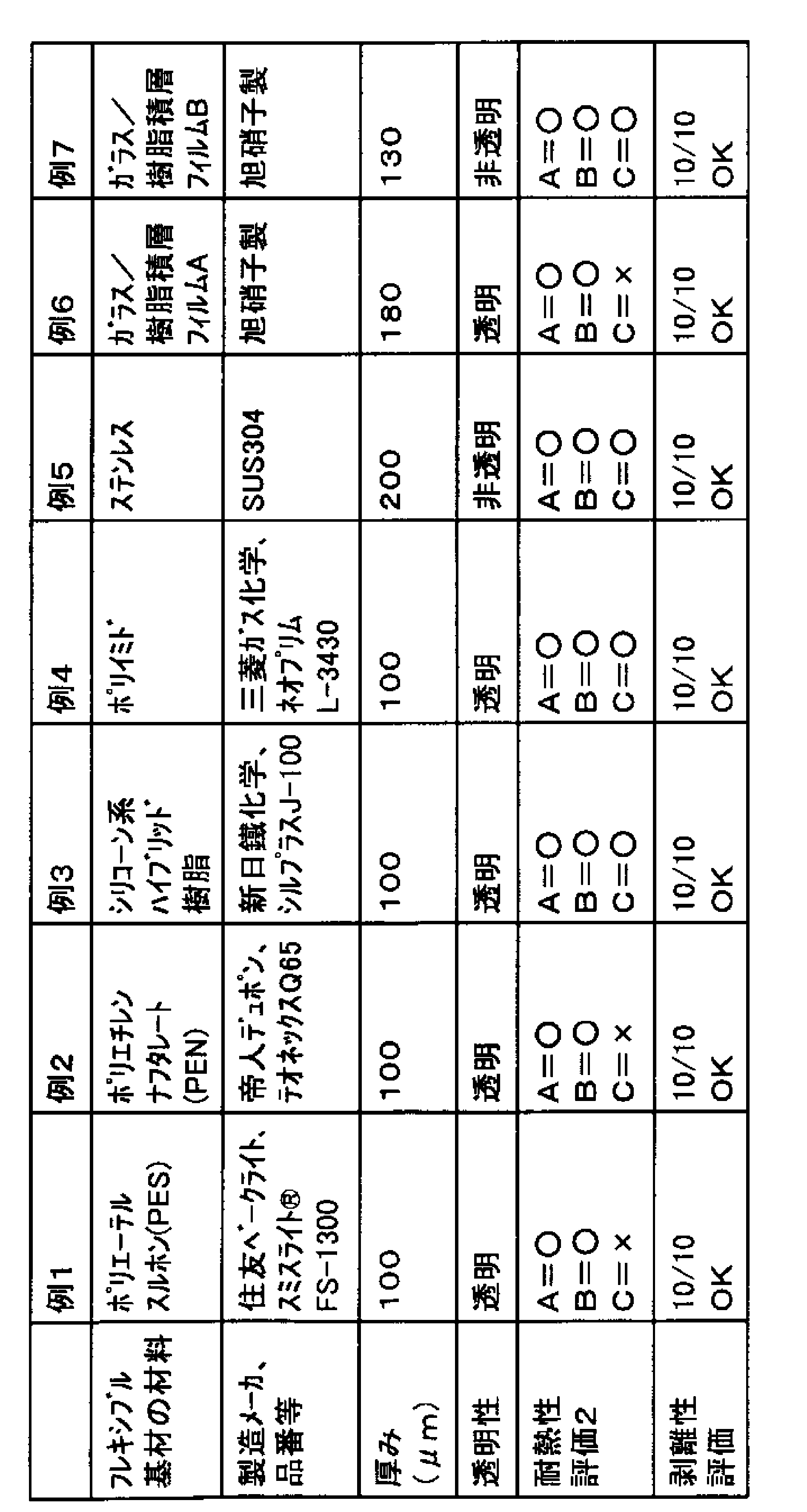
各例についてフレキシブル基材および支持ガラスは、シリコーン樹脂層と気泡を発生することなく密着しており、凸状欠点もなく平滑性も良好であった。
本例では、構成例1で得たガラス積層体(例1と例3)を用いてLCDを製造する。
本例では、構成例1で得たガラス積層体(例6と例7)を用いてOLEDを製造する。例7のガラス積層体D3は通常のガラス基板用OLEDバックプレート用工程に流し、電極を形成する工程、ホール注入層・ホール輸送層・発光層・電子輸送層等を蒸着する工程、バリヤー層を塗布する工程等を流動する。そして、例6のガラス積層体D4は通常のガラス基板用OLEDフロントプレート用工程に流動させる。
初めに縦350mm、横300mm、板厚0.6mm、線膨張係数38×10-7/℃の支持ガラス(旭硝子株式会社製、AN100)を純水洗浄、UV洗浄して表面を清浄化し、支持基板として準備した。
構成例5では、支持ガラス表面を清浄化した後であって、支持ガラス表面に樹脂層を設置する前に、支持ガラス表面をシランカップリング剤で表面処理した他は、構成例4と同様にして、支持体を得た。表面処理は、ビニルトリメトキシシラン(信越化学工業社製、KBM1003)をイソプロピルアルコールで0.25質量%に希釈した溶液を支持ガラス表面に塗工し、100℃で1分間加熱処理することで行った。
UV光の主波長:185nm、254nm
UV光の照度:7mW/cm2(測定波長254nm)
UV光の照射量:400mJ/cm2(測定波長254nm)
オゾン濃度:20ppm(体積比)
その後、評価サンプルに、構成例4と同様にして、ポリイミドフィルム(三菱ガス化学、ネオプリムL-3430)を積層して、ガラス積層体を得た。
構成例6では、易剥離性樹脂層を形成するための樹脂に、シランカップリング剤を添加した他は、構成例4と同様にして、支持体を得た。添加処理は、ビニルトリメトキシシラン(信越化学工業社製、KBM1003)3質量部を、直鎖状ポリオルガノシロキサンと、分岐状ポリオルガノシロキサンと、オルガノハイドロジェンポリシロキサンとの合計100質量部に添加して行った。
UV光の主波長:185nm、254nm
UV光の照度:7mW/cm2(測定波長254nm)
UV光の照射量:400mJ/cm2(測定波長254nm)
オゾン濃度:20ppm(体積比)
その後、評価サンプルに、構成例4と同様にして、ポリイミドフィルム(三菱ガス化学、ネオプリムL-3430)を積層して、ガラス積層体を得た。
直鎖状ポリオルガノシロキサン(A)と分岐状ポリオルガノシロキサン(B)との混合重量比(A/B)を60/40とした以外は構成例4と同様の方法にて、ガラス積層体を得た。
構成例8では、支持ガラス表面を清浄化した後であって、支持ガラス表面に樹脂層を設置する前に、支持ガラス表面をシランカップリング剤で表面処理した他は、構成例7と同様にして、支持体を得た。表面処理は、ビニルトリメトキシシラン(信越化学工業社製、KBM1003)をイソプロピルアルコールで0.25質量%に希釈した溶液を支持ガラス表面に塗工し、100℃で1分間加熱処理することで行った。
UV光の主波長:185nm、254nm
UV光の照度:7mW/cm2(測定波長254nm)
UV光の照射量:400mJ/cm2(測定波長254nm)
オゾン濃度:20ppm(体積比)
その後、評価サンプルに、構成例4と同様にして、ポリイミドフィルム(三菱ガス化学、ネオプリムL-3430)を積層して、ガラス積層体を得た。
(構成例9)
直鎖状ポリオルガノシロキサン(A)と分岐状ポリオルガノシロキサン(B)との混合重量比(A/B)を10/90とした以外は構成例4と同様の方法にて、ガラス積層体を得た。
構成例1において使用したシリコーン樹脂の代わりに、光照射により粘着力が低下させることが出来る粘着剤(日東電工社製、アクリル硬化型粘着剤)に変更した以外は同じ方法で支持体を作成した。本支持体についても耐熱性評価1を実施したが、300℃のホットプレートにおいてすぐに白煙が発生し、樹脂層の顕著な劣化が認められた。
本出願は、2009年8月27日出願の日本特許出願2009-197201に基づくものであり、その内容はここに参照として取り込まれる。
12 支持ガラス
14 樹脂層
16 フレキシブル基材
18 電子デバイス用パネルの構成部材
20 支持体
30 ガラス積層体(ガラス積層構造体)
40 電子デバイス用パネル
60 刃物
70A、70B 吸着パッド
80 ダイ(スロット・オリフィス)
90 定盤
Claims (16)
- 第1主面と第2主面とを有する厚さ0.3mm以下のフレキシブル基材、
支持基板、および
前記フレキシブル基材と前記支持基板との間に設けられ、剥離性表面を有する硬化シリコーン樹脂層
を含む積層構造体であって、
前記硬化シリコーン樹脂層は、前記支持基板の第1主面に固定されており、また、前記フレキシブル基材の第1主面に対する易剥離性を備え、前記フレキシブル基材の第1主面と密着されている積層構造体。 - 前記剥離性表面を有する硬化シリコーン樹脂層が、両末端及び/又は側鎖中にビニル基を有する直鎖状ポリオルガノシロキサンと、分子内にハイドロシリル基を有するオルガノハイドロジェンポリシロキサンとを含む硬化性シリコーン樹脂組成物の架橋反応物である請求項1に記載の積層構造体。
- 前記直鎖状ポリオルガノシロキサンと、前記オルガノハイドロジェンポリシロキサンとの混合比率が、ハイドロシリル基とビニル基のモル比(ハイドロシリル基/ビニル基)で1.3/1~0.7/1である請求項2に記載の積層構造体。
- 前記フレキシブル基材は、5%加熱重量減温度が150℃以上の樹脂フィルムからなる請求項1、2または3に記載の積層構造体。
- 前記フレキシブル基材は、金属フィルムからなる請求項1、2または3に記載の積層構造体。
- 前記フレキシブル基材は、厚さ0.1mm以下のガラスフィルムと厚さ0.2mm以下の5%加熱重量減温度が150℃以上の樹脂フィルムとの積層体からなり、前記フレキシブル基材の第2主面がガラスフィルムの面である請求項1、2または3に記載の積層構造体。
- 前記剥離性表面を有する硬化シリコーン樹脂層が、前記支持基板表面に接触し、かつ前記フレキシブル基材には接触していない状態にある前記硬化性シリコーン樹脂組成物を硬化させ、前記硬化シリコーン樹脂層形成後に前記フレキシブル基材の表面に接触させて形成されてなる、請求項1~6のいずれか1項に記載の積層構造体。
- 前記支持基板がガラス基板である請求項1~7のいずれか1項に記載の積層構造体。
- 前記硬化性シリコーン樹脂組成物は、R1 3SiO0.5単位(R1は脂肪族不飽和結合を有さない1価炭化水素基であって炭素数1~10のもの)およびSiO2単位を含有すると共に、R1 3SiO0.5単位/SiO2単位のモル比が0.5~1.7であるポリオルガノシロキサンをさらに含む請求項2または3に記載の積層構造体。
- 前記硬化性シリコーン樹脂組成物は、前記両末端及び/又は側鎖中にビニル基を有する直鎖状ポリオルガノシロキサン(A)と、前記R1 3SiO0.5単位およびSiO2単位を含有すると共に、R1 3SiO0.5単位/SiO2単位のモル比が0.5~1.7であるポリオルガノシロキサン(B)との混合重量比(A/B)が20/80~80/20である請求項9に記載の積層構造体。
- 前記硬化シリコーン樹脂層の前記フレキシブル基材側の面は、前記フレキシブル基材の設置前に、UVオゾン処理された面である請求項1~10のいずれか1項に記載の積層構造体。
- 前記支持基板の前記硬化シリコーン樹脂層側の面が、前記硬化シリコーン樹脂層または前記硬化シリコーン樹脂層となる硬化性シリコーン樹脂組成物の設置前に、シランカップリング剤で表面処理された面であるか、
または、前記硬化シリコーン樹脂層が、シランカップリング剤を含む硬化性シリコーン樹脂組成物を硬化してなる請求項1~11のいずれか1項に記載の積層構造体。 - 請求項1~12のいずれか1項に記載の積層構造体のフレキシブル基材の表面上に、表示装置用パネルの構成部材の少なくとも一部を形成してなる、表示装置用パネル製造用の支持体付き表示装置用パネル。
- 請求項1~12のいずれか1項に記載の積層構造体のフレキシブル基材の表面上に、表示装置用パネルの構成部材の少なくとも一部を形成すること、および、
その後、前記フレキシブル基材と前記硬化シリコーン樹脂層付き支持基板とを分離すること
を含む表示装置用パネルの製造方法。 - 請求項1~12のいずれか1項に記載の積層構造体のフレキシブル基材の表面上に、光発電装置用パネルの構成部材の少なくとも一部を形成してなる、光発電装置用パネル製造用の支持体付き光発電装置用パネル。
- 請求項1~12のいずれか1項に記載の積層構造体のフレキシブル基材の表面上に、光発電装置用パネルの構成部材の少なくとも一部を形成すること、および
その後、前記フレキシブル基材と前記硬化シリコーン樹脂層付き支持基板とを分離すること
を含む光発電装置用パネルの製造方法。
Priority Applications (4)
| Application Number | Priority Date | Filing Date | Title |
|---|---|---|---|
| JP2011528752A JPWO2011024690A1 (ja) | 2009-08-27 | 2010-08-18 | フレキシブル基材−支持体の積層構造体、支持体付き電子デバイス用パネル、および電子デバイス用パネルの製造方法 |
| CN201080048943.1A CN102596565B (zh) | 2009-08-27 | 2010-08-18 | 挠性基材-支撑体的层叠结构体、带有支撑体的电子装置用面板、以及电子装置用面板的制造方法 |
| KR1020127005002A KR20120059512A (ko) | 2009-08-27 | 2010-08-18 | 플렉시블 기재-지지체의 적층 구조체, 지지체를 갖는 전자 디바이스용 패널 및 전자 디바이스용 패널의 제조 방법 |
| US13/404,565 US20120156457A1 (en) | 2009-08-27 | 2012-02-24 | Multilayer structure with flexible base material and support, panel for use in electronic device provided with support and production method for panel for use in electronic device |
Applications Claiming Priority (2)
| Application Number | Priority Date | Filing Date | Title |
|---|---|---|---|
| JP2009-197201 | 2009-08-27 | ||
| JP2009197201 | 2009-08-27 |
Related Child Applications (1)
| Application Number | Title | Priority Date | Filing Date |
|---|---|---|---|
| US13/404,565 Continuation US20120156457A1 (en) | 2009-08-27 | 2012-02-24 | Multilayer structure with flexible base material and support, panel for use in electronic device provided with support and production method for panel for use in electronic device |
Publications (1)
| Publication Number | Publication Date |
|---|---|
| WO2011024690A1 true WO2011024690A1 (ja) | 2011-03-03 |
Family
ID=43627796
Family Applications (1)
| Application Number | Title | Priority Date | Filing Date |
|---|---|---|---|
| PCT/JP2010/063947 Ceased WO2011024690A1 (ja) | 2009-08-27 | 2010-08-18 | フレキシブル基材-支持体の積層構造体、支持体付き電子デバイス用パネル、および電子デバイス用パネルの製造方法 |
Country Status (6)
| Country | Link |
|---|---|
| US (1) | US20120156457A1 (ja) |
| JP (1) | JPWO2011024690A1 (ja) |
| KR (1) | KR20120059512A (ja) |
| CN (1) | CN102596565B (ja) |
| TW (1) | TW201116404A (ja) |
| WO (1) | WO2011024690A1 (ja) |
Cited By (29)
| Publication number | Priority date | Publication date | Assignee | Title |
|---|---|---|---|---|
| JP2012199546A (ja) * | 2011-03-18 | 2012-10-18 | Eternal Chemical Co Ltd | フレキシブルデバイスを製造する方法 |
| JP2013080876A (ja) * | 2011-10-05 | 2013-05-02 | Jsr Corp | 基板の製造方法および基板 |
| WO2014050933A1 (ja) * | 2012-09-27 | 2014-04-03 | 新日鉄住金化学株式会社 | 表示装置の製造方法 |
| US8697228B2 (en) | 2009-05-06 | 2014-04-15 | Corning Incorporated | Carrier for glass substrates |
| JP2014216007A (ja) * | 2013-04-26 | 2014-11-17 | エルジー ディスプレイ カンパニー リミテッド | タッチタイプの有機発光ディスプレイ装置 |
| JP2014237270A (ja) * | 2013-06-07 | 2014-12-18 | 東洋紡株式会社 | 高分子フィルム積層基板 |
| JPWO2013021560A1 (ja) * | 2011-08-05 | 2015-03-05 | パナソニック株式会社 | フレキシブルデバイスの製造方法 |
| JP2015104843A (ja) * | 2013-11-29 | 2015-06-08 | 三星電子株式会社Samsung Electronics Co.,Ltd. | 積層体とその製造方法、及び該積層体を用いた電子デバイスの製造方法 |
| JP2015138740A (ja) * | 2014-01-24 | 2015-07-30 | コニカミノルタ株式会社 | 照明パネル |
| JP2015522451A (ja) * | 2013-04-09 | 2015-08-06 | エルジー・ケム・リミテッド | 積層体、積層体の製造方法、素子用基板の製造方法、素子の製造方法、素子及びポリイミド系フィルム |
| JP2015179260A (ja) * | 2014-02-28 | 2015-10-08 | 新日鉄住金化学株式会社 | 表示装置の製造方法及び表示装置用樹脂溶液 |
| JP2015534528A (ja) * | 2012-08-22 | 2015-12-03 | コーニング インコーポレイテッド | 可撓性ガラス基板の加工並びに可撓性ガラス基板及びキャリヤ基板を含む基板積層体 |
| KR20160014614A (ko) | 2013-05-28 | 2016-02-11 | 아사히 가라스 가부시키가이샤 | 플렉시블 기재 및 그 제조 방법, 유리 적층체 및 그 제조 방법, 전자 디바이스의 제조 방법 |
| WO2016052323A1 (ja) * | 2014-09-30 | 2016-04-07 | 東レ株式会社 | ディスプレイ用支持基板、それを用いたカラーフィルターおよびその製造方法、有機el素子およびその製造方法、ならびにフレキシブル有機elディスプレイ |
| JP2016060129A (ja) * | 2014-09-18 | 2016-04-25 | 三菱樹脂株式会社 | ガラス積層体 |
| JP2016068401A (ja) * | 2014-09-30 | 2016-05-09 | 東レ株式会社 | 樹脂積層体、それを用いた有機el素子基板、カラーフィルター基板及びそれらの製造方法ならびにフレキシブル有機elディスプレイ |
| JP2016072246A (ja) * | 2014-09-30 | 2016-05-09 | 東レ株式会社 | ディスプレイ用支持基板、それを用いたカラーフィルターおよびその製造方法、有機el素子およびその製造方法、ならびにフレキシブル有機elディスプレイ |
| JP2016524298A (ja) * | 2013-09-30 | 2016-08-12 | エルジー・ケム・リミテッド | 有機電子装置の製造方法 |
| JPWO2014119648A1 (ja) * | 2013-02-04 | 2017-01-26 | 東洋紡株式会社 | 積層体、積層体の製造方法、およびフレキシブル電子デバイスの製造方法 |
| CN106427137A (zh) * | 2015-08-06 | 2017-02-22 | 旭硝子株式会社 | 玻璃层叠体和其制造方法 |
| JP2017506204A (ja) * | 2014-01-27 | 2017-03-02 | コーニング インコーポレイテッド | 高分子表面の担体との制御された結合のための物品および方法 |
| JPWO2015098886A1 (ja) * | 2013-12-27 | 2017-03-23 | 旭硝子株式会社 | ガラス積層体およびその製造方法 |
| JPWO2015098888A1 (ja) * | 2013-12-26 | 2017-03-23 | 旭硝子株式会社 | ガラス積層体、および電子デバイスの製造方法 |
| JP2017080970A (ja) * | 2015-10-27 | 2017-05-18 | 三菱樹脂株式会社 | ガラス積層体、電子デバイス用基板、及び電子デバイス |
| JP2019527268A (ja) * | 2016-09-09 | 2019-09-26 | エルジー・ケム・リミテッド | フォルダブルディスプレイ用粘着剤組成物 |
| WO2020137783A1 (ja) * | 2018-12-28 | 2020-07-02 | Jfeスチール株式会社 | フィルムラミネート金属板、フレキシブルデバイス用基板、及び有機elデバイス用基板 |
| JP2021500417A (ja) * | 2017-10-19 | 2021-01-07 | ダウ シリコーンズ コーポレーション | 感圧接着剤組成物およびその調製方法ならびにフレキシブル有機発光ダイオード用途での使用 |
| CN112331076A (zh) * | 2020-11-04 | 2021-02-05 | 京东方科技集团股份有限公司 | 一种柔性显示器及电子设备 |
| JP2023521590A (ja) * | 2020-09-21 | 2023-05-25 | エルジー・ケム・リミテッド | フレキシブルディスプレイ装置製造用複合基板、これを利用したフレキシブルディスプレイ装置の製造方法、およびフレキシブルディスプレイ装置用積層体 |
Families Citing this family (53)
| Publication number | Priority date | Publication date | Assignee | Title |
|---|---|---|---|---|
| US8164818B2 (en) | 2010-11-08 | 2012-04-24 | Soladigm, Inc. | Electrochromic window fabrication methods |
| US8802464B2 (en) * | 2011-07-21 | 2014-08-12 | Lg Display Co., Ltd. | Method of forming process substrate using thin glass substrate and method of fabricating flat display device using the same |
| US11048137B2 (en) | 2011-12-12 | 2021-06-29 | View, Inc. | Thin-film devices and fabrication |
| US12321075B2 (en) | 2011-12-12 | 2025-06-03 | View Operating Corporation | Electrochromic laminates |
| US10739658B2 (en) | 2011-12-12 | 2020-08-11 | View, Inc. | Electrochromic laminates |
| US10606142B2 (en) | 2011-12-12 | 2020-03-31 | View, Inc. | Thin-film devices and fabrication |
| WO2015157202A1 (en) | 2014-04-09 | 2015-10-15 | Corning Incorporated | Device modified substrate article and methods for making |
| US10543662B2 (en) | 2012-02-08 | 2020-01-28 | Corning Incorporated | Device modified substrate article and methods for making |
| KR102091687B1 (ko) | 2012-07-05 | 2020-03-20 | 가부시키가이샤 한도오따이 에네루기 켄큐쇼 | 발광 장치 및 발광 장치의 제작 방법 |
| KR102173801B1 (ko) * | 2012-07-12 | 2020-11-04 | 가부시키가이샤 한도오따이 에네루기 켄큐쇼 | 표시 장치, 및 표시 장치의 제작 방법 |
| KR102097477B1 (ko) * | 2012-10-22 | 2020-04-07 | 삼성디스플레이 주식회사 | 박형 유리기판 및 그를 구비하는 평판표시장치 |
| KR102002959B1 (ko) * | 2012-11-20 | 2019-07-24 | 삼성디스플레이 주식회사 | 표시 장치의 제조 방법 |
| US10086584B2 (en) | 2012-12-13 | 2018-10-02 | Corning Incorporated | Glass articles and methods for controlled bonding of glass sheets with carriers |
| US9340443B2 (en) | 2012-12-13 | 2016-05-17 | Corning Incorporated | Bulk annealing of glass sheets |
| US10014177B2 (en) | 2012-12-13 | 2018-07-03 | Corning Incorporated | Methods for processing electronic devices |
| TWI617437B (zh) | 2012-12-13 | 2018-03-11 | 康寧公司 | 促進控制薄片與載體間接合之處理 |
| JP6237623B2 (ja) * | 2013-05-07 | 2017-11-29 | 日本電気硝子株式会社 | ガラスフィルム積層体 |
| CN103346163B (zh) * | 2013-06-19 | 2016-12-28 | 青岛海信电器股份有限公司 | 一种柔性显示装置及其制造方法 |
| CN104347449A (zh) * | 2013-07-24 | 2015-02-11 | 上海和辉光电有限公司 | 一种剥离装置及剥离方法 |
| US9981457B2 (en) * | 2013-09-18 | 2018-05-29 | Semiconductor Emergy Laboratory Co., Ltd. | Manufacturing apparatus of stack |
| US20150099110A1 (en) * | 2013-10-07 | 2015-04-09 | Corning Incorporated | Glass articles and methods for controlled bonding of glass sheets with carriers |
| US10510576B2 (en) | 2013-10-14 | 2019-12-17 | Corning Incorporated | Carrier-bonding methods and articles for semiconductor and interposer processing |
| KR20150056316A (ko) | 2013-11-15 | 2015-05-26 | 삼성디스플레이 주식회사 | 소자 기판 제조 방법 및 상기 방법을 이용하여 제조한 표시 장치 |
| JP2015103572A (ja) * | 2013-11-21 | 2015-06-04 | 日東電工株式会社 | 両面セパレータ付き封止用シート、及び、半導体装置の製造方法 |
| JP6136910B2 (ja) * | 2013-12-17 | 2017-05-31 | 旭硝子株式会社 | ガラス積層体の製造方法、電子デバイスの製造方法 |
| TWI655488B (zh) * | 2014-01-02 | 2019-04-01 | 美商唯景公司 | 薄膜裝置及製造 |
| JP6770432B2 (ja) | 2014-01-27 | 2020-10-14 | コーニング インコーポレイテッド | 薄いシートの担体との制御された結合のための物品および方法 |
| KR20160119080A (ko) * | 2014-02-07 | 2016-10-12 | 아사히 가라스 가부시키가이샤 | 유리 적층체 |
| JP2015199350A (ja) * | 2014-03-31 | 2015-11-12 | 新日鉄住金化学株式会社 | フレキシブルデバイスの製造方法、フレキシブルデバイス製造装置、フレキシブルデバイス及び液状組成物 |
| JP6075567B2 (ja) * | 2014-04-30 | 2017-02-08 | 旭硝子株式会社 | 積層体の剥離装置及び剥離方法並びに電子デバイスの製造方法 |
| JP2016004112A (ja) * | 2014-06-16 | 2016-01-12 | 株式会社ジャパンディスプレイ | 表示装置の製造方法 |
| CN104362077A (zh) * | 2014-10-31 | 2015-02-18 | 华南理工大学 | 一种衬底与基板分离工艺、柔性显示器件及其制备工艺 |
| JP2018524201A (ja) | 2015-05-19 | 2018-08-30 | コーニング インコーポレイテッド | シートをキャリアと結合するための物品および方法 |
| KR102378893B1 (ko) * | 2015-05-29 | 2022-03-24 | 엘지디스플레이 주식회사 | 유기발광 표시장치 |
| WO2016209897A1 (en) | 2015-06-26 | 2016-12-29 | Corning Incorporated | Methods and articles including a sheet and a carrier |
| JP2017041391A (ja) * | 2015-08-21 | 2017-02-23 | 旭硝子株式会社 | 積層体の剥離装置及び剥離方法並びに電子デバイスの製造方法 |
| TW201825623A (zh) | 2016-08-30 | 2018-07-16 | 美商康寧公司 | 用於片材接合的矽氧烷電漿聚合物 |
| TWI821867B (zh) | 2016-08-31 | 2023-11-11 | 美商康寧公司 | 具以可控制式黏結的薄片之製品及製作其之方法 |
| WO2018048240A1 (ko) * | 2016-09-09 | 2018-03-15 | 주식회사 엘지화학 | 폴더블 디스플레이용 점착제 조성물 |
| WO2018048243A1 (ko) * | 2016-09-09 | 2018-03-15 | 주식회사 엘지화학 | 폴더블 디스플레이용 점착제 조성물 |
| KR102024251B1 (ko) | 2016-09-09 | 2019-09-23 | 주식회사 엘지화학 | 폴더블(foldable) 디스플레이용 점착제 조성물 |
| WO2018048245A1 (ko) * | 2016-09-09 | 2018-03-15 | 주식회사 엘지화학 | 폴더블 디스플레이용 점착제 조성물 |
| KR102024253B1 (ko) | 2016-09-09 | 2019-09-23 | 주식회사 엘지화학 | 폴더블(foldable) 디스플레이용 점착제 조성물 |
| JP6755202B2 (ja) * | 2017-02-09 | 2020-09-16 | 住友化学株式会社 | 有機電子デバイスの製造方法 |
| CN110325664A (zh) * | 2017-03-15 | 2019-10-11 | 富士胶片株式会社 | 导电性层叠体的制造方法、导电性层叠体及触摸传感器 |
| KR20190013128A (ko) * | 2017-07-31 | 2019-02-11 | 다우 실리콘즈 코포레이션 | 임시 결합 접착제용 실리콘 조성물, 이의 경화체를 포함하는 전자 제품 및 그 제조방법 |
| JP7260523B2 (ja) | 2017-08-18 | 2023-04-18 | コーニング インコーポレイテッド | ポリカチオン性高分子を使用した一時的結合 |
| CN111278926B (zh) * | 2017-09-21 | 2022-06-07 | 陶氏东丽株式会社 | 硬化性硅酮组合物、包含其的光学构件用树脂片材及发光器件 |
| CN107945665B (zh) | 2017-11-15 | 2019-09-17 | 武汉华星光电半导体显示技术有限公司 | 柔性显示屏的贴合方法及柔性显示屏贴合设备 |
| JP7431160B2 (ja) | 2017-12-15 | 2024-02-14 | コーニング インコーポレイテッド | 基板を処理するための方法および結合されたシートを含む物品を製造するための方法 |
| WO2021132106A1 (ja) * | 2019-12-26 | 2021-07-01 | Agc株式会社 | フレキシブル透明電子デバイスの製造方法及び物品 |
| CN111624800A (zh) | 2020-06-29 | 2020-09-04 | 京东方科技集团股份有限公司 | 调光结构及其制作方法、调光模组 |
| KR20240027704A (ko) * | 2021-06-24 | 2024-03-04 | 미쓰이금속광업주식회사 | 배선 기판의 제조 방법 |
Citations (6)
| Publication number | Priority date | Publication date | Assignee | Title |
|---|---|---|---|---|
| JP2000252342A (ja) * | 1999-03-01 | 2000-09-14 | Seiko Epson Corp | 薄板の搬送方法および液晶パネルの製造方法 |
| JP2003022032A (ja) * | 2001-07-06 | 2003-01-24 | Sharp Corp | 機能素子基板の製造方法および機能性パネルの製造方法 |
| WO2007018028A1 (ja) * | 2005-08-09 | 2007-02-15 | Asahi Glass Company, Limited | 薄板ガラス積層体及び薄板ガラス積層体を用いた表示装置の製造方法 |
| JP2008242154A (ja) * | 2007-03-28 | 2008-10-09 | Kyoto Univ | フレキシブル基板 |
| JP2009186645A (ja) * | 2008-02-05 | 2009-08-20 | Toray Ind Inc | ディスプレイ基板用部材 |
| JP2009184172A (ja) * | 2008-02-05 | 2009-08-20 | Asahi Glass Co Ltd | ガラス積層体、支持体付き表示装置用パネル、およびそれらの製造方法 |
Family Cites Families (3)
| Publication number | Priority date | Publication date | Assignee | Title |
|---|---|---|---|---|
| JP2005062506A (ja) * | 2003-08-13 | 2005-03-10 | Asahi Glass Co Ltd | 近赤外線吸収性粘着剤組成物および光学フィルム |
| WO2008111361A1 (ja) * | 2007-03-12 | 2008-09-18 | Asahi Glass Company, Limited | 保護ガラス付ガラス基板及び保護ガラス付ガラス基板を用いた表示装置の製造方法 |
| JP5283944B2 (ja) * | 2008-03-25 | 2013-09-04 | 株式会社東芝 | 表示装置 |
-
2010
- 2010-08-18 CN CN201080048943.1A patent/CN102596565B/zh not_active Expired - Fee Related
- 2010-08-18 JP JP2011528752A patent/JPWO2011024690A1/ja not_active Withdrawn
- 2010-08-18 KR KR1020127005002A patent/KR20120059512A/ko not_active Withdrawn
- 2010-08-18 WO PCT/JP2010/063947 patent/WO2011024690A1/ja not_active Ceased
- 2010-08-27 TW TW099128979A patent/TW201116404A/zh unknown
-
2012
- 2012-02-24 US US13/404,565 patent/US20120156457A1/en not_active Abandoned
Patent Citations (6)
| Publication number | Priority date | Publication date | Assignee | Title |
|---|---|---|---|---|
| JP2000252342A (ja) * | 1999-03-01 | 2000-09-14 | Seiko Epson Corp | 薄板の搬送方法および液晶パネルの製造方法 |
| JP2003022032A (ja) * | 2001-07-06 | 2003-01-24 | Sharp Corp | 機能素子基板の製造方法および機能性パネルの製造方法 |
| WO2007018028A1 (ja) * | 2005-08-09 | 2007-02-15 | Asahi Glass Company, Limited | 薄板ガラス積層体及び薄板ガラス積層体を用いた表示装置の製造方法 |
| JP2008242154A (ja) * | 2007-03-28 | 2008-10-09 | Kyoto Univ | フレキシブル基板 |
| JP2009186645A (ja) * | 2008-02-05 | 2009-08-20 | Toray Ind Inc | ディスプレイ基板用部材 |
| JP2009184172A (ja) * | 2008-02-05 | 2009-08-20 | Asahi Glass Co Ltd | ガラス積層体、支持体付き表示装置用パネル、およびそれらの製造方法 |
Cited By (46)
| Publication number | Priority date | Publication date | Assignee | Title |
|---|---|---|---|---|
| US8697228B2 (en) | 2009-05-06 | 2014-04-15 | Corning Incorporated | Carrier for glass substrates |
| JP2012199546A (ja) * | 2011-03-18 | 2012-10-18 | Eternal Chemical Co Ltd | フレキシブルデバイスを製造する方法 |
| JPWO2013021560A1 (ja) * | 2011-08-05 | 2015-03-05 | パナソニック株式会社 | フレキシブルデバイスの製造方法 |
| US9925754B2 (en) | 2011-08-05 | 2018-03-27 | Panasonic Corporation | Method for manufacturing flexible device |
| JP2013080876A (ja) * | 2011-10-05 | 2013-05-02 | Jsr Corp | 基板の製造方法および基板 |
| JP2015534528A (ja) * | 2012-08-22 | 2015-12-03 | コーニング インコーポレイテッド | 可撓性ガラス基板の加工並びに可撓性ガラス基板及びキャリヤ基板を含む基板積層体 |
| JPWO2014050933A1 (ja) * | 2012-09-27 | 2016-08-22 | 新日鉄住金化学株式会社 | 表示装置の製造方法 |
| JP2016145987A (ja) * | 2012-09-27 | 2016-08-12 | 新日鉄住金化学株式会社 | 表示装置の製造方法 |
| WO2014050933A1 (ja) * | 2012-09-27 | 2014-04-03 | 新日鉄住金化学株式会社 | 表示装置の製造方法 |
| JPWO2014119648A1 (ja) * | 2013-02-04 | 2017-01-26 | 東洋紡株式会社 | 積層体、積層体の製造方法、およびフレキシブル電子デバイスの製造方法 |
| US10414869B2 (en) | 2013-04-09 | 2019-09-17 | Lg Chem, Ltd. | Laminite, and element comprising substrate manufactured using same |
| JP2015522451A (ja) * | 2013-04-09 | 2015-08-06 | エルジー・ケム・リミテッド | 積層体、積層体の製造方法、素子用基板の製造方法、素子の製造方法、素子及びポリイミド系フィルム |
| JP2015525143A (ja) * | 2013-04-09 | 2015-09-03 | エルジー・ケム・リミテッド | 積層体、積層体の製造方法、素子用基板、素子用基板の製造方法、素子及び素子の製造方法 |
| US9611358B2 (en) | 2013-04-09 | 2017-04-04 | Lg Chem, Ltd. | Laminate, and element comprising substrate manufactured using same |
| JP2014216007A (ja) * | 2013-04-26 | 2014-11-17 | エルジー ディスプレイ カンパニー リミテッド | タッチタイプの有機発光ディスプレイ装置 |
| US9696768B2 (en) | 2013-04-26 | 2017-07-04 | Lg Display Co., Ltd. | Touch type organic light emitting diode display device |
| KR20160014614A (ko) | 2013-05-28 | 2016-02-11 | 아사히 가라스 가부시키가이샤 | 플렉시블 기재 및 그 제조 방법, 유리 적층체 및 그 제조 방법, 전자 디바이스의 제조 방법 |
| JP2014237270A (ja) * | 2013-06-07 | 2014-12-18 | 東洋紡株式会社 | 高分子フィルム積層基板 |
| US10950808B2 (en) | 2013-09-30 | 2021-03-16 | Lg Display Co., Ltd. | Method of preparing organic electronic device |
| US10079351B2 (en) | 2013-09-30 | 2018-09-18 | Lg Display Co., Ltd. | Method of preparing organic electronic device |
| JP2016524298A (ja) * | 2013-09-30 | 2016-08-12 | エルジー・ケム・リミテッド | 有機電子装置の製造方法 |
| JP2015104843A (ja) * | 2013-11-29 | 2015-06-08 | 三星電子株式会社Samsung Electronics Co.,Ltd. | 積層体とその製造方法、及び該積層体を用いた電子デバイスの製造方法 |
| JPWO2015098888A1 (ja) * | 2013-12-26 | 2017-03-23 | 旭硝子株式会社 | ガラス積層体、および電子デバイスの製造方法 |
| JPWO2015098886A1 (ja) * | 2013-12-27 | 2017-03-23 | 旭硝子株式会社 | ガラス積層体およびその製造方法 |
| JP2015138740A (ja) * | 2014-01-24 | 2015-07-30 | コニカミノルタ株式会社 | 照明パネル |
| JP2017506204A (ja) * | 2014-01-27 | 2017-03-02 | コーニング インコーポレイテッド | 高分子表面の担体との制御された結合のための物品および方法 |
| JP2015179260A (ja) * | 2014-02-28 | 2015-10-08 | 新日鉄住金化学株式会社 | 表示装置の製造方法及び表示装置用樹脂溶液 |
| JP2017201405A (ja) * | 2014-02-28 | 2017-11-09 | 新日鉄住金化学株式会社 | 表示装置の製造方法 |
| JP2016060129A (ja) * | 2014-09-18 | 2016-04-25 | 三菱樹脂株式会社 | ガラス積層体 |
| US10431753B2 (en) | 2014-09-30 | 2019-10-01 | Toray Industries, Inc. | Substrate for display, color filter using the same and method for the production thereof, organic EL element and method for the production thereof, and flexible organic EL display |
| CN107073914A (zh) * | 2014-09-30 | 2017-08-18 | 东丽株式会社 | 显示器用支承基板、使用其的滤色片及其制造方法、有机el元件及其制造方法以及柔性有机el显示器 |
| JP2016072246A (ja) * | 2014-09-30 | 2016-05-09 | 東レ株式会社 | ディスプレイ用支持基板、それを用いたカラーフィルターおよびその製造方法、有機el素子およびその製造方法、ならびにフレキシブル有機elディスプレイ |
| JP2016068401A (ja) * | 2014-09-30 | 2016-05-09 | 東レ株式会社 | 樹脂積層体、それを用いた有機el素子基板、カラーフィルター基板及びそれらの製造方法ならびにフレキシブル有機elディスプレイ |
| WO2016052323A1 (ja) * | 2014-09-30 | 2016-04-07 | 東レ株式会社 | ディスプレイ用支持基板、それを用いたカラーフィルターおよびその製造方法、有機el素子およびその製造方法、ならびにフレキシブル有機elディスプレイ |
| CN106427137A (zh) * | 2015-08-06 | 2017-02-22 | 旭硝子株式会社 | 玻璃层叠体和其制造方法 |
| CN106427137B (zh) * | 2015-08-06 | 2020-08-11 | Agc株式会社 | 玻璃层叠体和其制造方法 |
| JP2017080970A (ja) * | 2015-10-27 | 2017-05-18 | 三菱樹脂株式会社 | ガラス積層体、電子デバイス用基板、及び電子デバイス |
| JP2019527268A (ja) * | 2016-09-09 | 2019-09-26 | エルジー・ケム・リミテッド | フォルダブルディスプレイ用粘着剤組成物 |
| JP2021500417A (ja) * | 2017-10-19 | 2021-01-07 | ダウ シリコーンズ コーポレーション | 感圧接着剤組成物およびその調製方法ならびにフレキシブル有機発光ダイオード用途での使用 |
| JP7254065B2 (ja) | 2017-10-19 | 2023-04-07 | ダウ シリコーンズ コーポレーション | 感圧接着剤組成物およびその調製方法ならびにフレキシブル有機発光ダイオード用途での使用 |
| JPWO2020137783A1 (ja) * | 2018-12-28 | 2021-02-18 | Jfeスチール株式会社 | フィルムラミネート金属板、フレキシブルデバイス用基板、及び有機elデバイス用基板 |
| WO2020137783A1 (ja) * | 2018-12-28 | 2020-07-02 | Jfeスチール株式会社 | フィルムラミネート金属板、フレキシブルデバイス用基板、及び有機elデバイス用基板 |
| JP7004071B2 (ja) | 2018-12-28 | 2022-01-21 | Jfeスチール株式会社 | フィルムラミネート金属板、フレキシブルデバイス用基板、及び有機elデバイス用基板 |
| US12245493B2 (en) | 2018-12-28 | 2025-03-04 | Jfe Steel Corporation | Film-laminated metal sheet, substrate for flexible device, and substrate for organic el device |
| JP2023521590A (ja) * | 2020-09-21 | 2023-05-25 | エルジー・ケム・リミテッド | フレキシブルディスプレイ装置製造用複合基板、これを利用したフレキシブルディスプレイ装置の製造方法、およびフレキシブルディスプレイ装置用積層体 |
| CN112331076A (zh) * | 2020-11-04 | 2021-02-05 | 京东方科技集团股份有限公司 | 一种柔性显示器及电子设备 |
Also Published As
| Publication number | Publication date |
|---|---|
| JPWO2011024690A1 (ja) | 2013-01-31 |
| TW201116404A (en) | 2011-05-16 |
| CN102596565A (zh) | 2012-07-18 |
| US20120156457A1 (en) | 2012-06-21 |
| CN102596565B (zh) | 2014-09-10 |
| KR20120059512A (ko) | 2012-06-08 |
Similar Documents
| Publication | Publication Date | Title |
|---|---|---|
| JPWO2011024690A1 (ja) | フレキシブル基材−支持体の積層構造体、支持体付き電子デバイス用パネル、および電子デバイス用パネルの製造方法 | |
| JP5562597B2 (ja) | 支持体、ガラス基板積層体、支持体付き表示装置用パネル、および表示装置用パネルの製造方法 | |
| CN101489949B (zh) | 带保护用玻璃的玻璃基板、使用带保护用玻璃的玻璃基板的显示装置的制造方法及剥离纸用硅酮 | |
| JP5200538B2 (ja) | 薄板ガラス積層体及び薄板ガラス積層体を用いた表示装置の製造方法 | |
| JP6443350B2 (ja) | ガラス積層体 | |
| CN102271908A (zh) | 玻璃层叠体及其制造方法 | |
| JP7310973B2 (ja) | 積層体、積層体の製造方法、および、電子デバイスの製造方法 | |
| JP5760376B2 (ja) | 支持体、ガラス基板積層体、支持体付き表示装置用パネル、オルガノポリシロキサン組成物、および表示装置用パネルの製造方法 | |
| JP6252490B2 (ja) | ガラス積層体およびその製造方法、並びに、シリコーン樹脂層付き支持基材 | |
| WO2011142280A1 (ja) | 積層体の製造方法、および積層体 | |
| JP6561845B2 (ja) | ガラス積層体およびその製造方法 | |
| KR102526047B1 (ko) | 유리 적층체 및 그의 제조 방법 | |
| JP6194893B2 (ja) | ガラス積層体およびその製造方法、並びに、シリコーン樹脂層付き支持基材 | |
| JP2017087417A (ja) | ガラス積層体 | |
| JP2017132036A (ja) | 支持体およびその製造方法ならびにガラス積層体 | |
| JP5770890B2 (ja) | 支持体、ガラス基板積層体、支持体付き表示装置用パネル、および表示装置用パネルの製造方法 | |
| KR20150138048A (ko) | 유리 적층체 및 그 제조 방법, 전자 디바이스의 제조 방법 | |
| JP6063522B2 (ja) | 支持体、ガラス基板積層体、支持体付き表示装置用パネル、および表示装置用パネルの製造方法 |
Legal Events
| Date | Code | Title | Description |
|---|---|---|---|
| WWE | Wipo information: entry into national phase |
Ref document number: 201080048943.1 Country of ref document: CN |
|
| 121 | Ep: the epo has been informed by wipo that ep was designated in this application |
Ref document number: 10811740 Country of ref document: EP Kind code of ref document: A1 |
|
| ENP | Entry into the national phase |
Ref document number: 2011528752 Country of ref document: JP Kind code of ref document: A |
|
| ENP | Entry into the national phase |
Ref document number: 20127005002 Country of ref document: KR Kind code of ref document: A |
|
| NENP | Non-entry into the national phase |
Ref country code: DE |
|
| 122 | Ep: pct application non-entry in european phase |
Ref document number: 10811740 Country of ref document: EP Kind code of ref document: A1 |