WO2021132106A1 - フレキシブル透明電子デバイスの製造方法及び物品 - Google Patents
フレキシブル透明電子デバイスの製造方法及び物品 Download PDFInfo
- Publication number
- WO2021132106A1 WO2021132106A1 PCT/JP2020/047563 JP2020047563W WO2021132106A1 WO 2021132106 A1 WO2021132106 A1 WO 2021132106A1 JP 2020047563 W JP2020047563 W JP 2020047563W WO 2021132106 A1 WO2021132106 A1 WO 2021132106A1
- Authority
- WO
- WIPO (PCT)
- Prior art keywords
- flexible transparent
- release layer
- electronic device
- resin
- manufacturing
- Prior art date
Links
- 238000000034 method Methods 0.000 title claims abstract description 56
- 238000004519 manufacturing process Methods 0.000 title claims abstract description 47
- 239000000758 substrate Substances 0.000 claims abstract description 96
- 239000000463 material Substances 0.000 claims abstract description 80
- 229920005989 resin Polymers 0.000 claims abstract description 65
- 239000011347 resin Substances 0.000 claims abstract description 65
- 239000011521 glass Substances 0.000 claims abstract description 52
- 238000002834 transmittance Methods 0.000 claims abstract description 44
- 239000010410 layer Substances 0.000 claims description 154
- 239000011241 protective layer Substances 0.000 claims description 20
- 239000006097 ultraviolet radiation absorber Substances 0.000 claims description 16
- 230000003746 surface roughness Effects 0.000 claims description 14
- 230000009477 glass transition Effects 0.000 claims description 10
- 125000003118 aryl group Chemical group 0.000 claims description 5
- 230000001678 irradiating effect Effects 0.000 claims description 5
- 239000002585 base Substances 0.000 description 60
- 229910052751 metal Inorganic materials 0.000 description 42
- 239000002184 metal Substances 0.000 description 42
- 239000005340 laminated glass Substances 0.000 description 25
- 239000010408 film Substances 0.000 description 18
- 229920003986 novolac Polymers 0.000 description 14
- 239000012790 adhesive layer Substances 0.000 description 13
- 229920002037 poly(vinyl butyral) polymer Polymers 0.000 description 13
- 239000000243 solution Substances 0.000 description 12
- 229920002120 photoresistant polymer Polymers 0.000 description 11
- 239000004642 Polyimide Substances 0.000 description 10
- 229920001721 polyimide Polymers 0.000 description 10
- -1 GaAsP Inorganic materials 0.000 description 9
- 239000011295 pitch Substances 0.000 description 7
- 239000004065 semiconductor Substances 0.000 description 7
- 229920000089 Cyclic olefin copolymer Polymers 0.000 description 6
- 239000005357 flat glass Substances 0.000 description 6
- RYGMFSIKBFXOCR-UHFFFAOYSA-N Copper Chemical compound [Cu] RYGMFSIKBFXOCR-UHFFFAOYSA-N 0.000 description 5
- 229920001577 copolymer Polymers 0.000 description 5
- 239000010949 copper Substances 0.000 description 5
- NIHNNTQXNPWCJQ-UHFFFAOYSA-N fluorene Chemical group C1=CC=C2CC3=CC=CC=C3C2=C1 NIHNNTQXNPWCJQ-UHFFFAOYSA-N 0.000 description 5
- 239000010931 gold Substances 0.000 description 5
- 239000011229 interlayer Substances 0.000 description 5
- 239000000203 mixture Substances 0.000 description 5
- BASFCYQUMIYNBI-UHFFFAOYSA-N platinum Chemical compound [Pt] BASFCYQUMIYNBI-UHFFFAOYSA-N 0.000 description 5
- 229920003229 poly(methyl methacrylate) Polymers 0.000 description 5
- 239000004926 polymethyl methacrylate Substances 0.000 description 5
- 229920002803 thermoplastic polyurethane Polymers 0.000 description 5
- 230000000007 visual effect Effects 0.000 description 5
- VMRIVYANZGSGRV-UHFFFAOYSA-N 4-phenyl-2h-triazin-5-one Chemical compound OC1=CN=NN=C1C1=CC=CC=C1 VMRIVYANZGSGRV-UHFFFAOYSA-N 0.000 description 4
- 239000004925 Acrylic resin Substances 0.000 description 4
- 229920000178 Acrylic resin Polymers 0.000 description 4
- OKTJSMMVPCPJKN-UHFFFAOYSA-N Carbon Chemical compound [C] OKTJSMMVPCPJKN-UHFFFAOYSA-N 0.000 description 4
- 239000004698 Polyethylene Substances 0.000 description 4
- 239000004372 Polyvinyl alcohol Substances 0.000 description 4
- 239000004433 Thermoplastic polyurethane Substances 0.000 description 4
- 239000000853 adhesive Substances 0.000 description 4
- 230000001070 adhesive effect Effects 0.000 description 4
- 229910052782 aluminium Inorganic materials 0.000 description 4
- XAGFODPZIPBFFR-UHFFFAOYSA-N aluminium Chemical compound [Al] XAGFODPZIPBFFR-UHFFFAOYSA-N 0.000 description 4
- 239000006258 conductive agent Substances 0.000 description 4
- 239000011231 conductive filler Substances 0.000 description 4
- 229910052802 copper Inorganic materials 0.000 description 4
- PCHJSUWPFVWCPO-UHFFFAOYSA-N gold Chemical compound [Au] PCHJSUWPFVWCPO-UHFFFAOYSA-N 0.000 description 4
- 229910052737 gold Inorganic materials 0.000 description 4
- 238000003384 imaging method Methods 0.000 description 4
- 150000008040 ionic compounds Chemical class 0.000 description 4
- 238000005259 measurement Methods 0.000 description 4
- 229920001225 polyester resin Polymers 0.000 description 4
- 239000004645 polyester resin Substances 0.000 description 4
- 229920000573 polyethylene Polymers 0.000 description 4
- 229920000139 polyethylene terephthalate Polymers 0.000 description 4
- 239000005020 polyethylene terephthalate Substances 0.000 description 4
- 239000011118 polyvinyl acetate Substances 0.000 description 4
- 229920002689 polyvinyl acetate Polymers 0.000 description 4
- 229920002451 polyvinyl alcohol Polymers 0.000 description 4
- HRPVXLWXLXDGHG-UHFFFAOYSA-N Acrylamide Chemical compound NC(=O)C=C HRPVXLWXLXDGHG-UHFFFAOYSA-N 0.000 description 3
- 239000004593 Epoxy Substances 0.000 description 3
- VGGSQFUCUMXWEO-UHFFFAOYSA-N Ethene Chemical compound C=C VGGSQFUCUMXWEO-UHFFFAOYSA-N 0.000 description 3
- 239000005977 Ethylene Substances 0.000 description 3
- PXHVJJICTQNCMI-UHFFFAOYSA-N Nickel Chemical compound [Ni] PXHVJJICTQNCMI-UHFFFAOYSA-N 0.000 description 3
- BQCADISMDOOEFD-UHFFFAOYSA-N Silver Chemical compound [Ag] BQCADISMDOOEFD-UHFFFAOYSA-N 0.000 description 3
- 229910010413 TiO 2 Inorganic materials 0.000 description 3
- XLOMVQKBTHCTTD-UHFFFAOYSA-N Zinc monoxide Chemical compound [Zn]=O XLOMVQKBTHCTTD-UHFFFAOYSA-N 0.000 description 3
- 125000003178 carboxy group Chemical group [H]OC(*)=O 0.000 description 3
- 239000011248 coating agent Substances 0.000 description 3
- 238000000576 coating method Methods 0.000 description 3
- 229920001940 conductive polymer Polymers 0.000 description 3
- 239000000945 filler Substances 0.000 description 3
- 125000000524 functional group Chemical group 0.000 description 3
- 239000011159 matrix material Substances 0.000 description 3
- 239000011368 organic material Substances 0.000 description 3
- 238000007747 plating Methods 0.000 description 3
- 239000011112 polyethylene naphthalate Substances 0.000 description 3
- 229920005672 polyolefin resin Polymers 0.000 description 3
- 239000000843 powder Substances 0.000 description 3
- 229910052709 silver Inorganic materials 0.000 description 3
- 239000004332 silver Substances 0.000 description 3
- 238000004528 spin coating Methods 0.000 description 3
- 239000000126 substance Substances 0.000 description 3
- 125000000391 vinyl group Chemical group [H]C([*])=C([H])[H] 0.000 description 3
- 229910002704 AlGaN Inorganic materials 0.000 description 2
- 229920002284 Cellulose triacetate Polymers 0.000 description 2
- URLKBWYHVLBVBO-UHFFFAOYSA-N Para-Xylene Chemical group CC1=CC=C(C)C=C1 URLKBWYHVLBVBO-UHFFFAOYSA-N 0.000 description 2
- 239000004952 Polyamide Substances 0.000 description 2
- 239000004793 Polystyrene Substances 0.000 description 2
- XTXRWKRVRITETP-UHFFFAOYSA-N Vinyl acetate Chemical compound CC(=O)OC=C XTXRWKRVRITETP-UHFFFAOYSA-N 0.000 description 2
- NNLVGZFZQQXQNW-ADJNRHBOSA-N [(2r,3r,4s,5r,6s)-4,5-diacetyloxy-3-[(2s,3r,4s,5r,6r)-3,4,5-triacetyloxy-6-(acetyloxymethyl)oxan-2-yl]oxy-6-[(2r,3r,4s,5r,6s)-4,5,6-triacetyloxy-2-(acetyloxymethyl)oxan-3-yl]oxyoxan-2-yl]methyl acetate Chemical compound O([C@@H]1O[C@@H]([C@H]([C@H](OC(C)=O)[C@H]1OC(C)=O)O[C@H]1[C@@H]([C@@H](OC(C)=O)[C@H](OC(C)=O)[C@@H](COC(C)=O)O1)OC(C)=O)COC(=O)C)[C@@H]1[C@@H](COC(C)=O)O[C@@H](OC(C)=O)[C@H](OC(C)=O)[C@H]1OC(C)=O NNLVGZFZQQXQNW-ADJNRHBOSA-N 0.000 description 2
- 239000006096 absorbing agent Substances 0.000 description 2
- 239000002253 acid Substances 0.000 description 2
- 239000003513 alkali Substances 0.000 description 2
- 125000000129 anionic group Chemical group 0.000 description 2
- 230000015572 biosynthetic process Effects 0.000 description 2
- 229910052799 carbon Inorganic materials 0.000 description 2
- 125000002091 cationic group Chemical group 0.000 description 2
- 229920002678 cellulose Polymers 0.000 description 2
- 239000001913 cellulose Substances 0.000 description 2
- 229920006026 co-polymeric resin Polymers 0.000 description 2
- 239000003086 colorant Substances 0.000 description 2
- 238000001514 detection method Methods 0.000 description 2
- 238000005516 engineering process Methods 0.000 description 2
- 229920000840 ethylene tetrafluoroethylene copolymer Polymers 0.000 description 2
- 238000002248 hydride vapour-phase epitaxy Methods 0.000 description 2
- 229920001477 hydrophilic polymer Polymers 0.000 description 2
- 238000010030 laminating Methods 0.000 description 2
- 239000011259 mixed solution Substances 0.000 description 2
- 238000004806 packaging method and process Methods 0.000 description 2
- 238000000059 patterning Methods 0.000 description 2
- 239000003504 photosensitizing agent Substances 0.000 description 2
- 229910052697 platinum Inorganic materials 0.000 description 2
- 229920002647 polyamide Polymers 0.000 description 2
- 229920000642 polymer Polymers 0.000 description 2
- 239000004800 polyvinyl chloride Substances 0.000 description 2
- SBIBMFFZSBJNJF-UHFFFAOYSA-N selenium;zinc Chemical compound [Se]=[Zn] SBIBMFFZSBJNJF-UHFFFAOYSA-N 0.000 description 2
- 239000005361 soda-lime glass Substances 0.000 description 2
- 239000010409 thin film Substances 0.000 description 2
- 239000010936 titanium Substances 0.000 description 2
- 229920002554 vinyl polymer Polymers 0.000 description 2
- JYEUMXHLPRZUAT-UHFFFAOYSA-N 1,2,3-triazine Chemical compound C1=CN=NN=C1 JYEUMXHLPRZUAT-UHFFFAOYSA-N 0.000 description 1
- NIXOWILDQLNWCW-UHFFFAOYSA-M Acrylate Chemical compound [O-]C(=O)C=C NIXOWILDQLNWCW-UHFFFAOYSA-M 0.000 description 1
- 229910000980 Aluminium gallium arsenide Inorganic materials 0.000 description 1
- LSNNMFCWUKXFEE-UHFFFAOYSA-M Bisulfite Chemical compound OS([O-])=O LSNNMFCWUKXFEE-UHFFFAOYSA-M 0.000 description 1
- 229920000049 Carbon (fiber) Polymers 0.000 description 1
- BVKZGUZCCUSVTD-UHFFFAOYSA-L Carbonate Chemical compound [O-]C([O-])=O BVKZGUZCCUSVTD-UHFFFAOYSA-L 0.000 description 1
- 235000008733 Citrus aurantifolia Nutrition 0.000 description 1
- QPLDLSVMHZLSFG-UHFFFAOYSA-N Copper oxide Chemical compound [Cu]=O QPLDLSVMHZLSFG-UHFFFAOYSA-N 0.000 description 1
- 239000005751 Copper oxide Substances 0.000 description 1
- JOYRKODLDBILNP-UHFFFAOYSA-N Ethyl urethane Chemical compound CCOC(N)=O JOYRKODLDBILNP-UHFFFAOYSA-N 0.000 description 1
- 125000002066 L-histidyl group Chemical group [H]N1C([H])=NC(C([H])([H])[C@](C(=O)[*])([H])N([H])[H])=C1[H] 0.000 description 1
- ZOKXTWBITQBERF-UHFFFAOYSA-N Molybdenum Chemical compound [Mo] ZOKXTWBITQBERF-UHFFFAOYSA-N 0.000 description 1
- ABLZXFCXXLZCGV-UHFFFAOYSA-N Phosphorous acid Chemical compound OP(O)=O ABLZXFCXXLZCGV-UHFFFAOYSA-N 0.000 description 1
- OAICVXFJPJFONN-UHFFFAOYSA-N Phosphorus Chemical compound [P] OAICVXFJPJFONN-UHFFFAOYSA-N 0.000 description 1
- 229920012266 Poly(ether sulfone) PES Polymers 0.000 description 1
- 229920000265 Polyparaphenylene Polymers 0.000 description 1
- JUJWROOIHBZHMG-UHFFFAOYSA-N Pyridine Chemical class C1=CC=NC=C1 JUJWROOIHBZHMG-UHFFFAOYSA-N 0.000 description 1
- XUIMIQQOPSSXEZ-UHFFFAOYSA-N Silicon Chemical compound [Si] XUIMIQQOPSSXEZ-UHFFFAOYSA-N 0.000 description 1
- 229910006404 SnO 2 Inorganic materials 0.000 description 1
- 235000011941 Tilia x europaea Nutrition 0.000 description 1
- GWEVSGVZZGPLCZ-UHFFFAOYSA-N Titan oxide Chemical compound O=[Ti]=O GWEVSGVZZGPLCZ-UHFFFAOYSA-N 0.000 description 1
- RTAQQCXQSZGOHL-UHFFFAOYSA-N Titanium Chemical compound [Ti] RTAQQCXQSZGOHL-UHFFFAOYSA-N 0.000 description 1
- SMEGJBVQLJJKKX-HOTMZDKISA-N [(2R,3S,4S,5R,6R)-5-acetyloxy-3,4,6-trihydroxyoxan-2-yl]methyl acetate Chemical compound CC(=O)OC[C@@H]1[C@H]([C@@H]([C@H]([C@@H](O1)O)OC(=O)C)O)O SMEGJBVQLJJKKX-HOTMZDKISA-N 0.000 description 1
- 230000001133 acceleration Effects 0.000 description 1
- 229940081735 acetylcellulose Drugs 0.000 description 1
- NIXOWILDQLNWCW-UHFFFAOYSA-N acrylic acid group Chemical group C(C=C)(=O)O NIXOWILDQLNWCW-UHFFFAOYSA-N 0.000 description 1
- 150000001336 alkenes Chemical class 0.000 description 1
- HSFWRNGVRCDJHI-UHFFFAOYSA-N alpha-acetylene Natural products C#C HSFWRNGVRCDJHI-UHFFFAOYSA-N 0.000 description 1
- 150000001408 amides Chemical class 0.000 description 1
- 150000001412 amines Chemical class 0.000 description 1
- 150000001413 amino acids Chemical class 0.000 description 1
- DQPBABKTKYNPMH-UHFFFAOYSA-M amino sulfate Chemical class NOS([O-])(=O)=O DQPBABKTKYNPMH-UHFFFAOYSA-M 0.000 description 1
- 239000012298 atmosphere Substances 0.000 description 1
- WPYMKLBDIGXBTP-UHFFFAOYSA-N benzoic acid Chemical compound OC(=O)C1=CC=CC=C1 WPYMKLBDIGXBTP-UHFFFAOYSA-N 0.000 description 1
- RWCCWEUUXYIKHB-UHFFFAOYSA-N benzophenone Chemical compound C=1C=CC=CC=1C(=O)C1=CC=CC=C1 RWCCWEUUXYIKHB-UHFFFAOYSA-N 0.000 description 1
- 239000012965 benzophenone Substances 0.000 description 1
- QRUDEWIWKLJBPS-UHFFFAOYSA-N benzotriazole Chemical compound C1=CC=C2N[N][N]C2=C1 QRUDEWIWKLJBPS-UHFFFAOYSA-N 0.000 description 1
- 239000012964 benzotriazole Substances 0.000 description 1
- 230000000740 bleeding effect Effects 0.000 description 1
- 239000006229 carbon black Substances 0.000 description 1
- 239000004917 carbon fiber Substances 0.000 description 1
- 229910021393 carbon nanotube Inorganic materials 0.000 description 1
- 239000002041 carbon nanotube Substances 0.000 description 1
- 239000003054 catalyst Substances 0.000 description 1
- 229920002301 cellulose acetate Polymers 0.000 description 1
- 238000006243 chemical reaction Methods 0.000 description 1
- 238000005229 chemical vapour deposition Methods 0.000 description 1
- 238000004140 cleaning Methods 0.000 description 1
- 230000000052 comparative effect Effects 0.000 description 1
- 230000000295 complement effect Effects 0.000 description 1
- 150000001875 compounds Chemical class 0.000 description 1
- 239000000470 constituent Substances 0.000 description 1
- 230000008602 contraction Effects 0.000 description 1
- 229910000431 copper oxide Inorganic materials 0.000 description 1
- 239000013078 crystal Substances 0.000 description 1
- 238000005520 cutting process Methods 0.000 description 1
- 238000010586 diagram Methods 0.000 description 1
- 238000004090 dissolution Methods 0.000 description 1
- 238000001312 dry etching Methods 0.000 description 1
- 238000010292 electrical insulation Methods 0.000 description 1
- 238000005538 encapsulation Methods 0.000 description 1
- 239000003822 epoxy resin Substances 0.000 description 1
- 150000002148 esters Chemical class 0.000 description 1
- 238000005530 etching Methods 0.000 description 1
- 238000004299 exfoliation Methods 0.000 description 1
- 239000000835 fiber Substances 0.000 description 1
- 238000010304 firing Methods 0.000 description 1
- 239000011888 foil Substances 0.000 description 1
- VOZRXNHHFUQHIL-UHFFFAOYSA-N glycidyl methacrylate Chemical compound CC(=C)C(=O)OCC1CO1 VOZRXNHHFUQHIL-UHFFFAOYSA-N 0.000 description 1
- 230000020169 heat generation Effects 0.000 description 1
- 238000010438 heat treatment Methods 0.000 description 1
- 150000003949 imides Chemical class 0.000 description 1
- 229910003437 indium oxide Inorganic materials 0.000 description 1
- PJXISJQVUVHSOJ-UHFFFAOYSA-N indium(iii) oxide Chemical compound [O-2].[O-2].[O-2].[In+3].[In+3] PJXISJQVUVHSOJ-UHFFFAOYSA-N 0.000 description 1
- 229910010272 inorganic material Inorganic materials 0.000 description 1
- 239000011147 inorganic material Substances 0.000 description 1
- 239000002608 ionic liquid Substances 0.000 description 1
- 239000004571 lime Substances 0.000 description 1
- 239000007791 liquid phase Substances 0.000 description 1
- 238000001755 magnetron sputter deposition Methods 0.000 description 1
- 238000000691 measurement method Methods 0.000 description 1
- 229910044991 metal oxide Inorganic materials 0.000 description 1
- 150000004706 metal oxides Chemical class 0.000 description 1
- 229910052750 molybdenum Inorganic materials 0.000 description 1
- 239000011733 molybdenum Substances 0.000 description 1
- 239000000178 monomer Substances 0.000 description 1
- 229910052759 nickel Inorganic materials 0.000 description 1
- JRZJOMJEPLMPRA-UHFFFAOYSA-N olefin Natural products CCCCCCCC=C JRZJOMJEPLMPRA-UHFFFAOYSA-N 0.000 description 1
- 230000010355 oscillation Effects 0.000 description 1
- 239000002245 particle Substances 0.000 description 1
- 230000002093 peripheral effect Effects 0.000 description 1
- 239000005011 phenolic resin Substances 0.000 description 1
- 150000003014 phosphoric acid esters Chemical class 0.000 description 1
- 238000000206 photolithography Methods 0.000 description 1
- FIADGNVRKBPQEU-UHFFFAOYSA-N pizotifen Chemical compound C1CN(C)CCC1=C1C2=CC=CC=C2CCC2=C1C=CS2 FIADGNVRKBPQEU-UHFFFAOYSA-N 0.000 description 1
- 229920001197 polyacetylene Polymers 0.000 description 1
- 229920002312 polyamide-imide Polymers 0.000 description 1
- 229920000767 polyaniline Polymers 0.000 description 1
- 239000004417 polycarbonate Substances 0.000 description 1
- 229920000515 polycarbonate Polymers 0.000 description 1
- 229920000647 polyepoxide Polymers 0.000 description 1
- 229920000728 polyester Polymers 0.000 description 1
- 229920006146 polyetheresteramide block copolymer Polymers 0.000 description 1
- 229920001223 polyethylene glycol Polymers 0.000 description 1
- 239000003505 polymerization initiator Substances 0.000 description 1
- 229920005862 polyol Polymers 0.000 description 1
- 150000003077 polyols Chemical group 0.000 description 1
- 229920000128 polypyrrole Polymers 0.000 description 1
- 229920000123 polythiophene Polymers 0.000 description 1
- 238000007639 printing Methods 0.000 description 1
- 150000003242 quaternary ammonium salts Chemical class 0.000 description 1
- 239000011342 resin composition Substances 0.000 description 1
- 229910052710 silicon Inorganic materials 0.000 description 1
- 239000010703 silicon Substances 0.000 description 1
- 239000002904 solvent Substances 0.000 description 1
- 238000004544 sputter deposition Methods 0.000 description 1
- 150000003457 sulfones Chemical class 0.000 description 1
- 239000004094 surface-active agent Substances 0.000 description 1
- 125000001302 tertiary amino group Chemical group 0.000 description 1
- 229920005992 thermoplastic resin Polymers 0.000 description 1
- XOLBLPGZBRYERU-UHFFFAOYSA-N tin dioxide Chemical compound O=[Sn]=O XOLBLPGZBRYERU-UHFFFAOYSA-N 0.000 description 1
- 229910001887 tin oxide Inorganic materials 0.000 description 1
- 229910052719 titanium Inorganic materials 0.000 description 1
- OGIDPMRJRNCKJF-UHFFFAOYSA-N titanium oxide Inorganic materials [Ti]=O OGIDPMRJRNCKJF-UHFFFAOYSA-N 0.000 description 1
- 239000012780 transparent material Substances 0.000 description 1
- 238000001771 vacuum deposition Methods 0.000 description 1
- 229920006163 vinyl copolymer Polymers 0.000 description 1
- 238000005406 washing Methods 0.000 description 1
- 230000037303 wrinkles Effects 0.000 description 1
- 239000011787 zinc oxide Substances 0.000 description 1
Images


Classifications
-
- G—PHYSICS
- G09—EDUCATION; CRYPTOGRAPHY; DISPLAY; ADVERTISING; SEALS
- G09F—DISPLAYING; ADVERTISING; SIGNS; LABELS OR NAME-PLATES; SEALS
- G09F9/00—Indicating arrangements for variable information in which the information is built-up on a support by selection or combination of individual elements
- G09F9/30—Indicating arrangements for variable information in which the information is built-up on a support by selection or combination of individual elements in which the desired character or characters are formed by combining individual elements
-
- H—ELECTRICITY
- H01—ELECTRIC ELEMENTS
- H01L—SEMICONDUCTOR DEVICES NOT COVERED BY CLASS H10
- H01L33/00—Semiconductor devices having potential barriers specially adapted for light emission; Processes or apparatus specially adapted for the manufacture or treatment thereof or of parts thereof; Details thereof
- H01L33/48—Semiconductor devices having potential barriers specially adapted for light emission; Processes or apparatus specially adapted for the manufacture or treatment thereof or of parts thereof; Details thereof characterised by the semiconductor body packages
- H01L33/62—Arrangements for conducting electric current to or from the semiconductor body, e.g. lead-frames, wire-bonds or solder balls
Definitions
- the present invention relates to a method and an article for manufacturing a flexible transparent electronic device.
- Patent Document 1 discloses a transparent display device using a light emitting diode (LED: Light Emitting Diode) element formed on a transparent base material as a pixel.
- LED Light Emitting Diode
- Such a transparent display device is used for, for example, a windshield of an automobile because the back side can be visually recognized through the transparent display device.
- a transparent sensing device in which a microsensor is provided on a transparent base material is known.
- an electronic device such as a transparent display device or a transparent sensing device in which an electronic element is formed on a transparent base material and the back side can be visually recognized is referred to as a "transparent electronic device".
- a transparent electronic device if the transparent base material is flexible, a “flexible transparent electronic device" can be obtained.
- Patent Documents 2 and 3 disclose a method of irradiating an interface between a flexible base material and a glass-supporting substrate with a laser beam to peel off the flexible electronic device from the glass-supporting substrate. Such a method is called a laser lift-off (LLO) method.
- LLO laser lift-off
- the interface between the flexible transparent base material and the glass support substrate is irradiated with a laser beam to peel off the flexible transparent electronic device from the glass support substrate.
- the flexible transparent substrate located at the interface with the glass support substrate decomposes and peels off from the glass support substrate. At that time, there is a risk that the flexible transparent base material may be damaged by the irradiation of the laser beam, or the electronic element or the like may be damaged due to the impact.
- the present invention has been made in view of such circumstances, and provides a method for manufacturing a flexible transparent electronic device capable of suppressing damage to a flexible transparent base material due to irradiation with a laser beam.
- the present invention provides a method for manufacturing a flexible transparent electronic device having the configuration of [1] below.
- a flexible transparent electronic device including a flexible transparent base material, an electronic element formed on the flexible transparent base material, and a protective layer made of a transparent resin covering the electronic element was formed on a glass support substrate.
- Prepare the goods A method for manufacturing a flexible transparent electronic device, which peels off the flexible transparent electronic device from the glass-supporting substrate by irradiating the article with an ultraviolet laser beam through the glass-supporting substrate.
- a release layer containing a resin as a main component and having a smaller transmittance of ultraviolet laser light than the flexible transparent substrate was formed between the glass support substrate and the flexible transparent substrate.
- the electronic element includes a light emitting diode element, and at least one of the light emitting diode elements is arranged for each pixel on the flexible transparent substrate, and each has an area of 10,000 ⁇ m 2 or less.
- the method for manufacturing a flexible transparent electronic device according to any one of [1] to [8], wherein the flexible transparent electronic device has a function as a display device.
- the present invention provides an article having the following constitution [10].
- [10] Flexible transparent base material and The electronic element formed on the flexible transparent base material and A flexible transparent electronic device provided with a protective layer made of a transparent resin that covers the electronic element is an article formed on a glass support substrate.
- a release layer containing a resin as a main component and having a smaller transmittance of ultraviolet laser light than the flexible transparent substrate is formed between the glass support substrate and the flexible transparent substrate. Goods.
- the electronic element includes a light emitting diode element, and at least one of the light emitting diode elements is arranged for each pixel on the flexible transparent substrate, and each has an area of 10,000 ⁇ m 2 or less.
- the present invention it is possible to provide a method for manufacturing a flexible transparent electronic device capable of suppressing damage to a flexible transparent base material due to irradiation with a laser beam.
- FIG. 5 is a cross-sectional view taken along the line II-II in FIG.
- the "transparent electronic device” means that an electronic element is formed on a transparent base material, and visual information such as a person and a background located on the back side of the electronic device can be visually recognized under a desired usage environment.
- the term “transparent display device” refers to a display device in which visual information such as a person or a background located on the back side of the display device can be visually recognized under a desired usage environment. Whether or not it is visible is determined at least when the display device is not displayed, that is, when it is not energized.
- a “transparent display device” is a form of a "transparent electronic device”.
- the “transparent sensing device” refers to a sensing device capable of visually recognizing visual information such as a person or a background located on the back side of the sensing device under a desired usage environment.
- the “sensing device” refers to a device capable of acquiring various information by using a sensor.
- a “transparent sensing device” is a form of a “transparent electronic device”.
- “transparent” means that the transmittance of visible light is 40% or more, preferably 60% or more, and more preferably 70% or more. It may also indicate that the transmittance is 5% or more and the haze value is 10 or less. When the transmittance is 5% or more, when the outdoor is viewed from the room during the daytime, the outdoor can be seen with the same or higher brightness as the indoor, and sufficient visibility can be ensured.
- the transmittance when the transmittance is 40% or more, the back side of the transparent display device can be visually recognized without any problem even if the brightness of the front side and the back side of the transparent display device is about the same. Further, when the haze value is 10 or less, sufficient background contrast can be secured.
- transparent means whether or not a color is applied, that is, it may be colorless and transparent, or it may be colored and transparent.
- the transmittance refers to a value (%) measured by a method conforming to ISO9050.
- the haze value refers to a value measured by a method conforming to ISO14782.
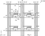
- FIG. 1 is a schematic partial plan view showing an example of a flexible transparent display device.
- FIG. 2 is a cross-sectional view taken along the line II-II in FIG.
- the right-handed xyz orthogonal coordinates shown in FIGS. 1 and 2 are for convenience to explain the positional relationship of the components.
- the z-axis positive direction is vertically upward
- the xy plane is a horizontal plane.
- the flexible transparent display device 100 shown in FIGS. 1 and 2 is a flexible transparent electronic device including a flexible transparent base material 10, a light emitting unit 20, an IC chip 30, wiring 40, and a protective layer 50.
- the display area 101 in the flexible transparent display device 100 shown in FIG. 1 is an area composed of a plurality of pixels and in which an image is displayed.
- the image includes characters.
- the display area 101 is composed of a plurality of pixels arranged in the row direction (x-axis direction) and the column direction (y-axis direction). In FIG. 1, a part of the display area 101 is shown, and a total of 4 pixels are shown, 2 pixels each in the row direction and the column direction.
- FIG. 1 is a plan view, the light emitting unit 20 and the IC chip 30 are displayed in dots for easy understanding.
- each pixel PIX includes a light emitting unit 20 and an IC chip 30.
- the light emitting unit 20 and the IC chip 30 are arranged in a matrix with a pixel pitch Px in the row direction (x-axis direction) and a pixel pitch Py in the column direction (y-axis direction). If the pixels are arranged in a predetermined direction at a predetermined pixel pitch, the arrangement format of the pixels PIX, that is, the light emitting unit 20 is not limited to the matrix shape.
- the light emitting unit 20 in each pixel PIX includes at least one light emitting diode element (hereinafter, LED element). That is, the flexible transparent display device is a display device that uses an LED element for each pixel PIX, and is called an LED display or the like.
- LED element light emitting diode element
- each light emitting unit 20 includes a red LED element 21, a green LED element 22, and a blue LED element 23 as electronic elements.
- the LED elements 21 to 23 correspond to sub-pixels (sub-pixels) constituting one pixel.
- each light emitting unit 20 has LED elements 21 to 23 that emit red, green, and blue, which are the three primary colors of light, the flexible transparent display device can display a full-color image.
- Each light emitting unit 20 may include two or more LED elements of similar colors. As a result, the dynamic range of the image can be expanded.
- the LED elements 21 to 23 have a minute size and are so-called micro LED elements. Specifically, the width (length in the x-axis direction) and the length (length in the y-axis direction) of the LED element 21 on the flexible transparent base material 10 are, for example, 100 ⁇ m or less, preferably 50 ⁇ m or less, more preferably. Is 20 ⁇ m or less. The same applies to the LED elements 22 and 23.
- the lower limit of the width and length of the LED element is, for example, 3 ⁇ m or more due to various manufacturing conditions and the like.
- the dimensions, that is, the width and the length of the LED elements 21 to 23 in FIG. 1 are the same, they may be different from each other.
- the occupied area of each of the LED elements 21 to 23 on the flexible transparent base material 10 is, for example, 10,000 ⁇ m 2 or less, preferably 1,000 ⁇ m 2 or less, and more preferably 100 ⁇ m 2 or less.
- the lower limit of the occupied area of each LED element is, for example, 10 ⁇ m 2 or more due to various manufacturing conditions and the like.
- the occupied area of the constituent members such as the LED element and the wiring refers to the area in the xy plan view in FIG.
- the shape of the LED elements 21 to 23 shown in FIG. 1 is rectangular, but is not particularly limited. For example, it may be a square, a hexagon, a cone structure, a pillar shape, or the like.
- the LED elements 21 to 23 have, for example, a mirror structure for efficiently extracting light to the visual recognition side. Therefore, the transmittance of the LED elements 21 to 23 is as low as about 10% or less, for example.
- the flexible transparent display device uses, for example, LED elements 21 to 23 having a minute size having an area of 10,000 ⁇ m 2 or less. Therefore, for example, even when observing the flexible transparent display device from a short distance of about several tens of centimeters to 2 m, the LED elements 21 to 23 are almost invisible. Further, the area where the transmittance is low is narrow in the display area 101, and the visibility on the back side is excellent. In addition, the degree of freedom in arranging the wiring 40 and the like is large.
- the “region with low transmittance in the display region 101” is, for example, a region having a transmittance of 20% or less. The same applies hereinafter.
- the flexible transparent display device can be mounted on a curved transparent plate such as a window glass for an automobile, or can be used by being enclosed between two curved transparent plates.
- the flexible transparent base material 10 is flexible (has flexibility), the flexible transparent display device can be curved.
- the illustrated LED elements 21 to 23 are chip type, but are not particularly limited.
- the LED elements 21 to 23 may not be packaged with a resin, or may be packaged in whole or in part.
- the packaging resin may have a lens function to improve the light utilization rate and the efficiency of taking out light to the outside. Further, in that case, the LED elements 21 to 23 may be packaged separately, or a 3in1 chip in which the three LED elements 21 to 23 are packaged together may be used.
- each LED element emits light at the same wavelength, light having a different wavelength may be extracted depending on a phosphor or the like contained in the packaging resin.
- the dimensions and the area of the above-mentioned LED elements are the dimensions and the area in the packaged state, respectively.
- the area of each LED element is one-third of the total area.
- the LED elements 21 to 23 are not particularly limited, but are, for example, inorganic materials.
- the red LED element 21 is, for example, AlGaAs, GaAsP, GaP, or the like.
- the green LED element 22 is, for example, InGaN, GaN, AlGaN, GaP, AlGaInP, ZnSe, or the like.
- the blue LED element 23 is, for example, InGaN, GaN, AlGaN, ZnSe, or the like.
- the luminous efficiency that is, the energy conversion efficiency of the LED elements 21 to 23 is, for example, 1% or more, preferably 5% or more, and more preferably 15% or more.
- the luminous efficiency of the LED elements 21 to 23 is 1% or more, sufficient brightness can be obtained even with the minute-sized LED elements 21 to 23 as described above, and the LED elements 21 to 23 can be used as a display device during the daytime. Further, when the luminous efficiency of the LED element is 15% or more, heat generation is suppressed, and encapsulation inside the laminated glass using the resin adhesive layer becomes easy.
- the LED elements 21 to 23 are obtained by cutting crystals grown by, for example, a liquid phase growth method, an HVPE (Hydride Vapor Phase Epitaxy) method, a MOCVD (Metal Organic Chemical Vapor Deposition) method, or the like.
- the obtained LED elements 21 to 23 are mounted on the flexible transparent base material 10.
- the LED elements 21 to 23 may be formed by peeling from the semiconductor wafer by microtransfer printing or the like and transferring the LED elements 21 to 23 onto the flexible transparent substrate 10.
- the pixel pitches Px and Py are, for example, 100 to 3000 ⁇ m, preferably 180 to 1000 ⁇ m, and more preferably 250 to 400 ⁇ m, respectively.
- the pixel pitches Px and Py are, for example, 100 to 3000 ⁇ m, preferably 180 to 1000 ⁇ m, and more preferably 250 to 400 ⁇ m, respectively.
- the pixel pitches Px and Py are, for example, 100 to 3000 ⁇ m, preferably 180 to 1000 ⁇ m, and more preferably 250 to 400 ⁇ m, respectively.
- the pixel density in the display area 101 of the flexible transparent display device is, for example, 10 ppi or more, preferably 30 ppi or more, and more preferably 60 ppi or more.
- the area of one pixel PIX can be represented by Px ⁇ Py.
- the area of one pixel is, for example, 1 ⁇ 10 4 ⁇ m 2 to 9 ⁇ 10 6 ⁇ m 2 , preferably 3 ⁇ 10 4 to 1 ⁇ 10 6 ⁇ m 2 , and more preferably 6 ⁇ 10 4 to 2 ⁇ 10 6 ⁇ m 2 . is there.
- the area of one pixel may be appropriately selected depending on the size of the display area 101, the application, the viewing distance, and the like.
- the ratio of the occupied area of the LED elements 21 to 23 to the area of one pixel is, for example, 30% or less, preferably 10% or less, more preferably 5% or less, and further preferably 1% or less.
- three LED elements 21 to 23 are arranged in a row in the positive direction of the x-axis in this order in each pixel, but the present invention is not limited to this.
- the arrangement order of the three LED elements 21 to 23 may be changed.
- the three LED elements 21 to 23 may be arranged in the y-axis direction.
- the three LED elements 21 to 23 may be arranged at the vertices of the triangle.
- each light emitting unit 20 includes a plurality of LED elements 21 to 23
- the distance between the LED elements 21 to 23 in the light emitting unit 20 is, for example, 100 ⁇ m or less, preferably 10 ⁇ m or less. is there.
- the LED elements 21 to 23 may be arranged so as to be in contact with each other. As a result, the first power supply branch line 41a can be easily shared, and the aperture ratio can be improved.
- each light emitting unit 20 includes three LED elements that emit light having different wavelengths, in some light emitting units 20, the LED elements are arranged side by side in the x-axis direction or the y-axis direction, and in the other light emitting unit 20, the LED elements are arranged side by side. , LED elements of each color may be arranged at the apex of the triangle.
- the IC chip 30 is an electronic element arranged for each pixel PIX and driving the light emitting unit 20. Specifically, the IC chip 30 is connected to each of the LED elements 21 to 23 via a drive line 45, and the LED elements 21 to 23 can be individually driven.
- the IC chip 30 may be arranged for each of a plurality of pixels, and the plurality of pixels to which each IC chip 30 is connected may be driven. For example, if one IC chip 30 is arranged for every four pixels, the number of IC chips 30 can be reduced to 1/4 of the example of FIG. 1, and the occupied area of the IC chip 30 can be reduced.
- Area of the IC chip 30 is, for example 100,000Myuemu 2 or less, preferably 10,000 2 or less, more preferably 5,000 .mu.m 2 or less.
- the transmittance of the IC chip 30 is as low as about 20% or less, but by using the IC chip 30 of the above size, the area of the display area 101 where the transmittance is low is narrowed, and the visibility on the back side is improved.
- the IC chip 30 is, for example, a hybrid IC having an analog area and a logic area.
- the analog domain includes, for example, a current control circuit, a transformer circuit, and the like.
- An LED element with an IC chip in which the LED elements 21 to 23 and the IC chip 30 are packaged together with a resin may be used.
- a circuit including a thin film transistor (TFT) may be used instead of the IC chip 30, a circuit including a thin film transistor (TFT) may be used.
- the IC chip 30 is not essential.
- the IC chip 30 may be equipped with a microsensor. That is, the flexible transparent display device may be a flexible transparent sensing device at the same time. Details of the microsensor will be described later in the fourth embodiment.
- the wiring 40 according to the present embodiment is a display wiring, and as shown in FIG. 1, includes a plurality of power supply lines 41, ground lines 42, row data lines 43, column data lines 44, and drive lines 45. ..
- the power supply line 41, the ground line 42, and the column data line 44 extend in the y-axis direction.
- the row data line 43 extends in the x-axis direction.
- the power supply line 41 and the column data line 44 are provided on the x-axis negative direction side of the light emitting unit 20 and the IC chip 30, and the ground line 42 is provided from the light emitting unit 20 and the IC chip 30. Is also provided on the positive side of the x-axis.
- the power supply line 41 is provided on the side in the negative direction of the x-axis with respect to the column data line 44.
- the row data line 43 is provided on the y-axis negative direction side of the light emitting unit 20 and the IC chip 30.
- the power supply line 41 includes a first power supply branch line 41a and a second power supply branch line 41b.
- the ground line 42 includes a ground branch line 42a.
- the row data line 43 includes a row data branch line 43a.
- the column data line 44 includes a column data branch line 44a. Each of these branch lines is included in the wiring 40.
- each power supply line 41 extending in the y-axis direction is connected to a light emitting unit 20 and an IC chip 30 of each pixel PIX arranged side by side in the y-axis direction. More specifically, in each pixel PIX, the LED elements 21 to 23 are arranged side by side in the x-axis positive direction in this order on the x-axis positive direction side of the power supply line 41. Therefore, the first power supply branch line 41a branched from the power supply line 41 in the positive direction of the x-axis is connected to the end of the LED elements 21 to 23 in the positive direction of the y-axis.
- the IC chip 30 is arranged on the y-axis negative direction side of the LED elements 21 to 23. Therefore, between the LED element 21 and the column data line 44, the second power supply branch line 41b branched from the first power supply branch line 41a in the negative direction of the y-axis is extended in a straight line, and the y-axis of the IC chip 30 is extended. It is connected to the x-axis negative direction side of the positive side end.
- each ground wire 42 extending in the y-axis direction is connected to an IC chip 30 of each pixel PIX arranged side by side in the y-axis direction.
- the ground branch line 42a branched from the ground line 42 in the negative direction on the x-axis extends linearly and is connected to the end on the positive side of the x-axis of the IC chip 30.
- the ground line 42 is connected to the LED elements 21 to 23 via the ground branch line 42a, the IC chip 30, and the drive line 45.
- each row data line 43 extending in the x-axis direction is connected to an IC chip 30 of each pixel PIX arranged side by side in the x-axis direction (row direction).
- the row data branch line 43a branched from the row data line 43 in the positive direction of the y-axis extends linearly and is connected to the end of the IC chip 30 in the negative direction of the y-axis.
- the row data line 43 is connected to the LED elements 21 to 23 via the row data branch line 43a, the IC chip 30, and the drive line 45.
- each column data line 44 extending in the y-axis direction is connected to an IC chip 30 of each pixel PIX arranged side by side in the y-axis direction (column direction).
- the column data branch line 44a branched from the column data line 44 in the positive direction on the x-axis extends linearly and is connected to the end on the negative side of the x-axis of the IC chip 30.
- the column data line 44 is connected to the LED elements 21 to 23 via the column data branch line 44a, the IC chip 30, and the drive line 45.
- the drive line 45 connects the LED elements 21 to 23 and the IC chip 30 in each pixel PIX. Specifically, in each pixel PIX, three drive lines 45 are extended in the y-axis direction, and each is the y-axis negative side end of the LED elements 21 to 23 and the y-axis positive side of the IC chip 30. It is connected to the end.
- the arrangement of the power supply line 41, the ground line 42, the row data line 43, the column data line 44, their branch lines, and the drive line 45 shown in FIG. 1 is merely an example and can be changed as appropriate.
- at least one of the power supply line 41 and the ground line 42 may extend in the x-axis direction instead of the y-axis direction.
- the power supply line 41 and the column data line 44 may be interchanged.
- the entire configuration shown in FIG. 1 may be upside down, left-right inverted, or the like. Further, the entire configuration shown in FIG. 1 may be upside down, left-right inverted, or the like. Further, the row data line 43, the column data line 44, their branch lines, and the drive line 45 are not essential.
- the wiring 40 is a metal such as copper (Cu), aluminum (Al), silver (Ag), and gold (Au). Of these, a metal containing copper or aluminum as a main component is preferable from the viewpoint of low resistivity and cost. Further, the wiring 40 may be coated with a material such as titanium (Ti), molybdenum (Mo), copper oxide, or carbon for the purpose of reducing the reflectance. Further, the surface of the coated material may have irregularities.
- the width of the wiring 40 in the display area 101 shown in FIG. 1 is, for example, 1 to 100 ⁇ m, preferably 3 to 20 ⁇ m. Since the width of the wiring 40 is 100 ⁇ m or less, the wiring 40 is almost invisible even when observing the flexible transparent display device from a short distance of about several tens of centimeters to 2 m, and the visibility on the back side is excellent. There is. On the other hand, in the case of the thickness range described later, if the width of the wiring 40 is 1 ⁇ m or more, an excessive increase in the resistance of the wiring 40 can be suppressed, and a voltage drop and a decrease in signal strength can be suppressed. Further, it is possible to suppress a decrease in heat conduction due to the wiring 40.
- the wiring 40 when the wiring 40 extends mainly in the x-axis direction and the y-axis direction, it extends in the x-axis direction and the y-axis direction by the light emitted from the outside of the flexible transparent display device. A cross-diffraction image may occur, reducing the visibility of the back side of the flexible transparent display device. By reducing the width of each wiring, this diffraction can be suppressed and the visibility on the back surface side can be further improved. From the viewpoint of suppressing diffraction, the width of the wiring 40 may be 50 ⁇ m or less, preferably 10 ⁇ m or less, and more preferably 5 ⁇ m or less.
- the electrical resistivity of the wiring 40 is, for example, 1.0 ⁇ 10 -6 ⁇ m or less, preferably 2.0 ⁇ 10 -8 ⁇ m or less.
- the thermal conductivity of the wiring 40 is, for example, 150 to 5,500 W / (m ⁇ K), preferably 350 to 450 W / (m ⁇ K).
- the distance between adjacent wirings 40 in the display area 101 shown in FIG. 1 is, for example, 3 to 100 ⁇ m, preferably 5 to 30 ⁇ m. If there is an area where the wiring 40 is dense, the visibility on the back side may be hindered. By setting the distance between adjacent wirings 40 to 3 ⁇ m or more, such obstruction of visual recognition can be suppressed. On the other hand, by setting the distance between adjacent wirings 40 to 100 ⁇ m or less, sufficient display capability can be ensured. When the distance between the wirings 40 is not constant due to the curved wiring 40 or the like, the above-mentioned distance between the adjacent wirings 40 indicates the minimum value thereof.
- the ratio of the occupied area of the wiring 40 to the area of one pixel is, for example, 30% or less, preferably 10% or less, more preferably 5% or less, and further preferably 3% or less.
- the transmittance of the wiring 40 is as low as 20% or less or 10% or less, for example.
- the total occupied area of the light emitting unit 20, the IC chip 30, and the wiring 40 with respect to the area of one pixel is, for example, 30% or less, preferably 20% or less, and more preferably 10% or less.
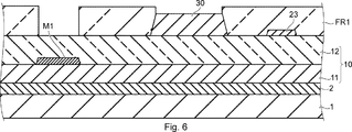
- the flexible transparent base material 10 is made of a transparent material having an insulating property.
- the flexible transparent base material 10 has a two-layer structure consisting of a main substrate 11 and an adhesive layer 12.
- the main substrate 11 is made of, for example, a transparent resin, as will be described in detail later.
- the adhesive constituting the adhesive layer 12 include transparent resin adhesives such as epoxy-based, acrylic-based, olefin-based, polyimide-based, and novolac-based.
- the main substrate 11 may be a thin glass plate having a thickness of, for example, 200 ⁇ m or less, preferably 100 ⁇ m or less. Further, the adhesive layer 12 is not essential.
- polyester resins such as polyethylene terephthalate (PET) and polyethylene naphthalate (PEN)
- olefin resins such as cycloolefin polymer (COP) and cycloolefin copolymer (COC)
- cellulose and acetyl Cellulose cellulose-based resins such as triacetyl cellulose (TAC), imide-based resins such as polyimide (PI), amide-based resins such as polyamide (PA), amide-imide-based resins such as polyamideimide (PAI), polycarbonate (PC), etc.
- Carbonate-based resin sulfone-based resin such as polyether sulfone (PES), paraxylene-based resin such as polyparaxylene, polyethylene (PE), polyvinyl chloride (PVC), polystyrene (PS), polyvinyl acetate (PVAC) ), Polyvinyl alcohol (PVA), vinyl resin such as polyvinyl butyral (PVB), acrylic resin such as polymethyl methacrylate (PMMA), ethylene / vinyl acetate copolymer resin (EVA), thermoplastic polyurethane (TPU), etc. Examples thereof include urethane-based resins and epoxy-based resins.
- PES polyether sulfone
- paraxylene-based resin such as polyparaxylene
- PE polyethylene
- PVC polyvinyl chloride
- PS polystyrene
- PVAC polyvinyl acetate
- PVA polyvinyl alcohol
- PVB vinyl resin
- acrylic resin such as polymethyl methacrylate
- polyethylene naphthalate (PEN) and polyimide (PI) are preferable from the viewpoint of improving heat resistance.
- PEN polyethylene naphthalate
- PI polyimide
- cycloolefin polymer (COP), cycloolefin copolymer (COC), polyvinyl butyral (PVB) and the like are preferable in that the birefringence is low and distortion and bleeding of the image seen through the transparent substrate can be reduced.
- the above materials may be used alone, or two or more kinds of materials may be mixed and used.
- the main substrate 11 may be formed by laminating flat plates of different materials.
- the total thickness of the flexible transparent base material 10 is, for example, 3 to 1000 ⁇ m, preferably 5 to 200 ⁇ m.
- the internal transmittance of visible light of the flexible transparent base material 10 is, for example, 50% or more, preferably 70% or more, and more preferably 90% or more. Further, since the flexible transparent base material 10 is flexible, for example, a flexible transparent display device can be mounted on a curved transparent plate or sandwiched between two curved transparent plates.
- the LED elements 21 to 23 and the IC chip 30 are provided on the flexible transparent base material 10, that is, the adhesive layer 12, and are connected to the wiring 40 arranged on the flexible transparent base material 10. ing.
- the wiring 40 is composed of a first metal layer M1 formed on the main substrate 11 and a second metal layer M2 formed on the adhesive layer 12.
- the total thickness of the wiring 40 that is, the thickness of the first metal layer M1 and the thickness of the second metal layer M2 is, for example, 0.1 to 10 ⁇ m, preferably 0.5 to 5 ⁇ m.
- the thickness of the first metal layer M1 is, for example, about 0.5 ⁇ m
- the thickness of the second metal layer M2 is, for example, about 3 ⁇ m.
- the ground wire 42 extending in the y-axis direction since the ground wire 42 extending in the y-axis direction has a large amount of current, it has a two-layer structure including the first metal layer M1 and the second metal layer M2. There is. That is, at the portion where the ground wire 42 is provided, the adhesive layer 12 is removed, and the second metal layer M2 is formed on the first metal layer M1.
- the power supply line 41, the row data line 43, and the column data line 44 shown in FIG. 1 also have a two-layer structure including the first metal layer M1 and the second metal layer M2. have.
- the power supply line 41, the ground line 42, and the column data line 44 extending in the y-axis direction intersect with the row data line 43 extending in the x-axis direction.
- the row data line 43 is composed of only the first metal layer M1
- the power supply line 41, the ground line 42, and the column data line 44 are composed of only the second metal layer M2. It is composed of.
- an adhesive layer 12 is provided between the first metal layer M1 and the second metal layer M2, and the first metal layer M1 and the second metal layer M2 are insulated from each other.
- the first power supply branch line 41a is composed of only the first metal layer M1
- the column data line 44 is the second metal. It is composed of only the layer M2.
- the ground branch line 42a, the drive line 45, and the first power supply branch line 41a are composed of only the second metal layer M2 and cover the ends of the LED elements 21 to 23 and the IC chip 30. Is formed in.
- the second power supply branch line 41b, the row data branch line 43a, and the column data branch line 44a are similarly composed of only the second metal layer M2.
- the first power supply branch line 41a is composed of only the first metal layer M1 at the intersection with the column data line 44, and is composed of only the second metal layer M2 at other parts. Further, a metal pad made of copper, silver, gold or the like is arranged on the wiring 40 formed on the flexible transparent base material 10, and at least one of the LED elements 21 to 23 and the IC chip 30 is arranged on the metal pad. May be good.
- the protective layer 50 is a transparent resin formed on substantially the entire surface of the flexible transparent base material 10 so as to cover and protect the light emitting portion 20, the IC chip 30, and the wiring 40.
- the thickness of the protective layer 50 is, for example, 3 to 1000 ⁇ m, preferably 5 to 200 ⁇ m.
- the elastic modulus of the protective layer 50 is, for example, 10 GPa or less. The lower the elastic modulus, the more the impact at the time of peeling can be absorbed, and the damage of the protective layer 50 can be suppressed.
- the internal transmittance of visible light of the protective layer 50 is, for example, 50% or more, preferably 70% or more, and more preferably 90% or more.
- vinyl resins such as polyethylene (PE), polyvinyl chloride (PVC), polystyrene (PS), polyvinyl acetate (PVAC), polyvinyl alcohol (PVA), and polyvinyl butyral (PVB)
- Olefin resins such as cycloolefin polymer (COP) and cycloolefin copolymer (COC)
- urethane resins such as thermoplastic polyurethane (TPU), polyester resins such as polyethylene terephthalate (PET) and polyethylene naphthalate (PEN)
- acrylic resins such as polymethyl methacrylate (PMMA) and thermoplastic resins such as ethylene / vinyl acetate copolymer resin (EVA).
- FIGS. 3 to 13 are cross-sectional views showing an example of a method for manufacturing a flexible transparent display device according to the first embodiment.
- 3 to 13 are cross-sectional views corresponding to FIG.
- the glass support substrate 1 is a glass substrate for supporting and transporting the flexible transparent display device 100 formed on the glass support substrate 1.
- the peeling layer 2 is provided for peeling the flexible transparent display device 100 from the glass support substrate 1 as described later.
- the release layer 2 contains a resin as a main component, and has a smaller transmittance of ultraviolet laser light LB than the flexible transparent base material 10.
- the transmittance of the ultraviolet laser beam LB of the release layer 2 is, for example, 50% or less, preferably 30% or less, and more preferably 10% or less.
- the flexible transparent display device 100 When the ultraviolet laser beam LB described later is irradiated, the flexible transparent display device 100 is peeled from the glass support substrate 1 by decomposing a part or the whole of the peeling layer 2 instead of the flexible transparent base material 10. Further, since the release layer 2 absorbs the ultraviolet laser light LB, it is difficult for the ultraviolet laser light LB to reach the flexible transparent base material 10. Therefore, it is possible to suppress damage to the flexible transparent base material 10 due to irradiation with laser light and damage to electronic elements and the like due to the impact.
- the thickness of the release layer 2 is, for example, 1 to 20 ⁇ m, preferably 2 to 10 ⁇ m.
- the surface roughness Ra of the release layer 2 is, for example, 0.5 ⁇ m or less, preferably 0.01 ⁇ m or less.
- the surface roughness Ra of the release layer 2 affects the surface roughness of the main substrate 11 formed on the release layer 2. The smaller the surface roughness Ra of the release layer 2, the more accurately the first metal layer M1 formed on the main substrate 11 can be patterned (see FIG. 4).
- the surface roughness Ra of the release layer 2 is measured according to JIS B0601 using, for example, SURFCOM 1400D manufactured by Tokyo Seimitsu Co., Ltd.
- the resin constituting the release layer 2 is, for example, a resin having a smaller transmittance of ultraviolet laser light LB than the resin constituting the flexible transparent base material 10 (particularly the main substrate 11) (for example, an aromatic ring-containing resin). More specifically, for example, a polyester resin or a phenol resin (for example, novolac) containing a fluorene derivative skeleton.
- the resin constituting the release layer 2 may be, for example, a transparent resin similar to the main substrate 11 to which an ultraviolet absorber is added.
- the amount of the ultraviolet absorber added is, for example, 1 to 70 parts by mass, with 100 parts by mass as a whole. It is preferably 2 to 50 parts by mass. Since the resin constituting the release layer 2 is removed, it does not need to be transparent.
- the glass transition temperature Tg of the resin constituting the release layer 2 is, for example, 60 ° C. or higher. It is preferably 100 ° C. or higher.
- the glass transition temperature Tg is, for example, 60 ° C. or higher. It is preferably 100 ° C. or higher.
- the dissolution rate in acid or alkali is preferably 1.0 ⁇ 10 -3 ⁇ m / s or more, and more preferably 1.0 ⁇ 10 -2 ⁇ m / s or more.
- Examples of the ultraviolet absorber contained in the release layer 2 include organic ultraviolet absorbers such as benzophenone, benzotriazole, triazine, hindered amine and benzoate, and inorganic ultraviolet absorbers such as titanium oxide and zinc oxide.
- the release layer 2 may have a surface resistivity (sheet resistance) of 10 4 to 10 13 ⁇ / ⁇ .
- the surface resistivity is preferably 10 7 to 10 12 ⁇ / ⁇ . More preferably, it is 10 8 to 10 11 ⁇ / ⁇ . The method for measuring the surface resistivity will be described later.
- the release layer 2 may be a resin containing 1 to 90 parts by mass of a conductive filler with 100 parts by mass as a whole.
- the content of the conductive filler is preferably 30 to 80 parts by mass.
- the resin may contain 0.01 to 50 parts by mass of the ionic compound, with 100 parts by mass as a whole.
- the content of the ionic compound is preferably 0.1 to 10 parts by mass.
- the resin itself may be at least one of a conductive polymer and a hydrophilic polymer. In this way, the release layer 2 may have conductivity.
- the release layer 2 When the release layer 2 has conductivity, it is irradiated with an ultraviolet laser beam LB described later, and when the flexible transparent display device 100 formed on the glass support substrate 1 is peeled from the glass support substrate 1, the flexible transparent base material 10 is used. Can suppress the charge of. As a result, it is possible to prevent the electronic elements and the like included in the flexible transparent electronic device 100 from being damaged by the electrostatic discharge.
- the conductive filler contained in the release layer 2 powders such as copper, aluminum, silver, gold, nickel (Ni), metal fillers such as fibers and foil pieces, carbon black, graphite powder, carbon nanotubes, carbon fibers and the like Examples thereof include metal oxide-based fillers such as carbon-based fillers, tin oxide (SnO 2 ), indium oxide (In 2 O 3), and zinc oxide (ZnO) powders. Further, the conductive filler may be a semiconductor, a powder of a polymer complex, or the like.
- the ionic compound contained in the release layer 2 is, for example, an ionic conductive agent, an ionic liquid, a surfactant, or the like.
- a cationic conductive agent having a cationic functional group such as a quaternary ammonium salt, a pyridinium salt, a primary to tertiary amino group, a sulfonic acid base, a sulfate ester base, and a phosphoric acid ester.
- Anionic conductive agents having anionic functional groups such as bases and phosphonic acid bases, amphoteric conductive agents such as amino acids and aminosulfate esters, and organics having nonionic functional groups such as polyols, polyglycerins and polyethylene glycols. Examples of system antistatic compounds can be given.
- Examples of the conductive polymer constituting the release layer 2 include ⁇ -conjugated conductive polymers such as polyacetylene, polyparaphenylene, polythiophene, polypyrrole, and polyaniline.
- a hydrophilic polymer constituting the release layer 2 a modified vinyl copolymer containing a specific polyether ester amide and a carboxyl group, polymethylmethacrylate having a carboxyl group at the end is converted to glycidyl methacrylate, and the carboxyl group at the end is converted to a methacryloyl group.
- a comb-type copolymer consisting of a polymer monomer and an aminoalkylacrylic acid ester or acrylamide, a quaternized cation-modified product thereof, an acrylamide-based copolymer composed of an ethylene structural unit, an acrylate structural unit, and an acrylamide structural unit
- Examples of the polyolefin resin composition to which this is added can be illustrated.
- the first metal layer M1 is patterned by photolithography to form the lower layer wiring.
- the lower layer wiring is formed by the first metal layer M1 at the position where the power supply line 41, the ground line 42, the row data line 43, the column data line 44, and the like shown in FIG. 1 are formed. No lower layer wiring is formed at the intersection of the power supply line 41, the ground line 42, and the row data line 43 in the column data line 44.
- an adhesive layer 12 is formed on substantially the entire surface of the main substrate 11, and then the LED elements 21 to 23 and the IC chip 30 are mounted on the tacky adhesive layer 12. .
- the photoresist FR1 is formed on substantially the entire surface of the flexible transparent base material 10 including the main substrate 11 and the adhesive layer 12, and then the photoresist FR1 on the first metal layer M1 is formed. Remove by patterning.
- the photoresist FR1 at the intersection of the power supply line 41, the ground line 42, and the column data line 44 in the row data line 43 shown in FIG. 1 is not removed.
- the adhesive layer 12 at the portion where the photoresist FR1 has been removed is removed by dry etching to expose the first metal layer M1, that is, the lower layer wiring.
- all the photoresist FR1 on the flexible transparent substrate 10 is removed.
- a seed layer for plating (not shown) is formed on substantially the entire surface of the flexible transparent base material 10.
- the photoresist FR2 at the portion where the upper layer wiring is formed is removed by patterning to expose the seed layer. ..
- a second metal layer M2 is formed by plating on the site where the photoresist FR2 has been removed, that is, on the seed layer.
- the upper layer wiring is formed by the second metal layer M2.
- the photoresist FR2 is removed. Further, the seed layer exposed by the removal of the photoresist FR2 is removed by etching.
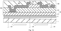
- FIG. 12 shows an article according to the present embodiment. As shown in FIG. 12, in the article according to the present embodiment, the release layer 2 is formed between the glass support substrate 1 and the flexible transparent display device 100.
- the flexible transparent display device 100 formed on the glass support substrate 1 by irradiating the ultraviolet laser beam LB such as an excimer laser from the lower side of the drawing of the glass support substrate 1 is mounted on the glass support substrate 1. Peel from 1.
- the release layer 2 is decomposed by the ultraviolet laser beam LB transmitted through the glass support substrate 1, and the flexible transparent display device 100 can be separated from the glass support substrate 1.
- the entire glass support substrate 1 can be irradiated with the ultraviolet laser beam LB.
- the wavelength of ultraviolet rays is, for example, 400 nm or less.
- the wavelength of the excimer laser light used for laser exfoliation is, for example, 308 nm (XeCl) or 248 nm (KrF).
- the peeling layer 2 remaining on the flexible transparent display device 100 after peeling can be removed by washing or the like. By the above steps, the flexible transparent display device 100 can be manufactured.
- the transmittance of the ultraviolet laser beam LB is smaller than that of the flexible transparent base material 10 between the glass support substrate 1 and the flexible transparent base material 10 before peeling.
- Layer 2 is formed. That is, the glass support substrate 1 and the flexible transparent substrate 10 are not in direct contact with each other, and a release layer 2 is formed between them. Then, when the ultraviolet laser beam LB is irradiated, the release layer 2 is decomposed instead of the flexible transparent base material 10, so that the flexible transparent display device 100 is separated from the glass support substrate 1. Further, since the release layer 2 absorbs the ultraviolet laser light LB, it is difficult for the ultraviolet laser light LB to reach the flexible transparent base material 10. Therefore, it is possible to suppress damage to the flexible transparent base material 10 due to irradiation with laser light and damage to electronic elements and the like due to the impact.
- FIG. 14 is a schematic plan view of a comb-shaped electrode used for measuring the surface resistivity.
- the comb-shaped electrode has a shape in which the five comb teeth of the first comb-shaped electrode and the four comb teeth of the second comb-shaped electrode are alternately arranged to face each other.
- the width of the comb teeth, the length of the comb teeth, and the distance between the comb teeth are equal to each other. Therefore, the four comb teeth of the second comb-shaped electrode are inserted in the center between the five comb teeth of the first comb-shaped electrode.
- the electrode coefficient r of the comb-shaped electrode is, for example, about 100 to 130.
- the metal constituting the comb-shaped electrode for example, a material having a small electric resistance such as platinum, aluminum, or gold is used.
- platinum is preferred.
- a metal film constituting a comb-shaped electrode is formed on a substrate having electrical insulation by means such as sputtering, vacuum deposition, and plating.
- FIG. 15 is a diagram showing a specific example of each dimension in the comb-shaped electrode shown in FIG.
- the unit of the numerical value in FIG. 15 is mm.
- the electrode coefficient r 112.75.
- a digital ultra-high resistance / micro ammeter (ADVANTEST R830A ULTRA HIGH RESISTANCE METER) is used. For example, after connecting a copper wire to the obtained comb-shaped electrode, a voltage of 10 V is applied and the current measurement is started every 3 minutes until the voltage stabilizes. Then, the current value after 3 minutes is read, and the surface resistivity ⁇ is calculated from the above-mentioned relational expression.
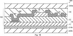
- FIG. 16 is a schematic plan view showing an example of the laminated glass according to the second embodiment.
- FIG. 17 is a schematic cross-sectional view showing an example of the laminated glass according to the second embodiment.
- the laminated glass 200 shown in FIGS. 16 and 17 is used for the windshield of the window glass of an automobile, but is not particularly limited.
- a black shielding portion 201 is provided on the entire peripheral edge of the laminated glass 200.
- the shielding portion 201 shields sunlight and protects the adhesive for assembling the laminated glass 200 to the automobile from ultraviolet rays.
- the shielding portion 201 makes the adhesive invisible from the outside.
- the flexible transparent display device 100 includes a non-display area 102 provided around the display area in addition to the display area 101 shown in FIG.
- the display area 101 is an area composed of a large number of pixels and in which an image is displayed, and therefore detailed description thereof will be omitted.
- FIG. 16 is a plan view, the non-display area 102 and the shielding portion 201 are displayed in dots for easy understanding.
- the non-display area 102 is an area that does not include pixels and does not display an image.
- the non-display area 102 is densely provided with wide wiring connected to the power supply line 41, the ground line 42, the row data line 43, and the column data line 44 shown in FIG.
- the width of the wiring in the non-display area 102 is, for example, 100 to 10,000 ⁇ m, preferably 100 to 5,000 ⁇ m.
- the distance between the wires is, for example, 3 to 5,000 ⁇ m, preferably 50 to 1,500 ⁇ m.
- the non-display area 102 is opaque and can be visually recognized from inside the vehicle.
- the design of the laminated glass 200 is deteriorated. Therefore, in the laminated glass 200 according to the second embodiment, at least a part of the non-display area 102 of the flexible transparent display device 100 is provided in the shielding portion 201.
- the non-display area 102 provided in the shielding portion 201 is hidden by the shielding portion 201 and cannot be visually recognized. Therefore, the design of the laminated glass 200 is improved as compared with the case where the entire non-display area 102 can be visually recognized.
- FIG. 17 is a cross-sectional view of the flexible transparent display device 100 in the display area 101.
- the laminated glass 200 according to the second embodiment is formed by laminating a pair of glass plates 220a and 220b via an interlayer film.
- the laminated glass 200 includes the flexible transparent display device 100 according to the first embodiment between the pair of glass plates 220a and 220b via the interlayer films 210a and 210b.
- the interlayer films 210a and 210b are made of, for example, polyvinyl butyral (PVB).
- FIG. 18 is a schematic cross-sectional view showing another example of the laminated glass according to the second embodiment.
- the protective layer 50 in the flexible transparent display device 100 is composed of, for example, polyvinyl butyral (PVB), and also has a function as an interlayer film. Therefore, in the laminated glass 200 shown in FIG. 18, the interlayer film 210a formed on the protective layer 50 in FIG. 17 can be omitted.
- PVB polyvinyl butyral
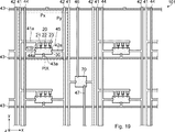
- FIG. 19 is a schematic partial plan view showing an example of the flexible transparent display device according to the third embodiment.
- the flexible transparent display device according to the present embodiment includes a sensor 70 in the display area 101 in addition to the configuration of the flexible transparent display device according to the first embodiment shown in FIG.
- the senor 70 is provided between predetermined pixels PIX and is connected to the power supply line 41 and the ground line 42. Further, the detection data by the sensor 70 is output via the data output line 46 extending from the sensor 70 in the y-axis direction. On the other hand, a control signal is input to the sensor 70 via a control signal line 47 extending in the y-axis direction to the sensor 70, and the sensor 70 is controlled.
- the number of sensors 70 may be singular or plural.
- a plurality of sensors 70 may be arranged at predetermined intervals, for example, in the x-axis direction or the y-axis direction.
- the flexible transparent display device according to the present embodiment is mounted on the windshield of the window glass of an automobile. That is, the flexible transparent display device according to the present embodiment can also be applied to the laminated glass according to the second embodiment.
- the sensor 70 is, for example, an illuminance sensor (for example, a light receiving element) for detecting illuminance inside and outside the vehicle.
- the brightness of the display area 101 by the LED elements 21 to 23 is controlled according to the illuminance detected by the sensor 70.
- the greater the illuminance outside the vehicle with respect to the illuminance inside the vehicle the greater the brightness of the display area 101 by the LED elements 21 to 23. With such a configuration, the visibility of the flexible transparent display device is further improved.
- the senor 70 may be an infrared sensor (for example, a light receiving element) or an image sensor (for example, a CMOS (Complementary Metal-Oxide-Semiconductor) image sensor) for detecting the line of sight of an observer (for example, a driver).
- the flexible transparent display device is driven only when the sensor 70 senses the line of sight.
- the flexible transparent display device is used for the laminated glass shown in FIG. 16, it is preferable because the flexible transparent display device does not block the observer's field of view unless the observer directs his / her line of sight to the flexible transparent display device.
- the sensor 70 which is an image sensor, may detect the movement of the observer, and based on the movement, for example, the flexible transparent display device may be turned on / off or the display screen may be switched.
- Other configurations are the same as those of the flexible transparent display device according to the first embodiment.
- FIG. 20 is a schematic partial plan view showing an example of the flexible transparent sensing device according to the fourth embodiment.
- the flexible transparent sensing device shown in FIG. 20 is a flexible transparent electronic device having a configuration in which each pixel PIX is provided with a sensor 70 instead of a light emitting unit 20 and an IC chip 30 in the configuration of the flexible transparent display device shown in FIG. Is. That is, the flexible transparent sensing device shown in FIG. 20 does not have a light emitting unit 20 and does not have a display function.
- the sensor 70 is not particularly limited, but the flexible transparent sensing device shown in FIG. 20 is a CMOS image sensor. That is, the flexible transparent sensing device shown in FIG. 20 includes an imaging region 301 composed of a plurality of pixel PIX arranged in the row direction (x-axis direction) and the column direction (y-axis direction), and has an imaging function. ing. In FIG. 20, a part of the imaging region 301 is shown, and a total of 4 pixels are shown, 2 pixels each in the row direction and the column direction. Here, one pixel PIX is shown surrounded by an alternate long and short dash line. Further, in FIG. 20, the flexible transparent base material 10 and the protective layer 50 are omitted as in FIG. 1. Further, although FIG. 20 is a plan view, the sensor 70 is displayed in dots for easy understanding.
- one sensor 70 is provided for each pixel PIX, is arranged between the power supply line 41 and the ground line 42 extending in the y-axis direction, and is connected to both. Further, the detection data by the sensor 70 is output via the data output line 46 extending from the sensor 70 in the y-axis direction. On the other hand, a control signal is input to the sensor 70 via a control signal line 47 extending in the y-axis direction to the sensor 70, and the sensor 70 is controlled.
- the control signal is, for example, a synchronization signal, a reset signal, or the like.
- the power supply line 41 may be connected to a battery (not shown).
- FIG. 21 is a schematic cross-sectional view of the sensor 70.
- the sensor 70 shown in FIG. 21 is a back-illuminated CMOS image sensor.
- the sensor 70 as an image sensor is not particularly limited, and a surface-illuminated CMOS image sensor or a CCD (Charge-Coupled Device) image sensor may be used.
- CCD Charge-Coupled Device
- each sensor 70 includes a wiring layer, a semiconductor substrate, color filters CF1 to CF3, and microlenses ML1 to ML3.
- an internal wiring IW is formed inside the wiring layer.
- photodiodes PD1 to PD3 are formed inside the semiconductor substrate.
- a semiconductor substrate for example, a silicon substrate is formed on the wiring layer.
- the internal wiring IW formed inside the wiring layer connects the wiring 40 (power supply line 41, ground line 42, data output line 46, and control signal line 47) with the photodiodes PD1 to PD3.
- the photodiodes PD1 to PD3 are irradiated with light, a current is output from the photodiodes PD1 to PD3.
- the currents output from the photodiodes PD1 to PD3 are amplified by an amplifier circuit (not shown) and output via the internal wiring IW and the data output line 46.
- the color filters CF1 to CF3 are formed on the photodiodes PD1 to PD3 formed inside the semiconductor substrate, respectively.
- the color filters CF1 to CF3 are, for example, a red filter, a green filter, and a blue filter, respectively.
- the microlenses ML1 to ML3 are placed on the color filters CF1 to CF3, respectively.
- the light collected by the microlenses ML1 to ML3, which are convex lenses, is incident on the photodiodes PD1 to PD3 via the color filters CF1 to CF3, respectively.
- the sensor 70 is, for example, a microsensor having a minute size of 250,000 ⁇ m 2 or less in an occupied area on the flexible transparent base material 10.
- the microsensor is a sensor having a minute size of 250,000 ⁇ m 2 or less in a plan view.
- the occupied area of the sensor 70 is, for example, preferably 25,000 ⁇ m 2 or less, more preferably 2,500 ⁇ m 2 or less.
- the lower limit of the occupied area of the sensor 70 is, for example, 10 ⁇ m 2 or more due to various manufacturing conditions and the like.
- the shape of the sensor 70 shown in FIG. 20 is rectangular, but is not particularly limited.
- the flexible transparent sensing device according to the present embodiment can also be applied to the laminated glass according to the second embodiment.
- the sensor 70 can acquire at least one image inside or outside the vehicle, for example. That is, the flexible transparent sensing device according to the present embodiment has a function as a drive recorder.
- the number of sensors 70 in the flexible transparent sensing device according to the fourth embodiment may be singular. Further, the sensor 70 in the flexible transparent sensing device according to the fourth embodiment is not limited to the image sensor, and may be an illuminance sensor, an infrared sensor, or the like exemplified in the third embodiment. Further, the sensor 70 may be a radar sensor, a lidar sensor, or the like. For example, the inside and outside of a vehicle can be monitored by a window glass for a vehicle equipped with a flexible transparent sensing device using these sensors 70.
- the senor 70 according to the fourth embodiment is not particularly limited as long as it is a microsensor having a minute size of 250,000 ⁇ m 2 or less in the occupied area on the flexible transparent base material 10.
- the sensor 70 may be a temperature sensor, an ultraviolet sensor, a radio wave sensor, a pressure sensor, a sound sensor, a speed / acceleration sensor, or the like.
- Other configurations are the same as those of the flexible transparent display device according to the first embodiment.
- Example 1 [Formation of release layer 2 and flexible transparent base material 10]
- a polyimide solution was applied by spin coating on a glass support substrate 1 made of non-alkali glass having a square size of 99.5 mm and a thickness of 0.9 mm. By heating this coating film at 190 ° C. for 10 minutes in the air, a polyimide release layer 2 was formed on the glass support substrate 1.
- the surface roughness Ra was 0.004 ⁇ m.
- a novolak type epoxy solution was applied onto the release layer 2 by spin coating.
- This coating film is heated at 140 ° C. for 4 minutes in the air, irradiated with ultraviolet rays of 500 mJ, and further heated at 175 ° C. for 1 hour in an oven to be made of a novolak type epoxy resin on the release layer 2.
- the flexible transparent base material 10 was formed.
- protective layer 50 Two sheets of 100 mm square and 2 mm thick soda lime glass and one PVB film having a thickness of 0.38 mm (15 mil) were prepared. A PVB film for the protective layer 50 and an ETFE film for peeling are laminated in this order on a flexible transparent base material 10 formed on the glass support substrate 1 via the release layer 2, and the laminate is laminated with two sodas. It was sandwiched between lime glass and vacuum packed. Further, the vacuum-packed laminate was heated at 100 ° C. for 1 hour, and then the peeling ETFE film and the two soda lime glasses were removed to form a protective layer 50 made of PVB.
- Example 2 A polyimide solution (ECRIOS manufactured by Mitsui Chemicals, Inc.) was used as the material of the release layer 2, and the mixture was heated at 220 ° C. for 2 hours. As a result, the release layer 2 made of polyimide was obtained.
- an acrylic resin 70 parts by mass of A-DCP manufactured by Shin-Nakamura Chemical Industry Co., Ltd., 30 parts by mass of U-6LPA manufactured by Shin-Nakamura Chemical Industry Co., Ltd., and Omnirad 184, a polymerization initiator manufactured by IGMResins BV. A mixture of parts by mass
- Example 3 The same procedure as in Example 2 was carried out except that a fluorene-based polyester solution (OKP-2 manufactured by Osaka Gas Chemical Co., Ltd.) was used as the material of the release layer 2 and the layers were sequentially heated at 90 ° C. for 5 minutes and 110 ° C. for 2 minutes. As a result, the release layer 2 made of fluorene-based polyester resin was obtained.
- a fluorene-based polyester solution (OKP-2 manufactured by Osaka Gas Chemical Co., Ltd.) was used as the material of the release layer 2 and the layers were sequentially heated at 90 ° C. for 5 minutes and 110 ° C. for 2 minutes.
- the release layer 2 made of fluorene-based polyester resin was obtained.
- Example 4 Novolak / photosensitizer solution (OFPR-800LB manufactured by Tokyo Ohka Kogyo Co., Ltd.) was used as the material of the release layer 2, and the same procedure as in Example 1 was carried out except that the mixture was heated at 140 ° C. for 5 minutes. As a result, a release layer 2 made of novolac resin containing 1 to 55 parts by mass of a photosensitizer was obtained with 100 parts by mass as a whole.
- OFPR-800LB manufactured by Tokyo Ohka Kogyo Co., Ltd.
- Tg 150 to 170 ° C.
- Example 7 As the material of the release layer 2, a novolak / ultraviolet absorber solution (a mixed solution of TR4020G manufactured by Asahi Organic Materials Industry Co., Ltd. and Tinuvin 477 manufactured by BASF) was used, and the same procedure as in Example 2 was carried out except that the solution was heated at 150 ° C. for 5 minutes. As a result, a release layer 2 made of novolak resin containing 4 parts by mass of a hydroxyphenyltriazine (HPT) -based ultraviolet absorber was obtained with 100 parts by mass as a whole. The surface roughness Ra was 0.003 ⁇ m.
- HPT hydroxyphenyltriazine
- Example 8 As the material of the release layer 2, a novolak / ultraviolet absorber solution (a mixed solution of TR4020G manufactured by Asahi Organic Materials Industry Co., Ltd. and Tinuvin 477 manufactured by BASF) was used, and the same procedure as in Example 2 was carried out except that the solution was heated at 150 ° C. for 5 minutes. As a result, a stripping layer 2 made of novolak resin containing about 14 parts by mass of a hydroxyphenyltriazine (HPT) -based ultraviolet absorber was obtained with 100 parts by mass as a whole. The surface roughness Ra was 0.004 ⁇ m.
- HPT hydroxyphenyltriazine
- the flexible transparent substrate 10 in Examples 1 and 4 are the same material, the transmittance T 308 nm of the flexible transparent substrate 10 was 7.5%.
- Examples flexible transparent substrate 10 in the 2, 3, 5 and 8 are the same material, the transmittance T 308 nm of the flexible transparent substrate 10 was 84%.
Landscapes
- Engineering & Computer Science (AREA)
- Physics & Mathematics (AREA)
- General Physics & Mathematics (AREA)
- Theoretical Computer Science (AREA)
- Microelectronics & Electronic Packaging (AREA)
- Manufacturing & Machinery (AREA)
- Computer Hardware Design (AREA)
- Power Engineering (AREA)
- Devices For Indicating Variable Information By Combining Individual Elements (AREA)
- Electroluminescent Light Sources (AREA)
Abstract
本発明の一形態は、フレキシブル透明基材(10)と、フレキシブル透明基材(10)上に形成された電子素子(20)と、電子素子(20)を覆う透明樹脂製の保護層(50)と、を備えたフレキシブル透明電子デバイス(100)が、ガラス支持基板(1)上に形成された物品を準備し、物品におけるガラス支持基板1を介して紫外線レーザ光(LB)を照射することによって、ガラス支持基板(1)からフレキシブル透明電子デバイス(100)を剥離するフレキシブル透明電子デバイスの製造方法である。物品を準備した際、ガラス支持基板(1)とフレキシブル透明基材(10)との間に、樹脂を主成分とし、フレキシブル透明基材よりも紫外線レーザ光(LB)の透過率が小さい剥離層(2)が形成されている。
Description
本発明は、フレキシブル透明電子デバイスの製造方法及び物品に関する。
特許文献1には、透明基材上に形成された発光ダイオード(LED:Light Emitting Diode)素子を画素に用いた透明表示デバイスが開示されている。このような透明表示デバイスは、当該透明表示デバイスを介して背面側を視認可能であるため、例えば自動車のフロントガラス等に用いられる。関連技術として、透明基材上にマイクロセンサが設けられた透明センシングデバイスが知られている。
本明細書では、透明表示デバイスや透明センシングデバイス等のように、透明基材上に電子素子が形成され、背面側を視認可能な電子デバイスを「透明電子デバイス」と呼ぶ。透明電子デバイスにおいて、透明基材がフレキシブルであれば、「フレキシブル透明電子デバイス」が得られる。
フレキシブル電子デバイスの製造方法としては、ガラス支持基板上にフレキシブル基材及び電子素子を順次形成した後、フレキシブル基材及び電子素子を含むフレキシブル電子デバイスをガラス支持基板から剥離する手法が知られている。例えば特許文献2、3には、フレキシブル基材とガラス支持基板との界面にレーザ光を照射して、フレキシブル電子デバイスをガラス支持基板から剥離する手法が開示されている。このような手法は、レーザリフトオフ(LLO:Laser lift-off)法と呼ばれる。
LLO法をフレキシブル透明電子デバイスの製造方法に適用した場合、フレキシブル透明基材とガラス支持基板との界面にレーザ光を照射して、フレキシブル透明電子デバイスをガラス支持基板から剥離することになる。このような手法について、発明者らは、以下の問題点を見出した。
レーザ光を照射すると、ガラス支持基板との界面に位置するフレキシブル透明基材が分解し、ガラス支持基板から剥離する。その際、レーザ光の照射によって、フレキシブル透明基材が損傷したり、その衝撃に伴い電子素子等がダメージを受けたりする虞があった。
本発明は、このような事情に鑑みなされたものであって、レーザ光の照射によるフレキシブル透明基材の損傷を抑制可能なフレキシブル透明電子デバイスの製造方法を提供するものである。
本発明は、以下[1]の構成を有するフレキシブル透明電子デバイスの製造方法を提供する。
[1]
フレキシブル透明基材と、前記フレキシブル透明基材上に形成された電子素子と、前記電子素子を覆う透明樹脂製の保護層と、を備えたフレキシブル透明電子デバイスが、ガラス支持基板上に形成された物品を準備し、
前記物品における前記ガラス支持基板を介して紫外線レーザ光を照射することによって、前記ガラス支持基板から前記フレキシブル透明電子デバイスを剥離する、フレキシブル透明電子デバイスの製造方法であって、
前記物品を準備した際、前記ガラス支持基板と前記フレキシブル透明基材との間に、樹脂を主成分とし、前記フレキシブル透明基材よりも前記紫外線レーザ光の透過率が小さい剥離層が形成されている、
フレキシブル透明電子デバイスの製造方法。
本発明の一態様においては、
[2]前記樹脂が、芳香環含有樹脂である、[1]に記載のフレキシブル透明電子デバイスの製造方法。
[2]前記樹脂が、芳香環含有樹脂である、[1]に記載のフレキシブル透明電子デバイスの製造方法。
[3]前記樹脂のガラス転移温度Tgが60℃以上である、[1]又は[2]に記載のフレキシブル透明電子デバイスの製造方法。
[4]前記剥離層における前記紫外線レーザ光の透過率が、50%以下である、[1]又は[2]に記載のフレキシブル透明電子デバイスの製造方法。
[5]前記剥離層が、紫外線吸収剤を含有する、[4]に記載のフレキシブル透明電子デバイスの製造方法。
[6]前記剥離層が、紫外線吸収剤を含有せずに、前記剥離層における前記紫外線レーザ光の透過率が、5%以下である、[4]に記載のフレキシブル透明電子デバイスの製造方法。
[7]前記剥離層が、104~1013Ω/□の表面抵抗率を有する、[1]~[6]のいずれか一項に記載のフレキシブル透明電子デバイスの製造方法。
[8]前記剥離層の表面粗さRaが、0.5μm以下である、[1]~[7]のいずれか一項に記載のフレキシブル透明電子デバイスの製造方法。
[9]前記電子素子が、発光ダイオード素子を含み、前記発光ダイオード素子は、前記フレキシブル透明基材上において画素ごとに少なくとも1つ配置されると共に、それぞれが10,000μm2以下の面積を有し、当該フレキシブル透明電子デバイスが表示デバイスとしての機能を有する、[1]~[8]のいずれか一項に記載のフレキシブル透明電子デバイスの製造方法。
本発明は、以下[10]の構成を有する物品を提供する。
[10]
フレキシブル透明基材と、
前記フレキシブル透明基材上に形成された電子素子と、
前記電子素子を覆う透明樹脂製の保護層と、を備えたフレキシブル透明電子デバイスが、ガラス支持基板上に形成された物品であって、
前記ガラス支持基板と前記フレキシブル透明基材との間に、樹脂を主成分とし、前記フレキシブル透明基材よりも紫外線レーザ光の透過率が小さい剥離層が形成されている、
物品。
[10]
フレキシブル透明基材と、
前記フレキシブル透明基材上に形成された電子素子と、
前記電子素子を覆う透明樹脂製の保護層と、を備えたフレキシブル透明電子デバイスが、ガラス支持基板上に形成された物品であって、
前記ガラス支持基板と前記フレキシブル透明基材との間に、樹脂を主成分とし、前記フレキシブル透明基材よりも紫外線レーザ光の透過率が小さい剥離層が形成されている、
物品。
本発明の一態様においては、
[11]前記樹脂が、芳香環含有樹脂である、[10]に記載の物品。
[11]前記樹脂が、芳香環含有樹脂である、[10]に記載の物品。
[12]前記樹脂のガラス転移温度Tgが60℃以上である、[10]又は[11]に記載の物品。
[13]前記剥離層における前記紫外線レーザ光の透過率が、50%以下である、[10]~[11]のいずれか一項に記載の物品。
[14]前記剥離層が、紫外線吸収剤を含有する、[13]に記載の物品。
[15]前記剥離層が、紫外線吸収剤を含有せずに、前記剥離層における前記紫外線レーザ光の透過率が、5%以下である、[13]に記載の物品。
[16]前記剥離層が、104~1013Ω/□の表面抵抗率を有する、[10]~[115]のいずれか一項に記載の物品。
[17]前記剥離層の表面粗さRaが、0.5μm以下である、[10]~[16]のいずれか一項に記載の物品。
[18]前記電子素子が、発光ダイオード素子を含み、前記発光ダイオード素子は、前記フレキシブル透明基材上において画素ごとに少なくとも1つ配置されると共に、それぞれが10,000μm2以下の面積を有し、当該フレキシブル透明電子デバイスが表示デバイスとしての機能を有する、[10]~[17]のいずれか一項に記載の物品。
本発明によれば、レーザ光の照射によるフレキシブル透明基材の損傷を抑制可能なフレキシブル透明電子デバイスの製造方法を提供できる。
以下、本発明を適用した具体的な実施形態について、図面を参照しながら詳細に説明する。但し、本発明が以下の実施形態に限定される訳ではない。また、説明を明確にするため、以下の記載及び図面は、適宜、簡略化されている。
本明細書において「透明電子デバイス」とは、透明基材上に電子素子が形成され、当該電子デバイスの背面側に位置する人物や背景等の視覚情報を、所望の使用環境下で視認可能な電子デバイスを指す。
本明細書において「透明表示デバイス」とは、表示デバイスの背面側に位置する人物や背景等の視覚情報を、所望の使用環境下で視認可能な表示デバイスを指す。なお、視認可能か否かは、少なくとも表示デバイスが非表示状態、すなわち通電されていない状態で判定される。「透明表示デバイス」は、「透明電子デバイス」の一形態である。
同様に、本明細書において「透明センシングデバイス」とは、センシングデバイスの背面側に位置する人物や背景等の視覚情報を、所望の使用環境下で視認可能なセンシングデバイスを指す。「センシングデバイス」とは、センサを利用して、各種情報を取得可能なデバイスを指す。「透明センシングデバイス」は、「透明電子デバイス」の一形態である。
本明細書において、「透明」とは、可視光の透過率が40%以上、好ましくは60%以上、より好ましくは70%以上であることを指す。また、透過率が5%以上かつヘイズ値が10以下であることを指していてもよい。透過率が5%以上であれば、室内から日中の屋外を見た際に、室内と同程度以上の明るさで屋外を見ることができ、充分な視認性を確保できる。
また、透過率が40%以上であれば、透明表示デバイスの前面側と背面側との明るさが同程度であっても、透明表示デバイスの背面側を実質的に問題なく視認できる。また、ヘイズ値が10以下であれば、背景のコントラストを充分に確保できる。
「透明」とは、色が付与されているか否かは問わず、つまり無色透明であってもよく、有色透明であってもよい。
なお、透過率は、ISO9050に準拠する方法により測定された値(%)を指す。ヘイズ値は、ISO14782に準拠する方法により測定された値を指す。
「透明」とは、色が付与されているか否かは問わず、つまり無色透明であってもよく、有色透明であってもよい。
なお、透過率は、ISO9050に準拠する方法により測定された値(%)を指す。ヘイズ値は、ISO14782に準拠する方法により測定された値を指す。
(第1の実施形態)
<フレキシブル透明表示デバイスの構成>
まず、図1及び図2を参照して、第1の実施形態に係るフレキシブル透明表示デバイスの製造方法を用いて製造されるフレキシブル透明表示デバイスの構成について説明する。図1は、フレキシブル透明表示デバイスの一例を示す模式的な部分平面図である。図2は、図1におけるII-II切断線による断面図である。
なお、当然のことながら、図1及び図2に示した右手系xyz直交座標は、構成要素の位置関係を説明するための便宜的なものである。通常、z軸正向きが鉛直上向き、xy平面が水平面である。
<フレキシブル透明表示デバイスの構成>
まず、図1及び図2を参照して、第1の実施形態に係るフレキシブル透明表示デバイスの製造方法を用いて製造されるフレキシブル透明表示デバイスの構成について説明する。図1は、フレキシブル透明表示デバイスの一例を示す模式的な部分平面図である。図2は、図1におけるII-II切断線による断面図である。
なお、当然のことながら、図1及び図2に示した右手系xyz直交座標は、構成要素の位置関係を説明するための便宜的なものである。通常、z軸正向きが鉛直上向き、xy平面が水平面である。
図1及び図2に示したフレキシブル透明表示デバイス100は、フレキシブル透明基材10、発光部20、ICチップ30、配線40、保護層50を備えたフレキシブル透明電子デバイスである。図1に示したフレキシブル透明表示デバイス100における表示領域101は、複数の画素から構成され、画像が表示される領域である。なお、画像は文字を含む。図1に示すように、表示領域101は、行方向(x軸方向)及び列方向(y軸方向)に並んだ複数の画素から構成されている。図1には、表示領域101の一部が示されており、行方向及び列方向に2画素ずつ計4画素が示されている。ここで、1つの画素PIXが一点鎖線によって囲んで示されている。また、図1では、図2に示したフレキシブル透明基材10及び保護層50が省略されている。さらに、図1は平面図だが、理解を容易にするため、発光部20及びICチップ30がドット表示されている。
<発光部20、ICチップ30、及び配線40の平面配置>
まず、図1を参照して、発光部20、IC(Integrated Circuit)チップ30、及び配線40の平面配置について説明する。
図1に示すように、一点鎖線によって囲まれた画素PIXが、行方向(x軸方向)に画素ピッチPxで、列方向(y軸方向)に画素ピッチPyで、マトリクス状に配置されている。ここで、図1に示すように、各画素PIXは、発光部20及びICチップ30を備えている。すなわち、発光部20及びICチップ30は、行方向(x軸方向)に画素ピッチPxで、列方向(y軸方向)に画素ピッチPyで、マトリクス状に配置されている。
なお、所定の方向に所定の画素ピッチで配置されれば、画素PIXすなわち発光部20の配置形式はマトリクス状に限らない。
図1に示すように、各画素PIXにおける発光部20は、少なくとも1つの発光ダイオード素子(以下、LED素子)を含む。すなわち、フレキシブル透明表示デバイスは、各画素PIXにLED素子を用いる表示デバイスであり、LEDディスプレイ等と呼ばれる。
図1の例では、各発光部20が、電子素子として、赤色系のLED素子21、緑色系のLED素子22、及び青色系のLED素子23を含んでいる。LED素子21~23は、1つの画素を構成する副画素(サブピクセル)に対応する。このように、各発光部20が、光の三原色である赤、緑、青を発光するLED素子21~23を有するため、当該フレキシブル透明表示デバイスは、フルカラー画像を表示できる。
なお、各発光部20は同系色のLED素子を2つ以上含んでいてもよい。これにより、画像のダイナミクスレンジを拡大できる。
なお、各発光部20は同系色のLED素子を2つ以上含んでいてもよい。これにより、画像のダイナミクスレンジを拡大できる。
LED素子21~23は、微小サイズを有し、いわゆるマイクロLED素子である。具体的には、フレキシブル透明基材10上におけるLED素子21の幅(x軸方向の長さ)及び長さ(y軸方向の長さ)はそれぞれ、例えば100μm以下、好ましくは50μm以下、より好ましくは20μm以下である。LED素子22、23についても同様である。LED素子の幅及び長さの下限は、製造上の諸条件等から例えば3μm以上である。
なお、図1におけるLED素子21~23の寸法すなわち幅及び長さは同一であるが、互いに異なっていてもよい。
なお、図1におけるLED素子21~23の寸法すなわち幅及び長さは同一であるが、互いに異なっていてもよい。
また、各LED素子21~23のフレキシブル透明基材10上における占有面積は、例えば10,000μm2以下、好ましくは1,000μm2以下、より好ましくは100μm2以下である。なお、各LED素子の占有面積の下限は、製造上の諸条件等から例えば10μm2以上である。ここで、本明細書において、LED素子や配線等の構成部材の占有面積は、図1におけるxy平面視での面積を指す。
なお、図1に示したLED素子21~23の形状は、矩形状であるが、特に限定されない。例えば、正方形、六角形、錐構造、ピラー形状等でもよい。
なお、図1に示したLED素子21~23の形状は、矩形状であるが、特に限定されない。例えば、正方形、六角形、錐構造、ピラー形状等でもよい。
ここで、LED素子21~23は、例えば、光を視認側に効率よく取り出すためのミラー構造を有している。そのため、LED素子21~23の透過率は、例えば10%以下程度と低い。しかしながら、当該フレキシブル透明表示デバイスでは、上述の通り、例えば面積10,000μm2以下の微小サイズのLED素子21~23を用いている。そのため、例えば数10cm~2m程度の近距離から、フレキシブル透明表示デバイスを観察するような場合でも、LED素子21~23はほとんど視認できない。また、表示領域101において透過率が低い領域が狭く、背面側の視認性に優れている。その上、配線40等の配置の自由度も大きい。
なお、「表示領域101において透過率が低い領域」とは、例えば、透過率が20%以下の領域である。以下同様である。
なお、「表示領域101において透過率が低い領域」とは、例えば、透過率が20%以下の領域である。以下同様である。
また、微小サイズのLED素子21~23を用いているため、フレキシブル透明表示デバイスを湾曲させても、LED素子が損傷し難い。そのため、当該フレキシブル透明表示デバイスは、自動車用のウインドウガラスのような湾曲した透明板に装着したり、湾曲した2枚の透明板の間に封入したりして使用できる。ここで、フレキシブル透明基材10がフレキシブルである(可撓性を有する)ため、フレキシブル透明表示デバイスを湾曲させられる。
図示したLED素子21~23は、チップ型であるが、特に限定されない。LED素子21~23は、樹脂によりパッケージングされていなくてもよいし、全体あるいは一部がパッケージングされていてもよい。パッケージング樹脂がレンズ機能を備え、光の利用率や、外部への取り出し効率を上げるものでもよい。また、その場合、LED素子21~23がそれぞれ別々にパッケージングされたものでもよいし、3つのLED素子21~23が一緒にパッケージングされた3in1チップでもよい。あるいは、各LED素子は同一の波長で発光するが、パッケージング樹脂に含まれる蛍光体等により異なる波長の光を取り出せるものであってもよい。
なお、LED素子21~23がパッケージングされている場合、上述のLED素子の寸法及び面積はそれぞれ、パッケージングされた状態での寸法及び面積である。3つLED素子21~23が一緒にパッケージングされている場合には、各LED素子の面積は、全体の面積の3分の1とする。
LED素子21~23は、特に限定されないが、例えば無機材料である。赤色系のLED素子21は、例えばAlGaAs、GaAsP、GaP等である。緑色系のLED素子22は、例えばInGaN、GaN、AlGaN、GaP、AlGaInP、ZnSe等である。青色系のLED素子23は、例えばInGaN、GaN、AlGaN、ZnSe等である。
LED素子21~23の発光効率すなわちエネルギー変換効率は、例えば1%以上、好ましくは5%以上、より好ましくは15%以上である。LED素子21~23の発光効率が1%以上であると、上述のように微小サイズのLED素子21~23でも充分な輝度が得られ、表示デバイスとして日中にも利用できる。また、LED素子の発光効率が15%以上であると、発熱が抑制され、樹脂接着層を用いた合わせガラス内部への封入が容易になる。
LED素子21~23は、例えば液相成長法、HVPE(Hydride Vapor Phase Epitaxy)法、MOCVD(Metal Organic Chemical Vapor Deposition)法等により成長させた結晶を切断することによって得られる。得られたLED素子21~23が、フレキシブル透明基材10上に実装される。
あるいは、マイクロトランスファープリンティング等によって、半導体ウェハから剥離し、フレキシブル透明基材10上に転写することによって、LED素子21~23を形成してもよい。
あるいは、マイクロトランスファープリンティング等によって、半導体ウェハから剥離し、フレキシブル透明基材10上に転写することによって、LED素子21~23を形成してもよい。
画素ピッチPx、Pyはそれぞれ、例えば100~3000μm、好ましくは180~1000μm、より好ましくは250~400μmである。画素ピッチPx、Pyを上記範囲とすることによって、充分な表示能を確保しつつ、高い透明性を実現できる。また、フレキシブル透明表示デバイスの背面側からの光によって生じ得る回折現象を抑制できる。
また、当該フレキシブル透明表示デバイスの表示領域101における画素密度は、例えば10ppi以上、好ましくは30ppi以上、より好ましくは60ppi以上である。
また、当該フレキシブル透明表示デバイスの表示領域101における画素密度は、例えば10ppi以上、好ましくは30ppi以上、より好ましくは60ppi以上である。
また、1画素PIXの面積はPx×Pyで表すことができる。1画素の面積は、例えば1×104μm2~9×106μm2、好ましくは3×10⁴~1×106μm2、より好ましくは6×10⁴~2×106μm2である。1画素の面積を1×104μm2~9×106μm2とすることで、適切な表示能を確保しつつ、表示デバイスの透明性を向上させることができる。1画素の面積は、表示領域101のサイズ、用途、視認距離等によって適宜選択すればよい。
1画素の面積に対するLED素子21~23の占有面積の割合は、例えば30%以下、好ましくは10%以下、より好ましくは5%以下、さらに好ましくは1%以下である。1画素の面積に対するLED素子21~23の占有面積の割合を30%以下とすることで、透明性及び背面側の視認性が向上する。
図1では、各画素において、3つのLED素子21~23が、この順にx軸正方向に一列に並べて配置されているが、これに限定されない。例えば、3つのLED素子21~23の配置順を変更してもよい。また、3つのLED素子21~23を、y軸方向に並べてもよい。あるいは、3つのLED素子21~23を三角形の頂点に配置してもよい。
また、図1に示すように、各発光部20が複数のLED素子21~23を備えている場合、発光部20におけるLED素子21~23同士の間隔は、例えば100μm以下、好ましくは10μm以下である。また、LED素子21~23同士は、互いに接するように配置されていてもよい。これにより、第1電源分岐線41aを共通化し易くなり、開口率を向上させることができる。
なお、図1の例では、各発光部20における複数のLED素子の配置順、配置方向等は互いに同じだが、異なっていてもよい。また、各発光部20が波長の異なる光を発する3つのLED素子を含む場合、一部の発光部20では、LED素子をx軸方向又はy軸方向に並べて配置し、他の発光部20では、各色のLED素子を三角形の頂点に配置してもよい。
図1の例では、ICチップ30は、画素PIXごとに配置され、発光部20を駆動する電子素子である。具体的には、ICチップ30は、LED素子21~23のそれぞれに駆動線45を介して接続されており、LED素子21~23を個別に駆動できる。
なお、ICチップ30を複数の画素ごとに配置し、各ICチップ30が接続された複数の画素を駆動してもよい。例えば、ICチップ30を4画素ごとに1個配置すれば、ICチップ30の個数を図1の例の1/4に削減し、ICチップ30の占有面積を削減できる。
なお、ICチップ30を複数の画素ごとに配置し、各ICチップ30が接続された複数の画素を駆動してもよい。例えば、ICチップ30を4画素ごとに1個配置すれば、ICチップ30の個数を図1の例の1/4に削減し、ICチップ30の占有面積を削減できる。
ICチップ30の面積は、例えば100,000μm2以下、好ましくは10,000μm2以下、より好ましくは5,000μm2以下である。ICチップ30の透過率は20%以下程度と低いが、上記のサイズのICチップ30を用いることによって、表示領域101において透過率が低い領域が狭くなり、背面側の視認性が向上する。
ICチップ30としては、例えば、アナログ領域と論理領域とを備えたハイブリッドICである。アナログ領域は、例えば、電流制御回路及び変圧回路等を含んでいる。
なお、LED素子21~23とICチップ30とが一緒に樹脂によってパッケージされたICチップ付LED素子を用いてもよい。また、ICチップ30に代えて、薄膜トランジスタ(TFT:Thin Film Transistor)を含んだ回路を用いてもよい。さらに、ICチップ30は必須ではない。
他方、ICチップ30にマイクロセンサが搭載されていてもよい。すなわち、当該フレキシブル透明表示デバイスは、同時にフレキシブル透明センシングデバイスであってもよい。マイクロセンサの詳細については、第4の実施形態において後述する。
なお、LED素子21~23とICチップ30とが一緒に樹脂によってパッケージされたICチップ付LED素子を用いてもよい。また、ICチップ30に代えて、薄膜トランジスタ(TFT:Thin Film Transistor)を含んだ回路を用いてもよい。さらに、ICチップ30は必須ではない。
他方、ICチップ30にマイクロセンサが搭載されていてもよい。すなわち、当該フレキシブル透明表示デバイスは、同時にフレキシブル透明センシングデバイスであってもよい。マイクロセンサの詳細については、第4の実施形態において後述する。
本実施形態に係る配線40は表示用配線であって、図1に示すように、電源線41、グランド線42、行データ線43、列データ線44、及び駆動線45を複数ずつ備えている。
図1の例では、電源線41、グランド線42、及び列データ線44はy軸方向に延設されている。他方、行データ線43は、x軸方向に延設されている。
図1の例では、電源線41、グランド線42、及び列データ線44はy軸方向に延設されている。他方、行データ線43は、x軸方向に延設されている。
また、各画素PIXにおいて、電源線41及び列データ線44は、発光部20及びICチップ30よりもx軸負方向側に設けられており、グランド線42は、発光部20及びICチップ30よりもx軸正方向側に設けられている。ここで、電源線41は、列データ線44よりもx軸負方向側に設けられている。また、各画素PIXにおいて、行データ線43は、発光部20及びICチップ30よりもy軸負方向側に設けられている。
さらに、詳細には後述するが、図1に示すように、電源線41は、第1電源分岐線41a及び第2電源分岐線41bを備えている。グランド線42は、グランド分岐線42aを備えている。行データ線43は、行データ分岐線43aを備えている。列データ線44は、列データ分岐線44aを備えている。これら各分岐線は、配線40に含まれる。
図1に示すように、y軸方向に延設された各電源線41は、y軸方向に並設された各画素PIXの発光部20及びICチップ30に接続されている。より詳細には、各画素PIXにおいて、電源線41よりもx軸正方向側において、LED素子21~23がこの順にx軸正方向に並設されている。そのため、電源線41からx軸正方向に分岐した第1電源分岐線41aが、LED素子21~23のy軸正方向側端部に接続されている。
また、各画素PIXにおいて、ICチップ30は、LED素子21~23のy軸負方向側に配置されている。そのため、LED素子21と列データ線44との間において、第1電源分岐線41aからy軸負方向に分岐した第2電源分岐線41bが、直線状に延設され、ICチップ30のy軸正方向側端部のx軸負方向側に接続されている。
図1に示すように、y軸方向に延設された各グランド線42は、y軸方向に並設された各画素PIXのICチップ30に接続されている。具体的には、グランド線42からx軸負方向に分岐したグランド分岐線42aが、直線状に延設され、ICチップ30のx軸正方向側端部に接続されている。
ここで、グランド線42は、グランド分岐線42a、ICチップ30、及び駆動線45を介して、LED素子21~23に接続されている。
ここで、グランド線42は、グランド分岐線42a、ICチップ30、及び駆動線45を介して、LED素子21~23に接続されている。
図1に示すように、x軸方向に延設された各行データ線43は、x軸方向(行方向)に並設された各画素PIXのICチップ30に接続されている。具体的には、行データ線43からy軸正方向に分岐した行データ分岐線43aが、直線状に延設され、ICチップ30のy軸負方向側端部に接続されている。
ここで、行データ線43は、行データ分岐線43a、ICチップ30、及び駆動線45を介して、LED素子21~23に接続されている。
ここで、行データ線43は、行データ分岐線43a、ICチップ30、及び駆動線45を介して、LED素子21~23に接続されている。
図1に示すように、y軸方向に延設された各列データ線44は、y軸方向(列方向)に並設された各画素PIXのICチップ30に接続されている。具体的には、列データ線44からx軸正方向に分岐した列データ分岐線44aが、直線状に延設され、ICチップ30のx軸負方向側端部に接続されている。
ここで、列データ線44は、列データ分岐線44a、ICチップ30、及び駆動線45を介して、LED素子21~23に接続されている。
ここで、列データ線44は、列データ分岐線44a、ICチップ30、及び駆動線45を介して、LED素子21~23に接続されている。
駆動線45は、各画素PIXにおいて、LED素子21~23とICチップ30とを接続している。具体的には、各画素PIXにおいて、3本の駆動線45がy軸方向に延設され、それぞれがLED素子21~23のy軸負方向側端部とICチップ30のy軸正方向側端部とを接続している。
なお、図1に示した電源線41、グランド線42、行データ線43、列データ線44、及びそれらの分岐線、並びに駆動線45の配置はあくまでも一例であり、適宜変更可能である。例えば、電源線41及びグランド線42の少なくとも一方が、y軸方向でなくx軸方向に延設されていてもよい。また、電源線41と列データ線44とを入れ換えた構成でもよい。
また、図1に示した構成全体を、上下反転させた構成あるいは左右反転させた構成等でもよい。さらに、図1に示した構成全体を、上下反転させた構成あるいは左右反転させた構成等でもよい。
さらに、行データ線43、列データ線44、及びそれらの分岐線、並びに駆動線45は必須ではない。
さらに、行データ線43、列データ線44、及びそれらの分岐線、並びに駆動線45は必須ではない。
配線40は、例えば銅(Cu)、アルミニウム(Al)、銀(Ag)、金(Au)等の金属である。このうち、低抵抗率であることやコスト的な観点から銅又はアルミニウムを主成分とする金属であることが好ましい。また、配線40は、反射率を低減することを目的として、チタン(Ti)、モリブデン(Mo)、酸化銅、カーボン等の材料で被覆されていてもよい。また、被覆した材料の表面に凹凸が形成されていてもよい。
図1に示した表示領域101における配線40の幅は、いずれも例えば1~100μm、好ましくは3~20μmである。配線40の幅が100μm以下であるため、例えば数10cm~2m程度の近距離から、フレキシブル透明表示デバイスを観察するような場合でも、配線40はほとんど視認できず、背面側の視認性に優れている。他方、後述する厚さの範囲の場合、配線40の幅を1μm以上であれば、配線40の抵抗の過度な上昇を抑制し、電圧降下や信号強度の低下を抑制できる。また、配線40による熱伝導の低下も抑制できる。
ここで、図1に示すように、配線40が主にx軸方向及びy軸方向に延びている場合、フレキシブル透明表示デバイスの外部から照射された光によってx軸方向及びy軸方向に延びた十字回折像が発生し、フレキシブル透明表示デバイスの背面側の視認性が低下する場合がある。各配線の幅を小さくすることによって、この回折を抑制し、背面側の視認性をさらに向上させることができる。回折を抑制する観点から、配線40の幅を50μm以下、好ましくは10μm以下、より好ましくは5μm以下としてもよい。
配線40の電気抵抗率は、例えば1.0×10⁻⁶Ωm以下、好ましくは2.0×10⁻⁸Ωm以下である。また、配線40の熱伝導率は、例えば150~5,500W/(m・K)、好ましくは350~450W/(m・K)である。
図1に示した表示領域101における隣接する配線40同士の間隔は、例えば3~100μm、好ましくは5~30μmである。配線40が密になっている領域があると、背面側の視認を妨げる場合がある。隣接する配線40同士の間隔を3μm以上とすることによって、そのような視認の妨げを抑制できる。他方、隣接する配線40同士の間隔を100μm以下とすることによって、充分な表示能を確保できる。
なお、配線40が湾曲していること等によって配線40同士の間隔が一定でない場合、上述の隣接する配線40同士の間隔は、その最小値を指す。
なお、配線40が湾曲していること等によって配線40同士の間隔が一定でない場合、上述の隣接する配線40同士の間隔は、その最小値を指す。
1画素の面積に対する配線40の占有面積の割合は、例えば30%以下、好ましくは10%以下、より好ましくは5%以下、さらに好ましくは3%以下である。配線40の透過率は、例えば20%以下、あるいは10%以下と低い。しかしながら、1画素において配線40の占有面積の割合を30%以下とすることによって、表示領域101において透過率の低い領域が狭くなり、背面側の視認性が向上する。
さらに、1画素の面積に対する発光部20、ICチップ30、及び配線40の占有面積の合計は、例えば30%以下、好ましくは20%以下、より好ましくは10%以下である。
さらに、1画素の面積に対する発光部20、ICチップ30、及び配線40の占有面積の合計は、例えば30%以下、好ましくは20%以下、より好ましくは10%以下である。
<フレキシブル透明表示デバイスの断面構成>
次に、図2を参照して、フレキシブル透明表示デバイスの断面構成について説明する。
フレキシブル透明基材10は、絶縁性を有する透明な材料から構成されている。図2の例では、フレキシブル透明基材10は、主基板11及び接着剤層12である2層構造を有している。
主基板11は、詳細には後述するように、例えば透明樹脂製である。
接着剤層12を構成する接着剤としては、例えばエポキシ系、アクリル系、オレフィン系、ポリイミド系、ノボラック系等の透明樹脂接着剤を挙げられる。
なお、主基板11は、厚さが例えば200μm以下、好ましくは100μm以下等の薄いガラス板でもよい。また、接着剤層12は、必須ではない。
次に、図2を参照して、フレキシブル透明表示デバイスの断面構成について説明する。
フレキシブル透明基材10は、絶縁性を有する透明な材料から構成されている。図2の例では、フレキシブル透明基材10は、主基板11及び接着剤層12である2層構造を有している。
主基板11は、詳細には後述するように、例えば透明樹脂製である。
接着剤層12を構成する接着剤としては、例えばエポキシ系、アクリル系、オレフィン系、ポリイミド系、ノボラック系等の透明樹脂接着剤を挙げられる。
なお、主基板11は、厚さが例えば200μm以下、好ましくは100μm以下等の薄いガラス板でもよい。また、接着剤層12は、必須ではない。
主基板11を構成する透明樹脂として、ポリエチレンテレフタレート(PET)、ポリエチレンナフタレート(PEN)等のポリエステル系樹脂、シクロオレフィンポリマー(COP)、シクロオレフィンコポリマー(COC)等のオレフィン系樹脂、セルロース、アセチルセルロース、トリアセチルセルロース(TAC)等のセルロース系樹脂、ポリイミド(PI)等のイミド系樹脂、ポリアミド(PA)等のアミド系樹脂、ポリアミドイミド(PAI)等のアミドイミド系樹脂、ポリカーボネート(PC)等のカーボネート系樹脂、ポリエーテルスルホン(PES)等のスルホン系樹脂、ポリパラキシレン等のパラキシレンケイ系樹脂、ポリエチレン(PE)、ポリ塩化ビニル(PVC)、ポリスチレン(PS)、ポリ酢酸ビニル(PVAc)、ポリビニルアルコール(PVA)、ポリビニルブチラール(PVB)等のビニル系樹脂、ポリメタクリル酸メチル(PMMA)等のアクリル系樹脂、エチレン・酢酸ビニル共重合樹脂(EVA)、熱可塑性ポリウレタン(TPU)等のウレタン系樹脂、エポキシ系樹脂等を例示できる。
上記の主基板11に用いられる材料のうち、耐熱性向上の観点からはポリエチレンナフタレート(PEN)、ポリイミド(PI)が好ましい。また、複屈折率が低く、透明基材を通して見た像の歪みや滲みを低減できる点では、シクロオレフィンポリマー(COP)、シクロオレフィンコポリマー(COC)、ポリビニルブチラール(PVB)等が好ましい。
上記材料を単一で用いても、2種以上の材料を混合して用いてもよい。さらに、異なる材料の平板を積層させて主基板11を構成してもよい。
上記材料を単一で用いても、2種以上の材料を混合して用いてもよい。さらに、異なる材料の平板を積層させて主基板11を構成してもよい。
フレキシブル透明基材10全体の厚さは、例えば3~1000μm、好ましくは5~200μmである。フレキシブル透明基材10の可視光の内部透過率は、例えば50%以上、好ましくは70%以上、より好ましくは90%以上である。
また、フレキシブル透明基材10はフレキシブルであるため、例えばフレキシブル透明表示デバイスを湾曲した透明板に装着したり、湾曲した2枚の透明板の間に挟んで使用したりできる。
また、フレキシブル透明基材10はフレキシブルであるため、例えばフレキシブル透明表示デバイスを湾曲した透明板に装着したり、湾曲した2枚の透明板の間に挟んで使用したりできる。
図2に示すように、LED素子21~23及びICチップ30は、フレキシブル透明基材10すなわち接着剤層12上に設けられており、フレキシブル透明基材10上に配置された配線40と接続されている。図2の例では、配線40は、主基板11上に形成された第1メタル層M1、及び接着剤層12上に形成された第2メタル層M2から構成されている。
配線40の厚さすなわち第1メタル層M1の厚さと第2メタル層M2の厚さとの合計は、例えば0.1~10μm、好ましくは0.5~5μmである。第1メタル層M1の厚さは、例えば0.5μm程度、第2メタル層M2の厚さは、例えば3μm程度である。
詳細には、図2に示すように、y軸方向に延設されたグランド線42は、電流量が多いため、第1メタル層M1及び第2メタル層M2を含む2層構造を有している。すなわち、グランド線42が設けられた部位では、接着剤層12が除去され、第1メタル層M1上に第2メタル層M2が形成されている。図2には示されていないが、図1に示した電源線41、行データ線43、及び列データ線44も、同様に、第1メタル層M1及び第2メタル層M2を含む2層構造を有している。
ここで、図1に示すように、y軸方向に延設された電源線41、グランド線42、及び列データ線44と、x軸方向に延設された行データ線43とは、交差している。図2には図示されていないが、この交差部では、行データ線43は第1メタル層M1のみから構成され、電源線41、グランド線42、及び列データ線44は第2メタル層M2のみから構成されている。そして、この交差部では、第1メタル層M1と第2メタル層M2との間に接着剤層12が設けられ、第1メタル層M1と第2メタル層M2とが絶縁されている。
同様に、図1に示した列データ線44と第1電源分岐線41aとの交差部では、第1電源分岐線41aが第1メタル層M1のみから構成され、列データ線44が第2メタル層M2のみから構成されている。
同様に、図1に示した列データ線44と第1電源分岐線41aとの交差部では、第1電源分岐線41aが第1メタル層M1のみから構成され、列データ線44が第2メタル層M2のみから構成されている。
また、図2の例では、グランド分岐線42a、駆動線45、及び第1電源分岐線41aは第2メタル層M2のみから構成され、LED素子21~23及びICチップ30の端部を覆うように形成されている。図2には示されていないが、第2電源分岐線41b、行データ分岐線43a、及び列データ分岐線44aも、同様に、第2メタル層M2のみから構成されている。
なお、第1電源分岐線41aは、上述の通り、列データ線44との交差部では第1メタル層M1のみから構成され、それ以外の部位では第2メタル層M2のみから構成されている。また、フレキシブル透明基材10上に形成された配線40上に、銅、銀、金製等の金属パッドを配置し、その上にLED素子21~23及びICチップ30の少なくとも一方を配置してもよい。
保護層50は、発光部20、ICチップ30、及び配線40を覆って保護するように、フレキシブル透明基材10上の略全面に形成された透明樹脂である。
保護層50の厚さは、例えば3~1000μm、好ましくは5~200μmである。
保護層50の弾性率は、例えば10GPa以下である。弾性率が低い方が、剥離時の衝撃を吸収でき、保護層50の破損を抑制できる。
保護層50の可視光の内部透過率は、例えば50%以上、好ましくは70%以上、より好ましくは90%以上である。
保護層50の厚さは、例えば3~1000μm、好ましくは5~200μmである。
保護層50の弾性率は、例えば10GPa以下である。弾性率が低い方が、剥離時の衝撃を吸収でき、保護層50の破損を抑制できる。
保護層50の可視光の内部透過率は、例えば50%以上、好ましくは70%以上、より好ましくは90%以上である。
保護層50を構成する透明樹脂として、ポリエチレン(PE)、ポリ塩化ビニル(PVC)、ポリスチレン(PS)、ポリ酢酸ビニル(PVAc)、ポリビニルアルコール(PVA)、ポリビニルブチラール(PVB)等のビニル系樹脂、シクロオレフィンポリマー(COP)、シクロオレフィンコポリマー(COC)等のオレフィン系樹脂、熱可塑性ポリウレタン(TPU)等のウレタン系樹脂、ポリエチレンテレフタレート(PET)、ポリエチレンナフタレート(PEN)等のポリエステル系樹脂、ポリメタクリル酸メチル(PMMA)等のアクリル系樹脂、エチレン・酢酸ビニル共重合樹脂(EVA)等の熱可塑性樹脂を例示できる。
<フレキシブル透明表示デバイスの製造方法>
次に、図3~図13を参照して、第1の実施形態に係るフレキシブル透明表示デバイスの製造方法の一例について説明する。図3~図13は、第1の実施形態に係るフレキシブル透明表示デバイスの製造方法の一例を示す断面図である。図3~図13は、図2に対応した断面図である。
次に、図3~図13を参照して、第1の実施形態に係るフレキシブル透明表示デバイスの製造方法の一例について説明する。図3~図13は、第1の実施形態に係るフレキシブル透明表示デバイスの製造方法の一例を示す断面図である。図3~図13は、図2に対応した断面図である。
まず、図3に示すように、ガラス支持基板1上の略全面に剥離層2及び主基板11を順次形成する。ここで、ガラス支持基板1及び剥離層2について説明する。
ガラス支持基板1は、ガラス支持基板1に形成されるフレキシブル透明表示デバイス100を支持すると共に、搬送するためのガラス基板である。
ガラス支持基板1は、ガラス支持基板1に形成されるフレキシブル透明表示デバイス100を支持すると共に、搬送するためのガラス基板である。
剥離層2は、後述するようにフレキシブル透明表示デバイス100をガラス支持基板1から剥離するために設けられている。剥離層2は、樹脂を主成分とし、フレキシブル透明基材10よりも紫外線レーザ光LBの透過率が小さい。剥離層2の紫外線レーザ光LBの透過率は、例えば50%以下、好ましくは30%以下、より好ましくは10%以下である。
後述する紫外線レーザ光LBを照射した際に、フレキシブル透明基材10ではなく剥離層2の一部又は全体が分解することによって、ガラス支持基板1からフレキシブル透明表示デバイス100が剥離される。また、剥離層2が紫外線レーザ光LBを吸収するため、紫外線レーザ光LBがフレキシブル透明基材10に到達し難い。そのため、レーザ光の照射によるフレキシブル透明基材10の損傷やその衝撃に伴う電子素子等へのダメージを抑制できる。
剥離層2の厚さは、例えば1~20μm、好ましくは2~10μmである。
また、剥離層2の表面粗さRaは、例えば0.5μm以下、好ましくは0.01μm以下である。剥離層2の表面粗さRaは、剥離層2上に形成される主基板11の表面粗さに影響する。そして、剥離層2の表面粗さRaが小さい程、主基板11に形成される第1メタル層M1を精度良くパターニングできる(図4参照)。
剥離層2の表面粗さRaは、例えば東京精密社製SURFCOM1400Dを用いて、JIS B0601に準拠して測定される。
また、剥離層2の表面粗さRaは、例えば0.5μm以下、好ましくは0.01μm以下である。剥離層2の表面粗さRaは、剥離層2上に形成される主基板11の表面粗さに影響する。そして、剥離層2の表面粗さRaが小さい程、主基板11に形成される第1メタル層M1を精度良くパターニングできる(図4参照)。
剥離層2の表面粗さRaは、例えば東京精密社製SURFCOM1400Dを用いて、JIS B0601に準拠して測定される。
剥離層2を構成する樹脂は、例えばフレキシブル透明基材10(特に主基板11)を構成する樹脂よりも紫外線レーザ光LBの透過率が小さい樹脂(例えば芳香環含有樹脂)である。より具体的には、例えばフルオレン誘導体骨格を含有するポリエステル樹脂やフェノール樹脂(例えばノボラック)である。
また、剥離層2を構成する樹脂は、例えば主基板11と同様の透明樹脂に、紫外線吸収剤が添加されたものでもよい。紫外線吸収剤の添加量は、全体を100質量部として、例えば1~70質量部である。好ましくは2~50質量部である。なお、剥離層2を構成する樹脂は、除去されるため、透明である必要はない。
剥離層2を構成する樹脂のガラス転移温度Tgは、例えば60℃以上である。好ましくは100℃以上である。ガラス転移温度Tgを60℃以上とすることでガラス支持基板1の表面への樹脂の粘着性を下げ、剥離後に剥離層2がガラス支持基板1に再付着することを抑制できる。また、剥離層2のガラス転移温度Tgよりも低い温度では、剥離層2上にフレキシブル透明基材10が形成された状態において、剥離層2の膨張収縮により皺やクラックが発生し難い。そのため、剥離層2のガラス転移温度Tgは高い方が好ましい。
剥離層2を構成する樹脂として、LLO法による剥離後の樹脂残渣を除去するプロセスとして溶媒洗浄による操作を実施した場合、ポリイミドでは焼成後の結晶化度の高さから完全に除去することが困難である。そのため、剥離層2では、酸又はアルカリに対する溶解速度が、1.0×10⁻³μm/s以上であることが好ましく、1.0×10-2μm/s以上であることがより好ましい。
剥離層2に含まれる紫外線吸収剤として、ベンゾフェノン系、ベンゾトリアゾール系、トリアジン系、ヒンダードアミン系、ベンゾエート系等の有機系紫外線吸収剤、酸化チタン、酸化亜鉛等の無機系紫外線吸収剤を例示できる。
さらに、剥離層2は、104~1013Ω/□の表面抵抗率(シート抵抗)を有していてもよい。表面抵抗率は、好ましくは107~1012Ω/□である。さらに好ましくは108~1011Ω/□である。
なお、表面抵抗率の測定方法については後述する。
なお、表面抵抗率の測定方法については後述する。
例えば、剥離層2は、全体を100質量部として、1~90質量部の導電性フィラーを含有する樹脂でもよい。導電性フィラーの含有量は、好ましくは30~80質量部である。もしくは、全体を100質量部として、0.01~50質量部のイオン性化合物を含有する樹脂でもよい。イオン性化合物の含有量は、好ましくは0.1~10質量部である。あるいは、樹脂自体が、導電性ポリマー及び親水性ポリマーの少なくともいずれか一方であってもよい。このように、剥離層2が導電性を有していてもよい。
剥離層2が導電性を有すると、後述する紫外線レーザ光LBを照射し、ガラス支持基板1上に形成されたフレキシブル透明表示デバイス100をガラス支持基板1から剥離する際に、フレキシブル透明基材10の帯電を抑制できる。その結果、静電気放電によってフレキシブル透明電子デバイス100に含まれる電子素子等がダメージを受けることを抑制できる。
剥離層2に含まれる導電性フィラーとして、銅、アルミニウム、銀、金、ニッケル(Ni)等の粉末、繊維、箔片等の金属系フィラー、カーボンブラック、黒鉛粉末、カーボンナノチューブ、炭素繊維等の炭素系フィラー、酸化錫(SnO2)、酸化インジウム(In2O3)、酸化亜鉛(ZnO)の粉末等の金属酸化物系フィラーを例示できる。さらに、導電性フィラーは、半導体や高分子錯体の粉末等でもよい。
剥離層2に含まれるイオン性化合物は、例えば、イオン導電剤、イオン液体、界面活性剤等である。具体的には、イオン性化合物として、第4級アンモニウム塩、ピリジニウム塩、第1~3級アミノ基等のカチオン性官能基を有するカチオン性導電剤、スルホン酸塩基、硫酸エステル塩基、リン酸エステル塩基、ホスホン酸塩基等のアニオン性官能基を有するアニオン系導電剤、アミノ酸系、アミノ硫酸エステル系等の両性導電剤、ポリオール系、ポリグリセリン系、ポリエチレングリコール系等のノニオン性官能基を有する有機系帯電防止化合物を例示できる。
剥離層2を構成する導電性ポリマーとして、ポリアセチレン、ポリパラフェニレン、ポリチオフェン、ポリピロール、ポリアニリン等のπ共役系導電性ポリマーを例示できる。
剥離層2を構成する親水性ポリマーとして、特定のポリエーテルエステルアミドとカルボキシル基を含有する変性ビニル共重合体、末端がカルボキシル基のポリメチルメタクリレートをグリシジルメタクリレートで末端のカルボキシル基をメタクリロイル基に変換した高分子単量体とアミノアルキルアクリル酸エステル又はアクリルアミドとの櫛型共重合体及びその4級化カチオン変性体、エチレン構造単位、アクリレート構造単位、及びアクリルアミド構造単位よりなるアクリルアミド系共重合体及びこれを添加したポリオレフィン樹脂組成物を例示できる。
剥離層2を構成する親水性ポリマーとして、特定のポリエーテルエステルアミドとカルボキシル基を含有する変性ビニル共重合体、末端がカルボキシル基のポリメチルメタクリレートをグリシジルメタクリレートで末端のカルボキシル基をメタクリロイル基に変換した高分子単量体とアミノアルキルアクリル酸エステル又はアクリルアミドとの櫛型共重合体及びその4級化カチオン変性体、エチレン構造単位、アクリレート構造単位、及びアクリルアミド構造単位よりなるアクリルアミド系共重合体及びこれを添加したポリオレフィン樹脂組成物を例示できる。
次に、図4に示すように、主基板11上の略全面に第1メタル層M1を成膜した後、第1メタル層M1をフォトリソグラフィーによってパターニングし、下層配線を形成する。具体的には、図1に示した電源線41、グランド線42、行データ線43、及び列データ線44等が形成される位置に、第1メタル層M1によって下層配線を形成する。
なお、電源線41、グランド線42、及び列データ線44おける行データ線43との交差部には下層配線を形成しない。
なお、電源線41、グランド線42、及び列データ線44おける行データ線43との交差部には下層配線を形成しない。
次に、図5に示すように、主基板11上の略全面に接着剤層12を成膜した後、タック性を有する接着剤層12上にLED素子21~23及びICチップ30を実装する。
次に、図6に示すように、主基板11及び接着剤層12を含むフレキシブル透明基材10上の略全面にフォトレジストFR1を成膜した後、第1メタル層M1上のフォトレジストFR1をパターニングによって除去する。ここで、図1に示した行データ線43における電源線41、グランド線42、及び列データ線44との交差部のフォトレジストFR1は除去されない。
次に、図6に示すように、主基板11及び接着剤層12を含むフレキシブル透明基材10上の略全面にフォトレジストFR1を成膜した後、第1メタル層M1上のフォトレジストFR1をパターニングによって除去する。ここで、図1に示した行データ線43における電源線41、グランド線42、及び列データ線44との交差部のフォトレジストFR1は除去されない。
次に、図7に示すように、フォトレジストFR1が除去された部位の接着剤層12をドライエッチングによって除去し、第1メタル層M1すなわち下層配線を露出させる。
次に、図8に示すように、フレキシブル透明基材10上のフォトレジストFR1を全て除去する。その後、フレキシブル透明基材10上の略全面に図示しないめっき用シード層を形成する。
次に、図8に示すように、フレキシブル透明基材10上のフォトレジストFR1を全て除去する。その後、フレキシブル透明基材10上の略全面に図示しないめっき用シード層を形成する。
次に、図9に示すように、フレキシブル透明基材10上の略全面にフォトレジストFR2を成膜した後、上層配線を形成する部位のフォトレジストFR2をパターニングによって除去し、シード層を露出させる。
次に、図10に示すように、フォトレジストFR2が除去された部位すなわちシード層上に、めっきによって第2メタル層M2を形成する。これによって、第2メタル層M2によって上層配線が形成される。
次に、図11に示すように、フォトレジストFR2を除去する。さらに、フォトレジストFR2の除去によって露出したシード層を、エッチングによって除去する。
次に、図10に示すように、フォトレジストFR2が除去された部位すなわちシード層上に、めっきによって第2メタル層M2を形成する。これによって、第2メタル層M2によって上層配線が形成される。
次に、図11に示すように、フォトレジストFR2を除去する。さらに、フォトレジストFR2の除去によって露出したシード層を、エッチングによって除去する。
次に、図12に示すように、フレキシブル透明基材10上の略全面に保護層50を形成する。これによって、ガラス支持基板1上に剥離層2を介してフレキシブル透明表示デバイス100が形成される。図12は、本実施形態に係る物品を示している。図12に示すように、本実施形態に係る物品では、ガラス支持基板1とフレキシブル透明表示デバイス100との間に、剥離層2が形成されている。
最後に、図13に示すように、ガラス支持基板1の図面下側からエキシマレーザ等の紫外線レーザ光LBを照射し、ガラス支持基板1上に形成されたフレキシブル透明表示デバイス100を、ガラス支持基板1から剥離する。ガラス支持基板1を透過した紫外線レーザ光LBによって剥離層2が分解され、フレキシブル透明表示デバイス100をガラス支持基板1から剥離できる。
例えば、紫外線レーザ光LBのラインビームを走査させることによって、ガラス支持基板1全体に紫外線レーザ光LBを照射できる。紫外線の波長は、例えば400nm以下である。また、レーザ剥離に用いるエキシマレーザ光の波長は、例えば308nm(XeCl)や248nm(KrF)等である。
剥離後にフレキシブル透明表示デバイス100に残留した剥離層2は、洗浄等によって除去できる。
以上の工程によって、フレキシブル透明表示デバイス100を製造できる。
剥離後にフレキシブル透明表示デバイス100に残留した剥離層2は、洗浄等によって除去できる。
以上の工程によって、フレキシブル透明表示デバイス100を製造できる。
本実施形態に係るフレキシブル透明表示デバイスの製造方法では、剥離する前のガラス支持基板1とフレキシブル透明基材10との間に、フレキシブル透明基材10よりも紫外線レーザ光LBの透過率が小さい剥離層2が形成されている。すなわち、ガラス支持基板1とフレキシブル透明基材10とは直接接触しておらず、両者の間に剥離層2が形成されている。そして、紫外線レーザ光LBを照射した際に、フレキシブル透明基材10ではなく剥離層2が分解することによって、ガラス支持基板1からフレキシブル透明表示デバイス100が剥離される。また、剥離層2が紫外線レーザ光LBを吸収するため、紫外線レーザ光LBがフレキシブル透明基材10に到達し難い。そのため、レーザ光の照射によるフレキシブル透明基材10の損傷やその衝撃に伴う電子素子等へのダメージを抑制できる。
<表面抵抗率の測定方法の詳細>
ここで、図14を参照して、表面抵抗率の測定方法の詳細について説明する。
図14は、表面抵抗率の測定に用いる櫛型電極の概略平面図である。図14に示すように、櫛型電極は、第1櫛型電極の5本の櫛歯と第2櫛型電極の4本の櫛歯とが互い違いに対向配置された形状を有する。第1櫛型電極と第2櫛型電極とおいて、櫛歯の幅、櫛歯の長さ、櫛歯同士の間隔は互いに等しい。そのため、第1櫛型電極の5本の櫛歯同士の間の中央に第2櫛型電極の4本の櫛歯が挿入されている。
ここで、図14を参照して、表面抵抗率の測定方法の詳細について説明する。
図14は、表面抵抗率の測定に用いる櫛型電極の概略平面図である。図14に示すように、櫛型電極は、第1櫛型電極の5本の櫛歯と第2櫛型電極の4本の櫛歯とが互い違いに対向配置された形状を有する。第1櫛型電極と第2櫛型電極とおいて、櫛歯の幅、櫛歯の長さ、櫛歯同士の間隔は互いに等しい。そのため、第1櫛型電極の5本の櫛歯同士の間の中央に第2櫛型電極の4本の櫛歯が挿入されている。
表面抵抗率ρは、抵抗値Rと電極係数rとを用いて、ρ=R×rによって算出される。ここで、抵抗値Rは、櫛型電極を用いて測定される電流値Iと電圧Vとを用いて、R=V/Iによって算出される。また、電極係数rは隣接する櫛歯の長さとその間隔の比から算出される。例えば、図14の櫛型電極では、8箇所において長さW3の櫛歯が間隔W2で隣接すると共に、7箇所において長さW4の櫛歯が間隔W1で隣接している。そのため、電極係数rは、r=(W3/W2)×8+(W1/W4)×7によって算出される。櫛型電極の電極係数rは、例えば100~130程度である。
また、櫛型電極を構成する金属としては、例えば、白金、アルミニウム、金などの電気抵抗の小さい材料を用いる。例えば、白金が好ましい。例えば、電気絶縁性を有する基板上に、スパッタリング、真空蒸着、めっき等の手段により、櫛型電極を構成する金属膜を形成する。
例えば、剥離層2(60mm×60mm)の表面にマグネトロンスパッタコーター(Quorum Techbiologies社製 Q300TT)を用いて、Ar雰囲気下でPt膜を20nm成膜し、図14に示す櫛型の電極パターンを作製する。図15は、図14に示した櫛型電極における各寸法の具体例を示す図である。図15における数値の単位はいずれもmmである。図15に示した寸法を有する櫛型電極では、電極係数r=112.75である。
測定には、例えばデジタル超高抵抗/微少電流計(ADVANTEST R830A ULTRA HIGH RESISTANCE METER)を用いる。例えば、得られた櫛型電極に銅線をつないだ後、10Vの電圧をかけて電圧が安定するまで3分おき、電流測定を開始する。そして、3分後の電流値を読み取って、前述の関係式から表面抵抗率ρを算出する。
(第2の実施形態)
<フレキシブル透明表示デバイスを備える合わせガラスの構成>
次に、図16、図17を参照して、第2の実施形態に係る合わせガラスの構成について説明する。図16は、第2の実施形態に係る合わせガラスの一例を示す模式的な平面図である。図17は、第2の実施形態に係る合わせガラスの一例を示す模式的な断面図である。図16、図17に示された合わせガラス200は、自動車のウインドウガラスのうちフロントガラスに用いられるが、特に限定されない。
<フレキシブル透明表示デバイスを備える合わせガラスの構成>
次に、図16、図17を参照して、第2の実施形態に係る合わせガラスの構成について説明する。図16は、第2の実施形態に係る合わせガラスの一例を示す模式的な平面図である。図17は、第2の実施形態に係る合わせガラスの一例を示す模式的な断面図である。図16、図17に示された合わせガラス200は、自動車のウインドウガラスのうちフロントガラスに用いられるが、特に限定されない。
まず、図16を参照して、合わせガラス200の平面構成について説明する。
図16に示すように、合わせガラス200の周縁全体に例えば黒色の遮蔽部201が設けられている。遮蔽部201は、日光を遮蔽し、合わせガラス200を自動車に組み付けるための接着剤を紫外線から保護する。また、遮蔽部201によって、当該接着剤が外部から視認できなくなる。
図16に示すように、合わせガラス200の周縁全体に例えば黒色の遮蔽部201が設けられている。遮蔽部201は、日光を遮蔽し、合わせガラス200を自動車に組み付けるための接着剤を紫外線から保護する。また、遮蔽部201によって、当該接着剤が外部から視認できなくなる。
図16に示すように、フレキシブル透明表示デバイス100は、図1に示した表示領域101に加え、表示領域の周囲に設けられた非表示領域102を備えている。ここで、表示領域101は、第1の実施形態において説明した通り、多数の画素から構成され、画像が表示される領域であるため、詳細な説明を省略する。
なお、図16は平面図だが、理解を容易にするため、非表示領域102及び遮蔽部201がドット表示されている。
なお、図16は平面図だが、理解を容易にするため、非表示領域102及び遮蔽部201がドット表示されている。
非表示領域102は、画素を備えておらず、画像が表示されない領域である。非表示領域102には、図1に示した電源線41、グランド線42、行データ線43、及び列データ線44に接続された太幅の配線が密集して設けられている。非表示領域102における配線の幅は、例えば100~10,000μm、好ましくは100~5,000μmである。配線同士の間隔は、例えば3~5,000μm、好ましくは50~1,500μmである。
そのため、表示領域101が透明なのに対し、非表示領域102は不透明であって、車内から視認できてしまう。ここで、非表示領域102が視認できると、合わせガラス200の意匠性が低下する。そこで、第2の実施形態に係る合わせガラス200では、フレキシブル透明表示デバイス100の非表示領域102の少なくとも一部が、遮蔽部201に設けられている。遮蔽部201に設けられた非表示領域102は、遮蔽部201に隠れ、視認できない。そのため、非表示領域102の全体を視認できる場合よりも、合わせガラス200の意匠性が向上する。
次に、図17を参照して、合わせガラス200の断面構成について説明する。図17は、フレキシブル透明表示デバイス100の表示領域101における断面図である。
図17に示すように、第2の実施形態に係る合わせガラス200は、中間膜を介して一対のガラス板220a、220bを貼り合わせたものである。そして、合わせガラス200は、この一対のガラス板220a、220bの間に、中間膜210a、210bを介して第1の実施形態に係るフレキシブル透明表示デバイス100を備えている。中間膜210a、210bは、例えばポリビニルブチラール(PVB)から構成されている。
図17に示すように、第2の実施形態に係る合わせガラス200は、中間膜を介して一対のガラス板220a、220bを貼り合わせたものである。そして、合わせガラス200は、この一対のガラス板220a、220bの間に、中間膜210a、210bを介して第1の実施形態に係るフレキシブル透明表示デバイス100を備えている。中間膜210a、210bは、例えばポリビニルブチラール(PVB)から構成されている。
ここで、図18は、第2の実施形態に係る合わせガラスの他の一例を示す模式的な断面図である。図18に示した合わせガラス200では、フレキシブル透明表示デバイス100における保護層50が、例えばポリビニルブチラール(PVB)から構成され、中間膜としての機能も有している。そのため、図18に示した合わせガラス200では、図17において保護層50上に形成された中間膜210aを省略できる。
(第3の実施形態)
<フレキシブル透明表示デバイスの構成>
次に、図19を参照して、第3の実施形態に係るフレキシブル透明表示デバイスの構成について説明する。図19は、第3の実施形態に係るフレキシブル透明表示デバイスの一例を示す模式的な部分平面図である。図19に示すように、本実施形態に係るフレキシブル透明表示デバイスは、図1に示した第1の実施形態に係るフレキシブル透明表示デバイスの構成に加え、表示領域101にセンサ70を備えている。
<フレキシブル透明表示デバイスの構成>
次に、図19を参照して、第3の実施形態に係るフレキシブル透明表示デバイスの構成について説明する。図19は、第3の実施形態に係るフレキシブル透明表示デバイスの一例を示す模式的な部分平面図である。図19に示すように、本実施形態に係るフレキシブル透明表示デバイスは、図1に示した第1の実施形態に係るフレキシブル透明表示デバイスの構成に加え、表示領域101にセンサ70を備えている。
図19に示した例では、センサ70は所定の画素PIX間に設けられており、電源線41及びグランド線42に接続されている。また、センサ70からy軸方向に延びたデータ出力線46を介して、センサ70による検出データが出力される。他方、センサ70までy軸方向に延びた制御信号線47を介して、制御信号がセンサ70に入力され、センサ70が制御される。センサ70は、単数でも複数でもよい。複数のセンサ70が所定の間隔で、例えばx軸方向もしくはy軸方向に配置されていてもよい。
以下の説明では、本実施形態に係るフレキシブル透明表示デバイスが自動車のウインドウガラスのうちフロントガラスに搭載されている場合について説明する。すなわち、本実施形態に係るフレキシブル透明表示デバイスは、第2の実施形態に係る合わせガラスにも適用できる。
センサ70は、例えば、車内及び車外の照度を検知するための照度センサ(例えば受光素子)である。例えば、センサ70が検知した照度に応じて、LED素子21~23による表示領域101の輝度を制御する。例えば、車内の照度に対して車外の照度が大きい程、LED素子21~23による表示領域101の輝度も大きくする。このような構成によって、フレキシブル透明表示デバイスの視認性がより向上する。
また、センサ70は、観察者(例えば運転者)の視線を感知するための赤外線センサ(例えば受光素子)やイメージセンサ(例えばCMOS(Complementary Metal-Oxide-Semiconductor)イメージセンサ)であってもよい。例えば、センサ70が視線を感知した場合のみ、フレキシブル透明表示デバイスを駆動する。例えば、フレキシブル透明表示デバイスを図16に示した合わせガラスに用いた場合、観察者がフレキシブル透明表示デバイスに視線を向けない限り、フレキシブル透明表示デバイスが観察者の視界を遮らなくなるため、好ましい。あるいは、イメージセンサであるセンサ70によって、観察者の動作を検出し、当該動作に基づいて、例えばフレキシブル透明表示デバイスをオン・オフしたり、表示画面を切り換えたりしてもよい。
その他の構成は第1の実施形態に係るフレキシブル透明表示デバイスと同様である。
その他の構成は第1の実施形態に係るフレキシブル透明表示デバイスと同様である。
(第4の実施形態)
<フレキシブル透明センシングデバイスの構成>
次に、図20を参照して、第4の実施形態に係るフレキシブル透明センシングデバイスの構成について説明する。図20は、第4の実施形態に係るフレキシブル透明センシングデバイスの一例を示す模式的な部分平面図である。図20に示したフレキシブル透明センシングデバイスは、図1に示したフレキシブル透明表示デバイスの構成において、各画素PIXに発光部20及びICチップ30に代えてセンサ70を備えた構成を有するフレキシブル透明電子デバイスである。すなわち、図20に示したフレキシブル透明センシングデバイスは、発光部20を備えず、表示機能を有していない。
<フレキシブル透明センシングデバイスの構成>
次に、図20を参照して、第4の実施形態に係るフレキシブル透明センシングデバイスの構成について説明する。図20は、第4の実施形態に係るフレキシブル透明センシングデバイスの一例を示す模式的な部分平面図である。図20に示したフレキシブル透明センシングデバイスは、図1に示したフレキシブル透明表示デバイスの構成において、各画素PIXに発光部20及びICチップ30に代えてセンサ70を備えた構成を有するフレキシブル透明電子デバイスである。すなわち、図20に示したフレキシブル透明センシングデバイスは、発光部20を備えず、表示機能を有していない。
センサ70は特に限定されないが、図20に示したフレキシブル透明センシングデバイスでは、CMOSイメージセンサである。すなわち、図20に示したフレキシブル透明センシングデバイスは、行方向(x軸方向)及び列方向(y軸方向)に並んだ複数の画素PIXから構成された撮像領域301を備え、撮像機能を有している。図20には、撮像領域301の一部が示されており、行方向及び列方向に2画素ずつ計4画素が示されている。ここで、1つの画素PIXが一点鎖線によって囲んで示されている。また、図20では、図1と同様に、フレキシブル透明基材10及び保護層50が省略されている。また、図20は平面図だが、理解を容易にするため、センサ70がドット表示されている。
図20に示した例では、センサ70は各画素PIXに1つずつ設けられており、y軸方向に延びた電源線41及びグランド線42の間に配置され、両者に接続されている。また、センサ70からy軸方向に延びたデータ出力線46を介して、センサ70による検出データが出力される。他方、センサ70までy軸方向に延びた制御信号線47を介して、制御信号がセンサ70に入力され、センサ70が制御される。制御信号は例えば、同期信号やリセット信号等である。
なお、電源線41が、図示しない電池に接続されていてもよい。
なお、電源線41が、図示しない電池に接続されていてもよい。
ここで、図21は、センサ70の模式断面図である。図21に示したセンサ70は、裏面照射型CMOSイメージセンサである。なお、イメージセンサとしてのセンサ70も特に限定されず、表面照射型CMOSイメージセンサやCCD(Charge-Coupled Device)イメージセンサでもよい。
図21に示すように、各センサ70は、配線層、半導体基板、カラーフィルタCF1~CF3、マイクロレンズML1~ML3を備えている。ここで、配線層の内部には内部配線IWが形成されている。また、半導体基板の内部にはフォトダイオードPD1~PD3が形成されている。
配線層上に半導体基板(例えばシリコン基板)が形成されている。配線層の内部に形成された内部配線IWは、配線40(電源線41、グランド線42、データ出力線46、及び制御信号線47)とフォトダイオードPD1~PD3とを接続している。フォトダイオードPD1~PD3に光が照射されると、フォトダイオードPD1~PD3から電流が出力される。フォトダイオードPD1~PD3から出力された電流は、それぞれ図示しないアンプ回路によって増幅され、内部配線IW及びデータ出力線46を介して出力される。
カラーフィルタCF1~CF3は、半導体基板の内部に形成されたフォトダイオードPD1~PD3上にそれぞれ形成されている。カラーフィルタCF1~CF3は、例えばそれぞれ赤色フィルタ、緑色フィルタ、青色フィルタである。
マイクロレンズML1~ML3は、カラーフィルタCF1~CF3上にそれぞれ載置されている。凸レンズであるマイクロレンズML1~ML3によって集光された光が、それぞれカラーフィルタCF1~CF3を介して、フォトダイオードPD1~PD3に入射する。
マイクロレンズML1~ML3は、カラーフィルタCF1~CF3上にそれぞれ載置されている。凸レンズであるマイクロレンズML1~ML3によって集光された光が、それぞれカラーフィルタCF1~CF3を介して、フォトダイオードPD1~PD3に入射する。
本実施形態に係るセンサ70は、例えばフレキシブル透明基材10上における占有面積が250,000μm2以下の微小サイズを有するマイクロセンサである。換言すると、本明細書において、マイクロセンサとは、平面視での面積が250,000μm2以下の微小サイズを有するセンサである。センサ70の占有面積は、例えば、好ましくは25,000μm2以下、より好ましくは2,500μm2以下である。なお、センサ70が占有面積の下限は、製造上の諸条件等から例えば10μm2以上である。
なお、図20に示したセンサ70の形状は、矩形状であるが、特に限定されない。
なお、図20に示したセンサ70の形状は、矩形状であるが、特に限定されない。
本実施形態に係るフレキシブル透明センシングデバイスは、第2の実施形態に係る合わせガラスにも適用できる。本実施形態に係るフレキシブル透明センシングデバイスが車両(例えば自動車)のウインドウガラスのうちフロントガラスに搭載されている場合、センサ70によって、例えば、車内及び車外の少なくともいずれかの画像を取得できる。すなわち、本実施形態に係るフレキシブル透明センシングデバイスは、ドライブレコーダとしての機能を有する。
なお、第4の実施形態に係るフレキシブル透明センシングデバイスにおけるセンサ70は、単数でもよい。また、第4の実施形態に係るフレキシブル透明センシングデバイスにおけるセンサ70も、イメージセンサに限らず、第3の実施形態において例示した照度センサ、赤外線センサ等でもよい。さらに、センサ70は、レーダセンサ、Lidarセンサ等でもよい。これらのセンサ70を用いたフレキシブル透明センシングデバイスが搭載された車両用ウインドウガラスによって、例えば車内や車外をモニタリングできる。
すなわち、第4の実施形態に係るセンサ70は、フレキシブル透明基材10上における占有面積が250,000μm2以下の微小サイズを有するマイクロセンサであれば、特に限定されない。例えば、センサ70は、温度センサ、紫外線センサ、電波センサ、圧力センサ、音センサ、速度/加速度センサ等であってもよい。
その他の構成は第1の実施形態に係るフレキシブル透明表示デバイスと同様である。
その他の構成は第1の実施形態に係るフレキシブル透明表示デバイスと同様である。
以下に、本発明に係る例を示すが、本発明は、以下の例に限定して解釈されるものではない。例1~5、7、8が、本発明の実施例である。例6は、比較例である。
<例1>
[剥離層2及びフレキシブル透明基材10の形成]
まず、99.5mm角、厚さ0.9mmの無アルカリガラス製のガラス支持基板1上に、ポリイミド溶液をスピンコートによって塗布した。この塗膜を大気下にて、190℃で10分間加熱することによって、ガラス支持基板1上にポリイミド製の剥離層2を形成した。表面粗さRaは0.004μmだった。
<例1>
[剥離層2及びフレキシブル透明基材10の形成]
まず、99.5mm角、厚さ0.9mmの無アルカリガラス製のガラス支持基板1上に、ポリイミド溶液をスピンコートによって塗布した。この塗膜を大気下にて、190℃で10分間加熱することによって、ガラス支持基板1上にポリイミド製の剥離層2を形成した。表面粗さRaは0.004μmだった。
次に、剥離層2上に、ノボラック型エポキシ溶液をスピンコートによって塗布した。この塗膜を大気下にて、140℃で4分間加熱し、500mJの紫外線を照射し、オーブン内にて175℃で1時間さらに加熱することによって、剥離層2上にノボラック型エポキシ樹脂製のフレキシブル透明基材10を形成した。
[保護層50の形成]
100mm角、厚さ2mmのソーダライムガラスを2枚、厚さ0.38mm(15mil)のPVBフィルムを1枚準備した。ガラス支持基板1上に剥離層2を介して形成されたフレキシブル透明基材10上に、保護層50用のPVBフィルム及び剥離用のETFEフィルムをこの順に積層し、この積層体を2枚のソーダライムガラスによって挟持して真空パックした。さらに、真空パックされた積層体を、100℃で1時間加熱した後、剥離用ETFEフィルム及び2枚のソーダライムガラスを取り除くことによって、PVB製の保護層50を形成した。
100mm角、厚さ2mmのソーダライムガラスを2枚、厚さ0.38mm(15mil)のPVBフィルムを1枚準備した。ガラス支持基板1上に剥離層2を介して形成されたフレキシブル透明基材10上に、保護層50用のPVBフィルム及び剥離用のETFEフィルムをこの順に積層し、この積層体を2枚のソーダライムガラスによって挟持して真空パックした。さらに、真空パックされた積層体を、100℃で1時間加熱した後、剥離用ETFEフィルム及び2枚のソーダライムガラスを取り除くことによって、PVB製の保護層50を形成した。
<例2>
剥離層2の材料としてポリイミド溶液(三井化学社製ECRIOS)を用い、220℃で2時間加熱した。これにより、ポリイミド製の剥離層2が得られた。次に、剥離層2上に、アクリル樹脂(新中村化学工業製A-DCPを70質量部と新中村化学工業製U-6LPAを30質量部、IGMResinsB.V.社製重合開始剤Omnirad184を3質量部の混合物)をスピンコートによって塗布した。この塗膜に2000mJの紫外線を照射することによって、剥離層2上にアクリル樹脂製のフレキシブル透明基材10を形成した。それ以外は、例1と同様とした。
剥離層2の材料としてポリイミド溶液(三井化学社製ECRIOS)を用い、220℃で2時間加熱した。これにより、ポリイミド製の剥離層2が得られた。次に、剥離層2上に、アクリル樹脂(新中村化学工業製A-DCPを70質量部と新中村化学工業製U-6LPAを30質量部、IGMResinsB.V.社製重合開始剤Omnirad184を3質量部の混合物)をスピンコートによって塗布した。この塗膜に2000mJの紫外線を照射することによって、剥離層2上にアクリル樹脂製のフレキシブル透明基材10を形成した。それ以外は、例1と同様とした。
<例3>
剥離層2の材料としてフルオレン系ポリエステル溶液(大阪ガスケミカル社製OKP-2)を用い、90℃で5分間、110℃で2分間順次加熱した以外は、例2と同様とした。これにより、フルオレン系ポリエステル樹脂製の剥離層2が得られた。
剥離層2の材料としてフルオレン系ポリエステル溶液(大阪ガスケミカル社製OKP-2)を用い、90℃で5分間、110℃で2分間順次加熱した以外は、例2と同様とした。これにより、フルオレン系ポリエステル樹脂製の剥離層2が得られた。
<例4>
剥離層2の材料としてノボラック/感光剤溶液(東京応化工業社製OFPR-800LB)を用い、140℃で5分間加熱した以外は、例1と同様とした。これにより、全体を100質量部として1~55質量部の感光剤を含有するノボラック樹脂製の剥離層2が得られた。
剥離層2の材料としてノボラック/感光剤溶液(東京応化工業社製OFPR-800LB)を用い、140℃で5分間加熱した以外は、例1と同様とした。これにより、全体を100質量部として1~55質量部の感光剤を含有するノボラック樹脂製の剥離層2が得られた。
<例5>
剥離層2の材料としてノボラック/TiO2溶液(日本化薬社製KAYAHARD GPH-65:ガラス転移温度Tg=63~69℃と日揮触媒化成社製オプトレイク2120Z:TiO2粒子径=13nmとの混合溶液)を用い、110℃で5分間加熱した以外は、例2と同様とした。これにより、全体を100質量部として50質量部のTiO2を紫外線吸収剤として含有するノボラック樹脂製の剥離層2が得られた。
剥離層2の材料としてノボラック/TiO2溶液(日本化薬社製KAYAHARD GPH-65:ガラス転移温度Tg=63~69℃と日揮触媒化成社製オプトレイク2120Z:TiO2粒子径=13nmとの混合溶液)を用い、110℃で5分間加熱した以外は、例2と同様とした。これにより、全体を100質量部として50質量部のTiO2を紫外線吸収剤として含有するノボラック樹脂製の剥離層2が得られた。
<例6>
剥離層2の材料としてノボラック溶液(旭有機材工業社製TR4020G:ガラス転移温度Tg=150~170℃)を用い、150℃で5分間加熱した以外は、例2と同様とした。これにより、ノボラック樹脂製の剥離層2が得られた。
剥離層2の材料としてノボラック溶液(旭有機材工業社製TR4020G:ガラス転移温度Tg=150~170℃)を用い、150℃で5分間加熱した以外は、例2と同様とした。これにより、ノボラック樹脂製の剥離層2が得られた。
<例7>
剥離層2の材料としてノボラック/紫外線吸収剤溶液(旭有機材工業社製TR4020GとBASF社製Tinuvin477との混合溶液)を用い、150℃で5分間加熱した以外は、例2と同様とした。これにより、全体を100質量部として4質量部のヒドロキシフェニルトリアジン(HPT)系紫外線吸収剤を含有するノボラック樹脂製の剥離層2が得られた。表面粗さRaは0.003μmだった。
剥離層2の材料としてノボラック/紫外線吸収剤溶液(旭有機材工業社製TR4020GとBASF社製Tinuvin477との混合溶液)を用い、150℃で5分間加熱した以外は、例2と同様とした。これにより、全体を100質量部として4質量部のヒドロキシフェニルトリアジン(HPT)系紫外線吸収剤を含有するノボラック樹脂製の剥離層2が得られた。表面粗さRaは0.003μmだった。
<例8>
剥離層2の材料としてノボラック/紫外線吸収剤溶液(旭有機材工業社製TR4020GとBASF社製Tinuvin477との混合溶液)を用い、150℃で5分間加熱した以外は、例2と同様とした。これにより、全体を100質量部として約14質量部のヒドロキシフェニルトリアジン(HPT)系紫外線吸収剤を含有するノボラック樹脂製の剥離層2が得られた。表面粗さRaは0.004μmだった。
剥離層2の材料としてノボラック/紫外線吸収剤溶液(旭有機材工業社製TR4020GとBASF社製Tinuvin477との混合溶液)を用い、150℃で5分間加熱した以外は、例2と同様とした。これにより、全体を100質量部として約14質量部のヒドロキシフェニルトリアジン(HPT)系紫外線吸収剤を含有するノボラック樹脂製の剥離層2が得られた。表面粗さRaは0.004μmだった。
[LLO法による樹脂薄膜の剥離]
例1~8で得られた剥離層2について、LLO法を用いてガラス支持基板1から剥離できるか否かを評価した。ライテック社製のエキシマレーザニールデバイスを用い、レーザ光源には発振波長308nmのXeClを用いた。レーザ光の照射エネルギー密度は、590mJ/cm2、750mJ/cm2、900mJ/cm2、1080mJ/cm2とし、剥離層2が剥離するまで順に増加させた。試料面におけるビームサイズは、30.3mm×0.704mmとした。
表1において、○印は剥離層2が剥離したことを示し、剥離した際のエネルギー密度を記載した。×印はエネルギー密度を1080mJ/cm2としても剥離しなかったことを示している。
例1~8で得られた剥離層2について、LLO法を用いてガラス支持基板1から剥離できるか否かを評価した。ライテック社製のエキシマレーザニールデバイスを用い、レーザ光源には発振波長308nmのXeClを用いた。レーザ光の照射エネルギー密度は、590mJ/cm2、750mJ/cm2、900mJ/cm2、1080mJ/cm2とし、剥離層2が剥離するまで順に増加させた。試料面におけるビームサイズは、30.3mm×0.704mmとした。
表1において、○印は剥離層2が剥離したことを示し、剥離した際のエネルギー密度を記載した。×印はエネルギー密度を1080mJ/cm2としても剥離しなかったことを示している。
[剥離層2の膜厚、表面粗さRa及び透過率]
例1~8で得られた剥離層2について、東京精密社製SURFCOM1400Dを用いて、膜厚及び表面粗さ(算術平均粗さ)Raを測定した。表1に、膜厚の測定結果を示した。有効数字は2桁とした。
例1~8で得られた剥離層2について、波長308nmの光線の透過率T308nm[%]を評価した。透過率T308nmは、島津製作所社製SolidSpec-3700DUVを用いて、リファレンスをガラス支持基板1として、室温で測定した。表1に、透過率T308nmの測定結果を示した。有効数字は2桁とした。
例1~8で得られた剥離層2について、東京精密社製SURFCOM1400Dを用いて、膜厚及び表面粗さ(算術平均粗さ)Raを測定した。表1に、膜厚の測定結果を示した。有効数字は2桁とした。
例1~8で得られた剥離層2について、波長308nmの光線の透過率T308nm[%]を評価した。透過率T308nmは、島津製作所社製SolidSpec-3700DUVを用いて、リファレンスをガラス支持基板1として、室温で測定した。表1に、透過率T308nmの測定結果を示した。有効数字は2桁とした。

なお、例1、4におけるフレキシブル透明基材10は同じ材料であり、フレキシブル透明基材10の透過率T308nmは7.5%であった。例2、3、5~8におけるフレキシブル透明基材10は同じ材料であり、フレキシブル透明基材10の透過率T308nmは84%であった。
表1に示すように、剥離層2の透過率T308nmがフレキシブル透明基材10の透過率T308nmよりも低い例1~5、7、8では樹脂の種類に依らずLLO法により剥離できた。また、剥離層2の透過率T308nmの絶対値は50%以下が好ましいことが分かった。一方、剥離層2の透過率T308nmがフレキシブル透明基材10の透過率T308nmよりも高く、剥離層2の透過率T308nmの絶対値が50%より大きい例6ではLLO法により剥離できなかった。
なお、本発明は上記実施形態に限られたものではなく、趣旨を逸脱しない範囲で適宜変更できる。
この出願は、2019年12月26日に出願された日本出願特願2019-235574を基礎とする優先権を主張し、その開示の全てをここに取り込む。
1 ガラス支持基板
2 剥離層
10 フレキシブル透明基材
11 主基板
12 接着剤層
20 発光部
21~23 LED素子
30 ICチップ
40 配線
41 電源線
41a 第1電源分岐線
41b 第2電源分岐線
42 グランド線
42a グランド分岐線
43 行データ線
43a 行データ分岐線
44 列データ線
44a 列データ分岐線
45 駆動線
46 データ出力線
47 制御信号線
50 保護層
70 センサ
100 フレキシブル透明表示デバイス
101 表示領域
102 非表示領域
200 合わせガラス(ウインドウガラス)
201 遮蔽部
210a、210b 中間膜
220a、220b ガラス板
301 撮像領域
CF1~CF3 カラーフィルタ
FR1、FR2 フォトレジスト
IW 内部配線
M1 第1メタル層
M2 第2メタル層
ML1~ML3 マイクロレンズ
PD1~PD3 フォトダイオード
PIX 画素
Claims (18)
- フレキシブル透明基材と、前記フレキシブル透明基材上に形成された電子素子と、前記電子素子を覆う透明樹脂製の保護層と、を備えたフレキシブル透明電子デバイスが、ガラス支持基板上に形成された物品を準備し、
前記物品における前記ガラス支持基板を介して紫外線レーザ光を照射することによって、前記ガラス支持基板から前記フレキシブル透明電子デバイスを剥離する、フレキシブル透明電子デバイスの製造方法であって、
前記物品を準備した際、前記ガラス支持基板と前記フレキシブル透明基材との間に、樹脂を主成分とし、前記フレキシブル透明基材よりも前記紫外線レーザ光の透過率が小さい剥離層が形成されている、
フレキシブル透明電子デバイスの製造方法。 - 前記樹脂が、芳香環含有樹脂である、
請求項1に記載のフレキシブル透明電子デバイスの製造方法。 - 前記樹脂のガラス転移温度Tgが60℃以上である、
請求項1又は2に記載のフレキシブル透明電子デバイスの製造方法。 - 前記剥離層における前記紫外線レーザ光の透過率が、50%以下である、
請求項1~3のいずれか一項に記載のフレキシブル透明電子デバイスの製造方法。 - 前記剥離層が、紫外線吸収剤を含有する、
請求項4に記載のフレキシブル透明電子デバイスの製造方法。 - 前記剥離層が、紫外線吸収剤を含有せずに、前記剥離層における前記紫外線レーザ光の透過率が、5%以下である、
請求項4に記載のフレキシブル透明電子デバイスの製造方法。 - 前記剥離層が、104~1013Ω/□の表面抵抗率を有する、
請求項1~6のいずれか一項に記載のフレキシブル透明電子デバイスの製造方法。 - 前記剥離層の表面粗さRaが、0.5μm以下である、
請求項1~7のいずれか一項に記載のフレキシブル透明電子デバイスの製造方法。 - 前記電子素子が、発光ダイオード素子を含み、
前記発光ダイオード素子は、前記フレキシブル透明基材上において画素ごとに少なくとも1つ配置されると共に、それぞれが10,000μm2以下の面積を有し、
当該フレキシブル透明電子デバイスが表示デバイスとしての機能を有する、
請求項1~8のいずれか一項に記載のフレキシブル透明電子デバイスの製造方法。 - フレキシブル透明基材と、
前記フレキシブル透明基材上に形成された電子素子と、
前記電子素子を覆う透明樹脂製の保護層と、を備えたフレキシブル透明電子デバイスが、ガラス支持基板上に形成された物品であって、
前記ガラス支持基板と前記フレキシブル透明基材との間に、樹脂を主成分とし、前記フレキシブル透明基材よりも紫外線レーザ光の透過率が小さい剥離層が形成されている、
物品。 - 前記樹脂が、芳香環含有樹脂である、
請求項10に記載の物品。 - 前記樹脂のガラス転移温度Tgが60℃以上である、
請求項10又は11に記載の物品。 - 前記剥離層における前記紫外線レーザ光の透過率が、50%以下である、
請求項10~12のいずれか一項に記載の物品。 - 前記剥離層が、紫外線吸収剤を含有する、
請求項13に記載の物品。 - 前記剥離層が、紫外線吸収剤を含有せずに、前記剥離層における前記紫外線レーザ光の透過率が、5%以下である、
請求項13に記載の物品。 - 前記剥離層が、104~1013Ω/□の表面抵抗率を有する、
請求項10~15のいずれか一項に記載の物品。 - 前記剥離層の表面粗さRaが、0.5μm以下である、
請求項10~16のいずれか一項に記載の物品。 - 前記電子素子が、発光ダイオード素子を含み、
前記発光ダイオード素子は、前記フレキシブル透明基材上において画素ごとに少なくとも1つ配置されると共に、それぞれが10,000μm2以下の面積を有し、
当該フレキシブル透明電子デバイスが表示デバイスとしての機能を有する、
請求項10~17のいずれか一項に記載の物品。
Priority Applications (2)
| Application Number | Priority Date | Filing Date | Title |
|---|---|---|---|
| CN202080085332.8A CN114762024A (zh) | 2019-12-26 | 2020-12-18 | 柔性透明电子器件的制造方法以及物品 |
| JP2021567414A JPWO2021132106A1 (ja) | 2019-12-26 | 2020-12-18 |
Applications Claiming Priority (2)
| Application Number | Priority Date | Filing Date | Title |
|---|---|---|---|
| JP2019-235574 | 2019-12-26 | ||
| JP2019235574 | 2019-12-26 |
Publications (1)
| Publication Number | Publication Date |
|---|---|
| WO2021132106A1 true WO2021132106A1 (ja) | 2021-07-01 |
Family
ID=76574148
Family Applications (1)
| Application Number | Title | Priority Date | Filing Date |
|---|---|---|---|
| PCT/JP2020/047563 WO2021132106A1 (ja) | 2019-12-26 | 2020-12-18 | フレキシブル透明電子デバイスの製造方法及び物品 |
Country Status (3)
| Country | Link |
|---|---|
| JP (1) | JPWO2021132106A1 (ja) |
| CN (1) | CN114762024A (ja) |
| WO (1) | WO2021132106A1 (ja) |
Cited By (2)
| Publication number | Priority date | Publication date | Assignee | Title |
|---|---|---|---|---|
| JP2023063266A (ja) * | 2021-10-22 | 2023-05-09 | 隆達電子股▲ふん▼有限公司 | マイクロ発光ダイオードパッケージ構造 |
| WO2023090335A1 (ja) * | 2021-11-19 | 2023-05-25 | Agc株式会社 | 透明電子デバイス、合わせガラス、及び透明電子デバイスの製造方法 |
Citations (6)
| Publication number | Priority date | Publication date | Assignee | Title |
|---|---|---|---|---|
| JP2003142666A (ja) * | 2001-07-24 | 2003-05-16 | Seiko Epson Corp | 素子の転写方法、素子の製造方法、集積回路、回路基板、電気光学装置、icカード、及び電子機器 |
| JP2007264609A (ja) * | 2006-03-03 | 2007-10-11 | Semiconductor Energy Lab Co Ltd | 半導体装置の作製方法 |
| US20140145587A1 (en) * | 2012-11-26 | 2014-05-29 | Samsung Display Co., Ltd., | Display device, method of manufacturing the display device and carrier substrate for manufacturing display device |
| JP2015187987A (ja) * | 2014-03-12 | 2015-10-29 | 新日鉄住金化学株式会社 | 表示装置及びその製造方法、並びに表示装置用のポリイミドフィルム |
| JP2016038556A (ja) * | 2014-08-11 | 2016-03-22 | 株式会社ジャパンディスプレイ | フレキシブル表示装置の製造方法 |
| WO2019146634A1 (ja) * | 2018-01-25 | 2019-08-01 | Agc株式会社 | 透明表示装置、及び透明表示装置を備えた合わせガラス |
Family Cites Families (8)
| Publication number | Priority date | Publication date | Assignee | Title |
|---|---|---|---|---|
| US6814832B2 (en) * | 2001-07-24 | 2004-11-09 | Seiko Epson Corporation | Method for transferring element, method for producing element, integrated circuit, circuit board, electro-optical device, IC card, and electronic appliance |
| US8173519B2 (en) * | 2006-03-03 | 2012-05-08 | Semiconductor Energy Laboratory Co., Ltd. | Method for manufacturing semiconductor device |
| CN102596565B (zh) * | 2009-08-27 | 2014-09-10 | 旭硝子株式会社 | 挠性基材-支撑体的层叠结构体、带有支撑体的电子装置用面板、以及电子装置用面板的制造方法 |
| CN102208547B (zh) * | 2011-04-18 | 2013-11-20 | 电子科技大学 | 一种柔性光电子器件用基板及其制备方法 |
| TW201618625A (zh) * | 2014-11-14 | 2016-05-16 | Wisechip Semiconductor Inc | 具電子元件之可撓式基板的製造方法 |
| WO2016200122A1 (ko) * | 2015-06-08 | 2016-12-15 | 주식회사 엘지화학 | 금속배선층이 형성된 적층체 및 이를 제조하는 방법 |
| CN105336873B (zh) * | 2015-11-05 | 2018-12-07 | 广州竞择微电子技术有限公司 | 一种柔性光电子器件用基板及其制备方法 |
| CN109343307A (zh) * | 2018-11-19 | 2019-02-15 | 中国科学技术大学 | 基于纳米压印光刻的金属图案转移方法以及系统 |
-
2020
- 2020-12-18 WO PCT/JP2020/047563 patent/WO2021132106A1/ja active Application Filing
- 2020-12-18 CN CN202080085332.8A patent/CN114762024A/zh active Pending
- 2020-12-18 JP JP2021567414A patent/JPWO2021132106A1/ja active Pending
Patent Citations (6)
| Publication number | Priority date | Publication date | Assignee | Title |
|---|---|---|---|---|
| JP2003142666A (ja) * | 2001-07-24 | 2003-05-16 | Seiko Epson Corp | 素子の転写方法、素子の製造方法、集積回路、回路基板、電気光学装置、icカード、及び電子機器 |
| JP2007264609A (ja) * | 2006-03-03 | 2007-10-11 | Semiconductor Energy Lab Co Ltd | 半導体装置の作製方法 |
| US20140145587A1 (en) * | 2012-11-26 | 2014-05-29 | Samsung Display Co., Ltd., | Display device, method of manufacturing the display device and carrier substrate for manufacturing display device |
| JP2015187987A (ja) * | 2014-03-12 | 2015-10-29 | 新日鉄住金化学株式会社 | 表示装置及びその製造方法、並びに表示装置用のポリイミドフィルム |
| JP2016038556A (ja) * | 2014-08-11 | 2016-03-22 | 株式会社ジャパンディスプレイ | フレキシブル表示装置の製造方法 |
| WO2019146634A1 (ja) * | 2018-01-25 | 2019-08-01 | Agc株式会社 | 透明表示装置、及び透明表示装置を備えた合わせガラス |
Cited By (3)
| Publication number | Priority date | Publication date | Assignee | Title |
|---|---|---|---|---|
| JP2023063266A (ja) * | 2021-10-22 | 2023-05-09 | 隆達電子股▲ふん▼有限公司 | マイクロ発光ダイオードパッケージ構造 |
| JP7469428B2 (ja) | 2021-10-22 | 2024-04-16 | 隆達電子股▲ふん▼有限公司 | マイクロ発光ダイオードパッケージ構造 |
| WO2023090335A1 (ja) * | 2021-11-19 | 2023-05-25 | Agc株式会社 | 透明電子デバイス、合わせガラス、及び透明電子デバイスの製造方法 |
Also Published As
| Publication number | Publication date |
|---|---|
| JPWO2021132106A1 (ja) | 2021-07-01 |
| CN114762024A (zh) | 2022-07-15 |
Similar Documents
| Publication | Publication Date | Title |
|---|---|---|
| KR101789145B1 (ko) | 투명한 디스플레이용 led 전광 판넬 및 그 제작 방법 | |
| JP6525420B2 (ja) | 発光装置 | |
| EP2704196B1 (en) | Organic light emitting display and method for manufacturing the same | |
| KR101908501B1 (ko) | 터치 스크린 일체형 유기 발광 표시 장치 및 이의 제조 방법 | |
| KR102356792B1 (ko) | 보호필름 및 이를 이용한 표시장치의 제조방법 | |
| WO2021132106A1 (ja) | フレキシブル透明電子デバイスの製造方法及び物品 | |
| US20050156244A1 (en) | Thin film apparatus, a manufacturing method of the thin film apparatus, an active matrix substrate, a manufacturing method of the active matrix substrate, and an electro-optical apparatus having the active matrix substrate | |
| US20170069870A1 (en) | Display panel, method for packaging the same, and display device | |
| JP2008304880A (ja) | 有機電界発光表示装置及び有機電界発光表示装置のマザー基板 | |
| CN109326626B (zh) | 显示装置及其制造方法 | |
| CN110930880A (zh) | 显示模组及显示模组制作方法 | |
| WO2021132092A1 (ja) | フレキシブル透明電子デバイスの製造方法及び物品 | |
| TW202038199A (zh) | 透明顯示裝置及移動體 | |
| KR20190081475A (ko) | 디스플레이 장치 | |
| JP6588186B1 (ja) | フレキシブルoledデバイスの製造方法及び支持基板 | |
| CN113097279B (zh) | 显示面板及其制备方法 | |
| WO2021010219A1 (ja) | 透明センシングデバイス、合わせガラス、及び透明センシングデバイスの製造方法 | |
| CN111788864A (zh) | 柔性oled装置、其制造方法以及支承基板 | |
| WO2021010217A1 (ja) | 透明表示装置、合わせガラス、及び透明表示装置の製造方法 | |
| WO2023090335A1 (ja) | 透明電子デバイス、合わせガラス、及び透明電子デバイスの製造方法 | |
| WO2023243546A1 (ja) | 樹脂組成物、物品、及びフレキシブル透明電子デバイスの製造方法 | |
| WO2022091999A1 (ja) | 透明電子デバイス、合わせガラス、及び透明電子デバイスの製造方法 | |
| JP2024065379A (ja) | 透明電子デバイス及び合わせガラス | |
| CN111583815A (zh) | 显示装置和制造显示装置的方法 | |
| JP2021015262A (ja) | 透明表示装置、合わせガラス、及び透明表示装置の製造方法 |
Legal Events
| Date | Code | Title | Description |
|---|---|---|---|
| 121 | Ep: the epo has been informed by wipo that ep was designated in this application |
Ref document number: 20907637 Country of ref document: EP Kind code of ref document: A1 |
|
| ENP | Entry into the national phase |
Ref document number: 2021567414 Country of ref document: JP Kind code of ref document: A |
|
| NENP | Non-entry into the national phase |
Ref country code: DE |
|
| 122 | Ep: pct application non-entry in european phase |
Ref document number: 20907637 Country of ref document: EP Kind code of ref document: A1 |