WO2010125810A1 - 半導体装置およびその製造方法 - Google Patents
半導体装置およびその製造方法 Download PDFInfo
- Publication number
- WO2010125810A1 WO2010125810A1 PCT/JP2010/003038 JP2010003038W WO2010125810A1 WO 2010125810 A1 WO2010125810 A1 WO 2010125810A1 JP 2010003038 W JP2010003038 W JP 2010003038W WO 2010125810 A1 WO2010125810 A1 WO 2010125810A1
- Authority
- WO
- WIPO (PCT)
- Prior art keywords
- nitride layer
- metal nitride
- metal
- film
- insulating film
- Prior art date
- Legal status (The legal status is an assumption and is not a legal conclusion. Google has not performed a legal analysis and makes no representation as to the accuracy of the status listed.)
- Ceased
Links
Images








Classifications
-
- H—ELECTRICITY
- H10—SEMICONDUCTOR DEVICES; ELECTRIC SOLID-STATE DEVICES NOT OTHERWISE PROVIDED FOR
- H10D—INORGANIC ELECTRIC SEMICONDUCTOR DEVICES
- H10D64/00—Electrodes of devices having potential barriers
- H10D64/60—Electrodes characterised by their materials
- H10D64/66—Electrodes having a conductor capacitively coupled to a semiconductor by an insulator, e.g. MIS electrodes
- H10D64/68—Electrodes having a conductor capacitively coupled to a semiconductor by an insulator, e.g. MIS electrodes characterised by the insulator, e.g. by the gate insulator
- H10D64/691—Electrodes having a conductor capacitively coupled to a semiconductor by an insulator, e.g. MIS electrodes characterised by the insulator, e.g. by the gate insulator comprising metallic compounds, e.g. metal oxides or metal silicates
-
- H—ELECTRICITY
- H10—SEMICONDUCTOR DEVICES; ELECTRIC SOLID-STATE DEVICES NOT OTHERWISE PROVIDED FOR
- H10D—INORGANIC ELECTRIC SEMICONDUCTOR DEVICES
- H10D30/00—Field-effect transistors [FET]
-
- H—ELECTRICITY
- H10—SEMICONDUCTOR DEVICES; ELECTRIC SOLID-STATE DEVICES NOT OTHERWISE PROVIDED FOR
- H10D—INORGANIC ELECTRIC SEMICONDUCTOR DEVICES
- H10D30/00—Field-effect transistors [FET]
- H10D30/01—Manufacture or treatment
- H10D30/021—Manufacture or treatment of FETs having insulated gates [IGFET]
- H10D30/0223—Manufacture or treatment of FETs having insulated gates [IGFET] having source and drain regions or source and drain extensions self-aligned to sides of the gate
- H10D30/0227—Manufacture or treatment of FETs having insulated gates [IGFET] having source and drain regions or source and drain extensions self-aligned to sides of the gate having both lightly-doped source and drain extensions and source and drain regions self-aligned to the sides of the gate, e.g. lightly-doped drain [LDD] MOSFET or double-diffused drain [DDD] MOSFET
-
- H—ELECTRICITY
- H10—SEMICONDUCTOR DEVICES; ELECTRIC SOLID-STATE DEVICES NOT OTHERWISE PROVIDED FOR
- H10D—INORGANIC ELECTRIC SEMICONDUCTOR DEVICES
- H10D30/00—Field-effect transistors [FET]
- H10D30/60—Insulated-gate field-effect transistors [IGFET]
- H10D30/601—Insulated-gate field-effect transistors [IGFET] having lightly-doped drain or source extensions, e.g. LDD IGFETs or DDD IGFETs
-
- H—ELECTRICITY
- H10—SEMICONDUCTOR DEVICES; ELECTRIC SOLID-STATE DEVICES NOT OTHERWISE PROVIDED FOR
- H10D—INORGANIC ELECTRIC SEMICONDUCTOR DEVICES
- H10D64/00—Electrodes of devices having potential barriers
- H10D64/01—Manufacture or treatment
- H10D64/013—Manufacture or treatment of electrodes having a conductor capacitively coupled to a semiconductor by an insulator
- H10D64/01302—Manufacture or treatment of electrodes having a conductor capacitively coupled to a semiconductor by an insulator the insulator being formed after the semiconductor body, the semiconductor being silicon
- H10D64/01304—Manufacture or treatment of electrodes having a conductor capacitively coupled to a semiconductor by an insulator the insulator being formed after the semiconductor body, the semiconductor being silicon characterised by the conductor
- H10D64/01318—Manufacture or treatment of electrodes having a conductor capacitively coupled to a semiconductor by an insulator the insulator being formed after the semiconductor body, the semiconductor being silicon characterised by the conductor the conductor comprising a layer of alloy material, compound material or organic material contacting the insulator, e.g. TiN
-
- H—ELECTRICITY
- H10—SEMICONDUCTOR DEVICES; ELECTRIC SOLID-STATE DEVICES NOT OTHERWISE PROVIDED FOR
- H10D—INORGANIC ELECTRIC SEMICONDUCTOR DEVICES
- H10D64/00—Electrodes of devices having potential barriers
- H10D64/60—Electrodes characterised by their materials
- H10D64/66—Electrodes having a conductor capacitively coupled to a semiconductor by an insulator, e.g. MIS electrodes
- H10D64/667—Electrodes having a conductor capacitively coupled to a semiconductor by an insulator, e.g. MIS electrodes the conductor comprising a layer of alloy material, compound material or organic material contacting the insulator, e.g. TiN workfunction layers
-
- H—ELECTRICITY
- H10—SEMICONDUCTOR DEVICES; ELECTRIC SOLID-STATE DEVICES NOT OTHERWISE PROVIDED FOR
- H10D—INORGANIC ELECTRIC SEMICONDUCTOR DEVICES
- H10D84/00—Integrated devices formed in or on semiconductor substrates that comprise only semiconducting layers, e.g. on Si wafers or on GaAs-on-Si wafers
- H10D84/01—Manufacture or treatment
- H10D84/0123—Integrating together multiple components covered by H10D12/00 or H10D30/00, e.g. integrating multiple IGBTs
- H10D84/0126—Integrating together multiple components covered by H10D12/00 or H10D30/00, e.g. integrating multiple IGBTs the components including insulated gates, e.g. IGFETs
- H10D84/0165—Integrating together multiple components covered by H10D12/00 or H10D30/00, e.g. integrating multiple IGBTs the components including insulated gates, e.g. IGFETs the components including complementary IGFETs, e.g. CMOS devices
- H10D84/0172—Manufacturing their gate conductors
- H10D84/0177—Manufacturing their gate conductors the gate conductors having different materials or different implants
-
- H—ELECTRICITY
- H10—SEMICONDUCTOR DEVICES; ELECTRIC SOLID-STATE DEVICES NOT OTHERWISE PROVIDED FOR
- H10D—INORGANIC ELECTRIC SEMICONDUCTOR DEVICES
- H10D84/00—Integrated devices formed in or on semiconductor substrates that comprise only semiconducting layers, e.g. on Si wafers or on GaAs-on-Si wafers
- H10D84/01—Manufacture or treatment
- H10D84/0123—Integrating together multiple components covered by H10D12/00 or H10D30/00, e.g. integrating multiple IGBTs
- H10D84/0126—Integrating together multiple components covered by H10D12/00 or H10D30/00, e.g. integrating multiple IGBTs the components including insulated gates, e.g. IGFETs
- H10D84/0165—Integrating together multiple components covered by H10D12/00 or H10D30/00, e.g. integrating multiple IGBTs the components including insulated gates, e.g. IGFETs the components including complementary IGFETs, e.g. CMOS devices
- H10D84/0181—Manufacturing their gate insulating layers
-
- H—ELECTRICITY
- H10—SEMICONDUCTOR DEVICES; ELECTRIC SOLID-STATE DEVICES NOT OTHERWISE PROVIDED FOR
- H10D—INORGANIC ELECTRIC SEMICONDUCTOR DEVICES
- H10D84/00—Integrated devices formed in or on semiconductor substrates that comprise only semiconducting layers, e.g. on Si wafers or on GaAs-on-Si wafers
- H10D84/01—Manufacture or treatment
- H10D84/02—Manufacture or treatment characterised by using material-based technologies
- H10D84/03—Manufacture or treatment characterised by using material-based technologies using Group IV technology, e.g. silicon technology or silicon-carbide [SiC] technology
- H10D84/038—Manufacture or treatment characterised by using material-based technologies using Group IV technology, e.g. silicon technology or silicon-carbide [SiC] technology using silicon technology, e.g. SiGe
Definitions
- the present invention relates to a semiconductor device having a high-dielectric-constant insulating film and a metal gate electrode, a manufacturing method thereof, and a manufacturing program.
- the present invention relates to a technique for improving the performance of a MOSFET (Metal Oxide Semiconductor Field Effect Transistor).
- MOSFET Metal Oxide Semiconductor Field Effect Transistor
- the threshold voltage of the transistor is determined by the impurity concentration in the channel region and the impurity concentration in the polycrystalline silicon film.
- the threshold voltage of the transistor is determined by the impurity concentration of the channel region and the work function of the gate electrode.
- a material with a work function of Si midgap (4.6 eV) or less, preferably 4.4 eV or less is desirable for an N-type MOSFET, and work is desired for a P-type MOSFET. It is necessary to use a material having a function of a Si mid gap (4.6 eV) or more, preferably 4.8 eV or more for the gate electrode.
- CMOS Metal-inserted Poly-silicon Stack
- a gate electrode in which a metal film is inserted between Poly-Si and a gate insulating film is formed, and the threshold voltage is adjusted by the work function of the inserted gate electrode.
- the work function of the metal film changes due to the mutual reaction with the gate insulating film and Poly-Si in the heat treatment process.
- Patent Document 1 discloses a method using a gate electrode having a laminated structure of polycrystalline silicon, PVD-TiN (second metal layer), and CVD-TiN (first metal layer).
- TiN which is the first metal layer
- TiN is formed at a low temperature of 450 ° C. or less by a thermal CVD method using TiCl 4 and NH 3 , so that 4.8 eV suitable for a metal gate of a P-type MOSFET. It is described that TiN having the above work function can be realized.
- TiN which is the second metal layer is formed by PVD method at 500 ° C.
- This (100) -oriented TiN has the effect of suppressing the work function from being reduced by diffusion of Si from Poly-Si to TiN in the thermal process (eg, activation annealing process) after the formation of the gate electrode. It is stated that there is.
- Patent Document 2 discloses a method using a metal gate electrode having an average crystal grain size of 30 nm or less at a portion in contact with the gate insulating film.
- this method for example, when TiN formed by a sputtering method is used as a gate electrode, at a film forming temperature of 300 ° C. or lower, Ar and Ar are made so that the ratio of Ti and N is more than 1: 1. It is described that, by controlling the partial pressure ratio of nitrogen, the particle size of TiN becomes 30 nm or less, and variation in threshold voltage of transistors can be suppressed.
- the use of the (111) -oriented TiN film has more variation in threshold voltage value than the case of using the TiN film in which the (111) and (110) orientations coexist. It is said that it will be smaller.
- Patent Document 3 discloses a method for aligning the plane orientation of the metal gate electrode in contact with the gate insulating film.
- the work function of TiN varies depending on the crystal orientation of TiN, and is described as 4.3 eV in the (100) orientation and 4.6 eV in the (111) orientation.
- Patent Document 4 discloses a technique for changing the work function according to the nitrogen concentration of titanium nitride using a gate electrode having a laminated structure of refractory metals such as TiN and tungsten as a method for changing the work function of TiN. It is disclosed. According to this method, the work function is lowered by increasing the flow rate of nitrogen gas during the formation of TiN by nitrogen ion implantation or reactive sputtering into the TiN film and increasing the nitrogen content in the TiN film. It is disclosed that it can be done. Further, by setting the nitrogen content at the time of reactive sputtering to 100%, the crystal orientation of the TiN film changes to approximately (200), and TiN having a low work function suitable for the gate electrode of the N-type channel MOSFET is obtained. It is disclosed that it is obtained.
- Patent Document 5 discloses a method for suppressing a reaction that occurs between a gate electrode using TiN and a high dielectric constant gate insulating film. According to this method, in a gate electrode having a laminated structure of TiN and tungsten, the film density of TiN is set to 5.0 g / cm 3 or more, the crystal structure is set to (100) orientation, and the film composition Ti / N is set to 1 It is stated that the reaction between TiN and the high dielectric constant gate insulating film can be suppressed by setting the value within the range of 0.0 to 1.2.
- JP 2008-16538 A Japanese Patent No. 3523093 Japanese Patent No. 3540613 JP 2001-203276 A JP 2009-59882 A
- Patent Document 1 realizes TiN having a high work function and can suppress reduction in work function due to diffusion of Si from Poly-Si to TiN in the thermal process after formation of the gate electrode. Although it is an effective technique, it does not describe the film composition of each TiN, and there is a problem that the work function varies depending on the composition. In addition, the optimum crystal orientation with respect to TiN in the region in contact with the gate insulating film is unknown. Further, after TiN having a high work function is formed by the CVD method, TiN that can suppress the diffusion of Si is formed by the PVD method. In addition, in order to form TiN capable of suppressing the diffusion of Si by the PVD method, it is necessary to form a film at a high temperature of about 500 ° C., so that there is a concern about a decrease in throughput.
- Patent Document 4 is an effective technique that can control the work function by the concentration of nitrogen contained in titanium nitride, but when applied as a metal film for MIPS, nothing is said about the change in work function due to the interaction of.
- a silicon nitride film or a silicon nitride oxide film is used as the gate insulating film, the film composition and crystal orientation of the TiN film optimum for the high dielectric constant gate insulating film are not described.
- the present invention has been made with respect to the above-described conventional problems.
- the object of the present invention is to optimize the element characteristics by optimizing the film composition and crystal orientation of TiN using a more simplified manufacturing process.
- a semiconductor device that can be improved, a manufacturing method thereof, and a manufacturing program are provided.
- a semiconductor device of the present invention includes a field effect transistor having a gate insulating film and a gate electrode provided on the gate insulating film on a silicon substrate.
- the gate insulating film has a high dielectric constant insulating film made of metal oxide, metal silicate, or metal oxide or metal silicate into which nitrogen is introduced;
- the molar ratio (N / Ti) of Ti and N of the first metal nitride layer is 1.1 or more, and the crystal orientation X 1 is 1.1 ⁇ X 1 ⁇ 1.8.
- the molar ratio (N / Ti) of Ti and N of the second metal nitride layer is 1.1 or more, and the crystal orientation X 2 is 1.8 ⁇ X
- the method for manufacturing a semiconductor device of the present invention includes a gate insulating film having a high dielectric constant insulating film made of metal oxide, metal silicate, or metal oxide or metal silicate introduced with nitrogen on a silicon substrate, A first metal nitride layer containing Ti and N provided on the gate insulating film, a second metal nitride layer containing Ti and N arranged on the first metal nitride layer, and the second A method of manufacturing a semiconductor device comprising a field effect transistor having a gate electrode having a polycrystalline silicon layer disposed on a metal nitride layer, Forming a first metal nitride layer in which the molar ratio of Ti to N (N / Ti) is 1.1 or more and the crystal orientation X 1 is in the range of 1.1 ⁇ X 1 ⁇ 1.8 When, Forming a second metal nitride layer in which the molar ratio of Ti to N (N / Ti) is 1.1 or more and the crystal orientation X 2 is 1.8 ⁇
- the semiconductor device manufacturing program of the present invention includes a gate insulating film having a high dielectric constant insulating film made of a metal oxide, a metal silicate, or a metal oxide or metal silicate into which nitrogen is introduced on a silicon substrate, A first metal nitride layer containing Ti and N provided on the gate insulating film, a second metal nitride layer containing Ti and N arranged on the first metal nitride layer, and the second A manufacturing program for a semiconductor device including a field effect transistor having a gate electrode having a polycrystalline silicon layer disposed on a metal nitride layer, Procedure for forming a first metal nitride layer in which the molar ratio of Ti to N (N / Ti) is 1.1 or more and the crystal orientation X 1 is in the range of 1.1 ⁇ X 1 ⁇ 1.8 When, A step of forming a second metal nitride layer in which the molar ratio of Ti to N (N / Ti) is 1.1 or more and the crystal orientation
- the present invention it is possible to suppress a decrease in work function due to diffusion of Si from the polycrystalline silicon layer into the TiN film in the heat treatment step after forming the gate electrode without causing deterioration of the electrical characteristics of the device.
- the inventors have a field effect transistor structure in which a gate electrode having a laminated structure of a metal nitride film made of TiN and a polycrystalline silicon film is provided on a high dielectric constant gate insulating film, and has a high work function and a gate.
- the titanium nitride film structure is disposed on the first metal nitride layer and the first metal nitride layer disposed on the gate insulating film.
- the first metal nitride layer has a laminated structure comprising a second metal nitride layer, the molar ratio of Ti and N (N / Ti) of the first metal nitride layer is 1.1 or more, and the crystal orientation X 1 is 1.1. ⁇ X 1 ⁇ 1.8, the molar ratio of Ti and N (N / Ti) of the second metal nitride layer is 1.1 or more, and the crystal orientation X 2 is 1.8 ⁇ X 2
- crystal orientation means the ratio of (200) peak intensity to (111) peak intensity in the X-ray diffraction spectrum of a metal nitride layer containing Ti and N (C (200) / C (111)).
- the form of the titanium nitride film for realizing a high work function in the present invention will be described by taking the element having the MISP type gate electrode of FIG. 1 as an example.
- a titanium nitride film 3 and a silicon film 4 are formed on a p-type silicon substrate 1 having a gate insulating film 2 using a silicon oxide film and a HfSiO film as a high dielectric constant film on the surface. .
- the high dielectric constant material used for the gate insulating film 2 is a material having a relative dielectric constant larger than that of SiO 2 (3.9), and is a metal oxide, metal silicate, and metal oxide into which nitrogen is introduced. And metal silicate introduced with nitrogen. From the viewpoint of suppressing crystallization and improving the reliability of the element, a high dielectric constant film into which nitrogen is introduced is preferable.
- the metal in the high dielectric constant material is preferably Hf or Zr from the viewpoint of heat resistance of the film and suppression of fixed charge in the film.
- a metal oxide containing Hf or Zr and Si a metal oxynitride containing nitrogen in addition to this metal oxide is preferable, and HfSiO and HfSiON are more preferable.
- a silicon oxide film and a high dielectric constant film laminated thereon are used as the gate insulating film 2.
- the present invention is not limited to this, and the high dielectric constant insulating film alone or the silicon oxynitride film is not limited thereto. A high dielectric constant film laminated thereon can be used.
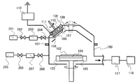
- FIG. 2 shows an outline of a processing apparatus used in the process of forming the titanium nitride film 3 in the present invention.
- the film forming chamber 100 can be heated to a predetermined temperature by the heater 101.
- the substrate 102 to be processed can be heated to a predetermined temperature by a heater 105 via a susceptor 104 incorporated in a substrate support base 103. It is preferable that the substrate support 103 can be rotated at a predetermined rotational speed from the viewpoint of film thickness uniformity.
- a target 106 is installed at a position where the target substrate 102 is desired.
- the target 106 is installed on the target holder 108 via a back plate 107 made of a metal such as Cu.
- the outer shape of the target assembly in which the target 106 and the back plate 107 are combined may be made of a target material as a single component and attached as a target. That is, the target may be installed on the target holder.
- a direct current power source 110 for applying power for sputtering discharge is connected to the target holder 108 made of metal such as Cu, and is insulated from the wall of the film formation processing chamber 100 at the ground potential by an insulator 109.
- a magnet 111 for realizing magnetron sputtering is disposed behind the target 106 as viewed from the sputtering surface.
- the magnets 111 may be arranged in any arrangement as long as they generate magnetic flux lines (magnetic flux).
- the magnet 111 is held by a magnet holder 112 and can be rotated by a magnet holder rotation mechanism (not shown). In order to make the erosion of the target uniform, the magnet 111 rotates during discharge.
- the target 106 is installed at an offset position obliquely above the substrate 102. That is, the center point of the sputtering surface of the target 106 is at a position that is shifted by a predetermined dimension with respect to the normal line of the center point of the substrate 102.
- a shielding plate 116 is disposed between the target 106 and the processing substrate 102 to control film formation on the processing substrate 102 by sputtered particles emitted from the target 106 to which power is supplied.
- the target was a Ti metal target 106.
- the deposition of the titanium nitride film is performed by supplying electric power to the metal target 106 from the DC power source 110 via the target holder 108 and the back plate 107, respectively.
- an inert gas is introduced into the film forming chamber 100 from the vicinity of the target from the inert gas source 201 via the valve 202, the mass flow controller 203, and the valve 204.
- a reactive gas composed of nitrogen is introduced from the nitrogen gas source 205 to the vicinity of the substrate in the film formation processing chamber 100 through the valve 206, the mass flow controller 207, and the valve 208.
- the introduced inert gas and reactive gas are exhausted by the exhaust pump 118 via the conductance valve 117.
- the titanium nitride film 3 was deposited using argon as a sputtering gas and nitrogen as a reactive gas.
- the substrate temperature is 27 ° C. to 600 ° C.
- the target power is 50 W to 1000 W
- the sputtering gas pressure is 0.1 Pa to 1.0 Pa
- the Ar flow rate is 0 sccm to 100 sccm (0 Pa ⁇ m 3 / sec to 1.69 ⁇ 10 ⁇ 1. Pa ⁇ m 3 / sec)
- the nitrogen gas flow rate may be suitably determined in 0sccm ⁇ 100sccm (0Pa ⁇ m 3 /sec ⁇ 1.69 ⁇ 10 -1 Pa ⁇ m 3 / sec), range.
- the substrate temperature of 30 ° C., Ti target power 750W, sputtering gas pressure 0.2Pa and the argon gas flow rate 0sccm ⁇ 20sccm (0Pa ⁇ m 3 /sec ⁇ 3.38 ⁇ 10 -2 Pa ⁇ m 3 / sec) was deposited by varying the nitrogen gas flow rate in the range of 2sccm ⁇ 50sccm (3.38 ⁇ 10 -3 Pa ⁇ m 3 /sec ⁇ 8.45 ⁇ 10 -2 Pa ⁇ m 3 / sec).
- the molar ratio and crystal orientation of the Ti element and N element in the titanium nitride film were adjusted by the mixing ratio of argon and nitrogen introduced at the time of sputtering using the control device 600 shown in FIGS.
- the “molar ratio” refers to the ratio of the number of moles, which is the basic unit of the substance amount.
- the molar ratio of the Ti element and the N element can be measured, for example, from X-ray photoelectron spectroscopy based on the binding energy of electrons inherent in the substance, the energy level and amount of electrons.
- a 20 nm thick silicon film 4 was deposited on the deposited titanium nitride film 3 by sputtering.
- the prepared sample was annealed in a nitrogen atmosphere in the range of 400 ° C. to 1000 ° C. for 2 minutes.
- the TiN film 4 was processed into a desired size using a lithography technique and an RIE (Reactive Ion Etching) technique to form an element having a MIPS type gate electrode.
- RIE Reactive Ion Etching
- the composition of the deposited titanium nitride film was analyzed by an X-ray photoelectron spectroscopy (XPS) method.
- XPS X-ray photoelectron spectroscopy
- the crystal orientation of the titanium nitride film was analyzed by an X-ray diffraction (XRD: X-ray diffraction) method.
- the film density was analyzed by an X-ray reflectometer method.
- electrical characteristics such as effective work function, EOT (Equivalent Oxide Thickness, SiO 2 equivalent film thickness), and leakage current characteristics were evaluated by CV and IV measurements.
- the “effective work function” is generally obtained from a flat band obtained by CV measurement between the gate insulating film and the gate electrode, and in addition to the original work function of the gate electrode, It is affected by electric charge, dipoles formed at the interface, Fermi level pinning, etc. It is distinguished from the original “work function” of the material constituting the gate electrode (energy required to extract one electron from the Fermi level to the vacuum level).
- EOT oxide equivalent film thickness
- the equivalent oxide film thickness the electrical film thickness of the insulating film obtained by calculating backward from the capacitance. That is, when the relative dielectric constant of the insulating film is ⁇ h, the relative dielectric constant of the silicon oxide film is ⁇ o, and the thickness of the insulating film is dh, the equivalent oxide film thickness de is expressed by the following formula (1). .
- the oxide film equivalent film thickness de is the film thickness of this insulating film. It shows that the silicon oxide film is thinner than the thickness dh.
- the relative dielectric constant ⁇ o of the silicon oxide film is about 3.9.
- FIG. 3 shows the relationship between the film density (N / Ti ratio) (molar ratio of Ti and N (N / Ti)) and the film density of the titanium nitride film in the present invention.
- the titanium nitride formation conditions flow rate conditions of argon gas and nitrogen gas
- the effective work function (eWf) values in the state where heat treatment is not performed are shown.
- condition C under the conditions (condition C) of an argon gas flow rate of 13.5 sccm (2.28 ⁇ 10 ⁇ 2 Pa ⁇ m 3 / sec) and a nitrogen gas flow rate of 6 sccm (1.01 ⁇ 10 ⁇ 2 Pa ⁇ m 3 / sec).
- the titanium nitride film of the present invention can control the film composition (N / Ti ratio), film density, and work function by adjusting the argon gas flow rate and the nitrogen gas flow rate during sputtering formation. Furthermore, it has been clarified that the effective work function of the titanium nitride film is related not to the film density but to the film composition (N / Ti ratio). Therefore, in order to obtain a work function of 4.6 eV or more suitable for a P-type MOSFET, the N / Ti ratio is preferably 1.1 or more. To obtain a work function of 4.8 eV or more, the N / Ti ratio is 1 .2 or more is preferable.
- the effective work function value of the titanium nitride film according to the present invention increases as the film composition (N / Ti ratio) increases, the titanium nitride (film composition (N / Ti ratio) described in Patent Document 4 described above is used. As the ratio) increases, the effective work function decreases).
- FIG. 4 shows the result of comparison of XRD diffraction spectra of the titanium nitride films produced under conditions A, B and C.
- the horizontal axis in FIG. 4 indicates the diffraction angle, and the vertical axis in FIG. 4 indicates the diffraction intensity.
- C (111), C (200), and C (220) represent the crystal plane, (111) plane, (200) plane, and (220) plane of the titanium nitride film, respectively.
- the titanium nitride films under conditions A and B where the film composition (N / Ti ratio) and the effective work function are high are compared with the condition C where the film composition (N / Ti ratio) and the effective work function are low.
- it has a crystal structure with high crystal orientation on the (200) plane.
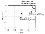
- FIG. 5 compares the film composition (N / Ti ratio) of the titanium nitride film and the peak intensity ratio C (200) / C (111) (crystal orientation) between the (111) plane and the (200) plane in the XRD spectrum. Results are shown.
- the horizontal axis represents the film composition (N / Ti ratio) of the titanium nitride film
- the vertical axis represents the peak intensity ratio.
- the peak intensity ratio of the titanium nitride film having a film composition (N / Ti ratio) of 1.2 or more under the conditions A and B has a high value of 1.7 or more.
- the peak intensity ratio of the titanium nitride film under the condition B is 1.8 or more, which is higher than the condition A. Therefore, a titanium nitride film having an effective work function value of 4.6 eV or more has a film composition (N / Ti ratio) of 1.1 or more, and an XRD diffraction spectrum peak intensity ratio C (200) / A titanium nitride film having C (111) of 1.1 or more and an effective work function value of 4.8 eV or more has a film composition (N / Ti ratio) of 1.2 or more, and exhibits XRD. It is shown that the diffraction spectrum peak intensity ratio C (200) / C (111) is 1.7 or more.
- the titanium nitride film in the present invention is disclosed in Patent Document 3 described above because the effective work function value is as high as 4.9 eV even when the crystal orientation of the (200) plane is present. It is shown that the value of the effective work function is different from the titanium nitride film (having 4.3 eV in the (100) orientation and 4.6 eV in the (111) orientation).
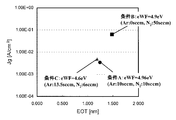
- FIG. 6 shows a relationship between an EOT (Equivalent Oxide Thickness, SiO 2 equivalent film thickness) and a leakage current (Jg) of an element having a titanium nitride film manufactured under the conditions A, B and C.
- EOT Equivalent Oxide Thickness, SiO 2 equivalent film thickness
- Jg leakage current
- the difference between the titanium nitride film of condition B and the titanium nitride film of conditions A and C is that the film density is low and the peak intensity ratio C (200) / C (111) that is an index of crystal orientation is 1.8 or more. It is expensive.
- the electrical characteristics of an element having an effective work function value and a peak intensity ratio C (200) / C (111) equivalent to those in condition C and having a titanium nitride film having a film density equivalent to that in condition B It was confirmed that there was no deterioration in EOT and leakage current value (Jg). Therefore, it is considered that the increase in EOT and leakage current in the element having the titanium nitride film under the condition B is caused by the crystal orientation.
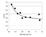
- FIG. 7 shows the relationship between the film composition (O / Ti ratio (molar ratio)) and the film density.
- the prepared sample is oxidized by exposure to the atmosphere. From the figure, the O / Ti ratio decreases as the film density increases. Since the oxidation of the titanium nitride film causes an increase in specific resistance and deteriorates the element characteristics, the film density of the titanium nitride film is preferably 4.8 g / cc or more.
- FIG. 8A and 8B are the same as the element structure shown in FIG. 1, and the titanium nitride films were produced under the conditions A and B described above, respectively.
- FIG. 8C is different in that the titanium nitride film has a laminated film structure. After depositing a 2 nm-thick titanium nitride film on the gate insulating film under the condition A, the same composition is obtained. A titanium nitride film having a thickness of 8 nm was continuously deposited in condition B in the film processing chamber. The other conditions are the same as those of the element shown in FIG.
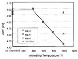
- FIG. 9 shows the annealing temperature dependence of the effective work function of the fabricated device.
- Structures (a), (b), and (c) in the figure correspond to the elements (a), (b), and (c) shown in FIG. 8, respectively.
- “No silicon” in the drawing represents an element structure in which silicon is not deposited on the titanium nitride of the element (a) in FIG.
- the effective work function of the device has a value of 4.9 eV or more when not annealed (as-deposited), but decreases by annealing at 600 ° C. or more.
- the effective work function is lowered to 4.45 eV by annealing at 1000 ° C.
- structures (b) and (c) have 4.6 eV, which is a value suitable for a P-type MOSFET, although the effective work function is lowered by annealing at 1000 ° C.
- the effective work function of the element in which the silicon film is not deposited on the titanium nitride film shows a high value of 4.9 eV or more even when the annealing process at 1000 ° C. is performed. The decrease is considered to be caused by the diffusion of silicon into the titanium nitride film as described in Patent Document 1 described above.
- the titanium nitride constituting the structures (b) and (c) has an effect of suppressing the diffusion of silicon into the titanium nitride film by the annealing treatment, and at least in the region in contact with the silicon under the condition B It is shown that the effect can be ensured if the deposited titanium nitride film exists.
- the value of the effective work function under the annealing conditions of 1000 ° C. and 2 min is shown here, the change of the effective work function can be further suppressed under the conditions of the activation annealing (1000 ° C., 10 sec) in the MOSFET manufacturing process. It was confirmed.
- the effective work function after annealing at 1000 ° C. of the structure (a) has a value of 4.6 eV or less suitable for the N-type MOSFET.
- the titanium nitride film of the element (a) a titanium nitride film having a molar ratio of Ti and N of 1.1 or less and a crystal orientation X 3 in a range of 1.1 or less is deposited.
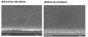
- FIG. 10 shows a surface SEM image of the titanium nitride film deposited under conditions A and B.
- the titanium nitride film deposited under condition A has a grain size columnar structure of about 20 nm, and the surface has sharp irregularities due to the crystal plane.
- the titanium nitride film deposited under condition B has a columnar structure with a grain size of 20 nm or less smaller than that in condition A, and the surface has a shape superior in flatness as compared with condition A.
- the difference in crystal shape and surface flatness depending on the deposition conditions of the titanium nitride film is due to the crystal orientation shown in FIG. 4, and nitriding with a peak intensity ratio C (200) / C (111) of 1.8 or more.
- the titanium film has a small grain size and excellent surface flatness. Further, it is considered that the difference in effective work function due to the difference in titanium nitride film shown in FIG. 9 is related to the grain size and surface flatness of the titanium nitride film. That is, since the titanium nitride film of condition B has a small grain size and excellent surface flatness, silicon diffusion through the crystal grain boundary is prevented, and as a result, a decrease in effective work function is suppressed. Yes. This effect is also exhibited in the element (C) having a titanium nitride film under condition B in a region in contact with silicon.
- the variation in threshold voltage can be suppressed by setting the average crystal grain size of the titanium nitride film to 30 nm or less, and the crystal structure of the titanium nitride film is a (111) -oriented TiN film. It is stated that the variation of the threshold voltage value is smaller when using the TiN film than when using the TiN film in which the (111) and (110) orientations coexist.
- the decrease in effective work function that contributes to variations in threshold voltage is greatly influenced not only by the grain size of titanium nitride but also by surface flatness, and an XRD diffraction spectrum that represents crystal orientation.
- titanium nitride having a peak intensity ratio C (200) / C (111) of not less than 1.8 By using titanium nitride having a peak intensity ratio C (200) / C (111) of not less than 1.8, flatness can be improved and a decrease in effective work function can be suppressed. Therefore, it is shown that the titanium nitride film in the present invention is different from the titanium nitride film disclosed in Patent Document 2.
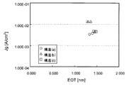
- FIG. 11 shows the relationship between EOT after 1000 ° C. annealing and leakage current (Jg).
- the EOT and Jg of the element (a) and the element (c) have substantially the same characteristics, whereas the Jg of the element (b) is compared with the elements (a) and (c). And about an order of magnitude larger.
- the titanium nitride film of the element (b) causes deterioration of the electric characteristics of the element even after the annealing process at 1000 ° C. That is, the titanium nitride film in the element (B) can suppress the effective work function by the annealing process at 1000 ° C.
- the first metal nitride layer in the present invention optimizes the film composition (N / Ti ratio) and crystal orientation in order to achieve a high work function by sputtering, and the second metal nitride layer is formed by sputtering.
- This method differs from the titanium nitride film described in Patent Document 1 in that the film composition (N / Ti ratio) and the crystal orientation are optimized in order to suppress a decrease in effective work function due to silicon diffusion.
- the laminated film of titanium nitride in the present invention is described in Patent Document 1 in that it is formed by using a continuous process by sputtering without increasing the substrate temperature during deposition in the same film forming chamber. It is different from the method.
- the molar ratio (N / Ti) of Ti and N of the first metal nitride layer in the present invention is preferably 1.1 or more in order to realize an effective work function suitable for the P-type MOSFET. .2 or more is more preferable.
- the peak intensity ratio X 1 of C [200] / C [111] in the XRD spectrum representing the crystal orientation of the first metal nitride layer realizes an effective work function suitable for a P-type MOSFET, and In order not to deteriorate the electrical characteristics, the range of 1.1 ⁇ X 1 ⁇ 1.8 is preferable.
- the film density is preferably 4.8 g / cc or more, and more preferably 5.0 g / cc or more in order to prevent deterioration of device characteristics due to oxidation.
- the molar ratio (N / Ti) of Ti and N of the second metal nitride layer in the present invention suppresses a decrease in effective work function value due to silicon diffusion in the heat treatment step after the formation of the gate electrode. .1 or more is preferable, and 1.2 or more is more preferable.
- the peak intensity ratio X 2 of C [200] / C [111] in the XRD spectrum representing the crystal orientation of the second metal nitride layer is preferably in the range of 1.8 ⁇ X 2 .
- the film density is preferably 4.8 g / cc or more in order to prevent deterioration of device characteristics due to oxidation.
- the total thickness of the first metal nitride layer and the second metal nitride layer in the present invention is the gate due to the side etching caused by the etching rate of silicon and titanium nitride in the etching process of the gate electrode. In order to suppress a change in shape, it is preferably 20 nm or less, and more preferably 10 nm or less.
- the thickness of the first metal nitride layer has a ratio of at least 50% or more with respect to the total thickness of the first metal nitride layer and the second metal nitride layer. Preferably, it has a ratio of 80%.
- the deposition of the titanium nitride film in the present invention suppresses deterioration of device characteristics due to plasma damage to the gate insulating film, and controls the composition and crystal orientation, so that the target as shown in FIG. Is a step of magnetron sputtering a Ti target in a mixed atmosphere of a reactive gas composed of nitrogen and an inert gas in a film forming chamber disposed at an offset position obliquely above the first metal nitride layer.
- the mixing ratio of the reactive gas and the inert gas is set so that the molar ratio of Ti and N is 1.1 or more and the crystal orientation X 1 satisfies the range of 1.1 ⁇ X 1 ⁇ 1.8.
- the molar ratio of Ti and N in the second metal nitride layer is not less than 1.1, and the mixing ratio of the reactive gas and an inert gas such crystalline orientation X 2 satisfies 1.8 ⁇ X 2 Preferred to set There.
- the first metal nitride layer forming step and the second metal nitride layer forming step are performed in the same film formation chamber in order to improve throughput and suppress oxidation of the titanium nitride film due to atmospheric exposure. It is preferable to implement the method because the manufacturing method can be simplified.
- an element having a gate insulating film using a silicon oxide film and an HfSiO film as a high dielectric constant film has been described.
- the present invention is not limited to this, and a high dielectric constant material used for the gate insulating film is described.
- a material having a relative dielectric constant larger than that of SiO 2 (3.9) include metal oxide, metal silicate, metal oxide into which nitrogen is introduced, and metal silicate into which nitrogen is introduced.
- a high dielectric constant film into which nitrogen is introduced is preferable.
- the metal in the high dielectric constant material is preferably Hf or Zr from the viewpoint of heat resistance of the film and suppression of fixed charge in the film.
- a metal oxide containing Hf or Zr and Si a metal oxynitride containing nitrogen in addition to this metal oxide is preferable, and HfSiO and HfSiON are more preferable.
- a silicon oxide film and a high dielectric constant film laminated thereon are used as a gate insulating film, but the present invention is not limited to this.
- a high dielectric constant insulating film alone or a silicon oxynitride film and its A high dielectric constant film laminated thereon can be used.
- a MIPS type gate electrode in which a titanium nitride film and a silicon film are formed on a p-type silicon substrate having a gate insulating film using a silicon oxide film and a HfSiO film as a high dielectric constant film on the surface is used.
- the MOSFET element having the gate electrode having the MIPS structure shown in FIG. 12 also includes a titanium nitride film that satisfies the conditions of the present invention. The effect can be sufficiently obtained.
- the N-type MOSFET when an N-type MOSFET is further provided on the silicon substrate, the N-type MOSFET has a gate insulating film and a gate electrode provided on the gate insulating film.
- the crystal orientation X 3 is preferably 1.1 or less.
- FIG. 16 is a schematic diagram of a control device that controls the processing device of FIG. 2.
- the valves 202, 204, 206, and 208 can be controlled to be opened and closed by the control device 600 via the control input / output ports 500, 501, 502, and 503, respectively.
- the mass flow controllers 203 and 207 can adjust the flow rate by the control device 600 via the control input / output ports 504 and 505, respectively. Further, the opening of the conductance valve 117 can be adjusted by the control device 600 via the control input / output port 506.
- the temperature of the heater 105 can be adjusted by the control device 600 via the input / output port 507.
- the rotation state of the substrate support 103 can be adjusted by the control device 600 via the input / output port 508.
- the frequency and supply power of the DC power supply 110 can be adjusted by the control device 600 via the input / output port 509.
- the control device 600 causes the molar ratio (N / Ti) of Ti and N of the first metal nitride layer to be 1.1 or more, and the crystal orientation X 1 is 1.1 ⁇ X 1 ⁇ Further, the molar ratio of Ti and N (N / Ti) of the second metal nitride layer is 1.1 or more, and the crystal orientation X 2 is 1.8 ⁇ X 2 .
- the mixing ratio of the reactive gas composed of an inert gas such as argon gas and nitrogen gas introduced during the sputtering film formation is controlled.
- FIG. 17 is a diagram showing an internal configuration of the control device 600 of FIG.
- the control device 600 includes an input unit 601, a storage unit 602 having a program and data, a processor 603, and an output unit 604.
- the control device 600 basically has a computer configuration and controls the processing device 605 of FIG.
- the manufacturing program of the present invention is recorded on a recording medium readable by a computer (PC) and installed in the storage unit 602 of the control device 600.
- Recording media include floppy (registered trademark) disks, ZIP (registered trademark) magnetic recording media, MO magneto-optical recording media, CD-R, DVD-R, DVD + R, DVD-RAM, DVD + RW (registered trademark).
- optical disks such as PD.
- flash memory systems such as CompactFlash (registered trademark), SmartMedia (registered trademark), Memory Stick (registered trademark), and SD card
- removable disks such as Microdrive (registered trademark) and Jaz (registered trademark).
- the manufacturing program of the present invention installed in the storage unit 602 includes a gate insulating film on a silicon substrate, a first metal nitride layer containing Ti and N provided on the gate insulating film, the first A field effect transistor having a second metal nitride layer containing Ti and N disposed on a metal nitride layer and a gate electrode having a polycrystalline silicon layer disposed on the second metal nitride layer is provided.
- a semiconductor device manufacturing program installed in the storage unit 602 includes a gate insulating film on a silicon substrate, a first metal nitride layer containing Ti and N provided on the gate insulating film, the first A field effect transistor having a second metal nitride layer containing Ti and N disposed on a metal nitride layer and a gate electrode having a polycrystalline silicon layer disposed on the second metal nitride layer is provided.
- the molar ratio of Ti to N (N / Ti) is 1.1 or more, and the crystal orientation X 1 is in the range of 1.1 ⁇ X 1 ⁇ 1.8.
- a procedure for forming one metal nitride layer, and a second metal nitride in which the molar ratio of Ti to N (N / Ti) is 1.1 or more and the crystal orientation X 2 is 1.8 ⁇ X 2 Causing the computer to perform the steps of forming the layer.
- the Ti of the metal nitride layer when the Ti target is magnetron sputtered in a mixed atmosphere of a reactive gas composed of nitrogen and an inert gas, the Ti of the metal nitride layer The mixing ratio of the reactive gas and the inert gas so that the molar ratio of N (N / Ti) is 1.1 or more and the crystal orientation X 1 satisfies the range of 1.1 ⁇ X 1 ⁇ 1.8.
- the procedure for forming the second metal nitride layer by controlling the Ti and N of the metal nitride layer when the Ti target is magnetron sputtered in a mixed atmosphere of a reactive gas composed of nitrogen and an inert gas. and the molar ratio (N / Ti) is 1.1 or more, and crystalline orientation X 2 controls the mixing ratio of the reactive gas and an inert gas so as to satisfy 1.8 ⁇ X 2.
- the manufacturing program of the present invention further includes, as a procedure for forming a gate insulating film, a procedure for heating a silicon substrate and depositing a metal film on a substrate to be processed by physical vapor deposition using a target, and oxidizing the metal film.
- a procedure for supplying a gas containing the element to be formed and oxidizing the metal film by a thermal oxidation reaction to form a high dielectric constant insulating film may be provided.
- FIG. 13 is a schematic cross-sectional view of an element structure having a MIPS type gate electrode according to the first embodiment.
- Hf having a thickness of 0.5 to 0.7 nm was deposited on the silicon substrate 5 having a silicon oxide film having a thickness of 1.8 nm on the surface by a sputtering method.
- annealing is performed at 900 ° C. for 1 minute in an atmosphere with an oxygen partial pressure of 0.1 Pa to diffuse Hf into the silicon oxide film, thereby forming the gate insulating film 6 having a laminated structure of the silicon oxide film and the HfSiO film. Formed.
- FIG. 13 is a schematic cross-sectional view of an element structure having a MIPS type gate electrode according to the first embodiment.
- the molar ratio of Ti and N is 1.1 or more by adjusting the mixing ratio of the argon gas flow rate and the nitrogen gas flow rate using a Ti metal target, A titanium nitride film 7 having a crystal orientation X 1 in the range of 1.1 ⁇ X 1 ⁇ 1.8 was deposited to 2 nm to 5 nm.
- the molar ratio of Ti and N is 1.1 or more and the crystal orientation X 2 is 1.
- a titanium nitride film 8 was deposited to 5 to 8 nm so that 8 ⁇ X 2 .
- the sputtering power is 750 W, and the substrate temperature is the same as 30 ° C.
- 20 nm of polycrystalline silicon 9 was deposited by CVD.
- annealing was performed at 1000 ° C. for 2 minutes in a nitrogen atmosphere.
- the TiN film was processed into a desired size using a lithography technique and an RIE (Reactive Ion Etching) technique to form an element having a MIPS type gate electrode.
- RIE Reactive Ion Etching
- the composition of the deposited titanium nitride film was analyzed by an X-ray photoelectron spectroscopy (XPS) method. Further, the crystal orientation of the titanium nitride film was analyzed by an X-ray diffraction (XRD: X-ray Diffraction) method. The film density was analyzed by an X-ray reflectometer method. In addition, electrical characteristics such as effective work function, EOT, and leakage current characteristics were evaluated by CV and IV measurements.
- XPS X-ray photoelectron spectroscopy
- the first metal nitride layer disposed on the gate insulating film in this example has a molar ratio of Ti and N of 1.1 or more, and the crystal orientation X 1 is 1.1 ⁇ X 1 ⁇
- the titanium nitride film having a range of 1.8 and the molar ratio of Ti and N as the second metal nitride layer is 1.1 or more and the crystal orientation X 2 is 1.8 ⁇ X 2
- an effective work function (4.6 eV or more) suitable for a P-type MOSFET can be obtained without deteriorating EOT or leakage current in an element having a MIPS type gate electrode made of a titanium nitride film.
- the film density of the first metal nitride layer and the second metal nitride layer was 4.8 g / cc or more, and no deterioration in electrical characteristics accompanying increase in specific resistance due to oxidation was observed.
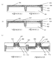
- FIGS. 14A to 14C are diagrams showing the steps of the method of manufacturing the semiconductor device shown in FIG. 12 which is the second embodiment of the present invention.
- an element isolation region 302 formed by STI (Shallow Trench Isolation) technology is provided on the surface of a silicon substrate 301.
- a silicon thermal oxide film having a film thickness of 1.0 nm is formed by thermal oxidation on the surface of the silicon substrate from which the elements are separated.
- an HfSiON film is deposited by the same method as in the first embodiment to form a gate insulating film 303.
- the molar ratio of Ti and N is 1.1 or more by adjusting the mixing ratio of the argon gas flow rate and the nitrogen gas flow rate on the gate insulating film 303 by the same method as in Example 1 using a Ti metal target.
- a titanium nitride film (first metal nitride layer) 304 having a crystal orientation X 1 in a range of 1.1 ⁇ X 1 ⁇ 1.8 was deposited to 2 nm to 5 nm.
- the molar ratio of Ti and N is 1.1 or more and the crystal orientation X 2 is 1.
- a titanium nitride film (second metal nitride layer) 305 was deposited to 5 to 8 nm so that 8 ⁇ X 2 .
- the gate electrode is processed using a lithography technique and an RIE technique, and then ion implantation is performed to form an extension diffusion region 307. It was formed in a self-aligned manner using the gate electrode as a mask.
- a gate side wall 308 was formed by sequentially depositing a silicon nitride film and a silicon oxide film and then performing etch back. Ion implantation was performed again in this state, and source / drain diffusion layers 309 were formed through activation annealing.
- FIGS. 15A to 15C are diagrams showing the steps of a semiconductor device manufacturing method according to the third embodiment of the present invention.
- an element isolation region 402 formed by STI (Shallow Trench Isolation) technology is provided on the surface of a silicon substrate 401, and an N-type MOSFET region and a P-type MOSFET region are separated.
- a silicon thermal oxide film having a film thickness of 1.0 nm is formed by thermal oxidation on the surface of the silicon substrate from which the elements are separated.
- an HfSiON film is deposited by the same method as in the first embodiment to form a gate insulating film 403.
- the molar ratio of Ti and N is 1.1 or more by adjusting the mixing ratio of the argon gas flow rate and the nitrogen gas flow rate.
- a titanium nitride film (first metal nitride layer) 404 having a crystal orientation X 1 in the range of 1.1 ⁇ X 1 ⁇ 1.8 was deposited to 2 nm.
- the molar ratio of Ti and N is 1.1 or more and the crystal orientation X 2 is 1.
- a titanium nitride film (second metal nitride layer) 405 was deposited to 8 nm so that 8 ⁇ X 2 .
- the sputtering power is 750 W, and the substrate temperature is the same as 30 ° C.
- the molar ratio of Ti and N is 1.1 or less by adjusting the mixing ratio of the argon gas flow rate and the nitrogen gas flow rate.
- a titanium nitride film (third metal nitride layer) 406 having a crystal orientation X 3 of 1.1 or less was deposited to a thickness of 10 nm.
- a silicon layer 407 having a thickness of 20 nm was formed.
- the gate electrode of the P-type MOSFET region was processed using lithography technology and RIE technology, and then ion implantation was performed to form the extension diffusion region 409 in a self-aligned manner using the gate electrode as a mask. Further, a gate side wall 408 was formed by sequentially depositing a silicon nitride film and a silicon oxide film and then etching back. In this state, ion implantation was performed again, and source / drain diffusion layers 410 were formed through activation annealing.
- the gate electrode in the N-type MOSFET region was processed using lithography technology and RIE technology, ion implantation was subsequently performed, and the extension diffusion region 411 was formed in a self-aligned manner using the gate electrode as a mask. Further, a gate side wall 413 was formed by sequentially depositing a silicon nitride film and a silicon oxide film and then etching back. In this state, ion implantation was performed again, and activation / annealing was performed to form a source / drain diffusion layer 412 to fabricate the semiconductor device shown in FIG.
Landscapes
- Insulated Gate Type Field-Effect Transistor (AREA)
- Electrodes Of Semiconductors (AREA)
- Physical Vapour Deposition (AREA)
- Metal-Oxide And Bipolar Metal-Oxide Semiconductor Integrated Circuits (AREA)
Abstract
Description
前記ゲート絶縁膜が、金属酸化物、金属シリケート、又は窒素が導入された金属酸化物もしくは金属シリケートからなる高誘電率絶縁膜を有し、
前記ゲート電極が、前記ゲート絶縁膜上に配置されたTiとNを含有する第1金属窒化物層、該第1金属窒化物層上に配置されたTiとNを含有する第2金属窒化物層および該第2金属窒化物層上に配置された多結晶シリコン層を有し、
前記第1金属窒化物層のTiとNのモル比率(N/Ti)が1.1以上であり、かつ結晶配向性X1が1.1<X1<1.8であり、
前記第2金属窒化物層のTiとNのモル比率(N/Ti)が1.1以上であり、かつ結晶配向性X2が1.8≦X2であることを特徴とする。
TiとNのモル比率(N/Ti)が1.1以上であり、かつ結晶配向性X1が1.1<X1<1.8の範囲である第1金属窒化物層を形成する工程と、
TiとNのモル比率(N/Ti)が1.1以上であり、かつ結晶配向性X2が1.8≦X2である第2金属窒化物層を形成する工程と、
を備えたことを特徴とする。
TiとNのモル比率(N/Ti)が1.1以上であり、かつ結晶配向性X1が1.1<X1<1.8の範囲である第1金属窒化物層を形成する手順と、
TiとNのモル比率(N/Ti)が1.1以上であり、かつ結晶配向性X2が1.8≦X2である第2金属窒化物層を形成する手順と、
をコンピューターに実行させることを特徴とする。
上記式(1)は、絶縁膜に、シリコン酸化膜の比誘電率εoに比べて大きな誘電率εhをもった材料を用いた場合には、酸化膜換算膜厚deは、この絶縁膜の膜厚dhよりも薄いシリコン酸化膜と同等になることを示している。なお、シリコン酸化膜の比誘電率εoは3.9程度である。そのため、例えば、εh=39の高誘電率材料からなる膜は、その物理膜厚dhを15nmとしても、酸化膜換算膜厚(電気膜厚)deが1.5nmになり、絶縁膜の容量値を膜厚が1.5nmのシリコン酸化膜と同等に保ちつつ、リーク電流を著しく低減することができる。
本発明の第1の実施例を、図面を参照しながら詳細に説明する。
本発明の第2の実施例を、図面を参照しながら詳細に説明する。
図15(a)~(c)は、本発明の第3の実施例である半導体装置の製造方法の工程を示した図である。まず図15(a)に示すようにシリコン基板401の表面に、STI(Shallow Trench Isolation)技術により形成された素子分離領域402が設けられ、N型MOSFET領域とP型MOSFET領域が分離される。続いて、素子分離されたシリコン基板表面に熱酸化法により膜厚1.0nmのシリコン熱酸化膜を形成する。その後、実施例1と同じ方法によりHfSiON膜を堆積しゲート絶縁膜403を形成する。
2 ゲート絶縁膜
3 窒化チタン膜
4 シリコン膜
5 シリコン基板
6 ゲート絶縁膜
7 第1金属窒化物層
8 第2金属窒化物層
9 シリコン膜
100 成膜処理室
101 ヒータ
102 被処理基板
103 基板支持台
104 サセプタ
105 ヒータ
106 金属ターゲット
107 バックプレート
108 ターゲットホルダー
109 絶縁体
110 直流電源
111 マグネット
112 マグネットホルダー
116 遮蔽板
117 コンダクタンスバルブ
118 排気ポンプ
201 不活性ガス源
202 バルブ
203 マスフローコントローラ
204 バルブ
205 反応性ガス源
206 バルブ
207 マスフルーコントローラ
208 バルブ
301 シリコン基板
302 素子分離領域
303 ゲート絶縁膜
304 第1金属窒化物層
305 第2金属窒化物層
306 シリコン層
307 エクステンション領域
308 ゲート側壁
309 ソース・ドレイン領域
401 シリコン基板
402 素子分離領域
403 ゲート絶縁膜
404 第1金属窒化物層
405 第2金属窒化物層
406 第3金属窒化物層
407 シリコン層
408 ゲート側壁
409 エクステンション領域
410 ソース・ドレイン領域
411 エクステンション領域
412 ソース・ドレイン領域
413 層間絶縁膜
Claims (14)
- シリコン基板上に、ゲート絶縁膜と該ゲート絶縁膜上に設けられたゲート電極とを有する電界効果トランジスタを備えた半導体装置において、
前記ゲート絶縁膜が、金属酸化物、金属シリケート、又は窒素が導入された金属酸化物もしくは金属シリケートからなる高誘電率絶縁膜を有し、
前記ゲート電極が、前記ゲート絶縁膜上に配置されたTiとNを含有する第1金属窒化物層、該第1金属窒化物層上に配置されたTiとNを含有する第2金属窒化物層および該第2金属窒化物層上に配置された多結晶シリコン層を有し、
前記第1金属窒化物層のTiとNのモル比率(N/Ti)が1.1以上であり、かつ結晶配向性X1が1.1<X1<1.8であり、
前記第2金属窒化物層のTiとNのモル比率(N/Ti)が1.1以上であり、かつ結晶配向性X2が1.8≦X2であることを特徴とする半導体装置。 - 前記電界効果トランジスタがP型MOSFETであることを特徴とする請求項1に記載の半導体装置。
- 前記シリコン基板上に、更にN型MOSFETを備え、
該N型MOSFETは、ゲート絶縁膜と該ゲート絶縁膜上に設けられたゲート電極を有し、
前記ゲート絶縁膜が、金属酸化物、金属シリケート、又は窒素が導入された金属酸化物もしくは金属シリケートからなる高誘電率絶縁膜を有し、
前記ゲート電極が、前記ゲート絶縁膜上に設けられたTiとNを含有する第3金属窒化物層と該第3金属窒化物層上に配置された多結晶シリコン層を有し、
前記第3金属窒化物層のTiとNのモル比率(N/Ti)が1.1以下であり、かつ結晶配向性X3が1.1以下であることを特徴とする請求項2に記載の半導体装置。 - 前記第1金属窒化物層と前記第2金属窒化物層のTiとNのモル比率が1.2以上であることを特徴とする請求項1~3のいずれか1項に記載の半導体装置。
- 前記第1金属窒化物層と前記第2金属窒化物層の膜密度が4.8g/cc以上であることを特徴とする請求項1~4のいずれか1項に記載の半導体装置。
- 前記第1金属窒化物層の膜厚と前記第2金属窒化物層の膜厚の合計が20nm以下でありことを特徴とする請求項1~5のいずれか1項に記載の半導体装置。
- 前記高誘電率絶縁膜として、HfもしくはZrを含む絶縁膜を有することを特徴とする請求項1~6のいずれか1項に記載の半導体装置。
- 前記ゲート絶縁膜が、シリコン酸化膜もしくはシリコン酸窒化膜と、HfもしくはZrを含む層の積層構造であることを特徴とする請求項1~7のいずれか1項に記載の半導体装置。
- シリコン基板上に、金属酸化物、金属シリケート、又は窒素が導入された金属酸化物もしくは金属シリケートからなる高誘電率絶縁膜を有するゲート絶縁膜と、該ゲート絶縁膜上に設けられたTiとNを含有する第1金属窒化物層、該第1金属窒化物層上に配置されたTiとNを含有する第2金属窒化物層及び該第2金属窒化物層上に配置された多結晶シリコン層を有するゲート電極とを有する電界効果トランジスタを備えた半導体装置の製造方法であって、
TiとNのモル比率(N/Ti)が1.1以上であり、かつ結晶配向性X1が1.1<X1<1.8の範囲である第1金属窒化物層を形成する工程と、
TiとNのモル比率(N/Ti)が1.1以上であり、かつ結晶配向性X2が1.8≦X2である第2金属窒化物層を形成する工程と、
を備えたことを特徴とする半導体装置の製造方法。 - 前記第1金属窒化物層を形成する工程と前記第2金属窒化物層を形成する工程が、
窒素からなる反応性ガスと不活性ガスの混合雰囲気下においてTiターゲットをマグネトロンスパッタする工程であり、
前記第1金属窒化物層を形成する工程では、金属窒化物層のTiとNのモル比率(N/Ti)が1.1以上であり、かつ結晶配向性X1が1.1<X1<1.8の範囲を満たすように反応性ガスと不活性ガスの混合比率を設定し、
前記第2金属窒化物層を形成する工程では、金属窒化物層のTiとNのモル比率(N/Ti)が1.1以上であり、かつ結晶配向性X2が1.8≦X2を満たすように反応性ガスと不活性ガスの混合比率を設定することを特徴とする請求項9に記載の半導体装置の製造方法。 - 前記第1金属窒化物層を形成する工程と前記第2金属窒化物層を形成する工程を同一の成膜処理室内で実施することを特徴とする請求項10または11に記載の半導体装置の製造方法。
- シリコン基板上に、金属酸化物、金属シリケート、又は窒素が導入された金属酸化物もしくは金属シリケートからなる高誘電率絶縁膜を有するゲート絶縁膜と、該ゲート絶縁膜上に設けられたTiとNを含有する第1金属窒化物層、該第1金属窒化物層上に配置されたTiとNを含有する第2金属窒化物層及び該第2金属窒化物層上に配置された多結晶シリコン層を有するゲート電極とを有する電界効果トランジスタを備えた半導体装置の製造プログラムであって、
TiとNのモル比率(N/Ti)が1.1以上であり、かつ結晶配向性X1が1.1<X1<1.8の範囲である第1金属窒化物層を形成する手順と、
TiとNのモル比率(N/Ti)が1.1以上であり、かつ結晶配向性X2が1.8≦X2である第2金属窒化物層を形成する手順と、
をコンピューターに実行させることを特徴とする半導体装置の製造プログラム。 - 前記第1金属窒化物層を形成する手順では、窒素からなる反応性ガスと不活性ガスの混合雰囲気下においてTiターゲットをマグネトロンスパッタする際に、金属窒化物層のTiとNのモル比率(N/Ti)が1.1以上であり、かつ結晶配向性X1が1.1<X1<1.8の範囲を満たすように反応性ガスと不活性ガスの混合比率を制御し、
前記第2金属窒化物層を形成する手順では、窒素からなる反応性ガスと不活性ガスの混合雰囲気下においてTiターゲットをマグネトロンスパッタする際に、金属窒化物層のTiとNのモル比率(N/Ti)が1.1以上であり、かつ結晶配向性X2が1.8≦X2を満たすように反応性ガスと不活性ガスの混合比率を制御することを特徴とする請求項12に記載の半導体装置の製造プログラム。 - 請求項12または13に記載の製造プログラムを記録したことを特徴とするコンピューター読み取り可能な記録媒体。
Priority Applications (3)
| Application Number | Priority Date | Filing Date | Title |
|---|---|---|---|
| KR1020117012645A KR101178166B1 (ko) | 2009-04-28 | 2010-04-28 | 반도체 장치 및 그 제조 방법 |
| US13/264,955 US8415753B2 (en) | 2009-04-28 | 2010-04-28 | Semiconductor device and method of manufacturing the same |
| JP2011511314A JP4871433B2 (ja) | 2009-04-28 | 2010-04-28 | 半導体装置およびその製造方法 |
Applications Claiming Priority (2)
| Application Number | Priority Date | Filing Date | Title |
|---|---|---|---|
| JP2009108996 | 2009-04-28 | ||
| JP2009-108996 | 2009-04-28 |
Publications (1)
| Publication Number | Publication Date |
|---|---|
| WO2010125810A1 true WO2010125810A1 (ja) | 2010-11-04 |
Family
ID=43031968
Family Applications (1)
| Application Number | Title | Priority Date | Filing Date |
|---|---|---|---|
| PCT/JP2010/003038 Ceased WO2010125810A1 (ja) | 2009-04-28 | 2010-04-28 | 半導体装置およびその製造方法 |
Country Status (4)
| Country | Link |
|---|---|
| US (1) | US8415753B2 (ja) |
| JP (1) | JP4871433B2 (ja) |
| KR (1) | KR101178166B1 (ja) |
| WO (1) | WO2010125810A1 (ja) |
Cited By (9)
| Publication number | Priority date | Publication date | Assignee | Title |
|---|---|---|---|---|
| WO2011052354A1 (ja) * | 2009-10-27 | 2011-05-05 | キヤノンアネルバ株式会社 | 不揮発性記憶素子およびその製造方法 |
| JP2012231123A (ja) * | 2011-04-15 | 2012-11-22 | Hitachi Kokusai Electric Inc | 半導体装置、半導体装置の製造方法、基板処理システムおよびプログラム |
| TWI485776B (zh) * | 2010-12-01 | 2015-05-21 | Canon Anelva Corp | Nonvolatile memory element and manufacturing method thereof |
| JP2016181571A (ja) * | 2015-03-24 | 2016-10-13 | 国立研究開発法人物質・材料研究機構 | 窒化チタン薄膜熱電半導体、その製造方法及び熱電発電素子 |
| WO2018181025A1 (ja) * | 2017-03-29 | 2018-10-04 | 京セラ株式会社 | サーマルヘッドおよびサーマルプリンタ |
| JP2019220557A (ja) * | 2018-06-19 | 2019-12-26 | 株式会社東芝 | 半導体装置及びその製造方法 |
| JP2023020628A (ja) * | 2021-07-30 | 2023-02-09 | 日機装株式会社 | 半導体発光素子および半導体発光素子の製造方法 |
| JP2023020627A (ja) * | 2021-07-30 | 2023-02-09 | 日機装株式会社 | 半導体発光素子および半導体発光素子の製造方法 |
| JP2023020629A (ja) * | 2021-07-30 | 2023-02-09 | 日機装株式会社 | 半導体発光素子 |
Families Citing this family (318)
| Publication number | Priority date | Publication date | Assignee | Title |
|---|---|---|---|---|
| US9394608B2 (en) | 2009-04-06 | 2016-07-19 | Asm America, Inc. | Semiconductor processing reactor and components thereof |
| US8802201B2 (en) | 2009-08-14 | 2014-08-12 | Asm America, Inc. | Systems and methods for thin-film deposition of metal oxides using excited nitrogen-oxygen species |
| US8513773B2 (en) * | 2011-02-02 | 2013-08-20 | Semiconductor Energy Laboratory Co., Ltd. | Capacitor and semiconductor device including dielectric and N-type semiconductor |
| US20130023129A1 (en) | 2011-07-20 | 2013-01-24 | Asm America, Inc. | Pressure transmitter for a semiconductor processing environment |
| US9017481B1 (en) | 2011-10-28 | 2015-04-28 | Asm America, Inc. | Process feed management for semiconductor substrate processing |
| US10714315B2 (en) | 2012-10-12 | 2020-07-14 | Asm Ip Holdings B.V. | Semiconductor reaction chamber showerhead |
| US20160376700A1 (en) | 2013-02-01 | 2016-12-29 | Asm Ip Holding B.V. | System for treatment of deposition reactor |
| US11015245B2 (en) | 2014-03-19 | 2021-05-25 | Asm Ip Holding B.V. | Gas-phase reactor and system having exhaust plenum and components thereof |
| US10858737B2 (en) | 2014-07-28 | 2020-12-08 | Asm Ip Holding B.V. | Showerhead assembly and components thereof |
| US9890456B2 (en) | 2014-08-21 | 2018-02-13 | Asm Ip Holding B.V. | Method and system for in situ formation of gas-phase compounds |
| CN105448918B (zh) | 2014-09-30 | 2020-05-12 | 联华电子股份有限公司 | 互补金属氧化物半导体与其制作方法 |
| US10941490B2 (en) | 2014-10-07 | 2021-03-09 | Asm Ip Holding B.V. | Multiple temperature range susceptor, assembly, reactor and system including the susceptor, and methods of using the same |
| US10276355B2 (en) | 2015-03-12 | 2019-04-30 | Asm Ip Holding B.V. | Multi-zone reactor, system including the reactor, and method of using the same |
| US10458018B2 (en) | 2015-06-26 | 2019-10-29 | Asm Ip Holding B.V. | Structures including metal carbide material, devices including the structures, and methods of forming same |
| CN106571299B (zh) * | 2015-10-10 | 2020-03-10 | 中芯国际集成电路制造(上海)有限公司 | Pmos晶体管及其形成方法 |
| US10211308B2 (en) | 2015-10-21 | 2019-02-19 | Asm Ip Holding B.V. | NbMC layers |
| US11139308B2 (en) | 2015-12-29 | 2021-10-05 | Asm Ip Holding B.V. | Atomic layer deposition of III-V compounds to form V-NAND devices |
| US10529554B2 (en) | 2016-02-19 | 2020-01-07 | Asm Ip Holding B.V. | Method for forming silicon nitride film selectively on sidewalls or flat surfaces of trenches |
| US10343920B2 (en) | 2016-03-18 | 2019-07-09 | Asm Ip Holding B.V. | Aligned carbon nanotubes |
| US10190213B2 (en) | 2016-04-21 | 2019-01-29 | Asm Ip Holding B.V. | Deposition of metal borides |
| US10865475B2 (en) | 2016-04-21 | 2020-12-15 | Asm Ip Holding B.V. | Deposition of metal borides and silicides |
| US10367080B2 (en) | 2016-05-02 | 2019-07-30 | Asm Ip Holding B.V. | Method of forming a germanium oxynitride film |
| US11453943B2 (en) | 2016-05-25 | 2022-09-27 | Asm Ip Holding B.V. | Method for forming carbon-containing silicon/metal oxide or nitride film by ALD using silicon precursor and hydrocarbon precursor |
| US9859151B1 (en) | 2016-07-08 | 2018-01-02 | Asm Ip Holding B.V. | Selective film deposition method to form air gaps |
| US10612137B2 (en) | 2016-07-08 | 2020-04-07 | Asm Ip Holdings B.V. | Organic reactants for atomic layer deposition |
| US10714385B2 (en) | 2016-07-19 | 2020-07-14 | Asm Ip Holding B.V. | Selective deposition of tungsten |
| US9812320B1 (en) | 2016-07-28 | 2017-11-07 | Asm Ip Holding B.V. | Method and apparatus for filling a gap |
| US9887082B1 (en) | 2016-07-28 | 2018-02-06 | Asm Ip Holding B.V. | Method and apparatus for filling a gap |
| KR102532607B1 (ko) | 2016-07-28 | 2023-05-15 | 에이에스엠 아이피 홀딩 비.브이. | 기판 가공 장치 및 그 동작 방법 |
| US10643826B2 (en) | 2016-10-26 | 2020-05-05 | Asm Ip Holdings B.V. | Methods for thermally calibrating reaction chambers |
| US11532757B2 (en) | 2016-10-27 | 2022-12-20 | Asm Ip Holding B.V. | Deposition of charge trapping layers |
| US10229833B2 (en) * | 2016-11-01 | 2019-03-12 | Asm Ip Holding B.V. | Methods for forming a transition metal nitride film on a substrate by atomic layer deposition and related semiconductor device structures |
| US10714350B2 (en) | 2016-11-01 | 2020-07-14 | ASM IP Holdings, B.V. | Methods for forming a transition metal niobium nitride film on a substrate by atomic layer deposition and related semiconductor device structures |
| KR102546317B1 (ko) | 2016-11-15 | 2023-06-21 | 에이에스엠 아이피 홀딩 비.브이. | 기체 공급 유닛 및 이를 포함하는 기판 처리 장치 |
| KR102762543B1 (ko) | 2016-12-14 | 2025-02-05 | 에이에스엠 아이피 홀딩 비.브이. | 기판 처리 장치 |
| US11447861B2 (en) | 2016-12-15 | 2022-09-20 | Asm Ip Holding B.V. | Sequential infiltration synthesis apparatus and a method of forming a patterned structure |
| US11581186B2 (en) | 2016-12-15 | 2023-02-14 | Asm Ip Holding B.V. | Sequential infiltration synthesis apparatus |
| KR102700194B1 (ko) | 2016-12-19 | 2024-08-28 | 에이에스엠 아이피 홀딩 비.브이. | 기판 처리 장치 |
| US10269558B2 (en) | 2016-12-22 | 2019-04-23 | Asm Ip Holding B.V. | Method of forming a structure on a substrate |
| US10867788B2 (en) | 2016-12-28 | 2020-12-15 | Asm Ip Holding B.V. | Method of forming a structure on a substrate |
| US11390950B2 (en) | 2017-01-10 | 2022-07-19 | Asm Ip Holding B.V. | Reactor system and method to reduce residue buildup during a film deposition process |
| US10468261B2 (en) | 2017-02-15 | 2019-11-05 | Asm Ip Holding B.V. | Methods for forming a metallic film on a substrate by cyclical deposition and related semiconductor device structures |
| US9966425B1 (en) * | 2017-02-28 | 2018-05-08 | United Microelectronics Corp. | Method for fabricating a MIM capacitor |
| US10529563B2 (en) | 2017-03-29 | 2020-01-07 | Asm Ip Holdings B.V. | Method for forming doped metal oxide films on a substrate by cyclical deposition and related semiconductor device structures |
| KR102457289B1 (ko) | 2017-04-25 | 2022-10-21 | 에이에스엠 아이피 홀딩 비.브이. | 박막 증착 방법 및 반도체 장치의 제조 방법 |
| US10770286B2 (en) | 2017-05-08 | 2020-09-08 | Asm Ip Holdings B.V. | Methods for selectively forming a silicon nitride film on a substrate and related semiconductor device structures |
| US10892156B2 (en) | 2017-05-08 | 2021-01-12 | Asm Ip Holding B.V. | Methods for forming a silicon nitride film on a substrate and related semiconductor device structures |
| US10886123B2 (en) | 2017-06-02 | 2021-01-05 | Asm Ip Holding B.V. | Methods for forming low temperature semiconductor layers and related semiconductor device structures |
| US12040200B2 (en) | 2017-06-20 | 2024-07-16 | Asm Ip Holding B.V. | Semiconductor processing apparatus and methods for calibrating a semiconductor processing apparatus |
| US11306395B2 (en) | 2017-06-28 | 2022-04-19 | Asm Ip Holding B.V. | Methods for depositing a transition metal nitride film on a substrate by atomic layer deposition and related deposition apparatus |
| US10685834B2 (en) | 2017-07-05 | 2020-06-16 | Asm Ip Holdings B.V. | Methods for forming a silicon germanium tin layer and related semiconductor device structures |
| KR20190009245A (ko) | 2017-07-18 | 2019-01-28 | 에이에스엠 아이피 홀딩 비.브이. | 반도체 소자 구조물 형성 방법 및 관련된 반도체 소자 구조물 |
| US10541333B2 (en) | 2017-07-19 | 2020-01-21 | Asm Ip Holding B.V. | Method for depositing a group IV semiconductor and related semiconductor device structures |
| US11018002B2 (en) | 2017-07-19 | 2021-05-25 | Asm Ip Holding B.V. | Method for selectively depositing a Group IV semiconductor and related semiconductor device structures |
| US11374112B2 (en) | 2017-07-19 | 2022-06-28 | Asm Ip Holding B.V. | Method for depositing a group IV semiconductor and related semiconductor device structures |
| US10590535B2 (en) | 2017-07-26 | 2020-03-17 | Asm Ip Holdings B.V. | Chemical treatment, deposition and/or infiltration apparatus and method for using the same |
| TWI815813B (zh) | 2017-08-04 | 2023-09-21 | 荷蘭商Asm智慧財產控股公司 | 用於分配反應腔內氣體的噴頭總成 |
| US10692741B2 (en) | 2017-08-08 | 2020-06-23 | Asm Ip Holdings B.V. | Radiation shield |
| US10770336B2 (en) | 2017-08-08 | 2020-09-08 | Asm Ip Holding B.V. | Substrate lift mechanism and reactor including same |
| US11139191B2 (en) | 2017-08-09 | 2021-10-05 | Asm Ip Holding B.V. | Storage apparatus for storing cassettes for substrates and processing apparatus equipped therewith |
| US11769682B2 (en) | 2017-08-09 | 2023-09-26 | Asm Ip Holding B.V. | Storage apparatus for storing cassettes for substrates and processing apparatus equipped therewith |
| US11830730B2 (en) | 2017-08-29 | 2023-11-28 | Asm Ip Holding B.V. | Layer forming method and apparatus |
| US11295980B2 (en) | 2017-08-30 | 2022-04-05 | Asm Ip Holding B.V. | Methods for depositing a molybdenum metal film over a dielectric surface of a substrate by a cyclical deposition process and related semiconductor device structures |
| US11056344B2 (en) | 2017-08-30 | 2021-07-06 | Asm Ip Holding B.V. | Layer forming method |
| KR102491945B1 (ko) | 2017-08-30 | 2023-01-26 | 에이에스엠 아이피 홀딩 비.브이. | 기판 처리 장치 |
| KR102401446B1 (ko) | 2017-08-31 | 2022-05-24 | 에이에스엠 아이피 홀딩 비.브이. | 기판 처리 장치 |
| US10134629B1 (en) * | 2017-09-06 | 2018-11-20 | United Microelectronics Corp. | Method for manufacturing a semiconductor structure |
| KR102630301B1 (ko) | 2017-09-21 | 2024-01-29 | 에이에스엠 아이피 홀딩 비.브이. | 침투성 재료의 순차 침투 합성 방법 처리 및 이를 이용하여 형성된 구조물 및 장치 |
| US10844484B2 (en) | 2017-09-22 | 2020-11-24 | Asm Ip Holding B.V. | Apparatus for dispensing a vapor phase reactant to a reaction chamber and related methods |
| US10658205B2 (en) | 2017-09-28 | 2020-05-19 | Asm Ip Holdings B.V. | Chemical dispensing apparatus and methods for dispensing a chemical to a reaction chamber |
| US10403504B2 (en) | 2017-10-05 | 2019-09-03 | Asm Ip Holding B.V. | Method for selectively depositing a metallic film on a substrate |
| US10319588B2 (en) | 2017-10-10 | 2019-06-11 | Asm Ip Holding B.V. | Method for depositing a metal chalcogenide on a substrate by cyclical deposition |
| US10923344B2 (en) | 2017-10-30 | 2021-02-16 | Asm Ip Holding B.V. | Methods for forming a semiconductor structure and related semiconductor structures |
| US10910262B2 (en) | 2017-11-16 | 2021-02-02 | Asm Ip Holding B.V. | Method of selectively depositing a capping layer structure on a semiconductor device structure |
| US11022879B2 (en) | 2017-11-24 | 2021-06-01 | Asm Ip Holding B.V. | Method of forming an enhanced unexposed photoresist layer |
| JP7214724B2 (ja) | 2017-11-27 | 2023-01-30 | エーエスエム アイピー ホールディング ビー.ブイ. | バッチ炉で利用されるウェハカセットを収納するための収納装置 |
| TWI791689B (zh) | 2017-11-27 | 2023-02-11 | 荷蘭商Asm智慧財產控股私人有限公司 | 包括潔淨迷你環境之裝置 |
| US10872771B2 (en) | 2018-01-16 | 2020-12-22 | Asm Ip Holding B. V. | Method for depositing a material film on a substrate within a reaction chamber by a cyclical deposition process and related device structures |
| KR102695659B1 (ko) | 2018-01-19 | 2024-08-14 | 에이에스엠 아이피 홀딩 비.브이. | 플라즈마 보조 증착에 의해 갭 충진 층을 증착하는 방법 |
| TWI799494B (zh) | 2018-01-19 | 2023-04-21 | 荷蘭商Asm 智慧財產控股公司 | 沈積方法 |
| US11018047B2 (en) | 2018-01-25 | 2021-05-25 | Asm Ip Holding B.V. | Hybrid lift pin |
| USD880437S1 (en) | 2018-02-01 | 2020-04-07 | Asm Ip Holding B.V. | Gas supply plate for semiconductor manufacturing apparatus |
| US11081345B2 (en) | 2018-02-06 | 2021-08-03 | Asm Ip Holding B.V. | Method of post-deposition treatment for silicon oxide film |
| US11685991B2 (en) | 2018-02-14 | 2023-06-27 | Asm Ip Holding B.V. | Method for depositing a ruthenium-containing film on a substrate by a cyclical deposition process |
| US10896820B2 (en) | 2018-02-14 | 2021-01-19 | Asm Ip Holding B.V. | Method for depositing a ruthenium-containing film on a substrate by a cyclical deposition process |
| US10731249B2 (en) | 2018-02-15 | 2020-08-04 | Asm Ip Holding B.V. | Method of forming a transition metal containing film on a substrate by a cyclical deposition process, a method for supplying a transition metal halide compound to a reaction chamber, and related vapor deposition apparatus |
| KR102636427B1 (ko) | 2018-02-20 | 2024-02-13 | 에이에스엠 아이피 홀딩 비.브이. | 기판 처리 방법 및 장치 |
| US10975470B2 (en) | 2018-02-23 | 2021-04-13 | Asm Ip Holding B.V. | Apparatus for detecting or monitoring for a chemical precursor in a high temperature environment |
| US11473195B2 (en) | 2018-03-01 | 2022-10-18 | Asm Ip Holding B.V. | Semiconductor processing apparatus and a method for processing a substrate |
| US11629406B2 (en) | 2018-03-09 | 2023-04-18 | Asm Ip Holding B.V. | Semiconductor processing apparatus comprising one or more pyrometers for measuring a temperature of a substrate during transfer of the substrate |
| US11114283B2 (en) | 2018-03-16 | 2021-09-07 | Asm Ip Holding B.V. | Reactor, system including the reactor, and methods of manufacturing and using same |
| KR102646467B1 (ko) | 2018-03-27 | 2024-03-11 | 에이에스엠 아이피 홀딩 비.브이. | 기판 상에 전극을 형성하는 방법 및 전극을 포함하는 반도체 소자 구조 |
| US11088002B2 (en) | 2018-03-29 | 2021-08-10 | Asm Ip Holding B.V. | Substrate rack and a substrate processing system and method |
| US11230766B2 (en) | 2018-03-29 | 2022-01-25 | Asm Ip Holding B.V. | Substrate processing apparatus and method |
| KR102501472B1 (ko) | 2018-03-30 | 2023-02-20 | 에이에스엠 아이피 홀딩 비.브이. | 기판 처리 방법 |
| KR102600229B1 (ko) | 2018-04-09 | 2023-11-10 | 에이에스엠 아이피 홀딩 비.브이. | 기판 지지 장치, 이를 포함하는 기판 처리 장치 및 기판 처리 방법 |
| US12025484B2 (en) | 2018-05-08 | 2024-07-02 | Asm Ip Holding B.V. | Thin film forming method |
| TWI843623B (zh) | 2018-05-08 | 2024-05-21 | 荷蘭商Asm Ip私人控股有限公司 | 藉由循環沉積製程於基板上沉積氧化物膜之方法及相關裝置結構 |
| US12272527B2 (en) | 2018-05-09 | 2025-04-08 | Asm Ip Holding B.V. | Apparatus for use with hydrogen radicals and method of using same |
| KR20190129718A (ko) | 2018-05-11 | 2019-11-20 | 에이에스엠 아이피 홀딩 비.브이. | 기판 상에 피도핑 금속 탄화물 막을 형성하는 방법 및 관련 반도체 소자 구조 |
| KR102596988B1 (ko) | 2018-05-28 | 2023-10-31 | 에이에스엠 아이피 홀딩 비.브이. | 기판 처리 방법 및 그에 의해 제조된 장치 |
| US11718913B2 (en) | 2018-06-04 | 2023-08-08 | Asm Ip Holding B.V. | Gas distribution system and reactor system including same |
| TWI840362B (zh) | 2018-06-04 | 2024-05-01 | 荷蘭商Asm Ip私人控股有限公司 | 水氣降低的晶圓處置腔室 |
| US11286562B2 (en) | 2018-06-08 | 2022-03-29 | Asm Ip Holding B.V. | Gas-phase chemical reactor and method of using same |
| US10797133B2 (en) | 2018-06-21 | 2020-10-06 | Asm Ip Holding B.V. | Method for depositing a phosphorus doped silicon arsenide film and related semiconductor device structures |
| KR102568797B1 (ko) | 2018-06-21 | 2023-08-21 | 에이에스엠 아이피 홀딩 비.브이. | 기판 처리 시스템 |
| US11499222B2 (en) | 2018-06-27 | 2022-11-15 | Asm Ip Holding B.V. | Cyclic deposition methods for forming metal-containing material and films and structures including the metal-containing material |
| TWI871083B (zh) | 2018-06-27 | 2025-01-21 | 荷蘭商Asm Ip私人控股有限公司 | 用於形成含金屬材料之循環沉積製程 |
| KR102686758B1 (ko) | 2018-06-29 | 2024-07-18 | 에이에스엠 아이피 홀딩 비.브이. | 박막 증착 방법 및 반도체 장치의 제조 방법 |
| US10612136B2 (en) | 2018-06-29 | 2020-04-07 | ASM IP Holding, B.V. | Temperature-controlled flange and reactor system including same |
| US10755922B2 (en) | 2018-07-03 | 2020-08-25 | Asm Ip Holding B.V. | Method for depositing silicon-free carbon-containing film as gap-fill layer by pulse plasma-assisted deposition |
| US10388513B1 (en) | 2018-07-03 | 2019-08-20 | Asm Ip Holding B.V. | Method for depositing silicon-free carbon-containing film as gap-fill layer by pulse plasma-assisted deposition |
| US10767789B2 (en) | 2018-07-16 | 2020-09-08 | Asm Ip Holding B.V. | Diaphragm valves, valve components, and methods for forming valve components |
| US11053591B2 (en) | 2018-08-06 | 2021-07-06 | Asm Ip Holding B.V. | Multi-port gas injection system and reactor system including same |
| US10883175B2 (en) | 2018-08-09 | 2021-01-05 | Asm Ip Holding B.V. | Vertical furnace for processing substrates and a liner for use therein |
| US10829852B2 (en) | 2018-08-16 | 2020-11-10 | Asm Ip Holding B.V. | Gas distribution device for a wafer processing apparatus |
| US11430674B2 (en) | 2018-08-22 | 2022-08-30 | Asm Ip Holding B.V. | Sensor array, apparatus for dispensing a vapor phase reactant to a reaction chamber and related methods |
| KR102707956B1 (ko) | 2018-09-11 | 2024-09-19 | 에이에스엠 아이피 홀딩 비.브이. | 박막 증착 방법 |
| US11024523B2 (en) | 2018-09-11 | 2021-06-01 | Asm Ip Holding B.V. | Substrate processing apparatus and method |
| US11049751B2 (en) | 2018-09-14 | 2021-06-29 | Asm Ip Holding B.V. | Cassette supply system to store and handle cassettes and processing apparatus equipped therewith |
| CN110970344B (zh) | 2018-10-01 | 2024-10-25 | Asmip控股有限公司 | 衬底保持设备、包含所述设备的系统及其使用方法 |
| US11232963B2 (en) | 2018-10-03 | 2022-01-25 | Asm Ip Holding B.V. | Substrate processing apparatus and method |
| KR102592699B1 (ko) | 2018-10-08 | 2023-10-23 | 에이에스엠 아이피 홀딩 비.브이. | 기판 지지 유닛 및 이를 포함하는 박막 증착 장치와 기판 처리 장치 |
| US10847365B2 (en) | 2018-10-11 | 2020-11-24 | Asm Ip Holding B.V. | Method of forming conformal silicon carbide film by cyclic CVD |
| US10811256B2 (en) | 2018-10-16 | 2020-10-20 | Asm Ip Holding B.V. | Method for etching a carbon-containing feature |
| KR102546322B1 (ko) | 2018-10-19 | 2023-06-21 | 에이에스엠 아이피 홀딩 비.브이. | 기판 처리 장치 및 기판 처리 방법 |
| KR102605121B1 (ko) | 2018-10-19 | 2023-11-23 | 에이에스엠 아이피 홀딩 비.브이. | 기판 처리 장치 및 기판 처리 방법 |
| USD948463S1 (en) | 2018-10-24 | 2022-04-12 | Asm Ip Holding B.V. | Susceptor for semiconductor substrate supporting apparatus |
| US12378665B2 (en) | 2018-10-26 | 2025-08-05 | Asm Ip Holding B.V. | High temperature coatings for a preclean and etch apparatus and related methods |
| US11087997B2 (en) | 2018-10-31 | 2021-08-10 | Asm Ip Holding B.V. | Substrate processing apparatus for processing substrates |
| KR102748291B1 (ko) | 2018-11-02 | 2024-12-31 | 에이에스엠 아이피 홀딩 비.브이. | 기판 지지 유닛 및 이를 포함하는 기판 처리 장치 |
| US11572620B2 (en) | 2018-11-06 | 2023-02-07 | Asm Ip Holding B.V. | Methods for selectively depositing an amorphous silicon film on a substrate |
| US11031242B2 (en) | 2018-11-07 | 2021-06-08 | Asm Ip Holding B.V. | Methods for depositing a boron doped silicon germanium film |
| US10818758B2 (en) | 2018-11-16 | 2020-10-27 | Asm Ip Holding B.V. | Methods for forming a metal silicate film on a substrate in a reaction chamber and related semiconductor device structures |
| US10847366B2 (en) | 2018-11-16 | 2020-11-24 | Asm Ip Holding B.V. | Methods for depositing a transition metal chalcogenide film on a substrate by a cyclical deposition process |
| US12040199B2 (en) | 2018-11-28 | 2024-07-16 | Asm Ip Holding B.V. | Substrate processing apparatus for processing substrates |
| US11217444B2 (en) | 2018-11-30 | 2022-01-04 | Asm Ip Holding B.V. | Method for forming an ultraviolet radiation responsive metal oxide-containing film |
| KR102636428B1 (ko) | 2018-12-04 | 2024-02-13 | 에이에스엠 아이피 홀딩 비.브이. | 기판 처리 장치를 세정하는 방법 |
| US11158513B2 (en) | 2018-12-13 | 2021-10-26 | Asm Ip Holding B.V. | Methods for forming a rhenium-containing film on a substrate by a cyclical deposition process and related semiconductor device structures |
| JP7504584B2 (ja) | 2018-12-14 | 2024-06-24 | エーエスエム・アイピー・ホールディング・ベー・フェー | 窒化ガリウムの選択的堆積を用いてデバイス構造体を形成する方法及びそのためのシステム |
| TWI866480B (zh) | 2019-01-17 | 2024-12-11 | 荷蘭商Asm Ip 私人控股有限公司 | 藉由循環沈積製程於基板上形成含過渡金屬膜之方法 |
| KR102727227B1 (ko) | 2019-01-22 | 2024-11-07 | 에이에스엠 아이피 홀딩 비.브이. | 기판 처리 장치 |
| CN111524788B (zh) | 2019-02-01 | 2023-11-24 | Asm Ip私人控股有限公司 | 氧化硅的拓扑选择性膜形成的方法 |
| KR20200102357A (ko) | 2019-02-20 | 2020-08-31 | 에이에스엠 아이피 홀딩 비.브이. | 3-d nand 응용의 플러그 충진체 증착용 장치 및 방법 |
| KR102626263B1 (ko) | 2019-02-20 | 2024-01-16 | 에이에스엠 아이피 홀딩 비.브이. | 처리 단계를 포함하는 주기적 증착 방법 및 이를 위한 장치 |
| TWI873122B (zh) | 2019-02-20 | 2025-02-21 | 荷蘭商Asm Ip私人控股有限公司 | 填充一基板之一表面內所形成的一凹槽的方法、根據其所形成之半導體結構、及半導體處理設備 |
| TWI845607B (zh) | 2019-02-20 | 2024-06-21 | 荷蘭商Asm Ip私人控股有限公司 | 用來填充形成於基材表面內之凹部的循環沉積方法及設備 |
| TWI842826B (zh) | 2019-02-22 | 2024-05-21 | 荷蘭商Asm Ip私人控股有限公司 | 基材處理設備及處理基材之方法 |
| KR102782593B1 (ko) | 2019-03-08 | 2025-03-14 | 에이에스엠 아이피 홀딩 비.브이. | SiOC 층을 포함한 구조체 및 이의 형성 방법 |
| KR102858005B1 (ko) | 2019-03-08 | 2025-09-09 | 에이에스엠 아이피 홀딩 비.브이. | 실리콘 질화물 층을 선택적으로 증착하는 방법, 및 선택적으로 증착된 실리콘 질화물 층을 포함하는 구조체 |
| KR102762833B1 (ko) | 2019-03-08 | 2025-02-04 | 에이에스엠 아이피 홀딩 비.브이. | SiOCN 층을 포함한 구조체 및 이의 형성 방법 |
| JP2020167398A (ja) | 2019-03-28 | 2020-10-08 | エーエスエム・アイピー・ホールディング・ベー・フェー | ドアオープナーおよびドアオープナーが提供される基材処理装置 |
| KR102809999B1 (ko) | 2019-04-01 | 2025-05-19 | 에이에스엠 아이피 홀딩 비.브이. | 반도체 소자를 제조하는 방법 |
| KR102897355B1 (ko) | 2019-04-19 | 2025-12-08 | 에이에스엠 아이피 홀딩 비.브이. | 층 형성 방법 및 장치 |
| KR20200125453A (ko) | 2019-04-24 | 2020-11-04 | 에이에스엠 아이피 홀딩 비.브이. | 기상 반응기 시스템 및 이를 사용하는 방법 |
| KR102929471B1 (ko) | 2019-05-07 | 2026-02-20 | 에이에스엠 아이피 홀딩 비.브이. | 딥 튜브가 있는 화학물질 공급원 용기 |
| KR102869364B1 (ko) | 2019-05-07 | 2025-10-10 | 에이에스엠 아이피 홀딩 비.브이. | 비정질 탄소 중합체 막을 개질하는 방법 |
| KR102929472B1 (ko) | 2019-05-10 | 2026-02-20 | 에이에스엠 아이피 홀딩 비.브이. | 표면 상에 재료를 증착하는 방법 및 본 방법에 따라 형성된 구조 |
| JP7598201B2 (ja) | 2019-05-16 | 2024-12-11 | エーエスエム・アイピー・ホールディング・ベー・フェー | ウェハボートハンドリング装置、縦型バッチ炉および方法 |
| JP7612342B2 (ja) | 2019-05-16 | 2025-01-14 | エーエスエム・アイピー・ホールディング・ベー・フェー | ウェハボートハンドリング装置、縦型バッチ炉および方法 |
| USD975665S1 (en) | 2019-05-17 | 2023-01-17 | Asm Ip Holding B.V. | Susceptor shaft |
| USD947913S1 (en) | 2019-05-17 | 2022-04-05 | Asm Ip Holding B.V. | Susceptor shaft |
| USD935572S1 (en) | 2019-05-24 | 2021-11-09 | Asm Ip Holding B.V. | Gas channel plate |
| USD922229S1 (en) | 2019-06-05 | 2021-06-15 | Asm Ip Holding B.V. | Device for controlling a temperature of a gas supply unit |
| KR20200141002A (ko) | 2019-06-06 | 2020-12-17 | 에이에스엠 아이피 홀딩 비.브이. | 배기 가스 분석을 포함한 기상 반응기 시스템을 사용하는 방법 |
| KR102918757B1 (ko) | 2019-06-10 | 2026-01-28 | 에이에스엠 아이피 홀딩 비.브이. | 석영 에피택셜 챔버를 세정하는 방법 |
| KR20200143254A (ko) | 2019-06-11 | 2020-12-23 | 에이에스엠 아이피 홀딩 비.브이. | 개질 가스를 사용하여 전자 구조를 형성하는 방법, 상기 방법을 수행하기 위한 시스템, 및 상기 방법을 사용하여 형성되는 구조 |
| USD944946S1 (en) | 2019-06-14 | 2022-03-01 | Asm Ip Holding B.V. | Shower plate |
| USD931978S1 (en) | 2019-06-27 | 2021-09-28 | Asm Ip Holding B.V. | Showerhead vacuum transport |
| KR102911421B1 (ko) | 2019-07-03 | 2026-01-12 | 에이에스엠 아이피 홀딩 비.브이. | 기판 처리 장치용 온도 제어 조립체 및 이를 사용하는 방법 |
| JP7499079B2 (ja) | 2019-07-09 | 2024-06-13 | エーエスエム・アイピー・ホールディング・ベー・フェー | 同軸導波管を用いたプラズマ装置、基板処理方法 |
| CN112216646B (zh) | 2019-07-10 | 2026-02-10 | Asmip私人控股有限公司 | 基板支撑组件及包括其的基板处理装置 |
| KR102895115B1 (ko) | 2019-07-16 | 2025-12-03 | 에이에스엠 아이피 홀딩 비.브이. | 기판 처리 장치 |
| KR102860110B1 (ko) | 2019-07-17 | 2025-09-16 | 에이에스엠 아이피 홀딩 비.브이. | 실리콘 게르마늄 구조를 형성하는 방법 |
| TWI826704B (zh) | 2019-07-17 | 2023-12-21 | 荷蘭商Asm Ip私人控股有限公司 | 自由基輔助引燃電漿系統和方法 |
| US11643724B2 (en) | 2019-07-18 | 2023-05-09 | Asm Ip Holding B.V. | Method of forming structures using a neutral beam |
| TWI839544B (zh) | 2019-07-19 | 2024-04-21 | 荷蘭商Asm Ip私人控股有限公司 | 形成形貌受控的非晶碳聚合物膜之方法 |
| KR102903090B1 (ko) | 2019-07-19 | 2025-12-19 | 에이에스엠 아이피 홀딩 비.브이. | 토폴로지-제어된 비정질 탄소 중합체 막을 형성하는 방법 |
| CN112309843B (zh) | 2019-07-29 | 2026-01-23 | Asmip私人控股有限公司 | 实现高掺杂剂掺入的选择性沉积方法 |
| CN112309899B (zh) | 2019-07-30 | 2025-11-14 | Asmip私人控股有限公司 | 基板处理设备 |
| KR20210015655A (ko) | 2019-07-30 | 2021-02-10 | 에이에스엠 아이피 홀딩 비.브이. | 기판 처리 장치 및 방법 |
| CN112309900B (zh) | 2019-07-30 | 2025-11-04 | Asmip私人控股有限公司 | 基板处理设备 |
| US11587815B2 (en) | 2019-07-31 | 2023-02-21 | Asm Ip Holding B.V. | Vertical batch furnace assembly |
| US11227782B2 (en) | 2019-07-31 | 2022-01-18 | Asm Ip Holding B.V. | Vertical batch furnace assembly |
| US11587814B2 (en) | 2019-07-31 | 2023-02-21 | Asm Ip Holding B.V. | Vertical batch furnace assembly |
| KR20210018759A (ko) | 2019-08-05 | 2021-02-18 | 에이에스엠 아이피 홀딩 비.브이. | 화학물질 공급원 용기를 위한 액체 레벨 센서 |
| KR20210018761A (ko) | 2019-08-09 | 2021-02-18 | 에이에스엠 아이피 홀딩 비.브이. | 냉각 장치를 포함한 히터 어셈블리 및 이를 사용하는 방법 |
| USD965044S1 (en) | 2019-08-19 | 2022-09-27 | Asm Ip Holding B.V. | Susceptor shaft |
| USD965524S1 (en) | 2019-08-19 | 2022-10-04 | Asm Ip Holding B.V. | Susceptor support |
| JP7810514B2 (ja) | 2019-08-21 | 2026-02-03 | エーエスエム・アイピー・ホールディング・ベー・フェー | 成膜原料混合ガス生成装置及び成膜装置 |
| KR20210024423A (ko) | 2019-08-22 | 2021-03-05 | 에이에스엠 아이피 홀딩 비.브이. | 홀을 구비한 구조체를 형성하기 위한 방법 |
| USD949319S1 (en) | 2019-08-22 | 2022-04-19 | Asm Ip Holding B.V. | Exhaust duct |
| USD930782S1 (en) | 2019-08-22 | 2021-09-14 | Asm Ip Holding B.V. | Gas distributor |
| USD940837S1 (en) | 2019-08-22 | 2022-01-11 | Asm Ip Holding B.V. | Electrode |
| USD979506S1 (en) | 2019-08-22 | 2023-02-28 | Asm Ip Holding B.V. | Insulator |
| KR102928101B1 (ko) | 2019-08-23 | 2026-02-13 | 에이에스엠 아이피 홀딩 비.브이. | 비스(디에틸아미노)실란을 사용하여 peald에 의해 개선된 품질을 갖는 실리콘 산화물 막을 증착하기 위한 방법 |
| US11286558B2 (en) | 2019-08-23 | 2022-03-29 | Asm Ip Holding B.V. | Methods for depositing a molybdenum nitride film on a surface of a substrate by a cyclical deposition process and related semiconductor device structures including a molybdenum nitride film |
| KR102868968B1 (ko) | 2019-09-03 | 2025-10-10 | 에이에스엠 아이피 홀딩 비.브이. | 칼코지나이드 막 및 상기 막을 포함한 구조체를 증착하기 위한 방법 및 장치 |
| KR102806450B1 (ko) | 2019-09-04 | 2025-05-12 | 에이에스엠 아이피 홀딩 비.브이. | 희생 캡핑 층을 이용한 선택적 증착 방법 |
| KR102733104B1 (ko) | 2019-09-05 | 2024-11-22 | 에이에스엠 아이피 홀딩 비.브이. | 기판 처리 장치 |
| US12469693B2 (en) | 2019-09-17 | 2025-11-11 | Asm Ip Holding B.V. | Method of forming a carbon-containing layer and structure including the layer |
| US11562901B2 (en) | 2019-09-25 | 2023-01-24 | Asm Ip Holding B.V. | Substrate processing method |
| US11031236B2 (en) | 2019-10-01 | 2021-06-08 | Taiwan Semiconductor Manufacturing Co., Ltd. | Method for improving surface of semiconductor device |
| CN112593212B (zh) | 2019-10-02 | 2023-12-22 | Asm Ip私人控股有限公司 | 通过循环等离子体增强沉积工艺形成拓扑选择性氧化硅膜的方法 |
| KR102948143B1 (ko) | 2019-10-08 | 2026-04-07 | 에이에스엠 아이피 홀딩 비.브이. | 활성 종을 이용하기 위한 가스 분배 어셈블리를 포함한 반응기 시스템 및 이를 사용하는 방법 |
| TW202128273A (zh) | 2019-10-08 | 2021-08-01 | 荷蘭商Asm Ip私人控股有限公司 | 氣體注入系統、及將材料沉積於反應室內之基板表面上的方法 |
| TWI846953B (zh) | 2019-10-08 | 2024-07-01 | 荷蘭商Asm Ip私人控股有限公司 | 基板處理裝置 |
| TWI846966B (zh) | 2019-10-10 | 2024-07-01 | 荷蘭商Asm Ip私人控股有限公司 | 形成光阻底層之方法及包括光阻底層之結構 |
| US12009241B2 (en) | 2019-10-14 | 2024-06-11 | Asm Ip Holding B.V. | Vertical batch furnace assembly with detector to detect cassette |
| TWI834919B (zh) | 2019-10-16 | 2024-03-11 | 荷蘭商Asm Ip私人控股有限公司 | 氧化矽之拓撲選擇性膜形成之方法 |
| US11637014B2 (en) | 2019-10-17 | 2023-04-25 | Asm Ip Holding B.V. | Methods for selective deposition of doped semiconductor material |
| KR102845724B1 (ko) | 2019-10-21 | 2025-08-13 | 에이에스엠 아이피 홀딩 비.브이. | 막을 선택적으로 에칭하기 위한 장치 및 방법 |
| US11996292B2 (en) | 2019-10-25 | 2024-05-28 | Asm Ip Holding B.V. | Methods for filling a gap feature on a substrate surface and related semiconductor structures |
| US11646205B2 (en) | 2019-10-29 | 2023-05-09 | Asm Ip Holding B.V. | Methods of selectively forming n-type doped material on a surface, systems for selectively forming n-type doped material, and structures formed using same |
| KR102890638B1 (ko) | 2019-11-05 | 2025-11-25 | 에이에스엠 아이피 홀딩 비.브이. | 도핑된 반도체 층을 갖는 구조체 및 이를 형성하기 위한 방법 및 시스템 |
| US11501968B2 (en) | 2019-11-15 | 2022-11-15 | Asm Ip Holding B.V. | Method for providing a semiconductor device with silicon filled gaps |
| KR102861314B1 (ko) | 2019-11-20 | 2025-09-17 | 에이에스엠 아이피 홀딩 비.브이. | 기판의 표면 상에 탄소 함유 물질을 증착하는 방법, 상기 방법을 사용하여 형성된 구조물, 및 상기 구조물을 형성하기 위한 시스템 |
| KR20210065848A (ko) | 2019-11-26 | 2021-06-04 | 에이에스엠 아이피 홀딩 비.브이. | 제1 유전체 표면과 제2 금속성 표면을 포함한 기판 상에 타겟 막을 선택적으로 형성하기 위한 방법 |
| CN112951697B (zh) | 2019-11-26 | 2025-07-29 | Asmip私人控股有限公司 | 基板处理设备 |
| CN120432376A (zh) | 2019-11-29 | 2025-08-05 | Asm Ip私人控股有限公司 | 基板处理设备 |
| CN112885692B (zh) | 2019-11-29 | 2025-08-15 | Asmip私人控股有限公司 | 基板处理设备 |
| JP7527928B2 (ja) | 2019-12-02 | 2024-08-05 | エーエスエム・アイピー・ホールディング・ベー・フェー | 基板処理装置、基板処理方法 |
| KR20210070898A (ko) | 2019-12-04 | 2021-06-15 | 에이에스엠 아이피 홀딩 비.브이. | 기판 처리 장치 |
| US11885013B2 (en) | 2019-12-17 | 2024-01-30 | Asm Ip Holding B.V. | Method of forming vanadium nitride layer and structure including the vanadium nitride layer |
| KR102943768B1 (ko) | 2019-12-19 | 2026-03-26 | 에이에스엠 아이피 홀딩 비.브이. | 기판 상의 갭 피처를 충진하는 방법 및 이와 관련된 반도체 소자 구조 |
| JP7730637B2 (ja) | 2020-01-06 | 2025-08-28 | エーエスエム・アイピー・ホールディング・ベー・フェー | ガス供給アセンブリ、その構成要素、およびこれを含む反応器システム |
| TWI887322B (zh) | 2020-01-06 | 2025-06-21 | 荷蘭商Asm Ip私人控股有限公司 | 反應器系統、抬升銷、及處理方法 |
| US11993847B2 (en) | 2020-01-08 | 2024-05-28 | Asm Ip Holding B.V. | Injector |
| KR102882467B1 (ko) | 2020-01-16 | 2025-11-05 | 에이에스엠 아이피 홀딩 비.브이. | 고 종횡비 피처를 형성하는 방법 |
| KR102675856B1 (ko) | 2020-01-20 | 2024-06-17 | 에이에스엠 아이피 홀딩 비.브이. | 박막 형성 방법 및 박막 표면 개질 방법 |
| TWI889744B (zh) | 2020-01-29 | 2025-07-11 | 荷蘭商Asm Ip私人控股有限公司 | 污染物捕集系統、及擋板堆疊 |
| TW202513845A (zh) | 2020-02-03 | 2025-04-01 | 荷蘭商Asm Ip私人控股有限公司 | 半導體裝置結構及其形成方法 |
| KR20210100010A (ko) | 2020-02-04 | 2021-08-13 | 에이에스엠 아이피 홀딩 비.브이. | 대형 물품의 투과율 측정을 위한 방법 및 장치 |
| US11776846B2 (en) | 2020-02-07 | 2023-10-03 | Asm Ip Holding B.V. | Methods for depositing gap filling fluids and related systems and devices |
| KR20210103953A (ko) | 2020-02-13 | 2021-08-24 | 에이에스엠 아이피 홀딩 비.브이. | 가스 분배 어셈블리 및 이를 사용하는 방법 |
| KR102916725B1 (ko) | 2020-02-13 | 2026-01-23 | 에이에스엠 아이피 홀딩 비.브이. | 수광 장치를 포함하는 기판 처리 장치 및 수광 장치의 교정 방법 |
| US11781243B2 (en) | 2020-02-17 | 2023-10-10 | Asm Ip Holding B.V. | Method for depositing low temperature phosphorous-doped silicon |
| TWI895326B (zh) | 2020-02-28 | 2025-09-01 | 荷蘭商Asm Ip私人控股有限公司 | 專用於零件清潔的系統 |
| KR102943116B1 (ko) | 2020-03-04 | 2026-03-23 | 에이에스엠 아이피 홀딩 비.브이. | 반응기 시스템용 정렬 고정구 |
| US11876356B2 (en) | 2020-03-11 | 2024-01-16 | Asm Ip Holding B.V. | Lockout tagout assembly and system and method of using same |
| KR20210116240A (ko) | 2020-03-11 | 2021-09-27 | 에이에스엠 아이피 홀딩 비.브이. | 조절성 접합부를 갖는 기판 핸들링 장치 |
| KR102775390B1 (ko) | 2020-03-12 | 2025-02-28 | 에이에스엠 아이피 홀딩 비.브이. | 타겟 토폴로지 프로파일을 갖는 층 구조를 제조하기 위한 방법 |
| US12173404B2 (en) | 2020-03-17 | 2024-12-24 | Asm Ip Holding B.V. | Method of depositing epitaxial material, structure formed using the method, and system for performing the method |
| KR102755229B1 (ko) | 2020-04-02 | 2025-01-14 | 에이에스엠 아이피 홀딩 비.브이. | 박막 형성 방법 |
| TWI887376B (zh) | 2020-04-03 | 2025-06-21 | 荷蘭商Asm Ip私人控股有限公司 | 半導體裝置的製造方法 |
| TWI888525B (zh) | 2020-04-08 | 2025-07-01 | 荷蘭商Asm Ip私人控股有限公司 | 用於選擇性蝕刻氧化矽膜之設備及方法 |
| KR20210128343A (ko) | 2020-04-15 | 2021-10-26 | 에이에스엠 아이피 홀딩 비.브이. | 크롬 나이트라이드 층을 형성하는 방법 및 크롬 나이트라이드 층을 포함하는 구조 |
| US11821078B2 (en) | 2020-04-15 | 2023-11-21 | Asm Ip Holding B.V. | Method for forming precoat film and method for forming silicon-containing film |
| US11996289B2 (en) | 2020-04-16 | 2024-05-28 | Asm Ip Holding B.V. | Methods of forming structures including silicon germanium and silicon layers, devices formed using the methods, and systems for performing the methods |
| KR102901748B1 (ko) | 2020-04-21 | 2025-12-17 | 에이에스엠 아이피 홀딩 비.브이. | 기판을 처리하기 위한 방법 |
| KR20210132600A (ko) | 2020-04-24 | 2021-11-04 | 에이에스엠 아이피 홀딩 비.브이. | 바나듐, 질소 및 추가 원소를 포함한 층을 증착하기 위한 방법 및 시스템 |
| TW202539998A (zh) | 2020-04-24 | 2025-10-16 | 荷蘭商Asm Ip私人控股有限公司 | 包含釩化合物之組成物與容器及用於穩定釩化合物之方法及系統 |
| KR102934380B1 (ko) | 2020-04-24 | 2026-03-05 | 에이에스엠 아이피 홀딩 비.브이. | 바나듐 보라이드 및 바나듐 포스파이드 층을 포함한 구조체를 형성하는 방법 |
| KR102866804B1 (ko) | 2020-04-24 | 2025-09-30 | 에이에스엠 아이피 홀딩 비.브이. | 냉각 가스 공급부를 포함한 수직형 배치 퍼니스 어셈블리 |
| CN113555279A (zh) | 2020-04-24 | 2021-10-26 | Asm Ip私人控股有限公司 | 形成含氮化钒的层的方法及包含其的结构 |
| KR102783898B1 (ko) | 2020-04-29 | 2025-03-18 | 에이에스엠 아이피 홀딩 비.브이. | 고체 소스 전구체 용기 |
| KR20210134869A (ko) | 2020-05-01 | 2021-11-11 | 에이에스엠 아이피 홀딩 비.브이. | Foup 핸들러를 이용한 foup의 빠른 교환 |
| JP7726664B2 (ja) | 2020-05-04 | 2025-08-20 | エーエスエム・アイピー・ホールディング・ベー・フェー | 基板を処理するための基板処理システム |
| JP7736446B2 (ja) | 2020-05-07 | 2025-09-09 | エーエスエム・アイピー・ホールディング・ベー・フェー | 同調回路を備える反応器システム |
| KR102788543B1 (ko) | 2020-05-13 | 2025-03-27 | 에이에스엠 아이피 홀딩 비.브이. | 반응기 시스템용 레이저 정렬 고정구 |
| KR102936676B1 (ko) | 2020-05-15 | 2026-03-10 | 에이에스엠 아이피 홀딩 비.브이. | 다중 전구체를 사용하여 실리콘 게르마늄 균일도를 제어하기 위한 방법 |
| KR102905441B1 (ko) | 2020-05-19 | 2025-12-30 | 에이에스엠 아이피 홀딩 비.브이. | 기판 처리 장치 |
| KR20210145079A (ko) | 2020-05-21 | 2021-12-01 | 에이에스엠 아이피 홀딩 비.브이. | 기판을 처리하기 위한 플랜지 및 장치 |
| KR102795476B1 (ko) | 2020-05-21 | 2025-04-11 | 에이에스엠 아이피 홀딩 비.브이. | 다수의 탄소 층을 포함한 구조체 및 이를 형성하고 사용하는 방법 |
| TWI873343B (zh) | 2020-05-22 | 2025-02-21 | 荷蘭商Asm Ip私人控股有限公司 | 用於在基材上形成薄膜之反應系統 |
| KR20210146802A (ko) | 2020-05-26 | 2021-12-06 | 에이에스엠 아이피 홀딩 비.브이. | 붕소 및 갈륨을 함유한 실리콘 게르마늄 층을 증착하는 방법 |
| TWI876048B (zh) | 2020-05-29 | 2025-03-11 | 荷蘭商Asm Ip私人控股有限公司 | 基板處理方法 |
| TW202212620A (zh) | 2020-06-02 | 2022-04-01 | 荷蘭商Asm Ip私人控股有限公司 | 處理基板之設備、形成膜之方法、及控制用於處理基板之設備之方法 |
| KR20210156219A (ko) | 2020-06-16 | 2021-12-24 | 에이에스엠 아이피 홀딩 비.브이. | 붕소를 함유한 실리콘 게르마늄 층을 증착하는 방법 |
| TWI908816B (zh) | 2020-06-24 | 2025-12-21 | 荷蘭商Asm Ip私人控股有限公司 | 形成含矽層之方法 |
| TWI873359B (zh) | 2020-06-30 | 2025-02-21 | 荷蘭商Asm Ip私人控股有限公司 | 基板處理方法 |
| US12431354B2 (en) | 2020-07-01 | 2025-09-30 | Asm Ip Holding B.V. | Silicon nitride and silicon oxide deposition methods using fluorine inhibitor |
| KR102707957B1 (ko) | 2020-07-08 | 2024-09-19 | 에이에스엠 아이피 홀딩 비.브이. | 기판 처리 방법 |
| KR20220010438A (ko) | 2020-07-17 | 2022-01-25 | 에이에스엠 아이피 홀딩 비.브이. | 포토리소그래피에 사용하기 위한 구조체 및 방법 |
| TWI878570B (zh) | 2020-07-20 | 2025-04-01 | 荷蘭商Asm Ip私人控股有限公司 | 用於沉積鉬層之方法及系統 |
| KR20220011092A (ko) | 2020-07-20 | 2022-01-27 | 에이에스엠 아이피 홀딩 비.브이. | 전이 금속층을 포함하는 구조체를 형성하기 위한 방법 및 시스템 |
| TW202219303A (zh) | 2020-07-27 | 2022-05-16 | 荷蘭商Asm Ip私人控股有限公司 | 薄膜沉積製程 |
| KR20220020210A (ko) | 2020-08-11 | 2022-02-18 | 에이에스엠 아이피 홀딩 비.브이. | 기판 상에 티타늄 알루미늄 카바이드 막 구조체 및 관련 반도체 구조체를 증착하는 방법 |
| KR102915124B1 (ko) | 2020-08-14 | 2026-01-19 | 에이에스엠 아이피 홀딩 비.브이. | 기판 처리 방법 |
| US12040177B2 (en) | 2020-08-18 | 2024-07-16 | Asm Ip Holding B.V. | Methods for forming a laminate film by cyclical plasma-enhanced deposition processes |
| TWI911263B (zh) | 2020-08-25 | 2026-01-11 | 荷蘭商Asm Ip私人控股有限公司 | 清潔基板的方法、選擇性沉積的方法、及反應器系統 |
| TW202534193A (zh) | 2020-08-26 | 2025-09-01 | 荷蘭商Asm Ip私人控股有限公司 | 形成金屬氧化矽層及金屬氮氧化矽層的方法 |
| TWI911265B (zh) | 2020-08-27 | 2026-01-11 | 荷蘭商Asm Ip私人控股有限公司 | 形成圖案化結構的方法、操控機械特性的方法、及裝置結構 |
| TWI904232B (zh) | 2020-09-10 | 2025-11-11 | 荷蘭商Asm Ip私人控股有限公司 | 沉積間隙填充流體之方法及相關系統和裝置 |
| USD990534S1 (en) | 2020-09-11 | 2023-06-27 | Asm Ip Holding B.V. | Weighted lift pin |
| KR20220036866A (ko) | 2020-09-16 | 2022-03-23 | 에이에스엠 아이피 홀딩 비.브이. | 실리콘 산화물 증착 방법 |
| USD1012873S1 (en) | 2020-09-24 | 2024-01-30 | Asm Ip Holding B.V. | Electrode for semiconductor processing apparatus |
| TWI889903B (zh) | 2020-09-25 | 2025-07-11 | 荷蘭商Asm Ip私人控股有限公司 | 基板處理方法 |
| US12009224B2 (en) | 2020-09-29 | 2024-06-11 | Asm Ip Holding B.V. | Apparatus and method for etching metal nitrides |
| KR20220045900A (ko) | 2020-10-06 | 2022-04-13 | 에이에스엠 아이피 홀딩 비.브이. | 실리콘 함유 재료를 증착하기 위한 증착 방법 및 장치 |
| TW202229612A (zh) | 2020-10-06 | 2022-08-01 | 荷蘭商Asm Ip私人控股有限公司 | 在部件的側壁上形成氮化矽的方法及系統 |
| CN114293174A (zh) | 2020-10-07 | 2022-04-08 | Asm Ip私人控股有限公司 | 气体供应单元和包括气体供应单元的衬底处理设备 |
| KR102855834B1 (ko) | 2020-10-14 | 2025-09-04 | 에이에스엠 아이피 홀딩 비.브이. | 단차형 구조 상에 재료를 증착하는 방법 |
| KR102873665B1 (ko) | 2020-10-15 | 2025-10-17 | 에이에스엠 아이피 홀딩 비.브이. | 반도체 소자의 제조 방법, 및 ether-cat을 사용하는 기판 처리 장치 |
| TW202217037A (zh) | 2020-10-22 | 2022-05-01 | 荷蘭商Asm Ip私人控股有限公司 | 沉積釩金屬的方法、結構、裝置及沉積總成 |
| TW202223136A (zh) | 2020-10-28 | 2022-06-16 | 荷蘭商Asm Ip私人控股有限公司 | 用於在基板上形成層之方法、及半導體處理系統 |
| US20220139706A1 (en) * | 2020-11-02 | 2022-05-05 | Applied Materials, Inc. | Methods and apparatus for processing a substrate |
| TW202229620A (zh) | 2020-11-12 | 2022-08-01 | 特文特大學 | 沉積系統、用於控制反應條件之方法、沉積方法 |
| TW202229795A (zh) | 2020-11-23 | 2022-08-01 | 荷蘭商Asm Ip私人控股有限公司 | 具注入器之基板處理設備 |
| TW202235649A (zh) | 2020-11-24 | 2022-09-16 | 荷蘭商Asm Ip私人控股有限公司 | 填充間隙之方法與相關之系統及裝置 |
| TW202235675A (zh) | 2020-11-30 | 2022-09-16 | 荷蘭商Asm Ip私人控股有限公司 | 注入器、及基板處理設備 |
| KR20220077875A (ko) | 2020-12-02 | 2022-06-09 | 에이에스엠 아이피 홀딩 비.브이. | 샤워헤드 어셈블리용 세정 고정구 |
| US12255053B2 (en) | 2020-12-10 | 2025-03-18 | Asm Ip Holding B.V. | Methods and systems for depositing a layer |
| US12159788B2 (en) | 2020-12-14 | 2024-12-03 | Asm Ip Holding B.V. | Method of forming structures for threshold voltage control |
| CN114639631A (zh) | 2020-12-16 | 2022-06-17 | Asm Ip私人控股有限公司 | 跳动和摆动测量固定装置 |
| TW202232639A (zh) | 2020-12-18 | 2022-08-16 | 荷蘭商Asm Ip私人控股有限公司 | 具有可旋轉台的晶圓處理設備 |
| KR20220090438A (ko) | 2020-12-22 | 2022-06-29 | 에이에스엠 아이피 홀딩 비.브이. | 전이금속 증착 방법 |
| TW202226899A (zh) | 2020-12-22 | 2022-07-01 | 荷蘭商Asm Ip私人控股有限公司 | 具匹配器的電漿處理裝置 |
| KR20220090435A (ko) | 2020-12-22 | 2022-06-29 | 에이에스엠 아이피 홀딩 비.브이. | 전구체 캡슐, 용기 및 방법 |
| USD1023959S1 (en) | 2021-05-11 | 2024-04-23 | Asm Ip Holding B.V. | Electrode for substrate processing apparatus |
| USD980814S1 (en) | 2021-05-11 | 2023-03-14 | Asm Ip Holding B.V. | Gas distributor for substrate processing apparatus |
| USD980813S1 (en) | 2021-05-11 | 2023-03-14 | Asm Ip Holding B.V. | Gas flow control plate for substrate processing apparatus |
| USD981973S1 (en) | 2021-05-11 | 2023-03-28 | Asm Ip Holding B.V. | Reactor wall for substrate processing apparatus |
| US12471342B2 (en) * | 2021-07-15 | 2025-11-11 | Taiwan Semiconductor Manufacturing Co., Ltd. | NFET with aluminum-free work-function layer and method forming same |
| USD990441S1 (en) | 2021-09-07 | 2023-06-27 | Asm Ip Holding B.V. | Gas flow control plate |
| USD1099184S1 (en) | 2021-11-29 | 2025-10-21 | Asm Ip Holding B.V. | Weighted lift pin |
| USD1060598S1 (en) | 2021-12-03 | 2025-02-04 | Asm Ip Holding B.V. | Split showerhead cover |
| KR20240057165A (ko) | 2022-10-24 | 2024-05-02 | 현대자동차주식회사 | 전력 반도체 소자 |
Citations (5)
| Publication number | Priority date | Publication date | Assignee | Title |
|---|---|---|---|---|
| JPH08250452A (ja) * | 1995-03-09 | 1996-09-27 | Fujitsu Ltd | 半導体装置及びその製造方法 |
| JPH10125627A (ja) * | 1996-10-24 | 1998-05-15 | Fujitsu Ltd | 半導体装置の製造方法および高融点金属ナイトライド膜の形成方法 |
| JPH11162873A (ja) * | 1997-11-21 | 1999-06-18 | Nec Corp | 半導体装置の製造方法 |
| JP2008016538A (ja) * | 2006-07-04 | 2008-01-24 | Renesas Technology Corp | Mos構造を有する半導体装置及びその製造方法 |
| JP2008240095A (ja) * | 2007-03-28 | 2008-10-09 | Showa Shinku:Kk | スパッタ装置及びスパッタ方法 |
Family Cites Families (5)
| Publication number | Priority date | Publication date | Assignee | Title |
|---|---|---|---|---|
| JP3523093B2 (ja) * | 1997-11-28 | 2004-04-26 | 株式会社東芝 | 半導体装置およびその製造方法 |
| JP3540613B2 (ja) | 1998-07-24 | 2004-07-07 | 株式会社東芝 | 半導体装置 |
| JP3613113B2 (ja) | 2000-01-21 | 2005-01-26 | 日本電気株式会社 | 半導体装置およびその製造方法 |
| JP5037242B2 (ja) | 2007-07-06 | 2012-09-26 | キヤノンアネルバ株式会社 | 半導体素子の製造方法 |
| JP2009059882A (ja) | 2007-08-31 | 2009-03-19 | Nec Electronics Corp | 半導体装置 |
-
2010
- 2010-04-28 WO PCT/JP2010/003038 patent/WO2010125810A1/ja not_active Ceased
- 2010-04-28 KR KR1020117012645A patent/KR101178166B1/ko active Active
- 2010-04-28 JP JP2011511314A patent/JP4871433B2/ja active Active
- 2010-04-28 US US13/264,955 patent/US8415753B2/en active Active
Patent Citations (5)
| Publication number | Priority date | Publication date | Assignee | Title |
|---|---|---|---|---|
| JPH08250452A (ja) * | 1995-03-09 | 1996-09-27 | Fujitsu Ltd | 半導体装置及びその製造方法 |
| JPH10125627A (ja) * | 1996-10-24 | 1998-05-15 | Fujitsu Ltd | 半導体装置の製造方法および高融点金属ナイトライド膜の形成方法 |
| JPH11162873A (ja) * | 1997-11-21 | 1999-06-18 | Nec Corp | 半導体装置の製造方法 |
| JP2008016538A (ja) * | 2006-07-04 | 2008-01-24 | Renesas Technology Corp | Mos構造を有する半導体装置及びその製造方法 |
| JP2008240095A (ja) * | 2007-03-28 | 2008-10-09 | Showa Shinku:Kk | スパッタ装置及びスパッタ方法 |
Cited By (23)
| Publication number | Priority date | Publication date | Assignee | Title |
|---|---|---|---|---|
| US8324608B2 (en) | 2009-10-27 | 2012-12-04 | Canon Anelva Corporation | Nonvolatile storage element and manufacturing method thereof |
| JP5390631B2 (ja) * | 2009-10-27 | 2014-01-15 | キヤノンアネルバ株式会社 | 不揮発性記憶素子およびその製造方法 |
| WO2011052354A1 (ja) * | 2009-10-27 | 2011-05-05 | キヤノンアネルバ株式会社 | 不揮発性記憶素子およびその製造方法 |
| TWI485776B (zh) * | 2010-12-01 | 2015-05-21 | Canon Anelva Corp | Nonvolatile memory element and manufacturing method thereof |
| US9391274B2 (en) | 2010-12-01 | 2016-07-12 | Canon Anelva Corporation | Nonvolatile memory element and method of manufacturing the same |
| JP2012231123A (ja) * | 2011-04-15 | 2012-11-22 | Hitachi Kokusai Electric Inc | 半導体装置、半導体装置の製造方法、基板処理システムおよびプログラム |
| JP2016181571A (ja) * | 2015-03-24 | 2016-10-13 | 国立研究開発法人物質・材料研究機構 | 窒化チタン薄膜熱電半導体、その製造方法及び熱電発電素子 |
| US10882329B2 (en) | 2017-03-29 | 2021-01-05 | Kyocera Corporation | Thermal head and thermal printer |
| WO2018181025A1 (ja) * | 2017-03-29 | 2018-10-04 | 京セラ株式会社 | サーマルヘッドおよびサーマルプリンタ |
| JP6419404B1 (ja) * | 2017-03-29 | 2018-11-07 | 京セラ株式会社 | サーマルヘッドおよびサーマルプリンタ |
| JP2019069598A (ja) * | 2017-03-29 | 2019-05-09 | 京セラ株式会社 | サーマルヘッドおよびサーマルプリンタ |
| JP2019220557A (ja) * | 2018-06-19 | 2019-12-26 | 株式会社東芝 | 半導体装置及びその製造方法 |
| JP7170433B2 (ja) | 2018-06-19 | 2022-11-14 | 株式会社東芝 | 半導体装置及びその製造方法 |
| USRE50471E1 (en) | 2018-06-19 | 2025-06-24 | Kabushiki Kaisha Toshiba | Semiconductor device and method for manufacturing the same |
| JP2023020628A (ja) * | 2021-07-30 | 2023-02-09 | 日機装株式会社 | 半導体発光素子および半導体発光素子の製造方法 |
| JP2023020627A (ja) * | 2021-07-30 | 2023-02-09 | 日機装株式会社 | 半導体発光素子および半導体発光素子の製造方法 |
| JP2023020629A (ja) * | 2021-07-30 | 2023-02-09 | 日機装株式会社 | 半導体発光素子 |
| JP7344937B2 (ja) | 2021-07-30 | 2023-09-14 | 日機装株式会社 | 半導体発光素子および半導体発光素子の製造方法 |
| JP7344936B2 (ja) | 2021-07-30 | 2023-09-14 | 日機装株式会社 | 半導体発光素子および半導体発光素子の製造方法 |
| JP7345524B2 (ja) | 2021-07-30 | 2023-09-15 | 日機装株式会社 | 半導体発光素子および半導体発光素子の製造方法 |
| US12336341B2 (en) | 2021-07-30 | 2025-06-17 | Nikkiso Co., Ltd. | Semiconductor light-emitting element and method of manufacturing semiconductor light-emitting element |
| US12364068B2 (en) | 2021-07-30 | 2025-07-15 | Nikkiso Co., Ltd. | Semiconductor light-emitting element and method of manufacturing semiconductor light-emitting element |
| US12408495B2 (en) | 2021-07-30 | 2025-09-02 | Nikkiso Co., Ltd. | Semiconductor light-emitting element |
Also Published As
| Publication number | Publication date |
|---|---|
| US8415753B2 (en) | 2013-04-09 |
| KR101178166B1 (ko) | 2012-08-30 |
| US20120043617A1 (en) | 2012-02-23 |
| KR20110082186A (ko) | 2011-07-18 |
| JP4871433B2 (ja) | 2012-02-08 |
| JPWO2010125810A1 (ja) | 2012-10-25 |
Similar Documents
| Publication | Publication Date | Title |
|---|---|---|
| JP4871433B2 (ja) | 半導体装置およびその製造方法 | |
| JP4792132B2 (ja) | 誘電体ならびに半導体装置の製造方法、プログラム、および、記録媒体 | |
| JP5937297B2 (ja) | 金属窒化膜、該金属窒化膜を用いた半導体装置、および半導体装置の製造方法 | |
| JP4494525B1 (ja) | 誘電体膜の製造方法、半導体装置の製造方法、誘電体膜、およびコンピュータ読み取り可能な記録媒体 | |
| US20040262642A1 (en) | Semiconductor device and manufacturing method thereof | |
| JP2006524438A (ja) | シリコンを導入することによって、仕事関数を微調整したメタルゲート構造を形成する方法 | |
| JP2009059882A (ja) | 半導体装置 | |
| JP5209791B2 (ja) | 半導体装置およびその製造方法 | |
| JP2011151366A (ja) | 誘電体膜の製造方法 | |
| JP5458177B2 (ja) | 半導体装置の製造方法および装置 | |
| WO2007142010A1 (ja) | 半導体装置およびその製造方法 | |
| US8669624B2 (en) | Semiconductor device and manufacturing method thereof | |
| JP4087998B2 (ja) | 半導体装置及びその製造方法 | |
| JP2009038229A (ja) | 半導体装置 | |
| JP5463423B2 (ja) | チャージトラップ型記憶装置及びその製造方法 |
Legal Events
| Date | Code | Title | Description |
|---|---|---|---|
| 121 | Ep: the epo has been informed by wipo that ep was designated in this application |
Ref document number: 10769510 Country of ref document: EP Kind code of ref document: A1 |
|
| ENP | Entry into the national phase |
Ref document number: 2011511314 Country of ref document: JP Kind code of ref document: A |
|
| ENP | Entry into the national phase |
Ref document number: 20117012645 Country of ref document: KR Kind code of ref document: A |
|
| WWE | Wipo information: entry into national phase |
Ref document number: 13264955 Country of ref document: US |
|
| NENP | Non-entry into the national phase |
Ref country code: DE |
|
| 122 | Ep: pct application non-entry in european phase |
Ref document number: 10769510 Country of ref document: EP Kind code of ref document: A1 |