WO2009131128A1 - Dispositif d’imagerie optique et procede d’imagerie optique mettant en œuvre ce dispositif - Google Patents
Dispositif d’imagerie optique et procede d’imagerie optique mettant en œuvre ce dispositif Download PDFInfo
- Publication number
- WO2009131128A1 WO2009131128A1 PCT/JP2009/057934 JP2009057934W WO2009131128A1 WO 2009131128 A1 WO2009131128 A1 WO 2009131128A1 JP 2009057934 W JP2009057934 W JP 2009057934W WO 2009131128 A1 WO2009131128 A1 WO 2009131128A1
- Authority
- WO
- WIPO (PCT)
- Prior art keywords
- light
- optical imaging
- light control
- control panel
- planar light
- Prior art date
Links
Images


Classifications
-
- G—PHYSICS
- G03—PHOTOGRAPHY; CINEMATOGRAPHY; ANALOGOUS TECHNIQUES USING WAVES OTHER THAN OPTICAL WAVES; ELECTROGRAPHY; HOLOGRAPHY
- G03B—APPARATUS OR ARRANGEMENTS FOR TAKING PHOTOGRAPHS OR FOR PROJECTING OR VIEWING THEM; APPARATUS OR ARRANGEMENTS EMPLOYING ANALOGOUS TECHNIQUES USING WAVES OTHER THAN OPTICAL WAVES; ACCESSORIES THEREFOR
- G03B35/00—Stereoscopic photography
- G03B35/18—Stereoscopic photography by simultaneous viewing
-
- G—PHYSICS
- G02—OPTICS
- G02B—OPTICAL ELEMENTS, SYSTEMS OR APPARATUS
- G02B30/00—Optical systems or apparatus for producing three-dimensional [3D] effects, e.g. stereoscopic images
- G02B30/20—Optical systems or apparatus for producing three-dimensional [3D] effects, e.g. stereoscopic images by providing first and second parallax images to an observer's left and right eyes
- G02B30/34—Stereoscopes providing a stereoscopic pair of separated images corresponding to parallactically displaced views of the same object, e.g. 3D slide viewers
- G02B30/35—Stereoscopes providing a stereoscopic pair of separated images corresponding to parallactically displaced views of the same object, e.g. 3D slide viewers using reflective optical elements in the optical path between the images and the observer
-
- G—PHYSICS
- G02—OPTICS
- G02B—OPTICAL ELEMENTS, SYSTEMS OR APPARATUS
- G02B5/00—Optical elements other than lenses
- G02B5/08—Mirrors
Definitions
- the present invention relates to an optical imaging apparatus for forming a stereoscopic image in the air and an optical imaging method using the same.
- an optical imaging device that forms a three-dimensional image using light (scattered light) emitted from the object surface, an opaque panel provided with a large number of minutely transparent parts, and a minutely placed on the back of the opaque panel
- a stereoscopic image display device having an image display panel on which a large number of small images corresponding to a light transmitting portion are displayed (see, for example, Patent Documents 1 and 2).
- an imaging element in which a plurality of double-sided reflection bands having a width of several microns to several tens of microns are arranged so that adjacent reflection surfaces face each other. (For example, refer to Patent Document 3).
- Patent Document 4 discloses a light-bending surface composed of a reflection-type plane-symmetric imaging element in which unit optical elements having two mirror elements perpendicular to each other are formed on a plurality of planes, and toward the light-bending surface. An image arranged on the observation side opposite to the mirror surface across the light beam bending surface is transmitted through the light beam bending surface and reflected by the mirror surface. Furthermore, an optical system has been proposed in which an image is formed at a position reflected on a virtual mirror that does not actually exist by being transmitted through a light-bending surface and moved to a plane-symmetrical position with respect to the light-bending surface of the mirror surface.
- Patent Documents 1 and 2 it is necessary to record a large number of small images in advance, and a great deal of labor is required to form an optical image.
- an optical image is processed, an enormous amount of information is required, and there is a problem that data processing becomes difficult.
- the invention of Patent Document 3 has a problem that scattered light from an object does not necessarily converge to one point after passing through the imaging element.
- the present invention has been made in view of such circumstances, and is relatively easy to manufacture, and an optical imaging apparatus capable of easily forming a three-dimensional image in the air on the side of an observer viewing an object, and an optical device using the same
- An object is to provide an imaging method.
- An optical imaging apparatus that meets the above-described object is the first optical image forming apparatus in which a plurality of strip-shaped planar light reflecting portions are arranged at a constant pitch perpendicular to one surface of the transparent flat plate.
- the first and second light control panels are used, and one surface side of each of the first and second light control panels is configured to face each other with the planar light reflecting portions orthogonal to each other.
- one surface side of the first and second light control panels is preferably arranged to face each other in parallel.
- the elongated rectangular (strip-shaped) planar light reflecting portion of the first light control panel and the elongated rectangular planar light reflecting portion of the second light control panel are orthogonal to each other in the longitudinal direction.
- the planar light reflecting portion of the first light control panel and the planar light reflecting portion of the second light control panel also form orthogonal surfaces.
- the planar light reflecting portion of the first and second light control panels is a metal reflecting surface (for example, a thin plate of silver or aluminum, a plating layer, a vapor deposition layer, or the like). It is preferable that Further, the planar light reflecting portion may be a double-sided reflecting plate.
- the first and second light control panels are each a transparent composite in which grooves having vertical surfaces extending in the thickness direction from one surface are formed at the constant pitch.
- the vertical plane is formed using a resin plate, and the vertical surface is the planar light reflecting portion that reflects light incident obliquely into the transparent synthetic resin plate, and is reflected from the planar light reflecting portion between the grooves. What formed the light passage surface which allows reflected light to pass through may be formed.
- the groove has a right-angled triangle cross section, and that a surface forming the hypotenuse of the right-angled triangle is subjected to a light shielding process or a scattered light process.
- first and second light control panels can be arranged in close contact with each other with a fixed gap in a state where the planar light reflecting portions of the first and second light control panels are orthogonal to each other.
- the constant gap is preferably, for example, about 0.5 to 4 times the interval between adjacent planar light reflecting portions, but the present invention is not limited to this value.
- a clear image is acquired, so that the pitch of the planar light reflection part of the 1st, 2nd light control panel is made fine and the number of planar light reflection parts is increased.
- the planar light reflecting portion is a double-sided reflector, and the plurality of planar light reflecting members respectively disposed in the first and second light control panels.
- the width of the part may gradually increase from the central part to the peripheral part.
- the first and second optical image forming methods according to the present invention are formed by arranging a large number of strip-shaped planar light reflecting portions in the transparent flat plate so as to be perpendicular to one surface of the transparent flat plate.
- the first light control panel and the first light control panel face each other with the planar light reflecting portion orthogonal to each other, and the planar light reflecting portion of the first light control panel faces the object. (Or a light source) is incident, the reflected light reflected by the planar light reflecting unit is reflected again by the planar light reflecting unit of the second light control panel, and the image of the object is reflected by the optical imaging device. Image on the opposite side.
- the planar light reflecting portions are arranged on the first and second light control panels at a constant pitch. It should be noted that the present invention is applied even when the distance between the planar light reflecting portions arranged in the first and second light control panels is not constant.
- the planar light reflecting section may be a double-sided reflecting plate (a metal plate, a metal plating layer, or a metal vapor deposition layer may be used).
- the light from the object is reflected an odd number of times by the double-sided reflecting plate facing one or both of the first and second light control panels.
- the present invention is applied even when an image of the object is formed.
- the first and second light controls are formed by arranging a large number of strip-shaped planar light reflecting portions arranged at a constant pitch inside the transparent flat plate and perpendicular to the surface on one side. Since one surface of each panel faces each other with the respective plane light reflecting portions orthogonal to each other, light emitted from an object arranged on one side of this optical imaging device Converge to the side and form an image. Further, this optical imaging apparatus uses two light control panels formed by arranging a large number of strip-shaped planar light reflecting portions arranged at a constant pitch perpendicularly to the surface on one side inside a transparent flat plate. Since the control panel is easy to manufacture, it can be manufactured inexpensively.
- the planar light reflecting portions of the first and second light control panels are metal reflecting surfaces
- the incident angle of light reflected by the planar light reflecting portion is limited. Therefore, a lot of reflected light can be obtained, and a bright object image can be obtained by forming an image in a wide range.
- the first and second light control panels are each a transparent synthetic resin plate in which grooves having vertical surfaces extending in the thickness direction from one surface are formed at a constant pitch.
- the vertical plane is a planar light reflecting portion that reflects light incident obliquely into the transparent synthetic resin plate, and the light passing surface that allows the reflected light reflected from the planar light reflecting portion to pass between the grooves Since the first and second light control panels can be manufactured with a mold, the first and second light control panels can be manufactured relatively inexpensively.
- the planar light reflecting portion is a double-sided reflecting plate, and the widths of a large number of planar light reflecting portions respectively disposed in the first and second light control panels.
- the widths of a large number of planar light reflecting portions respectively disposed in the first and second light control panels are gradually increasing from the central part to the peripheral part, it is possible to collect the light hitting the peripheral part of the first and second light control panels, and a brighter image can be obtained.
- the first and second optical imaging methods according to the present invention are formed by arranging a large number of strip-shaped planar light reflecting portions in the transparent flat plate so as to be perpendicular to one surface of the transparent flat plate.
- the light control panel one surface side of each of the first and second light control panels face each other in a state where the planar light reflecting portions are orthogonal to each other, and the planar light reflecting portion of the first light control panel is placed from the object. Since the reflected light reflected by the planar light reflecting portion is reflected again by the planar light reflecting portion of the second light control panel, the object image is connected to the opposite side of the optical imaging device. Can be imaged. According to this method, it is easy to manufacture the first and second light control panels with high accuracy, and the image of the object can be reproduced in the space at a lower cost.
- the planar light reflecting portion is constituted by a double-sided reflector
- incident light light from an object
- a reproduced image Can be made brighter.
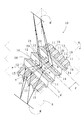
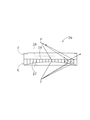
- (A) is a plan view of the optical imaging apparatus according to the first embodiment of the present invention
- (B) is an FF sectional view
- (C) is a GG sectional view.
- SYMBOLS 10 Optical imaging device, 11, 12: Plane light reflection part, 13, 14: Groove, 15, 16: Light transmission part, 19, 20: Slope, 21: Optical imaging device, 22, 23: Plane light reflection Part, 26: optical imaging device, 27, 28: planar light reflecting part, 29: contact surface, A, C, E: first light control panel, B, D, F: second light control panel
- the optical imaging apparatus 10 is an example of a transparent flat plate, and includes two transparent synthetic resin plates (0.5 to 10 mm in thickness)
- a large number of strip-shaped planar light reflecting portions 11 and 12 are formed at a constant pitch (for example, 0.1 to 1 mm) perpendicular to one surface of each transparent synthetic resin plate.
- the first light control panel A hereinafter simply referred to as “light control panel A”
- the second light control panel B hereinafter simply referred to as “light control panel B” are used.
- One surface side of each surface is brought into close contact with the planar light reflecting portions 11 and 12 orthogonal to each other. This will be described in detail below.
- grooves 13 and 14 having a right-angled triangular cross section each having a vertical surface extending in the thickness direction from one surface of the transparent synthetic resin plate are the same as the pitch of the planar light reflecting portions 11 and 12. It is formed at a predetermined pitch.
- the vertical surfaces of the grooves 13 and 14 are planar light reflecting portions 11 and 12 that reflect light incident obliquely into the light control panels A and B, respectively.
- light transmitting portions 15 and 16 constituting light passing surfaces through which the reflected light reflected from the planar light reflecting portions 11 and 12 pass are formed.
- the vertical surfaces of the grooves 13 and 14 may be formed with a metal (for example, silver) plating layer or a metal vapor deposition layer (which constitutes a metal reflection surface).
- the light control panels A and B can be manufactured by press molding using a mold, but are preferably manufactured by injecting a transparent synthetic resin into a mold having a predetermined shape and solidifying it.
- the grooves 13 and 14 have a base shape formed in advance in the mold, and are formed on one surface of the light control panels A and B when the light control panels A and B are manufactured.
- the surface of the mold part that forms the slopes 19 and 20 of the grooves 13 and 14 is subjected to, for example, shot blasting or matte treatment that forms uneven portions of 3 to 50 ⁇ m, so that the slopes 19 and 20 of the grooves 13 and 14 are formed.
- the end of the planar light reflecting portion 11 of the light control panel A and the end of the planar light reflecting portion 12 of the light control panel B are arranged in contact with each other.
- the width w of the planar light reflecting portions 11 and 12 is, for example, 0.5 p or more and 3 p or less with respect to the pitch p of the planar light reflecting portions 11 and 12 (grooves 13 and 14). (Preferably 0.9p to 1.1p, more preferably p).
- the width of the planar light reflecting portions 11 and 12 exceeds 3p, the light reflected by the planar light reflecting portions 11 and 12 is scattered by the slopes 19 and 20, and a part of the scattered light is reflected again by the planar light reflecting portions 11 and 12. Repeatedly, a clear image cannot be obtained.
- the width of the planar light reflecting portions 11 and 12 is less than 0.5p, the light reflected by the planar light reflecting portions 11 and 12 is reduced and a clear image cannot be obtained.
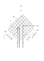
- FIG. 3 in order to clearly show the light reflection state in the light control panels A and B of the optical imaging apparatus 10, the light control panel on the left side with respect to the object M and the object image M ′ in a side view is shown.
- the right light control panel In the right light control panel, the right light control panels A and B are shown rotated by 90 degrees in the same plane with respect to the left light control panels A and B. Since the object image M ′ is obtained when the light is reflected twice in succession by the vertical planar light reflecting portion 11 of the light control panel A and the vertical planar light reflecting portion 12 of the light control panel B, the light control of the optical imaging device is performed.
- the panels A and B are divided into left and right sides when viewed from the side, and the object image is obtained even when the right light control panels A and B are rotated 90 degrees with respect to the left light control panels A and B in the same plane. Is obtained.
- the vertical plane becomes the planar light reflecting portion 11.
- the light control panel A and the light control panel B are in close contact with each other.
- a part of the light totally reflected by the vertical surface of the light control panel A enters the light control panel B, and the rest is scattered and attenuated by the slope 19 subjected to the scattered light processing.
- the light that has entered the light control panel B travels in the light control panel B and reaches the vertical plane of the groove 14 having a right-angled triangular section.
- the vertical surface acts as the planar light reflecting portion 12 only for the light incident on the point b in the vertical surface at an incident angle causing total reflection among the light reaching the vertical surface of the groove 14 and totally reflected.
- the light further travels in the light control panel B, and is emitted to the outside from the surface on the other side (the side on which the planar light reflecting portion 12 is not formed) in the light control panel B.
- FIG. 1 the light incident angle to the vertical plane of the light control panel A is incident at less than theta c is refracted in the vertical plane enters the groove 13, part of the light-scattering It is scattered and attenuated by the light-treated slope 19, and the remaining part passes through the light transmission part 16 of the light control panel B and enters the light control panel B.
- the light that has entered the light control panel B the light that is totally reflected by the vertical surface of the groove 14 and the light that travels in the light control panel B travels to the other side of the light control panel B. It is emitted from the surface of the outside.
- the light incident angle to the vertical surface of the groove 13 of the light control panel A is incident at theta c, taken with the light along the vertical plane is reflected on the vertical surface of the groove 13 the light transmission of the light control panel B Enter the light control panel B from the part 16.
- a part of the light is scattered and attenuated by the inclined surface 20 of the groove 14 subjected to the scattered light treatment, and the remaining part is emitted from the other surface of the light control panel B to the outside. Is done.
- planar light reflecting portions 11 and 12 are disposed in a state of being orthogonally opposed to each other, they travel in the light control panel B and are emitted to the outside from the other surface of the light control panel B.
- incident light incident on the planar light reflecting portion 11 is reflected at the point a of the planar light reflecting portion 11 for the first time, and the reflected light is reflected at the point b of the planar light reflecting portion 12 for the second time.
- the second reflected light is radiated at the same angle as the incident angle of the incident light incident on the planar light reflecting portion 11.
- the reflected light continuously reflected by the planar light reflecting portions 11 and 12 is in a symmetrical position with the object M across the optical imaging apparatus 10. It converges and an object image M ′ is generated at a symmetrical position with respect to the object M across the optical imaging apparatus 10.
- the light enters the light control panel B proceeds to the other side of the light control panel B, and is emitted to the outside from the other side surface.
- the light enters the vertical surface of the groove 13 at an incident angle ⁇ c enters the light control panel B as light along the vertical surface of the groove 13, travels to the other side of the light control panel B, and enters the outside from the other surface.
- the light emitted from the light control panel A directly enters the light control panel B, travels through the light control panel B, and is emitted from the other side of the light control panel B to the outside.
- the incident light entering the light control panel A is not reflected at the same angle. For this reason, the light emitted to the outside from the other surface of the light control panel B does not intersect and an image is not formed.
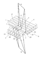
- the optical imaging apparatus 21 has a large number and a strip shape vertically in the thickness direction of the transparent flat plate inside the two transparent flat plates.
- the first light control panel C hereinafter simply referred to as “light control panel C”
- the second light control panel D hereinafter referred to as “light control panel C”
- the first light control panel C (hereinafter simply referred to as “light control panel C”) and the second light control panel D (hereinafter referred to as “light control panel C”) formed by arranging the planar light reflecting portions 22 and 23 made of metal reflective surfaces at a constant pitch.
- light control panel D simply referred to as “light control panel D”), and one surface side of each of the light control panels C and D is brought into close contact with each other with the planar light reflecting portions 22 and 23 orthogonal to each other. This will be described in detail below.
- Each of the light control panels C and D has a constant thickness in which a metal reflecting surface (and thus a double-sided reflecting plate) made of a deposited layer (or plating layer) of aluminum or silver, which is an example of a metal, is formed on one surface side.
- a large number of plate-like transparent synthetic resin plates (for example, acrylic resin plates) or glass plates are laminated so that the metal reflection surface is arranged on one side, and a laminate is produced.
- the light control panels C and D are manufactured by cutting so that a cut surface perpendicular to the surface is formed. And the thickness of a transparent synthetic resin board or a glass plate is equivalent to the pitch of the plane light reflection parts 22 and 23, and the thickness of the light control panels C and D is determined by the thickness at the time of cutting out from a laminated body.
- the thickness at the time of cutting needs to be adjusted according to the intensity of the light control panels C and D and the vertical and horizontal dimensions of the light control panels C and D, and is, for example, 0.5 to 10 mm.
- the width of the planar light reflecting portions 22 and 23 is, for example, 0.5q to 3q (preferably 0.9q to 1.1q, more preferably) with respect to the pitch q of the planar light reflecting portions 22 and 23. q).
- the width of the planar light reflecting portions 22 and 23 exceeds 3q, the light reflected by the planar light reflecting portions 22 and 23 is reflected by the adjacent planar light reflecting portions 22 and 23 and again reflected by the planar light reflecting portions 22 and 23. Repeatedly, a clear image cannot be obtained.
- the widths of the planar light reflecting portions 22 and 23 are less than 0.5 q, the light reflected by the planar light reflecting portions 22 and 23 is reduced and a clear image cannot be obtained.
- the light control panels C and D are fixed to each other by a restraining member (for example, an adhesive, a heat seal, a screw, etc.) that is not shown, in close contact with each other.
- the operation of the optical imaging apparatus 21 according to the second embodiment of the present invention will be described.
- the light emitted from the object N arranged on the other side of the light control panel C of the optical imaging device 21 (the non-contact side with the light control panel D) is reflected by the light control panel C.
- the incident light enters the light control panel C and is reflected at the point c of the planar light reflecting portion 22.
- the reflected light reflected by the planar light reflecting portion 22 passes through the surface on one side of the light control panel D (the contact side with the light control panel C) from the surface on one side of the light control panel C, and the light. Enter the control panel D.
- a part of the light is reflected at the point d of the planar light reflecting portion 23 of the light control panel D and further travels through the light control panel D to control the light.
- the light is discharged from the other side of the panel D to the outside. Further, a part of the remaining light travels in the light control panel D and is emitted to the outside from the other surface of the light control panel D.
- planar light reflecting portions 22 and 23 are arranged in a state of being orthogonally opposed to each other, they travel in the light control panel D and are emitted to the outside from the other surface of the light control panel D.
- incident light incident on the planar light reflecting portion 22 is reflected at the point c of the planar light reflecting portion 22 for the first time, and the reflected light is reflected at the point d of the planar light reflecting portion 23 for the second time.
- the second reflected light becomes parallel to the incident light incident on the planar light reflecting portion 22 in plan view (see FIG. 4).
- the reflected light continuously reflected by the planar light reflecting portions 22 and 23 is in a symmetrical position with the object N across the optical imaging device 21. It converges and an object image N ′ is generated at a symmetrical position with respect to the object N across the optical imaging device 21.
- light that is reflected by the planar light reflecting portion 22 of the light control panel C enters the light control panel D, travels through the light control panel D, and is emitted to the outside from the other surface, the light control panel C.
- the incident light is not parallel to the incident light in plan view. For this reason, the light emitted to the outside from the other surface of the light control panel D does not intersect and an image is not formed.
- planar light reflecting portions 22 and 23 are metal reflecting surfaces, the incident angle of light reflected by the planar light reflecting portions 22 and 23 is not limited, and the light reflection angle is arbitrary. For this reason, an image can be formed at a wider range of angles than the reflecting surface using the principle of “total reflection of matter”.
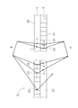
- FIG. 7 shows an optical imaging apparatus 26 according to a third embodiment of the present invention.
- a first light control panel E hereinafter simply referred to as “light control panel E”
- a second light control panel F hereinafter simply referred to as a light control panel F
- the light control panel E is provided with a number of long planar light reflecting portions 27 made of double-sided reflectors in parallel
- the light control panel F has a number of long planar light reflecting portions 28 made of double-sided reflectors in parallel. Is provided.
- the plane light reflecting portions 27 and 28 are erected in the same direction. Accordingly, the planar light reflecting portions 27 and 28 are arranged perpendicular to the contact surface 29 between the light control panel E and the light control panel F.
- planar light reflecting portion 27 and the longitudinal direction of the planar light reflecting portion 28 are orthogonal to each other. These planar light reflecting portions 27 and 28 are embedded at a predetermined pitch in a transparent resin (for example, acrylic) or glass as in the optical imaging apparatus 21 according to the second embodiment.
- the planar light reflecting portions 27 and 28 in the light control panels E and F are gradually increased in height (width) from the central portion toward the peripheral portion.
- One side cross section of F has an arc shape.
- the light (incident light) emitted from the light source P is reflected once by the planar light reflecting unit 27 in the center of the light control panel E to the planar light reflecting unit 28 of the light control panel F. And converges to the image point P ′.
- the light incident on the planar light reflecting portion 27 of the high portion in the peripheral portion of the light control panel F is internally reflected an odd number of times and enters the light control panel F, and the light control panel F has an odd number of times ( Once), the light is reflected and converges at or near the image point P ′.
- the light reflected by the light control panel E or the light control panel F an even number of times does not converge at the imaging point P ′. Therefore, although it is difficult for the optical imaging devices 10 and 21 to collect the light at the peripheral portion of the light control panel, the optical imaging device 26 can collect a part of the light hitting the peripheral portion of the light control panel. .
- the optical imaging apparatus is configured such that one surface side of each of the first and second light control panels on which the planar light reflecting portions are formed faces each other so that the planar light reflecting portions are orthogonal to each other.
- a gap may be formed between the first and second light control panels.
- the width of the gap can be, for example, 100 times or less the width of the band-shaped planar light reflecting portion.
- the metal reflection surface is formed on one side of the transparent synthetic resin plate.
- the metal reflection surface may be formed on both sides of the transparent synthetic resin plate or the glass plate.
- a laminated body is produced by laminating a large number of transparent synthetic resin plates or glass plates having metal reflecting surfaces formed on both side surfaces, and cut-out surfaces perpendicular to the respective metal reflecting surfaces are formed from this laminated body.
- the first and second light control panels can be formed by cutting out.
- the pitch of the planar light reflecting portion of the first light control panel and the pitch of the planar light reflecting portion of the second light control panel B are the same.
- the pitch of the planar light reflecting portions of the light control panel may be different from the pitch of the planar light reflecting portions of the second light control panel. Further, in each embodiment, the interval (pitch) between the planar light reflecting portions in the light control panel is not necessarily the same. Further, a light shielding process can be applied to the slope of the groove formed in the light control panel.
- a plurality of strip-shaped planar light reflecting portions are formed in a transparent flat plate so as to be arranged perpendicularly to one surface at a constant pitch. Since one surface side of each of the first and second light control panels faces each other with the respective planar light reflecting portions orthogonal to each other, the light emitted from the object disposed on one side of the optical imaging device is Then, it converges on the other side of the optical imaging device and forms an image. Therefore, a stereoscopic image can be projected in the space, and can be applied to a stereoscopic display device, a game machine, a game machine, an advertising tower, and the like. Furthermore, since the structure is simple, an inexpensive optical imaging apparatus can be provided.
Landscapes
- Physics & Mathematics (AREA)
- General Physics & Mathematics (AREA)
- Optics & Photonics (AREA)
- Optical Elements Other Than Lenses (AREA)
- Stereoscopic And Panoramic Photography (AREA)
- Lenses (AREA)
Abstract
L’invention concerne un dispositif d’imagerie optique (10) permettant de créer facilement une image tridimensionnelle dans l’espace, du côté d’un observateur en train de visualiser un objet, ainsi qu’un procédé d’imagerie optique mettant en œuvre ce dispositif. Le dispositif (10) selon l’invention comprend des premier et deuxième panneaux de commande de lumière (A,B) formés pour aligner une pluralité de réflecteurs de lumière plats en forme de bande (11,12) selon un pas constant, perpendiculaires à la surface sur un côté d’une plaque plate transparente dans la plaque plate transparente. Une surface du premier panneau de commande de lumière (A) est perpendiculaire et fait face à une surface du deuxième panneau de commande de lumière (B), et les réflecteurs de lumière plats (11,12) sont perpendiculaires et se font face les uns aux autres. Le procédé d’imagerie optique mettant en œuvre ce dispositif (10) consiste : à diriger la lumière provenant de l’objet (M) de sorte qu’elle frappe sur le réflecteur plat (11) du premier panneau de commande de lumière (A) ; à réfléchir à nouveau la lumière réfléchie par le réflecteur plat (11) au moyen du réflecteur plat (12) du deuxième panneau de commande de lumière (B) ; et à former l’image de l’objet (M) sur le côté opposé au dispositif d’imagerie (10).
Priority Applications (1)
| Application Number | Priority Date | Filing Date | Title |
|---|---|---|---|
| JP2010509189A JP4865088B2 (ja) | 2008-04-22 | 2009-04-21 | 光学結像方法 |
Applications Claiming Priority (2)
| Application Number | Priority Date | Filing Date | Title |
|---|---|---|---|
| JP2008-111672 | 2008-04-22 | ||
| JP2008111672 | 2008-04-22 |
Publications (1)
| Publication Number | Publication Date |
|---|---|
| WO2009131128A1 true WO2009131128A1 (fr) | 2009-10-29 |
Family
ID=41216860
Family Applications (1)
| Application Number | Title | Priority Date | Filing Date |
|---|---|---|---|
| PCT/JP2009/057934 WO2009131128A1 (fr) | 2008-04-22 | 2009-04-21 | Dispositif d’imagerie optique et procede d’imagerie optique mettant en œuvre ce dispositif |
Country Status (2)
| Country | Link |
|---|---|
| JP (5) | JP4865088B2 (fr) |
| WO (1) | WO2009131128A1 (fr) |
Cited By (62)
| Publication number | Priority date | Publication date | Assignee | Title |
|---|---|---|---|---|
| JP2009276699A (ja) * | 2008-05-16 | 2009-11-26 | National Institute Of Information & Communication Technology | 2面コーナーリフレクタアレイ |
| JP2011081309A (ja) * | 2009-10-09 | 2011-04-21 | Pioneer Electronic Corp | 空間映像表示装置 |
| JP2011081300A (ja) * | 2009-10-09 | 2011-04-21 | Pioneer Electronic Corp | 反射型面対称結像素子の製造方法 |
| JP2011175297A (ja) * | 2008-04-22 | 2011-09-08 | Askanet:Kk | 光学結像装置に使用する光制御パネルの製造方法 |
| JPWO2009136578A1 (ja) * | 2008-05-09 | 2011-09-08 | パイオニア株式会社 | 空間映像表示装置 |
| JP2012128456A (ja) * | 2012-03-22 | 2012-07-05 | Pioneer Electronic Corp | 反射型面対称結像素子の製造方法 |
| JP2012150502A (ja) * | 2012-03-22 | 2012-08-09 | Pioneer Electronic Corp | 反射型面対称結像素子の製造方法 |
| JP2012247459A (ja) * | 2011-05-25 | 2012-12-13 | National Institute Of Information & Communication Technology | リフレクタアレイ光学装置およびそれを用いた表示装置 |
| WO2013061619A1 (fr) | 2011-10-24 | 2013-05-02 | 株式会社アスカネット | Dispositif de formation d'image optique |
| JP2013109211A (ja) * | 2011-11-22 | 2013-06-06 | Pioneer Electronic Corp | 空間映像表示装置 |
| WO2013122085A1 (fr) * | 2012-02-14 | 2013-08-22 | シャープ株式会社 | Elément d'imagerie réfléchissant et système optique |
| US8540371B2 (en) | 2010-05-21 | 2013-09-24 | Stanley Electric Co., Ltd. | Display device |
| JP2013210502A (ja) * | 2012-03-30 | 2013-10-10 | Dainippon Printing Co Ltd | 光学パネルおよび表示装置 |
| JP2013242850A (ja) * | 2012-04-27 | 2013-12-05 | Nitto Denko Corp | 表示入力装置 |
| WO2013183454A1 (fr) * | 2012-06-07 | 2013-12-12 | 株式会社アスカネット | Dispositif formant image optique et procédé formant image optique |
| WO2014024677A1 (fr) * | 2012-08-10 | 2014-02-13 | 株式会社アスカネット | Dispositif de formation d'image optique à altération de taille et son procédé de fabrication |
| WO2014038303A1 (fr) * | 2012-09-10 | 2014-03-13 | 株式会社アスカネット | Écran tactile flottant |
| US8702252B2 (en) | 2012-01-30 | 2014-04-22 | Asukanet Company, Ltd. | Optical imaging apparatus and optical imaging method using the same |
| JP2014081617A (ja) * | 2012-09-28 | 2014-05-08 | Nlt Technologies Ltd | 空間結像素子及びその製造方法、表示装置および端末機 |
| WO2014073650A1 (fr) | 2012-11-08 | 2014-05-15 | 株式会社アスカネット | Méthode de fabrication de panneau de régulation de lumière |
| WO2014129454A1 (fr) * | 2013-02-19 | 2014-08-28 | 日本電気硝子株式会社 | Stratifié en verre, élément d'imagerie optique, procédé de fabrication de stratifié en verre et procédé de fabrication d'élément d'imagerie optique |
| JP2015018038A (ja) * | 2013-07-09 | 2015-01-29 | 株式会社アスカネット | 像再生方法 |
| WO2015033645A1 (fr) * | 2013-09-06 | 2015-03-12 | 株式会社アスカネット | Méthode de fabrication de panneau de photocommande comprenant des parties photoréflectrices qui sont positionnées parallèlement |
| JP2015079170A (ja) * | 2013-10-18 | 2015-04-23 | 増田 麻言 | 走査型投影装置、および携帯型投影装置 |
| JP2015125393A (ja) * | 2013-12-27 | 2015-07-06 | 株式会社アスカネット | 立体像形成装置及びその製造方法 |
| JP5820955B1 (ja) * | 2014-06-27 | 2015-11-24 | 株式会社アスカネット | 再帰性反射体並びにこれを利用した立体像表示装置 |
| WO2015198499A1 (fr) * | 2014-06-27 | 2015-12-30 | 株式会社アスカネット | Dispositif catadioptrique et procédé et dispositif d'affichage d'image stéréoscopique l'utilisant |
| KR101619638B1 (ko) * | 2014-11-11 | 2016-05-10 | 현대자동차일본기술연구소 | 공간결상장치를 이용한 자동차용 후방 시야 확보 장치 |
| WO2016088580A1 (fr) * | 2014-12-05 | 2016-06-09 | 昭和電工株式会社 | Panneau de commande de lumière et dispositif d'imagerie optique |
| JP2016180785A (ja) * | 2015-03-23 | 2016-10-13 | コニカミノルタ株式会社 | 反射型空中結像素子及びその製造方法 |
| US9517109B2 (en) | 2014-09-24 | 2016-12-13 | Olympus Corporation | Medical system |
| US9523859B2 (en) | 2012-02-28 | 2016-12-20 | Asukanet Company, Ltd. | Volumetric-image forming system and method thereof |
| KR20160148707A (ko) | 2014-06-05 | 2016-12-26 | 가부시키가이샤 아스카넷토 | 화상 표시 장치 및 화상 표시 방법 |
| US9618757B2 (en) | 2013-04-24 | 2017-04-11 | Asukanet Company, Ltd. | Stereoscopic image display device and stereoscopic image display method |
| CN106560734A (zh) * | 2016-06-01 | 2017-04-12 | 杭州飞像科技有限公司 | 空中成像元件在提词器中的应用及提词器 |
| JP2017126032A (ja) * | 2016-01-15 | 2017-07-20 | 大日本印刷株式会社 | 光学シート及び光学パネル |
| JP2017167224A (ja) * | 2016-03-14 | 2017-09-21 | 大日本印刷株式会社 | 空間浮遊映像表示装置 |
| JP6203978B1 (ja) * | 2017-04-17 | 2017-09-27 | 株式会社アスカネット | 立体像結像装置の製造方法 |
| JP6203989B1 (ja) * | 2017-01-27 | 2017-09-27 | 株式会社アスカネット | 立体像結像装置の製造方法 |
| JP2017219558A (ja) * | 2016-06-02 | 2017-12-14 | コニカミノルタ株式会社 | 光学素子の製造方法及び反射型空中結像素子の製造方法 |
| CN107533361A (zh) * | 2015-05-08 | 2018-01-02 | 京瓷办公信息系统株式会社 | 图像形成装置 |
| WO2018138932A1 (fr) * | 2017-01-27 | 2018-08-02 | 株式会社アスカネット | Procédé de fabrication de dispositif de formation d'image stéréoscopique, et dispositif de formation d'image stéréoscopique |
| WO2018139141A1 (fr) * | 2017-01-30 | 2018-08-02 | 株式会社パリティ・イノベーションズ | Élément optique et dispositif d'affichage d'image l'utilisant |
| WO2018220876A1 (fr) | 2017-06-01 | 2018-12-06 | 株式会社アスカネット | Procédé de fabrication de dispositif de formation d'image stéréoscopique, et dispositif de formation d'image stéréoscopique |
| DE112017000008B4 (de) | 2016-03-10 | 2018-12-20 | Omron Corporation | Stereoskopische anzeigevorrichtung |
| WO2019003730A1 (fr) | 2017-06-29 | 2019-01-03 | 株式会社アスカネット | Dispositif de formation d'image stéréoscopique et procédé de fabrication de dispositif de formation d'image stéréoscopique |
| WO2019021497A1 (fr) * | 2017-07-24 | 2019-01-31 | 株式会社アスカネット | Dispositif de formation d'image stéréoscopique et son procédé de fabrication |
| JP2019045562A (ja) * | 2017-08-30 | 2019-03-22 | 株式会社アスカネット | 立体像結像装置の製造方法 |
| CN110264916A (zh) * | 2019-06-21 | 2019-09-20 | 京东方科技集团股份有限公司 | 一种投影装置及空中成像设备 |
| JP6616554B1 (ja) * | 2018-07-18 | 2019-12-04 | 株式会社アスカネット | 立体像結像装置の製造方法 |
| WO2020017071A1 (fr) | 2018-07-18 | 2020-01-23 | 株式会社アスカネット | Procédé de fabrication de dispositif de formation d'image stéréoscopique, et dispositif de formation d'image stéréoscopique |
| JPWO2018139444A1 (ja) * | 2017-01-27 | 2020-03-26 | 株式会社アスカネット | 立体像結像装置の製造方法及び立体像結像装置 |
| CN111886567A (zh) * | 2018-03-07 | 2020-11-03 | 日本电气方案创新株式会社 | 操作输入装置、操作输入方法及计算机可读的记录介质 |
| JP2021026093A (ja) * | 2019-08-02 | 2021-02-22 | 本田技研工業株式会社 | 映像表示装置 |
| WO2021070400A1 (fr) | 2019-10-11 | 2021-04-15 | 株式会社アスカネット | Dispositif de formation d'image optique et son procédé de fabrication |
| WO2022080082A1 (fr) | 2020-10-15 | 2022-04-21 | 株式会社アスカネット | Élément de formation d'image aérienne et dispositif de formation d'image aérienne |
| KR20220136479A (ko) | 2020-03-10 | 2022-10-07 | 가부시키가이샤 아스카넷토 | 광학 결상 장치에 사용하는 광제어 패널의 제조 방법 |
| WO2022224613A1 (fr) | 2021-04-21 | 2022-10-27 | 株式会社アスカネット | Dispositif de formation d'image aérienne de type de réflexion et procédé de formation d'image aérienne de type de réflexion |
| US11537240B2 (en) | 2018-05-22 | 2022-12-27 | Murakami Corporation | Virtual image display device |
| WO2023007816A1 (fr) | 2021-07-26 | 2023-02-02 | 株式会社アスカネット | Procédé de fabrication d'un dispositif de formation d'image aérienne, et dispositif de formation d'image aérienne |
| US11662860B2 (en) | 2019-04-10 | 2023-05-30 | Murakami Corporation | Reference position setting method and operation detection device for displaying an operation surface as a virtual image |
| KR20230077751A (ko) | 2021-04-21 | 2023-06-01 | 가부시키가이샤 아스카넷토 | 반사형 공중상 결상 장치 및 반사형 공중상 결상 방법 |
Families Citing this family (24)
| Publication number | Priority date | Publication date | Assignee | Title |
|---|---|---|---|---|
| JP5904436B2 (ja) * | 2011-11-09 | 2016-04-13 | パイオニア株式会社 | 大型の反射型面対称結像素子の製造方法 |
| JP5995131B2 (ja) * | 2011-11-25 | 2016-09-21 | 大日本印刷株式会社 | 光学パネルおよび表示装置 |
| WO2013145983A1 (fr) * | 2012-03-27 | 2013-10-03 | 株式会社アスカネット | Procédé de fabrication d'un panneau de commande optique |
| JP2014032394A (ja) * | 2012-07-13 | 2014-02-20 | Nitto Denko Corp | マイクロミラーアレイおよびその製法並びにそれに用いる光学素子 |
| JP2014066825A (ja) * | 2012-09-25 | 2014-04-17 | Nitto Denko Corp | マイクロミラーアレイの製法 |
| WO2014167904A1 (fr) * | 2013-04-12 | 2014-10-16 | シャープ株式会社 | Elément formant image de type réfléchissant et procédé de fabrication d'élément formant image de type réfléchissant |
| JP5509391B1 (ja) * | 2013-06-07 | 2014-06-04 | 株式会社アスカネット | 再生画像の指示位置を非接触で検知する方法及び装置 |
| CN105264470B (zh) | 2013-06-07 | 2018-06-22 | 亚斯卡奈特股份有限公司 | 非接触地检测再现图像的指示位置的方法及装置 |
| JP5723928B2 (ja) * | 2013-07-09 | 2015-05-27 | 株式会社アスカネット | モールド型の製造方法 |
| WO2016051480A1 (fr) * | 2014-09-29 | 2016-04-07 | 日立マクセル株式会社 | Dispositif d'affichage et appareil le comprenant |
| JP6674683B2 (ja) * | 2014-12-19 | 2020-04-01 | 国立大学法人 鹿児島大学 | 認証処理装置及び認証処理方法 |
| CN107408372B (zh) | 2015-03-26 | 2019-10-25 | 京瓷办公信息系统株式会社 | 可视像形成装置以及图像形成装置 |
| JP6365767B2 (ja) | 2015-03-30 | 2018-08-01 | 京セラドキュメントソリューションズ株式会社 | 可視像形成装置及び画像形成装置 |
| JP6281520B2 (ja) | 2015-03-31 | 2018-02-21 | 京セラドキュメントソリューションズ株式会社 | 画像形成装置 |
| WO2017047527A1 (fr) * | 2015-09-15 | 2017-03-23 | コニカミノルタ株式会社 | Dispositif de forme physique et système de forme physique |
| EP3355088B1 (fr) | 2015-09-25 | 2021-09-01 | Asukanet Company, Ltd. | Catadioptre |
| JP6645371B2 (ja) | 2016-07-15 | 2020-02-14 | オムロン株式会社 | 光デバイス及び立体表示方法 |
| KR20190041884A (ko) | 2016-08-31 | 2019-04-23 | 에스씨아이브이에이엑스 가부시키가이샤 | 광 결상 장치 |
| JP6756281B2 (ja) | 2017-03-14 | 2020-09-16 | オムロン株式会社 | 表示方法および表示装置 |
| JP6716027B2 (ja) | 2017-04-17 | 2020-07-01 | 富士フイルム株式会社 | 光学フィルム、積層型光学フィルムおよびこの積層型光学フィルムを備えた空中結像装置 |
| CN107193125A (zh) * | 2017-07-26 | 2017-09-22 | 安徽省东超科技有限公司 | 一种实现空气成像的光学平板结构 |
| JP7134181B2 (ja) | 2017-11-01 | 2022-09-09 | 株式会社村上開明堂 | 画像表示システム |
| CN112180478B (zh) * | 2020-09-03 | 2022-03-18 | 核桃智能科技(常州)有限公司 | 一种空气成像透镜 |
| JP7184220B1 (ja) | 2021-07-12 | 2022-12-06 | 凸版印刷株式会社 | 空中表示装置 |
Citations (6)
| Publication number | Priority date | Publication date | Assignee | Title |
|---|---|---|---|---|
| JPS5821702A (ja) * | 1981-07-31 | 1983-02-08 | Ricoh Co Ltd | 微小幅両面反射帯を用いた結像素子 |
| JPS6125104A (ja) * | 1984-07-13 | 1986-02-04 | Hitachi Ltd | 複合レンズ |
| JPS63191182A (ja) * | 1987-02-04 | 1988-08-08 | キヤノン株式会社 | 画像表示部材 |
| JPH095503A (ja) * | 1995-06-23 | 1997-01-10 | Nittetsu Elex Co Ltd | 光学結像装置 |
| WO2008041616A1 (fr) * | 2006-10-02 | 2008-04-10 | National Institute Of Information And Communications Technology | Dispositif optique de formation d'image à deux points |
| JP2008158114A (ja) * | 2006-12-21 | 2008-07-10 | National Institute Of Information & Communication Technology | 光学システム |
Family Cites Families (2)
| Publication number | Priority date | Publication date | Assignee | Title |
|---|---|---|---|---|
| JPS62284740A (ja) * | 1986-06-03 | 1987-12-10 | 信越ポリマ−株式会社 | 微細すだれ状防眩シ−ト |
| JP4865088B2 (ja) * | 2008-04-22 | 2012-02-01 | 株式会社アスカネット | 光学結像方法 |
-
2009
- 2009-04-21 JP JP2010509189A patent/JP4865088B2/ja active Active
- 2009-04-21 WO PCT/JP2009/057934 patent/WO2009131128A1/fr active Application Filing
-
2011
- 2011-05-31 JP JP2011122306A patent/JP5085767B2/ja active Active
- 2011-09-30 JP JP2011217754A patent/JP5036898B2/ja active Active
-
2012
- 2012-05-10 JP JP2012108788A patent/JP5437436B2/ja active Active
-
2013
- 2013-01-11 JP JP2013003620A patent/JP5420774B2/ja active Active
Patent Citations (6)
| Publication number | Priority date | Publication date | Assignee | Title |
|---|---|---|---|---|
| JPS5821702A (ja) * | 1981-07-31 | 1983-02-08 | Ricoh Co Ltd | 微小幅両面反射帯を用いた結像素子 |
| JPS6125104A (ja) * | 1984-07-13 | 1986-02-04 | Hitachi Ltd | 複合レンズ |
| JPS63191182A (ja) * | 1987-02-04 | 1988-08-08 | キヤノン株式会社 | 画像表示部材 |
| JPH095503A (ja) * | 1995-06-23 | 1997-01-10 | Nittetsu Elex Co Ltd | 光学結像装置 |
| WO2008041616A1 (fr) * | 2006-10-02 | 2008-04-10 | National Institute Of Information And Communications Technology | Dispositif optique de formation d'image à deux points |
| JP2008158114A (ja) * | 2006-12-21 | 2008-07-10 | National Institute Of Information & Communication Technology | 光学システム |
Non-Patent Citations (1)
| Title |
|---|
| MAEKAWA S. ET AL.: "Advances in Passive Imaging Elements with Micromirror Array", PROCEEDINGS OF SPIE, vol. 6803, no. 28-30, January 2008 (2008-01-01), pages 68030B-1 - 68030B-1 * |
Cited By (121)
| Publication number | Priority date | Publication date | Assignee | Title |
|---|---|---|---|---|
| JP2011175297A (ja) * | 2008-04-22 | 2011-09-08 | Askanet:Kk | 光学結像装置に使用する光制御パネルの製造方法 |
| JP2012014194A (ja) * | 2008-04-22 | 2012-01-19 | Askanet:Kk | 光学結像装置 |
| JP2012177922A (ja) * | 2008-05-09 | 2012-09-13 | Pioneer Electronic Corp | 空間映像表示装置 |
| JPWO2009136578A1 (ja) * | 2008-05-09 | 2011-09-08 | パイオニア株式会社 | 空間映像表示装置 |
| JP2012128454A (ja) * | 2008-05-09 | 2012-07-05 | Pioneer Electronic Corp | 空間映像表示装置 |
| JP2012137779A (ja) * | 2008-05-09 | 2012-07-19 | Pioneer Electronic Corp | 空間映像表示装置 |
| US8867136B2 (en) | 2008-05-09 | 2014-10-21 | Pioneer Corporation | Floating image display device |
| JP5143898B2 (ja) * | 2008-05-09 | 2013-02-13 | パイオニア株式会社 | 空間映像表示装置 |
| JP2009276699A (ja) * | 2008-05-16 | 2009-11-26 | National Institute Of Information & Communication Technology | 2面コーナーリフレクタアレイ |
| JP2011081309A (ja) * | 2009-10-09 | 2011-04-21 | Pioneer Electronic Corp | 空間映像表示装置 |
| JP2011081300A (ja) * | 2009-10-09 | 2011-04-21 | Pioneer Electronic Corp | 反射型面対称結像素子の製造方法 |
| US8540371B2 (en) | 2010-05-21 | 2013-09-24 | Stanley Electric Co., Ltd. | Display device |
| JP2012247459A (ja) * | 2011-05-25 | 2012-12-13 | National Institute Of Information & Communication Technology | リフレクタアレイ光学装置およびそれを用いた表示装置 |
| US9513486B2 (en) | 2011-10-24 | 2016-12-06 | Asukanet Company, Ltd. | Optical imaging apparatus |
| WO2013061619A1 (fr) | 2011-10-24 | 2013-05-02 | 株式会社アスカネット | Dispositif de formation d'image optique |
| JP2013109211A (ja) * | 2011-11-22 | 2013-06-06 | Pioneer Electronic Corp | 空間映像表示装置 |
| US8702252B2 (en) | 2012-01-30 | 2014-04-22 | Asukanet Company, Ltd. | Optical imaging apparatus and optical imaging method using the same |
| WO2013122085A1 (fr) * | 2012-02-14 | 2013-08-22 | シャープ株式会社 | Elément d'imagerie réfléchissant et système optique |
| JP2013167667A (ja) * | 2012-02-14 | 2013-08-29 | Sharp Corp | 反射型結像素子および光学システム |
| US9645403B2 (en) | 2012-02-14 | 2017-05-09 | Sharp Kabushiki Kaisha | Reflective imaging element and optical system |
| US9523859B2 (en) | 2012-02-28 | 2016-12-20 | Asukanet Company, Ltd. | Volumetric-image forming system and method thereof |
| JP2012150502A (ja) * | 2012-03-22 | 2012-08-09 | Pioneer Electronic Corp | 反射型面対称結像素子の製造方法 |
| JP2012128456A (ja) * | 2012-03-22 | 2012-07-05 | Pioneer Electronic Corp | 反射型面対称結像素子の製造方法 |
| JP2013210502A (ja) * | 2012-03-30 | 2013-10-10 | Dainippon Printing Co Ltd | 光学パネルおよび表示装置 |
| JP2013242850A (ja) * | 2012-04-27 | 2013-12-05 | Nitto Denko Corp | 表示入力装置 |
| JPWO2013183454A1 (ja) * | 2012-06-07 | 2016-01-28 | 株式会社アスカネット | 光学結像装置 |
| JP5667729B2 (ja) * | 2012-06-07 | 2015-02-12 | 株式会社アスカネット | 光学結像装置 |
| WO2013183454A1 (fr) * | 2012-06-07 | 2013-12-12 | 株式会社アスカネット | Dispositif formant image optique et procédé formant image optique |
| JPWO2014024677A1 (ja) * | 2012-08-10 | 2016-07-25 | 株式会社アスカネット | 倍率変更型光学結像装置及びその製造方法 |
| WO2014024677A1 (fr) * | 2012-08-10 | 2014-02-13 | 株式会社アスカネット | Dispositif de formation d'image optique à altération de taille et son procédé de fabrication |
| WO2014038303A1 (fr) * | 2012-09-10 | 2014-03-13 | 株式会社アスカネット | Écran tactile flottant |
| JP2014067071A (ja) * | 2012-09-10 | 2014-04-17 | Askanet:Kk | 空中タッチパネル |
| JP2014081617A (ja) * | 2012-09-28 | 2014-05-08 | Nlt Technologies Ltd | 空間結像素子及びその製造方法、表示装置および端末機 |
| WO2014073650A1 (fr) | 2012-11-08 | 2014-05-15 | 株式会社アスカネット | Méthode de fabrication de panneau de régulation de lumière |
| JP2015172782A (ja) * | 2012-11-08 | 2015-10-01 | 株式会社アスカネット | 光制御パネルの製造方法 |
| JPWO2014073650A1 (ja) * | 2012-11-08 | 2016-09-08 | 株式会社アスカネット | 光制御パネルの製造方法 |
| CN104718468A (zh) * | 2012-11-08 | 2015-06-17 | 亚斯卡奈特股份有限公司 | 光控制面板的制造方法 |
| US20150234099A1 (en) * | 2012-11-08 | 2015-08-20 | Asukanet Company, Ltd. | Method for producing light control panel |
| JP2015083527A (ja) * | 2013-02-19 | 2015-04-30 | 日本電気硝子株式会社 | ガラス積層体、光学結像部材、ガラス積層体の製造方法及び光学結像部材の製造方法 |
| WO2014129454A1 (fr) * | 2013-02-19 | 2014-08-28 | 日本電気硝子株式会社 | Stratifié en verre, élément d'imagerie optique, procédé de fabrication de stratifié en verre et procédé de fabrication d'élément d'imagerie optique |
| JP2018065746A (ja) * | 2013-02-19 | 2018-04-26 | 日本電気硝子株式会社 | ガラス積層体及び光学結像部材 |
| US9618757B2 (en) | 2013-04-24 | 2017-04-11 | Asukanet Company, Ltd. | Stereoscopic image display device and stereoscopic image display method |
| JP2015018038A (ja) * | 2013-07-09 | 2015-01-29 | 株式会社アスカネット | 像再生方法 |
| JP5696264B1 (ja) * | 2013-09-06 | 2015-04-08 | 株式会社アスカネット | 平行配置された光反射部を備えた光制御パネルの製造方法 |
| WO2015033645A1 (fr) * | 2013-09-06 | 2015-03-12 | 株式会社アスカネット | Méthode de fabrication de panneau de photocommande comprenant des parties photoréflectrices qui sont positionnées parallèlement |
| JP2015079170A (ja) * | 2013-10-18 | 2015-04-23 | 増田 麻言 | 走査型投影装置、および携帯型投影装置 |
| JP2015125393A (ja) * | 2013-12-27 | 2015-07-06 | 株式会社アスカネット | 立体像形成装置及びその製造方法 |
| KR20160148707A (ko) | 2014-06-05 | 2016-12-26 | 가부시키가이샤 아스카넷토 | 화상 표시 장치 및 화상 표시 방법 |
| US9869876B2 (en) | 2014-06-05 | 2018-01-16 | Asukanet Company, Ltd. | Image display apparatus and image display method |
| EP3153908A4 (fr) * | 2014-06-05 | 2018-03-21 | Asukanet Company, Ltd. | Dispositif d'affichage d'image et procédé d'affichage d'image |
| JP5820955B1 (ja) * | 2014-06-27 | 2015-11-24 | 株式会社アスカネット | 再帰性反射体並びにこれを利用した立体像表示装置 |
| KR101918135B1 (ko) * | 2014-06-27 | 2018-11-13 | 가부시키가이샤 아스카넷토 | 재귀성 반사체 및 이것을 이용한 입체상 표시 장치 및 방법 |
| US20170146705A1 (en) * | 2014-06-27 | 2017-05-25 | Asukanet Company, Ltd. | Retroreflective body, and volumetric image display apparatus and volumetric image display method using the same |
| WO2015198499A1 (fr) * | 2014-06-27 | 2015-12-30 | 株式会社アスカネット | Dispositif catadioptrique et procédé et dispositif d'affichage d'image stéréoscopique l'utilisant |
| US9517109B2 (en) | 2014-09-24 | 2016-12-13 | Olympus Corporation | Medical system |
| KR101619638B1 (ko) * | 2014-11-11 | 2016-05-10 | 현대자동차일본기술연구소 | 공간결상장치를 이용한 자동차용 후방 시야 확보 장치 |
| EP3229046A4 (fr) * | 2014-12-05 | 2018-07-25 | Showa Denko K.K. | Panneau de commande de lumière et dispositif d'imagerie optique |
| JPWO2016088580A1 (ja) * | 2014-12-05 | 2017-09-14 | 昭和電工株式会社 | 光制御パネル及び光結像装置 |
| CN107003440A (zh) * | 2014-12-05 | 2017-08-01 | 昭和电工株式会社 | 光控制面板及光成像装置 |
| WO2016088580A1 (fr) * | 2014-12-05 | 2016-06-09 | 昭和電工株式会社 | Panneau de commande de lumière et dispositif d'imagerie optique |
| TWI655459B (zh) * | 2014-12-05 | 2019-04-01 | 日商昭和電工股份有限公司 | Light control panel and light imaging device |
| US20170341342A1 (en) * | 2014-12-05 | 2017-11-30 | Showa Denko K.K. | Light control panel and optical imaging device |
| JP2016180785A (ja) * | 2015-03-23 | 2016-10-13 | コニカミノルタ株式会社 | 反射型空中結像素子及びその製造方法 |
| CN107533361A (zh) * | 2015-05-08 | 2018-01-02 | 京瓷办公信息系统株式会社 | 图像形成装置 |
| CN107533361B (zh) * | 2015-05-08 | 2020-08-04 | 京瓷办公信息系统株式会社 | 图像形成装置 |
| JP2017126032A (ja) * | 2016-01-15 | 2017-07-20 | 大日本印刷株式会社 | 光学シート及び光学パネル |
| US10451886B2 (en) | 2016-03-10 | 2019-10-22 | Omron Corporation | Stereoscopic display device |
| DE112017000008B4 (de) | 2016-03-10 | 2018-12-20 | Omron Corporation | Stereoskopische anzeigevorrichtung |
| JP2017167224A (ja) * | 2016-03-14 | 2017-09-21 | 大日本印刷株式会社 | 空間浮遊映像表示装置 |
| CN106560734A (zh) * | 2016-06-01 | 2017-04-12 | 杭州飞像科技有限公司 | 空中成像元件在提词器中的应用及提词器 |
| JP2017219558A (ja) * | 2016-06-02 | 2017-12-14 | コニカミノルタ株式会社 | 光学素子の製造方法及び反射型空中結像素子の製造方法 |
| JP6203989B1 (ja) * | 2017-01-27 | 2017-09-27 | 株式会社アスカネット | 立体像結像装置の製造方法 |
| KR102219748B1 (ko) | 2017-01-27 | 2021-02-23 | 가부시키가이샤 아스카넷토 | 입체상 결상 장치의 제조 방법 및 입체상 결상 장치 |
| JP2018124534A (ja) * | 2017-01-27 | 2018-08-09 | 株式会社アスカネット | 立体像結像装置 |
| JPWO2018138932A1 (ja) * | 2017-01-27 | 2020-03-19 | 株式会社アスカネット | 立体像結像装置の製造方法 |
| CN109997068B (zh) * | 2017-01-27 | 2021-08-10 | 亚斯卡奈特股份有限公司 | 立体像成像装置的制造方法以及立体像成像装置 |
| JPWO2018139444A1 (ja) * | 2017-01-27 | 2020-03-26 | 株式会社アスカネット | 立体像結像装置の製造方法及び立体像結像装置 |
| KR102219750B1 (ko) | 2017-01-27 | 2021-02-23 | 가부시키가이샤 아스카넷토 | 입체상 결상 장치의 제조 방법 및 입체상 결상 장치 |
| WO2018138932A1 (fr) * | 2017-01-27 | 2018-08-02 | 株式会社アスカネット | Procédé de fabrication de dispositif de formation d'image stéréoscopique, et dispositif de formation d'image stéréoscopique |
| KR20210002769A (ko) | 2017-01-27 | 2021-01-08 | 가부시키가이샤 아스카넷토 | 입체상 결상 장치의 제조 방법 및 입체상 결상 장치 |
| WO2018138940A1 (fr) | 2017-01-27 | 2018-08-02 | 株式会社アスカネット | Procédé de fabrication de dispositif de formation d'image stéréoscopique, et dispositif de formation d'image stéréoscopique |
| CN109997068A (zh) * | 2017-01-27 | 2019-07-09 | 亚斯卡奈特股份有限公司 | 立体像成像装置的制造方法以及立体像成像装置 |
| KR20190103311A (ko) | 2017-01-27 | 2019-09-04 | 가부시키가이샤 아스카넷토 | 입체상 결상 장치의 제조 방법 및 입체상 결상 장치 |
| JP2020074028A (ja) * | 2017-01-27 | 2020-05-14 | 株式会社アスカネット | 立体像結像装置の製造方法及び立体像結像装置 |
| JPWO2018139141A1 (ja) * | 2017-01-30 | 2020-02-06 | 株式会社パリティ・イノベーションズ | 光学素子及びそれを用いた映像表示装置 |
| WO2018139141A1 (fr) * | 2017-01-30 | 2018-08-02 | 株式会社パリティ・イノベーションズ | Élément optique et dispositif d'affichage d'image l'utilisant |
| JP7152019B2 (ja) | 2017-01-30 | 2022-10-12 | 株式会社パリティ・イノベーションズ | 光学素子及びそれを用いた映像表示装置 |
| JP6203978B1 (ja) * | 2017-04-17 | 2017-09-27 | 株式会社アスカネット | 立体像結像装置の製造方法 |
| JP2018180369A (ja) * | 2017-04-17 | 2018-11-15 | 株式会社アスカネット | 立体像結像装置の製造方法 |
| WO2018193846A1 (fr) * | 2017-04-17 | 2018-10-25 | 株式会社アスカネット | Procédé de fabrication d'un dispositif de formation d'images stéréoscopiques |
| US11402654B2 (en) | 2017-06-01 | 2022-08-02 | Asukanet Company, Ltd. | Method for manufacturing stereoscopic image forming device, and stereoscopic image forming device |
| EP3633436A4 (fr) * | 2017-06-01 | 2021-03-10 | Asukanet Company, Ltd. | Procédé de fabrication de dispositif de formation d'image stéréoscopique, et dispositif de formation d'image stéréoscopique |
| KR20200004406A (ko) | 2017-06-01 | 2020-01-13 | 가부시키가이샤 아스카넷토 | 입체상 결상 장치의 제조 방법 및 입체상 결상 장치 |
| WO2018220876A1 (fr) | 2017-06-01 | 2018-12-06 | 株式会社アスカネット | Procédé de fabrication de dispositif de formation d'image stéréoscopique, et dispositif de formation d'image stéréoscopique |
| KR20200014929A (ko) | 2017-06-29 | 2020-02-11 | 가부시키가이샤 아스카넷토 | 입체상 결상 장치 및 입체상 결상 장치의 제조 방법 |
| CN110573935B (zh) * | 2017-06-29 | 2022-02-11 | 亚斯卡奈特股份有限公司 | 立体像成像装置及立体像成像装置的制造方法 |
| JPWO2019003730A1 (ja) * | 2017-06-29 | 2019-11-07 | 株式会社アスカネット | 立体像結像装置及び立体像結像装置の製造方法 |
| KR20210142773A (ko) | 2017-06-29 | 2021-11-25 | 가부시키가이샤 아스카넷토 | 입체상 결상 장치 및 입체상 결상 장치의 제조 방법 |
| US11714296B2 (en) | 2017-06-29 | 2023-08-01 | Asukanet Company, Ltd. | Stereoscopic image forming device and method for manufacturing stereoscopic image forming device |
| WO2019003730A1 (fr) | 2017-06-29 | 2019-01-03 | 株式会社アスカネット | Dispositif de formation d'image stéréoscopique et procédé de fabrication de dispositif de formation d'image stéréoscopique |
| CN110573935A (zh) * | 2017-06-29 | 2019-12-13 | 亚斯卡奈特股份有限公司 | 立体像成像装置及立体像成像装置的制造方法 |
| JPWO2019021497A1 (ja) * | 2017-07-24 | 2020-03-26 | 株式会社アスカネット | 立体像結像装置 |
| WO2019021497A1 (fr) * | 2017-07-24 | 2019-01-31 | 株式会社アスカネット | Dispositif de formation d'image stéréoscopique et son procédé de fabrication |
| JP2019045562A (ja) * | 2017-08-30 | 2019-03-22 | 株式会社アスカネット | 立体像結像装置の製造方法 |
| CN111886567A (zh) * | 2018-03-07 | 2020-11-03 | 日本电气方案创新株式会社 | 操作输入装置、操作输入方法及计算机可读的记录介质 |
| CN111886567B (zh) * | 2018-03-07 | 2023-10-20 | 日本电气方案创新株式会社 | 操作输入装置、操作输入方法及计算机可读的记录介质 |
| US11537240B2 (en) | 2018-05-22 | 2022-12-27 | Murakami Corporation | Virtual image display device |
| KR20210028698A (ko) | 2018-07-18 | 2021-03-12 | 가부시키가이샤 아스카넷토 | 입체상 결상 장치의 제조 방법 및 입체상 결상 장치 |
| JP6616554B1 (ja) * | 2018-07-18 | 2019-12-04 | 株式会社アスカネット | 立体像結像装置の製造方法 |
| WO2020017071A1 (fr) | 2018-07-18 | 2020-01-23 | 株式会社アスカネット | Procédé de fabrication de dispositif de formation d'image stéréoscopique, et dispositif de formation d'image stéréoscopique |
| US11662860B2 (en) | 2019-04-10 | 2023-05-30 | Murakami Corporation | Reference position setting method and operation detection device for displaying an operation surface as a virtual image |
| CN110264916A (zh) * | 2019-06-21 | 2019-09-20 | 京东方科技集团股份有限公司 | 一种投影装置及空中成像设备 |
| JP2021026093A (ja) * | 2019-08-02 | 2021-02-22 | 本田技研工業株式会社 | 映像表示装置 |
| WO2021070400A1 (fr) | 2019-10-11 | 2021-04-15 | 株式会社アスカネット | Dispositif de formation d'image optique et son procédé de fabrication |
| EP4043945A4 (fr) * | 2019-10-11 | 2023-11-01 | Asukanet Company, Ltd. | Dispositif de formation d'image optique et son procédé de fabrication |
| KR20220136479A (ko) | 2020-03-10 | 2022-10-07 | 가부시키가이샤 아스카넷토 | 광학 결상 장치에 사용하는 광제어 패널의 제조 방법 |
| KR20230079446A (ko) | 2020-10-15 | 2023-06-07 | 가부시키가이샤 아스카넷토 | 공중상 결상 소자 및 공중상 결상 장치 |
| WO2022080082A1 (fr) | 2020-10-15 | 2022-04-21 | 株式会社アスカネット | Élément de formation d'image aérienne et dispositif de formation d'image aérienne |
| WO2022224613A1 (fr) | 2021-04-21 | 2022-10-27 | 株式会社アスカネット | Dispositif de formation d'image aérienne de type de réflexion et procédé de formation d'image aérienne de type de réflexion |
| KR20230077751A (ko) | 2021-04-21 | 2023-06-01 | 가부시키가이샤 아스카넷토 | 반사형 공중상 결상 장치 및 반사형 공중상 결상 방법 |
| WO2023007816A1 (fr) | 2021-07-26 | 2023-02-02 | 株式会社アスカネット | Procédé de fabrication d'un dispositif de formation d'image aérienne, et dispositif de formation d'image aérienne |
Also Published As
| Publication number | Publication date |
|---|---|
| JP5420774B2 (ja) | 2014-02-19 |
| JP5437436B2 (ja) | 2014-03-12 |
| JP2012155345A (ja) | 2012-08-16 |
| JP5036898B2 (ja) | 2012-09-26 |
| JP5085767B2 (ja) | 2012-11-28 |
| JP2012014194A (ja) | 2012-01-19 |
| JP2013127625A (ja) | 2013-06-27 |
| JP4865088B2 (ja) | 2012-02-01 |
| JP2011175297A (ja) | 2011-09-08 |
| JPWO2009131128A1 (ja) | 2011-08-18 |
Similar Documents
| Publication | Publication Date | Title |
|---|---|---|
| JP5437436B2 (ja) | 光学結像装置 | |
| JP2012155345A5 (fr) | ||
| JP5085631B2 (ja) | 光学結像装置及びそれを用いた光学結像方法 | |
| KR102395414B1 (ko) | 디스플레이 시스템 및 도광체 | |
| KR101067941B1 (ko) | 광학 시스템 | |
| JP5024712B2 (ja) | 多視点空中映像表示素子 | |
| TWI564591B (zh) | 用於自動立體顯示器之微複製膜 | |
| KR102060161B1 (ko) | 재귀성 반사체 | |
| CN107238926B (zh) | 光学元件、显示装置、以及光学元件的制造方法 | |
| JP6376065B2 (ja) | 空中映像表示装置 | |
| WO2014122912A1 (fr) | Dispositif d'affichage tête haute | |
| WO2014122913A1 (fr) | Dispositif d'affichage tête haute | |
| JP2006337944A (ja) | 半透過型反射スクリーン | |
| JP5921243B2 (ja) | 反射型結像素子および光学システム | |
| JP2016206316A (ja) | スクリーン及び表示装置 | |
| JP6357361B2 (ja) | 再帰性反射体及びこれを利用した立体像表示装置 | |
| WO2020110961A1 (fr) | Écran transparent de type à réflexion et système d'affichage d'image | |
| JP2015102796A (ja) | 光分岐装置 | |
| JP5667729B2 (ja) | 光学結像装置 | |
| CN111742256B (zh) | 光学成像装置 | |
| JP2014139596A (ja) | 指向性反射スクリーン、画層表示装置 | |
| US11409157B2 (en) | Image source unit and display device | |
| JP2016218137A (ja) | マイクロレンズアレイおよび液晶パネル | |
| JP2012174665A (ja) | 面光源装置および表示装置 |
Legal Events
| Date | Code | Title | Description |
|---|---|---|---|
| 121 | Ep: the epo has been informed by wipo that ep was designated in this application |
Ref document number: 09734568 Country of ref document: EP Kind code of ref document: A1 |
|
| WWE | Wipo information: entry into national phase |
Ref document number: 2010509189 Country of ref document: JP |
|
| NENP | Non-entry into the national phase |
Ref country code: DE |
|
| 122 | Ep: pct application non-entry in european phase |
Ref document number: 09734568 Country of ref document: EP Kind code of ref document: A1 |