WO2013122085A1 - Elément d'imagerie réfléchissant et système optique - Google Patents
Elément d'imagerie réfléchissant et système optique Download PDFInfo
- Publication number
- WO2013122085A1 WO2013122085A1 PCT/JP2013/053358 JP2013053358W WO2013122085A1 WO 2013122085 A1 WO2013122085 A1 WO 2013122085A1 JP 2013053358 W JP2013053358 W JP 2013053358W WO 2013122085 A1 WO2013122085 A1 WO 2013122085A1
- Authority
- WO
- WIPO (PCT)
- Prior art keywords
- elements
- reflective
- light
- reflective element
- unit
- Prior art date
Links
Images

Classifications
-
- G—PHYSICS
- G02—OPTICS
- G02B—OPTICAL ELEMENTS, SYSTEMS OR APPARATUS
- G02B30/00—Optical systems or apparatus for producing three-dimensional [3D] effects, e.g. stereoscopic images
- G02B30/50—Optical systems or apparatus for producing three-dimensional [3D] effects, e.g. stereoscopic images the image being built up from image elements distributed over a 3D volume, e.g. voxels
- G02B30/56—Optical systems or apparatus for producing three-dimensional [3D] effects, e.g. stereoscopic images the image being built up from image elements distributed over a 3D volume, e.g. voxels by projecting aerial or floating images
-
- G—PHYSICS
- G02—OPTICS
- G02B—OPTICAL ELEMENTS, SYSTEMS OR APPARATUS
- G02B17/00—Systems with reflecting surfaces, with or without refracting elements
- G02B17/006—Systems in which light light is reflected on a plurality of parallel surfaces, e.g. louvre mirrors, total internal reflection [TIR] lenses
-
- G—PHYSICS
- G02—OPTICS
- G02B—OPTICAL ELEMENTS, SYSTEMS OR APPARATUS
- G02B17/00—Systems with reflecting surfaces, with or without refracting elements
- G02B17/008—Systems specially adapted to form image relays or chained systems
-
- G—PHYSICS
- G02—OPTICS
- G02B—OPTICAL ELEMENTS, SYSTEMS OR APPARATUS
- G02B5/00—Optical elements other than lenses
- G02B5/08—Mirrors
- G02B5/0816—Multilayer mirrors, i.e. having two or more reflecting layers
-
- G—PHYSICS
- G02—OPTICS
- G02B—OPTICAL ELEMENTS, SYSTEMS OR APPARATUS
- G02B5/00—Optical elements other than lenses
- G02B5/08—Mirrors
- G02B5/09—Multifaceted or polygonal mirrors, e.g. polygonal scanning mirrors; Fresnel mirrors
Definitions
- the present invention relates to a reflective imaging element capable of forming an image of a projection object in a space and an optical system having the reflective imaging element.
- Patent Documents 1 to 3 an optical system that forms an image of a projection object in a space using a reflective imaging element has been proposed (for example, Patent Documents 1 to 3).
- the optical system has a reflective imaging element and a projection, and an image displayed in space (hereinafter referred to as “aerial image”) is in a plane-symmetric position with the reflective imaging element as a symmetry plane.
- the image of the projection object is formed.
- This optical system uses specular reflection of a reflective imaging element, and in principle, the ratio of the size of the image of the projection object and the image projected in space is 1: 1.
- the reflective imaging element includes an optical element (also referred to as a “unit imaging element”) that includes a hole penetrating in the thickness direction of a flat substrate and is composed of two mirror elements perpendicular to the inner wall of each hole. .) (For example, see FIG. 4 of Patent Document 1), or two mirror surfaces orthogonal to the inner wall surface of each cylindrical body, including a plurality of transparent cylindrical bodies protruding in the thickness direction of the substrate An apparatus having an optical element composed of elements is disclosed (for example, see FIG. 7 of Patent Document 1).
- Patent Documents 1 and 2 tens of thousands to hundreds of thousands of square holes each having a side of about 50 ⁇ m to 200 ⁇ m are formed on a substrate having a thickness of 50 ⁇ m to 200 ⁇ m.
- the inner surface of each hole is mirror-coated by electroforming, nanoprinting or sputtering.
- Patent Document 2 discloses a reflective imaging element capable of observing an aerial image from various directions by a large number of people.
- the reflection type imaging element disclosed in Patent Document 3 has a wedge shape by continuously changing the thickness of the reflection type imaging element, thereby widening the viewing angle of the aerial image.
- Patent Documents 1 and 2 are incorporated herein by reference.
- JP 2008-158114 A International publication “WO2008 / 111426”
- WO2009 / 136578 International publication "WO2009 / 136578”
- the reflective imaging element disclosed in Patent Document 3 is formed by laminating a glass substrate on which a mirror element is formed, and then cutting with a wire saw or the like, but cutting while changing the thickness. This is extremely difficult to manufacture. Further, after cutting, the cut surface is polished, but it is also very difficult to mirror-polish the wedge-shaped reflective imaging element.
- the present invention has been made in view of the above problems, and a main object of the present invention is to provide a reflective imaging element that can be manufactured by a simple method and can obtain an aerial image with a wide viewing angle.
- a reflective imaging element includes a light receiving surface that receives light from a projection object, and a light emitting surface that is parallel to the light receiving surface and that emits light from the projection object.
- a first reflection type element and a second reflection type element wherein the first reflection type element forms an image of light from the projection object in a plane-symmetric position with the first reflection type element as a symmetry plane;
- the second reflective element forms an image of light from the projection object at a plane-symmetrical position with the second reflective element as a symmetry plane, and contributes to imaging of the light from the projection object.
- the maximum incident angle of the first reflective element when the light incident ratio is the angle at which the light from the projection is incident on the light receiving surface when the light intensity ratio is the highest. And the maximum incident angle of the second reflective element are different from each other.
- the first reflective element includes a first unit reflective element and a second unit reflective element disposed on the first unit reflective element, and the first unit reflective element.
- the element has a plurality of first specular elements and a plurality of first light-transmitting elements, and each of the plurality of first light-transmitting elements is a first two adjacent first mirror-surface elements.
- the second unit reflection type element includes a plurality of first reflection elements.
- Each of the plurality of second light-transmitting elements is provided between two adjacent second mirror-surface elements of the plurality of second mirror-surface elements.
- the plurality of second mirror surface elements and the plurality of second light-transmitting elements are second orthogonal to the first direction.
- the second reflection type element includes a third unit reflection type element and a fourth unit reflection type element disposed on the third unit reflection type element.
- the unit reflection type element has a plurality of third mirror surface elements and a plurality of third light transmission elements, and each of the plurality of third light transmission elements is adjacent to each other among the plurality of third mirror surface elements.
- the plurality of third mirror surface elements and the plurality of third light-transmitting elements are extended in the first direction, and the fourth unit reflective element is , A plurality of fourth mirror surface elements, and a plurality of fourth light transmissive elements, each of the plurality of fourth light transmissive elements being adjacent to one of the plurality of fourth mirror surface elements.
- the plurality of fourth specular elements and the plurality of fourth light-transmitting elements extend in the second direction. .
- the thickness of the first reflective element and the thickness of the second reflective element are different from each other.
- the refractive index of each of at least one of the plurality of first light-transmitting elements and the plurality of second light-transmitting elements is equal to the plurality of third light-transmitting elements and the plurality of fourth light-transmitting elements. Different from the refractive index of each of at least one of the elements.
- the length of each of the plurality of first specular elements in the thickness direction of the first unit reflective element and the length of each of the plurality of second specular elements in the thickness direction of the second unit reflective element At least one of the lengths is the length of each of the plurality of third specular elements in the thickness direction of the third unit reflective element and the plurality of the lengths of the fourth unit reflective element. It differs from at least any one of each length of the 4th mirror surface element.
- An optical system includes the above reflective imaging element and a display panel disposed on the light incident side of the reflective imaging element, and is displayed on the display surface of the display panel.
- the refractive index of each of at least one of the plurality of first light-transmitting elements and the plurality of second light-transmitting elements is equal to the plurality of third light-transmitting elements and the plurality of fourth light-transmitting elements. Greater than the respective refractive index of at least one of the elements.
- the length of each of the plurality of first specular elements in the thickness direction of the first unit reflective element and the length of each of the plurality of second specular elements in the thickness direction of the second unit reflective element At least one of the lengths is the length of each of the plurality of third specular elements in the thickness direction of the third unit reflective element and the plurality of the lengths of the fourth unit reflective element. Greater than at least one of the lengths of the fourth mirror surface elements.
- An optical system includes the reflective imaging element described above and a display panel disposed on the light incident side of the reflective imaging element, and displays on the display surface of the display panel.
- An optical system that forms an image on a plane-symmetrical position with the reflective imaging element as a symmetry plane, wherein the first reflective element is closer to the display panel than the second reflective element.
- the refractive index of each of at least one of the plurality of first light transmitting elements and the plurality of second light transmitting elements is determined by the plurality of third light transmitting elements and the plurality of fourth light transmitting elements. Greater than the respective refractive index of at least one of the above.
- An optical system includes the above-described reflective imaging element, and a display panel disposed on the light incident side of the reflective imaging element, on the display surface of the display panel.
- An optical system that forms an image of a displayed image at a plane-symmetrical position with the reflective imaging element as a symmetry plane, wherein the first reflective element is more than the second reflective element.
- At least one of the lengths is the length of each of the plurality of third specular elements in the thickness direction of the third unit reflective element and the plurality of the lengths of the fourth unit reflective element. Less of each length of the fourth mirror element of Greater than any one of them also.
- a reflective imaging element that can be manufactured by a simple method and can obtain an aerial image with a wide viewing angle.
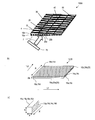
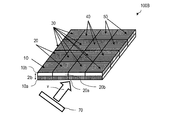
- FIG. (A) is a schematic perspective view of the reflective imaging element 100A in the embodiment according to the present invention
- (b) is a schematic perspective view of the reflective elements 10 and 20, and
- FIG. 5 is a schematic perspective view for explaining mirror surface elements 14a to 14d and light transmitting elements 15a to 15d.
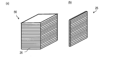
- (A) And (b) is a typical perspective view explaining the manufacturing method of the unit reflection type element 25.
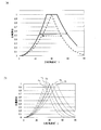
- FIG. (A) is a graph for explaining the relationship between the incident angle ⁇ and the light quantity ratio of each of the reflective imaging element 100A and the reflective elementary imaging element of the comparative example
- (b) is a graph illustrating each of the reflective elements 10 to 50. It is a graph explaining the relationship between incident angle (theta) and the light quantity ratio.
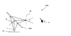
- FIG. 1 is a schematic side view of an optical system 1000.
- FIG. It is a typical perspective view of reflection type image formation element 100B in other embodiments by the present invention.
- (A) is a typical perspective view explaining the mirror surface elements 14a and 14b
- (b) is a typical perspective view explaining the mirror surface elements 14c and 14d.
- (A)-(c) is a typical perspective view explaining the manufacturing method of the unit imaging element 25 of the reflective imaging element 100C.
- FIG. 1A is a schematic perspective view of the reflective imaging element 100A.
- FIG. 1B is a perspective view illustrating the reflective elements 10 to 50.
- FIG. 1C is a schematic perspective view for explaining the specular elements 14a to 14d and the translucent elements 15a to 15d.
- V shown in FIG. 1A is light from a display panel (for example, a liquid crystal display panel) 70.
- a reflective imaging element 100A shown in FIG. 1A includes a light receiving surface 2 that receives light from the projection object 70, and an emission surface that is parallel to the light reception surface 2 and that emits light from the projection object 70. 4 and the reflective element 10 and the reflective element 20.
- the reflective element 10 forms an image of light from the projection object 70 at a plane-symmetrical position with the reflective element 10 as a symmetry plane.
- the reflective element 20 forms an image of light from the projection object 70 at a plane-symmetrical position with the reflective element 20 as a symmetry plane.
- the ratio of the light that contributes to image formation out of the light from the projection object 70 is the light quantity ratio, and the angle at which the light from the projection object 70 enters the light receiving surface when the light quantity ratio is the highest is the maximum incidence angle.
- the maximum incident angle of the reflective element 10 and the maximum incident angle of the reflective element 20 are different from each other.
- the difference between the maximum incident angle of the reflective element 10 and the maximum incident angle of the reflective element 20 is 40 ° or less.
- the light quantity ratio and the maximum incident angle will be described later.
- the reflective imaging element 100A having such a structure can be manufactured by a simple method, and an aerial image with a wide viewing angle can be obtained.
- the reflective element 10 includes a first unit reflective element 10a and a second unit reflective type disposed on the first unit reflective element 10a. Element 10b.
- the first unit reflection type element 10a includes a plurality of first mirror surface elements 14a and a plurality of first light transmission elements 15a, and each of the plurality of first light transmission elements 15a includes a plurality of first mirror surface elements 14a.
- the plurality of first mirror surface elements 14a and the plurality of first light-transmitting elements 15a extend in the first direction L1.
- the second unit reflection type element 10b includes a plurality of second mirror surface elements 14b and a plurality of second light transmission elements 15b, and each of the plurality of second light transmission elements 15b includes a plurality of second mirror surface elements 14b.
- the plurality of second mirror surface elements 14b and the plurality of second light transmitting elements 15b are arranged in a second direction L2 orthogonal to the first direction L1. It is extended.
- the reflective element 20 includes a third unit reflective element 20a and a fourth unit reflective element 20b disposed on the third unit reflective element 20a.
- the third unit reflection type element 20a includes a plurality of third mirror surface elements 14c and a plurality of third light transmission elements 15c, and each of the plurality of third light transmission elements 15c includes a plurality of third mirror surface elements 14c.
- the plurality of third mirror surface elements 14c and the plurality of third light-transmitting elements 15c are extended in the first direction L1.
- the fourth unit reflection type element 20b includes a plurality of fourth mirror surface elements 14d and a plurality of fourth light transmission elements 15d, and each of the plurality of fourth light transmission elements 15d includes a plurality of fourth mirror surface elements 14d.
- the plurality of fourth mirror surface elements 14d and the plurality of fourth light transmissive elements 15d extend in the second direction L2.
- the refractive index of each of at least one of the plurality of first light transmitting elements 15a and the plurality of second light transmitting elements 15b is at least that of the plurality of third light transmitting elements 15c and the plurality of fourth light transmitting elements 15d. It is preferable that the refractive index of any one of them is different. Further, the refractive indexes of the plurality of first light transmitting elements 15a and the plurality of second light transmitting elements 15b are different from the refractive indexes of the plurality of third light transmitting elements 15c and the plurality of fourth light transmitting elements 15d, respectively. It is more preferable.
- the reflective imaging element 100A is a combination of the reflective elements 10 to 50 including the first reflective element 10 and the second reflective element 20 (see FIG. "Tiling" is sometimes formed).
- the reflective elements 10 to 50 are different from each other only in the thickness of the reflective elements 10 to 50, respectively.
- the reflective imaging element 100 ⁇ / b> A includes one reflective element 10, two reflective elements 20, seven reflective elements 30, three reflective elements 40, and three reflective elements 50.
- the reflective elements 10 to 50 are arranged such that the thickness of the reflective elements 10 to 50 increases as they approach the display panel 70 side. It is preferable to configure the reflective imaging element 100A by tiling. This is because an aerial image with a wider viewing angle can be obtained.
- the thickness of the reflective elements 10 to 50 increases approximately from the right back corner to the left front corner in the figure.
- the thickness of the reflective element 10 is, for example, 1100 ⁇ m.
- the thickness of the reflective element 20 is, for example, 1000 ⁇ m.
- the thickness of the reflective element 30 is, for example, 900 ⁇ m.
- the thickness of the reflective element 40 is, for example, 800 ⁇ m.
- the thickness of the reflective element 50 is, for example, 700 ⁇ m. That is, the thickness decreases in the order of the reflective imaging element 10, the reflective imaging element 20, the reflective imaging element 30, the reflective imaging element 40, and the reflective imaging element 50.
- each of the plurality of translucent elements 15a to 15d has, for example, a rectangular parallelepiped shape, and is made of, for example, a glass material. Specular elements 14a to 14d are formed on one surface of each of the plurality of translucent elements 15a to 15d.
- the mirror surface elements 14a to 14d are made of, for example, aluminum (Al).
- Al aluminum
- the unit reflection type element 25 in each of the unit reflection type elements 10a, 10b, 20a and 20b (hereinafter referred to as the unit reflection type element 25), the mirror surface elements 14a to 14d and the light transmitting elements 15a to 15d are alternately arranged. Are arranged in stripes.
- Each of the translucent elements 15a to 15d has a width a, a thickness b, and a length X.
- the width a is, for example, 50 ⁇ m or more and 1500 ⁇ m or less.
- the aerial image becomes higher definition as the width a becomes smaller.
- the thickness b is, for example, 150 ⁇ m or more and 10000 ⁇ m or less. It is preferable to set the thickness b so as to influence the light quantity ratio described later and to obtain a high light quantity ratio.
- the width a and the thickness b satisfy the relationship b> a.
- the length X may be appropriately determined depending on the application to be used.
- the width a is 300 ⁇ m
- the refractive index n of all the light transmitting elements including the light transmitting elements 15a to 15d is 1.5, for example.
- the thickness b was set to be the thickness of each of the reflective elements 10 to 50 described above.
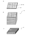
- FIG. 2A and 2B are schematic perspective views for explaining a method of manufacturing the unit reflection type element 25.
- FIG. 2A and 2B are schematic perspective views for explaining a method of manufacturing the unit reflection type element 25.
- a metal thin film for example, an aluminum thin film to be the above-described mirror elements 14a to 14d is formed by, for example, sputtering.
- the thickness of the metal thin film is, for example, 200 nm.
- a stacked structure as shown in FIG. 2A is formed by stacking a plurality of substrates 26 such that the metal thin film is sandwiched between the light-transmitting substrates 26. 56 is formed.
- the laminated structure 56 is cut using a wire saw or the like from a direction perpendicular to the surface of the translucent substrate 26 on which the metal thin film is formed.
- a unit reflection type element 25 is formed.
- the thickness b of the unit reflection type element 25 is determined by the cutting pitch at this time, and the unit reflection type element 25 having a desired thickness can be easily obtained.
- the reflective imaging element 100A can be obtained by combining the unit reflective elements 25 having different thicknesses. Therefore, unlike the reflective imaging element disclosed in Patent Document 3, it is not necessary to cut it into a wedge shape. Therefore, the reflective imaging element 100A can be manufactured by a simple method.
- FIG. 3A is a graph showing the relationship between the light amount ratio and the incident angle ⁇ in the optical system using each of the reflective imaging element and the reflective imaging element 100A of the comparative example.
- the broken line in the graph is a graph showing the relationship between the light amount ratio and the incident angle ⁇ in the optical system using the reflective imaging element of the comparative example.
- the reflective imaging element of the comparative example is a reflective imaging element having a uniform thickness over the entire surface.
- the solid line of the graph is a graph showing the relationship between the light quantity ratio and the incident angle ⁇ in the optical system when the number of reflective elements with different thicknesses forming the reflective imaging element 100A is further increased.
- the incident angle ⁇ is an angle at which light from a projection object (for example, a display panel) enters each reflective imaging element.
- the light quantity ratio is the ratio of light imaged in the air out of the light from the projection object. Therefore, the closer the light quantity ratio is to 1, the more efficiently the light from the non-projection is imaged, and the higher the visibility of the resulting aerial image. Moreover, if the light quantity ratio is 0.5 or more, the visibility of the obtained aerial image is good.
- the incident angle ⁇ at which the light quantity ratio is 0.5 or more is approximately 10 ° to 45 °.
- the incident angle ⁇ at which the light quantity ratio is 0.5 or more is 10 ° or more and 65 ° or less.
- the viewing angle of an aerial image obtained in an optical system using a reflective imaging element is determined by the incident angle ⁇ . Therefore, the wider the range of the incident angle ⁇ at which a highly visible aerial image is obtained, the larger the viewing angle of the aerial image. Therefore, when the reflective imaging element 100A is used, the viewing angle of the obtained aerial image increases.
- FIG. 3B is a graph for explaining the relationship between the incident angle ⁇ of each of the reflective elements 10 to 50 and the light quantity ratio.
- a line T1 is a graph showing the relationship between the incident angle ⁇ of the reflective element 10 and the light quantity ratio.
- a line T2 is a graph showing the relationship between the incident angle ⁇ of the reflective element 20 and the light quantity ratio.
- a line T3 is a graph showing the relationship between the incident angle ⁇ of the reflective element 30 and the light quantity ratio.
- a line T4 is a graph showing the relationship between the incident angle ⁇ of the reflective element 40 and the light amount ratio.
- a line T5 is a graph showing the relationship between the incident angle ⁇ of the reflective element 50 and the light amount ratio.
- the incident angles (maximum incident angles) when the light quantity ratios of the reflective elements 10 to 50 are maximum (when the light quantity ratio is 1) are different from each other.
- the maximum incident angle of the reflective element 10 is 33 °
- the maximum incident angle of the reflective element 20 is 36 °
- the maximum incident angle of the reflective element 30 is 40 °.
- the maximum incident angle of 40 is 45 °
- the maximum incident angle of the reflective element 50 is 51 °.
- the reflective imaging element 100A has the reflective elements 10 to 50 whose maximum incident angles are different from each other, thereby realizing a wide viewing angle of the aerial image.
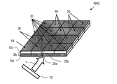
- FIG. 4 is a schematic side view of the optical system 1000.
- H in FIG. 4 is an observer, and ⁇ is the incident angle described in FIG.
- the optical system 1000 includes a reflective imaging element 100A and a display panel 70 disposed on the light incident side of the reflective imaging element 100A, and displays an image displayed on the display surface of the display panel 70 as a reflective type.
- This is an optical system that forms an image at a plane-symmetrical position with the imaging element 100A as a symmetry plane.
- the above-described reflective element 10 (not shown in FIG. 4) is located closer to the display panel 70 than the reflective element 20 (not shown in FIG. 4), and the thickness of the reflective element 10 is the reflective element. Greater than 20 thickness.
- the reflective elements 10 to 50 are arranged such that the closer to the display panel 70, the thicker the reflective elements 10 to 50 are.
- the relationship between the incident angle ⁇ when the light quantity ratio is the highest, the width a, the thickness b, and the refractive index n of each of the translucent elements 15a to 15d satisfies Expression (1).
- an aerial image 80 with a wide viewing angle can be obtained.
- FIG. 5 is a schematic perspective view of the reflective imaging element 100B. Constituent elements common to the reflective imaging element 100A are assigned the same reference numerals to avoid duplication of explanation.
- the reflective imaging element 100B also has reflective elements 10 to 50. However, unlike the reflective imaging element 100A, the thickness of each of the reflective elements 10 to 50 is the same, and at least one of the plurality of first light transmitting elements 15a and the plurality of second light transmitting elements 15b. Each of these refractive indexes is different from the refractive index of at least one of the plurality of third light transmitting elements 15c and the plurality of fourth light transmitting elements 15d.
- the refractive indexes of the plurality of first light transmitting elements 15a and the plurality of second light transmitting elements 15b are different from the refractive indexes of the plurality of third light transmitting elements 15c and the plurality of fourth light transmitting elements 15d. It is more preferable.
- each of the plurality of first light transmitting elements 15a and the plurality of second light transmitting elements 15b has a refractive index of 1.7, for example, and each of the plurality of third light transmitting elements 15c and the plurality of fourth light transmitting elements 15b.
- the refractive index of the translucent element 15d is 1.6, for example.
- the refractive index of all the light transmitting elements included in the reflective element 30 is, for example, 1.5
- the refractive index of all the light transmitting elements included in the reflective element 40 is, for example, 1.4.
- the refractive index of all the translucent elements included in the reflective element 50 is, for example, 1.3.
- the refractive index of all the translucent elements included in each of the reflective elements 10 to 50 in the order of the reflective element 10, the reflective element 20, the reflective element 30, the reflective element 40, and the reflective element 50 is small. It has become.
- the thicknesses of the reflective elements 10 to 50 may be different from each other as in the reflective imaging element 100A.
- the reflective element 10 of the reflective imaging element 100 ⁇ / b> B is preferably positioned closer to the display panel 70 than the reflective element 20.
- the reflective elements 10 to 50 are arranged so that the reflective element 10, the reflective element 20, the reflective element 30, the reflective element 40, and the reflective element 50 are positioned on the display panel 70 side in this order. That is, the reflective element 10 is located closest to the display panel 70, and the reflective element 50 is located farthest from the display panel 70.
- FIG. 6 is a schematic perspective view of the reflective imaging element 100C.
- 7A is a schematic perspective view for explaining the specular elements 14a and 14b included in the reflective element 10
- FIG. 7B illustrates the specular elements 14c and 14d included in the reflective element 20.
- FIG. It is a typical perspective view for explaining. Constituent elements common to the reflective imaging element 100A are assigned the same reference numerals to avoid duplication of explanation.
- the reflective imaging element 100C also has reflective elements 10-50. However, unlike the reflective imaging element 100A, the thickness of each of the reflective elements 10 to 50 is the same. Further, the length c of each of the plurality of first mirror surface elements 14a in the thickness direction of the first unit reflection type element 10a and each of the plurality of second mirror surface elements 14b in the thickness direction of the second unit reflection type element 20a. At least one of the lengths c is the length c of each of the plurality of third specular elements 14c in the thickness direction of the third unit reflective element 10b and the plurality of lengths in the thickness direction of the fourth unit reflective element 20b. It differs from at least one of the lengths c of each of the fourth mirror surface elements 14d.
- the length c of each of the plurality of first mirror surface elements 14a in the thickness direction of the first unit reflection type element 10a and each of the plurality of second mirror surface elements 14b in the thickness direction of the second unit reflection type element 20a is the length c of each of the plurality of third specular elements 14c in the thickness direction of the third unit reflective element 10b and the plurality of fourth specular elements 14d in the thickness direction of the fourth unit reflective element 20b. It is more preferable that the length is different from each length c.
- each of the plurality of first specular elements 14a in the thickness direction of the first unit reflective element 10a and the plurality of second in the thickness direction of the second unit reflective element 20a is, for example, 1100 ⁇ m.
- the length c of each of the plurality of third mirror surface elements 14c in the thickness direction of the third unit reflection type element 10b and the length of each of the plurality of fourth mirror surface elements 14d in the thickness direction of the fourth unit reflection type element 20b. c is, for example, 1000 ⁇ m.
- the length c of each of the plurality of specular elements in the thickness direction of the unit reflective element included in the reflective element 30 is, for example, 900 ⁇ m, and the unit reflective type included in the reflective element 40
- the length c of each of the plurality of specular elements in the thickness direction of the element is, for example, 800 ⁇ m
- the length c of each of the plurality of specular elements in the thickness direction of the unit reflection type element included in the reflective element 50 is, for example, 700 ⁇ m. It is.
- the thicknesses of the reflective elements 10 to 50 may be different from each other as in the reflective imaging element 100A, or each reflective type as in the reflective imaging element 100B.
- the refractive indexes of the light-transmitting elements included in the elements 10 to 50 may be varied, or these may be combined.
- the reflective element 10 of the reflective imaging element 100 ⁇ / b> B is preferably positioned closer to the display panel 70 than the reflective element 20.
- the reflective elements 10 to 50 are arranged so that the reflective element 10, the reflective element 20, the reflective element 30, the reflective element 40, and the reflective element 50 are positioned on the display panel 70 side in this order. That is, the reflective element 10 is located closest to the display panel 70, and the reflective element 50 is located farthest from the display panel 70.
- the relationship with c (see FIGS. 7A and 7B) satisfies the expression (2).
- FIG. 8A to 8C are schematic perspective views for explaining a method for manufacturing a unit reflection type element.
- Constituent elements common to the reflective imaging element 100A are assigned the same reference numerals to avoid duplication of explanation.
- a metal thin film for example, an aluminum thin film to be the above-described mirror surface elements 14a to 14d is formed on a light-transmitting substrate (for example, a glass substrate) 26 by, for example, sputtering. . Thereafter, the metal thin film is patterned, for example, in a rectangular shape using a photolithography method or the like. The shape of the patterned metal thin film is not limited to a rectangle, but may be a trapezoid or other shapes. Striped mirror elements 14a to 14d having a desired width are formed by patterning the metal thin film.
- the substrate 26 on which such stripe-shaped mirror surface elements 14a to 14d are formed is stacked on the substrate 26 so that the stripe-shaped mirror surface elements 14a to 14d are sandwiched between the translucent substrates 26.
- a laminated structure 56 as shown in FIG. 8B is formed.
- the laminated structure 56 is cut using a wire saw or the like to form the unit reflective element 25.
- the thickness b of the unit reflection type element 25 is determined by the cutting method at this time, and the unit reflection type element 25 having a desired thickness can be easily obtained.
- the reflective imaging element 100C is obtained by combining the unit reflective elements 25 having different lengths c of the mirror elements 14a to 14d. Therefore, unlike the reflective imaging element disclosed in Patent Document 3, it is not necessary to cut it into a wedge shape. Therefore, the reflective imaging element 100C can be manufactured by a simple method.
- the reflective optical element according to the embodiment of the present invention can be manufactured by a simple method, and an aerial image with a wide viewing angle can be obtained in an optical system using the same.
- the present invention can be widely applied to an optical system having a reflective imaging element capable of forming an image of a projection object in space and a display panel.
- Emitting surface Emitting surface 10, 20, 30, 40, 50 Reflective element 10a, 10b, 20a, 20b, 25 Unit reflective element 14a, 14b, 14c, 14d Mirror surface element 15a, 15b, 15c, 15d Translucent element 70 Projected object (display panel) 100A reflection type imaging element v light a, X width 2b thickness L1, L2 direction
Abstract
L'invention concerne un élément d'imagerie réfléchissant qui est fabriqué par un procédé simple et permet d'obtenir des images aériennes de haute qualité. Un élément d'imagerie réfléchissant (100A) selon la présente invention comporte un premier élément réfléchissant (10a) ayant une surface de réception de lumière (2) qui reçoit de la lumière provenant de l'objet (70) dont une image est formée et une surface d'émission (4) qui est parallèle à la surface de réception de lumière (2) et émet la lumière provenant de l'objet (70) dont une image est formée, et un second élément réfléchissant (10b). Si l'on prend comme rapport de quantité de lumière le pourcentage de la lumière contribuant à l'imagerie parmi la lumière provenant de l'objet (70) dont une image est formée, et comme angle d'incidence maximal l'angle d'incidence de la lumière provenant de l'objet, dont une image est formée, sur la surface de réception de lumière lorsque le rapport de quantité de lumière est le plus élevé, l'angle d'incidence maximal du premier élément réfléchissant (10a) et l'angle d'incidence maximal du second élément réfléchissant (10b) sont différents l'un de l'autre.
Priority Applications (1)
| Application Number | Priority Date | Filing Date | Title |
|---|---|---|---|
| US14/378,149 US9645403B2 (en) | 2012-02-14 | 2013-02-13 | Reflective imaging element and optical system |
Applications Claiming Priority (2)
| Application Number | Priority Date | Filing Date | Title |
|---|---|---|---|
| JP2012029208A JP5921243B2 (ja) | 2012-02-14 | 2012-02-14 | 反射型結像素子および光学システム |
| JP2012-029208 | 2012-02-14 |
Publications (1)
| Publication Number | Publication Date |
|---|---|
| WO2013122085A1 true WO2013122085A1 (fr) | 2013-08-22 |
Family
ID=48984195
Family Applications (1)
| Application Number | Title | Priority Date | Filing Date |
|---|---|---|---|
| PCT/JP2013/053358 WO2013122085A1 (fr) | 2012-02-14 | 2013-02-13 | Elément d'imagerie réfléchissant et système optique |
Country Status (3)
| Country | Link |
|---|---|
| US (1) | US9645403B2 (fr) |
| JP (1) | JP5921243B2 (fr) |
| WO (1) | WO2013122085A1 (fr) |
Cited By (1)
| Publication number | Priority date | Publication date | Assignee | Title |
|---|---|---|---|---|
| WO2017146017A1 (fr) * | 2016-02-26 | 2017-08-31 | コニカミノルタ株式会社 | Élément de formation d'image et son procédé de production |
Families Citing this family (5)
| Publication number | Priority date | Publication date | Assignee | Title |
|---|---|---|---|---|
| US9864178B2 (en) * | 2013-04-12 | 2018-01-09 | Sharp Kabushiki Kaisha | Reflection imaging device and method of producing reflection imaging device |
| TWI471610B (zh) * | 2013-07-02 | 2015-02-01 | Chunghwa Picture Tubes Ltd | 立體顯示裝置 |
| JP6773393B2 (ja) * | 2015-03-18 | 2020-10-21 | コニカミノルタ株式会社 | 光学素子の製造方法およびマイクロミラーアレイの製造方法 |
| SG11202111359PA (en) * | 2019-05-15 | 2021-11-29 | Anhui Easpeed Technology Co Ltd | Optical waveguide unit and array, and flat lens |
| JP7252361B2 (ja) | 2019-06-26 | 2023-04-04 | 安徽省東超科技有限公司 | 光導波路ユニット、アレイ及び平板レンズ |
Citations (2)
| Publication number | Priority date | Publication date | Assignee | Title |
|---|---|---|---|---|
| WO2009131128A1 (fr) * | 2008-04-22 | 2009-10-29 | Fujishima Tomohiko | Dispositif d’imagerie optique et procede d’imagerie optique mettant en œuvre ce dispositif |
| WO2009136578A1 (fr) * | 2008-05-09 | 2009-11-12 | パイオニア株式会社 | Appareil d'affichage d'image spatiale |
Family Cites Families (3)
| Publication number | Priority date | Publication date | Assignee | Title |
|---|---|---|---|---|
| JPH095503A (ja) * | 1995-06-23 | 1997-01-10 | Nittetsu Elex Co Ltd | 光学結像装置 |
| JP4734652B2 (ja) | 2006-12-21 | 2011-07-27 | 独立行政法人情報通信研究機構 | 光学システム |
| CN101641630B (zh) | 2007-03-05 | 2011-11-23 | 独立行政法人情报通信研究机构 | 多视点空中映像显示元件 |
-
2012
- 2012-02-14 JP JP2012029208A patent/JP5921243B2/ja active Active
-
2013
- 2013-02-13 WO PCT/JP2013/053358 patent/WO2013122085A1/fr active Application Filing
- 2013-02-13 US US14/378,149 patent/US9645403B2/en not_active Expired - Fee Related
Patent Citations (2)
| Publication number | Priority date | Publication date | Assignee | Title |
|---|---|---|---|---|
| WO2009131128A1 (fr) * | 2008-04-22 | 2009-10-29 | Fujishima Tomohiko | Dispositif d’imagerie optique et procede d’imagerie optique mettant en œuvre ce dispositif |
| WO2009136578A1 (fr) * | 2008-05-09 | 2009-11-12 | パイオニア株式会社 | Appareil d'affichage d'image spatiale |
Cited By (2)
| Publication number | Priority date | Publication date | Assignee | Title |
|---|---|---|---|---|
| WO2017146017A1 (fr) * | 2016-02-26 | 2017-08-31 | コニカミノルタ株式会社 | Élément de formation d'image et son procédé de production |
| JPWO2017146017A1 (ja) * | 2016-02-26 | 2018-08-02 | コニカミノルタ株式会社 | 結像素子およびその製造方法 |
Also Published As
| Publication number | Publication date |
|---|---|
| JP2013167667A (ja) | 2013-08-29 |
| JP5921243B2 (ja) | 2016-05-24 |
| US9645403B2 (en) | 2017-05-09 |
| US20150029585A1 (en) | 2015-01-29 |
Similar Documents
| Publication | Publication Date | Title |
|---|---|---|
| WO2013122085A1 (fr) | Elément d'imagerie réfléchissant et système optique | |
| US8941800B2 (en) | Reflective image forming element and optical system | |
| JP5462443B2 (ja) | 反射スクリーン、表示装置及び移動体 | |
| US10067369B2 (en) | Display apparatus with a prism module including a corner prism set disposed on a corner region | |
| JP6452815B2 (ja) | 画像表示装置 | |
| WO2012133403A1 (fr) | Élément d'imagerie réfléchissant, procédé de fabrication d'un élément d'imagerie réfléchissant, et système optique | |
| JP6405462B2 (ja) | 画像表示装置 | |
| CN107238926B (zh) | 光学元件、显示装置、以及光学元件的制造方法 | |
| JP2011175297A (ja) | 光学結像装置に使用する光制御パネルの製造方法 | |
| JP2018081138A (ja) | 画像表示装置 | |
| JP2005031502A (ja) | スクリーン | |
| US10466482B2 (en) | Optical element and display device | |
| WO2011136214A1 (fr) | Système optique | |
| US20140211308A1 (en) | Glasses-free reflective 3d color display | |
| JP2008003172A (ja) | 反射型立体表示スクリーン、反射型立体表示システム | |
| JP6953728B2 (ja) | スクリーン、映像表示装置 | |
| JP4498987B2 (ja) | 照明装置及び表示装置 | |
| JP6593201B2 (ja) | スクリーン、映像表示装置 | |
| JP2002107833A (ja) | スクリーンとそれを用いた立体表示システム | |
| JP2015166845A (ja) | 光学結像素子及びその製造方法 | |
| JP2013167670A (ja) | 反射型結像素子、反射型結像素子の製造方法、および光学システム | |
| WO2013183454A1 (fr) | Dispositif formant image optique et procédé formant image optique | |
| JP2014139596A (ja) | 指向性反射スクリーン、画層表示装置 | |
| JP5318242B2 (ja) | 反射型面対称結像素子の製造方法 | |
| US20230093069A1 (en) | Display device and method for manufacturing optical film |
Legal Events
| Date | Code | Title | Description |
|---|---|---|---|
| 121 | Ep: the epo has been informed by wipo that ep was designated in this application |
Ref document number: 13748881 Country of ref document: EP Kind code of ref document: A1 |
|
| WWE | Wipo information: entry into national phase |
Ref document number: 14378149 Country of ref document: US |
|
| NENP | Non-entry into the national phase |
Ref country code: DE |
|
| 122 | Ep: pct application non-entry in european phase |
Ref document number: 13748881 Country of ref document: EP Kind code of ref document: A1 |