JP6414090B2 - 半導体装置 - Google Patents
半導体装置 Download PDFInfo
- Publication number
- JP6414090B2 JP6414090B2 JP2016013713A JP2016013713A JP6414090B2 JP 6414090 B2 JP6414090 B2 JP 6414090B2 JP 2016013713 A JP2016013713 A JP 2016013713A JP 2016013713 A JP2016013713 A JP 2016013713A JP 6414090 B2 JP6414090 B2 JP 6414090B2
- Authority
- JP
- Japan
- Prior art keywords
- electrode
- gate
- region
- gate electrode
- voltage
- Prior art date
- Legal status (The legal status is an assumption and is not a legal conclusion. Google has not performed a legal analysis and makes no representation as to the accuracy of the status listed.)
- Active
Links
- 239000004065 semiconductor Substances 0.000 title claims description 34
- 230000004888 barrier function Effects 0.000 claims description 43
- 239000012535 impurity Substances 0.000 claims description 39
- 239000000758 substrate Substances 0.000 claims description 14
- 239000010410 layer Substances 0.000 description 15
- 210000000746 body region Anatomy 0.000 description 13
- 238000011084 recovery Methods 0.000 description 12
- 238000009792 diffusion process Methods 0.000 description 10
- 230000000694 effects Effects 0.000 description 7
- 238000001514 detection method Methods 0.000 description 4
- 238000002347 injection Methods 0.000 description 4
- 239000007924 injection Substances 0.000 description 4
- 239000002344 surface layer Substances 0.000 description 3
- 230000003071 parasitic effect Effects 0.000 description 2
- 238000005036 potential barrier Methods 0.000 description 2
- 230000001360 synchronised effect Effects 0.000 description 2
- 229910052782 aluminium Inorganic materials 0.000 description 1
- XAGFODPZIPBFFR-UHFFFAOYSA-N aluminium Chemical compound [Al] XAGFODPZIPBFFR-UHFFFAOYSA-N 0.000 description 1
- 238000010586 diagram Methods 0.000 description 1
- 230000012447 hatching Effects 0.000 description 1
- 229910052751 metal Inorganic materials 0.000 description 1
- 239000002184 metal Substances 0.000 description 1
- 230000004048 modification Effects 0.000 description 1
- 238000012986 modification Methods 0.000 description 1
- 238000010992 reflux Methods 0.000 description 1
Images


Classifications
-
- H—ELECTRICITY
- H01—ELECTRIC ELEMENTS
- H01L—SEMICONDUCTOR DEVICES NOT COVERED BY CLASS H10
- H01L21/00—Processes or apparatus adapted for the manufacture or treatment of semiconductor or solid state devices or of parts thereof
- H01L21/70—Manufacture or treatment of devices consisting of a plurality of solid state components formed in or on a common substrate or of parts thereof; Manufacture of integrated circuit devices or of parts thereof
- H01L21/77—Manufacture or treatment of devices consisting of a plurality of solid state components or integrated circuits formed in, or on, a common substrate
- H01L21/78—Manufacture or treatment of devices consisting of a plurality of solid state components or integrated circuits formed in, or on, a common substrate with subsequent division of the substrate into plural individual devices
- H01L21/82—Manufacture or treatment of devices consisting of a plurality of solid state components or integrated circuits formed in, or on, a common substrate with subsequent division of the substrate into plural individual devices to produce devices, e.g. integrated circuits, each consisting of a plurality of components
- H01L21/822—Manufacture or treatment of devices consisting of a plurality of solid state components or integrated circuits formed in, or on, a common substrate with subsequent division of the substrate into plural individual devices to produce devices, e.g. integrated circuits, each consisting of a plurality of components the substrate being a semiconductor, using silicon technology
- H01L21/8232—Field-effect technology
- H01L21/8234—MIS technology, i.e. integration processes of field effect transistors of the conductor-insulator-semiconductor type
- H01L21/823418—MIS technology, i.e. integration processes of field effect transistors of the conductor-insulator-semiconductor type with a particular manufacturing method of the source or drain structures, e.g. specific source or drain implants or silicided source or drain structures or raised source or drain structures
-
- H—ELECTRICITY
- H01—ELECTRIC ELEMENTS
- H01L—SEMICONDUCTOR DEVICES NOT COVERED BY CLASS H10
- H01L27/00—Devices consisting of a plurality of semiconductor or other solid-state components formed in or on a common substrate
- H01L27/02—Devices consisting of a plurality of semiconductor or other solid-state components formed in or on a common substrate including semiconductor components specially adapted for rectifying, oscillating, amplifying or switching and having potential barriers; including integrated passive circuit elements having potential barriers
- H01L27/04—Devices consisting of a plurality of semiconductor or other solid-state components formed in or on a common substrate including semiconductor components specially adapted for rectifying, oscillating, amplifying or switching and having potential barriers; including integrated passive circuit elements having potential barriers the substrate being a semiconductor body
- H01L27/06—Devices consisting of a plurality of semiconductor or other solid-state components formed in or on a common substrate including semiconductor components specially adapted for rectifying, oscillating, amplifying or switching and having potential barriers; including integrated passive circuit elements having potential barriers the substrate being a semiconductor body including a plurality of individual components in a non-repetitive configuration
- H01L27/07—Devices consisting of a plurality of semiconductor or other solid-state components formed in or on a common substrate including semiconductor components specially adapted for rectifying, oscillating, amplifying or switching and having potential barriers; including integrated passive circuit elements having potential barriers the substrate being a semiconductor body including a plurality of individual components in a non-repetitive configuration the components having an active region in common
- H01L27/0705—Devices consisting of a plurality of semiconductor or other solid-state components formed in or on a common substrate including semiconductor components specially adapted for rectifying, oscillating, amplifying or switching and having potential barriers; including integrated passive circuit elements having potential barriers the substrate being a semiconductor body including a plurality of individual components in a non-repetitive configuration the components having an active region in common comprising components of the field effect type
- H01L27/0727—Devices consisting of a plurality of semiconductor or other solid-state components formed in or on a common substrate including semiconductor components specially adapted for rectifying, oscillating, amplifying or switching and having potential barriers; including integrated passive circuit elements having potential barriers the substrate being a semiconductor body including a plurality of individual components in a non-repetitive configuration the components having an active region in common comprising components of the field effect type in combination with diodes, or capacitors or resistors
-
- H—ELECTRICITY
- H01—ELECTRIC ELEMENTS
- H01L—SEMICONDUCTOR DEVICES NOT COVERED BY CLASS H10
- H01L27/00—Devices consisting of a plurality of semiconductor or other solid-state components formed in or on a common substrate
- H01L27/02—Devices consisting of a plurality of semiconductor or other solid-state components formed in or on a common substrate including semiconductor components specially adapted for rectifying, oscillating, amplifying or switching and having potential barriers; including integrated passive circuit elements having potential barriers
- H01L27/04—Devices consisting of a plurality of semiconductor or other solid-state components formed in or on a common substrate including semiconductor components specially adapted for rectifying, oscillating, amplifying or switching and having potential barriers; including integrated passive circuit elements having potential barriers the substrate being a semiconductor body
- H01L27/08—Devices consisting of a plurality of semiconductor or other solid-state components formed in or on a common substrate including semiconductor components specially adapted for rectifying, oscillating, amplifying or switching and having potential barriers; including integrated passive circuit elements having potential barriers the substrate being a semiconductor body including only semiconductor components of a single kind
- H01L27/085—Devices consisting of a plurality of semiconductor or other solid-state components formed in or on a common substrate including semiconductor components specially adapted for rectifying, oscillating, amplifying or switching and having potential barriers; including integrated passive circuit elements having potential barriers the substrate being a semiconductor body including only semiconductor components of a single kind including field-effect components only
- H01L27/088—Devices consisting of a plurality of semiconductor or other solid-state components formed in or on a common substrate including semiconductor components specially adapted for rectifying, oscillating, amplifying or switching and having potential barriers; including integrated passive circuit elements having potential barriers the substrate being a semiconductor body including only semiconductor components of a single kind including field-effect components only the components being field-effect transistors with insulated gate
-
- H—ELECTRICITY
- H01—ELECTRIC ELEMENTS
- H01L—SEMICONDUCTOR DEVICES NOT COVERED BY CLASS H10
- H01L29/00—Semiconductor devices specially adapted for rectifying, amplifying, oscillating or switching and having potential barriers; Capacitors or resistors having potential barriers, e.g. a PN-junction depletion layer or carrier concentration layer; Details of semiconductor bodies or of electrodes thereof ; Multistep manufacturing processes therefor
- H01L29/02—Semiconductor bodies ; Multistep manufacturing processes therefor
- H01L29/06—Semiconductor bodies ; Multistep manufacturing processes therefor characterised by their shape; characterised by the shapes, relative sizes, or dispositions of the semiconductor regions ; characterised by the concentration or distribution of impurities within semiconductor regions
- H01L29/0603—Semiconductor bodies ; Multistep manufacturing processes therefor characterised by their shape; characterised by the shapes, relative sizes, or dispositions of the semiconductor regions ; characterised by the concentration or distribution of impurities within semiconductor regions characterised by particular constructional design considerations, e.g. for preventing surface leakage, for controlling electric field concentration or for internal isolations regions
- H01L29/0607—Semiconductor bodies ; Multistep manufacturing processes therefor characterised by their shape; characterised by the shapes, relative sizes, or dispositions of the semiconductor regions ; characterised by the concentration or distribution of impurities within semiconductor regions characterised by particular constructional design considerations, e.g. for preventing surface leakage, for controlling electric field concentration or for internal isolations regions for preventing surface leakage or controlling electric field concentration
- H01L29/0611—Semiconductor bodies ; Multistep manufacturing processes therefor characterised by their shape; characterised by the shapes, relative sizes, or dispositions of the semiconductor regions ; characterised by the concentration or distribution of impurities within semiconductor regions characterised by particular constructional design considerations, e.g. for preventing surface leakage, for controlling electric field concentration or for internal isolations regions for preventing surface leakage or controlling electric field concentration for increasing or controlling the breakdown voltage of reverse biased devices
- H01L29/0615—Semiconductor bodies ; Multistep manufacturing processes therefor characterised by their shape; characterised by the shapes, relative sizes, or dispositions of the semiconductor regions ; characterised by the concentration or distribution of impurities within semiconductor regions characterised by particular constructional design considerations, e.g. for preventing surface leakage, for controlling electric field concentration or for internal isolations regions for preventing surface leakage or controlling electric field concentration for increasing or controlling the breakdown voltage of reverse biased devices by the doping profile or the shape or the arrangement of the PN junction, or with supplementary regions, e.g. junction termination extension [JTE]
- H01L29/0619—Semiconductor bodies ; Multistep manufacturing processes therefor characterised by their shape; characterised by the shapes, relative sizes, or dispositions of the semiconductor regions ; characterised by the concentration or distribution of impurities within semiconductor regions characterised by particular constructional design considerations, e.g. for preventing surface leakage, for controlling electric field concentration or for internal isolations regions for preventing surface leakage or controlling electric field concentration for increasing or controlling the breakdown voltage of reverse biased devices by the doping profile or the shape or the arrangement of the PN junction, or with supplementary regions, e.g. junction termination extension [JTE] with a supplementary region doped oppositely to or in rectifying contact with the semiconductor containing or contacting region, e.g. guard rings with PN or Schottky junction
- H01L29/0623—Buried supplementary region, e.g. buried guard ring
-
- H—ELECTRICITY
- H01—ELECTRIC ELEMENTS
- H01L—SEMICONDUCTOR DEVICES NOT COVERED BY CLASS H10
- H01L29/00—Semiconductor devices specially adapted for rectifying, amplifying, oscillating or switching and having potential barriers; Capacitors or resistors having potential barriers, e.g. a PN-junction depletion layer or carrier concentration layer; Details of semiconductor bodies or of electrodes thereof ; Multistep manufacturing processes therefor
- H01L29/02—Semiconductor bodies ; Multistep manufacturing processes therefor
- H01L29/06—Semiconductor bodies ; Multistep manufacturing processes therefor characterised by their shape; characterised by the shapes, relative sizes, or dispositions of the semiconductor regions ; characterised by the concentration or distribution of impurities within semiconductor regions
- H01L29/08—Semiconductor bodies ; Multistep manufacturing processes therefor characterised by their shape; characterised by the shapes, relative sizes, or dispositions of the semiconductor regions ; characterised by the concentration or distribution of impurities within semiconductor regions with semiconductor regions connected to an electrode carrying current to be rectified, amplified or switched and such electrode being part of a semiconductor device which comprises three or more electrodes
- H01L29/083—Anode or cathode regions of thyristors or gated bipolar-mode devices
- H01L29/0834—Anode regions of thyristors or gated bipolar-mode devices, e.g. supplementary regions surrounding anode regions
-
- H—ELECTRICITY
- H01—ELECTRIC ELEMENTS
- H01L—SEMICONDUCTOR DEVICES NOT COVERED BY CLASS H10
- H01L29/00—Semiconductor devices specially adapted for rectifying, amplifying, oscillating or switching and having potential barriers; Capacitors or resistors having potential barriers, e.g. a PN-junction depletion layer or carrier concentration layer; Details of semiconductor bodies or of electrodes thereof ; Multistep manufacturing processes therefor
- H01L29/02—Semiconductor bodies ; Multistep manufacturing processes therefor
- H01L29/06—Semiconductor bodies ; Multistep manufacturing processes therefor characterised by their shape; characterised by the shapes, relative sizes, or dispositions of the semiconductor regions ; characterised by the concentration or distribution of impurities within semiconductor regions
- H01L29/10—Semiconductor bodies ; Multistep manufacturing processes therefor characterised by their shape; characterised by the shapes, relative sizes, or dispositions of the semiconductor regions ; characterised by the concentration or distribution of impurities within semiconductor regions with semiconductor regions connected to an electrode not carrying current to be rectified, amplified or switched and such electrode being part of a semiconductor device which comprises three or more electrodes
- H01L29/1095—Body region, i.e. base region, of DMOS transistors or IGBTs
-
- H—ELECTRICITY
- H01—ELECTRIC ELEMENTS
- H01L—SEMICONDUCTOR DEVICES NOT COVERED BY CLASS H10
- H01L29/00—Semiconductor devices specially adapted for rectifying, amplifying, oscillating or switching and having potential barriers; Capacitors or resistors having potential barriers, e.g. a PN-junction depletion layer or carrier concentration layer; Details of semiconductor bodies or of electrodes thereof ; Multistep manufacturing processes therefor
- H01L29/40—Electrodes ; Multistep manufacturing processes therefor
- H01L29/402—Field plates
- H01L29/407—Recessed field plates, e.g. trench field plates, buried field plates
-
- H—ELECTRICITY
- H01—ELECTRIC ELEMENTS
- H01L—SEMICONDUCTOR DEVICES NOT COVERED BY CLASS H10
- H01L29/00—Semiconductor devices specially adapted for rectifying, amplifying, oscillating or switching and having potential barriers; Capacitors or resistors having potential barriers, e.g. a PN-junction depletion layer or carrier concentration layer; Details of semiconductor bodies or of electrodes thereof ; Multistep manufacturing processes therefor
- H01L29/40—Electrodes ; Multistep manufacturing processes therefor
- H01L29/41—Electrodes ; Multistep manufacturing processes therefor characterised by their shape, relative sizes or dispositions
- H01L29/423—Electrodes ; Multistep manufacturing processes therefor characterised by their shape, relative sizes or dispositions not carrying the current to be rectified, amplified or switched
- H01L29/42312—Gate electrodes for field effect devices
- H01L29/42316—Gate electrodes for field effect devices for field-effect transistors
- H01L29/4232—Gate electrodes for field effect devices for field-effect transistors with insulated gate
- H01L29/42372—Gate electrodes for field effect devices for field-effect transistors with insulated gate characterised by the conducting layer, e.g. the length, the sectional shape or the lay-out
- H01L29/4238—Gate electrodes for field effect devices for field-effect transistors with insulated gate characterised by the conducting layer, e.g. the length, the sectional shape or the lay-out characterised by the surface lay-out
-
- H—ELECTRICITY
- H01—ELECTRIC ELEMENTS
- H01L—SEMICONDUCTOR DEVICES NOT COVERED BY CLASS H10
- H01L29/00—Semiconductor devices specially adapted for rectifying, amplifying, oscillating or switching and having potential barriers; Capacitors or resistors having potential barriers, e.g. a PN-junction depletion layer or carrier concentration layer; Details of semiconductor bodies or of electrodes thereof ; Multistep manufacturing processes therefor
- H01L29/66—Types of semiconductor device ; Multistep manufacturing processes therefor
- H01L29/68—Types of semiconductor device ; Multistep manufacturing processes therefor controllable by only the electric current supplied, or only the electric potential applied, to an electrode which does not carry the current to be rectified, amplified or switched
- H01L29/70—Bipolar devices
- H01L29/72—Transistor-type devices, i.e. able to continuously respond to applied control signals
- H01L29/739—Transistor-type devices, i.e. able to continuously respond to applied control signals controlled by field-effect, e.g. bipolar static induction transistors [BSIT]
- H01L29/7393—Insulated gate bipolar mode transistors, i.e. IGBT; IGT; COMFET
- H01L29/7395—Vertical transistors, e.g. vertical IGBT
- H01L29/7396—Vertical transistors, e.g. vertical IGBT with a non planar surface, e.g. with a non planar gate or with a trench or recess or pillar in the surface of the emitter, base or collector region for improving current density or short circuiting the emitter and base regions
- H01L29/7397—Vertical transistors, e.g. vertical IGBT with a non planar surface, e.g. with a non planar gate or with a trench or recess or pillar in the surface of the emitter, base or collector region for improving current density or short circuiting the emitter and base regions and a gate structure lying on a slanted or vertical surface or formed in a groove, e.g. trench gate IGBT
-
- H—ELECTRICITY
- H01—ELECTRIC ELEMENTS
- H01L—SEMICONDUCTOR DEVICES NOT COVERED BY CLASS H10
- H01L29/00—Semiconductor devices specially adapted for rectifying, amplifying, oscillating or switching and having potential barriers; Capacitors or resistors having potential barriers, e.g. a PN-junction depletion layer or carrier concentration layer; Details of semiconductor bodies or of electrodes thereof ; Multistep manufacturing processes therefor
- H01L29/66—Types of semiconductor device ; Multistep manufacturing processes therefor
- H01L29/68—Types of semiconductor device ; Multistep manufacturing processes therefor controllable by only the electric current supplied, or only the electric potential applied, to an electrode which does not carry the current to be rectified, amplified or switched
- H01L29/76—Unipolar devices, e.g. field effect transistors
- H01L29/772—Field effect transistors
- H01L29/78—Field effect transistors with field effect produced by an insulated gate
- H01L29/7801—DMOS transistors, i.e. MISFETs with a channel accommodating body or base region adjoining a drain drift region
- H01L29/7802—Vertical DMOS transistors, i.e. VDMOS transistors
- H01L29/7803—Vertical DMOS transistors, i.e. VDMOS transistors structurally associated with at least one other device
- H01L29/7804—Vertical DMOS transistors, i.e. VDMOS transistors structurally associated with at least one other device the other device being a pn-junction diode
- H01L29/7805—Vertical DMOS transistors, i.e. VDMOS transistors structurally associated with at least one other device the other device being a pn-junction diode in antiparallel, e.g. freewheel diode
-
- H—ELECTRICITY
- H01—ELECTRIC ELEMENTS
- H01L—SEMICONDUCTOR DEVICES NOT COVERED BY CLASS H10
- H01L29/00—Semiconductor devices specially adapted for rectifying, amplifying, oscillating or switching and having potential barriers; Capacitors or resistors having potential barriers, e.g. a PN-junction depletion layer or carrier concentration layer; Details of semiconductor bodies or of electrodes thereof ; Multistep manufacturing processes therefor
- H01L29/66—Types of semiconductor device ; Multistep manufacturing processes therefor
- H01L29/86—Types of semiconductor device ; Multistep manufacturing processes therefor controllable only by variation of the electric current supplied, or only the electric potential applied, to one or more of the electrodes carrying the current to be rectified, amplified, oscillated or switched
- H01L29/861—Diodes
- H01L29/868—PIN diodes
-
- H—ELECTRICITY
- H01—ELECTRIC ELEMENTS
- H01L—SEMICONDUCTOR DEVICES NOT COVERED BY CLASS H10
- H01L29/00—Semiconductor devices specially adapted for rectifying, amplifying, oscillating or switching and having potential barriers; Capacitors or resistors having potential barriers, e.g. a PN-junction depletion layer or carrier concentration layer; Details of semiconductor bodies or of electrodes thereof ; Multistep manufacturing processes therefor
- H01L29/66—Types of semiconductor device ; Multistep manufacturing processes therefor
- H01L29/86—Types of semiconductor device ; Multistep manufacturing processes therefor controllable only by variation of the electric current supplied, or only the electric potential applied, to one or more of the electrodes carrying the current to be rectified, amplified, oscillated or switched
- H01L29/861—Diodes
- H01L29/87—Thyristor diodes, e.g. Shockley diodes, break-over diodes
-
- H—ELECTRICITY
- H02—GENERATION; CONVERSION OR DISTRIBUTION OF ELECTRIC POWER
- H02M—APPARATUS FOR CONVERSION BETWEEN AC AND AC, BETWEEN AC AND DC, OR BETWEEN DC AND DC, AND FOR USE WITH MAINS OR SIMILAR POWER SUPPLY SYSTEMS; CONVERSION OF DC OR AC INPUT POWER INTO SURGE OUTPUT POWER; CONTROL OR REGULATION THEREOF
- H02M1/00—Details of apparatus for conversion
- H02M1/08—Circuits specially adapted for the generation of control voltages for semiconductor devices incorporated in static converters
-
- H—ELECTRICITY
- H02—GENERATION; CONVERSION OR DISTRIBUTION OF ELECTRIC POWER
- H02M—APPARATUS FOR CONVERSION BETWEEN AC AND AC, BETWEEN AC AND DC, OR BETWEEN DC AND DC, AND FOR USE WITH MAINS OR SIMILAR POWER SUPPLY SYSTEMS; CONVERSION OF DC OR AC INPUT POWER INTO SURGE OUTPUT POWER; CONTROL OR REGULATION THEREOF
- H02M7/00—Conversion of ac power input into dc power output; Conversion of dc power input into ac power output
- H02M7/003—Constructional details, e.g. physical layout, assembly, wiring or busbar connections
-
- H—ELECTRICITY
- H01—ELECTRIC ELEMENTS
- H01L—SEMICONDUCTOR DEVICES NOT COVERED BY CLASS H10
- H01L29/00—Semiconductor devices specially adapted for rectifying, amplifying, oscillating or switching and having potential barriers; Capacitors or resistors having potential barriers, e.g. a PN-junction depletion layer or carrier concentration layer; Details of semiconductor bodies or of electrodes thereof ; Multistep manufacturing processes therefor
- H01L29/02—Semiconductor bodies ; Multistep manufacturing processes therefor
- H01L29/06—Semiconductor bodies ; Multistep manufacturing processes therefor characterised by their shape; characterised by the shapes, relative sizes, or dispositions of the semiconductor regions ; characterised by the concentration or distribution of impurities within semiconductor regions
- H01L29/0684—Semiconductor bodies ; Multistep manufacturing processes therefor characterised by their shape; characterised by the shapes, relative sizes, or dispositions of the semiconductor regions ; characterised by the concentration or distribution of impurities within semiconductor regions characterised by the shape, relative sizes or dispositions of the semiconductor regions or junctions between the regions
- H01L29/0692—Surface layout
- H01L29/0696—Surface layout of cellular field-effect devices, e.g. multicellular DMOS transistors or IGBTs
-
- H—ELECTRICITY
- H02—GENERATION; CONVERSION OR DISTRIBUTION OF ELECTRIC POWER
- H02M—APPARATUS FOR CONVERSION BETWEEN AC AND AC, BETWEEN AC AND DC, OR BETWEEN DC AND DC, AND FOR USE WITH MAINS OR SIMILAR POWER SUPPLY SYSTEMS; CONVERSION OF DC OR AC INPUT POWER INTO SURGE OUTPUT POWER; CONTROL OR REGULATION THEREOF
- H02M7/00—Conversion of ac power input into dc power output; Conversion of dc power input into ac power output
- H02M7/42—Conversion of dc power input into ac power output without possibility of reversal
- H02M7/44—Conversion of dc power input into ac power output without possibility of reversal by static converters
- H02M7/48—Conversion of dc power input into ac power output without possibility of reversal by static converters using discharge tubes with control electrode or semiconductor devices with control electrode
- H02M7/53—Conversion of dc power input into ac power output without possibility of reversal by static converters using discharge tubes with control electrode or semiconductor devices with control electrode using devices of a triode or transistor type requiring continuous application of a control signal
- H02M7/537—Conversion of dc power input into ac power output without possibility of reversal by static converters using discharge tubes with control electrode or semiconductor devices with control electrode using devices of a triode or transistor type requiring continuous application of a control signal using semiconductor devices only, e.g. single switched pulse inverters
- H02M7/538—Conversion of dc power input into ac power output without possibility of reversal by static converters using discharge tubes with control electrode or semiconductor devices with control electrode using devices of a triode or transistor type requiring continuous application of a control signal using semiconductor devices only, e.g. single switched pulse inverters in a push-pull configuration
Landscapes
- Engineering & Computer Science (AREA)
- Power Engineering (AREA)
- Microelectronics & Electronic Packaging (AREA)
- Physics & Mathematics (AREA)
- Condensed Matter Physics & Semiconductors (AREA)
- General Physics & Mathematics (AREA)
- Computer Hardware Design (AREA)
- Ceramic Engineering (AREA)
- Manufacturing & Machinery (AREA)
- Power Conversion In General (AREA)
- Metal-Oxide And Bipolar Metal-Oxide Semiconductor Integrated Circuits (AREA)
Description
ダイオード素子は、第1導電型の第1不純物領域(72a,73a,75a)と、第1不純物領域に接合して形成された第2導電型の第2不純物領域(76a,91)と、第1不純物領域と電気的に接続される第1電極(71,95)と、第2不純物領域と電気的に接続される第2電極(78,94)と、を有し、ゲート電極に所定のゲート電圧が印加されることにより、第1不純物領域に反転層が生じるものであり、
スイッチング素子は、ダイオード素子と共通した第1電極および第2電極を有するとともに、ゲート電極に所定のゲート電圧が印加されることによりオンの状態とされて第1電極と第2電極との間に電流が流れるものであり、
複数のゲート電極は、スイッチング素子をオンの状態とする第1ゲート電圧が入力される第1ゲート電極(82a)と、第1ゲート電圧とは独立して制御され、第2電極の電位と同一、もしくは、第2電極の電位を基準として第1ゲート電圧の極性と反対の極性となる第2ゲート電圧が入力される第2ゲート電極(82b)と、を有し、
ダイオード素子に属するゲート電極は、少なくとも第2ゲート電極を含み、スイッチング素子に属するゲート電極は、少なくとも第1ゲート電極を含み、第1電極と第2電極との間を流れる電流に基づいて、モード判定部により、逆導通モードと判定された際、もしくは、逆導通モードか順導通モードかを判定できない際、第2ゲート電極に、第2ゲート電圧が印加されることを特徴としている。
最初に、図1を参照して、本実施形態に係る半導体装置の概略構成について説明する。
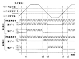
図5に示すように、この例では、第2ゲート電極82bに印加されるゲート電圧も、第1ゲート電極82aと同様にPWM基準信号に同期して印加される。PWM基準信号のHigh/Lowは、上アームを構成する第1素子10に対応するものと、下アームを構成する第2素子20に対応するものとで互いに反転した関係になっている。PWM基準信号がHighの期間において、図4に示すゲート電圧が有効となり、PWM基準信号がLowの期間はエミッタ電圧Veがゲート電圧として各ゲート電極82に入力される。
図6に示すように、この例では、状態B〜Dにおいて第2ゲート電極82bに印加されるゲート電圧が−V2であるとき、PWM基準信号に依らず常に電圧−V2が印加される。この例でも、ダイオード素子12にエミッタ電圧Veに対して負の電圧−V2を印加するので順電圧VFを低減することができる。また、IGBT素子11においてボディ領域76bへホールが流入しやすい状況をつくることができ、ターンオフに係るスイッチング速度を速くすることができる。ただし、上述したPWM基準信号に同期する動作に比べて、V2の大きさを小さく設定することが好ましい。これは、V2の大きさを過剰に設定すると逆導通によるダイオード電流が大きい状態では、ダイオード素子12におけるリカバリ損失が大きくなるためである。この例のように、PWM基準信号に依らず常に電圧−V2が印加されるような態様は、順電圧VFによる損失の低減効果が高いが、リカバリ損失も増大する虞があるため、システム全体の駆動損失に占める順電圧VFによる損失の割合が大きいシステムにおいて有効である。
PWM基準信号に依らず常に電圧−V2が印加される態様では、上記したように、ダイオード電流が大きい場合にリカバリ損失が増大してしまう虞がある。これを解決するため、この例では、図7に示すように、ダイオード電流、ひいては負荷電流Iに閾値を設ける。負荷電流Iの大きさが閾値より小さい場合には第2ゲート電極82bに電圧−V2が印加され、負荷電流Iの大きさが閾値以上の場合は、第2ゲート電極82bに電圧Veが印加される。これにより、ダイオード電流が大きい場合のリカバリ損失を低減することができる。
第1実施形態において説明した第1素子10、第2素子20たる逆導通絶縁ゲートバイポーラトランジスタに加えて、図8に示すように、n導電型のピラー領域79を有していることが好ましい。ピラー領域79は、半導体基板70の第2主面70bから厚さ方向に延び、アノード領域76aあるいはボディ領域76bを貫通して第1バリア領域75a、第2バリア領域75bに至るように形成されている。ピラー領域79は、第1、第2バリア領域75a,75bと同一の導電型の不純物がドープされた拡散層であり、ピラー領域79とバリア領域75a,75bとは略同電位である。
第1実施形態において図3を参照して平面レイアウトについて説明した間引き構造について、本実施形態において具体的に説明する。本実施形態では、第2実施形態において説明したように、ピラー領域79を備える態様であって、図9に示すように、ダイオード素子12において、互いに隣り合うゲート電極82をアノード電極78と短絡させないようになっている。換言すれば、アノード電極78と短絡したゲート電極82に隣接するゲート電極82は、第2ゲート電極82bに割り当てられている。これによれば、ダイオード素子12に形成された第1バリア領域75aは、少なくとも一つの第2ゲート電極82bに、絶縁膜81を介して接しているので、ダイオード素子12は、第2ゲート電極82bに負電圧−V2が印加されることによる順電圧VFの低減効果を奏することができる。また、間引き構造によるゲート容量の低減効果を奏することもできる。
以上、本発明の好ましい実施形態について説明したが、本発明は上記した実施形態になんら制限されることなく、本発明の主旨を逸脱しない範囲において、種々変形して実施することが可能である。
Claims (10)
- 同一の半導体基板(70,90)にダイオード素子(11)とスイッチング素子(12)とが並列して形成された逆導通スイッチング素子(10,20)と、
前記逆導通スイッチング素子に形成される複数のゲート電極(82)にゲート電圧を印加する駆動部(30,40)と、
主に前記スイッチング素子に電流が流れる順導通モードと、主に前記ダイオード素子に電流が流れる逆導通モードと、のいずれのモードで駆動しているかを判定するモード判定部(50)と、を備え、
前記ダイオード素子は、
第1導電型の第1不純物領域(72a,73a,75a)と、
前記第1不純物領域に接合して形成された第2導電型の第2不純物領域(76a,91)と、
前記第1不純物領域と電気的に接続される第1電極(71,95)と、
前記第2不純物領域と電気的に接続される第2電極(78,94)と、を有し、
前記ゲート電極に所定のゲート電圧が印加されることにより、前記第1不純物領域に反転層が生じるものであり、
前記スイッチング素子は、
前記ダイオード素子と共通した前記第1電極および前記第2電極を有するとともに、前記ゲート電極に所定のゲート電圧が印加されることによりオンの状態とされて前記第1電極と前記第2電極との間に電流が流れるものであり、
前記複数のゲート電極は、
前記スイッチング素子をオンの状態とする第1ゲート電圧が入力される第1ゲート電極(82a)と、
前記第1ゲート電圧とは独立して制御され、前記第2電極の電位と同一、もしくは、前記第2電極の電位を基準として前記第1ゲート電圧の極性と反対の極性となる第2ゲート電圧が入力される第2ゲート電極(82b)と、を有し、
前記ダイオード素子に属する前記ゲート電極は、少なくとも前記第2ゲート電極を含み、前記スイッチング素子に属する前記ゲート電極は、少なくとも前記第1ゲート電極を含み、
前記第1電極と前記第2電極との間を流れる電流に基づいて、前記モード判定部により、前記逆導通モードと判定された際、もしくは、前記逆導通モードか前記順導通モードかを判定できない際、前記第2ゲート電極に、前記第2ゲート電圧が印加される半導体装置。 - 前記ダイオード素子における前記第1不純物領域は、前記第2不純物領域に隣接する位置に第1導電型のバリア領域(75a,92)を有し、
前記ゲート電極に所定のゲート電圧が印加されることにより、前記バリア領域に反転層が生じる、請求項1に記載の半導体装置。 - 前記ダイオード素子は、
前記第1不純物領域にあって、前記第2不純物領域とは離間しつつ前記第1電極と前記第2電極との間の電流経路に形成された第2導通型の第3不純物領域(74a,93)をさらに有する、請求項1または請求項2に記載の半導体装置。 - 前記駆動部は、前記逆導通モードと判定された際、もしくは、前記逆導通モードか前記順導通モードかを判定できない際、ハイレベルとローレベルの2値を少なくとも有しPWM制御されたゲート電圧を前記第2ゲート電極に印加するものであり、
前記ローレベルは、前記第2電極の電位を基準として前記第1ゲート電圧の極性と反対の極性である請求項1〜3のいずれか1項に記載の半導体装置。 - 前記駆動部は、前記逆導通モードと判定された際、もしくは、前記逆導通モードか前記順導通モードかを判定できない際、常に前記第2電極の電位を基準として前記第1ゲート電圧の極性と反対の極性であるゲート電圧を前記第2ゲート電極に印加する請求項1〜3のいずれか1項に記載の半導体装置。
- 前記駆動部は、前記逆導通モードと判定された際、前記第1電極と前記第2電極との間に流れるダイオード電流の大きさが所定の閾値以上の場合に、前記第2電極の電位と同一のゲート電圧を前記第2ゲート電極に印加し、
前記ダイオード電流の大きさが所定の閾値より小さい場合に、前記第2電極の電位を基準として前記第1ゲート電圧の極性と反対の極性であるゲート電圧を前記第2ゲート電極に印加する請求項1〜3のいずれか1項に記載の半導体装置。 - 前記ダイオード素子が形成される領域と、前記スイッチング素子が形成される領域との境界となる混成領域における前記ゲート電極は、前記第2電極の電位を基準として前記第1ゲート電圧の極性と反対の極性であるゲート電圧が印加可能である請求項1〜6のいずれか1項に記載の半導体装置。
- 前記ダイオード素子が形成される領域と、前記スイッチング素子が形成される領域との境界となる混成領域における前記ゲート電極は、前記第1ゲート電圧が印加可能である請求項1〜7のいずれか1項に記載の半導体装置。
- 前記スイッチング素子に属する前記ゲート電極は、前記第2ゲート電極を含む請求項1〜8のいずれか1項に記載の半導体装置。
- 前記駆動部は、前記逆導通モードと判定された際、前記第1ゲート電極に印加されるゲート電圧を前記第2電極の電位と同一とする請求項1〜9のいずれか1項に記載の半導体装置。
Priority Applications (4)
| Application Number | Priority Date | Filing Date | Title |
|---|---|---|---|
| JP2016013713A JP6414090B2 (ja) | 2016-01-27 | 2016-01-27 | 半導体装置 |
| US15/770,258 US10438852B2 (en) | 2016-01-27 | 2016-12-16 | Semiconductor device |
| PCT/JP2016/087505 WO2017130597A1 (ja) | 2016-01-27 | 2016-12-16 | 半導体装置 |
| CN201680073924.1A CN108475675B (zh) | 2016-01-27 | 2016-12-16 | 半导体装置 |
Applications Claiming Priority (1)
| Application Number | Priority Date | Filing Date | Title |
|---|---|---|---|
| JP2016013713A JP6414090B2 (ja) | 2016-01-27 | 2016-01-27 | 半導体装置 |
Related Child Applications (1)
| Application Number | Title | Priority Date | Filing Date |
|---|---|---|---|
| JP2018182142A Division JP6652173B2 (ja) | 2018-09-27 | 2018-09-27 | 半導体装置 |
Publications (3)
| Publication Number | Publication Date |
|---|---|
| JP2017135255A JP2017135255A (ja) | 2017-08-03 |
| JP2017135255A5 JP2017135255A5 (ja) | 2018-02-01 |
| JP6414090B2 true JP6414090B2 (ja) | 2018-10-31 |
Family
ID=59398955
Family Applications (1)
| Application Number | Title | Priority Date | Filing Date |
|---|---|---|---|
| JP2016013713A Active JP6414090B2 (ja) | 2016-01-27 | 2016-01-27 | 半導体装置 |
Country Status (4)
| Country | Link |
|---|---|
| US (1) | US10438852B2 (ja) |
| JP (1) | JP6414090B2 (ja) |
| CN (1) | CN108475675B (ja) |
| WO (1) | WO2017130597A1 (ja) |
Cited By (2)
| Publication number | Priority date | Publication date | Assignee | Title |
|---|---|---|---|---|
| US11335787B2 (en) | 2019-10-25 | 2022-05-17 | Kabushiki Kaisha Toshiba | Semiconductor device |
| US11563112B2 (en) | 2019-11-01 | 2023-01-24 | Kabushiki Kaisha Toshiba | Method for controlling semiconductor device |
Families Citing this family (16)
| Publication number | Priority date | Publication date | Assignee | Title |
|---|---|---|---|---|
| JP6717432B2 (ja) * | 2017-07-18 | 2020-07-01 | 富士電機株式会社 | 半導体装置 |
| JP7095303B2 (ja) | 2018-02-14 | 2022-07-05 | 富士電機株式会社 | 半導体装置 |
| CN111052393B (zh) | 2018-02-14 | 2023-11-14 | 富士电机株式会社 | 半导体装置 |
| CN111033751B (zh) | 2018-02-14 | 2023-08-18 | 富士电机株式会社 | 半导体装置 |
| JP7002431B2 (ja) * | 2018-10-09 | 2022-01-20 | 三菱電機株式会社 | 半導体装置 |
| JP2020109901A (ja) | 2019-01-04 | 2020-07-16 | 株式会社東芝 | 制御回路、半導体装置及び電気回路装置 |
| JP7353891B2 (ja) * | 2019-09-20 | 2023-10-02 | 株式会社東芝 | 半導体装置及び半導体回路 |
| JP7456113B2 (ja) | 2019-10-11 | 2024-03-27 | 富士電機株式会社 | 半導体装置 |
| JP7319601B2 (ja) | 2019-11-01 | 2023-08-02 | 株式会社東芝 | 半導体装置 |
| JP7302469B2 (ja) * | 2019-12-24 | 2023-07-04 | 株式会社デンソー | 半導体装置 |
| JP7233387B2 (ja) * | 2020-01-24 | 2023-03-06 | 三菱電機株式会社 | 半導体モジュール |
| JP7335190B2 (ja) | 2020-03-23 | 2023-08-29 | 株式会社東芝 | 半導体装置 |
| JP7456902B2 (ja) * | 2020-09-17 | 2024-03-27 | 株式会社東芝 | 半導体装置 |
| JP7490604B2 (ja) | 2021-03-22 | 2024-05-27 | 株式会社東芝 | 半導体装置 |
| DE102022107009A1 (de) | 2022-03-24 | 2023-09-28 | Infineon Technologies Ag | Dual-gate-leistungshalbleitervorrichtung und verfahren zum steuern einer dual-gateleistungshalbleitervorrichtung |
| CN116504822B (zh) * | 2023-05-29 | 2024-02-09 | 上海林众电子科技有限公司 | 基于沟槽栅的逆导型igbt |
Family Cites Families (26)
| Publication number | Priority date | Publication date | Assignee | Title |
|---|---|---|---|---|
| US5828112A (en) * | 1995-09-18 | 1998-10-27 | Kabushiki Kaisha Toshiba | Semiconductor device incorporating an output element having a current-detecting section |
| JP4765252B2 (ja) * | 2004-01-13 | 2011-09-07 | 株式会社豊田自動織機 | 温度検出機能付き半導体装置 |
| JP2008072848A (ja) * | 2006-09-14 | 2008-03-27 | Mitsubishi Electric Corp | 半導体装置 |
| JP4380726B2 (ja) * | 2007-04-25 | 2009-12-09 | 株式会社デンソー | ブリッジ回路における縦型mosfet制御方法 |
| DE102008045410B4 (de) * | 2007-09-05 | 2019-07-11 | Denso Corporation | Halbleitervorrichtung mit IGBT mit eingebauter Diode und Halbleitervorrichtung mit DMOS mit eingebauter Diode |
| JP4240140B1 (ja) * | 2007-09-10 | 2009-03-18 | トヨタ自動車株式会社 | 給電装置とその駆動方法 |
| JP4840370B2 (ja) | 2008-01-16 | 2011-12-21 | トヨタ自動車株式会社 | 半導体装置とその半導体装置を備えている給電装置の駆動方法 |
| CN101946324B (zh) * | 2008-02-14 | 2013-02-27 | 丰田自动车株式会社 | 反向导通半导体元件的驱动方法和半导体装置以及供电装置 |
| JP4952638B2 (ja) * | 2008-04-07 | 2012-06-13 | トヨタ自動車株式会社 | 半導体素子と半導体装置とその駆動方法 |
| JP2010263149A (ja) | 2009-05-11 | 2010-11-18 | Toyota Motor Corp | 半導体装置 |
| WO2012018073A1 (ja) * | 2010-08-04 | 2012-02-09 | ローム株式会社 | パワーモジュールおよび出力回路 |
| JP2013026534A (ja) | 2011-07-25 | 2013-02-04 | Toyota Central R&D Labs Inc | 半導体装置 |
| JP4947230B2 (ja) * | 2011-08-29 | 2012-06-06 | トヨタ自動車株式会社 | 半導体装置 |
| JP5742672B2 (ja) | 2011-11-02 | 2015-07-01 | 株式会社デンソー | 半導体装置 |
| JP6064371B2 (ja) | 2012-05-30 | 2017-01-25 | 株式会社デンソー | 半導体装置 |
| JP5942737B2 (ja) * | 2012-09-24 | 2016-06-29 | 株式会社デンソー | 半導体装置 |
| JP2014073055A (ja) * | 2012-10-01 | 2014-04-21 | Denso Corp | 電子回路 |
| JP5949646B2 (ja) | 2013-04-10 | 2016-07-13 | 株式会社デンソー | 半導体装置 |
| GB2520617B (en) * | 2013-10-22 | 2020-12-30 | Abb Schweiz Ag | RC-IGBT with freewheeling SiC diode |
| DE112013007576B4 (de) * | 2013-11-05 | 2022-02-03 | Denso Corporation | Halbleitereinrichtung |
| JP6459791B2 (ja) | 2014-07-14 | 2019-01-30 | 株式会社デンソー | 半導体装置およびその製造方法 |
| JP2016092163A (ja) | 2014-11-03 | 2016-05-23 | 株式会社デンソー | 半導体装置 |
| JP6350298B2 (ja) | 2015-01-21 | 2018-07-04 | 株式会社デンソー | 半導体装置 |
| JP6439460B2 (ja) | 2015-01-23 | 2018-12-19 | 株式会社デンソー | 駆動装置 |
| CN104835841B (zh) * | 2015-05-08 | 2018-10-26 | 邓华鲜 | Igbt芯片的结构 |
| US10312904B2 (en) * | 2015-09-03 | 2019-06-04 | Mitsubishi Electric Corporation | Power converter |
-
2016
- 2016-01-27 JP JP2016013713A patent/JP6414090B2/ja active Active
- 2016-12-16 WO PCT/JP2016/087505 patent/WO2017130597A1/ja active Application Filing
- 2016-12-16 US US15/770,258 patent/US10438852B2/en active Active
- 2016-12-16 CN CN201680073924.1A patent/CN108475675B/zh active Active
Cited By (3)
| Publication number | Priority date | Publication date | Assignee | Title |
|---|---|---|---|---|
| US11335787B2 (en) | 2019-10-25 | 2022-05-17 | Kabushiki Kaisha Toshiba | Semiconductor device |
| US11563112B2 (en) | 2019-11-01 | 2023-01-24 | Kabushiki Kaisha Toshiba | Method for controlling semiconductor device |
| US11837654B2 (en) | 2019-11-01 | 2023-12-05 | Kabushiki Kaisha Toshiba | Method for controlling semiconductor device |
Also Published As
| Publication number | Publication date |
|---|---|
| CN108475675B (zh) | 2022-03-15 |
| JP2017135255A (ja) | 2017-08-03 |
| US20180308757A1 (en) | 2018-10-25 |
| CN108475675A (zh) | 2018-08-31 |
| WO2017130597A1 (ja) | 2017-08-03 |
| US10438852B2 (en) | 2019-10-08 |
Similar Documents
| Publication | Publication Date | Title |
|---|---|---|
| JP6414090B2 (ja) | 半導体装置 | |
| JP6652173B2 (ja) | 半導体装置 | |
| US8890252B2 (en) | Semiconductor device having switching element and free wheel diode and method for controlling the same | |
| JP6274318B2 (ja) | 半導体素子 | |
| JP6117640B2 (ja) | 半導体装置及び駆動システム | |
| JP5229288B2 (ja) | 半導体装置およびその制御方法 | |
| JP6658021B2 (ja) | 半導体装置 | |
| JP5488256B2 (ja) | 電力用半導体装置 | |
| JP2004296831A (ja) | 半導体装置 | |
| JP6565815B2 (ja) | 半導体装置 | |
| JP2016115763A (ja) | 逆導通igbt | |
| JP2009290070A (ja) | 半導体装置 | |
| JP6283468B2 (ja) | 逆導通igbt | |
| WO2018016282A1 (ja) | 半導体装置 | |
| JP5942737B2 (ja) | 半導体装置 | |
| JP6579273B2 (ja) | 半導体集積回路 | |
| JP6226101B2 (ja) | 半導体集積回路 | |
| TWI533435B (zh) | Semiconductor device | |
| JP6413467B2 (ja) | 半導体装置 | |
| JP6088401B2 (ja) | 逆導通igbt | |
| JP5072043B2 (ja) | 半導体装置 | |
| CN106663658B (zh) | 半导体集成电路 | |
| JP2014175367A (ja) | 逆導通igbt | |
| JP2012156370A (ja) | 半導体装置 | |
| JP6641967B2 (ja) | 高耐圧集積回路装置 |
Legal Events
| Date | Code | Title | Description |
|---|---|---|---|
| A521 | Request for written amendment filed |
Free format text: JAPANESE INTERMEDIATE CODE: A523 Effective date: 20171218 |
|
| A621 | Written request for application examination |
Free format text: JAPANESE INTERMEDIATE CODE: A621 Effective date: 20171218 |
|
| TRDD | Decision of grant or rejection written | ||
| A01 | Written decision to grant a patent or to grant a registration (utility model) |
Free format text: JAPANESE INTERMEDIATE CODE: A01 Effective date: 20180904 |
|
| A61 | First payment of annual fees (during grant procedure) |
Free format text: JAPANESE INTERMEDIATE CODE: A61 Effective date: 20180917 |
|
| R151 | Written notification of patent or utility model registration |
Ref document number: 6414090 Country of ref document: JP Free format text: JAPANESE INTERMEDIATE CODE: R151 |
|
| R250 | Receipt of annual fees |
Free format text: JAPANESE INTERMEDIATE CODE: R250 |
|
| R250 | Receipt of annual fees |
Free format text: JAPANESE INTERMEDIATE CODE: R250 |
|
| R250 | Receipt of annual fees |
Free format text: JAPANESE INTERMEDIATE CODE: R250 |