JP4850392B2 - 半導体装置の製造方法 - Google Patents
半導体装置の製造方法 Download PDFInfo
- Publication number
- JP4850392B2 JP4850392B2 JP2004040403A JP2004040403A JP4850392B2 JP 4850392 B2 JP4850392 B2 JP 4850392B2 JP 2004040403 A JP2004040403 A JP 2004040403A JP 2004040403 A JP2004040403 A JP 2004040403A JP 4850392 B2 JP4850392 B2 JP 4850392B2
- Authority
- JP
- Japan
- Prior art keywords
- forming
- insulating layer
- layer
- semiconductor substrate
- via hole
- Prior art date
- Legal status (The legal status is an assumption and is not a legal conclusion. Google has not performed a legal analysis and makes no representation as to the accuracy of the status listed.)
- Expired - Lifetime
Links
Images


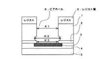
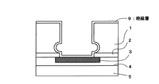


Classifications
-
- H—ELECTRICITY
- H10—SEMICONDUCTOR DEVICES; ELECTRIC SOLID-STATE DEVICES NOT OTHERWISE PROVIDED FOR
- H10W—GENERIC PACKAGES, INTERCONNECTIONS, CONNECTORS OR OTHER CONSTRUCTIONAL DETAILS OF DEVICES COVERED BY CLASS H10
- H10W72/00—Interconnections or connectors in packages
- H10W72/20—Bump connectors, e.g. solder bumps or copper pillars; Dummy bumps; Thermal bumps
-
- H—ELECTRICITY
- H10—SEMICONDUCTOR DEVICES; ELECTRIC SOLID-STATE DEVICES NOT OTHERWISE PROVIDED FOR
- H10D—INORGANIC ELECTRIC SEMICONDUCTOR DEVICES
- H10D64/00—Electrodes of devices having potential barriers
- H10D64/01—Manufacture or treatment
- H10D64/011—Manufacture or treatment of electrodes ohmically coupled to a semiconductor
-
- H—ELECTRICITY
- H10—SEMICONDUCTOR DEVICES; ELECTRIC SOLID-STATE DEVICES NOT OTHERWISE PROVIDED FOR
- H10W—GENERIC PACKAGES, INTERCONNECTIONS, CONNECTORS OR OTHER CONSTRUCTIONAL DETAILS OF DEVICES COVERED BY CLASS H10
- H10W20/00—Interconnections in chips, wafers or substrates
- H10W20/01—Manufacture or treatment
- H10W20/021—Manufacture or treatment of interconnections within wafers or substrates
- H10W20/023—Manufacture or treatment of interconnections within wafers or substrates the interconnections being through-semiconductor vias
-
- H—ELECTRICITY
- H10—SEMICONDUCTOR DEVICES; ELECTRIC SOLID-STATE DEVICES NOT OTHERWISE PROVIDED FOR
- H10W—GENERIC PACKAGES, INTERCONNECTIONS, CONNECTORS OR OTHER CONSTRUCTIONAL DETAILS OF DEVICES COVERED BY CLASS H10
- H10W20/00—Interconnections in chips, wafers or substrates
- H10W20/01—Manufacture or treatment
- H10W20/021—Manufacture or treatment of interconnections within wafers or substrates
- H10W20/023—Manufacture or treatment of interconnections within wafers or substrates the interconnections being through-semiconductor vias
- H10W20/0234—Manufacture or treatment of interconnections within wafers or substrates the interconnections being through-semiconductor vias comprising etching via holes that stop on pads or on electrodes
-
- H—ELECTRICITY
- H10—SEMICONDUCTOR DEVICES; ELECTRIC SOLID-STATE DEVICES NOT OTHERWISE PROVIDED FOR
- H10W—GENERIC PACKAGES, INTERCONNECTIONS, CONNECTORS OR OTHER CONSTRUCTIONAL DETAILS OF DEVICES COVERED BY CLASS H10
- H10W20/00—Interconnections in chips, wafers or substrates
- H10W20/01—Manufacture or treatment
- H10W20/021—Manufacture or treatment of interconnections within wafers or substrates
- H10W20/023—Manufacture or treatment of interconnections within wafers or substrates the interconnections being through-semiconductor vias
- H10W20/0242—Manufacture or treatment of interconnections within wafers or substrates the interconnections being through-semiconductor vias comprising etching via holes from the back sides of the chips, wafers or substrates
-
- H—ELECTRICITY
- H10—SEMICONDUCTOR DEVICES; ELECTRIC SOLID-STATE DEVICES NOT OTHERWISE PROVIDED FOR
- H10W—GENERIC PACKAGES, INTERCONNECTIONS, CONNECTORS OR OTHER CONSTRUCTIONAL DETAILS OF DEVICES COVERED BY CLASS H10
- H10W20/00—Interconnections in chips, wafers or substrates
- H10W20/20—Interconnections within wafers or substrates, e.g. through-silicon vias [TSV]
-
- H—ELECTRICITY
- H10—SEMICONDUCTOR DEVICES; ELECTRIC SOLID-STATE DEVICES NOT OTHERWISE PROVIDED FOR
- H10W—GENERIC PACKAGES, INTERCONNECTIONS, CONNECTORS OR OTHER CONSTRUCTIONAL DETAILS OF DEVICES COVERED BY CLASS H10
- H10W20/00—Interconnections in chips, wafers or substrates
- H10W20/20—Interconnections within wafers or substrates, e.g. through-silicon vias [TSV]
- H10W20/211—Through-semiconductor vias, e.g. TSVs
- H10W20/212—Top-view shapes or dispositions, e.g. top-view layouts of the vias
- H10W20/2125—Top-view shapes
-
- H—ELECTRICITY
- H10—SEMICONDUCTOR DEVICES; ELECTRIC SOLID-STATE DEVICES NOT OTHERWISE PROVIDED FOR
- H10W—GENERIC PACKAGES, INTERCONNECTIONS, CONNECTORS OR OTHER CONSTRUCTIONAL DETAILS OF DEVICES COVERED BY CLASS H10
- H10W72/00—Interconnections or connectors in packages
- H10W72/01—Manufacture or treatment
- H10W72/012—Manufacture or treatment of bump connectors, dummy bumps or thermal bumps
-
- H—ELECTRICITY
- H10—SEMICONDUCTOR DEVICES; ELECTRIC SOLID-STATE DEVICES NOT OTHERWISE PROVIDED FOR
- H10W—GENERIC PACKAGES, INTERCONNECTIONS, CONNECTORS OR OTHER CONSTRUCTIONAL DETAILS OF DEVICES COVERED BY CLASS H10
- H10W74/00—Encapsulations, e.g. protective coatings
- H10W74/10—Encapsulations, e.g. protective coatings characterised by their shape or disposition
- H10W74/111—Encapsulations, e.g. protective coatings characterised by their shape or disposition the semiconductor body being completely enclosed
- H10W74/129—Encapsulations, e.g. protective coatings characterised by their shape or disposition the semiconductor body being completely enclosed forming a chip-scale package [CSP]
-
- H—ELECTRICITY
- H10—SEMICONDUCTOR DEVICES; ELECTRIC SOLID-STATE DEVICES NOT OTHERWISE PROVIDED FOR
- H10W—GENERIC PACKAGES, INTERCONNECTIONS, CONNECTORS OR OTHER CONSTRUCTIONAL DETAILS OF DEVICES COVERED BY CLASS H10
- H10W70/00—Package substrates; Interposers; Redistribution layers [RDL]
- H10W70/60—Insulating or insulated package substrates; Interposers; Redistribution layers
- H10W70/62—Insulating or insulated package substrates; Interposers; Redistribution layers characterised by their interconnections
- H10W70/65—Shapes or dispositions of interconnections
-
- H—ELECTRICITY
- H10—SEMICONDUCTOR DEVICES; ELECTRIC SOLID-STATE DEVICES NOT OTHERWISE PROVIDED FOR
- H10W—GENERIC PACKAGES, INTERCONNECTIONS, CONNECTORS OR OTHER CONSTRUCTIONAL DETAILS OF DEVICES COVERED BY CLASS H10
- H10W70/00—Package substrates; Interposers; Redistribution layers [RDL]
- H10W70/60—Insulating or insulated package substrates; Interposers; Redistribution layers
- H10W70/62—Insulating or insulated package substrates; Interposers; Redistribution layers characterised by their interconnections
- H10W70/65—Shapes or dispositions of interconnections
- H10W70/654—Top-view layouts
- H10W70/655—Fan-out layouts
-
- H—ELECTRICITY
- H10—SEMICONDUCTOR DEVICES; ELECTRIC SOLID-STATE DEVICES NOT OTHERWISE PROVIDED FOR
- H10W—GENERIC PACKAGES, INTERCONNECTIONS, CONNECTORS OR OTHER CONSTRUCTIONAL DETAILS OF DEVICES COVERED BY CLASS H10
- H10W72/00—Interconnections or connectors in packages
- H10W72/01—Manufacture or treatment
- H10W72/019—Manufacture or treatment of bond pads
-
- H—ELECTRICITY
- H10—SEMICONDUCTOR DEVICES; ELECTRIC SOLID-STATE DEVICES NOT OTHERWISE PROVIDED FOR
- H10W—GENERIC PACKAGES, INTERCONNECTIONS, CONNECTORS OR OTHER CONSTRUCTIONAL DETAILS OF DEVICES COVERED BY CLASS H10
- H10W72/00—Interconnections or connectors in packages
- H10W72/20—Bump connectors, e.g. solder bumps or copper pillars; Dummy bumps; Thermal bumps
- H10W72/241—Dispositions, e.g. layouts
- H10W72/244—Dispositions, e.g. layouts relative to underlying supporting features, e.g. bond pads, RDLs or vias
-
- H—ELECTRICITY
- H10—SEMICONDUCTOR DEVICES; ELECTRIC SOLID-STATE DEVICES NOT OTHERWISE PROVIDED FOR
- H10W—GENERIC PACKAGES, INTERCONNECTIONS, CONNECTORS OR OTHER CONSTRUCTIONAL DETAILS OF DEVICES COVERED BY CLASS H10
- H10W72/00—Interconnections or connectors in packages
- H10W72/20—Bump connectors, e.g. solder bumps or copper pillars; Dummy bumps; Thermal bumps
- H10W72/251—Materials
-
- H—ELECTRICITY
- H10—SEMICONDUCTOR DEVICES; ELECTRIC SOLID-STATE DEVICES NOT OTHERWISE PROVIDED FOR
- H10W—GENERIC PACKAGES, INTERCONNECTIONS, CONNECTORS OR OTHER CONSTRUCTIONAL DETAILS OF DEVICES COVERED BY CLASS H10
- H10W72/00—Interconnections or connectors in packages
- H10W72/20—Bump connectors, e.g. solder bumps or copper pillars; Dummy bumps; Thermal bumps
- H10W72/29—Bond pads specially adapted therefor
-
- H—ELECTRICITY
- H10—SEMICONDUCTOR DEVICES; ELECTRIC SOLID-STATE DEVICES NOT OTHERWISE PROVIDED FOR
- H10W—GENERIC PACKAGES, INTERCONNECTIONS, CONNECTORS OR OTHER CONSTRUCTIONAL DETAILS OF DEVICES COVERED BY CLASS H10
- H10W72/00—Interconnections or connectors in packages
- H10W72/90—Bond pads, in general
- H10W72/921—Structures or relative sizes of bond pads
- H10W72/922—Bond pads being integral with underlying chip-level interconnections
-
- H—ELECTRICITY
- H10—SEMICONDUCTOR DEVICES; ELECTRIC SOLID-STATE DEVICES NOT OTHERWISE PROVIDED FOR
- H10W—GENERIC PACKAGES, INTERCONNECTIONS, CONNECTORS OR OTHER CONSTRUCTIONAL DETAILS OF DEVICES COVERED BY CLASS H10
- H10W72/00—Interconnections or connectors in packages
- H10W72/90—Bond pads, in general
- H10W72/921—Structures or relative sizes of bond pads
- H10W72/922—Bond pads being integral with underlying chip-level interconnections
- H10W72/9226—Bond pads being integral with underlying chip-level interconnections with via interconnections
-
- H—ELECTRICITY
- H10—SEMICONDUCTOR DEVICES; ELECTRIC SOLID-STATE DEVICES NOT OTHERWISE PROVIDED FOR
- H10W—GENERIC PACKAGES, INTERCONNECTIONS, CONNECTORS OR OTHER CONSTRUCTIONAL DETAILS OF DEVICES COVERED BY CLASS H10
- H10W72/00—Interconnections or connectors in packages
- H10W72/90—Bond pads, in general
- H10W72/921—Structures or relative sizes of bond pads
- H10W72/923—Bond pads having multiple stacked layers
-
- H—ELECTRICITY
- H10—SEMICONDUCTOR DEVICES; ELECTRIC SOLID-STATE DEVICES NOT OTHERWISE PROVIDED FOR
- H10W—GENERIC PACKAGES, INTERCONNECTIONS, CONNECTORS OR OTHER CONSTRUCTIONAL DETAILS OF DEVICES COVERED BY CLASS H10
- H10W72/00—Interconnections or connectors in packages
- H10W72/90—Bond pads, in general
- H10W72/941—Dispositions of bond pads
- H10W72/9415—Dispositions of bond pads relative to the surface, e.g. recessed, protruding
-
- H—ELECTRICITY
- H10—SEMICONDUCTOR DEVICES; ELECTRIC SOLID-STATE DEVICES NOT OTHERWISE PROVIDED FOR
- H10W—GENERIC PACKAGES, INTERCONNECTIONS, CONNECTORS OR OTHER CONSTRUCTIONAL DETAILS OF DEVICES COVERED BY CLASS H10
- H10W72/00—Interconnections or connectors in packages
- H10W72/90—Bond pads, in general
- H10W72/951—Materials of bond pads
- H10W72/952—Materials of bond pads comprising metals or metalloids, e.g. PbSn, Ag or Cu
Landscapes
- Internal Circuitry In Semiconductor Integrated Circuit Devices (AREA)
- Wire Bonding (AREA)
Priority Applications (7)
| Application Number | Priority Date | Filing Date | Title |
|---|---|---|---|
| JP2004040403A JP4850392B2 (ja) | 2004-02-17 | 2004-02-17 | 半導体装置の製造方法 |
| TW094102860A TWI268534B (en) | 2004-02-17 | 2005-01-31 | Semiconductor device and method for making same |
| EP05002897.6A EP1564810B1 (en) | 2004-02-17 | 2005-02-11 | Semiconductor device and manufacturing method thereof |
| US11/055,707 US7732925B2 (en) | 2004-02-17 | 2005-02-11 | Semiconductor device and manufacturing method thereof |
| KR1020050012866A KR100658543B1 (ko) | 2004-02-17 | 2005-02-16 | 반도체 장치 및 그 제조 방법 |
| CNB2005100093666A CN100382304C (zh) | 2004-02-17 | 2005-02-17 | 半导体装置及其制造方法 |
| US11/808,667 US7750478B2 (en) | 2004-02-17 | 2007-06-12 | Semiconductor device with via hole of uneven width |
Applications Claiming Priority (1)
| Application Number | Priority Date | Filing Date | Title |
|---|---|---|---|
| JP2004040403A JP4850392B2 (ja) | 2004-02-17 | 2004-02-17 | 半導体装置の製造方法 |
Publications (3)
| Publication Number | Publication Date |
|---|---|
| JP2005235858A JP2005235858A (ja) | 2005-09-02 |
| JP2005235858A5 JP2005235858A5 (https=) | 2007-03-22 |
| JP4850392B2 true JP4850392B2 (ja) | 2012-01-11 |
Family
ID=34697995
Family Applications (1)
| Application Number | Title | Priority Date | Filing Date |
|---|---|---|---|
| JP2004040403A Expired - Lifetime JP4850392B2 (ja) | 2004-02-17 | 2004-02-17 | 半導体装置の製造方法 |
Country Status (6)
| Country | Link |
|---|---|
| US (2) | US7732925B2 (https=) |
| EP (1) | EP1564810B1 (https=) |
| JP (1) | JP4850392B2 (https=) |
| KR (1) | KR100658543B1 (https=) |
| CN (1) | CN100382304C (https=) |
| TW (1) | TWI268534B (https=) |
Families Citing this family (47)
| Publication number | Priority date | Publication date | Assignee | Title |
|---|---|---|---|---|
| JP4850392B2 (ja) | 2004-02-17 | 2012-01-11 | 三洋電機株式会社 | 半導体装置の製造方法 |
| JP2005235860A (ja) * | 2004-02-17 | 2005-09-02 | Sanyo Electric Co Ltd | 半導体装置及びその製造方法 |
| SG120200A1 (en) | 2004-08-27 | 2006-03-28 | Micron Technology Inc | Slanted vias for electrical circuits on circuit boards and other substrates |
| TWI288448B (en) * | 2004-09-10 | 2007-10-11 | Toshiba Corp | Semiconductor device and method of manufacturing the same |
| TWI303864B (en) * | 2004-10-26 | 2008-12-01 | Sanyo Electric Co | Semiconductor device and method for making the same |
| JP4443379B2 (ja) * | 2004-10-26 | 2010-03-31 | 三洋電機株式会社 | 半導体装置の製造方法 |
| JP4873517B2 (ja) | 2004-10-28 | 2012-02-08 | オンセミコンダクター・トレーディング・リミテッド | 半導体装置及びその製造方法 |
| US7485967B2 (en) | 2005-03-10 | 2009-02-03 | Sanyo Electric Co., Ltd. | Semiconductor device with via hole for electric connection |
| TW200641774A (en) * | 2005-04-28 | 2006-12-01 | Sanyo Electric Co | Electroluminescense display device and data line driving circuit |
| US7425507B2 (en) * | 2005-06-28 | 2008-09-16 | Micron Technology, Inc. | Semiconductor substrates including vias of nonuniform cross section, methods of forming and associated structures |
| US7795134B2 (en) | 2005-06-28 | 2010-09-14 | Micron Technology, Inc. | Conductive interconnect structures and formation methods using supercritical fluids |
| JP2007067216A (ja) * | 2005-08-31 | 2007-03-15 | Sanyo Electric Co Ltd | 半導体装置およびその製造方法、回路基板およびその製造方法 |
| US7863187B2 (en) | 2005-09-01 | 2011-01-04 | Micron Technology, Inc. | Microfeature workpieces and methods for forming interconnects in microfeature workpieces |
| US7262134B2 (en) * | 2005-09-01 | 2007-08-28 | Micron Technology, Inc. | Microfeature workpieces and methods for forming interconnects in microfeature workpieces |
| US20070045120A1 (en) * | 2005-09-01 | 2007-03-01 | Micron Technology, Inc. | Methods and apparatus for filling features in microfeature workpieces |
| JP4812512B2 (ja) * | 2006-05-19 | 2011-11-09 | オンセミコンダクター・トレーディング・リミテッド | 半導体装置の製造方法 |
| US7629249B2 (en) | 2006-08-28 | 2009-12-08 | Micron Technology, Inc. | Microfeature workpieces having conductive interconnect structures formed by chemically reactive processes, and associated systems and methods |
| US7902643B2 (en) | 2006-08-31 | 2011-03-08 | Micron Technology, Inc. | Microfeature workpieces having interconnects and conductive backplanes, and associated systems and methods |
| JP4979320B2 (ja) * | 2006-09-28 | 2012-07-18 | ルネサスエレクトロニクス株式会社 | 半導体ウェハおよびその製造方法、ならびに半導体装置の製造方法 |
| JP4380718B2 (ja) | 2007-03-15 | 2009-12-09 | ソニー株式会社 | 半導体装置の製造方法 |
| DE102007019552B4 (de) * | 2007-04-25 | 2009-12-17 | Infineon Technologies Ag | Verfahren zur Herstellung eines Substrats mit Durchführung sowie Substrat und Halbleitermodul mit Durchführung |
| JP5078509B2 (ja) * | 2007-09-04 | 2012-11-21 | 三洋電機株式会社 | 太陽電池 |
| US7884015B2 (en) | 2007-12-06 | 2011-02-08 | Micron Technology, Inc. | Methods for forming interconnects in microelectronic workpieces and microelectronic workpieces formed using such methods |
| JP2009181981A (ja) * | 2008-01-29 | 2009-08-13 | Renesas Technology Corp | 半導体装置の製造方法および半導体装置 |
| US7629264B2 (en) * | 2008-04-09 | 2009-12-08 | International Business Machines Corporation | Structure and method for hybrid tungsten copper metal contact |
| JP5356742B2 (ja) | 2008-07-10 | 2013-12-04 | ラピスセミコンダクタ株式会社 | 半導体装置、半導体装置の製造方法および半導体パッケージの製造方法 |
| JP5654471B2 (ja) * | 2008-10-15 | 2015-01-14 | オー・アー・セー・マイクロテック・アクチボラゲット | ビア配線を作るための方法 |
| US8030780B2 (en) | 2008-10-16 | 2011-10-04 | Micron Technology, Inc. | Semiconductor substrates with unitary vias and via terminals, and associated systems and methods |
| JP2010114320A (ja) * | 2008-11-07 | 2010-05-20 | Panasonic Corp | 半導体装置 |
| JP5438980B2 (ja) | 2009-01-23 | 2014-03-12 | ラピスセミコンダクタ株式会社 | 半導体装置の製造方法 |
| JP5258735B2 (ja) * | 2009-11-13 | 2013-08-07 | セミコンダクター・コンポーネンツ・インダストリーズ・リミテッド・ライアビリティ・カンパニー | 半導体装置 |
| CN102148202B (zh) * | 2010-02-09 | 2016-06-08 | 精材科技股份有限公司 | 晶片封装体及其形成方法 |
| KR101097628B1 (ko) * | 2010-06-21 | 2011-12-22 | 삼성전기주식회사 | 인쇄회로기판 및 이의 제조방법 |
| JP5733990B2 (ja) | 2011-01-12 | 2015-06-10 | キヤノン株式会社 | 半導体装置の製造方法 |
| US8901701B2 (en) * | 2011-02-10 | 2014-12-02 | Chia-Sheng Lin | Chip package and fabrication method thereof |
| US8816505B2 (en) * | 2011-07-29 | 2014-08-26 | Tessera, Inc. | Low stress vias |
| US9330975B2 (en) * | 2012-05-31 | 2016-05-03 | Micron Technology, Inc. | Integrated circuit substrates comprising through-substrate vias and methods of forming through-substrate vias |
| JP5655825B2 (ja) * | 2012-07-30 | 2015-01-21 | セイコーエプソン株式会社 | 半導体装置、半導体装置の製造方法、回路基板および電子機器 |
| US20140151095A1 (en) * | 2012-12-05 | 2014-06-05 | Samsung Electro-Mechanics Co., Ltd. | Printed circuit board and method for manufacturing the same |
| JP5588553B2 (ja) * | 2013-08-29 | 2014-09-10 | ラピスセミコンダクタ株式会社 | 半導体装置および半導体装置の製造方法 |
| TWI581389B (zh) * | 2014-05-22 | 2017-05-01 | 精材科技股份有限公司 | 半導體結構及其製造方法 |
| US10727122B2 (en) | 2014-12-08 | 2020-07-28 | International Business Machines Corporation | Self-aligned via interconnect structures |
| CN105679770B (zh) | 2016-01-28 | 2019-02-26 | 京东方科技集团股份有限公司 | 阵列基板及其制造方法 |
| US11355465B2 (en) * | 2017-10-11 | 2022-06-07 | Sony Semiconductor Solutions Corporation | Semiconductor device including glass substrate having improved reliability and method of manufacturing the same |
| JP2019160893A (ja) * | 2018-03-09 | 2019-09-19 | ソニーセミコンダクタソリューションズ株式会社 | 固体撮像素子、半導体装置、電子機器、および製造方法 |
| CN111960376B (zh) * | 2020-07-21 | 2024-08-23 | 上海集成电路研发中心有限公司 | 一种mems支撑和电连接孔结构及制备方法 |
| CN118431158B (zh) * | 2024-07-04 | 2024-09-20 | 纳宇半导体材料(宁波)有限责任公司 | 一种基于印刷烧结的功率芯片封装方法、封装结构 |
Family Cites Families (78)
| Publication number | Priority date | Publication date | Assignee | Title |
|---|---|---|---|---|
| US4097890A (en) * | 1976-06-23 | 1978-06-27 | Hewlett-Packard Company | Low parasitic capacitance and resistance beamlead semiconductor component and method of manufacture |
| FR2637151A1 (fr) * | 1988-09-29 | 1990-03-30 | Commissariat Energie Atomique | Procede de realisation de connexions electriques a travers un substrat |
| US5056216A (en) * | 1990-01-26 | 1991-10-15 | Sri International | Method of forming a plurality of solder connections |
| US5229647A (en) * | 1991-03-27 | 1993-07-20 | Micron Technology, Inc. | High density data storage using stacked wafers |
| US5149674A (en) * | 1991-06-17 | 1992-09-22 | Motorola, Inc. | Method for making a planar multi-layer metal bonding pad |
| US5336626A (en) * | 1992-03-18 | 1994-08-09 | Samsung Electronics Co., Ltd. | Method of manufacturing a MESFET with an epitaxial void |
| US5248903A (en) * | 1992-09-18 | 1993-09-28 | Lsi Logic Corporation | Composite bond pads for semiconductor devices |
| US5432119A (en) * | 1994-01-31 | 1995-07-11 | Hughes Aircraft Company | High yield electron-beam gate fabrication method for sub-micron gate FETS |
| WO1996013062A1 (en) * | 1994-10-19 | 1996-05-02 | Ceram Incorporated | Apparatus and method of manufacturing stacked wafer array |
| US6204074B1 (en) * | 1995-01-09 | 2001-03-20 | International Business Machines Corporation | Chip design process for wire bond and flip-chip package |
| JPH08293523A (ja) * | 1995-02-21 | 1996-11-05 | Seiko Epson Corp | 半導体装置およびその製造方法 |
| JPH09321175A (ja) * | 1996-05-30 | 1997-12-12 | Oki Electric Ind Co Ltd | マイクロ波回路及びチップ |
| DE69730629T2 (de) * | 1996-12-26 | 2005-02-03 | Matsushita Electric Industrial Co., Ltd., Kadoma | Leiterplatte und Elektronikkomponente |
| US5910687A (en) * | 1997-01-24 | 1999-06-08 | Chipscale, Inc. | Wafer fabrication of die-bottom contacts for electronic devices |
| EP0860876A3 (de) * | 1997-02-21 | 1999-09-22 | DaimlerChrysler AG | Anordnung und Verfahren zur Herstellung von CSP-Gehäusen für elektrische Bauteile |
| US5915167A (en) * | 1997-04-04 | 1999-06-22 | Elm Technology Corporation | Three dimensional structure memory |
| JP3724110B2 (ja) * | 1997-04-24 | 2005-12-07 | 三菱電機株式会社 | 半導体装置の製造方法 |
| US5985749A (en) * | 1997-06-25 | 1999-11-16 | Vlsi Technology, Inc. | Method of forming a via hole structure including CVD tungsten silicide barrier layer |
| US6084173A (en) * | 1997-07-30 | 2000-07-04 | Dimatteo; Robert Stephen | Method and apparatus for the generation of charged carriers in semiconductor devices |
| IL123207A0 (en) * | 1998-02-06 | 1998-09-24 | Shellcase Ltd | Integrated circuit device |
| JP2974022B1 (ja) * | 1998-10-01 | 1999-11-08 | ヤマハ株式会社 | 半導体装置のボンディングパッド構造 |
| US6734564B1 (en) * | 1999-01-04 | 2004-05-11 | International Business Machines Corporation | Specially shaped contact via and integrated circuit therewith |
| TW442873B (en) * | 1999-01-14 | 2001-06-23 | United Microelectronics Corp | Three-dimension stack-type chip structure and its manufacturing method |
| US6110816A (en) * | 1999-03-05 | 2000-08-29 | Taiwan Semiconductor Manufacturing Company | Method for improving bondability for deep-submicron integrated circuit package |
| US6031293A (en) * | 1999-04-26 | 2000-02-29 | United Microelectronics Corporation | Package-free bonding pad structure |
| US6300670B1 (en) * | 1999-07-26 | 2001-10-09 | Stmicroelectronics, Inc. | Backside bus vias |
| JP2001044197A (ja) * | 1999-08-04 | 2001-02-16 | Sharp Corp | 半導体装置及びその製造方法 |
| JP3858545B2 (ja) * | 1999-12-27 | 2006-12-13 | セイコーエプソン株式会社 | 半導体モジュール及び電子機器 |
| JP3778256B2 (ja) * | 2000-02-28 | 2006-05-24 | セイコーエプソン株式会社 | 半導体装置及びその製造方法、回路基板並びに電子機器 |
| JP3879816B2 (ja) * | 2000-06-02 | 2007-02-14 | セイコーエプソン株式会社 | 半導体装置及びその製造方法、積層型半導体装置、回路基板並びに電子機器 |
| JP4329235B2 (ja) * | 2000-06-27 | 2009-09-09 | セイコーエプソン株式会社 | 半導体装置及びその製造方法 |
| US6562709B1 (en) * | 2000-08-22 | 2003-05-13 | Charles W. C. Lin | Semiconductor chip assembly with simultaneously electroplated contact terminal and connection joint |
| US6512292B1 (en) * | 2000-09-12 | 2003-01-28 | International Business Machines Corporation | Semiconductor chip structures with embedded thermal conductors and a thermal sink disposed over opposing substrate surfaces |
| JP2002124517A (ja) * | 2000-10-13 | 2002-04-26 | Sharp Corp | 半導体装置およびその製造方法 |
| KR100366635B1 (ko) * | 2000-11-01 | 2003-01-09 | 삼성전자 주식회사 | 반도체 소자의 금속 배선 및 그 제조방법 |
| KR100382729B1 (ko) * | 2000-12-09 | 2003-05-09 | 삼성전자주식회사 | 반도체 소자의 금속 컨택 구조체 및 그 형성방법 |
| JP4771607B2 (ja) * | 2001-03-30 | 2011-09-14 | 富士通セミコンダクター株式会社 | 半導体装置及びその製造方法 |
| JP3530149B2 (ja) * | 2001-05-21 | 2004-05-24 | 新光電気工業株式会社 | 配線基板の製造方法及び半導体装置 |
| JP4754105B2 (ja) * | 2001-07-04 | 2011-08-24 | パナソニック株式会社 | 半導体装置およびその製造方法 |
| JP2003045877A (ja) * | 2001-08-01 | 2003-02-14 | Sharp Corp | 半導体装置およびその製造方法 |
| US6734568B2 (en) * | 2001-08-29 | 2004-05-11 | Kabushiki Kaisha Toshiba | Semiconductor device and method of manufacturing the same |
| JP4703061B2 (ja) * | 2001-08-30 | 2011-06-15 | 富士通株式会社 | 薄膜回路基板の製造方法およびビア形成基板の形成方法 |
| JP2003168818A (ja) * | 2001-09-18 | 2003-06-13 | Anritsu Corp | 順メサ型アバランシェフォトダイオード及びその製造方法 |
| JP3998984B2 (ja) * | 2002-01-18 | 2007-10-31 | 富士通株式会社 | 回路基板及びその製造方法 |
| US6960837B2 (en) * | 2002-02-26 | 2005-11-01 | International Business Machines Corporation | Method of connecting core I/O pins to backside chip I/O pads |
| JP4110390B2 (ja) * | 2002-03-19 | 2008-07-02 | セイコーエプソン株式会社 | 半導体装置の製造方法 |
| EP2560199B1 (en) * | 2002-04-05 | 2016-08-03 | STMicroelectronics S.r.l. | Process for manufacturing a through insulated interconnection in a body of semiconductor material |
| JP4212293B2 (ja) * | 2002-04-15 | 2009-01-21 | 三洋電機株式会社 | 半導体装置の製造方法 |
| TWI232560B (en) * | 2002-04-23 | 2005-05-11 | Sanyo Electric Co | Semiconductor device and its manufacture |
| JP2003318178A (ja) * | 2002-04-24 | 2003-11-07 | Seiko Epson Corp | 半導体装置及びその製造方法、回路基板並びに電子機器 |
| TWI229435B (en) * | 2002-06-18 | 2005-03-11 | Sanyo Electric Co | Manufacture of semiconductor device |
| US6902872B2 (en) * | 2002-07-29 | 2005-06-07 | Hewlett-Packard Development Company, L.P. | Method of forming a through-substrate interconnect |
| US6716737B2 (en) * | 2002-07-29 | 2004-04-06 | Hewlett-Packard Development Company, L.P. | Method of forming a through-substrate interconnect |
| JP2004103761A (ja) * | 2002-09-09 | 2004-04-02 | Renesas Technology Corp | 半導体装置製造ライン |
| TWI227050B (en) | 2002-10-11 | 2005-01-21 | Sanyo Electric Co | Semiconductor device and method for manufacturing the same |
| TWI227550B (en) * | 2002-10-30 | 2005-02-01 | Sanyo Electric Co | Semiconductor device manufacturing method |
| JP2004186422A (ja) * | 2002-12-03 | 2004-07-02 | Shinko Electric Ind Co Ltd | 電子部品実装構造及びその製造方法 |
| US6924221B2 (en) * | 2002-12-03 | 2005-08-02 | Taiwan Semiconductor Manufacturing Co., Ltd. | Integrated process flow to improve copper filling in a damascene structure |
| JP4322508B2 (ja) | 2003-01-15 | 2009-09-02 | 新光電気工業株式会社 | 半導体装置の製造方法 |
| JP4145301B2 (ja) | 2003-01-15 | 2008-09-03 | 富士通株式会社 | 半導体装置及び三次元実装半導体装置 |
| TWI239629B (en) * | 2003-03-17 | 2005-09-11 | Seiko Epson Corp | Method of manufacturing semiconductor device, semiconductor device, circuit substrate and electronic apparatus |
| JP3972846B2 (ja) | 2003-03-25 | 2007-09-05 | セイコーエプソン株式会社 | 半導体装置の製造方法 |
| JP2004311948A (ja) * | 2003-03-27 | 2004-11-04 | Seiko Epson Corp | 半導体装置、半導体デバイス、電子機器、および半導体装置の製造方法 |
| US7247939B2 (en) * | 2003-04-01 | 2007-07-24 | Taiwan Semiconductor Manufacturing Co., Ltd. | Metal filled semiconductor features with improved structural stability |
| JP4130158B2 (ja) * | 2003-06-09 | 2008-08-06 | 三洋電機株式会社 | 半導体装置の製造方法、半導体装置 |
| US7453158B2 (en) * | 2003-07-31 | 2008-11-18 | Nvidia Corporation | Pad over active circuit system and method with meshed support structure |
| JP4323303B2 (ja) * | 2003-12-17 | 2009-09-02 | 株式会社フジクラ | 基板の製造方法 |
| JP4850392B2 (ja) * | 2004-02-17 | 2012-01-11 | 三洋電機株式会社 | 半導体装置の製造方法 |
| TWI249767B (en) * | 2004-02-17 | 2006-02-21 | Sanyo Electric Co | Method for making a semiconductor device |
| JP2005235860A (ja) | 2004-02-17 | 2005-09-02 | Sanyo Electric Co Ltd | 半導体装置及びその製造方法 |
| JP4803964B2 (ja) | 2004-03-17 | 2011-10-26 | 三洋電機株式会社 | 電極構造 |
| JP4373866B2 (ja) * | 2004-07-16 | 2009-11-25 | 三洋電機株式会社 | 半導体装置の製造方法 |
| JP4376715B2 (ja) * | 2004-07-16 | 2009-12-02 | 三洋電機株式会社 | 半導体装置の製造方法 |
| TWI303864B (en) * | 2004-10-26 | 2008-12-01 | Sanyo Electric Co | Semiconductor device and method for making the same |
| JP4443379B2 (ja) * | 2004-10-26 | 2010-03-31 | 三洋電機株式会社 | 半導体装置の製造方法 |
| JP4873517B2 (ja) * | 2004-10-28 | 2012-02-08 | オンセミコンダクター・トレーディング・リミテッド | 半導体装置及びその製造方法 |
| US7538434B2 (en) * | 2005-03-08 | 2009-05-26 | Taiwan Semiconductor Manufacturing Company, Ltd. | Copper interconnection with conductive polymer layer and method of forming the same |
| US7485967B2 (en) * | 2005-03-10 | 2009-02-03 | Sanyo Electric Co., Ltd. | Semiconductor device with via hole for electric connection |
-
2004
- 2004-02-17 JP JP2004040403A patent/JP4850392B2/ja not_active Expired - Lifetime
-
2005
- 2005-01-31 TW TW094102860A patent/TWI268534B/zh not_active IP Right Cessation
- 2005-02-11 US US11/055,707 patent/US7732925B2/en not_active Expired - Lifetime
- 2005-02-11 EP EP05002897.6A patent/EP1564810B1/en not_active Expired - Lifetime
- 2005-02-16 KR KR1020050012866A patent/KR100658543B1/ko not_active Expired - Fee Related
- 2005-02-17 CN CNB2005100093666A patent/CN100382304C/zh not_active Expired - Lifetime
-
2007
- 2007-06-12 US US11/808,667 patent/US7750478B2/en not_active Expired - Lifetime
Also Published As
| Publication number | Publication date |
|---|---|
| CN1658387A (zh) | 2005-08-24 |
| US20070249158A1 (en) | 2007-10-25 |
| EP1564810A1 (en) | 2005-08-17 |
| TW200531142A (en) | 2005-09-16 |
| KR100658543B1 (ko) | 2006-12-19 |
| US7732925B2 (en) | 2010-06-08 |
| JP2005235858A (ja) | 2005-09-02 |
| TWI268534B (en) | 2006-12-11 |
| KR20060042012A (ko) | 2006-05-12 |
| US20050189637A1 (en) | 2005-09-01 |
| EP1564810B1 (en) | 2017-01-11 |
| US7750478B2 (en) | 2010-07-06 |
| CN100382304C (zh) | 2008-04-16 |
Similar Documents
| Publication | Publication Date | Title |
|---|---|---|
| JP4850392B2 (ja) | 半導体装置の製造方法 | |
| JP4307284B2 (ja) | 半導体装置の製造方法 | |
| US9165898B2 (en) | Method of manufacturing semiconductor device with through hole | |
| KR100563887B1 (ko) | 반도체 장치 및 그 제조 방법 | |
| US7241679B2 (en) | Method of manufacturing semiconductor device | |
| KR20040101924A (ko) | 반도체 장치 및 그 제조 방법 | |
| KR20060041950A (ko) | 반도체 장치 및 그 제조 방법 | |
| CN100524725C (zh) | 半导体装置及其制造方法 | |
| CN100470766C (zh) | 半导体装置及其制造方法 | |
| JP4544902B2 (ja) | 半導体装置及びその製造方法 | |
| JP4282514B2 (ja) | 半導体装置の製造方法 | |
| JP4726221B2 (ja) | 半導体装置及びその製造方法 | |
| JP4936695B2 (ja) | 半導体装置及びその製造方法 | |
| JP4845986B2 (ja) | 半導体装置 | |
| JP2005260080A (ja) | 半導体装置及びその製造方法 |
Legal Events
| Date | Code | Title | Description |
|---|---|---|---|
| A521 | Request for written amendment filed |
Free format text: JAPANESE INTERMEDIATE CODE: A523 Effective date: 20070201 |
|
| A621 | Written request for application examination |
Free format text: JAPANESE INTERMEDIATE CODE: A621 Effective date: 20070201 |
|
| A711 | Notification of change in applicant |
Free format text: JAPANESE INTERMEDIATE CODE: A712 Effective date: 20090115 |
|
| RD02 | Notification of acceptance of power of attorney |
Free format text: JAPANESE INTERMEDIATE CODE: A7422 Effective date: 20090309 |
|
| A521 | Request for written amendment filed |
Free format text: JAPANESE INTERMEDIATE CODE: A821 Effective date: 20090309 |
|
| A977 | Report on retrieval |
Free format text: JAPANESE INTERMEDIATE CODE: A971007 Effective date: 20090527 |
|
| A131 | Notification of reasons for refusal |
Free format text: JAPANESE INTERMEDIATE CODE: A131 Effective date: 20110310 |
|
| A521 | Request for written amendment filed |
Free format text: JAPANESE INTERMEDIATE CODE: A523 Effective date: 20110425 |
|
| A131 | Notification of reasons for refusal |
Free format text: JAPANESE INTERMEDIATE CODE: A131 Effective date: 20110712 |
|
| A521 | Request for written amendment filed |
Free format text: JAPANESE INTERMEDIATE CODE: A523 Effective date: 20110905 |
|
| TRDD | Decision of grant or rejection written | ||
| A01 | Written decision to grant a patent or to grant a registration (utility model) |
Free format text: JAPANESE INTERMEDIATE CODE: A01 Effective date: 20111013 |
|
| A01 | Written decision to grant a patent or to grant a registration (utility model) |
Free format text: JAPANESE INTERMEDIATE CODE: A01 |
|
| A61 | First payment of annual fees (during grant procedure) |
Free format text: JAPANESE INTERMEDIATE CODE: A61 Effective date: 20111019 |
|
| R150 | Certificate of patent or registration of utility model |
Ref document number: 4850392 Country of ref document: JP Free format text: JAPANESE INTERMEDIATE CODE: R150 Free format text: JAPANESE INTERMEDIATE CODE: R150 |
|
| FPAY | Renewal fee payment (event date is renewal date of database) |
Free format text: PAYMENT UNTIL: 20141028 Year of fee payment: 3 |
|
| R250 | Receipt of annual fees |
Free format text: JAPANESE INTERMEDIATE CODE: R250 |
|
| R250 | Receipt of annual fees |
Free format text: JAPANESE INTERMEDIATE CODE: R250 |
|
| S111 | Request for change of ownership or part of ownership |
Free format text: JAPANESE INTERMEDIATE CODE: R313117 |
|
| S531 | Written request for registration of change of domicile |
Free format text: JAPANESE INTERMEDIATE CODE: R313531 |
|
| R350 | Written notification of registration of transfer |
Free format text: JAPANESE INTERMEDIATE CODE: R350 |
|
| S531 | Written request for registration of change of domicile |
Free format text: JAPANESE INTERMEDIATE CODE: R313531 |
|
| R350 | Written notification of registration of transfer |
Free format text: JAPANESE INTERMEDIATE CODE: R350 |
|
| R250 | Receipt of annual fees |
Free format text: JAPANESE INTERMEDIATE CODE: R250 |
|
| R250 | Receipt of annual fees |
Free format text: JAPANESE INTERMEDIATE CODE: R250 |
|
| R250 | Receipt of annual fees |
Free format text: JAPANESE INTERMEDIATE CODE: R250 |
|
| S111 | Request for change of ownership or part of ownership |
Free format text: JAPANESE INTERMEDIATE CODE: R313115 |
|
| R250 | Receipt of annual fees |
Free format text: JAPANESE INTERMEDIATE CODE: R250 |
|
| R350 | Written notification of registration of transfer |
Free format text: JAPANESE INTERMEDIATE CODE: R350 |
|
| S531 | Written request for registration of change of domicile |
Free format text: JAPANESE INTERMEDIATE CODE: R313531 |
|
| S533 | Written request for registration of change of name |
Free format text: JAPANESE INTERMEDIATE CODE: R313533 |
|
| R350 | Written notification of registration of transfer |
Free format text: JAPANESE INTERMEDIATE CODE: R350 |
|
| S111 | Request for change of ownership or part of ownership |
Free format text: JAPANESE INTERMEDIATE CODE: R313117 |
|
| R350 | Written notification of registration of transfer |
Free format text: JAPANESE INTERMEDIATE CODE: R350 |
|
| R250 | Receipt of annual fees |
Free format text: JAPANESE INTERMEDIATE CODE: R250 |
|
| R250 | Receipt of annual fees |
Free format text: JAPANESE INTERMEDIATE CODE: R250 |
|
| R250 | Receipt of annual fees |
Free format text: JAPANESE INTERMEDIATE CODE: R250 |
|
| R250 | Receipt of annual fees |
Free format text: JAPANESE INTERMEDIATE CODE: R250 |
|
| EXPY | Cancellation because of completion of term |