JP2005294547A - 半導体装置およびその製造方法 - Google Patents
半導体装置およびその製造方法 Download PDFInfo
- Publication number
- JP2005294547A JP2005294547A JP2004107799A JP2004107799A JP2005294547A JP 2005294547 A JP2005294547 A JP 2005294547A JP 2004107799 A JP2004107799 A JP 2004107799A JP 2004107799 A JP2004107799 A JP 2004107799A JP 2005294547 A JP2005294547 A JP 2005294547A
- Authority
- JP
- Japan
- Prior art keywords
- layer
- semiconductor device
- semiconductor
- wiring
- base member
- Prior art date
- Legal status (The legal status is an assumption and is not a legal conclusion. Google has not performed a legal analysis and makes no representation as to the accuracy of the status listed.)
- Granted
Links
Images


Classifications
-
- H10W70/614—
-
- E—FIXED CONSTRUCTIONS
- E04—BUILDING
- E04H—BUILDINGS OR LIKE STRUCTURES FOR PARTICULAR PURPOSES; SWIMMING OR SPLASH BATHS OR POOLS; MASTS; FENCING; TENTS OR CANOPIES, IN GENERAL
- E04H17/00—Fencing, e.g. fences, enclosures, corrals
- E04H17/14—Fences constructed of rigid elements, e.g. with additional wire fillings or with posts
- E04H17/16—Fences constructed of rigid elements, e.g. with additional wire fillings or with posts using prefabricated panel-like elements, e.g. wired frames
-
- E—FIXED CONSTRUCTIONS
- E01—CONSTRUCTION OF ROADS, RAILWAYS, OR BRIDGES
- E01F—ADDITIONAL WORK, SUCH AS EQUIPPING ROADS OR THE CONSTRUCTION OF PLATFORMS, HELICOPTER LANDING STAGES, SIGNS, SNOW FENCES, OR THE LIKE
- E01F8/00—Arrangements for absorbing or reflecting air-transmitted noise from road or railway traffic
- E01F8/0005—Arrangements for absorbing or reflecting air-transmitted noise from road or railway traffic used in a wall type arrangement
- E01F8/0047—Arrangements for absorbing or reflecting air-transmitted noise from road or railway traffic used in a wall type arrangement with open cavities, e.g. for covering sunken roads
-
- H10W42/20—
-
- H10W70/09—
-
- H10W70/093—
-
- H10W70/099—
-
- H10W70/60—
-
- H10W72/00—
-
- H10W72/01331—
-
- H10W72/073—
-
- H10W72/07338—
-
- H10W72/241—
-
- H10W72/325—
-
- H10W72/351—
-
- H10W72/354—
-
- H10W72/874—
-
- H10W72/922—
-
- H10W72/9223—
-
- H10W72/923—
-
- H10W72/9413—
-
- H10W72/9415—
-
- H10W72/942—
-
- H10W72/952—
-
- H10W90/734—
-
- H10W90/736—
-
- H10W99/00—
Landscapes
- Engineering & Computer Science (AREA)
- Architecture (AREA)
- Civil Engineering (AREA)
- Structural Engineering (AREA)
- Internal Circuitry In Semiconductor Integrated Circuit Devices (AREA)
Abstract
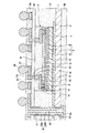
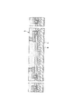
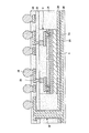
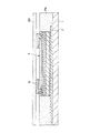
【解決手段】 ベース板1の上面にはグランド層2が設けられ、その上面にはCSPと呼ばれる半導体構成体3が設けられ、その周囲には方形枠状の絶縁層21が設けられ、それらの上面には上層絶縁膜15が設けられ、その上面には上層配線25が半導体構成体3の柱状電極16に接続されて設けられている。グランド層2は、上下導通部32を介してグランド用の上層配線25に接続されている。そして、半導体装置の内部にグランド層2を設けていることにより、半導体装置が搭載される回路基板を含む全体としての小型化を図ることができる。
【選択図】 図1
Description
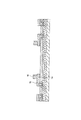
図1はこの発明の第1実施形態としての半導体装置の断面図を示す。この半導体装置は、ガラス布基材エポキシ樹脂等の絶縁材料からなる平面矩形形状のベース板1を備えている。ベース板1の上面には銅箔からなるべたパターンのグランド層2が設けられている。ここで、ベース板1およびその上に設けられたグランド層2は、グランド層としての機能を有するベース部材を構成している。
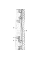
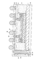
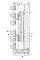
図16はこの発明の第2実施形態としての半導体装置の断面図を示す。この半導体装置において、図1に示す半導体装置と異なる点は、グランド層2を上下導通部32に直接接続させずに、ベース板1の下面に上下導通部32に接続されて設けられた下層下地金属層33を含む下層配線34をベース板1に形成された貫通孔61を介してグランド層2の下面に接続させた点である。この場合、ガラス布基材エポキシ樹脂等からなるベース板1への貫通孔61の形成は、レーザビームを照射するレーザ加工により行なう。
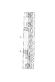
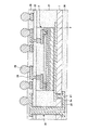
図17はこの発明の第3実施形態としての半導体装置の断面図を示す。この半導体装置において、図1に示す半導体装置と異なる点は、ベース板1の上面にグランド層2を設けた上に、ベース板の下面に下層下地金属層33を含む下層配線34をべた状に設け、このべたパターンからなる下層配線34にグランド層としての機能を持たせた点である。
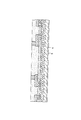
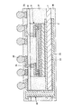
図18はこの発明の第4実施形態としての半導体装置の断面図を示す。この半導体装置において、図1に示す半導体装置と異なる点は、ベース板1の上面にグランド層2を設けずに、ベース板の下面に下層下地金属層33を含む下層配線34をべた状に設け、このべたパターンからなる下層配線34にグランド層としての機能を持たせた点である。
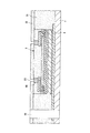
図19はこの発明の第5実施形態としての半導体装置の断面図を示す。この半導体装置において、図1に示す半導体装置と異なる点は、ガラス布基材エポキシ樹脂等の絶縁材料からなるベース板1を有せず、銅箔等からなる金属箔(ベース部材)2Aの上面に半導体構成体3および絶縁層21を設け、金属箔2Aの下面全体に下層下地金属層33を含む下層配線34を設け、下層配線34の下面全体に下層オーバーコート膜36を設けた点である。この場合、下層配線34を含む金属箔2Aは、グランド層としての機能を有する。
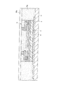
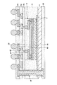
図22はこの発明の第6実施形態としての半導体装置の断面図を示す。この半導体装置において、図1に示す半導体装置と異なる点は、半導体構成体3として、柱状電極16および封止膜17を有せず、下地金属層14を含む配線15が露出された構造のものを用い、上層下地金属層24を含む上層配線25の一端部を上層絶縁膜22の開口部23を介して配線15の接続パッド(外部接続用電極)に接続させた点である。
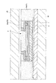
上記第1実施形態では、図1に示すように、上層絶縁膜22上に上層配線25を1層だけ形成した場合について説明したが、これに限らず、2層以上としてもよく、例えば、図24に示すこの発明の第7実施形態のように、2層としてもよい。すなわち、上層絶縁膜22と上層オーバーコート膜26との間に第2の上層絶縁膜62を設け、第2の上層絶縁膜62の上面に設けられた第2の上層下地金属層63を含む第2の上層配線64の一端部を第2の上層絶縁膜62の開口部65を介して上層配線25の接続パッド部に接続し、第2の上層配線64の接続パッド部上に半田ボール28を設けるようにしてもよい。この場合、グランド層2は、上下導通部32を介して、グランド用の第2の上層配線64に接続されている。
上記第1実施形態には、互いに隣接する半導体構成体3間において切断したが、これに限らず、2個またはそれ以上の半導体構成体3を1組として切断し、マルチチップモジュール型の半導体装置を得るようにしてもよい。この場合、2個で1組の半導体構成体3は同種、異種のいずれであってもよい。
2 グランド層
3 半導体構成体
4 接着層
5 SOI基板
6 シリコン基板
7 酸化シリコン膜
8 SOI集積回路部
9 接続パッド
10 絶縁膜
12 保護膜
15 配線
16 柱状電極
17 封止膜
21 絶縁層
22 上層絶縁膜
25 上層配線
26 上層オーバーコート膜
28 半田ボール
31 貫通孔
32 上下導通部
34 下層配線
36 下層オーバーコート膜
Claims (15)
- グランド層としての機能を有するベース部材と、前記ベース部材上に設けられ、且つ、半導体基板および該半導体基板上に設けられた複数の外部接続用電極を有する少なくとも1つの半導体構成体と、前記半導体構成体の周囲における前記ベース部材上に設けられた絶縁層と、前記半導体構成体および前記絶縁層上に前記半導体構成体の外部接続用電極に接続されて設けられた少なくとも1層の上層配線と、少なくとも前記絶縁層に設けられた貫通孔内に前記ベース部材のグランド層として機能する部分とグランド用の前記上層配線とを接続するように設けられた上下導通部と、前記ベース部材下に設けられた下層オーバーコート膜とを備えていることを特徴とする半導体装置。
- 請求項1に記載の発明において、前記ベース部材は、絶縁性のベース板と、前記ベース板の上下面のうちの少なくとも一方の面に設けられたグランド層とからなることを特徴とする半導体装置。
- 請求項1に記載の発明において、前記ベース部材はグランド層を兼ねた金属箔からなることを特徴とする半導体装置。
- 請求項3に記載の発明において、前記金属箔の下面にメッキ層が設けられていることを特徴とする半導体装置。
- 請求項1に記載の発明において、前記半導体構成体の半導体基板はSOI基板からなることを特徴とする半導体装置。
- 請求項1に記載の発明において、前記最上層の上層配線の接続パッド部を除く部分を覆う上層オーバーコート膜を有することを特徴とする半導体装置。
- 請求項6に記載の発明において、前記最上層の上層配線の接続パッド部上に半田ボールが設けられていることを特徴とする半導体装置。
- グランド層としての機能を有するベース部材上に、各々が半導体基板および該半導体基板上に設けられた複数の外部接続用電極を有する複数の半導体構成体を相互に離間させて配置する工程と、
前記半導体構成体の周囲における前記ベース部材上に絶縁層を形成する工程と、
前記半導体構成体および前記絶縁層上に少なくとも1層の上層配線を前記半導体構成体の外部接続用電極に接続させて形成する工程と、
少なくとも前記絶縁層に形成された貫通孔内に前記ベース部材のグランド層として機能する部分とグランド用の前記上層配線とを接続する上下導通部を形成する工程と、
前記ベース部材下に下層オーバーコート膜を形成する工程と、
前記半導体構成体間における前記絶縁層、前記ベース部材および前記下層オーバーコート膜を切断して前記半導体構成体が少なくとも1つ含まれる半導体装置を複数個得る工程と、
を有することを特徴とする半導体装置の製造方法。 - 請求項8に記載の発明において、前記ベース部材は、ベース板と、前記ベース板の上下面のうちの少なくとも一方の面に設けられたグランド層とからなることを特徴とする半導体装置の製造方法。
- 請求項8に記載の発明において、前記ベース部材はグランド層を兼ねた金属箔からなることを特徴とする半導体装置の製造方法。
- 請求項10に記載の発明において、前記金属箔は当初ベース板の上面にラミネートされ、前記半導体構成体配置工程および前記絶縁層形成工程後に前記金属箔から前記ベース板を剥離する工程を有することを特徴とする半導体装置の製造方法。
- 請求項11に記載の発明において、前記金属箔の下面にメッキ層を形成する工程を有することを特徴とする半導体装置の製造方法。
- 請求項8に記載の発明において、前記半導体構成体の半導体基板はSOI基板からなることを特徴とする半導体装置の製造方法。
- 請求項8に記載の発明において、前記最上層の上層配線の接続パッド部を除く部分を覆う上層オーバーコート膜を形成する工程を有することを特徴とする半導体装置の製造方法。
- 請求項14に記載の発明において、前記最上層の上層配線の接続パッド部上に半田ボールを形成する工程を有することを特徴とする半導体装置の製造方法。
Priority Applications (6)
| Application Number | Priority Date | Filing Date | Title |
|---|---|---|---|
| JP2004107799A JP3925809B2 (ja) | 2004-03-31 | 2004-03-31 | 半導体装置およびその製造方法 |
| TW094109690A TWI286373B (en) | 2004-03-31 | 2005-03-29 | Semiconductor device and the fabricating method of the same |
| US11/093,570 US7279750B2 (en) | 2004-03-31 | 2005-03-30 | Semiconductor device incorporating a semiconductor constructing body and an interconnecting layer which is connected to a ground layer via a vertical conducting portion |
| KR1020050026337A KR100695321B1 (ko) | 2004-03-31 | 2005-03-30 | 반도체장치 및 그 제조방법 |
| CNB2005100716563A CN100418215C (zh) | 2004-03-31 | 2005-03-31 | 半导体器件及其制造方法 |
| US11/880,162 US7608480B2 (en) | 2004-03-31 | 2007-07-20 | Method of fabricating a semiconductor device incorporating a semiconductor constructing body and an interconnecting layer which is connected to a ground layer via a vertical conducting portion |
Applications Claiming Priority (1)
| Application Number | Priority Date | Filing Date | Title |
|---|---|---|---|
| JP2004107799A JP3925809B2 (ja) | 2004-03-31 | 2004-03-31 | 半導体装置およびその製造方法 |
Publications (2)
| Publication Number | Publication Date |
|---|---|
| JP2005294547A true JP2005294547A (ja) | 2005-10-20 |
| JP3925809B2 JP3925809B2 (ja) | 2007-06-06 |
Family
ID=35053342
Family Applications (1)
| Application Number | Title | Priority Date | Filing Date |
|---|---|---|---|
| JP2004107799A Expired - Fee Related JP3925809B2 (ja) | 2004-03-31 | 2004-03-31 | 半導体装置およびその製造方法 |
Country Status (5)
| Country | Link |
|---|---|
| US (2) | US7279750B2 (ja) |
| JP (1) | JP3925809B2 (ja) |
| KR (1) | KR100695321B1 (ja) |
| CN (1) | CN100418215C (ja) |
| TW (1) | TWI286373B (ja) |
Cited By (1)
| Publication number | Priority date | Publication date | Assignee | Title |
|---|---|---|---|---|
| US8293574B2 (en) | 2006-01-10 | 2012-10-23 | Teramikros, Inc. | Semiconductor device having a plurality of semiconductor constructs |
Families Citing this family (59)
| Publication number | Priority date | Publication date | Assignee | Title |
|---|---|---|---|---|
| KR100778597B1 (ko) | 2003-06-03 | 2007-11-22 | 가시오게산키 가부시키가이샤 | 적층 반도체 장치와 그 제조방법 |
| TWI278048B (en) | 2003-11-10 | 2007-04-01 | Casio Computer Co Ltd | Semiconductor device and its manufacturing method |
| JP3945483B2 (ja) | 2004-01-27 | 2007-07-18 | カシオ計算機株式会社 | 半導体装置の製造方法 |
| JP4093186B2 (ja) | 2004-01-27 | 2008-06-04 | カシオ計算機株式会社 | 半導体装置の製造方法 |
| JP4449824B2 (ja) * | 2005-06-01 | 2010-04-14 | カシオ計算機株式会社 | 半導体装置およびその実装構造 |
| JP4395775B2 (ja) * | 2005-10-05 | 2010-01-13 | ソニー株式会社 | 半導体装置及びその製造方法 |
| JP4222400B2 (ja) * | 2006-09-26 | 2009-02-12 | カシオ計算機株式会社 | 半導体装置の製造方法 |
| JP4305502B2 (ja) * | 2006-11-28 | 2009-07-29 | カシオ計算機株式会社 | 半導体装置の製造方法 |
| JP2008218926A (ja) | 2007-03-07 | 2008-09-18 | Spansion Llc | 半導体装置及びその製造方法 |
| JP2008226945A (ja) * | 2007-03-09 | 2008-09-25 | Casio Comput Co Ltd | 半導体装置およびその製造方法 |
| US8877565B2 (en) * | 2007-06-28 | 2014-11-04 | Intel Corporation | Method of forming a multilayer substrate core structure using sequential microvia laser drilling and substrate core structure formed according to the method |
| US8440916B2 (en) | 2007-06-28 | 2013-05-14 | Intel Corporation | Method of forming a substrate core structure using microvia laser drilling and conductive layer pre-patterning and substrate core structure formed according to the method |
| TWI384595B (zh) * | 2007-08-08 | 2013-02-01 | 兆裝微股份有限公司 | 半導體裝置及其製造方法 |
| US8093704B2 (en) * | 2008-06-03 | 2012-01-10 | Intel Corporation | Package on package using a bump-less build up layer (BBUL) package |
| US20100126764A1 (en) * | 2008-11-24 | 2010-05-27 | Seagate Technology, Llc | die ground lead |
| JP5372579B2 (ja) * | 2009-04-10 | 2013-12-18 | 新光電気工業株式会社 | 半導体装置及びその製造方法、並びに電子装置 |
| US7928552B1 (en) * | 2010-03-12 | 2011-04-19 | Stats Chippac Ltd. | Integrated circuit packaging system with multi-tier conductive interconnects and method of manufacture thereof |
| US8343810B2 (en) * | 2010-08-16 | 2013-01-01 | Stats Chippac, Ltd. | Semiconductor device and method of forming Fo-WLCSP having conductive layers and conductive vias separated by polymer layers |
| US8552540B2 (en) * | 2011-05-10 | 2013-10-08 | Conexant Systems, Inc. | Wafer level package with thermal pad for higher power dissipation |
| US8916979B2 (en) | 2012-12-28 | 2014-12-23 | Taiwan Semiconductor Manufacturing Company, Ltd. | Through-vias and methods of forming the same |
| CN103227117B (zh) * | 2013-04-15 | 2016-01-13 | 江阴长电先进封装有限公司 | 一种硅基转接板的封装方法 |
| CN103871985A (zh) * | 2014-03-03 | 2014-06-18 | 江苏长电科技股份有限公司 | 一种半导体封装结构 |
| US9502270B2 (en) | 2014-07-08 | 2016-11-22 | Taiwan Semiconductor Manufacturing Company, Ltd. | Semiconductor device packages, packaging methods, and packaged semiconductor devices |
| US10085352B2 (en) | 2014-10-01 | 2018-09-25 | Qorvo Us, Inc. | Method for manufacturing an integrated circuit package |
| US10276495B2 (en) | 2015-09-11 | 2019-04-30 | Qorvo Us, Inc. | Backside semiconductor die trimming |
| US10784149B2 (en) | 2016-05-20 | 2020-09-22 | Qorvo Us, Inc. | Air-cavity module with enhanced device isolation |
| US10773952B2 (en) | 2016-05-20 | 2020-09-15 | Qorvo Us, Inc. | Wafer-level package with enhanced performance |
| US10103080B2 (en) | 2016-06-10 | 2018-10-16 | Qorvo Us, Inc. | Thermally enhanced semiconductor package with thermal additive and process for making the same |
| US10079196B2 (en) | 2016-07-18 | 2018-09-18 | Qorvo Us, Inc. | Thermally enhanced semiconductor package having field effect transistors with back-gate feature |
| US10486963B2 (en) | 2016-08-12 | 2019-11-26 | Qorvo Us, Inc. | Wafer-level package with enhanced performance |
| WO2018031995A1 (en) | 2016-08-12 | 2018-02-15 | Qorvo Us, Inc. | Wafer-level package with enhanced performance |
| JP7022112B2 (ja) | 2016-08-12 | 2022-02-17 | コーボ ユーエス,インコーポレイティド | 性能を向上させたウェーハレベルパッケージ |
| US10109502B2 (en) | 2016-09-12 | 2018-10-23 | Qorvo Us, Inc. | Semiconductor package with reduced parasitic coupling effects and process for making the same |
| US10749518B2 (en) | 2016-11-18 | 2020-08-18 | Qorvo Us, Inc. | Stacked field-effect transistor switch |
| US10068831B2 (en) | 2016-12-09 | 2018-09-04 | Qorvo Us, Inc. | Thermally enhanced semiconductor package and process for making the same |
| US10755992B2 (en) * | 2017-07-06 | 2020-08-25 | Qorvo Us, Inc. | Wafer-level packaging for enhanced performance |
| US10366972B2 (en) | 2017-09-05 | 2019-07-30 | Qorvo Us, Inc. | Microelectronics package with self-aligned stacked-die assembly |
| CN109911839B (zh) * | 2017-12-12 | 2023-10-13 | 中国科学院半导体研究所 | 能抑制光噪声的微电极、采用其的电路及其制备方法 |
| US11152363B2 (en) | 2018-03-28 | 2021-10-19 | Qorvo Us, Inc. | Bulk CMOS devices with enhanced performance and methods of forming the same utilizing bulk CMOS process |
| US12062700B2 (en) | 2018-04-04 | 2024-08-13 | Qorvo Us, Inc. | Gallium-nitride-based module with enhanced electrical performance and process for making the same |
| US12046505B2 (en) | 2018-04-20 | 2024-07-23 | Qorvo Us, Inc. | RF devices with enhanced performance and methods of forming the same utilizing localized SOI formation |
| US10804246B2 (en) | 2018-06-11 | 2020-10-13 | Qorvo Us, Inc. | Microelectronics package with vertically stacked dies |
| US12165951B2 (en) | 2018-07-02 | 2024-12-10 | Qorvo Us, Inc. | RF devices with enhanced performance and methods of forming the same |
| US10964554B2 (en) | 2018-10-10 | 2021-03-30 | Qorvo Us, Inc. | Wafer-level fan-out package with enhanced performance |
| US11069590B2 (en) | 2018-10-10 | 2021-07-20 | Qorvo Us, Inc. | Wafer-level fan-out package with enhanced performance |
| US11646242B2 (en) | 2018-11-29 | 2023-05-09 | Qorvo Us, Inc. | Thermally enhanced semiconductor package with at least one heat extractor and process for making the same |
| US12046570B2 (en) | 2019-01-23 | 2024-07-23 | Qorvo Us, Inc. | RF devices with enhanced performance and methods of forming the same |
| US12046483B2 (en) | 2019-01-23 | 2024-07-23 | Qorvo Us, Inc. | RF devices with enhanced performance and methods of forming the same |
| US12057374B2 (en) | 2019-01-23 | 2024-08-06 | Qorvo Us, Inc. | RF devices with enhanced performance and methods of forming the same |
| US11387157B2 (en) | 2019-01-23 | 2022-07-12 | Qorvo Us, Inc. | RF devices with enhanced performance and methods of forming the same |
| WO2020153983A1 (en) | 2019-01-23 | 2020-07-30 | Qorvo Us, Inc. | Rf semiconductor device and manufacturing method thereof |
| US12125825B2 (en) | 2019-01-23 | 2024-10-22 | Qorvo Us, Inc. | RF devices with enhanced performance and methods of forming the same |
| US12074086B2 (en) | 2019-11-01 | 2024-08-27 | Qorvo Us, Inc. | RF devices with nanotube particles for enhanced performance and methods of forming the same |
| US11646289B2 (en) | 2019-12-02 | 2023-05-09 | Qorvo Us, Inc. | RF devices with enhanced performance and methods of forming the same |
| US11923238B2 (en) | 2019-12-12 | 2024-03-05 | Qorvo Us, Inc. | Method of forming RF devices with enhanced performance including attaching a wafer to a support carrier by a bonding technique without any polymer adhesive |
| US12129168B2 (en) | 2019-12-23 | 2024-10-29 | Qorvo Us, Inc. | Microelectronics package with vertically stacked MEMS device and controller device |
| CN113224010B (zh) * | 2020-01-21 | 2025-06-03 | 世界先进积体电路股份有限公司 | 半导体结构 |
| US12482731B2 (en) | 2020-12-11 | 2025-11-25 | Qorvo Us, Inc. | Multi-level 3D stacked package and methods of forming the same |
| WO2022186857A1 (en) | 2021-03-05 | 2022-09-09 | Qorvo Us, Inc. | Selective etching process for si-ge and doped epitaxial silicon |
Family Cites Families (48)
| Publication number | Priority date | Publication date | Assignee | Title |
|---|---|---|---|---|
| US5243220A (en) * | 1990-03-23 | 1993-09-07 | Kabushiki Kaisha Toshiba | Semiconductor device having miniaturized contact electrode and wiring structure |
| US5337027A (en) | 1992-12-18 | 1994-08-09 | General Electric Company | Microwave HDI phase shifter |
| JPH09116273A (ja) | 1995-08-11 | 1997-05-02 | Shinko Electric Ind Co Ltd | 多層回路基板及びその製造方法 |
| JP2842378B2 (ja) | 1996-05-31 | 1999-01-06 | 日本電気株式会社 | 電子回路基板の高密度実装構造 |
| KR100213209B1 (ko) * | 1996-07-29 | 1999-08-02 | 윤종용 | 반도체장치의 제조방법 |
| JPH10100026A (ja) | 1996-09-30 | 1998-04-21 | Toshiba Corp | 電子部品の搬送装置とこの搬送装置を使用した電子部品装着機 |
| US6525414B2 (en) | 1997-09-16 | 2003-02-25 | Matsushita Electric Industrial Co., Ltd. | Semiconductor device including a wiring board and semiconductor elements mounted thereon |
| JPH11265975A (ja) | 1998-03-17 | 1999-09-28 | Mitsubishi Electric Corp | 多層化集積回路装置 |
| KR100290784B1 (ko) | 1998-09-15 | 2001-07-12 | 박종섭 | 스택 패키지 및 그 제조방법 |
| DE60023202T2 (de) | 1999-02-15 | 2006-07-20 | Mitsubishi Gas Chemical Co., Inc. | Leiterplatte für Plastikhalbleitergehäuse |
| JP3792445B2 (ja) | 1999-03-30 | 2006-07-05 | 日本特殊陶業株式会社 | コンデンサ付属配線基板 |
| JP2001044362A (ja) | 1999-07-27 | 2001-02-16 | Mitsubishi Electric Corp | 半導体装置の実装構造および実装方法 |
| JP3619395B2 (ja) | 1999-07-30 | 2005-02-09 | 京セラ株式会社 | 半導体素子内蔵配線基板およびその製造方法 |
| JP2001094046A (ja) | 1999-09-22 | 2001-04-06 | Seiko Epson Corp | 半導体装置 |
| JP3409759B2 (ja) | 1999-12-09 | 2003-05-26 | カシオ計算機株式会社 | 半導体装置の製造方法 |
| JP3670917B2 (ja) | 1999-12-16 | 2005-07-13 | 新光電気工業株式会社 | 半導体装置及びその製造方法 |
| US6538210B2 (en) | 1999-12-20 | 2003-03-25 | Matsushita Electric Industrial Co., Ltd. | Circuit component built-in module, radio device having the same, and method for producing the same |
| JP3809053B2 (ja) | 2000-01-20 | 2006-08-16 | 新光電気工業株式会社 | 電子部品パッケージ |
| JP3813402B2 (ja) * | 2000-01-31 | 2006-08-23 | 新光電気工業株式会社 | 半導体装置の製造方法 |
| JP4854845B2 (ja) | 2000-02-25 | 2012-01-18 | イビデン株式会社 | 多層プリント配線板 |
| JP3651346B2 (ja) | 2000-03-06 | 2005-05-25 | カシオ計算機株式会社 | 半導体装置およびその製造方法 |
| KR100344833B1 (ko) | 2000-04-03 | 2002-07-20 | 주식회사 하이닉스반도체 | 반도체 패키지 및 그의 제조방법 |
| JP3951091B2 (ja) | 2000-08-04 | 2007-08-01 | セイコーエプソン株式会社 | 半導体装置の製造方法 |
| JP4183375B2 (ja) * | 2000-10-04 | 2008-11-19 | 沖電気工業株式会社 | 半導体装置及びその製造方法 |
| JP2002134658A (ja) | 2000-10-24 | 2002-05-10 | Shinko Electric Ind Co Ltd | 半導体装置及びその製造方法 |
| TW511415B (en) | 2001-01-19 | 2002-11-21 | Matsushita Electric Industrial Co Ltd | Component built-in module and its manufacturing method |
| JP2002270712A (ja) | 2001-03-14 | 2002-09-20 | Sony Corp | 半導体素子内蔵多層配線基板と半導体素子内蔵装置、およびそれらの製造方法 |
| JP3767398B2 (ja) | 2001-03-19 | 2006-04-19 | カシオ計算機株式会社 | 半導体装置およびその製造方法 |
| JP2002343893A (ja) * | 2001-05-15 | 2002-11-29 | Sanyo Electric Co Ltd | 半導体装置の製造方法 |
| JP3999945B2 (ja) | 2001-05-18 | 2007-10-31 | 株式会社東芝 | 半導体装置の製造方法 |
| US20020175402A1 (en) | 2001-05-23 | 2002-11-28 | Mccormack Mark Thomas | Structure and method of embedding components in multi-layer substrates |
| JP2002368184A (ja) | 2001-06-08 | 2002-12-20 | Nec Kyushu Ltd | マルチチップ半導体装置 |
| US6713860B2 (en) | 2002-02-01 | 2004-03-30 | Intel Corporation | Electronic assembly and system with vertically connected capacitors |
| JP2003197849A (ja) | 2001-10-18 | 2003-07-11 | Matsushita Electric Ind Co Ltd | 部品内蔵モジュールとその製造方法 |
| JP3861669B2 (ja) | 2001-11-22 | 2006-12-20 | ソニー株式会社 | マルチチップ回路モジュールの製造方法 |
| JP3870778B2 (ja) | 2001-12-20 | 2007-01-24 | ソニー株式会社 | 素子内蔵基板の製造方法および素子内蔵基板 |
| US6680529B2 (en) | 2002-02-15 | 2004-01-20 | Advanced Semiconductor Engineering, Inc. | Semiconductor build-up package |
| JP2003273321A (ja) | 2002-03-13 | 2003-09-26 | Toshiba Corp | 半導体モジュール |
| JP2003318361A (ja) | 2002-04-19 | 2003-11-07 | Fujitsu Ltd | 半導体装置及びその製造方法 |
| US6770971B2 (en) | 2002-06-14 | 2004-08-03 | Casio Computer Co., Ltd. | Semiconductor device and method of fabricating the same |
| JP3918681B2 (ja) | 2002-08-09 | 2007-05-23 | カシオ計算機株式会社 | 半導体装置 |
| US7035113B2 (en) | 2003-01-30 | 2006-04-25 | Endicott Interconnect Technologies, Inc. | Multi-chip electronic package having laminate carrier and method of making same |
| KR100778597B1 (ko) | 2003-06-03 | 2007-11-22 | 가시오게산키 가부시키가이샤 | 적층 반도체 장치와 그 제조방법 |
| TWI278048B (en) | 2003-11-10 | 2007-04-01 | Casio Computer Co Ltd | Semiconductor device and its manufacturing method |
| JP4432470B2 (ja) * | 2003-11-25 | 2010-03-17 | 株式会社デンソー | 半導体装置 |
| JP3795040B2 (ja) * | 2003-12-03 | 2006-07-12 | 沖電気工業株式会社 | 半導体装置の製造方法 |
| US7489032B2 (en) * | 2003-12-25 | 2009-02-10 | Casio Computer Co., Ltd. | Semiconductor device including a hard sheet to reduce warping of a base plate and method of fabricating the same |
| JP3945483B2 (ja) * | 2004-01-27 | 2007-07-18 | カシオ計算機株式会社 | 半導体装置の製造方法 |
-
2004
- 2004-03-31 JP JP2004107799A patent/JP3925809B2/ja not_active Expired - Fee Related
-
2005
- 2005-03-29 TW TW094109690A patent/TWI286373B/zh not_active IP Right Cessation
- 2005-03-30 US US11/093,570 patent/US7279750B2/en not_active Expired - Fee Related
- 2005-03-30 KR KR1020050026337A patent/KR100695321B1/ko not_active Expired - Fee Related
- 2005-03-31 CN CNB2005100716563A patent/CN100418215C/zh not_active Expired - Fee Related
-
2007
- 2007-07-20 US US11/880,162 patent/US7608480B2/en not_active Expired - Lifetime
Cited By (1)
| Publication number | Priority date | Publication date | Assignee | Title |
|---|---|---|---|---|
| US8293574B2 (en) | 2006-01-10 | 2012-10-23 | Teramikros, Inc. | Semiconductor device having a plurality of semiconductor constructs |
Also Published As
| Publication number | Publication date |
|---|---|
| US7279750B2 (en) | 2007-10-09 |
| KR20060044978A (ko) | 2006-05-16 |
| CN1758433A (zh) | 2006-04-12 |
| KR100695321B1 (ko) | 2007-03-14 |
| CN100418215C (zh) | 2008-09-10 |
| US7608480B2 (en) | 2009-10-27 |
| TW200603367A (en) | 2006-01-16 |
| JP3925809B2 (ja) | 2007-06-06 |
| US20070264754A1 (en) | 2007-11-15 |
| TWI286373B (en) | 2007-09-01 |
| US20050218451A1 (en) | 2005-10-06 |
Similar Documents
| Publication | Publication Date | Title |
|---|---|---|
| JP3925809B2 (ja) | 半導体装置およびその製造方法 | |
| JP3945483B2 (ja) | 半導体装置の製造方法 | |
| USRE43380E1 (en) | Semiconductor device including semiconductor element surrounded by an insulating member and wiring structures on upper and lower surfaces of the semiconductor element and insulating member, and manufacturing method thereof | |
| JP2006173232A (ja) | 半導体装置およびその製造方法 | |
| JP4851794B2 (ja) | 半導体装置 | |
| CN101548378A (zh) | 半导体器件及其制造方法 | |
| JP4157829B2 (ja) | 半導体装置およびその製造方法 | |
| JP2007180351A (ja) | 回路基板、半導体装置及び回路基板の製造方法 | |
| JP4379693B2 (ja) | 半導体装置およびその製造方法 | |
| JP4438389B2 (ja) | 半導体装置の製造方法 | |
| JP4324732B2 (ja) | 半導体装置の製造方法 | |
| JP5377403B2 (ja) | 半導体装置及び回路基板の製造方法 | |
| JP4321758B2 (ja) | 半導体装置 | |
| JP4513302B2 (ja) | 半導体装置 | |
| JP4089629B2 (ja) | 光センサモジュール | |
| JP2009246404A (ja) | 半導体装置の製造方法 | |
| JP4341484B2 (ja) | 半導体装置およびその製造方法 | |
| JP2005191157A (ja) | 半導体装置およびその製造方法 | |
| JP4977169B2 (ja) | 半導体装置およびその製造方法 | |
| JP2007134739A (ja) | 半導体装置の製造方法 | |
| JP4209341B2 (ja) | 半導体装置およびその製造方法 | |
| JP5165006B2 (ja) | 半導体装置の製造方法 | |
| JP2006073844A (ja) | 半導体装置 | |
| HK1086386A1 (zh) | 可叠置的半导体器件及其制造方法 | |
| HK1086386B (en) | Stackable semiconductor device and method of manufacturing the same |
Legal Events
| Date | Code | Title | Description |
|---|---|---|---|
| RD02 | Notification of acceptance of power of attorney |
Free format text: JAPANESE INTERMEDIATE CODE: A7422 Effective date: 20060209 |
|
| RD04 | Notification of resignation of power of attorney |
Free format text: JAPANESE INTERMEDIATE CODE: A7424 Effective date: 20060314 |
|
| A711 | Notification of change in applicant |
Free format text: JAPANESE INTERMEDIATE CODE: A711 Effective date: 20060327 |
|
| A521 | Request for written amendment filed |
Free format text: JAPANESE INTERMEDIATE CODE: A821 Effective date: 20060404 |
|
| A521 | Request for written amendment filed |
Free format text: JAPANESE INTERMEDIATE CODE: A523 Effective date: 20060626 |
|
| A521 | Request for written amendment filed |
Free format text: JAPANESE INTERMEDIATE CODE: A523 Effective date: 20060727 |
|
| A977 | Report on retrieval |
Free format text: JAPANESE INTERMEDIATE CODE: A971007 Effective date: 20061205 |
|
| A01 | Written decision to grant a patent or to grant a registration (utility model) |
Free format text: JAPANESE INTERMEDIATE CODE: A01 Effective date: 20061212 |
|
| A61 | First payment of annual fees (during grant procedure) |
Free format text: JAPANESE INTERMEDIATE CODE: A61 Effective date: 20061226 |
|
| A61 | First payment of annual fees (during grant procedure) |
Free format text: JAPANESE INTERMEDIATE CODE: A61 Effective date: 20070222 |
|
| R150 | Certificate of patent or registration of utility model |
Free format text: JAPANESE INTERMEDIATE CODE: R150 |
|
| FPAY | Renewal fee payment (event date is renewal date of database) |
Free format text: PAYMENT UNTIL: 20110309 Year of fee payment: 4 |
|
| FPAY | Renewal fee payment (event date is renewal date of database) |
Free format text: PAYMENT UNTIL: 20120309 Year of fee payment: 5 |
|
| FPAY | Renewal fee payment (event date is renewal date of database) |
Free format text: PAYMENT UNTIL: 20120309 Year of fee payment: 5 |
|
| FPAY | Renewal fee payment (event date is renewal date of database) |
Free format text: PAYMENT UNTIL: 20120309 Year of fee payment: 5 |
|
| S111 | Request for change of ownership or part of ownership |
Free format text: JAPANESE INTERMEDIATE CODE: R313115 |
|
| FPAY | Renewal fee payment (event date is renewal date of database) |
Free format text: PAYMENT UNTIL: 20120309 Year of fee payment: 5 |
|
| R360 | Written notification for declining of transfer of rights |
Free format text: JAPANESE INTERMEDIATE CODE: R360 |
|
| FPAY | Renewal fee payment (event date is renewal date of database) |
Free format text: PAYMENT UNTIL: 20120309 Year of fee payment: 5 |
|
| R360 | Written notification for declining of transfer of rights |
Free format text: JAPANESE INTERMEDIATE CODE: R360 |
|
| R371 | Transfer withdrawn |
Free format text: JAPANESE INTERMEDIATE CODE: R371 |
|
| S111 | Request for change of ownership or part of ownership |
Free format text: JAPANESE INTERMEDIATE CODE: R313115 |
|
| FPAY | Renewal fee payment (event date is renewal date of database) |
Free format text: PAYMENT UNTIL: 20130309 Year of fee payment: 6 |
|
| R350 | Written notification of registration of transfer |
Free format text: JAPANESE INTERMEDIATE CODE: R350 |
|
| FPAY | Renewal fee payment (event date is renewal date of database) |
Free format text: PAYMENT UNTIL: 20140309 Year of fee payment: 7 |
|
| R250 | Receipt of annual fees |
Free format text: JAPANESE INTERMEDIATE CODE: R250 |
|
| R250 | Receipt of annual fees |
Free format text: JAPANESE INTERMEDIATE CODE: R250 |
|
| LAPS | Cancellation because of no payment of annual fees |