US8552540B2 - Wafer level package with thermal pad for higher power dissipation - Google Patents
Wafer level package with thermal pad for higher power dissipation Download PDFInfo
- Publication number
- US8552540B2 US8552540B2 US13/104,620 US201113104620A US8552540B2 US 8552540 B2 US8552540 B2 US 8552540B2 US 201113104620 A US201113104620 A US 201113104620A US 8552540 B2 US8552540 B2 US 8552540B2
- Authority
- US
- United States
- Prior art keywords
- metal
- interposer
- thermal pad
- thermal
- active
- Prior art date
- Legal status (The legal status is an assumption and is not a legal conclusion. Google has not performed a legal analysis and makes no representation as to the accuracy of the status listed.)
- Active
Links
Images


Classifications
-
- H—ELECTRICITY
- H10—SEMICONDUCTOR DEVICES; ELECTRIC SOLID-STATE DEVICES NOT OTHERWISE PROVIDED FOR
- H10W—GENERIC PACKAGES, INTERCONNECTIONS, CONNECTORS OR OTHER CONSTRUCTIONAL DETAILS OF DEVICES COVERED BY CLASS H10
- H10W40/00—Arrangements for thermal protection or thermal control
- H10W40/20—Arrangements for cooling
- H10W40/22—Arrangements for cooling characterised by their shape, e.g. having conical or cylindrical projections
- H10W40/226—Arrangements for cooling characterised by their shape, e.g. having conical or cylindrical projections characterised by projecting parts, e.g. fins to increase surface area
- H10W40/228—Arrangements for cooling characterised by their shape, e.g. having conical or cylindrical projections characterised by projecting parts, e.g. fins to increase surface area the projecting parts being wire-shaped or pin-shaped
-
- H—ELECTRICITY
- H10—SEMICONDUCTOR DEVICES; ELECTRIC SOLID-STATE DEVICES NOT OTHERWISE PROVIDED FOR
- H10W—GENERIC PACKAGES, INTERCONNECTIONS, CONNECTORS OR OTHER CONSTRUCTIONAL DETAILS OF DEVICES COVERED BY CLASS H10
- H10W70/00—Package substrates; Interposers; Redistribution layers [RDL]
- H10W70/01—Manufacture or treatment
- H10W70/04—Manufacture or treatment of leadframes
- H10W70/042—Etching
-
- H—ELECTRICITY
- H10—SEMICONDUCTOR DEVICES; ELECTRIC SOLID-STATE DEVICES NOT OTHERWISE PROVIDED FOR
- H10W—GENERIC PACKAGES, INTERCONNECTIONS, CONNECTORS OR OTHER CONSTRUCTIONAL DETAILS OF DEVICES COVERED BY CLASS H10
- H10W70/00—Package substrates; Interposers; Redistribution layers [RDL]
- H10W70/01—Manufacture or treatment
- H10W70/05—Manufacture or treatment of insulating or insulated package substrates, or of interposers, or of redistribution layers
- H10W70/08—Manufacture or treatment of insulating or insulated package substrates, or of interposers, or of redistribution layers by depositing layers on the chip or wafer, e.g. "chip-first" RDLs
- H10W70/09—Manufacture or treatment of insulating or insulated package substrates, or of interposers, or of redistribution layers by depositing layers on the chip or wafer, e.g. "chip-first" RDLs extending onto an encapsulation that laterally surrounds the chip or wafer, e.g. fan-out wafer level package [FOWLP] RDLs
-
- H—ELECTRICITY
- H10—SEMICONDUCTOR DEVICES; ELECTRIC SOLID-STATE DEVICES NOT OTHERWISE PROVIDED FOR
- H10W—GENERIC PACKAGES, INTERCONNECTIONS, CONNECTORS OR OTHER CONSTRUCTIONAL DETAILS OF DEVICES COVERED BY CLASS H10
- H10W70/00—Package substrates; Interposers; Redistribution layers [RDL]
- H10W70/60—Insulating or insulated package substrates; Interposers; Redistribution layers
- H10W70/62—Insulating or insulated package substrates; Interposers; Redistribution layers characterised by their interconnections
- H10W70/63—Vias, e.g. via plugs
- H10W70/635—Through-vias
-
- H—ELECTRICITY
- H10—SEMICONDUCTOR DEVICES; ELECTRIC SOLID-STATE DEVICES NOT OTHERWISE PROVIDED FOR
- H10W—GENERIC PACKAGES, INTERCONNECTIONS, CONNECTORS OR OTHER CONSTRUCTIONAL DETAILS OF DEVICES COVERED BY CLASS H10
- H10W74/00—Encapsulations, e.g. protective coatings
- H10W74/01—Manufacture or treatment
- H10W74/014—Manufacture or treatment using batch processing
-
- H—ELECTRICITY
- H10—SEMICONDUCTOR DEVICES; ELECTRIC SOLID-STATE DEVICES NOT OTHERWISE PROVIDED FOR
- H10W—GENERIC PACKAGES, INTERCONNECTIONS, CONNECTORS OR OTHER CONSTRUCTIONAL DETAILS OF DEVICES COVERED BY CLASS H10
- H10W74/00—Encapsulations, e.g. protective coatings
- H10W74/10—Encapsulations, e.g. protective coatings characterised by their shape or disposition
- H10W74/111—Encapsulations, e.g. protective coatings characterised by their shape or disposition the semiconductor body being completely enclosed
- H10W74/129—Encapsulations, e.g. protective coatings characterised by their shape or disposition the semiconductor body being completely enclosed forming a chip-scale package [CSP]
-
- H—ELECTRICITY
- H10—SEMICONDUCTOR DEVICES; ELECTRIC SOLID-STATE DEVICES NOT OTHERWISE PROVIDED FOR
- H10W—GENERIC PACKAGES, INTERCONNECTIONS, CONNECTORS OR OTHER CONSTRUCTIONAL DETAILS OF DEVICES COVERED BY CLASS H10
- H10W20/00—Interconnections in chips, wafers or substrates
- H10W20/40—Interconnections external to wafers or substrates, e.g. back-end-of-line [BEOL] metallisations or vias connecting to gate electrodes
- H10W20/49—Adaptable interconnections, e.g. fuses or antifuses
-
- H—ELECTRICITY
- H10—SEMICONDUCTOR DEVICES; ELECTRIC SOLID-STATE DEVICES NOT OTHERWISE PROVIDED FOR
- H10W—GENERIC PACKAGES, INTERCONNECTIONS, CONNECTORS OR OTHER CONSTRUCTIONAL DETAILS OF DEVICES COVERED BY CLASS H10
- H10W70/00—Package substrates; Interposers; Redistribution layers [RDL]
- H10W70/60—Insulating or insulated package substrates; Interposers; Redistribution layers
-
- H—ELECTRICITY
- H10—SEMICONDUCTOR DEVICES; ELECTRIC SOLID-STATE DEVICES NOT OTHERWISE PROVIDED FOR
- H10W—GENERIC PACKAGES, INTERCONNECTIONS, CONNECTORS OR OTHER CONSTRUCTIONAL DETAILS OF DEVICES COVERED BY CLASS H10
- H10W72/00—Interconnections or connectors in packages
- H10W72/01—Manufacture or treatment
- H10W72/012—Manufacture or treatment of bump connectors, dummy bumps or thermal bumps
- H10W72/01221—Manufacture or treatment of bump connectors, dummy bumps or thermal bumps using local deposition
- H10W72/01223—Manufacture or treatment of bump connectors, dummy bumps or thermal bumps using local deposition in liquid form, e.g. by dispensing droplets or by screen printing
-
- H—ELECTRICITY
- H10—SEMICONDUCTOR DEVICES; ELECTRIC SOLID-STATE DEVICES NOT OTHERWISE PROVIDED FOR
- H10W—GENERIC PACKAGES, INTERCONNECTIONS, CONNECTORS OR OTHER CONSTRUCTIONAL DETAILS OF DEVICES COVERED BY CLASS H10
- H10W72/00—Interconnections or connectors in packages
- H10W72/01—Manufacture or treatment
- H10W72/012—Manufacture or treatment of bump connectors, dummy bumps or thermal bumps
- H10W72/01221—Manufacture or treatment of bump connectors, dummy bumps or thermal bumps using local deposition
- H10W72/01225—Manufacture or treatment of bump connectors, dummy bumps or thermal bumps using local deposition in solid form, e.g. by using a powder or by stud bumping
-
- H—ELECTRICITY
- H10—SEMICONDUCTOR DEVICES; ELECTRIC SOLID-STATE DEVICES NOT OTHERWISE PROVIDED FOR
- H10W—GENERIC PACKAGES, INTERCONNECTIONS, CONNECTORS OR OTHER CONSTRUCTIONAL DETAILS OF DEVICES COVERED BY CLASS H10
- H10W72/00—Interconnections or connectors in packages
- H10W72/01—Manufacture or treatment
- H10W72/012—Manufacture or treatment of bump connectors, dummy bumps or thermal bumps
- H10W72/01231—Manufacture or treatment of bump connectors, dummy bumps or thermal bumps using blanket deposition
- H10W72/01233—Manufacture or treatment of bump connectors, dummy bumps or thermal bumps using blanket deposition in liquid form, e.g. spin coating, spray coating or immersion coating
- H10W72/01235—Manufacture or treatment of bump connectors, dummy bumps or thermal bumps using blanket deposition in liquid form, e.g. spin coating, spray coating or immersion coating by plating, e.g. electroless plating or electroplating
-
- H—ELECTRICITY
- H10—SEMICONDUCTOR DEVICES; ELECTRIC SOLID-STATE DEVICES NOT OTHERWISE PROVIDED FOR
- H10W—GENERIC PACKAGES, INTERCONNECTIONS, CONNECTORS OR OTHER CONSTRUCTIONAL DETAILS OF DEVICES COVERED BY CLASS H10
- H10W72/00—Interconnections or connectors in packages
- H10W72/01—Manufacture or treatment
- H10W72/012—Manufacture or treatment of bump connectors, dummy bumps or thermal bumps
- H10W72/01231—Manufacture or treatment of bump connectors, dummy bumps or thermal bumps using blanket deposition
- H10W72/01238—Manufacture or treatment of bump connectors, dummy bumps or thermal bumps using blanket deposition in gaseous form, e.g. by CVD or PVD
-
- H—ELECTRICITY
- H10—SEMICONDUCTOR DEVICES; ELECTRIC SOLID-STATE DEVICES NOT OTHERWISE PROVIDED FOR
- H10W—GENERIC PACKAGES, INTERCONNECTIONS, CONNECTORS OR OTHER CONSTRUCTIONAL DETAILS OF DEVICES COVERED BY CLASS H10
- H10W72/00—Interconnections or connectors in packages
- H10W72/01—Manufacture or treatment
- H10W72/012—Manufacture or treatment of bump connectors, dummy bumps or thermal bumps
- H10W72/01251—Changing the shapes of bumps
- H10W72/01255—Changing the shapes of bumps by using masks
-
- H—ELECTRICITY
- H10—SEMICONDUCTOR DEVICES; ELECTRIC SOLID-STATE DEVICES NOT OTHERWISE PROVIDED FOR
- H10W—GENERIC PACKAGES, INTERCONNECTIONS, CONNECTORS OR OTHER CONSTRUCTIONAL DETAILS OF DEVICES COVERED BY CLASS H10
- H10W72/00—Interconnections or connectors in packages
- H10W72/01—Manufacture or treatment
- H10W72/013—Manufacture or treatment of die-attach connectors
- H10W72/01321—Manufacture or treatment of die-attach connectors using local deposition
- H10W72/01323—Manufacture or treatment of die-attach connectors using local deposition in liquid form, e.g. by dispensing droplets or by screen printing
-
- H—ELECTRICITY
- H10—SEMICONDUCTOR DEVICES; ELECTRIC SOLID-STATE DEVICES NOT OTHERWISE PROVIDED FOR
- H10W—GENERIC PACKAGES, INTERCONNECTIONS, CONNECTORS OR OTHER CONSTRUCTIONAL DETAILS OF DEVICES COVERED BY CLASS H10
- H10W72/00—Interconnections or connectors in packages
- H10W72/01—Manufacture or treatment
- H10W72/013—Manufacture or treatment of die-attach connectors
- H10W72/01331—Manufacture or treatment of die-attach connectors using blanket deposition
- H10W72/01333—Manufacture or treatment of die-attach connectors using blanket deposition in liquid form, e.g. spin coating, spray coating or immersion coating
- H10W72/01335—Manufacture or treatment of die-attach connectors using blanket deposition in liquid form, e.g. spin coating, spray coating or immersion coating by plating, e.g. electroless plating or electroplating
-
- H—ELECTRICITY
- H10—SEMICONDUCTOR DEVICES; ELECTRIC SOLID-STATE DEVICES NOT OTHERWISE PROVIDED FOR
- H10W—GENERIC PACKAGES, INTERCONNECTIONS, CONNECTORS OR OTHER CONSTRUCTIONAL DETAILS OF DEVICES COVERED BY CLASS H10
- H10W72/00—Interconnections or connectors in packages
- H10W72/01—Manufacture or treatment
- H10W72/0198—Manufacture or treatment batch processes
-
- H—ELECTRICITY
- H10—SEMICONDUCTOR DEVICES; ELECTRIC SOLID-STATE DEVICES NOT OTHERWISE PROVIDED FOR
- H10W—GENERIC PACKAGES, INTERCONNECTIONS, CONNECTORS OR OTHER CONSTRUCTIONAL DETAILS OF DEVICES COVERED BY CLASS H10
- H10W72/00—Interconnections or connectors in packages
- H10W72/071—Connecting or disconnecting
- H10W72/072—Connecting or disconnecting of bump connectors
- H10W72/07231—Techniques
- H10W72/07234—Using a reflow oven
-
- H—ELECTRICITY
- H10—SEMICONDUCTOR DEVICES; ELECTRIC SOLID-STATE DEVICES NOT OTHERWISE PROVIDED FOR
- H10W—GENERIC PACKAGES, INTERCONNECTIONS, CONNECTORS OR OTHER CONSTRUCTIONAL DETAILS OF DEVICES COVERED BY CLASS H10
- H10W72/00—Interconnections or connectors in packages
- H10W72/071—Connecting or disconnecting
- H10W72/072—Connecting or disconnecting of bump connectors
- H10W72/07231—Techniques
- H10W72/07236—Soldering or alloying
-
- H—ELECTRICITY
- H10—SEMICONDUCTOR DEVICES; ELECTRIC SOLID-STATE DEVICES NOT OTHERWISE PROVIDED FOR
- H10W—GENERIC PACKAGES, INTERCONNECTIONS, CONNECTORS OR OTHER CONSTRUCTIONAL DETAILS OF DEVICES COVERED BY CLASS H10
- H10W72/00—Interconnections or connectors in packages
- H10W72/071—Connecting or disconnecting
- H10W72/073—Connecting or disconnecting of die-attach connectors
- H10W72/07331—Connecting techniques
- H10W72/07334—Using a reflow oven
-
- H—ELECTRICITY
- H10—SEMICONDUCTOR DEVICES; ELECTRIC SOLID-STATE DEVICES NOT OTHERWISE PROVIDED FOR
- H10W—GENERIC PACKAGES, INTERCONNECTIONS, CONNECTORS OR OTHER CONSTRUCTIONAL DETAILS OF DEVICES COVERED BY CLASS H10
- H10W72/00—Interconnections or connectors in packages
- H10W72/071—Connecting or disconnecting
- H10W72/073—Connecting or disconnecting of die-attach connectors
- H10W72/07331—Connecting techniques
- H10W72/07336—Soldering or alloying
-
- H—ELECTRICITY
- H10—SEMICONDUCTOR DEVICES; ELECTRIC SOLID-STATE DEVICES NOT OTHERWISE PROVIDED FOR
- H10W—GENERIC PACKAGES, INTERCONNECTIONS, CONNECTORS OR OTHER CONSTRUCTIONAL DETAILS OF DEVICES COVERED BY CLASS H10
- H10W72/00—Interconnections or connectors in packages
- H10W72/071—Connecting or disconnecting
- H10W72/073—Connecting or disconnecting of die-attach connectors
- H10W72/07351—Connecting or disconnecting of die-attach connectors characterised by changes in properties of the die-attach connectors during connecting
- H10W72/07354—Connecting or disconnecting of die-attach connectors characterised by changes in properties of the die-attach connectors during connecting changes in dispositions
-
- H—ELECTRICITY
- H10—SEMICONDUCTOR DEVICES; ELECTRIC SOLID-STATE DEVICES NOT OTHERWISE PROVIDED FOR
- H10W—GENERIC PACKAGES, INTERCONNECTIONS, CONNECTORS OR OTHER CONSTRUCTIONAL DETAILS OF DEVICES COVERED BY CLASS H10
- H10W72/00—Interconnections or connectors in packages
- H10W72/20—Bump connectors, e.g. solder bumps or copper pillars; Dummy bumps; Thermal bumps
- H10W72/241—Dispositions, e.g. layouts
-
- H—ELECTRICITY
- H10—SEMICONDUCTOR DEVICES; ELECTRIC SOLID-STATE DEVICES NOT OTHERWISE PROVIDED FOR
- H10W—GENERIC PACKAGES, INTERCONNECTIONS, CONNECTORS OR OTHER CONSTRUCTIONAL DETAILS OF DEVICES COVERED BY CLASS H10
- H10W72/00—Interconnections or connectors in packages
- H10W72/20—Bump connectors, e.g. solder bumps or copper pillars; Dummy bumps; Thermal bumps
- H10W72/251—Materials
- H10W72/252—Materials comprising solid metals or solid metalloids, e.g. PbSn, Ag or Cu
-
- H—ELECTRICITY
- H10—SEMICONDUCTOR DEVICES; ELECTRIC SOLID-STATE DEVICES NOT OTHERWISE PROVIDED FOR
- H10W—GENERIC PACKAGES, INTERCONNECTIONS, CONNECTORS OR OTHER CONSTRUCTIONAL DETAILS OF DEVICES COVERED BY CLASS H10
- H10W72/00—Interconnections or connectors in packages
- H10W72/30—Die-attach connectors
- H10W72/341—Dispositions of die-attach connectors, e.g. layouts
- H10W72/344—Dispositions of die-attach connectors, e.g. layouts relative to underlying supporting features, e.g. bond pads, RDLs or vias
-
- H—ELECTRICITY
- H10—SEMICONDUCTOR DEVICES; ELECTRIC SOLID-STATE DEVICES NOT OTHERWISE PROVIDED FOR
- H10W—GENERIC PACKAGES, INTERCONNECTIONS, CONNECTORS OR OTHER CONSTRUCTIONAL DETAILS OF DEVICES COVERED BY CLASS H10
- H10W72/00—Interconnections or connectors in packages
- H10W72/30—Die-attach connectors
- H10W72/351—Materials of die-attach connectors
- H10W72/352—Materials of die-attach connectors comprising metals or metalloids, e.g. solders
-
- H—ELECTRICITY
- H10—SEMICONDUCTOR DEVICES; ELECTRIC SOLID-STATE DEVICES NOT OTHERWISE PROVIDED FOR
- H10W—GENERIC PACKAGES, INTERCONNECTIONS, CONNECTORS OR OTHER CONSTRUCTIONAL DETAILS OF DEVICES COVERED BY CLASS H10
- H10W72/00—Interconnections or connectors in packages
- H10W72/851—Dispositions of multiple connectors or interconnections
- H10W72/853—On the same surface
- H10W72/856—Bump connectors and die-attach connectors
-
- H—ELECTRICITY
- H10—SEMICONDUCTOR DEVICES; ELECTRIC SOLID-STATE DEVICES NOT OTHERWISE PROVIDED FOR
- H10W—GENERIC PACKAGES, INTERCONNECTIONS, CONNECTORS OR OTHER CONSTRUCTIONAL DETAILS OF DEVICES COVERED BY CLASS H10
- H10W72/00—Interconnections or connectors in packages
- H10W72/851—Dispositions of multiple connectors or interconnections
- H10W72/874—On different surfaces
-
- H—ELECTRICITY
- H10—SEMICONDUCTOR DEVICES; ELECTRIC SOLID-STATE DEVICES NOT OTHERWISE PROVIDED FOR
- H10W—GENERIC PACKAGES, INTERCONNECTIONS, CONNECTORS OR OTHER CONSTRUCTIONAL DETAILS OF DEVICES COVERED BY CLASS H10
- H10W74/00—Encapsulations, e.g. protective coatings
-
- H—ELECTRICITY
- H10—SEMICONDUCTOR DEVICES; ELECTRIC SOLID-STATE DEVICES NOT OTHERWISE PROVIDED FOR
- H10W—GENERIC PACKAGES, INTERCONNECTIONS, CONNECTORS OR OTHER CONSTRUCTIONAL DETAILS OF DEVICES COVERED BY CLASS H10
- H10W74/00—Encapsulations, e.g. protective coatings
- H10W74/01—Manufacture or treatment
- H10W74/012—Manufacture or treatment of encapsulations on active surfaces of flip-chip devices, e.g. forming underfills
-
- H—ELECTRICITY
- H10—SEMICONDUCTOR DEVICES; ELECTRIC SOLID-STATE DEVICES NOT OTHERWISE PROVIDED FOR
- H10W—GENERIC PACKAGES, INTERCONNECTIONS, CONNECTORS OR OTHER CONSTRUCTIONAL DETAILS OF DEVICES COVERED BY CLASS H10
- H10W74/00—Encapsulations, e.g. protective coatings
- H10W74/10—Encapsulations, e.g. protective coatings characterised by their shape or disposition
- H10W74/15—Encapsulations, e.g. protective coatings characterised by their shape or disposition on active surfaces of flip-chip devices, e.g. underfills
-
- H—ELECTRICITY
- H10—SEMICONDUCTOR DEVICES; ELECTRIC SOLID-STATE DEVICES NOT OTHERWISE PROVIDED FOR
- H10W—GENERIC PACKAGES, INTERCONNECTIONS, CONNECTORS OR OTHER CONSTRUCTIONAL DETAILS OF DEVICES COVERED BY CLASS H10
- H10W90/00—Package configurations
- H10W90/701—Package configurations characterised by the relative positions of pads or connectors relative to package parts
- H10W90/721—Package configurations characterised by the relative positions of pads or connectors relative to package parts of bump connectors
- H10W90/724—Package configurations characterised by the relative positions of pads or connectors relative to package parts of bump connectors between a chip and a stacked insulating package substrate, interposer or RDL
-
- H—ELECTRICITY
- H10—SEMICONDUCTOR DEVICES; ELECTRIC SOLID-STATE DEVICES NOT OTHERWISE PROVIDED FOR
- H10W—GENERIC PACKAGES, INTERCONNECTIONS, CONNECTORS OR OTHER CONSTRUCTIONAL DETAILS OF DEVICES COVERED BY CLASS H10
- H10W90/00—Package configurations
- H10W90/701—Package configurations characterised by the relative positions of pads or connectors relative to package parts
- H10W90/721—Package configurations characterised by the relative positions of pads or connectors relative to package parts of bump connectors
- H10W90/726—Package configurations characterised by the relative positions of pads or connectors relative to package parts of bump connectors between a chip and a stacked lead frame, conducting package substrate or heat sink
-
- H—ELECTRICITY
- H10—SEMICONDUCTOR DEVICES; ELECTRIC SOLID-STATE DEVICES NOT OTHERWISE PROVIDED FOR
- H10W—GENERIC PACKAGES, INTERCONNECTIONS, CONNECTORS OR OTHER CONSTRUCTIONAL DETAILS OF DEVICES COVERED BY CLASS H10
- H10W90/00—Package configurations
- H10W90/701—Package configurations characterised by the relative positions of pads or connectors relative to package parts
- H10W90/731—Package configurations characterised by the relative positions of pads or connectors relative to package parts of die-attach connectors
- H10W90/734—Package configurations characterised by the relative positions of pads or connectors relative to package parts of die-attach connectors between a chip and a stacked insulating package substrate, interposer or RDL
-
- H—ELECTRICITY
- H10—SEMICONDUCTOR DEVICES; ELECTRIC SOLID-STATE DEVICES NOT OTHERWISE PROVIDED FOR
- H10W—GENERIC PACKAGES, INTERCONNECTIONS, CONNECTORS OR OTHER CONSTRUCTIONAL DETAILS OF DEVICES COVERED BY CLASS H10
- H10W99/00—Subject matter not provided for in other groups of this subclass
Definitions
- the present disclosure relates generally to semiconductor packaging and more specifically to wafer level packaging (WLP).
- WLP wafer level packaging
- WLP refers to semiconductor packages that are formed at the wafer level prior singulation and then singulated into their individual dies. As a result WLP packages can have a small foot print size—often as small as the fabricated die itself. WLP can be formed on the same wafer as an active die or active dies can be attached to a wafer substrate.
- WLP can streamline the semiconductor manufacturing process by fully integrating wafer fabrication, packaging and even testing.
- solder balls In order to accommodate the miniaturization resultant from WLP, smaller solder balls are used. Often the solder balls used to interface a package to a printed circuit board (PCB) in assembly are relied upon to offer thermal dissipation. However, WLP packages suffer from diminished thermal dissipation due to the reduction in size and pitch of the solder balls.
- PCB printed circuit board
- WLP packages can be formed with added heat dissipation capabilities by providing thermal pads on an interposer and attaching the interposer onto an active semiconductor die.
- Each semiconductor die is transformed into a bumped device (i.e., a semiconductor die with pillars or bumps formed onto the active surface) by forming metal pillars onto the active surface of the die.
- Some metal pillars are used for electrical conductivity and are coupled to the bond pads on the die, while others can be used for thermal conduction.
- the bumped devices are bonded to the interposers by heating metal bumps on the metal pillars.
- the active dies on a wafer are attached to interposers that have been singulated.
- the active dies are singulated and are attached to interposers built onto a single wafer.
- both the active dies and the interposer substrates are wafers during the packaging process.
- the interposers comprise through vias which couple the metal pillars to an interface pad on the opposite surface of the interposer.
- the interposer can comprise a large thermal pad which can later be coupled to a ground plane of a system for better thermal dissipation.
- the interposer can also comprise a redistribution layer which has metal traces connecting the through vias with the interface pads.
- the metal pillars can comprise copper.
- the metal bumps can comprise, solder, tin gold, silver or any combination thereof.
- the through vias, interface pads, and/or metal traces can comprise copper, tungsten, gold or any combination thereof.
- the interface pads are plated with solder, tin, nickel, palladium, gold or any combination thereof.
- the interface pads can be plated first with nickel, then with palladium.
- the interface pads can be plated with nickel, then palladium and flash plated with gold.
- the interposer is formed on a silicon substrate.
- the process of packaging of the active die comprises several steps including attaching metal pillars to the semiconductor, forming the metal bumps on each metal pillar, bonding the metal pillars to a corresponding through via on an interposer, encapsulating the entire structure in a mold compound; and singulating the structure into individual packages.
- the interposer can be fabricated by forming a plurality deep holes into which vias are to be formed, depositing a barrier layers onto the walls of the holes and on the interface surface of the substrate, depositing and patterning metal on the interface surface of the substrate.
- the interposer is a metal leadframe rather than fashioned on a wafer.
- the packaging process steps are similar to that of an interposer formed on a wafer, but may include an additional step of etching or removing excess metal from the leadframe to give definition to the leadframe features such as the thermal pad, electrical pads and metal traces.
- a thermal pad is formed under an active die in a fan-out configuration without the use of an interposer.
- the package is formed by applying a passivation layer on the active surface of the die, creating openings in the passivation layer to accommodate vias to connect a redistribution layer and a thermal pad to the active die.
- Metal is deposited into the openings. Additional passivation material is deposited in another layer and further openings are made to complete the thermal and electrical interface pads.
- FIGS. 1A and 1B show an example of a fan-out WLP with a thermal pad to improve thermal dissipation
- FIGS. 2 , 3 and 4 show an example of a fan-out WLP with a thermal pad and pillars as a standoff;
- FIG. 5 describes a method of packaging an active die in a WLP package with a thermal pad in accordance with an exemplary embodiment of the present disclosure
- FIGS. 6A-6E shows various exemplary thermal pad embodiments
- FIG. 6F shows an exemplary alternate embodiment of an electrical pad
- FIGS. 7A-J show exemplary structures corresponding to the steps of the method of FIG. 5 ;
- FIGS. 8A and 8B illustrate an embodiment of a WLP package with an interposer in accordance with an exemplary embodiment of the present disclosure
- FIGS. 9A and 9B illustrate another embodiment of an WLP package with an interposer, in accordance with an exemplary embodiment of the present disclosure
- FIGS. 10A and 10B illustrate another embodiment of an WLP package with an interposer, in accordance with an exemplary embodiment of the present disclosure
- FIGS. 11A and 11B illustrate an embodiment of a fan-out WLP package with an interposer, in accordance with an exemplary embodiment of the present disclosure
- FIG. 12 is flow chart algorithm of an exemplary process for producing bumped devices from active dies
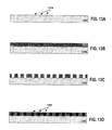
- FIGS. 13A-13G are exemplary embodiments of the results of corresponding processing steps in accordance with an exemplary embodiment of the present disclosure.
- FIG. 14 is a top view of an active die fashioned with a thermal bond pad in accordance with an exemplary embodiment of the present disclosure
- FIG. 15 and FIG. 16 are flow chart algorithms describing alternative ordering of steps in the production of bumped devices, in accordance with an exemplary embodiment of the present disclosure
- FIG. 17 is a flow chart algorithm for producing interposers in accordance with an exemplary embodiment of the present disclosure.
- FIGS. 18A-18J show exemplary results of corresponding processing steps
- FIG. 19 and FIG. 20 show via, redistribution layer and interface pad patterns in accordance with an exemplary embodiment of the present disclosure
- FIG. 21 is a flow chart algorithm of a process for completing the WLP package in accordance with an exemplary embodiment of the present disclosure
- FIGS. 22A-D show structures that can be created using the exemplary processes disclosed in FIGS. 12 and 15 - 17 ;
- FIG. 23 illustrates an example of where variable pitch can be used for the different types of vias in an interposer
- FIG. 24 shows a metal leadframe used as an interposer prior to singulation
- FIG. 25 shows a typical process for creating a metal leadframe
- FIG. 26 shows a side view of an exemplary metal leadframe where both surfaces are partially etched
- FIG. 27A shows the contact surface of a metal leadframe
- FIG. 27B shows the interface surface of the same metal leadframe
- the process of assembling the WLP package comprises an additional step over that described in FIG. 21 and is described in FIG. 28 ;
- FIGS. 29A-E show the corresponding structures that are created by the various process steps.
- FIGS. 1A and 1B show an example of a fan-out WLP with a thermal pad to improve thermal dissipation.
- the backside of a plurality of singulated dies e.g., die 314
- Gaps between the dies are filled by mold compound 410 such as a molded resin.
- the active surface of the die is covered with passivation layer 404 .
- Formed within passivation layer 404 is a redistribution layer (representative indicated by arrows 406 ).
- the WLP package shown in FIG. 1A also comprises a thermal pad such as thermal pad 412 underneath each active die.
- the redistribution layer and the thermal pad comprise metal traces (such as copper).
- FIG. 1B shows an individual singulated package.
- the package comprises wafer portion 422 which is the portion of wafer 302 attached to die 314 after singulation.
- solder is attached to the interface pads including thermal pad 412 .
- solder is built up either by plating or stenciling onto the electrical interface pads indicated by solder 416 and onto the thermal pad indicated by solder 418 . The solder can be applied either before or after singulation.
- thermal pad 412 is a solid piece of the chosen metal. This provides a great deal of thermal dissipation from the active die into a PCB. However, if the active die is sufficiently large, stresses due to the different thermal coefficients of expansion of the active die, the PCB and the thermal pad could damage the package during the packaging or assembly process when the temperature is drastically changed (e.g., heating in a reflow oven). In order to alleviate the stress in larger packages, pillars can be constructed between the thermal pad and the active die as a stand off.
- FIGS. 2 , 3 and 4 show an example of a fan-out WLP with a thermal pad and pillars as a standoff.
- the backside of a plurality of singulated dies e.g., die 314
- the gaps between the dies are filled with the same material as the passivation layer.
- Passivation material 510 fills both the gaps between the dies and provides a passivation layer which covers the active surface of each die.
- Formed within the passivation layer is a redistribution layer (representative indicated by arrows 506 .) and thermal pads represented by thermal pad 512 .
- thermal pad 512 is connected to active die 314 by an array of pillars. This allows the WLP package to flex during changes in temperature. The pillars can absorb the coefficient of thermal expansion stress that would otherwise be imparted to the device.
- FIG. 3 shows the corresponding singulated package.
- the package comprises wafer portion 522 which is the portion of wafer 302 attached to die 314 after singulation.
- solder is attached to the interface pads including thermal pad 512 .
- solder is built up either by plating or stenciling onto thermal pad 512 indicated by solder 518 to the same height as the solder balls. Then solder balls such as solder ball 516 are ball dropped onto their corresponding electrical pad.
- This process of applying solder can take place either before or after singulation. It should be noted that this approach could be used with a solid thermal pad such as thermal pad 412 in FIG. 2 or the approach described above of building up the solder on both the interface pads and thermal pads could be used in this example.
- FIG. 4 shows an exemplary pattern of interface pads.
- the electrical interface pads such as one connected to connection structure 506 are connected to bond pads by use of metal traces within a redistribution layer.
- Thermal pad 512 is shown with pillars 522 used as a stand off. The dotted area indicates the footprint of active die 314 .
- FIG. 5 describes a method of packaging an active die in a WLP package with a thermal pad in accordance with an exemplary embodiment of the present disclosure.
- FIGS. 6A-6E shows various exemplary thermal pad embodiments
- FIG. 6F shows an exemplary alternate embodiment of an electrical pad
- FIGS. 7A-J show exemplary structures corresponding to the steps of the method of FIG. 5 .
- Different configurations of the thermal pad structure can be fabricated, and several exemplary embodiments are shown in FIGS. 6A-6E .
- the examples depicted in FIGS. 7A-7J demonstrate a series of fabrication steps for the structure shown in FIG. 6B .
- the backside of active dies including exemplary die 314 are attached to wafer 302 as shown in FIG. 7A .
- a mold compound can be deposited between active dies.
- step 604 can be combined with step 606 .
- step 606 passivation layer 510 is applied atop the active die.
- the passivation layer is usually a dielectric such as a polyimide or benzocyclobutene (BCB).
- step 608 openings are made in the passivation layer to accommodate the vias for the array of pillars.
- Exemplary openings are shown in FIG. 7C with arrows 702 .
- the openings are made for the stand offs to the thermal pad.
- a large opening can be made for a solid thermal pad.
- the opening for the large thermal pad can be made to the passivation layer, the large thermal pad can be deposited prior to the application of the passivation layer, or other suitable processes can be used.
- metal is deposited in the openings in passivation layer 510 as show in FIG. 7D . This process can use sputtering, chemical vapor deposition (CVD), plating, or a combination thereof.
- metal traces for the redistribution layer are deposited.
- the metal for the electrical redistribution is shown by arrow 704 and for the thermal pad by arrows 706 .
- the redistribution layer and thermal pad can be deposited by sputtering and/or plating or alternatively by printing the metal traces onto the passivation layer or by a combination thereof as shown in FIG. 7E .
- the metal traces for the bond pad can be a pillar over the pillars created by steps 608 and 610 (e.g., FIGS.
- FIGS. 6A and 6C a metal layer spanning the extent of the thermal pad
- FIG. 6D a general redistribution
- FIG. 7F another layer of passivation material is deposited as shown in FIG. 7F .
- openings are created for the both the electrical and thermal bond pads as shown in FIG. 7G . Openings for the electrical pads are indicated by arrows 708 and for the thermal pad by arrows 710 . In an alternate embodiment (e.g., FIGS. 6E and 6F ) openings for vias to the electrical pads and thermal pad are created.
- metal is deposited into the openings as shown in FIG. 7H .
- Examples of metal for the electrical pads are indicated by arrows 712 .
- Examples of metal for the thermal pads are indicated by arrow 714 .
- this can be a sputtering, CVD or plating process or a combination thereof.
- the vias are filled at step 618 and additionally metal is deposited on the surface of the passivation layer to form interface pads.
- solder is applied to the interface pads—solder 716 is applied to the electrical interface pads and solder 718 is applied to the thermal pad as shown in FIG. 7I . As described above, the solder can be stenciled or plated on.
- solder 718 could be stenciled or plated on to a predetermined height and solder 718 can be solder balls that are ball dropped onto their corresponding interface pads.
- the package is singulated as shown in FIG. 7J .
- each example shows the two passivation layers (denoted by arrows 652 and 654 ).
- the metal corresponding to the redistribution layer is shown in a lighter shade for clarity.
- a solid thermal pad is shown.
- the thermal pad can be built up prior to applying the passivation layers or can be deposited according to the various steps described in FIG. 5 .
- the thermal pad is built on pillars coupled to the active die.
- a pillar (or alternatively) redistribution traces in a redistribution layer is formed on top of the first passivation layer.
- the thermal pad is also built on pillars coupled to the active die.
- a metal layer serving as the base of the thermal pad is fashion during step 610 on top of the first passivation layer.
- the thermal pad is once again built on pillars coupled to the active die. Redistribution traces in a redistribution layer is formed on top of the first passivation layer. However unlike FIG. 6B , vias are created in the second passivation layer to connect the redistribution traces to the thermal pad which is formed on top of the second passivation layer.
- FIG. 6E is similar to FIG. 6D except rather than redistribution traces, a pillar is formed on top of the passivation layer. Finally, FIG. 6F shows an electrical pad counterpart to FIG. 6E .
- the thermal pad is built on pillars coupled to the active die.
- a pillar (or alternatively) redistribution traces in a redistribution layer is formed on top of the first passivation layer.
- An alternative method to improve thermal dissipation in WLP packages includes attaching the fabricated die to an interposer to the active side of the die. This also eliminates the need for a separate structural wafer (such as wafer 302 ) to be attached to the backside of the active dies as a foundation of the package.
- the interposer comprises through substrate vias for electrically and thermally coupling the active die to interface pads on the interposer. The inclusion of an interposer permits an inexpensive foundation upon which to form a relatively large thermal pad which itself permits greater thermal conductance of heat away from the active die.
- FIGS. 8A and 8B illustrate an embodiment of a WLP package with an interposer in accordance with an exemplary embodiment of the present disclosure.
- Interposer 830 is attached to bumped device 820 .
- Bumped device 820 comprises active die 812 and metal pillars 822 .
- layer 804 is used to protect the backside of the active die.
- Bumps 824 couple metal pillars 822 to corresponding vias 832 on interposer 830 .
- the exposed surface metal of each via can serve as a catch pad on interposer 830 .
- the gap between bumped device 820 and interposer 830 is filled with moldable underfill 810 .
- Interposer 830 comprises substrate 816 and vias 832 , interface pads 834 and plating metal 836 .
- both the active die 812 and interposer substrate 816 are packaged as wafers prior to singulation.
- active die 812 is part of wafer 802 which comprises a plurality of active dies.
- Interposer substrate 816 is part of substrate 806 which houses a plurality of interposers. After metal pillars are attached to the active dies on the wafers, the wafer of interposers is attached. After which, moldable underfill 810 is used to fill the gaps between the two wafers. Once the two wafers are packaged together, individual packages are singulated along dotted lines 808 .
- FIGS. 9A and 9B illustrate another embodiment of a WLP package with an interposer, in accordance with an exemplary embodiment of the present disclosure.
- Interposer 930 is attached to bumped device 920 .
- bumped device 920 comprises active die 902 and metal pillars 922 .
- active die 902 is singulated prior to packaging and prior to being attached to interposer 930 .
- Interposer 930 comprises substrate 914 , vias 932 , interface pads 934 and plating metal 936 . Vias 932 are connected to interface pads 934 . Each interface pad is plated by metal 936 . Bumps 924 on bumped device 920 couple metal pillars 922 to corresponding catch pads (e.g., surface metal of corresponding vias 932 ) on interposer 930 . The gap between bumped device 920 and interposer 930 and the space around active die 902 is encapsulated with moldable underfill 906 . Moldable underfill 906 can also be used to protect the backside of active die 902 . In this embodiment, only the interposer substrate 914 is packaged as a wafer prior to singulation. Referring to FIG.
- Interposer substrate 914 is part of substrate 904 which houses a plurality of interposers. After metal pillars are attached to the active dies, each active die is attached to a corresponding interposer on the wafer of interposers. After which, moldable underfill 906 is used to fill the gaps between the interposers and active dies as well as encapsulating the active dies. Once the packaging is completed, individual packages are singulated along dotted lines 908 .
- FIGS. 10A and 10B illustrate another embodiment of a WLP package with an interposer, in accordance with an exemplary embodiment of the present disclosure.
- Interposer 1030 is attached to bumped device 1020 .
- bumped device 1020 comprises active die 1012 and metal pillars 1022 .
- layer 1006 is used to protect the backside of the active die.
- Interposer 1030 comprises substrate 1004 , vias 1032 , interface pads 1034 and plating metal 1036 . Vias 1032 are connected to interface pads 1034 . Each interface pad is plated by metal 1036 . Bumps 1024 on bumped device 1020 couple metal pillars 1022 to corresponding catch pads (e.g., surface metal of corresponding vias 1032 ) on interposer 1030 . The gap between bumped device 1020 and interposer 1030 and the space around interposer 1030 is encapsulated with underfill 1010 . In this embodiment, only the active die 1012 is packaged as a wafer prior to singulation. Referring to FIG.
- active die 1012 is part of wafer 1002 which comprises a plurality of active dies. However, each interposer is singulated prior to packaging. Each interposer is attached to a corresponding active die on wafer 1002 . After which underfill 1010 is used to fill the gaps between the interposers and active dies as well as gaps between interposers. Once the packaging is completed, individual packages are singulated along dotted lines 1008 .
- FIGS. 8A , 8 B, 9 A, 9 B, 10 A and 10 B show examples of fan-in WLP packaging using an interposer for improved heat dissipation.
- the interface pads can be formed directly under the corresponding catch pads or can be fanned in from a catch pad towards the center as the thermal pad permits.
- the use of an interposer permits the creation of a thermal interface pad under the center of the active die which can be coupled during assembly to the ground plane of a printed circuit board (PCB) allowing for significant heat to be drawn away from the active dies and dissipated into the PCB. Further dissipation can improved by adopting the fan-out WLP style of interfacing, which can allow for greater spacing and/or additional I/O between electrical interface pads and a larger thermal interface pad.
- FIGS. 11A and 11B illustrate an embodiment of a fan-out WLP package with an interposer, in accordance with an exemplary embodiment of the present disclosure.
- Interposer 1130 includes a redistribution layer to spread the interfacing across the interface surface of interposer 1130 , and is attached to bumped device 1120 .
- Bumped device includes active die 1102 and metal pillars 1122 .
- Interposer 1130 comprises substrate 1114 , vias 1132 , redistribution layer 1134 and plating metal 1136 .
- Vias 1132 are connected to redistribution layer 1134 .
- Redistribution layer comprises a plurality of interface pads and metal traces. The metal traces connect each interface pad to at least one via. Each interface pad is plated by metal 1136 .
- Bumps 1124 on bumped device 1120 couple metal pillars 1122 to corresponding vias 1132 on interposer 1130 .
- the gap between bumped device 1120 and interposer 1130 and the space around active die 1102 is encapsulated with underfill 1106 . Underfill 1106 can also be used to protect the backside of active die 1102 .
- interposer substrate 1114 is packaged as a wafer prior to singulation.
- FIG. 11A which shows the WLP package prior to singulation
- a plurality of active dies (represented by active die 1102 ) are singulated prior to packaging.
- Interposer substrate 1114 is part of substrate 1104 which houses a plurality of interposers.
- the metal pillars typically comprise copper. While other metals can be used, copper remains rigid during the reflow steps described below and during assembly.
- the bumps (which are also referred to as caps) such as bumps 824 , 924 , 1024 or 1124 typically comprise solder (e.g., tin), but can be made of a tin/silver alloy, gold, silver or copper. Generally, the bumps should comprise an electrically conductive material which will bond the metal pillars to the vias when suitably heated.
- the vias 832 , 932 , 1032 , or 1132 comprise a metal such as copper, tungsten or gold.
- the interface pads such as interface pads 834 , 934 , 1034 or 1134 can also comprise a metal such as copper, tungsten or gold.
- the plate metal used in these packages such as metals 836 , 936 , 1036 or 1136 can comprise a solder material such as tin or a protective material such as a nickel/palladium alloy or nickel/palladium/gold.
- a protective material would prevent the underlying interface pads (and metal traces) from oxidizing to maintain the shelf life of the package where a solder material could be added at a later time.
- a solder material can be included in the package to facilitate bonding to a PCB.
- the interposer substrate can be selected from a number of materials such as silicon or a ceramic.
- a silicon substrate is a workable and an inexpensive choice of material.
- the mold compounds (such as indicated by 804 , 810 , 906 , 1006 , 1010 , and 1106 can be any number of mold compounds commonly used for semiconductor encapsulation such epoxy-resins, hardeners, catalysts, or a combination thereof. These materials often comprise a fill material such as silica or a ceramic.
- FIG. 12 is flow chart algorithm of an exemplary process for producing bumped devices from active dies
- FIGS. 13A-13G are exemplary embodiments of the results of corresponding processing steps in accordance with an exemplary embodiment of the present disclosure.
- FIG. 13A shows wafer 1302 comprising a plurality of active dies. Each active die comprises a plurality of bond pads represented by bond pads 1304 .
- photoresist layer 1306 is applied to wafer 1302 as shown in FIG. 13B .
- photoresist layer 1306 is exposed to a mask and developed leaving openings above the bond pads as shown in FIG. 13C .
- metal 1308 is deposited into openings in photoresist layer 1306 as shown in FIG.
- the metal can be selected from a number of materials such as copper, aluminum and gold.
- the metal can be deposited by sputtering or by plating or a combination of both processes (e.g., a seed layer could be deposited by sputtering followed by a plating process to complete the deposition).
- photoresist layer 1306 is removed revealing metal pillars as shown in FIG. 13E .
- bumps represented by bumps 1310 are applied to the metal pillars as shown in FIG. 13F , for example by plating or stenciling.
- the active dies are optionally singulated at step 1212 and shown in FIG. 13G .
- FIG. 14 is a top view of an active die fashioned with a thermal bond pad in accordance with an exemplary embodiment of the present disclosure.
- Active die 1400 comprises conventional bond pads represented by bond pads 1402 around the perimeter of the active die. It also comprises thermal pad 1404 in the center of the active die. Pillars can then be grown on these bond pads in the matter described in FIG. 12 .
- FIG. 15 and FIG. 16 are flow chart algorithms describing alternative ordering of steps in the production of bumped devices, in accordance with an exemplary embodiment of the present disclosure.
- singulation takes place after the metal pillars are deposited but before bumps are applied to the metal pillars.
- the metal pillars are grown on singulated active dies. The variation in order may be necessary to accommodate the individual capabilities of each particular packaging vendor.
- FIG. 17 is a flow chart algorithm for producing interposers in accordance with an exemplary embodiment of the present disclosure.
- FIGS. 18A-18J show exemplary results of corresponding processing steps.
- deep holes are formed in the interposer substrate. These holes are located where the desired vias are located.
- DRIE deep reactive ion etching
- FIGS. 18 A- 18 C show exemplary results from using an etching method for step 1702 .
- Photoresist layer 1804 is applied to interposer substrate 1802 as shown in FIG. 18A .
- the photoresist layer 1804 is exposed to a mask and developed leaving openings where vias are desired as shown in FIG. 18B . Deep holes are etched in the openings in photoresist layer 1804 as shown in FIG. 18C .
- the surface of interposer 1802 and the walls of the vias are coated with a barrier material 1806 , which is typically a dielectric such as silicon dioxide as show in FIG. 18D .
- the barrier material is applied by chemical vapor deposition (CVD).
- metal is deposited to fill the vias and on the surface of the interposer.
- the deposition process can use CVD, sputter, plating, a combination thereof, or other suitable processes.
- the deposition process can also include a less common alternative, such as filling the vias with a metal filled paste.
- a metal filled paste For example, CVD or sputter can be used to create a seed layer of metal on top of the barrier layer. Then metal can be plated onto the seed layer to complete the deposition step.
- opposite surface 1810 is ground down to expose the via metal as shown in FIG. 18F .
- the surface can be ground down by processes such as chemical mechanical polishing (CMP).
- CMP chemical mechanical polishing
- the metal on the surface of the interposer is patterned into the desired pattern of interface pads and optionally a redistribution layer. There are several approaches to patterning the metal on the interface surface which are discussed below.
- the interface pads are plated with metal 1816 .
- the plating can be solder, a nickel/gold, a nickel/palladium or some combination thereof. Alternatively, the plating step 1712 can also be performed after the interposer is attached to the active die as described in FIG. 21 .
- the interposers are singulated.
- the interposers are not singulated prior to assembly stop step 1720 would be omitted.
- step 1710 the patterning of the interface surface is illustrated in FIGS. 18G , 18 H and 18 I.
- photoresist layer 1812 is applied to metal 1808 .
- FIG. 18H photoresist layer 1812 is exposed to a mask and developed revealing openings 1814 in accordance with the desired pattern.
- FIG. 18I the metal is etched away by a wet etch process. The photoresist is then removed (not shown).
- the layer of metal deposited in step 1706 only provides a thin coating on the interface surface.
- the metal is etched away, for example by steps similar to shown in FIGS. 18G , 18 H and 18 I, leaving the desired pattern in the metal. Due to the thinness of the metal layer, the initial metal layer serves as a seed layer for additional metal deposition. After the seed layer is patterned, additional metal can be deposited by plating until the desired thickness is achieved.
- the layer of deposited metal on the interface surface is ground down such as by CMP to the substrate leaving only the substrate and the via metal. Because the deposition in step 1706 often leaves depressions or dimples where the vias were filled, the resultant surface is not sufficiently flat to support fine metal lines for redistribution.
- a seed layer is deposited by sputtering or CVD, the result is a relatively flat metal layer on top of the interface surface of the interposer.
- the metal is etched away, for example by steps similar to shown in FIGS. 18G , 18 H and 18 I, leaving the desired pattern in the metal. Due to the thinness of the metal layer, after the seed layer is patterned, additional metal can be deposited by plating until the desired thickness is achieved.
- barrier material is only depicted in FIGS. 18D-18J . However, it should be understood that the barrier material and other suitable material is present at the interface between the substrate and a filled via, interface pad or metal trace.
- FIG. 19 and FIG. 20 show via, redistribution layer and interface pad patterns in accordance with an exemplary embodiment of the present disclosure.
- FIG. 19 is a top view of the contact surface of interposer 1900 .
- the contact surface is the surface to which the active die is to be applied.
- Exterior catch pads represented by catch pads 1902 correspond to the bond pad locations of the active die and in this example are the exposed surface metal of underlying vias. These vias are used to electrically couple the bond pad to corresponding interface pads on the interface surface of interposer 1900 .
- Interior catch pads 1904 are used for thermal purposes and in this example are the exposed surface metal of underlying vias. These vias make thermal contact with the active die and conduct heat to at least one thermal pad on the interface surface of interposer 1900 .
- these vias can also be electrically coupled to the ground on the active die.
- FIG. 20 is a top view of the interface surface of interposer 1900 in accordance with an exemplary embodiment of the present disclosure.
- the interface surface is the surface which is used to interface the package to a system during assembly such as by attaching it to a PCB.
- Metal traces represented by traces 2006 lead from the electrical via locations (e.g., via 1902 ) to electrical interface pads such as interface pads 2002 .
- thermal interface pad 2004 is coupled to one or more thermal vias and is often attached to the ground plane during assembly allowing for heat from the active die to be conducted into the ground plane of a system.
- FIG. 21 is a flow chart algorithm of a process for completing the WLP package in accordance with an exemplary embodiment of the present disclosure.
- Bump devices can be created by the process described in FIG. 12 , 15 or 16 .
- Interposers can be created by the process described in FIG. 17 .
- FIGS. 22A-D show structures that can be created using the exemplary processes disclosed in FIGS. 12 and 15 - 17 .
- the bumped devices are attached to the interposers.
- the bumped devices are placed onto of the interposers and placed into a reflow oven. The reflow oven heats the structure allowing the solder bumps on the metal pillars of each bumped device to melt and bond with its corresponding vias on interposer.
- the active dies are shown as singulated while the interposers share a common wafer substrate.
- a mold underfill is applied to the structure.
- the mold compound 2202 is allowed to flow in the gaps between the metal pillars as well as any gaps between the active die.
- the mold compound also encapsulates the backside of the active dies.
- the molding process can employ one of several encapsulation techniques including injection molding or compression molding.
- the interface pads are plated.
- the plating metal can be a solder material such as tin or a protective metal such as a nickel/palladium or nickel/palladium/flash gold alloy as previously discussed. This step can be performed if step 1712 is omitted or can be performed in addition to step 1712 . Whether the plating is performed before or after the interposer is attached to the die depends on the equipment available at each step and the application of the semiconductor package.
- each package is singulated into individual packages as shown in FIG. 22D , where gaps 2204 indicate the singulation incision.
- Singulation can be performed by saw singulation where the individual packages are sawn apart or by less commonly by punch singulation.
- FIG. 23 illustrates an example of where variable pitch can be used for the different types of vias in an interposer.
- the figure shows a top view of the contact side of interposer 2300 .
- Interposer 2300 comprises a plurality of electrical vias (e.g., vias 2302 ) and a plurality of thermal vias (e.g., vias 2304 ).
- the pitch of the thermal vias is twice that of electrical vias.
- thermal via pitch could be 250 ⁇ m and the electrical via pitch could be 125 ⁇ m, or vice versa.
- this example illustrates the densities of vias on an interposer.
- the preceding examples have their numbers reduced for clarity, but in practical examples, the vias could number in the hundreds or more as illustrated in FIG. 23 .
- FIG. 24 shows a metal leadframe used as an interposer prior to singulation.
- Dotted line 2402 shows an interposer constructed for a single active die.
- the unshaded structures are half etched (e.g., metal trace 2410 and tie bar 2412 ) and the shaded structures are not etched including the electrical pads (e.g., 2404 ) and thermal pads (e.g., 2406 ). Only the shaded structures are accessible on the interface side of the metal leadframe.
- the bumped device can be attached to the metal leadframe.
- the metal pads on the contact side are function as catch pads.
- the dark circles (e.g., 2408 ) show the placement of the metal pillars on the bumped device relative to the catch pads on the metal leadframe.
- Tie bars e.g., 2412 ) are used to hold metal leadframe together until the package is singulated where the tie bars are removed. For example, often the connecting tie bars are smaller than the blade width of the singulating saw. Thus, when the saw singulates the package it consumes much of the tie bar structure, leaving only what is shown within dotted line 2402 .
- FIG. 25 shows a typical process for creating a metal leadframe.
- the pattern on the interface side is half etched into a metal sheet.
- An example of the specific steps to etching is to apply a photoresist material, expose it to the desired pattern developing the photoresist material, etching the metal to a predetermined fraction of the metal thickness and the removal of the remaining photoresist material. Several etching processes can be used, such as wet etching.
- the pattern on the contact side of the metal sheet is fully etched. Once again a photoresist-etch process can be used.
- the sheet can be subdivided into strips.
- the assembly of the bumped device to the metal leadframe interposer is similar to that described in FIG. 21 , except at step 2104 the gaps within the metal leadframe can be filled with mold compound in addition to other suitable spaces, such as the space between the metal pillars and between the active die and interposer.
- FIG. 26 shows a side view of an exemplary metal leadframe where both surfaces are partially etched. Structures indicated by arrow 2602 show the structures such as catch pads and metal traces on the contact side of the leadframe. Structures indicated by arrow 2604 show the structures such as electrical and thermal interface pads on the interface side of the leadframe. Arrow 2606 shows the continuous sheet in between.
- FIG. 27A shows the contact surface of a metal leadframe.
- the connection structures are shown here as in FIG. 24 . It comprises a plurality of metal traces connecting the electrical catch pads to their corresponding interface pads (e.g., structure 2702 ). It comprises thermal pad 2704 .
- FIG. 27B shows the interface surface of the same metal leadframe. On this surface only the electrical (e.g., 2706 ) and thermal interface pads (e.g., 2704 ) are visible. After a leadframe of this type is assembled into a package, the interface surface is further etched to remove the intervening metal sheet.
- electrical e.g., 2706
- thermal interface pads e.g., 2704
- step 2504 the contact surface pattern does not need to be etched fully, but instead can be etched partially.
- the depth of the etch in step 2502 can also be modified to leave a metal sheet in between.
- step 2502 can etch a pattern to 45% of the metal thickness and step 2504 can etch another pattern to 45% of the metal thickness leaving 10% of the thickness of the original metal throughout the leadframe.
- FIGS. 29A-E show the corresponding structures that are created by the various process steps.
- the bumped devices are attached to metal leadframe 2902 .
- the bumped devices are placed onto of metal leadframe 2902 and placed into a reflow oven.
- the reflow oven heats the structure allowing the solder bumps on the metal pillars of each bumped device to melt and bond with its corresponding vias on interposer.
- the active dies are shown as singulated while the interposers metal leadframe are connected between packages.
- a mold underfill is applied to the structure.
- the mold compound 2906 is allowed to flow in the gaps between the metal pillars as well as any gaps between the active die.
- mold compound 2906 is allowed to flow in the gaps between the metal in metal leadframe 2902 (e.g., gaps indicated by arrows 2904 ).
- the mold compound also encapsulates the backside of the active dies.
- the molding process can employ one of several encapsulation techniques including injection molding or compression molding.
- the excess metal on metal leadframe 2902 is removed. This results in better definition of features such as the electrical and thermal interface pads and removes intervening metal between discrete structures. This removal can be a chemical etching process such as a wet etching or a physical process and is shown in FIG. 29C
- the interface pads are plated.
- the plating metal can be a solder material such as tin or a protective metal such as a nickel/palladium or nickel/palladium/flash gold alloy as previously discussed. This is shown in FIG. 29D .
- each package is singulated into individual packages as shown in FIG. 29E , where gaps 2908 indicate the singulation incision.
- Singulation can be performed by saw singulation where the individual packages are sawn apart or by less commonly by punch singulation.
Landscapes
- Internal Circuitry In Semiconductor Integrated Circuit Devices (AREA)
Abstract
Description
Claims (6)
Priority Applications (1)
| Application Number | Priority Date | Filing Date | Title |
|---|---|---|---|
| US13/104,620 US8552540B2 (en) | 2011-05-10 | 2011-05-10 | Wafer level package with thermal pad for higher power dissipation |
Applications Claiming Priority (1)
| Application Number | Priority Date | Filing Date | Title |
|---|---|---|---|
| US13/104,620 US8552540B2 (en) | 2011-05-10 | 2011-05-10 | Wafer level package with thermal pad for higher power dissipation |
Publications (2)
| Publication Number | Publication Date |
|---|---|
| US20120286408A1 US20120286408A1 (en) | 2012-11-15 |
| US8552540B2 true US8552540B2 (en) | 2013-10-08 |
Family
ID=47141343
Family Applications (1)
| Application Number | Title | Priority Date | Filing Date |
|---|---|---|---|
| US13/104,620 Active US8552540B2 (en) | 2011-05-10 | 2011-05-10 | Wafer level package with thermal pad for higher power dissipation |
Country Status (1)
| Country | Link |
|---|---|
| US (1) | US8552540B2 (en) |
Cited By (3)
| Publication number | Priority date | Publication date | Assignee | Title |
|---|---|---|---|---|
| US20230093214A1 (en) * | 2020-04-02 | 2023-03-23 | Texas Instruments Incorporated | Shape memory polymer for use in semiconductor device fabrication |
| US11656273B1 (en) | 2021-11-05 | 2023-05-23 | Advantest Test Solutions, Inc. | High current device testing apparatus and systems |
| US11676904B2 (en) | 2020-08-06 | 2023-06-13 | Samsung Electronics Co., Ltd. | Semiconductor package |
Families Citing this family (14)
| Publication number | Priority date | Publication date | Assignee | Title |
|---|---|---|---|---|
| JP6238121B2 (en) * | 2013-10-01 | 2017-11-29 | ローム株式会社 | Semiconductor device |
| TWM496091U (en) * | 2014-03-26 | 2015-02-21 | 賀喜能源股份有限公司 | Light-emitting diode with 矽 base and light-emitting diode lamp |
| TW201601358A (en) * | 2014-06-19 | 2016-01-01 | 道康寧公司 | Photopatternable polyfluorene for wafer level Z-axis thermal interposer |
| US9972593B2 (en) * | 2014-11-07 | 2018-05-15 | Mediatek Inc. | Semiconductor package |
| CN104681456B (en) * | 2015-01-27 | 2017-07-14 | 华进半导体封装先导技术研发中心有限公司 | A kind of fan-out-type wafer-level packaging method |
| US9779940B2 (en) * | 2015-07-01 | 2017-10-03 | Zhuahai Advanced Chip Carriers & Electronic Substrate Solutions Technologies Co. Ltd. | Chip package |
| US9589920B2 (en) * | 2015-07-01 | 2017-03-07 | Zhuhai Advanced Chip Carriers & Electronic Substrate Solutions Technologies Co. Ltd. | Chip package |
| US9875988B2 (en) * | 2015-10-29 | 2018-01-23 | Semtech Corporation | Semiconductor device and method of forming DCALGA package using semiconductor die with micro pillars |
| DE102015120745B4 (en) * | 2015-11-30 | 2021-12-09 | Infineon Technologies Austria Ag | Chip protective packaging and processes |
| CN106057820B (en) * | 2016-07-21 | 2019-04-30 | 京东方科技集团股份有限公司 | Array substrate and preparation method thereof, display panel, and display device |
| US10410988B2 (en) * | 2016-08-09 | 2019-09-10 | Semtech Corporation | Single-shot encapsulation |
| US11652074B2 (en) * | 2017-09-29 | 2023-05-16 | Intel Corporation | Semiconductor package with improved thermal blocks |
| US11282756B2 (en) * | 2020-08-17 | 2022-03-22 | Taiwan Semiconductor Manufacturing Company Limited | Organic interposer including stress-resistant bonding structures and methods of forming the same |
| US11894327B2 (en) * | 2021-08-18 | 2024-02-06 | Micron Technology, Inc. | Apparatus including integrated segments and methods of manufacturing the same |
Citations (62)
| Publication number | Priority date | Publication date | Assignee | Title |
|---|---|---|---|---|
| US5497033A (en) * | 1993-02-08 | 1996-03-05 | Martin Marietta Corporation | Embedded substrate for integrated circuit modules |
| US5616957A (en) | 1994-05-19 | 1997-04-01 | Nec Corporation | Plastic package type semiconductor device |
| US5656864A (en) | 1993-09-09 | 1997-08-12 | Fujitsu Limited | Semiconductor device having upper and lower package bodies and manufacturing method thereof |
| US5672548A (en) | 1994-07-11 | 1997-09-30 | International Business Machines Corporation | Method for attaching heat sinks directly to chip carrier modules using flexible-epoxy |
| US5886408A (en) | 1994-09-08 | 1999-03-23 | Fujitsu Limited | Multi-chip semiconductor device |
| EP0987757A2 (en) | 1998-09-17 | 2000-03-22 | Kitagawa Industries Co., Ltd. | Heat dissipator for electronic device |
| US6097602A (en) | 1998-06-23 | 2000-08-01 | Marian, Inc. | Integrated circuit package heat sink attachment |
| US6239482B1 (en) * | 1999-06-21 | 2001-05-29 | General Electric Company | Integrated circuit package including window frame |
| US20020074649A1 (en) | 2000-12-14 | 2002-06-20 | Intel Corporation | Electronic assembly with high capacity thermal interface and methods of manufacture |
| WO2002061830A1 (en) | 2001-01-31 | 2002-08-08 | Young Sun Kim | Heat dissipation type semiconductor package and method of fabricating the same |
| US6507116B1 (en) | 1997-04-24 | 2003-01-14 | International Business Machines Corporation | Electronic package and method of forming |
| US6506632B1 (en) * | 2002-02-15 | 2003-01-14 | Unimicron Technology Corp. | Method of forming IC package having downward-facing chip cavity |
| US6548338B2 (en) * | 1999-03-31 | 2003-04-15 | International Business Machines Corp. | Integrated high-performance decoupling capacitor and heat sink |
| US6734552B2 (en) | 2001-07-11 | 2004-05-11 | Asat Limited | Enhanced thermal dissipation integrated circuit package |
| US20050062147A1 (en) * | 2003-09-19 | 2005-03-24 | Casio Computer Co., Ltd. | Semiconductor device having heat dissipation layer |
| US20050095875A1 (en) * | 2001-06-04 | 2005-05-05 | Chien-Ping Huang | Fabrication method of semiconductor package with heat sink |
| US6891259B2 (en) | 2001-11-03 | 2005-05-10 | Samsung Electronics Co., Ltd. | Semiconductor package having dam and method for fabricating the same |
| US6962867B2 (en) * | 2002-07-31 | 2005-11-08 | Microntechnology, Inc. | Methods of fabrication of semiconductor dice having back side redistribution layer accessed using through-silicon vias and assemblies thereof |
| US20060012017A1 (en) * | 2004-07-14 | 2006-01-19 | Fujitsu Limited | Semiconductor device and method of manufacturing the same |
| US20060087037A1 (en) * | 2004-10-22 | 2006-04-27 | Phoenix Precision Technology Corporation | Substrate structure with embedded chip of semiconductor package and method for fabricating the same |
| US20060097381A1 (en) | 1999-08-31 | 2006-05-11 | Salman Akram | Chip package with grease heat sink |
| US20060115931A1 (en) * | 2004-11-26 | 2006-06-01 | Phoenix Precision Technology Corporation | Semiconductor package substrate with embedded chip and fabrication method thereof |
| US7061113B2 (en) * | 2003-08-29 | 2006-06-13 | Oki Data Corporation | Semiconductor apparatus, led head, and image forming apparatus |
| US7064440B2 (en) * | 2004-01-27 | 2006-06-20 | Casio Computer Co., Ltd. | Semiconductor device |
| US20060163722A1 (en) * | 2005-01-21 | 2006-07-27 | Phoenix Precision Technology Corporation | Semiconductor chip electrical connection structure |
| US7112469B2 (en) * | 2004-01-27 | 2006-09-26 | Casio Computer Co., Ltd. | Method of fabricating a semiconductor package utilizing a thermosetting resin base member |
| US7126218B1 (en) | 2001-08-07 | 2006-10-24 | Amkor Technology, Inc. | Embedded heat spreader ball grid array |
| US7193301B2 (en) * | 2003-11-28 | 2007-03-20 | Oki Electric Industry Co., Ltd. | Semiconductor device and manufacturing method thereof |
| US7202561B2 (en) | 2004-01-28 | 2007-04-10 | Samsung Electronics Co., Ltd. | Semiconductor package with heat dissipating structure and method of manufacturing the same |
| US20070096313A1 (en) * | 2005-10-28 | 2007-05-03 | Megic Corporation | Semiconductor chip with post-passivation scheme formed over passivation layer |
| US20070145594A1 (en) * | 2005-12-28 | 2007-06-28 | Dongbu Electronics Co., Ltd. | Semiconductor device and method for manufacturing the same |
| US20070161231A1 (en) * | 2005-12-29 | 2007-07-12 | Dongbu Electronics Co., Ltd. | Method for forming metal wiring in a semiconductor device |
| US20070163645A1 (en) * | 2003-10-06 | 2007-07-19 | Ngk Spark Plug Co., Ltd. | Dye-sensitized solar cell |
| US20070187836A1 (en) * | 2006-02-15 | 2007-08-16 | Texas Instruments Incorporated | Package on package design a combination of laminate and tape substrate, with back-to-back die combination |
| US7279750B2 (en) * | 2004-03-31 | 2007-10-09 | Casio Computer Co., Ltd. | Semiconductor device incorporating a semiconductor constructing body and an interconnecting layer which is connected to a ground layer via a vertical conducting portion |
| US7295441B1 (en) * | 2006-05-12 | 2007-11-13 | Giga-Gyte Technology Co. Ltd. | Heat dissipating type printed circuit board and structure thereof for conducting heat with heap pipe |
| US20070289127A1 (en) * | 2006-04-20 | 2007-12-20 | Amitec- Advanced Multilayer Interconnect Technologies Ltd | Coreless cavity substrates for chip packaging and their fabrication |
| US20080020566A1 (en) * | 2005-04-21 | 2008-01-24 | Endicott Interconnect Technologies, Inc. | Method of making an interposer |
| US20080054454A1 (en) * | 2006-09-04 | 2008-03-06 | Sony Corporation | Semiconductor device and method for manufacturing semiconductor device |
| US20080153245A1 (en) * | 2006-12-21 | 2008-06-26 | Stats Chippac, Ltd. | Semiconductor Device and Method of Forming Passive Devices |
| US20080157341A1 (en) * | 2006-12-29 | 2008-07-03 | Advanced Chip Engineering Technology Inc. | RF module package |
| US20090045487A1 (en) * | 2007-08-16 | 2009-02-19 | Oh-Jin Jung | Semiconductor chip, method of fabricating the same and stacked package having the same |
| US7494843B1 (en) * | 2006-12-26 | 2009-02-24 | Bridge Semiconductor Corporation | Method of making a semiconductor chip assembly with thermal conductor and encapsulant grinding |
| US20090166841A1 (en) * | 2007-12-28 | 2009-07-02 | Phoenix Precision Technology Corporation | Package substrate embedded with semiconductor component |
| US20090184420A1 (en) * | 2008-01-22 | 2009-07-23 | Samsung Electromechanics Co., Ltd. | Post bump and method of forming the same |
| US20090200662A1 (en) * | 2008-02-12 | 2009-08-13 | United Test And Assembly Center Ltd | Semiconductor package and method of making the same |
| US20090224402A1 (en) * | 2008-03-07 | 2009-09-10 | Stats Chippac, Ltd. | Semiconductor Package Having Semiconductor Die with Internal Vertical Interconnect Structure and Method Therefor |
| US20090242252A1 (en) * | 2008-03-27 | 2009-10-01 | Ibiden Co., Ltd. | Method for Manufacturing A Multilayer Printed Wiring Board for Providing an Electronic Component Therein |
| US20100001309A1 (en) * | 2008-03-25 | 2010-01-07 | Bridge Semiconductor Corporation | Semiconductor chip assembly with post/base heat spreader and horizontal signal routing |
| US20100078655A1 (en) * | 2008-09-25 | 2010-04-01 | Wen-Kun Yang | Substrate structure with die embedded inside and dual build-up layers over both side surfaces and method of the same |
| US7700986B2 (en) * | 2008-07-17 | 2010-04-20 | Unimicron Technology Corp. | Chip package carrier and fabrication method thereof |
| US20100246152A1 (en) * | 2009-03-30 | 2010-09-30 | Megica Corporation | Integrated circuit chip using top post-passivation technology and bottom structure technology |
| US20100264526A1 (en) * | 2006-12-14 | 2010-10-21 | Advanpack Solutions Pte Ltd. | Semiconductor package and manufacturing method thereof |
| US7830000B2 (en) * | 2007-06-25 | 2010-11-09 | Epic Technologies, Inc. | Integrated thermal structures and fabrication methods thereof facilitating implementing a cell phone or other electronic system |
| US20100290191A1 (en) * | 2009-05-14 | 2010-11-18 | Megica Corporation | System-in packages |
| US7915728B2 (en) * | 2007-07-12 | 2011-03-29 | Vishay General Semiconductor Llc | Subassembly that includes a power semiconductor die and a heat sink having an exposed surface portion thereof |
| US20110084401A1 (en) * | 2008-03-19 | 2011-04-14 | Taewoo Lee | Package-on-package system with via z-interconnections and method for manufacturing thereof |
| US7981722B2 (en) * | 2005-10-05 | 2011-07-19 | Sony Corporation | Semiconductor device and fabrication method thereof |
| US8013440B2 (en) | 2008-03-28 | 2011-09-06 | Conexant Systems, Inc. | Enhanced thermal dissipation ball grid array package |
| US20110278722A1 (en) * | 2009-01-30 | 2011-11-17 | Panasonic Corporation | Semiconductor device and manufacturing method thereof |
| US20120061825A1 (en) * | 2010-09-09 | 2012-03-15 | Siliconware Precision Industries Co., Ltd. | Chip scale package and method of fabricating the same |
| US8188378B2 (en) * | 2007-12-28 | 2012-05-29 | Ibiden Co., Ltd. | Interposer and method for manufacturing interposer |
-
2011
- 2011-05-10 US US13/104,620 patent/US8552540B2/en active Active
Patent Citations (67)
| Publication number | Priority date | Publication date | Assignee | Title |
|---|---|---|---|---|
| US5497033A (en) * | 1993-02-08 | 1996-03-05 | Martin Marietta Corporation | Embedded substrate for integrated circuit modules |
| US5656864A (en) | 1993-09-09 | 1997-08-12 | Fujitsu Limited | Semiconductor device having upper and lower package bodies and manufacturing method thereof |
| US5616957A (en) | 1994-05-19 | 1997-04-01 | Nec Corporation | Plastic package type semiconductor device |
| US5672548A (en) | 1994-07-11 | 1997-09-30 | International Business Machines Corporation | Method for attaching heat sinks directly to chip carrier modules using flexible-epoxy |
| US5886408A (en) | 1994-09-08 | 1999-03-23 | Fujitsu Limited | Multi-chip semiconductor device |
| US6507116B1 (en) | 1997-04-24 | 2003-01-14 | International Business Machines Corporation | Electronic package and method of forming |
| US6097602A (en) | 1998-06-23 | 2000-08-01 | Marian, Inc. | Integrated circuit package heat sink attachment |
| EP0987757A2 (en) | 1998-09-17 | 2000-03-22 | Kitagawa Industries Co., Ltd. | Heat dissipator for electronic device |
| US6548338B2 (en) * | 1999-03-31 | 2003-04-15 | International Business Machines Corp. | Integrated high-performance decoupling capacitor and heat sink |
| US6239482B1 (en) * | 1999-06-21 | 2001-05-29 | General Electric Company | Integrated circuit package including window frame |
| US20060097381A1 (en) | 1999-08-31 | 2006-05-11 | Salman Akram | Chip package with grease heat sink |
| US20020074649A1 (en) | 2000-12-14 | 2002-06-20 | Intel Corporation | Electronic assembly with high capacity thermal interface and methods of manufacture |
| WO2002061830A1 (en) | 2001-01-31 | 2002-08-08 | Young Sun Kim | Heat dissipation type semiconductor package and method of fabricating the same |
| US20050095875A1 (en) * | 2001-06-04 | 2005-05-05 | Chien-Ping Huang | Fabrication method of semiconductor package with heat sink |
| US6734552B2 (en) | 2001-07-11 | 2004-05-11 | Asat Limited | Enhanced thermal dissipation integrated circuit package |
| US7126218B1 (en) | 2001-08-07 | 2006-10-24 | Amkor Technology, Inc. | Embedded heat spreader ball grid array |
| US6891259B2 (en) | 2001-11-03 | 2005-05-10 | Samsung Electronics Co., Ltd. | Semiconductor package having dam and method for fabricating the same |
| US6506632B1 (en) * | 2002-02-15 | 2003-01-14 | Unimicron Technology Corp. | Method of forming IC package having downward-facing chip cavity |
| US6962867B2 (en) * | 2002-07-31 | 2005-11-08 | Microntechnology, Inc. | Methods of fabrication of semiconductor dice having back side redistribution layer accessed using through-silicon vias and assemblies thereof |
| US7061113B2 (en) * | 2003-08-29 | 2006-06-13 | Oki Data Corporation | Semiconductor apparatus, led head, and image forming apparatus |
| US20050062147A1 (en) * | 2003-09-19 | 2005-03-24 | Casio Computer Co., Ltd. | Semiconductor device having heat dissipation layer |
| US20070163645A1 (en) * | 2003-10-06 | 2007-07-19 | Ngk Spark Plug Co., Ltd. | Dye-sensitized solar cell |
| US7193301B2 (en) * | 2003-11-28 | 2007-03-20 | Oki Electric Industry Co., Ltd. | Semiconductor device and manufacturing method thereof |
| US7064440B2 (en) * | 2004-01-27 | 2006-06-20 | Casio Computer Co., Ltd. | Semiconductor device |
| US7112469B2 (en) * | 2004-01-27 | 2006-09-26 | Casio Computer Co., Ltd. | Method of fabricating a semiconductor package utilizing a thermosetting resin base member |
| US7202561B2 (en) | 2004-01-28 | 2007-04-10 | Samsung Electronics Co., Ltd. | Semiconductor package with heat dissipating structure and method of manufacturing the same |
| US7279750B2 (en) * | 2004-03-31 | 2007-10-09 | Casio Computer Co., Ltd. | Semiconductor device incorporating a semiconductor constructing body and an interconnecting layer which is connected to a ground layer via a vertical conducting portion |
| US20060012017A1 (en) * | 2004-07-14 | 2006-01-19 | Fujitsu Limited | Semiconductor device and method of manufacturing the same |
| US20060087037A1 (en) * | 2004-10-22 | 2006-04-27 | Phoenix Precision Technology Corporation | Substrate structure with embedded chip of semiconductor package and method for fabricating the same |
| US20060115931A1 (en) * | 2004-11-26 | 2006-06-01 | Phoenix Precision Technology Corporation | Semiconductor package substrate with embedded chip and fabrication method thereof |
| US20060163722A1 (en) * | 2005-01-21 | 2006-07-27 | Phoenix Precision Technology Corporation | Semiconductor chip electrical connection structure |
| US20080020566A1 (en) * | 2005-04-21 | 2008-01-24 | Endicott Interconnect Technologies, Inc. | Method of making an interposer |
| US7981722B2 (en) * | 2005-10-05 | 2011-07-19 | Sony Corporation | Semiconductor device and fabrication method thereof |
| US20070096313A1 (en) * | 2005-10-28 | 2007-05-03 | Megic Corporation | Semiconductor chip with post-passivation scheme formed over passivation layer |
| US20070145594A1 (en) * | 2005-12-28 | 2007-06-28 | Dongbu Electronics Co., Ltd. | Semiconductor device and method for manufacturing the same |
| US20070161231A1 (en) * | 2005-12-29 | 2007-07-12 | Dongbu Electronics Co., Ltd. | Method for forming metal wiring in a semiconductor device |
| US20070187836A1 (en) * | 2006-02-15 | 2007-08-16 | Texas Instruments Incorporated | Package on package design a combination of laminate and tape substrate, with back-to-back die combination |
| US20070289127A1 (en) * | 2006-04-20 | 2007-12-20 | Amitec- Advanced Multilayer Interconnect Technologies Ltd | Coreless cavity substrates for chip packaging and their fabrication |
| US7669320B2 (en) * | 2006-04-20 | 2010-03-02 | Amitec-Advanced Multilayer Interconnect Technologies Ltd. | Coreless cavity substrates for chip packaging and their fabrication |
| US7295441B1 (en) * | 2006-05-12 | 2007-11-13 | Giga-Gyte Technology Co. Ltd. | Heat dissipating type printed circuit board and structure thereof for conducting heat with heap pipe |
| US20080054454A1 (en) * | 2006-09-04 | 2008-03-06 | Sony Corporation | Semiconductor device and method for manufacturing semiconductor device |
| US20100264526A1 (en) * | 2006-12-14 | 2010-10-21 | Advanpack Solutions Pte Ltd. | Semiconductor package and manufacturing method thereof |
| US20080153245A1 (en) * | 2006-12-21 | 2008-06-26 | Stats Chippac, Ltd. | Semiconductor Device and Method of Forming Passive Devices |
| US7494843B1 (en) * | 2006-12-26 | 2009-02-24 | Bridge Semiconductor Corporation | Method of making a semiconductor chip assembly with thermal conductor and encapsulant grinding |
| US7911044B2 (en) * | 2006-12-29 | 2011-03-22 | Advanced Chip Engineering Technology Inc. | RF module package for releasing stress |
| US20080157341A1 (en) * | 2006-12-29 | 2008-07-03 | Advanced Chip Engineering Technology Inc. | RF module package |
| US7830000B2 (en) * | 2007-06-25 | 2010-11-09 | Epic Technologies, Inc. | Integrated thermal structures and fabrication methods thereof facilitating implementing a cell phone or other electronic system |
| US7915728B2 (en) * | 2007-07-12 | 2011-03-29 | Vishay General Semiconductor Llc | Subassembly that includes a power semiconductor die and a heat sink having an exposed surface portion thereof |
| US20090045487A1 (en) * | 2007-08-16 | 2009-02-19 | Oh-Jin Jung | Semiconductor chip, method of fabricating the same and stacked package having the same |
| US7964959B2 (en) * | 2007-08-16 | 2011-06-21 | Dongbu Hitek Co., Ltd. | Semiconductor chip, method of fabricating the same and stacked package having the same |
| US20090166841A1 (en) * | 2007-12-28 | 2009-07-02 | Phoenix Precision Technology Corporation | Package substrate embedded with semiconductor component |
| US8188378B2 (en) * | 2007-12-28 | 2012-05-29 | Ibiden Co., Ltd. | Interposer and method for manufacturing interposer |
| US20090184420A1 (en) * | 2008-01-22 | 2009-07-23 | Samsung Electromechanics Co., Ltd. | Post bump and method of forming the same |
| US20090200662A1 (en) * | 2008-02-12 | 2009-08-13 | United Test And Assembly Center Ltd | Semiconductor package and method of making the same |
| US20090224402A1 (en) * | 2008-03-07 | 2009-09-10 | Stats Chippac, Ltd. | Semiconductor Package Having Semiconductor Die with Internal Vertical Interconnect Structure and Method Therefor |
| US20110084401A1 (en) * | 2008-03-19 | 2011-04-14 | Taewoo Lee | Package-on-package system with via z-interconnections and method for manufacturing thereof |
| US20100001309A1 (en) * | 2008-03-25 | 2010-01-07 | Bridge Semiconductor Corporation | Semiconductor chip assembly with post/base heat spreader and horizontal signal routing |
| US8186046B2 (en) * | 2008-03-27 | 2012-05-29 | Ibiden Co., Ltd. | Method for manufacturing a multilayer printed wiring board for providing an electronic component therein |
| US20090242252A1 (en) * | 2008-03-27 | 2009-10-01 | Ibiden Co., Ltd. | Method for Manufacturing A Multilayer Printed Wiring Board for Providing an Electronic Component Therein |
| US8013440B2 (en) | 2008-03-28 | 2011-09-06 | Conexant Systems, Inc. | Enhanced thermal dissipation ball grid array package |
| US7700986B2 (en) * | 2008-07-17 | 2010-04-20 | Unimicron Technology Corp. | Chip package carrier and fabrication method thereof |
| US20100078655A1 (en) * | 2008-09-25 | 2010-04-01 | Wen-Kun Yang | Substrate structure with die embedded inside and dual build-up layers over both side surfaces and method of the same |
| US20110256714A1 (en) * | 2008-09-25 | 2011-10-20 | King Dragon International Inc. | Substrate structure with die embedded inside and dual build-up layers over both side surfaces and method of the same |
| US20110278722A1 (en) * | 2009-01-30 | 2011-11-17 | Panasonic Corporation | Semiconductor device and manufacturing method thereof |
| US20100246152A1 (en) * | 2009-03-30 | 2010-09-30 | Megica Corporation | Integrated circuit chip using top post-passivation technology and bottom structure technology |
| US20100290191A1 (en) * | 2009-05-14 | 2010-11-18 | Megica Corporation | System-in packages |
| US20120061825A1 (en) * | 2010-09-09 | 2012-03-15 | Siliconware Precision Industries Co., Ltd. | Chip scale package and method of fabricating the same |
Non-Patent Citations (3)
| Title |
|---|
| European Patent Office; International Preliminary Report on Patentability; PCT Application No. PCT/US2009/038592; Sep. 28, 2010. |
| European Patent Office; International Search Report; PCT Application No. PCT/US2009/038592; Oct. 29, 2009. |
| European Patent Office; Written Opinion; PCT Application No. PCT/US2009/038592; Oct. 29, 2009. |
Cited By (3)
| Publication number | Priority date | Publication date | Assignee | Title |
|---|---|---|---|---|
| US20230093214A1 (en) * | 2020-04-02 | 2023-03-23 | Texas Instruments Incorporated | Shape memory polymer for use in semiconductor device fabrication |
| US11676904B2 (en) | 2020-08-06 | 2023-06-13 | Samsung Electronics Co., Ltd. | Semiconductor package |
| US11656273B1 (en) | 2021-11-05 | 2023-05-23 | Advantest Test Solutions, Inc. | High current device testing apparatus and systems |
Also Published As
| Publication number | Publication date |
|---|---|
| US20120286408A1 (en) | 2012-11-15 |
Similar Documents
| Publication | Publication Date | Title |
|---|---|---|
| US8552540B2 (en) | Wafer level package with thermal pad for higher power dissipation | |
| TWI832448B (en) | Semiconductor device and manufacturing method thereof | |
| CN109786268B (en) | Metallization pattern in semiconductor package and method of forming the same | |
| TWI576927B (en) | Semiconductor device and method of manufacturing same | |
| US8829666B2 (en) | Semiconductor packages and methods of packaging semiconductor devices | |
| US8860079B2 (en) | Semiconductor packages and methods of packaging semiconductor devices | |
| CN104282649B (en) | Semiconductor devices and its manufacture method | |
| KR101496085B1 (en) | Packaging with interposer frame | |
| TWI413194B (en) | Embedded die package and process flow using digital carrier | |
| US9013037B2 (en) | Semiconductor package with improved pillar bump process and structure | |
| TWI860313B (en) | Semiconductor package | |
| KR101532816B1 (en) | Semiconductor packages and methods of packaging semiconductor devices | |
| JP4472682B2 (en) | Manufacturing method of wafer level chip scale package of image sensor | |
| JP2019512168A (en) | Fan-out 3D package structure embedded in silicon substrate | |
| US11562964B2 (en) | Semiconductor devices and methods of manufacturing semiconductor devices | |
| JP2017505999A (en) | Lower package with metal post interconnect | |
| US10224298B2 (en) | Semiconductor package device having glass transition temperature greater than binding layer temperature | |
| KR20150091933A (en) | Manufacturing method of semiconductor device and semiconductor device thereof | |
| US12444690B2 (en) | Semiconductor devices and methods of manufacturing semiconductor devices | |
| US11984378B2 (en) | Semiconductor package structure and method for forming the same | |
| TWI695437B (en) | Method and structure for manufacturing semiconductor package with multi-layer encapsulated conductive substrate |
Legal Events
| Date | Code | Title | Description |
|---|---|---|---|
| AS | Assignment |
Owner name: CONEXANT SYSTEMS, INC., CALIFORNIA Free format text: ASSIGNMENT OF ASSIGNORS INTEREST;ASSIGNORS:WARREN, ROBERT W.;ROSSI, NIC;SIGNING DATES FROM 20110404 TO 20110406;REEL/FRAME:026258/0234 |
|
| AS | Assignment |
Owner name: THE BANK OF NEW YORK MELLON TRUST COMPANY, N.A., I Free format text: SECURITY AGREEMENT;ASSIGNOR:CONEXANT SYSTEMS, INC.;REEL/FRAME:026571/0825 Effective date: 20100310 |
|
| FEPP | Fee payment procedure |
Free format text: PAYER NUMBER DE-ASSIGNED (ORIGINAL EVENT CODE: RMPN); ENTITY STATUS OF PATENT OWNER: LARGE ENTITY Free format text: PAYOR NUMBER ASSIGNED (ORIGINAL EVENT CODE: ASPN); ENTITY STATUS OF PATENT OWNER: LARGE ENTITY |
|
| STCF | Information on status: patent grant |
Free format text: PATENTED CASE |
|
| AS | Assignment |
Owner name: CONEXANT SYSTEMS, INC., CALIFORNIA Free format text: RELEASE BY SECURED PARTY;ASSIGNOR:THE BANK OF NEW YORK MELLON TRUST COMPANY, N.A.;REEL/FRAME:038631/0452 Effective date: 20140310 Owner name: CONEXANT SYSTEMS WORLDWIDE, INC., CALIFORNIA Free format text: RELEASE BY SECURED PARTY;ASSIGNOR:THE BANK OF NEW YORK MELLON TRUST COMPANY, N.A.;REEL/FRAME:038631/0452 Effective date: 20140310 Owner name: BROOKTREE BROADBAND HOLDING, INC., CALIFORNIA Free format text: RELEASE BY SECURED PARTY;ASSIGNOR:THE BANK OF NEW YORK MELLON TRUST COMPANY, N.A.;REEL/FRAME:038631/0452 Effective date: 20140310 Owner name: CONEXANT, INC., CALIFORNIA Free format text: RELEASE BY SECURED PARTY;ASSIGNOR:THE BANK OF NEW YORK MELLON TRUST COMPANY, N.A.;REEL/FRAME:038631/0452 Effective date: 20140310 |
|
| AS | Assignment |
Owner name: LAKESTAR SEMI INC., NEW YORK Free format text: CHANGE OF NAME;ASSIGNOR:CONEXANT SYSTEMS, INC.;REEL/FRAME:038777/0885 Effective date: 20130712 |
|
| AS | Assignment |
Owner name: CONEXANT SYSTEMS, INC., CALIFORNIA Free format text: ASSIGNMENT OF ASSIGNORS INTEREST;ASSIGNOR:LAKESTAR SEMI INC.;REEL/FRAME:038803/0693 Effective date: 20130712 |
|
| REMI | Maintenance fee reminder mailed | ||
| AS | Assignment |
Owner name: CONEXANT SYSTEMS, LLC, CALIFORNIA Free format text: CHANGE OF NAME;ASSIGNOR:CONEXANT SYSTEMS, INC.;REEL/FRAME:042986/0613 Effective date: 20170320 |
|
| AS | Assignment |
Owner name: SYNAPTICS INCORPORATED, CALIFORNIA Free format text: ASSIGNMENT OF ASSIGNORS INTEREST;ASSIGNOR:CONEXANT SYSTEMS, LLC;REEL/FRAME:043786/0267 Effective date: 20170901 |
|
| AS | Assignment |
Owner name: WELLS FARGO BANK, NATIONAL ASSOCIATION, NORTH CAROLINA Free format text: SECURITY INTEREST;ASSIGNOR:SYNAPTICS INCORPORATED;REEL/FRAME:044037/0896 Effective date: 20170927 Owner name: WELLS FARGO BANK, NATIONAL ASSOCIATION, NORTH CARO Free format text: SECURITY INTEREST;ASSIGNOR:SYNAPTICS INCORPORATED;REEL/FRAME:044037/0896 Effective date: 20170927 |
|
| FEPP | Fee payment procedure |
Free format text: SURCHARGE FOR LATE PAYMENT, LARGE ENTITY (ORIGINAL EVENT CODE: M1554) |
|
| MAFP | Maintenance fee payment |
Free format text: PAYMENT OF MAINTENANCE FEE, 4TH YEAR, LARGE ENTITY (ORIGINAL EVENT CODE: M1551) Year of fee payment: 4 |
|
| MAFP | Maintenance fee payment |
Free format text: PAYMENT OF MAINTENANCE FEE, 8TH YEAR, LARGE ENTITY (ORIGINAL EVENT CODE: M1552); ENTITY STATUS OF PATENT OWNER: LARGE ENTITY Year of fee payment: 8 |
|
| MAFP | Maintenance fee payment |
Free format text: PAYMENT OF MAINTENANCE FEE, 12TH YEAR, LARGE ENTITY (ORIGINAL EVENT CODE: M1553); ENTITY STATUS OF PATENT OWNER: LARGE ENTITY Year of fee payment: 12 |