EP3031083B1 - Vertical power transistor device - Google Patents
Vertical power transistor device Download PDFInfo
- Publication number
- EP3031083B1 EP3031083B1 EP14752742.8A EP14752742A EP3031083B1 EP 3031083 B1 EP3031083 B1 EP 3031083B1 EP 14752742 A EP14752742 A EP 14752742A EP 3031083 B1 EP3031083 B1 EP 3031083B1
- Authority
- EP
- European Patent Office
- Prior art keywords
- layer
- region
- transistor device
- spreading layer
- spreading
- Prior art date
- Legal status (The legal status is an assumption and is not a legal conclusion. Google has not performed a legal analysis and makes no representation as to the accuracy of the status listed.)
- Active
Links
Images


Classifications
-
- H—ELECTRICITY
- H10—SEMICONDUCTOR DEVICES; ELECTRIC SOLID-STATE DEVICES NOT OTHERWISE PROVIDED FOR
- H10D—INORGANIC ELECTRIC SEMICONDUCTOR DEVICES
- H10D30/00—Field-effect transistors [FET]
- H10D30/60—Insulated-gate field-effect transistors [IGFET]
- H10D30/64—Double-diffused metal-oxide semiconductor [DMOS] FETs
- H10D30/66—Vertical DMOS [VDMOS] FETs
-
- H—ELECTRICITY
- H10—SEMICONDUCTOR DEVICES; ELECTRIC SOLID-STATE DEVICES NOT OTHERWISE PROVIDED FOR
- H10D—INORGANIC ELECTRIC SEMICONDUCTOR DEVICES
- H10D62/00—Semiconductor bodies, or regions thereof, of devices having potential barriers
- H10D62/10—Shapes, relative sizes or dispositions of the regions of the semiconductor bodies; Shapes of the semiconductor bodies
- H10D62/13—Semiconductor regions connected to electrodes carrying current to be rectified, amplified or switched, e.g. source or drain regions
- H10D62/149—Source or drain regions of field-effect devices
- H10D62/151—Source or drain regions of field-effect devices of IGFETs
- H10D62/156—Drain regions of DMOS transistors
- H10D62/157—Impurity concentrations or distributions
-
- H—ELECTRICITY
- H10—SEMICONDUCTOR DEVICES; ELECTRIC SOLID-STATE DEVICES NOT OTHERWISE PROVIDED FOR
- H10D—INORGANIC ELECTRIC SEMICONDUCTOR DEVICES
- H10D30/00—Field-effect transistors [FET]
- H10D30/60—Insulated-gate field-effect transistors [IGFET]
- H10D30/63—Vertical IGFETs
-
- H—ELECTRICITY
- H10—SEMICONDUCTOR DEVICES; ELECTRIC SOLID-STATE DEVICES NOT OTHERWISE PROVIDED FOR
- H10D—INORGANIC ELECTRIC SEMICONDUCTOR DEVICES
- H10D30/00—Field-effect transistors [FET]
- H10D30/60—Insulated-gate field-effect transistors [IGFET]
- H10D30/64—Double-diffused metal-oxide semiconductor [DMOS] FETs
- H10D30/66—Vertical DMOS [VDMOS] FETs
- H10D30/662—Vertical DMOS [VDMOS] FETs having a drift region having a doping concentration that is higher between adjacent body regions relative to other parts of the drift region
-
- H—ELECTRICITY
- H10—SEMICONDUCTOR DEVICES; ELECTRIC SOLID-STATE DEVICES NOT OTHERWISE PROVIDED FOR
- H10D—INORGANIC ELECTRIC SEMICONDUCTOR DEVICES
- H10D62/00—Semiconductor bodies, or regions thereof, of devices having potential barriers
- H10D62/10—Shapes, relative sizes or dispositions of the regions of the semiconductor bodies; Shapes of the semiconductor bodies
- H10D62/124—Shapes, relative sizes or dispositions of the regions of semiconductor bodies or of junctions between the regions
-
- H—ELECTRICITY
- H10—SEMICONDUCTOR DEVICES; ELECTRIC SOLID-STATE DEVICES NOT OTHERWISE PROVIDED FOR
- H10D—INORGANIC ELECTRIC SEMICONDUCTOR DEVICES
- H10D62/00—Semiconductor bodies, or regions thereof, of devices having potential barriers
- H10D62/10—Shapes, relative sizes or dispositions of the regions of the semiconductor bodies; Shapes of the semiconductor bodies
- H10D62/13—Semiconductor regions connected to electrodes carrying current to be rectified, amplified or switched, e.g. source or drain regions
- H10D62/149—Source or drain regions of field-effect devices
- H10D62/151—Source or drain regions of field-effect devices of IGFETs
- H10D62/152—Source regions of DMOS transistors
- H10D62/154—Dispositions
-
- H—ELECTRICITY
- H10—SEMICONDUCTOR DEVICES; ELECTRIC SOLID-STATE DEVICES NOT OTHERWISE PROVIDED FOR
- H10D—INORGANIC ELECTRIC SEMICONDUCTOR DEVICES
- H10D62/00—Semiconductor bodies, or regions thereof, of devices having potential barriers
- H10D62/10—Shapes, relative sizes or dispositions of the regions of the semiconductor bodies; Shapes of the semiconductor bodies
- H10D62/13—Semiconductor regions connected to electrodes carrying current to be rectified, amplified or switched, e.g. source or drain regions
- H10D62/149—Source or drain regions of field-effect devices
- H10D62/151—Source or drain regions of field-effect devices of IGFETs
- H10D62/156—Drain regions of DMOS transistors
- H10D62/158—Dispositions
-
- H—ELECTRICITY
- H10—SEMICONDUCTOR DEVICES; ELECTRIC SOLID-STATE DEVICES NOT OTHERWISE PROVIDED FOR
- H10D—INORGANIC ELECTRIC SEMICONDUCTOR DEVICES
- H10D62/00—Semiconductor bodies, or regions thereof, of devices having potential barriers
- H10D62/10—Shapes, relative sizes or dispositions of the regions of the semiconductor bodies; Shapes of the semiconductor bodies
- H10D62/17—Semiconductor regions connected to electrodes not carrying current to be rectified, amplified or switched, e.g. channel regions
- H10D62/393—Body regions of DMOS transistors or IGBTs
-
- H—ELECTRICITY
- H10—SEMICONDUCTOR DEVICES; ELECTRIC SOLID-STATE DEVICES NOT OTHERWISE PROVIDED FOR
- H10D—INORGANIC ELECTRIC SEMICONDUCTOR DEVICES
- H10D62/00—Semiconductor bodies, or regions thereof, of devices having potential barriers
- H10D62/80—Semiconductor bodies, or regions thereof, of devices having potential barriers characterised by the materials
- H10D62/83—Semiconductor bodies, or regions thereof, of devices having potential barriers characterised by the materials being Group IV materials, e.g. B-doped Si or undoped Ge
- H10D62/832—Semiconductor bodies, or regions thereof, of devices having potential barriers characterised by the materials being Group IV materials, e.g. B-doped Si or undoped Ge being Group IV materials comprising two or more elements, e.g. SiGe
- H10D62/8325—Silicon carbide
Definitions
- the present disclosure relates to power transistor devices, and in particular to power metal-oxide-semiconductor field-effect transistor (MOSFET) devices.
- MOSFET metal-oxide-semiconductor field-effect transistor
- a power metal-oxide-semiconductor field-effect transistor is a type of transistor that is adapted for use in high power applications.
- a power MOSFET device has a vertical structure, wherein a source and gate contact are located on a first surface of the MOSFET device that is separated from a drain contact by a drift layer formed on a substrate.
- Vertical MOSFETS are sometimes referred to as vertical diffused MOSFETs (VDMOSFETs) or double-diffused MOSFETs (DMOSFETs). Due to their vertical structure, the voltage rating of a power MOSFET is a function of the doping and thickness of the drift layer. Accordingly, high voltage power MOSFETs may be achieved with a relatively small footprint.
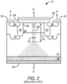
- FIG. 1 shows a conventional power MOSFET device 10.
- the conventional power MOSFET device 10 includes a substrate 12, a drift layer 14 formed over the substrate 12, one or more junction implants 16 in the surface of the drift layer 14 opposite the substrate, and a junction gate field effect transistor (JFET) region 18 between each one of the junction implants 16.
- Each one of the junction implants 16 is formed by an ion implantation process, and includes a deep well region 20, a base region 22, and a source region 24.
- Each deep well region 20 extends from a corner of the drift layer 14 opposite the substrate 12 downwards towards the substrate 12 and inwards towards the center of the drift layer 14.
- the deep well region 20 may be formed uniformly or include one or more protruding regions, as shown in Figure 1 .
- Each base region 22 is formed vertically from the surface of the drift layer 14 opposite the substrate 12 down towards the substrate 12 along a portion of the inner edge of each one of the deep well regions 20.
- Each source region 24 is formed in a shallow portion on the surface of the drift layer 14 opposite the substrate 12, and extends laterally to overlap a portion of the deep well region 20 and the base region 22, without extending over either.
- the JFET region 18 defines a channel width 26 between each one of the junction implants 16.
- a gate oxide layer 28 is positioned on the surface of the drift layer 14 opposite the substrate 12, and extends laterally between a portion of the surface of each source region 24, such that the gate oxide layer 28 partially overlaps and runs between the surface of each source region 24 in the junction implants 16.
- a gate contact 30 is positioned on top of the gate oxide layer 28.
- Two source contacts 32 are each positioned on the surface of the drift layer 14 opposite the substrate 12 such that each one of the source contacts 32 partially overlaps both the source region 24 and the deep well region 20 of one of the junction implants 16, respectively, and does not contact the gate oxide layer 28 or the gate contact 30.
- a drain contact 34 is located on the surface of the substrate 12 opposite the drift layer 14.
- FIG. 2 shows operation of the conventional power MOSFET 10 when the device is in an ON state.
- a positive bias is applied to the gate contact 30 of the conventional power MOSFET 10
- an inversion layer channel 36 is formed at the surface of the drift layer 14 underneath the gate contact 30, thereby placing the conventional power MOSFET 10 in an ON state.
- current shown by the shaded region in Figure 2
- current is allowed to flow from each one of the source contacts 32 through the inversion layer channel 36 and into the JFET region 18 of the drift layer 14. Once in the JFET region 18, current flows downward through the drift layer 14 towards the drain contact 34.
- An electric field presented by junctions formed between the deep well region 20, the base region 22, and the drift layer 14 constricts current flow in the JFET region 18 into a JFET channel 38 having a JFET channel width 40.
- a certain spreading distance 42 from the inversion layer channel 36 when the electric field presented by the junction implants 16 is diminished the flow of current is distributed laterally, or spread out in the drift layer 14, as shown in Figure 2 .
- the JFET channel width 40 and the spreading distance 42 determine the internal resistance of the power MOSFET 10, thereby dictating the performance of the device.
- a conventional power MOSFET 10 generally requires a channel width 26 of 3 microns or wider in order to sustain an adequate JFET channel width and 40 spreading distance 42 for proper operation of the device.
- the electric field formed by the junctions between the deep well region 20, the base region 22, and the drift layer 14 radiates through the gate oxide layer 28, thereby physically degrading the gate oxide layer 28 over time. Eventually, the electric field will cause the gate oxide layer 28 to break down, and the conventional power MOSFET 10 will cease to function.
- US2010/013007 A1 discloses a semiconductor device including a drift layer that includes a reference concentration layer including an impurity of a first conductive type at a first reference concentration and a low concentration layer provided under the reference concentration layer and including an impurity of the first conductive type at a concentration lower than the first reference concentration.
- a gate electrode is formed on an upper surface of the reference concentration layer; and a pair of source regions are respectively provided on the reference concentration layer in the vicinity of ends of the gate electrode and include an impurity of the first conductive type at a concentration higher than the first reference concentration.
- a pair of base regions surround outer surfaces of diffusion layers of the source regions and include an impurity of the second conductive type at a second reference concentration.
- a pair of depletion-layer extension regions are respectively provided in the reference concentration layer under diffusion layers of the base regions and include an impurity of the second conductive type at a concentration lower than the second reference concentration.
- a drain layer is provided on a lower surface of the low concentration layer and includes an impurity of the first conductive type at a concentration higher than the first reference concentration
- US 2006/192256 A1 discloses SiC based vertical MOSFET comprising a semiconductor substrate, a drift layer formed on the substrate, a first and a second source region, and a JFET region defined between the first and the second source regions.
- the JFET region may have a short width and/or a higher concentration of impurities than the drift layer.
- the semiconductor device include also a current spreading layer formed on the drift layer. The current spreading layer may also have a higher concentration of impurities than the drift layer.
- US 2012/292742 A1 discloses a SiC based vertical MOSFET comprising a first and a second drift layer. A current path region is formed between them and has an impurity concentration higher than them.
- the present disclosure relates to a transistor device including a substrate, a drift layer over the substrate, and a spreading layer over the drift layer.
- the spreading layer includes a pair of junction implants separated by a junction gate field effect (JFET) region. Each one of the junction implants may include a deep well region, a base region, and a source region.
- the transistor device further includes a gate oxide layer, a gate contact, a pair of source contacts, and a drain contact.
- the gate oxide layer is on a portion of the spreading layer such that the gate oxide layer partially overlaps and runs between each source region of each junction implant.
- the gate contact is on top of the gate oxide layer.
- Each one of the source contacts are on a portion of the spreading layer such that each source contact partially overlaps both the source region and the deep well region of each junction implant, respectively.
- the drain contact is on the surface of the substrate opposite the drift layer.
- the spreading layer has a graded doping profile, such that the doping concentration of the spreading layer decreases in proportion to the distance of the point in the spreading layer from the JFET region.
- the spreading layer includes multiple layers, each having a different doping concentration that progressively decreases in proportion to the distance of the layer from the JFET region.
- the space between each junction implant, or length of the JFET region can be reduced while simultaneously maintaining or reducing the ON resistance of the device.
- reducing the space between each junction implant a larger portion of the electric field generated during reverse bias of the transistor device is terminated by each one of the junction implants, thereby reducing the electric field seen by the gate oxide layer and increasing the longevity of the device.
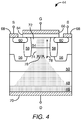
- the power MOSFET device 44 includes a substrate 46, a drift layer 48 formed over the substrate 46, a spreading layer 50 formed over the drift layer 48, one or more junction implants 52 in the surface of the spreading layer 50 opposite the drift layer 48, and a junction gate field effect transistor (JFET) region 54 between each one of the junction implants 52.
- Each one of the junction implants 52 may be formed by an ion implantation process, and may include a deep well region 56, a base region 58, and a source region 60.
- Each deep well region 56 extends from a corner of the spreading layer 50 opposite the drift layer 48 downwards towards the drift layer 48 and inwards towards the center of the spreading layer 50.
- the deep well region 56 may be formed uniformly or include one or more protruding regions.
- Each base region 58 is formed vertically from the surface of the spreading layer 50 opposite the drift layer 48 downwards towards the drift layer 48 along a portion of the inner edge of each one of the deep well regions 56.
- Each source region 60 is formed in a shallow portion on the surface of the spreading layer 50 opposite the drift layer 48, and extends laterally to overlap a portion of the deep well region 56 and the base region 58, without extending over either.
- the JFET region 54 defines a channel width 62 between each one of the junction implants 52.
- a gate oxide layer 64 is positioned on the surface of the spreading layer 50 opposite the drift layer 48, and extends laterally between a portion of the surface of each source region 60, such that the gate oxide layer 64 partially overlaps and runs between the surface of each source region 60 in the junction implants 52.
- a gate contact 66 is positioned on top of the gate oxide layer 64.
- Two source contacts 68 are each positioned on the surface of the spreading layer 50 opposite the drift layer 48 such that each one of the source contacts 68 partially overlaps both the source region 60 and the deep well region 56 of the junction implants 52, respectively, and does not contact the gate oxide layer 64 or the gate contact 66.
- a drain contact 70 is located on the surface of the substrate 46 opposite the drift layer 48.
- Figure 4 shows the operation of the power MOSFET 44 when the device is in an ON state.
- a positive bias is applied to the gate contact 66 of the power MOSFET 44, an inversion layer channel 72 is formed at the surface of the spreading layer 50 underneath the gate contact 66, thereby placing the power MOSFET 44 in an ON state.
- current shown by the shaded region in Figure 4
- current is allowed to flow from each one of the source contacts 68 through the inversion layer channel 72 and into the JFET region 54.
- Once in the JFET region 54 current flows downward through the spreading layer 50 towards the drain contact 70.
- An electric field presented by the junctions formed between the deep well region 56, the base region 58, and the spreading layer 50 constricts current flow in the JFET region 54 into a JFET channel 74 having a JFET channel width 76.
- the spreading layer 50 is doped in such a way to decrease resistance in the spreading layer 50, thereby mitigating the effects of the electric field by increasing the JFET channel width 76 and decreasing the spreading distance 78.
- the spreading layer 50 significantly reduces the ON resistance of the power MOSFET 44.
- the ON resistance of the power MOSFET 44 may be about 2.2 m ⁇ /cm 2 when the device is rated to handle 1200V and about 1.8 m ⁇ /cm 2 when the device is rated to handle 600V.
- the spreading layer 50 allows for a reduction of the channel width 62 between each one of the junction implants 52. Reducing the channel width 62 of the power MOSFET 44 not only improves the footprint of the device, but also the longevity. As each one of the junction implants 52 is moved closer to one another, a larger portion of the electric field generated by the junctions between the deep well region 56, the base region 58, and the spreading layer 50 is terminated by the opposite junction implant 52. Accordingly, the electric field seen by the gate oxide layer 64 is significantly reduced, thereby resulting in improved longevity of the power MOSFET 44. According to one embodiment, the channel width 62 of the power MOSFET 44 is less than 3 microns.
- the power MOSFET 44 may be, for example, a silicon carbide (SiC), gallium arsenide (GaAs), or gallium nitride (GaN) device.
- SiC silicon carbide
- GaAs gallium arsenide
- GaN gallium nitride
- the substrate 46 of the power MOSFET 44 may be about 180-350 microns thick.
- the drift layer 48 may be about 3.5-12 microns thick, depending upon the voltage rating of the power MOSFET 44.
- the spreading layer 50 may be about 1.0-2.5 microns thick.
- Each one of the junction implants 52 may be about 1.0-2.0 microns thick.
- the JFET region 54 may be about 0.75-1.5 microns thick.
- the spreading layer 50 is an N-doped layer with a doping concentration from about 2x10 17 cm -3 to 5x10 16 cm -3 .
- the spreading layer 50 may be graded, such that the portion of the spreading layer 50 closest to the drift layer 48 has a doping concentration about 5x10 16 cm -3 that is graduated as the spreading layer 50 extends upwards to a doping concentration of about 2x10 17 cm -3 .
- the spreading layer 50 may comprise multiple layers.
- the layer of the spreading layer 50 closest to the drift layer 48 may have a doping concentration about 5x10 16 cm -3 .
- the doping concentration of each additional layer in the spreading layer may decrease in proportion to the distance of the layer from the JFET region 54.
- the layer of the spreading layer 50 closest to the drift layer 48 may have a doping concentration about 2x10 17 cm -3 .
- the JFET region 54 may be an N-doped layer with a doping concentration from about 1x10 16 cm -3 to 2x10 17 cm -3 .
- the drift layer 48 may be an N-doped layer with a doping concentration from about 6x10 15 cm -3 to 1.5x10 16 cm -3 .
- the deep well region 56 may be a heavily P-doped region with a doping concentration from about 5x10 17 cm -3 to 1x10 20 cm -3 .
- the base region 58 may be a P-doped region with a doping concentration from about 5x10 16 cm -3 to 1x10 19 cm -3 .
- the source region 60 may be an N-doped region with a doping concentration from about 1x10 19 cm -3 to 1x10 21 cm -3 .
- the N doping agent may be nitrogen, phosphorous, or any other suitable element, as will be appreciated by those of ordinary skill in the art.
- the P doping agent may be aluminum, boron, or any other suitable element, as will be appreciated by those of ordinary skill in the art.
- the gate contact 66, the source contacts 68, and the drain contact 70 may be comprised of multiple layers.
- each one of the contacts may include a first layer of nickel or nickel-aluminum, a second layer of titanium over the first layer, a third layer of titanium-nickel over the second layer, and a fourth layer of aluminum over the third layer.
- the gate contact 66, the source contacts 68, and the drain contact 70 may be formed of any suitable material.
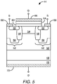
- Figure 5 shows the power MOSFET 44 according to an additional embodiment of the present disclosure.
- the power MOSFET 44 shown in Figure 5 is substantially similar to that of Figure 3 , but further includes a channel re-growth layer 80 between the gate oxide layer 64 and the spreading layer 50.
- the channel re-growth layer 80 is provided to lower the threshold voltage of the power MOSFET 44.
- the deep well region 56 due to a heavy level of doping, may raise the threshold voltage of the power MOSFET 44 to a level that inhibits optimum performance.
- the channel re-growth layer 80 may offset the effects of the deep well region 56 in order to lower the threshold voltage of the power MOSFET 44.
- the channel re-growth layer 80 may be an N-doped region with a doping concentration from about 1x10 15 cm -3 to 1x10 17 cm -3
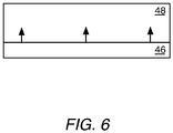
- FIGs 6-15 illustrate a process for manufacturing the power MOSFET 44 shown in Figure 3 .
- the drift layer 48 is grown on top of the substrate 46.
- any suitable growth process may be used to produce the drift layer 48 without departing from the principles of the present disclosure.
- a chemical vapor deposition process may be used to form the drift layer 48.
- the spreading layer 50 is grown on top of the drift layer 48.
- any suitable growth process may be used to create the spreading layer 50 without departing from the principles of the present disclosure.
- the spreading layer 50 is grown such that it includes a graded doping profile.
- the deep well region 56 of each one of the junction implants 52 is implanted in the spreading layer 50.
- the deep well regions 56 may be implanted by any suitable implantation process.
- an ion implantation process may be used to form the deep well regions 56.
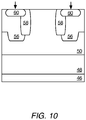
- the base regions 58 are then implanted, as illustrated by Figure 9 , followed by the source regions 60, as illustrated by Figure 10 .
- the JFET region 54 is implanted. As discussed above, any suitable implantation process may be used to create the JFET region 54 without departing from the principles of the present disclosure. Additionally, although not illustrated, the JFET region54 may alternatively be created by a growth process.
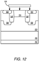
- the gate oxide layer 64 is formed on top of the spreading layer 50, such that the gate oxide layer 64 partially overlaps and runs between the surface of each source region 60 in the junction implants 52.
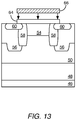
- the gate contact 66 is formed on top of the gate oxide layer 64.
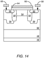
- the source contacts 68 are then formed on the surface of the spreading layer 50 such that each one of the source contacts 68 partially overlaps both the source region 60 and the deep well region 56 of the junction implants 52, respectively, and does not contact the gate oxide layer 64 or the gate contact 66, as illustrated by Figure 14 .
- the drain contact 70 is provided on the surface of the substrate 46 opposite the drift layer 48.
- Figure 16 is a chart depicting the effect of the spreading layer 50 on the ON resistance of the power MOSFET 44. As shown, the spreading layer provides about a 20% decrease in the ON resistance of the device.
- Figure 17 is a chart depicting the effect of the spreading layer 50 on the electric field seen by the gate oxide layer 64. Because the spreading layer 50 allows a reduction in channel width 62 without impeding the performance of the power MOSFET 44, up to 26% of the electric field seen by the gate oxide layer 64 may be terminated by the opposing junction implants 52, thereby significantly increasing the longevity of the device.
Landscapes
- Insulated Gate Type Field-Effect Transistor (AREA)
- Electrodes Of Semiconductors (AREA)
- Junction Field-Effect Transistors (AREA)
Applications Claiming Priority (2)
| Application Number | Priority Date | Filing Date | Title |
|---|---|---|---|
| US13/962,295 US9331197B2 (en) | 2013-08-08 | 2013-08-08 | Vertical power transistor device |
| PCT/US2014/049941 WO2015021154A1 (en) | 2013-08-08 | 2014-08-06 | Vertical power transistor device |
Publications (2)
| Publication Number | Publication Date |
|---|---|
| EP3031083A1 EP3031083A1 (en) | 2016-06-15 |
| EP3031083B1 true EP3031083B1 (en) | 2021-04-14 |
Family
ID=51358122
Family Applications (1)
| Application Number | Title | Priority Date | Filing Date |
|---|---|---|---|
| EP14752742.8A Active EP3031083B1 (en) | 2013-08-08 | 2014-08-06 | Vertical power transistor device |
Country Status (6)
| Country | Link |
|---|---|
| US (4) | US9331197B2 (enExample) |
| EP (1) | EP3031083B1 (enExample) |
| JP (2) | JP6306704B2 (enExample) |
| CN (1) | CN105431948A (enExample) |
| TW (1) | TWI536575B (enExample) |
| WO (1) | WO2015021154A1 (enExample) |
Families Citing this family (21)
| Publication number | Priority date | Publication date | Assignee | Title |
|---|---|---|---|---|
| US9331197B2 (en) | 2013-08-08 | 2016-05-03 | Cree, Inc. | Vertical power transistor device |
| US10600903B2 (en) | 2013-09-20 | 2020-03-24 | Cree, Inc. | Semiconductor device including a power transistor device and bypass diode |
| US10868169B2 (en) | 2013-09-20 | 2020-12-15 | Cree, Inc. | Monolithically integrated vertical power transistor and bypass diode |
| CN106898652B (zh) * | 2017-03-09 | 2019-06-04 | 电子科技大学 | 一种碳化硅vdmos器件 |
| US10608102B2 (en) | 2017-09-29 | 2020-03-31 | Electronics And Telecommunications Research Institute | Semiconductor device having a drain electrode contacting an epi material inside a through-hole and method of manufacturing the same |
| US10685886B2 (en) | 2017-12-15 | 2020-06-16 | International Business Machines Corporation | Fabrication of logic devices and power devices on the same substrate |
| JP7106881B2 (ja) * | 2018-02-09 | 2022-07-27 | 株式会社デンソー | 炭化珪素基板および炭化珪素半導体装置 |
| CN110718452B (zh) | 2018-07-12 | 2025-04-08 | 创能动力科技有限公司 | 碳化硅器件及其制造方法 |
| US11075295B2 (en) * | 2018-07-13 | 2021-07-27 | Cree, Inc. | Wide bandgap semiconductor device |
| US11069804B2 (en) | 2018-08-31 | 2021-07-20 | Alpha And Omega Semiconductor (Cayman) Ltd. | Integration of HVLDMOS with shared isolation region |
| JP7413701B2 (ja) | 2019-10-03 | 2024-01-16 | 富士電機株式会社 | 窒化物半導体装置及び窒化物半導体装置の製造方法 |
| CN112670344B (zh) * | 2020-12-10 | 2022-07-22 | 复旦大学 | 一种渐变沟道的SiC MOSFET及其自对准工艺 |
| CN116137283B (zh) * | 2021-11-17 | 2025-09-12 | 苏州东微半导体股份有限公司 | 半导体超结功率器件 |
| CN115117145B (zh) * | 2022-05-12 | 2025-09-09 | 厦门紫硅半导体科技有限公司 | 一种低导通电阻的SiC基MOSFET器件及其制备方法 |
| TWI818652B (zh) * | 2022-07-29 | 2023-10-11 | 鴻海精密工業股份有限公司 | 半導體裝置的製造方法 |
| US12471340B2 (en) * | 2022-10-27 | 2025-11-11 | Panjit International Inc. | Manufacturing method of forming semiconductor device and semiconductor device |
| WO2025052687A1 (ja) * | 2023-09-04 | 2025-03-13 | 株式会社 東芝 | 半導体装置 |
| CN119743984B (zh) * | 2023-09-27 | 2026-03-06 | 创圆科技股份有限公司 | 半导体装置和恒流二极管电路 |
| TWI885815B (zh) * | 2024-03-22 | 2025-06-01 | 鴻揚半導體股份有限公司 | 半導體裝置與其形成方法 |
| CN119421488B (zh) * | 2024-10-16 | 2025-09-23 | 浙江创芯集成电路有限公司 | 半导体结构及其形成方法、反相器电路 |
| TWI900409B (zh) * | 2025-02-12 | 2025-10-01 | 李羿軒 | 垂直型功率半導體裝置 |
Family Cites Families (133)
| Publication number | Priority date | Publication date | Assignee | Title |
|---|---|---|---|---|
| NL7700879A (nl) * | 1977-01-28 | 1978-08-01 | Philips Nv | Halfgeleiderinrichting. |
| JPS5742164A (en) * | 1980-08-27 | 1982-03-09 | Hitachi Ltd | Semiconductor device |
| JPS6149474A (ja) | 1984-08-17 | 1986-03-11 | Matsushita Electronics Corp | 電界効果トランジスタおよびその製造方法 |
| US4803533A (en) | 1986-09-30 | 1989-02-07 | General Electric Company | IGT and MOSFET devices having reduced channel width |
| US4967243A (en) | 1988-07-19 | 1990-10-30 | General Electric Company | Power transistor structure with high speed integral antiparallel Schottky diode |
| US5111253A (en) | 1989-05-09 | 1992-05-05 | General Electric Company | Multicellular FET having a Schottky diode merged therewith |
| IT1247293B (it) | 1990-05-09 | 1994-12-12 | Int Rectifier Corp | Dispositivo transistore di potenza presentante una regione ultra-profonda, a maggior concentrazione |
| JP3259330B2 (ja) * | 1992-06-19 | 2002-02-25 | 株式会社日立製作所 | 半導体装置の製造方法 |
| US5241195A (en) | 1992-08-13 | 1993-08-31 | North Carolina State University At Raleigh | Merged P-I-N/Schottky power rectifier having extended P-I-N junction |
| JP2561413B2 (ja) | 1993-02-23 | 1996-12-11 | 日産自動車株式会社 | 半導体装置 |
| US5365102A (en) | 1993-07-06 | 1994-11-15 | North Carolina State University | Schottky barrier rectifier with MOS trench |
| US5536977A (en) | 1993-11-30 | 1996-07-16 | Siliconix Incorporated | Bidirectional current blocking MOSFET for battery disconnect switching |
| EP0748520B1 (de) | 1994-03-04 | 1998-12-16 | Siemens Aktiengesellschaft | Mis-struktur auf siliciumcarbid-basis mit hoher latch-up-festigkeit |
| US5674766A (en) | 1994-12-30 | 1997-10-07 | Siliconix Incorporated | Method of making a trench MOSFET with multi-resistivity drain to provide low on-resistance by varying dopant concentration in epitaxial layer |
| US5973367A (en) | 1995-10-13 | 1999-10-26 | Siliconix Incorporated | Multiple gated MOSFET for use in DC-DC converter |
| JPH09146329A (ja) | 1995-11-20 | 1997-06-06 | Fuji Xerox Co Ltd | 画像形成装置 |
| US5689144A (en) | 1996-05-15 | 1997-11-18 | Siliconix Incorporated | Four-terminal power MOSFET switch having reduced threshold voltage and on-resistance |
| US5886383A (en) | 1997-01-10 | 1999-03-23 | International Rectifier Corporation | Integrated schottky diode and mosgated device |
| US6057558A (en) | 1997-03-05 | 2000-05-02 | Denson Corporation | Silicon carbide semiconductor device and manufacturing method thereof |
| US5925910A (en) | 1997-03-28 | 1999-07-20 | Stmicroelectronics, Inc. | DMOS transistors with schottky diode body structure |
| US6239463B1 (en) | 1997-08-28 | 2001-05-29 | Siliconix Incorporated | Low resistance power MOSFET or other device containing silicon-germanium layer |
| US7084456B2 (en) | 1999-05-25 | 2006-08-01 | Advanced Analogic Technologies, Inc. | Trench MOSFET with recessed clamping diode using graded doping |
| JP2006210368A (ja) | 1999-07-02 | 2006-08-10 | Toyota Central Res & Dev Lab Inc | 縦型半導体装置及びその製造方法 |
| US7186609B2 (en) | 1999-12-30 | 2007-03-06 | Siliconix Incorporated | Method of fabricating trench junction barrier rectifier |
| FR2814855B1 (fr) | 2000-10-03 | 2003-10-31 | St Microelectronics Sa | Jonction schottky a barriere stable sur carbure de silicium |
| US6956238B2 (en) | 2000-10-03 | 2005-10-18 | Cree, Inc. | Silicon carbide power metal-oxide semiconductor field effect transistors having a shorting channel and methods of fabricating silicon carbide metal-oxide semiconductor field effect transistors having a shorting channel |
| US7126169B2 (en) | 2000-10-23 | 2006-10-24 | Matsushita Electric Industrial Co., Ltd. | Semiconductor element |
| JP4198469B2 (ja) * | 2001-04-11 | 2008-12-17 | シリコン・セミコンダクター・コーポレイション | パワーデバイスとその製造方法 |
| US6683363B2 (en) | 2001-07-03 | 2004-01-27 | Fairchild Semiconductor Corporation | Trench structure for semiconductor devices |
| US6621107B2 (en) | 2001-08-23 | 2003-09-16 | General Semiconductor, Inc. | Trench DMOS transistor with embedded trench schottky rectifier |
| JP4097417B2 (ja) | 2001-10-26 | 2008-06-11 | 株式会社ルネサステクノロジ | 半導体装置 |
| GB0202437D0 (en) | 2002-02-02 | 2002-03-20 | Koninkl Philips Electronics Nv | Cellular mosfet devices and their manufacture |
| US6855970B2 (en) | 2002-03-25 | 2005-02-15 | Kabushiki Kaisha Toshiba | High-breakdown-voltage semiconductor device |
| US7701001B2 (en) | 2002-05-03 | 2010-04-20 | International Rectifier Corporation | Short channel trench power MOSFET with low threshold voltage |
| CN100544026C (zh) | 2002-12-20 | 2009-09-23 | 克里公司 | 碳化硅功率mos场效应晶体管及制造方法 |
| US7221010B2 (en) * | 2002-12-20 | 2007-05-22 | Cree, Inc. | Vertical JFET limited silicon carbide power metal-oxide semiconductor field effect transistors |
| US7169634B2 (en) | 2003-01-15 | 2007-01-30 | Advanced Power Technology, Inc. | Design and fabrication of rugged FRED |
| JP3964819B2 (ja) | 2003-04-07 | 2007-08-22 | 株式会社東芝 | 絶縁ゲート型半導体装置 |
| US6979863B2 (en) | 2003-04-24 | 2005-12-27 | Cree, Inc. | Silicon carbide MOSFETs with integrated antiparallel junction barrier Schottky free wheeling diodes and methods of fabricating the same |
| US7638841B2 (en) | 2003-05-20 | 2009-12-29 | Fairchild Semiconductor Corporation | Power semiconductor devices and methods of manufacture |
| JP2005011846A (ja) | 2003-06-16 | 2005-01-13 | Nissan Motor Co Ltd | 半導体装置 |
| JP4799829B2 (ja) | 2003-08-27 | 2011-10-26 | 三菱電機株式会社 | 絶縁ゲート型トランジスタ及びインバータ回路 |
| JP2005302925A (ja) * | 2004-04-09 | 2005-10-27 | Toshiba Corp | 半導体装置 |
| DE102004053760A1 (de) | 2004-11-08 | 2006-05-11 | Robert Bosch Gmbh | Halbleitereinrichtung und Verfahren für deren Herstellung |
| JP4899405B2 (ja) | 2004-11-08 | 2012-03-21 | 株式会社デンソー | 炭化珪素半導体装置およびその製造方法 |
| DE102004053761A1 (de) | 2004-11-08 | 2006-05-18 | Robert Bosch Gmbh | Halbleitereinrichtung und Verfahren für deren Herstellung |
| US7498633B2 (en) * | 2005-01-21 | 2009-03-03 | Purdue Research Foundation | High-voltage power semiconductor device |
| US8110869B2 (en) | 2005-02-11 | 2012-02-07 | Alpha & Omega Semiconductor, Ltd | Planar SRFET using no additional masks and layout method |
| US8836015B2 (en) | 2005-02-11 | 2014-09-16 | Alpha And Omega Semiconductor Incorporated | Planar SRFET using no additional masks and layout method |
| US8362547B2 (en) | 2005-02-11 | 2013-01-29 | Alpha & Omega Semiconductor Limited | MOS device with Schottky barrier controlling layer |
| US7737522B2 (en) | 2005-02-11 | 2010-06-15 | Alpha & Omega Semiconductor, Ltd. | Trench junction barrier controlled Schottky device with top and bottom doped regions for enhancing forward current in a vertical direction |
| US7436022B2 (en) | 2005-02-11 | 2008-10-14 | Alpha & Omega Semiconductors, Ltd. | Enhancing Schottky breakdown voltage (BV) without affecting an integrated MOSFET-Schottky device layout |
| JP4916671B2 (ja) | 2005-03-31 | 2012-04-18 | 住友電工デバイス・イノベーション株式会社 | 半導体装置 |
| JP2006344759A (ja) * | 2005-06-08 | 2006-12-21 | Sharp Corp | トレンチ型mosfet及びその製造方法 |
| US20070012983A1 (en) | 2005-07-15 | 2007-01-18 | Yang Robert K | Terminations for semiconductor devices with floating vertical series capacitive structures |
| US8461648B2 (en) | 2005-07-27 | 2013-06-11 | Infineon Technologies Austria Ag | Semiconductor component with a drift region and a drift control region |
| KR100674862B1 (ko) * | 2005-08-25 | 2007-01-29 | 삼성전기주식회사 | 질화물 반도체 발광 소자 |
| US7928470B2 (en) | 2005-11-25 | 2011-04-19 | Denso Corporation | Semiconductor device having super junction MOS transistor and method for manufacturing the same |
| US7696598B2 (en) | 2005-12-27 | 2010-04-13 | Qspeed Semiconductor Inc. | Ultrafast recovery diode |
| JP4727426B2 (ja) | 2006-01-10 | 2011-07-20 | 三菱電機株式会社 | 半導体装置および半導体装置の製造方法 |
| JP5017865B2 (ja) * | 2006-01-17 | 2012-09-05 | 富士電機株式会社 | 半導体装置 |
| JP4545800B2 (ja) | 2006-02-07 | 2010-09-15 | 三菱電機株式会社 | 炭化珪素半導体装置およびその製造方法 |
| JP4900662B2 (ja) | 2006-03-02 | 2012-03-21 | 独立行政法人産業技術総合研究所 | ショットキーダイオードを内蔵した炭化ケイ素mos電界効果トランジスタおよびその製造方法 |
| JP5560519B2 (ja) | 2006-04-11 | 2014-07-30 | 日産自動車株式会社 | 半導体装置及びその製造方法 |
| JP2008016747A (ja) | 2006-07-10 | 2008-01-24 | Fuji Electric Holdings Co Ltd | トレンチmos型炭化珪素半導体装置およびその製造方法 |
| US8710510B2 (en) | 2006-08-17 | 2014-04-29 | Cree, Inc. | High power insulated gate bipolar transistors |
| US7595241B2 (en) | 2006-08-23 | 2009-09-29 | General Electric Company | Method for fabricating silicon carbide vertical MOSFET devices |
| JP2008053448A (ja) | 2006-08-24 | 2008-03-06 | Rohm Co Ltd | Mis型電界効果トランジスタおよびその製造方法 |
| WO2008069309A1 (ja) | 2006-12-07 | 2008-06-12 | Shindengen Electric Manufacturing Co., Ltd. | 半導体装置及びその製造方法 |
| US20080142811A1 (en) * | 2006-12-13 | 2008-06-19 | General Electric Company | MOSFET devices and methods of fabrication |
| JP4412335B2 (ja) | 2007-02-23 | 2010-02-10 | 株式会社デンソー | 炭化珪素半導体装置の製造方法 |
| JP4450241B2 (ja) | 2007-03-20 | 2010-04-14 | 株式会社デンソー | 炭化珪素半導体装置の製造方法 |
| US7982239B2 (en) | 2007-06-13 | 2011-07-19 | Northrop Grumman Corporation | Power switching transistors |
| WO2008153142A1 (ja) | 2007-06-15 | 2008-12-18 | Rohm Co., Ltd. | 半導体装置 |
| JP4492735B2 (ja) | 2007-06-20 | 2010-06-30 | 株式会社デンソー | 半導体装置及び半導体装置の製造方法 |
| JP4599379B2 (ja) | 2007-08-31 | 2010-12-15 | 株式会社東芝 | トレンチゲート型半導体装置 |
| US7687825B2 (en) | 2007-09-18 | 2010-03-30 | Cree, Inc. | Insulated gate bipolar conduction transistors (IBCTS) and related methods of fabrication |
| US7772621B2 (en) | 2007-09-20 | 2010-08-10 | Infineon Technologies Austria Ag | Semiconductor device with structured current spread region and method |
| US7579632B2 (en) | 2007-09-21 | 2009-08-25 | Semiconductor Components Industries, L.L.C. | Multi-channel ESD device and method therefor |
| JP2009094203A (ja) | 2007-10-05 | 2009-04-30 | Denso Corp | 炭化珪素半導体装置 |
| US7943987B2 (en) | 2007-10-18 | 2011-05-17 | Infineon Technologies Austria Ag | Semiconductor component with a drift zone and a drift control zone |
| DE102007057674A1 (de) * | 2007-11-30 | 2009-06-04 | Osram Opto Semiconductors Gmbh | LED mit Stromaufweitungsschicht |
| US7989882B2 (en) | 2007-12-07 | 2011-08-02 | Cree, Inc. | Transistor with A-face conductive channel and trench protecting well region |
| US20090179297A1 (en) | 2008-01-16 | 2009-07-16 | Northrop Grumman Systems Corporation | Junction barrier schottky diode with highly-doped channel region and methods |
| US7795691B2 (en) | 2008-01-25 | 2010-09-14 | Cree, Inc. | Semiconductor transistor with P type re-grown channel layer |
| JP5369464B2 (ja) | 2008-03-24 | 2013-12-18 | 富士電機株式会社 | 炭化珪素mos型半導体装置 |
| JP5617175B2 (ja) | 2008-04-17 | 2014-11-05 | 富士電機株式会社 | ワイドバンドギャップ半導体装置とその製造方法 |
| JP5326405B2 (ja) | 2008-07-30 | 2013-10-30 | 株式会社デンソー | ワイドバンドギャップ半導体装置 |
| JP2010081043A (ja) | 2008-09-24 | 2010-04-08 | Oki Semiconductor Co Ltd | Hブリッジ回路 |
| US7906427B2 (en) | 2008-10-14 | 2011-03-15 | General Electric Company | Dimension profiling of SiC devices |
| JP2012114104A (ja) * | 2009-02-24 | 2012-06-14 | Hitachi Ltd | 蓄積型絶縁ゲート型電界効果型トランジスタ |
| JP5453903B2 (ja) * | 2009-04-28 | 2014-03-26 | 富士電機株式会社 | ワイドバンドギャップ半導体装置 |
| DE102009033302B4 (de) | 2009-07-15 | 2012-01-26 | Infineon Technologies Ag | Herstellungsverfahren für ein unipolares Halbleiter-Bauelement und Halbleitervorrichtung |
| US8283973B2 (en) | 2009-08-19 | 2012-10-09 | Panasonic Corporation | Semiconductor element, semiconductor device, and electric power converter |
| US8829614B2 (en) | 2009-08-31 | 2014-09-09 | Alpha And Omega Semiconductor Incorporated | Integrated Schottky diode in high voltage semiconductor device |
| US20110156810A1 (en) | 2009-12-30 | 2011-06-30 | Intersil Americas Inc. | Integrated dmos and schottky |
| US8896084B2 (en) | 2010-02-23 | 2014-11-25 | Yoshitaka Sugawara | Semiconductor device |
| JP2011228643A (ja) | 2010-03-30 | 2011-11-10 | Shindengen Electric Mfg Co Ltd | 半導体装置及びその製造方法 |
| US8415671B2 (en) * | 2010-04-16 | 2013-04-09 | Cree, Inc. | Wide band-gap MOSFETs having a heterojunction under gate trenches thereof and related methods of forming such devices |
| WO2011133481A2 (en) | 2010-04-20 | 2011-10-27 | Maxpower Semiconductor Inc. | Power mosfet with embedded recessed field plate and methods of fabrication |
| DE102011079747A1 (de) | 2010-07-27 | 2012-02-02 | Denso Corporation | Halbleitervorrichtung mit Schaltelement und Freilaufdiode, sowie Steuerverfahren hierfür |
| DE102010039258B4 (de) | 2010-08-12 | 2018-03-15 | Infineon Technologies Austria Ag | Transistorbauelement mit reduziertem Kurzschlussstrom |
| US8426258B2 (en) * | 2010-10-12 | 2013-04-23 | Io Semiconductor, Inc. | Vertical semiconductor device with thinned substrate |
| US8350549B2 (en) | 2010-10-29 | 2013-01-08 | Panasonic Corporation | Converter with switches having a diode region that is unipolar-conductive only in the reverse direction |
| CN102097560B (zh) * | 2010-12-31 | 2012-11-14 | 厦门市三安光电科技有限公司 | 具有复合式双电流扩展层的氮化物发光二极管 |
| JP5498431B2 (ja) | 2011-02-02 | 2014-05-21 | ローム株式会社 | 半導体装置およびその製造方法 |
| JP5858933B2 (ja) | 2011-02-02 | 2016-02-10 | ローム株式会社 | 半導体装置 |
| US8575692B2 (en) * | 2011-02-11 | 2013-11-05 | Freescale Semiconductor, Inc. | Near zero channel length field drift LDMOS |
| JP5881322B2 (ja) | 2011-04-06 | 2016-03-09 | ローム株式会社 | 半導体装置 |
| US9184230B2 (en) | 2011-04-08 | 2015-11-10 | Fuji Electric Co., Ltd. | Silicon carbide vertical field effect transistor |
| US9349797B2 (en) * | 2011-05-16 | 2016-05-24 | Cree, Inc. | SiC devices with high blocking voltage terminated by a negative bevel |
| JP5874723B2 (ja) * | 2011-05-18 | 2016-03-02 | 富士電機株式会社 | 半導体装置および半導体装置の製造方法 |
| JP2012243966A (ja) | 2011-05-20 | 2012-12-10 | Sumitomo Electric Ind Ltd | 半導体装置 |
| US20120306009A1 (en) | 2011-06-03 | 2012-12-06 | Suku Kim | Integration of superjunction mosfet and diode |
| CN103069571B (zh) | 2011-06-27 | 2015-11-25 | 松下电器产业株式会社 | 碳化硅半导体元件及其制造方法 |
| DE112012007322B3 (de) | 2011-07-27 | 2022-06-09 | Denso Corporation | Diode, Halbleitervorrichtung und MOSFET |
| JP2013030618A (ja) | 2011-07-28 | 2013-02-07 | Rohm Co Ltd | 半導体装置 |
| JP5745997B2 (ja) | 2011-10-31 | 2015-07-08 | トヨタ自動車株式会社 | スイッチング素子とその製造方法 |
| JP2013125827A (ja) | 2011-12-14 | 2013-06-24 | Toshiba Corp | 半導体装置およびその製造方法 |
| JP5677330B2 (ja) * | 2012-01-20 | 2015-02-25 | 三菱電機株式会社 | 炭化珪素半導体装置およびその製造方法 |
| CN102738334B (zh) * | 2012-06-19 | 2015-07-08 | 厦门市三安光电科技有限公司 | 具有电流扩展层的发光二极管及其制作方法 |
| US9214521B2 (en) | 2012-06-21 | 2015-12-15 | Infineon Technologies Ag | Reverse conducting IGBT |
| US8637922B1 (en) | 2012-07-19 | 2014-01-28 | Infineon Technologies Ag | Semiconductor device |
| US8901639B2 (en) | 2012-07-26 | 2014-12-02 | Cree, Inc. | Monolithic bidirectional silicon carbide switching devices |
| US9166048B2 (en) * | 2012-09-16 | 2015-10-20 | Sensor Electronic Technology, Inc. | Lateral/vertical semiconductor device |
| JP6082229B2 (ja) | 2012-10-30 | 2017-02-15 | 住友化学株式会社 | 窒化物半導体素子およびその製造方法 |
| CN103151371A (zh) * | 2013-03-05 | 2013-06-12 | 矽力杰半导体技术(杭州)有限公司 | 一种晶圆结构以及应用其的功率器件 |
| JP6135364B2 (ja) | 2013-07-26 | 2017-05-31 | 住友電気工業株式会社 | 炭化珪素半導体装置およびその製造方法 |
| US9331197B2 (en) | 2013-08-08 | 2016-05-03 | Cree, Inc. | Vertical power transistor device |
| US9318597B2 (en) | 2013-09-20 | 2016-04-19 | Cree, Inc. | Layout configurations for integrating schottky contacts into a power transistor device |
| US20150084063A1 (en) | 2013-09-20 | 2015-03-26 | Cree, Inc. | Semiconductor device with a current spreading layer |
| US10600903B2 (en) | 2013-09-20 | 2020-03-24 | Cree, Inc. | Semiconductor device including a power transistor device and bypass diode |
| US10868169B2 (en) | 2013-09-20 | 2020-12-15 | Cree, Inc. | Monolithically integrated vertical power transistor and bypass diode |
-
2013
- 2013-08-08 US US13/962,295 patent/US9331197B2/en not_active Ceased
-
2014
- 2014-08-06 JP JP2016533399A patent/JP6306704B2/ja active Active
- 2014-08-06 CN CN201480044619.0A patent/CN105431948A/zh active Pending
- 2014-08-06 WO PCT/US2014/049941 patent/WO2015021154A1/en not_active Ceased
- 2014-08-06 EP EP14752742.8A patent/EP3031083B1/en active Active
- 2014-08-07 TW TW103127134A patent/TWI536575B/zh active
-
2016
- 2016-03-31 US US15/087,406 patent/US9741842B2/en active Active
-
2018
- 2018-03-08 JP JP2018041765A patent/JP6644823B2/ja active Active
- 2018-05-03 US US15/970,148 patent/USRE48380E1/en active Active
-
2020
- 2020-10-26 US US17/080,062 patent/USRE49913E1/en active Active
Non-Patent Citations (1)
| Title |
|---|
| None * |
Also Published As
| Publication number | Publication date |
|---|---|
| JP6644823B2 (ja) | 2020-02-12 |
| JP6306704B2 (ja) | 2018-04-04 |
| JP2016529720A (ja) | 2016-09-23 |
| TW201515225A (zh) | 2015-04-16 |
| EP3031083A1 (en) | 2016-06-15 |
| US20160211360A1 (en) | 2016-07-21 |
| TWI536575B (zh) | 2016-06-01 |
| WO2015021154A1 (en) | 2015-02-12 |
| US9741842B2 (en) | 2017-08-22 |
| US20150041886A1 (en) | 2015-02-12 |
| CN105431948A (zh) | 2016-03-23 |
| JP2018125544A (ja) | 2018-08-09 |
| USRE49913E1 (en) | 2024-04-09 |
| US9331197B2 (en) | 2016-05-03 |
| USRE48380E1 (en) | 2021-01-05 |
Similar Documents
| Publication | Publication Date | Title |
|---|---|---|
| USRE49913E1 (en) | Vertical power transistor device | |
| US10950719B2 (en) | Seminconductor device with spreading layer | |
| US7498633B2 (en) | High-voltage power semiconductor device | |
| US9111919B2 (en) | Field effect device with enhanced gate dielectric structure | |
| US10573712B2 (en) | Super-junction structure and method for manufacturing the same and semiconductor device thereof | |
| KR101735230B1 (ko) | 게이트 산화물 층에 감소된 전기장을 갖는 반도체 디바이스들 | |
| US7626233B2 (en) | LDMOS device | |
| US9281392B2 (en) | Charge compensation structure and manufacturing therefor | |
| JP6066219B2 (ja) | 低いソース抵抗を有する電界効果トランジスタデバイス | |
| US9287383B2 (en) | Method for manufacturing a semiconductor device with step-shaped edge termination | |
| US20150084063A1 (en) | Semiconductor device with a current spreading layer | |
| US7211845B1 (en) | Multiple doped channel in a multiple doped gate junction field effect transistor | |
| US20150097233A1 (en) | Semiconductor Device and Method of Manufacturing the Same | |
| EP3117463A1 (en) | Igbt structure for wide band-gap semiconductor materials | |
| EP4169076A1 (en) | Power devices with a hybrid gate structure | |
| US20260101553A1 (en) | Semiconductor devices with length-graded channel | |
| KR100624053B1 (ko) | 펀치스루를 방지하기 위한 전력용 반도체 소자 및 그 제조방법 | |
| US20120126341A1 (en) | Using low pressure epi to enable low rdson fet |
Legal Events
| Date | Code | Title | Description |
|---|---|---|---|
| PUAI | Public reference made under article 153(3) epc to a published international application that has entered the european phase |
Free format text: ORIGINAL CODE: 0009012 |
|
| 17P | Request for examination filed |
Effective date: 20160121 |
|
| AK | Designated contracting states |
Kind code of ref document: A1 Designated state(s): AL AT BE BG CH CY CZ DE DK EE ES FI FR GB GR HR HU IE IS IT LI LT LU LV MC MK MT NL NO PL PT RO RS SE SI SK SM TR |
|
| AX | Request for extension of the european patent |
Extension state: BA ME |
|
| DAX | Request for extension of the european patent (deleted) | ||
| STAA | Information on the status of an ep patent application or granted ep patent |
Free format text: STATUS: EXAMINATION IS IN PROGRESS |
|
| 17Q | First examination report despatched |
Effective date: 20190104 |
|
| GRAP | Despatch of communication of intention to grant a patent |
Free format text: ORIGINAL CODE: EPIDOSNIGR1 |
|
| STAA | Information on the status of an ep patent application or granted ep patent |
Free format text: STATUS: GRANT OF PATENT IS INTENDED |
|
| INTG | Intention to grant announced |
Effective date: 20201110 |
|
| GRAS | Grant fee paid |
Free format text: ORIGINAL CODE: EPIDOSNIGR3 |
|
| GRAA | (expected) grant |
Free format text: ORIGINAL CODE: 0009210 |
|
| STAA | Information on the status of an ep patent application or granted ep patent |
Free format text: STATUS: THE PATENT HAS BEEN GRANTED |
|
| AK | Designated contracting states |
Kind code of ref document: B1 Designated state(s): AL AT BE BG CH CY CZ DE DK EE ES FI FR GB GR HR HU IE IS IT LI LT LU LV MC MK MT NL NO PL PT RO RS SE SI SK SM TR |
|
| REG | Reference to a national code |
Ref country code: GB Ref legal event code: FG4D |
|
| REG | Reference to a national code |
Ref country code: CH Ref legal event code: EP |
|
| REG | Reference to a national code |
Ref country code: DE Ref legal event code: R096 Ref document number: 602014076579 Country of ref document: DE |
|
| REG | Reference to a national code |
Ref country code: IE Ref legal event code: FG4D |
|
| REG | Reference to a national code |
Ref country code: AT Ref legal event code: REF Ref document number: 1383224 Country of ref document: AT Kind code of ref document: T Effective date: 20210515 |
|
| REG | Reference to a national code |
Ref country code: LT Ref legal event code: MG9D |
|
| REG | Reference to a national code |
Ref country code: NL Ref legal event code: MP Effective date: 20210414 |
|
| PG25 | Lapsed in a contracting state [announced via postgrant information from national office to epo] |
Ref country code: LT Free format text: LAPSE BECAUSE OF FAILURE TO SUBMIT A TRANSLATION OF THE DESCRIPTION OR TO PAY THE FEE WITHIN THE PRESCRIBED TIME-LIMIT Effective date: 20210414 Ref country code: NL Free format text: LAPSE BECAUSE OF FAILURE TO SUBMIT A TRANSLATION OF THE DESCRIPTION OR TO PAY THE FEE WITHIN THE PRESCRIBED TIME-LIMIT Effective date: 20210414 Ref country code: FI Free format text: LAPSE BECAUSE OF FAILURE TO SUBMIT A TRANSLATION OF THE DESCRIPTION OR TO PAY THE FEE WITHIN THE PRESCRIBED TIME-LIMIT Effective date: 20210414 Ref country code: BG Free format text: LAPSE BECAUSE OF FAILURE TO SUBMIT A TRANSLATION OF THE DESCRIPTION OR TO PAY THE FEE WITHIN THE PRESCRIBED TIME-LIMIT Effective date: 20210714 Ref country code: HR Free format text: LAPSE BECAUSE OF FAILURE TO SUBMIT A TRANSLATION OF THE DESCRIPTION OR TO PAY THE FEE WITHIN THE PRESCRIBED TIME-LIMIT Effective date: 20210414 |
|
| REG | Reference to a national code |
Ref country code: AT Ref legal event code: UEP Ref document number: 1383224 Country of ref document: AT Kind code of ref document: T Effective date: 20210414 |
|
| PG25 | Lapsed in a contracting state [announced via postgrant information from national office to epo] |
Ref country code: PL Free format text: LAPSE BECAUSE OF FAILURE TO SUBMIT A TRANSLATION OF THE DESCRIPTION OR TO PAY THE FEE WITHIN THE PRESCRIBED TIME-LIMIT Effective date: 20210414 Ref country code: NO Free format text: LAPSE BECAUSE OF FAILURE TO SUBMIT A TRANSLATION OF THE DESCRIPTION OR TO PAY THE FEE WITHIN THE PRESCRIBED TIME-LIMIT Effective date: 20210714 Ref country code: PT Free format text: LAPSE BECAUSE OF FAILURE TO SUBMIT A TRANSLATION OF THE DESCRIPTION OR TO PAY THE FEE WITHIN THE PRESCRIBED TIME-LIMIT Effective date: 20210816 Ref country code: ES Free format text: LAPSE BECAUSE OF FAILURE TO SUBMIT A TRANSLATION OF THE DESCRIPTION OR TO PAY THE FEE WITHIN THE PRESCRIBED TIME-LIMIT Effective date: 20210414 Ref country code: RS Free format text: LAPSE BECAUSE OF FAILURE TO SUBMIT A TRANSLATION OF THE DESCRIPTION OR TO PAY THE FEE WITHIN THE PRESCRIBED TIME-LIMIT Effective date: 20210414 Ref country code: SE Free format text: LAPSE BECAUSE OF FAILURE TO SUBMIT A TRANSLATION OF THE DESCRIPTION OR TO PAY THE FEE WITHIN THE PRESCRIBED TIME-LIMIT Effective date: 20210414 Ref country code: IS Free format text: LAPSE BECAUSE OF FAILURE TO SUBMIT A TRANSLATION OF THE DESCRIPTION OR TO PAY THE FEE WITHIN THE PRESCRIBED TIME-LIMIT Effective date: 20210814 Ref country code: LV Free format text: LAPSE BECAUSE OF FAILURE TO SUBMIT A TRANSLATION OF THE DESCRIPTION OR TO PAY THE FEE WITHIN THE PRESCRIBED TIME-LIMIT Effective date: 20210414 Ref country code: GR Free format text: LAPSE BECAUSE OF FAILURE TO SUBMIT A TRANSLATION OF THE DESCRIPTION OR TO PAY THE FEE WITHIN THE PRESCRIBED TIME-LIMIT Effective date: 20210715 |
|
| REG | Reference to a national code |
Ref country code: DE Ref legal event code: R097 Ref document number: 602014076579 Country of ref document: DE |
|
| PG25 | Lapsed in a contracting state [announced via postgrant information from national office to epo] |
Ref country code: SM Free format text: LAPSE BECAUSE OF FAILURE TO SUBMIT A TRANSLATION OF THE DESCRIPTION OR TO PAY THE FEE WITHIN THE PRESCRIBED TIME-LIMIT Effective date: 20210414 Ref country code: SK Free format text: LAPSE BECAUSE OF FAILURE TO SUBMIT A TRANSLATION OF THE DESCRIPTION OR TO PAY THE FEE WITHIN THE PRESCRIBED TIME-LIMIT Effective date: 20210414 Ref country code: EE Free format text: LAPSE BECAUSE OF FAILURE TO SUBMIT A TRANSLATION OF THE DESCRIPTION OR TO PAY THE FEE WITHIN THE PRESCRIBED TIME-LIMIT Effective date: 20210414 Ref country code: DK Free format text: LAPSE BECAUSE OF FAILURE TO SUBMIT A TRANSLATION OF THE DESCRIPTION OR TO PAY THE FEE WITHIN THE PRESCRIBED TIME-LIMIT Effective date: 20210414 Ref country code: CZ Free format text: LAPSE BECAUSE OF FAILURE TO SUBMIT A TRANSLATION OF THE DESCRIPTION OR TO PAY THE FEE WITHIN THE PRESCRIBED TIME-LIMIT Effective date: 20210414 Ref country code: RO Free format text: LAPSE BECAUSE OF FAILURE TO SUBMIT A TRANSLATION OF THE DESCRIPTION OR TO PAY THE FEE WITHIN THE PRESCRIBED TIME-LIMIT Effective date: 20210414 |
|
| PLBE | No opposition filed within time limit |
Free format text: ORIGINAL CODE: 0009261 |
|
| STAA | Information on the status of an ep patent application or granted ep patent |
Free format text: STATUS: NO OPPOSITION FILED WITHIN TIME LIMIT |
|
| 26N | No opposition filed |
Effective date: 20220117 |
|
| PG25 | Lapsed in a contracting state [announced via postgrant information from national office to epo] |
Ref country code: MC Free format text: LAPSE BECAUSE OF FAILURE TO SUBMIT A TRANSLATION OF THE DESCRIPTION OR TO PAY THE FEE WITHIN THE PRESCRIBED TIME-LIMIT Effective date: 20210414 |
|
| REG | Reference to a national code |
Ref country code: BE Ref legal event code: MM Effective date: 20210831 |
|
| GBPC | Gb: european patent ceased through non-payment of renewal fee |
Effective date: 20210806 |
|
| PG25 | Lapsed in a contracting state [announced via postgrant information from national office to epo] |
Ref country code: IS Free format text: LAPSE BECAUSE OF FAILURE TO SUBMIT A TRANSLATION OF THE DESCRIPTION OR TO PAY THE FEE WITHIN THE PRESCRIBED TIME-LIMIT Effective date: 20210814 Ref country code: LU Free format text: LAPSE BECAUSE OF NON-PAYMENT OF DUE FEES Effective date: 20210806 Ref country code: AL Free format text: LAPSE BECAUSE OF FAILURE TO SUBMIT A TRANSLATION OF THE DESCRIPTION OR TO PAY THE FEE WITHIN THE PRESCRIBED TIME-LIMIT Effective date: 20210414 |
|
| PG25 | Lapsed in a contracting state [announced via postgrant information from national office to epo] |
Ref country code: IE Free format text: LAPSE BECAUSE OF NON-PAYMENT OF DUE FEES Effective date: 20210806 Ref country code: GB Free format text: LAPSE BECAUSE OF NON-PAYMENT OF DUE FEES Effective date: 20210806 Ref country code: BE Free format text: LAPSE BECAUSE OF NON-PAYMENT OF DUE FEES Effective date: 20210831 |
|
| PG25 | Lapsed in a contracting state [announced via postgrant information from national office to epo] |
Ref country code: HU Free format text: LAPSE BECAUSE OF FAILURE TO SUBMIT A TRANSLATION OF THE DESCRIPTION OR TO PAY THE FEE WITHIN THE PRESCRIBED TIME-LIMIT; INVALID AB INITIO Effective date: 20140806 |
|
| PG25 | Lapsed in a contracting state [announced via postgrant information from national office to epo] |
Ref country code: CY Free format text: LAPSE BECAUSE OF FAILURE TO SUBMIT A TRANSLATION OF THE DESCRIPTION OR TO PAY THE FEE WITHIN THE PRESCRIBED TIME-LIMIT Effective date: 20210414 |
|
| PG25 | Lapsed in a contracting state [announced via postgrant information from national office to epo] |
Ref country code: MK Free format text: LAPSE BECAUSE OF FAILURE TO SUBMIT A TRANSLATION OF THE DESCRIPTION OR TO PAY THE FEE WITHIN THE PRESCRIBED TIME-LIMIT Effective date: 20210414 |
|
| PG25 | Lapsed in a contracting state [announced via postgrant information from national office to epo] |
Ref country code: MT Free format text: LAPSE BECAUSE OF FAILURE TO SUBMIT A TRANSLATION OF THE DESCRIPTION OR TO PAY THE FEE WITHIN THE PRESCRIBED TIME-LIMIT Effective date: 20210414 |
|
| REG | Reference to a national code |
Ref country code: DE Ref legal event code: R079 Ref document number: 602014076579 Country of ref document: DE Free format text: PREVIOUS MAIN CLASS: H01L0029780000 Ipc: H10D0030600000 |
|
| PGFP | Annual fee paid to national office [announced via postgrant information from national office to epo] |
Ref country code: DE Payment date: 20250827 Year of fee payment: 12 |
|
| PGFP | Annual fee paid to national office [announced via postgrant information from national office to epo] |
Ref country code: IT Payment date: 20250820 Year of fee payment: 12 |
|
| PGFP | Annual fee paid to national office [announced via postgrant information from national office to epo] |
Ref country code: AT Payment date: 20250827 Year of fee payment: 12 Ref country code: FR Payment date: 20250825 Year of fee payment: 12 |
|
| PGFP | Annual fee paid to national office [announced via postgrant information from national office to epo] |
Ref country code: CH Payment date: 20250901 Year of fee payment: 12 |
|
| PG25 | Lapsed in a contracting state [announced via postgrant information from national office to epo] |
Ref country code: TR Free format text: LAPSE BECAUSE OF FAILURE TO SUBMIT A TRANSLATION OF THE DESCRIPTION OR TO PAY THE FEE WITHIN THE PRESCRIBED TIME-LIMIT Effective date: 20210414 |