EP2982437A1 - Appareil et procédé de mesure d'analytes à l'aide de matrices de fet à grande échelle - Google Patents
Appareil et procédé de mesure d'analytes à l'aide de matrices de fet à grande échelle Download PDFInfo
- Publication number
- EP2982437A1 EP2982437A1 EP15170247.9A EP15170247A EP2982437A1 EP 2982437 A1 EP2982437 A1 EP 2982437A1 EP 15170247 A EP15170247 A EP 15170247A EP 2982437 A1 EP2982437 A1 EP 2982437A1
- Authority
- EP
- European Patent Office
- Prior art keywords
- array
- isfet
- chemfet
- pixel
- nucleic acid
- Prior art date
- Legal status (The legal status is an assumption and is not a legal conclusion. Google has not performed a legal analysis and makes no representation as to the accuracy of the status listed.)
- Granted
Links
- 0 CCc1cc(-c2ccc(*)cc2)cc(CC)c1C Chemical compound CCc1cc(-c2ccc(*)cc2)cc(CC)c1C 0.000 description 12
- UBLANNSTVDBNGB-LENDBXDUSA-N C1C=C2/C=N\CCNC/N=C\c(cc3)ccc3/C=N\CCNCC/N=C\C1C=C2 Chemical compound C1C=C2/C=N\CCNC/N=C\c(cc3)ccc3/C=N\CCNCC/N=C\C1C=C2 UBLANNSTVDBNGB-LENDBXDUSA-N 0.000 description 1
- NRGGMCIBEHEAIL-UHFFFAOYSA-N CCc1ccccn1 Chemical compound CCc1ccccn1 NRGGMCIBEHEAIL-UHFFFAOYSA-N 0.000 description 1
- DKUUTUKDSOGGQQ-UHFFFAOYSA-N COC(C(N)[IH]CCCN)O Chemical compound COC(C(N)[IH]CCCN)O DKUUTUKDSOGGQQ-UHFFFAOYSA-N 0.000 description 1
- BIWQNIMLAISTBV-UHFFFAOYSA-N Cc1ccc(B(O)O)cc1 Chemical compound Cc1ccc(B(O)O)cc1 BIWQNIMLAISTBV-UHFFFAOYSA-N 0.000 description 1
- CUZJLQAZQFPCQG-BQYQJAHWSA-N NCCCC/C(/N)=C\NCCN Chemical compound NCCCC/C(/N)=C\NCCN CUZJLQAZQFPCQG-BQYQJAHWSA-N 0.000 description 1
- WZNQAXLTLPRWJS-UHFFFAOYSA-N NCCNCC(CCCCNCc1ccccc1)N Chemical compound NCCNCC(CCCCNCc1ccccc1)N WZNQAXLTLPRWJS-UHFFFAOYSA-N 0.000 description 1
- KUCOHFSKRZZVRO-UHFFFAOYSA-N O=Cc1ccc(C=O)cc1 Chemical compound O=Cc1ccc(C=O)cc1 KUCOHFSKRZZVRO-UHFFFAOYSA-N 0.000 description 1
- XCIXKGXIYUWCLL-UHFFFAOYSA-N OC1CCCC1 Chemical compound OC1CCCC1 XCIXKGXIYUWCLL-UHFFFAOYSA-N 0.000 description 1
- YODIAPFXESLZGY-UHFFFAOYSA-N OCc(cc(cc1CO)Br)c1O Chemical compound OCc(cc(cc1CO)Br)c1O YODIAPFXESLZGY-UHFFFAOYSA-N 0.000 description 1
- LWFYQCXRWBCPKO-UHFFFAOYSA-N Oc(c(CN(Cc1ncccc1)Cc1ncccc1)c1)c(CN(Cc2ccccn2)Cc2ncccc2)cc1-c(cc1)ccc1N=C=S Chemical compound Oc(c(CN(Cc1ncccc1)Cc1ncccc1)c1)c(CN(Cc2ccccn2)Cc2ncccc2)cc1-c(cc1)ccc1N=C=S LWFYQCXRWBCPKO-UHFFFAOYSA-N 0.000 description 1
Images


Classifications
-
- C—CHEMISTRY; METALLURGY
- C12—BIOCHEMISTRY; BEER; SPIRITS; WINE; VINEGAR; MICROBIOLOGY; ENZYMOLOGY; MUTATION OR GENETIC ENGINEERING
- C12Q—MEASURING OR TESTING PROCESSES INVOLVING ENZYMES, NUCLEIC ACIDS OR MICROORGANISMS; COMPOSITIONS OR TEST PAPERS THEREFOR; PROCESSES OF PREPARING SUCH COMPOSITIONS; CONDITION-RESPONSIVE CONTROL IN MICROBIOLOGICAL OR ENZYMOLOGICAL PROCESSES
- C12Q1/00—Measuring or testing processes involving enzymes, nucleic acids or microorganisms; Compositions therefor; Processes of preparing such compositions
- C12Q1/68—Measuring or testing processes involving enzymes, nucleic acids or microorganisms; Compositions therefor; Processes of preparing such compositions involving nucleic acids
- C12Q1/6869—Methods for sequencing
- C12Q1/6874—Methods for sequencing involving nucleic acid arrays, e.g. sequencing by hybridisation
-
- B—PERFORMING OPERATIONS; TRANSPORTING
- B01—PHYSICAL OR CHEMICAL PROCESSES OR APPARATUS IN GENERAL
- B01L—CHEMICAL OR PHYSICAL LABORATORY APPARATUS FOR GENERAL USE
- B01L3/00—Containers or dishes for laboratory use, e.g. laboratory glassware; Droppers
- B01L3/50—Containers for the purpose of retaining a material to be analysed, e.g. test tubes
- B01L3/502—Containers for the purpose of retaining a material to be analysed, e.g. test tubes with fluid transport, e.g. in multi-compartment structures
- B01L3/5027—Containers for the purpose of retaining a material to be analysed, e.g. test tubes with fluid transport, e.g. in multi-compartment structures by integrated microfluidic structures, i.e. dimensions of channels and chambers are such that surface tension forces are important, e.g. lab-on-a-chip
- B01L3/502761—Containers for the purpose of retaining a material to be analysed, e.g. test tubes with fluid transport, e.g. in multi-compartment structures by integrated microfluidic structures, i.e. dimensions of channels and chambers are such that surface tension forces are important, e.g. lab-on-a-chip specially adapted for handling suspended solids or molecules independently from the bulk fluid flow, e.g. for trapping or sorting beads, for physically stretching molecules
-
- C—CHEMISTRY; METALLURGY
- C12—BIOCHEMISTRY; BEER; SPIRITS; WINE; VINEGAR; MICROBIOLOGY; ENZYMOLOGY; MUTATION OR GENETIC ENGINEERING
- C12Q—MEASURING OR TESTING PROCESSES INVOLVING ENZYMES, NUCLEIC ACIDS OR MICROORGANISMS; COMPOSITIONS OR TEST PAPERS THEREFOR; PROCESSES OF PREPARING SUCH COMPOSITIONS; CONDITION-RESPONSIVE CONTROL IN MICROBIOLOGICAL OR ENZYMOLOGICAL PROCESSES
- C12Q1/00—Measuring or testing processes involving enzymes, nucleic acids or microorganisms; Compositions therefor; Processes of preparing such compositions
- C12Q1/68—Measuring or testing processes involving enzymes, nucleic acids or microorganisms; Compositions therefor; Processes of preparing such compositions involving nucleic acids
- C12Q1/6869—Methods for sequencing
-
- G—PHYSICS
- G01—MEASURING; TESTING
- G01N—INVESTIGATING OR ANALYSING MATERIALS BY DETERMINING THEIR CHEMICAL OR PHYSICAL PROPERTIES
- G01N27/00—Investigating or analysing materials by the use of electric, electrochemical, or magnetic means
- G01N27/26—Investigating or analysing materials by the use of electric, electrochemical, or magnetic means by investigating electrochemical variables; by using electrolysis or electrophoresis
- G01N27/403—Cells and electrode assemblies
- G01N27/414—Ion-sensitive or chemical field-effect transistors, i.e. ISFETS or CHEMFETS
- G01N27/4145—Ion-sensitive or chemical field-effect transistors, i.e. ISFETS or CHEMFETS specially adapted for biomolecules, e.g. gate electrode with immobilised receptors
-
- G—PHYSICS
- G01—MEASURING; TESTING
- G01N—INVESTIGATING OR ANALYSING MATERIALS BY DETERMINING THEIR CHEMICAL OR PHYSICAL PROPERTIES
- G01N27/00—Investigating or analysing materials by the use of electric, electrochemical, or magnetic means
- G01N27/26—Investigating or analysing materials by the use of electric, electrochemical, or magnetic means by investigating electrochemical variables; by using electrolysis or electrophoresis
- G01N27/403—Cells and electrode assemblies
- G01N27/414—Ion-sensitive or chemical field-effect transistors, i.e. ISFETS or CHEMFETS
- G01N27/4148—Integrated circuits therefor, e.g. fabricated by CMOS processing
-
- B—PERFORMING OPERATIONS; TRANSPORTING
- B01—PHYSICAL OR CHEMICAL PROCESSES OR APPARATUS IN GENERAL
- B01L—CHEMICAL OR PHYSICAL LABORATORY APPARATUS FOR GENERAL USE
- B01L2300/00—Additional constructional details
- B01L2300/04—Closures and closing means
- B01L2300/046—Function or devices integrated in the closure
-
- B—PERFORMING OPERATIONS; TRANSPORTING
- B01—PHYSICAL OR CHEMICAL PROCESSES OR APPARATUS IN GENERAL
- B01L—CHEMICAL OR PHYSICAL LABORATORY APPARATUS FOR GENERAL USE
- B01L2300/00—Additional constructional details
- B01L2300/06—Auxiliary integrated devices, integrated components
- B01L2300/0627—Sensor or part of a sensor is integrated
- B01L2300/0663—Whole sensors
-
- B—PERFORMING OPERATIONS; TRANSPORTING
- B01—PHYSICAL OR CHEMICAL PROCESSES OR APPARATUS IN GENERAL
- B01L—CHEMICAL OR PHYSICAL LABORATORY APPARATUS FOR GENERAL USE
- B01L2300/00—Additional constructional details
- B01L2300/08—Geometry, shape and general structure
- B01L2300/0848—Specific forms of parts of containers
- B01L2300/0851—Bottom walls
-
- B—PERFORMING OPERATIONS; TRANSPORTING
- B01—PHYSICAL OR CHEMICAL PROCESSES OR APPARATUS IN GENERAL
- B01L—CHEMICAL OR PHYSICAL LABORATORY APPARATUS FOR GENERAL USE
- B01L2400/00—Moving or stopping fluids
- B01L2400/08—Regulating or influencing the flow resistance
- B01L2400/084—Passive control of flow resistance
- B01L2400/086—Passive control of flow resistance using baffles or other fixed flow obstructions
Definitions
- the present disclosure is directed generally to inventive methods and apparatus relating to detection and measurement of one or more analytes via electronic sensors.
- ISFET ion-sensitive field effect transistor
- pHFET pHFET
- an ISFET is an impedance transformation device that operates in a manner similar to that of a MOSFET (Metal Oxide Semiconductor Field Effect Transistor), and is particularly configured to selectively measure ion activity in a solution (e.g., hydrogen ions in the solution are the "analytes").
- MOSFET Metal Oxide Semiconductor Field Effect Transistor
- a detailed theory of operation of an ISFET is given in " Thirty years of ISFETOLOGY: what happened in the past 30 years and what may happen in the next 30 years," P. Bergveld, Sens. Actuators, 88 (2003), pp. 1-20 , which publication is hereby incorporated herein by reference (hereinafter referred to as "Bergveld").
- Fig. 1 illustrates a cross-section of a p-type (p-channel) ISFET 50 fabricated using a conventional CMOS (Complimentary Metal Oxide Semiconductor) process.
- CMOS Complementary Metal Oxide Semiconductor
- biCMOS i.e., bipolar and CMOS
- P-type ISFET fabrication is based on a p-type silicon substrate 52, in which an n-type well 54 forming a transistor "body" is formed.
- Highly doped p-type (p+) regions S and D constituting a source 56 and a drain 58 of the ISFET, are formed within the n-type well 54.
- a highly doped n-type (n+) region B is also formed within the n-type well to provide a conductive body (or "bulk") connection 62 to the n-type well.
- An oxide layer 65 is disposed above the source, drain and body connection regions, through which openings are made to provide electrical connections (via electrical conductors) to these regions; for example, metal contact 66 serves as a conductor to provide an electrical connection to the drain 58, and metal contact 68 serves as a conductor to provide a common connection to the source 56 and n-type well 54, via the highly conductive body connection 62.
- a polysilicon gate 64 is formed above the oxide layer at a location above a region 60 of the n-type well 54, between the source 56 and the drain 58. Because it is disposed between the polysilicon gate 64 and the transistor body (i.e., the n-type well), the oxide layer 65 often is referred to as the "gate oxide.”
- an ISFET Like a MOSFET, the operation of an ISFET is based on the modulation of charge concentration caused by a MOS (Metal-Oxide-Semiconductor) capacitance constituted by the polysilicon gate 64, the gate oxide 65 and the region 60 of the n-type well 54 between the source and the drain.
- MOS Metal-Oxide-Semiconductor
- the gate-source potential at which the channel 63 begins to conduct current is referred to as the transistor's threshold voltage V TH (the transistor conducts when V GS has an absolute value greater than the threshold voltage V TH ).
- the source is so named because it is the source of the charge carriers (holes for a p-channel) that flow through the channel 63; similarly, the drain is where the charge carriers leave the channel 63.
- This connection prevents forward biasing of the p+ source region and the n-type well, and thereby facilitates confinement of charge carriers to the area of the region 60 in which the channel 63 may be formed.
- any potential difference between the source 56 and the body/n-type well 54 affects the threshold voltage V TH of the ISFET according to a nonlinear relationship, and is commonly referred to as the "body effect," which in many applications is undesirable.
- the polysilicon gate 64 of the ISFET 50 is coupled to multiple metal layers disposed within one or more additional oxide layers 75 disposed above the gate oxide 65 to form a "floating gate" structure 70.
- the floating gate structure is so named because it is electrically isolated from other conductors associated with the ISFET; namely, it is sandwiched between the gate oxide 65 and a passivation layer 72.
- the passivation layer 72 constitutes an ion-sensitive membrane that gives rise to the ion-sensitivity of the device; i.e., the presence of -analytes such as ions in an "analyte solution" 74 (i.e.,., a solution containing analytes (including ions) of interest or being tested for the presence of analytes of interest) in contact with the passivation layer 72, particularly in a sensitive area 78 above the floating gate structure 70, alters the electrical characteristics of the ISFET so as to modulate a current flowing through the p-channel 63 between the source 56 and the drain 58.
- an "analyte solution” 74 i.e.,., a solution containing analytes (including ions) of interest or being tested for the presence of analytes of interest
- the passivation layer 72 may comprise any one of a variety of different materials to facilitate sensitivity to particular ions; for example, passivation layers comprising silicon nitride or silicon oxynitride, as well as metal oxides such as silicon, aluminum or tantalum oxides, generally provide sensitivity to hydrogen ion concentration (pH) in the analyte solution 74, whereas passivation layers comprising polyvinyl chloride containing valinomycin provide sensitivity to potassium ion concentration in the analyte solution 74.
- Materials suitable for passivation layers and sensitive to other ions such as sodium, silver, iron, bromine, iodine, calcium, and nitrate, for example, are known.
- an electric potential difference arises at the solid/liquid interface of the passivation layer 72 and the analyte solution 74 as a function of the ion concentration in the sensitive area 78 due to a chemical reaction (e.g., usually involving the dissociation of oxide surface groups by the ions in the analyte solution 74 in proximity to the sensitive area 78).
- This surface potential in turn affects the threshold voltage V TH of the ISFET; thus, it is the threshold voltage V TH of the ISFET that varies with changes in ion concentration in the analyte solution 74 in proximity to the sensitive area 78.
- Fig. 2 illustrates an electric circuit representation of the p-channel ISFET 50 shown in Fig. 1 .
- a reference electrode 76 (a conventional Ag/AgCl electrode) in the analyte solution 74 determines the electric potential of the bulk of the analyte solution 74 itself and is analogous to the gate terminal of a conventional MOSFET, as shown in Fig. 2 .
- V G 0 Volts
- the flatband voltage in turn is related to material properties such as workfunctions and charge accumulation. In the case of an ISFET, with reference to Figs.
- the flatband voltage contains terms that reflect interfaces between 1) the reference electrode 76 (acting as the transistor gate G) and the analyte solution 74; and 2) the analyte solution 74 and the passivation layer 72 in the sensitive area 78 (which in turn mimics the interface between the polysilicon gate 64 of the floating gate structure 70 and the gate oxide 65).
- V FB E ref - ⁇ 0 + ⁇ sol - ⁇ Si q - Q ss + Q ox C ox
- E ref is the reference electrode potential relative to vacuum
- ⁇ 0 is the surface potential that results from chemical reactions at the analyte solution/passivation layer interface (e.g., dissociation of surface groups in the passivation layer)
- ⁇ sol is the surface dipole potential of the analyte solution 74.
- the fourth term in Eq. (5) relates to the silicon workfunction ( q is the electron charge), and the last term relates to charge densities at the silicon surface and in the gate oxide. The only term in Eq.
- the surface of a given material employed for the passivation layer 72 may include chemical groups that may donate protons to or accept protons from the analyte solution 74, leaving at any given time negatively charged, positively charged, and neutral sites on the surface of the passivation layer 72 at the interface with the analyte solution 74.
- a model for this proton donation/acceptance process at the analyte solution/passivation layer interface is referred to in the relevant literature as the "Site-Dissociation Model” or the “Site-Binding Model,” and the concepts underlying such a process may be applied generally to characterize surface activity of passivation layers comprising various materials (e.g., metal oxides, metal nitrides, metal oxynitrides).
- the surface of any metal oxide contains hydroxyl groups that may donate a proton to or accept a proton from the analyte to leave negatively or positively charged sites, respectively, on the surface.
- the equilibrium reactions at these sites may be described by: AOH ⁇ ⁇ AO - + H s + AOH 2 + ⁇ ⁇ AOH + H s + where A denotes an exemplary metal, H s + represents a proton in the analyte solution 74, Eq. (6) describes proton donation by a surface group, and Eq. (7) describes proton acceptance by a surface group. It should be appreciated that the reactions given in Eqs.
- intrinsic dissociation constants K a for the reaction of Eq. (6)
- K b for the reaction of Eq. (7)
- K a for the reaction of Eq. (6)
- K b for the reaction of Eq. (7)
- This charge density ⁇ dl in turn is a function of the concentration of all ion species or other analyte species (i.e., not just protons) in the bulk analyte solution 74; in particular, the surface charge density can be balanced not only by hydrogen ions but other ion species (e.g., Na + , K + ) in the bulk analyte solution.
- passivation layer materials with a high intrinsic buffering capacity ⁇ int render the surface potential ⁇ 0 less sensitive to concentration in the analyte solution 74 of ionic species other than protons (e.g., ⁇ is maximized by a large ⁇ int ).
- ⁇ is maximized by a large ⁇ int .
- ⁇ V TH also may be denoted and referred to herein as ⁇ V TH for convenience.
- pH sensitivities ⁇ V TH i.e., a change in threshold voltage with change in pH of the analyte solution 74
- ⁇ V TH a change in threshold voltage with change in pH of the analyte solution 74
- pH pzc pH pzc
- the threshold voltage V TH of ISFETs is affected by any voltage V SB between the source and the body (n-type well 54). More specifically, the threshold voltage V TH is a nonlinear function of a nonzero source-to-body voltage V SB .
- the source 56 and body connection 62 of the ISFET 50 often are coupled to a common potential via the metal contact 68.
- This body-source coupling also is shown in the electric circuit representation of the ISFET 50 shown in Fig 2 .
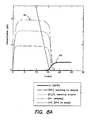
- a stepwise change in the concentration of one or more ionic species in the analyte solution in turn essentially instantaneously changes the charge density ⁇ dl on the analyte solution side of the double layer capacitance C dl .
- the surface charge density ⁇ 0 initially remains constant, and the change in ion concentration effectively results in a sudden change in the double layer capacitance C dl .
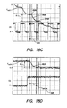
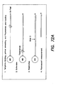
- Fig. 2A illustrates this phenomenon, in which an essentially instantaneous or stepwise increase in ion concentration in the analyte solution, as shown in the top graph, results in a corresponding change in the surface potential ⁇ 0 , as shown in the bottom graph of Fig. 2A .
- the passivation layer surface groups react to the stimulus (i.e., as the surface charge density adjusts)
- the system returns to some equilibrium point, as illustrated by the decay of the ISFET response "pulse" 79 shown in the bottom graph of Fig. 2A .
- the foregoing phenomenon is referred to in the relevant literature (and hereafter in this disclosure) as an "ion-step" response.
- the time decay profile 81 associated with the response 79 is determined at least in part by the kinetics of the equilibrium reactions at the analyte solution/passivation layer interface (e.g., as given by Eqs. (6) and (7) for metal oxides, and also Eq. (7b) for metal nitrides).
- Eqs. (6) and (7) for metal oxides
- Eq. (7b) for metal nitrides.
- One instructive treatment in this regard is provided by "Modeling the short-time response of ISFET sensors," P. Woias et al., Sensors and Actuators B, 24-25 (1995) 211-217 (hereinafter referred to as "Woias”), which publication is incorporated herein by reference.
- an exemplary ISFET having a silicon nitride passivation layer is considered.
- a system of coupled non-linear differential equations based on the equilibrium reactions given by Eqs. (6), (7), and (7a) is formulated to describe the dynamic response of the ISFET to a step (essentially instantaneous) change in pH; more specifically, these equations describe the change in concentration over time of the various surface species involved in the equilibrium reactions, based on the forward and backward rate constants for the involved proton acceptance and proton donation reactions and how changes in analyte pH affect one or more of the reaction rate constants.
- Exemplary solutions are provided for the concentration of each of the surface ion species as a function of time.
- ⁇ 0 denotes a theoretical minimum response time that only depends on material parameters.
- Woias provides exemplary values for ⁇ 0 on the order of 60 microseconds to 200 microseconds.
- the time constant ⁇ given by Eq. (19) is 1.9 seconds.
- Exemplary values for other types of passivation materials may be found in the relevant literature and/or determined empirically.
- ISFET sensor elements or "pixels"
- Exemplary research in ISFET array fabrication is reported in the publications " A large transistor-based sensor array chip for direct extracellular imaging," M.J. Milgrew, M.O. Riehle, and D.R.S. Cumming, Sensors and Actuators, B: Chemical, 111-112, (2005), pp. 347-353 , and " The development of scalable sensor arrays using standard CMOS technology," M.J. Milgrew, P.A. Hammond, and D.R.S.
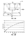
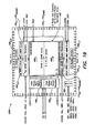
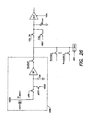
- Fig. 3 illustrates one column 85 j of a two-dimensional ISFET array according to the design of Milgrew et al.
- a given column 85 j includes a current source I SOURCEj that is shared by all pixels of the column, and ISFET bias/readout circuitry 82 j (including current sink I SINKj ) that is also shared by all pixels of the column.
- Each ISFET pixel 80 1 through 80 16 includes a p-channel ISFET 50 having an electrically coupled source and body (as shown in Figs. 1 and 2 ), plus two switches S1 and S2 that are responsive to one of sixteen row select signals (RSEL 1 through RSEL 16 , and their complements). As discussed below in connection with Fig. 7 , a row select signal and its complement are generated simultaneously to "enable" or select a given pixel of the column 85 j , and such signal pairs are generated in some sequence to successively enable different pixels of the column one at a time.
- the switch S2 of each pixel 80 in the design of Milgrew et al. is implemented as a conventional n-channel MOSFET that couples the current source I SOURCEj to the source of the ISFET 50 upon receipt of the corresponding row select signal.
- the switch S1 of each pixel 80 is implemented as a transmission gate, i.e., a CMOS pair including an n-channel MOSFET and a p-channel MOSFET, that couples the source of the ISFET 50 to the bias/readout circuitry 82 j upon receipt of the corresponding row select signal and its complement.
- An example of the switch S1 1 of the pixel 80 1 is shown in Fig.
- CMOS-pair transmission gate including an n-channel MOSFET and a p-channel MOSFET for switch S1, and an n-channel MOSFET for switch S2.
- the bias/readout circuitry 82 j employs a source-drain follower configuration in the form of a Kelvin bridge to maintain a constant drain-source voltage V DSj and isolate the measurement of the source voltage V Sj from the constant drain current I SOURCEj for the ISFET of an enabled pixel in the column 85 j .
- the bias/readout circuitry 82 j includes two operational amplifiers A1 and A2, a current sink I SINKj , and a resistor R SDj .
- the wide dynamic range for the source voltage V Sj provided by the transmission gate S1 ensures that a full range of pH values from 1-14 may be measured, and the source-body connection of each ISFET ensures sufficient linearity of the ISFETs threshold voltage over the full pH measurement range.
- a p-channel ISFET 50 as shown in Fig. 1 must be employed in each pixel; more specifically, an alternative implementation based on the Kelvin bridge configuration is not possible using an n-channel ISFET.
- the n-type well 54 would not be required, and highly doped n-type regions for the drain and source would be formed directly in the p-type silicon substrate 52 (which would constitute the transistor body).
- the transistor body typically is coupled to electrical ground.
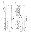
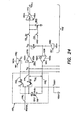
- Fig. 5 is a diagram similar to Fig. 1 , illustrating a wider cross-section of a portion of the p-type silicon substrate 52 corresponding to one pixel 80 of the column 85j shown in Fig.
- n-type well 54 containing the drain 58, source 56 and body connection 62 of the ISFET 50 is shown alongside a first n-channel MOSFET corresponding to the switch S2 and a second n-channel MOSFET S1 1N constituting one of the two transistors of the transmission gate S1 1 shown in Fig. 4 .
- the p-channel MOSFET required to implement the transmission gate S1 in each pixel cannot be formed in the same n-type well in which the p-channel ISFET 50 for the pixel is formed.
- the body and source of the p-channel ISFET are electrically coupled together, implementing the p-channel MOSFET S1 1P in the same n-well as the p-channel ISFET 50 would lead to unpredictable operation of the transmission gate, or preclude operation entirely. Accordingly, two separate n-type wells are required to implement each pixel in the design of Milgrew et al. Fig.
- FIG. 6 is a diagram similar to Fig. 5 , showing a cross-section of another portion of the p-type silicon substrate 52 corresponding to one pixel 80, in which the n-type well 54 corresponding to the ISFET 50 is shown alongside a second n-type well 55 in which is formed the p-channel MOSFET S1 1P constituting one of the two transistors of the transmission gate S1 1 shown in Fig. 4 . It should be appreciated that the drawings in Figs.
- 5 and 6 are not to scale and may not exactly represent the actual layout of a particular pixel in the design of Milgrew et al.; rather these figures are conceptual in nature and are provided primarily to illustrate the requirements of multiple n-wells, and separate n-channel MOSFETs fabricated outside of the n-wells, in the design of Milgrew et al.
- CMOS design rules dictate minimum separation distances between features.
- a distance "a" between neighboring n-wells must be at least three (3) micrometers.
- a distance "a/2" also is indicated in Fig. 6 to the left of the n-well 54 and to the right of the n-well 55 to indicate the minimum distance required to separate the pixel 80 shown in Fig. 6 from neighboring pixels in other columns to the left and right, respectively.
- a total distance "d" shown in Fig. 6 representing the width of the pixel 80 in cross-section is on the order of approximately 12 ⁇ m to 14 ⁇ m.
- Milgrew et al. report an array based on the column/pixel design shown in Fig. 3 comprising geometrically square pixels each having a dimension of 12.8 ⁇ m by 12.8 ⁇ m.
- each pixel of Milgrew's array requires four transistors (p-channel ISFET, p-channel MOSFET, and two n-channel MOSFETs) and two separate n-wells ( Fig. 6 ). Based on a 0.35 micrometer conventional CMOS fabrication process and corresponding design rules, the pixels of such an array have a minimum size appreciably greater than 10 ⁇ m, i.e., on the order of approximately 12 ⁇ m to 14 ⁇ m.
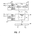
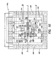
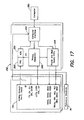
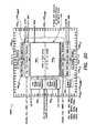
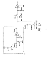
- Fig. 7 illustrates a complete two-dimensional pixel array 95 according to the design of Milgrew et al., together with accompanying row and column decoder circuitry and measurement readout circuitry.
- the array 95 includes sixteen columns 85 1 through 85 16 of pixels, each column having sixteen pixels as discussed above in connection with Fig. 3 (i.e., a 16 pixel by 16 pixel array).
- a row decoder 92 provides sixteen pairs of complementary row select signals, wherein each pair of row select signals simultaneously enables one pixel in each column 85 1 through 85 16 to provide a set of column output signals from the array 95 based on the respective source voltages V S1 through V S16 of the enabled row of ISFETs.
- the row decoder 92 is implemented as a conventional four-to-sixteen decoder (i.e., a four-bit binary input ROW 1 - ROW 4 to select one of 2 4 outputs).
- the set of column output signals V S1 through V S16 for an enabled row of the array is applied to switching logic 96, which includes sixteen transmission gates S 1 through S16 (one transmission gate for each output signal).
- each transmission gate of the switching logic 96 is implemented using a p-channel MOSFET and an n-channel MOSFET to ensure a sufficient dynamic range for each of the output signals V S1 through V S16 .
- the column decoder 94 like the row decoder 92, is implemented as a conventional four-to-sixteen decoder and is controlled via the four-bit binary input COL 1 - COL 4 to enable one of the transmission gates S1 through S16 of the switching logic 96 at any given time, so as to provide a single output signal V S from the switching logic 96.
- This output signal Vs is applied to a 10-bit analog to digital converter (ADC) 98 to provide a digital representation D 1 - D 10 of the output signal V S corresponding to a given pixel of the array.
- ADC analog to digital converter
- ISFETs and arrays of ISFETs similar to those discussed above have been employed as sensing devices in a variety of chemical and biological applications.
- ISFETs have been employed as pH sensors in the monitoring of various processes involving nucleic acids such as DNA.
- Some examples of employing ISFETs in various life-science related applications are given in the following publications, each of which is incorporated herein by reference: Massimo Barbaro, Annalisa Bonfiglio, Luigi Raffo, Andrea Alessandrini, Paolo Facci and Imrich Barak, "Fully electronic DNA hybridization detection by a standard CMOS biochip," Sensors and Actuators B: Chemical, Volume 118, Issues 1-2, 2006, pp.
- sequencing refers to the determination of a primary structure (or primary sequence) of an unbranched biopolymer, which results in a symbolic linear depiction known as a "sequence” that succinctly summarizes much of the atomic-level structure of the sequenced molecule.
- DNA sequencing particularly refers to the process of determining the nucleotide order of a given DNA fragment. Analysis of entire genomes of viruses, bacteria, fungi, animals and plants is now possible, but such analysis generally is limited due to the cost and time required to sequence such large genomes. Moreover, present conventional sequencing methods are limited in terms of their accuracy, the length of individual templates that can be sequenced, and the rate of sequence determination.
- ISFETs may be particularly configured and employed to facilitate DNA sequencing techniques based on monitoring changes in chemical processes, including DNA synthesis. More generally, Applicants have recognized and appreciated that large arrays of chemically-sensitive FETs (i.e., chemFETs) may be employed to detect and measure static and/or dynamic concentrations/levels of a variety of analytes (e.g., hydrogen ions, other ions, non-ionic molecules or compounds, etc.) in a host of chemical and/or biological processes (e.g., biological or chemical reactions, cell or tissue cultures or monitoring, neural activity, nucleic acid sequencing, etc.) in which valuable information may be obtained based on such analyte measurements.
- analytes e.g., hydrogen ions, other ions, non-ionic molecules or compounds, etc.
- biological processes e.g., biological or chemical reactions, cell or tissue cultures or monitoring, neural activity, nucleic acid sequencing, etc.
- FET arrays include multiple chemFETs, that act as chemical sensors.
- An ISFET as discussed above, is a particular type of chemFET that is configured for ion detection, and ISFETs may be employed in various embodiments disclosed herein.
- Other types of chemFETs contemplated by the present disclosure include enzyme FETs (EnFETs) which employ enzymes to detect analytes. It should be appreciated, however, that the present disclosure is not limited to ISFETs and EnFETs, but more generally relates to any FET that is configured for some type of chemical sensitivity.
- chemical sensitivity broadly encompasses sensitivity to any molecule of interest, including without limitation organic, inorganic, naturally occurring, non-naturally occurring, and synthetic chemical and biological compounds, such as ions, small molecules, polymers such as nucleic acids, proteins, peptides, polysaccharides, and the like.
- the present disclosure is directed generally to inventive methods and apparati relating to the use of the above-described large scale chemFET arrays in the analysis of chemical or biological samples.
- These samples are typically liquid (or are dissolved in a liquid) and of small volume, to facilitate high-speed, high-density determination of analyte (e.g., ion or other constituent) presence, concentration or other measurements on the analyte.
- analyte e.g., ion or other constituent
- some embodiments are directed to a "very large scale" two-dimensional chemFET sensor array (e.g., greater than 256 sensors), in which one or more chemFET-containing elements or "pixels" constituting the sensors of such an array are configured to monitor one or more independent biological or chemical reactions or events occurring in proximity to the pixels of the array.
- the array may be coupled to one or more microfluidics structures that form one or more reaction chambers, or "wells" or “microwells,” over individual sensors or groups of sensors of the array, and apparatus which delivers analyte samples (i.e., analyte solutions) to the wells and removes them from the wells between measurements.
- the sensor array may be coupled to one or more microfluidics structures for the delivery of one or more analytes to the pixels and for removal of analyte(s) between measurements.
- inventive aspects of this disclosure include the various microfluidic structures which may be employed to flow analytes and where appropriate other agents useful in for example the detection and measurement of analytes to and from the wells or pixels, the methods of manufacture of the array of wells, methods and structures for coupling the arrayed wells with arrayed pixels, and methods and apparatus for loading the wells with sample to be analyzed, including for example loading the wells with DNA-bearing beads when the apparatus is used for DNA sequencing or related analysis, as will be discussed in greater detail below.
- an analyte of particular interest is a byproduct of nucleic acid synthesis.
- a byproduct can be monitored as the readout of a sequencing-by-synthesis method.
- One particularly important byproduct is inorganic pyrophosphate (PPi) which is released upon the addition (or incorporation) of a deoxynucleotide triphosphate (also referred to herein as dNTP) to the 3' end of a nucleic acid (such as a sequencing primer).
- PPi may be hydrolyzed to orthophosphate (Pi) and free hydrogen ion (H + ) in the presence of water (and optionally and far more rapidly in the presence of pyrophosphatase).
- nucleotide incorporation can be monitored by detecting PPi, Pi and/or H + .
- PPi has not been detected or measured by chemFETs.
- Optically based sequencing-by-synthesis methods have detected PPi via its sulfurylase-mediated conversion to adenosine triphosphate (ATP), and then luciferase-mediated conversion of luciferin to oxyluciferin in the presence of the previously generated ATP, with concomitant release of light. Such detection is referred to herein as "enzymatic" detection of PPi.
- the invention provides methods for detecting PPi using non-enzymatic methods.
- non-enzymatic detection of PPi is detection of PPi that does not require an enzyme other than any enzyme required to produce or release the PPi in the first instance (e.g., a polymerase).
- An example of non-enzymatic detection of PPi is a detection method that does not require conversion of PPi to ATP.
- H+ has been detected by measuring pH changes using standard pH meters or in some instances ISFETs. Importantly, many if not all prior attempts to detect nucleotide incorporation using ISFETs have focused solely on pH changes and not on detection or measurement of released PPi.
- the instant invention contemplates and thus provides methods for monitoring nucleic acid sequencing reactions and thus determining the nucleotide sequence of nucleic acids by detecting H+ (or changes in pH), PPi (or Pi) in the absence of presence of PPi (or Pi) specific receptors, unincorporated dNTP, or some combination thereof.
- Some aspects therefore are aimed at monitoring pH while others are aimed at monitoring (and detecting) ion pulses at the FET surface resulting from changes in ionic species in the solution in contact with such surface.
- various aspects of the invention provide methods and apparati for directly detecting released PPi as an indicator of nucleotide incorporation into a nucleic acid.
- the invention does so through the use of the chemFET arrays described herein.
- a nucleic acid synthesis reaction is performed in a solution that is in contact with the chemFET and the released PPi is detected (or sensed) by the chemFET surface.
- synthesis and/or sequencing reactions may be performed, and in some instances are preferably performed, in an environment that is substantially pH insensitive (i.e., an environment in which changes in pH are not detected due to for example the strong buffering capacity of the environment).
- the analyte of interest is hydrogen ion
- large scale ISFET arrays according to the present disclosure are specifically configured to measure changes in H + concentration (i.e., changes in pH).
- chemFET arrays may be specifically configured to measure hydrogen ions and/or one or more other analytes that provide relevant information relating to the occurrence and/or progress of a particular biological or chemical process of interest.
- the chemFET arrays may be fabricated using conventional CMOS (or biCMOS or other suitable) processing technologies, and are particularly configured to facilitate the rapid acquisition of data from the entire array (scanning all of the pixels to obtain corresponding pixel output signals).
- CMOS complementary metal-oxide-semiconductor
- biCMOS complementary metal-oxide-semiconductor
- one or more analytes measured by a chemFET array may include any of a variety of biological or chemical substances that provide relevant information regarding a biological or chemical process (e.g., binding events such as hybridization of nucleic acids to each other, antigen-antibody binding, receptor-ligand binding, enzyme-inhibitor binding, enzyme-substrate binding, and the like).
- binding events such as hybridization of nucleic acids to each other, antigen-antibody binding, receptor-ligand binding, enzyme-inhibitor binding, enzyme-substrate binding, and the like.
- the ability to measure absolute or relative as well as static and/or dynamic levels and/or concentrations of one or more analytes provides valuable information in connection with biological and chemical processes.
- mere determination of the presence or absence of an analyte or analytes of interest may provide valuable information may be sufficient.
- a chemFET array may be configured for sensitivity to any one or more of a variety of analytes.
- one or more chemFETs of an array may be particularly configured for sensitivity to one or more analytes, and in other embodiments different chemFETs of a given array may be configured for sensitivity to different analytes.
- one or more sensors (pixels) of the array may include a first type of chemFET configured to be sensitive to a first analyte, and one or more other sensors of the array may include a second type of chemFET configured to be sensitive to a second analyte different from the first analyte.
- the first and second analytes may be related to each other.
- the first and second analytes may be byproducts of the same biological or chemical reaction/process and therefore they may be detected concurrently to confirm the occurrence of a reaction (or lack thereof).
- redundancy is preferably in some analyte detection methods.
- more than two different types of chemFETs may be employed in any given array to detect and/or measure different types of analytes, and optionally to monitor biological or chemical processes such as binding events.
- a given sensor array may be "homogeneous” and thereby consist of chemFETs of substantially similar or identical type that detect and/or measure the same analyte (e.g., pH or other ion concentration), or a sensor array may be "heterogeneous” and include chemFETs of different types to detect and/or measure different analytes.
- the sensors in an array may be configured to detect and/or measure a single type (or class) of analyte even though the species of that type (or class) detected and/or measured may be different between sensors.
- all the sensors in an array may be configured to detect and/or measure nucleic acids, but each sensor detects and/or measures a different nucleic acid.
- Applicants have specifically improved upon the ISFET array design of Milgrew et al. discussed above in connection with Figs. 1-7 , as well as other conventional ISFET array designs, so as to significantly reduce pixel size, and thereby increase the number of pixels of a chemFET array for a given semiconductor die size (i.e., increase pixel density).
- this increase in pixel density is accomplished while at the same time increasing the signal-to-noise ratio (SNR) of output signals corresponding to monitored biological and chemical processes, and the speed with which such output signals may be read from the array.
- SNR signal-to-noise ratio
- Applicants have recognized and appreciated that by relaxing requirements for chemFET linearity and focusing on a more limited measurement output signal range (e.g., output signals corresponding to a pH range of from approximately 7 to 9 or smaller, rather than 1 to 14, as well as output signals that do not necessarily relate significantly to pH), individual pixel complexity and size may be significantly reduced, thereby facilitating the realization of very large scale dense chemFET arrays.
- Applicants have also recognized and appreciated that alternative less complex approaches to pixel selection in an chemFET array (e.g., alternatives to the row and column decoder approach employed in the design of Milgrew et al. as shown in Fig. 7 , whose complexity scales with array size), as well as various data processing techniques involving ISFET response modeling and data extrapolation based on such modeling, facilitate rapid acquisition of data from significantly large and dense arrays.
- chemFET array fabrication Applicants have further recognized and appreciated that various techniques employed in a conventional CMOS fabrication process, as well as various post-fabrication processing steps (wafer handling, cleaning, dicing, packaging, etc.), may in some instances adversely affect performance of the resulting chemFET array.
- one potential issue relates to trapped charge that may be induced in the gate oxide 65 during etching of metals associated with the floating gate structure 70, and how such trapped charge may affect chemFET threshold voltage V TH .
- Another potential issue relates to the density/porosity of the chemFET passivation layer (e.g., see ISFET passivation layer 72 in Fig.
- one embodiment of the present invention is directed to an apparatus, comprising an array of CMOS-fabricated sensors, each sensor comprising one chemically-sensitive field effect transistor (chemFET) and occupying an area on a surface of the array of 10 ⁇ m 2 or less.
- chemFET chemically-sensitive field effect transistor
- Another embodiment is directed to a sensor array, comprising a two-dimensional array of electronic sensors including at least 512 rows and at least 512 columns of the electronic sensors, each sensor comprising one chemically-sensitive field effect transistor (chemFET) configured to provide at least one output signal representing a presence and/or concentration of an analyte proximate to a surface of the two-dimensional array.
- chemFET chemically-sensitive field effect transistor
- Another embodiment is directed to an apparatus, comprising an array of CMOS-fabricated sensors, each sensor comprising one chemically-sensitive field effect transistor (chemFET).
- the array of CMOS-fabricated sensors includes more than 256 sensors, and a collection of chemFET output signals from all chemFETs of the array constitutes a frame of data.
- the apparatus further comprises control circuitry coupled to the array and configured to generate at least one array output signal to provide multiple frames of data from the array at a frame rate of at least 1 frame per second.
- the frame rate may be at least 10 frames per second.
- the frame rate may be at least 20 frames per second.
- the frame rate may be at least 30, 40, 50, 70 or up to 100 frames per second.
- Another embodiment is directed to an apparatus, comprising an array of CMOS-fabricated sensors, each sensor comprising a chemically-sensitive field effect transistor (chemFET).
- the chemFET comprises a floating gate structure, and a source and a drain having a first semiconductor type and fabricated in a region having a second semiconductor type, wherein there is no electrical conductor that electrically connects the region having the second semiconductor type to either the source or the drain.
- Another embodiment is directed to an apparatus, comprising an array of electronic sensors, each sensor consisting of three field effect transistors (FETs) including one chemically-sensitive field effect transistor (chemFET).
- FETs field effect transistors
- chemFET chemically-sensitive field effect transistor
- Another embodiment is directed to an apparatus, comprising an array of electronic sensors, each sensor comprising three or fewer field effect transistors (FETs), wherein the three or fewer FETs includes one chemically-sensitive field effect transistor (chemFET).
- FETs field effect transistors
- chemFET chemically-sensitive field effect transistor
- Another embodiment is directed to an apparatus, comprising an array of electronic sensors, each sensor comprising a plurality of field effect transistors (FETs) including one chemically-sensitive field effect transistor (chemFET), and a plurality of electrical conductors electrically connected to the plurality of FETs, wherein the plurality of FETs are arranged such that the plurality of electrical conductors includes no more than four conductors traversing an area occupied by each sensor and interconnecting multiple sensors of the array.
- FETs field effect transistors
- chemFET chemically-sensitive field effect transistor
- Another embodiment is directed to an apparatus, comprising an array of CMOS-fabricated sensors, each sensor comprising a plurality of field effect transistors (FETs) including one chemically-sensitive field effect transistor (chemFET), wherein all of the FETs in each sensor are of a same channel type and are implemented in a single semiconductor region of an array substrate.
- FETs field effect transistors
- chemFET chemically-sensitive field effect transistor
- a sensor array comprising a plurality of electronic sensors arranged in a plurality of rows and a plurality of columns.
- Each sensor comprises one chemically-sensitive field effect transistor (chemFET) configured to provide at least one and in some instances at least two output signals representing a presence and/or a concentration of an analyte proximate to a surface of the array.
- chemFET chemically-sensitive field effect transistor
- the array further comprises column circuitry configured to provide a constant drain current and a constant drain-to-source voltage to respective chemFETs in the column, the column circuitry including two operational amplifiers and a diode-connected FET arranged in a Kelvin bridge configuration with the respective chemFETs to provide the constant drain-to-source voltage.
- Another embodiment is directed to a sensor array, comprising a plurality of electronic sensors arranged in a plurality of rows and a plurality of columns.
- Each sensor comprises one chemically-sensitive field effect transistor (chemFET) configured to provide at least one output signal and in some instances at least two output signals representing a concentration of ions in a solution proximate to a surface of the array.
- the array further comprises at least one row select shift register to enable respective rows of the plurality of rows, and at least one column select shift register to acquire chemFET output signals from respective columns of the plurality of columns.
- Another embodiment is directed to an apparatus, comprising an array of CMOS-fabricated sensors, each sensor comprising a chemically-sensitive field effect transistor (chemFET).
- the chemFET comprises a floating gate structure, and a source and a drain having a first semiconductor type and fabricated in a region having a second semiconductor type, wherein there is no electrical conductor that electrically connects the region having the second semiconductor type to either the source or the drain.
- the array includes a two-dimensional array of at least 512 rows and at least 512 columns of the CMOS-fabricated sensors.
- Each sensor consists of three field effect transistors (FETs) including the chemFET, and each sensor includes a plurality of electrical conductors electrically connected to the three FETs.
- the three FETs are arranged such that the plurality of electrical conductors includes no more than four conductors traversing an area occupied by each sensor and interconnecting multiple sensors of the array. All of the FETs in each sensor are of a same channel type and implemented in a single semiconductor region of an array substrate.
- a collection of chemFET output signals from all chemFETs of the array constitutes a frame of data.
- the apparatus further comprises control circuitry coupled to the array and configured to generate at least one array output signal to provide multiple frames of data from the array at a frame rate of at least 20 frames per second.
- Another embodiment is directed to a method for processing an array of CMOS-fabricated sensors, each sensor comprising a chemically-sensitive field effect transistor (chemFET).
- the method comprises: A) dicing a semiconductor wafer including the array to form at least one diced portion including the array; and B) performing a forming gas anneal on the at least one diced portion.
- chemFET chemically-sensitive field effect transistor
- Another embodiment is directed to a method for manufacturing an array of chemFETs.
- the method comprises: fabricating an array of chemFETs; depositing on the array a dielectric material; applying a forming gas anneal to the array before a dicing step; dicing the array; and applying a forming gas anneal after the dicing step.
- the method may further comprise testing the semiconductor wafer between one or more deposition steps.
- Another embodiment is directed to a method for processing an array of CMOS-fabricated sensors.
- Each sensor comprises a chemically-sensitive field effect transistor (chemFET) having a chemically-sensitive passivation layer of silicon nitride and/or silicon oxynitride deposited via plasma enhanced chemical vapor deposition (PECVD).
- the method comprises depositing at least one additional passivation material on the chemically-sensitive passivation layer so as to reduce a porosity and/or increase a density of the passivation layer.
- aspects of the invention relate to methods for monitoring nucleic acid synthesis reactions, including but not limited to those integral to sequencing-by-synthesis methods.
- various aspects of the invention provide methods for monitoring nucleic acid synthesis reactions, methods for determining or monitoring nucleotide incorporation into a nucleic acid, methods for determining the presence or absence of nucleotide incorporation, methods for determining the number of incorporated nucleotides, and the like.
- the invention provides a method for sequencing a nucleic acid comprising disposing (e.g., placing or positioning) a plurality of template nucleic acids into a plurality of reaction chambers, wherein the plurality of reaction chambers is in contact with a chemFET array comprising at least one chemFET for each reaction chamber, and wherein each of the template nucleic acids is hybridized to a sequencing primer (thereby forming a template/primer hybrid) and is bound to a polymerase, synthesizing a new nucleic acid strand (or extending the sequencing primer) by incorporating one or more known nucleotide triphosphates (also referred to generically herein as dNTP) sequentially at the 3' end of the sequencing primer, and detecting the incorporation of the one or more known nucleotide triphosphates by a change in voltage and/or current at the at least one chemFET.
- a sequencing primer thereby forming a template/primer hybrid
- a polymerase synthe
- the array (and thus the plurality) of chemFETs may be comprised of at least two, at least three, at least four, at least five, at least six, at least seven, at least eight, at least nine, at least ten, at least 100, at least 200, at least 300, at least 400, at least 500, at least 1000, at least 10 4 , at least 10 5 , at least 10 6 , at least 10 7 , or more chemFET (or chemFET sensors, or sensors, as the terms are used interchangeably herein).
- the plurality of reaction chambers may be at least two, at least three, at least four, at least five, at least six, at least seven, at least eight, at least nine, at least ten, at least 100, at least 200, at least 300, at least 400, at least 500, at least 1000, at least 10 4 , at least 10 5 , at least 10 6 , at least 10 7 , or more reaction chambers.
- the invention provides a method for sequencing a nucleic acid comprising disposing a plurality of template nucleic acids into a plurality of reaction chambers, wherein the plurality of reaction chambers is in contact with a chemFET array, wherein at least one chemFET is in contact with each reaction chamber, and wherein each of the template nucleic acids is hybridized to a sequencing primer (thereby forming a template/primer hybrid) and is bound to a polymerase, synthesizing a new nucleic acid strand (or extending the sequencing primer) by incorporating one or more known nucleotide triphosphates sequentially at the 3' end of the sequencing primer, and detecting the incorporation of the one or more known nucleotide triphosphates by a change in voltage and/or current at the at least one chemFET, wherein the chemFET array is any of the foregoing arrays.
- the invention provides a method for sequencing a nucleic acid comprising disposing a plurality of template nucleic acids into a plurality of reaction chambers, wherein the plurality of reaction chambers is in contact with a chemFET array comprising at least one chemFET for each reaction chamber, and wherein each of the template nucleic acids is hybridized to a sequencing primer (thereby forming a template/primer hybrid) and is bound to a polymerase, synthesizing a new nucleic acid strand (by extending the sequencing primer) by incorporating one or more known nucleotide triphosphates sequentially at the 3' end of the sequencing primer, and detecting the incorporation of the one or more known nucleotide triphosphates by a change in voltage and/or current at the at least one chemFET within the array, wherein a center-to-center distance between adjacent reaction chambers (or "pitch”) is 1-10 ⁇ m.
- the invention provides a method for sequencing a nucleic acid comprising disposing a plurality of template nucleic acids into a plurality of reaction chambers, wherein the plurality of reaction chambers is in contact with a chemFET array comprising at least one chemFET for each reaction chamber, and wherein each of the template nucleic acids is hybridized to a sequencing primer (thereby forming a template/primer hybrid) and is bound to a polymerase, synthesizing a new nucleic acid strand (by extending the sequencing primer) by incorporating one or more known nucleotide triphosphates sequentially at the 3' end of the sequencing primer, and detecting the incorporation of the one or more known nucleotide triphosphates by the generation of sequencing reaction byproduct, wherein (a) the chemFET array comprises more than 256 sensors, or (b) a center-to-center distance between adjacent reaction chambers is 1-10 ⁇ m.
- the sequencing reaction byproduct is PPi.
- the invention provides a method for sequencing a nucleic acid comprising fragmenting (or isolating, for example in the context of enriched exon isolation) a target nucleic acid to generate a plurality of fragmented (or isolated) nucleic acids, attaching each of the plurality of fragmented (or isolated) nucleic acids to individual beads to generate a plurality of beads each attached to a single fragmented (or isolated) nucleic acid, amplifying the number of fragmented (or isolated) nucleic acids on each bead, delivering the plurality of beads attached to amplified fragmented (or isolated) nucleic acids to a chemFET array having a separate reaction chamber for each sensor in the array, wherein only one bead is situated in each reaction chamber, and performing simultaneous sequencing reactions in the plurality of reaction chambers.
- nucleic acids to be sequenced may be derived from longer nucleic acids that are then subsequently fragmented (i.e., converted into shorter nucleic acids) or they may be isolated at a length that is suitable to the reactions contemplated herein and thus would not have to be shortened (or fragmented). It should therefore be understood that for every aspect and limitation discussed herein that refers to the process of fragmenting a target nucleic acid, the method can also be carried out by isolating a target nucleic acid in the absence of fragmenting.
- the invention provides a method for sequencing nucleic acids comprising fragmenting a target nucleic acid to generate a plurality of fragmented nucleic acids, amplifying each fragmented nucleic acid separately in the presence of a bead and binding amplified copies of the fragmented nucleic acid to the bead, thereby producing a plurality of beads each attached to a plurality of identical fragmented nucleic acids, delivering the plurality of beads each attached to a plurality of identical fragmented nucleic acids to a chemFET array having a separate reaction chamber for each chemFET sensor in the array, wherein only one bead is situated in each reaction chamber, and performing simultaneous sequencing reactions in the plurality of reaction chambers.
- the invention provides a method for sequencing a nucleic acid comprising disposing a plurality of template nucleic acids into a plurality of reaction chambers, wherein the plurality of reaction chambers is in contact with a chemFET array comprising at least one chemFET for each reaction chamber, and wherein each of the template nucleic acids is hybridized to a sequencing primer (thereby forming a template/primer hybrid) and is bound to a polymerase, synthesizing a new nucleic acid strand (by extending the sequencing primer) by incorporating one or more known nucleotide triphosphates sequentially at the 3' end of the sequencing primer, and detecting a change in the level of a sequencing byproduct as an indicator of incorporation of the one or more known nucleotide triphosphates.
- the change in the level may an increase or a decrease in a level relative to a level prior to incorporation of the one or more known nucleotide triphosphates.
- the change in the level may be read as a change in voltage and/or current at a chemFET sensor or a change in pH, but it is not so limited.
- the invention provides a method for sequencing a nucleic acid comprising disposing a plurality of template nucleic acids into a plurality of reaction chambers, wherein the plurality of reaction chambers is in contact with a chemFET array comprising at least one chemFET for each reaction chamber, and wherein each of the template nucleic acids is hybridized to a sequencing primer and is bound to a polymerase, synthesizing a new nucleic acid strand by incorporating one or more known nucleotide triphosphates sequentially at the 3' end of the sequencing primer, directly detecting release of PPi as an indicator of incorporation of the one or more known nucleotide triphosphates.
- the invention provides a method for sequencing nucleic acids comprising fragmenting a template nucleic acid to generate a plurality of fragmented nucleic acids, attaching one strand from each of the plurality of fragmented nucleic acids individually to beads to generate a plurality of beads each having a single stranded fragmented nucleic acid attached thereto, delivering the plurality of beads having a single stranded fragmented nucleic acid attached thereto to a chemFET array having a separate reaction chamber for each sensor in the area, and wherein only one bead is situated in each reaction chamber, and performing simultaneous sequencing reactions in the plurality of chambers.
- the invention provides a method for sequencing a nucleic acid comprising sequencing a plurality of identical template nucleic acids in a reaction chamber in contact with a chemFET, in an array which comprises at least 3 (and up to millions) of such assemblies of reaction chambers and chemFETs.
- the invention provides a method for sequencing a nucleic acid comprising detecting incorporation of one or more known nucleotide triphosphates to a 3' end of a sequencing primer hybridized to a template nucleic acid in a reaction chamber in contact with a chemFET of a chemFET array that comprises at least three chemFET.
- the invention provides a method for sequencing a nucleic acid comprising fragmenting a target nucleic acid to generate a plurality of fragmented nucleic acids, individually amplifying one or more of the plurality of fragmented nucleic acids, and sequencing the individually amplified fragmented nucleic acids using a chemFET array.
- the chemFET array comprises at least three chemFETs.
- the chemFET array comprises at least 500 chemFETs, or at least 100,000 chemFETs.
- the plurality of fragmented nucleic acids is individually amplified using a water in oil emulsion amplification method.
- the invention provides a method for sequencing a nucleic acid comprising fragmenting a target nucleic acid to generate a plurality of fragmented nucleic acids, attaching each of the plurality of fragmented nucleic acids to individual beads to generate a plurality of beads each attached to a single fragmented nucleic acid, amplifying the fragmented nucleic acids on each bead resulting in a plurality of identical fragmented nucleic acids on each bead, delivering a plurality of beads attached to fragmented nucleic acids to a chemFET array having a separate reaction chamber for each sensor in the array, wherein only one bead is situated in each reaction chamber, and performing sequencing reactions simultaneously in the plurality of reaction chambers.
- the invention provides a method for sequencing a nucleic acid comprising fragmenting a target nucleic acid to generate a plurality of fragmented nucleic acids, individually amplifying one or more of the plurality of fragmented nucleic acids, and sequencing the individually amplified fragmented nucleic acids in a plurality of reaction chambers having a center-to-center distance of about 1-10 ⁇ m using a chemFET array.
- the center-to-center distance is about 9 ⁇ m, about 5 ⁇ m, or about 2 ⁇ m.
- the invention provides a method for sequencing a nucleic acid comprising disposing a plurality of template nucleic acids into a plurality of reaction chambers, wherein the plurality of reaction chambers is in contact with a chemFET array comprising at least one chemFET for each reaction chamber, and wherein each of the template nucleic acids is hybridized to a sequencing primer and is bound to a polymerase, synthesizing a new nucleic acid strand by incorporating one or more known nucleotide triphosphates sequentially at the 3' end of the sequencing primer, and detecting incorporation of the one or more known nucleotide triphosphates by a change in voltage at the at least one chemFET within the array in the absence of a detectable pH change.
- the invention provides a method for sequencing a nucleic acid comprising disposing a plurality of template nucleic acids into a reaction chamber, wherein the plurality of template nucleic acids is attached to a single bead, each of the template nucleic acids is hybridized to a sequencing primer and is bound to a polymerase, and the reaction chamber is in contact with a chemFET, synthesizing a new nucleic acid strand by incorporating one or more known nucleotide triphosphates sequentially at the 3' end of the sequencing primer, and detecting incorporation of the one or more known nucleotide triphosphates by detection of a first and a second voltage pulse at the chemFET.
- the invention provides a method for sequencing a nucleic acid comprising disposing a plurality of template nucleic acids into a plurality of reaction chambers, wherein the plurality of reaction chambers is in contact with a chemFET array comprising at least one chemFET for each reaction chamber, and wherein each of the template nucleic acids is hybridized to a sequencing primer and is bound to a polymerase, synthesizing a new nucleic acid strand by incorporating one or more known nucleotide triphosphates sequentially at the 3' end of the sequencing primer, and detecting incorporation of the one or more known nucleotide triphosphates by non-enzymatically detecting released inorganic pyrophosphate.
- the detecting step occurs in the absence of a detectable pH change.
- the invention provides a method for sequencing a nucleic acid comprising disposing a plurality of template nucleic acids into a plurality of reaction chambers, wherein the plurality of reaction chambers is in contact with a chemFET array comprising at least one chemFET for each reaction chamber, and wherein each of the template nucleic acids is hybridized to a sequencing primer and is bound to a polymerase, synthesizing a new nucleic acid strand by incorporating one or more known nucleotide triphosphates sequentially at the 3' end of the sequencing primer, and detecting incorporation of the one or more known nucleotide triphosphates by detecting released inorganic pyrophosphate and unincorporated nucleotide triphosphates.
- the released inorganic pyrophosphate is detected at t 0 and unincorporated nucleotide triphosphates are detected at time t 1 .
- a time difference of t 1 - t 0 indicates a number of known nucleotide triphosphates incorporated.
- the invention provides a method for sequencing a nucleic acid comprising contacting a template nucleic acid with a sequencing primer and a polymerase for times and conditions sufficient to allow the template nucleic acid to bind to the sequencing primer for form a template/primer hybrid and to allow the polymerase to bind to the template/primer hybrid, and synthesizing a new nucleic acid strand by incorporating nucleotide triphosphates sequentially at the 3' end of the sequencing primer, and detecting incorporation of the one or more known nucleotide triphosphates by detecting released inorganic pyrophosphate and unincorporated nucleotide triphosphates.
- the released inorganic pyrophosphate is detected at t 0 and unincorporated nucleotide triphosphates are detected at time t 1 .
- the time difference between t 1 and to i.e., t 1 - to indicates the number of known nucleotide triphosphates incorporated.
- the invention provides a method for sequencing a nucleic acid comprising contacting a template nucleic acid with a sequencing primer and a polymerase for times and conditions sufficient to allow the template nucleic acid to bind to the sequencing primer for form a template/primer hybrid and to allow the polymerase to bind to the template/primer hybrid, and synthesizing a new nucleic acid strand (or extending sequencing primer) by incorporating one or more known nucleotide triphosphates sequentially at the 3' end of the sequencing primer in a low ionic strength environment, and detecting incorporation of the one or more known nucleotide triphosphates by detection of one or more voltage pulses at the chemFET.
- the low ionic strength environment may comprise less than 1 mM MgCl 2 , less than 0.5 mM MgCl 2 , less than 100 ⁇ M MgCl 2 , or less than 50 ⁇ M MgCl 2 .
- the low ionic strength environment may comprise less than 1 mM MnCl 2 , less than 0.5 mM MnCl 2 , less than 100 ⁇ M MnCl 2 , or less than 50 ⁇ M MnCl 2 .
- the salt may be another Mg 2+ or Mn 2+ containing salt, or it may be a Ca 2+ or Co 2+ containing salt, or it may be a combination of one or more such salts.
- the invention provides a method for determining incorporation of a nucleotide triphosphate into a newly synthesized nucleic acid (or onto a primer such as a sequencing primer) comprising combining a nucleotide triphosphate, a template/primer hybrid, and a polymerase, in a solution in contact with a chemFET, and detecting voltage pulses at the chemFET, wherein detection of a first and a second voltage pulse indicates incorporation of a nucleotide triphosphate and wherein detection of a first but not a second voltage pulse indicates lack of incorporation of a nucleotide triphosphate.
- the voltage pulses are detected at the chemFET independent of a binding event at the passivation layer of the chemFET.
- the invention provides a method for determining incorporation of a nucleotide triphosphate into a newly synthesized nucleic acid (or onto a primer such as a sequencing primer) comprising combining a nucleotide triphosphate, a template/primer hybrid, and a polymerase, in a solution in contact with a chemFET, and detecting voltage pulses at the chemFET independent of a binding event at the passivation layer of the chemFET, wherein detection of a first and a second voltage pulse indicates incorporation of at least one nucleotide triphosphate.
- the first voltage pulse occurs at time to and the second voltage pulse occurs at time t 1 , and t 1 - to indicates the number of nucleotide triphosphates incorporated.
- the incorporated nucleotide triphosphate is known.
- the nucleotide triphosphate is a plurality of identical nucleotide triphosphates
- the template/primer hybrid is a plurality of identical template/primer hybrids
- the polymerase is a plurality of identical polymerases.
- the polymerase may be a plurality of polymerases that are not identical and that rather may be comprised of 2, 3, or more types of polymerase.
- a mixture of two polymerases may be used with one having suitable processivity and the other having suitable rate of incorporation.
- the ratio of the different polymerases can vary and the invention is not to be limited in this regard.
- the template/primer hybrid may be a plurality of template/primer hybrids which may not be identical to each other, provided that any template/primer hybrids in a single reaction chamber or attached to a single bead are identical to each other.
- the invention provides a method for sequencing a nucleic acid comprising disposing (e.g., placing or positioning) a plurality of template nucleic acids into a plurality of reaction chambers, wherein the plurality of reaction chambers is in contact with a chemFET array comprising at least one chemFET for each reaction chamber, and wherein each of the template nucleic acids is hybridized to a sequencing primer and is bound to a polymerase, synthesizing a new nucleic acid strand (or extending the sequencing primer) by incorporating one or more known nucleotide triphosphates sequentially at the 3' end of the sequencing primer, and detecting incorporation of the one or more known nucleotide triphosphates by detecting at the at least one chemFET a first voltage pulse at time to having height h 0 and a second pulse at time t 1 having height h 1 , wherein h 0 and h 1 are each at least about 5mV over baseline, and t 1 -
- the invention provides a method for sequencing a nucleic acid comprising disposing a plurality of beads into a plurality of reaction chambers, wherein each reaction chamber comprises a single bead, each bead is attached to a plurality of identical template nucleic acids, each of the template nucleic acids is hybridized to a sequencing primer and is bound to a polymerase, and wherein the plurality of reaction chambers is in contact with a chemFET array comprising at least one chemFET for each reaction chamber, synthesizing a new nucleic acid strand (or extending the sequencing primer) by incorporating one or more known nucleotide triphosphates sequentially at the 3' end of the sequencing primer, and detecting the incorporation of the one or more known nucleotide triphosphates by detecting a first and a second voltage pulse at at least one chemFET within the array, wherein the chemFET array comprises at least three chemFET.
- the invention provides a method for sequencing a nucleic acid comprising disposing a plurality of beads into a plurality of reaction chambers, wherein each reaction chamber comprises a single bead, each bead is attached to a plurality of identical template nucleic acids, each of the template nucleic acids is hybridized to a sequencing primer and is bound to a polymerase, and wherein the plurality of reaction chambers is in contact with a chemical-sensitive field effect transistor (chemFET) array comprising at least one chemFET for each reaction chamber, initiating synthesis of a new nucleic acid strand (or extension of the sequencing primer) by introducing a plurality of known identical nucleotide triphosphates into each reaction chamber, synthesizing a new nucleic acid strand by incorporating one or more known nucleotide triphosphates sequentially at the 3' end of the sequencing primer, and detecting the incorporation of the one or more known nucleotide triphosphates by detecting a first and a
- each reaction chamber comprises adenosine triphosphate prior to introducing a plurality of known triphosphates into each reaction chamber.
- the invention provides a method for sequencing a nucleic acid comprising (a) disposing a plurality of beads into a plurality of reaction chambers, each reaction chamber comprising a single bead, each bead attached to a plurality of identical template nucleic acids, each of the template nucleic acids hybridized to a sequencing primer and bound to a polymerase, and each reaction chamber in contact with at least one chemFET, (b) introducing a plurality of known identical nucleotide triphosphates into each reaction chamber, (c) detecting sequential incorporation at the 3' end of the sequencing primer of one or more nucleotide triphosphates if complementary to corresponding nucleotides in the template nucleic acid, (d) washing unincorporated nucleotide triphosphates from the reaction chambers, and (e) repeating steps (b) through (d) in the same reaction chamber using a different plurality of known nucleotide triphosphates.
- step (e) comprises repeating steps (b) through (d) by separately introducing each different plurality of known nucleotide triphosphates into each reaction chamber
- the invention provides a method for sequencing a nucleic acid comprising disposing a plurality of beads into a plurality of reaction chambers, wherein each reaction chamber comprises a single bead, each bead is attached to a plurality of identical template nucleic acids, each of the template nucleic acids is hybridized to a sequencing primer and is bound to a polymerase, and wherein the each of the plurality of reaction chambers is in contact with at least one chemFET in a chemFET array, initiating synthesis of a new nucleic acid strand by introducing a divalent cation into each reaction chamber, synthesizing a new nucleic acid strand by incorporating one or more known nucleotide triphosphates sequentially at the 3' end of the sequencing primer, and detecting the incorporation of the one or more known nucleotide triphosphates by detecting a first and a second voltage pulse at at least one chemFET within the array.
- the divalent cation is Mg 2+ . In another embodiment, the divalent cation is Mn 2+ . In still a further embodiment, the divalent cation is a mixture of Mg 2+ and Mn 2+ . Depending on the embodiment, the divalent cation is at a concentration of less than 1 mM, or less than 100 ⁇ M, or about 50 ⁇ M.
- the invention provides a method for sequencing a nucleic acid comprising disposing a plurality of identical template nucleic acids into a reaction chamber, wherein the reaction chamber is in contact with a chemFET, and wherein each of the template nucleic acids is hybridized to a sequencing primer and is bound to a polymerase, incorporating one or more known nucleotide triphosphates sequentially at the 3' end of the sequencing primer, and detecting the incorporation of the one or more known nucleotide triphosphates by a voltage pulse at the chemFET, wherein the incorporation of 10-1000 nucleotide triphosphates is detected.
- the invention equally contemplates the use of double stranded templates that are engineered to have particular sequences at their free ends that can be acted upon by nicking enzymes such as DNA nickase.
- nicking enzymes such as DNA nickase.
- the polymerase incorporates nucleotide triphosphates at the nicked site. In these instances, there is no requirement for a separate sequencing primer.
- the incorporation of at least 10, at least 20, at least 30, at least 40, at least 50, at least 60, at least 70, at least 80, at least 90, or at least 100 nucleotide triphosphates is detected. In other embodiments, the incorporation of 100-1000 nucleotide triphosphates is detected. In still other some embodiments, the incorporation of 250-750 nucleotide triphosphates is detected.
- the reaction chamber comprises a plurality of packing beads. In some embodiments, the detecting step occurs in the presence of a plurality of packing beads.
- the reaction chamber comprises a soluble non-nucleic acid polymer.
- the detecting step occurs in the presence of a soluble non-nucleic acid polymer.
- the soluble non-nucleic acid polymer is polyethylene glycol, or PEA, or a dextran, or an acrylamide, or a cellulose (e.g., methyl cellulose).
- the non-nucleic acid polymer such as polyethylene glycol is attached to the single bead.
- the non-nucleic acid polymer is attached to one or more (or all) sides of a reaction chamber, except in some instances the bottom of the reaction chamber which is the FET surface
- the non-nucleic acid polymer is biotinylated such as but not limited to biotinylated polyethylene glycol.
- the method is carried out at a pH of about 7-9, or at about 8.5 to 9.5, or at about 9.
- the synthesizing and/or detecting step is carried out in a weak buffer.
- the weak buffer comprises Tris-HCl, boric acid or borate buffer, acetate, morpholine, citric acid, carbonic acid, or phosphoric acid as a buffering agent.
- the synthesizing and/or detecting step is carried out in about 1 mM Tris-HCl. In some embodiments, the synthesizing and/or detecting step is carried out in less than 1 mM Tris-HCl. In some embodiments, the synthesizing and/or detecting step is carried out in about 0.9 mM Tris-HCl, about 0.8 mM Tris-HCl, about 0.7 mM Tris-HCl, about 0.6 mM Tris-HCl, about 0.5 mM Tris-HCl, about 0.4 mM Tris-HCl, about 0.3 mM Tris-HCl, or about 0.2 mM Tris-HCl.
- the synthesizing and/or detecting step is carried out in about 1 mM borate buffer. In some embodiments, the synthesizing and/or detecting step is carried out in less than 1 mM borate buffer. In some embodiments, the synthesizing and/or detecting step is carried out in about 0.9 mM borate buffer, about 0.8 mM borate buffer, about 0.7 mM borate buffer, about 0.6 mM borate buffer, about 0.5 mM borate buffer, about 0.4 mM borate buffer, about 0.3 mM borate buffer, or about 0.2 mM borate buffer.
- the detection step occurs in the absence of a detectable pH change. In some embodiments, the detection step is carried out in an environment of constant pH. In some embodiment, the chemFET is relatively pH insensitive. In some embodiments, the synthesizing and/or detecting step is carried out in about 0.5 mM Tris-HCl.
- the synthesizing and/or detecting step is carried out in a low ionic strength environment. In some embodiments, synthesizing and/or detecting step is carried out in a low ionic strength environment that comprises less than 1 mM MgCl 2 or MnCl 2 , less than 0.5 mM MgCl 2 or MnCl 2 , or less than 100 ⁇ M MgCl 2 or MnCl 2 .
- the synthesizing and/or detecting step is carried out in a low ionic strength environment that comprises about 100 ⁇ M MgCl 2 or MnCl 2 , about 75 ⁇ M MgCl 2 or MnCl 2 , about 50 ⁇ M MgCl 2 or MnCl 2 , about 40 ⁇ M MgCl 2 or MnCl 2 , about 30 ⁇ M MgCl 2 or MnCl 2 , about 20 ⁇ M MgCl 2 or MnCl 2 , or about 10 ⁇ M MgCl 2 or MnCl 2 .
- the invention contemplates similarly amounts of other divalent cations and it is therefore not limited to MgCl 2 or MnCl 2 only. Similarly it should be understood that the invention contemplates the use of two or more divalent cations (and/or their corresponding salts) provided the total ion concentration is at the levels stated above.
- the synthesizing and/or detecting step is carried out in about 0.5 mM TRIS and about 50 ⁇ M MgCl 2 or MnCl 2 .
- the nucleotide triphosphates are unblocked.
- an unblocked nucleotide triphosphate is a nucleotide triphosphate with an unmodified end that can be incorporated into a nucleic acid (at its 3' end) and once it is incorporated can be attached to the following nucleotide triphosphate being incorporated.
- Blocked dNTP in contrast either cannot be added to a nucleic acid or their incorporation into a nucleic acid prevents any further nucleotide incorporation.
- the nucleotide triphosphates are deoxynucleotide triphosphates (dNTPs).
- the chemFET comprises a silicon nitride passivation layer. In some embodiments, the chemFET comprises a passivation layer attached to inorganic pyrophosphate (PPi) receptors. In some embodiments, the chemFET comprises a passivation layer that is not bound to a nucleic acid.
- PPi inorganic pyrophosphate
- each reaction chamber is in contact with a single chemFET.
- the reaction chamber has a volume of equal to or less than about 1 picoliter (pL), including less than 0.5 pL, less than 0.1 pL, less than 0.05 pL, less than 0.01 pL, less than 0.005 pL.
- the reaction chambers are separated by a center-to-center spacing of 1-10 ⁇ m. In some embodiments, the reaction chambers are separated by a center-to-center spacing of about 9 ⁇ m, about 5 microns, or about 2 microns.
- the reaction chambers may have a square cross section, for example at their base or bottom.
- Examples include an 8 ⁇ m by 8 ⁇ m cross section, a 4 ⁇ m by 4 ⁇ m cross section, or a 1.5 ⁇ m by 1.5 ⁇ m cross section. Alternatively, they may have a rectangular cross section, for example at their base or bottom. Examples include an 8 ⁇ m by 12 ⁇ m cross section, a 4 ⁇ m by 6 ⁇ m cross section, or a 1.5 ⁇ m by 2.25 ⁇ m cross section.
- the nucleotide triphosphates are pre-soaked in Mg 2+ (e.g., in the presence of MgCl 2 ) or Mn 2+ (for example in the presence of MnCl 2 ).
- the polymerase is pre-soaked in Mg 2+ (e.g., in the presence of MgCl 2 ) or Mn 2+ (for example in the presence of MnCl 2 ).
- the method is carried out in a reaction chamber comprising a single capture bead, wherein a ratio of reaction chamber width to single capture bead diameter is at least 0.7, at least 0.8, or at least 0.9.
- the polymerase is free in solution. In some embodiments, the polymerase is immobilized to a bead. In some embodiments, the polymerase is immobilized to a capture bead. In some embodiments, the template nucleic acids are attached to capture beads.
- inorganic pyrophosphate (PPi) is not significantly hydrolyzed prior to detecting nucleotide incorporation. In some embodiments, inorganic pyrophosphate (PPi) is not significantly hydrolyzed prior to detecting a first voltage pulse.
- the invention provides an apparatus comprising a chemFET array comprising a plurality of chemFET sensors each having a PPi receptor disposed on its surface, wherein the array comprises at least three chemFET sensors.
- the invention provides an apparatus comprising a chemFET array comprising a plurality of chemFET sensors each having a PPi receptor disposed on its surface, wherein adjacent chemFET sensors in the array are separated by a center-to-center distance of about less than about 10 ⁇ m (e.g., using .18 ⁇ m CMOS fabrication, the pitch may be about 2.8 ⁇ m).
- the invention provides an apparatus comprising a chemical-sensitive field effect transistor (chemFET) having disposed on its surface a PPi selective receptor.
- chemFET chemical-sensitive field effect transistor
- the PPi receptor may be immobilized to the chemFET surface.
- the invention provides an apparatus comprising a chemical-sensitive field effect transistor (chemFET) array comprising a plurality of chemFET sensors each having a PPi receptor disposed on its surface, wherein the plurality is a subset of the chemFET sensors in the array.
- the array comprises at least three chemFET sensors.
- the subset may represent 10%, 25%, 33%, 50%, 75% or more of the sensors in the array.
- the PPi selective receptor may be immobilized to the surface of each chemFET.
- the center-to-center distance between adjacent reaction chambers is about 1-9 ⁇ m, or about 2-9 ⁇ m, about 1 ⁇ m, about 2 ⁇ m, about 3 ⁇ m, about 4 ⁇ m, about 5 ⁇ m, about 6 ⁇ m, about 7 ⁇ m, about 8 ⁇ m, or about 9 ⁇ m.
- the chemFET array comprises more than 256 sensors (and optionally more than 256 corresponding reaction chambers (or wells)), more than 300 sensors (and optionally more than 300 corresponding reaction chambers), more than 400 sensors (and optionally more than 400 corresponding reaction chambers), more than 500 sensors (and optionally more than 500 corresponding reaction chambers), more than 600 sensors (and optionally more than 600 corresponding reaction chambers), more than 700 sensors (and optionally more than 700 corresponding reaction chambers), more than 800 sensors (and optionally more than 800 corresponding reaction chambers), more than 900 sensors (and optionally more than 900 corresponding reaction chambers), more than 10 3 sensors (and optionally more than 10 3 corresponding reaction chambers), more than 10 4 sensors (and optionally more than 10 4 corresponding reaction chambers), more than 10 5 sensors (and optionally more than 10 5 corresponding reaction chambers), or more than 10 6 sensors (and optionally more than 10 6 corresponding reaction chambers).
- the chemFET array comprises at least 512 rows and at least 512 rows and at least 512
- the sequencing byproduct is PPi.
- PPi is measured directly.
- PPi is detected by its binding to a PPi selective receptor immobilized on the surface of a chemFET sensor.
- PPi is detected in the absence of a PPi selective receptor.
- PPi is detected in a pH independent or insensitive environment.
- the sequencing reaction byproduct is hydrogen ion. In some embodiments, the sequencing reaction byproduct is Pi. In still other embodiments, the chemFET detects changes in any combination of the byproducts, optionally in combination with other parameters, as described herein.
- the PPi selective receptor is Compound 1, Compound 2, Compound 3, Compound 4, Compound 5, Compound 6, Compound 7, Compound 8, Compound 9 or Compound 10 as shown in Fig. 11B .
- the chemFET is present in an array of chemFETs, each of which has disposed, including immobilized, on its surface a PPi selective receptor. In some embodiments, identical PPi selective receptors are disposed on each chemFET of the array. In some embodiments, the array comprises more than 256 sensors. In some embodiments, the array comprises at least 512 rows and at least 512 columns of sensors. In some embodiments, the chemFET is located at a bottom of a reaction chamber.
- the invention provides an apparatus comprising a chemFET array having disposed on its surface a biological array or a chemical array.
- the biological array may be a nucleic acid array, a protein array including but not limited to an enzyme array, an antibody array and an antibody fragment array, a cell array, and the like.
- the chemical array may be an organic small molecule array, or an inorganic molecule array, but it is not so limited.
- the chemFET array may comprise at least 5, at least 10, at least 10 2 , at least 10 3 , at least 10 4 , at least 10 5 , at least 10 6 , or more sensors.
- the biological or chemical array may be arranged into a plurality of "cells" or spatially defined regions, and each of these regions is situated over a different sensor in the chemFET array, in some embodiments.
- the invention provides a method for detecting a nucleic acid comprising contacting a nucleic acid array disposed on a chemFET array with a sample, and detecting binding of a nucleic acid from the sample to one or more regions on the nucleic acid array.
- the invention provides a method for detecting a protein comprising contacting a protein array disposed on a chemFET array with a sample, and detecting binding of a protein from the sample to one or more regions on the protein array.
- the invention provides a method for detecting a nucleic acid comprising contacting a protein array disposed on a chemFET array with a sample, and detecting binding of a nucleic acid from the sample to one or more regions on the protein array.
- the invention provides a method for detecting an antigen comprising contacting an antibody array disposed on a chemFET array with a sample, and detecting binding of an antigen from the sample to one or more regions on the antibody array.
- the invention provides a method for detecting an enzyme substrate or inhibitor comprising contacting an enzyme array disposed on a chemFET array with a sample, and detecting binding of an entity from the sample to one or more regions on the enzyme array.
- inventive embodiments according to the present disclosure are directed at least in part to a semiconductor-based/microfluidic hybrid system that combines the power of microelectronics with the biocompatibility of a microfluidic system.
- the microelectronics portion of the hybrid system is implemented in CMOS technology for purposes of illustration. It should be appreciated, however, that the disclosure is not intended to be limiting in this respect, as other semiconductor-based technologies may be utilized to implement various aspects of the microelectronics portion of the systems discussed herein.
- One embodiment disclosed herein is directed to a large sensor array (e.g., a two-dimensional array) of chemically-sensitive field effect transistors (chemFETs), wherein the individual chemFET sensor elements or "pixels" of the array are configured to detect analyte presence (or absence), analyte levels (or amounts), and/or analyte concentration in an unmanipulated sample, or as a result of chemical and/or biological processes (chemical reactions, cell cultures, neural activity, nucleic acid sequencing processes, etc.) occurring in proximity to the array.
- chemFETs chemically-sensitive field effect transistors
- chemFETs contemplated by various embodiments discussed in greater detail below include, but are not limited to, ion-sensitive field effect transistors (ISFETs) and enzyme-sensitive field effect transistors (ENFETs).
- ISFETs ion-sensitive field effect transistors
- ENFETs enzyme-sensitive field effect transistors
- one or more microfluidic structures is/are fabricated above the chemFET sensor array to provide for containment and/or confinement of a biological or chemical reaction in which an analyte of interest may be produced or consumed, as the case may be.
- the microfluidic structure(s) may be configured as one or more "wells" (e.g., small reaction chambers or "reaction wells") disposed above one or more sensors of the array, such that the one or more sensors over which a given well is disposed detect and measure analyte presence, level, and/or concentration in the given well.
- wells e.g., small reaction chambers or "reaction wells”
- the invention encompasses a system for high-throughput sequencing comprising at least one two-dimensional array of reaction chambers, wherein each reaction chamber is coupled to a chemically-sensitive field effect transistor ("chemFET") and each reaction chamber is no greater than 10 ⁇ m 3 (i.e., 1pL) in volume.
- each reaction chamber is no greater than .34pL, and more preferably no greater than .096 pL or even .012 pL in volume.
- a reaction chamber can optionally be 2 2 , 3 2 , 4 2 , 5 2 , 6 2 , 7 2 , 8 2 , 9 2 , or 10 2 square microns in cross-sectional area at the top.
- the array has at least 100, 1,000, 10,000, 100,000, or 1,000,000 reaction chambers.
- the reaction chambers may be capacitively coupled to the chemFETs, and preferably are capacitively coupled to the chemFETs.
- such a chemFET array/microfluidics hybrid structure may be used to analyze solution(s)/material(s) of interest containing nucleic acids.
- such structures may be employed to monitor sequencing of nucleic acids. Sequencing of nucleic acids may be performed to determine partial or complete nucleotide sequence of a nucleic acid, to detect the presence and in some instances nature of a single nucleotide polymorphism in a nucleic acid, to determine what therapeutic regimen will be most effective to treat a subject having a particular condition as can be determined by the subject's genetic make-up, to determine and compare nucleic acid expression profiles of two or more states (e.g., comparing expression profiles of diseased and normal tissue, or comparing expression profiles of untreated tissue and tissue treated with drug, enzymes, radiation or chemical treatment), to haplotype a sample (e.g., comparing genes or variations in genes on each of the two alleles present in a human subject), to karyotype a sample (e
- the invention encompasses a method for sequencing a genome or part thereof comprising: delivering fragmented nucleic acids from the genome or part thereof to a system for high-throughput sequencing comprising at least one two-dimensional array of reaction chambers, wherein each reaction chamber is coupled to a chemically-sensitive field effect transistor ("chemFET") and each reaction chamber is no greater than 1 pL in volume; and detecting a sequencing reaction in at least one of the reaction chambers via a signal from the chemFET of the reaction chamber.
- chemFET chemically-sensitive field effect transistor
- the method comprises: delivering fragmented nucleic acids from the genome or part thereof to a sequencing apparatus comprising a two-dimensional array of reaction chambers, wherein each of the reaction chambers is disposed in a sensing relationship with an associated chemFET; and detecting a sequencing reaction in at least one of the reaction chambers via a signal from the associated chemFET.
- the sequencing reaction is performed by delivering a first deoxyribonucleotide triphosphate ("dNTP") to each of the reaction chambers.
- the delivering step comprises delivering the first dNTP at substantially the same time to each of the reaction chambers.
- an enzyme is typically delivered to the reaction chambers to degrade any unused dNTP, followed by washing to remove substantially all of the enzyme from the reaction chambers.
- the enzyme also degrades PPi. The washing can also remove any degraded dNTP or degraded PPi.
- the nucleic acids to be sequenced can be naturally or non-naturally occurring nucleic acids, and preferably are naturally occurring nucleic acids.
- the nucleic acids can be obtained from any of several sources including, but not limited to, deoxyribonucleic acid ("DNA”) (e.g ., messenger DNA, complementary DNA, or nuclear DNA), ribonucleic acid (“RNA”) (e.g., micro RNA, transfer RNA, messenger RNA, or small interfering RNA), or peptides.
- DNA deoxyribonucleic acid
- RNA ribonucleic acid
- the DNA can be obtained from any bodily fluid or tissue that contains DNA, including, but not limited to, blood, saliva, cerebrospinal fluid (“CSF”), skin, hair, urine, stool, and mucus.
- CSF cerebrospinal fluid
- the starting amounts of nucleic acids to be sequenced determine the minimum sample requirements. Considering the following bead sizes, with an average of 450 bases in the single strand, with an average molecular weight of 325 g/mol per base we have the following: Bead Size (um) femto gram of DNA 0.2 0.124 0.3 0.279 0.7 1.52 1.05 3.42 2.8 24.3 5.9 108
- At least 10 6 base pairs are sequenced per hour, more preferably at least 10 7 base pairs are sequenced per hour, even more preferably at least 10 8 base pairs are sequenced per hour, even more preferably at least 10 9 base pairs are sequenced per hour, and most preferably at least 10 10 base pairs are sequenced per hour using the above-described method.
- the method may be used to sequence an entire human genome within about 24 hours, more preferably within about 20 hours, even more preferably within about 15 hours, even more preferably within about 10 hours, even more preferably within about 5 hours, and most preferably within about 1 hour.
- the invention encompasses a method for sequencing an entire genome of an organism comprising delivering about 3 ⁇ g of DNA or less from the organism to an array of chemically sensitive field effect transistors and determining a sequence of the genome.
- the invention encompasses a device adapted for sequencing a complete human genome from about 1 ng of DNA or less without the use of optics or labels.
- the device comprises an array of chemFETs and/or an array of microfluidic reaction chambers and/or a semiconductor material coupled to a dielectric material.
- the above-described sequencing can be performed in a reaction mixture having an ionic strength of up to 500 ⁇ M, 400 ⁇ M, or 300 ⁇ M.
- the ionic strength, I of a solution is a function of the concentration of all ions present in a solution.
- c B is the molar concentration of ion B (mol dm -3 )
- z B is the charge number of that ion, and the sum is taken over all ions in the solution.
- the Mg +2 or Mn 2+ concentration may be 1000 ⁇ M, 500 ⁇ M, 200 ⁇ M, 100 ⁇ M, 50 ⁇ M, 10 ⁇ M, 5 ⁇ M, or even 1 ⁇ M.
- the above-described method may be automated such that the sequencing reactions are performed via robotics.
- the sequencing information obtained via the signal from the chemFET of the reaction chamber may be provided to a personal computer, a personal digital assistant, a cellular phone, a video game system, or a television so that a user can monitor the progress of the sequencing reactions remotely. This process is illustrated, for example, in Figure 71 .
- the systems described herein can also be used to aid in the identification and treatment of disease.
- the system can be used for identifying a sequence associated with a particular disease or for identifying a sequence associated with a positive response to a particular active ingredient.
- the invention encompasses a method for identifying a sequence associated with a condition comprising: delivering nucleic acids from a plurality of subjects having the condition to a sequencing apparatus comprising a two-dimensional array of reaction chambers, wherein each of the reaction chambers is capacitively coupled to a chemFET; determining sequences of the nucleic acids from signal from said chemFETs; and identifying a common sequence between the DNA from the plurality of subjects.
- the subject is a mammal, and more preferably a human.
- the condition is cancer, an immunosuppressant condition, a neurological condition, or a viral infection.
- the invention encompasses a method for identifying a sequence associated with a positive response to a particular active agent, comprising: sequencing DNA from a plurality of subjects that have exhibited a positive response and from a plurality of subjects having a negative response to an active agent using one or more sequencing apparatuses, wherein each sequencing apparatus comprises an array of chemFETs; and identifying a common DNA sequence in the plurality of subjects that have exhibited a positive response or from the subjects that have exhibited a negative response that is not present in the other plurality of subjects.
- the subject is a mammal, and more preferably a human.
- Fig. 8 generally illustrates a nucleic acid processing system 1000 comprising a large scale chemFET array, according to one inventive embodiment of the present disclosure.
- An example of a nucleic acid processing system is a nucleic acid sequencing system.
- the chemFET sensors of the array are described for purposes of illustration as ISFETs configured for sensitivity to static and/or dynamic ion concentration, including but not limited to hydrogen ion concentration and/or concentration of other ionic species involved in nucleic acid processing.
- ISFETs are employed as an illustrative example
- other types of chemFETs may be similarly employed in alternative embodiments, as discussed in further detail below.
- ISFETs as sensors yet detect one or more ionic species that are not hydrogen ions.
- the system 1000 includes a semiconductor/microfluidics hybrid structure 300 comprising an ISFET sensor array 100 and a microfluidics flow cell 200.
- the flow cell 200 may comprise a number of wells (not shown in Fig. 8 ) disposed above corresponding sensors of the ISFET array 100.
- the flow cell 200 is configured to facilitate the sequencing of one or more identical template nucleic acids disposed in the flow cell via the controlled and ordered admission (or introduction) to the flow cell of a number of sequencing reagents 272 (e.g., bases dATP, dCTP, dGTP, dTTP, generically referred to herein as dNTP, divalent cations such as but not limited to Mg 2+ , wash solutions, and the like).
- sequencing reagents 272 e.g., bases dATP, dCTP, dGTP, dTTP, generically referred to herein as dNTP, divalent cations such as but not limited to Mg 2+ , wash solutions, and the like.
- the admission of the sequencing reagents to the flow cell 200 may be accomplished via one or more valves 270 and one or more pumps 274 that are controlled by computer 260.
- a number of techniques may be used to admit (i.e., introduce) the various processing materials (i.e., solutions, samples, reaction reagents, wash solutions, and the like) to the wells of such a flow cell.
- reagents including bases may be admitted to the flow cell (e.g., via the computer controlled valve 270 and pumps 274) from which they diffuse into the wells, or reagents may be added to the flow cell by other means such as an ink jet.
- the flow cell 200 may not contain any wells, and diffusion properties of the reagents may be exploited to limit crosstalk between respective sensors of the ISFET array 100.
- each reaction well comprises only a single bead.
- the nucleic acid loaded beads of which there may be tens, hundreds, thousands, or more, first enter the flow cell and then individual beads enter individual wells.
- the beads may enter the wells passively or otherwise.
- the beads may enter the wells through gravity without any applied external force.
- the beads may enter the wells through an applied external force including but not limited to a magnetic force or a centrifugal force.
- an external force is applied, it is applied in a direction that is parallel to the well height/depth rather than transverse to the well height/depth, with the aim being to "capture” as many beads as possible.
- the wells or well arrays
- the wells are not agitated, as for example may occur through an applied external force that is perpendicular to the well height/depth.
- the wells are so loaded, they are not subjected to any other force that could dislodge the beads from the wells.
- each well may also comprise a plurality of smaller beads, referred to herein as "packing beads".
- the packing beads may be composed of any inert material that does not interact or interfere with analytes, reagents, reaction parameters, and the like, present in the wells.
- Packing beads may be positioned between the chemFET surface and the nucleic acid loaded bead, in which case they may be introduced into the wells before the nucleic acid loaded beads. Alternatively, they may be positioned all around the nucleic acid loaded beads, in which case they may be added to the wells before, during and/or after the nucleic acid loaded beads. In still other embodiments, the majority of the packing beads may be positioned on top of the nucleic acid loaded beads, in which case they may be added to the wells after the nucleic acid loaded beads.
- Packing beads may serve one or more various functions.
- the packing beads may act to minimize or prevent altogether dislodgement of nucleic acid loaded beads from wells, particularly if some fraction of them are positioned on top of the nucleic acid loaded beads.
- the packing beads may act to decrease the diffusion rate of one or more component in the solution in the well, including but not limited to PPi and unincorporated nucleotides.
- the packing beads are paramagnetic beads. Packing beads are commercially available from sources such as Bangs Laboratories.
- Diffusion may also be impacted by including in the reaction chambers viscosity increasing agents.
- An example of such an agent is a polymer that is not a nucleic acid (i.e., a non-nucleic acid polymer).
- the polymer may be naturally or non-naturally occurring, and it may be of any nature provided it does not interfere with nucleotide incorporation and detection thereof except for slowing the diffusion of PPi, unincorporated nucleotides, and/or other reaction byproducts or reagents, towards the reaction chamber bottom.
- An example of a suitable polymer is polyethylene glycol (PEG).
- Other examples include PEA, dextrans, acrylamides, celluloses (e.g. methyl cellulose), and the like.
- the polymer may be free in solution or it may be immobilized (covalently or non-covalently) to one or more sides of the reaction chamber, to the capture bead, and/or to any packing beads that may be present.
- Non-covalent attachment may be accomplished via a biotin-avidin interaction.
- the wells can be coated with one or more nucleic acids, including for example a pair of primer nucleic acids, and the template nucleic acid having adaptor nucleotide sequences complementary to the primer nucleotide sequence may be introduced into the wells.
- nucleic acids including for example a pair of primer nucleic acids
- the template nucleic acid having adaptor nucleotide sequences complementary to the primer nucleotide sequence may be introduced into the wells.
- agents useful in immobilizing analytes or template nucleic acids may be provided to the sensor array 100, to individual dies as part of the chip packaging, or to wells immediately before the processing of a sample).
- Other methods involving solgels may be used to immobilize agents such as nucleic acids near the surface of the ISFET array 100.
- the template nucleic acid may be amplified prior to or after placement in the well.
- amplification may be performed in the well, the resulting amplified product denatured, and sequencing-by-synthesis or then performed.
- Amplification methods include but are not limited to bridge amplification, rolling circle amplification, or other strategies using isothermal or non-isothermal amplification techniques.
- the flow cell 200 in the system of Fig. 8 may be configured in a variety of manners to provide one or more analytes (or one or more reaction solutions) in proximity to the ISFET array 100.
- a template nucleic acid may be directly attached or applied in suitable proximity to one or more pixels of the sensor array 100, or on a support material (e.g., one or more "beads") located above the sensor array.
- Processing reagents e.g., enzymes such as polymerases
- the device may be used without wells or beads for a number of biosensor applications involving the detection and/or measurement of at least one sensor-detectable product (e.g., ion concentration change).
- the ISFET sensor array 100 monitors ionic species, and in particular, changes in the levels/amounts and/or concentration of ionic species.
- the species are those that result from a nucleic acid synthesis or sequencing reaction.
- One particularly important ionic species is the PPi that is released as a result of nucleotide incorporation.
- Another important species is the excess nucleotides added to and remaining in the reaction chamber once the synthesis or sequencing reaction is complete. Such nucleotides are referred to herein as "unincorporated nucleotides.”
- various embodiments of the present invention may relate to monitoring/measurement techniques that involve the static and/or dynamic responses of an ISFET.
- detection/measurement techniques particularly rely on the transient or dynamic response of an ISFET (ion-step response, or "ion pulse" output), as discussed above in connection with Fig. 2A , to detect concentration changes of various ionic species relating to a nucleic acid synthesis or sequencing reaction.
- nucleic acid synthesis or sequencing reaction is provided to illustrate the transient or dynamic response of an ISFET, it should be appreciated that according to other embodiments, the transient or dynamic response of an ISFET as discussed below may be exploited for monitoring/sensing other types of chemical and/or biological activity beyond the specific example of a nucleic acid synthesis or sequencing reaction.
- detection/measurement techniques relying on the dynamic response of an ISFET are based at least in part on the differential diffusion of various ionic species proximate to the analyte/passivation layer interface of the ISFET(s) (e.g., at the bottom of a reaction well over an ISFET).
- Applicants have recognized and appreciated that if a given stimulus constituted by a change in ionic strength proximate to the analyte/passivation layer interface, due to the appropriate diffusion of respective species of interest, occurs at a rate that is significantly faster than the ability of the passivation layer to adjust its surface charge density in response to the stimulus of the concentration change (e.g., faster than a characteristic response time constant ⁇ associated with the passivation layer surface), a step-wise or essentially instantaneous change in ionic strength is not necessarily required to observe an ion pulse output from the ISFET.
- This principle is applicable not only to the example of DNA sequencing, but also to other types of chemical and chemical reaction sensing, as well/
- the pulse response of an ISFET to a stimulus constituted by any significant change in ionic strength in the analyte solution that occurs on a sufficiently fast time scale is referred to as an "ion pulse," wherein the amplitude of the pulse is described by Eq. (17) above, and wherein the width and shape of the pulse (rise and decay of the pulse over time) relate to the diffusion parameters associated with the ion species giving rise to the change in ionic strength and the equilibrium reaction kinetics at the analyte/passivation layer interface (as reflected in one or more characteristic time constants ⁇ , as discussed above in connection with Eq. (18)).
- one or more ion pulses due to concentration changes of ionic species proximate to the analyte/passivation layer surface may be observed in an ISFET output signal if such concentration changes occur at a rate that is faster than the ability of the passivation layer to adjust its surface charge density in response to the stimulus of the concentration change (e.g., ionic strength changes occur in a time t ⁇ ).
- concentration changes occur at a rate that is faster than the ability of the passivation layer to adjust its surface charge density in response to the stimulus of the concentration change (e.g., ionic strength changes occur in a time t ⁇ ).
- an exemplary ISFET of the array 100 may be employed to provide an output signal that includes one or more ion pulses in response to addition of synthesis or sequencing reagents to a corresponding reaction well associated with the ISFET and containing a previously loaded template.
- dNTP known nucleotides
- diffusion parameters discussed further below
- the number of ion pulses and the time interval between successive pulses (if multiple pulses are generated) detected in the ISFET output signal provide valuable information about nucleotide incorporation.
- a method for detecting nucleotide incorporation if one or more of the nucleotides introduced into a reaction well are incorporated upon their introduction, PPi is generated.
- Fig. 8A is a graph showing the concentration (in ⁇ M) of various ionic species as a function of time in the analyte proximate the ISFET analyte/passivation layer interface during a nucleic acid synthesis or sequencing reaction in one exemplary implementation.
- the plot 41 indicates PPi concentration as a function of time
- the plot 43 indicates dNTP concentration as a function of time (in seconds).
- each incorporation of a given nucleotide type dNTP upon admission to a reaction well is referred to as an "incorporation event.”
- incorporation event each incorporation of a given nucleotide type dNTP upon admission to a reaction well.
- Fig. 8B is a graph illustrating multiple plots of ISFET output voltage as a function of time for exemplary nucleic acid sequencing/synthesis reactions similar to those profiled in Fig. 8A .
- Table 1 above, and Eqs. (3), (4), (5) and (16), it may be appreciated that based on a passivation layer of either silicon dioxide or silicon nitride, for example, and an analyte pH of approximately 8-9, a "baseline" ISFET output voltage on the order of approximately -200 mV is to be expected, as illustrated in Fig. 8B .
- the initial generation of PPi proximate to the analyte/passivation layer interface of the ISFET due to one or more incorporation events constitutes a sufficiently fast ionic strength change stimulus I ( t ), thereby causing a change in the surface potential ⁇ 0 according to Eq. (23) above and a corresponding change in the ISFET output signal given by Eqs. (3), (4) and (5) above, resulting in an ion pulse in the ISFET output signal.
- the analyte/passivation layer interface returns to some steady-state equilibrium, thereby completing the transient response to the initial stimulus and giving rise to a pulse in the ISFET signal, examples of which are illustrated in Fig. 8B .
- the time constant ⁇ for the decay profile a given ion pulse may be on the order of approximately 2 to 2.5 seconds.
- time constant ⁇ may depend at least in part on material-dependent properties of a given passivation layer as well as the bulk pH of the analyte solution (e.g., as discussed above in connection with Eq. (19)).
- All of the plots of output signals corresponding to one or more incorporation events (N poly ⁇ 0) include two pulses whose respective peaks are separated by some time interval.
- PPi is generated pursuant to one or more incorporation events, at some point incorporation ceases, PPi is no longer generated, and the concentration of unincorporated nucleotide (dNTP) increases, as shown in Fig. 8A by the plot 43.
- dNTP unincorporated nucleotide
- the interval of time between a first ion pulse due to PPi generation and a second ion pulse due to increased concentration of unincorporated nucleotide relates at least in part to the number of incorporation events.
- this time interval also may relate at least in part to other parameters including, but not limited to, dimensions of the reaction well, packing density within the well, kinetics of the nucleotide sequencing or synthesis reaction, diffusion coefficients of the involved species, nucleotide concentration, and initial amount of DNA.
- N poly 7 in Fig.
- the above-described method provides for significant characterization of the nucleic acid synthesis or sequencing reaction as follows:
- Applicants have recognized and appreciated that various parameters of a nucleic acid synthesis or sequencing reaction may be improved and/or optimized to increase the signal-to-noise ratio (SNR) associated with a given ion pulse in an ISFET output signal (e.g., increase the amplitude ⁇ 0 of the ion pulse).
- SNR signal-to-noise ratio
- a higher initial equilibrium surface potential ⁇ 1 (e.g., the steady state surface potential in the presence of a wash buffer before introduction of a given nucleotide dNTP to a reaction well), generally results in a higher amplitude ⁇ 0 for an ion pulse.
- a higher ⁇ 1 is facilitated by the selection of a wash buffer having a pH that is significantly different than the pH pzc of the ISFET's passivation layer (i.e., the bulk analyte pH that results in zero charge density at the passivation layer surface).
- wash buffers may be appropriately selected based on the type of material employed for the passivation layer.
- a relatively high pH sensitivity ( ⁇ 0 / ⁇ pH ) of the ISFET also may contribute to a higher ⁇ 1 ; in this manner, as discussed above in connection with Eq. (15), a passivation layer material with a large intrinsic buffering capacity ⁇ int may be desirable, as the dimensionless sensitivity factor a given in Eq. (15) is increased by a large ⁇ int .
- a high sensitivity to pH is not necessarily a requirement in the nucleotide incorporation detection method according to the specific embodiment described above, as the method is predicated primarily on detection of PPi and dNTP concentration changes, and not measurement of hydrogen ion concentration per se .
- Applicants have appreciated from Eq. (17) that reducing or minimizing the initial double layer capacitance C dl, 1 due to the initial ionic strength in the analyte solution (i.e., arising from the wash buffer, prior to introduction of dNTP), and/or increasing or maximizing the subsequent double layer capacitance C dl ,2 arising from the concentration change stimulus (i.e., PPi generation or dNTP increase), also results in a higher amplitude ⁇ 0 for an ion pulse. Accordingly, in various implementations, low ionic strength buffers may be appropriately selected to facilitate an increased amplitude ⁇ 0 for an ion pulse and hence an increased SNR of the ISFET output signal.
- some aspect of pulse shape as well as the time interval between any two pulses is a function of the time and rate at which various ionic species of interest are generated proximate to the ISFET's analyte/passivation layer interface.
- Examples of significant parameters in these respects include, but are not limited to, the flow rate at which various constituents of the analyte solution (e.g., various reagents) are admitted to the reaction well, respective and/or collective concentration of various species, amount of template material present in the well, kinetics of the nucleic acid sequencing or synthesis reactions that may occur in the well, and various factors that affect diffusion of species in the reaction well (e.g., diffusion coefficients of various species, geometry/dimensions of the reaction well, presence and size of packing beads, additives to the analyte solution that affect density). Parameters generally relating to time resolution of one or more ion pulses in an ISFET output signal are discussed in greater detail below.
- the ISFET may be employed to measure steady state pH values, since in some embodiments pH change is proportional to the number of nucleotides incorporated into the newly synthesized nucleic acid strand.
- the FET sensor array may be particularly configured for sensitivity to other analytes that may provide relevant information about the chemical reactions of interest.
- An example of such a modification or configuration is the use of analyte-specific receptors to bind the analytes of interest, as discussed in greater detail herein.
- the ISFET array may be controlled so as to acquire data (e.g., output signals of respective ISFETs of the array) relating to analyte detection and/or measurements, and collected data may be processed by the computer 260 to yield meaningful information associated with the processing (including sequencing) of the template nucleic acid.
- data e.g., output signals of respective ISFETs of the array
- collected data may be processed by the computer 260 to yield meaningful information associated with the processing (including sequencing) of the template nucleic acid.
- the array 100 is implemented as an integrated circuit designed and fabricated using standard CMOS processes (e.g., 0.35 micrometer process, 0.18 micrometer process), comprising all the sensors and electronics needed to monitor/measure one or more analytes and/or reactions.
- CMOS processes e.g. 0.35 micrometer process, 0.18 micrometer process
- one or more reference electrodes 76 to be employed in connection with the ISFET array 100 may be placed in the flow cell 200 (e.g., disposed in "unused" wells of the flow cell) or otherwise exposed to a reference (e.g., one or more of the sequencing reagents 172) to establish a base line against which changes in analyte concentration proximate to respective ISFETs of the array 100 are compared.
- a reference e.g., one or more of the sequencing reagents 172
- the reference electrode(s) 76 may be electrically coupled to the array 100, the array controller 250 or directly to the computer 260 to facilitate analyte measurements based on voltage signals obtained from the array 100; in some implementations, the reference electrode(s) may be coupled to an electric ground or other predetermined potential, or the reference electrode voltage may be measured with respect to ground, to establish an electric reference for ISFET output signal measurements, as discussed further below.
- the ISFET array 100 is not limited to any particular size, as one- or two-dimensional arrays, including but not limited to as few as two to 256 pixels (e.g., 16 by 16 pixels in a two-dimensional implementation) or as many as 54 mega-pixels (e.g., 7400 by 7400 pixels in a two-dimensional implementation) or even greater may be fabricated and employed for various chemical/biological analysis purposes pursuant to the concepts disclosed herein.
- the individual ISFET sensors of the array may be configured for sensitivity to PPi, unincorporated nucleotides, hydrogen ions, and the like; however, it should also be appreciated that the present disclosure is not limited in this respect, as individual sensors of an ISFET sensor array may be particularly configured for sensitivity to other types of ion concentrations for a variety of applications (materials sensitive to other ions such as sodium, silver, iron, bromine, iodine, calcium, and nitrate, for example, are known).
- a chemFET array may be configured for sensitivity to any one or more of a variety of analytes.
- one or more chemFETs of an array may be particularly configured for sensitivity to one or more analytes and/or one or more binding events, and in other embodiments different chemFETs of a given array may be configured for sensitivity to different analytes.
- one or more sensors (pixels) of the array may include a first type of chemFET configured to be sensitive to a first analyte, and one or more other sensors of the array may include a second type of chemFET configured to be sensitive to a second analyte different from the first analyte.
- both a first and a second analyte may indicate a particular reaction such as for example nucleotide incorporation in a sequencing-by-synthesis method.
- more than two different types of chemFETs may be employed in any given array to detect and/or measure different types of analytes and/or other reactions.
- a given sensor array may be "homogeneous” and include chemFETs of substantially similar or identical types to detect and/or measure a same type of analyte (e.g., pH or other ion concentration), or a sensor array may be "heterogeneous” and include chemFETs of different types to detect and/or measure different analytes.
- analyte e.g., pH or other ion concentration
- the chemFET arrays configured for sensitivity to any one or more of a variety of analytes may be disposed in electronic chips, and each chip may be configured to perform one or more different biological reactions.
- the electronic chips can be connected to the portions of the above-described system which read the array output by means of pins coded in a manner such that the pins convey information to the system as to characteristics of the array and/or what kind of biological reaction(s) is(are) to be performed on the particular chip.
- the invention encompasses an electronic chip configured for conducting biological reactions thereon, comprising one or more pins for delivering information to a circuitry identifying a characteristic of the chip and/or a type of reaction to be performed on the chip.
- t may include, but are not limited to, a short nucleotide polymorphism detection, short tandem repeat detection, or sequencing.
- the invention encompasses a system adapted to performing more than one biological reaction on a chip comprising: a chip receiving module adapted for receiving the chip; and a receiver for detecting information from the electronic chip, wherein the information determines a biological reaction to be performed on the chip.
- the system further comprises one or more reagents to perform the selected biological reaction.
- the invention encompasses an apparatus for sequencing a polymer template comprising: at least one integrated circuit that is configured to relay information about spatial location of a reaction chamber, type of monomer added to the spatial location, time required to complete reaction of a reagent comprising a plurality of the monomers with an elongating polymer.
- each pixel of the ISFET array 100 may include an ISFET and accompanying enable/select components, and may occupy an area on a surface of the array of approximately ten micrometers by ten micrometers (i.e., 100 micrometers 2 ) or less; stated differently, arrays having a pitch (center of pixel-to-center of pixel spacing) on the order of 10 micrometers or less may be realized.
- An array pitch on the order of 10 micrometers or less using a 0.35 micrometer CMOS processing technique constitutes a significant improvement in terms of size reduction with respect to prior attempts to fabricate ISFET arrays, which resulted in pixel sizes on the order of at least 12 micrometers or greater.
- an array pitch of approximately nine (9) micrometers allows an ISFET array including over 256,000 pixels (e.g., a 512 by 512 array), together with associated row and column select and bias/readout electronics, to be fabricated on a 7 millimeter by 7 millimeter semiconductor die, and a similar sensor array including over four million pixels (e.g., a 2048 by 2048 array yielding over 4 Mega-pixels) to be fabricated on a 21 millimeter by 21 millimeter die.
- an array pitch of approximately 5 micrometers allows an ISFET array including approximately 1.55 Mega-pixels (e.g., a 1348 by 1152 array) and associated electronics to be fabricated on a 9 millimeter by 9 millimeter die, and an ISFET sensor array including over 14 Mega-pixels and associated electronics on a 22 millimeter by 20 millimeter die.
- ISFET sensor arrays with a pitch significantly below 5 micrometers may be fabricated (e.g., array pitch of 2.6 micrometers or pixel area of less than 8 or 9 micrometers 2 ), providing for significantly dense ISFET arrays.
- pixel sizes greater than 10 micrometers e.g., on the order of approximately 20, 50, 100 micrometers or greater
- the ability to miniaturize sequencing reactions reduces the time, cost and labor involved in sequencing of large genomes (such as the human genome).
- one or more array controllers 250 may be employed to operate the ISFET array 100 (e.g., selecting/enabling respective pixels of the array to obtain output signals representing analyte measurements).
- one or more components constituting one or more array controllers may be implemented together with pixel elements of the arrays themselves, on the same integrated circuit (IC) chip as the array but in a different portion of the IC chip, or off-chip.
- IC integrated circuit
- analog-to-digital conversion of ISFET output signals may be performed by circuitry implemented on the same integrated circuit chip as the ISFET array, but located outside of the sensor array region (locating the analog to digital conversion circuitry outside of the sensor array region allows for smaller pitch and hence a larger number of sensors, as well as reduced noise).
- analog-to-digital conversion can be 4-bit, 8-bit, 12-bit, 16-bit or other bit resolutions depending on the signal dynamic range required.
- an array is planar arrangement of elements such as sensors or wells.
- the array may be one or two dimensional.
- a one dimensional array is an array having one column (or row) of elements in the first dimension and a plurality of columns (or rows) in the second dimension.
- An example of a one dimensional array is a 1 x 5 array.
- a two dimensional array is an array having a plurality of columns (or rows) in both the first and the second dimension. The number of columns (or rows) in the first and second dimensions may or may not be the same.
- An example of a two dimensional array is a 5 x 10 array.
- chemFET array 100 e.g., ISFET
- ISFET chemFET array 100
- chemFET arrays according to various inventive embodiments of the present disclosure that may be employed in a variety of applications.
- chemFET arrays according to the present disclosure are discussed below using the particular example of an ISFET array, but other types of chemFETs may be employed in alternative embodiments.
- chemFET arrays are discussed in the context of nucleic acid sequencing applications, however, the invention is not so limited and rather contemplates a variety of applications for the chemFET arrays described herein.
- an increase in pixel density is accomplished while at the same time increasing the signal-to-noise ratio (SNR) of output signals corresponding to respective measurements relating to one or more analytes and the speed with which such output signals may be read from the array.
- SNR signal-to-noise ratio
- Applicants have recognized and appreciated that by relaxing requirements for ISFET linearity and focusing on a more limited signal output/measurement range (e.g., signal outputs corresponding to a pH range of from approximately 7 to 9 or smaller rather than 1 to 14, as well as output signals that may not necessarily relate significantly to pH changes in sample), individual pixel complexity and size may be significantly reduced, thereby facilitating the realization of very large scale dense ISFET arrays.
- signal outputs corresponding to a pH range of from approximately 7 to 9 or smaller rather than 1 to 14, as well as output signals that may not necessarily relate significantly to pH changes in sample
- Fig. 9 illustrates one column 102 j of an ISFET array 100, according to one inventive embodiment of the present disclosure, in which ISFET pixel design is appreciably simplified to facilitate small pixel size.
- the column 102 j includes n pixels, the first and last of which are shown in Fig. 9 as the pixels 105 1 and 105 n .
- the ISFETs may be arrayed in other than a row-column grid, such as in a honeycomb pattern.
- each pixel 105 1 through 105 n of the column 102 j includes only three components, namely, an ISFET 150 (also labeled as Q1) and two MOSFET switches Q2 and Q3.
- the MOSFET switches Q2 and Q3 are both responsive to one of n row select signals ( RowSel 1 through RowSel n , logic low active) so as to enable or select a given pixel of the column 102 j .
- the transistor switch Q3 couples a controllable current source 106 j via the line 112 1 to the source of the ISFET 150 upon receipt of the corresponding row select signal via the line 118 1 .
- the transistor switch Q2 couples the source of the ISFET 150 to column bias/readout circuitry 110 j via the line 114 1 upon receipt of the corresponding row select signal.
- the drain of the ISFET 150 is directly coupled via the line 116 1 to the bias/readout circuitry 110 j .
- only four signal lines per pixel namely the lines 112 1 , 114 1 , 116 1 and 118 1 , are required to operate the three components of the pixel 105 1 .
- a given row select signal is applied simultaneously to one pixel of each column (e.g., at same positions in respective columns).
- the design for the column 102 j is based on general principles similar to those discussed above in connection with the column design of Milgrew et al. shown Fig. 3 .
- the ISFET of each pixel when enabled, is configured with a constant drain current I Dj and a constant drain-to-source voltage V DSj to obtain an output signal V Sj from an enabled pixel according to Eq. (3) above.
- the column 102 j includes a controllable current source 106 j , coupled to an analog circuitry positive supply voltage VDDA and responsive to a bias voltage VB1, that is shared by all pixels of the column to provide a constant drain current I Dj to the ISFET of an enabled pixel.
- the current source 106 j is implemented as a current mirror including two long-channel length and high output impedance MOSFETs.
- the column also includes bias/readout circuitry 110 j that is also shared by all pixels of the column to provide a constant drain-to-source voltage to the ISFET of an enabled pixel.
- the bias/readout circuitry 110 j is based on a Kelvin Bridge configuration and includes two operational amplifiers 107A (A1) and 107B (A2) configured as buffer amplifiers and coupled to analog circuitry positive supply voltage VDDA and the analog supply voltage ground VSSA.
- the bias/readout circuitry also includes a controllable current sink 108 j (similar to the current source 106j) coupled to the analog ground VSSA and responsive to a bias voltage VB2, and a diode-connected MOSFET Q6.
- the bias voltages VB1 and VB2 are set/controlled in tandem to provide a complimentary source and sink current.
- the voltage developed across the diode-connected MOSFET Q6 as a result of the current drawn by the current sink 108 j is forced by the operational amplifiers to appear across the drain and source of the ISFET of an enabled pixel as a constant drain-source voltage V DSj .
- CMOS fabrication process By employing the diode-connected MOSFET Q6 in the bias/readout circuitry 110 j of Fig. 9 , rather than the resistor R SDj as shown in the design of Milgrew et al. illustrated in Fig. 3 , a significant advantage is provided in a CMOS fabrication process; specifically, matching resistors can be fabricated with error tolerances generally on the order of ⁇ 20%, whereas MOSFET matching in a CMOS fabrication process is on the order of ⁇ 1% or better.
- the degree to which the component responsible for providing a constant ISFET drain-to-source voltage V DSj can be matched from column to column significantly affects measurement accuracy (e.g., offset) from column to column.
- the column bias/readout circuitry 110j also includes sample/hold and buffer circuitry to provide an output signal V COLj from the column.
- the output of the amplifier 107A (A1) i.e., a buffered V Sj
- a switch e.g., a transmission gate
- suitable capacitances for the sample and hold capacitor include, but are not limited to, a range of from approximately 500fF to 2pF.
- the sampled voltage is buffered via a column output buffer amplifier 111j (BUF) and provided as the column output signal V COLj .
- a reference voltage VREF may be applied to the buffer amplifier 111j, via a switch responsive to a control signal CAL, to facilitate characterization of column-to-column nonuniformities due to the buffer amplifier 111j and thus allow post-read data correction.
- Fig. 9A illustrates an exemplary circuit diagram for one of the amplifiers 107A of the bias/readout circuitry 110j (the amplifier 107B is implemented identically), and Fig. 9B is a graph of amplifier bias vs. bandwidth for the amplifiers 107A and 107B.
- the amplifier 107A employs an arrangement of multiple current mirrors based on nine MOSFETs (M1 through M9) and is configured as a unity gain buffer, in which the amplifier's inputs and outputs are labeled for generality as IN+ and VOUT, respectively.
- the bias voltage VB4 (representing a corresponding bias current) controls the transimpedance of the amplifier and serves as a bandwidth control (i.e., increased bandwidth with increased current).
- the output of the amplifier 107A essentially drives a filter when the sample and hold switch is closed. Accordingly, to achieve appreciably high data rates, the bias voltage VB4 may be adjusted to provide higher bias currents and increased amplifier bandwidth. From Fig. 9B , it may be observed that in some exemplary implementations, amplifier bandwidths of at least 40 MHz and significantly greater may be realized. In some implementations, amplifier bandwidths as high as 100 MHz may be appropriate to facilitate high data acquisition rates and relatively lower pixel sample or "dwell" times (e.g., on the order of 10 to 20 microseconds).
- the pixels 105 1 through 105 n do not include any transmission gates or other devices that require both n-channel and p-channel FET components; in particular, the pixels 105 1 through 105 n of this embodiment include only FET devices of a same type (i.e., only n-channel or only p-channel).
- the pixels 105 1 and 105 n illustrated in Fig. 9 are shown as comprising only p-channel components, i.e., two p-channel MOSFETs Q2 and Q3 and a p-channel ISFET 150.
- some dynamic range for the ISFET output signal i.e., the ISFET source voltage V S
- V S the ISFET source voltage
- Applicants have recognized and appreciated that by potentially foregoing some output signal dynamic range (and thereby potentially limiting measurement range for a given static and/or dynamic chemical property, such as pH or concentration changes of other ion species), the requirement of different type FET devices (both n-channel and p-channel) in each pixel may be eliminated and the pixel component count reduced. As discussed further below in connection with Figs. 10-12 , this significantly facilitates pixel size reduction.
- the ISFET 150 of each pixel 105 1 through 105 n does not have its body connection tied to its source (i.e., there is no electrical conductor coupling the body connection and source of the ISFET such that they are forced to be at the same electric potential during operation). Rather, the body connections of all ISFETs of the array are tied to each other and to a body bias voltage V BODY . While not shown explicitly in Fig. 9 , the body connections for the MOSFETs Q2 and Q3 likewise are not tied to their respective sources, but rather to the body bias voltage V BODY . In one exemplary implementation based on pixels having all p-channel components, the body bias voltage V BODY is coupled to the highest voltage potential available to the array (e.g., VDDA), as discussed further below in connection with Fig. 17 .
- any measurement nonlinearity that may result over the reduced dynamic range may be ignored as insignificant or taken into consideration and compensated (e.g., via array calibration and data processing techniques, as discussed further below in connection with Fig. 17 ).
- Applicants have also recognized and appreciated that by not tying each ISFET source to its body connection, all of the FETs constituting the pixel may share a common body connection, thereby further facilitating pixel size reduction, as discussed further below in connection with Figs. 10-12 . Accordingly, in another aspect, there is a beneficial tradeoff between reduced linearity and smaller pixel size.
- Fig. 10 illustrates a top view of a chip layout design for the pixel 105 1 shown in Fig. 9 , according to one inventive embodiment of the present disclosure.
- Fig. 11A shows a composite cross-sectional view along the line I--I of the pixel shown in Fig. 10 , including additional elements on the right half of Fig. 10 between the lines II--II and III--III, illustrating a layer-by-layer view of the pixel fabrication
- Figs. 12A through 12L provide top views of each of the fabrication layers shown in Fig. 11A (the respective images of Figs. 12A through 12L are superimposed one on top of another to create the pixel chip layout design shown in Fig. 10 ).
- the pixel design illustrated in Figs. 10-12 may be realized using a standard 4-metal, 2-poly, 0.35 micrometer CMOS process to provide a geometrically square pixel having a dimension "e” as shown in Fig. 10 of approximately 9 micrometers, and a dimension "f" corresponding to the ISFET sensitive area of approximately 7 micrometers.
- the ISFET 150 (labeled as Q1 in Fig. 10 ) generally occupies the right center portion of the pixel illustration, and the respective locations of the gate, source and drain of the ISFET are indicated as Q1 G , Q1 S and Q1 D .
- the MOSFETs Q2 and Q3 generally occupy the left center portion of the pixel illustration; the gate and source of the MOSFET Q2 are indicated as Q2 G and Q2 S , and the gate and source of the MOSFET Q3 are indicated as Q3 G and Q3 S .
- the MOSFETs Q2 and Q3 share a drain, indicated as Q2/3 D .
- Fig. 10 shows the four lines required to operate the pixel, namely, the line 112 1 coupled to the source of Q3, the line 114 1 coupled to the source of Q2, the line 116 1 coupled to the drain of the ISFET, and the row select line 118 1 coupled to the gates of Q2 and Q3.
- highly doped p-type regions 156 and 158 (lying along the line I--I in Fig. 10 ) in n-well 154 constitute the source (S) and drain (D) of the ISFET, between which lies a region 160 of the n-well in which the ISFETs p-channel is formed below the ISFETs polysilicon gate 164 and a gate oxide 165.
- all of the FET components of the pixel 105 1 are fabricated as p-channel FETs in the single n-type well 154 formed in a p-type semiconductor substrate 152.
- n-well 154 provides a body connection (B) to the n-well 154 and, as shown in Fig. 10 , the body connection B is coupled to a metal conductor 322 around the perimeter of the pixel 105 1 .
- the body connection is not directly electrically coupled to the source region 156 of the ISFET (i.e., there is no electrical conductor coupling the body connection and source such that they are forced to be at the same electric potential during operation), nor is the body connection directly electrically coupled to the gate, source or drain of any component in the pixel.
- the other p-channel FET components of the pixel namely Q2 and Q3, may be fabricated in the same n-well 154.
- a highly doped p-type region 159 is also visible (lying along the line I--I in Fig. 10 ), corresponding to the shared drain (D) of the MOSFETs Q2 and Q3.
- a polysilicon gate 166 of the MOSFET Q3 also is visible in Fig. 11A , although this gate does not lie along the line I--I in Fig. 10 , but rather “behind the plane" of the cross-section along the line I--I.
- the respective sources of the MOSFETs Q2 and Q3 shown in Fig. 10 are not visible in Fig.
- a number of additional layers are provided to establish electrical connections to the various pixel components, including alternating metal layers and oxide layers through which conductive vias are formed.
- these layers are labeled in Fig. 11A as "Contact,” “Metall,” “Via1,” “Metal2,” “Via2,” “Metal3,” “Via3,” and “Metal4.” (Note that more or fewer metal layers may be employed.)
- the composite cross-sectional view of Fig. 11A shows additional elements of the pixel fabrication on the right side of the top view of Fig.
- the topmost metal layer 304 corresponds to the ISFETs sensitive area 178, above which is disposed an analyte-sensitive passivation layer 172.
- the topmost metal layer 304 together with the ISFET polysilicon gate 164 and the intervening conductors 306, 308, 312, 316, 320, 326 and 338, form the ISFETs "floating gate" structure 170, in a manner similar to that discussed above in connection with a conventional ISFET design shown in Fig. 1 .
- An electrical connection to the ISFETs drain is provided by the conductors 340, 328, 318, 314 and 310 coupled to the line 116 1 .
- the ISFETs source is coupled to the shared drain of the MOSFETs Q2 and Q3 via the conductors 334 and 336 and the conductor 324 (which lies along the line I-I in Fig. 10 ).
- the body connections 162 to the n-well 154 are electrically coupled to a metal conductor 322 around the perimeter of the pixel on the "Metal1" layer via the conductors 330 and 332.
- Figs. 12A through 12L provide top views of each of the fabrication layers shown in Fig. 11A (the respective images of Figs. 12A through 12L are superimposed one on top of another to create the pixel chip layout design shown in Fig. 10 ).
- Fig. 12 the correspondence between the lettered top views of respective layers and the cross-sectional view of Fig.
- 11A is as follows: A) n-type well 154; B) Implant; C) Diffusion; D) polysilicon gates 164 (ISFET) and 166 (MOSFETs Q2 and Q3); E) contacts; F) Metal1; G) Via1; H) Metal2; I) Via2; J) Metal3; K) Via3; L) Metal4 (top electrode contacting ISFET gate).
- the various reference numerals indicated in Figs. 12A through 12L correspond to the identical features that are present in the composite cross-sectional view of Fig. 11A .
- pixel capacitance may be a salient parameter for some type of analyte measurements.
- various via and metal layers may be reconfigured so as to at least partially mitigate the potential for parasitic capacitances to arise during pixel operation.
- pixels are designed such that there is a greater vertical distance between the signal lines 112 1 , 114 1 , 116 1 and 118 1 , and the topmost metal layer 304 constituting the floating gate structure 170.
- the topmost metal layer 304 is formed in the Metal4 layer (also see Fig. 12L ), and the signal lines 112 1 , 114 1 , and 116 1 are formed in the Metal3 layer (also see Fig. 12J ). Also, while not visible in the view of Fig. 11A , it may be observed from Fig. 12H that the signal line 118 1 is formed in the Metal2 layer. As one or more of these signals may be grounded from time to time during array operation, a parasitic capacitance may arise between any one or more of these signal lines and metal layer 304. By increasing a distance between these signal lines and the metal layer 304, such parasitic capacitance may be reduced.
- Fig. 10-1 illustrates a top view of a such a chip layout design for a cluster of four neighboring pixels of an chemFET array shown in Fig. 9 , with one particular pixel 105 1 identified and labeled.
- Fig. 10-1 illustrates a top view of a such a chip layout design for a cluster of four neighboring pixels of an chemFET array shown in Fig. 9 , with one particular pixel 105 1 identified and labeled.
- 11A-1 shows a composite cross-sectional view of neighboring pixels, along the line I--I of the pixel 105 1 shown in Fig. 10-1 , including additional elements between the lines II--II, illustrating a layer-by-layer view of the pixel fabrication, and Figs. 12-1A through 12-1L provide top views of each of the fabrication layers shown in Fig. 11A-1 (the respective images of Figs. 12-1A through 12-1L are superimposed one on top of another to create the pixel chip layout design shown in Fig. 10-1 ).
- Fig. 10-1 it may be observed that the pixel top view layout is generally similar to that shown in Fig. 10 .
- the ISFET 150 generally occupies the right center portion of each pixel, and the MOSFETs Q2 and Q3 generally occupy the left center portion of the pixel illustration.
- Many of the component labels included in Fig. 10 are omitted from Fig. 10-1 for clarity, although the ISFET polysilicon gate 164 is indicated in the pixel 105 1 for orientation.
- Fig. 10-1 also shows the four lines (112 l , 114 1 , 116 1 and 118 1 ) required to operate the pixel.
- 10-1 relates to the metal conductor 322 (located on the Metal1 layer) which provides an electrical connection to the body region 162; namely, in Fig. 10 , the conductor 322 surrounds a perimeter of the pixel, whereas in Fig. 10-1 , the conductor 322 does not completely surround a perimeter of the pixel but includes discontinuities 727. These discontinuities 727 permit the line 118 1 to also be fabricated on the Metal1 layer and traverse the pixel to connect to neighboring pixels of a row.
- Fig. 11A-1 three adjacent pixels are shown in cross-section, with the center pixel corresponding to the pixel 105 1 in Fig. 10-1 for purposes of discussion.
- all of the FET components of the pixel 105 1 are fabricated as p-channel FETs in the single n-type well 154.
- the highly doped p-type region 159 is also visible (lying along the line I--I in Fig. 10-1 ), corresponding to the shared drain (D) of the MOSFETs Q2 and Q3.
- the polysilicon gate 166 of the MOSFET Q3 also is visible in Fig. 11A-1 , although this gate does not lie along the line I--I in Fig. 10-1 , but rather “behind the plane" of the cross-section along the line I--I.
- the respective sources of the MOSFETs Q2 and Q3 shown in Fig. 10-1 , as well as the gate of Q2 are not visible in Fig. 11A-1 , as they lie along the same axis (i.e., perpendicular to the plane of the figure) as the shared drain.
- the composite cross-sectional view of Fig. 11A-1 shows additional elements of the pixel fabrication between the lines II--II of Fig. 10-1 .
- the topmost metal layer 304 corresponds to the ISFETs sensitive area 178, above which is disposed an analyte-sensitive passivation layer 172.
- the topmost metal layer 304 together with the ISFET polysilicon gate 164 and the intervening conductors 306, 308, 312, 316, 320, 326 and 338, form the ISFETs floating gate structure 170.
- an electrical connection to the ISFETs drain is provided by the conductors 340, 328, and 318, coupled to the line 116 1 which is formed in the Metal2 layer rather than the Metal3 layer.
- the lines 112 1 and 114 1 also are shown in Fig.
- parasitic capacitances in the ISFET may be at least partially mitigated.
- this general concept e.g., including one or more intervening metal layers between signal lines and topmost layer of the floating gate structure
- this general concept may be implemented in other fabrication processes involving greater numbers of metal layers.
- distance between pixel signal lines and the topmost metal layer may be increased by adding additional metal layers (more than four total metal layers) in which only jumpers to the topmost metal layer are formed in the additional metal layers.
- a six-metal-layer fabrication process may be employed, in which the signal lines are fabricated using the Metal1 and Metal2 layers, the topmost metal layer of the floating gate structure is formed in the Metal6 layer, and jumpers to the topmost metal layer are formed in the Metal3, Metal4 and Metal5 layers, respectively (with associated vias between the metal layers).
- the general pixel configuration shown in Figs. 10 , 11A , and 12A-12L may be employed (signal lines on Metal2 and Metal 3 layers), in which the topmost metal layer is formed in the Metal6 layer and jumpers are formed in the Metal4 and Metal5 layers, respectively.
- a dimension "f" of the topmost metal layer 304 may be reduced so as to reduce cross-capacitance between neighboring pixels.
- the well 725 may be fabricated so as to have a tapered shape, such that a dimension "g" at the top of the well is smaller than the pixel pitch "e” but yet larger than a dimension "f" at the bottom of the well.
- the topmost metal layer 304 also may be designed with the dimension "f” rather than the dimension "g” so as to provide for additional space between the top metal layers of neighboring pixels.
- the dimension "f” may be on the order of 6 micrometers (as opposed to 7 micrometers, as discussed above), and for pixels having a dimension "e” on the order of 5 micrometers the dimension "f” may be on the order of 3.5 micrometers.
- Figs. 10 , 11A , and 12A through 12L illustrate that according to various embodiments FET devices of a same type may be employed for all components of a pixel, and that all components may be implemented in a single well. This dramatically reduces the area required for the pixel, thereby facilitating increased pixel density in a given area.
- the gate oxide 165 for the ISFET may be fabricated to have a thickness on the order of approximately 75 Angstroms, giving rise to a gate oxide capacitance per unit area C ox of 4.5 fF/ ⁇ m 2 .
- the polysilicon gate 164 may be fabricated with dimensions corresponding to a channel width W of 1.2 ⁇ m and a channel length L of from 0.35 to 0.6 ⁇ m (i.e., W / L ranging from approximately 2 to 3.5), and the doping of the region 160 may be selected such that the carrier mobility for the p-channel is 190 cm 2 /V ⁇ s (i.e., 1.9E10 ⁇ m 2 /V ⁇ s). From Eq.
- ISFET transconductance parameter ⁇ on the order of approximately 170 to 300 ⁇ A/V 2 .
- the analog supply voltage VDDA is 3.3 Volts
- VB1 and VB2 are biased so as to provide a constant ISFET drain current I Dj on the order of 5 ⁇ A (in some implementations, VB1 and VB2 may be adjusted to provide drain currents from approximately 1 ⁇ A to 20 ⁇ A).
- the MOSFET Q6 see bias/readout circuitry 110j in Fig.
- V Sj pixel output voltages
- the passivation layer may be significantly sensitive to the concentration of various ion species, including hydrogen, and may include silicon nitride (Si 3 N 4 ) and/or silicon oxynitride (Si 2 N 2 O).
- a passivation layer may be formed by one or more successive depositions of these materials, and is employed generally to treat or coat devices so as to protect against contamination and increase electrical stability.
- a passivation layer including silicon nitride and/or silicon oxynitride also provides ion-sensitivity in ISFET devices, in that the passivation layer contains surface groups that may donate or accept protons from an analyte solution with which they are in contact, thereby altering the surface potential and the device threshold voltage V TH , as discussed above in connection with Figs. 1 and 2A .
- a silicon nitride and/or silicon oxynitride passivation layer generally is formed via plasma-enhanced chemical vapor deposition (PECVD), in which a glow discharge at 250-350 degrees Celsius ionizes the constituent gases that form silicon nitride or silicon oxynitride, creating active species that react at the wafer surface to form a laminate of the respective materials.
- PECVD plasma-enhanced chemical vapor deposition
- a passivation layer having a thickness on the order of approximately 1.0 to 1.5 ⁇ m may be formed by an initial deposition of a thin layer of silicon oxynitride (on the order of 0.2 to 0.4 ⁇ m) followed by a slighting thicker deposition of silicon oxynitride (on the order of 0.5 ⁇ m) and a final deposition of silicon nitride (on the order of 0.5 ⁇ m). Because of the low deposition temperature involved in the PECVD process, the aluminum metallization is not adversely affected.
- Applicants have recognized and appreciated that while a low-temperature PECVD process provides adequate passivation for conventional CMOS devices, the low-temperature process results in a generally low-density and somewhat porous passivation layer, which in some cases may adversely affect ISFET threshold voltage stability.
- a low-density porous passivation layer over time may absorb and become saturated with ions from the solution, which may in turn cause an undesirable time-varying drift in the ISFETs threshold voltage V TH , making accurate measurements challenging.
- CMOS process that uses tungsten metal instead of aluminum may be employed to fabricate ISFET arrays according to the present disclosure.
- the high melting temperature of Tungsten (above 3400 degrees Celsius) permits the use of a higher temperature low pressure chemical vapor deposition (LPCVD) process (e.g., approximately 700 to 800 degrees Celsius) for a silicon nitride or silicon oxynitride passivation layer.
- LPCVD low pressure chemical vapor deposition
- the LPCVD process typically results in significantly more dense and less porous films for the passivation layer, thereby mitigating the potentially adverse effects of ion absorption from the analyte solution leading to ISFET threshold voltage drift.
- the passivation layer 172 shown in Fig. 11A may comprise additional depositions and/or materials beyond those typically employed in a conventional CMOS process.
- the passivation layer 172 may include initial low-temperature plasma-assisted depositions (PECVD) of silicon nitride and/or silicon oxynitride as discussed above; for purposes of the present discussion, these conventional depositions are illustrated in Fig. 11A as a first portion 172A of the passivation layer 172.
- PECVD initial low-temperature plasma-assisted depositions
- one or more additional passivation materials are disposed to form at least a second portion 172B to increase density and reduce porosity of (and absorption by) the overall passivation layer 172. While one additional portion 172B is shown primarily for purposes of illustration in Fig. 11A , it should be appreciated that the disclosure is not limited in this respect, as the overall passivation layer 172 may comprise two or more constituent portions, in which each portion may comprise one or more layers/depositions of same or different materials, and respective portions may be configured similarly or differently.
- Examples of materials suitable for the second portion 172B (or other additional portions) of the passivation layer 172 include, but are not limited to, silicon nitride, silicon oxynitride, aluminum oxide (Al 2 O 3 ), tantalum oxide (Ta 3 O 5 ), tin oxide (SnO 2 ) and silicon dioxide (SiO 2 ).
- the second portion 172B (or other additional portions) may be deposited via a variety of relatively low-temperature processes including, but not limited to, RF sputtering, DC magnetron sputtering, thermal or e-beam evaporation, and ion-assisted depositions.
- a pre-sputtering etch process may be employed, prior to deposition of the second portion 172B, to remove any native oxide residing on the first portion 172A (alternatively, a reducing environment, such as an elevated temperature hydrogen environment, may be employed to remove native oxide residing on the first portion 172A).
- a thickness of the second portion 172B may be on the order of approximately 0.04 ⁇ m to 0.06 ⁇ m (400 to 600 Angstroms) and a thickness of the first portion may be on the order of 1.0 to 1.5 ⁇ m, as discussed above.
- the first portion 172A may include multiple layers of silicon oxynitride and silicon nitride having a combined thickness of 1.0 to 1.5 ⁇ m
- the second portion 172B may include a single layer of either aluminum oxide or tantalum oxide having a thickness of approximately 400 to 600 Angstroms.
- hydrogen ion sensitive passivation layers are also sensitive to other analytes including but not limited to PPi and unincorporated nucleotide triphosphates.
- a silicon nitride passivation layer is able to detect changes in the concentration of PPi and nucleotide triphosphates.
- the ability to measure the concentration change of these analytes using the same chemFET greatly facilitates the ability to sequence a nucleic acid using a single array, thereby simplifying the sequencing method.
- the chemFET arrays described herein may be used to detect and/or measure various analytes and, by doing so, may monitor a variety of reactions and/or interactions. It is also to be understood that the discussion herein relating to hydrogen ion detection (in the form of a pH change) is for the sake of convenience and brevity and that static or dynamic levels/concentrations of other analytes (including other ions) can be substituted for hydrogen in these descriptions. In particular, sufficiently fast concentration changes of any one or more of various ion species present in the analyte may be detected via the transient or dynamic response of a chemFET, as discussed above in connection with Fig. 2A .
- the chemFETs including ISFETs, described herein are capable of detecting any analyte that is itself capable of inducing a change in electric field when in contact with or otherwise sensed or detected by the chemFET surface.
- the analyte need not be charged in order to be detected by the sensor.
- the analyte may be positively charged (i.e., a cation), negatively charged (i.e., an anion), zwitterionic (i.e., capable of having two equal and opposite charges but being neutral overall), and polar yet neutral.
- This list is not intended as exhaustive as other analyte classes as well as species within each class will be readily contemplated by those of ordinary skill in the art based on the disclosure provided herein.
- the passivation layer may or may not be coated and the analyte may or may not interact directly with the passivation layer.
- the passivation layer may be comprised of silicon nitride and the analyte may be something other than hydrogen ions.
- the passivation layer may be comprised of silicon nitride and the analyte may be PPi. In these instances, PPi is detected directly (i.e., in the absence of PPi receptors attached to the passivation layer either directly or indirectly).
- analyte being detected is hydrogen (or alternatively hydroxide)
- weak buffers so that changes in either ionic species can be detected at the passivation layer.
- the analyte being detected is something other than hydrogen (or hydroxide) but there is some possibility of a pH change in the solution during the reaction or detection step, then it is preferable to use a strong buffer so that changes in pH do not interfere with the detection of the analyte.
- a buffer is an ionic molecule (or a solution comprising an ionic molecule) that resists to varying extents changes in pH. Some buffers are able to neutralize acids or bases added to or generated in a solution, resulting in no effective pH change in the solution.
- a suitable buffer is one that functions in about the pH range of 6 to 9, and more preferably 6.5 to 8.5. In other embodiments, a suitable buffer is one that functions in about the pH range of 7-10, including 8.5-9.5.
- a weak buffer is a buffer that allows detection (and therefore is not able to otherwise control) pH changes of about at least +/- 0.005, about at least +/- 0.01, about at least +/- 0.015, about at least +/- 0.02, about at least +/- 0.03, about at least +/- 0.04, about at least +/- 0.05, about at least +/- 0.10, about at least +/- 0.15, about at least +/- 0.20, about at least +/- 0.25, about at least +/- 0.30, about at least +/- 0.35, about at least +/- 0.45, about at least +/- 0.50, or more.
- the pH change is on the order of about 0.005 (e.g., per nucleotide incorporation) and is preferably an increase in pH.
- a strong buffer is a buffer that controls pH changes of about at least +/- 0.005, about at least +/- 0.01, about at least +/-0.015, about at least +/- 0.02, about at least +/- 0.03, about at least +/- 0.04, about at least +/- 0.05, about at least +/- 0.10, about at least +/- 0.15, about at least +/- 0.20, about at least +/- 0.25, about at least +/- 0.30, about at least +/- 0.35, about at least +/- 0.45, about at least +/- 0.50, or more.
- Buffer strength can be varied by varying the concentration of the buffer species itself.
- low concentration buffers can be low strength buffers. Examples include those having less than 1 mM (e.g., 50-100 ⁇ M) buffer species.
- a non-limiting example of a weak buffer suitable for the sequencing reactions described herein wherein pH change is the readout is 0.1 mM Tris or Tricine. Examples of suitable weak buffers are provided in the Examples and are also known in the art. Higher concentration buffers can be stronger buffers. Examples include those having 1-25 mM buffer species.
- a non-limiting example of a strong buffer suitable for the sequencing reactions described herein wherein PPi and/or nucleotide triphosphates are read directly is 1, 5 or 25 mM (or more) Tris or Tricine.
- One of ordinary skill in the art will be able to determine the optimal buffer for use in the reactions and detection methods encompassed by the invention.
- the passivation layer and/or the layers and/or molecules coated thereon dictate the analyte specificity of the array readout.
- Detection of hydrogen ions in the form of pH), and other analytes as determined by the invention, can be carried out using a passivation layer made of silicon nitride (Si 3 N 4 ), silicon oxynitride (Si 2 N 2 O), silicon oxide (SiO 2 ), aluminum oxide (Al 2 O 3 ), tantalum pentoxide (Ta 2 O 5 ), tin oxide or stannic oxide (SnO 2 ), and the like.
- the passivation layer can also detect other ion species directly including but not limited to calcium, potassium, sodium, iodide, magnesium, chloride, lithium, lead, silver, cadmium, nitrate, phosphate, dihydrogen phosphate, and the like.
- the passivation layer is coated with a receptor for the analyte of interest.
- the receptor binds selectively to the analyte of interest or in some instances to a class of agents to which the analyte belongs.
- a receptor that binds selectively to an analyte is a molecule that binds preferentially to that analyte (i.e., its binding affinity for that analyte is greater than its binding affinity for any other analyte).
- binding affinity for the analyte of interest may be 2-fold, 3-fold, 4-fold, 5-fold, 6-fold, 7-fold, 8-fold, 9-fold, 10-fold, 15-fold, 20-fold, 25-fold, 30-fold, 40-fold, 50-fold, 100-fold or more than its binding affinity for any other analyte.
- the receptor In addition to its relative binding affinity, the receptor must also have an absolute binding affinity that is sufficiently high to efficiently bind the analyte of interest (i.e., it must have a sufficient sensitivity).
- Receptors having binding affinities in the picomolar to micromolar range are suitable. Preferably such interactions are reversible.
- the receptor may be of any nature (e.g., chemical, nucleic acid, peptide, lipid, combinations thereof and the like).
- the analyte too may be of any nature provided there exists a receptor that binds to it selectively and in some instances specifically. It is to be understood however that the invention further contemplates detection of analytes in the absence of a receptor. An example of this is the detection of PPi and Pi by the passivation layer in the absence of PPi or Pi receptors.
- the invention contemplates receptors that are ionophores.
- an ionophore is a molecule that binds selectively to an ionic species, whether anion or cation.
- the ionophore is the receptor and the ion to which it binds is the analyte.
- Ionophores of the invention include art-recognized carrier ionophores (i.e., small lipid-soluble molecules that bind to a particular ion) derived from microorganisms.
- Various ionophores are commercially available from sources such as Calbiochem.
- Detection of some ions can be accomplished through the use of the passivation layer itself or through the use of receptors coated onto the passivation layer.
- potassium can be detected selectively using polysiloxane, valinomycin, or salinomycin
- sodium can be detected selectively using monensin, nystatin, or SQI-Pr
- calcium can be detected selectively using ionomycin, calcimycine (A23187), or CA 1001 (ETH 1001).
- Receptors able to bind more than one ion can also be used in some instances.
- beauvericin can be used to detect calcium and/or barium ions
- nigericin can be used to detect potassium, hydrogen and/or lead ions
- gramicidin can be used to detect hydrogen, sodium and/or potassium ions.
- receptors that bind multiple species of a particular genus may also be useful in some embodiments including those in which only one species within the genus will be present or in which the method does not require distinction between species.
- receptors for neurotoxins are described in Simonian Electroanalysis 2004, 16: 1896-1906 .
- receptors that bind selectively to PPi can be used.
- PPi receptors include those compounds shown in Figs. 11B(1)-(3) (compounds 1-10).
- Compound 1 is described in Angew, Chem Int (Ed 2004) 43:4777-4780 and US 2005/0119497 A1 and is referred to as p-naphthyl-bis[(bis(2-pyridylmethyl)amino)methyl]phenol.
- Compound 2 is described in J Am Chem Soc 2003 125:7752-7753 and US 2005/0119497 A1 and is referred to as p-(p-nitrophenylazo)-bis[(bis(2-pyridylmethyl-1)amino)methyl]phenol (or its dinuclear Zn complex). Synthesis schemes for compounds 1 and 2 are shown provided in US 2005/0119497 A1 .
- Compound 3 is described in by Lee et al. Organic Letters 2007 9(2):243-246 , and Sensors and Actuators B 1995 29:324-327 .
- Compound 4 is described in Angew, Chem Int (Ed 2002) 41(20):3811-3814 .
- Figs. 11C(1)-(3) Exemplary syntheses for compounds 7, 8 and 9 are shown in Figs. 11C(1)-(3) .
- Compound 5 is described in WO 2007/002204 and is referred to therein as bis-Zn 2+ -dipicolylamine (Zn 2+ -DPA).
- Compound 6 is illustrated in Fig. 11B(3) bound to PPi. ( McDonough et al. Chem. Commun. 2006 2971-2973 .) Attachment of compound 7 to a metal oxide surface is shown in Fig. 11E .
- Receptors may be attached to the passivation layer covalently or non-covalently. Covalent attachment of a receptor to the passivation layer may be direct or indirect (e.g., through a linker).
- Figs. 11D(1) and (2) illustrate the use of silanol chemistry to covalently bind receptors to the passivation layer. Receptors may be immobilized on the passivation layer using for example aliphatic primary amines (bottom left panel) or aryl isothiocyanates (bottom right panel).
- the passivation layer which itself may be comprised of silicon nitride, aluminum oxide, silicon oxide, tantalum pentoxide, or the like, is bonded to a silanation layer via its reactive surface groups.
- silanol chemistry for covalent attachment to the FET surface, reference can be made to at least the following publications: for silicon nitride, see Sensors and Actuators B 1995 29:324-327 , Jpn J Appl Phys 1999 38:3912-3917 and Langmuir 2005 21:395-402 ; for silicon oxide, see Protein Sci 1995 4:2532-2544 and Am Biotechnol Lab 2002 20(7):16-18 ; and for aluminum oxide, see Colloids and Surfaces 1992 63:1-9 , Sensors and Actuators B 2003 89:40-47 , and Bioconjugate Chem 1997 8:424-433 .
- the receptor is then conjugated to the silanation layer reactive groups. This latter binding can occur directly or indirectly through the use
- a bifunctional linker is a compound having at least two reactive groups to which two entities may be bound. In some instances, the reactive groups are located at opposite ends of the linker. In some embodiments, the bifunctional linker is a universal bifunctional linker such as that shown in Figs. 11D(1) and (2) .
- a universal linker is a linker that can be used to link a variety of entities. It should be understood that the chemistries shown in Figs. 11D(1) and (2) are meant to be illustrative and not limiting.
- the bifunctional linker may be a homo-bifunctional linker or a heterobifunctional linker, depending upon the nature of the molecules to be conjugated.
- Homo-bifunctional linkers have two identical reactive groups.
- Hetero-bifunctional linkers are have two different reactive groups.
- Various types of commercially available linkers are reactive with one or more of the following groups: primary amines, secondary amines, sulphydryls, carboxyls, carbonyls and carbohydrates.
- amine-specific linkers are bis(sulfosuccinimidyl) suberate, bis[2-(succinimidooxycarbonyloxy)ethyl] sulfone, disuccinimidyl suberate, disuccinimidyl tartarate, dimethyl adipimate ⁇ 2 HCl, dimethyl pimelimidate ⁇ 2 HCl, dimethyl suberimidate ⁇ 2 HCl, and ethylene glycolbis-[succinimidyl-[succinate]].
- Linkers reactive with sulfhydryl groups include bismaleimidohexane, 1,4-di-[3'-(2'-pyridyldithio)-propionamido)] butane, 1-[p-azidosalicylamido]-4-[iodoacetamido] butane, and N-[4-(p-azidosalicylamido) butyl]-3'-[2'-pyridyldithio] propionamide.
- Linkers preferentially reactive with carbohydrates include azidobenzoyl hydrazine.
- Linkers preferentially reactive with carboxyl groups include 4-[p-azidosalicylamido] butylamine.
- Heterobifunctional linkers that react with amines and sulfhydryls include N-succinimidyl-3-[2-pyridyldithio] propionate, succinimidyl [4-iodoacetyl]aminobenzoate, succinimidyl 4-[N-maleimidomethyl] cyclohexane-1- carboxylate, m-maleimidobenzoyl-N-hydroxysuccinimide ester, sulfosuccinimidyl 6-[3-[2-pyridyldithio]propionamido]hexanoate, and sulfosuccinimidyl 4-[N-maleimidomethyl] cyclohexane-1-carboxylate.
- Heterobifunctional linkers that react with carboxyl and amine groups include 1-ethyl-3-[3-dimethylaminopropyl]-carbodiimide hydrochloride.
- Heterobifunctional linkers that react with carbohydrates and sulfhydryls include 4-[N-maleimidomethyl]-cyclohexane-1-carboxylhydrazide ⁇ 2 HCl, 4-(4-N-maleimidophenyl)-butyric acid hydrazide ⁇ 2 HCl, and 3-[2-pyridyldithio] propionyl hydrazide.
- receptors may be non-covalently coated onto the passivation layer.
- Non-covalent deposition of the receptor onto the passivation layer may involve the use of a polymer matrix.
- the polymer may be naturally occurring or non-naturally occurring and may be of any type including but not limited to nucleic acid (e.g., DNA, RNA, PNA, LNA, and the like, or mimics, derivatives, or combinations thereof), amino acid (e.g., peptides, proteins (native or denatured), and the like, or mimics, derivatives, or combinations thereof, lipids, polysaccharides, and functionalized block copolymers.
- the receptor may be adsorbed onto and/or entrapped within the polymer matrix. The nature of the polymer will depend on the nature of the receptor being used and/or analyte being detected.
- the receptor may be covalently conjugated or crosslinked to the polymer (e.g., it may be "grafted” onto a functionalized polymer).
- poly-lysine e.g., poly-L-lysine
- polymers include block copolymers that comprise polyethylene glycol (PEG), polyamides, polycarbonates, polyalkylenes, polyalkylene glycols, polyalkylene oxides, polyalkylene terepthalates, polyvinyl alcohols, polyvinyl ethers, polyvinyl esters, polyvinyl halides, polyvinylpyrrolidone, polyglycolides, polysiloxanes, polyurethanes, alkyl cellulose, hydroxyalkyl celluloses, cellulose ethers, cellulose esters, nitrocelluloses, polymers of acrylic and methacrylic esters, methyl cellulose, ethyl cellulose, hydroxypropyl cellulose, hydroxypropyl methyl cellulose, hydroxybutyl methyl cellulose, cellulose acetate, cellulose propionate, cellulose acetate butyrate,
- PEG polyethylene glycol
- polyamides
- ISFET threshold voltage stability and/or predictability involves trapped charge that may accumulate (especially) on metal layers of CMOS-fabricated devices as a result of various processing activities during or following array fabrication (e.g., back-end-of-line processing such as plasma metal etching, wafer cleaning, dicing, packaging, handling, etc.).
- trapped charge may in some instances accumulate on one or more of the various conductors 304, 306, 308, 312, 316, 320, 326, 338, and 164 constituting the ISFETs floating gate structure 170. This phenomenon also is referred to in the relevant literature as the "antenna effect.”
- One opportunity for trapped charge to accumulate includes plasma etching of the topmost metal layer 304.
- Applicants have recognized and appreciated that other opportunities for charge to accumulate on one or more conductors of the floating gate structure or other portions of the FETs includes wafer dicing, during which the abrasive process of a dicing saw cutting through a wafer generates static electricity, and/or various post-processing wafer handling/packaging steps, such as die-to-package wire bonding, where in some cases automated machinery that handles/transports wafers may be sources of electrostatic discharge (ESD) to conductors of the floating gate structure.
- ESD electrostatic discharge
- inventive embodiments of the present disclosure are directed to methods and apparatus for improving ISFET performance by reducing trapped charge or mitigating the antenna effect.
- trapped charge may be reduced after a sensor array has been fabricated, while in other embodiments the fabrication process itself may be modified to reduce trapped charge that could be induced by some conventional process steps.
- both "during fabrication” and “post fabrication” techniques may be employed in combination to reduce trapped charge and thereby improve ISFET performance.
- the thickness of the gate oxide 165 shown in Fig. 11A may be particularly selected so as to facilitate bleeding of accumulated charge to the substrate; in particular, a thinner gate oxide may allow a sufficient amount of built-up charge to pass through the gate oxide to the substrate below without becoming trapped.
- a pixel may be designed to include an additional "sacrificial" device, i.e., another transistor having a thinner gate oxide than the gate oxide 165 of the ISFET.
- the floating gate structure of the ISFET may then be coupled to the gate of the sacrificial device such that it serves as a "charge bleed-off transistor.”
- a charge bleed-off transistor may be coupled to the gate of the sacrificial device such that it serves as a "charge bleed-off transistor.”
- the topmost metal layer 304 of the ISFETs floating gate structure 170 shown in Fig. 11A may be capped with a dielectric prior to plasma etching to mitigate trapped charge.
- charge accumulated on the floating gate structure may in some cases be coupled from the plasma being used for metal etching.
- a photoresist is applied over the metal to be etched and then patterned based on the desired geometry for the underlying metal.
- a capping dielectric layer e.g., an oxide
- the capping dielectric layer may remain behind and form a portion of the passivation layer 172.
- the metal etch process for the topmost metal layer 304 may be modified to include wet chemistry or ion-beam milling rather than plasma etching.
- the metal layer 304 could be etched using an aqueous chemistry selective to the underlying dielectric (e.g., see website for Transene relating to aluminum, which is hereby incorporated herein by reference).
- Another alternative approach employs ion-milling rather than plasma etching for the metal layer 304. Ion-milling is commonly used to etch materials that cannot be readily removed using conventional plasma or wet chemistries. The ion-milling process does not employ an oscillating electric field as does a plasma, so that charge build-up does not occur in the metal layer(s).
- Yet another metal etch alternative involves optimizing the plasma conditions so as to reduce the etch rate (i.e. less power density).
- architecture changes may be made to the metal layer to facilitate complete electrical isolation during definition of the floating gate.
- designing the metal stack-up so that the large area ISFET floating gate is not connected to anything during its final definition may require a subsequent metal layer serving as a "jumper” to realize the electrical connection to the floating gate of the transistor. This "jumper" connection scheme prevents charge flow from the large floating gate to the transistor.
- step v) need not be done, as the ISFET architecture according to some embodiments discussed above leaves the M4 passivation in place over the M4 floating gate.
- removal may nonetheless improve ISFET performance in other ways (i.e. sensitivity).
- the final sensitive passivation layer may be a thin sputter-deposited ion-sensitive metal-oxide layer.
- the over-layer jumpered architecture discussed above may be implemented in the standard CMOS fabrication flow to allow any of the first three metal layers to be used as the floating gates (i.e. M1, M2 or M3).
- a "forming gas anneal” may be employed as a post-fabrication process to mitigate potentially adverse effects of trapped charge.
- CMOS-fabricated ISFET devices are heated in a hydrogen and nitrogen gas mixture.
- the hydrogen gas in the mixture diffuses into the gate oxide 165 and neutralizes certain forms of trapped charges.
- the forming gas anneal need not necessarily remove all gate oxide damage that may result from trapped charges; rather, in some cases, a partial neutralization of some trapped charge is sufficient to significantly improve ISFET performance.
- ISFETs may be heated for approximately 30 to 60 minutes at approximately 400 to 425 degrees Celsius in a hydrogen/nitrogen mixture that includes 10% to 15% hydrogen.
- annealing at 425 degrees Celsius at 30 minutes in a hydrogen/nitrogen mixture that includes 10% hydrogen is observed to be particularly effective at improving ISFET performance.
- the temperature of the anneal should be kept at or below 450 degrees Celsius to avoid damaging the aluminum metallurgy.
- the forming gas anneal is performed after wafers of fabricated ISFET arrays are diced, so as to ensure that damage due to trapped charge induced by the dicing process itself, and/or other pre-dicing processing steps (e.g., plasma etching of metals) may be effectively ameliorated.
- the forming gas anneal may be performed after die-to-package wirebonding to similarly ameliorate damage due to trapped charge.
- a diced array chip is typically in a heat and chemical resistant ceramic package, and low-tolerance wirebonding procedures as well as heat-resistant die-to-package adhesives may be employed to withstand the annealing procedure.
- the invention encompasses a method for manufacturing an array of FETs, each having or coupled to a floating gate having a trapped charge of zero or substantially zero comprising: fabricating a plurality of FETs in a common semiconductor substrate, each of a plurality of which is coupled to a floating gate; applying a forming gas anneal to the semiconductor prior to a dicing step; dicing the semiconductor; and applying a forming gas anneal to the semiconductor after the dicing step.
- the semiconductor substrate comprises at least 100,000 FETs.
- the plurality of FETs are chemFETs.
- the method may further comprise depositing a passivation layer on the semiconductor, depositing a polymeric, glass, ion-reactively etchable or photodefineable material layer on the passivation layer and etching the polymeric, glass ion-reactively etchable or photodefineable material to form an array of reaction chambers in the glass layer.
- ESD electrostatic discharge
- anti-static dicing tape may be employed to hold wafer substrates in place (e.g., during the dicing process).
- high-resistivity (e.g., 10 M ⁇ ) deionized water conventionally is employed in connection with cooling of dicing saws
- less resistive/more conductive water may be employed for this purpose to facilitate charge conduction via the water; for example, deionized water may be treated with carbon dioxide to lower resistivity and improve conduction of charge arising from the dicing process.
- conductive and grounded die-ejection tools may be used during various wafer dicing/handling/packaging steps, again to provide effective conduction paths for charge generated during any of these steps, and thereby reduce opportunities for charge to accumulate on one or more conductors of the floating gate structure of respective ISFETs of an array.
- the gate oxide region of an ISFET may be irradiated with UV radiation.
- an optional hole or window 302 is included during fabrication of an ISFET array in the top metal layer 304 of each pixel of the array, proximate to the ISFET floating gate structure. This window is intended to allow UV radiation, when generated, to enter the ISFETs gate region; in particular, the various layers of the pixel 105 1 , as shown in Figs. 11 and 12 A-L , are configured such that UV radiation entering the window 302 may impinge in an essentially unobstructed manner upon the area proximate to the polysilicon gate 164 and the gate oxide 165.
- silicon nitride and silicon oxynitride generally need to be employed in the passivation layer 172 shown in Fig. 11A , as silicon nitride and silicon oxynitride significantly absorb UV radiation.
- these materials need to be substituted with others that are appreciably transparent to UV radiation, examples of which include, but are not limited to, phososilicate glass (PSG) and boron-doped phososilicate glass (BPSG).
- PSG phososilicate glass
- BPSG boron-doped phososilicate glass
- PSG and BPSG are not impervious to hydrogen and hydroxyl ions; accordingly, to be employed in a passivation layer of an ISFET designed for pH sensitivity, PSG and BPSG may be used together with an ion-impervious material that is also significantly transparent to UV radiation, such as aluminum oxide (Al 2 O 3 ), to form the passivation layer.
- an ion-impervious material that is also significantly transparent to UV radiation, such as aluminum oxide (Al 2 O 3 ), to form the passivation layer.
- PSG or BPSG may be employed as a substitute for silicon nitride or silicon oxynitride in the first portion 172A of the passivation layer 172, and a thin layer (e.g., 400 to 600 Angstroms) of aluminum oxide may be employed in the second portion 172B of the passivation layer 172 (e.g., the aluminum oxide may be deposited using a post-CMOS lift-off lithography process).
- each ISFET of a sensor array must be appropriately biased during a UV irradiation process to facilitate reduction of trapped charge.
- high energy photons from the UV irradiation, impinging upon the bulk silicon region 160 in which the ISFET conducting channel is formed create electron-hole pairs which facilitate neutralization of trapped charge in the gate oxide as current flows through the ISFETs conducting channel.
- an array controller discussed further below in connection with Fig. 17 , generates appropriate signals for biasing the ISFETs of the array during a UV irradiation process.
- each of the signals RowSel 1 through RowSel n is generated so as to enable/select (i.e., turn on) all rows of the sensor array at the same time and thereby couple all of the ISFETs of the array to respective controllable current sources 106 j in each column. With all pixels of each column simultaneously selected, the current from the current source 106 j of a given column is shared by all pixels of the column.
- the bias voltage VB1 for all of the controllable current sources 106 j is set such that each pixel's ISFET conducts approximately 1 ⁇ A of current.
- the array With the ISFET array thusly biased, the array then is irradiated with a sufficient dose of UV radiation (e.g., from an EPROM eraser generating approximately 20 milliWatts/cm 2 of radiation at a distance of approximately one inch from the array for approximately 1 hour). After irradiation, the array may be allowed to rest and stabilize over several hours before use for measurements of chemical properties such as ion concentration.
- an aspect of the invention encompasses a floating gate having a surface area of about 4 ⁇ m 2 to about 50 ⁇ m 2 having baseline threshold voltage and preferably a trapped charge of zero or substantially zero.
- the FETs are chemFETs.
- the trapped charge should be kept to a level that does not cause appreciable variations from FET to FET across the array, as that would limit the dynamic range of the devices, consistency of measurements, and otherwise adversely affect performance.
- Fig. 13 illustrates a block diagram of an exemplary CMOS IC chip implementation of an ISFET sensor array 100 based on the column and pixel designs discussed above in connection with Figs. 9-12 , according to one embodiment of the present disclosure.
- the array 100 includes 512 columns 102 1 through 102 512 with corresponding column bias/readout circuitry 110 1 through 110 512 (one for each column, as shown in Fig. 9 ), wherein each column includes 512 geometrically square pixels 105 1 through 105 512 , each having a size of approximately 9 micrometers by 9 micrometers (i.e., the array is 512 columns by 512 rows).
- the entire array may be fabricated on a semiconductor die as an application specific integrated circuit (ASIC) having dimensions of approximately 7 millimeters by 7 millimeters. While an array of 512 by 512 pixels is shown in the embodiment of Fig. 13 , it should be appreciated that arrays may be implemented with different numbers of rows and columns and different pixel sizes according to other embodiments, as discussed further below in connection with Figs. 19-23 .
- ASIC application specific integrated circuit
- arrays according to various embodiments of the present invention may be fabricated according to conventional CMOS fabrications techniques, as well as modified CMOS fabrication techniques (e.g., to facilitate realization of various functional aspects of the chemFET arrays discussed herein, such as additional deposition of passivation materials, process steps to mitigate trapped charge, etc.) and other semiconductor fabrication techniques beyond those conventionally employed in CMOS fabrication.
- various lithography techniques may be employed as part of an array fabrication process. For example, in one exemplary implementation, a lithography technique may be employed in which appropriately designed blocks are "stitched" together by overlapping the edges of a step and repeat lithography exposures on a wafer substrate by approximately 0.2 micrometers.
- the maximum die size typically is approximately 21 millimeters by 21 millimeters.
- the first and last two columns 102 1 , 102 2 , 102 511 and 102 512 , as well as the first two pixels 105 1 and 105 2 and the last two pixels 105 511 and 105 512 of each of the columns 102 3 through 102 510 may be configured as "reference" or "dummy" pixels 103.
- the topmost metal layer 304 of each dummy pixel's ISFET (coupled ultimately to the ISFETs polysilicon gate 164) is tied to the same metal layer of other dummy pixels and is made accessible as a terminal of the chip, which in turn may be coupled to a reference voltage VREF.
- the reference voltage VREF also may be applied to the bias/readout circuitry of respective columns of the array.
- preliminary test/evaluation data may be acquired from the array based on applying the reference voltage VREF and selecting and reading out dummy pixels, and/or reading out columns based on the direct application of VREF to respective column buffers (e.g., via the CAL signal), to facilitate offset determination (e.g., pixel-to-pixel and column-to-column variances) and array calibration.
- offset determination e.g., pixel-to-pixel and column-to-column variances
- the array may be fabricated to include an additional two rows/columns of reference pixels surrounding a perimeter of a 512 by 512 region of active pixels, such that the total size of the array in terms of actual pixels is 516 by 516 pixels.
- arrays of various sizes and configurations are contemplated by the present disclosure, it should be appreciated that the foregoing concept may be applied to any of the other array embodiments discussed herein. For purposes of the discussion immediately below regarding the exemplary array 100 shown in Fig. 13 , a total pixel count for the array of 512 by 512 pixels is considered.
- Fig. 13 various power supply and bias voltages required for array operation (as discussed above in connection with Fig. 9 ) are provided to the array via electrical connections (e.g., pins, metal pads) and labeled for simplicity in block 195 as "supply and bias connections.”
- the array 100 of Fig. 13 also includes a row select shift register 192, two sets of column select shift registers 194 1,2 and two output drivers 198 1 and 198 2 to provide two parallel array output signals, Vout1 and Vout2, representing sensor measurements (i.e., collections of individual output signals generated by respective ISFETs of the array).
- FIG. 13 are provided by an array controller, as discussed further below in connection with Fig. 17 , which also reads the array output signals Vout1 and Vout2 (and other optional status/diagnostic signals) from the array 100.
- an array controller as discussed further below in connection with Fig. 17 , which also reads the array output signals Vout1 and Vout2 (and other optional status/diagnostic signals) from the array 100.
- configuring the array such that multiple regions (e.g., multiple columns) of the array may be read at the same time via multiple parallel array output signals (e.g., Vout1 and Vout2) facilitates increased data acquisition rates, as discussed further below in connection with Figs. 17 and 18 . While Fig.
- arrays according to the present disclosure may be configured to have only one measurement signal output, or more than two measurement signal outputs; in particular, as discussed further below in connection with Figs. 19-23 , more dense arrays according to other inventive embodiments may be configured to have four our more parallel measurement signal outputs and simultaneously enable different regions of the array to provide data via the four or more outputs.
- Fig. 14 illustrates the row select shift register 192
- Fig. 15 illustrates one of the column select shift registers 194 2
- Fig. 16 illustrates one of the output drivers 198 2 of the array 100 shown in Fig. 13 , according to one exemplary implementation.
- the row and column select shift registers are implemented as a series of D-type flip-flops coupled to a digital circuitry positive supply voltage VDDD and a digital supply ground VSSD.
- a data signal is applied to a D-input of first flip-flop in each series and a clock signal is applied simultaneously to a clock input of all of the flip-flops in the series.
- the row select shift register 192 includes 512 D-type flip-flops, in which a first flip-flop 193 receives a vertical data signal DV and all flip-flops receive a vertical clock signal CV. A "Q" output of the first flip-flop 193 provides the first row select signal RowSel 1 and is coupled to the D-input of the next flip-flop in the series.
- the Q outputs of successive flip-flops are coupled to the D-inputs of the next flip-flop in the series and provide the row select signals RowSel 2 through RowSel 512 with successive falling edge transitions of the vertical clock signal CV, as discussed further below in connection with Fig. 18 .
- the last row select signal RowSel 512 also may be taken as an optional output of the array 100 as the signal LSTV (Last STage Vertical), which provides an indication (e.g., for diagnostic purposes) that the last row of the array has been selected. While not shown explicitly in Fig.
- each of the row select signals RowSel 1 through RowSel 512 is applied to a corresponding inverter, the output of which is used to enable a given pixel in each column (as illustrated in Fig. 9 by the signals RowSel 1 through RowSel n ).
- each column select shift register 194 1 and 194 2 are implemented in a manner similar to that of the row select shift registers, with each column select shift register comprising 256 series-connected flip-flops and responsible for enabling readout from either the odd columns of the array or the even columns of the array.
- each column select shift register comprising 256 series-connected flip-flops and responsible for enabling readout from either the odd columns of the array or the even columns of the array.
- FIG. 15 illustrates the column select shift register 194 2 , which is configured to enable readout from all of the even numbered columns of the array in succession via the column select signals ColSel 2 , ColSel 4 ,....ColSel 512 , whereas another column select shift register 194 1 is configured to enable readout from all of the odd numbered columns of the array in succession (via column select signals ColSel 1 , ColSel 3 ,....Col Sel 511 ).
- Both column select shift registers are controlled simultaneously by the horizontal data signal DH and the horizontal clock signal CH to provide the respective column select signals, as discussed further below in connection with Fig. 18 . As shown in Fig.
- the last column select signal ColSel 512 also may be taken as an optional output of the array 100 as the signal LSTH (Last STage Horizontal), which provides an indication (e.g., for diagnostic purposes) that the last column of the array has been selected.
- LSTH Last STage Horizontal
- the "odd" column select shift register 194 1 provides odd column select signals to an "odd” output driver 198 1 and the even column select shift register 194 2 provides even column select signals to an "even” output driver 198 2 .
- Both output drivers are configured similarly, and an example of the even output driver 198 2 is shown in Fig. 16 .
- Fig. 16 shows that respective even column output signals V COL2 , V COL4 ,...V COL512 (refer to Fig.
- the buffer amplifier 199 receives power from an output buffer positive supply voltage VDDO and an output buffer supply ground VSSO, and is responsive to an output buffer bias voltage VBO0 to set a corresponding bias current for the buffer output.
- a current sink 197 responsive to a bias voltage VB3 is coupled to the bus 175 to provide an appropriate drive current (e.g., on the order of approximately 100 ⁇ A) for the output of the column output buffer (see the buffer amplifier 111j of Fig. 9 ) of a selected column.
- the buffer amplifier 199 provides the output signal Vout2 based on the selected even column of the array; at the same time, with reference to Fig. 13 , a corresponding buffer amplifier of the "odd" output driver 198 1 provides the output signal Vout1 based on a selected odd column of the array.
- the switches of both the even and odd output drivers 198 1 and 198 2 may be implemented as CMOS-pair transmission gates (including an n-channel MOSFET and a p-channel MOSFET; see Fig. 4 ), and inverters may be employed so that each column select signal and its complement may be applied to a given transmission gate switch 191 to enable switching.
- Each switch 191 has a series resistance when enabled or "on” to couple a corresponding column output signal to the bus 175; likewise, each switch adds a capacitance to the bus 175 when the switch is off.
- a larger switch reduces series resistance and allows a higher drive current for the bus 175, which generally allows the bus 175 to settle more quickly; on the other hand, a larger switch increases capacitance of the bus 175 when the switch is off, which in turn increases the settling time of the bus 175.
- switch series resistance and capacitance in connection with switch size.
- the ability of the bus 175 to settle quickly following enabling of successive switches in turn facilitates rapid data acquisition from the array.
- the switches 191 of the output drivers 198 1 and 198 2 are particularly configured to significantly reduce the settling time of the bus 175.
- Both the n-channel and the p-channel MOSFETs of a given switch add to the capacitance of the bus 175; however, n-channel MOSFETs generally have better frequency response and current drive capabilities than their p-channel counterparts.
- n-channel MOSFETs may be exploited to improve settling time of the bus 175 by implementing "asymmetric" switches in which respective sizes for the n-channel MOSFET and p-channel MOSFET of a given switch are different.
- the current sink 197 may be configured such that the bus 175 is normally "pulled down" when all switches 191 2 , 191 4 , ....191 512 are open or off (not conducting).
- the bus 175 is normally "pulled down" when all switches 191 2 , 191 4 , ....191 512 are open or off (not conducting).
- the n-channel MOSFET and the p-channel MOSFET of each switch 191 are sized differently; namely, in one exemplary implementation, the n-channel MOSFET is sized to be significantly larger than the p-channel MOSFET. More specifically, considering equally-sized n-channel and p-channel MOSFETs as a point of reference, in one implementation the n-channel MOSFET may be increased to be about 2 to 2.5 times larger, and the p-channel MOSFET may be decreased in size to be about 8 to 10 times smaller, such that the n-channel MOSFET is approximately 20 times larger than the p-channel MOSFET.
- the overall capacitance of the switch in the off state is notably reduced, and there is a corresponding notable reduction in capacitance for the bus 175; at the same time, due to the larger n-channel MOSFET, there is a significant increase in current drive capability, frequency response and transconductance of the switch, which in turn results in a significant reduction in settling time of the bus 175.
- the converse may be implemented, namely, asymmetric switches in which the p-channel MOSFET is larger than the n-channel MOSFET.
- the current sink 197 may alternatively serve as a source of current to appropriately drive the output of the column output buffer (see the buffer amplifier 111j of Fig.
- asymmetric switches based on larger p-channel MOSFETs may still facilitate a notable reduction in bus settling time, and may also provide for circuit implementations in which the column output buffer amplifier (111j of Fig. 9 ) may be a body-tied source follower with appreciably increased gain.
- fewer switches 191 coupled to the bus 175 results in a smaller bus capacitance.
- more than two output drivers 198 1 and 198 2 may be employed in the ISFET array 100 such that each output driver handles a smaller number of columns of the array.
- the array may include four column select registers 194 1,2,3,4 and four corresponding output drivers 198 1,2,3,4 such that each output driver handles one-fourth of the total columns of the array, rather than one-half of the columns.
- each output driver would accordingly have half the number of switches 191 as compared with the embodiment discussed above in connection with Fig. 16 , and the bus 175 of each output driver would have a corresponding lower capacitance, thereby improving bus settling time. While four output drivers are discussed for purposes of illustration in this example, it should be appreciated that the present disclosure is not limited in this respect, and virtually any number of output drivers greater than two may be employed to improve bus settling time in the scenario described above. Other array embodiments in which more than two output drivers are employed to facilitate rapid data acquisition from the array are discussed in greater detail below (e.g., in connection with Figs. 19-23 ).
- the bus 175 may have a capacitance in the range of approximately 5 pF to 20 pF in any of the embodiments discussed immediately above (e.g. symmetric switches, asymmetric switches, greater numbers of output drivers, etc.).
- the capacitance of the bus 175 is not limited to these exemplary values, and that other capacitance values are possible in different implementations of an array according to the present disclosure.
- VDDA, VSSA analog supply voltage connections
- digital supply voltage connections for VDDD, VSSD
- output buffer supply voltage connections for VDDO, VSSO
- the positive supply voltages VDDA, VDDD and VDDO each may be approximately 3.3 Volts. In another aspect, these voltages respectively may be provided "off chip" by one or more programmable voltage sources, as discussed further below in connection with Fig. 17 .
- Fig. 17 illustrates a block diagram of the sensor array 100 of Fig. 13 coupled to an array controller 250, according to one inventive embodiment of the present disclosure.
- the array controller 250 may be fabricated as a "stand alone” controller, or as one or more computer compatible "cards" forming part of a computer 260, as discussed above in connection with Fig. 8 .
- the functions of the array controller 250 may be controlled by the computer 260 through an interface block 252 (e.g., serial interface, via USB port or PCI bus, Ethernet connection, etc.), as shown in Fig. 17 .
- an interface block 252 e.g., serial interface, via USB port or PCI bus, Ethernet connection, etc.
- all or a portion of the array controller 250 is fabricated as one or more printed circuit boards, and the array 100 is configured to plug into one of the printed circuit boards, similar to a conventional IC chip (e.g., the array 100 is configured as an ASIC that plugs into a chip socket, such as a zero-insertion-force or "ZIF" socket, of a printed circuit board).
- an array 100 configured as an ASIC may include one or more pins/terminal connections dedicated to providing an identification code, indicated as "ID" in Fig. 17 , that may be accessed/read by the array controller 250 and/or passed on to the computer 260.
- Such an identification code may represent various attributes of the array 100 (e.g., size, number of pixels, number of output signals, various operating parameters such as supply and/or bias voltages, etc.) and may be processed to determine corresponding operating modes, parameters and or signals provided by the array controller 250 to ensure appropriate operation with any of a number of different types of arrays 100.
- an array 100 configured as an ASIC may be provided with three pins dedicated to an identification code, and during the manufacturing process the ASIC may be encoded to provide one of three possible voltage states at each of these three pins (i.e., a tri-state pin coding scheme) to be read by the array controller 250, thereby providing for 27 unique array identification codes.
- all or portions of the array controller 250 may be implemented as a field programmable gate array (FPGA) configured to perform various array controller functions described in further detail below.
- FPGA field programmable gate array
- the array controller 250 provides various supply voltages and bias voltages to the array 100, as well as various signals relating to row and column selection, sampling of pixel outputs and data acquisition.
- the array controller 250 reads one or more analog output signals (e.g., Vout1 and Vout2) including multiplexed respective pixel voltage signals from the array 100 and then digitizes these respective pixel signals to provide measurement data to the computer 260, which in turn may store and/or process the data.
- the array controller 250 also may be configured to perform or facilitate various array calibration and diagnostic functions, and an optional array UV irradiation treatment as discussed above in connection with Fig. 11A .
- the array controller 250 generally provides to the array 100 the analog supply voltage and ground (VDDA, VSSA), the digital supply voltage and ground (VDDD, VSSD), and the buffer output supply voltage and ground (VDDO, VSSO).
- VDDA, VSSA analog supply voltage and ground
- VDDD, VSSD digital supply voltage and ground
- VDDO, VSSO buffer output supply voltage and ground
- each of the supply voltages VDDA, VDDD and VDDO is approximately 3.3 Volts.
- the supply voltages VDDA, VDDD and VDDO may be as low as approximately 1.8 Volts.
- each of these power supply voltages is provided to the array 100 via separate conducting paths to facilitate noise isolation.
- these supply voltages may originate from respective power supplies/regulators, or one or more of these supply voltages may originate from a common source in a power supply 258 of the array controller 250.
- the power supply 258 also may provide the various bias voltages required for array operation (e.g., VB1, VB2, VB3, VB4, VBO0, V BODY ) and the reference voltage VREF used for array diagnostics and calibration.
- the power supply 258 includes one or more digital-to-analog converters (DACs) that may be controlled by the computer 260 to allow any or all of the bias voltages, reference voltage, and supply voltages to be changed under software control (i.e., programmable bias settings).
- DACs digital-to-analog converters
- a power supply 258 responsive to computer control may facilitate adjustment of one or more of the supply voltages (e.g., switching between 3.3 Volts and 1.8 Volts depending on chip type as represented by an identification code), and or adjustment of one or more of the bias voltages VB1 and VB2 for pixel drain current, VB3 for column bus drive, VB4 for column amplifier bandwidth, and VBO0 for column output buffer current drive.
- one or more bias voltages may be adjusted to optimize settling times of signals from enabled pixels.
- the common body voltage V BODY for all ISFETs of the array may be grounded during an optional post-fabrication UV irradiation treatment to reduce trapped charge, and then coupled to a higher voltage (e.g., VDDA) during diagnostic analysis, calibration, and normal operation of the array for measurement/data acquisition.
- VDDA a higher voltage
- the reference voltage VREF may be varied to facilitate a variety of diagnostic and calibration functions.
- the reference electrode 76 which is typically employed in connection with an analyte solution to be measured by the array 100 (as discussed above in connection with Fig. 1 ), may be coupled to the power supply 258 to provide a reference potential for the pixel output voltages.
- the reference electrode 76 may be coupled to a supply ground (e.g., the analog ground VSSA) to provide a reference for the pixel output voltages based on Eq. (3) above.
- the reference electrode voltage may be set by placing a solution/sample of interest having a known pH level in proximity to the sensor array 100 and adjusting the reference electrode voltage until the array output signals Vout1 and Vout2 provide pixel voltages at a desired reference level, from which subsequent changes in pixel voltages reflect local changes in pH with respect to the known reference pH level.
- a voltage associated with the reference electrode 76 need not necessarily be identical to the reference voltage VREF discussed above (which may be employed for a variety of array diagnostic and calibration functions), although in some implementations the reference voltage VREF provided by the power supply 258 may be used to set the voltage of the reference electrode 76.
- the array controller 250 of Fig. 17 may include one or more preamplifiers 253 to further buffer one or more output signals (e.g., Vout1 and Vout2) from the sensor array and provide selectable gain.
- the array controller 250 may include one preamplifier for each output signal (e.g., two preamplifiers for two analog output signals).
- the preamplifiers may be configured to accept input voltages from 0.0 to 1.8 Volts or 0.0 to 3.3 Volts, may have programmable/computer selectable gains (e.g., 1, 2, 5, 10 and 20) and low noise outputs (e.g., ⁇ 10nV/sqrtHz), and may provide low pass filtering (e.g., bandwidths of 5 MHz and 25 MHz).
- programmable/computer selectable gains e.g., 1, 2, 5, 10 and 20
- low noise outputs e.g., ⁇ 10nV/sqrtHz
- filtering capacitors may be employed in proximity to the chip socket (e.g., the underside of a ZIF socket) to facilitate noise reduction.
- the preamplifiers may have a programmable/computer selectable offset for input and/or output voltage signals to set a nominal level for either to a desired range.
- the array controller 250 of Fig. 17 also comprises one or more analog-to-digital converters 254 (ADCs) to convert the sensor array output signals Vout1 and Vout2 to digital outputs (e.g., 10-bit or 12-bit) so as to provide data to the computer 260.
- ADC analog-to-digital converters 254
- one ADC may be employed for each analog output of the sensor array, and each ADC may be coupled to the output of a corresponding preamplifier (if preamplifiers are employed in a given implementation).
- the ADC(s) may have a computer-selectable input range (e.g., 50 mV, 200 mV, 500 mV, IV) to facilitate compatibility with different ranges of array output signals and/or preamplifier parameters.
- the bandwidth of the ADC(s) may be greater than 60 MHz, and the data acquisition/conversion rate greater than 25 MHz (e.g., as high as 100 MHz or greater).
- ADC acquisition timing and array row and column selection may be controlled by a timing generator 256.
- the timing generator provides the digital vertical data and clock signals (DV, CV) to control row selection, the digital horizontal data and clock signals (DH, CH) to control column selection, and the column sample and hold signal COL SH to sample respective pixel voltages for an enabled row, as discussed above in connection with Fig. 9 .
- the timing generator 256 also provides a sampling clock signal CS to the ADC(s) 254 so as to appropriately sample and digitize consecutive pixel values in the data stream of a given array analog output signal (e.g., Vout1 and Vout2), as discussed further below in connection with Fig. 18 .
- the timing generator 256 may be implemented by a microprocessor executing code and configured as a multi-channel digital pattern generator to provide appropriately timed control signals.
- the timing generator 256 may be implemented as a field-programmable gate array (FPGA).
- Fig. 18 illustrates an exemplary timing diagram for various array control signals, as provided by the timing generator 256, to acquire pixel data from the sensor array 100.
- a "frame” is defined as a data set that includes a value (e.g., pixel output signal or voltage V S ) for each pixel in the array
- a "frame rate” is defined as the rate at which successive frames may be acquired from the array.
- the frame rate corresponds essentially to a "pixel sampling rate" for each pixel of the array, as data from any given pixel is obtained at the frame rate.
- an exemplary frame rate of 20 frames/sec is chosen to illustrate operation of the array (i.e., row and column selection and signal acquisition); however, it should be appreciated that arrays and array controllers according to the present disclosure are not limited in this respect, as different frame rates, including lower frame rates (e.g., 1 to 10 frames/second) or higher frame rates (e.g., 25, 30, 40, 50, 60, 70 to 100 frames/sec., etc.), with arrays having the same or higher numbers of pixels, are possible.
- a data set may be acquired that includes many frames over several seconds to conduct an experiment on a given analyte or analytes. Several such experiments may be performed in succession, in some cases with pauses in between to allow for data transfer/processing and/or washing of the sensor array ASIC and reagent preparation for a subsequent experiment.
- ion pulses are generated in the output signal of a given ISFET pixel of the array during a nucleic acid synthesis or sequencing reaction in a reaction well above the ISFET
- appropriate frame rates may be chosen to sufficiently sample the ISFET's output signal so as to effectively detect the presence of one or more pulses and the time interval between pulses.
- one or more ion pulses may be generated having a full-width at half-maximum (FWHM) on the order of approximately 1 second to approximately 2.5 seconds, and time intervals between successive pulse peaks (if multiple pulses are generated) on the order of approximately 1 to 20 seconds, depending on the number of nucleotide incorporation events.
- FWHM full-width at half-maximum
- time intervals between successive pulse peaks (if multiple pulses are generated) on the order of approximately 1 to 20 seconds, depending on the number of nucleotide incorporation events.
- a frame rate (or pixel sampling rate) of 20 Hz is sufficient to reliably resolve the one or more pulses in a given pixel's output signal.
- the pulse characteristics and frame rate given in this example are provided primarily for purposes of illustration, and different pulse characteristics and frame rates may be involved in other implementations.
- the array controller 250 controls the array 100 to enable rows successively, one at a time. For example, with reference again for the moment to Fig. 9 , a first row of pixels is enabled via the row select signal RowSel 1 . The enabled pixels are allowed to settle for some time period, after which the COL SH signal is asserted briefly to close the sample/hold switch in each column and store on the column's sample/hold capacitor C sh the voltage value output by the first pixel in the column. This voltage is then available as the column output voltage V COLj applied to one of the two (odd and even column) array output drivers 198 1 and 198 2 (e.g., see Fig. 16 ).
- the COL SH signal is then de-asserted, thereby opening the sample/hold switches in each column and decoupling the column output buffer 111j from the column amplifiers 107A and 107B.
- the second row of pixels is enabled via the row select signal RowSel 2 .
- the column select signals are generated two at a time (one odd and one even; odd column select signals are applied in succession to the odd output driver, even column select signals are applied in succession to the even output driver) to read the column output voltages associated with the first row.
- RowSel 2 the row select signals are generated two at a time (one odd and one even; odd column select signals are applied in succession to the odd output driver, even column select signals are applied in succession to the even output driver) to read the column output voltages associated with the first row.
- Fig. 18 illustrates the timing details of the foregoing process for an exemplary frame rate of 20 frames/sec. Given this frame rate and 512 rows in the array, each row must be read out in approximately 98 microseconds, as indicated by the vertical delineations in Fig. 18 . Accordingly, the vertical clock signal CV has a period of 98 microseconds (i.e., a clock frequency of over 10 kHz), with a new row being enabled on a trailing edge (negative transition) of the CV signal.
- the vertical data signal DV is asserted before a first trailing edge of the CV signal and de-asserted before the next trailing edge of the CV signal (for data acquisition from successive frames, the vertical data signal is reasserted again only after row 512 is enabled).
- the COL SH signal is asserted for 2 microseconds, leaving approximately 50 nanoseconds before the trailing edge of the CV signal.
- the first occurrence of the COL SH signal is actually sampling the pixel values of row 512 of the array.
- the first row is enabled and allowed to settle (for approximately 96 microseconds) until the second occurrence of the COL SH signal.
- the pixel values of row 512 are read out via the column select signals. Because two column select signals are generated simultaneously to read 512 columns, the horizontal clock signal CH must generate 256 cycles within this period, each trailing edge of the CH signal generating one odd and one even column select signal. As shown in Fig.
- the first trailing edge of the CH signal in a given row is timed to occur two microseconds after the selection of the row (after deactivation of the COL SH signal) to allow for settling of the voltage values stored on the sample/hold capacitors C sh and provided by the column output buffers.
- the time period between the first trailing edge of the CH signal and a trailing edge (i.e., deactivation) of the COL SH signal may be significantly less than two microseconds, and in some cases as small as just over 50 nanoseconds.
- the horizontal data signal DH is asserted before the first trailing edge of the CH signal and de-asserted before the next trailing edge of the CH signal.
- the last two columns e.g., 511 and 512
- 512 columns are read, two at a time, within a time period of approximately 94 microseconds (i.e., 98 microseconds per row, minus two microseconds at the beginning and end of each row). This results in a data rate for each of the array output signals Vout1 and Vout2 of approximately 2.7 MHz.
- Fig. 18A illustrates another timing diagram of a data acquisition process from an array 100 that is slightly modified from the timing diagram of Fig. 18 .
- an array similar to that shown in Fig. 13 may be configured to include a region of 512 by 512 "active" pixels that are surrounded by a perimeter of reference pixels (i.e., the first and last two rows and columns of the array), resulting in an array having a total pixel count of 516 by 516 pixels.
- each row must be read out in approximately 97 microseconds, as indicated by the vertical delineations in Fig. 18A .
- the vertical clock signal CV has a slightly smaller period of 97 microseconds. Because two column select signals are generated simultaneously to read 516 columns, the horizontal clock signal CH must generate 258 cycles within this period, as opposed to the 256 cycles referenced in connection with Fig. 18 . Accordingly, in one aspect illustrated in Fig. 18A , the first trailing edge of the CH signal in a given row is timed to occur just over 50 nanoseconds from the trailing edge (i.e., deactivation) of the COL SH signal, so as to "squeeze" additional horizontal clock cycles into a slightly smaller period of the vertical clock signal CV. As in Fig.
- the horizontal data signal DH is asserted before the first trailing edge of the CH signal, and as such also occurs slightly earlier in the timing diagram of Fig. 18A as compared to Fig. 18 .
- the last two columns i.e., columns 515 and 516, labeled as "Ref3,4 in Fig. 18A ) are selected before the occurrence of the COL SH signal which, as discussed above, occurs approximately two microseconds before the next row is enabled.
- 516 columns are read, two at a time, within a time period of approximately 95 microseconds (i.e., 97 microseconds per row, minus two microseconds at the end of each row and negligible time at the beginning of each row). This results in essentially the same data rate for each of the array output signals Vout1 and Vout2 provided by the timing diagram of Fig. 18 , namely, approximately 2.7 MHz.
- the timing generator 256 also generates the sampling clock signal CS to the ADC(s) 254 so as to appropriately sample and digitize consecutive pixel values in the data stream of a given array output signal.
- the sampling clock signal CS provides for sampling a given pixel value in the data stream at least once.
- the signal CS may essentially track the timing of the horizontal clock signal CH; in particular, the sampling clock signal CS may be coordinated with the horizontal clock signal CH so as to cause the ADC(s) to sample a pixel value immediately prior to a next pixel value in the data stream being enabled by CH, thereby allowing for as much signal settling time as possible prior to sampling a given pixel value.
- the ADC(s) may be configured to sample an input pixel value upon a positive transition of CS, and respective positive transitions of CS may be timed by the timing generator 256 to occur immediately prior to, or in some cases essentially coincident with, respective negative transitions of CH, so as to sample a given pixel just prior to the next pixel in the data stream being enabled.
- the ADC(s) 254 may be controlled by the timing generator 256 via the sampling clock signal CS to sample the output signals Vout1 and Vout2 at a significantly higher rate to provide multiple digitized samples for each pixel measurement, which may then be averaged (e.g., the ADC data acquisition rate may be approximately 100 MHz to sample the 2.7 MHz array output signals, thereby providing as many as approximately 35-40 samples per pixel measurement).
- the computer 260 may be programmed to process pixel data obtained from the array 100 and the array controller 250 so as to facilitate high data acquisition rates that in some cases may exceed a sufficient settling time for pixel voltages represented in a given array output signal.
- a flow chart illustrating an exemplary method according to one embodiment of the present invention that may be implemented by the computer 260 for processing and correction of array data acquired at high acquisition rates is illustrated in Fig. 18B .
- the computer 260 is programmed to first characterize a sufficient settling time for pixel voltages in a given array output signal, as well as array response at appreciably high operating frequencies, using a reference or "dry" input to the array (e.g., no analyte present). This characterization forms the basis for deriving correction factors that are subsequently applied to data obtained from the array at the high operating frequencies and in the presence of an analyte to be measured.
- a given array output signal (e.g., Vout2 in Fig. 16 ) includes a series of pixel voltage values resulting from the sequential operation of the column select switches 191 to apply respective column voltages V COLj via the bus 175 to the buffer amplifier 199 (the respective column voltages V COLj in turn represent buffered versions of ISFET source voltages V Sj ).
- Figs. 18C and 18D illustrate exemplary pixel voltages in a given array output signal Vout (e.g., one of Vout1 and Vout2) showing pixel-to-pixel transitions in the output signal as a function of time, plotted against exemplary sampling clock signals CS.
- Vout e.g., one of Vout1 and Vout2
- the sampling clock signal CS has a period 524, and an ADC controlled by CS samples a pixel voltage upon a positive transition of CS (as discussed above, in one implementation CS and CH have essentially a same period).
- Fig. 18C indicates two samples 525A and 525B, between which an exponential voltage transition 522 corresponding to ⁇ V PIX ( t ), between a voltage difference A , may be readily observed.
- 18D conceptually illustrates a pixel settling time t settle (reference numeral 526) for a single voltage transition 522 between two pixel voltages having a difference A , using a sampling clock signal CS having a sufficiently long period so as to allow for full settling.
- a maximum value for A representing a maximum range for pixel voltage transitions (e.g., consecutive pixels at minimum and maximum values)
- n p of the array output signal is taken as approximately 100 ⁇ V
- the time constant k is taken as 5 nanoseconds.
- a settling time of 40 nanoseconds corresponds to maximum data rate of 25 MHz.
- A may be on the order of 20 mV and the time constant k may be on the order of 15 nanoseconds, resulting in a settling time t settle of approximately 80 nanoseconds and a maximum data rate of 12.5 MHz.
- the values of k indicated above generally correspond to capacitances for the bus 175 in a range of approximately 5 pF to 20 pF.
- arrays according to various embodiment of the present invention may have different pixel settling times t settle (e.g., in some cases less than 40 nanoseconds).
- pixel data may be acquired from the array at data rates that exceed those dictated by the pixel settling time.
- Fig. 18B illustrates a flow chart for such a method according to one inventive embodiment of the present disclosure.
- sufficiently slow clock frequencies initially are chosen for the signals CV, CH and CS such that the resulting data rate per array output signal is equal to or lower than the reciprocal of the pixel settling time t settle to allow for fully settled pixel voltage values from pixel to pixel in a given output signal.
- the clock frequencies for the signals CV, CH and CS are increased such that the resulting data rate per array output signal exceeds a rate at which pixel voltage values are fully settled (i.e., a data rate higher than the reciprocal of the settling time t settle ).
- the data rate per array output signal resulting from the selection of such increased clock frequencies for the signals CV, CH and CS is referred to as an "overspeed data rate.”
- overspeed data rate pixel voltage values are again obtained for the entire array in the absence of an analyte (or in the presence of the same reference analyte) to provide a second "dry" or reference data image for the array.
- a second transition value data set based on the second data image obtained at the overspeed data rate is calculated and stored, as described above for the first data image.
- a correction factor for each pixel of the array is calculated based on the values stored in the first and second transition value data sets.
- a correction factor for each pixel may be calculated as a ratio of its transition value from the first transition value data set and its corresponding transition value from the second transition value data set (e.g., the transition value from the first data set may be divided by the transition value from the second data set, or vice versa) to provide a correction factor data set which is then stored.
- a correction factor for each pixel may be calculated as a ratio of its transition value from the first transition value data set and its corresponding transition value from the second transition value data set (e.g., the transition value from the first data set may be divided by the transition value from the second data set, or vice versa) to provide a correction factor data set which is then stored.
- this correction factor data set may then be employed to process pixel data obtained from the array operated at clock frequencies corresponding to the overspeed data rate, in the presence of an actual analyte to be measured; in particular, data obtained from the array at the overspeed data rate in the presence of an analyte may be multiplied or divided as appropriate by the correction factor data set (e.g., each pixel multiplied or divided by a corresponding correction factor) to obtain corrected data representative of the desired analyte property to be measured (e.g., ion concentration). It should be appreciated that once the correction factor data set is calculated and stored, it may be used repeatedly to correct multiple frames of data acquired from the array at the overspeed data rate.
- the timing generator 256 may be configured to facilitate various array calibration and diagnostic functions, as well as an optional UV irradiation treatment. To this end, the timing generator may utilize the signal LSTV indicating the selection of the last row of the array and the signal LSTH to indicate the selection of the last column of the array. The timing generator 256 also may be responsible for generating the CAL signal which applies the reference voltage VREF to the column buffer amplifiers, and generating the UV signal which grounds the drains of all ISFETs in the array during a UV irradiation process (see Fig. 9 ).
- the timing generator also may provide some control function over the power supply 258 during various calibration and diagnostic functions, or UV irradiation, to appropriately control supply or bias voltages; for example, during UV irradiation, the timing generator may control the power supply to couple the body voltage V BODY to ground while the UV signal is activated to ground the ISFET drains.
- the timing generator may receive specialized programs from the computer 260 to provide appropriate control signals.
- the computer 260 may use various data obtained from reference and/or dummy pixels of the array, as well as column information based on the application of the CAL signal and the reference voltage VREF, to determine various calibration parameters associated with a given array and/or generate specialized programs for calibration and diagnostic functions.
- the interface is configured to facilitate a data rate of approximately 200 MB/sec to the computer 260, and may include local storage of up to 400 MB or greater.
- the computer 260 is configured to accept data at a rate of 200 MB/sec, and process the data so as to reconstruct an image of the pixels (e.g., which may be displayed in false-color on a monitor).
- the computer may be configured to execute a general-purpose program with routines written in C++ or Visual Basic to manipulate the data and display is as desired.
- the systems described herein when used for sequencing, typically involve a chemFET array supporting reaction chambers, the chemFETs being coupled to an interface capable of executing logic that converts the signals from the chemFETs into sequencing information.
- the invention encompasses logic (preferably computer executable logic) for polymer sequencing, comprising logic for determining ion pulses associated with an ionic interaction with a PPi or a dNTP or both.
- logic preferably computer executable logic
- the logic converts characteristic(s) of the ion pulses into polymer sequencing information.
- the invention encompasses logic (preferably computer executable logic) comprising logic for determining a sequence of a nucleic acid template based on time between ion pulses or a characteristic of a single ion pulse.
- the logic may optionally further comprise logic for determining spatial location of the ion pulse on an array of chemFETs.
- the invention encompasses logic (preferably computer executable logic) comprising logic for determining a sequence of a nucleic acid template based on a duration of time it takes for a particular dNTP to be utilized in a sequencing reaction.
- the logic receives signal from one or more chemFETs.
- the sequence is displayed in substantially real time.
- the invention encompasses logic (preferably computer executable logic) for processing ion pulses from an array of chemFETs to determine the sequence of a polymer of interest.
- the logic may optionally further comprise logic for file management, file storage, and visualization.
- the logic may also optionally further comprise logic for converting the ion pulses into nucleotide sequences.
- the sequence is displayed in substantially real time.
- the sequencing information obtained from the system may be delivered to a handheld computing device, such as a personal digital assistant.
- a handheld computing device such as a personal digital assistant.
- the invention encompasses logic for displaying a complete genome of an organism on a handheld computing device.
- the invention also encompasses logic adapted for sending data from a chemFET array to a handheld computing device. Any of such logic may be computer-implemented.
- Figs. 19-23 illustrate block diagrams of alternative CMOS IC chip implementations of ISFET sensor arrays having greater numbers of pixels, according to yet other inventive embodiments.
- each of the ISFET arrays discussed further below in connection with Figs. 19-23 may be controlled by an array controller similar to that shown in Fig. 17 , in some cases with minor modifications to accommodate higher numbers of pixels (e.g., additional preamplifiers 253 and analog-to-digital converters 254).
- Fig. 19 illustrates a block diagram of an ISFET sensor array 100A based on the column and pixel designs discussed above in connection with Figs. 9-12 and a 0.35 micrometer CMOS fabrication process, according to one inventive embodiment.
- the array 100A includes 2048 columns 102 1 through 102 2048 , wherein each column includes 2048 geometrically square pixels 105 1 through 105 2048 , each having a size of approximately 9 micrometers by 9 micrometers.
- the array includes over four million pixels (> 4 Mega-pixels) and, in one exemplary implementation, the complete array (ISFET pixels and associated circuitry) may be fabricated as an integrated circuit chip having dimensions of approximately 20.5 millimeters by 20.5 millimeters.
- the array 100A may be configured, at least in part, as multiple groups of pixels that may be respectively controlled.
- each column of pixels may be divided into top and bottom halves, and the collection of pixels in respective top halves of columns form a first group 400 1 of rows (e.g., a top group, rows 1-1024) and the collection of pixels in respective bottom halves of columns form a second group 400 2 of rows (e.g., a bottom group, rows 1025-2048).
- each of the first and second (e.g., top and bottom) groups of rows is associated with corresponding row select registers, column bias/readout circuitry, column select registers, and output drivers.
- pixel selection and data acquisition from each of the first and second groups of rows 400 1 and 400 2 is substantially similar to pixel selection and data acquisition from the entire array 100 shown in Fig. 13 ; stated differently, in one aspect, the array 100A of Fig. 19 substantially comprises two simultaneously controlled "subarrays" of different pixel groups to provide for significantly streamlined data acquisition from higher numbers of pixels.
- Fig. 19 shows that row selection of the first group 400 1 of rows may be controlled by a first row select register 192 1
- row selection of the second group 400 2 of rows may be controlled by a second row select register 192 2
- each of the row select registers 192 1 and 192 2 may be configured as discussed above in connection with Fig. 14 to receive vertical clock (CV) and vertical data (DV) signals and generate row select signals in response; for example the first row select register 192 1 may generate the signals RowSel 1 through RowSel 1024 and the second row select register 192 2 may generate the signals RowSel 1025 through RowSel 2048 .
- both row select registers 192 1 and 192 2 may simultaneously receive common vertical clock and data signals, such that two rows of the array are enabled at any given time, one from the top group and another from the bottom group.
- the array 100A of Fig. 19 further comprises column bias/readout circuitry 110 1T -110 2048T (for the first row group 400 1 ) and 110 1B -110 2048B (for the second row group 400 2 ), such that each column includes two instances of the bias/readout circuitry 110j shown in Fig. 9 .
- the array 100A also comprises two column select registers 192 1,2 (odd and even) and two output drivers 198 1,2 (odd and even) for the second row group 400 2 , and two column select registers 192 3,4 (odd and even) and two output drivers 198 3,4 (odd and even) for the first row group 400 1 (i.e., a total of four column select registers and four output drivers).
- the column select registers receive horizontal clock signals (CHT and CHB for the first row group and second row group, respectively) and horizontal data signals (DHT and DHB for the first row group and second row group, respectively) to control odd and even column selection.
- the CHT and CHB signals may be provided as common signals, and the DHT and DHB may be provided as common signals, to simultaneously read out four columns at a time from the array (i.e., one odd and one even column from each row group); in particular, as discussed above in connection with Figs. 13-18 , two columns may be simultaneously read for each enabled row and the corresponding pixel voltages provided as two output signals.
- the array 100A may provide four simultaneous output signals Vout1, Vout2, Vout3 and Vout4.
- each of the array output signals Vout1, Vout2, Vout3 and Vout4 has a data rate of approximately 23 MHz.
- data may be acquired from the array 100A of Fig. 19 at frame rates other than 20 frames/sec (e.g., 50-100 frames/sec).
- the array 100A of Fig. 19 may include multiple rows and columns of dummy or reference pixels 103 around a perimeter of the array to facilitate preliminary test/evaluation data, offset determination an/or array calibration. Additionally, various power supply and bias voltages required for array operation (as discussed above in connection with Fig. 9 ) are provided to the array 100A in block 195, in a manner similar to that discussed above in connection with Fig. 13 .
- Fig. 20 illustrates a block diagram of an ISFET sensor array 100B based on a 0.35 micrometer CMOS fabrication process and having a configuration substantially similar to the array 100A discussed above in Fig. 19 , according to yet another inventive embodiment. While the array 100B also is based generally on the column and pixel designs discussed above in connection with Figs. 9-12 , the pixel size/pitch in the array 100B is smaller than that of the pixel shown in Fig. 10 . In particular, with reference again to Figs. 10 and 11 , the dimension "e" shown in Fig. 10 is substantially reduced in the embodiment of Fig.
- FIG. 20 without affecting the integrity of the active pixel components disposed in the central region of the pixel, from approximately 9 micrometers to approximately 5 micrometers; similarly, the dimension "f" shown in Fig. 10 is reduced from approximately 7 micrometers to approximately 4 micrometers. Stated differently, some of the peripheral area of the pixel surrounding the active components is substantially reduced with respect to the dimensions given in connection with Fig. 10 , without disturbing the top-view and cross-sectional layout and design of the pixel's active components as shown in Fig. 10 and 11 .
- a top view of such a pixel 105A is shown in Fig. 20A , in which the dimension "e” is 5.1 micrometers and the dimension "f” is 4.1 micrometers.
- fewer body connections B are included in the pixel 105A (e.g., one at each corner of the pixel) as compared to the pixel shown in Fig. 10 , which includes several body connections B around the entire perimeter of the pixel.
- the array 100B includes 1348 columns 102 1 through 102 1348 , wherein each column includes 1152 geometrically square pixels 105A 1 through 105A 1152 , each having a size of approximately 5 micrometers by 5 micrometers.
- the array includes over 1.5 million pixels (> 1.5 Mega-pixels) and, in one exemplary implementation, the complete array (ISFET pixels and associated circuitry) may be fabricated as an integrated circuit chip having dimensions of approximately 9 millimeters by 9 millimeters.
- the array 100B of Fig. 20 is divided into two groups of rows 400 1 and 400 2 , as discussed above in connection with Fig. 19 .
- each of the array output signals Vout1, Vout2, Vout3 and Vout4 has a data rate of approximately 22 MHz.
- data may be acquired from the array 100B of Fig. 20 at frame rates other than 50 frames/sec.
- Fig. 21 illustrates a block diagram of an ISFET sensor array 100C based on a 0.35 micrometer CMOS fabrication process and incorporating the smaller pixel size discussed above in connection with Figs. 20 and 20A (5.1 micrometer square pixels), according to yet another embodiment.
- the array 100C includes 4000 columns 102 1 through 102 4000 , wherein each column includes 3600 geometrically square pixels 105A 1 through 105A 3600 , each having a size of approximately 5 micrometers by 5 micrometers.
- the array includes over 14 million pixels (> 14 Mega-pixels) and, in one exemplary implementation, the complete array (ISFET pixels and associated circuitry) may be fabricated as an integrated circuit chip having dimensions of approximately 22 millimeters by 22 millimeters.
- the array 100C of Fig. 21 is divided into two groups of rows 400 1 and 400 2 .
- the array 100C includes sixteen column select registers and sixteen output drivers to simultaneously read sixteen pixels at a time in an enabled row, such that thirty-two output signals Voutl-Vout32 may be provided from the array 100C.
- complete data frames (all pixels from both the first and second row groups 400 1 and 400 2 ) may be acquired at a frame rate of 50 frames/sec, thereby requiring 1800 pairs of rows to be successively enabled for periods of approximately 11 microseconds each.
- 250 pixels (4000/16) are read out by each column select register/output driver during approximately 7 microseconds (allowing 2 microseconds at the beginning and end of each row).
- each of the array output signals Vout1 - Vout32 has a data rate of approximately 35 MHz.
- data may be acquired from the array 100C at frame rates other than 50 frames/sec.
- CMOS fabrication processes having feature sizes of less than 0.35 micrometers may be employed (e.g., 0.18 micrometer CMOS processing techniques) to fabricate such arrays.
- ISFET sensor arrays with a pixel size/pitch significantly below 5 micrometers may be fabricated, providing for significantly denser ISFET arrays.
- FIG. 22 and 23 illustrate respective block diagrams of ISFET sensor arrays 100D and 100E according to yet other embodiments based on a 0.18 micrometer CMOS fabrication process, in which a pixel size of 2.6 micrometers is achieved.
- the pixel design itself is based substantially on the pixel 105A shown in Fig. 20A , albeit on a smaller scale due to the 0.18 micrometer CMOS process.
- the array 100D of Fig. 22 includes 2800 columns 102 1 through 102 2800 , wherein each column includes 2400 geometrically square pixels each having a size of approximately 2.6 micrometers by 2.6 micrometers.
- the array includes over 6.5 million pixels (> 6.5 Mega-pixels) and, in one exemplary implementation, the complete array (ISFET pixels and associated circuitry) may be fabricated as an integrated circuit chip having dimensions of approximately 9 millimeters by 9 millimeters.
- the array 100D of Fig. 22 is divided into two groups of rows 400 1 and 400 2 .
- the array 100D includes eight column select registers and eight output drivers to simultaneously read eight pixels at a time in an enabled row, such that sixteen output signals Vout1-Vout16 may be provided from the array 100D.
- complete data frames (all pixels from both the first and second row groups 400 1 and 400 2 ) may be acquired at a frame rate of 50 frames/sec, thereby requiring 1200 pairs of rows to be successively enabled for periods of approximately 16-17 microseconds each.
- 350 pixels (2800/8) are read out by each column select register/output driver during approximately 14 microseconds (allowing 1 to 2 microseconds at the beginning and end of each row).
- each of the array output signals Vout1 - Vout16 has a data rate of approximately 25 MHz.
- data may be acquired from the array 100D at frame rates other than 50 frames/sec.
- the array 100E of Fig. 23 includes 7400 columns 102 1 through 102 7400 , wherein each column includes 7400 geometrically square pixels each having a size of approximately 2.6 micrometers by 2.6 micrometers.
- the array includes over 54 million pixels (> 54 Mega-pixels) and, in one exemplary implementation, the complete array (ISFET pixels and associated circuitry) may be fabricated as an integrated circuit chip having dimensions of approximately 21 millimeters by 21 millimeters.
- the array 100E of Fig. 23 is divided into two groups of rows 400 1 and 400 2 .
- the array 100E includes thirty-two column select registers and thirty-two output drivers to simultaneously read thirty-two pixels at a time in an enabled row, such that sixty-four output signals Vout1-Vout64 may be provided from the array 100E.
- complete data frames (all pixels from both the first and second row groups 400 1 and 400 2 ) may be acquired at a frame rate of 100 frames/sec, thereby requiring 3700 pairs of rows to be successively enabled for periods of approximately 3 microseconds each.
- 230 pixels (7400/32) are read out by each column select register/output driver during approximately 700 nanoseconds.
- each of the array output signals Vout1 - Vout64 has a data rate of approximately 328 MHz.
- data may be acquired from the array 100D at frame rates other than 100 frames/sec.
- an array pitch of approximately nine (9) micrometers allows an ISFET array including over 256,000 pixels (i.e., a 512 by 512 array), together with associated row and column select and bias/readout electronics, to be fabricated on a 7 millimeter by 7 millimeter semiconductor die, and a similar sensor array including over four million pixels (i.e., a 2048 by 2048 array, over 4 Mega-pixels) to be fabricated on a 21 millimeter by 21 millimeter die.
- an array pitch of approximately 5 micrometers allows an ISFET array including approximately 1.55 Mega-pixels (i.e., a 1348 by 1152 array) and associated electronics to be fabricated on a 9 millimeter by 9 millimeter die, and an ISFET sensor array including over 14 Mega-pixels and associated electronics on a 22 millimeter by 20 millimeter die.
- ISFET sensor arrays with a pixel size/pitch significantly below 5 micrometers may be fabricated (e.g., array pitch of 2.6 micrometers or pixel/sensor area of less than 8 or 9 micrometers 2 ), providing for significantly dense ISFET arrays.
- array pixels employ a p-channel ISFET, as discussed above in connection with Fig. 9 .
- ISFET arrays according to the present disclosure are not limited in this respect, and that in other embodiments pixel designs for ISFET arrays may be based on an n-channel ISFET.
- any of the arrays discussed above in connection with Figs. 13 and 19-23 may be implemented with pixels based on n-channel ISFETs.
- Fig. 24 illustrates the pixel design of Fig. 9 implemented with an n-channel ISFET and accompanying n-channel MOSFETs, according to another inventive embodiment of the present disclosure. More specifically, Fig. 24 illustrates one exemplary pixel 105 1 of an array column (i.e., the first pixel of the column), together with column bias/readout circuitry 110j, in which the ISFET 150 (Q1) is an n-channel ISFET. Like the pixel design of Fig. 9 , the pixel design of Fig.
- n row select signals RowSel 1 through RowSel n , logic high active.
- No transmission gates are required in the pixel of Fig. 24 , and all devices of the pixel are of a "same type," i.e., n-channel devices.
- Also like the pixel design of Fig. 9 only four signal lines per pixel, namely the lines 112 1 , 114 1 , 116 1 and 118 1 , are required to operate the three components of the pixel 105 1 shown in Fig. 24 .
- the pixel designs of Fig. 9 and Fig. 24 are similar, in that they are both configured with a constant drain current I Dj and a constant drain-to-source voltage V DSj to obtain an output signal V Sj from an enabled pixel.
- the element 106 j is a controllable current sink coupled to the analog circuitry supply voltage ground VSSA
- the element 108 j of the bias/readout circuitry 110j is a controllable current source coupled to the analog positive supply voltage VDDA.
- the body connection of the ISFET 150 is not tied to its source, but rather to the body connections of other ISFETs of the array, which in turn is coupled to the analog ground VSSA, as indicated in Fig. 24 .
- pixel designs shown in Figs. 9 and 24 are contemplated for ISFET arrays, based on both p-channel ISFETs and n-channel ISFETs, according to yet other inventive embodiments of the present disclosure, as illustrated in Figs. 25-27 .
- some alternative pixel designs may require additional and/or modified signals from the array controller 250 to facilitate data acquisition.
- a common feature of the pixel designs shown in Figs. 25-27 includes a sample and hold capacitor within each pixel itself, in addition to a sample and hold capacitor for each column of the array. While the alternative pixel designs of Figs.
- the feature of a pixel sample and hold capacitor enables "snapshot" types of arrays, in which all pixels of an array may be enabled simultaneously to sample a complete frame and acquire signals representing measurements of one or more analytes in proximity to respective ISFETs of the array. In some applications, this may provide for higher data acquisition speeds and/or improved signal sensitivity (e.g., higher signal-to-noise ratio).
- Fig. 25 illustrates one such alternative design for a single pixel 105C and associated column circuitry 110j.
- the pixel 105C employs an n-channel ISFET and is based generally on the premise of providing a constant voltage across the ISFET Q1 based on a feedback amplifier (Q4, Q5 and Q6).
- transistor Q4 constitutes the feedback amplifier load, and the amplifier current is set by the bias voltage VB1 (provided by the array controller).
- Transistor Q5 is a common gate amplifier and transistor Q6 is a common source amplifier.
- the purpose of feedback amplifier is to hold the voltage across the ISFET Q1 constant by adjusting the current supplied by transistor Q3.
- Transistor Q2 limits the maximum current the ISFET Q1 can draw (e.g., so as to prevent damage from overheating a very large array of pixels). This maximum current is set by the bias voltage VB2 (also provided by the array controller).
- power to the pixel 105C may be turned off by setting the bias voltage VB2 to 0 Volts and the bias voltage VB1 to 3.3 Volts. In this manner, the power supplied to large arrays of such pixels may be modulated (turned on for a short time period and then off by the array controller) to obtain ion concentration measurements while at the same time reducing overall power consumption of the array. Modulating power to the pixels also reduces heat dissipation of the array and potential heating of the analyte solution, thereby also reducing any potentially deleterious effects from sample heating.
- Fig. 25 the output of the feedback amplifier (the gate of transistor Q3) is sampled by MOS switch Q7 and stored on a pixel sample and hold capacitor Csh within the pixel itself.
- the switch Q7 is controlled by a pixel sample and hold signal pSH (provided to the array chip by the array controller), which is applied simultaneously to all pixels of the array so as to simultaneously store the readings of all the pixels on their respective sample and hold capacitors.
- arrays based on the pixel design of Fig. 25 may be considered as "snapshot" arrays, in that a full frame of data is sampled at any given time, rather than sampling successive rows of the array.
- the pixel values stored on all of the pixel sample and hold capacitors Csh are applied to the column circuitry 110j one row at a time through source follower Q8, which is enabled via the transistor Q9 in response to a row select signal (e.g., RowSel1).
- a row select signal e.g., RowSel1
- the values stored in the pixel sample and hold capacitors are then in turn stored on the column sample and hold capacitors Csh2, as enabled by the column sample and hold signal COL SH, and provided as the column output signal V COLi .
- Fig. 26 illustrates another alternative design for a single pixel 105D and associated column circuitry 110j, according to one embodiment of the present disclosure.
- the ISFET is shown as a p-channel device.
- CMOS switches controlled by the signals pSH (pixel sample/hold) and pRST (pixel reset) are closed (these signals are supplied by the array controller).
- This pulls the source of ISFET (Q1) to the voltage VRST.
- the switch controlled by the signal pRST is opened, and the source of ISFET Q1 pulls the pixel sample and hold capacitor Csh to a threshold below the level set by pH.
- arrays based on the pixel 105D are "snapshot" type arrays in that all pixels of the array may be operated simultaneously. In one aspect, this design allows a long simultaneous integration time on all pixels followed by a high-speed read out of an entire frame of data.
- Fig. 27 illustrates yet another alternative design for a single pixel 105E and associated column circuitry 110j, according to one embodiment of the present disclosure.
- the ISFET is shown as a p-channel device.
- the switches operated by the control signals p1 and pRST are briefly closed. This clears the value stored on the sampling capacitor Csh and allows a charge to be stored on ISFET (Q1). Subsequently, the switch controlled by the signal pSH is closed, allowing the charge stored on the ISFET Q1 to be stored on the pixel sample and hold capacitor Csh.
- arrays based on the pixel 105D are "snapshot" type arrays in that all pixels of the array may be operated simultaneously.
- Figs. 28A and 28B are provided to assist the reader in beginning to visualize the resulting apparatus in three-dimensions.
- Fig. 28A shows a group of round cylindrical wells 2810 arranged in an array
- Fig. 28B shows a group of rectangular cylindrical wells 2830 arranged in an array. It will be seen that the wells are separated (isolated) from each other by the material 2840 forming the well walls.
- Such an array of microwells sits over the above-discussed ISFET array, with one or more ISFETs per well. In the subsequent drawings, when the microwell array is identified, one may picture one of these arrays.
- the fluid delivery system insofar as possible, not limit the speed of operation of the overall system.
- each microwell being small enough preferably to receive only one DNA-loaded bead, in connection with which an underlying pixel in the array will provide a corresponding output signal.
- microwell array involves three stages of fabrication and preparation, each of which is discussed separately: (1) creating the array of microwells to result in a chip having a coat comprising a microwell array layer; (2) mounting of the coated chip to a fluidic interface; and in the case of DNA sequencing, (3) loading DNA-loaded bead or beads into the wells. It will be understood, of course, that in other applications, beads may be unnecessary or beads having different characteristics may be employed.
- the systems described herein can include an array of microfluidic reaction chambers integrated with a semiconductor comprising an array of chemFETs.
- the invention encompasses such an array.
- the reaction chambers may, for example, be formed in a glass, dielectric, photodefineable or etchable material.
- the glass material may be silicon dioxide.
- the array comprises at least 100,000 chambers.
- each reaction chamber has a horizontal width and a vertical depth that has an aspect ratio of about 1:1 or less.
- the pitch between the reaction chambers is no more than about 10 microns.
- the above-described array can also be provided in a kit for sequencing.
- the invention encompasses a kit comprising an array of microfluidic reaction chambers integrated with an array of chemFETs, and one or more amplification reagents.
- the invention encompasses a sequencing apparatus comprising a dielectric layer overlying a chemFET, the dielectric layer having a recess laterally centered atop the chemFET.
- the dielectric layer is formed of silicon dioxide.
- Microwell fabrication may be accomplished in a number of ways. The actual details of fabrication may require some experimentation and vary with the processing capabilities that are available.
- fabrication of a high density array of microwells involves photolithographically patterning the well array configuration on a layer or layers of material such as photoresist (organic or inorganic), a dielectric, using an etching process.
- the patterning may be done with the material on the sensor array or it may be done separately and then transferred onto the sensor array chip, of some combination of the two.
- techniques other than photolithography are not to be excluded if they provide acceptable results.
- FIG. 29 That figure diagrammatically depicts a top view of one comer (i.e., the lower left corner) of the layout of a chip showing an array 2910 of the individual ISFET sensors 2912 on the CMOS die 2914. Signal lines 2916 and 2918 are used for addressing the array and reading its output.
- Block 2920 represents some of the electronics for the array, as discussed above, and layer 2922 represents a portion of a wall which becomes part of a microfluidics structure, the flow cell, as more fully explained below; the flow cell is that structure which provides a fluid flow over the microwell array or over the sensor surface directly, if there is no microwell structure.
- a pattern such as pattern 2922 at the bottom left of Fig. 29 may be formed during the semiconductor processing to form the ISFETs and associated circuitry, for use as alignment marks for locating the wells over the sensor pixels when the dielectric has covered the die's surface.
- the microwell structure is applied to the die. That is, the microwell structure can be formed right on the die or it may be formed separately and then mounted onto the die, either approach being acceptable.
- various processes may be used. For example, the entire die may be spin-coated with, for example, a negative photoresist such as Microchem's SU-8 2015 or a positive resist/polyimide such as HD Microsystems HD8820, to the desired height of the microwells.
- the desired height of the wells (e.g., about 4 - 12 ⁇ m in the example of one pixel per well, though not so limited as a general matter) in the photoresist layer(s) can be achieved by spinning the appropriate resist at predetermined rates (which can be found by reference to the literature and manufacturer specifications, or empirically), in one or more layers.
- Well height typically may be selected in correspondence with the lateral dimension of the sensor pixel, preferably for a nominal 1:1 - 1.5:1 aspect ratio, height:width or diameter. Based on signal-to-noise considerations, there is a relationship between dimensions and the required data sampling rates to achieve a desired level of performance.
- the individual wells may be generated by placing a mask (e.g., of chromium) over the resist-coated die and exposing the resist to cross-linking (typically UV) radiation. All resist exposed to the radiation (i.e., where the mask does not block the radiation) becomes cross-linked and as a result will form a permanent plastic layer bonded to the surface of the chip (die).
- a mask e.g., of chromium
- cross-linking typically UV
- Unreacted resist i.e., resist in areas which are not exposed, due to the mask blocking the light from reaching the resist and preventing cross-linking
- a suitable solvent i.e., developer
- PMEA propyleneglycolmethylethylacetate
- Fig. 30 shows an example of a layout for a portion of a chromium mask 3010 for a one-sensor-per-well embodiment, corresponding to the portion of the die shown in Fig. 29 .
- the grayed areas 3012, 3014 are those that block the UV radiation.
- the alignment marks in the white portions 3016 on the bottom left quadrant of Fig. 30 within gray area 3012, are used to align the layout of the wells with the ISFET sensors on the chip surface.
- the array of circles 3014 in the upper right quadrant of the mask block radiation from reaching the well areas, to leave unreacted resist which can be dissolved in forming the wells.
- Fig. 31 shows a corresponding layout for the mask 3020 for a 4-sensors-per-well embodiment. Note that the alignment pattern 3016 is still used and that the individual well-masking circles 3014A in the array 2910 now have twice the diameter as the wells 3014 in Fig. 30 , for accommodating four sensors per well instead of one sensor-per-well.
- a second layer of resist may be coated on the surface of the chip.
- This layer of resist may be relatively thick, such as about 400 - 450 ⁇ m thick, typically.
- a second mask 3210 ( Fig. 32 ), which also may be of chromium, is used to mask an area 3220 which surrounds the array, to build a collar or wall (or basin, using that term in the geological sense) 3310 of resist which surrounds the active array of sensors on substrate 3312, as shown in Fig. 33 .
- the collar is 150 ⁇ m wider than the sensor array, on each side of the array, in the x direction, and 9 ⁇ m wider on each side than the sensor array, in the y direction. Alignment marks on mask 3210 (most not shown) are matched up with the alignment marks on the first layer and the CMOS chip itself.
- contact lithography of various resolutions and with various etchants and developers may be employed. Both organic and inorganic materials may be used for the layer(s) in which the microwells are formed.
- the layer(s) may be etched on a chip having a dielectric layer over the pixel structures in the sensor array, such as a passivation layer, or the layer(s) may be formed separately and then applied over the sensor array.
- the specific choice or processes will depend on factors such as array size, well size, the fabrication facility that is available, acceptable costs, and the like.
- microwell layer(s) Among the various organic materials which may be used in some embodiments to form the microwell layer(s) are the above-mentioned SU-8 type of negative-acting photoresist, a conventional positive-acting photoresist and a positive-acting photodefineable polyimide. Each has its virtues and its drawbacks, well known to those familiar with the photolithographic art.
- Contact lithography has its limitations and it may not be the production method of choice to produce the highest densities of wells - i.e., it may impose a higher than desired minimum pitch limit in the lateral directions.
- Other techniques such as a deep UV step-and-repeat process, are capable of providing higher resolution lithography and can be used to produce small pitches and possibly smaller well diameters.
- desired specifications e.g., numbers of sensors and wells per chip
- different techniques may prove optimal.
- pragmatic factors such as the fabrication processes available to a manufacturer, may motivate the use of a specific fabrication method. While novel methods are discussed, various aspects of the invention are limited to use of these novel methods.
- the CMOS wafer with the ISFET array will be planarized after the final metallization process.
- a chemical mechanical dielectric planarization prior to the silicon nitride passivation is suitable. This will allow subsequent lithographic steps to be done on very flat surfaces which are free of back-end CMOS topography.
- High resolution lithography can then be used to pattern the microwell features and conventional SiO 2 etch chemistries can be used - one each for the bondpad areas and then the microwell areas - having selective etch stops; the etch stops then can be on aluminum bondpads and silicon nitride passivation (or the like), respectively.
- etch stops then can be on aluminum bondpads and silicon nitride passivation (or the like), respectively.
- other suitable substitute pattern transfer and etch processes can be employed to render microwells of inorganic materials.
- a dual-resist "soft-mask” process may be employed, whereby a thin high-resolution deep-UV resist is used on top of a thicker organic material (e.g., cured polyimide or opposite-acting resist).
- the top resist layer is patterned.
- the pattern can be transferred using an oxygen plasma reactive ion etch process.
- This process sequence is sometimes referred to as the "portable conformable mask” (PCM) technique.
- PCM portable conformable mask
- a "drill-focusing" technique may be employed, whereby several sequential step-and-repeat exposures are done at different focal depths to compensate for the limited depth of focus (DOF) of high-resolution steppers when patterning thick resist layers.
- DOE depth of focus
- This technique depends on the stepper NA and DOF as well as the contrast properties of the resist material.
- a layer of high contrast negative-acting photoresist such as type Shipley InterVia Photodielectric Material 8021 (IV8021) 3322 is spun on the surface of a wafer, which we shall assume to be the wafer providing the substrate 3312 of Fig. 33 (in which the sensor array is fabricated), and a soft bake operation is performed.
- a blocking anti-reflective coating (BARC) layer 3326 is applied and soft baked.
- a thin resist layer 3328 is spun on and soft baked, step 3330, the thin layer of resist being suitable for fine feature definition.
- the resist layer 3328 is then patterned, exposed and developed, and the BARC in the exposed regions 3329, not protected any longer by the resist 3328, is removed, Step 3332.
- the BARC layer can now act like a conformal contact mask A blanket exposure with a flooding exposure tool, Step 3334, cross-links the exposed IV8021, which is now shown as distinct from the uncured IV8021 at 3322.
- One or more developer steps 3338 are then performed, removing everything but the cross-linked IV8021 in regions 3336. Regions 3336 now constitute the walls of the microwells.
- ISFET sensor performance i.e. such as signal-to-noise ratio
- ISFET sensor performance i.e. such as signal-to-noise ratio
- One way to do so is to place a spacer "bump " within the boundary of the pixel microwell. An example of how this could be rendered would be not etching away a portion of the layer-or-layers used to form the microwell structure (i.e.
- the bump feature is shown as 3350 in Fig. 33B .
- An alternative (or additional) non-integrated approach is to load the wells with a layer or two of very small packing beads before loading the DNA-bearing beads.
- Fig. 33B-1 shows a scanning electron microscope (SEM) image of a cross-section of a portion 3300A of an array architecture as taught herein.
- Microwells 3302A are formed in the TEOS layer 3304A.
- the wells extend about 4 um into the 6 um thick layer.
- the etched well bottoms on an etch-stop material which may be, for example, an oxide, an organic material or other suitable material known in semiconductor processing for etch-stopping use.
- a thin layer of etch stop material may be formed on top of a thicker layer of polyimide or other suitable dielectric, such that there is about 2 um of etch stop+polyimide between the well bottom and the Metal4 (M4) layer of the chip in which the extended gate electrode 3308A is formed for each underlying ISFET in the array.
- M4 Metal4
- the CMOS metallization layers M3, M2 and M1 which form lower level interconnects and structures, are shown, with the ISFET channels being formed in the areas indicated by arrows 3310A.
- the wells may be formed in either round or square shape. Round wells may improve bead capture and may obviate the need for packing beads at the bottom or top of the wells.
- Fig. 33B-2 illustrates the example of microwells that are square in cross-section as viewed from the top, 4 um on a side, with 3.8 um diameter beads 3320A loaded. Experimentally and with some calculation, one may determine suitable bead size and well dimension combinations. Fig.
- 33B-3 shows a portion of one 4um well loaded with a 2.8 um diameter bead 3322A, which obviously is relatively small and falls all the way to the bottom of the well; a 4.0 um diameter bead 3324Awhich is stopped from reaching the bottom by the sidewall taper of the well; and an intermediate-sized bead 3326A of 3.6um diameter which is spaced from the well bottom by packing beads 3328A.
- bead size has to be carefully matched to the microwell etch taper.
- microwells can be fabricated by any high aspect ratio photo-definable or etchable thin-film process, that can provide requisite thickness (e.g., about 4 - 10 um).
- materials believed to be suitable are photosensitive polymers, deposited silicon dioxide, non-photosensitive polymer which can be etched using, for example, plasma etching processes, etc.
- TEOS and silane nitrous oxide (SILOX) appear suitable.
- the final structures are similar but the various materials present differing surface compositions that may cause the target biology or chemistry to react differently.
- etch stop layer When the microwell layer is formed, it may be necessary to provide an etch stop layer so that the etching process does not proceed further than desired. For example, there may be an underlying layer to be preserved, such as a low-K dielectric.
- the etch stop material should be selected according to the application. SiC and SiN materials may be suitable, but that is not meant to indicate that other materials may not be employed, instead. These etch-stop materials can also serve to enhance the surface chemistry which drives the ISFET sensor sensitivity, by choosing the etch-stop material to have an appropriate point of zero charge (PZC).
- PZC point of zero charge
- Various metal oxides may be suitable addition to silicon dioxide and silicon nitride.
- Ta 2 O 5 may be preferred as an etch stop over Al 2 O 3 because the PZC of Al 2 O 3 is right at the pH being used (i.e., about 8.8) and, hence, right at the point of zero charge.
- Ta 2 O 5 has a higher sensitivity to pH (i.e., mV/pH), another important factor in the sensor performance. Optimizing these parameters may require judicious selection of passivation surface materials.
- a post-microwell fabrication metal oxide deposition technique may allow placement of appropriate PZC metal oxide films at the bottom of the high aspect ratio microwells.
- Electron-beam depositions of of (a) reactively sputtered tantalum oxide, (b) nonreactive stoichiometric tantalum oxide, (c) tungsten oxide, or (d) Vanadium oxide may prove to have superior "down-in-well" coverage due to the superior directionality of the deposition process.
- the array typically comprises at least 100 microfluidic wells, each of which is coupled to one or more chemFET sensors.
- the wells are formed in at least one of a glass (e.g., SiO 2 ), a polymeric material, a photodefinable material or a reactively ion etchable thin film material.
- the wells have a width to height ratio less than about 1:1.
- the sensor is a field effect transistor, and more preferably a chemFET.
- the chemFET may optionally be coupled to a PPi receptor.
- each of the chemFETs occupies an area of the array that is 10 2 microns or less.
- the invention encompasses a sequencing device comprising a semiconductor wafer device coupled to a dielectric layer such as a glass (e.g., SiO 2 ), polymeric, photodefinable or reactive ion etchable material in which reaction chambers are formed.
- a dielectric layer such as a glass (e.g., SiO 2 ), polymeric, photodefinable or reactive ion etchable material in which reaction chambers are formed.
- the glass, dielectric, polymeric, photodefinable or reactive ion etchable material is integrated with the semiconductor wafer layer.
- the glass, polymeric, photodefinable or reactive ion etchable layer is non-crystalline.
- the glass may be SiO 2 .
- the device can optionally further comprise a fluid delivery module of a suitable material such as a polymeric material, preferably an injection moldable material. More preferably, the polymeric layer is polycarbonate.
- the invention encompasses a method for manufacturing a sequencing device comprising: using photolithography, generating wells in a glass, dielectric, photodefinable or reactively ion etchable material on top of an array of transistors.
- the process of using the assembly of an array of sensors on a chip combined with an array of microwells to sequence the DNA in a sample is referred to as an "experiment.”
- Executing an experiment requires loading the wells with the DNA-bound beads and the flowing of several different fluid solutions (i.e., reagents and washes) across the wells.
- a fluid delivery system e.g., valves, conduits, pressure source(s), etc.
- a fluidic interface is needed which flows the various solutions across the wells in a controlled even flow with acceptably small dead volumes and small cross contamination between sequential solutions.
- the fluidic interface to the chip (sometimes referred to as a "flow cell”) would cause the fluid to reach all microwells at the same time.
- designs will be discussed, meeting these criteria in differing ways and degrees.
- designs may be categorized by the way the reference electrode is integrated into the arrangement. Depending on the design, the reference electrode may be integrated into the flow cell (e.g., form part of the ceiling of the flow chamber) or be in the flow path (typically to the outlet or downstream side of the flow path, after the sensor array).
- FIG. 34 - 37 A first example of a suitable experiment apparatus 3410 incorporating such a fluidic interface is shown in Figs. 34 - 37 , the manufacture and construction of which will be discussed in greater detail below.
- the apparatus comprises a semiconductor chip 3412 (indicated generally, though hidden) on or in which the arrays of wells and sensors are formed, and a fluidics assembly 3414 on top of the chip and delivering the sample to the chip for reading.
- the fluidics assembly includes a portion 3416 for introducing fluid containing the sample, a portion 3418 for allowing the fluid to be piped out, and a flow chamber portion 3420 for allowing the fluid to flow from inlet to outlet and along the way interact with the material in the wells.
- a glass slide 3422 e.g., Erie Microarray Cat #C22-5128-M20 from Erie Scientific Company, Portsmouth, NH, cut in thirds, each to be of size about 25mm x 25mm).
- One port (e.g., 3424) serves as an inlet delivering liquids from the pumping/valving system described below but not shown here.
- the second port (e.g., 3426) is the outlet which pipes the liquids to waste.
- Each port connects to a conduit 3428, 3432 such as flexible tubing of appropriate inner diameter.
- the nanoports are mounted such that the tubing can penetrate corresponding holes in the glass slide. The tube apertures should be flush with the bottom surface of the slide.
- flow chamber 3420 may comprise various structures for promoting a substantially laminar flow across the microwell array.
- a series of microfluidic channels fanning out from the inlet pipe to the edge of the flow chamber may be patterned by contact lithography using positive photoresists such as SU-8 photoresist from MicroChem Corp. of Newton, MA.
- positive photoresists such as SU-8 photoresist from MicroChem Corp. of Newton, MA.
- the chip 3412 will in turn be mounted to a carrier 3430, for packaging and connection to connector pins 3432.
- a layer of photoresist 3810 is applied to the "top” of the slide (which will become the “bottom” side when the slide and its additional layers is turned over and mounted to the sensor assembly of ISFET array with microwell array on it).
- Layer 3810 may be about 150 ⁇ m thick in this example, and it will form the primary fluid carrying layer from the end of the tubing in the nanoports to the edge of the sensor array chip.
- Layer 3810 is patterned using a mask such as the mask 3910 of Fig. 39 ("patterned' meaning that a radiation source is used to expose the resist through the mask and then the non-plasticized resist is removed).
- the mask 3910 has radiation-transparent regions which are shown as white and radiation-blocking regions 3920, which are shown in shading.
- the radiation-blocking regions are at 3922-3928.
- the region 3926 will form a channel around the sensor assembly; it is formed about .5mm inside the outer boundary of the mask 3920, to avoid the edge bead that is typical.
- the regions 3922 and 3924 will block radiation so that corresponding portions of the resist are removed to form voids shaped as shown.
- Each of regions 3922, 3924 has a rounded end dimensioned to receive an end of a corresponding one of the tubes 3428, 3432 passing through a corresponding nanoport 3424, 3426. From the rounded end, the regions 3922, 3924 fan out in the direction of the sensor array to allow the liquid to spread so that the flow across the array will be substantially laminar.
- the region 3928 is simply an alignment pattern and may be any suitable alignment pattern or be replaced by a suitable substitute alignment mechanism. Dashed lines on Fig. 38 have been provided to illustrate the formation of the voids 3822 and 3824 under mask regions 3922 and 3924.
- a second layer of photoresist is formed quite separately, not on the resist 3810 or slide 3422. Preferably it is formed on a flat, flexible surface (not shown), to create a peel-off, patterned plastic layer. As shown in Fig. 40 , this second layer of photoresist may be formed using a mask such as mask 4010, which will leave on the flexible substrate, after patterning, the border under region 4012, two slits under regions 4014, 4016, whose use will be discussed below, and alignment marks produced by patterned regions 4018 and 4022. The second layer of photoresist is then applied to the first layer of photoresist using one alignment mark or set of alignment marks, let's say produced by pattern 4018, for alignment of these layers. Then the second layer is peeled from its flexible substrate and the latter is removed.
- a mask such as mask 4010, which will leave on the flexible substrate, after patterning, the border under region 4012, two slits under regions 4014, 4016, whose use will be discussed below,
- the other alignment mark or set of marks produced by pattern 4022 is used for alignment with a subsequent layer to be discussed.
- the second layer is preferably about 150 ⁇ m deep and it will cover the fluid-carrying channel with the exception of a slit about 150 ⁇ m long at each respective edge of the sensor array chip, under slit-forming regions 4014 and 4016.
- a third patterned layer of photoresist is formed over the second layer, using a mask such as mask 4110, shown in Fig. 41 .
- the third layer provides a baffle member under region 4112 which is as wide as the collar 3310 on the sensor chip array (see Fig. 33 ) but about 300 ⁇ m narrower to allow overlap with the fluid-carrying channel of the first layer.
- the third layer may be about 150 ⁇ m thick and will penetrate the chip collar 3310, toward the floor of the basin formed thereby, by 150 ⁇ m. This configuration will leave a headspace of about 300 ⁇ m above the wells on the sensor array chip.
- the liquids are flowed across the wells along the entire width of the sensor array through the 150 ⁇ m slits under 4014, 4016.
- Fig. 36 shows a partial sectional view, in perspective, of the above-described example embodiment of a microfluidics and sensor assembly, also depicted in Figs. 34 and 35 , enlarged to make more visible the fluid flow path.
- Fig. 37 A further enlarged schematic of half of the flow path is shown in Fig. 37 .
- fluid enters via the inlet pipe 3428 in inlet port 3424.
- the fluid flows through the flow expansion chamber 3610 formed by mask area 3922, that the fluid flows over the collar 3310 and then down into the bottom 3320 of the basin, and across the die 3412 with its microwell array.
- the fluid After passing over the array, the fluid then takes a vertical turn at the far wall of the collar 3310 and flows over the top of the collar to and across the flow concentration chamber 3612 formed by mask area 3924, exiting via outlet pipe 3432 in outlet port 3426. Part of this flow, from the middle of the array to the outlet, may be seen also in the enlarged diagrammatic illustration of Fig. 37 , wherein the arrows indicate the flow of the fluid.
- the fluidics assembly may be secured to the sensor array chip assembly by applying an adhesive to parts of mating surfaces of those two assemblies, and pressing them together, in alignment.
- the reference electrode may be understood to be a metallization 3710, as shown in Fig. 37 , at the ceiling of the flow chamber.
- a hole 4210 is provided in the ceiling of the flow chamber and a grommet 4212 (e.g., of silicone) is fitted into that hole, providing a central passage or bore through which a reference electrode 4220 may be inserted.
- a grommet 4212 e.g., of silicone
- Baffles or other microfeatures may be patterned into the flow channel to promote laminar flow over the microwell array.
- Achieving a uniform flow front and eliminating problematic flow path areas is desirable for a number of reasons.
- One reason is that very fast transition of fluid interfaces within the system's flow cell is desired for many applications, particularly gene sequencing.
- an incoming fluid must completely displace the previous fluid in a short period of time.
- Uneven fluid velocities and diffusion within the flow cell, as well as problematic flow paths, can compete with this requirement.
- Simple flow through a conduit of rectangular cross section can exhibit considerable disparity of fluid velocity from regions near the center of the flow volume to those adjacent the sidewalls, one sidewall being the top surface of the microwell layer and the fluid in the wells. Such disparity leads to spatially and temporally large concentration gradients between the two traveling fluids.
- bubbles are likely to be trapped or created in stagnant areas like sharp corners interior the flow cell.
- the surface energy hydrophilic vs. hydrophobic
- Avoidance of surface contamination during processing and use of a surface treatment to create a more hydrophilic surface should be considered if the as-molded surface is too hydrophobic.
- the physical arrangement of the flow chamber is probably the factor which most influences the degree of uniformity achievable for the flow front.
- the cross section of the diffuser i.e., flow expansion chamber section 3416, 3610 may be made as shown at 4204A in Fig. 42A , instead of simply being rectangular, as at 4204A. That is, it may have a curved (e.g., concave) wall.
- the non-flat wall 4206A of the diffuser can be the top or the bottom.
- Another approach is to configure the effective path lengths into the array so that the total path lengths from entrance to exit over the array are essentially the same.
- Figs. 42B-42F there are shown diagrammatically some examples of such structures.
- Fig. 42B-42F there are shown diagrammatically some examples of such structures.
- Fig. 42B on the surface of microwell layer 4210B there are formed a series of cylindrical flow disruptors 4214B extending vertically toward the flow chamber ceiling wall 4212B, and serving to disturb laminar flow for the fluid moving in the direction of arrow A.
- Fig. 42C depicts a similar arrangement except that the flow disruptors 4216C have rounded tops and appear more like bumps, perhaps hemispheres or cylinders with spherical tops.
- the flow disruptors 4218D protrude, or depend, from the ceiling wall 4212B of the flow chamber. Only one column of flow disruptors is shown but it will be appreciated that a plurality of more or less parallel columns typically would be required.
- Fig. 42C depicts a similar arrangement except that the flow disruptors 4216C have rounded tops and appear more like bumps, perhaps hemispheres or cylinders with spherical tops.
- the flow disruptors 4218D protrude, or depend, from the ceiling wall 4
- FIG. 42E shows several columns 4202E of such flow disruptors (projecting outwardly from ceiling wall 4212B (though the orientation is upside down relative to Figs. 42B-42D ).
- the spacing between the disruptors and their heights may be selected to influence the distance over which the flow profile becomes parabolic, so that transit time equilibrates.
- FIGs. 42F and 42F1 Another configuration, shown in Figs. 42F and 42F1 , involves the use of solid, beam-like projections or baffles 4220F as disruptors.
- This concept may be used to form a ceiling member for the flow chamber.
- Such an arrangement encourages more even fluid flow and significantly reduces fluid displacement times as compared with a simple rectangular cross-section without disruptor structure.
- fluid instead of fluid entry to the array occurring along one edge, fluid may be introduced at one corner 4242F, through a small port, and may exit from the opposite corner, 4244F, via a port in fluid communication with that corner area.
- the series of parallel baffles 4220F separates the flow volume between input and outlet corners into a series of channels.
- the lowest fluid resistant path is along the edge of the chip, perpendicular to the baffles. As incoming liquid fills this channel, the fluid is then directed between the baffles to the opposite side of the chip.
- the channel depth between each baffle pair preferably is graded across the chip, such that the flow is encouraged to travel toward the exit port through the farthest channel, thereby evening the flow front between the baffles.
- the baffles extend downwardly nearly to the chip (i.e., microwell layer) surface, but because they are quite thin, fluid can diffuse under them quickly and expose the associated area of the array assembly.
- Figs. 42F2-42F8 illustrate an example of a single-piece, injection-molded (preferably of polycarbonate) flow cell member 42F200 which may be used to provide baffles 4220F, a ceiling to the flow chamber, fluid inlet and outlet ports and even the reference electrode.
- Fig. 42F7 shows an enlarged view of the baffles on the bottom of member 42F200 and the baffles are shown as part of the underside of member 42F200 in Fig. 42F6 .
- the particular instance of these baffles, shown as 4220F' are triangular in cross section.
- Fig. 42F2 there is a top, isometric view of member 42F200 mounted onto a sensor array package 42F300, with a seal 42F202 formed between them and contact pins 42F204 depending from the sensor array chip package.
- Figs. 42F3 and 42F4 show sections, respectively, through section lines H-H and I-I of Fig. 42F5 , permitting one to see in relationship the sensor array chip 42F250, the baffles 4220F' and fluid flow paths via inlet 42F260 and outlet 42F270 ports.
- the reference electrode may be formed.
- fluid flow into the flow chamber may be introduced across the width of an edge of the chip assembly 42F1, as in Figs. 57-58 , for example, or fluid may be introduced at one corner of the chip assembly, as in Fig. 42F1 .
- Fluid also may be introduced, for example, as in Figs. 42G and 42H , where fluid is flowed through an inlet conduit 4252G to be discharged adjacent and toward the center of the chip, as at 4254G, and flowed radially outwardly from the introduction point.
- Figs. 42I and 42J in conjunction with Figs. 42G and 42H depict in cross-section an example of such a structure and its operation.
- this embodiment contains an additional element, a diaphragm valve, 4260I.
- the valve 4260I is open, providing a path via conduit 4262I to a waste reservoir (not shown).
- the open valve provides a low impedance flow to the waste reservoir or outlet.
- Air pressure is then applied to the diaphragm valve, as in Fig. 42J , closing the low impedance path and causing the fluid flow to continue downwardly through central bore 4264J in member 4266J which forms the ceiling of the flow chamber, and across the chip (sensor) assembly.
- the flow is collected by the channels at the edges of the sensor, as described above, and exits to the waste output via conduit 4268J.
- FIGs. 42K-42M show fluid being introduced not at the center of the chip assembly, but at one corner, 4272K, instead. It flows across the chip 3412 as symbolically indicated by lines 4274K and is removed at the diagonally opposing corner, 4276K.
- the advantage of this concept is that it all but eliminates any stagnation points.
- the sensor array can be positioned vertically so that the flow is introduced at the bottom and removed at the top to aid in the clearance of bubbles. This type of embodiment, by the way, may be considered as one quadrant of the embodiments with the flow introduced in the center of the array.
- FIG. 42L An example of an implementation with a valve 4278L closed and shunting flow to the waste outlet or reservoir is shown in Fig. 42L .
- the main difference with respect to the embodiment of Figs. 42I and 42J is that the fluid flow is introduced at a corner of the array rather than at its center.
- Flow disturbances may also induce or multiply bubbles in the fluid.
- a bubble may prevent the fluid from reaching a microwell, or delay its introduction to the microwell, introducing error into the microwell reading or making the output from that microwell useless in the processing of outputs from the array.
- Figs. 43 - 44 show another alternative flow cell design, 4310.
- This design relies on the molding of a single plastic piece or member 4320 to be attached to the chip to complete the flow cell.
- the connection to the fluidic system is made via threaded connections tapped into appropriate holes in the plastic piece at 4330 and 4340.
- the member 4320 is made of a material such as polydimethylsiloxane (PDMS)
- the connections may be made by simply inserting the tubing into an appropriately sized hole in the member 4320.
- a vertical cross section of this design is shown in Figs. 43-44 .
- This design may use an overhanging plastic collar 4350 (which may be a solid wall as shown or a series of depending, spaced apart legs forming a downwardly extending fence-like wall) to enclose the chip package and align the plastic piece with the chip package, or other suitable structure, and thereby to alignment the chip frame with the flow cell forming member 4320. Liquid is directed into the flow cell via one of apertures 4330, 4340, thence downwardly towards the flow chamber.
- the reference electrode is introduced to the top of the flow chamber via a bore 4325 in the member 4320.
- the placement of the removable reference electrode is facilitated by a silicone sleeve 4360 and an epoxy stop ring 4370 (see the blow-up of Fig. 44 ).
- the silicone sleeve provides a tight seal and the epoxy stop ring prevent the electrode from being inserted too far into the flow cell.
- other mechanisms may be employed for the same purposes, and it may not be necessary to employ structure to stop the electrode.
- a material such as PDMS is used for member 4320, the material itself may form a watertight seal when the electrode is inserted, obviating need for the silicone sleeve.
- Figs. 45 and 46 show a similar arrangement except that member 4510 lacks a bore for receiving a reference electrode. Instead, the reference electrode 4515 is formed on or affixed to the bottom of central portion 4520 and forms at least part of the flow chamber ceiling. For example, a metallization layer may be applied onto the bottom of central portion 4520 before member 4510 is mounted onto the chip package.
- Figs. 47-48 show another example, which is a variant of the embodiment shown in Figs. 43-44 , but wherein the frame is manufactured as part of the flow cell rather attaching a flow port structure to a frame previously attached to the chip surface.
- assembly is somewhat more delicate since the wirebonds to the chip are not protected by the epoxy encapsulating the chip.
- the success of this design is dependent on the accurate placement and secure gluing of the integrated "frame" to the surface of the chip.
- a counterpart embodiment to that of Figs. 45-46 , with the reference electrode 4910 on the ceiling of the flow chamber, and with the frame manufactured as part of the flow cell, is shown in Figs. 49-50 .
- FIG. 51-52 Yet another alternative for a fluidics assembly, as shown in Figs. 51-52 , has a fluidics member 5110 raised by about 5.5 mm on stand-offs 5120 from the top of the chip package 5130. This allows for an operator to visually inspect the quality of the bonding between plastic piece 5140 and chip surface and reinforce the bonding externally if necessary.
- a plastic part 5310 may make up the frame and flow chamber, resting on a PDMS "base" portion 5320.
- the plastic part 5310 may also provides a region 5330 to the array, for expansion of the fluid flow from the inlet port; and the PDMS part may then include communicating slits 5410, 5412 through which liquids are passed from the PDMS part to and from the flow chamber below.
- the fluidic structure may also be made from glass as discussed above, such as photo-definable (PD) glass.
- PD photo-definable
- Such a glass may have an enhanced etch rate in hydrofluoric acid once selectively exposed to UV light and features may thereby be micromachined on the top-side and back-side, which when glued together can form a three-dimensional low aspect ratio fluidic cell.
- FIG. 55 An example is shown in Fig. 55 .
- a first glass layer or sheet 5510 has been patterned and etched to create nanoport fluidic holes 5522 and 5524 on the top-side and fluid expansion channels 5526 and 5528 on the back-side.
- a second glass layer or sheet 5530 has been patterned and etched to provide downward fluid input/output channels 5532 and 5534, of about 300 ⁇ m height (the thickness of the layer).
- the bottom surface of layer 5530 is thinned to the outside of channels 5532 and 5534, to allow the layer 5530 to rest on the chip frame and protrusion area 5542 to be at an appropriate height to form the top of the flow channel.
- Both wafers should be aligned and bonded (e.g., with an appropriate glue, not shown) such that the downward fluid input/output ports are aligned properly with the fluid expansion channels.
- Alignment targets may be etched into the glass to facilitate the alignment process.
- Nanoports may be secured over the nanoport fluidic holes to facilitate connection of input and output tubing.
- a central bore 5550 may be etched through the glass layers for receiving a reference electrode, 5560.
- the electrode may be secured and sealed in place with a silicone collar 5570 or like structure; or the electrode may be equipped integrally with a suitable washer for effecting the same purpose.
- the reference electrode may also be a conductive layer or pattern deposited on the bottom surface of the second glass layer (not shown).
- the protrusion region may be etched to form a permeable glass membrane 5610 on the top of which is coated a silver (or other material) thin-film 5620 to form an integrated reference electrode.
- a hole 5630 may be etched into the upper layer for accessing the electrode and if that hole is large enough, it can also serve as a reservoir for a silver chloride solution.
- Electrical connection to the thin-film silver electrode may be made in any suitable way, such as by using a clip-on pushpin connector or alternatively wirebonded to the ceramic ISFET package.
- Another alternative is to integrate the reference electrode to the sequencing chip/flow cell by using a metalized surface on the ceiling of the flow chamber - i.e., on the underside of the member forming the ceiling of the fluidic cell.
- An electrical connection to the metalized surface may be made in any of a variety of ways, including, but not limited to, by means of applying a conductive epoxy to the ceramic package seal ring that, in turn, may be electrically connected through a via in the ceramic substrate to a spare pin at the bottom of the chip package. Doing this would allow system-level control of the reference potential in the fluid cell by means of inputs through the chip socket mount to the chip's control electronics.
- an externally inserted electrode requires extra fluid tubing to the inlet port, which requires additional fluid flow between cycles.
- Ceramic pin grid array (PGA) packaging may be used for the ISFET array, allowing customized electrical connections between various surfaces on the front face with pins on the back.
- the flow cell can be thought of as a "lid" to the ISFET chip and its PGA.
- the flow cell may be fabricated of many different materials. Injection molded polycarbonate appears to be quite suitable.
- a conductive metal e.g., gold
- an adhesion layer e.g., chrome
- Appropriate low-temperature thin-film deposition techniques preferably are employed in the deposition of the metal reference electrode due to the materials (e.g., polycarbonate) and large step coverage topography at the bottom-side of the fluidic cell (i.e., the frame surround of ISFET array).
- One possible approach would be to use electron-beam evaporation in a planetary system.
- the active electrode area is confined to the central flow chamber inside the frame surround of the ISFET array, as that is the only metalized surface that would be in contact with the ionic fluid during sequencing.
- conductive epoxy e.g., Epo-Tek H20E or similar
- the resulting fluidic system connections to the ISFET device thus incorporate shortened input and output fluidic lines, which is desirable.
- FIG. 57-58 Still another example embodiment for a fluidic assembly is shown in Figs. 57-58 .
- This design is limited to a plastic piece 5710 which incorporates the frame and is attached directly to the chip surface, and to a second piece 5720 which is used to connect tubing from the fluidic system and similarly to the PDMS piece discussed above, distributes the liquids from the small bore tube to a wide flat slit.
- the two pieces are glued together and multiple (e.g., three) alignment markers (not shown) may be used to precisely align the two pieces during the gluing process.
- a hole may be provided in the bottom plate and the hole used to fill the cavity with an epoxy (for example) to protect the wirebonds to the chip and to fill in any potential gaps in the frame/chip contact.
- the reference electrode is external to the flow cell (downstream in the exhaust stream, through the outlet port - see below), though other configurations of reference electrode may, of course, be used.
- FIG. 59A comprises eight views (A-H) of an injection molded bottom layer, or plate, 5910, for a flow cell fluidics interface
- Fig. 59B comprises seven views (A-G) of a mating, injection molded top plate, or layer, 5950.
- the bottom of plate 5910 has a downwardly depending rim 5912 configured and arranged to enclose the sensor chip and an upwardly extending rim 5914 for mating with the top plate 5610 along its outer edge.
- a stepped, downwardly depending portion 5960 of top plate 5950 separates the input chamber from the output chamber.
- inlet tube 5970 and an outlet tube 5980 are integrally molded with the rest of top plate 5950. From inlet tube 5970, which empties at the small end of the inlet chamber formed by a depression 5920 in the top of plate 5910, to the outlet edge of inlet chamber fans out to direct fluid across the whole array.
- a glass or plastic or other material is used to form the flow cell, it may be desirable, especially with larger arrays, to include in the inlet chamber of the flow cell, between the inlet conduit and the front edge of the array, not just a gradually expanding (fanning out) space, but also some structure to facilitate the flow across the array being suitably laminar.
- a bottom layer 5990 of an injection molded flow cell as an example, one example type of structure for this purpose, shown in Fig. 59C , is a tree structure 5992 of channels from the inlet location of the flow cell to the front edge of the microwell array or sensor array, which should be understood to be under the outlet side of the structure, at 5994.
- the fluid flow system preferably includes a flow chamber formed by the sensor chip and a single piece, injection molded member comprising inlet and outlet ports and mountable over the chip to establish the flow chamber.
- the surface of such member interior to the chamber is preferably formed to facilitate a desired expedient fluid flow, as described herein.
- the invention encompasses an apparatus for detection of ion pulses comprising a laminar fluid flow system.
- the apparatus is used for sequencing a plurality of nucleic acid templates, wherein the nucleic acid templates are optionally deposited on an array.
- the apparatus typically includes a fluidics assembly comprising a member comprising one or more apertures for non-mechanically directing a fluid to flow to an array of at least 100K, 500K, or 1M microfluidic reaction chambers such that the fluid reaches all of the microfluidic reaction chambers at the same time or substantially the same time.
- the fluid flow is parallel to the sensor surface.
- the assembly has a Reynolds number of less than 1000, 500, 200, 100, 50, 20, or 10.
- the member further comprises a first aperture for directing fluid towards the sensor array and a second aperture for directing fluid away from the sensor array.
- the invention encompasses a method for directing a fluid to a sensor array comprising: providing a fluidics assembly comprising an aperture fluidly coupling a fluid source to the sensor array; and non-mechanically directing a fluid to the sensor array.
- non-mechanically it is meant that the fluid is moved under pressure from a gaseous pressure source, as opposed to a mechanical pump.
- the invention encompasses an array of wells, each of which is coupled to a lid having an inlet port and an outlet port and a fluid delivery system for delivering and removing fluid from said inlet and outlet ports non-mechanically.
- the invention encompasses a method for sequencing a biological polymer utilizing the above-described apparatus, comprising: directing a fluid comprising a monomer to an array of reaction chambers wherein the fluid has a fluid flow Reynolds number of at most 2000, 1000, 200, 100, 50, or 20.
- the method may optionally further comprise detecting an ion pulse from each said reaction chamber.
- the ion pulse is typically detected by ion diffusion to the sensor surface.
- the metal capillary tube 6010 has a small inner diameter (e.g., on the order of 0.01 ") that does not trap gas to any appreciable degree and effectively transports fluid and gas like other microfluidic tubing. Also, because the capillary tube can be directly inserted into the flow cell port 6020, it close to the chip surface, reducing possible electrical losses through the fluid. The large inner surface area of the capillary tube (typically about 2" long) may also contribute to its high performance.
- a fluidic fitting 6040 is attached to the end of the capillary that is not in the flow cell port, for connection to tubing to the fluid delivery and removal subsystem.
- a complete system for using the sensor array will include suitable fluid sources, valving and a controller for operating the valving to low reagents and washes over the microarray or sensor array, depending on the application. These elements are readily assembled from off-the-shelf components, with and the controller may readily be programmed to perform a desired experiment.
- the readout at the chemFET may be current or voltage (and change thereof) and that any particular reference to either readout is intended for simplicity and not to the exclusion of the other readout. Therefore any reference in the following text to either current or voltage detection at the chemFET should be understood to contemplate and apply equally to the other readout as well.
- the readout reflects a rapid, transient change in concentration of an analyte. The concentration of more than one analyte may be detected at different times. Such measurements are to be contrasted with prior art methods which focused on steady state concentration measurements.
- the apparatus and systems of the invention can be used to detect and/or monitor interactions between various entities. These interactions include biological and chemical reactions and may involve enzymatic reactions and/or non-enzymatic interactions such as but not limited to binding events.
- the invention contemplates monitoring enzymatic reactions in which substrates and/or reagents are consumed and/or reaction intermediates, byproducts and/or products are generated.
- An example of a reaction that can be monitored according to the invention is a nucleic acid synthesis method such as one that provides information regarding nucleic acid sequence. This reaction will be discussed in greater detail herein.
- the apparatus and system provided herein is able to detect nucleotide incorporation based on changes in the chemFET current and/or voltage, as those latter parameters are interrelated.
- Current changes may be the result of one or more of the following events either singly or some combination thereof: generation of PPi, generation of Pi (e.g., in the presence of pyrophosphatase), generation of hydrogen (and concomitant changes in pH for example in the presence of low strength buffer), reduced concentration of unincorporated dNTP at the chemFET surface, delayed arrival of unincorporated dNTP at the chemFET surface, and the like.
- the methods described herein are able to detect changes in analyte concentration at the chemFET surface, and such changes may result from one or more of the afore-mentioned events.
- the invention contemplates the use of a chemFET such as an ISFET in the sequencing methods described herein, even if the readout is independent of (or insensitive to) pH.
- the invention contemplates the use of an ISFET for the detection of analytes such as PPi and unincorporated nucleotides.
- the methods provided herein in regards to sequencing can be contrasted to those in the literature including Pourmand et al. PNAS 2006 103(17):6466-6470 .
- the invention contemplates methods for determining the nucleotide sequence (i.e., the "sequence") of a nucleic acid.
- Such methods involve the synthesis of a new nucleic acid (primed by a pre-existing nucleic acid, as will be appreciated by those of ordinary skill), based on the sequence of a template nucleic acid. That is, the sequence of the newly synthesized nucleic acid is complimentary to the sequence of the template nucleic acid and therefore knowledge of sequence of the newly synthesized nucleic acid yields information about the sequence of the template nucleic acid.
- Knowledge of the sequence of the newly synthesized nucleic acid is derived by determining whether a known nucleotide has been incorporated into the newly synthesized nucleic acid and, if so, how many of such known nucleotides have been incorporated. Nucleotide incorporation can be monitored in a number of ways, including the production of products such as PPi, Pi and/or H + .
- Fig. 61 illustrates the production/generation of PPi resulting from the incorporation of a nucleotide in a newly synthesized nucleic acid strand.
- PPi generated as a reaction byproduct of nucleotide incorporation in a nucleic acid strand can be detected directly even in the absence of a PPi receptor (such as those provided in Fig. 11B1-3 ) and in the absence of a detectable pH change (e.g., as may occur in the presence of a strong buffer, as defined herein).
- the simple presence of PPi is sufficient, in some instances, to cause an electrical change in the chemFET surface, thereby resulting in a current change.
- the current change may result from PPi generation alone or in combination with other events such as those described above.
- FIG. 8A shows the calculated concentrations of substrates and products of a nucleotide incorporation reaction. These calculations are based on a model in which a plurality of nucleic acids are synchronously synthesized from a plurality of identical template nucleic acids bound to a bead situated in a well, as described herein.
- the model assumes that the wells contain template nucleic acids hybridized to primer nucleic acids, polymerases, and co-factors needed for nucleotide incorporation, except for nucleotides.
- the incorporation reaction is initiated by introducing (through flow) a population of known, identical nucleotide triphosphates into the well.
- the model indicates that the first analyte detected by the chemFET surface is the newly generated PPi, and that at some time point thereafter unincorporated nucleotide triphosphates are generated. Each of these analyte populations will give rise to a current readout at the chemFET.
- Fig. 8B shows the voltage pulses and/or peaks (referred to herein interchangeably) that correspond to changes in the concentration of PPi and unincorporated nucleotides.
- the time of the first observable pulse is referred to herein as t 0 and the time of the second observable pulse is referred to herein as t 1 .
- the various overlayed traces reflect the incorporation of none, one or more identical nucleotides in a given reaction.
- the difference in time between t 1 and t 0 increases with increasing nucleotide incorporation.
- the time difference between the PPi pulse and the unincorporated nucleotide triphosphate pulse may be used as a measure of how many nucleotide triphosphates have been incorporated in any given step. This will typically be used to determine how many of a known single type of dNTP is incorporated. However it may also be used to determine the number of dNTP incorporated regardless of the identity of the dNTP according to other aspects of the invention.
- the invention contemplate that upon introduction of nucleotides that are complementary to the next position to be sequenced on the template nucleic acid, such nucleotides will be effectively consumed yielding PPi which is then detected at the chemFET. Only once the synthesis reactions have gone to completion (i.e., the appropriate number of nucleotides have been incorporated into all newly synthesized nucleic acids) is the population of unincorporated nucleotides able to diffuse to and be detected by the chemFET surface. The delay in the detection of the unincorporated nucleotides is indicative of how many such nucleotides have been incorporated. These delays are modeled in Fig. 8B .
- the first analyte detected at the surface of the chemFET will be the population of unincorporated nucleotides since no PPi would be generated.
- detection of a single ionic pulse by the chemFET indicates that no nucleotide incorporation has occurred
- detection of two, temporally separated, ionic pulses indicates that nucleotide incorporation has occurred
- the time difference between the latter two pulses indicates the number of nucleotides that have been incorporated.
- SNR signal-to-noise ratio
- the chemFET (or ISFET) readouts are independent of (or insensitive to) changes in the concentration of Pi and/or H + .
- the rate of PPi hydrolysis to Pi with the concomitant release of H + is reduced, sometimes significantly.
- the PPi to Pi conversion may be catalyzed by an enzyme such as a pyrophosphatase and/or by certain ions. In the absence of the both (and in some cases, either) the enzyme and the particular ion, the rate of conversion is sufficiently slow to be negligible. (See for example J. Chem, Soc. Farady Trans.
- a pH insensitive environment may be one that is buffered sufficiently to obscure any changes in pH resulting from release of hydrogen.
- the reaction may be pH insensitive or independent as a result of there being few if any hydrogen ions released as a result of the reaction.
- Target nucleic acids include but are not limited to DNA such as but not limited to genomic DN A , mitochondrial DNA, cDNA and the like, and RNA such as but not limited to mRNA, miRNA, and the like.
- the nucleic acid may be from any source including naturally occurring sources or synthetic sources.
- the nucleic acids may be PCR products, cosmids, plasmids, naturally occurring or synthetic libraries, and the like. The invention is not intended to be limited in this regard.
- the methods provided herein can be used to sequence nucleic acids of any length. To be clear, the Examples provide a proof of principle demonstration of the sequencing of four templates of known sequence.
- This artificial model is intended to show that embodiments of the apparatuses and systems described herein are able to readout nucleotide incorporation that correlates to the known sequence of the templates. This is not intended to represent typical use of the method or system in the field. The following is a brief description of these methods.
- Target nucleic acids are prepared using any manner known in the art.
- genomic DNA may be harvested from a sample according to techniques known in the art (see for example Sambrook et al. "Maniatis"). Following harvest, the DNA may be fragmented to yield nucleic acids of smaller length. The resulting fragments may be on the order of hundreds, thousands, or tens of thousands nucleotides in length. In some embodiments, the fragments are 200-1000 base pairs in size, or 300-800 base pairs in size, about 200, about 300, about 400, about 500, about 600, about 700, about 800, about 900, or about 1000 base pairs in length, although they are not so limited.
- Nucleic acids may be fragmented by any means including but not limited to mechanical, enzymatic or chemical means. Examples include shearing, sonication, nebulization, endonuclease (e.g., DNase I) digestion, amplification such as PCR amplification, or any other technique known in the art to produce nucleic acid fragments, preferably of a desired length. As used herein, fragmentation also embraces the use of amplification to generate a population of smaller sized fragments of the target nucleic acid. That is, the target nucleic acids may be melted and then annealed to two (and preferably more) amplification primers and then amplified using for example a thermostable polymerase (such as Taq).
- a thermostable polymerase such as Taq
- fragmentation can be followed by size selection techniques to enrich or isolate fragments of a particular length or size.
- size selection techniques include but are not limited to gel electrophoresis or SPRI.
- target nucleic acids that are already of sufficient small size (or length) may be used.
- target nucleic acids include those derived from an exon enrichment process.
- the targets may be nucleic acids that naturally exist or can be isolated in shorter, useable lengths such as mRNAs, cDNAs, exons, PCR products (as described above), and the like. See Albert et al. Nature Methods 2007 4(11):903-905 (microarray hybridization of exons and locus-specific regions), Porreca et al. Nature Methods 2007 4(11):931-936 , and Okou et al. Nature Methods 2007 4(11):907-909 for methods of isolating and/or enriching sequences such as exons prior to sequencing.
- the size selected target nucleic acids are ligated to adaptor sequences on both the 5' and 3' ends.
- These adaptor sequences comprise sequences complementary to amplification primer sequences, to be used in amplifying the target nucleic acids.
- One adaptor sequence may also comprise a sequence complementary to the sequencing primer.
- the opposite adaptor sequence may comprise a moiety that facilitates binding of the nucleic acid to a solid support such as but not limited to a bead.
- An example of such a moiety is a biotin molecule (or a double biotin moiety, as described by Diehl et al.
- the resulting nucleic acid is referred to herein as a template nucleic acid.
- the template nucleic acid comprises at least the target nucleic acid and usually comprises nucleotide sequences in addition to the target at both the 5' and 3' ends.
- the template nucleic acid is able to self-anneal thereby creating a 3'end from which to incorporate nucleotide triphosphates.
- the template is used in a double stranded (or partially double stranded) from which is nicked preferably within an adaptor sequence (at the free end of the bead bound template).
- the opening in the double stranded template allows a polymerase such as DNA polymerase to enter at the nicked site and begin nucleotide incorporation.
- a polymerase such as DNA polymerase
- These openings can be introduced into the template in a controlled manner particularly since the sequence acted upon by DNA nickase (i.e., the nicking enzyme in this instance) is know (i.e., 5'GAGTC3'). See Zyrina et al. for a discussion of these consensus nicking target sequences.
- a spacer is used to distance the template nucleic acid (and in particular the target nucleic acid sequence comprised therein) from a solid support such as a bead. This facilitates sequencing of the end of the target closest to the bead, for instance.
- suitable linkers are known in the art (see Diehl et al. Nature Methods, 2006, 3(7):551-559 ) and include but are not limited to carbon-carbon linkers such as but not limited to iSpl8.
- the solid support to which the template nucleic acids are bound is referred to herein as the "capture solid support”. If the solid support is a bead, then such bead is referred to herein as a “capture bead”.
- the beads can be made of any material including but not limited to cellulose, cellulose derivatives, gelatin, acrylic resins, glass, silica gels, polyvinyl pyrrolidine (PVP), co-polymers of vinyl and acrylamide, polystyrene, polystyrene cross-linked with divinylbenzene or the like (see, Merrifield Biochemistry 1964, 3, 1385-1390 ), polyacrylamides, latex gels, dextran, crosslinked dextrans (e.g., SephadexTM), rubber, silicon, plastics, nitrocellulose, natural sponges, metal, and agarose gel (SepharoseTM).
- the beads are streptavidin-coated beads.
- the bead diameter will depend on the density of the chemFET and microwell array used with larger arrays (and thus smaller sized wells) requiring smaller beads. Generally the bead size may be about 1-10 ⁇ M, and more preferably 2-6 ⁇ M. In some embodiments, the beads are about 5.91 ⁇ M while in other embodiments the beads are about 2.8 ⁇ M. In still other embodiments, the beads are about 1.5 ⁇ m, or about 1 ⁇ m in diameter. It is to be understood that the beads may or may not be perfectly spherical in shape. It is also to be understood that other beads may be used and other mechanisms for attaching the nucleic acid to the beads may be used. In some instances the capture beads (i.e., the beads on which the sequencing reaction occurs) are the same as the template preparation beads including the amplification beads.
- Important aspects of the invention contemplate sequencing a plurality of different template nucleic acids simultaneously. This may be accomplished using the sensor arrays described herein.
- the sensor arrays are overlayed (and/or integral with) an array of microwells (or reaction chambers or wells, as those terms are used interchangeably herein), with the proviso that there be at least one sensor per microwell.
- Present in a plurality of microwells is a population of identical copies of a template nucleic acid. There is no requirement that any two microwells carry identical template nucleic acids, although in some instances such templates may share overlapping sequence.
- each microwell comprises a plurality of identical copies of a template nucleic acid, and the templates between microwells may be different.
- the microwells may vary in size between arrays.
- the microwell size may be described in terms of cross section.
- the cross section may refer to a "slice" parallel to the depth (or height) of the well, or it may be a slice perpendicular to the depth (or height) of the well.
- the size of these microwells may be described in terms of a width (or diameter) to height ratio. In some embodiments, this ratio is 1:1 to 1:1.5.
- the bead to well size e.g., the bead diameter to well width, diameter, or height
- the microwells may be square in cross-section, but they are not so limited.
- the dimensions at the bottom of a microwell i.e., in a cross section that is perpendicular to the depth of the well) may be 1.5 ⁇ m by 1.5 ⁇ m, or it may be 1.5 ⁇ m by 2 ⁇ m.
- diameters are shown in the Examples and include but are not limited to diameters at or about 100 ⁇ m, 95 ⁇ m, 90 ⁇ m, 85 ⁇ m, 80 ⁇ m, 75 ⁇ m, 70 ⁇ m, 65 ⁇ m, 60 ⁇ m, 55 ⁇ m, 50 ⁇ m, 45 ⁇ m, 40 ⁇ m, 35 ⁇ m, 30 ⁇ m, 25 ⁇ m, 20 ⁇ m, 15 ⁇ m, 10 ⁇ m, 9 ⁇ m, 8 ⁇ m, 7 ⁇ m, 6 ⁇ m, 5 ⁇ m, 4 ⁇ m, 3 ⁇ m, 2 ⁇ m, 1 ⁇ m or less.
- the diameters may be at or about 44 ⁇ m, 32 ⁇ m, 8 ⁇ m, 4 ⁇ m, or 1.5 ⁇ m.
- Various heights are shown in the Examples and include but are not limited to heights at or about 100 ⁇ m, 95 ⁇ m, 90 ⁇ m, 85 ⁇ m, 80 ⁇ m, 75 ⁇ m, 70 ⁇ m, 65 ⁇ m, 60 ⁇ m, 55 ⁇ m, 50 ⁇ m, 45 ⁇ m, 40 ⁇ m, 35 ⁇ m, 30 ⁇ m, 25 ⁇ m, 20 ⁇ m, 15 ⁇ m, 10 ⁇ m, 9 ⁇ m, 8 ⁇ m, 7 ⁇ m, 6 ⁇ m, 5 ⁇ m, 4 ⁇ m, 3 ⁇ m, 2 ⁇ m, 1 ⁇ m or less.
- the heights may be at or about 55 ⁇ m, 48 ⁇ m, 32 ⁇ m, 12 ⁇ m, 8 ⁇ m, 6 ⁇ m, 4 ⁇ m, 2.25 ⁇ m, 1.5 ⁇ m, or less.
- the reaction well dimensions may be (diameter in ⁇ m by height in ⁇ m) 44 by 55, 32 by 32, 32 by 48, 8 by 8, 8 by 12,4 by 4,4 by 6, 1.5 by 1.5, or 1.5 by 2.25.
- the reaction well volume may range (between arrays, and preferably not within a single array) based on the well dimensions. This volume may be at or about 100 picoliter (pL), 90, 80, 70, 60, 50, 40, 30, 20, 10, or fewer pL. In important embodiments, the well volume is less than 1 pL, including equal to or less than 0.5 pL, equal to or less than 0.1 pL, equal to or less than 0.05 pL, equal to or less than 0.01 pL, equal to or less than 0.005 pL, or equal to or less than 0.001 pL.
- the volume may be 0.001 to 0.9 pL, 0.001 to 0.5 pL, 0.001 to 0.1 pL, 0.001 to 0.05 pL, or 0.005 to 0.05 pL.
- the well volume is 75 pL, 34 pL, 23 pL, 0.54 pL, 0.36 pL, 0.07 pL, 0.045 pL, 0.0024 pL, or 0.004 pL.
- the plurality of templates in each microwell may be introduced into the microwells (e.g., via a nucleic acid loaded bead), or it may be generated in the microwell itself.
- a plurality is defined herein as at least two, and in the context of template nucleic acids in a microwell or on a nucleic acid loaded bead includes tens, hundreds, thousands, ten thousands, hundred thousands, millions, or more copies of the template nucleic acid.
- the limit on the number of copies will depend on a number of variables including the number of binding sites for template nucleic acids (e.g., on the beads or on the walls of the microwells), the size of the beads, the length of the template nucleic acid, the extent of the amplification reaction used to generate the plurality, and the like. It is generally preferred to have as many copies of a given template per well in order to increase signal to noise ratio as much as possible.
- Amplification and conjugation of nucleic acids to solid supports such as beads may be accomplished in a number of ways, including but not limited to emulsion PCR (i.e., water in oil emulsion amplification) as described by Margulies et al. Nature 2005 437(15):376-380 and accompanying supplemental materials.
- the amplification is a representative amplification.
- a representative amplification is an amplification that does not alter the relative representation of any nucleic acid species.
- the wells generally also include sequencing primers, polymerases and other substrates or catalysts necessary for the synthesis reaction.
- the degree of saturation of any capture (i.e., sequencing) bead with template nucleic acid to be sequenced may not be 100%. In some embodiments, a saturation level of 10%-100% exists.
- the degree of saturation of a capture bead with a template refers to the proportion of sites on the bead that are conjugated to template. In some instances this may be at least 5%, 10%, 15%, 20%, 25%, 30%, 35%, 40%, 45%, 50%, 55%, 60%, 65%, 70%, 75%, 80%, 85%, 90%, 95%, or it may be 100%.
- the amount of sequencing primers and polymerases may be saturating, above saturating level, or in some instances below saturating levels.
- a saturating level of a sequencing primer or a polymerase is a level at which every template nucleic acid is hybridized to a sequencing primer or bound by a polymerase, respectively.
- the saturating amount is the number of polymerases or primers that is equal to the number of templates on a single bead.
- the level is at greater than this, including at least 2 fold, 3 fold, 4 fold, 5 fold, 10 fold, or more over the level of the template nucleic acid.
- the number of polymerases and/or primers may be 10%, 20%, 30%, 40%, 50%, 60%, 70%, 80%, 90%, or up to 100% of the number of templates on a single bead in a single well.
- the template nucleic acids are incubated with a sequencing primer that binds to its complementary sequence located on the 3' end of the template nucleic acid (i.e., either in the amplification primer sequence or in another adaptor sequence ligated to the 3' end of the target nucleic acid) and with a polymerase for a time and under conditions that promote hybridization of the primer to its complementary sequence and that promote binding of the polymerase to the template nucleic acid.
- the primer can be of virtually any sequence provided it is long enough to be unique.
- the hybridization conditions are such that the primer will hybridize to only its true complement on the 3' end of the template. Suitable conditions are disclosed in Margulies et al. Nature 2005 437(15):376-380 and accompanying supplemental materials.
- the template nucleic acids may be engineered such that different templates have identical 5' ends and identical 3' ends.
- the invention contemplates the use of a plurality of template populations, wherein each member of a given plurality shares the same 3' end but different template populations differ from each other based on their 3' end sequences.
- the invention contemplates in some instances sequencing nucleic acids from more than one subject or source. Nucleic acids from first source may have a first 3' sequence, nucleic acids from a second source may have a second 3' sequence, and so on, provided that the first and second 3' sequences are different.
- the 3' end which is typically a unique sequence, can be used as a barcode or identifier to label (or identify) the source of the particular nucleic acid in a given well.
- a barcode or identifier to label (or identify) the source of the particular nucleic acid in a given well.
- the sequencing primers if used may be hybridized (or annealed, as the terms are used interchangeably herein) to the templates prior to loading (or introducing) the beads to the wells or after such loading.
- the 5' and 3' ends on every individual template are preferably different in sequence.
- the templates share identical primer binding sequences. This facilitates the use of an identical primer across microwells and also ensures that a similar (or identical) degree of primer hybridization occurs across microwells.
- the templates are in a complex referred to herein as a template/primer hybrid.
- one region of the template is double stranded (i.e., where it is bound to its complementary primer) and one region is single stranded. It is this single stranded region that acts as the template for the incorporation of nucleotides to the end of the primer and thus it is also this single stranded region which is ultimately sequenced according to the invention.
- Suitable polymerases include but are not limited to DNA polymerase, RNA polymerase, or a subunit thereof, provided it is capable of synthesizing a new nucleic acid strand based on the template and starting from the hybridized primer.
- An example of a suitable polymerase subunit is the exo-version of the Klenow fragment of E. coli DNA polymerase I which lacks 3' to 5' exonuclease activity.
- Other polymerases include T4 exo-, Therminator, and Bst polymerases.
- the polymerase may be free in solution (and may be present in wash and dNTP solutions) or it may be bound for example to the beads (or corresponding solid support) or to the walls of the chemFET but preferably not to the ISFET surface itself.
- the invention provides a method for sequencing a nucleic acid comprising disposing a plurality of template nucleic acids into a plurality of reaction chambers and each reaction chamber is in contact with a chemFET. Sequencing includes synthesizing a new nucleic acid strand by incorporating one or more known nucleotide triphosphates sequentially at the 3' end of the sequencing primer, and detecting incorporation of the one or more known nucleotide triphosphates.
- the incorporation is carried out by a DNA polymerase.
- the polymerase has high affinity for the template, and has a processivity of 100 bp, 250 bp, 500 bp, 750 bp or even 1000 bp.
- the polymerase has high activity and a high catalytic rate in high pH conditions.
- the pH of the reaction mixture is about 7 to 10, and preferably about 9.
- the enzyme has high activity and a high catalytic rate in low concentrations of dNTPs.
- the dNTP concentration is 50 ⁇ M, 40 ⁇ M, 30 ⁇ M, 20 ⁇ M, 10 ⁇ M, 5 ⁇ M, and preferably 20 ⁇ M or less.
- the enzyme has high activity a catalytic rate where the reaction mixture is of low ionic strength.
- concentration of MgCl 2 or MnCl 2 is 100 ⁇ M or less.
- concentration of Tris is 0.5 mM or less.
- a low ionic strength solution is a solution that has an ion concentration equal to or less than 3 mM total ion concentration.
- An example of a low ionic strength solution is a 0.5 mM Tris-HCl solution having less than 100 ⁇ M MgCl 2 .
- the MgCl 2 concentration may be equal to or less than 90 ⁇ M, equal to or less than 80 ⁇ M, equal to or less than 70 ⁇ M, equal to or less than 60 ⁇ M, equal to or less than 50 ⁇ M, equal to or less than 40 ⁇ M, equal to or less than 30 ⁇ M, equal to or less than 20 ⁇ M, equal to or less than 10 ⁇ M, or less.
- the polymerase in some embodiments therefore must be capable of functioning at low ionic strength. As described in the Examples, polymerases preferably will be able to recognize and bind to the primer/template hybrid, have sufficient affinity for the hybrid resulting for example in increased processivity of the polymerase, and extend the primer, in low ionic strength conditions.
- Example 2 demonstrates these various properties for T4 exo-, Therminator, Bst, and Klenow exo-polymerases.
- the Example further demonstrates that these polymerases are able to incorporate nucleotides into and thereby extend a primer in the context of a silicon well in contact with a chemFET.
- the polymerase must also be capable of incorporating nucleotides in low concentrations of dNTPs.
- a low concentration of dNTPs is a concentration that is less 20 ⁇ M total dNTP. It will be understood by those of ordinary skill in the art that this concentration relates to the concentration of each dNTP added to the reaction wells, in those embodiments contemplating sequential rather than concurrent introduction of dNTP to a reaction well.
- the dNTP concentration (either per dNTP or in some instances total dNTP present in a reaction well at any time during a reaction) is equal to or less than 19 ⁇ M, equal to or less than 18 ⁇ M, equal to or less than 17 ⁇ M, equal to or less than 16 ⁇ M, equal to or less than 15 ⁇ M, equal to or less than 14 ⁇ M, equal to or less than 13 ⁇ M, equal to or less than 12 ⁇ M, equal to or less than 11 ⁇ M, equal to or less than 10 ⁇ M, equal to or less than 9 ⁇ M, equal to or less than 8 ⁇ M, equal to or less than 7 ⁇ M, equal to or less than 6 ⁇ M, equal to or less than 5 ⁇ M, equal to or less than 4 ⁇ M, equal to or less than 3 ⁇ M, equal to or less than 2 ⁇ M, equal to or less than 1 ⁇ M, or less.
- the dNTP concentration is between 0-20 ⁇ M
- processivity is the ability of a polymerase to remain bound to a single primer/template hybrid. As used herein, it is measured by the number of nucleotides that a polymerase incorporates into a nucleic acid (such as a sequencing primer) prior to disassociation of the polymerase from the primer/template hybrid.
- the polymerase has a processivity of at least 100 nucleotides, although in other embodiments it has a processivity of at least 200 nucleotides, at least 300 nucleotides, at least 400 nucleotides, or at least 500 nucleotides.
- nucleotide incorporation at a high pH (i.e., a pH that is greater than 7).
- a high pH i.e., a pH that is greater than 7
- some reactions are carried out at a pH equal to or greater than 7.5, equal to or greater than 8, equal to or greater than 8.5, equal to or greater than 9, equal to or greater than 9.5, equal to or greater than 10, or equal to or greater than 11.
- the polymerase may be one that incorporates nucleotides into a nucleic acid (such as a sequencing primer) at a pH of 7-11, 7.5 - 10.5, 8-10, 8.5-9.5, or at about 9.
- nucleotide incorporation occurs at a rate faster than the diffusion of reagents within a reaction chamber.
- nucleotide incorporation occurs at a rate that exceeds the rate of diffusion of dNTP in the reaction well and preferably of dNTP towards the bottom or the reaction well (i.e., to the sensor). In these instances, the newly introduced dNTP do not diffuse towards the sensor until the incorporation reactions are complete.
- the remaining dNTP i.e., the unincorporated dNTP
- the hybrids or the beads, as the case may be
- the dNTP diffusing in the direction of the bead and the well bottom are used up before even reaching the well bottom.
- the rate at which a polymerase incorporates nucleotides will vary depending on the particular application, although generally faster rates of incorporation are preferable.
- the rate of incorporation of a single polymerase to a single nucleic acid (such as a sequencing primer) in some instances is faster than the rate of diffusion of the unincorporated nucleotide triphosphates in the well, and particularly their diffusion towards the bottom of the well.
- the rate of "sequencing" will depend on the number of arrays on chip, the size of the wells, the temperature and conditions at which the reactions are run, etc. As discussed elsewhere herein, the diffusion rate can also be manipulated by effectively impeding the movement of unincorporated nucleotide triphosphates.
- the time for a 4 nucleotide cycle may be 50-100 seconds, 60-90 seconds, or about 70 seconds. In other embodiments, this cycle time can be equal to or less than 70 seconds, including equal to or less than 60 seconds, equal to or less than 50 seconds, equal to or less than 40 seconds, or equal to or less than 30 seconds.
- a read length of about 400 bases may take on the order of 30 minutes, 60 minutes, 1.5 hours, 2 hours, 2.5 hours, 3 hours, 3.5 hours, 4 hours, 4.5 hours, or in some instance 5 or more hours. These times are sufficient for the sequencing of megabases, and more preferably gigabases of sequence, with greater amounts of sequence being attainable through the use of denser arrays (i.e., arrays with greater numbers of reaction wells and FETs) and/or the simultaneous use of multiple arrays.
- denser arrays i.e., arrays with greater numbers of reaction wells and FETs
- Table 2 provides estimates for the rates sequencing based on various array, chip and system configurations contemplated herein. It is to be understood that the invention contemplates even denser arrays than those shown in Table 2. These denser arrays can be characterized as 90 nm CMOS with a pitch of 1.4 ⁇ m and a well size of 1 ⁇ m which may be used with 0.7 ⁇ m beads, or 65 nm CMOS with a pitch of 1 ⁇ m and a well size of 0.5 ⁇ m which may be used with 0.3 ⁇ m beads, or 45 ⁇ m CMOS with a pitch of 0.7 ⁇ m and a well size of 0.3 ⁇ m which can be used with 0.2 ⁇ m beads. Table 2. Reaction Parameters and Read Rates.
- the template nucleic acid is also contacted with other reagents and/or cofactors including but not limited to buffer, detergent, reducing agents such as dithiothrietol (DTT, Cleland's reagent), single stranded binding proteins, and the like before and/or while in the well.
- the polymerase comprises one or more single stranded binding proteins (e.g., the polymerase may be one that is engineered to include one or more single stranded binding proteins).
- the template nucleic acid is contacted with the primer and the polymerase prior to its introduction into the flow chamber and wells thereof.
- the nucleic acid loaded beads are introduced into the flow chamber and ultimately the wells situated above the chemFET array.
- the method requires that each well in the flow chamber contain only one nucleic acid loaded bead since the presence of two beads per well will yield unusable sequencing information derived from two different template nucleic acids.
- the Examples provides a brief description of an exemplary bead loading protocol in the context of magnetic beads. It is to be understood that a similar approach could be used to load other bead types. The protocol has been demonstrated to reduce the likelihood and incidence of trapped air in the wells of the flow chamber, uniformly distribute nucleic acid loaded beads in the totality of wells of the flow chamber, and avoid the presence and/or accumulation of excess beads in the flow chamber.
- the microwell array may be analyzed to determine the degree of loading of beads into the microwells, and in some instances to identify those microwells having beads and those lacking beads.
- the ability to know which microwells lack beads provides another internal control for the sequencing reaction.
- the presence or absence of a bead in a well can be determined by standard microscopy or by the sensor itself.
- Fig. 61A and B are images captured from an optical microscope inspection of a microwell array (A) and from the sensor array underlying the microwell array (B). The white spots in both images each represent a bead in a well. Such microwell observation usually is only made once per run particularly since the beads once disposed in a microwell are unlikely to move to another well.
- the percentage of occupied wells in the well array may vary depending on the methods being performed. If the method is aimed at extracting maximum sequence data in the shortest time possible, then higher occupancy is desirable. If speed and throughout is not as critical, then lower occupancy may be tolerated. Therefore depending on the embodiment, suitable occupancy percentages may be at least 10%, at least 20%, at least 30%, at least 40%, at least 50%, at least 60%, at least 70%, at least 80%, at least 90%, at least 91%, at least 92%, at least 93%, at least 94%, at least 95%, at least 96%, at least 97%, at least 98%, at least 99%, or 100% of the wells.
- occupancy refers to the presence of one nucleic acid loaded bead in a well and the percentage occupancy refers to the proportion of total wells in an array that are occupied by a single bead. Wells that are occupied by more than one bead cannot be used in the analyses contemplated by the invention.
- a homogeneous population of template nucleic acids is placed into each of a plurality of wells, each well situated over and thus corresponding to at least one sensor.
- the well contains at least 10, at least 100, at least 1000, at least 10 4 , at least 10 5 , at least 10 6 , or more copies of an identical template nucleic acid.
- Identical template nucleic acids means that the templates are identical in sequence. Most and preferably all the template nucleic acids within a well are uniformly hybridized to a primer.
- Uniform hybridization of the template nucleic acids to the primers means that the primer hybridizes to the template at the same location (i.e., the sequence along the template that is complementary to the primer) as every other template/primer hybrid in the well.
- the uniform positioning of the primer on every template allows the co-ordinated synthesis of all new nucleic acid strands within a well, thereby resulting in a greater signal-to-noise ratio.
- nucleotides are then added in flow, or by any other suitable method, in sequential order to the flow chamber and thus the wells.
- the nucleotides can be added in any order provided it is known and for the sake of simplicity kept constant throughout a run.
- the method relies on detection of PPi and unincorporated nucleotides.
- unincorporated nucleotides are not detected. This can be accomplished for example by adding ATP to the wash buffer so that dNTPs flowing into a well displace ATP from the well.
- the ATP matches the ionic strength of the dNTPs entering the wells and it also has a similar diffusion profile as those dNTPs. In this way, influx and efflux of dNTPs during the sequencing reaction do not interfere with measurements at the chemFET.
- the concentration of ATP used is on the order of the concentration of dNTP used.
- the dNTP and/or the polymerase will be pre-incubated with divalent cation such as but not limited to Mg 2+ (for example in the form of MgCl 2 ) or Mn 2+ (for example in the form of MnCl 2 ).
- divalent cations can also be used including but not limited to Ca 2+ , Co 2+ .
- This pre-incubation (and thus "pre-loading" of the dNTP and/or the polymerase can ensure that the polymerase is exposed to a sufficient amount of divalent cation for proper and necessary functioning even if it is present in a low ionic strength environment. Pre-incubation may occur for 1-60 minutes, 5-45 minutes, or 10-30 minutes, depending on the embodiment, although the invention is not limited to these time ranges.
- a sequencing cycle may therefore proceed as follows washing of the flow chamber (and wells) with wash buffer (optionally containing ATP), introduction of a first dNTP species (e.g., dATP) into the flow chamber (and wells), release and detection of PPi and then unincorporated nucleotides (if incorporation occurred) or detection of solely unincorporated nucleotides (if incorporation did not occur) (by any of the mechanisms described herein), washing of the flow chamber (and wells) with wash buffer, washing of the flow chamber (and wells) with wash buffer containing apyrase (to remove as many of the unincorporated nucleotides as possible prior to the flow through of the next dNTP, washing of the flow chamber (and wells) with wash buffer, and introduction of a second dNTP species.
- wash buffer optionally containing ATP
- This process is continued until all 4 dNTP (i.e., dATP, dCTP, dGTP and dTTP) have been flowed through the chamber and allowed to incorporate into the newly synthesized strands.
- This 4-nucleotide cycle may be repeated any number of times including but not limited to 10, 25, 50, 100, 200 or more times. The number of cycles will be governed by the length of the template being sequenced and the need to replenish reaction reagents, in particular the dNTP stocks and wash buffers.
- a dNTP will be ligated to (or "incorporated into” as used herein) the 3' of the newly synthesized strand (or the 3' end of the sequencing primer in the case of the first incorporated dNTP) if its complementary nucleotide is present at that same location on the template nucleic acid. Incorporation of the introduced dNTP (and concomitant release of PPi) therefore indicates the identity of the corresponding nucleotide in the template nucleic acid. If no dNTP has been incorporated, then only a single ion pulse is detected corresponding to unincorporated nucleotides at the surface of the chemFET.
- the chemFET will detect a first ion pulse corresponding to the PPi and a second pulse corresponding to the unincorporated nucleotides. It is further possible to quantitate the number of dNTP incorporated by for example measuring the time difference between the time for of the first (PPi) ion pulse (i.e., to) and the second (unincorporated nucleotides) ion pulse (i.e., t 1 ). The greater the time difference, the greater the number of nucleotides incorporated. The result is that no sequence information is lost through the sequencing of a homopolymer stretch (e.g., poly A, poly T, poly C, or poly G) in the template.
- a homopolymer stretch e.g., poly A, poly T, poly C, or poly G
- Apyrase is an enzyme that degrades residual unincorporated nucleotides converting them into monophosphate and releasing inorganic phosphate in the process. It is useful for degrading dNTPs that are not incorporated and/or that are in excess. It is important that excess and/or unincorporated dNTP be washed away from all wells after measurements are complete and before introduction of the subsequent dNTP. Accordingly, addition of apyrase between the introduction of different dNTPs is useful to remove unincorporated dNTPs that would otherwise obscure the sequencing data.
- Additional sequencing reaction reagents such as those described above may be introduced throughout the reaction, although in some cases this may not be necessary. For example additional polymerase, DTT, SBB and the like may be added if necessary.
- the invention therefore contemplates performing a plurality of different sequencing reactions simultaneously.
- a plurality of identical sequencing reactions is occurring in each occupied well simultaneously. It is this simultaneous and identical incorporation of dNTP within each well that increases the signal to noise ratio.
- dNTP incorporation of dNTP within each well that increases the signal to noise ratio.
- the methods aim to maximize complete incorporation across all microwells for any given dNTP, reduce or decrease the number of unincorporated dNTPs that remain in the wells after signal detection is complete, and achieve as a high a signal to noise ratio as possible.
- the sequencing reaction can be run at a range of temperatures. Typically, the reaction is run in the range of 30-60°C, 35-55°C, or 40-45°C. It is preferable to run the reaction at temperatures that prevent formation of secondary structure in the nucleic acid. However this must be balanced with the binding of the primer (and the newly synthesized strand) to the template nucleic acid and the reduced half-life of apyrase at higher temperatures. A suitable temperature is about 41°C.
- the solutions including the wash buffers and the dNTP solutions are generally warmed to these temperatures in order not to alter the temperature in the wells.
- the wash buffer containing apyrase however is preferably maintained at a lower temperature in order to extend the half-life of the enzyme.
- this solution is maintained at about 4-15°C, and more preferably 4-10°C.
- sequencing primers may comprise nucleotide modifications such as modified bases, linked nucleic acid (LNA) monomers, peptide nucleic acid (PNA) monomers, or alternatively minor groove binders could be used to elevate the primer Tm into a suitable range.
- LNA linked nucleic acid
- PNA peptide nucleic acid
- the nucleotide incorporation reaction can occur very rapidly. As a result, it may be desirable in some instances to slow the reaction down or to slow the diffusion of analytes in the well in order to ensure maximal data capture during the reaction.
- the diffusion of reagents and/or byproducts can be slowed down in a number of ways including but not limited to addition of packing beads in the wells, and/or the use of polymers such as polyethylene glycol in the wells (e.g., PEG attached to the capture beads and/or to packing beads).
- the packing beads also tend to increase the concentration of reagents and/or byproducts at the chemFET surface, thereby increasing the potential for signal.
- the presence of packing beads generally allows a greater time to sample (e.g., by 2-or 4-fold).
- Data capture rates can vary and be for example anywhere from 10-100 frames per second and the choice of which rate to use will be dictated at least in part by the well size and the presence of packing beads or other diffusion limiting techniques. Smaller well sizes generally require faster data capture rates.
- packing beads are used in addition to the nucleic acid-loaded beads.
- the packing beads may be magnetic (including superparamagnetic) but they are not so limited.
- the packing beads and the capture beads are made of the same material (e.g., both are magnetic, both are polystyrene, etc.), while in other embodiment they are made of different materials (e.g., the packing beads are polystyrene and the capture beads are magnetic).
- the packing beads are generally smaller than the capture beads. The difference in size may be vary and may be 5-fold, 10-fold, 15-fold, 20-fold or more. As an example, 0.35 ⁇ m diameter packing beads can be used with 5.91 ⁇ m capture beads.
- Such packing beads are commercially available from sources such as Bang Labs.
- the placement of the packing beads relative to the capture bead may vary.
- the packing beads may surround the capture bead and thereby prevent the capture bead from contacting the chemFET surface.
- the packing beads may be loaded into the wells following the capture beads in which case the capture bead is in contact with the chemFET surface. The presence of packing beads between the capture bead and the chemFET surface slows the diffusion of the sequencing byproducts such as PPi, thereby facilitating data capture.
- the invention further contemplates the use of packing beads or modifications to the chemFET surface (as described herein) to prevent contact and thus interference of the chemFET surface with the template nucleic acids bound to the capture beads.
- a layer of packing beads that is 0.1-0.5 ⁇ m in depth or height would preclude this interaction.
- the background signal i.e., noise
- kits comprising the various reagents necessary to perform a sequencing reaction and instructions of use according to the methods set forth herein.
- One preferred kit comprises one or more containers housing wash buffer, one or more containers each containing one of the following reagents: dATP buffer, dCTP buffer, dGTP buffer or dTTP buffer, dATP, dCTP, dGTP and dTTP stocks, apyrase, SSB, polymerase, packing beads, and optionally pyrophosphatase.
- the kits may comprise only naturally occurring dNTPs.
- the kits may also comprise one or more wash buffers comprising components as described in the Examples, but are not so limited.
- the kits may also comprise instructions for use including diagrams that demonstrate the methods of the invention.
- interactions between receptors and ligands or between two members of a binding pair or between components of a molecular complex can also be detected using the chemFET arrays.
- Examples of such interactions include hybridization of nucleic acids to each other, protein-nucleic acid binding, protein-protein binding, enzyme-substrate binding, enzyme-inhibitor binding, antigen-antibody binding, and the like. Any binding or hybridization event that causes a change of the semiconductor charge density at the FET interface and thus changes the current that flows from the source to the drain of the sensors described herein can be detected according to the invention.
- the passivation layer (or possibly an intermediate layer coated onto the passivation layer) is functionalized with nucleic acids (e.g., DNA, RNA, miRNA, cDNA, and the like), antigens (which can be of any nature), proteins (e.g., enzymes, cofactors, antibodies, antibody fragments, and the like), and the like. Conjugation of these entities to the passivation layer can be direct or indirect (e.g., using bifunctional linkers that bind to both the passivation layer reactive group and the entity to be bound).
- nucleic acids e.g., DNA, RNA, miRNA, cDNA, and the like
- antigens which can be of any nature
- proteins e.g., enzymes, cofactors, antibodies, antibody fragments, and the like
- Conjugation of these entities to the passivation layer can be direct or indirect (e.g., using bifunctional linkers that bind to both the passivation layer reactive group and the entity to be bound).
- reaction groups such as amine or thiol groups may be added to a nucleic acid at any nucleotide during synthesis to provide a point of attachment for a bifunctional linker.
- the nucleic acid may be synthesized by incorporating conjugation-competent reagents such as Uni-Link AminoModifier, 3'-DMT-C6-Amine-ON CPG, AminoModifier II, N-TFA-C6-AminoModifier, C6-ThiolModifier, C6-Disulfide Phosphoramidite and C6-Disulfide CPG (Clontech, Palo Alto, CA). Other methods for attaching nucleic acids are discussed below.
- the chemFET arrays are provided in combination with nucleic acid arrays.
- Nucleic acids in the form of short nucleic acids (e.g., oligonucleotides) or longer nucleic acids (e.g., full length cDNAs) can be provided on chemFET surfaces of the arrays described herein.
- Nucleic acid arrays generally comprise a plurality of physically defined regions on a planar surface (e.g., "spots") each of which has conjugated to it one and more preferably more nucleic acids.
- the nucleic acids are usually single stranded.
- the nucleic acids conjugated to a given spot are usually identical.
- these nucleic acids may be on the order of less 100 nucleotides in length (including about 10, 20, 25, 30, 40, 50, 60, 70, 80, 90 or 100 nucleotides in length). If the arrays are used to detect certain genes (including mutations in such genes or expression levels of such genes), then the array may include a number of spots each of which contains oligonucleotides that span a defined and potentially different sequence of the gene. These spots are then located across the planar surface in order to exclude position related effects in the hybridization and readout means of the array.
- the arrays are contacted with a sample being tested.
- the sample may be a genomic DNA sample, a cDNA sample from a cell, a tissue or a mass (e.g., a tumor), a population of cells that are grown on the array, potentially in a two dimensional array that corresponds to the underlying sensor array, and the like.
- Such arrays are therefore useful for determining presence and/or level of a particular gene or of its expression, detecting mutations within particular genes (such as but not limited to deletions, additions, substitutions, including single nucleotide polymorphisms), and the like.
- the binding or hybridization of the sample nucleic acids and the immobilized nucleic acids is generally performed under stringent hybridization conditions as that term is understood in the art.
- relevant conditions include (in order of increasing stringency): incubation temperatures of 25°C, 37°C, 50°C and 68°C; buffer concentrations of 10X SSC, 6X SSC, 4X SSC, 1X SSC, 0.1X SSC (where SSC is 0.15 M NaCl and 15 mM citrate buffer) and their equivalents using other buffer systems; formamide concentrations of 0%, 25%, 50%, and 75%; incubation times from 5 minutes to 24 hours; 1, 2, or more washing steps; wash incubation times of 1, 2, or 15 minutes; and wash solutions of 6X SSC, 1X SSC, 0.1 X SSC, or deionized water.
- hybridization may be performed at 50% formamide and 4X SSC followed by washes of 2X SSC/form
- Nucleic acid arrays include those in which already formed nucleic acids such as cDNAs are deposited (or "spotted") on the array in a specific location. Nucleic acids can be spotted onto a surface by piezoelectrically deposition, UV crosslinking of nucleic acids to polymer layers such as but not limited to poly-L-lysine or polypyrrole, direct conjugation to silicon coated SiO 2 as described in published US patent application 2003/0186262 , direct conjugation to a silanised chemFET surface (e.g., a surface treated with 3-aminopropyltriethoxysilane (APTES) as described by Uslu et al. Biosensors and Bioelectronics 2004, 19:1723-1731 , for example.
- APTES 3-aminopropyltriethoxysilane
- Nucleic acid arrays also include those in which nucleic acids (such as oligonucleotides of known sequence) are synthesized directly on the array. Nucleic acids can be synthesized on arrays using art-recognized techniques such as but not limited to printing with fine-pointed pins onto glass slides, photolithography using pre-made masks, photolithography using dynamic micromirror devices (such as DLP mirrors), ink-jet printing, or electrochemistry on microelectrode arrays. Reference can also be made to Nuwaysir et al. 2002 "Gene expression analysis using oligonucleotide arrays produced by maskless photolithography.”. Genome Res 12: 1749-1755 . Commercial sources of this latter type of array include Agilent, Affymetrix, and NimbleGen.
- chemFET passivation layer may be coated with an intermediate layer of reactive molecules (and therefore reactive groups) to which the nucleic acids are bound and/or from which they are synthesized.
- the invention contemplates combining such nucleic acid arrays with the chemFET arrays and particularly the "large scale" chemFET arrays described herein.
- the chemFET/nucleic acid array can be used in a variety of applications, some of which will not require the wells (or microwells or reaction chambers, as they are interchangeably referred to herein). Since analyses may still be carried out in flow, including in a "closed" system (i.e., where the flow of reagents and wash solutions and the like is automated), there will be one or more flow chambers situated above and in contact with the array.
- the use of multiple flow chambers allows multiple samples (or nucleic acid libraries) to be analyzed simultaneously. There may be 2, 3, 4, 5, 6, 7, 8, 9, 10 or more flow chambers. This configuration applies equally to other biological arrays including those discussed herein such as protein arrays, antibody arrays, enzyme arrays, chemical arrays, and the like.
- binding event between binding partners or between components of a complex is detected electronically via the underlying FET, such assays may be carried out without the need to manipulate (e.g., extrinsically label) the sample being assayed. This is advantageous since such manipulation invariably results in loss of sample and generally requires increased time and work up.
- the present method allows binding interactions to be studied in real time.
- Protein arrays used in combination with the chemFET arrays of the invention are also contemplated.
- Protein arrays comprise proteins or peptides or other amino acid comprising biological moiety bound to a planar surface in an organized and predetermined manner.
- proteins include but are not limited to enzymes, antibodies and antibody fragments or antibody mimics (e.g., single chain antibodies).
- a protein array may comprise a plurality of different proteins (or other amino acid containing biological moieties). Each protein, and preferably a plurality of proteins, is present in a predetermined region or "cell" of the array.
- the regions (or cells) are aligned with the sensors in the sensor array such that there is one sensor for each region (or cell).
- the plurality of proteins in a single region (or cell) may vary depending on the size of the protein and the size of the region (or cell) and may be but is not limited to at least 10, 50, 100, 500, 10 3 , 10 4 or more.
- the array itself may have any number of cells, including but not limited to at least 10, 10 2 , 10 3 , 10 4 , 10 5 , 10 6 , 10 7 , or more.
- the array is exposed to a sample that is known to contain or is suspected of containing an analyte that binds to the protein.
- the analyte may be a substrate or an inhibitor if the protein is an enzyme.
- the analyte may be any molecule that binds to the protein including another protein, a nucleic acid, a chemical species (whether synthetic or naturally occurring), and the like.
- the readout from the protein arrays will be a change in current through the chemFET and thus no additional step of labeling and/or label detection is required in these array methods.
- the protein array may comprise a plurality of identical proteins (or other amino acid containing biological moieties).
- the identical proteins may be uniformly distributed on a planar surface or they may be organized into discrete regions (or cells) on that surface. In these latter embodiments, the regions (or cells) are aligned with the sensors in the sensor array such that there is one sensor for each region (or cell).
- the proteins may be synthesised off-chip, then purified and attached to the array. Alternatively they can be synthesised on-chip, similarly to the nucleic acids discussed above. Synthesis of proteins using cell-free DNA expression or chemical synthesis is amenable to on-chip synthesis. Using cell-free DNA expression, proteins are attached to the solid support once synthesized. Alternatively, proteins may be chemically synthesized on the solid support using solid phase peptide synthesis. Selective deprotection is carried out through lithographic methods or by SPOT-synthesis. Reference can be made to at least MacBeath and Schreiber, Science, 2000, 289:1760-1763 , or Jones et al. Nature, 2006, 439:168-174 . Reference can also be made to US Patent 6919211 to Fodor et al .
- Chemical compound microarrays in combination with chemFET arrays are also envisioned.
- Chemical compound microarrays can be made by covalently immobilizing the compounds (e.g., organic compounds) on the solid surface with diverse linking techniques (may be referred to in the literature as "small molecule microarray”), by spotting and drying compounds (e.g., organic compounds) on the solid surface without immobilization (may be referred to in the literature as "micro arrayed compound screening ( ⁇ ARCS)”), or by spotting organic compounds in a homogenous solution without immobilization and drying effect (commercialized as DiscoveryDotTM technology by Reaction Biology Corporation).
- ⁇ ARCS micro arrayed compound screening
- Tissue microarrays in combination with chemFET arrays are further contemplated by the invention. Tissue microarrays are discussed in greater detail in Battifora Lab Invest 1986, 55:244-248 ; Battifora and Mehta Lab Invest 1990, 63:722-724 ; and Kononen et al. Nat Med 1998,4:844-847 .
- the invention contemplates analysis of cell cultures (e.g., two-dimensional cells cultures) (see for example Baumann et al. Sensors and Actuators B 55 1999 77:89 ), and tissue sections placed in contact with the chemFET array.
- a brain section may be placed in contact with the chemFET array of the invention and changes in the section may be detected either in the presence or absence of stimulation such as but not limited to neurotoxins and the like. Transduction of neural processes and/or stimulation can thereby be analyzed.
- the chemFETs may operate by detecting calcium and/or potassium fluxes via the passivation layer itself or via receptors for these ions that are coated onto the passivation layer.
- the invention contemplates the use of chemFET arrays, functionalized as described herein or in another manner, for use in vivo.
- Such an array may be introduced into a subject (e.g., in the brain or other region that is subject to ion flux) and then analyzed for changes based on the status of the subject.
- the systems described herein can be used for sequencing unlabeled biological polymers without optical detection.
- the invention encompasses a sequencing apparatus adapted for sequencing unlabeled biological polymers without optical detection and comprising an array of at least 100 reaction chambers.
- each reaction chamber is capacitively coupled to a chemFET.
- each reaction chamber is no greater than about .39pL in volume and about 49 ⁇ m 2 surface aperture, and more preferably has an aperture no greater than about 16 ⁇ m 2 and volume no greater than about .064pL.
- the array has at least 1,000, 10,000, 100,000, or 1,000,000 reaction chambers.
- reaction chambers comprise microfluidic wells.
- the apparatus is adapted to sequence at least 10 6 base pairs per hour, more preferably at least 10 7 base pairs per hour, and most preferably at least 10 8 base pairs per hour.
- the invention encompasses a method for sequencing a biological polymer with the above-described apparatus comprising measuring time of incorporation of individual monomers into an elongating polymer.
- the biological polymer is a nucleic acid template and the monomer is a nucleotide.
- the nucleic acid template has 200-700 base pairs.
- the nucleic acid template is amplified prior to determining the sequence.
- the measuring is performed under diffusion limited conditions.
- the measuring may comprise detecting an electrical change, detecting an ion pulse, or detecting the release of inorganic pyrophosphate ("PPi").
- the incorporation takes place at an ionic strength no greater than 400 ⁇ M, wherein the concentration of Mg 2+ or Mn 2+ or other divalent cation is no greater than 100 ⁇ M.
- at least 10 6 base pairs are sequenced per hour, more preferably at least 10 7 base pairs are sequenced per hour, and most preferably at least 10 8 base pairs are sequenced per hour using the above-described method.
- the detecting is accomplished by an array of chemFETs as above described.
- the invention encompasses a method for determining a nucleic acid sequence comprising: performing at least 100 sequencing reactions simultaneously; and determining the sequence without the use of labels and without the use of optical detection.
- the nucleic acid template used in this and other methods of the invention may be derived from a variety of sources by a variety of methods, all known to those of ordinary skill in the art. Templates may be derived from, but are not limited to, entire genomes of varying complexity, cDNA, mRNA or siRNA samples, or may represent entire populations, as in the various environmental and metabiome sequencing projects. Template nucleic acids may also be generated from specific subsets of nucleic acid populations including but not limited to PCR products, specific exons or regions of interest, or 16S or other diagnostic or identifying genomic regions.
- the required starting material for sequencing is less than 3 ⁇ g of nucleic acids.
- the template nucleic acid is amplified prior to sequencing.
- the template nucleic acid may be optionally bound to one or more beads prior to sequencing.
- the determining step comprises measuring the amount of time it takes for one or more of a first monomer to incorporate into an elongating sequence.
- the incorporation of the monomer is measured under diffusion limited conditions.
- the measuring may comprise detecting an electrical change, detecting an ion pulse, or detecting the release of inorganic pyrophosphate ("PPi").
- At least 10 6 base pairs are sequenced per hour, more preferably at least 10 7 base pairs are sequenced per hour, and most preferably at least 10 8 base pairs are sequenced per hour using the above-described method.
- the method may be used to sequence an entire human genome within about 24 hours, more preferably within about 20 hours, even more preferably within about 15 hours, even more preferably within about 10 hours, even more preferably within about 5 hours, and most preferably within about 1 hour. These rates may be achieved using multiple ISFET arrays as shown herein, and processing their outputs in parallel.
- Single-stranded DNA oligonucleotide templates with a 5' Dual Biotin tag (HPLC purified), and a 20-base universal primer were ordered from IDT (Integrated DNA Technologies, Coralville, IN). Templates were 60 bases in length, and were designed to include 20 bases at the 3' end that were complementary to the 20-base primer (Table 3, italics).
- lyophilized and biotinylated templates and primer were re-suspended in TE buffer (10 mM Tris-HCl, 1 mM EDTA, pH 8) as 40 ⁇ M stock solutions and as a 400 ⁇ M stock solution, respectively, and stored at -20 °C until use.
- these magnetic beads Due to the strong covalent binding affinity of streptavidin for biotin (Kd ⁇ 10-15), these magnetic beads are used to immobilize the templates on a solid support, as described below.
- the reported binding capacity of these beads for free biotin is 0.650 pmol/ ⁇ L of bead stock solution.
- For a small ( ⁇ 100 bases) biotinylated ssDNA template it was conservatively calculated that 9.1 x 10 5 templates could be bound per bead.
- the beads are easily concentrated using simple magnets, as with the Dynal Magnetic Particle Concentrator or MPC-s (Invitrogen, Carlsbad, CA). The MPC-s was used in the described experiments.
- the beads were then washed 3 times in 120 ⁇ L of 25 mM Tricine buffer (25 mM Tricine, 0.4 mg/ml PVP, 0.1 % Tween 20, 8.8mM Magnesium Acetate; ph 7.8) as described above using the MPC-s. Beads were resuspended in 25 mM Tricine buffer.
- Template and primer hybrids are incubated with polymerase essentially as described by Margulies et al. Nature 2005 437(15):376-380 and accompanying supplemental materials.
- the dimensions and density of the ISFET array and the microfluidics positioned thereon may vary depending on the application.
- a non-limiting example is a 512 x 512 array.
- Each grid of such an array (of which there would be 262144) has a single ISFET.
- Each grid also has a well (or as they may be interchangeably referred to herein as a "microwell") positioned above it.
- the well (or microwell) may have any shape including columnar, conical, square, rectangular, and the like. In one exemplary conformation, the wells are square wells having dimensions of 7 x 7 x 10 ⁇ m.
- the center-to-center distance between wells is referred to herein as the "pitch".
- the pitch may be any distance although it is preferably to have shorter pitches in order to accommodate as large of an array as possible.
- the pitch may be less than 50 ⁇ m, less than 40 ⁇ m, less than 30 ⁇ m, less than 20 ⁇ m, or less than 10 ⁇ m. In one embodiment, the pitch is about 9 ⁇ m.
- the entire chamber above the array (within which the wells are situated) may have a volume of equal to or less than about 30 ⁇ L, equal to or less than about 20 ⁇ L, equal to or less than about 15 ⁇ L, or equal to or less than 10 ⁇ L. These volumes therefore correspond to the volume of solution within the chamber as well.
- Beads with templates 1-4 were loaded on the chip (10 ⁇ L of each template). Briefly, an aliquot of each template was added onto the chip using an Eppendorf pipette. A magnet was then used to pull the beads into the wells.
- the chip comprising the ISFET array and flow cell is seated in the ZIF (zero insertion force) socket of the loading fixture, then attaching a stainless steel capillary to one port of the flow cell and flexible nylon tubing on the other port. Both materials are microfluidic-type fluid paths (e.g., on the order of ⁇ 0.01" inner diameter).
- the bead loading fitting consisting of the major and minor reservoirs, it attached to the end of the capillary.
- a common plastic syringe is filled with buffer solution, then connected to the free end of the nylon tubing.
- the electrical leads protruding from the bottom of the chip are inserted into a socket on the top of a fixture unit (not shown).
- the chip comprising the ISFET array and flow cell is seated in a socket such as a ZIF (zero insertion force) socket of the loading fixture, then a stainless steel capillary may be attached to one port of the flow cell and flexible nylon tubing on the other port. Both materials are microfluidic-type fluid paths (e.g., on the order of ⁇ 0.01" inner diameter).
- the bead loading fitting consisting of the major and minor reservoirs, it attached to the end of the capillary.
- a common plastic syringe is filled with buffer solution, then connected to the free end of the nylon tubing.
- the electrical leads protruding from the bottom of the chip are inserted into a socket on the top of a fixture unit (not shown).
- a illustrative sequencing reaction can be performed in an 'open' system (i.e., the ISFET chip is placed on the platform of the ISFET apparatus and then each nucleotide (5 ⁇ L resulting in 6.5 ⁇ M each) is manually added in the following order: dATP, dCTP, dGTP and dTT (100 mM stock solutions, Pierce, Milwaukee, WI), by pipetting the given nucleotide into the liquid already on the surface of the chip and collecting data from the chip at a rate of 2.5 mHz. This can result in data collection over 7.5 seconds at approximately 18 frames/second. Data may then analyzed using LabView.
- each well contains apyrase in order to degrade the unincorporated dNTPs, or alternatively apyrase is added into each well following the addition and incorporation of each dNTP (e.g., dATP) and prior to the addition of another dNTP (e.g., dTTP).
- dNTP e.g., dATP
- dTTP dNTP
- apyrase can be substituted, in this embodiment or in any other embodiment discussed herein, with another compound (or enzyme) capable of degrading dNTPs.
- Table 4 Set-up of experiment and order of nucleotide addition.
- Sequencing in the flow regime is an extension of open application of nucleotide reagents for incorporation into DNA. Rather than add the reagents into a bulk solution on the ISFET chip, the reagents are flowed in a sequential manner across the chip surface, extending a single DNA base(s) at a time.
- the dNTPs are flowed sequentially, beginning with dTTP, then dATP, dCTP, and dGTP. Due to the laminar flow nature of the fluid movement over the chip, diffusion of the nucleotide into the microwells and finally around the nucleic acid loaded bead is the main mechanism for delivery.
- the flow regime also ensures that the vast majority of nucleotide solution is washed away between applications. This involves rinsing the chip with buffer solution and apyrase solution following every nucleotide flow.
- the nucleotides and wash solutions are stored in chemical bottles in the system, and are flowed over the chip using a system of fluidic tubing and automated valves.
- the ISFET chip is activated for sensing chemical products of the DNA extension during nucleotide flow.
- Polymerase Activity in Low Ionic Strength Polymerase activity can be measured by determining the extent to which a primer is extended along a template.
- a fluorescent reporter assay was devised to measure polymerase activity ( Fig. 72A ). Briefly, a fluorescently-labeled DNA oligonucleotide (referred to in the context of this Example as the template) is attached to superparamagnetic beads via a streptavidin-biotin interaction. The 5'end of the template is labeled with biotin and the 3' end is labeled with for example 6-FAM. The beads are labeled with streptavidin.
- a DNA oligonucleotide primer complementary to the 3' end of the template is annealed to the template, and the beads are incubated with polymerases in an extension solution containing buffer, salt and dNTP for sufficient time for extension of the primer based on the template sequence. After the incubation the polymerase and other reaction components are removed by serial washing of the beads. If the primer is extended through a predetermined restriction enzyme recognition site, the fluorescently-labeled double stranded DNA will be released when incubated with the proper endonuclease (e.g., HindIII). The supernatant from the restriction digestion is then subjected to fluorescence quantification. The magnitude of the released fluorescence is proportional to the amount of DNA released by restriction endonuclease activity, which is proportional to the amount of double-stranded DNA present on the bead, which in turn is proportional to the polymerase activity.
- the proper endonuclease e.g., HindIII
- Figs. 72B and 72C were generated by binding polymerases to bead-immobilized, primer/template hybrids in the absence of dNTPs.
- the indicated extension mix e.g., standard or low ionic strength
- the activity assay was subsequently completed as described above to measure the activity of the indicated polymerases and the background subtracted fluorescence is plotted.
- Fig. 72C "Therminator(+)" indicates the addition of dNTPs in the extension solution, and "Therminator(-)” indicates the absence of dNTPs in the extension solution i.e. a positive and negative control, respectively.
- polymerase activity has been measured in both standard and low ionic strength reaction conditions.
- a number of polymerases are relatively active in low ionic strength conditions when compared to standard conditions ( Figs. 72B and 72C ).
- Beads are then washed to remove unbound polymerase and other components, and then resuspended and incubated in a low ionic strength solution (e.g., 0.5mM Tris, 100 ⁇ M MgCl 2 , pH 9.0 at 25°C) at 40°C. After the times indicated in Fig.
- a low ionic strength solution e.g., 0.5mM Tris, 100 ⁇ M MgCl 2 , pH 9.0 at 25°C
- the beads were washed and resuspended in low ionic strength solution (e.g., 0.5mM Tris, 100 ⁇ M MgCl 2 , pH 9.0 at 25°C for Therminator and Klenow exo- or 0.5 mM Tris, 80 ⁇ M MgCl2, pH 9.0 at 25°C for T4 exo-) supplemented with 20 ⁇ M each dNTP.
- low ionic strength solution e.g., 0.5mM Tris, 100 ⁇ M MgCl 2 , pH 9.0 at 25°C for Therminator and Klenow exo- or 0.5 mM Tris, 80 ⁇ M MgCl2, pH 9.0 at 25°C for T4 exo-
- T4 exo- polymerase (3' to 5' exonuclease deficient), Therminator, and Klenow exo- extend primer after incubation for 40 minutes in low ionic strength solution suggesting that all three polymerases have a high affinity for template/primer hybrid in low ionic strength ( Fig. 73 ).
- Rates of Polymerases The rate at which a polymerase can extend a primer along a template can be measured with a standard assay by measuring the fraction of template extended per unit time.
- T4 exo- polymerase (3' to 5' exonuclease deficient) extends primer in both standard reaction conditions (STD; 10 mM Tris-HCl, 50 mM NaCl, 10 mM MgCl 2 , 1 mM dithiothreitol, 20 ⁇ M each dNTP, pH 7.9 at 25°C) and in low ionic strength conditions (LS; 0.5 mM Tris, 80 ⁇ M MgCl 2 , 20 ⁇ M each dNTP, pH 9.0 at 25°C), but at different rates.
- STD standard reaction conditions
- LS low ionic strength conditions
- T4 can extend a primer along a template at a maximal steady state rate of 4 nucleotides per second in a standard reaction solution (i.e., at standard ionic strength). At this rate, extension in the standard reaction solution is expected to be complete in 8.75 seconds, and indeed extension is complete at about 10 seconds experimentally ( Fig. 74A , T4-STD). In low ionic strength reaction solution T4 completes extension in 20 seconds suggesting a two fold decrease.
- the rate of T4 decreases by about twofold relative to 80 ⁇ M MgCl 2 and 20 ⁇ M for each dNTP (i.e., the low ionic strength solution of Fig. 74A , see Fig. 74B ) and fourfold relative to 10 mM MgCl 2 and 20 ⁇ M for each dNTP (i.e., the standard solution of Fig. 74A , data not shown).
- T4 has been reported to polymerize with biphasic kinetics including an initial burst of polymerization (or incorporation) followed by a slower polymerization rate. This initial burst of polymerization can compensate for the slightly reduced rate observed at low ionic strength. ( Capson et al. Biochemistry 1992 31:10984-10994 .)
- Therminator and Bst polymerases can extend primer in both standard reaction conditions (STD; 20 mM Tris-HCl, 10 mM (NH2) 2 SO 4 , 10 mM KCl, 2 mM MgSO 4 , 0.1% Triton X-100, pH 8.8 at 25°C) and in low ionic strength conditions (LS; 0.5 mM Tris, 100 ⁇ M MgCl 2 , 20 ⁇ M each dNTP, pH 9.0 at 25°C).
- STD standard reaction conditions
- LS low ionic strength conditions
- the steady state rate in low ionic strength conditions is slower than extension by these polymerases in standard ionic strength conditions, and it is slower than the steady state rate of T4 primer extension in low ionic strength extension solutions.
- primer extension was tested in the silicon wells of a chemFET sensor to determine whether or not the sensor well wall material inhibits the polymerase.
- This assay differs from those described above only in that the template is not labeled with 6-FAM.
- Beads with polymerase-bound primer-activated template were pipetted onto the silicon dye (as shown in Fig. 75A ), incubated for 1 minute at 40°C followed by the addition of dNTPs in a low salt buffer. After the incubation the beads are recovered from the chip and subjected to a standard restriction digest. Primer extension was measured by DNA fragment separation using a BioAnalyzer. The addition of dNTPs resulted in a fragment whereas the reaction without dNTPs did not, suggesting that the sensor well wall material does not inhibit polymerase extension of the primer ( Fig. 75B ).
- One advantage of the array architecture used on the ISFET/chemFET chips is that all microwells receive and process chemical materials in parallel and the outputs of the FETs are analyzed in parallel. While a single chip is limited to N wells and the number N will increase over time as semiconductor processes shrink devices ever smaller, no matter how many FETs and wells (also known as reaction chambers) are on a single chip, a system may readily be build with two or more chips in the same machine, operated in parallel; or multiple machines may be operated in parallel and as their FETs provide output, those outputs can be processed in parallel to reduce the time required to sequence a genome or perform another analysis.
- Parallel computing is well known and there are multiple known ways for computer scientists to configure the processing of the outputs of several chips to expedite the computation of the desired output.
- multiple chips each having 256k or more microwells, it is readily achievable to extract from a sample a human genome in a span of one or just a few hours. As chip speeds increase and device sizes shrink, these times may be achievable with a single chip.
- the ions in solution The ionic strength is a factor that is involved in determining the ion pulse response. It is helpful to limit the ions in the reaction buffer. Assuming 0.5 mM Tris and use of Cl - to balance the charge, the following may be determined: Species Concentration (mM) Tris 0.452 Tris-H + 0.048 Cl - 0.048
- the pH is 8.80.
- the pH is 9.03.
- the pH is 8.81.
- the pH is 9.04.
- the pH is 8.53 with the dNTP present and 8.97 without.
- the pH is 8.53 with the dNTP present and 8.97 without.
- a finite element method may be used to calculate the reaction and diffusion of these species.
- the method preferably is encoded in cylindrical coordinates. Reaction in each element follows the above scheme, with the note below about the effect of Mg ++ on the reaction rate. In addition, the diffusion of Mg ++ is also tracked. Recall that in the current calculations, however, Mg ++ is assumed to be constant.
- the reaction PPi + H 2 0 ⁇ 2 Pi occurs at a finite rate.
- the rate constant in the presence of the enzyme and Mg ++ is about 10 3 s -1 ( Biochemistry 41 (2002) 12025 ). So, this reaction is over in 1 ms. Thus, one can say this conversion is instantaneous. However, in the absence of any enzyme or ionic catalyst, the rate constant is about 3 -1 years -1 ( J. Chem. Soc. Farady Trans, 93 (1007) 4295 ). In this case, the reaction does not proceed at all. Many ions, however, do catalyze this reaction to some extent. Thus, if this reaction is desired not to proceed, care must be taken that the solution is chosen so that no ions catalyzing the reaction are present.
- H + The diffusion coefficient of H + is assumed equal to that of Na + , because by charge neutrality the H + must either diffusion with a negative ion as a pair, or the H + must exchange with another positive ion, of which the N + is the most rapidly diffusing.
- One preferred implementation includes the use of small spheres (e.g. 0.1 ⁇ m) to decrease the diffusion coefficients of all the species. This shifts the pH curves to larger time by roughly the ratio that the diffusion coefficient is reduced.
- Another approach is to use other methods to reduce the diffusion coefficient of the H + , Pi, PPi, and dNTP. For example, the viscosity of the solution may be increased.
- Mg ++ a diffusion coefficient for Mg ++ of 1.25 x 10 -5 cm 2 /2.
- Mg ++ a diffusion coefficient for Mg ++ of 1.25 x 10 -5 cm 2 /2.
- concentration of Mg ++ is 1mM at all times in the well.
- H + released by the DNA on the bead surface will diffuse out to beyond the DNA, and since the pH is much higher than the pKa of the DNA, these H + ions will diffuse out of the well during the equilibration time t ⁇ 0. (All these H + diffuse away.) That is, if the DNA on the bead is allowed to equilibrate before the dNTP is added, the solution should just be the usual buffer solution (with a bit of extra Na + near the bead to balance the negative charge on the DNA, within the Debye length). When the extra base of DNA is added, a pulse of H + will come off --- with a diffusion coefficient of something like Na + .
- Flow cell geometries are as follows for two models, designated 313 and 314: Flow Cell axis (mm) Width (mm) Height (mm) Volume ( ⁇ l) Cell Volumes/s 314 7.249 7.249 0.336 17.657 2.775 313 4.999 4.999 0.293 7.321 6.693
- Note ( ⁇ y) 2 2 D t.
- the above may be a bit too strict, in that the biggest signal is coming from the breakthrough of the dNTP, and this breakthrough is quite sharp. It is possible that the dNTP rise at the top of the well need not be complete in 0.02 s. Perhaps the rise just has to be complete significantly before the dNTP breakthrough at the bottom of the well occurs. And this is on the order of seconds. So, one needs to solve the reaction/diffusion equations with a dNTP concentration that is rising at the top of the well. Let it rise from 0 to 6.5 ⁇ M linearly between 0 and t, where t is the value specified in the previous paragraph for the rise time at the end of the device.
- a finite rise time of the dNTP at the surface of the well reduces the performance of the ion pulse device only slightly.
- a finite rise time of 0.2 s affects the observed sensor response curves only slightly.
- a finite rise time of 0.5 s affects the observed sensor response curves by shifting to longer times the first peak as well as reducing the height of the peaks for all values of N poly .
- a surface with a slower response time would be less affected by this finite dNTP rise time.
- the dNTP concentration was halved to 3.25 ⁇ M and doubled to 13 ⁇ M.
- the DNA on the bead surface was increased by a factor of 3.
- a run was done with a larger 3.6 ⁇ m bead.
- Both the DNA on the bead surface and the dNTP were increased by a factor of 3.
- the reaction rate, k, of the enzyme was halved and doubled.
- Sensor response curves for the 5 ⁇ M Tris, no free Mg ++ were produced for all of the above.
- the large bead works very well. Since there is more mass of DNA on the bead, consuming it takes longer. In addition, the bead is taking up more space in the volume, so that diffusion to the well bottom takes a bit longer. The peaks are spread out to larger times.
- a larger concentration of DNA on the bead spreads out the peaks in time. This is because the larger concentration of DNA means a greater mass of DNA on the beads. This greater mass of DNA takes a longer time to reaction. Thus the final breakthrough of the dNTP takes longer.
- the signa-to-noise ratio is proportional to the difference in mV between a N poly and N poly+1 signal and also to the square root of the length of time over which the mV curves are different.
- ⁇ as the sensor noise
- f as the number of frames per second.
- the average difference of the absolute value between signal 1 and signal 2 during 0 ⁇ t ⁇ t max as ⁇ , i.e. ⁇ ⁇ 0 tmax ⁇ v 1 - v 2 / t max .
- inventive embodiments are presented by way of example only and that, within the scope of the appended claims and equivalents thereto, inventive embodiments may be practiced otherwise than as specifically described and claimed.
- inventive embodiments of the present disclosure are directed to each individual feature, system, article, material, kit, and/or method described herein.
- a reference to "A and/or B", when used in conjunction with open-ended language such as “comprising” can refer, in one embodiment, to A only (optionally including elements other than B); in another embodiment, to B only (optionally including elements other than A); in yet another embodiment, to both A and B (optionally including other elements); etc.
- the phrase "at least one,” in reference to a list of one or more elements, should be understood to mean at least one element selected from any one or more of the elements in the list of elements, but not necessarily including at least one of each and every element specifically listed within the list of elements and not excluding any combinations of elements in the list of elements.
- This definition also allows that elements may optionally be present other than the elements specifically identified within the list of elements to which the phrase "at least one" refers, whether related or unrelated to those elements specifically identified.
- At least one of A and B can refer, in one embodiment, to at least one, optionally including more than one, A, with no B present (arid optionally including elements other than B); in another embodiment, to at least one, optionally including more than one, B, with no A present (and optionally including elements other than A); in yet another embodiment, to at least one, optionally including more than one, A, and at least one, optionally including more than one, B (and optionally including other elements); etc.
Landscapes
- Chemical & Material Sciences (AREA)
- Life Sciences & Earth Sciences (AREA)
- Health & Medical Sciences (AREA)
- Proteomics, Peptides & Aminoacids (AREA)
- Engineering & Computer Science (AREA)
- Organic Chemistry (AREA)
- Physics & Mathematics (AREA)
- Molecular Biology (AREA)
- General Health & Medical Sciences (AREA)
- Analytical Chemistry (AREA)
- Zoology (AREA)
- Wood Science & Technology (AREA)
- Biochemistry (AREA)
- Immunology (AREA)
- Chemical Kinetics & Catalysis (AREA)
- Microelectronics & Electronic Packaging (AREA)
- General Engineering & Computer Science (AREA)
- Bioinformatics & Cheminformatics (AREA)
- Biotechnology (AREA)
- Microbiology (AREA)
- Genetics & Genomics (AREA)
- Biophysics (AREA)
- General Physics & Mathematics (AREA)
- Electrochemistry (AREA)
- Pathology (AREA)
- Spectroscopy & Molecular Physics (AREA)
- Dispersion Chemistry (AREA)
- Computer Hardware Design (AREA)
- Fluid Mechanics (AREA)
- Hematology (AREA)
- Clinical Laboratory Science (AREA)
- Apparatus Associated With Microorganisms And Enzymes (AREA)
- Measuring Or Testing Involving Enzymes Or Micro-Organisms (AREA)
- Investigating Or Analyzing Materials By The Use Of Electric Means (AREA)
Applications Claiming Priority (3)
| Application Number | Priority Date | Filing Date | Title |
|---|---|---|---|
| GB0811657A GB2461128B (en) | 2008-06-25 | 2008-06-25 | ChemFET Arrays for Nucleic Acid Sequencing |
| GB0811656A GB2461127B (en) | 2008-06-25 | 2008-06-25 | Methods and apparatus for measuring analytes using large scale FET arrays |
| EP09798251.6A EP2307577B1 (fr) | 2008-06-25 | 2009-06-25 | Procédés pour mesurer des substances à analyser à l'aide de réseaux fet à grande échelle |
Related Parent Applications (1)
| Application Number | Title | Priority Date | Filing Date |
|---|---|---|---|
| EP09798251.6A Division EP2307577B1 (fr) | 2008-06-25 | 2009-06-25 | Procédés pour mesurer des substances à analyser à l'aide de réseaux fet à grande échelle |
Publications (2)
| Publication Number | Publication Date |
|---|---|
| EP2982437A1 true EP2982437A1 (fr) | 2016-02-10 |
| EP2982437B1 EP2982437B1 (fr) | 2017-12-06 |
Family
ID=41550902
Family Applications (2)
| Application Number | Title | Priority Date | Filing Date |
|---|---|---|---|
| EP09798251.6A Active EP2307577B1 (fr) | 2008-06-25 | 2009-06-25 | Procédés pour mesurer des substances à analyser à l'aide de réseaux fet à grande échelle |
| EP15170247.9A Active EP2982437B1 (fr) | 2008-06-25 | 2009-06-25 | Appareil et procédé de mesure d'analytes à l'aide de matrices de fet à grande échelle |
Family Applications Before (1)
| Application Number | Title | Priority Date | Filing Date |
|---|---|---|---|
| EP09798251.6A Active EP2307577B1 (fr) | 2008-06-25 | 2009-06-25 | Procédés pour mesurer des substances à analyser à l'aide de réseaux fet à grande échelle |
Country Status (5)
| Country | Link |
|---|---|
| US (6) | US8470164B2 (fr) |
| EP (2) | EP2307577B1 (fr) |
| JP (3) | JP5667049B2 (fr) |
| CN (1) | CN102203282B (fr) |
| WO (1) | WO2010008480A2 (fr) |
Families Citing this family (118)
| Publication number | Priority date | Publication date | Assignee | Title |
|---|---|---|---|---|
| US11339430B2 (en) | 2007-07-10 | 2022-05-24 | Life Technologies Corporation | Methods and apparatus for measuring analytes using large scale FET arrays |
| US8349167B2 (en) * | 2006-12-14 | 2013-01-08 | Life Technologies Corporation | Methods and apparatus for detecting molecular interactions using FET arrays |
| US8262900B2 (en) | 2006-12-14 | 2012-09-11 | Life Technologies Corporation | Methods and apparatus for measuring analytes using large scale FET arrays |
| CA2672315A1 (fr) | 2006-12-14 | 2008-06-26 | Ion Torrent Systems Incorporated | Procedes et appareil permettant de mesurer des analytes en utilisant des matrices de tec a grande echelle |
| WO2010008480A2 (fr) | 2008-06-25 | 2010-01-21 | Ion Torrent Systems Incorporated | Procédés et appareil pour mesurer des substances à analyser à l'aide de réseaux fet à grande échelle |
| US20100301398A1 (en) | 2009-05-29 | 2010-12-02 | Ion Torrent Systems Incorporated | Methods and apparatus for measuring analytes |
| US20100137143A1 (en) | 2008-10-22 | 2010-06-03 | Ion Torrent Systems Incorporated | Methods and apparatus for measuring analytes |
| CN102301228A (zh) * | 2008-10-22 | 2011-12-28 | 生命技术公司 | 用于生物和化学分析的集成式传感器阵列 |
| US20120261274A1 (en) | 2009-05-29 | 2012-10-18 | Life Technologies Corporation | Methods and apparatus for measuring analytes |
| US8673627B2 (en) | 2009-05-29 | 2014-03-18 | Life Technologies Corporation | Apparatus and methods for performing electrochemical reactions |
| US8776573B2 (en) | 2009-05-29 | 2014-07-15 | Life Technologies Corporation | Methods and apparatus for measuring analytes |
| US8574835B2 (en) | 2009-05-29 | 2013-11-05 | Life Technologies Corporation | Scaffolded nucleic acid polymer particles and methods of making and using |
| EP2459750A1 (fr) * | 2009-07-29 | 2012-06-06 | Pyrobett Pte Ltd | Procédé et appareil pour conduire un essai |
| US8962279B2 (en) * | 2009-12-30 | 2015-02-24 | Intel Corporation | Solid-phase chelators and electronic biosensors |
| JP2013533482A (ja) | 2010-06-30 | 2013-08-22 | ライフ テクノロジーズ コーポレーション | イオン感応性電荷蓄積回路および方法 |
| CN106932456B (zh) | 2010-06-30 | 2020-02-21 | 生命科技公司 | 用于测试isfet阵列的方法和装置 |
| CN106449632B (zh) | 2010-06-30 | 2019-09-20 | 生命科技公司 | 阵列列积分器 |
| US11307166B2 (en) | 2010-07-01 | 2022-04-19 | Life Technologies Corporation | Column ADC |
| JP5876044B2 (ja) | 2010-07-03 | 2016-03-02 | ライフ テクノロジーズ コーポレーション | 低濃度ドープドレインを有する化学的感応性センサ |
| ES2557108T3 (es) | 2010-08-06 | 2016-01-22 | Dnae Group Holdings Limited | Sensor de fluidos en un chip conectado de forma inalámbrica |
| US8715932B2 (en) | 2010-08-20 | 2014-05-06 | Intel Corporation | Nucleic acid sequencing |
| EP2617061B1 (fr) | 2010-09-15 | 2021-06-30 | Life Technologies Corporation | Procédés et appareil de mesure d'analytes |
| WO2012039812A1 (fr) | 2010-09-24 | 2012-03-29 | Life Technologies Corporation | Circuits à transistors à paires appariées |
| KR101963462B1 (ko) | 2010-10-04 | 2019-03-28 | 제납시스 인크. | 재사용 가능한 자동화 평행 생물 반응 시스템 및 방법 |
| US9184099B2 (en) | 2010-10-04 | 2015-11-10 | The Board Of Trustees Of The Leland Stanford Junior University | Biosensor devices, systems and methods therefor |
| US9399217B2 (en) * | 2010-10-04 | 2016-07-26 | Genapsys, Inc. | Chamber free nanoreactor system |
| EP2438860A1 (fr) | 2010-10-07 | 2012-04-11 | BIOTRONIK SE & Co. KG | Système de détection médical |
| KR20130094321A (ko) * | 2010-10-08 | 2013-08-23 | 디엔에이 일렉트로닉스 엘티디 | 이온성 신호 강화 |
| US8585973B2 (en) | 2011-05-27 | 2013-11-19 | The Board Of Trustees Of The Leland Stanford Junior University | Nano-sensor array |
| US9926596B2 (en) | 2011-05-27 | 2018-03-27 | Genapsys, Inc. | Systems and methods for genetic and biological analysis |
| WO2013009175A1 (fr) | 2011-07-08 | 2013-01-17 | Keygene N.V. | Génotypage à base de séquence en fonction d'analyses de ligature d'oligonucléotides |
| GB201112140D0 (en) * | 2011-07-14 | 2011-08-31 | Dna Electronics | Nucleic acid amplification |
| US9970984B2 (en) | 2011-12-01 | 2018-05-15 | Life Technologies Corporation | Method and apparatus for identifying defects in a chemical sensor array |
| CN106591103B (zh) | 2011-12-01 | 2021-06-04 | 吉纳普赛斯股份有限公司 | 用于高效电子测序与检测的系统和方法 |
| KR101813907B1 (ko) | 2011-12-15 | 2018-01-02 | 인텔 코포레이션 | 다이아몬드 전극 나노갭 트랜스듀서 |
| JP5985654B2 (ja) | 2011-12-28 | 2016-09-06 | インテル コーポレイション | 選択的表面固定化部位を有するナノギャップ・トランスデューサ |
| US8747748B2 (en) | 2012-01-19 | 2014-06-10 | Life Technologies Corporation | Chemical sensor with conductive cup-shaped sensor surface |
| US8821798B2 (en) | 2012-01-19 | 2014-09-02 | Life Technologies Corporation | Titanium nitride as sensing layer for microwell structure |
| US20150044686A1 (en) * | 2012-03-16 | 2015-02-12 | Life Technologies Corporation | Systems and Methods for Containing Biological Samples |
| EP2653562A1 (fr) | 2012-04-20 | 2013-10-23 | Institut Pasteur | Quantification de génome anellovirus en tant que biomarqueur de la suppression immunitaire |
| US8786331B2 (en) | 2012-05-29 | 2014-07-22 | Life Technologies Corporation | System for reducing noise in a chemical sensor array |
| DE102012210183B4 (de) * | 2012-06-18 | 2017-03-23 | Siemens Healthcare Gmbh | Anordnung und Verfahren zur Analyse von Nukleinsäuresequenzen |
| GB201212775D0 (en) | 2012-07-18 | 2012-08-29 | Dna Electronics Ltd | Sensing apparatus and method |
| US9034606B2 (en) * | 2012-08-23 | 2015-05-19 | New England Biolabs, Inc. | Detection of an amplification reaction product using pH-sensitive dyes |
| KR20150083992A (ko) * | 2012-09-14 | 2015-07-21 | 라이프 테크놀로지스 코포레이션 | 디지털 pcr 실험 디자이너를 위한 방법 및 시스템 |
| EP2909335B1 (fr) | 2012-10-17 | 2018-05-30 | Institut National de la Recherche Agronomique | Pronostic de l'impact d'un régime alimentaire sur des comorbidités liées à l'obésité |
| WO2014060542A1 (fr) | 2012-10-17 | 2014-04-24 | Institut National De La Recherche Agronomique | Détermination d'une tendance à la prise de poids |
| US9080968B2 (en) | 2013-01-04 | 2015-07-14 | Life Technologies Corporation | Methods and systems for point of use removal of sacrificial material |
| US9841398B2 (en) | 2013-01-08 | 2017-12-12 | Life Technologies Corporation | Methods for manufacturing well structures for low-noise chemical sensors |
| US8962366B2 (en) | 2013-01-28 | 2015-02-24 | Life Technologies Corporation | Self-aligned well structures for low-noise chemical sensors |
| US8963216B2 (en) | 2013-03-13 | 2015-02-24 | Life Technologies Corporation | Chemical sensor with sidewall spacer sensor surface |
| US8841217B1 (en) | 2013-03-13 | 2014-09-23 | Life Technologies Corporation | Chemical sensor with protruded sensor surface |
| EP2971089B1 (fr) * | 2013-03-14 | 2017-07-19 | Life Technologies Corporation | Réseaux matriciels et leurs procédés de fabrication |
| US9835585B2 (en) | 2013-03-15 | 2017-12-05 | Life Technologies Corporation | Chemical sensor with protruded sensor surface |
| WO2014152625A1 (fr) | 2013-03-15 | 2014-09-25 | Genapsys, Inc. | Systèmes et procédés pour l'analyse biologique |
| US9116117B2 (en) | 2013-03-15 | 2015-08-25 | Life Technologies Corporation | Chemical sensor with sidewall sensor surface |
| EP2972280B1 (fr) | 2013-03-15 | 2021-09-29 | Life Technologies Corporation | Capteur chimique avec des surfaces de capteur continues |
| EP2972281B1 (fr) | 2013-03-15 | 2023-07-26 | Life Technologies Corporation | Dispositif chimique avec un élément conducteur |
| JP6581074B2 (ja) | 2013-03-15 | 2019-09-25 | ライフ テクノロジーズ コーポレーション | 一貫性のあるセンサ表面積を有する化学センサ |
| US20140336063A1 (en) | 2013-05-09 | 2014-11-13 | Life Technologies Corporation | Windowed Sequencing |
| US10458942B2 (en) | 2013-06-10 | 2019-10-29 | Life Technologies Corporation | Chemical sensor array having multiple sensors per well |
| CN110988085B (zh) * | 2013-09-18 | 2023-07-04 | 克莱米特有限责任公司 | 基于分子受体的化学场效应晶体管 |
| US20160252517A1 (en) * | 2013-10-11 | 2016-09-01 | The Regents Of The University Of California | Biomolecular interaction detection devices and methods |
| DE102013220848A1 (de) | 2013-10-15 | 2015-04-16 | Robert Bosch Gmbh | Verfahren zum Betreiben eines chemisch sensitiven Feldeffekttransistors |
| CN103602726B (zh) * | 2013-10-21 | 2015-06-03 | 田埂 | 同时对多种核酸样本进行测序的方法 |
| EP2873739B1 (fr) | 2013-11-13 | 2017-04-12 | Centre National de la Recherche Scientifique (CNRS) | Diagnostic de l'obésité syndromique |
| CN104055526A (zh) * | 2013-12-05 | 2014-09-24 | 庞德兴 | 一种无源微创皮下生化参数检测芯片 |
| US10125393B2 (en) | 2013-12-11 | 2018-11-13 | Genapsys, Inc. | Systems and methods for biological analysis and computation |
| US9797976B2 (en) * | 2013-12-11 | 2017-10-24 | Taiwan Semiconductor Manufacturing Company | Biosensor calibration system and related method |
| US9822401B2 (en) | 2014-04-18 | 2017-11-21 | Genapsys, Inc. | Methods and systems for nucleic acid amplification |
| TWI535199B (zh) * | 2014-05-15 | 2016-05-21 | 聯詠科技股份有限公司 | 運算放大器 |
| US9454631B2 (en) | 2014-05-23 | 2016-09-27 | International Business Machines Corporation | Stitch-derived via structures and methods of generating the same |
| US9710592B2 (en) | 2014-05-23 | 2017-07-18 | International Business Machines Corporation | Multiple-depth trench interconnect technology at advanced semiconductor nodes |
| JP6854649B2 (ja) * | 2014-06-19 | 2021-04-07 | ライフ テクノロジーズ コーポレーション | 固体緩衝剤を組み込んだシステム及び方法 |
| KR102379805B1 (ko) * | 2014-07-02 | 2022-03-30 | 라이프 테크놀로지스 코포레이션 | 센서 기질에 로딩하기 위한 방법 |
| US10077472B2 (en) | 2014-12-18 | 2018-09-18 | Life Technologies Corporation | High data rate integrated circuit with power management |
| CN111505087A (zh) | 2014-12-18 | 2020-08-07 | 生命科技公司 | 使用大规模 fet 阵列测量分析物的方法和装置 |
| EP3234576B1 (fr) | 2014-12-18 | 2023-11-22 | Life Technologies Corporation | Circuit intégré à haut débit avec configuration d'émetteur |
| ES2924907T3 (es) * | 2015-03-05 | 2022-10-11 | Life Technologies Corp | Estabilización superficial de biosensores |
| JP6692831B2 (ja) * | 2015-05-12 | 2020-05-13 | イラミーナ インコーポレーテッド | 核酸をシーケンシングするための電界効果装置および方法 |
| ES2597129B1 (es) * | 2015-07-13 | 2017-11-08 | Consejo Superior De Investigaciones Científicas (Csic) | Sensor de iones de medida diferencial |
| CN105301079B (zh) * | 2015-10-13 | 2019-10-15 | 上海小海龟科技有限公司 | 用于待测物离子活度检测的半导体器件及其检测方法 |
| US20190024164A1 (en) * | 2016-01-11 | 2019-01-24 | Stc.Unm | Electric-field-assisted nucleotide sequencing methods |
| CN109072297B (zh) * | 2016-04-22 | 2022-09-13 | 加利福尼亚太平洋生物科学股份有限公司 | 使用增强的核苷酸特异性三元复合物形成检测的核酸测序方法和系统 |
| JP6821947B2 (ja) * | 2016-04-28 | 2021-01-27 | 凸版印刷株式会社 | 粒子の収容方法、及び、粒子の封入方法 |
| CN107460233A (zh) * | 2016-06-06 | 2017-12-12 | 张家港万众芯生物科技有限公司 | 一种通过检测焦磷酸电荷的基因测序方法 |
| CN116397014A (zh) | 2016-07-20 | 2023-07-07 | 测序健康公司 | 用于核酸测序的系统和方法 |
| US10611994B2 (en) * | 2016-08-30 | 2020-04-07 | International Business Machines Corporation | Electrochemical sensors for cell culture monitoring |
| US11268927B2 (en) | 2016-08-30 | 2022-03-08 | Analog Devices International Unlimited Company | Electrochemical sensor, and a method of forming an electrochemical sensor |
| US10620151B2 (en) | 2016-08-30 | 2020-04-14 | Analog Devices Global | Electrochemical sensor, and a method of forming an electrochemical sensor |
| US11684640B2 (en) | 2016-12-22 | 2023-06-27 | Institut Gustave Roussy | Microbiota composition, as a marker of responsiveness to anti-PD1/PD-L1/PD-L2 antibodies and use of microbial modulators for improving the efficacy of an anti-PD1/PD-L1/PD-L2 ab-based |
| JP6921217B2 (ja) * | 2017-02-22 | 2021-08-18 | エフ.ホフマン−ラ ロシュ アーゲーF. Hoffmann−La Roche Aktiengesellschaft | センサデバイスのための電極のポリマーコーティング |
| JP2018151324A (ja) * | 2017-03-14 | 2018-09-27 | 東芝テック株式会社 | イオンセンサチップ |
| CN107164466B (zh) * | 2017-05-11 | 2019-03-26 | 京东方科技集团股份有限公司 | 芯片基板及其制作工艺、基因测序芯片及基因测序方法 |
| US10163781B1 (en) * | 2017-05-31 | 2018-12-25 | Taiwan Semiconductor Manufacturing Co., Ltd. | Semiconductor devices and methods of forming the same |
| CN109212001B (zh) * | 2017-06-30 | 2021-02-05 | 中国科学院微电子研究所 | 检测装置及方法 |
| EP3684951A4 (fr) | 2017-09-21 | 2021-06-16 | Genapsys, Inc. | Systèmes et procédés de séquençage d'acides nucléiques |
| CN108225621B (zh) * | 2018-01-03 | 2020-05-22 | 电子科技大学 | 一种基于有机场效应管压力传感器及其制备方法 |
| CN108220412B (zh) * | 2018-01-03 | 2021-10-01 | 京东方科技集团股份有限公司 | 一种基因测序基板及其制备方法、基因测序装置 |
| US11022579B2 (en) | 2018-02-05 | 2021-06-01 | Analog Devices International Unlimited Company | Retaining cap |
| CN110184325A (zh) * | 2018-02-22 | 2019-08-30 | 张家港万众一芯生物科技有限公司 | 基于微孔阵列芯片的单分子文库pcr扩增的基因测序方法 |
| US10153317B1 (en) * | 2018-04-26 | 2018-12-11 | Alentic Microscience Inc. | Image sensors comprising a chamber to confine a sample at a sensor surface of successive light sensitive subareas and non-light sensitive areas |
| JP2022500634A (ja) * | 2018-09-13 | 2022-01-04 | ライフ テクノロジーズ コーポレーション | Chemfetセンサーアレイベースのシステムを用いた細胞分析 |
| US11768188B2 (en) * | 2018-10-24 | 2023-09-26 | Climate Llc | Cartridge-based sensor system for monitoring properties of field soils and wastewater |
| CN111349555B (zh) * | 2018-12-21 | 2023-07-18 | 成都万众壹芯生物科技有限公司 | 一种基于微孔阵列芯片的数字pcr扩增装置及其使用方法 |
| EP3942067A4 (fr) * | 2019-02-15 | 2022-11-23 | Illumina, Inc. | Systèmes de détection |
| WO2020180670A1 (fr) * | 2019-03-01 | 2020-09-10 | Revere Biosensors, Llc | Systèmes et procédés de séparation de réseaux décodés |
| CN110191760B (zh) * | 2019-04-16 | 2022-09-27 | 京东方科技集团股份有限公司 | 微通道器件及其制造方法、微流控系统 |
| CN112689751A (zh) | 2019-05-31 | 2021-04-20 | 伊鲁米那股份有限公司 | 具有一个或更多个屏障特征的流通池 |
| WO2020258037A1 (fr) * | 2019-06-25 | 2020-12-30 | Ardent Biomed Guangdong Co., Ltd | Appareil et procédé de séquençage d'acide nucléique en parallèle à haut rendement à la surface de microbilles |
| CN113115586B (zh) * | 2019-11-13 | 2022-12-02 | 京东方科技集团股份有限公司 | 检测芯片及其制备方法和使用方法、反应系统 |
| EP3895716A1 (fr) | 2020-04-17 | 2021-10-20 | Maat Pharma | Test de prédiction de performance fmt pour guider et optimiser la gestion thérapeutique de patients atteints d'une réaction du greffon contre l'hôte (gvhd) |
| US11610999B2 (en) * | 2020-06-10 | 2023-03-21 | Globalfoundries Dresden Module One Limited Liability Company & Co. Kg | Floating-gate devices in high voltage applications |
| EP3978630A1 (fr) | 2020-10-05 | 2022-04-06 | Commissariat à l'Energie Atomique et aux Energies Alternatives | Procédé pour prédire l'efficacité d'un traitement stimulant une réponse immunitaire adaptative dépendante de l'ifn-bêta par la détection d'un polymorphisme d'un seul nucléotide |
| FR3115795A1 (fr) | 2020-11-04 | 2022-05-06 | Biomerieux | Utilisation du virus torque teno (ttv) en tant que marqueur pour determiner la capacite de proliferation des lymphocytes t |
| KR20220132855A (ko) * | 2021-03-24 | 2022-10-04 | 삼성전자주식회사 | 유전자 증폭 칩, 유전자 증폭 장치, 및 유전자 증폭 칩의 제조방법 |
| FR3125300A1 (fr) | 2021-07-19 | 2023-01-20 | Biomerieux | Utilisation du virus torque teno (ttv) en tant que marqueurs pour determiner le risque de complication chez un patient admis au sein d’un etablissement de sante |
| CN115409174B (zh) * | 2022-11-01 | 2023-03-31 | 之江实验室 | 一种基于dram存内计算的碱基序列过滤方法与装置 |
Citations (4)
| Publication number | Priority date | Publication date | Assignee | Title |
|---|---|---|---|---|
| US20030186262A1 (en) * | 2000-03-01 | 2003-10-02 | Fabrice Cailloux | Novel dna chips |
| US20050062093A1 (en) * | 2001-11-16 | 2005-03-24 | Kazuaki Sawada | Fet type sensor, ion density detecting method comprising this sensor, and base sequence detecting method |
| US20070059741A1 (en) * | 2005-09-15 | 2007-03-15 | Hitachi, Ltd. | Deoxyribonucleic acid measuring apparatus and method of measuring deoxyribonucleic acid |
| WO2008076406A2 (fr) * | 2006-12-14 | 2008-06-26 | Ion Torrent Systems Incorporated | Procédés et appareil permettant de mesurer des analytes en utilisant des matrices de tec à grande échelle |
Family Cites Families (380)
| Publication number | Priority date | Publication date | Assignee | Title |
|---|---|---|---|---|
| US6019A (en) * | 1849-01-09 | Cast-iron car-wheel | ||
| JPS5530312B2 (fr) | 1975-01-16 | 1980-08-09 | ||
| GB2096824A (en) | 1981-04-09 | 1982-10-20 | Sibbald Alastair | Chemically sensitive field effect transistor |
| EP0065202B1 (fr) | 1981-05-15 | 1986-03-12 | Licentia Patent-Verwaltungs-GmbH | Procédé pour la mesure de concentrations ioniques |
| JPS5870155U (ja) | 1981-11-06 | 1983-05-12 | ヤマハ株式会社 | 電子機器用収納家具 |
| US4411741A (en) | 1982-01-12 | 1983-10-25 | University Of Utah | Apparatus and method for measuring the concentration of components in fluids |
| NL8302964A (nl) | 1983-08-24 | 1985-03-18 | Cordis Europ | Inrichting voor het bepalen van de aktiviteit van een ion (pion) in een vloeistof. |
| NL8303792A (nl) | 1983-11-03 | 1985-06-03 | Cordis Europ | Inrichting voorzien van een op een isfet gebaseerd meetcircuit; voor toepassing in het meetcircuit geschikte isfet en werkwijze ter vervaardiging van een in het meetcircuit toe te passen isfet. |
| JPS60128345A (ja) | 1983-12-15 | 1985-07-09 | Olympus Optical Co Ltd | イオン濃度測定装置 |
| US4660063A (en) | 1985-03-18 | 1987-04-21 | General Electric Company | Immersion type ISFET |
| DE3513168A1 (de) | 1985-04-12 | 1986-10-16 | Thomas 8000 München Dandekar | Biosensor bestehend aus einem halbleiter auf silizium oder kohlenstoffbasis (elektronischer teil) und nukleinbasen (od. anderen biol. monomeren) |
| US4743954A (en) | 1985-06-07 | 1988-05-10 | University Of Utah | Integrated circuit for a chemical-selective sensor with voltage output |
| US4863849A (en) | 1985-07-18 | 1989-09-05 | New York Medical College | Automatable process for sequencing nucleotide |
| EP0213825A3 (fr) | 1985-08-22 | 1989-04-26 | Molecular Devices Corporation | Capacitance multiple chimiquement modulée |
| GB8522785D0 (en) | 1985-09-14 | 1985-10-16 | Emi Plc Thorn | Chemical-sensitive semiconductor device |
| US4822566A (en) | 1985-11-19 | 1989-04-18 | The Johns Hopkins University | Optimized capacitive sensor for chemical analysis and measurement |
| DE3605178A1 (de) | 1986-02-19 | 1987-08-20 | Standard Elektrik Lorenz Ag | Bewegungssensor |
| US4864229A (en) | 1986-05-03 | 1989-09-05 | Integrated Ionics, Inc. | Method and apparatus for testing chemical and ionic sensors |
| US4722830A (en) | 1986-05-05 | 1988-02-02 | General Electric Company | Automated multiple stream analysis system |
| US5113870A (en) | 1987-05-01 | 1992-05-19 | Rossenfeld Joel P | Method and apparatus for the analysis, display and classification of event related potentials by interpretation of P3 responses |
| EP0400042B1 (fr) | 1988-02-08 | 1997-01-08 | I-Stat Corporation | Electrode en oxyde de metal |
| WO1989009238A1 (fr) | 1988-03-25 | 1989-10-05 | Jps Chimie, Jenneret, Pousaz Et Soerensen & Cie | Resines chelatantes et procede d'utilisation dans l'extraction d'ions metalliques |
| US4971903A (en) | 1988-03-25 | 1990-11-20 | Edward Hyman | Pyrophosphate-based method and apparatus for sequencing nucleic acids |
| US4874499A (en) | 1988-05-23 | 1989-10-17 | Massachusetts Institute Of Technology | Electrochemical microsensors and method of making such sensors |
| US5200051A (en) | 1988-11-14 | 1993-04-06 | I-Stat Corporation | Wholly microfabricated biosensors and process for the manufacture and use thereof |
| US4990974A (en) | 1989-03-02 | 1991-02-05 | Thunderbird Technologies, Inc. | Fermi threshold field effect transistor |
| DE68925897T2 (de) | 1989-04-28 | 1996-10-02 | Ibm | Gate-Array-Zelle, bestehend aus FET's von verschiedener und optimierter Grösse |
| US5143854A (en) | 1989-06-07 | 1992-09-01 | Affymax Technologies N.V. | Large scale photolithographic solid phase synthesis of polypeptides and receptor binding screening thereof |
| US6919211B1 (en) | 1989-06-07 | 2005-07-19 | Affymetrix, Inc. | Polypeptide arrays |
| JP3001104B2 (ja) * | 1989-10-04 | 2000-01-24 | オリンパス光学工業株式会社 | センサー構造体及びその製造法 |
| US5110441A (en) | 1989-12-14 | 1992-05-05 | Monsanto Company | Solid state ph sensor |
| US5317407A (en) | 1991-03-11 | 1994-05-31 | General Electric Company | Fixed-pattern noise correction circuitry for solid-state imager |
| KR940010562B1 (ko) | 1991-09-06 | 1994-10-24 | 손병기 | Ta_2O_5수소이온 감지막을 갖는 감이온 전계효과 트랜지스터의 제조방법 |
| AU2907092A (en) | 1991-10-21 | 1993-05-21 | James W. Holm-Kennedy | Method and device for biochemical sensing |
| US5846708A (en) | 1991-11-19 | 1998-12-08 | Massachusetts Institiute Of Technology | Optical and electrical methods and apparatus for molecule detection |
| US5637469A (en) | 1992-05-01 | 1997-06-10 | Trustees Of The University Of Pennsylvania | Methods and apparatus for the detection of an analyte utilizing mesoscale flow systems |
| US5284566A (en) | 1993-01-04 | 1994-02-08 | Bacharach, Inc. | Electrochemical gas sensor with wraparound reference electrode |
| US5436149A (en) | 1993-02-19 | 1995-07-25 | Barnes; Wayne M. | Thermostable DNA polymerase with enhanced thermostability and enhanced length and efficiency of primer extension |
| WO1994026029A1 (fr) | 1993-04-26 | 1994-11-10 | Unifet Incorporated | Procede et appareil pour multiplexer des dispositifs ayant de longues constantes de temps thermiques |
| US7115364B1 (en) | 1993-10-26 | 2006-10-03 | Affymetrix, Inc. | Arrays of nucleic acid probes on biological chips |
| JP3413664B2 (ja) | 1993-08-12 | 2003-06-03 | ソニー株式会社 | 電荷転送装置 |
| US20060229824A1 (en) | 1993-10-26 | 2006-10-12 | Affymetrix, Inc. | Arrays of nucleic acid probes for analyzing biotransformation genes |
| US6156501A (en) | 1993-10-26 | 2000-12-05 | Affymetrix, Inc. | Arrays of modified nucleic acid probes and methods of use |
| US6309823B1 (en) | 1993-10-26 | 2001-10-30 | Affymetrix, Inc. | Arrays of nucleic acid probes for analyzing biotransformation genes and methods of using the same |
| US7375198B2 (en) | 1993-10-26 | 2008-05-20 | Affymetrix, Inc. | Modified nucleic acid probes |
| US5965452A (en) | 1996-07-09 | 1999-10-12 | Nanogen, Inc. | Multiplexed active biologic array |
| US5414284A (en) | 1994-01-19 | 1995-05-09 | Baxter; Ronald D. | ESD Protection of ISFET sensors |
| JP3351088B2 (ja) | 1994-03-28 | 2002-11-25 | 松下電工株式会社 | 電源装置 |
| US5439839A (en) | 1994-07-13 | 1995-08-08 | Winbond Electronics Corporation | Self-aligned source/drain MOS process |
| DE4430811C1 (de) | 1994-08-30 | 1995-09-07 | Fraunhofer Ges Forschung | Verfahren zum Herstellen eines integrierten ionensensitiven Feldeffekttransistors in CMOS-Silizium-Planartechnologie |
| US6654505B2 (en) | 1994-10-13 | 2003-11-25 | Lynx Therapeutics, Inc. | System and apparatus for sequential processing of analytes |
| WO1998053300A2 (fr) | 1997-05-23 | 1998-11-26 | Lynx Therapeutics, Inc. | Systeme et appareil destines au traitement sequentiel des analytes |
| US5631704A (en) | 1994-10-14 | 1997-05-20 | Lucent Technologies, Inc. | Active pixel sensor and imaging system having differential mode |
| US5490971A (en) | 1994-10-25 | 1996-02-13 | Sippican, Inc. | Chemical detector |
| US5585069A (en) | 1994-11-10 | 1996-12-17 | David Sarnoff Research Center, Inc. | Partitioned microelectronic and fluidic device array for clinical diagnostics and chemical synthesis |
| DE19512117A1 (de) | 1995-04-04 | 1996-10-10 | Itt Ind Gmbh Deutsche | Meßeinrichtung |
| US5856174A (en) | 1995-06-29 | 1999-01-05 | Affymetrix, Inc. | Integrated nucleic acid diagnostic device |
| US5843655A (en) | 1995-09-18 | 1998-12-01 | Affymetrix, Inc. | Methods for testing oligonucleotide arrays |
| US5702964A (en) | 1995-10-17 | 1997-12-30 | Lg Semicon, Co., Ltd. | Method for forming a semiconductor device having a floating gate |
| WO1998008092A1 (fr) | 1996-08-21 | 1998-02-26 | Smithkline Beecham Corporation | Procede rapide d'amenagement de banques combinatoires a base de billes |
| GB9620209D0 (en) | 1996-09-27 | 1996-11-13 | Cemu Bioteknik Ab | Method of sequencing DNA |
| US5958703A (en) | 1996-12-03 | 1999-09-28 | Glaxo Group Limited | Use of modified tethers in screening compound libraries |
| ATE290205T1 (de) | 1996-12-12 | 2005-03-15 | Prolume Ltd | Vorrichtung und verfahren zum nachweis und identifizieren von infektiösen wirkstoffen |
| US20030215857A1 (en) | 1996-12-20 | 2003-11-20 | Roche Diagnostics Gmbh | Method for the direct, exponential amplification and sequencing of DNA molecules and its application |
| DE19653439A1 (de) | 1996-12-20 | 1998-07-02 | Svante Dr Paeaebo | Verfahren zur direkten, exponentiellen Amplifikation und Sequenzierung von DNA Molekülen und dessen Anwendung |
| US6605428B2 (en) | 1996-12-20 | 2003-08-12 | Roche Diagnostics Gmbh | Method for the direct, exponential amplification and sequencing of DNA molecules and its application |
| US5912560A (en) | 1997-02-25 | 1999-06-15 | Waferscale Integration Inc. | Charge pump circuit for voltage boosting in integrated semiconductor circuits |
| US5793230A (en) | 1997-02-26 | 1998-08-11 | Sandia Corporation | Sensor readout detector circuit |
| US6197557B1 (en) | 1997-03-05 | 2001-03-06 | The Regents Of The University Of Michigan | Compositions and methods for analysis of nucleic acids |
| US7622294B2 (en) | 1997-03-14 | 2009-11-24 | Trustees Of Tufts College | Methods for detecting target analytes and enzymatic reactions |
| US6327410B1 (en) | 1997-03-14 | 2001-12-04 | The Trustees Of Tufts College | Target analyte sensors utilizing Microspheres |
| US6391622B1 (en) | 1997-04-04 | 2002-05-21 | Caliper Technologies Corp. | Closed-loop biochemical analyzers |
| WO1998046797A1 (fr) | 1997-04-16 | 1998-10-22 | Immunological Associates Of Denver | Archivage d'acides nucleiques |
| US6872527B2 (en) | 1997-04-16 | 2005-03-29 | Xtrana, Inc. | Nucleic acid archiving |
| US5911873A (en) | 1997-05-02 | 1999-06-15 | Rosemount Analytical Inc. | Apparatus and method for operating an ISFET at multiple drain currents and gate-source voltages allowing for diagnostics and control of isopotential points |
| US7220550B2 (en) | 1997-05-14 | 2007-05-22 | Keensense, Inc. | Molecular wire injection sensors |
| US6969488B2 (en) | 1998-05-22 | 2005-11-29 | Solexa, Inc. | System and apparatus for sequential processing of analytes |
| JP4231560B2 (ja) | 1997-05-29 | 2009-03-04 | 株式会社堀場製作所 | 化学量の分布の電気化学的測定方法および装置 |
| US6002299A (en) | 1997-06-10 | 1999-12-14 | Cirrus Logic, Inc. | High-order multipath operational amplifier with dynamic offset reduction, controlled saturation current limiting, and current feedback for enhanced conditional stability |
| FR2764702B1 (fr) | 1997-06-11 | 1999-09-03 | Lyon Ecole Centrale | Procede d'identification et/ou de dosage de substances biologiques, presentes dans un liquide conducteur, dispositif et capteur d'affinite utiles pour la mise en oeuvre de ce procede |
| US5923421A (en) | 1997-07-24 | 1999-07-13 | Lockheed Martin Energy Research Corporation | Chemical detection using calorimetric spectroscopy |
| US6465178B2 (en) | 1997-09-30 | 2002-10-15 | Surmodics, Inc. | Target molecule attachment to surfaces |
| US6511803B1 (en) | 1997-10-10 | 2003-01-28 | President And Fellows Of Harvard College | Replica amplification of nucleic acid arrays |
| US6485944B1 (en) | 1997-10-10 | 2002-11-26 | President And Fellows Of Harvard College | Replica amplification of nucleic acid arrays |
| CA2305449A1 (fr) | 1997-10-10 | 1999-04-22 | President & Fellows Of Harvard College | Amplification par replique de reseaux d'acides nucleiques |
| KR100251528B1 (ko) | 1997-10-22 | 2000-04-15 | 김덕중 | 복수개의 센스 소오스 패드를 구비한 센스 전계효과 트랜지스터 |
| US6369737B1 (en) | 1997-10-30 | 2002-04-09 | The Board Of Trustees Of The Leland Stanford Junior University | Method and apparatus for converting a low dynamic range analog signal to a large dynamic range floating-point digital representation |
| US6050719A (en) | 1998-01-30 | 2000-04-18 | Affymetrix, Inc. | Rotational mixing method using a cartridge having a narrow interior |
| US7090975B2 (en) | 1998-03-13 | 2006-08-15 | Promega Corporation | Pyrophosphorolysis and incorporation of nucleotide method for nucleic acid detection |
| US6627154B1 (en) | 1998-04-09 | 2003-09-30 | Cyrano Sciences Inc. | Electronic techniques for analyte detection |
| WO1999057321A1 (fr) | 1998-05-01 | 1999-11-11 | Arizona Board Of Regents | Procede de determination de la sequence nucleotidique d'oligonucleotides et de molecules d'adn |
| US6780591B2 (en) | 1998-05-01 | 2004-08-24 | Arizona Board Of Regents | Method of determining the nucleotide sequence of oligonucleotides and DNA molecules |
| US7875440B2 (en) | 1998-05-01 | 2011-01-25 | Arizona Board Of Regents | Method of determining the nucleotide sequence of oligonucleotides and DNA molecules |
| EP2045334A1 (fr) | 1998-06-24 | 2009-04-08 | Illumina, Inc. | Décodage de capteurs de réseau avec des microsphères |
| US6195585B1 (en) | 1998-06-26 | 2001-02-27 | Advanced Bionics Corporation | Remote monitoring of implantable cochlear stimulator |
| JP4137239B2 (ja) | 1998-08-03 | 2008-08-20 | 株式会社堀場製作所 | Isfetアレイ |
| US6306643B1 (en) | 1998-08-24 | 2001-10-23 | Affymetrix, Inc. | Methods of using an array of pooled probes in genetic analysis |
| US6191444B1 (en) | 1998-09-03 | 2001-02-20 | Micron Technology, Inc. | Mini flash process and circuit |
| JP2002532717A (ja) | 1998-12-11 | 2002-10-02 | サイミックス テクノロジーズ、インク | 迅速な物質特性評価のためのセンサ配列に基づくシステム及びその方法 |
| DE69930310T3 (de) | 1998-12-14 | 2009-12-17 | Pacific Biosciences of California, Inc. (n. d. Ges. d. Staates Delaware), Menlo Park | Kit und methode zur nukleinsäuresequenzierung einzelner moleküle durch polymerase synthese |
| DE19857953C2 (de) | 1998-12-16 | 2001-02-15 | Conducta Endress & Hauser | Vorrichtung zum Messen der Konzentration von Ionen in einer Meßflüssigkeit |
| US6429027B1 (en) | 1998-12-28 | 2002-08-06 | Illumina, Inc. | Composite arrays utilizing microspheres |
| US7510841B2 (en) | 1998-12-28 | 2009-03-31 | Illumina, Inc. | Methods of making and using composite arrays for the detection of a plurality of target analytes |
| US6361671B1 (en) | 1999-01-11 | 2002-03-26 | The Regents Of The University Of California | Microfabricated capillary electrophoresis chip and method for simultaneously detecting multiple redox labels |
| GB9901475D0 (en) | 1999-01-22 | 1999-03-17 | Pyrosequencing Ab | A method of DNA sequencing |
| US20020150909A1 (en) | 1999-02-09 | 2002-10-17 | Stuelpnagel John R. | Automated information processing in randomly ordered arrays |
| EP1157431A1 (fr) | 1999-02-22 | 2001-11-28 | Yissum Research Development Company Of The Hebrew University Of Jerusalem | Dispositif electrique hybride a composants biologiques |
| ATE508200T1 (de) | 1999-02-23 | 2011-05-15 | Caliper Life Sciences Inc | Sequenzierung durch inkorporation |
| US20050191698A1 (en) | 1999-04-20 | 2005-09-01 | Illumina, Inc. | Nucleic acid sequencing using microsphere arrays |
| US20030108867A1 (en) | 1999-04-20 | 2003-06-12 | Chee Mark S | Nucleic acid sequencing using microsphere arrays |
| US6355431B1 (en) | 1999-04-20 | 2002-03-12 | Illumina, Inc. | Detection of nucleic acid amplification reactions using bead arrays |
| US20060275782A1 (en) | 1999-04-20 | 2006-12-07 | Illumina, Inc. | Detection of nucleic acid reactions on bead arrays |
| US6544732B1 (en) | 1999-05-20 | 2003-04-08 | Illumina, Inc. | Encoding and decoding of array sensors utilizing nanocrystals |
| EP2360270B1 (fr) | 1999-05-20 | 2016-11-09 | Illumina, Inc. | Décodage combinatoire d'analyses aléatoires d'acide nucléique |
| US8481268B2 (en) | 1999-05-21 | 2013-07-09 | Illumina, Inc. | Use of microfluidic systems in the detection of target analytes using microsphere arrays |
| US7097973B1 (en) | 1999-06-14 | 2006-08-29 | Alpha Mos | Method for monitoring molecular species within a medium |
| US6818395B1 (en) | 1999-06-28 | 2004-11-16 | California Institute Of Technology | Methods and apparatus for analyzing polynucleotide sequences |
| EP1204859B1 (fr) | 1999-07-16 | 2006-11-22 | The Board Of Regents, The University Of Texas System | Methode et appareil de distribution d'echantillons a un reseau de capteurs chimiques |
| US6459398B1 (en) | 1999-07-20 | 2002-10-01 | D.S.P.C. Technologies Ltd. | Pulse modulated digital to analog converter (DAC) |
| US6977145B2 (en) | 1999-07-28 | 2005-12-20 | Serono Genetics Institute S.A. | Method for carrying out a biochemical protocol in continuous flow in a microreactor |
| US6423536B1 (en) | 1999-08-02 | 2002-07-23 | Molecular Dynamics, Inc. | Low volume chemical and biochemical reaction system |
| US7604996B1 (en) | 1999-08-18 | 2009-10-20 | Illumina, Inc. | Compositions and methods for preparing oligonucleotide solutions |
| US6942968B1 (en) | 1999-08-30 | 2005-09-13 | Illumina, Inc. | Array compositions for improved signal detection |
| US7244559B2 (en) | 1999-09-16 | 2007-07-17 | 454 Life Sciences Corporation | Method of sequencing a nucleic acid |
| US7211390B2 (en) | 1999-09-16 | 2007-05-01 | 454 Life Sciences Corporation | Method of sequencing a nucleic acid |
| US6274320B1 (en) | 1999-09-16 | 2001-08-14 | Curagen Corporation | Method of sequencing a nucleic acid |
| US7124221B1 (en) | 1999-10-19 | 2006-10-17 | Rambus Inc. | Low latency multi-level communication interface |
| GB9926956D0 (en) | 1999-11-13 | 2000-01-12 | Koninkl Philips Electronics Nv | Amplifier |
| US6518024B2 (en) | 1999-12-13 | 2003-02-11 | Motorola, Inc. | Electrochemical detection of single base extension |
| US20030148301A1 (en) | 1999-12-10 | 2003-08-07 | Toshiya Aono | Method of detecting nucleotide polymorphism |
| JP2001175340A (ja) | 1999-12-14 | 2001-06-29 | Matsushita Electric Ind Co Ltd | 電位発生回路 |
| US7955794B2 (en) | 2000-09-21 | 2011-06-07 | Illumina, Inc. | Multiplex nucleic acid reactions |
| US7582420B2 (en) | 2001-07-12 | 2009-09-01 | Illumina, Inc. | Multiplex nucleic acid reactions |
| AU2001238068A1 (en) | 2000-02-07 | 2001-08-14 | Illumina, Inc. | Nucleic acid detection methods using universal priming |
| DE60107363T2 (de) | 2000-02-14 | 2005-12-22 | Koninklijke Philips Electronics N.V. | Strom-spannungsumwandler mit steuerbarer verstärkung und signalverarbeitender schaltkreis mit einem solchen umwandler |
| EP1198596A1 (fr) | 2000-02-15 | 2002-04-24 | Lynx Therapeutics, Inc. | Systeme d'analyse et d'affichage de donnees servant a effectuer le sequencement d'adn a base de ligation |
| US7285384B2 (en) | 2000-02-16 | 2007-10-23 | Illuminia, Inc. | Parallel genotyping of multiple patient samples |
| US6649416B1 (en) | 2000-02-18 | 2003-11-18 | Trustees Of Tufts College | Intelligent electro-optical sensor array and method for analyte detection |
| CA2399842C (fr) | 2000-03-02 | 2006-11-14 | Microchips, Inc. | Dispositifs microfabriques destines au stockage et a l'exposition selective de produits chimiques et de dispositifs |
| JP3442338B2 (ja) | 2000-03-17 | 2003-09-02 | 株式会社日立製作所 | Dna分析装置、dna塩基配列決定装置、dna塩基配列決定方法、および反応モジュール |
| US6856161B2 (en) | 2000-03-30 | 2005-02-15 | Infineon Technologies Ag | Sensor array and method for detecting the condition of a transistor in a sensor array |
| AU2001259128A1 (en) | 2000-04-24 | 2001-11-07 | Eagle Research And Development, Llc | An ultra-fast nucleic acid sequencing device and a method for making and using the same |
| US7001792B2 (en) | 2000-04-24 | 2006-02-21 | Eagle Research & Development, Llc | Ultra-fast nucleic acid sequencing device and a method for making and using the same |
| US6413792B1 (en) | 2000-04-24 | 2002-07-02 | Eagle Research Development, Llc | Ultra-fast nucleic acid sequencing device and a method for making and using the same |
| US8232582B2 (en) | 2000-04-24 | 2012-07-31 | Life Technologies Corporation | Ultra-fast nucleic acid sequencing device and a method for making and using the same |
| US7682837B2 (en) | 2000-05-05 | 2010-03-23 | Board Of Trustees Of Leland Stanford Junior University | Devices and methods to form a randomly ordered array of magnetic beads and uses thereof |
| US20020042388A1 (en) | 2001-05-01 | 2002-04-11 | Cooper Mark J. | Lyophilizable and enhanced compacted nucleic acids |
| US20020168678A1 (en) | 2000-06-07 | 2002-11-14 | Li-Cor, Inc. | Flowcell system for nucleic acid sequencing |
| US6482639B2 (en) | 2000-06-23 | 2002-11-19 | The United States Of America As Represented By The Secretary Of The Navy | Microelectronic device and method for label-free detection and quantification of biological and chemical molecules |
| WO2002004680A2 (fr) | 2000-07-07 | 2002-01-17 | Visigen Biotechnologies, Inc. | Determination de sequence en temps reel |
| US20070119711A1 (en) | 2000-08-02 | 2007-05-31 | Caliper Life Sciences, Inc. | High throughput separations based analysis systems and methods |
| US6611037B1 (en) | 2000-08-28 | 2003-08-26 | Micron Technology, Inc. | Multi-trench region for accumulation of photo-generated charge in a CMOS imager |
| US6939451B2 (en) | 2000-09-19 | 2005-09-06 | Aclara Biosciences, Inc. | Microfluidic chip having integrated electrodes |
| EP1330306A2 (fr) | 2000-10-10 | 2003-07-30 | BioTrove, Inc. | Dispositifs d'essai biologique, de synthese et de stockage, et procedes de fabrication, d'utilisation et de manipulation de tels dispositifs |
| US6537881B1 (en) | 2000-10-16 | 2003-03-25 | Advanced Micro Devices, Inc. | Process for fabricating a non-volatile memory device |
| US6558626B1 (en) | 2000-10-17 | 2003-05-06 | Nomadics, Inc. | Vapor sensing instrument for ultra trace chemical detection |
| WO2002047266A2 (fr) | 2000-10-20 | 2002-06-13 | The Board Of Trustees Of The Leland Stanford Junior University | Procedes bases sur un signal electrique transitoire et dispositifs permettant de caracteriser l'interaction et/ou le mouvement moleculaires dans un echantillon |
| US6770472B2 (en) | 2000-11-17 | 2004-08-03 | The Board Of Trustees Of The Leland Stanford Junior University | Direct DNA sequencing with a transcription protein and a nanometer scale electrometer |
| KR20030055346A (ko) | 2000-12-11 | 2003-07-02 | 프레지던트 앤드 펠로우즈 오브 하버드 칼리지 | 나노센서 |
| GB2370410A (en) | 2000-12-22 | 2002-06-26 | Seiko Epson Corp | Thin film transistor sensor |
| US6958216B2 (en) | 2001-01-10 | 2005-10-25 | The Trustees Of Boston College | DNA-bridged carbon nanotube arrays |
| JP4809983B2 (ja) | 2001-02-14 | 2011-11-09 | 明彦 谷岡 | 生体高分子とリガンドとの相互作用を検出する装置及びその方法 |
| EP1236804A1 (fr) | 2001-03-02 | 2002-09-04 | Boehringer Mannheim Gmbh | Méthode pour la détermination d'un acide nucléique utilisant un controle |
| GB0105831D0 (en) | 2001-03-09 | 2001-04-25 | Toumaz Technology Ltd | Method for dna sequencing utilising enzyme linked field effect transistors |
| DE10111458B4 (de) | 2001-03-09 | 2008-09-11 | Siemens Ag | Analyseeinrichtung |
| US8114591B2 (en) | 2001-03-09 | 2012-02-14 | Dna Electronics Ltd. | Sensing apparatus and method |
| EP1368497A4 (fr) | 2001-03-12 | 2007-08-15 | California Inst Of Techn | Procedes et appareil d'analyse de sequences de polynucleotide par extension de base asynchrone |
| JP2002272463A (ja) | 2001-03-22 | 2002-09-24 | Olympus Optical Co Ltd | 一塩基多型の型を判定する方法 |
| US20040146849A1 (en) | 2002-01-24 | 2004-07-29 | Mingxian Huang | Biochips including ion transport detecting structures and methods of use |
| US20050058990A1 (en) | 2001-03-24 | 2005-03-17 | Antonio Guia | Biochip devices for ion transport measurement, methods of manufacture, and methods of use |
| US6418968B1 (en) | 2001-04-20 | 2002-07-16 | Nanostream, Inc. | Porous microfluidic valves |
| ATE419387T1 (de) | 2001-04-23 | 2009-01-15 | Samsung Electronics Co Ltd | Verfahren zur herstellung eines chips zum molekularen nachweis |
| KR100442838B1 (ko) | 2001-12-11 | 2004-08-02 | 삼성전자주식회사 | 프로브의 고정화 검출방법 및 상기 프로브와 표적시료의결합정도 검출방법 |
| KR100455283B1 (ko) | 2001-04-23 | 2004-11-08 | 삼성전자주식회사 | 물질 유로의 측벽에 형성된 mosfet으로 이루어진물질 검출용 칩, 이를 포함하는 물질 검출 장치, 이의제조 방법 및 물질 검출 장치를 이용한 물질 검출 방법 |
| US6571189B2 (en) | 2001-05-14 | 2003-05-27 | Hewlett-Packard Company | System and method for scanner calibration |
| US20040023253A1 (en) | 2001-06-11 | 2004-02-05 | Sandeep Kunwar | Device structure for closely spaced electrodes |
| US20050009022A1 (en) | 2001-07-06 | 2005-01-13 | Weiner Michael P. | Method for isolation of independent, parallel chemical micro-reactions using a porous filter |
| DE10133363A1 (de) | 2001-07-10 | 2003-01-30 | Infineon Technologies Ag | Messzelle und Messfeld mit solchen Messzellen sowie Verwendung einer Messzelle und Verwendung eines Messfeldes |
| US7485443B2 (en) | 2001-07-17 | 2009-02-03 | Northwestern University | Solid-phase reactions |
| JP2003032908A (ja) | 2001-07-19 | 2003-01-31 | Nisshinbo Ind Inc | キャパシタ組電池、その制御方法、その制御装置及び自動車用蓄電システム |
| EP2135943A1 (fr) | 2001-07-30 | 2009-12-23 | Meso Scale Technologies, LLC. | Électrode de réseau dotée de couches de lipide/protéine immobilisées, son procédé de fabrication et procédés d'utilisation associés pour les mesures de test de luminescence |
| US6490220B1 (en) | 2001-08-13 | 2002-12-03 | Micron Technology, Inc. | Method for reliably shutting off oscillator pulses to a charge-pump |
| US6929944B2 (en) | 2001-08-31 | 2005-08-16 | Beckman Coulter, Inc. | Analysis using a distributed sample |
| US20030054396A1 (en) | 2001-09-07 | 2003-03-20 | Weiner Michael P. | Enzymatic light amplification |
| DE10151021A1 (de) | 2001-10-16 | 2003-04-30 | Infineon Technologies Ag | Sensor-Anordnung |
| DE10151020A1 (de) | 2001-10-16 | 2003-04-30 | Infineon Technologies Ag | Schaltkreis-Anordnung, Sensor-Array und Biosensor-Array |
| US6795117B2 (en) | 2001-11-06 | 2004-09-21 | Candela Microsystems, Inc. | CMOS image sensor with noise cancellation |
| US20030124599A1 (en) | 2001-11-14 | 2003-07-03 | Shiping Chen | Biochemical analysis system with combinatorial chemistry applications |
| CN1294260C (zh) | 2001-12-19 | 2007-01-10 | 株式会社日立高新技术 | 电位滴定dna微阵列、其制造方法及核酸解析方法 |
| US20050106587A1 (en) | 2001-12-21 | 2005-05-19 | Micronas Gmbh | Method for determining of nucleic acid analytes |
| US6518146B1 (en) | 2002-01-09 | 2003-02-11 | Motorola, Inc. | Semiconductor device structure and method for forming |
| US7772383B2 (en) | 2002-01-25 | 2010-08-10 | The Trustees Of Princeton University | Chemical PCR: Compositions for enhancing polynucleotide amplification reactions |
| KR100403637B1 (ko) | 2002-01-26 | 2003-10-30 | 삼성전자주식회사 | 출력 일그러짐을 최소화하는 파워 앰프 클리핑 회로 |
| US6614301B2 (en) | 2002-01-31 | 2003-09-02 | Intel Corporation | Differential amplifier offset adjustment |
| US7276749B2 (en) | 2002-02-05 | 2007-10-02 | E-Phocus, Inc. | Image sensor with microcrystalline germanium photodiode layer |
| US6926865B2 (en) | 2002-02-11 | 2005-08-09 | Matsushita Electric Industrial Co., Ltd. | Method and apparatus for detecting DNA hybridization |
| JP2003258128A (ja) | 2002-02-27 | 2003-09-12 | Nec Electronics Corp | 不揮発性半導体記憶装置およびその製造方法ならびにその動作方法 |
| US6953958B2 (en) | 2002-03-19 | 2005-10-11 | Cornell Research Foundation, Inc. | Electronic gain cell based charge sensor |
| CA2382382A1 (fr) | 2002-04-16 | 2003-10-16 | Universite De Sherbrooke | Moteur rotatif continu a combustion induite par onde de choc |
| US6828685B2 (en) | 2002-06-14 | 2004-12-07 | Hewlett-Packard Development Company, L.P. | Memory device having a semiconducting polymer film |
| US6894930B2 (en) | 2002-06-19 | 2005-05-17 | Sandisk Corporation | Deep wordline trench to shield cross coupling between adjacent cells for scaled NAND |
| US20040136866A1 (en) | 2002-06-27 | 2004-07-15 | Nanosys, Inc. | Planar nanowire based sensor elements, devices, systems and methods for using and making same |
| US7092757B2 (en) | 2002-07-12 | 2006-08-15 | Cardiac Pacemakers, Inc. | Minute ventilation sensor with dynamically adjusted excitation current |
| US6885827B2 (en) | 2002-07-30 | 2005-04-26 | Amplification Technologies, Inc. | High sensitivity, high resolution detection of signals |
| EP1525470A2 (fr) | 2002-07-31 | 2005-04-27 | Infineon Technologies AG | Ensemble capteur |
| US7842377B2 (en) | 2003-08-08 | 2010-11-30 | Boston Scientific Scimed, Inc. | Porous polymeric particle comprising polyvinyl alcohol and having interior to surface porosity-gradient |
| DE60234540D1 (de) | 2002-08-12 | 2010-01-07 | Hitachi High Tech Corp | Verfahren zum nachweis von nukleinsäure mittels dna-mikroarrays und vorrichtung zum nukleinsäurenachweis |
| US7267751B2 (en) | 2002-08-20 | 2007-09-11 | Nanogen, Inc. | Programmable multiplexed active biologic array |
| GB0219541D0 (en) | 2002-08-22 | 2002-10-02 | Secr Defence | Method and apparatus for stand-off chemical detection |
| US8449824B2 (en) | 2002-09-09 | 2013-05-28 | Yizhong Sun | Sensor instrument system including method for detecting analytes in fluids |
| US7595883B1 (en) | 2002-09-16 | 2009-09-29 | The Board Of Trustees Of The Leland Stanford Junior University | Biological analysis arrangement and approach therefor |
| SE0202867D0 (sv) | 2002-09-27 | 2002-09-27 | Pyrosequencing Ab | New sequencing method |
| WO2004029221A2 (fr) | 2002-09-27 | 2004-04-08 | The General Hospital Corporation | Dispositif microfluidique pour la separation de cellules et utilisations de ce dispositif |
| CN1500887A (zh) | 2002-10-01 | 2004-06-02 | 松下电器产业株式会社 | 引物伸长反应检测方法、碱基种类判别方法及其装置 |
| WO2004034025A2 (fr) | 2002-10-10 | 2004-04-22 | Nanosys, Inc. | Biocapteurs sur transistors a effet de champ a nanostructure chimique |
| DE10247889A1 (de) | 2002-10-14 | 2004-04-22 | Infineon Technologies Ag | Sensor-Anordnung und Verfahren zum Betreiben einer Sensor-Anordnung |
| US20040079636A1 (en) | 2002-10-25 | 2004-04-29 | Chin Hsia | Biomedical ion sensitive semiconductor sensor and sensor array |
| AU2003285092A1 (en) | 2002-10-29 | 2004-05-25 | Cornell Research Foundation, Inc. | Chemical-sensitive floating gate field effect transistor |
| US6700814B1 (en) | 2002-10-30 | 2004-03-02 | Motorola, Inc. | Sense amplifier bias circuit for a memory having at least two distinct resistance states |
| EP2228401A1 (fr) | 2002-11-01 | 2010-09-15 | Georgia Tech Research Corporation | Compositions sacrificielles, méthodes d'utilisation et de décomposition |
| DE10251757B4 (de) | 2002-11-05 | 2006-03-09 | Micronas Holding Gmbh | Vorrichtung zur Bestimmung der Konzentration von in einer zu untersuchenden Probe enthaltenen Liganden |
| US7022288B1 (en) | 2002-11-13 | 2006-04-04 | The United States Of America As Represented By The Secretary Of The Navy | Chemical detection sensor system |
| DE10255755B4 (de) | 2002-11-28 | 2006-07-13 | Schneider, Christian, Dr. | Integrierte elektronische Schaltung mit Feldeffekt-Sensoren zum Nachweis von Biomolekülen |
| US20040197803A1 (en) | 2002-12-06 | 2004-10-07 | Hidenobu Yaku | Method, primer and kit for determining base type |
| US7575865B2 (en) | 2003-01-29 | 2009-08-18 | 454 Life Sciences Corporation | Methods of amplifying and sequencing nucleic acids |
| DE602004024034D1 (de) | 2003-01-29 | 2009-12-24 | 454 Corp | Nukleinsäureamplifikation auf basis von kügelchenemulsion |
| US20050006234A1 (en) | 2003-02-13 | 2005-01-13 | Arjang Hassibi | Semiconductor electrochemical bio-sensor array |
| US7317484B2 (en) | 2003-02-26 | 2008-01-08 | Digital Imaging Systems Gmbh | CMOS APS readout scheme that combines reset drain current and the source follower output |
| US20070262363A1 (en) | 2003-02-28 | 2007-11-15 | Board Of Regents, University Of Texas System | Low temperature fabrication of discrete silicon-containing substrates and devices |
| TWI235236B (en) | 2003-05-09 | 2005-07-01 | Univ Chung Yuan Christian | Ion-sensitive circuit |
| WO2004106891A2 (fr) | 2003-05-22 | 2004-12-09 | University Of Hawaii | Capteur biochimique ultrasensible |
| US7250115B2 (en) | 2003-06-12 | 2007-07-31 | Agilent Technologies, Inc | Nanopore with resonant tunneling electrodes |
| WO2005015156A2 (fr) | 2003-08-04 | 2005-02-17 | Idaho Research Foundation, Inc. | Detecteur moleculaire |
| JP2005077210A (ja) | 2003-08-29 | 2005-03-24 | National Institute For Materials Science | 生体分子検出素子及びそれを用いた核酸解析方法 |
| GB0322010D0 (en) | 2003-09-19 | 2003-10-22 | Univ Cambridge Tech | Detection of molecular interactions using field effect transistors |
| US7008550B2 (en) | 2003-09-25 | 2006-03-07 | Hitachi Global Storage Technologies Netherlands B.V. | Method for forming a read transducer by ion milling and chemical mechanical polishing to eliminate nonuniformity near the MR sensor |
| GB0323224D0 (en) | 2003-10-03 | 2003-11-05 | Rolls Royce Plc | A module for a fuel cell stack |
| US20070087401A1 (en) | 2003-10-17 | 2007-04-19 | Andy Neilson | Analysis of metabolic activity in cells using extracellular flux rate measurements |
| US7317216B2 (en) | 2003-10-31 | 2008-01-08 | University Of Hawaii | Ultrasensitive biochemical sensing platform |
| US7067886B2 (en) | 2003-11-04 | 2006-06-27 | International Business Machines Corporation | Method of assessing potential for charging damage in SOI designs and structures for eliminating potential for damage |
| US7981362B2 (en) | 2003-11-04 | 2011-07-19 | Meso Scale Technologies, Llc | Modular assay plates, reader systems and methods for test measurements |
| DE10352917A1 (de) | 2003-11-11 | 2005-06-16 | Endress + Hauser Conducta Gesellschaft für Mess- und Regeltechnik mbH + Co. KG | Sensoranordnung mit mehreren potentiometrischen Sensoren |
| US7169560B2 (en) | 2003-11-12 | 2007-01-30 | Helicos Biosciences Corporation | Short cycle methods for sequencing polynucleotides |
| US20060019264A1 (en) | 2003-12-01 | 2006-01-26 | Said Attiya | Method for isolation of independent, parallel chemical micro-reactions using a porous filter |
| US7279588B2 (en) | 2003-12-02 | 2007-10-09 | Seoul National University Foundation | Dinuclear metal complex and pyrophosphate assay using the same |
| WO2005062049A2 (fr) | 2003-12-22 | 2005-07-07 | Interuniversitair Microelektronica Centrum (Imec) | Utilisation de structures micro-electronique pour le depot de molecules sur des surfaces selon un trace |
| US7462512B2 (en) | 2004-01-12 | 2008-12-09 | Polytechnic University | Floating gate field effect transistors for chemical and/or biological sensing |
| JP4065855B2 (ja) | 2004-01-21 | 2008-03-26 | 株式会社日立製作所 | 生体および化学試料検査装置 |
| EP1735458B1 (fr) | 2004-01-28 | 2013-07-24 | 454 Life Sciences Corporation | Amplification d'acide nucleique avec emulsion a flux continu |
| JP3903183B2 (ja) | 2004-02-03 | 2007-04-11 | 独立行政法人物質・材料研究機構 | 遺伝子検出電界効果デバイスおよびこれを用いた遺伝子多型解析方法 |
| CA2557841A1 (fr) | 2004-02-27 | 2005-09-09 | President And Fellows Of Harvard College | Sequencage in situ en fluorescence de billes par la technologie polony |
| WO2005084367A2 (fr) | 2004-03-03 | 2005-09-15 | The Trustees Of Columbia University In The City Of New York | Nucleotides fluorescents photoclivables destines a sequencer de l'adn sur une puce construite par chimie de couplage specifique au site |
| US20060057604A1 (en) | 2004-03-15 | 2006-03-16 | Thinkfar Nanotechnology Corporation | Method for electrically detecting oligo-nucleotides with nano-particles |
| JP4127679B2 (ja) | 2004-03-18 | 2008-07-30 | 株式会社東芝 | 核酸検出カセット及び核酸検出装置 |
| DE102004014537A1 (de) | 2004-03-23 | 2005-10-13 | Fujitsu Ltd., Kawasaki | Chipintegrierter Detektor zum Analysieren von Flüssigkeiten |
| WO2005090961A1 (fr) | 2004-03-24 | 2005-09-29 | Japan Science And Technology Agency | Méthode de mesure dans laquelle l’information et la configuration biomoléculaire sont détectées à l’aide de ce système is-fet. |
| US20050221473A1 (en) | 2004-03-30 | 2005-10-06 | Intel Corporation | Sensor array integrated circuits |
| US8138496B2 (en) | 2004-04-01 | 2012-03-20 | Nanyang Technological University | Addressable transistor chip for conducting assays |
| US7117605B2 (en) | 2004-04-13 | 2006-10-10 | Gyrodata, Incorporated | System and method for using microgyros to measure the orientation of a survey tool within a borehole |
| US7544979B2 (en) | 2004-04-16 | 2009-06-09 | Technion Research & Development Foundation Ltd. | Ion concentration transistor and dual-mode sensors |
| US7462452B2 (en) | 2004-04-30 | 2008-12-09 | Pacific Biosciences Of California, Inc. | Field-switch sequencing |
| TWI261801B (en) | 2004-05-24 | 2006-09-11 | Rohm Co Ltd | Organic EL drive circuit and organic EL display device using the same organic EL drive circuit |
| US7264934B2 (en) | 2004-06-10 | 2007-09-04 | Ge Healthcare Bio-Sciences Corp. | Rapid parallel nucleic acid analysis |
| US7361946B2 (en) | 2004-06-28 | 2008-04-22 | Nitronex Corporation | Semiconductor device-based sensors |
| US20060024711A1 (en) | 2004-07-02 | 2006-02-02 | Helicos Biosciences Corporation | Methods for nucleic acid amplification and sequence determination |
| GB2416210B (en) | 2004-07-13 | 2008-02-20 | Christofer Toumazou | Ion sensitive field effect transistors |
| JP3874772B2 (ja) | 2004-07-21 | 2007-01-31 | 株式会社日立製作所 | 生体関連物質測定装置及び測定方法 |
| JP4455215B2 (ja) | 2004-08-06 | 2010-04-21 | キヤノン株式会社 | 撮像装置 |
| US7276453B2 (en) | 2004-08-10 | 2007-10-02 | E.I. Du Pont De Nemours And Company | Methods for forming an undercut region and electronic devices incorporating the same |
| US7190026B2 (en) | 2004-08-23 | 2007-03-13 | Enpirion, Inc. | Integrated circuit employable with a power converter |
| US7888013B2 (en) | 2004-08-27 | 2011-02-15 | National Institute For Materials Science | Method of analyzing DNA sequence using field-effect device, and base sequence analyzer |
| US20070212681A1 (en) | 2004-08-30 | 2007-09-13 | Benjamin Shapiro | Cell canaries for biochemical pathogen detection |
| US7609303B1 (en) | 2004-10-12 | 2009-10-27 | Melexis Tessenderlo Nv | Low noise active pixel image sensor using a modified reset value |
| JP2006138846A (ja) | 2004-10-14 | 2006-06-01 | Toshiba Corp | 核酸検出センサ、核酸検出チップ及び核酸検出装置 |
| US7534097B2 (en) | 2004-10-15 | 2009-05-19 | Nanyang Technological University | Method and apparatus for controlling multi-fluid flow in a micro channel |
| US7381936B2 (en) | 2004-10-29 | 2008-06-03 | Ess Technology, Inc. | Self-calibrating anti-blooming circuit for CMOS image sensor having a spillover protection performance in response to a spillover condition |
| US7785785B2 (en) | 2004-11-12 | 2010-08-31 | The Board Of Trustees Of The Leland Stanford Junior University | Charge perturbation detection system for DNA and other molecules |
| EP1812772A4 (fr) | 2004-11-18 | 2011-04-27 | Morgan Res Corp | Spectrophotometre miniature a transformee de fourier |
| US20060205061A1 (en) | 2004-11-24 | 2006-09-14 | California Institute Of Technology | Biosensors based upon actuated desorption |
| KR100623177B1 (ko) | 2005-01-25 | 2006-09-13 | 삼성전자주식회사 | 높은 유전율을 갖는 유전체 구조물, 이의 제조 방법, 이를포함하는 불휘발성 반도체 메모리 장치 및 그 제조 방법 |
| AU2006211150A1 (en) | 2005-01-31 | 2006-08-10 | Pacific Biosciences Of California, Inc. | Use of reversible extension terminator in nucleic acid sequencing |
| US20060199493A1 (en) | 2005-02-04 | 2006-09-07 | Hartmann Richard Jr | Vent assembly |
| US20060182664A1 (en) | 2005-02-14 | 2006-08-17 | Peck Bill J | Flow cell devices, systems and methods of using the same |
| US9040237B2 (en) * | 2005-03-04 | 2015-05-26 | Intel Corporation | Sensor arrays and nucleic acid sequencing applications |
| KR101269508B1 (ko) | 2005-03-11 | 2013-05-30 | 고꾸리쯔 다이가꾸 호우징 도요하시 기쥬쯔 가가꾸 다이가꾸 | 누적형 화학·물리현상 검출장치 |
| AU2006235320A1 (en) | 2005-04-05 | 2006-10-19 | Protein Discovery, Inc. | Improved methods and devices for concentration and fractionation of analytes for chemical analysis including Matrix-Assisted Laser Desorption/Ionization (MALDI) Mass Spectrometry (MS) |
| US20060228721A1 (en) | 2005-04-12 | 2006-10-12 | Leamon John H | Methods for determining sequence variants using ultra-deep sequencing |
| TWI287041B (en) | 2005-04-27 | 2007-09-21 | Jung-Tang Huang | An ultra-rapid DNA sequencing method with nano-transistors array based devices |
| US20060269927A1 (en) | 2005-05-25 | 2006-11-30 | Lieber Charles M | Nanoscale sensors |
| CN1881457A (zh) | 2005-06-14 | 2006-12-20 | 松下电器产业株式会社 | 致动器控制方法和使用该方法的盘装置 |
| DK1907571T3 (en) | 2005-06-15 | 2017-08-21 | Complete Genomics Inc | NUCLEIC ACID ANALYSIS USING INCIDENTAL MIXTURES OF NON-OVERLAPPING FRAGMENTS |
| WO2007002204A2 (fr) | 2005-06-21 | 2007-01-04 | The Trustees Of Columbia University In The City Of New York | Procedes de pyrosequencage et compositions associees |
| TW200701588A (en) | 2005-06-29 | 2007-01-01 | Leadtrend Tech Corp | Dual loop voltage regulation circuit of power supply chip |
| US7890891B2 (en) | 2005-07-11 | 2011-02-15 | Peregrine Semiconductor Corporation | Method and apparatus improving gate oxide reliability by controlling accumulated charge |
| JP2007035726A (ja) | 2005-07-22 | 2007-02-08 | Rohm Co Ltd | 半導体装置、モジュールおよび電子機器 |
| EP1913372A1 (fr) | 2005-08-08 | 2008-04-23 | MicroGaN GmbH | Capteur a semi-conducteurs a large ecart energetique presentant une couche superieure isolante |
| US7365597B2 (en) | 2005-08-19 | 2008-04-29 | Micron Technology, Inc. | Switched capacitor amplifier with higher gain and improved closed-loop gain accuracy |
| SG130066A1 (en) | 2005-08-26 | 2007-03-20 | Micron Technology Inc | Microelectronic device packages, stacked microelectronic device packages, and methods for manufacturing microelectronic devices |
| EP1940543B1 (fr) | 2005-09-29 | 2012-03-07 | Siemens Medical Solutions USA, Inc. | Puce microfluidique capable de synthetiser des molecules radiomarquees a une echelle adaptee a l'imagerie humaine par tomographie par emission de positrons |
| US7466258B1 (en) | 2005-10-07 | 2008-12-16 | Cornell Research Foundation, Inc. | Asynchronous analog-to-digital converter and method |
| US7794584B2 (en) | 2005-10-12 | 2010-09-14 | The Research Foundation Of State University Of New York | pH-change sensor and method |
| US7335526B2 (en) | 2005-10-31 | 2008-02-26 | Hewlett-Packard Development Company, L.P. | Sensing system |
| TWI295729B (en) | 2005-11-01 | 2008-04-11 | Univ Nat Yunlin Sci & Tech | Preparation of a ph sensor, the prepared ph sensor, systems comprising the same, and measurement using the systems |
| US7538827B2 (en) | 2005-11-17 | 2009-05-26 | Chunghwa Picture Tubes, Ltd. | Pixel structure |
| US7576037B2 (en) | 2005-11-18 | 2009-08-18 | Mei Technologies, Inc. | Process and apparatus for combinatorial synthesis |
| US7566913B2 (en) | 2005-12-02 | 2009-07-28 | Nitronex Corporation | Gallium nitride material devices including conductive regions and methods associated with the same |
| GB2436619B (en) | 2005-12-19 | 2010-10-06 | Toumaz Technology Ltd | Sensor circuits |
| KR100718144B1 (ko) | 2006-01-09 | 2007-05-14 | 삼성전자주식회사 | 이온 물질 검출용 fet 기반 센서, 그를 포함하는 이온물질 검출 장치 및 그를 이용한 이온 물질 검출 방법 |
| EP2570490B1 (fr) | 2006-03-17 | 2017-06-28 | The Government of the United States of America, as represented by The Department of Health and Human Services | Appareil pour capteurs de liaison à microréseau comportant des matériaux de sonde biologique utilisant des transistors à nanotubes de carbone |
| US20070233477A1 (en) | 2006-03-30 | 2007-10-04 | Infima Ltd. | Lossless Data Compression Using Adaptive Context Modeling |
| US7923240B2 (en) | 2006-03-31 | 2011-04-12 | Intel Corporation | Photo-activated field effect transistor for bioanalyte detection |
| WO2007123908A2 (fr) | 2006-04-18 | 2007-11-01 | Advanced Liquid Logic, Inc. | Opérations en puits multiples à base de gouttelettes |
| KR100723426B1 (ko) | 2006-04-26 | 2007-05-30 | 삼성전자주식회사 | 이온 물질 검출용 전계 효과 트랜지스터 및 그를 이용한이온 물질 검출 방법 |
| EP2530168B1 (fr) | 2006-05-11 | 2015-09-16 | Raindance Technologies, Inc. | Dispositifs microfluidiques |
| JP4211805B2 (ja) | 2006-06-01 | 2009-01-21 | エプソンイメージングデバイス株式会社 | 電気光学装置および電子機器 |
| JP4883812B2 (ja) | 2006-07-13 | 2012-02-22 | 国立大学法人名古屋大学 | 物質検出装置 |
| KR100799577B1 (ko) | 2006-08-31 | 2008-01-30 | 한국전자통신연구원 | 가스 및 생화학물질 감지용 센서 제조 방법과 그 센서를포함하는 집적회로 및 그 제조 방법 |
| US7960776B2 (en) | 2006-09-27 | 2011-06-14 | Cornell Research Foundation, Inc. | Transistor with floating gate and electret |
| US8231831B2 (en) | 2006-10-06 | 2012-07-31 | Sharp Laboratories Of America, Inc. | Micro-pixelated fluid-assay structure |
| US20090111705A1 (en) | 2006-11-09 | 2009-04-30 | Complete Genomics, Inc. | Selection of dna adaptor orientation by hybrid capture |
| DE102006052863B4 (de) | 2006-11-09 | 2018-03-01 | Fraunhofer-Gesellschaft zur Förderung der angewandten Forschung e.V. | Schutzstruktur für Halbleitersensoren und deren Verwendung |
| US8349167B2 (en) | 2006-12-14 | 2013-01-08 | Life Technologies Corporation | Methods and apparatus for detecting molecular interactions using FET arrays |
| US8262900B2 (en) | 2006-12-14 | 2012-09-11 | Life Technologies Corporation | Methods and apparatus for measuring analytes using large scale FET arrays |
| US7972828B2 (en) | 2006-12-19 | 2011-07-05 | Sigma-Aldrich Co. | Stabilized compositions of thermostable DNA polymerase and anionic or zwitterionic detergent |
| US7932034B2 (en) | 2006-12-20 | 2011-04-26 | The Board Of Trustees Of The Leland Stanford Junior University | Heat and pH measurement for sequencing of DNA |
| WO2008089282A2 (fr) | 2007-01-16 | 2008-07-24 | Silver James H | Capteurs destinés à détecter des substances indicatives d'accident vasculaire cérébral, d'ischémie, d'infection ou d'inflammation |
| JP4325684B2 (ja) | 2007-02-20 | 2009-09-02 | 株式会社デンソー | センサ制御装置、及び印加電圧特性の調整方法 |
| US8031809B2 (en) | 2007-02-28 | 2011-10-04 | Seiko Epson Corporation | Template pulse generating circuit, communication device, and communication method |
| EP2129792B1 (fr) | 2007-03-02 | 2010-09-01 | DNA Electronics Ltd | Qpcr utilisant un transistor a effet de champ sensible aux ions pour detecter le ph |
| EP1975246A1 (fr) * | 2007-03-29 | 2008-10-01 | Micronas Holding GmbH | Séquençage sans marquage sur une surface solide en utilisant un transitor à effet de champ |
| AU2008276308A1 (en) | 2007-07-13 | 2009-01-22 | The Board Of Trustees Of The Leland Stanford Junior University | Method and apparatus using electric field for improved biological assays |
| US7609093B2 (en) | 2007-08-03 | 2009-10-27 | Tower Semiconductor Ltd. | Comparator with low supply current spike and input offset cancellation |
| EP2657869A3 (fr) | 2007-08-29 | 2015-06-03 | Applied Biosystems, LLC | Procédé de séquencage alternatif d'acide nucléique |
| US20100285601A1 (en) | 2007-09-28 | 2010-11-11 | Agency For Science, Technology And Research | Method of electrically detecting a nucleic acid molecule |
| KR100940415B1 (ko) | 2007-12-03 | 2010-02-02 | 주식회사 동부하이텍 | 배면 드레인 구조 웨이퍼의 온저항 측정방법 |
| CN101896624A (zh) | 2007-12-13 | 2010-11-24 | Nxp股份有限公司 | 对生物微粒进行测序的生物传感器装置和方法 |
| US8124936B1 (en) | 2007-12-13 | 2012-02-28 | The United States Of America As Represented By The Secretary Of The Army | Stand-off chemical detector |
| JP5273742B2 (ja) | 2007-12-20 | 2013-08-28 | 国立大学法人豊橋技術科学大学 | 複合検出装置 |
| US20090194416A1 (en) | 2008-01-31 | 2009-08-06 | Chung Yuan Christian University | Potentiometric biosensor for detection of creatinine and forming method thereof |
| DE102008012899A1 (de) | 2008-03-06 | 2009-09-10 | Robert Bosch Gmbh | Verfahren zum Betreiben eines Gassensors |
| US8067731B2 (en) | 2008-03-08 | 2011-11-29 | Scott Technologies, Inc. | Chemical detection method and system |
| US7885490B2 (en) | 2008-03-10 | 2011-02-08 | Octrolix Bv | Optical chemical detector and method |
| US7667501B2 (en) | 2008-03-19 | 2010-02-23 | Texas Instruments Incorporated | Correlated double sampling technique |
| JP5259219B2 (ja) | 2008-03-19 | 2013-08-07 | 株式会社三社電機製作所 | 電源装置 |
| US7821806B2 (en) | 2008-06-18 | 2010-10-26 | Nscore Inc. | Nonvolatile semiconductor memory circuit utilizing a MIS transistor as a memory cell |
| GB2461127B (en) | 2008-06-25 | 2010-07-14 | Ion Torrent Systems Inc | Methods and apparatus for measuring analytes using large scale FET arrays |
| WO2010008480A2 (fr) | 2008-06-25 | 2010-01-21 | Ion Torrent Systems Incorporated | Procédés et appareil pour mesurer des substances à analyser à l'aide de réseaux fet à grande échelle |
| JP2011525990A (ja) | 2008-06-26 | 2011-09-29 | ライフ テクノロジーズ コーポレーション | Fetアレイを用いて分子相互作用を検出するための方法および装置 |
| KR101026468B1 (ko) | 2008-09-10 | 2011-04-01 | 한국전자통신연구원 | 생분자 검출 장치 및 검출 방법 |
| US20100137143A1 (en) | 2008-10-22 | 2010-06-03 | Ion Torrent Systems Incorporated | Methods and apparatus for measuring analytes |
| CN102301228A (zh) | 2008-10-22 | 2011-12-28 | 生命技术公司 | 用于生物和化学分析的集成式传感器阵列 |
| US20100301398A1 (en) | 2009-05-29 | 2010-12-02 | Ion Torrent Systems Incorporated | Methods and apparatus for measuring analytes |
| US7898277B2 (en) | 2008-12-24 | 2011-03-01 | Agere Systems Inc. | Hot-electronic injection testing of transistors on a wafer |
| US8101479B2 (en) | 2009-03-27 | 2012-01-24 | National Semiconductor Corporation | Fabrication of asymmetric field-effect transistors using L-shaped spacers |
| US9309557B2 (en) | 2010-12-17 | 2016-04-12 | Life Technologies Corporation | Nucleic acid amplification |
| US9334531B2 (en) | 2010-12-17 | 2016-05-10 | Life Technologies Corporation | Nucleic acid amplification |
| US8080456B2 (en) | 2009-05-20 | 2011-12-20 | International Business Machines Corporation | Robust top-down silicon nanowire structure using a conformal nitride |
| US8776573B2 (en) | 2009-05-29 | 2014-07-15 | Life Technologies Corporation | Methods and apparatus for measuring analytes |
| US20120261274A1 (en) | 2009-05-29 | 2012-10-18 | Life Technologies Corporation | Methods and apparatus for measuring analytes |
| US8673627B2 (en) | 2009-05-29 | 2014-03-18 | Life Technologies Corporation | Apparatus and methods for performing electrochemical reactions |
| US20110037121A1 (en) | 2009-08-16 | 2011-02-17 | Tung-Hsing Lee | Input/output electrostatic discharge device with reduced junction breakdown voltage |
| JP2011041205A (ja) | 2009-08-18 | 2011-02-24 | Panasonic Corp | 電圧発生回路、デジタルアナログ変換器、ランプ波発生回路、アナログデジタル変換器、イメージセンサシステム及び電圧発生方法 |
| SG188863A1 (en) | 2009-09-11 | 2013-04-30 | Agency Science Tech & Res | Method of determining a sensitivity of a biosensor arrangement, and biosensor sensitivity determining system |
| US9018684B2 (en) | 2009-11-23 | 2015-04-28 | California Institute Of Technology | Chemical sensing and/or measuring devices and methods |
| US8545248B2 (en) | 2010-01-07 | 2013-10-01 | Life Technologies Corporation | System to control fluid flow based on a leak detected by a sensor |
| US9088208B2 (en) | 2010-01-27 | 2015-07-21 | Intersil Americas LLC | System and method for high precision current sensing |
| EP2539471B1 (fr) | 2010-02-26 | 2014-08-06 | Life Technologies Corporation | Procédés de séquencage utilisant une polymérase modifiée |
| US8878257B2 (en) | 2010-06-04 | 2014-11-04 | Freescale Semiconductor, Inc. | Methods and apparatus for an ISFET |
| JP2013533482A (ja) | 2010-06-30 | 2013-08-22 | ライフ テクノロジーズ コーポレーション | イオン感応性電荷蓄積回路および方法 |
| CN106932456B (zh) | 2010-06-30 | 2020-02-21 | 生命科技公司 | 用于测试isfet阵列的方法和装置 |
| CN106449632B (zh) | 2010-06-30 | 2019-09-20 | 生命科技公司 | 阵列列积分器 |
| JP5876044B2 (ja) | 2010-07-03 | 2016-03-02 | ライフ テクノロジーズ コーポレーション | 低濃度ドープドレインを有する化学的感応性センサ |
| JP5959516B2 (ja) | 2010-08-18 | 2016-08-02 | ライフ テクノロジーズ コーポレーション | 電気化学的検出装置のためのマイクロウェルの化学コーティング法 |
| EP2617061B1 (fr) | 2010-09-15 | 2021-06-30 | Life Technologies Corporation | Procédés et appareil de mesure d'analytes |
| WO2012039812A1 (fr) | 2010-09-24 | 2012-03-29 | Life Technologies Corporation | Circuits à transistors à paires appariées |
| WO2012092515A2 (fr) | 2010-12-30 | 2012-07-05 | Life Technologies Corporation | Procédés, systèmes et supports lisibles par ordinateur pour séquençage d'acide nucléique |
| WO2012152308A1 (fr) | 2011-05-06 | 2012-11-15 | X-Fab Semiconductor Foundries Ag | Transistor à effet de champ sensible aux ions |
| US8821798B2 (en) | 2012-01-19 | 2014-09-02 | Life Technologies Corporation | Titanium nitride as sensing layer for microwell structure |
| US8747748B2 (en) | 2012-01-19 | 2014-06-10 | Life Technologies Corporation | Chemical sensor with conductive cup-shaped sensor surface |
| US8786331B2 (en) | 2012-05-29 | 2014-07-22 | Life Technologies Corporation | System for reducing noise in a chemical sensor array |
-
2009
- 2009-06-25 WO PCT/US2009/003766 patent/WO2010008480A2/fr active Application Filing
- 2009-06-25 US US13/001,182 patent/US8470164B2/en active Active
- 2009-06-25 EP EP09798251.6A patent/EP2307577B1/fr active Active
- 2009-06-25 EP EP15170247.9A patent/EP2982437B1/fr active Active
- 2009-06-25 JP JP2011516300A patent/JP5667049B2/ja active Active
- 2009-06-25 CN CN200980133866.7A patent/CN102203282B/zh active Active
-
2011
- 2011-07-28 US US13/193,128 patent/US8524057B2/en active Active
-
2013
- 2013-08-13 US US13/966,184 patent/US9458502B2/en active Active
-
2014
- 2014-10-22 US US14/520,558 patent/US9194000B2/en active Active
- 2014-12-11 JP JP2014250922A patent/JP6088481B2/ja active Active
-
2016
- 2016-09-26 US US15/276,709 patent/US20170145497A1/en not_active Abandoned
-
2017
- 2017-02-02 JP JP2017017569A patent/JP6370938B2/ja active Active
-
2020
- 2020-05-22 US US16/882,414 patent/US11530444B2/en active Active
Patent Citations (4)
| Publication number | Priority date | Publication date | Assignee | Title |
|---|---|---|---|---|
| US20030186262A1 (en) * | 2000-03-01 | 2003-10-02 | Fabrice Cailloux | Novel dna chips |
| US20050062093A1 (en) * | 2001-11-16 | 2005-03-24 | Kazuaki Sawada | Fet type sensor, ion density detecting method comprising this sensor, and base sequence detecting method |
| US20070059741A1 (en) * | 2005-09-15 | 2007-03-15 | Hitachi, Ltd. | Deoxyribonucleic acid measuring apparatus and method of measuring deoxyribonucleic acid |
| WO2008076406A2 (fr) * | 2006-12-14 | 2008-06-26 | Ion Torrent Systems Incorporated | Procédés et appareil permettant de mesurer des analytes en utilisant des matrices de tec à grande échelle |
Non-Patent Citations (1)
| Title |
|---|
| MILGREW M J ET AL: "A large transistor-based sensor array chip for direct extracellular imaging", SENSORS AND ACTUATORS B: CHEMICAL: INTERNATIONAL JOURNAL DEVOTED TO RESEARCH AND DEVELOPMENT OF PHYSICAL AND CHEMICAL TRANSDUCERS, ELSEVIER S.A, CH, vol. 111-112, 11 November 2005 (2005-11-11), pages 347 - 353, XP027810901, ISSN: 0925-4005, [retrieved on 20051111] * |
Also Published As
| Publication number | Publication date |
|---|---|
| WO2010008480A3 (fr) | 2010-06-03 |
| EP2307577A2 (fr) | 2011-04-13 |
| US20110217697A1 (en) | 2011-09-08 |
| EP2307577A4 (fr) | 2013-09-25 |
| US8470164B2 (en) | 2013-06-25 |
| US20130324421A1 (en) | 2013-12-05 |
| JP2017136063A (ja) | 2017-08-10 |
| US11530444B2 (en) | 2022-12-20 |
| CN102203282B (zh) | 2014-04-30 |
| US9194000B2 (en) | 2015-11-24 |
| JP2011525810A (ja) | 2011-09-29 |
| JP6088481B2 (ja) | 2017-03-01 |
| US20150126378A1 (en) | 2015-05-07 |
| EP2307577B1 (fr) | 2015-06-03 |
| JP6370938B2 (ja) | 2018-08-08 |
| JP2015130858A (ja) | 2015-07-23 |
| US20120247977A1 (en) | 2012-10-04 |
| WO2010008480A2 (fr) | 2010-01-21 |
| US20210047686A1 (en) | 2021-02-18 |
| CN102203282A (zh) | 2011-09-28 |
| US9458502B2 (en) | 2016-10-04 |
| US20170145497A1 (en) | 2017-05-25 |
| JP5667049B2 (ja) | 2015-02-12 |
| EP2982437B1 (fr) | 2017-12-06 |
| US8524057B2 (en) | 2013-09-03 |
Similar Documents
| Publication | Publication Date | Title |
|---|---|---|
| US11530444B2 (en) | Methods and apparatus for measuring analytes using large scale FET arrays | |
| US11692964B2 (en) | Methods and apparatus for measuring analytes | |
| US11768171B2 (en) | Methods and apparatus for measuring analytes | |
| US11874250B2 (en) | Integrated sensor arrays for biological and chemical analysis | |
| EP2639578B1 (fr) | Appareil de mesure d'analytes à l'aide de matrices de FET à grande échelle | |
| GB2461127A (en) | A chemFET with PPi receptor | |
| GB2461128A (en) | Nucleic acid sequencing using chemically-sensitive field effect transistors (chemFETs) |
Legal Events
| Date | Code | Title | Description |
|---|---|---|---|
| PUAI | Public reference made under article 153(3) epc to a published international application that has entered the european phase |
Free format text: ORIGINAL CODE: 0009012 |
|
| 17P | Request for examination filed |
Effective date: 20150602 |
|
| AC | Divisional application: reference to earlier application |
Ref document number: 2307577 Country of ref document: EP Kind code of ref document: P |
|
| AK | Designated contracting states |
Kind code of ref document: A1 Designated state(s): AT BE BG CH CY CZ DE DK EE ES FI FR GB GR HR HU IE IS IT LI LT LU LV MC MK MT NL NO PL PT RO SE SI SK TR |
|
| RIN1 | Information on inventor provided before grant (corrected) |
Inventor name: HINZ, WOLFGANG Inventor name: ROTHBERG, JONATHAN M. Inventor name: JOHNSON, KIM L. Inventor name: LEAMON, JOHN H. Inventor name: BUSTILLO, JAMES M. Inventor name: SCHULTZ, JONATHAN |
|
| RAP1 | Party data changed (applicant data changed or rights of an application transferred) |
Owner name: LIFE TECHNOLOGIES CORPORATION |
|
| GRAP | Despatch of communication of intention to grant a patent |
Free format text: ORIGINAL CODE: EPIDOSNIGR1 |
|
| INTG | Intention to grant announced |
Effective date: 20170703 |
|
| GRAS | Grant fee paid |
Free format text: ORIGINAL CODE: EPIDOSNIGR3 |
|
| GRAA | (expected) grant |
Free format text: ORIGINAL CODE: 0009210 |
|
| AC | Divisional application: reference to earlier application |
Ref document number: 2307577 Country of ref document: EP Kind code of ref document: P |
|
| AK | Designated contracting states |
Kind code of ref document: B1 Designated state(s): AT BE BG CH CY CZ DE DK EE ES FI FR GB GR HR HU IE IS IT LI LT LU LV MC MK MT NL NO PL PT RO SE SI SK TR |
|
| REG | Reference to a national code |
Ref country code: GB Ref legal event code: FG4D |
|
| REG | Reference to a national code |
Ref country code: AT Ref legal event code: REF Ref document number: 951902 Country of ref document: AT Kind code of ref document: T Effective date: 20171215 Ref country code: CH Ref legal event code: EP |
|
| REG | Reference to a national code |
Ref country code: IE Ref legal event code: FG4D |
|
| REG | Reference to a national code |
Ref country code: DE Ref legal event code: R096 Ref document number: 602009049820 Country of ref document: DE |
|
| REG | Reference to a national code |
Ref country code: NL Ref legal event code: MP Effective date: 20171206 |
|
| REG | Reference to a national code |
Ref country code: LT Ref legal event code: MG4D |
|
| PG25 | Lapsed in a contracting state [announced via postgrant information from national office to epo] |
Ref country code: FI Free format text: LAPSE BECAUSE OF FAILURE TO SUBMIT A TRANSLATION OF THE DESCRIPTION OR TO PAY THE FEE WITHIN THE PRESCRIBED TIME-LIMIT Effective date: 20171206 Ref country code: SE Free format text: LAPSE BECAUSE OF FAILURE TO SUBMIT A TRANSLATION OF THE DESCRIPTION OR TO PAY THE FEE WITHIN THE PRESCRIBED TIME-LIMIT Effective date: 20171206 Ref country code: NO Free format text: LAPSE BECAUSE OF FAILURE TO SUBMIT A TRANSLATION OF THE DESCRIPTION OR TO PAY THE FEE WITHIN THE PRESCRIBED TIME-LIMIT Effective date: 20180306 Ref country code: LT Free format text: LAPSE BECAUSE OF FAILURE TO SUBMIT A TRANSLATION OF THE DESCRIPTION OR TO PAY THE FEE WITHIN THE PRESCRIBED TIME-LIMIT Effective date: 20171206 Ref country code: ES Free format text: LAPSE BECAUSE OF FAILURE TO SUBMIT A TRANSLATION OF THE DESCRIPTION OR TO PAY THE FEE WITHIN THE PRESCRIBED TIME-LIMIT Effective date: 20171206 |
|
| REG | Reference to a national code |
Ref country code: FR Ref legal event code: PLFP Year of fee payment: 10 |
|
| REG | Reference to a national code |
Ref country code: AT Ref legal event code: MK05 Ref document number: 951902 Country of ref document: AT Kind code of ref document: T Effective date: 20171206 |
|
| PG25 | Lapsed in a contracting state [announced via postgrant information from national office to epo] |
Ref country code: HR Free format text: LAPSE BECAUSE OF FAILURE TO SUBMIT A TRANSLATION OF THE DESCRIPTION OR TO PAY THE FEE WITHIN THE PRESCRIBED TIME-LIMIT Effective date: 20171206 Ref country code: BG Free format text: LAPSE BECAUSE OF FAILURE TO SUBMIT A TRANSLATION OF THE DESCRIPTION OR TO PAY THE FEE WITHIN THE PRESCRIBED TIME-LIMIT Effective date: 20180306 Ref country code: LV Free format text: LAPSE BECAUSE OF FAILURE TO SUBMIT A TRANSLATION OF THE DESCRIPTION OR TO PAY THE FEE WITHIN THE PRESCRIBED TIME-LIMIT Effective date: 20171206 Ref country code: GR Free format text: LAPSE BECAUSE OF FAILURE TO SUBMIT A TRANSLATION OF THE DESCRIPTION OR TO PAY THE FEE WITHIN THE PRESCRIBED TIME-LIMIT Effective date: 20180307 |
|
| PG25 | Lapsed in a contracting state [announced via postgrant information from national office to epo] |
Ref country code: NL Free format text: LAPSE BECAUSE OF FAILURE TO SUBMIT A TRANSLATION OF THE DESCRIPTION OR TO PAY THE FEE WITHIN THE PRESCRIBED TIME-LIMIT Effective date: 20171206 |
|
| PG25 | Lapsed in a contracting state [announced via postgrant information from national office to epo] |
Ref country code: CZ Free format text: LAPSE BECAUSE OF FAILURE TO SUBMIT A TRANSLATION OF THE DESCRIPTION OR TO PAY THE FEE WITHIN THE PRESCRIBED TIME-LIMIT Effective date: 20171206 Ref country code: EE Free format text: LAPSE BECAUSE OF FAILURE TO SUBMIT A TRANSLATION OF THE DESCRIPTION OR TO PAY THE FEE WITHIN THE PRESCRIBED TIME-LIMIT Effective date: 20171206 Ref country code: SK Free format text: LAPSE BECAUSE OF FAILURE TO SUBMIT A TRANSLATION OF THE DESCRIPTION OR TO PAY THE FEE WITHIN THE PRESCRIBED TIME-LIMIT Effective date: 20171206 |
|
| PG25 | Lapsed in a contracting state [announced via postgrant information from national office to epo] |
Ref country code: RO Free format text: LAPSE BECAUSE OF FAILURE TO SUBMIT A TRANSLATION OF THE DESCRIPTION OR TO PAY THE FEE WITHIN THE PRESCRIBED TIME-LIMIT Effective date: 20171206 Ref country code: IT Free format text: LAPSE BECAUSE OF FAILURE TO SUBMIT A TRANSLATION OF THE DESCRIPTION OR TO PAY THE FEE WITHIN THE PRESCRIBED TIME-LIMIT Effective date: 20171206 Ref country code: AT Free format text: LAPSE BECAUSE OF FAILURE TO SUBMIT A TRANSLATION OF THE DESCRIPTION OR TO PAY THE FEE WITHIN THE PRESCRIBED TIME-LIMIT Effective date: 20171206 Ref country code: PL Free format text: LAPSE BECAUSE OF FAILURE TO SUBMIT A TRANSLATION OF THE DESCRIPTION OR TO PAY THE FEE WITHIN THE PRESCRIBED TIME-LIMIT Effective date: 20171206 |
|
| REG | Reference to a national code |
Ref country code: DE Ref legal event code: R097 Ref document number: 602009049820 Country of ref document: DE |
|
| PLBE | No opposition filed within time limit |
Free format text: ORIGINAL CODE: 0009261 |
|
| STAA | Information on the status of an ep patent application or granted ep patent |
Free format text: STATUS: NO OPPOSITION FILED WITHIN TIME LIMIT |
|
| 26N | No opposition filed |
Effective date: 20180907 |
|
| PG25 | Lapsed in a contracting state [announced via postgrant information from national office to epo] |
Ref country code: DK Free format text: LAPSE BECAUSE OF FAILURE TO SUBMIT A TRANSLATION OF THE DESCRIPTION OR TO PAY THE FEE WITHIN THE PRESCRIBED TIME-LIMIT Effective date: 20171206 Ref country code: SI Free format text: LAPSE BECAUSE OF FAILURE TO SUBMIT A TRANSLATION OF THE DESCRIPTION OR TO PAY THE FEE WITHIN THE PRESCRIBED TIME-LIMIT Effective date: 20171206 |
|
| REG | Reference to a national code |
Ref country code: CH Ref legal event code: PL |
|
| REG | Reference to a national code |
Ref country code: BE Ref legal event code: MM Effective date: 20180630 |
|
| REG | Reference to a national code |
Ref country code: IE Ref legal event code: MM4A |
|
| PG25 | Lapsed in a contracting state [announced via postgrant information from national office to epo] |
Ref country code: LU Free format text: LAPSE BECAUSE OF NON-PAYMENT OF DUE FEES Effective date: 20180625 Ref country code: MC Free format text: LAPSE BECAUSE OF FAILURE TO SUBMIT A TRANSLATION OF THE DESCRIPTION OR TO PAY THE FEE WITHIN THE PRESCRIBED TIME-LIMIT Effective date: 20171206 |
|
| PG25 | Lapsed in a contracting state [announced via postgrant information from national office to epo] |
Ref country code: CH Free format text: LAPSE BECAUSE OF NON-PAYMENT OF DUE FEES Effective date: 20180630 Ref country code: IE Free format text: LAPSE BECAUSE OF NON-PAYMENT OF DUE FEES Effective date: 20180625 Ref country code: LI Free format text: LAPSE BECAUSE OF NON-PAYMENT OF DUE FEES Effective date: 20180630 |
|
| PG25 | Lapsed in a contracting state [announced via postgrant information from national office to epo] |
Ref country code: BE Free format text: LAPSE BECAUSE OF NON-PAYMENT OF DUE FEES Effective date: 20180630 |
|
| PG25 | Lapsed in a contracting state [announced via postgrant information from national office to epo] |
Ref country code: MT Free format text: LAPSE BECAUSE OF NON-PAYMENT OF DUE FEES Effective date: 20180625 |
|
| PG25 | Lapsed in a contracting state [announced via postgrant information from national office to epo] |
Ref country code: TR Free format text: LAPSE BECAUSE OF FAILURE TO SUBMIT A TRANSLATION OF THE DESCRIPTION OR TO PAY THE FEE WITHIN THE PRESCRIBED TIME-LIMIT Effective date: 20171206 |
|
| PG25 | Lapsed in a contracting state [announced via postgrant information from national office to epo] |
Ref country code: PT Free format text: LAPSE BECAUSE OF FAILURE TO SUBMIT A TRANSLATION OF THE DESCRIPTION OR TO PAY THE FEE WITHIN THE PRESCRIBED TIME-LIMIT Effective date: 20171206 |
|
| PG25 | Lapsed in a contracting state [announced via postgrant information from national office to epo] |
Ref country code: HU Free format text: LAPSE BECAUSE OF FAILURE TO SUBMIT A TRANSLATION OF THE DESCRIPTION OR TO PAY THE FEE WITHIN THE PRESCRIBED TIME-LIMIT; INVALID AB INITIO Effective date: 20090625 Ref country code: CY Free format text: LAPSE BECAUSE OF FAILURE TO SUBMIT A TRANSLATION OF THE DESCRIPTION OR TO PAY THE FEE WITHIN THE PRESCRIBED TIME-LIMIT Effective date: 20171206 Ref country code: MK Free format text: LAPSE BECAUSE OF NON-PAYMENT OF DUE FEES Effective date: 20171206 |
|
| PG25 | Lapsed in a contracting state [announced via postgrant information from national office to epo] |
Ref country code: IS Free format text: LAPSE BECAUSE OF FAILURE TO SUBMIT A TRANSLATION OF THE DESCRIPTION OR TO PAY THE FEE WITHIN THE PRESCRIBED TIME-LIMIT Effective date: 20180406 |
|
| PGFP | Annual fee paid to national office [announced via postgrant information from national office to epo] |
Ref country code: FR Payment date: 20230628 Year of fee payment: 15 Ref country code: DE Payment date: 20230616 Year of fee payment: 15 |
|
| PGFP | Annual fee paid to national office [announced via postgrant information from national office to epo] |
Ref country code: GB Payment date: 20230623 Year of fee payment: 15 |