EP2898532B1 - Gatekontaktstruktur über ein aktives gate und verfahren zur herstellung davon - Google Patents
Gatekontaktstruktur über ein aktives gate und verfahren zur herstellung davon Download PDFInfo
- Publication number
- EP2898532B1 EP2898532B1 EP13838318.7A EP13838318A EP2898532B1 EP 2898532 B1 EP2898532 B1 EP 2898532B1 EP 13838318 A EP13838318 A EP 13838318A EP 2898532 B1 EP2898532 B1 EP 2898532B1
- Authority
- EP
- European Patent Office
- Prior art keywords
- gate
- source
- dielectric layer
- layer
- cap dielectric
- Prior art date
- Legal status (The legal status is an assumption and is not a legal conclusion. Google has not performed a legal analysis and makes no representation as to the accuracy of the status listed.)
- Active
Links
Images





Classifications
-
- H—ELECTRICITY
- H10—SEMICONDUCTOR DEVICES; ELECTRIC SOLID-STATE DEVICES NOT OTHERWISE PROVIDED FOR
- H10D—INORGANIC ELECTRIC SEMICONDUCTOR DEVICES
- H10D64/00—Electrodes of devices having potential barriers
- H10D64/01—Manufacture or treatment
- H10D64/017—Manufacture or treatment using dummy gates in processes wherein at least parts of the final gates are self-aligned to the dummy gates, i.e. replacement gate processes
-
- H—ELECTRICITY
- H10—SEMICONDUCTOR DEVICES; ELECTRIC SOLID-STATE DEVICES NOT OTHERWISE PROVIDED FOR
- H10D—INORGANIC ELECTRIC SEMICONDUCTOR DEVICES
- H10D30/00—Field-effect transistors [FET]
- H10D30/01—Manufacture or treatment
- H10D30/021—Manufacture or treatment of FETs having insulated gates [IGFET]
- H10D30/0223—Manufacture or treatment of FETs having insulated gates [IGFET] having source and drain regions or source and drain extensions self-aligned to sides of the gate
- H10D30/0225—Manufacture or treatment of FETs having insulated gates [IGFET] having source and drain regions or source and drain extensions self-aligned to sides of the gate using an initial gate mask complementary to the prospective gate location, e.g. using dummy source and drain electrodes
-
- H—ELECTRICITY
- H10—SEMICONDUCTOR DEVICES; ELECTRIC SOLID-STATE DEVICES NOT OTHERWISE PROVIDED FOR
- H10D—INORGANIC ELECTRIC SEMICONDUCTOR DEVICES
- H10D30/00—Field-effect transistors [FET]
- H10D30/60—Insulated-gate field-effect transistors [IGFET]
- H10D30/62—Fin field-effect transistors [FinFET]
-
- H—ELECTRICITY
- H10—SEMICONDUCTOR DEVICES; ELECTRIC SOLID-STATE DEVICES NOT OTHERWISE PROVIDED FOR
- H10D—INORGANIC ELECTRIC SEMICONDUCTOR DEVICES
- H10D64/00—Electrodes of devices having potential barriers
- H10D64/01—Manufacture or treatment
- H10D64/013—Manufacture or treatment of electrodes having a conductor capacitively coupled to a semiconductor by an insulator
-
- H—ELECTRICITY
- H10—SEMICONDUCTOR DEVICES; ELECTRIC SOLID-STATE DEVICES NOT OTHERWISE PROVIDED FOR
- H10P—GENERIC PROCESSES OR APPARATUS FOR THE MANUFACTURE OR TREATMENT OF DEVICES COVERED BY CLASS H10
- H10P50/00—Etching of wafers, substrates or parts of devices
- H10P50/20—Dry etching; Plasma etching; Reactive-ion etching
- H10P50/28—Dry etching; Plasma etching; Reactive-ion etching of insulating materials
- H10P50/282—Dry etching; Plasma etching; Reactive-ion etching of insulating materials of inorganic materials
- H10P50/283—Dry etching; Plasma etching; Reactive-ion etching of insulating materials of inorganic materials by chemical means
-
- H—ELECTRICITY
- H10—SEMICONDUCTOR DEVICES; ELECTRIC SOLID-STATE DEVICES NOT OTHERWISE PROVIDED FOR
- H10W—GENERIC PACKAGES, INTERCONNECTIONS, CONNECTORS OR OTHER CONSTRUCTIONAL DETAILS OF DEVICES COVERED BY CLASS H10
- H10W20/00—Interconnections in chips, wafers or substrates
- H10W20/01—Manufacture or treatment
- H10W20/031—Manufacture or treatment of conductive parts of the interconnections
- H10W20/069—Manufacture or treatment of conductive parts of the interconnections by forming self-aligned vias or self-aligned contact plugs
-
- H—ELECTRICITY
- H10—SEMICONDUCTOR DEVICES; ELECTRIC SOLID-STATE DEVICES NOT OTHERWISE PROVIDED FOR
- H10W—GENERIC PACKAGES, INTERCONNECTIONS, CONNECTORS OR OTHER CONSTRUCTIONAL DETAILS OF DEVICES COVERED BY CLASS H10
- H10W20/00—Interconnections in chips, wafers or substrates
- H10W20/01—Manufacture or treatment
- H10W20/031—Manufacture or treatment of conductive parts of the interconnections
- H10W20/069—Manufacture or treatment of conductive parts of the interconnections by forming self-aligned vias or self-aligned contact plugs
- H10W20/0693—Manufacture or treatment of conductive parts of the interconnections by forming self-aligned vias or self-aligned contact plugs by forming self-aligned vias
-
- H—ELECTRICITY
- H10—SEMICONDUCTOR DEVICES; ELECTRIC SOLID-STATE DEVICES NOT OTHERWISE PROVIDED FOR
- H10W—GENERIC PACKAGES, INTERCONNECTIONS, CONNECTORS OR OTHER CONSTRUCTIONAL DETAILS OF DEVICES COVERED BY CLASS H10
- H10W20/00—Interconnections in chips, wafers or substrates
- H10W20/01—Manufacture or treatment
- H10W20/031—Manufacture or treatment of conductive parts of the interconnections
- H10W20/0698—Local interconnections
-
- H—ELECTRICITY
- H10—SEMICONDUCTOR DEVICES; ELECTRIC SOLID-STATE DEVICES NOT OTHERWISE PROVIDED FOR
- H10W—GENERIC PACKAGES, INTERCONNECTIONS, CONNECTORS OR OTHER CONSTRUCTIONAL DETAILS OF DEVICES COVERED BY CLASS H10
- H10W20/00—Interconnections in chips, wafers or substrates
- H10W20/01—Manufacture or treatment
- H10W20/071—Manufacture or treatment of dielectric parts thereof
- H10W20/081—Manufacture or treatment of dielectric parts thereof by forming openings in the dielectric parts
- H10W20/084—Manufacture or treatment of dielectric parts thereof by forming openings in the dielectric parts for dual-damascene structures
-
- H—ELECTRICITY
- H10—SEMICONDUCTOR DEVICES; ELECTRIC SOLID-STATE DEVICES NOT OTHERWISE PROVIDED FOR
- H10W—GENERIC PACKAGES, INTERCONNECTIONS, CONNECTORS OR OTHER CONSTRUCTIONAL DETAILS OF DEVICES COVERED BY CLASS H10
- H10W20/00—Interconnections in chips, wafers or substrates
- H10W20/40—Interconnections external to wafers or substrates, e.g. back-end-of-line [BEOL] metallisations or vias connecting to gate electrodes
- H10W20/41—Interconnections external to wafers or substrates, e.g. back-end-of-line [BEOL] metallisations or vias connecting to gate electrodes characterised by their conductive parts
- H10W20/42—Vias, e.g. via plugs
-
- H—ELECTRICITY
- H10—SEMICONDUCTOR DEVICES; ELECTRIC SOLID-STATE DEVICES NOT OTHERWISE PROVIDED FOR
- H10W—GENERIC PACKAGES, INTERCONNECTIONS, CONNECTORS OR OTHER CONSTRUCTIONAL DETAILS OF DEVICES COVERED BY CLASS H10
- H10W20/00—Interconnections in chips, wafers or substrates
- H10W20/40—Interconnections external to wafers or substrates, e.g. back-end-of-line [BEOL] metallisations or vias connecting to gate electrodes
- H10W20/41—Interconnections external to wafers or substrates, e.g. back-end-of-line [BEOL] metallisations or vias connecting to gate electrodes characterised by their conductive parts
- H10W20/44—Conductive materials thereof
- H10W20/4403—Conductive materials thereof based on metals, e.g. alloys, metal silicides
- H10W20/4437—Conductive materials thereof based on metals, e.g. alloys, metal silicides the principal metal being a transition metal
- H10W20/4441—Conductive materials thereof based on metals, e.g. alloys, metal silicides the principal metal being a transition metal the principal metal being a refractory metal
-
- H—ELECTRICITY
- H10—SEMICONDUCTOR DEVICES; ELECTRIC SOLID-STATE DEVICES NOT OTHERWISE PROVIDED FOR
- H10W—GENERIC PACKAGES, INTERCONNECTIONS, CONNECTORS OR OTHER CONSTRUCTIONAL DETAILS OF DEVICES COVERED BY CLASS H10
- H10W20/00—Interconnections in chips, wafers or substrates
- H10W20/01—Manufacture or treatment
- H10W20/071—Manufacture or treatment of dielectric parts thereof
- H10W20/074—Manufacture or treatment of dielectric parts thereof of dielectric parts comprising thin functional dielectric layers, e.g. dielectric etch-stop, barrier, capping or liner layers
- H10W20/077—Manufacture or treatment of dielectric parts thereof of dielectric parts comprising thin functional dielectric layers, e.g. dielectric etch-stop, barrier, capping or liner layers on sidewalls or on top surfaces of conductors
Definitions
- Embodiments of the invention are in the field of semiconductor devices and processing and, in particular, gate contact structures disposed over active portions of gates, and methods of forming such gate contact structures.
- tri-gate transistors In the manufacture of integrated circuit devices, multi-gate transistors, such as tri-gate transistors, have become more prevalent as device dimensions continue to scale down. In conventional processes, tri-gate transistors are generally fabricated on either bulk silicon substrates or silicon-on-insulator substrates. In some instances, bulk silicon substrates are preferred due to their lower cost and because they enable a less complicated tri-gate fabrication process.
- Scaling multi-gate transistors has not been without consequence, however. As the dimensions of these fundamental building blocks of microelectronic circuitry are reduced and as the sheer number of fundamental building blocks fabricated in a given region is increased, the constraints on the lithographic processes used to pattern these building blocks have become overwhelming. In particular, there may be a trade-off between the smallest dimension of a feature patterned in a semiconductor stack (the critical dimension) and the spacing between such features.
- US 2011 / 0 042 752 discloses a semiconductor device having a gate electrode. First contact portions are on both sides of the gate electrode. An etch stopping layer is formed over the gate electrode and over the first contact portions on both sides of the gate electrode.
- WO 2012 / 065377 discloses a gate with first contact vias on both sides of the gate.
- a gate etch stop layer is formed over the gate and over the first contact vias on both sides of the gate.
- US 2012 / 0 175 711 A1 discloses a substrate with source and drain regions.
- a contact metal is aligned above the source and drain regions, and is covered by an oxide cap.
- a respective work function metal layer is aligned, and is covered by a hardmask material layer.
- a vertical dielectric liner and vertical dielectric material layer are disposed between the work function metal layers and the contact metals.
- the present invention concerns a device as defined in claim 1 and a method as defined in claim 7. Preferred embodiments are defined in dependent claims.
- Gate contact structures disposed over active portions of gates and methods of forming such gate contact structures are described.
- numerous specific details are set forth, such as specific integration and material regimes, in order to provide a thorough understanding of embodiments of the present invention. It will be apparent to one skilled in the art that embodiments of the present invention may be practiced without these specific details. In other instances, well-known features, such as integrated circuit design layouts, are not described in detail in order to not unnecessarily obscure embodiments of the present invention.
- the various embodiments shown in the Figures are illustrative representations and are not necessarily drawn to scale.
- One or more embodiments of the present invention are directed to semiconductor structures or devices having one or more gate contact structures (e.g., as gate contact vias) disposed over active portions of gate electrodes of the semiconductor structures or devices.
- One or more embodiments of the present invention are directed to methods of fabricating semiconductor structures or devices having one or more gate contact structures formed over active portions of gate electrodes of the semiconductor structures or devices. Approaches described herein may be used to reduce a standard cell area by enabling gate contact formation over active gate regions.
- the gate contact structures fabricated to contact the gate electrodes are self-aligned via structures.
- a contact to gate structure may be fabricated by making contact to a portion of the gate electrode disposed over an isolation region.
- Figure 1A illustrates a plan view of a semiconductor device having a gate contact disposed over an inactive portion of a gate electrode.
- a semiconductor structure or device 100 A includes a diffusion or active region 104 disposed in a substrate 102, and within an isolation region 106, in an example not covered by the appended claims.
- One or more gate lines also known as poly lines
- gate lines 108 A, 108B and 108C are disposed over the diffusion or active region 104 as well as over a portion of the isolation region 106.
- Source or drain contacts also known as trench contacts
- contacts 110A and HOB are disposed over source and drain regions of the semiconductor structure or device 100A.
- Trench contact vias 112A and 112B provide contact to trench contacts 110A and HOB, respectively.
- a separate gate contact 114, and overlying gate contact via 116, provides contact to gate line 108B.
- the gate contact 114 is disposed, from a plan view perspective, over isolation region 106, but not over diffusion or active region 104.
- neither the gate contact 114 nor gate contact via 116 is disposed between the source or drain trench contacts 110A an 110B.
- Figure 1B illustrates a cross-sectional view of a planar semiconductor device having a gate contact disposed over an inactive portion of a gate electrode, an example not covered by the appended claims.
- a semiconductor structure or device 100B e.g. a planar version of device 100A of Figure 1A , includes a planar diffusion or active region 104B disposed in substrate 102, and within isolation region 106.
- Gate line 108B is disposed over the planar diffusion or active region 104B as well as over a portion of the isolation region 106.
- gate line 108B includes a gate electrode 150 and gate dielectric layer 152.
- a dielectric cap layer 154 may be disposed on the gate electrode, e.g., a dielectric cap layer for protecting a metal gate electrode.
- Gate contact 114, and overlying gate contact via 116 are also seen from this perspective, along with an overlying metal interconnect 160, all of which are disposed in inter-layer dielectric stacks or layers 170. Also seen from the perspective of Figure IB, the gate contact 114 and gate contact via 116 are disposed over isolation region 106, but not over planar diffusion or active region 104B.
- Figure 1C illustrates a cross-sectional view of a non-planar semiconductor device having a gate contact disposed over an inactive portion of a gate electrode, an example not covered by the appended claims.
- a semiconductor structure or device looC e.g. a non-planar version of device 100A of Figure 1A , includes a non-planar diffusion or active region 104C (e.g., a fin structure) formed from substrate 102, and within isolation region 106.
- Gate line 108B is disposed over the non-planar diffusion or active region 104C as well as over a portion of the isolation region 106.
- gate line 108B includes a gate electrode 150 and gate dielectric layer 152, along with a dielectric cap layer 154.
- Gate contact 114, and overlying gate contact via 116 are also seen from this perspective, along with an overlying metal interconnect 160, all of which are disposed in inter-layer dielectric stacks or layers 170. Also seen from the perspective of Figure 1C , the gate contact 114 is disposed over isolation region 106, but not over non-planar diffusion or active region 104C.
- the arrangement of semiconductor structure or device looA-looC places the gate contact over isolation regions.
- Such an arrangement wastes layout space.
- placing the gate contact over active regions would require either an extremely tight registration budget or gate dimensions would have to increase to provide enough space to land the gate contact.
- contact to gate over diffusion regions has been avoided for risk of drilling through conventional gate material (e.g., polysilicon) and contacting the underlying active region.
- Figure 2A illustrates a plan view of a semiconductor device having a gate contact via disposed over an active portion of a gate electrode, in accordance with an example not covered by the appended claims.
- a semiconductor structure or device 200A includes a diffusion or active region 204 disposed in a substrate 202, and within an isolation region 206.
- One or more gate lines, such as gate lines 208A, 208B and 208C are disposed over the diffusion or active region 204 as well as over a portion of the isolation region 206.
- Source or drain trench contacts, such as trench contacts 210A and 210B, are disposed over source and drain regions of the semiconductor structure or device 200A.
- Trench contact vias 212A and 212B provide contact to trench contacts 210A and 210B, respectively.
- a gate contact via 216 provides contact to gate line 208B.
- the gate contact 216 is disposed, from a plan view perspective, over the diffusion or active region 204 and between the source or drain contacts 21 OA and 210B.
- FIG. 2B illustrates a cross-sectional view of a planar semiconductor device having a gate contact via disposed over an active portion of a gate electrode, in accordance with an example not covered by the appended claims.
- a semiconductor structure or device 200B e.g. a planar version of device 200A of Figure 2A , includes a planar diffusion or active region 204B disposed in substrate 202, and within isolation region 206.
- Gate line 208B is disposed over the planar diffusion or active region 204B as well as over a portion of the isolation region 206. As shown, gate line 208B includes a gate electrode 250 and gate dielectric layer 252.
- a dielectric cap layer 254 may be disposed on the gate electrode, e.g., a dielectric cap layer for protecting a metal gate electrode.
- Gate contact via 216 is also seen from this perspective, along with an overlying metal interconnect 260, both of which are disposed in inter-layer dielectric stacks or layers 270. Also seen from the perspective of Figure 2B , the gate contact via 216 is disposed over planar diffusion or active region 204B.
- Figure 2C illustrates a cross-sectional view of a non-planar semiconductor device having a gate contact via disposed over an active portion of a gate electrode, in accordance with an example not covered by the appended claims.
- a semiconductor structure or device 200C e.g. a non-planar version of device 200A of Figure 2A , includes a non-planar diffusion or active region 204C (e.g., a fin structure) formed from substrate 202, and within isolation region 206.
- Gate line 208B is disposed over the non-planar diffusion or active region 204C as well as over a portion of the isolation region 206.
- gate line 208B includes a gate electrode 250 and gate dielectric layer 252, along with a dielectric cap layer 254.
- the gate contact via 216 is also seen from this perspective, along with an overlying metal interconnect 260, both of which are disposed in inter-layer dielectric stacks or layers 270. Also seen from the perspective of Figure 2C , the gate contact via 216 is disposed over non-planar diffusion or active region 204C.
- trench contact vias 212A, 212B and gate contact via 216 are formed in a same layer and are essentially co-planar.
- the contact to the gate line would otherwise include and additional gate contact layer, e.g., which could be run perpendicular to the corresponding gate line.
- the fabrication of structures 200A-200C, respectively enables the landing of a contact directly from a metal interconnect layer on an active gate portion without shorting to adjacent source drain regions. Such an arrangement provides a large area reduction in circuit layout by eliminating the need to extend transistor gates on isolation to form a reliable contact.
- reference to an active portion of a gate refers to that portion of a gate line or structure disposed over (from a plan view perspective) an active or diffusion region of an underlying substrate.
- reference to an inactive portion of a gate refers to that portion of a gate line or structure disposed over (from a plan view perspective) an isolation region of an underlying substrate.
- the semiconductor structure or device 200 is a planar device, such as shown in Figure 2B .
- the semiconductor structure or device 200 is a non-planar device such as, but not limited to, a fin-FET or a tri-gate device.
- a corresponding semiconducting channel region is composed of or is formed in a three-dimensional body.
- the gate electrode stacks of gate lines 208A-208C surround at least a top surface and a pair of sidewalls of the three-dimensional body.
- at least the channel region is made to be a discrete three-dimensional body, such as in a gate-all-around device.
- the gate electrode stacks of gate lines 208A-208C each completely surrounds the channel region.
- Substrate 202 may be composed of a semiconductor material that can withstand a manufacturing process and in which charge can migrate.
- substrate 202 is a bulk substrate composed of a crystalline silicon, silicon/germanium or germanium layer doped with a charge carrier, such as but not limited to phosphorus, arsenic, boron or a combination thereof, to form diffusion or active region 204.
- a charge carrier such as but not limited to phosphorus, arsenic, boron or a combination thereof
- the concentration of silicon atoms in bulk substrate 202 is greater than 97%.
- bulk substrate 202 is composed of an epitaxial layer grown atop a distinct crystalline substrate, e.g. a silicon epitaxial layer grown atop a boron-doped bulk silicon mono-crystalline substrate.
- Bulk substrate 202 may alternatively be composed of a group III-V material.
- bulk substrate 202 is composed of a III-V material such as, but not limited to, gallium nitride, gallium phosphide, gallium arsenide, indium phosphide, indium antimonide, indium gallium arsenide, aluminum gallium arsenide, indium gallium phosphide, or a combination thereof.
- bulk substrate 202 is composed of a III-V material and the charge-carrier dopant impurity atoms are ones such as, but not limited to, carbon, silicon, germanium, oxygen, sulfur, selenium or tellurium.
- substrate 202 is a silicon- or semiconductor-on insulator (SOI) substrate.
- SOI semiconductor-on insulator
- Isolation region 206 may be composed of a material suitable to ultimately electrically isolate, or contribute to the isolation of, portions of a permanent gate structure from an underlying bulk substrate or isolate active regions formed within an underlying bulk substrate, such as isolating fin active regions.
- the isolation region 206 is composed of a dielectric material such as, but not limited to, silicon dioxide, silicon oxy-nitride, silicon nitride, or carbon-doped silicon nitride.
- Gate lines 208A, 208B and 208C maybe composed of gate electrode stacks which each include a gate dielectric layer and a gate electrode layer (not shown as separate layers herein).
- the gate electrode of gate electrode stack is composed of a metal gate and the gate dielectric layer is composed of a high-K material.
- the gate dielectric layer is composed of a material such as, but not limited to, hafnium oxide, hafnium oxy-nitride, hafnium silicate, lanthanum oxide, zirconium oxide, zirconium silicate, tantalum oxide, barium strontium titanate, barium titanate, strontium titanate, yttrium oxide, aluminum oxide, lead scandium tantalum oxide, lead zinc niobate, or a combination thereof.
- a portion of gate dielectric layer may include a layer of native oxide formed from the top few layers of the substrate 202.
- the gate dielectric layer is composed of a top high-k portion and a lower portion composed of an oxide of a semiconductor material.
- the gate dielectric layer is composed of a top portion of hafnium oxide and a bottom portion of silicon dioxide or silicon oxy-nitride.
- the gate electrode is composed of a metal layer such as, but not limited to, metal nitrides, metal carbides, metal silicides, metal aluminides, hafnium, zirconium, titanium, tantalum, aluminum, ruthenium, palladium, platinum, cobalt, nickel or conductive metal oxides.
- the gate electrode is composed of a non-workfunction-setting fill material formed above a metal workfunction-setting layer.
- Spacers associated with the gate electrode stacks may be composed of a material suitable to ultimately electrically isolate, or contribute to the isolation of, a permanent gate structure from adjacent conductive contacts, such as self-aligned contacts.
- the spacers are composed of a dielectric material such as, but not limited to, silicon dioxide, silicon oxy-nitride, silicon nitride, or carbon-doped silicon nitride.
- contacts 210A and 210B and vias 212A, 212B and 216 maybe composed of a conductive material.
- contacts any or all of these contacts or vias are composed of a metal species.
- the metal species may be a pure metal, such as tungsten, nickel, or cobalt, or may be an alloy such as a metal-metal alloy or a metal-semiconductor alloy (e.g., such as a silicide material).
- one or more embodiments are directed to approaches for, and structures formed from, landing a gate contact via directly on an active transistor gate. Such approaches may eliminate the need for extension of a gate line on isolation for contact purposes. Such approaches may also eliminate the need for a separate gate contact (GCN) layer to conduct signals from a gate line or structure.
- GCN gate contact
- eliminating the above features is achieved by recessing contact metals in a trench contact (TCN) and introducing an additional dielectric material in the process flow (e.g., TILA).
- the additional dielectric material is included as a trench contact dielectric cap layer with etch characteristics different from the gate dielectric material cap layer already used for trench contact alignment in a gate aligned contact process (GAP ) processing scheme (e.g., GILA).
- GAP gate aligned contact process
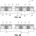
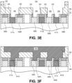
- Figures 3A-3F illustrate cross-sectional views representing various operations in a method of fabricating a semiconductor structure having a gate contact structure disposed over an active portion of a gate.
- a semiconductor structure 300 is provided following trench contact (TCN) formation. It is to be understood that the specific arrangement of structure 300 is used for illustration purposes only.
- the semiconductor structure 300 includes one or more gate stack structures, such as gate stack structures 308A-308E disposed above a substrate 302.
- the gate stack structures may include a gate dielectric layer and a gate electrode, as described above in association with Figure 2 .
- Trench contacts e.g., contacts to diffusion regions of substrate 302, such as trench contacts 310A-310C are also included in structure 300 and are spaced apart from gate stack structures 308A-308E by dielectric spacers 320.
- An insulating cap layer 322 may be disposed on the gate stack structures 308A-308E (e.g., GILA), as is also depicted in Figure 3A .
- contact blocking regions or "contact plugs,” such as region 323 fabricated from an inter-layer dielectric material, may be included in regions where contact formation is to be blocked.
- a process used to provide structure 300 may be one described in International Patent
- Providing structure 300 involves formation of a contact pattern which is essentially perfectly aligned to an existing gate pattern while eliminating the use of a lithographic step with exceedingly tight registration budget.
- this approach enables the use of intrinsically highly selective wet etching (e.g., versus conventionally implemented dry or plasma etching) to generate contact openings.
- a contact pattern is formed by utilizing an existing gate pattern in combination with a contact plug lithography operation.
- the approach enables elimination of the need for an otherwise critical lithography operation to generate a contact pattern, as used in conventional approaches.
- a trench contact grid is not separately patterned, but is rather formed between poly (gate) lines. For example, in one such example, a trench contact grid is formed subsequent to gate grating patterning but prior to gate grating cuts.
- the gate stack structures 308A-308E maybe fabricated by a replacement gate process.
- dummy gate material such as polysilicon or silicon nitride pillar material, may be removed and replaced with permanent gate electrode material.
- a permanent gate dielectric layer is also formed in this process, as opposed to being carried through from earlier processing.
- dummy gates are removed by a dry etch or wet etch process.
- dummy gates are composed of polycrystalline silicon or amorphous silicon and are removed with a dry etch process comprising SF6.
- dummy gates are composed of polycrystalline silicon or amorphous silicon and are removed with a wet etch process comprising aqueous NH4OH or tetramethylammonium hydroxide.
- dummy gates are composed of silicon nitride and are removed with a wet etch including aqueous phosphoric acid.
- one or more approaches described herein contemplate essentially a dummy and replacement gate process in combination with a dummy and replacement contact process to arrive at structure 300.
- the replacement contact process is performed after the replacement gate process to allow high temperature anneal of at least a portion of the permanent gate stack.
- an anneal of at least a portion of the permanent gate structures e.g., after a gate dielectric layer is formed, is performed at a temperature greater than approximately 600 degrees Celsius. The anneal is performed prior to formation of the permanent contacts.
- the trench contacts 310A-310C of the structure 300 are recessed within spacers 320 to provide recessed trench contacts 311A-311C that have a height below the top surface of spacers 320 and insulating cap layer 322.
- An insulating cap layer 324 is then formed on recessed trench contacts 311A-311C (e.g., TILA).
- the insulating cap layer 324 on recessed trench contacts 311A-311C is composed of a material having a different etch characteristic than insulating cap layer 322 on gate stack structures 308A-308E. As will be seen in subsequent processing operations, such a difference may be exploited to etch one of 322/324 selectively from the other of 322/324.
- the trench contacts 310A-310C maybe recessed by a process selective to the materials of spacers 320 and insulating cap layer 322.
- the trench contacts 310A-310C are recessed by an etch process such as a wet etch process or dry etch process.
- Insulating cap layer 324 may be formed by a process suitable to provide a conformal and sealing layer above the exposed portions of trench contacts 310A-310C.
- insulating cap layer 324 is formed by a chemical vapor deposition (CVD) process as a conformal layer above the entire structure.
- the conformal layer is then planarized, e.g., by chemical mechanical polishing (CMP), to provide insulating cap layer 324 material only above trench contacts 310A-310C, and re-exposing spacers 320 and insulating cap layer 322.
- CMP chemical mechanical polishing
- one of the pair of 322/324 is composed of silicon oxide while the other is composed of silicon nitride.
- one of the pair of 322/324 is composed of silicon oxide while the other is composed of carbon doped silicon nitride.
- one of the pair of 322/324 is composed of silicon oxide while the other is composed of silicon carbide. In another example, one of the pair of 322/324 is composed of silicon nitride while the other is composed of carbon doped silicon nitride. In another example, one of the pair of 322/324 is composed of silicon nitride while the other is composed of silicon carbide. In another example, one of the pair of 322/324 is composed of carbon doped silicon nitride while the other is composed of silicon carbide.
- an inter-layer dielectric (ILD) 330 and hardmask 332 stack is formed and patterned to provide, e.g., a metal (0) trench 334 patterned above the structure of Figure 3B .
- ILD inter-layer dielectric
- the inter-layer dielectric (ILD) 330 may be composed of a material suitable to electrically isolate metal features ultimately formed therein while maintaining a robust structure between front end and back end processing. Furthermore, in an, the composition of the ILD 330 is selected to be consistent with via etch selectivity for trench contact dielectric cap layer and gate dielectric cap layer patterning, as described in greater detail below in association with Figures 3D and 3E . In one, the ILD 330 is composed of a single or several layers of silicon oxide or a single or several layers of a carbon doped oxide (CDO) material.
- CDO carbon doped oxide
- the ILD 330 has a bi-layer composition with a top portion composed of a different material than an underlying bottom portion of the ILD 330, as described in greater detail below in association with Figure 4 .
- the hardmask layer 332 may be composed of a material suitable to act as a subsequent sacrificial layer.
- the hardmask layer 332 is composed substantially of carbon, e.g., as a layer of cross-linked organic polymer.
- a silicon nitride or carbon-doped silicon nitride layer is used as a hardmask 332.
- the inter-layer dielectric (ILD) 330 and hardmask 332 stack may be patterned by a lithography and etch process.
- via openings 336 are formed in inter-layer dielectric (ILD) 330, extending from metal (0) trench 334 to one or more of the recessed trench contacts 311A-311C.
- ILD inter-layer dielectric
- via openings are formed to expose recessed trench contacts 311A and 311C.
- the formation of via openings 336 includes etching of both inter-layer dielectric (ILD) 330 and respective portions of corresponding insulating cap layer 324.
- insulating cap layer 322 is exposed during patterning of inter-layer dielectric (ILD) 330 (e.g., a portion of insulating cap layer 322 over gate stack structures 308B and 308E is exposed).
- ILD inter-layer dielectric
- insulating cap layer 324 is etched to form via openings 336 selective to (i.e., without significantly etching or impacting) insulating cap layer 322.
- the via openings 336 may be formed by first depositing a hardmask layer, an anti-reflective coating (ARC) layer and a layer of photoresist.
- the hardmask layer is composed substantially of carbon, e.g., as a layer of cross-linked organic polymer.
- the ARC layer is suitable to suppress reflective interference during lithographic patterning of the photo-resist layer.
- the ARC layer is a silicon ARC layer.
- the photo-resist layer may be composed of a material suitable for use in a lithographic process.
- the photo-resist layer is formed by first masking a blanket layer of photo-resist material and then exposing it to a light source.
- a patterned photo-resist layer may then be formed by developing the blanket photo-resist layer.
- the portions of the photo-resist layer exposed to the light source are removed upon developing the photo-resist layer.
- patterned photo-resist layer is composed of a positive photo-resist material.
- the photo-resist layer is composed of a positive photo-resist material such as, but not limited to, a 248nm resist, a 193nm resist, a 157nm resist, an extreme ultra violet (EUV) resist, an e-beam imprint layer, or a phenolic resin matrix with a diazonaphthoquinone sensitizer.
- EUV extreme ultra violet
- the portions of the photo-resist layer exposed to the light source are retained upon developing the photo-resist layer.
- the photo-resist layer is composed of a negative photo-resist material.
- the photo-resist layer is composed of a negative photo-resist material such as, but not limited to, consisting of poly-cis-isoprene or poly-vinyl-cinnamate.
- the pattern of the photo-resist layer (e.g., the pattern of via openings 336) is transferred to the hardmask layer by using a plasma etch process.
- the pattern is ultimately transferred to the inter-layer dielectric (ILD) 330, e.g., by another or the same dry etch process.
- the pattern is then finally transferred to the insulating cap layer 324 (i.e., the trench contact insulating cap layers) by an etch process without etching the insulating cap layer 322 (i.e., the gate insulating cap layers).
- the insulating cap layer 324 may be composed of any of the following or a combination including silicon oxide, silicon nitride, silicon carbide, carbon doped silicon nitrides, carbon doped silicon oxides, amorphous silicon, various metal oxides and silicates including zirconium oxide, hafnium oxide, lanthanum oxide or a combination thereof.
- the layer may be deposited using any of the following techniques including CVD, ALD, PECVD, PVD, HDP assisted CVD, low temp CVD.
- a corresponding plasma dry etch is developed as a combination of chemical and physical sputtering mechanisms. Coincident polymer deposition may be used to control material removal rate, etch profiles and film selectivity.
- the dry etch is typically generated with a mix of gases that include NF3, CHF3, C4Fg, HBr and 02 with typically pressures in the range of 30-100 mTorr and a plasma bias of 50-1000 Watts.
- the dry etch may be engineered to achieve significant etch selectivity between cap layer 324 (TILA) and 322 (GILA) layers to minimize the loss of 322 (GILA) during dry etch of 324 (TILA) to form contacts to the source drain regions of the transistor.
- one or more additional via openings 338 are formed in inter-layer dielectric (ILD) 330, extending from metal (0) trench 334 to one or more of the gate stack structures 308A-308E.
- via openings are formed to expose gate stack structures 308C and 308D.
- the formation of via openings 338 includes etching of both inter-layer dielectric (ILD) 330 and respective portions of corresponding insulating cap layer 322.
- a portion of insulating cap layer 324 is exposed during patterning of inter-layer dielectric (ILD) 330 (e.g., a portion of insulating cap layer 324 over recessed trench contact 31 IB is exposed).
- insulating cap layer 322 is etched to form via openings 338 selective to (i.e., without significantly etching or impacting) insulating cap layer 324.
- the via openings 338 may be formed by first depositing a hardmask layer, an anti-reflective coating (ARC) layer and a layer of photoresist.
- the pattern of the photo-resist layer e.g., the pattern of via openings 338) is transferred to the hardmask layer by using a plasma etch process.
- the pattern is ultimately transferred inter-layer dielectric (ILD) 330, e.g., by another or the same dry etch process.
- ILD inter-layer dielectric
- the pattern is then finally transferred to the insulating cap layer 322 (i.e., the gate insulating cap layers) by an etch process without etching the insulating cap layer 324 (i.e., the trench contact insulating cap layers).
- the insulating cap layer 322 may be composed of any of the following or a combination including silicon oxide, silicon nitride, silicon carbide, carbon doped silicon nitrides, carbon doped silicon oxides, amorphous silicon, various metal oxides and silicates including zirconium oxide, hafnium oxide, lanthanum oxide or a combination thereof.
- the layer may be deposited using any of the following techniques including CVD, ALD, PECVD, PVD, HDP assisted CVD, low temp CVD.
- the insulating cap layer 322 (GILA) is, in an example, composed of a different material relative to cap layer 324 (TILA) to ensure significant etch rate differential between the two capping layers.
- a corresponding plasma dry etch may be developed as a combination of chemical and physical sputtering mechanisms to achieve acceptable etch rate differential between GILA and TILA films.
- Coincident polymer deposition may be used to control material removal rate, etch profiles and film selectivity.
- the dry etch is typically generated with a mix of gases that include NF3, CHF , C4F8, HBr and 02 with typically pressures in the range of 30-100 mTorr and a plasma bias of 50-1000 Watts.
- the dry etch may be engineered to achieve significant etch selectivity between cap layer 322 (GILA) and 324 (TILA) layers to minimize the loss of 324 (TILA) during dry etch of 322 (GILA) to form the gate contact on active regions of the transistor.
- a metal contact structure 340 is formed in the metal (0) trench 334 and via openings 336 and 338 of the structure described in association with Figure 3E .
- the metal contact structure 340 includes a metal (0) portion 350 along with trench contact vias (e.g., trench contact vias 341A and 341B to trench contacts 311A and 311C, respectively) and gate contact vias (e.g., gate contact vias 342A and 342B to gate stack structures 308C and 308D, respectively).
- trench contact vias e.g., trench contact vias 341A and 341B to trench contacts 311A and 311C, respectively
- gate contact vias e.g., gate contact vias 342A and 342B to gate stack structures 308C and 308D, respectively.
- the metal contact structure is formed by a metal deposition and subsequent chemical mechanical polishing operation.
- the metal deposition may involve first deposition of an adhesion layer followed by deposition of a fill metal layer.
- the metal structure 340 may be composed of a conductive material.
- the metal structure 340 is composed of a metal species.
- the metal species may be a pure metal, such as copper, tungsten, nickel or cobalt, or may be an alloy such as a metal-metal alloy or a metal-semiconductor alloy (e.g., such as a silicide material).
- ILD 330 may instead be a bi-layer structure.
- Figure 4 illustrates a cross-sectional view of another non-planar semiconductor device having a gate contact via disposed over an active portion of a gate electrode, in accordance with another example not covered by the claims.
- a semiconductor structure or device 400 e.g. a non-planar device, includes a non-planar diffusion or active region 404 (e.g., a fin structure) formed from substrate 402, and within isolation region 406.
- a gate electrode stack 408 is disposed over the non-planar diffusion or active region 404 as well as over a portion of the isolation region 406.
- gate electrode stack 408 includes a gate electrode 450 and gate dielectric layer 452, along with a dielectric cap layer 454.
- the gate electrode stack 408 is disposed in an inter-layer dielectric layer 420, such as a layer of silicon oxide.
- a gate contact via 416 and an overlying metal interconnect 460 are both disposed in inter-layer dielectric (ILD) stacks or layers 470.
- ILD inter-layer dielectric
- structure 470 is a bi-layer interlayer dielectric stack including a bottom layer 472 and a top layer 474, as depicted in Figure 4 .
- the top layer 474 of ILD structure 470 is composed of a material optimized for low-K performance, e.g., for reducing capacitive coupling between metal lines formed therein.
- the top layer 474 of ILD structure 470 is composed of a material such as, but not limited to, a carbon-doped oxide (CDO) or porous oxide film.
- the bottom layer 472 of ILD structure 470 is composed of a material optimized for via etch selectivity, e.g., for compatibility with an integration scheme leveraging the etch selectivities between a trench contact cap layer and a gate cap layer.
- the bottom layer 472 of ILD structure 470 is composed of a material such as, but not limited to, silicon dioxide (Si02) or a CDO film.
- the top layer 474 of ILD structure 470 is composed of a CDO material and the bottom layer 472 of ILD structure 470 is composed of Si02.
- the tops of the spacers 320 are exposed during via opening formation in cap layers 324 and 322.
- the spacers may be recessed to be essentially planar with the gate structures.
- the gate cap layer may be formed to cover the spacers, hindering exposure of the spacers during via opening formation.
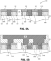
- Figures 5A and 5B illustrate cross-sectional views representing various operations in a method of fabricating another semiconductor structure having a gate contact structure disposed over an active portion of a gate, in accordance with an embodiment of the present invention.
- a semiconductor structure 500 is provided following trench contact (TCN) formation. It is to be understood that the specific arrangement of structure 500 is used for illustration purposes only, and that a variety of possible layouts may benefit from embodiments of the invention described herein.
- the semiconductor structure 500 includes one or more gate stack structures, such as gate stack structures 308A-308E disposed above a substrate 302.
- the gate stack structures include a gate dielectric layer and a gate electrode, as described above in association with Figure 2 .
- Trench contacts e.g., contacts to diffusion regions of substrate 302, such as trench contacts 310A-310C are also included in structure 500 and are spaced apart from gate stack structures 308A-308E by dielectric spacers 520.
- An insulating cap layer 522 is disposed on the gate stack structures 308A-308E (e.g., GILA), as is also depicted in Figure 5A .
- the spacers 520 have been recessed to approximately the same height as the gate stack structures 308A-308E.
- the corresponding insulating cap layers 522 cover the spacers 520 associated with each gate stack, as well as covering the gate stack.
- a metal contact structure 540 is formed in a metal (0) trench and via openings formed in a dielectric layer 330.
- the metal contact structure 540 includes a metal (0) portion 550 along with trench contact vias (e.g., trench contact vias 341A and 341B to trench contacts 311A and 311C, respectively).
- the metal contact structure 540 also includes gate contact vias (e.g., gate contact vias 542A and 542B to gate stack structures 308C and 308D, respectively).
- the trench contacts are recessed lower relative to the gate stack structures (including gate stack structures labeled 308C and 308D in Figure 5 ).
- the trench contacts are recessed lower relative to the gate stack structures in order to prevent a possibility of shorting between gate contact vias 542A and 542B and trench contacts 311A and 311C, respectively, e.g., at the corners where gate contact vias 542A and 542B and trench contacts 311A and 311C, respectively, would otherwise meet if the trench contacts were co-planar with the gate stack structures.
- spacers are recessed to approximately the same height as the trench contacts.
- the corresponding trench insulating cap layers cover the spacers associated with each trench contact, as well as covering the trench contact.
- the gate stack structures are recessed lower relative to the trench contacts in order to prevent a possibility of shorting between trench contact vias and adjacent or nearby
- Figure 6 illustrates a plan view of another semiconductor device having a gate contact via disposed over an active portion of a gate, in accordance with another example not covered by the claims.
- a semiconductor structure or device 600 includes a plurality of gate structures 608A-608C interdigitated with a plurality of trench contacts 61 OA and 610B (these features are disposed above an active region of a substrate, not shown).
- a gate contact via 680 is formed on an active portion the gate structure 608B.
- the gate contact via 680 is further disposed on the active portion of the gate structure 608C, coupling gate structures 608B and 608C. It is to be understood that the intervening trench contact 610B may be isolated from the contact 680 by using a trench contact isolation cap layer (e.g., TILA).
- TILA trench contact isolation cap layer
- the contact configuration of Figure 6 may provide an easier approach to strapping adjacent gate lines in a layout, without the need to route the strap through upper layers of metallization, hence enabling smaller cell areas and/or less intricate wiring schemes.
- Figure 7 illustrates a plan view of another semiconductor device having a trench contact via coupling a pair of trench contacts, in accordance with another example not covered by the claims.
- a semiconductor structure or device 700 includes a plurality of gate structures 708A-708C interdigitated with a plurality of trench contacts 71 OA and 710B (these features are disposed above an active region of a substrate, not shown).
- a trench contact via 790 is formed on the trench contact 710A.
- the trench contact via 790 is further disposed on the trench contact 710B, coupling trench contacts 710A and 710B.
- the intervening gate structure 708B may be isolated from the trench contact via 790 by using a gate isolation cap layer (e.g., by a GILA process).
- a gate isolation cap layer e.g., by a GILA process.
- the contact configuration of Figure 7 may provide an easier approach to strapping adjacent trench contacts in a layout, without the need to route the strap through upper layers of metallization, hence enabling smaller cell areas and/or less intricate wiring schemes.
- dummy gates need not ever be formed prior to fabricating gate contacts over active portions of the gate stacks.
- the gate stacks described above may actually be permanent gate stacks as initially formed.
- the processes described herein maybe used to fabricate one or a plurality of semiconductor devices.
- the semiconductor devices may be transistors or like devices.
- the semiconductor devices are a metal-oxide semiconductor (MOS) transistors for logic or memory, or are bipolar transistors.
- MOS metal-oxide semiconductor
- the semiconductor devices have a three-dimensional architecture, such as a trigate device, an independently accessed double gate device, or a FIN-FET.
- a trigate device such as a trigate device, an independently accessed double gate device, or a FIN-FET.
- One or more embodiments may be particularly useful for fabricating semiconductor devices at a 10 nm or smaller technology node.
- one or more embodiments of the present invention include first using a gate aligned trench contact process.
- a gate aligned trench contact process may be implemented to form trench contact structures for semiconductor structure fabrication, e.g., for integrated circuit fabrication.
- a trench contact pattern is formed as aligned to an existing gate pattern.
- conventional approaches typically involve an additional lithography process with tight registration of a lithographic contact pattern to an existing gate pattern in combination with selective contact etches.
- a conventional process may include patterning of a poly (gate) grid with separate patterning of contact features.
- FIG 8 illustrates a computing device 800 in accordance with one implementation of the invention.
- the computing device 800 houses a board 802.
- the board 802 may include a number of components, including but not limited to a processor 804 and at least one communication chip 806.
- the processor 804 is physically and electrically coupled to the board 802.
- the at least one communication chip 806 is also physically and electrically coupled to the board 802.
- the communication chip 806 is part of the processor 804.
- computing device 800 may include other components that may or may not be physically and electrically coupled to the board 802. These other components include, but are not limited to, volatile memory (e.g., DRAM), nonvolatile memory (e.g., ROM), flash memory, a graphics processor, a digital signal processor, a crypto processor, a chipset, an antenna, a display, a touchscreen display, a touchscreen controller, a battery, an audio codec, a video codec, a power amplifier, a global positioning system (GPS) device, a compass, an accelerometer, a gyroscope, a speaker, a camera, and a mass storage device (such as hard disk drive, compact disk (CD), digital versatile disk (DVD), and so forth).
- volatile memory e.g., DRAM
- nonvolatile memory e.g., ROM
- flash memory e.g., a graphics processor, a digital signal processor, a crypto processor, a chipset, an antenna, a display,
- the communication chip 806 enables wireless communications for the transfer of data to and from the computing device 800.
- wireless and its derivatives maybe used to describe circuits, devices, systems, methods, techniques, communications channels, etc., that may communicate data through the use of modulated electromagnetic radiation through a non-solid medium. The term does not imply that the associated devices do not contain any wires, although in some embodiments they might not.
- the communication chip 806 may implement any of a number of wireless standards or protocols, including but not limited to Wi-Fi (IEEE 802.11 family), WiMAX (IEEE 802.16 family), IEEE 802.20, long term evolution (LTE), Ev-DO, HSPA+, HSDPA+, HSUPA+, EDGE, GSM, GPRS, CDMA, TDMA, DECT, Bluetooth, derivatives thereof, as well as any other wireless protocols that are designated as 3G, 4G, 5G, and beyond.
- the computing device 800 may include a plurality of communication chips 806.
- a first communication chip 806 may be dedicated to shorter range wireless communications such as Wi-Fi and Bluetooth and a second communication chip 806 may be dedicated to longer range wireless communications such as GPS, EDGE, GPRS, CDMA, WiMAX, LTE, Ev-DO, and others.
- the processor 804 of the computing device 800 includes an integrated circuit die packaged within the processor 804.
- the integrated circuit die of the processor includes one or more devices, such as MOS-FET transistors built in accordance with implementations of the invention.
- the term "processor" may refer to any device or portion of a device that processes electronic data from registers and/or memory to transform that electronic data into other electronic data that may be stored in registers and/or memory.
- the communication chip 806 also includes an integrated circuit die packaged within the communication chip 806.
- the integrated circuit die of the communication chip includes one or more devices, such as MOS-FET transistors built in accordance with implementations of the invention.
- another component housed within the computing device 800 may contain an integrated circuit die that includes one or more devices, such as MOS-FET transistors built in accordance with implementations of the invention.
- the computing device 800 may be a laptop, a netbook, a notebook, an ultrabook, a smartphone, a tablet, a personal digital assistant (PDA), an ultra mobile PC, a mobile phone, a desktop computer, a server, a printer, a scanner, a monitor, a set-top box, an entertainment control unit, a digital camera, a portable music player, or a digital video recorder.
- the computing device 800 may be any other electronic device that processes data.
- embodiments of the present invention include gate contact structures disposed over active portions of gates and methods of forming such gate contact structures.
Landscapes
- Insulated Gate Type Field-Effect Transistor (AREA)
- Internal Circuitry In Semiconductor Integrated Circuit Devices (AREA)
- Chemical & Material Sciences (AREA)
- Chemical Kinetics & Catalysis (AREA)
- General Chemical & Material Sciences (AREA)
- Electrodes Of Semiconductors (AREA)
- Thin Film Transistor (AREA)
Claims (12)
- Halbleiterstruktur (300), umfassend:ein Substrat (302), das eine aktive Region und eine Isolationsregion umfasst;eine Mehrzahl von Gatestrukturen (308A-308E), die jeweils einen Abschnitt, der über der aktiven Region angeordnet ist, und einen Abschnitt aufweisen, der über der Isolationsregion des Substrats (302), wobei eine oder mehrere der Gatestrukturen (308A-308E) eine dielektrische Gate-Kappenschicht (322) auf einer Oberseite der Gatestruktur umfassen, wobei die dielektrische Gate-Kappenschicht (322) eine Oberseite aufweist und wobei die dielektrische Gate-Kappenschicht (322) ein erstes Material umfasst;eine Mehrzahl von Source- oder Drainregionen, die in der aktiven Region des Substrats (302) zwischen den über der aktiven Region angeordneten Abschnitten der Gatestrukturen (308A-308E) angeordnet ist;eine Mehrzahl von Source- oder Drainkontakten (311A-311C), wobei ein Source- oder Drainkontakt auf jeder der Source- oder Drainregionen angeordnet ist, einer oder mehrere der Mehrzahl von Source- oder Drainkontakten (311A-311C) eine dielektrische Graben-Kappenschicht (324) auf einer Oberseite des Source- oder Drainkontakts umfassen, die Source- oder Drainkontakte (311A-311C) eine Oberseite unter der Oberseite der Gatestrukturen (308A-308E) aufweisen und die dielektrische Graben-Kappenschicht (324) eine zur Oberseite der dielektrischen Gate-Kappenschicht (322) koplanare Oberseite aufweist, wobei die dielektrische Graben-Kappenschicht (324) ein zweites Material mit anderen Ätzcharakteristiken als das erste Material umfasst;einen Gate-Durchkontakt (342), der auf einer der Gatestrukturen (308A-308E), die nur teilweise von der dielektrischen Gate-Kappenschicht (322) bedeckt ist, auf dem Abschnitt der Gatestruktur angeordnet ist, der über der aktiven Region des Substrats (302) angeordnet ist; undeinen Source- oder Drain-Durchkontakt (341), der auf einem der Source- oder Drainkontakte (311A-311C) angeordnet ist, der nur teilweise von der dielektrischen Graben-Kappenschicht (324) bedeckt ist;wobei jede der Gatestrukturen (308A-308E) ferner ein Paar von Seitenwand-Abstandsschichten umfasst, wobei die Source- oder Drainkontakte (311A-311C) direkt benachbart zu den Seitenwand-Abstandsschichten einer entsprechenden Gatestruktur angeordnet sind, und wobei die Seitenwand-Abstandsschichten eine gleiche Höhe wie die Gatestrukturen (308A-308E) aufweisen und von der dielektrischen Gate-Kappenschicht (322) bedeckt sind.
- Halbleiterstruktur (300) nach Anspruch 1, wobei der Gate-Durchkontakt (342) und der Source- oder Drain-Durchkontakt (341) im Wesentlichen koplanar in einer gleichen Zwischenschicht-Dielektrikumschicht (330) angeordnet sind, die über dem Substrat (302) angeordnet ist.
- Halbleiterstruktur (300) nach Anspruch 2, wobei die Zwischenschicht-Dielektrikumschicht (330) eine Zweischichtige Struktur ist, die eine obere Dielektrikumschicht mit niedrigem k-Wert und eine untere Ätzselektivitätsschicht umfasst.
- Halbleiterstruktur (300) nach Anspruch 1, wobei der Gate-Durchkontakt (342) und der Source- oder Drain-Durchkontakt (341) im Wesentlichen koplanar zueinander sind.
- Halbleiterstruktur (300) nach Anspruch 1, wobei der Gate-Durchkontakt (342) ferner auf einer zweiten der Gatestrukturen (308A-308E) auf dem Abschnitt der zweiten Gatestruktur angeordnet ist, der über der aktiven Region des Substrats (302) angeordnet ist, wobei der Gate-Durchkontakt (342) die eine und die zweite Gatestruktur (308A-308E) koppelt.
- Halbleiterstruktur (300) nach Anspruch 1, wobei der Source- oder Drain-Durchkontakt (341) ferner auf einem zweiten der Source- oder Drainkontakte (311A-311C) angeordnet ist und den einen und den zweiten Source- oder Drainkontakt (311A-311C) koppelt.
- Verfahren zur Fertigung einer Halbleiterstruktur (300), wobei das Verfahren umfasst:Bilden einer Mehrzahl von Gatestrukturen (308A-308E) über einer aktiven Region eines Substrats (302), wobei jede der Gatestrukturen (308A-308E) ein Paar von Seitenwand-Abstandsschichten umfasst;Bilden einer Mehrzahl von Source- oder Drainregionen in der aktiven Region des Substrats (302) zwischen den Gatestrukturen (308A-308E);Bilden einer Mehrzahl von Source- oder Drainkontakten (311A-311C) direkt benachbart zu den Seitenwand-Abstandsschichten der entsprechenden Gatestruktur, wobei ein Source- oder Drainkontakt auf jeder der Source- oder Drainregionen gebildet wird, wobei die Source- oder Drainkontakte (311-311C) eine Oberseite unter der Oberseite der Gatestruktur (308A-308E) aufweisen;Bilden einer dielektrischen Gate-Kappenschicht (322) über jeder der Gatestrukturen (308A-308E), wobei die dielektrische Gate-Kappenschicht (322) eine Oberseite aufweist, wobei die dielektrische Gate-Kappenschicht (322) ein erstes Material umfasst und wobei die Seitenwand-Abstandsschichten eine gleiche Höhe wie die Gatestrukturen (308A-308E) aufweisen und von der dielektrischen Gate-Kappenschicht (322) bedeckt werden;Bilden einer dielektrischen Graben-Kappenschicht (324) über jedem der Source- oder Drainkontakte (311A-311C), wobei die dielektrische Graben-Kappenschicht (324) eine zur Oberseite der dielektrischen Gateschicht (322) koplanare Oberseite aufweist, wobei die dielektrische Graben-Kappenschicht (324) ein zweites Material mit anderen Ätzcharakteristiken als das erste Material umfasst;Bilden eines Gate-Durchkontakts (342) auf einer der Gatestrukturen (308A-308E), wobei das Bilden ein selektives Ätzen der entsprechenden dielektrischen Gate-Kappenschicht (322) zu einer dielektrischen Graben-Kappensicht (324) umfasst; undBilden eines Source- oder Drain-Durchkontakts (341) auf einem der Source- oder Drainkontakte (311A-311C), wobei das Bilden ein selektives Ätzen der entsprechenden dielektrischen Graben-Kappenschicht (324) zu einer dielektrischen Gate-Kappenschicht (322) umfasst.
- Verfahren nach Anspruch 7, wobei das Bilden des Gate-Durchkontakts (342) und des Source- oder Drain-Durchkontakts (341) ein Bilden leitfähigen Materials für beide in einem gleichen Prozessvorgang umfasst.
- Verfahren nach Anspruch 7, wobei das Bilden der Mehrzahl von Gatestrukturen (308A-308E) ein Ersetzen von Dummy-Gatestrukturen (308A-308E) durch permanente Gatestrukturen (308A-308E) umfasst.
- Verfahren nach Anspruch 7, wobei das Bilden der Mehrzahl von Source- oder Drain-Durchkontakten (311A-311C) ein Ersetzen von Dummy-Gatesource- oder Drain-Kontaktstrukturen durch permanente Source- oder Drain-Kontaktstrukturen umfasst.
- Verfahren nach Anspruch 7, ferner umfassend:
Bilden eines dreidimensionalen Körpers aus den aktiven Regionen des Substrats (302) vor dem Bilden der Mehrzahl von Gatestrukturen (308A-308E). - Verfahren nach Anspruch 11, wobei das Bilden des dreidimensionalen Körpers ein Ätzen von Finnen in einem Volumenhalbleitersubstrat umfasst.
Priority Applications (4)
| Application Number | Priority Date | Filing Date | Title |
|---|---|---|---|
| EP25226522.8A EP4723832A1 (de) | 2012-09-19 | 2013-08-28 | Gate-kontakt-struktur über ein aktives gate und verfahren zur herstellung davon |
| EP21217477.5A EP4002485A1 (de) | 2012-09-19 | 2013-08-28 | Gate-kontakt-struktur über ein aktives gate und verfahren zur herstellung davon |
| EP18209741.0A EP3514836B1 (de) | 2012-09-19 | 2013-08-28 | Gate-kontakt-struktur über ein aktives gate |
| EP17151166.0A EP3174105B1 (de) | 2012-09-19 | 2013-08-28 | Gatekontaktstruktur über ein aktives gate und verfahren zur herstellung davon |
Applications Claiming Priority (2)
| Application Number | Priority Date | Filing Date | Title |
|---|---|---|---|
| US13/622,974 US9461143B2 (en) | 2012-09-19 | 2012-09-19 | Gate contact structure over active gate and method to fabricate same |
| PCT/US2013/057116 WO2014046856A1 (en) | 2012-09-19 | 2013-08-28 | Gate contact structure over active gate and method to fabricate same |
Related Child Applications (7)
| Application Number | Title | Priority Date | Filing Date |
|---|---|---|---|
| EP21217477.5A Division EP4002485A1 (de) | 2012-09-19 | 2013-08-28 | Gate-kontakt-struktur über ein aktives gate und verfahren zur herstellung davon |
| EP21217477.5A Division-Into EP4002485A1 (de) | 2012-09-19 | 2013-08-28 | Gate-kontakt-struktur über ein aktives gate und verfahren zur herstellung davon |
| EP17151166.0A Division EP3174105B1 (de) | 2012-09-19 | 2013-08-28 | Gatekontaktstruktur über ein aktives gate und verfahren zur herstellung davon |
| EP17151166.0A Division-Into EP3174105B1 (de) | 2012-09-19 | 2013-08-28 | Gatekontaktstruktur über ein aktives gate und verfahren zur herstellung davon |
| EP25226522.8A Division EP4723832A1 (de) | 2012-09-19 | 2013-08-28 | Gate-kontakt-struktur über ein aktives gate und verfahren zur herstellung davon |
| EP18209741.0A Division EP3514836B1 (de) | 2012-09-19 | 2013-08-28 | Gate-kontakt-struktur über ein aktives gate |
| EP18209741.0A Division-Into EP3514836B1 (de) | 2012-09-19 | 2013-08-28 | Gate-kontakt-struktur über ein aktives gate |
Publications (3)
| Publication Number | Publication Date |
|---|---|
| EP2898532A1 EP2898532A1 (de) | 2015-07-29 |
| EP2898532A4 EP2898532A4 (de) | 2016-06-15 |
| EP2898532B1 true EP2898532B1 (de) | 2024-11-06 |
Family
ID=50273600
Family Applications (5)
| Application Number | Title | Priority Date | Filing Date |
|---|---|---|---|
| EP18209741.0A Active EP3514836B1 (de) | 2012-09-19 | 2013-08-28 | Gate-kontakt-struktur über ein aktives gate |
| EP21217477.5A Pending EP4002485A1 (de) | 2012-09-19 | 2013-08-28 | Gate-kontakt-struktur über ein aktives gate und verfahren zur herstellung davon |
| EP25226522.8A Pending EP4723832A1 (de) | 2012-09-19 | 2013-08-28 | Gate-kontakt-struktur über ein aktives gate und verfahren zur herstellung davon |
| EP13838318.7A Active EP2898532B1 (de) | 2012-09-19 | 2013-08-28 | Gatekontaktstruktur über ein aktives gate und verfahren zur herstellung davon |
| EP17151166.0A Active EP3174105B1 (de) | 2012-09-19 | 2013-08-28 | Gatekontaktstruktur über ein aktives gate und verfahren zur herstellung davon |
Family Applications Before (3)
| Application Number | Title | Priority Date | Filing Date |
|---|---|---|---|
| EP18209741.0A Active EP3514836B1 (de) | 2012-09-19 | 2013-08-28 | Gate-kontakt-struktur über ein aktives gate |
| EP21217477.5A Pending EP4002485A1 (de) | 2012-09-19 | 2013-08-28 | Gate-kontakt-struktur über ein aktives gate und verfahren zur herstellung davon |
| EP25226522.8A Pending EP4723832A1 (de) | 2012-09-19 | 2013-08-28 | Gate-kontakt-struktur über ein aktives gate und verfahren zur herstellung davon |
Family Applications After (1)
| Application Number | Title | Priority Date | Filing Date |
|---|---|---|---|
| EP17151166.0A Active EP3174105B1 (de) | 2012-09-19 | 2013-08-28 | Gatekontaktstruktur über ein aktives gate und verfahren zur herstellung davon |
Country Status (7)
| Country | Link |
|---|---|
| US (6) | US9461143B2 (de) |
| EP (5) | EP3514836B1 (de) |
| KR (5) | KR102037278B1 (de) |
| CN (3) | CN104584222B (de) |
| PL (1) | PL3174105T3 (de) |
| TW (1) | TWI502745B (de) |
| WO (1) | WO2014046856A1 (de) |
Families Citing this family (151)
| Publication number | Priority date | Publication date | Assignee | Title |
|---|---|---|---|---|
| KR101853316B1 (ko) * | 2012-03-29 | 2018-04-30 | 삼성전자주식회사 | 반도체 소자 |
| US8877578B2 (en) * | 2012-05-18 | 2014-11-04 | Unisantis Electronics Singapore Pte. Ltd. | Method for producing semiconductor device and semiconductor device |
| US9461143B2 (en) * | 2012-09-19 | 2016-10-04 | Intel Corporation | Gate contact structure over active gate and method to fabricate same |
| EP3036757A4 (de) * | 2013-08-21 | 2017-03-29 | Intel Corporation | Verfahren und struktur zur kontaktierung kompakter leitfähiger schichten mit geführten kontaktlöchern |
| US9153483B2 (en) * | 2013-10-30 | 2015-10-06 | Taiwan Semiconductor Manufacturing Company, Ltd. | Method of semiconductor integrated circuit fabrication |
| US9397004B2 (en) * | 2014-01-27 | 2016-07-19 | GlobalFoundries, Inc. | Methods for fabricating FinFET integrated circuits with simultaneous formation of local contact openings |
| US10700170B2 (en) * | 2014-04-29 | 2020-06-30 | Globalfoundries Inc. | Multiple fin finFET with low-resistance gate structure |
| US10998228B2 (en) * | 2014-06-12 | 2021-05-04 | Taiwan Semiconductor Manufacturing Company, Ltd. | Self-aligned interconnect with protection layer |
| US20160163646A1 (en) * | 2014-12-05 | 2016-06-09 | Qualcomm Incorporated | Strapped contact in a semiconductor device |
| CN107004601B (zh) * | 2014-12-22 | 2021-05-14 | 英特尔公司 | 受益于气隙集成电容的过孔自对准和短路改善 |
| US9799560B2 (en) * | 2015-03-31 | 2017-10-24 | Qualcomm Incorporated | Self-aligned structure |
| US9425097B1 (en) * | 2015-04-29 | 2016-08-23 | Globalfoundries Inc. | Cut first alternative for 2D self-aligned via |
| US9397049B1 (en) * | 2015-08-10 | 2016-07-19 | International Business Machines Corporation | Gate tie-down enablement with inner spacer |
| US9831090B2 (en) | 2015-08-19 | 2017-11-28 | Taiwan Semiconductor Manufacturing Company, Ltd. | Method and structure for semiconductor device having gate spacer protection layer |
| TWI656566B (zh) * | 2015-08-28 | 2019-04-11 | 聯華電子股份有限公司 | 半導體結構以及其製作方法 |
| US10163879B2 (en) * | 2015-10-05 | 2018-12-25 | Samsung Electronics Co., Ltd. | Semiconductor device having jumper pattern |
| US9793164B2 (en) * | 2015-11-12 | 2017-10-17 | Qualcomm Incorporated | Self-aligned metal cut and via for back-end-of-line (BEOL) processes for semiconductor integrated circuit (IC) fabrication, and related processes and devices |
| US10269697B2 (en) | 2015-12-28 | 2019-04-23 | Taiwan Semiconductor Manufacturing Co., Ltd. | Semiconductor device and manufacturing method thereof |
| DE102016118207B4 (de) * | 2015-12-30 | 2024-08-01 | Taiwan Semiconductor Manufacturing Co. Ltd. | Halbleitervorrichtung und verfahren zu ihrer herstellung |
| US11088030B2 (en) * | 2015-12-30 | 2021-08-10 | Taiwan Semiconductor Manufacturing Co., Ltd. | Semiconductor device and a method for fabricating the same |
| US9761483B1 (en) * | 2016-03-07 | 2017-09-12 | Taiwan Semiconductor Manufacturing Co., Ltd. | Semiconductor devices, FinFET devices and methods of forming the same |
| US9548366B1 (en) * | 2016-04-04 | 2017-01-17 | Taiwan Semiconductor Manufacturing Company, Ltd. | Self aligned contact scheme |
| US10510599B2 (en) * | 2016-04-13 | 2019-12-17 | Taiwan Semiconductor Manufacturing Company Limited | FinFET switch |
| US10096522B2 (en) | 2016-05-06 | 2018-10-09 | Taiwan Semiconductor Manufacturing Co., Ltd. | Dummy MOL removal for performance enhancement |
| US10277227B2 (en) * | 2016-05-31 | 2019-04-30 | Taiwan Semiconductor Manufacturing Company Limited | Semiconductor device layout |
| US9893171B2 (en) | 2016-06-03 | 2018-02-13 | International Business Machines Corporation | Fin field effect transistor fabrication and devices having inverted T-shaped gate |
| US9741613B1 (en) * | 2016-06-07 | 2017-08-22 | Globalfoundries Inc. | Method for producing self-aligned line end vias and related device |
| TWI695477B (zh) * | 2016-07-07 | 2020-06-01 | 聯華電子股份有限公司 | 半導體結構及其製作方法 |
| KR102517568B1 (ko) | 2016-09-28 | 2023-04-03 | 삼성전자주식회사 | 반도체 장치 |
| US11227766B2 (en) * | 2016-09-30 | 2022-01-18 | Intel Corporation | Metal oxide nanoparticles as fillable hardmask materials |
| KR102472135B1 (ko) | 2016-10-06 | 2022-11-29 | 삼성전자주식회사 | 집적회로 소자 및 그 제조 방법 |
| US9881926B1 (en) * | 2016-10-24 | 2018-01-30 | International Business Machines Corporation | Static random access memory (SRAM) density scaling by using middle of line (MOL) flow |
| US9985109B2 (en) | 2016-10-25 | 2018-05-29 | International Business Machines Corporation | FinFET with reduced parasitic capacitance |
| US9941162B1 (en) | 2016-11-17 | 2018-04-10 | Globalfoundries Inc. | Self-aligned middle of the line (MOL) contacts |
| US10879120B2 (en) * | 2016-11-28 | 2020-12-29 | Taiwan Semiconductor Manufacturing | Self aligned via and method for fabricating the same |
| DE102017118364B4 (de) | 2016-11-29 | 2021-10-14 | Taiwan Semiconductor Manufacturing Co. Ltd. | Verfahren mit Herstellung von Source/Drain- und Gate-Kontakten und Struktur mit solchen |
| US10424664B2 (en) | 2016-12-14 | 2019-09-24 | Globalfoundries Inc. | Poly gate extension source to body contact |
| US9929048B1 (en) | 2016-12-22 | 2018-03-27 | Globalfoundries Inc. | Middle of the line (MOL) contacts with two-dimensional self-alignment |
| CN110337715B (zh) | 2016-12-23 | 2023-08-25 | 英特尔公司 | 高级光刻和自组装装置 |
| KR102718741B1 (ko) * | 2016-12-29 | 2024-10-18 | 인텔 코포레이션 | 자체-정렬형 비아 |
| US10026824B1 (en) | 2017-01-18 | 2018-07-17 | Globalfoundries Inc. | Air-gap gate sidewall spacer and method |
| US10283406B2 (en) | 2017-01-23 | 2019-05-07 | International Business Machines Corporation | Fabrication of self-aligned gate contacts and source/drain contacts directly above gate electrodes and source/drains |
| CN108573926B (zh) * | 2017-03-09 | 2020-01-21 | 联华电子股份有限公司 | 半导体存储装置以及其制作方法 |
| US11276767B2 (en) | 2017-03-15 | 2022-03-15 | International Business Machines Corporation | Additive core subtractive liner for metal cut etch processes |
| US10950605B2 (en) | 2017-03-24 | 2021-03-16 | Taiwan Semiconductor Manufacturing Co., Ltd. | Semiconductor device |
| KR102308779B1 (ko) | 2017-04-10 | 2021-10-05 | 삼성전자주식회사 | 이종 컨택들을 구비하는 집적 회로 및 이를 포함하는 반도체 장치 |
| US10304728B2 (en) * | 2017-05-01 | 2019-05-28 | Advanced Micro Devices, Inc. | Double spacer immersion lithography triple patterning flow and method |
| US10269636B2 (en) * | 2017-05-26 | 2019-04-23 | Taiwan Semiconductor Manufacturing Co., Ltd. | Semiconductor device and method of fabricating the same |
| US10522392B2 (en) * | 2017-05-31 | 2019-12-31 | Taiwan Semiconductor Manufacturing Co., Ltd. | Semiconductor device and method of fabricating the same |
| KR102336827B1 (ko) * | 2017-06-08 | 2021-12-09 | 삼성전자주식회사 | 반도체 장치 |
| KR102307127B1 (ko) * | 2017-06-14 | 2021-10-05 | 삼성전자주식회사 | 반도체 소자 |
| US10211302B2 (en) * | 2017-06-28 | 2019-02-19 | International Business Machines Corporation | Field effect transistor devices having gate contacts formed in active region overlapping source/drain contacts |
| US10128334B1 (en) | 2017-08-09 | 2018-11-13 | Globalfoundries Inc. | Field effect transistor having an air-gap gate sidewall spacer and method |
| KR102360410B1 (ko) * | 2017-08-30 | 2022-02-08 | 삼성전자주식회사 | 반도체 장치 |
| US10515896B2 (en) | 2017-08-31 | 2019-12-24 | Taiwan Semiconductor Manufacturing Co., Ltd. | Interconnect structure for semiconductor device and methods of fabrication thereof |
| KR102469885B1 (ko) | 2017-09-11 | 2022-11-22 | 삼성전자주식회사 | 반도체 장치 |
| KR102494918B1 (ko) | 2017-09-12 | 2023-02-02 | 삼성전자주식회사 | 반도체 소자 |
| US10381480B2 (en) | 2017-09-27 | 2019-08-13 | International Business Machines Corporation | Reliable gate contacts over active areas |
| TW201921498A (zh) * | 2017-09-27 | 2019-06-01 | 美商微材料有限責任公司 | 選擇性氧化鋁蝕刻的使用 |
| KR102343219B1 (ko) * | 2017-11-15 | 2021-12-23 | 삼성전자주식회사 | 반도체 장치 |
| US10910313B2 (en) * | 2017-11-16 | 2021-02-02 | Samsung Electronics Co., Ltd. | Integrated circuit including field effect transistors having a contact on active gate compatible with a small cell area having a small contacted poly pitch |
| US10529624B2 (en) | 2017-11-21 | 2020-01-07 | International Business Machines Corporation | Simple contact over gate on active area |
| US10796951B2 (en) | 2017-11-30 | 2020-10-06 | Intel Corporation | Etch-stop layer topography for advanced integrated circuit structure fabrication |
| TW202524711A (zh) | 2017-11-30 | 2025-06-16 | 美商英特爾股份有限公司 | 用於先進積體電路結構製造之異質金屬線組成 |
| US10796968B2 (en) | 2017-11-30 | 2020-10-06 | Intel Corporation | Dual metal silicide structures for advanced integrated circuit structure fabrication |
| US10756204B2 (en) | 2017-11-30 | 2020-08-25 | Intel Corporation | Fin trim isolation with single gate spacing for advanced integrated circuit structure fabrication |
| TW202425290A (zh) * | 2017-11-30 | 2024-06-16 | 美商英特爾股份有限公司 | 用於先進積體電路結構製造之互連線的插塞 |
| DE102018128925B4 (de) | 2017-11-30 | 2024-04-25 | Taiwan Semiconductor Manufacturing Co., Ltd. | Verfahren zur Herstellung einer Halbleitervorrichtung und Halbleitervorrichtung |
| TWI866183B (zh) | 2017-11-30 | 2024-12-11 | 美商英特爾股份有限公司 | 用於先進積體電路結構製造的鰭切割和鰭修整隔離 |
| US10707133B2 (en) * | 2017-11-30 | 2020-07-07 | Intel Corporation | Trench plug hardmask for advanced integrated circuit structure fabrication |
| US11462436B2 (en) | 2017-11-30 | 2022-10-04 | Intel Corporation | Continuous gate and fin spacer for advanced integrated circuit structure fabrication |
| US10734379B2 (en) | 2017-11-30 | 2020-08-04 | Intel Corporation | Fin end plug structures for advanced integrated circuit structure fabrication |
| KR20250070116A (ko) | 2017-11-30 | 2025-05-20 | 인텔 코포레이션 | 진보된 집적 회로 구조체 제조를 위한 핀 패터닝 |
| TWI835515B (zh) | 2017-11-30 | 2024-03-11 | 美商英特爾股份有限公司 | 用於先進積體電路結構製造的主動閘極結構上方的接觸 |
| US10867833B2 (en) | 2017-11-30 | 2020-12-15 | Taiwan Semiconductor Manufacturing Company, Ltd. | Buried metal for FinFET device and method |
| DE102018107721B4 (de) | 2017-11-30 | 2023-10-19 | Taiwan Semiconductor Manufacturing Co., Ltd. | Halbleitervorrichtung und Herstellungsverfahren |
| DE102018126911A1 (de) * | 2017-11-30 | 2019-06-06 | Intel Corporation | Gate-Schnitt und Finnentrimmisolation für fortschrittliche Integrierter-Schaltkreis-Struktur-Fertigung |
| US10243053B1 (en) | 2018-01-22 | 2019-03-26 | Globalfoundries Inc. | Gate contact structure positioned above an active region of a transistor device |
| TWI806638B (zh) * | 2018-02-22 | 2023-06-21 | 美商英特爾股份有限公司 | 先進微影及自聚合裝置 |
| TWI898215B (zh) * | 2018-02-22 | 2025-09-21 | 美商英特爾股份有限公司 | 先進微影及自聚合裝置 |
| TWI766949B (zh) * | 2018-02-22 | 2022-06-11 | 美商英特爾股份有限公司 | 先進微影及自聚合裝置 |
| JP7362268B2 (ja) * | 2018-03-12 | 2023-10-17 | アプライド マテリアルズ インコーポレイテッド | 多色自己整合接点の選択的エッチング |
| US10388747B1 (en) | 2018-03-28 | 2019-08-20 | Globalfoundries Inc. | Gate contact structure positioned above an active region with air gaps positioned adjacent the gate structure |
| US10573724B2 (en) | 2018-04-10 | 2020-02-25 | International Business Machines Corporation | Contact over active gate employing a stacked spacer |
| US11152347B2 (en) | 2018-04-13 | 2021-10-19 | Qualcomm Incorporated | Cell circuits formed in circuit cells employing offset gate cut areas in a non-active area for routing transistor gate cross-connections |
| US10818762B2 (en) * | 2018-05-25 | 2020-10-27 | Advanced Micro Devices, Inc. | Gate contact over active region in cell |
| US10685872B2 (en) * | 2018-05-30 | 2020-06-16 | International Business Machines Corporation | Electrically isolated contacts in an active region of a semiconductor device |
| US10770388B2 (en) | 2018-06-15 | 2020-09-08 | International Business Machines Corporation | Transistor with recessed cross couple for gate contact over active region integration |
| US20200020688A1 (en) * | 2018-07-13 | 2020-01-16 | Qualcomm Incorporated | Integrated circuits employing varied gate topography between an active gate region(s) and a field gate region(s) in a gate(s) for reduced gate layout parasitic capacitance, and related methods |
| CN110739265B (zh) * | 2018-07-18 | 2022-07-15 | 中芯国际集成电路制造(北京)有限公司 | 半导体结构及其形成方法 |
| KR102520599B1 (ko) | 2018-07-23 | 2023-04-11 | 삼성전자주식회사 | 반도체 소자 |
| US10593593B2 (en) | 2018-07-27 | 2020-03-17 | Globalfoundries Inc. | Methods, apparatus, and system for protecting cobalt formations from oxidation during semiconductor device formation |
| US10672770B2 (en) * | 2018-08-14 | 2020-06-02 | Taiwan Semiconductor Manufacturing Co., Ltd. | Semiconductor structure |
| US11437284B2 (en) * | 2018-08-31 | 2022-09-06 | Applied Materials, Inc. | Contact over active gate structure |
| KR102609372B1 (ko) | 2018-08-31 | 2023-12-06 | 삼성전자주식회사 | 반도체 소자 |
| US10930556B2 (en) | 2018-09-05 | 2021-02-23 | Applied Materials, Inc. | Contact over active gate structure |
| US10930555B2 (en) | 2018-09-05 | 2021-02-23 | Applied Materials, Inc. | Contact over active gate structure |
| EP3624178A1 (de) * | 2018-09-11 | 2020-03-18 | IMEC vzw | Gate-, kontakt- und finnenschnittverfahren |
| US11393754B2 (en) * | 2018-09-28 | 2022-07-19 | Intel Corporation | Contact over active gate structures with etch stop layers for advanced integrated circuit structure fabrication |
| US10892338B2 (en) | 2018-10-24 | 2021-01-12 | Globalfoundries Inc. | Scaled gate contact and source/drain cap |
| US10665692B2 (en) | 2018-10-24 | 2020-05-26 | International Business Machines Corporation | Non-self aligned gate contacts formed over the active region of a transistor |
| US10943990B2 (en) | 2018-10-25 | 2021-03-09 | International Business Machines Corporation | Gate contact over active enabled by alternative spacer scheme and claw-shaped cap |
| US10707127B2 (en) | 2018-11-06 | 2020-07-07 | International Business Machines Corporation | Field effect transistor devices with self-aligned source/drain contacts and gate contacts positioned over active transistors |
| US10811319B2 (en) | 2018-11-29 | 2020-10-20 | Globalfoundries Inc. | Middle of line structures |
| US10879400B2 (en) * | 2018-12-24 | 2020-12-29 | Taiwan Semiconductor Manufacturing Company, Ltd. | Field effect transistor and method of manufacturing the same |
| US11004687B2 (en) | 2019-02-11 | 2021-05-11 | Applied Materials, Inc. | Gate contact over active processes |
| US11437273B2 (en) | 2019-03-01 | 2022-09-06 | Micromaterials Llc | Self-aligned contact and contact over active gate structures |
| US10832961B1 (en) | 2019-04-22 | 2020-11-10 | International Business Machines Corporation | Sacrificial gate spacer regions for gate contacts formed over the active region of a transistor |
| CN111916391A (zh) * | 2019-05-09 | 2020-11-10 | 中芯国际集成电路制造(上海)有限公司 | 半导体结构及其形成方法 |
| US11031389B2 (en) | 2019-06-11 | 2021-06-08 | Globalfoundries U.S. Inc. | Semiconductor structures over active region and methods of forming the structures |
| CN112151497B (zh) * | 2019-06-28 | 2023-08-22 | 台湾积体电路制造股份有限公司 | 半导体结构以及形成半导体结构的方法 |
| DE102019131408B4 (de) | 2019-06-28 | 2025-12-04 | Taiwan Semiconductor Manufacturing Company, Ltd. | Verbesserte Kontaktierung von Metallleitungen bei Fehlausrichtung von BEOL-Durchkontaktierungen |
| US12206001B2 (en) * | 2019-07-30 | 2025-01-21 | Qualcomm Incorporated | FinFET semiconductor device |
| US11004750B2 (en) | 2019-09-16 | 2021-05-11 | International Business Machines Corporation | Middle of the line contact formation |
| WO2021054158A1 (ja) | 2019-09-19 | 2021-03-25 | 東京エレクトロン株式会社 | 半導体装置の作製方法 |
| US11205590B2 (en) | 2019-09-21 | 2021-12-21 | International Business Machines Corporation | Self-aligned contacts for MOL |
| US12080639B2 (en) * | 2019-09-23 | 2024-09-03 | Intel Corporation | Contact over active gate structures with metal oxide layers to inhibit shorting |
| US10930568B1 (en) | 2019-09-23 | 2021-02-23 | International Business Machines Corporation | Method and structure to improve overlay margin of non-self-aligned contact in metallization layer |
| US11239115B2 (en) | 2019-10-30 | 2022-02-01 | International Business Machines Corporation | Partial self-aligned contact for MOL |
| US11264419B2 (en) * | 2019-12-30 | 2022-03-01 | Omnivision Technologies, Inc. | Image sensor with fully depleted silicon on insulator substrate |
| US11164782B2 (en) | 2020-01-07 | 2021-11-02 | International Business Machines Corporation | Self-aligned gate contact compatible cross couple contact formation |
| KR102802195B1 (ko) | 2020-03-27 | 2025-04-30 | 삼성전자주식회사 | 집적회로 소자 |
| US11973121B2 (en) | 2020-03-27 | 2024-04-30 | Intel Corporation | Device contacts in integrated circuit structures |
| US12191202B2 (en) * | 2020-05-15 | 2025-01-07 | Tokyo Electron Limited | Contact openings in semiconductor devices |
| CN114068481B (zh) * | 2020-07-31 | 2025-08-01 | 中芯国际集成电路制造(上海)有限公司 | 半导体结构及其形成方法 |
| US12272731B2 (en) * | 2020-09-22 | 2025-04-08 | Taiwan Semiconductor Manufacturing Company, Ltd. | Middle-of-line interconnect structure and manufacturing method |
| US11527614B2 (en) | 2021-03-09 | 2022-12-13 | Taiwan Semiconductor Manufacturing Company, Ltd. | Semiconductor structure with conductive structure and method for manufacturing the same |
| KR20220158340A (ko) * | 2021-05-24 | 2022-12-01 | 삼성전자주식회사 | 게이트 구조체를 갖는 반도체 소자들 및 그 형성 방법 |
| US20220392840A1 (en) * | 2021-06-04 | 2022-12-08 | Intel Corporation | Conductive via structures for gate contact or trench contact |
| US20220390990A1 (en) * | 2021-06-04 | 2022-12-08 | Intel Corporation | Spacer self-aligned via structures for gate contact or trench contact |
| US20220399233A1 (en) * | 2021-06-14 | 2022-12-15 | Intel Corporation | Stent and wrap contact |
| US12364001B2 (en) * | 2021-06-14 | 2025-07-15 | Intel Corporation | Integrated circuit structures with backside gate partial cut or trench contact partial cut |
| US20220415792A1 (en) * | 2021-06-24 | 2022-12-29 | Intel Corporation | Inverse taper via to self-aligned gate contact |
| US20230008496A1 (en) * | 2021-07-09 | 2023-01-12 | Taiwan Semiconductor Manufacturing Co., Ltd. | Contact structure for semiconductor device |
| US12046670B2 (en) | 2021-09-28 | 2024-07-23 | Globalfoundries U.S. Inc. | Semiconductor device having a gate contact over an active region |
| US12107132B2 (en) | 2021-09-30 | 2024-10-01 | International Business Machines Corporation | Source/drain contact positioning under power rail |
| US11855191B2 (en) | 2021-10-06 | 2023-12-26 | International Business Machines Corporation | Vertical FET with contact to gate above active fin |
| EP4199052B1 (de) * | 2021-12-17 | 2024-08-21 | IMEC vzw | Metallisierungsschema für eine integrierte schaltung |
| CN115188671B (zh) * | 2022-01-27 | 2025-02-18 | 聚芯半导体科技(深圳)有限公司 | 功率半导体结构及其制造方法 |
| US20230282574A1 (en) * | 2022-03-03 | 2023-09-07 | Intel Corporation | Interconnect feature contacted within a recess |
| US12324217B2 (en) | 2022-03-30 | 2025-06-03 | Globalfoundries U.S. Inc. | Laterally diffused metal-oxide semiconductor with gate contact |
| US12557625B2 (en) | 2022-03-31 | 2026-02-17 | Intel Corporation | Spacer self-aligned via structures using directed self assembly for gate contact or trench contact |
| US12406907B2 (en) | 2022-04-15 | 2025-09-02 | Taiwan Semiconductor Manufacturing Company, Ltd. | Semiconductor structure with conductive_structure |
| US12581702B2 (en) | 2022-06-24 | 2026-03-17 | International Business Machines Corporation | Common self aligned gate contact for stacked transistor structures |
| US20240038658A1 (en) * | 2022-07-26 | 2024-02-01 | Taiwan Semiconductor Manufacturing Company, Ltd. | Semiconductor device and method of fabricating the same |
| US20240063223A1 (en) * | 2022-08-22 | 2024-02-22 | International Business Machines Corporation | Staggered pitch stacked vertical transport field-effect transistors |
| KR20240030634A (ko) * | 2022-08-31 | 2024-03-07 | 에스케이하이닉스 주식회사 | 씨모스 장치, 씨모스 장치의 제조방법 및 씨모스 장치를 포함하는 반도체 메모리 장치 |
| US12604510B2 (en) * | 2022-09-09 | 2026-04-14 | International Business Machines Corporation | Contact jumper for non-self aligned contact devices |
| US20240088030A1 (en) * | 2022-09-13 | 2024-03-14 | Taiwan Semiconductor Manufacturing Company, Ltd. | Hybrid cut metal gate to achieve minimum cell pitches, reducing routing and rising the yield |
| US12610615B2 (en) | 2023-01-11 | 2026-04-21 | Globalfoundries U.S. Inc | Device with isolation structures in active regions |
| US20250125250A1 (en) * | 2023-10-12 | 2025-04-17 | International Business Machines Corporation | Line-via-line structure for bspdn |
Citations (1)
| Publication number | Priority date | Publication date | Assignee | Title |
|---|---|---|---|---|
| US20120175711A1 (en) * | 2011-01-10 | 2012-07-12 | International Business Machines Corporation | Self-Aligned Contacts for High k/Metal Gate Process Flow |
Family Cites Families (56)
| Publication number | Priority date | Publication date | Assignee | Title |
|---|---|---|---|---|
| JPS6336564A (ja) | 1986-07-31 | 1988-02-17 | Nec Corp | 半導体装置の製造方法 |
| JP2778600B2 (ja) | 1990-03-20 | 1998-07-23 | 富士通株式会社 | 半導体装置の製造方法 |
| JPH08181323A (ja) | 1994-12-27 | 1996-07-12 | Hitachi Ltd | 半導体装置及びその製造方法 |
| US5780339A (en) * | 1997-05-02 | 1998-07-14 | Vanguard International Semiconductor Corporation | Method for fabricating a semiconductor memory cell in a DRAM |
| US8713641B1 (en) | 1998-12-08 | 2014-04-29 | Nomadix, Inc. | Systems and methods for authorizing, authenticating and accounting users having transparent computer access to a network using a gateway device |
| JP2001102550A (ja) * | 1999-09-02 | 2001-04-13 | Samsung Electronics Co Ltd | 自己整合コンタクトを有する半導体メモリ装置及びその製造方法 |
| US6445050B1 (en) * | 2000-02-08 | 2002-09-03 | International Business Machines Corporation | Symmetric device with contacts self aligned to gate |
| KR100363091B1 (ko) * | 2000-06-27 | 2002-11-30 | 삼성전자 주식회사 | 자기정합 콘택을 갖는 반도체 메모리소자 및 그 제조방법 |
| JP3833903B2 (ja) * | 2000-07-11 | 2006-10-18 | 株式会社東芝 | 半導体装置の製造方法 |
| JP3669919B2 (ja) | 2000-12-04 | 2005-07-13 | シャープ株式会社 | 半導体装置の製造方法 |
| JP4907014B2 (ja) * | 2001-06-22 | 2012-03-28 | ルネサスエレクトロニクス株式会社 | 半導体装置の製造方法および半導体装置 |
| US6613623B1 (en) * | 2001-08-20 | 2003-09-02 | Taiwan Semiconductor Manufacturing Company | High fMAX deep submicron MOSFET |
| KR100487950B1 (ko) * | 2003-02-03 | 2005-05-06 | 삼성전자주식회사 | 활성영역과 중첩되는 게이트 전극 상에 배치된 콘택홀을갖는 반도체 소자 |
| JP2004266185A (ja) * | 2003-03-04 | 2004-09-24 | Renesas Technology Corp | 半導体装置およびその製造方法 |
| KR100487567B1 (ko) | 2003-07-24 | 2005-05-03 | 삼성전자주식회사 | 핀 전계효과 트랜지스터 형성 방법 |
| US7173338B2 (en) * | 2004-03-06 | 2007-02-06 | International Business Machines Corporation | Suppression of localized metal precipitate formation and corresponding metallization depletion in semiconductor processing |
| US7701018B2 (en) * | 2004-03-19 | 2010-04-20 | Nec Corporation | Semiconductor device and method for manufacturing same |
| JP4401874B2 (ja) * | 2004-06-21 | 2010-01-20 | 株式会社ルネサステクノロジ | 半導体装置 |
| KR20060077063A (ko) * | 2004-12-30 | 2006-07-05 | 매그나칩 반도체 유한회사 | 구리 공정을 이용한 씨모스이미지센서 및 그의 제조 방법 |
| CN1855508A (zh) * | 2005-04-18 | 2006-11-01 | 力晶半导体股份有限公司 | 非挥发性存储器及其制造方法以及其操作方法 |
| US7335943B2 (en) | 2005-05-06 | 2008-02-26 | Atmel Corporation | Ultrascalable vertical MOS transistor with planar contacts |
| KR100618908B1 (ko) * | 2005-08-12 | 2006-09-05 | 삼성전자주식회사 | 게이트 저항을 개선한 반도체 소자 및 제조 방법 |
| CN1956186A (zh) * | 2005-10-27 | 2007-05-02 | 松下电器产业株式会社 | 半导体装置及其制造方法 |
| DE102005052000B3 (de) * | 2005-10-31 | 2007-07-05 | Advanced Micro Devices, Inc., Sunnyvale | Halbleiterbauelement mit einer Kontaktstruktur auf der Grundlage von Kupfer und Wolfram |
| JP4751705B2 (ja) * | 2005-11-18 | 2011-08-17 | 富士通セミコンダクター株式会社 | 半導体装置の製造方法 |
| JP4917387B2 (ja) * | 2006-08-28 | 2012-04-18 | ラピスセミコンダクタ株式会社 | 不揮発性半導体記憶装置およびその製造方法 |
| JP2008091638A (ja) * | 2006-10-02 | 2008-04-17 | Nec Electronics Corp | 電子装置およびその製造方法 |
| US8120128B2 (en) * | 2007-10-12 | 2012-02-21 | Panasonic Corporation | Optical device |
| US20090108359A1 (en) * | 2007-10-31 | 2009-04-30 | Agere Systems Inc. | A semiconductor device and method of manufacture therefor |
| JP2009111200A (ja) * | 2007-10-31 | 2009-05-21 | Panasonic Corp | 半導体装置及びその製造方法 |
| KR101408877B1 (ko) | 2007-12-03 | 2014-06-17 | 삼성전자주식회사 | 트랜지스터, 고전압 트랜지스터 및 상기 고전압트랜지스터를 구비한 디스플레이 구동 집적회로 |
| US7932577B2 (en) | 2007-12-31 | 2011-04-26 | Silicon Laboratories, Inc. | Circuit device and method of forming a circuit device having a reduced peak current density |
| US7915659B2 (en) * | 2008-03-06 | 2011-03-29 | Micron Technology, Inc. | Devices with cavity-defined gates and methods of making the same |
| JP2010219139A (ja) | 2009-03-13 | 2010-09-30 | Elpida Memory Inc | 半導体装置及びその製造方法 |
| US8754533B2 (en) * | 2009-04-14 | 2014-06-17 | Monolithic 3D Inc. | Monolithic three-dimensional semiconductor device and structure |
| US7960282B2 (en) * | 2009-05-21 | 2011-06-14 | Globalfoundries Singapore Pte. Ltd. | Method of manufacture an integrated circuit system with through silicon via |
| KR20100134178A (ko) | 2009-06-15 | 2010-12-23 | 이환종 | 콘크리트 구조물의 신축이음장치 |
| JP5434360B2 (ja) | 2009-08-20 | 2014-03-05 | ソニー株式会社 | 半導体装置及びその製造方法 |
| US8436404B2 (en) | 2009-12-30 | 2013-05-07 | Intel Corporation | Self-aligned contacts |
| JP2011192744A (ja) * | 2010-03-12 | 2011-09-29 | Panasonic Corp | 半導体装置及びその製造方法 |
| CN102201409A (zh) * | 2010-03-24 | 2011-09-28 | 万国半导体(开曼)股份有限公司 | 具有钨间隔层的功率mosfet器件及其制造方法 |
| KR101718981B1 (ko) | 2010-06-30 | 2017-03-23 | 삼성전자주식회사 | 콘택 플러그를 포함하는 반도체 소자 |
| JP5542550B2 (ja) * | 2010-07-08 | 2014-07-09 | 株式会社東芝 | 抵抗変化メモリ |
| US8358012B2 (en) | 2010-08-03 | 2013-01-22 | International Business Machines Corporation | Metal semiconductor alloy structure for low contact resistance |
| KR101800438B1 (ko) * | 2010-11-05 | 2017-11-23 | 삼성전자주식회사 | 3차원 반도체 장치 및 그 제조 방법 |
| US8084311B1 (en) | 2010-11-17 | 2011-12-27 | International Business Machines Corporation | Method of forming replacement metal gate with borderless contact and structure thereof |
| CN102468226B (zh) | 2010-11-18 | 2014-08-20 | 中国科学院微电子研究所 | 一种半导体结构及其制造方法 |
| JP5864054B2 (ja) * | 2010-12-28 | 2016-02-17 | 株式会社半導体エネルギー研究所 | 半導体装置 |
| CN102593000B (zh) * | 2011-01-13 | 2015-01-14 | 中国科学院微电子研究所 | 半导体器件及其制造方法 |
| JP5858933B2 (ja) * | 2011-02-02 | 2016-02-10 | ローム株式会社 | 半導体装置 |
| CN102420172B (zh) * | 2011-05-13 | 2014-02-05 | 上海华力微电子有限公司 | 用于提高半导体器件性能的在浅沟槽上形成接触孔的方法 |
| US8564030B2 (en) * | 2011-06-10 | 2013-10-22 | Advanced Micro Devices | Self-aligned trench contact and local interconnect with replacement gate process |
| CN102437090B (zh) * | 2011-07-12 | 2015-01-14 | 上海华力微电子有限公司 | 无金属阻挡层的铜后道互连工艺 |
| KR102840942B1 (ko) | 2011-12-22 | 2025-08-01 | 인텔 코포레이션 | 반도체 구조 |
| CN102543857A (zh) * | 2012-02-28 | 2012-07-04 | 上海华力微电子有限公司 | Sram共享接触孔的形成方法 |
| US9461143B2 (en) * | 2012-09-19 | 2016-10-04 | Intel Corporation | Gate contact structure over active gate and method to fabricate same |
-
2012
- 2012-09-19 US US13/622,974 patent/US9461143B2/en active Active
-
2013
- 2013-08-28 EP EP18209741.0A patent/EP3514836B1/de active Active
- 2013-08-28 KR KR1020187032716A patent/KR102037278B1/ko active Active
- 2013-08-28 CN CN201380043706.XA patent/CN104584222B/zh active Active
- 2013-08-28 EP EP21217477.5A patent/EP4002485A1/de active Pending
- 2013-08-28 EP EP25226522.8A patent/EP4723832A1/de active Pending
- 2013-08-28 KR KR1020167033155A patent/KR101996710B1/ko active Active
- 2013-08-28 PL PL17151166.0T patent/PL3174105T3/pl unknown
- 2013-08-28 KR KR1020157001655A patent/KR101682317B1/ko active Active
- 2013-08-28 EP EP13838318.7A patent/EP2898532B1/de active Active
- 2013-08-28 CN CN201711401705.4A patent/CN107895712B/zh active Active
- 2013-08-28 WO PCT/US2013/057116 patent/WO2014046856A1/en not_active Ceased
- 2013-08-28 KR KR1020207024356A patent/KR102221448B1/ko active Active
- 2013-08-28 CN CN201710034693.XA patent/CN107425065B/zh active Active
- 2013-08-28 EP EP17151166.0A patent/EP3174105B1/de active Active
- 2013-08-28 KR KR1020197031142A patent/KR102149451B1/ko active Active
- 2013-09-04 TW TW102131803A patent/TWI502745B/zh active
-
2016
- 2016-09-15 US US15/266,819 patent/US10192783B2/en active Active
-
2018
- 2018-12-13 US US16/219,795 patent/US11004739B2/en active Active
-
2021
- 2021-03-24 US US17/211,757 patent/US12278144B2/en active Active
-
2025
- 2025-03-10 US US19/075,195 patent/US20250233020A1/en active Pending
- 2025-09-24 US US19/339,058 patent/US20260026325A1/en active Pending
Patent Citations (1)
| Publication number | Priority date | Publication date | Assignee | Title |
|---|---|---|---|---|
| US20120175711A1 (en) * | 2011-01-10 | 2012-07-12 | International Business Machines Corporation | Self-Aligned Contacts for High k/Metal Gate Process Flow |
Also Published As
Similar Documents
| Publication | Publication Date | Title |
|---|---|---|
| US12278144B2 (en) | Gate contact structure over active gate and method to fabricate same | |
| US12033894B2 (en) | Gate aligned contact and method to fabricate same |
Legal Events
| Date | Code | Title | Description |
|---|---|---|---|
| PUAI | Public reference made under article 153(3) epc to a published international application that has entered the european phase |
Free format text: ORIGINAL CODE: 0009012 |
|
| 17P | Request for examination filed |
Effective date: 20150204 |
|
| AK | Designated contracting states |
Kind code of ref document: A1 Designated state(s): AL AT BE BG CH CY CZ DE DK EE ES FI FR GB GR HR HU IE IS IT LI LT LU LV MC MK MT NL NO PL PT RO RS SE SI SK SM TR |
|
| AX | Request for extension of the european patent |
Extension state: BA ME |
|
| DAX | Request for extension of the european patent (deleted) | ||
| RA4 | Supplementary search report drawn up and despatched (corrected) |
Effective date: 20160518 |
|
| RIC1 | Information provided on ipc code assigned before grant |
Ipc: H01L 29/78 20060101AFI20160511BHEP Ipc: H01L 21/336 20060101ALI20160511BHEP Ipc: H01L 21/768 20060101ALI20160511BHEP |
|
| STAA | Information on the status of an ep patent application or granted ep patent |
Free format text: STATUS: EXAMINATION IS IN PROGRESS |
|
| 17Q | First examination report despatched |
Effective date: 20191108 |
|
| GRAP | Despatch of communication of intention to grant a patent |
Free format text: ORIGINAL CODE: EPIDOSNIGR1 |
|
| STAA | Information on the status of an ep patent application or granted ep patent |
Free format text: STATUS: GRANT OF PATENT IS INTENDED |
|
| RIC1 | Information provided on ipc code assigned before grant |
Ipc: H01L 21/768 20060101ALI20231121BHEP Ipc: H01L 29/66 20060101ALI20231121BHEP Ipc: H01L 29/78 20060101AFI20231121BHEP |
|
| INTG | Intention to grant announced |
Effective date: 20231215 |
|
| GRAJ | Information related to disapproval of communication of intention to grant by the applicant or resumption of examination proceedings by the epo deleted |
Free format text: ORIGINAL CODE: EPIDOSDIGR1 |
|
| STAA | Information on the status of an ep patent application or granted ep patent |
Free format text: STATUS: EXAMINATION IS IN PROGRESS |
|
| GRAP | Despatch of communication of intention to grant a patent |
Free format text: ORIGINAL CODE: EPIDOSNIGR1 |
|
| STAA | Information on the status of an ep patent application or granted ep patent |
Free format text: STATUS: GRANT OF PATENT IS INTENDED |
|
| INTC | Intention to grant announced (deleted) | ||
| INTG | Intention to grant announced |
Effective date: 20240430 |
|
| GRAS | Grant fee paid |
Free format text: ORIGINAL CODE: EPIDOSNIGR3 |
|
| GRAA | (expected) grant |
Free format text: ORIGINAL CODE: 0009210 |
|
| STAA | Information on the status of an ep patent application or granted ep patent |
Free format text: STATUS: THE PATENT HAS BEEN GRANTED |
|
| AK | Designated contracting states |
Kind code of ref document: B1 Designated state(s): AL AT BE BG CH CY CZ DE DK EE ES FI FR GB GR HR HU IE IS IT LI LT LU LV MC MK MT NL NO PL PT RO RS SE SI SK SM TR |
|
| REG | Reference to a national code |
Ref country code: GB Ref legal event code: FG4D |
|
| REG | Reference to a national code |
Ref country code: CH Ref legal event code: EP |
|
| REG | Reference to a national code |
Ref country code: DE Ref legal event code: R079 Ref document number: 602013086268 Country of ref document: DE Free format text: PREVIOUS MAIN CLASS: H01L0029780000 Ipc: H10D0030600000 |
|
| REG | Reference to a national code |
Ref country code: DE Ref legal event code: R096 Ref document number: 602013086268 Country of ref document: DE |
|
| REG | Reference to a national code |
Ref country code: IE Ref legal event code: FG4D |
|
| P01 | Opt-out of the competence of the unified patent court (upc) registered |
Free format text: CASE NUMBER: APP_60034/2024 Effective date: 20241106 |
|
| REG | Reference to a national code |
Ref country code: NL Ref legal event code: FP |
|
| REG | Reference to a national code |
Ref country code: LT Ref legal event code: MG9D |
|
| PG25 | Lapsed in a contracting state [announced via postgrant information from national office to epo] |
Ref country code: HR Free format text: LAPSE BECAUSE OF FAILURE TO SUBMIT A TRANSLATION OF THE DESCRIPTION OR TO PAY THE FEE WITHIN THE PRESCRIBED TIME-LIMIT Effective date: 20241106 Ref country code: IS Free format text: LAPSE BECAUSE OF FAILURE TO SUBMIT A TRANSLATION OF THE DESCRIPTION OR TO PAY THE FEE WITHIN THE PRESCRIBED TIME-LIMIT Effective date: 20250306 Ref country code: PT Free format text: LAPSE BECAUSE OF FAILURE TO SUBMIT A TRANSLATION OF THE DESCRIPTION OR TO PAY THE FEE WITHIN THE PRESCRIBED TIME-LIMIT Effective date: 20250306 |
|
| PG25 | Lapsed in a contracting state [announced via postgrant information from national office to epo] |
Ref country code: FI Free format text: LAPSE BECAUSE OF FAILURE TO SUBMIT A TRANSLATION OF THE DESCRIPTION OR TO PAY THE FEE WITHIN THE PRESCRIBED TIME-LIMIT Effective date: 20241106 |
|
| REG | Reference to a national code |
Ref country code: AT Ref legal event code: MK05 Ref document number: 1740386 Country of ref document: AT Kind code of ref document: T Effective date: 20241106 |
|
| PG25 | Lapsed in a contracting state [announced via postgrant information from national office to epo] |
Ref country code: BG Free format text: LAPSE BECAUSE OF FAILURE TO SUBMIT A TRANSLATION OF THE DESCRIPTION OR TO PAY THE FEE WITHIN THE PRESCRIBED TIME-LIMIT Effective date: 20241106 |
|
| PG25 | Lapsed in a contracting state [announced via postgrant information from national office to epo] |
Ref country code: ES Free format text: LAPSE BECAUSE OF FAILURE TO SUBMIT A TRANSLATION OF THE DESCRIPTION OR TO PAY THE FEE WITHIN THE PRESCRIBED TIME-LIMIT Effective date: 20241106 |
|
| PG25 | Lapsed in a contracting state [announced via postgrant information from national office to epo] |
Ref country code: NO Free format text: LAPSE BECAUSE OF FAILURE TO SUBMIT A TRANSLATION OF THE DESCRIPTION OR TO PAY THE FEE WITHIN THE PRESCRIBED TIME-LIMIT Effective date: 20250206 |
|
| PG25 | Lapsed in a contracting state [announced via postgrant information from national office to epo] |
Ref country code: LV Free format text: LAPSE BECAUSE OF FAILURE TO SUBMIT A TRANSLATION OF THE DESCRIPTION OR TO PAY THE FEE WITHIN THE PRESCRIBED TIME-LIMIT Effective date: 20241106 Ref country code: GR Free format text: LAPSE BECAUSE OF FAILURE TO SUBMIT A TRANSLATION OF THE DESCRIPTION OR TO PAY THE FEE WITHIN THE PRESCRIBED TIME-LIMIT Effective date: 20250207 Ref country code: AT Free format text: LAPSE BECAUSE OF FAILURE TO SUBMIT A TRANSLATION OF THE DESCRIPTION OR TO PAY THE FEE WITHIN THE PRESCRIBED TIME-LIMIT Effective date: 20241106 |
|
| PG25 | Lapsed in a contracting state [announced via postgrant information from national office to epo] |
Ref country code: PL Free format text: LAPSE BECAUSE OF FAILURE TO SUBMIT A TRANSLATION OF THE DESCRIPTION OR TO PAY THE FEE WITHIN THE PRESCRIBED TIME-LIMIT Effective date: 20241106 |
|
| PG25 | Lapsed in a contracting state [announced via postgrant information from national office to epo] |
Ref country code: RS Free format text: LAPSE BECAUSE OF FAILURE TO SUBMIT A TRANSLATION OF THE DESCRIPTION OR TO PAY THE FEE WITHIN THE PRESCRIBED TIME-LIMIT Effective date: 20250206 |
|
| PG25 | Lapsed in a contracting state [announced via postgrant information from national office to epo] |
Ref country code: SM Free format text: LAPSE BECAUSE OF FAILURE TO SUBMIT A TRANSLATION OF THE DESCRIPTION OR TO PAY THE FEE WITHIN THE PRESCRIBED TIME-LIMIT Effective date: 20241106 |
|
| PG25 | Lapsed in a contracting state [announced via postgrant information from national office to epo] |
Ref country code: DK Free format text: LAPSE BECAUSE OF FAILURE TO SUBMIT A TRANSLATION OF THE DESCRIPTION OR TO PAY THE FEE WITHIN THE PRESCRIBED TIME-LIMIT Effective date: 20241106 |
|
| PG25 | Lapsed in a contracting state [announced via postgrant information from national office to epo] |
Ref country code: EE Free format text: LAPSE BECAUSE OF FAILURE TO SUBMIT A TRANSLATION OF THE DESCRIPTION OR TO PAY THE FEE WITHIN THE PRESCRIBED TIME-LIMIT Effective date: 20241106 |
|
| PG25 | Lapsed in a contracting state [announced via postgrant information from national office to epo] |
Ref country code: RO Free format text: LAPSE BECAUSE OF FAILURE TO SUBMIT A TRANSLATION OF THE DESCRIPTION OR TO PAY THE FEE WITHIN THE PRESCRIBED TIME-LIMIT Effective date: 20241106 |
|
| PG25 | Lapsed in a contracting state [announced via postgrant information from national office to epo] |
Ref country code: SK Free format text: LAPSE BECAUSE OF FAILURE TO SUBMIT A TRANSLATION OF THE DESCRIPTION OR TO PAY THE FEE WITHIN THE PRESCRIBED TIME-LIMIT Effective date: 20241106 |
|
| PG25 | Lapsed in a contracting state [announced via postgrant information from national office to epo] |
Ref country code: CZ Free format text: LAPSE BECAUSE OF FAILURE TO SUBMIT A TRANSLATION OF THE DESCRIPTION OR TO PAY THE FEE WITHIN THE PRESCRIBED TIME-LIMIT Effective date: 20241106 |
|
| PG25 | Lapsed in a contracting state [announced via postgrant information from national office to epo] |
Ref country code: IT Free format text: LAPSE BECAUSE OF FAILURE TO SUBMIT A TRANSLATION OF THE DESCRIPTION OR TO PAY THE FEE WITHIN THE PRESCRIBED TIME-LIMIT Effective date: 20241106 |
|
| REG | Reference to a national code |
Ref country code: DE Ref legal event code: R097 Ref document number: 602013086268 Country of ref document: DE |
|
| PGFP | Annual fee paid to national office [announced via postgrant information from national office to epo] |
Ref country code: NL Payment date: 20250704 Year of fee payment: 13 |
|
| PG25 | Lapsed in a contracting state [announced via postgrant information from national office to epo] |
Ref country code: SE Free format text: LAPSE BECAUSE OF FAILURE TO SUBMIT A TRANSLATION OF THE DESCRIPTION OR TO PAY THE FEE WITHIN THE PRESCRIBED TIME-LIMIT Effective date: 20241106 |
|
| PLBE | No opposition filed within time limit |
Free format text: ORIGINAL CODE: 0009261 |
|
| STAA | Information on the status of an ep patent application or granted ep patent |
Free format text: STATUS: NO OPPOSITION FILED WITHIN TIME LIMIT |
|
| PGFP | Annual fee paid to national office [announced via postgrant information from national office to epo] |
Ref country code: DE Payment date: 20250702 Year of fee payment: 13 |
|
| 26N | No opposition filed |
Effective date: 20250807 |
|
| PGFP | Annual fee paid to national office [announced via postgrant information from national office to epo] |
Ref country code: GB Payment date: 20250703 Year of fee payment: 13 |
|
| PGFP | Annual fee paid to national office [announced via postgrant information from national office to epo] |
Ref country code: FR Payment date: 20250703 Year of fee payment: 13 |
|
| REG | Reference to a national code |
Ref country code: CH Ref legal event code: H13 Free format text: ST27 STATUS EVENT CODE: U-0-0-H10-H13 (AS PROVIDED BY THE NATIONAL OFFICE) Effective date: 20260324 |
|
| PG25 | Lapsed in a contracting state [announced via postgrant information from national office to epo] |
Ref country code: MC Free format text: LAPSE BECAUSE OF FAILURE TO SUBMIT A TRANSLATION OF THE DESCRIPTION OR TO PAY THE FEE WITHIN THE PRESCRIBED TIME-LIMIT Effective date: 20241106 |
|
| PG25 | Lapsed in a contracting state [announced via postgrant information from national office to epo] |
Ref country code: LU Free format text: LAPSE BECAUSE OF NON-PAYMENT OF DUE FEES Effective date: 20250828 |
|
| PG25 | Lapsed in a contracting state [announced via postgrant information from national office to epo] |
Ref country code: CH Free format text: LAPSE BECAUSE OF NON-PAYMENT OF DUE FEES Effective date: 20250831 |