EP2704215B1 - Ultrakleine led und herstellungsverfahren dafür - Google Patents
Ultrakleine led und herstellungsverfahren dafür Download PDFInfo
- Publication number
- EP2704215B1 EP2704215B1 EP12777172.3A EP12777172A EP2704215B1 EP 2704215 B1 EP2704215 B1 EP 2704215B1 EP 12777172 A EP12777172 A EP 12777172A EP 2704215 B1 EP2704215 B1 EP 2704215B1
- Authority
- EP
- European Patent Office
- Prior art keywords
- layer
- semiconductor layer
- conductive semiconductor
- led element
- subminiature
- Prior art date
- Legal status (The legal status is an assumption and is not a legal conclusion. Google has not performed a legal analysis and makes no representation as to the accuracy of the status listed.)
- Active
Links
Images


Classifications
-
- H—ELECTRICITY
- H01—ELECTRIC ELEMENTS
- H01L—SEMICONDUCTOR DEVICES NOT COVERED BY CLASS H10
- H01L33/00—Semiconductor devices with at least one potential-jump barrier or surface barrier specially adapted for light emission; Processes or apparatus specially adapted for the manufacture or treatment thereof or of parts thereof; Details thereof
- H01L33/36—Semiconductor devices with at least one potential-jump barrier or surface barrier specially adapted for light emission; Processes or apparatus specially adapted for the manufacture or treatment thereof or of parts thereof; Details thereof characterised by the electrodes
-
- H—ELECTRICITY
- H01—ELECTRIC ELEMENTS
- H01L—SEMICONDUCTOR DEVICES NOT COVERED BY CLASS H10
- H01L33/00—Semiconductor devices with at least one potential-jump barrier or surface barrier specially adapted for light emission; Processes or apparatus specially adapted for the manufacture or treatment thereof or of parts thereof; Details thereof
- H01L33/005—Processes
- H01L33/0095—Post-treatment of devices, e.g. annealing, recrystallisation or short-circuit elimination
-
- H—ELECTRICITY
- H01—ELECTRIC ELEMENTS
- H01L—SEMICONDUCTOR DEVICES NOT COVERED BY CLASS H10
- H01L33/00—Semiconductor devices with at least one potential-jump barrier or surface barrier specially adapted for light emission; Processes or apparatus specially adapted for the manufacture or treatment thereof or of parts thereof; Details thereof
- H01L33/02—Semiconductor devices with at least one potential-jump barrier or surface barrier specially adapted for light emission; Processes or apparatus specially adapted for the manufacture or treatment thereof or of parts thereof; Details thereof characterised by the semiconductor bodies
- H01L33/08—Semiconductor devices with at least one potential-jump barrier or surface barrier specially adapted for light emission; Processes or apparatus specially adapted for the manufacture or treatment thereof or of parts thereof; Details thereof characterised by the semiconductor bodies with a plurality of light emitting regions, e.g. laterally discontinuous light emitting layer or photoluminescent region integrated within the semiconductor body
-
- H—ELECTRICITY
- H01—ELECTRIC ELEMENTS
- H01L—SEMICONDUCTOR DEVICES NOT COVERED BY CLASS H10
- H01L33/00—Semiconductor devices with at least one potential-jump barrier or surface barrier specially adapted for light emission; Processes or apparatus specially adapted for the manufacture or treatment thereof or of parts thereof; Details thereof
- H01L33/02—Semiconductor devices with at least one potential-jump barrier or surface barrier specially adapted for light emission; Processes or apparatus specially adapted for the manufacture or treatment thereof or of parts thereof; Details thereof characterised by the semiconductor bodies
- H01L33/16—Semiconductor devices with at least one potential-jump barrier or surface barrier specially adapted for light emission; Processes or apparatus specially adapted for the manufacture or treatment thereof or of parts thereof; Details thereof characterised by the semiconductor bodies with a particular crystal structure or orientation, e.g. polycrystalline, amorphous or porous
- H01L33/18—Semiconductor devices with at least one potential-jump barrier or surface barrier specially adapted for light emission; Processes or apparatus specially adapted for the manufacture or treatment thereof or of parts thereof; Details thereof characterised by the semiconductor bodies with a particular crystal structure or orientation, e.g. polycrystalline, amorphous or porous within the light emitting region
-
- H—ELECTRICITY
- H01—ELECTRIC ELEMENTS
- H01L—SEMICONDUCTOR DEVICES NOT COVERED BY CLASS H10
- H01L33/00—Semiconductor devices with at least one potential-jump barrier or surface barrier specially adapted for light emission; Processes or apparatus specially adapted for the manufacture or treatment thereof or of parts thereof; Details thereof
- H01L33/44—Semiconductor devices with at least one potential-jump barrier or surface barrier specially adapted for light emission; Processes or apparatus specially adapted for the manufacture or treatment thereof or of parts thereof; Details thereof characterised by the coatings, e.g. passivation layer or anti-reflective coating
-
- H—ELECTRICITY
- H01—ELECTRIC ELEMENTS
- H01L—SEMICONDUCTOR DEVICES NOT COVERED BY CLASS H10
- H01L33/00—Semiconductor devices with at least one potential-jump barrier or surface barrier specially adapted for light emission; Processes or apparatus specially adapted for the manufacture or treatment thereof or of parts thereof; Details thereof
- H01L33/48—Semiconductor devices with at least one potential-jump barrier or surface barrier specially adapted for light emission; Processes or apparatus specially adapted for the manufacture or treatment thereof or of parts thereof; Details thereof characterised by the semiconductor body packages
-
- H—ELECTRICITY
- H01—ELECTRIC ELEMENTS
- H01L—SEMICONDUCTOR DEVICES NOT COVERED BY CLASS H10
- H01L2224/00—Indexing scheme for arrangements for connecting or disconnecting semiconductor or solid-state bodies and methods related thereto as covered by H01L24/00
- H01L2224/93—Batch processes
- H01L2224/95—Batch processes at chip-level, i.e. with connecting carried out on a plurality of singulated devices, i.e. on diced chips
-
- H—ELECTRICITY
- H01—ELECTRIC ELEMENTS
- H01L—SEMICONDUCTOR DEVICES NOT COVERED BY CLASS H10
- H01L33/00—Semiconductor devices with at least one potential-jump barrier or surface barrier specially adapted for light emission; Processes or apparatus specially adapted for the manufacture or treatment thereof or of parts thereof; Details thereof
- H01L33/005—Processes
- H01L33/0093—Wafer bonding; Removal of the growth substrate
-
- H—ELECTRICITY
- H01—ELECTRIC ELEMENTS
- H01L—SEMICONDUCTOR DEVICES NOT COVERED BY CLASS H10
- H01L33/00—Semiconductor devices with at least one potential-jump barrier or surface barrier specially adapted for light emission; Processes or apparatus specially adapted for the manufacture or treatment thereof or of parts thereof; Details thereof
- H01L33/02—Semiconductor devices with at least one potential-jump barrier or surface barrier specially adapted for light emission; Processes or apparatus specially adapted for the manufacture or treatment thereof or of parts thereof; Details thereof characterised by the semiconductor bodies
- H01L33/04—Semiconductor devices with at least one potential-jump barrier or surface barrier specially adapted for light emission; Processes or apparatus specially adapted for the manufacture or treatment thereof or of parts thereof; Details thereof characterised by the semiconductor bodies with a quantum effect structure or superlattice, e.g. tunnel junction
- H01L33/06—Semiconductor devices with at least one potential-jump barrier or surface barrier specially adapted for light emission; Processes or apparatus specially adapted for the manufacture or treatment thereof or of parts thereof; Details thereof characterised by the semiconductor bodies with a quantum effect structure or superlattice, e.g. tunnel junction within the light emitting region, e.g. quantum confinement structure or tunnel barrier
-
- H—ELECTRICITY
- H01—ELECTRIC ELEMENTS
- H01L—SEMICONDUCTOR DEVICES NOT COVERED BY CLASS H10
- H01L33/00—Semiconductor devices with at least one potential-jump barrier or surface barrier specially adapted for light emission; Processes or apparatus specially adapted for the manufacture or treatment thereof or of parts thereof; Details thereof
- H01L33/02—Semiconductor devices with at least one potential-jump barrier or surface barrier specially adapted for light emission; Processes or apparatus specially adapted for the manufacture or treatment thereof or of parts thereof; Details thereof characterised by the semiconductor bodies
- H01L33/20—Semiconductor devices with at least one potential-jump barrier or surface barrier specially adapted for light emission; Processes or apparatus specially adapted for the manufacture or treatment thereof or of parts thereof; Details thereof characterised by the semiconductor bodies with a particular shape, e.g. curved or truncated substrate
-
- H—ELECTRICITY
- H01—ELECTRIC ELEMENTS
- H01L—SEMICONDUCTOR DEVICES NOT COVERED BY CLASS H10
- H01L33/00—Semiconductor devices with at least one potential-jump barrier or surface barrier specially adapted for light emission; Processes or apparatus specially adapted for the manufacture or treatment thereof or of parts thereof; Details thereof
- H01L33/48—Semiconductor devices with at least one potential-jump barrier or surface barrier specially adapted for light emission; Processes or apparatus specially adapted for the manufacture or treatment thereof or of parts thereof; Details thereof characterised by the semiconductor body packages
- H01L33/52—Encapsulations
Definitions
- the present disclosure relates to a subminiature LED element and a manufacturing method thereof, and more particularly, to a subminiature LED element capable of effectively producing a subminiature LED element of a nanometer or micrometer size by combining a top-down manner and a bottom-up manner, and improving light emission efficiency by preventing a surface defect of the produced subminiature LED element and a manufacturing method thereof.
- a nanorod light emitting diode and a manufacturing method thereof are provided to form an LED configuration element including an electrode by polymer materials.
- An LED wafer includes a first conductive semiconductor layer, an active layer, and a second conductive semiconductor layer which are successively stacked on a substrate.
- a nanorod structure is formed by selectively etching the LED wafer as much as the thickness of a part of the first conductive semiconductor layer.
- An insulating support area is formed between nanorods.
- An upper transparent electrode layer is formed on the nanorod structure.
- a lower transparent electrode layer is formed on the lower surface of the nanorod structure.
- CHIU C H et al. "Fabrication of InGaN/GaN nanorod light-emitting diodes with self-assembled Ni metal islands", Nanotechnology, IOP, BRISTOL, GB, vol. 18, no. 44, 7 Nov. 2007, page 445201 discloses a method of fabrication nanorod light-emitting diodes.
- US 2007/0224712 A1 discloses a method for manufacturing of a display device using subminiature LED elements. According to this method a porous template is used and a plurality of first electrodes are formed on a substrate. LED chips are attached to pixel sites on first electrodes using fluidic self-assembly, afterwards a plurality of second electrodes is formed on a top surface of the LED chips.
- an LED TV known in the art until now adopts a white or three-color LED element as a backlight instead of a cold cathode fluorescent lamp (CCFL) backlight used in an existing LCD TV, and this is actually an LCD TV using an LED backlight.
- CCFL cold cathode fluorescent lamp
- an outdoor electronic display board having several ten thousands or several hundred thousands of three-color (red, green and blue) LED lamps inserted into an ultra-large substrate is known as a full-color LED display available at the present, which is substantially a unique available product encountered everyday life. Therefore, in an accurate conception, an LED full-color display is not yet implemented at the present as a home TV or a computer monitor.
- a display having a size of a TV or monitor has not been developed using an existing LED element due to the limits in a display manufacturing technique using an LED element and a full-color implementation technique.
- a p-semiconductor layer, a quantum well layer and a n-semiconductor layer of III-V group material are deposited to a sapphire substrate of 2 to 8 inches by means of metal organic chemical vapor deposition (MOCVD), and then an LED element of a desired shape is made through various post-processes such as cutting, wiring, packaging or the like.
- MOCVD metal organic chemical vapor deposition
- a III-V group film and a nanorod LED element are directly grown at patterned pixel sites of a large-sized glass substrate for an actual display.
- a process of directly depositing to a large-sized substrate such as a display for TV is not possible in view of equipment.
- growing a high crystallinity/high efficiency III-V group film and a nanorod heterojunction LED element on a transparent electrode patterned on a transparent amorphous glass substrate is very difficult in view of crystallography. Due to such technical limits, a method for implementing a full-color display for TV or monitor by directly growing LED elements on a large-sized glass substrate without using a small element is substantially not attempted.
- Another approach prosecuted by many researchers to implement an LED display is a bottom-up manner based on the nano technology.
- a nanorod-type LED is grown on a single crystal substrate, and then this is partially picked and rearranged in a bottom-up manner on an electrode patterned with pixels, thereby implementing a large-sized display.
- a nanorod LED manufactured in the bottom-up manner has seriously bad light emission efficiency in comparison to a film-type LED grown on an existing wafer. Therefore, even though an LED display is implemented using this technique, the efficiency deterioration problem may not be easily solved for a considerable period.
- nanorod LED elements grown in the bottom-up manner on an electrode by means of self-assembling of the bottom-up manner, it is essential to obtain nanorod elements having the uniform size and height.
- a nanorod growth method such as vapor-liquid-solid (VLS) method well known in the art is used, the possibility of mass-production of nanorod LED elements having the uniform size and characteristics suitable for self-assembling is very low.
- a display is implemented by arranging a single micro LED element prepared in the top-down manner at each sub-pixel site of a large-sized glass substrate in one-to-one relation.
- an LED display of a micrometer size has been developed for a small micro LED display, since individual micro LEDs prepared in the top-down manner are manufactured into each sub-pixel.
- the LED element is grown on a sapphire substrate, the LED element is patterned into a micrometer size to make a micro LED element, and then an electrode is wired, thereby implementing a micro LED display smaller than the wafer substrate size. If this method is used, there is no problem in efficiency, but due to the limits in substrate size and manufacturing processes, it is impossible to implement an LED display of a large size.
- a subminiature LED element manufactured using an existing top-down or bottom-up manner is highly likely to cause problems in efficiency and stability due to the increase of surface defects by an etching work.
- mutual cohesiveness is generated due to surface polarity among subminiature elements to form aggregates, which may result in many defects in a pixel patterning process. Therefore, manufacturing independent subminiature micro LED elements has a limit in implementing a high efficiency/large-sized LED display which allows mass production.
- the subminiature LED element may not stand upright on the sub-pixel of the LED display but lie down or turn over.
- the present disclosure is directed to providing a manufacturing method of a subminiature LED element, which may solve problems of deteriorated efficiency and stability and aggregation of subminiature LED elements due to the increase of surface defects by an etching work for the subminiature LED elements.
- the present disclosure is also directed to providing a subminiature LED element, which may be accurately located at a sub-pixel (pixel site) of an LED display without lying or turning over.
- a manufacturing method of a subminiature LED element which includes: 1) forming a first conductive semiconductor layer, an active layer and a second conductive semiconductor layer in order on a substrate; 2) etching the first conductive semiconductor layer, the active layer and the second conductive semiconductor layer so that the LED element has a diameter of a nanometer or micrometer level; and 3) forming an insulation film on the outer circumference of the first conductive semiconductor layer, the active layer and the second conductive semiconductor layer, coating the upper portion of the insulation film with a hydrophobic film and removing the substrate, wherein the diameter of the subminiature LED element is 50 - 3.000 nm.
- the first conductive semiconductor layer may include at least one n-type semiconductor layer
- the second conductive semiconductor layer may include at least one p-type semiconductor layer
- Step 2) may include: 2-1) forming a first electrode layer, an insulation layer and a metal mask layer in order on the second conductive semiconductor layer; 2-2) forming a polymer layer on the metal mask layer and patterning the polymer layer with nanometer or micrometer intervals; 2-3) dry-etching or wet-etching the first conductive semiconductor layer, the active layer and the second conductive semiconductor layer according to the pattern with nanometer or micrometer intervals; and 2-4) removing the insulation layer, the metal mask layer and the polymer layer.
- Step 2) may include: 2-5) forming a first electrode layer, an insulation layer and a metal mask layer on the second conductive semiconductor layer; 2-6) forming a nanosphere or microsphere monolayer on the metal mask layer and performing self-assembling; 2-7) dry-etching or wet-etching the first conductive semiconductor layer, the active layer and the second conductive semiconductor layer according to the pattern with nanometer or micrometer intervals; and 2-8) removing the insulation layer, the metal mask layer and the monolayer.
- the nanosphere or microsphere may be made of polystyrene.
- Step 3) may include: 3-1) forming a support film on the first electrode layer; 3-2) forming an insulation film on the outer circumference including the first conductive semiconductor layer, the active layer and the second conductive semiconductor layer; 3-3) coating the upper portion of the insulation film with a hydrophobic film; 3-4) removing the substrate; 3-5) forming a second electrode layer at the lower portion of the first conductive semiconductor layer; and 3-6) removing the support film to manufacture a plurality of subminiature LED elements.
- Step 3) may include: 3-7) forming a support film on the first electrode layer; 3-8) forming an insulation film on the outer circumference including the first conductive semiconductor layer, the active layer and the second conductive semiconductor layer; 3-9) removing the substrate; 3-10) forming a second electrode layer at the lower portion of the first conductive semiconductor layer; 3-11) forming a coupling linker on at least one surface of the second electrode layer and the first electrode layer; and 3-12) removing the support film to manufacture a plurality of subminiature LED elements.
- a subminiature LED element which includes: a first conductive semiconductor layer; an active layer formed on the first conductive semiconductor layer; and a semiconductor light emission element of a micrometer or nanometer size including a second conductive semiconductor layer formed on the active layer, wherein the outer circumference of the semiconductor light emission element is coated with an insulation film, wherein the upper portion of the insulation film is coated with a hydrophobic film and wherein the diameter of the subminiature LED element is 50 - 3.000 nm.
- the upper portion of the insulation film is coated with a hydrophobic film.
- a second electrode layer may be formed at the lower portion of the first conductive semiconductor layer, and a first electrode layer may be formed at the upper portion of the second conductive semiconductor layer.
- a coupling linker for self-assembling may be provided to at least one of the lower surface of the second electrode layer and the upper surface of the first electrode layer.
- the coupling linker may be complementarily coupled to a substrate of an LED display.
- the first conductive semiconductor layer may include at least one n-type semiconductor layer
- the second conductive semiconductor layer may include at least one p-type semiconductor layer
- the insulation film may include at least one selected from the group consisting of SiO 2 , Si 3 N 4 , Al 2 O 3 and TiO 2
- the hydrophobic film may include at least one of SAMs and fluorine polymer
- the coupling linker may include a thiol group.
- the manufacturing method of a subminiature LED element according to the present disclosure may solve problems of existing subminiature LED elements, namely the increase of surface defects by an etching work, resultant deteriorated efficiency and stability and aggregation among subminiature LED elements.
- the subminiature LED element according to the present disclosure does not cause a surface defect and aggregation, and the subminiature LED element may be accurately located at a sub-pixel (pixel site) of an LED display without lying or turning over, thereby greatly improving the efficiency of the LED display.
- the subminiature LED element according to the present disclosure may be freely assembled to a desired pixel pattern location by combining the coupling linkers, the LED display may be applied in various ways.
- a subminiature LED element manufactured using an existing top-down or bottom-up manner is highly likely to cause problems such as deteriorated efficiency and stability due to the increase of surface defects by an etching work.
- problems such as deteriorated efficiency and stability due to the increase of surface defects by an etching work.
- mutual cohesiveness is generated due to surface polarity among subminiature elements to form aggregates, which may result in many defects in a pixel patterning process. Therefore, manufacturing independent subminiature micro LED elements has a limit in implementing a high efficiency/large-sized LED display which allows mass production.
- the subminiature LED element may not stand upright on the sub-pixel of the LED display but lie down or turn over.
- the present disclosure provides a manufacturing method of a subminiature LED element, which includes: 1) forming a first conductive semiconductor layer, an active layer and a second conductive semiconductor layer in order on a substrate; 2) etching the first conductive semiconductor layer, the active layer and the second conductive semiconductor layer so that the LED element has a diameter of a nanometer or micrometer level; and 3) forming an insulation film on the outer circumference of the first conductive semiconductor layer, the active layer and the second conductive semiconductor layer and removing the substrate.
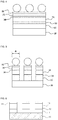
- FIG. 1 is a sectional view for illustrating a step of forming an LED basic element layer according to an embodiment of the present disclosure, which includes a step of forming a first conductive semiconductor layer 11, an active layer 12 and a second conductive semiconductor layer 13 on a substrate 10.
- the substrate 10 may use a penetrating substrate such as a sapphire substrate (Al 2 O 3 ) and a glass substrate.
- the substrate 10 may be selected from a group consisting of GaN, SiC, ZnO, Si, GaP and GaAs, or a conductive substrate.
- this embodiment will be described based on a sapphire substrate.
- the upper surface of the substrate 10 may have an uneven pattern.
- a nitride semiconductor is grown on the substrate 10, and the growth device may use electron beam deposition, physical vapor deposition (PVD), chemical vapor deposition (CVD), plasma laser deposition (PLD), dual-type thermal evaporator, sputtering, metal organic chemical vapor deposition (MOCVD) or the like, without being limited thereto.
- PVD physical vapor deposition
- CVD chemical vapor deposition
- PLD plasma laser deposition
- MOCVD metal organic chemical vapor deposition
- a buffer layer (not shown) and/or an undoped semiconductor layer (not shown) may be formed on the substrate 10.
- the buffer layer is a layer for reducing a difference in a lattice constant from the substrate 10 and may be formed with at least one of GaN, InN, AIN, InGaN, AlGaN, InAlGaN and AlInN.
- the undoped semiconductor layer may be implemented as an undoped GaN layer, and serves as a substrate at which the nitride semiconductor grows.
- the buffer layer and the undoped semiconductor layer may be formed selectively, or both of them may also not be formed.
- the substrate may have a thickness of 400 to 1500 ⁇ m, without being limited thereto.
- the first conductive semiconductor layer 11 is formed on the substrate 10.
- the first conductive semiconductor layer 11 may include, for example, an n-type semiconductor layer.
- the n-type semiconductor layer may be at least one selected from semiconductor materials having a composition formula of InxAlyGa1-x-yN (0 ⁇ x ⁇ 1, 0 ⁇ y ⁇ 1, 0 ⁇ x+y ⁇ 1), for example InAIGaN, GaN, AIGaN, InGaN, AIN, InN or the like, and may also be doped with a first conductive dopant (e.g., Si, Ge, Sn or the like).
- the first conductive semiconductor layer may have a thickness of 1.5 to 5 ⁇ m, without being limited thereto.
- the active layer 12 is formed on the first conductive semiconductor layer 11 and may have a single or multi quantum well structure.
- a clad layer (not shown) doped with a conductive dopant may be formed on and/or under the active layer 12, the clad layer doped with a conductive dopant may be implemented as an AlGaN layer or an InAlGaN layer.
- materials such as AlGaN, AlInGaN or the like may also be used as the active layer 12.
- the active layer 12 generates light by coupling of an electron-hole pair when an electric field is applied thereto.
- the active layer may have a thickness of 0.05 to 0.25 ⁇ m, without being limited thereto.
- a second conductive semiconductor layer 13 is formed on the active layer 12, and the second conductive semiconductor layer 13 may be implemented with at least one p-type semiconductor layer.
- the p-type semiconductor layer may be at least one selected from semiconductor materials having a composition formula of InxAlyGa1-x-yN (0 ⁇ x ⁇ 1, 0 ⁇ y ⁇ 1, 0 ⁇ x+y ⁇ 1), for example InAIGaN, GaN, AIGaN, InGaN, AIN, InN or the like, and may also be doped with a second conductive dopant (e.g., Mg).
- the light emitting structure includes the first conductive semiconductor layer 11, the active layer 12 and the second conductive semiconductor layer 13 as final components, and may further include another fluorescent layer, active layer, semiconductor layer and/or electrode layer on or under each layer.
- the second conductive semiconductor layer may have a thickness of 0.08 to 0.25 ⁇ m, without being limited thereto.
- the LED element is etched to have a diameter of a nanometer or micrometer size, including the first conductive semiconductor layer, the active layer and the second conductive semiconductor layer.
- the method may further include: 2-5) forming a first electrode layer, an insulation layer and a metal mask layer on the second conductive semiconductor layer; 2-6) forming a nanosphere or microsphere monolayer on the metal mask layer and performing self-assembling; 2-7) dry-etching or wet-etching the first conductive semiconductor layer, the active layer and the second conductive semiconductor layer according to the pattern with nanometer or micrometer intervals; and 2-8) removing the insulation layer, the metal mask layer and the monolayer.
- FIG. 2 is a sectional view for illustrating a step of forming a first electrode layer 20, an insulation layer 21 and a metal mask layer 22 on the second conductive semiconductor 13 of the present disclosure.
- the first electrode layer 20 may be made of metals or metal oxides used for a common LED element, preferably Cr, Ti, Al, Au, Ni, ITO, their oxides or alloys solely or in combination, without being limited thereto.
- the metal mask layer may have a thickness of 0.02 to 0.1 ⁇ m, without being limited thereto.
- the insulation layer 21 formed on the first electrode layer 20 may play a role of a mask for successively etching the first electrode layer, the second conductive semiconductor layer, the active layer and the first conductive semiconductor layer and may use oxides or nitrides, representatively, silicon oxide (SiO 2 ) or silicon nitride (SiN), without being limited thereto.
- the insulation layer may have a thickness of 0.5 to 1.5 ⁇ m, without being limited thereto.
- the metal mask layer 22 formed on the insulation layer 21 plays a role of a mask for etching and may be made of metals commonly used in the art, representatively chrome (Cr), without being limited thereto. According to an embodiment of the present disclosure, the metal mask layer may have a thickness of 30 to 150 nm, without being limited thereto.
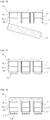
- FIG. 3 is a sectional view for illustrating a step of forming a nanosphere or microsphere monolayer 30 on the metal mask layer 22 of the present disclosure.
- the nanosphere or microsphere monolayer is formed to play a role of a mask for etching the metal mask layer 22, and sphere particles may be formed by using the self-assembling characteristic of the spheres.
- spheres are put afloat on the water surface to move at a certain speed for the purpose of self-assembling of them.
- a first sphere layer having a large and regular arrangement may be formed by applying additional energy and a surfactant, and a sphere monolayer regularly arranged on a metal layer may be formed by ladling the first sphere layer onto the metal mask layer 22.
- the diameter of sphere particles may be selected according to a desired diameter of a subminiature LED element to be finally produced, and preferably, polystyrene spheres, silica spheres or the like having a diameter of 50 to 3000 nm may be used, without being limited thereto.
- FIG. 4 is a sectional view for illustrating a step of ashing the nanosphere or microsphere monolayer 30 of the present disclosure, in which sphere particles are spaced apart from each other. This may be performed by a common sphere monolayer ashing process, and preferably, the ashing process may be performed by means of oxygen (O 2 )-based reactive ion ashing and plasma ashing (e.g.).
- O 2 oxygen
- plasma ashing e.g.
- FIG. 5 is a sectional view for illustrating an etching step of the present disclosure, in which the sphere particles spaced apart from each other during the ashing process of FIG. 4 are etched to form holes.
- a portion where the sphere particles 30 are formed is not etched, and a spatial portion between the sphere particles is etched to form a hole.
- the hole may be selectively formed from the metal mask layer 22 to the upper portion of the substrate 10.
- This etching process may adopt dry etching such as reactive ion etching (RIE) or inductively coupled plasma reactive ion etching (ICP-RIE).
- RIE reactive ion etching
- ICP-RIE inductively coupled plasma reactive ion etching
- the dry etching allows one-directional etching, which is suitable for the above patterning work, different from the wet etching.
- the wet etching performs isotropic etching in which the etching work is performed in all directions, but the dry etching enables to etch in a depth direction to form a hole, different from the wet etching, and thus allows adjusting the hole size and forming intervals into a desired pattern.
- an etching gas available for a metal mask may include Cl 2 , O 2 or the like.
- An interval (A) of the LED element manufactured by the etching process is identical to the diameter of the sphere particles 30.
- the interval (A) of the LED element may have a nanometer or micrometer unit, more preferably 50 to 3000 nm.
- FIG. 6 shows a step of removing the sphere particles 30, the metal mask layer 22 and the insulation layer 21 after the etching process, which may be performed by wet etching or dry etching.
- Step 2) may include: 2-1) forming a first electrode layer, an insulation layer and a metal mask layer in order on the second conductive semiconductor layer; 2-2) forming a polymer layer on the metal mask layer and patterning the polymer layer with nanometer or micrometer intervals; 2-3) dry-etching or wet-etching the first conductive semiconductor layer, the active layer and the second conductive semiconductor layer according to the pattern with nanometer or micrometer intervals; and 2-4) removing the insulation layer, the metal mask layer and the polymer layer.
- a common polymer layer available for common lithography is formed on the metal mask layer.
- the polymer layer is patterned with nanometer or micrometer intervals by means of photo lithography, e-beam lithography, or nano implant lithography, and then dry-etched or wet-etched. After that, the insulation layer, the metal mask layer and the polymer layer are removed.
- Step 3 an insulation film is formed on the outer circumference of the first conductive semiconductor layer, the active layer and the second conductive semiconductor layer, and the substrate is removed, thereby manufacturing a subminiature LED element.
- Step 3) may include: 3-1) forming a support film on the first electrode layer; 3-2) forming an insulation film on the outer circumference including the first conductive semiconductor layer, the active layer and the second conductive semiconductor layer; 3-3) coating the upper portion of the insulation film with a hydrophobic film; 3-4) removing the substrate; 3-5) forming a second electrode layer at the lower portion of the first conductive semiconductor layer; and 3-6) removing the support film to manufacture a plurality of subminiature LED elements.
- FIG. 7 is a sectional view for illustrating a step of attaching a support film 70 onto the first electrode layer 20 of the present disclosure.
- the support film 70 supports the plurality of subminiature LED elements not to be dispersed when the substrate 10 is removed by means of laser lift-off (LLO), and is also attached to prevent the LED element from cracking.
- the support film may be made of polymer epoxy or bonding metal and have a thickness of 0.3 to 70 ⁇ m, without being limited thereto.
- FIG. 8 shows that an insulation film 80 is formed on the outer circumference of the first conductive semiconductor layer, the active layer and the second conductive semiconductor layer with respect to the subminiature LED elements at which the support film of the present disclosure is formed. By doing so, surface defects of the subminiature LED element may be minimized, which improves life cycle and efficiency.
- the insulation film may be formed on the outer circumference of not only the first conductive semiconductor layer 11, the active layer 12 and the second conductive semiconductor layer 13 but also the second electrode layer and/or the first electrode layer and other layers.
- the outer circumference of the subminiature LED elements to which the support film 70 and the substrate 10 are attached may be coated with or dipped in insulation material, without being limited thereto.
- Material available for the insulation film may be at least one selected from the group consisting of SiO 2 , Si 3 N 4 , Al 2 O 3 and TiO 2 , without being limited thereto.
- the Al 2 O 3 film may be formed by means of atomic layer deposition (ALD), and a film may be formed by supplying trimethyl aluminum (TMA) and H 2 O source in a pulse form and using chemical absorption and desorption.
- FIG. 9 is a sectional view for illustrating a step of coating the insulation film 80 formed on the outer circumference of the LED element of the present disclosure with a hydrophobic film 90.
- the hydrophobic film 90 gives a hydrophobic property to the surface of the subminiature LED element, thereby preventing elements from cohering. Therefore, it is possible to reduce characteristic deterioration of independent subminiature elements and eliminate many defects of subminiature LED elements in the pixel patterning process.
- the hydrophobic film 90 may be formed on the insulation film 80.
- the hydrophobic film may use any material which can be formed on the insulation film and prevent cohesion among the subminiature LED elements, without limitation, for example octadecyltrichlorosilane (OTS), self-assembled monolayers (SAMs) such as fluoroalkyltrichlorosilane, perfluoroalkyltri-ethoxysilane or the like, fluoropolymers such as Teflon (registered trademark), Cytop (registered trademark) or the like, solely or in combination.
- OTS octadecyltrichlorosilane
- SAMs self-assembled monolayers
- fluoroalkyltrichlorosilane perfluoroalkyltri-ethoxysilane or the like
- fluoropolymers such as Teflon (registered trademark), Cytop (registered trademark) or the like, solely or in combination.
- FIG. 10 is a sectional view for illustrating a step of removing the substrate 10 formed under the first conductive semiconductor layer 11 of the LED element of the present disclosure.
- the substrate 10 may be removed using a common method, preferably chemical lift-off (CLO) or laser lift-off (LLO), without being limited thereto.
- CLO chemical lift-off
- LLO laser lift-off
- FIG. 11 is a sectional view for illustrating a step of forming a first electrode 110 under the first conductive semiconductor layer 11 from which the substrate 10 is removed according to the present disclosure.
- the first electrode 110 may use any material commonly available for the LED element without limitation, preferably Cr, Ti, Al, Au, Ni, ITO, their oxides or alloys alone or in combination.
- the electrode may have a thickness of 0.02 to 1 ⁇ m, without being limited thereto.
- FIG. 12 is a sectional view for illustrating a step of coating the surface of the first electrode 110 of the present disclosure with a coupling linker 120 for self-assembling.
- the subminiature LED element since the subminiature LED element has a very small size, when being attached to a sub-pixel (pixel site) of the LED display substrate, the subminiature LED element may not stand upright but lie down or turn over.
- the surface of the first electrode 110 is coated with a coupling linker 120 for self-assembling, and a second linker (not shown) capable of being coupled to the coupling linker 120 is formed at the sub-pixel (pixel site) of the LED display substrate.
- the subminiature LED element even though the subminiature LED element is transferred or added to the sub-pixel in an ink or paste form, the subminiature LED element does not lie down or turn over but the electrode surface may be attached to a sub-pixel at a desired location.
- the second linker is not formed, if a functional group remaining in the coupling linker is coupled to the surface of the sub-pixel of the LED display substrate, it is possible to prevent the subminiature LED element from lying or turning over without standing upright.
- the coupling linker should be coupled to an electrode surface of the subminiature LED element, the surface of the sub-pixel of the display substrate and/or the second linker formed at the sub-pixel.
- the coupling linker may have at least two functional groups.
- the coupling linker may contain thiol-based aminoethanethiol or its oxide, which reacts with metal, and aminopropyltrirthoxysilane reacting with it, without being limited thereto.
- the second linker formed on the surface of the sub-pixel of the display substrate may use any material capable of being complementarily coupled with the coupling linker of the present disclosure without limitation, preferably materials in the same group as the coupling linker, without being limited thereto.
- FIG. 13 shows that independent subminiature LED elements 130, 131 are manufactured by removing the support film 70.
- the coupling linker 120 may be formed on at least one surface of the second electrode 20 and the first electrode 110 after the support film 70 is removed.
- a subminiature LED element which includes: a first conductive semiconductor layer; an active layer formed on the first conductive semiconductor layer; and a semiconductor light emission element of a micrometer or nanometer size including a second conductive semiconductor layer formed on the active layer, wherein the outer circumference of the semiconductor light emission element is coated with an insulation film.
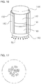
- FIG. 14 is a perspective view showing a subminiature LED element of the present disclosure.
- the subminiature LED element according to the present disclosure includes an active layer 141 formed on the first conductive semiconductor layer 140 and a second conductive semiconductor layer 142 formed on the active layer 141.
- a first electrode 143 may be formed under the first conductive semiconductor layer 140, and a second electrode 144 may be formed on the second conductive semiconductor layer 142.
- a buffer layer, an active layer, a fluorescent layer and/or a semiconductor layer may also be further provided as described above.
- the insulation film 150 may be formed to surround the partial or entire outer circumference of the active layer 141 formed on the first conductive semiconductor layer 140 and the second conductive semiconductor layer 142 formed on the active layer 141.
- the insulation film 150 may also be formed to surround the partial or entire outer circumference of the first electrode 143 and/or the second electrode 144.
- FIG. 15 is a perspective view showing a subminiature LED element according to an embodiment of the present disclosure in which the insulation film 150 formed on the outer circumference according to an embodiment of the present disclosure is coated with a hydrophobic film 160 in order to prevent cohesion among the subminiature LED elements.
- the hydrophobic film 160 may be formed to surround a part or entire of the insulation film 150.
- FIG. 16 is a perspective view showing a subminiature LED element in which a coupling linker for self-assembling is formed on the electrode surface of the present disclosure.
- a coupling linker 170 for self-assembling may be formed on at least one surface of the first electrode 143 and the second electrode 144.
- the coupling linker 170 is formed on the surface of the first electrode 143, and a second linker (not shown) capable of being coupled with the coupling linker 170 is formed at a corresponding sub-pixel (pixel site) of the LED display substrate.
- a second linker capable of being coupled with the coupling linker 170 is formed at a corresponding sub-pixel (pixel site) of the LED display substrate.
- the subminiature LED element is transferred or added to the sub-pixel in an ink or paste form, the subminiature LED element does not lie down or turn over but the electrode surface may be attached to a sub-pixel at a desired location.
- the coupling linker 170 is formed on both the first electrode 143 and the second electrode 144, a part of the subminiature LED elements coupled to the subpixels (pixel sites) of the LED display substrate will be coupled to the first electrode 143, and the other will be coupled to the second electrode 144. In this case, if an AC current is applied to the LED display substrate, the LED display may be driven.
- the subminiature LED element of the present disclosure may have a cylindrical shape, a rectangular shape or the like without limitation, but preferably a cylindrical shape.
- the diameter (the diameter of the circle) may be 50 to 3000 nm, and the height may be 1.5 to 7 ⁇ m, without being limited thereto.
- FIG. 17 shows ink or paste including the subminiature LED elements of the present disclosure, which may be transferred directly or in an ink or paste form to a sub-pixel of the display substrate of the subminiature LED elements according to the present disclosure.
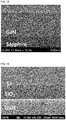
- a buffer layer or undoped semiconductor layer (undoped GaN, 2.4 to 2.8 ⁇ m in thickness), a first conductive semiconductor layer (n-type GaN, 2.0 to 2.4 ⁇ m in thickness), an active layer (InGaN/GaN multiple quantum well, 100 to 140 nm), and a second conductive semiconductor layer (p-type GaN, 200nm in thickness) were formed on a sapphire substrate (2-inch wafer size, 430 ⁇ 25 ⁇ m) by means of MOCVD (see FIG. 18 ).
- a subminiature LED element was prepared according to the following process.
- SiO 2 800nm to 1 ⁇ m in thickness
- a chrome layer 100 to 120nm in thickness
- thermal evaporation respectively (PECVD: 60W, 550 mtorr, SiH 4 160 sccm, N 2 240 sccm, N 2 O 1500 sccm, 35 to 40 minutes; thermal evaporation: 130 to 140A, 9.0x10 -6 torr, 20 to 30 minutes) (see FIG. 19 ).
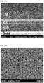
- a polystyrene nano-sphere was prepared as a monolayer (960 to 1000nm in thickness) agreeably arranged in a hexagonal shape and formed on the metal mask layer (see FIGS. 20a and 20b ).
- the monolayer was ashed (50W, 0.05 torr, O 2 100 sccm) under an O 2 gas circumstance to have a reduced size of 500 to 800nm (see FIGS. 21 a and 21b).
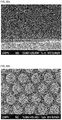
- the polystyrene nano-sphere having a reduced size was used as a mask, and the metal mask layer was etched under a Cl 2 gas circumstance by means of RIE which is a dry etching method (50W, 0.08 torr, Cl 2 40 sccm) (see FIGS. 22a and 22b ).
- RIE a dry etching method
- a metal mask layer pattern transferred according to the shape of polystyrene was prepared (see FIGS. 23a and 23b ), and by using the prepared metal mask layer pattern, the insulation layer region present at a lower portion was etched again under a CF 4 and O 2 gas circumstance (100W, 0.042 torr, CF 4 40 sccm, O 2 2 sccm) (see FIGS.
- the semiconductor layer (GaN) was etched under a SiCl 4 and Ar gas circumstance by means of ICP (RF 50W, ICP 300W, 3 torr, SiCl 4 2 sccm, Ar 20 sccm), thereby making a rod pattern of the semiconductor layer (see FIGS. 25a and 25b ).
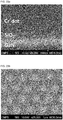
- the insulation layer used as a mask in order to make the rod pattern of the semiconductor layer was removed by etching under a CF 4 and O 2 gas circumstance (see FIGS. 26a and 26b ).
- the outer circumference of the semiconductor layer prepared as above was coated with an insulation coating (Al 2 O 3 ) by means of atomic layer deposition (ALD) (trimethylaluminum (TMA) was used as a metal reactant material, steam was used as an oxygen source, TMA vapor pressure was 0.04 torr, a chamber temperature was maintained to be 80°C, Ar was used as a carrier gas and a purging gas, and a growth rate was ⁇ 1.5 ⁇ ) (thickness: 20nm), and was also coated with octadecyltrichlorosilane (OTS) as a hydrophobic coating by means of a self-assembling process to have a thickness of several nanometers.
- ALD atomic layer deposition
- TMA trimethylaluminum
- steam was used as an oxygen source
- TMA vapor pressure was 0.04 torr
- a chamber temperature was maintained to be 80°C
- Ar was used as a carrier gas and a purging gas
- a growth rate was
- the buffer layer or the undoped semiconductor layer was removed by etching by means of ICP under a SiCl 4 and Ar gas circumstance (RF 50W, ICP 300W, 3 torr, SiCl 4 2 sccm, Ar 20 sccm).
- RF 50W, ICP 300W, 3 torr, SiCl 4 2 sccm, Ar 20 sccm By doing so, an independent subminiature LED rod pattern to which the support film was attached may be obtained (see FIGS. 29a and 29b , FIGS. 30a and 30b , and FIGS. 31 a and 31b).
- a Ti electrode was deposited to the first conductive semiconductor layer of the subminiature LED by using a sputtering device (DC-sputtering system) (300V, 0.17A, Ar 100 sccm) (see FIG. 32 ).
- the electrode surface was coated with dithiol as a coupling linker by means of liquid or vapor self-assembling. The coating process was performed in a liquid state.
- nonamedithiol solution 1 mM was prepared by mixing ethanol anhydride (10 ml) and nonamedithiol (20 ⁇ l), and the subminiature LED rod shape to which the electrode was deposited was dipped in the nonamedithiol solution for a day and then taken out and washed.
- the support film was removed by using acetone so that independent subminiature LEDs are prepared in an ink or paste form (see FIGS. 33 and 34 ).
- the ink or paste form was arranged by being dropped onto an electrode substrate having a linker (metal micro powder: silver nanoparticles) which reacts with the coupling linker.
- a pattern was formed by using a dithiol linker reacting with the electrode substrate and silver nanoparticles serving as the metal micro powder capable of reacting with the coupling linker of the subminiature LED.
- the nonamedithiol linker was firstly attached to the electrode substrate by reaction, and an opposite side of the nonamedithiol linker not attached to the electrode substrate was coated with silver nanoparticles. The coating process was performed by putting the electrode substrate attached to the nonamedithiol linker into a toluene solution in which silver nanoparticles are dispersed, and then taking out the same after reaction.
- FIG. 35 shows a spectrum measured after the subminiature LED elements prepared as above are arranged on the electrode substrate, and FIGS. 37a to 37c are photographs observed by naked eyes, showing that the manufactured subminiature LED elements. As shown in these figures, it may be found that a blue light is emitted from the subminiature LED element according to the present disclosure.
- the subminiature LED element according the present disclosure may be widely utilized over the entire display industries.
Claims (13)
- Herstellungsverfahren für ein Subminiatur-LED-Element (130, 131), umfassend:1) Bilden einer ersten leitenden Halbleiterschicht (11, 140), einer aktiven Schicht (12, 141) und einer zweiten leitenden Halbleiterschicht (13, 142) in dieser Reihenfolge auf einem Substrat (10);2) Ätzen der ersten leitenden Halbleiterschicht (11, 140), der aktiven Schicht (12, 141) und der zweiten leitenden Halbleiterschicht (13, 142), so dass das Subminiatur-LED-Element (130, 131) einen Durchmesser im Nanometer- oder Mikrometer-Niveau aufweist; und3) Bilden eines Isolierfilms (80, 150) auf dem Außenumfang der ersten leitenden Halbleiterschicht (11,140), der aktiven Schicht (12, 141) und der zweiten leitenden Halbleiterschicht (13,142), Beschichten des oberen Abschnitts des Isolierfilms (80, 150) mit einem hydrophoben Film (90, 160) und Entfernen des Substrats (10), wobei der Durchmesser des Subminiatur-LED-Elements (130, 131) 50 bis 3000 nm beträgt.
- Herstellungsverfahren für ein Subminiatur-LED-Element (130, 131) nach Anspruch 1, wobei die erste leitende Halbleiterschicht (11, 140) mindestens eine n-Typ-Halbleiterschicht umfasst und die zweite leitende Halbleiterschicht (13, 142) mindestens eine p-Typ-Halbleiterschicht umfasst.
- Herstellungsverfahren für ein Subminiatur-LED-Element (130, 131) nach Anspruch 1, wobei der Schritt 2) folgendes umfasst:2-1) Bilden einer ersten Elektrodenschicht (20, 144), einer Isolierschicht (21) und einer Metallmaskenschicht (22) in dieser Reihenfolge auf der zweiten leitenden Halbleiterschicht (13, 142);2-2) Bilden einer Polymerschicht auf der Metallmaskenschicht (22) und Mustern der Polymerschicht mit Nanometer- oder Mikrometer-Intervallen;2-3) Trockenätzen oder Nassätzen der ersten leitenden Halbleiterschicht (11, 140), der aktiven Schicht (12, 141) und der zweiten leitenden Halbleiterschicht (13, 142) gemäß dem Muster mit Nanometer- oder Mikrometer-Intervallen; und2-4) Entfernen der Isolierschicht (21), der Metallmaskenschicht (22) und der Polymerschicht.
- Herstellungsverfahren für ein Subminiatur-LED-Element (130, 131) nach Anspruch 1, wobei der Schritt 2) folgendes umfasst:2-5) Bilden einer ersten Elektrodenschicht (20, 144), einer Isolierschicht (21) und einer Metallmaskenschicht (22) auf der zweiten leitenden Halbleiterschicht (13, 142);2-6) Bilden einer Nano- oder Mikrokügelchen-Monoschicht (30) auf der Metallmaskenschicht (22) und Durchführen von Selbstaufbau;2-7) Trockenätzen oder Nassätzen der ersten leitenden Halbleiterschicht (11, 140), der aktiven Schicht (12, 141) und der zweiten leitenden Halbleiterschicht (13, 142) gemäß dem Muster mit Nanometer- oder Mikrometer-Intervallen; und2-8) Entfernen der Isolierschicht (21), der Metallmaskenschicht (22) und der Monoschicht (30).
- Herstellungsverfahren für ein Subminiatur-LED-Element (130, 131) nach Anspruch 4, wobei die Schicht der Nano- oder Mikrokügelchen aus Polystyrol hergestellt ist.
- Herstellungsverfahren für ein Subminiatur-LED-Element (130, 131) nach Anspruch 3 oder 4, wobei der Schritt 3) folgendes umfasst:3-1) Bilden eines Trägerfilms (70) auf der ersten Elektrodenschicht (20, 144);3-2) Bilden eines Isolierfilms (80, 150) auf dem Außenumfang, einschließlich der ersten leitenden Halbleiterschicht (11,140), der aktiven Schicht (12,141) und der zweiten leitenden Halbleiterschicht (13, 142);3-3) Beschichten des oberen Abschnitts des Isolierfilms (80, 150) mit einem hydrophoben Film (90, 160);3-5) Bilden einer zweiten Elektrodenschicht (110, 143) auf dem unteren Abschnitt der ersten leitenden Halbleiterschicht (11, 140); und3-6) Entfernen des Trägerfilms (70) unter Herstellung einer Vielzahl von Subminiatur-LED-Elementen (130, 131).
- Herstellungsverfahren für ein Subminiatur-LED-Element (130, 131) nach Anspruch 3 oder 4, wobei der Schritt 3) folgendes umfasst:3-7) Bilden eines Trägerfilms (70) auf der ersten Elektrodenschicht (20, 144);3-8) Bilden eines Isolierfilm (80, 150) auf dem Außenumfang, einschließlich der ersten leitenden Halbleiterschicht (11,140), der aktiven Schicht (12,141) und der zweiten leitenden Halbleiterschicht (13, 142);3-9) Entfernen des Substrats (10);3-10) Bilden einer zweiten Elektrodenschicht (110, 143) auf dem unteren Abschnitt der ersten leitenden Halbleiterschicht (11, 140);3-11) Bilden eines Kopplungsverbinders (120, 170) auf mindestens einer Oberfläche der zweiten Elektrodenschicht (110, 143) und der ersten Elektrodenschicht (20, 144); und3-12) Entfernen des Trägerfilms (70) unter Herstellung einer Vielzahl von Subminiatur-LED-Elementen (130, 131).
- Subminiatur-LED-Element (130, 131), umfassend:eine erste leitende Halbleiterschicht (11,140);eine auf der ersten leitenden Halbleiterschicht (11, 140) ausgebildete aktive Schicht (12, 141); undein Halbleiter-Lichtemissionselement einer Mikrometer- oder Nanometergröße, einschließlich einer auf der aktiven Schicht (12, 141) ausgebildeten zweiten leitenden Halbleiterschicht (13, 142),wobei der Außenumfang des Halbleiter-Lichtemissionselements mit einem Isolierfilm (80,150) beschichtet ist, wobei der obere Abschnitt des Isolierfilms (80, 150) mit einem hydrophoben Film (90, 160) beschichtet ist, und wobei der Durchmesser des Subminiatur-LED-Elements (130, 131) 50 bis 3000 nm beträgt.
- Subminiatur-LED-Element (130, 131) nach Anspruch 8,
wobei eine zweite Elektrodenschicht (110, 143) auf dem unteren Abschnitt der ersten leitenden Halbleiterschicht (11, 140) ausgebildet ist, und eine erste Elektrodenschicht (20, 144) auf dem oberen Abschnitt der zweiten leitenden Halbleiterschicht (13, 142) ausgebildet ist. - Subminiatur-LED-Element (130, 131) nach Anspruch 8,
wobei ein Kopplungsverbinder (120,170) zum Selbstaufbau für die Unterseite der zweiten Elektrodenschicht (110, 143) und/oder die Oberseite der ersten Elektrodenschicht (20, 144) bereitgestellt ist. - Subminiatur-LED-Element (130, 131) nach Anspruch 10,
wobei der Kopplungsverbinder (120, 170) komplementär mit einem Substrat (10) für eine LED-Anzeige gekoppelt ist. - Subminiatur-LED-Element (130, 131) nach Anspruch 8,
wobei die erste leitende Halbleiterschicht (11, 140) mindestens eine n-Typ-Halbleiterschicht umfasst und die zweite leitende Halbleiterschicht (13, 142) mindestens eine p-Typ-Halbleiterschicht umfasst. - Subminiatur-LED-Element (130, 131) nach einem der Ansprüche 8 bis 11,
wobei der Isolierfilm (80, 150) mindestens eine Verbindung, ausgewählt aus der Gruppe bestehend aus SiO2, Si3N4, Al2O3 und TiO2, umfasst, der hydrophobe Film (90, 160) SAM und/oder Fluorpolymer umfasst, und der Kopplungsverbinder (120, 170) eine Thiolgruppe umfasst.
Applications Claiming Priority (2)
| Application Number | Priority Date | Filing Date | Title |
|---|---|---|---|
| KR1020110040174A KR101244926B1 (ko) | 2011-04-28 | 2011-04-28 | 초소형 led 소자 및 그 제조방법 |
| PCT/KR2012/003309 WO2012148228A2 (ko) | 2011-04-28 | 2012-04-27 | 초소형 led 소자 및 그 제조방법 |
Publications (3)
| Publication Number | Publication Date |
|---|---|
| EP2704215A2 EP2704215A2 (de) | 2014-03-05 |
| EP2704215A4 EP2704215A4 (de) | 2014-09-10 |
| EP2704215B1 true EP2704215B1 (de) | 2018-04-11 |
Family
ID=47072950
Family Applications (1)
| Application Number | Title | Priority Date | Filing Date |
|---|---|---|---|
| EP12777172.3A Active EP2704215B1 (de) | 2011-04-28 | 2012-04-27 | Ultrakleine led und herstellungsverfahren dafür |
Country Status (5)
| Country | Link |
|---|---|
| US (1) | US9112112B2 (de) |
| EP (1) | EP2704215B1 (de) |
| KR (1) | KR101244926B1 (de) |
| CN (1) | CN103608937B (de) |
| WO (1) | WO2012148228A2 (de) |
Cited By (6)
| Publication number | Priority date | Publication date | Assignee | Title |
|---|---|---|---|---|
| US11156759B2 (en) | 2019-01-29 | 2021-10-26 | Osram Opto Semiconductors Gmbh | μ-LED, μ-LED device, display and method for the same |
| US11271143B2 (en) | 2019-01-29 | 2022-03-08 | Osram Opto Semiconductors Gmbh | μ-LED, μ-LED device, display and method for the same |
| US11302248B2 (en) | 2019-01-29 | 2022-04-12 | Osram Opto Semiconductors Gmbh | U-led, u-led device, display and method for the same |
| WO2022119107A1 (ko) * | 2020-12-02 | 2022-06-09 | 삼성디스플레이 주식회사 | 표시 장치 및 발광 소자의 제조 방법 |
| US11538852B2 (en) | 2019-04-23 | 2022-12-27 | Osram Opto Semiconductors Gmbh | μ-LED, μ-LED device, display and method for the same |
| US11610868B2 (en) | 2019-01-29 | 2023-03-21 | Osram Opto Semiconductors Gmbh | μ-LED, μ-LED device, display and method for the same |
Families Citing this family (112)
| Publication number | Priority date | Publication date | Assignee | Title |
|---|---|---|---|---|
| CN105453284B (zh) * | 2013-07-09 | 2018-03-20 | Psi株式会社 | 超小型发光二极管电极组件及其制造方法 |
| KR101429095B1 (ko) * | 2013-07-09 | 2014-08-12 | 피에스아이 주식회사 | 초소형 led 전극어셈블리를 이용한 led 램프 |
| KR101436123B1 (ko) | 2013-07-09 | 2014-11-03 | 피에스아이 주식회사 | 초소형 led를 포함하는 디스플레이 및 이의 제조방법 |
| DE102014103133A1 (de) * | 2014-03-10 | 2015-09-10 | Osram Opto Semiconductors Gmbh | Optoelektronisches Bauelement und Verfahren zu seiner Herstellung |
| KR101628345B1 (ko) * | 2014-07-08 | 2016-06-09 | 피에스아이 주식회사 | 초소형 led 전극어셈블리의 제조방법 |
| KR101713818B1 (ko) | 2014-11-18 | 2017-03-10 | 피에스아이 주식회사 | 초소형 led 소자를 포함하는 전극어셈블리 및 그 제조방법 |
| KR101674052B1 (ko) * | 2014-11-18 | 2016-11-09 | 피에스아이 주식회사 | 초소형 led 소자를 전극어셈블리에 배치시키는 방법 |
| KR101723822B1 (ko) * | 2014-11-18 | 2017-04-07 | 피에스아이 주식회사 | 초소형 led 전극어셈블리 제조용 복합섬유 및 이를 포함하는 원단 |
| KR101672781B1 (ko) * | 2014-11-18 | 2016-11-07 | 피에스아이 주식회사 | 수평배열 어셈블리용 초소형 led 소자, 이의 제조방법 및 이를 포함하는 수평배열 어셈블리 |
| DE102015101888A1 (de) | 2015-02-10 | 2016-08-11 | Osram Opto Semiconductors Gmbh | Optoelektronisches Halbleiterbauelement und Verfahren zur Herstellung eines optoelektronischen Halbleiterbauelements |
| KR101730929B1 (ko) | 2015-11-17 | 2017-04-28 | 피에스아이 주식회사 | 선택적 금속오믹층을 포함하는 초소형 led 전극어셈블리 제조방법 |
| KR101770632B1 (ko) | 2016-01-07 | 2017-08-24 | 피에스아이 주식회사 | 자가 조립형 초소형 led 전극어셈블리 제조용 용매 및 이를 통해 자가 조립형 초소형 led 전극어셈블리를 제조하는 방법 |
| KR101730977B1 (ko) | 2016-01-14 | 2017-04-28 | 피에스아이 주식회사 | 초소형 led 전극어셈블리 |
| KR101845907B1 (ko) * | 2016-02-26 | 2018-04-06 | 피에스아이 주식회사 | 초소형 led 모듈을 포함하는 디스플레이 장치 |
| KR101787435B1 (ko) * | 2016-02-29 | 2017-10-19 | 피에스아이 주식회사 | 나노 로드 제조방법 |
| KR101987196B1 (ko) | 2016-06-14 | 2019-06-11 | 삼성디스플레이 주식회사 | 픽셀 구조체, 픽셀 구조체를 포함하는 표시장치 및 그 제조 방법 |
| KR20180007025A (ko) | 2016-07-11 | 2018-01-22 | 삼성디스플레이 주식회사 | 초소형 발광 소자를 포함하는 픽셀 구조체, 표시장치 및 그 제조방법 |
| KR102608419B1 (ko) | 2016-07-12 | 2023-12-01 | 삼성디스플레이 주식회사 | 표시장치 및 표시장치의 제조방법 |
| KR102574603B1 (ko) | 2016-07-15 | 2023-09-07 | 삼성디스플레이 주식회사 | 발광장치 및 그의 제조방법 |
| KR102592276B1 (ko) | 2016-07-15 | 2023-10-24 | 삼성디스플레이 주식회사 | 발광장치 및 그의 제조방법 |
| KR102568252B1 (ko) | 2016-07-21 | 2023-08-22 | 삼성디스플레이 주식회사 | 발광 장치 및 그의 제조방법 |
| KR102587215B1 (ko) | 2016-12-21 | 2023-10-12 | 삼성디스플레이 주식회사 | 발광 장치 및 이를 구비한 표시 장치 |
| KR101874993B1 (ko) | 2016-12-28 | 2018-07-05 | 피에스아이 주식회사 | 전기적 컨택이 향상된 초소형 led 전극 어셈블리 및 이의 제조방법 |
| KR102621662B1 (ko) * | 2017-01-09 | 2024-01-09 | 삼성디스플레이 주식회사 | 발광 소자 및 이의 제조 방법 |
| KR102513267B1 (ko) | 2017-10-13 | 2023-03-23 | 삼성디스플레이 주식회사 | 표시 장치 및 이의 제조 방법 |
| US20190198720A1 (en) | 2017-12-22 | 2019-06-27 | Lumileds Llc | Particle systems and patterning for monolithic led arrays |
| KR102448104B1 (ko) | 2018-02-08 | 2022-09-29 | 삼성디스플레이 주식회사 | 발광 장치 및 그의 제조 방법 |
| KR102503168B1 (ko) | 2018-02-08 | 2023-02-27 | 삼성디스플레이 주식회사 | 표시 장치 및 그의 제조 방법 |
| KR102552300B1 (ko) | 2018-02-08 | 2023-07-10 | 삼성디스플레이 주식회사 | 표시 장치 |
| KR102503172B1 (ko) | 2018-02-13 | 2023-02-27 | 삼성디스플레이 주식회사 | 표시 장치 |
| KR102546733B1 (ko) | 2018-03-30 | 2023-06-23 | 삼성디스플레이 주식회사 | 표시 장치 |
| KR102299992B1 (ko) | 2018-04-25 | 2021-09-10 | 삼성디스플레이 주식회사 | 발광 장치, 이를 구비한 표시 장치, 및 그의 제조 방법 |
| KR102058503B1 (ko) | 2018-05-11 | 2019-12-23 | 영남대학교 산학협력단 | 초소형 발광다이오드의 제조방법 및 이에 의해 제조된 초소형 발광다이오드 |
| KR102502608B1 (ko) * | 2018-06-11 | 2023-02-22 | 삼성디스플레이 주식회사 | 발광 소자, 그 제조방법 및 발광 소자를 포함하는 표시 장치 |
| KR102634586B1 (ko) * | 2018-06-11 | 2024-02-07 | 삼성디스플레이 주식회사 | 발광 소자, 그 제조방법 및 발광 소자를 포함하는 표시 장치 |
| KR20180077114A (ko) * | 2018-06-22 | 2018-07-06 | 피에스아이 주식회사 | 전기적 컨택이 향상된 초소형 led 전극 어셈블리 |
| KR102585158B1 (ko) | 2018-07-04 | 2023-10-05 | 삼성디스플레이 주식회사 | 표시 장치 |
| KR102552602B1 (ko) * | 2018-07-10 | 2023-07-10 | 삼성디스플레이 주식회사 | 발광 장치, 그의 제조 방법, 및 이를 구비한 표시 장치 |
| KR102604659B1 (ko) | 2018-07-13 | 2023-11-21 | 삼성디스플레이 주식회사 | 발광 장치 및 이의 제조 방법 |
| KR102520554B1 (ko) * | 2018-07-30 | 2023-04-13 | 삼성디스플레이 주식회사 | 발광 장치 및 이를 구비한 표시 장치 |
| KR102557754B1 (ko) * | 2018-08-03 | 2023-07-20 | 삼성디스플레이 주식회사 | 발광 소자, 이의 제조방법 및 발광 소자를 포함하는 표시 장치 |
| CN110828646B (zh) * | 2018-08-09 | 2020-12-08 | 汕头超声显示器技术有限公司 | 一种微led显示器的制造方法 |
| KR102626051B1 (ko) * | 2018-08-14 | 2024-01-19 | 삼성디스플레이 주식회사 | 발광 소자, 발광 소자를 포함하는 픽셀 구조체 및 그 제조 방법 |
| KR102568353B1 (ko) * | 2018-08-16 | 2023-08-18 | 삼성디스플레이 주식회사 | 발광 소자, 이의 제조방법 및 발광 소자를 포함하는 표시 장치 |
| KR102581666B1 (ko) * | 2018-08-24 | 2023-09-22 | 삼성디스플레이 주식회사 | 발광 소자, 이를 포함하는 표시 장치 및 표시 장치의 제조 방법 |
| US11271033B2 (en) | 2018-09-27 | 2022-03-08 | Lumileds Llc | Micro light emitting devices |
| US10923628B2 (en) | 2018-09-27 | 2021-02-16 | Lumileds Llc | Micrometer scale light emitting diode displays on patterned templates and substrates |
| US10811460B2 (en) | 2018-09-27 | 2020-10-20 | Lumileds Holding B.V. | Micrometer scale light emitting diode displays on patterned templates and substrates |
| US10964845B2 (en) | 2018-09-27 | 2021-03-30 | Lumileds Llc | Micro light emitting devices |
| KR102568713B1 (ko) | 2018-10-12 | 2023-08-22 | 삼성디스플레이 주식회사 | 화소 및 이를 구비한 표시 장치 |
| KR102590984B1 (ko) * | 2018-10-30 | 2023-10-18 | 삼성디스플레이 주식회사 | 발광 소자 구조물 및 발광 소자의 제조방법 |
| KR102651789B1 (ko) * | 2018-11-06 | 2024-03-27 | 삼성디스플레이 주식회사 | 발광 소자 구조물 및 이의 제조방법 |
| KR20200063386A (ko) | 2018-11-27 | 2020-06-05 | 삼성디스플레이 주식회사 | 표시 장치 |
| KR20200066438A (ko) | 2018-11-30 | 2020-06-10 | 삼성디스플레이 주식회사 | 표시 장치 및 그의 제조 방법 |
| KR102626452B1 (ko) * | 2019-01-15 | 2024-01-18 | 삼성디스플레이 주식회사 | 발광 소자의 제조방법 및 발광 소자를 포함하는 표시 장치 |
| KR20200105598A (ko) | 2019-02-28 | 2020-09-08 | 삼성디스플레이 주식회사 | 표시 장치 |
| KR102091810B1 (ko) | 2019-06-03 | 2020-03-23 | 삼성디스플레이 주식회사 | 픽셀 구조체 및 이를 포함하는 표시장치 |
| KR102430815B1 (ko) | 2019-06-03 | 2022-08-10 | 삼성디스플레이 주식회사 | 픽셀 구조체 및 이를 포함하는 표시장치 |
| US11275473B2 (en) | 2019-06-13 | 2022-03-15 | Samsung Display Co., Ltd. | Display panel and display device including the same |
| KR20210000351A (ko) * | 2019-06-24 | 2021-01-05 | 삼성전자주식회사 | 반도체 발광소자 및 디스플레이 장치 |
| KR20210008206A (ko) * | 2019-07-10 | 2021-01-21 | 삼성디스플레이 주식회사 | 발광 소자, 이의 제조 방법 및 표시 장치 |
| KR20210044938A (ko) | 2019-10-15 | 2021-04-26 | 삼성디스플레이 주식회사 | 표시 장치 |
| KR20210053391A (ko) | 2019-11-01 | 2021-05-12 | 삼성디스플레이 주식회사 | 표시 장치 |
| US11869880B2 (en) | 2019-11-05 | 2024-01-09 | Samsung Electronics Co., Ltd. | Method of transferring micro-light emitting diode for LED display |
| KR20210056483A (ko) | 2019-11-08 | 2021-05-20 | 삼성디스플레이 주식회사 | 표시 장치 |
| KR20210059107A (ko) | 2019-11-14 | 2021-05-25 | 삼성디스플레이 주식회사 | 표시 장치 |
| KR20210059110A (ko) | 2019-11-14 | 2021-05-25 | 삼성디스플레이 주식회사 | 표시 장치 |
| KR20210078649A (ko) | 2019-12-18 | 2021-06-29 | 삼성디스플레이 주식회사 | 표시 패널 및 이를 구비하는 표시 장치 |
| KR20210081506A (ko) | 2019-12-23 | 2021-07-02 | 삼성디스플레이 주식회사 | 표시 장치 및 그의 제조 방법 |
| US11404473B2 (en) | 2019-12-23 | 2022-08-02 | Lumileds Llc | III-nitride multi-wavelength LED arrays |
| US11923398B2 (en) | 2019-12-23 | 2024-03-05 | Lumileds Llc | III-nitride multi-wavelength LED arrays |
| KR20210082316A (ko) | 2019-12-24 | 2021-07-05 | 삼성디스플레이 주식회사 | 표시 패널 및 이를 구비하는 표시 장치 |
| KR20210098589A (ko) * | 2020-01-31 | 2021-08-11 | 삼성디스플레이 주식회사 | 잉크 조성물, 이를 이용한 발광 장치 및 이의 제조 방법 |
| KR20210098661A (ko) * | 2020-02-03 | 2021-08-11 | 삼성전자주식회사 | 반도체 발광소자 및 디스플레이 장치 |
| KR20210103048A (ko) | 2020-02-12 | 2021-08-23 | 삼성디스플레이 주식회사 | 표시 장치 |
| KR20210109079A (ko) * | 2020-02-26 | 2021-09-06 | 삼성디스플레이 주식회사 | 잉크 조성물, 이를 이용한 발광 소자 및 이의 제조 방법 |
| US11735695B2 (en) | 2020-03-11 | 2023-08-22 | Lumileds Llc | Light emitting diode devices with current spreading layer |
| US11848402B2 (en) | 2020-03-11 | 2023-12-19 | Lumileds Llc | Light emitting diode devices with multilayer composite film including current spreading layer |
| US11569415B2 (en) | 2020-03-11 | 2023-01-31 | Lumileds Llc | Light emitting diode devices with defined hard mask opening |
| US11942507B2 (en) | 2020-03-11 | 2024-03-26 | Lumileds Llc | Light emitting diode devices |
| KR20210130889A (ko) | 2020-04-22 | 2021-11-02 | 삼성디스플레이 주식회사 | 발광 소자 잉크 및 표시 장치의 제조 방법 |
| KR102332349B1 (ko) * | 2020-04-28 | 2021-11-26 | 국민대학교산학협력단 | 마이크로-나노핀 led 소자 및 이의 제조방법 |
| KR102414266B1 (ko) * | 2020-04-27 | 2022-06-29 | 국민대학교산학협력단 | 마이크로-나노핀 led 소자를 이용한 풀-컬러 led 디스플레이 및 이의 제조방법 |
| KR102345917B1 (ko) * | 2020-04-27 | 2021-12-30 | 국민대학교산학협력단 | 마이크로-나노핀 led 소자 및 이의 제조방법 |
| CN115668517A (zh) * | 2020-04-27 | 2023-01-31 | 国民大学校产学协力团 | Micro-Nano PIN LED元件及其制造方法 |
| KR20210145049A (ko) | 2020-05-22 | 2021-12-01 | 삼성디스플레이 주식회사 | 표시 장치 및 그의 제조 방법 |
| KR102332350B1 (ko) * | 2020-05-25 | 2021-11-26 | 국민대학교산학협력단 | 마이크로-나노핀 led 전극어셈블리 및 이의 제조방법 |
| KR20210147158A (ko) * | 2020-05-27 | 2021-12-07 | 삼성디스플레이 주식회사 | 발광 소자, 이의 제조 방법, 발광 소자를 포함한 잉크 조성물 및 장치 |
| KR20210149962A (ko) * | 2020-06-02 | 2021-12-10 | 삼성디스플레이 주식회사 | 발광 소자의 제조 장치 및 제조 방법 |
| KR20210154295A (ko) * | 2020-06-11 | 2021-12-21 | 삼성디스플레이 주식회사 | 발광 소자 잉크, 표시 장치 및 그 제조 방법 |
| CN113808937B (zh) * | 2020-06-16 | 2023-11-21 | 重庆康佳光电科技有限公司 | 一种显示背板的制备方法、显示背板及显示装置 |
| TWI735263B (zh) * | 2020-06-19 | 2021-08-01 | 台灣愛司帝科技股份有限公司 | 紅光晶片承載結構的製作方法 |
| KR20220014388A (ko) * | 2020-07-24 | 2022-02-07 | 삼성디스플레이 주식회사 | 발광 소자, 이의 제조 방법 및 표시 장치 |
| KR102375861B1 (ko) * | 2020-07-28 | 2022-03-16 | 광운대학교 산학협력단 | 백투백 구조의 초소형 이중 led 소자 및 그 제조 방법과 백투백 구조의 초소형 이중 led 의 전극 어셈블리 및 그 제조방법 |
| KR20220019902A (ko) * | 2020-08-10 | 2022-02-18 | 삼성디스플레이 주식회사 | 발광 소자 및 이를 이용한 표시 장치와 그의 제조 방법 |
| KR20220021946A (ko) * | 2020-08-13 | 2022-02-23 | 삼성디스플레이 주식회사 | 발광 소자, 이의 제조 방법 및 표시 장치 |
| KR20220033538A (ko) * | 2020-09-07 | 2022-03-17 | 삼성디스플레이 주식회사 | 발광 소자, 발광 소자의 제조 방법 및 표시 장치 |
| US11626538B2 (en) | 2020-10-29 | 2023-04-11 | Lumileds Llc | Light emitting diode device with tunable emission |
| US11901491B2 (en) | 2020-10-29 | 2024-02-13 | Lumileds Llc | Light emitting diode devices |
| US11631786B2 (en) | 2020-11-12 | 2023-04-18 | Lumileds Llc | III-nitride multi-wavelength LED arrays with etch stop layer |
| US11955583B2 (en) | 2020-12-01 | 2024-04-09 | Lumileds Llc | Flip chip micro light emitting diodes |
| US11705534B2 (en) | 2020-12-01 | 2023-07-18 | Lumileds Llc | Methods of making flip chip micro light emitting diodes |
| US11600656B2 (en) | 2020-12-14 | 2023-03-07 | Lumileds Llc | Light emitting diode device |
| WO2022149627A1 (ko) * | 2021-01-06 | 2022-07-14 | 엘지전자 주식회사 | 발광 소자 및 디스플레이 장치 |
| CN112951924B (zh) * | 2021-02-02 | 2022-07-12 | Tcl华星光电技术有限公司 | Tft器件及其制备方法 |
| KR102463022B1 (ko) * | 2021-06-08 | 2022-11-03 | 광주과학기술원 | 나노로드 led의 제조방법 |
| KR20220170236A (ko) * | 2021-06-22 | 2022-12-29 | 삼성전자주식회사 | 나노 막대 발광 소자, 복수의 나노 막대 발광 소자를 포함하는 기판 구조물, 및 기판 구조물의 제조 방법 |
| WO2023282365A1 (ko) * | 2021-07-05 | 2023-01-12 | 엘지전자 주식회사 | 반도체 발광 소자 및 디스플레이 장치 |
| KR20230013705A (ko) * | 2021-07-19 | 2023-01-27 | 삼성디스플레이 주식회사 | 발광 소자 및 이를 포함하는 표시 장치 |
| US11935987B2 (en) | 2021-11-03 | 2024-03-19 | Lumileds Llc | Light emitting diode arrays with a light-emitting pixel area |
| WO2023171833A1 (ko) * | 2022-03-10 | 2023-09-14 | 엘지전자 주식회사 | 반도체 발광소자를 포함하는 디스플레이 장치 및 이의 제조방법 |
| KR20240020311A (ko) * | 2022-08-03 | 2024-02-15 | 삼성디스플레이 주식회사 | 도전성 소자, 표시 장치, 및 표시 장치의 제조 방법 |
Family Cites Families (16)
| Publication number | Priority date | Publication date | Assignee | Title |
|---|---|---|---|---|
| JPH06244457A (ja) * | 1993-02-16 | 1994-09-02 | Nisshin Steel Co Ltd | 発光ダイオードの製造方法 |
| JP2002088357A (ja) * | 2000-09-14 | 2002-03-27 | Three Bond Co Ltd | 有機物被覆発光体粒子の製造方法及び有機物被覆発光体粒子 |
| JP3813599B2 (ja) * | 2003-06-13 | 2006-08-23 | ローム株式会社 | 白色発光の発光ダイオード素子を製造する方法 |
| JP2005267991A (ja) | 2004-03-18 | 2005-09-29 | Hitachi Ltd | 表示装置 |
| DE102004044179B4 (de) * | 2004-06-30 | 2010-04-22 | Osram Opto Semiconductors Gmbh | Verfahren zur Montage von Halbleiterchips |
| JP4450207B2 (ja) | 2005-01-14 | 2010-04-14 | セイコーエプソン株式会社 | 発光素子の製造方法 |
| FR2898434B1 (fr) | 2006-03-13 | 2008-05-23 | Centre Nat Rech Scient | Diode electroluminescente blanche monolithique |
| KR100763894B1 (ko) * | 2006-03-21 | 2007-10-05 | 삼성에스디아이 주식회사 | Led 칩을 이용한 디스플레이 장치의 제조방법 |
| KR100888440B1 (ko) * | 2007-11-23 | 2009-03-11 | 삼성전기주식회사 | 수직구조 발광다이오드 소자의 제조방법 |
| CN101971369B (zh) * | 2008-03-14 | 2012-05-23 | 松下电器产业株式会社 | 化合物半导体发光元件、采用该化合物半导体发光元件的照明装置以及化合物半导体发光元件的制造方法 |
| WO2010068460A2 (en) * | 2008-12-12 | 2010-06-17 | 3M Innovative Properties Company | Particle reflow etching |
| TWI399869B (zh) * | 2009-02-05 | 2013-06-21 | Huga Optotech Inc | 發光二極體 |
| WO2010149027A1 (en) * | 2009-06-22 | 2010-12-29 | Industrial Technology Research Institute | Light-emitting unit array, method for fabricating the same and projection apparatus |
| KR101140096B1 (ko) * | 2009-10-12 | 2012-04-30 | 전북대학교산학협력단 | 나노로드 발광 다이오드 및 이의 제조방법 |
| KR20110041401A (ko) | 2009-10-15 | 2011-04-21 | 샤프 가부시키가이샤 | 발광 장치 및 그 제조 방법 |
| KR100996446B1 (ko) * | 2010-05-24 | 2010-11-25 | 엘지이노텍 주식회사 | 발광 소자, 발광 소자의 제조방법 및 발광 소자 패키지 |
-
2011
- 2011-04-28 KR KR1020110040174A patent/KR101244926B1/ko active IP Right Grant
-
2012
- 2012-04-27 EP EP12777172.3A patent/EP2704215B1/de active Active
- 2012-04-27 CN CN201280029867.9A patent/CN103608937B/zh active Active
- 2012-04-27 US US14/114,317 patent/US9112112B2/en active Active
- 2012-04-27 WO PCT/KR2012/003309 patent/WO2012148228A2/ko active Application Filing
Non-Patent Citations (1)
| Title |
|---|
| None * |
Cited By (9)
| Publication number | Priority date | Publication date | Assignee | Title |
|---|---|---|---|---|
| US11156759B2 (en) | 2019-01-29 | 2021-10-26 | Osram Opto Semiconductors Gmbh | μ-LED, μ-LED device, display and method for the same |
| US11271143B2 (en) | 2019-01-29 | 2022-03-08 | Osram Opto Semiconductors Gmbh | μ-LED, μ-LED device, display and method for the same |
| US11302248B2 (en) | 2019-01-29 | 2022-04-12 | Osram Opto Semiconductors Gmbh | U-led, u-led device, display and method for the same |
| US11480723B2 (en) | 2019-01-29 | 2022-10-25 | Osram Opto Semiconductors Gmbh | μ-LED, μ-LED device, display and method for the same |
| US11513275B2 (en) | 2019-01-29 | 2022-11-29 | Osram Opto Semiconductors Gmbh | μ-LED, μ-LED device, display and method for the same |
| US11610868B2 (en) | 2019-01-29 | 2023-03-21 | Osram Opto Semiconductors Gmbh | μ-LED, μ-LED device, display and method for the same |
| US11764339B2 (en) | 2019-01-29 | 2023-09-19 | Osram Opto Semiconductors Gmbh | μ-LED, μ-LED device, display and method for the same |
| US11538852B2 (en) | 2019-04-23 | 2022-12-27 | Osram Opto Semiconductors Gmbh | μ-LED, μ-LED device, display and method for the same |
| WO2022119107A1 (ko) * | 2020-12-02 | 2022-06-09 | 삼성디스플레이 주식회사 | 표시 장치 및 발광 소자의 제조 방법 |
Also Published As
| Publication number | Publication date |
|---|---|
| EP2704215A2 (de) | 2014-03-05 |
| US20140145237A1 (en) | 2014-05-29 |
| WO2012148228A3 (ko) | 2012-12-20 |
| CN103608937A (zh) | 2014-02-26 |
| US9112112B2 (en) | 2015-08-18 |
| KR20120122159A (ko) | 2012-11-07 |
| EP2704215A4 (de) | 2014-09-10 |
| KR101244926B1 (ko) | 2013-03-18 |
| CN103608937B (zh) | 2017-03-22 |
| WO2012148228A2 (ko) | 2012-11-01 |
Similar Documents
| Publication | Publication Date | Title |
|---|---|---|
| EP2704215B1 (de) | Ultrakleine led und herstellungsverfahren dafür | |
| US11728457B2 (en) | Nano-scale LED element for horizontally-aligned assembly, method for manufacturing same, and horizontally-aligned assembly comprising same | |
| KR101209446B1 (ko) | 초소형 led 소자 번들 및 그 제조방법 | |
| TWI541992B (zh) | 發光二極體顯示器與其製造方法 | |
| CN102403428B (zh) | Ⅲ族氮化物纳米棒发光装置及其制造方法 | |
| JP5323934B2 (ja) | 半導体素子、発光素子及びその製造方法 | |
| JP6872618B2 (ja) | 発光ダイオードを備えた光電子デバイス | |
| KR101681242B1 (ko) | 발광다이오드의 제조방법 및 이에 의해 제조된 발광다이오드 | |
| EP2389693B1 (de) | Leuchtdioden-Bauelement und dessen Herstellungsverfahren | |
| TW201205862A (en) | III-nitride light-emitting diode and method of producing the same | |
| WO2007001098A1 (en) | Nanostructure having a nitride-based quantum well and light emitting diode employing the same | |
| US8704227B2 (en) | Light emitting diode and fabrication method thereof | |
| US20180277713A1 (en) | Red light emitting diodes having an indium gallium nitride template layer and method of making thereof | |
| TWI493747B (zh) | 發光二極體及其形成方法 | |
| EP2495773A1 (de) | Lichtemittierende diode und verfahren zu ihrer herstellung | |
| CN207651512U (zh) | 一种复合衬底及半导体器件结构 | |
| JP2023536363A (ja) | Ledデバイス及びledデバイスの製造方法 | |
| CN207818603U (zh) | 一种发光二极管芯片 | |
| KR102463022B1 (ko) | 나노로드 led의 제조방법 | |
| TW201419580A (zh) | 具有高亮度的氮化物發光裝置及其製造方法 | |
| KR102128835B1 (ko) | 그래핀 양자점 광증폭 발광소자를 포함하는 자동차 전장 부품 | |
| TW201349564A (zh) | 發光元件的形成方法 | |
| WO2022109991A1 (zh) | 基板结构及其制备方法、发光器件及其制备方法 | |
| KR20220138780A (ko) | Led 구조체 제조방법 및 이를 이용한 led 구조체 | |
| TWI497764B (zh) | Iii族-氮化物發光二極體與其形成方法 |
Legal Events
| Date | Code | Title | Description |
|---|---|---|---|
| PUAI | Public reference made under article 153(3) epc to a published international application that has entered the european phase |
Free format text: ORIGINAL CODE: 0009012 |
|
| 17P | Request for examination filed |
Effective date: 20131104 |
|
| AK | Designated contracting states |
Kind code of ref document: A2 Designated state(s): AL AT BE BG CH CY CZ DE DK EE ES FI FR GB GR HR HU IE IS IT LI LT LU LV MC MK MT NL NO PL PT RO RS SE SI SK SM TR |
|
| REG | Reference to a national code |
Ref country code: DE Ref legal event code: R079 Ref document number: 602012045091 Country of ref document: DE Free format text: PREVIOUS MAIN CLASS: H01L0033020000 Ipc: H01L0033180000 |
|
| DAX | Request for extension of the european patent (deleted) | ||
| A4 | Supplementary search report drawn up and despatched |
Effective date: 20140811 |
|
| RIC1 | Information provided on ipc code assigned before grant |
Ipc: H01L 33/06 20100101ALN20140805BHEP Ipc: H01L 33/20 20100101ALN20140805BHEP Ipc: H01L 33/08 20100101ALI20140805BHEP Ipc: H01L 33/18 20100101AFI20140805BHEP Ipc: H01L 33/00 20100101ALI20140805BHEP |
|
| RAP1 | Party data changed (applicant data changed or rights of an application transferred) |
Owner name: PSI CO., LTD. |
|
| 17Q | First examination report despatched |
Effective date: 20170314 |
|
| GRAP | Despatch of communication of intention to grant a patent |
Free format text: ORIGINAL CODE: EPIDOSNIGR1 |
|
| INTG | Intention to grant announced |
Effective date: 20171113 |
|
| GRAS | Grant fee paid |
Free format text: ORIGINAL CODE: EPIDOSNIGR3 |
|
| GRAA | (expected) grant |
Free format text: ORIGINAL CODE: 0009210 |
|
| AK | Designated contracting states |
Kind code of ref document: B1 Designated state(s): AL AT BE BG CH CY CZ DE DK EE ES FI FR GB GR HR HU IE IS IT LI LT LU LV MC MK MT NL NO PL PT RO RS SE SI SK SM TR |
|
| REG | Reference to a national code |
Ref country code: GB Ref legal event code: FG4D |
|
| REG | Reference to a national code |
Ref country code: CH Ref legal event code: EP |
|
| REG | Reference to a national code |
Ref country code: AT Ref legal event code: REF Ref document number: 988891 Country of ref document: AT Kind code of ref document: T Effective date: 20180415 |
|
| REG | Reference to a national code |
Ref country code: IE Ref legal event code: FG4D |
|
| REG | Reference to a national code |
Ref country code: DE Ref legal event code: R096 Ref document number: 602012045091 Country of ref document: DE |
|
| REG | Reference to a national code |
Ref country code: FR Ref legal event code: PLFP Year of fee payment: 7 |
|
| REG | Reference to a national code |
Ref country code: NL Ref legal event code: MP Effective date: 20180411 |
|
| REG | Reference to a national code |
Ref country code: LT Ref legal event code: MG4D |
|
| PG25 | Lapsed in a contracting state [announced via postgrant information from national office to epo] |
Ref country code: NL Free format text: LAPSE BECAUSE OF FAILURE TO SUBMIT A TRANSLATION OF THE DESCRIPTION OR TO PAY THE FEE WITHIN THE PRESCRIBED TIME-LIMIT Effective date: 20180411 |
|
| PG25 | Lapsed in a contracting state [announced via postgrant information from national office to epo] |
Ref country code: SE Free format text: LAPSE BECAUSE OF FAILURE TO SUBMIT A TRANSLATION OF THE DESCRIPTION OR TO PAY THE FEE WITHIN THE PRESCRIBED TIME-LIMIT Effective date: 20180411 Ref country code: AL Free format text: LAPSE BECAUSE OF FAILURE TO SUBMIT A TRANSLATION OF THE DESCRIPTION OR TO PAY THE FEE WITHIN THE PRESCRIBED TIME-LIMIT Effective date: 20180411 Ref country code: FI Free format text: LAPSE BECAUSE OF FAILURE TO SUBMIT A TRANSLATION OF THE DESCRIPTION OR TO PAY THE FEE WITHIN THE PRESCRIBED TIME-LIMIT Effective date: 20180411 Ref country code: BG Free format text: LAPSE BECAUSE OF FAILURE TO SUBMIT A TRANSLATION OF THE DESCRIPTION OR TO PAY THE FEE WITHIN THE PRESCRIBED TIME-LIMIT Effective date: 20180711 Ref country code: NO Free format text: LAPSE BECAUSE OF FAILURE TO SUBMIT A TRANSLATION OF THE DESCRIPTION OR TO PAY THE FEE WITHIN THE PRESCRIBED TIME-LIMIT Effective date: 20180711 Ref country code: PL Free format text: LAPSE BECAUSE OF FAILURE TO SUBMIT A TRANSLATION OF THE DESCRIPTION OR TO PAY THE FEE WITHIN THE PRESCRIBED TIME-LIMIT Effective date: 20180411 Ref country code: ES Free format text: LAPSE BECAUSE OF FAILURE TO SUBMIT A TRANSLATION OF THE DESCRIPTION OR TO PAY THE FEE WITHIN THE PRESCRIBED TIME-LIMIT Effective date: 20180411 Ref country code: LT Free format text: LAPSE BECAUSE OF FAILURE TO SUBMIT A TRANSLATION OF THE DESCRIPTION OR TO PAY THE FEE WITHIN THE PRESCRIBED TIME-LIMIT Effective date: 20180411 |
|
| RAP2 | Party data changed (patent owner data changed or rights of a patent transferred) |
Owner name: SAMSUNG DISPLAY CO., LTD. |
|
| PG25 | Lapsed in a contracting state [announced via postgrant information from national office to epo] |
Ref country code: GR Free format text: LAPSE BECAUSE OF FAILURE TO SUBMIT A TRANSLATION OF THE DESCRIPTION OR TO PAY THE FEE WITHIN THE PRESCRIBED TIME-LIMIT Effective date: 20180712 Ref country code: HR Free format text: LAPSE BECAUSE OF FAILURE TO SUBMIT A TRANSLATION OF THE DESCRIPTION OR TO PAY THE FEE WITHIN THE PRESCRIBED TIME-LIMIT Effective date: 20180411 Ref country code: LV Free format text: LAPSE BECAUSE OF FAILURE TO SUBMIT A TRANSLATION OF THE DESCRIPTION OR TO PAY THE FEE WITHIN THE PRESCRIBED TIME-LIMIT Effective date: 20180411 Ref country code: RS Free format text: LAPSE BECAUSE OF FAILURE TO SUBMIT A TRANSLATION OF THE DESCRIPTION OR TO PAY THE FEE WITHIN THE PRESCRIBED TIME-LIMIT Effective date: 20180411 |
|
| REG | Reference to a national code |
Ref country code: CH Ref legal event code: PL |
|
| REG | Reference to a national code |
Ref country code: AT Ref legal event code: MK05 Ref document number: 988891 Country of ref document: AT Kind code of ref document: T Effective date: 20180411 |
|
| REG | Reference to a national code |
Ref country code: BE Ref legal event code: MM Effective date: 20180430 |
|
| PG25 | Lapsed in a contracting state [announced via postgrant information from national office to epo] |
Ref country code: PT Free format text: LAPSE BECAUSE OF FAILURE TO SUBMIT A TRANSLATION OF THE DESCRIPTION OR TO PAY THE FEE WITHIN THE PRESCRIBED TIME-LIMIT Effective date: 20180813 |
|
| REG | Reference to a national code |
Ref country code: DE Ref legal event code: R097 Ref document number: 602012045091 Country of ref document: DE |
|
| REG | Reference to a national code |
Ref country code: IE Ref legal event code: MM4A |
|
| PG25 | Lapsed in a contracting state [announced via postgrant information from national office to epo] |
Ref country code: AT Free format text: LAPSE BECAUSE OF FAILURE TO SUBMIT A TRANSLATION OF THE DESCRIPTION OR TO PAY THE FEE WITHIN THE PRESCRIBED TIME-LIMIT Effective date: 20180411 Ref country code: RO Free format text: LAPSE BECAUSE OF FAILURE TO SUBMIT A TRANSLATION OF THE DESCRIPTION OR TO PAY THE FEE WITHIN THE PRESCRIBED TIME-LIMIT Effective date: 20180411 Ref country code: CZ Free format text: LAPSE BECAUSE OF FAILURE TO SUBMIT A TRANSLATION OF THE DESCRIPTION OR TO PAY THE FEE WITHIN THE PRESCRIBED TIME-LIMIT Effective date: 20180411 Ref country code: LU Free format text: LAPSE BECAUSE OF NON-PAYMENT OF DUE FEES Effective date: 20180427 Ref country code: EE Free format text: LAPSE BECAUSE OF FAILURE TO SUBMIT A TRANSLATION OF THE DESCRIPTION OR TO PAY THE FEE WITHIN THE PRESCRIBED TIME-LIMIT Effective date: 20180411 Ref country code: DK Free format text: LAPSE BECAUSE OF FAILURE TO SUBMIT A TRANSLATION OF THE DESCRIPTION OR TO PAY THE FEE WITHIN THE PRESCRIBED TIME-LIMIT Effective date: 20180411 Ref country code: MC Free format text: LAPSE BECAUSE OF FAILURE TO SUBMIT A TRANSLATION OF THE DESCRIPTION OR TO PAY THE FEE WITHIN THE PRESCRIBED TIME-LIMIT Effective date: 20180411 Ref country code: SK Free format text: LAPSE BECAUSE OF FAILURE TO SUBMIT A TRANSLATION OF THE DESCRIPTION OR TO PAY THE FEE WITHIN THE PRESCRIBED TIME-LIMIT Effective date: 20180411 |
|
| PLBE | No opposition filed within time limit |
Free format text: ORIGINAL CODE: 0009261 |
|
| STAA | Information on the status of an ep patent application or granted ep patent |
Free format text: STATUS: NO OPPOSITION FILED WITHIN TIME LIMIT |
|
| PG25 | Lapsed in a contracting state [announced via postgrant information from national office to epo] |
Ref country code: IT Free format text: LAPSE BECAUSE OF FAILURE TO SUBMIT A TRANSLATION OF THE DESCRIPTION OR TO PAY THE FEE WITHIN THE PRESCRIBED TIME-LIMIT Effective date: 20180411 Ref country code: BE Free format text: LAPSE BECAUSE OF NON-PAYMENT OF DUE FEES Effective date: 20180430 Ref country code: SM Free format text: LAPSE BECAUSE OF FAILURE TO SUBMIT A TRANSLATION OF THE DESCRIPTION OR TO PAY THE FEE WITHIN THE PRESCRIBED TIME-LIMIT Effective date: 20180411 Ref country code: CH Free format text: LAPSE BECAUSE OF NON-PAYMENT OF DUE FEES Effective date: 20180430 Ref country code: LI Free format text: LAPSE BECAUSE OF NON-PAYMENT OF DUE FEES Effective date: 20180430 |
|
| 26N | No opposition filed |
Effective date: 20190114 |
|
| PG25 | Lapsed in a contracting state [announced via postgrant information from national office to epo] |
Ref country code: IE Free format text: LAPSE BECAUSE OF NON-PAYMENT OF DUE FEES Effective date: 20180427 |
|
| PG25 | Lapsed in a contracting state [announced via postgrant information from national office to epo] |
Ref country code: SI Free format text: LAPSE BECAUSE OF FAILURE TO SUBMIT A TRANSLATION OF THE DESCRIPTION OR TO PAY THE FEE WITHIN THE PRESCRIBED TIME-LIMIT Effective date: 20180411 |
|
| PG25 | Lapsed in a contracting state [announced via postgrant information from national office to epo] |
Ref country code: MT Free format text: LAPSE BECAUSE OF NON-PAYMENT OF DUE FEES Effective date: 20180427 |
|
| PG25 | Lapsed in a contracting state [announced via postgrant information from national office to epo] |
Ref country code: TR Free format text: LAPSE BECAUSE OF FAILURE TO SUBMIT A TRANSLATION OF THE DESCRIPTION OR TO PAY THE FEE WITHIN THE PRESCRIBED TIME-LIMIT Effective date: 20180411 |
|
| PG25 | Lapsed in a contracting state [announced via postgrant information from national office to epo] |
Ref country code: HU Free format text: LAPSE BECAUSE OF FAILURE TO SUBMIT A TRANSLATION OF THE DESCRIPTION OR TO PAY THE FEE WITHIN THE PRESCRIBED TIME-LIMIT; INVALID AB INITIO Effective date: 20120427 |
|
| PG25 | Lapsed in a contracting state [announced via postgrant information from national office to epo] |
Ref country code: CY Free format text: LAPSE BECAUSE OF FAILURE TO SUBMIT A TRANSLATION OF THE DESCRIPTION OR TO PAY THE FEE WITHIN THE PRESCRIBED TIME-LIMIT Effective date: 20180411 Ref country code: MK Free format text: LAPSE BECAUSE OF NON-PAYMENT OF DUE FEES Effective date: 20180411 |
|
| PG25 | Lapsed in a contracting state [announced via postgrant information from national office to epo] |
Ref country code: IS Free format text: LAPSE BECAUSE OF FAILURE TO SUBMIT A TRANSLATION OF THE DESCRIPTION OR TO PAY THE FEE WITHIN THE PRESCRIBED TIME-LIMIT Effective date: 20180811 |
|
| PGFP | Annual fee paid to national office [announced via postgrant information from national office to epo] |
Ref country code: FR Payment date: 20230321 Year of fee payment: 12 |
|
| PGFP | Annual fee paid to national office [announced via postgrant information from national office to epo] |
Ref country code: GB Payment date: 20230320 Year of fee payment: 12 |
|
| P01 | Opt-out of the competence of the unified patent court (upc) registered |
Effective date: 20230516 |
|
| PGFP | Annual fee paid to national office [announced via postgrant information from national office to epo] |
Ref country code: DE Payment date: 20230320 Year of fee payment: 12 |