EP2600404A2 - GaN Hochspannungs-HFET mit Passivierungs- und Gatedielektrikums-Mehrschichtstruktur - Google Patents
GaN Hochspannungs-HFET mit Passivierungs- und Gatedielektrikums-Mehrschichtstruktur Download PDFInfo
- Publication number
- EP2600404A2 EP2600404A2 EP12193415.2A EP12193415A EP2600404A2 EP 2600404 A2 EP2600404 A2 EP 2600404A2 EP 12193415 A EP12193415 A EP 12193415A EP 2600404 A2 EP2600404 A2 EP 2600404A2
- Authority
- EP
- European Patent Office
- Prior art keywords
- layer
- nitride
- oxy
- source
- nitride layer
- Prior art date
- Legal status (The legal status is an assumption and is not a legal conclusion. Google has not performed a legal analysis and makes no representation as to the accuracy of the status listed.)
- Withdrawn
Links
Images


Classifications
-
- H—ELECTRICITY
- H10—SEMICONDUCTOR DEVICES; ELECTRIC SOLID-STATE DEVICES NOT OTHERWISE PROVIDED FOR
- H10D—INORGANIC ELECTRIC SEMICONDUCTOR DEVICES
- H10D30/00—Field-effect transistors [FET]
- H10D30/01—Manufacture or treatment
- H10D30/015—Manufacture or treatment of FETs having heterojunction interface channels or heterojunction gate electrodes, e.g. HEMT
-
- H—ELECTRICITY
- H10—SEMICONDUCTOR DEVICES; ELECTRIC SOLID-STATE DEVICES NOT OTHERWISE PROVIDED FOR
- H10D—INORGANIC ELECTRIC SEMICONDUCTOR DEVICES
- H10D30/00—Field-effect transistors [FET]
- H10D30/40—FETs having zero-dimensional [0D], one-dimensional [1D] or two-dimensional [2D] charge carrier gas channels
- H10D30/47—FETs having zero-dimensional [0D], one-dimensional [1D] or two-dimensional [2D] charge carrier gas channels having two-dimensional [2D] charge carrier gas channels, e.g. nanoribbon FETs or high electron mobility transistors [HEMT]
-
- H—ELECTRICITY
- H10—SEMICONDUCTOR DEVICES; ELECTRIC SOLID-STATE DEVICES NOT OTHERWISE PROVIDED FOR
- H10D—INORGANIC ELECTRIC SEMICONDUCTOR DEVICES
- H10D30/00—Field-effect transistors [FET]
- H10D30/40—FETs having zero-dimensional [0D], one-dimensional [1D] or two-dimensional [2D] charge carrier gas channels
- H10D30/47—FETs having zero-dimensional [0D], one-dimensional [1D] or two-dimensional [2D] charge carrier gas channels having two-dimensional [2D] charge carrier gas channels, e.g. nanoribbon FETs or high electron mobility transistors [HEMT]
- H10D30/471—High electron mobility transistors [HEMT] or high hole mobility transistors [HHMT]
- H10D30/475—High electron mobility transistors [HEMT] or high hole mobility transistors [HHMT] having wider bandgap layer formed on top of lower bandgap active layer, e.g. undoped barrier HEMTs such as i-AlGaN/GaN HEMTs
-
- H—ELECTRICITY
- H10—SEMICONDUCTOR DEVICES; ELECTRIC SOLID-STATE DEVICES NOT OTHERWISE PROVIDED FOR
- H10D—INORGANIC ELECTRIC SEMICONDUCTOR DEVICES
- H10D30/00—Field-effect transistors [FET]
- H10D30/60—Insulated-gate field-effect transistors [IGFET]
-
- H—ELECTRICITY
- H10—SEMICONDUCTOR DEVICES; ELECTRIC SOLID-STATE DEVICES NOT OTHERWISE PROVIDED FOR
- H10D—INORGANIC ELECTRIC SEMICONDUCTOR DEVICES
- H10D64/00—Electrodes of devices having potential barriers
- H10D64/01—Manufacture or treatment
- H10D64/013—Manufacture or treatment of electrodes having a conductor capacitively coupled to a semiconductor by an insulator
- H10D64/01358—Manufacture or treatment of electrodes having a conductor capacitively coupled to a semiconductor by an insulator the insulator being formed after the semiconductor body, the semiconductor being a Group III-V material
-
- H—ELECTRICITY
- H10—SEMICONDUCTOR DEVICES; ELECTRIC SOLID-STATE DEVICES NOT OTHERWISE PROVIDED FOR
- H10D—INORGANIC ELECTRIC SEMICONDUCTOR DEVICES
- H10D64/00—Electrodes of devices having potential barriers
- H10D64/60—Electrodes characterised by their materials
- H10D64/66—Electrodes having a conductor capacitively coupled to a semiconductor by an insulator, e.g. MIS electrodes
- H10D64/68—Electrodes having a conductor capacitively coupled to a semiconductor by an insulator, e.g. MIS electrodes characterised by the insulator, e.g. by the gate insulator
- H10D64/681—Electrodes having a conductor capacitively coupled to a semiconductor by an insulator, e.g. MIS electrodes characterised by the insulator, e.g. by the gate insulator having a compositional variation, e.g. multilayered
- H10D64/685—Electrodes having a conductor capacitively coupled to a semiconductor by an insulator, e.g. MIS electrodes characterised by the insulator, e.g. by the gate insulator having a compositional variation, e.g. multilayered being perpendicular to the channel plane
-
- H—ELECTRICITY
- H10—SEMICONDUCTOR DEVICES; ELECTRIC SOLID-STATE DEVICES NOT OTHERWISE PROVIDED FOR
- H10P—GENERIC PROCESSES OR APPARATUS FOR THE MANUFACTURE OR TREATMENT OF DEVICES COVERED BY CLASS H10
- H10P14/00—Formation of materials, e.g. in the shape of layers or pillars
- H10P14/60—Formation of materials, e.g. in the shape of layers or pillars of insulating materials
- H10P14/63—Formation of materials, e.g. in the shape of layers or pillars of insulating materials characterised by the formation processes
- H10P14/6302—Non-deposition formation processes
- H10P14/6316—Formation by nitridation, e.g. nitridation of the substrate
-
- H—ELECTRICITY
- H10—SEMICONDUCTOR DEVICES; ELECTRIC SOLID-STATE DEVICES NOT OTHERWISE PROVIDED FOR
- H10P—GENERIC PROCESSES OR APPARATUS FOR THE MANUFACTURE OR TREATMENT OF DEVICES COVERED BY CLASS H10
- H10P14/00—Formation of materials, e.g. in the shape of layers or pillars
- H10P14/60—Formation of materials, e.g. in the shape of layers or pillars of insulating materials
- H10P14/63—Formation of materials, e.g. in the shape of layers or pillars of insulating materials characterised by the formation processes
- H10P14/6302—Non-deposition formation processes
- H10P14/6318—Formation by simultaneous oxidation and nitridation
-
- H—ELECTRICITY
- H10—SEMICONDUCTOR DEVICES; ELECTRIC SOLID-STATE DEVICES NOT OTHERWISE PROVIDED FOR
- H10P—GENERIC PROCESSES OR APPARATUS FOR THE MANUFACTURE OR TREATMENT OF DEVICES COVERED BY CLASS H10
- H10P14/00—Formation of materials, e.g. in the shape of layers or pillars
- H10P14/60—Formation of materials, e.g. in the shape of layers or pillars of insulating materials
- H10P14/63—Formation of materials, e.g. in the shape of layers or pillars of insulating materials characterised by the formation processes
- H10P14/6302—Non-deposition formation processes
- H10P14/6319—Formation by plasma treatments, e.g. plasma oxidation of the substrate
-
- H—ELECTRICITY
- H10—SEMICONDUCTOR DEVICES; ELECTRIC SOLID-STATE DEVICES NOT OTHERWISE PROVIDED FOR
- H10P—GENERIC PROCESSES OR APPARATUS FOR THE MANUFACTURE OR TREATMENT OF DEVICES COVERED BY CLASS H10
- H10P14/00—Formation of materials, e.g. in the shape of layers or pillars
- H10P14/60—Formation of materials, e.g. in the shape of layers or pillars of insulating materials
- H10P14/63—Formation of materials, e.g. in the shape of layers or pillars of insulating materials characterised by the formation processes
- H10P14/6326—Deposition processes
- H10P14/6328—Deposition from the gas or vapour phase
- H10P14/6334—Deposition from the gas or vapour phase using decomposition or reaction of gaseous or vapour phase compounds, i.e. chemical vapour deposition
- H10P14/6336—Deposition from the gas or vapour phase using decomposition or reaction of gaseous or vapour phase compounds, i.e. chemical vapour deposition in the presence of a plasma [PECVD]
-
- H—ELECTRICITY
- H10—SEMICONDUCTOR DEVICES; ELECTRIC SOLID-STATE DEVICES NOT OTHERWISE PROVIDED FOR
- H10P—GENERIC PROCESSES OR APPARATUS FOR THE MANUFACTURE OR TREATMENT OF DEVICES COVERED BY CLASS H10
- H10P14/00—Formation of materials, e.g. in the shape of layers or pillars
- H10P14/60—Formation of materials, e.g. in the shape of layers or pillars of insulating materials
- H10P14/65—Formation of materials, e.g. in the shape of layers or pillars of insulating materials characterised by treatments performed before or after the formation of the materials
- H10P14/6502—Formation of materials, e.g. in the shape of layers or pillars of insulating materials characterised by treatments performed before or after the formation of the materials of treatments performed before formation of the materials
- H10P14/6512—Formation of materials, e.g. in the shape of layers or pillars of insulating materials characterised by treatments performed before or after the formation of the materials of treatments performed before formation of the materials by exposure to a gas or vapour
- H10P14/6514—Formation of materials, e.g. in the shape of layers or pillars of insulating materials characterised by treatments performed before or after the formation of the materials of treatments performed before formation of the materials by exposure to a gas or vapour by exposure to a plasma
-
- H—ELECTRICITY
- H10—SEMICONDUCTOR DEVICES; ELECTRIC SOLID-STATE DEVICES NOT OTHERWISE PROVIDED FOR
- H10P—GENERIC PROCESSES OR APPARATUS FOR THE MANUFACTURE OR TREATMENT OF DEVICES COVERED BY CLASS H10
- H10P14/00—Formation of materials, e.g. in the shape of layers or pillars
- H10P14/60—Formation of materials, e.g. in the shape of layers or pillars of insulating materials
- H10P14/65—Formation of materials, e.g. in the shape of layers or pillars of insulating materials characterised by treatments performed before or after the formation of the materials
- H10P14/6516—Formation of materials, e.g. in the shape of layers or pillars of insulating materials characterised by treatments performed before or after the formation of the materials of treatments performed after formation of the materials
- H10P14/6529—Formation of materials, e.g. in the shape of layers or pillars of insulating materials characterised by treatments performed before or after the formation of the materials of treatments performed after formation of the materials by exposure to a gas or vapour
- H10P14/6532—Formation of materials, e.g. in the shape of layers or pillars of insulating materials characterised by treatments performed before or after the formation of the materials of treatments performed after formation of the materials by exposure to a gas or vapour by exposure to a plasma
-
- H—ELECTRICITY
- H10—SEMICONDUCTOR DEVICES; ELECTRIC SOLID-STATE DEVICES NOT OTHERWISE PROVIDED FOR
- H10W—GENERIC PACKAGES, INTERCONNECTIONS, CONNECTORS OR OTHER CONSTRUCTIONAL DETAILS OF DEVICES COVERED BY CLASS H10
- H10W74/00—Encapsulations, e.g. protective coatings
- H10W74/40—Encapsulations, e.g. protective coatings characterised by their materials
- H10W74/43—Encapsulations, e.g. protective coatings characterised by their materials comprising oxides, nitrides or carbides, e.g. ceramics or glasses
-
- H—ELECTRICITY
- H10—SEMICONDUCTOR DEVICES; ELECTRIC SOLID-STATE DEVICES NOT OTHERWISE PROVIDED FOR
- H10D—INORGANIC ELECTRIC SEMICONDUCTOR DEVICES
- H10D62/00—Semiconductor bodies, or regions thereof, of devices having potential barriers
- H10D62/80—Semiconductor bodies, or regions thereof, of devices having potential barriers characterised by the materials
- H10D62/85—Semiconductor bodies, or regions thereof, of devices having potential barriers characterised by the materials being Group III-V materials, e.g. GaAs
- H10D62/8503—Nitride Group III-V materials, e.g. AlN or GaN
-
- H—ELECTRICITY
- H10—SEMICONDUCTOR DEVICES; ELECTRIC SOLID-STATE DEVICES NOT OTHERWISE PROVIDED FOR
- H10D—INORGANIC ELECTRIC SEMICONDUCTOR DEVICES
- H10D64/00—Electrodes of devices having potential barriers
- H10D64/111—Field plates
-
- H—ELECTRICITY
- H10—SEMICONDUCTOR DEVICES; ELECTRIC SOLID-STATE DEVICES NOT OTHERWISE PROVIDED FOR
- H10D—INORGANIC ELECTRIC SEMICONDUCTOR DEVICES
- H10D64/00—Electrodes of devices having potential barriers
- H10D64/20—Electrodes characterised by their shapes, relative sizes or dispositions
- H10D64/27—Electrodes not carrying the current to be rectified, amplified, oscillated or switched, e.g. gates
- H10D64/311—Gate electrodes for field-effect devices
- H10D64/411—Gate electrodes for field-effect devices for FETs
- H10D64/511—Gate electrodes for field-effect devices for FETs for IGFETs
- H10D64/517—Gate electrodes for field-effect devices for FETs for IGFETs characterised by the conducting layers
- H10D64/518—Gate electrodes for field-effect devices for FETs for IGFETs characterised by the conducting layers characterised by their lengths or sectional shapes
-
- H—ELECTRICITY
- H10—SEMICONDUCTOR DEVICES; ELECTRIC SOLID-STATE DEVICES NOT OTHERWISE PROVIDED FOR
- H10D—INORGANIC ELECTRIC SEMICONDUCTOR DEVICES
- H10D64/00—Electrodes of devices having potential barriers
- H10D64/60—Electrodes characterised by their materials
- H10D64/66—Electrodes having a conductor capacitively coupled to a semiconductor by an insulator, e.g. MIS electrodes
- H10D64/68—Electrodes having a conductor capacitively coupled to a semiconductor by an insulator, e.g. MIS electrodes characterised by the insulator, e.g. by the gate insulator
- H10D64/693—Electrodes having a conductor capacitively coupled to a semiconductor by an insulator, e.g. MIS electrodes characterised by the insulator, e.g. by the gate insulator the insulator comprising nitrogen, e.g. nitrides, oxynitrides or nitrogen-doped materials
-
- H—ELECTRICITY
- H10—SEMICONDUCTOR DEVICES; ELECTRIC SOLID-STATE DEVICES NOT OTHERWISE PROVIDED FOR
- H10W—GENERIC PACKAGES, INTERCONNECTIONS, CONNECTORS OR OTHER CONSTRUCTIONAL DETAILS OF DEVICES COVERED BY CLASS H10
- H10W74/00—Encapsulations, e.g. protective coatings
- H10W74/10—Encapsulations, e.g. protective coatings characterised by their shape or disposition
- H10W74/131—Encapsulations, e.g. protective coatings characterised by their shape or disposition the semiconductor body being only partially enclosed
- H10W74/137—Encapsulations, e.g. protective coatings characterised by their shape or disposition the semiconductor body being only partially enclosed the encapsulations being directly on the semiconductor body
Definitions
- the present invention relates generally to Nitride III-based compound semiconductor devices and methods of fabrication thereof; more specifically, to Gallium Nitride (GaN) switching devices including GaN high electron mobility transistors (HEMTs) and GaN Hetero-junction Field Effect transistors (HFETs) and to methods of fabricating such power transistor devices.
- GaN Gallium Nitride
- HEMTs high electron mobility transistors
- HFETs GaN Hetero-junction Field Effect transistors
- Gallium nitride (GaN) and other wide band-gap nitride III based direct transitional semiconductor materials are advantageously utilized in certain electronic devices due to their superior physical prosperities over silicon-based devices.
- GaN and AlGaN/GaN transistors are commonly used in high-speed switching and high-power applications due to the high electron mobility, high breakdown voltage, and high saturation electron velocity characteristics offered by GaN-based materials and device structures.
- GaN and AlGaN/GaN integrated circuit (IC) devices are typically prepared by epitaxial growth of a semi-insulating (highly-resistive) GaN buffer layer on a substrate material such as Sapphire, Silicon Carbide, single crystal GaN, Si and so on.
- the IC device is required to have a high breakdown voltage VBR with minimal leakage current through the GaN buffer layer.
- One source of leakage current is the unintentionally doping (UID) by residual donors such as oxygen in the GaN buffer layer.
- UID unintentionally doping
- oxygen may be unintentionally introduced into the GaN buffer layer as a result of surface contamination during frontend and backend fabrication processing steps.
- charge build-up (either positive or negative) may occur at the interfaces as a result of the piezoelectric nature of GaN and multiple dielectric depositions commonly performed during passivation. This charge build-up can adversely impact the voltage-current characteristics and frequency response of the IC device.
- FIGS. 1A-1C are cross-sectional side views that illustrate an example GaN-based HFET device at various stages in a fabrication process, in accordance with embodiments of the present invention.
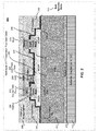
- FIG. 2 is a cross-sectional side view of another example GaN HFET with embodiments of the present invention shown in FIGS. 1A-1C after completion of the fabrication process.
- FIG. 3 is an example sequence of steps for formation of a passivation plus gate dielectric/insulation multilayer structure.
- a "wafer” is a thin slice of semiconductor material, such as a silicon, sapphire, silicon carbide, gallium nitride, etc., crystal, used in the fabrication of integrated circuits.
- a GaN-based transistor device and method of fabricating the same which includes an in situ processing step to form a passivation plus gate dielectric (e.g., oxide) multilayer for an HFET.
- a new material combination based on aluminum nitride (AlN) and aluminum oxy-nitride (AlON) is advantageously utilized in a fabrication process flow that mitigates charge build-up during passivation.
- AlN aluminum nitride
- AlON aluminum oxy-nitride
- a high quality gate oxy-nitride layer is produced for use in a high power GaN-based HEMT.
- an Atomic Layer Deposition (ALD) reaction chamber technique is utilized to form a high-quality, thin layer of nitride compound (e.g., AlN) over active transistor device layers, immediately followed by a gate oxide deposition comprising an oxy-nitride (e.g., AlON) material layer.
- nitride compound e.g., AlN
- gate oxide deposition comprising an oxy-nitride (e.g., AlON) material layer.
- FIGS. 1A-1C illustrate cross-sectional side views of a semiconductor device structure (e.g., a GaN HFET device) at various stages in an example fabrication process.
- a semiconductor device structure e.g., a GaN HFET device
- FIG. 1A shows a bulk epitaxial wafer 102 which includes a substrate 115 formed of any one of a number of different materials, e.g., Sapphire, Si, GaN, or SiC.
- An epitaxial GaN buffer layer 120 is shown formed as the first active layer on substrate 115.
- an optional thin nucleation layer may be formed between substrate 115 and buffer layer 120 (see e.g., layer 215 in FIG. 2 ).
- FIG. 1A further shows an Aluminum Gallium Nitride (AlGaN) layer 120 formed atop GaN buffer layer 120.
- AlGaN layer 120 comprises a second active layer of the GaN HFET device.
- a two dimensional electron gas channel (2-DEG) 130 is formed at the interface between AlGaN layer 120 and GaN buffer layer 120 due to the band-gap difference between the two material layers.
- FIG. 1A also illustrates the device structure at a point in the fabrication process just after formation of ohmic metal contacts 180 and 170, which respectively comprise source and drain electrodes of the GaN HFET device.
- FIG. 1A shows ohmic metal contacts 180 and 170 formed directly on AlGaN layer 120.
- ohmic metal contacts 180 and 170 may be formed in recesses that extend vertically downward through AlGaN layer 125 to contact GaN buffer layer 120.
- FIG. 1B illustrates the example GaN HFET device structure of FIG 1A after formation of a multi-layer structure 140 which comprises a passivation plus gate dielectric structure.
- multi-layer structure 140 comprises an AlN layer 142 disposed directly on AlGaN layer 142, and an AlON layer 145 disposed directly on AlN layer 140.
- passivation layer 142 may comprise SiN or other similar nitride-based materials.
- Gate dielectric layer 145 may also comprise silicon oxy-nitride (SiON) or another oxy-nitride material having similar properties.
- FIG 1B also shows an optional thin (e.g., 2-4 nm) second passivation layer 148 disposed directly on AlON layer 145.
- second passivation layer 148 comprises silicon nitride (SiN). It is appreciated that second passivation layer 148 may not be needed in certain embodiments.
- multilayer structure 140 functions both as a first or initial passivation layer to prevent surface oxidation/contamination of the underlying AlGaN (active) layer 125, and also a gate dielectric (insulator) for the completed GaN HFET device.
- AlN passivation layer 140 helps with the efficient modulation of charge, reduces leakage current, and increases the off-state voltage withstand of the completed GaN HFET device.
- multilayer structure 140 is formed in situ in an ALD reaction chamber with AlN layer 140 being formed with a thickness in a range of about 2-10 nm, and AlON layer 145 being formed with a thickness in a range of about 10-25 nm thick.
- AlON layer 145 may either be graded to allow for a smooth, gradual transition from the nitride to oxy-nitride layers (films). That is, the nitrogen composition in AlON layer 145 may vary from a highest atomic percentage (e.g., at or near 100%) at the interface with AlN layer 140 to a lowest percentage (e.g., a few atomic percent) at or near the top surface of AlON layer 145.
- FIG. 1C illustrates the device structure of FIG. 1B after formation of a gate member160, gate field plate 165, and Plasma Enhanced Chemical Vapor Deposition (PECVD) second passivation layer 170, the latter of which, in the example shown, comprises SiN.
- PECVD Plasma Enhanced Chemical Vapor Deposition
- FIG. 1C illustrates a completely fabricated GaN HFET device. It is further appreciated that other standard post-fabrication or back-end processing steps may be performed, including forming metal (e.g., patterned lines or traces) on the surface of the wafer, wafer backgrinding (also called backlapping or wafer thinning), die separation, and packaging.
- metal e.g., patterned lines or traces
- FIG. 2 is a cross-sectional side view of another completely fabricated GaN HFET device 200 that includes multilayer structure 240 comprising a combined first passivation and gate dielectric as described above.
- GaN HFET device 200 includes a nucleation (transitional) layer 215 disposed atop a substrate 210.
- Substrate 210 may comprise, without limitation, materials such as sapphire, silicon, gallium nitride, or silicon carbide (SiC).
- nucleation layer 215 comprises an aluminum rich layer of AlGaN (Al x Ga (x-1) N; 0>x>1).
- Substrate 210, nucleation layer 215, and GaN buffer layer 220 collectively comprise bulk epitaxial wafer 202.
- GaN HFET device 200 a GaN buffer layer 220 is disposed atop nucleation layer 215, and an AlGaN (or more generally, Al x Ga (x-1) N; 0>x>1) layer 225 is disposed atop GaN buffer layer 220.
- GaN HFET device 200 further includes a multi-layer (e. g., passivation plus gate dielectric) structure 235, second passivation layer 240, third passivation layer 245, and polyimide encapsulation layer 290.
- Source and drain ohmic metal contacts 280 and 270 are respectively formed directly on (or alternatively in recesses of) AlGaN layer 225.
- a gate member 260 is disposed atop of multi-layer structure 240.
- GaN HFET device 200 is also shown including a gate field plate 265 and a source field plate 285.
- FIG. 3 is an example sequence of steps for formation of a first passivation plus gate dielectric multilayer structure.
- the multi-layer structure formation process begins with the immediate loading of the wafer into an ALD reaction chamber (block 301). Extended exposure to ambient atmosphere should be minimized to prevent oxidation of the top surface (i.e., active layer) of the wafer, which could result in the formation of an unwanted Ga 2 O 3 layer.
- the wafer after the wafer has been loaded into chamber, it remains under vacuum for about 3 minutes, with the temperature being stabilized at around 300 C.
- the top surface of the wafer e.g., AlGaN layer 125 in FIG. 1
- a nitrogen (N 2 ) plasma strike typically performed at low power (block 302). This plasma exposure acts as a cleaning step to prepare the surface of the wafer material for the subsequent ALD deposition steps.
- the first (e.g., AlN) passivation layer is formed in repetitive cycles of a sequence of steps (block 303).
- the typical time duration of each cycle may take anywhere from about 20 ms to about 20 seconds, which results in the formation of a layer (film) of between 0.1 ⁇ - 3.0 ⁇ thick.
- the sequence begins with exposure of the wafer to an aluminum source, e.g., tri-methyl aluminum (TMA), for about 30 milliseconds. This allows aluminum to react with the top surface (e.g., AlGaN) of the wafer. Following exposure to the aluminum source, the chamber and lines are purged of aluminum by an argon gas flush for approximately 2 seconds.
- TMA tri-methyl aluminum
- a nitrogen plasma strike is performed for about 15 seconds. This step provides a source of nitrogen to react with the aluminum previously deposited on the surface of wafer. In other words, a surface reaction occurs resulting in the formation of an AlN passivation layer.
- a SiN passivation layer may also be formed using silicon as a source rather than aluminum.
- the chamber and lines are again purged (e.g., Argon gas for about 3 seconds), after which time the cycle may be repeated to achieve the desired material layer thickness.
- the thickness of the AlN passivation layer is in an approximate range of 2-10 nm thick.
- a second sequence of repetitive cycles is then performed to form a gate dielectric (e.g., oxide) layer atop the first AlN passivation layer (block 304).
- a gate dielectric e.g., oxide
- the wafer is not removed from the ALD reaction chamber after any of the preceding steps. That is, the formation of the passivation plus gate dielectric multilayer structure is accomplished in situ, i.e., with the wafer in the ALD reaction chamber for the entirety of the processing steps required for formation of the multi-layer structure.
- the second sequence begins with exposure to an aluminum source (TMA) with a specific dose which results in the reaction of aluminum on the AlN surface.
- TMA aluminum source
- the ALD reaction chamber and lines are then purged by an Argon gas flush for about 2 seconds.
- a nitrogen-oxygen plasma strike is performed for about 15 seconds to provide a dual source of nitrogen and oxygen to react with the aluminum previously deposited on the surface of wafer.
- This step results in the formation of an atomic smooth layer of AlON atop the underlying AlN passivation layer.
- a second purge of the chamber and lines is performed again using Argon gas for about 3 seconds to flush out any excess of nitrogen and oxygen.
- the above sequence of steps may be repeated as necessary to produce the desired layer (film) thickness.
- an AlON gate dielectric layer is formed to a thickness of about 10-25 nm.
- an optional SiN layer (e.g., 2-4 nm thick) may be formed atop the AlON layer while the wafer remains in the ALD reaction chamber.
- the wafer is then removed from the ALD reaction chamber (block 305) and then subjected to the remaining processing steps necessary to completely fabricate the GaN HFET device. It is appreciated that the total processing time in the ALD reaction chamber is a function of the desired total thicknesses of the passivation and gate dielectric layers which form the multi-layer structure.
Landscapes
- Junction Field-Effect Transistors (AREA)
- Engineering & Computer Science (AREA)
- Physics & Mathematics (AREA)
- Plasma & Fusion (AREA)
- Formation Of Insulating Films (AREA)
- Insulated Gate Type Field-Effect Transistor (AREA)
- Chemical & Material Sciences (AREA)
- Ceramic Engineering (AREA)
- Thin Film Transistor (AREA)
Applications Claiming Priority (1)
| Application Number | Priority Date | Filing Date | Title |
|---|---|---|---|
| US13/373,811 US8633094B2 (en) | 2011-12-01 | 2011-12-01 | GaN high voltage HFET with passivation plus gate dielectric multilayer structure |
Publications (2)
| Publication Number | Publication Date |
|---|---|
| EP2600404A2 true EP2600404A2 (de) | 2013-06-05 |
| EP2600404A3 EP2600404A3 (de) | 2014-07-23 |
Family
ID=47632686
Family Applications (1)
| Application Number | Title | Priority Date | Filing Date |
|---|---|---|---|
| EP12193415.2A Withdrawn EP2600404A3 (de) | 2011-12-01 | 2012-11-20 | GaN Hochspannungs-HFET mit Passivierungs- und Gatedielektrikums-Mehrschichtstruktur |
Country Status (5)
| Country | Link |
|---|---|
| US (2) | US8633094B2 (de) |
| EP (1) | EP2600404A3 (de) |
| JP (1) | JP2013118377A (de) |
| CN (1) | CN103137476B (de) |
| TW (1) | TWI500149B (de) |
Cited By (3)
| Publication number | Priority date | Publication date | Assignee | Title |
|---|---|---|---|---|
| EP3480854A3 (de) * | 2017-10-12 | 2019-08-14 | Power Integrations, Inc. | Gatestapel für bauelement mit heterostruktur |
| WO2021025688A1 (en) * | 2019-08-06 | 2021-02-11 | Iqe Plc | Dielectric passivation for layered iii-nitride structures |
| US11133408B2 (en) | 2019-08-06 | 2021-09-28 | Iqe Plc | Dielectric passivation for layered structures |
Families Citing this family (48)
| Publication number | Priority date | Publication date | Assignee | Title |
|---|---|---|---|---|
| WO2012143742A1 (en) * | 2011-04-21 | 2012-10-26 | Aristotle University Of Thessaloniki-Research Committee | Method for in-line determination of film thickness and quality during printing processes for the production of organic electronics |
| US8633094B2 (en) | 2011-12-01 | 2014-01-21 | Power Integrations, Inc. | GaN high voltage HFET with passivation plus gate dielectric multilayer structure |
| US10002957B2 (en) * | 2011-12-21 | 2018-06-19 | Power Integrations, Inc. | Shield wrap for a heterostructure field effect transistor |
| JP6090764B2 (ja) * | 2012-05-24 | 2017-03-08 | ローム株式会社 | 窒化物半導体装置およびその製造方法 |
| US9443941B2 (en) * | 2012-06-04 | 2016-09-13 | Infineon Technologies Austria Ag | Compound semiconductor transistor with self aligned gate |
| US8928037B2 (en) | 2013-02-28 | 2015-01-06 | Power Integrations, Inc. | Heterostructure power transistor with AlSiN passivation layer |
| US9443737B2 (en) * | 2013-04-03 | 2016-09-13 | Texas Instruments Incorporated | Method of forming metal contacts in the barrier layer of a group III-N HEMT |
| US8916427B2 (en) * | 2013-05-03 | 2014-12-23 | Texas Instruments Incorporated | FET dielectric reliability enhancement |
| JPWO2015008430A1 (ja) * | 2013-07-16 | 2017-03-02 | パナソニックIpマネジメント株式会社 | 半導体装置 |
| JP6253927B2 (ja) * | 2013-09-10 | 2017-12-27 | トランスフォーム・ジャパン株式会社 | 半導体装置 |
| CN103500763B (zh) * | 2013-10-15 | 2017-03-15 | 苏州晶湛半导体有限公司 | Ⅲ族氮化物半导体器件及其制造方法 |
| US9793370B2 (en) | 2014-05-30 | 2017-10-17 | Delta Electronics, Inc. | Transistor with oxidized cap layer |
| US9640620B2 (en) | 2014-11-03 | 2017-05-02 | Texas Instruments Incorporated | High power transistor with oxide gate barriers |
| CN104409494B (zh) * | 2014-11-18 | 2017-04-19 | 西安电子科技大学 | 基于直角源场板和直角漏场板的复合场板功率器件 |
| CN104409480B (zh) * | 2014-11-18 | 2017-05-10 | 西安电子科技大学 | 绝缘栅型直角源场板高电子迁移率器件及其制作方法 |
| CN104393030B (zh) * | 2014-11-18 | 2017-04-19 | 西安电子科技大学 | 绝缘栅型直角复合源场板功率晶体管 |
| CN104393042B (zh) * | 2014-11-18 | 2017-04-19 | 西安电子科技大学 | T形漏场板异质结功率器件及其制作方法 |
| CN104409495B (zh) * | 2014-11-18 | 2017-03-29 | 西安电子科技大学 | 直角栅场板异质结场效应晶体管及其制作方法 |
| US9799509B2 (en) * | 2014-11-26 | 2017-10-24 | Asm Ip Holding B.V. | Cyclic aluminum oxynitride deposition |
| US9837281B2 (en) * | 2014-11-26 | 2017-12-05 | Asm Ip Holding B.V. | Cyclic doped aluminum nitride deposition |
| US10745808B2 (en) * | 2015-07-24 | 2020-08-18 | Versum Materials Us, Llc | Methods for depositing Group 13 metal or metalloid nitride films |
| JP6784010B2 (ja) * | 2015-08-28 | 2020-11-11 | 富士電機株式会社 | 窒化物半導体装置の製造方法 |
| US9941384B2 (en) * | 2015-08-29 | 2018-04-10 | Taiwan Semiconductor Manufacturing Co., Ltd. | Semiconductor device and method for fabricating the same |
| CN105405878B (zh) * | 2015-11-27 | 2018-11-16 | 西安电子科技大学 | 多沟道侧栅结构的绝缘栅AlGaN/GaN高电子迁移率晶体管 |
| CN105448962B (zh) * | 2015-11-27 | 2019-01-08 | 西安电子科技大学 | 多沟道侧栅结构的AlGaN/GaN高电子迁移率晶体管 |
| US9490335B1 (en) | 2015-12-30 | 2016-11-08 | International Business Machines Corporation | Extra gate device for nanosheet |
| US20180076310A1 (en) * | 2016-08-23 | 2018-03-15 | David Sheridan | Asymmetrical blocking bidirectional gallium nitride switch |
| JP6594272B2 (ja) * | 2016-09-02 | 2019-10-23 | 株式会社東芝 | 半導体装置及びその製造方法 |
| CN106373884B (zh) * | 2016-09-08 | 2019-12-24 | 西安电子科技大学 | 复合栅介质GaN基绝缘栅高电子迁移率晶体管的制作方法 |
| TWI736600B (zh) | 2017-03-31 | 2021-08-21 | 聯穎光電股份有限公司 | 高電子遷移率電晶體 |
| TWI722166B (zh) * | 2017-04-10 | 2021-03-21 | 聯穎光電股份有限公司 | 高電子遷移率電晶體 |
| US11133190B2 (en) * | 2017-05-05 | 2021-09-28 | Lawrence Livermore National Security, Llc | Metal-based passivation-assisted plasma etching of III-v semiconductors |
| JP7203727B2 (ja) * | 2017-07-07 | 2023-01-13 | パナソニックホールディングス株式会社 | 半導体装置 |
| CN107425051B (zh) * | 2017-07-19 | 2020-10-02 | 苏州能讯高能半导体有限公司 | 一种半导体器件及其制备方法 |
| US10680090B2 (en) * | 2017-07-20 | 2020-06-09 | Delta Electronics, Inc. | Enclosed gate runner for eliminating miller turn-on |
| CN111834435B (zh) | 2019-04-15 | 2025-03-25 | 联华电子股份有限公司 | 高电子迁移率晶体管 |
| US11127847B2 (en) * | 2019-05-16 | 2021-09-21 | Vanguard International Semiconductor Corporation | Semiconductor devices having a gate field plate including an extension portion and methods for fabricating the semiconductor device |
| TWI851591B (zh) * | 2019-08-06 | 2024-08-11 | 英商Iqe有限公司 | 分層結構的介電鈍化 |
| JP6793887B1 (ja) * | 2020-01-10 | 2020-12-02 | 三菱電機株式会社 | 半導体装置およびその製造方法 |
| FR3112422B1 (fr) * | 2020-07-09 | 2022-08-12 | Commissariat Energie Atomique | Procédé de réalisation d’une couche diélectrique sur une structure en matériaux III-V |
| CN113517354B (zh) * | 2021-04-29 | 2023-04-28 | 电子科技大学 | 一种高压jfet器件 |
| JP7369827B1 (ja) * | 2022-06-24 | 2023-10-26 | 日機装株式会社 | 半導体発光素子の製造方法 |
| WO2024108491A1 (en) * | 2022-11-24 | 2024-05-30 | Innoscience (suzhou) Semiconductor Co., Ltd. | Nitride-based semiconductor device and method for manufacturing the same |
| KR102790971B1 (ko) * | 2022-12-22 | 2025-04-02 | 경북대학교 산학협력단 | 고전자이동도 트랜지스터 및 고전자이동도 트랜지스터 제조 방법 |
| CN116246956A (zh) * | 2023-03-07 | 2023-06-09 | 复旦大学 | 用于氮化物半导体器件的钝化层制备方法及器件制备方法 |
| KR20260040066A (ko) * | 2023-07-19 | 2026-03-23 | 어플라이드 머티어리얼스, 인코포레이티드 | 통합된 플라즈마 세정 및 유전체 패시베이션 증착 프로세스들 |
| US20250118548A1 (en) * | 2023-10-06 | 2025-04-10 | Taiwan Semiconductor Manufacturing Company, Ltd. | Heat dissipation for field effect transistors |
| CN117790307A (zh) * | 2023-12-18 | 2024-03-29 | 湖北九峰山实验室 | 原位钝化的超宽禁带高电子迁移率晶体管及其制作方法 |
Citations (2)
| Publication number | Priority date | Publication date | Assignee | Title |
|---|---|---|---|---|
| US20090026556A1 (en) * | 2007-07-25 | 2009-01-29 | Rohm Co., Ltd. | Nitride semiconductor device and method for producing nitride semiconductor device |
| JP2009302435A (ja) * | 2008-06-17 | 2009-12-24 | Nippon Telegr & Teleph Corp <Ntt> | 半導体装置 |
Family Cites Families (147)
| Publication number | Priority date | Publication date | Assignee | Title |
|---|---|---|---|---|
| NL167277C (nl) | 1970-08-29 | 1981-11-16 | Philips Nv | Halfgeleiderinrichting met een plaatvorming half- geleiderlichaam met over althans een deel van de dikte van het halfgeleiderlichaam afgeschuinde randen, dat is voorzien van een metalen elektrode die een gelijkrichtende overgang vormt met het halfgeleider- lichaam en werkwijze ter vervaardiging van de halfgeleiderinrichting. |
| US4142195A (en) | 1976-03-22 | 1979-02-27 | Rca Corporation | Schottky barrier semiconductor device and method of making same |
| US4408216A (en) | 1978-06-02 | 1983-10-04 | International Rectifier Corporation | Schottky device and method of manufacture using palladium and platinum intermetallic alloys and titanium barrier for low reverse leakage over wide temperature range |
| NL184551C (nl) | 1978-07-24 | 1989-08-16 | Philips Nv | Veldeffekttransistor met geisoleerde stuurelektrode. |
| FR2517883A1 (fr) | 1981-12-09 | 1983-06-10 | Thomson Csf | Dispositif semi-conducteur a faible capacite parasite muni de connexions externes prises au moyen de poutres |
| US4543595A (en) | 1982-05-20 | 1985-09-24 | Fairchild Camera And Instrument Corporation | Bipolar memory cell |
| GB2137412B (en) | 1983-03-15 | 1987-03-04 | Standard Telephones Cables Ltd | Semiconductor device |
| US4967243A (en) | 1988-07-19 | 1990-10-30 | General Electric Company | Power transistor structure with high speed integral antiparallel Schottky diode |
| US4946547A (en) | 1989-10-13 | 1990-08-07 | Cree Research, Inc. | Method of preparing silicon carbide surfaces for crystal growth |
| US5200022A (en) | 1990-10-03 | 1993-04-06 | Cree Research, Inc. | Method of improving mechanically prepared substrate surfaces of alpha silicon carbide for deposition of beta silicon carbide thereon and resulting product |
| WO1992016966A1 (en) | 1991-03-18 | 1992-10-01 | Boston University | A method for the preparation and doping of highly insulating monocrystalline gallium nitride thin films |
| US5221413A (en) | 1991-04-24 | 1993-06-22 | At&T Bell Laboratories | Method for making low defect density semiconductor heterostructure and devices made thereby |
| US5602418A (en) | 1992-08-07 | 1997-02-11 | Asahi Kasei Kogyo Kabushiki Kaisha | Nitride based semiconductor device and manufacture thereof |
| DE69425186T3 (de) | 1993-04-28 | 2005-04-14 | Nichia Corp., Anan | Halbleitervorrichtung aus einer galliumnitridartigen III-V-Halbleiterverbindung und Verfahren zu ihrer Herstellung |
| JP3495814B2 (ja) | 1994-05-30 | 2004-02-09 | キヤノン株式会社 | 電池用電極及び該電極を有するリチウム二次電池 |
| EP0690517B1 (de) | 1994-05-30 | 2003-10-01 | Canon Kabushiki Kaisha | Wiederaufladbare Lithiumbatterie |
| US6078090A (en) | 1997-04-02 | 2000-06-20 | Siliconix Incorporated | Trench-gated Schottky diode with integral clamping diode |
| US5689128A (en) | 1995-08-21 | 1997-11-18 | Siliconix Incorporated | High density trenched DMOS transistor |
| US5874747A (en) | 1996-02-05 | 1999-02-23 | Advanced Technology Materials, Inc. | High brightness electroluminescent device emitting in the green to ultraviolet spectrum and method of making the same |
| JP3742144B2 (ja) | 1996-05-08 | 2006-02-01 | ソニー株式会社 | 非水電解液二次電池及び非水電解液二次電池用の平面状集電体 |
| US5612567A (en) | 1996-05-13 | 1997-03-18 | North Carolina State University | Schottky barrier rectifiers and methods of forming same |
| US5741724A (en) | 1996-12-27 | 1998-04-21 | Motorola | Method of growing gallium nitride on a spinel substrate |
| JP3491492B2 (ja) | 1997-04-09 | 2004-01-26 | 松下電器産業株式会社 | 窒化ガリウム結晶の製造方法 |
| US5785606A (en) | 1997-05-02 | 1998-07-28 | Marquez; Ruben L. | Method of playing multiple hand card game |
| US6239033B1 (en) | 1998-05-28 | 2001-05-29 | Sony Corporation | Manufacturing method of semiconductor device |
| DE19723176C1 (de) | 1997-06-03 | 1998-08-27 | Daimler Benz Ag | Leistungshalbleiter-Bauelement und Verfahren zu dessen Herstellung |
| WO1999001594A1 (en) | 1997-07-03 | 1999-01-14 | Cbl Technologies | Thermal mismatch compensation to produce free standing substrates by epitaxial deposition |
| JP3505357B2 (ja) | 1997-07-16 | 2004-03-08 | 株式会社東芝 | 窒化ガリウム系半導体素子およびその製造方法 |
| JP4453111B2 (ja) | 1997-10-27 | 2010-04-21 | 三菱化学株式会社 | 負極材料とその製造方法、負極活物質、および非水系二次電池 |
| JP3036495B2 (ja) | 1997-11-07 | 2000-04-24 | 豊田合成株式会社 | 窒化ガリウム系化合物半導体の製造方法 |
| US6608327B1 (en) | 1998-02-27 | 2003-08-19 | North Carolina State University | Gallium nitride semiconductor structure including laterally offset patterned layers |
| JP2948205B1 (ja) | 1998-05-25 | 1999-09-13 | 花王株式会社 | 二次電池用負極の製造方法 |
| JP4352473B2 (ja) | 1998-06-26 | 2009-10-28 | ソニー株式会社 | 半導体装置の製造方法 |
| JP2000150535A (ja) | 1998-11-09 | 2000-05-30 | Fujitsu Quantum Device Kk | 電界効果トランジスタとその製造方法 |
| US6331450B1 (en) | 1998-12-22 | 2001-12-18 | Toyoda Gosei Co., Ltd. | Method of manufacturing semiconductor device using group III nitride compound |
| US6252288B1 (en) | 1999-01-19 | 2001-06-26 | Rockwell Science Center, Llc | High power trench-based rectifier with improved reverse breakdown characteristic |
| US20010001494A1 (en) | 1999-04-01 | 2001-05-24 | Christopher B. Kocon | Power trench mos-gated device and process for forming same |
| US6389051B1 (en) | 1999-04-09 | 2002-05-14 | Xerox Corporation | Structure and method for asymmetric waveguide nitride laser diode |
| US6291298B1 (en) | 1999-05-25 | 2001-09-18 | Advanced Analogic Technologies, Inc. | Process of manufacturing Trench gate semiconductor device having gate oxide layer with multiple thicknesses |
| US7084456B2 (en) | 1999-05-25 | 2006-08-01 | Advanced Analogic Technologies, Inc. | Trench MOSFET with recessed clamping diode using graded doping |
| US6252258B1 (en) | 1999-08-10 | 2001-06-26 | Rockwell Science Center Llc | High power rectifier |
| US6211018B1 (en) | 1999-08-14 | 2001-04-03 | Electronics And Telecommunications Research Institute | Method for fabricating high density trench gate type power device |
| JP4412827B2 (ja) | 1999-08-20 | 2010-02-10 | シャープ株式会社 | 窒化物半導体厚膜基板 |
| JP2002083594A (ja) | 1999-10-22 | 2002-03-22 | Sanyo Electric Co Ltd | リチウム電池用電極並びにこれを用いたリチウム電池及びリチウム二次電池 |
| EP1231653B1 (de) | 1999-10-22 | 2010-12-08 | Sanyo Electric Co., Ltd. | Elektrode für lithiumzelle und lithiumsekundärzelle |
| CA2388016C (en) | 1999-10-22 | 2009-12-22 | Sanyo Electric Co., Ltd. | Method for fabricating electrode for rechargeable lithium battery |
| US6184570B1 (en) | 1999-10-28 | 2001-02-06 | Ericsson Inc. | Integrated circuit dies including thermal stress reducing grooves and microelectronic packages utilizing the same |
| US6380108B1 (en) | 1999-12-21 | 2002-04-30 | North Carolina State University | Pendeoepitaxial methods of fabricating gallium nitride semiconductor layers on weak posts, and gallium nitride semiconductor structures fabricated thereby |
| US6573537B1 (en) | 1999-12-22 | 2003-06-03 | Lumileds Lighting, U.S., Llc | Highly reflective ohmic contacts to III-nitride flip-chip LEDs |
| US6586781B2 (en) | 2000-02-04 | 2003-07-01 | Cree Lighting Company | Group III nitride based FETs and HEMTs with reduced trapping and method for producing the same |
| KR100348269B1 (ko) | 2000-03-22 | 2002-08-09 | 엘지전자 주식회사 | 루데니움 산화물을 이용한 쇼트키 콘택 방법 |
| JP2001357855A (ja) | 2000-06-14 | 2001-12-26 | Shin Kobe Electric Mach Co Ltd | 非水電解液二次電池 |
| US6344665B1 (en) | 2000-06-23 | 2002-02-05 | Arima Optoelectronics Corp. | Electrode structure of compound semiconductor device |
| JP4022708B2 (ja) | 2000-06-29 | 2007-12-19 | 日本電気株式会社 | 半導体装置 |
| US20020015833A1 (en) | 2000-06-29 | 2002-02-07 | Naotomi Takahashi | Manufacturing method of electrodeposited copper foil and electrodeposited copper foil |
| JP2003101036A (ja) | 2001-09-25 | 2003-04-04 | Sanyo Electric Co Ltd | ショットキーバリアダイオードおよびその製造方法 |
| JP2002064201A (ja) | 2000-08-18 | 2002-02-28 | Toshiba Corp | 半導体電界効果トランジスタ及び電力増幅器 |
| US6518079B2 (en) | 2000-12-20 | 2003-02-11 | Lumileds Lighting, U.S., Llc | Separation method for gallium nitride devices on lattice-mismatched substrates |
| JP2002305309A (ja) | 2001-02-01 | 2002-10-18 | Hitachi Ltd | 半導体装置およびその製造方法 |
| JP4073176B2 (ja) | 2001-04-02 | 2008-04-09 | 新電元工業株式会社 | 半導体装置およびその製造方法 |
| US6437374B1 (en) | 2001-05-07 | 2002-08-20 | Xerox Corporation | Semiconductor device and method of forming a semiconductor device |
| TW492202B (en) | 2001-06-05 | 2002-06-21 | South Epitaxy Corp | Structure of III-V light emitting diode (LED) arranged in flip chip configuration having structure for preventing electrostatic discharge |
| US20020197835A1 (en) * | 2001-06-06 | 2002-12-26 | Sey-Ping Sun | Anti-reflective coating and methods of making the same |
| US20030015708A1 (en) | 2001-07-23 | 2003-01-23 | Primit Parikh | Gallium nitride based diodes with low forward voltage and low reverse current operation |
| US6524900B2 (en) | 2001-07-25 | 2003-02-25 | Abb Research, Ltd | Method concerning a junction barrier Schottky diode, such a diode and use thereof |
| US20050179106A1 (en) | 2001-07-27 | 2005-08-18 | Sanyo Electric Company, Ltd. | Schottky barrier diode |
| JP4064085B2 (ja) | 2001-10-18 | 2008-03-19 | 三菱電機株式会社 | 半導体装置及びその製造方法 |
| US6768146B2 (en) | 2001-11-27 | 2004-07-27 | The Furukawa Electric Co., Ltd. | III-V nitride semiconductor device, and protection element and power conversion apparatus using the same |
| JP3871607B2 (ja) | 2001-12-14 | 2007-01-24 | 松下電器産業株式会社 | 半導体素子およびその製造方法 |
| US6515308B1 (en) | 2001-12-21 | 2003-02-04 | Xerox Corporation | Nitride-based VCSEL or light emitting diode with p-n tunnel junction current injection |
| US6855970B2 (en) | 2002-03-25 | 2005-02-15 | Kabushiki Kaisha Toshiba | High-breakdown-voltage semiconductor device |
| US6624444B1 (en) | 2002-03-28 | 2003-09-23 | Intel Corporation | Electrical-optical package with capacitor DC shunts and associated methods |
| DE10217235A1 (de) | 2002-04-18 | 2003-10-30 | Philips Intellectual Property | Schaltungsanordnung zur Erzeugung von Gleichspannungen |
| JP4221697B2 (ja) | 2002-06-17 | 2009-02-12 | 日本電気株式会社 | 半導体装置 |
| US7323402B2 (en) | 2002-07-11 | 2008-01-29 | International Rectifier Corporation | Trench Schottky barrier diode with differential oxide thickness |
| JP3790500B2 (ja) | 2002-07-16 | 2006-06-28 | ユーディナデバイス株式会社 | 電界効果トランジスタ及びその製造方法 |
| US20040021152A1 (en) | 2002-08-05 | 2004-02-05 | Chanh Nguyen | Ga/A1GaN Heterostructure Field Effect Transistor with dielectric recessed gate |
| JP2004087587A (ja) | 2002-08-23 | 2004-03-18 | Mitsubishi Electric Corp | 窒化物半導体装置およびその製造方法 |
| FR2844099B1 (fr) | 2002-09-03 | 2005-09-02 | Commissariat Energie Atomique | Dispositif semiconducteur de puissance quasi-vertical sur substrat composite |
| US7115896B2 (en) | 2002-12-04 | 2006-10-03 | Emcore Corporation | Semiconductor structures for gallium nitride-based devices |
| JP4748498B2 (ja) | 2002-12-05 | 2011-08-17 | 古河電気工業株式会社 | 電流遮断器付きGaN系半導体装置 |
| TWI240434B (en) | 2003-06-24 | 2005-09-21 | Osram Opto Semiconductors Gmbh | Method to produce semiconductor-chips |
| FR2857982B1 (fr) | 2003-07-24 | 2007-05-18 | Soitec Silicon On Insulator | Procede de fabrication d'une couche epitaxiee |
| WO2005015618A1 (ja) * | 2003-08-12 | 2005-02-17 | Nippon Telegraph And Telephone Corporation | 窒化物半導体成長用基板 |
| US7109551B2 (en) | 2003-08-29 | 2006-09-19 | Fuji Electric Holdings Co., Ltd. | Semiconductor device |
| US7026665B1 (en) | 2003-09-19 | 2006-04-11 | Rf Micro Devices, Inc. | High voltage GaN-based transistor structure |
| US7041579B2 (en) | 2003-10-22 | 2006-05-09 | Northrop Grumman Corporation | Hard substrate wafer sawing process |
| JP2005129696A (ja) | 2003-10-23 | 2005-05-19 | Matsushita Electric Ind Co Ltd | 半導体装置及びその製造方法 |
| JP4288592B2 (ja) | 2004-01-20 | 2009-07-01 | ソニー株式会社 | 電池 |
| JP4449467B2 (ja) | 2004-01-28 | 2010-04-14 | サンケン電気株式会社 | 半導体装置 |
| US7084475B2 (en) | 2004-02-17 | 2006-08-01 | Velox Semiconductor Corporation | Lateral conduction Schottky diode with plural mesas |
| US7253015B2 (en) | 2004-02-17 | 2007-08-07 | Velox Semiconductor Corporation | Low doped layer for nitride-based semiconductor device |
| JP4610207B2 (ja) | 2004-02-24 | 2011-01-12 | 三洋電機株式会社 | 半導体装置およびその製造方法 |
| US7229866B2 (en) | 2004-03-15 | 2007-06-12 | Velox Semiconductor Corporation | Non-activated guard ring for semiconductor devices |
| US7465592B2 (en) | 2004-04-28 | 2008-12-16 | Verticle, Inc. | Method of making vertical structure semiconductor devices including forming hard and soft copper layers |
| JP4398780B2 (ja) | 2004-04-30 | 2010-01-13 | 古河電気工業株式会社 | GaN系半導体装置 |
| US20050277292A1 (en) * | 2004-05-28 | 2005-12-15 | Chao-Hsien Peng | Method for fabricating low resistivity barrier for copper interconnect |
| US7417266B1 (en) | 2004-06-10 | 2008-08-26 | Qspeed Semiconductor Inc. | MOSFET having a JFET embedded as a body diode |
| US7238976B1 (en) | 2004-06-15 | 2007-07-03 | Qspeed Semiconductor Inc. | Schottky barrier rectifier and method of manufacturing the same |
| US7118970B2 (en) | 2004-06-22 | 2006-10-10 | Cree, Inc. | Methods of fabricating silicon carbide devices with hybrid well regions |
| US7547928B2 (en) | 2004-06-30 | 2009-06-16 | Interuniversitair Microelektronica Centrum (Imec) | AlGaN/GaN high electron mobility transistor devices |
| EP2273553B1 (de) | 2004-06-30 | 2020-02-12 | IMEC vzw | Verfahren zur Herstellung von AlGaN/GaN HEMT Anordnungen |
| JP2006100645A (ja) | 2004-09-30 | 2006-04-13 | Furukawa Electric Co Ltd:The | GaN系半導体集積回路 |
| KR100889362B1 (ko) | 2004-10-19 | 2009-03-18 | 삼성전자주식회사 | 다층 유전체막으로 이루어진 트랜지스터 및 그 제조 방법 |
| US7456443B2 (en) | 2004-11-23 | 2008-11-25 | Cree, Inc. | Transistors having buried n-type and p-type regions beneath the source region |
| JP4609048B2 (ja) | 2004-11-25 | 2011-01-12 | ソニー株式会社 | 二次電池用負極および二次電池 |
| US7116567B2 (en) | 2005-01-05 | 2006-10-03 | Velox Semiconductor Corporation | GaN semiconductor based voltage conversion device |
| US7436039B2 (en) | 2005-01-06 | 2008-10-14 | Velox Semiconductor Corporation | Gallium nitride semiconductor device |
| US20060151868A1 (en) | 2005-01-10 | 2006-07-13 | Zhu Tinggang | Package for gallium nitride semiconductor devices |
| US7429534B2 (en) | 2005-02-22 | 2008-09-30 | Sensor Electronic Technology, Inc. | Etching a nitride-based heterostructure |
| JP2006245317A (ja) | 2005-03-03 | 2006-09-14 | Fujitsu Ltd | 半導体装置およびその製造方法 |
| DE102005012217B4 (de) | 2005-03-15 | 2007-02-22 | Infineon Technologies Austria Ag | Lateraler MISFET und Verfahren zur Herstellung desselben |
| JP4912604B2 (ja) | 2005-03-30 | 2012-04-11 | 住友電工デバイス・イノベーション株式会社 | 窒化物半導体hemtおよびその製造方法。 |
| US7615774B2 (en) | 2005-04-29 | 2009-11-10 | Cree.Inc. | Aluminum free group III-nitride based high electron mobility transistors |
| US8482035B2 (en) | 2005-07-29 | 2013-07-09 | International Rectifier Corporation | Enhancement mode III-nitride transistors with single gate Dielectric structure |
| WO2008027027A2 (en) | 2005-09-07 | 2008-03-06 | Cree, Inc | Transistor with fluorine treatment |
| US8026568B2 (en) | 2005-11-15 | 2011-09-27 | Velox Semiconductor Corporation | Second Schottky contact metal layer to improve GaN Schottky diode performance |
| US7696598B2 (en) | 2005-12-27 | 2010-04-13 | Qspeed Semiconductor Inc. | Ultrafast recovery diode |
| JP5351519B2 (ja) | 2005-12-27 | 2013-11-27 | パワー・インテグレーションズ・インコーポレーテッド | 高速回復整流器構造体の装置および方法 |
| US7592211B2 (en) * | 2006-01-17 | 2009-09-22 | Cree, Inc. | Methods of fabricating transistors including supported gate electrodes |
| JP4705482B2 (ja) | 2006-01-27 | 2011-06-22 | パナソニック株式会社 | トランジスタ |
| US7964514B2 (en) * | 2006-03-02 | 2011-06-21 | Applied Materials, Inc. | Multiple nitrogen plasma treatments for thin SiON dielectrics |
| JP5231719B2 (ja) | 2006-03-30 | 2013-07-10 | 富士通株式会社 | 電界効果トランジスタの製造方法 |
| JP5032145B2 (ja) | 2006-04-14 | 2012-09-26 | 株式会社東芝 | 半導体装置 |
| US8399911B2 (en) | 2006-06-07 | 2013-03-19 | Imec | Enhancement mode field effect device and the method of production thereof |
| WO2008012877A1 (fr) * | 2006-07-26 | 2008-01-31 | Fujitsu Limited | DISPOSITIF À SEMI-CONDUCTEURS COMPOSÉ EMPLOYANT UN SUBSTRAT DE SiC ET PROCÉDÉ POUR PRODUIRE CELUI-CI |
| US7939853B2 (en) | 2007-03-20 | 2011-05-10 | Power Integrations, Inc. | Termination and contact structures for a high voltage GaN-based heterojunction transistor |
| WO2009012536A1 (en) | 2007-07-20 | 2009-01-29 | Interuniversitair Microelektronica Centrum | Damascene contacts on iii-v cmos devices |
| US20090278233A1 (en) | 2007-07-26 | 2009-11-12 | Pinnington Thomas Henry | Bonded intermediate substrate and method of making same |
| JP4584293B2 (ja) | 2007-08-31 | 2010-11-17 | 富士通株式会社 | 窒化物半導体装置、ドハティ増幅器、ドレイン電圧制御増幅器 |
| CN100594591C (zh) * | 2007-10-17 | 2010-03-17 | 中国科学院微电子研究所 | 一种提高氮化镓基场效应晶体管性能的方法 |
| CN101459080B (zh) * | 2007-12-12 | 2010-04-14 | 中国科学院微电子研究所 | 一种制作氮化镓基场效应晶体管的方法 |
| FR2926672B1 (fr) | 2008-01-21 | 2010-03-26 | Soitec Silicon On Insulator | Procede de fabrication de couches de materiau epitaxie |
| US8309987B2 (en) | 2008-07-15 | 2012-11-13 | Imec | Enhancement mode semiconductor device |
| US7985986B2 (en) * | 2008-07-31 | 2011-07-26 | Cree, Inc. | Normally-off semiconductor devices |
| EP2324488B1 (de) | 2008-08-27 | 2013-02-13 | Soitec | Verfahren zum herstellen von halbleiterstrukturen oder bauelementen unter verwendung von schichten aus halbleitermaterial mit gewählten oder kontrollierten gitterparametern |
| US8168486B2 (en) | 2009-06-24 | 2012-05-01 | Intersil Americas Inc. | Methods for manufacturing enhancement-mode HEMTs with self-aligned field plate |
| WO2010151721A1 (en) | 2009-06-25 | 2010-12-29 | The Government Of The United States Of America, As Represented By The Secretary Of The Navy | Transistor with enhanced channel charge inducing material layer and threshold voltage control |
| WO2010151856A2 (en) | 2009-06-26 | 2010-12-29 | Cornell University | Chemical vapor deposition process for aluminum silicon nitride |
| WO2010151857A2 (en) | 2009-06-26 | 2010-12-29 | Cornell University | Method for forming iii-v semiconductor structures including aluminum-silicon nitride passivation |
| EP2317542B1 (de) | 2009-10-30 | 2018-05-23 | IMEC vzw | Halbleiterbauelement und Herstellungsverfahren dafür |
| JP5635803B2 (ja) * | 2010-05-07 | 2014-12-03 | トランスフォーム・ジャパン株式会社 | 化合物半導体装置の製造方法及び化合物半導体装置 |
| US9070758B2 (en) | 2011-06-20 | 2015-06-30 | Imec | CMOS compatible method for manufacturing a HEMT device and the HEMT device thereof |
| US8633094B2 (en) | 2011-12-01 | 2014-01-21 | Power Integrations, Inc. | GaN high voltage HFET with passivation plus gate dielectric multilayer structure |
| US8940620B2 (en) | 2011-12-15 | 2015-01-27 | Power Integrations, Inc. | Composite wafer for fabrication of semiconductor devices |
| US20140077266A1 (en) | 2012-09-14 | 2014-03-20 | Power Integrations, Inc. | Heterostructure Transistor with Multiple Gate Dielectric Layers |
| US8928037B2 (en) | 2013-02-28 | 2015-01-06 | Power Integrations, Inc. | Heterostructure power transistor with AlSiN passivation layer |
-
2011
- 2011-12-01 US US13/373,811 patent/US8633094B2/en not_active Expired - Fee Related
-
2012
- 2012-11-20 EP EP12193415.2A patent/EP2600404A3/de not_active Withdrawn
- 2012-11-28 CN CN201210494905.XA patent/CN103137476B/zh active Active
- 2012-11-30 TW TW101144897A patent/TWI500149B/zh active
- 2012-11-30 JP JP2012262399A patent/JP2013118377A/ja active Pending
-
2014
- 2014-01-14 US US14/154,355 patent/US9343541B2/en active Active
Patent Citations (2)
| Publication number | Priority date | Publication date | Assignee | Title |
|---|---|---|---|---|
| US20090026556A1 (en) * | 2007-07-25 | 2009-01-29 | Rohm Co., Ltd. | Nitride semiconductor device and method for producing nitride semiconductor device |
| JP2009302435A (ja) * | 2008-06-17 | 2009-12-24 | Nippon Telegr & Teleph Corp <Ntt> | 半導体装置 |
Cited By (4)
| Publication number | Priority date | Publication date | Assignee | Title |
|---|---|---|---|---|
| EP3480854A3 (de) * | 2017-10-12 | 2019-08-14 | Power Integrations, Inc. | Gatestapel für bauelement mit heterostruktur |
| US11114539B2 (en) | 2017-10-12 | 2021-09-07 | Power Integrations, Inc. | Gate stack for heterostructure device |
| WO2021025688A1 (en) * | 2019-08-06 | 2021-02-11 | Iqe Plc | Dielectric passivation for layered iii-nitride structures |
| US11133408B2 (en) | 2019-08-06 | 2021-09-28 | Iqe Plc | Dielectric passivation for layered structures |
Also Published As
| Publication number | Publication date |
|---|---|
| US20140124789A1 (en) | 2014-05-08 |
| US9343541B2 (en) | 2016-05-17 |
| US20130140605A1 (en) | 2013-06-06 |
| TWI500149B (zh) | 2015-09-11 |
| CN103137476B (zh) | 2016-05-25 |
| EP2600404A3 (de) | 2014-07-23 |
| JP2013118377A (ja) | 2013-06-13 |
| CN103137476A (zh) | 2013-06-05 |
| TW201342592A (zh) | 2013-10-16 |
| US8633094B2 (en) | 2014-01-21 |
Similar Documents
| Publication | Publication Date | Title |
|---|---|---|
| US8633094B2 (en) | GaN high voltage HFET with passivation plus gate dielectric multilayer structure | |
| US10446676B2 (en) | Heterostructure power transistor with AlSiN passivation layer | |
| US7960756B2 (en) | Transistors including supported gate electrodes | |
| CN100468770C (zh) | 具有保护层和低损凹槽的氮化物基晶体管及其制造方法 | |
| KR101763029B1 (ko) | Ⅲ-ⅴ계 디바이스를 위한 저손상 패시배이션층 | |
| US8247796B2 (en) | Semiconductor device | |
| CN102881720B (zh) | 半导体结构及其形成方法 | |
| CN103177960B (zh) | 对硅衬底上的iii族氮化物的衬底击穿电压的改进 | |
| JP4897948B2 (ja) | 半導体素子 | |
| CN113875017B (zh) | 半导体装置及其制造方法 | |
| WO2022205469A1 (en) | Iii nitride semiconductor wafers | |
| US11222968B2 (en) | HEMT device structure and manufacturing method thereof | |
| WO2023240491A1 (en) | Nitride-based semiconductor device and method for manufacturing the same | |
| WO2024040465A1 (en) | Nitride-based semiconductor device and method for manufacturing the same | |
| WO2024026816A1 (en) | Nitride-based semiconductor device and method for manufacturing the same | |
| EP4573602A2 (de) | Transistoren mit hoher elektronenmobilität mit verbesserten passivierungsstrukturen und reduzierter drain-strom-drift sowie verfahren zur herstellung solcher vorrichtungen |
Legal Events
| Date | Code | Title | Description |
|---|---|---|---|
| PUAI | Public reference made under article 153(3) epc to a published international application that has entered the european phase |
Free format text: ORIGINAL CODE: 0009012 |
|
| 17P | Request for examination filed |
Effective date: 20121120 |
|
| AK | Designated contracting states |
Kind code of ref document: A2 Designated state(s): AL AT BE BG CH CY CZ DE DK EE ES FI FR GB GR HR HU IE IS IT LI LT LU LV MC MK MT NL NO PL PT RO RS SE SI SK SM TR |
|
| AX | Request for extension of the european patent |
Extension state: BA ME |
|
| PUAL | Search report despatched |
Free format text: ORIGINAL CODE: 0009013 |
|
| AK | Designated contracting states |
Kind code of ref document: A3 Designated state(s): AL AT BE BG CH CY CZ DE DK EE ES FI FR GB GR HR HU IE IS IT LI LT LU LV MC MK MT NL NO PL PT RO RS SE SI SK SM TR |
|
| AX | Request for extension of the european patent |
Extension state: BA ME |
|
| RIC1 | Information provided on ipc code assigned before grant |
Ipc: H01L 21/28 20060101ALI20140618BHEP Ipc: H01L 21/336 20060101ALI20140618BHEP Ipc: H01L 29/423 20060101ALN20140618BHEP Ipc: H01L 23/29 20060101ALI20140618BHEP Ipc: H01L 29/51 20060101ALI20140618BHEP Ipc: H01L 29/20 20060101ALN20140618BHEP Ipc: H01L 23/31 20060101ALN20140618BHEP Ipc: H01L 29/778 20060101AFI20140618BHEP |
|
| 17Q | First examination report despatched |
Effective date: 20140707 |
|
| STAA | Information on the status of an ep patent application or granted ep patent |
Free format text: STATUS: THE APPLICATION IS DEEMED TO BE WITHDRAWN |
|
| 18D | Application deemed to be withdrawn |
Effective date: 20151027 |