EP2427893B1 - Magnetic components - Google Patents
Magnetic components Download PDFInfo
- Publication number
- EP2427893B1 EP2427893B1 EP10716225A EP10716225A EP2427893B1 EP 2427893 B1 EP2427893 B1 EP 2427893B1 EP 10716225 A EP10716225 A EP 10716225A EP 10716225 A EP10716225 A EP 10716225A EP 2427893 B1 EP2427893 B1 EP 2427893B1
- Authority
- EP
- European Patent Office
- Prior art keywords
- magnetic
- coil
- layers
- fabricated
- component assembly
- Prior art date
- Legal status (The legal status is an assumption and is not a legal conclusion. Google has not performed a legal analysis and makes no representation as to the accuracy of the status listed.)
- Not-in-force
Links
- 230000005291 magnetic effect Effects 0.000 title claims description 187
- 239000000463 material Substances 0.000 claims description 57
- 239000002245 particle Substances 0.000 claims description 29
- 238000004804 winding Methods 0.000 claims description 23
- 239000004020 conductor Substances 0.000 claims description 21
- 239000011230 binding agent Substances 0.000 claims description 13
- 239000006247 magnetic powder Substances 0.000 claims description 13
- 230000035699 permeability Effects 0.000 claims description 11
- 239000000203 mixture Substances 0.000 claims description 7
- 229920005992 thermoplastic resin Polymers 0.000 claims description 4
- WYTGDNHDOZPMIW-RCBQFDQVSA-N alstonine Natural products C1=CC2=C3C=CC=CC3=NC2=C2N1C[C@H]1[C@H](C)OC=C(C(=O)OC)[C@H]1C2 WYTGDNHDOZPMIW-RCBQFDQVSA-N 0.000 claims description 3
- 238000004519 manufacturing process Methods 0.000 description 30
- 239000000696 magnetic material Substances 0.000 description 28
- 238000000034 method Methods 0.000 description 26
- 230000004907 flux Effects 0.000 description 13
- 239000006249 magnetic particle Substances 0.000 description 11
- 239000000843 powder Substances 0.000 description 10
- 230000000712 assembly Effects 0.000 description 9
- 238000000429 assembly Methods 0.000 description 9
- 239000007767 bonding agent Substances 0.000 description 9
- XEEYBQQBJWHFJM-UHFFFAOYSA-N Iron Chemical compound [Fe] XEEYBQQBJWHFJM-UHFFFAOYSA-N 0.000 description 8
- 230000008901 benefit Effects 0.000 description 6
- 238000010276 construction Methods 0.000 description 6
- 230000008569 process Effects 0.000 description 6
- 238000009413 insulation Methods 0.000 description 5
- 238000003475 lamination Methods 0.000 description 5
- 239000002184 metal Substances 0.000 description 5
- 229910052751 metal Inorganic materials 0.000 description 5
- 229910017082 Fe-Si Inorganic materials 0.000 description 4
- 229910017133 Fe—Si Inorganic materials 0.000 description 4
- 238000000748 compression moulding Methods 0.000 description 4
- 229910000859 α-Fe Inorganic materials 0.000 description 4
- 238000009472 formulation Methods 0.000 description 3
- 230000009467 reduction Effects 0.000 description 3
- 238000005476 soldering Methods 0.000 description 3
- RYGMFSIKBFXOCR-UHFFFAOYSA-N Copper Chemical compound [Cu] RYGMFSIKBFXOCR-UHFFFAOYSA-N 0.000 description 2
- 229910003271 Ni-Fe Inorganic materials 0.000 description 2
- 239000000853 adhesive Substances 0.000 description 2
- 230000001070 adhesive effect Effects 0.000 description 2
- 229910045601 alloy Inorganic materials 0.000 description 2
- 239000000956 alloy Substances 0.000 description 2
- 239000011248 coating agent Substances 0.000 description 2
- 238000000576 coating method Methods 0.000 description 2
- 239000010941 cobalt Substances 0.000 description 2
- 229910017052 cobalt Inorganic materials 0.000 description 2
- GUTLYIVDDKVIGB-UHFFFAOYSA-N cobalt atom Chemical compound [Co] GUTLYIVDDKVIGB-UHFFFAOYSA-N 0.000 description 2
- 230000000295 complement effect Effects 0.000 description 2
- 239000002131 composite material Substances 0.000 description 2
- 229910052802 copper Inorganic materials 0.000 description 2
- 239000010949 copper Substances 0.000 description 2
- 238000007598 dipping method Methods 0.000 description 2
- 230000000694 effects Effects 0.000 description 2
- 229910052742 iron Inorganic materials 0.000 description 2
- 230000005415 magnetization Effects 0.000 description 2
- 229920005596 polymer binder Polymers 0.000 description 2
- 239000002491 polymer binding agent Substances 0.000 description 2
- 238000009824 pressure lamination Methods 0.000 description 2
- 229910000702 sendust Inorganic materials 0.000 description 2
- 239000011856 silicon-based particle Substances 0.000 description 2
- 229910002555 FeNi Inorganic materials 0.000 description 1
- 238000010923 batch production Methods 0.000 description 1
- 230000015572 biosynthetic process Effects 0.000 description 1
- 230000002860 competitive effect Effects 0.000 description 1
- 230000008878 coupling Effects 0.000 description 1
- 238000010168 coupling process Methods 0.000 description 1
- 238000005859 coupling reaction Methods 0.000 description 1
- 238000005336 cracking Methods 0.000 description 1
- 230000003247 decreasing effect Effects 0.000 description 1
- 238000004100 electronic packaging Methods 0.000 description 1
- 238000010438 heat treatment Methods 0.000 description 1
- 239000011810 insulating material Substances 0.000 description 1
- 239000002648 laminated material Substances 0.000 description 1
- 239000002923 metal particle Substances 0.000 description 1
- 239000005300 metallic glass Substances 0.000 description 1
- 230000036961 partial effect Effects 0.000 description 1
- 229910000889 permalloy Inorganic materials 0.000 description 1
- 239000012254 powdered material Substances 0.000 description 1
- 238000007639 printing Methods 0.000 description 1
- 238000000926 separation method Methods 0.000 description 1
- 239000000758 substrate Substances 0.000 description 1
- 238000003466 welding Methods 0.000 description 1
Images


Classifications
-
- H—ELECTRICITY
- H01—ELECTRIC ELEMENTS
- H01F—MAGNETS; INDUCTANCES; TRANSFORMERS; SELECTION OF MATERIALS FOR THEIR MAGNETIC PROPERTIES
- H01F41/00—Apparatus or processes specially adapted for manufacturing or assembling magnets, inductances or transformers; Apparatus or processes specially adapted for manufacturing materials characterised by their magnetic properties
- H01F41/02—Apparatus or processes specially adapted for manufacturing or assembling magnets, inductances or transformers; Apparatus or processes specially adapted for manufacturing materials characterised by their magnetic properties for manufacturing cores, coils, or magnets
- H01F41/0206—Manufacturing of magnetic cores by mechanical means
- H01F41/0233—Manufacturing of magnetic circuits made from sheets
-
- H—ELECTRICITY
- H01—ELECTRIC ELEMENTS
- H01F—MAGNETS; INDUCTANCES; TRANSFORMERS; SELECTION OF MATERIALS FOR THEIR MAGNETIC PROPERTIES
- H01F17/00—Fixed inductances of the signal type
- H01F17/04—Fixed inductances of the signal type with magnetic core
-
- H—ELECTRICITY
- H01—ELECTRIC ELEMENTS
- H01F—MAGNETS; INDUCTANCES; TRANSFORMERS; SELECTION OF MATERIALS FOR THEIR MAGNETIC PROPERTIES
- H01F1/00—Magnets or magnetic bodies characterised by the magnetic materials therefor; Selection of materials for their magnetic properties
- H01F1/01—Magnets or magnetic bodies characterised by the magnetic materials therefor; Selection of materials for their magnetic properties of inorganic materials
- H01F1/03—Magnets or magnetic bodies characterised by the magnetic materials therefor; Selection of materials for their magnetic properties of inorganic materials characterised by their coercivity
- H01F1/12—Magnets or magnetic bodies characterised by the magnetic materials therefor; Selection of materials for their magnetic properties of inorganic materials characterised by their coercivity of soft-magnetic materials
- H01F1/33—Magnets or magnetic bodies characterised by the magnetic materials therefor; Selection of materials for their magnetic properties of inorganic materials characterised by their coercivity of soft-magnetic materials mixtures of metallic and non-metallic particles; metallic particles having oxide skin
-
- H—ELECTRICITY
- H01—ELECTRIC ELEMENTS
- H01F—MAGNETS; INDUCTANCES; TRANSFORMERS; SELECTION OF MATERIALS FOR THEIR MAGNETIC PROPERTIES
- H01F3/00—Cores, Yokes, or armatures
- H01F3/10—Composite arrangements of magnetic circuits
-
- H—ELECTRICITY
- H01—ELECTRIC ELEMENTS
- H01F—MAGNETS; INDUCTANCES; TRANSFORMERS; SELECTION OF MATERIALS FOR THEIR MAGNETIC PROPERTIES
- H01F41/00—Apparatus or processes specially adapted for manufacturing or assembling magnets, inductances or transformers; Apparatus or processes specially adapted for manufacturing materials characterised by their magnetic properties
- H01F41/02—Apparatus or processes specially adapted for manufacturing or assembling magnets, inductances or transformers; Apparatus or processes specially adapted for manufacturing materials characterised by their magnetic properties for manufacturing cores, coils, or magnets
- H01F41/04—Apparatus or processes specially adapted for manufacturing or assembling magnets, inductances or transformers; Apparatus or processes specially adapted for manufacturing materials characterised by their magnetic properties for manufacturing cores, coils, or magnets for manufacturing coils
- H01F41/041—Printed circuit coils
- H01F41/046—Printed circuit coils structurally combined with ferromagnetic material
-
- H—ELECTRICITY
- H01—ELECTRIC ELEMENTS
- H01F—MAGNETS; INDUCTANCES; TRANSFORMERS; SELECTION OF MATERIALS FOR THEIR MAGNETIC PROPERTIES
- H01F17/00—Fixed inductances of the signal type
- H01F17/0006—Printed inductances
-
- H—ELECTRICITY
- H01—ELECTRIC ELEMENTS
- H01F—MAGNETS; INDUCTANCES; TRANSFORMERS; SELECTION OF MATERIALS FOR THEIR MAGNETIC PROPERTIES
- H01F17/00—Fixed inductances of the signal type
- H01F17/04—Fixed inductances of the signal type with magnetic core
- H01F2017/048—Fixed inductances of the signal type with magnetic core with encapsulating core, e.g. made of resin and magnetic powder
-
- H—ELECTRICITY
- H01—ELECTRIC ELEMENTS
- H01F—MAGNETS; INDUCTANCES; TRANSFORMERS; SELECTION OF MATERIALS FOR THEIR MAGNETIC PROPERTIES
- H01F27/00—Details of transformers or inductances, in general
- H01F27/28—Coils; Windings; Conductive connections
- H01F27/2847—Sheets; Strips
-
- Y—GENERAL TAGGING OF NEW TECHNOLOGICAL DEVELOPMENTS; GENERAL TAGGING OF CROSS-SECTIONAL TECHNOLOGIES SPANNING OVER SEVERAL SECTIONS OF THE IPC; TECHNICAL SUBJECTS COVERED BY FORMER USPC CROSS-REFERENCE ART COLLECTIONS [XRACs] AND DIGESTS
- Y10—TECHNICAL SUBJECTS COVERED BY FORMER USPC
- Y10T—TECHNICAL SUBJECTS COVERED BY FORMER US CLASSIFICATION
- Y10T29/00—Metal working
- Y10T29/49—Method of mechanical manufacture
- Y10T29/49002—Electrical device making
- Y10T29/4902—Electromagnet, transformer or inductor
- Y10T29/49073—Electromagnet, transformer or inductor by assembling coil and core
Definitions
- the field of the invention relates generally to magnetic components and their manufacture, and more specifically to magnetic, surface mount electronic components such as inductors and transformers.
- Manufacturing processes for magnetic components such as inductors and transformers, like other components, have been scrutinized as a way to reduce costs in the highly competitive electronics manufacturing business. Reduction of manufacturing costs is particularly desirable when the components being manufactured are low cost, high volume components. In high volume, mass production processes for such components, and also electronic devices utilizing the components, any reduction in manufacturing costs is, of course, significant.
- Figure 1 is an exploded view of a first exemplary magnetic component assembly formed in accordance with an exemplary embodiment of the invention.
- Figure 2 is a perspective view of a first exemplary coil for the magnetic component assembly shown in Figure 1 .
- Figure 3 is a cross sectional view of the wire of the coil shown in Figure 2 .
- Figure 4 is perspective view of a second exemplary coil for the magnetic component assembly shown in Figure 1 .
- Figure 5 is a cross sectional view of the wire of the coil shown in Figure 4 .
- Figure 6 is a perspective view of a second exemplary magnetic component assembly formed in accordance with an exemplary embodiment of the invention.
- Figure 7 is a perspective view of a third exemplary magnetic component assembly formed in accordance with an exemplary embodiment of the invention.
- Figure 8 is an assembly view of the component shown in Figure 7 .
- Conventional magnetic components such as inductors for circuit board applications typically include a magnetic core and a conductive winding, sometimes referred to as a coil, within the core.
- the core may be fabricated from discrete core pieces fabricated from magnetic material with the winding placed between the core pieces.
- Various shapes and types of core pieces and assemblies are familiar to those in the art, including but not necessarily limited to U core and I core assemblies, ER core and I core assemblies, ER core and ER core assemblies, a pot core and T core assemblies, and other matching shapes.
- the discrete core pieces may be bonded together with an adhesive and typically are physically spaced or gapped from one another.
- the coils are fabricated from a conductive wire that is wound around the core or a terminal clip. That is, the wire may be wrapped around a core piece, sometimes referred to as a drum core or other bobbin core, after the core pieces has been completely formed. Each free end of the coil may be referred to as a lead and may be used for coupling the inductor to an electrical circuit, either via direct attachment to a circuit board or via an indirect connection through a terminal clip. Especially for small core pieces, winding the coil in a cost effective and reliable manner is challenging. Hand wound components tend to be inconsistent in their performance.
- the shape of the core pieces renders them quite fragile and prone to core cracking as the coil is wound, and variation in the gaps between the core pieces can produce undesirable variation in component performance.
- a further difficulty is that the DC resistance (“DCR”) may undesirably vary due to uneven winding and tension during the winding process.
- the coils of known surface mount magnetic components are typically separately fabricated from the core pieces and later assembled with the core pieces. That is, the coils are sometimes referred to as being pre-formed or pre-wound to avoid issues attributable to hand winding of the coil and to simplify the assembly of the magnetic components. Such pre-formed coils are especially advantageous for small component sizes.
- conductive terminals or clips are typically provided.
- the clips are assembled on the shaped core pieces and are electrically connected to the respective ends of the coil.
- the terminal clips typically include generally flat and planar regions that may be electrically connected to conductive traces and pads on a circuit board using, for example, known soldering techniques.
- electrical current may flow from the circuit board to one of the terminal clips, through the coil to the other of the terminal clips, and back to the circuit board.
- current flow through the coil induces magnetic fields and energy in the magnetic core. More than one coil may be provided.
- transformer In the case of a transformer, a primary coil and a secondary coil are provided, wherein current flow through the primary coil induces current flow in the secondary coil.
- the manufacture of transformer components presents similar challenges as inductor components.
- a number of practical issues are also presented with regard to making the electrical connection between the coils and the terminal clips in miniaturized, surface mount magnetic components.
- a rather fragile connection between the coil and terminal clips is typically made external to the core and is consequently vulnerable to separation.
- wrapping of the coil ends is not practical for certain types of coils, such as coils having rectangular cross section with flat surfaces that are not as flexible as thin, round wire constructions.
- Fabricating the coils from flat, rather than round conductors may alleviate such issues for certain applications, but flat conductors tend to be more rigid and more difficult to form into the coils in the first instance and thus introduce other manufacturing issues.
- the use of flat, as opposed to round, conductors can also alter the performance of the component in use, sometimes undesirably.
- termination features such as hooks or other structural features may be formed into the ends of the coil to facilitate connections to the terminal clips. Forming such features into the ends of the coils, however, can introduce further expenses in the manufacturing process.
- Each component on a circuit board may be generally defined by a perpendicular width and depth dimension measured in a plane parallel to the circuit board, the product of the width and depth determining the surface area occupied by the component on the circuit board, sometimes referred to as the "footprint" of the component.
- the overall height of the component measured in a direction that is normal or perpendicular to the circuit board, is sometimes referred to as the "profile" of the component.
- the footprint of the components determines how many components may be installed on a circuit board, and the profile in part determines the spacing allowed between parallel circuit boards in the electronic device. Smaller electronic devices generally require more components to be installed on each circuit board present, a reduced clearance between adjacent circuit boards, or both.
- magnetic components are described below including magnetic body constructions and coil constructions that provide manufacturing and assembly advantages over existing magnetic components for circuit board applications.
- the advantages are provided at least in part because of the magnetic materials utilized which may be molded over the coils, thereby eliminating assembly steps of discrete, gapped cores and coils.
- the magnetic materials have distributed gap properties that avoids any need to physically gap or separate different pieces of magnetic materials. As such, difficulties and expenses associated with establishing and maintaining consistent physical gap sizes are advantageously avoided. Still other advantages are in part apparent and in part pointed out hereinafter.
- a magnetic component assembly 100 is fabricated in a layered construction wherein multiple layers are stacked and assembled in a batch process.
- the assembly 100 as illustrated includes a plurality of layers including outer magnetic layers 102 and 104, inner magnetic layers 106 and 108, and a coil layer 110.
- the inner magnetic layers 106 and 108 are positioned on opposing sides of the coil layer 110 and sandwich the coil layer 110 in between.
- the outer magnetic layers 102 and 104 are positioned on surfaces of the inner magnetic layers 106 and 108 opposite the coil layer 110.
- each of the magnetic layers 102, 104, 106 and 108 is fabricated from a moldable magnetic material which may be, for example, a mixture of magnetic powder particles and a polymeric binder having distributed gap properties as those in the art will no doubt appreciate.
- the magnetic layers 102, 104, 106 and 108 may accordingly be pressed around the coil layer 110, and pressed to one another, to form an integral or monolithic magnetic body 112 above, below and around the coil layer 110. While four magnetic layers and one coil layer are shown, it is contemplated that greater or fewer numbers of magnetic layers and more than one coil layer 110 could be utilized in further and/or alternative embodiments.
- materials used to fabricate the magnetic layers exhibit a relative magnetic permeability ⁇ r of much greater than one to produce sufficient inductance for a miniature power inductor component. More specifically, in an exemplary embodiment the magnetic permeability ⁇ r may be at least 10.0 or more.
- the coil layer 110 includes a plurality of coils, sometimes also referred to as windings. Any number of coils may be utilized in the coil layer 110.
- the coils in the coil layer 110 may be fabricated from conductive materials in any manner, including but not limited to those described in the related commonly owned patent applications referenced above.
- the coil layer 110 in different embodiments may each be formed from flat wire conductors wound about an axis for a number of turns, round wire conductors wound about an axis for a number of turns, or by printing techniques and the like on rigid or flexible substrate materials.
- Each coil in the coil layer 110 may include any number of turns or loops, including fractional or partial turns less than one complete turn, to achieve a desired magnetic effect, such as an inductance value for a magnetic component.
- the turns or loops may include a number of straight conductive paths joined at their ends, curved conductive paths, spiral conductive paths, serpentine conductive paths or still other known shapes and configurations.
- the coils in the coil layer 110 may be formed as generally planar elements, or may alternatively be formed as a three dimensional, free standing coil element. In the latter case where freestanding coil elements are used, the free standing elements may be coupled to a lead frame for manufacturing purposes.
- the magnetic powder particles used to form the magnetic layers 102, 104, 106 and 108 may be, in various embodiments, Ferrite particles, Iron (Fe) particles, Sendust (Fe-Si-Al) particles, MPP (Ni-Mo-Fe) particles, HighFlux (Ni-Fe) particles, Megaflux (Fe-Si Alloy) particles, iron-based amorphous powder particles, cobalt-based amorphous powder particles, or other equivalent materials known in the art.
- Ferrite particles Ferrite particles, Iron (Fe) particles, Sendust (Fe-Si-Al) particles, MPP (Ni-Mo-Fe) particles, HighFlux (Ni-Fe) particles, Megaflux (Fe-Si Alloy) particles, iron-based amorphous powder particles, cobalt-based amorphous powder particles, or other equivalent materials known in the art.
- the magnetic layers 102, 104, 106 and 108 may be fabricated from the same type of magnetic particles or different types of magnetic particles. That is, in one embodiment, all the magnetic layers 102, 104, 106 and 108 may be fabricated from one and the same type of magnetic particles such that the layers 102, 104, 106 and 108 have substantially similar, if not identical, magnetic properties. In another embodiment, however, one or more of the layers 102, 104, 106 and 108 could be fabricated from a different type of magnetic powder particle than the other layers.
- the inner magnetic layers 106 and 108 may include a different type of magnetic particles than the outer magnetic layers 102 and 104, such that the inner layers 106 and 108 have different properties from the outer magnetic layers 102 and 104.
- the performance characteristics of completed components may accordingly be varied depending on the number of magnetic layers utilized and the type of magnetic materials used to form each of the magnetic layers.
- the magnetic performance of the material is generally proportional to the flux density saturation point (Bsat) of the magnetic particles used in the layers, the permeability ( ⁇ ) of the magnetic particles, the loading (% by weight) of the magnetic particles in the layers, and the bulk density of the layers after being pressed around the coil as explained below. That is, by increasing the magnetic saturation point, the permeability, the loading and the bulk density a higher inductance will be realized and performance will be improved.
- the magnetic performance of the component assembly is inversely proportional to the amount of binder material used in the layers 102, 104, 106 and 108.
- the inductance value of the end component tends to decrease, as well as the overall magnetic performance of the component.
- Each of Bsat and ⁇ are material properties associated with the magnetic particles and may vary among different types of particles, while the loading of the magnetic particles and the loading of the binder may be varied among different formulations of the layers.
- metal powder materials may be preferred over ferrite materials for use as the magnetic powder materials in higher power indicator applications because metal powders, such as Fe-Si particles have a higher Bsat value.
- the Bsat value refers the maximum flux density B in a magnetic material attainable by an application of an external magnetic field intensity H.
- a magnetization curve, sometimes referred to as a B-H curve wherein a flux density B is plotted against a range of magnetic field intensity H may reveal the Bsat value for any given material.
- the initial part of the B-H curve defines the permeability or propensity of the material to become magnetized.
- Bsat refers to the point in the B-H curve where a maximum state of magnetization or flux of the material is established, such that the magnetic flux stays more or less constant even if the magnetic field intensity continues to increase.
- the point where the B-H curve reaches and maintains a minimum slope represents the flux density saturation point (Bsat).
- metal powder particles such as Fe-Si particles have a relatively high level of permeability
- ferrite materials such as FeNi (permalloy) have a relatively low permeability.
- a higher permeability slope in the B-H curve of the metal particles used the greater the ability of the composite material to store magnetic flux and energy at a specified current level, which induces the magnetic field generating the flux.
- the magnetic layers 102, 104, 106 and 108 may be provided in relatively thin sheets that may be stacked with the coil layer 110 and joined to one another in a lamination process or via other techniques known in the art.
- laminate shall refer to a process wherein the magnetic layers are joined or united as layers, and remain as identifiable layers after being joined and united.
- the polymeric binder material used to fabricate the magnetic layers may include thermoplastic resins that allow for pressure lamination of the powder sheets without heating during the lamination process. Expenses and costs associated with elevated temperatures of heat lamination, that are required by other known laminate materials, are therefore obviated in favor of pressure lamination.
- the magnetic sheets may be placed in a mold or other pressure vessel, and compressed to laminate the magnetic powder sheets to one another.
- the magnetic layers 102, 104, 106 and 108 may be prefabricated at a separate stage of manufacture to simplify the formation of the magnetic component at a later assembly stage.
- the magnetic material is beneficially moldable into a desired shape through, for example, compression molding techniques or other techniques to couple the layers to the coil and to define the magnetic body into a desired shape.
- the ability to mold the material is advantageous in that the magnetic body can be formed around the coil layer(s) 110 in an integral or monolithic structure including the coil, and a separate manufacturing step of assembling the coil(s) to a magnetic structure is avoided.
- Various shapes of magnetic bodies may be provided in various embodiments.
- each component may be a substantially rectangular, chip type component, although other variations are possible.
- Each component may include a single coil or multiple coils depending on the desired end use or application.
- Surface mount termination structure such as any of the termination structures described in the related applications herein incorporated by reference, may be provided to the assembly 100 before or after the components are singulated.
- the components may be mounted to a surface of a circuit board using known soldering techniques and the like to establish electrical connections between the circuitry on the boards and the coils in the magnetic components.
- the components may be specifically adapted for use as transformers or inductors in direct current (DC) power applications, single phase voltage converter power applications, two phase voltage converter power applications, three phase voltage converter power applications, and multi-phase power applications.
- the coils may be electrically connected in series or in parallel, either in the components themselves or via circuitry in the circuit boards on which they are mounted, to accomplish different objectives.
- the coils may be arranged so that there is flux sharing between the coils. That is, the coils utilize common flux paths through portions of a single magnetic body.
- the moldable magnetic material may be pressed around, for example, only the desired number of coils for the individual device.
- the moldable magnetic material may be pressed around two or more independent coils, providing an integral body and coil structure that may be completed by adding any necessary termination structure.
- Figure 2 is a perspective view of a first exemplary wire coil 120 that may be utilized in constructing magnetic components such as those described above.
- the wire coil 120 includes opposing ends 122 and 124, sometimes referred to as leads, with a winding portion 126 extending between the ends 120 and 122.
- the wire conductor used to fabricate the coil 120 may be fabricated from copper or another conductive metal or alloy known in the art.
- the wire may be flexibly wound around an axis 128 in a known manner to provide a winding portion 126 having a number of turns to achieve a desired effect, such as, for example, a desired inductance value for a selected end use or application of the component.
- a desired inductance value of the winding portion 126 depends primarily upon the number of turns of the wire, the specific material of the wire used to fabricate the coil, and the cross sectional area of the wire used to fabricate the coil.
- inductance ratings of the magnetic component may be varied considerably for different applications by varying the number of coil turns, the arrangement of the turns, and the cross sectional area of the coil turns.
- Many coils 120 may be prefabricated and connected to a lead frame to form the coil layer 110 ( Figure 1 ) for manufacturing purposes.
- Figure 3 is a cross sectional view of the coil end 124 illustrating further features of the wire used to fabricate the coil 120 ( Figure 2 ). While only the coil end 124 is illustrated, it is understood that the entire coil is provided with similar features. In other embodiments, the features shown in Figure 3 could be provided in some, but not all portions of the coil. As one example, the features shown in Figure 3 could be provided in the winding portion 126 ( Figure 2 ) but not the ends 122, 124. Other variations are likewise possible.
- the wire conductor 130 is seen in the center of the cross section.
- the wire conductor 130 is generally circular in cross section, and hence the wire conductor is sometimes referred to as a round wire.
- An insulation 132 may be provided over the wire conductor 130 to avoid electrical shorting of the wire with adjacent magnetic powder particles in the completed assembly, as well as to provide some protection to the coil during manufacturing processes. Any insulating material sufficient for such purposes may be provided in any known manner, including but not limited to coating techniques or dipping techniques.
- a bonding agent 134 is also provided.
- the bonding agent may optionally be heat activated or chemically activated during manufacture of the component assembly.
- the bonding agent beneficially provides additional structural strength and integrity and improved bonding between the coil and the magnetic body. Bonding agents suitable for such purposes may be provided in any known manner, including but not limited to coating techniques or dipping techniques.
- insulation 132 and bonding agent 134 are advantageous, it is contemplated that they may be considered optional, individually and collectively, in different embodiments. That is, the insulation 132 and/or the bonding agent 134 need not be present in all embodiments.
- FIG 4 is a perspective view of a second exemplary wire coil 140 that may be used in the magnetic component assembly 100 ( Figure 1 ) in lieu of the coil 120 ( Figure 2 ).
- the wire coil 140 includes opposing ends 142 and 144, sometimes referred to as leads, with a winding portion 146 extending between the ends 142 and 144.
- the wire conductor used to fabricate the coil 140 may be fabricated from copper or another conductive metal or alloy known in the art.
- the wire may be flexibly formed or wound around an axis 148 in a known manner to provide a winding portion 146 having a number of turns to achieve a desired effect, such as, for example, a desired inductance value for a selected end use application of the component.
- the wire conductor 150 is seen in the center of the cross section.
- the wire conductor 150 is generally elongated and rectangular in cross section having opposed and generally flat and planar sides.
- the wire conductor 150 is sometimes referred to as a flat wire.
- the high temperature insulation 132 and/or the bonding agent 134 may optionally be provided as explained above, with similar advantages.
- wire conductors are possible to fabricate the coils 120 or 140. That is, the wires need not be round or flat, but may have other shapes if desired.
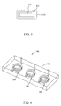
- Figure 6 illustrates another magnetic component assembly 160 that generally includes a moldable magnetic material defining a magnetic body 162 and plurality of multi-tum wire coils 164 coupled to the magnetic body.
- the magnetic body 162 may be pressed around the coils 164 in a relatively simple manufacturing process.
- the coils 164 are spaced from one another in the magnetic body and are independently operable in the magnetic body 162.
- three wire coils 164 are provided, although a greater or fewer number of coils 164 may be provided in other embodiments.
- the coils 164 shown in Figure 6 are fabricated from round wire conductors, other types of coils may alternatively be used, including but not limited to any of those described herein or in the related applications identified above.
- the coils 164 may optionally be provided with high temperature insulation and/or bonding agent as described above.
- the moldable magnetic material defining the magnetic body 162 may be any of the materials mentioned above or other suitable materials known in the art. While magnetic powder materials mixed with binder are believed to be advantageous, neither powder particles nor a non-magnetic binder material arc necessarily required for the magnetic material forming the magnetic body 162. Additionally, the moldable magnetic material need not be provided in sheets or layers as described above, but rather may be directly coupled to the coils 164 using compression molding techniques or other techniques known in the art. While the body 162 shown in Figure 6 is generally elongated and rectangular, other shapes of the magnetic body 162 are possible.
- the coils 164 may be arranged in the magnetic body 162 so that there is flux sharing between them. That is, adjacent coils 164 may share common flux paths through portions of the magnetic body.
- Figure 7 and 8 illustrate another miniaturized magnetic component assembly 170 generally including a powdered magnetic material defining a magnetic body 172 and the coil 120 coupled to the magnetic body.
- the magnetic body 172 is fabricated with moldable magnetic layers 174, 176, 178 on one side of the coil 120, and moldable magnetic layers 180, 182, 184 on the opposing side of the coil 120. While six layers of magnetic material are shown, it is understood that greater or fewer numbers of magnetic layers may be provided in further and/or alternative embodiments. It is also contemplated that a single sheet, such as the upper sheet 178 may define the magnetic body 172 in certain embodiments without utilizing any other sheet, this latter option, however, not Falling within the scope of the claims.
- the magnetic layers 174, 176, 178, 180, 182, 184 may include powdered magnetic material such as any of the powdered materials described above or other powdered magnetic material known in the art. Layers of magnetic material are shown in Figure 7 .
- All the layers 174, 176, 178, 180, 182, 184 may be fabricated from the same magnetic material in one embodiment such that the layers 174, 176, 178, 180, 182, 184 have similar, if not identically magnetic properties.
- one or more of the layers 174, 176, 178, 180, 182, 184 may be fabricated from a different magnetic material than other layers in the magnetic body 172.
- the layers 176, 180 and 184 may be fabricated from a first moldable material having first magnetic properties
- layers 174, 178 and 182 may be fabricated from a second moldable magnetic material having second properties that are different from the first properties.
- the magnetic component assembly 170 includes a shaped core element 186 inserted through the coil 120.
- the shaped core element 186 may be fabricated from a different magnetic material than the magnetic body 172.
- the shaped core element 186 may be fabricated from any material known in the art, including but not limited to those described above.
- the shaped core element 186 may be formed into a generally cylindrical shape complementary to the shape of the central opening 188 of the coil 120, although it is contemplated that non-cylindrical shapes may likewise be used with coils having non-cylindrical openings.
- the shaped core element 186 and the coil openings need not have complementary shapes.
- the shaped core element 186 may be extended through the opening 186 in the coil 120, and the moldable magnetic material is then molded around the coil 120 and shaped core element 186 to complete the magnetic body 172.
- the different magnetic properties of the shaped core element 186 and the magnetic body 172 may be especially advantageous when the material chosen for the shaped core element 186 has better properties than the moldable magnetic material used to define the magnetic body 172.
- flux paths passing though the core element 186 may provide better performance than if the magnetic body otherwise would.
- the manufacturing advantages of the moldable magnetic material may result in a lower component cost than if the entire magnetic body was fabricated from the material of the shaped core element 186.
- coil 120 and core element 186 are shown in Figures 7 and 8 , it is contemplated that more than one coil and coil element may likewise be provided in the magnetic body 172. Additionally, other types of coils, including but not limited to those described above or in the related applications identified above, may be utilized in lieu of the coil 120 as desired.
- Surface mount termination structure may also be provided on the magnetic component assembly 170 to provide a chip-type component familiar to those in the art.
- Such surface mount termination structure may include any terminal structure identified in the related disclosures herein incorporated by reference or other terminal structure known in the art.
- the component assembly 170 may accordingly be mounted to a circuit board using the surface mount termination structure and known techniques.
- the miniaturized, low profile component assembly 170 therefore facilitates a relatively high power, high performance magnetic component that occupies a relatively smaller space (both in terms of the footprint and profile) in a larger circuit board assembly and enables even further reduction in the size of circuit board assemblies. More powerful, yet smaller electronic devices including the circuit board assemblies are therefore made possible.
- a magnetic component assembly according to the invention is claimed in claim 1. No physical gap is formed in the magnetic body, and the assembly may define a power inductor.
- the at least one pre-fabricated layer of magnetic sheet material includes a mixture of magnetic powder particles and a polymeric binder.
- the magnetic particles may be selected from the group of Ferrite particles, Iron (Fe) particles, Sendust (Fe-Si-Al) particles, MPP (Ni-Mo-Fe) particles, HighFlux (Ni-Fe) particles, Megaflux (Fe-Si Alloy) particles, iron-based amorphous powder particles, cobalt-based amorphous powder particles, and equivalents and combinations thereof.
- the at least one pre-fabricated layer of magnetic sheet material may include at least two layers of magnetic sheet materials, with the at least one pre-fabricated coil sandwiched between the at least two layers of magnetic sheet materials. At least two layers of magnetic sheet materials may each be fabricated from different types of magnetic powder particles, whereby the at least two of the plurality of layers of magnetic sheet materials exhibit different magnetic properties from one another.
- the at least one pre-fabricated layer of magnetic sheet material may have a relative magnetic permeability greater than about 10.
- the polymeric binder may be a thermoplastic resin.
- the coil may define a central opening, and the component assembly may further comprising a shaped magnetic core element.
- the shaped magnetic core element may be separately provided from the shaped core element and fitted within the central opening.
- the at least one pre-fabricated layer of magnetic sheet material may include at least two layers of magnetic sheet materials, with the at least one pre-fabricated coil sandwiched between the at least two layers of magnetic sheet materials, and with the shaped magnetic core element also being sandwiched between the at least two layers of magnetic sheet materials.
- the shaped magnetic core element may be substantially cylindrical.
- the coil may include a wire conductor that is flexibly wound around an axis for a number of turns to define a winding portion.
- the wire conductor may be round or flat.
- the number of turns may include at least one of straight conductive paths joined at their ends, curved conductive paths, spiral conductive paths, and serpentine conductive paths.
- the coil may be formed as a three dimensional, free standing coil element.
- the coil may be provided with a bonding agent.
- the coil may be connected to a lead frame.
- a method of manufacturing a magnetic component is also disclosed.
- the component includes a coil winding and a magnetic body therefore, and the method includes: compression molding at least one pre-fabricated layer of magnetic sheet material about at least one pre-fabricated coil winding, thereby forming a laminated magnetic body containing the coil winding.
- Compression molding may not involve heat lamination.
- the coil winding may include a central opening, and the method may further include applying a separately fabricated shaped core element to the central opening.
- a product may be obtained by the method.
- the at least one pre-fabricated layer of magnetic sheet material may have a relative magnetic permeability of at least about 10.
- the at least one pre-fabricated layer of magnetic sheet material may include a mixture of magnetic powder particles and a polymeric binder.
- the polymer binder may be a thermoplastic resin.
- the at least one pre-fabricated layer of magnetic sheet material may include at least two layers of magnetic sheet material, the two layers of magnetic sheet material including different types of magnetic particles and therefore having different magnetic properties.
- the product may be a miniature power inductor.
Landscapes
- Engineering & Computer Science (AREA)
- Power Engineering (AREA)
- Microelectronics & Electronic Packaging (AREA)
- Chemical & Material Sciences (AREA)
- Composite Materials (AREA)
- Manufacturing & Machinery (AREA)
- Dispersion Chemistry (AREA)
- Coils Or Transformers For Communication (AREA)
- Manufacturing Cores, Coils, And Magnets (AREA)
Priority Applications (1)
| Application Number | Priority Date | Filing Date | Title |
|---|---|---|---|
| EP13151890.4A EP2584569A1 (en) | 2009-05-04 | 2010-04-26 | Magnetic components and methods of manufacturing the same |
Applications Claiming Priority (2)
| Application Number | Priority Date | Filing Date | Title |
|---|---|---|---|
| US17526909P | 2009-05-04 | 2009-05-04 | |
| PCT/US2010/032414 WO2010129230A1 (en) | 2009-05-04 | 2010-04-26 | Magnetic components and methods of manufacturing the same |
Related Child Applications (1)
| Application Number | Title | Priority Date | Filing Date |
|---|---|---|---|
| EP13151890.4 Division-Into | 2013-01-18 |
Publications (2)
| Publication Number | Publication Date |
|---|---|
| EP2427893A1 EP2427893A1 (en) | 2012-03-14 |
| EP2427893B1 true EP2427893B1 (en) | 2013-03-13 |
Family
ID=42270089
Family Applications (7)
| Application Number | Title | Priority Date | Filing Date |
|---|---|---|---|
| EP10716686A Withdrawn EP2427895A1 (en) | 2009-05-04 | 2010-04-26 | Magnetic components and methods of manufacturing the same |
| EP10716225A Not-in-force EP2427893B1 (en) | 2009-05-04 | 2010-04-26 | Magnetic components |
| EP13151890.4A Withdrawn EP2584569A1 (en) | 2009-05-04 | 2010-04-26 | Magnetic components and methods of manufacturing the same |
| EP10716230.7A Not-in-force EP2427888B1 (en) | 2009-05-04 | 2010-04-27 | Surface mount magnetic components |
| EP10716245A Withdrawn EP2427894A1 (en) | 2009-05-04 | 2010-04-28 | Magnetic component assembly |
| EP10716244.8A Not-in-force EP2427890B1 (en) | 2009-05-04 | 2010-04-28 | Surface mount magnetic components |
| EP10716243A Withdrawn EP2427889A1 (en) | 2009-05-04 | 2010-04-28 | Low profile layered coil and cores for magnetic components |
Family Applications Before (1)
| Application Number | Title | Priority Date | Filing Date |
|---|---|---|---|
| EP10716686A Withdrawn EP2427895A1 (en) | 2009-05-04 | 2010-04-26 | Magnetic components and methods of manufacturing the same |
Family Applications After (5)
| Application Number | Title | Priority Date | Filing Date |
|---|---|---|---|
| EP13151890.4A Withdrawn EP2584569A1 (en) | 2009-05-04 | 2010-04-26 | Magnetic components and methods of manufacturing the same |
| EP10716230.7A Not-in-force EP2427888B1 (en) | 2009-05-04 | 2010-04-27 | Surface mount magnetic components |
| EP10716245A Withdrawn EP2427894A1 (en) | 2009-05-04 | 2010-04-28 | Magnetic component assembly |
| EP10716244.8A Not-in-force EP2427890B1 (en) | 2009-05-04 | 2010-04-28 | Surface mount magnetic components |
| EP10716243A Withdrawn EP2427889A1 (en) | 2009-05-04 | 2010-04-28 | Low profile layered coil and cores for magnetic components |
Country Status (8)
| Country | Link |
|---|---|
| US (1) | US20100277267A1 (ja) |
| EP (7) | EP2427895A1 (ja) |
| JP (8) | JP5711219B2 (ja) |
| KR (6) | KR20120018157A (ja) |
| CN (7) | CN105529175A (ja) |
| ES (1) | ES2413632T3 (ja) |
| TW (4) | TWI588849B (ja) |
| WO (6) | WO2010129228A1 (ja) |
Families Citing this family (89)
| Publication number | Priority date | Publication date | Assignee | Title |
|---|---|---|---|---|
| US7791445B2 (en) | 2006-09-12 | 2010-09-07 | Cooper Technologies Company | Low profile layered coil and cores for magnetic components |
| US9589716B2 (en) | 2006-09-12 | 2017-03-07 | Cooper Technologies Company | Laminated magnetic component and manufacture with soft magnetic powder polymer composite sheets |
| US8466764B2 (en) | 2006-09-12 | 2013-06-18 | Cooper Technologies Company | Low profile layered coil and cores for magnetic components |
| US8941457B2 (en) | 2006-09-12 | 2015-01-27 | Cooper Technologies Company | Miniature power inductor and methods of manufacture |
| US8378777B2 (en) | 2008-07-29 | 2013-02-19 | Cooper Technologies Company | Magnetic electrical device |
| US9558881B2 (en) | 2008-07-11 | 2017-01-31 | Cooper Technologies Company | High current power inductor |
| US9859043B2 (en) | 2008-07-11 | 2018-01-02 | Cooper Technologies Company | Magnetic components and methods of manufacturing the same |
| US8659379B2 (en) | 2008-07-11 | 2014-02-25 | Cooper Technologies Company | Magnetic components and methods of manufacturing the same |
| CN104051133B (zh) * | 2011-01-07 | 2020-03-10 | 乾坤科技股份有限公司 | 电感器 |
| CN106057432B (zh) * | 2011-01-07 | 2021-07-23 | 乾坤科技股份有限公司 | 电感器 |
| US8610533B2 (en) * | 2011-03-31 | 2013-12-17 | Bose Corporation | Power converter using soft composite magnetic structure |
| US9157952B2 (en) | 2011-04-14 | 2015-10-13 | National Instruments Corporation | Switch matrix system and method |
| US9097757B2 (en) | 2011-04-14 | 2015-08-04 | National Instruments Corporation | Switching element system and method |
| US8704408B2 (en) | 2011-04-14 | 2014-04-22 | National Instruments Corporation | Switch matrix modeling system and method |
| TWI430720B (zh) | 2011-11-16 | 2014-03-11 | Ind Tech Res Inst | 多層微型線圈總成 |
| US10128035B2 (en) * | 2011-11-22 | 2018-11-13 | Volterra Semiconductor LLC | Coupled inductor arrays and associated methods |
| US9373438B1 (en) * | 2011-11-22 | 2016-06-21 | Volterra Semiconductor LLC | Coupled inductor arrays and associated methods |
| TWM438075U (en) * | 2012-04-19 | 2012-09-21 | Sea Sonic Electronics Co Ltd | Power supply power filter output architecture |
| EP2660611A1 (en) * | 2012-04-30 | 2013-11-06 | LEM Intellectual Property SA | Electrical current transducer module |
| US9287062B2 (en) | 2012-05-02 | 2016-03-15 | National Instruments Corporation | Magnetic switching system |
| US9558903B2 (en) | 2012-05-02 | 2017-01-31 | National Instruments Corporation | MEMS-based switching system |
| JP6050667B2 (ja) * | 2012-12-04 | 2016-12-21 | デクセリアルズ株式会社 | コイルモジュール、非接触電力伝送用アンテナユニット、及び電子機器 |
| CN103871724B (zh) * | 2012-12-18 | 2016-09-28 | 佳邦科技股份有限公司 | 功率电感及其制造方法 |
| JP2014130879A (ja) * | 2012-12-28 | 2014-07-10 | Panasonic Corp | コイル埋設型磁性素子の製造方法 |
| US8723629B1 (en) * | 2013-01-10 | 2014-05-13 | Cyntec Co., Ltd. | Magnetic device with high saturation current and low core loss |
| KR20140094324A (ko) * | 2013-01-22 | 2014-07-30 | 삼성전기주식회사 | 공통모드필터 및 이의 제조방법 |
| US10840005B2 (en) * | 2013-01-25 | 2020-11-17 | Vishay Dale Electronics, Llc | Low profile high current composite transformer |
| KR101451503B1 (ko) * | 2013-03-25 | 2014-10-15 | 삼성전기주식회사 | 인덕터 및 그 제조 방법 |
| TW201444052A (zh) * | 2013-05-15 | 2014-11-16 | Inpaq Technology Co Ltd | 薄型疊層式功率電感製程之改進 |
| JP2015026812A (ja) * | 2013-07-29 | 2015-02-05 | サムソン エレクトロ−メカニックス カンパニーリミテッド. | チップ電子部品及びその製造方法 |
| KR101450471B1 (ko) * | 2013-08-27 | 2014-10-13 | 주식회사 두산 | 배치 경화 방식을 이용하는 연성 금속박 적층판의 제조방법 |
| KR101449518B1 (ko) * | 2013-09-10 | 2014-10-16 | 주식회사 아모텍 | 파워 인덕터 및 그의 제조방법 |
| KR101334653B1 (ko) * | 2013-09-11 | 2013-12-05 | 신우이.엔.지 주식회사 | 복합 자성 코아 및 그 제조방법 |
| JP5944373B2 (ja) * | 2013-12-27 | 2016-07-05 | 東光株式会社 | 電子部品の製造方法、電子部品 |
| KR20150080797A (ko) * | 2014-01-02 | 2015-07-10 | 삼성전기주식회사 | 세라믹 전자 부품 |
| WO2015133310A1 (ja) * | 2014-03-04 | 2015-09-11 | 株式会社村田製作所 | インダクタ装置、インダクタアレイおよび多層基板、ならびにインダクタ装置の製造方法 |
| KR101548862B1 (ko) * | 2014-03-10 | 2015-08-31 | 삼성전기주식회사 | 칩형 코일 부품 및 그 제조 방법 |
| DE102014207635A1 (de) * | 2014-04-23 | 2015-10-29 | Würth Elektronik eiSos Gmbh & Co. KG | Verfahren zum Herstellen eines Induktionsbauteils und Induktionsbauteil |
| CN105091051A (zh) * | 2014-05-09 | 2015-11-25 | 名硕电脑(苏州)有限公司 | 薄型化底盘及具有薄型化底盘的电磁炉 |
| US9831023B2 (en) * | 2014-07-10 | 2017-11-28 | Cyntec Co., Ltd. | Electrode structure and the corresponding electrical component using the same and the fabrication method thereof |
| JP6522297B2 (ja) * | 2014-07-28 | 2019-05-29 | 太陽誘電株式会社 | コイル部品 |
| KR102143005B1 (ko) * | 2014-07-29 | 2020-08-11 | 삼성전기주식회사 | 인덕터 및 그 실장 기판 |
| KR101475677B1 (ko) | 2014-09-11 | 2014-12-23 | 삼성전기주식회사 | 코일 부품 및 이를 포함하는 전원공급장치 |
| WO2016047653A1 (ja) * | 2014-09-24 | 2016-03-31 | 株式会社村田製作所 | インダクタ部品の製造方法およびインダクタ部品 |
| KR102029726B1 (ko) * | 2014-10-13 | 2019-10-10 | 주식회사 위츠 | 무선 전력 전송용 코일형 유닛 및 무선전력 전송용 코일형 유닛의 제조방법 |
| US10049808B2 (en) | 2014-10-31 | 2018-08-14 | Samsung Electro-Mechanics Co., Ltd. | Coil component assembly for mass production of coil components and coil components made from coil component assembly |
| CN105679520B (zh) * | 2014-11-17 | 2019-04-19 | 华为技术有限公司 | 耦合电感、磁体和多电平逆变器 |
| TWI553677B (zh) * | 2015-04-08 | 2016-10-11 | Yun-Guang Fan | Thin inductive components embedded in the structure |
| KR102198528B1 (ko) * | 2015-05-19 | 2021-01-06 | 삼성전기주식회사 | 코일 전자부품 및 그 제조방법 |
| KR102171679B1 (ko) * | 2015-08-24 | 2020-10-29 | 삼성전기주식회사 | 코일 전자 부품 및 이의 제조방법 |
| KR102154201B1 (ko) * | 2015-08-24 | 2020-09-09 | 삼성전기주식회사 | 코일 전자 부품 |
| JP6551142B2 (ja) * | 2015-10-19 | 2019-07-31 | Tdk株式会社 | コイル部品及びこれを内蔵した回路基板 |
| CN105405610A (zh) * | 2015-12-28 | 2016-03-16 | 江苏晨朗电子集团有限公司 | 变压器 |
| JP6274376B2 (ja) | 2016-01-28 | 2018-02-07 | 株式会社村田製作所 | 表面実装型コイル部品及びその製造方法、並びにdc−dcコンバータ |
| ITUB20161251A1 (it) | 2016-03-02 | 2017-09-02 | Irca Spa | Piano cottura ad induzione e metodo per la realizzazione di piani cottura ad induzione |
| DE112017000026T5 (de) | 2016-04-01 | 2017-12-21 | Murata Manufacturing Co., Ltd. | Spulenkomponente und Verfahren zum Herstellen einer Spulenkomponente |
| JP6531712B2 (ja) * | 2016-04-28 | 2019-06-19 | 株式会社村田製作所 | 複合インダクタ |
| KR102558332B1 (ko) * | 2016-05-04 | 2023-07-21 | 엘지이노텍 주식회사 | 인덕터 및 이의 제조 방법 |
| US10998124B2 (en) | 2016-05-06 | 2021-05-04 | Vishay Dale Electronics, Llc | Nested flat wound coils forming windings for transformers and inductors |
| KR20180023163A (ko) * | 2016-08-25 | 2018-03-07 | 현대자동차주식회사 | 트랜스 인덕터 및 이를 이용한 전력 변환 장치 |
| JP7160438B2 (ja) | 2016-08-31 | 2022-10-25 | ヴィシェイ デール エレクトロニクス エルエルシー | 低い直流抵抗を有す高電流コイルを備えた誘導子 |
| JP6872342B2 (ja) * | 2016-10-18 | 2021-05-19 | 株式会社ディスコ | 切削ブレード |
| JP6610498B2 (ja) * | 2016-10-21 | 2019-11-27 | 株式会社村田製作所 | 複合型電子部品の製造方法 |
| US10340074B2 (en) | 2016-12-02 | 2019-07-02 | Cyntec Co., Ltd. | Transformer |
| CN110114846B (zh) * | 2016-12-20 | 2022-03-29 | Lg伊诺特有限公司 | 磁芯、线圈组件以及包括线圈组件的电子组件 |
| US10396016B2 (en) * | 2016-12-30 | 2019-08-27 | Texas Instruments Incorporated | Leadframe inductor |
| CN107068375B (zh) * | 2017-02-22 | 2018-11-16 | 湧德电子股份有限公司 | 制作电感器之组合式模具 |
| DE202017104061U1 (de) * | 2017-07-07 | 2018-10-09 | Aixtron Se | Beschichtungseinrichtung mit beschichteter Sendespule |
| KR102463331B1 (ko) * | 2017-10-16 | 2022-11-04 | 삼성전기주식회사 | 인덕터 어레이 |
| KR102501904B1 (ko) | 2017-12-07 | 2023-02-21 | 삼성전기주식회사 | 권선형 인덕터 |
| KR102394054B1 (ko) * | 2018-02-01 | 2022-05-04 | 엘지이노텍 주식회사 | 자성코어 조립체 및 이를 포함하는 코일부품 |
| US20200038952A1 (en) * | 2018-08-02 | 2020-02-06 | American Axle & Manufacturing, Inc. | System And Method For Additive Manufacturing |
| KR102098867B1 (ko) * | 2018-09-12 | 2020-04-09 | (주)아이테드 | 임프린팅 장치 및 임프린팅 방법 |
| JP6856059B2 (ja) * | 2018-09-25 | 2021-04-07 | 株式会社村田製作所 | インダクタ |
| JP6962480B2 (ja) * | 2018-10-10 | 2021-11-05 | 味の素株式会社 | 磁性ペースト |
| CN115359999A (zh) | 2018-11-02 | 2022-11-18 | 台达电子企业管理(上海)有限公司 | 变压器模块及功率模块 |
| DE102019103895A1 (de) * | 2019-02-15 | 2020-08-20 | Tdk Electronics Ag | Spule und Verfahren zur Herstellung der Spule |
| KR102188451B1 (ko) | 2019-03-15 | 2020-12-08 | 삼성전기주식회사 | 코일 부품 |
| US20200303114A1 (en) * | 2019-03-22 | 2020-09-24 | Cyntec Co., Ltd. | Inductor array in a single package |
| US20210035730A1 (en) * | 2019-07-31 | 2021-02-04 | Murata Manufacturing Co., Ltd. | Inductor |
| JP7485505B2 (ja) | 2019-08-09 | 2024-05-16 | 日東電工株式会社 | インダクタ |
| KR102662853B1 (ko) * | 2019-09-30 | 2024-05-03 | 삼성전기주식회사 | 인쇄회로기판 |
| JP7173065B2 (ja) * | 2020-02-19 | 2022-11-16 | 株式会社村田製作所 | インダクタ部品 |
| DE102020110850A1 (de) * | 2020-04-21 | 2021-10-21 | Tdk Electronics Ag | Spule und Verfahren zur Herstellung der Spule |
| CN112071579A (zh) * | 2020-09-03 | 2020-12-11 | 深圳市铂科新材料股份有限公司 | 一种贴片电感的制造方法及由其制得的贴片电感 |
| US11948724B2 (en) | 2021-06-18 | 2024-04-02 | Vishay Dale Electronics, Llc | Method for making a multi-thickness electro-magnetic device |
| TWI760275B (zh) | 2021-08-26 | 2022-04-01 | 奇力新電子股份有限公司 | 電感元件及其製造方法 |
| CN117941019A (zh) * | 2021-09-16 | 2024-04-26 | 松下知识产权经营株式会社 | 电感器 |
| WO2023188588A1 (ja) * | 2022-03-29 | 2023-10-05 | パナソニックIpマネジメント株式会社 | 結合インダクタ、インダクタユニット、電圧コンバータ及び電力変換装置 |
Family Cites Families (142)
| Publication number | Priority date | Publication date | Assignee | Title |
|---|---|---|---|---|
| US3255512A (en) * | 1962-08-17 | 1966-06-14 | Trident Engineering Associates | Molding a ferromagnetic casing upon an electrical component |
| US4072780A (en) * | 1976-10-28 | 1978-02-07 | Varadyne Industries, Inc. | Process for making electrical components having dielectric layers comprising particles of a lead oxide-germanium dioxide-silicon dioxide glass and a resin binder therefore |
| GB2045540B (en) * | 1978-12-28 | 1983-08-03 | Tdk Electronics Co Ltd | Electrical inductive device |
| NL7900244A (nl) * | 1979-01-12 | 1980-07-15 | Philips Nv | Vlakke tweelaags electrische spoel. |
| EP0117764A1 (en) * | 1983-03-01 | 1984-09-05 | Mitsubishi Denki Kabushiki Kaisha | Coil device |
| JPS6041312A (ja) * | 1983-08-16 | 1985-03-05 | Tdk Corp | 回路素子 |
| JPH0217447Y2 (ja) * | 1984-12-21 | 1990-05-16 | ||
| JPS6261305A (ja) * | 1985-09-11 | 1987-03-18 | Murata Mfg Co Ltd | 積層チツプコイル |
| JPS62252112A (ja) * | 1986-04-24 | 1987-11-02 | Murata Mfg Co Ltd | バルントランス |
| US4803425A (en) * | 1987-10-05 | 1989-02-07 | Xerox Corporation | Multi-phase printed circuit board tachometer |
| JPH01266705A (ja) | 1988-04-18 | 1989-10-24 | Sony Corp | コイル部品 |
| JPH0236013U (ja) * | 1988-09-02 | 1990-03-08 | ||
| JPH02172207A (ja) * | 1988-12-23 | 1990-07-03 | Murata Mfg Co Ltd | 積層型インダクター |
| JPH03241711A (ja) * | 1990-02-20 | 1991-10-28 | Matsushita Electric Ind Co Ltd | リニアリティコイル |
| DE4117878C2 (de) * | 1990-05-31 | 1996-09-26 | Toshiba Kawasaki Kk | Planares magnetisches Element |
| JP3108931B2 (ja) * | 1991-03-15 | 2000-11-13 | 株式会社トーキン | インダクタ及びその製造方法 |
| JP3197022B2 (ja) * | 1991-05-13 | 2001-08-13 | ティーディーケイ株式会社 | ノイズサプレッサ用積層セラミック部品 |
| US5487214A (en) * | 1991-07-10 | 1996-01-30 | International Business Machines Corp. | Method of making a monolithic magnetic device with printed circuit interconnections |
| JP2563943Y2 (ja) * | 1991-10-02 | 1998-03-04 | 富士電気化学株式会社 | インダクタンスコア |
| JPH0555515U (ja) * | 1991-12-25 | 1993-07-23 | 太陽誘電株式会社 | 面実装型コイル |
| JPH05283238A (ja) * | 1992-03-31 | 1993-10-29 | Sony Corp | トランス |
| JP3160685B2 (ja) * | 1992-04-14 | 2001-04-25 | 株式会社トーキン | インダクタ |
| JPH065450A (ja) * | 1992-06-18 | 1994-01-14 | Showa Electric Wire & Cable Co Ltd | コイル装置の製造方法 |
| JP2566100B2 (ja) * | 1992-07-02 | 1996-12-25 | 株式会社トーキン | 高周波トランス |
| US5312674A (en) * | 1992-07-31 | 1994-05-17 | Hughes Aircraft Company | Low-temperature-cofired-ceramic (LTCC) tape structures including cofired ferromagnetic elements, drop-in components and multi-layer transformer |
| EP0593020B1 (en) * | 1992-10-12 | 1999-02-03 | Matsushita Electronics Corporation | Manufacturing method for an electronic component |
| JPH06290975A (ja) * | 1993-03-30 | 1994-10-18 | Tokin Corp | コイル部品並びにその製造方法 |
| US5500629A (en) * | 1993-09-10 | 1996-03-19 | Meyer Dennis R | Noise suppressor |
| JP3472329B2 (ja) * | 1993-12-24 | 2003-12-02 | 株式会社村田製作所 | チップ型トランス |
| JP3434339B2 (ja) * | 1994-01-27 | 2003-08-04 | エヌイーシートーキン株式会社 | インダクタの製造方法 |
| JPH07320938A (ja) * | 1994-05-24 | 1995-12-08 | Sony Corp | インダクタ装置 |
| US6911887B1 (en) * | 1994-09-12 | 2005-06-28 | Matsushita Electric Industrial Co., Ltd. | Inductor and method for producing the same |
| US5985356A (en) * | 1994-10-18 | 1999-11-16 | The Regents Of The University Of California | Combinatorial synthesis of novel materials |
| US5821846A (en) * | 1995-05-22 | 1998-10-13 | Steward, Inc. | High current ferrite electromagnetic interference suppressor and associated method |
| US7034645B2 (en) * | 1999-03-16 | 2006-04-25 | Vishay Dale Electronics, Inc. | Inductor coil and method for making same |
| US7263761B1 (en) * | 1995-07-18 | 2007-09-04 | Vishay Dale Electronics, Inc. | Method for making a high current low profile inductor |
| CA2180992C (en) * | 1995-07-18 | 1999-05-18 | Timothy M. Shafer | High current, low profile inductor and method for making same |
| US7921546B2 (en) * | 1995-07-18 | 2011-04-12 | Vishay Dale Electronics, Inc. | Method for making a high current low profile inductor |
| US6198375B1 (en) * | 1999-03-16 | 2001-03-06 | Vishay Dale Electronics, Inc. | Inductor coil structure |
| JPH0992540A (ja) * | 1995-09-21 | 1997-04-04 | Nippon Steel Corp | 薄型インダクタ |
| JP3796290B2 (ja) * | 1996-05-15 | 2006-07-12 | Necトーキン株式会社 | 電子部品及びその製造方法 |
| JP2978117B2 (ja) * | 1996-07-01 | 1999-11-15 | ティーディーケイ株式会社 | つぼ型コアを用いた面実装部品 |
| US6038134A (en) * | 1996-08-26 | 2000-03-14 | Johanson Dielectrics, Inc. | Modular capacitor/inductor structure |
| US6683783B1 (en) * | 1997-03-07 | 2004-01-27 | William Marsh Rice University | Carbon fibers formed from single-wall carbon nanotubes |
| US6284060B1 (en) * | 1997-04-18 | 2001-09-04 | Matsushita Electric Industrial Co., Ltd. | Magnetic core and method of manufacturing the same |
| JP3336346B2 (ja) * | 1997-07-01 | 2002-10-21 | スミダコーポレーション株式会社 | チップインダクタンス素子 |
| US5922514A (en) * | 1997-09-17 | 1999-07-13 | Dale Electronics, Inc. | Thick film low value high frequency inductor, and method of making the same |
| US6169801B1 (en) * | 1998-03-16 | 2001-01-02 | Midcom, Inc. | Digital isolation apparatus and method |
| US6054914A (en) * | 1998-07-06 | 2000-04-25 | Midcom, Inc. | Multi-layer transformer having electrical connection in a magnetic core |
| JP2001185421A (ja) * | 1998-12-28 | 2001-07-06 | Matsushita Electric Ind Co Ltd | 磁性素子およびその製造方法 |
| US6392525B1 (en) * | 1998-12-28 | 2002-05-21 | Matsushita Electric Industrial Co., Ltd. | Magnetic element and method of manufacturing the same |
| US6566731B2 (en) * | 1999-02-26 | 2003-05-20 | Micron Technology, Inc. | Open pattern inductor |
| US6379579B1 (en) * | 1999-03-09 | 2002-04-30 | Tdk Corporation | Method for the preparation of soft magnetic ferrite powder and method for the production of laminated chip inductor |
| JP2000323336A (ja) * | 1999-03-11 | 2000-11-24 | Taiyo Yuden Co Ltd | インダクタ及びその製造方法 |
| US6198374B1 (en) * | 1999-04-01 | 2001-03-06 | Midcom, Inc. | Multi-layer transformer apparatus and method |
| JP3776281B2 (ja) * | 1999-04-13 | 2006-05-17 | アルプス電気株式会社 | インダクティブ素子 |
| US6114939A (en) * | 1999-06-07 | 2000-09-05 | Technical Witts, Inc. | Planar stacked layer inductors and transformers |
| JP3365622B2 (ja) * | 1999-12-17 | 2003-01-14 | 松下電器産業株式会社 | Lc複合部品および電源素子 |
| US6908960B2 (en) * | 1999-12-28 | 2005-06-21 | Tdk Corporation | Composite dielectric material, composite dielectric substrate, prepreg, coated metal foil, molded sheet, composite magnetic substrate, substrate, double side metal foil-clad substrate, flame retardant substrate, polyvinylbenzyl ether resin composition, thermosettin |
| JP3670575B2 (ja) * | 2000-01-12 | 2005-07-13 | Tdk株式会社 | コイル封入圧粉コアの製造方法およびコイル封入圧粉コア |
| GB2360292B (en) * | 2000-03-15 | 2002-04-03 | Murata Manufacturing Co | Photosensitive thick film composition and electronic device using the same |
| US6594157B2 (en) * | 2000-03-21 | 2003-07-15 | Alps Electric Co., Ltd. | Low-loss magnetic powder core, and switching power supply, active filter, filter, and amplifying device using the same |
| JP4684461B2 (ja) * | 2000-04-28 | 2011-05-18 | パナソニック株式会社 | 磁性素子の製造方法 |
| US6420953B1 (en) * | 2000-05-19 | 2002-07-16 | Pulse Engineering. Inc. | Multi-layer, multi-functioning printed circuit board |
| DE10024824A1 (de) * | 2000-05-19 | 2001-11-29 | Vacuumschmelze Gmbh | Induktives Bauelement und Verfahren zu seiner Herstellung |
| JP2001345212A (ja) * | 2000-05-31 | 2001-12-14 | Tdk Corp | 積層電子部品 |
| JP2002083732A (ja) * | 2000-09-08 | 2002-03-22 | Murata Mfg Co Ltd | インダクタ及びその製造方法 |
| US7485366B2 (en) * | 2000-10-26 | 2009-02-03 | Inframat Corporation | Thick film magnetic nanoparticulate composites and method of manufacture thereof |
| US6720074B2 (en) * | 2000-10-26 | 2004-04-13 | Inframat Corporation | Insulator coated magnetic nanoparticulate composites with reduced core loss and method of manufacture thereof |
| US20020067234A1 (en) * | 2000-12-01 | 2002-06-06 | Samuel Kung | Compact surface-mountable inductors |
| CN1218333C (zh) * | 2000-12-28 | 2005-09-07 | Tdk株式会社 | 叠层衬底、电子部件的制造方法及叠层电子部件 |
| JP3593986B2 (ja) * | 2001-02-19 | 2004-11-24 | 株式会社村田製作所 | コイル部品及びその製造方法 |
| JP3612028B2 (ja) * | 2001-02-27 | 2005-01-19 | 松下電器産業株式会社 | コイル部品の製造方法 |
| EP1356479B1 (en) * | 2001-02-27 | 2006-01-04 | Matsushita Electric Industrial Co., Ltd. | Coil component and method of manufacturing the same |
| WO2002070432A1 (fr) * | 2001-03-01 | 2002-09-12 | Tdk Corporation | Agglomere d'oxyde magnetique et partie de circuit haute frequence l'utilisant |
| JP2002299130A (ja) * | 2001-04-02 | 2002-10-11 | Densei Lambda Kk | 電源用複合素子 |
| JP2002313632A (ja) * | 2001-04-17 | 2002-10-25 | Matsushita Electric Ind Co Ltd | 磁性素子およびその製造方法 |
| US6768409B2 (en) * | 2001-08-29 | 2004-07-27 | Matsushita Electric Industrial Co., Ltd. | Magnetic device, method for manufacturing the same, and power supply module equipped with the same |
| JP2003203813A (ja) * | 2001-08-29 | 2003-07-18 | Matsushita Electric Ind Co Ltd | 磁性素子およびその製造方法、並びにそれを備えた電源モジュール |
| US7162302B2 (en) * | 2002-03-04 | 2007-01-09 | Nanoset Llc | Magnetically shielded assembly |
| JP2003229311A (ja) * | 2002-01-31 | 2003-08-15 | Tdk Corp | コイル封入圧粉磁芯およびその製造方法、コイルおよびその製造方法 |
| JP3932933B2 (ja) * | 2002-03-01 | 2007-06-20 | 松下電器産業株式会社 | 磁性素子の製造方法 |
| TW553465U (en) * | 2002-07-25 | 2003-09-11 | Micro Star Int Co Ltd | Integrated inductor |
| JP2004165539A (ja) * | 2002-11-15 | 2004-06-10 | Toko Inc | インダクタ |
| KR100479625B1 (ko) * | 2002-11-30 | 2005-03-31 | 주식회사 쎄라텍 | 칩타입 파워인덕터 및 그 제조방법 |
| DE60332062D1 (de) * | 2002-12-11 | 2010-05-20 | Konica Minolta Holdings Inc | Tintenstrahldrucker und Bildaufzeichnungsverfahren |
| US7259648B2 (en) * | 2002-12-13 | 2007-08-21 | Matsushita Electric Industrial Co., Ltd. | Multiple choke coil and electronic equipment using the same |
| US7965165B2 (en) * | 2002-12-13 | 2011-06-21 | Volterra Semiconductor Corporation | Method for making magnetic components with M-phase coupling, and related inductor structures |
| JP3800540B2 (ja) * | 2003-01-31 | 2006-07-26 | Tdk株式会社 | インダクタンス素子の製造方法と積層電子部品と積層電子部品モジュ−ルとこれらの製造方法 |
| US6873241B1 (en) * | 2003-03-24 | 2005-03-29 | Robert O. Sanchez | High frequency transformers and high Q factor inductors formed using epoxy-based magnetic polymer materials |
| US6879238B2 (en) * | 2003-05-28 | 2005-04-12 | Cyntec Company | Configuration and method for manufacturing compact high current inductor coil |
| US20050007232A1 (en) * | 2003-06-12 | 2005-01-13 | Nec Tokin Corporation | Magnetic core and coil component using the same |
| JP4514031B2 (ja) * | 2003-06-12 | 2010-07-28 | 株式会社デンソー | コイル部品及びコイル部品製造方法 |
| US7598837B2 (en) * | 2003-07-08 | 2009-10-06 | Pulse Engineering, Inc. | Form-less electronic device and methods of manufacturing |
| US7307502B2 (en) * | 2003-07-16 | 2007-12-11 | Marvell World Trade Ltd. | Power inductor with reduced DC current saturation |
| JP2005064319A (ja) * | 2003-08-18 | 2005-03-10 | Matsushita Electric Ind Co Ltd | コイル部品およびそれを搭載した電子機器 |
| JP4532167B2 (ja) * | 2003-08-21 | 2010-08-25 | コーア株式会社 | チップコイルおよびチップコイルを実装した基板 |
| ATE448553T1 (de) * | 2003-09-04 | 2009-11-15 | Koninkl Philips Electronics Nv | Transformator mit fraktionalen bindungen mit ferritpolymerkern |
| JPWO2005031764A1 (ja) * | 2003-09-29 | 2006-12-07 | 株式会社タムラ製作所 | 積層型磁性部品及びその製造方法 |
| US7319599B2 (en) * | 2003-10-01 | 2008-01-15 | Matsushita Electric Industrial Co., Ltd. | Module incorporating a capacitor, method for manufacturing the same, and capacitor used therefor |
| EP1526556A1 (en) * | 2003-10-21 | 2005-04-27 | Yun-Kuang Fan | Ferrite cored coil structure for SMD and fabrication method of the same |
| US7489225B2 (en) * | 2003-11-17 | 2009-02-10 | Pulse Engineering, Inc. | Precision inductive devices and methods |
| US7187263B2 (en) * | 2003-11-26 | 2007-03-06 | Vlt, Inc. | Printed circuit transformer |
| JP4851062B2 (ja) * | 2003-12-10 | 2012-01-11 | スミダコーポレーション株式会社 | インダクタンス素子の製造方法 |
| JP4293603B2 (ja) * | 2004-02-25 | 2009-07-08 | Tdk株式会社 | コイル部品及びその製造方法 |
| US7019391B2 (en) * | 2004-04-06 | 2006-03-28 | Bao Tran | NANO IC packaging |
| US7330369B2 (en) * | 2004-04-06 | 2008-02-12 | Bao Tran | NANO-electronic memory array |
| JP2005310864A (ja) * | 2004-04-19 | 2005-11-04 | Matsushita Electric Ind Co Ltd | コイル部品 |
| CN2726077Y (zh) * | 2004-07-02 | 2005-09-14 | 郑长茂 | 电感器 |
| JP2006032587A (ja) * | 2004-07-15 | 2006-02-02 | Matsushita Electric Ind Co Ltd | インダクタンス部品およびその製造方法 |
| JP4528058B2 (ja) * | 2004-08-20 | 2010-08-18 | アルプス電気株式会社 | コイル封入圧粉磁心 |
| US7567163B2 (en) * | 2004-08-31 | 2009-07-28 | Pulse Engineering, Inc. | Precision inductive devices and methods |
| US7339451B2 (en) * | 2004-09-08 | 2008-03-04 | Cyntec Co., Ltd. | Inductor |
| JPWO2006070544A1 (ja) * | 2004-12-27 | 2008-06-12 | スミダコーポレーション株式会社 | 磁性素子 |
| TWM278046U (en) * | 2005-02-22 | 2005-10-11 | Traben Co Ltd | Inductor component |
| JP2007053312A (ja) * | 2005-08-19 | 2007-03-01 | Taiyo Yuden Co Ltd | 面実装型コイル部品及びその製造方法並びにその実装方法 |
| JP2007123376A (ja) * | 2005-10-26 | 2007-05-17 | Matsushita Electric Ind Co Ltd | 複合磁性体およびそれを用いた磁性素子並びにその製造方法 |
| JP2007165779A (ja) * | 2005-12-16 | 2007-06-28 | Sumida Corporation | コイル封入型磁性部品 |
| KR20070082539A (ko) * | 2006-02-15 | 2007-08-21 | 쿠퍼 테크놀로지스 컴파니 | 자기 부품을 위한 갭이 있는 코어 구조체 |
| JP4904889B2 (ja) * | 2006-03-31 | 2012-03-28 | Tdk株式会社 | コイル部品 |
| US7994889B2 (en) * | 2006-06-01 | 2011-08-09 | Taiyo Yuden Co., Ltd. | Multilayer inductor |
| TW200800443A (en) * | 2006-06-23 | 2008-01-01 | Delta Electronics Inc | Powder-compressed assembly and its manufacturing method |
| CN101501791A (zh) * | 2006-07-14 | 2009-08-05 | 美商·帕斯脉冲工程有限公司 | 自引线表面安装电感器和方法 |
| US20080278275A1 (en) * | 2007-05-10 | 2008-11-13 | Fouquet Julie E | Miniature Transformers Adapted for use in Galvanic Isolators and the Like |
| US8378777B2 (en) * | 2008-07-29 | 2013-02-19 | Cooper Technologies Company | Magnetic electrical device |
| US7791445B2 (en) * | 2006-09-12 | 2010-09-07 | Cooper Technologies Company | Low profile layered coil and cores for magnetic components |
| US8400245B2 (en) * | 2008-07-11 | 2013-03-19 | Cooper Technologies Company | High current magnetic component and methods of manufacture |
| US8310332B2 (en) * | 2008-10-08 | 2012-11-13 | Cooper Technologies Company | High current amorphous powder core inductor |
| US7986208B2 (en) * | 2008-07-11 | 2011-07-26 | Cooper Technologies Company | Surface mount magnetic component assembly |
| US9589716B2 (en) * | 2006-09-12 | 2017-03-07 | Cooper Technologies Company | Laminated magnetic component and manufacture with soft magnetic powder polymer composite sheets |
| JP2008078178A (ja) * | 2006-09-19 | 2008-04-03 | Shindengen Electric Mfg Co Ltd | インダクタンス素子 |
| JP2008147342A (ja) * | 2006-12-08 | 2008-06-26 | Sumida Corporation | 磁気素子 |
| TWI315529B (en) * | 2006-12-28 | 2009-10-01 | Ind Tech Res Inst | Monolithic inductor |
| CN101217070A (zh) * | 2007-01-05 | 2008-07-09 | 胜美达电机(香港)有限公司 | 面安装型磁性元件 |
| JP2008288370A (ja) * | 2007-05-17 | 2008-11-27 | Nec Tokin Corp | 面実装インダクタおよびその製造方法 |
| JP2009021549A (ja) * | 2007-06-15 | 2009-01-29 | Taiyo Yuden Co Ltd | コイル部品及びその製造方法 |
| JP5084408B2 (ja) * | 2007-09-05 | 2012-11-28 | 太陽誘電株式会社 | 巻線型電子部品 |
| US7525406B1 (en) * | 2008-01-17 | 2009-04-28 | Well-Mag Electronic Ltd. | Multiple coupling and non-coupling inductor |
| JP5165415B2 (ja) * | 2008-02-25 | 2013-03-21 | 太陽誘電株式会社 | 面実装型コイル部材 |
| US8183967B2 (en) * | 2008-07-11 | 2012-05-22 | Cooper Technologies Company | Surface mount magnetic components and methods of manufacturing the same |
| US8279037B2 (en) * | 2008-07-11 | 2012-10-02 | Cooper Technologies Company | Magnetic components and methods of manufacturing the same |
| US8659379B2 (en) * | 2008-07-11 | 2014-02-25 | Cooper Technologies Company | Magnetic components and methods of manufacturing the same |
-
2010
- 2010-04-23 US US12/766,300 patent/US20100277267A1/en not_active Abandoned
- 2010-04-26 EP EP10716686A patent/EP2427895A1/en not_active Withdrawn
- 2010-04-26 KR KR1020117027081A patent/KR20120018157A/ko not_active Application Discontinuation
- 2010-04-26 CN CN201610087085.0A patent/CN105529175A/zh active Pending
- 2010-04-26 JP JP2012509833A patent/JP5711219B2/ja not_active Expired - Fee Related
- 2010-04-26 WO PCT/US2010/032407 patent/WO2010129228A1/en active Application Filing
- 2010-04-26 WO PCT/US2010/032414 patent/WO2010129230A1/en active Application Filing
- 2010-04-26 CN CN2010800281522A patent/CN102460613A/zh active Pending
- 2010-04-26 ES ES10716225T patent/ES2413632T3/es active Active
- 2010-04-26 EP EP10716225A patent/EP2427893B1/en not_active Not-in-force
- 2010-04-26 CN CN201080028144.8A patent/CN102460612B/zh not_active Expired - Fee Related
- 2010-04-26 KR KR1020117027670A patent/KR20120018168A/ko not_active Application Discontinuation
- 2010-04-26 EP EP13151890.4A patent/EP2584569A1/en not_active Withdrawn
- 2010-04-26 JP JP2012509834A patent/JP6002035B2/ja not_active Expired - Fee Related
- 2010-04-27 JP JP2012509837A patent/JP2012526385A/ja active Pending
- 2010-04-27 EP EP10716230.7A patent/EP2427888B1/en not_active Not-in-force
- 2010-04-27 CN CN201080020152.8A patent/CN102428526B/zh not_active Expired - Fee Related
- 2010-04-27 KR KR1020117027083A patent/KR20120014563A/ko not_active Application Discontinuation
- 2010-04-27 WO PCT/US2010/032517 patent/WO2010129256A1/en active Application Filing
- 2010-04-28 WO PCT/US2010/032787 patent/WO2010129344A1/en active Application Filing
- 2010-04-28 JP JP2012509843A patent/JP2012526387A/ja active Pending
- 2010-04-28 KR KR1020117028031A patent/KR20120023700A/ko not_active Application Discontinuation
- 2010-04-28 KR KR1020117027417A patent/KR20120018166A/ko not_active Application Discontinuation
- 2010-04-28 EP EP10716245A patent/EP2427894A1/en not_active Withdrawn
- 2010-04-28 CN CN201080020154.7A patent/CN102428527B/zh not_active Expired - Fee Related
- 2010-04-28 WO PCT/US2010/032798 patent/WO2010129349A1/en active Application Filing
- 2010-04-28 EP EP10716244.8A patent/EP2427890B1/en not_active Not-in-force
- 2010-04-28 CN CN201080028165XA patent/CN102460614A/zh active Pending
- 2010-04-28 KR KR1020117026960A patent/KR20120011875A/ko not_active Application Discontinuation
- 2010-04-28 WO PCT/US2010/032803 patent/WO2010129352A1/en active Application Filing
- 2010-04-28 CN CN201080020350.4A patent/CN102428528B/zh not_active Expired - Fee Related
- 2010-04-28 JP JP2012509846A patent/JP5557902B2/ja not_active Expired - Fee Related
- 2010-04-28 EP EP10716243A patent/EP2427889A1/en not_active Withdrawn
- 2010-04-28 JP JP2012509845A patent/JP5699133B2/ja not_active Expired - Fee Related
- 2010-05-04 TW TW099114255A patent/TWI588849B/zh not_active IP Right Cessation
- 2010-05-04 TW TW099114240A patent/TWI484513B/zh not_active IP Right Cessation
- 2010-05-04 TW TW099114251A patent/TW201110164A/zh unknown
- 2010-05-04 TW TW099114241A patent/TW201108269A/zh unknown
-
2014
- 2014-09-12 JP JP2014186238A patent/JP2015015492A/ja not_active Withdrawn
-
2016
- 2016-08-31 JP JP2016169707A patent/JP6517764B2/ja not_active Expired - Fee Related
Also Published As
Similar Documents
| Publication | Publication Date | Title |
|---|---|---|
| EP2427893B1 (en) | Magnetic components | |
| US9859043B2 (en) | Magnetic components and methods of manufacturing the same | |
| US8279037B2 (en) | Magnetic components and methods of manufacturing the same | |
| US8659379B2 (en) | Magnetic components and methods of manufacturing the same | |
| EP2561524B1 (en) | Laminated magnetic component and manufacture with soft magnetic powder polymer composite sheets | |
| WO2010129392A1 (en) | Miniature shielded magnetic component and methods of manufacture | |
| US20100271162A1 (en) | Surface mount magnetic components and methods of manufacturing the same | |
| WO2011016883A1 (en) | High current magnetic component and methods of manufacture |
Legal Events
| Date | Code | Title | Description |
|---|---|---|---|
| PUAI | Public reference made under article 153(3) epc to a published international application that has entered the european phase |
Free format text: ORIGINAL CODE: 0009012 |
|
| 17P | Request for examination filed |
Effective date: 20111124 |
|
| AK | Designated contracting states |
Kind code of ref document: A1 Designated state(s): AT BE BG CH CY CZ DE DK EE ES FI FR GB GR HR HU IE IS IT LI LT LU LV MC MK MT NL NO PL PT RO SE SI SK SM TR |
|
| DAX | Request for extension of the european patent (deleted) | ||
| GRAP | Despatch of communication of intention to grant a patent |
Free format text: ORIGINAL CODE: EPIDOSNIGR1 |
|
| GRAS | Grant fee paid |
Free format text: ORIGINAL CODE: EPIDOSNIGR3 |
|
| GRAA | (expected) grant |
Free format text: ORIGINAL CODE: 0009210 |
|
| AK | Designated contracting states |
Kind code of ref document: B1 Designated state(s): AT BE BG CH CY CZ DE DK EE ES FI FR GB GR HR HU IE IS IT LI LT LU LV MC MK MT NL NO PL PT RO SE SI SK SM TR |
|
| REG | Reference to a national code |
Ref country code: GB Ref legal event code: FG4D |
|
| REG | Reference to a national code |
Ref country code: CH Ref legal event code: EP Ref country code: AT Ref legal event code: REF Ref document number: 601238 Country of ref document: AT Kind code of ref document: T Effective date: 20130315 |
|
| REG | Reference to a national code |
Ref country code: IE Ref legal event code: FG4D |
|
| REG | Reference to a national code |
Ref country code: DE Ref legal event code: R096 Ref document number: 602010005463 Country of ref document: DE Effective date: 20130508 |
|
| REG | Reference to a national code |
Ref country code: ES Ref legal event code: FG2A Ref document number: 2413632 Country of ref document: ES Kind code of ref document: T3 Effective date: 20130717 |
|
| PG25 | Lapsed in a contracting state [announced via postgrant information from national office to epo] |
Ref country code: BG Free format text: LAPSE BECAUSE OF FAILURE TO SUBMIT A TRANSLATION OF THE DESCRIPTION OR TO PAY THE FEE WITHIN THE PRESCRIBED TIME-LIMIT Effective date: 20130613 Ref country code: LT Free format text: LAPSE BECAUSE OF FAILURE TO SUBMIT A TRANSLATION OF THE DESCRIPTION OR TO PAY THE FEE WITHIN THE PRESCRIBED TIME-LIMIT Effective date: 20130313 Ref country code: NO Free format text: LAPSE BECAUSE OF FAILURE TO SUBMIT A TRANSLATION OF THE DESCRIPTION OR TO PAY THE FEE WITHIN THE PRESCRIBED TIME-LIMIT Effective date: 20130613 Ref country code: SE Free format text: LAPSE BECAUSE OF FAILURE TO SUBMIT A TRANSLATION OF THE DESCRIPTION OR TO PAY THE FEE WITHIN THE PRESCRIBED TIME-LIMIT Effective date: 20130313 |
|
| REG | Reference to a national code |
Ref country code: AT Ref legal event code: MK05 Ref document number: 601238 Country of ref document: AT Kind code of ref document: T Effective date: 20130313 |
|
| REG | Reference to a national code |
Ref country code: NL Ref legal event code: VDEP Effective date: 20130313 |
|
| REG | Reference to a national code |
Ref country code: LT Ref legal event code: MG4D |
|
| PG25 | Lapsed in a contracting state [announced via postgrant information from national office to epo] |
Ref country code: SI Free format text: LAPSE BECAUSE OF FAILURE TO SUBMIT A TRANSLATION OF THE DESCRIPTION OR TO PAY THE FEE WITHIN THE PRESCRIBED TIME-LIMIT Effective date: 20130313 Ref country code: FI Free format text: LAPSE BECAUSE OF FAILURE TO SUBMIT A TRANSLATION OF THE DESCRIPTION OR TO PAY THE FEE WITHIN THE PRESCRIBED TIME-LIMIT Effective date: 20130313 Ref country code: LV Free format text: LAPSE BECAUSE OF FAILURE TO SUBMIT A TRANSLATION OF THE DESCRIPTION OR TO PAY THE FEE WITHIN THE PRESCRIBED TIME-LIMIT Effective date: 20130313 Ref country code: GR Free format text: LAPSE BECAUSE OF FAILURE TO SUBMIT A TRANSLATION OF THE DESCRIPTION OR TO PAY THE FEE WITHIN THE PRESCRIBED TIME-LIMIT Effective date: 20130614 |
|
| PG25 | Lapsed in a contracting state [announced via postgrant information from national office to epo] |
Ref country code: BE Free format text: LAPSE BECAUSE OF FAILURE TO SUBMIT A TRANSLATION OF THE DESCRIPTION OR TO PAY THE FEE WITHIN THE PRESCRIBED TIME-LIMIT Effective date: 20130313 Ref country code: HR Free format text: LAPSE BECAUSE OF FAILURE TO SUBMIT A TRANSLATION OF THE DESCRIPTION OR TO PAY THE FEE WITHIN THE PRESCRIBED TIME-LIMIT Effective date: 20130313 |
|
| PG25 | Lapsed in a contracting state [announced via postgrant information from national office to epo] |
Ref country code: EE Free format text: LAPSE BECAUSE OF FAILURE TO SUBMIT A TRANSLATION OF THE DESCRIPTION OR TO PAY THE FEE WITHIN THE PRESCRIBED TIME-LIMIT Effective date: 20130313 Ref country code: IS Free format text: LAPSE BECAUSE OF FAILURE TO SUBMIT A TRANSLATION OF THE DESCRIPTION OR TO PAY THE FEE WITHIN THE PRESCRIBED TIME-LIMIT Effective date: 20130713 Ref country code: AT Free format text: LAPSE BECAUSE OF FAILURE TO SUBMIT A TRANSLATION OF THE DESCRIPTION OR TO PAY THE FEE WITHIN THE PRESCRIBED TIME-LIMIT Effective date: 20130313 Ref country code: RO Free format text: LAPSE BECAUSE OF FAILURE TO SUBMIT A TRANSLATION OF THE DESCRIPTION OR TO PAY THE FEE WITHIN THE PRESCRIBED TIME-LIMIT Effective date: 20130313 Ref country code: PT Free format text: LAPSE BECAUSE OF FAILURE TO SUBMIT A TRANSLATION OF THE DESCRIPTION OR TO PAY THE FEE WITHIN THE PRESCRIBED TIME-LIMIT Effective date: 20130715 Ref country code: CZ Free format text: LAPSE BECAUSE OF FAILURE TO SUBMIT A TRANSLATION OF THE DESCRIPTION OR TO PAY THE FEE WITHIN THE PRESCRIBED TIME-LIMIT Effective date: 20130313 Ref country code: SK Free format text: LAPSE BECAUSE OF FAILURE TO SUBMIT A TRANSLATION OF THE DESCRIPTION OR TO PAY THE FEE WITHIN THE PRESCRIBED TIME-LIMIT Effective date: 20130313 Ref country code: NL Free format text: LAPSE BECAUSE OF FAILURE TO SUBMIT A TRANSLATION OF THE DESCRIPTION OR TO PAY THE FEE WITHIN THE PRESCRIBED TIME-LIMIT Effective date: 20130313 |
|
| PG25 | Lapsed in a contracting state [announced via postgrant information from national office to epo] |
Ref country code: PL Free format text: LAPSE BECAUSE OF FAILURE TO SUBMIT A TRANSLATION OF THE DESCRIPTION OR TO PAY THE FEE WITHIN THE PRESCRIBED TIME-LIMIT Effective date: 20130313 |
|
| PG25 | Lapsed in a contracting state [announced via postgrant information from national office to epo] |
Ref country code: MC Free format text: LAPSE BECAUSE OF FAILURE TO SUBMIT A TRANSLATION OF THE DESCRIPTION OR TO PAY THE FEE WITHIN THE PRESCRIBED TIME-LIMIT Effective date: 20130313 |
|
| PLBE | No opposition filed within time limit |
Free format text: ORIGINAL CODE: 0009261 |
|
| STAA | Information on the status of an ep patent application or granted ep patent |
Free format text: STATUS: NO OPPOSITION FILED WITHIN TIME LIMIT |
|
| REG | Reference to a national code |
Ref country code: IE Ref legal event code: MM4A |
|
| PG25 | Lapsed in a contracting state [announced via postgrant information from national office to epo] |
Ref country code: DK Free format text: LAPSE BECAUSE OF FAILURE TO SUBMIT A TRANSLATION OF THE DESCRIPTION OR TO PAY THE FEE WITHIN THE PRESCRIBED TIME-LIMIT Effective date: 20130313 |
|
| 26N | No opposition filed |
Effective date: 20131216 |
|
| REG | Reference to a national code |
Ref country code: DE Ref legal event code: R097 Ref document number: 602010005463 Country of ref document: DE Effective date: 20131216 |
|
| PG25 | Lapsed in a contracting state [announced via postgrant information from national office to epo] |
Ref country code: IE Free format text: LAPSE BECAUSE OF NON-PAYMENT OF DUE FEES Effective date: 20130426 |
|
| PGFP | Annual fee paid to national office [announced via postgrant information from national office to epo] |
Ref country code: ES Payment date: 20140428 Year of fee payment: 5 |
|
| REG | Reference to a national code |
Ref country code: CH Ref legal event code: PL |
|
| PG25 | Lapsed in a contracting state [announced via postgrant information from national office to epo] |
Ref country code: CH Free format text: LAPSE BECAUSE OF NON-PAYMENT OF DUE FEES Effective date: 20140430 Ref country code: LI Free format text: LAPSE BECAUSE OF NON-PAYMENT OF DUE FEES Effective date: 20140430 |
|
| PG25 | Lapsed in a contracting state [announced via postgrant information from national office to epo] |
Ref country code: MT Free format text: LAPSE BECAUSE OF FAILURE TO SUBMIT A TRANSLATION OF THE DESCRIPTION OR TO PAY THE FEE WITHIN THE PRESCRIBED TIME-LIMIT Effective date: 20130313 |
|
| PG25 | Lapsed in a contracting state [announced via postgrant information from national office to epo] |
Ref country code: SM Free format text: LAPSE BECAUSE OF FAILURE TO SUBMIT A TRANSLATION OF THE DESCRIPTION OR TO PAY THE FEE WITHIN THE PRESCRIBED TIME-LIMIT Effective date: 20130313 |
|
| PG25 | Lapsed in a contracting state [announced via postgrant information from national office to epo] |
Ref country code: TR Free format text: LAPSE BECAUSE OF FAILURE TO SUBMIT A TRANSLATION OF THE DESCRIPTION OR TO PAY THE FEE WITHIN THE PRESCRIBED TIME-LIMIT Effective date: 20130313 Ref country code: CY Free format text: LAPSE BECAUSE OF FAILURE TO SUBMIT A TRANSLATION OF THE DESCRIPTION OR TO PAY THE FEE WITHIN THE PRESCRIBED TIME-LIMIT Effective date: 20130313 |
|
| PG25 | Lapsed in a contracting state [announced via postgrant information from national office to epo] |
Ref country code: MK Free format text: LAPSE BECAUSE OF FAILURE TO SUBMIT A TRANSLATION OF THE DESCRIPTION OR TO PAY THE FEE WITHIN THE PRESCRIBED TIME-LIMIT Effective date: 20130313 Ref country code: HU Free format text: LAPSE BECAUSE OF FAILURE TO SUBMIT A TRANSLATION OF THE DESCRIPTION OR TO PAY THE FEE WITHIN THE PRESCRIBED TIME-LIMIT; INVALID AB INITIO Effective date: 20100426 Ref country code: LU Free format text: LAPSE BECAUSE OF NON-PAYMENT OF DUE FEES Effective date: 20130426 |
|
| REG | Reference to a national code |
Ref country code: FR Ref legal event code: PLFP Year of fee payment: 7 |
|
| REG | Reference to a national code |
Ref country code: ES Ref legal event code: FD2A Effective date: 20160527 |
|
| PG25 | Lapsed in a contracting state [announced via postgrant information from national office to epo] |
Ref country code: ES Free format text: LAPSE BECAUSE OF NON-PAYMENT OF DUE FEES Effective date: 20150427 |
|
| REG | Reference to a national code |
Ref country code: FR Ref legal event code: PLFP Year of fee payment: 8 |
|
| REG | Reference to a national code |
Ref country code: FR Ref legal event code: PLFP Year of fee payment: 9 |
|
| PGFP | Annual fee paid to national office [announced via postgrant information from national office to epo] |
Ref country code: GB Payment date: 20180321 Year of fee payment: 9 |
|
| PGFP | Annual fee paid to national office [announced via postgrant information from national office to epo] |
Ref country code: IT Payment date: 20180326 Year of fee payment: 9 Ref country code: FR Payment date: 20180322 Year of fee payment: 9 |
|
| REG | Reference to a national code |
Ref country code: GB Ref legal event code: 732E Free format text: REGISTERED BETWEEN 20181206 AND 20181212 |
|
| REG | Reference to a national code |
Ref country code: DE Ref legal event code: R082 Ref document number: 602010005463 Country of ref document: DE Ref country code: DE Ref legal event code: R081 Ref document number: 602010005463 Country of ref document: DE Owner name: EATON INTELLIGENT POWER LIMITED, IE Free format text: FORMER OWNER: COOPER TECHNOLOGIES COMPANY, HOUSTON, TEX., US |
|
| GBPC | Gb: european patent ceased through non-payment of renewal fee |
Effective date: 20190426 |
|
| PG25 | Lapsed in a contracting state [announced via postgrant information from national office to epo] |
Ref country code: GB Free format text: LAPSE BECAUSE OF NON-PAYMENT OF DUE FEES Effective date: 20190426 |
|
| PG25 | Lapsed in a contracting state [announced via postgrant information from national office to epo] |
Ref country code: FR Free format text: LAPSE BECAUSE OF NON-PAYMENT OF DUE FEES Effective date: 20190430 |
|
| PG25 | Lapsed in a contracting state [announced via postgrant information from national office to epo] |
Ref country code: IT Free format text: LAPSE BECAUSE OF NON-PAYMENT OF DUE FEES Effective date: 20190426 |
|
| PGFP | Annual fee paid to national office [announced via postgrant information from national office to epo] |
Ref country code: DE Payment date: 20220322 Year of fee payment: 13 |
|
| REG | Reference to a national code |
Ref country code: DE Ref legal event code: R119 Ref document number: 602010005463 Country of ref document: DE |
|
| PG25 | Lapsed in a contracting state [announced via postgrant information from national office to epo] |
Ref country code: DE Free format text: LAPSE BECAUSE OF NON-PAYMENT OF DUE FEES Effective date: 20231103 |