EP2403013A1 - Photodiode et barrette de photodiodes - Google Patents
Photodiode et barrette de photodiodes Download PDFInfo
- Publication number
- EP2403013A1 EP2403013A1 EP10746106A EP10746106A EP2403013A1 EP 2403013 A1 EP2403013 A1 EP 2403013A1 EP 10746106 A EP10746106 A EP 10746106A EP 10746106 A EP10746106 A EP 10746106A EP 2403013 A1 EP2403013 A1 EP 2403013A1
- Authority
- EP
- European Patent Office
- Prior art keywords
- semiconductor layer
- type semiconductor
- conductivity type
- photodiode array
- photodiode
- Prior art date
- Legal status (The legal status is an assumption and is not a legal conclusion. Google has not performed a legal analysis and makes no representation as to the accuracy of the status listed.)
- Granted
Links
- 239000004065 semiconductor Substances 0.000 claims abstract description 298
- 239000000758 substrate Substances 0.000 claims abstract description 135
- 230000001788 irregular Effects 0.000 claims abstract description 56
- 238000001514 detection method Methods 0.000 claims abstract description 33
- 239000000969 carrier Substances 0.000 claims abstract description 18
- 238000009825 accumulation Methods 0.000 claims description 34
- XUIMIQQOPSSXEZ-UHFFFAOYSA-N Silicon Chemical compound [Si] XUIMIQQOPSSXEZ-UHFFFAOYSA-N 0.000 claims description 30
- 229910052710 silicon Inorganic materials 0.000 claims description 30
- 239000010703 silicon Substances 0.000 claims description 30
- 239000012535 impurity Substances 0.000 claims description 23
- 208000012204 PDA1 Diseases 0.000 abstract description 57
- 101100243945 Fusarium vanettenii PDAT9 gene Proteins 0.000 abstract description 54
- 101150102492 pda1 gene Proteins 0.000 abstract description 54
- 101100123718 Neurospora crassa (strain ATCC 24698 / 74-OR23-1A / CBS 708.71 / DSM 1257 / FGSC 987) pda-1 gene Proteins 0.000 abstract 1
- 230000035945 sensitivity Effects 0.000 description 50
- 238000004519 manufacturing process Methods 0.000 description 37
- 230000003595 spectral effect Effects 0.000 description 37
- 230000004048 modification Effects 0.000 description 22
- 238000012986 modification Methods 0.000 description 22
- 239000000463 material Substances 0.000 description 16
- 208000030770 patent ductus arteriosus 3 Diseases 0.000 description 16
- 230000015572 biosynthetic process Effects 0.000 description 15
- VYPSYNLAJGMNEJ-UHFFFAOYSA-N Silicium dioxide Chemical compound O=[Si]=O VYPSYNLAJGMNEJ-UHFFFAOYSA-N 0.000 description 12
- 238000007669 thermal treatment Methods 0.000 description 12
- 101001072191 Homo sapiens Protein disulfide-isomerase A2 Proteins 0.000 description 11
- 102100040678 Programmed cell death protein 1 Human genes 0.000 description 11
- 102100036351 Protein disulfide-isomerase A2 Human genes 0.000 description 11
- 208000030825 patent ductus arteriosus 2 Diseases 0.000 description 11
- 230000000052 comparative effect Effects 0.000 description 10
- 238000002161 passivation Methods 0.000 description 10
- 230000002093 peripheral effect Effects 0.000 description 10
- XAGFODPZIPBFFR-UHFFFAOYSA-N aluminium Chemical compound [Al] XAGFODPZIPBFFR-UHFFFAOYSA-N 0.000 description 9
- 238000009792 diffusion process Methods 0.000 description 9
- 239000007789 gas Substances 0.000 description 9
- 230000031700 light absorption Effects 0.000 description 9
- 229910052782 aluminium Inorganic materials 0.000 description 8
- 230000015556 catabolic process Effects 0.000 description 7
- 230000000694 effects Effects 0.000 description 6
- 238000005530 etching Methods 0.000 description 6
- 238000000034 method Methods 0.000 description 6
- 238000003491 array Methods 0.000 description 5
- 229910052681 coesite Inorganic materials 0.000 description 5
- 229910052906 cristobalite Inorganic materials 0.000 description 5
- 239000000377 silicon dioxide Substances 0.000 description 5
- 229910052682 stishovite Inorganic materials 0.000 description 5
- 229910052905 tridymite Inorganic materials 0.000 description 5
- 229910052581 Si3N4 Inorganic materials 0.000 description 4
- 238000003475 lamination Methods 0.000 description 4
- 229910021420 polycrystalline silicon Inorganic materials 0.000 description 4
- 229920005591 polysilicon Polymers 0.000 description 4
- 230000001629 suppression Effects 0.000 description 4
- WGTYBPLFGIVFAS-UHFFFAOYSA-M tetramethylammonium hydroxide Chemical compound [OH-].C[N+](C)(C)C WGTYBPLFGIVFAS-UHFFFAOYSA-M 0.000 description 4
- 239000011261 inert gas Substances 0.000 description 3
- 230000001678 irradiating effect Effects 0.000 description 3
- 229910052751 metal Inorganic materials 0.000 description 3
- 239000002184 metal Substances 0.000 description 3
- 238000005498 polishing Methods 0.000 description 3
- 238000005215 recombination Methods 0.000 description 3
- 230000006798 recombination Effects 0.000 description 3
- HQVNEWCFYHHQES-UHFFFAOYSA-N silicon nitride Chemical compound N12[Si]34N5[Si]62N3[Si]51N64 HQVNEWCFYHHQES-UHFFFAOYSA-N 0.000 description 3
- XKRFYHLGVUSROY-UHFFFAOYSA-N Argon Chemical compound [Ar] XKRFYHLGVUSROY-UHFFFAOYSA-N 0.000 description 2
- 238000010521 absorption reaction Methods 0.000 description 2
- 230000003667 anti-reflective effect Effects 0.000 description 2
- 150000001875 compounds Chemical class 0.000 description 2
- 238000010586 diagram Methods 0.000 description 2
- 238000001312 dry etching Methods 0.000 description 2
- 230000005684 electric field Effects 0.000 description 2
- 238000011049 filling Methods 0.000 description 2
- 239000011159 matrix material Substances 0.000 description 2
- 238000002844 melting Methods 0.000 description 2
- 230000008018 melting Effects 0.000 description 2
- 229920002120 photoresistant polymer Polymers 0.000 description 2
- 230000008569 process Effects 0.000 description 2
- 239000011347 resin Substances 0.000 description 2
- 229920005989 resin Polymers 0.000 description 2
- 229910052814 silicon oxide Inorganic materials 0.000 description 2
- WFKWXMTUELFFGS-UHFFFAOYSA-N tungsten Chemical compound [W] WFKWXMTUELFFGS-UHFFFAOYSA-N 0.000 description 2
- 229910052721 tungsten Inorganic materials 0.000 description 2
- 239000010937 tungsten Substances 0.000 description 2
- IJGRMHOSHXDMSA-UHFFFAOYSA-N Atomic nitrogen Chemical compound N#N IJGRMHOSHXDMSA-UHFFFAOYSA-N 0.000 description 1
- ZOXJGFHDIHLPTG-UHFFFAOYSA-N Boron Chemical compound [B] ZOXJGFHDIHLPTG-UHFFFAOYSA-N 0.000 description 1
- KWYUFKZDYYNOTN-UHFFFAOYSA-M Potassium hydroxide Chemical compound [OH-].[K+] KWYUFKZDYYNOTN-UHFFFAOYSA-M 0.000 description 1
- 101710089372 Programmed cell death protein 1 Proteins 0.000 description 1
- 230000009471 action Effects 0.000 description 1
- 239000003513 alkali Substances 0.000 description 1
- 238000000137 annealing Methods 0.000 description 1
- 229910052787 antimony Inorganic materials 0.000 description 1
- WATWJIUSRGPENY-UHFFFAOYSA-N antimony atom Chemical compound [Sb] WATWJIUSRGPENY-UHFFFAOYSA-N 0.000 description 1
- 229910052786 argon Inorganic materials 0.000 description 1
- 229910052785 arsenic Inorganic materials 0.000 description 1
- RQNWIZPPADIBDY-UHFFFAOYSA-N arsenic atom Chemical compound [As] RQNWIZPPADIBDY-UHFFFAOYSA-N 0.000 description 1
- 229910052796 boron Inorganic materials 0.000 description 1
- 239000006229 carbon black Substances 0.000 description 1
- 230000008859 change Effects 0.000 description 1
- 239000004020 conductor Substances 0.000 description 1
- 239000013078 crystal Substances 0.000 description 1
- 238000000151 deposition Methods 0.000 description 1
- 230000008021 deposition Effects 0.000 description 1
- 229910001873 dinitrogen Inorganic materials 0.000 description 1
- 239000000428 dust Substances 0.000 description 1
- 238000002474 experimental method Methods 0.000 description 1
- 230000006872 improvement Effects 0.000 description 1
- AMGQUBHHOARCQH-UHFFFAOYSA-N indium;oxotin Chemical compound [In].[Sn]=O AMGQUBHHOARCQH-UHFFFAOYSA-N 0.000 description 1
- 239000011810 insulating material Substances 0.000 description 1
- 238000005468 ion implantation Methods 0.000 description 1
- 238000002156 mixing Methods 0.000 description 1
- 230000003647 oxidation Effects 0.000 description 1
- 238000007254 oxidation reaction Methods 0.000 description 1
- 230000000149 penetrating effect Effects 0.000 description 1
- 239000000049 pigment Substances 0.000 description 1
- 238000005268 plasma chemical vapour deposition Methods 0.000 description 1
- 238000012545 processing Methods 0.000 description 1
- 230000009467 reduction Effects 0.000 description 1
- 238000001878 scanning electron micrograph Methods 0.000 description 1
Images


Classifications
-
- H—ELECTRICITY
- H01—ELECTRIC ELEMENTS
- H01L—SEMICONDUCTOR DEVICES NOT COVERED BY CLASS H10
- H01L31/00—Semiconductor devices sensitive to infrared radiation, light, electromagnetic radiation of shorter wavelength or corpuscular radiation and specially adapted either for the conversion of the energy of such radiation into electrical energy or for the control of electrical energy by such radiation; Processes or apparatus specially adapted for the manufacture or treatment thereof or of parts thereof; Details thereof
- H01L31/02—Details
- H01L31/0232—Optical elements or arrangements associated with the device
-
- H—ELECTRICITY
- H01—ELECTRIC ELEMENTS
- H01L—SEMICONDUCTOR DEVICES NOT COVERED BY CLASS H10
- H01L27/00—Devices consisting of a plurality of semiconductor or other solid-state components formed in or on a common substrate
- H01L27/14—Devices consisting of a plurality of semiconductor or other solid-state components formed in or on a common substrate including semiconductor components sensitive to infrared radiation, light, electromagnetic radiation of shorter wavelength or corpuscular radiation and specially adapted either for the conversion of the energy of such radiation into electrical energy or for the control of electrical energy by such radiation
- H01L27/144—Devices controlled by radiation
- H01L27/146—Imager structures
- H01L27/14601—Structural or functional details thereof
- H01L27/1464—Back illuminated imager structures
-
- H—ELECTRICITY
- H01—ELECTRIC ELEMENTS
- H01L—SEMICONDUCTOR DEVICES NOT COVERED BY CLASS H10
- H01L27/00—Devices consisting of a plurality of semiconductor or other solid-state components formed in or on a common substrate
- H01L27/14—Devices consisting of a plurality of semiconductor or other solid-state components formed in or on a common substrate including semiconductor components sensitive to infrared radiation, light, electromagnetic radiation of shorter wavelength or corpuscular radiation and specially adapted either for the conversion of the energy of such radiation into electrical energy or for the control of electrical energy by such radiation
- H01L27/144—Devices controlled by radiation
- H01L27/146—Imager structures
- H01L27/14601—Structural or functional details thereof
- H01L27/1462—Coatings
-
- H—ELECTRICITY
- H01—ELECTRIC ELEMENTS
- H01L—SEMICONDUCTOR DEVICES NOT COVERED BY CLASS H10
- H01L27/00—Devices consisting of a plurality of semiconductor or other solid-state components formed in or on a common substrate
- H01L27/14—Devices consisting of a plurality of semiconductor or other solid-state components formed in or on a common substrate including semiconductor components sensitive to infrared radiation, light, electromagnetic radiation of shorter wavelength or corpuscular radiation and specially adapted either for the conversion of the energy of such radiation into electrical energy or for the control of electrical energy by such radiation
- H01L27/144—Devices controlled by radiation
- H01L27/146—Imager structures
- H01L27/14601—Structural or functional details thereof
- H01L27/14625—Optical elements or arrangements associated with the device
-
- H—ELECTRICITY
- H01—ELECTRIC ELEMENTS
- H01L—SEMICONDUCTOR DEVICES NOT COVERED BY CLASS H10
- H01L27/00—Devices consisting of a plurality of semiconductor or other solid-state components formed in or on a common substrate
- H01L27/14—Devices consisting of a plurality of semiconductor or other solid-state components formed in or on a common substrate including semiconductor components sensitive to infrared radiation, light, electromagnetic radiation of shorter wavelength or corpuscular radiation and specially adapted either for the conversion of the energy of such radiation into electrical energy or for the control of electrical energy by such radiation
- H01L27/144—Devices controlled by radiation
- H01L27/146—Imager structures
- H01L27/14601—Structural or functional details thereof
- H01L27/1463—Pixel isolation structures
-
- H—ELECTRICITY
- H01—ELECTRIC ELEMENTS
- H01L—SEMICONDUCTOR DEVICES NOT COVERED BY CLASS H10
- H01L27/00—Devices consisting of a plurality of semiconductor or other solid-state components formed in or on a common substrate
- H01L27/14—Devices consisting of a plurality of semiconductor or other solid-state components formed in or on a common substrate including semiconductor components sensitive to infrared radiation, light, electromagnetic radiation of shorter wavelength or corpuscular radiation and specially adapted either for the conversion of the energy of such radiation into electrical energy or for the control of electrical energy by such radiation
- H01L27/144—Devices controlled by radiation
- H01L27/146—Imager structures
- H01L27/14643—Photodiode arrays; MOS imagers
- H01L27/14649—Infrared imagers
-
- H—ELECTRICITY
- H01—ELECTRIC ELEMENTS
- H01L—SEMICONDUCTOR DEVICES NOT COVERED BY CLASS H10
- H01L27/00—Devices consisting of a plurality of semiconductor or other solid-state components formed in or on a common substrate
- H01L27/14—Devices consisting of a plurality of semiconductor or other solid-state components formed in or on a common substrate including semiconductor components sensitive to infrared radiation, light, electromagnetic radiation of shorter wavelength or corpuscular radiation and specially adapted either for the conversion of the energy of such radiation into electrical energy or for the control of electrical energy by such radiation
- H01L27/144—Devices controlled by radiation
- H01L27/146—Imager structures
- H01L27/14683—Processes or apparatus peculiar to the manufacture or treatment of these devices or parts thereof
- H01L27/14689—MOS based technologies
-
- H—ELECTRICITY
- H01—ELECTRIC ELEMENTS
- H01L—SEMICONDUCTOR DEVICES NOT COVERED BY CLASS H10
- H01L31/00—Semiconductor devices sensitive to infrared radiation, light, electromagnetic radiation of shorter wavelength or corpuscular radiation and specially adapted either for the conversion of the energy of such radiation into electrical energy or for the control of electrical energy by such radiation; Processes or apparatus specially adapted for the manufacture or treatment thereof or of parts thereof; Details thereof
- H01L31/02—Details
- H01L31/0236—Special surface textures
- H01L31/02363—Special surface textures of the semiconductor body itself, e.g. textured active layers
-
- H—ELECTRICITY
- H01—ELECTRIC ELEMENTS
- H01L—SEMICONDUCTOR DEVICES NOT COVERED BY CLASS H10
- H01L31/00—Semiconductor devices sensitive to infrared radiation, light, electromagnetic radiation of shorter wavelength or corpuscular radiation and specially adapted either for the conversion of the energy of such radiation into electrical energy or for the control of electrical energy by such radiation; Processes or apparatus specially adapted for the manufacture or treatment thereof or of parts thereof; Details thereof
- H01L31/0248—Semiconductor devices sensitive to infrared radiation, light, electromagnetic radiation of shorter wavelength or corpuscular radiation and specially adapted either for the conversion of the energy of such radiation into electrical energy or for the control of electrical energy by such radiation; Processes or apparatus specially adapted for the manufacture or treatment thereof or of parts thereof; Details thereof characterised by their semiconductor bodies
- H01L31/0352—Semiconductor devices sensitive to infrared radiation, light, electromagnetic radiation of shorter wavelength or corpuscular radiation and specially adapted either for the conversion of the energy of such radiation into electrical energy or for the control of electrical energy by such radiation; Processes or apparatus specially adapted for the manufacture or treatment thereof or of parts thereof; Details thereof characterised by their semiconductor bodies characterised by their shape or by the shapes, relative sizes or disposition of the semiconductor regions
- H01L31/035272—Semiconductor devices sensitive to infrared radiation, light, electromagnetic radiation of shorter wavelength or corpuscular radiation and specially adapted either for the conversion of the energy of such radiation into electrical energy or for the control of electrical energy by such radiation; Processes or apparatus specially adapted for the manufacture or treatment thereof or of parts thereof; Details thereof characterised by their semiconductor bodies characterised by their shape or by the shapes, relative sizes or disposition of the semiconductor regions characterised by at least one potential jump barrier or surface barrier
- H01L31/035281—Shape of the body
-
- H—ELECTRICITY
- H01—ELECTRIC ELEMENTS
- H01L—SEMICONDUCTOR DEVICES NOT COVERED BY CLASS H10
- H01L31/00—Semiconductor devices sensitive to infrared radiation, light, electromagnetic radiation of shorter wavelength or corpuscular radiation and specially adapted either for the conversion of the energy of such radiation into electrical energy or for the control of electrical energy by such radiation; Processes or apparatus specially adapted for the manufacture or treatment thereof or of parts thereof; Details thereof
- H01L31/08—Semiconductor devices sensitive to infrared radiation, light, electromagnetic radiation of shorter wavelength or corpuscular radiation and specially adapted either for the conversion of the energy of such radiation into electrical energy or for the control of electrical energy by such radiation; Processes or apparatus specially adapted for the manufacture or treatment thereof or of parts thereof; Details thereof in which radiation controls flow of current through the device, e.g. photoresistors
- H01L31/10—Semiconductor devices sensitive to infrared radiation, light, electromagnetic radiation of shorter wavelength or corpuscular radiation and specially adapted either for the conversion of the energy of such radiation into electrical energy or for the control of electrical energy by such radiation; Processes or apparatus specially adapted for the manufacture or treatment thereof or of parts thereof; Details thereof in which radiation controls flow of current through the device, e.g. photoresistors characterised by at least one potential-jump barrier or surface barrier, e.g. phototransistors
- H01L31/101—Devices sensitive to infrared, visible or ultraviolet radiation
- H01L31/102—Devices sensitive to infrared, visible or ultraviolet radiation characterised by only one potential barrier or surface barrier
- H01L31/103—Devices sensitive to infrared, visible or ultraviolet radiation characterised by only one potential barrier or surface barrier the potential barrier being of the PN homojunction type
-
- H—ELECTRICITY
- H01—ELECTRIC ELEMENTS
- H01L—SEMICONDUCTOR DEVICES NOT COVERED BY CLASS H10
- H01L31/00—Semiconductor devices sensitive to infrared radiation, light, electromagnetic radiation of shorter wavelength or corpuscular radiation and specially adapted either for the conversion of the energy of such radiation into electrical energy or for the control of electrical energy by such radiation; Processes or apparatus specially adapted for the manufacture or treatment thereof or of parts thereof; Details thereof
- H01L31/08—Semiconductor devices sensitive to infrared radiation, light, electromagnetic radiation of shorter wavelength or corpuscular radiation and specially adapted either for the conversion of the energy of such radiation into electrical energy or for the control of electrical energy by such radiation; Processes or apparatus specially adapted for the manufacture or treatment thereof or of parts thereof; Details thereof in which radiation controls flow of current through the device, e.g. photoresistors
- H01L31/10—Semiconductor devices sensitive to infrared radiation, light, electromagnetic radiation of shorter wavelength or corpuscular radiation and specially adapted either for the conversion of the energy of such radiation into electrical energy or for the control of electrical energy by such radiation; Processes or apparatus specially adapted for the manufacture or treatment thereof or of parts thereof; Details thereof in which radiation controls flow of current through the device, e.g. photoresistors characterised by at least one potential-jump barrier or surface barrier, e.g. phototransistors
- H01L31/101—Devices sensitive to infrared, visible or ultraviolet radiation
- H01L31/102—Devices sensitive to infrared, visible or ultraviolet radiation characterised by only one potential barrier or surface barrier
- H01L31/107—Devices sensitive to infrared, visible or ultraviolet radiation characterised by only one potential barrier or surface barrier the potential barrier working in avalanche mode, e.g. avalanche photodiode
-
- H—ELECTRICITY
- H01—ELECTRIC ELEMENTS
- H01L—SEMICONDUCTOR DEVICES NOT COVERED BY CLASS H10
- H01L2224/00—Indexing scheme for arrangements for connecting or disconnecting semiconductor or solid-state bodies and methods related thereto as covered by H01L24/00
- H01L2224/01—Means for bonding being attached to, or being formed on, the surface to be connected, e.g. chip-to-package, die-attach, "first-level" interconnects; Manufacturing methods related thereto
- H01L2224/42—Wire connectors; Manufacturing methods related thereto
- H01L2224/47—Structure, shape, material or disposition of the wire connectors after the connecting process
- H01L2224/48—Structure, shape, material or disposition of the wire connectors after the connecting process of an individual wire connector
- H01L2224/4805—Shape
- H01L2224/4809—Loop shape
- H01L2224/48091—Arched
-
- Y—GENERAL TAGGING OF NEW TECHNOLOGICAL DEVELOPMENTS; GENERAL TAGGING OF CROSS-SECTIONAL TECHNOLOGIES SPANNING OVER SEVERAL SECTIONS OF THE IPC; TECHNICAL SUBJECTS COVERED BY FORMER USPC CROSS-REFERENCE ART COLLECTIONS [XRACs] AND DIGESTS
- Y02—TECHNOLOGIES OR APPLICATIONS FOR MITIGATION OR ADAPTATION AGAINST CLIMATE CHANGE
- Y02E—REDUCTION OF GREENHOUSE GAS [GHG] EMISSIONS, RELATED TO ENERGY GENERATION, TRANSMISSION OR DISTRIBUTION
- Y02E10/00—Energy generation through renewable energy sources
- Y02E10/50—Photovoltaic [PV] energy
Definitions
- the present invention relates to a photodiode and a photodiode array.
- a photodiode using compound semiconductors is known as a photodiode with a high spectral sensitivity characteristic in the near-infrared wavelength band (e.g., cf. Patent Literature 1).
- the photodiode described in Patent Literature 1 is provided with a first light receiving layer comprised of one of InGaAsN, InGaAsNSb, and InGaAsNP, and a second light receiving layer having an absorption edge at a longer wavelength than that of the first light receiving layer and comprised of a quantum well structure.
- Patent Literature 1 Japanese Patent Application Laid-open No. 2008-153311
- a photodiode array is a photodiode array in which a plurality of photodetecting channels for detection target light to be entered thereinto are formed on a silicon substrate having a semiconductor layer of a first conductivity type, the photodiode array comprising: an epitaxial semiconductor layer of a second conductivity type formed on the semiconductor layer of the first conductivity type, forming pn junctions at an interface to the semiconductor layer, and having a plurality of multiplication regions for avalanche multiplication of carriers generated with incidence of the detection target light, so that the multiplication regions correspond to the respective photodetecting channels; and a plurality of resistors each having two end portions, provided for the respective photodetecting channels, and each electrically connected through one of the end portions to the epitaxial semiconductor layer and connected through the other of the end portions to a signal conducting wire, wherein an irregular asperity is formed in at least a surface corresponding to the photodetecting channels in the semiconductor layer of the first conductivity type, and wherein at least the surface corresponding to the photo
- the pn junctions are composed of the semiconductor layer of the first conductivity type and the epitaxial semiconductor layer formed on the semiconductor layer.
- the multiplication regions are formed in the epitaxial semiconductor layer where the pn junctions are substantialized, and the multiplication regions corresponding to the respective photodetecting channels are present in this epitaxial semiconductor layer. Therefore, the photodiode array has no end portions (edges) of the pn junctions to cause edge breakdown when operated in a Geiger mode, and thus there is no need for providing a guard ring. For this reason, the photodiode array can have a higher aperture rate.
- the irregular asperity is formed in at least the surface corresponding to the photodetecting channels in the semiconductor layer of the first conductivity type. For this reason, light incident into the photodiode array is reflected, scattered, or diffused by the surface with the irregular asperity formed therein, to travel through a long distance in the silicon substrate. This causes the light incident into the photodiode to be mostly absorbed by the photodetecting channels, without passing through the photodiode array (silicon substrate). In the photodiode array, therefore, the travel distance of the light incident into the photodiode array becomes long and the distance of absorption of light also becomes long, thus improving the spectral sensitivity characteristic in the red to near-infrared wavelength band.
- the irregular asperity is formed in the surface of the semiconductor layer of the first conductivity type. This induces recombination of unnecessary carriers generated independent of light on the surface side where the irregular asperity is formed, so as to reduce dark current.
- the semiconductor layer of the first conductivity type functions as an accumulation layer and prevents carriers generated by light near the surface of the semiconductor layer of the first conductivity type, from being trapped in the surface. For this reason, the carriers generated by light efficiently migrate to the multiplication regions, so as to improve the photodetection sensitivity of the photodiode array.
- Another photodiode array is a photodiode array in which a plurality of photodetecting channels for detection target light to be entered thereinto are formed on a silicon substrate having a semiconductor layer of a first conductivity type, the photodiode array comprising: an epitaxial semiconductor layer of the first conductivity type formed on the semiconductor layer of the first conductivity type, and having a plurality of multiplication regions for avalanche multiplication of carriers generated with incidence of the detection target light, so that the multiplication regions correspond to the respective photodetecting channels; a semiconductor region of a second conductivity type formed in the epitaxial semiconductor layer of the first conductivity type and forming pn junctions at an interface to the epitaxial semiconductor layer; and a plurality of resistors each having two end portions, provided for the respective photodetecting channels, and each electrically connected through one of the end portions to the semiconductor region of the second conductivity type in the epitaxial semiconductor layer and connected through the other of the end portions to a signal conducting wire, wherein an irregular asperity
- the pn junctions are composed of the epitaxial semiconductor layer of the first conductivity type and the semiconductor region of the second conductivity type formed in the semiconductor layer.
- the multiplication regions are formed in the epitaxial semiconductor layer where the pn junctions are substantialized, and the multiplication regions corresponding to the respective photodetecting channels are present in the epitaxial semiconductor layer. Therefore, the photodiode array has no end portions (edges) of the pn junctions to cause edge breakdown when operated in a Geiger mode, and thus there is no need for providing a guard ring. For this reason, the photodiode array can have a higher aperture rate.
- the travel distance of light incident into the photodiode array becomes long and the distance of absorption of light also becomes long, thus improving the spectral sensitivity characteristic in the red to near-infrared wavelength band.
- the semiconductor layer of the first conductivity type functions as an accumulation layer and in the present invention, it is feasible to reduce the dark current and improve the photodetection sensitivity of the photodiode.
- the irregular asperity is further formed in a surface corresponding to a region between the plurality of photodetecting channels in the semiconductor layer of the first conductivity type and the surface is optically exposed.
- the light incident into the region between the plurality of photodetecting channels is also reflected, scattered, or diffused by the surface with the irregular asperity formed therein, to be absorbed by any one of the photodetecting channels. Therefore, the detection sensitivity is not lowered between the photodetecting channels, so as to further improve the photodetection sensitivity.
- a portion in the silicon substrate where the plurality of photodetecting channels are formed may be thinned while leaving a surrounding region around the thinned portion.
- a thickness of the semiconductor layer of the first conductivity type is larger than a height difference of the irregular asperity. In this case, as described above, it is feasible to ensure the operational effect as an accumulation layer by the first conductivity type semiconductor layer.
- a photodiode according to the present invention is one comprising: a silicon substrate comprised of a semiconductor of a first conductivity type, having a first principal surface and a second principal surface opposed to each other, and having a semiconductor region of a second conductivity type formed on the first principal surface side, wherein on the silicon substrate, an accumulation layer of the first conductivity type having a higher impurity concentration than the silicon substrate is formed on the second principal surface side and an irregular asperity is formed in at least a region opposed to the semiconductor region of the second conductivity type in the second principal surface, and wherein the region opposed to the semiconductor region of the second conductivity type in the second principal surface of the silicon substrate is optically exposed.
- the travel distance of light incident into the photodiode becomes long and the distance of absorption of light also becomes long, so as to improve the spectral sensitivity characteristic in the red to near-infrared wavelength band. Furthermore, the accumulation layer of the first conductivity type formed on the second principal surface side of the silicon substrate reduces the dark current and improves the photodetection sensitivity of the photodiode.
- a portion in the silicon substrate corresponding to the semiconductor region of the second conductivity type is thinned from the second principal surface side while leaving a surrounding region around the thinned portion.
- the photodiode can be obtained with respective light incident surfaces on the first principal surface and second principal surface sides of the silicon substrate.
- a thickness of the accumulation layer of the first conductivity type is larger than a height difference of the irregular asperity. In this case, as described above, it is feasible to ensure the operational effect by the accumulation layer.
- the present invention provides the silicon photodiode and silicon photodiode array as the photodiode and the photodiode array with the sufficient spectral sensitivity characteristic in the near-infrared wavelength band.
- FIG. 1 to 10 are drawings for explaining the manufacturing method of the photodiode according to the first embodiment.
- the first step is to prepare an n - type semiconductor substrate 1 comprised of silicon (Si) crystal and having a first principal surface 1a and a second principal surface 1b opposed to each other (cf. Fig. 1 ).
- the n - type semiconductor substrate 1 has the thickness of about 300 ⁇ m and the resistivity of about 1 k ⁇ cm.
- a "high impurity concentration” refers to, for example, an impurity concentration of not less than about 1 ⁇ 10 17 cm -3 and is denoted by sign "+" attached to conductivity type.
- a “low impurity concentration” refers to, for example, an impurity concentration of not more than about 1 ⁇ 10 15 cm -3 and is denoted by sign "-" attached to conductivity type.
- Examples of n-type impurities include antimony (Sb), arsenic (As), and so on, and examples of p-type impurities include boron (B) and others.
- a p + type semiconductor region 3 and an n + type semiconductor region 5 are formed on the first principal surface 1a side of the n - type semiconductor substrate 1 (cf. Fig. 2 ).
- the p + type semiconductor region 3 is formed by diffusing a p-type impurity in a high concentration from the first principal surface 1a side in the n - type semiconductor substrate 1, using a mask opening in a central region.
- the n + type semiconductor region 5 is formed by diffusing an n-type impurity in a higher concentration than in the n - type semiconductor substrate 1, from the first principal surface 1a side in the n - type semiconductor substrate 1 so as to surround the p + type semiconductor region 3, using another mask opening in a peripheral region.
- the p + type semiconductor region 3 has the thickness of, for example, about 0.55 ⁇ m and the sheet resistance of, for example, 44 ⁇ /sq.
- the n + type semiconductor region 5 has the thickness of, for example, about 1.5 ⁇ m and the sheet resistance of, for example, 12 ⁇ /sq.
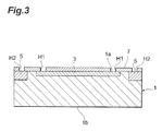
- an insulating layer 7 is formed on the first principal surface 1a side of the n - type semiconductor substrate 1 (cf. Fig. 3 ).
- the insulating layer 7 is comprised of SiO 2 and is formed by thermal oxidation of the n - type semiconductor substrate 1.
- the insulating layer 7 has the thickness of, for example, about 0.1 ⁇ m.
- a contact hole H1 is formed in the insulating layer 7 on the p + type semiconductor region 3 and a contact hole H2 is formed in the insulating layer 7 on the n + type semiconductor region 5.
- An antireflective (AR) layer comprised of SiN may be formed instead of the insulating layer 7.
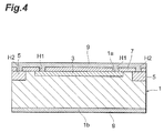
- a passivation layer 9 is formed on the second principal surface 1b of the n - type semiconductor substrate 1 and on the insulating layer 7 (cf. Fig. 4 ).
- the passivation layer 9 is comprised of SiN and is formed, for example, by the plasma CVD process.
- the passivation layer 9 has the thickness of, for example, 0.1 ⁇ m.
- the n - type semiconductor substrate 1 is polished from the second principal surface 1b side before the thickness of the n - type semiconductor substrate 1 reaches a desired thickness (cf. Fig. 5 ). This process removes the passivation layer 9 from on the second principal surface 1b of the n - type semiconductor substrate 1, thereby exposing the n - type semiconductor substrate 1.
- a surface exposed by polishing is also referred to herein as the second principal surface 1b.
- the desired thickness is, for example, 270 ⁇ m.
- the second principal surface 1b of the n - type semiconductor substrate 1 is subjected to irradiation with a pulsed laser beam PL, thereby forming an irregular asperity 10 (cf. Fig. 6 ).
- the n - type semiconductor substrate 1 is placed in a chamber C, and the n - type semiconductor substrate 1 is irradiated with the pulsed laser beam PL from a pulse laser generating device PLD located outside the chamber C.
- the chamber C has a gas inlet port G In and a gas outlet port G OUT .
- An inert gas (e.g., nitrogen gas, argon gas, or the like) is introduced through the gas inlet port G IN and discharged through the gas outlet port G OUT , thereby forming an inert gas flow G f in the chamber C. Dust and other materials made during the irradiation with the pulsed laser beam PL are discharged as trapped into the inert gas flow G f , to the outside of the chamber C, thereby preventing processing debris, dust, and other materials from attaching to the n - type semiconductor substrate 1.
- inert gas e.g., nitrogen gas, argon gas, or the like
- the pulse laser generating device PLD to be used is a picosecond to femtosecond pulse laser generating device and a picosecond to femtosecond pulsed laser beam is applied across the entire area of the second principal surface 1b.
- the second principal surface 1b is roughened by the picosecond to femtosecond pulsed laser beam, whereby the irregular asperity 10 is formed throughout the entire area of the second principal surface 1b, as shown in Fig. 8 .
- the irregular asperity 10 has facets intersecting with a direction perpendicular to the first principal surface 1a.
- the height difference of asperity 10 is, for example, about 0.5 to 10 ⁇ m and the spacing of projections in the asperity 10 is about 0.5 to 10 ⁇ m.
- the picosecond to femtosecond pulsed laser beam has the pulse duration of, for example, about 50 fs-2 ps, the intensity of, for example, about 4 to 16 GW, and the pulse energy of, for example, about 200 to 800 ⁇ J/pulse. More generally, the peak intensity is 3 ⁇ 10 11 to 2.5 ⁇ 10 13 (W/cm 2 ) and the fluence is about 0.1 to 1.3 (J/cm 2 ).
- Fig. 8 is an SEM image resulting from observation of the irregular asperity 10 formed in the second principal surface 1b.
- an accumulation layer 11 is formed on the second principal surface 1b side of the n - type semiconductor substrate 1 (cf. Fig. 9 ).
- the accumulation layer 11 is formed by ion implantation or diffusion of an n-type impurity from the second principal surface 1b side in the n - type semiconductor substrate 1 so that an impurity concentration thereof becomes higher than that of the n - type semiconductor substrate 1.
- the accumulation layer 11 has the thickness of, for example, about 1 ⁇ m.
- the n - type semiconductor substrate 1 is subjected to a thermal treatment (annealing).
- the n - type semiconductor substrate 1 is heated, for example, in the temperature range of about 800 to 1000°C under an ambience of N 2 gas for about 0.5 to 1 hour.
- the electrode 13 is formed in the contact hole H1 and the electrode 15 in the contact hole H2.
- the electrodes 13, 15 each are comprised of aluminum (A1) or the like and have the thickness of, for example, about 1 ⁇ m. This completes the photodiode PD 1.
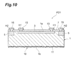
- the photodiode PD1 is provided with the n - type semiconductor substrate 1, as shown in Fig. 10 .
- the p + type semiconductor region 3 and the n + type semiconductor region 5 are formed on the first principal surface 1a side of the n - type semiconductor substrate 1 and a pn junction is formed between the n - type semiconductor substrate 1 and the p + type semiconductor region 3.
- the electrode 13 is in electrical contact with and connection to the p + type semiconductor region 3 through the contact hole H1.
- the electrode 15 is in electrical contact with and connection to the n + type semiconductor region 5 through the contact hole H2.
- the irregular asperity 10 is formed in the second principal surface 1b of the n - type semiconductor substrate 1.
- the accumulation layer 11 is formed on the second principal surface 1b side of the n - type semiconductor substrate 1 and the second principal surface 1b is optically exposed. That the second principal surface 1b is optically exposed encompasses not only the case where the second principal surface 1b is in contact with ambient gas such as air, but also the case where an optically transparent film is formed on the second principal surface 1b.
- the irregular asperity 10 is formed in the second principal surface 1b. For this reason, light L incident into the photodiode PD1 is reflected, scattered, or diffused by the asperity 10, as shown in Fig. 11 , to travel through a long distance in the n - type semiconductor substrate 1.
- a photodiode when light is incident from a direction normal to a light incident surface, light remaining unabsorbed in the photodiode (silicon substrate) is separated into a light component reflected on the back surface to the light incident surface and a light component passing through the photodiode. The light passing through the photodiode does not contribute to the sensitivity of the photodiode. The light component reflected on the back surface to the light incident surface, if absorbed in the photodiode, becomes a photocurrent. A light component still remaining unabsorbed is reflected or transmitted by the light incident surface as the light component having reached the back surface to the light incident surface was.
- the photodiode PD1 where light L is incident from the direction normal to the light incident surface (first principal surface 1a), when the light reaches the irregular asperity 10 formed in the second principal surface 1b, light components arriving thereat at angles of not less than 16.6° to a direction of emergence from the asperity 10 are totally reflected by the asperity 10. Since the asperity 10 is formed irregularly, it has various angles to the emergence direction and the totally reflected light components diffuse into various directions. For this reason, the totally reflected light components include light components absorbed inside the n - type semiconductor substrate 1 and light components arriving at the first principal surface 1a and side faces.
- the light components arriving at the first principal surface 1a and side faces travel in various directions because of the diffusion on the asperity 10, the light components arriving at the first principal surface 1a and the side faces are extremely highly likely to be totally reflected on the first principal surface 1a and the side faces.
- the light components totally reflected on the first principal surface 1a and the side faces are repeatedly totally reflected on different faces to further increase their travel distance.
- the light L incident into the photodiode PD1 is absorbed in the n - type semiconductor substrate 1 during travel through the long distance inside the n - type semiconductor substrate 1 to be detected as a photocurrent.
- the light L incident into the photodiode PD1 mostly travels, without being transmitted by the photodiode PD1, through the long travel distance to be absorbed in the n - type semiconductor substrate 1. Therefore, the photodiode PD1 is improved in the spectral sensitivity characteristic in the red to near-infrared wavelength band.
- the light components arriving at the first principal surface 1a and the side faces are diffused by the asperity but travel in uniform directions. Therefore, the light components arriving at the first principal surface 1a and the side faces are less likely to be totally reflected on the first principal surface 1a and the side faces. This results in increase in light passing through the first principal surface 1a and the side faces, and through the second principal surface 1b, and thus the travel distance of the light incident into the photodiode must be short. As a result, it becomes difficult to improve the spectral sensitivity characteristic in the near-infrared wavelength band.
- Example 1 We fabricated a photodiode with the above-described configuration (referred to as Example 1) and a photodiode without the irregular asperity in the second principal surface of the n - type semiconductor substrate (referred to as Comparative Example 1), and investigated their spectral sensitivity characteristics.
- Example 1 and Comparative Example 1 have the same configuration, except for the formation of the irregular asperity by irradiation with the pulsed laser beam.
- the size of the n - type semiconductor substrate 1 was set to 6.5 mm ⁇ 6.5 mm.
- the size of the p + type semiconductor region 3, or a photosensitive region was set to 5.8 mm ⁇ 5.8 mm.
- a bias voltage VR applied to the photodiodes was set to 0 V
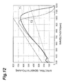
- the spectral sensitivity characteristic of Example 1 is represented by T1 and the spectral sensitivity characteristic of Comparative Example 1 by characteristic T2.
- the vertical axis represents the spectral sensitivity (mA/W) and the horizontal axis the wavelength of light (nm).
- a characteristic indicated by a chain line represents a spectral sensitivity characteristic where the quantum efficiency (QE) is 100%, and a characteristic indicated by a dashed line, a spectral sensitivity characteristic where the quantum efficiency is 50%.
- Example 1 We also checked temperature characteristics of spectral sensitivity in Example 1 and Comparative Example 1.
- the characteristic of temperature coefficient of Example 1 is represented by T3 and that of Comparative Example 1 by characteristic T4.
- the vertical axis represents the temperature coefficient (%/°C) and the horizontal axis the wavelength of light (nm).
- the temperature coefficient in Comparative Example 1 is 0.7 %/°C, whereas the temperature coefficient in Example 1 is 0.2 %/°C, demonstrating lower temperature dependence.
- an increase in temperature leads to an increase in spectral sensitivity because of increase in absorption coefficient and decrease in bandgap energy.
- the change of spectral sensitivity due to temperature rise is smaller than in Comparative Example 1.
- the accumulation layer 11 is formed on the second principal surface 1b side of the n - type semiconductor substrate 1. This induces recombination of unnecessary carriers generated independent of light on the second principal surface 1b side, which can reduce dark current.
- the accumulation layer 11 prevents carriers generated by light near the second principal surface 1b, from being trapped in the second principal surface 1b. For this reason, the carriers generated by light efficiently migrate to the pn junction portion, which can further improve the photodetection sensitivity of the photodiode PD1.
- the n - type semiconductor substrate 1 is subjected to the thermal treatment. This treatment restores the crystallinity of the n - type semiconductor substrate 1, which can prevent such a problem as increase of dark current.
- the electrodes 13, 15 are formed. This prevents the electrodes 13, 15 from melting during the thermal treatment, even in the case where the electrodes 13, 15 are made of a metal with a relatively low melting point. Therefore, the electrodes 13, 15 can be appropriately formed without being affected by the thermal treatment.
- the irregular asperity 10 is formed by the irradiation with the picosecond to femtosecond pulsed laser beam. This permits the irregular asperity 10 to be appropriately and readily formed.
- FIG. 14 to 16 are drawings for explaining the manufacturing method of the photodiode according to the second embodiment.
- the manufacturing method of the second embodiment, up to the polishing of the n - type semiconductor substrate 1 from the second principal surface 1b side, is the same as the manufacturing method of the first embodiment, and the description of the previous steps before it is omitted herein.
- the accumulation layer 11 is formed on the second principal surface 1b side of the n - type semiconductor substrate 1 (cf. Fig. 14 ).
- the formation of the accumulation layer 11 is carried out in the same manner as in the first embodiment.
- the accumulation layer 11 has the thickness of, for example, about 1 ⁇ m.
- the second principal surface 1b of the n - type semiconductor substrate 1 is irradiated with the pulsed laser beam PL to form the irregular asperity 10 (cf. Fig. 15 ).
- the formation of the irregular asperity 10 is carried out in the same manner as in the first embodiment.
- the n - type semiconductor substrate 1 is subjected to a thermal treatment. Thereafter, the passivation layer 9 formed on the insulating layer 7 is removed and then the electrodes 13, 15 are formed (cf. Fig. 16 ). This completes the photodiode PD2.
- the travel distance of light incident into the photodiode PD2 also becomes long and the distance of absorption of light also becomes long. This allows the photodiode PD2 also to be improved in the spectral sensitivity characteristic in the red to near-infrared wavelength band.
- the thickness of the accumulation layer 11 is larger than the height difference of the irregular asperity 10. For this reason, even if the irregular asperity 10 is formed by the irradiation with the pulsed laser beam after the formation of the accumulation layer 11, the accumulation layer 11 remains with certainty. Therefore, it is feasible to ensure the operational effect by the accumulation layer 11.
- FIG. 17 to 21 are drawings for explaining the manufacturing method of the photodiode according to the third embodiment.
- the manufacturing method of the third embodiment, up to the formation of the passivation layer 9, is the same as the manufacturing method of the first embodiment, and the description of the previous steps before it is omitted herein.
- a portion corresponding to the p + type semiconductor region 3 in the n - type semiconductor substrate 1 is thinned from the second principal surface 1b side while leaving a surrounding region around the thinned portion (cf. Fig. 17 ).
- the thinning of the n - type semiconductor substrate 1 is carried out, for example, by anisotropic etching based on alkali etching using a potassium hydroxide solution, TMAH (tetramethylammonium hydroxide solution), or the like.
- the thinned portion of the n - type semiconductor substrate 1 has the thickness of, for example, about 100 ⁇ m, and the surrounding region around it has the thickness of, for example, about 300 ⁇ m.
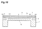
- the n - type semiconductor substrate 1 is polished from the second principal surface 1b side before the thickness of the surrounding region of the n - type semiconductor substrate 1 reaches a desired thickness (cf. Fig. 18 ).
- the desired thickness herein is, for example, 270 ⁇ m.
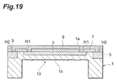
- the second principal surface 1b of the n - type semiconductor substrate 1 is irradiated with the pulsed laser beam PL to form the irregular asperity 10 (cf. Fig. 19 ).
- the formation of the irregular asperity 10 is carried out in the same manner as in the first embodiment.
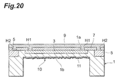
- the accumulation layer 11 is formed on the second principal surface 1b side of the thinned portion of the n - type semiconductor substrate 1 (cf. Fig. 20 ).
- the formation of the accumulation layer 11 is carried out in the same manner as in the first embodiment.
- the accumulation layer 11 has the thickness of, for example, about 3 ⁇ m.
- the n - type semiconductor substrate 1 is subjected to a thermal treatment and thereafter, the passivation layer 9 formed on the insulating layer 7 is removed, followed by formation of the electrodes 13, 15 (cf. Fig. 21 ). This completes the photodiode PD3.
- the travel distance of light incident into the photodiode PD3 also becomes long and the distance of absorption of light also becomes long. This allows the photodiode PD3 also to be improved in the spectral sensitivity characteristic in the red to near-infrared wavelength band.
- the portion corresponding to the p + type semiconductor region 3 in the n - type semiconductor substrate 1 is thinned from the second principal surface 1b side while leaving the surrounding region around the thinned portion. This permits the photodiode PD3 to be formed with respective light incident surfaces on the first principal surface 1a and the second principal surface 1b sides of the n - type semiconductor substrate 1.
- FIG. 22 to 24 are drawings for explaining the manufacturing method of the photodiode according to the fourth embodiment.
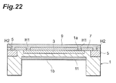
- the manufacturing method of the fourth embodiment, up to the thinning of the n - type semiconductor substrate 1, is the same as the manufacturing method of the third embodiment, and the description of the previous steps before it is omitted herein.
- the accumulation layer 11 is formed on the second principal surface 1b side of the thinned portion of the n - type semiconductor substrate 1 (cf. Fig. 22 ).
- the formation of the accumulation layer 11 is carried out in the same manner as in the first embodiment.
- the accumulation layer 11 has the thickness of, for example, about 3 ⁇ m.
- the second principal surface 1b of the n - type semiconductor substrate 1 is irradiated with the pulsed laser beam PL to form the irregular asperity 10 (cf. Fig. 23 ).
- the formation of the irregular asperity 10 is carried out in the same manner as in the first embodiment.
- the n - type semiconductor substrate 1 is subjected to a thermal treatment as in the first embodiment. Then the passivation layer 9 formed on the insulating layer 7 is removed and thereafter, the electrodes 13, 15 are formed (cf. Fig. 24 ). This completes the photodiode PD4.
- the travel distance of light incident into the photodiode PD4 also becomes long and the distance of absorption of light also becomes long. This allows the photodiode PD4 also to be improved in the spectral sensitivity characteristic in the red to near-infrared wavelength band.
- the portion corresponding to the p + type semiconductor region 3 in the n - type semiconductor substrate 1 is thinned from the second principal surface 1b side while leaving the surrounding region around the thinned portion. This permits the photodiode PD4 to be formed with respective light incident surfaces on the first principal surface 1a and the second principal surface 1b sides of the n - type semiconductor substrate 1.
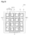
- FIG. 25 is a plan view schematically showing the photodiode array PDA1 of the fifth embodiment.
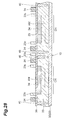
- Fig. 26 is a drawing showing a cross-sectional configuration along the line XXVI-XXVI of the photodiode array PDA1 shown in Fig. 25 .
- the photodiode array PDA1 is composed of a plurality of semiconductor layers and an insulating layer layered on a substrate 22. As shown in Fig. 25 , the photodiode array PDA1 is a multichannel avalanche photodiode for photon counting in which a plurality of photodetecting channels CH for detection target light to be entered thereinto are formed in a matrix pattern (4 ⁇ 4 in the present embodiment). There are signal conducting wires 23, resistors 24, and an electrode pad 25 provided on the top side of the photodiode array PDA I .
- the substrate 22 has, for example, a square shape about 1 mm on each side.
- Each photodetecting channel CH has, for example, a square shape.
- the signal conductor wire 23 consists of a readout portion 23a, connecting portions 23b, and channel peripheral portions 23c.
- the readout portion 23a transfers a signal output from each photodetecting channel CH.
- the connecting portion 23b connects each resistor 24 and the readout portion 23a.
- Each channel peripheral portion 23c is routed so as to surround the periphery of the photodetecting channel CH.
- the readout portion 23a is connected to each of the photodetecting channels CH arranged in two adjacent columns with the readout portion 23a in between, and is connected at one end thereof to the electrode pad 25. Since in the present embodiment the photodiodes are arranged in the 4 ⁇ 4 matrix pattern, there are two readout portions 23a as wiring on the photodiode array PDA1 and these are connected both to the electrode pad 25.
- the signal conducting wires 23 are comprised, for example, of aluminum (Al).
- the resistor 24 is provided for each photodetecting channel CH through one end portion 24a and the channel peripheral portion 23c and is connected through the other end portion 24b and the connecting portion 23b to the readout portion 23a.
- a plurality of resistors 24 (eight in the present embodiment) connected to an identical readout portion 23a are connected to the readout portion 23a.
- the resistors 24 are comprised, for example, of polysilicon (Poly-Si).
- the photodiode array PDA1 is provided with a substrate 22 having a semiconductor layer with the conductivity type of n-type (first conductivity type), a p - type semiconductor layer 33 with the conductivity type of p-type (second conductivity type) formed on the substrate 22, p + type semiconductor regions 34 with the conductivity type of p-type formed on the p - type semiconductor layer 33, a protecting film 36, a separating portion 40 with the conductivity type of n-type (first conductivity type) formed in the p - type semiconductor layer 33, and the aforementioned signal conducting wires 23 and resistors 24 formed on the protecting film 36.
- the detection target light is incident from the top side or the bottom side in Fig. 26 .
- the substrate 22 has a substrate member S, an insulating film 31 formed on the substrate member S, and an n + type semiconductor layer 32 formed on the insulating film 31.
- the substrate member S is comprised of Si (silicon).
- the insulating film 31 is comprised, for example, of SiO 2 (silicon oxide).
- the n + type semiconductor layer 32 is a semiconductor layer with the conductivity type of n-type comprised of Si and having a high impurity concentration.
- the thickness of the n + type semiconductor layer 32 is, for example, 1 ⁇ m-12 ⁇ m.
- the p - type semiconductor layer 33 is an epitaxial semiconductor layer with the conductivity type of p-type having a low impurity concentration.
- the p - type semiconductor layer 33 forms pn junctions at the interface to the substrate 22.
- the p - type semiconductor layer 33 has a plurality of multiplication regions AM for avalanche multiplication of carriers generated with incidence of the detection target light, corresponding to the respective photodetecting channels CH.
- the thickness of the p - type semiconductor layer 33 is, for example, 3 ⁇ m-5 ⁇ m.
- the p - type semiconductor layer 33 is comprised of Si. Therefore, the n + type semiconductor layer 32 and the p - type semiconductor layer 33 constitute a silicon substrate.
- each multiplication region AM is a region near the interface to the substrate 22 in the p - type semiconductor layer 33 located below the p + type semiconductor region 34 in the lamination direction of semiconductor layers (which will be referred to hereinafter simply as the lamination direction).
- the p + type semiconductor regions 34 are comprised of Si.
- the separating portion 40 is formed between the plurality of photodetecting channels CH to separate the photodetecting channels CH. Namely, the separating portion 40 is formed so as to form the multiplication regions AM in the p - type semiconductor layer 33 in one-to-one correspondence to the respective photodetecting channels CH.
- the separating portion 40 is formed in a two-dimensional lattice pattern on the substrate 22 so as to completely surround the periphery of each multiplication region AM.
- the separating portion 40 is formed so as to penetrate from the top side to the bottom side of the p - type semiconductor layer 33 in the lamination direction.
- the separating portion 40 is a semiconductor layer with the conductivity type of n-type an impurity of which is comprised, for example, of P and an impurity concentration of which is high.
- the separating portion 40 may be formed in such a manner that a trench is formed by etching near centers of regions corresponding to the separating portion 40 and thereafter performing diffusion of the impurity.
- a light shielding portion may be formed in the trench groove by filling the trench groove with a material to absorb or reflect the light in the wavelength band to be absorbed by the photodetecting channels. In this case, it is feasible to prevent crosstalk caused by influence of emission by avalanche multiplication on neighboring photodetecting channels.
- the p - type semiconductor layer 33, p + type semiconductor regions 34, and separating portion 40 form a flat surface on the top side of the photodiode array PDA1 and the protecting film 36 is formed thereon.
- the protecting film 36 is made of an insulating layer comprised, for example, of SiO 2 .
- the signal conducting wires 23 and resistors 24 are formed on the protecting film 36.
- the readout portions 23a of the signal conducting wires 23 and the resistors 24 are formed above the separating portion 40.
- the signal conducting wires 23 function as anodes and the photodiode array may be provided with a transparent electrode layer (e.g., a layer comprised of ITO (Indium Tin Oxide)) over the entire surface on the bottom side (the side without the insulating film 31) of the substrate 22, as a cathode though not shown.
- a transparent electrode layer e.g., a layer comprised of ITO (Indium Tin Oxide)
- ITO Indium Tin Oxide
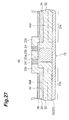
- Fig. 27 is a drawing for schematically explaining the connection relation of each photodetecting channel CH to the signal conducting wire 23 and resistor 24.
- the p + type semiconductor region 34 of each photodetecting channel CH is directly connected to the signal conducting wire 23 (channel peripheral portion 23c). This establishes electrical connection between the signal conducting wire 23 (channel peripheral portion 23c) and the p - type semiconductor layer 33.
- the p - type semiconductor layer 33 and one end 24a of the resistor 24 are connected through the signal conducting wire 23 (channel peripheral portion 23c) and the other end 24b of each resistor 24 is connected through the connecting portion 23b to the readout portion 23a.
- the region where the plurality of photodetecting channels CH are formed is thinned from the substrate member S side, so as to remove a portion corresponding to the region where the plurality of photodetecting channels CH are formed in the substrate member S.
- the substrate member S exists as a frame portion around the thinned region. By removing the frame portion, the substrate 22 may have a configuration wherein the entire region is thinned, i.e., the whole substrate member S is removed.
- the removal of the substrate member S can be implemented by etching (e.g., dry etching or the like), polishing, and so on.
- the insulating film 31 also functions as an etching stop layer. The insulating film 31 exposed after the removal of the substrate member S is removed as described later.
- the irregular asperity 10 is formed throughout the entire region where the plurality of photodetecting channels CH are formed.
- the region where the irregular asperity 10 is formed in the surface of the n + type semiconductor layer 32 is optically exposed. That the surface of the n + type semiconductor layer 32 is optically exposed embraces, not only the case where the surface of the n + type semiconductor layer 32 is in contact with ambient gas such as air, but also the case where an optically transparent film is formed on the surface of the n + type semiconductor layer 32.
- the irregular asperity 10 may also be formed only in the regions opposed to the respective photodetecting channels CH.
- the irregular asperity 10 is formed by irradiating the insulating film 31 exposed after the removal of the substrate member S with a pulsed laser beam, in the same manner as in the aforementioned embodiments. Namely, when the exposed insulating film 31 is irradiated with the pulsed laser beam, the insulating film 31 is removed and the surface of the n + type semiconductor layer 32 is roughened by the pulsed laser beam, thereby forming the irregular asperity 10.
- a pulse laser generating device to irradiate the pulsed laser beam can be a picosecond to femtosecond pulse laser generating device.
- the irregular asperity 10 has facets intersecting with the direction perpendicular to the surface of the n + type semiconductor layer 32.
- the height difference of the asperity 10 is, for example, about 0.5-10 ⁇ m and the spacing of projections in the asperity 10 is about 0.5-10 ⁇ m.
- the picosecond to femtosecond pulsed laser beam has the pulse duration of, for example, about 50 fs-2 ps, the intensity of, for example, about 4-16 GW, and the pulse energy of, for example, about 200-800 ⁇ J/pulse. More generally, the peak intensity is about 3 ⁇ 10 11 -2.5 ⁇ 10 13 (W/cm 2 ) and the fluence about 0.1-1.3(J/cm 2 ).
- the substrate 22 is preferably subjected to a thermal treatment (anneal).
- a thermal treatment for example, the substrate 22 is heated in the temperature range of about 800 to 1000°C in an ambience of N 2 gas or the like for about 0.5 to 1.0 hour.
- the foregoing thermal treatment restores the crystallinity of the n + type semiconductor layer 32 and thus prevents the problem such as increase of dark current.
- the photodiode array PDA1 configured as described above is used for photon counting, it is operated under an operation condition called a Geiger mode.
- a reverse voltage e.g., 50 V or more
- the detection target light is incident from the top side into each photodetecting channel CH in this state, the target light is absorbed in each photodetecting channel CH to generate a carrier.
- the generated carrier migrates as accelerated according to an electric field in each photodetecting channel CH to be multiplied in each multiplication region AM. Then the multiplied carriers are taken out through the resistor 24 and through the signal conducting wire 23 to the outside to be detected based on a wave height value of an output signal thereof.
- the photodiode array PDA1 accomplishes the photon counting by the single irradiation operation with the detection target light.
- the irregular asperity 10 is formed in the surface of the n + type semiconductor layer 32 in the photodiode array PDA1. For this reason, the light incident into the photodiode array PDA1 is reflected, scattered, or diffused by the asperity 10 to travel through a long distance in the photodiode array PDA1.
- the photodiode array PDA1 is used as a front-illuminated type photodiode array and where the light is incident from the protecting film 36 side into the photodiode array PDA1
- the irregular asperity 10 formed in the surface of the n + type semiconductor layer 32 when the light reaches the irregular asperity 10 formed in the surface of the n + type semiconductor layer 32, light components arriving thereat at angles of not less than 16.6° to the direction of emergence from the asperity 10 are totally reflected by the asperity 10. Since the asperity 10 is formed irregularly, it has various angles relative to the emergence direction and the totally reflected light components diffuse into various directions. For this reason, the totally reflected light components include light components absorbed in each photodetecting channel CH and light components reaching the surface on the protecting film 36 side and the side faces of the n + type semiconductor layer 32.
- the light components reaching the surface on the protecting film 36 side and the side faces of the n + type semiconductor layer 32 travel in various directions because of the diffusion on the asperity 10. For this reason, the light components reaching the surface on the protecting film 36 side and the side faces of the n + type semiconductor layer 32 are extremely highly likely to be totally reflected on the surface on the protecting film 36 side and the side faces of the n + type semiconductor layer 32.
- the light components totally reflected on the surface on the protecting film 36 side and the side faces of the n + type semiconductor layer 32 are repeatedly totally reflected on different faces, to further increase their travel distance. While the light incident into the photodiode array PDA1 travels through the long distance inside the photodiode array PDA1, it is absorbed in each photodetecting channel CH to be detected as a photocurrent.
- the photodiode array PDA1 is used as a back-thinned type photodiode array and where the light is incident from the front surface side of the n + type semiconductor layer 32 into the photodiode array PDA1, the incident light is scattered by the asperity 10 and travels in various directions in the photodiode array PDA1.
- the light components reaching the surface on the protecting film 36 side and the side faces of the n + type semiconductor layer 32 travel in various directions because of the diffusion on the asperity 10. For this reason, the light components reaching the surface on the protecting film 36 side and the side faces of the n + type semiconductor layer 32 are extremely highly likely to be totally reflected on each surface.
- the light components totally reflected on the surface on the protecting film 36 side and the side faces of the n + type semiconductor layer 32 are repeatedly totally reflected on different faces and reflected, scattered, or diffused on the asperity 10, to further increase their travel distance.
- the light incident into the photodiode array PDA1 is reflected, scattered, or diffused by the asperity 10 to travel through the long distance in the photodiode array PDA1, and to be absorbed in each photodetecting channel CH to be detected as a photocurrent.
- the light L incident into the photodiode array PDA1 mostly travels through the long travel distance to be absorbed in each photodetecting channel CH, without passing through the photodiode array PDA1. Therefore, the photodiode array PDA1 is improved in the spectral sensitivity characteristic in the red to near-infrared wavelength band.
- the irregular asperity 10 is formed in the surface of the n + type semiconductor layer 32. For this reason, it induces recombination of unnecessary carriers generated independent of light on the surface side where the irregular asperity 10 is formed, so as to reduce the dark current.
- the n + type semiconductor layer 32 functions as an accumulation layer to prevent carriers generated by light near the surface of the n + type semiconductor layer 32 from being trapped in the surface. For this reason, the carriers generated by light efficiently migrate to the multiplication regions AM, so as to improve the photodetection sensitivity of the photodiode array PDA1.
- the irregular asperity 10 is also formed in the surface corresponding to the regions between the plurality of photodetecting channels CH in the n + type semiconductor layer 32 and the surface is optically exposed. For this reason, light incident into the regions between the plurality of photodetecting channels CH is also reflected, scattered, or diffused by the irregular asperity 10 to be absorbed in any one of the photodetecting channels CH. Therefore, the detection sensitivity is not lowered in the regions between the photodetecting channels CH, whereby the photodetection sensitivity of the photodiode array PDA1 is further improved.
- each photodetecting channel CH is not one to detect a position of incidence of light and the output of the array is the sum of outputs of the respective photodetecting channels CH. For this reason, crosstalk between the photodetecting channels CH does not matter, and the point is that incident light is detected by any one of the photodetecting channels CH.
- the thickness of the n + type semiconductor layer 32 is larger than the height difference of the irregular asperity 10. For this reason, it is feasible to certainly ensure the operational effect as an accumulation layer by the n + type semiconductor layer 32.
- the pn junctions are composed of the n + type semiconductor layer 32 of the substrate 22 and the p - type semiconductor layer 33 being the epitaxial semiconductor layer formed on the n + type semiconductor layer 32 of the substrate 22.
- the multiplication regions AM are formed in the p - type semiconductor layer 33 where the pn junctions are substantialized, and the correspondence of each multiplication region AM to each photodetecting channel CH is realized by the separating portion 40 formed between the photodetecting channels CH.
- a pn junction surface is composed of an interface between the n + type semiconductor layer 32 and the p - type semiconductor layer 33 and an interface between the separating portion 40 and the p - type semiconductor layer 33.
- the photodiode array PDA1 has no ends (edges) of pn junctions where edge breakdown occurs in the Geiger mode operation. For this reason, the photodiode array PDA1 does not have to be provided with a guard ring for the pn junction of each photodetecting channel CH. This enables the photodiode array PDA1 to have a drastically high aperture rate.
- the channels can be separated well because the separating portion 40 is formed between the photodetecting channels CH.
- the signal conducting wires 23 are prevented from crossing above the multiplication regions AM, i.e., above the photodetection surface. For this reason, the aperture rate is more increased. Furthermore, it is considered to be also effective to suppression of dark current. In the photodiode array PDA1, the aperture rate is still more increased because the resistors 24 are also formed above the separating portion 40.
- the photodiode array PDA1 is constructed by removing the substrate member S from the region where the plurality of photodetecting channels CH are formed, so as to suppress the after pulse.
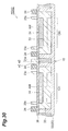
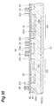
- Fig. 28 is a drawing schematically showing a cross-sectional configuration of a first modification example of the photodiode array PDA1 of the fifth embodiment.
- a plurality of separating portions 40 are formed between the photodetecting channels CH.
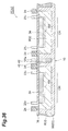
- Fig. 29 is a drawing schematically showing a cross-sectional configuration of a second modification example of the photodiode array PDA1 of the present embodiment.
- the separating portion 40 is formed only in the vicinity of the top surface (detection target light incident surface) without penetrating from the top side to the bottom side of the p - type semiconductor layer 33 in the lamination direction.
- the above embodiment showed the configuration wherein the epitaxial semiconductor layer had the second conductivity type, but it is also possible to adopt a configuration wherein the epitaxial semiconductor layer has the first conductivity type, second conductivity type semiconductor regions are provided in the semiconductor layer, and the pn junctions are composed of the first conductivity type epitaxial semiconductor layer and the second conductivity type semiconductor regions.
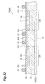
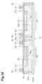
- the photodiode array PDA1 is mounted on a board WB as shown in Figs. 39 and 40 .
- the photodiode array PDA1 is fixed to the board WB by bonding or the like and is electrically connected to wiring formed on the board WB by wire bonding.
- the photodiode array PDA1 is fixed to a board WB and electrically connected to wiring formed on the board WB by bumps.
- the board WB is preferably optically transparent.
- the board WB is also preferably optically transparent.
- the underfill resin to be filled is also preferably optically transparent.
- FIG. 30 is a drawing schematically showing a cross-sectional configuration of the photodiode array PDA2 of the sixth embodiment.
- the photodiode array PDA2 of the sixth embodiment is different from the photodiode array PDA1 of the fifth embodiment in that the separating portion 40 has a light shielding portion.
- the separating portion 40 includes the light shielding portion 42 comprised of a material to absorb light in the wavelength band of detection target light (from visible to near infrared) to be detected by the photodetecting channels CH.
- the light shielding portion 42 is formed so as to be embedded in the separating portion 40 like a core extending from the top side to the bottom side of the p - type semiconductor layer 33.
- the light shielding portion 42 is comprised, for example, of a black photoresist obtained by mixing a black dye or a pigment such as insulated carbon black in a photoresist, or a metal such as tungsten.
- the light shielding portion 42 needs to be coated with an insulating film such as SiO 2
- the separating portion 40 may be formed by forming a trench near the centers of the regions corresponding to the separating portion 40 by etching and thereafter performing diffusion of the impurity. As shown in Fig.
- the light shielding portion may also be formed by filling the remaining trench groove with a material to absorb the light in the wavelength band to be absorbed by the photodetecting channels as described above (or a material to reflect the light in the wavelength band to be absorbed by the photodetecting channels, as described below). This can prevent the crosstalk caused by influence of emission by avalanche multiplication on neighboring photodetecting channels.
- the travel distance of the light incident into the photodiode array PDA2 becomes long and the distance of absorption of light also becomes long. This allows the photodiode array PDA2 also to be improved in the spectral sensitivity characteristic in the red to near-infrared wavelength band. Furthermore, the dark current is reduced and the photodetection sensitivity of the photodiode array PDA2 is also improved.
- the photodiode array PDA2 As in the photodiode array PDA1, there is no ends (edges) of the pn junctions to cause edge breakdown in the Geiger mode operation. For this reason, the photodiode array PDA2 does not have to be provided with a guard ring for the pn junction of each photodetecting channel CH, either. This allows the photodiode array PDA2 to have a higher aperture rate.
- the photodetecting channels CH are separated by the separating portion 40, it is feasible to well suppress the crosstalk.
- the aperture rate is more improved. Furthermore, it is considered to be also effective to suppression of dark current.
- Each separating portion 40 includes the light shielding portion 42 comprised of the material to absorb the light in the wavelength band of the detection target light to be detected by the photodetecting channels CH. Therefore, the light shielding portion absorbs the detection target light, and thus it becomes feasible to well suppress occurrence of crosstalk.
- the light shielding portion 42 is comprised of a material that absorbs light in the wavelength band of the detection target light to be detected by the photodetecting channels CH, particularly, in the visible to near-infrared wavelength band generated by avalanche multiplication, in order to prevent the light generated by avalanche multiplication from affecting the neighboring photodetecting channels CH. For this reason, it becomes feasible to well suppress occurrence of crosstalk.
- the light shielding portion 42 does not have to be limited to the material that absorbs the light in the visible to near-infrared band, but may be a material that reflects the light in the visible to near-infrared band. In this case, the light shielding portion reflects the detection target light and thus it becomes feasible to well suppress occurrence of crosstalk.
- the light shielding portion 42 is comprised of the material that reflects light in the wavelength band of the detection target light to be detected by the photodetecting channels CH, particularly, in the visible to near-infrared wavelength band generated by avalanche multiplication, in order to prevent the light generated by avalanche multiplication from affecting the neighboring photodetecting channels CH. For this reason, it becomes feasible to well suppress occurrence of crosstalk.
- the light shielding portion 42 does not have to be limited to the material absorbing or reflecting the light in the visible to near-infrared band, but may be any material that absorbs or reflects light in the wavelength band of the detection target light to be detected by the photodetecting channels CH.
- the light shielding portion 42 is preferably comprised of a material that absorbs or reflects light in the wavelength band of the detection target light to be detected by the photodetecting channels CH, particularly, in the visible to near-infrared wavelength band generated by avalanche multiplication, in order to prevent the light generated by avalanche multiplication from affecting the neighboring photodetecting channels CH.
- the light shielding portion 42 may be comprised of a material with the refractive index lower than that of the separating portion 40. In this case, the light is also reflected by the light shielding portion and thus it becomes feasible to well suppress occurrence of crosstalk.
- FIG. 31 is a drawing for schematically explaining a cross-sectional configuration of the photodiode array PDA3 of the seventh embodiment.
- the photodiode array PDA3 of the seventh embodiment is different from the photodiode array PDA1 of the fifth embodiment in that the signal conducting wires 23 are formed on a silicon nitride film.
- the photodiode array PDA3 is provided with a substrate 22 having a semiconductor layer with the conductivity type of n-type (first conductivity type), a p-type semiconductor layer 35 with the conductivity type of p-type (second conductivity type) formed on the substrate 22, p + type semiconductor regions 34 with the conductivity type of p-type formed on the p-type semiconductor layer 35, protecting films 36a, 36b, a separating portion 40 with the conductivity type of n-type (first conductivity type) formed in the p-type semiconductor layer 35, signal conducting wires 23 of aluminum, and resistors 24, for example, of Ply-Si.
- the substrate 22 has an n + type substrate member (not shown), and an n-type semiconductor layer 32 formed on the substrate member.
- the p-type semiconductor layer 35 is an epitaxial semiconductor layer with the conductivity type of p-type having an impurity concentration lower than that of the p + type semiconductor regions 34.
- the p-type semiconductor layer 35 forms pn junctions at its interface to the n-type semiconductor layer 32 of the substrate 22.
- the p-type semiconductor layer 35 has a plurality of multiplication regions AM for avalanche multiplication of carriers generated with incidence of detection target light, corresponding to the respective photodetecting channels CH.
- the p-type semiconductor layer 35 is comprised of Si.
- the p-type semiconductor layer 35, p + type semiconductor regions 34, and separating portion 40 form a flat surface on the top side of the photodiode array PDA3 and the protecting films 36a, 36b are formed thereon.
- the protecting film 36a is comprised of an insulating film of silicon oxide film (SiO 2 film) and the protecting film 36b is comprised of an insulating film of silicon nitride (SiN film or Si 3 N 4 film).
- the protecting film 36a, resistors 24, protecting film 36b, and signal conducting wires 23 are layered in this order on the separating portion 40.
- the protecting film 36a is layered on the separating portion 40.
- the resistors 24 are layered on the protecting film 36a.
- the protecting film 36b is layered except for a part of each resistor 24 on the protecting film 36a and on the resistors 24.
- the signal conducting wires 23 are layered for electrical connection, on the protecting film 36b and the parts of resistors 24 on which the protecting film 36b is not layered.
- a readout portion 23a of the signal conducting wire 23 is layered between resistors 24, and the signal conducting wire 23 as an electrical connection to the connecting portion 23b or the channel peripheral portion 23c is layered for electrical connection on each resistor 24.
- the protecting film 36b is layered except for a part on each p + type semiconductor region 34.
- the channel peripheral portion 23c of the signal conducting wire 23 for electrical connection is layered on the part of the p + type semiconductor region 34 without deposition of the protecting film 36b and on the part of the protecting film 36b layered on the p + type semiconductor region 34.
- the travel distance of the light incident into the photodiode array PDA3 becomes long and the distance of absorption of light also becomes long. This allows the photodiode array PDA3 also to be improved in the spectral sensitivity characteristic in the red to near-infrared wavelength band. Furthermore, the dark current is reduced and the photodetection sensitivity of the photodiode array PDA3 is improved.
- the photodiode array PDA3 like the photodiode array PDA1, has no ends (edges) of the pn junctions to cause edge breakdown in the Geiger mode operation. For this reason, the photodiode array PDA3 does not have to be provided with a guard ring for the pn junction of each photodetecting channel CH, either. This allows the photodiode array PDA3 to have a higher aperture rate.
- the aperture rate is more improved. Furthermore, it is considered to be also effective to suppression of dark current.
- the signal conducting wires 23 are comprised of aluminum, for example, if they are formed on an oxide film, there will arise a problem that aluminum leaks into the underlying film with application of high voltage. In view of this problem, the signal conducting wires 23 are formed on the protecting film 36b of silicon nitride film in the photodiode array PDA3. For this reason, aluminum is prevented from leaking into the underlying film (protecting film 36b) even with application of high voltage to the photodiode array PDA3.
- the protecting film 36b and the protecting film 36a or the resistor 24 are layered under the readout portion 23a of each signal conducting wire 23. For this reason, aluminum is well prevented from leaking into the separating portion 40 and the p-type semiconductor layer 35 with application of high voltage.
- the resistors 24 of polysilicon are formed on the protecting film 36a, and the protecting film 36b and signal conducting wires 23 are formed on the resistors 24.
- a p-type semiconductor layer may be used instead of the n-type semiconductor layer 32.
- the pn junctions are established between the p-type semiconductor layer and the n + type substrate member S (substrate 22) and the multiplication portions AM are formed in this p-type semiconductor layer.
- FIG. 32 is a drawing schematically showing a cross-sectional configuration of the photodiode array PDA4 of the eighth embodiment.
- the photodiode array PDA4 of the eighth embodiment is different from the photodiode array PDA1 of the fifth embodiment in that it is not provided with the separating portion 40.
- the p - type semiconductor layer 33 has a plurality of multiplication regions AM so that the multiplication regions AM correspond to the respective photodetecting channels CH.
- the signal conducting wires 23 and resistors 24 are formed between the photodetecting channels CH.
- the travel distance of light incident into the photodiode array PDA4 becomes long and the distance of absorption of light also becomes long. This allows the photodiode array PDA4 also to be improved in the spectral sensitivity characteristic in the red to near-infrared wavelength band. Furthermore, the dark current is reduced and the photodetection sensitivity of the photodiode array PDA4 is improved.
- the photodiode array PDA4 like the photodiode array PDA1, has no ends (edges) of the pn junctions to cause edge breakdown in the Geiger mode operation, either. For this reason, the photodiode array PDA4 does not have to be provided with a guard ring for the pn junction of each photodetecting channel CH, either. This allows the photodiode array PDA4 to have a higher aperture rate. Furthermore, since the photodiode array PDA4 has no separating portion, it can demonstrate a much higher aperture rate.
- the aperture rate is more improved. Furthermore, it is considered to be also effective to suppression of dark current.
- the irregular asperity 10 is formed by irradiating the entire area of the second principal surface 1b with the pulsed laser beam, but the present invention is not limited to it.
- the irregular asperity 10 may also be formed by irradiating only the region opposed to the p + type semiconductor region 3 in the second principal surface 1b of the n - type semiconductor substrate 1 with the pulsed laser beam.
- the electrode 15 is in electrical contact with and connection to the n + type semiconductor region 5 formed on the first principal surface 1a side of the n - type semiconductor substrate 1, but it is not limited only to this example.
- the electrode 15 may be in electrical contact with and connection to the accumulation layer 11 formed on the second principal surface 1b side of the n - type semiconductor substrate 1.
- the electrode 15 is preferably formed outside the region opposed to the p + type semiconductor region 3 in the second principal surface 1b of the n - type semiconductor substrate 1.
- the reason for it is as follows: if the electrode 15 is formed in the region opposed to the p + type semiconductor region 3 in the second principal surface 1b of the n - type semiconductor substrate 1, the irregular asperity 10 formed in the second principal surface 1b is blocked by the electrode 15, causing an event of reduction in the spectral sensitivity in the near-infrared wavelength band.
- the conductivity types of p type and n type in the photodiodes PD1-PD4 in the first to fourth embodiments may be interchanged so as to be reverse to those described above.
- the number of photodetecting channels formed in the photodiode array is not limited to the number (4 ⁇ 4) in the above embodiments.
- the number of separating portion 40 formed between the photodetecting channels CH is not limited to the numbers shown in the above embodiments and modification examples, either, but it may be, for example, three or more.
- the signal conducting wires 23 do not have to be formed above the separating portion 40.
- the resistors 24 do not have to be formed above the separating portion 40, either.
- Each of the layers and others does not have to be the one exemplified in the above embodiments and modification examples.
- the conductivity types of p-type and n-type in the above-described photodiode arrays PDA1-PDA4 may be interchanged so as to be reverse to those described above.
- Fig. 33 is a drawing schematically showing a cross-sectional configuration of a photodiode array according to a modification example of the layer structure in the embodiment shown in Fig. 26 .
- Fig. 34 is a drawing schematically showing a cross-sectional configuration of a photodiode array according to a modification example of the layer structure in the embodiment shown in Fig. 28 .
- Fig. 35 is a drawing schematically showing a cross-sectional configuration of a photodiode array according to a modification example of the layer structure in the embodiment shown in Fig. 29 .
- Fig. 36 is a drawing schematically showing a cross-sectional configuration of a photodiode array according to a modification example of the layer structure in the embodiment shown in Fig. 30 .
- Fig. 37 is a drawing schematically showing a cross-sectional configuration of a photodiode array according to a modification example of the layer structure in the embodiment shown in Fig. 31 .
- Fig. 38 is a drawing schematically showing a cross-sectional configuration of a photodiode array according to a modification example of the layer structure in the embodiment shown in Fig. 32 .
- the basic planar configuration and connection relation of these are the same as those shown in Fig. 25 .
- an n-type semiconductor layer R33 or R35 is used instead of the p-type semiconductor layer 33 or p-type semiconductor layer 35 in Figs. 26 , 28 , 29 , 30 , 31 , and 32 .
- the pn junctions are formed at the interface between the low-concentration n-type semiconductor layer R33 (or R35) and the p-type semiconductor regions 34, depleted layers spread from the pn junctions toward the n-type semiconductor layer R33 (or R35), and, corresponding to the depleted layers, the multiplication regions AM are formed from the pn junction interfaces toward the n-type semiconductor layer R33 (or R35).
- the other structure and action are the same as those as described above.
- These photodiode arrays PDA1-PDA4 are configured so that the plurality of photodetecting channels CH for the detection target light to be entered thereinto are formed on the n-type substrate 22 having the n-type semiconductor layer 32. They are the photodiode arrays wherein the plurality of photodetecting channels CH for the detection target light to be entered thereinto are formed on the substrate having the n + type semiconductor layer 32 (S) of the first conductivity type.
- the plurality of photodetecting channels CH are provided with the substrate 22, the n - type epitaxial semiconductor layer R33 (or R35) of the first conductivity type, the p + type semiconductor regions 34 of, the second conductivity type, and the plurality of resistors 24.
- the epitaxial semiconductor layer R33 (or R35) is formed on the first conductivity type semiconductor layer 32 of the substrate 22.
- the epitaxial semiconductor layer R33 (or R35) has the plurality of multiplication regions AM for avalanche multiplication of carriers generated with incidence of the detection target light, so that the multiplication regions AM correspond to the respective photodetecting channels.
- the semiconductor regions 34 are formed in the epitaxial semiconductor layer R33 (or R35) to form the pn junctions at the interface to the epitaxial semiconductor layer R33 (or R35).
- the plurality of resistors 24 each have the two end portions and are provided for the respective photodetecting channels CH.
- the plurality of resistors 24 each are electrically connected through the one end portion 24a to the second conductivity type semiconductor region 34 in the epitaxial semiconductor layer R33 (or R35) and are connected through the other end portion 24b to the signal conducting wire 23.
- the resistors 24, as shown in Fig. 25 are provided for the respective photodetecting channels CH through the one end portion 24a and channel peripheral portion 23c and are connected each through the other end portion 24b and connecting portion 23b to the readout portion 23a.
- the plurality of resistors 24 to be connected to the same readout portion 23a are connected to the readout portion 23a.
- the pn junctions are composed of the epitaxial semiconductor layer R33 (or R35) of the first conductivity type on the substrate and the semiconductor regions 34 of the second conductivity type formed in the epitaxial semiconductor layer R33 (or R35).
- the multiplication regions AM are formed in the epitaxial semiconductor layer R33 (or R35) where the pn junctions are substantialized, and the multiplication regions AM corresponding to the respective photodetecting channels are present in the epitaxial semiconductor layer R33 (or R35).
- the present invention is applicable to semiconductor photodetection elements and photodetection apparatus.
- 1 n - type semiconductor substrate 1a first principal surface; 1b second principal surface; 3 p + type semiconductor region; 5 n + semiconductor region: 10 irregular asperity; 11 accumulation layer; 13, 15 electrodes; 22 substrate; 23 signal conducting wires; 24 resistors; 25 electrode pad; 31 insulating film; 32 n + type semiconductor layer; 33 p - type semiconductor layer; 34 p + type semiconductor regions; 35 p-type semiconductor layer; 36 protecting film; 40 separating portion; 42 light shielding portion; AM multiplication regions; CH photodetecting channels; S substrate member; PL pulsed laser beam; PD1-PD4 photodiodes; PDA1-PDA4 photodiode arrays.
Priority Applications (1)
| Application Number | Priority Date | Filing Date | Title |
|---|---|---|---|
| EP18206453.5A EP3467875B1 (fr) | 2009-02-24 | 2010-02-15 | Réseau de photodiodes |
Applications Claiming Priority (3)
| Application Number | Priority Date | Filing Date | Title |
|---|---|---|---|
| JP2009041078 | 2009-02-24 | ||
| JP2009136419A JP5185207B2 (ja) | 2009-02-24 | 2009-06-05 | フォトダイオードアレイ |
| PCT/JP2010/052212 WO2010098225A1 (fr) | 2009-02-24 | 2010-02-15 | Photodiode et barrette de photodiodes |
Related Child Applications (2)
| Application Number | Title | Priority Date | Filing Date |
|---|---|---|---|
| EP18206453.5A Division EP3467875B1 (fr) | 2009-02-24 | 2010-02-15 | Réseau de photodiodes |
| EP18206453.5A Division-Into EP3467875B1 (fr) | 2009-02-24 | 2010-02-15 | Réseau de photodiodes |
Publications (3)
| Publication Number | Publication Date |
|---|---|
| EP2403013A1 true EP2403013A1 (fr) | 2012-01-04 |
| EP2403013A4 EP2403013A4 (fr) | 2013-04-03 |
| EP2403013B1 EP2403013B1 (fr) | 2018-12-19 |
Family
ID=42665435
Family Applications (2)
| Application Number | Title | Priority Date | Filing Date |
|---|---|---|---|
| EP10746106.3A Active EP2403013B1 (fr) | 2009-02-24 | 2010-02-15 | Barrette de photodiodes |
| EP18206453.5A Active EP3467875B1 (fr) | 2009-02-24 | 2010-02-15 | Réseau de photodiodes |
Family Applications After (1)
| Application Number | Title | Priority Date | Filing Date |
|---|---|---|---|
| EP18206453.5A Active EP3467875B1 (fr) | 2009-02-24 | 2010-02-15 | Réseau de photodiodes |
Country Status (7)
| Country | Link |
|---|---|
| US (2) | US8742528B2 (fr) |
| EP (2) | EP2403013B1 (fr) |
| JP (1) | JP5185207B2 (fr) |
| KR (1) | KR101708069B1 (fr) |
| CN (1) | CN102334199B (fr) |
| TW (1) | TWI476906B (fr) |
| WO (1) | WO2010098225A1 (fr) |
Cited By (2)
| Publication number | Priority date | Publication date | Assignee | Title |
|---|---|---|---|---|
| EP2560215A1 (fr) * | 2010-04-14 | 2013-02-20 | Hamamatsu Photonics K.K. | Élément semi-conducteur photo-détecteur |
| CN106121470A (zh) * | 2016-07-26 | 2016-11-16 | 司夏 | 桥洞安全门 |
Families Citing this family (49)
| Publication number | Priority date | Publication date | Assignee | Title |
|---|---|---|---|---|
| US7057256B2 (en) | 2001-05-25 | 2006-06-06 | President & Fellows Of Harvard College | Silicon-based visible and near-infrared optoelectric devices |
| US7442629B2 (en) | 2004-09-24 | 2008-10-28 | President & Fellows Of Harvard College | Femtosecond laser-induced formation of submicrometer spikes on a semiconductor substrate |
| JP5185205B2 (ja) | 2009-02-24 | 2013-04-17 | 浜松ホトニクス株式会社 | 半導体光検出素子 |
| JP5185206B2 (ja) | 2009-02-24 | 2013-04-17 | 浜松ホトニクス株式会社 | 半導体光検出素子 |
| JP5185208B2 (ja) | 2009-02-24 | 2013-04-17 | 浜松ホトニクス株式会社 | フォトダイオード及びフォトダイオードアレイ |
| EP2478560A4 (fr) * | 2009-09-17 | 2014-06-18 | Sionyx Inc | Dispositifs d'imagerie photosensibles et procédés associés |
| US9673243B2 (en) | 2009-09-17 | 2017-06-06 | Sionyx, Llc | Photosensitive imaging devices and associated methods |
| US9911781B2 (en) | 2009-09-17 | 2018-03-06 | Sionyx, Llc | Photosensitive imaging devices and associated methods |
| US8692198B2 (en) | 2010-04-21 | 2014-04-08 | Sionyx, Inc. | Photosensitive imaging devices and associated methods |
| EP2583312A2 (fr) | 2010-06-18 | 2013-04-24 | Sionyx, Inc. | Dispositifs photosensibles à grande vitesse et procédés associés |
| DE202010012735U1 (de) | 2010-09-17 | 2011-04-14 | Ketek Gmbh | Strahlungsdetektor und Verwendung eines Strahlungsdetektors |
| US9496308B2 (en) | 2011-06-09 | 2016-11-15 | Sionyx, Llc | Process module for increasing the response of backside illuminated photosensitive imagers and associated methods |
| JP5808592B2 (ja) | 2011-07-04 | 2015-11-10 | 浜松ホトニクス株式会社 | 基準電圧決定方法及び推奨動作電圧決定方法 |
| JP2014525091A (ja) | 2011-07-13 | 2014-09-25 | サイオニクス、インク. | 生体撮像装置および関連方法 |
| TWI458111B (zh) * | 2011-07-26 | 2014-10-21 | Univ Nat Central | 水平式累崩型光檢測器結構 |
| US9064764B2 (en) | 2012-03-22 | 2015-06-23 | Sionyx, Inc. | Pixel isolation elements, devices, and associated methods |
| CN103208555A (zh) * | 2012-12-24 | 2013-07-17 | 西南技术物理研究所 | 紫外选择性硅雪崩光电探测芯片 |
| JP6466346B2 (ja) | 2013-02-15 | 2019-02-06 | サイオニクス、エルエルシー | アンチブルーミング特性を有するハイダイナミックレンジcmos画像センサおよび関連づけられた方法 |
| US9939251B2 (en) | 2013-03-15 | 2018-04-10 | Sionyx, Llc | Three dimensional imaging utilizing stacked imager devices and associated methods |
| JP6216448B2 (ja) * | 2013-06-26 | 2017-10-18 | 林 大偉LIN,Dai Wei | フォトダイオード |
| WO2014209421A1 (fr) | 2013-06-29 | 2014-12-31 | Sionyx, Inc. | Régions texturées formées de tranchées peu profondes et procédés associés. |
| US9425121B2 (en) | 2013-09-11 | 2016-08-23 | Taiwan Semiconductor Manufacturing Company, Ltd. | Integrated fan-out structure with guiding trenches in buffer layer |
| US9455211B2 (en) | 2013-09-11 | 2016-09-27 | Taiwan Semiconductor Manufacturing Company, Ltd. | Integrated fan-out structure with openings in buffer layer |
| US9281336B2 (en) * | 2013-09-26 | 2016-03-08 | Taiwan Semiconductor Manufacturing Co., Ltd | Mechanisms for forming backside illuminated image sensor device structure |
| US9876127B2 (en) * | 2013-11-22 | 2018-01-23 | Taiwan Semiconductor Manufacturing Company, Ltd. | Backside-illuminated photodetector structure and method of making the same |
| US9219185B2 (en) | 2013-12-19 | 2015-12-22 | Excelitas Technologies Singapore Pte. Ltd | CMOS integrated method for the fabrication of thermopile pixel with umbrella absorber on semiconductor substrate |
| US9373772B2 (en) | 2014-01-15 | 2016-06-21 | Excelitas Technologies Singapore Pte. Ltd. | CMOS integrated method for the release of thermopile pixel on a substrate by using anisotropic and isotropic etching |
| US9324760B2 (en) * | 2014-01-21 | 2016-04-26 | Excelitas Technologies Singapore Pte. Ltd | CMOS integrated method for fabrication of thermopile pixel on semiconductor substrate with buried insulation regions |
| CN104022130B (zh) * | 2014-06-20 | 2017-01-25 | 北京师范大学 | 硅光电倍增探测器 |
| JP2016062996A (ja) | 2014-09-16 | 2016-04-25 | 株式会社東芝 | 光検出器 |
| US9450007B1 (en) | 2015-05-28 | 2016-09-20 | Stmicroelectronics S.R.L. | Integrated circuit with reflective material in trenches and related methods |
| JP6738129B2 (ja) | 2015-07-28 | 2020-08-12 | 株式会社東芝 | 光検出器およびこれを用いたライダー装置 |
| WO2017038542A1 (fr) * | 2015-09-03 | 2017-03-09 | ソニーセミコンダクタソリューションズ株式会社 | Élément de capture d'image à semi-conducteurs et dispositif électronique |
| JP6730820B2 (ja) | 2016-03-10 | 2020-07-29 | 株式会社東芝 | 光検出器およびこれを用いたライダー装置 |
| JP6649207B2 (ja) * | 2016-08-26 | 2020-02-19 | 株式会社東芝 | 受光装置 |
| US10312391B2 (en) * | 2016-10-04 | 2019-06-04 | Omnivision Technologies, Inc. | Apparatus and method for single-photon avalanche-photodiode detectors with reduced dark count rate |
| JP6658910B2 (ja) * | 2016-10-28 | 2020-03-04 | 三菱電機株式会社 | 裏面入射型受光素子及び光モジュール |
| CN107039425B (zh) * | 2017-03-29 | 2018-07-13 | 湖北京邦科技有限公司 | 一种半导体光电倍增器件 |
| US20190088812A1 (en) * | 2017-09-15 | 2019-03-21 | Kabushiki Kaisha Toshiba | Photodetection element, photodetector and laser imaging detection and ranging apparatus |
| JP7109718B2 (ja) * | 2017-11-24 | 2022-08-01 | アイアールスペック株式会社 | 化合物半導体フォトダイオードアレイ |
| JP2018078304A (ja) * | 2017-12-07 | 2018-05-17 | 株式会社東芝 | 光検出器 |
| JP7089930B2 (ja) * | 2018-04-16 | 2022-06-23 | 浜松ホトニクス株式会社 | 半導体光検出素子 |
| JP7209744B2 (ja) | 2018-06-08 | 2023-01-20 | エーエスエムエル ネザーランズ ビー.ブイ. | 顕微鏡検査のための半導体荷電粒子検出器 |
| WO2020022313A1 (fr) * | 2018-07-25 | 2020-01-30 | 株式会社デンソー | Élément de photodétection et dispositif lidar |
| JP2020170812A (ja) | 2019-04-05 | 2020-10-15 | ソニーセミコンダクタソリューションズ株式会社 | アバランシェフォトダイオードセンサおよびセンサ装置 |
| JP7445397B2 (ja) * | 2019-07-31 | 2024-03-07 | ソニーセミコンダクタソリューションズ株式会社 | 受光素子および電子機器 |
| US20230132945A1 (en) * | 2020-04-24 | 2023-05-04 | Sony Semiconductor Solutions Corporation | Photodetector and electronic apparatus |
| KR102307789B1 (ko) * | 2021-02-24 | 2021-10-01 | 이상환 | 후면 입사형 애벌런치 포토다이오드 및 그 제조 방법 |
| US20230030282A1 (en) * | 2021-07-30 | 2023-02-02 | Sony Semiconductor Solutions Corporation | Backside illuminated single photon avalanche diode |
Citations (8)
| Publication number | Priority date | Publication date | Assignee | Title |
|---|---|---|---|---|
| US4072541A (en) * | 1975-11-21 | 1978-02-07 | Communications Satellite Corporation | Radiation hardened P-I-N and N-I-P solar cells |
| US4277793A (en) * | 1979-07-16 | 1981-07-07 | Rca Corporation | Photodiode having enhanced long wavelength response |
| JPS6218075A (ja) * | 1985-07-17 | 1987-01-27 | Agency Of Ind Science & Technol | 光電変換装置 |
| EP0616373A2 (fr) * | 1993-03-16 | 1994-09-21 | Seiko Instruments Inc. | Dispositif semi-conducteur de conversion photoélectrique et méthode de fabrication |
| US20010008144A1 (en) * | 1998-02-26 | 2001-07-19 | Tsuyoshi Uematsu | Photovoltalic device, photovoltaic module and establishing method of photovoltaic system |
| US20050127401A1 (en) * | 2001-05-25 | 2005-06-16 | President & Fellows Of Harvard Coll | Silicon-based visible and near-infrared optoelectric devices |
| EP1840967A1 (fr) * | 2004-12-24 | 2007-10-03 | Hamamatsu Photonics K.K. | Matrice de photodiodes |
| WO2008004547A1 (fr) * | 2006-07-03 | 2008-01-10 | Hamamatsu Photonics K.K. | Ensemble photodiode |
Family Cites Families (63)
| Publication number | Priority date | Publication date | Assignee | Title |
|---|---|---|---|---|
| JPS4934398A (fr) | 1972-07-26 | 1974-03-29 | ||
| JPS50147230A (fr) * | 1974-05-15 | 1975-11-26 | ||
| US4532537A (en) | 1982-09-27 | 1985-07-30 | Rca Corporation | Photodetector with enhanced light absorption |
| JPS59117274A (ja) | 1982-12-24 | 1984-07-06 | Toshiba Corp | 太陽電池の製造方法 |
| JPH06101571B2 (ja) * | 1983-06-03 | 1994-12-12 | 株式会社半導体エネルギー研究所 | 半導体装置 |
| US4645621A (en) | 1984-12-17 | 1987-02-24 | E. I. Du Pont De Nemours And Company | Resistor compositions |
| CA1289404C (fr) | 1985-10-24 | 1991-09-24 | Keiichi Murai | Membres photocapteurs electrophotographiques a teneur de silicone amorphe etsubstrat a irregularites infimes |
| JPS6411556A (en) | 1987-07-03 | 1989-01-17 | Teisan Seiyaku Kk | Injury protecting agent |
| JPH027576A (ja) | 1988-06-27 | 1990-01-11 | Matsushita Electric Works Ltd | 薄膜型光電変換素子の製造方法 |
| JP2810435B2 (ja) | 1989-08-31 | 1998-10-15 | シャープ株式会社 | レーザ加工方法 |
| JPH04116870A (ja) | 1990-09-06 | 1992-04-17 | Fujitsu Ltd | 受光素子の製造方法 |
| JP3312921B2 (ja) | 1991-12-13 | 2002-08-12 | 昭和電工株式会社 | アルミニウム材のフラックスガスろう付用連続式ろう付炉 |
| JPH05243600A (ja) | 1992-02-28 | 1993-09-21 | Toshiba Corp | 半導体受光素子 |
| JP2500245B2 (ja) | 1992-05-07 | 1996-05-29 | 岐阜プラスチック工業株式会社 | パレット容器 |
| JP3133494B2 (ja) | 1992-07-21 | 2001-02-05 | 三洋電機株式会社 | 光起電力素子 |
| JP3526308B2 (ja) | 1993-02-18 | 2004-05-10 | 株式会社日立製作所 | 受光素子 |
| JPH06350068A (ja) * | 1993-06-03 | 1994-12-22 | Hamamatsu Photonics Kk | 半導体エネルギー線検出器の製造方法 |
| JP3271222B2 (ja) * | 1994-02-22 | 2002-04-02 | ソニー株式会社 | 固体撮像装置 |
| JP3091903B2 (ja) | 1994-08-17 | 2000-09-25 | セイコーインスツルメンツ株式会社 | アバランシェ・フォト・ダイオード及びその製造方法 |
| US5589704A (en) | 1995-01-27 | 1996-12-31 | Lucent Technologies Inc. | Article comprising a Si-based photodetector |
| JP3725246B2 (ja) | 1996-05-15 | 2005-12-07 | 株式会社カネカ | 薄膜光電材料およびそれを含む薄膜型光電変換装置 |
| JPH1070298A (ja) | 1996-08-28 | 1998-03-10 | Nippon Telegr & Teleph Corp <Ntt> | 太陽電池およびその製造方法 |
| JPH10173998A (ja) | 1996-12-16 | 1998-06-26 | Nec Corp | ショットキー障壁型固体撮像素子およびこれを用いた撮像装置 |
| US6207890B1 (en) | 1997-03-21 | 2001-03-27 | Sanyo Electric Co., Ltd. | Photovoltaic element and method for manufacture thereof |
| JP3924352B2 (ja) | 1997-06-05 | 2007-06-06 | 浜松ホトニクス株式会社 | 裏面照射型受光デバイス |
| JP3582569B2 (ja) | 1998-02-10 | 2004-10-27 | 三菱住友シリコン株式会社 | シリコンウェーハの裏面ゲッタリング処理方法 |
| JP4786035B2 (ja) | 1999-04-13 | 2011-10-05 | 浜松ホトニクス株式会社 | 半導体装置 |
| JP2000299489A (ja) * | 1999-04-15 | 2000-10-24 | Hamamatsu Photonics Kk | 光電変換素子及び光受信器 |
| JP2002170981A (ja) | 2000-12-04 | 2002-06-14 | Fujitsu Ltd | 化合物半導体結晶の不純物濃度制御方法及び光半導体装置 |
| JP2002222975A (ja) | 2001-01-29 | 2002-08-09 | Kyocera Corp | 薄膜結晶質Si太陽電池およびその製造方法 |
| JP2002231993A (ja) | 2001-02-05 | 2002-08-16 | Toshiba Corp | 半導体受光装置および半導体受光装置を備えた電気機器 |
| JP4012743B2 (ja) | 2002-02-12 | 2007-11-21 | 浜松ホトニクス株式会社 | 光検出装置 |
| JP4242294B2 (ja) | 2002-02-26 | 2009-03-25 | シャープ株式会社 | 板状シリコンの製造方法、板状シリコン製造用基板、板状シリコン、その板状シリコンを用いた太陽電池および太陽電池モジュール |
| JP2003258285A (ja) | 2002-02-27 | 2003-09-12 | Sharp Corp | 表面凹凸構造の作製方法及び太陽電池 |
| JP4075410B2 (ja) | 2002-03-01 | 2008-04-16 | 三菱電機株式会社 | 太陽電池 |
| CN100388503C (zh) | 2002-05-10 | 2008-05-14 | 浜松光子学株式会社 | 背面照射型光电二极管阵列及其制造方法 |
| JP4228887B2 (ja) | 2003-04-02 | 2009-02-25 | ソニー株式会社 | 固体撮像素子およびその製造方法 |
| JP4373695B2 (ja) | 2003-04-16 | 2009-11-25 | 浜松ホトニクス株式会社 | 裏面照射型光検出装置の製造方法 |
| JP2005045073A (ja) | 2003-07-23 | 2005-02-17 | Hamamatsu Photonics Kk | 裏面入射型光検出素子 |
| JP4499386B2 (ja) | 2003-07-29 | 2010-07-07 | 浜松ホトニクス株式会社 | 裏面入射型光検出素子の製造方法 |
| JP2005150614A (ja) * | 2003-11-19 | 2005-06-09 | Sharp Corp | 太陽電池及びその製造方法 |
| JP2005203708A (ja) | 2004-01-19 | 2005-07-28 | Hamamatsu Photonics Kk | X線撮像素子 |
| WO2005088720A2 (fr) | 2004-03-17 | 2005-09-22 | Matsushita Electric Works, Ltd. | Élément détecteur de lumière et procédé de commande d’élément détecteur de lumière |
| GB0413749D0 (en) | 2004-06-19 | 2004-07-21 | Koninkl Philips Electronics Nv | Active matrix electronic array device |
| EP1794804B1 (fr) * | 2004-09-24 | 2010-09-01 | The President and Fellows of Harvard College | Fabrication de detecteurs a base de silicium presentant des couches de surface avec des donneurs d'electrons micro-structurees par laser |
| JP4674894B2 (ja) | 2004-12-28 | 2011-04-20 | パナソニック株式会社 | 固体撮像装置及びその製造方法 |
| JP4766880B2 (ja) * | 2005-01-18 | 2011-09-07 | シャープ株式会社 | 結晶シリコンウエハ、結晶シリコン太陽電池、結晶シリコンウエハの製造方法および結晶シリコン太陽電池の製造方法 |
| WO2006109515A1 (fr) | 2005-03-31 | 2006-10-19 | Pioneer Corporation | Dispositif de reconnaissance d’operateur, procede de reconnaissance d'operateur, et programme de reconnaissance d'operateur |
| JP5289764B2 (ja) * | 2005-05-11 | 2013-09-11 | 三菱電機株式会社 | 太陽電池およびその製造方法 |
| KR100660714B1 (ko) | 2005-12-29 | 2006-12-21 | 매그나칩 반도체 유한회사 | 백사이드 조명 구조의 씨모스 이미지 센서 및 그의 제조방법 |
| JP2007266327A (ja) | 2006-03-29 | 2007-10-11 | Kyocera Corp | 太陽電池素子 |
| JP2008060380A (ja) | 2006-08-31 | 2008-03-13 | Matsushita Electric Ind Co Ltd | 固体撮像素子及びその製造方法 |
| JP2008066584A (ja) | 2006-09-08 | 2008-03-21 | Asahi Kasei Electronics Co Ltd | 光センサ |
| JP2008153311A (ja) | 2006-12-14 | 2008-07-03 | Sumitomo Electric Ind Ltd | 半導体受光素子、視界支援装置および生体医療装置 |
| JP2008229701A (ja) | 2007-03-23 | 2008-10-02 | Japan Steel Works Ltd:The | 微細表面凹凸形状材の製造方法および電界放射型ディスプレイ |
| TWI413240B (zh) | 2007-05-07 | 2013-10-21 | Sony Corp | A solid-state imaging device, a manufacturing method thereof, and an image pickup device |
| US8039396B2 (en) | 2007-07-31 | 2011-10-18 | Mitsubishi Electric Corporation | Method for manufacturing photovoltaic device |
| JP5286046B2 (ja) | 2007-11-30 | 2013-09-11 | 株式会社半導体エネルギー研究所 | 光電変換装置の製造方法 |
| JP4808748B2 (ja) | 2008-06-13 | 2011-11-02 | 浜松ホトニクス株式会社 | ホトダイオードアレイの製造方法 |
| JP5185205B2 (ja) | 2009-02-24 | 2013-04-17 | 浜松ホトニクス株式会社 | 半導体光検出素子 |
| JP5185208B2 (ja) | 2009-02-24 | 2013-04-17 | 浜松ホトニクス株式会社 | フォトダイオード及びフォトダイオードアレイ |
| JP5185206B2 (ja) | 2009-02-24 | 2013-04-17 | 浜松ホトニクス株式会社 | 半導体光検出素子 |
| JP2010283223A (ja) | 2009-06-05 | 2010-12-16 | Hamamatsu Photonics Kk | 半導体光検出素子及び半導体光検出素子の製造方法 |
-
2009
- 2009-06-05 JP JP2009136419A patent/JP5185207B2/ja active Active
-
2010
- 2010-02-15 WO PCT/JP2010/052212 patent/WO2010098225A1/fr active Application Filing
- 2010-02-15 KR KR1020117017486A patent/KR101708069B1/ko active IP Right Grant
- 2010-02-15 EP EP10746106.3A patent/EP2403013B1/fr active Active
- 2010-02-15 EP EP18206453.5A patent/EP3467875B1/fr active Active
- 2010-02-15 US US13/147,884 patent/US8742528B2/en active Active
- 2010-02-15 CN CN201080009101.5A patent/CN102334199B/zh active Active
- 2010-02-24 TW TW099105362A patent/TWI476906B/zh active
-
2013
- 2013-12-23 US US14/138,950 patent/US8994135B2/en active Active
Patent Citations (8)
| Publication number | Priority date | Publication date | Assignee | Title |
|---|---|---|---|---|
| US4072541A (en) * | 1975-11-21 | 1978-02-07 | Communications Satellite Corporation | Radiation hardened P-I-N and N-I-P solar cells |
| US4277793A (en) * | 1979-07-16 | 1981-07-07 | Rca Corporation | Photodiode having enhanced long wavelength response |
| JPS6218075A (ja) * | 1985-07-17 | 1987-01-27 | Agency Of Ind Science & Technol | 光電変換装置 |
| EP0616373A2 (fr) * | 1993-03-16 | 1994-09-21 | Seiko Instruments Inc. | Dispositif semi-conducteur de conversion photoélectrique et méthode de fabrication |
| US20010008144A1 (en) * | 1998-02-26 | 2001-07-19 | Tsuyoshi Uematsu | Photovoltalic device, photovoltaic module and establishing method of photovoltaic system |
| US20050127401A1 (en) * | 2001-05-25 | 2005-06-16 | President & Fellows Of Harvard Coll | Silicon-based visible and near-infrared optoelectric devices |
| EP1840967A1 (fr) * | 2004-12-24 | 2007-10-03 | Hamamatsu Photonics K.K. | Matrice de photodiodes |
| WO2008004547A1 (fr) * | 2006-07-03 | 2008-01-10 | Hamamatsu Photonics K.K. | Ensemble photodiode |
Non-Patent Citations (2)
| Title |
|---|
| MINER G E ET AL: "HIGH VOLUME PROCESSING OF POINT CONTACT SOLAR CELLS", PHOTOVOLTAIC SPECIALISTS CONFERENCE. LAS VEGAS, SEPT. 26 - 30, 1988; [PHOTOVOLTAIC SPECIALISTS CONFERENCE], NEW YORK, IEEE, US, vol. 1, 26 September 1988 (1988-09-26), pages 518-522, XP000166693, * |
| See also references of WO2010098225A1 * |
Cited By (4)
| Publication number | Priority date | Publication date | Assignee | Title |
|---|---|---|---|---|
| EP2560215A1 (fr) * | 2010-04-14 | 2013-02-20 | Hamamatsu Photonics K.K. | Élément semi-conducteur photo-détecteur |
| EP2560215A4 (fr) * | 2010-04-14 | 2014-04-09 | Hamamatsu Photonics Kk | Élément semi-conducteur photo-détecteur |
| US9293499B2 (en) | 2010-04-14 | 2016-03-22 | Hamamatsu Photonics K.K. | Semiconductor light detecting element having silicon substrate and conductor |
| CN106121470A (zh) * | 2016-07-26 | 2016-11-16 | 司夏 | 桥洞安全门 |
Also Published As
| Publication number | Publication date |
|---|---|
| US20110291218A1 (en) | 2011-12-01 |
| TWI476906B (zh) | 2015-03-11 |
| JP2010226073A (ja) | 2010-10-07 |
| TW201101469A (en) | 2011-01-01 |
| CN102334199B (zh) | 2016-04-06 |
| EP3467875B1 (fr) | 2023-07-12 |
| KR101708069B1 (ko) | 2017-02-17 |
| EP3467875A1 (fr) | 2019-04-10 |
| US20140110808A1 (en) | 2014-04-24 |
| EP2403013A4 (fr) | 2013-04-03 |
| WO2010098225A1 (fr) | 2010-09-02 |
| JP5185207B2 (ja) | 2013-04-17 |
| CN102334199A (zh) | 2012-01-25 |
| CN104201219A (zh) | 2014-12-10 |
| KR20110136789A (ko) | 2011-12-21 |
| US8742528B2 (en) | 2014-06-03 |
| EP2403013B1 (fr) | 2018-12-19 |
| US8994135B2 (en) | 2015-03-31 |
Similar Documents
| Publication | Publication Date | Title |
|---|---|---|
| US8994135B2 (en) | Photodiode and photodiode array | |
| US9419159B2 (en) | Semiconductor light-detecting element | |
| US9972729B2 (en) | Photodiode and photodiode array | |
| EP2403009B1 (fr) | Élément de photodétection à semi-conducteur | |
| JP5805681B2 (ja) | フォトダイオードアレイ | |
| US9293499B2 (en) | Semiconductor light detecting element having silicon substrate and conductor | |
| TW200822354A (en) | Photodiode array | |
| CN104201219B (zh) | 光电二极管以及光电二极管阵列 |
Legal Events
| Date | Code | Title | Description |
|---|---|---|---|
| PUAI | Public reference made under article 153(3) epc to a published international application that has entered the european phase |
Free format text: ORIGINAL CODE: 0009012 |
|
| 17P | Request for examination filed |
Effective date: 20110803 |
|
| AK | Designated contracting states |
Kind code of ref document: A1 Designated state(s): AT BE BG CH CY CZ DE DK EE ES FI FR GB GR HR HU IE IS IT LI LT LU LV MC MK MT NL NO PL PT RO SE SI SK SM TR |
|
| DAX | Request for extension of the european patent (deleted) | ||
| A4 | Supplementary search report drawn up and despatched |
Effective date: 20130301 |
|
| RIC1 | Information provided on ipc code assigned before grant |
Ipc: H01L 27/144 20060101AFI20130225BHEP Ipc: H01L 31/0236 20060101ALI20130225BHEP Ipc: H01L 31/10 20060101ALI20130225BHEP |
|
| STAA | Information on the status of an ep patent application or granted ep patent |
Free format text: STATUS: EXAMINATION IS IN PROGRESS |
|
| 17Q | First examination report despatched |
Effective date: 20171103 |
|
| GRAP | Despatch of communication of intention to grant a patent |
Free format text: ORIGINAL CODE: EPIDOSNIGR1 |
|
| STAA | Information on the status of an ep patent application or granted ep patent |
Free format text: STATUS: GRANT OF PATENT IS INTENDED |
|
| INTG | Intention to grant announced |
Effective date: 20181004 |
|
| GRAS | Grant fee paid |
Free format text: ORIGINAL CODE: EPIDOSNIGR3 |
|
| GRAA | (expected) grant |
Free format text: ORIGINAL CODE: 0009210 |
|
| STAA | Information on the status of an ep patent application or granted ep patent |
Free format text: STATUS: THE PATENT HAS BEEN GRANTED |
|
| AK | Designated contracting states |
Kind code of ref document: B1 Designated state(s): AT BE BG CH CY CZ DE DK EE ES FI FR GB GR HR HU IE IS IT LI LT LU LV MC MK MT NL NO PL PT RO SE SI SK SM TR |
|
| REG | Reference to a national code |
Ref country code: GB Ref legal event code: FG4D |
|
| REG | Reference to a national code |
Ref country code: CH Ref legal event code: EP |
|
| REG | Reference to a national code |
Ref country code: IE Ref legal event code: FG4D |
|
| REG | Reference to a national code |
Ref country code: DE Ref legal event code: R096 Ref document number: 602010055925 Country of ref document: DE |
|
| REG | Reference to a national code |
Ref country code: AT Ref legal event code: REF Ref document number: 1079597 Country of ref document: AT Kind code of ref document: T Effective date: 20190115 |
|
| REG | Reference to a national code |
Ref country code: NL Ref legal event code: MP Effective date: 20181219 |
|
| PG25 | Lapsed in a contracting state [announced via postgrant information from national office to epo] |
Ref country code: LV Free format text: LAPSE BECAUSE OF FAILURE TO SUBMIT A TRANSLATION OF THE DESCRIPTION OR TO PAY THE FEE WITHIN THE PRESCRIBED TIME-LIMIT Effective date: 20181219 Ref country code: LT Free format text: LAPSE BECAUSE OF FAILURE TO SUBMIT A TRANSLATION OF THE DESCRIPTION OR TO PAY THE FEE WITHIN THE PRESCRIBED TIME-LIMIT Effective date: 20181219 Ref country code: HR Free format text: LAPSE BECAUSE OF FAILURE TO SUBMIT A TRANSLATION OF THE DESCRIPTION OR TO PAY THE FEE WITHIN THE PRESCRIBED TIME-LIMIT Effective date: 20181219 Ref country code: BG Free format text: LAPSE BECAUSE OF FAILURE TO SUBMIT A TRANSLATION OF THE DESCRIPTION OR TO PAY THE FEE WITHIN THE PRESCRIBED TIME-LIMIT Effective date: 20190319 Ref country code: FI Free format text: LAPSE BECAUSE OF FAILURE TO SUBMIT A TRANSLATION OF THE DESCRIPTION OR TO PAY THE FEE WITHIN THE PRESCRIBED TIME-LIMIT Effective date: 20181219 Ref country code: NO Free format text: LAPSE BECAUSE OF FAILURE TO SUBMIT A TRANSLATION OF THE DESCRIPTION OR TO PAY THE FEE WITHIN THE PRESCRIBED TIME-LIMIT Effective date: 20190319 |
|
| REG | Reference to a national code |
Ref country code: LT Ref legal event code: MG4D |
|
| REG | Reference to a national code |
Ref country code: AT Ref legal event code: MK05 Ref document number: 1079597 Country of ref document: AT Kind code of ref document: T Effective date: 20181219 |
|
| PG25 | Lapsed in a contracting state [announced via postgrant information from national office to epo] |
Ref country code: SE Free format text: LAPSE BECAUSE OF FAILURE TO SUBMIT A TRANSLATION OF THE DESCRIPTION OR TO PAY THE FEE WITHIN THE PRESCRIBED TIME-LIMIT Effective date: 20181219 Ref country code: GR Free format text: LAPSE BECAUSE OF FAILURE TO SUBMIT A TRANSLATION OF THE DESCRIPTION OR TO PAY THE FEE WITHIN THE PRESCRIBED TIME-LIMIT Effective date: 20190320 |
|
| PG25 | Lapsed in a contracting state [announced via postgrant information from national office to epo] |
Ref country code: NL Free format text: LAPSE BECAUSE OF FAILURE TO SUBMIT A TRANSLATION OF THE DESCRIPTION OR TO PAY THE FEE WITHIN THE PRESCRIBED TIME-LIMIT Effective date: 20181219 |
|
| PG25 | Lapsed in a contracting state [announced via postgrant information from national office to epo] |
Ref country code: ES Free format text: LAPSE BECAUSE OF FAILURE TO SUBMIT A TRANSLATION OF THE DESCRIPTION OR TO PAY THE FEE WITHIN THE PRESCRIBED TIME-LIMIT Effective date: 20181219 Ref country code: PT Free format text: LAPSE BECAUSE OF FAILURE TO SUBMIT A TRANSLATION OF THE DESCRIPTION OR TO PAY THE FEE WITHIN THE PRESCRIBED TIME-LIMIT Effective date: 20190419 Ref country code: IT Free format text: LAPSE BECAUSE OF FAILURE TO SUBMIT A TRANSLATION OF THE DESCRIPTION OR TO PAY THE FEE WITHIN THE PRESCRIBED TIME-LIMIT Effective date: 20181219 Ref country code: CZ Free format text: LAPSE BECAUSE OF FAILURE TO SUBMIT A TRANSLATION OF THE DESCRIPTION OR TO PAY THE FEE WITHIN THE PRESCRIBED TIME-LIMIT Effective date: 20181219 Ref country code: PL Free format text: LAPSE BECAUSE OF FAILURE TO SUBMIT A TRANSLATION OF THE DESCRIPTION OR TO PAY THE FEE WITHIN THE PRESCRIBED TIME-LIMIT Effective date: 20181219 |
|
| PG25 | Lapsed in a contracting state [announced via postgrant information from national office to epo] |
Ref country code: RO Free format text: LAPSE BECAUSE OF FAILURE TO SUBMIT A TRANSLATION OF THE DESCRIPTION OR TO PAY THE FEE WITHIN THE PRESCRIBED TIME-LIMIT Effective date: 20181219 Ref country code: IS Free format text: LAPSE BECAUSE OF FAILURE TO SUBMIT A TRANSLATION OF THE DESCRIPTION OR TO PAY THE FEE WITHIN THE PRESCRIBED TIME-LIMIT Effective date: 20190419 Ref country code: SK Free format text: LAPSE BECAUSE OF FAILURE TO SUBMIT A TRANSLATION OF THE DESCRIPTION OR TO PAY THE FEE WITHIN THE PRESCRIBED TIME-LIMIT Effective date: 20181219 Ref country code: SM Free format text: LAPSE BECAUSE OF FAILURE TO SUBMIT A TRANSLATION OF THE DESCRIPTION OR TO PAY THE FEE WITHIN THE PRESCRIBED TIME-LIMIT Effective date: 20181219 Ref country code: EE Free format text: LAPSE BECAUSE OF FAILURE TO SUBMIT A TRANSLATION OF THE DESCRIPTION OR TO PAY THE FEE WITHIN THE PRESCRIBED TIME-LIMIT Effective date: 20181219 |
|
| REG | Reference to a national code |
Ref country code: DE Ref legal event code: R097 Ref document number: 602010055925 Country of ref document: DE |
|
| REG | Reference to a national code |
Ref country code: CH Ref legal event code: PL |
|
| PLBE | No opposition filed within time limit |
Free format text: ORIGINAL CODE: 0009261 |
|
| STAA | Information on the status of an ep patent application or granted ep patent |
Free format text: STATUS: NO OPPOSITION FILED WITHIN TIME LIMIT |
|
| PG25 | Lapsed in a contracting state [announced via postgrant information from national office to epo] |
Ref country code: DK Free format text: LAPSE BECAUSE OF FAILURE TO SUBMIT A TRANSLATION OF THE DESCRIPTION OR TO PAY THE FEE WITHIN THE PRESCRIBED TIME-LIMIT Effective date: 20181219 Ref country code: AT Free format text: LAPSE BECAUSE OF FAILURE TO SUBMIT A TRANSLATION OF THE DESCRIPTION OR TO PAY THE FEE WITHIN THE PRESCRIBED TIME-LIMIT Effective date: 20181219 Ref country code: MC Free format text: LAPSE BECAUSE OF FAILURE TO SUBMIT A TRANSLATION OF THE DESCRIPTION OR TO PAY THE FEE WITHIN THE PRESCRIBED TIME-LIMIT Effective date: 20181219 Ref country code: LU Free format text: LAPSE BECAUSE OF NON-PAYMENT OF DUE FEES Effective date: 20190215 |
|
| REG | Reference to a national code |
Ref country code: BE Ref legal event code: MM Effective date: 20190228 |
|
| 26N | No opposition filed |
Effective date: 20190920 |
|
| REG | Reference to a national code |
Ref country code: IE Ref legal event code: MM4A |
|
| PG25 | Lapsed in a contracting state [announced via postgrant information from national office to epo] |
Ref country code: CH Free format text: LAPSE BECAUSE OF NON-PAYMENT OF DUE FEES Effective date: 20190228 Ref country code: LI Free format text: LAPSE BECAUSE OF NON-PAYMENT OF DUE FEES Effective date: 20190228 |
|
| PG25 | Lapsed in a contracting state [announced via postgrant information from national office to epo] |
Ref country code: IE Free format text: LAPSE BECAUSE OF NON-PAYMENT OF DUE FEES Effective date: 20190215 |
|
| PG25 | Lapsed in a contracting state [announced via postgrant information from national office to epo] |
Ref country code: SI Free format text: LAPSE BECAUSE OF FAILURE TO SUBMIT A TRANSLATION OF THE DESCRIPTION OR TO PAY THE FEE WITHIN THE PRESCRIBED TIME-LIMIT Effective date: 20181219 Ref country code: BE Free format text: LAPSE BECAUSE OF NON-PAYMENT OF DUE FEES Effective date: 20190228 |
|
| PG25 | Lapsed in a contracting state [announced via postgrant information from national office to epo] |
Ref country code: TR Free format text: LAPSE BECAUSE OF FAILURE TO SUBMIT A TRANSLATION OF THE DESCRIPTION OR TO PAY THE FEE WITHIN THE PRESCRIBED TIME-LIMIT Effective date: 20181219 |
|
| PG25 | Lapsed in a contracting state [announced via postgrant information from national office to epo] |
Ref country code: MT Free format text: LAPSE BECAUSE OF NON-PAYMENT OF DUE FEES Effective date: 20190215 |
|
| PG25 | Lapsed in a contracting state [announced via postgrant information from national office to epo] |
Ref country code: CY Free format text: LAPSE BECAUSE OF FAILURE TO SUBMIT A TRANSLATION OF THE DESCRIPTION OR TO PAY THE FEE WITHIN THE PRESCRIBED TIME-LIMIT Effective date: 20181219 |
|
| PG25 | Lapsed in a contracting state [announced via postgrant information from national office to epo] |
Ref country code: HU Free format text: LAPSE BECAUSE OF FAILURE TO SUBMIT A TRANSLATION OF THE DESCRIPTION OR TO PAY THE FEE WITHIN THE PRESCRIBED TIME-LIMIT; INVALID AB INITIO Effective date: 20100215 |
|
| REG | Reference to a national code |
Ref country code: DE Ref legal event code: R081 Ref document number: 602010055925 Country of ref document: DE Owner name: SIONYX, LLC, BEVERLY, US Free format text: FORMER OWNER: HAMAMATSU PHOTONICS K.K., HAMAMATSU, SHIZUOKA, JP |
|
| REG | Reference to a national code |
Ref country code: GB Ref legal event code: 732E Free format text: REGISTERED BETWEEN 20220113 AND 20220119 |
|
| PG25 | Lapsed in a contracting state [announced via postgrant information from national office to epo] |
Ref country code: MK Free format text: LAPSE BECAUSE OF FAILURE TO SUBMIT A TRANSLATION OF THE DESCRIPTION OR TO PAY THE FEE WITHIN THE PRESCRIBED TIME-LIMIT Effective date: 20181219 |
|
| REG | Reference to a national code |
Ref country code: DE Ref legal event code: R119 Ref document number: 602010055925 Country of ref document: DE |
|
| GBPC | Gb: european patent ceased through non-payment of renewal fee |
Effective date: 20220215 |
|
| REG | Reference to a national code |
Ref country code: DE Ref legal event code: R073 Ref document number: 602010055925 Country of ref document: DE |
|
| REG | Reference to a national code |
Ref country code: DE Ref legal event code: R074 Ref document number: 602010055925 Country of ref document: DE |
|
| REG | Reference to a national code |
Ref country code: GB Ref legal event code: S28 Free format text: APPLICATION FILED |
|
| PG25 | Lapsed in a contracting state [announced via postgrant information from national office to epo] |
Ref country code: FR Free format text: LAPSE BECAUSE OF NON-PAYMENT OF DUE FEES Effective date: 20220228 |
|
| REG | Reference to a national code |
Ref country code: GB Ref legal event code: S28 Free format text: RESTORATION ALLOWED Effective date: 20221208 |
|
| PG25 | Lapsed in a contracting state [announced via postgrant information from national office to epo] |
Ref country code: GB Free format text: LAPSE BECAUSE OF NON-PAYMENT OF DUE FEES Effective date: 20220215 Ref country code: FR Free format text: LAPSE BECAUSE OF NON-PAYMENT OF DUE FEES Effective date: 20220228 |
|
| PGRI | Patent reinstated in contracting state [announced from national office to epo] |
Ref country code: FR Effective date: 20221124 |
|
| PGFP | Annual fee paid to national office [announced via postgrant information from national office to epo] |
Ref country code: FR Payment date: 20230223 Year of fee payment: 14 |
|
| P01 | Opt-out of the competence of the unified patent court (upc) registered |
Effective date: 20230530 |
|
| PGFP | Annual fee paid to national office [announced via postgrant information from national office to epo] |
Ref country code: DE Payment date: 20240228 Year of fee payment: 15 Ref country code: GB Payment date: 20240227 Year of fee payment: 15 |