EP2401669B1 - Berührungsschirmsensor und strukturiertes substrat mit überlagerten mikrostrukturen mit geringer sichtbarkeit - Google Patents
Berührungsschirmsensor und strukturiertes substrat mit überlagerten mikrostrukturen mit geringer sichtbarkeit Download PDFInfo
- Publication number
- EP2401669B1 EP2401669B1 EP10708451.9A EP10708451A EP2401669B1 EP 2401669 B1 EP2401669 B1 EP 2401669B1 EP 10708451 A EP10708451 A EP 10708451A EP 2401669 B1 EP2401669 B1 EP 2401669B1
- Authority
- EP
- European Patent Office
- Prior art keywords
- conductive
- micropattern
- conductive micropattern
- cell
- micropatterns
- Prior art date
- Legal status (The legal status is an assumption and is not a legal conclusion. Google has not performed a legal analysis and makes no representation as to the accuracy of the status listed.)
- Not-in-force
Links
Images


Classifications
-
- G—PHYSICS
- G06—COMPUTING; CALCULATING OR COUNTING
- G06F—ELECTRIC DIGITAL DATA PROCESSING
- G06F3/00—Input arrangements for transferring data to be processed into a form capable of being handled by the computer; Output arrangements for transferring data from processing unit to output unit, e.g. interface arrangements
- G06F3/01—Input arrangements or combined input and output arrangements for interaction between user and computer
- G06F3/03—Arrangements for converting the position or the displacement of a member into a coded form
- G06F3/041—Digitisers, e.g. for touch screens or touch pads, characterised by the transducing means
- G06F3/045—Digitisers, e.g. for touch screens or touch pads, characterised by the transducing means using resistive elements, e.g. a single continuous surface or two parallel surfaces put in contact
-
- G—PHYSICS
- G06—COMPUTING; CALCULATING OR COUNTING
- G06F—ELECTRIC DIGITAL DATA PROCESSING
- G06F3/00—Input arrangements for transferring data to be processed into a form capable of being handled by the computer; Output arrangements for transferring data from processing unit to output unit, e.g. interface arrangements
- G06F3/01—Input arrangements or combined input and output arrangements for interaction between user and computer
- G06F3/03—Arrangements for converting the position or the displacement of a member into a coded form
- G06F3/041—Digitisers, e.g. for touch screens or touch pads, characterised by the transducing means
-
- C—CHEMISTRY; METALLURGY
- C23—COATING METALLIC MATERIAL; COATING MATERIAL WITH METALLIC MATERIAL; CHEMICAL SURFACE TREATMENT; DIFFUSION TREATMENT OF METALLIC MATERIAL; COATING BY VACUUM EVAPORATION, BY SPUTTERING, BY ION IMPLANTATION OR BY CHEMICAL VAPOUR DEPOSITION, IN GENERAL; INHIBITING CORROSION OF METALLIC MATERIAL OR INCRUSTATION IN GENERAL
- C23F—NON-MECHANICAL REMOVAL OF METALLIC MATERIAL FROM SURFACE; INHIBITING CORROSION OF METALLIC MATERIAL OR INCRUSTATION IN GENERAL; MULTI-STEP PROCESSES FOR SURFACE TREATMENT OF METALLIC MATERIAL INVOLVING AT LEAST ONE PROCESS PROVIDED FOR IN CLASS C23 AND AT LEAST ONE PROCESS COVERED BY SUBCLASS C21D OR C22F OR CLASS C25
- C23F1/00—Etching metallic material by chemical means
- C23F1/02—Local etching
-
- C—CHEMISTRY; METALLURGY
- C23—COATING METALLIC MATERIAL; COATING MATERIAL WITH METALLIC MATERIAL; CHEMICAL SURFACE TREATMENT; DIFFUSION TREATMENT OF METALLIC MATERIAL; COATING BY VACUUM EVAPORATION, BY SPUTTERING, BY ION IMPLANTATION OR BY CHEMICAL VAPOUR DEPOSITION, IN GENERAL; INHIBITING CORROSION OF METALLIC MATERIAL OR INCRUSTATION IN GENERAL
- C23F—NON-MECHANICAL REMOVAL OF METALLIC MATERIAL FROM SURFACE; INHIBITING CORROSION OF METALLIC MATERIAL OR INCRUSTATION IN GENERAL; MULTI-STEP PROCESSES FOR SURFACE TREATMENT OF METALLIC MATERIAL INVOLVING AT LEAST ONE PROCESS PROVIDED FOR IN CLASS C23 AND AT LEAST ONE PROCESS COVERED BY SUBCLASS C21D OR C22F OR CLASS C25
- C23F1/00—Etching metallic material by chemical means
- C23F1/10—Etching compositions
- C23F1/14—Aqueous compositions
-
- G—PHYSICS
- G06—COMPUTING; CALCULATING OR COUNTING
- G06F—ELECTRIC DIGITAL DATA PROCESSING
- G06F3/00—Input arrangements for transferring data to be processed into a form capable of being handled by the computer; Output arrangements for transferring data from processing unit to output unit, e.g. interface arrangements
- G06F3/01—Input arrangements or combined input and output arrangements for interaction between user and computer
- G06F3/03—Arrangements for converting the position or the displacement of a member into a coded form
- G06F3/041—Digitisers, e.g. for touch screens or touch pads, characterised by the transducing means
- G06F3/0412—Digitisers structurally integrated in a display
-
- G—PHYSICS
- G06—COMPUTING; CALCULATING OR COUNTING
- G06F—ELECTRIC DIGITAL DATA PROCESSING
- G06F3/00—Input arrangements for transferring data to be processed into a form capable of being handled by the computer; Output arrangements for transferring data from processing unit to output unit, e.g. interface arrangements
- G06F3/01—Input arrangements or combined input and output arrangements for interaction between user and computer
- G06F3/03—Arrangements for converting the position or the displacement of a member into a coded form
- G06F3/041—Digitisers, e.g. for touch screens or touch pads, characterised by the transducing means
- G06F3/044—Digitisers, e.g. for touch screens or touch pads, characterised by the transducing means by capacitive means
- G06F3/0446—Digitisers, e.g. for touch screens or touch pads, characterised by the transducing means by capacitive means using a grid-like structure of electrodes in at least two directions, e.g. using row and column electrodes
-
- H—ELECTRICITY
- H05—ELECTRIC TECHNIQUES NOT OTHERWISE PROVIDED FOR
- H05K—PRINTED CIRCUITS; CASINGS OR CONSTRUCTIONAL DETAILS OF ELECTRIC APPARATUS; MANUFACTURE OF ASSEMBLAGES OF ELECTRICAL COMPONENTS
- H05K9/00—Screening of apparatus or components against electric or magnetic fields
- H05K9/0073—Shielding materials
- H05K9/0094—Shielding materials being light-transmitting, e.g. transparent, translucent
-
- G—PHYSICS
- G06—COMPUTING; CALCULATING OR COUNTING
- G06F—ELECTRIC DIGITAL DATA PROCESSING
- G06F2203/00—Indexing scheme relating to G06F3/00 - G06F3/048
- G06F2203/041—Indexing scheme relating to G06F3/041 - G06F3/045
- G06F2203/04112—Electrode mesh in capacitive digitiser: electrode for touch sensing is formed of a mesh of very fine, normally metallic, interconnected lines that are almost invisible to see. This provides a quite large but transparent electrode surface, without need for ITO or similar transparent conductive material
-
- G—PHYSICS
- G06—COMPUTING; CALCULATING OR COUNTING
- G06F—ELECTRIC DIGITAL DATA PROCESSING
- G06F2203/00—Indexing scheme relating to G06F3/00 - G06F3/048
- G06F2203/041—Indexing scheme relating to G06F3/041 - G06F3/045
- G06F2203/04113—Peripheral electrode pattern in resistive digitisers, i.e. electrodes at the periphery of the resistive sheet are shaped in patterns enhancing linearity of induced field
-
- G—PHYSICS
- G06—COMPUTING; CALCULATING OR COUNTING
- G06F—ELECTRIC DIGITAL DATA PROCESSING
- G06F3/00—Input arrangements for transferring data to be processed into a form capable of being handled by the computer; Output arrangements for transferring data from processing unit to output unit, e.g. interface arrangements
- G06F3/01—Input arrangements or combined input and output arrangements for interaction between user and computer
- G06F3/03—Arrangements for converting the position or the displacement of a member into a coded form
- G06F3/041—Digitisers, e.g. for touch screens or touch pads, characterised by the transducing means
- G06F3/044—Digitisers, e.g. for touch screens or touch pads, characterised by the transducing means by capacitive means
- G06F3/0448—Details of the electrode shape, e.g. for enhancing the detection of touches, for generating specific electric field shapes, for enhancing display quality
-
- Y—GENERAL TAGGING OF NEW TECHNOLOGICAL DEVELOPMENTS; GENERAL TAGGING OF CROSS-SECTIONAL TECHNOLOGIES SPANNING OVER SEVERAL SECTIONS OF THE IPC; TECHNICAL SUBJECTS COVERED BY FORMER USPC CROSS-REFERENCE ART COLLECTIONS [XRACs] AND DIGESTS
- Y10—TECHNICAL SUBJECTS COVERED BY FORMER USPC
- Y10T—TECHNICAL SUBJECTS COVERED BY FORMER US CLASSIFICATION
- Y10T428/00—Stock material or miscellaneous articles
- Y10T428/24—Structurally defined web or sheet [e.g., overall dimension, etc.]
- Y10T428/24802—Discontinuous or differential coating, impregnation or bond [e.g., artwork, printing, retouched photograph, etc.]
Definitions
- Touch screen sensors detect the location of an object (e.g. a finger or a stylus) applied to the surface of a touch screen display or the location of an object positioned near the surface of a touch screen display. These sensors detect the location of the object along the surface of the display, e.g. in the plane of a flat rectangular display.
- Examples of touch screen sensors include capacitive sensors, resistive sensors, and projected capacitive sensors.
- Such sensors include transparent conductive elements that overlay the display. The elements are combined with electronic components that use electrical signals to probe the elements in order to determine the location of an object near or in contact with the display. Other components that can overlay a display and that include transparent conductive elements include electromagnetic interference (EMI) shields and antennas.
- EMI electromagnetic interference
- US 2008/303798 A1 discloses a display device with a touch panel which adopts a novel detection structure.
- the display device with the touch panel includes: a touch panel including a pair of substrates provided with electrodes on opposing surfaces thereof, and a spacer for retaining a gap between the pair of substrates; and a display panel located on a back surface of the touch panel, in which one of the pair of substrates is provided with a metal wiring formed on a resin.
- JP 2006 344163 A aims to provide a electrostatic capacitance touch panel causing no erroneous operation due to an input failure.
- an electrode formed on the substantially whole surface of an insulative transparent substrate is formed of a conductive thin film having a mesh structure in a part requiring transparency.
- An outline of each mesh is constructed of a very shin band with a band with of 30 ⁇ m or less, while a total light transmittance of the electrode is 70% or more, and a surface resistance value of the electrode by a four terminal method is 1 ⁇ /cm2 or less.
- US 2009/046077 A1 discloses a display device that includes a first substrate and a second substrate disposed to face each other, a display medium layer interposed between the first substrate and the second substrate, a plurality of pixel electrodes arranged in a matrix between the first substrate and the display medium layer, a first transparent electrode, interposed between the second substrate and the display medium layer, for detecting a touched location; and a second transparent electrode, interposed between the first transparent electrode and the display medium layer, for receiving a display signal.
- the display device detects the touched location using a capacitive coupling method and displays an image.
- a shield electrode for suppressing capacitive coupling is formed between the first transparent electrode and the second transparent electrode.
- JP 11 110115 A aims to provide a digitizer device which never causes an interference fringe even if the position of an electrode of a digitizer shifts and also can eliminate such a case that the electrode overlaps a specific color part of a display pixel.
- JP 2004 192093 A aims to provide an inexpensively manufacturable transparent touch panel by easily manufacturing a largely scaled transparent touch panel, and easily securing transparency.
- the invention provides metallic films formed on the surfaces of a movable electrode plate and a fixed electrode plate that are fixed opposite to each other at a fixed interval, and a switch operation is performed according as the metallic films are brought into contact with each other with a pressurizing force applied to the surface of the movable electrode plate side.
- the metallic films of the movable electrode plate and the fixed electrode plate are formed like a uniform and continuous grid mesh over the whole surface.
- a single conductive (e.g. mesh) micropattern on a transparent (e.g. plastic film) substrate can be virtually undetectable to an unaided human eye of normal (20/20) vision
- the placement of a second conductive (e.g. mesh) micropattern overlaying the first micropattern can result in the combination of micropatterns (i.e. the composite pattern) being highly visible.
- electrically conductive articles such as antennas, EMI shields, and especially touch screen sensors are described.
- the electrically conductive articles comprise a visible light transparent substrate; a first conductive micropattern comprising linear traces defining a first open mesh of a repeating cell geometry disposed on or in the visible light transparent substrate, and a second conductive micropattern comprising linear traces defining a second open mesh of a repeating cell geometry electrically isolated from the first conductive micropattern.
- the second conductive micropattern overlays the first conductive micropattern.
- At least a portion of the second conductive micropattern has a different cell geometry from the cell geometry of the first conductive micropattern and/or at least a portion of the second conductive micropattern has a different cell dimension from the cell dimension of the first conductive micropattern.
- the cell geometry of the first conductive micropattern and/or the second conductive micropattern comprises cells, which are defined by wavy or irregular linear traces.
- the overlaid micropatterns can exhibit low visibility by virtue of the design and arrangement of the first and second micropatterns relative to each other.
- the methods comprise providing a digital image of a micropatterned substrate; and calculating the spatial contrast threshold from the digital image by use of a mathematical model for foveal detection. Such method can be useful for evaluating and designing micropatterns and micropatterned substrates having a particular (e.g. low) visibility without fabricating a physical sample.
- touch screen sensors and micropatterned substrates that comprise a visible light transparent substrate and at least two electrically conductive micropatterns disposed on or in the visible light transparent substrate.
- each electrically conductive micropattern is disposed on or in separate visible light transparent substrates.
- the at least two electrically conductive micropattern are disposed on or in a single visible light transparent substrate such that the conductive patterns are electrically isolated.
- the micropatterns are overlaid and can exhibit low visibility by virtue of the design and arrangement of the first and second patterns relative to each other.
- micropattern refers to an arrangement of dots, lines, filled shapes, or a combination thereof having a dimension (e.g. line width) of no greater than 1 mm.
- the arrangement of dots, lines, filled shapes, or a combination thereof have a dimension (e.g. line width) of at least 0.5 microns and typically no greater than 20 microns.
- the dimension of the micropattern features can vary depending on the micropattern selection. In some favored embodiments, the micropattern feature dimension (e.g. line width) is less than 10, 9, 8, 7, 6, or 5 micrometers (e.g. 1-3 micrometers).
- visible light transparent refers to the level of transmission of the unpatterned substrate or article comprising the micropatterned substrate being at least 60 percent transmissive to at least one polarization state of visible light, where the percent transmission is normalized to the intensity of the incident, optionally polarized light. It is within the meaning of visible light transparent for an article that transmits at least 60 percent of incident light to include microscopic features (e.g., dots, squares, or lines with minimum dimension, e.g.
- the average transmittance is greater than 60 percent.
- visible in connection with “visible light transparent” is modifying the term "light,” so as to specify the wavelength range of light for which the substrate or micropatterned article is transparent.
- a polymeric "film” substrate is a polymer material in the form of a flat sheet that is sufficiently flexible and strong to be processed in a roll-to-roll fashion.
- roll-to-roll what is meant is a process where material is wound onto or unwound from a support, as well as further processed in some way. Examples of further processes include coating, slitting, blanking, and exposing to radiation, or the like.
- Polymeric films can be manufactured in a variety of thicknesses, ranging in general from about 5 ⁇ m to 1000 ⁇ m. In many embodiments, polymeric film thicknesses range from about 25 ⁇ m to about 500 ⁇ m, or from about 50 ⁇ m to about 250 ⁇ m, or from about 75 ⁇ m to about 200 ⁇ m.
- Roll-to-roll polymeric films may have a width of at least 12 inches, 24 inches, 36 inches, or 48 inches.
- overlaid conductive micropatterns that can be integrated directly with materials or components of a display.
- one or more overlaid conductive micropatterns may be deposited onto the color filter glass layer of a liquid crystal display.
- one or more overlaid conductive micropatterns may be deposited onto the exit polarizing film or compensation film of a liquid crystal display (LCD).
- one or more overlaid conductive micropatterns may be deposited onto a substrate that is in contact with electrophoretic media in a reflective electrophoretic (EP) display.
- one or more overlaid conductive micropatterns may be deposited onto a glass or plastic substrate that supports material layers of an organic light emitting diode (OLED) display.
- the disclosure further relates to contact or proximity sensors for touch input of information or instructions into electronic devices (e.g., computers, cellular telephones, etc.) These sensors are visible light transparent and useful in direct combination with a display, overlaying a display element, and interfaced with a device that drives the display (as a "touch screen” sensor).
- the sensor element has a sheet like form and includes at least one electrically insulating visible light transparent substrate layer that supports a conductive material (e.g., metal) that is patterned onto the surface of the substrate in a mesh geometry so as to generate a transparent conductive region that lies within the touch sensing area of the sensor.
- a conductive material e.g., metal
- the first and second conductive micropattern may have other arrangements provided that the second conductive micropattern (e.g.
- an insulating component can be provided at the intersections between the first and second conductive micropatterns, as known in the art. It is within the scope of two conductive micropatterns that are electrically isolated for the micropatterns both to be connected to the same signal processing, logic, memory, or other circuitry for the purpose of using the micropatterns as part of a system (e.g., driving the conductive micropatterns with electrical signals for the purpose of capacitively detecting the presence or location of a touch event to an information display). To be electrically isolated, the micropatterns need only be lacking electrical contact in an overlapping or overlaid region, by means of an insulating space (e.g., air, dielectric material) between them.
- an insulating space e.g., air, dielectric material
- At least a portion of the metal micropattern is contiguous and in electrical connection with circuitry of an electronic illuminated display.
- the sensing area of a touch sensor for an information display is that region of the sensor that is intended to overlay, or that overlays, a viewable portion of the information display and is visible light transparent in order to allow viewability of the information display.
- Viewable portion of the information display refers to that portion of an information display that has changeable information content, e.g. the portion of a display "screen" that is occupied by pixels, e.g. the pixels of a liquid crystal display.
- the touch screen sensors may be for example a resistive, capacitive, and projected capacitive types.
- the visible light transparent conductor micropatterns are particularly useful for projected capacitive touch screen sensors that are integrated with electronic displays.
- the visible light transparent conductive micropattern are useful for enabling high touch sensitivity, multi-touch detection, and stylus input.
- FIG. 1 illustrates a schematic diagram of a touch screen sensor 100.
- the touch screen sensor 100 includes a touch screen panel 110 having a touch sensing area 105.
- the touch sensing area 105 is electrically coupled to a touch sensor drive device 120.
- the touch screen panel 110 is incorporated into a display device.
- FIG. 2 illustrates a perspective view of a conductive visible light transparent region 101 that would lie within a touch sensing area of a touch screen panel, e.g., touch sensing area 105 in FIG. 1 .
- the conductive visible light transparent region 101 includes a visible light transparent substrate 130 and an electrically conductive micropattern 140 disposed on or in the visible light transparent substrate 130.
- the visible light transparent substrate 130 includes a major surface 132 and is electrically insulating.
- the visible light transparent substrate 130 can be formed of any useful electrically insulating material such as, e.g., glass or polymer.
- Examples of useful polymers for light transparent substrate 130 include polyethylene terephthalate (PET), polycarbonate (PC), polycarbonate co-polymers, and polyethylene naphthalate (PEN).
- PET polyethylene terephthalate
- PC polycarbonate
- PEN polyethylene naphthalate
- the electrically conductive micropattern 140 can be formed of a plurality of linear metallic features.
- FIG. 2 also illustrates an axis system for use in describing the conductive visible light transparent region 101 that would lie within a touch sensing area of a touch screen panel.
- the x and y axes correspond to the width and length of the display and the z axis is typically along the thickness (i.e., height) direction of a display. This convention will be used throughout, unless otherwise stated.
- the x axis and y axis are defined to be parallel to a major surface 132 of the visible light transparent substrate 130 and may correspond to width and length directions of a square or rectangular surface.
- the z axis is perpendicular to that major surface and is typically along the thickness direction of the visible light transparent substrate 130.
- a width of the plurality of linear metallic features that form the electrically conductive micropattern 140 correspond to an x-direction distance for the parallel linear metallic features that extend linearly along the y axis and a y-direction distance for the orthogonal linear metallic features correspond to a width of the orthogonal linear metallic features.
- a thickness or height of the linear metallic features corresponds to a z-direction distance.
- the conductive visible light transparent region 101 that lies within a touch sensing area of a touch screen panel includes two or more layers of visible light transparent substrate 130 each having a conductive micropattern 140.
- the conductive micropattern 140 is deposited on the major surface 132. Because the sensor is to be interfaced with a display to form a touch screen display, or touch panel display, the substrate 130 is visible light transparent and substantially planar. The substrate and the sensor may be substantially planar and flexible. By visible light transparent, what is meant is that information (e.g., text, images, or figures) that is rendered by the display can be viewed through the touch sensor. The viewability and transparency can be achieved for touch sensors including conductors in the form of a deposited metal, even metal that is deposited with thickness great enough to block light, if the metal is deposited in an appropriate micropattern.
- the conductive micropattern 140 includes at least one visible light transparent conductive region overlaying a viewable portion of the display that renders information.
- visible light transparent conductive what is meant is that the portion of the display can be viewed through the region of conductive micropattern and that the region of micropattern is electrically conductive in the plane of the pattern, or stated differently, along the major surface of the substrate onto which the conductive micropattern is deposited and to which it is adjacent.
- the articles described herein comprise a first conductive micropattern comprising linear traces defining a first open mesh of a repeating cell geometry disposed on or in the visible light transparent substrate and a second conductive micropattern comprising linear traces defining a second open mesh of a repeating cell geometry electrically isolated from the first conductive micropattern.
- the second conductive micropattern may be disposed on the same substrate as the first conductive micropattern, or it may be disposed on another substrate.
- the second conductive micropattern overlays the first conductive micropattern in particular arrangements as will be described.
- both conductive micropatterns form at least a portion of a touch sensor, for example a touch screen sensor, as just described.
- one of the conductive micropatterns forms at least a portion of a touch sensor, for example a touch screen sensor, and the other conductive micropattern may function as an antenna for wireless communication.
- one of the conductive micropatterns forms at least a portion of a touch sensor, for example a touch screen sensor, and the other conductive micropattern may function as an electromagnetic interference (EMI) shield.
- EMI electromagnetic interference
- one of the conductive micropatterns forms at least a portion of an antenna for wireless communication and the other conductive micropattern may function as an electromagnetic interference (EMI) shield.
- EMI electromagnetic interference
- Preferred conductive micropatterns include regions with two dimensional meshes (or simply, meshes), where a plurality of linear micropattern features (often referred to as conductor traces or metal traces) such as micropatterned lines define enclosed open areas within the mesh.
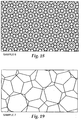
- the open areas defined by the (e.g. metal) micropattern can be described as cells such as square geometry cells, as depicted in FIG 3B , and (i.e. regular) hexagon geometry cells, as depicted in-FIG.-3A.
- the first and second conductive micropatterns generally comprise linear traces defining an open mesh of a repeating cell geometry.
- repeating cell geometry it is meant that the micropattern has translational symmetry.
- Figs. 4A and 4B are illustrations depicting an open mesh of a repeating cell geometry wherein the repeat segment comprises a combination of a square cell and an octagonal cell.
- the micropattern repeats over a relatively short distance. In some embodiments, the repeat segment comprises no greater than 2 or 3 cells.
- the depicted open meshes include various arrangements of polygonal cell geometries with straight line borders, the cells may also be defined by wavy or irregular linear traces, provided that the cells form a micropattern having a repeating pattern.
- a repeating cell geometry to include multiple cells having different geometries and/or different sizes, provided that a repeat segment (or primitive) is present that can be translated in at least one direction for at least a portion of the overall mesh or conductive micropattern.
- the geometry of a cell refers to its shape, and is distinguished from its dimension(s).
- Cell geometries include squares, non-square rectangles, hexagons, octagons, other polygons, or other free-form shapes.
- a regular hexagon has a different shape than a non-regular hexagon wherein at least one of the edges has a different length from another edge or at least one included angle is not equal to 120 degrees.
- either the first or the second micropattern comprises a (e.g. repeating) pattern of cells having a regular cell geometry.
- both the first and the second micropattern comprise a (e.g. repeating) pattern of cells having a regular cell geometry.
- both the first and second micropattern comprise cells having the same regular cell geometry.
- regular cell geometry it is meant that the cells of the micropattern have the shape of a regular polygon.
- a regular polygon has all edges of equal length and all included angles of equal magnitude.
- the conductive traces defining the conductive micropattern are designed not to include segments that are approximately straight for a distance greater than the combined edge length of five adjacent cells, preferably four adjacent cells, more preferably three adjacent cells, even more preferably two adjacent cells. Most preferably, the traces defining the micropattern are designed not to include segments that are straight for a distance greater than the edge length of a single cell. Accordingly, in some embodiments, the traces that define the micropattern are not straight over long distances, e.g., 10 centimeters, 1 centimeter, or even 1 millimeter. Patterns with minimal lengths of straight line segments, as just described, are particularly useful for touch screen sensors with the advantage of causing minimal disturbance of display viewability.
- the first and second micropatterns each comprise a square mesh.
- one of the micropatterns comprises a square mesh and the other micropattern a (e.g. regular) hexagonal mesh.
- Preferred overlaid conductive micropatterns comprise a first and second micropattern region with two dimensional contiguous (e.g. metal) meshes, wherein at least a portion of the linear traces that form the mesh are non-parallel, such as certain polygonal networks such as (e.g. regular) triangular, pentagonal, and (e.g. regular) hexagonal networks. More preferably, the first and second micropatterns each comprise a (e.g. regular) hexagonal mesh.
- the two-dimensional geometry of the conductive micropattern (that is, geometry of the pattern in the plane or along the major surface of the substrate) can be designed, with consideration of the optical and electrical properties of the conductor material, to achieve special transparent conductive properties that are useful in touch screen sensors.
- regions of the conductive micropattern through which the display is to be viewed should have an area fraction of the sensor that is shadowed by the conductor of less than 50%, or less than 25%, or less than 20%, or less than 10%, or less than 5%, or less than 4%, or less than 3%, or less than 2%, or less than 1%, or in a range from 0.25 to 0.75%, or less than 0.5%.
- the open area fraction (or open area or Percentage of Open Area) of a conductive micropattern, or region of a conductive micropattern is the proportion of the micropattern area or region area that is not shadowed by the conductor.
- the open area is equal to one minus the area fraction that is shadowed by the conductor, and may be expressed conveniently, and interchangeably, as a decimal or a percentage.
- Area fraction that is shadowed by conductor is used interchangeably with the density of lines for a micropatterned conductor.
- Micropatterned conductor is used interchangeably with electrically conductive micropattern and conductive micropattern.
- the open area values are greater than 50%, greater than 75%, greater than 80%, greater than 90%, greater than 95%, greater than 96%, greater than 97%, greater than 98%, greater than 99%, 99.25 to 99.75%,, 99.8%, 99.85%, 99.9% and even 99.95.
- the open area of a region of the conductor micropattern is between 80% and 99.5%, in other embodiments between 90% and 99.5%, in other embodiments between 95% and 99%, in other embodiments between 96% and 99.5%, in other embodiments between 97% and 98%, and in other embodiments up to 99.95%.
- preferred values of open area are between 90 and 99.5%, more preferably between 95 and 99.5%, and in some embodiments between 95 and 99.95%.
- the minimum dimension of the conductive pattern elements should be less than or equal to approximately 50 micrometers, or less than or equal to approximately 25 micrometers, or less than or equal to approximately 10 micrometers, or less than or equal to approximately 5 micrometers, or less than or equal to approximately 4 micrometers, or less than or equal to approximately 3 micrometers, or less than or equal to approximately 2 micrometers, or less than or equal to approximately 1 micrometer, or less than or equal to approximately 0.5 micrometer.
- one may include concepts known in the art for minimizing interference such as moire effects between the one or more overlaid conductive micropatterns and the display pixels.
- the minimum dimension of conductive pattern elements is between 0.5 and 50 micrometers, in other embodiments between 0.5 and 25 micrometers, in other embodiments between 1 and 10 micrometers, in other embodiments between 1 and 5 micrometers, in other embodiments between 1 and 4 micrometers, in other embodiments between 1 and 3 micrometers, in other embodiments between 0.5 and 3 micrometers, and in other embodiments between 0.5 and 2 micrometers.
- useful optical properties e.g.
- preferred values of minimum dimension of conductive pattern elements are between 0.5 and 5 micrometers, more preferably between 1 and 4 micrometers, and most preferably between 1 and 3 micrometers.
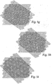
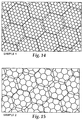
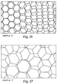
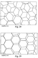
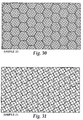
- Figs. 5a- 5c are illustrations depicting two layers of the same regular hexagonal mesh overlaid.
- the second micropattern is rotated relative to the first micropattern at increasing angles, starting with 5 degrees for Fig. 5a and increasing respectively from FIG. 5a to 5c in 5 degree increments.
- an apparent composite pattern is present wherein the center of each composite pattern has a diameter of at least about 4 cells.
- the apparent composite pattern has spatial dimensions greater than the dimensions of conductive features or the spacing between conductive features for either micropattern.
- the apparent composite pattern typically has spatial dimensions greater than the repeat segment of the repeating geometry.
- the size of the apparent composite pattern is smaller, having a center portion spanning about 3 and 2 cells in diameter, respectively.
- the individual linear traces of the meshes of Figs. 5a-5i are apparent and identifiable.
- the hexagonal cells are also apparent and identifiable.
- the pattern is a micropattern, the individual linear traces are not identifiable, nor are the individual cells identifiable.
- the composite pattern that was created by the overlay of the micropatterns is highly visible (i.e. apparent), but not necessarily identifiable.
- conductive mesh micropatterns e.g. with repeating cell geometry
- the visibility can be even lower than some conductive mesh micropatterns having random or pseudo-random cell geometry.
- the designs and arrangement relate to reducing visibility when two conductive micropatterns are overlaid.
- the second conductive micropattern overlays the first conductive micropattern such that at least a portion of the linear traces of the second conductive micropattern are non-parallel to the linear traces of first conductive micropattern.
- first and second conductive micropatterns can be arranged intentionally with a specific relative orientation.
- Two conductive micropatterns arranged with a specific relative orientation can have a defined angle (or defined bias angle) with respect to each other.
- the angle of one conductive micropattern with respect to second conductive micropattern is readily evident when the two micropatterns comprise repeat segments having the same geometry of cell(s).
- the following includes a procedure for defining the bias angle for some embodiments.
- the two micropatterns comprise repeat segments having the same geometry of cell(s)
- the visual appearance of the combination of micropatterns will be periodic with respect to changing bias angle.
- the angular period of the changing visual appearance with increasing bias angle will be equal to 360 degrees divided by the level of rotational symmetry (1 for no rotational symmetry, 2 for two-fold rotational symmetry, 3 for three-fold rotational symmetry, 4-for four-fold rotational symmetry, and 6 for six-fold rotational symmetry, for example).
- the term repeat angle is used herein to describe the angular period.
- the full range of visual appearance of combined micropatterns can be defined within the bias angle range of zero degrees to one half of the repeat angle. It is useful in some cases to define the bias angle between conductive micropatterns comprising the same mesh geometry as a fraction of the repeat angle. In some embodiments, the bias angle is between 0.1 to 0.9 times the repeat angle. In preferred embodiments, the bias angle is between 0.1 and 0.4 or between 0.6 and 0.9 times the repeat angle. In other preferred embodiments, the bias angle is between 0.2 and 0.3 or between 0.7 and 0.8 times the repeat angle.
- the second conductive micropattern has linear traces that are non-parallel relative to the linear traces of the first conductive micropattern by rotating the second micropattern relative to the first micropattern.
- the geometry of the first conductive micropattern is the same as the geometry of the second conductive micropattern.
- the geometry for both micropatterns is a hexagonal mesh with six-fold rotational symmetry.
- the repeat angle is 60 degrees. The use of a relative bias angle is particularly useful when the first and second micropattern have the same cell (e.g. regular) geometry and the same cell dimension.
- the angle of rotation is preferably at least 10 degrees (as illustrated in Fig. 5i ) and less than 45 degrees (as illustrated in Fig. 5i ).
- the second conductive micropattern has linear traces that are non-parallel to the linear traces of the first conductive micropattern as a result of the second conductive micropattern having a different cell geometry from the cell geometry of the first conductive micropattern.
- the first conductive micropattern may have a square cell geometry and the second conductive micropattern a hexagonal cell geometry, or vice-versa.
- a portion of the linear traces of the square cells can be parallel to the linear traces of the hexagon cells, a portion of the linear traces are non-parallel.
- the second conductive micropattern has a different cell dimension from the cell dimension of the first conductive micropattern.
- the term cell dimension refers generally to the size of a cell of a mesh conductive micropattern.
- a cell dimension as the width of the cell, for example the edge length of a square cell, or as a further example the separation between parallel faces of a hexagonal cell (also referred to herein as the diameter or pitch of a hexagon).
- the average width or pitch of a regular cell formed from the conductive traces is typically no greater than 500 microns, 450 microns, or 400 microns. In some preferred embodiments, both of the micropatterns have an average cell width no greater than 350 microns, 300 microns, 250 microns, 200 microns, 150 microns, 100 microns, or 50 microns.
- a cell dimension can be defined as the average length of all line segments (i.e., of all orientations) that pass through the centroid of the cell shape and that extend in each direction to the boundary of the cell shape.
- the cell dimension of the first conductive micropattern is equal to between 1.1 and 6 times the cell dimension of the second conductive micropattern (i.e. ratios of 1:1.1 to 1:6 respectively. It is preferred for the cell dimension of the first conductive micropattern to be equal to between 1.2 and 3 times the cell dimension of the second conductive micropattern, more preferably between 1.2 and 2.
- the first conductive micropattern and the second conductive micropattern have the same repeating cell geometry, wherein the cell dimension of the first conductive micropattern is between 1.1 and 6 times the cell dimension of the second conductive micropattern, and there is a bias angle between the patterns of between 0.1 and 0.9 times the repeat angle. In some embodiments, the bias angle between the patterns of between 0.1 and 0.4 or between 0.6 and 0.9 times the repeat angle.
- the repeating cell geometry comprises regular polygons. In some of these embodiments, the repeating cell geometry is composed of a single regular polygon. In some of these embodiments, the repeating cell geometry is composed of regular hexagons.
- the first conductive micropattern and the second conductive micropattern have the same repeating cell geometry, wherein the cell dimension of the first conductive micropattern is between 1.2 and 3 times the cell dimension of the second conductive micropattern, and there is a bias angle between the patterns of between 0.1 and 0.4 or between 0.6 and 0.9 times the repeat angle.
- the repeating cell geometry comprises regular polygons. In some of these embodiments, the repeating cell geometry is composed of a single regular polygon. In some of these embodiments, the repeating cell geometry is composed of regular hexagons.
- the first conductive micropattern and the second conductive micropattern have the same repeating cell geometry, wherein the cell dimension of the first conductive micropattern is between 1.1 and 6 times the cell dimension of the second conductive micropattern, and there is a bias angle between the patterns of between about 10 degrees and about 45 degrees. In some embodiments, the cell dimension of the first conductive micropattern is between 1.2 and 3 times the cell dimension of the second conductive micropattern.
- the repeating cell geometry comprises regular polygons. In some of these embodiments, the repeating cell geometry is composed of a single regular polygon. In some of these embodiments, the repeating cell geometry is composed of regular hexagons.
- the visibility of the overlaid micropattern can be determined by using various methods.
- the visibility of the overlaid micropattern is determined by use of (i.e. human) test panels to evaluate the visibility (according to the method described in the examples).
- a method of determining the visibility of a patterned substrate comprising providing a digital image of a micropatterned substrate such as overlaid micropatterns and calculating the spatial contrast threshold of the digital image with a model for foveal detection (i.e. standard spatial observer model).
- a model for foveal detection i.e. standard spatial observer model
- Test panels are typically more subjective and generally require a multiple of participants to obtain a statistically meaningful result. Further, the use of test panels typically requires that actual samples be made of each of the micropatterns in order that the visibility can be evaluated.
- the input for a mathematical model can also be generated by providing a sample comprising (e.g. a light transparent) substrate and a non-transparent micropattern, simulating the lighting conditions of the sample when the sample is viewed during use; and digitally imaging the sample.
- the mathematical model can also utilize a digital image of a digitally designed micropattern.
- the visibility of a micropattern or overlaid micropattern can be evaluated without actually fabricating a physical sample. This is amenable to more efficiently evaluating the visibility of a multitude of micropatterns without actual fabrication thereof.
- the digital image of the micropatterned substrate, or digital design thereof is typically cropped to include only the micropattern. Any edges or borders that arise as a result of cropping that are not actually present in the overlaid patterns should be omitted prior to calculating the contrast thresholds.
- the metal micropattern appears dark against a transparent background, in order to simulate the micropattern's appearance when viewed with reflected light, it is preferred to digitally alter (such as by reversing the polarity of the image on a computer screen) such that the transparent substrate is dark and the micropattern is light.
- Different contrast threshold values may be computed by the model in the absence of digitally altering the micropattern image in this manner.
- the calculated contrast threshold described herein have been found to correspond with the visibility as determined by (i.e. human) test panels.
- the micropattern or overlaid micropatterns have a contrast threshold of less than - 35 decibels, the micropattern is most visible.
- the contrast threshold is preferably greater than - 35 decibels.
- the contrast threshold is greater than - 30 decibels or - 25 decibels, the micropattern. (e.g. beat pattern of overlaid micropattern) is still apparent and identifiable.
- the micropattern or overlaid micropatterns has a predicted contrast threshold of greater than - 24, - 23, - 22, - 21 or - 20 decibels, the micropattern or overlaid micropatterns becomes substantially less visible.
- the contrast threshold is greater than -15 decibels, -10 decibels, or -5 decibels.
- the micropattern or overlaid micropatterns has a predicted contrast threshold of 0 or greater, the micropattern or overlaid micropattern is not visible.
- a difference in contrast threshold values of 1 decibel is a 'just noticeable difference' to the average human viewer.
- the distance for calculating the contrast threshold can vary, yet is chosen to correlate with a viewing distance of interest, i.e. typically the average viewing distance of the micropatterned substrate during ordinary use.
- a viewing distance of interest i.e. typically the average viewing distance of the micropatterned substrate during ordinary use.
- the normal viewing distance is typically about 280 mm to 300 mm. This corresponds to a distance unit of the model of about 30000 (i.e. 3000 foveal detection model distance units).
- the preferred (e.g. overlaid) micropattern has the contrast thresholds, as described above, at less than 30000 distance units such as 25000 or 20000 or 15000.
- the sample size utilized in the calculation is generally of sufficient size to be representative of the physical and/or designed sample. If the overlaid pattern (the net pattern) is larger than the sample size but within a viewing area that would be covered by foveal viewing (i.e., 2.13 degrees of visual angle) at the desired viewing distance, one should obtain a sample that would subtend the fovea.
- the deposited electrically conductive material reduces the light transmission of the touch sensor. Basically, wherever there is electrically conductive material deposited, the display is shadowed in terms of its viewability by a user.
- the degree of attenuation caused by the conductor material is proportional to the area fraction of the sensor or region of the sensor that is covered by conductor, within the conductor micropattern.
- a transparent touch screen sensor In general, it is desirable for a transparent touch screen sensor to exhibit a low value of haze.
- Haze refers to a property related to the scattering of light as it passes through a medium, e.g. as measured by a Haze-Gard instrument (Haze-Gard plus, BYK Gardner, Columbia, Maryland).
- the touch screen sensor exhibits haze less than 10%, in some embodiments less than 5%, in some embodiments less than 4%, in some embodiments less than 3%, in some embodiments less than 2%.
- Embodiments are disclosed which achieve a desirable combination of high transmission (also referred to as visible light transmittance), low haze, and low conductor trace visibility for regions including conductor micropatterns.
- the conductor micropatterns are thus especially useful when used as part of a sensing area or region of a touch screen sensor display, e.g. when the micropattern overlays a viewable region of the display.
- the sensors in order to generate a visible light transparent display sensor that has uniform light transmission across the viewable display field, even if there is a non-uniform distribution of sheet resistance, e.g. derived from a non-uniform mesh of conductive material, the sensors include isolated conductor deposits added to the conductor micropattern that serve to maintain the uniformity of light transmittance across the pattern. Such isolated conductor deposits are not connected to the drive device (e.g., electrical circuit or computer) for the sensor and thus do not serve an electrical function.
- the drive device e.g., electrical circuit or computer
- Similar isolated conductive (e.g. metal) features can be added in regions of space between contiguous transparent conductive regions, e.g. contiguous transparent conductive regions that include micropatterned conductors in the form of two dimensional meshes or networks, in order to maintain uniformity of light transmittance across the sensor, including the transparent conductive regions and the region of space between them.
- contiguous transparent conductive regions e.g. contiguous transparent conductive regions that include micropatterned conductors in the form of two dimensional meshes or networks, in order to maintain uniformity of light transmittance across the sensor, including the transparent conductive regions and the region of space between them.
- other useful isolated deposits of conductor for tailoring optical uniformity include circles and lines.
- the minimum dimension of the electrically isolated deposits e.g., the edge length of a square feature, the diameter of a circular feature, or the width of a linear feature
- the minimum dimension of the electrically isolated deposits is less than 10 micrometers, less than 5 micrometers, less than 2 micrometers,
- the minimum dimension of the electrically isolated deposits is preferably between 0.5 and 10 micrometers, more preferably between 0.5 and 5 micrometers, even more preferably between 0.5 and 4 micrometers, even more preferably between 1 and 4 micrometers, and most preferably between 1 and 3 micrometers.
- the arrangement of electrically isolated conductor deposits is designed to lack periodicity. A lack of periodicity is preferred for limiting unfavorable visible interactions with the periodic pixel pattern of an underlying display.
- an ensemble of electrically isolated conductor deposits to lack periodicity there need only be a single disruption to the otherwise periodic placement of at least a portion of the deposits, across a region having the deposits and lacking micropattern elements that are connected to decoding or signal generation and/or processing electronics.
- Such electrically isolated conductor deposits are said to have an aperiodic arrangement, or are said to be an aperiodic arrangement of electrically isolated conductor deposits.
- the electrically isolated conductor deposits are designed to lack straight, parallel edges spaced closer than 10 micrometers apart, e.g. as would exist for opposing faces of a square deposit with edge length of 5 micrometers.
- the isolated conductor deposits are designed to lack straight, parallel edges spaced closer than 5 micrometers apart, more preferably 4 micrometers apart, even more preferably 3 micrometers apart, even more preferably 2 micrometers apart.
- Examples of electrically isolated conductor deposits that lack straight, parallel edges are ellipses, circles, pentagons, heptagons, and triangles. The absence within the design of electrically isolated conductor deposits of straight, parallel edges serves to minimize light-diffractive artifacts that could disrupt the viewability of a display that integrates the sensor.
- preferred sensors include conductor micropatterns wherein none of the regions have a shadowed area fraction that differs by greater than 75 percent from the average for all of the regions. More preferably, none have a shadowed area fraction that differs by greater than 50 percent. More preferably, none have a shadowed area fraction that differs by greater than 25 percent. Even more preferably, none have a shadowed area fraction that differs by greater than 10 percent.
- preferred sensors include conductor micropatterns wherein none of the regions have a shadowed area fraction that differs by greater than 50 percent from the average for all of the regions. Preferably, none have a shadowed area fraction that differs by greater than 50 percent. More preferably, none have a shadowed area fraction that differs by greater than 25 percent. Even more preferably, none have a shadowed area fraction that differs by greater than 10 percent.
- the disclosure allows for the use of metals as the conductive material in a transparent conductive sensor, as opposed to transparent conducting oxides (TCO's), such as ITO.
- TCO's transparent conducting oxides
- Examples of useful metals for forming the electrically conductive micropattern include gold, silver, palladium, platinum, aluminum, copper, nickel, tin, alloys, and combinations thereof.
- the conductor can also be a composite material, for example a metal-filled polymer.
- the conductor can be reflective, as in the case of thin film metal, for example silver, aluminum, etc.
- the conductor can be absorptive and appear dark or black, as in the case of a carbon-filled composite conductor, for example as derived from a printable carbon-based conductive ink.
- the conductor can comprise multiple layers, for example the conductor may comprise a metal layer and an overlayer designed to reduce the reflectivity of the metal or to prevent corrosion of the metal, as is known in the art. This disclosure is not limited with respect to the selection or design of the material that comprises the conductor. However, the concepts developed herein have been found to be particularly useful when reflective conductor patterns are needed or otherwise preferred.
- the (e.g. metal) micropattern is relatively thin, ranging in thickness from about 5 nanometers to about 50 nanometers. In other embodiments, the (e.g. metal) micropattern has a thickness of at least 60 nm, 70 nm, 80 nm, 90 nm, or 100 nm. In some embodiments, the thickness of the (e.g. metal) micropattern is at least 250 nm. In some embodiments, the micropattern is a silver micropattern have a thickness of at least 300 nm, 400 nm, 500 nm, 600 nm, 700 nm, 800 nm, 900 nm, and even 1000 nm or greater.
- the micropattern is a gold micropattern having a thickness of at least 300 nm, 350 nm, 400 nm, or greater.
- Metal micropatterns of increased thickness can be prepared as described in WO 2010/151471 A1 .
- the (e.g. metal) conductive micropatterned substrates are suitable for use in electronic displays.
- Electronic displays include reflective displays and displays with internal sources of light.
- Electronic displays with internal sources of light include illuminated displays.
- illuminated it is meant “brightened by light or emitting light”.
- the illuminated display may be a liquid crystal display having a backlighting or edge lighting light source that may be external to the core liquid crystal panel but internal to the display device overall.
- the illuminated display may be an emissive display such as a plasma display panel (PDP) or organic light emitting diode (OLED) display.
- Reflective displays include electrophoretic displays, electrowetting displays, electrochromic displays, and reflective cholesteric liquid crystal displays.
- the micropatterned substrates of the invention are especially useful as part of an illuminated electronic display.
- Conductor micropatterns according to the invention can be generated by any appropriate patterning method, e.g. methods that include photolithography with etching or photolithography with plating (see, e.g., U.S. Patent No. 5,126,007 ; U.S. Patent No. 5,492,611 ; U.S. Patent No. 6,775,907 ). Additionally, the conductor patterns can be created utilizing on one of several other exemplary methods including laser cured masking, inkjet printing, gravure printing, and microreplication; each of which are known in the art and described in greater detail in U.S. Publication No. US2009/0219257 . In some embodiments, the conductive (e.g. metal) micropatterns are prepared via microcontact printing, such as described in WO 2010/151471 A1 .
- the two-dimensional conductive micropattern can be designed to achieve anisotropic or isotropic sheet resistance in a conductive region (e.g., a visible light transparent conductive region) of the sensor, such as described in U.S. Publication No. US2009/0219257 .
- anisotropic sheet resistance what is meant is that the magnitude of the sheet resistance of the conductive micropattern is different when measured or modeled along two orthogonal directions.
- isotropic sheet resistance what is meant is that the magnitude of the sheet resistance of the conductive micropattern is the same when measured or modeled along any two orthogonal directions in the plane, as in the case for a square grid formed with traces of constant width for both directions.
- transparent conductive regions with different sheet resistance in at least one direction are created by including selective breaks in conductive traces within an otherwise continuous and uniform mesh. This approach of selective placement of breaks is especially useful for generating articles including patterns of visible transparent conductive regions where the optical transmittance across the article is uniform.
- the starting mesh can be isotropic or anisotropic.
- the breaks can be placed in order to create approximately continuously varying sheet resistance in a given direction.
- two transparent conductive regions with different sheet resistance in at least one direction are created by including in each of the two regions a contiguous mesh with its own design, each mesh not necessarily including selectively placed breaks.
- Examples of two meshes with designs that lead to different values of sheet resistance for current passing in a single direction, e.g. the x direction in FIG. 2 include two meshes with the same thickness (dimension in the z direction in FIG. 2 ) of the same conductive material deposit but with different amounts with current-carrying cross-sectional area (y-z plane in FIG. 2 ) per unit width in the y direction.
- Such a pair of mesh regions are two square grid regions each comprising conductive traces of width 2 micrometers but with different pitch, e.g. 100 micrometers and 200 micrometers.
- Another example of such a pair of mesh regions are two rectangular grid regions (non-square, with 100 micrometer pitch in the one direction and 200 micrometer pitch in the orthogonal direction) each comprising conductive traces of width 2 micrometers but with different orientation, e.g. with the long axes of the rectangular cells in the first regions oriented at 90 degrees with respect to the rectangular cells in the second region.
- the sensors include an insulating visible light transparent substrate layer that supports a pattern of conductor, the pattern includes a visible light transparent micropattern region and a region having a larger feature that is not transparent, wherein the visible light transparent micropattern region and the larger feature region include a patterned deposit of the same conductor (e.g., a metal) at approximately the same thickness.
- the larger feature can take the form of, e.g., a wide conductive trace that makes contact to a visible light transparent conductive micropattern region or a pad for making contact with an electronic decoding, signal generation, or signal processing device.
- the width of useful larger features, in combination on the same insulating layer with visible light transparent conductive micropattern regions is e.g. between 25 micrometers and 3 millimeters, between 25 micrometers and 1 millimeter, between 25 micrometers and 500 micrometers, between 25 micrometers and 250 micrometers, or between 50 micrometers and 100 micrometers.
- exemplary touch screen sensor designs can be fabricated using known photolithographic methods, e.g. as described in U.S. Patent No. 5,126,007 or U.S. Patent No. 5,492,611 .
- the conductor can be deposited using physical vapor deposition methods, e.g. sputtering or evaporation, as is known in the art.
- the examples below include conductors patterned by a micro-contact printing technique (see technique description above and also co-pending US Patent PublicationNo. US2009/0218310 ).
- Each conductive pattern exemplified herein is useful as a transparent touch screen sensor, when connected to decoding circuitry, as is known in the art (e.g., U.S. Patent No. 4,087,625 ; U.S. Patent No. 5,386,219 ; U.S. Patent No. 6,297,811 ; WO 2005/121940 A2 ).
- the contrast thresholds of the overlaid micropatterned substrates of Comparative Example A, Example B and Examples 1-25 were calculated using a version of the mathematical model "Standard A” described in " A Standard Model for Foveal Detection of Spatial Contrast” (Journal of Vision, 2005 5, 717-740 ).
- the Standard A model was implemented using Matlab version 7.7.0.471 (R2008b) on a Hewlett-Packard xw8400 workstation using the following parameters. Parameter Fit Value A - Gain 373.08 ⁇ 0.8493 p .7786 f 0 4.1726 (cycles/deg) f 1 1.3625 (cycles/deg) ⁇ 2.4081 ⁇ 0.6273
- micropattern analysis was accomplished by:
- contrast thresholds were then calculated for a viewing distance of 30000 units of distance according to the model which is equivalent to about 28-30 cm.
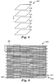
- a transparent sensor element 400 for a touch screen sensor is illustrated in FIG. 8 .
- the sensor element 400 includes two patterned conductor layers 410, 414, (e.g., an X axis layer and a Y axis layer) two optically clear adhesive layers 412, 416, and a base plate 418, laminated together and depicted as separated in FIG. 8 for clarity.
- Layers 410 and 414 include transparent conductive mesh bars where one layer is oriented in the x axis direction and the other layer is orientated in the y axis direction, with reference to FIG. 2 .
- the base plate 418 is a sheet of glass measuring 6 centimeter by 6 centimeters in area and 1 millimeter in thickness.
- a suitable optically clear adhesive is Optically Clear Laminating Adhesive 8141 from 3M Company, St. Paul, Minnesota.
- a clear polymer film with a micropattern of metal is used for each of the X - layer and the Y - layer.
- a micropattern of thin film gold according to the following description is deposited onto a thin sheet of PET.
- Suitable PET substrates include ST504 PET from DuPont, Wilmington, Delaware, measuring approximately 125 micrometers in thickness.
- the micropattern 440 is depicted in FIG. 9 and FIG. 10 .
- the thickness of the gold is about 100 nanometers.
- the micropattern has transparent conductive regions in the form of a series of parallel mesh bars 442.
- mesh bars 441 that are electrically isolated from the electronic device.
- the isolated mesh bars 441 serve to maintain optical uniformity across the sensor.
- Each bar is comprised of a mesh made up of narrow metallic traces 443, the traces 443 measuring approximately 5 micrometers in width.
- the mesh bars each measure approximately 2 millimeters in width and 66 millimeters in length. Within each mesh bar are rectangular cells measuring approximately 0.667 millimeters in width and 12 millimeters in length.
- This mesh design serves to provide ties between long-axis traces in each mesh bar, to maintain electrical continuity along the mesh bar, in case of any open-circuit defects in the long axis traces.
- the rectangular mesh of FIG. 9 and FIG. 10 trades off sheet resistance along the mesh bar with optical transmittance more optimally. More specifically, the mesh bar depicted in FIG. 9 and FIG.
- the overlaid micropattern is illustrated in FIG. 36 .
- the contrast threshold at a distance of 30000 units (with pixel size of 0.265) of Comparative Example A was determined to be -41.4.
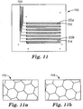
- a transparent sensor element was fabricated and combined with a touch sensor drive device as generally shown in FIGs. 11 , 12 and 13 using microcontact printing and etching as described in WO 2009/108771 A2 .
- the device was then integrated with a computer processing unit connected to a display to test the device.
- the device was able to detect the positions of multiple single and or simultaneous finger touches, which was evidenced graphically on the display.
- This example used micro-contact printing and etching techniques (see also WO 2009/108771 A2 ) to form the micro-conductor pattern used in the touch sensor.
- a first visible light substrate made of polyethylene terephthalate (PET) having a thickness of 125 micrometers ( ⁇ m) was vapor coated with 100nm silver thin film using a thermal evaporative coater to yield a first silver metalized film.
- PET polyethylene terephthalate
- the PET was commercially available as product number ST504 from E.I. du Pont de Nemours, Wilmington, DE.
- the silver was commercially available from Cerac Inc., Milwaukee, WI as 99.99% pure 3mm shot.
- a first poly(dimethylsiloxane) stamp referred to as PDMS and commercially available as product number Sylgard 184, Dow Chemical Co., Midland, MI, having a thickness of 3mm, was molded against a 10cm diameter silicon wafer (sometimes referred to in the industry as a "master") that had previously been patterned using standard photolithography techniques.
- the PDMS was cured on the silicon wafer at 65°C for 2 hours. Thereafter, the PDMS was peeled away from the wafer to yield a first stamp having two different low-density regions with patterns of raised features, a first continuous hexagonal mesh pattern and a second discontinuous hexagonal mesh pattern. That is, the raised features define the edges of edge-sharing hexagons.
- a discontinuous hexagon is one that contains selective breaks in a line segment.
- the selective breaks had a length less than 10 ⁇ m.
- the breaks were designed and estimated to be approximately 5 ⁇ m. In order to reduce their visibility, it found that, preferably, the breaks should be less than 10 ⁇ m, more preferably, 5 ⁇ m or less, e.g., between 1 and 5 ⁇ m.
- Each raised hexagon outline pattern had a height of 2 ⁇ m, had 1% to 3% area coverage, corresponding to 97% to 99% open area, and line segments that measured from 2 to 3 ⁇ m in width.
- the first stamp also included raised features defining 500 ⁇ m wide traces.
- the first stamp has a first structured side that has the hexagonal mesh pattern regions and the traces and an opposing second substantially flat side.
- the stamp was placed, structured side up, in a glass Petri dish containing 2mm diameter glass beads.
- the second, substantially flat side was in direct contact with the glass beads.
- the beads served to lift the stamp away from the base of the dish, allowing the following ink solution to contact essentially all of the flat side of the stamp.
- a 10 millimolar ink solution of 1-octadecanethiol (product number C18H3CS, 97%, commercially available from TCI America, Portland OR) in ethanol was pipetted into the Petri dish beneath the stamp.
- the ink solution was in direct contact with the second substantially flat side of the stamp.
- sufficient inking time e.g:, 3 hours
- the inked stamp was placed, structured side up, onto a working surface.
- the first silver metalized film was applied using a hand-held roller onto the now inked structured surface of the stamp such that the silver film was in direct contact with the structured surface.
- the metalized film remained on the inked stamp for 15 seconds.
- the first metalized film was removed from the inked stamp.
- the removed film was placed for three minutes into a silver etchant solution, which contained (i) 0.030 molar thiourea (product number T8656, Sigma-Aldrich, St. Louis, MO) and (ii) 0.020 molar ferric nitrate (product number 216828, Sigma-Aldrich) in deionized water.
- the resulting first substrate was rinsed with deionized water and dried with nitrogen gas to yield a first patterned surface.
- the silver remained after etching. Thus silver was removed from the locations where contact was not made between the inked stamp and silver film.
- FIGS 11, 11a and 11b show a first patterned substrate 700 having a plurality of first continuous regions 702 alternating between a plurality of first discontinuous regions 704 on a first side of the substrate, which is the side that contained the now etched and patterned silver metalized film.
- the substrate has an opposing second side that is substantially bare PET film.
- Each of the first regions 702 has a corresponding 500 ⁇ m wide conductive trace 706 disposed at one end.
- FIG. 11a shows an exploded view of the first region 702 having a plurality of continuous lines forming a hexagonal mesh structure.
- FIG. 11b shows an exploded view of the first discontinuous region 704 having a plurality of discontinuous lines (shown as selective breaks in each hexagon) forming a discontinuous hexagonal mesh structure.
- Each mesh structure of regions 702 and 704 had 97% to 99% open area.
- Each line segment measured from 2 to 3 ⁇ m.
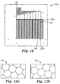
- the second patterned substrate was made as the first patterned substrate using a second visible light substrate to produce a second silver metalized film.
- a second stamp was produced having a second continuous hexagonal mesh pattern interposed between a second discontinuous hexagonal mesh pattern.
- FIGS 12, 12a and 12b show a second patterned substrate 720 having a plurality of second continuous regions 722 alternating between a plurality of second discontinuous regions 724 on a first side of the second substrate. Each of the second regions 722 has a corresponding 500 ⁇ m wide second conductive trace 726 disposed at one end.
- FIG. 12a shows an exploded view of one second region 722 having a plurality of continuous lines forming a hexagonal mesh structure.
- FIG. 12b shows an exploded view of one second discontinuous region 724 having a plurality of discontinuous lines (shown as selective breaks in each hexagon) forming discontinuous hexagonal mesh structure.
- the selective breaks had a length less than 10 ⁇ m. The breaks were designed and estimated to be approximately 5 ⁇ m.
- the breaks should be less than 10 ⁇ m, more preferably, 5 ⁇ m or less, e.g., between 1 and 5 ⁇ m.
- Each mesh structure of region 722 and 724 had 97% to 99% open area.
- Each line segment measured from 2 to 3 ⁇ m.
- the first patterned substrate comprised hexagonal cells with diameter of 300 micrometers and the second pattern substrate comprised hexagonal cells with diameter of 200 micrometers.
- One of the conductor micropatterns had a cell dimension of 1.5 times the cell dimension of the second conductor micropattern.
- the first and second patterned substrates made above were used to produce a two-layer projected capacitive touch screen transparent sensor element as follows.
- the first and second patterned substrates were adhered together using Optically Clear Laminating Adhesive 8141 from 3M Company, St. Paul, MN to yield a multilayer construction.
- a handheld roller was used to laminate the two patterned substrates with the regions of the first and second conductive trace regions 706 and 726 being adhesive free.
- the multilayer construction was laminated to a 0.7mm thick float glass using Optically Clear Laminating Adhesive 8141 such that the first side of the first substrate was proximate to the float glass.
- the adhesive free first and second conductive trace regions 706 and 726 allowed electrical connection to be made to the first and second patterned substrates 700 and 720.
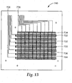
- FIG. 13 shows a top plan view of a multilayer touch screen sensor element 740 where the first and second patterned substrate have been laminated.
- Region 730 represented the overlap of the first and second continuous regions.
- Region 732 represented the overlap of the first continuous region and the second discontinuous region.
- Region 734 represented the overlap of the second continuous region and the first discontinuous region.
- region 736 represented the overlap between the first and second discontinuous regions. While there was a plurality of these overlap regions, for ease of illustration, only one region of each has been depicted in the figure.
- the integrated circuits used to make mutual capacitance measurements of the transparent sensor element were PIC18F87J10 (Microchip Technology, Chandler, Arizona), AD7142 (Analog Devices, Norwood, Massachusetts), and MM74HC154WM (Fairchild Semiconductor, South Portland, Maine).
- the PIC18F87J10 was the microcontroller for the system. It controlled the selection of sensor bars which MM74HC154WM drives. It also configured the AD7142 to make the appropriate measurements.
- the configuration of the AD7142 included selection of the number of channels to convert, how accurately or quickly to take measurements, if an offset in capacitance should be applied, and the connections for the analog to digital converter.
- the measurement from the AD7142 was a 16 bit value representing the capacitance of the cross point between conductive bars in the matrix of the transparent sensor element.
- the AD7142 After the AD7142 completed its measurements it signaled the microcontroller, via an interrupt, to tell it to collect the data. The microcontroller then collected the data over the SPI port. After the data was received, the microcontroller incremented the MM74HC154WM to the next drive line and cleared the interrupt in the AD7142 signaling it to take the next set of data. While the sampling from above was constantly running, the microcontroller was also sending the data to a computer with monitor via a serial interface. This serial interface allowed a simple computer program, as are known to those of skill in the art, to render the raw data from the AD7142 and see how the values were changing between a touch and no touch. The computer program rendered different color across the display, depending on the value of the 16 bit value.
- the display region When the 16 bit value was below a certain value, based on the calibration, the display region was rendered white. Above that threshold, based on the calibration, the display region was rendered green.
- the data were sent asynchronously in the format of a 4 byte header (0xAAAAAAAA), one byte channel (0x00 - 0x0F), 24 bytes of data (represents the capacitive measurements), and carriage return (0x0D).
- the transparent sensor element was connected to the touch sensor drive device.
- the computer monitor rendered the position of touch that was occurring within the touch sensing region in the form of a color change (white to green) in the corresponding location of the monitor.
- the computer monitor rendered the positions of touches that were occurring within the touch sensing region in the form of a color change (white to green) in the corresponding locations of the monitor.
- the computer monitor rendered the positions of touches that were occurring within the touch sensing region in the form of a color change (white to green) in the corresponding locations of the monitor.
- Samples of microcontact printed meshes were prepared as described in WO 2011/002617 A1 .
- Two-layer mesh samples were prepared as follows: single layers of micropatterned meshes approximately 1.7 cm x 1.7 cm were laminated to each other using 3M Optically Clear Adhesive 8271 (3M Company, Maplewood, MN), one layer being rotated a specified number of degrees from the other layer, and the centers of both layers being located over one another (the specifics of each overly arrangement is further described in the following table).
- the two-layer construction was then laminated to the center of a 2 inch x 3 inch x 1 mm glass microscope slide using the same optically clear adhesive. The silver patterned side of each layer faced the glass slide.
- a viewing device was constructed in which a participant ("viewer") was seated in front of a viewing port. Behind the viewing port and contained within an enclosure was a light source and a sample holder. A single sample was mounted in a black sample holder positioned approximately 25 cm below the light source (30 watt bulb) and tilted towards the viewer at an approximately 7 deg angle. The sample holder masked the microscope slide except for a 1.4 cm x 1.4 cm square aperture through which the two-layer samples could be seen by the viewer. Hence, the sample size viewed by the test panel were covered a larger surface area than the sample size used for determining the contrast threshold. The sample holder was inserted into an aperatured stage within a chamber.
- the viewing distance between the sample and the viewer's eyes was 280 mm to 320 mm.
- the chamber was darkened on the other side of the aperture allowing the viewer to look through the layers of the mesh pattern, the mounting glass, and into the darkened viewing box beyond - so as to simulate looking at the surface of a display with the backlighting illumination turned off with ambient light reflecting off the surface of the display.
- the light source was connected to a Powerstat® Variable Autotransformer (Type 3PN116C, 120 V in, 0-140 V out, 10 ⁇ , The Superior Electric Company, Bristol, Connecticut) which allowed viewers to adjust the amount of light illuminating the sample.
- the Method of Adjustment paradigm ( Psychophysic: The fundamentals, Gescheider, G. A., Lawrence Erlbaum Associates, Inc. Mahwah, NJ. (1997 )) was used to measure visibility of the samples as follows: The room lights were turned off. A sample was placed in the aperture of the sample holder and inserted into the viewing device. The viewer placed their head in the viewing port such that they could see the sample, but direct reflection of the light bulb was not visible. The viewer was instructed to begin with the light source dark (variable autotransformer dial set at 0) and increase the amount of light by turning the dial until the pattern of the sample was just barely able to be seen (Test Method A).
- Test Method A was used for half of the total number of measurements made by each viewer, and Test Method B was used for the other half of the total number of measurements made by each viewer.
- Each of the samples were measured twice per viewer using test Method A and twice per viewer using Test Method B.
- a mean value was then calculated for each viewer. For half of the viewers, Method A was used first for each of the samples followed by Method B; whereas for the other half of the viewers Method B was used first and then Method A. The sample order was randomized.
- the micropatterns can be overlaid precisely resulting in a regular net pattern.
- a small degree of positioning error can occur (1-2 degrees).
- such positioning error does not significantly affect the calculated contrast thresholds.
- the contrast threshold was calculated on only a portion of the pattern, it may not be representative of the entire pattern, as was viewed by the test panel. This is believed to be the cause of the discrepancy between the sample order as determined by the model and the sample order as determined by the test panel in connection with Sample 4.
- Table 3a First Conductive Micropattern Sample Cell Dimension* (microns) Trace (i.e. line ) Width (microns) Cell Geometry 10 105 5 Square 11 105 5 Square 12 105 5 Square 13 105 5 Square 14 300 5 Hexagon 15 300 5 Hexagon 16 300 5 Hexagon 17 600 3 Hexagon 18 600 3 Hexagon 19 600 3 Hexagon 20 300 3 Hexagon 21 200 3 Hexagon 22 300 3 Hexagon 23 133 2 Hexagon 24 600 3 Hexagon 25 200 2 Hexagon * Hex face - to - face distance or square edge length
- Table 3b Second Conductive Micropattern Sample Cell Dimension * (microns) Trace (i.e.) Line Width (microns) Cell Geometry Cell Dimension Ratio 10 105 5 Square 1 11 105 5 Square 1 12 105 5 Square 1 13 105 5 Square 1 14 300 5 Hexagon 1 15 300 5 Hexa
- FIG. 30 Infinite (i.e., uniform appearance) 21 30 FIG. 31 -8.5 22 30 FIG. 32 -17.4 23 0 FIG. 33 -3.9 24 0 FIG. 34 -38.2 25 0 FIG. 35 -17.7
Claims (10)
- Elektrisch leitfähiger Artikel, umfassend:ein für sichtbares Licht transparentes Substrat (130);eine erste leitfähige Mikrostruktur (140), umfassend lineare Bahnen, die ein erstes offenes Gitter einer sich wiederholenden Zellgeometrie definieren, die auf oder in dem für sichtbares Licht transparenten Substrat (130) angeordnet ist, undeine zweite leitfähige Mikrostruktur, umfassend lineare Bahnen, die ein zweites offenes Gitter einer sich wiederholenden Zellgeometrie definieren, die von der ersten leitfähigen Mikrostruktur (140) elektrisch isoliert ist;wobei die zweite leitfähige Mikrostruktur die erste leitfähige Mikrostruktur (140) überlagert,wobei mindestens ein Teil der zweiten leitfähigen Mikrostruktur eine von der Zellgeometrie der ersten leitfähigen Mikrostruktur (140) unterschiedliche Zellgeometrie hat; und/oderwobei mindestens ein Teil der zweiten leitfähigen Mikrostruktur eine von der Zelldimension der ersten leitfähigen Mikrostruktur (140) unterschiedliche Zelldimension hat;wobei die Zellgeometrie der ersten leitfähigen Mikrostruktur (140) und/oder der zweiten leitfähigen Mikrostruktur Zellen umfasst, die durch wellenförmige oder unregelmäßige lineare Bahnen definiert sind.
- Elektrisch leitfähiger Artikel nach Anspruch 1, wobei die zweite leitfähige Mikrostruktur in einem Schnittwinkel ausgerichtet ist, der von 15 Grad bis etwa 40 Grad relativ zur ersten leitfähigen Mikrostruktur (140) reicht.
- Elektrisch leitfähiger Artikel nach einem der vorstehenden Ansprüche, wobei die Zellgeometrie der ersten (140) und der zweiten Mikrostruktur eine durchschnittliche Zellbreite von nicht mehr als 500 µ hat.
- Elektrisch leitfähiger Artikel nach Anspruch 1, wobei mindestens ein Teil der linearen Bahnen der zweiten leitfähigen Mikrostruktur nicht parallel zu den linearen Bahnen der ersten leitfähigen Mikrostruktur (140) ist und wobei zwischen der ersten leitfähigen Mikrostruktur (140) und der zweiten leitfähigen Mikrostruktur ein Schnittwinkel zwischen dem etwa 0,1-fachen und dem etwa 0,9-fachen eines Wiederholwinkels vorliegt.
- Elektrisch leitfähiger Artikel nach Anspruch 1, wobei die Zelldimension der ersten leitfähigen Mikrostruktur (140) zwischen dem 1,1-fachen und dem 6-fachen der Zelldimension der zweiten leitfähigen Mikrostruktur ist und wobei zwischen den Strukturen ein Schnittwinkel zwischen dem 0,1-fachen und dem 0,9-fachen des Wiederholwinkels vorliegt.
- Elektrisch leitfähiger Artikel nach Anspruch 1, wobei der elektrisch leitfähige Artikel ein Touchscreen-Sensor (740) ist.
- Elektrisch leitfähiger Artikel nach Anspruch 1, wobei die erste (140) oder die zweite leitfähige Mikrostruktur als Antenne oder Abschirmung gegen Störausstrahlung (EMV) fungiert.
- Elektrisch leitfähiger Artikel nach Anspruch 1, umfassend ein strukturiertes Substrat (700), wobei das strukturierte Substrat (700)
das für sichtbares Licht transparente Substrat (130); und
die überlagerte erste leitfähige Mikrostruktur (140) und zweite leitfähige Mikrostruktur umfasst, wobei die Kombination der leitfähigen Mikrostruktur (140) und der zweiten leitfähigen Mikrostruktur eine Kontrastschwelle von mehr als -35 Dezibel in einer Distanz von 30000 Einheiten hat. - Elektrisch leitfähiger Artikel nach Anspruch 8, wobei die erste leitfähige Mikrostruktur (140) und die zweite leitfähige Mikrostruktur eine Strukturdichte von weniger als 20 % haben.
- Elektrisch leitfähiger Artikel nach Anspruch 8, wobei die Zellgeometrie der ersten leitfähigen Mikrostruktur (140) und der zweiten leitfähigen Mikrostruktur eine durchschnittliche Zellbreite von nicht mehr als 500 µ hat.
Priority Applications (1)
| Application Number | Priority Date | Filing Date | Title |
|---|---|---|---|
| EP16163524.8A EP3056978A1 (de) | 2009-02-26 | 2010-02-24 | Berührungsbildschirmsensor und gemustertes substrat mit überlagerten mikromustern mit niedriger sichtbarkeit |
Applications Claiming Priority (3)
| Application Number | Priority Date | Filing Date | Title |
|---|---|---|---|
| PCT/US2009/035250 WO2009154812A2 (en) | 2008-02-28 | 2009-02-26 | Touch screen sensor |
| US23767309P | 2009-08-27 | 2009-08-27 | |
| PCT/US2010/025127 WO2010099132A2 (en) | 2009-02-26 | 2010-02-24 | Touch screen sensor and patterned substrate having overlaid micropatterns with low visibility |
Related Child Applications (1)
| Application Number | Title | Priority Date | Filing Date |
|---|---|---|---|
| EP16163524.8A Division EP3056978A1 (de) | 2009-02-26 | 2010-02-24 | Berührungsbildschirmsensor und gemustertes substrat mit überlagerten mikromustern mit niedriger sichtbarkeit |
Publications (2)
| Publication Number | Publication Date |
|---|---|
| EP2401669A2 EP2401669A2 (de) | 2012-01-04 |
| EP2401669B1 true EP2401669B1 (de) | 2016-04-06 |
Family
ID=42666180
Family Applications (2)
| Application Number | Title | Priority Date | Filing Date |
|---|---|---|---|
| EP16163524.8A Ceased EP3056978A1 (de) | 2009-02-26 | 2010-02-24 | Berührungsbildschirmsensor und gemustertes substrat mit überlagerten mikromustern mit niedriger sichtbarkeit |
| EP10708451.9A Not-in-force EP2401669B1 (de) | 2009-02-26 | 2010-02-24 | Berührungsschirmsensor und strukturiertes substrat mit überlagerten mikrostrukturen mit geringer sichtbarkeit |
Family Applications Before (1)
| Application Number | Title | Priority Date | Filing Date |
|---|---|---|---|
| EP16163524.8A Ceased EP3056978A1 (de) | 2009-02-26 | 2010-02-24 | Berührungsbildschirmsensor und gemustertes substrat mit überlagerten mikromustern mit niedriger sichtbarkeit |
Country Status (6)
| Country | Link |
|---|---|
| US (2) | US8970515B2 (de) |
| EP (2) | EP3056978A1 (de) |
| JP (1) | JP5643774B2 (de) |
| KR (1) | KR101786119B1 (de) |
| CN (1) | CN102334091B (de) |
| WO (1) | WO2010099132A2 (de) |
Cited By (1)
| Publication number | Priority date | Publication date | Assignee | Title |
|---|---|---|---|---|
| US11201181B2 (en) | 2018-12-14 | 2021-12-14 | Novatek Microelectronics Corp. | Image sensor of fingerprint |
Families Citing this family (157)
| Publication number | Priority date | Publication date | Assignee | Title |
|---|---|---|---|---|
| WO2011002617A1 (en) | 2009-06-30 | 2011-01-06 | 3M Innovative Properties Company | Electronic displays and metal micropatterned substrates having a graphic |
| WO2011077834A1 (ja) * | 2009-12-25 | 2011-06-30 | Kagawa Seiji | 複合電磁波吸収フィルム |
| JP5676645B2 (ja) | 2009-12-29 | 2015-02-25 | クォルコム・メムズ・テクノロジーズ・インコーポレーテッド | 補助電極構造を有するコーティングされた光方向転換照明デバイス |
| TWI471790B (zh) | 2010-02-03 | 2015-02-01 | Wintek Corp | 電容式觸控感應器及其製造方法及電容式觸控面板 |
| KR101100987B1 (ko) | 2010-03-23 | 2011-12-30 | 삼성모바일디스플레이주식회사 | 터치 스크린 패널 |
| US9031310B2 (en) * | 2010-03-31 | 2015-05-12 | Fujifilm Corporation | Conductive film manufacturing method, conductive film, and recording medium |
| KR101101088B1 (ko) * | 2010-05-03 | 2011-12-30 | 삼성모바일디스플레이주식회사 | 터치 스크린 패널 및 그 제조방법 |
| CN102243553B (zh) * | 2010-05-16 | 2015-06-10 | 宸鸿科技(厦门)有限公司 | 电容式触控面板及降低其金属导体可见度的方法 |
| CN102314271B (zh) * | 2010-07-07 | 2014-11-05 | 宸鸿科技(厦门)有限公司 | 一种电容式触控图形结构及其制法、触控面板及触控显示装置 |
| US10306758B2 (en) * | 2010-07-16 | 2019-05-28 | Atmel Corporation | Enhanced conductors |
| JP5667938B2 (ja) * | 2010-09-30 | 2015-02-12 | 富士フイルム株式会社 | 静電容量方式タッチパネル |
| US10620754B2 (en) * | 2010-11-22 | 2020-04-14 | 3M Innovative Properties Company | Touch-sensitive device with electrodes having location pattern included therein |
| EP2652837A4 (de) * | 2010-12-16 | 2014-07-30 | 3M Innovative Properties Co | Transparente mikrostrukturierte rfid-antenne und diese enthaltende artikel |
| TWI404996B (zh) * | 2010-12-31 | 2013-08-11 | Au Optronics Corp | 觸控面板的製造方法以及觸控面板 |
| KR101473132B1 (ko) * | 2011-01-18 | 2014-12-15 | 후지필름 가부시키가이샤 | 투명 전극 시트들, 투명 전극 시트들의 제조 방법, 및 투명 전극 시트들을 사용한 정전 용량 방식의 터치 패널 |
| KR20140009287A (ko) * | 2011-01-18 | 2014-01-22 | 후지필름 가부시키가이샤 | 도전성 필름 및 그것을 구비한 표시 장치 |
| US8933906B2 (en) | 2011-02-02 | 2015-01-13 | 3M Innovative Properties Company | Patterned substrates with non-linear conductor traces |
| EP2671438A4 (de) | 2011-02-02 | 2017-06-14 | 3M Innovative Properties Company | Gemusterte substrate mit geschwärzten leiterspuren |
| KR20140051117A (ko) * | 2011-02-07 | 2014-04-30 | 데쿠세리아루즈 가부시키가이샤 | 투명 도전성 소자, 입력 장치, 전자 기기 및 투명 도전성 소자 제작용 원반 |
| US20120242606A1 (en) * | 2011-03-23 | 2012-09-27 | Synaptics Incorporated | Trace design for reduced visibility in touch screen devices |
| JP2012221120A (ja) * | 2011-04-06 | 2012-11-12 | Fujitsu Component Ltd | タッチパネル |
| US8797285B2 (en) | 2011-04-18 | 2014-08-05 | Atmel Corporation | Panel |
| CN103828502B (zh) * | 2011-09-27 | 2016-10-26 | Lg化学株式会社 | 透明导电基板及其制造方法 |
| US9262019B2 (en) | 2011-11-22 | 2016-02-16 | Atmel Corporation | Touch sensor with conductive lines having different widths |
| US20130127784A1 (en) * | 2011-11-22 | 2013-05-23 | Qualcomm Mems Technologies, Inc. | Methods and apparatuses for hiding optical contrast features |
| KR101310585B1 (ko) * | 2011-11-25 | 2013-09-23 | 삼성전기주식회사 | 터치패널 |
| WO2013119308A1 (en) | 2012-02-10 | 2013-08-15 | 3M Innovative Properties Company | Mesh patterns for touch sensor electrodes |
| US9046974B2 (en) * | 2012-02-28 | 2015-06-02 | Eastman Kodak Company | Transparent touch-screen capacitor with micro-wire electrode |
| KR101301480B1 (ko) * | 2012-02-29 | 2013-08-29 | 미래나노텍(주) | 터치스크린 센서, 이를 구비하는 영상 표시 장치 및 그 제조 방법 |
| US9154127B2 (en) | 2012-03-06 | 2015-10-06 | Atmel Corporation | Touch sensor with conductive lines having portions with different widths |
| JP5779535B2 (ja) * | 2012-03-30 | 2015-09-16 | 富士フイルム株式会社 | 導電性フイルム、それを備える表示装置及び導電性フイルムのパターンの決定方法 |
| JP5795746B2 (ja) * | 2012-03-30 | 2015-10-14 | 富士フイルム株式会社 | 導電性フイルム、それを備える表示装置及び導電性フイルムのパターンの決定方法 |
| KR101375072B1 (ko) * | 2012-04-03 | 2014-03-17 | (주)메타실리콘 | 전자 디바이스의 원격 조정을 위한 터치 센싱 장치 |
| JP2013225195A (ja) * | 2012-04-20 | 2013-10-31 | Toppan Printing Co Ltd | フィルム状の静電容量型タッチパネル及びその使用方法 |
| KR20130119045A (ko) * | 2012-04-23 | 2013-10-31 | 삼성전자주식회사 | 터치 패널 및 그의 제조 방법 |
| TWI647988B (zh) * | 2012-05-04 | 2019-01-11 | 柯達公司 | 使用有機金屬油墨和帶狀的傳墨輥製造觸控感測器、rf天線及高解析傳導圖案的方法 |
| JP2015523619A (ja) * | 2012-05-04 | 2015-08-13 | ユニピクセル ディスプレイズ,インコーポレーテッド | 有機金属インクと縞状アニロックスロールを用いる高解像度導電パターンの製造 |
| JP5829647B2 (ja) * | 2012-05-08 | 2015-12-09 | 富士フイルム株式会社 | 導電性フイルム |
| JP5224203B1 (ja) | 2012-07-11 | 2013-07-03 | 大日本印刷株式会社 | タッチパネルセンサ、タッチパネル装置および表示装置 |
| JP6324656B2 (ja) * | 2012-07-12 | 2018-05-16 | 大日本印刷株式会社 | タッチパネル基板、及び表示装置 |
| US20150220176A1 (en) * | 2012-08-02 | 2015-08-06 | Sharp Kabushiki Kaisha | Touch panel substrate and display device |
| US9167688B2 (en) * | 2012-08-10 | 2015-10-20 | Eastman Kodak Company | Micro-wire pattern for electrode connection |
| US20140354899A1 (en) * | 2012-08-16 | 2014-12-04 | Ronald Steven Cok | Display apparatus with pixel-obscuring micro-wires |
| US20140354898A1 (en) * | 2012-08-16 | 2014-12-04 | Ronald Steven Cok | Display with pixel-obscuring micro-wires |
| CN102902856B (zh) * | 2012-09-27 | 2015-03-04 | 中国科学院苏州纳米技术与纳米仿生研究所 | 金属网导电薄膜的随机网格设计方法、导电膜及其制作方法 |
| US20140104185A1 (en) * | 2012-10-15 | 2014-04-17 | Htc Corporation | Touch display device and handheld electronic device |
| CN102930922B (zh) * | 2012-10-25 | 2015-07-08 | 南昌欧菲光科技有限公司 | 一种具有各向异性导电的透明导电膜 |
| US9411474B2 (en) | 2012-11-15 | 2016-08-09 | Nokia Technologies Oy | Shield electrode overlying portions of capacitive sensor electrodes |
| US9164607B2 (en) | 2012-11-30 | 2015-10-20 | 3M Innovative Properties Company | Complementary touch panel electrodes |
| US9250753B2 (en) | 2013-01-07 | 2016-02-02 | Microsoft Technology Licensing, Llc | Capacitive touch surface in close proximity to display |
| KR20150108356A (ko) * | 2013-01-24 | 2015-09-25 | 도판 인사츠 가부시키가이샤 | 터치 패널 및 표시 장치 |
| JP5923629B2 (ja) * | 2013-01-29 | 2016-05-24 | シャープ株式会社 | 入力装置及びその製造方法、並びに電子情報機器 |
| US9110528B2 (en) * | 2013-02-03 | 2015-08-18 | J Touch Corporation | Touch-sensitive display apparatus |
| CN103426500B (zh) * | 2013-02-04 | 2016-03-09 | 南昌欧菲光科技有限公司 | 双层透明导电膜及其制备方法 |
| CN103426502B (zh) * | 2013-02-05 | 2016-08-03 | 南昌欧菲光科技有限公司 | 图形化透明导电膜 |
| CN103187119B (zh) * | 2013-02-06 | 2014-08-06 | 南昌欧菲光科技有限公司 | 导电膜及其制备方法以及包含该导电膜的触摸屏 |
| CN103106953B (zh) * | 2013-02-06 | 2014-11-26 | 南昌欧菲光科技有限公司 | 导电膜及其制备方法以及包含该导电膜的触摸屏 |
| CN103105970B (zh) * | 2013-02-06 | 2014-09-17 | 南昌欧菲光科技有限公司 | 触摸屏感应模组及包含该触摸屏感应模组的显示器 |
| US9268446B2 (en) | 2013-02-06 | 2016-02-23 | Nanchang O-Film Tech. Co., Ltd. | Monitor, touchscreen sensing module thereof, and method for manufacturing the touchscreen sensing module |
| KR20140101200A (ko) * | 2013-02-08 | 2014-08-19 | 삼성전자주식회사 | 디스플레이 표시장치 |
| US9052766B2 (en) | 2013-02-14 | 2015-06-09 | Synaptics Incorporated | Mesh sensor design for reduced visibility in touch screen devices |
| JP6053571B2 (ja) * | 2013-02-28 | 2016-12-27 | 三菱電機株式会社 | タッチスクリーン、タッチパネル及びそれを備える表示装置 |
| KR102044900B1 (ko) * | 2013-03-07 | 2019-11-15 | 삼성디스플레이 주식회사 | 터치 스크린 패널 |
| WO2014141867A1 (ja) * | 2013-03-11 | 2014-09-18 | 富士フイルム株式会社 | 導電性フィルム、これを備える表示装置及び配線の視認性の評価方法 |
| CN103247366B (zh) * | 2013-03-28 | 2015-04-08 | 南昌欧菲光科技有限公司 | 电容式透明导电膜及其制造方法 |
| CN103164100B (zh) * | 2013-03-28 | 2014-08-06 | 南昌欧菲光科技有限公司 | 电容式触摸屏 |
| CN104102333B (zh) * | 2013-04-10 | 2017-04-12 | 宏碁股份有限公司 | 操作系统及其操作方法 |
| KR101482401B1 (ko) * | 2013-04-30 | 2015-01-13 | 삼성전기주식회사 | 터치패널을 포함하는 디스플레이장치 및 그 터치패널의 전극패턴 시인성 평가방법 |
| KR20140129805A (ko) * | 2013-04-30 | 2014-11-07 | 삼성전기주식회사 | 터치센서 |
| US20140333555A1 (en) * | 2013-05-10 | 2014-11-13 | Samsung Electro-Mechanics Co., Ltd. | Touch sensor and electronic device having the same |
| US9448666B2 (en) * | 2013-06-08 | 2016-09-20 | Microsoft Technology Licensing, Llc | Dark film lamination for a touch sensor |
| US20150289421A1 (en) * | 2013-06-20 | 2015-10-08 | Joel Ho | Apparatus for an emp shield for computing devices |
| US9377646B2 (en) * | 2013-06-24 | 2016-06-28 | Microsoft Technology Licensing, Llc | Capacitive touch sensor having oblique electrode matrix |
| US9715314B2 (en) | 2013-06-24 | 2017-07-25 | Microsoft Technology Licensing, Llc | Capacitive touch sensor having pseudo jumpers |
| KR102108846B1 (ko) * | 2013-07-16 | 2020-05-11 | 엘지이노텍 주식회사 | 터치 윈도우 |
| WO2015030090A1 (ja) | 2013-08-30 | 2015-03-05 | 富士フイルム株式会社 | 導電性フィルム、それを備えるタッチパネル及び表示装置、並びに導電性フィルムの評価方法 |
| KR20150036903A (ko) * | 2013-09-30 | 2015-04-08 | 엘지이노텍 주식회사 | 터치 윈도우 및 이를 포함하는 디스플레이 장치 |
| JP2015097039A (ja) * | 2013-11-15 | 2015-05-21 | 富士フイルム株式会社 | 導電性フィルム、これを備えるタッチパネル及び表示装置、並びに配線の視認性の評価方法 |
| JP6068322B2 (ja) * | 2013-12-03 | 2017-01-25 | 富士フイルム株式会社 | 導電シート、静電容量式タッチパネル及び表示装置 |
| JP6010012B2 (ja) | 2013-12-03 | 2016-10-19 | 富士フイルム株式会社 | 導電シート、静電容量式タッチパネル及び表示装置 |
| KR101512568B1 (ko) | 2013-12-24 | 2015-04-15 | 삼성전기주식회사 | 터치 패널 및 이를 포함하는 터치스크린 장치 |
| US9699898B2 (en) | 2013-12-27 | 2017-07-04 | Lg Chem, Ltd. | Conductive film and method for manufacturing same |
| JP6384058B2 (ja) * | 2014-02-12 | 2018-09-05 | 三菱電機株式会社 | タッチスクリーン、タッチパネル、タッチパネル付き表示装置および電子機器 |
| KR101584423B1 (ko) * | 2014-02-21 | 2016-01-11 | 하이디스 테크놀로지 주식회사 | 모아레 감소를 위한 오버코트층을 구비한 터치 패널, 터치 패널을 구비한 액정표시장치 및 터치 패널 형성 방법 |
| JP6225793B2 (ja) * | 2014-03-28 | 2017-11-08 | 凸版印刷株式会社 | タッチセンサ用電極、タッチパネル、および、表示装置 |
| JP6231432B2 (ja) * | 2014-05-02 | 2017-11-15 | 富士フイルム株式会社 | 導電性フイルム、それを備える表示装置及び導電性フイルムの評価方法 |
| US9479153B2 (en) * | 2014-06-04 | 2016-10-25 | Displax S.A. | Large projected capacitive touch sensor |
| JP2015232819A (ja) * | 2014-06-10 | 2015-12-24 | 株式会社ジャパンディスプレイ | センサ付き表示装置 |
| CN104123037A (zh) * | 2014-07-04 | 2014-10-29 | 业成光电(深圳)有限公司 | 触控面板及其制作方法 |
| WO2016018392A1 (en) * | 2014-07-31 | 2016-02-04 | Hewlett-Packard Development Company, L.P. | Three dimensional scanning system and framework |
| US9927939B2 (en) | 2014-08-13 | 2018-03-27 | Samsung Display Co., Ltd. | Touch panel and display apparatus including the same |
| JP6504456B2 (ja) * | 2014-08-21 | 2019-04-24 | 大日本印刷株式会社 | タッチパネルセンサおよびタッチ位置検出機能付き表示装置 |
| AU2014405615B2 (en) * | 2014-09-03 | 2019-08-15 | Continental Accessory Corp. | RF shielding for mobile devices |
| TWI534677B (zh) * | 2014-10-03 | 2016-05-21 | 群創光電股份有限公司 | 觸控面板 |
| JP6202443B2 (ja) * | 2014-10-31 | 2017-09-27 | 日本電信電話株式会社 | タッチスクリーン用シールド、電子装置 |
| CN104360766B (zh) * | 2014-11-11 | 2017-12-15 | 深圳市华星光电技术有限公司 | 触摸屏及电子设备 |
| CN104375710B (zh) * | 2014-12-04 | 2018-01-09 | 合肥鑫晟光电科技有限公司 | 一种金属网格、触摸屏和显示装置 |
| KR102269919B1 (ko) * | 2014-12-12 | 2021-06-28 | 삼성디스플레이 주식회사 | 터치 센서를 포함하는 표시 장치 |
| CN105988613B (zh) * | 2015-02-05 | 2019-06-18 | 鸿富锦精密工业(深圳)有限公司 | 触控感应电极层及显示装置 |
| KR102283002B1 (ko) | 2015-02-16 | 2021-07-30 | 삼성디스플레이 주식회사 | 표시장치 |
| CN104658942A (zh) * | 2015-03-13 | 2015-05-27 | 合肥京东方光电科技有限公司 | 关键尺寸测量设备的光源亮度调整系统和方法 |
| KR101980472B1 (ko) | 2015-03-26 | 2019-05-20 | 미쓰비시 세이시 가부시키가이샤 | 광 투과성 도전 재료 |
| WO2016163323A1 (ja) * | 2015-04-06 | 2016-10-13 | 株式会社カネカ | 透明導電フィルムおよび表示デバイス |
| KR102329810B1 (ko) * | 2015-04-14 | 2021-11-22 | 삼성디스플레이 주식회사 | 메시 형태의 전극 패턴 및 전극 패턴의 형성 방법, 그리고 전극 패턴을 포함하는 터치 패널 |
| KR102316401B1 (ko) | 2015-04-16 | 2021-10-25 | 삼성디스플레이 주식회사 | 표시장치 |
| JP6421077B2 (ja) * | 2015-05-19 | 2018-11-07 | 富士フイルム株式会社 | アンテナの製造方法およびタッチセンサ |
| JP6556510B2 (ja) * | 2015-06-16 | 2019-08-07 | 株式会社Vtsタッチセンサー | タッチセンサ用電極、タッチパネル、および、表示装置 |
| CN105094424B (zh) * | 2015-07-07 | 2018-10-09 | 业成光电(深圳)有限公司 | 触控显示面板结构与触控显示面板 |
| KR102456050B1 (ko) | 2015-09-16 | 2022-10-20 | 삼성디스플레이 주식회사 | 터치 패널 |
| KR102402256B1 (ko) | 2015-11-04 | 2022-05-27 | 삼성디스플레이 주식회사 | 표시장치 |
| EP3171258A1 (de) * | 2015-11-17 | 2017-05-24 | JTOUCH Corporation | Metallnetzberührungsmodul mit transparenter antenne und berührungsanzeigevorrichtung damit |
| US20170139520A1 (en) * | 2015-11-17 | 2017-05-18 | Jtouch Corporation | Metal mesh touch module with transparent antenna and touch display apparatus using same |
| KR102472641B1 (ko) * | 2015-11-30 | 2022-11-30 | 삼성디스플레이 주식회사 | 터치 패널 |
| US9958996B2 (en) | 2016-01-29 | 2018-05-01 | Displax S.A. | Capacitive touch sensor |
| JP6639296B2 (ja) | 2016-03-23 | 2020-02-05 | 株式会社ジャパンディスプレイ | 表示装置 |
| US10868314B2 (en) * | 2016-05-09 | 2020-12-15 | Lg Chem, Ltd. | Porous separator including plurality of porous patterns, method for preparing the same, and fuel cell using the same |
| KR102533076B1 (ko) | 2016-05-26 | 2023-05-18 | 삼성디스플레이 주식회사 | 터치 센서 |
| KR102561328B1 (ko) | 2016-05-30 | 2023-08-01 | 삼성디스플레이 주식회사 | 터치 스크린 |
| KR102557140B1 (ko) | 2016-06-16 | 2023-07-20 | 삼성디스플레이 주식회사 | 표시장치 |
| WO2018008530A1 (ja) * | 2016-07-08 | 2018-01-11 | 旭化成株式会社 | 導電性フィルム、電子ペーパー、タッチパネル、及びフラットパネルディスプレイ |
| US10101860B2 (en) | 2016-07-20 | 2018-10-16 | Displax S.A. | Borderless projected capacitive multitouch sensor |
| KR20180015322A (ko) | 2016-08-02 | 2018-02-13 | 삼성디스플레이 주식회사 | 터치 패널 및 이를 포함하는 표시 장치 |
| KR102581950B1 (ko) | 2016-08-29 | 2023-09-22 | 삼성디스플레이 주식회사 | 표시 장치 및 그 제조 방법 |
| US10775949B2 (en) | 2016-09-21 | 2020-09-15 | Koninklijke N.V. | Capacitive touchscreen mirror device and method of manufacturing |
| KR20180058338A (ko) | 2016-11-24 | 2018-06-01 | 서울과학기술대학교 산학협력단 | 정방형 메탈 메쉬 구조를 통한 투명 전자부품 형성방법 및 이를 통해 형성된 투명 rf 수동소자 |
| JP6913297B2 (ja) * | 2016-11-29 | 2021-08-04 | 大日本印刷株式会社 | 発熱用導電体、発熱板および乗り物 |
| WO2018116082A1 (en) | 2016-12-20 | 2018-06-28 | 3M Innovative Properties Company | Mesh electrode |
| KR101882130B1 (ko) * | 2017-01-23 | 2018-07-25 | 한국과학기술원 | 터치가 가능한 투명 전자파 차폐 필름 및 그를 포함하는 전자기기 |
| CN108541205B (zh) * | 2017-03-01 | 2020-05-22 | 庆鼎精密电子(淮安)有限公司 | 电磁屏蔽罩及其制作方法 |
| JP2017126387A (ja) * | 2017-04-26 | 2017-07-20 | 大日本印刷株式会社 | タッチパネル基板、及び表示装置 |
| KR102305971B1 (ko) * | 2017-04-28 | 2021-09-29 | 엘지디스플레이 주식회사 | 터치 스크린 패널 및 그를 구비한 표시장치 |
| KR102367724B1 (ko) | 2017-06-21 | 2022-03-02 | 삼성디스플레이 주식회사 | 터치 스크린 및 이를 구비한 표시 장치 |
| KR102322834B1 (ko) | 2017-06-28 | 2021-11-09 | 삼성디스플레이 주식회사 | 터치 센서 및 이를 구비하는 표시 장치 |
| KR102369337B1 (ko) | 2017-07-11 | 2022-03-04 | 삼성디스플레이 주식회사 | 입력 감지 유닛 및 이를 구비한 표시 장치 |
| KR102364418B1 (ko) | 2017-07-11 | 2022-02-18 | 삼성디스플레이 주식회사 | 지문 센서 일체형 터치 표시 장치 |
| KR102421678B1 (ko) | 2017-07-20 | 2022-07-19 | 삼성디스플레이 주식회사 | 터치 센서 및 이를 구비한 표시 장치 |
| US10305163B2 (en) * | 2017-08-14 | 2019-05-28 | GM Global Technology Operations LLC | Method and apparatus for semitransparent antenna and transmission lines |
| US10402026B2 (en) | 2017-08-18 | 2019-09-03 | Int Tech Co., Ltd. | Conductive mesh and touch sensor |
| KR102508964B1 (ko) | 2018-01-31 | 2023-03-14 | 삼성디스플레이 주식회사 | 표시 장치 |
| KR102578168B1 (ko) | 2018-10-01 | 2023-09-14 | 삼성디스플레이 주식회사 | 표시 장치 |
| KR102566269B1 (ko) | 2018-10-05 | 2023-08-14 | 삼성디스플레이 주식회사 | 표시 장치 |
| KR102601689B1 (ko) | 2018-10-12 | 2023-11-15 | 삼성디스플레이 주식회사 | 전자 장치 |
| KR102639185B1 (ko) | 2018-11-07 | 2024-02-23 | 삼성디스플레이 주식회사 | 입력 감지 유닛을 포함하는 표시 장치 |
| KR20200093111A (ko) | 2019-01-25 | 2020-08-05 | 삼성디스플레이 주식회사 | 터치 센서를 구비한 표시 장치 |
| US10963084B2 (en) | 2019-04-02 | 2021-03-30 | Samsung Display Co., Ltd. | Touch sensor |
| WO2020227280A1 (en) * | 2019-05-06 | 2020-11-12 | 3M Innovative Properties Company | Patterned article including electrically conductive elements |
| KR20210008269A (ko) * | 2019-07-12 | 2021-01-21 | 삼성디스플레이 주식회사 | 입력 감지 유닛 및 이를 포함하는 표시모듈 |
| CN110572998B (zh) * | 2019-09-27 | 2021-04-16 | 南京理工大学 | 基于镂空正六边形网格结构的小型化透明电磁屏蔽体 |
| KR20210052804A (ko) | 2019-10-31 | 2021-05-11 | 삼성디스플레이 주식회사 | 표시 장치 |
| KR102413194B1 (ko) | 2020-02-14 | 2022-06-23 | 동우 화인켐 주식회사 | 안테나 삽입 전극 구조체 및 이를 포함하는 화상 표시 장치 |
| KR20210125649A (ko) | 2020-04-08 | 2021-10-19 | 삼성디스플레이 주식회사 | 터치 센서 및 그의 구동 방법 |
| KR20210138848A (ko) | 2020-05-12 | 2021-11-22 | 삼성디스플레이 주식회사 | 터치 센서 및 이를 구비하는 표시 장치 |
| JP7012120B2 (ja) * | 2020-05-22 | 2022-01-27 | Nissha株式会社 | 導電シート、タッチセンサ及びタッチセンサの製造方法 |
| KR20220058696A (ko) | 2020-10-29 | 2022-05-10 | 삼성디스플레이 주식회사 | 전자 장치 |
| KR102518437B1 (ko) * | 2020-11-19 | 2023-04-05 | 주식회사 볼트크리에이션 | Metal의 Micro-patterning을 이용한 패러데이 케이지 |
| TWI786022B (zh) * | 2021-04-01 | 2022-12-01 | 友達光電股份有限公司 | 顯示裝置 |
| KR102572146B1 (ko) * | 2021-08-03 | 2023-08-30 | 주식회사 볼트크리에이션 | 전자파 차폐 시트 및 그 제조방법 |
Citations (4)
| Publication number | Priority date | Publication date | Assignee | Title |
|---|---|---|---|---|
| JP2004192093A (ja) * | 2002-12-09 | 2004-07-08 | Micro Gijutsu Kenkyusho:Kk | 透明タッチパネル及びその製造方法 |
| US20040183788A1 (en) * | 2003-01-30 | 2004-09-23 | Fujitsu Component Limited | Touch panel, and input device and electronic apparatus each equipped with the touch panel |
| DE102006045514A1 (de) * | 2006-08-16 | 2008-02-21 | Saint-Gobain Sekurit Deutschland Gmbh & Co. Kg | Transparente Flächenelektrode |
| US20080158183A1 (en) * | 2007-01-03 | 2008-07-03 | Apple Computer, Inc. | Double-sided touch-sensitive panel with shield and drive combined layer |
Family Cites Families (59)
| Publication number | Priority date | Publication date | Assignee | Title |
|---|---|---|---|---|
| US3227308A (en) | 1962-11-06 | 1966-01-04 | Continental Can Co | Food container for use in space ships |
| US4087625A (en) | 1976-12-29 | 1978-05-02 | International Business Machines Corporation | Capacitive two dimensional tablet with single conductive layer |
| US5126007A (en) | 1990-11-16 | 1992-06-30 | At&T Bell Laboratories | Method for etching a pattern in layer of gold |
| US5492611A (en) | 1991-03-20 | 1996-02-20 | Fujitsu Limited | Miniaturized oxygen electrode |
| JPH0769767B2 (ja) | 1991-10-16 | 1995-07-31 | インターナショナル・ビジネス・マシーンズ・コーポレイション | フィンガ・タッチまたはスタイラスの位置を検出するためのタッチ・オーバーレイ、および検出システム |
| CA2161634C (en) * | 1993-04-28 | 2004-04-27 | Kenichirou Ikura | Transparent touch panel |
| JP3442893B2 (ja) * | 1995-01-27 | 2003-09-02 | 富士通株式会社 | 入力装置 |
| JPH10312715A (ja) | 1997-05-13 | 1998-11-24 | Sumitomo Osaka Cement Co Ltd | 透明導電膜およびその製造方法 |
| JPH11110115A (ja) | 1997-09-30 | 1999-04-23 | Fujitsu General Ltd | デジタイザ装置 |
| JP3490304B2 (ja) | 1997-10-17 | 2004-01-26 | シャープ株式会社 | 無線通信装置 |
| JPH11330772A (ja) | 1998-03-17 | 1999-11-30 | Gunze Ltd | 高電磁波シールド性透明シート |
| JPH11266095A (ja) | 1998-03-17 | 1999-09-28 | Dainippon Printing Co Ltd | 電磁波遮蔽板 |
| JP4268235B2 (ja) | 1998-04-17 | 2009-05-27 | 大日本印刷株式会社 | 電磁波遮蔽板 |
| JPH11330774A (ja) | 1998-05-14 | 1999-11-30 | Mitsubishi Chemical Corp | 電磁波遮蔽体 |
| DE69831860T2 (de) * | 1998-07-04 | 2006-07-20 | Au Optronics Corp. | Elektrode zur verwendung in elektrooptischen bauelementen |
| JP2000066614A (ja) | 1998-08-18 | 2000-03-03 | Tomoegawa Paper Co Ltd | ディスプレイ用フィルタおよびその使用方法 |
| JP2000223036A (ja) | 1999-01-28 | 2000-08-11 | Sumitomo Chem Co Ltd | 電磁波遮蔽透明板及びプラズマディスプレイ装置 |
| DE60036289T2 (de) * | 1999-04-13 | 2008-06-05 | Mitsubishi Rayon Co., Ltd. | Filter und abbildungsvorrichtung mit filter |
| JP2001022283A (ja) * | 1999-04-13 | 2001-01-26 | Mitsubishi Rayon Co Ltd | フィルタ及びフィルタ付き画像装置 |
| US6297811B1 (en) | 1999-06-02 | 2001-10-02 | Elo Touchsystems, Inc. | Projective capacitive touchscreen |
| US6212769B1 (en) | 1999-06-29 | 2001-04-10 | International Business Machines Corporation | Process for manufacturing a printed wiring board |
| US20020050783A1 (en) | 2000-06-01 | 2002-05-02 | Tadahiko Kubota | Electromagnetic-wave-shielding film, production method thereof and image display device using the same |
| US6798464B2 (en) | 2001-05-11 | 2004-09-28 | International Business Machines Corporation | Liquid crystal display |
| US7129935B2 (en) * | 2003-06-02 | 2006-10-31 | Synaptics Incorporated | Sensor patterns for a capacitive sensing apparatus |
| US7382139B2 (en) | 2004-06-03 | 2008-06-03 | Synaptics Incorporated | One layer capacitive sensing apparatus having varying width sensing elements |
| WO2006080059A1 (ja) * | 2005-01-26 | 2006-08-03 | Fujitsu Limited | ディスク選択方法、ディスク選択プログラム、raid制御装置、raidシステム及びそのディスク装置 |
| TWI403761B (zh) | 2005-02-15 | 2013-08-01 | Fujifilm Corp | 透光性導電性膜之製法 |
| WO2006106982A1 (ja) * | 2005-04-01 | 2006-10-12 | Nissha Printing Co., Ltd. | ディスプレイ用透明アンテナ及びアンテナ付きディスプレイ用透光性部材並びにアンテナ付き筺体用部品 |
| JP4610416B2 (ja) | 2005-06-10 | 2011-01-12 | 日本写真印刷株式会社 | 静電容量型タッチパネル |
| EP1746488A2 (de) * | 2005-07-21 | 2007-01-24 | TPO Displays Corp. | Sensoranordnungsstruktur eines elektromagnetischen Digitalisierers |
| JP2007156371A (ja) | 2005-12-01 | 2007-06-21 | Sp Solution:Kk | Emiフィルターおよびその製造方法 |
| JP2007227906A (ja) | 2006-01-25 | 2007-09-06 | Toray Ind Inc | 導電性基板およびその製造方法 |
| US7395717B2 (en) * | 2006-02-10 | 2008-07-08 | Milliken & Company | Flexible capacitive sensor |
| WO2007102238A1 (ja) | 2006-03-08 | 2007-09-13 | Sharp Kabushiki Kaisha | 表示装置 |
| US8264466B2 (en) * | 2006-03-31 | 2012-09-11 | 3M Innovative Properties Company | Touch screen having reduced visibility transparent conductor pattern |
| JP2007310091A (ja) | 2006-05-17 | 2007-11-29 | Fujifilm Corp | プラズマディスプレイパネル |
| JP2008034501A (ja) | 2006-07-27 | 2008-02-14 | Toray Ind Inc | ディスプレイ用フィルター |
| JP4894418B2 (ja) | 2006-08-30 | 2012-03-14 | 大日本印刷株式会社 | 化粧シート |
| US8120584B2 (en) * | 2006-12-21 | 2012-02-21 | Cypress Semiconductor Corporation | Feedback mechanism for user detection of reference location on a sensing device |
| JP2008187039A (ja) | 2007-01-30 | 2008-08-14 | Bridgestone Corp | 電磁波遮断用フィルタ |
| KR100891648B1 (ko) * | 2007-04-04 | 2009-04-02 | 삼성정밀화학 주식회사 | 고해상도 시트, 이를 구비하는 필터, 및 상기 시트 또는필터를 구비하는 표시소자 |
| JP5029609B2 (ja) | 2007-05-09 | 2012-09-19 | 東レ株式会社 | 導電性基板、プラズマディスプレイ用電磁波シールド基板および導電性基板の製造方法 |
| JP2008305036A (ja) * | 2007-06-06 | 2008-12-18 | Hitachi Displays Ltd | タッチパネル付表示装置 |
| US7666568B2 (en) * | 2007-10-23 | 2010-02-23 | E. I. Du Pont De Nemours And Company | Composition and method for providing a patterned metal layer having high conductivity |
| US8284332B2 (en) | 2008-08-01 | 2012-10-09 | 3M Innovative Properties Company | Touch screen sensor with low visibility conductors |
| JP2011517367A (ja) | 2008-02-28 | 2011-06-02 | スリーエム イノベイティブ プロパティズ カンパニー | 基材上に導電体をパターン化する方法 |
| EP3614418B1 (de) | 2008-02-28 | 2023-11-01 | 3M Innovative Properties Company | Berührungsbildschirmsensor |
| CN102016768B (zh) | 2008-02-28 | 2014-11-19 | 3M创新有限公司 | 具有变化的薄层电阻的触屏传感器 |
| EP2327007A4 (de) | 2008-08-01 | 2012-12-26 | 3M Innovative Properties Co | Berührungsempfindliche vorrichtungen mit verbundelektroden |
| US8159467B2 (en) * | 2008-08-21 | 2012-04-17 | Wacom Co. Ltd. | Meshed touchscreen pattern |
| US9244568B2 (en) * | 2008-11-15 | 2016-01-26 | Atmel Corporation | Touch screen sensor |
| WO2010068531A1 (en) | 2008-12-11 | 2010-06-17 | 3M Innovative Properties Company | Amide-linked perfluoropolyether thiol compounds and processes for their preparation and use |
| JP5230533B2 (ja) * | 2009-05-29 | 2013-07-10 | 三菱電機株式会社 | タッチパネルおよびそれを備えた表示装置 |
| US9075484B2 (en) * | 2009-06-02 | 2015-07-07 | Pixart Imaging Inc. | Sensor patterns for mutual capacitance touchscreens |
| TWI398799B (zh) * | 2009-06-18 | 2013-06-11 | Ritfast Corp | 觸控面板 |
| CN102803562B (zh) | 2009-06-25 | 2015-09-30 | 3M创新有限公司 | 湿式蚀刻自组装单层图案化基材和金属图案化制品的方法 |
| WO2011002617A1 (en) | 2009-06-30 | 2011-01-06 | 3M Innovative Properties Company | Electronic displays and metal micropatterned substrates having a graphic |
| JP4989749B2 (ja) | 2010-05-28 | 2012-08-01 | パナソニック株式会社 | タッチパネル装置 |
| US8933906B2 (en) * | 2011-02-02 | 2015-01-13 | 3M Innovative Properties Company | Patterned substrates with non-linear conductor traces |
-
2010
- 2010-02-24 JP JP2011552088A patent/JP5643774B2/ja not_active Expired - Fee Related
- 2010-02-24 WO PCT/US2010/025127 patent/WO2010099132A2/en active Application Filing
- 2010-02-24 KR KR1020117022272A patent/KR101786119B1/ko active IP Right Grant
- 2010-02-24 US US13/148,369 patent/US8970515B2/en not_active Expired - Fee Related
- 2010-02-24 EP EP16163524.8A patent/EP3056978A1/de not_active Ceased
- 2010-02-24 EP EP10708451.9A patent/EP2401669B1/de not_active Not-in-force
- 2010-02-24 CN CN201080009602.3A patent/CN102334091B/zh not_active Expired - Fee Related
-
2015
- 2015-01-22 US US14/602,612 patent/US20150138151A1/en not_active Abandoned
Patent Citations (4)
| Publication number | Priority date | Publication date | Assignee | Title |
|---|---|---|---|---|
| JP2004192093A (ja) * | 2002-12-09 | 2004-07-08 | Micro Gijutsu Kenkyusho:Kk | 透明タッチパネル及びその製造方法 |
| US20040183788A1 (en) * | 2003-01-30 | 2004-09-23 | Fujitsu Component Limited | Touch panel, and input device and electronic apparatus each equipped with the touch panel |
| DE102006045514A1 (de) * | 2006-08-16 | 2008-02-21 | Saint-Gobain Sekurit Deutschland Gmbh & Co. Kg | Transparente Flächenelektrode |
| US20080158183A1 (en) * | 2007-01-03 | 2008-07-03 | Apple Computer, Inc. | Double-sided touch-sensitive panel with shield and drive combined layer |
Cited By (2)
| Publication number | Priority date | Publication date | Assignee | Title |
|---|---|---|---|---|
| US11201181B2 (en) | 2018-12-14 | 2021-12-14 | Novatek Microelectronics Corp. | Image sensor of fingerprint |
| TWI762808B (zh) * | 2018-12-14 | 2022-05-01 | 聯詠科技股份有限公司 | 指紋影像感測器 |
Also Published As
| Publication number | Publication date |
|---|---|
| JP5643774B2 (ja) | 2014-12-17 |
| JP2012519329A (ja) | 2012-08-23 |
| WO2010099132A2 (en) | 2010-09-02 |
| CN102334091A (zh) | 2012-01-25 |
| CN102334091B (zh) | 2016-01-06 |
| KR101786119B1 (ko) | 2017-10-17 |
| KR20110127236A (ko) | 2011-11-24 |
| US8970515B2 (en) | 2015-03-03 |
| EP2401669A2 (de) | 2012-01-04 |
| US20150138151A1 (en) | 2015-05-21 |
| US20110310037A1 (en) | 2011-12-22 |
| WO2010099132A3 (en) | 2011-04-28 |
| EP3056978A1 (de) | 2016-08-17 |
Similar Documents
| Publication | Publication Date | Title |
|---|---|---|
| EP2401669B1 (de) | Berührungsschirmsensor und strukturiertes substrat mit überlagerten mikrostrukturen mit geringer sichtbarkeit | |
| TWI447615B (zh) | 具有低能見度導體之觸控螢幕感測器 | |
| EP3614418B1 (de) | Berührungsbildschirmsensor | |
| US8284332B2 (en) | Touch screen sensor with low visibility conductors | |
| US9229553B2 (en) | Mesh patterns for touch sensor electrodes | |
| US9360971B2 (en) | Mesh patterns for touch sensor electrodes |
Legal Events
| Date | Code | Title | Description |
|---|---|---|---|
| PUAI | Public reference made under article 153(3) epc to a published international application that has entered the european phase |
Free format text: ORIGINAL CODE: 0009012 |
|
| 17P | Request for examination filed |
Effective date: 20110922 |
|
| AK | Designated contracting states |
Kind code of ref document: A2 Designated state(s): AT BE BG CH CY CZ DE DK EE ES FI FR GB GR HR HU IE IS IT LI LT LU LV MC MK MT NL NO PL PT RO SE SI SK SM TR |
|
| DAX | Request for extension of the european patent (deleted) | ||
| 17Q | First examination report despatched |
Effective date: 20120622 |
|
| TPAC | Observations by third parties |
Free format text: ORIGINAL CODE: EPIDOSNTIPA |
|
| REG | Reference to a national code |
Ref country code: DE Ref legal event code: R079 Ref document number: 602010032028 Country of ref document: DE Free format text: PREVIOUS MAIN CLASS: G06F0003045000 Ipc: G06F0003041000 |
|
| RIC1 | Information provided on ipc code assigned before grant |
Ipc: G06F 3/044 20060101ALN20150916BHEP Ipc: H05K 9/00 20060101ALN20150916BHEP Ipc: G06F 3/041 20060101AFI20150916BHEP Ipc: G06F 3/045 20060101ALI20150916BHEP |
|
| GRAP | Despatch of communication of intention to grant a patent |
Free format text: ORIGINAL CODE: EPIDOSNIGR1 |
|
| INTG | Intention to grant announced |
Effective date: 20151023 |
|
| GRAS | Grant fee paid |
Free format text: ORIGINAL CODE: EPIDOSNIGR3 |
|
| GRAA | (expected) grant |
Free format text: ORIGINAL CODE: 0009210 |
|
| AK | Designated contracting states |
Kind code of ref document: B1 Designated state(s): AT BE BG CH CY CZ DE DK EE ES FI FR GB GR HR HU IE IS IT LI LT LU LV MC MK MT NL NO PL PT RO SE SI SK SM TR |
|
| REG | Reference to a national code |
Ref country code: GB Ref legal event code: FG4D |
|
| REG | Reference to a national code |
Ref country code: AT Ref legal event code: REF Ref document number: 788451 Country of ref document: AT Kind code of ref document: T Effective date: 20160415 Ref country code: CH Ref legal event code: EP |
|
| REG | Reference to a national code |
Ref country code: IE Ref legal event code: FG4D |
|
| REG | Reference to a national code |
Ref country code: DE Ref legal event code: R096 Ref document number: 602010032028 Country of ref document: DE |
|
| REG | Reference to a national code |
Ref country code: LT Ref legal event code: MG4D Ref country code: NL Ref legal event code: MP Effective date: 20160406 |
|
| REG | Reference to a national code |
Ref country code: AT Ref legal event code: MK05 Ref document number: 788451 Country of ref document: AT Kind code of ref document: T Effective date: 20160406 |
|
| PG25 | Lapsed in a contracting state [announced via postgrant information from national office to epo] |
Ref country code: NL Free format text: LAPSE BECAUSE OF FAILURE TO SUBMIT A TRANSLATION OF THE DESCRIPTION OR TO PAY THE FEE WITHIN THE PRESCRIBED TIME-LIMIT Effective date: 20160406 |
|
| PG25 | Lapsed in a contracting state [announced via postgrant information from national office to epo] |
Ref country code: NO Free format text: LAPSE BECAUSE OF FAILURE TO SUBMIT A TRANSLATION OF THE DESCRIPTION OR TO PAY THE FEE WITHIN THE PRESCRIBED TIME-LIMIT Effective date: 20160706 Ref country code: LT Free format text: LAPSE BECAUSE OF FAILURE TO SUBMIT A TRANSLATION OF THE DESCRIPTION OR TO PAY THE FEE WITHIN THE PRESCRIBED TIME-LIMIT Effective date: 20160406 Ref country code: FI Free format text: LAPSE BECAUSE OF FAILURE TO SUBMIT A TRANSLATION OF THE DESCRIPTION OR TO PAY THE FEE WITHIN THE PRESCRIBED TIME-LIMIT Effective date: 20160406 Ref country code: IS Free format text: LAPSE BECAUSE OF FAILURE TO SUBMIT A TRANSLATION OF THE DESCRIPTION OR TO PAY THE FEE WITHIN THE PRESCRIBED TIME-LIMIT Effective date: 20160806 Ref country code: PL Free format text: LAPSE BECAUSE OF FAILURE TO SUBMIT A TRANSLATION OF THE DESCRIPTION OR TO PAY THE FEE WITHIN THE PRESCRIBED TIME-LIMIT Effective date: 20160406 |
|
| PG25 | Lapsed in a contracting state [announced via postgrant information from national office to epo] |
Ref country code: ES Free format text: LAPSE BECAUSE OF FAILURE TO SUBMIT A TRANSLATION OF THE DESCRIPTION OR TO PAY THE FEE WITHIN THE PRESCRIBED TIME-LIMIT Effective date: 20160406 Ref country code: PT Free format text: LAPSE BECAUSE OF FAILURE TO SUBMIT A TRANSLATION OF THE DESCRIPTION OR TO PAY THE FEE WITHIN THE PRESCRIBED TIME-LIMIT Effective date: 20160808 Ref country code: LV Free format text: LAPSE BECAUSE OF FAILURE TO SUBMIT A TRANSLATION OF THE DESCRIPTION OR TO PAY THE FEE WITHIN THE PRESCRIBED TIME-LIMIT Effective date: 20160406 Ref country code: SE Free format text: LAPSE BECAUSE OF FAILURE TO SUBMIT A TRANSLATION OF THE DESCRIPTION OR TO PAY THE FEE WITHIN THE PRESCRIBED TIME-LIMIT Effective date: 20160406 Ref country code: HR Free format text: LAPSE BECAUSE OF FAILURE TO SUBMIT A TRANSLATION OF THE DESCRIPTION OR TO PAY THE FEE WITHIN THE PRESCRIBED TIME-LIMIT Effective date: 20160406 Ref country code: AT Free format text: LAPSE BECAUSE OF FAILURE TO SUBMIT A TRANSLATION OF THE DESCRIPTION OR TO PAY THE FEE WITHIN THE PRESCRIBED TIME-LIMIT Effective date: 20160406 Ref country code: GR Free format text: LAPSE BECAUSE OF FAILURE TO SUBMIT A TRANSLATION OF THE DESCRIPTION OR TO PAY THE FEE WITHIN THE PRESCRIBED TIME-LIMIT Effective date: 20160707 |
|
| PG25 | Lapsed in a contracting state [announced via postgrant information from national office to epo] |
Ref country code: IT Free format text: LAPSE BECAUSE OF FAILURE TO SUBMIT A TRANSLATION OF THE DESCRIPTION OR TO PAY THE FEE WITHIN THE PRESCRIBED TIME-LIMIT Effective date: 20160406 Ref country code: BE Free format text: LAPSE BECAUSE OF FAILURE TO SUBMIT A TRANSLATION OF THE DESCRIPTION OR TO PAY THE FEE WITHIN THE PRESCRIBED TIME-LIMIT Effective date: 20160406 |
|
| REG | Reference to a national code |
Ref country code: DE Ref legal event code: R097 Ref document number: 602010032028 Country of ref document: DE |
|
| PG25 | Lapsed in a contracting state [announced via postgrant information from national office to epo] |
Ref country code: RO Free format text: LAPSE BECAUSE OF FAILURE TO SUBMIT A TRANSLATION OF THE DESCRIPTION OR TO PAY THE FEE WITHIN THE PRESCRIBED TIME-LIMIT Effective date: 20160406 Ref country code: CZ Free format text: LAPSE BECAUSE OF FAILURE TO SUBMIT A TRANSLATION OF THE DESCRIPTION OR TO PAY THE FEE WITHIN THE PRESCRIBED TIME-LIMIT Effective date: 20160406 Ref country code: EE Free format text: LAPSE BECAUSE OF FAILURE TO SUBMIT A TRANSLATION OF THE DESCRIPTION OR TO PAY THE FEE WITHIN THE PRESCRIBED TIME-LIMIT Effective date: 20160406 Ref country code: SK Free format text: LAPSE BECAUSE OF FAILURE TO SUBMIT A TRANSLATION OF THE DESCRIPTION OR TO PAY THE FEE WITHIN THE PRESCRIBED TIME-LIMIT Effective date: 20160406 Ref country code: DK Free format text: LAPSE BECAUSE OF FAILURE TO SUBMIT A TRANSLATION OF THE DESCRIPTION OR TO PAY THE FEE WITHIN THE PRESCRIBED TIME-LIMIT Effective date: 20160406 |
|
| PLBE | No opposition filed within time limit |
Free format text: ORIGINAL CODE: 0009261 |
|
| STAA | Information on the status of an ep patent application or granted ep patent |
Free format text: STATUS: NO OPPOSITION FILED WITHIN TIME LIMIT |
|
| PG25 | Lapsed in a contracting state [announced via postgrant information from national office to epo] |
Ref country code: SM Free format text: LAPSE BECAUSE OF FAILURE TO SUBMIT A TRANSLATION OF THE DESCRIPTION OR TO PAY THE FEE WITHIN THE PRESCRIBED TIME-LIMIT Effective date: 20160406 |
|
| 26N | No opposition filed |
Effective date: 20170110 |
|
| PG25 | Lapsed in a contracting state [announced via postgrant information from national office to epo] |
Ref country code: SI Free format text: LAPSE BECAUSE OF FAILURE TO SUBMIT A TRANSLATION OF THE DESCRIPTION OR TO PAY THE FEE WITHIN THE PRESCRIBED TIME-LIMIT Effective date: 20160406 |
|
| PG25 | Lapsed in a contracting state [announced via postgrant information from national office to epo] |
Ref country code: MC Free format text: LAPSE BECAUSE OF FAILURE TO SUBMIT A TRANSLATION OF THE DESCRIPTION OR TO PAY THE FEE WITHIN THE PRESCRIBED TIME-LIMIT Effective date: 20160406 |
|
| REG | Reference to a national code |
Ref country code: CH Ref legal event code: PL |
|
| GBPC | Gb: european patent ceased through non-payment of renewal fee |
Effective date: 20170224 |
|
| PG25 | Lapsed in a contracting state [announced via postgrant information from national office to epo] |
Ref country code: CH Free format text: LAPSE BECAUSE OF NON-PAYMENT OF DUE FEES Effective date: 20170228 Ref country code: LI Free format text: LAPSE BECAUSE OF NON-PAYMENT OF DUE FEES Effective date: 20170228 |
|
| REG | Reference to a national code |
Ref country code: IE Ref legal event code: MM4A |
|
| REG | Reference to a national code |
Ref country code: FR Ref legal event code: ST Effective date: 20171031 |
|
| PG25 | Lapsed in a contracting state [announced via postgrant information from national office to epo] |
Ref country code: LU Free format text: LAPSE BECAUSE OF NON-PAYMENT OF DUE FEES Effective date: 20170224 |
|
| PG25 | Lapsed in a contracting state [announced via postgrant information from national office to epo] |
Ref country code: FR Free format text: LAPSE BECAUSE OF NON-PAYMENT OF DUE FEES Effective date: 20170228 |
|
| PG25 | Lapsed in a contracting state [announced via postgrant information from national office to epo] |
Ref country code: IE Free format text: LAPSE BECAUSE OF NON-PAYMENT OF DUE FEES Effective date: 20170224 Ref country code: GB Free format text: LAPSE BECAUSE OF NON-PAYMENT OF DUE FEES Effective date: 20170224 |
|
| PG25 | Lapsed in a contracting state [announced via postgrant information from national office to epo] |
Ref country code: MT Free format text: LAPSE BECAUSE OF NON-PAYMENT OF DUE FEES Effective date: 20170224 |
|
| PG25 | Lapsed in a contracting state [announced via postgrant information from national office to epo] |
Ref country code: HU Free format text: LAPSE BECAUSE OF FAILURE TO SUBMIT A TRANSLATION OF THE DESCRIPTION OR TO PAY THE FEE WITHIN THE PRESCRIBED TIME-LIMIT; INVALID AB INITIO Effective date: 20100224 |
|
| PG25 | Lapsed in a contracting state [announced via postgrant information from national office to epo] |
Ref country code: BG Free format text: LAPSE BECAUSE OF FAILURE TO SUBMIT A TRANSLATION OF THE DESCRIPTION OR TO PAY THE FEE WITHIN THE PRESCRIBED TIME-LIMIT Effective date: 20160406 |
|
| PG25 | Lapsed in a contracting state [announced via postgrant information from national office to epo] |
Ref country code: CY Free format text: LAPSE BECAUSE OF NON-PAYMENT OF DUE FEES Effective date: 20160406 |
|
| PG25 | Lapsed in a contracting state [announced via postgrant information from national office to epo] |
Ref country code: MK Free format text: LAPSE BECAUSE OF FAILURE TO SUBMIT A TRANSLATION OF THE DESCRIPTION OR TO PAY THE FEE WITHIN THE PRESCRIBED TIME-LIMIT Effective date: 20160406 |
|
| PG25 | Lapsed in a contracting state [announced via postgrant information from national office to epo] |
Ref country code: TR Free format text: LAPSE BECAUSE OF FAILURE TO SUBMIT A TRANSLATION OF THE DESCRIPTION OR TO PAY THE FEE WITHIN THE PRESCRIBED TIME-LIMIT Effective date: 20160406 |
|
| PGFP | Annual fee paid to national office [announced via postgrant information from national office to epo] |
Ref country code: DE Payment date: 20200211 Year of fee payment: 11 |
|
| REG | Reference to a national code |
Ref country code: DE Ref legal event code: R119 Ref document number: 602010032028 Country of ref document: DE |
|
| PG25 | Lapsed in a contracting state [announced via postgrant information from national office to epo] |
Ref country code: DE Free format text: LAPSE BECAUSE OF NON-PAYMENT OF DUE FEES Effective date: 20210901 |