EP2381470A1 - Halbleiterbauelement mit einem Feldeffekttransistor in einer Silicium-auf-Isolator-Struktur - Google Patents
Halbleiterbauelement mit einem Feldeffekttransistor in einer Silicium-auf-Isolator-Struktur Download PDFInfo
- Publication number
- EP2381470A1 EP2381470A1 EP20100290217 EP10290217A EP2381470A1 EP 2381470 A1 EP2381470 A1 EP 2381470A1 EP 20100290217 EP20100290217 EP 20100290217 EP 10290217 A EP10290217 A EP 10290217A EP 2381470 A1 EP2381470 A1 EP 2381470A1
- Authority
- EP
- European Patent Office
- Prior art keywords
- layer
- semiconductor
- dielectric
- seoi
- gate
- Prior art date
- Legal status (The legal status is an assumption and is not a legal conclusion. Google has not performed a legal analysis and makes no representation as to the accuracy of the status listed.)
- Granted
Links
- 239000004065 semiconductor Substances 0.000 title claims abstract description 60
- 239000012212 insulator Substances 0.000 title claims abstract description 32
- 230000005669 field effect Effects 0.000 title description 4
- 239000000758 substrate Substances 0.000 claims abstract description 45
- 229910021421 monocrystalline silicon Inorganic materials 0.000 claims description 79
- 229910021420 polycrystalline silicon Inorganic materials 0.000 claims description 42
- 229920005591 polysilicon Polymers 0.000 claims description 42
- 238000000034 method Methods 0.000 claims description 34
- XUIMIQQOPSSXEZ-UHFFFAOYSA-N Silicon Chemical compound [Si] XUIMIQQOPSSXEZ-UHFFFAOYSA-N 0.000 claims description 29
- 229910052710 silicon Inorganic materials 0.000 claims description 29
- 239000010703 silicon Substances 0.000 claims description 29
- VYPSYNLAJGMNEJ-UHFFFAOYSA-N Silicium dioxide Chemical compound O=[Si]=O VYPSYNLAJGMNEJ-UHFFFAOYSA-N 0.000 claims description 25
- 238000004519 manufacturing process Methods 0.000 claims description 25
- 239000002184 metal Substances 0.000 claims description 19
- 238000002955 isolation Methods 0.000 claims description 16
- 238000005530 etching Methods 0.000 claims description 14
- 238000007667 floating Methods 0.000 claims description 14
- 229910052814 silicon oxide Inorganic materials 0.000 claims description 12
- 230000008569 process Effects 0.000 claims description 8
- 238000000059 patterning Methods 0.000 claims description 5
- 230000001590 oxidative effect Effects 0.000 claims description 3
- 230000015572 biosynthetic process Effects 0.000 description 8
- 239000002019 doping agent Substances 0.000 description 7
- 229920002120 photoresistant polymer Polymers 0.000 description 7
- 239000003989 dielectric material Substances 0.000 description 6
- 239000000463 material Substances 0.000 description 6
- 235000012239 silicon dioxide Nutrition 0.000 description 5
- 239000000377 silicon dioxide Substances 0.000 description 5
- 229910052581 Si3N4 Inorganic materials 0.000 description 4
- 230000008901 benefit Effects 0.000 description 4
- 239000013078 crystal Substances 0.000 description 4
- 230000003247 decreasing effect Effects 0.000 description 4
- 230000001965 increasing effect Effects 0.000 description 4
- 238000009413 insulation Methods 0.000 description 4
- 150000004767 nitrides Chemical class 0.000 description 4
- HQVNEWCFYHHQES-UHFFFAOYSA-N silicon nitride Chemical compound N12[Si]34N5[Si]62N3[Si]51N64 HQVNEWCFYHHQES-UHFFFAOYSA-N 0.000 description 4
- 229910000577 Silicon-germanium Inorganic materials 0.000 description 3
- LEVVHYCKPQWKOP-UHFFFAOYSA-N [Si].[Ge] Chemical compound [Si].[Ge] LEVVHYCKPQWKOP-UHFFFAOYSA-N 0.000 description 3
- 238000005516 engineering process Methods 0.000 description 3
- 230000009467 reduction Effects 0.000 description 3
- 238000004090 dissolution Methods 0.000 description 2
- 229910052732 germanium Inorganic materials 0.000 description 2
- GNPVGFCGXDBREM-UHFFFAOYSA-N germanium atom Chemical compound [Ge] GNPVGFCGXDBREM-UHFFFAOYSA-N 0.000 description 2
- 230000014759 maintenance of location Effects 0.000 description 2
- 230000003647 oxidation Effects 0.000 description 2
- 238000007254 oxidation reaction Methods 0.000 description 2
- 230000004224 protection Effects 0.000 description 2
- ATJFFYVFTNAWJD-UHFFFAOYSA-N Tin Chemical compound [Sn] ATJFFYVFTNAWJD-UHFFFAOYSA-N 0.000 description 1
- PNEYBMLMFCGWSK-UHFFFAOYSA-N aluminium oxide Inorganic materials [O-2].[O-2].[O-2].[Al+3].[Al+3] PNEYBMLMFCGWSK-UHFFFAOYSA-N 0.000 description 1
- QVGXLLKOCUKJST-UHFFFAOYSA-N atomic oxygen Chemical compound [O] QVGXLLKOCUKJST-UHFFFAOYSA-N 0.000 description 1
- 239000003990 capacitor Substances 0.000 description 1
- 239000002800 charge carrier Substances 0.000 description 1
- 230000000295 complement effect Effects 0.000 description 1
- 239000002131 composite material Substances 0.000 description 1
- 229910052593 corundum Inorganic materials 0.000 description 1
- 230000008878 coupling Effects 0.000 description 1
- 238000010168 coupling process Methods 0.000 description 1
- 238000005859 coupling reaction Methods 0.000 description 1
- 238000009792 diffusion process Methods 0.000 description 1
- 230000002708 enhancing effect Effects 0.000 description 1
- -1 for example Substances 0.000 description 1
- CJNBYAVZURUTKZ-UHFFFAOYSA-N hafnium(IV) oxide Inorganic materials O=[Hf]=O CJNBYAVZURUTKZ-UHFFFAOYSA-N 0.000 description 1
- 238000002513 implantation Methods 0.000 description 1
- 238000001459 lithography Methods 0.000 description 1
- 229910044991 metal oxide Inorganic materials 0.000 description 1
- 150000004706 metal oxides Chemical class 0.000 description 1
- 238000001465 metallisation Methods 0.000 description 1
- 229910052760 oxygen Inorganic materials 0.000 description 1
- 239000001301 oxygen Substances 0.000 description 1
- 238000012856 packing Methods 0.000 description 1
- 125000006850 spacer group Chemical group 0.000 description 1
- 230000007704 transition Effects 0.000 description 1
- 229910001845 yogo sapphire Inorganic materials 0.000 description 1
Images


Classifications
-
- H—ELECTRICITY
- H01—ELECTRIC ELEMENTS
- H01L—SEMICONDUCTOR DEVICES NOT COVERED BY CLASS H10
- H01L21/00—Processes or apparatus adapted for the manufacture or treatment of semiconductor or solid state devices or of parts thereof
- H01L21/70—Manufacture or treatment of devices consisting of a plurality of solid state components formed in or on a common substrate or of parts thereof; Manufacture of integrated circuit devices or of parts thereof
- H01L21/77—Manufacture or treatment of devices consisting of a plurality of solid state components or integrated circuits formed in, or on, a common substrate
- H01L21/78—Manufacture or treatment of devices consisting of a plurality of solid state components or integrated circuits formed in, or on, a common substrate with subsequent division of the substrate into plural individual devices
- H01L21/82—Manufacture or treatment of devices consisting of a plurality of solid state components or integrated circuits formed in, or on, a common substrate with subsequent division of the substrate into plural individual devices to produce devices, e.g. integrated circuits, each consisting of a plurality of components
- H01L21/822—Manufacture or treatment of devices consisting of a plurality of solid state components or integrated circuits formed in, or on, a common substrate with subsequent division of the substrate into plural individual devices to produce devices, e.g. integrated circuits, each consisting of a plurality of components the substrate being a semiconductor, using silicon technology
- H01L21/8232—Field-effect technology
- H01L21/8234—MIS technology, i.e. integration processes of field effect transistors of the conductor-insulator-semiconductor type
- H01L21/823462—MIS technology, i.e. integration processes of field effect transistors of the conductor-insulator-semiconductor type with a particular manufacturing method of the gate insulating layers, e.g. different gate insulating layer thicknesses, particular gate insulator materials or particular gate insulator implants
-
- H—ELECTRICITY
- H01—ELECTRIC ELEMENTS
- H01L—SEMICONDUCTOR DEVICES NOT COVERED BY CLASS H10
- H01L21/00—Processes or apparatus adapted for the manufacture or treatment of semiconductor or solid state devices or of parts thereof
- H01L21/70—Manufacture or treatment of devices consisting of a plurality of solid state components formed in or on a common substrate or of parts thereof; Manufacture of integrated circuit devices or of parts thereof
- H01L21/77—Manufacture or treatment of devices consisting of a plurality of solid state components or integrated circuits formed in, or on, a common substrate
- H01L21/78—Manufacture or treatment of devices consisting of a plurality of solid state components or integrated circuits formed in, or on, a common substrate with subsequent division of the substrate into plural individual devices
- H01L21/82—Manufacture or treatment of devices consisting of a plurality of solid state components or integrated circuits formed in, or on, a common substrate with subsequent division of the substrate into plural individual devices to produce devices, e.g. integrated circuits, each consisting of a plurality of components
- H01L21/822—Manufacture or treatment of devices consisting of a plurality of solid state components or integrated circuits formed in, or on, a common substrate with subsequent division of the substrate into plural individual devices to produce devices, e.g. integrated circuits, each consisting of a plurality of components the substrate being a semiconductor, using silicon technology
- H01L21/8232—Field-effect technology
- H01L21/8234—MIS technology, i.e. integration processes of field effect transistors of the conductor-insulator-semiconductor type
- H01L21/823481—MIS technology, i.e. integration processes of field effect transistors of the conductor-insulator-semiconductor type isolation region manufacturing related aspects, e.g. to avoid interaction of isolation region with adjacent structure
-
- H—ELECTRICITY
- H01—ELECTRIC ELEMENTS
- H01L—SEMICONDUCTOR DEVICES NOT COVERED BY CLASS H10
- H01L21/00—Processes or apparatus adapted for the manufacture or treatment of semiconductor or solid state devices or of parts thereof
- H01L21/70—Manufacture or treatment of devices consisting of a plurality of solid state components formed in or on a common substrate or of parts thereof; Manufacture of integrated circuit devices or of parts thereof
- H01L21/77—Manufacture or treatment of devices consisting of a plurality of solid state components or integrated circuits formed in, or on, a common substrate
- H01L21/78—Manufacture or treatment of devices consisting of a plurality of solid state components or integrated circuits formed in, or on, a common substrate with subsequent division of the substrate into plural individual devices
- H01L21/82—Manufacture or treatment of devices consisting of a plurality of solid state components or integrated circuits formed in, or on, a common substrate with subsequent division of the substrate into plural individual devices to produce devices, e.g. integrated circuits, each consisting of a plurality of components
- H01L21/822—Manufacture or treatment of devices consisting of a plurality of solid state components or integrated circuits formed in, or on, a common substrate with subsequent division of the substrate into plural individual devices to produce devices, e.g. integrated circuits, each consisting of a plurality of components the substrate being a semiconductor, using silicon technology
- H01L21/8232—Field-effect technology
- H01L21/8234—MIS technology, i.e. integration processes of field effect transistors of the conductor-insulator-semiconductor type
- H01L21/8238—Complementary field-effect transistors, e.g. CMOS
-
- H—ELECTRICITY
- H01—ELECTRIC ELEMENTS
- H01L—SEMICONDUCTOR DEVICES NOT COVERED BY CLASS H10
- H01L21/00—Processes or apparatus adapted for the manufacture or treatment of semiconductor or solid state devices or of parts thereof
- H01L21/70—Manufacture or treatment of devices consisting of a plurality of solid state components formed in or on a common substrate or of parts thereof; Manufacture of integrated circuit devices or of parts thereof
- H01L21/77—Manufacture or treatment of devices consisting of a plurality of solid state components or integrated circuits formed in, or on, a common substrate
- H01L21/78—Manufacture or treatment of devices consisting of a plurality of solid state components or integrated circuits formed in, or on, a common substrate with subsequent division of the substrate into plural individual devices
- H01L21/82—Manufacture or treatment of devices consisting of a plurality of solid state components or integrated circuits formed in, or on, a common substrate with subsequent division of the substrate into plural individual devices to produce devices, e.g. integrated circuits, each consisting of a plurality of components
- H01L21/84—Manufacture or treatment of devices consisting of a plurality of solid state components or integrated circuits formed in, or on, a common substrate with subsequent division of the substrate into plural individual devices to produce devices, e.g. integrated circuits, each consisting of a plurality of components the substrate being other than a semiconductor body, e.g. being an insulating body
-
- H—ELECTRICITY
- H01—ELECTRIC ELEMENTS
- H01L—SEMICONDUCTOR DEVICES NOT COVERED BY CLASS H10
- H01L27/00—Devices consisting of a plurality of semiconductor or other solid-state components formed in or on a common substrate
- H01L27/02—Devices consisting of a plurality of semiconductor or other solid-state components formed in or on a common substrate including semiconductor components specially adapted for rectifying, oscillating, amplifying or switching and having potential barriers; including integrated passive circuit elements having potential barriers
- H01L27/04—Devices consisting of a plurality of semiconductor or other solid-state components formed in or on a common substrate including semiconductor components specially adapted for rectifying, oscillating, amplifying or switching and having potential barriers; including integrated passive circuit elements having potential barriers the substrate being a semiconductor body
- H01L27/06—Devices consisting of a plurality of semiconductor or other solid-state components formed in or on a common substrate including semiconductor components specially adapted for rectifying, oscillating, amplifying or switching and having potential barriers; including integrated passive circuit elements having potential barriers the substrate being a semiconductor body including a plurality of individual components in a non-repetitive configuration
- H01L27/07—Devices consisting of a plurality of semiconductor or other solid-state components formed in or on a common substrate including semiconductor components specially adapted for rectifying, oscillating, amplifying or switching and having potential barriers; including integrated passive circuit elements having potential barriers the substrate being a semiconductor body including a plurality of individual components in a non-repetitive configuration the components having an active region in common
- H01L27/0705—Devices consisting of a plurality of semiconductor or other solid-state components formed in or on a common substrate including semiconductor components specially adapted for rectifying, oscillating, amplifying or switching and having potential barriers; including integrated passive circuit elements having potential barriers the substrate being a semiconductor body including a plurality of individual components in a non-repetitive configuration the components having an active region in common comprising components of the field effect type
-
- H—ELECTRICITY
- H01—ELECTRIC ELEMENTS
- H01L—SEMICONDUCTOR DEVICES NOT COVERED BY CLASS H10
- H01L27/00—Devices consisting of a plurality of semiconductor or other solid-state components formed in or on a common substrate
- H01L27/02—Devices consisting of a plurality of semiconductor or other solid-state components formed in or on a common substrate including semiconductor components specially adapted for rectifying, oscillating, amplifying or switching and having potential barriers; including integrated passive circuit elements having potential barriers
- H01L27/12—Devices consisting of a plurality of semiconductor or other solid-state components formed in or on a common substrate including semiconductor components specially adapted for rectifying, oscillating, amplifying or switching and having potential barriers; including integrated passive circuit elements having potential barriers the substrate being other than a semiconductor body, e.g. an insulating body
- H01L27/1203—Devices consisting of a plurality of semiconductor or other solid-state components formed in or on a common substrate including semiconductor components specially adapted for rectifying, oscillating, amplifying or switching and having potential barriers; including integrated passive circuit elements having potential barriers the substrate being other than a semiconductor body, e.g. an insulating body the substrate comprising an insulating body on a semiconductor body, e.g. SOI
- H01L27/1207—Devices consisting of a plurality of semiconductor or other solid-state components formed in or on a common substrate including semiconductor components specially adapted for rectifying, oscillating, amplifying or switching and having potential barriers; including integrated passive circuit elements having potential barriers the substrate being other than a semiconductor body, e.g. an insulating body the substrate comprising an insulating body on a semiconductor body, e.g. SOI combined with devices in contact with the semiconductor body, i.e. bulk/SOI hybrid circuits
-
- H—ELECTRICITY
- H01—ELECTRIC ELEMENTS
- H01L—SEMICONDUCTOR DEVICES NOT COVERED BY CLASS H10
- H01L29/00—Semiconductor devices specially adapted for rectifying, amplifying, oscillating or switching and having potential barriers; Capacitors or resistors having potential barriers, e.g. a PN-junction depletion layer or carrier concentration layer; Details of semiconductor bodies or of electrodes thereof ; Multistep manufacturing processes therefor
- H01L29/66—Types of semiconductor device ; Multistep manufacturing processes therefor
- H01L29/68—Types of semiconductor device ; Multistep manufacturing processes therefor controllable by only the electric current supplied, or only the electric potential applied, to an electrode which does not carry the current to be rectified, amplified or switched
- H01L29/76—Unipolar devices, e.g. field effect transistors
- H01L29/772—Field effect transistors
- H01L29/78—Field effect transistors with field effect produced by an insulated gate
- H01L29/788—Field effect transistors with field effect produced by an insulated gate with floating gate
- H01L29/7881—Programmable transistors with only two possible levels of programmation
Definitions
- the present invention relates to the manufacture of a field-effect transistor in a silicon-on-insulator structure and, in particular, to a system-on-chip comprising densely packed field-effect transistors that may share functional regions.
- CMOS Complementary Metal Oxide Semiconductor
- CMOS Complementary Metal Oxide Semiconductor
- CMOS Complementary Metal Oxide Semiconductor
- CMOS Complementary Metal Oxide Semiconductor
- CMOS Complementary Metal Oxide Semiconductor
- CMOS Complementary Metal Oxide Semiconductor
- field effect transistors in the form of CMOS, NMOS, PMOS elements, resistors, capacitors, and the like are formed on a single chip area.
- feature sizes of these circuit elements are steadily decreasing with the introduction of every new circuit generation, to provide currently available integrated circuits with an improved degree of performance in terms of speed and/or power consumption.
- a reduction in size of transistors is an important aspect in steadily improving device performance of complex integrated circuits, such as CPUs. The reduction in size commonly brings about an increased switching speed, thereby enhancing signal processing performance.
- transistors i.e., n-channel transistors and p-channel transistors
- Transistor elements are the dominant circuit element in highly complex integrated circuits which substantially determine the overall performance of these devices.
- a MOS transistor irrespective of whether an n-channel transistor or a p-channel transistor is considered, comprises so-called pn-junctions that are formed by an interface of highly doped drain and source regions with an inversely or weakly doped channel region disposed between the drain region and the source region.
- the conductivity of the channel region i.e., the drive current capability of the conductive channel, is controlled by a gate electrode formed near the channel region and separated therefrom by a thin insulating layer.
- the conductivity of the channel region upon formation of a conductive channel due to the application of an appropriate control voltage to the gate electrode depends on the dopant concentration, the mobility of the majority charge carriers, and - for a given extension of the channel region in the transistor width direction - on the distance between the source and drain regions, which is also referred to as channel length.
- circuit elements Due to the decreased dimensions of circuit elements, not only the performance of the individual transistor elements may be increased, but also their packing density may be improved, thereby providing the potential for incorporating increased functionality into a given chip area. For this reason, highly complex circuits have been developed, which may include different types of circuits, such as analogue circuits, digital circuits and the like, thereby providing entire systems on a single chip (SoC).
- SoC single chip
- the continuing shrinkage of the transistor dimensions involves a plurality of issues associated therewith that have to be addressed so as to not unduly offset the advantages obtained by steadily decreasing the channel length of MOS transistors.
- One major problem in this respect is to provide for low sheet and contact resistivity in drain and source regions and any contacts connected thereto and to maintain channel controllability.
- reducing the channel length may necessitate an increase of the capacitive coupling between the gate electrode and the channel region, which may call for reduced thickness of the gate insulation layer.
- the thickness of silicon dioxide based gate insulation layers is in the range of 1 to 2 nanometers, wherein a further reduction may be less desirable in view of leakage currents which typically exponentially increase when reducing the gate dielectric thickness.
- the interface of the gate dielectric and polysilicon that is conventionally used for the manufacture of the gate electrode is characterized by grain boundaries affecting a uniform dopant profile and resulting in poor adhesion properties and reliability failures.
- the interface of the gate dielectric and polysilicon that is conventionally used for the manufacture of the gate electrode is characterized by grain boundaries affecting a uniform dopant profile and resulting in poor adhesion properties and reliability failures.
- the present disclosure relates to methods for the manufacture of semiconductor devices and semiconductor devices in which transistors may be formed in a space efficient manner and improved properties with respect to the gate dielectric - gate electrode interface.
- a semiconductor device comprising a semiconductor-on-insulator, in particular, a silicon-on-insulator, SOI, structure comprising a substrate, an oxide layer (BOX layer) on the substrate and a semiconductor layer, in particular, a single crystal silicon layer, on the oxide layer; with a field-effect-transistor, FET, wherein the FET comprises a channel region in the substrate; a dielectric being at least a part of the oxide layer of the semiconductor-on-insulator structure; and a gate at least partially being a first part of the semiconductor layer of the semiconductor-on-insulator structure.
- a semiconductor-on-insulator in particular, a silicon-on-insulator, SOI, structure comprising a substrate, an oxide layer (BOX layer) on the substrate and a semiconductor layer, in particular, a single crystal silicon layer, on the oxide layer
- FET field-effect-transistor
- the dielectric is a gate dielectric and the gate is a gate electrode that, in particular, may further comprise a layer of polysilicon on the first part of the semiconductor layer (for example, the single crystal silicon layer) of the semiconductor-on-insulator structure, for example, SOI structure, that at least partially forms the gate.
- the semiconductor layer for example, the single crystal silicon layer
- SOI structure for example, SOI structure
- FETs with gate dielectrics in form of parts of initial BOX layers of SOI structures are provided that, furthermore, have gate electrodes that at least partially are formed from parts of the single crystal silicon layers of the SOI structures.
- improved electrode characteristics due to the single crystal silicon are provided (in the art, usually, polysilicon only is used for the gate material) and the material properties of the interface between the dielectric and the gate electrode is significantly improved.
- a polysilicon - oxide interface is provided between the gate electrode and the gate dielectric.
- a single crystal silicon - oxide interface is provided between the gate electrode and the gate dielectric, thereby avoiding grain boundaries resulting in inhomogeneous dopant profiles and affecting the long time operation reliability of high-performance transistors, as well as contributing to V T variability.
- the provided transistors are particularly suitable for high-voltage applications, for example, in the context of RF devices and electrostatic discharge (ESD) protections,
- the FET is a floating-gate FET and the dielectric is a tunnel dielectric and the gate is a floating-gate.
- the floating-gate FET may further comprise a gate dielectric on the floating gate and a gate electrode, in particular, made of polysilicon, on the gate dielectric.
- a single crystal silicon - oxide interface can be provided this time between the floating gate and the tunnel dielectric.
- the single crystal silicon - oxide interface results in improved charge/data retention as compared to the conventional polysilicon - oxide interface.
- this embodiment is particularly suitable for the manufacture of high-voltage FLASH memory devices.
- Manufacture of the floating-gate FET is compatible with the manufacture of the FET comprising a part of the BOX layer as a gate dielectric and a gate electrode that is at least partly made of single crystal silicon as described above.
- the substrate of the SOI structure may be a polysilicon substrate and the BOX layer may be provided in form of a silicon dioxide layer, for example.
- the SOI structure may be obtained by the SMARTCUT ⁇ process.
- the semiconductor device according to one of the above-described examples may further comprise another FET comprising a channel region and source-drain regions both made of a second part of the silicon layer of the SOI structure.
- the other FET may comprise a dielectric layer, particularly, comprising a low-k material, formed on the channel region that is located in the single crystal silicon layer of the SOI and a gate metal layer formed on this gate dielectric layer.
- the first part of the silicon layer of the SOI structure is different from the second part of the silicon layer of the SOI structure and an insulator region, in particular, a shallow trench isolation, is provided separating the FET comprising the dielectric that is made from a part of the oxide layer of the SOI structure from the other FET comprising a channel region and source-drain regions both made of the second part of the single crystal silicon layer of the SOI structure.
- the first part of the single crystal silicon layer of the SOI structure and the second part of the single crystal silicon layer of the SOI structure at least partially overlap each other.
- the first part of the single crystal silicon layer of the SOI structure (functioning as a gate for the inventive transistor) may form at least partially a source or drain region of the other (conventional) FET.
- the process flow for the manufacture of the transistors readily allows for the co-integration of both transistor devices.
- the first part of the single crystal silicon layer of the SOI structure forms at least partially a source or drain region of the other FET a very compact configuration arises that allows for minimizing the necessary space.
- the semiconductor device may comprise the FET comprising the dielectric that is made from a part of the oxide layer of the SOI structure, a conventional MOSFET separated from that FET and an additional conventional MOSFET with a source or drain region shared with the gate of the inventive FET comprising the dielectric that is made from a part of the oxide layer of the SOI structure.
- the present invention also provides a method for manufacturing a semiconductor device, comprising providing a silicon-on-insulator, SOI structure comprising a substrate, an oxide layer on the substrate and a single crystal silicon layer on the oxide layer; forming a polysilicon layer on the single crystal silicon layer to obtain a polysilicon on SOI structure; and etching the polysilicon on SOI structure to form a FET comprising a channel region in the substrate, a gate dielectric made from a part of the oxide layer of the SOI structure and a gate electrode at least partially made of a first part of the single crystal silicon layer of the SOI structure and a part of the polysilicon layer formed on the single crystal silicon layer.
- the etching may be performed based on a photoresist formed and patterned on the polysilicon layer on the SOI structure.
- any other suitable semiconductor material can be used.
- the invention covers a semiconductor-in-insulator structure, for example, comprising germanium or silicon-germanium on an oxide layer, and is not restricted to an SOI structure.
- the method may further comprise the steps forming a mask layer on the SOI structure; forming a shallow trench isolation through the mask layer extending to the substrate and separating a first region of the SOI structure from a second region of the SOI structure, removing the mask layer from the second region of the SOI structure; subsequently forming a dielectric layer on the second region of the SOI structure; forming a metal layer on the dielectric layer; and removing the mask layer from the first region of the SOI structure; and etching the metal layer, the dielectric layer and the SOI structure in the second region to form a MOSFET in the second region of the SOI structure; and wherein the polysilicon layer is formed on the single crystal silicon layer in the first region of the SOI structure to obtain the polysilicon on SOI structure and on the metal layer.
- the method according to the above examples may further comprise manufacturing a MOSFET on the SOI structure comprising the steps of forming a gate dielectric on the single crystal silicon layer of the SOI structure; forming a gate electrode on the gate dielectric; and forming source and drain regions such that one of the source and drain regions is at least partly formed of at least a part of the gate electrode that is at least partially made of the first part of the single crystal silicon layer of the SOI structure.
- a method for manufacturing a semiconductor device comprising providing a silicon-on-insulator, SOI structure comprising a substrate, an oxide layer on the substrate and a single crystal silicon layer on the oxide layer; forming a dielectric layer on the single crystal silicon layer; forming a polysilicon layer on the dielectric layer to obtain a multilayer structure; and etching the multilayer structure to form a floating-gate FET comprising a channel region in the substrate, a tunnel dielectric made from a part of the oxide layer of the SOI structure, a floating gate made of a first part of the single crystal silicon layer of the SOI structure, a gate dielectric made of a part of the dielectric layer formed on the single crystal silicon layer and a gate electrode comprising a part of the polysilicon layer formed on the dielectric layer.
- the etching step may be performed based on a photoresist formed and patterned on the polysilicon layer on SOI structure
- This method including the formation of a floating-gate transistor may also comprise the steps of forming a mask layer on the SOI structure; forming a shallow trench isolation through the mask layer extending to the substrate and separating a first region of the SOI structure from a second region of the SOI structure; removing the mask layer from the second region of the SOI structure; subsequently forming another dielectric layer on the second region of the SOI structure; forming a metal layer on the other dielectric layer; removing the mask layer from the first region of the SOI structure; and etching the metal layer, the other dielectric layer and the SOI structure in the second region to form the MOSFET in the second region of the SOI structure; and wherein the dielectric layer is formed on the single crystal silicon layer and the polysilicon layer is formed on the dielectric layer to obtain a multilayer structure in the first region of the SOI structure.
- the method related to a floating-gate transistor according to the above examples may further comprise manufacturing a MOSFET on the SOI structure comprising the steps of forming a gate dielectric on the single crystal silicon layer of the SOI structure; forming a gate electrode on the gate dielectric; and forming source and drain regions such that one of the source and drain regions is at least partly formed of at least a part of the floating gate that is at least partially made of the first part of the single crystal silicon layer of the SOI structure.
- the SOI structure may have a BOX layer with varying thickness.
- the thickness of the BOX layer may be adapted to be suitable for a dielectric layer of a high-performance FET or a tunnel dielectric of a floating-gate FET.
- An SOI structure with a varying thickness of the BOX layer may be obtained by providing an SOI stack comprising a substrate layer, a first silicon (di)oxide layer on the substrate layer and a single crystal silicon layer on the first silicon (di)oxide layer; forming a second oxide layer on the single crystal silicon layer and a mask layer on the second oxide layer; patterning the second oxide layer and the mask layer to expose a first part of the single crystal silicon layer; subjecting the resulting structure to an anneal process thereby partially dissolving the part of the first silicon (di)oxide layer beneath the exposed first part of the single crystal silicon layer in order to obtain a thinned silicon (di)oxide layer; and removing the second oxide layer and the mask layer.
- the thinned silicon (di)oxide layer can subsequently serve as a dielectric layer or tunnel dielectric in the above-described examples of the present invention, i.e. the part of the oxide layer of the SOI structure the gate dielectric or floating dielectric is made from is at least a part of the thinned silicon (di)oxide layer.
- the high-temperature anneal process can be performed at a temperature of 900 °C to 1200 °C in an anneal ambient comprising Ar and/or N 2 , thereby partially dissolving the part of the first oxide layer beneath the first thinned silicon layer in order to obtain a first thinned silicon oxide layer.
- the advantage is provided to obtain an SOI structure with a BOX layer of varying thickness such that the thickness of the BOX layer can properly be adapted to fulfill standards for a gate dielectric or tunnel dielectric of a FET or floating-gate FET, respectively, that is manufactured according to the present invention.
- the thickness of the single crystal silicon layer can be adjusted to the particular needs for a reliably operating gate electrode or floating gate, respectively.
- the SOI structure in the above-described examples may be formed comprising the steps of providing an SOI stack comprising a substrate layer, a first oxide layer on the substrate layer and a single crystal silicon layer on the first oxide layer; forming a second oxide layer on the single crystal silicon layer and a mask layer on the second oxide layer; patterning the second oxide layer and the mask layer to expose a first part of the single crystal silicon layer; thermally oxidizing the exposed single crystal silicon layer to form a silicon oxide layer on the previously exposed single crystal silicon layer and a first thinned single crystal silicon layer; and removing the second oxide layer and the mask layer and the silicon oxide layer formed on the previously exposed single crystal silicon layer; and wherein first part of the silicon layer of the SOI structure is at least a part of the first thinned single crystal silicon layer.
- the thermal oxidation processing can be performed in an oxygen atmosphere, in particular, comprising O 2 /H 2 or O 2 /H 2 /HCl or O 2 /HCl and/or at a temperature of 800 °C to 1000 °C.
- the mask layers can be nitride layers, in particular, silicon nitride layers or a stack of oxide/nitride layers. Steps of the above examples for adjusting the thickness of the BOX layer or of the single crystal silicon layer can be repeated.
- the method comprising the anneal processing for thinning the BOX layer may further comprise the steps of forming a third oxide layer and another mask layer on the exposed first part of the single crystal silicon layer; patterning the third oxide layer and the other mask layer to expose a second part of the single crystal silicon layer; and subjecting the resulting structure to another anneal process thereby partially dissolving the part of the first thinned silicon oxide layer beneath the exposed second part of the single crystal silicon layer in order to obtain a second thinned silicon oxide layer.
- the method comprising the step of thermal oxidation for forming a thinned single crystal silicon layer may further comprise the steps of forming a second mask layer on a part of the silicon oxide layer and thermally oxidizing a part of the first thinned silicon layer located beneath the part of the silicon oxide layer that is not covered by the second mask layer thereby forming another silicon oxide layer and a second thinned single crystal silicon layer.
- dissolution dissolution of the buried oxide in the SOI structure is performed before the further processing comprising STI formation and dopant implantation and diffusion.
- the STI is arranged at the transition zones between the dissolved and originally provided BOX. layer
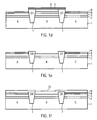
- Figures 1a - 1g illustrate an example for the method for manufacturing a semiconductor device according to the present invention, wherein an FET is formed that comprises a part of a BOX layer of an SOI structure as a gate dielectric.
- Figures 2a to 2g illustrate further examples for the method for manufacturing a semiconductor device according to the present invention, wherein a floating-gate FET is formed that comprises a part of a BOX layer of an SOI structure as a tunnel dielectric.
- Figure 3 illustrates an example of a semiconductor device according to the present invention comprising a MOSFET and a lower positioned FET wherein the drain of the MOSFET also functions as a gate of the lower positioned FET.
- Figures 4a , 4b und 4c illustrate an example for the method for manufacturing a semiconductor device according to the present invention, wherein a floating-gate FET is formed that comprises a part of a BOX layer of an SOI structure as a tunnel dielectric.
- Figures 1a - 1g show stages of an embodiment of manufacturing a semiconductor device according to the invention are shown. It is provided an SOI structure comprising a polysilicon substrate 1, an oxide layer 2 (BOX layer), for example, made of silicon dioxide, and a single crystal silicon layer 3. As shown in Figure 1b a hard mask layer 4 is grown or deposited atop of the silicon layer 3. In the shown example the hard mask layer comprises a thin oxide layer 5 and a silicon nitride layer 6. A photoresist is deposited on the hard mask layer 4 and patterned for the formation of shallow trench isolations 7. For this purpose, the hard mask layer 4, the silicon layer 3 and the BOX layer 2 are etched and the resulting trench is extended partly into the substrate 1. Then, the trench is filled by one or more dielectric materials, for example, silicon dioxide, and excess dielectric is removed from the surface of the mask layer 5 by chemical-mechanical planarization.
- dielectric materials for example, silicon dioxide
- the hard mask layer 4 is removed from regions A and C to expose the single crystal silicon layer 1 in these regions.
- a high-k dielectric layer 8 (for example, with a dielectric constant k more than 3.9 is formed on the exposed surfaces of the single crystal silicon layer 3 and silicon nitride layer 6 of region B as well as atop of the shallow trench isolations 7 and, subsequently a metal layer 9 is formed atop of the high-k dielectric layer 8 (see Figure 1d ).
- the high-k dielectric layer 8 may be made of silicon nitride or a composite material (SiON, Al 2 O 3 , HfO 2 , etc...) and the metal layer 9 may be made of TiN, W, TaN, and ternary components (Ti-Ta-N) etc., for example
- a polysilicon layer 10 is deposited as it is shown in Figure 1f .
- a photoresist (not shown) is formed atop the resulting structure and patterned for etching to form gate electrodes in the regions A, B and C (see Figure 1g ).
- three FETs are formed.
- regions A and C conventional MOSFETs 20 on SOI result.
- the channel regions of the conventional MOSFETs 20 are located below the gate dielectrics 8 in the silicon layer 3.
- Adjacent to the channel regions source and drain regions are formed by n or p carrier type dopants as known in the art.
- Gate electrodes of the MOSFETs 20 are formed from the metal layer 9 and also include the etched polysilicon material 10".
- the inventive FET 30 is formed separated from the conventional MOSFETs 20 by the trench isolations 7.
- the inventive FET 30 is characterized by a gate dielectric formed from the original BOX layer 2 provided in the SOI structure shown in Figure 1a and a gate electrode that comprises single crystal silicon 3' formed from the original single crystal silicon layer 3 provided in the SOI structure shown in Figure 1a .
- Polysillicon layer 10' is also formed as part of the gate electrode.
- N or P dopants adjacent to the channel region provided in the substrate 1 below the gate dielectric provide source and drain regions.
- the BOX layer of an SOI structure is used as the gate dielectric and the single crystal silicon of the SOI structure is used as part of the gate electrode.
- the BOX layer 2 may be provided with a lower thickness in region B than in regions A and C.
- FIGs 2a und 2b illustrate another example for the method for manufacturing a semiconductor device according to the present invention.
- a floating-gate FET is formed that comprises a part of a BOX layer of an SOI structure as a tunnel dielectric and a part of a single crystal silicon layer of the SOI structure as a floating gate.
- the exposed surface of the single crystal silicon layer 3 is thermally oxidized at some 700 °C to 900 °C, for example, in order to grow oxide dielectric layer 11 (see Figure 2a ).
- a dielectric layer 11 for instance, a silicon oxide layer, may be grown or deposited on the exposed surface of the single crystal silicon layer 3.
- a polysilicon layer 10 is deposited on the metal layer 9 in regions A and C and on the dielectric layer 11.
- the configuration shown in Figure 2a is etched in order to form two MOSFETs 20 in regions A and B.
- a floating-gate FET 40 is formed that is separated from the MOSFETs 20 by the shallow trench isolations 7. Due to the above-described processing steps the floating-gate FET 40 in region B comprises a channel region in the substrate 1 below the tunnel dielectric 2'. At both sides of the channel region source and drain regions are provided by appropriate doping of the substrate 1.
- the floating-gate FET 40 furthermore, comprises a floating gate 3' above the tunnel dielectric 2'. The floating gate 3' is separated from the gate electrode 10' by the gate dielectric 11'.
- the better single crystal silicon - oxide (floating gate - tunnel dielectric) interface allows for improved data retention when the floating-gate FET is used as a memory device.
- a reliable high-voltage FLASH device can, thus, be provided. It is noted that depending on the desired properties of the tunnel dielectric the BOX layer in the starting SOI structure may be provided with a lower thickness in region B than in regions A and C.
- FIG. 2c to 2g An alternative example for the manufacture of s semiconductor device according to the present invention is illustrated in Figures 2c to 2g .
- the process flow starts from the structure shown in Figure 1c .
- a high-k dielectric layer 8 is grown or deposited on single crystal silicon layer 3 in regions A and C.
- a metal gate layer 9 is formed atop of the high-k dielectric layer 8 (see Figure 2c ).
- a thin polysilicon layer 13 is formed on the metal gate layer 9 in regions A and C.
- the formation of layers 8, 9 and 13 over regions A and C comprises continuous formation of the layers over regions A, B and C and a lithographic step for removing the layers from region B (and the insulation region 7) by employing a photoresist mask (not shown) patterned to cover regions A and C, respectively. After etching the regions exposed by the photoresist mask the configuration shown in Figure 2c results.
- the hard mask (5 and 6) is removed in region B as is shown in Figure 2d .
- the thus exposed crystal silicon layer 3 is oxidized in region B to obtain an oxidized layer 11 as is shown in Figure 2e .
- a dielectric layer 11 is formed on the exposed crystal silicon layer 3.
- a polysilicon layer 10 for forming a gate electrode is deposited as it is shown in Figure 2f . Thereby, a configuration similar to the one shown in Figure 2a but including the thin polysilicon layer 13 is obtained.
- This structure comprises gate structures for circuits in regions A, B and C.
- the gate structures comprise the gate dielectric 8, gate metal layer 9 and both etched polysilicon gate material 10" and etched thin polysilicon layer 13 in regions A and C.
- inventive transistor devices can be manufactured in co-integration with conventional SOI based transistors.
- inventive transistor devices can be manufactured in co-integration with conventional SOI based transistors.
- the above-described exemplary examples for the manufacture of the semiconductor device may be amended in a manner not to include the formation of the conventional MOSFETs 20.
- FIG. 3 a configuration comprising in a particular manner a conventional SOI MOSFET and an inventive FET is provided.
- a conventional MOSFET comprising a gate electrode 100 and sidewall spacers 110 used for the formation of source and drain regions is formed according to SOI technology.
- the source and drain regions of this MOSFET are designated as "top source” 120 and "top drain” 130, respectively. These top source 120 and top drain 130 regions are formed in a single crystal silicon layer 230 of the SOI structure. Insulation regions 140 are provided adjacent to the source/drain regions.
- the gate electrode 100 is separated from the channel region 150 that is located between the top source 120 and top drain region 130 by a gate dielectric 160.
- the contacts 170 are formed in another dielectric material 180 covering the MOSFETs.
- the contacts 170 provide connection to metal interconnects of a metallization layer, for example.
- the MOSFET is indicated by an ellipsoid dashed contour.
- the single crystal silicon layer 230 is located atop of a BOX layer 190.
- the BOX layer 190 is located above a substrate 200, for example, a silicon substrate 200.
- the drain 130 of the MOSFET indicated by the ellipsoid dashed contour also functions as a gate electrode designated as "bottom gate” of an FET located partially below the MOSFET.
- the FET that is indicated by the ellipsoid dotted contour comprises the part of the single crystal silicon layer 230 that functions as a drain 130 for the MOSFET, a part of the BOX layer 190 functioning as a gate dielectric and a drain 210 and a source 220 region provided by appropriate dopants in the substrate 200 of the SOI structure.
- Figures 4a to 4c illustrate an example for the method for manufacturing a semiconductor device according to the present invention, wherein a floating-gate FET that comprises a part of a BOX layer of an SOI structure as a tunnel dielectric and SOI transistors are formed.
- the starting point for this exemplary inventive method is the stack shown in Figure 1a .
- a dielectric layer 11 is grown or deposited on crystal silicon layer 3 and a polysilicon layer 12 is formed on the dielectric layer 11 (see Figure 4a ).
- the thin polysilicon layer 12 serves as a protection layer for the dielectric layer 11 during the further processing.
- a dielectric layer 5 is formed on the polysilicon layer 12 and a nitride layer 6 is deposited on the dielectric layer 5.
- Shallow trench isolation regions are defined by lithography and trenches are etched through layers 2, 3, 11, 12, 5 and 6 and extending to the polysilicon substrate 1 and filled with some dielectric material to obtain shallow trench isolations 7.
- Layers 5 and 6 function as a hard mask during the process of etching the trenches.
- the dielectric material filled into the trenches is planarized with the nitride layer 6. The thus resulting structure is illustrated in Figure 4b .
- MOSFETs 20 are formed in the left and right regions of Figure 4c that are separated from the central region by shallow trench isolations 7.
- a floating-gate FET 30 comprising a floating gate 3' above a tunnel dielectric 2 wherein the floating gate 3' is separated from a gate electrode 10' by a gate dielectric 11' and thin polysilicon layer 12' is formed in the central region.
- a semiconductor-on-insulator structure in general can be processed according to the described inventive methods.
- germanium, silicon-germanium, strained silicon strained silicon-germanium, etc. can be used rather than conventional silicon in the semiconductor-on-insulator structure.
Landscapes
- Engineering & Computer Science (AREA)
- Power Engineering (AREA)
- Microelectronics & Electronic Packaging (AREA)
- General Physics & Mathematics (AREA)
- Computer Hardware Design (AREA)
- Physics & Mathematics (AREA)
- Condensed Matter Physics & Semiconductors (AREA)
- Manufacturing & Machinery (AREA)
- Ceramic Engineering (AREA)
- Thin Film Transistor (AREA)
- Semiconductor Memories (AREA)
- Non-Volatile Memory (AREA)
- Metal-Oxide And Bipolar Metal-Oxide Semiconductor Integrated Circuits (AREA)
Priority Applications (7)
| Application Number | Priority Date | Filing Date | Title |
|---|---|---|---|
| EP20100290217 EP2381470B1 (de) | 2010-04-22 | 2010-04-22 | Halbleiterbauelement mit einem Feldeffekttransistor in einer Silizium-auf-Isolator-Struktur |
| US12/886,421 US8455938B2 (en) | 2010-04-22 | 2010-09-20 | Device comprising a field-effect transistor in a silicon-on-insulator |
| JP2011073029A JP2011228677A (ja) | 2010-04-22 | 2011-03-29 | シリコン・オン・インシュレータ構造において電界効果トランジスタを備える半導体デバイス |
| SG2011022712A SG175502A1 (en) | 2010-04-22 | 2011-03-30 | Semiconductor device comprising a field-effecttransistor in a silicon-on-insulator structure |
| KR20110036304A KR101259402B1 (ko) | 2010-04-22 | 2011-04-19 | 실리콘-온-절연체 구조 내의 전계-효과 트랜지스터를 포함하는 반도체 소자 |
| TW100113780A TWI503979B (zh) | 2010-04-22 | 2011-04-20 | 包含一場效電晶體於一覆矽的絕緣層構造的半導體裝置 |
| CN201110099463.4A CN102237371B (zh) | 2010-04-22 | 2011-04-20 | 包含绝缘体上硅结构体中的场效应晶体管的半导体器件 |
Applications Claiming Priority (1)
| Application Number | Priority Date | Filing Date | Title |
|---|---|---|---|
| EP20100290217 EP2381470B1 (de) | 2010-04-22 | 2010-04-22 | Halbleiterbauelement mit einem Feldeffekttransistor in einer Silizium-auf-Isolator-Struktur |
Publications (2)
| Publication Number | Publication Date |
|---|---|
| EP2381470A1 true EP2381470A1 (de) | 2011-10-26 |
| EP2381470B1 EP2381470B1 (de) | 2012-08-22 |
Family
ID=42697363
Family Applications (1)
| Application Number | Title | Priority Date | Filing Date |
|---|---|---|---|
| EP20100290217 Active EP2381470B1 (de) | 2010-04-22 | 2010-04-22 | Halbleiterbauelement mit einem Feldeffekttransistor in einer Silizium-auf-Isolator-Struktur |
Country Status (7)
| Country | Link |
|---|---|
| US (1) | US8455938B2 (de) |
| EP (1) | EP2381470B1 (de) |
| JP (1) | JP2011228677A (de) |
| KR (1) | KR101259402B1 (de) |
| CN (1) | CN102237371B (de) |
| SG (1) | SG175502A1 (de) |
| TW (1) | TWI503979B (de) |
Cited By (3)
| Publication number | Priority date | Publication date | Assignee | Title |
|---|---|---|---|---|
| WO2016043857A1 (en) * | 2014-09-19 | 2016-03-24 | Silicon Storage Technology, Inc. | Method of making embedded memory device with silicon-on-insulator substrate |
| US9634020B1 (en) | 2015-10-07 | 2017-04-25 | Silicon Storage Technology, Inc. | Method of making embedded memory device with silicon-on-insulator substrate |
| US9786755B2 (en) | 2015-03-18 | 2017-10-10 | Stmicroelectronics (Crolles 2) Sas | Process for producing, from an SOI and in particular an FDSOI type substrate, transistors having gate oxides of different thicknesses, and corresponding integrated circuit |
Families Citing this family (13)
| Publication number | Priority date | Publication date | Assignee | Title |
|---|---|---|---|---|
| EP2500933A1 (de) * | 2011-03-11 | 2012-09-19 | S.O.I. TEC Silicon | Mehrschichtige Strukturen und Verfahren zur Herstellung von Halbleitervorrichtungen |
| FR2987710B1 (fr) | 2012-03-05 | 2017-04-28 | Soitec Silicon On Insulator | Architecture de table de correspondance |
| US8963228B2 (en) * | 2013-04-18 | 2015-02-24 | International Business Machines Corporation | Non-volatile memory device integrated with CMOS SOI FET on a single chip |
| US9224755B2 (en) | 2013-09-06 | 2015-12-29 | Globalfoundries Inc. | Flexible active matrix display |
| US20150263040A1 (en) * | 2014-03-17 | 2015-09-17 | Silicon Storage Technology, Inc. | Embedded Memory Device With Silicon-On-Insulator Substrate, And Method Of Making Same |
| US9748379B2 (en) * | 2015-06-25 | 2017-08-29 | Taiwan Semiconductor Manufacturing Co., Ltd. | Double exponential mechanism controlled transistor |
| US9768254B2 (en) * | 2015-07-30 | 2017-09-19 | International Business Machines Corporation | Leakage-free implantation-free ETSOI transistors |
| US9735061B1 (en) * | 2016-02-03 | 2017-08-15 | Globalfoundries Inc. | Methods to form multi threshold-voltage dual channel without channel doping |
| US20170338343A1 (en) * | 2016-05-23 | 2017-11-23 | Globalfoundries Inc. | High-voltage transistor device |
| FR3057705B1 (fr) * | 2016-10-13 | 2019-04-12 | Soitec | Procede de dissolution d'un oxyde enterre dans une plaquette de silicium sur isolant |
| FR3069702B1 (fr) * | 2017-07-27 | 2020-01-24 | Stmicroelectronics (Rousset) Sas | Procede de fabrication simultanee de transistors soi et de transistors sur substrat massif |
| US11315825B2 (en) * | 2019-08-28 | 2022-04-26 | Globalfoundries U.S. Inc. | Semiconductor structures including stacked depleted and high resistivity regions |
| US11183514B2 (en) | 2019-09-05 | 2021-11-23 | Globalfoundries U.S. Inc. | Vertically stacked field effect transistors |
Citations (9)
| Publication number | Priority date | Publication date | Assignee | Title |
|---|---|---|---|---|
| JPH04345064A (ja) * | 1991-05-22 | 1992-12-01 | Hitachi Ltd | 半導体集積回路装置およびその製造方法 |
| JPH08255846A (ja) * | 1995-03-17 | 1996-10-01 | Nippondenso Co Ltd | 半導体装置及びその製造方法 |
| US5869872A (en) * | 1995-07-10 | 1999-02-09 | Nippondenso Co., Ltd. | Semiconductor integrated circuit device and manufacturing method for the same |
| US20070029596A1 (en) * | 1995-09-29 | 2007-02-08 | Katsuki Hazama | Semiconductor device including transistor with composite gate structure and transistor with single gate structure, and method for manufacturing the same |
| US20080042187A1 (en) * | 2006-08-17 | 2008-02-21 | Hynix Semiconductor Inc. | Flash Memory Device And A Method Of Fabricating The Same |
| US20090096036A1 (en) * | 2007-10-11 | 2009-04-16 | Takashi Ishigaki | Semiconductor device and method of manufacturing the same |
| US20090111223A1 (en) * | 2007-10-31 | 2009-04-30 | Maciej Wiatr | Soi device having a substrate diode formed by reduced implantation energy |
| US20100035390A1 (en) * | 2008-08-08 | 2010-02-11 | International Business Machines Corporation | Method of forming a high performance fet and a high voltage fet on a soi substrate |
| US20100032761A1 (en) * | 2008-08-08 | 2010-02-11 | Hanyi Ding | Semiconductor structure including a high performance fet and a high voltage fet on a soi substrate |
Family Cites Families (92)
| Publication number | Priority date | Publication date | Assignee | Title |
|---|---|---|---|---|
| US4169233A (en) | 1978-02-24 | 1979-09-25 | Rockwell International Corporation | High performance CMOS sense amplifier |
| KR100213602B1 (ko) | 1988-05-13 | 1999-08-02 | 가나이 쓰도무 | 다이나믹형 반도체 기억장치 |
| US5028810A (en) | 1989-07-13 | 1991-07-02 | Intel Corporation | Four quadrant synapse cell employing single column summing line |
| JP2717740B2 (ja) | 1991-08-30 | 1998-02-25 | 三菱電機株式会社 | 半導体集積回路装置 |
| EP0564204A3 (en) | 1992-03-30 | 1994-09-28 | Mitsubishi Electric Corp | Semiconductor device |
| US5325054A (en) | 1992-07-07 | 1994-06-28 | Texas Instruments Incorporated | Method and system for screening reliability of semiconductor circuits |
| US5306530A (en) | 1992-11-23 | 1994-04-26 | Associated Universities, Inc. | Method for producing high quality thin layer films on substrates |
| JP3488730B2 (ja) | 1993-11-05 | 2004-01-19 | 株式会社ルネサステクノロジ | 半導体集積回路装置 |
| US5455791A (en) | 1994-06-01 | 1995-10-03 | Zaleski; Andrzei | Method for erasing data in EEPROM devices on SOI substrates and device therefor |
| JP3003088B2 (ja) | 1994-06-10 | 2000-01-24 | 住友イートンノバ株式会社 | イオン注入装置 |
| JP3549602B2 (ja) | 1995-01-12 | 2004-08-04 | 株式会社ルネサステクノロジ | 半導体記憶装置 |
| JP3288554B2 (ja) | 1995-05-29 | 2002-06-04 | 株式会社日立製作所 | イオン注入装置及びイオン注入方法 |
| JP3265178B2 (ja) | 1996-02-20 | 2002-03-11 | 株式会社東芝 | 半導体記憶装置及びその製造方法 |
| JPH10125064A (ja) | 1996-10-14 | 1998-05-15 | Toshiba Corp | 記憶装置 |
| JPH10208484A (ja) | 1997-01-29 | 1998-08-07 | Mitsubishi Electric Corp | 半導体記憶装置のデータ読出回路及び半導体記憶装置 |
| US5889293A (en) | 1997-04-04 | 1999-03-30 | International Business Machines Corporation | Electrical contact to buried SOI structures |
| JP3699823B2 (ja) | 1998-05-19 | 2005-09-28 | 株式会社東芝 | 半導体装置 |
| US6072217A (en) | 1998-06-11 | 2000-06-06 | Sun Microsystems, Inc. | Tunable threshold SOI device using isolated well structure for back gate |
| FR2779869B1 (fr) | 1998-06-15 | 2003-05-16 | Commissariat Energie Atomique | Circuit integre de type soi a capacite de decouplage, et procede de realisation d'un tel circuit |
| US6826730B2 (en) | 1998-12-15 | 2004-11-30 | Texas Instruments Incorporated | System and method for controlling current in an integrated circuit |
| JP3456913B2 (ja) | 1998-12-25 | 2003-10-14 | 株式会社東芝 | 半導体装置 |
| US6372600B1 (en) | 1999-08-30 | 2002-04-16 | Agere Systems Guardian Corp. | Etch stops and alignment marks for bonded wafers |
| US6476462B2 (en) | 1999-12-28 | 2002-11-05 | Texas Instruments Incorporated | MOS-type semiconductor device and method for making same |
| US6417697B2 (en) | 2000-02-02 | 2002-07-09 | Broadcom Corporation | Circuit technique for high speed low power data transfer bus |
| US6300218B1 (en) | 2000-05-08 | 2001-10-09 | International Business Machines Corporation | Method for patterning a buried oxide thickness for a separation by implanted oxygen (simox) process |
| US6350653B1 (en) | 2000-10-12 | 2002-02-26 | International Business Machines Corporation | Embedded DRAM on silicon-on-insulator substrate |
| JP2002164544A (ja) | 2000-11-28 | 2002-06-07 | Sony Corp | 半導体装置 |
| US6614190B2 (en) | 2001-01-31 | 2003-09-02 | Hitachi, Ltd. | Ion implanter |
| JP3982218B2 (ja) | 2001-02-07 | 2007-09-26 | ソニー株式会社 | 半導体装置およびその製造方法 |
| JP3884266B2 (ja) | 2001-02-19 | 2007-02-21 | 株式会社東芝 | 半導体メモリ装置及びその製造方法 |
| US6611023B1 (en) | 2001-05-01 | 2003-08-26 | Advanced Micro Devices, Inc. | Field effect transistor with self alligned double gate and method of forming same |
| US6759282B2 (en) | 2001-06-12 | 2004-07-06 | International Business Machines Corporation | Method and structure for buried circuits and devices |
| US6620656B2 (en) * | 2001-12-19 | 2003-09-16 | Motorola, Inc. | Method of forming body-tied silicon on insulator semiconductor device |
| US6498057B1 (en) | 2002-03-07 | 2002-12-24 | International Business Machines Corporation | Method for implementing SOI transistor source connections using buried dual rail distribution |
| EP1357603A3 (de) | 2002-04-18 | 2004-01-14 | Innovative Silicon SA | Halbleiterbauelement |
| US6838723B2 (en) | 2002-08-29 | 2005-01-04 | Micron Technology, Inc. | Merged MOS-bipolar capacitor memory cell |
| JP3595818B2 (ja) * | 2002-10-11 | 2004-12-02 | 沖電気工業株式会社 | Soi−mosfet装置 |
| US7710771B2 (en) * | 2002-11-20 | 2010-05-04 | The Regents Of The University Of California | Method and apparatus for capacitorless double-gate storage |
| JP2004179506A (ja) | 2002-11-28 | 2004-06-24 | Seiko Epson Corp | Soi構造を有する半導体基板及びその製造方法及び半導体装置 |
| US7030436B2 (en) | 2002-12-04 | 2006-04-18 | Micron Technology, Inc. | Embedded DRAM gain memory cell having MOS transistor body provided with a bi-polar transistor charge injecting means |
| JP2004303499A (ja) | 2003-03-31 | 2004-10-28 | Hitachi High-Technologies Corp | イオン注入装置およびイオン注入方法 |
| JP4077381B2 (ja) | 2003-08-29 | 2008-04-16 | 株式会社東芝 | 半導体集積回路装置 |
| US6965143B2 (en) | 2003-10-10 | 2005-11-15 | Advanced Micro Devices, Inc. | Recess channel flash architecture for reduced short channel effect |
| JP2005158952A (ja) | 2003-11-25 | 2005-06-16 | Toshiba Corp | 半導体装置及びその製造方法 |
| US7109532B1 (en) | 2003-12-23 | 2006-09-19 | Lee Zachary K | High Ion/Ioff SOI MOSFET using body voltage control |
| US20050255666A1 (en) | 2004-05-11 | 2005-11-17 | Miradia Inc. | Method and structure for aligning mechanical based device to integrated circuits |
| US7112997B1 (en) | 2004-05-19 | 2006-09-26 | Altera Corporation | Apparatus and methods for multi-gate silicon-on-insulator transistors |
| JP4795653B2 (ja) | 2004-06-15 | 2011-10-19 | ルネサスエレクトロニクス株式会社 | 半導体記憶装置 |
| US7190616B2 (en) | 2004-07-19 | 2007-03-13 | Micron Technology, Inc. | In-service reconfigurable DRAM and flash memory device |
| US7196921B2 (en) | 2004-07-19 | 2007-03-27 | Silicon Storage Technology, Inc. | High-speed and low-power differential non-volatile content addressable memory cell and array |
| US7560361B2 (en) | 2004-08-12 | 2009-07-14 | International Business Machines Corporation | Method of forming gate stack for semiconductor electronic device |
| KR100663359B1 (ko) | 2005-03-31 | 2007-01-02 | 삼성전자주식회사 | 리세스 채널 트랜지스터 구조를 갖는 단일 트랜지스터플로팅 바디 디램 셀 및 그 제조방법 |
| US20060267064A1 (en) | 2005-05-31 | 2006-11-30 | Infineon Technologies Ag | Semiconductor memory device |
| US7274618B2 (en) | 2005-06-24 | 2007-09-25 | Monolithic System Technology, Inc. | Word line driver for DRAM embedded in a logic process |
| JP4967264B2 (ja) | 2005-07-11 | 2012-07-04 | 株式会社日立製作所 | 半導体装置 |
| JP4800700B2 (ja) | 2005-08-01 | 2011-10-26 | ルネサスエレクトロニクス株式会社 | 半導体装置およびそれを用いた半導体集積回路 |
| US7314794B2 (en) | 2005-08-08 | 2008-01-01 | International Business Machines Corporation | Low-cost high-performance planar back-gate CMOS |
| US7812397B2 (en) * | 2005-09-29 | 2010-10-12 | International Business Machines Corporation | Ultra thin channel (UTC) MOSFET structure formed on BOX regions having different depths and different thicknesses beneath the UTC and source/drain regions and method of manufacture thereof |
| JP4413841B2 (ja) | 2005-10-03 | 2010-02-10 | 株式会社東芝 | 半導体記憶装置及びその製造方法 |
| JP4822791B2 (ja) | 2005-10-04 | 2011-11-24 | ルネサスエレクトロニクス株式会社 | 半導体記憶装置 |
| US7601271B2 (en) | 2005-11-28 | 2009-10-13 | S.O.I.Tec Silicon On Insulator Technologies | Process and equipment for bonding by molecular adhesion |
| JP5054919B2 (ja) | 2005-12-20 | 2012-10-24 | ルネサスエレクトロニクス株式会社 | 半導体集積回路装置 |
| KR100735613B1 (ko) | 2006-01-11 | 2007-07-04 | 삼성전자주식회사 | 이온주입설비의 디스크 어셈블리 |
| US7304903B2 (en) | 2006-01-23 | 2007-12-04 | Purdue Research Foundation | Sense amplifier circuit |
| JP4762036B2 (ja) | 2006-04-14 | 2011-08-31 | 株式会社東芝 | 半導体装置 |
| JPWO2007125775A1 (ja) | 2006-04-24 | 2009-09-10 | パナソニック株式会社 | 受信装置、それを用いた電子機器、及び受信方法 |
| US7494902B2 (en) | 2006-06-23 | 2009-02-24 | Interuniversitair Microelektronica Centrum Vzw (Imec) | Method of fabricating a strained multi-gate transistor |
| US7560344B2 (en) | 2006-11-15 | 2009-07-14 | Samsung Electronics Co., Ltd. | Semiconductor device having a pair of fins and method of manufacturing the same |
| JP2008130670A (ja) | 2006-11-17 | 2008-06-05 | Seiko Epson Corp | 半導体装置、論理回路および電子機器 |
| JP5057430B2 (ja) | 2006-12-18 | 2012-10-24 | ルネサスエレクトロニクス株式会社 | 半導体集積回路とその製造方法 |
| JP4869088B2 (ja) | 2007-01-22 | 2012-02-01 | 株式会社東芝 | 半導体記憶装置及びその書き込み方法 |
| JP5019436B2 (ja) | 2007-02-22 | 2012-09-05 | ルネサスエレクトロニクス株式会社 | 半導体集積回路 |
| JP5594927B2 (ja) | 2007-04-11 | 2014-09-24 | ピーエスフォー ルクスコ エスエイアールエル | 半導体記憶装置 |
| FR2915024A1 (fr) | 2007-04-12 | 2008-10-17 | St Microelectronics Crolles 2 | Procede de fabrication permettant l'homogeneisation de l'environnement de transistors et dispositif associe |
| US7729149B2 (en) | 2007-05-01 | 2010-06-01 | Suvolta, Inc. | Content addressable memory cell including a junction field effect transistor |
| EP2015362A1 (de) | 2007-06-04 | 2009-01-14 | STMicroelectronics (Crolles 2) SAS | Halbleitermatrix und deren Herstellungsverfahren |
| US7449922B1 (en) | 2007-06-15 | 2008-11-11 | Arm Limited | Sensing circuitry and method of detecting a change in voltage on at least one input line |
| US7759714B2 (en) | 2007-06-26 | 2010-07-20 | Hitachi, Ltd. | Semiconductor device |
| FR2918823B1 (fr) | 2007-07-13 | 2009-10-16 | Ecole Centrale De Lyon Etablis | Cellule logique reconfigurable a base de transistors mosfet double grille |
| FR2919112A1 (fr) | 2007-07-16 | 2009-01-23 | St Microelectronics Crolles 2 | Circuit integre comprenant un transistor et un condensateur et procede de fabrication |
| JP5035345B2 (ja) | 2007-08-30 | 2012-09-26 | 富士通セミコンダクター株式会社 | イオン注入装置、基板クランプ機構、及びイオン注入方法 |
| KR100884344B1 (ko) | 2007-10-10 | 2009-02-18 | 주식회사 하이닉스반도체 | 비대칭 소스/드레인 접합을 갖는 불휘발성 메모리소자 및그 제조방법 |
| US20090101940A1 (en) | 2007-10-19 | 2009-04-23 | Barrows Corey K | Dual gate fet structures for flexible gate array design methodologies |
| FR2925223B1 (fr) | 2007-12-18 | 2010-02-19 | Soitec Silicon On Insulator | Procede d'assemblage avec marques enterrees |
| US7593265B2 (en) | 2007-12-28 | 2009-09-22 | Sandisk Corporation | Low noise sense amplifier array and method for nonvolatile memory |
| US7759729B2 (en) * | 2008-02-07 | 2010-07-20 | International Business Machines Corporation | Metal-oxide-semiconductor device including an energy filter |
| JP5412445B2 (ja) | 2008-02-20 | 2014-02-12 | ソイテック | 酸化物溶解後の酸化 |
| JP6053250B2 (ja) | 2008-06-12 | 2016-12-27 | ピーエスフォー ルクスコ エスエイアールエルPS4 Luxco S.a.r.l. | 半導体装置 |
| WO2010007478A1 (en) | 2008-06-13 | 2010-01-21 | Yale University | Improved complementary metal oxide semiconductor devices |
| KR101623958B1 (ko) | 2008-10-01 | 2016-05-25 | 삼성전자주식회사 | 인버터 및 그의 동작방법과 인버터를 포함하는 논리회로 |
| KR101522400B1 (ko) | 2008-11-10 | 2015-05-21 | 삼성전자주식회사 | 인버터 및 그를 포함하는 논리소자 |
| US8008146B2 (en) * | 2009-12-04 | 2011-08-30 | International Business Machines Corporation | Different thickness oxide silicon nanowire field effect transistors |
-
2010
- 2010-04-22 EP EP20100290217 patent/EP2381470B1/de active Active
- 2010-09-20 US US12/886,421 patent/US8455938B2/en active Active
-
2011
- 2011-03-29 JP JP2011073029A patent/JP2011228677A/ja not_active Withdrawn
- 2011-03-30 SG SG2011022712A patent/SG175502A1/en unknown
- 2011-04-19 KR KR20110036304A patent/KR101259402B1/ko active IP Right Grant
- 2011-04-20 TW TW100113780A patent/TWI503979B/zh active
- 2011-04-20 CN CN201110099463.4A patent/CN102237371B/zh active Active
Patent Citations (9)
| Publication number | Priority date | Publication date | Assignee | Title |
|---|---|---|---|---|
| JPH04345064A (ja) * | 1991-05-22 | 1992-12-01 | Hitachi Ltd | 半導体集積回路装置およびその製造方法 |
| JPH08255846A (ja) * | 1995-03-17 | 1996-10-01 | Nippondenso Co Ltd | 半導体装置及びその製造方法 |
| US5869872A (en) * | 1995-07-10 | 1999-02-09 | Nippondenso Co., Ltd. | Semiconductor integrated circuit device and manufacturing method for the same |
| US20070029596A1 (en) * | 1995-09-29 | 2007-02-08 | Katsuki Hazama | Semiconductor device including transistor with composite gate structure and transistor with single gate structure, and method for manufacturing the same |
| US20080042187A1 (en) * | 2006-08-17 | 2008-02-21 | Hynix Semiconductor Inc. | Flash Memory Device And A Method Of Fabricating The Same |
| US20090096036A1 (en) * | 2007-10-11 | 2009-04-16 | Takashi Ishigaki | Semiconductor device and method of manufacturing the same |
| US20090111223A1 (en) * | 2007-10-31 | 2009-04-30 | Maciej Wiatr | Soi device having a substrate diode formed by reduced implantation energy |
| US20100035390A1 (en) * | 2008-08-08 | 2010-02-11 | International Business Machines Corporation | Method of forming a high performance fet and a high voltage fet on a soi substrate |
| US20100032761A1 (en) * | 2008-08-08 | 2010-02-11 | Hanyi Ding | Semiconductor structure including a high performance fet and a high voltage fet on a soi substrate |
Cited By (5)
| Publication number | Priority date | Publication date | Assignee | Title |
|---|---|---|---|---|
| WO2016043857A1 (en) * | 2014-09-19 | 2016-03-24 | Silicon Storage Technology, Inc. | Method of making embedded memory device with silicon-on-insulator substrate |
| CN107078035A (zh) * | 2014-09-19 | 2017-08-18 | 硅存储技术公司 | 制成具有绝缘体上硅衬底的嵌入式存储器设备的方法 |
| CN107078035B (zh) * | 2014-09-19 | 2018-12-21 | 硅存储技术公司 | 制成具有绝缘体上硅衬底的嵌入式存储器设备的方法 |
| US9786755B2 (en) | 2015-03-18 | 2017-10-10 | Stmicroelectronics (Crolles 2) Sas | Process for producing, from an SOI and in particular an FDSOI type substrate, transistors having gate oxides of different thicknesses, and corresponding integrated circuit |
| US9634020B1 (en) | 2015-10-07 | 2017-04-25 | Silicon Storage Technology, Inc. | Method of making embedded memory device with silicon-on-insulator substrate |
Also Published As
| Publication number | Publication date |
|---|---|
| SG175502A1 (en) | 2011-11-28 |
| CN102237371B (zh) | 2015-02-25 |
| US20110260233A1 (en) | 2011-10-27 |
| TWI503979B (zh) | 2015-10-11 |
| US8455938B2 (en) | 2013-06-04 |
| JP2011228677A (ja) | 2011-11-10 |
| CN102237371A (zh) | 2011-11-09 |
| EP2381470B1 (de) | 2012-08-22 |
| KR101259402B1 (ko) | 2013-04-30 |
| TW201140842A (en) | 2011-11-16 |
| KR20110118087A (ko) | 2011-10-28 |
Similar Documents
| Publication | Publication Date | Title |
|---|---|---|
| EP2381470B1 (de) | Halbleiterbauelement mit einem Feldeffekttransistor in einer Silizium-auf-Isolator-Struktur | |
| US7687365B2 (en) | CMOS structure for body ties in ultra-thin SOI (UTSOI) substrates | |
| US7229893B2 (en) | Method and apparatus for a semiconductor device with a high-k gate dielectric | |
| US9406679B2 (en) | Integration of multiple threshold voltage devices for complementary metal oxide semiconductor using full metal gate | |
| US20160005738A1 (en) | Semiconductor device having a fin structure and method of manufacture the same | |
| US11031301B2 (en) | Gate formation scheme for n-type and p-type transistors having separately tuned threshold voltages | |
| US7332407B2 (en) | Method and apparatus for a semiconductor device with a high-k gate dielectric | |
| JP2004241755A (ja) | 半導体装置 | |
| JP2010123947A (ja) | 性能を改善する新しいレイアウト構造 | |
| JP2009302317A (ja) | 半導体装置およびその製造方法 | |
| US7919379B2 (en) | Dielectric spacer removal | |
| US10615159B2 (en) | Integrated LDMOS and VFET transistors | |
| JP2007150296A (ja) | 低接触抵抗の受動素子を内蔵するcmos回路、およびその形成方法 | |
| US9570318B1 (en) | High-k and p-type work function metal first fabrication process having improved annealing process flows | |
| US11888048B2 (en) | Gate oxide for nanosheet transistor devices | |
| US11127818B2 (en) | High voltage transistor with fin source/drain regions and trench gate structure | |
| JP4011014B2 (ja) | 半導体装置およびその製造方法 | |
| US20210359108A1 (en) | Double diffusion break gates fully overlapping fin edges with insulator regions | |
| US20140217544A1 (en) | Methods of forming a transistor device on a bulk substrate and the resulting device | |
| TW202329257A (zh) | 包含使用埋入絕緣層作為閘極介電層及溝槽隔離於源極和汲極中的電晶體的結構 | |
| US9412848B1 (en) | Methods of forming a complex GAA FET device at advanced technology nodes | |
| JP2004031529A (ja) | 半導体装置及びその製造方法 |
Legal Events
| Date | Code | Title | Description |
|---|---|---|---|
| 17P | Request for examination filed |
Effective date: 20101208 |
|
| AK | Designated contracting states |
Kind code of ref document: A1 Designated state(s): AT BE BG CH CY CZ DE DK EE ES FI FR GB GR HR HU IE IS IT LI LT LU LV MC MK MT NL NO PL PT RO SE SI SK SM TR |
|
| AX | Request for extension of the european patent |
Extension state: AL BA ME RS |
|
| PUAI | Public reference made under article 153(3) epc to a published international application that has entered the european phase |
Free format text: ORIGINAL CODE: 0009012 |
|
| REG | Reference to a national code |
Ref country code: DE Ref legal event code: R079 Ref document number: 602010002519 Country of ref document: DE Free format text: PREVIOUS MAIN CLASS: H01L0021823400 Ipc: H01L0027070000 |
|
| GRAP | Despatch of communication of intention to grant a patent |
Free format text: ORIGINAL CODE: EPIDOSNIGR1 |
|
| RIC1 | Information provided on ipc code assigned before grant |
Ipc: H01L 27/07 20060101AFI20120127BHEP Ipc: H01L 27/12 20060101ALI20120127BHEP Ipc: H01L 21/84 20060101ALI20120127BHEP Ipc: H01L 21/8234 20060101ALI20120127BHEP |
|
| RTI1 | Title (correction) |
Free format text: SEMICONDUCTOR DEVICE COMPRISING A FIELD-EFFECT TRANSISTOR IN A SILICON-ON-INSULATOR STRUCTURE |
|
| RAP1 | Party data changed (applicant data changed or rights of an application transferred) |
Owner name: SOITEC |
|
| GRAS | Grant fee paid |
Free format text: ORIGINAL CODE: EPIDOSNIGR3 |
|
| GRAA | (expected) grant |
Free format text: ORIGINAL CODE: 0009210 |
|
| AK | Designated contracting states |
Kind code of ref document: B1 Designated state(s): AT BE BG CH CY CZ DE DK EE ES FI FR GB GR HR HU IE IS IT LI LT LU LV MC MK MT NL NO PL PT RO SE SI SK SM TR |
|
| REG | Reference to a national code |
Ref country code: GB Ref legal event code: FG4D |
|
| REG | Reference to a national code |
Ref country code: CH Ref legal event code: EP |
|
| REG | Reference to a national code |
Ref country code: NL Ref legal event code: T3 Ref country code: IE Ref legal event code: FG4D |
|
| REG | Reference to a national code |
Ref country code: AT Ref legal event code: REF Ref document number: 572351 Country of ref document: AT Kind code of ref document: T Effective date: 20120915 |
|
| REG | Reference to a national code |
Ref country code: DE Ref legal event code: R096 Ref document number: 602010002519 Country of ref document: DE Effective date: 20121018 |
|
| REG | Reference to a national code |
Ref country code: AT Ref legal event code: MK05 Ref document number: 572351 Country of ref document: AT Kind code of ref document: T Effective date: 20120822 |
|
| REG | Reference to a national code |
Ref country code: LT Ref legal event code: MG4D Effective date: 20120822 |
|
| PG25 | Lapsed in a contracting state [announced via postgrant information from national office to epo] |
Ref country code: FI Free format text: LAPSE BECAUSE OF FAILURE TO SUBMIT A TRANSLATION OF THE DESCRIPTION OR TO PAY THE FEE WITHIN THE PRESCRIBED TIME-LIMIT Effective date: 20120822 Ref country code: IS Free format text: LAPSE BECAUSE OF FAILURE TO SUBMIT A TRANSLATION OF THE DESCRIPTION OR TO PAY THE FEE WITHIN THE PRESCRIBED TIME-LIMIT Effective date: 20121222 Ref country code: NO Free format text: LAPSE BECAUSE OF FAILURE TO SUBMIT A TRANSLATION OF THE DESCRIPTION OR TO PAY THE FEE WITHIN THE PRESCRIBED TIME-LIMIT Effective date: 20121122 Ref country code: HR Free format text: LAPSE BECAUSE OF FAILURE TO SUBMIT A TRANSLATION OF THE DESCRIPTION OR TO PAY THE FEE WITHIN THE PRESCRIBED TIME-LIMIT Effective date: 20120822 Ref country code: LT Free format text: LAPSE BECAUSE OF FAILURE TO SUBMIT A TRANSLATION OF THE DESCRIPTION OR TO PAY THE FEE WITHIN THE PRESCRIBED TIME-LIMIT Effective date: 20120822 Ref country code: AT Free format text: LAPSE BECAUSE OF FAILURE TO SUBMIT A TRANSLATION OF THE DESCRIPTION OR TO PAY THE FEE WITHIN THE PRESCRIBED TIME-LIMIT Effective date: 20120822 |
|
| PG25 | Lapsed in a contracting state [announced via postgrant information from national office to epo] |
Ref country code: BE Free format text: LAPSE BECAUSE OF FAILURE TO SUBMIT A TRANSLATION OF THE DESCRIPTION OR TO PAY THE FEE WITHIN THE PRESCRIBED TIME-LIMIT Effective date: 20120822 Ref country code: SE Free format text: LAPSE BECAUSE OF FAILURE TO SUBMIT A TRANSLATION OF THE DESCRIPTION OR TO PAY THE FEE WITHIN THE PRESCRIBED TIME-LIMIT Effective date: 20120822 Ref country code: SI Free format text: LAPSE BECAUSE OF FAILURE TO SUBMIT A TRANSLATION OF THE DESCRIPTION OR TO PAY THE FEE WITHIN THE PRESCRIBED TIME-LIMIT Effective date: 20120822 Ref country code: LV Free format text: LAPSE BECAUSE OF FAILURE TO SUBMIT A TRANSLATION OF THE DESCRIPTION OR TO PAY THE FEE WITHIN THE PRESCRIBED TIME-LIMIT Effective date: 20120822 Ref country code: PT Free format text: LAPSE BECAUSE OF FAILURE TO SUBMIT A TRANSLATION OF THE DESCRIPTION OR TO PAY THE FEE WITHIN THE PRESCRIBED TIME-LIMIT Effective date: 20121224 Ref country code: GR Free format text: LAPSE BECAUSE OF FAILURE TO SUBMIT A TRANSLATION OF THE DESCRIPTION OR TO PAY THE FEE WITHIN THE PRESCRIBED TIME-LIMIT Effective date: 20121123 |
|
| PG25 | Lapsed in a contracting state [announced via postgrant information from national office to epo] |
Ref country code: RO Free format text: LAPSE BECAUSE OF FAILURE TO SUBMIT A TRANSLATION OF THE DESCRIPTION OR TO PAY THE FEE WITHIN THE PRESCRIBED TIME-LIMIT Effective date: 20120822 Ref country code: CZ Free format text: LAPSE BECAUSE OF FAILURE TO SUBMIT A TRANSLATION OF THE DESCRIPTION OR TO PAY THE FEE WITHIN THE PRESCRIBED TIME-LIMIT Effective date: 20120822 Ref country code: EE Free format text: LAPSE BECAUSE OF FAILURE TO SUBMIT A TRANSLATION OF THE DESCRIPTION OR TO PAY THE FEE WITHIN THE PRESCRIBED TIME-LIMIT Effective date: 20120822 Ref country code: DK Free format text: LAPSE BECAUSE OF FAILURE TO SUBMIT A TRANSLATION OF THE DESCRIPTION OR TO PAY THE FEE WITHIN THE PRESCRIBED TIME-LIMIT Effective date: 20120822 |
|
| PG25 | Lapsed in a contracting state [announced via postgrant information from national office to epo] |
Ref country code: PL Free format text: LAPSE BECAUSE OF FAILURE TO SUBMIT A TRANSLATION OF THE DESCRIPTION OR TO PAY THE FEE WITHIN THE PRESCRIBED TIME-LIMIT Effective date: 20120822 Ref country code: IT Free format text: LAPSE BECAUSE OF FAILURE TO SUBMIT A TRANSLATION OF THE DESCRIPTION OR TO PAY THE FEE WITHIN THE PRESCRIBED TIME-LIMIT Effective date: 20120822 Ref country code: SK Free format text: LAPSE BECAUSE OF FAILURE TO SUBMIT A TRANSLATION OF THE DESCRIPTION OR TO PAY THE FEE WITHIN THE PRESCRIBED TIME-LIMIT Effective date: 20120822 |
|
| PLBE | No opposition filed within time limit |
Free format text: ORIGINAL CODE: 0009261 |
|
| STAA | Information on the status of an ep patent application or granted ep patent |
Free format text: STATUS: NO OPPOSITION FILED WITHIN TIME LIMIT |
|
| 26N | No opposition filed |
Effective date: 20130523 |
|
| PG25 | Lapsed in a contracting state [announced via postgrant information from national office to epo] |
Ref country code: BG Free format text: LAPSE BECAUSE OF FAILURE TO SUBMIT A TRANSLATION OF THE DESCRIPTION OR TO PAY THE FEE WITHIN THE PRESCRIBED TIME-LIMIT Effective date: 20121122 |
|
| REG | Reference to a national code |
Ref country code: DE Ref legal event code: R097 Ref document number: 602010002519 Country of ref document: DE Effective date: 20130523 |
|
| PG25 | Lapsed in a contracting state [announced via postgrant information from national office to epo] |
Ref country code: ES Free format text: LAPSE BECAUSE OF FAILURE TO SUBMIT A TRANSLATION OF THE DESCRIPTION OR TO PAY THE FEE WITHIN THE PRESCRIBED TIME-LIMIT Effective date: 20121203 |
|
| PG25 | Lapsed in a contracting state [announced via postgrant information from national office to epo] |
Ref country code: MC Free format text: LAPSE BECAUSE OF FAILURE TO SUBMIT A TRANSLATION OF THE DESCRIPTION OR TO PAY THE FEE WITHIN THE PRESCRIBED TIME-LIMIT Effective date: 20120822 Ref country code: CY Free format text: LAPSE BECAUSE OF FAILURE TO SUBMIT A TRANSLATION OF THE DESCRIPTION OR TO PAY THE FEE WITHIN THE PRESCRIBED TIME-LIMIT Effective date: 20120822 |
|
| REG | Reference to a national code |
Ref country code: IE Ref legal event code: MM4A |
|
| PG25 | Lapsed in a contracting state [announced via postgrant information from national office to epo] |
Ref country code: IE Free format text: LAPSE BECAUSE OF NON-PAYMENT OF DUE FEES Effective date: 20130422 |
|
| PGFP | Annual fee paid to national office [announced via postgrant information from national office to epo] |
Ref country code: NL Payment date: 20140320 Year of fee payment: 5 |
|
| PGFP | Annual fee paid to national office [announced via postgrant information from national office to epo] |
Ref country code: GB Payment date: 20140327 Year of fee payment: 5 |
|
| REG | Reference to a national code |
Ref country code: CH Ref legal event code: PL |
|
| PG25 | Lapsed in a contracting state [announced via postgrant information from national office to epo] |
Ref country code: LI Free format text: LAPSE BECAUSE OF NON-PAYMENT OF DUE FEES Effective date: 20140430 Ref country code: CH Free format text: LAPSE BECAUSE OF NON-PAYMENT OF DUE FEES Effective date: 20140430 |
|
| PG25 | Lapsed in a contracting state [announced via postgrant information from national office to epo] |
Ref country code: MT Free format text: LAPSE BECAUSE OF FAILURE TO SUBMIT A TRANSLATION OF THE DESCRIPTION OR TO PAY THE FEE WITHIN THE PRESCRIBED TIME-LIMIT Effective date: 20120822 |
|
| PG25 | Lapsed in a contracting state [announced via postgrant information from national office to epo] |
Ref country code: SM Free format text: LAPSE BECAUSE OF FAILURE TO SUBMIT A TRANSLATION OF THE DESCRIPTION OR TO PAY THE FEE WITHIN THE PRESCRIBED TIME-LIMIT Effective date: 20120822 |
|
| PG25 | Lapsed in a contracting state [announced via postgrant information from national office to epo] |
Ref country code: TR Free format text: LAPSE BECAUSE OF FAILURE TO SUBMIT A TRANSLATION OF THE DESCRIPTION OR TO PAY THE FEE WITHIN THE PRESCRIBED TIME-LIMIT Effective date: 20120822 |
|
| PG25 | Lapsed in a contracting state [announced via postgrant information from national office to epo] |
Ref country code: LU Free format text: LAPSE BECAUSE OF NON-PAYMENT OF DUE FEES Effective date: 20130422 Ref country code: HU Free format text: LAPSE BECAUSE OF FAILURE TO SUBMIT A TRANSLATION OF THE DESCRIPTION OR TO PAY THE FEE WITHIN THE PRESCRIBED TIME-LIMIT; INVALID AB INITIO Effective date: 20100422 Ref country code: MK Free format text: LAPSE BECAUSE OF FAILURE TO SUBMIT A TRANSLATION OF THE DESCRIPTION OR TO PAY THE FEE WITHIN THE PRESCRIBED TIME-LIMIT Effective date: 20120822 |
|
| GBPC | Gb: european patent ceased through non-payment of renewal fee |
Effective date: 20150422 |
|
| REG | Reference to a national code |
Ref country code: NL Ref legal event code: MM Effective date: 20150501 |
|
| PG25 | Lapsed in a contracting state [announced via postgrant information from national office to epo] |
Ref country code: GB Free format text: LAPSE BECAUSE OF NON-PAYMENT OF DUE FEES Effective date: 20150422 |
|
| REG | Reference to a national code |
Ref country code: FR Ref legal event code: PLFP Year of fee payment: 7 |
|
| PG25 | Lapsed in a contracting state [announced via postgrant information from national office to epo] |
Ref country code: NL Free format text: LAPSE BECAUSE OF NON-PAYMENT OF DUE FEES Effective date: 20150501 |
|
| REG | Reference to a national code |
Ref country code: FR Ref legal event code: PLFP Year of fee payment: 8 |
|
| REG | Reference to a national code |
Ref country code: FR Ref legal event code: PLFP Year of fee payment: 9 |
|
| PGFP | Annual fee paid to national office [announced via postgrant information from national office to epo] |
Ref country code: FR Payment date: 20230328 Year of fee payment: 14 |
|
| PGFP | Annual fee paid to national office [announced via postgrant information from national office to epo] |
Ref country code: DE Payment date: 20230307 Year of fee payment: 14 |