US7729149B2 - Content addressable memory cell including a junction field effect transistor - Google Patents
Content addressable memory cell including a junction field effect transistor Download PDFInfo
- Publication number
- US7729149B2 US7729149B2 US11/799,305 US79930507A US7729149B2 US 7729149 B2 US7729149 B2 US 7729149B2 US 79930507 A US79930507 A US 79930507A US 7729149 B2 US7729149 B2 US 7729149B2
- Authority
- US
- United States
- Prior art keywords
- jfet
- cell
- dram
- source
- terminal
- Prior art date
- Legal status (The legal status is an assumption and is not a legal conclusion. Google has not performed a legal analysis and makes no representation as to the accuracy of the status listed.)
- Expired - Fee Related, expires
Links
- 230000015654 memory Effects 0.000 title claims abstract description 28
- 230000005669 field effect Effects 0.000 title claims abstract description 9
- 238000013500 data storage Methods 0.000 claims abstract description 65
- 239000004065 semiconductor Substances 0.000 claims abstract description 38
- 230000000295 complement effect Effects 0.000 claims description 47
- 238000002955 isolation Methods 0.000 claims description 36
- 238000010586 diagram Methods 0.000 description 79
- 230000007704 transition Effects 0.000 description 28
- 229910021420 polycrystalline silicon Inorganic materials 0.000 description 27
- 229920005591 polysilicon Polymers 0.000 description 27
- 238000000034 method Methods 0.000 description 12
- 239000000758 substrate Substances 0.000 description 10
- 102100032305 Bcl-2 homologous antagonist/killer Human genes 0.000 description 4
- 101000798320 Homo sapiens Bcl-2 homologous antagonist/killer Proteins 0.000 description 4
- 230000008901 benefit Effects 0.000 description 4
- 238000009792 diffusion process Methods 0.000 description 4
- 238000003491 array Methods 0.000 description 3
- 239000003990 capacitor Substances 0.000 description 2
- 230000000694 effects Effects 0.000 description 2
- 238000005530 etching Methods 0.000 description 2
- 230000007935 neutral effect Effects 0.000 description 2
- 230000004075 alteration Effects 0.000 description 1
- 230000015572 biosynthetic process Effects 0.000 description 1
- 230000008859 change Effects 0.000 description 1
- 230000001627 detrimental effect Effects 0.000 description 1
- 230000008030 elimination Effects 0.000 description 1
- 238000003379 elimination reaction Methods 0.000 description 1
- 230000006870 function Effects 0.000 description 1
- 239000007943 implant Substances 0.000 description 1
- 238000009413 insulation Methods 0.000 description 1
- 230000002452 interceptive effect Effects 0.000 description 1
- 238000004519 manufacturing process Methods 0.000 description 1
- 230000007246 mechanism Effects 0.000 description 1
- 238000006467 substitution reaction Methods 0.000 description 1
Images


Classifications
-
- H—ELECTRICITY
- H10—SEMICONDUCTOR DEVICES; ELECTRIC SOLID-STATE DEVICES NOT OTHERWISE PROVIDED FOR
- H10B—ELECTRONIC MEMORY DEVICES
- H10B12/00—Dynamic random access memory [DRAM] devices
-
- G—PHYSICS
- G11—INFORMATION STORAGE
- G11C—STATIC STORES
- G11C15/00—Digital stores in which information comprising one or more characteristic parts is written into the store and in which information is read-out by searching for one or more of these characteristic parts, i.e. associative or content-addressed stores
- G11C15/04—Digital stores in which information comprising one or more characteristic parts is written into the store and in which information is read-out by searching for one or more of these characteristic parts, i.e. associative or content-addressed stores using semiconductor elements
- G11C15/043—Digital stores in which information comprising one or more characteristic parts is written into the store and in which information is read-out by searching for one or more of these characteristic parts, i.e. associative or content-addressed stores using semiconductor elements using capacitive charge storage elements
-
- H—ELECTRICITY
- H01—ELECTRIC ELEMENTS
- H01L—SEMICONDUCTOR DEVICES NOT COVERED BY CLASS H10
- H01L27/00—Devices consisting of a plurality of semiconductor or other solid-state components formed in or on a common substrate
- H01L27/02—Devices consisting of a plurality of semiconductor or other solid-state components formed in or on a common substrate including semiconductor components specially adapted for rectifying, oscillating, amplifying or switching and having at least one potential-jump barrier or surface barrier; including integrated passive circuit elements with at least one potential-jump barrier or surface barrier
- H01L27/04—Devices consisting of a plurality of semiconductor or other solid-state components formed in or on a common substrate including semiconductor components specially adapted for rectifying, oscillating, amplifying or switching and having at least one potential-jump barrier or surface barrier; including integrated passive circuit elements with at least one potential-jump barrier or surface barrier the substrate being a semiconductor body
- H01L27/08—Devices consisting of a plurality of semiconductor or other solid-state components formed in or on a common substrate including semiconductor components specially adapted for rectifying, oscillating, amplifying or switching and having at least one potential-jump barrier or surface barrier; including integrated passive circuit elements with at least one potential-jump barrier or surface barrier the substrate being a semiconductor body including only semiconductor components of a single kind
- H01L27/085—Devices consisting of a plurality of semiconductor or other solid-state components formed in or on a common substrate including semiconductor components specially adapted for rectifying, oscillating, amplifying or switching and having at least one potential-jump barrier or surface barrier; including integrated passive circuit elements with at least one potential-jump barrier or surface barrier the substrate being a semiconductor body including only semiconductor components of a single kind including field-effect components only
- H01L27/098—Devices consisting of a plurality of semiconductor or other solid-state components formed in or on a common substrate including semiconductor components specially adapted for rectifying, oscillating, amplifying or switching and having at least one potential-jump barrier or surface barrier; including integrated passive circuit elements with at least one potential-jump barrier or surface barrier the substrate being a semiconductor body including only semiconductor components of a single kind including field-effect components only the components being PN junction gate field-effect transistors
-
- H—ELECTRICITY
- H01—ELECTRIC ELEMENTS
- H01L—SEMICONDUCTOR DEVICES NOT COVERED BY CLASS H10
- H01L29/00—Semiconductor devices adapted for rectifying, amplifying, oscillating or switching, or capacitors or resistors with at least one potential-jump barrier or surface barrier, e.g. PN junction depletion layer or carrier concentration layer; Details of semiconductor bodies or of electrodes thereof ; Multistep manufacturing processes therefor
- H01L29/66—Types of semiconductor device ; Multistep manufacturing processes therefor
- H01L29/68—Types of semiconductor device ; Multistep manufacturing processes therefor controllable by only the electric current supplied, or only the electric potential applied, to an electrode which does not carry the current to be rectified, amplified or switched
- H01L29/76—Unipolar devices, e.g. field effect transistors
- H01L29/772—Field effect transistors
- H01L29/80—Field effect transistors with field effect produced by a PN or other rectifying junction gate, i.e. potential-jump barrier
- H01L29/808—Field effect transistors with field effect produced by a PN or other rectifying junction gate, i.e. potential-jump barrier with a PN junction gate, e.g. PN homojunction gate
Definitions
- the present invention relates generally to semiconductor devices, and more particularly to a junction field effect transistor content addressable memory (CAM) cell.
- CAM junction field effect transistor content addressable memory
- a typical dynamic random access memory (DRAM) cell includes a metal-oxide-semiconductor field effect transistor (MOSFET) and a capacitor.
- MOSFET metal-oxide-semiconductor field effect transistor
- the MOSFET is used as a pass transistor to allow charge to be transferred to and from a capacitor used to store data.
- a DRAM cell using a junction field effect transistor having a buried gate used to store charge is disclosed in Heald et al., “Multilevel Random-Access Memory Using One Transistor Per Cell,” IEEE Journal of Solid - State Circuits , Vol. SC-11, No. 4, pp. 519-528, August 1979, the contents of which are incorporated herein.
- the buried gate in Heald et al. is a n-type diffusion buried inside a p-type region so that the buried gate is surrounded on all sides by the p-type region.
- Such a structure can require an implant mask during the formation of the n-type buried gate. Such a mask may need proper alignment, particularly as minimum dimensions of the DRAM become deep sub-micron.
- a semiconductor device may include a content addressable memory (CAM) cell.
- the CAM cell may include a first junction field effect transistor (JFET) coupled between a match line and a source line.
- JFET junction field effect transistor
- the JFET can include a data storage region that may provide a threshold voltage to the JFET in accordance with a data value stored thereon.
- FIG. 1A is a cross-sectional diagram of a JFET dynamic random access memory (DRAM) cell according to an embodiment.
- DRAM dynamic random access memory
- FIG. 1B is a circuit schematic diagram of JFET DRAM cell according to an embodiment.
- FIG. 2 is a table illustrating the voltage applied (Vg) to a gate terminal, the voltage applied (Vd) to a drain terminal, the voltage applied (Vs) to a source terminal, and the voltage applied (Vwell) to a deep N-well for various operation modes of a JFET DRAM cell according to an embodiment.
- FIG. 3A is a circuit schematic diagram showing the configuration for an array of JFET DRAM cells according to an embodiment.
- FIG. 3B is a circuit schematic diagram showing the configuration for an array of JFET DRAM cells according to an embodiment.
- FIG. 3C is a circuit schematic diagram showing the configuration for an array of JFET DRAM cells according to an embodiment.
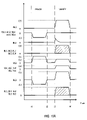
- FIG. 4A is a timing diagram of an erase mode of operation according to an embodiment.
- FIG. 4B is a timing diagram of a program operation according to an embodiment.
- FIG. 4C is a timing diagram of a read operation according to an embodiment.
- FIG. 4D is a timing diagram of a refresh operation according to an embodiment.
- FIG. 5A is a cross-section diagram of a JFET DRAM cell according to an embodiment.
- FIG. 5B is a circuit schematic diagram showing the configuration for an array of JFET DRAM cells according to an embodiment.
- FIG. 6 is a table illustrating the voltages applied to the terminals of a JFET DRAM for various operations according to an embodiment.
- FIG. 7A is a cross-sectional diagram of a TTJFET DRAM cell utilizing a JFET DRAM cell according to an embodiment.
- FIG. 7B is a circuit schematic diagram of a TTJFET DRAM cell utilizing a JFET DRAM cell according to an embodiment.
- FIG. 7C is a cross-sectional diagram of a TTJFET DRAM cell utilizing a JFET DRAM cell according to an embodiment.
- FIG. 8 is a table indicating the voltages applied to a TTJFET DRAM cell during various modes of operation according to an embodiment.
- FIG. 9 is a circuit schematic diagram of an array of TTDRAM cells according to an embodiment.
- FIG. 10A is a timing diagram of an erase mode of operation according to an embodiment.
- FIG. 10B is a timing diagram of a row erase mode of operation according to an embodiment.
- FIG. 10C is a timing diagram of a column erase mode of operation according to an embodiment.
- FIG. 10D is a timing diagram of full block erase mode of operation according to an embodiment.
- FIG. 10E is a timing diagram of a partial block erase mode of operation according to an embodiment.
- FIG. 10F is a timing diagram of a program mode of operation according to an embodiment.
- FIG. 10G is a timing diagram of a read mode of operation according to an embodiment.
- FIG. 11A is a cross-sectional diagram of a TTJFET DRAM cell utilizing a JFET DRAM cell according to an embodiment.
- FIG. 11B is a circuit schematic diagram of a TTJFET DRAM cell utilizing a JFET DRAM cell according to an embodiment.
- FIG. 11C is a cross-sectional diagram of a TTJFET DRAM cell utilizing a JFET DRAM cell according to an embodiment.
- FIG. 12A is a cross-sectional diagram of a TTJFET DRAM cell utilizing a JFET DRAM cell according to an embodiment.
- FIG. 12B is a circuit schematic diagram of a TTJFET DRAM cell utilizing a JFET DRAM cell according to an embodiment.
- FIG. 12C is a cross-sectional diagram of a TTJFET DRAM cell utilizing a JFET DRAM cell according to an embodiment.
- FIG. 13 is a circuit schematic diagram illustrating the use of a TTJFET DRAM cells as a ternary content addressable memory (TCAM) cell according to an embodiment.
- TCAM ternary content addressable memory
- FIG. 14 is a truth table illustrating whether there is a hit “match” or a miss on a match line for values stored in an X-cell and a Y-cell based on an input search key data.
- FIG. 15 is a circuit schematic diagram of a TCAM array according to an embodiment.
- FIG. 16 is a circuit schematic diagram of a TCAM cell according to an embodiment.
- FIG. 17 is a circuit schematic diagram of a TCAM array according to an embodiment.
- FIG. 18 is a table illustrating the voltage applied (Vg) to a gate terminal, the voltage applied (Vd) to a drain terminal, the voltage applied (Vs) to a source terminal, and the voltage applied (Vwell) to a deep N-well for various operation modes of a JFET DRAM cell used in a TCAM cell according to an embodiment.
- FIG. 19A is a cross-sectional diagram of a TTJFET DRAM cell utilizing a JFET DRAM cell according to an embodiment.
- FIG. 19B is a circuit schematic diagram of a TTJFET DRAM cell utilizing a JFET DRAM cell according to an embodiment.
- FIG. 19C is a cross-sectional diagram of a TTJFET DRAM cell utilizing a JFET DRAM cell according to an embodiment.
- JFET junction field effect transistor
- JFET DRAM cell 100 a is an n-channel JFET DRAM cell.
- JFET DRAM cell 100 a can be formed on a semiconductor substrate 102 .
- JFET DRAM cell 100 a is formed between two isolation regions 104 .
- Isolation regions 104 can be formed with a shallow trench isolation (STI) method or the like.
- JFET DRAM cell 100 a can include a deep n-type well 106 formed on a semiconductor substrate 102 .
- a data storing region 108 can be formed on the deep n-type well 106 .
- the data storing region 108 can be formed by a p-well.
- a channel region 110 can be formed on the data storing region 108 .
- the channel region 110 can be a n-type doped region.
- JFET DRAM cell 100 a can include a source terminal 114 , a gate terminal 112 , and a drain terminal 116 .
- the source terminal 114 and drain terminal 116 can be formed from a n-type polysilicon layer and the gate terminal 112 can be formed from a p-type polysilicon layer.
- the deep n-type well 106 can be electrically connected to a deep n-type well terminal (not shown) so that an electrical bias may be connected to the deep n-type well 106 .
- the polysilicon layer that forms gate terminal 112 can be used as a word line, for example.
- a bit line may be connected to the drain terminal 116 .
- the bit line and word line can be orthogonal to each other. In this way, a bit line can connect a column of like JFET DRAM cells 100 a and a word line can connect a row of like JFET DRAM cells 100 a.
- JFET DRAM cell 100 b includes a drain terminal 116 , a source terminal 114 , a gate terminal 112 , a data storage region 108 , and a deep n-well terminal 106 .
- Data storage region 108 can operate as a back-gate terminal, for the JFET DRAM cell 100 b.
- JFET DRAM cell ( 100 a and 100 b ) The operation of JFET DRAM cell ( 100 a and 100 b ) will now be explained.
- data storage region 108 can be a p-type diffusion region. Data can be stored on data storage region 108 by collecting charge onto the data storage region 108 . When electrons are collected on data storage region 108 , a depletion region above data storage region 108 can encroach into channel region 110 so that when the gate terminal 112 is at zero volts (or slightly positive) with respect to a source terminal 114 , JFET DRAM cell 100 a and 100 b (comprising a JFET) can be turned off. In this way, a high impedance path may be formed between the source terminal 114 and drain terminal 116 .
- a depletion region above the data storage region 108 can be insufficient to turn off the JFET DRAM cell 100 a and 100 b (comprising a JFET).
- current can flow between the source 114 and drain 116 when the gate terminal 112 is at zero volts with respect to a source terminal 114 .
- a low impedance path may be formed between the source terminal 114 and drain terminal 116 .
- JFET DRAM cell ( 100 a and 100 b ) can have four primary modes of operation.
- a read operation in which data stored on data storage region 108 can be read out.
- An erase operation in which holes can be collected by the data storage region 108 .
- a program operation in which holes can be depleted from the data storage region 108 .
- a refresh operation in which charge can be restored onto the data storage region 108 after having leaked off.
- a deep n-well bias may be applied to deep N-well 106 .
- An erase mode of operation can be used to allow the data storage region 108 to collect holes in a way similar to a bipolar junction transistor operation.
- a p-n junction forward bias voltage may be applied between the gate terminal 112 and the source and/or drain terminals ( 114 and 116 ) to allow a current to be flow from gate terminal 112 to the source and/or drain terminals ( 114 and 116 ). Because the channel region 110 is sufficiently thin, holes injected into the channel region 110 from the gate terminal 112 may be swept across the channel region 110 and collected by data storage region 108 . In this way, data storage region 108 may reach a neutral state.
- the JFET DRAM cell ( 100 a and 100 b ) may have a low impedance path between the drain terminal 116 and source terminal 114 with a zero volt bias (or a slightly positive voltage bias) between the gate terminal 112 and source terminal 114 (i.e. the JFET transistor may be turned on).
- the JFET DRAM cell ( 100 a and 100 b ) may be programmed by utilizing a punch through condition between gate terminal 112 and the data storage region 108 .
- a negative gate bias may be applied to the gate terminal 112 while applying a drain/source bias to the drain and/or source terminals ( 114 and 116 ).
- the data storage region 108 may collect electrons and become negatively charged.
- a negatively charged data storage region 108 can induce a depletion region in the channel region 110 such that the JFET DRAM cell ( 100 a and 100 b ) may have a high impedance path between the drain terminal 116 and source terminal 114 with a zero volt bias (or a slightly positive voltage bias) between the gate terminal 112 and source terminal 114 (i.e. the JFET transistor may be turned off).
- a gate bias may be applied to the gate terminal 112 while providing a drain voltage to the drain terminal 116 and a ground voltage to the source. If the JFET DRAM cell ( 100 a and 100 b ) is in an erased state, a low impedance path may be formed between the drain terminal 116 and source terminal 114 ). The erased condition may correspond to a data zero, for example. If the JFET DRAM cell ( 100 a and 100 b ) is in a programmed state, a high impedance path may be formed between the drain terminal 116 and source terminal 114 ). The programmed condition may correspond to a data one, for example.
- a refresh operation may be conceptualized as a soft program mode of operation in that the JFET DRAM cells ( 100 a and 100 b ) that are in the erased state should not be affected.
- the gate terminal 112 may be in a normal JFET DRAM cell deselect condition, for example zero volts, and a drain bias may be applied to the drain terminal 116 .
- a relatively high reverse bias condition between the channel region 110 and data storage regions 108 that have been negatively charged (through previous programming or the like) may be created.
- only those JFET DRAM memory cells ( 100 a and 100 b ) may have their negative charge replenished.
- FIG. 3A a circuit schematic diagram showing the configuration for an array of JFET DRAM cells according to an embodiment is set forth and given the general reference character 300 A.
- JFET DRAM cells 9 JFET DRAM cells are shown, although a DRAM may have 1 billion or more memory cells, for example.
- Array 300 A includes JFET DRAM cells ( 320 - 11 to 320 - 33 ) arranged in three rows and three columns.
- Three JFET DRAM cells ( 320 - 11 to 320 - 33 ) can be connected to each row (i.e. sharing a word line WL 1 to WL 3 ) and three JFET DRAM cells ( 320 - 11 to 320 - 33 ) can be connected to each column (i.e. sharing a bit line BL 1 to BL 3 ).
- Each JFET DRAM cell ( 320 - 11 to 320 - 33 ) can correspond to a JFET DRAM cell 100 a and 100 b .
- Each JFET DRAM cell ( 320 - 11 to 320 - 33 ) can include a deep n-well 306 , a charge storage node 308 , a source terminal 314 , a drain terminal 316 , and a gate terminal 312 .
- JFET DRAM cells ( 320 - 11 , 320 - 12 , and 320 - 13 ) can each have a gate terminal 312 connected to word line WL 1 .
- JFET DRAM cells ( 320 - 21 , 320 - 22 , and 320 - 23 ) can each have a gate terminal 312 connected to word line WL 2 .
- JFET DRAM cells ( 320 - 31 , 320 - 32 , and 320 - 33 ) can each have a gate terminal 312 connected to word line WL 3 .
- JFET DRAM cells ( 320 - 11 , 320 - 21 , and 320 - 31 ) can each have a drain terminal 316 connected to bit line BL 1 .
- JFET DRAM cells ( 320 - 12 , 320 - 22 , and 320 - 32 ) can each have a drain terminal 316 connected to bit line BL 2 .
- JFET DRAM cells ( 320 - 13 , 320 - 23 , and 320 - 33 ) can each have a drain terminal 316 connected to bit line BL 3 .
- FIG. 3A illustrates the sources of JFET DRAM cells ( 320 - 11 to 320 - 33 ) are connected to ground.
- FIG. 3B a circuit schematic diagram showing the configuration for an array of JFET DRAM cells according to an embodiment is set forth and given the general reference character 300 B.
- the sources of JFET DRAM cells ( 320 - 11 to 320 - 33 ) can be connected to source lines (SL 1 to SL 3 ) running parallel to the bit lines (BL 1 to BL 3 ).
- FIG. 3C a circuit schematic diagram showing the configuration for an array of JFET DRAM cells according to an embodiment is set forth and given the general reference character 300 C.
- the sources of JFET DRAM cells ( 320 - 11 to 320 - 33 ) can be connected to source lines (SL 1 to SL 3 ) running parallel to the word lines (WL 1 to WL 3 ).
- the arrays 300 B and 300 C can allow greater flexibility for erase, program, or soft program operations by allowing the source and drain of a JFET DRAM cell ( 320 - 11 to 320 - 33 ) to be biased in the same manner.
- FIG. 4A a timing diagram of an erase mode of operation according to an embodiment is set forth.
- FIG. 4A illustrates an erase operation in which JFET DRAM cell 320 - 21 is erased (i.e. set to store data zero).
- the deep n-well bias (Vwell 1 to Vwell 3 ) can be commonly connected to a well bias voltage of 0.5 V.
- all word lines (WL 1 to WL 3 ) and bit lines (BL 1 to BL 3 ) may be at zero volts in a standby state.
- word line WL 2 may transition to about 0.4 Volts and bit line BL 1 may transition to about a ⁇ 0.3 volts.
- the source line (SL 1 in FIG. 3B or SL 2 in FIG. 3C ) may also transition to ⁇ 0.3V to improve the erase efficiency.
- the pn junction formed by the gate terminal 312 to drain terminal 316 of JFET DRAM cell 320 - 21 may be forward biased and holes injected into the channel region from the gate terminal 312 may be swept across the channel region and collected by data storage region 308 . In this way, data storage region 308 of JFET DRAM cell 320 - 21 may reach a neutral state.
- a verify operation may be performed to ensure JFET DRAM cell 320 - 21 has been properly erased.
- word line WL 2 may transition to about 0.2 Volts and bit line BL 1 may transition to about 0.1 Volts.
- bit line BL 1 may transition to about 0.1 Volts.
- JFET DRAM cell 320 - 21 turns on and forms a relatively low impedance between the drain terminal 316 and source terminal 314 , the erase operation was successful. However, if JFET DRAM cell 320 - 21 does not turn on and a relatively high impedance remains between the drain terminal 316 and source terminal 314 , the erase operation was not successful. In this case, the erase operation may be repeated.
- word line WL 2 and bit line BL 1 may return to a ground potential.
- a block erase may be performed by pulsing all of the word lines (WL 1 to WL 3 ) and bit lines (BL 1 to BL 3 ) in a similar way as word line WL 2 and bit line BL 1 as illustrated in FIG. 4( a ).
- the source lines (SL 1 to SL 3 ) may be biased in the same way as bit lines (BL 1 to BL 3 ) to improve erase efficiency. In this way, a whole array or a whole block of JFET DRAM cells in an array may be erased.
- JFET DRAM cell 100 a of the embodiment in FIG. 1A can have programmable threshold voltages that remain positive even in an erased state
- alternative embodiments may include an erased state threshold voltage that is negative.
- word lines WL 1 to WL 3
- WL 1 to WL 3 may be driven negative when a JFET DRAM cell 100 a is deselected to properly turn off the current paths.
- FIG. 4B a timing diagram of a program operation according to an embodiment is set forth.
- FIG. 4B illustrates a program operation in which JFET DRAM cell 320 - 21 is programmed (i.e. set to store data one).
- the deep n-well bias (Vwell 1 to Vwell 3 ) can be commonly connected to a well bias voltage of 0.5 V.
- all word lines (WL 1 to WL 3 ) and bit lines (BL 1 to BL 3 ) may be at zero volts in a standby state.
- word line WL 2 may transition to about ⁇ 0.9 Volts and bit line BL 1 may transition to about a 0.5 volts.
- Respective source lines (SL 1 to SL 3 ) may transition in the same way as bit line BL 1 to improve programming efficiency. In this way, the pn junction formed by the gate terminal 312 to drain terminal 316 and optionally source terminal 314 of JFET DRAM cell 320 - 21 may be reverse biased to induce a punch through condition.
- the data storage region 308 may have holes depleted near the channel junction and become negatively charged.
- a negatively charged data storage region 308 can induce a depletion region in the channel region such that the JFET DRAM cell 320 - 21 may have a high impedance path between the drain terminal 316 and source terminal 314 with a zero volt bias (or a slightly positive voltage bias) between the gate terminal 312 and source terminal 314 (i.e. the JFET transistor may be turned off).
- the word lines (WL 1 to WL 3 ) and bit lines (BL 1 to BL 3 ) may return to ground.
- a verify operation may be performed to ensure JFET DRAM cell 320 - 21 has been properly programmed.
- word line WL 2 may transition to about 0.2 Volts and bit line BL 1 may transition to about 0.1 Volts.
- bit line BL 1 may transition to about 0.1 Volts.
- JFET DRAM cell 320 - 21 remains off and forms a relatively high impedance between the drain terminal 316 and source terminal 314 , the program operation was successful. However, if JFET DRAM cell 320 - 21 does turn on and a relatively low impedance remains between the drain terminal 316 and source terminal 314 , the program operation was not successful. In this case, the program operation may be repeated.
- word line WL 2 and bit line BL 1 may return to a ground potential.
- word may be written to in the JFET DRAM array 300 by first erasing a selected word along a word line (WL 1 to WL 3 ) and then programming selected bits along the word line (WL 1 to WL 3 ).
- data can be written to a complete word.
- an erase operation may first be performed.
- a word line can go high to about 0.4 V while taking only the 8 bit lines that correspond to the 8-bit word to about ⁇ 0.3 V.
- the respective source lines (SL 1 to SL 3 ) may be driven to about ⁇ 0.3 V to improve erase efficiency. In this way, the whole 8-bit word can be erased. Then a program operation can be performed only on the bits out of the 8-bit word that correspond to a data one.
- a word can consist of, for example, 8-bits, 16-bits, 32-bits, etc.
- an erase operation is performed to erase all bits of the word to set all the data bits to a data zero in parallel.
- a program operation is performed in which the bits of the word that have a data one value are programmed in parallel. For example, to write a data word “10101011”, first a parallel erase operation on all 8-bits can be performed to give “00000000”, then a program only the bits having a data one value can be performed to store the data word “101011”.
- a write operation of a word can be performed by first programming all the all bits of the word to set all the data bits to a data one. Then an erase operation can be performed in which the bits of the word that have a data zero value are erased.
- a block program may be performed by pulsing all of the word lines (WL 1 to WL 3 ) and bit lines (BL 1 to BL 3 ) in a similar way as word line WL 2 and bit line BL 1 as illustrated in FIG. 4B .
- the respective source lines (SL 1 to SL 3 ) may be driven the same as the bit lines (BL 1 to BL 3 ) improve program efficiency. In this way, a whole array or a whole block of JFET DRAM cells in an array may be programmed.
- FIG. 4C a timing diagram of a read operation according to an embodiment is set forth.
- FIG. 4C illustrates a read operation in which JFET DRAM cell 320 - 21 is read (i.e. a data value stored in JFET DRAM cell 320 - 21 is detected.
- the deep n-well bias Vwell 1 to Vwell 3
- the well bias voltage can be commonly connected to a well bias voltage of 0.5 V.
- all word lines (WL 1 to WL 3 ) and bit lines (BL 1 to BL 3 ) may be at zero volts or negatively biased in a standby state.
- word line WL 2 may transition to about 0.2 Volts and bit line BL 1 may transition to about a 0.1 volts.
- a the impedance of JFET DRAM cell 320 - 21 may be determined in accordance with a data value stored in a data storage region 108 .
- a high impedance value may indicate a data value of “one” and a low impedance value may indicate a data value of “zero”.
- the word line WL 2 and bit line BL 1 may return to the standby state.
- FIG. 4D a timing diagram of a refresh operation according to an embodiment is set forth.
- a refresh operation can be performed as a operation at any time that the JFET DRAM array 300 is not being used.
- FIG. 4D shows a refresh operation in which only a single column is being refreshed.
- all word lines (WL 1 to WL 3 ) and bit lines (BL 1 to BL 3 ) may be at zero volts (i.e. ground) or negatively biased in a standby state.
- bit line BL 1 may transition to about 0.5 Volts (i.e. the same voltage as in a program operation). In this way, a relatively high reverse bias condition between the channel regions and data storage regions 308 that have been negatively charged (through previous programming or the like) may be created. Thus, only those JFET DRAM memory cells ( 320 - 11 to 320 - 31 ) may have their negative charge replenished.
- bit line BL 1 may return to ground.
- block (or array) refresh can be performed by placing the refresh voltage (about 0.5V) on all the bit lines (BL 1 to BL 3 ) in an array simultaneously.
- JFET DRAM cell 500 a is a p-channel JFET DRAM cell.
- JFET DRAM cell 500 a can be formed on a semiconductor substrate 502 .
- JFET DRAM cell 500 a is formed between two isolation regions 504 .
- Isolation regions 504 can be formed with a shallow trench isolation (STI) method or the like.
- JFET DRAM cell 500 a can include a deep p-type well 506 formed on a semiconductor substrate 502 .
- a data storing region 508 can be formed on the deep p-type well 506 .
- the data storing region 508 can be formed by a n-well.
- a channel region 510 can be formed on the data storing region 508 .
- the channel region 510 can be a p-type doped region.
- JFET DRAM cell 500 a can include a source terminal 514 , a gate terminal 512 , and a drain terminal 516 .
- the source terminal 514 and drain terminal 516 can be formed from a p-type polysilicon layer and the gate terminal 512 can be formed from a n-type polysilicon layer 512 .
- the deep p-type well 506 can be electrically connected to a deep p-type well terminal (not shown) so that an electrical bias may be connected to the deep p-type well 506 .
- the polysilicon layer that forms gate terminal 512 can be used as a word line, for example.
- a bit line may be connected to the drain terminal 516 .
- the bit line and word line can be orthogonal to each other. In this way, a bit line can connect a column of like JFET DRAM cells 500 a and a word line can connect a row of like JFET DRAM cells 500 a.
- JFET DRAM cell 500 b includes a drain terminal 516 , a source terminal 514 , a gate terminal 512 , a data storage region 508 , and a deep p-well terminal 506 .
- Data storage region 508 can operate as a back-gate terminal, for the JFET DRAM cell 500 b.
- FIG. 6 a table illustrating the voltages applied to the terminals of JFET DRAM cell 500 a and 500 b for various operations according to an embodiment is set forth.
- the table of FIG. 6 illustrates the voltage applied (Vg) to a gate terminal 512 , the voltage applied (Vd) to a drain terminal 516 , the voltage applied (Vs) to the source terminal 514 , and the voltage applied (Vwell) to the deep p-well 506 for each of the four above-mentioned operation modes are set forth.
- a JFET DRAM cell such as illustrated in FIGS. 1A , 1 B, 5 A, and 5 B may be used with an access transistor to form a two transistor JFET DRAM cell (TTJFET DRAM cell).
- TTJFET DRAM cell One such example of a JFET DRAM cell such as illustrated in FIGS. 1A and 1B in a TTJFET DRAM cell is shown in FIGS. 7A and 7B .
- FIG. 7A a cross-sectional diagram of a TTJFET DRAM cell utilizing a JFET DRAM cell according to an embodiment is set forth and given the general reference character 700 a .
- FIG. 7B a circuit schematic diagram of a TTJFET DRAM cell utilizing a JFET DRAM cell according to an embodiment is set forth and given the general reference character 700 b.
- the TTJFET DRAM cell ( 700 a and 700 b ) utilizing a JFET DRAM cell can include a JFET DRAM cell 750 and a JFET access transistor 760 .
- JFET DRAM cell 750 is formed between two isolation regions 704 .
- Isolation regions 704 can be formed with a shallow trench isolation (STI) method or the like.
- JFET DRAM cell 750 can include a deep n-type well 706 formed on a semiconductor substrate 702 .
- a data storing region 708 can be formed on the deep n-type well 706 .
- the data storing region 708 can be formed by a p-well.
- a channel region 710 can be formed on the data storing region 708 .
- the channel region 710 can be a n-type doped region.
- JFET DRAM cell 750 can include a source terminal 714 , a gate terminal 712 , and a drain terminal 716 .
- the source terminal 714 and drain terminal 716 can be formed from a n-type polysilicon layer and the gate terminal 712 can be formed from a p-type polysilicon layer 712 .
- the deep n-type well 706 can be electrically connected to a deep n-type well terminal (not shown) so that an electrical bias may be connected to the deep n-type well 706 .
- the JFET access transistor 760 is formed between two isolation regions 704 .
- Isolation regions 704 can be formed with a shallow trench isolation (STI) method or the like.
- JFET access transistor 760 can include a deep n-type well 726 formed on a semiconductor substrate 702 .
- the back gate region 728 can be formed by a p-well.
- a channel region 730 can be formed on the back gate region 728 .
- the channel region 730 can be a n-type doped region.
- JFET access transistor 760 can include a source terminal 734 , a gate terminal 732 , and a drain terminal 736 .
- the source terminal 734 and drain terminal 736 can be formed from a n-type polysilicon layer and the gate terminal 732 can be formed from a p-type polysilicon layer.
- the deep n-type well 706 can be electrically connected to a deep n-type well terminal (not shown) so that an electrical bias may be connected to the deep n-type well 706 .
- Back gate region 728 can be electrically connected to gate terminal 732 .
- JFET access transistor 760 can be a double-gate JFET transistor and better control may be provided to channel region 730 .
- FIG. 7C a cross-sectional diagram of TTJFET DRAM cell 700 a along the gate electrode 732 according to an embodiment is set forth.
- the STI area 704 has been etched at least down to the back gate region 728 .
- the front gate 732 can be electrically connected to the back gate region 728 . It should be noted that as long as the etch reaches the back gate region 728 and does not reach the p-type substrate 702 , any over-etching or slight under-etching may not be detrimental to the performance of the JFET access transistor 760 .
- TTJFET DRAM cell ( 700 a and 700 b ) can have an advantage by reducing leakage current as compared to JFET DRAM cell ( 100 a and 100 b ). Furthermore, by providing JFET access transistor 760 , programming and erasing operations may have more margins as there is no need to worry about inadvertently conducting current through the JFET DRAM cell 750 .
- the polysilicon layer that forms gate terminal 732 of JFET access transistor 760 can be used as a word line (WL), for example.
- Source terminal 734 can be connected to a source voltage on a source line SL.
- the gate terminal 712 of JFET DRAM cell 750 can be connected to a bias voltage Vb.
- the drain terminal 716 of JFET DRAM cell 750 can be connected to a bit line BL.
- the bit line and word line can be orthogonal to each other. In this way, a bit line can connect a column of like TTJFET DRAM cells 700 a and a word line (WL) can connect a row of like TTJFET DRAM cells 700 a.
- JFET DRAM cell 750 and JFET access transistor 760 can be switched such that the JFET access transistor 760 may be on the top of the stack and connected to the bit line BL while the JFET DRAM cell 750 may be on the bottom of the stack and connected to the source line SL.
- FIG. 8 is a table indicating the voltages applied to TTJFET DRAM cell ( 700 a and 700 b ) during various modes of operation according to an embodiment.
- the JFET DRAM cell 750 can be programmed and erased using the same mechanisms as JFET DRAM cell 100 a and 100 b as described previously.
- the table of FIG. 8 shows voltages applied to the word line WL, bit line BL, bias voltage Vb, and source voltage Vvss for an erase mode, program mode, read mode, and refresh mode of operation.
- the word line WL may be set to either about 0.0 volts when the TTJFET DRAM cell ( 700 a and 700 b ) is to be erased or to ⁇ 0.3 volts when the TTJFET DRAM cell ( 700 a and 700 b ) is not to be erased.
- the bit line BL may be set to about 0.0 volts or ⁇ 0.3 volts to improve erase efficiency
- the bias voltage Vb may be set to about 0.4 volts
- the source voltage Vvss may be set to about ⁇ 0.3 volts.
- An erased TTJFET DRAM cell ( 700 a and 700 b ) may be considered a data zero and may provide a JFET DRAM cell 750 having a threshold voltage Vth of about ⁇ 0.4 volts.
- the source line voltage Vvss may be set to either about 0.5 volts when the TTJFET DRAM cell ( 700 a and 700 b ) is to be programmed or to 0.0 volts when the TTJFET DRAM cell ( 700 a and 700 b ) is not to be programmed.
- the word line WL may be set to about 0.7 volts
- the bias voltage Vb may be set to about ⁇ 1.0 volts
- the bit line BL may be set to about 0.5 volts or 0.0 volts.
- a programmed TTJFET DRAM cell ( 700 a and 700 b ) may be considered a data one and may provide a JFET DRAM cell 750 having a threshold voltage Vth of about 0.4 volts.
- bias voltage Vb may be about 0.2 volts and the word line WL may be 0.5 volts for a TTJFET DRAM cell ( 700 a and 700 b ) being read and may be 0.0 volts for a TTJFET DRAM cell ( 700 a and 700 b ) that is not being read.
- Bit line BL and source line SL may be sense nodes.
- a source voltage Vvss may be applied to source line SL and only bit line BL may be used in a single ended sensing scheme.
- a circuit schematic diagram of an array of TTDRAM cells is set forth and given the general reference character 900 .
- Array of TTJFET DRAM cells 900 only shows 36 TTJFET DRAM cells ( 700 - 11 to 700 - 66 ) to avoid unduly cluttering the figure although a DRAM may have 1 billion or more memory cells, for example.
- Each TTJFET DRAM cell ( 700 - 11 to 700 - 66 ) can be configured like TTJFET DRAM cell 700 b.
- Array of TTJFET DRAM cells 900 includes TTJFET DRAM cells ( 700 - 11 to 700 - 66 ) arranged in six rows and six columns.
- Six TTJFET DRAM cells ( 700 - 11 to 700 - 66 ) can be connected to each row (i.e. sharing a word line WL 1 to WL 6 ) and six TTJFET DRAM cells ( 700 - 11 to 700 - 66 ) can be connected to each column (i.e. sharing a bit line BL 1 to BL 6 ).
- each of the six columns TTJFET DRAM cells ( 700 - 11 to 700 - 61 , 700 - 12 to 700 - 62 , 700 - 13 to 700 - 63 , 700 - 14 to 700 - 64 , 700 - 15 to 700 - 65 , 700 - 16 to 700 - 66 ) can share a reference voltage line (Vb 1 to Vb 6 ) and source line (SL 1 to SL 6 ).
- each TTJFET DRAM cell ( 700 - 11 to 700 - 66 ) can correspond to a TTJFET DRAM cell 700 b .
- Each TTJFET DRAM cell ( 700 - 11 to 700 - 66 ) can include a JFET DRAM cell 750 and a JFET access transistor 760 .
- the gate electrode 732 and back gate region 728 of each JFET access transistor 760 in row of TTJFET DRAM cells can be connected to word line WL 1 .
- the gate electrode 732 and back gate region 728 of each JFET access transistor 760 in row of TTJFET DRAM cells can be connected to word line WL 2 .
- the gate electrode 732 and back gate region 728 of each JFET access transistor 760 in row of TTJFET DRAM cells ( 700 - 31 to 700 - 36 ) can be connected to word line WL 3 .
- the gate electrode 732 and back gate region 728 of each JFET access transistor 760 in row of TTJFET DRAM cells can be connected to word line WL 4 .
- the gate electrode 732 and back gate region 728 of each JFET access transistor 760 in row of TTJFET DRAM cells can be connected to word line WL 5 .
- the gate electrode 732 and back gate region 728 of each JFET access transistor 760 in row of TTJFET DRAM cells ( 700 - 61 to 700 - 66 ) can be connected to word line WL 6 .
- the column of TTJFET DRAM cells ( 700 - 11 to 700 - 61 ) can have a drain electrode 716 and gate electrode 712 of each JFET DRAM cell 750 and a source electrode 734 of each JFET access transistor 760 connected to bit line BL 1 , reference voltage line Vb 1 , and source line SL 1 , respectively.
- the column of TTJFET DRAM cells ( 700 - 12 to 700 - 62 ) can have a drain electrode 716 and gate electrode 712 of each JFET DRAM cell 750 and a source electrode 734 of each JFET access transistor 760 connected to bit line BL 2 , reference voltage line Vb 2 , and source line SL 2 , respectively.
- the column of TTJFET DRAM cells ( 700 - 13 to 700 - 63 ) can have a drain electrode 716 and gate electrode 712 of each JFET DRAM cell 750 and a source electrode 734 of each JFET access transistor 760 connected to bit line BL 3 , reference voltage line Vb 3 , and source line SL 3 , respectively.
- the column of TTJFET DRAM cells ( 700 - 14 to 700 - 64 ) can have a drain electrode 716 and gate electrode 712 of each JFET DRAM cell 750 and a source electrode 734 of each JFET access transistor 760 connected to bit line BL 4 , reference voltage line Vb 4 , and source line SL 4 , respectively.
- the column of TTJFET DRAM cells ( 700 - 15 to 700 - 65 ) can have a drain electrode 716 and gate electrode 712 of each JFET DRAM cell 750 and a source electrode 734 of each JFET access transistor 760 connected to bit line BL 5 , reference voltage line Vb 5 , and source line SL 5 , respectively.
- the column of TTJFET DRAM cells ( 700 - 16 to 700 - 66 ) can have a drain electrode 716 and gate electrode 712 of each JFET DRAM cell 750 and a source electrode 734 of each JFET access transistor 760 connected to bit line BL 6 , reference voltage line Vb 6 , and source line SL 6 , respectively.
- FIG. 10A is a timing diagram of an erase mode of operation according to an embodiment.
- FIG. 10A illustrates an erase operation in which TTJFET DRAM cell 700 - 33 is erased (i.e. set to store data zero).
- the deep n-well bias 706 and 726 for each TTJFET DRAM cell 700 - 11 to 700 - 66 ) can be commonly connected to a well bias voltage of 0.5 V.
- all word line (WL 1 to WL 6 ), bit lines (BL 1 to BL 6 ), bias voltage lines (Vb 1 to VB 6 ), and source lines (SL 1 to SL 6 ) may be at zero volts in a standby state.
- word lines (WL 1 , WL 2 , WL 4 , WL 5 , and WL 6 ) may transition to about ⁇ 0.3 volts
- bias line Vb 3 may transition to about 0.4 volts
- source line SL 3 may transition to about a ⁇ 0.3 volts while word line WL 3 may maintain a ground potential (i.e. 0.0 volts).
- JFET access transistor 760 of TTJFET DRAM cell 700 - 33 can turn on and the ⁇ 0.3 volts may be passed to a source terminal 714 of JFET DRAM cell 750 of TTJFET DRAM cell 700 - 33 .
- the pn junction formed by the gate terminal 712 to source terminal 714 of TTJFET DRAM cell 700 - 33 may be forward biased and holes injected into the channel region from the gate terminal 712 may be swept across the channel region and collected by data storage region 708 .
- data storage region 708 of TTJFET DRAM cell 700 - 33 may be erased and may achieve a threshold voltage Vth of about ⁇ 0.4 volts.
- JFET access transistors 760 in TTJFET memory cells 700 - 13 , 700 - 23 , 700 - 43 , 700 - 53 , and 700 - 63 ) that share source line SL 3 may remain off even though source line SL 3 is at about ⁇ 0.3 volts.
- the corresponding bit line in this example bit line BL 3 ) may also be biased at ⁇ 0.3 volts at time t 1 , thus improving erase efficiency.
- all word line (WL 1 to WL 6 ), bit lines (BL 1 to BL 6 ), bias voltage lines (Vb 1 to Vb 6 ), and source lines (SL 1 to SL 6 ) may return to zero volts (i.e. a standby state).
- a verify operation may be performed to ensure TTJFET DRAM cell 700 - 33 has been properly erased.
- word line WL 3 may transition to about 0.5 volts and bias line Vb 3 may transition to about 0.2 volts. If JFET DRAM cell 750 of TTJFET DRAM cell 700 - 33 turns on and forms a relatively low impedance between the drain terminal 716 and source terminal 714 , the erase operation was successful. This can be detected by sensing the impedance between bit line BL 3 and source line SL 3 .
- JFET DRAM cell 750 of TTJFET DRAM cell 700 - 33 does not turn on and a relatively high impedance remains between the drain terminal 316 and source terminal 314 , the erase operation was not successful. In this case, the erase operation may be repeated. At time t 4 , word line WL 3 and bit line BL 3 may return to a ground potential.
- TTJFET DRAM cells may be erased in a row erase, a column erase, a partial row erase, a partial column erase, or a block erase.
- FIG. 10B A timing diagram illustrating a row erase operation in array of TTJFET DRAM cell 900 is set forth in FIG. 10B .
- FIG. 10B illustrates erasing all the TTJFET DRAM cells ( 700 - 31 to 700 - 36 ) connected to word line WL 3 .
- the timing diagram of FIG. 10B may differ from the timing diagram of FIG. 10A in that all source lines (SL 1 to SL 6 ) may be set to ⁇ 0.3 volts between times t 1 and t 2 . Also, all bias voltage lines (Vb 1 to Vb 6 ) may be set to about 0.4 volts between times t 1 and t 2 . In this way, the pn junction formed by the gate terminal 712 to source terminal 714 of TTJFET DRAM cells ( 700 - 31 to 700 - 36 ) may be forward biased and holes injected into the channel region from the respective gate terminals 712 may be swept across the channel region and collected by the respective data storage regions 708 .
- data storage regions 708 of row of TTJFET DRAM cells ( 700 - 31 to 700 - 36 ) connected to word line WL 3 may be erased and may achieve a threshold voltage Vth of about ⁇ 0.4 volts.
- the bit lines (BL 1 to BL 6 ) may be biased at about ⁇ 0.3 volts at time t 1 , thus improving erase efficiency.
- bias lines (Vb 1 to Vb 6 ) and source lines (SL 1 to SL 6 ) connected to the TTJFET DRAM cells ( 700 - 31 to 700 - 36 ) which are desired to be erased may be set to 0.4 volts and ⁇ 0.3 volts, respectively between times t 1 and t 2 .
- FIG. 10C A timing diagram illustrating a column erase operation in array of TTJFET DRAM cell 900 is set forth in FIG. 10C .
- FIG. 10C illustrates erasing all the TTJFET DRAM cells ( 700 - 13 to 700 - 63 ) connected to bit line BL 3 .
- the timing diagram of FIG. 10C may differ from the timing diagram of FIG. 10A in that all word lines (WL 1 to WL 6 ) may be set to 0.0 volts between times t 1 and t 2 .
- the pn junction formed by the gate terminal 712 to drain terminal 716 of TTJFET DRAM cells ( 700 - 13 to 700 - 63 ) connected to bit line BL 3 may be forward biased and holes injected into the channel region from the respective gate terminals 712 may be swept across the channel region and collected by the respective data storage regions 708 .
- data storage regions 708 of row of TTJFET DRAM cells ( 700 - 13 to 700 - 63 ) connected to bit line BL 3 may be erased and may achieve a threshold voltage Vth of about ⁇ 0.4 volts.
- the word lines (WL 1 to WL 6 ) connected to the TTJFET DRAM cells ( 700 - 13 to 700 - 63 ) which are desired to be erased may be set to 0.0 volts.
- the word lines (WL 1 to WL 6 ) connected to the TTJFET DRAM cells ( 700 - 13 to 700 - 63 ) which are not to be erased may be set to ⁇ 0.3 volts between times t 1 and t 2 .
- FIG. 10D A timing diagram illustrating a full block erase operation in array of TTJFET DRAM cells 900 is set forth in FIG. 10D .
- FIG. 10D illustrates erasing all the TTJFET DRAM cells ( 700 - 11 to 700 - 66 ) in the array of TTJFET DRAM cells 900 .
- the timing diagram of FIG. 10D may differ from the timing diagram of FIG. 10A in that all word lines (WL 1 to WL 6 ) may be set to 0.0 volts between times t 1 and t 2 , all bit lines (BL 1 to BL 6 ) may be set to 0.0 volts or to ⁇ 0.3 volts to improve erase efficiency between t 1 and t 2 , all bias lines (Vb 1 to Vb 3 ) may be set to 0.4 volts between t 1 and t 2 , and all source lines (SL 1 to SL 3 ) may be set to ⁇ 0.3 volts between t 1 and t 2 .
- the pn junction formed by the gate terminal 712 to drain terminal 716 of TTJFET DRAM cells may be forward biased and holes injected into the channel region from the respective gate terminals 712 may be swept across the channel region and collected by the respective data storage regions 708 .
- data storage regions 708 of TTJFET DRAM cells may be erased and may achieve a threshold voltage Vth of about ⁇ 0.4 volts.
- a partial block erase can be an operation in which a sub-block smaller than the array of TTJFET DRAM cells 900 is erased.
- FIG. 10E illustrates erasing a partial block the TTJFET DRAM cells ( 700 - 11 to 700 - 66 ) in the array of TTJFET DRAM cells 900 .
- the partial block can be the TTJFET DRAM cells ( 700 - 11 to 700 - 66 ) commonly connected to word lines (WL 3 to WL 5 ) and bit lines (BL 3 to BL 5 ), for example.
- word lines (WL 3 to WL 5 ), bias lines (Vb 3 to Vb 5 ), and source lines (SL 3 to SL 5 ) connected to the TTJFET DRAM cells ( 700 - 23 to 700 - 45 ) which are desired to be erased may be set to 0.0 volts, 0.4 volts, and ⁇ 0.3 volts respectively.
- All other word lines (WL 1 , WL 2 , and WL 6 ), bias lines (Vb 1 , Vb 2 , and Vb 6 ), and source lines (SL 1 , SL 2 , and SL 6 ) may be set to ⁇ 0.3 volts, 0.0 volts, and 0.0 volts, respectively, between times t 1 and t 2 .
- the first step is to program a whole word or all TTJFET DRAM cells connected to the bit line (i.e. column) in which the TTJFET DRAM cell that is desired to be programmed is included.
- a partial column erase operation as set forth above is performed to return all the TTJFET DRAM cells that are to retain the erased state to a data zero.
- FIG. 10F is a timing diagram of a program mode of operation according to an embodiment.
- FIG. 10F illustrates program operation in which TTJFET DRAM cell 700 - 33 is programmed (i.e. set to store data one).
- the deep n-well bias 706 and 726 for each TTJFET DRAM cell 700 - 11 to 700 - 66 ) can be commonly connected to a well bias voltage of 0.5 V.
- TTJFET DRAM cells ( 700 - 13 , 700 - 23 , 700 - 33 , 700 - 43 , 700 - 53 , and 700 - 63 ) have a data state of “010001” and TTJFET DRAM cell 700 - 33 is to be programmed to a data one giving a state of “011001”.
- all word line (WL 1 to WL 6 ), bit lines (BL 1 to BL 6 ), bias voltage lines (Vb 1 to VB 6 ), and source lines (SL 1 to SL 6 ) may be at zero volts in a standby state.
- word lines may transition to about 0.7 volts
- bias line Vb 3 may transition to about ⁇ 1.0 volts.
- bit line BL 3 and source line SL 3 may transition to about a 0.5 volts while bit lines (BL 1 , BL 2 , BL 4 , BL 5 , and BL 6 ) and source lines (SL 1 , SL 2 , SL 4 , SL 5 , and SL 6 ) may maintain a ground potential (i.e. 0.0 volts).
- bias line Vb 3 may transition to about ⁇ 1.0 volts while bias lines (Vb 1 , Vb 2 , Vb 4 , Vb 5 , and Vb 6 ) may be maintained at 0.2 volts or 0.0 volts.
- the pn junction formed by the gate terminal 712 to drain terminal 716 of column of TTJFET DRAM cells may be reverse biased to induce a punch through condition.
- the data storage regions 708 may have holes depleted therefrom and become negatively charged.
- a negatively charged data storage region 708 can induce a depletion region in the channel region such that the column of TTJFET DRAM cells ( 700 - 13 , 700 - 23 , 700 - 33 , 700 - 43 , 700 - 53 , and 700 - 63 ) include a JFET DRAM cell 750 having a threshold voltage of about 0.4 volts.
- the JFET DRAM cell 750 may have a high impedance path between the drain terminal 716 and source terminal 714 with about a 0.2 volt bias on the respective word line (WL 1 to WL 6 ).
- TTJFET DRAM cells ( 700 - 13 , 700 - 23 , 700 - 33 , 700 - 43 , 700 - 53 , and 700 - 63 ) have a programmed data state of “111111”
- a partial column erase may be performed to return TTJFET DRAM cells ( 700 - 13 , 700 - 43 , and 700 - 53 ) to logic zeros.
- word lines (WL 2 , WL 3 , and WL 6 ) and source line SL 3 may transition to about ⁇ 0.3 volts while word lines (WL 1 , WL 4 , and WL 5 ) may remain at 0.0 volts or ground.
- bias line Vb 3 may transition to about 0.4 volts while bias lines (Vb 1 , Vb 2 , Vb 4 , Vb 5 , and Vb 6 ) may remain at 0.0 volts or ground.
- the pn junction formed by the gate terminal 712 to source terminal 714 of TTJFET DRAM cells ( 700 - 13 , 700 - 43 , and 700 - 53 ) connected to bit line BL 3 may be forward biased and holes injected into the channel region from the respective gate terminals 712 may be swept across the channel region and collected by the respective data storage regions 708 .
- data storage regions 708 of row of TTJFET DRAM cells ( 700 - 13 , 70043 , and 700 - 53 ) connected to bit line BL 3 may be erased and may achieve a threshold voltage Vth of about ⁇ 0.4 volts.
- all signals may return to the standby state and at this time TTJFET DRAM cells ( 700 - 13 , 700 - 23 , 700 - 33 , 70043 , 700 - 53 , and 700 - 63 ) have a data state of “011001”.
- FIG. 10G A timing diagram illustrating a read operation in array of TTJFET DRAM cells 900 according to an embodiment is set forth in FIG. 10G .
- FIG. 10G illustrates reading the row of TTJFET DRAM cells ( 700 - 31 to 700 - 36 ) commonly connected to word line WL 3 .
- all word line (WL 1 to WL 6 ), bit lines (BL 1 to BL 6 ), bias voltage lines (Vb 1 to VB 6 ), and source lines (SL 1 to SL 6 ) may be at zero volts in a standby state.
- bias voltage lines (Vb 1 to Vb 6 ) may be at 0.2 volts in the standby state at time t 0 .
- word line WL 3 may transition to 0.5 volts and bias voltage lines (Vb 1 to Vb 6 ) may transition to about 0.2 volts.
- each JFET access transistors 760 in row of TTJFET DRAM cells ( 700 - 31 to 700 - 36 ) commonly connected to word line WL 3 may be turned on.
- bias voltage lines (Vb 1 to Vb 6 ) at 0.2 volts
- a TTJFET DRAM cell 700 in row of TTJFET DRAM cells ( 700 - 31 to 700 - 36 ) storing a data one may provide a high impedance between a bit line (BL 1 to BL 6 ) and respective source line (SL 1 to SL 6 ) and a TTJFET DRAM cell 700 in row of TTJFET DRAM cells ( 700 - 31 to 700 - 36 ) storing a data zero may provide a low impedance between a bit line (BL 1 to BL 6 ) and respective source line (SL 1 to SL 6 ).
- a bit line (BL 1 to BL 6 ) may either be pulled high when a data one is stored or be pulled low, when a data zero is stored.
- a current sense scheme may be used to sense a low impedance state (i.e. the erased state) or a high impedance state (i.e. a programmed state) in which a voltage swing on bit lines (BL 1 to BL 6 ) may be small. In this way, data DATA may be placed on bit lines (BL 1 to BL 6 ) to be read out external to the semiconductor memory device.
- all word line (WL 1 to WL 6 ), bit lines (BL 1 to BL 6 ), bias voltage lines (Vb 1 to VB 6 ), and source lines (SL 1 to SL 6 ) may return to a standby state.
- the refresh operation can be a back ground refresh operation and may only affect TTJFET DRAM cells ( 700 - 11 to 700 - 66 ) storing a data one (i.e. the programmed state).
- a refresh operation may be performed by simply placing the bias voltage lines (Vb 1 to Vb 6 ) to 0.0 volts. With bias voltage lines (Vb 1 to Vb 6 ) at 0.0 volts, a relatively high reverse bias condition between the channel regions and data storage regions 708 that have been negatively charged (through previous programming or the like) may be created. Thus, only those TTJFET DRAM memory cells ( 700 - 11 to 300 - 66 ) may have their negative charge replenished.
- bias lines (Vb 1 to Vb 6 ) can have the same voltage (i.e. 0.0 volts) in a standby state and a refresh operation.
- TTJFET DRAM memory cells ( 700 - 11 to 300 - 66 ) may be refreshed when the semiconductor memory device is in a standby state. This can prevent refresh from interfering in any way with any other operations.
- any other active mode of operation read, program, or erase
- the refresh operation described above can be a true background refresh operation that has no effect on the operation timing of the semiconductor memory device including array of TTJFET DRAM cells ( 700 - 11 to 700 - 66 ).
- FIGS. 11A and 11B An alternative embodiment for a TTJFET DRAM cell will now be described by referring to FIGS. 11A and 11B .
- FIG. 11A a cross-sectional diagram of a TTJFET DRAM cell utilizing a JFET DRAM cell according to an embodiment is set forth and given the general reference character 1100 a .
- FIG. 11B a circuit schematic diagram of a TTJFET DRAM cell utilizing a JFET DRAM cell according to an embodiment is set forth and given the general reference character 1100 b.
- the TTJFET DRAM cell ( 1100 a and 1100 b ) utilizing a JFET DRAM cell can include a JFET DRAM cell 1150 and a JFET access transistor 1160 .
- JFET DRAM cell 1150 is formed between two isolation regions 1104 .
- Isolation regions 1104 can be formed with a shallow trench isolation (STI) method or the like.
- JFET DRAM cell 1150 can include a deep n-type well 1102 formed on a semiconductor substrate.
- a data storing region 1108 can be formed on the deep n-type well 1102 .
- the data storing region 1108 can be formed by a p-well.
- a channel region 1110 can be formed on the data storing region 1108 .
- the channel region 1110 can be a n-type doped region.
- JFET DRAM cell 1150 can include a source terminal 1114 , a gate terminal 1112 , and a drain terminal 1116 .
- the source terminal 1114 and drain terminal 1116 can be formed from a n-type polysilicon layer and the gate terminal 1114 can be formed from a p-type polysilicon layer 1112 .
- the deep n-type well 1102 can be electrically connected to a deep n-type well terminal (not shown) so that an electrical bias may be connected to the deep n-type well 1102 .
- JFET access transistor 1160 is formed between two isolation regions 1104 .
- Isolation regions 1104 can be formed with a shallow trench isolation (STI) method or the like.
- JFET access transistor 1160 can include a deep p-type well region 1103 on a semiconductor substrate.
- a channel region 1130 can be formed on the deep p-type well region 1103 .
- the channel region 1130 can be a n-type doped region.
- JFET access transistor 1160 can include a source terminal 1134 , a gate terminal 1132 , and a drain terminal 1136 .
- the source terminal 1134 and drain terminal 1136 can be formed from a n-type polysilicon layer and the gate terminal 1132 can be formed from a p-type polysilicon layer.
- TTJFET DRAM cell 1100 a and 1100 b includes a single gate JFET access transistor 1160 .
- TTJFET DRAM cell ( 1100 a and 1100 b ) can have an advantage by reducing leakage current as compared to JFET DRAM cell ( 100 a and 100 b ). Furthermore, by providing JFET access transistor 1160 , programming and erasing operations may have more margins as there is no need to worry about inadvertently conducting current through the JFET DRAM cell 1150 .
- the polysilicon layer that forms gate terminal 1132 of JFET access transistor 1160 can be used as a word line (WL), for example.
- Source terminal 1134 can be connected to a source voltage Vvss on a source line SL.
- the gate terminal 1112 of JFET DRAM cell 1150 can be connected to a bias voltage Vb.
- the drain terminal 1116 of JFET DRAM cell 1150 can be connected to a bit line BL.
- the bit line and word line can be orthogonal to each other. In this way, a bit line can connect a column of like TTJFET DRAM cells 1100 a and a word line (WL) can connect a row of like TTJFET DRAM cells 1100 a.
- TTJFET DRAM cell 100 b can be used in an array of TTJFET DRAM cells 900 . Furthermore, the operation of the array of TTJFET DRAM cells 900 using TTJFET DRAM cell 1100 b can be essentially the same as illustrated in FIGS. 10A to 10G .
- FIGS. 12A to 12C Yet another alternative embodiment for a TTJFET DRAM cell will now be described by referring to FIGS. 12A to 12C .
- FIG. 12A a cross-sectional diagram of a TTJFET DRAM cell utilizing a JFET DRAM cell according to an embodiment is set forth and given the general reference character 1200 a .
- FIG. 12B a circuit schematic diagram of a TTJFET DRAM cell utilizing a JFET DRAM cell according to an embodiment is set forth and given the general reference character 1200 b.
- the TTJFET DRAM cell ( 1200 a and 1200 b ) utilizing a JFET DRAM cell can include a JFET DRAM cell 1250 and a JFET access transistor 1260 .
- the JFET access transistor 1260 of FIGS. 12A and 12B is a single-gated p-channel JFET.
- JFET DRAM cell 1250 is formed between two isolation regions 1204 .
- Isolation regions 1204 can be formed with a shallow trench isolation (STI) method or the like.
- JFET DRAM cell 1250 can include a data storage region 1208 formed on a deep n-type well 1202 between isolation regions 1204 .
- the data storing region 1208 can be formed by a p-well.
- a channel region 1210 can be formed on the data storing region 1208 .
- the channel region 1210 can be a n-type doped region.
- JFET DRAM cell 1250 can include a source terminal 1214 , a gate terminal 1212 , and a drain terminal 1216 .
- the source terminal 1214 and drain terminal 1216 can be formed from an n-type polysilicon layer and the gate terminal 1212 can be formed from a p-type polysilicon layer.
- the deep n-type well 1202 can be electrically connected to a deep n-type well terminal (not shown) so that an electrical bias may be connected to the deep n-type well 1202 .
- the JFET access transistor 1260 is formed between two isolation regions 1204 .
- Isolation regions 1204 can be formed with a shallow trench isolation (STI) method or the like.
- a channel region 1230 can be formed on the deep n-type well 1202 and between the isolation regions 1204 .
- the channel region 1230 can be a p-type doped region.
- JFET access transistor 1260 can include a source terminal 1234 , a gate terminal 1232 , and a drain terminal 1236 .
- the source terminal 1234 and drain terminal 1236 can be formed from a p-type polysilicon layer and the gate terminal 1232 can be formed from a n-type polysilicon layer.
- FIG. 12C a cross-sectional diagram of TTJFET DRAM cell 1200 a along the gate electrode 1232 according to an embodiment is set forth.
- TTJFET DRAM cell ( 1200 a and 1200 b ) can have an advantage by reducing leakage current as compared to JFET DRAM cell ( 100 a and 100 b ). Furthermore, by providing JFET access transistor 1260 , programming and erasing operations may have more margins as there is no need to worry about inadvertently conducting current through the JFET DRAM cell 1250 .
- the polysilicon layer that forms gate terminal 1232 of JFET access transistor 1260 can be used as a word line (WL), for example.
- Drain terminal 1216 of JFET DRAM cell 1250 can be connected to a bit line (BL).
- the bit line and word line can be orthogonal to each other. In this way, a bit line can connect a column of like TTJFET DRAM cells 1200 a and a word line (WL) can connect a row of like TTJFET DRAM cells 1200 a .
- the gate terminal 1212 of JFET DRAM cell 1250 can be connected to a bias voltage Vb.
- the source terminal 1214 of JFET DRAM cell 1250 can be connected to a source voltage Vvss on a source line SL.
- JFET DRAM cell 1250 may be interchangeable.
- the JFET DRAM cell 1250 may be positioned on the bottom of the stack and may be connected to source line SL while JFET access transistor 1260 may be positioned on the top of the stack and connected to the bit line BL.
- TTJFET DRAM cell 1200 b can be used in an array of TTJFET DRAM cells 900 .
- the operation of the array of TTJFET DRAM cells 900 using TTJFET DRAM cell 1200 b can be similar to the timing diagrams as illustrated in FIGS. 10A to 10G , however, the polarity of the word line (WL 1 to WL 6 ) waveforms may be inverted due to the fact that JFET access transistor 1260 is a p-channel JFET.
- TTJFET DRAM cells illustrated in the embodiments of FIGS. 1 to 12 .
- DRAMs dynamic random access memories
- CAM content addressable memory
- CAMs provide a rapid comparison between a specific pattern of received data bits, commonly known as a search key or comparand, and data values stored in an associative CAM memory array to provide a match/no-match result. If there is a match for every bit in a group of stored bits in selected CAM memory cells, with every corresponding bit in the comparand, a match flag via a match line indicates a match condition. In this way, the user is notified that the data in the comparand was found in memory and a value corresponding to the match is returned. Thus, the result is determined from finding a matching value (content), not from providing the address of the value as done for a Random Access Memory (RAM).
- RAM Random Access Memory
- CAM cells typically used in CAM arrays: binary CAM cells and ternary CAM or TCAM cells.
- Binary CAM cells store either a logic high bit value or a logic low bit value.
- the logic value stored in the binary CAM cell matches a data bit from an applied comparand, then that CAM cell provides a high impedance path to the match line and the match line is maintained at a logic high value (assuming all other CAM cells electrically connected to the CAM array row also match). In this way, a match is indicated.
- the logic value stored in the binary CAM cell does not match the data bit from the applied comparand, then that CAM cell provides a low impedance path to ground to the match line and the match line is pulled low. In this way, it is indicated that a match has not occurred.
- TCAM cells can store three bit values including a logic high value, a logic low value, and a “don't care” value. When storing logic high and logic low values, the TCAM cell operates like a binary CAM cell as described above. However, a TCAM cell storing a “don't care” value will provide a match condition for any data bit value from a comparand applied to that TCAM cell. This “don't care” capability allows CAM arrays to indicate when a data value matches a selected group of TCAM cells in a row of the CAM array. For example, assume each row of a TCAM array has eight. TCAM cells.
- the first four TCAM cells of each row store one of a logic high and a logic low value (for comparison to the first four bits of an 8-bit comparand data value) and the last four TCAM cells of each row store “don't care” values.
- an 8-bit comparand data value is applied to the CAM array, a match occurs for each row of the CAM array in which the data values stored in the first four TCAM cells match the first four bits of the applied 8-bit comparand data value.
- TTJFET DRAM cells 700 b and 1100 b as a ternary content addressable memory (TCAM) cell according to an embodiment is set forth and given the general reference character 1300 .
- TCAM cell 1300 can include a first TTJFET DRAM cell as an X-cell 1310 and a second TTJFET DRAM cell as a Y-cell 1320 connected in parallel between a match line ML and a source line SL.
- X-cell 1310 can receive a word line WL and a compare data CD as inputs.
- Y-cell 1320 can receive a word line WL and a compare data complement CDN as inputs.
- the X-cell 1310 and Y-cell 1320 can be the same as any of TTJFET DRAM cells ( 700 a , 700 b , 100 a and 100 b ) and may operate in the same manner.
- X-cell 1310 can include a JFET DRAM cell 1312 and a JFET access transistor 1314 .
- JFET DRAM cell 1312 can have a drain terminal connected to the match line ML, a gate terminal connected to a word line WL, and a source terminal commonly connected to a drain terminal of JFET access transistor 1314 .
- JFET access transistor 1314 can have a front gate terminal and a optionally a back gate terminal commonly connected to receive compare data CD, and a source connected to a source line SL.
- Y-cell 1320 can include a JFET DRAM cell 1322 and a JFET access transistor 1324 .
- JFET DRAM cell 1322 can have a drain terminal connected to the match line ML, a gate terminal connected to a word line WL, and a source terminal commonly connected to a drain terminal of JFET access transistor 1324 .
- JFET access transistor 1324 can have a front gate terminal and optionally a back gate terminal commonly connected to receive compare data complement CDN, and a source connected to a source line Vvss.
- X-cell 1310 can form a first impedance path between a match line ML and a source line Vvss and Y-cell 1320 can form a second impedance path between a match line ML and a source line SL.
- TCAM cell 1300 can have four different states.
- a first state is when X-cell 1310 and Y-cell 1320 are both erased (i.e. store zeros).
- a second state is when X-cell 1310 is erased and Y-cell 1320 is programmed.
- a third state is when X-cell 1310 is programmed and Y-cell 1320 is erased.
- a fourth state is when X-cell 1310 and Y-cell 1320 are both programmed (i.e. store ones).
- FIG. 14 is a truth table illustrating whether there is a hit “match” or a miss on match line ML for values stored in the X-cell 1310 and Y-cell 1320 based on an input search key data (data values on compare data line CD and compare data complement line CDN).
- the truth table of FIG. 14 includes a X-cell value (a value stored in X-cell 1310 ), a Y-cell value (a value stored in Y-cell 1320 ), input search key (value compare data CD and compare data complement CDN), and a match output (output on match line ML).
- word line WL is at about 0.2 volts (note that word line WL corresponds to the bias line Vb in the TTJFET DRAM cell 700 b ). Also, in a compare operation, match line ML may be initially pre-charged to about 0.5 volts and source line SL may be at essentially 0.0 volts.
- X-cell 1310 and Y-cell 1320 operate in the same manner as TTJFET DRAM cell 700 b .
- An X-cell value or Y-cell value of “0” can be when X-cell 1310 or Y-cell 1320 stores an erased value.
- An X-cell value or Y-cell value of “1” can be when X-cell 1310 or Y-cell 1320 stores a programmed value.
- the respective X-cell 1310 or Y-cell 1320 having the erased state will have a low impedance path between the match line ML and source line SL when the respective compare data (CD or CDN) has a value of “1”.
- the respective X-cell 1310 or Y-cell 1320 in an programmed state will have a high impedance path between the match line ML and source line SL no matter the value of compare data (CD or CDN).
- the match line ML When a “hit” occurs, the match line ML is not discharged and stays at a logic high value of 0.5 volts. When a “miss” occurs the match line ML is discharged through either the X-cell 1310 or Y-cell 1320 to the source line SL, which is at about 0.0 volts.
- a match output on match line ML can indicate a hit.
- a match output on match line ML can indicate a miss.
- a match output on match line ML can indicate a miss.
- a match output on match line ML can indicate a hit.
- a match output on match line ML can indicate a hit no matter the value of complementary compare data (CD and CDN).
- a match output on match line ML can indicate a miss.
- a match output on match line ML indicates a hit if complementary compare data (CD and CDN) are both “0”, otherwise a miss is indicated.
- match line ML always indicates a hit.
- FIG. 15 a circuit schematic diagram of a TCAM array according to an embodiment is set forth and given the general reference character 1500 .
- TCAM array 1500 can include four rows and four columns of TCAM cells ( 1300 - 11 to 1300 - 44 ). TCAM array 1500 can be arranged in four groups of four bit words ( 1300 - 11 to 1300 - 41 , 1300 - 12 to 1300 - 42 , 1300 - 13 to 1300 - 43 , and 1300 - 14 to 1300 - 44 ). TCAM array 1500 can include decoders ( 1510 and 1520 ) and sense amplifiers 1530 .
- Decoder 1510 can provide source lines (SL 1 to SL 4 ) and word lines (WL 1 to WL 4 ) to the TCAM cells ( 1300 - 11 to 1300 - 44 ). Decoder 1520 can provide complementary compare signals (CD 1 -CDN 1 to CD 4 -CDN 4 ) to TCAM cells (CD 1 -CDN 1 to CD 4 -CDN 4 ). Sense amplifiers 1530 can receive match lines (ML 1 to ML 4 ).
- Source line SL 1 , word line WL 1 , and match line ML 1 can be commonly connected to TCAM cells ( 1300 - 11 to 1300 - 41 ).
- Source line SL 2 , word line WL 2 , and match line ML 2 can be commonly connected to TCAM cells ( 1300 - 12 to 1300 - 42 ).
- Source line SL 3 , word line WL 3 , and match line ML 3 can be commonly connected to TCAM cells ( 1300 - 13 to 1300 - 43 ).
- Source line SL 4 , word line WL 4 , and match line ML 4 can be commonly connected to TCAM cells ( 1300 - 41 to 1300 - 44 ).
- Complementary compare signals can be commonly connected to TCAM cells ( 1300 - 11 to 1300 - 41 ).
- Complementary compare signals (CD 2 and CDN 2 ) can be commonly connected to TCAM cells ( 1300 - 12 to 1300 - 42 ).
- Complementary compare signals (CD 3 and CDN 3 ) can be commonly connected to TCAM cells ( 1300 - 13 to 1300 - 43 ).
- Complementary compare signals (CD 4 and CDN 4 ) can be commonly connected to TCAM cells ( 1300 - 14 to 1300 - 44 ).
- complementary compare signals may not always be complementary signals.
- respective pairs of complementary compare signals may both be pulled low (i.e. a logic zero).
- respective TCAM cells 1300 - 11 to 1300 - 44 ) may have their comparisons “masked”.
- each TCAM cell ( 1300 - 11 to 1300 - 44 ) can essentially comprise two of the TTJFET DRAM cells 700 b connected in parallel.
- the array of TTJFET DRAM cells 900 illustrated in FIG. 9 can easily be turned into an array of TCAM cells that can search six 3-bit words in parallel.
- bias voltages Vb 1 to Vb 6
- word lines WL 1 to WL 6 ).
- Bit lines (BL 1 to BL 6 ) become match lines (ML 1 to ML 6 ), and word lines (WL 1 -WL 2 , WL 3 -WL 4 , and WL 5 -WL 6 ) become complementary compare signals (CD 1 -CDN 1 , CD 2 -CDN 2 , and CD 3 -CDN 3 ), respectively.
- TCAM cells ( 1300 - 11 to 1300 - 44 ) can be programmed, erased, and refreshed in the same manner as illustrated in FIGS. 10A to 10G , by interchanging the bias voltages (Vb 1 to Vb 6 ), word lines (WL 1 to WL 6 ) and bit lines (BL 1 to BL 6 ) to become word lines (WL 1 to WL 6 ), complementary compare data (CD 1 to CD 4 and CDN 1 to CD 4 ), and match lines (ML 1 to ML 6 ), as mentioned above.
- Vb 1 to Vb 6 bias voltages
- word lines WL 1 to WL 6
- bit lines BL 1 to BL 6
- CD 1 to CD 4 and CDN 1 to CD 4 complementary compare data
- ML 1 to ML 6 match lines
- a TTJFET DRAM cell 700 b When a TTJFET DRAM cell 700 b is used in a TCAM configuration as illustrated in FIGS. 13 to 15 , multiple cycles may be needed to read a word. For example, if a word is 32 bits (i.e. 32 bits along a match line ML), it can take 32 read cycles following the general read flow of FIG. 10G . In this case, a counter or the like may be connected to decoder 1520 of FIG. 15 to serially select bits stored in a word of TCAM cells ( 1300 ).
- decoder 1520 In converting from a DRAM configuration to a CAM configuration, DRAM rows become CAM columns an DRAM columns become CAM rows. Thus, when a read operation is performed on TCAM 1500 , decoder 1520 acts to drive complementary compare data (CD and CDN) as a column multiplexer. However, in a search (compare) operation, decoder 1520 drives complementary compare data (CD and CDN) as the search data to be compared with the data stored in TCAM cells 1300 .
- CD and CDN complementary compare data
- each TTJFET DRAM cell 100 b , 700 b , 1100 b , and 1200 b ). This may be performed by having discrete charge storing levels, each having acceptable and non-overlapping windows of charge storage. In this way, threshold voltage ranges of the JFET DRAM cells ( 100 b , 750 b , 1150 b , and 1250 b ) may be detected for multiple bit storage, such as 2 bits (4 states), 3 bits (8 states), 4 bits (16 states), etc.
- FIG. 16 a circuit schematic diagram of a TCAM cell according to an embodiment is set forth and given the general reference character 1600 .
- TCAM cell 1600 can be formed from JFET DRAM cells, such as JFET DRAM cell 100 b , as just one example.
- TCAM cell 1600 can include a first JFET DRAM cell as an X-cell 1610 and a second JFET DRAM cell as a Y-cell 1620 connected in parallel between a match line ML and a source line SL.
- X-cell 1610 can receive a compare data CD as an input.
- Y-cell 1620 can receive a compare data complement CDN as an input.
- the X-cell 1610 and Y-cell 1620 can be essentially the same as JFET DRAM cell ( 100 a and 100 b ) and may operate in a similar manner. However, the data storage regions ( 1618 and 1628 ) in X-cell 1610 and Y-cell 1620 can operate as complete control back gates as will be explained below.
- X-cell 1610 can include a JFET DRAM cell 1612 .
- JFET DRAM cell 1612 can have a drain terminal connected to the match line ML, a gate terminal connected to receive compare data CD, and a source connected to a source line SL.
- JFET DRAM cell 1612 can include a data storage region 1618 .
- Y-cell 1620 can include a JFET DRAM cell 1622 .
- JFET DRAM cell 1622 can have a drain terminal connected to the match line ML, a gate terminal connected to receive compare data complement CDN, and a source connected to a source line SL.
- JFET DRAM cell 1622 can include a data storage region 1628 .
- X-cell 1610 can form a first impedance path between a match line ML and a source line SL and Y-cell 1620 can form a second impedance path between a match line ML and a source line SL.
- TCAM cell 1600 can have four different states. A first state is when X-cell 1610 and Y-cell 1620 are both erased (i.e. store zeros). A second state is when X-cell 1610 is erased and Y-cell 1620 is programmed. A third state is when X-cell 1610 is programmed and Y-cell 1620 is erased. A fourth state is when X-cell 1610 and Y-cell 1620 are both programmed (i.e. store ones). The operation of TCAM cell 1600 will now be described with reference to FIG. 14 . FIG.
- FIG. 14 is a truth table illustrating whether there is a hit “match” or a miss on match line ML for values stored in the X-cell 1610 and Y-cell 1620 based on an input search key data (data values on compare data line CD and compare data complement line CDN).
- the truth table of FIG. 14 includes a X-cell value (a value stored in X-cell 1610 ), a Y-cell value (a value stored in Y-cell 1620 ), input search key (value compare data CD and compare data complement CDN), and a match output (output on match line ML).
- match line ML When a compare is being performed on TCAM cell 1600 , match line ML may be initially pre-charged to about 0.1 volts and source line SL may be at essentially 0.0 volts.
- An X-cell value or Y-cell value of “0” can be when X-cell 1610 or Y-cell 1620 stores an erased value.
- An X-cell value or Y-cell value of “1” can be when X-cell 1610 or Y-cell 1620 stores a programmed value.
- X-cell 1610 and Y-cell 1620 operate in a similar manner as JFET DRAM cell 100 b .
- JFET DRAM cell 1612 or 1622
- a high impedance path remains between the respective drain and source even if the gate potential is 0.5 volts.
- the data storage regions 1618 and 1628 ) act as a back control gate to keep the respective channels turned off.
- the respective X-cell 1610 or Y-cell 1620 having the erased state will have a low impedance path between the match line ML and source line SL when the respective compare data (CD or CDN) has a value of “1”.
- the respective X-cell 1610 or Y-cell 1620 having the programmed state will have a high impedance path between the match line ML and source line SL no matter the value of compare data (CD or CDN).
- the data storage regions ( 1618 and 1628 ) can operate to change the threshold voltage of the respective JFET DRAM cell ( 1612 or 1622 ) forming the X-cell 1610 and Y-cell 1620 .
- the match line ML When a “hit” occurs, the match line ML is not discharged and stays at a logic high value of 0.1 volts. When a “miss” occurs the match line ML is discharged through either the X-cell 1610 or Y-cell 1620 to the source line SL, which is at about 0.0 volts.
- a match output on match line ML can indicate a hit.
- a match output on match line ML can indicate a miss.
- a match output on match line ML can indicate a miss.
- a match output on match line ML can indicate a hit.
- a match output on match line ML can indicate a hit no matter the value of complementary compare data (CD and CDN).
- a match output on match line ML can indicate a miss.
- a match output on match line ML indicates a hit if complementary compare data (CD and CDN) are both “0”, otherwise a miss is indicated.
- match line ML always indicates a hit.
- FIG. 17 a circuit schematic diagram of a TCAM array according to an embodiment is set forth and given the general reference character 1700 .
- TCAM array 1700 can include four rows and four columns of TCAM cells ( 1600 - 11 to 1600 - 44 ). TCAM array 1700 can be arranged in four groups of four bit words ( 1600 - 11 to 1600 - 41 , 1600 - 12 to 1600 - 42 , 1600 - 13 to 1600 - 43 , and 1600 - 14 to 1600 - 44 ). TCAM array 1700 can include decoders ( 1710 and 1720 ) and sense amplifiers 1730 .
- Decoder 1710 can provide source lines (SL 1 to SL 4 ) to the TCAM cells ( 1600 - 11 to 1600 - 44 ). Decoder 1720 can provide complementary compare signals (CD 1 -CDN 1 to CD 4 -CDN 4 ) to TCAM cells ( 1600 - 11 to 1600 - 44 ). Sense amplifiers 1730 can receive match lines (ML 1 to ML 4 ).
- Source line SL 1 and match line ML 1 can be commonly connected to TCAM cells ( 1600 - 11 to 1600 - 41 ).
- Source line SL 2 and match line ML 2 can be commonly connected to TCAM cells ( 1600 - 12 to 1600 - 42 ).
- Source line SL 3 and match line ML 3 can be commonly connected to TCAM cells ( 1600 - 13 to 1600 - 43 ).
- Source line SL 4 and match line ML 4 can be commonly connected to TCAM cells ( 1600 - 41 to 1600 - 44 ).
- Complementary compare signals can be commonly connected to TCAM cells ( 1600 - 11 to 1600 - 14 ).
- Complementary compare signals (CD 2 and CDN 2 ) can be commonly connected to TCAM cells ( 1600 - 21 to 1600 - 24 ).
- Complementary compare signals (CD 3 and CDN 3 ) can be commonly connected to TCAM cells ( 1600 - 31 to 1600 - 34 ).
- Complementary compare signals (CD 4 and CDN 4 ) can be commonly connected to TCAM cells ( 1600 - 41 to 1600 - 44 ).
- each TCAM cell ( 1600 - 11 to 1600 - 44 ) can essentially comprise two of the JFET DRAM cells 100 b connected in parallel.
- the array of TTJFET DRAM cells 300 illustrated in FIG. 3 can easily be turned into an array of TCAM cells 1700 .
- bit lines (BL 1 to BL 3 ) become match lines (ML 1 to ML 3 )
- word lines (WL 1 -WL 3 ) become complementary compare signals (CD 1 -CDN 1 , CD 2 ), respectively and so on.
- TCAM cells 1600 - 11 to 1600 - 44 can be programmed, erased, and refreshed in the same manner as illustrated in FIGS. 4A to 4D , by interchanging word lines (WL 1 to WL 6 ) and bit lines (BL 1 to BL 6 ) to become word lines (WL 1 to WL 6 ), match lines (ML 1 to ML 6 ) complementary compare data (CD 1 to CD 4 and CDN 1 to CD 4 ), as mentioned above and using the voltage levels as shown in FIG. 17 .
- FIG. 18 a table illustrating the voltage applied (Vg) to a gate terminal 112 , the voltage applied (Vd) to a drain terminal 116 , the voltage applied (Vs) to the source terminal 114 , and the voltage applied (Vwell) to the deep N-well 106 for each of the four above-mentioned operation modes when using JFET DRAM cell 100 b of FIG. 1B as an X-cell 1610 and Y-cell 1620 of a TCAM cell 1600 are set forth.
- a JFET DRAM cell 100 b When a JFET DRAM cell 100 b is used in a TCAM configuration as illustrated in FIGS. 13 to 15 , multiple cycles may be needed to read a word. For example, if a word is 32 bits (i.e. 32 bits along a match line ML), it can take 32 read cycles following the general read flow of FIG. 4C using the voltages of FIG. 18 . In this case, a counter or the like may be connected to decoder 1720 of FIG. 17 to serially select bits stored in a word of TCAM cells ( 1600 ).
- decoder 1720 In converting from a DRAM configuration to a CAM configuration, DRAM rows become CAM columns and DRAM columns become CAM rows. Thus, when a read operation is performed on TCAM 1700 , decoder 1720 acts to drive complementary compare data (CD and CDN) as a column multiplexer. However, in a search (compare) operation, decoder 1720 drives complementary compare data (CD and CDN) as the search data to be compared with the data stored in TCAM cells 1600 .
- CD and CDN complementary compare data
- each JFET DRAM cell 100 b may be stored in memory applications (DRAM applications). This may be performed by having discrete charge storing levels, each having acceptable and non-overlapping windows of charge storage. In this way, threshold voltage ranges of the JFET DRAM cells 100 b may be detected for multiple bit storage, such as 2 bits (4 states), 3 bits (8 states), 4 bits (16 states), etc.
- a memory cell includes a JFET having a data storage region disposed in a substrate and between two insulating regions, such as a shallow trench insulation (STI).
- the data storage region can provide a first threshold voltage to the JFET when storing a first data value and provide a second threshold voltage to the JFET when storing a second data value.
- the memory cell is a dynamic random access memory (DRAM) cell and can be used to form a content addressable memory (CAM) cell.
- DRAM dynamic random access memory
- CAM content addressable memory
- FIGS. 19A to 19C Yet another alternative embodiment for a TTJFET DRAM cell will now be described by referring to FIGS. 19A to 19C .
- FIG. 19A a cross-sectional diagram of a TTJFET DRAM cell utilizing a JFET DRAM cell according to an embodiment is set forth and given the general reference character 1900 a .
- FIG. 19B a circuit schematic diagram of a TTJFET DRAM cell utilizing a JFET DRAM cell according to an embodiment is set forth and given the general reference character 1900 b.
- the TTJFET DRAM cell ( 1900 a and 1900 b ) utilizing a JFET DRAM cell can include a JFET DRAM cell 1950 and a JFET access transistor 1960 .
- the JFET access transistor 1260 of FIGS. 12A and 12B is a single-gated n-channel JFET.
- JFET DRAM cell 1950 is formed between two isolation regions 1904 .
- Isolation regions 1904 can be formed with a shallow trench isolation (STI) method or the like.
- JFET DRAM cell 1950 can include an n-well 1906 formed on a deep p-type well 1902 .
- a data storage region 1908 can be formed on n-well 1906 between isolation regions 1904 .
- the data storing region 1908 can be formed by a p-well.
- a channel region 1910 can be formed on the data storing region 1908 .
- the channel region 1910 can be a n-type doped region.
- JFET DRAM cell 1950 can include a source terminal 1914 , a gate terminal 1912 , and a drain terminal 1916 .
- the source terminal 1914 and drain terminal 1916 can be formed from an n-type polysilicon layer and the gate terminal 1912 can be formed from a p-type polysilicon layer.
- JFET DRAM cell 1950 can include an n-type diffusion region 1915 providing an electrical connection between the source terminal 1914 and the n-well 1906 .
- n-well 1906 is a first diffusion region under the data storage region 1908 and having opposite conductivity type as the data storage region 1908 .
- the deep p-type well 1902 can be electrically connected to a deep p-type well terminal (not shown) so that an electrical bias may be connected to the deep p-type well 1902 .
- the JFET access transistor 1960 is formed between two isolation regions 1904 .
- Isolation regions 1904 can be formed with a shallow trench isolation (STI) method or the like.
- a channel region 1930 can be formed on the deep p-type well 1902 and between the isolation regions 1904 .
- the channel region 1930 can be a n-type doped region.
- JFET access transistor 1960 can include a source terminal 1934 , a gate terminal 1932 , and a drain terminal 1936 .
- the source terminal 1934 and drain terminal 1936 can be formed from a n-type polysilicon layer and the gate terminal 1932 can be formed from a p-type polysilicon layer.
- FIG. 19C a cross-sectional diagram of TTJFET DRAM cell 1900 a along the gate electrode 1932 according to an embodiment is set forth.
- TTJFET DRAM cell ( 1900 a and 1900 b ) can have an advantage by reducing leakage current as compared to JFET DRAM cell ( 100 a and 100 b ). Furthermore, by providing JFET access transistor 1960 , programming and erasing operations may have more margins as there is no need to worry about inadvertently conducting current through the JFET DRAM cell 1950 .
- the polysilicon layer that forms gate terminal 1932 of JFET access transistor 1960 can be used as a word line (WL), for example.
- Drain terminal 1916 of JFET DRAM cell 1950 can be connected to a bit line (BL).
- the bit line and word line can be orthogonal to each other. In this way, a bit line can connect a column of like TTJFET DRAM cells 1900 a and a word line (WL) can connect a row of like TTJFET DRAM cells 1900 a .
- the gate terminal 1912 of JFET DRAM cell 1950 can be connected to a bias voltage Vb.
- the source terminal 1914 of JFET DRAM cell 1950 can be connected to a source voltage Vvss on a source line SL.
- TTJFET DRAM cell 1900 b can be used in an array of TTJFET DRAM cells 900 .
- the operation of the array of TTJFET DRAM cells 900 using TTJFET DRAM cell 1900 b can be similar to the timing diagrams as illustrated in FIGS. 10A to 10G .
- TTJFET DRAM cell 1900 a and 1900 b may be used in a Ternary TCAM cell as illustrated in FIGS. 13-15 .
- the semiconductor devices of the embodiments may be manufactured in accordance with known process steps. Examples of known process steps for manufacture of the JFETs set forth in the embodiments are shown in U.S. patent application Ser. No. 11/507,793 filed Aug. 22, 2006 and U.S. patent application Ser. No. 11/261,873 filed Oct. 28, 2005. The contents of both are incorporated herein by reference.
Abstract
Description
Claims (21)
Priority Applications (3)
| Application Number | Priority Date | Filing Date | Title |
|---|---|---|---|
| US11/799,305 US7729149B2 (en) | 2007-05-01 | 2007-05-01 | Content addressable memory cell including a junction field effect transistor |
| TW097115871A TW200901446A (en) | 2007-05-01 | 2008-04-30 | Content addressable memory cell including a junction field effect transistor |
| PCT/US2008/061946 WO2008134688A1 (en) | 2007-05-01 | 2008-04-30 | Content addressable memory cell including a junction field effect transistor |
Applications Claiming Priority (1)
| Application Number | Priority Date | Filing Date | Title |
|---|---|---|---|
| US11/799,305 US7729149B2 (en) | 2007-05-01 | 2007-05-01 | Content addressable memory cell including a junction field effect transistor |
Publications (2)
| Publication Number | Publication Date |
|---|---|
| US20080272405A1 US20080272405A1 (en) | 2008-11-06 |
| US7729149B2 true US7729149B2 (en) | 2010-06-01 |
Family
ID=39636948
Family Applications (1)
| Application Number | Title | Priority Date | Filing Date |
|---|---|---|---|
| US11/799,305 Expired - Fee Related US7729149B2 (en) | 2007-05-01 | 2007-05-01 | Content addressable memory cell including a junction field effect transistor |
Country Status (3)
| Country | Link |
|---|---|
| US (1) | US7729149B2 (en) |
| TW (1) | TW200901446A (en) |
| WO (1) | WO2008134688A1 (en) |
Cited By (1)
| Publication number | Priority date | Publication date | Assignee | Title |
|---|---|---|---|---|
| US20100118634A1 (en) * | 2008-11-10 | 2010-05-13 | Samsung Electronics Co., Ltd. | Semiconductor apparatuses and methods of operating the same |
Families Citing this family (16)
| Publication number | Priority date | Publication date | Assignee | Title |
|---|---|---|---|---|
| US7633784B2 (en) * | 2007-05-17 | 2009-12-15 | Dsm Solutions, Inc. | Junction field effect dynamic random access memory cell and content addressable memory cell |
| US8508289B2 (en) | 2009-12-08 | 2013-08-13 | Soitec | Data-path cell on an SeOI substrate with a back control gate beneath the insulating layer |
| FR2957193B1 (en) | 2010-03-03 | 2012-04-20 | Soitec Silicon On Insulator | SEOI SUBSTRATE DATA PATH CELL WITH REAR CONTROL GRID BURED UNDER THE INSULATING LAYER |
| FR2953641B1 (en) | 2009-12-08 | 2012-02-10 | S O I Tec Silicon On Insulator Tech | HOMOGENEOUS TRANSISTOR CIRCUIT ON SEOI WITH REAR CONTROL CHANNEL BURED UNDER THE INSULATING LAYER |
| FR2953643B1 (en) | 2009-12-08 | 2012-07-27 | Soitec Silicon On Insulator | MEMORY CELL FLASH ON SEOI HAVING A SECOND CHECK GRID ENTERREE UNDER THE INSULATING LAYER |
| FR2955195B1 (en) * | 2010-01-14 | 2012-03-09 | Soitec Silicon On Insulator | DEVICE FOR COMPARING DATA IN A MEMORY ADDRESSABLE BY CONTENT ON SEOI |
| FR2955200B1 (en) | 2010-01-14 | 2012-07-20 | Soitec Silicon On Insulator | DEVICE AND MANUFACTURING METHOD HAVING CONTACT BETWEEN SEMICONDUCTOR REGIONS THROUGH AN INSULATED INSULATED LAYER |
| FR2955203B1 (en) | 2010-01-14 | 2012-03-23 | Soitec Silicon On Insulator | MEMORY CELL WITH THE CHANNEL CROSSING A DIELECTRIC LAYER ENTERREE |
| FR2955204B1 (en) | 2010-01-14 | 2012-07-20 | Soitec Silicon On Insulator | DRAM MEMORY CELL HAVING A VERTICAL BIPOLAR INJECTOR |
| FR2957186B1 (en) | 2010-03-08 | 2012-09-28 | Soitec Silicon On Insulator | MEMORY CELL OF SRAM TYPE |
| FR2957449B1 (en) | 2010-03-11 | 2022-07-15 | S O I Tec Silicon On Insulator Tech | READOUT MICRO-AMPLIFIER FOR MEMORY |
| FR2958441B1 (en) | 2010-04-02 | 2012-07-13 | Soitec Silicon On Insulator | PSEUDO-INVERTER CIRCUIT ON SEOI |
| EP2378549A1 (en) | 2010-04-06 | 2011-10-19 | S.O.I.Tec Silicon on Insulator Technologies | Method for manufacturing a semiconductor substrate |
| EP2381470B1 (en) | 2010-04-22 | 2012-08-22 | Soitec | Semiconductor device comprising a field-effect transistor in a silicon-on-insulator structure |
| US8730752B1 (en) * | 2012-04-02 | 2014-05-20 | Adesto Technologies Corporation | Circuits and methods for placing programmable impedance memory elements in high impedance states |
| CN115881189A (en) * | 2021-09-27 | 2023-03-31 | 三星电子株式会社 | Content addressable memory and electronic device including the same |
Citations (11)
| Publication number | Priority date | Publication date | Assignee | Title |
|---|---|---|---|---|
| US3964083A (en) | 1973-06-14 | 1976-06-15 | U.S. Philips Corporation | Punchthrough resetting jfet image sensor |
| US6166938A (en) * | 1999-05-21 | 2000-12-26 | Sandisk Corporation | Data encoding for content addressable memories |
| US6262907B1 (en) * | 2000-05-18 | 2001-07-17 | Integrated Device Technology, Inc. | Ternary CAM array |
| US6307223B1 (en) * | 1998-12-11 | 2001-10-23 | Lovoltech, Inc. | Complementary junction field effect transistors |
| US7115933B2 (en) * | 2001-01-12 | 2006-10-03 | Stmicroelectronics S.A. | Integrated circuit and fabrication process |
| US7196921B2 (en) * | 2004-07-19 | 2007-03-27 | Silicon Storage Technology, Inc. | High-speed and low-power differential non-volatile content addressable memory cell and array |
| US20070096144A1 (en) * | 2005-10-28 | 2007-05-03 | Kapoor Ashok K | Integrated circuit using complementary junction field effect transistor and MOS transistor in silicon and silicon alloys |
| US20080001183A1 (en) * | 2005-10-28 | 2008-01-03 | Ashok Kumar Kapoor | Silicon-on-insulator (SOI) junction field effect transistor and method of manufacture |
| US20080265936A1 (en) * | 2007-04-27 | 2008-10-30 | Dsm Solutions, Inc. | Integrated circuit switching device, structure and method of manufacture |
| US20080273409A1 (en) * | 2007-05-01 | 2008-11-06 | Thummalapally Damodar R | Junction field effect dynamic random access memory cell and applications therefor |
| US20080285322A1 (en) * | 2007-05-17 | 2008-11-20 | Thummalapally Damodar R | Junction field effect dynamic random access memory cell and content addressable memory cell |
Family Cites Families (6)
| Publication number | Priority date | Publication date | Assignee | Title |
|---|---|---|---|---|
| IT1044690B (en) * | 1974-11-11 | 1980-04-21 | Siemens Ag | DEVICE WITH TWO COMPLEMENTARY FIELD-EFFECT TRANSISTORS |
| NL7700880A (en) * | 1976-12-17 | 1978-08-01 | Philips Nv | ACCESSIBLE MEMORY WITH JUNCTION FIELD DEFECT TRANSISTORS. |
| NL7701172A (en) * | 1977-02-04 | 1978-08-08 | Philips Nv | SEMICONDUCTOR MEMORY DEVICE. |
| US6421265B1 (en) * | 2001-03-22 | 2002-07-16 | Integrated Devices Technology, Inc. | DRAM-based CAM cell using 3T or 4T DRAM cells |
| US6861303B2 (en) * | 2003-05-09 | 2005-03-01 | Texas Instruments Incorporated | JFET structure for integrated circuit and fabrication method |
| US6979849B2 (en) * | 2003-12-31 | 2005-12-27 | Micron Technology, Inc. | Memory cell having improved interconnect |
-
2007
- 2007-05-01 US US11/799,305 patent/US7729149B2/en not_active Expired - Fee Related
-
2008
- 2008-04-30 WO PCT/US2008/061946 patent/WO2008134688A1/en active Application Filing
- 2008-04-30 TW TW097115871A patent/TW200901446A/en unknown
Patent Citations (12)
| Publication number | Priority date | Publication date | Assignee | Title |
|---|---|---|---|---|
| US3964083A (en) | 1973-06-14 | 1976-06-15 | U.S. Philips Corporation | Punchthrough resetting jfet image sensor |
| US6307223B1 (en) * | 1998-12-11 | 2001-10-23 | Lovoltech, Inc. | Complementary junction field effect transistors |
| US6166938A (en) * | 1999-05-21 | 2000-12-26 | Sandisk Corporation | Data encoding for content addressable memories |
| US6262907B1 (en) * | 2000-05-18 | 2001-07-17 | Integrated Device Technology, Inc. | Ternary CAM array |
| US7115933B2 (en) * | 2001-01-12 | 2006-10-03 | Stmicroelectronics S.A. | Integrated circuit and fabrication process |
| US7196921B2 (en) * | 2004-07-19 | 2007-03-27 | Silicon Storage Technology, Inc. | High-speed and low-power differential non-volatile content addressable memory cell and array |
| US20070096144A1 (en) * | 2005-10-28 | 2007-05-03 | Kapoor Ashok K | Integrated circuit using complementary junction field effect transistor and MOS transistor in silicon and silicon alloys |
| US20080001183A1 (en) * | 2005-10-28 | 2008-01-03 | Ashok Kumar Kapoor | Silicon-on-insulator (SOI) junction field effect transistor and method of manufacture |
| US20080265936A1 (en) * | 2007-04-27 | 2008-10-30 | Dsm Solutions, Inc. | Integrated circuit switching device, structure and method of manufacture |
| US20080273409A1 (en) * | 2007-05-01 | 2008-11-06 | Thummalapally Damodar R | Junction field effect dynamic random access memory cell and applications therefor |
| US20080285322A1 (en) * | 2007-05-17 | 2008-11-20 | Thummalapally Damodar R | Junction field effect dynamic random access memory cell and content addressable memory cell |
| US7633784B2 (en) * | 2007-05-17 | 2009-12-15 | Dsm Solutions, Inc. | Junction field effect dynamic random access memory cell and content addressable memory cell |
Non-Patent Citations (4)
| Title |
|---|
| Bedair, Wissenam, and Cooper, "Atomic Layer Epitaxy of Advanced Devices and Circuits," Final Report submitted to Office of Naval Research N00014-88-K-0527P3. Nov. 1991. pp. 1-63. * |
| Heald et al., Multilevel Random-Access Memory Using One Transistor Per Cell, IEEE Journal of Solid-State Circuits, Aug. 1976, pp. 519-528 vol. SC11, No. 4. |
| Oldham et al., A One-Transistor Memory Cell with Nondestructive Readout, IEEE International Solid-State Circuits Conference, Feb. 14, 1973, pp. 34-35, and 195. |
| PCT International Search Report and Written Opinion of the International Searching Authority for International Application No. PCT/US2008/061946, dated Aug. 5, 2008. |
Cited By (1)
| Publication number | Priority date | Publication date | Assignee | Title |
|---|---|---|---|---|
| US20100118634A1 (en) * | 2008-11-10 | 2010-05-13 | Samsung Electronics Co., Ltd. | Semiconductor apparatuses and methods of operating the same |
Also Published As
| Publication number | Publication date |
|---|---|
| WO2008134688A1 (en) | 2008-11-06 |
| US20080272405A1 (en) | 2008-11-06 |
| TW200901446A (en) | 2009-01-01 |
Similar Documents
| Publication | Publication Date | Title |
|---|---|---|
| US7729149B2 (en) | Content addressable memory cell including a junction field effect transistor | |
| US11881264B2 (en) | Content addressable memory device having electrically floating body transistor | |
| US9142549B2 (en) | Semiconductor memory device | |
| US10916297B2 (en) | Memory device comprising an electrically floating body transistor | |
| US8902637B2 (en) | Semiconductor memory device comprising inverting amplifier circuit and driving method thereof | |
| US7643326B2 (en) | Semiconductor memory device with ferroelectric device | |
| US7701751B2 (en) | One-transistor type DRAM | |
| WO2011125432A1 (en) | Semiconductor memory device | |
| KR20080034433A (en) | Word line driver for dram embedded in a logic process | |
| TWI793973B (en) | Semiconductor element memory device | |
| US9530502B2 (en) | Configuration memory storing data by injecting carriers in gate insulating layer of MISFET | |
| US20080273409A1 (en) | Junction field effect dynamic random access memory cell and applications therefor | |
| US8325506B2 (en) | Devices and methods for comparing data in a content-addressable memory | |
| US6990007B2 (en) | Semiconductor memory device |
Legal Events
| Date | Code | Title | Description |
|---|---|---|---|
| AS | Assignment |
Owner name: DSM SOLUTIONS, INC., CALIFORNIA Free format text: ASSIGNMENT OF ASSIGNORS INTEREST;ASSIGNOR:THUMMALAPALLY, DAMODAR R.;REEL/FRAME:019313/0074 Effective date: 20070430 Owner name: DSM SOLUTIONS, INC.,CALIFORNIA Free format text: ASSIGNMENT OF ASSIGNORS INTEREST;ASSIGNOR:THUMMALAPALLY, DAMODAR R.;REEL/FRAME:019313/0074 Effective date: 20070430 |
|
| AS | Assignment |
Owner name: SUVOLTA, INC.,CALIFORNIA Free format text: CHANGE OF NAME;ASSIGNOR:DSM SOLUTIONS, INC.;REEL/FRAME:023960/0924 Effective date: 20091207 |
|
| FEPP | Fee payment procedure |
Free format text: PAT HOLDER NO LONGER CLAIMS SMALL ENTITY STATUS, ENTITY STATUS SET TO UNDISCOUNTED (ORIGINAL EVENT CODE: STOL); ENTITY STATUS OF PATENT OWNER: LARGE ENTITY |
|
| FPAY | Fee payment |
Year of fee payment: 4 |
|
| AS | Assignment |
Owner name: MIE FUJITSU SEMICONDUCTOR LIMITED, JAPAN Free format text: ASSIGNMENT OF ASSIGNORS INTEREST;ASSIGNOR:SU VOLTA, INC.;REEL/FRAME:035508/0113 Effective date: 20150303 |
|
| FEPP | Fee payment procedure |
Free format text: MAINTENANCE FEE REMINDER MAILED (ORIGINAL EVENT CODE: REM.) |
|
| LAPS | Lapse for failure to pay maintenance fees |
Free format text: PATENT EXPIRED FOR FAILURE TO PAY MAINTENANCE FEES (ORIGINAL EVENT CODE: EXP.) |
|
| STCH | Information on status: patent discontinuation |
Free format text: PATENT EXPIRED DUE TO NONPAYMENT OF MAINTENANCE FEES UNDER 37 CFR 1.362 |
|
| FP | Lapsed due to failure to pay maintenance fee |
Effective date: 20180601 |