EP2221909A1 - Module für eine farbstoffempfindliche photoelektrische wandlungsvorrichtung und herstellungverfahren dafür, modul für eine photoelektrische wandlungsvorrichtung und herstellungsverfahren dafür sowie elektronische vorrichtung - Google Patents
Module für eine farbstoffempfindliche photoelektrische wandlungsvorrichtung und herstellungverfahren dafür, modul für eine photoelektrische wandlungsvorrichtung und herstellungsverfahren dafür sowie elektronische vorrichtung Download PDFInfo
- Publication number
- EP2221909A1 EP2221909A1 EP08858684A EP08858684A EP2221909A1 EP 2221909 A1 EP2221909 A1 EP 2221909A1 EP 08858684 A EP08858684 A EP 08858684A EP 08858684 A EP08858684 A EP 08858684A EP 2221909 A1 EP2221909 A1 EP 2221909A1
- Authority
- EP
- European Patent Office
- Prior art keywords
- dye
- photoelectric conversion
- conversion element
- element module
- sensitized photoelectric
- Prior art date
- Legal status (The legal status is an assumption and is not a legal conclusion. Google has not performed a legal analysis and makes no representation as to the accuracy of the status listed.)
- Withdrawn
Links
- 238000006243 chemical reaction Methods 0.000 title claims abstract description 265
- 238000004519 manufacturing process Methods 0.000 title claims abstract description 24
- 238000000034 method Methods 0.000 title claims description 42
- 239000000758 substrate Substances 0.000 claims abstract description 148
- 239000011521 glass Substances 0.000 claims abstract description 134
- 239000004065 semiconductor Substances 0.000 claims abstract description 109
- 239000000463 material Substances 0.000 claims abstract description 89
- 230000001681 protective effect Effects 0.000 claims abstract description 74
- 239000003792 electrolyte Substances 0.000 claims abstract description 55
- 229920005989 resin Polymers 0.000 claims abstract description 26
- 239000011347 resin Substances 0.000 claims abstract description 26
- 150000001875 compounds Chemical class 0.000 claims description 26
- 239000011888 foil Substances 0.000 claims description 21
- 239000000203 mixture Substances 0.000 claims description 19
- 229910052751 metal Inorganic materials 0.000 claims description 17
- 239000002184 metal Substances 0.000 claims description 17
- 229910045601 alloy Inorganic materials 0.000 claims description 16
- 239000000956 alloy Substances 0.000 claims description 16
- 239000003054 catalyst Substances 0.000 claims description 16
- 230000003197 catalytic effect Effects 0.000 claims description 11
- IQPQWNKOIGAROB-UHFFFAOYSA-N isocyanate group Chemical group [N-]=C=O IQPQWNKOIGAROB-UHFFFAOYSA-N 0.000 claims description 7
- 238000010248 power generation Methods 0.000 abstract description 9
- 239000010408 film Substances 0.000 description 102
- GWEVSGVZZGPLCZ-UHFFFAOYSA-N Titan oxide Chemical compound O=[Ti]=O GWEVSGVZZGPLCZ-UHFFFAOYSA-N 0.000 description 77
- 239000000975 dye Substances 0.000 description 41
- 239000002245 particle Substances 0.000 description 31
- 239000010419 fine particle Substances 0.000 description 30
- 239000002585 base Substances 0.000 description 18
- 230000000052 comparative effect Effects 0.000 description 14
- 239000007789 gas Substances 0.000 description 13
- WEVYAHXRMPXWCK-UHFFFAOYSA-N Acetonitrile Chemical compound CC#N WEVYAHXRMPXWCK-UHFFFAOYSA-N 0.000 description 12
- 230000008569 process Effects 0.000 description 12
- -1 that is Inorganic materials 0.000 description 12
- 229910021419 crystalline silicon Inorganic materials 0.000 description 11
- 239000007788 liquid Substances 0.000 description 11
- 230000004888 barrier function Effects 0.000 description 10
- 238000000605 extraction Methods 0.000 description 10
- 230000001235 sensitizing effect Effects 0.000 description 10
- 229910052710 silicon Inorganic materials 0.000 description 10
- XUIMIQQOPSSXEZ-UHFFFAOYSA-N Silicon Chemical compound [Si] XUIMIQQOPSSXEZ-UHFFFAOYSA-N 0.000 description 9
- 239000004020 conductor Substances 0.000 description 9
- 239000010703 silicon Substances 0.000 description 9
- 239000002904 solvent Substances 0.000 description 9
- OGIDPMRJRNCKJF-UHFFFAOYSA-N titanium oxide Inorganic materials [Ti]=O OGIDPMRJRNCKJF-UHFFFAOYSA-N 0.000 description 9
- 239000000853 adhesive Substances 0.000 description 8
- 150000001412 amines Chemical class 0.000 description 8
- 238000005304 joining Methods 0.000 description 8
- 238000005498 polishing Methods 0.000 description 8
- 238000007650 screen-printing Methods 0.000 description 8
- XOLBLPGZBRYERU-UHFFFAOYSA-N tin dioxide Chemical compound O=[Sn]=O XOLBLPGZBRYERU-UHFFFAOYSA-N 0.000 description 8
- XLYOFNOQVPJJNP-UHFFFAOYSA-N water Substances O XLYOFNOQVPJJNP-UHFFFAOYSA-N 0.000 description 8
- 229910052799 carbon Inorganic materials 0.000 description 7
- 230000002708 enhancing effect Effects 0.000 description 7
- 239000000243 solution Substances 0.000 description 7
- YEJRWHAVMIAJKC-UHFFFAOYSA-N 4-Butyrolactone Chemical compound O=C1CCCO1 YEJRWHAVMIAJKC-UHFFFAOYSA-N 0.000 description 6
- YSHMQTRICHYLGF-UHFFFAOYSA-N 4-tert-butylpyridine Chemical compound CC(C)(C)C1=CC=NC=C1 YSHMQTRICHYLGF-UHFFFAOYSA-N 0.000 description 6
- KFZMGEQAYNKOFK-UHFFFAOYSA-N Isopropanol Chemical compound CC(C)O KFZMGEQAYNKOFK-UHFFFAOYSA-N 0.000 description 6
- DKGAVHZHDRPRBM-UHFFFAOYSA-N Tert-Butanol Chemical compound CC(C)(C)O DKGAVHZHDRPRBM-UHFFFAOYSA-N 0.000 description 6
- 229910021417 amorphous silicon Inorganic materials 0.000 description 6
- 230000008901 benefit Effects 0.000 description 6
- 238000007639 printing Methods 0.000 description 6
- FVAUCKIRQBBSSJ-UHFFFAOYSA-M sodium iodide Chemical compound [Na+].[I-] FVAUCKIRQBBSSJ-UHFFFAOYSA-M 0.000 description 6
- 230000003667 anti-reflective effect Effects 0.000 description 5
- 238000005452 bending Methods 0.000 description 5
- 230000015572 biosynthetic process Effects 0.000 description 5
- 239000003795 chemical substances by application Substances 0.000 description 5
- 230000006866 deterioration Effects 0.000 description 5
- 238000005530 etching Methods 0.000 description 5
- 230000001965 increasing effect Effects 0.000 description 5
- 238000002347 injection Methods 0.000 description 5
- 239000007924 injection Substances 0.000 description 5
- 150000002500 ions Chemical class 0.000 description 5
- 239000004033 plastic Substances 0.000 description 5
- 229920003023 plastic Polymers 0.000 description 5
- 229910052697 platinum Inorganic materials 0.000 description 5
- 229910052719 titanium Inorganic materials 0.000 description 5
- 239000010936 titanium Substances 0.000 description 5
- AZQWKYJCGOJGHM-UHFFFAOYSA-N 1,4-benzoquinone Chemical compound O=C1C=CC(=O)C=C1 AZQWKYJCGOJGHM-UHFFFAOYSA-N 0.000 description 4
- FXPLCAKVOYHAJA-UHFFFAOYSA-N 2-(4-carboxypyridin-2-yl)pyridine-4-carboxylic acid Chemical compound OC(=O)C1=CC=NC(C=2N=CC=C(C=2)C(O)=O)=C1 FXPLCAKVOYHAJA-UHFFFAOYSA-N 0.000 description 4
- ZCYVEMRRCGMTRW-UHFFFAOYSA-N 7553-56-2 Chemical compound [I] ZCYVEMRRCGMTRW-UHFFFAOYSA-N 0.000 description 4
- CSCPPACGZOOCGX-UHFFFAOYSA-N Acetone Chemical compound CC(C)=O CSCPPACGZOOCGX-UHFFFAOYSA-N 0.000 description 4
- OKTJSMMVPCPJKN-UHFFFAOYSA-N Carbon Chemical compound [C] OKTJSMMVPCPJKN-UHFFFAOYSA-N 0.000 description 4
- 239000004215 Carbon black (E152) Substances 0.000 description 4
- IAZDPXIOMUYVGZ-UHFFFAOYSA-N Dimethylsulphoxide Chemical compound CS(C)=O IAZDPXIOMUYVGZ-UHFFFAOYSA-N 0.000 description 4
- LFQSCWFLJHTTHZ-UHFFFAOYSA-N Ethanol Chemical compound CCO LFQSCWFLJHTTHZ-UHFFFAOYSA-N 0.000 description 4
- 239000001856 Ethyl cellulose Substances 0.000 description 4
- ZZSNKZQZMQGXPY-UHFFFAOYSA-N Ethyl cellulose Chemical compound CCOCC1OC(OC)C(OCC)C(OCC)C1OC1C(O)C(O)C(OC)C(CO)O1 ZZSNKZQZMQGXPY-UHFFFAOYSA-N 0.000 description 4
- VYPSYNLAJGMNEJ-UHFFFAOYSA-N Silicium dioxide Chemical compound O=[Si]=O VYPSYNLAJGMNEJ-UHFFFAOYSA-N 0.000 description 4
- WUOACPNHFRMFPN-UHFFFAOYSA-N alpha-terpineol Chemical compound CC1=CCC(C(C)(C)O)CC1 WUOACPNHFRMFPN-UHFFFAOYSA-N 0.000 description 4
- 229910052782 aluminium Inorganic materials 0.000 description 4
- QVGXLLKOCUKJST-UHFFFAOYSA-N atomic oxygen Chemical compound [O] QVGXLLKOCUKJST-UHFFFAOYSA-N 0.000 description 4
- SQIFACVGCPWBQZ-UHFFFAOYSA-N delta-terpineol Natural products CC(C)(O)C1CCC(=C)CC1 SQIFACVGCPWBQZ-UHFFFAOYSA-N 0.000 description 4
- 229920001249 ethyl cellulose Polymers 0.000 description 4
- 235000019325 ethyl cellulose Nutrition 0.000 description 4
- 125000000524 functional group Chemical group 0.000 description 4
- 229930195733 hydrocarbon Natural products 0.000 description 4
- 229910052740 iodine Inorganic materials 0.000 description 4
- 239000011630 iodine Substances 0.000 description 4
- 229910052741 iridium Inorganic materials 0.000 description 4
- 238000002156 mixing Methods 0.000 description 4
- PXHVJJICTQNCMI-UHFFFAOYSA-N nickel Substances [Ni] PXHVJJICTQNCMI-UHFFFAOYSA-N 0.000 description 4
- 239000001301 oxygen Substances 0.000 description 4
- 229910052760 oxygen Inorganic materials 0.000 description 4
- 239000011112 polyethylene naphthalate Substances 0.000 description 4
- 229910052707 ruthenium Inorganic materials 0.000 description 4
- 229940116411 terpineol Drugs 0.000 description 4
- ISHFYECQSXFODS-UHFFFAOYSA-M 1,2-dimethyl-3-propylimidazol-1-ium;iodide Chemical compound [I-].CCCN1C=C[N+](C)=C1C ISHFYECQSXFODS-UHFFFAOYSA-M 0.000 description 3
- JUJWROOIHBZHMG-UHFFFAOYSA-N Pyridine Chemical compound C1=CC=NC=C1 JUJWROOIHBZHMG-UHFFFAOYSA-N 0.000 description 3
- RTAQQCXQSZGOHL-UHFFFAOYSA-N Titanium Chemical compound [Ti] RTAQQCXQSZGOHL-UHFFFAOYSA-N 0.000 description 3
- XAGFODPZIPBFFR-UHFFFAOYSA-N aluminium Chemical compound [Al] XAGFODPZIPBFFR-UHFFFAOYSA-N 0.000 description 3
- GDTBXPJZTBHREO-UHFFFAOYSA-N bromine Substances BrBr GDTBXPJZTBHREO-UHFFFAOYSA-N 0.000 description 3
- 239000006229 carbon black Substances 0.000 description 3
- 230000006378 damage Effects 0.000 description 3
- 238000009792 diffusion process Methods 0.000 description 3
- 238000001035 drying Methods 0.000 description 3
- 239000008151 electrolyte solution Substances 0.000 description 3
- 238000010438 heat treatment Methods 0.000 description 3
- 239000012943 hotmelt Substances 0.000 description 3
- 238000005259 measurement Methods 0.000 description 3
- 238000002844 melting Methods 0.000 description 3
- 229910052759 nickel Inorganic materials 0.000 description 3
- 229910052758 niobium Inorganic materials 0.000 description 3
- 229910052757 nitrogen Inorganic materials 0.000 description 3
- QJGQUHMNIGDVPM-UHFFFAOYSA-N nitrogen group Chemical group [N] QJGQUHMNIGDVPM-UHFFFAOYSA-N 0.000 description 3
- 229920003207 poly(ethylene-2,6-naphthalate) Polymers 0.000 description 3
- 229920000642 polymer Polymers 0.000 description 3
- 239000000843 powder Substances 0.000 description 3
- 230000005855 radiation Effects 0.000 description 3
- 150000003839 salts Chemical class 0.000 description 3
- 239000008279 sol Substances 0.000 description 3
- 229910052721 tungsten Inorganic materials 0.000 description 3
- 229910052726 zirconium Inorganic materials 0.000 description 3
- CYSGHNMQYZDMIA-UHFFFAOYSA-N 1,3-Dimethyl-2-imidazolidinon Chemical compound CN1CCN(C)C1=O CYSGHNMQYZDMIA-UHFFFAOYSA-N 0.000 description 2
- JJWJFWRFHDYQCN-UHFFFAOYSA-J 2-(4-carboxypyridin-2-yl)pyridine-4-carboxylate;ruthenium(2+);tetrabutylazanium;dithiocyanate Chemical compound [Ru+2].[S-]C#N.[S-]C#N.CCCC[N+](CCCC)(CCCC)CCCC.CCCC[N+](CCCC)(CCCC)CCCC.OC(=O)C1=CC=NC(C=2N=CC=C(C=2)C([O-])=O)=C1.OC(=O)C1=CC=NC(C=2N=CC=C(C=2)C([O-])=O)=C1 JJWJFWRFHDYQCN-UHFFFAOYSA-J 0.000 description 2
- VWIIJDNADIEEDB-UHFFFAOYSA-N 3-methyl-1,3-oxazolidin-2-one Chemical compound CN1CCOC1=O VWIIJDNADIEEDB-UHFFFAOYSA-N 0.000 description 2
- PAYRUJLWNCNPSJ-UHFFFAOYSA-N Aniline Chemical compound NC1=CC=CC=C1 PAYRUJLWNCNPSJ-UHFFFAOYSA-N 0.000 description 2
- IJGRMHOSHXDMSA-UHFFFAOYSA-N Atomic nitrogen Chemical compound N#N IJGRMHOSHXDMSA-UHFFFAOYSA-N 0.000 description 2
- ROFVEXUMMXZLPA-UHFFFAOYSA-N Bipyridyl Chemical compound N1=CC=CC=C1C1=CC=CC=N1 ROFVEXUMMXZLPA-UHFFFAOYSA-N 0.000 description 2
- CURLTUGMZLYLDI-UHFFFAOYSA-N Carbon dioxide Chemical compound O=C=O CURLTUGMZLYLDI-UHFFFAOYSA-N 0.000 description 2
- RYGMFSIKBFXOCR-UHFFFAOYSA-N Copper Chemical compound [Cu] RYGMFSIKBFXOCR-UHFFFAOYSA-N 0.000 description 2
- VEXZGXHMUGYJMC-UHFFFAOYSA-N Hydrochloric acid Chemical compound Cl VEXZGXHMUGYJMC-UHFFFAOYSA-N 0.000 description 2
- QIGBRXMKCJKVMJ-UHFFFAOYSA-N Hydroquinone Chemical compound OC1=CC=C(O)C=C1 QIGBRXMKCJKVMJ-UHFFFAOYSA-N 0.000 description 2
- JLTDJTHDQAWBAV-UHFFFAOYSA-N N,N-dimethylaniline Chemical compound CN(C)C1=CC=CC=C1 JLTDJTHDQAWBAV-UHFFFAOYSA-N 0.000 description 2
- SECXISVLQFMRJM-UHFFFAOYSA-N N-Methylpyrrolidone Chemical compound CN1CCCC1=O SECXISVLQFMRJM-UHFFFAOYSA-N 0.000 description 2
- XLOMVQKBTHCTTD-UHFFFAOYSA-N Zinc monoxide Chemical compound [Zn]=O XLOMVQKBTHCTTD-UHFFFAOYSA-N 0.000 description 2
- MCMNRKCIXSYSNV-UHFFFAOYSA-N Zirconium dioxide Chemical compound O=[Zr]=O MCMNRKCIXSYSNV-UHFFFAOYSA-N 0.000 description 2
- YRKCREAYFQTBPV-UHFFFAOYSA-N acetylacetone Chemical compound CC(=O)CC(C)=O YRKCREAYFQTBPV-UHFFFAOYSA-N 0.000 description 2
- 239000002253 acid Substances 0.000 description 2
- 238000004220 aggregation Methods 0.000 description 2
- 230000002776 aggregation Effects 0.000 description 2
- 150000001298 alcohols Chemical class 0.000 description 2
- 239000003513 alkali Substances 0.000 description 2
- PNEYBMLMFCGWSK-UHFFFAOYSA-N aluminium oxide Inorganic materials [O-2].[O-2].[O-2].[Al+3].[Al+3] PNEYBMLMFCGWSK-UHFFFAOYSA-N 0.000 description 2
- 150000001408 amides Chemical class 0.000 description 2
- 150000003863 ammonium salts Chemical class 0.000 description 2
- 238000004364 calculation method Methods 0.000 description 2
- 150000001768 cations Chemical class 0.000 description 2
- 238000005229 chemical vapour deposition Methods 0.000 description 2
- 229910052804 chromium Inorganic materials 0.000 description 2
- 239000011651 chromium Substances 0.000 description 2
- 238000004140 cleaning Methods 0.000 description 2
- 239000002131 composite material Substances 0.000 description 2
- 238000007906 compression Methods 0.000 description 2
- 229910052802 copper Inorganic materials 0.000 description 2
- 239000010949 copper Substances 0.000 description 2
- 239000013078 crystal Substances 0.000 description 2
- 238000000151 deposition Methods 0.000 description 2
- 230000008021 deposition Effects 0.000 description 2
- 150000002148 esters Chemical class 0.000 description 2
- 239000002803 fossil fuel Substances 0.000 description 2
- 239000010439 graphite Substances 0.000 description 2
- 229910002804 graphite Inorganic materials 0.000 description 2
- 150000002430 hydrocarbons Chemical class 0.000 description 2
- YAGKRVSRTSUGEY-UHFFFAOYSA-Q hydron;iron(3+);hexacyanide Chemical compound [H+].[H+].[H+].[Fe+3].N#[C-].N#[C-].N#[C-].N#[C-].N#[C-].N#[C-] YAGKRVSRTSUGEY-UHFFFAOYSA-Q 0.000 description 2
- 229910052742 iron Inorganic materials 0.000 description 2
- XEEYBQQBJWHFJM-UHFFFAOYSA-N iron Substances [Fe] XEEYBQQBJWHFJM-UHFFFAOYSA-N 0.000 description 2
- 150000002540 isothiocyanates Chemical class 0.000 description 2
- 239000010955 niobium Substances 0.000 description 2
- ZKATWMILCYLAPD-UHFFFAOYSA-N niobium pentoxide Chemical compound O=[Nb](=O)O[Nb](=O)=O ZKATWMILCYLAPD-UHFFFAOYSA-N 0.000 description 2
- LYGJENNIWJXYER-UHFFFAOYSA-N nitromethane Chemical compound C[N+]([O-])=O LYGJENNIWJXYER-UHFFFAOYSA-N 0.000 description 2
- 239000003960 organic solvent Substances 0.000 description 2
- 230000000149 penetrating effect Effects 0.000 description 2
- 239000004014 plasticizer Substances 0.000 description 2
- 229910021420 polycrystalline silicon Inorganic materials 0.000 description 2
- 238000002360 preparation method Methods 0.000 description 2
- 238000006862 quantum yield reaction Methods 0.000 description 2
- 150000003856 quaternary ammonium compounds Chemical class 0.000 description 2
- 239000002994 raw material Substances 0.000 description 2
- 239000000377 silicon dioxide Substances 0.000 description 2
- 238000005476 soldering Methods 0.000 description 2
- 239000007921 spray Substances 0.000 description 2
- 238000004544 sputter deposition Methods 0.000 description 2
- 229910052715 tantalum Inorganic materials 0.000 description 2
- 239000002562 thickening agent Substances 0.000 description 2
- XJDNKRIXUMDJCW-UHFFFAOYSA-J titanium tetrachloride Chemical compound Cl[Ti](Cl)(Cl)Cl XJDNKRIXUMDJCW-UHFFFAOYSA-J 0.000 description 2
- 229910021642 ultra pure water Inorganic materials 0.000 description 2
- 239000012498 ultrapure water Substances 0.000 description 2
- 238000004506 ultrasonic cleaning Methods 0.000 description 2
- QGKMIGUHVLGJBR-UHFFFAOYSA-M (4z)-1-(3-methylbutyl)-4-[[1-(3-methylbutyl)quinolin-1-ium-4-yl]methylidene]quinoline;iodide Chemical compound [I-].C12=CC=CC=C2N(CCC(C)C)C=CC1=CC1=CC=[N+](CCC(C)C)C2=CC=CC=C12 QGKMIGUHVLGJBR-UHFFFAOYSA-M 0.000 description 1
- YEACGXMAEGBJSM-UHFFFAOYSA-N 1,3,5-triphenyl-1,3,5-triazinane-2,4,6-trione Chemical compound O=C1N(C=2C=CC=CC=2)C(=O)N(C=2C=CC=CC=2)C(=O)N1C1=CC=CC=C1 YEACGXMAEGBJSM-UHFFFAOYSA-N 0.000 description 1
- FGYADSCZTQOAFK-UHFFFAOYSA-N 1-methylbenzimidazole Chemical compound C1=CC=C2N(C)C=NC2=C1 FGYADSCZTQOAFK-UHFFFAOYSA-N 0.000 description 1
- JBOIAZWJIACNJF-UHFFFAOYSA-N 1h-imidazole;hydroiodide Chemical compound [I-].[NH2+]1C=CN=C1 JBOIAZWJIACNJF-UHFFFAOYSA-N 0.000 description 1
- JFJNVIPVOCESGZ-UHFFFAOYSA-N 2,3-dipyridin-2-ylpyridine Chemical compound N1=CC=CC=C1C1=CC=CN=C1C1=CC=CC=N1 JFJNVIPVOCESGZ-UHFFFAOYSA-N 0.000 description 1
- 125000001340 2-chloroethyl group Chemical group [H]C([H])(Cl)C([H])([H])* 0.000 description 1
- ZPSJGADGUYYRKE-UHFFFAOYSA-N 2H-pyran-2-one Chemical compound O=C1C=CC=CO1 ZPSJGADGUYYRKE-UHFFFAOYSA-N 0.000 description 1
- 125000004179 3-chlorophenyl group Chemical group [H]C1=C([H])C(*)=C([H])C(Cl)=C1[H] 0.000 description 1
- IICCLYANAQEHCI-UHFFFAOYSA-N 4,5,6,7-tetrachloro-3',6'-dihydroxy-2',4',5',7'-tetraiodospiro[2-benzofuran-3,9'-xanthene]-1-one Chemical compound O1C(=O)C(C(=C(Cl)C(Cl)=C2Cl)Cl)=C2C21C1=CC(I)=C(O)C(I)=C1OC1=C(I)C(O)=C(I)C=C21 IICCLYANAQEHCI-UHFFFAOYSA-N 0.000 description 1
- GJCOSYZMQJWQCA-UHFFFAOYSA-N 9H-xanthene Chemical compound C1=CC=C2CC3=CC=CC=C3OC2=C1 GJCOSYZMQJWQCA-UHFFFAOYSA-N 0.000 description 1
- 239000004925 Acrylic resin Substances 0.000 description 1
- 229920000178 Acrylic resin Polymers 0.000 description 1
- CPELXLSAUQHCOX-UHFFFAOYSA-M Bromide Chemical compound [Br-] CPELXLSAUQHCOX-UHFFFAOYSA-M 0.000 description 1
- WKBOTKDWSSQWDR-UHFFFAOYSA-N Bromine atom Chemical compound [Br] WKBOTKDWSSQWDR-UHFFFAOYSA-N 0.000 description 1
- BWGNESOTFCXPMA-UHFFFAOYSA-N Dihydrogen disulfide Chemical compound SS BWGNESOTFCXPMA-UHFFFAOYSA-N 0.000 description 1
- RAXXELZNTBOGNW-UHFFFAOYSA-O Imidazolium Chemical compound C1=C[NH+]=CN1 RAXXELZNTBOGNW-UHFFFAOYSA-O 0.000 description 1
- GRYLNZFGIOXLOG-UHFFFAOYSA-N Nitric acid Chemical compound O[N+]([O-])=O GRYLNZFGIOXLOG-UHFFFAOYSA-N 0.000 description 1
- 229920003171 Poly (ethylene oxide) Polymers 0.000 description 1
- 239000004372 Polyvinyl alcohol Substances 0.000 description 1
- 239000012327 Ruthenium complex Substances 0.000 description 1
- BQCADISMDOOEFD-UHFFFAOYSA-N Silver Chemical compound [Ag] BQCADISMDOOEFD-UHFFFAOYSA-N 0.000 description 1
- 229910003074 TiCl4 Inorganic materials 0.000 description 1
- 229910008559 TiSrO3 Inorganic materials 0.000 description 1
- YIYFFLYGSHJWFF-UHFFFAOYSA-N [Zn].N1C(C=C2N=C(C=C3NC(=C4)C=C3)C=C2)=CC=C1C=C1C=CC4=N1 Chemical compound [Zn].N1C(C=C2N=C(C=C3NC(=C4)C=C3)C=C2)=CC=C1C=C1C=CC4=N1 YIYFFLYGSHJWFF-UHFFFAOYSA-N 0.000 description 1
- 230000009471 action Effects 0.000 description 1
- 239000000654 additive Substances 0.000 description 1
- 230000000996 additive effect Effects 0.000 description 1
- 230000004931 aggregating effect Effects 0.000 description 1
- 125000000217 alkyl group Chemical group 0.000 description 1
- PYKYMHQGRFAEBM-UHFFFAOYSA-N anthraquinone Natural products CCC(=O)c1c(O)c2C(=O)C3C(C=CC=C3O)C(=O)c2cc1CC(=O)OC PYKYMHQGRFAEBM-UHFFFAOYSA-N 0.000 description 1
- 150000004056 anthraquinones Chemical class 0.000 description 1
- 239000012298 atmosphere Substances 0.000 description 1
- 239000000987 azo dye Substances 0.000 description 1
- 239000000981 basic dye Substances 0.000 description 1
- 239000011230 binding agent Substances 0.000 description 1
- 229910052794 bromium Inorganic materials 0.000 description 1
- 229910052792 caesium Inorganic materials 0.000 description 1
- 229910052791 calcium Inorganic materials 0.000 description 1
- 239000001569 carbon dioxide Substances 0.000 description 1
- 229910002092 carbon dioxide Inorganic materials 0.000 description 1
- 239000000969 carrier Substances 0.000 description 1
- 239000001913 cellulose Substances 0.000 description 1
- 229920002678 cellulose Polymers 0.000 description 1
- 239000000919 ceramic Substances 0.000 description 1
- 239000013522 chelant Substances 0.000 description 1
- 229930002875 chlorophyll Natural products 0.000 description 1
- 235000019804 chlorophyll Nutrition 0.000 description 1
- ATNHDLDRLWWWCB-AENOIHSZSA-M chlorophyll a Chemical compound C1([C@@H](C(=O)OC)C(=O)C2=C3C)=C2N2C3=CC(C(CC)=C3C)=[N+]4C3=CC3=C(C=C)C(C)=C5N3[Mg-2]42[N+]2=C1[C@@H](CCC(=O)OC\C=C(/C)CCC[C@H](C)CCC[C@H](C)CCCC(C)C)[C@H](C)C2=C5 ATNHDLDRLWWWCB-AENOIHSZSA-M 0.000 description 1
- 239000003245 coal Substances 0.000 description 1
- 239000011248 coating agent Substances 0.000 description 1
- 238000000576 coating method Methods 0.000 description 1
- 239000004567 concrete Substances 0.000 description 1
- 238000011109 contamination Methods 0.000 description 1
- 150000004696 coordination complex Chemical class 0.000 description 1
- 230000007797 corrosion Effects 0.000 description 1
- 238000005260 corrosion Methods 0.000 description 1
- CEJANLKHJMMNQB-UHFFFAOYSA-M cryptocyanin Chemical compound [I-].C12=CC=CC=C2N(CC)C=CC1=CC=CC1=CC=[N+](CC)C2=CC=CC=C12 CEJANLKHJMMNQB-UHFFFAOYSA-M 0.000 description 1
- 230000007423 decrease Effects 0.000 description 1
- 230000003247 decreasing effect Effects 0.000 description 1
- KXGVEGMKQFWNSR-LLQZFEROSA-N deoxycholic acid Chemical compound C([C@H]1CC2)[C@H](O)CC[C@]1(C)[C@@H]1[C@@H]2[C@@H]2CC[C@H]([C@@H](CCC(O)=O)C)[C@@]2(C)[C@@H](O)C1 KXGVEGMKQFWNSR-LLQZFEROSA-N 0.000 description 1
- 229960003964 deoxycholic acid Drugs 0.000 description 1
- KXGVEGMKQFWNSR-UHFFFAOYSA-N deoxycholic acid Natural products C1CC2CC(O)CCC2(C)C2C1C1CCC(C(CCC(O)=O)C)C1(C)C(O)C2 KXGVEGMKQFWNSR-UHFFFAOYSA-N 0.000 description 1
- 238000007606 doctor blade method Methods 0.000 description 1
- 229920001971 elastomer Polymers 0.000 description 1
- 239000012777 electrically insulating material Substances 0.000 description 1
- 238000005516 engineering process Methods 0.000 description 1
- 230000007613 environmental effect Effects 0.000 description 1
- SEACYXSIPDVVMV-UHFFFAOYSA-L eosin Y Chemical compound [Na+].[Na+].[O-]C(=O)C1=CC=CC=C1C1=C2C=C(Br)C(=O)C(Br)=C2OC2=C(Br)C([O-])=C(Br)C=C21 SEACYXSIPDVVMV-UHFFFAOYSA-L 0.000 description 1
- 239000003822 epoxy resin Substances 0.000 description 1
- 150000002170 ethers Chemical class 0.000 description 1
- KTWOOEGAPBSYNW-UHFFFAOYSA-N ferrocene Chemical compound [Fe+2].C=1C=C[CH-]C=1.C=1C=C[CH-]C=1 KTWOOEGAPBSYNW-UHFFFAOYSA-N 0.000 description 1
- 238000011049 filling Methods 0.000 description 1
- 235000013305 food Nutrition 0.000 description 1
- 230000009477 glass transition Effects 0.000 description 1
- 150000002391 heterocyclic compounds Chemical class 0.000 description 1
- 125000004836 hexamethylene group Chemical group [H]C([H])([*:2])C([H])([H])C([H])([H])C([H])([H])C([H])([H])C([H])([H])[*:1] 0.000 description 1
- XMBWDFGMSWQBCA-UHFFFAOYSA-N hydrogen iodide Chemical compound I XMBWDFGMSWQBCA-UHFFFAOYSA-N 0.000 description 1
- 230000003301 hydrolyzing effect Effects 0.000 description 1
- 150000004693 imidazolium salts Chemical class 0.000 description 1
- 238000005470 impregnation Methods 0.000 description 1
- RHZWSUVWRRXEJF-UHFFFAOYSA-N indium tin Chemical compound [In].[Sn] RHZWSUVWRRXEJF-UHFFFAOYSA-N 0.000 description 1
- NJWNEWQMQCGRDO-UHFFFAOYSA-N indium zinc Chemical compound [Zn].[In] NJWNEWQMQCGRDO-UHFFFAOYSA-N 0.000 description 1
- PNDPGZBMCMUPRI-UHFFFAOYSA-N iodine Chemical compound II PNDPGZBMCMUPRI-UHFFFAOYSA-N 0.000 description 1
- 150000002576 ketones Chemical class 0.000 description 1
- 150000002596 lactones Chemical class 0.000 description 1
- 238000010030 laminating Methods 0.000 description 1
- QDLAGTHXVHQKRE-UHFFFAOYSA-N lichenxanthone Natural products COC1=CC(O)=C2C(=O)C3=C(C)C=C(OC)C=C3OC2=C1 QDLAGTHXVHQKRE-UHFFFAOYSA-N 0.000 description 1
- 230000031700 light absorption Effects 0.000 description 1
- 229910052744 lithium Inorganic materials 0.000 description 1
- 229910052749 magnesium Inorganic materials 0.000 description 1
- 239000011777 magnesium Substances 0.000 description 1
- KIQQAJNFBLKFPO-UHFFFAOYSA-N magnesium;porphyrin-22,23-diide Chemical compound [Mg+2].[N-]1C(C=C2[N-]C(=CC3=NC(=C4)C=C3)C=C2)=CC=C1C=C1C=CC4=N1 KIQQAJNFBLKFPO-UHFFFAOYSA-N 0.000 description 1
- 239000011159 matrix material Substances 0.000 description 1
- 230000008018 melting Effects 0.000 description 1
- DZVCFNFOPIZQKX-LTHRDKTGSA-M merocyanine Chemical compound [Na+].O=C1N(CCCC)C(=O)N(CCCC)C(=O)C1=C\C=C\C=C/1N(CCCS([O-])(=O)=O)C2=CC=CC=C2O\1 DZVCFNFOPIZQKX-LTHRDKTGSA-M 0.000 description 1
- 229910001509 metal bromide Inorganic materials 0.000 description 1
- 150000002736 metal compounds Chemical class 0.000 description 1
- 229910001511 metal iodide Inorganic materials 0.000 description 1
- 150000002739 metals Chemical class 0.000 description 1
- CXKWCBBOMKCUKX-UHFFFAOYSA-M methylene blue Chemical compound [Cl-].C1=CC(N(C)C)=CC2=[S+]C3=CC(N(C)C)=CC=C3N=C21 CXKWCBBOMKCUKX-UHFFFAOYSA-M 0.000 description 1
- 229960000907 methylthioninium chloride Drugs 0.000 description 1
- 239000000178 monomer Substances 0.000 description 1
- 239000004570 mortar (masonry) Substances 0.000 description 1
- 125000001280 n-hexyl group Chemical group C(CCCCC)* 0.000 description 1
- 229910017604 nitric acid Inorganic materials 0.000 description 1
- 125000005245 nitryl group Chemical group [N+](=O)([O-])* 0.000 description 1
- 125000003261 o-tolyl group Chemical group [H]C1=C([H])C(*)=C(C([H])=C1[H])C([H])([H])[H] 0.000 description 1
- 239000003921 oil Substances 0.000 description 1
- 230000003287 optical effect Effects 0.000 description 1
- 150000002894 organic compounds Chemical class 0.000 description 1
- 239000011368 organic material Substances 0.000 description 1
- 230000003647 oxidation Effects 0.000 description 1
- 238000007254 oxidation reaction Methods 0.000 description 1
- 125000001037 p-tolyl group Chemical group [H]C1=C([H])C(=C([H])C([H])=C1*)C([H])([H])[H] 0.000 description 1
- 238000000059 patterning Methods 0.000 description 1
- 125000001997 phenyl group Chemical group [H]C1=C([H])C([H])=C(*)C([H])=C1[H] 0.000 description 1
- 230000001699 photocatalysis Effects 0.000 description 1
- 230000001443 photoexcitation Effects 0.000 description 1
- 239000002985 plastic film Substances 0.000 description 1
- 229920006255 plastic film Polymers 0.000 description 1
- 238000007747 plating Methods 0.000 description 1
- 125000003367 polycyclic group Chemical group 0.000 description 1
- 229920000647 polyepoxide Polymers 0.000 description 1
- 229920002451 polyvinyl alcohol Polymers 0.000 description 1
- 229920002717 polyvinylpyridine Polymers 0.000 description 1
- 150000004032 porphyrins Chemical class 0.000 description 1
- 229910052700 potassium Inorganic materials 0.000 description 1
- 239000002243 precursor Substances 0.000 description 1
- 230000001737 promoting effect Effects 0.000 description 1
- UMJSCPRVCHMLSP-UHFFFAOYSA-N pyridine Natural products COC1=CC=CN=C1 UMJSCPRVCHMLSP-UHFFFAOYSA-N 0.000 description 1
- JUJWROOIHBZHMG-UHFFFAOYSA-O pyridinium Chemical compound C1=CC=[NH+]C=C1 JUJWROOIHBZHMG-UHFFFAOYSA-O 0.000 description 1
- 150000003242 quaternary ammonium salts Chemical class 0.000 description 1
- 238000005215 recombination Methods 0.000 description 1
- 230000006798 recombination Effects 0.000 description 1
- PYWVYCXTNDRMGF-UHFFFAOYSA-N rhodamine B Chemical compound [Cl-].C=12C=CC(=[N+](CC)CC)C=C2OC2=CC(N(CC)CC)=CC=C2C=1C1=CC=CC=C1C(O)=O PYWVYCXTNDRMGF-UHFFFAOYSA-N 0.000 description 1
- 229940043267 rhodamine b Drugs 0.000 description 1
- 229930187593 rose bengal Natural products 0.000 description 1
- 229940081623 rose bengal Drugs 0.000 description 1
- STRXNPAVPKGJQR-UHFFFAOYSA-N rose bengal A Natural products O1C(=O)C(C(=CC=C2Cl)Cl)=C2C21C1=CC(I)=C(O)C(I)=C1OC1=C(I)C(O)=C(I)C=C21 STRXNPAVPKGJQR-UHFFFAOYSA-N 0.000 description 1
- SOUHUMACVWVDME-UHFFFAOYSA-N safranin O Chemical compound [Cl-].C12=CC(N)=CC=C2N=C2C=CC(N)=CC2=[N+]1C1=CC=CC=C1 SOUHUMACVWVDME-UHFFFAOYSA-N 0.000 description 1
- 229920002050 silicone resin Polymers 0.000 description 1
- 229910052709 silver Inorganic materials 0.000 description 1
- 239000004332 silver Substances 0.000 description 1
- 239000002002 slurry Substances 0.000 description 1
- 229910052708 sodium Inorganic materials 0.000 description 1
- 239000011734 sodium Substances 0.000 description 1
- 235000009518 sodium iodide Nutrition 0.000 description 1
- HYHCSLBZRBJJCH-UHFFFAOYSA-N sodium polysulfide Chemical compound [Na+].S HYHCSLBZRBJJCH-UHFFFAOYSA-N 0.000 description 1
- 229910000679 solder Inorganic materials 0.000 description 1
- 239000007787 solid Substances 0.000 description 1
- 238000001179 sorption measurement Methods 0.000 description 1
- 238000005507 spraying Methods 0.000 description 1
- 239000000126 substance Substances 0.000 description 1
- HXJUTPCZVOIRIF-UHFFFAOYSA-N sulfolane Chemical compound O=S1(=O)CCCC1 HXJUTPCZVOIRIF-UHFFFAOYSA-N 0.000 description 1
- 150000003464 sulfur compounds Chemical class 0.000 description 1
- 239000004094 surface-active agent Substances 0.000 description 1
- 125000005207 tetraalkylammonium group Chemical group 0.000 description 1
- 229920002803 thermoplastic polyurethane Polymers 0.000 description 1
- 229920001187 thermosetting polymer Polymers 0.000 description 1
- 230000008719 thickening Effects 0.000 description 1
- 239000010409 thin film Substances 0.000 description 1
- 150000000451 thiocines Chemical class 0.000 description 1
- YONPGGFAJWQGJC-UHFFFAOYSA-K titanium(iii) chloride Chemical compound Cl[Ti](Cl)Cl YONPGGFAJWQGJC-UHFFFAOYSA-K 0.000 description 1
- 125000005628 tolylene group Chemical group 0.000 description 1
- 239000012780 transparent material Substances 0.000 description 1
- ZNOKGRXACCSDPY-UHFFFAOYSA-N tungsten(VI) oxide Inorganic materials O=[W](=O)=O ZNOKGRXACCSDPY-UHFFFAOYSA-N 0.000 description 1
- 239000011882 ultra-fine particle Substances 0.000 description 1
- 238000001132 ultrasonic dispersion Methods 0.000 description 1
- 238000001771 vacuum deposition Methods 0.000 description 1
- 229910052725 zinc Inorganic materials 0.000 description 1
- 239000011701 zinc Substances 0.000 description 1
Images


Classifications
-
- H—ELECTRICITY
- H01—ELECTRIC ELEMENTS
- H01M—PROCESSES OR MEANS, e.g. BATTERIES, FOR THE DIRECT CONVERSION OF CHEMICAL ENERGY INTO ELECTRICAL ENERGY
- H01M14/00—Electrochemical current or voltage generators not provided for in groups H01M6/00 - H01M12/00; Manufacture thereof
- H01M14/005—Photoelectrochemical storage cells
-
- H—ELECTRICITY
- H01—ELECTRIC ELEMENTS
- H01L—SEMICONDUCTOR DEVICES NOT COVERED BY CLASS H10
- H01L31/00—Semiconductor devices sensitive to infrared radiation, light, electromagnetic radiation of shorter wavelength or corpuscular radiation and specially adapted either for the conversion of the energy of such radiation into electrical energy or for the control of electrical energy by such radiation; Processes or apparatus specially adapted for the manufacture or treatment thereof or of parts thereof; Details thereof
- H01L31/04—Semiconductor devices sensitive to infrared radiation, light, electromagnetic radiation of shorter wavelength or corpuscular radiation and specially adapted either for the conversion of the energy of such radiation into electrical energy or for the control of electrical energy by such radiation; Processes or apparatus specially adapted for the manufacture or treatment thereof or of parts thereof; Details thereof adapted as photovoltaic [PV] conversion devices
- H01L31/042—PV modules or arrays of single PV cells
-
- H—ELECTRICITY
- H01—ELECTRIC ELEMENTS
- H01G—CAPACITORS; CAPACITORS, RECTIFIERS, DETECTORS, SWITCHING DEVICES, LIGHT-SENSITIVE OR TEMPERATURE-SENSITIVE DEVICES OF THE ELECTROLYTIC TYPE
- H01G9/00—Electrolytic capacitors, rectifiers, detectors, switching devices, light-sensitive or temperature-sensitive devices; Processes of their manufacture
- H01G9/20—Light-sensitive devices
- H01G9/2068—Panels or arrays of photoelectrochemical cells, e.g. photovoltaic modules based on photoelectrochemical cells
- H01G9/2077—Sealing arrangements, e.g. to prevent the leakage of the electrolyte
-
- H—ELECTRICITY
- H01—ELECTRIC ELEMENTS
- H01G—CAPACITORS; CAPACITORS, RECTIFIERS, DETECTORS, SWITCHING DEVICES, LIGHT-SENSITIVE OR TEMPERATURE-SENSITIVE DEVICES OF THE ELECTROLYTIC TYPE
- H01G9/00—Electrolytic capacitors, rectifiers, detectors, switching devices, light-sensitive or temperature-sensitive devices; Processes of their manufacture
- H01G9/20—Light-sensitive devices
- H01G9/2095—Light-sensitive devices comprising a flexible sustrate
-
- H—ELECTRICITY
- H01—ELECTRIC ELEMENTS
- H01G—CAPACITORS; CAPACITORS, RECTIFIERS, DETECTORS, SWITCHING DEVICES, LIGHT-SENSITIVE OR TEMPERATURE-SENSITIVE DEVICES OF THE ELECTROLYTIC TYPE
- H01G9/00—Electrolytic capacitors, rectifiers, detectors, switching devices, light-sensitive or temperature-sensitive devices; Processes of their manufacture
- H01G9/20—Light-sensitive devices
- H01G9/2004—Light-sensitive devices characterised by the electrolyte, e.g. comprising an organic electrolyte
- H01G9/2013—Light-sensitive devices characterised by the electrolyte, e.g. comprising an organic electrolyte the electrolyte comprising ionic liquids, e.g. alkyl imidazolium iodide
-
- H—ELECTRICITY
- H01—ELECTRIC ELEMENTS
- H01G—CAPACITORS; CAPACITORS, RECTIFIERS, DETECTORS, SWITCHING DEVICES, LIGHT-SENSITIVE OR TEMPERATURE-SENSITIVE DEVICES OF THE ELECTROLYTIC TYPE
- H01G9/00—Electrolytic capacitors, rectifiers, detectors, switching devices, light-sensitive or temperature-sensitive devices; Processes of their manufacture
- H01G9/20—Light-sensitive devices
- H01G9/2027—Light-sensitive devices comprising an oxide semiconductor electrode
- H01G9/2031—Light-sensitive devices comprising an oxide semiconductor electrode comprising titanium oxide, e.g. TiO2
-
- H—ELECTRICITY
- H01—ELECTRIC ELEMENTS
- H01G—CAPACITORS; CAPACITORS, RECTIFIERS, DETECTORS, SWITCHING DEVICES, LIGHT-SENSITIVE OR TEMPERATURE-SENSITIVE DEVICES OF THE ELECTROLYTIC TYPE
- H01G9/00—Electrolytic capacitors, rectifiers, detectors, switching devices, light-sensitive or temperature-sensitive devices; Processes of their manufacture
- H01G9/20—Light-sensitive devices
- H01G9/2059—Light-sensitive devices comprising an organic dye as the active light absorbing material, e.g. adsorbed on an electrode or dissolved in solution
-
- Y—GENERAL TAGGING OF NEW TECHNOLOGICAL DEVELOPMENTS; GENERAL TAGGING OF CROSS-SECTIONAL TECHNOLOGIES SPANNING OVER SEVERAL SECTIONS OF THE IPC; TECHNICAL SUBJECTS COVERED BY FORMER USPC CROSS-REFERENCE ART COLLECTIONS [XRACs] AND DIGESTS
- Y02—TECHNOLOGIES OR APPLICATIONS FOR MITIGATION OR ADAPTATION AGAINST CLIMATE CHANGE
- Y02E—REDUCTION OF GREENHOUSE GAS [GHG] EMISSIONS, RELATED TO ENERGY GENERATION, TRANSMISSION OR DISTRIBUTION
- Y02E10/00—Energy generation through renewable energy sources
- Y02E10/50—Photovoltaic [PV] energy
- Y02E10/542—Dye sensitized solar cells
-
- Y—GENERAL TAGGING OF NEW TECHNOLOGICAL DEVELOPMENTS; GENERAL TAGGING OF CROSS-SECTIONAL TECHNOLOGIES SPANNING OVER SEVERAL SECTIONS OF THE IPC; TECHNICAL SUBJECTS COVERED BY FORMER USPC CROSS-REFERENCE ART COLLECTIONS [XRACs] AND DIGESTS
- Y02—TECHNOLOGIES OR APPLICATIONS FOR MITIGATION OR ADAPTATION AGAINST CLIMATE CHANGE
- Y02P—CLIMATE CHANGE MITIGATION TECHNOLOGIES IN THE PRODUCTION OR PROCESSING OF GOODS
- Y02P70/00—Climate change mitigation technologies in the production process for final industrial or consumer products
- Y02P70/50—Manufacturing or production processes characterised by the final manufactured product
Definitions
- the present invention relates to a dye-sensitized photoelectric conversion element module and a method of manufacturing the same, and a photoelectric conversion element module and a method of manufacturing the same, and an electronic apparatus, and, for example, is suitable for being applied to a dye-sensitized solar cell module using a dye-sensitized semiconductor layer made of semiconductor fine particles supporting a dye, and various kinds of electronic apparatuses.
- the solar cell as a photoelectric conversion element for converting a solar light into an electrical energy exerts an extremely less influence on the global environment because it uses the solar light as the energy source, and thus is expected to be further widely used.
- the amorphous silicon system solar cell has the features that a light adsorbing property is high, a selection room of a substrate is wide, promotion for increasing an area is easily attained as compared with the crystalline silicon system solar cell.
- the photoelectric conversion efficiency is lower in the amorphous silicon system solar cell than in the crystalline silicon system solar cell.
- the amorphous silicon system solar cell has the higher productivity than that of the crystalline silicon system solar cell, the amorphous silicon system solar cell requires a vacuum process for manufacture similarly to the case of the crystalline silicon system solar cell, and thus still has a large burden in an equipment phase.
- This solar cell is a wet solar cell which has a titanium oxide porous thin film spectroscopically sensitized by using a ruthenium complex as a sensitizing dye as a photo-electrode, that is, an electrochemical solar cell.
- the advantages of this dye-sensitized solar cell are such that an inexpensive titanium oxide can be used, light absorption of the sensitizing dye is over a wide visible light wavelength range up to 800 nm, and a high energy conversion efficiency can be realized because a quantum efficiency in photoelectric conversion is high.
- a problem to be solved by the present invention is to provide a dye-sensitized photoelectric conversion element module such as a dye-sensitized solar cell module which can be structured so as to be lightweight, thin and flexible, and with which a high electric power efficiency can be obtained, and a method of manufacturing the same, and an electronic apparatus using the excellent dye-sensitized photoelectric conversion element module.
- the problem to be solved by the present invention is to provide a photoelectric conversion element module, such as any of various kinds of solar cell modules including a dye-sensitized solar cell module and a silicon system solar cell module, which can be structured so as to be lightweight, thin and flexible, and with which a high electric power efficiency can be obtained, and a method of manufacturing the same, and an electronic apparatus using the excellent photoelectric conversion element module.
- a photoelectric conversion element module such as any of various kinds of solar cell modules including a dye-sensitized solar cell module and a silicon system solar cell module, which can be structured so as to be lightweight, thin and flexible, and with which a high electric power efficiency can be obtained, and a method of manufacturing the same, and an electronic apparatus using the excellent photoelectric conversion element module.
- a dye-sensitized photoelectric conversion element module having a plurality of dye-sensitized photoelectric conversion elements on a supporting base material, the dye-sensitized photoelectric conversion element module being characterized in that:
- the filmy glass substrate is used as the supporting base material, whereby a burning treatment can be carried out at a high temperature of about 500°C in a phase of formation of a porous semiconductor layer used in a dye-sensitized semiconductor layer. Therefore, a high electric power generation efficiency can be obtained because a crystalline property, and a bonding state of particles in the porous semiconductor layer become satisfactory, and thus the high electron conductivity can be obtained.
- the filmy glass substrate having the thickness of 0.2 mm or less can be not only readily bent, i.e., flexible, but also lightweight similarly to the case of the plastic substrate. The filmy glass substrate is readily bent as a thickness thereof is smaller, which leads to the weight saving.
- the thickness is preferably in the range of 0.01 to 0.2 mm.
- the filmy glass substrate having the thickness of 0.2 mm or less may be made by thinning a thicker glass substrate through polishing, or the filmy glass substrate may be used which is made to have this thickness from the beginning.
- a material for the filmy glass substrate is not especially limited, and any of various kinds of conventionally known materials can be used. Thus, the material for the filmy glass substrate is suitably selected from these various kinds of materials.
- the filmy glass substrate can also be made in the form of a hardened glass as may be necessary, thereby making it possible to increase the mechanical strength thereof.
- a resin system protective film having a size equal to or larger than that of the filmy glass substrate is bonded to at least one surface, desirably, both the surfaces of the dye-sensitized photoelectric conversion element module.
- the entire surface of the at least one surface of the dye-sensitized photoelectric conversion element module is covered with the protective film, whereby it is possible to greatly enhance the mechanical strength of the dye-sensitized photoelectric conversion element module against the bending.
- the protective film For the purpose of further enhancing the mechanical strength of the dye-sensitized photoelectric conversion element module against the bending, desirably, at least a part, suitably, all the possible of the end surface of the filmy glass substrate are covered with the protective film.
- the protective film when the protective film is bonded to only one surface of the dye-sensitized photoelectric conversion element module, preferably, the protective film is folded and so forth to cover the end surface of the filmy glass substrate.
- these protective films are joined to each other in portions thereof sticking out from the filmy glass substrate, thereby covering the end surface of the filmy glass substrate.
- the protection for the end surface of the filmy glass substrate is preferably made for the entire periphery of the filmy glass substrate.
- Transparent materials are used as a protective film and an adhesive agent which are bonded to a light incidence side surface of the dye-sensitized photoelectric conversion element module.
- the dye-sensitized photoelectric conversion element module has a transparent conductive layer on a plurality of areas of the filmy glass substrate, a dye-sensitized semiconductor layer, a porous insulating layer and a counter electrode are laminated in order on each of the transparent conductive layers, thereby structuring a dye-sensitized photoelectric conversion element, and the protective film is bonded on a surface on a side of the dye-sensitized photoelectric conversion element of the dye-sensitized photoelectric conversion element module, thereby covering the dye-sensitized photoelectric conversion element with the protective film.
- the transparent conductive layer of one dye-sensitized photoelectric conversion element, and the counter electrode of another dye-sensitized photoelectric conversion element are electrically connected to each other in a portion defined between the two dye-sensitized photoelectric conversion elements adjacent to each other.
- At least the dye-sensitized semiconductor layer and the porous insulating layer, typically, the counter electrode in addition to the dye-sensitized semiconductor layer and the porous insulating layer are impregnated with an electrolyte.
- the transparent conductive layer formed on a plurality of areas on the filmy glass substrate may be patterned before the dye-sensitized semiconductor layer, the porous insulating layer and the counter electrode are laminated in order, or may be patterned after the dye-sensitized semiconductor layer, the porous insulating layer and the counter electrode are laminated in order.
- This patterning can be carried out by utilizing any of the various kinds of etching methods, laser scribe, physical polishing processing or the like which is conventionally known.
- a surface resistance (sheet resistance) of the transparent conductive layer formed on the filmy glass substrate is preferable as the surface resistance thereof is set as being lower.
- the surface resistance of the transparent conductive layer is preferably equal to or lower than 500 ⁇ / ⁇ , and is more preferably equal to or lower than 100 ⁇ / ⁇ .
- the known material can be used as a material for the transparent conductive layer.
- ITO indium-tin composite oxide
- FTO fluorine-doped SnO 2
- ATO antimony-doped SnO 2
- SnO 2 , ZnO, indium-zinc composite oxide (IZO), or the like the present invention is by no means limited thereto.
- a material obtained by combining two or more kinds of materials described above with one another can also be used.
- a wiring made of a metal or the like having a high conductivity or a conductive material such as carbon may be specially provided.
- the conductive material used in the wiring desirably has a high corrosion resistance, a high oxidation resistance, and a low leakage current of the conductive material itself.
- the dye-sensitized semiconductor layer is typically a porous semiconductor layer made of semiconductor fine particles supporting a dye.
- various kinds of compound semiconductors, a compound having a perovskite structure, or the like can be used as the material for the semiconductor fine particle.
- Each of these semiconductors is preferably an n-type semiconductor in which the electrons in a conduction band become the carriers under photo-excitation to give an anode current.
- these semiconductors are TiO 2 , ZnO, WO 3 , Nb 2 O 5 , TiSrO 3 , SnO 2 , and the like. Of them, anatase-type TiO 2 is especially preferable.
- the kind of semiconductor is by no means limited thereto, and thus a semiconductor material obtained by mixing two or more kinds of semiconductors described above can also be used.
- the semiconductor fine particle can take various kinds of forms such as a particle-shaped form, a tube-shaped form, and a rod-shaped form as may be necessary.
- the particle diameter of the semiconductor fine particle is preferably in the range of 1 to 200 nm in average particle diameter of the original particle, and is especially preferably in the range of 5 to 100 nm in average particle diameter of the original particle.
- the semiconductor fine particles each having that average particle diameter are mixed with the semiconductor fine particles each having an average particle diameter larger than that average particle diameter, and an incident light is scattered by the semiconductor fine particles each having the larger average particle diameter, thereby enhancing a quantum yield.
- the average particle diameter of the semiconductor fine particles for special mixing is preferably in the range of 20 to 500 nm.
- a wet film forming method is preferable when the physicality, the convenience, the manufacture cost, and the like are taken into consideration. Also, a method is preferable in which a paste obtained by uniformly dispersing powders or a sol of semiconductor fine particles into a solvent such as water or an organic solvent is prepared and is then applied onto a transparent conductive substrate. There is especially no limit to a method for the application, and thus the application can be carried out in accordance with the known method.
- the application can be carried out in accordance with a dip method, a spray method, a wire-bar method, a spin coat method, a roller coat method, a blade coat method, or a gravure coat method.
- the application can also be carried out in accordance with a wet printing method.
- the wet printing method is typified by various kinds of methods such as anastatic printing, offset, gravure, copper plate printing, rubber plate printing, and screen printing.
- a crystalline titanium oxide is used as the material for the semiconductor fine particle, a crystal type thereof is preferable an anatase type from a viewpoint of photocatalytic activity.
- the anatase type titanium oxide may be commercially available powder, sol or slurry.
- the anatase type titanium oxide having a predetermined particle diameter may also be made by utilizing a known method of, for example, hydrolyzing a titanium oxide alkoxide.
- the secondary aggregation is preferably resolved.
- the particles are preferably dispersed by using a mortar, a ball mill, an ultrasonic dispersion device or the like.
- acetylacetone a hydrochloric acid, a nitric acid, a surface active agent, a chelate agent or the like.
- thickening it is possible to add various kinds of thickening agents such as a polymer molecule such as polyethylene oxide or polyvinyl alcohol, and a cellulose system thickening agent.
- the semiconductor layer made of the semiconductor fine particles is preferably large in surface area thereof so as to be able to adsorb many sensitizing dyes.
- a surface area in a state of applying the semiconductor fine particle layer onto a supporting body is preferably 10 or more times as large as that of a projected area, and is more preferably 100 or more times as large as that of the projected area.
- the surface area is normally about 1000 times as large as that of the projected area. In general, a rate of capturing a light becomes high because an amount of dyes supported per unit projected area increases as a thickness of the semiconductor fine particle layer further increases.
- the preferred thickness is generally in the range of 1 to 100 ⁇ m, is more preferably in the range of 1 to 50 ⁇ m, and is especially, preferably in the range of 3 to 30 ⁇ m. It is preferable that the particles are made to electronically contact each other after the semiconductor fine particle layer is applied onto a supporting body, and are burnt for the purpose of enhancing a film strength, and enhancing adhesiveness to the substrate.
- the burning temperature is normally in the range of 40 to 700°C, and is more preferably in the range of 40 to 650°C because when the burning temperature is made to rise too much, a resistance of the substrate increases, and the substrate may be melt.
- the burning time is normally in the range of about 10 minutes to about 10 hours.
- a surface area of the semiconductor fine particle layer For the purpose of increasing a surface area of the semiconductor fine particle layer, and enhancing necking between the semiconductor fine particles, for example, there may be carried out chemical plating using a titanium tetrachloride solution, a necking treatment using a titanium trichloride solution, a dip treatment for the semiconductor ultra-fine particle sol having a diameter of 10 nm or less, or the like.
- the dye supported by the semiconductor layer is not especially limited as long as it exhibits a sensitizing operation.
- a xanthene system dye such as Rhodamine B, rose bengal, eosine or erythrocine
- a cyanine system dye such as merocyanine, quinocyanine or cryptocyanine
- a basic dye such as phenosafranine, Cabri Blue, thiocine or Methylene Blue
- a porphyrin system compound such as chlorophyll, zinc porphyrin, or magnesium porphyrin.
- an azo dye there are given an azo dye, a phthalocyanine compound, a coumalin system compound, a Ru bipyridine complex compound, an Ru terpyridine complex compound, an anthraquinone system dye, a polycyclic quinone system dye, squarylium, and the like.
- the Ru bipyridine complex compound is especially preferable because a quantum yield thereof is high.
- the sensitizing dye is by no means limited thereto, and thus two or more kinds of sensitizing dyes described above may be mixed with one another.
- a method of adsorbing the dye to the semiconductor layer is not especially limited.
- the sensitizing dyes described above can be dissolved in a solvent such as an alcohol class, a nitryle class, nitromethane, hydrocarbon halide, an ether class, dimethyl sulfoxide, an amide class, N-methylpyrrolidone, 1, 3-dimethylimidazolidinone, 3-methyloxazolidinone, an ester class, a carbonate ester class, a ketone class, hydrocarbon, and water.
- the semiconductor layer can be immersed in the solvent described above, or the dye solution can be applied onto the semiconductor layer.
- a deoxycholic acid or the like may be added for the purpose of reducing association between the dye molecules.
- a surface of the semiconductor electrode may be processed by using an amine class for the purpose of promoting the removal of the excessively adsorbed sensitizing dye.
- an amine class for the purpose of promoting the removal of the excessively adsorbed sensitizing dye.
- Pyridine, 4-tert-butylpyridine, polyvinylpyridine or the like is given as an example of the amine class.
- amine class is a liquid, it may be used as it is, or may be dissolved in an organic solvent to be used.
- a material for the porous insulating layer is not especially limited so long as it has no conductivity.
- an oxide containing therein at least one or more kinds of elements selected from the group consisting of Zr, Al, Ti, Si,Zn, W and Nb, especially, zirconia, alumina, titania, silica or the like is desirably used.
- a fine particle of this oxide is used.
- a porosity of the porous insulating layer is preferably equal or larger than 10%. Although there is no limit to an upper limit of the porosity, the porosity is normally, preferably in the range of about 10 to about 80% from a viewpoint of the physical strength of the porous insulating layer.
- the porosity is equal to or smaller than 10%, which exerts an influence on the diffusion of the electrolyte, thereby remarkably reducing the characteristics of the dye-sensitized photoelectric conversion element module.
- a micropore diameter of the porous insulating layer is preferably in the range of 1 to 1000 nm. When the micropore diameter is smaller than 1 nm, which exerts an influence on the diffusion of the electrolyte, and the impregnation of the dye, thereby reducing the characteristics of the dye-sensitized photoelectric conversion element module.
- the micropore diameter is larger than 1000 nm, there is caused the possibility that short-circuit is caused because the catalytic particles of the counter electrode invades into the porous insulating layer.
- the porous insulating layer is preferably a sintered body of the oxide particles described above.
- a material for the counter electrode is not especially limited, and thus when a material itself having a catalytic activity has a conductive property, this material can be used in the counter electrode as it is.
- the catalyst itself does not have the conductive property, a combination of a conductive material and a material having the catalytic activity can also be used.
- the counter electrode preferably contains therein at least one or more kinds of elements selected from the group consisting of Pt, Ru, Ir and C.
- the counter electrode preferably contains therein Pt or C.
- the counter electrode preferably contains therein C because carbon black as a material containing therein C is inexpensive.
- the counter electrode may be formed from a foil, made of a metal or an alloy, having a catalyst layer on one surface on the porous insulating layer side, or a foil made of a material having a catalytic ability.
- a foil made of a material having a catalytic ability.
- each of the material for the foil, made of either the metal or the alloy, forming the counter electrode, and the material, having the catalytic ability, forming the counter electrode has a wide room of selection, and thus there is no restriction in material for the counter electrode.
- a foil made of either a metal or an alloy containing therein at least one or more kinds of elements selected from the group consisting of Ti, Ni, Cr, Fe, Nb, Ta, W, Co and Zr is preferably used as the foil, made of either the metal or the alloy, forming the counter electrode.
- the material having either the catalyst layer or the catalytic ability provided on the one surface, on the porous insulating layer side, of the foil made of either the metal or the alloy preferably contains therein at least one or more kinds of elements selected from the group consisting of Pt, Ru, Ir and C.
- a thickness of the counter electrode, that is, a total of thicknesses of the foil made of either the metal or the alloy, and the catalyst layer, or a thickness of the material having the catalytic ability is preferably equal to or smaller than 0.1 mm from a viewpoint of the thinning of the dye-sensitized photoelectric conversion element module.
- the counter electrode and the transparent conductive layer may be directly joined to each other, or may be joined to each other through a conductive material.
- the counter electrode and the transparent conductive layer for example, is joined to each other through a conductive adhesive agent, or a low-melting point metal having a melting point of 300°C or less, or an alloy.
- a commercially available silver, carbon, nickel or copper paste, or the like can be used as the conductive adhesive agent, and in addition thereto, an anisotropically conductive adhesive agent or a film-shaped agent can also be used.
- various kinds of low-melting point metals or alloys such as In and an In-Sn system solder capable of being joined to the transparent conductive layer can also be used.
- the joining portion when a joining portion between the counter electrode and the transparent conductive layer directly contact the electrolyte, the joining portion may be protected with e resin, thereby preventing the joining portion from directly contacting the electrolyte.
- a material for the protective film is not especially limited as long as the material is resin system one, suitably, a material having a high gas barrier property is used as the material for the protective film.
- the material having a high gas barrier property which is equal to or smaller than 100 (cc/m 2 /day/atm) in permeation rate of oxygen, and is equal to or smaller than 100 (g/m 2 /day) in permeation rate of water vapor is used as the material for the protective film.
- a film having a gas barrier property typified by an armoring film for foods, for example, is used as the material for the protective film.
- a film, having a gas barrier property which is obtained by laminating at least one or more kinds of materials, each having a gas barrier property, selected from the group consisting of aluminum, silica and alumina, or the like is used as the material for the protective film.
- the protective film is suitably sealed under a reduced pressure and in an inactive gas atmosphere.
- Such a protective film is provided on either a surface on the side of the dye-sensitized photoelectric conversion element of the dye-sensitized photoelectric conversion element module, or a back surface of the filmy glass substrate, which results in that gas such as oxygen, water vapor or the like can be prevented from penetrating from the outside into the inside of the dye-sensitized photoelectric conversion element module.
- a material for a bonding layer used for the bonding of the protective film is not especially limited, it is preferable to use an electrically insulating material which has a high gas barrier property, and which is chemically inactive. Specifically, it is possible to use a resin, a glass frit or the like.
- UV curable resins such as an epoxy resin, an urethane resin, a silicone resin, and an acrylic resin, various kinds of thermosetting resins, a hot-melt resin, a low-melting-point glass frit, or the like.
- this bonding layer is preferably integrated with the protective film, the present invention is by no means limited thereto.
- a metal complex such as a ferricyanic acid chloride/ferricyanic acid chloride, or ferrocene/ferricinum ion, a sulfur compound such as sodium polysulfide, or alkyl thiollalkyl disulfide, or a viologen dye, hydroquinone/quinone, or the like can be used as the electrolyte.
- Li, Na, K, Mg, Ca, Cs or the like is preferable as a cation of the metal compound described above, and a quaternary ammonium compound such as a tetraalkyl ammonium class, a pyridinium class or an imidazolium class is preferable as a cation of the organic compound described above.
- a quaternary ammonium compound such as a tetraalkyl ammonium class, a pyridinium class or an imidazolium class is preferable as a cation of the organic compound described above.
- the present invention is by no means limited thereto.
- a material obtained by mixing two or more kinds of materials described above can also be used. Of them, the electrolyte obtained by combining I 2 , and LiI, NaI or the quaternary ammonium compound such as imidazoliumiodide with each other is preferable.
- a concentration of an electrolyte salt is preferably in the range of 0.05 to 5 M for a solvent, and is more preferably in the range of 0.2 to 3 M for the solvent.
- a concentration of I 2 or Br 2 is preferably in the range of 0.0005 to 1 M, and is more preferably in the range of 0.001 to 0.3 M.
- an additive made of an amine system compound typified by 4-tert-butylpyridine may be added for the purpose of enhancing an open voltage.
- an alcohol class, an eter class, an ester class, a carbonate ester class, a lactone class, a carboxylate ester class, a triester phosphate class, a heterocyclic compound class, a nitryl class, a keton class, an amide class, nitromethane, hydrocarbon halide, dimethyl sulfoxide, sulfolane, N-methylpyrrolidone, 1,3-dimethyl imidazolidinone, 3-methyl-oxazolidinone, hydrocarbon, or the like is given as the solvent composing the electrolyte composition described above.
- the present invention is by no means limited thereto, and thus a material obtained by mixing two or more kinds of materials described above can also be used.
- an ion liquid of a tetraalkyl system, a pyridinium system, or an imidazolium system quaternary ammonium salt can also be used as the solvent.
- a gelatinizing agent, polymer, cross-linked monomer, or the like can be dissolved in the electrolyte composition described above, and in addition thereto, inorganic ceramic particles can be dispersed into the electrolyte composition.
- the resulting material can also be used as a gel-like electrolyte.
- a ratio between a gel matrix and the electrolyte composition when an amount of electrolyte composition is much, an ion conductivity increases, but a mechanical strength decreased. Conversely, when the amount of electrolyte composition is too less, the mechanical strength is large, but the ion conductivity decreases.
- the electrolyte composition is desirably in the range of 50 to 99 wt% of the gel-like electrolyte, and is more preferably in the range of 80 to 97 wt%.
- the electrolyte described above and a plasticizer are both dissolved in polymer, and the plasticizer is volatilized to be removed, thereby making it also possible to realize a total solid type dye-sensitized photoelectric conversion element module.
- a method of manufacturing the dye-sensitized photoelectric conversion element module is not especially limited.
- the semiconductor layer, the porous insulating layer, the counter electrode and the bonding layer, and moreover the catalyst layer in the case where the counter electrode has the catalyst layer before the dye is adsorbed are all preferably formed by utilizing the wet application method such as the screen printing or the spray application, and are especially, preferably all formed by utilizing the screen printing.
- the semiconductor layer and the porous insulating layer before the dye is adsorbed are preferably formed by the application and burning of the paste containing therein the particles composing the respective layers.
- the porosities of the respective layers are determined depending on a ratio between the binder component and the particles of the paste.
- the counter electrode is similarly, preferably formed by the application and burning of the paste, when the adsorption of the dye on the counter electrode exerts an influence on the characteristics, the dye may be adsorbed on the semiconductor layer in a stage in which up to the semiconductor layer and porous insulating layer are formed, and after that, the counter electrode may be formed on the porous insulating layer.
- the counter electrode When the counter electrode is formed from the member having the catalyst layer on one surface on the side of the porous insulating layer of the foil made of either the metal or the alloy, the catalyst layer, on the foil, made of either the metal or the alloy is directed toward the porous insulating layer side, and the counter electrode is joined to the transparent conductive layer of the adjacent dye-sensitized photoelectric conversion element.
- the filling of the electrolyte for impregnating the dye-sensitized semiconductor layer, the porous insulating layer and the like of each of the dye-sensitized photoelectric conversion elements with the electrolyte for example, can be carried out by utilizing a method using a dispenser, printing, ink jet or the like.
- the dye-sensitized photoelectric conversion element module having a plurality of dye-sensitized photoelectric conversion elements connected in series with one another, flowing-out of the electrolyte results in that short-circuit occurs between the dye-sensitized photoelectric conversion elements. Therefore, it is not preferable to add an amount of electrolyte than is needed to impregnate the dye-sensitized semiconductor layer, the porous insulating layer and the like of each of the dye-sensitized photoelectric conversion elements with the electrolyte.
- the dye-sensitized photoelectric conversion element module can be manufactured into various shapes depending on applications thereof, and thus the shape thereof is not especially limited.
- the dye-sensitized photoelectric conversion element module is most typically structured as the dye-sensitized solar cell module.
- the dye-sensitized photoelectric conversion element module may also be structured as any other suitable one other than the dye-sensitized solar cell module, for example, as a dye-sensitized photosensor or the like.
- a method of manufacturing a dye-sensitized photoelectric conversion element module having a plurality of dye-sensitized photoelectric conversion elements on a supporting base material the method being characterized by having:
- the dye-sensitized photoelectric conversion element module typically, when a dye-sensitized semiconductor layer, a porous insulating layer and a counter electrode are laminated in order on a transparent conductive layer, thereby forming the dye-sensitized photoelectric conversion elements, the transparent conductive layer of one dye-sensitized photoelectric conversion element, and the counter electrode of another dye-sensitized photoelectric conversion element are electrically connected to each other in portion thereof between the two dye-sensitized photoelectric conversion elements adjacent to each other.
- an electronic apparatus using a dye-sensitized photoelectric conversion element module the electronic apparatus being characterized in that:
- the electronic apparatus may be basically any type one, and thus includes portable type one and stationary type one. Giving concrete examples, there are a mobile phone, a mobile device, a robot, a personal computer, an on-board apparatus, various kinds of home electric appliances, and the like.
- the dye-sensitized photoelectric conversion element module for example, is a dye-sensitized solar cell used as a power source of any of these electronic apparatuses.
- a photoelectric conversion element module having a plurality of photoelectric conversion elements on a supporting base material, the photoelectric conversion element module being characterized in that:
- a photoelectric conversion element module having a plurality of photoelectric conversion elements on a supporting base material, the method being characterized by having:
- an electronic apparatus using a photoelectric conversion element module the electronic apparatus being characterized in that:
- the photoelectric conversion element contains therein not only the dye-sensitized photoelectric conversion element such as the dye-sensitized solar cell, but also the conventionally known photoelectric conversion element such as the silicon system solar cell.
- the filmy glass substrate having the thickness of 0.2 mm or less used as the supporting base material is flexible and lightweight.
- the mechanical strength of either the dye-sensitized photoelectric conversion element module or the photoelectric conversion element module can be improved by the provision of the resin system protective film, having the size equal to or larger than that of the filmy glass substrate, bonded to at least one surface of either the dye-sensitized photoelectric conversion element module or the photoelectric conversion element module.
- the filmy glass substrate can resist the heating at the temperature of about 500°C.
- the burning treatment can be carried out at the high temperature of, for example, about 500°C in the phase of the formation of the porous semiconductor layer used in the dye-sensitized semiconductor layer. Therefore, the crystalline property and the bonding state of the particles in the porous semiconductor layer become satisfactory. As a result, the high electron conductivity can be obtained, and the high electric power generation efficiency can be obtained.
- the process such as the deposition and heat treatment of the silicon film can be carried out at the high temperature up to about 500°C, the silicon film of good quality can be obtained, and the high electric power generation efficiency can be obtained.
- the present invention it is possible to realize either the dye-sensitized photoelectric conversion element module or the photoelectric conversion element module which can be structured so as to be lightweight, thin and flexible, and with which the high electric power generation efficiency can be obtained. Also, the high-performance electronic apparatus can be realized using either the excellent dye-sensitized photoelectric conversion element module or photoelectric conversion element module.
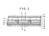
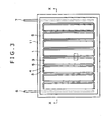
- FIGS. 1 to 3 each show a dye-sensitized photoelectric conversion element module according to a first embodiment of the present invention.
- FIG. 1 is a cross sectional view of the dye-sensitized photoelectric conversion element module
- FIG. 2 is a cross sectional view of a main portion of the dye-sensitized photoelectric conversion element module
- FIG. 3 is a top plan view of the dye-sensitized photoelectric conversion element module.
- FIG. 1 corresponds to a cross sectional view taken on line X - X of FIG. 3
- FIG. 2 is a partially enlarged cross sectional view taken on line X - X of FIG. 3 .
- a plurality of stripe-shaped transparent conductive layers 2 are provided on an insulating transparent filmy glass substrate 1 in parallel with one another.
- a thickness of the filmy glass substrate 1 is set as being equal to or smaller than 0.2 mm, suitably, in the range of 0.01 to 0.2 mm.
- a stripe-shaped dye-sensitized semiconductor layer 3, a stripe-shaped porous insulating layer 4 and a stripe-shaped counter electrode 5 which extend in the same direction as that of each of the transparent conductive layers 2 are laminated in order on each of the transparent conductive layers 2, thereby structuring each of dye-sensitized photoelectric conversion elements.
- At least the dye-sensitized semiconductor layer 3 and the porous insulating layer 4 are entirely impregnated with an electrolyte, typically, the dye-sensitized semiconductor layer 3, the porous insulating layer 4 and the counter electrode 5 are entirely impregnated with the electrolyte.
- a width of the dye-sensitized semiconductor layer 3 is smaller than that of the transparent conductive layer 2, and a portion thereof adjacent to one side in a longitudinal direction of the transparent conductive layer 2 is exposed.
- a width of the porous insulating layer 4 is larger than that of the dye-sensitized semiconductor layer 3, and the porous insulating layer 4 is provided so as to cover the entire dye-sensitized semiconductor layer 3.
- One end of the porous insulating layer 4 extends along one side surface of the dye-sensitized semiconductor layer 3 to contact the filmy glass substrate 1, and the other end thereof extends along the other side surface of the dye-sensitized semiconductor layer 3 to contact the transparent conductive layer 2.
- one end of the counter electrode 5 of one dye-sensitized photoelectric conversion element is joined to the transparent conductive layer 2 of the adjacent dye-sensitized photoelectric conversion element.
- a plurality of dye-sensitized photoelectric conversion elements are electrically connected in series with one another.
- An extraction electrode 6 is connected to the transparent conductive layer 2 on which the dye-sensitized photoelectric conversion element is formed in one end of a plurality of dye-sensitized photoelectric conversion elements connected in series with one another.
- an extraction electrode 7 is connected to the transparent conductive layer 2 which is formed adjacent to the transparent conductive layer 2 on which the dye-sensitized photoelectric conversion element is formed in the other end, and to which one end of the counter electrode 5 of the dye-sensitized photoelectric conversion element is connected.
- a bonding layer 8 is provided so as to cover an entire surface of a portion defined between the counter electrode 5 between each two dye-sensitized photoelectric conversion elements, and the porous insulating layer 4, and an entire surface of the counter electrode 5.
- a resin system protective film 9 having a size larger than that of the filmy glass substrate 1 is bonded to the entire surface of the bonding layer 8.
- a bonding layer 10 is entirely provided on a back surface of the filmy glass substrate 1, and a resin system protective film 11 having a size larger than that of the filmy glass substrate 1 is bonded to the entire surface of the bonding layer 10. Also, the protective film 9 and the protective film 11 are joined to each other in portions thereof each sticking out from the filmy glass substrate 1, whereby an end surface of the filmy glass substrate 1 is also covered with the protective film 9.
- transparent members are used as the protective film 11 and the bonding layer 10, respectively, bonded to the light incidence surface side, transparent members may be or not may be used as the protective film 9 and the bonding layer 8, respectively.
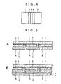
- a top plan view obtained by enlarging a portion (a portion surrounded by a chain line in FIG. 3 ) of the porous insulating layer 4, the counter electrode 5 and the bonding layer 8 is shown in FIG. 4 .
- a layer obtained by supporting a dye in either a semiconductor fine particle layer or a porous semiconductor layer is used as the dye-sensitized semiconductor layer 3.
- a resin system film made of a gas barrier material is suitably used as at least one of the protective films 9 and 11.
- a film which is equal to or smaller than 100 (cc/m 2 /day/atm) in permeation rate of oxygen, and is equal to or smaller than 100 (g/m 2 /day) in permeation rate of water vapor is suitably used as at least one of the protective films 9 and 11.
- an antireflective (AR) film is suitably used as the protective film 11 on the light incidence side for the purpose of suppressing a loss of a light quantity of an incident light due to reflection.
- the filmy glass substrate 1 Materials which are selected from those previously given as may be necessary can be used for the filmy glass substrate 1, the transparent conductive layer 2, the dye-sensitized semiconductor layer 3, the porous insulating layer 4, the counter electrode 5, and the bonding layers 8 and 10, respectively.
- the transparent conductive layer 2 is patterned into stripe shapes by etching.
- a substrate having a thickness of 0.2 mm or less may be used from the beginning as the filmy glass substrate 1 or a substrate having a thickness larger than 0.2 mm may be used as the filmy glass substrate 1.
- the filmy glass substrate 1 is thinned later through the polishing or the like to have a thickness of 0.2 mm or less.
- a paste into which the semiconductor fine particles are dispersed is applied at a predetermined gap onto each of the transparent conductive layers 2.
- the filmy glass substrate 1 is heated at a predetermined temperature to sinter the semiconductor fine particles, thereby forming a porous semiconductor layer made of the semiconductor fine particle sintered body.
- the porous insulating layer 4 is patterned into stripe shapes by etching.
- the counter electrode 5 is formed over the entire surface of the porous insulating layer 4, and one end of the counter electrode 5 is joined to each of the transparent conductive layers 2.
- the filmy glass substrate 1 on which the porous semiconductor layer made of the semiconductor fine particle sintered body, the porous insulating layer 4, and the counter electrode 5 are formed in order, for example, is immersed in a dye solution, thereby supporting a dye for sensitizing in the semiconductor fine particles composing the porous semiconductor layer.
- the dye-sensitized semiconductor layer 3 is formed.
- an electrolyte is applied onto a surface on the counter electrode 5 side. Also, at least the dye-sensitized semiconductor layer 3 and the porous insulating layer 4 are entirely impregnated with the electrolyte, typically, the dye-sensitized semiconductor layer 3, the porous insulating layer 4 and the counter electrode 5 are entirely impregnated with the electrolyte.
- the extraction electrodes 6 and 7 are joined to the transparent conductive layer 2 on which the dye-sensitized photoelectric conversion element is formed in one end, and the transparent conductive layer 2 formed adjacent to the transparent conductive layer 2 on which the dye-sensitized photoelectric conversion element is formed in the other end, respectively.
- a protective film 9 is bonded onto the surface on the counter electrode 5 side through the bonding layer 8.
- the filmy glass substrate 1 is thinned through the polishing or the like to have the thickness of 0.2 mm or less.
- the protective film 11 is bonded onto the back surface of the filmy glass substrate 1 through the bonding layer 10, and the protective film 11 and the protective film 9 are joined to each other in the portions thereof sticking from the filmy glass substrate 1, thereby covering the end surface of the filmy glass substrate 1 with the protective film 9.
- the dye-sensitized photoelectric conversion element module shown in FIGS. 1 to 3 is manufactured in the manner as described above.
- a light which is transmitted through the filmy glass substrate 1 to be made incident from the filmy glass substrate 1 side excites the dye of the dye-sensitized semiconductor layer 3 to generate an electron.
- the electron is quickly delivered from the dye to the semiconductor fine particles of the dye-sensitized semiconductor layer 3.
- the dye which has lost the electron receives an electron from an ion in the electrolyte with which each of the dye-sensitized semiconductor layer 3 and the porous insulating layer 4 are entirely impregnated, and a molecule which has delivered the electron receives an electron again on the surface of the counter electrode 5.
- An electromotive force is generated between the transparent conductive layer 2 electrically connected to the dye-sensitized semiconductor layer 3, and the counter electrode 5 in accordance with the series of reactions.
- the photoelectric conversion is carried out in the manner as described above.
- a total electromotive force of the electromotive forces of the dye-sensitized photoelectric conversion elements is generated between the extraction electrode 6 connected to the transparent conductive layer 2 of the dye-sensitized photoelectric conversion element in one end of a plurality of dye-sensitized photoelectric conversion elements connected in series with one another, and the extraction electrode 7 connected to the transparent conductive layer 2 of the dye-sensitized photoelectric conversion element in the other end thereof.
- the filmy glass substrate 1 having the thickness of 0.2 mm or less, suitably, in the range of 0.01 to 0.2 mm is used as the supporting base material, the entire surface of the dye-sensitized photoelectric conversion element side, and the end surface of the filmy glass substrate 1 are covered with the protective film 9, and the entire back surface of the filmy glass substrate 1 is covered with the protective film 11. Therefore, the dye-sensitized photoelectric conversion element module can be structured so as to be lightweight, thin and flexible, and the mechanical strength of the dye-sensitized photoelectric conversion element module can also be sufficiently ensured.
- the burning treatment in the phase of the formation of the porous semiconductor layer used in the dye-sensitized semiconductor layer 3 can be carried out at the temperature of about 500°C.
- the crystalline property of the porous semiconductor layer, and the bonding state of the particles can be made satisfactory, and thus the electron conductivity can be made satisfactory.
- the electric power generation efficiency of the dye-sensitized photoelectric conversion element module can be increased.
- the films made of the gas barrier materials are used as the protective films 9 and 11, respectively, which results in that gas such as oxygen, water vapor or the like can be prevented from penetrating from the outside into the inside of the dye-sensitized photoelectric conversion element module, and thus, it is possible to suppress deterioration of the characteristics such as the photoelectric conversion efficiency. For this reason, it is possible to realize the dye-sensitized photoelectric conversion element module which can maintain the excellent characteristics for a long period of time, and which can have the high durability.
- the dye-sensitized semiconductor layer 3 and the counter electrode 5 are separated from each other through the porous insulating layer 4, the dye of the dye-sensitized semiconductor layer 3 can be prevented from being adsorbed on the counter electrode 5, and thus no deterioration of the characteristics is caused. Therefore, it is possible to realize the dye-sensitized photoelectric conversion element module which has the same performance of the electric power generation as that of the dye-sensitized solar cell module having the Z type structure.
- An FTO glass substrate (having a sheet resistance of 10 ⁇ / ⁇ ) for an amorphous solar cell, made by Nippon Sheet Glass Co., Ltd. was prepared in which an FTO film was formed on a glass substrate having a size of 60 mm ⁇ 46 mm, and a thickness of 4 mm.
- the FTO film was patterned by etching to nine stripe-shaped patterns so as to define a gap, having a width of 0.5 mm, between each two stripe-shaped patterns. After that, ultrasonic cleaning was carried out by using acetone, alcohol, an alkali system cleaning liquid, and ultrapure water in order, and drying was sufficiently carried out.
- a titanium oxide paste made by Solaronix was applied onto the eight FTO films, with the exception of one FTO film at the termination, of the nine FTO films on the FTO glass substrate so as to obtain eight stripe-shaped patterns (a total area was 16 cm 2 ) each having a width of 5 mm, and a length of 40 mm by using a screen printer.
- a transparent Ti-Nanoxide TSP paste, and a Ti-Nanoxide DSP containing therein scattering particles were laminated in order from the glass substrate side so as to have a thickness of 7 ⁇ m, and a thickness of 13 ⁇ m, respectively.
- a porous TiO 2 film having a thickness of 20 ⁇ m in total was obtained.
- the porous TiO 2 film was burnt in an electrical furnace at 500°C for 30 minutes, and the standing to cool was then carried out, the porous TiO 2 film was immersed in 0.1 mol/L of a TiCl 4 solution, was held at 70°C for 30 minutes, and was sufficiently cleaned by using pure water and ethanol. After drying, the porous TiO 2 film was burnt at 500°C for 30 minutes again. In such a way, a TiO 2 sintered body was manufactured.
- a TiO 2 paste for screen printing which was prepared by using commercially available TiO 2 particles (having a particle diameter of 200 nm), terpineol and ethyl cellulose was applied onto the TiO 2 sintered body described above so as to have a length of 41 mm, a width of 5.5 mm, and a thickness of 10 ⁇ m.
- the TiO 2 paste was dried, and the paste for the screen printing which was prepared by using the commercially available carbon black and graphite particles, and terpineol and ethyl cellulose was applied onto the TiO 2 layer described above so as to have a length of 40 mm, a width of 6 mm, and a thickness of 30 ⁇ m in order to form a counter electrode.
- the paste was burnt in the electrical furnace at 450°C for 30 minutes. In such a way, a porous insulating layer, and a porous counter electrode were formed.
- the TiO 2 sintered body was immersed in a tert-butylalcohol/acetonitrile mixed medium (1 : 1 in volume) of 0.5 mM of cis-bis (isothiocyanate)-N, N-bis (2,2'-dipyridyl-4,4'-dicarboxylic acid)-ruthenium (II) ditetrabutyl ammonium salt (N719 dye) at a room temperature for 48 hours, thereby supporting the dye in the TiO 2 sintered body.
- the TiO 2 sintered body having the dye thus supported therein was cleaned by using acetonitrile, and was then dried in a dark place.
- a dye-sensitized TiO 2 sintered body was manufactured in the manner as described above.
- the electrolyte composition thus prepared was applied onto the entire surface on the counter electrode side by using the dispenser, and the insides of the counter electrode, the porous insulating layer, and the dye-sensitized semiconductor layer were impregnated with the electrolyte composition. Also, the extra electrolyte composition which exuded from the counter electrode, the porous insulating layer and the dye-sensitized semiconductor layer was clearly cleaned off.
- titanium foils each having a size of 60 mm ⁇ 3 mm, and a thickness of 30 ⁇ m were joined to extraction electrode joining portions provided on a transparent conductive layer formed from the FTO film on both ends of the FTO glass substrate by utilizing an ultrasonic soldering method, thereby forming the extraction electrodes 6 and 7, respectively.
- a protective film obtained by joining a hot-melt resin as a bonding layer to a sticking surface of a gas barrier film having aluminum evaporated thereon was cut into a piece having a size of 70 mm ⁇ 56 mm, and the resulting film was hot-pressed against a surface on a dye-sensitized photoelectric conversion element side under a reduced pressure, thereby obtaining a dye-sensitized photoelectric conversion element module.
- a back surface of the glass substrate having a thickness of 4 mm, and having the dye-sensitized photoelectric conversion element module thus formed thereon was successively polished through lap polishing and optical polishing, thereby obtaining a filmy glass substrate having a thickness of 0.1 mm.
- An AR film (having a trade mark of "ARCTOP"), made by Asahi Glass Co., Ltd., which was cut to have the size of 70 mm ⁇ 56 mm was stuck onto a surface on a light incidence side of the dye-sensitized photoelectric conversion element module, that is, the back surface of the filmy glass substrate, and was joined to the protective film bonded to the dye-sensitized photoelectric conversion element side by thermo-compression bonding in a portion sticking out from the filmy glass substrate, thereby covering an end surface of the filmy glass substrate.
- the desired dye-sensitized photoelectric conversion element module was obtained through the processes described above.
- eight dye-sensitized photoelectric conversion elements each having a size of 5 mm ⁇ 40 mm were connected in series with one another.
- a dye-sensitized photoelectric conversion element module was manufactured similarly to the case of Example 1 except that a member in which a transparent conductive layer made of an ITO (having a thickness of 450 nm)/an ATO (having a thickness of 50 nm) was formed on a filmy glass substrate, having a thickness of 0.1 mm, which was subjected to a hardened glass treatment by utilizing sputtering so as to have the same pattern as that of the FTO film of Example 1 was used, and thus no back surface polishing for the filmy glass substrate was carried out.
- a transparent conductive layer made of an ITO (having a thickness of 450 nm)/an ATO (having a thickness of 50 nm) was formed on a filmy glass substrate, having a thickness of 0.1 mm, which was subjected to a hardened glass treatment by utilizing sputtering so as to have the same pattern as that of the FTO film of Example 1 was used, and thus no back surface polish
- a dye-sensitized photoelectric conversion element module was manufactured similarly to the case of Example 1 except that no back surface polishing for the glass substrate was carried out, and thus a thickness of 0.4 mm of the glass substrate was left as it is.
- a dye-sensitized photoelectric conversion element module was manufactured similarly to the case of Example 2 except that no AR film was formed on a back surface of a filmy glass substrate as a protective film, a filmy glass substrate similarly having a thickness of 0.1 mm was covered with a filmy glass substrate having a thickness of 0.1 mm, and no protective film was formed on a surface as well on a dye-sensitized photoelectric conversion element side.
- a plastic film (having a sheet resistance of 20 ⁇ / ⁇ , a size of 60 mm ⁇ 46 mm, and a thickness of 0.125 mm) in which an ITO film was evaporated on a polyethylene naphthalate (PEN) film was used as a transparent conductive substrate, and the ITO film was patterned into nine stripe-shaped patterns by utilizing the etching so as to define a gap, having a width of 0.5 mm, between each two stripe-shaped pattern. After that, ultrasonic cleaning was carried out by using acetone, alcohol, an alkali system cleaning liquid, and ultrapure water in order, and drying was sufficiently carried out.
- PEN polyethylene naphthalate
- a titanium oxide paste for low-temperature deposition (made by Peccell Technologies) was used as a titanium oxide paste, and was applied onto the eight ITO films except for one ITO film at the termination of the nine ITO films on the PEN/ITO substrate so as to obtain eight stripe-shaped patterns each having a width of 5 mm, and a length of 40 mm (having a total area of 16 cm 2 ) by utilizing a doctor blade method. After this film was dried, this film was held on a hot plate at 150°C for 30 minutes. A porous TiO 2 layer was manufactured in the manner as described above.
- a TiO 2 paste for screen printing which was prepared by using commercially available TiO 2 particles (having a particle diameter of 200 nm), terpineol and ethyl cellulose was applied onto the porous TiO 2 layer described above so as to have a length of 41 mm, a width of 5.5 mm, and a thickness of 10 ⁇ m.
- the TiO 2 paste was dried, and the paste for the screen printing which was prepared by using the commercially available carbon black and graphite particles, and terpineol and ethyl cellulose was applied onto the TiO 2 layer described above so as to have a length of 40 mm, a width of 6 mm, and a thickness of 30 ⁇ m in order to form a counter electrode.
- the paste was held on the hot plate at 150°C for 30 minutes. In such a way, a porous insulating layer, and a porous counter electrode were formed.
- porous TiO 2 layer was immersed in a tert-butylalcohol/acetonitrile mixed medium (1 : 1 in volume) of 0.5 mM of cis-bis (isothiocyanate)-N, N-bis (2,2'-dipyridyl-4,4'-dicarboxylic acid)-ruthenium (II) ditetrabutyl ammonium salt (N719 dye) at a room temperature for 48 hours, thereby supporting the dye in the porous TiO 2 layer.
- the porous TiO 2 layer having the dye thus supported therein was cleaned by using acetonitrile, and was then dried in a dark place.
- a dye-sensitized porous TiO 2 layer was manufactured in the manner as described above.
- the electrolyte composition thus prepared was applied onto the entire surface on the counter electrode side by using the dispenser, and the insides of the counter electrode, the porous insulating layer, and the dye-sensitized semiconductor layer were impregnated with the electrolyte composition. Also, the extra electrolyte composition which exuded from the counter electrode, the porous insulating layer and the dye-sensitized semiconductor layer was clearly cleaned off.
- titanium foils each having a size of 60 mm ⁇ 3 mm, and a thickness of 30 ⁇ m were joined to extraction electrode joining portions provided on a transparent conduction layer formed from an ITO film on both sides of the PEN/ITO substrate by utilizing an ultrasonic soldering method, thereby forming extraction electrodes, respectively.
- a protective film obtained by joining a hot-melt resin as a bonding layer to a sticking surface of a gas barrier film having aluminum evaporated thereon was cut into a piece having a size of 70mm ⁇ 56 mm, and the resulting film was hot-pressed against a surface on a dye-sensitized photoelectric conversion element side under a reduced pressure, thereby perfectly covering a surface on a dye-sensitized photoelectric conversion element side of a dye-sensitized photoelectric conversion element module with the protective film.
- the desired dye-sensitized photoelectric conversion element module was obtained through the processes described above.
- eight dye-sensitized photoelectric conversion elements each having a size of 5 mm ⁇ 40 mm were connected in series with one another.
- the photoelectric conversion efficiency under the radiation condition of AM1.5 (1sun) was measured for the dye-sensitized photoelectric conversion element modules of Examples 1 and 2, and Comparative Examples 1 to 3 manufactured in the manners as described above.
- a bending test was carried out for the dye-sensitized photoelectric conversion element modules for which the measurement of the photoelectric conversion efficiency was completed, and radii of curvature right before the breaking was generated were calculated. The calculation results are shown in TABLE 1.
- Comparative Example 3 is an example in which the dye-sensitized photoelectric conversion element module was manufactured by not using the filmy glass substrate, but using the PEN/ITO substrate, the photoelectric conversion efficiency is very low because no burning process was carried out at 500°C in the phase of formation of the porous TiO 2 layer.
- this dye-sensitized photoelectric conversion element module no protective film 11 is bonded onto the back surface of the filmy glass substrate 1, and the protective film 9 bonded onto the surface on the dye-sensitized photoelectric conversion element side is folded at the end surface of the filmy glass substrate 1 to be joined to the back surface of the filmy glass substrate 1.
- Other structures of this dye-sensitized photoelectric conversion element module are the same as those of the dye-sensitized photoelectric conversion element module according to the first embodiment.
- a method of manufacturing this dye-sensitized photoelectric conversion element module is the same as that of the dye-sensitized photoelectric conversion element module according to the first embodiment except that no protective film 11 is bonded onto the back surface of the filmy glass substrate 1, and the protective film 9 is folded at the end surface of the filmy glass substrate 1.
- a dye-sensitized photoelectric conversion element module was manufactured similarly to the case of Example 1 except that no AR film was bonded onto a back surface of a filmy glass substrate, and a protective film bonded onto a surface on the dye-sensitized photoelectric conversion element side was folded at an end surface of the filmy glass substrate to be joined to the back surface of the filmy glass substrate.
- a dye-sensitized photoelectric conversion element module was manufactured similarly to the case of Example 3 except that a size of a protective film to be bonded onto a surface on a dye-sensitized photoelectric conversion element side was set as a size of 58 mm ⁇ 44 mm smaller than that of (60 mm ⁇ 46 mm) of a filmy glass substrate, and the protective film was bonded so as to expose an end surface of the filmy glass substrate.
- the photoelectric conversion efficiency under the radiation condition of AM1.5 (1sun) was measured for the dye-sensitized photoelectric conversion element modules of Example 3 and Comparative Example 4 manufactured in the manners as described above.
- a bending test was carried out for the dye-sensitized photoelectric conversion element modules for which the measurement of the photoelectric conversion efficiency was completed, and radii of curvature right before the breaking was generated were calculated. The calculation results are shown in TABLE 1.
- the dye-sensitized photoelectric conversion element module of Example 3 is excellent in photoelectric conversion efficiency, small in minimum radius of curvature, and lightweight.
- Comparative Example 4 shows the high photoelectric conversion efficiency, a radius of curvature is large as compared with the case of Example 3 because the size of the protective film is smaller than that of the filmy glass substrate, and thus the end surface of the filmy glass substrate is covered with no protective film.
- a counter electrode 5 is formed from a foil made of either a material having a catalyst layer containing therein at least one or more kinds of elements selected from the group consisting of Pt, Ru, Ir and C or a material containing therein at least one or more kinds of elements selected from the group consisting of Pt, Ru, Ir and C which is provided on one surface, on a side of the porous insulating layer 4, of a foil made of either a metal or an alloy containing therein at least one or more kinds of elements selected from the group consisting of Ti, Ni, Cr, Fe, Nb, Ta, W, Co and Zr.
- one end of the counter electrode 5 of one dye-sensitized photoelectric conversion element is joined to the transparent conductive layer 2 of the adjacent dye-sensitized photoelectric conversion element through a conductive material 12.
- Other structures of this dye-sensitized photoelectric conversion element module are the same as those in the dye-sensitized photoelectric conversion element module according to the first embodiment.
- a conductive material 12 is formed on a joining portion to the counter electrode 5 on each of the transparent conductive layers 2. Also, the counter electrode 5 formed from the foil made of either the material having the catalyst layer or the material having the catalytic ability on one surface of the foil, made of either the metal or the alloy, having the predetermined shape is formed, and is then joined to the conductive material 12.
- the extraction electrodes 6 and 7 are formed similarly to the case of the first embodiment.
- the bonding layer 8 is formed over the entire surface of the portion defined between the counter electrode 5 between each two dye-sensitized photoelectric conversion elements, and the porous insulating layer 4, and the entire surface of the counter electrode 5 except for a portion of a liquid injection hole which is previously formed every dye-sensitized photoelectric conversion element.
- an electrolyte solution is injected through the liquid injection hole previously formed every dye-sensitized photoelectric conversion element, thereby impregnating entirely at least the dye-sensitized semiconductor layer 3, and the porous insulating layer 4, typically, entirely the dye-sensitized semiconductor layer 3, the porous insulating layer 4 and the counter electrode 5 with the electrolyte.
- the process in and after the bonding of the protective film 9 is advanced similarly to the case of the first embodiment, thereby manufacturing the dye-sensitized photoelectric conversion element module.
- the counter electrode 5 is formed from the foil made of either the material having the catalyst layer or the material having the catalytic ability on the foil made of either the metal or the alloy, the counter electrode 5 can be structured to be thin, and thus the thinning and weight saving of the dye-sensitized photoelectric conversion element module become possible.
- the materials of the foil made of either the metal or the alloy, and the catalyst layer, or the material having the catalytic ability which form the counter electrode 5 have the wide room of selection, and thus there is no restriction in material of the counter electrode.
- the dye-sensitized semiconductor layer 3 and the counter electrode 5 are separated from each other through the porous insulating layer 4, the dye of the dye-sensitized semiconductor layer 3 can be prevented from being adsorbed on the counter electrode 5, and thus no deterioration of the characteristics is caused. Therefore, it is possible to realize the dye-sensitized photoelectric conversion element module which has the same performance of the electric power generation as that of a dye-sensitized solar cell module having a Z type structure.
- an anisotropically conductive paste was applied onto the stripe-shaped dye-sensitized TiO 2 sintered body to have a width of 0.5 mm so as to be parallel with the stripe-shaped dye-sensitized TiO 2 sintered body, and was then dried.
- a counter electrode obtained by spray-coating one surface of a titanium foil having a thickness of 0.05 mm with an isopropyl alcohol (IPA) solution of 0.05 mM of a chloroplatinic acid, and carrying out the burning at 385°C was cut into pieces each having a size of 6 mm ⁇ 40 mm. Also, after the surface onto which the chloroplatinic acid was sprayed was directed toward the dye-sensitized TiO 2 sintered body side, thereby carrying out the alignment, the anisotropically conductive paste described above, and the counter electrode were joined to each other by thermo-compression bonding.
- IPA isopropyl alcohol
- An UV cure adhesive agent was applied onto the FTO glass substrate by carrying out the screen printing so as to cover all the dye-sensitized photoelectric conversion elements with a pattern for liquid injection having a diameter of 1 mm being left. After the application, when air bubbles perfectly outgassed, an ultraviolet light was radiated to the UV cure adhesive agent by using a conveyer type UV exposure system, thereby curing the UV cure adhesive agent.
- the electrolyte composition prepared similarly to the case of Example 1 was injected under a reduced pressure through the liquid injection hole, having a diameter of 1 mm, prepared in the manner as described above, the electrolyte composition was held under an increased pressure of 0.4 MPa for 30 minutes, so that the electrolyte solution was made to perfectly penetrate into each of the dye-sensitized photoelectric conversion elements. In such a way, each of the dye-sensitized TiO 2 sintered body and the porous insulating layer was impregnated with the electrolyte.
- a protective film was bonded to the dye-sensitized photoelectric conversion element side. Also, after the glass substrate was polished to obtain a filmy glass substrate having a thickness of 0.1 mm, a protective film was bonded to a back surface of the resulting filmy glass substrate, and these protective films are joined to each other in portions thereof sticking out from the filmy glass substrate, thereby obtaining a dye-sensitized photoelectric conversion element module.
- an electrolyte is made of an electrolyte composition which contains therein iodine, and contains therein a compound having at least one isocyanate group (-NCO), in which the compound suitably contains therein at least one or more nitrogen containing functional groups within the same molecule in addition to the isocyanate group, or which further contains therein a compound having at least one or more nitrogen containing functional groups in addition to that compound.
- a compound having at least one isocyanate group (-NCO)
- the compound suitably contains therein at least one or more nitrogen containing functional groups within the same molecule in addition to the isocyanate group, or which further contains therein a compound having at least one or more nitrogen containing functional groups in addition to that compound.
- the compound having at least one or more isocyanate groups is preferably compatible with a solvent of an electrolyte, an electrolyte salt, and other addition agents.
- the compound having at least one or more nitrogen contacting functional group is suitably an amine system compound, the compound concerned is not especially limited thereto.
- the amine system compound is preferably compatible with a solvent of an electrolyte, an electrolyte salt, and other addition agents.
- the nitrogen containing functional group is made to exist together with the compound having at least one or more isocyanate groups, which especially, largely contributes to an increase in open voltage of the dye-sensitized photoelectric conversion element modules.
- the compound having at least one or more isocyanate groups for example, is isocyanic phenyl, isocyanic 2-chloroethyl, isocyanic m-chlorophenyl, isocyanic cychlohexyl, isocyanic o-tolyl, isocyanic p-tolyl, isocyanic n-hexyl, 2,4-diisocyanic tolylene, diisocyanic hexamethylene, 4,4'-diisocyanic methylenediphenyl or the like.
- the present invention is by no means limited thereto.
- the amine system compound for example, is 4-tert-butylpyridine, aniline, N,N-dimethylaniline, N-methylbenz imidazole, or the like.
- the present invention is by no means limited thereto.
- the electrolyte is made of the electrolyte compound containing therein the compound having at least one or more isocyanate groups, which results in that both the short current and the open voltage can be increased, thereby making it possible to obtain the dye-sensitized photoelectric conversion element module having the very high photoelectric conversion efficiency.
- Example 1 During the preparation of the electrolyte compound in Example 1, in addition to 0.045g of sodium iodide (NaI), 1.11g of 1-propyl-2,3-dimethyl imidazolium iodide, 0.11g of iodine (I 2 ), and 0.081g of 4-tert-butyl pyridine, 0.071g (0.2 mol/L) of phenyl isocyanurate was dissolved in 3g of ⁇ -butyrolactone. Any of other matters is made similar to that in Example 1, and a dye-sensitized photoelectric conversion element module was obtained.
- NaI sodium iodide
- I 2 iodine
- 4-tert-butyl pyridine 4-tert-butyl pyridine
Landscapes
- Power Engineering (AREA)
- Engineering & Computer Science (AREA)
- Electrochemistry (AREA)
- Chemical Kinetics & Catalysis (AREA)
- Chemical & Material Sciences (AREA)
- Microelectronics & Electronic Packaging (AREA)
- General Chemical & Material Sciences (AREA)
- Physics & Mathematics (AREA)
- Computer Hardware Design (AREA)
- General Physics & Mathematics (AREA)
- Electromagnetism (AREA)
- Condensed Matter Physics & Semiconductors (AREA)
- Photovoltaic Devices (AREA)
- Hybrid Cells (AREA)
Applications Claiming Priority (2)
| Application Number | Priority Date | Filing Date | Title |
|---|---|---|---|
| JP2007320261A JP2009146625A (ja) | 2007-12-12 | 2007-12-12 | 色素増感光電変換素子モジュールおよびその製造方法ならびに光電変換素子モジュールおよびその製造方法ならびに電子機器 |
| PCT/JP2008/072340 WO2009075267A1 (ja) | 2007-12-12 | 2008-12-09 | 色素増感光電変換素子モジュールおよびその製造方法ならびに光電変換素子モジュールおよびその製造方法ならびに電子機器 |
Publications (1)
| Publication Number | Publication Date |
|---|---|
| EP2221909A1 true EP2221909A1 (de) | 2010-08-25 |
Family
ID=40755509
Family Applications (1)
| Application Number | Title | Priority Date | Filing Date |
|---|---|---|---|
| EP08858684A Withdrawn EP2221909A1 (de) | 2007-12-12 | 2008-12-09 | Module für eine farbstoffempfindliche photoelektrische wandlungsvorrichtung und herstellungverfahren dafür, modul für eine photoelektrische wandlungsvorrichtung und herstellungsverfahren dafür sowie elektronische vorrichtung |
Country Status (7)
| Country | Link |
|---|---|
| US (1) | US20100132785A1 (de) |
| EP (1) | EP2221909A1 (de) |
| JP (1) | JP2009146625A (de) |
| KR (1) | KR20100091883A (de) |
| CN (1) | CN101606275B (de) |
| TW (1) | TW200947790A (de) |
| WO (1) | WO2009075267A1 (de) |
Cited By (2)
| Publication number | Priority date | Publication date | Assignee | Title |
|---|---|---|---|---|
| US9985240B2 (en) | 2010-02-10 | 2018-05-29 | Nippon Electric Glass Co., Ltd. | Sealing material and sealing method using the same |
| US10096431B2 (en) | 2012-09-01 | 2018-10-09 | Fujikura Ltd. | Dye-sensitized solar cell element for low illuminance |
Families Citing this family (37)
| Publication number | Priority date | Publication date | Assignee | Title |
|---|---|---|---|---|
| JP5007784B2 (ja) * | 2006-01-30 | 2012-08-22 | ソニー株式会社 | 光電変換装置 |
| JP2007234580A (ja) * | 2006-02-02 | 2007-09-13 | Sony Corp | 色素増感型光電変換装置 |
| JP2007280906A (ja) * | 2006-04-12 | 2007-10-25 | Sony Corp | 機能デバイス及びその製造方法 |
| JP5023866B2 (ja) * | 2007-07-27 | 2012-09-12 | ソニー株式会社 | 色素増感光電変換素子およびその製造方法ならびに電子機器 |
| JP2009099476A (ja) * | 2007-10-19 | 2009-05-07 | Sony Corp | 色素増感光電変換素子およびその製造方法 |
| JP2010003468A (ja) * | 2008-06-19 | 2010-01-07 | Sony Corp | 色素増感太陽電池およびその製造方法 |
| JP2010010191A (ja) * | 2008-06-24 | 2010-01-14 | Sony Corp | 電子装置 |
| JP2010009769A (ja) * | 2008-06-24 | 2010-01-14 | Sony Corp | 光電変換素子の製造方法 |
| JP2010092762A (ja) * | 2008-10-09 | 2010-04-22 | Sony Corp | 機能性デバイス及びその製造方法 |
| US20110048525A1 (en) * | 2008-11-26 | 2011-03-03 | Sony Corporation | Functional device and method for producing the same |
| JP5428555B2 (ja) * | 2009-06-08 | 2014-02-26 | ソニー株式会社 | 色素増感光電変換素子の製造方法 |
| JP5334708B2 (ja) * | 2009-06-29 | 2013-11-06 | 株式会社Nsc | 太陽電池の製造方法 |
| EP2457243A1 (de) * | 2009-07-23 | 2012-05-30 | Tata Steel UK Limited | Verfahren zur herstellung von arbeitselektroden für farbstoffsensibilisierte solarzellen |
| JP2011044357A (ja) * | 2009-08-21 | 2011-03-03 | Sony Corp | 光電池モジュール及び光電池モジュールの製造方法 |
| JP5582821B2 (ja) * | 2010-02-25 | 2014-09-03 | 日新製鋼株式会社 | 色素増感型太陽電池モジュールの製造法 |
| JP2011204662A (ja) * | 2010-03-05 | 2011-10-13 | Sony Corp | 光電変換素子およびその製造方法ならびに電子機器 |
| JP5621488B2 (ja) * | 2010-03-17 | 2014-11-12 | ソニー株式会社 | 光電変換装置 |
| JP2011216190A (ja) * | 2010-03-31 | 2011-10-27 | Sony Corp | 光電変換装置及びその製造方法 |
| CN104331199A (zh) * | 2010-06-12 | 2015-02-04 | 宸鸿科技(厦门)有限公司 | 触控电路图形结构及制造方法、触控面板及触控显示屏 |
| CN102279678A (zh) * | 2010-06-12 | 2011-12-14 | 宸鸿科技(厦门)有限公司 | 触控电路图形结构及制造方法、触控面板及触控显示屏 |
| JP2012014849A (ja) * | 2010-06-29 | 2012-01-19 | Sony Corp | 光電変換素子およびその製造方法ならびに光電変換素子モジュールおよびその製造方法 |
| JP5912316B2 (ja) * | 2010-08-04 | 2016-04-27 | 株式会社半導体エネルギー研究所 | 電気二重層キャパシタ、又は太陽光発電装置 |
| JP5744570B2 (ja) * | 2011-03-02 | 2015-07-08 | キヤノン株式会社 | 放射線検出装置、放射線検出装置の製造方法及び放射線検出システム |
| CN102315335A (zh) * | 2011-04-13 | 2012-01-11 | 东旭集团有限公司 | 一种减少薄膜太阳能电池死区面积的制备工艺 |
| KR101281216B1 (ko) | 2011-11-03 | 2013-07-02 | 현대하이스코 주식회사 | 유연성 기판을 이용한 염료감응 태양전지 및 그 제조방법 |
| WO2013145975A1 (ja) * | 2012-03-30 | 2013-10-03 | 株式会社フジクラ | 色素増感太陽電池 |
| JP5933013B2 (ja) * | 2012-09-01 | 2016-06-08 | 株式会社フジクラ | 低照度用色素増感太陽電池素子 |
| JP5922242B2 (ja) * | 2012-09-07 | 2016-05-24 | シャープ株式会社 | 光電変換素子、その製造方法、光電変換素子モジュールおよびその製造方法 |
| US20170338050A1 (en) * | 2012-12-14 | 2017-11-23 | Sharp Kabushiki Kaisha | Photoelectric conversion element |
| JP6594313B2 (ja) * | 2014-07-30 | 2019-10-23 | シャープ株式会社 | 光電変換素子およびこれを含む光電変換素子モジュール |
| TWI553892B (zh) * | 2015-12-31 | 2016-10-11 | 台灣中油股份有限公司 | 具鈣鈦礦施體層之太陽能電池模組 |
| WO2018025821A1 (ja) * | 2016-08-02 | 2018-02-08 | 日本ゼオン株式会社 | 太陽電池モジュール及び太陽電池モジュールの製造方法 |
| CN109564823B (zh) * | 2016-09-06 | 2021-12-21 | 日本瑞翁株式会社 | 太阳能电池模块 |
| TWI644448B (zh) * | 2017-10-18 | 2018-12-11 | 台灣中油股份有限公司 | 鈣鈦礦太陽能電池模組及其製備方法 |
| JP2019145663A (ja) * | 2018-02-20 | 2019-08-29 | 株式会社フジクラ | 光電変換素子 |
| JP7063454B2 (ja) * | 2018-03-30 | 2022-05-09 | 太陽誘電株式会社 | 色素増感太陽電池及びその製造方法 |
| CN110047959B (zh) * | 2019-04-26 | 2021-08-06 | 圣晖莱南京能源科技有限公司 | 柔性太阳能薄膜电池的封装结构、封装工装及封装方法 |
Family Cites Families (44)
| Publication number | Priority date | Publication date | Assignee | Title |
|---|---|---|---|---|
| US5507880A (en) * | 1992-06-08 | 1996-04-16 | Kanegafuchi Kagaku Kogyo Kabushiki Kaisha | Amorphous solar module having improved passivation |
| JP3132608B2 (ja) * | 1993-04-07 | 2001-02-05 | 富士電機株式会社 | 光電変換装置 |
| JP3222361B2 (ja) * | 1995-08-15 | 2001-10-29 | キヤノン株式会社 | 太陽電池モジュールの製造方法及び太陽電池モジュール |
| DE69513203T2 (de) * | 1995-10-31 | 2000-07-20 | Ecole Polytech | Batterie-anordnung von fotovoltaischen zellen und herstellungsverfahren |
| JPH10112549A (ja) * | 1996-10-08 | 1998-04-28 | Canon Inc | 太陽電池モジュール |
| JP2997773B1 (ja) * | 1998-07-15 | 2000-01-11 | 工業技術院長 | 増感剤として有用な金属錯体、酸化物半導体電極及び太陽電池 |
| JP2000031509A (ja) * | 1998-07-16 | 2000-01-28 | Dainippon Printing Co Ltd | 太陽電池モジュール |
| DE69827649T2 (de) * | 1998-12-21 | 2005-12-01 | Chi Mei Optoelectronics Corp. | Elektrisch leitfähiges Verbundglas |
| AUPP953999A0 (en) * | 1999-03-30 | 1999-04-29 | Sustainable Technologies Australia Limited | Methods to manufacture single cell and multi-cell regenerative photoelectrochemical devices |
| AUPP967799A0 (en) * | 1999-04-09 | 1999-05-06 | Sustainable Technologies Australia Ltd | Methods to implement sealing and electrical connections to single cell and multi-cell regenerative photovoltaic photoelectrochemical devices |
| SE521683C2 (sv) * | 2000-06-14 | 2003-11-25 | Ivf Industriforskning Och Utve | Metod för tillverkning av förseglade monolitiska elektrokemiska system och förseglat monolitiskt elektrokemiskt system |
| US7202412B2 (en) * | 2002-01-18 | 2007-04-10 | Sharp Kabushiki Kaisha | Photovoltaic cell including porous semiconductor layer, method of manufacturing the same and solar cell |
| JP4010170B2 (ja) * | 2002-04-11 | 2007-11-21 | ソニー株式会社 | 光電変換素子の製造方法 |
| JP4221643B2 (ja) * | 2002-05-27 | 2009-02-12 | ソニー株式会社 | 光電変換装置 |
| US20050260786A1 (en) * | 2002-08-13 | 2005-11-24 | Bridgestone Corporation | Dye-sensitized solar cell |
| JP4570867B2 (ja) * | 2003-12-25 | 2010-10-27 | 株式会社フジクラ | 光電変換素子 |
| JP4635473B2 (ja) * | 2004-05-13 | 2011-02-23 | ソニー株式会社 | 光電変換素子の製造方法及び半導体電極の製造方法 |
| JP4635474B2 (ja) * | 2004-05-14 | 2011-02-23 | ソニー株式会社 | 光電変換素子、及びこれに用いる透明導電性基板 |
| KR100661116B1 (ko) * | 2004-11-22 | 2006-12-22 | 가부시키가이샤후지쿠라 | 전극, 광전 변환 소자 및 색소 증감 태양 전지 |
| US20070224464A1 (en) * | 2005-03-21 | 2007-09-27 | Srini Balasubramanian | Dye-sensitized photovoltaic cells |
| JP2007053049A (ja) * | 2005-08-19 | 2007-03-01 | Mazda Motor Corp | 色素増感太陽電池付き車両用ガラス及びその車両取付構造 |
| JP2007055861A (ja) * | 2005-08-25 | 2007-03-08 | Nippon Sheet Glass Co Ltd | 色素増感太陽電池用導電膜付き車載用ガラスの曲げ成形方法及び色素増感太陽電池用導電膜付き車載用ガラス |
| JP5007784B2 (ja) * | 2006-01-30 | 2012-08-22 | ソニー株式会社 | 光電変換装置 |
| JP2007234580A (ja) * | 2006-02-02 | 2007-09-13 | Sony Corp | 色素増感型光電変換装置 |
| JP2007280906A (ja) * | 2006-04-12 | 2007-10-25 | Sony Corp | 機能デバイス及びその製造方法 |
| US8581094B2 (en) * | 2006-09-20 | 2013-11-12 | Dow Global Technologies, Llc | Electronic device module comprising polyolefin copolymer |
| JP5106876B2 (ja) * | 2007-01-31 | 2012-12-26 | 藤森工業株式会社 | 色素増感型太陽電池モジュール及びその製造方法 |
| JP5158561B2 (ja) * | 2007-04-13 | 2013-03-06 | 日本電気硝子株式会社 | 積層体及びそれを用いた太陽電池 |
| JP5023866B2 (ja) * | 2007-07-27 | 2012-09-12 | ソニー株式会社 | 色素増感光電変換素子およびその製造方法ならびに電子機器 |
| JP5192769B2 (ja) * | 2007-10-12 | 2013-05-08 | 古河電気工業株式会社 | 色素増感型太陽電池 |
| JP2009099476A (ja) * | 2007-10-19 | 2009-05-07 | Sony Corp | 色素増感光電変換素子およびその製造方法 |
| JP2009110796A (ja) * | 2007-10-30 | 2009-05-21 | Sony Corp | 色素増感光電変換素子モジュールおよびその製造方法ならびに電子機器 |
| JP2010003468A (ja) * | 2008-06-19 | 2010-01-07 | Sony Corp | 色素増感太陽電池およびその製造方法 |
| JP2010009769A (ja) * | 2008-06-24 | 2010-01-14 | Sony Corp | 光電変換素子の製造方法 |
| JP2010010191A (ja) * | 2008-06-24 | 2010-01-14 | Sony Corp | 電子装置 |
| JP2010092762A (ja) * | 2008-10-09 | 2010-04-22 | Sony Corp | 機能性デバイス及びその製造方法 |
| US20110048525A1 (en) * | 2008-11-26 | 2011-03-03 | Sony Corporation | Functional device and method for producing the same |
| JP5428555B2 (ja) * | 2009-06-08 | 2014-02-26 | ソニー株式会社 | 色素増感光電変換素子の製造方法 |
| JP2011204662A (ja) * | 2010-03-05 | 2011-10-13 | Sony Corp | 光電変換素子およびその製造方法ならびに電子機器 |
| JP5621488B2 (ja) * | 2010-03-17 | 2014-11-12 | ソニー株式会社 | 光電変換装置 |
| JP2011216189A (ja) * | 2010-03-31 | 2011-10-27 | Sony Corp | 光電変換装置及び光電変換装置モジュール |
| JP2011216190A (ja) * | 2010-03-31 | 2011-10-27 | Sony Corp | 光電変換装置及びその製造方法 |
| JP2011238472A (ja) * | 2010-05-11 | 2011-11-24 | Sony Corp | 光電変換装置 |
| JP2012014849A (ja) * | 2010-06-29 | 2012-01-19 | Sony Corp | 光電変換素子およびその製造方法ならびに光電変換素子モジュールおよびその製造方法 |
-
2007
- 2007-12-12 JP JP2007320261A patent/JP2009146625A/ja active Pending
-
2008
- 2008-12-09 US US12/449,228 patent/US20100132785A1/en not_active Abandoned
- 2008-12-09 KR KR1020097016713A patent/KR20100091883A/ko not_active Application Discontinuation
- 2008-12-09 WO PCT/JP2008/072340 patent/WO2009075267A1/ja active Application Filing
- 2008-12-09 EP EP08858684A patent/EP2221909A1/de not_active Withdrawn
- 2008-12-09 CN CN2008800048253A patent/CN101606275B/zh not_active Expired - Fee Related
- 2008-12-10 TW TW097148029A patent/TW200947790A/zh not_active IP Right Cessation
Non-Patent Citations (1)
| Title |
|---|
| See references of WO2009075267A1 * |
Cited By (2)
| Publication number | Priority date | Publication date | Assignee | Title |
|---|---|---|---|---|
| US9985240B2 (en) | 2010-02-10 | 2018-05-29 | Nippon Electric Glass Co., Ltd. | Sealing material and sealing method using the same |
| US10096431B2 (en) | 2012-09-01 | 2018-10-09 | Fujikura Ltd. | Dye-sensitized solar cell element for low illuminance |
Also Published As
| Publication number | Publication date |
|---|---|
| CN101606275B (zh) | 2011-05-11 |
| TW200947790A (en) | 2009-11-16 |
| CN101606275A (zh) | 2009-12-16 |
| WO2009075267A1 (ja) | 2009-06-18 |
| TWI380494B (de) | 2012-12-21 |
| US20100132785A1 (en) | 2010-06-03 |
| JP2009146625A (ja) | 2009-07-02 |
| KR20100091883A (ko) | 2010-08-19 |
Similar Documents
| Publication | Publication Date | Title |
|---|---|---|
| EP2221909A1 (de) | Module für eine farbstoffempfindliche photoelektrische wandlungsvorrichtung und herstellungverfahren dafür, modul für eine photoelektrische wandlungsvorrichtung und herstellungsverfahren dafür sowie elektronische vorrichtung | |
| EP2214249A1 (de) | Farbstoffempfindliches photoelektrisches wandlungsvorrichtungsmodul, verfahren zu seiner herstellung und elektronische vorrichtung | |
| EP2224533A1 (de) | Pigmentsensibilisierendes fotoelektrisches wandlerelement und verfahren zu seiner herstellung | |
| JP5621488B2 (ja) | 光電変換装置 | |
| US20110277818A1 (en) | Photoelectric conversion device | |
| EP2287962A1 (de) | Farbstoffsensibilisierte solarzelle und verfahren zur herstellung der farbstoffsensibilisierten solarzelle | |
| EP2530779A1 (de) | Elektrolytlösung für eine farbstoffsensibilisierte solarzelle und farbstoffsensibilisierte solarzelle damit | |
| JP4914660B2 (ja) | 色素増感太陽電池モジュールおよびその製造方法 | |
| JP2011216190A (ja) | 光電変換装置及びその製造方法 | |
| EP2683021B1 (de) | Farbstoffsensibilisiertes solarzellenmodul und verfahren zu seiner herstellung | |
| US20140174524A1 (en) | Photoelectric conversion element, method for manufacturing the same, electronic apparatus, counter electrode for photoelectric conversion element, and architecture | |
| JP2006236960A (ja) | 色素増感太陽電池及びその製造方法 | |
| JP5128118B2 (ja) | 湿式太陽電池とその製造方法 | |
| JP4606777B2 (ja) | 湿式太陽電池 | |
| JP2009193911A (ja) | 色素増感光電変換素子およびその製造方法ならびに色素増感光電変換素子モジュールおよびその製造方法ならびに電子機器ならびに多孔質シリカ膜の製造方法 | |
| JP4843899B2 (ja) | 光電変換素子およびその製造方法 | |
| JP5095226B2 (ja) | 色素増感型太陽電池及びその製造方法 | |
| JP4678125B2 (ja) | 光電変換素子およびその製造方法ならびに電子装置およびその製造方法 | |
| JP2009110797A (ja) | 色素増感光電変換素子モジュールおよびその製造方法ならびに電子機器 | |
| WO2013114733A1 (ja) | 光電変換素子モジュール | |
| WO2013015067A1 (ja) | 光電変換装置、電子機器および建築物 | |
| JP2009081074A (ja) | 色素増感光電変換素子、電解質組成物、電解質用添加剤および電子機器 | |
| WO2012117995A1 (ja) | 光電変換素子および光電変換素子モジュール | |
| JP2013200960A (ja) | 光電変換素子モジュールおよびその製造方法 |
Legal Events
| Date | Code | Title | Description |
|---|---|---|---|
| PUAI | Public reference made under article 153(3) epc to a published international application that has entered the european phase |
Free format text: ORIGINAL CODE: 0009012 |
|
| 17P | Request for examination filed |
Effective date: 20090728 |
|
| AK | Designated contracting states |
Kind code of ref document: A1 Designated state(s): AT BE BG CH CY CZ DE DK EE ES FI FR GB GR HR HU IE IS IT LI LT LU LV MC MT NL NO PL PT RO SE SI SK TR |
|
| AX | Request for extension of the european patent |
Extension state: AL BA MK RS |
|
| DAX | Request for extension of the european patent (deleted) | ||
| STAA | Information on the status of an ep patent application or granted ep patent |
Free format text: STATUS: THE APPLICATION HAS BEEN WITHDRAWN |
|
| 18W | Application withdrawn |
Effective date: 20130424 |