EP2212249B1 - Verfahren zur herstellung von mittel- und hochreinem silicium aus metallurgischem silicium - Google Patents
Verfahren zur herstellung von mittel- und hochreinem silicium aus metallurgischem silicium Download PDFInfo
- Publication number
- EP2212249B1 EP2212249B1 EP08733596.4A EP08733596A EP2212249B1 EP 2212249 B1 EP2212249 B1 EP 2212249B1 EP 08733596 A EP08733596 A EP 08733596A EP 2212249 B1 EP2212249 B1 EP 2212249B1
- Authority
- EP
- European Patent Office
- Prior art keywords
- silicon
- process according
- ingot
- mould
- melt
- Prior art date
- Legal status (The legal status is an assumption and is not a legal conclusion. Google has not performed a legal analysis and makes no representation as to the accuracy of the status listed.)
- Active
Links
- 229910052710 silicon Inorganic materials 0.000 title claims description 112
- 239000010703 silicon Substances 0.000 title claims description 111
- 238000000034 method Methods 0.000 title claims description 51
- 230000008569 process Effects 0.000 title claims description 41
- 238000004519 manufacturing process Methods 0.000 title description 11
- 238000007711 solidification Methods 0.000 claims description 83
- 230000008023 solidification Effects 0.000 claims description 83
- 239000007788 liquid Substances 0.000 claims description 78
- 239000007787 solid Substances 0.000 claims description 53
- 239000000155 melt Substances 0.000 claims description 43
- 239000012535 impurity Substances 0.000 claims description 30
- 229910052742 iron Inorganic materials 0.000 claims description 24
- 229910021420 polycrystalline silicon Inorganic materials 0.000 claims description 21
- 229910052698 phosphorus Inorganic materials 0.000 claims description 20
- OAICVXFJPJFONN-UHFFFAOYSA-N Phosphorus Chemical compound [P] OAICVXFJPJFONN-UHFFFAOYSA-N 0.000 claims description 17
- 229910052796 boron Inorganic materials 0.000 claims description 17
- 239000011574 phosphorus Substances 0.000 claims description 17
- 238000003756 stirring Methods 0.000 claims description 17
- ZOXJGFHDIHLPTG-UHFFFAOYSA-N Boron Chemical compound [B] ZOXJGFHDIHLPTG-UHFFFAOYSA-N 0.000 claims description 14
- 229910052799 carbon Inorganic materials 0.000 claims description 13
- 229910052751 metal Inorganic materials 0.000 claims description 13
- 239000002184 metal Substances 0.000 claims description 13
- OKTJSMMVPCPJKN-UHFFFAOYSA-N Carbon Chemical compound [C] OKTJSMMVPCPJKN-UHFFFAOYSA-N 0.000 claims description 11
- 229910052760 oxygen Inorganic materials 0.000 claims description 11
- 239000001301 oxygen Substances 0.000 claims description 10
- QVGXLLKOCUKJST-UHFFFAOYSA-N atomic oxygen Chemical compound [O] QVGXLLKOCUKJST-UHFFFAOYSA-N 0.000 claims description 9
- 238000009413 insulation Methods 0.000 claims description 9
- 229910052782 aluminium Inorganic materials 0.000 claims description 8
- 230000015572 biosynthetic process Effects 0.000 claims description 7
- 229910052791 calcium Inorganic materials 0.000 claims description 7
- 238000000605 extraction Methods 0.000 claims description 7
- 229910052787 antimony Inorganic materials 0.000 claims description 6
- 229910052785 arsenic Inorganic materials 0.000 claims description 6
- 229910052793 cadmium Inorganic materials 0.000 claims description 6
- 229910052804 chromium Inorganic materials 0.000 claims description 6
- 239000000356 contaminant Substances 0.000 claims description 6
- 229910052802 copper Inorganic materials 0.000 claims description 6
- 210000001787 dendrite Anatomy 0.000 claims description 6
- 229910052746 lanthanum Inorganic materials 0.000 claims description 6
- 229910052745 lead Inorganic materials 0.000 claims description 6
- 229910052749 magnesium Inorganic materials 0.000 claims description 6
- 229910052748 manganese Inorganic materials 0.000 claims description 6
- 229910052759 nickel Inorganic materials 0.000 claims description 6
- 229910052712 strontium Inorganic materials 0.000 claims description 6
- 229910052719 titanium Inorganic materials 0.000 claims description 6
- 229910052720 vanadium Inorganic materials 0.000 claims description 6
- 229910052725 zinc Inorganic materials 0.000 claims description 6
- 229910052726 zirconium Inorganic materials 0.000 claims description 6
- XLYOFNOQVPJJNP-UHFFFAOYSA-N water Substances O XLYOFNOQVPJJNP-UHFFFAOYSA-N 0.000 claims description 5
- 239000002826 coolant Substances 0.000 claims description 4
- 229910052700 potassium Inorganic materials 0.000 claims description 4
- 230000008018 melting Effects 0.000 claims description 2
- 238000002844 melting Methods 0.000 claims description 2
- XUIMIQQOPSSXEZ-UHFFFAOYSA-N Silicon Chemical compound [Si] XUIMIQQOPSSXEZ-UHFFFAOYSA-N 0.000 description 104
- XEEYBQQBJWHFJM-UHFFFAOYSA-N Iron Chemical compound [Fe] XEEYBQQBJWHFJM-UHFFFAOYSA-N 0.000 description 49
- 238000000746 purification Methods 0.000 description 10
- 238000013019 agitation Methods 0.000 description 9
- 239000011575 calcium Substances 0.000 description 9
- 238000002474 experimental method Methods 0.000 description 8
- VYPSYNLAJGMNEJ-UHFFFAOYSA-N Silicium dioxide Chemical compound O=[Si]=O VYPSYNLAJGMNEJ-UHFFFAOYSA-N 0.000 description 7
- 239000010410 layer Substances 0.000 description 7
- 210000004027 cell Anatomy 0.000 description 6
- 238000009826 distribution Methods 0.000 description 6
- 239000000523 sample Substances 0.000 description 6
- 238000005204 segregation Methods 0.000 description 6
- 238000004458 analytical method Methods 0.000 description 5
- 238000002425 crystallisation Methods 0.000 description 5
- 239000000203 mixture Substances 0.000 description 5
- 230000009467 reduction Effects 0.000 description 5
- 239000004065 semiconductor Substances 0.000 description 5
- 229910021422 solar-grade silicon Inorganic materials 0.000 description 5
- 239000003570 air Substances 0.000 description 4
- 230000008025 crystallization Effects 0.000 description 4
- 238000009792 diffusion process Methods 0.000 description 4
- 239000012452 mother liquor Substances 0.000 description 4
- 238000005070 sampling Methods 0.000 description 3
- 239000007858 starting material Substances 0.000 description 3
- 239000000725 suspension Substances 0.000 description 3
- 230000009471 action Effects 0.000 description 2
- XAGFODPZIPBFFR-UHFFFAOYSA-N aluminium Chemical compound [Al] XAGFODPZIPBFFR-UHFFFAOYSA-N 0.000 description 2
- 239000003610 charcoal Substances 0.000 description 2
- 239000003795 chemical substances by application Substances 0.000 description 2
- 229910021419 crystalline silicon Inorganic materials 0.000 description 2
- 238000010586 diagram Methods 0.000 description 2
- 238000010891 electric arc Methods 0.000 description 2
- 238000010438 heat treatment Methods 0.000 description 2
- 229910001338 liquidmetal Inorganic materials 0.000 description 2
- 238000010791 quenching Methods 0.000 description 2
- 230000000171 quenching effect Effects 0.000 description 2
- 238000007670 refining Methods 0.000 description 2
- 239000000377 silicon dioxide Substances 0.000 description 2
- 239000000126 substance Substances 0.000 description 2
- 238000004781 supercooling Methods 0.000 description 2
- 238000011282 treatment Methods 0.000 description 2
- 229910000789 Aluminium-silicon alloy Inorganic materials 0.000 description 1
- OYPRJOBELJOOCE-UHFFFAOYSA-N Calcium Chemical compound [Ca] OYPRJOBELJOOCE-UHFFFAOYSA-N 0.000 description 1
- ZAMOUSCENKQFHK-UHFFFAOYSA-N Chlorine atom Chemical compound [Cl] ZAMOUSCENKQFHK-UHFFFAOYSA-N 0.000 description 1
- 229910000831 Steel Inorganic materials 0.000 description 1
- 229910045601 alloy Inorganic materials 0.000 description 1
- 239000000956 alloy Substances 0.000 description 1
- 239000004411 aluminium Substances 0.000 description 1
- 239000012080 ambient air Substances 0.000 description 1
- 230000005587 bubbling Effects 0.000 description 1
- 239000000460 chlorine Substances 0.000 description 1
- 229910052801 chlorine Inorganic materials 0.000 description 1
- 239000003245 coal Substances 0.000 description 1
- 230000002860 competitive effect Effects 0.000 description 1
- 238000011109 contamination Methods 0.000 description 1
- 238000001816 cooling Methods 0.000 description 1
- 238000005336 cracking Methods 0.000 description 1
- 239000013078 crystal Substances 0.000 description 1
- 230000006837 decompression Effects 0.000 description 1
- 230000001419 dependent effect Effects 0.000 description 1
- 238000011161 development Methods 0.000 description 1
- 230000000694 effects Effects 0.000 description 1
- 230000004907 flux Effects 0.000 description 1
- 230000008014 freezing Effects 0.000 description 1
- 238000007710 freezing Methods 0.000 description 1
- 239000007789 gas Substances 0.000 description 1
- BHEPBYXIRTUNPN-UHFFFAOYSA-N hydridophosphorus(.) (triplet) Chemical compound [PH] BHEPBYXIRTUNPN-UHFFFAOYSA-N 0.000 description 1
- 230000006698 induction Effects 0.000 description 1
- 239000000463 material Substances 0.000 description 1
- 238000010907 mechanical stirring Methods 0.000 description 1
- 230000007246 mechanism Effects 0.000 description 1
- 238000005272 metallurgy Methods 0.000 description 1
- 238000012986 modification Methods 0.000 description 1
- 230000004048 modification Effects 0.000 description 1
- 238000005192 partition Methods 0.000 description 1
- 239000002006 petroleum coke Substances 0.000 description 1
- 238000009832 plasma treatment Methods 0.000 description 1
- 229920001296 polysiloxane Polymers 0.000 description 1
- 230000000135 prohibitive effect Effects 0.000 description 1
- 239000010453 quartz Substances 0.000 description 1
- 238000011160 research Methods 0.000 description 1
- 238000010079 rubber tapping Methods 0.000 description 1
- 239000004576 sand Substances 0.000 description 1
- 238000000926 separation method Methods 0.000 description 1
- 150000003376 silicon Chemical class 0.000 description 1
- 239000002210 silicon-based material Substances 0.000 description 1
- 239000010959 steel Substances 0.000 description 1
- 239000002344 surface layer Substances 0.000 description 1
- 235000012431 wafers Nutrition 0.000 description 1
- 238000005406 washing Methods 0.000 description 1
Images


Classifications
-
- C—CHEMISTRY; METALLURGY
- C01—INORGANIC CHEMISTRY
- C01B—NON-METALLIC ELEMENTS; COMPOUNDS THEREOF; METALLOIDS OR COMPOUNDS THEREOF NOT COVERED BY SUBCLASS C01C
- C01B33/00—Silicon; Compounds thereof
- C01B33/02—Silicon
- C01B33/037—Purification
-
- C—CHEMISTRY; METALLURGY
- C30—CRYSTAL GROWTH
- C30B—SINGLE-CRYSTAL GROWTH; UNIDIRECTIONAL SOLIDIFICATION OF EUTECTIC MATERIAL OR UNIDIRECTIONAL DEMIXING OF EUTECTOID MATERIAL; REFINING BY ZONE-MELTING OF MATERIAL; PRODUCTION OF A HOMOGENEOUS POLYCRYSTALLINE MATERIAL WITH DEFINED STRUCTURE; SINGLE CRYSTALS OR HOMOGENEOUS POLYCRYSTALLINE MATERIAL WITH DEFINED STRUCTURE; AFTER-TREATMENT OF SINGLE CRYSTALS OR A HOMOGENEOUS POLYCRYSTALLINE MATERIAL WITH DEFINED STRUCTURE; APPARATUS THEREFOR
- C30B11/00—Single-crystal growth by normal freezing or freezing under temperature gradient, e.g. Bridgman-Stockbarger method
- C30B11/006—Controlling or regulating
-
- C—CHEMISTRY; METALLURGY
- C30—CRYSTAL GROWTH
- C30B—SINGLE-CRYSTAL GROWTH; UNIDIRECTIONAL SOLIDIFICATION OF EUTECTIC MATERIAL OR UNIDIRECTIONAL DEMIXING OF EUTECTOID MATERIAL; REFINING BY ZONE-MELTING OF MATERIAL; PRODUCTION OF A HOMOGENEOUS POLYCRYSTALLINE MATERIAL WITH DEFINED STRUCTURE; SINGLE CRYSTALS OR HOMOGENEOUS POLYCRYSTALLINE MATERIAL WITH DEFINED STRUCTURE; AFTER-TREATMENT OF SINGLE CRYSTALS OR A HOMOGENEOUS POLYCRYSTALLINE MATERIAL WITH DEFINED STRUCTURE; APPARATUS THEREFOR
- C30B28/00—Production of homogeneous polycrystalline material with defined structure
- C30B28/04—Production of homogeneous polycrystalline material with defined structure from liquids
- C30B28/06—Production of homogeneous polycrystalline material with defined structure from liquids by normal freezing or freezing under temperature gradient
-
- C—CHEMISTRY; METALLURGY
- C30—CRYSTAL GROWTH
- C30B—SINGLE-CRYSTAL GROWTH; UNIDIRECTIONAL SOLIDIFICATION OF EUTECTIC MATERIAL OR UNIDIRECTIONAL DEMIXING OF EUTECTOID MATERIAL; REFINING BY ZONE-MELTING OF MATERIAL; PRODUCTION OF A HOMOGENEOUS POLYCRYSTALLINE MATERIAL WITH DEFINED STRUCTURE; SINGLE CRYSTALS OR HOMOGENEOUS POLYCRYSTALLINE MATERIAL WITH DEFINED STRUCTURE; AFTER-TREATMENT OF SINGLE CRYSTALS OR A HOMOGENEOUS POLYCRYSTALLINE MATERIAL WITH DEFINED STRUCTURE; APPARATUS THEREFOR
- C30B29/00—Single crystals or homogeneous polycrystalline material with defined structure characterised by the material or by their shape
- C30B29/02—Elements
- C30B29/06—Silicon
Definitions
- This invention relates generally to the production of silicon metal, more particularly it concerns a process of purification by crystallization that produces medium and/or high purity silicon metal for use in photovoltaic applications.
- Si silicon
- Metallurgical grade silicon is a silicon of low purity. Typically, metallurgical grade silicon that is about 98% pure silicon is produced via the reaction between carbon (coal, charcoal, pet coke) and silica (SiO 2 ) at a temperature around 1700 °C in a process known as carbothermal reduction.
- Metallurgical grade Si is diverted to the semiconductor industry for use in the production of Si wafers, etc.
- the semiconductor industry requires silicon of ultra-high purity, e.g. electronic grade silicon (EG-Si) having approximately a 99.9999999% purity (9N).
- EG-Si electronic grade silicon
- Metallurgical grade silicon must be purified to produce this electronic grade.
- the purification process is elaborate resulting in the higher cost of electronic grade silicon.
- PV photovoltaic
- US 4,094,731 discloses a process for producing crystalline silicon having an iron concentration less than about one-twentieth of the iron concentration of the mother liquor.
- Iron-contaminated silicon is introduced into a mould and the mould walls are maintained at a temperature sufficient to cause silicon crystalline growth.
- the mother liquor is agitated with a carbon rod stirrer or by bubbling a gas to wash the exposed surfaces of the growing silicon crystals and to prevent the freezing of the top surface of the mother liquor.
- a hollow crystalline silicon ingot is formed and both the inner zone centrally of the crystalline ingot and the outer zone adjacent to the mould wall are removed leaving an inner zone having an iron concentration less than one-twentieth of the iron concentration of the original mother liquor.
- neither boron nor phosphorous is removed by this process.
- An object of the present invention is to provide a process for purifying silicon metal that satisfies the above-mentioned need.
- the specification requirements for silicon are determined by the photovoltaic application and in turn by the photovoltaic cells; the specification requirements for a silicon necessary to obtain the best performances are boron ⁇ 3 ppmw, phosphorus ⁇ 10 ppmw, total metallic impurities ⁇ 300 ppmw and preferably ⁇ 150 ppmw.
- the present invention provides a process for purifying low-purity metallurgical grade silicon, containing at least one of the following contaminants Al, As, Ba, Bi, Ca, Cd, Fe, Co, Cr, Cu, Fe, K, La, Mg, Mn, Mo, Na, Ni, P, Pb, Sb, Sc, Sn, Sr, Ti, V, Zn, Zr, O, C and B, and obtaining a higher-purity solid polycrystalline silicon.
- the process includes the steps of:
- the insulated bottom wall and the insulated side walls are heated to minimize a formation of a skin of silicon on the insulated bottom wall and the insulated side walls of the mould.
- the rate of unidirectional solidification may be controlled by an insulation of the insulated bottom wall and the insulated side walls.
- the rate of unidirectional solidification may also be controlled by controlling a rate of heat extraction from the melt at the open top of the mould.
- the controlling a rate of heat extraction may include placing a cooling medium (for example, water or air) in contact with a free surface of the melt at the open top of the mould.
- the rate of unidirectional solidification may be adjusted in combination with the stirring power of the electromagnetic stirrer so as to wash the solidification interface and prevent impurity rich liquid to be trapped by dendrite formation and obtain a polycrystalline unidirectional solidification.
- the rate of unidirectional solidification is between 1x10 -4 m/s and 5x10 -6 m/s.
- Stopping of the unidirectional solidification is preferably done when 40 to 80% of the melt has solidified.
- Creating an opening in the exterior shell of the ingot includes piercing the exterior shell of the ingot.
- the piercing may be done by mechanical means or thermal lance.
- Creating an opening in the exterior shell of the ingot may be accomplished through a tap opening in the mould.
- the process may further include an additional step before step (e) of removing the ingot from the mould.
- the process may include a step (f) of melting the higher-purity solid polycrystalline silicon and repeating steps (b) to (e).
- a top portion of the higher-purity solid polycrystalline silicon may contain approximately at least 90% less metal contaminants Al, As, Ba, Bi, Ca, Cd, Co, Cr, Cu, Fe, K, La, Mg, Mn, Mo, Na, Ni, Pb, Sb, Sc, Sn, Sr, Ti, V, Zn, Zr than the low-purity metallurgical grade silicon.
- the higher-purity solid polycrystalline silicon may contain approximately at least 45% less phosphorus and approximately at least 10% less boron than the low-purity metallurgical grade silicon.
- the impurity-enriched liquid silicon contains less than 60 ppmw of carbon and less than 20 ppmw of oxygen and is a low carbon and low oxygen grade of silicon.
- the present invention relates to a process of purification by crystallization that produces medium and/or high purity silicon metal for use in photovoltaic applications.
- a process for purifying low-purity metallurgical grade silicon containing at least one of the following contaminants Al, As, Ba, Bi, Ca, Cd, Fe, Co, Cr, Cu, Fe, La, Mg, Mn, Mo, Na, Ni, P, Pb, Sb, Sc, Sn, Sr, Ti, V, Zn, Zr, and B, and obtaining a higher-purity solid polycrystalline silicon.
- Low-purity liquid metallurgical grade silicon is produced by carbothermal reduction of quartz in an electric arc furnace.
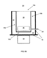
- the liquid silicon (the melt) 11 may be transferred into ladles from where it may be then outpoured into a mould 10 having an insulated bottom wall 10a, insulated side walls 10b, and an open top 10c.
- the mould 10 may have a rectangular, cylindrical, inverted-bell shape, or any other shape known to a person skilled in the art. It may also have a tap 24 provided thereon (see FIG. 1 B) .
- the side walls 10b and bottom wall 10a of the mould are insulated with an appropriate insulation, for example silica sand or some appropriate refractory lining, while the top 10c of the mould is open to allow the exposed surface of the melt to emit heat (see FIGs. 1A and 1B ). Accordingly, the solidification of the ingot along the side walls 10b and the bottom wall 10a should be negligible compared to that along the top 10c. Heating of the insulation is recommended in order to minimize the thickness of a silicon skin that may solidify and form on the walls of the mould 10.
- an appropriate insulation for example silica sand or some appropriate refractory lining
- FIGs. 1A , 1B , 2 , 3 , and 6 show a mould with an electromagnetic stirrer placed underneath the mould. Electromagnetic stirring, unlike conventional mechanical stirring, is a non-contact stirring, i.e. no part of the actual stirrer comes into contact with the molten metal.
- the rate of unidirectional solidification In order to minimize the quantity of impurity rich liquid silicon trapped by dendrite formation, the rate of unidirectional solidification must be controlled. Preferably, the rate of unidirectional solidification is less than 1x10 4 m/s or even more preferably comprised between 1x10 -4 m/s and 5x10 -6 m/s.
- the rate of unidirectional solidification may be controlled by controlling the rate of heat extraction from the open top 10c of the mould 10.
- heat extraction is understood to include heat removal and simple heat emission. This may be accomplished with the type of insulation used for the bottom and side walls as well as by placing the free surface of the melt at the open top of the mould in contact with a cooling medium 20, such as air or water.
- a cooling medium 20 such as air or water.
- the solidification can be slowed by using a light insulation or accelerated by using a water shower to cool the exposed free surface of the melt.
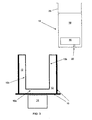
- the unidirectional solidification is stopped thus obtaining an ingot 19 having an exterior shell made of higher-purity solid polycrystalline silicon 18 and a center made of an impurity-enriched liquid silicon 16. Stopping the unidirectional solidification simply implies not allowing the melt to completely solidify and proceeding to the next step.
- a crack or an opening 22 is created in the exterior shell of the ingot 19 to outflow the impurity-enriched liquid silicon 16 from the center and leave behind the exterior shell of higher-purity solid polycrystalline silicon 18.
- the liquid silicon 16 may be extracted from the center of the ingot 19 by piercing the exterior shell of the ingot 19, for example by mechanical means or thermal lance, to create an opening 22 in the exterior shell of the ingot 19 through which the liquid silicon may be extracted.
- the actual extraction of the liquid silicon 16 from the ingot 19 may be done by tapping the ingot through a tap 24 found in the mould 10 (see FIG. 1 B) , either in the bottom wall 10a of the mould 10 or a side wall 10b.
- a thermal lance may be used to create an opening in the exterior shell of the ingot through the tap 24 in the mould 10 to outpour the liquid silicon 16.
- the process may further include an additional step before step (e) of removing the ingot 19 from the mould 10 (see FIG. 2 ), for example by lifting the ingot 19 out of the mould 10 using an appropriate suspension mechanism 26 (see FIG. 3 ). For example, in this way, while the ingot 19 is suspended in mid-air, the bottom portion of the ingot 19 is caused to crack, by piercing or quenching, to draw off the liquid silicon 16.
- a top portion of the higher-purity solid polycrystalline silicon thus obtained may contain approximately at least 90% less of contaminants Al, As, Ba, Bi, Ca, Cd, Co, Cr, Cu, Fe, K, La, Mg, Mn, Mo, Na, Ni, Pb, Sb, Sc, Sn, Sr, Ti, V, Zn, Zr than the silicon starting material.
- the higher-purity solid polycrystalline silicon may contain approximately at least 45% less phosphorus and approximately at least 10% less boron than the metallurgical grade silicon starting material.
- the impurity-enriched liquid silicon may contain less than 60 ppmw of carbon and less than 20 ppmw of oxygen and thus may provide a low carbon and low oxygen grade of silicon.
- step (a) to (e) - may be repeated using the higher purity solid polycrystalline silicon, a so-called medium purity silicon, as starting material to thereby obtain a final silicon material of an even higher purity, a so-called high purity silicon.
- solar grade silicon may be obtained from metallurgical grade silicon.
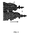
- Directional solidification is a common method of purification.
- Metallurgical grade silicon contains a significant level of impurities which favours structural supercooling during solidification.
- the type of solidification is dendritic, as shown in FIG. 4 .
- Dendritic solidification is a very inefficient directional solidification - a certain quantity of impurity-rich liquid (L) is trapped during solidification by the dendritic arms.
- Table 1 Element k eff Al 0.50 Ca 0.50 Co 0.50 Cr 0.50 Cu 0.50 Fe 0.50 Mg 0.50 Mn 0.50 Mo 0.50 Ni 0.50 P 0.68 Ti 0.50 V 0.50 Zr 0.50 B 0.90
- a purification efficiency of approximately 50% is obtained for a majority of the elements (except boron and phosphorus). In fact, about 30% of the phosphorus and 10% of boron can be removed by our technique of large mould segregation by directional solidification without electromagnetic stirring.
- the lower part of the ingot is typically richer in impurities than the upper part.
- An explanation for this could possibly be found in the difference in densities between the (cooler) impurity-rich liquid and that of the center of the ingot: the composition of the liquid is not homogeneous.
- the liquid may be separated from the solid by creating an opening or a crack in the shell for example by piercing the shell of the ingot (for example: by thermal lance, mechanical piercing, or other).
- the opening or crack may be obtained by solidifying the silicon in a mould provided with a closable outlet in the bottom portion. Once the liquid has solidified to the required degree, the outlet is opened and the shell pierced to draw off the liquid.
- the opening or crack can also be obtained by lifting up the shell from the mould with an appropriate suspension system. While the shell is in suspension in the air, the bottom portion is caused to crack by piercing or quenching to draw off the liquid.
- the ingot could also be completely solidified so as to then remove the portions that are of interest chemically.
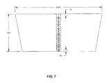
- the mould may have a rectangular or cylindrical shape. It could also have the shape of upside down bell or any other shape known to a person skilled in the art. (See FIGs. 1 to 3 )
- the final silicon solid contains fewer impurities (i.e. is depleted of impurities) while the liquid at the center of the ingot is enriched in impurities.
- the quantity of liquid silicon is 5.0 mt and the composition of the liquid silicon includes 0.35% Fe.
- the dendrites trap impurity-rich liquid coming from a diffusion layer at the solid/liquid interface.
- planar solidification front may be promoted.
- a certain quantity of solute may be trapped with planar solidification, but this quantity is far less than that trapped during dendritic solidification.
- a planar directional solidification may be promoted by allowing heat to escape from a single surface of the ingot.
- the liquid should preferably be agitated, stirred.
- the walls of the mould may be insulated (as shown in FIGs. 1 to 3 ) while the top may be open to allow heat to be emitted therefrom (the solidification of the melt can be slowed by a light insulation or accelerated by a water shower). Accordingly, the solidification along the walls and the bottom should be negligible compared to that along the top of the ingot (heating of the insulation is recommended in order to minimize the thickness of the silicon skin solidified on the walls of the mould).
- Electromagnetic stirrers are known for stirring molten metal. For example, they are used to stir aluminum as it melts in a furnace.
- the electromagnetic stirrer utilizes the principle of a linear motor and differs from the conventional mechanical and decompression types as it is a non-contact stirrer in which no part touches the molten metal (see FIG. 6 ).
- a coil installed at the bottom of the mould generates a moving magnetic field (H) when a 3-phase AC voltage is applied to this coil (inductor).
- Electric power force is generated in the molten metal due to the action of the magnetic field (magnetic flux) and causes induction current (I) to flow.
- This current then acts with the magnetic field of the inductor to induce electromagnetic force (F) in the molten metal.
- the molten metal also moves. In other words, a stirring action is applied.
- this thrust has components in the horizontal direction and in the vertical direction, the molten metal flows diagonally upwards resulting in a uniform temperature and chemical composition in both the top and bottom layers of the molten metal.
- the speed of the solidification interface is fixed by the rate of heat loss.
- E is the thickess of the top solid layer of the ingot
- v is the rate of solidification at the interface
- t is the total time of solidification.
- Table 3 Element Theory k eff Experimental k eff Al 0.50 0.46 Ca 0.50 0.43 Co 0.50 0.43 Cr 0.50 0.71 Cu 0.50 0.49 Fe 0.50 0.49 Mg 0.50 0.49 Mn 0.50 0.49 Mo 0.50 0.75 Ni 0.50 0.50 P 0.68 0.70 Ti 0.50 0.48 V 0.50 0.50 Zr 0.50 0.50 B 0.90 0.92
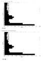
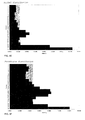
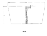
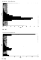
- FIG. 10A to 10H A sample was taken from the center of the ingot, according to the diagram shown in FIG. 9 , and analyzed the results are given hereinbelow in Table 4.
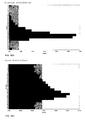
- FIGs. 10A to 10H A graphical representation of the elemental impurity distribution in the ingot as a function of position in the ingot of several of the elements is shown in FIGs. 10A to 10H .
- Electromagnetic agitation had a large effect on the distribution of impurities in the silicon ingot.
- the agitation prevented the separation of impurities towards the bottom of the silicon ingot.
- there was a large increase in the segregation of impurities the surface layer is much more pure.
- a more homogeneous liquid is obtained with electromagnetic agitation (i.e., electromagnetic stirring) of the melt during solidification of the melt.
- this procedure may be capable of removing more than 50% of phosphorus and makes the method very interesting for the production of Solar Grade silicon from Metallurgic Grade silicon.
- the solidification speed may range between 10 -6 m/s and 10 -4 m/s. High solidification speeds may be achieved with this method as compared with other crystallization methods. This provides a cost effective solution for mass production of high-purity silicon.
- the outer layer (first skin of silicon) of the ingot freezes rapidly, relieving the heat in excess. Then the temperature of the liquid silicon drops to approximately 1410°C. At this moment, we obtain the minimum solubility values for carbon and oxygen.
Landscapes
- Chemical & Material Sciences (AREA)
- Organic Chemistry (AREA)
- Engineering & Computer Science (AREA)
- Crystallography & Structural Chemistry (AREA)
- Materials Engineering (AREA)
- Metallurgy (AREA)
- Inorganic Chemistry (AREA)
- Silicon Compounds (AREA)
Claims (17)
- Verfahren zum Reinigen von Silicium metallurgischer Qualität mit geringer Reinheit, das wenigstens einen der folgenden Kontaminanten Al, As, Ba, Bi, Ca, Cd, Fe, Co, Cr, Cu, Fe, La, Mg, Mn, Mo, Na, Ni, P, Pb, Sb, Sc, Sn, Sr, Ti, V, Zn, Zr und B enthält, und Gewinnen eines festen polykristallinen Siliciums höherer Reinheit, wobei das Verfahren die folgenden Schritte umfasst:(a) Fassen einer Schmelze von Silicium metallurgischer Qualität mit geringer Reinheit in einer Form, wobei die Form eine isolierte Bodenwand, isolierte Seitenwände und eine offene Oberseite aufweist;(b) Verfestigen der Schmelze durch unidirektionale Verfestigung ausgehend von der offenen Oberseite hin zu der isolierten Bodenwand der Form, während die Schmelze elektromagnetisch gerührt wird;(c) Steuern der Geschwindigkeit der unidirektionalen Verfestigung;(d) Anhalten der unidirektionalen Verfestigung, wenn die Schmelze teilweise so erstarrt ist, dass ein Block mit einer äußeren Hülle, die das feste polykristalline Silicium höherer Reinheit umfasst, und einer Mitte, die ein an Verunreinigungen angereichertes flüssiges Silicium umfasst, entstanden ist; und(e) Erzeugen einer Öffnung in der äußeren Hülle des Blocks, damit das an Verunreinigungen angereicherte flüssige Silicium abläuft und die äußere Hülle, die das feste polykristalline Silicium höherer Reinheit umfasst, zurückbleibt, wodurch man das feste polykristalline Silicium höherer Reinheit erhält.
- Verfahren gemäß Anspruch 1, wobei die isolierte Bodenwand und die isolierten Seitenwände erhitzt werden, um die Bildung einer Siliciumhaut auf der isolierten Bodenwand und den isolierten Seitenwänden der Form zu minimieren.
- Verfahren gemäß Anspruch 1, wobei die Geschwindigkeit der unidirektionalen Verfestigung durch eine Isolierung der isolierten Bodenwand und der isolierten Seitenwände gesteuert wird.
- Verfahren gemäß Anspruch 1, wobei die Geschwindigkeit der unidirektionalen Verfestigung dadurch gesteuert wird, dass man die Geschwindigkeit des Entweichens der Wärme aus der Schmelze an der offenen Oberseite der Form steuert.
- Verfahren gemäß Anspruch 4, wobei das Steuern der Geschwindigkeit des Entweichens der Wärme das In-Kontakt-Bringen eines Kühlmediums mit einer freien Oberfläche der Schmelze an der offenen Oberseite der Form umfasst.
- Verfahren gemäß Anspruch 5, wobei es sich bei dem Kühlmedium um Wasser oder Luft handelt.
- Verfahren gemäß Anspruch 1, wobei die Geschwindigkeit der unidirektionalen Verfestigung so bestimmt wird, dass die Dendritenbildung minimiert wird.
- Verfahren gemäß Anspruch 7, wobei die Geschwindigkeit der unidirektionalen Verfestigung kleiner als 1 x 10⁻⁴ m/s ist.
- Verfahren gemäß Anspruch 7, wobei die Geschwindigkeit der unidirektionalen Verfestigung zwischen 1 x 10⁻⁴ m/s und 5 x 10⁻⁶ m/s liegt.
- Verfahren gemäß Anspruch 1, wobei das Anhalten der unidirektionalen Verfestigung dann erfolgt, wenn 40 bis 80% der Schmelze verfestigt sind.
- Verfahren gemäß Anspruch 1, wobei das Erzeugen einer Öffnung in der äußeren Hülle des Blocks in Schritt (e) das Durchstechen der äußeren Hülle des Blocks mit mechanischen Mitteln oder einer thermischen Lanze umfasst.
- Verfahren gemäß Anspruch 1, wobei das Erzeugen einer Öffnung in der äußeren Hülle des Blocks in Schritt (e) durch eine Zapföffnung in der Form bewerkstelligt wird.
- Verfahren gemäß Anspruch 1, wobei das Verfahren weiterhin vor Schritt (e) einen zusätzlichen Schritt des Entnehmens des Blocks aus der Form umfasst.
- Verfahren gemäß Anspruch 1, wobei das Verfahren weiterhin einen zusätzlichen Schritt (f) des Schmelzens des festen polykristallinen Siliciums höherer Reinheit und des Wiederholens der Schritte (b) bis (e) umfasst.
- Verfahren gemäß Anspruch 1, wobei der obere Teil des festen polykristallinen Siliciums höherer Reinheit wenigstens 90% weniger Metallkontaminanten Al, As, Ba, Bi, Ca, Cd, Co, Cr, Cu, Fe, K, La, Mg, Mn, Mo, Na, Ni, Pb, Sb, Sc, Sn, Sr, Ti, V, Zn und Zr enthält als das Silicium metallurgischer Qualität mit geringer Reinheit.
- Verfahren gemäß Anspruch 1, wobei das feste polykristalline Silicium höherer Reinheit ungefähr wenigstens 45% weniger Phosphor und ungefähr wenigstens 10% weniger Bor enthält als das Silicium metallurgischer Qualität mit geringer Reinheit.
- Verfahren gemäß Anspruch 1, wobei das an Verunreinigungen angereicherte flüssige Silicium weniger als 60 ppm Kohlenstoff und weniger als 20 ppm Sauerstoff enthält und eine kohlenstoffarme und sauerstoffarme Siliciumqualität darstellt.
Applications Claiming Priority (2)
| Application Number | Priority Date | Filing Date | Title |
|---|---|---|---|
| US96006107P | 2007-09-13 | 2007-09-13 | |
| PCT/CA2008/000492 WO2009033255A1 (en) | 2007-09-13 | 2008-03-13 | Process for the production of medium and high purity silicon from metallurgical grade silicon |
Publications (3)
| Publication Number | Publication Date |
|---|---|
| EP2212249A1 EP2212249A1 (de) | 2010-08-04 |
| EP2212249A4 EP2212249A4 (de) | 2012-08-15 |
| EP2212249B1 true EP2212249B1 (de) | 2015-01-14 |
Family
ID=40451503
Family Applications (1)
| Application Number | Title | Priority Date | Filing Date |
|---|---|---|---|
| EP08733596.4A Active EP2212249B1 (de) | 2007-09-13 | 2008-03-13 | Verfahren zur herstellung von mittel- und hochreinem silicium aus metallurgischem silicium |
Country Status (16)
| Country | Link |
|---|---|
| US (1) | US7727502B2 (de) |
| EP (1) | EP2212249B1 (de) |
| JP (1) | JP2010538952A (de) |
| KR (1) | KR20100061510A (de) |
| CN (1) | CN101868422B (de) |
| AU (1) | AU2008299523A1 (de) |
| BR (1) | BRPI0816972A2 (de) |
| CA (1) | CA2695393C (de) |
| EA (1) | EA017480B1 (de) |
| ES (1) | ES2530720T3 (de) |
| MX (1) | MX2010002728A (de) |
| MY (1) | MY143807A (de) |
| NO (1) | NO20100512L (de) |
| UA (1) | UA97691C2 (de) |
| WO (1) | WO2009033255A1 (de) |
| ZA (1) | ZA201000882B (de) |
Families Citing this family (15)
| Publication number | Priority date | Publication date | Assignee | Title |
|---|---|---|---|---|
| EP2172424A4 (de) * | 2007-06-08 | 2012-03-07 | Shinetsu Chemical Co | Verfahren zur verfestigung von metallischem silicium |
| JP4748187B2 (ja) * | 2007-12-27 | 2011-08-17 | 国立大学法人東北大学 | Si結晶インゴットの製造方法 |
| KR20130063501A (ko) | 2010-05-20 | 2013-06-14 | 다우 코닝 코포레이션 | 알루미늄-규소 합금을 생성하기 위한 방법 및 시스템 |
| JP2012106886A (ja) * | 2010-11-17 | 2012-06-07 | Nippon Steel Materials Co Ltd | 金属シリコンの凝固精製方法及び装置 |
| CN102275931B (zh) * | 2011-07-05 | 2013-05-29 | 兰州大学 | 氢氧焰等离子体提纯冶金级多晶硅粉体的方法 |
| CN103443296B (zh) * | 2011-07-18 | 2015-06-03 | Abb研究有限公司 | 用于控制熔化过程的方法和控制系统 |
| CN103266350B (zh) * | 2013-05-31 | 2015-08-12 | 大连理工大学 | 多晶硅铸锭硅真空固液分离方法及分离设备 |
| CN103266349B (zh) * | 2013-05-31 | 2015-07-15 | 大连理工大学 | 高纯中空硅材料、多晶硅铸锭硅真空固液分离方法及设备 |
| JP6401051B2 (ja) * | 2014-12-26 | 2018-10-03 | 京セラ株式会社 | 多結晶シリコンインゴットの製造方法 |
| RU2632827C2 (ru) * | 2015-12-08 | 2017-10-10 | Общество с ограниченной ответственностью "Современные химические и металлургические технологии" (ООО "СХИМТ") | Устройство для рафинирования кремния |
| CN107255572B (zh) * | 2017-05-12 | 2020-04-21 | 宜昌南玻硅材料有限公司 | 半熔铸锭工艺中硅锭的少子寿命抽样方法 |
| JP6919633B2 (ja) | 2018-08-29 | 2021-08-18 | 信越半導体株式会社 | 単結晶育成方法 |
| EP3847131B1 (de) * | 2019-04-30 | 2023-03-01 | Wacker Chemie AG | Verfahren zur raffination von rohsilicium-schmelzen mittels eines partikulären mediators |
| CN111675222B (zh) * | 2020-07-13 | 2022-08-09 | 昆明理工大学 | 一种利用低品位硅石生产工业硅的方法 |
| EP4082966A1 (de) | 2021-04-26 | 2022-11-02 | Ferroglobe Innovation, S.L. | Verfahren zur gewinnung von gereinigtem siliziummetall |
Family Cites Families (59)
| Publication number | Priority date | Publication date | Assignee | Title |
|---|---|---|---|---|
| US2890139A (en) * | 1956-12-10 | 1959-06-09 | Shockley William | Semi-conductive material purification method and apparatus |
| US3012865A (en) * | 1957-11-25 | 1961-12-12 | Du Pont | Silicon purification process |
| US3752221A (en) * | 1969-10-30 | 1973-08-14 | United Aircraft Corp | Mold apparatus for casting with downward unidirectional solidification |
| US4094731A (en) * | 1976-06-21 | 1978-06-13 | Interlake, Inc. | Method of purifying silicon |
| US4298423A (en) * | 1976-12-16 | 1981-11-03 | Semix Incorporated | Method of purifying silicon |
| US4200621A (en) * | 1978-07-18 | 1980-04-29 | Motorola, Inc. | Sequential purification and crystal growth |
| US4242175A (en) * | 1978-12-26 | 1980-12-30 | Zumbrunnen Allen D | Silicon refining process |
| GB2052461B (en) * | 1979-05-24 | 1983-04-07 | Aluminum Co Of America | Silicon purification method |
| US4304703A (en) * | 1980-06-23 | 1981-12-08 | Ppg Industries, Inc. | Cationic polymer dispersions and their method of preparation |
| DE3150539A1 (de) | 1981-12-21 | 1983-06-30 | Siemens AG, 1000 Berlin und 8000 München | Verfahren zum herstellen von fuer halbleiterbauelemente, insbesondere fuer solarzellen, verwendbarem silizium |
| FR2524489A1 (fr) * | 1982-03-30 | 1983-10-07 | Pechiney Aluminium | Procede de purification de metaux par segregation |
| DE3220285A1 (de) | 1982-05-28 | 1983-12-01 | Siemens AG, 1000 Berlin und 8000 München | Verfahren zum herstellen polykristalliner, fuer nachfolgendes zonenschmelzen geeigneter siliciumstaebe |
| NO152551C (no) * | 1983-02-07 | 1985-10-16 | Elkem As | Fremgangsmaate til fremstilling av rent silisium. |
| DE3310827A1 (de) * | 1983-03-24 | 1984-09-27 | Bayer Ag, 5090 Leverkusen | Verfahren zur herstellung von grobkristallinem silicium |
| DE3323896A1 (de) | 1983-07-02 | 1985-01-17 | Leybold-Heraeus GmbH, 5000 Köln | Verfahren und vorrichtung zum gerichteten erstarren von schmelzen |
| JPH0753569B2 (ja) * | 1986-08-07 | 1995-06-07 | 昭和アルミニウム株式会社 | ケイ素の精製方法 |
| JPH0696444B2 (ja) | 1987-08-27 | 1994-11-30 | 川崎製鉄株式会社 | 高純度シリコンの製造方法 |
| DE3802531A1 (de) | 1988-01-28 | 1989-08-17 | Siemens Ag | Verfahren zum abtrennen von festen partikeln aus siliziumschmelzen |
| DE3804248A1 (de) | 1988-02-11 | 1989-08-24 | Siemens Ag | Verfahren zum abtrennen von verunreinigungen aus einer siliziumschmelze durch gerichtete erstarrung |
| DE3929635A1 (de) | 1989-09-06 | 1991-03-07 | Siemens Ag | Verfahren zum abtrennen fester partikel aus siliziumschmelzen |
| JPH05124809A (ja) | 1991-10-30 | 1993-05-21 | Nippon Sheet Glass Co Ltd | シリコンの凝固精製法 |
| JP3263104B2 (ja) | 1991-11-27 | 2002-03-04 | 川崎製鉄株式会社 | 金属シリコンの精製方法 |
| JPH05254817A (ja) | 1992-03-12 | 1993-10-05 | Kawasaki Steel Corp | 多結晶シリコン鋳塊の製造方法 |
| WO1997003922A1 (fr) | 1994-01-10 | 1997-02-06 | Showa Aluminum Corporation | Procede pour produire du silicium tres pur |
| JP3140300B2 (ja) | 1994-03-29 | 2001-03-05 | 川崎製鉄株式会社 | シリコンの精製方法および精製装置 |
| NO180532C (no) * | 1994-09-01 | 1997-05-07 | Elkem Materials | Fremgangsmåte for fjerning av forurensninger fra smeltet silisium |
| JPH0873297A (ja) | 1994-09-05 | 1996-03-19 | Shin Etsu Chem Co Ltd | 太陽電池用基板材料の製法とこれを用いた太陽電池 |
| JPH08217436A (ja) | 1995-02-17 | 1996-08-27 | Kawasaki Steel Corp | 金属シリコンの凝固精製方法、その装置及びその装置に用いる鋳型 |
| DE69616686T2 (de) * | 1995-08-04 | 2002-08-14 | Sharp K.K., Osaka | Vorrichtung zum Reinigen von Metallen |
| BR9611816A (pt) * | 1996-10-14 | 1999-07-13 | Kawasaki Steel Co | Processo e aparelho para fabricação de silício policristalino e processo para fabricação de pastilhas de silício para baterias solares |
| JPH10139415A (ja) | 1996-10-30 | 1998-05-26 | Kawasaki Steel Corp | 溶融シリコンの凝固精製方法 |
| JPH10182135A (ja) | 1996-12-20 | 1998-07-07 | Kawasaki Steel Corp | シリコンの凝固精製方法 |
| JPH10182129A (ja) | 1996-12-26 | 1998-07-07 | Kawasaki Steel Corp | 金属シリコンの精製方法 |
| JPH10182137A (ja) | 1996-12-26 | 1998-07-07 | Kawasaki Steel Corp | 太陽電池用シリコンの凝固精製方法及び装置 |
| JPH10182286A (ja) | 1996-12-26 | 1998-07-07 | Kawasaki Steel Corp | シリコンの連続鋳造方法 |
| JP3852147B2 (ja) | 1996-12-27 | 2006-11-29 | Jfeスチール株式会社 | 太陽電池用多結晶シリコン・インゴットの製造方法 |
| JPH10251008A (ja) | 1997-03-14 | 1998-09-22 | Kawasaki Steel Corp | 金属シリコンの凝固精製方法 |
| JPH10251009A (ja) | 1997-03-14 | 1998-09-22 | Kawasaki Steel Corp | 太陽電池用シリコンの凝固精製方法 |
| CA2232777C (en) * | 1997-03-24 | 2001-05-15 | Hiroyuki Baba | Method for producing silicon for use in solar cells |
| JPH10273313A (ja) | 1997-03-28 | 1998-10-13 | Kawasaki Steel Corp | 多結晶シリコン鋳塊の製造方法 |
| JPH10273311A (ja) | 1997-03-28 | 1998-10-13 | Kawasaki Steel Corp | 太陽電池用シリコンの精製方法及び装置 |
| JP3520957B2 (ja) * | 1997-06-23 | 2004-04-19 | シャープ株式会社 | 多結晶半導体インゴットの製造方法および装置 |
| JP3523986B2 (ja) * | 1997-07-02 | 2004-04-26 | シャープ株式会社 | 多結晶半導体の製造方法および製造装置 |
| US5972107A (en) * | 1997-08-28 | 1999-10-26 | Crystal Systems, Inc. | Method for purifying silicon |
| JP4003271B2 (ja) | 1998-01-12 | 2007-11-07 | Jfeスチール株式会社 | シリコンの一方向凝固装置 |
| JPH11310496A (ja) * | 1998-02-25 | 1999-11-09 | Mitsubishi Materials Corp | 一方向凝固組織を有するシリコンインゴットの製造方法およびその製造装置 |
| JP4365480B2 (ja) | 1999-06-07 | 2009-11-18 | 昭和電工株式会社 | 高純度シリコンの製造方法 |
| JP2001278613A (ja) | 2000-03-29 | 2001-10-10 | Kawasaki Steel Corp | シリコンの一方向凝固装置 |
| FR2827592B1 (fr) * | 2001-07-23 | 2003-08-22 | Invensil | Silicium metallurgique de haute purete et procede d'elaboration |
| FR2831881B1 (fr) | 2001-11-02 | 2004-01-16 | Hubert Lauvray | Procede de purification de silicium metallurgique par plasma inductif couple a une solidification directionnelle et obtention directe de silicium de qualite solaire |
| JP2003238137A (ja) | 2002-02-21 | 2003-08-27 | Kawatetsu Techno Res Corp | 太陽電池用多結晶シリコンの製造方法 |
| NO318092B1 (no) | 2002-05-22 | 2005-01-31 | Elkem Materials | Kalsium-silikatbasert slagg, fremgangsmate for fremstilling av kalsium-silikatbasert slagg, og anvendelse for slaggbehandling av smeltet silium |
| US20060048698A1 (en) * | 2002-09-27 | 2006-03-09 | Ge Energy (Usa) Llc | Methods and systems for purifying elements |
| CN1221470C (zh) | 2002-11-26 | 2005-10-05 | 郑智雄 | 高纯度硅的生产方法 |
| CN1299983C (zh) | 2003-07-22 | 2007-02-14 | 龚炳生 | 光电级硅的制造方法 |
| JP2007513048A (ja) | 2003-12-04 | 2007-05-24 | ダウ・コーニング・コーポレイション | 太陽電池グレードのケイ素を生産するための、冶金グレードのケイ素から不純物を除去する方法 |
| NO333319B1 (no) | 2003-12-29 | 2013-05-06 | Elkem As | Silisiummateriale for fremstilling av solceller |
| JP4115432B2 (ja) | 2004-07-14 | 2008-07-09 | シャープ株式会社 | 金属の精製方法 |
| WO2008031229A1 (en) * | 2006-09-14 | 2008-03-20 | Silicium Becancour Inc. | Process and apparatus for purifying low-grade silicon material |
-
2008
- 2008-03-13 WO PCT/CA2008/000492 patent/WO2009033255A1/en active Application Filing
- 2008-03-13 BR BRPI0816972 patent/BRPI0816972A2/pt not_active IP Right Cessation
- 2008-03-13 AU AU2008299523A patent/AU2008299523A1/en not_active Abandoned
- 2008-03-13 MY MYPI2010000616A patent/MY143807A/en unknown
- 2008-03-13 UA UAA201004264A patent/UA97691C2/ru unknown
- 2008-03-13 CA CA2695393A patent/CA2695393C/en active Active
- 2008-03-13 EA EA201070358A patent/EA017480B1/ru not_active IP Right Cessation
- 2008-03-13 CN CN200880106298.7A patent/CN101868422B/zh active Active
- 2008-03-13 KR KR1020107006648A patent/KR20100061510A/ko not_active Application Discontinuation
- 2008-03-13 ES ES08733596T patent/ES2530720T3/es active Active
- 2008-03-13 US US12/047,913 patent/US7727502B2/en active Active
- 2008-03-13 EP EP08733596.4A patent/EP2212249B1/de active Active
- 2008-03-13 JP JP2010524312A patent/JP2010538952A/ja not_active Withdrawn
- 2008-03-13 MX MX2010002728A patent/MX2010002728A/es active IP Right Grant
-
2010
- 2010-02-05 ZA ZA2010/00882A patent/ZA201000882B/en unknown
- 2010-04-08 NO NO20100512A patent/NO20100512L/no not_active Application Discontinuation
Also Published As
| Publication number | Publication date |
|---|---|
| EP2212249A1 (de) | 2010-08-04 |
| CN101868422A (zh) | 2010-10-20 |
| KR20100061510A (ko) | 2010-06-07 |
| ZA201000882B (en) | 2011-04-28 |
| UA97691C2 (ru) | 2012-03-12 |
| EA201070358A1 (ru) | 2010-08-30 |
| MY143807A (en) | 2011-07-15 |
| AU2008299523A1 (en) | 2009-03-19 |
| US7727502B2 (en) | 2010-06-01 |
| EA017480B1 (ru) | 2012-12-28 |
| MX2010002728A (es) | 2010-08-02 |
| NO20100512L (no) | 2010-04-08 |
| CA2695393A1 (en) | 2009-03-19 |
| BRPI0816972A2 (pt) | 2015-03-24 |
| ES2530720T3 (es) | 2015-03-04 |
| US20090074648A1 (en) | 2009-03-19 |
| CA2695393C (en) | 2012-01-03 |
| CN101868422B (zh) | 2013-10-09 |
| WO2009033255A1 (en) | 2009-03-19 |
| EP2212249A4 (de) | 2012-08-15 |
| JP2010538952A (ja) | 2010-12-16 |
Similar Documents
| Publication | Publication Date | Title |
|---|---|---|
| EP2212249B1 (de) | Verfahren zur herstellung von mittel- und hochreinem silicium aus metallurgischem silicium | |
| CN101423220B (zh) | 一种多温区硅材料提纯与铸锭的方法及其装置 | |
| US7858063B2 (en) | High purity metallurgical silicon and method for preparing same | |
| US7682585B2 (en) | Silicon refining process | |
| Li et al. | Si purity control and separation from Si–Al alloy melt with Zn addition | |
| US4312849A (en) | Phosphorous removal in silicon purification | |
| WO2013111314A1 (ja) | シリコン純化法 | |
| Wang et al. | Control of silicon solidification and the impurities from an Al–Si melt | |
| CA1130985A (en) | Silicon purification method | |
| CN104030291A (zh) | 一种用合金法高效去除硅中的磷的方法 | |
| He et al. | A review of the process on the purification of metallurgical grade silicon by solvent refining | |
| US4246249A (en) | Silicon purification process | |
| US4312848A (en) | Boron removal in silicon purification | |
| US20100178195A1 (en) | Method of solidifying metallic silicon | |
| US4312847A (en) | Silicon purification system | |
| CN104085893B (zh) | 利用Al-Si合金熔体连铸硅提纯装置及方法 | |
| JPH07206420A (ja) | 高純度ケイ素の製造方法 | |
| CN104071790B (zh) | 电磁搅拌硅合金熔体硅提纯装置及方法 | |
| Li et al. | Bulk Si production from Si–Fe melts by directional-solidification, part II: Element distribution | |
| US4312846A (en) | Method of silicon purification | |
| US9352970B2 (en) | Method for producing silicon for solar cells by metallurgical refining process | |
| EP4082966A1 (de) | Verfahren zur gewinnung von gereinigtem siliziummetall | |
| KR20090102199A (ko) | 저순도 실리콘 스크랩을 정련하여 태양 전지급 고순도실리콘 주괴를 제조하기 위한 시스템, 방법 및 그에 의해제조된 태양 전지급 고순도 실리콘 주괴 | |
| Delannoy et al. | Electromagnetic Processing of Materials at SIMaP: focus on Solar Silicon elaboration | |
| Pizzini | Solar grade silicon production from MG-Silicon |
Legal Events
| Date | Code | Title | Description |
|---|---|---|---|
| PUAI | Public reference made under article 153(3) epc to a published international application that has entered the european phase |
Free format text: ORIGINAL CODE: 0009012 |
|
| 17P | Request for examination filed |
Effective date: 20100408 |
|
| AK | Designated contracting states |
Kind code of ref document: A1 Designated state(s): AT BE BG CH CY CZ DE DK EE ES FI FR GB GR HR HU IE IS IT LI LT LU LV MC MT NL NO PL PT RO SE SI SK TR |
|
| AX | Request for extension of the european patent |
Extension state: AL BA MK RS |
|
| DAX | Request for extension of the european patent (deleted) | ||
| A4 | Supplementary search report drawn up and despatched |
Effective date: 20120712 |
|
| RIC1 | Information provided on ipc code assigned before grant |
Ipc: C01B 33/037 20060101AFI20120706BHEP |
|
| RAP1 | Party data changed (applicant data changed or rights of an application transferred) |
Owner name: SILICIO FERROSOLAR, S.L.U. |
|
| GRAP | Despatch of communication of intention to grant a patent |
Free format text: ORIGINAL CODE: EPIDOSNIGR1 |
|
| INTG | Intention to grant announced |
Effective date: 20140814 |
|
| GRAS | Grant fee paid |
Free format text: ORIGINAL CODE: EPIDOSNIGR3 |
|
| GRAA | (expected) grant |
Free format text: ORIGINAL CODE: 0009210 |
|
| AK | Designated contracting states |
Kind code of ref document: B1 Designated state(s): AT BE BG CH CY CZ DE DK EE ES FI FR GB GR HR HU IE IS IT LI LT LU LV MC MT NL NO PL PT RO SE SI SK TR |
|
| REG | Reference to a national code |
Ref country code: GB Ref legal event code: FG4D |
|
| REG | Reference to a national code |
Ref country code: CH Ref legal event code: EP |
|
| REG | Reference to a national code |
Ref country code: IE Ref legal event code: FG4D |
|
| REG | Reference to a national code |
Ref country code: AT Ref legal event code: REF Ref document number: 706939 Country of ref document: AT Kind code of ref document: T Effective date: 20150215 |
|
| REG | Reference to a national code |
Ref country code: DE Ref legal event code: R096 Ref document number: 602008036353 Country of ref document: DE Effective date: 20150226 |
|
| REG | Reference to a national code |
Ref country code: ES Ref legal event code: FG2A Ref document number: 2530720 Country of ref document: ES Kind code of ref document: T3 Effective date: 20150304 |
|
| REG | Reference to a national code |
Ref country code: NO Ref legal event code: T2 Effective date: 20150114 |
|
| REG | Reference to a national code |
Ref country code: NL Ref legal event code: VDEP Effective date: 20150114 |
|
| REG | Reference to a national code |
Ref country code: AT Ref legal event code: MK05 Ref document number: 706939 Country of ref document: AT Kind code of ref document: T Effective date: 20150114 |
|
| REG | Reference to a national code |
Ref country code: LT Ref legal event code: MG4D |
|
| PG25 | Lapsed in a contracting state [announced via postgrant information from national office to epo] |
Ref country code: SE Free format text: LAPSE BECAUSE OF FAILURE TO SUBMIT A TRANSLATION OF THE DESCRIPTION OR TO PAY THE FEE WITHIN THE PRESCRIBED TIME-LIMIT Effective date: 20150114 Ref country code: LT Free format text: LAPSE BECAUSE OF FAILURE TO SUBMIT A TRANSLATION OF THE DESCRIPTION OR TO PAY THE FEE WITHIN THE PRESCRIBED TIME-LIMIT Effective date: 20150114 Ref country code: FI Free format text: LAPSE BECAUSE OF FAILURE TO SUBMIT A TRANSLATION OF THE DESCRIPTION OR TO PAY THE FEE WITHIN THE PRESCRIBED TIME-LIMIT Effective date: 20150114 Ref country code: BG Free format text: LAPSE BECAUSE OF FAILURE TO SUBMIT A TRANSLATION OF THE DESCRIPTION OR TO PAY THE FEE WITHIN THE PRESCRIBED TIME-LIMIT Effective date: 20150414 Ref country code: HR Free format text: LAPSE BECAUSE OF FAILURE TO SUBMIT A TRANSLATION OF THE DESCRIPTION OR TO PAY THE FEE WITHIN THE PRESCRIBED TIME-LIMIT Effective date: 20150114 |
|
| PG25 | Lapsed in a contracting state [announced via postgrant information from national office to epo] |
Ref country code: PL Free format text: LAPSE BECAUSE OF FAILURE TO SUBMIT A TRANSLATION OF THE DESCRIPTION OR TO PAY THE FEE WITHIN THE PRESCRIBED TIME-LIMIT Effective date: 20150114 Ref country code: AT Free format text: LAPSE BECAUSE OF FAILURE TO SUBMIT A TRANSLATION OF THE DESCRIPTION OR TO PAY THE FEE WITHIN THE PRESCRIBED TIME-LIMIT Effective date: 20150114 Ref country code: NL Free format text: LAPSE BECAUSE OF FAILURE TO SUBMIT A TRANSLATION OF THE DESCRIPTION OR TO PAY THE FEE WITHIN THE PRESCRIBED TIME-LIMIT Effective date: 20150114 Ref country code: LV Free format text: LAPSE BECAUSE OF FAILURE TO SUBMIT A TRANSLATION OF THE DESCRIPTION OR TO PAY THE FEE WITHIN THE PRESCRIBED TIME-LIMIT Effective date: 20150114 Ref country code: GR Free format text: LAPSE BECAUSE OF FAILURE TO SUBMIT A TRANSLATION OF THE DESCRIPTION OR TO PAY THE FEE WITHIN THE PRESCRIBED TIME-LIMIT Effective date: 20150415 |
|
| REG | Reference to a national code |
Ref country code: DE Ref legal event code: R097 Ref document number: 602008036353 Country of ref document: DE |
|
| PG25 | Lapsed in a contracting state [announced via postgrant information from national office to epo] |
Ref country code: DK Free format text: LAPSE BECAUSE OF FAILURE TO SUBMIT A TRANSLATION OF THE DESCRIPTION OR TO PAY THE FEE WITHIN THE PRESCRIBED TIME-LIMIT Effective date: 20150114 Ref country code: CZ Free format text: LAPSE BECAUSE OF FAILURE TO SUBMIT A TRANSLATION OF THE DESCRIPTION OR TO PAY THE FEE WITHIN THE PRESCRIBED TIME-LIMIT Effective date: 20150114 Ref country code: SK Free format text: LAPSE BECAUSE OF FAILURE TO SUBMIT A TRANSLATION OF THE DESCRIPTION OR TO PAY THE FEE WITHIN THE PRESCRIBED TIME-LIMIT Effective date: 20150114 Ref country code: MC Free format text: LAPSE BECAUSE OF FAILURE TO SUBMIT A TRANSLATION OF THE DESCRIPTION OR TO PAY THE FEE WITHIN THE PRESCRIBED TIME-LIMIT Effective date: 20150114 Ref country code: EE Free format text: LAPSE BECAUSE OF FAILURE TO SUBMIT A TRANSLATION OF THE DESCRIPTION OR TO PAY THE FEE WITHIN THE PRESCRIBED TIME-LIMIT Effective date: 20150114 Ref country code: RO Free format text: LAPSE BECAUSE OF FAILURE TO SUBMIT A TRANSLATION OF THE DESCRIPTION OR TO PAY THE FEE WITHIN THE PRESCRIBED TIME-LIMIT Effective date: 20150114 Ref country code: LU Free format text: LAPSE BECAUSE OF FAILURE TO SUBMIT A TRANSLATION OF THE DESCRIPTION OR TO PAY THE FEE WITHIN THE PRESCRIBED TIME-LIMIT Effective date: 20150313 |
|
| REG | Reference to a national code |
Ref country code: CH Ref legal event code: PL |
|
| PLBE | No opposition filed within time limit |
Free format text: ORIGINAL CODE: 0009261 |
|
| STAA | Information on the status of an ep patent application or granted ep patent |
Free format text: STATUS: NO OPPOSITION FILED WITHIN TIME LIMIT |
|
| 26N | No opposition filed |
Effective date: 20151015 |
|
| PG25 | Lapsed in a contracting state [announced via postgrant information from national office to epo] |
Ref country code: IT Free format text: LAPSE BECAUSE OF FAILURE TO SUBMIT A TRANSLATION OF THE DESCRIPTION OR TO PAY THE FEE WITHIN THE PRESCRIBED TIME-LIMIT Effective date: 20150114 |
|
| REG | Reference to a national code |
Ref country code: IE Ref legal event code: MM4A |
|
| PG25 | Lapsed in a contracting state [announced via postgrant information from national office to epo] |
Ref country code: LI Free format text: LAPSE BECAUSE OF NON-PAYMENT OF DUE FEES Effective date: 20150331 Ref country code: CH Free format text: LAPSE BECAUSE OF NON-PAYMENT OF DUE FEES Effective date: 20150331 Ref country code: IE Free format text: LAPSE BECAUSE OF NON-PAYMENT OF DUE FEES Effective date: 20150313 |
|
| PG25 | Lapsed in a contracting state [announced via postgrant information from national office to epo] |
Ref country code: SI Free format text: LAPSE BECAUSE OF FAILURE TO SUBMIT A TRANSLATION OF THE DESCRIPTION OR TO PAY THE FEE WITHIN THE PRESCRIBED TIME-LIMIT Effective date: 20150114 |
|
| REG | Reference to a national code |
Ref country code: FR Ref legal event code: PLFP Year of fee payment: 9 |
|
| PG25 | Lapsed in a contracting state [announced via postgrant information from national office to epo] |
Ref country code: BE Free format text: LAPSE BECAUSE OF FAILURE TO SUBMIT A TRANSLATION OF THE DESCRIPTION OR TO PAY THE FEE WITHIN THE PRESCRIBED TIME-LIMIT Effective date: 20150114 |
|
| PG25 | Lapsed in a contracting state [announced via postgrant information from national office to epo] |
Ref country code: MT Free format text: LAPSE BECAUSE OF FAILURE TO SUBMIT A TRANSLATION OF THE DESCRIPTION OR TO PAY THE FEE WITHIN THE PRESCRIBED TIME-LIMIT Effective date: 20150114 |
|
| REG | Reference to a national code |
Ref country code: FR Ref legal event code: PLFP Year of fee payment: 10 |
|
| PG25 | Lapsed in a contracting state [announced via postgrant information from national office to epo] |
Ref country code: HU Free format text: LAPSE BECAUSE OF FAILURE TO SUBMIT A TRANSLATION OF THE DESCRIPTION OR TO PAY THE FEE WITHIN THE PRESCRIBED TIME-LIMIT; INVALID AB INITIO Effective date: 20080313 |
|
| PG25 | Lapsed in a contracting state [announced via postgrant information from national office to epo] |
Ref country code: CY Free format text: LAPSE BECAUSE OF FAILURE TO SUBMIT A TRANSLATION OF THE DESCRIPTION OR TO PAY THE FEE WITHIN THE PRESCRIBED TIME-LIMIT Effective date: 20150114 |
|
| PG25 | Lapsed in a contracting state [announced via postgrant information from national office to epo] |
Ref country code: PT Free format text: LAPSE BECAUSE OF FAILURE TO SUBMIT A TRANSLATION OF THE DESCRIPTION OR TO PAY THE FEE WITHIN THE PRESCRIBED TIME-LIMIT Effective date: 20150514 |
|
| PG25 | Lapsed in a contracting state [announced via postgrant information from national office to epo] |
Ref country code: TR Free format text: LAPSE BECAUSE OF FAILURE TO SUBMIT A TRANSLATION OF THE DESCRIPTION OR TO PAY THE FEE WITHIN THE PRESCRIBED TIME-LIMIT Effective date: 20150114 |
|
| REG | Reference to a national code |
Ref country code: FR Ref legal event code: PLFP Year of fee payment: 11 |
|
| REG | Reference to a national code |
Ref country code: NO Ref legal event code: CREP Representative=s name: TANDBERG INNOVATION AS, POSTBOKS 1570 VIKA, 0118 |
|
| REG | Reference to a national code |
Ref country code: DE Ref legal event code: R081 Ref document number: 602008036353 Country of ref document: DE Owner name: FERROGLOBE INNOVATION, S.L., ES Free format text: FORMER OWNER: SILICIO FERROSOLAR, S.L.U., MADRID, ES |
|
| REG | Reference to a national code |
Ref country code: ES Ref legal event code: PC2A Owner name: FERROGLOBE INNOVATION, S.L. Effective date: 20210413 |
|
| PGFP | Annual fee paid to national office [announced via postgrant information from national office to epo] |
Ref country code: IS Payment date: 20240221 Year of fee payment: 17 |
|
| PGFP | Annual fee paid to national office [announced via postgrant information from national office to epo] |
Ref country code: DE Payment date: 20240327 Year of fee payment: 17 Ref country code: GB Payment date: 20240320 Year of fee payment: 17 |
|
| PGFP | Annual fee paid to national office [announced via postgrant information from national office to epo] |
Ref country code: NO Payment date: 20240229 Year of fee payment: 17 Ref country code: FR Payment date: 20240222 Year of fee payment: 17 |
|
| PGFP | Annual fee paid to national office [announced via postgrant information from national office to epo] |
Ref country code: ES Payment date: 20240401 Year of fee payment: 17 |